EP3667708A1 - Procédé d'encapsulation de diodes électroluminescentes - Google Patents
Procédé d'encapsulation de diodes électroluminescentes Download PDFInfo
- Publication number
- EP3667708A1 EP3667708A1 EP20156945.6A EP20156945A EP3667708A1 EP 3667708 A1 EP3667708 A1 EP 3667708A1 EP 20156945 A EP20156945 A EP 20156945A EP 3667708 A1 EP3667708 A1 EP 3667708A1
- Authority
- EP
- European Patent Office
- Prior art keywords
- matrix material
- leds
- led
- formation cavity
- semiconductor devices
- Prior art date
- Legal status (The legal status is an assumption and is not a legal conclusion. Google has not performed a legal analysis and makes no representation as to the accuracy of the status listed.)
- Pending
Links
- 238000000034 method Methods 0.000 title abstract description 76
- 239000000463 material Substances 0.000 claims abstract description 93
- 239000004065 semiconductor Substances 0.000 claims abstract description 71
- 238000006243 chemical reaction Methods 0.000 claims abstract description 31
- 239000011159 matrix material Substances 0.000 claims description 135
- 239000004593 Epoxy Substances 0.000 claims description 13
- 229920001296 polysiloxane Polymers 0.000 claims description 13
- 239000008393 encapsulating agent Substances 0.000 claims 2
- 230000015572 biosynthetic process Effects 0.000 abstract description 95
- 238000000576 coating method Methods 0.000 abstract description 91
- 239000011248 coating agent Substances 0.000 abstract description 90
- 239000002245 particle Substances 0.000 abstract description 19
- 239000010410 layer Substances 0.000 description 45
- 238000001723 curing Methods 0.000 description 23
- 239000002313 adhesive film Substances 0.000 description 16
- OAICVXFJPJFONN-UHFFFAOYSA-N Phosphorus Chemical compound [P] OAICVXFJPJFONN-UHFFFAOYSA-N 0.000 description 15
- 125000006850 spacer group Chemical group 0.000 description 13
- 239000000758 substrate Substances 0.000 description 7
- 239000000203 mixture Substances 0.000 description 6
- 229920000642 polymer Polymers 0.000 description 6
- 239000008151 electrolyte solution Substances 0.000 description 5
- 238000013007 heat curing Methods 0.000 description 5
- 229910052909 inorganic silicate Inorganic materials 0.000 description 5
- 239000000853 adhesive Substances 0.000 description 4
- 230000001070 adhesive effect Effects 0.000 description 4
- 239000004020 conductor Substances 0.000 description 4
- 238000007796 conventional method Methods 0.000 description 4
- 239000011888 foil Substances 0.000 description 4
- 229910052733 gallium Inorganic materials 0.000 description 4
- 230000003287 optical effect Effects 0.000 description 4
- 239000000243 solution Substances 0.000 description 4
- 238000010586 diagram Methods 0.000 description 3
- 239000011521 glass Substances 0.000 description 3
- 238000002347 injection Methods 0.000 description 3
- 239000007924 injection Substances 0.000 description 3
- 229910052751 metal Inorganic materials 0.000 description 3
- 239000002184 metal Substances 0.000 description 3
- 238000000926 separation method Methods 0.000 description 3
- 229910052727 yttrium Inorganic materials 0.000 description 3
- 229910002370 SrTiO3 Inorganic materials 0.000 description 2
- 229910019990 cerium-doped yttrium aluminum garnet Inorganic materials 0.000 description 2
- 238000004140 cleaning Methods 0.000 description 2
- 239000011247 coating layer Substances 0.000 description 2
- 238000005520 cutting process Methods 0.000 description 2
- 230000005684 electric field Effects 0.000 description 2
- 238000005530 etching Methods 0.000 description 2
- 238000000605 extraction Methods 0.000 description 2
- 238000011049 filling Methods 0.000 description 2
- 229910003443 lutetium oxide Inorganic materials 0.000 description 2
- 150000004767 nitrides Chemical class 0.000 description 2
- 239000007787 solid Substances 0.000 description 2
- 229910052725 zinc Inorganic materials 0.000 description 2
- 229910001477 LaPO4 Inorganic materials 0.000 description 1
- 229910003383 SrSiO3 Inorganic materials 0.000 description 1
- 229910052771 Terbium Inorganic materials 0.000 description 1
- GWEVSGVZZGPLCZ-UHFFFAOYSA-N Titan oxide Chemical compound O=[Ti]=O GWEVSGVZZGPLCZ-UHFFFAOYSA-N 0.000 description 1
- 229910009372 YVO4 Inorganic materials 0.000 description 1
- 229910052782 aluminium Inorganic materials 0.000 description 1
- XAGFODPZIPBFFR-UHFFFAOYSA-N aluminium Chemical compound [Al] XAGFODPZIPBFFR-UHFFFAOYSA-N 0.000 description 1
- 239000011230 binding agent Substances 0.000 description 1
- 239000003086 colorant Substances 0.000 description 1
- 150000001875 compounds Chemical class 0.000 description 1
- 238000001816 cooling Methods 0.000 description 1
- 239000003792 electrolyte Substances 0.000 description 1
- 238000001652 electrophoretic deposition Methods 0.000 description 1
- 238000000295 emission spectrum Methods 0.000 description 1
- 238000005538 encapsulation Methods 0.000 description 1
- 230000005284 excitation Effects 0.000 description 1
- 229910052738 indium Inorganic materials 0.000 description 1
- 238000001746 injection moulding Methods 0.000 description 1
- 238000004519 manufacturing process Methods 0.000 description 1
- 239000011148 porous material Substances 0.000 description 1
- 230000001681 protective effect Effects 0.000 description 1
- 229920005573 silicon-containing polymer Polymers 0.000 description 1
- 230000000087 stabilizing effect Effects 0.000 description 1
- 229910001220 stainless steel Inorganic materials 0.000 description 1
- 239000010935 stainless steel Substances 0.000 description 1
- 229920001187 thermosetting polymer Polymers 0.000 description 1
- 229910019901 yttrium aluminum garnet Inorganic materials 0.000 description 1
Images


Classifications
-
- H—ELECTRICITY
- H01—ELECTRIC ELEMENTS
- H01L—SEMICONDUCTOR DEVICES NOT COVERED BY CLASS H10
- H01L33/00—Semiconductor devices with at least one potential-jump barrier or surface barrier specially adapted for light emission; Processes or apparatus specially adapted for the manufacture or treatment thereof or of parts thereof; Details thereof
- H01L33/48—Semiconductor devices with at least one potential-jump barrier or surface barrier specially adapted for light emission; Processes or apparatus specially adapted for the manufacture or treatment thereof or of parts thereof; Details thereof characterised by the semiconductor body packages
- H01L33/50—Wavelength conversion elements
- H01L33/501—Wavelength conversion elements characterised by the materials, e.g. binder
- H01L33/502—Wavelength conversion materials
- H01L33/504—Elements with two or more wavelength conversion materials
-
- H—ELECTRICITY
- H01—ELECTRIC ELEMENTS
- H01L—SEMICONDUCTOR DEVICES NOT COVERED BY CLASS H10
- H01L21/00—Processes or apparatus adapted for the manufacture or treatment of semiconductor or solid state devices or of parts thereof
- H01L21/02—Manufacture or treatment of semiconductor devices or of parts thereof
- H01L21/04—Manufacture or treatment of semiconductor devices or of parts thereof the devices having at least one potential-jump barrier or surface barrier, e.g. PN junction, depletion layer or carrier concentration layer
- H01L21/50—Assembly of semiconductor devices using processes or apparatus not provided for in a single one of the subgroups H01L21/06 - H01L21/326, e.g. sealing of a cap to a base of a container
- H01L21/56—Encapsulations, e.g. encapsulation layers, coatings
- H01L21/565—Moulds
-
- H—ELECTRICITY
- H01—ELECTRIC ELEMENTS
- H01L—SEMICONDUCTOR DEVICES NOT COVERED BY CLASS H10
- H01L24/00—Arrangements for connecting or disconnecting semiconductor or solid-state bodies; Methods or apparatus related thereto
- H01L24/93—Batch processes
- H01L24/95—Batch processes at chip-level, i.e. with connecting carried out on a plurality of singulated devices, i.e. on diced chips
- H01L24/96—Batch processes at chip-level, i.e. with connecting carried out on a plurality of singulated devices, i.e. on diced chips the devices being encapsulated in a common layer, e.g. neo-wafer or pseudo-wafer, said common layer being separable into individual assemblies after connecting
-
- H—ELECTRICITY
- H01—ELECTRIC ELEMENTS
- H01L—SEMICONDUCTOR DEVICES NOT COVERED BY CLASS H10
- H01L27/00—Devices consisting of a plurality of semiconductor or other solid-state components formed in or on a common substrate
- H01L27/15—Devices consisting of a plurality of semiconductor or other solid-state components formed in or on a common substrate including semiconductor components with at least one potential-jump barrier or surface barrier specially adapted for light emission
-
- H—ELECTRICITY
- H01—ELECTRIC ELEMENTS
- H01L—SEMICONDUCTOR DEVICES NOT COVERED BY CLASS H10
- H01L33/00—Semiconductor devices with at least one potential-jump barrier or surface barrier specially adapted for light emission; Processes or apparatus specially adapted for the manufacture or treatment thereof or of parts thereof; Details thereof
- H01L33/48—Semiconductor devices with at least one potential-jump barrier or surface barrier specially adapted for light emission; Processes or apparatus specially adapted for the manufacture or treatment thereof or of parts thereof; Details thereof characterised by the semiconductor body packages
- H01L33/50—Wavelength conversion elements
-
- H—ELECTRICITY
- H01—ELECTRIC ELEMENTS
- H01L—SEMICONDUCTOR DEVICES NOT COVERED BY CLASS H10
- H01L2224/00—Indexing scheme for arrangements for connecting or disconnecting semiconductor or solid-state bodies and methods related thereto as covered by H01L24/00
- H01L2224/01—Means for bonding being attached to, or being formed on, the surface to be connected, e.g. chip-to-package, die-attach, "first-level" interconnects; Manufacturing methods related thereto
- H01L2224/18—High density interconnect [HDI] connectors; Manufacturing methods related thereto
- H01L2224/23—Structure, shape, material or disposition of the high density interconnect connectors after the connecting process
- H01L2224/25—Structure, shape, material or disposition of the high density interconnect connectors after the connecting process of a plurality of high density interconnect connectors
- H01L2224/251—Disposition
- H01L2224/2518—Disposition being disposed on at least two different sides of the body, e.g. dual array
-
- H—ELECTRICITY
- H01—ELECTRIC ELEMENTS
- H01L—SEMICONDUCTOR DEVICES NOT COVERED BY CLASS H10
- H01L2924/00—Indexing scheme for arrangements or methods for connecting or disconnecting semiconductor or solid-state bodies as covered by H01L24/00
- H01L2924/10—Details of semiconductor or other solid state devices to be connected
- H01L2924/11—Device type
- H01L2924/12—Passive devices, e.g. 2 terminal devices
- H01L2924/1204—Optical Diode
- H01L2924/12041—LED
-
- H—ELECTRICITY
- H01—ELECTRIC ELEMENTS
- H01L—SEMICONDUCTOR DEVICES NOT COVERED BY CLASS H10
- H01L2924/00—Indexing scheme for arrangements or methods for connecting or disconnecting semiconductor or solid-state bodies as covered by H01L24/00
- H01L2924/15—Details of package parts other than the semiconductor or other solid state devices to be connected
- H01L2924/181—Encapsulation
- H01L2924/1815—Shape
-
- H—ELECTRICITY
- H01—ELECTRIC ELEMENTS
- H01L—SEMICONDUCTOR DEVICES NOT COVERED BY CLASS H10
- H01L2933/00—Details relating to devices covered by the group H01L33/00 but not provided for in its subgroups
- H01L2933/0008—Processes
- H01L2933/0033—Processes relating to semiconductor body packages
- H01L2933/0041—Processes relating to semiconductor body packages relating to wavelength conversion elements
Definitions
- This invention relates to coating of semiconductor devices and more particularly to a method and apparatus for coating light emitting diodes (LEDs) with a matrix material containing one or more light conversion materials.
- LEDs light emitting diodes
- LEDs are solid-state devices that convert electric energy to light and they generally comprise an active layer of semiconductor material sandwiched between two oppositely doped layers. When a bias is applied across the doped layers, holes and electrons are injected into the active layer where they recombine to generate light that is emitted omnidirectionally from the active layer and from all surfaces of the LED. Recent advances in LEDs (such as Group III nitride based LEDs) have resulted in highly efficient light sources that surpass the efficiency of filament-based light sources, providing light with equal or greater brightness in relation to input power.
- white light can be produced by combining the light from red, green and blue emitting LEDs, or combining the light from blue and yellow LEDs.
- One disadvantage of this approach is that it requires the use of multiple LEDs to produce a single color of light, increasing the overall cost and complexity.
- the different colors of light are also generated from different types of LEDs fabricated from different material systems. Combining different LED types to form a white lamp can require costly fabrication techniques and can require complex control circuitry since each device may have different electrical requirements and may behave differently under varied operating conditions (e.g. with temperature, current or time).
- the light from a single blue emitting LED has been converted to white light by coating the LED with a yellow phosphor, polymer or dye, with a typical phosphor being cerium-doped yttrium aluminum garnet (Ce:YAG).
- a typical phosphor being cerium-doped yttrium aluminum garnet (Ce:YAG).
- Ce:YAG cerium-doped yttrium aluminum garnet
- a nitride-based blue emitting LED is surrounded by a yellow phosphor, some of the blue light passes through the phosphor without being changed while a substantial portion of the light is downconverted to yellow.
- the LED emits both blue and yellow light, which combine to provide a white light.
- One conventional method for coating an LED with a phosphor layer utilizes a syringe or nozzle for injecting a phosphor containing epoxy over the LED.
- One disadvantage of this method is that it is often difficult to control the phosphor layer's geometry and thickness. As a result, light emitting from the LED at different angles can pass through different amounts of conversion material, which can result in an LED with non-uniform color temperature as a function of viewing angle.
- Another disadvantage of the syringe method is that because the geometry and thickness is hard to control, it is difficult to consistently reproduce LEDs with the same or similar emission characteristics.
- Another conventional method for coating an LED is by stencil printing, which is described in European Patent Application EP 1198016 A2 to Lowery .
- Multiple light emitting semiconductor devices are arranged on a substrate with a desired distance between adjacent LEDs.
- the stencil is provided having openings that align with the LEDs, with the holes being slightly larger than the LEDs and the stencil being thicker than the LEDs.
- a stencil is positioned on the substrate with each of the LEDs located within a respective opening in the stencil.
- a composition is then deposited in the stencil openings, covering the LEDs, with a typical composition being a phosphor in a silicone polymer that can be cured by heat or light. After the holes are filled, the stencil is removed from the substrate and the stenciling composition is cured to a solid state.
- One disadvantage of this method is that, like the syringe method above, it can be difficult to control the geometry and layer thickness of the phosphor containing polymer.
- the stenciling composition may not fully fill the stencil opening such that the resulting layer is not uniform.
- the phosphor containing composition can also stick to the stencil opening which reduces the amount of composition remaining on the LED.
- Another conventional method for coating LEDs with a phosphor utilizes electrophoretic deposition.
- the conversion material particles are suspended in an electrolyte based solution.
- a plurality of LEDs are arranged on a conductive substrate that is then almost completely immersed in the electrolyte solution.
- One electrode from a power source is coupled to the conductive substrate at a location that is not immersed in the solution, and the other electrode is arranged in the electrolyte solution.
- the bias from the power source is applied across the electrodes, which causes current to pass through the solution to the substrate and its LEDs. This creates an electric field that causes the conversion material to be drawn to the LEDs, covering the LEDs with the conversion material.
- One of the disadvantages of this method is that after the LEDs are covered by the conversion material, the substrate is removed from the electrolyte solution so that LEDs and their conversion material can be covered by a protective epoxy. This adds an additional step to the process and the conversion material (phosphor particles) can be disturbed prior to the application of the epoxy.
- Another disadvantage of this process is that the electric field in the electrolyte solution can vary such that different concentrations of conversion material can be deposited across the LEDs. The conversion particles can also settle in the solution which can also result in different conversion material concentrations across the LEDs. The electrolyte solution can be stirred to prevent settling, but this presents the danger of disturbing the particles already on the LEDs.
- the present invention seeks to provide a method and apparatus for coating semiconductor devices wherein the geometry and thickness of the coating layer can be controlled.
- the methods and apparatus according to the present invention are particularly adapted to coating light emitting diodes (LEDs) with a controlled layer of "matrix material” having conversion particles.
- the methods and apparatus are simple and easy to use, and allow for the reproduction of coated semiconductor devices having coating layer geometry and thickness that are substantially the same.
- One embodiment of a method for coating a plurality of semiconductor devices comprises providing a mold with a formation cavity.
- a plurality of semiconductor devices are mounted within the mold formation cavity and a coating material is injected into the mold to fill the mold formation cavity and at least partially cover the semiconductor devices.
- the coating material is cured or otherwise treated so that the semiconductor devices are at least partially embedded in the coating material.
- the cured coating material with the embedded semiconductor devices is removed from the formation cavity.
- the semiconductor devices are separated so that each is at least partially covered by a layer of the coating material.
- Another embodiment of a method according to the present invention is particularly adapted to coating a plurality of light emitting diodes (LEDs) and comprises providing a mold with a formation cavity. A plurality of LEDs are mounted within the mold formation cavity and a matrix material is injected or otherwise introduced into the mold to fill the formation cavity and at least partially cover the LEDs. The matrix material is then cured or otherwise treated so that the LEDs are at least partially embedded in the matrix material. The matrix material with the embedded LEDs is removed from the formation cavity and the embedded LEDs are separated so that each is at least partially covered by a layer of the matrix material.
- LEDs light emitting diodes
- One embodiment of an apparatus for coating a plurality of semiconductor devices comprises a mold housing having a formation cavity arranged to hold semiconductor devices.
- the formation cavity is also arranged so that a coating material can be injected or otherwise introduced into and fills the formation cavity to at least partially cover the semiconductor devices.
- Another embodiment of apparatus according to the present invention is particularly adapted to coating LEDs and comprises a mold housing having a formation cavity arranged to hold a plurality of LEDs.
- the formation cavity comprising at least a top and bottom surface with the LEDs arranged on the bottom or top surface.
- the mold housing is also arranged so that a matrix material can be injected into its formation cavity covering the LEDs and filling the formation cavity.
- a bias can be applied to each causing light to be emitted omnidirectionally.
- LED light passes through the layer of matrix material where at least some of it is converted to a different wavelength of light by the conversion particles.
- the arrangement of the formation cavity and the location of cuts between adjacent LEDs allows for the geometry and thickness of the layer of matrix material on each of the separated LEDs to be controlled such that the light emitting from the LED at different points on its surface passes through essentially the same amount of conversion material. This results in an LED with a more uniform color temperature as a function of viewing angle.
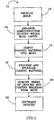
- FIG. 1 shows one embodiment of a method 10 for coating semiconductor devices according to the present invention and comprises a first step 12 of providing a mold.
- a preferred mold comprises a formation cavity that is arranged so that semiconductor devices can be held within it and a coating material can be injected or otherwise introduced into it to cover the devices.
- the cavity can have many different shapes and is preferably defined by at least upper and lower parallel surfaces. In other embodiments the cavity can be further defined by side surfaces running between the upper and lower surfaces.
- the different shapes of the formation cavity including, but are not limited to, disk, box or lens shaped.
- the side surfaces can run around the entire edge of the upper and lower surfaces or can be intermittent.
- semiconductor devices are arranged within the formation cavity and in the preferred method 10, the devices are precisely arranged in a predetermined pattern.
- the devices can be arranged in many different ways within the formation cavity using many different methods.
- the devices are placed on the lower surface by separating the upper surface from the lower and placing the devices using a precision pick and place system.
- the devices can be placed on the lower surface using a template such as a thin metal foil having a size and shape similar to the lower surface and openings corresponding to desired locations of the semiconductor devices.
- the foil can be placed on the lower surface and the semiconductor devices can be arranged within the foil openings. After the devices are placed, the foil can be removed.
- the upper surface can then be returned over the lower surface after the devices are placed.
- the lateral space between adjacent devices and the space between the upper and lower surfaces provides the desired coating thickness over the semiconductor devices.
- a coating material is injected or otherwise introduced into the mold's formation cavity, filling the cavity and covering the semiconductor devices.
- the coating material is processed and stabilized resulting in the hardening of the coating material and the semiconductors becoming at least partially embedded in the coating material.
- a sheet of semiconductor devices and coating material is formed.
- the coating material is as an epoxy, silicone or other polymer and the preferred processing and stabilizing step 18 includes curing using conventional methods dictated by the coating material's curing schedule. This can include heat curing, optical curing or curing in room temperature.
- the matrix or coating material may comprise any variety of thermoset, thermoplast, injection molding, or other polymers or related materials.
- step 20 the sheet of semiconductor devices and coating material is removed from the mold's formation cavity for further processing.
- step 22 the individual semiconductor devices are separated by cutting through the coating material between devices. This can be accomplished using many different methods such as conventional sawing or dicing, or by using a scribe and break.
- the semiconductor devices are placed on the lower surface with a uniform lateral distance between adjacent devices.
- the upper and lower surfaces of the formation cavity are also preferably parallel. If similar semiconductor devices having the same height are placed on the lower surface of the formation cavity, the distance between the top of each of the devices and the upper surface should be the same. This results in the thickness of the layer of coating material on the top of each of the devices that is substantially the same.
- the cut is preferably located such that the resulting layer covering the sides of each of the devices has the same thickness. In one embodiment of a method according to the present invention, the cut is equal distance between adjacent devices. This process produces devices that have a nearly uniform layer of coating material and the process can be repeated to produce similar devices. In other embodiments different types of cuts can be made at different angles to change the coating material thickness at different locations over the semiconductor devices.
- the method 10 can be used to coat many different types of semiconductor devices, with a preferred device being a solid state light emitter such as a light emitting diode (LED).
- a preferred coating material in the method for covering LEDs is a "matrix material” that comprises a curable material and one or more light conversion materials (further described below).
- FIG. 2 shows a flow diagram for a method 30 according to the present invention that is similar to the method 10, but is used to coat a plurality of LEDs.
- a mold is provided having a formation cavity having at least upper and lower surfaces that are parallel, although the formation cavity can have many different shapes.
- the mold surfaces are preferably flat and comprise a material which does not adhere strongly to matrix materials or the LED during processing steps such as curing. By not adhering the upper and lower surfaces can be removed from the matrix material and LEDs without damage that could result in a non-uniform layer of matrix material over the LEDs.
- the upper and lower surfaces can be made of by many different materials and can be provided by sheet metal or glass slides.
- the surfaces of the formation cavity can also be covered with a coating or film layer that resists adhering to the matrix material and can also withstand heat from processing and curing.
- the film should be tacky enough on both sides to stick to glass or metal that forms the upper and lower surfaces and to stick to semiconductor materials that form the LEDs.
- the film should not bond to these materials or the matrix material which allows the semiconductor devices and cured matrix material to be easily separated from the mold surfaces without damage.
- Many different films can be used with a preferred film being a commercially available tape referred to as Gel-Pak®, provided by Gel-Pak, LLC.
- step 34 the LEDs are placed in a predefined array or pattern within the mold's formation cavity and in a preferred embodiment the film layer is arranged between the LEDs and the cavity's surface.
- the LEDs are preferably arranged on the lower surface of the formation cavity and can be placed using the same methods as used in step 14 of the method 10 described above.
- LEDs have contacts on one surface and this surface is typically adjacent to a formation cavity surface (or film layer).
- Vertical LEDs typically have contacts on opposite surfaces, both of which can be adjacent to a formation cavity surface. It is desirable to avoid matrix material underflow that can cover the contacts so that after processing the LED can be electrically contacted. If underflow occurs, the matrix material must be removed from the contact surface, typically by etching, which can damage the LED and the contacts.
- One method to improve adhesion and reduce underflow is to apply a small amount of low tack adhesive such as silicone between the LED and the mold surface or film. This additional layer prevents underflow and can also serve as surface protection for the contacts during heat processing steps such as curing. Silicone can be removed by using convention cleaning processes that do not damage the LED or contacts.
- the matrix material is injected or otherwise introduced into and fills the mold's cavity, covering the LEDs.
- the matrix material can be made of many different compounds but preferably contains one or more light sensitive conversion materials such as phosphors distributed in an epoxy or silicone binder that can be thermally or optically curable, or cured at room temperature. To achieve uniform LED light emission, the conversion material should be distributed uniformly throughout the epoxy or silicone. For embodiments where it is desirable to emit non-uniform light, the conversion material can be non-uniform in the matrix material such that LED light emitting at different angles passes through different amounts of matrix material.
- the matrix material may exhibit or contain materials which exhibit a variety of useful properties such as high index of refraction to increase light extraction from the LED.
- the following phosphors are preferred for use as the conversion material based on certain desirable characteristic.
- Each is excited in the blue and/or UV emission spectrum, provides a desirable peak emission, has efficient light conversion, and has acceptable Stokes shift.
- the matrix material can also include scattering particles to randomly refract the light as it passes through the matrix material.
- the diameter of the scattering particles should be approximately one half of the wavelength of the light being scattered.
- Light from the LEDs pass through the particles and is refracted to mix and spread the light.
- Preferred scattering particles do not substantially absorb LED light and have a substantially different index of refraction than the material in which it is embedded (for example, epoxy).
- the scattering particles should have as high of an index of refraction as possible.
- the matrix material is cured such that the the LEDs are at least partially embedded in the matrix material.
- LEDs and matrix material form a sheet with the LEDs at least partially embedded in the matrix: material.
- the matrix material is allowed to cure by the material's curing schedule either in room temperature, under light for optical curing, or at an elevated temperature for heat curing. In a preferred embodiment of the method 30, all surfaces of the LEDs are covered except for their bottom surface.
- the sheet of LEDs and matrix material is removed from the molds formation cavity, with one method being separating the upper and lower surfaces of the mold to release the sheet, although many other methods can also be used.
- each LED can be singulated, preferably by separating the LEDs in the sheet into individual devices each of which has a similar thickness of matrix material around it.
- the methods described under step 20 of method 10 can be used, including sawing or dicing or scribe-and-break.
- the mold is designed such that the distance between the formation cavity's upper and lower surfaces and the lateral separation between adjacent LEDs results in the desired uniform matrix material thickness on each of the separated LEDs. This results in coated LEDs that emit uniform color temperature and LEDs that can be consistently reproduced with the same or similar emission characteristics.
- the mold can be arranged differently depending on the type of LED being coated.
- the LEDs can be arranged with the contacts adjacent to the cavity's lower surface. Spacers can be included between the upper and lower surfaces to maintain the desired distance between the two such that there is a space between the top of the LEDs and the upper surface of the formation cavity.
- that top surface of each of the LEDs is covered by a layer of matrix material having a similar thickness.
- one contact can be on each LED's top surface and the other contact can be on the LED's bottom surface.
- the top contact terminal should be protected during injection of the matrix material so that it is not covered by the matrix material.
- the cavity's upper surface rests on the top surface contacts of the LEDs, with the contact point between the two preventing the top contacts from being fully covered by the injected matrix material.
- the mold's formation cavity can be provided without a top surface.
- the matrix should be applied carefully and in a more controlled fashion to proved the desired thickness for the top layer in lateral LEDs and to prevent covering the top contact surface in vertical LEDs.
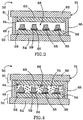
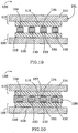
- FIGs. 3 and 4 show one embodiment of a compact coating apparatus 50 according to the present invention that can be used to compact coat many different semiconductor devices, but is particularly adapted to compact coating lateral LEDs with a matrix material.
- the apparatus 50 includes a mold housing 51 comprising a lower section 52 that includes a bottom rigid support block 54 having LEDs 55 arranged on its top surface.
- the top surface 56 the bottom support block 54 is preferably flat and the block 54 can be made of many different materials with many different thicknesses.
- the block material should not adhere to the LED or matrix material during the curing process. Suitable materials include aluminum, glass and stainless steel, and the bottom support block 54 should be thick enough that it does not flex during the layer formation process.
- the LEDs 55 can be placed on the support block using the precision placement methods described above.
- a double sided adhesive film 58 can also be included between the LEDs 55 and the bottom block's flat surface 56. As described above, the film 58 sticks to the block surface 56 and also provides a tacky surface that holds the LEDs 55.
- the film 58 also withstands processing and curing steps while not adhering to the matrix material, with a suitable material for film 58 being Gel-Pak® (described above in the method 10 of FIG. 1 ).
- the film 58 helps to reduce the amount of matrix material that sticks to the surface of the bottom support block 54.
- the positive and negative terminals 59, 60 for each of the LEDs 55 are on the surface of each LED that is adjacent to the first film 58 so that when the matrix material is injected into the mold 50, the positive and negative terminals are not covered by the matrix material.
- the mold housing 50 also includes an upper section 61 arranged over the lower section 52.
- the upper section 61 comprises a top rigid support block 62 that provides a flat top surface 64 and can be made of the same material with the same or different thicknes as the bottom rigid support block 54.
- a second layer of adhesive film 63 can also be included on the flat top surface 64 to provide a surface that does resists adhesion to the matrix material, and withstands the processing and curing steps.
- the upper section 61 is arranged over the lower section 52 with the space between the two at least partially defining the mold's formation cavity 68.
- the space between the two should be large enough to provide a space between the top of the LEDs 55 and the second adhesive film 63.
- a matrix material 70 can be injected or otherwise introduced into the formation cavity 68 such that it fills the space between the upper and lower section 52 and 61 and each of the LEDs is covered by the matrix material 70.
- the positive and negative terminals 59, 60 are protected from being covered by the matrix material and after the individual LEDs are separated (singulated) the terminals 59, 60 are available for contacting.
- the lower and upper sections 52 and 61 can have first and second vertical spacers 65, 66 (shown in FIG. 2 and 4 ) running between them.
- the spacers 65, 66 are arranged to maintain the distance between the lower and upper sections 52 and 61 so that the desired matrix material layer thickness is achieved on the top surface of the LEDs 54.
- the spacers 65, 66 can be arranged in many different ways and can be formed as a single spacer around the edge of the entire formation cavity 68, or multiple spacers can be used.
- the inside surfaces of the spacers 65, 66 further define the formation cavity 68 into which the matrix material 70 is injected.
- the matrix material 70 can be injected or introduced into the cavity 68 by many different methods according to the present invention.
- One such method comprises removing the upper- section 61, injecting the material 70 into the cavity using a syringe, and replacing the upper section 61.
- the mold 50 can have an access opening through one of its rigid blocks 54, 62 or through one its spacers 65, 66 so that the matrix material 70 can be injected into the cavity without removing either the lower and upper sections 52, 61 or one of the spacers 65, 66.
- the matrix material 70 can be made of the same material as described in step 36 of the method 30 above and preferably comprises phosphor conversion particles of one or more different type distributed uniformly throughout a curable epoxy, silicone or other polymer.
- the matrix material 70 is injected into the formation cavity 68, the matrix material 70 is cured using a process dictated by the type of epoxy or silicone such as heat curing, light curing or room temperature cooling. After the curing process is complete the matrix material 70 and LEDs 55 form a sheet that can be removed from the mold's formation cavity 68 by removing one or both of the lower and upper sections 52, 61, and/or one or both of the spacers 65, 66.
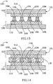
- FIG. 5 shows a sheet 72 of matrix material 70 and LEDs 55 after it is removed from the formation cavity 68 of the mold apparatus 50.
- the sheet can now be separated into individual coated LEDs by sawing, dicing or using a scribe and break.
- FIG. 6 shows two coated LEDs 76 separated from the sheet 72 shown in FIG. 5 .
- each of the coated LEDs 76 is separated by making vertical cuts through the matrix material between adjacent LEDs 55.
- the matrix material can be cut in many different ways such that the layer has different thickness over the LEDs 55 or different LEDs 55 cut from the same sheets can have layers with different thicknesses.
- the coated LEDs 76 shown in FIG. 6 are cube shaped and the matrix material cut is preferably made at a midpoint between adjacent LEDs 55 so that the side thickness of the matrix material on each coated LED 76 is the same.
- the cut can be made off midpoint or two cuts can be made, each of which is off midpoint but closer to one of the adjacent LEDs 55 such that the side thickness of the matrix material is still the same for each LED.
- This type of cubed shaped arrangement is particularly applicable to LEDs that are square, although it can also be used with LEDs having angled surfaces as shown.
- the matrix material can also be cut so that the matrix material layer conforms to the shape of the LED.
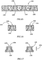
- FIGs. 7 and 8 show individually coated angled side surface coated LEDs 79 that have a layer of matrix material 80 that more closely conforms to the shape of each LED 55. Angled side surfaces are typically included to increase the LEDs light extraction.
- the shape of the matrix layer 80 can be obtained using different methods, with a preferred method being cutting through the matrix material to a depth 84 using a wider sawing (dicing) blade having an angled point. The remainder of the matrix material can then be cut using a standard narrow sawing (dicing) blade.
- the layer 80 conforms more closely to the shape of the LED such that light emitting from the LED 55 passes through substantially the same amount of matrix material.
- each of the coated LEDs 79 have both contacts on the bottom, uncoated surface 86 and FIG. 8 also shows first and second conductors 88, 89 that can be used to apply a bias across the contacts, causing the LED 55 to emit light.
- FIGs. 9 and 10 show another embodiment of a compact coating apparatus 90 according to the present invention that comprises many of the same features as the apparatus 50 shown in FIGs. 3 and 4 , with the apparatus 90 used to coat square LEDs 92.
- the features of the apparatus 90 that are the same as those in the apparatus 50 use the same reference numerals in FIGs 9 and 10 . Accordingly, the reference numerals and many of the corresponding features are not introduced or described again in the referring to FIGs. 9 and 10 .
- the square LEDs 92 are arranged on either the top surface 56 of the support block 54, or in the embodiment shown with a first film 58, on the top surface of the adhesive film 58 such that portions of the film are sandwiched between the LEDs 92 and the support block 54.
- the LEDs 92 have bottom contacts 93 whose top surface is protected by the block 54 or film 58 from being covered by the matrix material.
- a matrix material 94 can be injected into the formation cavity 68 covering the LEDs 92 and the matrix material 94 can be cured such that the LEDs 92 become embedded in the matrix material 94.
- FIG. 11 shows the sheet 96 of LEDs 92 and matrix material 94 after being removed from the formation cavity by the methods described during the discussion of FIGs. 4 and 5 above.
- FIG. 12 shows the individual coated LEDs 98 after being separated from the sheet 96 using the separation methods described above, with each of the square LEDs 92 having a nearly uniform layer of matrix material 94 so that the coated LEDs 98 emit similar light.
- FIG. 13 shows another embodiment of a mold apparatus 100 that can also be used to compact coat different semiconductor devices, but is particularly adapted to coating semiconductor devices that have a contact on their top surface.
- One such device is a vertical LED 102 having a first contact 103 on its bottom surface and a second contact 104 on its top surface.
- the apparatus 100 comprises a mold housing 101 including a lower section 106 that is similar to the lower section 54 described in FIG. 3 , and comprises a bottom support block 108 and a first double sided adhesive film 110 (e.g. Gel-Pak®). Vertical LEDs 102 are arranged on the layer 110 with their first contact 103 adjacent to the layer 110.
- first double sided adhesive film 110 e.g. Gel-Pak®
- the apparatus 100 also comprises an upper section 112 that is similar to the upper section 61 described in FIG. 3 and 4 , and comprises a top rigid block 114 and a second double sided adhesive film 116. However, in apparatus 100 there are no spacers. Instead, the second adhesive film 116 rests on the second contacts 104 of the LEDs 102, which maintains the appropriate distance between the lower and upper sections 106, 112 and also protects the top of the contacts 94 from being covered by the matrix material. If desired, the apparatus 100 can include side surfaces (not shown) to further define the formation cavity 119.
- FIG. 14 shows the apparatus 100 with the matrix material 118 injected or otherwise introduced between the lower and upper sections 106, 112, that at least partially define a formation cavity 119.
- the matrix material 118 can then be cured using the processes described above, so that the LEDs 102 and matrix material 118 form a sheet 120.
- the first contact 103 of each LED 102 is protected from being covered by the matrix material 118 by the first adhesive film 110 and second contact 104 is protected from being fully covered by the matrix material by the second adhesive film 116. Accordingly, both the first and second contacts 103, 104 are available for electrical contact without further processing or etching.
- FIG. 15 shows the sheet 120 after it has been removed from the apparatus 100.
- FIG 16 shows individual coated LEDs 122 after they have been separated, with the preferred separation method being vertical cuts through the matrix material between adjacent LEDs 102 to form cube shaped devices.
- FIGs. 17 and 16 show LEDs 123 after being cut to match the angled sides of the LEDs 92. This can be accomplished using the two cut method described above wherein a wider saw with and angled blade is used to cut the matrix material to a first depth 124 and a standard narrower blade is used to cut through the remainder of the matrix material.
- FIG. 18 shows the second contact 104 available for contacting with a first conductor 128 coupled to the second contact 104.
- a bottom conductor 129 is coupled to the LED's first contact 103 (shown in FIG. 17 ).
- a bias applied across conductors 128 and 129 causes the coated LED 102 to emit light.
- FIGs. 19 and 20 show another embodiment of a compact coating apparatus 130 according to the present invention that comprises many of the same features as the apparatus 100 shown in FIGs. 13 and 14 , with the apparatus 130 used to coat square LEDs 132.
- the features of the apparatus 130 in FIGs. 19 and 20 that are the same as those in the apparatus 100 in FIGs. 13 and 14 use the same reference numerals for the same features. Accordingly, the reference numerals and many of the corresponding features are not introduced or described again in the referring to FIGs. 19 and 20 .
- the square LEDs 132 have a first contact 133 and a second contact 134 and the LEDs 132 are arranged on either the top surface of the block 108, or in the embodiment shown with a first film 110, on the top surface of the adhesive film 110. Portions of the film 110 are sandwiched between the LEDs 132 and the block 108, with their first contacts 133 protected.
- the upper section 112 is arranged on the LEDs second contacts 134 such that they are also protected.
- a matrix material 136 can be injected or otherwise introduced into the formation cavity covering the LEDs 123 and the matrix material 136 can be cured such that the LEDs 132 become embedded in the matrix material 136.
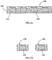
- FIG. 21 shows the sheet 138 of LEDs 132 and matrix material 136 after being removed from the formation cavity by the methods described in the discussion of FIGs. 4 and 5 above.
- FIG. 22 shows the individual coated LEDs 139 after being separated from the sheet 138 using the methods described above in the discussion of FIGs. 6, 7 and 8 .
- Each of the square LEDs 132 has a similar layer of matrix material 136 so that the LEDs 132 emit similar light.
- Each of the apparatus described above can include a small amount of low tack adhesive such as silicone between the LED contacts and the mold surface or film as described in the method 10 of FIG. 1 .
- this additional layer prevents underflow and can also serve as surface protection for the contacts during heat processing steps such as curing. Silicone can then be removed by using convention cleaning processes that do not damage the LED or contacts.
- the molds can take different shapes, can have different components and the semiconductor devices can be arranged differently in the mold's formation cavity.
- the individual LEDs can be separated from the sheet using many different sawing or dicing methods, with the cuts being straight or angled through the matrix material.
- the different coating apparatus described above can be provided without an upper section and in those embodiments the matrix material should be introduced in a carefull and controlled manner to provide the desired layer of matrix material. Therefore, the spirit and scope of the appended claims should not be limited to their preferred versions contained therein.
Applications Claiming Priority (3)
| Application Number | Priority Date | Filing Date | Title |
|---|---|---|---|
| US10/666,399 US7915085B2 (en) | 2003-09-18 | 2003-09-18 | Molded chip fabrication method |
| EP04783941.0A EP1665361B1 (fr) | 2003-09-18 | 2004-09-13 | Procédé d'encapsulation des diodes électroluminescentes |
| PCT/US2004/029916 WO2005029580A2 (fr) | 2003-09-18 | 2004-09-13 | Procede et appareil de fabrication d'une puce moulee |
Related Parent Applications (2)
| Application Number | Title | Priority Date | Filing Date |
|---|---|---|---|
| EP04783941.0A Division EP1665361B1 (fr) | 2003-09-18 | 2004-09-13 | Procédé d'encapsulation des diodes électroluminescentes |
| EP04783941.0A Division-Into EP1665361B1 (fr) | 2003-09-18 | 2004-09-13 | Procédé d'encapsulation des diodes électroluminescentes |
Publications (1)
| Publication Number | Publication Date |
|---|---|
| EP3667708A1 true EP3667708A1 (fr) | 2020-06-17 |
Family
ID=34313104
Family Applications (2)
| Application Number | Title | Priority Date | Filing Date |
|---|---|---|---|
| EP20156945.6A Pending EP3667708A1 (fr) | 2003-09-18 | 2004-09-13 | Procédé d'encapsulation de diodes électroluminescentes |
| EP04783941.0A Active EP1665361B1 (fr) | 2003-09-18 | 2004-09-13 | Procédé d'encapsulation des diodes électroluminescentes |
Family Applications After (1)
| Application Number | Title | Priority Date | Filing Date |
|---|---|---|---|
| EP04783941.0A Active EP1665361B1 (fr) | 2003-09-18 | 2004-09-13 | Procédé d'encapsulation des diodes électroluminescentes |
Country Status (5)
| Country | Link |
|---|---|
| US (6) | US7915085B2 (fr) |
| EP (2) | EP3667708A1 (fr) |
| JP (3) | JP5431646B2 (fr) |
| TW (1) | TWI358837B (fr) |
| WO (1) | WO2005029580A2 (fr) |
Families Citing this family (59)
| Publication number | Priority date | Publication date | Assignee | Title |
|---|---|---|---|---|
| US7915085B2 (en) | 2003-09-18 | 2011-03-29 | Cree, Inc. | Molded chip fabrication method |
| TWI275189B (en) * | 2003-12-30 | 2007-03-01 | Osram Opto Semiconductors Gmbh | Radiation-emitting and/or radiation-receiving semiconductor component and method for producing such component |
| US7355284B2 (en) | 2004-03-29 | 2008-04-08 | Cree, Inc. | Semiconductor light emitting devices including flexible film having therein an optical element |
| US7553683B2 (en) * | 2004-06-09 | 2009-06-30 | Philips Lumiled Lighting Co., Llc | Method of forming pre-fabricated wavelength converting elements for semiconductor light emitting devices |
| US8563339B2 (en) | 2005-08-25 | 2013-10-22 | Cree, Inc. | System for and method for closed loop electrophoretic deposition of phosphor materials on semiconductor devices |
| US20070045643A1 (en) * | 2005-08-29 | 2007-03-01 | Shih-Lung Liu | Substrate-based white light diode |
| JP5308618B2 (ja) * | 2006-04-26 | 2013-10-09 | 日亜化学工業株式会社 | 半導体発光装置 |
| DE202006007482U1 (de) * | 2006-05-10 | 2006-07-20 | Sentner, Thomas | Leuchtmöbel |
| JP2009538531A (ja) * | 2006-05-23 | 2009-11-05 | クリー エル イー ディー ライティング ソリューションズ インコーポレイテッド | 照明装置、および、製造方法 |
| CN101174058A (zh) * | 2006-10-30 | 2008-05-07 | 鸿富锦精密工业(深圳)有限公司 | 背光模组及其制备方法 |
| US7521862B2 (en) * | 2006-11-20 | 2009-04-21 | Philips Lumileds Lighting Co., Llc | Light emitting device including luminescent ceramic and light-scattering material |
| US9024349B2 (en) | 2007-01-22 | 2015-05-05 | Cree, Inc. | Wafer level phosphor coating method and devices fabricated utilizing method |
| US9159888B2 (en) * | 2007-01-22 | 2015-10-13 | Cree, Inc. | Wafer level phosphor coating method and devices fabricated utilizing method |
| WO2009012287A1 (fr) * | 2007-07-17 | 2009-01-22 | Cree Led Lighting Solutions, Inc. | Eléments optiques avec caractéristiques optiques internes et procédés de fabrication de ceux-ci |
| JP2011507254A (ja) * | 2007-12-11 | 2011-03-03 | コーニンクレッカ フィリップス エレクトロニクス エヌ ヴィ | ハイブリッド上部反射器を備える側面放射装置 |
| US9041285B2 (en) | 2007-12-14 | 2015-05-26 | Cree, Inc. | Phosphor distribution in LED lamps using centrifugal force |
| US8878219B2 (en) * | 2008-01-11 | 2014-11-04 | Cree, Inc. | Flip-chip phosphor coating method and devices fabricated utilizing method |
| DE102008010512A1 (de) * | 2008-02-22 | 2009-08-27 | Osram Opto Semiconductors Gmbh | Optoelektronisches Bauteil und Verfahren zur Herstellung eines optoelektronischen Bauteils |
| US8236582B2 (en) * | 2008-07-24 | 2012-08-07 | Philips Lumileds Lighting Company, Llc | Controlling edge emission in package-free LED die |
| US10147843B2 (en) | 2008-07-24 | 2018-12-04 | Lumileds Llc | Semiconductor light emitting device including a window layer and a light-directing structure |
| US20100279437A1 (en) * | 2009-05-01 | 2010-11-04 | Koninklijke Philips Electronics N.V. | Controlling edge emission in package-free led die |
| US8957428B2 (en) * | 2008-09-25 | 2015-02-17 | Koninklijke Philips N.V. | Coated light emitting device and method for coating thereof |
| US8075165B2 (en) * | 2008-10-14 | 2011-12-13 | Ledengin, Inc. | Total internal reflection lens and mechanical retention and locating device |
| US8507300B2 (en) * | 2008-12-24 | 2013-08-13 | Ledengin, Inc. | Light-emitting diode with light-conversion layer |
| TWI381556B (zh) * | 2009-03-20 | 2013-01-01 | Everlight Electronics Co Ltd | 發光二極體封裝結構及其製作方法 |
| US7985000B2 (en) * | 2009-04-08 | 2011-07-26 | Ledengin, Inc. | Lighting apparatus having multiple light-emitting diodes with individual light-conversion layers |
| DE102009035100A1 (de) * | 2009-07-29 | 2011-02-03 | Osram Opto Semiconductors Gmbh | Leuchtdiode und Konversionselement für eine Leuchtdiode |
| TWI385782B (zh) * | 2009-09-10 | 2013-02-11 | Lextar Electronics Corp | 白光發光元件 |
| JP5468349B2 (ja) * | 2009-10-22 | 2014-04-09 | シチズンホールディングス株式会社 | Led光源装置の製造方法 |
| US8303141B2 (en) * | 2009-12-17 | 2012-11-06 | Ledengin, Inc. | Total internal reflection lens with integrated lamp cover |
| US10546846B2 (en) | 2010-07-23 | 2020-01-28 | Cree, Inc. | Light transmission control for masking appearance of solid state light sources |
| US9373606B2 (en) * | 2010-08-30 | 2016-06-21 | Bridgelux, Inc. | Light-emitting device array with individual cells |
| US8937324B2 (en) * | 2010-08-30 | 2015-01-20 | Bridgelux, Inc. | Light-emitting device array with individual cells |
| US9515229B2 (en) * | 2010-09-21 | 2016-12-06 | Cree, Inc. | Semiconductor light emitting devices with optical coatings and methods of making same |
| CN102487110A (zh) * | 2010-12-03 | 2012-06-06 | 展晶科技(深圳)有限公司 | 发光二极管封装方法 |
| KR101725220B1 (ko) | 2010-12-22 | 2017-04-10 | 삼성전자 주식회사 | 형광체 도포 방법 및 형광체 도포 장치 |
| KR101897308B1 (ko) * | 2011-01-17 | 2018-09-10 | 루미리즈 홀딩 비.브이. | 발광 디바이스를 제조하기 위한 방법 및 그것을 포함하는 구조체 |
| US9166126B2 (en) * | 2011-01-31 | 2015-10-20 | Cree, Inc. | Conformally coated light emitting devices and methods for providing the same |
| US8513900B2 (en) | 2011-05-12 | 2013-08-20 | Ledengin, Inc. | Apparatus for tuning of emitter with multiple LEDs to a single color bin |
| DE102011102590A1 (de) * | 2011-05-27 | 2012-11-29 | Osram Opto Semiconductors Gmbh | Verfahren zum Herstellen von Leuchtdioden-Bauelementen |
| SG189315A1 (en) * | 2011-06-07 | 2013-05-31 | Toray Industries | Resin sheet laminated body, method for producing same, and method for producing led chip with phosphor-containing resin sheet using same |
| KR20130083207A (ko) * | 2012-01-12 | 2013-07-22 | 삼성전자주식회사 | 웨이퍼 레벨 몰드를 이용한 발광소자 칩 웨이퍼의 형광층 형성방법 |
| KR101645263B1 (ko) * | 2012-01-19 | 2016-08-03 | 나노코 테크놀로지스 리미티드 | 발광 장치 적용을 위한 성형된 나노입자 형광체 |
| US9343383B2 (en) * | 2012-03-02 | 2016-05-17 | Cree, Inc. | High voltage semiconductor devices including electric arc suppression material and methods of forming the same |
| US9897284B2 (en) | 2012-03-28 | 2018-02-20 | Ledengin, Inc. | LED-based MR16 replacement lamp |
| US9159643B2 (en) * | 2012-09-14 | 2015-10-13 | Freescale Semiconductor, Inc. | Matrix lid heatspreader for flip chip package |
| US8921994B2 (en) | 2012-09-14 | 2014-12-30 | Freescale Semiconductor, Inc. | Thermally enhanced package with lid heat spreader |
| KR101968637B1 (ko) * | 2012-12-07 | 2019-04-12 | 삼성전자주식회사 | 유연성 반도체소자 및 그 제조방법 |
| KR102636282B1 (ko) | 2014-09-19 | 2024-02-15 | 가부시키가이샤 한도오따이 에네루기 켄큐쇼 | 이차 전지 |
| US9530943B2 (en) | 2015-02-27 | 2016-12-27 | Ledengin, Inc. | LED emitter packages with high CRI |
| CN106328008B (zh) * | 2015-06-30 | 2019-03-22 | 光宝光电(常州)有限公司 | 胶体填充至壳体的制法、发光二极管的数字显示器及制法 |
| DE102015114849B4 (de) * | 2015-09-04 | 2022-01-13 | OSRAM Opto Semiconductors Gesellschaft mit beschränkter Haftung | Verfahren zur Herstellung von Leuchtdiodenfilamenten und Leuchtdiodenfilament |
| EP3327755A1 (fr) * | 2016-10-10 | 2018-05-30 | Shenzhen Goodix Technology Co., Ltd. | Structure de boîtier à puce et procédé de conditionnement de puce |
| US10219345B2 (en) | 2016-11-10 | 2019-02-26 | Ledengin, Inc. | Tunable LED emitter with continuous spectrum |
| CN106449945B (zh) * | 2016-12-07 | 2019-03-26 | 湘能华磊光电股份有限公司 | 制作csp芯片的模注方法 |
| DE102017215797B4 (de) * | 2017-09-07 | 2023-09-21 | Infineon Technologies Ag | Verfahren zur Herstellung von gehäusten Halbleitervorrichtungen |
| US10170304B1 (en) | 2017-10-25 | 2019-01-01 | Globalfoundries Inc. | Self-aligned nanotube structures |
| KR101977261B1 (ko) * | 2017-11-03 | 2019-05-13 | 엘지전자 주식회사 | 형광체 모듈 |
| CN112234070B (zh) * | 2019-06-27 | 2022-12-13 | 成都辰显光电有限公司 | 显示面板、显示装置及显示面板的制造方法 |
Citations (5)
| Publication number | Priority date | Publication date | Assignee | Title |
|---|---|---|---|---|
| US5959316A (en) | 1998-09-01 | 1999-09-28 | Hewlett-Packard Company | Multiple encapsulation of phosphor-LED devices |
| US6252254B1 (en) * | 1998-02-06 | 2001-06-26 | General Electric Company | Light emitting device with phosphor composition |
| US20020011667A1 (en) * | 1999-02-18 | 2002-01-31 | Nec Corporation | Semiconductor device and method for manufacturing same |
| EP1198016A2 (fr) | 2000-10-13 | 2002-04-17 | LumiLeds Lighting U.S., LLC | Déposition de couches luminescentes sur des diodes émetteurs de lumière via un pochoir |
| JP2002261325A (ja) * | 2001-03-02 | 2002-09-13 | Nichia Chem Ind Ltd | 発光装置およびその製造方法 |
Family Cites Families (364)
| Publication number | Priority date | Publication date | Assignee | Title |
|---|---|---|---|---|
| US333522A (en) * | 1886-01-05 | Feanklin e | ||
| US257737A (en) * | 1882-05-09 | Gate-holder | ||
| US66861A (en) * | 1867-07-16 | Impeoyed lasd-eqllee and marieb | ||
| US566639A (en) * | 1896-08-25 | werner | ||
| US468832A (en) * | 1892-02-16 | Corn-harvester | ||
| US720259A (en) * | 1902-07-29 | 1903-02-10 | Christopher Kuenzel | Stem winding and setting watch. |
| US813753A (en) * | 1905-05-24 | 1906-02-27 | Sieber & Trussell Mnfg Co | Loose-leaf binder. |
| US959316A (en) * | 1908-01-02 | 1910-05-24 | Edmund Dawes | Spinning and twisting machine. |
| US924233A (en) * | 1908-06-16 | 1909-06-08 | Aage Jensen | Apparatus for heating and cooling liquids. |
| US3780357A (en) | 1973-02-16 | 1973-12-18 | Hewlett Packard Co | Electroluminescent semiconductor display apparatus and method of fabricating the same |
| NL162469C (nl) * | 1975-01-23 | 1980-05-16 | Schelde Nv | Werkwijze voor het lassen van een pijp aan een pijpplaat. |
| JPS5479985A (en) | 1977-12-09 | 1979-06-26 | Tokyo Shibaura Electric Co | Ultrasonic scanning device |
| JPS5927559Y2 (ja) | 1979-06-08 | 1984-08-09 | 才市 岡本 | 防振装置 |
| JPS5927559B2 (ja) | 1980-05-14 | 1984-07-06 | 株式会社村田製作所 | 電気音響変成器 |
| JPS5752072A (en) * | 1980-09-16 | 1982-03-27 | Tokyo Shibaura Electric Co | Display unit |
| US4527179A (en) * | 1981-02-09 | 1985-07-02 | Semiconductor Energy Laboratory Co., Ltd. | Non-single-crystal light emitting semiconductor device |
| JPS5927559A (ja) | 1982-08-07 | 1984-02-14 | Mitsubishi Electric Corp | 半導体装置パツケ−ジ |
| JPS5939124A (ja) | 1982-08-27 | 1984-03-03 | Toshiba Corp | Cmos論理回路 |
| US4587729A (en) * | 1982-09-17 | 1986-05-13 | The Gillette Company | Safety razor |
| US4576796A (en) * | 1984-01-18 | 1986-03-18 | Pelam, Inc. | Centrifugal tissue processor |
| JPS6148951A (ja) | 1984-08-16 | 1986-03-10 | Toshiba Corp | 半導体装置 |
| JPS6148951U (fr) | 1984-08-29 | 1986-04-02 | ||
| US4853010A (en) * | 1984-09-12 | 1989-08-01 | Spence Billy F | Multi stage gas scrubber |
| US4733335A (en) * | 1984-12-28 | 1988-03-22 | Koito Manufacturing Co., Ltd. | Vehicular lamp |
| JPS6227559A (ja) | 1985-07-29 | 1987-02-05 | Hitachi Cable Ltd | 溶融錫メツキ銅線の製造方法 |
| US4866005A (en) * | 1987-10-26 | 1989-09-12 | North Carolina State University | Sublimation of silicon carbide to produce large, device quality single crystals of silicon carbide |
| US4935665A (en) * | 1987-12-24 | 1990-06-19 | Mitsubishi Cable Industries Ltd. | Light emitting diode lamp |
| EP0333162B1 (fr) * | 1988-03-16 | 1994-06-15 | Mitsubishi Rayon Co., Ltd. | Compositions de pâte de luminescente et revêtements luminescents obtenus à partir de celles-ci |
| JPH0261821A (ja) | 1988-08-25 | 1990-03-01 | Victor Co Of Japan Ltd | 磁気記録媒体 |
| JP2558840B2 (ja) * | 1988-09-22 | 1996-11-27 | 関西日本電気株式会社 | モールドダイオードおよびその製造方法 |
| JPH065290Y2 (ja) | 1988-10-28 | 1994-02-09 | 株式会社サンゲツ | ワークの情報読取装置 |
| US4918497A (en) * | 1988-12-14 | 1990-04-17 | Cree Research, Inc. | Blue light emitting diode formed in silicon carbide |
| US5027168A (en) * | 1988-12-14 | 1991-06-25 | Cree Research, Inc. | Blue light emitting diode formed in silicon carbide |
| US4966862A (en) * | 1989-08-28 | 1990-10-30 | Cree Research, Inc. | Method of production of light emitting diodes |
| US4946547A (en) * | 1989-10-13 | 1990-08-07 | Cree Research, Inc. | Method of preparing silicon carbide surfaces for crystal growth |
| US5210051A (en) * | 1990-03-27 | 1993-05-11 | Cree Research, Inc. | High efficiency light emitting diodes from bipolar gallium nitride |
| FR2666147B1 (fr) | 1990-08-27 | 1992-10-16 | Inst Francais Du Petrole | Mesure de la repartition des concentrations de constituants d'un syteme en centrifugation par emission/reception de signaux mecaniques. |
| US5200022A (en) * | 1990-10-03 | 1993-04-06 | Cree Research, Inc. | Method of improving mechanically prepared substrate surfaces of alpha silicon carbide for deposition of beta silicon carbide thereon and resulting product |
| US5265792A (en) * | 1992-08-20 | 1993-11-30 | Hewlett-Packard Company | Light source and technique for mounting light emitting diodes |
| FR2704690B1 (fr) | 1993-04-27 | 1995-06-23 | Thomson Csf | Procédé d'encapsulation de pastilles semi-conductrices, dispositif obtenu par ce procédé et application à l'interconnexion de pastilles en trois dimensions. |
| US5414342A (en) * | 1993-04-29 | 1995-05-09 | Unitrode Corporation | Voltage mode pulse width modulation controller |
| US5416342A (en) * | 1993-06-23 | 1995-05-16 | Cree Research, Inc. | Blue light-emitting diode with high external quantum efficiency |
| US5338944A (en) * | 1993-09-22 | 1994-08-16 | Cree Research, Inc. | Blue light-emitting diode with degenerate junction structure |
| US5393993A (en) * | 1993-12-13 | 1995-02-28 | Cree Research, Inc. | Buffer structure between silicon carbide and gallium nitride and resulting semiconductor devices |
| US5604135A (en) * | 1994-08-12 | 1997-02-18 | Cree Research, Inc. | Method of forming green light emitting diode in silicon carbide |
| US5523589A (en) * | 1994-09-20 | 1996-06-04 | Cree Research, Inc. | Vertical geometry light emitting diode with group III nitride active layer and extended lifetime |
| US5631190A (en) * | 1994-10-07 | 1997-05-20 | Cree Research, Inc. | Method for producing high efficiency light-emitting diodes and resulting diode structures |
| DE19509262C2 (de) | 1995-03-15 | 2001-11-29 | Siemens Ag | Halbleiterbauelement mit Kunststoffumhüllung und Verfahren zu dessen Herstellung |
| US5614131A (en) * | 1995-05-01 | 1997-03-25 | Motorola, Inc. | Method of making an optoelectronic device |
| US5739554A (en) * | 1995-05-08 | 1998-04-14 | Cree Research, Inc. | Double heterojunction light emitting diode with gallium nitride active layer |
| US6056421A (en) * | 1995-08-25 | 2000-05-02 | Michael Brian Johnson | Architectural lighting devices with photosensitive lens |
| US5766987A (en) * | 1995-09-22 | 1998-06-16 | Tessera, Inc. | Microelectronic encapsulation methods and equipment |
| DE19536438A1 (de) * | 1995-09-29 | 1997-04-03 | Siemens Ag | Halbleiterbauelement und Herstellverfahren |
| TW412744B (en) * | 1996-02-13 | 2000-11-21 | Dainippon Printing Co Ltd | Device with display portion capable of rewriting |
| JP2947156B2 (ja) * | 1996-02-29 | 1999-09-13 | 双葉電子工業株式会社 | 蛍光体の製造方法 |
| US5926359A (en) * | 1996-04-01 | 1999-07-20 | International Business Machines Corporation | Metal-insulator-metal capacitor |
| US6001671A (en) * | 1996-04-18 | 1999-12-14 | Tessera, Inc. | Methods for manufacturing a semiconductor package having a sacrificial layer |
| JP3350354B2 (ja) | 1996-06-03 | 2002-11-25 | 松下電器産業株式会社 | モノクロームブラウン管蛍光面形成方法 |
| US5803579A (en) * | 1996-06-13 | 1998-09-08 | Gentex Corporation | Illuminator assembly incorporating light emitting diodes |
| EP2267801B1 (fr) * | 1996-06-26 | 2015-05-27 | OSRAM Opto Semiconductors GmbH | Puce à semi-conducteur luminescente et composant à semi-conducteur luminescent |
| DE19638667C2 (de) * | 1996-09-20 | 2001-05-17 | Osram Opto Semiconductors Gmbh | Mischfarbiges Licht abstrahlendes Halbleiterbauelement mit Lumineszenzkonversionselement |
| JP3751587B2 (ja) * | 1996-07-12 | 2006-03-01 | 富士通株式会社 | 半導体装置の製造方法 |
| TW383508B (en) | 1996-07-29 | 2000-03-01 | Nichia Kagaku Kogyo Kk | Light emitting device and display |
| JP3065258B2 (ja) | 1996-09-30 | 2000-07-17 | 日亜化学工業株式会社 | 発光装置及びそれを用いた表示装置 |
| JPH10150223A (ja) * | 1996-11-15 | 1998-06-02 | Rohm Co Ltd | チップ型発光素子 |
| JP3448441B2 (ja) | 1996-11-29 | 2003-09-22 | 三洋電機株式会社 | 発光装置 |
| US5833903A (en) * | 1996-12-10 | 1998-11-10 | Great American Gumball Corporation | Injection molding encapsulation for an electronic device directly onto a substrate |
| JP3492178B2 (ja) | 1997-01-15 | 2004-02-03 | 株式会社東芝 | 半導体発光装置及びその製造方法 |
| US6274890B1 (en) * | 1997-01-15 | 2001-08-14 | Kabushiki Kaisha Toshiba | Semiconductor light emitting device and its manufacturing method |
| EP0921577A4 (fr) | 1997-01-31 | 2007-10-31 | Matsushita Electric Ind Co Ltd | Element electroluminescent, dispositif electroluminescent a semiconducteur, et leur procede de production |
| US6583444B2 (en) * | 1997-02-18 | 2003-06-24 | Tessera, Inc. | Semiconductor packages having light-sensitive chips |
| JP3246386B2 (ja) | 1997-03-05 | 2002-01-15 | 日亜化学工業株式会社 | 発光ダイオード及び発光ダイオード用の色変換モールド部材 |
| JP3351706B2 (ja) * | 1997-05-14 | 2002-12-03 | 株式会社東芝 | 半導体装置およびその製造方法 |
| US5813753A (en) * | 1997-05-27 | 1998-09-29 | Philips Electronics North America Corporation | UV/blue led-phosphor device with efficient conversion of UV/blues light to visible light |
| FR2764111A1 (fr) * | 1997-06-03 | 1998-12-04 | Sgs Thomson Microelectronics | Procede de fabrication de boitiers semi-conducteurs comprenant un circuit integre |
| JP3617587B2 (ja) | 1997-07-17 | 2005-02-09 | 日亜化学工業株式会社 | 発光ダイオード及びその形成方法 |
| US6340824B1 (en) | 1997-09-01 | 2002-01-22 | Kabushiki Kaisha Toshiba | Semiconductor light emitting device including a fluorescent material |
| JPH1187778A (ja) | 1997-09-02 | 1999-03-30 | Toshiba Corp | 半導体発光素子、半導体発光装置およびその製造方法 |
| CN2310925Y (zh) | 1997-09-26 | 1999-03-17 | 陈兴 | 发光二极管的新结构 |
| US6201262B1 (en) * | 1997-10-07 | 2001-03-13 | Cree, Inc. | Group III nitride photonic devices on silicon carbide substrates with conductive buffer interlay structure |
| US6350704B1 (en) * | 1997-10-14 | 2002-02-26 | Micron Technology Inc. | Porous silicon oxycarbide integrated circuit insulator |
| US6495083B2 (en) | 1997-10-29 | 2002-12-17 | Hestia Technologies, Inc. | Method of underfilling an integrated circuit chip |
| TW408497B (en) * | 1997-11-25 | 2000-10-11 | Matsushita Electric Works Ltd | LED illuminating apparatus |
| EP1928034A3 (fr) | 1997-12-15 | 2008-06-18 | Philips Lumileds Lighting Company LLC | Dispositif électroluminescent |
| US6580097B1 (en) * | 1998-02-06 | 2003-06-17 | General Electric Company | Light emitting device with phosphor composition |
| JPH11276932A (ja) | 1998-03-30 | 1999-10-12 | Japan Tobacco Inc | 遠心分離機 |
| US6329224B1 (en) * | 1998-04-28 | 2001-12-11 | Tessera, Inc. | Encapsulation of microelectronic assemblies |
| US6504180B1 (en) * | 1998-07-28 | 2003-01-07 | Imec Vzw And Vrije Universiteit | Method of manufacturing surface textured high-efficiency radiating devices and devices obtained therefrom |
| JP2000053532A (ja) * | 1998-08-04 | 2000-02-22 | Shiseido Co Ltd | 美容法 |
| JP3724620B2 (ja) | 1998-09-29 | 2005-12-07 | シャープ株式会社 | 発光ダイオードの製造方法 |
| US6366018B1 (en) * | 1998-10-21 | 2002-04-02 | Sarnoff Corporation | Apparatus for performing wavelength-conversion using phosphors with light emitting diodes |
| US6404125B1 (en) * | 1998-10-21 | 2002-06-11 | Sarnoff Corporation | Method and apparatus for performing wavelength-conversion using phosphors with light emitting diodes |
| US5988925A (en) * | 1998-10-26 | 1999-11-23 | Baggett; R. Sherman | Stacked paper fastener |
| US6184465B1 (en) * | 1998-11-12 | 2001-02-06 | Micron Technology, Inc. | Semiconductor package |
| US6307218B1 (en) | 1998-11-20 | 2001-10-23 | Lumileds Lighting, U.S., Llc | Electrode structures for light emitting devices |
| JP3775081B2 (ja) | 1998-11-27 | 2006-05-17 | 松下電器産業株式会社 | 半導体発光装置 |
| US6429583B1 (en) * | 1998-11-30 | 2002-08-06 | General Electric Company | Light emitting device with ba2mgsi2o7:eu2+, ba2sio4:eu2+, or (srxcay ba1-x-y)(a1zga1-z)2sr:eu2+phosphors |
| US6339304B1 (en) * | 1998-12-18 | 2002-01-15 | Graco Children's Products Inc. | Swing control for altering power to drive motor after each swing cycle |
| JP2000208822A (ja) * | 1999-01-11 | 2000-07-28 | Matsushita Electronics Industry Corp | 半導体発光装置 |
| JP4256968B2 (ja) | 1999-01-14 | 2009-04-22 | スタンレー電気株式会社 | 発光ダイオードの製造方法 |
| US6784541B2 (en) * | 2000-01-27 | 2004-08-31 | Hitachi, Ltd. | Semiconductor module and mounting method for same |
| WO2000059036A1 (fr) | 1999-03-26 | 2000-10-05 | Hitachi, Ltd. | Module en semi-conducteur et son procede de montage |
| JP3494586B2 (ja) | 1999-03-26 | 2004-02-09 | アピックヤマダ株式会社 | 樹脂封止装置及び樹脂封止方法 |
| US6699492B2 (en) | 1999-03-31 | 2004-03-02 | Insite Vision Incorporated | Quinolone carboxylic acid compositions and related methods of treatment |
| JP2000299334A (ja) * | 1999-04-14 | 2000-10-24 | Apic Yamada Corp | 樹脂封止装置 |
| DE19918370B4 (de) | 1999-04-22 | 2006-06-08 | Osram Opto Semiconductors Gmbh | LED-Weißlichtquelle mit Linse |
| US6257737B1 (en) | 1999-05-20 | 2001-07-10 | Philips Electronics Na | Low-profile luminaire having a reflector for mixing light from a multi-color linear array of LEDs |
| JP3337000B2 (ja) | 1999-06-07 | 2002-10-21 | サンケン電気株式会社 | 半導体発光装置 |
| EP1059678A2 (fr) | 1999-06-09 | 2000-12-13 | Sanyo Electric Co., Ltd. | Dispositif à circuit intégré hybride |
| JP3675234B2 (ja) * | 1999-06-28 | 2005-07-27 | 豊田合成株式会社 | 半導体発光素子の製造方法 |
| US6274690B1 (en) | 1999-08-11 | 2001-08-14 | Shin-Etsu Chemical Co., Ltd. | Preparation of vinyl chloride polymer |
| JP2001064937A (ja) | 1999-08-31 | 2001-03-13 | Seni Doboku Kaihatsu Kk | 土木工事用ふとんかごとこれを用いた保護工および中詰材の充填方法。 |
| US6696703B2 (en) | 1999-09-27 | 2004-02-24 | Lumileds Lighting U.S., Llc | Thin film phosphor-converted light emitting diode device |
| US6338813B1 (en) * | 1999-10-15 | 2002-01-15 | Advanced Semiconductor Engineering, Inc. | Molding method for BGA semiconductor chip package |
| KR20010044907A (ko) * | 1999-11-01 | 2001-06-05 | 김순택 | 저전압 구동용 고휘도 형광체막 및 그 제조 방법 |
| DE19955747A1 (de) | 1999-11-19 | 2001-05-23 | Osram Opto Semiconductors Gmbh | Optische Halbleitervorrichtung mit Mehrfach-Quantentopf-Struktur |
| US6410942B1 (en) * | 1999-12-03 | 2002-06-25 | Cree Lighting Company | Enhanced light extraction through the use of micro-LED arrays |
| US6666567B1 (en) * | 1999-12-28 | 2003-12-23 | Honeywell International Inc. | Methods and apparatus for a light source with a raised LED structure |
| US6406991B2 (en) | 1999-12-27 | 2002-06-18 | Hoya Corporation | Method of manufacturing a contact element and a multi-layered wiring substrate, and wafer batch contact board |
| DE19964252A1 (de) * | 1999-12-30 | 2002-06-06 | Osram Opto Semiconductors Gmbh | Oberflächenmontierbares Bauelement für eine LED-Weißlichtquelle |
| US6541367B1 (en) * | 2000-01-18 | 2003-04-01 | Applied Materials, Inc. | Very low dielectric constant plasma-enhanced CVD films |
| DE10010638A1 (de) | 2000-03-03 | 2001-09-13 | Osram Opto Semiconductors Gmbh | Verfahren zur Herstellung eines lichtabstrahlenden Halbleiterkörpers mit Lumineszenzkonversionselement |
| US6793371B2 (en) * | 2000-03-09 | 2004-09-21 | Mongo Light Co. Inc. | LED lamp assembly |
| US6522065B1 (en) | 2000-03-27 | 2003-02-18 | General Electric Company | Single phosphor for creating white light with high luminosity and high CRI in a UV led device |
| JP4810746B2 (ja) | 2000-03-31 | 2011-11-09 | 豊田合成株式会社 | Iii族窒化物系化合物半導体素子 |
| TW200529308A (en) | 2000-03-31 | 2005-09-01 | Toyoda Gosei Kk | Method for dicing semiconductor wafer into chips |
| US6653765B1 (en) * | 2000-04-17 | 2003-11-25 | General Electric Company | Uniform angular light distribution from LEDs |
| JP4403631B2 (ja) | 2000-04-24 | 2010-01-27 | ソニー株式会社 | チップ状電子部品の製造方法、並びにその製造に用いる擬似ウエーハの製造方法 |
| CN1292494C (zh) * | 2000-04-26 | 2006-12-27 | 奥斯兰姆奥普托半导体有限责任公司 | 发光半导体元件及其制造方法 |
| JP2001319928A (ja) * | 2000-05-08 | 2001-11-16 | Hitachi Ltd | 半導体集積回路装置およびその製造方法 |
| US6501100B1 (en) | 2000-05-15 | 2002-12-31 | General Electric Company | White light emitting phosphor blend for LED devices |
| US6621211B1 (en) * | 2000-05-15 | 2003-09-16 | General Electric Company | White light emitting phosphor blends for LED devices |
| GB0013394D0 (en) * | 2000-06-01 | 2000-07-26 | Microemissive Displays Ltd | A method of creating a color optoelectronic device |
| JP2002009097A (ja) * | 2000-06-22 | 2002-01-11 | Oki Electric Ind Co Ltd | 半導体装置とその製造方法 |
| JP2002018293A (ja) | 2000-07-06 | 2002-01-22 | Nippon Steel Chem Co Ltd | 陽イオン交換樹脂 |
| DE10033502A1 (de) * | 2000-07-10 | 2002-01-31 | Osram Opto Semiconductors Gmbh | Optoelektronisches Modul, Verfahren zu dessen Herstellung und dessen Verwendung |
| US6468832B1 (en) | 2000-07-19 | 2002-10-22 | National Semiconductor Corporation | Method to encapsulate bumped integrated circuit to create chip scale package |
| JP3589187B2 (ja) | 2000-07-31 | 2004-11-17 | 日亜化学工業株式会社 | 発光装置の形成方法 |
| US20020033486A1 (en) * | 2000-08-04 | 2002-03-21 | Samsung Electronics Co., Ltd. | Method for forming an interconnection line using a hydrosilsesquioxane (HSQ) layer as an interlayer insulating layer |
| JP2002050799A (ja) | 2000-08-04 | 2002-02-15 | Stanley Electric Co Ltd | Ledランプおよびその製造方法 |
| US20020024299A1 (en) * | 2000-08-09 | 2002-02-28 | Tadahiro Okazaki | Chip-type light-emitting device |
| JP2002076196A (ja) * | 2000-08-25 | 2002-03-15 | Nec Kansai Ltd | チップ型半導体装置及びその製造方法 |
| US6537912B1 (en) * | 2000-08-25 | 2003-03-25 | Micron Technology Inc. | Method of forming an encapsulated conductive pillar |
| JP5398943B2 (ja) | 2000-08-31 | 2014-01-29 | ビーエーエスエフ ソシエタス・ヨーロピア | ブチノールiエステラーゼ |
| US6614103B1 (en) * | 2000-09-01 | 2003-09-02 | General Electric Company | Plastic packaging of LED arrays |
| JP2002076445A (ja) | 2000-09-01 | 2002-03-15 | Sanken Electric Co Ltd | 半導体発光装置 |
| JP2002093830A (ja) * | 2000-09-14 | 2002-03-29 | Sony Corp | チップ状電子部品の製造方法、及びその製造に用いる疑似ウェーハの製造方法 |
| JP2002101147A (ja) | 2000-09-26 | 2002-04-05 | Hitachi Kokusai Electric Inc | 通信システム |
| EP1328973A2 (fr) * | 2000-10-03 | 2003-07-23 | Broadcom Corporation | Condensateur metallique a haute densite utilisant une interconnexion en cuivre double damascene |
| DE10051242A1 (de) * | 2000-10-17 | 2002-04-25 | Philips Corp Intellectual Pty | Lichtemittierende Vorrichtung mit beschichtetem Leuchtstoff |
| US6889088B2 (en) * | 2000-11-20 | 2005-05-03 | Bassem M. Demian | Bunion treating device |
| JP2002161325A (ja) | 2000-11-20 | 2002-06-04 | Ulvac Japan Ltd | アルミニウム合金、水素ガス発生方法、水素ガス発生器及び発電機 |
| US20020063520A1 (en) | 2000-11-29 | 2002-05-30 | Huei-Che Yu | Pre-formed fluorescent plate - LED device |
| JP3614776B2 (ja) | 2000-12-19 | 2005-01-26 | シャープ株式会社 | チップ部品型ledとその製造方法 |
| JP5110744B2 (ja) * | 2000-12-21 | 2012-12-26 | フィリップス ルミレッズ ライティング カンパニー リミテッド ライアビリティ カンパニー | 発光装置及びその製造方法 |
| JP2002208822A (ja) | 2000-12-28 | 2002-07-26 | Tamura Seisakusho Co Ltd | 電子回路および音響出力装置 |
| AUPR245601A0 (en) * | 2001-01-10 | 2001-02-01 | Silverbrook Research Pty Ltd | An apparatus (WSM09) |
| JP2002280607A (ja) | 2001-01-10 | 2002-09-27 | Toyoda Gosei Co Ltd | 発光装置 |
| US6734571B2 (en) | 2001-01-23 | 2004-05-11 | Micron Technology, Inc. | Semiconductor assembly encapsulation mold |
| MY145695A (en) | 2001-01-24 | 2012-03-30 | Nichia Corp | Light emitting diode, optical semiconductor device, epoxy resin composition suited for optical semiconductor device, and method for manufacturing the same |
| US6891200B2 (en) | 2001-01-25 | 2005-05-10 | Matsushita Electric Industrial Co., Ltd. | Light-emitting unit, light-emitting unit assembly, and lighting apparatus produced using a plurality of light-emitting units |
| US6791119B2 (en) * | 2001-02-01 | 2004-09-14 | Cree, Inc. | Light emitting diodes including modifications for light extraction |
| TW516247B (en) | 2001-02-26 | 2003-01-01 | Arima Optoelectronics Corp | Light emitting diode with light conversion using scattering optical media |
| US6661167B2 (en) | 2001-03-14 | 2003-12-09 | Gelcore Llc | LED devices |
| US20020132471A1 (en) * | 2001-03-16 | 2002-09-19 | International Business Machines Corporation | High modulus film structure for enhanced electromigration resistance |
| US6486059B2 (en) * | 2001-04-19 | 2002-11-26 | Silicon Intergrated Systems Corp. | Dual damascene process using an oxide liner for a dielectric barrier layer |
| ATE551731T1 (de) | 2001-04-23 | 2012-04-15 | Panasonic Corp | Lichtemittierende einrichtung mit einem leuchtdioden-chip |
| JP2002319704A (ja) | 2001-04-23 | 2002-10-31 | Matsushita Electric Works Ltd | Ledチップ |
| US6686676B2 (en) * | 2001-04-30 | 2004-02-03 | General Electric Company | UV reflectors and UV-based light sources having reduced UV radiation leakage incorporating the same |
| US6531358B1 (en) * | 2001-05-09 | 2003-03-11 | Taiwan Semiconductor Manufacturing Company | Method of fabricating capacitor-under-bit line (CUB) DRAM |
| US6861347B2 (en) * | 2001-05-17 | 2005-03-01 | Samsung Electronics Co., Ltd. | Method for forming metal wiring layer of semiconductor device |
| US6958497B2 (en) * | 2001-05-30 | 2005-10-25 | Cree, Inc. | Group III nitride based light emitting diode structures with a quantum well and superlattice, group III nitride based quantum well structures and group III nitride based superlattice structures |
| US6642652B2 (en) * | 2001-06-11 | 2003-11-04 | Lumileds Lighting U.S., Llc | Phosphor-converted light emitting device |
| US6576488B2 (en) * | 2001-06-11 | 2003-06-10 | Lumileds Lighting U.S., Llc | Using electrophoresis to produce a conformally coated phosphor-converted light emitting semiconductor |
| CN1505843B (zh) | 2001-06-15 | 2010-05-05 | 克里公司 | 在SiC衬底上形成的GaN基LED |
| JP4114331B2 (ja) | 2001-06-15 | 2008-07-09 | 豊田合成株式会社 | 発光装置 |
| JP4010299B2 (ja) | 2001-06-20 | 2007-11-21 | 日亜化学工業株式会社 | 半導体発光装置とその形成方法 |
| JP4529319B2 (ja) | 2001-06-27 | 2010-08-25 | 日亜化学工業株式会社 | 半導体チップとその製造方法 |
| JPWO2003002661A1 (ja) * | 2001-06-28 | 2004-10-21 | 東レ株式会社 | 耐候性に優れたエポキシ樹脂組成物および繊維強化複合材料 |
| DE10131698A1 (de) * | 2001-06-29 | 2003-01-30 | Osram Opto Semiconductors Gmbh | Oberflächenmontierbares strahlungsemittierendes Bauelement und Verfahren zu dessen Herstellung |
| US20030008490A1 (en) * | 2001-07-09 | 2003-01-09 | Guoqiang Xing | Dual hardmask process for the formation of copper/low-k interconnects |
| US6696222B2 (en) * | 2001-07-24 | 2004-02-24 | Silicon Integrated Systems Corp. | Dual damascene process using metal hard mask |
| JP4147755B2 (ja) | 2001-07-31 | 2008-09-10 | 日亜化学工業株式会社 | 発光装置とその製造方法 |
| TW511303B (en) | 2001-08-21 | 2002-11-21 | Wen-Jr He | A light mixing layer and method |
| EP1563119A4 (fr) | 2001-08-31 | 2006-03-22 | Semitool Inc | Appareil et procede de depot d'une emulsion electrophoretique |
| JPWO2003021668A1 (ja) * | 2001-08-31 | 2004-12-24 | 日立化成工業株式会社 | 配線基板、半導体装置及びそれらの製造方法 |
| JP2006080565A (ja) | 2001-09-03 | 2006-03-23 | Matsushita Electric Ind Co Ltd | 半導体発光デバイスの製造方法 |
| CN101335322B (zh) * | 2001-09-03 | 2010-12-08 | 松下电器产业株式会社 | 荧光体层、半导体发光装置及半导体发光元件的制造方法 |
| US6759266B1 (en) * | 2001-09-04 | 2004-07-06 | Amkor Technology, Inc. | Quick sealing glass-lidded package fabrication method |
| JP3925137B2 (ja) | 2001-10-03 | 2007-06-06 | 日亜化学工業株式会社 | 発光装置の製造方法 |
| TW517356B (en) * | 2001-10-09 | 2003-01-11 | Delta Optoelectronics Inc | Package structure of display device and its packaging method |
| JP3948650B2 (ja) | 2001-10-09 | 2007-07-25 | アバゴ・テクノロジーズ・イーシービーユー・アイピー(シンガポール)プライベート・リミテッド | 発光ダイオード及びその製造方法 |
| US6531328B1 (en) * | 2001-10-11 | 2003-03-11 | Solidlite Corporation | Packaging of light-emitting diode |
| ATE525755T1 (de) | 2001-10-12 | 2011-10-15 | Nichia Corp | Lichtemittierendes bauelement und verfahren zu seiner herstellung |
| JP4233454B2 (ja) | 2001-11-27 | 2009-03-04 | バーゼル・ポリオレフィン・イタリア・ソチエタ・ア・レスポンサビリタ・リミタータ | 透明で柔軟なプロピレンポリマー組成物 |
| JP4055405B2 (ja) | 2001-12-03 | 2008-03-05 | ソニー株式会社 | 電子部品及びその製造方法 |
| JP2003170465A (ja) * | 2001-12-04 | 2003-06-17 | Matsushita Electric Ind Co Ltd | 半導体パッケージの製造方法およびそのための封止金型 |
| US7066335B2 (en) * | 2001-12-19 | 2006-06-27 | Pretech As | Apparatus for receiving and distributing cash |
| US7160012B2 (en) | 2002-01-07 | 2007-01-09 | Patent-Treuhand-Gesellschaft für elektrische Glëhlapen mbH | Lamp |
| TW518775B (en) * | 2002-01-29 | 2003-01-21 | Chi-Hsing Hsu | Immersion cooling type light emitting diode and its packaging method |
| JP2003234511A (ja) | 2002-02-06 | 2003-08-22 | Toshiba Corp | 半導体発光素子およびその製造方法 |
| US6924514B2 (en) | 2002-02-19 | 2005-08-02 | Nichia Corporation | Light-emitting device and process for producing thereof |
| JP4269709B2 (ja) | 2002-02-19 | 2009-05-27 | 日亜化学工業株式会社 | 発光装置およびその製造方法 |
| JP3801931B2 (ja) * | 2002-03-05 | 2006-07-26 | ローム株式会社 | Ledチップを使用した発光装置の構造及び製造方法 |
| JP3972183B2 (ja) * | 2002-03-07 | 2007-09-05 | セイコーエプソン株式会社 | 半導体装置及びその製造方法、回路基板並びに電子機器 |
| US6756186B2 (en) | 2002-03-22 | 2004-06-29 | Lumileds Lighting U.S., Llc | Producing self-aligned and self-exposed photoresist patterns on light emitting devices |
| US20030189215A1 (en) | 2002-04-09 | 2003-10-09 | Jong-Lam Lee | Method of fabricating vertical structure leds |
| US6949389B2 (en) * | 2002-05-02 | 2005-09-27 | Osram Opto Semiconductors Gmbh | Encapsulation for organic light emitting diodes devices |
| CA2427559A1 (fr) * | 2002-05-15 | 2003-11-15 | Sumitomo Electric Industries, Ltd. | Dispositif electroluminescent a lumiere blanche |
| JP2004014841A (ja) * | 2002-06-07 | 2004-01-15 | Fujitsu Ltd | 半導体装置及びその製造方法 |
| US6841802B2 (en) | 2002-06-26 | 2005-01-11 | Oriol, Inc. | Thin film light emitting diode |
| JP2004031856A (ja) | 2002-06-28 | 2004-01-29 | Sumitomo Electric Ind Ltd | ZnSe系発光装置およびその製造方法 |
| KR101030068B1 (ko) | 2002-07-08 | 2011-04-19 | 니치아 카가쿠 고교 가부시키가이샤 | 질화물 반도체 소자의 제조방법 및 질화물 반도체 소자 |
| DE10237084A1 (de) * | 2002-08-05 | 2004-02-19 | Osram Opto Semiconductors Gmbh | Verfahren zum Herstellen eines elektrischen Leiterrahmens und Verfahren zum Herstellen eines oberflächenmontierbaren Halbleiterbauelements |
| KR20040017926A (ko) | 2002-08-22 | 2004-03-02 | 웬-치 호 | 광-혼합 층 및 광-혼합 방법 |
| JP2004083653A (ja) | 2002-08-23 | 2004-03-18 | Sharp Corp | 発光装置ならびに蛍光体およびその製造方法 |
| US20040038442A1 (en) * | 2002-08-26 | 2004-02-26 | Kinsman Larry D. | Optically interactive device packages and methods of assembly |
| EP2149907A3 (fr) | 2002-08-29 | 2014-05-07 | Seoul Semiconductor Co., Ltd. | Dispositif électroluminescent comprenant des diodes électroluminescents |
| JP2004095765A (ja) | 2002-08-30 | 2004-03-25 | Nichia Chem Ind Ltd | 発光装置およびその製造方法 |
| US7078737B2 (en) * | 2002-09-02 | 2006-07-18 | Matsushita Electric Industrial Co., Ltd. | Light-emitting device |
| US7264378B2 (en) | 2002-09-04 | 2007-09-04 | Cree, Inc. | Power surface mount light emitting die package |
| ATE543221T1 (de) * | 2002-09-19 | 2012-02-15 | Cree Inc | Leuchtstoffbeschichtete leuchtdioden mit verjüngten seitenwänden und herstellungsverfahren dafür |
| JP2004134699A (ja) | 2002-10-15 | 2004-04-30 | Toyoda Gosei Co Ltd | 発光装置 |
| US20060003477A1 (en) * | 2002-10-30 | 2006-01-05 | Bert Braune | Method for producing a light source provided with electroluminescent diodes and comprising a luminescence conversion element |
| JP4072632B2 (ja) | 2002-11-29 | 2008-04-09 | 豊田合成株式会社 | 発光装置及び発光方法 |
| JP4292794B2 (ja) | 2002-12-04 | 2009-07-08 | 日亜化学工業株式会社 | 発光装置、発光装置の製造方法および発光装置の色度調整方法 |
| DE10258193B4 (de) | 2002-12-12 | 2014-04-10 | Osram Opto Semiconductors Gmbh | Verfahren zum Herstellen von Leuchtdioden-Lichtquellen mit Lumineszenz-Konversionselement |
| US6917057B2 (en) | 2002-12-31 | 2005-07-12 | Gelcore Llc | Layered phosphor coatings for LED devices |
| JP4411841B2 (ja) | 2003-01-10 | 2010-02-10 | 三菱化学株式会社 | 発光装置及びそれを用いた照明装置並びにディスプレイ |
| JP3858829B2 (ja) | 2003-02-06 | 2006-12-20 | 日亜化学工業株式会社 | 発光ダイオードの形成方法 |
| US7042020B2 (en) | 2003-02-14 | 2006-05-09 | Cree, Inc. | Light emitting device incorporating a luminescent material |
| JP4254266B2 (ja) | 2003-02-20 | 2009-04-15 | 豊田合成株式会社 | 発光装置及び発光装置の製造方法 |
| US7423296B2 (en) * | 2003-02-26 | 2008-09-09 | Avago Technologies Ecbu Ip Pte Ltd | Apparatus for producing a spectrally-shifted light output from a light emitting device utilizing thin-film luminescent layers |
| JP4131178B2 (ja) | 2003-02-28 | 2008-08-13 | 豊田合成株式会社 | 発光装置 |
| JP4303550B2 (ja) | 2003-09-30 | 2009-07-29 | 豊田合成株式会社 | 発光装置 |
| JP3900093B2 (ja) | 2003-03-11 | 2007-04-04 | 日立電線株式会社 | モールド金型及びそれを用いた半導体装置の製造方法 |
| US7038370B2 (en) | 2003-03-17 | 2006-05-02 | Lumileds Lighting, U.S., Llc | Phosphor converted light emitting device |
| JP4550386B2 (ja) | 2003-03-27 | 2010-09-22 | 三菱電機株式会社 | 光半導体素子用パッケージ |
| WO2004099342A1 (fr) | 2003-05-12 | 2004-11-18 | Luxpia Co., Ltd. | Phosphore jaune a base de borate de terbium (tb, b), procede de preparation de celui-ci et dispositif electroluminescent semi-conducteur blanc renfermant ce phosphore |
| JP4415572B2 (ja) | 2003-06-05 | 2010-02-17 | 日亜化学工業株式会社 | 半導体発光素子およびその製造方法 |
| JP2004363380A (ja) | 2003-06-05 | 2004-12-24 | Sanyo Electric Co Ltd | 光半導体装置およびその製造方法 |
| JP3813599B2 (ja) | 2003-06-13 | 2006-08-23 | ローム株式会社 | 白色発光の発光ダイオード素子を製造する方法 |
| US6921929B2 (en) * | 2003-06-27 | 2005-07-26 | Lockheed Martin Corporation | Light-emitting diode (LED) with amorphous fluoropolymer encapsulant and lens |
| US7075225B2 (en) | 2003-06-27 | 2006-07-11 | Tajul Arosh Baroky | White light emitting device |
| JP4034241B2 (ja) | 2003-06-27 | 2008-01-16 | 日本ライツ株式会社 | 光源装置および光源装置の製造方法 |
| US7200009B2 (en) * | 2003-07-01 | 2007-04-03 | Nokia Corporation | Integrated electromechanical arrangement and method of production |
| US20080106893A1 (en) | 2004-07-02 | 2008-05-08 | S. C. Johnson & Son, Inc. | Lamp and bulb for illumination and ambiance lighting |
| JP2005030369A (ja) | 2003-07-11 | 2005-02-03 | Denso Corp | 環境保全貢献システム、車載装置、回生電力活用システム、および回生発電の価値還元方法 |
| JP4503950B2 (ja) | 2003-07-11 | 2010-07-14 | スタンレー電気株式会社 | 蛍光体一体型ledランプの製造方法 |
| US7391153B2 (en) | 2003-07-17 | 2008-06-24 | Toyoda Gosei Co., Ltd. | Light emitting device provided with a submount assembly for improved thermal dissipation |
| JP4277617B2 (ja) | 2003-08-08 | 2009-06-10 | 日立電線株式会社 | 半導体発光素子の製造方法 |
| WO2005022654A2 (fr) | 2003-08-28 | 2005-03-10 | Matsushita Electric Industrial Co.,Ltd. | Dispositif electroluminescent a semiconducteur, module electroluminescent, appareil d'eclairage, element d'affichage et procede de fabrication du dispositif electroluminescent a semiconducteur |
| US7029935B2 (en) * | 2003-09-09 | 2006-04-18 | Cree, Inc. | Transmissive optical elements including transparent plastic shell having a phosphor dispersed therein, and methods of fabricating same |
| US7183587B2 (en) * | 2003-09-09 | 2007-02-27 | Cree, Inc. | Solid metal block mounting substrates for semiconductor light emitting devices |
| US7915085B2 (en) | 2003-09-18 | 2011-03-29 | Cree, Inc. | Molded chip fabrication method |
| WO2005031882A1 (fr) | 2003-09-30 | 2005-04-07 | Kabushiki Kaisha Toshiba | Dispositif luminescent |
| CN1863828A (zh) * | 2003-10-08 | 2006-11-15 | 艾利丹尼森公司 | 隔音胶粘剂 |
| KR100587328B1 (ko) | 2003-10-16 | 2006-06-08 | 엘지전자 주식회사 | Led 면광원 |
| KR101127314B1 (ko) * | 2003-11-19 | 2012-03-29 | 니치아 카가쿠 고교 가부시키가이샤 | 반도체소자 |
| JP2005167079A (ja) | 2003-12-04 | 2005-06-23 | Toyoda Gosei Co Ltd | 発光装置 |
| CN1317775C (zh) | 2003-12-10 | 2007-05-23 | 玄基光电半导体股份有限公司 | 发光二极管封装结构及其封装方法 |
| JP2005197369A (ja) | 2004-01-05 | 2005-07-21 | Toshiba Corp | 光半導体装置 |
| JP4231417B2 (ja) | 2004-01-07 | 2009-02-25 | パナソニック株式会社 | 基板処理装置及びそのクリーニング方法 |
| JP2005252222A (ja) | 2004-02-03 | 2005-09-15 | Matsushita Electric Ind Co Ltd | 半導体発光装置、照明モジュール、照明装置、表示素子、および半導体発光装置の製造方法 |
| JP4357311B2 (ja) | 2004-02-04 | 2009-11-04 | シチズン電子株式会社 | 発光ダイオードチップ |
| US7246923B2 (en) | 2004-02-11 | 2007-07-24 | 3M Innovative Properties Company | Reshaping light source modules and illumination systems using the same |
| US20070018573A1 (en) | 2004-02-18 | 2007-01-25 | Showa Denko K,K. | Phosphor, production method thereof and light-emitting device using the phosphor |
| US7569863B2 (en) * | 2004-02-19 | 2009-08-04 | Panasonic Corporation | Semiconductor light emitting device |
| US7250715B2 (en) | 2004-02-23 | 2007-07-31 | Philips Lumileds Lighting Company, Llc | Wavelength converted semiconductor light emitting devices |
| US6924233B1 (en) | 2004-03-19 | 2005-08-02 | Agilent Technologies, Inc. | Phosphor deposition methods |
| JP4516337B2 (ja) | 2004-03-25 | 2010-08-04 | シチズン電子株式会社 | 半導体発光装置 |
| KR100486177B1 (ko) | 2004-03-25 | 2005-05-06 | 에피밸리 주식회사 | Ⅲ-질화물 반도체 발광소자 |
| US20050211991A1 (en) | 2004-03-26 | 2005-09-29 | Kyocera Corporation | Light-emitting apparatus and illuminating apparatus |
| US20050211910A1 (en) | 2004-03-29 | 2005-09-29 | Jmar Research, Inc. | Morphology and Spectroscopy of Nanoscale Regions using X-Rays Generated by Laser Produced Plasma |
| US7517728B2 (en) | 2004-03-31 | 2009-04-14 | Cree, Inc. | Semiconductor light emitting devices including a luminescent conversion element |
| US7419912B2 (en) | 2004-04-01 | 2008-09-02 | Cree, Inc. | Laser patterning of light emitting devices |
| US20060007207A1 (en) | 2004-04-01 | 2006-01-12 | Toshiba Matsushita Display Technology Co., Ltd. | Liquid crystal display device and method of driving liquid crystal display device |
| US20050280894A1 (en) | 2004-04-02 | 2005-12-22 | David Hartkop | Apparatus for creating a scanning-column backlight in a scanning aperture display device |
| US7868343B2 (en) | 2004-04-06 | 2011-01-11 | Cree, Inc. | Light-emitting devices having multiple encapsulation layers with at least one of the encapsulation layers including nanoparticles and methods of forming the same |
| EP1738385A1 (fr) | 2004-04-15 | 2007-01-03 | Koninklijke Philips Electronics N.V. | Cellule chromato-convertible electriquement commandee |
| WO2005103562A2 (fr) * | 2004-04-23 | 2005-11-03 | Light Prescriptions Innovators, Llc | Collecteur optique destine a des diodes electroluminescentes |
| KR101041311B1 (ko) | 2004-04-27 | 2011-06-14 | 파나소닉 주식회사 | 형광체 조성물과 그 제조 방법, 및 그 형광체 조성물을 이용한 발광장치 |
| JP4471729B2 (ja) | 2004-04-30 | 2010-06-02 | シチズン電子株式会社 | 液晶レンズ付き発光装置 |
| TWI241034B (en) | 2004-05-20 | 2005-10-01 | Lighthouse Technology Co Ltd | Light emitting diode package |
| US7278760B2 (en) | 2004-05-24 | 2007-10-09 | Osram Opto Semiconductor Gmbh | Light-emitting electronic component |
| EP1601030B1 (fr) | 2004-05-24 | 2019-04-03 | OSRAM OLED GmbH | Composant électronique électroluminescent |
| EP1759145A1 (fr) | 2004-05-28 | 2007-03-07 | Tir Systems Ltd. | Appareil pour ameliorer la luminance et procede correspondant |
| WO2005121641A1 (fr) | 2004-06-11 | 2005-12-22 | Koninklijke Philips Electronics N.V. | Systeme d'eclairage |
| DE102004031603B4 (de) * | 2004-06-30 | 2008-04-17 | Eads Deutschland Gmbh | Verfahren zur Formung von Signalspektren und Schaltung zur Durchführung des Verfahrens |
| US7534633B2 (en) | 2004-07-02 | 2009-05-19 | Cree, Inc. | LED with substrate modifications for enhanced light extraction and method of making same |
| US7271420B2 (en) | 2004-07-07 | 2007-09-18 | Cao Group, Inc. | Monolitholic LED chip to emit multiple colors |
| JP4932144B2 (ja) | 2004-07-12 | 2012-05-16 | 株式会社朝日ラバー | Ledランプ |
| JP2006049533A (ja) | 2004-08-04 | 2006-02-16 | Wacker Asahikasei Silicone Co Ltd | 樹脂封止発光ダイオード装置及び封止方法 |
| JP4613546B2 (ja) | 2004-08-04 | 2011-01-19 | 日亜化学工業株式会社 | 発光装置 |
| JP4747726B2 (ja) | 2004-09-09 | 2011-08-17 | 豊田合成株式会社 | 発光装置 |
| JP3802911B2 (ja) | 2004-09-13 | 2006-08-02 | ローム株式会社 | 半導体発光装置 |
| US7217583B2 (en) | 2004-09-21 | 2007-05-15 | Cree, Inc. | Methods of coating semiconductor light emitting elements by evaporating solvent from a suspension |
| US8513686B2 (en) | 2004-09-22 | 2013-08-20 | Cree, Inc. | High output small area group III nitride LEDs |
| US7737459B2 (en) | 2004-09-22 | 2010-06-15 | Cree, Inc. | High output group III nitride light emitting diodes |
| US7259402B2 (en) | 2004-09-22 | 2007-08-21 | Cree, Inc. | High efficiency group III nitride-silicon carbide light emitting diode |
| US8174037B2 (en) | 2004-09-22 | 2012-05-08 | Cree, Inc. | High efficiency group III nitride LED with lenticular surface |
| US7372198B2 (en) | 2004-09-23 | 2008-05-13 | Cree, Inc. | Semiconductor light emitting devices including patternable films comprising transparent silicone and phosphor |
| JP4756841B2 (ja) | 2004-09-29 | 2011-08-24 | スタンレー電気株式会社 | 半導体発光装置の製造方法 |
| DE102004060358A1 (de) | 2004-09-30 | 2006-04-13 | Osram Opto Semiconductors Gmbh | Verfahren zum Herstellen von Lumineszenzdiodenchips und Lumineszenzdiodenchip |
| JP2006114637A (ja) | 2004-10-13 | 2006-04-27 | Toshiba Corp | 半導体発光装置 |
| US8134292B2 (en) | 2004-10-29 | 2012-03-13 | Ledengin, Inc. | Light emitting device with a thermal insulating and refractive index matching material |
| JP4802533B2 (ja) | 2004-11-12 | 2011-10-26 | 日亜化学工業株式会社 | 半導体装置 |
| JP2006165416A (ja) | 2004-12-10 | 2006-06-22 | Stanley Electric Co Ltd | 白色表示器とその製造方法 |
| US7671529B2 (en) | 2004-12-10 | 2010-03-02 | Philips Lumileds Lighting Company, Llc | Phosphor converted light emitting device |
| KR100646093B1 (ko) | 2004-12-17 | 2006-11-15 | 엘지이노텍 주식회사 | 발광소자 패키지 |
| US8288942B2 (en) | 2004-12-28 | 2012-10-16 | Cree, Inc. | High efficacy white LED |
| KR100638666B1 (ko) * | 2005-01-03 | 2006-10-30 | 삼성전기주식회사 | 질화물 반도체 발광소자 |
| US7195944B2 (en) | 2005-01-11 | 2007-03-27 | Semileds Corporation | Systems and methods for producing white-light emitting diodes |
| US7221044B2 (en) | 2005-01-21 | 2007-05-22 | Ac Led Lighting, L.L.C. | Heterogeneous integrated high voltage DC/AC light emitter |
| US7932111B2 (en) | 2005-02-23 | 2011-04-26 | Cree, Inc. | Substrate removal process for high light extraction LEDs |
| JP2006245020A (ja) | 2005-02-28 | 2006-09-14 | Sharp Corp | 発光ダイオード素子とその製造方法 |
| JP4601464B2 (ja) | 2005-03-10 | 2010-12-22 | 株式会社沖データ | 半導体装置、プリントヘッド、及びそれを用いた画像形成装置 |
| US7341878B2 (en) | 2005-03-14 | 2008-03-11 | Philips Lumileds Lighting Company, Llc | Wavelength-converted semiconductor light emitting device |
| JP4961799B2 (ja) | 2005-04-08 | 2012-06-27 | 日亜化学工業株式会社 | スクリーン印刷で形成したシリコーン樹脂層を有する発光装置 |
| KR101047683B1 (ko) | 2005-05-17 | 2011-07-08 | 엘지이노텍 주식회사 | 와이어 본딩이 불필요한 발광소자 패키징 방법 |
| US8669572B2 (en) | 2005-06-10 | 2014-03-11 | Cree, Inc. | Power lamp package |
| KR100665219B1 (ko) | 2005-07-14 | 2007-01-09 | 삼성전기주식회사 | 파장변환형 발광다이오드 패키지 |
| JP2007063538A (ja) | 2005-08-03 | 2007-03-15 | Shin Etsu Chem Co Ltd | 発光ダイオード用付加硬化型シリコーン樹脂組成物 |
| US7365371B2 (en) | 2005-08-04 | 2008-04-29 | Cree, Inc. | Packages for semiconductor light emitting devices utilizing dispensed encapsulants |
| US8563339B2 (en) * | 2005-08-25 | 2013-10-22 | Cree, Inc. | System for and method for closed loop electrophoretic deposition of phosphor materials on semiconductor devices |
| JP2007087973A (ja) | 2005-09-16 | 2007-04-05 | Rohm Co Ltd | 窒化物半導体素子の製法およびその方法により得られる窒化物半導体発光素子 |
| DE102005062514A1 (de) | 2005-09-28 | 2007-03-29 | Osram Opto Semiconductors Gmbh | Optoelektronisches Bauelement |
| US7936418B2 (en) | 2005-09-29 | 2011-05-03 | Kabushiki Kaisha Toshiba | White light-emitting device and manufacturing method thereof, and backlight and liquid crystal display device using the same |
| US7391558B2 (en) * | 2005-10-19 | 2008-06-24 | Raytheon Company | Laser amplifier power extraction enhancement system and method |
| US20070092636A1 (en) | 2005-10-24 | 2007-04-26 | 3M Innovative Properties Company | Method of making light emitting device having a molded encapsulant |
| US7344952B2 (en) | 2005-10-28 | 2008-03-18 | Philips Lumileds Lighting Company, Llc | Laminating encapsulant film containing phosphor over LEDs |
| US7564070B2 (en) * | 2005-11-23 | 2009-07-21 | Visteon Global Technologies, Inc. | Light emitting diode device having a shield and/or filter |
| DE102005058127A1 (de) | 2005-11-30 | 2007-06-06 | Schefenacker Vision Systems Germany Gmbh | Fahrzeugleuchte |
| KR100732849B1 (ko) * | 2005-12-21 | 2007-06-27 | 삼성에스디아이 주식회사 | 유기 발광 표시장치 |
| JP4828226B2 (ja) | 2005-12-28 | 2011-11-30 | 新光電気工業株式会社 | 発光装置及びその製造方法 |
| KR100723247B1 (ko) | 2006-01-10 | 2007-05-29 | 삼성전기주식회사 | 칩코팅형 led 패키지 및 그 제조방법 |
| EP1979439A1 (fr) | 2006-01-16 | 2008-10-15 | Philips Intellectual Property & Standards GmbH | Dispositif luminescent a materiau au phosphore avec eu |
| KR200412776Y1 (ko) | 2006-01-19 | 2006-03-31 | 주식회사 닥터코리아 | 약쑥이 함유된 침구류용 솜 |
| US7682850B2 (en) | 2006-03-17 | 2010-03-23 | Philips Lumileds Lighting Company, Llc | White LED for backlight with phosphor plates |
| KR200417926Y1 (ko) | 2006-03-21 | 2006-06-02 | 황성민 | 차량 진입 방지용 경계석 |
| WO2007107903A1 (fr) | 2006-03-23 | 2007-09-27 | Koninklijke Philips Electronics N.V. | Dispositif d'eclairage par led a couleur reglable |
| US20070269586A1 (en) | 2006-05-17 | 2007-11-22 | 3M Innovative Properties Company | Method of making light emitting device with silicon-containing composition |
| TWI308401B (en) | 2006-07-04 | 2009-04-01 | Epistar Corp | High efficient phosphor-converted light emitting diode |
| CN101485004B (zh) | 2006-07-06 | 2012-05-02 | 皇家飞利浦电子股份有限公司 | 照明器件封装 |
| KR200429313Y1 (ko) | 2006-08-03 | 2006-10-20 | (주)에코청진 | 계단 적층식 식생 옹벽블록 |
| JP2008129043A (ja) | 2006-11-16 | 2008-06-05 | Toyoda Gosei Co Ltd | Led発光表示装置 |
| EP1935452A1 (fr) | 2006-12-19 | 2008-06-25 | Koninklijke Philips Electronics N.V. | Dispostif électrochromique et dispositif pour le traitement photodynamique utilisant un tel dispositf électrochromique |
| US8704254B2 (en) | 2006-12-22 | 2014-04-22 | Philips Lumileds Lighting Company, Llc | Light emitting device including a filter |
| US9024349B2 (en) * | 2007-01-22 | 2015-05-05 | Cree, Inc. | Wafer level phosphor coating method and devices fabricated utilizing method |
| US8232564B2 (en) | 2007-01-22 | 2012-07-31 | Cree, Inc. | Wafer level phosphor coating technique for warm light emitting diodes |
| JP2008218511A (ja) | 2007-02-28 | 2008-09-18 | Toyoda Gosei Co Ltd | 半導体発光装置及びその製造方法 |
| DE102007022090A1 (de) | 2007-05-11 | 2008-11-13 | Osram Opto Semiconductors Gmbh | Lichtemittierendes Bauelement |
| US7588351B2 (en) * | 2007-09-27 | 2009-09-15 | Osram Sylvania Inc. | LED lamp with heat sink optic |
| WO2009045438A1 (fr) | 2007-10-03 | 2009-04-09 | Superbulbs, Inc. | Ampoules a del en verre |
| US7915627B2 (en) * | 2007-10-17 | 2011-03-29 | Intematix Corporation | Light emitting device with phosphor wavelength conversion |
| TW200921934A (en) | 2007-11-06 | 2009-05-16 | Prodisc Technology Inc | Discrete light-emitting diode light source device of wavelength conversion unit |
| CN101855591B (zh) | 2007-11-09 | 2016-01-06 | 皇家飞利浦电子股份有限公司 | 光输出器件 |
| CN101925772B (zh) | 2008-01-22 | 2016-09-28 | 皇家飞利浦电子股份有限公司 | 具有led和包括发光材料的透射支架的照明器件 |
| JP5279329B2 (ja) | 2008-04-24 | 2013-09-04 | パナソニック株式会社 | レンズ付発光ユニット |
| US20090268461A1 (en) | 2008-04-28 | 2009-10-29 | Deak David G | Photon energy conversion structure |
| US8159131B2 (en) | 2008-06-30 | 2012-04-17 | Bridgelux, Inc. | Light emitting device having a transparent thermally conductive layer |
| US8432500B2 (en) | 2008-09-23 | 2013-04-30 | Koninklijke Philips Electronics N.V. | Lighting device with thermally variable reflecting element |
| US8089085B2 (en) | 2009-02-26 | 2012-01-03 | Bridgelux, Inc. | Heat sink base for LEDS |
| US20120043886A1 (en) * | 2010-08-18 | 2012-02-23 | Hua Ji | Integrated Heat Conductive Light Emitting Diode (LED) White Light Source Module |
-
2003
- 2003-09-18 US US10/666,399 patent/US7915085B2/en not_active Expired - Lifetime
-
2004
- 2004-09-13 WO PCT/US2004/029916 patent/WO2005029580A2/fr active Search and Examination
- 2004-09-13 JP JP2006526964A patent/JP5431646B2/ja active Active
- 2004-09-13 EP EP20156945.6A patent/EP3667708A1/fr active Pending
- 2004-09-13 EP EP04783941.0A patent/EP1665361B1/fr active Active
- 2004-09-17 TW TW093128231A patent/TWI358837B/zh active
-
2009
- 2009-07-21 US US12/506,989 patent/US10546978B2/en not_active Expired - Lifetime
-
2010
- 2010-08-24 US US12/862,640 patent/US10164158B2/en not_active Expired - Lifetime
-
2011
- 2011-03-25 US US13/072,371 patent/US9093616B2/en not_active Expired - Lifetime
-
2012
- 2012-02-09 JP JP2012026326A patent/JP2012138587A/ja active Pending
- 2012-02-09 JP JP2012026327A patent/JP6058894B2/ja active Active
-
2014
- 2014-03-13 US US14/209,652 patent/US9105817B2/en not_active Expired - Lifetime
-
2019
- 2019-03-05 US US16/293,267 patent/US20190198725A1/en not_active Abandoned
Patent Citations (5)
| Publication number | Priority date | Publication date | Assignee | Title |
|---|---|---|---|---|
| US6252254B1 (en) * | 1998-02-06 | 2001-06-26 | General Electric Company | Light emitting device with phosphor composition |
| US5959316A (en) | 1998-09-01 | 1999-09-28 | Hewlett-Packard Company | Multiple encapsulation of phosphor-LED devices |
| US20020011667A1 (en) * | 1999-02-18 | 2002-01-31 | Nec Corporation | Semiconductor device and method for manufacturing same |
| EP1198016A2 (fr) | 2000-10-13 | 2002-04-17 | LumiLeds Lighting U.S., LLC | Déposition de couches luminescentes sur des diodes émetteurs de lumière via un pochoir |
| JP2002261325A (ja) * | 2001-03-02 | 2002-09-13 | Nichia Chem Ind Ltd | 発光装置およびその製造方法 |
Also Published As
| Publication number | Publication date |
|---|---|
| US20100323465A1 (en) | 2010-12-23 |
| US20140191259A1 (en) | 2014-07-10 |
| US10546978B2 (en) | 2020-01-28 |
| JP5431646B2 (ja) | 2014-03-05 |
| US7915085B2 (en) | 2011-03-29 |
| JP2012138587A (ja) | 2012-07-19 |
| WO2005029580A2 (fr) | 2005-03-31 |
| EP1665361A2 (fr) | 2006-06-07 |
| WO2005029580A3 (fr) | 2006-05-18 |
| TW200524181A (en) | 2005-07-16 |
| JP6058894B2 (ja) | 2017-01-11 |
| US20190198725A1 (en) | 2019-06-27 |
| US10164158B2 (en) | 2018-12-25 |
| US9093616B2 (en) | 2015-07-28 |
| US20090278156A1 (en) | 2009-11-12 |
| US9105817B2 (en) | 2015-08-11 |
| JP2007506279A (ja) | 2007-03-15 |
| JP2012138588A (ja) | 2012-07-19 |
| US20110169038A1 (en) | 2011-07-14 |
| EP1665361B1 (fr) | 2020-03-25 |
| US20050062140A1 (en) | 2005-03-24 |
| TWI358837B (en) | 2012-02-21 |
Similar Documents
| Publication | Publication Date | Title |
|---|---|---|
| US20190198725A1 (en) | Molded chip fabrication method and apparatus | |
| US10193036B2 (en) | Light emitting device and method for producing the same | |
| US10002993B2 (en) | Light emitting device | |
| EP3706179B1 (fr) | Dispositif électroluminescent et son procédé de fabrication | |
| US10505083B2 (en) | Coating method utilizing phosphor containment structure and devices fabricated using same | |
| EP2008315B1 (fr) | Ensemble de del à émission uniforme | |
| US11424396B2 (en) | Flip chip LED with side reflectors and phosphor | |
| CN102057511A (zh) | 使用单晶荧光体的led及其制备方法 | |
| KR20120049288A (ko) | 몰딩된 반사 측벽 코팅을 갖는 led | |
| EP3301718B1 (fr) | Procédé de fabrication d'un dispositif électroluminescent linéaire | |
| JP2007067183A (ja) | 化合物半導体発光素子を有するledパッケージ | |
| TWI546988B (zh) | 製造發光二極體之方法 | |
| CN109983589B (zh) | 具有侧面反射器和磷光体的倒装芯片led | |
| DE102018109542A1 (de) | Licht emittierendes bauelement und verfahren zur herstellung eines licht emittierenden bauelements | |
| KR102211753B1 (ko) | 전자기 방사선을 방출하는 어셈블리의 제조 방법 및 전자기 방사선을 방출하는 어셈블리 | |
| US10424698B2 (en) | Method for producing optoelectronic conversion semiconductor chips and composite of conversion semiconductor chips | |
| EP3813129A1 (fr) | Module à del et son procédé de fabrication | |
| KR20150024630A (ko) | 반도체 발광소자 및 이를 제조하는 방법 |
Legal Events
| Date | Code | Title | Description |
|---|---|---|---|
| PUAI | Public reference made under article 153(3) epc to a published international application that has entered the european phase |
Free format text: ORIGINAL CODE: 0009012 |
|
| STAA | Information on the status of an ep patent application or granted ep patent |
Free format text: STATUS: THE APPLICATION HAS BEEN PUBLISHED |
|
| AC | Divisional application: reference to earlier application |
Ref document number: 1665361 Country of ref document: EP Kind code of ref document: P |
|
| AK | Designated contracting states |
Kind code of ref document: A1 Designated state(s): AT BE BG CH CY CZ DE DK EE ES FI FR GB GR HU IE IT LI LU MC NL PL PT RO SE SI SK TR |
|
| STAA | Information on the status of an ep patent application or granted ep patent |
Free format text: STATUS: REQUEST FOR EXAMINATION WAS MADE |
|
| 17P | Request for examination filed |
Effective date: 20201216 |
|
| RBV | Designated contracting states (corrected) |
Designated state(s): AT BE BG CH CY CZ DE DK EE ES FI FR GB GR HU IE IT LI LU MC NL PL PT RO SE SI SK TR |
|
| RAP1 | Party data changed (applicant data changed or rights of an application transferred) |
Owner name: CREELED, INC. |
|
| P01 | Opt-out of the competence of the unified patent court (upc) registered |
Effective date: 20230530 |
|
| STAA | Information on the status of an ep patent application or granted ep patent |
Free format text: STATUS: EXAMINATION IS IN PROGRESS |
|
| 17Q | First examination report despatched |
Effective date: 20240305 |