EP1566959B1 - Festkörper-Bildaufnahmevorrichtung und Verfahren zu ihrer Ansteuerung - Google Patents
Festkörper-Bildaufnahmevorrichtung und Verfahren zu ihrer Ansteuerung Download PDFInfo
- Publication number
- EP1566959B1 EP1566959B1 EP05003683A EP05003683A EP1566959B1 EP 1566959 B1 EP1566959 B1 EP 1566959B1 EP 05003683 A EP05003683 A EP 05003683A EP 05003683 A EP05003683 A EP 05003683A EP 1566959 B1 EP1566959 B1 EP 1566959B1
- Authority
- EP
- European Patent Office
- Prior art keywords
- analog
- pixels
- column
- digital
- row
- Prior art date
- Legal status (The legal status is an assumption and is not a legal conclusion. Google has not performed a legal analysis and makes no representation as to the accuracy of the status listed.)
- Expired - Lifetime
Links
Images


Classifications
-
- H—ELECTRICITY
- H04—ELECTRIC COMMUNICATION TECHNIQUE
- H04N—PICTORIAL COMMUNICATION, e.g. TELEVISION
- H04N25/00—Circuitry of solid-state image sensors [SSIS]; Control thereof
- H04N25/70—SSIS architectures; Circuits associated therewith
- H04N25/76—Addressed sensors, e.g. MOS or CMOS sensors
- H04N25/77—Pixel circuitry, e.g. memories, A/D converters, pixel amplifiers, shared circuits or shared components
- H04N25/772—Pixel circuitry, e.g. memories, A/D converters, pixel amplifiers, shared circuits or shared components comprising A/D, V/T, V/F, I/T or I/F converters
-
- H—ELECTRICITY
- H03—ELECTRONIC CIRCUITRY
- H03M—CODING; DECODING; CODE CONVERSION IN GENERAL
- H03M1/00—Analogue/digital conversion; Digital/analogue conversion
- H03M1/10—Calibration or testing
- H03M1/1009—Calibration
- H03M1/1014—Calibration at one point of the transfer characteristic, i.e. by adjusting a single reference value, e.g. bias or gain error
- H03M1/1023—Offset correction
-
- H—ELECTRICITY
- H04—ELECTRIC COMMUNICATION TECHNIQUE
- H04N—PICTORIAL COMMUNICATION, e.g. TELEVISION
- H04N23/00—Cameras or camera modules comprising electronic image sensors; Control thereof
- H04N23/50—Constructional details
- H04N23/54—Mounting of pick-up tubes, electronic image sensors, deviation or focusing coils
-
- H—ELECTRICITY
- H04—ELECTRIC COMMUNICATION TECHNIQUE
- H04N—PICTORIAL COMMUNICATION, e.g. TELEVISION
- H04N25/00—Circuitry of solid-state image sensors [SSIS]; Control thereof
- H04N25/40—Extracting pixel data from image sensors by controlling scanning circuits, e.g. by modifying the number of pixels sampled or to be sampled
- H04N25/46—Extracting pixel data from image sensors by controlling scanning circuits, e.g. by modifying the number of pixels sampled or to be sampled by combining or binning pixels
-
- H—ELECTRICITY
- H04—ELECTRIC COMMUNICATION TECHNIQUE
- H04N—PICTORIAL COMMUNICATION, e.g. TELEVISION
- H04N25/00—Circuitry of solid-state image sensors [SSIS]; Control thereof
- H04N25/60—Noise processing, e.g. detecting, correcting, reducing or removing noise
- H04N25/616—Noise processing, e.g. detecting, correcting, reducing or removing noise involving a correlated sampling function, e.g. correlated double sampling [CDS] or triple sampling
-
- H—ELECTRICITY
- H04—ELECTRIC COMMUNICATION TECHNIQUE
- H04N—PICTORIAL COMMUNICATION, e.g. TELEVISION
- H04N25/00—Circuitry of solid-state image sensors [SSIS]; Control thereof
- H04N25/70—SSIS architectures; Circuits associated therewith
- H04N25/76—Addressed sensors, e.g. MOS or CMOS sensors
- H04N25/767—Horizontal readout lines, multiplexers or registers
-
- H—ELECTRICITY
- H04—ELECTRIC COMMUNICATION TECHNIQUE
- H04N—PICTORIAL COMMUNICATION, e.g. TELEVISION
- H04N25/00—Circuitry of solid-state image sensors [SSIS]; Control thereof
- H04N25/70—SSIS architectures; Circuits associated therewith
- H04N25/76—Addressed sensors, e.g. MOS or CMOS sensors
- H04N25/78—Readout circuits for addressed sensors, e.g. output amplifiers or A/D converters
-
- H—ELECTRICITY
- H03—ELECTRONIC CIRCUITRY
- H03M—CODING; DECODING; CODE CONVERSION IN GENERAL
- H03M1/00—Analogue/digital conversion; Digital/analogue conversion
- H03M1/12—Analogue/digital converters
- H03M1/50—Analogue/digital converters with intermediate conversion to time interval
- H03M1/56—Input signal compared with linear ramp
Definitions
- the present invention relates to a solid-state image pickup device and a method for driving the same.
- the present invention relates to a solid-state image pickup device for converting analog signals output from unit pixels through column signal lines to digital signals and reading the digital signals, and to a method for driving the same.
- CMOS image sensor including a column-parallel ADCs (analog-digital converters) has been reported (e.g., see non-Patent Document 1: W. Yang et al., "An Integrated 800x600 CMOS Image System” ISS CC Digest of Technical Papers, pp. 304-305, Feb. 1999 ).
- ADCs are arranged for respective columns in matrix-patterned unit pixels.
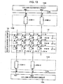
- Fig. 15 is a block diagram showing the configuration of a CMOS image sensor 100 including column-parallel ADCs according to a known art.
- unit pixels 101 each including a photodiode and an intra-pixel amplifier, are two-dimensionally arranged in a matrix pattern so as to form a pixel array unit 102.
- row control lines 103 (103-1, 103-2, ⁇ ) are arranged for respective rows and column signal lines 104 (104-1, 104-2, ⁇ ) are arranged for respective columns.
- the row address and row scanning in the pixel array unit 102 is controlled by a row scanning circuit 105 through the row control lines 103-1, 103-2, ⁇ .
- An ADC 106 is disposed at one end of each of the column signal lines 104-1, 104-2, ⁇ , so that a column processing unit (column-parallel ADC block) 107 is formed. Further, a digital-analog converter (hereinafter referred to as a DAC) 108 for generating a reference voltage Vref having a RAMP waveform and a counter 109 for measuring the time of a comparing operation in a comparator 110 (to be described later) by performing a counting operation in synchronization with a clock CK of a predetermined period are provided for the ADCs 106.
- a digital-analog converter hereinafter referred to as a DAC
- Each of the ADCs 106 includes the comparator 110 for comparing an analog signal obtained from the unit pixel 101 in a selected row among the row control lines 103-1, 103-2, ⁇ , through the column signal line 104-1, 104-2, or ⁇ , with a reference voltage Vref generated by the DAC 108; and a memory device 111 for holding the count value of the counter 109 in response to the output of the comparator 110.
- the ADC 106 has a function of converting an analog signal supplied from each unit pixel 101 to a digital signal of N bits.
- Control of a column address and column scanning to each ADC 106 in the column processing unit 107 is performed by a column scanning circuit 112. That is, digital signals of N bits which have been AD converted by the ADCs 106 are sequentially read into a horizontal output line 113 having a width of 2N bits by column scanning of the column scanning circuit 112 and the signals are transmitted to a signal processing circuit 114 through the horizontal output line 113.
- the signal processing circuit 114 includes sensing circuits, subtraction circuits, and output circuits, the number thereof being 2N corresponding to the horizontal output line 113 having a width of 2N bits.
- a timing control circuit 115 generates clock signals and timing signals required by the operations of the row scanning circuit 105, the ADCs 106, the DAC 108, the counter 109, and the column scanning circuit 112 based on a master clock MCK, and supplies the clock signals and timing signals to corresponding circuits.
- a reference voltage Vref of a ramp waveform is supplied from the DAC 108 to each of the comparators 110. Accordingly, the respective comparators 110 compare the signal voltage Vx of the column signal lines 104-1, 104-2, ⁇ , with the reference voltage Vref. In this comparing operation, the polarity of the output Vco of the comparator 110 is reversed when the reference voltage Vref and the signal voltage Vx become equal to each other. In response to the reversed output of the comparator 110, a count value N1 of the counter 109 according to the comparison time in the comparator 110 is stored in the memory device 111.
- a reset component ⁇ V of each unit pixel 101 is read.
- the reset component ⁇ V includes fixed pattern noise as offset, which varies in each unit pixel 101.
- the signal voltage Vx of the column signal lines 104 at the first reading operation is approximately known. Therefore, at the first operation of reading the reset component ⁇ V, the comparison time in the comparator 110 can be shortened by adjusting the reference voltage Vref of a ramp waveform.
- the reset component ⁇ V is compared in a count period of 7 bits (128 clocks).
- a signal component according to the amount of incident light in each unit pixel 101 is read in addition to the reset component ⁇ V in the same manner as in the first reading operation. That is, after the second reading operation from the unit pixels 101 in the selected row to the column signal lines 104-1, 104-2, ⁇ , has become stable, the reference voltage Vref of a ramp waveform is supplied from the DAC 108 to each of the comparators 110. Accordingly, the respective comparators 110 compare the signal voltage Vx of the corresponding column signal lines 104-1, 104-2, ⁇ , with the reference voltage Vref.
- the counter 109 starts second counting. Then, in the second comparing operation, the polarity of the output Vco of the comparator 110 is reversed when the reference voltage Vref and the signal voltage Vx become equal to each other. In response to the reversed output of the comparator 110, a count value N2 of the counter 109 according to the comparison time in the comparator 110 is stored in the memory device 111. The first count value N1 and the second count value N2 are stored in different areas in the memory device 111.
- the column scanning circuit 112 performs column scanning, whereby the first and second N-bit digital signals held in each memory device 111 are supplied to the signal processing circuit 114 through 2N lines of the horizontal output line 113. Then, the subtraction circuit (not shown) in the signal processing circuit 114 performs subtraction (second signal)-(first signal) and the result is output. Then, the same operation is sequentially performed for the other rows, so that a two-dimensional image is formed.
- each memory device 111 must hold the first and second count values N1 and N2.
- 2N memory devices 111 are required for an N-bit signal, so that the scale and area of the circuitry increases.
- N-series clocks CK1 to CKN must be input from the counter 109 to the memory devices 111, so that clock noise and power consumption increase.
- 2N lines are required in the horizontal output line 113 in order to output the first and second count values N1 and N2, and the current increases accordingly.
- N subtraction circuits are required for subtraction of the first and second count values N1 and N2 before output, so that the scale and area of the circuitry increase.
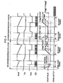
- a frame rate is increased by skip-reading pixel information (e.g., see non-Patent Document 2: M. Loose et al., "2/3-inch CMOS Imaging Sensor for High Definition Television", 2001, IEEE Workshop on CMOS and CCD Imaging sensors ).
- the frame rate of 60 frames per second can be realized in the interlaced scanning shown in Fig. 18 , although the frame rate is 30 frames per second in the progressive scanning shown in Fig. 17 .
- the frame rate can be doubled.
- non-Patent Document 2 that is, in the technique of increasing the frame rate by reading pixel information by skipping rows, the exposure time in each unit pixel is shortened as the frame rate increases. For example, the exposure time is reduced by half when the frame rate doubles. As a result, the effective sensitivity of the unit pixel is reduced by half. Therefore, when the frame rate is increased by applying skip reading of pixel information in the CMOS image sensor 100 including column-parallel ADCs, the sensitivity of the unit pixel decreases due to the higher frame rate, and thus the sensitivity of imaging result decreases disadvantageously.
- US 5.877,715 describes a circuit for performing correlated double sampling with up/down counter, wherein the circuit includes a plurality of comparators, each having a first input coupled to an associated data line for receiving first and second signals in first and second sampling intervals and a time varying reference signal is applied to the second input of each comparator.
- US 4,996,413 describes an apparatus and a method for reading data from an image detector, which includes an array of photodetectors arranged in n rows and m columns with at least a portion of the photodetectors in each column being selectively connected to a common column output signal line by a selector means.
- the present invention has been made in view of the above-described problems, and an object of the present invention is to provide a solid-state image pickup device capable of realizing a higher frame rate without decreasing sensitivity and a method for driving the solid-state image pickup device.
- unit pixels each including a photoelectric converter, are two-dimensionally arranged in a matrix pattern, column signal lines arranged for respective columns of the matrix pattern, and the unit pixels are selectively controlled in units of rows sequentially.
- Analog signals are output from the unit pixels in a selectively controlled row through the column signal lines and converted to digital values.
- the obtained digital values are added among the unit pixels of a plurality of rows and the added digital values are read.
- analog signals output from the unit pixels are converted to digital values and the digital values are added among a plurality of unit pixels and are read.
- this operation is equivalent to interlaced reading (skip reading) of pixel information.
- the amount of each piece of pixel information is larger by X times if the number of pixels to be added is X. Therefore, even when the exposure time of the unit pixels is reduced to 1/2 in order to double the frame rate, the amount of each piece of pixel information is doubled by adding digital values of unit pixels between two rows at analog-digital conversion, so that a decrease of sensitivity can be prevented.
- the digital values are added among the unit pixels of a plurality of rows and the added values are read.
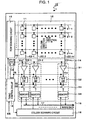
- Fig. 1 is a block diagram showing the configuration of a solid-state image pickup device according to a first embodiment of the present invention, for example, a CMOS image sensor 10 including column-parallel ADCs.
- the CMOS image sensor 10 includes a pixel array unit 12, where unit pixels 11, each including a photoelectric transducer, are two-dimensionally arranged in a matrix pattern; a row scanning circuit 13, a column processing unit 14; a reference-voltage supplying unit 15; a column scanning circuit 16; a horizontal output line 17; and a timing control circuit 18.
- the timing control circuit 18 generates clock signals and control signals serving as reference of the operations of the row scanning circuit 13, the column processing unit 14, the reference-voltage supplying unit 15, the column scanning circuit 16, and so on, based on a master clock MCK, and supplies the signals to the row scanning circuit 13, the column processing unit 14, the reference-voltage supplying unit 15, the column scanning circuit 16, and so on.
- a driving system and a signal processing system for driving and controlling each unit pixel 11 of the pixel array unit 12, that is, the row scanning circuit 13, the column processing unit 14, the reference-voltage supplying unit 15, the column scanning circuit 16, the horizontal output line 17, and the timing control circuit 18 are integrated in a chip (semiconductor substrate) 19 together with the pixel array unit 12.
- the unit pixel 11 includes a photoelectric transducer (e.g., photodiode) and a three-transistor unit consisting of a transfer transistor for transferring a charge obtained by photoelectric conversion in the photoelectric transducer to an FD (floating diffusion) unit; a reset transistor for controlling the potential of the FD unit; and an amplifier transistor for outputting a signal according to the potential of the FD unit, or a four-transistor unit further including a selecting transistor for selecting a pixel.
- a photoelectric transducer e.g., photodiode
- a three-transistor unit consisting of a transfer transistor for transferring a charge obtained by photoelectric conversion in the photoelectric transducer to an FD (floating diffusion) unit
- FD floating diffusion
- reset transistor for controlling the potential of the FD unit
- an amplifier transistor for outputting a signal according to the potential of the FD unit
- a four-transistor unit further including a selecting transistor for selecting a pixel.
- each of the row control lines 21-1 to 21-n is connected to a corresponding output terminal of the row scanning circuit 13.
- the row scanning circuit 13 includes a shift register or the like and controls the row address and row scanning of the pixel array unit 12 through the row control lines 21-1 to 21-n.
- the column processing unit 14 includes ADCs (analog-digital converters) 23-1 to 23-m, which are provided for the respective column signal lines 22-1 to 22-m of the pixel array unit 12.
- the ADCs 23-1 to 23-m convert analog signals output from the unit pixels 11 in the columns of the pixel array unit 12 to digital signals and output the digital signals.
- the present invention features the configuration of these ADCs 23-1 to 23-m, which will be described in detail later.
- the reference-voltage supplying unit 15 includes a DAC (digital-analog converter) 151 serving as a unit for generating a reference voltage Vref having a so-called ramp waveform, in which the level changes in a ramp form with a lapse of time.
- DAC digital-analog converter
- Other units than the DAC 151 may be used as a unit for generating a reference voltage Vref of a ramp waveform.
- the DAC 151 generates a reference voltage Vref having a ramp waveform based on a clock CK supplied from the timing control circuit 18 under the control by a control signal CS1 supplied from the timing control circuit 18 and supplies the reference voltage Vref to the ADCs 23-1 to 23-m of the column processing unit 14.
- Each of the ADCs 23-1 to 23-m is capable of selectively performing AD conversion according to each operation mode: a normal-frame-rate mode in a progressive scanning for reading entire information of all of the unit pixels 11; and a high-frame-rate mode where the exposure time of the unit pixels 11 is set to 1/N of the normal-frame-rate mode and the frame rate is increased by N times (e.g., twice).
- the operation mode is switched under control of control signals CS2 and CS3 supplied from the timing control circuit 18.
- Instructing information for switching between the normal-frame-rate mode and the high-frame-rate mode is supplied from an external system controller (not shown) to the timing control circuit 18.
- the ADC 23-m includes a comparator 31, an up/down counter serving as a counting unit (referred to as U/D CNT in Fig. 1 ) 32, a transfer switch 33, and a memory device 34.
- the comparator 31 compares the signal voltage Vx of the column signal line 22-m according to signals output from the unit pixels 11 in the m-th column of the pixel array unit 12 with the reference voltage Vref of a ramp waveform supplied from the reference-voltage supplying unit 15. For example, when the reference voltage Vref is higher than the signal voltage Vx, the output Vco is in a "H” level. When the reference voltage Vref is equal to or lower than the signal voltage Vx, the output Vco is in a "L" level.
- the up/down counter 32 is an asynchronous counter.
- the timing control circuit 18 supplies a clock CK to the up/down counter 32 and the DAC 151 at the same time under control by the control signal CS2, which is supplied from the timing control circuit 18. Accordingly, the up/down counter 32 performs up/down count in synchronization with the clock CK in order to measure comparison time from the start to the end of the comparing operation in the comparator 31.
- the comparison time of the first reading is measured by performing down count at the first reading operation
- the comparison time of the second reading is measured by performing up count at the second reading operation.
- a count result on the unit pixel 11 in a row is held as is. Then, after the process goes onto the unit pixel 11 in the next row, down count is performed on the previous count result at the first reading operation so as to measure the comparison time at the first reading operation, and up count is performed at the second reading operation so as to measure the comparison time at the second reading operation.
- the transfer switch 33 is turned on (closed) when the count operation of the up/down counter 32 on the unit pixel 11 of a row has been completed under control by the control signal CS3 supplied from the timing control circuit 18, and transfers the count result of the up/down counter 32 to the memory device 34 in the normal-frame-rate mode.
- the transfer switch 33 is kept in an off-state (open) when the count operation of the up/down counter 32 on the unit pixel 11 of a row is completed. Then, after the count operation of the up/down counter 32 on the unit pixel 11 of the next row has been completed, the transfer switch 33 is turned on and transfers the count result of the vertical two pixels in the up/down counter 32 to the memory device 34.
- analog signals supplied from the unit pixels 11 of the pixel array unit 12 through the column signal lines 22-1 to 22-m are converted to N-bit digital signals by the respective comparators 31 and the up/down counters 32 of the ADCs 23 (23-1 to 23-m), and the digital signals are stored in the memory devices 34 (34-1 to 34-m).
- the column scanning circuit 16 includes a shift register or the like and controls a column address and column scanning of the ADCs 23-1 to 23-m in the column processing unit 14. Under the control by the column scanning circuit 16, the N-bit digital signals which have been AD converted by the ADCs 23-1 to 23-m are sequentially read to the horizontal output line 17 and are output theretrough as image data.
- a circuit or the like for performing various signal processes on the image data output through the horizontal output line 17 may be additionally provided.
- the count result generated by the up/down counter 32 can be selectively transferred to the memory device 34 via the transfer switch 33. Therefore, the count operation by the up/down counter 32 and the operation of reading the counter result from the up/down counter 32 to the horizontal output line 17 can be controlled independently from each other.
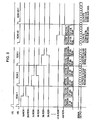
- a reset operation and a transfer operation are performed in the unit pixels 11.
- the potential of the FD unit reset to a predetermined potential is output as a reset component from the respective unit pixels 11 to the column signal lines 22-1 to 22-m.
- the transfer operation the potential of the FD unit at the time when charge generated by photoelectric conversion is transferred from the photoelectric transducer is output as a signal component from the respective unit pixels 11 to the column signal lines 22-1 to 22-m.
- a row i is selected in row scanning by the row scanning circuit 13.
- the reference voltage Vref of a ramp waveform is supplied from the DAC 151 to the respective comparators 31 of the ADCs 23-1 to 23-m, whereby the comparators 31 compare the signal voltages Vx of the column signal lines 22-1 to 22-m with the reference voltage Vref.
- a clock CK is supplied from the timing control circuit 18 to each of the up/down counters 32, so that the up/down counter 32 measures the comparison time in the comparator 31 at the first reading operation by a down count operation.
- the output Vco of the comparator 31 is reversed from a "H" level to a "L” level.
- the up/down counter 32 stops the down count operation and holds a count value corresponding to the first comparing period in the comparator 31.
- a reset component ⁇ V of the unit pixels 11 is read in the first reading operation.
- the reset component ⁇ V includes fixed-pattern noise which varies in each pixel unit 11 as an offset.
- the signal voltages Vx of the column signal lines 22-1 to 22-m are approximately known. Therefore, at the first operation of reading the reset component ⁇ V, the comparing period can be shortened by adjusting the reference voltage Vref.
- the reset component ⁇ V is compared in a count period of 7 bits (128 clocks).
- a signal component Vsig according to the amount of incident light of each unit pixel 11 is read in addition to the reset component ⁇ V in the same manner as in the first reading operation. That is, after the second reading operation from the unit pixels 11 in the selected row i to the column signal lines 22-1 to 22-m has become stable, the reference voltage Vref is supplied from the DAC 151 to the respective comparators 31 of the ADCs 23-1 to 23-m. Accordingly, the respective comparators 31 compare the signal voltages Vx of the column signal lines 22-1 to 22-m with the reference voltage Vref, and at the same time, the time of the second comparison in the respective comparators 31 is measured by the corresponding up/down counters 32 by an up count operation unlike in the first operation.
- each of the up/down counters 32 performs a down count operation at the first time and an up count operation at the second time. Accordingly, subtraction of (second comparing period)-(first comparing period) is automatically performed in the up/down counter 32. Then, the polarity of the output Vco of the comparator 31 is reversed when the reference voltage Vref and the signal voltage Vx of the respective column signal lines 22-1 to 22-m become equal to each other, and the count operation of the up/down counter 32 is stopped in response to the reversed polarity. As a result, a count value according to the subtraction result of (second comparing period)-(first comparing period) is held in the up/down counter 32.
- a signal component Vsig according to the amount of incident light is read, and thus the reference voltage Vref must be significantly varied in order to judge the amount of light in a wide range.
- comparison is performed in a count period of 10 bits (1024 clocks) when the signal component Vsig is read.
- the number of comparison bits is different in the first and second time.
- the accuracy of AD conversion can be made equal. Accordingly, a correct subtraction result can be obtained from a subtraction process (second comparing period)-(first comparing period) by the up/down counter 32.
- a digital value of N bits is held in each of the up/down counters 32. Then, the digital values (digital signals) of N bits which have been AD converted by the respective ADCs 23-1 to 23-m of the column processing unit 14 are sequentially output to the outside through the horizontal output line 17 of a width of N bits by column scanning by the column scanning circuit 16. Then, the same operation is sequentially performed for the respective rows, so that a two-dimensional image is generated.
- each of the ADCs 23-1 to 23-m includes the memory device 34.
- AD converted digital values of the unit pixels 11 in the i-th row can be transferred to the corresponding memory devices 34 and output to the outside through the horizontal output line 17, while performing in parallel a reading operation and an up/down count operation on the unit pixels 11 in the i+1-th row.
- VS denotes a vertical synchronizing signal indicating one frame period
- HS denotes a horizontal synchronizing signal indicating one horizontal scanning period.
- the up/down counter 32 In the operation shown in Fig. 3 , after a count value has been transferred from the up/down counter 32 to the memory device 34, the up/down counter 32 must be reset before starting a count operation in the up/down counter 32. If an up/down count operation for the i+1-th row is performed without resetting the up/down counter 32, the AD conversion result of the previous i-th row is set to the initial value of the up/down counter 32, and thus the sum of the i-th row and the i+1-th row is held in the up/down counter 32 by repeating the same operation.
- the adding operation in the up/down counter 32 is performed in an operation in a high-frame-rate mode, where the exposure time of the unit pixels 11 is reduced to 1/2 from the normal-frame-rate mode, where pixel information is read from all the unit pixels 11 of the pixel array unit 12.
- the up/down counter 32 is capable of holding a digital value of N bits therein after reading the digital value.
- AD-converted values of the unit pixels 11 in a plurality of rows i-th row and i+1-th row in this embodiment are added in the up/down counter 32.
- This digital value is in the up/down counter 32 is transferred to the memory device 34 through the transfer switch 33 and is output to the outside through the horizontal output line 17. Accordingly, the sum Vsig 1+Vsig 2 of the signal components of the unit pixels 11 in the i-th row and the i+1-th row can be output.
- analog signals output from the unit pixels 11 through the column signal lines 22-1 to 22-m are converted to digital values by the ADCs 23-1 to 23-m provided for the respective columns. Then, among the digital values, the values of a plurality of unit pixels 11 (e.g., each two unit pixels 11) in the vertical direction (column direction) are added and read. Accordingly, the following function and advantages can be obtained.
- the above-described operation is equivalent to interlaced reading (skip reading) of 1/2 in the vertical direction.
- pixel information is added between two pixels in the vertical direction, and thus the amount of one piece of pixel information doubles. Therefore, even when the exposure time of the unit pixels 11 is reduced to 1/2 in order to double the frame rate, the amount of each piece of pixel information doubles by adding digital values of the unit pixels of two rows at AD conversion, so that the sensitivity is not degraded compared to the normal-frame-rate mode.
- each of the ADCs 23-1 to 23-m includes the up/down counter 32, which performs an adding operation. With this configuration, a highly-accurate adding operation can be realized without using a memory device outside the chip 19 or using an additional circuit as column-parallel ADCs.
- the adding operation is performed by using the up/down counter 32 in the first embodiment, a counter may be used instead of the up/down counter 32 for a simple adding operation.
- the up/down counter 32 is advantageous because an adding operation can be performed while performing digital CDS processing of removing a reset component ⁇ V from the signal component Vsig of the unit pixel 11. Also, the processing may be realized by using an operating unit for performing a digital operation.
- the pixels are added between two rows in the first embodiment, but the pixels may be added among three or more rows. At this time, when the number of added rows is M, the amount of image data can be compressed to 1/M.
- the frame rate is increased by M times by compressing the amount of image data to 1/M and changing the data output rate.
- the frame rate may be increased by M times without changing the data output rate by shortening the AD conversion period to 1/M. That is, the amount of data may be compressed by adding pixels of rows by using the up/down counters 32 as in the CMOS image sensor 10 according to the first embodiment, but alternatively, as shown in the timing chart in Fig. 5 , the frame rate may be doubled without changing the data output rate by shortening the AD conversion period to 1/M, for example, 1/2.
- the digital count value of up-count of the up/down counter 32 is restricted up to N-1 bits in the timing chart shown in Fig. 4 .
- comparison is performed in a 1024-clock period.
- 9-bit count that is, a 512-clock period.
- the rate of time change of the reference voltage Vref (ramp waveform) generated by the DAC 151 is the same. This means that the bit accuracy of AD conversion does not change.
- the accumulation time of each unit pixel is reduced to 1/2 and the amplitude of a signal is also reduced to 1/2, so that the S/N decreases.
- the digital value generated by addition of pixels in two rows is Vsig 1+Vsig 2.
- the amplitude of the signal is (Vsig 1+Vsig 2)/2 ⁇ Vsig 1. In this way, the change of signal amplitude is small and thus the S/N is not degraded.
- the frame rate increases by M times. At this time, the frame rate can be increased without degrading the S/N by decreasing the bit accuracy of AD conversion of N bits to N-M bits.
- Fig. 6 is a block diagram showing the configuration of a CMOS image sensor 50 including column-parallel ADCs according to a second embodiment of the present invention.
- Fig. 7 shows a timing chart for illustrating the operation of the CMOS image sensor 50 according to this embodiment.
- CMOS image sensor 50 including column-parallel ADCs is basically the same as that of the CMOS image sensor 10 including column-parallel ADCs according to the first embodiment shown in Fig. 1 .
- a row scanning circuit 13A includes an address decoder capable of selecting arbitrary row control lines 21-i (21-1 to 21-n).
- the row scanning circuit 13A including the address decoder is capable of sequentially selecting the row control lines 21-1 to 21-n in the order of first row, third row, second row, fourth row, ⁇ , as shown in Fig. 7 , for example.
- the pixel 11-11 in the first row control line 21-1 and the pixel 11-31 in the third row control line 21-3 are added, and the pixel 11-12 in the first row control line 21-1 and the pixel 11-32 in the third row control line 21-3 are added.
- the pixels 11-11, 11-12, 11-13, ⁇ in the first row can be added to the pixels 11-31, 11-32, 11-33 ⁇ in the third row, respectively.
- the pixel 11-21 in the second row control line 21-2 and the pixel 11-41 in the fourth row control line 21-4 are added, and the pixel 11-22 in the second row control line 21-2 and the pixel 11-42 in the fourth row control line 21-4 are added.
- the pixels 11-21, 11-22, 11-23 ⁇ in the second row can be added to the pixels 11-41, 11-42, and 11-43 ⁇ in the fourth row, respectively. That is, pixels can be added between odd-numbered rows and between even-numbered rows.
- color filters are arranged in a Bayer pattern on the pixel array unit 12 as shown in Fig. 6 .
- G (green) and R (red) color filters or B (blue) and G color filters are arranged in each row.
- CMOS image sensor including the Bayer-patterned color filters
- the row control lines 21-1 to 21-n are sequentially selected as in the CMOS sensor 10 according to the first embodiment, pixels of different color-filter elements are added, and thus different colors are mixed.
- pixels can be added between odd-numbered rows and between even-numbered rows so that pixels of the same color can be added. Therefore, color mixture due to addition of pixels does not occur.
- Fig. 8 is a block diagram showing the configuration of a CMOS image sensor 60 including column-parallel ADCs according to a third embodiment of the present invention.
- parts which are the same as those in Fig. 1 are denoted by the same reference numerals.
- the configuration of the CMOS image sensor 60 including column-parallel ADCs according to this embodiment is basically the same as that of the CMOS image sensor 10 including column-parallel ADCs according to the first embodiment shown in Fig. 1 . The difference between them is as follows.
- each of the ADCs 23-1, 23-3, ⁇ , connected to the odd-numbered column signal lines 22-1, 22-3, ⁇ is output through a horizontal output line 17-1 of an N-bit width.
- the output of each of the ADCs 23-2, 23-4, ⁇ , connected to the even-numbered column signal lines 22-2, 22-4, ⁇ is output through a horizontal output line 17-2 of an N-bit width.
- the digital signals of the odd-numbered rows output through the horizontal output line 17-1 and the digital signals of the even-numbered rows output through the horizontal output line 17-2 are added in a digital adder 61 of N bits.
- the count result generated by the up/down counter 32 is transferred to the memory device 34 and is held therein.
- a counting operation in the up/down counter 32 and an operation of reading a count result from the memory device 34 to the horizontal output line 17-1 or 17-2 can be controlled independently from each other. Therefore, count values of the even-numbered columns and odd-numbered columns can be read from the memory devices 34 and added in the digital adder 61 while performing a counting operation in each up/down counter 32. As a result, pixels can be added between two columns.
- An operation of reading signals from the unit pixels 11 of the pixel array unit 12 in units of rows and performing a count operation in the up/down counters 32 of the ADCs 23-1, 23-2, ⁇ , is the same as that in the CMOS image sensor 10 according to the first embodiment.
- An operation of adding digital count values of the x-th row (x is an arbitrary number of 1 to n-1) and the x+1-th row in the corresponding up/down counter 32 is the same as that in the CMOS image sensor 50 according to the second embodiment.
- the addition result is transferred to the memory device 34 in each column, and the addition results of the odd-numbered columns and the even-numbered columns are input to the digital adder 31 through the horizontal output lines 17-1 and 17-2, respectively.
- control signals M1, M2, M3, ⁇ , output from the column scanning circuit 16 are simultaneously output in pairs of M1 and M2, M3 and M4, ⁇ . Accordingly, the digital values (addition results) held in the memory devices 34 are simultaneously output to the horizontal output line 17-1 or 17-2 in units of two columns.
- the addition result in the odd-numbered columns is output to signal output A and the addition result in the even-numbered columns is output to signal output B.
- the addition result of the pixels 11-11 and 11-21 is output as a top signal of the signal output A and the addition result of the pixels 11-12 and 11-22 is output as a top signal of the signal output B.
- the addition result of the four pixels 11-11, 11-12, 11-21, and 11-22 is output as the top output of the digital adder 61.
- the frame rate can be increased by four times while keeping the sensitivity constant as in the CMOS image sensor 50 according to the second embodiment.
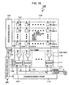
- Fig. 10 is a block diagram showing the configuration of a CMOS image sensor 70 including column-parallel ADCs according to a fourth embodiment of the present invention.
- parts which are the same as those in Fig. 1 are denoted by the same reference numerals.
- the column processing unit 14, the reference-voltage supplying unit 15, the column scanning circuit 16, and the horizontal output line 17 (17-1 and 17-2) are provided on only one of the upper and lower sides (e.g., lower side) of the column direction of the pixel array unit 12.
- CMOS image sensor 70 including column-parallel ADCs in the CMOS image sensor 70 including column-parallel ADCs according to this embodiment, a pair of column processing units 14A and 14B, a pair of reference-voltage supplying units 15A and 15B, a pair of column scanning circuits 16A and 16B, and a pair of horizontal output lines 17A and 17B are disposed on both sides of the pixel array unit 12 in the column direction. Further, selecting switches 71A and 71B are disposed between the pixel array unit 12 and the column processing units 14A and 14B.
- the pair of column processing units 14A and 14B, the pair of reference-voltage supplying units 15A and 15B, and the pair of column scanning circuits 16A and 16B have the entirely same configuration as that of the column processing unit 14, the reference-voltage supplying unit 15, and the column scanning circuit 16, respectively, of the CMOS image sensor 10 according to the first embodiment.
- Each of the horizontal output lines 17A and 17B is a signal line of N bits, which transmits digital signals of N bits output from the column processing unit 14A or 14B to a digital adder 72 of N bits.
- the digital adder 72 adds the digital signals output from the column processing units 14A and 14B through the horizontal output lines 17A and 17B.
- the selecting switches 71A and 71B operate in a complimentary manner so as to connect one of two adjoining column signal lines to the column processing unit 14A when the other column signal line is connected to the column processing unit 14B, and vice versa.
- the selecting switches 71A and 71B fixed contacts on one side (contacts a) are connected to both ends of the column signal line 22-2, the other fixed contacts b are connected to both ends of the column signal line 22-3, and movable contacts c are connected to an ADC 23A-2 and an ADC 23B-1, respectively.
- the movable contact c of the selecting switch 71A is connected to the fixed contact a
- the movable contact c of the selecting switch 71B is connected to the fixed contact b.
- the movable contact c of the selecting switch 71A is connected to the fixed contact b
- the movable contact c of the selecting switch 71B is connected to the fixed contact a.
- Fig. 10 In order to simplify the figure, only the selecting switches 71A and 71B connected between the column signal lines 22-2 and 22-3 are shown in Fig. 10 . However, these selecting switches 71A and 71B are provided for every two columns in units of two adjoining column signal lines from the second column.
- CMOS image sensor 70 including the column-parallel ADCs when the movable contact c of the selecting switch 71A is connected to the fixed contact a and when the movable contact c of the selecting switch 71B is connected to the fixed contact b, analog signals of the pixels in the first and second columns, the fifth and sixth columns, ⁇ , are read into the column processing unit 14A, and analog signals of the pixels in the third and fourth columns, the seventh and eighth columns, ⁇ , are read into the column processing unit 14B. Then, the analog signals are converted to digital signals by respective comparators 31A and 31B and up/down counters 32A and 32B, and the digital signals are stored in the respective memory devices 34A and 34B. The equivalent circuit of this case is shown in Fig. 11 .
- control signals Ma1, Ma2, ⁇ , from the column scanning circuit 16A and control signals Mb1, Mb2, ⁇ , from the column scanning circuit 16B are sequentially output in the same timing, respectively.
- the digital values of the pixels in the first and third columns stored in the memory devices 34A and 34B in the ADCs 23A-1 and 23B-1 are simultaneously read into the horizontal output lines 17A and 17B by the control signals Ma1 and Mb1, respectively.
- the digital values of the pixels in the second and fourth columns stored in the memory devices 34A and 34B in the ADCs 23A-2 and 23B-2 are simultaneously read into the horizontal output lines 17A and 17B by the control signals Ma2 and Mb2, respectively.
- the same operation is sequentially performed thereafter.
- the digital adder 72 adds digital values of the pixels of two odd-numbered columns and two even-numbered columns like this: digital values of the pixels in the first and third columns are added and digital values of the pixels in the second and fourth columns are added.
- digital values of the pixels in the first and third columns are added and digital values of the pixels in the second and fourth columns are added.
- same colors can be added together when the color filters are arranged in a Bayer pattern as shown in Fig. 11 . Therefore, mixture of different colors due to addition of pixels does not occur.
- the frame rate can be increased by four times while keeping the sensitivity constant.
- the control signals Ma1, Ma2, ⁇ from the column scanning circuit 16A and the control signals Mb1, Mb2, ⁇ from the column scanning circuit 16B are sequentially output in the same timing, respectively. Therefore, the digital values of the pixels in the first and second columns stored in the memory devices 34A and 34B in the ADCs 23A-1 and 23B-1 are simultaneously read into the horizontal output lines 17A and 17B by the control signals Ma1 and Mb1, respectively. Then, the digital values of the pixels in the third and fourth columns stored in the memory devices 34A and 34B in the ADCs 23A-2 and 23B-2 are simultaneously read into the horizontal output lines 17A and 17B by the control signals Ma2 and Mb2, respectively. The same operation is sequentially performed thereafter.
- the digital adder 72 adds digital values of the pixels in two adjoining (sequential) columns like this: digital values of the pixels in the first and second columns are added and digital values of the pixels in the third and fourth columns are added.
- digital values of the pixels in the first and second columns are added and digital values of the pixels in the third and fourth columns are added.
- Such addition of pixels between two adjoining columns can be applied to a three-plate image sensor in which color filters of the same color (only R/G/B) are provided on the same sensor.
- the frame rate can be increased by four times while keeping the sensitivity constant.
- the column processing units 14A and 14B are disposed on both sides of the pixel array unit 12, and the selecting switches 71A and 71B are provided between the pixel array unit 12 and the column processing units 14A and 14B.
- the pair of columns to be added can be arbitrarily selected.
- addition of digital values of pixels can be realized both in a single-plate image sensor having a Bayer pattern and a three-plate image sensor.
- each of the horizontal output lines 17A and 17B are provided corresponding to the pair of column processing units 14A and 14B.
- each of the horizontal output lines 17A and 17B may comprise a plurality of lines (e.g., two lines), so that two control signals M are simultaneously output from each of the column scanning circuits 16A and 16B. Accordingly, addition of pixels can be realized between four columns.
- the pair of column processing units, the pair of reference-voltage supplying units, the pair of column scanning circuits, the pair of horizontal output lines, and the pair of selecting switches are provided so as to add pixels in two columns.
- three or more column processing units, reference-voltage supplying units, column scanning circuits, horizontal output lines, and selecting switches may be provided. With this configuration, addition of pixels can be realized between three or more columns.
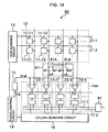
- Fig. 14 is a block diagram showing the configuration of a CMOS image sensor 80 including column-parallel ADCs according to a fifth embodiment of the present invention.
- parts which are the same as those in Fig. 8 are denoted by the same reference numerals.
- the configuration of the CMOS image sensor 80 including column-parallel ADCs according to this embodiment is basically the same as that of the CMOS image sensor 60 including column-parallel ADCs according to the third embodiment shown in Fig. 8 .
- the difference therebetween is as follows.
- CMOS image sensor 60 including column-parallel ADCs digital values of pixels are added between odd-numbered columns and between even-numbered columns.
- a selecting switch 81 is provided between the pixel array unit 12 and the column processing unit 14. By using the function of the selecting switch 81, the pair of columns to be added can be arbitrarily selected.
- the selecting switch 81 includes two switches 81A and 81B which operate in conjunction with each other.
- a fixed contact a1 is connected to the second column signal line 22-2
- a fixed contact b1 is connected to the third column signal line 22-3
- a movable contact c1 is connected to the second ADC 23-2.
- a fixed contact a2 is connected to the third column signal line 22-3
- a fixed contact b2 is connected to the second column signal line 22-2
- a movable contact c2 is connected to the third ADC 23-3.
- the selecting switch 81 between the column signal lines 22-2 and 22-3 is shown in Fig. 14 .
- the selecting switch 81 is provided for every two columns in units of adjoining two column signal lines from the second column.
- CMOS image sensor 80 including column-parallel ADCs when the movable contacts c1 and c2 of the selecting switch 81 are connected to the fixed contacts a1 and a2, respectively, analog signals of the pixels in the first, second, third, fourth, ⁇ columns are converted to digital signals by the ADCs 23-1, 23-2, 23-3, 23-4, ⁇ , respectively, and the digital signals are held in the ADCs.
- control signals M1, M2, M3, M4, ⁇ are simultaneously output from the column scanning circuit 16 in pairs of M1 and M2, M3 and M4, ⁇ , so that the digital values held in the memory devices 34 are simultaneously output to the horizontal output lines 17-1 and 17-2 in units of two columns. Then, the digital values output through the horizontal output line 17-1 and the digital values output through the horizontal output line 17-2 are added in the digital adder 61 of N bits.
- the digital adder 61 adds the digital values of the pixels in adjoining (sequential) two columns like this: adds the digital values of the pixels in the first and second columns and then adds the digital values of the pixels in the third and fourth columns.
- Such addition of pixels between two adjoining columns can be applied to a three-plate image sensor in which color filters of the same color (only R/G/B) are provided on the same sensor.
- the frame rate can be increased by four times while keeping the sensitivity constant.
- analog signals of the pixels in the first column, the third column, ⁇ are converted to digital signals by the odd-numbered ADCs 23-1, 23-3, ⁇ , respectively, and the digital signals are held in the ADCs.
- analog signals of the pixels in the second column, the fourth column, ⁇ are converted to digital signals by the even-numbered ADCs 23-2, 23-4, ⁇ , respectively, and the digital signals are held in the ADCs.
- the output of each of the odd-numbered ADCs 23-1, 23-3, ⁇ is output through the horizontal output line 17-1 of an N-bit width
- the output of each of the even-numbered ADCs 23-2, 23-4, ⁇ is output through the horizontal output line 17-2 of an N-bit width.
- the digital signals in the odd-numbered columns output through the horizontal output line 17-1 and the digital signals in the even-numbered columns output through the horizontal output line 17-2 are added in the digital adder 61 of N bits.
- This operation is the same as that of the CMOS image sensor 60 including column-parallel ADCs according to the third embodiment. With this operation, two pixels can be added between odd-numbered columns and between even-numbered columns. As a result, pixels of same colors can be added when the color filters are arranged in a Bayer pattern, and thus mixture of different colors caused by addition of pixels does not occur.
- the selecting switch 81 is provided between the pixel array unit 12 and the column processing unit 14. With this configuration, the pair of columns to be added can be arbitrarily selected by using the function of the selecting switch 81. Therefore, addition of pixels can be realized both in a single-plate image sensor having a Bayer pattern and a three-plate image sensor by using this circuit configuration.
- two horizontal output lines are provided and the selecting switch 81 is provided between two columns so as to realize addition of two pixels between columns.
- the selecting switch 81 is provided between three or more columns so as to realize addition of two pixels between columns.
Landscapes
- Engineering & Computer Science (AREA)
- Multimedia (AREA)
- Signal Processing (AREA)
- Theoretical Computer Science (AREA)
- Transforming Light Signals Into Electric Signals (AREA)
- Computer Vision & Pattern Recognition (AREA)
- Solid State Image Pick-Up Elements (AREA)
Claims (17)
- Festkörperbildaufnahmevorrichtung, mit:einer Pixelanordnung (12), die Pixel (11) enthält, die zweidimensional in einem Matrixmuster angeordnet sind, wobei Spaltensignalleitungen (22-1 bis 22-n) jeweiligen Spalten des Matrixmusters entsprechen und Zeilensteuerleitungen (21-1 bis 21-n) jeweiligen Zeilen des Matrixmusters entsprechen, wobei jedes Pixel (11) einen photoelektrischen Umsetzer enthält,einer Spaltenverarbeitungseinheit (14), die Analog/Digital-Umsetzungsmittel (23-1 bis 23-m) enthält, die für jeweilige Spaltensignalleitungen (21-1 bis 22-m) vorgesehen sind, wobei die Analog/Digital-Umsetzungsmittel konfiguriert sind, um analoge Signale, die von den Pixeln (11) in den Spalten ausgegeben werden, in addierte digitale Signale umzusetzen, wobei die Analog/Digital-Umsetzungsmittel enthalten:Vergleichsmittel (31) zum Vergleichen des analogen Signalausgangs von einem Pixel (11) mit einer Referenzspannung; undeinen Zähler (32) zum Messen der Vergleichszeit vom Beginn bis zum Ende der Vergleichsoperation in den Vergleichsmitteln (31) und zum Speichern der Vergleichszeit als ein digitales Signal;wobei die Festkörperbildaufnahmevorrichtung ferner versehen ist mit:Mitteln (18) zum Steuern jedes der Analog/Digital-Umsetzungsmittel (23-1 bis 23-m), um die Vergleichsoperation und die Zähloperation an mehreren analogen Signalen mehrerer jeweiliger Zeilen zu wiederholen, ohne den Zähler zurückzusetzen, bevor eine wiederholte Zähloperation begonnen wird, wobei eine Summe von Pixeln (11) einer Spalte und der mehreren Zeilen in dem Zähler (32) als ein addiertes digitales Signal gespeichert wird.
- Festkörperbildaufnahmevorrichtung nach Anspruch 1, ferner mit:Zeilenabtastmitteln (13) zum Steuern einer Zeilenadresse und zum Abtasten der Zeilenpixelanordnung (12) durch die Zeilensteuerleitungen (21-1 bis 21-n);Spaltenabtastmitteln (16) zum Steuern der Ausgabe der digitalen Signale, die in den jeweiligen Analog/Digital-Umsetzungsmitteln (23-1 bis 23-m) gespeichert sind; undeiner Ausgabeleitung zum Senden der von den Analog/Digital-Umsetzungsmitteln (23-1 bis 23-m) ausgegebenen digitalen Signale unter der Steuerung durch die Spaltenabtastmitteln (16).
- Festkörperbildaufnahmevorrichtung nach Anspruch 1 oder 2, wobei der Zähler (32) ein Aufwärts/Abwärts-Zähler ist, der eine Subtraktion durch Ausführen einer Abwärtszählung und einer Aufwärtszählung an einem ersten und einem zweiten analogen Signal, die von einem der Pixel (11) ausgegeben werden, ausführt und der eine Addition durch Wiederholen einer Aufwärtszählung an den mehreren analogen Signalen ausführt.
- Festkörperbildaufnahmevorrichtung nach Anspruch 2, wobei die Zeilenabtastmittel (13) einen Adressendecodierer enthalten, der konfiguriert ist, um eine Zeile von Pixeln in der Pixelanordnung in beliebiger Reihenfolge auszuwählen.
- Festkörperbildaufnahmevorrichtung nach Anspruch 4, wobei jedes der Analog/Digital-Umsetzungsmittel (23-1 bis 23-m) konfiguriert ist, um die digitalen Signale der Pixel (11) in derselben Spalte unter den mehreren Zeilen zu addieren.
- Festkörperbildaufnahmevorrichtung nach Anspruch 5, wobei jedes der Analog/Digital-Umsetzungsmittel (23-1 bis 23-m) konfiguriert ist, um die digitalen Signale der Pixel (11) in derselben Spalte unter ungeradzahligen Zeilen und unter geradzahligen Zeilen unabhängig voneinander zu addieren.
- Festkörperbildaufnahmevorrichtung nach Anspruch 2, wobei die Spaltenverarbeitungseinheit (14) ferner enthält:Auswahlmittel, die konfiguriert sind, um analoge Signale, die von den Pixeln (11) in einer Zeile, die durch die Zeilenabtastmittel (11) über die Spaltensignalleitungen (22-1, ..., 22-m) wahlweise gesteuert werden, ausgegeben werden, auf die mehreren Analog/Digital-Umsetzungsmittel (23-1 bis 23-m), die den Spalten entsprechen, zu verteilen.
- Festkörperbildaufnahmevorrichtung nach Anspruch 2, wobei die mehreren Analog/Digital-Umsetzungsmittel (23-1 bis 23-m) den Spaltensignalleitungen (22-1, ..., 22-m) entsprechen und die Ausgabeleitung mehrere Ausgabeleitungen enthält, so dass die von den mehreren Analog/Digital-Umsetzungsmitteln (23-1 bis 23-m) ausgegebenen digitalen Signale durch die mehreren Ausgabeleitungen übertragen werden, wobei die Festkörperbildaufnahmevorrichtung ferner versehen ist mit:Auswahlmitteln, die konfiguriert sind, um analoge Signale, die von den Pixeln (11) in einer Zeile, die durch die Zeilenabtastmittel (13) über die Spaltensignalleitungen (22-1, ..., 22-m) wahlweise gesteuert werden, ausgegeben werden, auf die mehreren Analog/Digital-Umsetzungsmittel (23-1 bis 23-m), die den jeweiligen Spaltensignalleitungen (22-1, ..., 22-m) entsprechen, zu verteilen.
- Verfahren zum Ansteuern einer Festkörperbildaufnahmevorrichtung, die eine Pixelanordnung (12) enthält, die Pixel (11) aufweist, die in einem Matrixmuster zweidimensional angeordnet sind, wobei Spaltensignalleitungen (22-1, ..., 22-m) jeweiligen Spalten des Matrixmusters entsprechen, wobei die Pixel (11) durch Zeilensteuerleitungen gesteuert werden, die jeweiligen Zeilen des Matrixmusters entsprechen, wobei jedes Pixel (11) einen photoelektrischen Umsetzer enthält, wobei das Verfahren enthält:Übertragen analoger Signale, die von den Pixeln (11) in einer durch die Zeilensteuerleitungen ausgewählten Zeile über die Spaltensignalleitungen (22-1, ..., 22-m) ausgegeben werden, an Analog/Digital-Umsetzungsmittel (23-1 bis 23-m), wobei die Analog/Digital-Umsetzungsmittel für jeweilige Spaltensignalleitungen vorgesehen sind und ein Verarbeitungsmittel (32) enthalten, wobei die Analog/Digital-Umsetzungsmittel (23-1 bis 23-m) einen Teil einer Spaltenverarbeitungseinheit (14) bilden, wobei die Analog/Digital-Umsetzungsmittel konfiguriert sind, umdie analogen Signale in addierte digitale Signale umzusetzen;wobei jedes der Analog/Digital-Umsetzungsmittel ausführt:Vergleichen in einer Vergleichsoperation des von jedem Einheitspixel ausgegebenen analogen Signals mit einer Referenzspannung;Messen in einer Zähloperation eines Zählers der Vergleichszeit von dem Beginn zu dem Ende der Vergleichsoperation und Speichern der Vergleichszeit in dem Zähler als ein digitales Signal;Wiederholen der Vergleichsoperation und der Zähloperation an mehreren analogen Signalen mehrerer entsprechender Zeilen ohne Zurücksetzen des Zählers, bevor eine wiederholte Zähloperation beginnt, wobei eine Summe von Pixeln einer Spalte der mehreren Zeilen in dem Zähler (32) als ein addiertes digitales Signal gespeichert wird; undLesen der addierten digitalen Signale von den jeweiligen Analog/Digital-Umsetzungsmitteln (23-1 bis 23-m).
- Verfahren nach Anspruch 9, das ferner das Senken der Bitgenauigkeit einer Analog/Digital-Umsetzung entsprechend der Anzahl von zu addierenden Zeilen und das Verringern der Analog/Digital-Umsetzungszeit enthält.
- Verfahren nach Anspruch 10, das ferner dann, wenn die Anzahl von Zeilen gleich M ist, das Senken der Bitgenauigkeit der Analog/Digital-Umsetzung von N Bits auf N - M Bits und das Verringern der Analog/Digital-Umsetzungszeit auf 1/M enthält.
- Verfahren nach Anspruch 9, das ferner das Auswählen der Zeile von Pixeln (11) in der Pixelanordnungseinheit in beliebiger Reihenfolge enthält.
- Verfahren nach Anspruch 12, wobei in den jeweiligen wiederholten Zähloperationen die digitalen Signale der Pixel (11) in derselben Spalte unter den mehreren Zeilen addiert werden.
- Verfahren nach Anspruch 13, wobei in den jeweiligen wiederholten Zähloperationen die digitalen Signale der Pixel (11) derselben Spalte unter ungeradzahligen Zeilen und unter geradzahligen Zeilen unabhängig voneinander addiert werden.
- Verfahren nach Anspruch 9, das ferner das Ausführen einer Addition unter den Pixeln (11) mehrerer Spalten enthält.
- Verfahren nach Anspruch 15, wobei bei der Addition die addierten digitalen Signale unter den mehreren Spalten addiert werden.
- Verfahren nach Anspruch 15, wobei bei der Addition die addierten digitalen Signale unter beliebigen Paaren mehrerer Spalten addiert werden.
Applications Claiming Priority (4)
| Application Number | Priority Date | Filing Date | Title |
|---|---|---|---|
| JP2004045943 | 2004-02-23 | ||
| JP2004045943 | 2004-02-23 | ||
| JP2004208038 | 2004-07-15 | ||
| JP2004208038A JP4107269B2 (ja) | 2004-02-23 | 2004-07-15 | 固体撮像装置 |
Publications (3)
| Publication Number | Publication Date |
|---|---|
| EP1566959A2 EP1566959A2 (de) | 2005-08-24 |
| EP1566959A3 EP1566959A3 (de) | 2007-11-21 |
| EP1566959B1 true EP1566959B1 (de) | 2012-11-14 |
Family
ID=34713016
Family Applications (1)
| Application Number | Title | Priority Date | Filing Date |
|---|---|---|---|
| EP05003683A Expired - Lifetime EP1566959B1 (de) | 2004-02-23 | 2005-02-21 | Festkörper-Bildaufnahmevorrichtung und Verfahren zu ihrer Ansteuerung |
Country Status (5)
| Country | Link |
|---|---|
| US (11) | US7623173B2 (de) |
| EP (1) | EP1566959B1 (de) |
| JP (1) | JP4107269B2 (de) |
| KR (1) | KR101141449B1 (de) |
| TW (1) | TWI260162B (de) |
Families Citing this family (211)
| Publication number | Priority date | Publication date | Assignee | Title |
|---|---|---|---|---|
| US8169517B2 (en) * | 2001-03-26 | 2012-05-01 | Panavision Imaging Llc | Image sensor ADC and CDS per column with oversampling |
| US7903159B2 (en) * | 2001-03-26 | 2011-03-08 | Panavision Imaging Llc | Image sensor ADC and CDS per column |
| JP4107269B2 (ja) * | 2004-02-23 | 2008-06-25 | ソニー株式会社 | 固体撮像装置 |
| JP4584634B2 (ja) * | 2004-06-29 | 2010-11-24 | オリンパス株式会社 | 固体撮像装置 |
| JP2006018663A (ja) * | 2004-07-02 | 2006-01-19 | Fujitsu Ltd | 電流安定化回路、電流安定化方法、及び固体撮像装置 |
| JP4481758B2 (ja) * | 2004-07-28 | 2010-06-16 | 株式会社東芝 | 信号処理装置及びデータ処理装置 |
| JP4687155B2 (ja) * | 2005-03-09 | 2011-05-25 | ソニー株式会社 | 固体撮像装置およびその駆動方法 |
| GB2438693B (en) * | 2005-03-30 | 2009-07-08 | Micron Technology Inc | High density row ram for column parallel CMOS image sensors |
| JP4855704B2 (ja) * | 2005-03-31 | 2012-01-18 | 株式会社東芝 | 固体撮像装置 |
| TW201101476A (en) | 2005-06-02 | 2011-01-01 | Sony Corp | Semiconductor image sensor module and method of manufacturing the same |
| US8179296B2 (en) | 2005-09-30 | 2012-05-15 | The Massachusetts Institute Of Technology | Digital readout method and apparatus |
| JP4765578B2 (ja) * | 2005-11-24 | 2011-09-07 | ソニー株式会社 | 固体撮像素子とその駆動方法、及びカメラモジュール |
| JP4802767B2 (ja) * | 2006-03-06 | 2011-10-26 | ソニー株式会社 | アナログ−デジタル変換装置と、それを用いた固体撮像装置とその駆動方法 |
| JP4744343B2 (ja) * | 2006-04-10 | 2011-08-10 | ソニー株式会社 | 固体撮像装置および固体撮像装置の駆動方法 |
| JP5168595B2 (ja) | 2006-05-22 | 2013-03-21 | トムソン ライセンシング | イメージセンサおよびイメージセンサのピクセル読出し方法 |
| US8889348B2 (en) * | 2006-06-07 | 2014-11-18 | The Trustees Of Columbia University In The City Of New York | DNA sequencing by nanopore using modified nucleotides |
| JP4882545B2 (ja) * | 2006-06-28 | 2012-02-22 | ソニー株式会社 | 固体撮像装置 |
| JP2008017090A (ja) * | 2006-07-05 | 2008-01-24 | Casio Comput Co Ltd | 撮像装置、及び電子ズーム方法 |
| KR100803229B1 (ko) | 2006-08-09 | 2008-02-14 | (주) 픽셀플러스 | 리드 아웃 회로를 공유하는 이미지 센서 및 리드 아웃회로를 공유하는 방법 |
| JP4952498B2 (ja) * | 2006-10-13 | 2012-06-13 | ソニー株式会社 | データ処理装置、固体撮像装置、撮像装置、電子機器 |
| US7755017B2 (en) * | 2006-10-13 | 2010-07-13 | Sony Corporation | Solid-image-pickup device, image-pickup device, and method of driving solid-image-pickup device |
| US8154606B2 (en) | 2006-10-24 | 2012-04-10 | Sony Corporation | Image pickup apparatus and reproduction control apparatus |
| US20100226495A1 (en) | 2007-10-29 | 2010-09-09 | Michael Kelly | Digital readout method and apparatus |
| JP4843461B2 (ja) | 2006-11-13 | 2011-12-21 | 株式会社東芝 | 固体撮像装置 |
| JP2008136043A (ja) * | 2006-11-29 | 2008-06-12 | Sony Corp | 固体撮像装置、撮像装置 |
| US8237808B2 (en) | 2007-01-17 | 2012-08-07 | Sony Corporation | Solid state imaging device and imaging apparatus adjusting the spatial positions of pixels after addition by controlling the ratio of weight values during addition |
| JP4674589B2 (ja) | 2007-02-05 | 2011-04-20 | ソニー株式会社 | 固体撮像装置および撮像装置 |
| JP4325681B2 (ja) * | 2007-02-13 | 2009-09-02 | ソニー株式会社 | 固体撮像装置、撮像装置 |
| JP4101281B1 (ja) | 2007-03-15 | 2008-06-18 | キヤノン株式会社 | 固体撮像装置及び固体撮像装置の駆動方法 |
| JP5066996B2 (ja) * | 2007-04-23 | 2012-11-07 | ソニー株式会社 | 固体撮像装置、固体撮像装置の信号処理方法および撮像装置 |
| JP4389959B2 (ja) * | 2007-04-23 | 2009-12-24 | ソニー株式会社 | 固体撮像装置、固体撮像装置の信号処理方法および撮像装置 |
| JP5067011B2 (ja) * | 2007-05-18 | 2012-11-07 | ソニー株式会社 | 固体撮像装置、撮像装置、電子機器 |
| JP2008294913A (ja) * | 2007-05-28 | 2008-12-04 | Panasonic Corp | 固体撮像装置およびその駆動方法 |
| US7538702B2 (en) * | 2007-06-15 | 2009-05-26 | Micron Technology, Inc. | Quantizing circuits with variable parameters |
| US7884871B2 (en) * | 2007-06-15 | 2011-02-08 | Aptina Imaging Corporation | Images with high speed digital frame transfer and frame processing |
| US7889257B2 (en) * | 2007-07-18 | 2011-02-15 | Mesa Imaging Ag | On-chip time-based digital conversion of pixel outputs |
| US8063976B2 (en) * | 2007-07-24 | 2011-11-22 | Casio Computer Co., Ltd. | Image pick-up apparatus and method of controlling the image pick-up apparatus |
| JP4929090B2 (ja) * | 2007-07-26 | 2012-05-09 | パナソニック株式会社 | 固体撮像装置およびその駆動方法 |
| JP4951440B2 (ja) * | 2007-08-10 | 2012-06-13 | 富士フイルム株式会社 | 撮像装置及び固体撮像素子の駆動方法 |
| JP4379504B2 (ja) | 2007-08-13 | 2009-12-09 | ソニー株式会社 | 固体撮像素子、およびカメラシステム |
| KR101377270B1 (ko) * | 2007-08-29 | 2014-03-21 | 삼성전자주식회사 | 리플 카운터를 포함하는 이미지 센서와 상기 이미지 센서의 동작 방법 |
| JP4386118B2 (ja) | 2007-08-31 | 2009-12-16 | ソニー株式会社 | 撮像回路 |
| JP4978795B2 (ja) | 2007-09-28 | 2012-07-18 | ソニー株式会社 | 固体撮像装置、駆動制御方法、および撮像装置 |
| JP2009089085A (ja) * | 2007-09-28 | 2009-04-23 | Sony Corp | 固体撮像素子およびその駆動方法、並びにカメラシステム |
| JP4858388B2 (ja) | 2007-09-28 | 2012-01-18 | ソニー株式会社 | 固体撮像装置、駆動制御方法、および撮像装置 |
| JP4853445B2 (ja) * | 2007-09-28 | 2012-01-11 | ソニー株式会社 | A/d変換回路、固体撮像素子、およびカメラシステム |
| US7920190B2 (en) * | 2007-10-11 | 2011-04-05 | Aptina Imaging Corporation | Method and apparatus providing column parallel architecture for imagers |
| TWI399088B (zh) | 2007-10-12 | 2013-06-11 | Sony Corp | 資料處理器,固態成像裝置,成像裝置,及電子設備 |
| JP2009124514A (ja) | 2007-11-15 | 2009-06-04 | Sony Corp | 固体撮像素子、およびカメラシステム |
| JP4900200B2 (ja) | 2007-11-15 | 2012-03-21 | ソニー株式会社 | 固体撮像素子、およびカメラシステム |
| JP4403435B2 (ja) | 2007-11-16 | 2010-01-27 | ソニー株式会社 | 固体撮像装置、駆動制御方法、および撮像装置 |
| US7855748B2 (en) * | 2007-12-03 | 2010-12-21 | Altasens, Inc. | Reference voltage generation in imaging sensors |
| JP4661876B2 (ja) | 2008-01-18 | 2011-03-30 | ソニー株式会社 | 固体撮像素子、およびカメラシステム |
| JP2009206709A (ja) * | 2008-02-27 | 2009-09-10 | Sony Corp | 固体撮像装置、固体撮像装置の駆動方法および電子機器 |
| JP4442695B2 (ja) * | 2008-02-29 | 2010-03-31 | ソニー株式会社 | 固体撮像装置及びカメラ装置 |
| JP4661891B2 (ja) * | 2008-03-18 | 2011-03-30 | ソニー株式会社 | Ad変換装置、固体撮像素子、およびカメラシステム |
| JP4569647B2 (ja) * | 2008-03-18 | 2010-10-27 | ソニー株式会社 | Ad変換装置、ad変換方法、固体撮像素子、およびカメラシステム |
| JP5059669B2 (ja) * | 2008-03-26 | 2012-10-24 | オリンパス株式会社 | 固体撮像装置 |
| JP4500862B2 (ja) * | 2008-04-11 | 2010-07-14 | キヤノン株式会社 | 固体撮像装置の駆動方法 |
| US8023022B2 (en) * | 2008-05-13 | 2011-09-20 | Olympus Corporation | Solid-state imaging apparatus |
| JP5347341B2 (ja) * | 2008-06-06 | 2013-11-20 | ソニー株式会社 | 固体撮像装置、撮像装置、電子機器、ad変換装置、ad変換方法 |
| JP5279352B2 (ja) * | 2008-06-06 | 2013-09-04 | キヤノン株式会社 | 固体撮像装置 |
| JP5272634B2 (ja) | 2008-06-20 | 2013-08-28 | ソニー株式会社 | 固体撮像装置、固体撮像装置の信号処理方法および撮像装置 |
| JP4725608B2 (ja) | 2008-07-03 | 2011-07-13 | ソニー株式会社 | 比較器、比較器の校正方法、固体撮像素子、およびカメラシステム |
| JP4661912B2 (ja) | 2008-07-18 | 2011-03-30 | ソニー株式会社 | 固体撮像素子およびカメラシステム |
| US8253809B2 (en) * | 2008-08-27 | 2012-08-28 | Sony Corporation | Analog-digital converter, analog-digital conversion method, image pickup device, method of driving the same, and camera |
| JP2010057019A (ja) * | 2008-08-29 | 2010-03-11 | Sony Corp | 撮像素子及び撮像装置 |
| JP5435916B2 (ja) * | 2008-09-18 | 2014-03-05 | 富士フイルム株式会社 | 電子内視鏡システム |
| JP2010081259A (ja) * | 2008-09-25 | 2010-04-08 | Panasonic Corp | 固体撮像装置 |
| JP5407264B2 (ja) * | 2008-10-09 | 2014-02-05 | ソニー株式会社 | 固体撮像素子およびカメラシステム |
| US20100301398A1 (en) * | 2009-05-29 | 2010-12-02 | Ion Torrent Systems Incorporated | Methods and apparatus for measuring analytes |
| JP2010114550A (ja) | 2008-11-05 | 2010-05-20 | Sony Corp | 撮像素子、撮像素子の駆動方法およびカメラ |
| JP2010147614A (ja) * | 2008-12-16 | 2010-07-01 | Panasonic Corp | 固体撮像装置およびその駆動方法、撮像装置 |
| JP2010154372A (ja) * | 2008-12-25 | 2010-07-08 | Panasonic Corp | 固体撮像装置、デジタルカメラ及びad変換方法 |
| JP4650572B2 (ja) | 2009-01-20 | 2011-03-16 | ソニー株式会社 | 撮像素子およびその制御方法、並びにカメラ |
| US8913166B2 (en) * | 2009-01-21 | 2014-12-16 | Canon Kabushiki Kaisha | Solid-state imaging apparatus |
| JP5521345B2 (ja) * | 2009-02-12 | 2014-06-11 | 株式会社ニコン | 撮像ユニット及び撮像装置 |
| KR101621244B1 (ko) * | 2009-02-13 | 2016-05-16 | 삼성전자주식회사 | 카운터 회로, 이를 포함하는 장치 및 카운팅 방법 |
| JP5251592B2 (ja) | 2009-02-25 | 2013-07-31 | ソニー株式会社 | 固体撮像装置、撮像装置、半導体装置 |
| KR101365408B1 (ko) * | 2009-03-03 | 2014-02-19 | 삼성전자주식회사 | 카운터 회로, 이를 포함하는 물리량 측정 장치 및 카운팅 방법 |
| JP2010212365A (ja) * | 2009-03-09 | 2010-09-24 | Sony Corp | 固体撮像装置、および、その製造方法、電子機器 |
| JP2010251957A (ja) | 2009-04-14 | 2010-11-04 | Sony Corp | Ad変換装置、固体撮像素子、およびカメラシステム |
| JP5304410B2 (ja) | 2009-04-17 | 2013-10-02 | ソニー株式会社 | Ad変換装置、固体撮像素子、およびカメラシステム |
| JP5359521B2 (ja) | 2009-04-24 | 2013-12-04 | ソニー株式会社 | バイナリ値変換回路およびその方法、ad変換装置、固体撮像素子、並びにカメラシステム |
| JP5233828B2 (ja) | 2009-05-11 | 2013-07-10 | ソニー株式会社 | 固体撮像装置、固体撮像装置の駆動方法および電子機器 |
| JP2010268080A (ja) | 2009-05-12 | 2010-11-25 | Canon Inc | 固体撮像装置 |
| KR101597785B1 (ko) * | 2009-07-14 | 2016-02-25 | 삼성전자주식회사 | 이미지 센서 및 영상 처리 방법 |
| JP5218309B2 (ja) | 2009-07-14 | 2013-06-26 | ソニー株式会社 | 固体撮像素子およびその制御方法、並びにカメラシステム |
| US8310580B2 (en) | 2009-07-27 | 2012-11-13 | Sony Corporation | Solid-state imaging device and camera system for suppressing occurrence of quantization vertical streaks |
| JP5251778B2 (ja) | 2009-08-03 | 2013-07-31 | ソニー株式会社 | 固体撮像装置、固体撮像装置のアナログ−デジタル変換方法および電子機器 |
| JP5418073B2 (ja) * | 2009-08-28 | 2014-02-19 | ソニー株式会社 | Da変換器及び固体撮像装置 |
| JP5429547B2 (ja) * | 2009-10-02 | 2014-02-26 | ソニー株式会社 | 固体撮像装置、撮像装置、ad変換方法 |
| JP5434502B2 (ja) | 2009-11-13 | 2014-03-05 | ソニー株式会社 | 固体撮像素子およびその駆動方法、カメラシステム |
| US9678055B2 (en) | 2010-02-08 | 2017-06-13 | Genia Technologies, Inc. | Methods for forming a nanopore in a lipid bilayer |
| US8324914B2 (en) | 2010-02-08 | 2012-12-04 | Genia Technologies, Inc. | Systems and methods for characterizing a molecule |
| US9605307B2 (en) | 2010-02-08 | 2017-03-28 | Genia Technologies, Inc. | Systems and methods for forming a nanopore in a lipid bilayer |
| JP5493980B2 (ja) | 2010-02-19 | 2014-05-14 | ソニー株式会社 | 固体撮像素子、およびカメラシステム |
| JP5799531B2 (ja) | 2010-04-30 | 2015-10-28 | ソニー株式会社 | A/d変換器、a/d変換方法、固体撮像素子およびカメラシステム |
| JP5631050B2 (ja) | 2010-05-10 | 2014-11-26 | キヤノン株式会社 | 固体撮像装置およびカメラ |
| JP5521758B2 (ja) | 2010-05-13 | 2014-06-18 | ソニー株式会社 | 固体撮像素子およびカメラシステム |
| JP2011259407A (ja) | 2010-05-13 | 2011-12-22 | Sony Corp | 信号処理回路、固体撮像素子およびカメラシステム |
| JP5531797B2 (ja) | 2010-06-15 | 2014-06-25 | ソニー株式会社 | 固体撮像素子およびカメラシステム |
| JP5609358B2 (ja) | 2010-07-20 | 2014-10-22 | ソニー株式会社 | 撮像装置、制御装置及び撮像装置の制御方法 |
| US8716643B2 (en) * | 2010-09-06 | 2014-05-06 | King Abdulaziz City Science And Technology | Single photon counting image sensor and method |
| JP5664141B2 (ja) | 2010-11-08 | 2015-02-04 | ソニー株式会社 | 固体撮像素子およびカメラシステム |
| KR101191916B1 (ko) * | 2010-11-17 | 2012-10-17 | 에스케이하이닉스 주식회사 | 이미지 센싱장치 및 그 구동방법 |
| JP2012124729A (ja) * | 2010-12-09 | 2012-06-28 | Sony Corp | 撮像素子および撮像装置 |
| US9121059B2 (en) | 2010-12-22 | 2015-09-01 | Genia Technologies, Inc. | Nanopore-based single molecule characterization |
| US8962242B2 (en) | 2011-01-24 | 2015-02-24 | Genia Technologies, Inc. | System for detecting electrical properties of a molecular complex |
| US9110478B2 (en) | 2011-01-27 | 2015-08-18 | Genia Technologies, Inc. | Temperature regulation of measurement arrays |
| JP2012191359A (ja) | 2011-03-09 | 2012-10-04 | Sony Corp | A/d変換装置、a/d変換方法、並びにプログラム |
| US9052497B2 (en) | 2011-03-10 | 2015-06-09 | King Abdulaziz City For Science And Technology | Computing imaging data using intensity correlation interferometry |
| US9099214B2 (en) | 2011-04-19 | 2015-08-04 | King Abdulaziz City For Science And Technology | Controlling microparticles through a light field having controllable intensity and periodicity of maxima thereof |
| JP2012253624A (ja) | 2011-06-03 | 2012-12-20 | Sony Corp | 固体撮像装置およびカメラシステム |
| JP5821300B2 (ja) | 2011-06-07 | 2015-11-24 | ソニー株式会社 | 撮像装置及び撮像方法 |
| JP5822547B2 (ja) * | 2011-06-10 | 2015-11-24 | キヤノン株式会社 | 撮像装置および撮像システム |
| JP5845140B2 (ja) | 2011-06-29 | 2016-01-20 | キヤノン株式会社 | 撮像素子及び撮像装置 |
| WO2013006188A1 (en) | 2011-07-01 | 2013-01-10 | Schultz Kenneth I | Methods and apparatus for in-pixel filtering in focal plane arrays |
| JP2013055499A (ja) | 2011-09-02 | 2013-03-21 | Sony Corp | 固体撮像素子およびカメラシステム |
| JP2013055500A (ja) | 2011-09-02 | 2013-03-21 | Sony Corp | 固体撮像素子およびカメラシステム |
| JP5862126B2 (ja) * | 2011-09-06 | 2016-02-16 | ソニー株式会社 | 撮像素子および方法、並びに、撮像装置 |
| JP5858695B2 (ja) * | 2011-09-08 | 2016-02-10 | キヤノン株式会社 | 固体撮像装置及び固体撮像装置の駆動方法 |
| JP5850680B2 (ja) * | 2011-09-09 | 2016-02-03 | キヤノン株式会社 | 撮像装置及びその制御方法 |
| JP5935274B2 (ja) | 2011-09-22 | 2016-06-15 | ソニー株式会社 | 固体撮像装置、固体撮像装置の制御方法および固体撮像装置の制御プログラム |
| WO2013084408A1 (ja) | 2011-12-09 | 2013-06-13 | パナソニック株式会社 | 固体撮像装置及びそれを備える撮像装置 |
| JP2015039086A (ja) * | 2011-12-16 | 2015-02-26 | パナソニック株式会社 | 固体撮像装置、撮像装置 |
| JP5979882B2 (ja) | 2012-01-13 | 2016-08-31 | キヤノン株式会社 | 固体撮像装置 |
| JP5979896B2 (ja) * | 2012-02-09 | 2016-08-31 | キヤノン株式会社 | 固体撮像装置 |
| JP2013168880A (ja) | 2012-02-16 | 2013-08-29 | Sony Corp | 比較器、ad変換器、固体撮像装置、カメラシステム、および電子機器 |
| JP2013172270A (ja) | 2012-02-20 | 2013-09-02 | Sony Corp | 比較器、ad変換器、固体撮像装置、カメラシステム、および電子機器 |
| US8986629B2 (en) | 2012-02-27 | 2015-03-24 | Genia Technologies, Inc. | Sensor circuit for controlling, detecting, and measuring a molecular complex |
| JP6151530B2 (ja) | 2012-02-29 | 2017-06-21 | 株式会社半導体エネルギー研究所 | イメージセンサ、カメラ、及び監視システム |
| CN104205811B (zh) | 2012-02-29 | 2019-01-25 | 索尼公司 | 列a/d转换器、列a/d转换方法、固态成像设备、和照相机系统 |
| JP2013192059A (ja) | 2012-03-14 | 2013-09-26 | Sony Corp | 固体撮像装置および駆動方法、並びに、電子機器 |
| KR101934260B1 (ko) | 2012-03-19 | 2019-01-03 | 삼성전자 주식회사 | 이미지 센서 |
| FR2989219B1 (fr) * | 2012-04-04 | 2015-05-29 | Commissariat Energie Atomique | Circuit de traitement de pixels |
| US8830361B2 (en) | 2012-04-12 | 2014-09-09 | Taiwan Semiconductor Manufacturing Company, Ltd. | Method of reducing column fixed pattern noise |
| JP5841894B2 (ja) | 2012-04-25 | 2016-01-13 | ルネサスエレクトロニクス株式会社 | 固体撮像装置 |
| JP5978771B2 (ja) * | 2012-05-31 | 2016-08-24 | ソニー株式会社 | 信号処理装置および方法、撮像素子、並びに、撮像装置 |
| JP2015525077A (ja) | 2012-06-15 | 2015-09-03 | ジェニア・テクノロジーズ・インコーポレイテッド | チップの構成および高精度な核酸配列決定 |
| JP6049332B2 (ja) | 2012-07-11 | 2016-12-21 | キヤノン株式会社 | 光電変換装置および撮像システム |
| US9036065B1 (en) * | 2012-08-16 | 2015-05-19 | Rambus Inc. | Shared-counter image sensor |
| JP6053398B2 (ja) * | 2012-09-03 | 2016-12-27 | キヤノン株式会社 | 撮像装置の駆動方法、撮像システムの駆動方法、撮像装置、撮像システム |
| US9605309B2 (en) | 2012-11-09 | 2017-03-28 | Genia Technologies, Inc. | Nucleic acid sequencing using tags |
| JP2014121060A (ja) | 2012-12-19 | 2014-06-30 | Sony Corp | アナログデジタル変換器、固体撮像装置、および電子機器 |
| GB201300999D0 (en) * | 2013-01-21 | 2013-03-06 | Cmosis Nv | Analog-to-digital conversation in pixel arrays |
| US9759711B2 (en) | 2013-02-05 | 2017-09-12 | Genia Technologies, Inc. | Nanopore arrays |
| JP6346479B2 (ja) * | 2013-05-16 | 2018-06-20 | キヤノン株式会社 | 撮像装置、撮像装置の制御方法及びプログラム |
| US9551697B2 (en) | 2013-10-17 | 2017-01-24 | Genia Technologies, Inc. | Non-faradaic, capacitively coupled measurement in a nanopore cell array |
| US9322062B2 (en) | 2013-10-23 | 2016-04-26 | Genia Technologies, Inc. | Process for biosensor well formation |
| CA2926138A1 (en) | 2013-10-23 | 2015-04-30 | Genia Technologies, Inc. | High speed molecular sensing with nanopores |
| KR102210539B1 (ko) | 2013-12-26 | 2021-02-01 | 삼성전자주식회사 | 상관 이중 샘플링 회로, 이를 포함하는 아날로그-디지털 컨버터, 및 이미지 센서 |
| EP3117757B1 (de) * | 2014-03-12 | 2020-02-19 | FUJIFILM Corporation | Endoskopsystem |
| JP2015216625A (ja) | 2014-04-22 | 2015-12-03 | キヤノン株式会社 | 撮像素子及び撮像装置 |
| KR20150127923A (ko) | 2014-05-07 | 2015-11-18 | 에스케이하이닉스 주식회사 | 이미지 센싱 장치 |
| JP6612056B2 (ja) * | 2014-05-16 | 2019-11-27 | 株式会社半導体エネルギー研究所 | 撮像装置、及び監視装置 |
| WO2015192062A1 (en) * | 2014-06-12 | 2015-12-17 | The University Of North Carolina At Chapel Hill | Camera sensor with event token based image capture and reconstruction |
| KR102261595B1 (ko) | 2014-09-19 | 2021-06-04 | 삼성전자주식회사 | 이미지 센서, 및 이를 포함하는 이미지 처리 시스템 |
| JP5914612B2 (ja) * | 2014-10-08 | 2016-05-11 | キヤノン株式会社 | 固体撮像装置およびカメラ |
| KR102210513B1 (ko) * | 2014-12-11 | 2021-02-02 | 삼성전자주식회사 | 커플링-프리 읽기를 수행할 수 있는 이미지 센서와 이를 포함하는 장치 |
| US9531979B2 (en) * | 2014-12-30 | 2016-12-27 | Stmicroelectronics (Grenoble 2) Sas | IC image sensor device with twisted pixel lines and related methods |
| WO2016113837A1 (ja) * | 2015-01-13 | 2016-07-21 | オリンパス株式会社 | 撮像装置および撮像システム |
| US10306168B2 (en) | 2015-05-04 | 2019-05-28 | Semiconductor Energy Laboratory Co., Ltd. | Semiconductor device, imaging system, and electronic device |
| RU2679011C1 (ru) | 2015-09-16 | 2019-02-05 | Кэнон Кабусики Кайся | Датчик изображения и устройство захвата изображения |
| GB2598525B (en) | 2015-09-16 | 2022-06-01 | Canon Kk | Image sensor and image capturing apparatus |
| CN107135359B (zh) * | 2016-02-26 | 2020-04-14 | 上海箩箕技术有限公司 | Tft平板图像传感器的图像采集方法 |
| US9955096B2 (en) * | 2016-03-22 | 2018-04-24 | Taiwan Semiconductor Manufacturing Co., Ltd. | System and method for high-speed down-sampled CMOS image sensor readout |
| KR102527110B1 (ko) * | 2016-05-23 | 2023-05-03 | 에스케이하이닉스 주식회사 | 아날로그-디지털 변환 장치 및 그 동작 방법 |
| JP6701001B2 (ja) | 2016-06-22 | 2020-05-27 | キヤノン株式会社 | 撮像装置及びその制御方法、プログラム、記憶媒体 |
| US9711231B1 (en) * | 2016-06-24 | 2017-07-18 | Sandisk Technologies Llc | System solution for first read issue using time dependent read voltages |
| JP6792361B2 (ja) | 2016-07-20 | 2020-11-25 | キヤノン株式会社 | 撮像装置及びその制御方法 |
| WO2018047618A1 (ja) * | 2016-09-08 | 2018-03-15 | ソニー株式会社 | 撮像素子および駆動方法、並びに電子機器 |
| JP6530736B2 (ja) | 2016-10-18 | 2019-06-12 | キヤノン株式会社 | 撮像装置及びその制御方法 |
| US9952944B1 (en) | 2016-10-25 | 2018-04-24 | Sandisk Technologies Llc | First read solution for memory |
| US10262743B2 (en) | 2016-10-25 | 2019-04-16 | Sandisk Technologies Llc | Command sequence for first read solution for memory |
| JP6903417B2 (ja) | 2016-11-07 | 2021-07-14 | ソニーセミコンダクタソリューションズ株式会社 | 固体撮像素子および制御方法、並びに電子機器 |
| WO2018090163A1 (en) * | 2016-11-15 | 2018-05-24 | Shenzhen Xpectvision Technology Co., Ltd. | An image sensor |
| KR102617441B1 (ko) * | 2016-12-29 | 2023-12-27 | 에스케이하이닉스 주식회사 | 아날로그-디지털 변환 장치 및 그 동작 방법 |
| CN107174268A (zh) * | 2017-04-24 | 2017-09-19 | 沈阳东软医疗系统有限公司 | 一种数据采集方法及装置 |
| US10090030B1 (en) * | 2017-04-28 | 2018-10-02 | Hewlett Packard Enterprise Development Lp | Signal conversion using an analog-to-digital converter and reference voltage comparison |
| JP6528819B2 (ja) * | 2017-09-01 | 2019-06-12 | 株式会社リコー | 光電変換素子、画像読取装置、画像形成装置及び画像読取方法 |
| CN109561264B (zh) | 2017-09-26 | 2020-12-22 | 普里露尼库斯股份有限公司 | 固体摄像装置、固体摄像装置的驱动方法以及电子设备 |
| JP7072362B2 (ja) | 2017-09-26 | 2022-05-20 | ブリルニクス シンガポール プライベート リミテッド | 固体撮像装置、固体撮像装置の駆動方法、および電子機器 |
| US11223785B2 (en) | 2017-10-19 | 2022-01-11 | Gwangju Institute Of Science And Technology | Compressive sensing image sensor for enhancing frame rate and operating method thereof |
| JP7100439B2 (ja) | 2017-10-20 | 2022-07-13 | ブリルニクス シンガポール プライベート リミテッド | 固体撮像装置、固体撮像装置の駆動方法、および電子機器 |
| JP6987603B2 (ja) | 2017-10-26 | 2022-01-05 | ブリルニクス シンガポール プライベート リミテッド | 固体撮像装置、固体撮像装置の駆動方法、および電子機器 |
| US10347315B2 (en) | 2017-10-31 | 2019-07-09 | Sandisk Technologies Llc | Group read refresh |
| JP7018293B2 (ja) | 2017-11-06 | 2022-02-10 | ブリルニクス シンガポール プライベート リミテッド | 固体撮像装置、固体撮像装置の駆動方法、および電子機器 |
| JP7018294B2 (ja) | 2017-11-10 | 2022-02-10 | ブリルニクス シンガポール プライベート リミテッド | 固体撮像装置、固体撮像装置の駆動方法、および電子機器 |
| US10692179B2 (en) * | 2017-11-17 | 2020-06-23 | Semiconductor Components Industries, Llc | Methods and apparatus for signal distribution in an image sensor |
| KR102474449B1 (ko) * | 2018-03-07 | 2022-12-06 | 삼성전자주식회사 | 이미지 센서 및 이를 포함하는 전자 시스템 |
| JP6693537B2 (ja) * | 2018-04-20 | 2020-05-13 | ソニー株式会社 | 撮像素子および撮像装置 |
| KR102538220B1 (ko) * | 2018-10-02 | 2023-06-01 | 삼성전자주식회사 | 이미지 센싱 시스템 및 이의 동작 방법 |
| JP2020088481A (ja) * | 2018-11-19 | 2020-06-04 | ソニーセミコンダクタソリューションズ株式会社 | 固体撮像素子、および、撮像装置 |
| US11360704B2 (en) | 2018-12-21 | 2022-06-14 | Micron Technology, Inc. | Multiplexed signal development in a memory device |
| JP7341659B2 (ja) | 2018-12-25 | 2023-09-11 | ブリルニクス シンガポール プライベート リミテッド | 固体撮像装置、固体撮像装置の駆動方法、および電子機器 |
| JP7319780B2 (ja) | 2019-01-11 | 2023-08-02 | ブリルニクス シンガポール プライベート リミテッド | 固体撮像装置、固体撮像装置の駆動方法、および電子機器 |
| JP7338974B2 (ja) | 2019-01-11 | 2023-09-05 | ブリルニクス シンガポール プライベート リミテッド | 固体撮像装置、固体撮像装置の駆動方法、および電子機器 |
| JP7460345B2 (ja) | 2019-09-30 | 2024-04-02 | ブリルニクス シンガポール プライベート リミテッド | 固体撮像装置、固体撮像装置の駆動方法、および電子機器 |
| US11297270B2 (en) | 2019-12-26 | 2022-04-05 | Sony Corporation | Readout circuit and method for time-of-flight image sensor |
| US12081890B2 (en) | 2020-03-24 | 2024-09-03 | Sony Semiconductor Solutions Corporation | Imaging device |
| JP2022071317A (ja) | 2020-10-28 | 2022-05-16 | ブリルニクス シンガポール プライベート リミテッド | 固体撮像装置、固体撮像装置の駆動方法、および電子機器 |
| JP7656469B2 (ja) | 2021-04-05 | 2025-04-03 | ブリルニクス シンガポール プライベート リミテッド | 固体撮像装置、固体撮像装置の駆動方法、および電子機器 |
| US11777515B2 (en) * | 2021-04-27 | 2023-10-03 | Novatek Microelectronics Corp. | Column analog-to-digital converter and local counting method thereof |
| WO2023286401A1 (ja) * | 2021-07-13 | 2023-01-19 | 浜松ホトニクス株式会社 | X線画像取得装置及びx線画像取得システム |
| JP7674175B2 (ja) * | 2021-07-13 | 2025-05-09 | 浜松ホトニクス株式会社 | 撮像素子 |
| KR20230094416A (ko) | 2021-12-21 | 2023-06-28 | 삼성전자주식회사 | 이미지 센싱 장치, 이미지 센싱 방법 및 전자 장치 |
| CN115297285B (zh) * | 2022-10-09 | 2023-01-06 | 天津希格玛微电子技术有限公司 | 一种读出图像数据的方法、装置、计算机及存储介质 |
| JP2024078504A (ja) * | 2022-11-30 | 2024-06-11 | キヤノン株式会社 | 光電変換装置、機器 |
| CN117714907B (zh) * | 2024-02-06 | 2024-04-19 | 安徽大学 | 用在cmos图像传感器的fir滤波器以及adc模块 |
| JP2025121503A (ja) * | 2024-02-07 | 2025-08-20 | キヤノン株式会社 | 撮像装置及び撮像装置の駆動方法 |
Family Cites Families (113)
| Publication number | Priority date | Publication date | Assignee | Title |
|---|---|---|---|---|
| JPH0799868B2 (ja) * | 1984-12-26 | 1995-10-25 | 日本放送協会 | 固体撮像装置 |
| JPS63206867A (ja) * | 1987-02-23 | 1988-08-26 | Akai Electric Co Ltd | デジタル信号処理装置 |
| JPH01191520A (ja) * | 1988-01-27 | 1989-08-01 | Sony Corp | Ad変換回路 |
| US5014056A (en) * | 1988-05-11 | 1991-05-07 | Analog Devices Kk | A/D converter with a main range up/down counter and a subrange A/D converter |
| US4996413A (en) | 1990-02-27 | 1991-02-26 | General Electric Company | Apparatus and method for reading data from an image detector |
| JPH04258787A (ja) * | 1991-02-13 | 1992-09-14 | Fujitsu Ltd | カウント方法および該方法を使用したタイマ |
| US6011583A (en) * | 1995-09-08 | 2000-01-04 | Canon Kabushiki Kaisha | Image sensing apparatus using a non-interlace or progressive scanning type sensing device |
| GB9619088D0 (en) * | 1996-09-12 | 1996-10-23 | Vlsi Vision Ltd | Ofset cancellation in array image sensors |
| US6344877B1 (en) * | 1997-06-12 | 2002-02-05 | International Business Machines Corporation | Image sensor with dummy pixel or dummy pixel array |
| US5877715A (en) * | 1997-06-12 | 1999-03-02 | International Business Machines Corporation | Correlated double sampling with up/down counter |
| US6115066A (en) * | 1997-06-12 | 2000-09-05 | International Business Machines Corporation | Image sensor with direct digital correlated sampling |
| US5920274A (en) * | 1997-08-05 | 1999-07-06 | International Business Machines Corporation | Image sensor employing non-uniform A/D conversion |
| AU9246598A (en) * | 1997-09-22 | 1999-04-12 | Interuniversitair Micro-Elektronica Centrum | Devices and methods for improving the image quality in an image sensor |
| JP3548410B2 (ja) * | 1997-12-25 | 2004-07-28 | キヤノン株式会社 | 固体撮像装置および固体撮像装置の信号読み出し方法 |
| US6330030B1 (en) * | 1998-01-05 | 2001-12-11 | Intel Corporation | Digital image sensor with low device count per pixel analog-to-digital conversion |
| US6512546B1 (en) * | 1998-07-17 | 2003-01-28 | Analog Devices, Inc. | Image sensor using multiple array readout lines |
| US6587145B1 (en) * | 1998-08-20 | 2003-07-01 | Syscan Technology (Shenzhen) Co., Ltd. | Image sensors generating digital signals from light integration processes |
| US6624850B1 (en) * | 1998-12-30 | 2003-09-23 | Eastman Kodak Company | Photogate active pixel sensor with high fill factor and correlated double sampling |
| KR100284309B1 (ko) * | 1998-12-30 | 2001-03-02 | 김영환 | 이미지 센서에서의 리셋 전압을 자동으로 조절하기 위한 리셋전압 조절 장치 |
| US6661457B1 (en) * | 1999-03-22 | 2003-12-09 | Biomorphic Vlsi, Inc. | Pixel read-out architecture |
| US6992714B1 (en) * | 1999-05-31 | 2006-01-31 | Canon Kabushiki Kaisha | Image pickup apparatus having plural pixels arranged two-dimensionally, and selective addition of different pixel color signals to control spatial color arrangement |
| KR100306876B1 (ko) * | 1999-10-30 | 2001-11-02 | 박종섭 | 피드백 회로를 구비하여 고속으로 동작하기 위한 이미지 센서 |
| US6498576B1 (en) * | 2000-05-09 | 2002-12-24 | Pixim, Inc. | Selective analog-to-digital conversion for a digital pixel sensor |
| GB0020280D0 (en) * | 2000-08-18 | 2000-10-04 | Vlsi Vision Ltd | Modification of column fixed pattern column noise in solid image sensors |
| US7154548B2 (en) * | 2001-01-29 | 2006-12-26 | Valley Oak Semiconductor | Multiplexed and pipelined column buffer for use with an array of photo sensors |
| US6965407B2 (en) * | 2001-03-26 | 2005-11-15 | Silicon Video, Inc. | Image sensor ADC and CDS per column |
| US7903159B2 (en) * | 2001-03-26 | 2011-03-08 | Panavision Imaging Llc | Image sensor ADC and CDS per column |
| US8169517B2 (en) * | 2001-03-26 | 2012-05-01 | Panavision Imaging Llc | Image sensor ADC and CDS per column with oversampling |
| KR100886308B1 (ko) * | 2001-08-17 | 2009-03-04 | 마이크론 테크놀로지, 인크 | 고체 상태 이미저의 판독 속도를 증가시키는 이미징 시스템, 이미징 시스템의 동작 방법 및 홀로그래픽 메모리 시스템 |
| US6667769B2 (en) * | 2001-12-10 | 2003-12-23 | Motorola, Inc. | Time integrating pixel sensor |
| US6590610B2 (en) * | 2001-12-10 | 2003-07-08 | Motorola, Inc. | Digital double sampling in time integrating pixel sensors |
| KR100477158B1 (ko) * | 2001-12-18 | 2005-03-17 | 매그나칩 반도체 유한회사 | 디지털-아날로그 변환기를 구비한 씨모스 이미지 센서 |
| US6838651B1 (en) * | 2002-03-28 | 2005-01-04 | Ess Technology, Inc. | High sensitivity snap shot CMOS image sensor |
| KR100833177B1 (ko) * | 2002-05-14 | 2008-05-28 | 삼성전자주식회사 | 자동적으로 오프 셋을 조정할 수 있는 신호변환회로 및 그방법 |
| US6903670B1 (en) * | 2002-10-04 | 2005-06-07 | Smal Camera Technologies | Circuit and method for cancellation of column pattern noise in CMOS imagers |
| US7408443B2 (en) * | 2003-01-13 | 2008-08-05 | Samsung Electronics Co., Ltd. | Circuit and method for reducing fixed pattern noise |
| US7859581B2 (en) * | 2003-07-15 | 2010-12-28 | Eastman Kodak Company | Image sensor with charge binning and dual channel readout |
| JP4107269B2 (ja) * | 2004-02-23 | 2008-06-25 | ソニー株式会社 | 固体撮像装置 |
| US7129883B2 (en) * | 2004-02-23 | 2006-10-31 | Sony Corporation | Method and apparatus for AD conversion, semiconductor device for detecting distribution of physical quantity, and electronic apparatus |
| JP4655500B2 (ja) * | 2004-04-12 | 2011-03-23 | ソニー株式会社 | Ad変換装置並びに物理量分布検知の半導体装置および電子機器 |
| JP4289206B2 (ja) * | 2004-04-26 | 2009-07-01 | ソニー株式会社 | カウンタ回路 |
| JP4449565B2 (ja) * | 2004-05-12 | 2010-04-14 | ソニー株式会社 | 物理量分布検知の半導体装置 |
| JP4380439B2 (ja) * | 2004-07-16 | 2009-12-09 | ソニー株式会社 | データ処理方法およびデータ処理装置並びに物理量分布検知の半導体装置および電子機器 |
| JP4289244B2 (ja) * | 2004-07-16 | 2009-07-01 | ソニー株式会社 | 画像処理方法並びに物理量分布検知の半導体装置および電子機器 |
| JP4193768B2 (ja) * | 2004-07-16 | 2008-12-10 | ソニー株式会社 | データ処理方法並びに物理量分布検知の半導体装置および電子機器 |
| JP4157083B2 (ja) * | 2004-09-09 | 2008-09-24 | マイクロン テクノロジー,インコーポレイテッド | オンチップ半列並列パイプラインアナログ‐デジタル変換器を具えるイメージセンサ |
| EP1655840B1 (de) * | 2004-11-08 | 2009-03-25 | Sony Corporation | Verfahren zur Analog-Digital-Wandlung, Analog-Digital-Wandler, Halbleitervorrichtung zur Detektierung der Verteilung von physikalischen Grössen und elektronisches Gerät |
| KR100660862B1 (ko) * | 2005-02-23 | 2006-12-26 | 삼성전자주식회사 | 동일 색상의 화소 데이터를 가산하여 출력하는 컬러 촬상장치 및 그 화소 데이터 독출 방법 |
| JP5005179B2 (ja) * | 2005-03-23 | 2012-08-22 | ソニー株式会社 | 固体撮像装置 |
| JP4442515B2 (ja) * | 2005-06-02 | 2010-03-31 | ソニー株式会社 | 固体撮像装置、固体撮像装置におけるアナログ−デジタル変換方法および撮像装置 |
| TW201101476A (en) * | 2005-06-02 | 2011-01-01 | Sony Corp | Semiconductor image sensor module and method of manufacturing the same |
| JP4524652B2 (ja) * | 2005-07-06 | 2010-08-18 | ソニー株式会社 | Ad変換装置並びに半導体装置 |
| JP4833213B2 (ja) * | 2005-07-15 | 2011-12-07 | パナソニック株式会社 | 撮像データ処理装置、撮像データ処理方法および撮像素子 |
| JP4682750B2 (ja) * | 2005-08-22 | 2011-05-11 | ソニー株式会社 | Da変換装置 |
| KR100744117B1 (ko) * | 2005-08-24 | 2007-08-01 | 삼성전자주식회사 | 손실이 없는 비선형 아날로그 게인 콘트롤러를 지닌 이미지 센서 및 제조 방법 |
| JP4654857B2 (ja) * | 2005-09-26 | 2011-03-23 | ソニー株式会社 | Da変換装置、ad変換装置、半導体装置 |
| US8179296B2 (en) * | 2005-09-30 | 2012-05-15 | The Massachusetts Institute Of Technology | Digital readout method and apparatus |
| JP4396655B2 (ja) * | 2006-03-06 | 2010-01-13 | ソニー株式会社 | 固体撮像装置 |
| JP4959207B2 (ja) * | 2006-03-06 | 2012-06-20 | ソニー株式会社 | 固体撮像装置 |
| US7342212B2 (en) * | 2006-03-31 | 2008-03-11 | Micron Technology, Inc. | Analog vertical sub-sampling in an active pixel sensor (APS) image sensor |
| JP4615472B2 (ja) * | 2006-04-03 | 2011-01-19 | ソニー株式会社 | 物理量分布検出装置および撮像装置 |
| JP4744343B2 (ja) * | 2006-04-10 | 2011-08-10 | ソニー株式会社 | 固体撮像装置および固体撮像装置の駆動方法 |
| US8889348B2 (en) * | 2006-06-07 | 2014-11-18 | The Trustees Of Columbia University In The City Of New York | DNA sequencing by nanopore using modified nucleotides |
| US20100226495A1 (en) * | 2007-10-29 | 2010-09-09 | Michael Kelly | Digital readout method and apparatus |
| JP5067011B2 (ja) * | 2007-05-18 | 2012-11-07 | ソニー株式会社 | 固体撮像装置、撮像装置、電子機器 |
| US7884871B2 (en) * | 2007-06-15 | 2011-02-08 | Aptina Imaging Corporation | Images with high speed digital frame transfer and frame processing |
| US7538702B2 (en) * | 2007-06-15 | 2009-05-26 | Micron Technology, Inc. | Quantizing circuits with variable parameters |
| US7889257B2 (en) * | 2007-07-18 | 2011-02-15 | Mesa Imaging Ag | On-chip time-based digital conversion of pixel outputs |
| JP4929090B2 (ja) * | 2007-07-26 | 2012-05-09 | パナソニック株式会社 | 固体撮像装置およびその駆動方法 |
| US7746400B2 (en) * | 2007-07-31 | 2010-06-29 | Aptina Imaging Corporation | Method, apparatus, and system providing multi-column shared readout for imagers |
| JP5187550B2 (ja) * | 2007-08-21 | 2013-04-24 | ソニー株式会社 | 撮像装置 |
| US7920190B2 (en) * | 2007-10-11 | 2011-04-05 | Aptina Imaging Corporation | Method and apparatus providing column parallel architecture for imagers |
| JP2009124514A (ja) * | 2007-11-15 | 2009-06-04 | Sony Corp | 固体撮像素子、およびカメラシステム |
| JP4403435B2 (ja) * | 2007-11-16 | 2010-01-27 | ソニー株式会社 | 固体撮像装置、駆動制御方法、および撮像装置 |
| KR101448918B1 (ko) * | 2007-12-18 | 2014-10-15 | 삼성전자주식회사 | 픽셀 데이터의 고속 출력이 가능한 cmos 이미지 센서 |
| US8144226B2 (en) * | 2008-01-04 | 2012-03-27 | AltaSens, Inc | Two-by-two pixel structure in an imaging system-on-chip |
| JP4442695B2 (ja) * | 2008-02-29 | 2010-03-31 | ソニー株式会社 | 固体撮像装置及びカメラ装置 |
| JP5059669B2 (ja) * | 2008-03-26 | 2012-10-24 | オリンパス株式会社 | 固体撮像装置 |
| JP4500862B2 (ja) * | 2008-04-11 | 2010-07-14 | キヤノン株式会社 | 固体撮像装置の駆動方法 |
| US8023022B2 (en) * | 2008-05-13 | 2011-09-20 | Olympus Corporation | Solid-state imaging apparatus |
| JP5279352B2 (ja) * | 2008-06-06 | 2013-09-04 | キヤノン株式会社 | 固体撮像装置 |
| US8253809B2 (en) * | 2008-08-27 | 2012-08-28 | Sony Corporation | Analog-digital converter, analog-digital conversion method, image pickup device, method of driving the same, and camera |
| JP5165520B2 (ja) * | 2008-10-01 | 2013-03-21 | ソニー株式会社 | 固体撮像装置、撮像装置、および固体撮像装置のad変換方法 |
| JP5251592B2 (ja) * | 2009-02-25 | 2013-07-31 | ソニー株式会社 | 固体撮像装置、撮像装置、半導体装置 |
| JP5272860B2 (ja) * | 2009-04-08 | 2013-08-28 | ソニー株式会社 | 固体撮像素子およびカメラシステム |
| JP5233828B2 (ja) * | 2009-05-11 | 2013-07-10 | ソニー株式会社 | 固体撮像装置、固体撮像装置の駆動方法および電子機器 |
| JP5218309B2 (ja) * | 2009-07-14 | 2013-06-26 | ソニー株式会社 | 固体撮像素子およびその制御方法、並びにカメラシステム |
| KR101597785B1 (ko) * | 2009-07-14 | 2016-02-25 | 삼성전자주식회사 | 이미지 센서 및 영상 처리 방법 |
| JP5251778B2 (ja) * | 2009-08-03 | 2013-07-31 | ソニー株式会社 | 固体撮像装置、固体撮像装置のアナログ−デジタル変換方法および電子機器 |
| JP5434502B2 (ja) * | 2009-11-13 | 2014-03-05 | ソニー株式会社 | 固体撮像素子およびその駆動方法、カメラシステム |
| US8324914B2 (en) * | 2010-02-08 | 2012-12-04 | Genia Technologies, Inc. | Systems and methods for characterizing a molecule |
| JP5493980B2 (ja) * | 2010-02-19 | 2014-05-14 | ソニー株式会社 | 固体撮像素子、およびカメラシステム |
| JP5526928B2 (ja) * | 2010-03-30 | 2014-06-18 | ソニー株式会社 | 固体撮像装置および撮像装置 |
| US8716643B2 (en) * | 2010-09-06 | 2014-05-06 | King Abdulaziz City Science And Technology | Single photon counting image sensor and method |
| JP5664141B2 (ja) * | 2010-11-08 | 2015-02-04 | ソニー株式会社 | 固体撮像素子およびカメラシステム |
| DE102010051440A1 (de) * | 2010-11-15 | 2012-05-16 | Arnold & Richter Cine Technik Gmbh & Co. Betriebs Kg | Bildsensor |
| KR101758090B1 (ko) * | 2010-12-06 | 2017-07-17 | 삼성전자주식회사 | 이미지 센서 및 이미지 센서를 포함하는 카메라 시스템 |
| JP2012124729A (ja) * | 2010-12-09 | 2012-06-28 | Sony Corp | 撮像素子および撮像装置 |
| US8962242B2 (en) * | 2011-01-24 | 2015-02-24 | Genia Technologies, Inc. | System for detecting electrical properties of a molecular complex |
| US9110478B2 (en) * | 2011-01-27 | 2015-08-18 | Genia Technologies, Inc. | Temperature regulation of measurement arrays |
| US9052497B2 (en) * | 2011-03-10 | 2015-06-09 | King Abdulaziz City For Science And Technology | Computing imaging data using intensity correlation interferometry |
| US9099214B2 (en) * | 2011-04-19 | 2015-08-04 | King Abdulaziz City For Science And Technology | Controlling microparticles through a light field having controllable intensity and periodicity of maxima thereof |
| WO2013006188A1 (en) * | 2011-07-01 | 2013-01-10 | Schultz Kenneth I | Methods and apparatus for in-pixel filtering in focal plane arrays |
| JP5935274B2 (ja) * | 2011-09-22 | 2016-06-15 | ソニー株式会社 | 固体撮像装置、固体撮像装置の制御方法および固体撮像装置の制御プログラム |
| WO2013084408A1 (ja) * | 2011-12-09 | 2013-06-13 | パナソニック株式会社 | 固体撮像装置及びそれを備える撮像装置 |
| US8986629B2 (en) * | 2012-02-27 | 2015-03-24 | Genia Technologies, Inc. | Sensor circuit for controlling, detecting, and measuring a molecular complex |
| JP6151530B2 (ja) * | 2012-02-29 | 2017-06-21 | 株式会社半導体エネルギー研究所 | イメージセンサ、カメラ、及び監視システム |
| KR101934260B1 (ko) * | 2012-03-19 | 2019-01-03 | 삼성전자 주식회사 | 이미지 센서 |
| US8830361B2 (en) * | 2012-04-12 | 2014-09-09 | Taiwan Semiconductor Manufacturing Company, Ltd. | Method of reducing column fixed pattern noise |
| JP5841894B2 (ja) * | 2012-04-25 | 2016-01-13 | ルネサスエレクトロニクス株式会社 | 固体撮像装置 |
| JP6053398B2 (ja) * | 2012-09-03 | 2016-12-27 | キヤノン株式会社 | 撮像装置の駆動方法、撮像システムの駆動方法、撮像装置、撮像システム |
| GB201300999D0 (en) * | 2013-01-21 | 2013-03-06 | Cmosis Nv | Analog-to-digital conversation in pixel arrays |
| US9322062B2 (en) * | 2013-10-23 | 2016-04-26 | Genia Technologies, Inc. | Process for biosensor well formation |
-
2004
- 2004-07-15 JP JP2004208038A patent/JP4107269B2/ja not_active Expired - Lifetime
-
2005
- 2005-02-16 US US11/058,851 patent/US7623173B2/en not_active Expired - Fee Related
- 2005-02-21 EP EP05003683A patent/EP1566959B1/de not_active Expired - Lifetime
- 2005-02-22 KR KR1020050014555A patent/KR101141449B1/ko not_active Expired - Lifetime
- 2005-02-23 TW TW094105484A patent/TWI260162B/zh not_active IP Right Cessation
-
2009
- 2009-04-06 US US12/419,077 patent/US7710479B2/en not_active Expired - Fee Related
-
2010
- 2010-05-03 US US12/772,573 patent/US7961238B2/en not_active Expired - Fee Related
-
2011
- 2011-04-26 US US13/094,420 patent/US8553122B2/en not_active Expired - Fee Related
-
2013
- 2013-09-10 US US14/023,239 patent/US8786746B2/en not_active Expired - Fee Related
-
2014
- 2014-06-03 US US14/294,942 patent/US9313435B2/en not_active Expired - Lifetime
-
2015
- 2015-12-02 US US14/957,407 patent/US9392200B2/en not_active Expired - Lifetime
-
2016
- 2016-06-13 US US15/180,300 patent/US9769411B2/en not_active Expired - Fee Related
-
2017
- 2017-07-07 US US15/644,539 patent/US9942505B2/en not_active Expired - Lifetime
-
2018
- 2018-02-09 US US15/893,425 patent/US10057531B2/en not_active Expired - Lifetime
- 2018-07-10 US US16/031,390 patent/US10764525B2/en not_active Expired - Lifetime
Also Published As
| Publication number | Publication date |
|---|---|
| US10057531B2 (en) | 2018-08-21 |
| US20170310915A1 (en) | 2017-10-26 |
| US20160295145A1 (en) | 2016-10-06 |
| US20050195304A1 (en) | 2005-09-08 |
| TW200541328A (en) | 2005-12-16 |
| US20140285697A1 (en) | 2014-09-25 |
| US9392200B2 (en) | 2016-07-12 |
| US8553122B2 (en) | 2013-10-08 |
| US7710479B2 (en) | 2010-05-04 |
| US20180184032A1 (en) | 2018-06-28 |
| US9313435B2 (en) | 2016-04-12 |
| US7961238B2 (en) | 2011-06-14 |
| EP1566959A3 (de) | 2007-11-21 |
| KR101141449B1 (ko) | 2012-05-04 |
| US7623173B2 (en) | 2009-11-24 |
| US20140016011A1 (en) | 2014-01-16 |
| US8786746B2 (en) | 2014-07-22 |
| KR20060043071A (ko) | 2006-05-15 |
| TWI260162B (en) | 2006-08-11 |
| US9769411B2 (en) | 2017-09-19 |
| EP1566959A2 (de) | 2005-08-24 |
| US9942505B2 (en) | 2018-04-10 |
| US20160088252A1 (en) | 2016-03-24 |
| JP4107269B2 (ja) | 2008-06-25 |
| US20110199526A1 (en) | 2011-08-18 |
| US20090190021A1 (en) | 2009-07-30 |
| US20100245649A1 (en) | 2010-09-30 |
| US20180324376A1 (en) | 2018-11-08 |
| JP2005278135A (ja) | 2005-10-06 |
| US10764525B2 (en) | 2020-09-01 |
Similar Documents
| Publication | Publication Date | Title |
|---|---|---|
| EP1566959B1 (de) | Festkörper-Bildaufnahmevorrichtung und Verfahren zu ihrer Ansteuerung | |
| JP4453761B2 (ja) | 固体撮像装置および固体撮像装置の駆動方法 | |
| US8350941B2 (en) | A/D converter, solid-state image sensing device, and camera system | |
| EP2071831B1 (de) | Festkörper-bildgeberanordnung, ansteuerverfahren für eine festkörper-bildgeberanordnung und bildgeberanordnung | |
| US8130295B2 (en) | Analog-to-digital converter, solid-state image pickup device, and camera system | |
| US8035541B2 (en) | Digital-analog converter circuit, solid-state imaging device, and imaging apparatus | |
| JP2004015208A (ja) | 固体撮像装置及びその信号処理方法 | |
| Snoeij et al. | Power and area efficient column-parallel ADC architectures for CMOS image sensors | |
| KR100588734B1 (ko) | 이미지 센서에서의 아날로그-디지털 변환 장치 |
Legal Events
| Date | Code | Title | Description |
|---|---|---|---|
| PUAI | Public reference made under article 153(3) epc to a published international application that has entered the european phase |
Free format text: ORIGINAL CODE: 0009012 |
|
| AK | Designated contracting states |
Kind code of ref document: A2 Designated state(s): AT BE BG CH CY CZ DE DK EE ES FI FR GB GR HU IE IS IT LI LT LU MC NL PL PT RO SE SI SK TR |
|
| AX | Request for extension of the european patent |
Extension state: AL BA HR LV MK YU |
|
| PUAL | Search report despatched |
Free format text: ORIGINAL CODE: 0009013 |
|
| AK | Designated contracting states |
Kind code of ref document: A3 Designated state(s): AT BE BG CH CY CZ DE DK EE ES FI FR GB GR HU IE IS IT LI LT LU MC NL PL PT RO SE SI SK TR |
|
| AX | Request for extension of the european patent |
Extension state: AL BA HR LV MK YU |
|
| RIC1 | Information provided on ipc code assigned before grant |
Ipc: H04N 3/15 20060101AFI20050425BHEP Ipc: H03M 1/12 20060101ALI20071012BHEP |
|
| 17P | Request for examination filed |
Effective date: 20080428 |
|
| AKX | Designation fees paid |
Designated state(s): DE FR GB |
|
| 17Q | First examination report despatched |
Effective date: 20090818 |
|
| REG | Reference to a national code |
Ref country code: DE Ref legal event code: R079 Ref document number: 602005036931 Country of ref document: DE Free format text: PREVIOUS MAIN CLASS: H04N0003150000 Ipc: H04N0005347000 |
|
| GRAJ | Information related to disapproval of communication of intention to grant by the applicant or resumption of examination proceedings by the epo deleted |
Free format text: ORIGINAL CODE: EPIDOSDIGR1 |
|
| GRAP | Despatch of communication of intention to grant a patent |
Free format text: ORIGINAL CODE: EPIDOSNIGR1 |
|
| RIC1 | Information provided on ipc code assigned before grant |
Ipc: H04N 5/347 20110101AFI20120302BHEP Ipc: H04N 5/3745 20110101ALI20120302BHEP |
|
| RIN1 | Information on inventor provided before grant (corrected) |
Inventor name: YASUI, YUKIHIROC/O SONY LSI DESIGN INC. Inventor name: FUKUSHIMA, NORIYUKIC/O SONY CORPORATION Inventor name: MURAMATSU, YOSHINORIC/O SONY CORPORATION Inventor name: NITTA, YOSHIKAZUC/O SONY CORPORATION |
|
| GRAP | Despatch of communication of intention to grant a patent |
Free format text: ORIGINAL CODE: EPIDOSNIGR1 |
|
| GRAS | Grant fee paid |
Free format text: ORIGINAL CODE: EPIDOSNIGR3 |
|
| RIN1 | Information on inventor provided before grant (corrected) |
Inventor name: YASUI, YUKIHIRO C/O SONY CORPORATION Inventor name: NITTA, YOSHIKAZU C/O SONY CORPORATION Inventor name: FUKUSHIMA, NORIYUKI C/O SONY CORPORATION Inventor name: MURAMATSU, YOSHINORI C/O SONY CORPORATION |
|
| GRAA | (expected) grant |
Free format text: ORIGINAL CODE: 0009210 |
|
| RAP1 | Party data changed (applicant data changed or rights of an application transferred) |
Owner name: SONY CORPORATION |
|
| AK | Designated contracting states |
Kind code of ref document: B1 Designated state(s): DE FR GB |
|
| REG | Reference to a national code |
Ref country code: GB Ref legal event code: FG4D |
|
| RIN1 | Information on inventor provided before grant (corrected) |
Inventor name: MURAMATSU, YOSHINORI SONY CORPORATION Inventor name: YASUI, YUKIHIRO SONY CORPORATION Inventor name: FUKUSHIMA, NORIYUKI SONY CORPORATION Inventor name: NITTA, YOSHIKAZU SONY CORPORATION |
|
| RIN2 | Information on inventor provided after grant (corrected) |
Inventor name: MURAMATSU, YOSHINORI SONY CORPORATION Inventor name: NITTA, YOSHIKAZU SONY CORPORATION Inventor name: YASUI, YUKIHIRO C/O SONY LSI DESIGN INC. Inventor name: FUKUSHIMA, NORIYUKI SONY CORPORATION |
|
| REG | Reference to a national code |
Ref country code: DE Ref legal event code: R096 Ref document number: 602005036931 Country of ref document: DE Effective date: 20130110 |
|
| PLBE | No opposition filed within time limit |
Free format text: ORIGINAL CODE: 0009261 |
|
| STAA | Information on the status of an ep patent application or granted ep patent |
Free format text: STATUS: NO OPPOSITION FILED WITHIN TIME LIMIT |
|
| 26N | No opposition filed |
Effective date: 20130815 |
|
| REG | Reference to a national code |
Ref country code: DE Ref legal event code: R097 Ref document number: 602005036931 Country of ref document: DE Effective date: 20130815 |
|
| REG | Reference to a national code |
Ref country code: FR Ref legal event code: PLFP Year of fee payment: 12 |
|
| REG | Reference to a national code |
Ref country code: FR Ref legal event code: PLFP Year of fee payment: 13 |
|
| REG | Reference to a national code |
Ref country code: FR Ref legal event code: PLFP Year of fee payment: 14 |
|
| REG | Reference to a national code |
Ref country code: DE Ref legal event code: R079 Ref document number: 602005036931 Country of ref document: DE Free format text: PREVIOUS MAIN CLASS: H04N0005347000 Ipc: H04N0025460000 |
|
| P01 | Opt-out of the competence of the unified patent court (upc) registered |
Effective date: 20230527 |
|
| PGFP | Annual fee paid to national office [announced via postgrant information from national office to epo] |
Ref country code: DE Payment date: 20240123 Year of fee payment: 20 Ref country code: GB Payment date: 20240123 Year of fee payment: 20 |
|
| PGFP | Annual fee paid to national office [announced via postgrant information from national office to epo] |
Ref country code: FR Payment date: 20240123 Year of fee payment: 20 |
|
| REG | Reference to a national code |
Ref country code: DE Ref legal event code: R071 Ref document number: 602005036931 Country of ref document: DE |
|
| REG | Reference to a national code |
Ref country code: GB Ref legal event code: PE20 Expiry date: 20250220 |
|
| PG25 | Lapsed in a contracting state [announced via postgrant information from national office to epo] |
Ref country code: GB Free format text: LAPSE BECAUSE OF EXPIRATION OF PROTECTION Effective date: 20250220 |