JP4978795B2 - 固体撮像装置、駆動制御方法、および撮像装置 - Google Patents
固体撮像装置、駆動制御方法、および撮像装置 Download PDFInfo
- Publication number
- JP4978795B2 JP4978795B2 JP2007253354A JP2007253354A JP4978795B2 JP 4978795 B2 JP4978795 B2 JP 4978795B2 JP 2007253354 A JP2007253354 A JP 2007253354A JP 2007253354 A JP2007253354 A JP 2007253354A JP 4978795 B2 JP4978795 B2 JP 4978795B2
- Authority
- JP
- Japan
- Prior art keywords
- circuit
- signal
- output
- pixel
- unit
- Prior art date
- Legal status (The legal status is an assumption and is not a legal conclusion. Google has not performed a legal analysis and makes no representation as to the accuracy of the status listed.)
- Expired - Fee Related
Links
Images


Classifications
-
- H—ELECTRICITY
- H04—ELECTRIC COMMUNICATION TECHNIQUE
- H04N—PICTORIAL COMMUNICATION, e.g. TELEVISION
- H04N25/00—Circuitry of solid-state image sensors [SSIS]; Control thereof
-
- H—ELECTRICITY
- H04—ELECTRIC COMMUNICATION TECHNIQUE
- H04N—PICTORIAL COMMUNICATION, e.g. TELEVISION
- H04N25/00—Circuitry of solid-state image sensors [SSIS]; Control thereof
- H04N25/60—Noise processing, e.g. detecting, correcting, reducing or removing noise
- H04N25/616—Noise processing, e.g. detecting, correcting, reducing or removing noise involving a correlated sampling function, e.g. correlated double sampling [CDS] or triple sampling
-
- H—ELECTRICITY
- H04—ELECTRIC COMMUNICATION TECHNIQUE
- H04N—PICTORIAL COMMUNICATION, e.g. TELEVISION
- H04N25/00—Circuitry of solid-state image sensors [SSIS]; Control thereof
- H04N25/70—SSIS architectures; Circuits associated therewith
- H04N25/76—Addressed sensors, e.g. MOS or CMOS sensors
- H04N25/78—Readout circuits for addressed sensors, e.g. output amplifiers or A/D converters
Landscapes
- Engineering & Computer Science (AREA)
- Multimedia (AREA)
- Signal Processing (AREA)
- Transforming Light Signals Into Electric Signals (AREA)
Description
Claims (4)
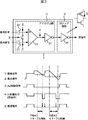
- 2次元マトリクス状に配列された複数の画素から出力されるアナログの画素信号のAD変換処理を列並列に行う固体撮像装置において、
前記画素から出力される前記画素信号とランプ波形の基準信号とを比較して得られる差信号を出力する比較回路と、
前記比較回路から出力された前記差信号の論理を反転する反転回路と、
前記比較回路で前記画素信号と前記基準信号の入力オフセットをキャンセルしている入力オフセットキャンセル期間を含む、P相ADイネーブル期間とD相ADイネーブル期間以外の全期間において、前記反転回路の出力信号の後段の回路への出力をマスクするマスク回路と
を備える固体撮像装置。 - 前記マスク回路は、前記反転回路の出力信号と、出力イネーブル信号を入力とするNAND回路で構成される
請求項1に記載の固体撮像装置。 - 画素から出力されるアナログの画素信号とランプ波形の基準信号とを比較して得られる差信号を出力する比較回路と、前記比較回路から出力された前記差信号の論理を反転する反転回路と、前記反転回路の出力信号の後段の回路への出力をマスクするマスク回路とを備え、2次元マトリクス状に配列された複数の前記画素のAD変換処理を列並列に行う固体撮像装置の駆動制御方法において、
前記比較回路において、前記画素信号と前記基準信号の入力オフセットをキャンセルし、
前記マスク回路において、前記比較回路で前記入力オフセットをキャンセルしている入力オフセットキャンセル期間を含む、P相ADイネーブル期間とD相ADイネーブル期間以外の全期間において、前記反転回路の出力信号の後段の回路への出力をマスクする
ステップを含む駆動制御方法。 - 2次元マトリクス状に配列された複数の画素から出力されるアナログの画素信号のAD変換処理を列並列に行う固体撮像装置を備える撮像装置において、
前記固体撮像装置が、
前記画素から出力される前記画素信号とランプ波形の基準信号とを比較して得られる差信号を出力する比較回路と、
前記比較回路から出力された前記差信号の論理を反転する反転回路と、
前記比較回路で前記画素信号と前記基準信号の入力オフセットをキャンセルしている入力オフセットキャンセル期間を含む、P相ADイネーブル期間とD相ADイネーブル期間以外の全期間において、前記反転回路の出力信号の後段の回路への出力をマスクするマスク回路と
を備える撮像装置。
Priority Applications (3)
| Application Number | Priority Date | Filing Date | Title |
|---|---|---|---|
| JP2007253354A JP4978795B2 (ja) | 2007-09-28 | 2007-09-28 | 固体撮像装置、駆動制御方法、および撮像装置 |
| US12/235,698 US8072518B2 (en) | 2007-09-28 | 2008-09-23 | Solid-state imaging device, driving control method thereof, and imaging apparatus |
| US13/280,002 US8749674B2 (en) | 2007-09-28 | 2011-10-24 | Solid-state imaging device, driving control method thereof, and imaging apparatus |
Applications Claiming Priority (1)
| Application Number | Priority Date | Filing Date | Title |
|---|---|---|---|
| JP2007253354A JP4978795B2 (ja) | 2007-09-28 | 2007-09-28 | 固体撮像装置、駆動制御方法、および撮像装置 |
Publications (2)
| Publication Number | Publication Date |
|---|---|
| JP2009088769A JP2009088769A (ja) | 2009-04-23 |
| JP4978795B2 true JP4978795B2 (ja) | 2012-07-18 |
Family
ID=40507786
Family Applications (1)
| Application Number | Title | Priority Date | Filing Date |
|---|---|---|---|
| JP2007253354A Expired - Fee Related JP4978795B2 (ja) | 2007-09-28 | 2007-09-28 | 固体撮像装置、駆動制御方法、および撮像装置 |
Country Status (2)
| Country | Link |
|---|---|
| US (2) | US8072518B2 (ja) |
| JP (1) | JP4978795B2 (ja) |
Cited By (1)
| Publication number | Priority date | Publication date | Assignee | Title |
|---|---|---|---|---|
| US11102435B2 (en) | 2017-06-30 | 2021-08-24 | Canon Kabushiki Kaisha | Imaging device and method of driving imaging device |
Families Citing this family (9)
| Publication number | Priority date | Publication date | Assignee | Title |
|---|---|---|---|---|
| US9462199B2 (en) * | 2012-10-12 | 2016-10-04 | Samsung Electronics Co., Ltd. | Image sensors, image processing systems including same, and methods of operating the same |
| JP5886806B2 (ja) * | 2013-09-17 | 2016-03-16 | キヤノン株式会社 | 固体撮像装置 |
| JP6353247B2 (ja) * | 2014-03-11 | 2018-07-04 | キヤノン株式会社 | 半導体装置、その制御方法、及びカメラ |
| US10840281B2 (en) * | 2015-12-08 | 2020-11-17 | Taiwan Semiconductor Manufacturing Company Ltd. | Imaging device |
| US9888185B1 (en) * | 2016-12-20 | 2018-02-06 | Omnivision Technologies, Inc. | Row decoder for high dynamic range image sensor using in-frame multi-bit exposure control |
| US9955091B1 (en) | 2016-12-20 | 2018-04-24 | Omnivision Technologies, Inc. | High dynamic range image sensor read out architecture using in-frame multi-bit exposure control |
| US9961279B1 (en) * | 2016-12-20 | 2018-05-01 | Omnivision Technologies, Inc. | Blooming free high dynamic range image sensor read out architecture using in-frame multi-bit exposure control |
| JP2020088585A (ja) * | 2018-11-22 | 2020-06-04 | キヤノン株式会社 | アナログデジタル変換装置、光電変換装置、光電変換システム、および、移動体 |
| WO2021012071A1 (zh) * | 2019-07-19 | 2021-01-28 | 深圳市汇顶科技股份有限公司 | 图像传感器以及相关芯片及电子装置 |
Family Cites Families (9)
| Publication number | Priority date | Publication date | Assignee | Title |
|---|---|---|---|---|
| JPH0691382B2 (ja) * | 1986-06-11 | 1994-11-14 | 日本電気株式会社 | 比較回路と論理回路のインターフェイス回路 |
| JPH07183808A (ja) * | 1993-12-24 | 1995-07-21 | Mitsubishi Denki Semiconductor Software Kk | アナログ/ディジタル変換回路装置 |
| JPH0969980A (ja) * | 1995-08-31 | 1997-03-11 | Sharp Corp | カメラ装置 |
| US7317481B2 (en) * | 2002-02-20 | 2008-01-08 | Canon Kabushiki Kaisha | Image data correction processing based on sensitivity |
| JP2004194066A (ja) * | 2002-12-12 | 2004-07-08 | Fujitsu Ltd | 増幅回路、比較回路、及びad変換回路 |
| JP4107269B2 (ja) | 2004-02-23 | 2008-06-25 | ソニー株式会社 | 固体撮像装置 |
| JP2005322985A (ja) * | 2004-05-06 | 2005-11-17 | Matsushita Electric Ind Co Ltd | 増幅回路、アナログデジタル変換回路及び移動体通信端末 |
| JP4396655B2 (ja) * | 2006-03-06 | 2010-01-13 | ソニー株式会社 | 固体撮像装置 |
| JP2008136042A (ja) * | 2006-11-29 | 2008-06-12 | Sony Corp | 固体撮像装置、撮像装置 |
-
2007
- 2007-09-28 JP JP2007253354A patent/JP4978795B2/ja not_active Expired - Fee Related
-
2008
- 2008-09-23 US US12/235,698 patent/US8072518B2/en active Active
-
2011
- 2011-10-24 US US13/280,002 patent/US8749674B2/en active Active
Cited By (1)
| Publication number | Priority date | Publication date | Assignee | Title |
|---|---|---|---|---|
| US11102435B2 (en) | 2017-06-30 | 2021-08-24 | Canon Kabushiki Kaisha | Imaging device and method of driving imaging device |
Also Published As
| Publication number | Publication date |
|---|---|
| US20090086067A1 (en) | 2009-04-02 |
| US20120038804A1 (en) | 2012-02-16 |
| JP2009088769A (ja) | 2009-04-23 |
| US8749674B2 (en) | 2014-06-10 |
| US8072518B2 (en) | 2011-12-06 |
Similar Documents
| Publication | Publication Date | Title |
|---|---|---|
| JP4978795B2 (ja) | 固体撮像装置、駆動制御方法、および撮像装置 | |
| JP4403435B2 (ja) | 固体撮像装置、駆動制御方法、および撮像装置 | |
| US8704898B2 (en) | A/D converter, solid-state imaging device and camera system | |
| JP5067011B2 (ja) | 固体撮像装置、撮像装置、電子機器 | |
| JP4946761B2 (ja) | 固体撮像素子およびカメラシステム | |
| US7471230B2 (en) | Analog-to-digital converter and semiconductor device | |
| JP4379504B2 (ja) | 固体撮像素子、およびカメラシステム | |
| US7859583B2 (en) | Solid-state image capture device, analog/digital conversion method for solid state image capture device, and image capture device | |
| JP5620652B2 (ja) | 固体撮像装置および駆動方法 | |
| US8269872B2 (en) | Analog-to-digital converter, analog-to-digital converting method, solid-state image pickup device, and camera system | |
| JP4882652B2 (ja) | 固体撮像装置、固体撮像装置の駆動方法および撮像装置 | |
| US8330635B2 (en) | A/D conversion circuit, solid-state image sensor, and camera system | |
| US7315273B2 (en) | Analog-to-digital conversion method, analog-to-digital converter, semiconductor device for detecting distribution of physical quantity, and electronic apparatus | |
| KR101340183B1 (ko) | 고체 촬상 장치, 고체 촬상 장치를 구동하는 방법 및카메라 | |
| US8130295B2 (en) | Analog-to-digital converter, solid-state image pickup device, and camera system | |
| US8054354B2 (en) | Solid state imaging device having built in signal transfer test circuitry | |
| JP2011182095A (ja) | 固体撮像装置および撮像装置 | |
| JP2012165168A (ja) | 半導体装置、物理情報取得装置、及び、信号読出し方法 | |
| JP2011171889A (ja) | 固体撮像素子及び撮像機器 | |
| US20100033601A1 (en) | Solid-state imaging device with a sensor core unit and method of driving the same |
Legal Events
| Date | Code | Title | Description |
|---|---|---|---|
| A621 | Written request for application examination |
Free format text: JAPANESE INTERMEDIATE CODE: A621 Effective date: 20100223 |
|
| A131 | Notification of reasons for refusal |
Free format text: JAPANESE INTERMEDIATE CODE: A131 Effective date: 20111115 |
|
| A521 | Request for written amendment filed |
Free format text: JAPANESE INTERMEDIATE CODE: A523 Effective date: 20120104 |
|
| TRDD | Decision of grant or rejection written | ||
| A01 | Written decision to grant a patent or to grant a registration (utility model) |
Free format text: JAPANESE INTERMEDIATE CODE: A01 Effective date: 20120322 |
|
| A01 | Written decision to grant a patent or to grant a registration (utility model) |
Free format text: JAPANESE INTERMEDIATE CODE: A01 |
|
| A61 | First payment of annual fees (during grant procedure) |
Free format text: JAPANESE INTERMEDIATE CODE: A61 Effective date: 20120404 |
|
| FPAY | Renewal fee payment (event date is renewal date of database) |
Free format text: PAYMENT UNTIL: 20150427 Year of fee payment: 3 |
|
| LAPS | Cancellation because of no payment of annual fees |