JP4978795B2 - Solid-state imaging device, drive control method, and imaging device - Google Patents
Solid-state imaging device, drive control method, and imaging device Download PDFInfo
- Publication number
- JP4978795B2 JP4978795B2 JP2007253354A JP2007253354A JP4978795B2 JP 4978795 B2 JP4978795 B2 JP 4978795B2 JP 2007253354 A JP2007253354 A JP 2007253354A JP 2007253354 A JP2007253354 A JP 2007253354A JP 4978795 B2 JP4978795 B2 JP 4978795B2
- Authority
- JP
- Japan
- Prior art keywords
- circuit
- signal
- output
- pixel
- unit
- Prior art date
- Legal status (The legal status is an assumption and is not a legal conclusion. Google has not performed a legal analysis and makes no representation as to the accuracy of the status listed.)
- Expired - Fee Related
Links
Images


Classifications
-
- H—ELECTRICITY
- H04—ELECTRIC COMMUNICATION TECHNIQUE
- H04N—PICTORIAL COMMUNICATION, e.g. TELEVISION
- H04N25/00—Circuitry of solid-state image sensors [SSIS]; Control thereof
-
- H—ELECTRICITY
- H04—ELECTRIC COMMUNICATION TECHNIQUE
- H04N—PICTORIAL COMMUNICATION, e.g. TELEVISION
- H04N25/00—Circuitry of solid-state image sensors [SSIS]; Control thereof
- H04N25/60—Noise processing, e.g. detecting, correcting, reducing or removing noise
- H04N25/616—Noise processing, e.g. detecting, correcting, reducing or removing noise involving a correlated sampling function, e.g. correlated double sampling [CDS] or triple sampling
-
- H—ELECTRICITY
- H04—ELECTRIC COMMUNICATION TECHNIQUE
- H04N—PICTORIAL COMMUNICATION, e.g. TELEVISION
- H04N25/00—Circuitry of solid-state image sensors [SSIS]; Control thereof
- H04N25/70—SSIS architectures; Circuits associated therewith
- H04N25/71—Charge-coupled device [CCD] sensors; Charge-transfer registers specially adapted for CCD sensors
- H04N25/75—Circuitry for providing, modifying or processing image signals from the pixel array
-
- H—ELECTRICITY
- H04—ELECTRIC COMMUNICATION TECHNIQUE
- H04N—PICTORIAL COMMUNICATION, e.g. TELEVISION
- H04N25/00—Circuitry of solid-state image sensors [SSIS]; Control thereof
- H04N25/70—SSIS architectures; Circuits associated therewith
- H04N25/76—Addressed sensors, e.g. MOS or CMOS sensors
- H04N25/77—Pixel circuitry, e.g. memories, A/D converters, pixel amplifiers, shared circuits or shared components
- H04N25/772—Pixel circuitry, e.g. memories, A/D converters, pixel amplifiers, shared circuits or shared components comprising A/D, V/T, V/F, I/T or I/F converters
Description
本発明は、固体撮像装置、駆動制御方法、および撮像装置に関し、特に、画素信号と基準信号の入力オフセットキャンセル時に流れる貫通電流を抑制することで、消費電力を低減させることができるようにする固体撮像装置、駆動制御方法、および撮像装置に関する。 The present invention relates to a solid-state imaging device, a drive control method, and an imaging device, and in particular, a solid-state that can reduce power consumption by suppressing a through current that flows when an input offset is canceled between a pixel signal and a reference signal. The present invention relates to an imaging device, a drive control method, and an imaging device.
固体撮像装置として、画素を行列状に2次元配置し、列ごとにAD変換部(ADC(Analog-Digital Converter)を配置させた列並列AD変換方式(以下、カラムAD変換方式という)搭載のCMOS(Complementary Metal Oxide Semiconductor)イメージセンサが提案されている。 As a solid-state imaging device, a CMOS with a column-parallel AD conversion method (hereinafter referred to as column AD conversion method) in which pixels are two-dimensionally arranged in a matrix and an AD conversion unit (ADC (Analog-Digital Converter)) is arranged for each column (Complementary Metal Oxide Semiconductor) Image sensors have been proposed.
また近年では、より高速撮像に適したように改良されたカラムAD変換方式搭載のCMOSイメージセンサも提案されており、例えば、特許文献1では、アップダウンカウンタを用いることにより、回路規模を大きくすることなく高フレームレート化および高分解能を達成したカラムAD変換方式搭載のCMOSイメージセンサが提案されている。
In recent years, a CMOS image sensor equipped with a column AD conversion method improved so as to be suitable for higher-speed imaging has also been proposed. For example, in
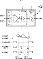
図1は、カラムAD変換方式搭載のCMOSイメージセンサにおいて、行列状に2次元配置された各画素の画素信号がアップダウンカウンタに入力されるまでの簡単な構成例を示している。 FIG. 1 shows a simple configuration example until a pixel signal of each pixel arranged two-dimensionally in a matrix is input to an up / down counter in a CMOS image sensor equipped with a column AD conversion system.
画素(Pixel)1は、受光量に応じたアナログの画素信号を電圧比較部(Comp)3に供給する。また、電圧比較部3には、参照電圧供給回路としてのDAC(Digital to Analog Converter)2から、時間が経過するにつれてレベル(電圧)が傾斜状に変化する、いわゆるランプ(RAMP)波形の信号である基準信号も供給されている。
The pixel (Pixel) 1 supplies an analog pixel signal corresponding to the amount of received light to the voltage comparison unit (Comp) 3. Further, the
電圧比較部3は、画素1からの画素信号をDAC2からの基準信号と比較して得られる差信号をアップダウンカウンタ4に出力する。例えば、基準信号が画素信号より大である場合にはHi(High)の差信号がアップダウンカウンタ4に供給され、基準信号が画素信号より小である場合にはLo(Low)の差信号がアップダウンカウンタ4に供給される。
The
アップダウンカウンタ(CNT)4は、P相(Reset Phase)ADイネーブル期間では、Hiの差信号が供給されている間だけダウンカウントし、P相(Reset Phase)ADイネーブル期間では、Hiの差信号が供給されている間だけアップカウントする。P相ADイネーブル期間は、画素1のばらつき成分であるリセット成分△Vを測定する期間であり、D相ADイネーブル期間は、(信号成分Vsig+リセット成分△V)を測定する期間であり、P相ADイネーブル期間におけるカウントとD相ADイネーブル期間におけるカウントを合わせると、(信号成分Vsig+リセット成分△V)−(リセット成分△V)により、信号成分Vsigのみを求めることができ、CDS処理を実現している。
The up / down counter (CNT) 4 counts down only while the Hi difference signal is supplied in the P phase (Reset Phase) AD enable period, and in the P phase (Reset Phase) AD enable period, it counts down. Counts up only while is supplied. The P-phase AD enable period is a period for measuring the reset component ΔV, which is a variation component of the
図2は、電圧比較部3の詳細な構成を模式的に示した図である。
FIG. 2 is a diagram schematically illustrating a detailed configuration of the
電圧比較部3は、アナログ回路11とロジック回路(デジタル回路)12とで構成されている。
The
アナログ回路11においては、画素1からの画素信号が容量素子21を介して比較器23に入力され、DAC2からの基準信号が容量素子22を介して比較器23に入力される。比較器23は、画素信号と基準信号の差信号を出力し、インバータ24は、差信号を反転増幅してロジック回路12に出力する。
In the
ロジック回路12においては、アナログ回路11のインバータ24からの差信号が、インバータ25において反転増幅され、アップダウンカウンタ4に出力される。インバータ25は、例えば、PMOSトランジスタとNMOSトランジスタの組み合わせにより構成することができる。
In the
以上のように構成される電圧比較部3では、差信号を生成する際の前処理として、画素信号と基準信号の入力オフセットをキャンセルするために、比較器23の2つの入力ノードの電位を導通させる処理が行われる。この処理をオートゼロ(AZ)処理と呼ぶ。
In the
図3を参照して、CDS処理と、その前処理であるAZ処理の期間中の電圧比較部3内の各信号について説明する。
With reference to FIG. 3, each signal in the
AZ処理期間では、AZ制御信号がアクティブ(High)となることにより、比較器23に入力される画素信号と基準信号の電位は同電位となり、画素信号と基準信号の入力オフセットがキャンセルされる。なお、図3では、画素信号と基準信号の縦軸は共通となっており、点線で示される画素信号が図示されていない期間は、同電位の基準信号と重なっていることを表す。
In the AZ processing period, when the AZ control signal becomes active (High), the pixel signal input to the
後段のアップダウンカウンタ4では、図示せぬP相ADイネーブルパルスによって定義されるP相ADイネーブル期間のうちの、基準信号が画素信号より大である間、ダウンカウントが行われ、図示せぬD相ADイネーブルパルスによって定義されるD相ADイネーブル期間のうちの、基準信号が画素信号より大である間、アップカウントが行われる。
The subsequent up / down
ところで、画素信号と基準信号の電位が同電位となった場合には、アナログ回路11から、中間電位の差信号が出力される。中間電位の差信号がインバータ25に入力された場合、図3に示されるように、PMOSトランジスタとNMOSトランジスタの組み合わせにより構成されるインバータ25では、貫通電流が流れることになる。この貫通電流による差信号は不要な信号であり、無駄な電力を消費していることになる。
By the way, when the potentials of the pixel signal and the reference signal become the same potential, the
本発明は、このような状況に鑑みてなされたものであり、画素信号と基準信号の入力オフセットキャンセル時に流れる貫通電流を抑制することで、消費電力を低減させることができるようにするものである。 The present invention has been made in view of such a situation, and is capable of reducing power consumption by suppressing a through current that flows when an input offset is canceled between a pixel signal and a reference signal. .
本発明の第1の側面の固体撮像装置は、2次元マトリクス状に配列された複数の画素から出力されるアナログの画素信号のAD変換処理を列並列に行う固体撮像装置において、前記画素から出力される前記画素信号とランプ波形の基準信号とを比較して得られる差信号を出力する比較回路と、前記比較回路から出力された前記差信号の論理を反転する反転回路と、前記比較回路で前記画素信号と前記基準信号の入力オフセットをキャンセルしている入力オフセットキャンセル期間を含む、P相ADイネーブル期間とD相ADイネーブル期間以外の全期間において、前記反転回路の出力信号の後段の回路への出力をマスクするマスク回路とを備える。 The solid-state imaging device according to the first aspect of the present invention is a solid-state imaging device that performs AD conversion processing of analog pixel signals output from a plurality of pixels arranged in a two-dimensional matrix in a column parallel manner. A comparison circuit that outputs a difference signal obtained by comparing the pixel signal and a reference signal having a ramp waveform, an inversion circuit that inverts the logic of the difference signal output from the comparison circuit, and the comparison circuit In all periods other than the P-phase AD enable period and D-phase AD enable period, including the input offset cancellation period in which the input offset of the pixel signal and the reference signal is canceled, to the subsequent circuit of the output signal of the inverting circuit And a mask circuit for masking the output of.
本発明の第1の側面の駆動制御方法は、画素から出力されるアナログの画素信号とランプ波形の基準信号とを比較して得られる差信号を出力する比較回路と、前記比較回路から出力された前記差信号の論理を反転する反転回路と、前記反転回路の出力信号の後段の回路への出力をマスクするマスク回路とを備え、2次元マトリクス状に配列された複数の前記画素のAD変換処理を列並列に行う固体撮像装置の駆動制御方法において、前記比較回路において、前記画素信号と前記基準信号の入力オフセットをキャンセルし、前記マスク回路において、前記比較回路で前記入力オフセットをキャンセルしている入力オフセットキャンセル期間を含む、P相ADイネーブル期間とD相ADイネーブル期間以外の全期間において、前記反転回路の出力信号の後段の回路への出力をマスクするステップを含む。 A drive control method according to a first aspect of the present invention includes a comparison circuit that outputs a difference signal obtained by comparing an analog pixel signal output from a pixel and a reference signal having a ramp waveform, and is output from the comparison circuit. AD conversion of a plurality of pixels arranged in a two-dimensional matrix, comprising: an inverting circuit that inverts the logic of the difference signal; and a mask circuit that masks output of the output signal of the inverting circuit to a subsequent circuit. In the solid-state imaging device drive control method in which processing is performed in parallel in the column, the comparison circuit cancels the input offset of the pixel signal and the reference signal, and the mask circuit cancels the input offset by the comparison circuit. in the input offset or canceled period, P-phase AD enable period and the total duration of the non-D-phase AD enable period you are, subsequent output signal of the inverting circuit Comprising the step of masking the output of the circuit.
本発明の第2の側面の撮像装置は、2次元マトリクス状に配列された複数の画素から出力されるアナログの画素信号のAD変換処理を列並列に行う固体撮像装置を備える撮像装置において、前記固体撮像装置が、前記画素から出力される前記画素信号とランプ波形の基準信号とを比較して得られる差信号を出力する比較回路と、前記比較回路から出力された前記差信号の論理を反転する反転回路と、前記比較回路で前記画素信号と前記基準信号の入力オフセットをキャンセルしている入力オフセットキャンセル期間を含む、P相ADイネーブル期間とD相ADイネーブル期間以外の全期間において、前記反転回路の出力信号の後段の回路への出力をマスクするマスク回路とを備える。 The imaging device according to a second aspect of the present invention is an imaging device including a solid-state imaging device that performs AD conversion processing of analog pixel signals output from a plurality of pixels arranged in a two-dimensional matrix in parallel. A solid-state imaging device that outputs a difference signal obtained by comparing the pixel signal output from the pixel and a reference signal of a ramp waveform, and inverts the logic of the difference signal output from the comparison circuit And the inversion circuit in all periods other than the P-phase AD enable period and the D-phase AD enable period, including an input offset cancel period in which the input offset of the pixel signal and the reference signal is canceled by the comparison circuit. And a mask circuit for masking the output of the circuit output signal to the subsequent circuit.
本発明の第1および第2の側面においては、比較回路で画素信号と基準信号の入力オフセットをキャンセルしている入力オフセットキャンセル期間を含む、P相ADイネーブル期間とD相ADイネーブル期間以外の全期間において、反転回路の出力信号の後段の回路への出力がマスクされる。 In the first and second aspects of the present invention , all except the P-phase AD enable period and the D-phase AD enable period, including the input offset cancellation period in which the input offset of the pixel signal and the reference signal is canceled by the comparison circuit. In the period, the output of the output signal of the inverting circuit to the subsequent circuit is masked.
本発明の第1および第2の側面によれば、消費電力を低減させることができる。 According to the first and second aspects of the present invention, power consumption can be reduced.
また、本発明の第1および第2の側面によれば、画素信号と基準信号の入力オフセットキャンセル時に流れる貫通電流を抑制することができる。 Further, according to the first and second aspects of the present invention, it is possible to suppress the through current that flows when the input offset of the pixel signal and the reference signal is canceled.
以下に本発明の実施の形態を説明するが、本発明の構成要件と、明細書又は図面に記載の実施の形態との対応関係を例示すると、次のようになる。この記載は、本発明をサポートする実施の形態が、明細書又は図面に記載されていることを確認するためのものである。従って、明細書又は図面中には記載されているが、本発明の構成要件に対応する実施の形態として、ここには記載されていない実施の形態があったとしても、そのことは、その実施の形態が、その構成要件に対応するものではないことを意味するものではない。逆に、実施の形態が構成要件に対応するものとしてここに記載されていたとしても、そのことは、その実施の形態が、その構成要件以外の構成要件には対応しないものであることを意味するものでもない。 Embodiments of the present invention will be described below. Correspondences between the constituent elements of the present invention and the embodiments described in the specification or the drawings are exemplified as follows. This description is intended to confirm that the embodiments supporting the present invention are described in the specification or the drawings. Therefore, even if there is an embodiment which is described in the specification or the drawings but is not described here as an embodiment corresponding to the constituent elements of the present invention, that is not the case. It does not mean that the form does not correspond to the constituent requirements. Conversely, even if an embodiment is described here as corresponding to a configuration requirement, that means that the embodiment does not correspond to a configuration requirement other than the configuration requirement. It's not something to do.
本発明の第1の側面の固体撮像装置は、2次元マトリクス状に配列された複数の画素から出力されるアナログの画素信号のAD変換処理を列並列に行う固体撮像装置(例えば、図4の固体撮像装置51)において、前記画素から出力される前記画素信号とランプ波形の基準信号とを比較して得られる差信号を出力する比較回路(例えば、図5の比較器23)と、前記比較回路から出力された前記差信号の論理を反転する反転回路(例えば、図5のインバータ24)と、前記比較回路で前記画素信号と前記基準信号の入力オフセットをキャンセルしている入力オフセットキャンセル期間を含む、P相ADイネーブル期間とD相ADイネーブル期間以外の全期間において、前記反転回路の出力信号の後段の回路への出力をマスクするマスク回路(例えば、図5のNAND回路101)とを備える。
The solid-state imaging device according to the first aspect of the present invention is a solid-state imaging device that performs AD conversion processing of analog pixel signals output from a plurality of pixels arranged in a two-dimensional matrix in parallel (for example, FIG. 4). In the solid-state imaging device 51), a comparison circuit (for example, the
以下、図を参照して、本発明の実施の形態について説明する。 Hereinafter, embodiments of the present invention will be described with reference to the drawings.
図4は、本発明を適用したCMOS固体撮像装置(CMOSイメージセンサ)の一実施の形態の構成例を示すブロック図である。 FIG. 4 is a block diagram showing a configuration example of an embodiment of a CMOS solid-state imaging device (CMOS image sensor) to which the present invention is applied.
固体撮像装置51は、入射光量に応じた電気信号を出力するフォトダイオードなどの光電変換素子(電荷生成部の一例)を含む複数個の画素が行および列に配列された(すなわち2次元マトリクス状の)撮像部を有する。固体撮像装置51には、各画素から出力される画素信号(電圧信号)に対して、CDS(Correlated Double Sampling ;相関2重サンプリング)処理やデジタル変換(ADC;Analog Digital Converter)処理などを行う信号処理部が列並列に設けられている。 In the solid-state imaging device 51, a plurality of pixels including photoelectric conversion elements (an example of a charge generation unit) such as a photodiode that outputs an electrical signal corresponding to the amount of incident light are arranged in rows and columns (that is, in a two-dimensional matrix form). A) an imaging unit. In the solid-state imaging device 51, a signal for performing a CDS (Correlated Double Sampling) process, a digital conversion (ADC) process, or the like on a pixel signal (voltage signal) output from each pixel. Processing units are provided in parallel with each other.
固体撮像装置51は、正方状の複数の単位画素60が行および列に(2次元マトリクス状に)配列された撮像部としての画素部61、画素部61の外側に設けられた駆動制御部62、列並列に信号処理を行うカラム処理部63、カラム処理部63にAD変換用の基準信号を供給する参照信号生成部64、および出力回路65を備えている。
The solid-state imaging device 51 includes a pixel unit 61 as an imaging unit in which a plurality of square unit pixels 60 are arranged in rows and columns (in a two-dimensional matrix), and a drive control unit 62 provided outside the pixel unit 61. A
駆動制御部62は、列アドレスや列走査を制御する水平走査回路66、行アドレスや行走査を制御する垂直走査回路67、内部クロックを生成するなどの機能を持つ通信・タイミング制御部68、および、高速のクロック周波数のパルスを生成するクロック変換部69を有し、画素信号を順次読み出すための制御を行う。
The drive control unit 62 includes a
画素部61において、単位画素60は、典型的には、受光素子(電荷生成部)としてのフォトダイオードと、増幅用の半導体素子(たとえばトランジスタ)を有する画素内アンプとから構成される。 In the pixel unit 61, the unit pixel 60 is typically composed of a photodiode as a light receiving element (charge generation unit) and an in-pixel amplifier having an amplifying semiconductor element (for example, a transistor).
画素内アンプとしては、たとえばフローティングディフュージョンアンプ構成のものが用いられる。一例としては、電荷生成部に対して、電荷読出部(転送ゲート部/読出ゲート部)の一例である読出選択用トランジスタ、リセットゲート部の一例であるリセットトランジスタ、垂直選択用トランジスタ、およびフローティングディフュージョンの電位変化を検知する検知素子の一例であるソースフォロア構成の増幅用トランジスタを有する、CMOSセンサとして汎用的な4つのトランジスタからなる4TR構成を使用することができる。 As the intra-pixel amplifier, for example, a floating diffusion amplifier configuration is used. As an example, with respect to the charge generation unit, a read selection transistor that is an example of a charge readout unit (transfer gate unit / read gate unit), a reset transistor that is an example of a reset gate unit, a vertical selection transistor, and a floating diffusion A 4TR configuration composed of four general-purpose transistors can be used as a CMOS sensor having an amplifying transistor having a source follower configuration, which is an example of a detection element that detects a change in potential of the transistor.
あるいは、特許第2708455号公報に記載のように、電荷生成部により生成された信号電荷に対応する信号電圧を増幅するための、ドレイン線(DRN)に接続された増幅用トランジスタと、電荷生成部をリセットするためのリセットトランジスタと、垂直シフトレジスタより転送配線(TRF)を介して走査される読出選択用トランジスタ(転送ゲート部)を有する、3つのトランジスタからなる3TR構成を使用することもできる。 Alternatively, as described in Japanese Patent No. 2708455, an amplifying transistor connected to a drain line (DRN) for amplifying a signal voltage corresponding to a signal charge generated by the charge generating unit, and a charge generating unit It is also possible to use a 3TR configuration including three transistors, each having a reset transistor for resetting and a read selection transistor (transfer gate portion) scanned from a vertical shift register via a transfer wiring (TRF).
単位画素60は、行選択のための行制御線70を介して垂直走査回路67と、また垂直信号線71を介してカラムAD回路81が垂直列ごとに設けられているカラム処理部63と、それぞれ接続されている。ここで、行制御線70は垂直走査回路67から単位画素60に入る配線全般を表す。
The unit pixel 60 includes a
水平走査回路66および垂直走査回路67は、通信・タイミング制御部68から与えられる制御信号CN1またはCN2に応答して、処理対象の単位画素60の画素信号の読出しを開始する。このため、単位画素60を駆動するための種々のパルス信号(たとえば、リセットパルスRST、転送パルスTRF、DRN制御パルスDRNなど)が行制御線70を介して垂直走査回路67から各単位画素60に供給される。
The
通信・タイミング制御部68は、各部の動作に必要なクロックや所定タイミングのパルス信号を供給するタイミングジェネレータTGの機能を有する。また、通信・タイミング制御部68は、端子73aを介してマスタークロックCLK0を、端子73bを介して動作モードなどを指令するデータDATAを受け取るとともに、固体撮像装置51の情報を含むデータを出力する通信インタフェースの機能を有する。
The communication / timing control unit 68 has a function of a timing generator TG that supplies a clock signal necessary for the operation of each unit and a pulse signal having a predetermined timing. Further, the communication / timing control unit 68 receives the master clock CLK0 via the
たとえば、通信・タイミング制御部68は、水平アドレス信号を水平デコーダ66aに供給し、垂直アドレス信号を垂直デコーダ67aに供給する。この際、単位画素60は2次元マトリックス状に配置されているので、垂直信号線71を介して列方向に出力されるアナログの画素信号を行単位で(列並列で)アクセスし取り込む(垂直)スキャン読みを行い、その後に、垂直列の並び方向である行方向にアクセスし画素信号(本例ではデジタル化された画素データ)を出力側へ読み出す(水平)スキャン読みを行うようにすることで、画素信号や画素データの読出しの高速化を図ることができる。もちろん、スキャン読みに限らず、読み出したい単位画素60を直接にアドレス指定することで、必要な単位画素60の情報のみを読み出すランダムアクセスも可能である。
For example, the communication / timing control unit 68 supplies the horizontal address signal to the
また、通信・タイミング制御部68は、端子73aを介して入力されるマスタークロックCLK0と同じ周波数のクロックCLK1や、それを2分周したクロック、2分周よりさらに分周した低速のクロックをデバイス内の各部、たとえば水平走査回路66、垂直走査回路67、カラム処理部63などに供給する。以下、2分周したクロックやそれ以下の周波数のクロック全般を纏めて、低速クロックCLK2という。
Further, the communication / timing control unit 68 uses a clock CLK1 having the same frequency as the master clock CLK0 input via the
クロック変換部69は、入力されたクロック周波数よりも高速のクロック周波数のパルスを生成する逓倍回路を内蔵している。クロック変換部69は、通信・タイミング制御部68から低速クロックCLK2を受け取り、それを元にして2倍以上高い周波数のクロックを生成する。クロック変換部69の逓倍回路としては、k1を低速クロックCLK2の周波数の倍数としたときk1逓倍回路を設ければよく、周知の様々な回路を利用することができる。
The
垂直走査回路67は、画素部61の行を選択し、その行に必要なパルスを供給する。垂直走査回路67は、垂直方向の読出行を規定する(画素部61の行を選択する)垂直デコーダ67aと、垂直デコーダ67aにて規定された読出アドレス上(行方向)の単位画素60に対する行制御線70にパルスを供給して駆動する垂直駆動回路67bとを有する。なお、垂直デコーダ67aは、信号を読み出す行の他に、電子シャッタ用の行なども選択することができる。
The
水平走査回路66は、低速クロックCLK2に同期してカラム処理部63のカラムAD回路81を順番に選択し、その信号を水平信号線(水平出力線)72に出力させる。水平走査回路66は、水平方向の読出列を規定する(カラム処理部63内の個々のカラムAD回路81を選択する)水平デコーダ66aと、水平デコーダ66aにて規定された読出アドレスに従って、カラム処理部63の各信号を水平信号線72に導く水平駆動回路66bとを有する。なお、水平信号線72は、たとえばカラムAD回路81が取り扱うビット数n(nは正の整数)分、たとえば10(=n)ビットならば、そのビット数分に対応して10本配置される。
The
参照信号生成部64は、DA変換回路(DAC;Digital to Analog Converter)64aを有して構成されており、通信・タイミング制御部68からの制御データCN4が表す初期値から、通信・タイミング制御部68からのカウントクロックCKdacに同期して、ランプ(RAMP)波形の基準信号を生成して、カラム処理部63の個々のカラムAD回路81に供給する。
The reference
カラムAD回路81は、行制御線70(H0,H1,…)ごとに単位画素60から供給される画素信号をnビットの画素データに変換する。カラムAD回路81は、参照信号生成部64のDA変換回路64aで生成される基準信号と、行制御線70(H0,H1,…)ごとに単位画素60から垂直信号線71(V0,V1,…)を経由し得られるアナログの画素信号とを比較する電圧比較部(コンパレータ)82と、電圧比較部82が比較処理を完了するまでの時間をカウントし、その結果を保持するカウンタ部83とを備える。
The column AD circuit 81 converts the pixel signal supplied from the unit pixel 60 for each row control line 70 (H0, H1,...) Into n-bit pixel data. The column AD circuit 81 includes the reference signal generated by the
カウンタ部83には、カウンタ部83がダウンカウントモードで動作するのかアップカウントモードで動作するのかを指示するためのモード制御信号CN5と、カウンタ部83が保持しているカウント値を初期値にリセットするリセット制御信号CN6が、通信・タイミング制御部68から供給される。また、カウンタ部83には、通信・タイミング制御部68からカウントクロックCK0も供給される。 The counter unit 83 resets the mode control signal CN5 for instructing whether the counter unit 83 operates in the down-count mode or the up-count mode, and the count value held by the counter unit 83 to the initial value. The reset control signal CN6 to be supplied is supplied from the communication / timing control unit 68. The counter unit 83 is also supplied with a count clock CK 0 from the communication / timing control unit 68.
カウンタ部83は、アップダウンカウンタ(U/D CNT)を用いて、モード制御信号CN5に応じて、同一の処理対象の画素信号あるいは物理的な性質が同一の複数の画素信号に対してダウンカウント動作とアップカウント動作とを切り替えてカウント処理を行う。 The counter unit 83 uses an up / down counter (U / D CNT) to count down the same pixel signal to be processed or a plurality of pixel signals having the same physical properties in accordance with the mode control signal CN5. The count process is performed by switching between the operation and the up-count operation.
カウンタ部83には、水平走査回路66から制御線66cを介して制御パルスが入力される。カウンタ部83は、カウント結果を保持するラッチ機能を有しており、制御線66cを介しての制御パルスによる指示があるまでは、カウンタ出力値を保持する。
A control pulse is input to the counter unit 83 from the
カラムAD回路81は、カウント動作を行い、所定のタイミングでカウント結果を出力する。すなわち、先ず、電圧比較部82では、参照信号生成部64からの基準信号と、垂直信号線71を介して入力される画素信号とを比較し、双方の電圧が同じになると、電圧比較部82のコンパレータ出力が反転(本例ではHiレベルからLoレベルへ遷移)する。
The column AD circuit 81 performs a count operation and outputs a count result at a predetermined timing. That is, first, the
カウンタ部83は、カウントクロックCK0に同期してダウンカウントモードもしくはアップカウントモードでカウント動作を開始しており、コンパレータ出力の反転した情報がカウンタ部83に通知されると、カウント動作を停止し、その時点のカウント値を画素データとしてラッチ(保持・記憶)することでAD変換を完了する。 The counter unit 83 starts the count operation in the down-count mode or the up-count mode in synchronization with the count clock CK0. When the inverted information of the comparator output is notified to the counter unit 83, the counter unit 83 stops the count operation, The AD conversion is completed by latching (holding / storing) the count value at that time as pixel data.
カウンタ部83は、所定のタイミングで水平走査回路66から制御線66cを介して供給される水平選択信号によるシフト動作に基づいて、記憶・保持した画素データを、順次、出力回路65に出力する。出力回路65は、入力された画素データを出力端子73cから出力する。
The counter unit 83 sequentially outputs the stored and held pixel data to the
図5は、図4の固体撮像装置51における電圧比較部(コンパレータ)82の詳細な構成を模式的に示した図である。 FIG. 5 is a diagram schematically illustrating a detailed configuration of the voltage comparison unit (comparator) 82 in the solid-state imaging device 51 of FIG.
図5において、図2の電圧比較部3と対応する部分については同一の符号を付してある。すなわち、図5の電圧比較部82は、電圧比較部3と同様にアナログ回路11とロジック回路12とで構成され、そのうちのアナログ回路11は、電圧比較部3と同様の構成とされている。
In FIG. 5, portions corresponding to those of the
従って、比較器23は、単位画素60からの画素信号とDAC64aからの基準信号とを比較して得られる差信号を出力し、インバータ24は、差信号を反転増幅してロジック回路12に出力する。
Therefore, the
一方、ロジック回路12では、図2の電圧比較部3におけるインバータ25に代えて、NAND回路101が設けられている。NAND回路101には、アナログ回路11のインバータ24からの差信号と、通信・タイミング制御部68からの電流カット信号が入力され、NAND回路101は、その2入力のNANDを出力する。
On the other hand, in the
なお、画素信号と基準信号の入力オフセットをキャンセルするためのAZ制御信号と、NAND回路101に入力される電流カット信号は、いずれも、通信・タイミング制御部68から供給される。
Note that both the AZ control signal for canceling the input offset of the pixel signal and the reference signal and the current cut signal input to the
図6は、AZ制御信号と電流カット信号との関係を示しており、通信・タイミング制御部68は、少なくともAZ制御信号がHiレベルとなっている期間(入力オフセットキャンセル期間)はLoレベルとなるような電流カット信号をNAND回路101に供給する。
FIG. 6 shows the relationship between the AZ control signal and the current cut signal. The communication / timing control unit 68 is at the Lo level at least during the period when the AZ control signal is at the Hi level (input offset cancellation period). Such a current cut signal is supplied to the
NAND回路101は、AND回路とインバータ(NOT回路)の接続で構成することができるので、図5の電圧比較部82のロジック回路12は、図2のインバータ25の前段に、インバータ24からの差信号と電流カット信号とのAND回路が設けられていると考えることができる。この場合、電流カット信号がLoレベルである限り、後段のインバータには、インバータ24からの差信号が供給されないことになる。
Since the
したがって、図7に示すように、図2のロジック回路12ではAZ制御信号がHiレベルとなっている期間(入力オフセットキャンセル期間)に発生していた貫通電流(点線で示される部分)は、NAND回路101では発生しない。すなわち、図5の電圧比較部82によれば、貫通電流を抑制することができ、以って、固体撮像装置51全体としての消費電力を低減することができる。
Therefore, as shown in FIG. 7, in the
電流カット信号がLoレベルである限り差信号そのものは電圧比較部82から出力されず、電流カット信号がHiレベルであれば差信号を電圧比較部82から出力することができるということは、換言すれば、電流カット信号は、後段のカウンタ部83への差信号の出力をマスクする出力イネーブル信号であり、NAND回路101は、カウンタ部83への差信号の出力をマスクするマスク回路としての機能も備えていると言うことができる。
In other words, as long as the current cut signal is at the Lo level, the difference signal itself is not output from the
なお、上述した例では、カウンタ部83への差信号の出力をマスクするマスク機能と、図2のインバータ25の機能とを兼ね備えた回路としてNAND回路を用いたが、この2つの機能が実現できればその他の回路構成を採用してもよい。
In the above-described example, the NAND circuit is used as a circuit having both the mask function for masking the output of the difference signal to the counter unit 83 and the function of the
中間電位の差信号による貫通電流を抑制するという観点では、電流カット信号は、少なくとも、画素信号と基準信号の電位が同電位となっている期間だけ、Loレベルであればよいが、最大でどれだけの期間をLoレベルとしておくことができるかと言えば、電圧比較部82の後段のカウンタ部83においてダウンカウント動作またはアップカウント動作を行っている間だけは、正確な差信号を出力する必要があるので、P相ADイネーブル期間とD相ADイネーブル期間以外の期間は、電流カット信号をLoレベルとしておくことができる。
From the viewpoint of suppressing the through current due to the difference signal of the intermediate potential, the current cut signal may be at the Lo level at least during the period in which the potential of the pixel signal and the reference signal are the same potential, but which is the maximum That is, it is necessary to output an accurate difference signal only during the down-counting operation or the up-counting operation in the counter unit 83 subsequent to the
図8は、図4の固体撮像装置51を採用した撮像装置120の構成例を示すブロック図である。なお、撮像装置120は、静止画を撮像するもの、動画を撮像するもの、または、その両方を撮像するもののいずれでもよい。
FIG. 8 is a block diagram illustrating a configuration example of an
撮像装置120は、ズーム光学系を含むレンズ121、図4の固体撮像装置51を採用しているイメージセンサ部122、信号処理部123、表示部124、コーデック処理部125、媒体記録部126、コントローラ127、マスタCLK発生部128、および操作入力部129により構成される。
The
イメージセンサ部122は、コントローラ127からの制御信号に基づいて、撮像して得られた撮像信号(nビットの画素データに対応する信号)を信号処理部123に供給する。
The
信号処理部123は、供給される撮像信号に対して、ホワイトバランス処理、ガンマ補正処理、色分離処理等の所定の信号処理を施し、表示部124およびコーデック処理部125に供給する。なお、信号処理部123は、表示部124とコーデック処理部125のそれぞれに対して独立して信号処理を施すことが可能である。
The
表示部124は、例えば、LCD(Liquid Crystal Display)等で構成され、信号処理部123からの撮像信号を画像として表示する。コーデック処理部125は、信号処理部123からの撮像信号を所定の圧縮方式により圧縮し、媒体記録部126に供給する。媒体記録部126は、コントローラ127の制御に基づいて、信号処理部123からの撮像信号を、例えば、半導体メモリ、磁気ディスク、光磁気ディスク、光ディスクなどの記録媒体に記憶する。この記録媒体は、撮像装置120に対して着脱可能なようになされていても良い。
The
コントローラ127は、操作入力部129により入力されたユーザの操作入力に基づいて、イメージセンサ部122、信号処理部123、表示部124、コーデック処理部125、媒体記録部126、およびマスタCLK発生部128を制御する。
Based on the user's operation input input by the
マスタCLK発生部128は、メインCLKを発生し、イメージセンサ部122に供給する。操作入力部129は、撮像を指令するシャッタボタンをはじめとして、例えば、ジョグダイヤル、キー、レバー、ボタン、またはタッチパネルなどにより構成され、ユーザによる操作に対応する操作信号をコントローラ127に供給する。
The master
以上のように構成される撮像装置120においても、イメージセンサ部122に図4の固体撮像装置51を採用しているので、画素信号と基準信号の入力オフセットキャンセル時に流れる貫通電流が抑制され、消費電力を低減することができる。
Also in the
本発明の実施の形態は、上述した実施の形態に限定されるものではなく、本発明の要旨を逸脱しない範囲において種々の変更が可能である。 The embodiments of the present invention are not limited to the above-described embodiments, and various modifications can be made without departing from the scope of the present invention.
11 アナログ回路, 12 ロジック回路, 23 比較器, 24 インバータ, 51 固体撮像装置, 68 通信・タイミング制御部, 82 電圧比較部, 83 カウンタ部, 101 NAND回路, 120 撮像装置
DESCRIPTION OF
Claims (4)
前記画素から出力される前記画素信号とランプ波形の基準信号とを比較して得られる差信号を出力する比較回路と、
前記比較回路から出力された前記差信号の論理を反転する反転回路と、
前記比較回路で前記画素信号と前記基準信号の入力オフセットをキャンセルしている入力オフセットキャンセル期間を含む、P相ADイネーブル期間とD相ADイネーブル期間以外の全期間において、前記反転回路の出力信号の後段の回路への出力をマスクするマスク回路と
を備える固体撮像装置。 In a solid-state imaging device that performs AD conversion processing of analog pixel signals output from a plurality of pixels arranged in a two-dimensional matrix in a column,
A comparison circuit that outputs a difference signal obtained by comparing the pixel signal output from the pixel and a reference signal of a ramp waveform;
An inverting circuit for inverting the logic of the difference signal output from the comparison circuit;
In all the periods other than the P-phase AD enable period and the D-phase AD enable period, including the input offset cancellation period in which the input offset of the pixel signal and the reference signal is canceled by the comparison circuit, the output signal of the inverting circuit A solid-state imaging device comprising: a mask circuit that masks output to a circuit at a subsequent stage.
請求項1に記載の固体撮像装置。 The solid-state imaging device according to claim 1, wherein the mask circuit includes a NAND circuit that receives an output signal of the inverting circuit and an output enable signal .
前記比較回路において、前記画素信号と前記基準信号の入力オフセットをキャンセルし、
前記マスク回路において、前記比較回路で前記入力オフセットをキャンセルしている入力オフセットキャンセル期間を含む、P相ADイネーブル期間とD相ADイネーブル期間以外の全期間において、前記反転回路の出力信号の後段の回路への出力をマスクする
ステップを含む駆動制御方法。 A comparison circuit that outputs a difference signal obtained by comparing an analog pixel signal output from a pixel and a reference signal having a ramp waveform; an inversion circuit that inverts the logic of the difference signal output from the comparison circuit; A solid-state imaging device drive control method for performing AD conversion processing of a plurality of the pixels arranged in a two-dimensional matrix in a column-parallel manner, comprising: a mask circuit that masks output of the output signal of the inversion circuit to a subsequent circuit; In
In the comparison circuit, cancel the input offset of the pixel signal and the reference signal,
In the mask circuit, in the entire period other than the P-phase AD enable period and the D-phase AD enable period, including the input offset cancellation period in which the input offset is canceled by the comparison circuit, A drive control method including a step of masking an output to a circuit.
前記固体撮像装置が、
前記画素から出力される前記画素信号とランプ波形の基準信号とを比較して得られる差信号を出力する比較回路と、
前記比較回路から出力された前記差信号の論理を反転する反転回路と、
前記比較回路で前記画素信号と前記基準信号の入力オフセットをキャンセルしている入力オフセットキャンセル期間を含む、P相ADイネーブル期間とD相ADイネーブル期間以外の全期間において、前記反転回路の出力信号の後段の回路への出力をマスクするマスク回路と
を備える撮像装置。 In an imaging apparatus including a solid-state imaging apparatus that performs AD conversion processing of analog pixel signals output from a plurality of pixels arranged in a two-dimensional matrix in a column in parallel,
The solid-state imaging device is
A comparison circuit that outputs a difference signal obtained by comparing the pixel signal output from the pixel and a reference signal of a ramp waveform;
An inverting circuit for inverting the logic of the difference signal output from the comparison circuit;
In all the periods other than the P-phase AD enable period and the D-phase AD enable period, including the input offset cancellation period in which the input offset of the pixel signal and the reference signal is canceled by the comparison circuit, the output signal of the inverting circuit An imaging apparatus comprising: a mask circuit that masks output to a circuit at a subsequent stage.
Priority Applications (3)
| Application Number | Priority Date | Filing Date | Title |
|---|---|---|---|
| JP2007253354A JP4978795B2 (en) | 2007-09-28 | 2007-09-28 | Solid-state imaging device, drive control method, and imaging device |
| US12/235,698 US8072518B2 (en) | 2007-09-28 | 2008-09-23 | Solid-state imaging device, driving control method thereof, and imaging apparatus |
| US13/280,002 US8749674B2 (en) | 2007-09-28 | 2011-10-24 | Solid-state imaging device, driving control method thereof, and imaging apparatus |
Applications Claiming Priority (1)
| Application Number | Priority Date | Filing Date | Title |
|---|---|---|---|
| JP2007253354A JP4978795B2 (en) | 2007-09-28 | 2007-09-28 | Solid-state imaging device, drive control method, and imaging device |
Publications (2)
| Publication Number | Publication Date |
|---|---|
| JP2009088769A JP2009088769A (en) | 2009-04-23 |
| JP4978795B2 true JP4978795B2 (en) | 2012-07-18 |
Family
ID=40507786
Family Applications (1)
| Application Number | Title | Priority Date | Filing Date |
|---|---|---|---|
| JP2007253354A Expired - Fee Related JP4978795B2 (en) | 2007-09-28 | 2007-09-28 | Solid-state imaging device, drive control method, and imaging device |
Country Status (2)
| Country | Link |
|---|---|
| US (2) | US8072518B2 (en) |
| JP (1) | JP4978795B2 (en) |
Cited By (1)
| Publication number | Priority date | Publication date | Assignee | Title |
|---|---|---|---|---|
| US11102435B2 (en) | 2017-06-30 | 2021-08-24 | Canon Kabushiki Kaisha | Imaging device and method of driving imaging device |
Families Citing this family (9)
| Publication number | Priority date | Publication date | Assignee | Title |
|---|---|---|---|---|
| US9462199B2 (en) * | 2012-10-12 | 2016-10-04 | Samsung Electronics Co., Ltd. | Image sensors, image processing systems including same, and methods of operating the same |
| JP5886806B2 (en) * | 2013-09-17 | 2016-03-16 | キヤノン株式会社 | Solid-state imaging device |
| JP6353247B2 (en) * | 2014-03-11 | 2018-07-04 | キヤノン株式会社 | Semiconductor device, control method thereof, and camera |
| US10840281B2 (en) * | 2015-12-08 | 2020-11-17 | Taiwan Semiconductor Manufacturing Company Ltd. | Imaging device |
| US9955091B1 (en) | 2016-12-20 | 2018-04-24 | Omnivision Technologies, Inc. | High dynamic range image sensor read out architecture using in-frame multi-bit exposure control |
| US9888185B1 (en) * | 2016-12-20 | 2018-02-06 | Omnivision Technologies, Inc. | Row decoder for high dynamic range image sensor using in-frame multi-bit exposure control |
| US9961279B1 (en) | 2016-12-20 | 2018-05-01 | Omnivision Technologies, Inc. | Blooming free high dynamic range image sensor read out architecture using in-frame multi-bit exposure control |
| JP2020088585A (en) * | 2018-11-22 | 2020-06-04 | キヤノン株式会社 | Analog-digital conversion device, photoelectric conversion device, photoelectric conversion system, and mobile body |
| CN110972518B (en) * | 2019-07-19 | 2022-12-16 | 深圳市汇顶科技股份有限公司 | Image sensor, related chip and electronic device |
Family Cites Families (9)
| Publication number | Priority date | Publication date | Assignee | Title |
|---|---|---|---|---|
| JPH0691382B2 (en) * | 1986-06-11 | 1994-11-14 | 日本電気株式会社 | Interface circuit of comparison circuit and logic circuit |
| JPH07183808A (en) * | 1993-12-24 | 1995-07-21 | Mitsubishi Denki Semiconductor Software Kk | Analog/digital conversion circuit device |
| JPH0969980A (en) * | 1995-08-31 | 1997-03-11 | Sharp Corp | Camera device |
| US7317481B2 (en) * | 2002-02-20 | 2008-01-08 | Canon Kabushiki Kaisha | Image data correction processing based on sensitivity |
| JP2004194066A (en) * | 2002-12-12 | 2004-07-08 | Fujitsu Ltd | Amplifier circuit, comparison circuit and a/d converter circuit |
| JP4107269B2 (en) | 2004-02-23 | 2008-06-25 | ソニー株式会社 | Solid-state imaging device |
| JP2005322985A (en) * | 2004-05-06 | 2005-11-17 | Matsushita Electric Ind Co Ltd | Amplifier circuit, analog digital conversion circuit, and mobile communication terminal |
| JP4396655B2 (en) * | 2006-03-06 | 2010-01-13 | ソニー株式会社 | Solid-state imaging device |
| JP2008136042A (en) * | 2006-11-29 | 2008-06-12 | Sony Corp | Solid-state imaging apparatus and imaging apparatus |
-
2007
- 2007-09-28 JP JP2007253354A patent/JP4978795B2/en not_active Expired - Fee Related
-
2008
- 2008-09-23 US US12/235,698 patent/US8072518B2/en active Active
-
2011
- 2011-10-24 US US13/280,002 patent/US8749674B2/en active Active
Cited By (1)
| Publication number | Priority date | Publication date | Assignee | Title |
|---|---|---|---|---|
| US11102435B2 (en) | 2017-06-30 | 2021-08-24 | Canon Kabushiki Kaisha | Imaging device and method of driving imaging device |
Also Published As
| Publication number | Publication date |
|---|---|
| US8072518B2 (en) | 2011-12-06 |
| US20090086067A1 (en) | 2009-04-02 |
| US20120038804A1 (en) | 2012-02-16 |
| US8749674B2 (en) | 2014-06-10 |
| JP2009088769A (en) | 2009-04-23 |
Similar Documents
| Publication | Publication Date | Title |
|---|---|---|
| JP4978795B2 (en) | Solid-state imaging device, drive control method, and imaging device | |
| JP4403435B2 (en) | Solid-state imaging device, drive control method, and imaging device | |
| US8704898B2 (en) | A/D converter, solid-state imaging device and camera system | |
| JP5619434B2 (en) | Solid-state imaging device and imaging device | |
| JP5067011B2 (en) | Solid-state imaging device, imaging device, electronic equipment | |
| US7471230B2 (en) | Analog-to-digital converter and semiconductor device | |
| JP4946761B2 (en) | Solid-state imaging device and camera system | |
| US7859583B2 (en) | Solid-state image capture device, analog/digital conversion method for solid state image capture device, and image capture device | |
| US8269872B2 (en) | Analog-to-digital converter, analog-to-digital converting method, solid-state image pickup device, and camera system | |
| JP4882652B2 (en) | Solid-state imaging device, driving method of solid-state imaging device, and imaging device | |
| JP4379504B2 (en) | Solid-state imaging device and camera system | |
| US8330635B2 (en) | A/D conversion circuit, solid-state image sensor, and camera system | |
| JP5620652B2 (en) | Solid-state imaging device and driving method | |
| US8130295B2 (en) | Analog-to-digital converter, solid-state image pickup device, and camera system | |
| JP2012165168A (en) | Semiconductor device, physical information acquisition apparatus and signal readout method | |
| JP2006340044A (en) | Solid-state imaging apparatus, analog/digital conversion method in solid-state imaging apparatus and imaging apparatus | |
| JP2011171889A (en) | Solid-state imaging element and imaging apparatus |
Legal Events
| Date | Code | Title | Description |
|---|---|---|---|
| A621 | Written request for application examination |
Free format text: JAPANESE INTERMEDIATE CODE: A621 Effective date: 20100223 |
|
| A131 | Notification of reasons for refusal |
Free format text: JAPANESE INTERMEDIATE CODE: A131 Effective date: 20111115 |
|
| A521 | Request for written amendment filed |
Free format text: JAPANESE INTERMEDIATE CODE: A523 Effective date: 20120104 |
|
| TRDD | Decision of grant or rejection written | ||
| A01 | Written decision to grant a patent or to grant a registration (utility model) |
Free format text: JAPANESE INTERMEDIATE CODE: A01 Effective date: 20120322 |
|
| A01 | Written decision to grant a patent or to grant a registration (utility model) |
Free format text: JAPANESE INTERMEDIATE CODE: A01 |
|
| A61 | First payment of annual fees (during grant procedure) |
Free format text: JAPANESE INTERMEDIATE CODE: A61 Effective date: 20120404 |
|
| FPAY | Renewal fee payment (event date is renewal date of database) |
Free format text: PAYMENT UNTIL: 20150427 Year of fee payment: 3 |
|
| LAPS | Cancellation because of no payment of annual fees |