JP2012165168A - Semiconductor device, physical information acquisition apparatus and signal readout method - Google Patents
Semiconductor device, physical information acquisition apparatus and signal readout method Download PDFInfo
- Publication number
- JP2012165168A JP2012165168A JP2011023782A JP2011023782A JP2012165168A JP 2012165168 A JP2012165168 A JP 2012165168A JP 2011023782 A JP2011023782 A JP 2011023782A JP 2011023782 A JP2011023782 A JP 2011023782A JP 2012165168 A JP2012165168 A JP 2012165168A
- Authority
- JP
- Japan
- Prior art keywords
- unit
- signal
- column
- signal processing
- read
- Prior art date
- Legal status (The legal status is an assumption and is not a legal conclusion. Google has not performed a legal analysis and makes no representation as to the accuracy of the status listed.)
- Pending
Links
Images


Classifications
-
- H—ELECTRICITY
- H04—ELECTRIC COMMUNICATION TECHNIQUE
- H04N—PICTORIAL COMMUNICATION, e.g. TELEVISION
- H04N25/00—Circuitry of solid-state image sensors [SSIS]; Control thereof
- H04N25/40—Extracting pixel data from image sensors by controlling scanning circuits, e.g. by modifying the number of pixels sampled or to be sampled
- H04N25/44—Extracting pixel data from image sensors by controlling scanning circuits, e.g. by modifying the number of pixels sampled or to be sampled by partially reading an SSIS array
- H04N25/443—Extracting pixel data from image sensors by controlling scanning circuits, e.g. by modifying the number of pixels sampled or to be sampled by partially reading an SSIS array by reading pixels from selected 2D regions of the array, e.g. for windowing or digital zooming
-
- H—ELECTRICITY
- H04—ELECTRIC COMMUNICATION TECHNIQUE
- H04N—PICTORIAL COMMUNICATION, e.g. TELEVISION
- H04N25/00—Circuitry of solid-state image sensors [SSIS]; Control thereof
- H04N25/70—SSIS architectures; Circuits associated therewith
- H04N25/709—Circuitry for control of the power supply
-
- H—ELECTRICITY
- H04—ELECTRIC COMMUNICATION TECHNIQUE
- H04N—PICTORIAL COMMUNICATION, e.g. TELEVISION
- H04N25/00—Circuitry of solid-state image sensors [SSIS]; Control thereof
- H04N25/70—SSIS architectures; Circuits associated therewith
- H04N25/71—Charge-coupled device [CCD] sensors; Charge-transfer registers specially adapted for CCD sensors
- H04N25/74—Circuitry for scanning or addressing the pixel array
-
- H—ELECTRICITY
- H04—ELECTRIC COMMUNICATION TECHNIQUE
- H04N—PICTORIAL COMMUNICATION, e.g. TELEVISION
- H04N25/00—Circuitry of solid-state image sensors [SSIS]; Control thereof
- H04N25/70—SSIS architectures; Circuits associated therewith
- H04N25/71—Charge-coupled device [CCD] sensors; Charge-transfer registers specially adapted for CCD sensors
- H04N25/75—Circuitry for providing, modifying or processing image signals from the pixel array
-
- H—ELECTRICITY
- H04—ELECTRIC COMMUNICATION TECHNIQUE
- H04N—PICTORIAL COMMUNICATION, e.g. TELEVISION
- H04N25/00—Circuitry of solid-state image sensors [SSIS]; Control thereof
- H04N25/70—SSIS architectures; Circuits associated therewith
- H04N25/76—Addressed sensors, e.g. MOS or CMOS sensors
- H04N25/77—Pixel circuitry, e.g. memories, A/D converters, pixel amplifiers, shared circuits or shared components
- H04N25/772—Pixel circuitry, e.g. memories, A/D converters, pixel amplifiers, shared circuits or shared components comprising A/D, V/T, V/F, I/T or I/F converters
Abstract
Description
本開示は、半導体装置(固体撮像装置を含む)、物理情報取得装置(撮像装置を含む)、及び、信号読出し方法に関する。 The present disclosure relates to a semiconductor device (including a solid-state imaging device), a physical information acquisition device (including an imaging device), and a signal reading method.
単位素子が配された素子部(好ましくは行列状に単位素子が配された素子アレイ部)の全ての単位素子の情報を必要とする全素子モード(通常モードとも称する)以外に、所定の間隔ごとの単位素子の情報を必要とする間引きモードや、特定領域の単位素子の情報を必要とする切出しモード等、一部の単位素子の情報のみを必要とするモード(素子選択モードと称する)も知られている。又、行列状に単位素子が配された素子アレイ部の各単位素子から信号を読み出す際に、1行分を同時にアクセスして行単位で信号を読み出す方式(いわゆるカラム読出し方式)が用いられることもある。素子選択モードとカラム読出し方式とを併用する場合は列選択モードと称する。例えば、特開2001−298748号公報や特開2007−142738号公報に、カラム読出し方式や列選択モードの技術が記載されている。 In addition to all element modes (also referred to as normal mode) that require information on all unit elements of the element unit in which unit elements are arranged (preferably an element array unit in which unit elements are arranged in a matrix), a predetermined interval There is also a mode (referred to as an element selection mode) that requires only information on some unit elements, such as a thinning mode that requires information on each unit element and a cut-out mode that requires information on unit elements in a specific region. Are known. In addition, when reading a signal from each unit element of an element array section in which unit elements are arranged in a matrix, a system (so-called column reading system) is used in which signals are read in units of rows by simultaneously accessing one row. There is also. When the element selection mode and the column readout method are used together, it is called a column selection mode. For example, Japanese Patent Application Laid-Open Nos. 2001-298748 and 2007-142738 describe techniques of a column reading method and a column selection mode.
しかしながら、特開2001−298748号公報では、列選択モード時に選択対象とならない非選択列の信号を水平転送しない(読み飛ばす)手法が記載されているに過ぎない。特開2007−142738号公報では、列選択モードにおける消費電力低減についても記載されているが、選択対象とならない非選択列の出力信号線(垂直信号線)の動作電流を低減する手法が記載されているに過ぎない。更には、特開2001−298748号公報及び特開2007−142738号公報の何れも、全列共通の水平信号線を使用する場合での適用に過ぎない。 However, Japanese Patent Application Laid-Open No. 2001-298748 only describes a method in which a signal of a non-selected column that is not a selection target in the column selection mode is not horizontally transferred (is skipped). Japanese Patent Application Laid-Open No. 2007-142738 describes reduction of power consumption in the column selection mode, but describes a method of reducing the operating current of the output signal lines (vertical signal lines) of the non-selected columns that are not the selection target. It ’s just that. Furthermore, both Japanese Patent Application Laid-Open Nos. 2001-298748 and 2007-142738 are only applied when a horizontal signal line common to all columns is used.
本開示は、素子選択モード時に、出力信号線の動作電流を低減しなくても通常モード時よりも消費電力を低減できる技術を提供することを第1の目的とする。本開示は、全列共通の水平信号線を使用しない構成を採用しつつ、素子選択モード時に必要とされない単位素子と対応する信号を読み飛ばすことができる技術を提供することを第2の目的とする。本開示は、素子選択モード時に、消費電力を低減しつつ、必要とされない単位素子と対応する信号を読み飛ばすことができる特開2007−142738号公報に記載の技術とは異なる技術を提供することを第3の目的とする。 The first object of the present disclosure is to provide a technique capable of reducing power consumption in the element selection mode as compared with that in the normal mode without reducing the operating current of the output signal line. A second object of the present disclosure is to provide a technology that can skip a signal corresponding to a unit element that is not required in the element selection mode while adopting a configuration that does not use a horizontal signal line that is common to all columns. To do. The present disclosure provides a technique different from the technique described in Japanese Patent Laid-Open No. 2007-142738 that can skip a signal corresponding to a unit element that is not required while reducing power consumption in the element selection mode. Is the third purpose.
本開示の第1の態様に係る半導体装置は、単位素子が行列状に配された素子アレイ部と、単位素子から出力された単位信号に基づいて予め定められた信号処理を行なう信号処理回路を列ごとに具備する信号処理部、とを備える。素子アレイ部における1行分の単位素子の内の一部の単位素子の情報のみを必要とする素子選択モード時には、必要とされない単位素子と対応する信号処理回路が通常動作モード時よりも低消費電力状態となるように当該信号処理回路の機能が制御される。本開示の第1の態様に係る半導体装置の従属項に記載された各半導体装置は、本開示の第1の態様に係る半導体装置のさらなる有利な具体例を規定する。 A semiconductor device according to a first aspect of the present disclosure includes an element array unit in which unit elements are arranged in a matrix, and a signal processing circuit that performs predetermined signal processing based on unit signals output from the unit elements. A signal processing unit provided for each column. In the element selection mode in which only information on some of the unit elements in one row in the element array portion is required, the signal processing circuit corresponding to the unnecessary unit elements is less consumed than in the normal operation mode. The function of the signal processing circuit is controlled so as to be in the power state. Each semiconductor device described in the dependent claims of the semiconductor device according to the first aspect of the present disclosure defines a further advantageous specific example of the semiconductor device according to the first aspect of the present disclosure.
本開示の第2の態様に係る物理情報取得装置は、物理量の変化を検知する検知部と当該検知部で検知した物理量の変化に基づいて単位信号を出力信号線を介して出力する単位信号生成部とを含む単位素子が行列状に配された素子アレイ部と、物理量についての所定の検知条件の元で取得された単位信号に基づいて、予め定められた信号処理を行なうことで、所定目的用の物理情報を取得する信号処理回路を列ごとに具備する信号処理部、とを備える。素子アレイ部における1行分の単位素子の内の一部の単位素子の情報のみを必要とする素子選択モード時には、必要とされない単位素子と対応する信号処理回路が通常動作モード時よりも低消費電力状態となるように当該信号処理回路の機能が制御される。本開示の第1の態様に係る半導体装置の従属項に記載された各構成を、本開示の第2の態様に係る物理情報取得装置にも同様に適用することで、本開示の第2の態様に係る物理情報取得装置のさらなる有利な具体例を規定することができる。 A physical information acquisition apparatus according to a second aspect of the present disclosure includes a detection unit that detects a change in physical quantity and a unit signal generation that outputs a unit signal via an output signal line based on the change in physical quantity detected by the detection unit. A predetermined purpose by performing predetermined signal processing based on a unit signal obtained under a predetermined detection condition for a physical quantity and an element array unit in which unit elements including a unit are arranged in a matrix And a signal processing unit including a signal processing circuit for acquiring physical information for each column. In the element selection mode in which only information on some of the unit elements in one row in the element array portion is required, the signal processing circuit corresponding to the unnecessary unit elements is less consumed than in the normal operation mode. The function of the signal processing circuit is controlled so as to be in the power state. By similarly applying each configuration described in the dependent claims of the semiconductor device according to the first aspect of the present disclosure to the physical information acquisition device according to the second aspect of the present disclosure, Further advantageous specific examples of the physical information acquisition apparatus according to the aspect can be defined.
本開示の第3の態様に係る信号読出し方法は、単位素子が行列状に配された素子アレイ部と、単位素子から出力された単位信号に基づいて予め定められた信号処理を行なう信号処理回路を列ごとに具備する信号処理部、とを備えた装置を使用して、単位信号に基づく信号を読み出す。素子アレイ部における1行分の単位素子の内の一部の単位素子の情報のみを必要とする素子選択モードが指定されたときには、必要とされない単位素子と対応する信号処理回路が通常動作モード時よりも低消費電力状態となるように当該信号処理回路の機能を制御する。本開示の第1の態様に係る半導体装置の従属項に記載された各構成を、本開示の第3の態様に係る信号読出し方法にも同様に適用することで、本開示の第3の態様に係る信号読出し方法のさらなる有利な具体例を規定することができる。 A signal readout method according to a third aspect of the present disclosure includes an element array unit in which unit elements are arranged in a matrix, and a signal processing circuit that performs predetermined signal processing based on unit signals output from the unit elements The signal based on the unit signal is read out using a device including a signal processing unit including for each column. When an element selection mode that requires information on only some of the unit elements in one row in the element array portion is designated, the signal processing circuit corresponding to the unnecessary unit elements is in the normal operation mode. The function of the signal processing circuit is controlled so as to be in a lower power consumption state. By similarly applying each configuration described in the dependent claims of the semiconductor device according to the first aspect of the present disclosure to the signal reading method according to the third aspect of the present disclosure, the third aspect of the present disclosure Further advantageous specific examples of the signal reading method according to the above can be defined.
本開示の第4の態様に係る半導体装置は、単位素子が予め定められた方向に配された素子部と、記憶部が縦続接続されており、各単位素子から出力された単位信号と対応する読出し信号を各記憶部に保持し、記憶部に保持した読出し信号を順次後段へ転送する転送部、とを備える。素子部における一部の単位素子の情報のみを必要とする素子選択モード時には、必要とされない単位素子と対応する読出し信号の転送が禁止される。本開示の第4の態様に係る半導体装置の従属項に記載された各半導体装置は、本開示の第4の態様に係る半導体装置のさらなる有利な具体例を規定する。 In the semiconductor device according to the fourth aspect of the present disclosure, an element unit in which unit elements are arranged in a predetermined direction and a storage unit are connected in cascade, and corresponds to a unit signal output from each unit element. A transfer unit that holds a read signal in each storage unit and sequentially transfers the read signal held in the storage unit to a subsequent stage. In the element selection mode that requires only information of some unit elements in the element section, transfer of read signals corresponding to unnecessary unit elements is prohibited. Each semiconductor device described in the dependent claims of the semiconductor device according to the fourth aspect of the present disclosure defines further advantageous specific examples of the semiconductor device according to the fourth aspect of the present disclosure.
本開示の第5の態様に係る物理情報取得装置は、物理量の変化を検知する検知部と当該検知部で検知した物理量の変化に基づいて単位信号を出力信号線を介して出力する単位信号生成部とを含む単位素子が予め定められた方向に配された素子部と、記憶部が縦続接続されており、各単位素子から出力された単位信号と対応する所定目的用の物理情報を各記憶部に保持し、記憶部に保持した物理情報を順次後段へ転送する転送部、とを備える。素子部における一部の単位素子の情報のみを必要とする素子選択モード時には、必要とされない単位素子と対応する物理情報の転送が禁止される。本開示の第4の態様に係る半導体装置の従属項に記載された各構成を、本開示の第5の態様に係る物理情報取得装置にも同様に適用することで、本開示の第5の態様に係る物理情報取得装置のさらなる有利な具体例を規定することができる。 A physical information acquisition apparatus according to a fifth aspect of the present disclosure includes a detection unit that detects a change in physical quantity and a unit signal generation that outputs a unit signal via an output signal line based on the change in physical quantity detected by the detection unit. Are connected in cascade, and each storage unit stores physical information for a predetermined purpose corresponding to a unit signal output from each unit element. And a transfer unit that sequentially transfers the physical information held in the storage unit to the subsequent stage. In the element selection mode in which only information of some unit elements in the element unit is required, transfer of physical information corresponding to unnecessary unit elements is prohibited. By similarly applying each configuration described in the dependent claim of the semiconductor device according to the fourth aspect of the present disclosure to the physical information acquisition device according to the fifth aspect of the present disclosure, Further advantageous specific examples of the physical information acquisition apparatus according to the aspect can be defined.
本開示の第6の態様に係る信号読出し方法は、単位素子が予め定められた方向に配された素子部と、記憶部が縦続接続されており、各単位素子から出力された単位信号と対応する読出し信号を各記憶部に保持し、記憶部に保持した読出し信号を順次後段へ転送する転送部、とを備えた装置を使用して、単位信号に基づく信号を読み出す。素子部における一部の単位素子の情報のみを必要とする素子選択モードが指定されたときには、必要とされない単位素子と対応する読出し信号の転送を禁止する。本開示の第4の態様に係る半導体装置の従属項に記載された各構成を、本開示の第6の態様に係る信号読出し方法にも同様に適用することで、本開示の第6の態様に係る信号読出し方法のさらなる有利な具体例を規定することができる。 In the signal readout method according to the sixth aspect of the present disclosure, an element unit in which unit elements are arranged in a predetermined direction and a storage unit are connected in cascade, and corresponds to a unit signal output from each unit element. A signal based on the unit signal is read using a device including a read unit that holds the read signal to be stored in each storage unit, and a transfer unit that sequentially transfers the read signal held in the storage unit to the subsequent stage. When an element selection mode that requires only information on some unit elements in the element unit is designated, transfer of read signals corresponding to unit elements that are not required is prohibited. By similarly applying each configuration described in the dependent claims of the semiconductor device according to the fourth aspect of the present disclosure to the signal reading method according to the sixth aspect of the present disclosure, the sixth aspect of the present disclosure Further advantageous specific examples of the signal reading method according to the above can be defined.
本開示の第7の態様に係る半導体装置は、単位素子が行列状に配された素子アレイ部と、単位素子から出力された単位信号に基づいて予め定められた信号処理を行ない読出し信号を生成する信号処理回路を列ごとに具備する信号処理部と、単位素子が単位信号を出力するための動作電流を供給する電流源を列ごとに具備する動作電流供給部と、信号処理回路で生成された読出し信号を順次転送する転送部、とを備える。素子アレイ部における1行分の単位素子の内の一部の単位素子の情報のみを必要とする素子選択モード時には、必要とされない単位素子と対応する信号処理回路と電流源の少なくとも一方が通常動作モード時よりも低消費電力状態となるように当該機能が制御され、かつ、必要とされない単位素子と対応する読出し信号の転送が禁止される。本開示の第7の態様に係る半導体装置の従属項に記載された各半導体装置は、本開示の第7の態様に係る半導体装置のさらなる有利な具体例を規定する。 A semiconductor device according to a seventh aspect of the present disclosure generates a read signal by performing predetermined signal processing based on an element array unit in which unit elements are arranged in a matrix and unit signals output from the unit elements A signal processing unit including a signal processing circuit for each column, an operation current supply unit including a current source for supplying an operation current for each unit element to output a unit signal, and a signal processing circuit. A transfer unit for sequentially transferring the read signals. In the element selection mode in which only information on some of the unit elements in one row in the element array section is required, at least one of the signal processing circuit and current source corresponding to the unnecessary unit elements is normally operated. This function is controlled so that the power consumption state is lower than that in the mode, and transfer of read signals corresponding to unit elements that are not required is prohibited. Each semiconductor device described in the dependent claims of the semiconductor device according to the seventh aspect of the present disclosure defines further advantageous specific examples of the semiconductor device according to the seventh aspect of the present disclosure.
本開示の第8の態様に係る物理情報取得装置は、物理量の変化を検知する検知部と当該検知部で検知した物理量の変化に基づいて単位信号を出力信号線を介して出力する単位信号生成部とを含む単位素子が行列状に配された素子アレイ部と、物理量についての所定の検知条件の元で取得された単位信号に基づいて、予め定められた信号処理を行なうことで、所定目的用の物理情報を生成する信号処理回路を列ごとに具備する信号処理部と、単位素子が単位信号を出力するための動作電流を供給する電流源を列ごとに具備する動作電流供給部と、信号処理回路で生成された物理情報を順次転送する転送部、とを備える。素子アレイ部における1行分の単位素子の内の一部の単位素子の情報のみを必要とする素子選択モード時には、必要とされない単位素子と対応する信号処理回路と電流源の少なくとも一方が通常動作モード時よりも低消費電力状態となるように当該機能が制御され、かつ、必要とされない単位素子と対応する物理情報の転送が禁止される。本開示の第7の態様に係る半導体装置の従属項に記載された各構成を、本開示の第8の態様に係る物理情報取得装置にも同様に適用することで、本開示の第8の態様に係る物理情報取得装置のさらなる有利な具体例を規定することができる。 A physical information acquisition apparatus according to an eighth aspect of the present disclosure includes a detection unit that detects a change in physical quantity and a unit signal generation that outputs a unit signal via an output signal line based on the change in physical quantity detected by the detection unit. A predetermined purpose by performing predetermined signal processing based on a unit signal obtained under a predetermined detection condition for a physical quantity and an element array unit in which unit elements including a unit are arranged in a matrix A signal processing unit that includes a signal processing circuit for generating physical information for each column; an operating current supply unit that includes a current source for supplying an operating current for each unit element to output a unit signal; A transfer unit that sequentially transfers physical information generated by the signal processing circuit. In the element selection mode in which only information on some of the unit elements in one row in the element array section is required, at least one of the signal processing circuit and current source corresponding to the unnecessary unit elements is normally operated. The function is controlled so that the power consumption state is lower than that in the mode, and the transfer of physical information corresponding to the unnecessary unit elements is prohibited. By similarly applying each configuration described in the dependent claims of the semiconductor device according to the seventh aspect of the present disclosure to the physical information acquisition device according to the eighth aspect of the present disclosure, Further advantageous specific examples of the physical information acquisition apparatus according to the aspect can be defined.
本開示の第9の態様に係る信号読出し方法は、単位素子が行列状に配された素子アレイ部と、単位素子から出力された単位信号に基づいて予め定められた信号処理を行ない読出し信号を生成する信号処理回路を列ごとに具備する信号処理部と、単位素子が単位信号を出力するための動作電流を供給する電流源を列ごとに具備する動作電流供給部と、信号処理回路で生成された読出し信号を順次転送する転送部、とを備えた装置を使用して、単位信号に基づく信号を読み出す。素子アレイ部における1行分の単位素子の内の一部の単位素子の情報のみを必要とする素子選択モードが指定されたときには、必要とされない単位素子と対応する信号処理回路と電流源の少なくとも一方に関して、通常動作モード時よりも低消費電力状態となるように当該機能を制御し、かつ、必要とされない単位素子と対応する読出し信号の転送を禁止する。本開示の第7の態様に係る半導体装置の従属項に記載された各構成を、本開示の第9の態様に係る信号読出し方法にも同様に適用することで、本開示の第9の態様に係る信号読出し方法のさらなる有利な具体例を規定することができる。 A signal readout method according to a ninth aspect of the present disclosure includes an element array unit in which unit elements are arranged in a matrix, and a predetermined signal processing based on a unit signal output from the unit elements to perform a readout signal. Generated by a signal processing unit having a signal processing circuit for each column, an operating current supply unit having a current source for supplying an operating current for each unit element to output a unit signal, and a signal processing circuit A signal based on the unit signal is read using a device including a transfer unit that sequentially transfers the read signals. When an element selection mode that requires information on only some of the unit elements in one row in the element array section is designated, at least the signal processing circuit and current source corresponding to the unit elements that are not required On the other hand, the function is controlled so that the power consumption state is lower than that in the normal operation mode, and transfer of a read signal corresponding to a unit element that is not required is prohibited. By similarly applying each configuration described in the dependent claims of the semiconductor device according to the seventh aspect of the present disclosure to the signal reading method according to the ninth aspect of the present disclosure, the ninth aspect of the present disclosure Further advantageous specific examples of the signal reading method according to the above can be defined.
本開示の第1の態様に係る半導体装置、本開示の第2の態様に係る物理情報取得装置、及び、本開示の第3の態様に係る信号読出し方法によれば、素子選択モード時に、出力信号線の動作電流を低減しなくても、必要とされない単位素子と対応する信号処理回路を低消費電力状態とすることで、全体の消費電力を通常モード時よりも低減できる。 According to the semiconductor device according to the first aspect of the present disclosure, the physical information acquisition apparatus according to the second aspect of the present disclosure, and the signal reading method according to the third aspect of the present disclosure, the output is performed in the element selection mode. Even if the operating current of the signal line is not reduced, the entire power consumption can be reduced as compared with that in the normal mode by setting the signal processing circuit corresponding to the unit element that is not required to the low power consumption state.
本開示の第4の態様に係る半導体装置、本開示の第5の態様に係る物理情報取得装置、及び、本開示の第6の態様に係る信号読出し方法によれば、全列共通の水平信号線を使用しない構成を採用しつつ、素子選択モード時に必要とされない単位素子と対応する信号を読み飛ばすことができる。 According to the semiconductor device according to the fourth aspect of the present disclosure, the physical information acquisition apparatus according to the fifth aspect of the present disclosure, and the signal reading method according to the sixth aspect of the present disclosure, the horizontal signal common to all the columns While adopting a configuration that does not use a line, signals corresponding to unit elements that are not required in the element selection mode can be skipped.
本開示の第7の態様に係る半導体装置、本開示の第8の態様に係る物理情報取得装置、及び、本開示の第9の態様に係る信号読出し方法によれば、素子選択モード時に、特開2007−142738号公報に記載の技術とは異なる手法で、全体の消費電力を低減できるし、必要とされない単位素子と対応する信号を読み飛ばすことができる。 According to the semiconductor device according to the seventh aspect of the present disclosure, the physical information acquisition apparatus according to the eighth aspect of the present disclosure, and the signal reading method according to the ninth aspect of the present disclosure, The power consumption can be reduced by a method different from the technique described in Japanese Unexamined Patent Publication No. 2007-142738, and signals corresponding to unnecessary unit elements can be skipped.
以下、図面を参照して本明細書で開示する技術の実施形態について詳細に説明する。各機能要素について形態別に区別する際には、A,B,C,…等のようにアルファベットの参照子を付して記載し、特に区別しないで説明する際にはこの参照子を割愛して記載する。図面においても同様である。 Hereinafter, embodiments of the technology disclosed in this specification will be described in detail with reference to the drawings. When distinguishing each functional element by form, add an alphabetic reference such as A, B, C,..., And omit this reference when explaining without distinction. Describe. The same applies to the drawings.
説明は以下の順序で行なう。
1.全体概要
2.固体撮像装置:基本構成と動作
3.撮像装置
4.水平読み飛ばし処理
5.具体的な構成例
実施例1:切出しモード、シフトレジスタで水平転送、先頭側読飛ばしなし
実施例2:切出しモード、シフトレジスタで水平転送、先頭側読飛ばしあり
実施例3:切出しモード、水平信号線で水平転送、先頭側読飛ばしあり
実施例4:切出しモード、水平信号線で水平転送、先頭側読飛ばしあり
実施例5:間引きモード、シフトレジスタで水平転送
実施例6:間引きモード、水平信号線で水平転送
The description will be made in the following order.
1.
<全体概要>
[半導体装置、物理情報取得装置、信号読出し方法]
先ず、基本的な事項について以下に説明する。本開示の第1の態様に係る半導体装置、本開示の第2の態様に係る物理情報取得装置、及び、本開示の第3の態様に係る信号読出し方法と対応する本実施形態の第1の構成においては、素子選択モードが指定されたときには、素子選択モードで必要とされない単位素子と対応する信号処理回路を低消費電力状態とする。出力信号線の動作電流を低減しなくても、全体の消費電力を低減できる。
<Overview>
[Semiconductor device, physical information acquisition device, signal reading method]
First, basic items will be described below. The first of the present embodiment corresponding to the semiconductor device according to the first aspect of the present disclosure, the physical information acquisition apparatus according to the second aspect of the present disclosure, and the signal reading method according to the third aspect of the present disclosure In the configuration, when the element selection mode is designated, the signal processing circuit corresponding to the unit element that is not required in the element selection mode is set in the low power consumption state. The entire power consumption can be reduced without reducing the operating current of the output signal line.
具体的には、半導体装置の場合は、単位素子が行列状に配された素子アレイ部と、単位素子から出力された単位信号に基づいて予め定められた信号処理を行なう信号処理回路を列ごとに具備する信号処理部、とを備える。物理情報取得装置の場合は、物理量の変化を検知する検知部と当該検知部で検知した物理量の変化に基づいて単位信号を出力信号線を介して出力する単位信号生成部とを含む単位素子が行列状に配された素子アレイ部と、物理量についての所定の検知条件の元で取得された単位信号に基づいて、予め定められた信号処理を行なうことで、所定目的用の物理情報を取得する信号処理回路を列ごとに具備する信号処理部、とを備える。そして、素子アレイ部における1行分の単位素子の内の一部の単位素子の情報のみを必要とする素子選択モード時には、必要とされない単位素子と対応する信号処理回路が通常動作モード時よりも低消費電力状態となるように当該信号処理回路の機能を制御する。 Specifically, in the case of a semiconductor device, an element array unit in which unit elements are arranged in a matrix and a signal processing circuit that performs predetermined signal processing based on unit signals output from the unit elements are arranged for each column. A signal processing unit. In the case of a physical information acquisition apparatus, a unit element including a detection unit that detects a change in physical quantity and a unit signal generation unit that outputs a unit signal via an output signal line based on the change in physical quantity detected by the detection unit. Physical information for a predetermined purpose is acquired by performing predetermined signal processing based on element arrays arranged in a matrix and unit signals acquired under predetermined detection conditions for physical quantities. A signal processing unit including a signal processing circuit for each column. In the element selection mode in which only information on some of the unit elements in one row in the element array portion is required, the signal processing circuit corresponding to the unnecessary unit elements is more than in the normal operation mode. The function of the signal processing circuit is controlled so as to be in a low power consumption state.
「素子選択モード」とは、全ての単位素子の信号を読み出す全素子モード以外で、ある特定の単位素子の信号のみを必要とするモードであり、素子選択モードの具体的な例としては、所定の間隔列ごとに画素信号を読み出すいわゆる間引きモードや、ある領域を区切って読み出す切出しモード等が該当する。間引きモードと切出しモードとを併用してもよい。後述の本実施形態の第2の構成及び第3の構成においても同様である。 The “element selection mode” is a mode that requires only a signal of a specific unit element other than the all element mode in which signals of all unit elements are read out. A specific example of the element selection mode is a predetermined mode. A so-called thinning mode for reading out pixel signals for each interval row, a cut-out mode for reading out a certain area, and the like are applicable. The thinning mode and the cutting mode may be used in combination. The same applies to a second configuration and a third configuration of the present embodiment described later.
本実施形態の第1の構成において、必要とされない単位素子と対応する信号処理回路が通常動作モード時よりも低消費電力状態となるように信号処理回路の機能を制御するに当たっては、低消費電力状態となるようにする形態である限りどのような方式を採用してもよい。例えば、電源を供給したままで低消費電力状態となるように当該機能を制御してもよいし、電流源との関係がある機能部では電流源の電流を低減する方式を採用してもよい。電源の供給自体を停止することで当該機能を制御してもよい。電源を供給したままで当該機能を制御するよりも、電源の供給自体を停止する方が、消費電力の削減効果が高い。 In the first configuration of the present embodiment, when controlling the function of the signal processing circuit so that the signal processing circuit corresponding to the unit element that is not required is in a lower power consumption state than in the normal operation mode, low power consumption Any method may be adopted as long as the state is set to be in a state. For example, the function may be controlled so as to be in a low power consumption state while supplying power, or a method of reducing the current of the current source may be adopted in a functional unit having a relationship with the current source. . The function may be controlled by stopping the power supply itself. The power consumption reduction effect is higher when the power supply itself is stopped than when the function is controlled while the power is supplied.
電源を供給したままで当該機能を制御するには、信号処理回路の構成に応じた対処を行なう。電源の供給を停止するには、電源供給をオン・オフするスイッチを設ければよい。この際には、各機能部の入力側に接続される前段回路の出力段或いは出力側に接続される後段回路の入力段に対して弊害を及ぼさない対処をしておくとよい。電源の供給を停止したことで、前段回路や後段回路がラッチアップ等の問題を起こさないようにするためである。換言すると、電源を供給したままで当該機能を制御する手法は、ラッチアップ等の弊害を気にせずに電力消費を低減できる。 In order to control the function with the power supplied, a countermeasure is taken according to the configuration of the signal processing circuit. In order to stop the power supply, a switch for turning on / off the power supply may be provided. In this case, it is preferable to take measures that do not adversely affect the output stage of the pre-stage circuit connected to the input side of each functional unit or the input stage of the post-stage circuit connected to the output side. This is because the supply of power is stopped so that problems such as latch-up do not occur in the front-stage circuit and the rear-stage circuit. In other words, the method of controlling the function while the power is supplied can reduce power consumption without worrying about harmful effects such as latch-up.
本実施形態の第1の構成において、信号処理回路は、アナログ処理を行なってアナログの読出し信号を生成する構成でもよいが、好適には、アナログの単位信号をデジタルデータに変換するAD変換部(Analog to Digital Conversion)を備えるとよい。アナログ信号で後段回路に読み出すよりも、デジタルデータとして信号を後段回路に読み出す方が対ノイズ性が有利である。AD変換部の構成としては種々のものを採用し得るが、好適には、レベルが漸次変化する参照信号と単位信号とを比較する比較処理部と、AD変換用の計数クロックを使用して比較部の比較結果に基づきアナログの単位信号をデジタルデータに変換するための計数動作を行なう計数処理部とを備えた、いわゆる参照信号比較型を採用するとよい。この場合、素子選択モード時には、比較処理部と計数処理部の何れか一方が通常動作モード時よりも低消費電力状態となるように当該機能を制御するとよく、好適には、比較処理部と計数処理部の双方が通常動作モード時よりも低消費電力状態となるように当該機能を制御するとよい。 In the first configuration of the present embodiment, the signal processing circuit may be configured to perform analog processing to generate an analog read signal, but preferably an AD conversion unit that converts an analog unit signal into digital data ( Analog to Digital Conversion) should be provided. Rather than reading out an analog signal to a subsequent circuit, it is more advantageous for noise to read a signal as digital data to the subsequent circuit. Various configurations can be adopted as the AD conversion unit. Preferably, a comparison processing unit that compares a reference signal whose level changes gradually with a unit signal and a comparison clock using a count clock for AD conversion are used. A so-called reference signal comparison type that includes a counting processing unit that performs a counting operation for converting an analog unit signal into digital data based on the comparison result of the unit may be employed. In this case, in the element selection mode, the function may be controlled so that one of the comparison processing unit and the counting processing unit is in a lower power consumption state than in the normal operation mode. The function may be controlled so that both of the processing units are in a lower power consumption state than in the normal operation mode.
本実施形態の第1の構成においては、単位素子が単位信号を出力するための動作電流を供給する電流源を列ごとに具備する動作電流供給部を更に備えてもよい。この場合、素子選択モード時には、必要とされない単位素子と対応する電流源による動作電流を、通常動作モード時よりも少なく設定するとよい。 The first configuration of the present embodiment may further include an operating current supply unit that includes a current source that supplies an operating current for each unit element to output a unit signal for each column. In this case, in the element selection mode, it is preferable to set the operation current by the current source corresponding to the unit element that is not required to be smaller than that in the normal operation mode.
動作電流を通常動作モード時よりも少なく設定するには、例えば電流路をオン/オフ切替可能なスイッチを設けることで、動作電流をゼロにするとよい。或いは、各出力信号線について電流源を設け、電流源を制御することにより、必要とされない単位素子の電流源を直接に制御してもよい。この場合、制御量を調整することで、必要とされない単位素子の電流源の電流をゼロにすることもできるし、通常モード時(換言すると、必要とされる単位素子の出力信号線)の電流よりも少ない微少電流を維持させてもよい。必要とされない単位素子の電流源の電流をゼロにする際には、必要とされない単位素子の出力信号線の動作点電位を所定値にする基準電圧供給部を設けるとよい。 In order to set the operating current to be smaller than that in the normal operation mode, for example, a switch that can switch the current path on / off may be provided to set the operating current to zero. Alternatively, a current source of each unit signal element that is not required may be directly controlled by providing a current source for each output signal line and controlling the current source. In this case, by adjusting the control amount, the current of the current source of the unit element that is not required can be made zero, or the current in the normal mode (in other words, the output signal line of the unit element that is required) A smaller current may be maintained. When the current of the current source of the unit element that is not required is set to zero, a reference voltage supply unit that sets the operating point potential of the output signal line of the unit element that is not required to a predetermined value may be provided.
本開示の第4の態様に係る半導体装置、本開示の第5の態様に係る物理情報取得装置、及び、本開示の第6の態様に係る信号読出し方法と対応する本実施形態の第2の構成においては、記憶部が縦続接続されており、各単位素子から出力された単位信号と対応する読出し信号を各記憶部に保持し、記憶部に保持した読出し信号を順次後段へ転送する転送部を備える。因みに、半導体装置の場合は、単位素子が予め定められた方向に配された素子部を備えるし、物理情報取得装置の場合は、物理量の変化を検知する検知部と当該検知部で検知した物理量の変化に基づいて単位信号を出力信号線を介して出力する単位信号生成部とを含む単位素子が予め定められた方向に配された素子部を備える。そして、素子部における一部の単位素子の情報のみを必要とする素子選択モード時には、必要とされない単位素子と対応する読出し信号の転送を禁止する。したがって、全列共通の水平信号線を使用しない構成となるが、素子選択モード時に必要とされない単位素子と対応する信号を読み飛ばすことができる。 The second of the present embodiment corresponding to the semiconductor device according to the fourth aspect of the present disclosure, the physical information acquisition apparatus according to the fifth aspect of the present disclosure, and the signal reading method according to the sixth aspect of the present disclosure. In the configuration, the storage units are connected in cascade, the read signal corresponding to the unit signal output from each unit element is held in each storage unit, and the read unit held in the storage unit is sequentially transferred to the subsequent stage Is provided. Incidentally, in the case of a semiconductor device, a unit element is provided with an element unit arranged in a predetermined direction, and in the case of a physical information acquisition device, a detection unit that detects a change in physical quantity and a physical quantity detected by the detection unit A unit element including a unit signal generation unit that outputs a unit signal via an output signal line based on the change of the element unit is arranged in a predetermined direction. In the element selection mode that requires only information on some unit elements in the element section, transfer of read signals corresponding to unnecessary unit elements is prohibited. Therefore, the horizontal signal line common to all the columns is not used, but signals corresponding to unit elements that are not required in the element selection mode can be skipped.
切出しモードでは、切出し範囲外における転送の先頭側と後尾側の双方の読出し信号の転送を禁止することは必須ではなく、少なくとも一方の読出し信号の転送を禁止すればよい。転送の先頭側の読出し信号の転送を禁止する際には、禁止する記憶部をパス(ショートカット)して転送するスイッチを設けてもよい。 In the cut-out mode, it is not essential to prohibit transfer of read signals on both the head side and the tail side of transfer outside the cut-out range, and at least one read signal may be prohibited from being transferred. When prohibiting the transfer of the read signal on the head side of the transfer, a switch may be provided which passes (shortcuts) and transfers the prohibited storage unit.
間引きモードでは、間引き数に応じた数の入力端と1つの出力端を持つスイッチを記憶部の各段間に配置するとよい。この場合、各入力端は、順に前段の記憶部の出力を入力し、間引きモードでのスイッチによる選択は、間引き数に応じた数だけ前段の記憶部の出力とする。或いは又、間引き数に関わらず2つの入力端と1つの出力端を持つスイッチを間引き数ごとの記憶部の段間に配置して、一方の入力端は直前の記憶部の出力を入力し、他方の入力端には、間引き数に応じた数だけ前段の記憶部の出力を入力し、間引きモードでのスイッチによる選択は、間引き数に応じた数だけ前段の記憶部の出力とする。間引き数の設定との関係で、最終段の記憶部が最後の読出用とならない場合は、最後の読出用となるまでの分の実質的に使用しない記憶部をパス(ショートカット)して転送するスイッチを設けるとよい。 In the thinning mode, a switch having a number of input terminals corresponding to the thinning number and one output terminal may be arranged between each stage of the storage unit. In this case, each input terminal sequentially inputs the output of the preceding storage unit, and the selection by the switch in the thinning mode is the output of the preceding storage unit by the number corresponding to the thinning number. Alternatively, a switch having two input terminals and one output terminal regardless of the thinning number is arranged between the storage units for each thinning number, and one input terminal inputs the output of the immediately preceding storage unit, The output of the preceding storage unit is input to the other input terminal by the number corresponding to the thinning number, and the selection by the switch in the thinning mode is the output of the previous storage unit by the number corresponding to the thinning number. If the storage unit at the final stage is not used for the last reading due to the setting of the thinning-out number, the storage unit that is not actually used until the last reading is passed (shortcut) and transferred. A switch may be provided.
本実施形態の第2の構成においては、素子部は、単位素子が行列状に配された素子アレイ部であってもよい。この場合、単位素子から出力された単位信号に基づいて予め定められた信号処理を行ない読出し信号を生成する信号処理回路を列ごとに具備する信号処理部を更に設ける。そして、素子選択モード時には、必要とされない単位素子と対応する読出し信号の転送を禁止する。 In the second configuration of the present embodiment, the element unit may be an element array unit in which unit elements are arranged in a matrix. In this case, a signal processing unit is further provided that includes a signal processing circuit for each column that performs predetermined signal processing based on the unit signal output from the unit element and generates a read signal. In the element selection mode, transfer of read signals corresponding to unnecessary unit elements is prohibited.
本実施形態の第2の構成において、信号処理回路は、アナログの単位信号をデジタルデータに変換するAD変換部を備えるとよい。アナログ信号で後段回路に読み出すよりも、デジタルデータとして信号を後段回路に読み出す方が対ノイズ性が有利である。AD変換部の構成としては種々のものを採用し得るが、好適には、前述のいわゆる参照信号比較型を採用するとよい。この場合、転送部は、単位信号のデジタルデータを読出し信号として転送する。 In the second configuration of the present embodiment, the signal processing circuit may include an AD conversion unit that converts an analog unit signal into digital data. Rather than reading out an analog signal to a subsequent circuit, it is more advantageous for noise to read a signal as digital data to the subsequent circuit. Various configurations of the AD conversion unit can be employed, but preferably the so-called reference signal comparison type described above is employed. In this case, the transfer unit transfers the digital data of the unit signal as a read signal.
本開示の第7の態様に係る半導体装置、本開示の第8の態様に係る物理情報取得装置、及び、本開示の第9の態様に係る信号読出し方法と対応する本実施形態の第3の構成においては、素子選択モード時に、特開2007−142738号公報に記載の技術とは異なる手法で、全体の消費電力を低減でき、かつ、必要とされない単位素子と対応する信号を読み飛ばすことができる構成にする。基本的な考え方は、素子選択モード時に低消費電力状態とする第1の構成の手法と、素子選択モード時に必要とされない単位素子と対応する読出し信号の転送を禁止する第2の構成の手法とを併用するのである。但し、第1の構成においては、素子選択モード時に低消費電力状態とする対象が信号処理回路であったし、第2の構成においては、記憶部が縦続接続された転送部を使用したが、第3の構成では、これらの限定は不要である。即ち、非選択素子と対応する機能部の機能停止と、非選択素子の信号の読み飛ばしが併用されている限り、様々な構成を採り得る。 The third embodiment of the present embodiment corresponding to the semiconductor device according to the seventh aspect of the present disclosure, the physical information acquisition apparatus according to the eighth aspect of the present disclosure, and the signal reading method according to the ninth aspect of the present disclosure. In the configuration, in the element selection mode, the overall power consumption can be reduced and signals corresponding to unnecessary unit elements can be skipped by a method different from the technique described in Japanese Patent Laid-Open No. 2007-142737. Make it possible. The basic idea is that a first configuration technique for setting a low power consumption state in the element selection mode, and a second configuration technique for prohibiting transfer of a read signal corresponding to a unit element that is not required in the element selection mode; Is used together. However, in the first configuration, the target to be in the low power consumption state in the element selection mode is the signal processing circuit, and in the second configuration, the transfer unit in which the storage units are connected in cascade is used. In the third configuration, these limitations are not necessary. That is, as long as the function stop of the functional unit corresponding to the non-selected element and the skipping of the signal of the non-selected element are used in combination, various configurations can be adopted.
具体的には、半導体装置の場合は、単位素子が行列状に配された素子アレイ部と、単位素子から出力された単位信号に基づいて予め定められた信号処理を行ない読出し信号を生成する信号処理回路を列ごとに具備する信号処理部と、単位素子が単位信号を出力するための動作電流を供給する電流源を列ごとに具備する動作電流供給部と、信号処理回路で生成された読出し信号を順次転送する転送部、とを備える。物理情報取得装置の場合は、物理量の変化を検知する検知部と当該検知部で検知した物理量の変化に基づいて単位信号を出力信号線を介して出力する単位信号生成部とを含む単位素子が行列状に配された素子アレイ部と、物理量についての所定の検知条件の元で取得された単位信号に基づいて、予め定められた信号処理を行なうことで、所定目的用の物理情報を生成する信号処理回路を列ごとに具備する信号処理部と、単位素子が単位信号を出力するための動作電流を供給する電流源を列ごとに具備する動作電流供給部と、信号処理回路で生成された物理情報を順次転送する転送部、とを備える。そして、素子アレイ部における1行分の単位素子の内の一部の単位素子の情報のみを必要とする素子選択モード時には、必要とされない単位素子と対応する信号処理回路と電流源の少なくとも一方が通常動作モード時よりも低消費電力状態となるように当該機能を制御し、かつ、必要とされない単位素子と対応する読出し信号の転送を禁止する。切出しモードや間引きモードで、必要とされない単位素子と対応する読出し信号の転送を禁止する際の具体的な対処については、第2の構成と同様の手法を採用すればよい。 Specifically, in the case of a semiconductor device, an element array unit in which unit elements are arranged in a matrix, and a signal that performs predetermined signal processing based on unit signals output from the unit elements and generates a read signal A signal processing unit including a processing circuit for each column, an operating current supply unit including a current source for supplying an operating current for each unit element to output a unit signal, and a read generated by the signal processing circuit A transfer unit that sequentially transfers signals. In the case of a physical information acquisition apparatus, a unit element including a detection unit that detects a change in physical quantity and a unit signal generation unit that outputs a unit signal via an output signal line based on the change in physical quantity detected by the detection unit. Physical information for a predetermined purpose is generated by performing predetermined signal processing based on element units arranged in a matrix and unit signals acquired under predetermined detection conditions for physical quantities. Generated by a signal processing unit having a signal processing circuit for each column, an operating current supply unit having a current source for supplying an operating current for each unit element to output a unit signal for each column, and a signal processing circuit A transfer unit that sequentially transfers physical information. In the element selection mode in which only information on some of the unit elements in one row in the element array section is required, at least one of the signal processing circuit and current source corresponding to the unnecessary unit elements is The function is controlled so that the power consumption state is lower than that in the normal operation mode, and transfer of a read signal corresponding to a unit element that is not required is prohibited. As a specific countermeasure when prohibiting transfer of a read signal corresponding to a unit element that is not required in the cut-out mode or the thinning-out mode, a method similar to that of the second configuration may be employed.
本実施形態の第3の構成においては、好ましくは、第2の構成と同様に、転送部は、記憶部が縦続接続されており、各単位素子から出力された単位信号と対応する読出し信号を各記憶部に保持し、記憶部に保持した読出し信号を順次後段へ転送するとよい。或いは、これに限らず、全列共通の水平信号線を使用する形態、即ち、転送部は、各信号処理回路に共通に使用される信号線を有し、各信号処理回路から順に信号線に読出し信号を読み出すことにより、読出し信号の転送を行なってもよい。 In the third configuration of the present embodiment, preferably, similarly to the second configuration, the transfer unit has a storage unit connected in cascade, and receives a read signal corresponding to the unit signal output from each unit element. The read signals held in the respective storage units may be sequentially transferred to subsequent stages. Alternatively, the present invention is not limited to this, and a mode in which horizontal signal lines common to all columns are used, that is, the transfer unit has signal lines that are commonly used for each signal processing circuit, and the signal lines are sequentially arranged from each signal processing circuit. The read signal may be transferred by reading the read signal.
本実施形態の第3の構成においては、必要とされない単位素子と対応する信号処理回路と電流源の少なくとも一方が通常動作モード時よりも低消費電力状態となるように当該機能を制御するに当たっては、低消費電力状態となるようにする形態である限りどのような方式を採用してもよい。例えば、電源を供給したままで低消費電力状態となるように当該機能を制御してもよいし、電流源との関係がある機能部では電流源の電流を低減する方式を採用してもよい。電源の供給自体を停止することで当該機能を制御してもよい。基本的には、第1の構成で採用している手法を同様に適用できる。 In the third configuration of the present embodiment, when controlling the function so that at least one of the signal processing circuit and the current source corresponding to the unit elements that are not required is in a lower power consumption state than in the normal operation mode. Any method may be adopted as long as the power consumption state is achieved. For example, the function may be controlled so as to be in a low power consumption state while supplying power, or a method of reducing the current of the current source may be adopted in a functional unit having a relationship with the current source. . The function may be controlled by stopping the power supply itself. Basically, the technique employed in the first configuration can be applied in the same manner.
本実施形態の第3の構成において、信号処理回路は、第1の構成と同様に、アナログの単位信号をデジタルデータに変換するAD変換部を備えるとよく、好適には、いわゆる参照信号比較型を採用するとよい。この場合、第1の構成と同様に、素子選択モード時には、比較処理部と計数処理部の何れか一方が通常動作モード時よりも低消費電力状態となるように当該機能を制御するとよく、好適には、比較処理部と計数処理部の双方が通常動作モード時よりも低消費電力状態となるように当該機能を制御するとよい。 In the third configuration of the present embodiment, the signal processing circuit may include an AD conversion unit that converts an analog unit signal into digital data, preferably the so-called reference signal comparison type, as in the first configuration. Should be adopted. In this case, as in the first configuration, in the element selection mode, the function should be controlled so that either the comparison processing unit or the counting processing unit is in a lower power consumption state than in the normal operation mode. In this case, it is preferable to control the function so that both the comparison processing unit and the counting processing unit are in a lower power consumption state than in the normal operation mode.
固体撮像装置は、電磁波に対して感応性をする電荷検出部(典型的には光電変換部)を備えており、電荷検出部を利用して画像を取り込む画像取込部に適用可能であり、当該固体撮像装置を用いる撮像装置や電子機器全般に搭載して用いられる。例えば、デジタルスチルカメラやビデオカメラ等の撮像装置(カメラシステム)に使用されるし、電子機器としては、携帯電話機等の撮像機能を有する携帯端末装置、画像読取部に固体撮像装置或いは撮像装置を用いる複写装置等が挙げられる。固体撮像装置及び撮像装置はリニアセンサ及びエリアセンサを含む。固体撮像装置は、光や放射線等の外部から入力される電磁波に対して感応性をする単位構成要素(例えば画素)をライン状もしくはマトリクス状に複数個配列してなる物理量分布検知半導体装置の一態様と捉えることもできるし、撮像装置は物理量分布検知半導体装置を利用した物理情報取得装置(物理量分布検知装置)の一態様と捉えることもできる。 The solid-state imaging device includes a charge detection unit (typically a photoelectric conversion unit) that is sensitive to electromagnetic waves, and can be applied to an image capture unit that captures an image using the charge detection unit, It is mounted and used in general imaging devices and electronic devices that use the solid-state imaging device. For example, it is used in an imaging device (camera system) such as a digital still camera or a video camera. As an electronic device, a mobile terminal device having an imaging function such as a mobile phone, a solid-state imaging device or an imaging device is used as an image reading unit. Examples thereof include a copying machine to be used. The solid-state imaging device and the imaging device include a linear sensor and an area sensor. A solid-state imaging device is a physical quantity distribution detection semiconductor device in which a plurality of unit components (for example, pixels) that are sensitive to electromagnetic waves input from the outside such as light and radiation are arranged in a line shape or a matrix shape. The imaging apparatus can also be regarded as an aspect of a physical information acquisition apparatus (physical quantity distribution detection apparatus) using a physical quantity distribution detection semiconductor device.
本実施形態の構成は、光や放射線等の外部から入力される電磁波に対して感応性をする電荷検出部を備えた固体撮像装置に限らず、各種の物理量の変化を電荷量の変化として検知するあらゆるものに適用できる。例えば指紋に関する情報を圧力に基づく電気的特性の変化や光学的特性の変化に基づき指紋の像を検知する指紋認証装置等、その他の物理的な変化を検知する装置に適用することができる。例えば、タッチパネルにおける検出部に本開示の技術を適用できる。或いは、コンピュータ機器の分野では、指紋に関する情報を圧力に基づく電気的特性の変化や光学的特性の変化に基づき指紋の像を検知する指紋認証装置等が使われているが、これらは、単位構成要素(固体撮像装置にあっては画素)によって電気信号に変換された物理量分布を電気信号として読み出すものであり、本開示の技術を適用できる。電子機器に搭載されるカメラモジュールを撮像装置と称する場合もある。以下で説明する構成は、固体撮像装置及びこれを搭載した撮像装置で代表的に説明するが、これに限らず、撮像機能を有する各種の電子機器にも適用可能である。 The configuration of this embodiment is not limited to a solid-state imaging device including a charge detection unit that is sensitive to electromagnetic waves input from the outside such as light and radiation, but detects changes in various physical quantities as changes in charge amount. Applicable to everything you do. For example, information related to fingerprints can be applied to other devices that detect physical changes, such as fingerprint authentication devices that detect fingerprint images based on changes in electrical characteristics and optical characteristics based on pressure. For example, the technology of the present disclosure can be applied to a detection unit in a touch panel. Alternatively, in the field of computer equipment, fingerprint authentication devices that detect fingerprint images based on changes in electrical characteristics or changes in optical characteristics based on pressure are used for information related to fingerprints. A physical quantity distribution converted into an electric signal by an element (a pixel in a solid-state imaging device) is read out as an electric signal, and the technique of the present disclosure can be applied. A camera module mounted on an electronic device may be referred to as an imaging device. The configuration described below is representatively described with a solid-state imaging device and an imaging device equipped with the solid-state imaging device, but is not limited thereto, and is applicable to various electronic devices having an imaging function.
このことから理解されるように、請求項に記載の技術に限らず、半導体装置、固体撮像装置、物理量分布検知半導体装置、撮像装置、物理情報取得装置等と同様の機能部を備えた電子機器を、本明細書で開示する技術として抽出することもできる。因みに、本明細書では、特段の断り(例えばここで区別して説明した点)のない限り、半導体装置には固体撮像装置を含み、物理情報取得装置には撮像装置を含む。 As can be understood from the above, not only the technology recited in the claims but also an electronic apparatus having a functional unit similar to a semiconductor device, a solid-state imaging device, a physical quantity distribution detection semiconductor device, an imaging device, a physical information acquisition device, or the like Can also be extracted as a technique disclosed in this specification. By the way, in this specification, unless otherwise specified (for example, the points described here), the semiconductor device includes a solid-state imaging device, and the physical information acquisition device includes an imaging device.
<固体撮像装置:基本構成と動作>
以下においては、X−Yアドレス型の固体撮像装置の一例である、CMOS型の固体撮像装置をデバイスとして使用した場合を例に説明する。特に断りのない限り、CMOS型の固体撮像装置は、全ての単位画素がnMOS(nチャネル型のMOSトランジスタ)よりなり、信号電荷は負電荷(電子)であるものとして説明する。但しこれは一例であって、対象となるデバイスはMOS型の固体撮像装置に限らないし、単位画素がpMOS(pチャネル型のMOSトランジスタ)で構成されていてもよいし、信号電荷は正電荷(正孔・ホール)であってもよい。光や放射線等の外部から入力される電磁波に対して感応性をする単位画素をライン状もしくはマトリクス状に複数個配列してなりアドレス制御にて信号を読み出す物理量分布検知用の半導体装置の全てに、後述する全ての形態が同様に適用できる。
<Solid-state imaging device: basic configuration and operation>
In the following, a case where a CMOS type solid-state imaging device, which is an example of an XY address type solid-state imaging device, is used as a device will be described as an example. Unless otherwise specified, the CMOS type solid-state imaging device will be described on the assumption that all unit pixels are composed of nMOSs (n-channel type MOS transistors) and the signal charges are negative charges (electrons). However, this is merely an example, and the target device is not limited to a MOS type solid-state imaging device. The unit pixel may be composed of a pMOS (p-channel type MOS transistor), and the signal charge is a positive charge ( Hole). For all semiconductor devices for physical quantity distribution detection in which a plurality of unit pixels that are sensitive to electromagnetic waves input from the outside, such as light and radiation, are arranged in a line or matrix form and signals are read by address control All forms to be described later can be similarly applied.
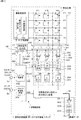
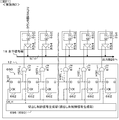
[基本構成]
図1は、固体撮像装置の一実施形態であるCMOS型の固体撮像装置(CMOSイメージセンサ)の基本構成図である。固体撮像装置も半導体装置の一例である。固体撮像装置1は、複数個の単位画素3が2次元マトリクス状に配列された画素アレイ部10を有する。固体撮像装置1は、例えばR、G、Bの色フィルタがベイヤー配列とされている色分解(色分離)フィルタを使用することで、画素アレイ部10をカラー撮像対応にすることができる。図1では、簡単のため行及び列の一部を省略して示しているが、現実には、各行や各列には、数十から数千の単位画素3が配置される。後述するように、単位画素3は検知部の一例である受光素子(電荷生成部)としてのフォトダイオードの他に例えば、電荷転送用やリセット用や増幅用等の3個或いは4個のトランジスタを有する画素内アンプを有する。画素アレイ部10は、2次元に単位画素3が配列されていればよく、その配列形態は2次元格子状に限らず、斜め格子状に単位画素3を配列した画素ずらしのものでもよいしハニカム状に単位画素3を配列したものでもよい。
[Basic configuration]
FIG. 1 is a basic configuration diagram of a CMOS type solid-state imaging device (CMOS image sensor) which is an embodiment of a solid-state imaging device. A solid-state imaging device is also an example of a semiconductor device. The solid-
単位画素3からは、列ごとに垂直信号線19を介して画素信号電圧Vxが出力される。垂直信号線19の画素信号電圧Vxは、時間系列として、基準レベルとしての画素信号の雑音を含むリセットレベルSrst(暗時信号)の後に信号レベルSsig(受光信号)が現れる。例えばリセットレベルSrstはフィードスルーレベルSfeedにリセット成分Vrstを加えたレベルである。信号レベルSsigはリセットレベルSrstに信号成分Vsigを加えたレベルであり、Ssig(=Srst+Vsig)−Srstで信号成分Vsigが得られる。この差分処理がいわゆるCDS(Correlated Double Sampling;相関2重サンプリング)処理に該当する。暗時信号と受光信号を取得し、その差分(レベル差)を取得することで、ノイズ成分は暗時信号と光信号の両方に同じようにのることから、差分に含まれるノイズは非常に小さくなる。
A pixel signal voltage Vx is output from the
垂直信号線19の一端がカラム部26側に延在するとともに、その経路において、読出電流源部24が接続され動作電流(読出電流)が垂直信号線19に供給される。動作電流供給部24は、電流源240を垂直信号線19(列)ごとに備えるとともに、各列共通に使用される基準電流源部248を備える。ここで、本構成の特徴点として、電流源240には、電流源240のオン・オフを制御するカラム停止信号CLMSTPn(詳細は後述する)が列別に入力される。画素データの水平転送が不要な非選択列の電流源240の機能が停止されることで消費電力の低減が図られる。
One end of the
カラム部26は、CDS処理機能やデジタル変換機能をなすAD変換部250が列並列に設けられている。つまり、固体撮像装置1には、列ごとに、電流源240とAD変換部250とが設けられている。詳細は後述するが、カラム部26には、比較部252、カウント動作期間制御部253、計数部254が設けられ、それぞれの1列分の機能部の集合でAD変換部250が構成される。“列並列”とは、垂直列の垂直信号線19(列信号線の一例)に対し並列に複数のCDS処理機能部やデジタル変換部(AD変換部)等の機能要素(本例ではAD変換部250)が設けられていることを意味する。このような読出方式をカラム読出方式と称する。典型的なカラム読出方式では、垂直信号線19とAD変換部250が一対一で配置されるが、これに限らず、予め決められた複数列に対して1つのAD変換部250を設けた、いわゆるカラム共有の構成を採ってもよい。この場合、図示しないが、カラム部26は、予め決められた複数列に対して1つの垂直信号線19を選択する垂直線選択部を設ける。カラム共有の構成を採ることで、コンパレータやカウンタを複数列で共有することができ、カラム部26がセンサチップ上に占有する面積を低減でき、製造費用が安くなる等の利点が得られる。
In the
固体撮像装置1は更に、駆動制御部7、単位画素3に画素信号読出用の動作電流(読出電流)を供給する読出電流源部24と、カラム部26にAD変換用の参照信号SLP_ADCを供給する参照信号生成部27と、出力部28を備えている。
The solid-
駆動制御部7は、画素アレイ部10の信号を順次読み出すための制御回路機能の実現のため水平転送部11と、垂直走査部14(行走査回路)と、通信・タイミング制御部20とを備えている。水平転送部11は、通信・タイミング制御部20からの制御信号CN2に応答して列の走査を開始し、データ転送動作時に読み出すべきデータのカラム位置を指示しつつ、カラム部26で取得される画素データを水平方向へ転送する。垂直走査部14は、行アドレスや行走査を制御する垂直アドレス設定部14aや垂直駆動部14bを有する。垂直走査部14は、画素アレイ部10の行を選択し、その行に必要なパルスを供給するものであり、通信・タイミング制御部20からの制御信号CN1に応答して行の走査を開始する。垂直アドレス設定部14aは、信号を読み出す行(読出し行:選択行や信号出力行とも称する)の他に、電子シャッタ用の行等も選択する。
The drive control unit 7 includes a
ここで、詳細は後述するが、本実施形態の水平転送部11は、水平方向の全画素のデータを水平転送する通常の読出し処理の他に、水平方向の一部分の画素(列)の画素データのみを水平転送する水平方向の部分読出し処理も可能になっている点に特徴がある。
Here, although details will be described later, the
単位画素3は、行選択のための行制御線15を介して垂直走査部14と、また垂直信号線19を介してカラム部26の垂直列ごとに設けられているAD変換部250と、それぞれ接続される。行制御線15は垂直走査部14から画素に入る配線全般を示す。
The
通信・タイミング制御部20は、端子5aを介して入力されるマスタークロックCLK0に同期したクロックをデバイス内の各部(水平転送部11、垂直走査部14、カラム部26等)に供給するタイミングジェネレータ(読出アドレス制御装置の一例)の機能ブロックを備える。更に、端子5aを介して外部の主制御部から供給されるマスタークロックCLK0を受け取り、また端子5bを介して外部の主制御部から供給される動作モード等を指令するデータを受け取り、更に固体撮像装置1の情報を含むデータを外部の主制御部に出力する通信インタフェースの機能ブロックを備える。例えば、通信・タイミング制御部20は、内部クロックを生成するクロック変換部の機能を持つクロック変換部20a及び通信機能や各部を制御する機能を持つシステム制御部20b等を有する。クロック変換部20aは、端子5aを介して入力されるマスタークロックCLK0に基づき、マスタークロックCLK0よりも高速周波数のパルスを生成する逓倍回路を内蔵しており、カウントクロックCKcnt1やカウントクロックCKdac1等の内部クロックを生成する。
The communication /
出力部28は、信号増幅部402(センスアンプS・A)と、固体撮像装置1と外部とのインタフェース機能をなすデジタルインタフェース部406(DIF)とを有する。信号増幅部402は、水平転送部11との間のデータ転送用の信号線(転送配線)である水平信号線18上の信号(デジタルデータではあるが小振幅)を検出する。出力部28は、信号増幅部402とデジタルインタフェース部406との間に、各種のデジタル演算処理を行なうデジタル演算部404(SIG)を必要に応じて設けてもよい。デジタルインタフェース部406は、信号増幅部402と外部回路の間に介在し外部回路とのインタフェース機能をなす。デジタルインタフェース部406の出力は出力端5cに接続されており、映像データが後段回路に出力される。
The
[カラムAD回路と参照信号生成部の詳細]
AD変換部250におけるAD変換方式としては、回路規模や処理速度(高速化)や分解能等の観点から様々な方式が考えられているが、一例として、参照信号比較型、スロープ積分型、或いはランプ信号比較型等とも称されるAD変換方式を採用する。この手法は、簡単な構成でAD変換器が実現できるため、並列に設けても回路規模が大きくならないという特徴を有している。参照信号比較型のAD変換に当たっては、変換開始(比較処理の開始)から変換終了(比較処理の終了)までの時間に基づいてカウント動作有効期間Tenを決定し(ここではその期間を示すカウントイネーブル信号ENとする)、その期間のクロック数に基づき処理対象信号をデジタルデータに変換する。
[Details of column AD circuit and reference signal generator]
As the AD conversion method in the
比較処理によって得られる情報は、アナログ信号(ここでは画素信号電圧Vx)の大きさに対応した時間情報を持つパルス情報である。参照信号比較型のAD変換処理では、この比較処理で得られるパルス情報(時間情報)に基づき、計数処理の有効期間を決定し、その計数処理の有効期間に一定の割合で値を変化させる計数処理を行なう。典型例としては、カウンタを使用して、基準クロック周期で最下位桁を1ずつ変化させる。これによって得たカウント値をアナログ信号の大きさに応じたデジタルデータとして取得する。もちろん、一定の割合で値を変化させる計数処理を行なうことができればよく、カウンタを使用した構成に限らず、様々な変形が可能である。例えば、いわゆる加算器や加減算器とその結果を基準クロック周期で保持するデータ保持部(ラッチ)を使用して巡回型に構成し、各回の変化値を一定の割合(典型例は1)にするように構成してもよい。 The information obtained by the comparison process is pulse information having time information corresponding to the magnitude of the analog signal (here, the pixel signal voltage Vx). In the reference signal comparison type AD conversion process, a count period in which the valid period of the count process is determined based on the pulse information (time information) obtained by the comparison process, and the value is changed at a constant rate during the valid period of the count process. Perform processing. As a typical example, a counter is used to change the least significant digit by one in a reference clock cycle. The count value thus obtained is acquired as digital data corresponding to the magnitude of the analog signal. Of course, it is only necessary to be able to perform a counting process for changing the value at a constant rate, and the present invention is not limited to the configuration using the counter, and various modifications are possible. For example, a so-called adder or adder / subtracter and a data holding unit (latch) that holds the result in a reference clock cycle are used to form a cyclic type, and the change value of each time is set to a constant ratio (typical example is 1). You may comprise as follows.
参照信号比較型AD変換方式を採用する場合に、考え方としては、参照信号生成部27もAD変換部250ごとに設けることも考えられる。例えば、AD変換部250ごとに比較器と参照信号発生器を設け、比較器の比較結果を基に、逐次、参照信号の値を対応する列の参照信号発生器で変化させていく構成を採る場合である。しかしながらこれでは回路規模や消費電力が増える。そこで、本実施形態では、参照信号生成部27を全てのAD変換部250に共通に使用する構成を採り、参照信号生成部27から発生される参照信号SLP_ADCを各AD変換部250が共通に使用する構成にする。
When adopting the reference signal comparison type AD conversion method, it is conceivable to provide the reference
このため、参照信号生成部27は、DA変換部270(DAC;Digital Analog Converter)を有し、通信・タイミング制御部20からの制御データCN4で示される初期値からカウントクロックCKdac1に同期して、制御データCN4で示される傾き(変化率)の参照信号SLP_ADCを生成する。カウントクロックCKdac1は計数部254の計数処理用のカウントクロックCKcnt1と同一にしてもよい。参照信号SLP_ADCは、全体的にある傾きを持って線形に変化する波形を持つものであればよく、その変化が滑らかなスロープ状を呈するものであってもよいし、階段状に順次変化するものであってもよい。
For this reason, the reference
参照信号比較型のAD変換に当たっては、比較部252による参照信号SLP_ADCと画素信号電圧Vxとの比較結果に基づいてカウント動作有効期間Ten(その期間を示す信号をカウントイネーブル信号ENと称する)を決定し、カウントイネーブル信号ENがアクティブな期間のカウントクロックCKcnt1のクロック数に基づきアナログの処理対象信号をデジタルデータに変換する。基準レベル(リセットレベルSrst)についての処理をプリチャージ相(P相と省略して記すこともある)の処理と称し、信号レベルSsigについての処理をデータ相(D相と省略して記すこともある)の処理と称する。P相の処理後にD相の処理を行なう場合、D相の処理はリセットレベルSrstに信号成分Vsigを加えた信号レベルSsigについての処理となる。カウント動作有効期間Tenとしては、P相・D相とも比較出力が反転するまで計数する前半カウント方式、P相・D相とも比較出力が反転してから計数する後半カウント方式、P相・D相の何れか一方では比較出力が反転するまで計数するが他方では比較出力が反転してから計数する前後半カウント方式がある。又、それぞれにおいて、P相・D相のカウントモードを巧みに組み合わせることやP相処理開始時の初期値設定を制御することで、カラム内でCDS処理を行なうようにすることもできる。これら、カウント動作有効期間Tenをどうとるかや、AD変換部250内で差分処理(CDS処理)を行なうか否か等、本出願人は、参照信号比較型のAD変換方式を種々提案しており、それらも基本的には後述する各実施形態で採用し得る。
In the reference signal comparison type AD conversion, a count operation effective period Ten (a signal indicating the period is referred to as a count enable signal EN) is determined based on a comparison result between the reference signal SLP_ADC and the pixel signal voltage Vx by the
何れの処理例においても、原理的には、電圧比較器に参照信号SLP_ADCを供給し、垂直信号線19を介して入力されたアナログの画素信号を参照信号SLP_ADCと比較する。カウント動作有効期間Tenに入るとクロック信号でのカウント(計数)を開始することによって、指定されているカウント動作有効期間Tenにおけるクロック数をカウントすることでAD変換を行なう。
In any processing example, in principle, the reference signal SLP_ADC is supplied to the voltage comparator, and the analog pixel signal input through the
参照信号比較型のAD変換を行なうため、本実施形態のカラム部26の各列のAD変換部250は、比較処理部322(COMP:電圧比較部、コンパレータ)、カウンタ制御信号生成部332(EN生成部)、計数処理部351を備える。本実施形態のカラム部26は、カウント動作期間制御部253(カウンタ制御信号生成部332)を比較部252(比較処理部322)と計数部254(計数処理部351)の間に配置している。好ましくは計数処理部351はアップカウントモードとダウンカウントモードを切替可能なもの(アップダウンカウンタ)にする。アップダウンカウンタを用いることにより、回路規模を大きくすることなく高フレームレート化を達成できる。各AD変換部250の比較処理部322の集合で比較部252が構成される。各AD変換部250のカウンタ制御信号生成部332の集合でカウント動作期間制御部253が構成される。各AD変換部250の計数処理部352の集合で計数部254が構成される。
In order to perform reference signal comparison type AD conversion, the
比較部252(比較処理部322)は、参照信号生成部27(DA変換部270)で生成された参照信号SLP_ADCと選択行の単位画素3から垂直信号線19(H1,H2,…,Hh)を経由し得られるアナログの画素信号電圧Vxを比較する。比較処理部322は、参照信号SLP_ADCと画素信号電圧Vxが一致したとき比較パルスCo(コンパレート出力)を反転する。
The comparison unit 252 (comparison processing unit 322) generates the vertical signal line 19 (H1, H2,..., Hh) from the reference signal SLP_ADC generated by the reference signal generation unit 27 (DA conversion unit 270) and the
カウント動作期間制御部253のカウンタ制御信号生成部332は、比較出力Coと通信・タイミング制御部20からの制御情報に基づきカウントイネーブル信号ENを生成して計数処理部351に供給し、計数処理部351のカウント動作期間を制御する。ここで、本構成の特徴点として、カウンタ制御信号生成部332には、カウント動作期間制御のオン・オフを制御するカラム停止信号CLMSTPn(詳細は後述する)が列別に入力される。画素データの水平転送が不要な非選択列のカウント動作期間制御機能が停止されることで消費電力の低減が図られる。
The counter control
通信・タイミング制御部20から各AD変換部250の計数処理部351には、計数処理部351がP相・D相のカウント処理をダウンカウントモードで動作するのかアップカウントモードで動作するのかや、P相のカウント処理における初期値Diniの設定やリセット処理等、その他の制御情報を指示する制御信号CN5が入力されている。
From the communication /
比較処理部322の一方の入力端子(+)は、他の比較処理部322の入力端子(+)と共通に、参照信号生成部27で生成される参照信号SLP_ADCが入力される。比較処理部322の他方の入力端子(−)には、それぞれ対応する垂直列の垂直信号線19が接続され、画素アレイ部10からの画素信号電圧Vxが個々に入力される。ここで、本構成の特徴点として、比較処理部322には、比較動作のオン・オフを制御するカラム停止信号CLMSTPn(詳細は後述する)が列別に入力される。画素データの水平転送が不要な非選択列の比較機能が停止されることで消費電力の低減が図られる。
The reference signal SLP_ADC generated by the reference
計数処理部351のクロック端CKには、他の計数処理部351のクロック端CKと共通に通信・タイミング制御部20からカウントクロックCKcnt1が入力される。計数処理部351は、カウント結果を保持するラッチ機能を有する。ここで、本構成の特徴点として、計数処理部351には、カウント動作のオン・オフを制御するカラム停止信号CLMSTPnが列別に入力される。画素データの水平転送が不要な非選択列のカウント機能が停止されることで消費電力の低減が図られる。
The count clock CKcnt1 from the communication /
本実施形態では、計数部254(の計数処理部351)にてCDS処理を行なう基本構成とするが、これに限らず、リセットレベルSrstのP相データと信号レベルSsigのD相データを個別に出力部28側に転送し、AD変換部250の後段のデジタル演算部404でCDS処理を行なってもよい。
In this embodiment, the basic configuration is such that the CDS processing is performed by the counting unit 254 (the counting processing unit 351), but this is not limiting, and the P-phase data at the reset level Srst and the D-phase data at the signal level Ssig are individually provided. The data may be transferred to the
水平転送部11や垂直走査部14等の駆動制御部7の各要素は、画素アレイ部10とともに、半導体集積回路製造技術と同様の技術を用いて単結晶シリコン等の半導体領域に一体的に形成されたいわゆる1チップもの(同一の半導体基板上に設けられているもの)として、本実施形態の固体撮像装置1が構成される。固体撮像装置1は、このように各部が半導体領域に一体的に形成された1チップとして形成された形態であってもよいし、図示を割愛するが、画素アレイ部10、駆動制御部7、カラム部26等の各種の信号処理部の他に、撮影レンズ、光学ローパスフィルタ、或いは赤外光カットフィルタ等の光学系をも含む状態で、これらを纏めてパッケージングされた撮像機能を有するモジュール状の形態としてもよい。
The elements of the drive control unit 7 such as the
個々のAD変換部250(詳しくは計数部254の計数処理部351)の出力側は水平転送部11と接続される。水平転送部11の詳細については後述する。尚、いわゆるパイプライン水平転送を可能にするため、計数処理部351の後段に、計数処理部351の保持したカウント結果を保持するラッチを具備したメモリ装置としてのデータ記憶部を備える構成を採ることもできる。ラッチは、決められたタイミングで計数処理部351から出力されたカウントデータを保持・記憶する。パイプライン水平転送とは、AD変換部250でのカラム処理(AD変換やCDS処理)と画素データの水平転送を並行して行なう処理のことである。
The output side of each AD conversion unit 250 (specifically, the
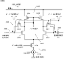
[比較部の入力段]
図2は、比較部252の入力段の構成と動作を説明する図である。比較部252は、回路構成を工夫することで、単位画素3ごとのリセット成分ΔVのばらつきに左右されずに比較期間を設定できるようにする点に特徴を有する。
[Input stage of comparison unit]
FIG. 2 is a diagram for explaining the configuration and operation of the input stage of the
比較部252の基本構成は、一般に良く知られている差動アンプ構成を採用しており、差動トランジスタ対部352と、負荷トランジスタ対部360と、電流源部370とを備え、更に本構成の特徴点として、動作点リセット部380も備えている。差動トランジスタ対部352は、NMOS型のトランジスタ353とトランジスタ354とを有し、トランジスタ353とトランジスタ354のソース同士が接続されている。差動トランジスタ対部352の出力(図示した例ではトランジスタ354のドレイン)は、図示しないアンプ機能を有したバッファ部(非反転型・反転型の何れでもよい)に接続され、十分な増幅がなされた後、比較パルスCoとして出力されるようになっている。
The basic configuration of the
負荷トランジスタ対部360は、差動トランジスタ対部352の能動(アクティブ)負荷となるように接続されたPMOS型のトランジスタ362とトランジスタ364とが電源側に配されている。具体的には、トランジスタ353とトランジスタ362のドレイン同士が接続されており、更に、トランジスタ354とトランジスタ364のドレイン同士がトランジスタ362とトランジスタ364の各ゲート同士と接続されている。
In the
電流源部370は、差動トランジスタ対部352と負荷トランジスタ対部360に一定の動作電流を供給するもので、接地(GND)側に配された定電流源372を有する。更に、本構成の特徴点として、電流源部370は、“画素信号を必要としない非選択列の比較処理部322に流れる動作電流を減少させる”構成を備える。基本的には、後述の動作電流供給部24における電流源240についての構成と同様の構成を採用することができる。例えば、図示のように、動作電流供給部24の各列の電流源240は、定電流源372の電流路上に(図の例は定電流源372とトランジスタ353及びトランジスタ354のソース)との間にNMOS型のスイッチトランジスタ374を有する。定電流源372の制御入力端には、DCゲート電圧VG_ADCが各列共通に入力される。スイッチトランジスタ374のゲートには、トランジスタ374のオン・オフを制御するカラム停止信号CLMSTPnが列別に入力される。画素データの水平転送が不要な非選択列のスイッチトランジスタ374へのカラム停止信号CLMSTPnがLレベルとなることでスイッチトランジスタ374がオフされて、比較部252の機能が停止され消費電力の低減が図られる。
The
動作点リセット部380は、PMOS型のスイッチトランジスタ382とスイッチトランジスタ384とを有する。スイッチトランジスタ382とスイッチトランジスタ384の各ゲートには共通にオートゼロ信号AZが比較器リセット信号として供給される。オートゼロ信号AZがアクティブ(本例ではLレベル)となるタイミングは、単位画素3のリセットトランジスタのゲート端に供給されるリセット信号RSTがアクティブからインアクティブに変化した後の画素信号電圧VxがリセットレベルSrstとなる期間内とする。或いは、単位画素3のリセットトランジスタ36のゲート端に供給されるリセット信号RSTがアクティブの期間内とする。これらの期間は、参照信号SLP_ADCはランプ状への変化開始レベルである初期値よりも少し低いリセットレベルにあるとする。
The operating point reset unit 380 includes a PMOS type switch transistor 382 and a
トランジスタ353のゲート(入力端子)には、容量素子386を介して画素信号Vxが供給され、トランジスタ354のゲート(入力端子)には、図示しない参照信号生成部27から参照信号SLP_ADCが容量素子388を介して供給されるようになっている。動作点リセット部380は、容量素子386及び容量素子388を介して入力される各信号に対してサンプル/ホールド機能を発揮する。すなわち、画素信号Vxと参照信号SLP_ADCとの比較を開始する直前だけオートゼロ信号AZをアクティブLにし、差動トランジスタ対部352の動作点をドレイン電圧(基準成分や信号成分を読み出す動作基準値)にリセットする。その後、容量素子386を介して画素信号Vxをトランジスタ353へ、容量素子388を介して参照信号SLP_ADCをトランジスタ354へ入力し、画素信号Vxと参照信号SLP_ADCが同電位となるまで比較する。画素信号Vxと参照信号SLP_ADCとが同電位となると出力が反転する。比較処理開始の当初は、画素信号Vxよりも参照信号SLP_ADCが高く、例えば比較部252の出力(比較パルスCo)はLレベルにある。その後、画素信号Vxと参照信号SLP_ADCの同電位時に比較部252の出力はLレベルからHレベルへ反転する。この比較パルスCoは、図示を割愛したカウント動作期間制御部253に供給される。
The pixel signal Vx is supplied to the gate (input terminal) of the
単位画素3のリセットトランジスタのゲート端にはリセット信号RST(のアクティブ状態)を供給してリセットする。このとき、画素信号電圧Vxは、リセット信号RSTがアクティブ状態の期間では比較的大きな電圧レベルのノイズパルスが生じ、その後、リセット信号RSTがアクティブからインアクティブに変化するとリセットレベルSrstに落ち着く。このリセットアクティブ時のノイズパルスのレベルとその後のリセットレベルSrstは単位画素3ごとにばらつく。電荷生成部で検出された信号電荷に応じた信号レベルSsigはリセットレベルSrstに重畳され、画素信号電圧Vxとしては信号レベルSsigとして現われる。よって、リセットレベルSrstがばらつくと信号レベルSsigもばらつく。このとき、信号レベルSsigそのものにはばらつきの影響は存在しない。CDS処理では、この点を勘案して、リセットレベルSrstと信号レベルSsigの差分をとることでばらつきの影響が存在しない信号レベルSsigを取得する。
The reset signal RST (active state) is supplied to the gate terminal of the reset transistor of the
リセットレベルSrstはばらつきを持ち、レベルが参照信号SLP_ADCの比較可能範囲を超えると正しい比較できなくなることが起こり得る。これを避けるべく、P相処理時に、電圧比較部252をリセットレベルSrstを読み出す動作基準値にリセットし、その後、比較部252に参照信号SLP_ADCを供給してから比較処理とカウント処理を開始する。すなわち、比較部252では、オートゼロ信号AZを供給して差動トランジスタ対部302のトランジスタ303及びトランジスタ304のゲートとドレインを一時的に接続してダイオード接続とする。そして、単位画素3の増幅用トランジスタ42の入力にトランジスタ304のオフセット成分を加えたものをトランジスタ304の入力端子(ゲート)に保持した後に参照信号SLP_ADCを入力して、画素信号Vxと参照信号SLP_ADCとの比較を開始する。こうすることで、単位画素3ごとに、画素信号の読出電位で電圧比較部252の動作点が設定されるので、リセットレベルSrstのばらつきの影響を受け難くなる。但し、比較部252を動作基準値にリセットするとkTC雑音の発生が懸念されるので、D相処理時には、比較部252のリセットを行なわない(オートゼロをしない)で、直ちに比較部252に参照信号SLP_ADCを供給して比較処理とカウント処理を開始する。
The reset level Srst varies, and if the level exceeds the comparison range of the reference signal SLP_ADC, a correct comparison may not be possible. In order to avoid this, during the P-phase processing, the
[固体撮像装置の基本動作]
図3は、AD変換処理とCDS処理に着目した固体撮像装置1の簡易的な回路構成図である。カウント動作期間制御部253は割愛して示している。
[Basic operation of solid-state imaging device]
FIG. 3 is a simple circuit configuration diagram of the solid-
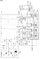
単位画素3は、電荷生成部32の他に、4個のトランジスタ(読出選択用トランジスタ34、リセットトランジスタ36、垂直選択用トランジスタ40、増幅用トランジスタ42)を画素信号生成部5を構成する基本素子として備える。転送部を構成する読出選択用トランジスタ34は、転送信号TRGで駆動される。初期化部を構成するリセットトランジスタ36は、リセット信号RSTで駆動される。垂直選択用トランジスタ40は、垂直選択信号VSELで駆動される。
The
電荷生成部32は、フォトダイオード等の受光素子で構成される検知部の一例である。電荷生成部32は、受光素子のアノードが低電位側の基準電位Vssに接続され、カソード側が読出選択用トランジスタ34のソースに接続されている。基準電位Vssは接地電位GNDとしてもよい。読出選択用トランジスタ34(転送ゲート)は、ドレインがリセットトランジスタ36とフローティングディフュージョン38と増幅用トランジスタ42とが接続される接続ノードに接続される。リセットトランジスタ36は、ソースがフローティングディフュージョン38に、ドレインがリセット電源Vrd(通常は電源Vddと共通にする)にそれぞれ接続される。
The
垂直選択用トランジスタ40は、一例として、ドレインが増幅用トランジスタ42のソースに、ソースが画素線51にそれぞれ接続され、ゲート(特に垂直選択ゲートSELVという)が垂直選択線52に接続される。増幅用トランジスタ42は、ゲートがフローティングディフュージョン38に接続され、ドレインが電源Vddに接続され、ソースは垂直選択用トランジスタ40を介して画素線51に接続され、更に画素線51が垂直信号線19に接続される。他の接続例として、垂直選択用トランジスタ40は、ドレインを電源Vddに接続し、ソースを増幅用トランジスタ42のドレインに接続し、増幅用トランジスタ42のソースを画素線51に接続してもよい。
For example, in the
垂直信号線19は、一端がカラム部26側に延在するとともに、その経路において、読出電流源部24が接続されている。動作電流供給部24の各列の電流源240は、垂直列に対して負荷MOSトランジスタを有し、各列共通に使用される基準電流源部248と負荷MOSトランジスタとの間でゲート同士が接続されカレントミラー回路を構成し、垂直信号線19に対し定電流源242として機能するようになっている。そして、増幅用トランジスタ42との間で、略一定の動作電流(読出電流)が供給されるソースフォロワ構成が採られる。
One end of the
更に、本構成の特徴点として、動作電流供給部24は、“画素信号を必要としない非選択列の垂直信号線19に流れる電流を減少させる”構成を備える。電流源としての負荷MOSトランジスタと垂直信号線19との間に、画素信号を必要としない列の電流を流さないようにする機構を設けてもよい。この構成は、画素信号を必要としない列の画素信号を読み出す機能を完全に果たさなくすることができ、その分、消費電力の低減を図ることができる。“画素信号を必要としない列の電流を流さないようにする機構”としては、例えば、トランジスタなどの半導体製のスイッチを設ける等、電流路をオン/オフ切替えする(導通状態と非導通状態とを切り替える)切替手段を設ければよい。
Further, as a feature point of the present configuration, the operating
或いは、動作電流供給部24は、“画素信号を必要としない非選択列の垂直信号線19に流れる電流を減少させる”構成として、画素信号を必要としない列の垂直信号線19に接続されている電流源としての負荷MOSトランジスタを直接に制御することにより電流量を減少させてもよい。この構成でも、画素信号を必要としない列の画素信号を読み出す機能を果たさなくすることができ、その分、消費電力の低減を図ることができる。
Alternatively, the operating
画素信号を必要としない列について“電流量を減少させる”際には、通常の読取時の負荷電流よりも小さくすればよく、電流源としての負荷MOSトランジスタの活性(能動)状態を維持することで小さな電流を流しておいてもよいし、電流源としての負荷MOSトランジスタそのものを完全にオフ(非導通状態)状態にすることで電流を完全に流さない状態にしてもよい。因みに、画素信号を必要としない列の垂直信号線19に電流を流さない状態にすると、場合によっては、該当列の垂直信号線19の電位が不定状態となり、系が不安定になることが懸念される。この問題を解消するには、画素信号を必要としない列の垂直信号線19に電流を流さない状態にするのに対応して、読み出さない列の垂直信号線19をある電位に固定する構成を設けるとよい。
When “decreasing the amount of current” for a column that does not require a pixel signal, the load current may be smaller than the load current during normal reading, and the active state of the load MOS transistor as a current source is maintained. In this case, a small current may be allowed to flow, or the load MOS transistor itself as a current source may be completely turned off (non-conducting state) so that no current flows completely. Incidentally, there is a concern that if a current is not passed through the
例えば、図示した構成では、定電流源242の電流路上に(図の例は定電流源242と垂直信号線19)との間にNMOS型のスイッチトランジスタ244を有する。スイッチトランジスタ244のゲートには、スイッチトランジスタ244のオン・オフを制御するカラム停止信号CLMSTPnが列別に入力される。画素データの水平転送が不要な非選択列のスイッチトランジスタ244へのカラム停止信号CLMSTPnがLレベルとなることで、スイッチトランジスタ244がオフされて読出電流供給機能が停止される。電流源としての負荷MOSトランジスタそのものを完全にオフ(非導通状態)状態にすることで消費電力の低減が図られる。
For example, in the illustrated configuration, an NMOS
参照信号生成部27は、DA変換部270と抵抗部340とを有する。図示しないが、DA変換部270は、定電流源の組合せで構成されている電流源部、カウンタ部、オフセット生成部、電流源制御部、規定電流I_0を設定する基準電流源部を備え、電流出力型のDA変換回路となっている。電流源部の電流出力端には、抵抗値R_340の抵抗部340が電流電圧変換部として接続されている。電流源部、電流源制御部、抵抗部340で、電流電圧変換部が構成され、電流源部と抵抗部340との接続点の発生する電圧が参照信号SLP_ADCとして利用される。
The reference
各カラムの垂直信号線19は、比較処理部322の一方の端子(この例では反転入力端)に接続されている。これによって、垂直信号線19を介して、画素信号電圧Vxがカラム部26のAD変換部250に供給される。AD変換部250では、単位画素3から垂直信号線19に読み出した画素信号電圧Vxを、AD変換部250の比較処理部322で参照信号SLP_ADCと比較する。そして、図示を割愛したカウンタ制御信号生成部332が計数処理部351をカウントイネーブル信号ENに基づき動作させ、そのカウント動作と1対1の対応をとりながらを参照信号電位を変化させ、垂直信号線19の画素信号電圧Vxをデジタルデータに変換する。
The
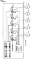
<撮像装置>
図4は、固体撮像装置1を使用した撮像装置の概略構成図である。これは、前述の固体撮像装置1に採用していたAD変換処理及び画素データの水平転送処理を、物理情報取得装置の一例である撮像装置に適用した形態である。主要な構成要素について説明すると次の通りである(主要なもの以外は説明を割愛する)。
<Imaging device>
FIG. 4 is a schematic configuration diagram of an imaging apparatus using the solid-
撮像装置8は、撮影レンズ802、光学ローパスフィルタ804、色フィルタ群812、画素アレイ部10、駆動制御部7、カラム部26、参照信号生成部27、カメラ信号処理部810を備えている。図中に破線で示すように、光学ローパスフィルタ804と合わせて、赤外光成分を低減させる赤外光カットフィルタ805を設けることもできる。カラム部26の後段に設けられたカメラ信号処理部810は、撮像信号処理部820と、撮像装置8の全体を制御する主制御部として機能するカメラ制御部900を有する。撮像信号処理部820は、信号分離部822と、色信号処理部830と、輝度信号処理部840と、エンコーダ部860を有する。
The
カメラ制御部900は、マイクロプロセッサ(microprocessor)902、読出専用の記憶部であるROM(Read Only Memory)904、RAM906(Random Access Memory)、図示を割愛したその他の周辺部材を有している。マイクロプロセッサ902は、コンピュータが行なう演算と制御の機能を超小型の集積回路に集約させたCPU(Central Processing Unit)を代表例とする電子計算機の中枢をなすものと同様である。RAM906は、随時書込み及び読出しが可能であるとともに揮発性の記憶部の一例である。マイクロプロセッサ902、ROM904、及びRAM906を纏めて、マイクロコンピュータ(microcomputer)とも称する。
The camera control unit 900 includes a
カメラ制御部900は、システム全体を制御するものであり、カウントクロックCKcnt1及びカウントクロックCKdac1の周波数や、参照信号SLP_ADCの傾き等を調整する機能を有している。ROM904にはカメラ制御部900の制御プログラム等が格納されているが、特に本例では、カメラ制御部900によって、参照信号比較型のAD変換処理や水平方向の部分読出し処理や非選択列の機能停止処理を制御するためのプログラムが格納されている。RAM906にはカメラ制御部900が各種処理を行なうためのデータ等が格納されている。カメラ制御部900は、メモリカード等の記録媒体924を挿脱可能に構成し、またインターネット等の通信網との接続が可能に構成している。例えば、カメラ制御部900は、マイクロプロセッサ902、ROM904、及びRAM906の他に、メモリ読出部907及び通信I/F(インタフェース)908を備える。
The camera control unit 900 controls the entire system and has a function of adjusting the frequency of the count clock CKcnt1 and the count clock CKdac1, the inclination of the reference signal SLP_ADC, and the like. The
記録媒体924は、マイクロプロセッサ902にソフトウェア処理をさせるためのプログラムデータや、輝度信号処理部840からの輝度系信号に基づく測光データDLの収束範囲や露光制御処理(電子シャッタ制御を含む)を登録する等のために利用される。特に、本実施形態では、水平方向の部分読出し処理や非選択列の機能停止処理を行なうための各種の制御情報の設定値等の様々なデータを登録するためにも利用される。メモリ読出部907は、記録媒体924から読み出したデータをRAM906に格納(インストール)する。通信I/F908は、インターネット等の通信網との間の通信データの受け渡しを仲介する。
The
撮像装置8は、駆動制御部7及びカラム部26を、画素アレイ部10と別体にしてモジュール状のもので示しているが、これらが画素アレイ部10と同一の半導体基板上に一体的に形成されたワンチップものを利用してもよい。図は、画素アレイ部10や駆動制御部7やカラム部26や参照信号生成部27やカメラ信号処理部810の他に、撮影レンズ802、光学ローパスフィルタ804、あるいは赤外光カットフィルタ805等の光学系をも含む状態で撮像装置8を示している。この態様は、これらを纏めてパッケージングされた撮像機能を有するモジュール状の形態とする場合に好適である。このような撮像装置8は、「撮像」を行なうための、例えば、カメラや撮像機能を有する携帯機器等の電子機器として提供される。「撮像」は、通常のカメラ撮影時の像の撮り込みだけではなく、広義の意味として、指紋検出や、タッチパネル等の物理量分布検知半導体装置或いは物理情報取得装置(物理量分布検知装置)において物理量分布として圧力を利用して像情報を取得すること等も含む。
In the
このような構成の撮像装置8も、後述の水平方向の部分読出し処理や非選択列の機能停止処理を適用することで、全体の消費電力を低減できるし、素子選択モード時に必要とされない単位素子と対応する信号を読み飛ばすことができる。
The
<水平読み飛ばし処理>
以下に、水平方向の部分読出し処理(水平読み飛ばし処理)及びこれと関連する技術の具体的な実施例を説明する。因みに、実施例1〜実施例3は、切出しモードでの水平方向切出し処理の適用例であり、実施例5〜実施例6は、間引きモードでの水平方向間引き処理の適用例である。一定の行周期で画素行を読み飛ばし、残りの画素行の画素から信号を読み出す行方向に関しての間引き読出しや行方向についての切り出し処理も併用する場合で説明するが、このことは必須でない。
<Horizontal skip processing>
In the following, specific examples of the horizontal partial reading process (horizontal skipping process) and techniques related thereto will be described. Incidentally, the first to third embodiments are application examples of the horizontal direction cutting process in the cutting mode, and the fifth to sixth examples are application examples of the horizontal direction thinning process in the thinning mode. Although a case will be described in which pixel rows are skipped at a constant row cycle and thinning-out readout in the row direction for reading out signals from pixels in the remaining pixel rows and cut-out processing in the row direction are also used, this is not essential.
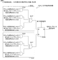
図5は、本実施形態の水平読み飛ばし処理の基本概念を説明する図である。詳細には、図5(A)は、本実施形態に対する比較例の水平読み飛ばし処理を説明する図であり、図5(B)は、本実施形態の水平読み飛ばし処理を説明する図である。 FIG. 5 is a diagram for explaining the basic concept of the horizontal skip processing of the present embodiment. Specifically, FIG. 5A is a diagram for explaining horizontal reading skip processing of a comparative example with respect to this embodiment, and FIG. 5B is a diagram for explaining horizontal reading skip processing of this embodiment. .
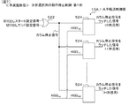
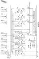
本実施形態の水平読み飛ばし処理は、水平転送部11がシフトレジスタを備え、水平転送用のクロックが入る都度、画素データ(読出し信号)を順次後段へシフトすることによって画素データの水平方向の読出し(水平転送)を行なう場合における水平方向切出し処理の適用例である。
In the horizontal skip processing of this embodiment, the
図5(A)に示す比較例の固体撮像装置1Zにおいて、水平転送部11Zは、レジスタ512Z(記憶部の一例)が一定方向に縦続接続されたシフトレジスタ510Z(転送部の一例)を備え、データの水平転送そのものにシフトレジスタ510Zを使用して、水平転送用のクロックが入る都度、読み出し信号(画素データ)を順次後段へシフトする。シフトレジスタ510Zは、各単位画素3から出力された画素信号と対応するAD変換部250で処理した画素データ(読出し信号の一例)を各レジスタ512Zに保持し、レジスタ512Zに保持した画素データを順次後段へ転送する。固体撮像装置1Zは、シフトレジスタ510を制御する各種の制御信号を生成する水平転送制御部13Zを有する。水平転送制御部13Zは、ゲート回路その他のロジック回路で構成されている。固体撮像装置1Zは、切出し範囲外の不要な列(非選択列と称する)の分も含めて、各列のAD変換部250で取得された画素データの全てを水平方向に読み出し(「水平転送」とも称する)、出力部28を介して後段のデータ処理ブロック(信号処理部:例えば出力部28のデジタル演算部404)で非選択列の不要な画素データを捨てる。この場合、非選択列の電流源240及びAD変換部250で費やす消費電力が、全画素読出し時と同等になり、消費電力の点でメリットがない。又、非選択列の水平転送に必要な時間は、全画素読出し時と同等になり、高速化の面でもメリットがない。
In the solid-state imaging device 1Z of the comparative example shown in FIG. 5A, the horizontal transfer unit 11Z includes a shift register 510Z (an example of a transfer unit) in which registers 512Z (an example of a storage unit) are cascaded in a certain direction. The shift register 510Z is used for the horizontal transfer of data itself, and the read signal (pixel data) is sequentially shifted to the subsequent stage each time a horizontal transfer clock is input. The shift register 510Z holds pixel data (an example of a read signal) processed by the
一方、図5(B)に示す本実施形態の固体撮像装置1Aにおいて、水平転送部11Aは、レジスタ512A(記憶部の一例)が一定方向に縦続接続されたシフトレジスタ510A(転送部の一例)を備え、データの水平転送そのものにシフトレジスタ510Aを使用して、水平転送用のクロックが入る都度、読み出し信号(画素データ)を順次後段へシフトする。シフトレジスタ510Aは、各単位画素3から出力された画素信号と対応するAD変換部250で処理した画素データ(読出し信号の一例)を各レジスタ512Aに保持し、レジスタ512Aに保持した画素データを順次後段へ転送する。固体撮像装置1Aは、シフトレジスタ510Aを制御する各種の制御信号を生成する水平転送制御部13Aを有する。水平転送制御部13Aも、ゲート回路その他のロジック回路で構成されている。固体撮像装置1Aの構成そのものは、比較例の固体撮像装置1Zと同様に見えるが、構成している各機能部の詳細構成や動作に相違がある。即ち、本実施形態の固体撮像装置1Aでは、各列のAD変換部250で取得されたデータの内、非選択列の分は水平転送せず、切出し範囲内の必要な列(選択列と称する)の分のみを水平転送する。このような選択的な水平方向のデータ読出し(転送)処理を、(非選択列の)水平読み飛ばし処理と称する。こうすることで、非選択列の水平転送に要する電力を削減することができる(低消費電力化を実現できる)し、非選択列の水平転送に必要な時間を削減することができるので水平転送の高速化も実現できる。
On the other hand, in the solid-state imaging device 1A of the present embodiment illustrated in FIG. 5B, the horizontal transfer unit 11A includes a shift register 510A (an example of a transfer unit) in which registers 512A (an example of a storage unit) are cascade-connected in a certain direction. The shift register 510A is used for the horizontal transfer of data itself, and the read signal (pixel data) is sequentially shifted to the subsequent stage each time a clock for horizontal transfer is input. The shift register 510A holds the pixel data (an example of a read signal) processed by the
このとき、好ましくは、動作電流供給部24(電流源240)やカラム部26(AD変換部250)の非選択列が低消費電力状態となるように当該機能を制御する。このことを、非選択列をスタンバイ状態にすると称する。こうすることで、非選択列の動作電流供給部24やAD変換部250の動作に要する電力を削減することができる。付加的な効果として、電力消費熱による熱電流(暗電流)が抑制されるので、画素データ及びデータ転送時のノイズが低減される。又、非選択列の水平読み飛ばしにより、選択列の水平転送に要する時間を短縮できるので、水平方向の部分読出し処理の高速化が可能になる。このとき、許容される場合(詳細は後述する)には、1水平期間を短くすることで、全体の処理の高速化が可能になる。
At this time, the function is preferably controlled so that the non-selected columns of the operating current supply unit 24 (current source 240) and the column unit 26 (AD conversion unit 250) are in a low power consumption state. This is referred to as setting a non-selected column to a standby state. By doing so, it is possible to reduce the power required for the operation of the operating
好ましくは、電流源240とAD変換部250の双方の非選択列を対象に低消費電力状態となるように当該機能を制御するのがよいが、これには限定されない。但し、構成によっては、少なくともAD変換部250の非選択列を対象とし、更に好ましくは電流源240の非選択列も対象とする。更に詳しくは、好適には、動作電流供給部24の非選択列の電流源240及びカラム部26の非選択列のAD変換部250の各機能部(比較処理部322、カウンタ制御信号生成部332、計数処理部351)の全当該機能を制御させるのがよいが、このことは必須でなく、AD変換部250については、それを構成する各機能部の少なくとも何れか1つが低消費電力状態となるように当該機能を制御してもよい。
Preferably, the function is controlled so that the non-selected columns of both the
「当該機能を制御」するに当たっては、低消費電力状態となるようにする形態である限りどのような方式を採用してもよく、電源を供給したままで低消費電力状態となるように当該機能を制御してもよいし、電流源240等のように電流源との関係がある機能部では電流源の電流を低減する方式を採用してもよい。又、電源の供給自体を停止することで当該機能を制御してもよい。「電源を供給したままで当該機能を制御」するには、回路構成に応じた対処を行なう。その一例については後述する。「電源の供給を停止」する際には、好ましくは、各機能部の入力側に接続される前段回路の出力段或いは出力側に接続される後段回路の入力段に対して弊害を及ぼさない対処をしておくとよい。「電源を供給したままで当該機能を制御」するよりも、「電源の供給を停止」する方が、消費電力の削減効果が高い。例えば、回路規模増大が許されれば、読み飛ばしたカラムにパワースイッチを負荷することによって、更なる低消費電力化が可能である。
In controlling the function, any method may be adopted as long as the power consumption state is set, and the function is set so that the power consumption state can be maintained with the power supplied. In a functional unit having a relationship with the current source such as the
[非選択列の動作停止制御:第1例]
図6〜図7は、水平方向切り出し時の非選択列のカラム回路を停止させる機能(カラム停止機能)の第1例を説明する図である。ここで、図6は、水平走査レートでのタイミングチャートとカラム停止機能のイメージ図である。詳しくは、水平同期信号と、転送データの切り出しスタート及び切り出しエンドのタイミングと、カラム停止信号と、対応する画素切り出し部のタイミングチャートのイメージ図が示されている。図7は、カラム停止機能の第1例におけるカラム停止信号の生成手法を説明する図である。
[Operation stop control of non-selected column: first example]
6 to 7 are diagrams illustrating a first example of a function (column stop function) for stopping a column circuit of a non-selected column at the time of horizontal cut-out. Here, FIG. 6 is a timing chart at the horizontal scanning rate and an image diagram of the column stop function. Specifically, an image diagram of a horizontal synchronization signal, transfer data cutout start and cutout timing, a column stop signal, and a corresponding pixel cutout timing chart is shown. FIG. 7 is a diagram for explaining a method for generating a column stop signal in the first example of the column stop function.
第1例のカラム停止機能は、切り出し部分のスタート位置やエンド位置を示す制御信号をL/Hの論理で示す点に特徴がある。因みに、“L”はローレベルを意味し、“H”はハイレベルを意味する。図5(B)に示した本実施形態の固体撮像装置1Aの構成も参照して説明を続ける。水平方向切り出し時の非選択列のカラム回路を停止させる制御信号を水平転送制御部13A_1で生成し、水平方向で使用しない画素データ(灰色部)を生成する非選択列のカラム回路の動作を停止させる。水平転送制御部13A_1には、通信・タイミング制御部20から切り出し部分のスタート位置を指示する制御信号(切り出しスタート設定信号)と切り出し部分のエンド位置を指示する制御信号(切り出しエンド設定信号)とが供給される。例えば図6に示すように、切り出しスタート設定信号は水平同期信号(アクティブL)の開始点から切り出し部分のスタート位置までがアクティブHでその他はインアクティブLであり、切り出しエンド設定信号は、切り出し部分のエンド位置から水平ブランキング期間の開始位置までがアクティブHでその他はインアクティブLである。切り出し部分のスタート位置及びエンド位置の設定は、例えばレジスタ等で設定可能である。切出し範囲を決め打ち設定ではなく、任意での範囲指定が可能である。切り出しスタート設定信号及び切り出しエンド設定信号のタイミング及び論理は、図6に示したものに限定されない。
The column stop function of the first example is characterized in that a control signal indicating the start position and end position of the cutout portion is indicated by L / H logic. Incidentally, “L” means low level, and “H” means high level. The description will be continued with reference to the configuration of the solid-state imaging device 1A of the present embodiment shown in FIG. The horizontal transfer control unit 13A_1 generates a control signal for stopping the column circuit of the non-selected column at the time of horizontal cutout, and stops the operation of the column circuit of the non-selected column that generates pixel data (gray part) that is not used in the horizontal direction. Let The horizontal transfer control unit 13A_1 has a control signal (cutout start setting signal) for instructing the start position of the cutout portion from the communication /
第1例が適用される水平転送制御部13A_1は、図7に示すように、2入力型のORゲート522を1つとカラム数分のラッチ部524とを備える。ORゲート522の入力端には切り出しスタート設定信号と切り出しエンド設定信号とが供給される。ORゲート522は、切り出しスタート設定信号と切り出しエンド設定信号との論理和をとりカラム停止信号を生成し、このカラム停止信号を各列用のラッチ部524に供給する。各ラッチ部524のラッチタイミング制御入力端には画素毎に水平方向の転送を行なう際のトリガを出す信号(例えば水平読出制御パルスHSELn)が供給される。例えば、カラム停止信号を生成するために、垂直ブランキングの読出し期間中に1ライン分は全ての画素(切り出し画素+切り出し部分以外の画素)も読み出す。このとき、各ラッチ部524はORゲート522から出力されたカラム停止信号を水平読出制御パルスHSELnに同期して各別に取り込み、物理的な値として値を保存し、全ての画素の読み出しが終わるまでラッチ(保持)しておく。ラッチ部524がラッチした物理的な値の信号をカラムスタンバイ信号とする。
As shown in FIG. 7, the horizontal transfer control unit 13A_1 to which the first example is applied includes one 2-input OR
[非選択列の動作停止制御:第2例]
図8〜図9は、水平方向切り出し時の非選択列のカラム回路を停止させる機能(カラム停止機能)の第2例を説明する図である。ここで図8は、図6と同様に、水平走査レートでのタイミングチャートとカラム停止機能のイメージ図であり、詳しくは、水平同期信号と、転送データの切り出しスタート及び切り出しエンドのタイミングと、カラム停止信号と、対応する画素切り出し部のタイミングチャートのイメージ図が示されている。図9は、カラム停止機能の第2例における切り出しアドレス指定信号の生成手法を説明する図である。
[Operation stop control of non-selected column: second example]
FIGS. 8 to 9 are diagrams illustrating a second example of a function (column stop function) for stopping the column circuit of the non-selected column at the time of horizontal cut-out. Here, as in FIG. 6, FIG. 8 is a timing chart at the horizontal scanning rate and an image diagram of the column stop function. Specifically, the horizontal synchronization signal, transfer data start and end timing, and column stop are shown. An image diagram of a signal and a timing chart of a corresponding pixel cutout unit is shown. FIG. 9 is a diagram for explaining a generation method of the cut-out address designation signal in the second example of the column stop function.
第2例のカラム停止機能は、アドレスの概念を用いて、水平方向のアドレス情報を付加することで、切り出し部分のスタート位置やエンド位置を示す制御信号(切り出しアドレス指定信号)を、水平方向に各画素のアドレスを指定する信号から作成する点に特徴がある。第2例が適用される水平転送制御部13A_2には、通信・タイミング制御部20から、水平方向のアドレス信号と切り出し部分のスタート位置を指示するアドレス信号(切り出しスタートアドレス設定信号)と切り出し部分のエンド位置を指示するアドレス信号(切り出しエンドアドレス設定信号)とが供給される。 The column stop function of the second example uses the concept of address, and adds horizontal address information, so that a control signal (cutout address designation signal) indicating the start position and end position of the cutout portion is sent in the horizontal direction. It is characterized in that it is created from a signal that specifies the address of each pixel. The horizontal transfer control unit 13A_2 to which the second example is applied includes a horizontal address signal, an address signal (cutout start address setting signal) for instructing the start position of the cutout portion, and the cutout portion of the cutout portion. An address signal (cutout end address setting signal) indicating the end position is supplied.
水平転送制御部13A_2は、図9に示すように、デジタルコンパレータ532及びデジタルコンパレータ534と、RSラッチ538(RS型のフリップフロップ)とを備える。デジタルコンパレータ532及びデジタルコンパレータ534は、2入力型のANDゲート536をビット数分有するとともに、ビット数分の入力端を持つANDゲート537を有する。デジタルコンパレータ532のビット別のANDゲート536は、一方の入力端にアドレス指定信号の対応するビットデータが供給され、他方の入力端に切り出しスタートアドレス設定信号の対応するビットデータが供給される。デジタルコンパレータ534のビット別のANDゲート536は、一方の入力端にアドレス指定信号の対応するビットデータが供給され、他方の入力端に切り出しエンドアドレス設定信号の対応するビットデータが供給される。デジタルコンパレータ532及びデジタルコンパレータ534の何れにおいても、各ANDゲート536の出力はANDゲート537の各入力端に供給されており、各ANDゲート536の出力が全てHのときANDゲート537の出力がHとなる。RSラッチ538のプリセット端には水平同期信号(アクティブL)が供給される。デジタルコンパレータ532の出力はRSラッチ538のリセット入力端Rに接続されており、デジタルコンパレータ534の出力はRSラッチ538のセット入力端Sに接続されている。
As shown in FIG. 9, the horizontal transfer control unit 13A_2 includes a
RSラッチ538は、セット入力端SがLのときにリセット入力端RがHになるとリセットされ非反転出力がLになり、リセット入力端RがLのときにセット入力端SがHになるとセットされ非反転出力がHになる。例えば、1ライン分の信号処理時に、先ず水平同期信号(アクティブL)によりRSラッチ538はプリセットされ非反転出力がHになる。その後、水平転送の画素位置に応じてアドレス指定信号(が示すアドレスデータ)が順次変化し、アドレス指定信号が切り出しスタートアドレス設定信号と一致したとき、デジタルコンパレータ532の各ANDゲート536の出力が全てHとなるのでANDゲート537の出力(つまりRSラッチ538のリセット入力端R)がHとなり、RSラッチ538はリセットされ非反転出力がLになる。その後更に、水平転送の画素位置に応じてアドレス指定信号(が示すアドレスデータ)が順次変化し、アドレス指定信号が切り出しエンドアドレス設定信号と一致したとき、デジタルコンパレータ534の各ANDゲート536の出力が全てHとなるのでANDゲート537の出力(つまりRSラッチ538のセット入力端S)がHとなり、RSラッチ538はセットされ非反転出力がHになる。これにより、図8に示すように、RSラッチ538の非反転出力端Qから、カラム停止信号と同じタイミングの切り出しアドレス指定信号が出力される。
The
このように、第2例の手法のように、切り出す画素のアドレスが明らかなら、カラム停止信号を生成する必要がなくなる。換言すると、第1例では、垂直ブランキング期間中に少なくとも1水平走査期間は切り出し部分以外の画素のカラムADCを行なわなければならないが、第2例ではそのような必要はない。但し、図7と図9との比較から理解できるように、第1例の水平転送制御部13A_1よりも第2例の水平転送制御部13A_2の方が回路規模が大きくなるので、第2例は回路規模増大が許されるときに採用し得る。 As described above, if the address of the pixel to be cut out is clear as in the method of the second example, it is not necessary to generate a column stop signal. In other words, in the first example, the column ADC of pixels other than the cut-out portion must be performed in at least one horizontal scanning period during the vertical blanking period. However, in the second example, this is not necessary. However, as can be understood from the comparison between FIG. 7 and FIG. 9, the horizontal transfer control unit 13A_2 of the second example has a larger circuit scale than the horizontal transfer control unit 13A_1 of the first example. It can be adopted when an increase in circuit scale is allowed.
[スタンバイ信号生成]
図10〜図12は、カラムスタンバイ信号を生成する手法を説明する図である。ここで、図10は、カラムスタンバイ信号を生成する際のタイミングチャートである。図11は、カラムスタンバイ信号生成部の第1例を説明する図である。図12は、カラムスタンバイ信号生成部の第2例を説明する図である。
[Standby signal generation]
10 to 12 are diagrams illustrating a method for generating a column standby signal. Here, FIG. 10 is a timing chart when the column standby signal is generated. FIG. 11 is a diagram illustrating a first example of the column standby signal generation unit. FIG. 12 is a diagram illustrating a second example of the column standby signal generation unit.
ここでは、図6〜図7に示した第1例の非選択列の動作停止制御を適用して生成されるカラム停止信号に基づいてカラムスタンバイ信号を生成する手法を説明する。そのため、図10では、カラム停止信号から、カラムスタンバイ信号を作成する例を示したタイミングチャートが示されている。図8〜図9に示した第2例の非選択列の動作停止制御を適用する場合には、第1例のカラム停止信号に代えて切り出しアドレス指定信号を使用すればよい。 Here, a method of generating a column standby signal based on a column stop signal generated by applying the operation stop control of the non-selected column of the first example shown in FIGS. 6 to 7 will be described. Therefore, FIG. 10 shows a timing chart showing an example of creating a column standby signal from a column stop signal. When the operation stop control of the non-selected column of the second example shown in FIGS. 8 to 9 is applied, a cut-out address designation signal may be used instead of the column stop signal of the first example.
画素毎に水平方向の転送を行なう際のトリガを出す信号(例えば水平読出制御パルスHSELn)と垂直ブランキング期間の読み出し処理時に生成したカラム停止信号CLMSTPとで論理をとり、動作電流供給部24の電流源240nやカラム部26のAD変換部250nをスタンバイ状態にし得る列ごとのカラムスタンバイ信号CLMSTBnを生成する。水平読出制御パルスHSELについては後述の実施例3を参照するとよい。例えば、カラム停止信号がHのときは、水平読出制御パルスHSELnのパルスと論理をとり、カラムスタンバイ信号CLMSTBnをHレベルにして、電流源240n及びAD変換部250nをスタンバイ状態にする。カラム停止信号がLのときは、水平読出制御パルスHSELnのパルスと論理をとっても、カラムスタンバイ信号CLMSTBnをLレベルにして、電流源240n及びAD変換部250nをスタンバイ状態にしないで、画素データを出力する。この制御により、画素の切り出し部分(選択列)では電流源240n及びAD変換部250nが動作し、それ以外の部分(非選択列)は電流源240n及びAD変換部250nの当該機能を制御させることができる。非選択列の電流源240n及びAD変換部250nの当該機能を制御させると、切り出し部分以外ではカラムADC処理が行なわれないため、低消費電力化に貢献できる。
The operating
画素毎に水平方向の転送を行う際のトリガを出す水平読出制御パルスHSELnとカラム停止信号CLMSTPとで論理を取り、カラムをスタンバイ状態にするカラムスタンバイ信号を生成する。カラム停止信号CLMSTPが例えばアクティブHのときは水平読出制御パルスHSELnと論理をとり、カラムスタンバイ信号をアクティブH(カラムがスタンバイ状態)にする。カラム停止信号CLMSTPがインアクティブLのときは、水平読出制御パルスHSELnとの論理をとっても、カラムスタンバイ信号がインアクティブL(カラムをスタンバイ状態にしない)のままとなるようにする。例えば、図11には、水平転送制御部13Aに備えられる第1例のカラムスタンバイ信号生成部550A(図7との対応ではラッチ部524に相当する)の構成が示されている。第1例のカラムスタンバイ信号生成部550Aは、水平読出制御パルスHSELnが入ったときのみカラム停止信号CLMSTPを取り込み保持する構成であり、具体的には、2入力型のセレクタ552と、D型のフリップフロップ554とを、列(つまりカラム部23)ごとに備える。セレクタ552は、図7に示したORゲート522から出力されたカラム停止信号CLMSTPが一方の入力端(「1]側)に入力され、フリップフロップ554の非反転出力信号Qが他方の入力端(「0]側)に入力される。セレクタ552の制御入力端に水平読出制御パルスHSELnが供給される。各フリップフロップ554は、データ入力端Dにセレクタ552の出力信号が入力され、クロック入力端に水平転送用のクロック(水平転送クロックCK_H)が供給される。動作開始時には(例えば垂直走査の開始時)、フリップフロップ554のリセット端RSTにリセット信号が供給されて非反転出力信号QがLがリセットされる。
The logical in the horizontal read control pulse HSEL n and column stop signal CLMSTP issuing a trigger in performing the horizontal transfer for each pixel, and generates a column standby signal to the column to the standby state. When the column stop signal CLMSTP is, for example, active H, logic is obtained with the horizontal read control pulse HSEL n and the column standby signal is set to active H (column is in a standby state). When the column stop signal CLMSTP is inactive L, the column standby signal remains inactive L (the column is not placed in the standby state) even if the logic with the horizontal read control pulse HSEL n is taken. For example, FIG. 11 shows a configuration of a column standby signal generation unit 550A (corresponding to FIG. 7 corresponding to the latch unit 524) of the first example provided in the horizontal
このような構成では、セレクタ552は、水平読出制御パルスHSELnが、アクティブ(この例では「1](H)レベル)のときには「1]側の入力信号であるカラム停止信号CLMSTPを選択して出力し、インアクティブ(この例では「0](L)レベル)のときには「0]側の入力信号を選択して出力する。この選択出力された信号をフリップフロップ554で取り込むので、一旦、カラム停止信号CLMSTPのHレベル(切出し範囲外を示す)を取り込むと、このHレベルを維持することができる。その結果、フリップフロップ554の非反転出力端Qからは、図10に示されたようなカラムスタンバイ信号CLMSTBnが出力される。
In such a configuration, the
図12には、水平転送制御部13Aに備えられる第2例のカラムスタンバイ信号生成部550Bの構成が示されている。図12(A)に示すように、第2例のカラムスタンバイ信号生成部550Bは、レジスタ562(記憶部の一例)が縦続接続されたシフトレジスタ560(転送部の一例)と、停止判定部566とを備える。レジスタ562及びシフトレジスタ560は、後述の実施例3におけるレジスタ662及びシフトレジスタ660と対応する。ここでは、その詳細説明を割愛する。シフトレジスタ660は、水平走査に伴い、水平読出制御パルスHSELnを順次、次の段のレジスタ562に供給するシフト動作を行なう。
FIG. 12 shows a configuration of a column standby signal generation unit 550B of the second example provided in the horizontal
図12(B)に示すように、停止判定部566は、Dラッチ568(D型のフリップフロップ)を列ごとに有する。Dラッチ568のデータ入力端Dにはカラム停止信号CLMSTPが各列共通に供給される。Dラッチ568のクロック入力端CKには対応する列の水平読出制御パルスHSELnが供給される。Dラッチ568は、水平読出制御パルスHSELnの立上りエッジでカラム停止信号CLMSTPの値(L又はH)を取り込み保持することで非反転出力端Qにカラムスタンバイ信号CLMSTBnを出力し、対応する列の電流源240やAD変換部250に供給する。これにより、図10に示すように、切り出し範囲外の非選択列のカラムスタンバイ信号CLMSTBnはHレベルであり、切り出し範囲内の選択列のカラムスタンバイ信号CLMSTBnはLレベルである。因みに、AD変換部250に供給される水平読出制御パルスHSELnは、例えば画素データの読出し対象となるAD変換部250を選択するために利用される。
As illustrated in FIG. 12B, the
[機能停止制御回路]
図13は、列ごとに生成したカラムスタンバイ信号CLMSTBnを使用して動作電流供給部24の電流源240nやカラム部26のAD変換部250nの機能を列別にオン・オフする機能停止制御回路の構成例を示す図である。図1、図2、及び、図3でも説明したように、電流源240のスイッチトランジスタ244、比較部252のスイッチトランジスタ374、カウンタ制御信号生成部332、計数処理部351には、各機能のオン・オフを制御するカラム停止信号CLMSTPnが列別に入力される。カラム停止信号CLMSTPnはカラムスタンバイ信号CLMSTBnをインバータ572で論理反転して生成すればよい。電流源240nの当該機能を制御させる機能停止制御回路は、図2に示したように、定電流源242にスイッチトランジスタ244を設けてカラム停止信号CLMSTPn(のLレベル)よって電流供給を抑える構成で実現される。比較処理部322nの当該機能を制御させる機能停止制御回路は、図3に示したように、定電流源372にスイッチトランジスタ374を設けてカラム停止信号CLMSTPn(のLレベル)によって電流供給を抑える構成で実現される。計数処理部351nの当該機能を制御させる機能停止制御回路は、図13(B)に示すように、カラム停止信号CLMSTPnとカウントクロックCKcnt1との論理積をANDゲート576でとり、計数処理部351のアップダウンカウンタ578のクロック入力端CKに供給するクロック(カウントクロックCKcnt1と同じ論理)を停止させる構成で実現される。或いは、図示しないが、アップダウンカウンタ578内のカウントイネーブル信号ENと論理をとり、クロック供給を停止させる構成にしてもよい。通常は、カウントイネーブル信号ENがアクティブのときのみカウントするが、カラム停止信号と論理をとることにより、カウントイネーブル信号ENがアクティブにならないように制御する構成にする。図示しないが、カウンタ制御信号生成部332の当該機能を制御させる機能停止制御回路は、カウントイネーブル信号ENを生成する当該機能を制御させるものであればよく、カウンタ制御信号生成部332の構成に応じた構成を採用すればよい。このように、画素データの水平転送が不要な非選択列の電流源240やAD変換部250の機能が停止されることで、消費電力の削減につながる。
[Function stop control circuit]
FIG. 13 shows a function stop control for turning on / off the functions of the
[水平走査読み飛ばし処理]
図14及び図15は、画素データの水平転送時に、切り出し範囲外の非選択列の画素データの水平転送を行なわない(読出し信号の転送が禁止される)、つまり、水平転送において非選択列の画素データを読み飛ばす処理(水平走査読み飛ばし処理と称する)を説明する図である。ここで、図14は、水平走査読み飛ばし処理を実現するための読み出し開始位置制御を説明する図である。図15は、非選択列のカラム停止機能と水平走査読み飛ばし機能とを併用する場合の、水平走査レートでのタイミングチャートと、カラム停止機能及び水平走査読み飛ばし機能のイメージ図である。
[Horizontal scanning skip processing]
14 and 15 do not perform horizontal transfer of pixel data of non-selected columns outside the cut-out range during horizontal transfer of pixel data (read signal transfer is prohibited), that is, in the case of non-selected columns in horizontal transfer. It is a figure explaining the process (it calls a horizontal scanning skipping process) skipping pixel data. Here, FIG. 14 is a diagram illustrating the read start position control for realizing the horizontal scanning skip process. FIG. 15 is a timing chart at the horizontal scanning rate and an image diagram of the column stop function and the horizontal scanning skip function when the column stop function and the horizontal scanning skip function of the non-selected row are used in combination.
図14において、破線で示すパルスが読み飛ばしを行なわないときのパルスであり、実線が水平読出制御パルスHSELの制御を行なって、水平走査読み飛ばし処理を行なったときのパルスである。画素の読み出し(画素データの水平転送)を行なうときは、1画素単位に水平読出制御パルスHSELを出して画素の読み出しタイミングの制御を行なう。このとき、水平走査読み飛ばし処理のための水平読出制御パルスHSELの読み飛ばしの制御は、水平読出制御パルスHSELの最初の出力を、切り出しスタートに対応する画素ビットから開始することで実現する。これにより、図15に示すように、切り出しスタート以前の画素データを読み飛ばす(読み出さない)ことができる。 In FIG. 14, a pulse indicated by a broken line is a pulse when no skipping is performed, and a solid line is a pulse when the horizontal scanning control skipping process is performed by controlling the horizontal reading control pulse HSEL. When pixel reading (pixel data horizontal transfer) is performed, a horizontal reading control pulse HSEL is issued for each pixel to control pixel reading timing. At this time, the horizontal skip control pulse HSEL skip control for the horizontal scanning skip process is realized by starting the first output of the horizontal read control pulse HSEL from the pixel bit corresponding to the cut start. Thereby, as shown in FIG. 15, the pixel data before the start of cutting can be skipped (not read).
[読出し開始位置制御]
図16は、本実施形態の水平走査読み飛ばし処理を説明する概念図である。図16に示すように、読み出し開始位置が設定されると、設定された動作電流供給部24の電流源240やカラム部26のAD変換部250から画素データが出力される。クロックが入る都度、読み出し信号を順次シフトレジストすることによって、画素の読み出し(画素データの水平転送)を行なう。又、画素の切り出し部分の読み出しが終了したら、スキャン終了信号(スキャンが終わったことを示すトリガ信号)と論理を取り水平読出制御パルスHSELの出力を止めること(例えばリセット)で、それ以降の画素を読み飛ばす(画素データを読み出さない)ことが可能である。
[Read start position control]
FIG. 16 is a conceptual diagram illustrating the horizontal scanning skip process of the present embodiment. As shown in FIG. 16, when the read start position is set, pixel data is output from the set
前述したように水平方向にアドレスの概念が加われば、水平読出制御パルスHSELの制御に画素切り出し部分のスタートアドレス及びエンドアドレスを設定することにより、読み飛ばしを行なうことが可能(指定したアドレスから水平読出制御パルスHSELの出力を始める)となる。 If the concept of address is added in the horizontal direction as described above, it is possible to skip reading by setting the start address and end address of the pixel cut-out portion in the control of the horizontal readout control pulse HSEL (horizontal from the specified address). Readout control pulse HSEL starts to be output).
[読出し開始位置信号の生成手法]
図17は、読出開始位置信号を生成する手法を説明する図である。ここで、図17(A)は、読出開始位置信号生成部の構成例を示す図であり、図17(B)は、読出開始位置信号生成部の動作例を説明するタイミングチャートである。
[Reading start position signal generation method]
FIG. 17 is a diagram for explaining a method for generating a reading start position signal. Here, FIG. 17A is a diagram illustrating a configuration example of the reading start position signal generation unit, and FIG. 17B is a timing chart illustrating an operation example of the reading start position signal generation unit.
読出開始位置信号生成部580は、D型のフリップフロップ582、インバータ583、2入力型のANDゲート584、2入力型のセレクタ586、D型のフリップフロップ588を、列(つまりカラム部23)ごとに備える。動作開始時には(例えば垂直走査の開始時)、フリップフロップ582及びフリップフロップ588のリセット端RSTにリセット信号が供給されて非反転出力信号QがLにリセットされる。フリップフロップ582は、図7に示したORゲート522から出力されたカラム停止信号CLMSTPがデータ入力端Dに入力され、水平転送クロックCK_Hがクロック入力端に供給される。ANDゲート584は、一方の入力端にカラム停止信号CLMSTPをインバータ583で論理反転した信号が入力され、他方の入力端にフリップフロップ582の非反転出力信号Qが入力される。セレクタ586とフリップフロップ588は、水平読出制御パルスHSELnが入ったときのみ原読出開始位置信号を取り込み保持する構成である。セレクタ586は、ANDゲート584の出力信号(原読出開始位置信号ST)が一方の入力端(「1]側)に入力され、フリップフロップ588の非反転出力信号Qが他方の入力端(「0]側)に入力される。セレクタ586の制御入力端に水平読出制御パルスHSELnが供給される。セレクタ585は、水平読出制御パルスHSELnが、アクティブ(この例では「1](H)レベル)のときには「1]側の入力信号を選択して出力し、インアクティブ(この例では「0](L)レベル)のときには「0]側の入力信号を選択して出力する。各フリップフロップ588は、データ入力端Dにセレクタ586の出力信号が入力され、クロック入力端に水平転送クロックCK_Hが供給される。
The read start position signal generator 580 includes a D-type flip-
このような構成では、図17(B)に示すように、カラム停止信号CLMSTPとカラム停止信号CLMSTPをフリップフロップ582でラッチした信号とを用いて、ANDゲート584にてエッジ検出することにより、読み出しスタート位置を示す原読出開始位置信号STを生成する。この原読出開始位置信号STを、フリップフロップ588にて、水平転送クロックCK_Hに同期してラッチすることにより、カラムごとの読出開始位置信号STnを生成して保持する。その結果、フリップフロップ588の非反転出力端Qからは、図17(B)に示されたような読出開始位置信号STnが出力される。因みに、読出開始位置信号STnは、例えばVブランキング中に作成することを想定しているため、Vグランキング中の1ラインは、読み飛ばし動作を行なうことはできないが、切り出し範囲の画像は、読飛ばしを行なって画素データを出力させることが可能である。
In such a configuration, as shown in FIG. 17B, an edge is detected by an AND gate 584 using a column stop signal CLMSTP and a signal obtained by latching the column stop signal CLMSTP by a flip-
[カラムAD変換処理との関係]
図18は、非選択列の機能停止とカラムAD変換処理との関係を説明する図である。非選択列(ここでは切出し画素以外)のカラム回路(動作電流供給部24の定電流源242をなす負荷MOSトランジスタ及びAD変換部250)の当該機能を制御させることにより画素読出し時の消費電力の削減が図られるし、非選択列の画素データの水平転送を止める(画素を読み飛ばす)機能を付加することにより水平切出し期間の短縮が図られる。但し、図18に示すように、読み出す1ラインの水平走査期間の短縮はカラムAD変換処理(参照信号比較型のAD変換処理)に必要な期間に律速するので、必要な期間を越えての期間短縮は不可能という制限は付く。換言すると、カラムAD変換処理に必要な期間の長さまでしか非選択列の水平読み飛ばしを行なうことはできない。
[Relationship with column AD conversion processing]
FIG. 18 is a diagram for explaining the relationship between the function stop of a non-selected column and column AD conversion processing. By controlling the function of the column circuit (the load MOS transistor and the
例えば、図中に示したカラムADC期間1は、カラムAD変換処理に必要な期間が切り出し部分の期間よりも長い場合であり、この場合、読み飛ばし可能範囲は、切り出し範囲外の全てではなく、その一部分に制限されるので、水平方向間引き処理における実際の読み飛ばし処理はこの一部分(=読み飛ばし可能範囲)に限られる。一方、図中に示したカラムADC期間2は、カラムAD変換処理に必要な期間が切り出し部分の期間よりも短い場合であり、この場合、読み飛ばし可能範囲は、切り出し範囲外の全てを含むので、水平方向間引き処理における実際の読み飛ばし処理は切り出し範囲外の全てが対象となる。
For example, the
<具体的な構成例>
以下に、前述の本実施形態の水平読み飛ばし処理を行なう具体的な構成例について説明する。
<Specific configuration example>
Hereinafter, a specific configuration example for performing the horizontal reading skip processing of the above-described embodiment will be described.
[水平転送部の構成例]
図19は、実施例1の水平転送部11の概略構成を示す図であり、図18は、実施例1の水平転送部11の詳細構成を示す図である。図は、図中の左側が読出しの先頭側となる形態で示す。
[Configuration example of horizontal transfer unit]
FIG. 19 is a diagram illustrating a schematic configuration of the
実施例1の水平読み飛ばし処理は、後述の実施例2と同様に、水平転送部11がシフトレジスタを備え、水平転送用のクロック(水平転送クロックCK_H)が入る都度、読出し信号(画素データ)を順次後段へシフトすることによって、画素データの水平方向の読出し(つまり、画素データの水平転送)を行なう場合における水平読み飛ばし処理の適用例である。具体的には、実施例1の水平転送部11は、レジスタ612が縦続接続され、画素データを順次後段へシフトするシフトレジスタ610を備える。実施例1のシフトレジスタ610としては、カラム部26の各列のAD変換部250から一斉に取り込んだパラレルデータをシリアルデータとして出力部28側へ出力する形態のもの(いわゆるパラレル入力/シリアル出力用のシフトレジスタ:パラシリ変換器)を使用する。シフトレジスタ610は、各段のレジスタ612のシリアル出力端SOが次段のレジスタ612のシリアル入力端SIに接続されており、パラレル入力端(各レジスタ612のデータ入力端DI)が各列のAD変換部250(の計数部254)と接続されている。又、シフトレジスタ610(の各レジスタ612)は、クロック入力端CKに水平転送用のクロック(水平転送クロックCK_H)が入力され、モード設定端SLにシフトモードとロードモードとを切り替えるモード制御信号SLが入力され、クリア端CL(リセット端)にクリア信号CLが入力される。シフトレジスタ610全体としてのシリアル出力端DOUTが出力部28と接続される。水平転送クロックCK_H、モード制御信号SL、クリア信号CLはそれぞれ、通信・タイミング制御部20から供給される。
In the horizontal reading skip processing of the first embodiment, the
水平走査の開始時には、先ずクリア信号CLにより各レジスタ612の保持データがリセットされ、その後、モード制御信号SLがロードモードを指示する状態になることでカラム部26の各計数部254のデータがレジスタ612に取り込まれる。この後、モード制御信号SLがシフトモードを指示する状態になると、水平転送クロックCK_Hが入る都度、レジスタ612に取り込んだ画素データ(読出し信号)を順次後段へシフトすることによって、画素データの水平方向の読出し(画素データの水平転送)を行なう。レジスタ612は、計数部254の保持したカウント結果を保持するラッチ機能をなすので、AD変換部250でのAD変換処理と画素データの水平転送を並行して行なういわゆるパイプライン動作に対応することができる。
At the start of horizontal scanning, first, the data held in each
ここで、実施例1では、通常の水平転送時に限らず切出し読出しをする際にも、先頭側から出力部28へ画素データが転送される。このため、実施例1の水平読み飛ばし処理では、シフトレジスタの先頭側(つまり、切出しスタート以前の画素データ)については読み飛ばすことができないが、切出しエンド以降の画素データを読み飛ばすことができる。つまり、切出しエンドの列の画素データが読出しバッファから出力されると(画素の切出し部分の読出しが終了したら)、水平転送クロックCK_Hの供給を停止して水平転送を停止することで、それ以降の画素データを読み飛ばす(読み出さない)ことが可能である。
Here, in the first embodiment, pixel data is transferred from the head side to the
図20は、実施例2の水平読み飛ばし処理を説明する図である。図は、図中の左側が読出しの先頭側となる形態で示す。実施例1に対する水平転送の変形例であり、非選択列の動作停止制御に関しては実施例1と同様でよい。 FIG. 20 is a diagram for explaining horizontal skip processing according to the second embodiment. The figure is shown in a form in which the left side in the figure is the read start side. This is a modification of the horizontal transfer with respect to the first embodiment, and the operation stop control of the non-selected columns may be the same as that of the first embodiment.
実施例2の水平読み飛ばし処理は、実施例1と同様に、水平転送部11がシフトレジスタを備え、水平転送用のクロック(水平転送クロックCK_H)が入る都度、読出し信号(画素データ)を順次後段へシフトすることによって、画素データの水平方向の読出し(つまり、画素データの水平転送)を行なう場合における水平読み飛ばし処理の適用例である。実施例2の水平読み飛ばし処理は、シフトレジスタの先頭側に出力セレクタを設けることで、切出しスタート以前の画素データを読み飛ばすことを簡易に実現する点が実施例1と相違する。
In the horizontal skip processing of the second embodiment, as in the first embodiment, the
具体的には、シフトレジスタ610において、水平読み飛ばし処理時に、先頭側の非選択列となり得る範囲(図中のADJで示している範囲)のレジスタ612に関してはシリアル出力端SOに出力バッファ614が設けられている。各出力バッファ614のシリアル出力端DOは共通にシフトレジスタ610全体としてのシリアル出力端DOUTに接続されている。各出力バッファ614には、どの出力バッファ614の出力を出力部28に供給するか、換言すると、どの出力バッファ612を読出しバッファとするかを指示する制御信号(読出しバッファ指示信号Hrd_k:参照子kは最終段側からの列番号)が各別に読出し列制御信号生成部690から供給される。読出し列制御信号生成部690は、読出しバッファ位置判定部694を有する。読出しバッファ位置判定部694には切出しスタートアドレス指定信号が通信・タイミング制御部20から供給されている。読出しバッファ位置判定部694は、切出しスタートアドレス指定信号に基づいて読出しバッファの列を特定し、読出しバッファとなる列番号のもののみがアクティブ(例えばHレベルとする)であり、その他はインアクティブ(例えばLレベルとする)である読出しバッファ指示信号Hrd_kを生成する。読出しバッファ指示信号Hrd_kがインアクティブの出力バッファ614はシリアル出力端SOがハイインピーダンス状態になり、読出しバッファ指示信号Hrd_kがアクティブの出力バッファ614(読出しバッファ)は、画素データをシリアル出力端DOUTから順次出力部28へ転送する。
Specifically, in the shift register 610, an output buffer 614 is provided at the serial output terminal SO for the
実施例1では、通常の水平転送時に限らず切出し読出しをする際にも、先頭側から出力部28へ画素データが転送される一方、実施例2で切出し読出しをする際には、読出しバッファから出力部28へ画素データが転送される。これにより、先頭側の非選択列の画素データは水平転送されることがなく、読出し開始位置からの選択列の画素データが順次、水平転送される。そして、切出しエンドの列の画素データが読出しバッファから出力されると、つまり、画素の切出し部分の読出しが終了したら、実施例1と同様に、水平転送を停止することで、それ以降の画素データを読み飛ばす(読み出さない)ことが可能である。因みに、実施例2で通常の水平転送を行なう際には、先頭の出力バッファ614(つまりレジスタ612)から出力部28へ画素データが転送されるので不都合はない。
In the first embodiment, the pixel data is transferred from the head side to the
図21は、実施例3の水平読み飛ばし処理を説明する図である。図は、図中の左側が読出しの先頭側となる形態で示す。実施例1に対する水平転送の変形例であり、非選択列の動作停止制御に関しては実施例1と同様でよい。 FIG. 21 is a diagram for explaining the horizontal skip processing according to the third embodiment. The figure is shown in a form in which the left side in the figure is the read start side. This is a modification of the horizontal transfer with respect to the first embodiment, and the operation stop control of the non-selected columns may be the same as that of the first embodiment.
実施例3の水平読み飛ばし処理は、実施例1及び実施例2とは異なり、水平転送クロックCK_Hが入る都度画素データ(読出し信号)を順次後段へシフトレジスタで転送するのではなく、水平走査部12の制御により、水平方向の読出し開始位置と終了位置を規定し、水平走査位置を順次シフトする点に特徴がある。つまり、画素データの水平転送を行なう際には、1画素単位に水平読出制御パルスHSELを出して画素データの読出しタイミングの制御を行なう。そして、水平読み飛ばしの制御は、水平読出制御パルスHSELの出力を切出しスタートに対応する位置から開始することで切出しスタート以前の画素データを読み飛ばす(読み出さない)。例えば、読出し開始位置が設定されると、設定された水平位置のAD変換部250から画素データが出力され、水平転送クロックCK_Hが入る都度、水平読出制御パルスHSEL(アクティブHとする)をシフトすることにより水平方向の読出し位置がシフトされ(つまり読出し開始位置から水平読出制御パルスHSELのスキャンを始め)、これによって画素データの水平転送が行なわれる。切出し部分の読出しが終了したら、水平読出制御パルスHSELの出力を止めることで、それ以降の画素データを読み飛ばす(読み出さない)。
Unlike the first and second embodiments, the horizontal skip processing of the third embodiment is not performed by sequentially transferring pixel data (read signal) to the subsequent stage by a shift register every time the horizontal transfer clock CK_H is input. 12 is characterized in that the horizontal readout position is sequentially shifted by defining the readout start position and end position in the horizontal direction. That is, when performing horizontal transfer of pixel data, the horizontal read control pulse HSEL is issued for each pixel to control the read timing of the pixel data. In the horizontal reading skip control, the output of the horizontal reading control pulse HSEL is started from the position corresponding to the cutting start, so that the pixel data before the cutting start is skipped (not read). For example, when the read start position is set, pixel data is output from the
例えば、水平転送部11は、画素アレイ部10の信号を順次水平方向に読み出すための制御回路機能の実現のため水平走査部12(列走査回路)と水平信号線18とを備えている。水平走査部12は、データ転送動作時に読み出すべきデータのカラム位置を指示する。具体的には、水平走査部12は、列アドレスや列走査を制御する水平アドレス設定部12aや水平駆動部12bを有する。水平走査部12は、通信・タイミング制御部20からの制御信号CN2に応答して列の走査を開始する。
For example, the
個々のAD変換部250の出力側は、例えば計数部254の出力を水平信号線18に接続することができる。或いは、図示のように、計数部254の後段に、この計数部254の保持したカウント結果を保持するラッチを具備したメモリ装置としてのデータ記憶部256を備える構成を採ることでパイプライン処理に対応してもよい。データ記憶部256は、決められたタイミングで計数部254から出力されたカウントデータを保持・記憶する。以下では、データ記憶部256を備える場合で説明する。
The output side of each
水平走査部12は、カラム部26の各比較部252と計数部254とが、それぞれが担当する処理を行なうのと並行して、各データ記憶部256が保持していたカウント値を読み出す読出走査部の機能を持つ。
The
各データ記憶部256は、例えばD型フリップフロップ652と出力バッファ654とを備える。D型フリップフロップ652は、データ入力端Dが計数部254の出力端と接続されており、非反転出力端Qが出力バッファ664の入力端に接続されている。出力バッファ654の出力端は水平信号線18に接続されている。D型フリップフロップ652のクロック入力端CKには、水平読出制御パルスHSELが水平走査部12(の水平駆動部12b)から供給される。出力バッファ654はL/H(ローレベルLとハイレベルH)の他に、ハイインピーダンス状態をとり得るタイプのものであり、水平読出制御パルスHSELがアクティブHのときにはD型フリップフロップ652の非反転出力端Q(L/H)をそのまま水平信号線18に出力するが、水平読出制御パルスHSELがインアクティブLのときには出力端をハイインピーダンス状態とする。これにより、水平読出制御パルスHSELがアクティブHの列の画素データのみが水平信号線18を介して出力部28の伝達されるようになり画素データの水平転送が実現可能になっている。
Each
水平信号線18は、AD変換部250のビット幅分もしくはその2倍幅分(例えば相補出力とするとき)の信号線を有し、それぞれの出力線に対応した信号増幅部402を有する出力部28に接続される。計数部254、データ記憶部256、及び水平信号線18はそれぞれ、Nビットに対応した構成を採っている。
The
水平走査部12は、レジスタ662(例えばD型フリップフロップ)が縦続接続されたシフトレジスタ660を水平アドレス設定部12aとして備え、水平走査開始を指示するスタートパルスH_STが入力されると、そのスタートパルスH_STと対応する水平読出制御パルスHSELを順次、次の段に供給するシフト動作を行なう。例えば、スタートパルスH_STは、水平転送クロックCK_Hの1周期よりも短い期間だけHレベルであり、かつ、そのHレベルを水平転送クロックCK_Hの立上りエッジでラッチできる信号とする。レジスタ662は、前段から転送されてきた水平読出制御パルスHSEL(初段はスタートパルスH_ST)を水平転送クロックCK_Hの立上りでラッチし、立下りでホールドして後段に転送する。水平転送クロックCK_Hのデューティに依存することなくその周期に応じてスタートパルスH_STに対応した水平転送クロックCK_Hの1周期分のアクティブ期間(Hレベル)を有する水平読出制御パルスHSELを転送可能である。この水平読出制御パルスHSELのシフト動作(つまり水平読出制御パルスHSELの水平転送動作)については、例えば後述の実施例6を参照するとよい。
The
ここで、実施例3の水平走査部12は、レジスタ662の出力とAD変換部250(詳しくはデータ記憶部256)との間に水平駆動部12bをなすゲート回路を備えるとともに、ゲート回路を制御するための(換言すると読み出し列を規定するための)切出し制御信号を生成する切出し制御信号生成部696を具備した読出し列制御信号生成部690を備える。ゲート回路としては、水平読出制御パルスHSELがアクティブHで、切出し範囲を規定する切出し制御信号のH期間が切出し範囲(アクティブ期間)を指示する場合、例えば2入力型のANDゲート672を使用する。因みに、水平読出制御パルスHSELや切出し制御信号のアクティブ期間の論理がこれらと異なる場合には、ゲート回路もそれに応じたものを使用する。
Here, the
ANDゲート672は、一方の入力端にレジスタ662から出力された水平読出制御パルスHSELが供給され、他方の入力端に切出し範囲を規定する切出し制御信号が切出し制御信号生成部696から供給される。この切出し制御信号は、列別の信号でもよいし、例えば図6や図10のカラム停止信号CLMSTPを論理反転した信号を共通に使用してもよい。前者は図7に示したカラム停止信号CLMSTPをラッチした信号を使用できる。つまり、切出し制御信号生成部696は、図7に示したカラム停止信号生成部の構成の一部或いは全部を利用することができる。
The AND
このような実施例3では、切出し制御信号がアクティブHの期間のみ画素データが水平転送される。因みに、図14や実施例1及び実施例2に示したように、水平読出制御パルスHSELの出力を切出しスタートに対応する位置から開始する読出し開始位置の制御も行なうと、切出しスタート以前の非選択列の画素データを読み飛ばす(読み出さない)ことができる。 In the third embodiment, pixel data is horizontally transferred only during a period when the cut-out control signal is active H. Incidentally, as shown in FIG. 14 and Example 1 and Example 2, if the read start position is controlled so that the output of the horizontal read control pulse HSEL is started from the position corresponding to the cut start, the non-selection before the cut start is performed. The pixel data of the column can be skipped (not read).
図22〜図24は、実施例4の水平読み飛ばし処理を説明する図である。ここで、図22は、実施例4の水平転送部11の概略構成を示す図である。図23及び図24は、実施例4の水平転送部11の詳細構成を示す図である。図22に示すように、実施例4の水平転送部11は、スイッチ回路644を内蔵した水平転送制御部640を列ごとに備える。スイッチ回路644nには、読出開始位置信号生成部580から読出開始位置信号STnが入力され、又、通信・タイミング制御部20から水平転送制御信号が制御入力端に供給される。水平転送制御部640nには、カラムスタンバイ信号CLMSTBnが供給される。水平転送制御部640nは、水平読出制御パルスHSELを、順次後段へ転送するとともに、対応する列のデータ記憶部256に供給する。データ記憶部256の出力端が水平信号線18に接続されている。図示しないが、データ記憶部256は、実施例3と同様に、D型フリップフロップ652と出力バッファ654とを備え、水平読出制御パルスHSELがアクティブHのときには保持したデータを水平信号線18に出力するが、水平読出制御パルスHSELがインアクティブLのときには出力端をハイインピーダンス状態とする。
22 to 24 are diagrams illustrating horizontal skip processing according to the fourth embodiment. Here, FIG. 22 is a diagram illustrating a schematic configuration of the
図23及び図24に示すように、水平転送制御部640は、D型のフリップフロップ642(レジスタ)と、2入力型のスイッチ645及びスイッチ646を有するスイッチ回路644とを備える。スイッチ回路644(のスイッチ645)の制御入力端には、水平読出制御パルスHSELを次のシフトレジスタに転送する方向(ルート)を切替える水平転送制御信号が供給される。
As shown in FIGS. 23 and 24, the horizontal transfer control unit 640 includes a D-type flip-flop 642 (register), and a switch circuit 644 having a two-
スイッチ645nは、前段のフリップフロップ642n-1から出力された水平読出制御パルスHSELn-1が一方の入力端(「0]側)に入力され、次段のフリップフロップ642n+1から出力された水平読出制御パルスHSELn+1が他方の入力端(「1]側)に入力されている。尚、初段のスイッチ6450の一方の入力端(「0]側)及び最終段のスイッチ645Hの他方の入力端(「1]側)はLレベル或いはHレベルに固定される。スイッチ645nは、水平転送制御信号が「0:Lレベル」のときには「0]側の入力信号を選択して出力し、「1:Hレベル」のときには「1]側の入力信号を選択して出力する。例えば、正転読出しの場合には「0:Lレベル」側へスイッチして、反転時には「1:Hレベル」側にスイッチする。スイッチ646nは、スイッチ645nの出力信号が一方の入力端(「0]側)に入力され、読出開始位置信号STnに相当する読み出しスタート位置信号nが他方の入力端(「1]側)に入力され、水平同期信号に相当する水平走査スタートパルスが制御入力端に入力されている。因みに、図23は、水平走査スタートパルスがHレベルのときの状態を示し、図24は、水平走査スタートパルスがLレベルのときの状態を示している。フリップフロップ642nは、スイッチ646nの出力信号がD入力端に入力され、水平転送クロックCK_Hがクロック入力端に供給され、カラムスタンバイ信号CLMSTBnがリセット端RSTに供給され、非反転出力端Qから水平読出制御パルスHSELnを出力する。
In the
このような構成においては、スイッチ646nは、水平走査スタートパルスで、水平転送信号1サイクル(水平同期信号が入った時)だけ読み出しスタート位置信号n(切出し信号)を取り込む方へスイッチする。これにより、読み出しスタート位置信号nがHのカラムから、水平読出制御パルスHSELnの転送がスタートする。具体的には、先ず、図23に示すように、水平走査スタートパルス(水平同期信号)がHレベルのときに、スイッチ646nは、「1]側に切り替えられ、読み出しスタート位置信号nを選択して、フリップフロップ642nのD入力端に供給する。フリップフロップ642nは、水平転送クロックCK_Hに同期して読み出しスタート位置信号n(スタート開始位置のカラムのみHになっている信号)を取り込み、水平読出制御パルスHSELnとして保持する。図24に示すように、水平走査スタート信号がLレベルになったとき(水平転送クロックCK_Hで1サイクル後)、水平転送クロックCK_Hが入力される都度、水平読出制御パルスHSELnをシフトレジストする。これにより、スタート開始位置から順に水平読出制御パルスHSELnがHレベルとなるので、対応する列のデータ記憶部256の画素データが順に選択されて水平信号線18を介して転送される。つまり、読み出しスタート位置信号nがHのカラムのスイッチ646nを制御し、そのカラムからシフト動作による読出しを開始する。これにより、切出しスタート以前の画素データの読飛ばしが可能となる。読出しスタート位置から、水平読出制御パルスHSELnをシフトレジストすることにより、読飛ばしを行なう構成となる。因みに、読み出さない画素列のフリップフロップ642nについては、カラムスタンバイ信号CLMSTBnによってリセットされることで、動作を停止する。
[水平方向間引き処理]
In such a configuration, the
[Horizontal thinning]
図25〜図26は、実施例5の水平読み飛ばし処理を説明する図である。実施例5は、実施例1に対する水平転送の変形例であり、非選択列の動作停止制御に関しては実施例1と同様でよい。 FIG. 25 to FIG. 26 are diagrams for explaining horizontal reading skip processing according to the fifth embodiment. The fifth embodiment is a modification of the horizontal transfer with respect to the first embodiment, and the operation stop control for the non-selected columns may be the same as that of the first embodiment.
実施例5の水平読み飛ばし処理は、水平方向切出し処理の適用例である実施例1〜実施例4とは異なり、水平方向間引き処理の適用例であって、水平転送クロックCK_Hが入る都度画素データ(読出し信号)を順次後段へシフトレジスタで転送する構成をベースに(この点は実施例1或いは実施例2と同様)、水平方向間引き処理に適用するように対処する点に特徴がある。因みに、水平方向間引き処理は、カラム数m(mは間引き数であって、2以上の正の整数である)ごとに画素データを水平信号線18側へ転送する形態であり、以下では、これを1/m間引きと称する。詳細な説明は割愛するが、動作電流供給部24やカラム部26は、読出し対象とならない非選択列の動作を停止させることで消費電力を低減するとよい。
The horizontal skip processing of the fifth embodiment is an application example of the horizontal thinning process, unlike the first to fourth embodiments, which is an application example of the horizontal cutout process, and each time the horizontal transfer clock CK_H is input, the pixel data Based on a configuration in which (read signal) is sequentially transferred to a subsequent stage by a shift register (this is the same as in the first or second embodiment), the present invention is characterized in that it is applied to the thinning process in the horizontal direction. Incidentally, the thinning process in the horizontal direction is a form in which pixel data is transferred to the
図25に示す第1例では、任意の間引き数mの1/m間引きに対応できるように、水平転送部11は、シフトレジスタ610の各レジスタ612の間(つまり段間に)に水平方向間引き処理に対応するためのセレクタ622を有するスイッチ部620を備える。セレクタ622としては、任意の間引き数mの1/m間引きに対応できるように、m入力−1出力型のスイッチを使用する。
In the first example shown in FIG. 25, the
作図の都合で、全体図ではセレクタ622nの入力端への信号線の接続を割愛して示しているが、図中の特記部分に示すように、n段目のレジスタ612nの入力側に配されたセレクタ622nは、出力端OUTがレジスタ612nの入力側に接続され、第1の入力端IN1が直前(つまりn−1段目)のレジスタ612n-1の出力端に接続され、第2の入力端IN2が更に前段(つまりn−2段目)のレジスタ612n-2の出力端に接続され、以下同様にして、最後の第mの入力端INmがn−m段目のレジスタ612n-mの出力端に接続される。n−1段目のレジスタ612n-1の入力側に配されたセレクタ622n-1は、出力端OUTがレジスタ612n-1の入力側に接続され、第1の入力端IN1が直前(つまりn−2段目)のレジスタ612n-2の出力端に接続され、第2の入力端IN2が更に前段(つまりn−3段目)のレジスタ612n-3の出力端に接続され、以下同様にして、最後の第mの入力端INmがn−m−1段目のレジスタ612n-m-1の出力端に接続される。他の段についても同様である。
For the convenience of drawing, in the overall diagram, the connection of the signal line to the input terminal of the
セレクタ622は、制御入力端に間引き数mを制御する制御信号Mが通信・タイミング制御部20から入力され、1/2間引き時には第2の入力端IN2が選択されるように制御され、以下同様にして、1/m間引き時には第mの入力端INmが選択されるように制御される。この結果、n±m・α(αは任意の整数)段目のレジスタ612の出力のみが選択的に出力部28側へ転送されるので、間引き数mごとに画素データを水平信号線18側へ転送することができる。因みに、通常の読出し処理時には第1の入力端IN1が選択されるように制御されるので不都合はない。
The
図26に示す第2例では、間引き数mが固定でよい場合であり、間引き数mごとに2入力−1出力型のスイッチを使用する。n段目のレジスタ612nの入力側に配されたセレクタ622nは、出力端OUTがレジスタ612nの入力側に接続され、第1の入力端IN1が直前(つまりn−1段目)のレジスタ612n-1の出力端に接続され、第2の入力端IN2がn−m段目のレジスタ612n-mの出力端に接続される。他のn±m・α(αは任意の整数)段目についても同様である。
In the second example shown in FIG. 26, the thinning-out number m may be fixed, and a 2-input-1 output-type switch is used for each thinning-out number m. In the
セレクタ622の制御入力端には、水平方向間引き処理を行なうか否かを制御する制御信号が入力される。1/m間引き時には第2の入力端IN2が選択されるように制御される。この結果、n±m・α(αは任意の整数)段目のレジスタ612の出力のみが選択的に出力部28側へ転送されるので、間引き数mごとに画素データを水平信号線18側へ転送することができる。因みに、通常の読出し処理時には第1の入力端IN1が選択されるように制御されるので不都合はない。
The control input terminal of the
尚、第1例及び第2例の何れでも、シフトレジスタ610の先頭側(出力部28側)については、例えば不要な分が発生しないようにn段目(あるいは任意のn±m・α段目)を最終段(つまり読出しバッファ)とするとよい。これらを最終段としない場合には、不要な分を読み飛ばす構成にするとよい。実施例2と同様の考え方である。即ち、シフトレジスタ610において、水平間引き処理時に、先頭側の非選択列となり得る範囲(例えばn段目からn+m−1段目までの範囲)のレジスタ612に関しては出力側に出力バッファ680を設ける。各出力バッファ680の出力端は共通にシフトレジスタ610全体としてのシリアル出力端DOUTに接続される。各出力バッファ680には、間引き数mを指示する制御信号M_jが各別に読出し列制御信号生成部690から供給される。読出し列制御信号生成部690は、読出しバッファ位置判定部697を有する。読出しバッファ位置判定部697には間引き数mを制御する制御信号Mが通信・タイミング制御部20から供給される。読出しバッファ位置判定部697は、制御信号Mに基づいて読出しバッファの列を特定し、読出しバッファとなる列番号のもののみがアクティブ(例えばHレベルとする)であり、その他はインアクティブ(例えばLレベルとする)である制御信号M_j(読出しバッファ指示信号Hrd_kと等価)を生成する。制御信号M_jは、n段目のみがアクティブ(例えばHレベルとする)であり、その他はインアクティブ(例えばLレベルとする)である。制御信号M_jがインアクティブの出力バッファは出力端がハイインピーダンス状態になり、制御信号M_jがアクティブの出力バッファ(読出しバッファ)は、その出力を出力部28へ転送する。これにより、先頭側の非選択列の画素データは水平転送されることがない。因みに、通常の水平転送を行なう際には先頭の出力バッファから出力部28へ画素データが転送されるので不都合はない。
In both the first example and the second example, the first stage (or the
図27〜図28は、実施例6の水平読み飛ばし処理を説明する図である。ここで、図27は、実施例6の水平転送部11の構成を説明する図である。図28は、実施例6の水平転送部11の動作を説明する図である。実施例1に対する水平転送の変形例であり、非選択列の動作停止制御に関しては実施例1と同様でよい。
FIGS. 27 to 28 are diagrams for explaining horizontal skip processing according to the sixth embodiment. FIG. 27 is a diagram illustrating the configuration of the
実施例6の水平読み飛ばし処理は、実施例3と同様に水平方向間引き処理の適用例であって、水平走査部12の制御により(この点は実施例3と同様)、水平方向間引き処理に適用するように対処する点に特徴がある。基本的な構成は実施例3と同様であり、ゲート回路670に対する制御信号が異なるのみである。具体的には、実施例6の水平走査部12は、レジスタ662の出力とAD変換部250(詳しくはデータ記憶部256)との間に水平駆動部12bをなすゲート回路を備えるとともに、ゲート回路を制御するための(換言すると読み出し列を規定するための)間引き制御信号を生成する間引き制御信号生成部698を具備した読出し列制御信号生成部690を備える。
The horizontal skipping process of the sixth embodiment is an application example of the horizontal thinning process as in the third embodiment, and is controlled by the horizontal scanning unit 12 (this is the same as in the third embodiment). It is characterized in that it is dealt with so that it can be applied. The basic configuration is the same as that of the third embodiment, and only the control signal for the gate circuit 670 is different. Specifically, the
ANDゲート672は、一方の入力端にレジスタ662から出力された水平読出制御パルスHSELが供給され、他方の入力端に間引き位置を規定する間引き制御信号が間引き制御信号生成部698から供給される。間引き制御信号は、間引き位置(画素データの読出し列)のみがアクティブHとなる信号である。この結果、n±m・α(αは任意の整数)段目のデータ記憶部256の出力のみが選択的に水平信号線18を介して出力部28側へ転送されるので、間引き数mごとに画素データを水平信号線18側へ転送することができる。因みに、通常の読出し処理時には全ての列の間引き制御信号がアクティブHとなるよに制御されるので不都合はない。詳細な説明は割愛するが、動作電流供給部24やカラム部26は、読出し対象とならない非選択列の動作を停止させることで消費電力を低減するとよい。
The AND
例えば、図28(A)に示す第1例は、スタートパルスH_STのHレベル期間が、水平転送クロックCK_Hの1周期よりも短く、かつ、そのHレベルを水平転送クロックCK_Hの立上りエッジでラッチできる信号の場合の動作例であり、1/2間引きの例で示している。図では、偶数番目(0番目を含む)の列の画素データのみが選択的に水平信号線18を介して出力部28に転送され、偶数番目(0番目を含む)の列を選択しているときには画素データの転送がなされない。
For example, in the first example shown in FIG. 28A, the H level period of the start pulse H_ST is shorter than one cycle of the horizontal transfer clock CK_H, and the H level can be latched at the rising edge of the horizontal transfer clock CK_H. This is an operation example in the case of a signal, and is shown as an example of 1/2 thinning. In the figure, only the pixel data in the even-numbered (including 0th) column is selectively transferred to the
これに対して、図28(B)に示す第2例は、1/m間引き時におけるスタートパルスH_STのHレベル期間が、水平転送クロックCK_Hの“m−1”周期よりも長くかつm周期よりも短く、更に、そのHレベルを水平転送クロックCK_Hの立上りエッジでラッチできる信号の場合の動作例であり、1/2間引き(m=2)の例で示している。通常時のスタートパルスH_STは第1例と同様にする。この場合、レジスタ662は、前段から転送されてきた水平読出制御パルスHSEL(初段はスタートパルスH_ST)を水平転送クロックCK_Hの立上りでラッチし、立下りでホールドして後段に転送する。水平転送クロックCK_Hのデューティに依存することなくその周期に応じてスタートパルスH_STに対応した水平転送クロックCK_Hのm周期分のアクティブ期間(Hレベル)を有する水平読出制御パルスHSELを転送可能である。
On the other hand, in the second example shown in FIG. 28B, the H level period of the start pulse H_ST at the time of 1 / m thinning is longer than the “m−1” period of the horizontal transfer clock CK_H and longer than the m period. This is an operation example in the case of a signal that can be latched at the rising edge of the horizontal transfer clock CK_H, and is shown as an example of 1/2 decimation (m = 2). The normal start pulse H_ST is the same as in the first example. In this case, the
図では、偶数番目(0番目を含む)の列の画素データのみが選択的に水平信号線18を介して出力部28に転送され、偶数番目(0番目を含む)の列を選択しているときには画素データの転送がなされない。因みに、レジスタ662から出力される各水平読出制御パルスHSELそのものは隣接する列のものと水平転送クロックCK_Hの“m−1”周期分のオーバーラップを有するが、1/m間引きを制御する信号が間引き制御信号生成部698から出力されANDゲート672でゲートされることで、水平信号線18上で転送される画素データのオーバーラップは起きない。又、1/m間引き時における水平転送クロックCK_Hの周期を通常動作時の1/mにする(換言するとクロックレートをm倍にする)と、読出し時間を通常時の1/mにすることができる。
In the figure, only the pixel data in the even-numbered (including 0th) column is selectively transferred to the
以上、本明細書で開示する技術について実施形態を用いて説明したが、本明細書で開示する技術の技術的範囲は前記実施形態に記載の範囲には限定されない。本明細書で開示する技術の要旨を逸脱しない範囲で前記実施形態に多様な変更または改良を加えることができ、そのような変更または改良を加えた形態も本明細書で開示する技術の技術的範囲に含まれる。前記の実施形態は、請求項に係る技術を限定するものではなく、実施形態の中で説明されている特徴の組合せの全てが、本明細書で開示する技術が対象とする課題の解決手段に必須であるとは限らない。前述した実施形態には種々の段階の技術が含まれており、開示される複数の構成要件における適宜の組合せにより種々の技術を抽出できる。実施形態に示される全構成要件から幾つかの構成要件が削除されても、本明細書で開示する技術が対象とする課題と対応した効果が得られる限りにおいて、この幾つかの構成要件が削除された構成も、本明細書で開示する技術として抽出され得る。 As mentioned above, although the technique disclosed by this specification was demonstrated using embodiment, the technical scope of the technique disclosed by this specification is not limited to the range as described in the said embodiment. Various modifications or improvements can be added to the above-described embodiment without departing from the gist of the technique disclosed in the present specification, and the form added with such a modification or improvement is also technical of the technology disclosed in the present specification. Included in the range. The embodiments described above do not limit the technology according to the claims, and all combinations of features described in the embodiments are the means for solving the problems to which the technology disclosed in the present specification is directed. It is not always essential. The above-described embodiments include technologies at various stages, and various technologies can be extracted by appropriately combining a plurality of disclosed constituent elements. Even if some configuration requirements are deleted from all the configuration requirements shown in the embodiment, these configuration requirements are deleted as long as the effect corresponding to the problem targeted by the technology disclosed in this specification can be obtained. The configured configuration can also be extracted as a technique disclosed in this specification.
1…固体撮像装置、10…画素アレイ部、11…水平転送部、12…水平走査部、14…垂直走査部、15…行制御線15、18…水平信号線、19…垂直信号線、20…通信・タイミング制御部、24…動作電流供給部、240…電流源、242…定電流源、244…スイッチトランジスタ、250…AD変換部、252…比較部、253…カウント動作期間制御部、254…計数部、256…データ記憶部、26…カラム部、27…参照信号生成部、270…DA変換部、28…出力部、3…単位画素、322…比較処理部、332…カウンタ制御信号生成部、351…計数処理部、5…画素信号生成部、510…シフトレジスタ(転送部の一例)、512…レジスタ(記憶部の一例)、550…カラムスタンバイ信号生成部、560…カラムスタンバイ信号生成部、560…シフトレジスタ(転送部の一例)、562…レジスタ(記憶部の一例)、610…シフトレジスタ(転送部の一例)、612…レジスタ(記憶部の一例)、660…シフトレジスタ(転送部の一例)、662…レジスタ(記憶部の一例)、690…読出し列制御信号生成部、7…駆動制御部、8…撮像装置、900…カメラ制御部
DESCRIPTION OF
Claims (20)
単位素子から出力された単位信号に基づいて予め定められた信号処理を行なう信号処理回路を列ごとに具備する信号処理部、
とを備え、
素子アレイ部における1行分の単位素子の内の一部の単位素子の情報のみを必要とする素子選択モード時には、必要とされない単位素子と対応する信号処理回路が通常動作モード時よりも低消費電力状態となるように当該信号処理回路の機能が制御される
半導体装置。 An element array section in which unit elements are arranged in a matrix;
A signal processing unit comprising a signal processing circuit for each column that performs predetermined signal processing based on a unit signal output from a unit element;
And
In the element selection mode in which only information on some of the unit elements in one row in the element array portion is required, the signal processing circuit corresponding to the unnecessary unit elements is less consumed than in the normal operation mode. A semiconductor device in which the function of the signal processing circuit is controlled so as to be in a power state.
請求項1に記載の半導体装置。 The semiconductor device according to claim 1, wherein power supply to the signal processing circuit is stopped in the element selection mode.
請求項1に記載の半導体装置。 2. The semiconductor device according to claim 1, wherein in the element selection mode, the function of the signal processing circuit is controlled so that a power consumption state is lower than that in the normal operation mode when power is supplied to the signal processing circuit. .
素子選択モード時には、比較処理部と計数処理部の少なくとも一方が、通常動作モード時よりも低消費電力状態となるように当該機能が制御される
請求項1乃至請求項3の何れか1項に記載の半導体装置。 The signal processing circuit compares the reference signal whose level changes gradually with the unit signal, and converts the analog unit signal into digital data based on the comparison result of the comparison unit using the AD conversion count clock. A counting processing unit that performs a counting operation for
4. The function according to claim 1, wherein the function is controlled so that at least one of the comparison processing unit and the counting processing unit is in a lower power consumption state than in the normal operation mode in the element selection mode. The semiconductor device described.
素子選択モード時には、必要とされない単位素子と対応する電流源による動作電流が通常動作モード時よりも少なく設定される
請求項1乃至請求項4の何れか1項に記載の半導体装置。 The apparatus further comprises an operating current supply unit that includes, for each column, a current source that supplies an operating current for the unit element to output a unit signal.
5. The semiconductor device according to claim 1, wherein in the element selection mode, an operation current caused by a current source corresponding to a unit element that is not required is set to be smaller than that in the normal operation mode.
物理量についての所定の検知条件の元で取得された単位信号に基づいて、予め定められた信号処理を行なうことで、所定目的用の物理情報を取得する信号処理回路を列ごとに具備する信号処理部、
とを備え、
素子アレイ部における1行分の単位素子の内の一部の単位素子の情報のみを必要とする素子選択モード時には、必要とされない単位素子と対応する信号処理回路が通常動作モード時よりも低消費電力状態となるように当該信号処理回路の機能が制御される
物理情報取得装置。 An element array in which unit elements including a detection unit that detects a change in physical quantity and a unit signal generation unit that outputs a unit signal via an output signal line based on the change in physical quantity detected by the detection unit are arranged in a matrix And
Signal processing including a signal processing circuit for acquiring physical information for a predetermined purpose for each column by performing predetermined signal processing based on a unit signal acquired under a predetermined detection condition for a physical quantity Part,
And
In the element selection mode in which only information on some of the unit elements in one row in the element array portion is required, the signal processing circuit corresponding to the unnecessary unit elements is less consumed than in the normal operation mode. A physical information acquisition apparatus in which the function of the signal processing circuit is controlled so as to be in a power state.
素子アレイ部における1行分の単位素子の内の一部の単位素子の情報のみを必要とする素子選択モードが指定されたときには、必要とされない単位素子と対応する信号処理回路が通常動作モード時よりも低消費電力状態となるように当該信号処理回路の機能を制御する
信号読出し方法。 An element array unit in which unit elements are arranged in a matrix, and a signal processing unit that includes a signal processing circuit that performs predetermined signal processing based on unit signals output from the unit elements for each column. A signal reading method for reading a signal based on a unit signal using an apparatus,
When an element selection mode that requires information on only some of the unit elements in one row in the element array portion is designated, the signal processing circuit corresponding to the unnecessary unit elements is in the normal operation mode. A signal reading method for controlling the function of the signal processing circuit so as to be in a lower power consumption state.
記憶部が縦続接続されており、各単位素子から出力された単位信号と対応する読出し信号を各記憶部に保持し、記憶部に保持した読出し信号を順次後段へ転送する転送部、
とを備え、
素子部における一部の単位素子の情報のみを必要とする素子選択モード時には、必要とされない単位素子と対応する読出し信号の転送が禁止される
半導体装置。 An element portion in which unit elements are arranged in a predetermined direction;
The storage unit is connected in cascade, the read signal corresponding to the unit signal output from each unit element is held in each storage unit, the transfer unit that sequentially transfers the read signal held in the storage unit to the subsequent stage,
And
A semiconductor device in which transfer of a read signal corresponding to a unit element that is not required is prohibited in an element selection mode that requires only information of some unit elements in the element unit.
単位素子から出力された単位信号に基づいて予め定められた信号処理を行ない読出し信号を生成する信号処理回路を列ごとに具備する信号処理部を更に備え、
素子選択モード時には、必要とされない単位素子と対応する読出し信号の転送が禁止される
請求項8に記載の半導体装置。 The element part is an element array part in which unit elements are arranged in a matrix,
A signal processing unit that includes a signal processing circuit that performs a predetermined signal processing based on a unit signal output from the unit element and generates a read signal for each column;
9. The semiconductor device according to claim 8, wherein transfer of a read signal corresponding to an unnecessary unit element is prohibited in the element selection mode.
転送部は、単位信号のデジタルデータを読出し信号として転送する
請求項8又は請求項9に記載の半導体装置。 The signal processing circuit compares the reference signal whose level changes gradually with the unit signal, and converts the analog unit signal into digital data based on the comparison result of the comparison unit using the AD conversion count clock. A counting processing unit that performs a counting operation for
The semiconductor device according to claim 8, wherein the transfer unit transfers the digital data of the unit signal as a read signal.
記憶部が縦続接続されており、各単位素子から出力された単位信号と対応する所定目的用の物理情報を各記憶部に保持し、記憶部に保持した物理情報を順次後段へ転送する転送部、
とを備え、
素子部における一部の単位素子の情報のみを必要とする素子選択モード時には、必要とされない単位素子と対応する物理情報の転送が禁止される
物理情報取得装置。 A unit element including a detection unit that detects a change in physical quantity and a unit signal generation unit that outputs a unit signal via an output signal line based on the change in physical quantity detected by the detection unit is arranged in a predetermined direction. And the element part
Transfer units that have storage units connected in cascade, hold physical information for a predetermined purpose corresponding to unit signals output from each unit element in each storage unit, and sequentially transfer the physical information held in the storage units to subsequent stages ,
And
A physical information acquisition apparatus in which transfer of physical information corresponding to unnecessary unit elements is prohibited in an element selection mode that requires only information of some unit elements in the element unit.
素子部における一部の単位素子の情報のみを必要とする素子選択モードが指定されたときには、必要とされない単位素子と対応する読出し信号の転送を禁止する
信号読出し方法。 An element unit in which unit elements are arranged in a predetermined direction and a storage unit are connected in cascade, and a read signal corresponding to a unit signal output from each unit element is held in each storage unit. A signal reading method for reading a signal based on a unit signal using a device including a transfer unit that sequentially transfers a held read signal to a subsequent stage,
A signal reading method for prohibiting transfer of a read signal corresponding to a unit element that is not required when an element selection mode that requires only information on some unit elements in the element unit is designated.
単位素子から出力された単位信号に基づいて予め定められた信号処理を行ない読出し信号を生成する信号処理回路を列ごとに具備する信号処理部と、
単位素子が単位信号を出力するための動作電流を供給する電流源を列ごとに具備する動作電流供給部と、
信号処理回路で生成された読出し信号を順次転送する転送部、
とを備え、
素子アレイ部における1行分の単位素子の内の一部の単位素子の情報のみを必要とする素子選択モード時には、
必要とされない単位素子と対応する信号処理回路と電流源の少なくとも一方が通常動作モード時よりも低消費電力状態となるように当該機能が制御され、かつ、
必要とされない単位素子と対応する読出し信号の転送が禁止される
半導体装置。 An element array section in which unit elements are arranged in a matrix;
A signal processing unit including a signal processing circuit for each column that performs predetermined signal processing based on a unit signal output from the unit element and generates a read signal;
An operating current supply unit that includes, for each column, a current source that supplies an operating current for the unit element to output a unit signal;
A transfer unit for sequentially transferring read signals generated by the signal processing circuit;
And
In the element selection mode in which only information of some unit elements in one row of unit elements in the element array portion is required,
The function is controlled so that at least one of the signal processing circuit and the current source corresponding to the unit element not required is in a lower power consumption state than in the normal operation mode, and
A semiconductor device in which transfer of a read signal corresponding to a unit element that is not required is prohibited.
請求項13に記載の半導体装置。 14. The transfer unit according to claim 13, wherein the transfer units are connected in cascade, hold the read signals output from the respective signal processing circuits in the respective storage units, and sequentially transfer the read signals held in the storage units to subsequent stages. Semiconductor device.
請求項13に記載の半導体装置。 14. The semiconductor device according to claim 13, wherein the transfer unit has a signal line commonly used for each signal processing circuit, and reads the read signal to the signal line in order from each signal processing circuit, thereby transferring the read signal. .
請求項13又は請求項14に記載の半導体装置。 15. The semiconductor device according to claim 13, wherein power supply to the signal processing circuit is stopped in the element selection mode.
請求項13又は請求項14に記載の半導体装置。 15. In the element selection mode, the function of the signal processing circuit is controlled so that the power consumption state is lower than that in the normal operation mode when power is supplied to the signal processing circuit. The semiconductor device described.
素子選択モード時には、比較処理部と計数処理部の少なくとも一方が、通常動作モード時よりも低消費電力状態となるように当該機能が制御される
請求項13乃至請求項17の何れか1項に記載の半導体装置。 The signal processing circuit compares the reference signal whose level changes gradually with the unit signal, and converts the analog unit signal into digital data based on the comparison result of the comparison unit using the AD conversion count clock. A counting processing unit that performs a counting operation for
18. The function according to claim 13, wherein the function is controlled so that at least one of the comparison processing unit and the counting processing unit is in a lower power consumption state than in the normal operation mode in the element selection mode. The semiconductor device described.
物理量についての所定の検知条件の元で取得された単位信号に基づいて、予め定められた信号処理を行なうことで、所定目的用の物理情報を生成する信号処理回路を列ごとに具備する信号処理部と、
単位素子が単位信号を出力するための動作電流を供給する電流源を列ごとに具備する動作電流供給部と、
信号処理回路で生成された物理情報を順次転送する転送部、
とを備え、
素子アレイ部における1行分の単位素子の内の一部の単位素子の情報のみを必要とする素子選択モード時には、
必要とされない単位素子と対応する信号処理回路と電流源の少なくとも一方が通常動作モード時よりも低消費電力状態となるように当該機能が制御され、かつ、
必要とされない単位素子と対応する物理情報の転送が禁止される
物理情報取得装置。 An element array in which unit elements including a detection unit that detects a change in physical quantity and a unit signal generation unit that outputs a unit signal via an output signal line based on the change in physical quantity detected by the detection unit are arranged in a matrix And
Signal processing including a signal processing circuit for each column that generates physical information for a predetermined purpose by performing predetermined signal processing based on a unit signal acquired under a predetermined detection condition for a physical quantity And
An operating current supply unit that includes, for each column, a current source that supplies an operating current for the unit element to output a unit signal;
A transfer unit for sequentially transferring physical information generated by the signal processing circuit;
And
In the element selection mode in which only information of some unit elements in one row of unit elements in the element array portion is required,
The function is controlled so that at least one of the signal processing circuit and the current source corresponding to the unit element not required is in a lower power consumption state than in the normal operation mode, and
A physical information acquisition apparatus in which transfer of physical information corresponding to a unit element that is not required is prohibited.
素子アレイ部における1行分の単位素子の内の一部の単位素子の情報のみを必要とする素子選択モードが指定されたときには、
必要とされない単位素子と対応する信号処理回路と電流源の少なくとも一方に関して、通常動作モード時よりも低消費電力状態となるように当該機能を制御し、かつ、
必要とされない単位素子と対応する読出し信号の転送を禁止する
信号読出し方法。 An element array unit in which unit elements are arranged in a matrix, and a signal processing unit that includes a signal processing circuit that performs predetermined signal processing based on unit signals output from the unit elements and generates read signals for each column. An operation current supply unit that includes, for each column, a current source that supplies an operation current for the unit element to output a unit signal, and a transfer unit that sequentially transfers the read signal generated by the signal processing circuit. A signal reading method for reading a signal based on a unit signal using
When an element selection mode that requires information on only some of the unit elements in one row in the element array unit is designated,
For the signal processing circuit corresponding to the unit element that is not required and at least one of the current source, the function is controlled so as to be in a lower power consumption state than in the normal operation mode, and
A signal reading method for prohibiting transfer of a read signal corresponding to a unit element which is not required.
Priority Applications (4)
| Application Number | Priority Date | Filing Date | Title |
|---|---|---|---|
| JP2011023782A JP2012165168A (en) | 2011-02-07 | 2011-02-07 | Semiconductor device, physical information acquisition apparatus and signal readout method |
| US13/359,151 US8953074B2 (en) | 2011-02-07 | 2012-01-26 | Semiconductor device, physical information acquiring apparatus, and signal reading-out method |
| CN2012100262429A CN102629993A (en) | 2011-02-07 | 2012-02-07 | Semiconductor device, physical information acquiring apparatus, and signal reading-out method |
| US14/616,036 US9398238B2 (en) | 2011-02-07 | 2015-02-06 | Semiconductor device, physical information acquiring apparatus, and signal reading-out method |
Applications Claiming Priority (1)
| Application Number | Priority Date | Filing Date | Title |
|---|---|---|---|
| JP2011023782A JP2012165168A (en) | 2011-02-07 | 2011-02-07 | Semiconductor device, physical information acquisition apparatus and signal readout method |
Publications (2)
| Publication Number | Publication Date |
|---|---|
| JP2012165168A true JP2012165168A (en) | 2012-08-30 |
| JP2012165168A5 JP2012165168A5 (en) | 2014-03-06 |
Family
ID=46588143
Family Applications (1)
| Application Number | Title | Priority Date | Filing Date |
|---|---|---|---|
| JP2011023782A Pending JP2012165168A (en) | 2011-02-07 | 2011-02-07 | Semiconductor device, physical information acquisition apparatus and signal readout method |
Country Status (3)
| Country | Link |
|---|---|
| US (2) | US8953074B2 (en) |
| JP (1) | JP2012165168A (en) |
| CN (1) | CN102629993A (en) |
Cited By (13)
| Publication number | Priority date | Publication date | Assignee | Title |
|---|---|---|---|---|
| JP2015156581A (en) * | 2014-02-20 | 2015-08-27 | オリンパス株式会社 | Image pickup device and imaging apparatus |
| JP2016082354A (en) * | 2014-10-15 | 2016-05-16 | オリンパス株式会社 | Image sensor and imaging apparatus |
| WO2017061191A1 (en) * | 2015-10-09 | 2017-04-13 | ソニー株式会社 | Solid-state imaging element, drive method for solid-state imaging element, and electronic device |
| WO2018211986A1 (en) * | 2017-05-17 | 2018-11-22 | ソニーセミコンダクタソリューションズ株式会社 | Signal processing device and method, imaging device, and electronic apparatus |
| WO2019049923A1 (en) | 2017-09-06 | 2019-03-14 | ソニーセミコンダクタソリューションズ株式会社 | Solid-state imaging device, control method and drive method therefor, and electronic equipment |
| US10506182B2 (en) | 2014-08-05 | 2019-12-10 | Sony Semiconductor Solutions Corporation | Imaging device and pixel signal reading method |
| WO2020066245A1 (en) * | 2018-09-26 | 2020-04-02 | ソニーセミコンダクタソリューションズ株式会社 | Solid-state imaging element and imaging device |
| US10666885B2 (en) | 2018-03-23 | 2020-05-26 | Kabushiki Kaisha Toshiba | Solid-state imaging device comprising a plurality of pixels with plurality of charge detection parts and individual current sources |
| WO2020105313A1 (en) * | 2018-11-19 | 2020-05-28 | ソニーセミコンダクタソリューションズ株式会社 | Solid-state imaging element, and imaging device |
| JP2020167544A (en) * | 2019-03-29 | 2020-10-08 | キヤノン株式会社 | Imaging device, imaging system, and driving method of imaging device |
| US10863129B2 (en) | 2017-01-17 | 2020-12-08 | Sony Semiconductor Solutions Corporation | Imaging apparatus and imaging apparatus control method to reduce power consumption without reduction of number of pixel signals |
| WO2021010036A1 (en) * | 2019-07-18 | 2021-01-21 | ソニーセミコンダクタソリューションズ株式会社 | Solid-state image capturing element, image capturing device, and method for controlling solid-state image capturing element |
| WO2024024261A1 (en) * | 2022-07-26 | 2024-02-01 | ソニーセミコンダクタソリューションズ株式会社 | Solid-state imaging element, imaging system, and method for controlling solid-state imaging element |
Families Citing this family (17)
| Publication number | Priority date | Publication date | Assignee | Title |
|---|---|---|---|---|
| JP2012165168A (en) * | 2011-02-07 | 2012-08-30 | Sony Corp | Semiconductor device, physical information acquisition apparatus and signal readout method |
| JP6025356B2 (en) * | 2012-03-21 | 2016-11-16 | キヤノン株式会社 | Imaging device |
| JP6174901B2 (en) * | 2013-05-10 | 2017-08-02 | キヤノン株式会社 | Solid-state imaging device and camera |
| GB2520726A (en) * | 2013-11-29 | 2015-06-03 | St Microelectronics Res & Dev | Read-out circuitry for an image sensor |
| KR102210539B1 (en) * | 2013-12-26 | 2021-02-01 | 삼성전자주식회사 | correlated double sampling circuit, analog-to digital converter and image sensor including the same |
| US10469784B2 (en) * | 2014-08-26 | 2019-11-05 | Sony Semiconductor Solutions Corporation | Control device, control method, and solid-state imaging device for generating shutter row addresses |
| WO2016072280A1 (en) | 2014-11-05 | 2016-05-12 | ソニー株式会社 | Signal processing device, imaging element, and electronic apparatus |
| US10491845B2 (en) * | 2014-11-14 | 2019-11-26 | Sony Corporation | Signal processing apparatus, control method, image pickup element, and electronic appliance with a comparison unit controlled by a control unit to provide periods of reduced electrical current |
| JP2016184843A (en) * | 2015-03-26 | 2016-10-20 | ソニー株式会社 | Image sensor, processing method, and electronic apparatus |
| US10937360B2 (en) * | 2016-01-20 | 2021-03-02 | Silicon Works Co., Ltd. | Source driver for display apparatus |
| TW201815156A (en) * | 2016-10-07 | 2018-04-16 | 原相科技股份有限公司 | Analog-to-digital signal processing method and apparatus for image sensor |
| US10839190B2 (en) * | 2018-04-16 | 2020-11-17 | Fingerprint Cards Ab | Gate driver for a fingerprint sensor |
| KR102581210B1 (en) * | 2019-01-10 | 2023-09-22 | 에스케이하이닉스 주식회사 | Method for processing image signal, image signal processor, and image sensor chip |
| US11132522B2 (en) | 2019-08-09 | 2021-09-28 | Next Biometrics Group Asa | Sensors configured to operate at multiple resolutions |
| US10854306B1 (en) | 2019-09-19 | 2020-12-01 | Analog Devices, Inc. | Common-gate comparator and fuse reader |
| US11012653B2 (en) * | 2019-10-14 | 2021-05-18 | Pixart Imaging Inc. | Image sensor apparatus and method capable of rapidly reading out and processing pixel voltages of pixel array |
| US11290671B2 (en) * | 2020-09-01 | 2022-03-29 | Pixart Imaging Inc. | Pixel circuit outputting pulse width signals and performing analog operation |
Citations (4)
| Publication number | Priority date | Publication date | Assignee | Title |
|---|---|---|---|---|
| JP2000004406A (en) * | 1998-04-16 | 2000-01-07 | Nikon Corp | Solid-state image pickup device and electronic camera using it |
| JP2000101927A (en) * | 1998-08-20 | 2000-04-07 | Scan Vision Inc | Image sensor for generating digital signal by means of optical synthesis method |
| JP2009159069A (en) * | 2007-12-25 | 2009-07-16 | Panasonic Corp | Solid-state imaging device and camera |
| JP2010109564A (en) * | 2008-10-29 | 2010-05-13 | Olympus Corp | Solid-state imaging apparatus and solid-state imaging method |
Family Cites Families (5)
| Publication number | Priority date | Publication date | Assignee | Title |
|---|---|---|---|---|
| JP4518616B2 (en) | 2000-04-13 | 2010-08-04 | ソニー株式会社 | Solid-state imaging device, driving method thereof, and camera system |
| US6670904B1 (en) * | 2002-08-22 | 2003-12-30 | Micron Technology, Inc. | Double-ramp ADC for CMOS sensors |
| JP4792934B2 (en) | 2005-11-17 | 2011-10-12 | ソニー株式会社 | Physical information acquisition method and physical information acquisition device |
| JP5165520B2 (en) * | 2008-10-01 | 2013-03-21 | ソニー株式会社 | Solid-state imaging device, imaging device, and AD conversion method for solid-state imaging device |
| JP2012165168A (en) * | 2011-02-07 | 2012-08-30 | Sony Corp | Semiconductor device, physical information acquisition apparatus and signal readout method |
-
2011
- 2011-02-07 JP JP2011023782A patent/JP2012165168A/en active Pending
-
2012
- 2012-01-26 US US13/359,151 patent/US8953074B2/en not_active Expired - Fee Related
- 2012-02-07 CN CN2012100262429A patent/CN102629993A/en active Pending
-
2015
- 2015-02-06 US US14/616,036 patent/US9398238B2/en active Active
Patent Citations (4)
| Publication number | Priority date | Publication date | Assignee | Title |
|---|---|---|---|---|
| JP2000004406A (en) * | 1998-04-16 | 2000-01-07 | Nikon Corp | Solid-state image pickup device and electronic camera using it |
| JP2000101927A (en) * | 1998-08-20 | 2000-04-07 | Scan Vision Inc | Image sensor for generating digital signal by means of optical synthesis method |
| JP2009159069A (en) * | 2007-12-25 | 2009-07-16 | Panasonic Corp | Solid-state imaging device and camera |
| JP2010109564A (en) * | 2008-10-29 | 2010-05-13 | Olympus Corp | Solid-state imaging apparatus and solid-state imaging method |
Cited By (19)
| Publication number | Priority date | Publication date | Assignee | Title |
|---|---|---|---|---|
| JP2015156581A (en) * | 2014-02-20 | 2015-08-27 | オリンパス株式会社 | Image pickup device and imaging apparatus |
| US10506182B2 (en) | 2014-08-05 | 2019-12-10 | Sony Semiconductor Solutions Corporation | Imaging device and pixel signal reading method |
| JP2016082354A (en) * | 2014-10-15 | 2016-05-16 | オリンパス株式会社 | Image sensor and imaging apparatus |
| WO2017061191A1 (en) * | 2015-10-09 | 2017-04-13 | ソニー株式会社 | Solid-state imaging element, drive method for solid-state imaging element, and electronic device |
| US10506184B2 (en) | 2015-10-09 | 2019-12-10 | Sony Semiconductor Solutions Corporation | Solid-state image pickup element, method of driving solid-state image pickup element, and electronic apparatus |
| US10863129B2 (en) | 2017-01-17 | 2020-12-08 | Sony Semiconductor Solutions Corporation | Imaging apparatus and imaging apparatus control method to reduce power consumption without reduction of number of pixel signals |
| WO2018211986A1 (en) * | 2017-05-17 | 2018-11-22 | ソニーセミコンダクタソリューションズ株式会社 | Signal processing device and method, imaging device, and electronic apparatus |
| US11265497B2 (en) | 2017-05-17 | 2022-03-01 | Sony Semiconductor Solutions Corporation | Signal processing apparatus and method, imaging element, and electronic apparatus |
| WO2019049923A1 (en) | 2017-09-06 | 2019-03-14 | ソニーセミコンダクタソリューションズ株式会社 | Solid-state imaging device, control method and drive method therefor, and electronic equipment |
| KR20200043393A (en) * | 2017-09-06 | 2020-04-27 | 소니 세미컨덕터 솔루션즈 가부시키가이샤 | Solid-state imaging device, control method and driving method thereof, and electronic device |
| KR102544589B1 (en) * | 2017-09-06 | 2023-06-15 | 소니 세미컨덕터 솔루션즈 가부시키가이샤 | Solid-state imaging device, control method and driving method thereof, and electronic device |
| US10666885B2 (en) | 2018-03-23 | 2020-05-26 | Kabushiki Kaisha Toshiba | Solid-state imaging device comprising a plurality of pixels with plurality of charge detection parts and individual current sources |
| WO2020066245A1 (en) * | 2018-09-26 | 2020-04-02 | ソニーセミコンダクタソリューションズ株式会社 | Solid-state imaging element and imaging device |
| US11323645B2 (en) | 2018-09-26 | 2022-05-03 | Sony Semiconductor Solutions Corporation | Solid-state imaging element and imaging device with light receiving chip and circuit chip |
| WO2020105313A1 (en) * | 2018-11-19 | 2020-05-28 | ソニーセミコンダクタソリューションズ株式会社 | Solid-state imaging element, and imaging device |
| JP2020167544A (en) * | 2019-03-29 | 2020-10-08 | キヤノン株式会社 | Imaging device, imaging system, and driving method of imaging device |
| JP7258629B2 (en) | 2019-03-29 | 2023-04-17 | キヤノン株式会社 | Imaging device, imaging system, and imaging device driving method |
| WO2021010036A1 (en) * | 2019-07-18 | 2021-01-21 | ソニーセミコンダクタソリューションズ株式会社 | Solid-state image capturing element, image capturing device, and method for controlling solid-state image capturing element |
| WO2024024261A1 (en) * | 2022-07-26 | 2024-02-01 | ソニーセミコンダクタソリューションズ株式会社 | Solid-state imaging element, imaging system, and method for controlling solid-state imaging element |
Also Published As
| Publication number | Publication date |
|---|---|
| US20150156433A1 (en) | 2015-06-04 |
| US8953074B2 (en) | 2015-02-10 |
| CN102629993A (en) | 2012-08-08 |
| US9398238B2 (en) | 2016-07-19 |
| US20120199724A1 (en) | 2012-08-09 |
Similar Documents
| Publication | Publication Date | Title |
|---|---|---|
| JP2012165168A (en) | Semiconductor device, physical information acquisition apparatus and signal readout method | |
| JP5067011B2 (en) | Solid-state imaging device, imaging device, electronic equipment | |
| US8130295B2 (en) | Analog-to-digital converter, solid-state image pickup device, and camera system | |
| CN111327846B (en) | Imaging device | |
| JP4289206B2 (en) | Counter circuit | |
| US8085329B2 (en) | Solid-state imaging device, driving control method, and imaging apparatus | |
| JP5347341B2 (en) | Solid-state imaging device, imaging device, electronic device, AD conversion device, AD conversion method | |
| US7315273B2 (en) | Analog-to-digital conversion method, analog-to-digital converter, semiconductor device for detecting distribution of physical quantity, and electronic apparatus | |
| JP3904111B2 (en) | Solid-state imaging device and signal processing method thereof | |
| US8054354B2 (en) | Solid state imaging device having built in signal transfer test circuitry | |
| EP2568699A2 (en) | Solid-state imaging apparatus and method for driving solid-state imaging apparatus | |
| JP5251592B2 (en) | Solid-state imaging device, imaging device, semiconductor device | |
| JP4743227B2 (en) | AD conversion method, AD conversion apparatus, and semiconductor device and electronic apparatus for detecting physical quantity distribution | |
| JP2005328135A (en) | Ad conversion method and semiconductor apparatus for detecting physical quantity distribution | |
| JP2005323331A (en) | Method and apparatus for a/d conversion, semiconductor device for detecting distribution of physical quantity, and electronic apparatus | |
| JP2010022063A (en) | Method and apparatus for ad conversion | |
| US9930283B2 (en) | Solid state image sensor and electronic apparatus | |
| US9900538B2 (en) | Phase delay counting analog-to-digital converter circuitry | |
| JP4978795B2 (en) | Solid-state imaging device, drive control method, and imaging device | |
| JP4661212B2 (en) | Physical information acquisition method, physical information acquisition device, and semiconductor device | |
| US9307174B2 (en) | Solid-state imaging apparatus using counter to count a clock signal at start of change in level of a reference signal | |
| JP5177198B2 (en) | Physical information acquisition method and physical information acquisition device | |
| US9148603B2 (en) | Offset injection in an analog-to-digital converter | |
| JP5293052B2 (en) | Solid-state image sensor |
Legal Events
| Date | Code | Title | Description |
|---|---|---|---|
| RD04 | Notification of resignation of power of attorney |
Free format text: JAPANESE INTERMEDIATE CODE: A7424 Effective date: 20130215 |
|
| A521 | Request for written amendment filed |
Free format text: JAPANESE INTERMEDIATE CODE: A523 Effective date: 20140116 |
|
| A621 | Written request for application examination |
Free format text: JAPANESE INTERMEDIATE CODE: A621 Effective date: 20140116 |
|
| A977 | Report on retrieval |
Free format text: JAPANESE INTERMEDIATE CODE: A971007 Effective date: 20140926 |
|
| A131 | Notification of reasons for refusal |
Free format text: JAPANESE INTERMEDIATE CODE: A131 Effective date: 20141007 |
|
| A521 | Request for written amendment filed |
Free format text: JAPANESE INTERMEDIATE CODE: A523 Effective date: 20141128 |
|
| A02 | Decision of refusal |
Free format text: JAPANESE INTERMEDIATE CODE: A02 Effective date: 20150421 |