EP2519975B1 - Selbstausrichtende kontakte - Google Patents
Selbstausrichtende kontakte Download PDFInfo
- Publication number
- EP2519975B1 EP2519975B1 EP10844169.2A EP10844169A EP2519975B1 EP 2519975 B1 EP2519975 B1 EP 2519975B1 EP 10844169 A EP10844169 A EP 10844169A EP 2519975 B1 EP2519975 B1 EP 2519975B1
- Authority
- EP
- European Patent Office
- Prior art keywords
- layer
- metal
- gate electrode
- spacers
- pair
- Prior art date
- Legal status (The legal status is an assumption and is not a legal conclusion. Google has not performed a legal analysis and makes no representation as to the accuracy of the status listed.)
- Active
Links
Images


Classifications
-
- H—ELECTRICITY
- H10—SEMICONDUCTOR DEVICES; ELECTRIC SOLID-STATE DEVICES NOT OTHERWISE PROVIDED FOR
- H10D—INORGANIC ELECTRIC SEMICONDUCTOR DEVICES
- H10D30/00—Field-effect transistors [FET]
- H10D30/01—Manufacture or treatment
- H10D30/021—Manufacture or treatment of FETs having insulated gates [IGFET]
- H10D30/0212—Manufacture or treatment of FETs having insulated gates [IGFET] using self-aligned silicidation
-
- H—ELECTRICITY
- H10—SEMICONDUCTOR DEVICES; ELECTRIC SOLID-STATE DEVICES NOT OTHERWISE PROVIDED FOR
- H10D—INORGANIC ELECTRIC SEMICONDUCTOR DEVICES
- H10D30/00—Field-effect transistors [FET]
- H10D30/60—Insulated-gate field-effect transistors [IGFET]
-
- H—ELECTRICITY
- H10—SEMICONDUCTOR DEVICES; ELECTRIC SOLID-STATE DEVICES NOT OTHERWISE PROVIDED FOR
- H10D—INORGANIC ELECTRIC SEMICONDUCTOR DEVICES
- H10D30/00—Field-effect transistors [FET]
- H10D30/60—Insulated-gate field-effect transistors [IGFET]
- H10D30/62—Fin field-effect transistors [FinFET]
-
- H—ELECTRICITY
- H10—SEMICONDUCTOR DEVICES; ELECTRIC SOLID-STATE DEVICES NOT OTHERWISE PROVIDED FOR
- H10D—INORGANIC ELECTRIC SEMICONDUCTOR DEVICES
- H10D62/00—Semiconductor bodies, or regions thereof, of devices having potential barriers
- H10D62/10—Shapes, relative sizes or dispositions of the regions of the semiconductor bodies; Shapes of the semiconductor bodies
- H10D62/13—Semiconductor regions connected to electrodes carrying current to be rectified, amplified or switched, e.g. source or drain regions
- H10D62/149—Source or drain regions of field-effect devices
- H10D62/151—Source or drain regions of field-effect devices of IGFETs
-
- H—ELECTRICITY
- H10—SEMICONDUCTOR DEVICES; ELECTRIC SOLID-STATE DEVICES NOT OTHERWISE PROVIDED FOR
- H10D—INORGANIC ELECTRIC SEMICONDUCTOR DEVICES
- H10D62/00—Semiconductor bodies, or regions thereof, of devices having potential barriers
- H10D62/80—Semiconductor bodies, or regions thereof, of devices having potential barriers characterised by the materials
- H10D62/83—Semiconductor bodies, or regions thereof, of devices having potential barriers characterised by the materials being Group IV materials, e.g. B-doped Si or undoped Ge
-
- H10D64/01326—
-
- H10D64/0135—
-
- H10D64/01356—
-
- H—ELECTRICITY
- H10—SEMICONDUCTOR DEVICES; ELECTRIC SOLID-STATE DEVICES NOT OTHERWISE PROVIDED FOR
- H10D—INORGANIC ELECTRIC SEMICONDUCTOR DEVICES
- H10D64/00—Electrodes of devices having potential barriers
- H10D64/01—Manufacture or treatment
- H10D64/015—Manufacture or treatment removing at least parts of gate spacers, e.g. disposable spacers
-
- H—ELECTRICITY
- H10—SEMICONDUCTOR DEVICES; ELECTRIC SOLID-STATE DEVICES NOT OTHERWISE PROVIDED FOR
- H10D—INORGANIC ELECTRIC SEMICONDUCTOR DEVICES
- H10D64/00—Electrodes of devices having potential barriers
- H10D64/01—Manufacture or treatment
- H10D64/017—Manufacture or treatment using dummy gates in processes wherein at least parts of the final gates are self-aligned to the dummy gates, i.e. replacement gate processes
-
- H—ELECTRICITY
- H10—SEMICONDUCTOR DEVICES; ELECTRIC SOLID-STATE DEVICES NOT OTHERWISE PROVIDED FOR
- H10D—INORGANIC ELECTRIC SEMICONDUCTOR DEVICES
- H10D64/00—Electrodes of devices having potential barriers
- H10D64/01—Manufacture or treatment
- H10D64/021—Manufacture or treatment using multiple gate spacer layers, e.g. bilayered sidewall spacers
-
- H—ELECTRICITY
- H10—SEMICONDUCTOR DEVICES; ELECTRIC SOLID-STATE DEVICES NOT OTHERWISE PROVIDED FOR
- H10D—INORGANIC ELECTRIC SEMICONDUCTOR DEVICES
- H10D64/00—Electrodes of devices having potential barriers
- H10D64/20—Electrodes characterised by their shapes, relative sizes or dispositions
- H10D64/27—Electrodes not carrying the current to be rectified, amplified, oscillated or switched, e.g. gates
- H10D64/311—Gate electrodes for field-effect devices
- H10D64/411—Gate electrodes for field-effect devices for FETs
- H10D64/511—Gate electrodes for field-effect devices for FETs for IGFETs
- H10D64/514—Gate electrodes for field-effect devices for FETs for IGFETs characterised by the insulating layers
-
- H—ELECTRICITY
- H10—SEMICONDUCTOR DEVICES; ELECTRIC SOLID-STATE DEVICES NOT OTHERWISE PROVIDED FOR
- H10D—INORGANIC ELECTRIC SEMICONDUCTOR DEVICES
- H10D64/00—Electrodes of devices having potential barriers
- H10D64/60—Electrodes characterised by their materials
- H10D64/62—Electrodes ohmically coupled to a semiconductor
-
- H—ELECTRICITY
- H10—SEMICONDUCTOR DEVICES; ELECTRIC SOLID-STATE DEVICES NOT OTHERWISE PROVIDED FOR
- H10D—INORGANIC ELECTRIC SEMICONDUCTOR DEVICES
- H10D64/00—Electrodes of devices having potential barriers
- H10D64/60—Electrodes characterised by their materials
- H10D64/66—Electrodes having a conductor capacitively coupled to a semiconductor by an insulator, e.g. MIS electrodes
- H10D64/665—Electrodes having a conductor capacitively coupled to a semiconductor by an insulator, e.g. MIS electrodes the conductor comprising a layer of elemental metal contacting the insulator, e.g. tungsten or molybdenum
-
- H—ELECTRICITY
- H10—SEMICONDUCTOR DEVICES; ELECTRIC SOLID-STATE DEVICES NOT OTHERWISE PROVIDED FOR
- H10D—INORGANIC ELECTRIC SEMICONDUCTOR DEVICES
- H10D64/00—Electrodes of devices having potential barriers
- H10D64/60—Electrodes characterised by their materials
- H10D64/66—Electrodes having a conductor capacitively coupled to a semiconductor by an insulator, e.g. MIS electrodes
- H10D64/667—Electrodes having a conductor capacitively coupled to a semiconductor by an insulator, e.g. MIS electrodes the conductor comprising a layer of alloy material, compound material or organic material contacting the insulator, e.g. TiN workfunction layers
-
- H—ELECTRICITY
- H10—SEMICONDUCTOR DEVICES; ELECTRIC SOLID-STATE DEVICES NOT OTHERWISE PROVIDED FOR
- H10D—INORGANIC ELECTRIC SEMICONDUCTOR DEVICES
- H10D64/00—Electrodes of devices having potential barriers
- H10D64/60—Electrodes characterised by their materials
- H10D64/66—Electrodes having a conductor capacitively coupled to a semiconductor by an insulator, e.g. MIS electrodes
- H10D64/68—Electrodes having a conductor capacitively coupled to a semiconductor by an insulator, e.g. MIS electrodes characterised by the insulator, e.g. by the gate insulator
- H10D64/681—Electrodes having a conductor capacitively coupled to a semiconductor by an insulator, e.g. MIS electrodes characterised by the insulator, e.g. by the gate insulator having a compositional variation, e.g. multilayered
- H10D64/683—Electrodes having a conductor capacitively coupled to a semiconductor by an insulator, e.g. MIS electrodes characterised by the insulator, e.g. by the gate insulator having a compositional variation, e.g. multilayered being parallel to the channel plane
-
- H—ELECTRICITY
- H10—SEMICONDUCTOR DEVICES; ELECTRIC SOLID-STATE DEVICES NOT OTHERWISE PROVIDED FOR
- H10D—INORGANIC ELECTRIC SEMICONDUCTOR DEVICES
- H10D64/00—Electrodes of devices having potential barriers
- H10D64/60—Electrodes characterised by their materials
- H10D64/66—Electrodes having a conductor capacitively coupled to a semiconductor by an insulator, e.g. MIS electrodes
- H10D64/68—Electrodes having a conductor capacitively coupled to a semiconductor by an insulator, e.g. MIS electrodes characterised by the insulator, e.g. by the gate insulator
- H10D64/691—Electrodes having a conductor capacitively coupled to a semiconductor by an insulator, e.g. MIS electrodes characterised by the insulator, e.g. by the gate insulator comprising metallic compounds, e.g. metal oxides or metal silicates
-
- H—ELECTRICITY
- H10—SEMICONDUCTOR DEVICES; ELECTRIC SOLID-STATE DEVICES NOT OTHERWISE PROVIDED FOR
- H10D—INORGANIC ELECTRIC SEMICONDUCTOR DEVICES
- H10D64/00—Electrodes of devices having potential barriers
- H10D64/60—Electrodes characterised by their materials
- H10D64/66—Electrodes having a conductor capacitively coupled to a semiconductor by an insulator, e.g. MIS electrodes
- H10D64/68—Electrodes having a conductor capacitively coupled to a semiconductor by an insulator, e.g. MIS electrodes characterised by the insulator, e.g. by the gate insulator
- H10D64/693—Electrodes having a conductor capacitively coupled to a semiconductor by an insulator, e.g. MIS electrodes characterised by the insulator, e.g. by the gate insulator the insulator comprising nitrogen, e.g. nitrides, oxynitrides or nitrogen-doped materials
-
- H10P14/40—
-
- H10P14/432—
-
- H10P50/282—
-
- H10W20/037—
-
- H10W20/056—
-
- H10W20/063—
-
- H10W20/069—
-
- H10W20/0693—
-
- H10W20/076—
-
- H10W20/077—
-
- H10W20/081—
-
- H10W20/20—
-
- H10W20/42—
-
- H10W20/43—
-
- H—ELECTRICITY
- H10—SEMICONDUCTOR DEVICES; ELECTRIC SOLID-STATE DEVICES NOT OTHERWISE PROVIDED FOR
- H10D—INORGANIC ELECTRIC SEMICONDUCTOR DEVICES
- H10D30/00—Field-effect transistors [FET]
- H10D30/60—Insulated-gate field-effect transistors [IGFET]
- H10D30/62—Fin field-effect transistors [FinFET]
- H10D30/6219—Fin field-effect transistors [FinFET] characterised by the source or drain electrodes
Definitions
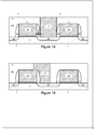
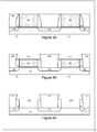
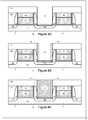
- FIG. 1A illustrates a substrate 100 and two MOS transistors 101.
- the MOS transistors 101 include gate electrodes 102, gate dielectric layers 104, and spacers 108. Diffusion regions 106 are formed in the substrate 100. Interlayer dielectrics (ILD), such as ILD layers 110a and 110b, are deposited in the regions between and around the two MOS transistors 101.
- ILD Interlayer dielectrics
- CTG contact-to-gate
- metals that may be used for the gate electrode include, but are not limited to, ruthenium, palladium, platinum, cobalt, nickel, and conductive metal oxides, e.g., ruthenium oxide.
- a P-type metal layer will enable the formation of a PMOS gate electrode with a workfunction that is between about 4.9 eV and about 5.2 eV.
- metals that may be used for the gate electrode include, but are not limited to, hafnium, zirconium, titanium, tantalum, aluminum, alloys of these metals, and carbides of these metals such as hafnium carbide, zirconium carbide, titanium carbide, tantalum carbide, and aluminum carbide.
- An N-type metal layer will enable the formation of an NMOS gate electrode with a workfunction that is between about 3.9 eV and about 4.2 eV.
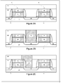
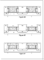
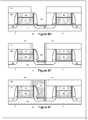
- one or multiple etching processes are carried out to partially recess both the dummy gate electrode layer 500 and the spacers 108.
- This dual recess is shown in Figure 5B .
- the etch chemistry used to recess the dummy gate electrode 500 may differ from the etch chemistry used to recess the spacers 108.
- the etching processes used may be wet etches, dry etches, or a combination.
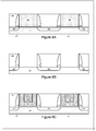
- spacer material This removes any constraints on the choice of spacer material and enables the use of materials that are optimized for capacitance. For instance, materials such as silicon oxynitride (SiON), carbon-doped silicon oxynitride (SiOCN), or low-k dielectric materials may be used in the spacers 108 to reduce issues with parasitic capacitance.
- SiON silicon oxynitride
- SiOCN carbon-doped silicon oxynitride
- low-k dielectric materials may be used in the spacers 108 to reduce issues with parasitic capacitance.
- the initial metal gate electrode layer 102a is typically a workfunction metal layer and can be formed using any of the workfunction metals described above.
- the second metal gate electrode layer 102b may be a second workfunction metal layer or it may be a low resistance fill metal layer such as aluminum, tungsten, or copper.
- the metal used in the metal gate electrode 102a has different etch properties than the metal used in the metal gate electrode 102b.
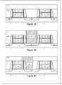
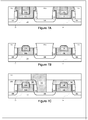
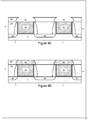
- Figure 8B illustrates a pair of contact sidewall spacers 804 that are formed along the sidewalls of the contact trench opening 800, in accordance with an implementation of the invention.
- the contact sidewall spacers 804 may be formed using deposition and etching processes similar to the fabrication of gate spacers 108. For instance, a conformal layer of an insulating material may be deposited within the contact trench opening 800, resulting in the insulating material being deposited along the sidewalls and bottom surface of the contact trench opening 800.
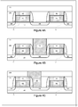
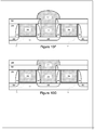
- an insulating layer 906 may be blanket deposited over the ILD layer 902 and within the void 904.
- the insulating layer 906 may be formed of materials that include, but are not limited to, silicon nitride, silicon oxide, silicon carbide, silicon nitride doped with carbon, silicon oxynitride, other nitride materials, other carbide materials, aluminum oxide, other oxide materials, other metal oxides, and low-k dielectric materials, including materials that are the same or similar to the material used in the ILD layer 902.
Landscapes
- Engineering & Computer Science (AREA)
- Physics & Mathematics (AREA)
- Computer Hardware Design (AREA)
- Microelectronics & Electronic Packaging (AREA)
- Power Engineering (AREA)
- Condensed Matter Physics & Semiconductors (AREA)
- General Physics & Mathematics (AREA)
- Manufacturing & Machinery (AREA)
- Electrodes Of Semiconductors (AREA)
- Insulated Gate Type Field-Effect Transistor (AREA)
- Chemical & Material Sciences (AREA)
- Geometry (AREA)
- Materials Engineering (AREA)
- Composite Materials (AREA)
- Inorganic Chemistry (AREA)
- Chemical Kinetics & Catalysis (AREA)
- General Chemical & Material Sciences (AREA)
- Internal Circuitry In Semiconductor Integrated Circuit Devices (AREA)
Claims (12)
- Transistor, der Folgendes umfasst:ein Substrat (100);ein Paar von Abstandshaltern (108) auf dem Substrat;eine U-förmige Gate-Dielektrikum-Schicht (104) mit hohem k auf einer Oberfläche des Substrats und entlang Seitenwänden des Paares von Abstandshaltern;eine Metall-Gate-Elektrode (102) auf der Gate-Dielektrikum-Schicht mit hohem k und zwischen dem Paar von Abstandshaltern;eine Isolationsdeckschicht (300) zwischen dem Paar von Abstandshaltern und auf der Metall-Gate-Elektrode, wobei sich die Isolationsdeckschicht in Kontakt mit der Gate-Dielektrikum-Schicht mit hohem k befindet;ein Paar von Diffusionsgebieten (106) angrenzend an das Paar von Abstandshaltern, wobei die Diffusionsgebiete innerhalb des Substrats liegen;eine erste Zwischenschichtdielektrikumschicht (110a) auf dem Paar von Diffusionsgebieten und angrenzend an einen des Paares von Abstandshaltern, wobei die erste Zwischenschichtdielektrikumschicht eine obere Oberfläche aufweist, die ebenflächig mit einer oberen Oberfläche der Isolationsdeckschicht und ebenflächig mit einer oberen Oberfläche des Paares von Abstandshaltern ist;eine zweite Zwischenschichtdielektrikumschicht (110b) auf der oberen Oberfläche der ersten Zwischenschichtdielektrikumschicht und auf einem ersten Teil der Isolationsdeckschicht; undeinen leitfähigen Kontakt (200), der sich in Kontakt mit einem des Paares von Diffusionsgebieten befindet, wobei der leitfähige Kontakt angrenzend an und auf dem anderen des Paares von Abstandshaltern und angrenzend an die zweite Zwischenschichtdielektrikumschicht ist, wobei sich ein Teil des leitfähigen Kontakts auf einem zweiten Teil der Isolationsdeckschicht auf der Metall-Gate-Elektrode befindet.
- Transistor nach Anspruch 1, wobei eine Höhe der Kombination der Gate-Dielektrikum-Schicht, der Metall-Gate-Elektrode und der Isolationsdeckschicht eine Höhe des Paares von Abstandshaltern nicht überschreitet.
- Transistor nach Anspruch 1, wobei die Isolationsdeckschicht Siliciumnitrid, Siliciumoxid, Siliciumcarbid, mit Kohlenstoff dotiertes Siliciumnitrid, Siliciumoxinitrid oder Aluminiumoxid umfasst.
- Transistor nach Anspruch 1, wobei die Isolationsdeckschicht ein Nitridmaterial, ein Carbidmaterial, ein Oxidmaterial, ein Metalloxidmaterial oder ein dielektrisches Material mit niedrigem k umfasst.
- Transistor nach Anspruch 1, wobei die Isolationsdeckschicht Bornitrid oder Borcarbid umfasst.
- Transistor nach Anspruch 1, wobei die Isolationsdeckschicht ein dielektrisches Material mit niedrigem k umfasst, das mit Kohlenstoff und/oder Stickstoff und/oder Wasserstoff dotiert ist.
- Verfahren zum Bilden eines Transistors, das Folgendes umfasst:Bilden einer Opfer-Gate-Dielektrikum-Schicht und einer Opfer-Gate-Elektrode-Schicht auf einem Substrat (100);Bilden eines Paares von Abstandshaltern (108) auf gegenüberliegenden Seiten der Opfer-Gate-Dielektrikum-Schicht und der Opfer-Gate-Elektrode-Schicht;Bilden eines Paares von Diffusionsgebieten (106) angrenzend an das Paar von Abstandshaltern innerhalb des Substrats;Bilden einer ersten Zwischenschichtdielektrikumschicht (110a) auf dem Paar von Diffusionsgebieten und angrenzend an beide des Paares von Abstandshaltern;vollständiges Entfernen der Opfer-Gate-Dielektrikum-Schicht und der Opfer-Gate-Elektrode-Schicht, nachdem die Diffusionsgebiete gebildet wurden, um die Oberseite des Substrats freizulegen, wodurch ein Graben zwischen dem Paar von Abstandshaltern gebildet wird;Abscheiden einer U-förmigen Gate-Dielektrikum-Schicht (104) mit hohem k entlang den Seitenwänden und der unteren Oberfläche des Grabens zwischen den Abstandshaltern;Abscheiden einer Metall-Gate-Elektrode (102) auf der Gate-Dielektrikum-Schicht mit hohem k;Bilden einer Isolationsdeckschicht (300) auf der Metall-Gate-Elektrode innerhalb des Paares von Abstandshaltern, wobei sich die Isolationsdeckschicht in Kontakt mit der Gate-Dielektrikum-Schicht mit hohem k befindet und wobei die Isolationsdeckschicht eine obere Oberfläche ebenflächig mit einer oberen Oberfläche der ersten Zwischenschichtdielektrikumschicht und ebenflächig mit einer oberen Oberfläche des Paares von Abstandshaltern aufweist;Bilden einer zweite Zwischenschichtdielektrikumschicht (110b) auf der oberen Oberfläche der ersten Zwischenschichtdielektrikumschicht und auf einem ersten Teil der Isolationsdeckschicht; undBilden eines leitfähigen Kontakts (200), der sich in Kontakt mit einem des Paares von Diffusionsgebieten befindet, wobei der leitfähige Kontakt angrenzend an und auf dem anderen des Paares von Abstandshaltern und angrenzend an die zweite Zwischenschichtdielektrikumschicht ist, wobei sich ein Teil des leitfähigen Kontakts auf einem zweiten Teil der Isolationsdeckschicht auf der Metall-Gate-Elektrode befindet.
- Verfahren nach Anspruch 7, wobei das Bilden der Isolationsdeckschicht Folgendes umfasst:Abscheiden einer Deckenschicht eines Isolationsmaterials über der Metall-Gate-Elektrode; undPlanarisieren der Isolationsmaterialschicht, um die Isolationsdeckschicht zu bilden.
- Verfahren nach Anspruch 7, wobei die Isolationsdeckschicht Siliciumnitrid, Siliciumoxid, Siliciumcarbid, mit Kohlenstoff dotiertes Siliciumnitrid, Siliciumoxinitrid oder Aluminiumoxid umfasst.
- Verfahren nach Anspruch 7, wobei die Isolationsdeckschicht ein Nitridmaterial, ein Carbidmaterial, ein Oxidmaterial, ein Metalloxidmaterial oder ein dielektrisches Material mit niedrigem k umfasst.
- Verfahren nach Anspruch 7, wobei die Isolationsdeckschicht Bornitrid oder Borcarbid umfasst.
- Verfahren nach Anspruch 7, wobei die Isolationsdeckschicht ein dielektrisches Material mit niedrigem k umfasst, das mit Kohlenstoff und/oder Stickstoff und/oder Wasserstoff dotiert ist.
Priority Applications (5)
| Application Number | Priority Date | Filing Date | Title |
|---|---|---|---|
| EP19152329.9A EP3506366A1 (de) | 2009-12-30 | 2010-12-07 | Selbstausrichtende kontakte |
| EP16172290.5A EP3096357B1 (de) | 2009-12-30 | 2010-12-07 | Selbstausrichtende kontakte |
| EP17201192.6A EP3312888A3 (de) | 2009-12-30 | 2010-12-07 | Selbstausrichtende kontakte |
| EP22161202.1A EP4033543A1 (de) | 2009-12-30 | 2010-12-07 | Selbstausrichtende kontakte |
| EP25192640.8A EP4637296A3 (de) | 2009-12-30 | 2010-12-07 | Selbstjustierte kontakte |
Applications Claiming Priority (2)
| Application Number | Priority Date | Filing Date | Title |
|---|---|---|---|
| US12/655,408 US8436404B2 (en) | 2009-12-30 | 2009-12-30 | Self-aligned contacts |
| PCT/US2010/059302 WO2011090571A2 (en) | 2009-12-30 | 2010-12-07 | Self-aligned contacts |
Related Child Applications (7)
| Application Number | Title | Priority Date | Filing Date |
|---|---|---|---|
| EP22161202.1A Division EP4033543A1 (de) | 2009-12-30 | 2010-12-07 | Selbstausrichtende kontakte |
| EP16172290.5A Division EP3096357B1 (de) | 2009-12-30 | 2010-12-07 | Selbstausrichtende kontakte |
| EP16172290.5A Division-Into EP3096357B1 (de) | 2009-12-30 | 2010-12-07 | Selbstausrichtende kontakte |
| EP17201192.6A Division-Into EP3312888A3 (de) | 2009-12-30 | 2010-12-07 | Selbstausrichtende kontakte |
| EP17201192.6A Division EP3312888A3 (de) | 2009-12-30 | 2010-12-07 | Selbstausrichtende kontakte |
| EP19152329.9A Division EP3506366A1 (de) | 2009-12-30 | 2010-12-07 | Selbstausrichtende kontakte |
| EP25192640.8A Division EP4637296A3 (de) | 2009-12-30 | 2010-12-07 | Selbstjustierte kontakte |
Publications (3)
| Publication Number | Publication Date |
|---|---|
| EP2519975A2 EP2519975A2 (de) | 2012-11-07 |
| EP2519975A4 EP2519975A4 (de) | 2013-09-11 |
| EP2519975B1 true EP2519975B1 (de) | 2018-05-09 |
Family
ID=44186364
Family Applications (6)
| Application Number | Title | Priority Date | Filing Date |
|---|---|---|---|
| EP17201192.6A Ceased EP3312888A3 (de) | 2009-12-30 | 2010-12-07 | Selbstausrichtende kontakte |
| EP25192640.8A Pending EP4637296A3 (de) | 2009-12-30 | 2010-12-07 | Selbstjustierte kontakte |
| EP10844169.2A Active EP2519975B1 (de) | 2009-12-30 | 2010-12-07 | Selbstausrichtende kontakte |
| EP22161202.1A Pending EP4033543A1 (de) | 2009-12-30 | 2010-12-07 | Selbstausrichtende kontakte |
| EP16172290.5A Active EP3096357B1 (de) | 2009-12-30 | 2010-12-07 | Selbstausrichtende kontakte |
| EP19152329.9A Ceased EP3506366A1 (de) | 2009-12-30 | 2010-12-07 | Selbstausrichtende kontakte |
Family Applications Before (2)
| Application Number | Title | Priority Date | Filing Date |
|---|---|---|---|
| EP17201192.6A Ceased EP3312888A3 (de) | 2009-12-30 | 2010-12-07 | Selbstausrichtende kontakte |
| EP25192640.8A Pending EP4637296A3 (de) | 2009-12-30 | 2010-12-07 | Selbstjustierte kontakte |
Family Applications After (3)
| Application Number | Title | Priority Date | Filing Date |
|---|---|---|---|
| EP22161202.1A Pending EP4033543A1 (de) | 2009-12-30 | 2010-12-07 | Selbstausrichtende kontakte |
| EP16172290.5A Active EP3096357B1 (de) | 2009-12-30 | 2010-12-07 | Selbstausrichtende kontakte |
| EP19152329.9A Ceased EP3506366A1 (de) | 2009-12-30 | 2010-12-07 | Selbstausrichtende kontakte |
Country Status (7)
| Country | Link |
|---|---|
| US (13) | US8436404B2 (de) |
| EP (6) | EP3312888A3 (de) |
| JP (6) | JP5539538B2 (de) |
| KR (15) | KR101510034B1 (de) |
| CN (2) | CN104795444B (de) |
| TW (5) | TWI590453B (de) |
| WO (1) | WO2011090571A2 (de) |
Cited By (1)
| Publication number | Priority date | Publication date | Assignee | Title |
|---|---|---|---|---|
| US12464810B2 (en) | 2021-05-18 | 2025-11-04 | Samsung Electronics Co., Ltd. | Integrated circuit device having inclined structures |
Families Citing this family (266)
| Publication number | Priority date | Publication date | Assignee | Title |
|---|---|---|---|---|
| US8436404B2 (en) | 2009-12-30 | 2013-05-07 | Intel Corporation | Self-aligned contacts |
| US8946828B2 (en) | 2010-02-09 | 2015-02-03 | Taiwan Semiconductor Manufacturing Company, Ltd. | Semiconductor device having elevated structure and method of manufacturing the same |
| KR101675373B1 (ko) * | 2010-03-24 | 2016-11-11 | 삼성전자주식회사 | 반도체 소자 및 그 제조 방법 |
| KR101615654B1 (ko) * | 2010-05-14 | 2016-05-12 | 삼성전자주식회사 | 반도체 소자의 형성방법 |
| US8860107B2 (en) * | 2010-06-03 | 2014-10-14 | International Business Machines Corporation | FinFET-compatible metal-insulator-metal capacitor |
| US8421077B2 (en) * | 2010-06-08 | 2013-04-16 | International Business Machines Corporation | Replacement gate MOSFET with self-aligned diffusion contact |
| JP5569243B2 (ja) * | 2010-08-09 | 2014-08-13 | ソニー株式会社 | 半導体装置及びその製造方法 |
| KR101692309B1 (ko) * | 2010-08-25 | 2017-01-04 | 삼성전자 주식회사 | 반도체 장치의 제조방법 |
| US8592266B2 (en) * | 2010-10-27 | 2013-11-26 | International Business Machines Corporation | Replacement gate MOSFET with a high performance gate electrode |
| US8946006B2 (en) * | 2010-10-28 | 2015-02-03 | International Business Machines Corporation | Replacement gate MOSFET with raised source and drain |
| US8232607B2 (en) * | 2010-11-23 | 2012-07-31 | International Business Machines Corporation | Borderless contact for replacement gate employing selective deposition |
| US8536656B2 (en) * | 2011-01-10 | 2013-09-17 | International Business Machines Corporation | Self-aligned contacts for high k/metal gate process flow |
| DE102011004323B4 (de) * | 2011-02-17 | 2016-02-25 | Globalfoundries Dresden Module One Limited Liability Company & Co. Kg | Halbleiterbauelement mit selbstjustierten Kontaktelementen und Verfahren zu seiner Herstellung |
| CN102779754B (zh) * | 2011-05-12 | 2015-04-08 | 中芯国际集成电路制造(北京)有限公司 | 半导体器件及其制造方法 |
| US8872286B2 (en) * | 2011-08-22 | 2014-10-28 | United Microelectronics Corp. | Metal gate structure and fabrication method thereof |
| US9190261B2 (en) * | 2011-08-25 | 2015-11-17 | Taiwan Semiconductor Manufacturing Company, Ltd. | Layer alignment in FinFET fabrication |
| US8822283B2 (en) * | 2011-09-02 | 2014-09-02 | Taiwan Semiconductor Manufacturing Company, Ltd. | Self-aligned insulated film for high-k metal gate device |
| US8877645B2 (en) * | 2011-09-15 | 2014-11-04 | International Business Machines Corporation | Integrated circuit structure having selectively formed metal cap |
| EP3506367B1 (de) * | 2011-09-30 | 2026-01-14 | Sony Group Corporation | Wolfram-gates für nichtplanare transistoren |
| US9637810B2 (en) | 2011-09-30 | 2017-05-02 | Intel Corporation | Tungsten gates for non-planar transistors |
| KR20140049075A (ko) * | 2011-09-30 | 2014-04-24 | 인텔 코오퍼레이션 | 트랜지스터 게이트용 캡핑 유전체 구조 |
| WO2013048524A1 (en) | 2011-10-01 | 2013-04-04 | Intel Corporation | Source/drain contacts for non-planar transistors |
| US8614123B2 (en) * | 2011-11-28 | 2013-12-24 | Globalfoundries Inc. | Method of forming a semiconductor device by using sacrificial gate electrodes and sacrificial self-aligned contact structures |
| DE112011105925B4 (de) | 2011-12-06 | 2023-02-09 | Tahoe Research, Ltd. | Mikroelektronischer Transistor und Verfahren zum Herstellen desselben |
| KR20200054336A (ko) | 2011-12-22 | 2020-05-19 | 인텔 코포레이션 | 반도체 구조 |
| US20130175619A1 (en) * | 2012-01-06 | 2013-07-11 | International Business Machines Corporation | Silicon-on-insulator transistor with self-aligned borderless source/drain contacts |
| US8772168B2 (en) * | 2012-01-19 | 2014-07-08 | Globalfoundries Singapore Pte. Ltd. | Formation of the dielectric cap layer for a replacement gate structure |
| US20130187236A1 (en) * | 2012-01-20 | 2013-07-25 | Globalfoundries Inc. | Methods of Forming Replacement Gate Structures for Semiconductor Devices |
| US8927407B2 (en) | 2012-01-20 | 2015-01-06 | Globalfoundries Inc. | Method of forming self-aligned contacts for a semiconductor device |
| US8580628B2 (en) * | 2012-02-02 | 2013-11-12 | GlobalFoundries, Inc. | Integrated circuit contact structure and method |
| KR101853316B1 (ko) * | 2012-03-29 | 2018-04-30 | 삼성전자주식회사 | 반도체 소자 |
| US8946049B2 (en) | 2012-04-11 | 2015-02-03 | International Business Machines Corporation | Replacement gate structures and methods of manufacturing |
| JP6100589B2 (ja) * | 2012-04-13 | 2017-03-22 | ルネサスエレクトロニクス株式会社 | 自己整合型ソース・ドレインコンタクトを有する半導体装置およびその製造方法 |
| US8759172B2 (en) * | 2012-04-18 | 2014-06-24 | International Business Machines Corporation | Etch stop layer formation in metal gate process |
| US20130309856A1 (en) * | 2012-05-15 | 2013-11-21 | International Business Machines Corporation | Etch resistant barrier for replacement gate integration |
| US8779515B2 (en) * | 2012-05-21 | 2014-07-15 | International Business Machines Corporation | Semiconductor structure containing an aluminum-containing replacement gate electrode |
| US9130023B2 (en) * | 2012-06-05 | 2015-09-08 | Kabushiki Kaisha Toshiba | Isolated insulating gate structure |
| US8679909B2 (en) | 2012-06-08 | 2014-03-25 | Globalfoundries Singapore Pte. Ltd. | Recessing and capping of gate structures with varying metal compositions |
| US8883583B2 (en) * | 2012-06-26 | 2014-11-11 | Taiwan Semiconductor Manufacturing Company, Ltd. | Semiconductor devices, transistors, and methods of manufacture thereof |
| US8937006B2 (en) | 2012-07-30 | 2015-01-20 | Taiwan Semiconductor Manufacturing Company, Ltd. | Method of semiconductor integrated circuit fabrication |
| US9218975B2 (en) * | 2012-08-17 | 2015-12-22 | Globalfoundries Inc. | Methods of forming a replacement gate structure having a gate electrode comprised of a deposited intermetallic compound material |
| US8877621B2 (en) * | 2012-09-05 | 2014-11-04 | Globalfoundries Inc. | Low resistivity gate conductor |
| US8896030B2 (en) | 2012-09-07 | 2014-11-25 | Intel Corporation | Integrated circuits with selective gate electrode recess |
| US8753970B2 (en) * | 2012-09-12 | 2014-06-17 | Globalfoundries Inc. | Methods of forming semiconductor devices with self-aligned contacts and the resulting devices |
| US9034703B2 (en) * | 2012-09-13 | 2015-05-19 | International Business Machines Corporation | Self aligned contact with improved robustness |
| US9461143B2 (en) * | 2012-09-19 | 2016-10-04 | Intel Corporation | Gate contact structure over active gate and method to fabricate same |
| US9299802B2 (en) | 2012-10-28 | 2016-03-29 | International Business Machines Corporation | Method to improve reliability of high-K metal gate stacks |
| US8928090B2 (en) * | 2012-10-31 | 2015-01-06 | International Business Machines Corporation | Self-aligned contact structure for replacement metal gate |
| US8765590B2 (en) | 2012-10-31 | 2014-07-01 | International Business Machines Corporation | Insulative cap for borderless self-aligning contact in semiconductor device |
| US8907427B2 (en) * | 2012-11-05 | 2014-12-09 | Stmicroelectronics, Inc. | Semiconductor device including low-K dielectric cap layer for gate electrodes and related methods |
| US8890262B2 (en) * | 2012-11-29 | 2014-11-18 | Globalfoundries Inc. | Semiconductor device having a metal gate recess |
| US8778789B2 (en) * | 2012-11-30 | 2014-07-15 | GlobalFoundries, Inc. | Methods for fabricating integrated circuits having low resistance metal gate structures |
| US8785283B2 (en) * | 2012-12-05 | 2014-07-22 | United Microelectronics Corp. | Method for forming semiconductor structure having metal connection |
| US8728927B1 (en) * | 2012-12-10 | 2014-05-20 | International Business Machines Corporation | Borderless contacts for semiconductor transistors |
| CN103871857B (zh) * | 2012-12-18 | 2017-09-26 | 中芯国际集成电路制造(上海)有限公司 | 半导体器件的形成方法 |
| US8928048B2 (en) | 2013-01-17 | 2015-01-06 | Globalfoundries Inc. | Methods of forming semiconductor device with self-aligned contact elements and the resulting device |
| US8940633B2 (en) * | 2013-03-05 | 2015-01-27 | Globalfoundries Inc. | Methods of forming semiconductor device with self-aligned contact elements and the resulting devices |
| US8946075B2 (en) * | 2013-03-05 | 2015-02-03 | Globalfoundries Inc. | Methods of forming semiconductor device with self-aligned contact elements and the resulting devices |
| US8884344B2 (en) | 2013-03-08 | 2014-11-11 | International Business Machines Corporation | Self-aligned contacts for replacement metal gate transistors |
| US9263275B2 (en) * | 2013-03-12 | 2016-02-16 | Taiwan Semiconductor Manufacturing Company, Ltd. | Interface for metal gate integration |
| US9006072B2 (en) * | 2013-03-14 | 2015-04-14 | United Microelectronics Corp. | Method of forming metal silicide layer |
| US8981490B2 (en) * | 2013-03-14 | 2015-03-17 | Texas Instruments Incorporated | Transistor with deep Nwell implanted through the gate |
| TWI581316B (zh) * | 2013-03-15 | 2017-05-01 | 聯華電子股份有限公司 | 形成金屬矽化物層的方法 |
| US20140264640A1 (en) * | 2013-03-18 | 2014-09-18 | Nanya Technology Corp. | Semiconductor device and method for fabricating the same |
| CN104124173A (zh) * | 2013-04-28 | 2014-10-29 | 中芯国际集成电路制造(上海)有限公司 | Mos晶体管的形成方法 |
| CN104143515B (zh) * | 2013-05-09 | 2017-12-01 | 中芯国际集成电路制造(上海)有限公司 | Mos晶体管的形成方法 |
| US20140342553A1 (en) * | 2013-05-14 | 2014-11-20 | United Microelectronics Corp. | Method for Forming Semiconductor Structure Having Opening |
| KR102050779B1 (ko) * | 2013-06-13 | 2019-12-02 | 삼성전자 주식회사 | 반도체 소자 및 이의 제조 방법 |
| KR20150000546A (ko) * | 2013-06-24 | 2015-01-05 | 삼성전자주식회사 | 반도체 소자 및 이의 제조 방법 |
| US20150024584A1 (en) * | 2013-07-17 | 2015-01-22 | Global Foundries, Inc. | Methods for forming integrated circuits with reduced replacement metal gate height variability |
| US9153498B2 (en) * | 2013-07-22 | 2015-10-06 | Globalfoundries Inc. | Methods of forming semiconductor device with self-aligned contact elements and the resulting devices |
| US9257348B2 (en) | 2013-08-06 | 2016-02-09 | Globalfoundries Inc. | Methods of forming replacement gate structures for transistors and the resulting devices |
| US9324709B2 (en) * | 2013-08-19 | 2016-04-26 | Globalfoundries Inc. | Self-aligned gate contact structure |
| US9105497B2 (en) | 2013-09-04 | 2015-08-11 | Globalfoundries Inc. | Methods of forming gate structures for transistor devices for CMOS applications |
| JP6120738B2 (ja) * | 2013-09-17 | 2017-04-26 | ルネサスエレクトロニクス株式会社 | 半導体装置および半導体装置の製造方法 |
| US9564332B2 (en) * | 2013-09-26 | 2017-02-07 | Taiwan Semiconductor Manufacturing Co., Ltd. | Mechanism for forming metal gate structure |
| FR3011382B1 (fr) | 2013-09-27 | 2019-03-29 | Commissariat A L'energie Atomique Et Aux Energies Alternatives | Procede de realisation d'un circuit integre |
| US9018711B1 (en) * | 2013-10-17 | 2015-04-28 | Globalfoundries Inc. | Selective growth of a work-function metal in a replacement metal gate of a semiconductor device |
| US20150111373A1 (en) * | 2013-10-18 | 2015-04-23 | GlobalFoundries, Inc. | Reducing gate height variation in rmg process |
| US9059164B2 (en) | 2013-10-22 | 2015-06-16 | International Business Machines Corporation | Embedded interlevel dielectric barrier layers for replacement metal gate field effect transistors |
| US20150118836A1 (en) * | 2013-10-28 | 2015-04-30 | United Microelectronics Corp. | Method of fabricating semiconductor device |
| US9153483B2 (en) * | 2013-10-30 | 2015-10-06 | Taiwan Semiconductor Manufacturing Company, Ltd. | Method of semiconductor integrated circuit fabrication |
| US10158000B2 (en) * | 2013-11-26 | 2018-12-18 | Taiwan Semiconductor Manufacturing Company Limited | Low-K dielectric sidewall spacer treatment |
| CN104681488B (zh) * | 2013-11-26 | 2018-05-01 | 中芯国际集成电路制造(上海)有限公司 | 晶体管及其形成方法 |
| US9245894B2 (en) * | 2013-12-12 | 2016-01-26 | Texas Instruments Incorporated | Self aligned active trench contact |
| US9331072B2 (en) * | 2014-01-28 | 2016-05-03 | Samsung Electronics Co., Ltd. | Integrated circuit devices having air-gap spacers defined by conductive patterns and methods of manufacturing the same |
| US9660035B2 (en) * | 2014-01-29 | 2017-05-23 | International Business Machines Corporation | Semiconductor device including superlattice SiGe/Si fin structure |
| US9093467B1 (en) | 2014-02-04 | 2015-07-28 | Globalfoundries Inc. | Methods of forming gate structures for semiconductor devices using a replacement gate technique and the resulting devices |
| KR20150091895A (ko) * | 2014-02-04 | 2015-08-12 | 에스케이하이닉스 주식회사 | 반도체 장치 및 그 동작방법 |
| US9252243B2 (en) | 2014-02-07 | 2016-02-02 | International Business Machines Corporation | Gate structure integration scheme for fin field effect transistors |
| US20150228546A1 (en) * | 2014-02-11 | 2015-08-13 | United Microelectronics Corp. | Semiconductor device and method of removing spacers on semiconductor device |
| US9524965B2 (en) | 2014-02-12 | 2016-12-20 | Taiwan Semiconductor Manufacturing Co., Ltd. | Gate structures with various widths and method for forming the same |
| US9293557B2 (en) * | 2014-02-20 | 2016-03-22 | International Business Machines Corporation | Low temperature spacer for advanced semiconductor devices |
| US9236437B2 (en) | 2014-02-20 | 2016-01-12 | Globalfoundries Inc. | Method for creating self-aligned transistor contacts |
| US9159822B2 (en) | 2014-02-24 | 2015-10-13 | International Business Machines Corporation | III-V semiconductor device having self-aligned contacts |
| US9231063B2 (en) | 2014-02-24 | 2016-01-05 | International Business Machines Corporation | Boron rich nitride cap for total ionizing dose mitigation in SOI devices |
| US9231067B2 (en) | 2014-02-26 | 2016-01-05 | Taiwan Semiconductor Manufacturing Co., Ltd. | Semiconductor device and fabricating method thereof |
| US9293576B2 (en) | 2014-03-05 | 2016-03-22 | International Business Machines Corporation | Semiconductor device with low-k gate cap and self-aligned contact |
| US9257529B2 (en) | 2014-03-11 | 2016-02-09 | Tokyo Electron Limited | Method of forming self-aligned contacts using a replacement metal gate process in a semiconductor device |
| US9324830B2 (en) | 2014-03-27 | 2016-04-26 | International Business Machines Corporation | Self-aligned contact process enabled by low temperature |
| US9711646B2 (en) | 2014-03-31 | 2017-07-18 | United Microelectronics Corp. | Semiconductor structure and manufacturing method for the same |
| US9484205B2 (en) * | 2014-04-07 | 2016-11-01 | International Business Machines Corporation | Semiconductor device having self-aligned gate contacts |
| US9236258B2 (en) * | 2014-04-23 | 2016-01-12 | Globalfoundries Inc. | Methods of forming gate structures for semiconductor devices using a replacement gate technique and the resulting devices |
| US9147748B1 (en) * | 2014-05-01 | 2015-09-29 | Globalfoundries Inc. | Methods of forming replacement spacer structures on semiconductor devices |
| US9608086B2 (en) * | 2014-05-20 | 2017-03-28 | Global Foundries Inc. | Metal gate structure and method of formation |
| US9385235B2 (en) | 2014-05-30 | 2016-07-05 | Taiwan Semiconductor Manufacturing Co., Ltd. | Fin field effect transistor (FinFET) device and method for forming the same |
| US9570319B2 (en) * | 2014-05-30 | 2017-02-14 | Taiwan Semiconductor Manufacturing Company, Ltd. | Method of manufacturing a semiconductor device |
| TWI612563B (zh) | 2014-07-07 | 2018-01-21 | United Microelectronics Corp. | 金屬閘極結構與其製作方法 |
| CN105280486B (zh) | 2014-07-23 | 2020-09-22 | 联华电子股份有限公司 | 金属栅极结构的制作方法 |
| KR102276642B1 (ko) | 2014-07-28 | 2021-07-15 | 삼성전자주식회사 | 반도체 장치 및 이의 제조 방법 |
| US10176996B2 (en) * | 2014-08-06 | 2019-01-08 | Globalfoundries Inc. | Replacement metal gate and fabrication process with reduced lithography steps |
| KR102251363B1 (ko) | 2014-08-08 | 2021-05-14 | 삼성전자주식회사 | 반도체 소자 |
| US9812577B2 (en) | 2014-09-05 | 2017-11-07 | Taiwan Semiconductor Manufacturing Co., Ltd. | Semiconductor structure and fabricating method thereof |
| US10134861B2 (en) | 2014-10-08 | 2018-11-20 | Taiwan Semiconductor Manufacturing Co., Ltd. | Semiconductor device structure and method for forming the same |
| US20160126336A1 (en) * | 2014-10-29 | 2016-05-05 | Globalfoundries Inc. | Method of improved ca/cb contact and device thereof |
| US9876114B2 (en) | 2014-12-30 | 2018-01-23 | Taiwan Semiconductor Manufacturing Company, Ltd. | Structure and method for 3D FinFET metal gate |
| US9391204B1 (en) | 2015-03-12 | 2016-07-12 | International Business Machines Corporation | Asymmetric FET |
| US9892924B2 (en) * | 2015-03-16 | 2018-02-13 | Taiwan Semiconductor Manufacturing Company Ltd | Semiconductor structure and manufacturing method thereof |
| US9698232B2 (en) | 2015-03-18 | 2017-07-04 | Qualcomm Incorporated | Conductive cap for metal-gate transistor |
| US9685532B2 (en) | 2015-03-24 | 2017-06-20 | International Business Machines Corporation | Replacement metal gate structures |
| TWI642188B (zh) * | 2015-03-26 | 2018-11-21 | 聯華電子股份有限公司 | 半導體元件及其製作方法 |
| US9799560B2 (en) * | 2015-03-31 | 2017-10-24 | Qualcomm Incorporated | Self-aligned structure |
| TWI650833B (zh) | 2015-04-01 | 2019-02-11 | 聯華電子股份有限公司 | 具有金屬閘極之半導體元件及其製作方法 |
| US9443853B1 (en) | 2015-04-07 | 2016-09-13 | International Business Machines Corporation | Minimizing shorting between FinFET epitaxial regions |
| KR102290538B1 (ko) | 2015-04-16 | 2021-08-19 | 삼성전자주식회사 | 반도체 소자 및 이의 제조 방법 |
| KR102342847B1 (ko) | 2015-04-17 | 2021-12-23 | 삼성전자주식회사 | 반도체 소자 및 그 제조 방법 |
| US9431235B1 (en) * | 2015-04-24 | 2016-08-30 | International Business Machines Corporation | Multilayer dielectric structures with graded composition for nano-scale semiconductor devices |
| US9941376B2 (en) | 2015-04-30 | 2018-04-10 | Taiwan Semiconductor Manufacturing Company, Ltd. | Metal gate scheme for device and methods of forming |
| US20160322473A1 (en) * | 2015-04-30 | 2016-11-03 | Taiwan Semiconductor Manufacturing Company, Ltd. | Buffer Layer on Gate and Methods of Forming the Same |
| US10199230B2 (en) * | 2015-05-01 | 2019-02-05 | Applied Materials, Inc. | Methods for selective deposition of metal silicides via atomic layer deposition cycles |
| US9647091B2 (en) | 2015-05-01 | 2017-05-09 | International Business Machines Corporation | Annealed metal source drain overlapping the gate |
| US10411113B2 (en) * | 2015-05-22 | 2019-09-10 | Taiwan Semiconductor Manufacturing Co., Ltd. | Structure and formation method of semiconductor device structure |
| US9876074B2 (en) * | 2015-05-22 | 2018-01-23 | International Business Machines Corporation | Structure and process to tuck fin tips self-aligned to gates |
| US10062763B2 (en) | 2015-05-27 | 2018-08-28 | Qualcomm Incorporated | Method and apparatus for selectively forming nitride caps on metal gate |
| US9722043B2 (en) | 2015-06-15 | 2017-08-01 | International Business Machines Corporation | Self-aligned trench silicide process for preventing gate contact to silicide shorts |
| KR102396111B1 (ko) | 2015-06-18 | 2022-05-10 | 삼성전자주식회사 | 반도체 소자 및 그 제조 방법 |
| US10090396B2 (en) * | 2015-07-20 | 2018-10-02 | Taiwan Semiconductor Manufacturing Company, Ltd. | Method for fabricating metal gate devices and resulting structures |
| US9831090B2 (en) * | 2015-08-19 | 2017-11-28 | Taiwan Semiconductor Manufacturing Company, Ltd. | Method and structure for semiconductor device having gate spacer protection layer |
| KR102321373B1 (ko) | 2015-08-19 | 2021-11-02 | 삼성전자주식회사 | 반도체 장치의 제조 방법 |
| CN106531776B (zh) * | 2015-09-11 | 2021-06-29 | 联华电子股份有限公司 | 半导体结构 |
| US9768272B2 (en) | 2015-09-30 | 2017-09-19 | International Business Machines Corporation | Replacement gate FinFET process using a sit process to define source/drain regions, gate spacers and a gate cavity |
| US9871114B2 (en) * | 2015-09-30 | 2018-01-16 | Taiwan Semiconductor Manufacturing Company, Ltd. | Metal gate scheme for device and methods of forming |
| US9673101B2 (en) | 2015-09-30 | 2017-06-06 | International Business Machines Corporation | Minimize middle-of-line contact line shorts |
| US9627484B1 (en) | 2015-10-12 | 2017-04-18 | International Business Machines Corporation | Devices with multiple threshold voltages formed on a single wafer using strain in the high-K layer |
| CN106684041B (zh) * | 2015-11-10 | 2020-12-08 | 联华电子股份有限公司 | 半导体元件及其制作方法 |
| US9570450B1 (en) | 2015-11-19 | 2017-02-14 | International Business Machines Corporation | Hybrid logic and SRAM contacts |
| US9660050B1 (en) * | 2015-11-25 | 2017-05-23 | International Business Machines Corporation | Replacement low-k spacer |
| US20170162444A1 (en) * | 2015-12-02 | 2017-06-08 | International Business Machines Corporation | Contact resistance reduction for advanced technology nodes |
| US9627510B1 (en) | 2015-12-02 | 2017-04-18 | International Business Machines Corporation | Structure and method for replacement gate integration with self-aligned contacts |
| US9437714B1 (en) | 2015-12-09 | 2016-09-06 | International Business Machines Corporation | Selective gate contact fill metallization |
| US9704971B2 (en) * | 2015-12-09 | 2017-07-11 | Globalfoundries Inc. | Epi facet height uniformity improvement for FDSOI technologies |
| US10867852B2 (en) * | 2015-12-15 | 2020-12-15 | Taiwan Semiconductor Manufacturing Company, Ltd. | Semiconductor device and manufacturing method thereof |
| CN106920771B (zh) * | 2015-12-28 | 2020-03-10 | 中芯国际集成电路制造(北京)有限公司 | 金属栅晶体管源漏区接触塞的制作方法 |
| CN106920750B (zh) * | 2015-12-28 | 2019-11-05 | 中芯国际集成电路制造(上海)有限公司 | 金属栅晶体管源漏区接触塞的制作方法 |
| DE102016118207B4 (de) | 2015-12-30 | 2024-08-01 | Taiwan Semiconductor Manufacturing Co. Ltd. | Halbleitervorrichtung und verfahren zu ihrer herstellung |
| US9865703B2 (en) * | 2015-12-31 | 2018-01-09 | International Business Machines Corporation | High-K layer chamfering to prevent oxygen ingress in replacement metal gate (RMG) process |
| US9450095B1 (en) * | 2016-02-04 | 2016-09-20 | International Business Machines Corporation | Single spacer for complementary metal oxide semiconductor process flow |
| US9716093B1 (en) * | 2016-03-07 | 2017-07-25 | Taiwan Semiconductor Manufacturing Co., Ltd. | Semiconductor device |
| US9824920B2 (en) * | 2016-04-04 | 2017-11-21 | Globalfoundries Inc. | Methods of forming self-aligned contact structures by work function material layer recessing and the resulting devices |
| CN107275214A (zh) * | 2016-04-08 | 2017-10-20 | 中芯国际集成电路制造(上海)有限公司 | 半导体器件及其形成方法 |
| US10510599B2 (en) * | 2016-04-13 | 2019-12-17 | Taiwan Semiconductor Manufacturing Company Limited | FinFET switch |
| US9793267B1 (en) | 2016-04-22 | 2017-10-17 | United Microelectronics Corp. | Semiconductor device having gate structure with reduced threshold voltage and method for manufacturing the same |
| KR102384818B1 (ko) * | 2016-04-25 | 2022-04-08 | 어플라이드 머티어리얼스, 인코포레이티드 | 수평 게이트 올어라운드 디바이스 나노와이어 에어 갭 스페이서 형성 |
| KR102514620B1 (ko) * | 2016-04-28 | 2023-03-29 | 삼성전자주식회사 | 반도체 소자 및 이의 제조 방법 |
| US9991361B2 (en) * | 2016-05-26 | 2018-06-05 | Globalfoundries Inc. | Methods for performing a gate cut last scheme for FinFET semiconductor devices |
| US9837351B1 (en) | 2016-06-07 | 2017-12-05 | International Business Machines Corporation | Avoiding gate metal via shorting to source or drain contacts |
| US10164032B2 (en) * | 2016-06-17 | 2018-12-25 | Taiwan Semiconductor Manufacturing Company, Ltd. | Self-aligned contact and manufacturing method thereof |
| WO2018004680A1 (en) * | 2016-07-01 | 2018-01-04 | Intel Corporation | Self-aligned gate edge trigate and finfet devices |
| CN107591366B (zh) * | 2016-07-06 | 2020-06-09 | 中芯国际集成电路制造(上海)有限公司 | 半导体结构及其形成方法 |
| US9847398B1 (en) * | 2016-07-13 | 2017-12-19 | United Microelectronics Corp. | Semiconductor device with gate structure having dielectric layer on one side and contact plug on the other side |
| US9929046B2 (en) * | 2016-07-21 | 2018-03-27 | International Business Machines Corporation | Self-aligned contact cap |
| US9929271B2 (en) * | 2016-08-03 | 2018-03-27 | Taiwan Semiconductor Manufacturing Company, Ltd. | Semiconductor device and method |
| CN107785259B (zh) * | 2016-08-24 | 2020-09-15 | 中芯国际集成电路制造(北京)有限公司 | 一种半导体器件及制备方法、电子装置 |
| US9704754B1 (en) * | 2016-09-22 | 2017-07-11 | International Business Machines Corporation | Self-aligned spacer for cut-last transistor fabrication |
| KR102698026B1 (ko) * | 2016-09-28 | 2024-08-21 | 삼성전자주식회사 | 유전막 형성 방법 및 반도체 장치의 제조 방법 |
| US9991362B2 (en) * | 2016-09-30 | 2018-06-05 | Taiwan Semiconductor Manufacturing Co., Ltd. | Semiconductor device including tungsten gate and manufacturing method thereof |
| US9704991B1 (en) | 2016-10-31 | 2017-07-11 | International Business Machines Corporation | Gate height and spacer uniformity |
| DE102017118364B4 (de) | 2016-11-29 | 2021-10-14 | Taiwan Semiconductor Manufacturing Co. Ltd. | Verfahren mit Herstellung von Source/Drain- und Gate-Kontakten und Struktur mit solchen |
| US9985134B1 (en) * | 2016-11-29 | 2018-05-29 | Taiwan Semiconductor Manufacturing Company, Ltd. | FinFETs and methods of forming FinFETs |
| US10522359B2 (en) * | 2016-11-29 | 2019-12-31 | Taiwan Semiconductor Manufacturing Company, Ltd. | FinFET device and method of forming |
| US10008416B2 (en) * | 2016-11-30 | 2018-06-26 | Taiwan Semiconductor Manufacturing Co., Ltd. | Forming a protective layer to prevent formation of leakage paths |
| US20180158821A1 (en) * | 2016-12-06 | 2018-06-07 | Globalfoundries Inc. | Gate structures with low resistance |
| US10707316B2 (en) * | 2016-12-09 | 2020-07-07 | Taiwan Semiconductor Manufacturing Co., Ltd. | Structure and formation method of semiconductor device structure with gate structure |
| US10079290B2 (en) | 2016-12-30 | 2018-09-18 | United Microelectronics Corp. | Semiconductor device having asymmetric spacer structures |
| EP3567005A4 (de) | 2017-01-06 | 2020-07-29 | Japan Science and Technology Agency | Hexagonale bornitrid-dünnschicht und verfahren zur herstellung davon |
| US10242918B2 (en) | 2017-02-08 | 2019-03-26 | International Business Machines Corporation | Shallow trench isolation structures and contact patterning |
| US10103237B2 (en) * | 2017-02-28 | 2018-10-16 | International Business Machines Corporation | Inverted MOSFET with scaling advantage |
| US10186456B2 (en) | 2017-04-20 | 2019-01-22 | Taiwan Semiconductor Manufacturing Company, Ltd. | Methods for forming contact plugs with reduced corrosion |
| US10062784B1 (en) * | 2017-04-20 | 2018-08-28 | Taiwan Semiconductor Manufacturing Company, Ltd. | Self-aligned gate hard mask and method forming same |
| US10141225B2 (en) | 2017-04-28 | 2018-11-27 | Taiwan Semiconductor Manufacturing Company, Ltd. | Metal gates of transistors having reduced resistivity |
| TWI729128B (zh) | 2017-05-10 | 2021-06-01 | 聯華電子股份有限公司 | 半導體結構及其製作方法 |
| US10522392B2 (en) * | 2017-05-31 | 2019-12-31 | Taiwan Semiconductor Manufacturing Co., Ltd. | Semiconductor device and method of fabricating the same |
| TWI730119B (zh) | 2017-06-09 | 2021-06-11 | 聯華電子股份有限公司 | 具有金屬閘極之半導體元件之製作方法 |
| US10304735B2 (en) | 2017-06-22 | 2019-05-28 | Globalfoundries Inc. | Mechanically stable cobalt contacts |
| US10181421B1 (en) * | 2017-07-12 | 2019-01-15 | Globalfoundries Inc. | Liner recess for fully aligned via |
| US10186599B1 (en) * | 2017-07-20 | 2019-01-22 | International Business Machines Corporation | Forming self-aligned contact with spacer first |
| CN109411405A (zh) * | 2017-08-17 | 2019-03-01 | 联华电子股份有限公司 | 半导体结构及其制作方法 |
| US10014180B1 (en) | 2017-08-21 | 2018-07-03 | Globalfoundries Inc. | Tungsten gate and method for forming |
| US10804148B2 (en) * | 2017-08-25 | 2020-10-13 | International Business Machines Corporation | Buried contact to provide reduced VFET feature-to-feature tolerance requirements |
| US10763338B2 (en) * | 2017-08-30 | 2020-09-01 | Taiwan Semiconductor Manufacturing Co., Ltd. | Silicide implants |
| US10374058B2 (en) * | 2017-09-15 | 2019-08-06 | Taiwan Semiconductor Manufacturing Co., Ltd. | Semiconductor device and method for manufacturing the same |
| US10504782B2 (en) * | 2017-09-29 | 2019-12-10 | Taiwan Semiconductor Manufacturing Company, Ltd. | Fin Field-Effect Transistor device and method of forming the same |
| US10236215B1 (en) * | 2017-10-24 | 2019-03-19 | Globalfoundries Inc. | Methods of forming gate contact structures and cross-coupled contact structures for transistor devices |
| US10651284B2 (en) | 2017-10-24 | 2020-05-12 | Globalfoundries Inc. | Methods of forming gate contact structures and cross-coupled contact structures for transistor devices |
| KR102291538B1 (ko) | 2017-11-10 | 2021-08-18 | 삼성전자주식회사 | 반도체 장치 |
| US10418453B2 (en) * | 2017-11-22 | 2019-09-17 | Taiwan Semiconductor Manufacturing Co., Ltd. | Forming metal contacts on metal gates |
| TWI869190B (zh) | 2017-11-30 | 2025-01-01 | 美商英特爾股份有限公司 | 用於先進積體電路結構製造的主動閘極結構上方的接觸 |
| US11411095B2 (en) * | 2017-11-30 | 2022-08-09 | Intel Corporation | Epitaxial source or drain structures for advanced integrated circuit structure fabrication |
| US10403547B2 (en) * | 2017-12-12 | 2019-09-03 | Varian Semiconductor Equipment Associates, Inc. | Structure and method of forming self aligned contacts in semiconductor device |
| CN110246895A (zh) * | 2018-03-09 | 2019-09-17 | 中芯国际集成电路制造(上海)有限公司 | 半导体结构及其形成方法 |
| US10468409B2 (en) * | 2018-03-14 | 2019-11-05 | Taiwan Semiconductor Manufacturing Co., Ltd. | FinFET device with oxidation-resist STI liner structure |
| JP7072064B2 (ja) * | 2018-03-26 | 2022-05-19 | インテル・コーポレーション | デバイス製造のための遷移金属酸化物膜の選択エッチングおよび制御された原子層エッチング |
| US10249533B1 (en) | 2018-04-12 | 2019-04-02 | International Business Machines Corporation | Method and structure for forming a replacement contact |
| US10665505B2 (en) | 2018-05-22 | 2020-05-26 | International Business Machines Corporation | Self-aligned gate contact isolation |
| US10685872B2 (en) | 2018-05-30 | 2020-06-16 | International Business Machines Corporation | Electrically isolated contacts in an active region of a semiconductor device |
| US10522644B1 (en) | 2018-06-21 | 2019-12-31 | Globalfoundries Inc. | Different upper and lower spacers for contact |
| US11107902B2 (en) * | 2018-06-25 | 2021-08-31 | Taiwan Semiconductor Manufacturing Company, Ltd. | Dielectric spacer to prevent contacting shorting |
| US10818557B2 (en) | 2018-07-03 | 2020-10-27 | Globalfoundries Inc. | Integrated circuit structure to reduce soft-fail incidence and method of forming same |
| US10553486B1 (en) | 2018-07-27 | 2020-02-04 | Globalfoundries Inc. | Field effect transistors with self-aligned metal plugs and methods |
| CN110875396B (zh) * | 2018-08-31 | 2023-08-15 | 力智电子股份有限公司 | 沟槽式栅极金氧半场效晶体管及其制造方法 |
| US11195753B2 (en) | 2018-09-18 | 2021-12-07 | International Business Machines Corporation | Tiered-profile contact for semiconductor |
| US11195754B2 (en) | 2018-10-09 | 2021-12-07 | International Business Machines Corporation | Transistor with reduced gate resistance and improved process margin of forming self-aligned contact |
| US10978571B2 (en) | 2018-10-24 | 2021-04-13 | International Business Machines Corporation | Self-aligned contact with metal-insulator transition materials |
| US10892338B2 (en) | 2018-10-24 | 2021-01-12 | Globalfoundries Inc. | Scaled gate contact and source/drain cap |
| US10943990B2 (en) | 2018-10-25 | 2021-03-09 | International Business Machines Corporation | Gate contact over active enabled by alternative spacer scheme and claw-shaped cap |
| US11062946B2 (en) | 2018-11-08 | 2021-07-13 | International Business Machines Corporation | Self-aligned contact on a semiconductor device |
| KR102664157B1 (ko) * | 2018-12-03 | 2024-05-07 | 엘지디스플레이 주식회사 | 투명표시장치 |
| US11152307B2 (en) * | 2018-12-18 | 2021-10-19 | International Business Machines Corporation | Buried local interconnect |
| KR102709128B1 (ko) * | 2019-01-31 | 2024-09-23 | 삼성전자주식회사 | 반도체 장치의 제조 방법 및 이를 이용하여 제조한 반도체 장치 |
| US10770562B1 (en) | 2019-03-01 | 2020-09-08 | International Business Machines Corporation | Interlayer dielectric replacement techniques with protection for source/drain contacts |
| US10892164B2 (en) | 2019-04-16 | 2021-01-12 | International Business Machines Corporation | Dual hard mask replacement gate |
| US11139306B2 (en) * | 2019-05-28 | 2021-10-05 | Winbond Electronics Corp. | Memory device and method for fabricating the same |
| US10818548B1 (en) * | 2019-05-30 | 2020-10-27 | International Business Machines Corporation | Method and structure for cost effective enhanced self-aligned contacts |
| KR102697041B1 (ko) * | 2019-06-10 | 2024-08-20 | 삼성전자주식회사 | 반도체 장치 |
| CN112103249B (zh) * | 2019-06-18 | 2024-03-01 | 中芯国际集成电路制造(上海)有限公司 | 半导体结构及其形成方法 |
| US10832964B1 (en) | 2019-07-15 | 2020-11-10 | International Business Machines Corporatior | Replacement contact formation for gate contact over active region with selective metal growth |
| US10832916B1 (en) * | 2019-07-15 | 2020-11-10 | International Business Machines Corporation | Self-aligned gate isolation with asymmetric cut placement |
| CN112309861B (zh) * | 2019-07-30 | 2023-10-13 | 中芯国际集成电路制造(上海)有限公司 | 半导体结构及其形成方法、晶体管 |
| KR102833589B1 (ko) * | 2019-08-23 | 2025-07-15 | 삼성전자주식회사 | 반도체 소자 및 이의 제조 방법 |
| US11328990B2 (en) * | 2019-09-27 | 2022-05-10 | Taiwan Semiconductor Manufacturing Co., Ltd. | Via structure having a metal hump for low interface resistance |
| US11522083B2 (en) | 2019-10-18 | 2022-12-06 | Taiwan Semiconductor Manufacturing Company, Ltd. | Fin field-effect transistor device and method of forming the same |
| US11264419B2 (en) * | 2019-12-30 | 2022-03-01 | Omnivision Technologies, Inc. | Image sensor with fully depleted silicon on insulator substrate |
| US11302577B2 (en) | 2020-01-17 | 2022-04-12 | Taiwan Semiconductor Manufacturing Company, Ltd. | Self aligned contact scheme |
| KR20210104260A (ko) | 2020-02-17 | 2021-08-25 | 삼성전자주식회사 | 반도체 장치 및 이의 제조 방법 |
| CN113327980B (zh) * | 2020-02-28 | 2023-03-28 | 中芯国际集成电路制造(天津)有限公司 | 半导体结构及其形成方法 |
| US11211462B2 (en) * | 2020-03-05 | 2021-12-28 | International Business Machines Corporation | Using selectively formed cap layers to form self-aligned contacts to source/drain regions |
| US11682707B2 (en) | 2020-03-31 | 2023-06-20 | Taiwan Semiconductor Manufacturing Co., Ltd. | Contact formation method and related structure |
| DE102020126070B4 (de) * | 2020-03-31 | 2025-12-11 | Taiwan Semiconductor Manufacturing Co., Ltd. | Kontaktbildungsverfahren und entsprechende struktur |
| US11508572B2 (en) * | 2020-04-01 | 2022-11-22 | Taiwan Semiconductor Manufacturing Co., Ltd. | Semiconductor device and manufacturing method thereof |
| US11257926B2 (en) | 2020-06-08 | 2022-02-22 | Taiwan Semiconductor Manufacturing Co., Ltd. | Self-aligned contact structures |
| US11264481B2 (en) * | 2020-07-01 | 2022-03-01 | International Business Machines Corporation | Self-aligned source and drain contacts |
| KR102879038B1 (ko) | 2021-03-09 | 2025-10-29 | 삼성전자주식회사 | 집적회로 소자 |
| US20220302129A1 (en) * | 2021-03-10 | 2022-09-22 | Invention And Collaboration Laboratory Pte. Ltd. | SRAM Cell Structures |
| US12308072B2 (en) | 2021-03-10 | 2025-05-20 | Invention And Collaboration Laboratory Pte. Ltd. | Integrated scaling and stretching platform for optimizing monolithic integration and/or heterogeneous integration in a single semiconductor die |
| US12400949B2 (en) | 2021-03-10 | 2025-08-26 | Invention And Collaboration Laboratory Pte. Ltd. | Interconnection structure and manufacture method thereof |
| TWI888706B (zh) * | 2021-03-10 | 2025-07-01 | 新加坡商發明與合作實驗室有限公司 | 內連線結構及其製造方法 |
| KR102830283B1 (ko) | 2021-03-29 | 2025-07-03 | 삼성전자주식회사 | 반도체 장치 |
| KR20220158340A (ko) * | 2021-05-24 | 2022-12-01 | 삼성전자주식회사 | 게이트 구조체를 갖는 반도체 소자들 및 그 형성 방법 |
| US20230008496A1 (en) * | 2021-07-09 | 2023-01-12 | Taiwan Semiconductor Manufacturing Co., Ltd. | Contact structure for semiconductor device |
| US11935929B2 (en) * | 2021-10-21 | 2024-03-19 | International Business Machines Corporation | High aspect ratio shared contacts |
| CN119014136A (zh) * | 2022-03-22 | 2024-11-22 | 株式会社 Hpsp | 半导体器件及半导体器件的制造方法 |
| US12268026B2 (en) | 2022-03-29 | 2025-04-01 | International Business Machines Corporation | High aspect ratio contact structure with multiple metal stacks |
| TWI801222B (zh) * | 2022-04-26 | 2023-05-01 | 國立成功大學 | 多元合金材料層、其製造方法及半導體裝置的電容結構 |
| US20240014256A1 (en) * | 2022-07-08 | 2024-01-11 | Taiwan Semiconductor Manufacturing Company, Ltd. | Threshold voltage modulation by gate height variation |
| US20240021484A1 (en) * | 2022-07-14 | 2024-01-18 | Changxin Memory Technologies, Inc. | Semiconductor structure and preparation method |
| JP2025150851A (ja) * | 2024-03-27 | 2025-10-09 | 東京エレクトロン株式会社 | 基板処理方法及び基板処理装置 |
Citations (1)
| Publication number | Priority date | Publication date | Assignee | Title |
|---|---|---|---|---|
| WO2009142982A2 (en) * | 2008-05-21 | 2009-11-26 | Intel Corporation | Metal gate structure and method of manufacturing same |
Family Cites Families (159)
| Publication number | Priority date | Publication date | Assignee | Title |
|---|---|---|---|---|
| US5210435A (en) * | 1990-10-12 | 1993-05-11 | Motorola, Inc. | ITLDD transistor having a variable work function |
| JP3104193B2 (ja) * | 1991-06-28 | 2000-10-30 | ソニー株式会社 | 半導体装置の接続構造形成方法 |
| US5392189A (en) | 1993-04-02 | 1995-02-21 | Micron Semiconductor, Inc. | Capacitor compatible with high dielectric constant materials having two independent insulative layers and the method for forming same |
| US5381302A (en) * | 1993-04-02 | 1995-01-10 | Micron Semiconductor, Inc. | Capacitor compatible with high dielectric constant materials having a low contact resistance layer and the method for forming same |
| US5385866A (en) * | 1994-06-22 | 1995-01-31 | International Business Machines Corporation | Polish planarizing using oxidized boron nitride as a polish stop |
| JPH0936319A (ja) * | 1995-07-18 | 1997-02-07 | Toshiba Corp | 半導体装置の製造方法 |
| JP3703885B2 (ja) * | 1995-09-29 | 2005-10-05 | 株式会社東芝 | 半導体記憶装置とその製造方法 |
| US5792703A (en) | 1996-03-20 | 1998-08-11 | International Business Machines Corporation | Self-aligned contact wiring process for SI devices |
| JP4064496B2 (ja) * | 1996-07-12 | 2008-03-19 | 株式会社東芝 | 半導体装置及びその製造方法 |
| JP3520697B2 (ja) * | 1996-11-07 | 2004-04-19 | 富士通株式会社 | 半導体装置及びその製造方法 |
| JPH10144781A (ja) | 1996-11-12 | 1998-05-29 | Fujitsu Ltd | 半導体装置の製造方法 |
| JP3232043B2 (ja) * | 1997-06-30 | 2001-11-26 | 株式会社東芝 | 半導体装置の製造方法 |
| US6054355A (en) * | 1997-06-30 | 2000-04-25 | Kabushiki Kaisha Toshiba | Method of manufacturing a semiconductor device which includes forming a dummy gate |
| JP4160167B2 (ja) * | 1997-06-30 | 2008-10-01 | 株式会社東芝 | 半導体装置の製造方法 |
| JP2008153687A (ja) * | 1997-06-30 | 2008-07-03 | Toshiba Corp | 半導体装置の製造方法 |
| US5807779A (en) * | 1997-07-30 | 1998-09-15 | Taiwan Semiconductor Manufacturing Company Ltd. | Method of making tungsten local interconnect using a silicon nitride capped self-aligned contact process |
| KR100245271B1 (ko) * | 1997-10-01 | 2000-02-15 | 윤종용 | 반도체 장치 및 그의 제조 방법 |
| JPH11135745A (ja) * | 1997-10-29 | 1999-05-21 | Toshiba Corp | 半導体装置及びその製造方法 |
| US5907781A (en) | 1998-03-27 | 1999-05-25 | Advanced Micro Devices, Inc. | Process for fabricating an integrated circuit with a self-aligned contact |
| JPH11307473A (ja) * | 1998-04-24 | 1999-11-05 | Sony Corp | 半導体装置およびその製造方法 |
| JP3025478B2 (ja) * | 1998-07-13 | 2000-03-27 | 松下電器産業株式会社 | 半導体装置およびその製造方法 |
| JP3380172B2 (ja) * | 1998-07-29 | 2003-02-24 | 松下電器産業株式会社 | 半導体装置の製造方法 |
| US6383951B1 (en) * | 1998-09-03 | 2002-05-07 | Micron Technology, Inc. | Low dielectric constant material for integrated circuit fabrication |
| US6184129B1 (en) * | 1998-09-29 | 2001-02-06 | Texas Instruments Incorporated | Low resistivity poly-silicon gate produced by selective metal growth |
| US20020008257A1 (en) * | 1998-09-30 | 2002-01-24 | John P. Barnak | Mosfet gate electrodes having performance tuned work functions and methods of making same |
| JP3439135B2 (ja) * | 1998-10-05 | 2003-08-25 | 沖電気工業株式会社 | 半導体装置の製造方法及び半導体装置 |
| US6207514B1 (en) * | 1999-01-04 | 2001-03-27 | International Business Machines Corporation | Method for forming borderless gate structures and apparatus formed thereby |
| TW404009B (en) * | 1999-01-27 | 2000-09-01 | United Microelectronics Corp | The method of manufacturing self-aligned contact (SAC) |
| JP2000223703A (ja) * | 1999-01-29 | 2000-08-11 | Toshiba Corp | 半導体装置及びその製造方法 |
| US6235593B1 (en) * | 1999-02-18 | 2001-05-22 | Taiwan Semiconductor Manufacturing Company | Self aligned contact using spacers on the ILD layer sidewalls |
| JP2000243854A (ja) * | 1999-02-22 | 2000-09-08 | Toshiba Corp | 半導体装置及びその製造方法 |
| US6274426B1 (en) * | 1999-02-25 | 2001-08-14 | Taiwan Semiconductor Manufacturing Company | Self-aligned contact process for a crown shaped dynamic random access memory capacitor structure |
| US6348709B1 (en) * | 1999-03-15 | 2002-02-19 | Micron Technology, Inc. | Electrical contact for high dielectric constant capacitors and method for fabricating the same |
| US6573132B1 (en) * | 1999-03-25 | 2003-06-03 | Matsushita Electric Industrial Co., Ltd. | Method for fabricating a semiconductor device having contacts self-aligned with a gate electrode thereof |
| KR100397153B1 (ko) | 1999-07-27 | 2003-09-06 | 한국전기초자 주식회사 | 유리튜브절단용 버너 |
| US6033963A (en) * | 1999-08-30 | 2000-03-07 | Taiwan Semiconductor Manufacturing Company | Method of forming a metal gate for CMOS devices using a replacement gate process |
| US6265319B1 (en) | 1999-09-01 | 2001-07-24 | Taiwan Semiconductor Manufacturing Company | Dual damascene method employing spin-on polymer (SOP) etch stop layer |
| US6294449B1 (en) * | 1999-11-23 | 2001-09-25 | International Business Machines Corporation | Self-aligned contact for closely spaced transistors |
| US7391087B2 (en) * | 1999-12-30 | 2008-06-24 | Intel Corporation | MOS transistor structure and method of fabrication |
| TW506079B (en) * | 2000-02-17 | 2002-10-11 | Koninkl Philips Electronics Nv | A method of manufacturing a semiconductor device |
| KR100350056B1 (ko) | 2000-03-09 | 2002-08-24 | 삼성전자 주식회사 | 다마신 게이트 공정에서 자기정렬콘택패드 형성 방법 |
| JP2001284467A (ja) * | 2000-03-30 | 2001-10-12 | Mitsubishi Electric Corp | 半導体装置およびその製造方法 |
| US6607950B2 (en) * | 2000-03-30 | 2003-08-19 | Interuniversitair Microelektronic Centrum (Imec) | MIS transistors with a metal gate and high-k dielectric and method of forming |
| JP2001308323A (ja) * | 2000-04-26 | 2001-11-02 | Hitachi Ltd | 半導体装置の製造方法 |
| JP2001345443A (ja) * | 2000-06-01 | 2001-12-14 | Hitachi Ltd | 半導体集積回路装置およびその製造方法 |
| FR2810157B1 (fr) * | 2000-06-09 | 2002-08-16 | Commissariat Energie Atomique | Procede de realisation d'un composant electronique a source, drain et grille auto-allignes, en architecture damascene |
| KR100333372B1 (ko) * | 2000-06-21 | 2002-04-19 | 박종섭 | 금속 게이트 모스팻 소자의 제조방법 |
| WO2002019396A1 (en) | 2000-08-29 | 2002-03-07 | Boise State University | Damascene double gated transistors and related manufacturing methods |
| JP2002110966A (ja) * | 2000-09-26 | 2002-04-12 | Seiko Epson Corp | 半導体装置の製造方法および半導体装置 |
| US6306713B1 (en) * | 2000-10-10 | 2001-10-23 | Advanced Micro Devices, Inc. | Method for forming self-aligned contacts and local interconnects for salicided gates using a secondary spacer |
| JP2002141420A (ja) | 2000-10-31 | 2002-05-17 | Mitsubishi Electric Corp | 半導体装置及びその製造方法 |
| JP2002198441A (ja) * | 2000-11-16 | 2002-07-12 | Hynix Semiconductor Inc | 半導体素子のデュアル金属ゲート形成方法 |
| JP2002170821A (ja) * | 2000-11-30 | 2002-06-14 | Sony Corp | 膜の形成方法 |
| KR100649821B1 (ko) * | 2000-12-26 | 2006-11-24 | 주식회사 하이닉스반도체 | 반도체소자의 트랜지스터 제조방법 |
| KR100363701B1 (ko) * | 2000-12-29 | 2002-12-05 | 주식회사 하이닉스반도체 | 반도체 소자의 비트 라인 콘택 형성 방법 |
| KR100365414B1 (en) * | 2001-04-30 | 2002-12-18 | Hynix Semiconductor Inc | Method for forming ultra-shallow junction using laser annealing process |
| JP2003007850A (ja) * | 2001-06-18 | 2003-01-10 | Matsushita Electric Ind Co Ltd | 半導体装置及びその製造方法 |
| KR100394524B1 (ko) * | 2001-12-21 | 2003-08-14 | 동부전자 주식회사 | 반도체소자의 제조방법 |
| KR100434505B1 (ko) * | 2002-06-19 | 2004-06-05 | 삼성전자주식회사 | 다마신 배선을 이용한 반도체 소자의 제조방법 |
| JP2004071959A (ja) * | 2002-08-08 | 2004-03-04 | Renesas Technology Corp | 半導体装置 |
| US7902029B2 (en) * | 2002-08-12 | 2011-03-08 | Acorn Technologies, Inc. | Process for fabricating a self-aligned deposited source/drain insulated gate field-effect transistor |
| US6624024B1 (en) * | 2002-08-29 | 2003-09-23 | Micron Technology, Inc. | Method and apparatus for a flash memory device comprising a source local interconnect |
| US6909152B2 (en) * | 2002-11-14 | 2005-06-21 | Infineon Technologies, Ag | High density DRAM with reduced peripheral device area and method of manufacture |
| KR20040060335A (ko) * | 2002-12-30 | 2004-07-06 | 주식회사 하이닉스반도체 | 반도체소자의 자기정렬적인 콘택 형성방법 |
| KR100503519B1 (ko) * | 2003-01-22 | 2005-07-22 | 삼성전자주식회사 | 반도체 장치 및 그 제조방법 |
| KR100505062B1 (ko) * | 2003-02-22 | 2005-07-29 | 삼성전자주식회사 | 반도체 소자의 제조방법 |
| US6891192B2 (en) | 2003-08-04 | 2005-05-10 | International Business Machines Corporation | Structure and method of making strained semiconductor CMOS transistors having lattice-mismatched semiconductor regions underlying source and drain regions |
| TWI304633B (en) * | 2003-08-25 | 2008-12-21 | Promos Technologies Inc | Semiconductor device and fabricating method thereof |
| KR20050024667A (ko) * | 2003-09-01 | 2005-03-11 | 삼성전자주식회사 | 반도체소자의 버팅컨택 형성방법 |
| US6906360B2 (en) | 2003-09-10 | 2005-06-14 | International Business Machines Corporation | Structure and method of making strained channel CMOS transistors having lattice-mismatched epitaxial extension and source and drain regions |
| US20050085072A1 (en) * | 2003-10-20 | 2005-04-21 | Kim Hyun T. | Formation of self-aligned contact plugs |
| US7056794B2 (en) | 2004-01-09 | 2006-06-06 | International Business Machines Corporation | FET gate structure with metal gate electrode and silicide contact |
| TWI227917B (en) * | 2004-01-29 | 2005-02-11 | Nanya Technology Corp | A word line structure with single-sided partially recessed gate and method for forming the same |
| US7285829B2 (en) * | 2004-03-31 | 2007-10-23 | Intel Corporation | Semiconductor device having a laterally modulated gate workfunction and method of fabrication |
| US7253125B1 (en) * | 2004-04-16 | 2007-08-07 | Novellus Systems, Inc. | Method to improve mechanical strength of low-k dielectric film using modulated UV exposure |
| US7153784B2 (en) | 2004-04-20 | 2006-12-26 | Intel Corporation | Method for making a semiconductor device having a high-k gate dielectric layer and a metal gate electrode |
| US6884715B1 (en) * | 2004-06-04 | 2005-04-26 | International Business Machines Corporation | Method for forming a self-aligned contact with a silicide or damascene conductor and the structure formed thereby |
| US7148548B2 (en) * | 2004-07-20 | 2006-12-12 | Intel Corporation | Semiconductor device with a high-k gate dielectric and a metal gate electrode |
| US7074666B2 (en) * | 2004-07-28 | 2006-07-11 | International Business Machines Corporation | Borderless contact structures |
| US6979622B1 (en) | 2004-08-24 | 2005-12-27 | Freescale Semiconductor, Inc. | Semiconductor transistor having structural elements of differing materials and method of formation |
| US7026689B2 (en) * | 2004-08-27 | 2006-04-11 | Taiwan Semiconductor Manufacturing Company | Metal gate structure for MOS devices |
| US7126199B2 (en) * | 2004-09-27 | 2006-10-24 | Intel Corporation | Multilayer metal gate electrode |
| US7361958B2 (en) * | 2004-09-30 | 2008-04-22 | Intel Corporation | Nonplanar transistors with metal gate electrodes |
| KR100611776B1 (ko) * | 2004-10-06 | 2006-08-10 | 주식회사 하이닉스반도체 | 반도체 소자 제조 방법 |
| US6949768B1 (en) * | 2004-10-18 | 2005-09-27 | International Business Machines Corporation | Planar substrate devices integrated with finfets and method of manufacture |
| US7037774B1 (en) * | 2004-10-21 | 2006-05-02 | Integrated Device Technology, Inc. | Self-aligned contact structure and process for forming self-aligned contact structure |
| US7230296B2 (en) * | 2004-11-08 | 2007-06-12 | International Business Machines Corporation | Self-aligned low-k gate cap |
| US7138308B2 (en) * | 2004-12-14 | 2006-11-21 | International Business Machines Corporation | Replacement gate with TERA cap |
| KR100719342B1 (ko) | 2005-02-01 | 2007-05-17 | 삼성전자주식회사 | 듀얼 게이트 전극을 갖는 반도체 소자 및 그 형성 방법 |
| KR100585178B1 (ko) * | 2005-02-05 | 2006-05-30 | 삼성전자주식회사 | 금속 게이트 전극을 가지는 FinFET을 포함하는반도체 소자 및 그 제조방법 |
| US7294890B2 (en) * | 2005-03-03 | 2007-11-13 | Agency For Science, Technology And Research | Fully salicided (FUSA) MOSFET structure |
| JP2006253461A (ja) * | 2005-03-11 | 2006-09-21 | Toshiba Corp | 半導体集積回路装置およびその製造方法 |
| US7563701B2 (en) * | 2005-03-31 | 2009-07-21 | Intel Corporation | Self-aligned contacts for transistors |
| US7354854B2 (en) | 2005-05-24 | 2008-04-08 | Texas Instruments Incorporated | Nickel silicide method and structure |
| US7858481B2 (en) * | 2005-06-15 | 2010-12-28 | Intel Corporation | Method for fabricating transistor with thinned channel |
| KR100618908B1 (ko) * | 2005-08-12 | 2006-09-05 | 삼성전자주식회사 | 게이트 저항을 개선한 반도체 소자 및 제조 방법 |
| US20070063277A1 (en) | 2005-09-22 | 2007-03-22 | International Business Machines Corporation | Multiple low and high k gate oxides on single gate for lower miller capacitance and improved drive current |
| JP2007103694A (ja) | 2005-10-05 | 2007-04-19 | Matsushita Electric Ind Co Ltd | 半導体装置及びその製造方法 |
| TWI298175B (en) * | 2005-11-09 | 2008-06-21 | Promos Technologies Inc | Gate structure and fabricating method thereof |
| US7183613B1 (en) | 2005-11-15 | 2007-02-27 | International Business Machines Corporation | Method and structure for enhancing both NMOSFET and PMOSFET performance with a stressed film |
| US20070141798A1 (en) * | 2005-12-20 | 2007-06-21 | Intel Corporation | Silicide layers in contacts for high-k/metal gate transistors |
| JP2007220701A (ja) * | 2006-02-14 | 2007-08-30 | Elpida Memory Inc | 半導体装置の製造方法、半導体記憶装置の製造方法 |
| US20070241411A1 (en) * | 2006-04-12 | 2007-10-18 | International Business Machines Corporation | Structures and methods for forming sram cells with self-aligned contacts |
| US20070249156A1 (en) * | 2006-04-20 | 2007-10-25 | Griselda Bonilla | Method for enabling hard mask free integration of ultra low-k materials and structures produced thereby |
| US8193641B2 (en) * | 2006-05-09 | 2012-06-05 | Intel Corporation | Recessed workfunction metal in CMOS transistor gates |
| JP4920310B2 (ja) | 2006-05-30 | 2012-04-18 | 株式会社東芝 | 半導体装置およびその製造方法 |
| US7544594B2 (en) * | 2006-06-28 | 2009-06-09 | Intel Corporation | Method of forming a transistor having gate protection and transistor formed according to the method |
| US7541239B2 (en) * | 2006-06-30 | 2009-06-02 | Intel Corporation | Selective spacer formation on transistors of different classes on the same device |
| KR101008277B1 (ko) * | 2006-09-29 | 2011-01-14 | 후지쯔 세미컨덕터 가부시키가이샤 | 반도체 장치 및 그 제조 방법 |
| KR100760926B1 (ko) * | 2006-10-11 | 2007-09-21 | 동부일렉트로닉스 주식회사 | 다중 비트셀을 구현하는 비휘발성 반도체 메모리 장치 및그 제조방법 |
| JP4501965B2 (ja) * | 2006-10-16 | 2010-07-14 | ソニー株式会社 | 半導体装置の製造方法 |
| US8304342B2 (en) * | 2006-10-31 | 2012-11-06 | Texas Instruments Incorporated | Sacrificial CMP etch stop layer |
| JP2008130797A (ja) | 2006-11-21 | 2008-06-05 | Matsushita Electric Ind Co Ltd | 半導体装置及びその製造方法 |
| JP2008130979A (ja) | 2006-11-24 | 2008-06-05 | Takenaka Komuten Co Ltd | 電磁波シールド構造体 |
| US8120114B2 (en) * | 2006-12-27 | 2012-02-21 | Intel Corporation | Transistor having an etch stop layer including a metal compound that is selectively formed over a metal gate |
| US7682891B2 (en) | 2006-12-28 | 2010-03-23 | Intel Corporation | Tunable gate electrode work function material for transistor applications |
| US7432167B2 (en) | 2007-01-10 | 2008-10-07 | United Microelectronics Corp. | Method of fabricating a strained silicon channel metal oxide semiconductor transistor |
| JP4367523B2 (ja) | 2007-02-06 | 2009-11-18 | ソニー株式会社 | 絶縁ゲート電界効果トランジスタ及びその製造方法 |
| US20080190760A1 (en) * | 2007-02-08 | 2008-08-14 | Applied Materials, Inc. | Resputtered copper seed layer |
| US8129235B2 (en) * | 2007-03-15 | 2012-03-06 | United Microelectronics Corp. | Method of fabricating two-step self-aligned contact |
| US7566651B2 (en) * | 2007-03-28 | 2009-07-28 | International Business Machines Corporation | Low contact resistance metal contact |
| US20080272410A1 (en) * | 2007-05-02 | 2008-11-06 | Chung-Te Lin | Self-Aligned Spacer Contact |
| JP2008282901A (ja) * | 2007-05-09 | 2008-11-20 | Sony Corp | 半導体装置および半導体装置の製造方法 |
| US8450165B2 (en) * | 2007-05-14 | 2013-05-28 | Intel Corporation | Semiconductor device having tipless epitaxial source/drain regions |
| KR101244456B1 (ko) * | 2007-07-10 | 2013-03-18 | 삼성전자주식회사 | 콘택 스페이서를 구비하는 콘택 구조체의 형성 방법 및이를 이용한 반도체 소자의 제조 방법 |
| US7927989B2 (en) | 2007-07-27 | 2011-04-19 | Freescale Semiconductor, Inc. | Method for forming a transistor having gate dielectric protection and structure |
| DE102007041207B4 (de) * | 2007-08-31 | 2015-05-21 | Globalfoundries Dresden Module One Limited Liability Company & Co. Kg | CMOS-Bauelement mit Gateisolationsschichten mit unterschiedlicher Art und Dicke und Verfahren zur Herstellung |
| US7659171B2 (en) * | 2007-09-05 | 2010-02-09 | International Business Machines Corporation | Methods and structure for forming self-aligned borderless contacts for strain engineered logic devices |
| KR20090025778A (ko) * | 2007-09-07 | 2009-03-11 | 주식회사 하이닉스반도체 | 반도체 소자의 콘택홀 형성 방법 |
| US20090085131A1 (en) | 2007-09-28 | 2009-04-02 | Nec Electronics Corporation | Semiconductor device and manufacturing method thereof |
| US7939889B2 (en) * | 2007-10-16 | 2011-05-10 | Taiwan Semiconductor Manufacturing Company, Ltd. | Reducing resistance in source and drain regions of FinFETs |
| KR20090038972A (ko) * | 2007-10-17 | 2009-04-22 | 삼성전자주식회사 | 콘택홀 형성방법 및 그를 이용한 반도체 메모리소자의제조방법 |
| US20090108359A1 (en) * | 2007-10-31 | 2009-04-30 | Agere Systems Inc. | A semiconductor device and method of manufacture therefor |
| US8354347B2 (en) * | 2007-12-11 | 2013-01-15 | Globalfoundries Singapore Pte. Ltd. | Method of forming high-k dielectric stop layer for contact hole opening |
| JP2009158591A (ja) | 2007-12-25 | 2009-07-16 | Nec Electronics Corp | 半導体装置およびその製造方法 |
| KR101374323B1 (ko) * | 2008-01-07 | 2014-03-17 | 삼성전자주식회사 | 반도체 소자 및 그 제조방법 |
| JP2009231592A (ja) * | 2008-03-24 | 2009-10-08 | Nec Electronics Corp | 半導体装置の製造方法 |
| US7955909B2 (en) * | 2008-03-28 | 2011-06-07 | International Business Machines Corporation | Strained ultra-thin SOI transistor formed by replacement gate |
| US20090275182A1 (en) * | 2008-05-01 | 2009-11-05 | International Business Machines Corporation | Method for fabricating a metal high dielectric constant transistor with reverse-t gate |
| US7838913B2 (en) * | 2008-05-28 | 2010-11-23 | International Business Machines Corporation | Hybrid FET incorporating a finFET and a planar FET |
| KR101479997B1 (ko) * | 2008-06-20 | 2015-01-07 | 삼성디스플레이 주식회사 | 액정 표시 장치 및 그 제조 방법 |
| JP2010010218A (ja) | 2008-06-24 | 2010-01-14 | Fujitsu Microelectronics Ltd | 半導体装置とその製造方法 |
| US7902009B2 (en) * | 2008-12-11 | 2011-03-08 | Intel Corporation | Graded high germanium compound films for strained semiconductor devices |
| US8227867B2 (en) * | 2008-12-23 | 2012-07-24 | International Business Machines Corporation | Body contacted hybrid surface semiconductor-on-insulator devices |
| US8202776B2 (en) * | 2009-04-22 | 2012-06-19 | Taiwan Semiconductor Manufacturing Company, Ltd. | Method for protecting a gate structure during contact formation |
| WO2011000020A1 (en) | 2009-06-12 | 2011-01-06 | Sbc Research Pty Ltd | Enhanced method of detection |
| US20100314690A1 (en) * | 2009-06-15 | 2010-12-16 | Taiwan Semiconductor Manufacturing Company, Ltd. | Sidewall-Free CESL for Enlarging ILD Gap-Fill Window |
| US8530971B2 (en) * | 2009-11-12 | 2013-09-10 | International Business Machines Corporation | Borderless contacts for semiconductor devices |
| US8436404B2 (en) | 2009-12-30 | 2013-05-07 | Intel Corporation | Self-aligned contacts |
| US8373239B2 (en) * | 2010-06-08 | 2013-02-12 | International Business Machines Corporation | Structure and method for replacement gate MOSFET with self-aligned contact using sacrificial mandrel dielectric |
| US8421077B2 (en) * | 2010-06-08 | 2013-04-16 | International Business Machines Corporation | Replacement gate MOSFET with self-aligned diffusion contact |
| US8232607B2 (en) * | 2010-11-23 | 2012-07-31 | International Business Machines Corporation | Borderless contact for replacement gate employing selective deposition |
| KR20120057818A (ko) * | 2010-11-29 | 2012-06-07 | 삼성전자주식회사 | 반도체 장치 제조 방법 |
| US8637359B2 (en) * | 2011-06-10 | 2014-01-28 | International Business Machines Corporation | Fin-last replacement metal gate FinFET process |
| US8557666B2 (en) * | 2011-09-13 | 2013-10-15 | GlobalFoundries, Inc. | Methods for fabricating integrated circuits |
| US20140179093A1 (en) * | 2012-12-20 | 2014-06-26 | GlobalFoundries, Inc. | Gate structure formation processes |
| US9147748B1 (en) * | 2014-05-01 | 2015-09-29 | Globalfoundries Inc. | Methods of forming replacement spacer structures on semiconductor devices |
| US9728505B2 (en) * | 2015-11-16 | 2017-08-08 | Taiwan Semiconductor Manufacturing Company, Ltd. | Methods and structrues of novel contact feature |
| US12046475B2 (en) * | 2021-01-14 | 2024-07-23 | Taiwan Semiconductor Manufacturing Co., Ltd. | Surface oxidation control of metal gates using capping layer |
-
2009
- 2009-12-30 US US12/655,408 patent/US8436404B2/en active Active
-
2010
- 2010-12-07 EP EP17201192.6A patent/EP3312888A3/de not_active Ceased
- 2010-12-07 CN CN201510084707.XA patent/CN104795444B/zh active Active
- 2010-12-07 KR KR1020137033304A patent/KR101510034B1/ko active Active
- 2010-12-07 EP EP25192640.8A patent/EP4637296A3/de active Pending
- 2010-12-07 KR KR1020157016332A patent/KR101625811B1/ko active Active
- 2010-12-07 KR KR1020187027315A patent/KR101987928B1/ko active Active
- 2010-12-07 KR KR1020207037113A patent/KR102254439B1/ko active Active
- 2010-12-07 EP EP10844169.2A patent/EP2519975B1/de active Active
- 2010-12-07 CN CN201080054553.5A patent/CN102640291B/zh active Active
- 2010-12-07 KR KR1020207013406A patent/KR20200055148A/ko not_active Ceased
- 2010-12-07 KR KR1020197016116A patent/KR102115127B1/ko active Active
- 2010-12-07 KR KR1020217029038A patent/KR102432086B1/ko active Active
- 2010-12-07 KR KR1020167032674A patent/KR101778717B1/ko active Active
- 2010-12-07 KR KR1020187036157A patent/KR102033275B1/ko active Active
- 2010-12-07 KR KR1020127016899A patent/KR101459198B1/ko active Active
- 2010-12-07 KR KR1020167003449A patent/KR101685886B1/ko active Active
- 2010-12-07 JP JP2012547095A patent/JP5539538B2/ja active Active
- 2010-12-07 KR KR1020177025380A patent/KR20170105645A/ko not_active Ceased
- 2010-12-07 EP EP22161202.1A patent/EP4033543A1/de active Pending
- 2010-12-07 KR KR1020137024989A patent/KR101510032B1/ko active Active
- 2010-12-07 KR KR1020217014516A patent/KR102302712B1/ko active Active
- 2010-12-07 EP EP16172290.5A patent/EP3096357B1/de active Active
- 2010-12-07 WO PCT/US2010/059302 patent/WO2011090571A2/en not_active Ceased
- 2010-12-07 EP EP19152329.9A patent/EP3506366A1/de not_active Ceased
- 2010-12-07 KR KR1020147025871A patent/KR20140119201A/ko not_active Ceased
- 2010-12-14 TW TW104143854A patent/TWI590453B/zh active
- 2010-12-14 TW TW106134564A patent/TWI641140B/zh active
- 2010-12-14 TW TW107127791A patent/TWI666772B/zh active
- 2010-12-14 TW TW106112596A patent/TWI632680B/zh active
- 2010-12-14 TW TW099143705A patent/TWI518904B/zh active
-
2013
- 2013-03-05 US US13/786,372 patent/US9093513B2/en active Active
-
2014
- 2014-02-06 US US14/174,822 patent/US9054178B2/en active Active
- 2014-04-30 JP JP2014093489A patent/JP6109781B2/ja active Active
-
2015
- 2015-06-04 US US14/731,363 patent/US9466565B2/en active Active
- 2015-11-27 JP JP2015232164A patent/JP2016028462A/ja active Pending
- 2015-12-23 US US14/998,092 patent/US9508821B2/en active Active
-
2016
- 2016-10-20 US US15/299,106 patent/US9892967B2/en active Active
-
2017
- 2017-02-15 JP JP2017025499A patent/JP6306231B2/ja active Active
- 2017-10-06 JP JP2017195735A patent/JP6605554B2/ja active Active
- 2017-11-30 US US15/827,491 patent/US10141226B2/en active Active
-
2018
- 2018-10-16 US US16/162,186 patent/US10629483B2/en active Active
- 2018-11-26 JP JP2018220316A patent/JP6746664B2/ja active Active
-
2020
- 2020-03-16 US US16/819,590 patent/US10930557B2/en active Active
-
2021
- 2021-01-12 US US17/147,423 patent/US11600524B2/en active Active
-
2023
- 2023-01-17 US US18/098,029 patent/US11887891B2/en active Active
- 2023-09-29 US US18/374,976 patent/US12266571B2/en active Active
-
2025
- 2025-02-24 US US19/061,610 patent/US20250239486A1/en active Pending
Patent Citations (1)
| Publication number | Priority date | Publication date | Assignee | Title |
|---|---|---|---|---|
| WO2009142982A2 (en) * | 2008-05-21 | 2009-11-26 | Intel Corporation | Metal gate structure and method of manufacturing same |
Cited By (1)
| Publication number | Priority date | Publication date | Assignee | Title |
|---|---|---|---|---|
| US12464810B2 (en) | 2021-05-18 | 2025-11-04 | Samsung Electronics Co., Ltd. | Integrated circuit device having inclined structures |
Also Published As
Similar Documents
| Publication | Publication Date | Title |
|---|---|---|
| US12266571B2 (en) | Self-aligned contacts | |
| HK1173851B (en) | Self-aligned contacts |
Legal Events
| Date | Code | Title | Description |
|---|---|---|---|
| PUAI | Public reference made under article 153(3) epc to a published international application that has entered the european phase |
Free format text: ORIGINAL CODE: 0009012 |
|
| 17P | Request for examination filed |
Effective date: 20120508 |
|
| AK | Designated contracting states |
Kind code of ref document: A2 Designated state(s): AL AT BE BG CH CY CZ DE DK EE ES FI FR GB GR HR HU IE IS IT LI LT LU LV MC MK MT NL NO PL PT RO RS SE SI SK SM TR |
|
| DAX | Request for extension of the european patent (deleted) | ||
| A4 | Supplementary search report drawn up and despatched |
Effective date: 20130812 |
|
| RIC1 | Information provided on ipc code assigned before grant |
Ipc: H01L 21/336 20060101ALI20130806BHEP Ipc: H01L 29/78 20060101AFI20130806BHEP Ipc: H01L 21/28 20060101ALI20130806BHEP |
|
| 17Q | First examination report despatched |
Effective date: 20140512 |
|
| GRAP | Despatch of communication of intention to grant a patent |
Free format text: ORIGINAL CODE: EPIDOSNIGR1 |
|
| STAA | Information on the status of an ep patent application or granted ep patent |
Free format text: STATUS: GRANT OF PATENT IS INTENDED |
|
| INTG | Intention to grant announced |
Effective date: 20171220 |
|
| GRAS | Grant fee paid |
Free format text: ORIGINAL CODE: EPIDOSNIGR3 |
|
| GRAA | (expected) grant |
Free format text: ORIGINAL CODE: 0009210 |
|
| STAA | Information on the status of an ep patent application or granted ep patent |
Free format text: STATUS: THE PATENT HAS BEEN GRANTED |
|
| AK | Designated contracting states |
Kind code of ref document: B1 Designated state(s): AL AT BE BG CH CY CZ DE DK EE ES FI FR GB GR HR HU IE IS IT LI LT LU LV MC MK MT NL NO PL PT RO RS SE SI SK SM TR |
|
| REG | Reference to a national code |
Ref country code: GB Ref legal event code: FG4D |
|
| REG | Reference to a national code |
Ref country code: CH Ref legal event code: EP Ref country code: AT Ref legal event code: REF Ref document number: 998299 Country of ref document: AT Kind code of ref document: T Effective date: 20180515 |
|
| REG | Reference to a national code |
Ref country code: DE Ref legal event code: R096 Ref document number: 602010050559 Country of ref document: DE Ref country code: IE Ref legal event code: FG4D |
|
| REG | Reference to a national code |
Ref country code: NL Ref legal event code: MP Effective date: 20180509 |
|
| REG | Reference to a national code |
Ref country code: LT Ref legal event code: MG4D |
|
| PG25 | Lapsed in a contracting state [announced via postgrant information from national office to epo] |
Ref country code: NO Free format text: LAPSE BECAUSE OF FAILURE TO SUBMIT A TRANSLATION OF THE DESCRIPTION OR TO PAY THE FEE WITHIN THE PRESCRIBED TIME-LIMIT Effective date: 20180809 Ref country code: LT Free format text: LAPSE BECAUSE OF FAILURE TO SUBMIT A TRANSLATION OF THE DESCRIPTION OR TO PAY THE FEE WITHIN THE PRESCRIBED TIME-LIMIT Effective date: 20180509 Ref country code: ES Free format text: LAPSE BECAUSE OF FAILURE TO SUBMIT A TRANSLATION OF THE DESCRIPTION OR TO PAY THE FEE WITHIN THE PRESCRIBED TIME-LIMIT Effective date: 20180509 Ref country code: SE Free format text: LAPSE BECAUSE OF FAILURE TO SUBMIT A TRANSLATION OF THE DESCRIPTION OR TO PAY THE FEE WITHIN THE PRESCRIBED TIME-LIMIT Effective date: 20180509 Ref country code: BG Free format text: LAPSE BECAUSE OF FAILURE TO SUBMIT A TRANSLATION OF THE DESCRIPTION OR TO PAY THE FEE WITHIN THE PRESCRIBED TIME-LIMIT Effective date: 20180809 Ref country code: FI Free format text: LAPSE BECAUSE OF FAILURE TO SUBMIT A TRANSLATION OF THE DESCRIPTION OR TO PAY THE FEE WITHIN THE PRESCRIBED TIME-LIMIT Effective date: 20180509 |
|
| PG25 | Lapsed in a contracting state [announced via postgrant information from national office to epo] |
Ref country code: GR Free format text: LAPSE BECAUSE OF FAILURE TO SUBMIT A TRANSLATION OF THE DESCRIPTION OR TO PAY THE FEE WITHIN THE PRESCRIBED TIME-LIMIT Effective date: 20180810 Ref country code: LV Free format text: LAPSE BECAUSE OF FAILURE TO SUBMIT A TRANSLATION OF THE DESCRIPTION OR TO PAY THE FEE WITHIN THE PRESCRIBED TIME-LIMIT Effective date: 20180509 Ref country code: RS Free format text: LAPSE BECAUSE OF FAILURE TO SUBMIT A TRANSLATION OF THE DESCRIPTION OR TO PAY THE FEE WITHIN THE PRESCRIBED TIME-LIMIT Effective date: 20180509 Ref country code: HR Free format text: LAPSE BECAUSE OF FAILURE TO SUBMIT A TRANSLATION OF THE DESCRIPTION OR TO PAY THE FEE WITHIN THE PRESCRIBED TIME-LIMIT Effective date: 20180509 Ref country code: NL Free format text: LAPSE BECAUSE OF FAILURE TO SUBMIT A TRANSLATION OF THE DESCRIPTION OR TO PAY THE FEE WITHIN THE PRESCRIBED TIME-LIMIT Effective date: 20180509 |
|
| REG | Reference to a national code |
Ref country code: AT Ref legal event code: MK05 Ref document number: 998299 Country of ref document: AT Kind code of ref document: T Effective date: 20180509 |
|
| PG25 | Lapsed in a contracting state [announced via postgrant information from national office to epo] |
Ref country code: AT Free format text: LAPSE BECAUSE OF FAILURE TO SUBMIT A TRANSLATION OF THE DESCRIPTION OR TO PAY THE FEE WITHIN THE PRESCRIBED TIME-LIMIT Effective date: 20180509 Ref country code: PL Free format text: LAPSE BECAUSE OF FAILURE TO SUBMIT A TRANSLATION OF THE DESCRIPTION OR TO PAY THE FEE WITHIN THE PRESCRIBED TIME-LIMIT Effective date: 20180509 Ref country code: DK Free format text: LAPSE BECAUSE OF FAILURE TO SUBMIT A TRANSLATION OF THE DESCRIPTION OR TO PAY THE FEE WITHIN THE PRESCRIBED TIME-LIMIT Effective date: 20180509 Ref country code: SK Free format text: LAPSE BECAUSE OF FAILURE TO SUBMIT A TRANSLATION OF THE DESCRIPTION OR TO PAY THE FEE WITHIN THE PRESCRIBED TIME-LIMIT Effective date: 20180509 Ref country code: RO Free format text: LAPSE BECAUSE OF FAILURE TO SUBMIT A TRANSLATION OF THE DESCRIPTION OR TO PAY THE FEE WITHIN THE PRESCRIBED TIME-LIMIT Effective date: 20180509 Ref country code: CZ Free format text: LAPSE BECAUSE OF FAILURE TO SUBMIT A TRANSLATION OF THE DESCRIPTION OR TO PAY THE FEE WITHIN THE PRESCRIBED TIME-LIMIT Effective date: 20180509 Ref country code: EE Free format text: LAPSE BECAUSE OF FAILURE TO SUBMIT A TRANSLATION OF THE DESCRIPTION OR TO PAY THE FEE WITHIN THE PRESCRIBED TIME-LIMIT Effective date: 20180509 |
|
| REG | Reference to a national code |
Ref country code: DE Ref legal event code: R097 Ref document number: 602010050559 Country of ref document: DE |
|
| PG25 | Lapsed in a contracting state [announced via postgrant information from national office to epo] |
Ref country code: IT Free format text: LAPSE BECAUSE OF FAILURE TO SUBMIT A TRANSLATION OF THE DESCRIPTION OR TO PAY THE FEE WITHIN THE PRESCRIBED TIME-LIMIT Effective date: 20180509 Ref country code: SM Free format text: LAPSE BECAUSE OF FAILURE TO SUBMIT A TRANSLATION OF THE DESCRIPTION OR TO PAY THE FEE WITHIN THE PRESCRIBED TIME-LIMIT Effective date: 20180509 |
|
| PLBE | No opposition filed within time limit |
Free format text: ORIGINAL CODE: 0009261 |
|
| STAA | Information on the status of an ep patent application or granted ep patent |
Free format text: STATUS: NO OPPOSITION FILED WITHIN TIME LIMIT |
|
| 26N | No opposition filed |
Effective date: 20190212 |
|
| PG25 | Lapsed in a contracting state [announced via postgrant information from national office to epo] |
Ref country code: SI Free format text: LAPSE BECAUSE OF FAILURE TO SUBMIT A TRANSLATION OF THE DESCRIPTION OR TO PAY THE FEE WITHIN THE PRESCRIBED TIME-LIMIT Effective date: 20180509 |
|
| REG | Reference to a national code |
Ref country code: CH Ref legal event code: PL |
|
| PG25 | Lapsed in a contracting state [announced via postgrant information from national office to epo] |
Ref country code: LU Free format text: LAPSE BECAUSE OF NON-PAYMENT OF DUE FEES Effective date: 20181207 Ref country code: MC Free format text: LAPSE BECAUSE OF FAILURE TO SUBMIT A TRANSLATION OF THE DESCRIPTION OR TO PAY THE FEE WITHIN THE PRESCRIBED TIME-LIMIT Effective date: 20180509 |
|
| REG | Reference to a national code |
Ref country code: IE Ref legal event code: MM4A |
|
| REG | Reference to a national code |
Ref country code: BE Ref legal event code: MM Effective date: 20181231 |
|
| PG25 | Lapsed in a contracting state [announced via postgrant information from national office to epo] |
Ref country code: IE Free format text: LAPSE BECAUSE OF NON-PAYMENT OF DUE FEES Effective date: 20181207 |
|
| PG25 | Lapsed in a contracting state [announced via postgrant information from national office to epo] |
Ref country code: BE Free format text: LAPSE BECAUSE OF NON-PAYMENT OF DUE FEES Effective date: 20181231 Ref country code: AL Free format text: LAPSE BECAUSE OF FAILURE TO SUBMIT A TRANSLATION OF THE DESCRIPTION OR TO PAY THE FEE WITHIN THE PRESCRIBED TIME-LIMIT Effective date: 20180509 |
|
| PG25 | Lapsed in a contracting state [announced via postgrant information from national office to epo] |
Ref country code: LI Free format text: LAPSE BECAUSE OF NON-PAYMENT OF DUE FEES Effective date: 20181231 Ref country code: CH Free format text: LAPSE BECAUSE OF NON-PAYMENT OF DUE FEES Effective date: 20181231 |
|
| PG25 | Lapsed in a contracting state [announced via postgrant information from national office to epo] |
Ref country code: MT Free format text: LAPSE BECAUSE OF NON-PAYMENT OF DUE FEES Effective date: 20181207 |
|
| PG25 | Lapsed in a contracting state [announced via postgrant information from national office to epo] |
Ref country code: TR Free format text: LAPSE BECAUSE OF FAILURE TO SUBMIT A TRANSLATION OF THE DESCRIPTION OR TO PAY THE FEE WITHIN THE PRESCRIBED TIME-LIMIT Effective date: 20180509 |
|
| PG25 | Lapsed in a contracting state [announced via postgrant information from national office to epo] |
Ref country code: PT Free format text: LAPSE BECAUSE OF FAILURE TO SUBMIT A TRANSLATION OF THE DESCRIPTION OR TO PAY THE FEE WITHIN THE PRESCRIBED TIME-LIMIT Effective date: 20180509 |
|
| PG25 | Lapsed in a contracting state [announced via postgrant information from national office to epo] |
Ref country code: MK Free format text: LAPSE BECAUSE OF NON-PAYMENT OF DUE FEES Effective date: 20180509 Ref country code: CY Free format text: LAPSE BECAUSE OF FAILURE TO SUBMIT A TRANSLATION OF THE DESCRIPTION OR TO PAY THE FEE WITHIN THE PRESCRIBED TIME-LIMIT Effective date: 20180509 Ref country code: HU Free format text: LAPSE BECAUSE OF FAILURE TO SUBMIT A TRANSLATION OF THE DESCRIPTION OR TO PAY THE FEE WITHIN THE PRESCRIBED TIME-LIMIT; INVALID AB INITIO Effective date: 20101207 |
|
| PG25 | Lapsed in a contracting state [announced via postgrant information from national office to epo] |
Ref country code: IS Free format text: LAPSE BECAUSE OF FAILURE TO SUBMIT A TRANSLATION OF THE DESCRIPTION OR TO PAY THE FEE WITHIN THE PRESCRIBED TIME-LIMIT Effective date: 20180909 |
|
| P01 | Opt-out of the competence of the unified patent court (upc) registered |
Effective date: 20230518 |
|
| REG | Reference to a national code |
Ref country code: DE Ref legal event code: R079 Ref document number: 602010050559 Country of ref document: DE Free format text: PREVIOUS MAIN CLASS: H01L0029780000 Ipc: H10D0030600000 |
|
| PGFP | Annual fee paid to national office [announced via postgrant information from national office to epo] |
Ref country code: DE Payment date: 20251119 Year of fee payment: 16 |
|
| PGFP | Annual fee paid to national office [announced via postgrant information from national office to epo] |
Ref country code: GB Payment date: 20251120 Year of fee payment: 16 |
|
| PGFP | Annual fee paid to national office [announced via postgrant information from national office to epo] |
Ref country code: FR Payment date: 20251124 Year of fee payment: 16 |