US10804148B2 - Buried contact to provide reduced VFET feature-to-feature tolerance requirements - Google Patents
Buried contact to provide reduced VFET feature-to-feature tolerance requirements Download PDFInfo
- Publication number
- US10804148B2 US10804148B2 US15/686,315 US201715686315A US10804148B2 US 10804148 B2 US10804148 B2 US 10804148B2 US 201715686315 A US201715686315 A US 201715686315A US 10804148 B2 US10804148 B2 US 10804148B2
- Authority
- US
- United States
- Prior art keywords
- active region
- gate
- spacer
- contact
- semiconductor
- Prior art date
- Legal status (The legal status is an assumption and is not a legal conclusion. Google has not performed a legal analysis and makes no representation as to the accuracy of the status listed.)
- Active, expires
Links
- 239000004065 semiconductor Substances 0.000 claims abstract description 130
- 239000000758 substrate Substances 0.000 claims abstract description 33
- 125000006850 spacer group Chemical group 0.000 claims description 107
- 239000000463 material Substances 0.000 claims description 76
- 239000003989 dielectric material Substances 0.000 claims description 27
- 239000002019 doping agent Substances 0.000 claims description 16
- 230000000295 complement effect Effects 0.000 claims description 11
- 238000000034 method Methods 0.000 description 85
- 230000008569 process Effects 0.000 description 58
- 238000004519 manufacturing process Methods 0.000 description 47
- 239000010410 layer Substances 0.000 description 46
- 238000001459 lithography Methods 0.000 description 16
- 238000005530 etching Methods 0.000 description 15
- OKTJSMMVPCPJKN-UHFFFAOYSA-N Carbon Chemical compound [C] OKTJSMMVPCPJKN-UHFFFAOYSA-N 0.000 description 14
- VYPSYNLAJGMNEJ-UHFFFAOYSA-N Silicium dioxide Chemical compound O=[Si]=O VYPSYNLAJGMNEJ-UHFFFAOYSA-N 0.000 description 14
- 230000008901 benefit Effects 0.000 description 12
- XUIMIQQOPSSXEZ-UHFFFAOYSA-N Silicon Chemical compound [Si] XUIMIQQOPSSXEZ-UHFFFAOYSA-N 0.000 description 11
- 239000007789 gas Substances 0.000 description 11
- 229910052710 silicon Inorganic materials 0.000 description 11
- 239000010703 silicon Substances 0.000 description 11
- 238000000151 deposition Methods 0.000 description 10
- 230000008021 deposition Effects 0.000 description 10
- 230000015572 biosynthetic process Effects 0.000 description 9
- 150000001875 compounds Chemical class 0.000 description 9
- 238000000407 epitaxy Methods 0.000 description 9
- 229910052814 silicon oxide Inorganic materials 0.000 description 9
- 229910052799 carbon Inorganic materials 0.000 description 8
- 238000005229 chemical vapour deposition Methods 0.000 description 8
- -1 halogermane Chemical compound 0.000 description 8
- 230000009467 reduction Effects 0.000 description 8
- 229910000530 Gallium indium arsenide Inorganic materials 0.000 description 7
- 229910000577 Silicon-germanium Inorganic materials 0.000 description 7
- KXNLCSXBJCPWGL-UHFFFAOYSA-N [Ga].[As].[In] Chemical compound [Ga].[As].[In] KXNLCSXBJCPWGL-UHFFFAOYSA-N 0.000 description 7
- 229910052782 aluminium Inorganic materials 0.000 description 7
- 238000001020 plasma etching Methods 0.000 description 7
- 238000000231 atomic layer deposition Methods 0.000 description 6
- 229910017052 cobalt Inorganic materials 0.000 description 6
- 239000010941 cobalt Substances 0.000 description 6
- GUTLYIVDDKVIGB-UHFFFAOYSA-N cobalt atom Chemical compound [Co] GUTLYIVDDKVIGB-UHFFFAOYSA-N 0.000 description 6
- 229910052732 germanium Inorganic materials 0.000 description 6
- GNPVGFCGXDBREM-UHFFFAOYSA-N germanium atom Chemical compound [Ge] GNPVGFCGXDBREM-UHFFFAOYSA-N 0.000 description 6
- 229910052751 metal Inorganic materials 0.000 description 6
- 239000002184 metal Substances 0.000 description 6
- 238000005240 physical vapour deposition Methods 0.000 description 6
- BASFCYQUMIYNBI-UHFFFAOYSA-N platinum Chemical compound [Pt] BASFCYQUMIYNBI-UHFFFAOYSA-N 0.000 description 6
- 229910052721 tungsten Inorganic materials 0.000 description 6
- 239000010937 tungsten Substances 0.000 description 6
- 229910052581 Si3N4 Inorganic materials 0.000 description 5
- 229910045601 alloy Inorganic materials 0.000 description 5
- 239000000956 alloy Substances 0.000 description 5
- XAGFODPZIPBFFR-UHFFFAOYSA-N aluminium Chemical compound [Al] XAGFODPZIPBFFR-UHFFFAOYSA-N 0.000 description 5
- 239000004020 conductor Substances 0.000 description 5
- 238000007796 conventional method Methods 0.000 description 5
- 238000005137 deposition process Methods 0.000 description 5
- 238000004943 liquid phase epitaxy Methods 0.000 description 5
- 238000001465 metallisation Methods 0.000 description 5
- 238000001451 molecular beam epitaxy Methods 0.000 description 5
- 238000000059 patterning Methods 0.000 description 5
- 229920002120 photoresistant polymer Polymers 0.000 description 5
- 238000000623 plasma-assisted chemical vapour deposition Methods 0.000 description 5
- HQVNEWCFYHHQES-UHFFFAOYSA-N silicon nitride Chemical compound N12[Si]34N5[Si]62N3[Si]51N64 HQVNEWCFYHHQES-UHFFFAOYSA-N 0.000 description 5
- 238000000927 vapour-phase epitaxy Methods 0.000 description 5
- XKRFYHLGVUSROY-UHFFFAOYSA-N Argon Chemical compound [Ar] XKRFYHLGVUSROY-UHFFFAOYSA-N 0.000 description 4
- JBRZTFJDHDCESZ-UHFFFAOYSA-N AsGa Chemical compound [As]#[Ga] JBRZTFJDHDCESZ-UHFFFAOYSA-N 0.000 description 4
- IJGRMHOSHXDMSA-UHFFFAOYSA-N Atomic nitrogen Chemical compound N#N IJGRMHOSHXDMSA-UHFFFAOYSA-N 0.000 description 4
- RYGMFSIKBFXOCR-UHFFFAOYSA-N Copper Chemical compound [Cu] RYGMFSIKBFXOCR-UHFFFAOYSA-N 0.000 description 4
- QAOWNCQODCNURD-UHFFFAOYSA-N Sulfuric acid Chemical compound OS(O)(=O)=O QAOWNCQODCNURD-UHFFFAOYSA-N 0.000 description 4
- 238000000224 chemical solution deposition Methods 0.000 description 4
- 229910052802 copper Inorganic materials 0.000 description 4
- 239000010949 copper Substances 0.000 description 4
- 238000002513 implantation Methods 0.000 description 4
- 238000011065 in-situ storage Methods 0.000 description 4
- 238000005468 ion implantation Methods 0.000 description 4
- 239000000203 mixture Substances 0.000 description 4
- 239000011347 resin Substances 0.000 description 4
- 229920005989 resin Polymers 0.000 description 4
- 229910021332 silicide Inorganic materials 0.000 description 4
- FVBUAEGBCNSCDD-UHFFFAOYSA-N silicide(4-) Chemical compound [Si-4] FVBUAEGBCNSCDD-UHFFFAOYSA-N 0.000 description 4
- 238000012546 transfer Methods 0.000 description 4
- 229910015890 BF2 Inorganic materials 0.000 description 3
- GPXJNWSHGFTCBW-UHFFFAOYSA-N Indium phosphide Chemical compound [In]#P GPXJNWSHGFTCBW-UHFFFAOYSA-N 0.000 description 3
- KJTLSVCANCCWHF-UHFFFAOYSA-N Ruthenium Chemical compound [Ru] KJTLSVCANCCWHF-UHFFFAOYSA-N 0.000 description 3
- 229910020177 SiOF Inorganic materials 0.000 description 3
- BQCADISMDOOEFD-UHFFFAOYSA-N Silver Chemical compound [Ag] BQCADISMDOOEFD-UHFFFAOYSA-N 0.000 description 3
- ATJFFYVFTNAWJD-UHFFFAOYSA-N Tin Chemical compound [Sn] ATJFFYVFTNAWJD-UHFFFAOYSA-N 0.000 description 3
- RTAQQCXQSZGOHL-UHFFFAOYSA-N Titanium Chemical compound [Ti] RTAQQCXQSZGOHL-UHFFFAOYSA-N 0.000 description 3
- NRTOMJZYCJJWKI-UHFFFAOYSA-N Titanium nitride Chemical compound [Ti]#N NRTOMJZYCJJWKI-UHFFFAOYSA-N 0.000 description 3
- QCWXUUIWCKQGHC-UHFFFAOYSA-N Zirconium Chemical compound [Zr] QCWXUUIWCKQGHC-UHFFFAOYSA-N 0.000 description 3
- UQZIWOQVLUASCR-UHFFFAOYSA-N alumane;titanium Chemical compound [AlH3].[Ti] UQZIWOQVLUASCR-UHFFFAOYSA-N 0.000 description 3
- PNEYBMLMFCGWSK-UHFFFAOYSA-N aluminium oxide Inorganic materials [O-2].[O-2].[O-2].[Al+3].[Al+3] PNEYBMLMFCGWSK-UHFFFAOYSA-N 0.000 description 3
- 229910052785 arsenic Inorganic materials 0.000 description 3
- 239000002041 carbon nanotube Substances 0.000 description 3
- 229910021393 carbon nanotube Inorganic materials 0.000 description 3
- 229910052593 corundum Inorganic materials 0.000 description 3
- 238000001312 dry etching Methods 0.000 description 3
- 238000005516 engineering process Methods 0.000 description 3
- 229910052733 gallium Inorganic materials 0.000 description 3
- PCHJSUWPFVWCPO-UHFFFAOYSA-N gold Chemical compound [Au] PCHJSUWPFVWCPO-UHFFFAOYSA-N 0.000 description 3
- 229910052737 gold Inorganic materials 0.000 description 3
- 239000010931 gold Substances 0.000 description 3
- 229910021389 graphene Inorganic materials 0.000 description 3
- 239000012212 insulator Substances 0.000 description 3
- 229910000765 intermetallic Inorganic materials 0.000 description 3
- 238000010884 ion-beam technique Methods 0.000 description 3
- 238000002955 isolation Methods 0.000 description 3
- 239000011133 lead Substances 0.000 description 3
- 239000012705 liquid precursor Substances 0.000 description 3
- 229910044991 metal oxide Inorganic materials 0.000 description 3
- 150000004706 metal oxides Chemical class 0.000 description 3
- NFFIWVVINABMKP-UHFFFAOYSA-N methylidynetantalum Chemical compound [Ta]#C NFFIWVVINABMKP-UHFFFAOYSA-N 0.000 description 3
- 229910021334 nickel silicide Inorganic materials 0.000 description 3
- RUFLMLWJRZAWLJ-UHFFFAOYSA-N nickel silicide Chemical compound [Ni]=[Si]=[Ni] RUFLMLWJRZAWLJ-UHFFFAOYSA-N 0.000 description 3
- 229910052698 phosphorus Inorganic materials 0.000 description 3
- 229910052697 platinum Inorganic materials 0.000 description 3
- 229910052707 ruthenium Inorganic materials 0.000 description 3
- 229910001925 ruthenium oxide Inorganic materials 0.000 description 3
- WOCIAKWEIIZHES-UHFFFAOYSA-N ruthenium(iv) oxide Chemical compound O=[Ru]=O WOCIAKWEIIZHES-UHFFFAOYSA-N 0.000 description 3
- 238000000926 separation method Methods 0.000 description 3
- 235000012239 silicon dioxide Nutrition 0.000 description 3
- 239000000377 silicon dioxide Substances 0.000 description 3
- 229910052709 silver Inorganic materials 0.000 description 3
- 239000004332 silver Substances 0.000 description 3
- 239000000126 substance Substances 0.000 description 3
- 229910003468 tantalcarbide Inorganic materials 0.000 description 3
- 229910052715 tantalum Inorganic materials 0.000 description 3
- GUVRBAGPIYLISA-UHFFFAOYSA-N tantalum atom Chemical compound [Ta] GUVRBAGPIYLISA-UHFFFAOYSA-N 0.000 description 3
- MZLGASXMSKOWSE-UHFFFAOYSA-N tantalum nitride Chemical compound [Ta]#N MZLGASXMSKOWSE-UHFFFAOYSA-N 0.000 description 3
- 229910052718 tin Inorganic materials 0.000 description 3
- 239000011135 tin Substances 0.000 description 3
- 229910052719 titanium Inorganic materials 0.000 description 3
- 239000010936 titanium Substances 0.000 description 3
- MTPVUVINMAGMJL-UHFFFAOYSA-N trimethyl(1,1,2,2,2-pentafluoroethyl)silane Chemical compound C[Si](C)(C)C(F)(F)C(F)(F)F MTPVUVINMAGMJL-UHFFFAOYSA-N 0.000 description 3
- WFKWXMTUELFFGS-UHFFFAOYSA-N tungsten Chemical compound [W] WFKWXMTUELFFGS-UHFFFAOYSA-N 0.000 description 3
- WQJQOUPTWCFRMM-UHFFFAOYSA-N tungsten disilicide Chemical compound [Si]#[W]#[Si] WQJQOUPTWCFRMM-UHFFFAOYSA-N 0.000 description 3
- 229910021342 tungsten silicide Inorganic materials 0.000 description 3
- 229910001845 yogo sapphire Inorganic materials 0.000 description 3
- 229910052726 zirconium Inorganic materials 0.000 description 3
- 239000004925 Acrylic resin Substances 0.000 description 2
- 229910002601 GaN Inorganic materials 0.000 description 2
- 229910001218 Gallium arsenide Inorganic materials 0.000 description 2
- JMASRVWKEDWRBT-UHFFFAOYSA-N Gallium nitride Chemical compound [Ga]#N JMASRVWKEDWRBT-UHFFFAOYSA-N 0.000 description 2
- 239000004721 Polyphenylene oxide Substances 0.000 description 2
- 239000004734 Polyphenylene sulfide Substances 0.000 description 2
- LEVVHYCKPQWKOP-UHFFFAOYSA-N [Si].[Ge] Chemical compound [Si].[Ge] LEVVHYCKPQWKOP-UHFFFAOYSA-N 0.000 description 2
- FTWRSWRBSVXQPI-UHFFFAOYSA-N alumanylidynearsane;gallanylidynearsane Chemical compound [As]#[Al].[As]#[Ga] FTWRSWRBSVXQPI-UHFFFAOYSA-N 0.000 description 2
- RNQKDQAVIXDKAG-UHFFFAOYSA-N aluminum gallium Chemical compound [Al].[Ga] RNQKDQAVIXDKAG-UHFFFAOYSA-N 0.000 description 2
- 238000000137 annealing Methods 0.000 description 2
- 229910052787 antimony Inorganic materials 0.000 description 2
- 229910052786 argon Inorganic materials 0.000 description 2
- RBFQJDQYXXHULB-UHFFFAOYSA-N arsane Chemical compound [AsH3] RBFQJDQYXXHULB-UHFFFAOYSA-N 0.000 description 2
- 239000012159 carrier gas Substances 0.000 description 2
- 239000011248 coating agent Substances 0.000 description 2
- 238000000576 coating method Methods 0.000 description 2
- 230000008878 coupling Effects 0.000 description 2
- 238000010168 coupling process Methods 0.000 description 2
- 238000005859 coupling reaction Methods 0.000 description 2
- 238000013461 design Methods 0.000 description 2
- OXTURSYJKMYFLT-UHFFFAOYSA-N dichlorogermane Chemical compound Cl[GeH2]Cl OXTURSYJKMYFLT-UHFFFAOYSA-N 0.000 description 2
- 238000009792 diffusion process Methods 0.000 description 2
- VXGHASBVNMHGDI-UHFFFAOYSA-N digermane Chemical compound [Ge][Ge] VXGHASBVNMHGDI-UHFFFAOYSA-N 0.000 description 2
- 238000003618 dip coating Methods 0.000 description 2
- 230000000694 effects Effects 0.000 description 2
- 238000004070 electrodeposition Methods 0.000 description 2
- 239000003822 epoxy resin Substances 0.000 description 2
- 230000005669 field effect Effects 0.000 description 2
- 229910000078 germane Inorganic materials 0.000 description 2
- 229910052734 helium Inorganic materials 0.000 description 2
- 239000001307 helium Substances 0.000 description 2
- SWQJXJOGLNCZEY-UHFFFAOYSA-N helium atom Chemical compound [He] SWQJXJOGLNCZEY-UHFFFAOYSA-N 0.000 description 2
- 239000001257 hydrogen Substances 0.000 description 2
- 229910052739 hydrogen Inorganic materials 0.000 description 2
- 125000004435 hydrogen atom Chemical class [H]* 0.000 description 2
- MRELNEQAGSRDBK-UHFFFAOYSA-N lanthanum(3+);oxygen(2-) Chemical compound [O-2].[O-2].[O-2].[La+3].[La+3] MRELNEQAGSRDBK-UHFFFAOYSA-N 0.000 description 2
- 238000000608 laser ablation Methods 0.000 description 2
- 238000004518 low pressure chemical vapour deposition Methods 0.000 description 2
- 238000012986 modification Methods 0.000 description 2
- 230000004048 modification Effects 0.000 description 2
- 150000004767 nitrides Chemical class 0.000 description 2
- 229910052757 nitrogen Inorganic materials 0.000 description 2
- 239000005011 phenolic resin Substances 0.000 description 2
- 229920006122 polyamide resin Polymers 0.000 description 2
- 229920000647 polyepoxide Polymers 0.000 description 2
- 229920001721 polyimide Polymers 0.000 description 2
- 239000009719 polyimide resin Substances 0.000 description 2
- 229920000069 polyphenylene sulfide Polymers 0.000 description 2
- 238000004151 rapid thermal annealing Methods 0.000 description 2
- 238000001289 rapid thermal chemical vapour deposition Methods 0.000 description 2
- 238000007761 roller coating Methods 0.000 description 2
- 238000005389 semiconductor device fabrication Methods 0.000 description 2
- 238000005507 spraying Methods 0.000 description 2
- IEXRMSFAVATTJX-UHFFFAOYSA-N tetrachlorogermane Chemical compound Cl[Ge](Cl)(Cl)Cl IEXRMSFAVATTJX-UHFFFAOYSA-N 0.000 description 2
- MUDDKLJPADVVKF-UHFFFAOYSA-N trichlorogermane Chemical compound Cl[GeH](Cl)Cl MUDDKLJPADVVKF-UHFFFAOYSA-N 0.000 description 2
- XCZXGTMEAKBVPV-UHFFFAOYSA-N trimethylgallium Chemical compound C[Ga](C)C XCZXGTMEAKBVPV-UHFFFAOYSA-N 0.000 description 2
- IBEFSUTVZWZJEL-UHFFFAOYSA-N trimethylindium Chemical compound C[In](C)C IBEFSUTVZWZJEL-UHFFFAOYSA-N 0.000 description 2
- 238000000038 ultrahigh vacuum chemical vapour deposition Methods 0.000 description 2
- 229920006337 unsaturated polyester resin Polymers 0.000 description 2
- 238000001039 wet etching Methods 0.000 description 2
- PIGFYZPCRLYGLF-UHFFFAOYSA-N Aluminum nitride Chemical compound [Al]#N PIGFYZPCRLYGLF-UHFFFAOYSA-N 0.000 description 1
- 229910052582 BN Inorganic materials 0.000 description 1
- PZNSFCLAULLKQX-UHFFFAOYSA-N Boron nitride Chemical compound N#B PZNSFCLAULLKQX-UHFFFAOYSA-N 0.000 description 1
- 229910005542 GaSb Inorganic materials 0.000 description 1
- GYHNNYVSQQEPJS-UHFFFAOYSA-N Gallium Chemical compound [Ga] GYHNNYVSQQEPJS-UHFFFAOYSA-N 0.000 description 1
- 229910000673 Indium arsenide Inorganic materials 0.000 description 1
- OAICVXFJPJFONN-UHFFFAOYSA-N Phosphorus Chemical compound [P] OAICVXFJPJFONN-UHFFFAOYSA-N 0.000 description 1
- GWEVSGVZZGPLCZ-UHFFFAOYSA-N Titan oxide Chemical compound O=[Ti]=O GWEVSGVZZGPLCZ-UHFFFAOYSA-N 0.000 description 1
- XWCMFHPRATWWFO-UHFFFAOYSA-N [O-2].[Ta+5].[Sc+3].[O-2].[O-2].[O-2] Chemical compound [O-2].[Ta+5].[Sc+3].[O-2].[O-2].[O-2] XWCMFHPRATWWFO-UHFFFAOYSA-N 0.000 description 1
- CEPICIBPGDWCRU-UHFFFAOYSA-N [Si].[Hf] Chemical compound [Si].[Hf] CEPICIBPGDWCRU-UHFFFAOYSA-N 0.000 description 1
- ILCYGSITMBHYNK-UHFFFAOYSA-N [Si]=O.[Hf] Chemical compound [Si]=O.[Hf] ILCYGSITMBHYNK-UHFFFAOYSA-N 0.000 description 1
- LVQULNGDVIKLPK-UHFFFAOYSA-N aluminium antimonide Chemical compound [Sb]#[Al] LVQULNGDVIKLPK-UHFFFAOYSA-N 0.000 description 1
- MDPILPRLPQYEEN-UHFFFAOYSA-N aluminium arsenide Chemical compound [As]#[Al] MDPILPRLPQYEEN-UHFFFAOYSA-N 0.000 description 1
- AJGDITRVXRPLBY-UHFFFAOYSA-N aluminum indium Chemical compound [Al].[In] AJGDITRVXRPLBY-UHFFFAOYSA-N 0.000 description 1
- WATWJIUSRGPENY-UHFFFAOYSA-N antimony atom Chemical compound [Sb] WATWJIUSRGPENY-UHFFFAOYSA-N 0.000 description 1
- RQNWIZPPADIBDY-UHFFFAOYSA-N arsenic atom Chemical compound [As] RQNWIZPPADIBDY-UHFFFAOYSA-N 0.000 description 1
- 238000004380 ashing Methods 0.000 description 1
- NWAIGJYBQQYSPW-UHFFFAOYSA-N azanylidyneindigane Chemical compound [In]#N NWAIGJYBQQYSPW-UHFFFAOYSA-N 0.000 description 1
- VKJLWXGJGDEGSO-UHFFFAOYSA-N barium(2+);oxygen(2-);titanium(4+) Chemical compound [O-2].[O-2].[O-2].[Ti+4].[Ba+2] VKJLWXGJGDEGSO-UHFFFAOYSA-N 0.000 description 1
- 238000001311 chemical methods and process Methods 0.000 description 1
- 238000006243 chemical reaction Methods 0.000 description 1
- 238000004891 communication Methods 0.000 description 1
- 230000005672 electromagnetic field Effects 0.000 description 1
- 238000001704 evaporation Methods 0.000 description 1
- 230000008020 evaporation Effects 0.000 description 1
- 238000011049 filling Methods 0.000 description 1
- VTGARNNDLOTBET-UHFFFAOYSA-N gallium antimonide Chemical compound [Sb]#[Ga] VTGARNNDLOTBET-UHFFFAOYSA-N 0.000 description 1
- 229910021478 group 5 element Inorganic materials 0.000 description 1
- 229910000449 hafnium oxide Inorganic materials 0.000 description 1
- WIHZLLGSGQNAGK-UHFFFAOYSA-N hafnium(4+);oxygen(2-) Chemical compound [O-2].[O-2].[Hf+4] WIHZLLGSGQNAGK-UHFFFAOYSA-N 0.000 description 1
- 230000006872 improvement Effects 0.000 description 1
- 229910052738 indium Inorganic materials 0.000 description 1
- WPYVAWXEWQSOGY-UHFFFAOYSA-N indium antimonide Chemical compound [Sb]#[In] WPYVAWXEWQSOGY-UHFFFAOYSA-N 0.000 description 1
- RPQDHPTXJYYUPQ-UHFFFAOYSA-N indium arsenide Chemical compound [In]#[As] RPQDHPTXJYYUPQ-UHFFFAOYSA-N 0.000 description 1
- APFVFJFRJDLVQX-UHFFFAOYSA-N indium atom Chemical compound [In] APFVFJFRJDLVQX-UHFFFAOYSA-N 0.000 description 1
- 239000011229 interlayer Substances 0.000 description 1
- 150000002500 ions Chemical class 0.000 description 1
- 229910052746 lanthanum Inorganic materials 0.000 description 1
- FZLIPJUXYLNCLC-UHFFFAOYSA-N lanthanum atom Chemical compound [La] FZLIPJUXYLNCLC-UHFFFAOYSA-N 0.000 description 1
- JQJCSZOEVBFDKO-UHFFFAOYSA-N lead zinc Chemical compound [Zn].[Pb] JQJCSZOEVBFDKO-UHFFFAOYSA-N 0.000 description 1
- 238000005259 measurement Methods 0.000 description 1
- 238000004377 microelectronic Methods 0.000 description 1
- TWNQGVIAIRXVLR-UHFFFAOYSA-N oxo(oxoalumanyloxy)alumane Chemical compound O=[Al]O[Al]=O TWNQGVIAIRXVLR-UHFFFAOYSA-N 0.000 description 1
- KJXBRHIPHIVJCS-UHFFFAOYSA-N oxo(oxoalumanyloxy)lanthanum Chemical compound O=[Al]O[La]=O KJXBRHIPHIVJCS-UHFFFAOYSA-N 0.000 description 1
- SIWVEOZUMHYXCS-UHFFFAOYSA-N oxo(oxoyttriooxy)yttrium Chemical compound O=[Y]O[Y]=O SIWVEOZUMHYXCS-UHFFFAOYSA-N 0.000 description 1
- BPUBBGLMJRNUCC-UHFFFAOYSA-N oxygen(2-);tantalum(5+) Chemical compound [O-2].[O-2].[O-2].[O-2].[O-2].[Ta+5].[Ta+5] BPUBBGLMJRNUCC-UHFFFAOYSA-N 0.000 description 1
- RVTZCBVAJQQJTK-UHFFFAOYSA-N oxygen(2-);zirconium(4+) Chemical compound [O-2].[O-2].[Zr+4] RVTZCBVAJQQJTK-UHFFFAOYSA-N 0.000 description 1
- 239000011574 phosphorus Substances 0.000 description 1
- 229910021420 polycrystalline silicon Inorganic materials 0.000 description 1
- 229920000642 polymer Polymers 0.000 description 1
- 238000013404 process transfer Methods 0.000 description 1
- 238000012545 processing Methods 0.000 description 1
- 230000005855 radiation Effects 0.000 description 1
- UVGLBOPDEUYYCS-UHFFFAOYSA-N silicon zirconium Chemical compound [Si].[Zr] UVGLBOPDEUYYCS-UHFFFAOYSA-N 0.000 description 1
- 238000004528 spin coating Methods 0.000 description 1
- 238000009987 spinning Methods 0.000 description 1
- 230000003068 static effect Effects 0.000 description 1
- VEALVRVVWBQVSL-UHFFFAOYSA-N strontium titanate Chemical compound [Sr+2].[O-][Ti]([O-])=O VEALVRVVWBQVSL-UHFFFAOYSA-N 0.000 description 1
- CZXRMHUWVGPWRM-UHFFFAOYSA-N strontium;barium(2+);oxygen(2-);titanium(4+) Chemical compound [O-2].[O-2].[O-2].[O-2].[Ti+4].[Sr+2].[Ba+2] CZXRMHUWVGPWRM-UHFFFAOYSA-N 0.000 description 1
- 229910001936 tantalum oxide Inorganic materials 0.000 description 1
- OGIDPMRJRNCKJF-UHFFFAOYSA-N titanium oxide Inorganic materials [Ti]=O OGIDPMRJRNCKJF-UHFFFAOYSA-N 0.000 description 1
- 238000003631 wet chemical etching Methods 0.000 description 1
- 229910001928 zirconium oxide Inorganic materials 0.000 description 1
- GFQYVLUOOAAOGM-UHFFFAOYSA-N zirconium(iv) silicate Chemical compound [Zr+4].[O-][Si]([O-])([O-])[O-] GFQYVLUOOAAOGM-UHFFFAOYSA-N 0.000 description 1
Images


Classifications
-
- H—ELECTRICITY
- H01—ELECTRIC ELEMENTS
- H01L—SEMICONDUCTOR DEVICES NOT COVERED BY CLASS H10
- H01L21/00—Processes or apparatus adapted for the manufacture or treatment of semiconductor or solid state devices or of parts thereof
- H01L21/70—Manufacture or treatment of devices consisting of a plurality of solid state components formed in or on a common substrate or of parts thereof; Manufacture of integrated circuit devices or of parts thereof
- H01L21/71—Manufacture of specific parts of devices defined in group H01L21/70
- H01L21/768—Applying interconnections to be used for carrying current between separate components within a device comprising conductors and dielectrics
- H01L21/76897—Formation of self-aligned vias or contact plugs, i.e. involving a lithographically uncritical step
-
- H—ELECTRICITY
- H01—ELECTRIC ELEMENTS
- H01L—SEMICONDUCTOR DEVICES NOT COVERED BY CLASS H10
- H01L21/00—Processes or apparatus adapted for the manufacture or treatment of semiconductor or solid state devices or of parts thereof
- H01L21/70—Manufacture or treatment of devices consisting of a plurality of solid state components formed in or on a common substrate or of parts thereof; Manufacture of integrated circuit devices or of parts thereof
- H01L21/77—Manufacture or treatment of devices consisting of a plurality of solid state components or integrated circuits formed in, or on, a common substrate
- H01L21/78—Manufacture or treatment of devices consisting of a plurality of solid state components or integrated circuits formed in, or on, a common substrate with subsequent division of the substrate into plural individual devices
- H01L21/82—Manufacture or treatment of devices consisting of a plurality of solid state components or integrated circuits formed in, or on, a common substrate with subsequent division of the substrate into plural individual devices to produce devices, e.g. integrated circuits, each consisting of a plurality of components
- H01L21/822—Manufacture or treatment of devices consisting of a plurality of solid state components or integrated circuits formed in, or on, a common substrate with subsequent division of the substrate into plural individual devices to produce devices, e.g. integrated circuits, each consisting of a plurality of components the substrate being a semiconductor, using silicon technology
- H01L21/8232—Field-effect technology
- H01L21/8234—MIS technology, i.e. integration processes of field effect transistors of the conductor-insulator-semiconductor type
- H01L21/8238—Complementary field-effect transistors, e.g. CMOS
- H01L21/823864—Complementary field-effect transistors, e.g. CMOS with a particular manufacturing method of the gate sidewall spacers, e.g. double spacers, particular spacer material or shape
-
- H—ELECTRICITY
- H01—ELECTRIC ELEMENTS
- H01L—SEMICONDUCTOR DEVICES NOT COVERED BY CLASS H10
- H01L21/00—Processes or apparatus adapted for the manufacture or treatment of semiconductor or solid state devices or of parts thereof
- H01L21/70—Manufacture or treatment of devices consisting of a plurality of solid state components formed in or on a common substrate or of parts thereof; Manufacture of integrated circuit devices or of parts thereof
- H01L21/71—Manufacture of specific parts of devices defined in group H01L21/70
- H01L21/74—Making of localized buried regions, e.g. buried collector layers, internal connections substrate contacts
- H01L21/743—Making of internal connections, substrate contacts
-
- H—ELECTRICITY
- H01—ELECTRIC ELEMENTS
- H01L—SEMICONDUCTOR DEVICES NOT COVERED BY CLASS H10
- H01L21/00—Processes or apparatus adapted for the manufacture or treatment of semiconductor or solid state devices or of parts thereof
- H01L21/70—Manufacture or treatment of devices consisting of a plurality of solid state components formed in or on a common substrate or of parts thereof; Manufacture of integrated circuit devices or of parts thereof
- H01L21/77—Manufacture or treatment of devices consisting of a plurality of solid state components or integrated circuits formed in, or on, a common substrate
- H01L21/78—Manufacture or treatment of devices consisting of a plurality of solid state components or integrated circuits formed in, or on, a common substrate with subsequent division of the substrate into plural individual devices
- H01L21/82—Manufacture or treatment of devices consisting of a plurality of solid state components or integrated circuits formed in, or on, a common substrate with subsequent division of the substrate into plural individual devices to produce devices, e.g. integrated circuits, each consisting of a plurality of components
- H01L21/822—Manufacture or treatment of devices consisting of a plurality of solid state components or integrated circuits formed in, or on, a common substrate with subsequent division of the substrate into plural individual devices to produce devices, e.g. integrated circuits, each consisting of a plurality of components the substrate being a semiconductor, using silicon technology
- H01L21/8232—Field-effect technology
- H01L21/8234—MIS technology, i.e. integration processes of field effect transistors of the conductor-insulator-semiconductor type
- H01L21/8238—Complementary field-effect transistors, e.g. CMOS
- H01L21/823821—Complementary field-effect transistors, e.g. CMOS with a particular manufacturing method of transistors with a horizontal current flow in a vertical sidewall of a semiconductor body, e.g. FinFET, MuGFET
-
- H—ELECTRICITY
- H01—ELECTRIC ELEMENTS
- H01L—SEMICONDUCTOR DEVICES NOT COVERED BY CLASS H10
- H01L21/00—Processes or apparatus adapted for the manufacture or treatment of semiconductor or solid state devices or of parts thereof
- H01L21/70—Manufacture or treatment of devices consisting of a plurality of solid state components formed in or on a common substrate or of parts thereof; Manufacture of integrated circuit devices or of parts thereof
- H01L21/77—Manufacture or treatment of devices consisting of a plurality of solid state components or integrated circuits formed in, or on, a common substrate
- H01L21/78—Manufacture or treatment of devices consisting of a plurality of solid state components or integrated circuits formed in, or on, a common substrate with subsequent division of the substrate into plural individual devices
- H01L21/82—Manufacture or treatment of devices consisting of a plurality of solid state components or integrated circuits formed in, or on, a common substrate with subsequent division of the substrate into plural individual devices to produce devices, e.g. integrated circuits, each consisting of a plurality of components
- H01L21/822—Manufacture or treatment of devices consisting of a plurality of solid state components or integrated circuits formed in, or on, a common substrate with subsequent division of the substrate into plural individual devices to produce devices, e.g. integrated circuits, each consisting of a plurality of components the substrate being a semiconductor, using silicon technology
- H01L21/8232—Field-effect technology
- H01L21/8234—MIS technology, i.e. integration processes of field effect transistors of the conductor-insulator-semiconductor type
- H01L21/8238—Complementary field-effect transistors, e.g. CMOS
- H01L21/823828—Complementary field-effect transistors, e.g. CMOS with a particular manufacturing method of the gate conductors, e.g. particular materials, shapes
-
- H—ELECTRICITY
- H01—ELECTRIC ELEMENTS
- H01L—SEMICONDUCTOR DEVICES NOT COVERED BY CLASS H10
- H01L21/00—Processes or apparatus adapted for the manufacture or treatment of semiconductor or solid state devices or of parts thereof
- H01L21/70—Manufacture or treatment of devices consisting of a plurality of solid state components formed in or on a common substrate or of parts thereof; Manufacture of integrated circuit devices or of parts thereof
- H01L21/77—Manufacture or treatment of devices consisting of a plurality of solid state components or integrated circuits formed in, or on, a common substrate
- H01L21/78—Manufacture or treatment of devices consisting of a plurality of solid state components or integrated circuits formed in, or on, a common substrate with subsequent division of the substrate into plural individual devices
- H01L21/82—Manufacture or treatment of devices consisting of a plurality of solid state components or integrated circuits formed in, or on, a common substrate with subsequent division of the substrate into plural individual devices to produce devices, e.g. integrated circuits, each consisting of a plurality of components
- H01L21/822—Manufacture or treatment of devices consisting of a plurality of solid state components or integrated circuits formed in, or on, a common substrate with subsequent division of the substrate into plural individual devices to produce devices, e.g. integrated circuits, each consisting of a plurality of components the substrate being a semiconductor, using silicon technology
- H01L21/8232—Field-effect technology
- H01L21/8234—MIS technology, i.e. integration processes of field effect transistors of the conductor-insulator-semiconductor type
- H01L21/8238—Complementary field-effect transistors, e.g. CMOS
- H01L21/823885—Complementary field-effect transistors, e.g. CMOS with a particular manufacturing method of vertical transistor structures, i.e. with channel vertical to the substrate surface
-
- H—ELECTRICITY
- H01—ELECTRIC ELEMENTS
- H01L—SEMICONDUCTOR DEVICES NOT COVERED BY CLASS H10
- H01L23/00—Details of semiconductor or other solid state devices
- H01L23/52—Arrangements for conducting electric current within the device in operation from one component to another, i.e. interconnections, e.g. wires, lead frames
- H01L23/535—Arrangements for conducting electric current within the device in operation from one component to another, i.e. interconnections, e.g. wires, lead frames including internal interconnections, e.g. cross-under constructions
-
- H—ELECTRICITY
- H01—ELECTRIC ELEMENTS
- H01L—SEMICONDUCTOR DEVICES NOT COVERED BY CLASS H10
- H01L27/00—Devices consisting of a plurality of semiconductor or other solid-state components formed in or on a common substrate
- H01L27/02—Devices consisting of a plurality of semiconductor or other solid-state components formed in or on a common substrate including semiconductor components specially adapted for rectifying, oscillating, amplifying or switching and having at least one potential-jump barrier or surface barrier; including integrated passive circuit elements with at least one potential-jump barrier or surface barrier
- H01L27/04—Devices consisting of a plurality of semiconductor or other solid-state components formed in or on a common substrate including semiconductor components specially adapted for rectifying, oscillating, amplifying or switching and having at least one potential-jump barrier or surface barrier; including integrated passive circuit elements with at least one potential-jump barrier or surface barrier the substrate being a semiconductor body
- H01L27/08—Devices consisting of a plurality of semiconductor or other solid-state components formed in or on a common substrate including semiconductor components specially adapted for rectifying, oscillating, amplifying or switching and having at least one potential-jump barrier or surface barrier; including integrated passive circuit elements with at least one potential-jump barrier or surface barrier the substrate being a semiconductor body including only semiconductor components of a single kind
- H01L27/085—Devices consisting of a plurality of semiconductor or other solid-state components formed in or on a common substrate including semiconductor components specially adapted for rectifying, oscillating, amplifying or switching and having at least one potential-jump barrier or surface barrier; including integrated passive circuit elements with at least one potential-jump barrier or surface barrier the substrate being a semiconductor body including only semiconductor components of a single kind including field-effect components only
- H01L27/088—Devices consisting of a plurality of semiconductor or other solid-state components formed in or on a common substrate including semiconductor components specially adapted for rectifying, oscillating, amplifying or switching and having at least one potential-jump barrier or surface barrier; including integrated passive circuit elements with at least one potential-jump barrier or surface barrier the substrate being a semiconductor body including only semiconductor components of a single kind including field-effect components only the components being field-effect transistors with insulated gate
- H01L27/092—Devices consisting of a plurality of semiconductor or other solid-state components formed in or on a common substrate including semiconductor components specially adapted for rectifying, oscillating, amplifying or switching and having at least one potential-jump barrier or surface barrier; including integrated passive circuit elements with at least one potential-jump barrier or surface barrier the substrate being a semiconductor body including only semiconductor components of a single kind including field-effect components only the components being field-effect transistors with insulated gate complementary MIS field-effect transistors
- H01L27/0922—Combination of complementary transistors having a different structure, e.g. stacked CMOS, high-voltage and low-voltage CMOS
-
- H—ELECTRICITY
- H01—ELECTRIC ELEMENTS
- H01L—SEMICONDUCTOR DEVICES NOT COVERED BY CLASS H10
- H01L27/00—Devices consisting of a plurality of semiconductor or other solid-state components formed in or on a common substrate
- H01L27/02—Devices consisting of a plurality of semiconductor or other solid-state components formed in or on a common substrate including semiconductor components specially adapted for rectifying, oscillating, amplifying or switching and having at least one potential-jump barrier or surface barrier; including integrated passive circuit elements with at least one potential-jump barrier or surface barrier
- H01L27/04—Devices consisting of a plurality of semiconductor or other solid-state components formed in or on a common substrate including semiconductor components specially adapted for rectifying, oscillating, amplifying or switching and having at least one potential-jump barrier or surface barrier; including integrated passive circuit elements with at least one potential-jump barrier or surface barrier the substrate being a semiconductor body
- H01L27/08—Devices consisting of a plurality of semiconductor or other solid-state components formed in or on a common substrate including semiconductor components specially adapted for rectifying, oscillating, amplifying or switching and having at least one potential-jump barrier or surface barrier; including integrated passive circuit elements with at least one potential-jump barrier or surface barrier the substrate being a semiconductor body including only semiconductor components of a single kind
- H01L27/085—Devices consisting of a plurality of semiconductor or other solid-state components formed in or on a common substrate including semiconductor components specially adapted for rectifying, oscillating, amplifying or switching and having at least one potential-jump barrier or surface barrier; including integrated passive circuit elements with at least one potential-jump barrier or surface barrier the substrate being a semiconductor body including only semiconductor components of a single kind including field-effect components only
- H01L27/088—Devices consisting of a plurality of semiconductor or other solid-state components formed in or on a common substrate including semiconductor components specially adapted for rectifying, oscillating, amplifying or switching and having at least one potential-jump barrier or surface barrier; including integrated passive circuit elements with at least one potential-jump barrier or surface barrier the substrate being a semiconductor body including only semiconductor components of a single kind including field-effect components only the components being field-effect transistors with insulated gate
- H01L27/092—Devices consisting of a plurality of semiconductor or other solid-state components formed in or on a common substrate including semiconductor components specially adapted for rectifying, oscillating, amplifying or switching and having at least one potential-jump barrier or surface barrier; including integrated passive circuit elements with at least one potential-jump barrier or surface barrier the substrate being a semiconductor body including only semiconductor components of a single kind including field-effect components only the components being field-effect transistors with insulated gate complementary MIS field-effect transistors
- H01L27/0924—Devices consisting of a plurality of semiconductor or other solid-state components formed in or on a common substrate including semiconductor components specially adapted for rectifying, oscillating, amplifying or switching and having at least one potential-jump barrier or surface barrier; including integrated passive circuit elements with at least one potential-jump barrier or surface barrier the substrate being a semiconductor body including only semiconductor components of a single kind including field-effect components only the components being field-effect transistors with insulated gate complementary MIS field-effect transistors including transistors with a horizontal current flow in a vertical sidewall of a semiconductor body, e.g. FinFET, MuGFET
-
- H—ELECTRICITY
- H01—ELECTRIC ELEMENTS
- H01L—SEMICONDUCTOR DEVICES NOT COVERED BY CLASS H10
- H01L27/00—Devices consisting of a plurality of semiconductor or other solid-state components formed in or on a common substrate
- H01L27/02—Devices consisting of a plurality of semiconductor or other solid-state components formed in or on a common substrate including semiconductor components specially adapted for rectifying, oscillating, amplifying or switching and having at least one potential-jump barrier or surface barrier; including integrated passive circuit elements with at least one potential-jump barrier or surface barrier
- H01L27/04—Devices consisting of a plurality of semiconductor or other solid-state components formed in or on a common substrate including semiconductor components specially adapted for rectifying, oscillating, amplifying or switching and having at least one potential-jump barrier or surface barrier; including integrated passive circuit elements with at least one potential-jump barrier or surface barrier the substrate being a semiconductor body
- H01L27/08—Devices consisting of a plurality of semiconductor or other solid-state components formed in or on a common substrate including semiconductor components specially adapted for rectifying, oscillating, amplifying or switching and having at least one potential-jump barrier or surface barrier; including integrated passive circuit elements with at least one potential-jump barrier or surface barrier the substrate being a semiconductor body including only semiconductor components of a single kind
- H01L27/085—Devices consisting of a plurality of semiconductor or other solid-state components formed in or on a common substrate including semiconductor components specially adapted for rectifying, oscillating, amplifying or switching and having at least one potential-jump barrier or surface barrier; including integrated passive circuit elements with at least one potential-jump barrier or surface barrier the substrate being a semiconductor body including only semiconductor components of a single kind including field-effect components only
- H01L27/088—Devices consisting of a plurality of semiconductor or other solid-state components formed in or on a common substrate including semiconductor components specially adapted for rectifying, oscillating, amplifying or switching and having at least one potential-jump barrier or surface barrier; including integrated passive circuit elements with at least one potential-jump barrier or surface barrier the substrate being a semiconductor body including only semiconductor components of a single kind including field-effect components only the components being field-effect transistors with insulated gate
- H01L27/092—Devices consisting of a plurality of semiconductor or other solid-state components formed in or on a common substrate including semiconductor components specially adapted for rectifying, oscillating, amplifying or switching and having at least one potential-jump barrier or surface barrier; including integrated passive circuit elements with at least one potential-jump barrier or surface barrier the substrate being a semiconductor body including only semiconductor components of a single kind including field-effect components only the components being field-effect transistors with insulated gate complementary MIS field-effect transistors
- H01L27/0928—Devices consisting of a plurality of semiconductor or other solid-state components formed in or on a common substrate including semiconductor components specially adapted for rectifying, oscillating, amplifying or switching and having at least one potential-jump barrier or surface barrier; including integrated passive circuit elements with at least one potential-jump barrier or surface barrier the substrate being a semiconductor body including only semiconductor components of a single kind including field-effect components only the components being field-effect transistors with insulated gate complementary MIS field-effect transistors comprising both N- and P- wells in the substrate, e.g. twin-tub
-
- H—ELECTRICITY
- H01—ELECTRIC ELEMENTS
- H01L—SEMICONDUCTOR DEVICES NOT COVERED BY CLASS H10
- H01L27/00—Devices consisting of a plurality of semiconductor or other solid-state components formed in or on a common substrate
- H01L27/02—Devices consisting of a plurality of semiconductor or other solid-state components formed in or on a common substrate including semiconductor components specially adapted for rectifying, oscillating, amplifying or switching and having at least one potential-jump barrier or surface barrier; including integrated passive circuit elements with at least one potential-jump barrier or surface barrier
- H01L27/12—Devices consisting of a plurality of semiconductor or other solid-state components formed in or on a common substrate including semiconductor components specially adapted for rectifying, oscillating, amplifying or switching and having at least one potential-jump barrier or surface barrier; including integrated passive circuit elements with at least one potential-jump barrier or surface barrier the substrate being other than a semiconductor body, e.g. an insulating body
- H01L27/1203—Devices consisting of a plurality of semiconductor or other solid-state components formed in or on a common substrate including semiconductor components specially adapted for rectifying, oscillating, amplifying or switching and having at least one potential-jump barrier or surface barrier; including integrated passive circuit elements with at least one potential-jump barrier or surface barrier the substrate being other than a semiconductor body, e.g. an insulating body the substrate comprising an insulating body on a semiconductor body, e.g. SOI
- H01L27/1211—Devices consisting of a plurality of semiconductor or other solid-state components formed in or on a common substrate including semiconductor components specially adapted for rectifying, oscillating, amplifying or switching and having at least one potential-jump barrier or surface barrier; including integrated passive circuit elements with at least one potential-jump barrier or surface barrier the substrate being other than a semiconductor body, e.g. an insulating body the substrate comprising an insulating body on a semiconductor body, e.g. SOI combined with field-effect transistors with a horizontal current flow in a vertical sidewall of a semiconductor body, e.g. FinFET, MuGFET
-
- H—ELECTRICITY
- H01—ELECTRIC ELEMENTS
- H01L—SEMICONDUCTOR DEVICES NOT COVERED BY CLASS H10
- H01L29/00—Semiconductor devices adapted for rectifying, amplifying, oscillating or switching, or capacitors or resistors with at least one potential-jump barrier or surface barrier, e.g. PN junction depletion layer or carrier concentration layer; Details of semiconductor bodies or of electrodes thereof ; Multistep manufacturing processes therefor
- H01L29/40—Electrodes ; Multistep manufacturing processes therefor
- H01L29/41—Electrodes ; Multistep manufacturing processes therefor characterised by their shape, relative sizes or dispositions
- H01L29/423—Electrodes ; Multistep manufacturing processes therefor characterised by their shape, relative sizes or dispositions not carrying the current to be rectified, amplified or switched
- H01L29/42312—Gate electrodes for field effect devices
- H01L29/42316—Gate electrodes for field effect devices for field-effect transistors
- H01L29/4232—Gate electrodes for field effect devices for field-effect transistors with insulated gate
- H01L29/42384—Gate electrodes for field effect devices for field-effect transistors with insulated gate for thin film field effect transistors, e.g. characterised by the thickness or the shape of the insulator or the dimensions, the shape or the lay-out of the conductor
- H01L29/42392—Gate electrodes for field effect devices for field-effect transistors with insulated gate for thin film field effect transistors, e.g. characterised by the thickness or the shape of the insulator or the dimensions, the shape or the lay-out of the conductor fully surrounding the channel, e.g. gate-all-around
-
- H—ELECTRICITY
- H01—ELECTRIC ELEMENTS
- H01L—SEMICONDUCTOR DEVICES NOT COVERED BY CLASS H10
- H01L29/00—Semiconductor devices adapted for rectifying, amplifying, oscillating or switching, or capacitors or resistors with at least one potential-jump barrier or surface barrier, e.g. PN junction depletion layer or carrier concentration layer; Details of semiconductor bodies or of electrodes thereof ; Multistep manufacturing processes therefor
- H01L29/40—Electrodes ; Multistep manufacturing processes therefor
- H01L29/43—Electrodes ; Multistep manufacturing processes therefor characterised by the materials of which they are formed
- H01L29/49—Metal-insulator-semiconductor electrodes, e.g. gates of MOSFET
- H01L29/4983—Metal-insulator-semiconductor electrodes, e.g. gates of MOSFET with a lateral structure, e.g. a Polysilicon gate with a lateral doping variation or with a lateral composition variation or characterised by the sidewalls being composed of conductive, resistive or dielectric material
-
- H—ELECTRICITY
- H01—ELECTRIC ELEMENTS
- H01L—SEMICONDUCTOR DEVICES NOT COVERED BY CLASS H10
- H01L29/00—Semiconductor devices adapted for rectifying, amplifying, oscillating or switching, or capacitors or resistors with at least one potential-jump barrier or surface barrier, e.g. PN junction depletion layer or carrier concentration layer; Details of semiconductor bodies or of electrodes thereof ; Multistep manufacturing processes therefor
- H01L29/66—Types of semiconductor device ; Multistep manufacturing processes therefor
- H01L29/66007—Multistep manufacturing processes
- H01L29/66075—Multistep manufacturing processes of devices having semiconductor bodies comprising group 14 or group 13/15 materials
- H01L29/66227—Multistep manufacturing processes of devices having semiconductor bodies comprising group 14 or group 13/15 materials the devices being controllable only by the electric current supplied or the electric potential applied, to an electrode which does not carry the current to be rectified, amplified or switched, e.g. three-terminal devices
- H01L29/66409—Unipolar field-effect transistors
- H01L29/66477—Unipolar field-effect transistors with an insulated gate, i.e. MISFET
- H01L29/66666—Vertical transistors
-
- H—ELECTRICITY
- H01—ELECTRIC ELEMENTS
- H01L—SEMICONDUCTOR DEVICES NOT COVERED BY CLASS H10
- H01L29/00—Semiconductor devices adapted for rectifying, amplifying, oscillating or switching, or capacitors or resistors with at least one potential-jump barrier or surface barrier, e.g. PN junction depletion layer or carrier concentration layer; Details of semiconductor bodies or of electrodes thereof ; Multistep manufacturing processes therefor
- H01L29/66—Types of semiconductor device ; Multistep manufacturing processes therefor
- H01L29/66007—Multistep manufacturing processes
- H01L29/66075—Multistep manufacturing processes of devices having semiconductor bodies comprising group 14 or group 13/15 materials
- H01L29/66227—Multistep manufacturing processes of devices having semiconductor bodies comprising group 14 or group 13/15 materials the devices being controllable only by the electric current supplied or the electric potential applied, to an electrode which does not carry the current to be rectified, amplified or switched, e.g. three-terminal devices
- H01L29/66409—Unipolar field-effect transistors
- H01L29/66477—Unipolar field-effect transistors with an insulated gate, i.e. MISFET
- H01L29/66742—Thin film unipolar transistors
-
- H—ELECTRICITY
- H01—ELECTRIC ELEMENTS
- H01L—SEMICONDUCTOR DEVICES NOT COVERED BY CLASS H10
- H01L29/00—Semiconductor devices adapted for rectifying, amplifying, oscillating or switching, or capacitors or resistors with at least one potential-jump barrier or surface barrier, e.g. PN junction depletion layer or carrier concentration layer; Details of semiconductor bodies or of electrodes thereof ; Multistep manufacturing processes therefor
- H01L29/66—Types of semiconductor device ; Multistep manufacturing processes therefor
- H01L29/68—Types of semiconductor device ; Multistep manufacturing processes therefor controllable by only the electric current supplied, or only the electric potential applied, to an electrode which does not carry the current to be rectified, amplified or switched
- H01L29/76—Unipolar devices, e.g. field effect transistors
- H01L29/772—Field effect transistors
- H01L29/78—Field effect transistors with field effect produced by an insulated gate
- H01L29/7827—Vertical transistors
-
- H—ELECTRICITY
- H01—ELECTRIC ELEMENTS
- H01L—SEMICONDUCTOR DEVICES NOT COVERED BY CLASS H10
- H01L29/00—Semiconductor devices adapted for rectifying, amplifying, oscillating or switching, or capacitors or resistors with at least one potential-jump barrier or surface barrier, e.g. PN junction depletion layer or carrier concentration layer; Details of semiconductor bodies or of electrodes thereof ; Multistep manufacturing processes therefor
- H01L29/66—Types of semiconductor device ; Multistep manufacturing processes therefor
- H01L29/68—Types of semiconductor device ; Multistep manufacturing processes therefor controllable by only the electric current supplied, or only the electric potential applied, to an electrode which does not carry the current to be rectified, amplified or switched
- H01L29/76—Unipolar devices, e.g. field effect transistors
- H01L29/772—Field effect transistors
- H01L29/78—Field effect transistors with field effect produced by an insulated gate
- H01L29/786—Thin film transistors, i.e. transistors with a channel being at least partly a thin film
- H01L29/78642—Vertical transistors
-
- H—ELECTRICITY
- H01—ELECTRIC ELEMENTS
- H01L—SEMICONDUCTOR DEVICES NOT COVERED BY CLASS H10
- H01L21/00—Processes or apparatus adapted for the manufacture or treatment of semiconductor or solid state devices or of parts thereof
- H01L21/70—Manufacture or treatment of devices consisting of a plurality of solid state components formed in or on a common substrate or of parts thereof; Manufacture of integrated circuit devices or of parts thereof
- H01L21/71—Manufacture of specific parts of devices defined in group H01L21/70
- H01L21/768—Applying interconnections to be used for carrying current between separate components within a device comprising conductors and dielectrics
- H01L21/76838—Applying interconnections to be used for carrying current between separate components within a device comprising conductors and dielectrics characterised by the formation and the after-treatment of the conductors
- H01L21/76895—Local interconnects; Local pads, as exemplified by patent document EP0896365
-
- H—ELECTRICITY
- H01—ELECTRIC ELEMENTS
- H01L—SEMICONDUCTOR DEVICES NOT COVERED BY CLASS H10
- H01L21/00—Processes or apparatus adapted for the manufacture or treatment of semiconductor or solid state devices or of parts thereof
- H01L21/70—Manufacture or treatment of devices consisting of a plurality of solid state components formed in or on a common substrate or of parts thereof; Manufacture of integrated circuit devices or of parts thereof
- H01L21/77—Manufacture or treatment of devices consisting of a plurality of solid state components or integrated circuits formed in, or on, a common substrate
- H01L21/78—Manufacture or treatment of devices consisting of a plurality of solid state components or integrated circuits formed in, or on, a common substrate with subsequent division of the substrate into plural individual devices
- H01L21/82—Manufacture or treatment of devices consisting of a plurality of solid state components or integrated circuits formed in, or on, a common substrate with subsequent division of the substrate into plural individual devices to produce devices, e.g. integrated circuits, each consisting of a plurality of components
- H01L21/822—Manufacture or treatment of devices consisting of a plurality of solid state components or integrated circuits formed in, or on, a common substrate with subsequent division of the substrate into plural individual devices to produce devices, e.g. integrated circuits, each consisting of a plurality of components the substrate being a semiconductor, using silicon technology
- H01L21/8232—Field-effect technology
- H01L21/8234—MIS technology, i.e. integration processes of field effect transistors of the conductor-insulator-semiconductor type
- H01L21/8238—Complementary field-effect transistors, e.g. CMOS
- H01L21/823871—Complementary field-effect transistors, e.g. CMOS interconnection or wiring or contact manufacturing related aspects
-
- H01L27/1104—
-
- H—ELECTRICITY
- H10—SEMICONDUCTOR DEVICES; ELECTRIC SOLID-STATE DEVICES NOT OTHERWISE PROVIDED FOR
- H10B—ELECTRONIC MEMORY DEVICES
- H10B10/00—Static random access memory [SRAM] devices
- H10B10/12—Static random access memory [SRAM] devices comprising a MOSFET load element
Definitions
- the present invention generally relates to fabrication methods and resulting structures for semiconductor devices. More specifically, the present invention relates to the formation of buried contacts in vertical field effect transistors (VFETs) of a static random-access memory (SRAM) device that reduces the VFET feature-to-feature requirements from the feature-to-feature tolerances that are required by known VFET fabrication processes.
- VFETs vertical field effect transistors
- SRAM static random-access memory
- VFET field effect transistor
- FETs field effect transistors
- Some non-planar transistor device architectures such as VFETs, employ semiconductor fins and side-gates that can be contacted outside the active region, resulting in increased device density and performance over lateral devices.
- the source to drain current flows through a vertical pillar in a direction that is perpendicular with respect to a horizontal major surface of the wafer or substrate.
- a VFET can achieve a smaller device footprint because its channel length is decoupled from the contacted gate pitch.
- VFET-based SRAM architectures provide a non-planar SRAM topology that is critical to scaling integrated circuits (ICs) beyond the 10 nm node.
- ICs integrated circuits
- challenges however, in integrating sub-10 nm VFET technologies into CMOS circuit components such as SRAM.
- Fin pitch is the centerline-to-centerline distance between corresponding elements (e.g., the fins) of adjacent transistors.
- the required feature-to-feature spacing requirements for sub-10 nm VFET-based SRAM layouts can limit the extent to which the fin pitch can be reduced using known VFET device structures.
- a bottom source/drain (S/D) contact is formed over portions of two active regions having complementary doping types, for example, an n-type active region and a p-type active region.
- a conductive contact is formed to contact the bottom S/D contact and a p-type semiconductor fin gate, and current is prevented from flowing between the p-type active region and the p-type semiconductor fin by a shallow trench isolation (STI).
- STI shallow trench isolation
- the bottom S/D contact is prevented from shorting to an n-type semiconductor fin gate by a dielectric region.
- the width of the dielectric region is relatively wide and difficult to scale due to the limitations of fabrication processes such as lithography, which are subject to overlay errors. In other words, as the width of the dielectric region scales to smaller critical dimensions, the innate overlay errors associated with the best available lithography techniques become relatively large and a short between the bottom S/D contact and the n-type semiconductor fin gate cannot be reliably prevented.
- Overlay errors, or positioning errors, of a mask during the fabrication operations for forming semiconductor device features can lead to reliability issues in the final fabricated semiconductor device. Overlay errors can result from misalignment during the lithography process as the mask invariably becomes misaligned with the underlying structure. Some level of overlay error is unavoidable.
- the allowable tolerances between various transistor features cannot be reduced below certain levels.
- the current requirements for the spacing between the nFET gate and the bottom S/D contact of an SRAM VFET is not less than 32 nanometers. Accordingly, overall scaling of conventional VFET-based SRAM devices is bottlenecked by the relatively wide dielectric region between the n-type semiconductor fin gate and the bottom S/D contact.
- the current invention is directed to systems and methods for fabricating VFET devices in a manner that allows the distance between features of the VFET device to be reduced, thereby enabling a reduction in fin pitch.
- systems and methods are provided for forming a buried trench silicide contact in a VFET to enable aggressive scaling in VFET-based SRAM devices.
- Embodiments of the present invention are directed to a semiconductor device.
- a non-limiting example of the semiconductor device includes a first semiconductor fin formed opposite a surface of a first active region of a substrate.
- the semiconductor device further includes a second semiconductor fin formed opposite a surface of a second active region of the substrate.
- the semiconductor device further includes a self-aligned buried contact formed over portions of the first active region and the second active region and between the first semiconductor fin and the second semiconductor fin.
- the self-aligned buried contact provides the technical benefit of a significant footprint reduction in VFET-based SRAM devices. Consequently, the size of an SRAM device can be made smaller.
- the semiconductor device further includes a spacer between the first gate and the self-aligned buried contact.
- the spacer provides the advantage of enabling a self-aligned contact (SAC) process for forming the self-aligned buried contact.
- the spacer has a thickness of about 5 nanometers to about 12 nanometers.
- the technical benefit of achieving increased device density requirements can be realized.
- SRAM devices formed by conventional methods can require a contact-to-gate separation of about 32 nanometers.
- Embodiments of the present invention are directed to a semiconductor device.
- a non-limiting example of the semiconductor device includes a substrate comprising a first active region and a second active region.
- the semiconductor device further includes a gate formed opposite a surface of the first active region.
- the semiconductor device further includes a buried contact formed over portions of the first active region and the second active region.
- the semiconductor device further includes a dielectric spacer formed on the first active region and between the buried contact and the gate.
- the dielectric spacer provides the technical benefit of reducing the minimum required contact-to-gate spacing between the buried contact and the first gate. In this manner, a VFET-based SRAM device having a reduced contact-to-gate spacing requirement and a reduced footprint is provided.
- the dielectric spacer has a thickness of about 5 nanometers to about 12 nanometers. Accordingly, the dielectric spacer provides the advantage of substantially reducing the conventional VFET-based SRAM contact-to-gate spacing from about 32 nanometers to about 5 nanometers to 12 nanometers.
- Embodiments of the present invention are directed to a method of forming a semiconductor device.
- a non-limiting example of the method includes forming a first semiconductor fin opposite a surface of a first active region of a substrate.
- the method further includes forming a second semiconductor fin opposite a surface of a second active region of the substrate.
- the method further includes forming a self-aligned buried contact over portions of the first active region and the second active region and between the first semiconductor fin and the second semiconductor fin.
- Formation of the self-aligned buried contact provides the technical benefit of reducing contact-to-gate spacing requirements.
- formation of the self-aligned buried contact enables a reduction in contact spacing between the first gate and the self-aligned buried contact.
- forming the self-aligned buried contact includes forming a spacer.
- the spacer provide the advantage of easing contact misalignment tolerances by preventing the buried contact from electrically shorting to the first gate.
- the spacer has a thickness of about 5 nanometers to about 12 nanometers. Such a distance which provides the technical benefit of reducing fin pitch in VFET-based SRAM layouts.
- FIG. 1 depicts a semiconductor device after a fabrication operation according to embodiments of the invention
- FIG. 2 depicts a semiconductor device after a fabrication operation according to embodiments of the invention
- FIG. 3 depicts a semiconductor device after a fabrication operation according to embodiments of the invention
- FIG. 4 depicts a semiconductor device after a fabrication operation according to embodiments of the invention
- FIG. 5 depicts a semiconductor device after a fabrication operation according to embodiments of the invention.
- FIG. 6 depicts a semiconductor device after a fabrication operation according to embodiments of the invention.
- FIG. 7 depicts a semiconductor device after a fabrication operation according to embodiments of the invention.
- FIG. 8 depicts a semiconductor device after a fabrication operation according to embodiments of the invention.
- FIG. 9 depicts a semiconductor device after a fabrication operation according to embodiments of the invention.
- FIG. 10 depicts a semiconductor device after a fabrication operation according to embodiments of the invention.
- FIG. 11 depicts a semiconductor device after a fabrication operation according to embodiments of the invention.
- Embodiments of the invention address the above-described shortcomings of known VFET fabrication processes by providing fabrication methods and resulting structures based on novel self-alignment fabrication operations that reduce the reliance on lithography-based fabrication processes, thereby enabling reductions in feature-to-feature spacing requirements and enabling an ultimate reduction in the footprint of the VFET.
- the feature-to-feature spacing requirement is a contact-to-gate spacing requirement
- the VFET is fabricated using a self-aligned contact (SAC) process to form a buried contact.
- SAC self-aligned contact
- a gate material is deposited and a first spacer is conformally formed over the gate material.
- the first spacer is formed from a first dielectric material.
- the gate material and the first spacer are patterned to define an nFET gate and a pFET gate.
- a second spacer is formed after patterning the gates.
- the second spacer is formed from a second dielectric material.
- the first and second spacers enable a novel application of a SAC process for forming a buried contact between the nFET gate and the pFET gate.
- the buried contact is formed in an enclosed region defined by the spacers.
- the spacers ease contact misalignment tolerances by preventing the buried contact from electrically shorting to the gates.
- the buried contact need only be separated from the gates by the thickness of the second spacer, which can be fabrication to a relatively thin (e.g., from about 5 nanometers to about 12 nanometers) thickness level.
- the minimum required contact-to-gate spacing is defined by the thickness of the second spacer.
- VFET device having a reduced contact-to-gate spacing requirement.
- the VFET device can be used to form SRAM.
- the SRAM device having a self-aligned buried contact offers a significant footprint reduction. Accordingly, the overall size of each SRAM device, as well as the device-to-device fin pitch, can be made smaller, and increased device density requirements can be achieved.
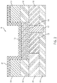
- FIG. 1 depicts a cross-sectional view of a VFET-based SRAM device structure 10 after various fabrication operations according to one or more embodiments of the invention.
- Known fabrication operations have been utilized to form the structure 10 at the stage of fabrication shown in FIG. 1 .
- the structure 10 includes a substrate 103 , an nFET active region 105 , a pFET active region 106 , a shallow trench isolation (STI) 107 , a bottom spacer 108 , a gate material 109 , an nFET semiconductor fin 101 , a pFET semiconductor fin 102 , and hard mask regions 104 , configured and arranged as shown.
- STI shallow trench isolation
- the structure 10 shown in FIG. 1 includes two complementary VFETs side by side over substrate 103 .
- Each of VFETs has a bottom S/D region and a channel fin.
- the n-type VFET has nFET active region 105 and semiconductor fin 101 , respectively.
- the p-type VFET has pFET active region 106 and semiconductor fin 102 , respectively.
- the substrate 103 can be made of any suitable substrate material, for example, Si, SiGe, SiC, Group III-V compound semiconductor, Group II-VI compound semiconductor, or semiconductor-on-insulator (SOI).
- the substrate 103 can be InP.
- the substrate 103 includes a buried oxide layer (not depicted).
- the nFET active region 105 and the pFET active region 106 are formed over the substrate 103 .
- the shallow trench isolation (STI) 107 is also formed over the substrate 103 .
- the STI 107 prevents electrical current leakage between adjacent semiconductor device components (e.g., between adjacent semiconductor fins).
- the STI 107 can be of any suitable dielectric material, for example, a silicon oxide. Any known manner of forming the STI 107 can be utilized.
- the STI 107 is formed by etching back a portion of the substrate 103 to form a trench, filling the trench with the STI 107 material, and planarizing to a surface of the substrate 103 using, for example, a chemical-mechanical planarization (CMP) process.
- CMP chemical-mechanical planarization
- Each of the nFET active region 105 and the pFET active region 106 can be formed by a variety of methods, for example, diffusion, ion implantation of a dopant into the substrate, or in-situ doped epitaxy. More specifically, the nFET active region 105 and the pFET active region 106 will form the bottom S/D regions of adjacent VFET devices in the final fabricated semiconductor device.
- the nFET active region 105 and the pFET active region 106 have complementary doping.
- Complementary doping of semiconducting materials which entails the creation of specified n-type regions (i.e., regions where the conductivity is dominated by electrons) and p-type regions (i.e. regions where the conductivity is dominated by holes), is necessary for the formation of complementary metal oxide semiconductor (CMOS) circuitry that is found in many modern electronic devices.
- CMOS complementary metal oxide semiconductor
- each of the nFET active region 105 and the pFET active region 106 includes epitaxial semiconductor materials grown from gaseous or liquid precursors. In some embodiments, epitaxial regions are epitaxially grown over the substrate 103 . Epitaxial semiconductor materials can be grown using vapor-phase epitaxy (VPE), MBE, liquid-phase epitaxy (LPE), or other suitable processes.
- VPE vapor-phase epitaxy
- MBE MBE
- LPE liquid-phase epitaxy
- Epitaxial silicon, SiGe, and/or carbon doped silicon can be doped during deposition (in-situ doped) by adding dopants, n-type dopants (e.g., phosphorus or arsenic) or p-type dopants (e.g., Ga, B, BF 2 , or Al).
- dopant concentration in the doped regions can range from 1 ⁇ 10 19 cm ⁇ 3 to 2 ⁇ 10 21 cm ⁇ 3 , or between 1 ⁇ 10 20 cm ⁇ 3 and 1 ⁇ 10 21 cm ⁇ 3 .
- the nFET semiconductor fin 101 and the pFET semiconductor fin 102 are formed over the nFET active region 105 and the pFET active region 106 , respectively.
- the nFET semiconductor fin 101 and the pFET semiconductor fin 102 can be formed using known front-end-of-line (FEOL) fabrication techniques.
- a layer of hard mask material can be deposited on the substrate 103 and then etched to form the hard masks 104 , which cover the portions of the substrate 103 where the fins will be formed.
- the hard masks 104 can be any suitable material, for example, a nitride or silicon nitride. An etch is applied such that the portions of the substrate 103 that are not covered by the hard masks 104 are removed to form the nFET and pFET semiconductor fins 101 , 102 .
- the nFET semiconductor fin 101 and pFET semiconductor fin 102 are formed by epitaxially growing semiconductor materials from gaseous or liquid precursors.
- Epitaxial semiconductor materials can be grown using vapor-phase epitaxy (VPE), molecular beam epitaxy (MBE), liquid-phase epitaxy (LPE), or other suitable processes.
- VPE vapor-phase epitaxy
- MBE molecular beam epitaxy
- LPE liquid-phase epitaxy
- the nFET semiconductor fin 101 and pFET semiconductor fin 102 can be made of any suitable material, for example, Si, SiGe, Group III-V compound semiconductor, or other suitable materials.
- the gas source for the deposition of epitaxial semiconductor material includes a silicon, a germanium, or a Group III-V compound semiconductor containing gas source, or a combination thereof.
- an epitaxial InGaAs layer can be deposited from a gas source that is selected from the group consisting of arsine, trimethyl indium, and trimethyl gallium.
- an epitaxial germanium layer can be deposited from a germanium gas source that is selected from the group consisting of germane, digermane, halogermane, dichlorogermane, trichlorogermane, tetrachlorogermane and combinations thereof.
- an epitaxial silicon germanium alloy layer can be formed utilizing a combination of such gas sources. Carrier gases like hydrogen, nitrogen, helium and argon can be used.
- the nFET semiconductor fin 101 and pFET semiconductor fin 102 include silicon.
- the nFET semiconductor fin 101 and pFET semiconductor fin 102 include carbon doped silicon (Si:C). This Si:C layer can be grown in the same chamber used for other epitaxy steps or in a dedicated Si:C epitaxy chamber. The Si:C can include carbon in the range of about 0.2 percent to about 3.0 percent.
- the nFET semiconductor fin 101 and pFET semiconductor fin 102 can be made of any suitable material, for example, Si, SiGe, Group III-V compound semiconductor, or other suitable materials.
- Group III-V compound semiconductors include materials having at least one group III element and at least one group V element, for example, one or more of aluminum gallium arsenide (AlGaAs), aluminum gallium nitride (AlGaN), aluminum arsenide (AlAs), aluminum indium arsenide (AlIAs), aluminum nitride (AlN), gallium antimonide (GaSb), gallium aluminum antimonide (GaAlSb), gallium arsenide (GaAs), gallium arsenide antimonide (GaAsSb), gallium nitride (GaN), indium antimonide (InSb), indium arsenide (InAs), indium gallium arsenide (InGaAs), indium gallium arsen
- the alloy combinations can include binary (two elements, e.g., gallium (III) arsenide (GaAs)), ternary (three elements, e.g., InGaAs) and quaternary (four elements, e.g., aluminum gallium indium phosphide (AlInGaP)) alloys.
- binary two elements, e.g., gallium (III) arsenide (GaAs)
- ternary three elements, e.g., InGaAs
- AlInGaP aluminum gallium indium phosphide
- the bottom spacer 108 is formed opposite surfaces of the nFET active region 105 and the pFET active region 106 .
- the bottom spacer 108 can include a high-k dielectric for example, silicon oxide, silicon nitride, silicon oxynitride, boron nitride, high-k materials, or any combination of these materials.
- high-k materials include but are not limited to metal oxides such as hafnium oxide, hafnium silicon oxide, hafnium silicon oxynitride, lanthanum oxide, lanthanum aluminum oxide, zirconium oxide, zirconium silicon oxide, zirconium silicon oxynitride, tantalum oxide, titanium oxide, barium strontium titanium oxide, barium titanium oxide, strontium titanium oxide, yttrium oxide, aluminum oxide, lead scandium tantalum oxide, and lead zinc niobate.
- the high-k materials can further include dopants such as lanthanum and aluminum.
- the bottom spacer 108 is formed by performing a deposition process for example, a Gas Cluster Ion Beam (GCIB) process.
- GCIB Gas Cluster Ion Beam
- the GCIB process is a deposition process that can be highly directional in nature.
- the directional deposition process can result in the deposition of dielectric material on the horizontally oriented surfaces of the structure, such as the upper surface the nFET active region 105 and pFET active region 106 , while avoiding deposition of any substantial amount of dielectric material on the vertically-oriented surfaces of the structure, such as sidewalls of the nFET semiconductor fin 101 , the pFET semiconductor fin 102 , and the hard masks 104 .
- the gate material 109 is deposited opposite a surface of the bottom spacer 108 .
- the gate material 109 can be made of any suitable conducting material, for example, metal (e.g., tungsten, titanium, tantalum, ruthenium, zirconium, cobalt, copper, aluminum, lead, platinum, tin, silver, gold), conducting metallic compound material (e.g., tantalum nitride, titanium nitride, tantalum carbide, titanium carbide, titanium aluminum carbide, tungsten silicide, tungsten nitride, ruthenium oxide, cobalt silicide, nickel silicide), carbon nanotube, conductive carbon, graphene, or any suitable combination of these materials.
- metal e.g., tungsten, titanium, tantalum, ruthenium, zirconium, cobalt, copper, aluminum, lead, platinum, tin, silver, gold
- conducting metallic compound material e.g., tantalum nitride, titanium n
- the gate material 109 can be deposited using known metallization techniques.
- a RIE selective to the hard masks 104 recesses the gate material 109 below a surface of the hard masks 104 .
- FIG. 2 depicts a cross-sectional view of the structure 10 after a first spacer 201 has been deposited on the structure 10 .
- the first spacer 201 is formed from a first dielectric material, which is selected such that a material in the hard masks 104 and a second dielectric material in a second spacer 401 (as depicted in FIG. 4 ) has an etch selectivity relative to the first dielectric material.
- a first dielectric material include SiCO (carbon-doped silicon oxide), SiOF (fluorine-doped silicon oxide), SiC, and Al 2 O 3 .
- the first spacer 201 is made of SiCO. Formation of the second spacer 401 on the first spacer 201 will be further described below with reference to FIG. 4 .
- the first spacer 201 can be conformally deposited on the structure 10 .
- Conformal deposition refers to deposition of a generally uniform layer of material on a surface in the same shape as the surface, i.e., including on vertically-oriented surfaces of the structure 10 .
- the first spacer 201 is formed using a chemical vapor deposition (CVD), plasma-enhanced chemical vapor deposition (PECVD), atomic layer deposition (ALD), physical vapor deposition (PVD), chemical solution deposition, or other like process.
- CVD chemical vapor deposition
- PECVD plasma-enhanced chemical vapor deposition
- ALD atomic layer deposition
- PVD physical vapor deposition
- chemical solution deposition or other like process.
- FIG. 3 depicts a cross-sectional view of the structure 10 after a gate patterning operation in which portions of the first spacer 201 and the gate material 109 are etched to form an nFET gate 301 and a pFET gate 302 , and to expose an upper surface of a portion of the bottom spacer 108 .
- the nFET gate 301 and the pFET gate 302 are formed, for example, by a lithographic patterning and RIE of the first spacer 201 and the gate material 109 .
- each of the complementary VFETs shown in FIG. 3 has a bottom S/D region and a channel fin. Additionally, each of the complementary VFETs shown in FIG. 3 has a gate that surrounds the sidewalls of the channel fin.
- the n-type VFET has nFET active region 105 , semiconductor fin 101 , and nFET gate 301 that surrounds the sidewalls of the semiconductor fin 101 , respectively.
- the p-type VFET has pFET active region 106 , semiconductor fin 102 , and pFET gate 302 that surrounds the sidewalls of the semiconductor fin 102 , respectively.
- FIG. 3 also depicts that an organic planarization layer (OPL) 303 has been deposited opposite a surface of the first spacer 201 that is opposite a surface of the pFET gate 302 .
- the OPL 303 protects sections of the first spacer 201 and the gate material 109 and allows for etching of portions of the first spacer 201 and the gate material 109 to form the nFET gate 301 and the pFET gate 302 .
- the OPL 303 can include an organic-based planarization material.
- Exemplary organic planarization materials include polyacrylate resin, epoxy resin, phenol resin, polyamide resin, polyimide resin, unsaturated polyester resin, polyphenylenether resin, and polyphenylene sulfide resin.
- the OPL 303 can be formed using a variety of methods including spinning coating, spray coating, dip coating, roller coating, and the like.
- portions of the first spacer 201 and the gate material 109 are removed to provide an opening to an exposed portion of the bottom spacer 108 .
- the portions of the first spacer 201 can be removed using a selective etch process that removes the relevant portions of the first spacer 201 selective to the hard mask 104 .
- the etch can be an isotropic etch, which is non-directional. In some embodiments of the invention, the isotropic etch is a wet chemical etch.
- FIG. 4 depicts a cross-sectional view of the structure 10 after a fabrication operation in which the OPL 303 and the exposed portion of the bottom spacer 108 are removed and a set of second spacers 401 is formed.
- the OPL which was deposited to protect sections of the first spacer 201 and the gate material 109 during the etching, can be removed.
- the OPL 303 and the exposed portion of the bottom spacer 108 can be removed using a variety of methods including an anisotropic etch (e.g., a RIE), chemical wet etching, sulfuric acid stripping, and the like.
- the second spacers 401 are formed from a second dielectric material.
- the second spacers 401 can be formed in the following manner. Subsequent to removing the exposed portion of the bottom spacer 108 , the second dielectric material is conformally deposited on the structure 10 .
- the second dielectric material is deposited using a CVD, PECVD, ALD, PVD, chemical solution deposition, or other like process.
- the second dielectric material can include an oxide, for example, silicon dioxide.
- the second dielectric material is etched to form the set of second spacers 401 on sidewalls of the bottom spacer 108 , the first spacer 201 , the nFET gate 301 , and the pFET gate 302 as depicted in FIG. 4 .
- Etching the second dielectric material can be performed using an anisotropic etch, which is directional.
- the anisotropic etch can include reactive-ion etching (ME).
- Other examples of anisotropic etching that can be used include ion beam etching, plasma etching or laser ablation.
- the second spacers 401 can each have a thickness with a range from about 5 nanometers to about 12 nanometers.
- the first dielectric material used to form the first spacer 201 is selected such that the hard mask 104 and the second dielectric material of the second spacer 401 each have an etch selectivity relative to the first dielectric material.
- the first spacer 201 can include SiCO (carbon-doped silicon oxide), SiOF (fluorine-doped silicon oxide), SiC, or Al 2 O 3 . In this manner, the hard mask 104 and the second spacer 401 can be etched selective to the first spacer 201 .
- the second spacer 401 having a thickness within the range from about 5 nanometers to about 12 nanometers will provide spacing between the nFET gate 301 and a buried contact 701 (shown in FIG. 7 ). Formation of the buried contact 701 will be further described below in connection with the description of the fabrication operations shown in FIG. 7 .
- FIG. 5 depicts a cross-sectional view of the structure 10 after a fabrication operation in which a set of OPLs 501 is deposited and a portion of each of the nFET active region 105 and the pFET active region 106 is etched.
- the OPLs 501 are deposited on upper surfaces of the hard mask 104 , the first spacers 201 , and one of the second spacers 401 .
- the OPL 501 can include an organic-based planarization material.
- Exemplary organic planarization materials include polyacrylate resin, epoxy resin, phenol resin, polyamide resin, polyimide resin, unsaturated polyester resin, polyphenylenether resin, and polyphenylene sulfide resin.
- the OPL 501 can be formed by a variety of methods including spin coating, spray coating, dip coating, roller coating, and the like.
- FIG. 5 also depicts a fabrication operation in which a trench is formed in the nFET active region 105 and the pFET active region 106 by etching exposed portions of the nFET active region 105 and the pFET active region 106 .
- the exposed portions of the nFET active region 105 and the pFET active region 106 are etched selective to the exposed first spacers 201 , the exposed second spacer 401 , and the OPL 501 .
- the leftmost OPL 501 covers and prevents etching of the leftmost hard mask 104
- the rightmost OPL 501 covers and prevents etching of the rightmost hard mask 104 , the rightmost first spacer 201 , and the rightmost second spacer 401 .
- the trench in the nFET active region 105 and pFET active region 106 can be formed by patterning the OPL 501 and using known lithographic processes to transfer the pattern to the nFET active region 105 and the pFET active region 106 to form the trench.
- the lithographic process can include applying a photoresist layer (not depicted) atop the OPL 501 , exposing the photoresist layer to a desired pattern of radiation, and developing the exposed photoresist layer utilizing a resist developer.
- the etching process can include dry etching and/or wet chemical etching. Examples of dry etching processes that can be used include ME, ion beam etching, plasma etching or laser ablation.
- the etching process transfers the pattern from the patterned photoresist layer to the OPL 501 , the nFET active region 105 , and the pFET active region 106 .
- the patterned photoresist layer can be removed utilizing a resist stripping process for example, ashing.
- FIG. 6 depicts a cross-sectional view of the structure 10 after a fabrication operation in which the OPL 501 has been removed and a contact material 601 has been deposited in the trench that was previously formed in the nFET active region 105 and pFET active region 106 and between remaining portions of the second spacer 401 .
- the OPL 501 can be removed by an anisotropic etch, for example, a ME, or by chemical wet etching, or by sulfuric acid stripping.
- the contact material 601 can be made of any suitable conducting material, for example, metal (e.g., tungsten, titanium, tantalum, ruthenium, zirconium, cobalt, copper, aluminum, lead, platinum, tin, silver, gold), conducting metallic compound material (e.g., tantalum nitride, titanium nitride, tantalum carbide, titanium carbide, titanium aluminum carbide, tungsten silicide, tungsten nitride, ruthenium oxide, cobalt silicide, nickel silicide), carbon nanotube, conductive carbon, graphene, or any suitable combination of these materials.
- the contact material 601 includes a same material as the gate material 109 , and accordingly, a same material as the nFET gate 301 and the pFET gate 302 .
- the contact material 601 can be deposited using known metallization techniques. In some embodiments of the invention, the contact material 601 is overfilled into the trench formed in the nFET active region 105 and the pFET active region 106 and between remaining portions of the second spacer 401 , forming an overburden above a surface of the hard masks 104 , the first spacers 201 , and the second spacers 401 . In some embodiments of the invention, a CMP selective to the hard masks 104 , the first spacers 201 , and the second spacers 401 removes the overburden.
- FIG. 7 depicts a cross-sectional view of the structure 10 after the buried contact 701 has been formed by recessing the contact metal 601 , for example, by ME.
- the contact metal 601 is recessed below a surface of the leftmost and rightmost second spacers 401 . Recessing the contact metal 601 to form the buried contact 701 also forms a trench 702 defined by an upper surface of the buried contact 701 , exposed portions of the second spacers 401 and an upper surface of the rightmost first spacer 201 .
- FIGS. 1-7 depict an example of performing a SAC process to form the buried contact 701 in accordance with aspects of the present invention.
- a region for metal deposition was created and defined by the space between the leftmost second spacer 401 and the centrally located second spacer 401 , as well as by the trench that was previously formed in the nFET active region 105 and the pFET active region 106 .
- the enclosed metal deposition region enables the buried contact 701 to self-align to the second spacer 401 along sidewalls of the nFET gate 301 and the pFET gate 302 , and also enables the buried contact 701 to be formed using a deposition and etch back process. Boundaries of the buried contact 701 are further defined by the first spacers 201 , which prevent a short to the pFET gate 302 .
- the second spacers 401 are provided with a thickness in the range from about 5 nanometers to about 12 nanometers, which provides spacing between the nFET gate 301 and the buried contact 701 of from about 5 nanometers to about 12 nanometers.
- a conductive contact will be formed contacting the buried contact 701 and the pFET gate 302 .
- FIG. 8 depicts a cross-sectional view of the structure 10 after an interlayer dielectric (ILD) 801 is deposited in the trench 702 (shown in FIG. 7 ).
- the ILD 801 can be formed using any known deposition process such as a spin-on coating operation.
- the ILD 801 can be any suitable material, for example, an oxide.
- the ILD 801 is overfilled into the trench 702 (shown in FIG. 7 ) to form an overburden above a surface of the hard masks 104 , the first spacer 201 , and the second spacer 401 .
- a CMP selective to the hard masks 104 , the first spacers 201 , and the second spacers 401 can be utilized to remove the overburden.
- FIG. 9 depicts a cross-sectional view of the structure 10 after a fabrication operation in which the hard masks 104 have been removed using an etch process.
- the etch process can be a wet etch process, a dry etch process or a combination thereof.
- the first dielectric material used to form the first spacers 201 is selected such that a material used to form the hard masks 104 has an etch selectivity relative to the first dielectric material.
- the first spacers 201 can include SiCO (carbon-doped silicon oxide), SiOF (fluorine-doped silicon oxide), SiC, or Al 2 O 3 .
- the hard masks 104 are etched selective to the first spacers 201 .
- the hard masks 104 are also etched selective to the second spacers 401 .
- the nFET semiconductor fin 101 and the pFET semiconductor fin 102 can then be doped with n-type (e.g., As, P, Sb) or p-type dopants (e.g., B, BF 2 , Al, Ga), respectively.
- n-type e.g., As, P, Sb
- p-type dopants e.g., B, BF 2 , Al, Ga
- FIG. 10 depicts a cross-sectional view of the structure 10 after a fabrication operation in which S/D regions 1001 and 1003 are formed, followed by formation of cap layers 1002 and 1004 on the source/drain regions 1001 and 1003 , respectively.
- each of the complementary VFETs shown in FIG. 10 has a bottom S/D region, a channel fin, and a gate that surrounds the sidewalls of the channel fin. Additionally, each of the complementary VFETs shown in FIG. 10 has a top S/D region.
- the n-type VFET has nFET active region 105 , semiconductor fin 101 , nFET gate 301 that surrounds the sidewalls of the semiconductor fin 101 , and source/drain region 1001 , respectively.
- the p-type VFET has pFET active region 106 , semiconductor fin 102 , pFET gate 302 that surrounds the sidewalls of the semiconductor fin 102 , and source/drain region 1003 , respectively.
- Source/drain regions 1001 and 1003 are formed opposite exposed surfaces of the nFET semiconductor fin 101 and pFET semiconductor fin 102 , respectively.
- the source/drain regions 1001 and 1003 can be formed by any suitable process, including but not limited to, ultrahigh vacuum chemical vapor deposition (UHVCVD), rapid thermal chemical vapor deposition (RTCVD), metalorganic chemical vapor deposition (MOCVD), low-pressure chemical vapor deposition (LPCVD), limited reaction processing chemical vapor deposition (LRPCVD), and MBE.
- UHVCVD ultrahigh vacuum chemical vapor deposition
- RTCVD rapid thermal chemical vapor deposition
- MOCVD metalorganic chemical vapor deposition
- LPCVD low-pressure chemical vapor deposition
- LPCVD limited reaction processing chemical vapor deposition
- MBE limited reaction processing chemical vapor deposition
- the source/drain regions 1001 and 1003 include epitaxial semiconductor materials grown from gaseous or liquid precursors using VPE, MBE, LPE, or other suitable processes.
- the source/drain regions 1001 and 1003 can be made of any suitable material, for example, Si, SiGe, Group III-V compound semiconductor, or other suitable materials.
- the source/drain regions 1001 and 1003 are raised source/drain regions formed from III-V compound semiconductor material.
- the gas source for the deposition of epitaxial semiconductor material includes a silicon, a germanium, or a Group III-V compound semiconductor containing gas source, or a combination thereof.
- an epitaxial InGaAs layer can be deposited from a gas source that is selected from the group consisting of arsine, trimethyl indium, and trimethyl gallium.
- an epitaxial germanium layer can be deposited from a germanium gas source that is selected from the group consisting of germane, digermane, halogermane, dichlorogermane, trichlorogermane, tetrachlorogermane and combinations thereof.
- an epitaxial silicon germanium alloy layer can be formed utilizing a combination of such gas sources. Carrier gases like hydrogen, nitrogen, helium and argon can be used.
- the source/drain regions 1001 and 1003 include silicon.
- the source/drain regions 1001 and 1003 include carbon doped silicon (Si:C).
- This Si:C layer can be grown in the same chamber used for other epitaxy steps or in a dedicated Si:C epitaxy chamber.
- the Si:C can include carbon in the range of about 0.2 percent to about 3.0 percent.
- the source/drain region 1001 is an n-doped region over the nFET semiconductor fin 101 .
- the source/drain region 1001 can be doped by a variety of methods, for example, in-situ doped epitaxy, doped following the epitaxy, or by implantation and plasma doping.
- the n-type doping concentration can range from 1 ⁇ 10 19 cm ⁇ 3 to 5 ⁇ 10 21 cm ⁇ 3 , or between 1 ⁇ 10 20 cm ⁇ 3 and 5 ⁇ 10 21 cm ⁇ 3 .
- the depth of the n-type dopant (e.g., As, P, Sb) ion implantation is controlled by adjusting the implantation energy.
- the source/drain region 1003 is a p-doped region over the pFET semiconductor fin 102 .
- the source/drain regions 1003 can be doped by a variety of methods, for example, in-situ doped epitaxy, doped following the epitaxy, or by implantation and plasma doping.
- the p-type doping concentration can range from 1 ⁇ 10 19 cm ⁇ 3 to 5 ⁇ 10 21 cm ⁇ 3 , or between 1 ⁇ 10 20 cm ⁇ 3 and 5 ⁇ 10 21 cm ⁇ 3 .
- the depth of the p-type dopant (e.g., B, BF 2 , Al, Ga) ion implantation is controlled by adjusting the implantation energy.
- the cap layers 1002 and 1004 are opposite a surface of the source/drain regions 1001 and 1003 .
- the cap layers 1002 and 1004 can be formed using any suitable deposition processes, for example, CVD, PECVD, ALD, evaporation, PVD, chemical solution deposition, or other like processes.
- the Cap layers 1002 and 1004 are a silicon nitride, silicon carbonitride, or metal oxide.
- FIG. 11 depicts a cross-sectional view of the structure 10 after a fabrication operation in which a dielectric layer 1101 is formed opposite a surface of the dielectric layer 801 , the cap layers 1002 and 1004 , the first spacers 201 , and the second spacers 401 .
- the dielectric layer 1101 can be formed using any known process. In some embodiments of the invention, the dielectric layer 1101 is deposited using a CVD, PECVD, ALD, PVD, chemical solution deposition, or other like process in combination with a wet or dry etch process.
- the dielectric layer 1101 can be made of any suitable material, for example, a low-k dielectric, a nitride, silicon nitride, silicon dioxide, SiON, SiOCN, or SiBCN. As shown in FIG. 11 , the dielectric layer 1101 can include a same material as the dielectric layer 801 .
- the conductive contact 1102 includes a surface that contacts the buried contact 701 , the pFET gate 302 , and centermost second spacers 401 between the buried contact 701 and the pFET gate 302 .
- An additional surface of the conductive contact contacts the rightmost first spacer 201 .
- the conductive contact 1102 can be made of any suitable conducting material, for example, metal (e.g., tungsten, titanium, tantalum, ruthenium, zirconium, cobalt, copper, aluminum, lead, platinum, tin, silver, gold), conducting metallic compound material (e.g., tantalum nitride, titanium nitride, tantalum carbide, titanium carbide, titanium aluminum carbide, tungsten silicide, tungsten nitride, ruthenium oxide, cobalt silicide, nickel silicide), carbon nanotube, conductive carbon, graphene, or any suitable combination of these materials.
- metal e.g., tungsten, titanium, tantalum, ruthenium, zirconium, cobalt, copper, aluminum, lead, platinum, tin, silver, gold
- conducting metallic compound material e.g., tantalum nitride, titanium nitride, tantalum carbide, titanium carbide, titanium aluminum carbide, tungsten
- the conductive contact 1102 includes a same material as at least one of the contact material 601 and the gate material 109 , and accordingly, a same material as the nFET gate 301 and the pFET gate 302 .
- the conductive contact 1102 can be formed or deposited using known metallization techniques.
- the contact material is overfilled, forming an overburden above a surface of the dielectric layer 1101 .
- a CMP selective to the dielectric layer 1101 removes the overburden.
- First spacer 201 and second spacer 401 enable application of a SAC process for forming buried contact 701 between the nFET gate 301 and the pFET gate 302 .
- the buried contact 701 contacts the nFET active region 105 and the pFET active region 106 .
- a conductive contact 1102 contacts the pFET gate 302 and the buried contact 701 .
- the second spacer 401 prevents the buried contact 701 from electrically shorting to the nFET gate 301 and a thickness of the second spacer 401 provides a minimal separation between the buried contact 701 and the nFET gate 301 , for example, of about 5 nanometers to about 12 nanometers. Stated otherwise, a minimum required buried contact 701 to nFET gate 301 spacing is defined by a thickness of the second spacer 401 .
- Embodiments of the invention address the above-described shortcomings of known VFET fabrication processes by providing technical effects and benefits that include fabrication methods and resulting structures based on novel self-alignment fabrication operations that reduce the reliance on lithography-based fabrication processes, thereby enabling reductions in feature-to-feature spacing requirements and enabling an ultimate reduction in the footprint of the VFET.
- the feature-to-feature spacing requirement is a contact-to-gate spacing requirement
- the VFET is fabricated using a SAC process to form a buried contact. Because the SAC process does not rely on lithography-based fabrication processes, there is no need to include in contact-to-gate spacing requirements sufficient tolerance to compensate for overlay errors inherent in lithography-based fabrication processes.
- a coupling of entities can refer to either a direct or an indirect coupling
- a positional relationship between entities can be a direct or indirect positional relationship.
- references in the present description to forming layer “A” over layer “B” include situations in which one or more intermediate layers (e.g., layer “C”) is between layer “A” and layer “B” as long as the relevant characteristics and functionalities of layer “A” and layer “B” are not substantially changed by the intermediate layer(s).
- compositions comprising, “comprising,” “includes,” “including,” “has,” “having,” “contains” or “containing,” or any other variation thereof, are intended to cover a non-exclusive inclusion.
- a composition, a mixture, process, method, article, or apparatus that comprises a list of elements is not necessarily limited to only those elements but can include other elements not expressly listed or inherent to such composition, mixture, process, method, article, or apparatus.
- connection can include an indirect “connection” and a direct “connection.”
- references in the specification to “one embodiment,” “an embodiment,” “an example embodiment,” etc., indicate that the embodiment described can include a particular feature, structure, or characteristic, but every embodiment may or may not include the particular feature, structure, or characteristic. Moreover, such phrases are not necessarily referring to the same embodiment. Further, when a particular feature, structure, or characteristic is described in connection with an embodiment, it is submitted that it is within the knowledge of one skilled in the art to affect such feature, structure, or characteristic in connection with other embodiments whether or not explicitly described.
- the terms “upper,” “lower,” “right,” “left,” “vertical,” “horizontal,” “top,” “bottom,” and derivatives thereof shall relate to the described structures and methods, as oriented in the drawing figures.
- the terms “overlying,” “atop,” “on top,” “positioned on” or “positioned atop” mean that a first element, such as a first structure, is present on a second element, such as a second structure, wherein intervening elements such as an interface structure can be present between the first element and the second element.
- the term “direct contact” means that a first element, such as a first structure, and a second element, such as a second structure, are connected without any intermediary conducting, insulating or semiconductor layers at the interface of the two elements.
- etch selectivity relative to and “selective to,” such as, for example, “a first element has an etch selectivity relative to a second element” and “a first element selective to a second element,” means that the first element can be etched and the second element can act as an etch stop.
- conformal e.g., a conformal layer
- the thickness of the layer is substantially the same on all surfaces, or that the thickness variation is less than 15% of the nominal thickness of the layer.
- the various processes used to form a micro-chip that will be packaged into an IC fall into four general categories, namely, film deposition, removal/etching, semiconductor doping and patterning/lithography.
- Deposition is any process that grows, coats, or otherwise transfers a material onto the wafer. Available technologies include PVD, CVD, electrochemical deposition (ECD), MBE and more recently, ALD among others.
- Removal/etching is any process that removes material from the wafer. Examples include etch processes (either wet or dry), CMP, and the like.
- RIE for example, is a type of dry etching that uses chemically reactive plasma to remove a material, such as a masked pattern of semiconductor material, by exposing the material to a bombardment of ions that dislodge portions of the material from the exposed surface.
- the plasma is typically generated under low pressure (vacuum) by an electromagnetic field.
- Semiconductor doping is the modification of electrical properties by doping, for example, transistor sources and drains, generally by diffusion and/or by ion implantation. These doping processes are followed by furnace annealing or by rapid thermal annealing (RTA). Annealing serves to activate the implanted dopants.
- Films of both conductors e.g., poly-silicon, aluminum, copper, etc.
- insulators e.g., various forms of silicon dioxide, silicon nitride, etc.
- Semiconductor lithography is the formation of three-dimensional relief images or patterns on the semiconductor substrate for subsequent transfer of the pattern to the substrate. In semiconductor lithography, the patterns are formed by a light sensitive polymer called a photo-resist.
- lithography and etch pattern transfer steps are repeated multiple times. Each pattern being printed on the wafer is aligned to the previously formed patterns and slowly the conductors, insulators and selectively doped regions are built up to form the final device.
Abstract
Description
Claims (6)
Priority Applications (2)
| Application Number | Priority Date | Filing Date | Title |
|---|---|---|---|
| US15/686,315 US10804148B2 (en) | 2017-08-25 | 2017-08-25 | Buried contact to provide reduced VFET feature-to-feature tolerance requirements |
| US15/815,055 US10796957B2 (en) | 2017-08-25 | 2017-11-16 | Buried contact to provide reduced VFET feature-to-feature tolerance requirements |
Applications Claiming Priority (1)
| Application Number | Priority Date | Filing Date | Title |
|---|---|---|---|
| US15/686,315 US10804148B2 (en) | 2017-08-25 | 2017-08-25 | Buried contact to provide reduced VFET feature-to-feature tolerance requirements |
Related Child Applications (1)
| Application Number | Title | Priority Date | Filing Date |
|---|---|---|---|
| US15/815,055 Continuation US10796957B2 (en) | 2017-08-25 | 2017-11-16 | Buried contact to provide reduced VFET feature-to-feature tolerance requirements |
Publications (2)
| Publication Number | Publication Date |
|---|---|
| US20190067100A1 US20190067100A1 (en) | 2019-02-28 |
| US10804148B2 true US10804148B2 (en) | 2020-10-13 |
Family
ID=65434357
Family Applications (2)
| Application Number | Title | Priority Date | Filing Date |
|---|---|---|---|
| US15/686,315 Active 2037-11-12 US10804148B2 (en) | 2017-08-25 | 2017-08-25 | Buried contact to provide reduced VFET feature-to-feature tolerance requirements |
| US15/815,055 Active 2037-10-01 US10796957B2 (en) | 2017-08-25 | 2017-11-16 | Buried contact to provide reduced VFET feature-to-feature tolerance requirements |
Family Applications After (1)
| Application Number | Title | Priority Date | Filing Date |
|---|---|---|---|
| US15/815,055 Active 2037-10-01 US10796957B2 (en) | 2017-08-25 | 2017-11-16 | Buried contact to provide reduced VFET feature-to-feature tolerance requirements |
Country Status (1)
| Country | Link |
|---|---|
| US (2) | US10804148B2 (en) |
Families Citing this family (1)
| Publication number | Priority date | Publication date | Assignee | Title |
|---|---|---|---|---|
| US11817497B2 (en) | 2021-08-25 | 2023-11-14 | International Business Machines Corporation | Vertical field effect transistor inverter with single fin device |
Citations (32)
| Publication number | Priority date | Publication date | Assignee | Title |
|---|---|---|---|---|
| US5376814A (en) | 1991-05-13 | 1994-12-27 | Goldstar Electron Co., Ltd. | Method of constructing reduced size highly integrated static random access memory with double vertical channel structure |
| US5416736A (en) | 1992-07-28 | 1995-05-16 | Motorola, Inc. | Vertical field-effect transistor and a semiconductor memory cell having the transistor |
| US5554870A (en) | 1994-02-04 | 1996-09-10 | Motorola, Inc. | Integrated circuit having both vertical and horizontal devices and process for making the same |
| US5656842A (en) * | 1995-06-20 | 1997-08-12 | Mitsubishi Denki Kabushiki Kaisha | Vertical mosfet including a back gate electrode |
| US5981995A (en) | 1997-06-13 | 1999-11-09 | Advanced Micro Devices, Inc. | Static random access memory cell having buried sidewall transistors, buried bit lines, and buried vdd and vss nodes |
| US6038164A (en) | 1997-11-27 | 2000-03-14 | Siemens Aktiengesellschaft | SRAM cell configuration and method for its fabrication |
| US20030075758A1 (en) * | 2001-10-18 | 2003-04-24 | Chartered Semiconductor Manufacturing Ltd. | Method to form a self-aligned CMOS inverter using vertical device integration |
| US20040104419A1 (en) * | 2002-08-22 | 2004-06-03 | Mark Bohr | Self-aligned contacts to gates |
| US7098114B1 (en) * | 2004-06-22 | 2006-08-29 | Integrated Device Technology, Inc. | Method for forming cmos device with self-aligned contacts and region formed using salicide process |
| US20070090428A1 (en) * | 2005-10-25 | 2007-04-26 | Taiwan Semiconductor Manufacturing Co., Ltd. | Integrated semiconductor structure for SRAM cells |
| US7285467B2 (en) | 2003-01-07 | 2007-10-23 | Samsung Electronics Co., Ltd. | Methods of fabricating static random access memories (SRAMS) having vertical transistors |
| US20100059831A1 (en) * | 2006-06-05 | 2010-03-11 | Chartered Semiconductor Manufacturing, Ltd. | Spacer-less Low-K Dielectric Processes |
| US20100207201A1 (en) * | 2008-01-29 | 2010-08-19 | Fujio Masuoka | Semiconductor device and production method therefor |
| US20100213525A1 (en) * | 2008-01-29 | 2010-08-26 | Unisantis Electronics (Japan) Ltd. | Semiconductor storage device and methods of producing it |
| US20100219483A1 (en) * | 2008-01-29 | 2010-09-02 | Fujio Masuoka | Semiconductor storage device |
| US20100224936A1 (en) * | 2009-03-03 | 2010-09-09 | Kabushiki Kaisha Toshiba | Semiconductor device and method of fabricating the same |
| US20100314690A1 (en) * | 2009-06-15 | 2010-12-16 | Taiwan Semiconductor Manufacturing Company, Ltd. | Sidewall-Free CESL for Enlarging ILD Gap-Fill Window |
| US20110073940A1 (en) * | 2009-09-30 | 2011-03-31 | Lee Jin-Ku | Semiconductor device with one-side-contact and method for fabricating the same |
| US20110156107A1 (en) * | 2009-12-30 | 2011-06-30 | Bohr Mark T | Self-aligned contacts |
| US8373235B2 (en) | 2009-05-22 | 2013-02-12 | Unisantis Electronics Singapore Pte Ltd. | Semiconductor memory device and production method therefor |
| US20130256767A1 (en) * | 2011-10-01 | 2013-10-03 | Sameer S. Pradhan | Source/drain contacts for non-planar transistors |
| US20150318213A1 (en) * | 2014-04-30 | 2015-11-05 | Taiwan Semiconductor Manufacturing Co., Ltd. | Tunnel field-effect transistor and method for fabricating the same |
| US9251888B1 (en) | 2014-09-15 | 2016-02-02 | Taiwan Semiconductor Manufacturing Company, Ltd. | SRAM cells with vertical gate-all-round MOSFETs |
| US20160056173A1 (en) * | 2013-09-03 | 2016-02-25 | Unisantis Electronics Singapore Pte. Ltd. | Semiconductor device with surrounding gate transistors in a nand circuit |
| US9312383B1 (en) * | 2015-08-12 | 2016-04-12 | International Business Machines Corporation | Self-aligned contacts for vertical field effect transistors |
| US20160247720A1 (en) * | 2015-01-29 | 2016-08-25 | Taiwan Semiconductor Manufacturing Company, Ltd. | Top Metal Pads as Local Interconnectors of Vertical Transistors |
| US9530863B1 (en) * | 2016-04-13 | 2016-12-27 | Globalfoundries Inc. | Methods of forming vertical transistor devices with self-aligned replacement gate structures |
| US9613955B1 (en) * | 2015-12-10 | 2017-04-04 | International Business Machines Corporation | Hybrid circuit including a tunnel field-effect transistor |
| US9653575B1 (en) * | 2016-05-09 | 2017-05-16 | International Business Machines Corporation | Vertical transistor with a body contact for back-biasing |
| US9825032B1 (en) | 2016-11-23 | 2017-11-21 | Globalfoundries Inc. | Metal layer routing level for vertical FET SRAM and logic cell scaling |
| US20170352625A1 (en) * | 2016-06-03 | 2017-12-07 | International Business Machines Corporation | Self-aligned vertical transistor with local interconnect |
| US9960272B1 (en) * | 2017-05-16 | 2018-05-01 | International Business Machines Corporation | Bottom contact resistance reduction on VFET |
-
2017
- 2017-08-25 US US15/686,315 patent/US10804148B2/en active Active
- 2017-11-16 US US15/815,055 patent/US10796957B2/en active Active
Patent Citations (33)
| Publication number | Priority date | Publication date | Assignee | Title |
|---|---|---|---|---|
| US5376814A (en) | 1991-05-13 | 1994-12-27 | Goldstar Electron Co., Ltd. | Method of constructing reduced size highly integrated static random access memory with double vertical channel structure |
| US5416736A (en) | 1992-07-28 | 1995-05-16 | Motorola, Inc. | Vertical field-effect transistor and a semiconductor memory cell having the transistor |
| US5554870A (en) | 1994-02-04 | 1996-09-10 | Motorola, Inc. | Integrated circuit having both vertical and horizontal devices and process for making the same |
| US5656842A (en) * | 1995-06-20 | 1997-08-12 | Mitsubishi Denki Kabushiki Kaisha | Vertical mosfet including a back gate electrode |
| US5981995A (en) | 1997-06-13 | 1999-11-09 | Advanced Micro Devices, Inc. | Static random access memory cell having buried sidewall transistors, buried bit lines, and buried vdd and vss nodes |
| US6038164A (en) | 1997-11-27 | 2000-03-14 | Siemens Aktiengesellschaft | SRAM cell configuration and method for its fabrication |
| US20030075758A1 (en) * | 2001-10-18 | 2003-04-24 | Chartered Semiconductor Manufacturing Ltd. | Method to form a self-aligned CMOS inverter using vertical device integration |
| US20040104419A1 (en) * | 2002-08-22 | 2004-06-03 | Mark Bohr | Self-aligned contacts to gates |
| US7285467B2 (en) | 2003-01-07 | 2007-10-23 | Samsung Electronics Co., Ltd. | Methods of fabricating static random access memories (SRAMS) having vertical transistors |
| US7098114B1 (en) * | 2004-06-22 | 2006-08-29 | Integrated Device Technology, Inc. | Method for forming cmos device with self-aligned contacts and region formed using salicide process |
| US20070090428A1 (en) * | 2005-10-25 | 2007-04-26 | Taiwan Semiconductor Manufacturing Co., Ltd. | Integrated semiconductor structure for SRAM cells |
| US20100059831A1 (en) * | 2006-06-05 | 2010-03-11 | Chartered Semiconductor Manufacturing, Ltd. | Spacer-less Low-K Dielectric Processes |
| US20100207201A1 (en) * | 2008-01-29 | 2010-08-19 | Fujio Masuoka | Semiconductor device and production method therefor |
| US20100213525A1 (en) * | 2008-01-29 | 2010-08-26 | Unisantis Electronics (Japan) Ltd. | Semiconductor storage device and methods of producing it |
| US20100219483A1 (en) * | 2008-01-29 | 2010-09-02 | Fujio Masuoka | Semiconductor storage device |
| US8378425B2 (en) | 2008-01-29 | 2013-02-19 | Unisantis Electronics Singapore Pte Ltd. | Semiconductor storage device |
| US20100224936A1 (en) * | 2009-03-03 | 2010-09-09 | Kabushiki Kaisha Toshiba | Semiconductor device and method of fabricating the same |
| US8373235B2 (en) | 2009-05-22 | 2013-02-12 | Unisantis Electronics Singapore Pte Ltd. | Semiconductor memory device and production method therefor |
| US20100314690A1 (en) * | 2009-06-15 | 2010-12-16 | Taiwan Semiconductor Manufacturing Company, Ltd. | Sidewall-Free CESL for Enlarging ILD Gap-Fill Window |
| US20110073940A1 (en) * | 2009-09-30 | 2011-03-31 | Lee Jin-Ku | Semiconductor device with one-side-contact and method for fabricating the same |
| US20110156107A1 (en) * | 2009-12-30 | 2011-06-30 | Bohr Mark T | Self-aligned contacts |
| US20130256767A1 (en) * | 2011-10-01 | 2013-10-03 | Sameer S. Pradhan | Source/drain contacts for non-planar transistors |
| US20160056173A1 (en) * | 2013-09-03 | 2016-02-25 | Unisantis Electronics Singapore Pte. Ltd. | Semiconductor device with surrounding gate transistors in a nand circuit |
| US20150318213A1 (en) * | 2014-04-30 | 2015-11-05 | Taiwan Semiconductor Manufacturing Co., Ltd. | Tunnel field-effect transistor and method for fabricating the same |
| US9251888B1 (en) | 2014-09-15 | 2016-02-02 | Taiwan Semiconductor Manufacturing Company, Ltd. | SRAM cells with vertical gate-all-round MOSFETs |
| US20160247720A1 (en) * | 2015-01-29 | 2016-08-25 | Taiwan Semiconductor Manufacturing Company, Ltd. | Top Metal Pads as Local Interconnectors of Vertical Transistors |
| US9312383B1 (en) * | 2015-08-12 | 2016-04-12 | International Business Machines Corporation | Self-aligned contacts for vertical field effect transistors |
| US9613955B1 (en) * | 2015-12-10 | 2017-04-04 | International Business Machines Corporation | Hybrid circuit including a tunnel field-effect transistor |
| US9530863B1 (en) * | 2016-04-13 | 2016-12-27 | Globalfoundries Inc. | Methods of forming vertical transistor devices with self-aligned replacement gate structures |
| US9653575B1 (en) * | 2016-05-09 | 2017-05-16 | International Business Machines Corporation | Vertical transistor with a body contact for back-biasing |
| US20170352625A1 (en) * | 2016-06-03 | 2017-12-07 | International Business Machines Corporation | Self-aligned vertical transistor with local interconnect |
| US9825032B1 (en) | 2016-11-23 | 2017-11-21 | Globalfoundries Inc. | Metal layer routing level for vertical FET SRAM and logic cell scaling |
| US9960272B1 (en) * | 2017-05-16 | 2018-05-01 | International Business Machines Corporation | Bottom contact resistance reduction on VFET |
Non-Patent Citations (1)
| Title |
|---|
| List of IBM Patents or Patent Applictions Treated as Related; (Appendix P), Filed Mar. 21, 2019, 2 pages. |
Also Published As
| Publication number | Publication date |
|---|---|
| US20190067100A1 (en) | 2019-02-28 |
| US20190067101A1 (en) | 2019-02-28 |
| US10796957B2 (en) | 2020-10-06 |
Similar Documents
| Publication | Publication Date | Title |
|---|---|---|
| US11011622B2 (en) | Closely packed vertical transistors with reduced contact resistance | |
| US11018240B2 (en) | Vertical field effect transistor with reduced parasitic capacitance | |
| US10157798B1 (en) | Uniform bottom spacers in vertical field effect transistors | |
| US11637179B2 (en) | Airgap vertical transistor without structural collapse | |
| US10629699B2 (en) | Gate height control and ILD protection | |
| US10923590B2 (en) | Wrap-around contact for vertical field effect transistors | |
| US10249542B2 (en) | Self-aligned doping in source/drain regions for low contact resistance | |
| KR20220160683A (en) | Nanosheet transistors with asymmetric gate stacks | |
| US10586741B2 (en) | Gate height and spacer uniformity | |
| US11646235B2 (en) | Vertical tunneling field effect transistor with dual liner bottom spacer | |
| US11183419B2 (en) | Unconfined buried interconnects | |
| US10312245B2 (en) | Laser spike annealing for solid phase epitaxy and low contact resistance in an SRAM with a shared pFET and nFET trench | |
| US10796957B2 (en) | Buried contact to provide reduced VFET feature-to-feature tolerance requirements | |
| US11201089B2 (en) | Robust low-k bottom spacer for VFET | |
| US11205723B2 (en) | Selective source/drain recess for improved performance, isolation, and scaling | |
| US11024536B2 (en) | Contact interlayer dielectric replacement with improved SAC cap retention | |
| US11830774B2 (en) | Buried contact through fin-to-fin space for vertical transport field effect transistor | |
| US10529832B2 (en) | Shallow, abrupt and highly activated tin extension implant junction |
Legal Events
| Date | Code | Title | Description |
|---|---|---|---|
| AS | Assignment |
Owner name: INTERNATIONAL BUSINESS MACHINES CORPORATION, NEW Y Free format text: ASSIGNMENT OF ASSIGNORS INTEREST;ASSIGNORS:FAN, SU CHEN;SHEARER, JEFFREY C.;WONG, ROBERT C.;AND OTHERS;SIGNING DATES FROM 20170816 TO 20170824;REEL/FRAME:043401/0501 Owner name: INTERNATIONAL BUSINESS MACHINES CORPORATION, NEW YORK Free format text: ASSIGNMENT OF ASSIGNORS INTEREST;ASSIGNORS:FAN, SU CHEN;SHEARER, JEFFREY C.;WONG, ROBERT C.;AND OTHERS;SIGNING DATES FROM 20170816 TO 20170824;REEL/FRAME:043401/0501 |
|
| STPP | Information on status: patent application and granting procedure in general |
Free format text: RESPONSE TO NON-FINAL OFFICE ACTION ENTERED AND FORWARDED TO EXAMINER |
|
| STPP | Information on status: patent application and granting procedure in general |
Free format text: FINAL REJECTION MAILED |
|
| STPP | Information on status: patent application and granting procedure in general |
Free format text: RESPONSE AFTER FINAL ACTION FORWARDED TO EXAMINER |
|
| STPP | Information on status: patent application and granting procedure in general |
Free format text: DOCKETED NEW CASE - READY FOR EXAMINATION |
|
| STPP | Information on status: patent application and granting procedure in general |
Free format text: NON FINAL ACTION MAILED |
|
| STPP | Information on status: patent application and granting procedure in general |
Free format text: FINAL REJECTION MAILED |
|
| STPP | Information on status: patent application and granting procedure in general |
Free format text: NOTICE OF ALLOWANCE MAILED -- APPLICATION RECEIVED IN OFFICE OF PUBLICATIONS |
|
| STPP | Information on status: patent application and granting procedure in general |
Free format text: PUBLICATIONS -- ISSUE FEE PAYMENT VERIFIED |
|
| STCF | Information on status: patent grant |
Free format text: PATENTED CASE |
|
| MAFP | Maintenance fee payment |
Free format text: PAYMENT OF MAINTENANCE FEE, 4TH YEAR, LARGE ENTITY (ORIGINAL EVENT CODE: M1551); ENTITY STATUS OF PATENT OWNER: LARGE ENTITY Year of fee payment: 4 |