JP5919121B2 - ダイオードおよび半導体装置 - Google Patents
ダイオードおよび半導体装置 Download PDFInfo
- Publication number
- JP5919121B2 JP5919121B2 JP2012166576A JP2012166576A JP5919121B2 JP 5919121 B2 JP5919121 B2 JP 5919121B2 JP 2012166576 A JP2012166576 A JP 2012166576A JP 2012166576 A JP2012166576 A JP 2012166576A JP 5919121 B2 JP5919121 B2 JP 5919121B2
- Authority
- JP
- Japan
- Prior art keywords
- region
- diode
- electrode
- anode
- barrier
- Prior art date
- Legal status (The legal status is an assumption and is not a legal conclusion. Google has not performed a legal analysis and makes no representation as to the accuracy of the status listed.)
- Active
Links
Images


Classifications
-
- H—ELECTRICITY
- H10—SEMICONDUCTOR DEVICES; ELECTRIC SOLID-STATE DEVICES NOT OTHERWISE PROVIDED FOR
- H10D—INORGANIC ELECTRIC SEMICONDUCTOR DEVICES
- H10D12/00—Bipolar devices controlled by the field effect, e.g. insulated-gate bipolar transistors [IGBT]
- H10D12/411—Insulated-gate bipolar transistors [IGBT]
- H10D12/441—Vertical IGBTs
- H10D12/461—Vertical IGBTs having non-planar surfaces, e.g. having trenches, recesses or pillars in the surfaces of the emitter, base or collector regions
- H10D12/481—Vertical IGBTs having non-planar surfaces, e.g. having trenches, recesses or pillars in the surfaces of the emitter, base or collector regions having gate structures on slanted surfaces, on vertical surfaces, or in grooves, e.g. trench gate IGBTs
-
- H—ELECTRICITY
- H10—SEMICONDUCTOR DEVICES; ELECTRIC SOLID-STATE DEVICES NOT OTHERWISE PROVIDED FOR
- H10D—INORGANIC ELECTRIC SEMICONDUCTOR DEVICES
- H10D30/00—Field-effect transistors [FET]
- H10D30/60—Insulated-gate field-effect transistors [IGFET]
- H10D30/64—Double-diffused metal-oxide semiconductor [DMOS] FETs
- H10D30/66—Vertical DMOS [VDMOS] FETs
- H10D30/668—Vertical DMOS [VDMOS] FETs having trench gate electrodes, e.g. UMOS transistors
-
- H—ELECTRICITY
- H10—SEMICONDUCTOR DEVICES; ELECTRIC SOLID-STATE DEVICES NOT OTHERWISE PROVIDED FOR
- H10D—INORGANIC ELECTRIC SEMICONDUCTOR DEVICES
- H10D62/00—Semiconductor bodies, or regions thereof, of devices having potential barriers
- H10D62/10—Shapes, relative sizes or dispositions of the regions of the semiconductor bodies; Shapes of the semiconductor bodies
- H10D62/102—Constructional design considerations for preventing surface leakage or controlling electric field concentration
- H10D62/103—Constructional design considerations for preventing surface leakage or controlling electric field concentration for increasing or controlling the breakdown voltage of reverse-biased devices
- H10D62/105—Constructional design considerations for preventing surface leakage or controlling electric field concentration for increasing or controlling the breakdown voltage of reverse-biased devices by having particular doping profiles, shapes or arrangements of PN junctions; by having supplementary regions, e.g. junction termination extension [JTE]
- H10D62/106—Constructional design considerations for preventing surface leakage or controlling electric field concentration for increasing or controlling the breakdown voltage of reverse-biased devices by having particular doping profiles, shapes or arrangements of PN junctions; by having supplementary regions, e.g. junction termination extension [JTE] having supplementary regions doped oppositely to or in rectifying contact with regions of the semiconductor bodies, e.g. guard rings with PN or Schottky junctions
- H10D62/107—Buried supplementary regions, e.g. buried guard rings
-
- H—ELECTRICITY
- H10—SEMICONDUCTOR DEVICES; ELECTRIC SOLID-STATE DEVICES NOT OTHERWISE PROVIDED FOR
- H10D—INORGANIC ELECTRIC SEMICONDUCTOR DEVICES
- H10D62/00—Semiconductor bodies, or regions thereof, of devices having potential barriers
- H10D62/10—Shapes, relative sizes or dispositions of the regions of the semiconductor bodies; Shapes of the semiconductor bodies
- H10D62/113—Isolations within a component, i.e. internal isolations
-
- H—ELECTRICITY
- H10—SEMICONDUCTOR DEVICES; ELECTRIC SOLID-STATE DEVICES NOT OTHERWISE PROVIDED FOR
- H10D—INORGANIC ELECTRIC SEMICONDUCTOR DEVICES
- H10D62/00—Semiconductor bodies, or regions thereof, of devices having potential barriers
- H10D62/10—Shapes, relative sizes or dispositions of the regions of the semiconductor bodies; Shapes of the semiconductor bodies
- H10D62/124—Shapes, relative sizes or dispositions of the regions of semiconductor bodies or of junctions between the regions
- H10D62/126—Top-view geometrical layouts of the regions or the junctions
- H10D62/127—Top-view geometrical layouts of the regions or the junctions of cellular field-effect devices, e.g. multicellular DMOS transistors or IGBTs
-
- H—ELECTRICITY
- H10—SEMICONDUCTOR DEVICES; ELECTRIC SOLID-STATE DEVICES NOT OTHERWISE PROVIDED FOR
- H10D—INORGANIC ELECTRIC SEMICONDUCTOR DEVICES
- H10D62/00—Semiconductor bodies, or regions thereof, of devices having potential barriers
- H10D62/10—Shapes, relative sizes or dispositions of the regions of the semiconductor bodies; Shapes of the semiconductor bodies
- H10D62/13—Semiconductor regions connected to electrodes carrying current to be rectified, amplified or switched, e.g. source or drain regions
- H10D62/149—Source or drain regions of field-effect devices
- H10D62/151—Source or drain regions of field-effect devices of IGFETs
- H10D62/156—Drain regions of DMOS transistors
- H10D62/157—Impurity concentrations or distributions
-
- H—ELECTRICITY
- H10—SEMICONDUCTOR DEVICES; ELECTRIC SOLID-STATE DEVICES NOT OTHERWISE PROVIDED FOR
- H10D—INORGANIC ELECTRIC SEMICONDUCTOR DEVICES
- H10D62/00—Semiconductor bodies, or regions thereof, of devices having potential barriers
- H10D62/10—Shapes, relative sizes or dispositions of the regions of the semiconductor bodies; Shapes of the semiconductor bodies
- H10D62/17—Semiconductor regions connected to electrodes not carrying current to be rectified, amplified or switched, e.g. channel regions
- H10D62/393—Body regions of DMOS transistors or IGBTs
-
- H—ELECTRICITY
- H10—SEMICONDUCTOR DEVICES; ELECTRIC SOLID-STATE DEVICES NOT OTHERWISE PROVIDED FOR
- H10D—INORGANIC ELECTRIC SEMICONDUCTOR DEVICES
- H10D62/00—Semiconductor bodies, or regions thereof, of devices having potential barriers
- H10D62/60—Impurity distributions or concentrations
-
- H—ELECTRICITY
- H10—SEMICONDUCTOR DEVICES; ELECTRIC SOLID-STATE DEVICES NOT OTHERWISE PROVIDED FOR
- H10D—INORGANIC ELECTRIC SEMICONDUCTOR DEVICES
- H10D62/00—Semiconductor bodies, or regions thereof, of devices having potential barriers
- H10D62/80—Semiconductor bodies, or regions thereof, of devices having potential barriers characterised by the materials
- H10D62/83—Semiconductor bodies, or regions thereof, of devices having potential barriers characterised by the materials being Group IV materials, e.g. B-doped Si or undoped Ge
- H10D62/832—Semiconductor bodies, or regions thereof, of devices having potential barriers characterised by the materials being Group IV materials, e.g. B-doped Si or undoped Ge being Group IV materials comprising two or more elements, e.g. SiGe
- H10D62/8325—Silicon carbide
-
- H—ELECTRICITY
- H10—SEMICONDUCTOR DEVICES; ELECTRIC SOLID-STATE DEVICES NOT OTHERWISE PROVIDED FOR
- H10D—INORGANIC ELECTRIC SEMICONDUCTOR DEVICES
- H10D62/00—Semiconductor bodies, or regions thereof, of devices having potential barriers
- H10D62/80—Semiconductor bodies, or regions thereof, of devices having potential barriers characterised by the materials
- H10D62/85—Semiconductor bodies, or regions thereof, of devices having potential barriers characterised by the materials being Group III-V materials, e.g. GaAs
- H10D62/8503—Nitride Group III-V materials, e.g. AlN or GaN
-
- H—ELECTRICITY
- H10—SEMICONDUCTOR DEVICES; ELECTRIC SOLID-STATE DEVICES NOT OTHERWISE PROVIDED FOR
- H10D—INORGANIC ELECTRIC SEMICONDUCTOR DEVICES
- H10D64/00—Electrodes of devices having potential barriers
- H10D64/111—Field plates
- H10D64/117—Recessed field plates, e.g. trench field plates or buried field plates
-
- H—ELECTRICITY
- H10—SEMICONDUCTOR DEVICES; ELECTRIC SOLID-STATE DEVICES NOT OTHERWISE PROVIDED FOR
- H10D—INORGANIC ELECTRIC SEMICONDUCTOR DEVICES
- H10D64/00—Electrodes of devices having potential barriers
- H10D64/60—Electrodes characterised by their materials
- H10D64/64—Electrodes comprising a Schottky barrier to a semiconductor
- H10D64/647—Schottky drain or source electrodes for IGFETs
-
- H—ELECTRICITY
- H10—SEMICONDUCTOR DEVICES; ELECTRIC SOLID-STATE DEVICES NOT OTHERWISE PROVIDED FOR
- H10D—INORGANIC ELECTRIC SEMICONDUCTOR DEVICES
- H10D8/00—Diodes
- H10D8/411—PN diodes having planar bodies
-
- H—ELECTRICITY
- H10—SEMICONDUCTOR DEVICES; ELECTRIC SOLID-STATE DEVICES NOT OTHERWISE PROVIDED FOR
- H10D—INORGANIC ELECTRIC SEMICONDUCTOR DEVICES
- H10D8/00—Diodes
- H10D8/60—Schottky-barrier diodes
-
- H—ELECTRICITY
- H10—SEMICONDUCTOR DEVICES; ELECTRIC SOLID-STATE DEVICES NOT OTHERWISE PROVIDED FOR
- H10D—INORGANIC ELECTRIC SEMICONDUCTOR DEVICES
- H10D84/00—Integrated devices formed in or on semiconductor substrates that comprise only semiconducting layers, e.g. on Si wafers or on GaAs-on-Si wafers
- H10D84/101—Integrated devices comprising main components and built-in components, e.g. IGBT having built-in freewheel diode
- H10D84/141—VDMOS having built-in components
- H10D84/146—VDMOS having built-in components the built-in components being Schottky barrier diodes
-
- H—ELECTRICITY
- H10—SEMICONDUCTOR DEVICES; ELECTRIC SOLID-STATE DEVICES NOT OTHERWISE PROVIDED FOR
- H10D—INORGANIC ELECTRIC SEMICONDUCTOR DEVICES
- H10D84/00—Integrated devices formed in or on semiconductor substrates that comprise only semiconducting layers, e.g. on Si wafers or on GaAs-on-Si wafers
- H10D84/80—Integrated devices formed in or on semiconductor substrates that comprise only semiconducting layers, e.g. on Si wafers or on GaAs-on-Si wafers characterised by the integration of at least one component covered by groups H10D12/00 or H10D30/00, e.g. integration of IGFETs
- H10D84/811—Combinations of field-effect devices and one or more diodes, capacitors or resistors
-
- H—ELECTRICITY
- H10—SEMICONDUCTOR DEVICES; ELECTRIC SOLID-STATE DEVICES NOT OTHERWISE PROVIDED FOR
- H10D—INORGANIC ELECTRIC SEMICONDUCTOR DEVICES
- H10D62/00—Semiconductor bodies, or regions thereof, of devices having potential barriers
- H10D62/10—Shapes, relative sizes or dispositions of the regions of the semiconductor bodies; Shapes of the semiconductor bodies
- H10D62/124—Shapes, relative sizes or dispositions of the regions of semiconductor bodies or of junctions between the regions
- H10D62/126—Top-view geometrical layouts of the regions or the junctions
-
- H—ELECTRICITY
- H10—SEMICONDUCTOR DEVICES; ELECTRIC SOLID-STATE DEVICES NOT OTHERWISE PROVIDED FOR
- H10D—INORGANIC ELECTRIC SEMICONDUCTOR DEVICES
- H10D62/00—Semiconductor bodies, or regions thereof, of devices having potential barriers
- H10D62/10—Shapes, relative sizes or dispositions of the regions of the semiconductor bodies; Shapes of the semiconductor bodies
- H10D62/13—Semiconductor regions connected to electrodes carrying current to be rectified, amplified or switched, e.g. source or drain regions
- H10D62/141—Anode or cathode regions of thyristors; Collector or emitter regions of gated bipolar-mode devices, e.g. of IGBTs
- H10D62/142—Anode regions of thyristors or collector regions of gated bipolar-mode devices
-
- H—ELECTRICITY
- H10—SEMICONDUCTOR DEVICES; ELECTRIC SOLID-STATE DEVICES NOT OTHERWISE PROVIDED FOR
- H10D—INORGANIC ELECTRIC SEMICONDUCTOR DEVICES
- H10D62/00—Semiconductor bodies, or regions thereof, of devices having potential barriers
- H10D62/80—Semiconductor bodies, or regions thereof, of devices having potential barriers characterised by the materials
- H10D62/85—Semiconductor bodies, or regions thereof, of devices having potential barriers characterised by the materials being Group III-V materials, e.g. GaAs
-
- H—ELECTRICITY
- H10—SEMICONDUCTOR DEVICES; ELECTRIC SOLID-STATE DEVICES NOT OTHERWISE PROVIDED FOR
- H10D—INORGANIC ELECTRIC SEMICONDUCTOR DEVICES
- H10D64/00—Electrodes of devices having potential barriers
- H10D64/20—Electrodes characterised by their shapes, relative sizes or dispositions
- H10D64/23—Electrodes carrying the current to be rectified, amplified, oscillated or switched, e.g. sources, drains, anodes or cathodes
- H10D64/251—Source or drain electrodes for field-effect devices
- H10D64/256—Source or drain electrodes for field-effect devices for lateral devices wherein the source or drain electrodes are recessed in semiconductor bodies
Landscapes
- Electrodes Of Semiconductors (AREA)
- Metal-Oxide And Bipolar Metal-Oxide Semiconductor Integrated Circuits (AREA)
Description
図1に示すように、本実施例のダイオード2は、シリコンの半導体基板4を用いて形成されている。半導体基板4には、高濃度n型半導体領域であるn+カソード領域6と、n型半導体領域であるnバッファ領域8と、低濃度n型半導体領域であるn−ドリフト領域10と、n型半導体領域であるnバリア領域12と、p型半導体領域であるpアノード領域14が順に積層されている。本実施例では、n型半導体領域には不純物として例えばリンが添加されており、p型半導体領域には不純物として例えばボロンが添加されている。本実施例では、n+カソード領域6の不純物濃度は1×10¹⁷〜5×10²⁰[cm-3]程度であり、nバッファ領域8の不純物濃度は1×10¹⁶〜1×10¹⁹[cm-3]程度であり、n−ドリフト領域10の不純物濃度は1×10¹²〜1×10¹⁵[cm-3]程度であり、nバリア領域12の不純物濃度は1×10¹⁵〜1×10¹⁸[cm-3]程度であり、pアノード領域14の不純物濃度は1×10¹⁶〜1×10¹⁹[cm-3]程度である。また、nバリア領域12の厚みは0.5〜3.0[μm]程度である。
図4に示すように、本実施例のダイオード32は、シリコンの半導体基板34を用いて形成されている。半導体基板34には、高濃度n型半導体領域であるn+カソード領域6と、n型半導体領域であるnバッファ領域8と、低濃度n型半導体領域であるn−ドリフト領域10と、p型半導体領域であるp電界進展防止領域36と、n型半導体領域であるnバリア領域12と、p型半導体領域であるpアノード領域14が順に積層されている。本実施例では、p電界進展防止領域36の不純物濃度は1×10¹⁵〜1×10¹⁹[cm-3]程度である。また、p電界進展防止領域36の厚みは0.5〜3.0[μm]程度である。
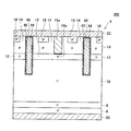
図7に示すように、本実施例のダイオード42は、実施例1のダイオード2と同様に、シリコンの半導体基板4を用いて形成されている。半導体基板4には、高濃度n型半導体領域であるn+カソード領域6と、n型半導体領域であるnバッファ領域8と、低濃度n型半導体領域であるn−ドリフト領域10と、n型半導体領域であるnバリア領域12と、p型半導体領域であるpアノード領域14が順に積層されている。半導体基板4の上側表面には、n型半導体領域であるnピラー領域16が、所定の間隔を隔てて複数形成されている。nピラー領域16は、pアノード領域14を貫通して、nバリア領域12の上側表面まで達するように形成されている。また、半導体基板4の上側には、複数のトレンチ44が所定の間隔で形成されている。それぞれのトレンチ44は、pアノード領域14の上側表面からnバリア領域12を貫通してn−ドリフト領域10の内部まで達している。トレンチ44の内部には、絶縁膜46によって被覆されたトレンチ電極48が充填されている。また、pアノード領域14の上側表面には、高濃度p型半導体領域であるp+コンタクト領域18が所定の間隔を隔てて複数形成されている。
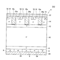
図8に示すように、本実施例のダイオード52は、実施例2のダイオード32と同様に、シリコンの半導体基板34を用いて形成されている。半導体基板34には、高濃度n型半導体領域であるn+カソード領域6と、n型半導体領域であるnバッファ領域8と、低濃度n型半導体領域であるn−ドリフト領域10と、p型半導体領域であるp電界進展防止領域36と、n型半導体領域であるnバリア領域12と、p型半導体領域であるpアノード領域14が順に積層されている。半導体基板34の上側表面には、n型半導体領域であるnピラー領域16が、所定の間隔を隔てて複数形成されている。nピラー領域16は、pアノード領域14を貫通して、nバリア領域12の上側表面まで達するように形成されている。また、半導体基板34の上側には、複数のトレンチ44が所定の間隔で形成されている。それぞれのトレンチ44は、pアノード領域14の上側表面からnバリア領域12とp電界進展防止領域36を貫通してn−ドリフト領域10の内部まで達している。トレンチ44の内部には、絶縁膜46によって被覆されたトレンチ電極48が充填されている。また、pアノード領域14の上側表面には、高濃度p型半導体領域であるp+コンタクト領域18が所定の間隔を隔てて複数形成されている。
図10に示すように、本実施例のダイオード62は、実施例4のダイオード52とほぼ同様の構成を備えている。本実施例のダイオード62では、n+カソード領域6に、高濃度p型半導体領域であるp+カソードショート領域64が、所定の間隔を隔てて複数形成されている点で、実施例4のダイオード52と異なる。本実施例では、p+カソードショート領域64の不純物濃度は1×10¹⁷〜5×10²⁰[cm-3]程度である。
図14に示すように、本実施例の半導体装置72は、実施例3のダイオード42とほぼ同様の構成を備えている。半導体装置72では、pアノード領域14の上側表面において、トレンチ44に隣接する箇所に、高濃度n型半導体領域であるn+エミッタ領域74が形成されている。本実施例では、n+エミッタ領域74の不純物濃度は1×10¹⁷〜5×10²⁰[cm-3]程度である。n+エミッタ領域74は、アノード電極22とオーミック接合によって接合している。
図15に示すように、本実施例の半導体装置82は、実施例4のダイオード52とほぼ同様の構成を備えている。半導体装置82では、pアノード領域14の上側表面において、トレンチ44に隣接する箇所に、n+エミッタ領域74が形成されている。n+エミッタ領域74は、アノード電極22とオーミック接合によって接合している。
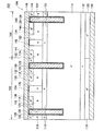
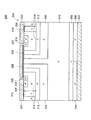
図16に示すように、本実施例の半導体装置102は、シリコンの半導体基板104を用いて形成されている。半導体装置102は、IGBT領域106と、ダイオード領域108を備えている。IGBT領域106において、半導体基板104は、高濃度p型半導体領域であるp+コレクタ領域110と、n型半導体領域であるnバッファ領域112と、低濃度n型半導体領域であるn−ドリフト領域114と、n型半導体領域であるnバリア領域116と、p型半導体領域であるpボディ領域118が順に積層されている。本実施例では、p+コレクタ領域110の不純物濃度は1×1017〜5×1020[cm-3]程度であり、nバッファ領域112の不純物濃度は1×10¹⁶〜1×10¹⁹[cm-3]程度であり、n−ドリフト領域114の不純物濃度は1×10¹²〜1×10¹⁵[cm-3]程度であり、nバリア領域116の不純物濃度は1×10¹⁵〜1×10¹⁸[cm-3]程度であり、pボディ領域118の不純物濃度は1×10¹⁶〜1×10¹⁹[cm-3]程度である。また、nバリア領域116の厚みは0.5〜3.0[μm]程度である。ダイオード領域108において、半導体基板104は、高濃度n型半導体領域であるn+カソード領域120と、nバッファ領域112と、n−ドリフト領域114と、nバリア領域122と、p型半導体領域であるpアノード領域124が順に積層されている。本実施例では、n+カソード領域120の不純物濃度は1×1017〜5×1020[cm-3]程度であり、nバリア領域122の不純物濃度は1×1015〜1×1018[cm-3]程度であり、pアノード領域124の不純物濃度は1×1016〜1×1019[cm-3]程度である。また、nバリア領域122の厚みは0.5〜3.0[μm]程度である。半導体基板4の上側には、複数のトレンチ126が所定の間隔で形成されている。
図17に示すように、本実施例の半導体装置162は、実施例8の半導体装置102とほぼ同様の構成を備えている。半導体装置162は、シリコンの半導体基板164を用いて形成されている。半導体基板164は、実施例8の半導体基板104とほぼ同様の構成を備えている。半導体基板164では、IGBT領域106において、n−ドリフト領域114とnバリア領域116の間に、p型半導体領域であるp電界進展防止領域166が形成されており、ダイオード領域108において、n−ドリフト領域114とnバリア領域122の間に、p型半導体領域であるp電界進展防止領域168が形成されている。p電界進展防止領域166およびp電界進展防止領域168の不純物濃度は1×10¹⁵〜1×10¹⁹[cm-3]程度である。また、p電界進展防止領域166およびp電界進展防止領域168の厚みは0.5〜3.0[μm]程度である。IGBT領域106において、トレンチ126は、pボディ領域118の上側表面からnバリア領域116およびp電界進展防止領域166を貫通して、n−ドリフト領域114の内部まで達している。ダイオード領域108において、トレンチ126は、pアノード領域124の上側表面からnバリア領域122およびp電界進展防止領域168を貫通して、n−ドリフト領域114の内部まで達している。
図19に示すように、本実施例の半導体装置172は、実施例8の半導体装置102とほぼ同様の構成を備えている。本実施例の半導体装置172では、ダイオード領域108のn+カソード領域120に、高濃度p型半導体領域であるp+カソードショート領域174が、所定の間隔を隔てて複数形成されている点で、実施例8の半導体装置102と異なる。本実施例では、p+カソードショート領域174の不純物濃度は1×10¹⁷〜5×10²⁰[cm-3]程度である。本実施例の半導体装置172によれば、順バイアスの印加時において、n+カソード領域120からn−ドリフト領域114への電子の注入が抑制されているので、実施例8の半導体装置102に比べて、逆回復電流をさらに小さくし、逆回復時間をさらに短くすることができる。本実施例の半導体装置172によれば、さらにスイッチング損失を小さくすることが出来る。
図20に示すように、本実施例の半導体装置182は、実施例9の半導体装置162とほぼ同様の構成を備えている。本実施例の半導体装置182では、ダイオード領域108のn+カソード領域120に、p+カソードショート領域174が、所定の間隔を隔てて複数形成されている点で、実施例9の半導体装置162と異なる。本実施例の半導体装置182によれば、順バイアスの印加時において、n+カソード領域120からn−ドリフト領域114への電子の注入が抑制されているので、実施例9の半導体装置162に比べて、逆回復電流をさらに小さくし、逆回復時間をさらに短くすることができる。本実施例の半導体装置182によれば、さらにスイッチング損失を小さくすることが出来る。
図21に示すように、本実施例の半導体装置202は、シリコンの半導体基板204を用いて形成されている。半導体基板204は、高濃度n型半導体領域であるn+カソード領域206と、n型半導体領域であるnバッファ領域208と、低濃度n型半導体領域であるn−ドリフト領域210が順に積層されている。本実施例では、n+カソード領域206の不純物濃度は1×10¹⁷〜5×10²⁰[cm-3]程度であり、nバッファ領域208の不純物濃度は1×10¹⁶〜1×10¹⁹[cm-3]程度であり、n−ドリフト領域210の不純物濃度は1×10¹²〜1×10¹⁵[cm-3]程度である。
図22に示すように、本実施例の半導体装置232は、実施例12の半導体装置202とほぼ同様の構成を備えている。本実施例の半導体装置232も、実施例12の半導体装置202と同様に、縦型のMOSFETの構造を有している。本実施例の半導体装置232では、n−ドリフト領域210とnバリア領域212の間に、p型半導体領域であるp電界進展防止領域234が形成されている。p電界進展防止領域234の不純物濃度は1×10¹⁵〜1×10¹⁹[cm-3]程度である。また、p電界進展防止領域234厚さは0.5〜3.0[μm]程度である。
図23に示すように、本実施例の半導体装置242は、実施例12の半導体装置202とほぼ同様の構成を備えている。本実施例の半導体装置242では、n+カソード領域206において、高濃度p型半導体領域であるp+コレクタ領域244が部分的に形成されている。本実施例では、p+コレクタ領域244の不純物濃度は1×10¹⁷〜5×10²⁰[cm-3]程度である。
図24に示すように、本実施例の半導体装置252は、実施例14の半導体装置242とほぼ同様の構成を備えている。本実施例の半導体装置252では、n−ドリフト領域210とnバリア領域212の間に、p型半導体領域であるp電界進展防止領域234が形成されている。p電界進展防止領域234の不純物濃度は1×10¹⁵〜1×10¹⁹[cm-3]程度である。また、p電界進展防止領域234厚さは0.5〜3.0[μm]程度である。半導体装置252は、プレーナ型のIGBTとフリーホイーリングダイオードが逆並列に接続された構造を有している。
図25に示すように、本実施例のダイオード302は、実施例1のダイオード2とほぼ同様の構成を備えている。本実施例のダイオード302は、nピラー領域16の代わりに、金属製のピラー電極16aを備えている。ピラー電極16aは、半導体基板4の上側表面にpアノード領域14を貫通してnバリア領域12まで達するトレンチを形成し、そのトレンチに金属を充填することで形成される。ピラー電極16aはアノード電極22と導通しており、nバリア領域12とショットキー界面24aを介してショットキー接合している。
図26に示すように、本実施例のダイオード304は、実施例2のダイオード32とほぼ同様の構成を備えている。本実施例のダイオード304は、nピラー領域16の代わりに、金属製のピラー電極16aを備えている。ピラー電極16aは、半導体基板34の上側表面にpアノード領域14を貫通してnバリア領域12まで達するトレンチを形成し、そのトレンチに金属を充填することで形成される。ピラー電極16aはアノード電極22と導通しており、nバリア領域12とショットキー界面24aを介してショットキー接合している。
図7に示すダイオード42、図8に示すダイオード52、図10に示すダイオード62、図11に示すダイオード66、図12に示すダイオード68、図13に示すダイオード70のそれぞれにおいて、nピラー領域16を上述のピラー電極16aで置き換えることによって、図27に示すダイオード306、図28に示すダイオード308、図29に示すダイオード310、図30に示すダイオード312、図31に示すダイオード314、図32に示すダイオード316のように構成することもできる。
Claims (6)
- カソード電極と、第1導電型の半導体からなるカソード領域と、前記カソード領域よりも濃度が低い第1導電型の半導体からなるドリフト領域と、第2導電型の半導体からなるアノード領域と、金属からなるアノード電極を備えるダイオードであって、
前記ドリフト領域と前記アノード領域の間に形成された、前記ドリフト領域よりも濃度が高い第1導電型の半導体からなるバリア領域と、
前記バリア領域と前記アノード電極を接続するように形成された、前記バリア領域よりも濃度が高い第1導電型の半導体からなるピラー領域を備えており、
前記ピラー領域が、前記アノード電極側から前記アノード領域を貫通して前記バリア領域まで達するように形成されており、
前記ピラー領域と前記アノード電極がショットキー接合していることを特徴とするダイオード。 - 前記バリア領域と前記ドリフト領域の間に形成された、第2導電型の半導体からなる電界進展防止領域をさらに備えていることを特徴とする請求項1のダイオード。
- 前記アノード領域から前記ドリフト領域まで達するトレンチが形成されており、
前記トレンチの内部に絶縁膜で被覆されたトレンチ電極が形成されていることを特徴とする請求項1または2のダイオード。 - 前記カソード領域に部分的に形成された、第2導電型の半導体からなるカソードショート領域をさらに備えていることを特徴とする請求項1から3の何れか一項のダイオード。
- 請求項1から4の何れか一項のダイオードとIGBTが一体化された半導体装置であって、
前記IGBTが、コレクタ電極と、第2導電型の半導体からなるコレクタ領域と、前記ドリフト領域から連続しており、第1導電型の半導体からなる第2ドリフト領域と、第2導電型の半導体からなるボディ領域と、第1導電型の半導体からなるエミッタ領域と、金属からなるエミッタ電極と、前記エミッタ領域と前記第2ドリフト領域の間の前記ボディ領域に対して絶縁膜を挟んで対向するゲート電極を備えており、
前記IGBTが、前記第2ドリフト領域と前記ボディ領域の間に形成された、前記第2ドリフト領域よりも濃度が高い第1導電型の半導体からなる第2バリア領域と、前記第2バリア領域と前記エミッタ電極を接続するように形成された、前記第2バリア領域よりも濃度が高い第1導電型の半導体からなる第2ピラー領域を備えており、
前記第2ピラー領域が、前記エミッタ電極側から前記ボディ領域を貫通して前記第2バリア領域まで達するように形成されており、
前記第2ピラー領域と前記エミッタ電極がショットキー接合していることを特徴とする半導体装置。 - 前記第2バリア領域と前記第2ドリフト領域の間に形成された、第2導電型の半導体からなる第2電界進展防止領域をさらに備えることを特徴とする請求項5の半導体装置。
Priority Applications (9)
| Application Number | Priority Date | Filing Date | Title |
|---|---|---|---|
| DE112012003111.3T DE112012003111B4 (de) | 2011-07-27 | 2012-07-27 | Diode, Halbleitervorrichtung und Mosfet |
| DE112012007322.3T DE112012007322B3 (de) | 2011-07-27 | 2012-07-27 | Diode, Halbleitervorrichtung und MOSFET |
| CN201611257527.8A CN107068733B (zh) | 2011-07-27 | 2012-07-27 | 半导体器件 |
| JP2012166576A JP5919121B2 (ja) | 2011-07-27 | 2012-07-27 | ダイオードおよび半導体装置 |
| CN201280035577.5A CN103890955B (zh) | 2011-07-27 | 2012-07-27 | 半导体器件 |
| US14/113,276 US9520465B2 (en) | 2011-07-27 | 2012-07-27 | Diode, semiconductor device, and MOSFET |
| PCT/JP2012/004804 WO2013014943A2 (en) | 2011-07-27 | 2012-07-27 | Diode, semiconductor device, and mosfet |
| US15/342,858 US10147812B2 (en) | 2011-07-27 | 2016-11-03 | Diode, semiconductor device, and MOSFET |
| US16/111,745 US10658503B2 (en) | 2011-07-27 | 2018-08-24 | Diode, semiconductor device, and MOSFET |
Applications Claiming Priority (3)
| Application Number | Priority Date | Filing Date | Title |
|---|---|---|---|
| JP2011164746 | 2011-07-27 | ||
| JP2011164746 | 2011-07-27 | ||
| JP2012166576A JP5919121B2 (ja) | 2011-07-27 | 2012-07-27 | ダイオードおよび半導体装置 |
Related Child Applications (2)
| Application Number | Title | Priority Date | Filing Date |
|---|---|---|---|
| JP2015153160A Division JP6011696B2 (ja) | 2011-07-27 | 2015-08-03 | ダイオード、半導体装置およびmosfet |
| JP2015153159A Division JP6001735B2 (ja) | 2011-07-27 | 2015-08-03 | Mosfet |
Publications (2)
| Publication Number | Publication Date |
|---|---|
| JP2013048230A JP2013048230A (ja) | 2013-03-07 |
| JP5919121B2 true JP5919121B2 (ja) | 2016-05-18 |
Family
ID=47143235
Family Applications (1)
| Application Number | Title | Priority Date | Filing Date |
|---|---|---|---|
| JP2012166576A Active JP5919121B2 (ja) | 2011-07-27 | 2012-07-27 | ダイオードおよび半導体装置 |
Country Status (5)
| Country | Link |
|---|---|
| US (3) | US9520465B2 (ja) |
| JP (1) | JP5919121B2 (ja) |
| CN (2) | CN103890955B (ja) |
| DE (2) | DE112012007322B3 (ja) |
| WO (1) | WO2013014943A2 (ja) |
Cited By (3)
| Publication number | Priority date | Publication date | Assignee | Title |
|---|---|---|---|---|
| JP2019149511A (ja) * | 2018-02-28 | 2019-09-05 | 株式会社 日立パワーデバイス | 半導体装置および電力変換装置 |
| JP2021040071A (ja) * | 2019-09-04 | 2021-03-11 | 株式会社デンソー | 半導体装置 |
| JP2021040070A (ja) * | 2019-09-04 | 2021-03-11 | 株式会社デンソー | 半導体装置 |
Families Citing this family (113)
| Publication number | Priority date | Publication date | Assignee | Title |
|---|---|---|---|---|
| JP5815882B2 (ja) * | 2012-09-06 | 2015-11-17 | 三菱電機株式会社 | 半導体装置 |
| US9219138B2 (en) | 2012-10-05 | 2015-12-22 | Semiconductor Components Industries, Llc | Semiconductor device having localized charge balance structure and method |
| KR101427948B1 (ko) * | 2012-12-18 | 2014-08-08 | 현대자동차 주식회사 | 쇼트키 배리어 다이오드 및 그 제조 방법 |
| JP5981859B2 (ja) * | 2013-02-15 | 2016-08-31 | 株式会社豊田中央研究所 | ダイオード及びダイオードを内蔵する半導体装置 |
| US9577086B2 (en) | 2013-04-03 | 2017-02-21 | Mitsubishi Electric Corporation | Semiconductor device |
| WO2014188569A1 (ja) * | 2013-05-23 | 2014-11-27 | トヨタ自動車株式会社 | ダイオード内蔵igbt |
| US9331197B2 (en) | 2013-08-08 | 2016-05-03 | Cree, Inc. | Vertical power transistor device |
| WO2015029116A1 (ja) * | 2013-08-26 | 2015-03-05 | トヨタ自動車株式会社 | 半導体装置 |
| JP6242633B2 (ja) * | 2013-09-03 | 2017-12-06 | 株式会社東芝 | 半導体装置 |
| JP2015056486A (ja) | 2013-09-11 | 2015-03-23 | 株式会社東芝 | 半導体装置およびその製造方法 |
| US10868169B2 (en) | 2013-09-20 | 2020-12-15 | Cree, Inc. | Monolithically integrated vertical power transistor and bypass diode |
| US10600903B2 (en) | 2013-09-20 | 2020-03-24 | Cree, Inc. | Semiconductor device including a power transistor device and bypass diode |
| US9318597B2 (en) | 2013-09-20 | 2016-04-19 | Cree, Inc. | Layout configurations for integrating schottky contacts into a power transistor device |
| CN104465791B (zh) * | 2013-09-22 | 2018-10-26 | 南京励盛半导体科技有限公司 | 一种快恢复二极管的结构和背面的制备方法 |
| DE102013220011B4 (de) * | 2013-10-02 | 2025-01-02 | Robert Bosch Gmbh | Halbleiteranordnung mit temperaturkompensierter Durchbruchsspannung |
| WO2015050262A1 (ja) | 2013-10-04 | 2015-04-09 | 富士電機株式会社 | 半導体装置 |
| JP6154292B2 (ja) * | 2013-11-06 | 2017-06-28 | トヨタ自動車株式会社 | 半導体装置及び半導体装置の製造方法 |
| JP6311723B2 (ja) * | 2013-12-16 | 2018-04-18 | 富士電機株式会社 | 半導体装置および半導体装置の製造方法 |
| JP5918288B2 (ja) * | 2014-03-03 | 2016-05-18 | トヨタ自動車株式会社 | 半導体装置 |
| JP2015170654A (ja) * | 2014-03-05 | 2015-09-28 | 株式会社東芝 | 半導体装置 |
| US9634128B2 (en) | 2014-03-17 | 2017-04-25 | Kabushiki Kaisha Toshiba | Semiconductor device |
| KR20150108291A (ko) * | 2014-03-17 | 2015-09-25 | 가부시끼가이샤 도시바 | 반도체 장치 |
| JP6237408B2 (ja) * | 2014-03-28 | 2017-11-29 | 住友電気工業株式会社 | 炭化珪素半導体装置およびその製造方法 |
| US10608104B2 (en) * | 2014-03-28 | 2020-03-31 | Infineon Technologies Ag | Trench transistor device |
| JP2015216200A (ja) * | 2014-05-09 | 2015-12-03 | 株式会社豊田中央研究所 | 半導体装置 |
| JP2015216270A (ja) * | 2014-05-12 | 2015-12-03 | ローム株式会社 | 半導体装置および半導体装置の製造方法 |
| JP2016009712A (ja) * | 2014-06-23 | 2016-01-18 | 住友電気工業株式会社 | 炭化珪素半導体装置 |
| JP6036765B2 (ja) | 2014-08-22 | 2016-11-30 | トヨタ自動車株式会社 | 半導体装置及び半導体装置の製造方法 |
| JP6135636B2 (ja) * | 2014-10-17 | 2017-05-31 | トヨタ自動車株式会社 | 半導体装置 |
| JP6003961B2 (ja) * | 2014-11-04 | 2016-10-05 | トヨタ自動車株式会社 | 半導体装置 |
| CN104393056B (zh) * | 2014-11-10 | 2017-02-15 | 电子科技大学 | 一种积累型二极管 |
| JP6164201B2 (ja) | 2014-11-17 | 2017-07-19 | トヨタ自動車株式会社 | 半導体装置 |
| JP2016096307A (ja) * | 2014-11-17 | 2016-05-26 | トヨタ自動車株式会社 | 半導体装置 |
| JP6053050B2 (ja) | 2014-12-12 | 2016-12-27 | 株式会社豊田中央研究所 | 逆導通igbt |
| JP6063915B2 (ja) * | 2014-12-12 | 2017-01-18 | 株式会社豊田中央研究所 | 逆導通igbt |
| DE102014226161B4 (de) * | 2014-12-17 | 2017-10-26 | Infineon Technologies Ag | Halbleitervorrichtung mit Überlaststrombelastbarkeit |
| US10510904B2 (en) * | 2015-02-09 | 2019-12-17 | Mitsubishi Electric Corporation | Semiconductor device with backside N-type layer at active region/termination region boundary and extending into action region |
| JP6152861B2 (ja) * | 2015-02-09 | 2017-06-28 | トヨタ自動車株式会社 | ダイオードの製造方法 |
| CN107068742B (zh) * | 2015-03-02 | 2020-04-21 | 常州中明半导体技术有限公司 | 具有不连续p型基区嵌入原胞结构的半导体器件 |
| JP6293688B2 (ja) * | 2015-03-02 | 2018-03-14 | 株式会社豊田中央研究所 | ダイオード及びそのダイオードを内蔵する逆導通igbt |
| JP6222140B2 (ja) | 2015-03-04 | 2017-11-01 | トヨタ自動車株式会社 | 半導体装置 |
| JP6126150B2 (ja) | 2015-03-06 | 2017-05-10 | トヨタ自動車株式会社 | 半導体装置 |
| US9929260B2 (en) | 2015-05-15 | 2018-03-27 | Fuji Electric Co., Ltd. | IGBT semiconductor device |
| US10217738B2 (en) * | 2015-05-15 | 2019-02-26 | Smk Corporation | IGBT semiconductor device |
| JP6185511B2 (ja) | 2015-05-26 | 2017-08-23 | トヨタ自動車株式会社 | 半導体装置 |
| JP6274154B2 (ja) * | 2015-05-27 | 2018-02-07 | トヨタ自動車株式会社 | 逆導通igbt |
| JP6213522B2 (ja) * | 2015-06-03 | 2017-10-18 | トヨタ自動車株式会社 | 半導体装置 |
| CN106298774A (zh) * | 2015-06-10 | 2017-01-04 | 北大方正集团有限公司 | 一种mps二极管及其制造方法 |
| JP6217700B2 (ja) * | 2015-07-21 | 2017-10-25 | トヨタ自動車株式会社 | ダイオード |
| JP6217708B2 (ja) | 2015-07-30 | 2017-10-25 | トヨタ自動車株式会社 | 半導体装置とその製造方法 |
| JP6441192B2 (ja) * | 2015-09-11 | 2018-12-19 | 株式会社東芝 | 半導体装置 |
| JP6281548B2 (ja) * | 2015-09-17 | 2018-02-21 | トヨタ自動車株式会社 | 半導体装置 |
| DE102015120210B4 (de) * | 2015-11-23 | 2019-02-21 | Infineon Technologies Ag | Leistungshalbleitertransistor mit vergrößerter bipolarer Verstärkung |
| JP6304221B2 (ja) * | 2015-12-08 | 2018-04-04 | トヨタ自動車株式会社 | Igbt |
| WO2017099096A1 (ja) * | 2015-12-11 | 2017-06-15 | 富士電機株式会社 | 半導体装置 |
| JP6658021B2 (ja) * | 2016-02-03 | 2020-03-04 | 株式会社デンソー | 半導体装置 |
| WO2017149607A1 (ja) * | 2016-02-29 | 2017-09-08 | 三菱電機株式会社 | 半導体装置 |
| JP6846119B2 (ja) * | 2016-05-02 | 2021-03-24 | 株式会社 日立パワーデバイス | ダイオード、およびそれを用いた電力変換装置 |
| US9768247B1 (en) | 2016-05-06 | 2017-09-19 | Semiconductor Components Industries, Llc | Semiconductor device having improved superjunction trench structure and method of manufacture |
| DE102016112721B4 (de) | 2016-07-12 | 2022-02-03 | Infineon Technologies Ag | n-Kanal-Leistungshalbleitervorrichtung mit p-Schicht im Driftvolumen |
| US9935188B2 (en) * | 2016-07-22 | 2018-04-03 | Pakal Technologies Llc | Insulated gate turn-off device with turn-off Schottky-Barrier MOSFET |
| JP6702423B2 (ja) | 2016-08-12 | 2020-06-03 | 富士電機株式会社 | 半導体装置および半導体装置の製造方法 |
| JP6805655B2 (ja) * | 2016-09-07 | 2020-12-23 | 富士電機株式会社 | 半導体装置 |
| WO2018074425A1 (ja) * | 2016-10-17 | 2018-04-26 | 富士電機株式会社 | 半導体装置 |
| JP6589817B2 (ja) | 2016-10-26 | 2019-10-16 | 株式会社デンソー | 半導体装置 |
| JP6939300B2 (ja) * | 2016-11-17 | 2021-09-22 | 富士電機株式会社 | 半導体装置 |
| EP3324443B1 (en) * | 2016-11-17 | 2019-09-11 | Fuji Electric Co., Ltd. | Semiconductor device |
| JP6784164B2 (ja) * | 2016-12-15 | 2020-11-11 | 株式会社豊田中央研究所 | 半導体装置 |
| DE102016125879B3 (de) * | 2016-12-29 | 2018-06-21 | Infineon Technologies Ag | Halbleitervorrichtung mit einer IGBT-Region und einer nicht schaltbaren Diodenregion |
| JP6852541B2 (ja) * | 2017-04-20 | 2021-03-31 | 株式会社デンソー | 半導体装置 |
| US10439054B2 (en) * | 2017-06-29 | 2019-10-08 | Kabushiki Kaisha Toshiba | Insulated gate bipolar transistor |
| CN107359125A (zh) * | 2017-07-03 | 2017-11-17 | 苏州达晶微电子有限公司 | 一种优化体二极管反向恢复特性的方法及装置 |
| DE102017118665A1 (de) * | 2017-08-16 | 2019-02-21 | Infineon Technologies Ag | Rc-igbt |
| JP6740986B2 (ja) * | 2017-08-31 | 2020-08-19 | 株式会社デンソー | 炭化珪素半導体装置およびその製造方法 |
| JP6946922B2 (ja) * | 2017-10-18 | 2021-10-13 | 株式会社デンソー | 半導体装置 |
| JP7334407B2 (ja) * | 2017-12-28 | 2023-08-29 | 富士電機株式会社 | 半導体装置および半導体装置の製造方法 |
| CN109979935B (zh) * | 2017-12-28 | 2025-04-22 | 富士电机株式会社 | 半导体装置及半导体装置的制造方法 |
| JP7151084B2 (ja) | 2018-01-11 | 2022-10-12 | 株式会社デンソー | 半導体装置 |
| JP7095303B2 (ja) | 2018-02-14 | 2022-07-05 | 富士電機株式会社 | 半導体装置 |
| DE102018103973B4 (de) * | 2018-02-22 | 2020-12-03 | Infineon Technologies Ag | Siliziumcarbid-halbleiterbauelement |
| JP7119422B2 (ja) * | 2018-02-28 | 2022-08-17 | 富士電機株式会社 | 縦型半導体装置及び縦型半導体装置の製造方法 |
| US10608122B2 (en) * | 2018-03-13 | 2020-03-31 | Semicondutor Components Industries, Llc | Schottky device and method of manufacture |
| JP6935351B2 (ja) * | 2018-03-20 | 2021-09-15 | 株式会社東芝 | 半導体装置 |
| DE102018106967B3 (de) * | 2018-03-23 | 2019-05-23 | Infineon Technologies Ag | SILIZIUMCARBID HALBLEITERBAUELEMENT und Halbleiterdiode |
| JP7263740B2 (ja) * | 2018-11-06 | 2023-04-25 | 富士電機株式会社 | 炭化珪素半導体装置および炭化珪素半導体装置の製造方法 |
| DE112018008178T5 (de) | 2018-11-30 | 2021-09-02 | Mitsubishi Electric Corporation | Halbleitereinheit |
| CN110416319B (zh) * | 2019-08-21 | 2023-05-05 | 江苏中科君芯科技有限公司 | 双面肖特基控制的快恢复二极管器件及制备方法 |
| WO2021038699A1 (ja) * | 2019-08-26 | 2021-03-04 | 株式会社デンソー | 半導体装置とその製造方法 |
| US11469333B1 (en) * | 2020-02-19 | 2022-10-11 | Semiq Incorporated | Counter-doped silicon carbide Schottky barrier diode |
| US10910478B1 (en) * | 2020-03-04 | 2021-02-02 | Shuming Xu | Metal-oxide-semiconductor field-effect transistor having enhanced high-frequency performance |
| JP7296907B2 (ja) * | 2020-03-10 | 2023-06-23 | 株式会社東芝 | 半導体装置 |
| JP7359053B2 (ja) * | 2020-03-26 | 2023-10-11 | 三菱電機株式会社 | 半導体装置 |
| US12166111B2 (en) | 2020-06-18 | 2024-12-10 | Dynex Semiconductor Limited | Reverse conducting IGBT with controlled anode injection |
| WO2022013991A1 (ja) | 2020-07-16 | 2022-01-20 | 三菱電機株式会社 | 電力用半導体装置 |
| JP7486373B2 (ja) * | 2020-07-29 | 2024-05-17 | 三菱電機株式会社 | 半導体装置 |
| JP7528687B2 (ja) * | 2020-09-30 | 2024-08-06 | 三菱電機株式会社 | 半導体装置 |
| JP7370309B2 (ja) * | 2020-10-21 | 2023-10-27 | 三菱電機株式会社 | 逆導通型半導体装置および逆導通型半導体装置の製造方法 |
| US11769828B2 (en) | 2020-10-28 | 2023-09-26 | Wolfspeed, Inc. | Gate trench power semiconductor devices having improved deep shield connection patterns |
| US11610991B2 (en) | 2020-10-28 | 2023-03-21 | Wolfspeed, Inc. | Gate trench power semiconductor devices having improved deep shield connection patterns |
| US12080790B2 (en) * | 2020-10-28 | 2024-09-03 | Wolfspeed, Inc. | Power semiconductor devices including angled gate trenches |
| JP7528743B2 (ja) * | 2020-11-27 | 2024-08-06 | 三菱電機株式会社 | 半導体装置 |
| JP7456520B2 (ja) * | 2020-12-07 | 2024-03-27 | 富士電機株式会社 | 半導体装置 |
| DE102021000610A1 (de) * | 2021-02-08 | 2022-08-11 | 3-5 Power Electronics GmbH | Stapelförmige III-V-Halbleiterdiode |
| JP7476129B2 (ja) * | 2021-03-12 | 2024-04-30 | 株式会社東芝 | 半導体装置及び半導体回路 |
| JP7517218B2 (ja) * | 2021-03-24 | 2024-07-17 | 株式会社デンソー | 半導体装置 |
| JP7701610B2 (ja) * | 2021-09-02 | 2025-07-02 | ミネベアパワーデバイス株式会社 | 半導体装置、半導体装置の製造方法、電力変換装置 |
| JP7574161B2 (ja) | 2021-09-22 | 2024-10-28 | 株式会社東芝 | 半導体装置 |
| JP7799575B2 (ja) * | 2022-03-22 | 2026-01-15 | 株式会社東芝 | 半導体装置 |
| JP7754783B2 (ja) * | 2022-09-07 | 2025-10-15 | 株式会社東芝 | 半導体装置 |
| CN116632053B (zh) * | 2023-07-25 | 2024-01-30 | 深圳市美浦森半导体有限公司 | 一种rc-igbt器件的控制方法 |
| WO2025134384A1 (ja) * | 2023-12-22 | 2025-06-26 | サンケン電気株式会社 | 半導体装置及び電子機器 |
| JP2025122257A (ja) * | 2024-02-08 | 2025-08-21 | ミネベアパワーデバイス株式会社 | 半導体装置、半導体装置の製造方法 |
| CN118553763B (zh) * | 2024-07-24 | 2024-10-18 | 江西萨瑞微电子技术有限公司 | 一种sgt器件制备方法及外延片 |
Family Cites Families (19)
| Publication number | Priority date | Publication date | Assignee | Title |
|---|---|---|---|---|
| GB1558506A (en) | 1976-08-09 | 1980-01-03 | Mullard Ltd | Semiconductor devices having a rectifying metalto-semicondductor junction |
| JPH0286173A (ja) | 1988-09-22 | 1990-03-27 | Fuji Electric Co Ltd | 半導体ダイオード |
| US5998833A (en) * | 1998-10-26 | 1999-12-07 | North Carolina State University | Power semiconductor devices having improved high frequency switching and breakdown characteristics |
| JP3968912B2 (ja) | 1999-05-10 | 2007-08-29 | 富士電機デバイステクノロジー株式会社 | ダイオード |
| US6252258B1 (en) | 1999-08-10 | 2001-06-26 | Rockwell Science Center Llc | High power rectifier |
| JP2003163357A (ja) | 2001-11-26 | 2003-06-06 | Fuji Electric Co Ltd | 半導体装置およびその製造方法 |
| JP4047153B2 (ja) | 2002-12-03 | 2008-02-13 | 株式会社東芝 | 半導体装置 |
| EP2546865B1 (en) * | 2005-09-16 | 2023-12-06 | Wolfspeed, Inc. | Methods of processing semiconductor wafers having silicon carbide power devices thereon |
| JP2008066708A (ja) | 2006-08-09 | 2008-03-21 | Toshiba Corp | 半導体装置 |
| US7595241B2 (en) * | 2006-08-23 | 2009-09-29 | General Electric Company | Method for fabricating silicon carbide vertical MOSFET devices |
| JP4532536B2 (ja) * | 2007-12-19 | 2010-08-25 | トヨタ自動車株式会社 | 半導体装置 |
| KR100936808B1 (ko) * | 2007-12-26 | 2010-01-14 | 주식회사 하이닉스반도체 | 저 시트저항 워드라인과 수직채널트랜지스터를 구비한반도체소자 및 그 제조 방법 |
| JP5617175B2 (ja) | 2008-04-17 | 2014-11-05 | 富士電機株式会社 | ワイドバンドギャップ半導体装置とその製造方法 |
| JP5206096B2 (ja) * | 2008-04-25 | 2013-06-12 | トヨタ自動車株式会社 | ダイオードとそのダイオードを備えている半導体装置 |
| WO2010143288A1 (ja) * | 2009-06-11 | 2010-12-16 | トヨタ自動車株式会社 | 半導体装置 |
| US7910486B2 (en) * | 2009-06-12 | 2011-03-22 | Alpha & Omega Semiconductor, Inc. | Method for forming nanotube semiconductor devices |
| JP5706275B2 (ja) * | 2011-08-31 | 2015-04-22 | 株式会社豊田中央研究所 | ダイオード、半導体装置およびmosfet |
| JP2013051345A (ja) * | 2011-08-31 | 2013-03-14 | Toyota Central R&D Labs Inc | ダイオード、半導体装置およびmosfet |
| JP5753814B2 (ja) * | 2012-04-16 | 2015-07-22 | 株式会社豊田中央研究所 | ダイオード、半導体装置およびmosfet |
-
2012
- 2012-07-27 CN CN201280035577.5A patent/CN103890955B/zh active Active
- 2012-07-27 WO PCT/JP2012/004804 patent/WO2013014943A2/en not_active Ceased
- 2012-07-27 US US14/113,276 patent/US9520465B2/en active Active
- 2012-07-27 DE DE112012007322.3T patent/DE112012007322B3/de active Active
- 2012-07-27 DE DE112012003111.3T patent/DE112012003111B4/de active Active
- 2012-07-27 CN CN201611257527.8A patent/CN107068733B/zh active Active
- 2012-07-27 JP JP2012166576A patent/JP5919121B2/ja active Active
-
2016
- 2016-11-03 US US15/342,858 patent/US10147812B2/en active Active
-
2018
- 2018-08-24 US US16/111,745 patent/US10658503B2/en active Active
Cited By (7)
| Publication number | Priority date | Publication date | Assignee | Title |
|---|---|---|---|---|
| JP2019149511A (ja) * | 2018-02-28 | 2019-09-05 | 株式会社 日立パワーデバイス | 半導体装置および電力変換装置 |
| WO2019167543A1 (ja) * | 2018-02-28 | 2019-09-06 | 株式会社 日立パワーデバイス | 半導体装置および電力変換装置 |
| US11282937B2 (en) | 2018-02-28 | 2022-03-22 | Hitachi Power Semiconductor Device, Ltd. | Semiconductor device and power conversion device |
| JP2021040071A (ja) * | 2019-09-04 | 2021-03-11 | 株式会社デンソー | 半導体装置 |
| JP2021040070A (ja) * | 2019-09-04 | 2021-03-11 | 株式会社デンソー | 半導体装置 |
| JP7172920B2 (ja) | 2019-09-04 | 2022-11-16 | 株式会社デンソー | 半導体装置 |
| JP7294004B2 (ja) | 2019-09-04 | 2023-06-20 | 株式会社デンソー | 半導体装置 |
Also Published As
| Publication number | Publication date |
|---|---|
| DE112012003111T5 (de) | 2014-04-10 |
| US20170098700A1 (en) | 2017-04-06 |
| WO2013014943A3 (en) | 2013-05-02 |
| US20140048847A1 (en) | 2014-02-20 |
| CN107068733B (zh) | 2020-08-11 |
| US10147812B2 (en) | 2018-12-04 |
| DE112012003111B4 (de) | 2024-12-05 |
| US9520465B2 (en) | 2016-12-13 |
| DE112012007322B3 (de) | 2022-06-09 |
| WO2013014943A2 (en) | 2013-01-31 |
| US10658503B2 (en) | 2020-05-19 |
| CN103890955B (zh) | 2017-06-13 |
| CN103890955A (zh) | 2014-06-25 |
| CN107068733A (zh) | 2017-08-18 |
| US20180374947A1 (en) | 2018-12-27 |
| JP2013048230A (ja) | 2013-03-07 |
Similar Documents
| Publication | Publication Date | Title |
|---|---|---|
| JP5919121B2 (ja) | ダイオードおよび半導体装置 | |
| JP5981859B2 (ja) | ダイオード及びダイオードを内蔵する半導体装置 | |
| JP6011696B2 (ja) | ダイオード、半導体装置およびmosfet | |
| JP5753814B2 (ja) | ダイオード、半導体装置およびmosfet | |
| JP5922886B2 (ja) | ダイオードおよび半導体装置 | |
| JP5787853B2 (ja) | 電力用半導体装置 | |
| CN102473705B (zh) | 半导体装置 | |
| CN105322002B (zh) | 反向传导igbt | |
| CN105702718B (zh) | 反向导通绝缘栅双极性晶体管 | |
| JP6053050B2 (ja) | 逆導通igbt | |
| US9082815B2 (en) | Semiconductor device having carrier extraction in electric field alleviating layer | |
| JP2013051345A (ja) | ダイオード、半導体装置およびmosfet | |
| JP5706275B2 (ja) | ダイオード、半導体装置およびmosfet | |
| WO2014112239A1 (ja) | 半導体素子 | |
| JP6674395B2 (ja) | 半導体装置 | |
| WO2015008458A1 (ja) | 半導体装置 | |
| JP6077309B2 (ja) | ダイオード及びダイオードを内蔵した半導体装置 | |
| JP6406274B2 (ja) | 半導体装置 | |
| JP2016149429A (ja) | 逆導通igbt | |
| US20140159106A1 (en) | Power semiconductor device and method for manufacturing the same | |
| JP2009182205A (ja) | 半導体装置 | |
| JP2017199723A (ja) | 半導体装置 |
Legal Events
| Date | Code | Title | Description |
|---|---|---|---|
| A621 | Written request for application examination |
Free format text: JAPANESE INTERMEDIATE CODE: A621 Effective date: 20130917 |
|
| A131 | Notification of reasons for refusal |
Free format text: JAPANESE INTERMEDIATE CODE: A131 Effective date: 20141111 |
|
| A131 | Notification of reasons for refusal |
Free format text: JAPANESE INTERMEDIATE CODE: A131 Effective date: 20150602 |
|
| A521 | Request for written amendment filed |
Free format text: JAPANESE INTERMEDIATE CODE: A523 Effective date: 20150803 |
|
| TRDD | Decision of grant or rejection written | ||
| A01 | Written decision to grant a patent or to grant a registration (utility model) |
Free format text: JAPANESE INTERMEDIATE CODE: A01 Effective date: 20160405 |
|
| A61 | First payment of annual fees (during grant procedure) |
Free format text: JAPANESE INTERMEDIATE CODE: A61 Effective date: 20160411 |
|
| R150 | Certificate of patent or registration of utility model |
Ref document number: 5919121 Country of ref document: JP Free format text: JAPANESE INTERMEDIATE CODE: R150 |
|
| R250 | Receipt of annual fees |
Free format text: JAPANESE INTERMEDIATE CODE: R250 |
|
| R250 | Receipt of annual fees |
Free format text: JAPANESE INTERMEDIATE CODE: R250 |
|
| S111 | Request for change of ownership or part of ownership |
Free format text: JAPANESE INTERMEDIATE CODE: R313117 |
|
| R350 | Written notification of registration of transfer |
Free format text: JAPANESE INTERMEDIATE CODE: R350 |
|
| R250 | Receipt of annual fees |
Free format text: JAPANESE INTERMEDIATE CODE: R250 |
|
| R250 | Receipt of annual fees |
Free format text: JAPANESE INTERMEDIATE CODE: R250 |
|
| R250 | Receipt of annual fees |
Free format text: JAPANESE INTERMEDIATE CODE: R250 |
|
| R250 | Receipt of annual fees |
Free format text: JAPANESE INTERMEDIATE CODE: R250 |
|
| R250 | Receipt of annual fees |
Free format text: JAPANESE INTERMEDIATE CODE: R250 |