JP6036765B2 - 半導体装置及び半導体装置の製造方法 - Google Patents
半導体装置及び半導体装置の製造方法 Download PDFInfo
- Publication number
- JP6036765B2 JP6036765B2 JP2014169454A JP2014169454A JP6036765B2 JP 6036765 B2 JP6036765 B2 JP 6036765B2 JP 2014169454 A JP2014169454 A JP 2014169454A JP 2014169454 A JP2014169454 A JP 2014169454A JP 6036765 B2 JP6036765 B2 JP 6036765B2
- Authority
- JP
- Japan
- Prior art keywords
- electrode
- insulating film
- semiconductor substrate
- interlayer insulating
- schottky
- Prior art date
- Legal status (The legal status is an assumption and is not a legal conclusion. Google has not performed a legal analysis and makes no representation as to the accuracy of the status listed.)
- Active
Links
- 239000004065 semiconductor Substances 0.000 title claims description 132
- 238000004519 manufacturing process Methods 0.000 title claims description 24
- 239000011229 interlayer Substances 0.000 claims description 75
- 239000000758 substrate Substances 0.000 claims description 68
- 229910052751 metal Inorganic materials 0.000 claims description 32
- 239000002184 metal Substances 0.000 claims description 32
- 238000005530 etching Methods 0.000 claims description 31
- 239000010410 layer Substances 0.000 claims description 29
- 230000004888 barrier function Effects 0.000 claims description 27
- 238000000034 method Methods 0.000 claims description 15
- 210000000746 body region Anatomy 0.000 description 29
- 238000010586 diagram Methods 0.000 description 11
- 239000012535 impurity Substances 0.000 description 6
- 239000000463 material Substances 0.000 description 6
- 229910018503 SF6 Inorganic materials 0.000 description 5
- SFZCNBIFKDRMGX-UHFFFAOYSA-N sulfur hexafluoride Chemical compound FS(F)(F)(F)(F)F SFZCNBIFKDRMGX-UHFFFAOYSA-N 0.000 description 5
- NRTOMJZYCJJWKI-UHFFFAOYSA-N Titanium nitride Chemical compound [Ti]#N NRTOMJZYCJJWKI-UHFFFAOYSA-N 0.000 description 3
- 238000005516 engineering process Methods 0.000 description 3
- KDLHZDBZIXYQEI-UHFFFAOYSA-N palladium Substances [Pd] KDLHZDBZIXYQEI-UHFFFAOYSA-N 0.000 description 3
- 238000011084 recovery Methods 0.000 description 2
- 229960000909 sulfur hexafluoride Drugs 0.000 description 2
- 229910052782 aluminium Inorganic materials 0.000 description 1
- XAGFODPZIPBFFR-UHFFFAOYSA-N aluminium Chemical compound [Al] XAGFODPZIPBFFR-UHFFFAOYSA-N 0.000 description 1
- 230000015572 biosynthetic process Effects 0.000 description 1
- 239000003795 chemical substances by application Substances 0.000 description 1
- 238000005468 ion implantation Methods 0.000 description 1
- 238000012986 modification Methods 0.000 description 1
- 230000004048 modification Effects 0.000 description 1
- 229910052763 palladium Inorganic materials 0.000 description 1
- 238000004544 sputter deposition Methods 0.000 description 1
- WFKWXMTUELFFGS-UHFFFAOYSA-N tungsten Chemical compound [W] WFKWXMTUELFFGS-UHFFFAOYSA-N 0.000 description 1
- 229910052721 tungsten Inorganic materials 0.000 description 1
- 239000010937 tungsten Substances 0.000 description 1
Images


Classifications
-
- H—ELECTRICITY
- H01—ELECTRIC ELEMENTS
- H01L—SEMICONDUCTOR DEVICES NOT COVERED BY CLASS H10
- H01L27/00—Devices consisting of a plurality of semiconductor or other solid-state components formed in or on a common substrate
- H01L27/02—Devices consisting of a plurality of semiconductor or other solid-state components formed in or on a common substrate including semiconductor components specially adapted for rectifying, oscillating, amplifying or switching and having at least one potential-jump barrier or surface barrier; including integrated passive circuit elements with at least one potential-jump barrier or surface barrier
- H01L27/04—Devices consisting of a plurality of semiconductor or other solid-state components formed in or on a common substrate including semiconductor components specially adapted for rectifying, oscillating, amplifying or switching and having at least one potential-jump barrier or surface barrier; including integrated passive circuit elements with at least one potential-jump barrier or surface barrier the substrate being a semiconductor body
- H01L27/06—Devices consisting of a plurality of semiconductor or other solid-state components formed in or on a common substrate including semiconductor components specially adapted for rectifying, oscillating, amplifying or switching and having at least one potential-jump barrier or surface barrier; including integrated passive circuit elements with at least one potential-jump barrier or surface barrier the substrate being a semiconductor body including a plurality of individual components in a non-repetitive configuration
- H01L27/0611—Devices consisting of a plurality of semiconductor or other solid-state components formed in or on a common substrate including semiconductor components specially adapted for rectifying, oscillating, amplifying or switching and having at least one potential-jump barrier or surface barrier; including integrated passive circuit elements with at least one potential-jump barrier or surface barrier the substrate being a semiconductor body including a plurality of individual components in a non-repetitive configuration integrated circuits having a two-dimensional layout of components without a common active region
- H01L27/0617—Devices consisting of a plurality of semiconductor or other solid-state components formed in or on a common substrate including semiconductor components specially adapted for rectifying, oscillating, amplifying or switching and having at least one potential-jump barrier or surface barrier; including integrated passive circuit elements with at least one potential-jump barrier or surface barrier the substrate being a semiconductor body including a plurality of individual components in a non-repetitive configuration integrated circuits having a two-dimensional layout of components without a common active region comprising components of the field-effect type
- H01L27/0635—Devices consisting of a plurality of semiconductor or other solid-state components formed in or on a common substrate including semiconductor components specially adapted for rectifying, oscillating, amplifying or switching and having at least one potential-jump barrier or surface barrier; including integrated passive circuit elements with at least one potential-jump barrier or surface barrier the substrate being a semiconductor body including a plurality of individual components in a non-repetitive configuration integrated circuits having a two-dimensional layout of components without a common active region comprising components of the field-effect type in combination with bipolar transistors and diodes, or resistors, or capacitors
-
- H—ELECTRICITY
- H01—ELECTRIC ELEMENTS
- H01L—SEMICONDUCTOR DEVICES NOT COVERED BY CLASS H10
- H01L21/00—Processes or apparatus adapted for the manufacture or treatment of semiconductor or solid state devices or of parts thereof
- H01L21/02—Manufacture or treatment of semiconductor devices or of parts thereof
- H01L21/04—Manufacture or treatment of semiconductor devices or of parts thereof the devices having at least one potential-jump barrier or surface barrier, e.g. PN junction, depletion layer or carrier concentration layer
- H01L21/18—Manufacture or treatment of semiconductor devices or of parts thereof the devices having at least one potential-jump barrier or surface barrier, e.g. PN junction, depletion layer or carrier concentration layer the devices having semiconductor bodies comprising elements of Group IV of the Periodic System or AIIIBV compounds with or without impurities, e.g. doping materials
- H01L21/28—Manufacture of electrodes on semiconductor bodies using processes or apparatus not provided for in groups H01L21/20 - H01L21/268
-
- H—ELECTRICITY
- H01—ELECTRIC ELEMENTS
- H01L—SEMICONDUCTOR DEVICES NOT COVERED BY CLASS H10
- H01L21/00—Processes or apparatus adapted for the manufacture or treatment of semiconductor or solid state devices or of parts thereof
- H01L21/70—Manufacture or treatment of devices consisting of a plurality of solid state components formed in or on a common substrate or of parts thereof; Manufacture of integrated circuit devices or of parts thereof
- H01L21/77—Manufacture or treatment of devices consisting of a plurality of solid state components or integrated circuits formed in, or on, a common substrate
- H01L21/78—Manufacture or treatment of devices consisting of a plurality of solid state components or integrated circuits formed in, or on, a common substrate with subsequent division of the substrate into plural individual devices
- H01L21/82—Manufacture or treatment of devices consisting of a plurality of solid state components or integrated circuits formed in, or on, a common substrate with subsequent division of the substrate into plural individual devices to produce devices, e.g. integrated circuits, each consisting of a plurality of components
- H01L21/822—Manufacture or treatment of devices consisting of a plurality of solid state components or integrated circuits formed in, or on, a common substrate with subsequent division of the substrate into plural individual devices to produce devices, e.g. integrated circuits, each consisting of a plurality of components the substrate being a semiconductor, using silicon technology
- H01L21/8232—Field-effect technology
- H01L21/8234—MIS technology, i.e. integration processes of field effect transistors of the conductor-insulator-semiconductor type
-
- H—ELECTRICITY
- H01—ELECTRIC ELEMENTS
- H01L—SEMICONDUCTOR DEVICES NOT COVERED BY CLASS H10
- H01L21/00—Processes or apparatus adapted for the manufacture or treatment of semiconductor or solid state devices or of parts thereof
- H01L21/70—Manufacture or treatment of devices consisting of a plurality of solid state components formed in or on a common substrate or of parts thereof; Manufacture of integrated circuit devices or of parts thereof
- H01L21/77—Manufacture or treatment of devices consisting of a plurality of solid state components or integrated circuits formed in, or on, a common substrate
- H01L21/78—Manufacture or treatment of devices consisting of a plurality of solid state components or integrated circuits formed in, or on, a common substrate with subsequent division of the substrate into plural individual devices
- H01L21/82—Manufacture or treatment of devices consisting of a plurality of solid state components or integrated circuits formed in, or on, a common substrate with subsequent division of the substrate into plural individual devices to produce devices, e.g. integrated circuits, each consisting of a plurality of components
- H01L21/822—Manufacture or treatment of devices consisting of a plurality of solid state components or integrated circuits formed in, or on, a common substrate with subsequent division of the substrate into plural individual devices to produce devices, e.g. integrated circuits, each consisting of a plurality of components the substrate being a semiconductor, using silicon technology
- H01L21/8248—Combination of bipolar and field-effect technology
- H01L21/8249—Bipolar and MOS technology
-
- H—ELECTRICITY
- H01—ELECTRIC ELEMENTS
- H01L—SEMICONDUCTOR DEVICES NOT COVERED BY CLASS H10
- H01L27/00—Devices consisting of a plurality of semiconductor or other solid-state components formed in or on a common substrate
- H01L27/02—Devices consisting of a plurality of semiconductor or other solid-state components formed in or on a common substrate including semiconductor components specially adapted for rectifying, oscillating, amplifying or switching and having at least one potential-jump barrier or surface barrier; including integrated passive circuit elements with at least one potential-jump barrier or surface barrier
- H01L27/04—Devices consisting of a plurality of semiconductor or other solid-state components formed in or on a common substrate including semiconductor components specially adapted for rectifying, oscillating, amplifying or switching and having at least one potential-jump barrier or surface barrier; including integrated passive circuit elements with at least one potential-jump barrier or surface barrier the substrate being a semiconductor body
- H01L27/06—Devices consisting of a plurality of semiconductor or other solid-state components formed in or on a common substrate including semiconductor components specially adapted for rectifying, oscillating, amplifying or switching and having at least one potential-jump barrier or surface barrier; including integrated passive circuit elements with at least one potential-jump barrier or surface barrier the substrate being a semiconductor body including a plurality of individual components in a non-repetitive configuration
-
- H—ELECTRICITY
- H01—ELECTRIC ELEMENTS
- H01L—SEMICONDUCTOR DEVICES NOT COVERED BY CLASS H10
- H01L27/00—Devices consisting of a plurality of semiconductor or other solid-state components formed in or on a common substrate
- H01L27/02—Devices consisting of a plurality of semiconductor or other solid-state components formed in or on a common substrate including semiconductor components specially adapted for rectifying, oscillating, amplifying or switching and having at least one potential-jump barrier or surface barrier; including integrated passive circuit elements with at least one potential-jump barrier or surface barrier
- H01L27/04—Devices consisting of a plurality of semiconductor or other solid-state components formed in or on a common substrate including semiconductor components specially adapted for rectifying, oscillating, amplifying or switching and having at least one potential-jump barrier or surface barrier; including integrated passive circuit elements with at least one potential-jump barrier or surface barrier the substrate being a semiconductor body
- H01L27/08—Devices consisting of a plurality of semiconductor or other solid-state components formed in or on a common substrate including semiconductor components specially adapted for rectifying, oscillating, amplifying or switching and having at least one potential-jump barrier or surface barrier; including integrated passive circuit elements with at least one potential-jump barrier or surface barrier the substrate being a semiconductor body including only semiconductor components of a single kind
- H01L27/085—Devices consisting of a plurality of semiconductor or other solid-state components formed in or on a common substrate including semiconductor components specially adapted for rectifying, oscillating, amplifying or switching and having at least one potential-jump barrier or surface barrier; including integrated passive circuit elements with at least one potential-jump barrier or surface barrier the substrate being a semiconductor body including only semiconductor components of a single kind including field-effect components only
- H01L27/088—Devices consisting of a plurality of semiconductor or other solid-state components formed in or on a common substrate including semiconductor components specially adapted for rectifying, oscillating, amplifying or switching and having at least one potential-jump barrier or surface barrier; including integrated passive circuit elements with at least one potential-jump barrier or surface barrier the substrate being a semiconductor body including only semiconductor components of a single kind including field-effect components only the components being field-effect transistors with insulated gate
-
- H—ELECTRICITY
- H01—ELECTRIC ELEMENTS
- H01L—SEMICONDUCTOR DEVICES NOT COVERED BY CLASS H10
- H01L29/00—Semiconductor devices adapted for rectifying, amplifying, oscillating or switching, or capacitors or resistors with at least one potential-jump barrier or surface barrier, e.g. PN junction depletion layer or carrier concentration layer; Details of semiconductor bodies or of electrodes thereof ; Multistep manufacturing processes therefor
- H01L29/02—Semiconductor bodies ; Multistep manufacturing processes therefor
- H01L29/06—Semiconductor bodies ; Multistep manufacturing processes therefor characterised by their shape; characterised by the shapes, relative sizes, or dispositions of the semiconductor regions ; characterised by the concentration or distribution of impurities within semiconductor regions
- H01L29/10—Semiconductor bodies ; Multistep manufacturing processes therefor characterised by their shape; characterised by the shapes, relative sizes, or dispositions of the semiconductor regions ; characterised by the concentration or distribution of impurities within semiconductor regions with semiconductor regions connected to an electrode not carrying current to be rectified, amplified or switched and such electrode being part of a semiconductor device which comprises three or more electrodes
- H01L29/1095—Body region, i.e. base region, of DMOS transistors or IGBTs
-
- H—ELECTRICITY
- H01—ELECTRIC ELEMENTS
- H01L—SEMICONDUCTOR DEVICES NOT COVERED BY CLASS H10
- H01L29/00—Semiconductor devices adapted for rectifying, amplifying, oscillating or switching, or capacitors or resistors with at least one potential-jump barrier or surface barrier, e.g. PN junction depletion layer or carrier concentration layer; Details of semiconductor bodies or of electrodes thereof ; Multistep manufacturing processes therefor
- H01L29/40—Electrodes ; Multistep manufacturing processes therefor
- H01L29/41—Electrodes ; Multistep manufacturing processes therefor characterised by their shape, relative sizes or dispositions
- H01L29/417—Electrodes ; Multistep manufacturing processes therefor characterised by their shape, relative sizes or dispositions carrying the current to be rectified, amplified or switched
- H01L29/41725—Source or drain electrodes for field effect devices
- H01L29/41741—Source or drain electrodes for field effect devices for vertical or pseudo-vertical devices
-
- H—ELECTRICITY
- H01—ELECTRIC ELEMENTS
- H01L—SEMICONDUCTOR DEVICES NOT COVERED BY CLASS H10
- H01L29/00—Semiconductor devices adapted for rectifying, amplifying, oscillating or switching, or capacitors or resistors with at least one potential-jump barrier or surface barrier, e.g. PN junction depletion layer or carrier concentration layer; Details of semiconductor bodies or of electrodes thereof ; Multistep manufacturing processes therefor
- H01L29/66—Types of semiconductor device ; Multistep manufacturing processes therefor
- H01L29/66007—Multistep manufacturing processes
- H01L29/66075—Multistep manufacturing processes of devices having semiconductor bodies comprising group 14 or group 13/15 materials
- H01L29/66227—Multistep manufacturing processes of devices having semiconductor bodies comprising group 14 or group 13/15 materials the devices being controllable only by the electric current supplied or the electric potential applied, to an electrode which does not carry the current to be rectified, amplified or switched, e.g. three-terminal devices
- H01L29/66409—Unipolar field-effect transistors
- H01L29/66477—Unipolar field-effect transistors with an insulated gate, i.e. MISFET
- H01L29/66674—DMOS transistors, i.e. MISFETs with a channel accommodating body or base region adjoining a drain drift region
- H01L29/66712—Vertical DMOS transistors, i.e. VDMOS transistors
- H01L29/66734—Vertical DMOS transistors, i.e. VDMOS transistors with a step of recessing the gate electrode, e.g. to form a trench gate electrode
-
- H—ELECTRICITY
- H01—ELECTRIC ELEMENTS
- H01L—SEMICONDUCTOR DEVICES NOT COVERED BY CLASS H10
- H01L29/00—Semiconductor devices adapted for rectifying, amplifying, oscillating or switching, or capacitors or resistors with at least one potential-jump barrier or surface barrier, e.g. PN junction depletion layer or carrier concentration layer; Details of semiconductor bodies or of electrodes thereof ; Multistep manufacturing processes therefor
- H01L29/66—Types of semiconductor device ; Multistep manufacturing processes therefor
- H01L29/68—Types of semiconductor device ; Multistep manufacturing processes therefor controllable by only the electric current supplied, or only the electric potential applied, to an electrode which does not carry the current to be rectified, amplified or switched
- H01L29/76—Unipolar devices, e.g. field effect transistors
- H01L29/772—Field effect transistors
- H01L29/78—Field effect transistors with field effect produced by an insulated gate
- H01L29/7801—DMOS transistors, i.e. MISFETs with a channel accommodating body or base region adjoining a drain drift region
- H01L29/7802—Vertical DMOS transistors, i.e. VDMOS transistors
- H01L29/7803—Vertical DMOS transistors, i.e. VDMOS transistors structurally associated with at least one other device
- H01L29/7806—Vertical DMOS transistors, i.e. VDMOS transistors structurally associated with at least one other device the other device being a Schottky barrier diode
-
- H—ELECTRICITY
- H01—ELECTRIC ELEMENTS
- H01L—SEMICONDUCTOR DEVICES NOT COVERED BY CLASS H10
- H01L29/00—Semiconductor devices adapted for rectifying, amplifying, oscillating or switching, or capacitors or resistors with at least one potential-jump barrier or surface barrier, e.g. PN junction depletion layer or carrier concentration layer; Details of semiconductor bodies or of electrodes thereof ; Multistep manufacturing processes therefor
- H01L29/66—Types of semiconductor device ; Multistep manufacturing processes therefor
- H01L29/68—Types of semiconductor device ; Multistep manufacturing processes therefor controllable by only the electric current supplied, or only the electric potential applied, to an electrode which does not carry the current to be rectified, amplified or switched
- H01L29/76—Unipolar devices, e.g. field effect transistors
- H01L29/772—Field effect transistors
- H01L29/78—Field effect transistors with field effect produced by an insulated gate
- H01L29/7801—DMOS transistors, i.e. MISFETs with a channel accommodating body or base region adjoining a drain drift region
- H01L29/7802—Vertical DMOS transistors, i.e. VDMOS transistors
- H01L29/7813—Vertical DMOS transistors, i.e. VDMOS transistors with trench gate electrode, e.g. UMOS transistors
-
- H—ELECTRICITY
- H01—ELECTRIC ELEMENTS
- H01L—SEMICONDUCTOR DEVICES NOT COVERED BY CLASS H10
- H01L29/00—Semiconductor devices adapted for rectifying, amplifying, oscillating or switching, or capacitors or resistors with at least one potential-jump barrier or surface barrier, e.g. PN junction depletion layer or carrier concentration layer; Details of semiconductor bodies or of electrodes thereof ; Multistep manufacturing processes therefor
- H01L29/66—Types of semiconductor device ; Multistep manufacturing processes therefor
- H01L29/86—Types of semiconductor device ; Multistep manufacturing processes therefor controllable only by variation of the electric current supplied, or only the electric potential applied, to one or more of the electrodes carrying the current to be rectified, amplified, oscillated or switched
- H01L29/861—Diodes
- H01L29/868—PIN diodes
-
- H—ELECTRICITY
- H01—ELECTRIC ELEMENTS
- H01L—SEMICONDUCTOR DEVICES NOT COVERED BY CLASS H10
- H01L29/00—Semiconductor devices adapted for rectifying, amplifying, oscillating or switching, or capacitors or resistors with at least one potential-jump barrier or surface barrier, e.g. PN junction depletion layer or carrier concentration layer; Details of semiconductor bodies or of electrodes thereof ; Multistep manufacturing processes therefor
- H01L29/66—Types of semiconductor device ; Multistep manufacturing processes therefor
- H01L29/86—Types of semiconductor device ; Multistep manufacturing processes therefor controllable only by variation of the electric current supplied, or only the electric potential applied, to one or more of the electrodes carrying the current to be rectified, amplified, oscillated or switched
- H01L29/861—Diodes
- H01L29/872—Schottky diodes
-
- H—ELECTRICITY
- H01—ELECTRIC ELEMENTS
- H01L—SEMICONDUCTOR DEVICES NOT COVERED BY CLASS H10
- H01L29/00—Semiconductor devices adapted for rectifying, amplifying, oscillating or switching, or capacitors or resistors with at least one potential-jump barrier or surface barrier, e.g. PN junction depletion layer or carrier concentration layer; Details of semiconductor bodies or of electrodes thereof ; Multistep manufacturing processes therefor
- H01L29/66—Types of semiconductor device ; Multistep manufacturing processes therefor
- H01L29/68—Types of semiconductor device ; Multistep manufacturing processes therefor controllable by only the electric current supplied, or only the electric potential applied, to an electrode which does not carry the current to be rectified, amplified or switched
- H01L29/70—Bipolar devices
- H01L29/72—Transistor-type devices, i.e. able to continuously respond to applied control signals
- H01L29/739—Transistor-type devices, i.e. able to continuously respond to applied control signals controlled by field-effect, e.g. bipolar static induction transistors [BSIT]
- H01L29/7393—Insulated gate bipolar mode transistors, i.e. IGBT; IGT; COMFET
- H01L29/7395—Vertical transistors, e.g. vertical IGBT
- H01L29/7396—Vertical transistors, e.g. vertical IGBT with a non planar surface, e.g. with a non planar gate or with a trench or recess or pillar in the surface of the emitter, base or collector region for improving current density or short circuiting the emitter and base regions
- H01L29/7397—Vertical transistors, e.g. vertical IGBT with a non planar surface, e.g. with a non planar gate or with a trench or recess or pillar in the surface of the emitter, base or collector region for improving current density or short circuiting the emitter and base regions and a gate structure lying on a slanted or vertical surface or formed in a groove, e.g. trench gate IGBT
Description
本明細書または図面に説明した技術要素は、単独あるいは各種の組み合わせによって技術有用性を発揮するものであり、出願時請求項記載の組み合わせに限定されるものではない。また、本明細書または図面に例示した技術は複数目的を同時に達成するものであり、そのうちの1つの目的を達成すること自体で技術有用性を持つものである。
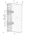
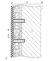
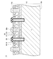
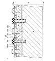
12:半導体基板
14:トレンチ
16:ゲート絶縁膜
18:ゲート電極
20:層間絶縁膜
22:ソース電極
22a:埋め込み電極
22b:ショットキー電極
22c:表面電極
22d:バリアメタル層
24:凹部
26:ドレイン電極
30:ソース領域
32:上部ボディ領域
34:中間領域
36:下部ボディ領域
38:ドリフト領域
40:ドレイン領域
Claims (6)
- 半導体装置であって、
表面にトレンチが形成されている半導体基板と、
前記トレンチ内に配置されているトレンチ電極と、
前記トレンチ電極の表面を覆っており、前記半導体基板の前記表面から突出している層間絶縁膜と、
前記半導体基板の前記表面上に配置されており、前記層間絶縁膜から離間した位置に配置されており、前記半導体基板に対してショットキー接触しているショットキー電極と、
前記層間絶縁膜と前記ショットキー電極の間の凹部内に配置されており、前記ショットキー電極とは異なる金属により構成されている埋め込み電極と、
前記層間絶縁膜、前記埋め込み電極及び前記ショットキー電極を覆う表面電極、
を有し、
前記埋め込み電極に覆われている範囲において、前記半導体基板の前記表面と前記ショットキー電極の側面の間の角度が90度より大きい半導体装置。 - 前記埋め込み電極に覆われている範囲において、前記半導体基板の前記表面と前記層間絶縁膜の側面の間の角度が90度より大きい請求項1の半導体装置。
- 前記ショットキー電極と前記表面電極の間、及び、前記層間絶縁膜と前記表面電極の間に、前記埋め込み電極に対してエッチング選択性を有するバリアメタル層が配置されている請求項1または2の半導体装置。
- 前記埋め込み電極が、前記半導体基板に対してオーミック接触している請求項1〜3のいずれか一項の半導体装置。
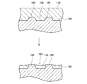
- 半導体装置を製造する方法であって、
半導体基板の表面にトレンチを形成する工程と、
前記トレンチ内にトレンチ電極を形成する工程と、
前記トレンチ電極の表面上に、前記トレンチ電極の表面を覆う層間絶縁膜を含み、前記半導体基板の前記表面から突出する第1凸部を形成する工程と、
前記半導体基板の前記表面上であって前記第1凸部から離間した位置に、前記半導体基板に対してショットキー接触しているショットキー電極を含み、前記半導体基板の前記表面から突出する第2凸部を形成する工程と、
前記第1凸部と、前記第2凸部と、前記第1凸部と前記第2凸部の間の前記半導体基板の前記表面を覆うように、埋め込み電極を成長させる工程と、
前記第1凸部と前記第2凸部の表面が露出し、前記第1凸部と前記第2凸部の間の凹部内に前記埋め込み電極が残存するように、前記埋め込み電極をエッチングする工程と、
前記エッチングの後に、前記第1凸部、前記埋め込み電極及び前記第2凸部を覆う表面電極を成長させる工程、
を有する方法。 - 前記埋め込み電極が、前記ショットキー電極とは異なる金属により構成されている請求項5の方法。
Priority Applications (7)
| Application Number | Priority Date | Filing Date | Title |
|---|---|---|---|
| JP2014169454A JP6036765B2 (ja) | 2014-08-22 | 2014-08-22 | 半導体装置及び半導体装置の製造方法 |
| CN201580045037.9A CN106575668B (zh) | 2014-08-22 | 2015-06-23 | 半导体装置以及半导体装置的制造方法 |
| KR1020167031726A KR101868730B1 (ko) | 2014-08-22 | 2015-06-23 | 반도체 장치 및 반도체 장치의 제조 방법 |
| PCT/JP2015/068095 WO2016027564A1 (ja) | 2014-08-22 | 2015-06-23 | 半導体装置及び半導体装置の製造方法 |
| US15/125,857 US9941273B2 (en) | 2014-08-22 | 2015-06-23 | Semiconductor device and method of manufacturing the semiconductor device |
| DE112015003835.3T DE112015003835B4 (de) | 2014-08-22 | 2015-06-23 | Halbleitervorrichtung und verfahren zur herstellung der halbleitervorrichtung |
| TW104126111A TWI587478B (zh) | 2014-08-22 | 2015-08-11 | Semiconductor device and method for manufacturing semiconductor device |
Applications Claiming Priority (1)
| Application Number | Priority Date | Filing Date | Title |
|---|---|---|---|
| JP2014169454A JP6036765B2 (ja) | 2014-08-22 | 2014-08-22 | 半導体装置及び半導体装置の製造方法 |
Publications (3)
| Publication Number | Publication Date |
|---|---|
| JP2016046377A JP2016046377A (ja) | 2016-04-04 |
| JP2016046377A5 JP2016046377A5 (ja) | 2016-10-13 |
| JP6036765B2 true JP6036765B2 (ja) | 2016-11-30 |
Family
ID=55350516
Family Applications (1)
| Application Number | Title | Priority Date | Filing Date |
|---|---|---|---|
| JP2014169454A Active JP6036765B2 (ja) | 2014-08-22 | 2014-08-22 | 半導体装置及び半導体装置の製造方法 |
Country Status (7)
| Country | Link |
|---|---|
| US (1) | US9941273B2 (ja) |
| JP (1) | JP6036765B2 (ja) |
| KR (1) | KR101868730B1 (ja) |
| CN (1) | CN106575668B (ja) |
| DE (1) | DE112015003835B4 (ja) |
| TW (1) | TWI587478B (ja) |
| WO (1) | WO2016027564A1 (ja) |
Families Citing this family (8)
| Publication number | Priority date | Publication date | Assignee | Title |
|---|---|---|---|---|
| JP6299789B2 (ja) * | 2016-03-09 | 2018-03-28 | トヨタ自動車株式会社 | スイッチング素子 |
| JP6784164B2 (ja) * | 2016-12-15 | 2020-11-11 | 株式会社豊田中央研究所 | 半導体装置 |
| DE102017118665A1 (de) | 2017-08-16 | 2019-02-21 | Infineon Technologies Ag | Rc-igbt |
| JP6776205B2 (ja) * | 2017-09-20 | 2020-10-28 | 株式会社東芝 | 半導体装置の製造方法 |
| CN117238852A (zh) | 2018-02-02 | 2023-12-15 | 三菱电机株式会社 | 半导体装置的制造方法 |
| JP6964538B2 (ja) * | 2018-02-28 | 2021-11-10 | 株式会社 日立パワーデバイス | 半導体装置および電力変換装置 |
| US11417762B2 (en) * | 2019-06-26 | 2022-08-16 | Skyworks Solutions, Inc. | Switch with integrated Schottky barrier contact |
| CN113921614B (zh) * | 2021-12-13 | 2022-03-25 | 捷捷微电(上海)科技有限公司 | 一种半导体功率器件结构及其制造方法 |
Family Cites Families (18)
| Publication number | Priority date | Publication date | Assignee | Title |
|---|---|---|---|---|
| US6593620B1 (en) * | 2000-10-06 | 2003-07-15 | General Semiconductor, Inc. | Trench DMOS transistor with embedded trench schottky rectifier |
| US6998678B2 (en) * | 2001-05-17 | 2006-02-14 | Infineon Technologies Ag | Semiconductor arrangement with a MOS-transistor and a parallel Schottky-diode |
| WO2004032243A1 (en) * | 2002-10-04 | 2004-04-15 | Koninklijke Philips Electronics N.V. | Power semiconductor devices |
| JP4406535B2 (ja) * | 2003-01-14 | 2010-01-27 | 新電元工業株式会社 | ショットキーダイオード付きトランジスタ |
| JP4799829B2 (ja) * | 2003-08-27 | 2011-10-26 | 三菱電機株式会社 | 絶縁ゲート型トランジスタ及びインバータ回路 |
| JP4829473B2 (ja) | 2004-01-21 | 2011-12-07 | オンセミコンダクター・トレーディング・リミテッド | 絶縁ゲート型半導体装置およびその製造方法 |
| JP4935160B2 (ja) * | 2006-04-11 | 2012-05-23 | 株式会社デンソー | 炭化珪素半導体装置およびその製造方法 |
| JP4292427B2 (ja) * | 2006-12-04 | 2009-07-08 | サンケン電気株式会社 | 絶縁ゲート型電界効果トランジスタ及びその製造方法 |
| US8049276B2 (en) * | 2009-06-12 | 2011-11-01 | Fairchild Semiconductor Corporation | Reduced process sensitivity of electrode-semiconductor rectifiers |
| JP5511308B2 (ja) * | 2009-10-26 | 2014-06-04 | 三菱電機株式会社 | 半導体装置およびその製造方法 |
| JP2011199060A (ja) * | 2010-03-19 | 2011-10-06 | Toshiba Corp | 半導体装置及びその製造方法 |
| KR101396611B1 (ko) * | 2010-04-28 | 2014-05-16 | 닛산 지도우샤 가부시키가이샤 | 반도체 장치 |
| US8580667B2 (en) * | 2010-12-14 | 2013-11-12 | Alpha And Omega Semiconductor Incorporated | Self aligned trench MOSFET with integrated diode |
| US9520465B2 (en) | 2011-07-27 | 2016-12-13 | Kabushiki Kaisha Toyota Chuo Kenkyusho | Diode, semiconductor device, and MOSFET |
| DE112012005869B4 (de) * | 2012-02-14 | 2021-09-23 | Denso Corporation | IGBT und IGBT-Herstellungsverfahren |
| US8809948B1 (en) * | 2012-12-21 | 2014-08-19 | Alpha And Omega Semiconductor Incorporated | Device structure and methods of making high density MOSFETs for load switch and DC-DC applications |
| US8951867B2 (en) * | 2012-12-21 | 2015-02-10 | Alpha And Omega Semiconductor Incorporated | High density trench-based power MOSFETs with self-aligned active contacts and method for making such devices |
| JP2014157896A (ja) * | 2013-02-15 | 2014-08-28 | Toyota Central R&D Labs Inc | 半導体装置とその製造方法 |
-
2014
- 2014-08-22 JP JP2014169454A patent/JP6036765B2/ja active Active
-
2015
- 2015-06-23 KR KR1020167031726A patent/KR101868730B1/ko active IP Right Grant
- 2015-06-23 WO PCT/JP2015/068095 patent/WO2016027564A1/ja active Application Filing
- 2015-06-23 DE DE112015003835.3T patent/DE112015003835B4/de active Active
- 2015-06-23 CN CN201580045037.9A patent/CN106575668B/zh active Active
- 2015-06-23 US US15/125,857 patent/US9941273B2/en active Active
- 2015-08-11 TW TW104126111A patent/TWI587478B/zh not_active IP Right Cessation
Also Published As
| Publication number | Publication date |
|---|---|
| WO2016027564A1 (ja) | 2016-02-25 |
| KR20160138308A (ko) | 2016-12-02 |
| CN106575668B (zh) | 2019-09-03 |
| TW201624670A (zh) | 2016-07-01 |
| DE112015003835B4 (de) | 2020-10-15 |
| DE112015003835T5 (de) | 2017-05-11 |
| US9941273B2 (en) | 2018-04-10 |
| US20170040316A1 (en) | 2017-02-09 |
| TWI587478B (zh) | 2017-06-11 |
| CN106575668A (zh) | 2017-04-19 |
| KR101868730B1 (ko) | 2018-06-18 |
| JP2016046377A (ja) | 2016-04-04 |
Similar Documents
| Publication | Publication Date | Title |
|---|---|---|
| JP6036765B2 (ja) | 半導体装置及び半導体装置の製造方法 | |
| US8829607B1 (en) | Fast switching super-junction trench MOSFETs | |
| US8648413B2 (en) | Super-junction trench MOSFET with multiple trenched source-body contacts | |
| US8901573B2 (en) | Silicon carbide semiconductor device and method of manufacturing the same | |
| US8564058B1 (en) | Super-junction trench MOSFET with multiple trenched gates in unit cell | |
| US20130168760A1 (en) | Trench mosfet with resurf stepped oxide and diffused drift region | |
| JP5566020B2 (ja) | トレンチショットキバリアダイオードの製造方法 | |
| US20210028305A1 (en) | Trench mosfets with oxide charge balance region in active area and junction charge balance region in termination area | |
| US9722041B2 (en) | Breakdown voltage blocking device | |
| US9530882B1 (en) | Trench MOSFET with shielded gate and diffused drift region | |
| JP6193163B2 (ja) | 絶縁ゲート型半導体装置 | |
| US11222962B2 (en) | Edge termination designs for super junction device | |
| US9947574B2 (en) | Semiconductor device | |
| JP5556863B2 (ja) | ワイドバンドギャップ半導体縦型mosfet | |
| US10854759B2 (en) | Trenched MOS gate controlled rectifier | |
| US9530881B2 (en) | Semiconductor device, and method of manufacturing the same | |
| JP7371724B2 (ja) | 半導体装置とその製造方法 | |
| JP7051890B2 (ja) | ワイドギャップ半導体装置 | |
| JP7159949B2 (ja) | 半導体装置 | |
| JP6988262B2 (ja) | 窒化物半導体装置とその製造方法 | |
| JP6648743B2 (ja) | 炭化珪素半導体装置の製造方法 | |
| JP6554614B1 (ja) | ワイドギャップ半導体装置 | |
| JP6293380B1 (ja) | 半導体装置 | |
| JP2019036606A (ja) | 窒化物半導体装置の製造方法 | |
| WO2018066662A1 (ja) | 炭化珪素半導体装置の製造方法 |
Legal Events
| Date | Code | Title | Description |
|---|---|---|---|
| A621 | Written request for application examination |
Free format text: JAPANESE INTERMEDIATE CODE: A621 Effective date: 20160404 |
|
| A521 | Request for written amendment filed |
Free format text: JAPANESE INTERMEDIATE CODE: A523 Effective date: 20160829 |
|
| TRDD | Decision of grant or rejection written | ||
| A01 | Written decision to grant a patent or to grant a registration (utility model) |
Free format text: JAPANESE INTERMEDIATE CODE: A01 Effective date: 20161004 |
|
| A61 | First payment of annual fees (during grant procedure) |
Free format text: JAPANESE INTERMEDIATE CODE: A61 Effective date: 20161017 |
|
| R151 | Written notification of patent or utility model registration |
Ref document number: 6036765 Country of ref document: JP Free format text: JAPANESE INTERMEDIATE CODE: R151 |
|
| S111 | Request for change of ownership or part of ownership |
Free format text: JAPANESE INTERMEDIATE CODE: R313113 |
|
| R350 | Written notification of registration of transfer |
Free format text: JAPANESE INTERMEDIATE CODE: R350 |
|
| R250 | Receipt of annual fees |
Free format text: JAPANESE INTERMEDIATE CODE: R250 |
|
| R250 | Receipt of annual fees |
Free format text: JAPANESE INTERMEDIATE CODE: R250 |
|
| R250 | Receipt of annual fees |
Free format text: JAPANESE INTERMEDIATE CODE: R250 |
|
| R250 | Receipt of annual fees |
Free format text: JAPANESE INTERMEDIATE CODE: R250 |