JP6740986B2 - 炭化珪素半導体装置およびその製造方法 - Google Patents
炭化珪素半導体装置およびその製造方法 Download PDFInfo
- Publication number
- JP6740986B2 JP6740986B2 JP2017166883A JP2017166883A JP6740986B2 JP 6740986 B2 JP6740986 B2 JP 6740986B2 JP 2017166883 A JP2017166883 A JP 2017166883A JP 2017166883 A JP2017166883 A JP 2017166883A JP 6740986 B2 JP6740986 B2 JP 6740986B2
- Authority
- JP
- Japan
- Prior art keywords
- source region
- type
- region
- layer
- forming
- Prior art date
- Legal status (The legal status is an assumption and is not a legal conclusion. Google has not performed a legal analysis and makes no representation as to the accuracy of the status listed.)
- Active
Links
- HBMJWWWQQXIZIP-UHFFFAOYSA-N silicon carbide Chemical compound [Si+]#[C-] HBMJWWWQQXIZIP-UHFFFAOYSA-N 0.000 title claims description 86
- 229910010271 silicon carbide Inorganic materials 0.000 title claims description 86
- 239000004065 semiconductor Substances 0.000 title claims description 62
- 238000004519 manufacturing process Methods 0.000 title claims description 17
- 239000010410 layer Substances 0.000 claims description 225
- 239000012535 impurity Substances 0.000 claims description 146
- 239000000758 substrate Substances 0.000 claims description 29
- 239000002019 doping agent Substances 0.000 claims description 10
- 238000000034 method Methods 0.000 claims description 9
- 239000011229 interlayer Substances 0.000 claims description 8
- 238000010438 heat treatment Methods 0.000 claims description 2
- 230000003213 activating effect Effects 0.000 claims 1
- 230000005684 electric field Effects 0.000 description 49
- 230000000903 blocking effect Effects 0.000 description 38
- 238000005468 ion implantation Methods 0.000 description 22
- 230000007480 spreading Effects 0.000 description 18
- 238000003892 spreading Methods 0.000 description 18
- 230000008878 coupling Effects 0.000 description 15
- 238000010168 coupling process Methods 0.000 description 15
- 238000005859 coupling reaction Methods 0.000 description 15
- 238000004088 simulation Methods 0.000 description 10
- 238000009826 distribution Methods 0.000 description 7
- 239000007789 gas Substances 0.000 description 7
- 229910052751 metal Inorganic materials 0.000 description 7
- 239000002184 metal Substances 0.000 description 7
- 230000003071 parasitic effect Effects 0.000 description 7
- 230000006378 damage Effects 0.000 description 6
- 230000000694 effects Effects 0.000 description 6
- 239000002784 hot electron Substances 0.000 description 6
- IJGRMHOSHXDMSA-UHFFFAOYSA-N Atomic nitrogen Chemical compound N#N IJGRMHOSHXDMSA-UHFFFAOYSA-N 0.000 description 5
- 230000008859 change Effects 0.000 description 5
- 150000002739 metals Chemical class 0.000 description 5
- 230000015572 biosynthetic process Effects 0.000 description 4
- 238000005229 chemical vapour deposition Methods 0.000 description 4
- 230000007547 defect Effects 0.000 description 4
- 230000004913 activation Effects 0.000 description 3
- 239000000969 carrier Substances 0.000 description 3
- 230000015556 catabolic process Effects 0.000 description 3
- 238000010586 diagram Methods 0.000 description 3
- 229910021420 polycrystalline silicon Inorganic materials 0.000 description 3
- ATUOYWHBWRKTHZ-UHFFFAOYSA-N Propane Chemical compound CCC ATUOYWHBWRKTHZ-UHFFFAOYSA-N 0.000 description 2
- 229910052782 aluminium Inorganic materials 0.000 description 2
- XAGFODPZIPBFFR-UHFFFAOYSA-N aluminium Chemical compound [Al] XAGFODPZIPBFFR-UHFFFAOYSA-N 0.000 description 2
- 238000006243 chemical reaction Methods 0.000 description 2
- 239000013078 crystal Substances 0.000 description 2
- 230000006866 deterioration Effects 0.000 description 2
- 239000007772 electrode material Substances 0.000 description 2
- 229910052757 nitrogen Inorganic materials 0.000 description 2
- 230000003647 oxidation Effects 0.000 description 2
- 238000007254 oxidation reaction Methods 0.000 description 2
- 238000001020 plasma etching Methods 0.000 description 2
- 230000008569 process Effects 0.000 description 2
- 230000006798 recombination Effects 0.000 description 2
- 238000005215 recombination Methods 0.000 description 2
- 229910021332 silicide Inorganic materials 0.000 description 2
- FVBUAEGBCNSCDD-UHFFFAOYSA-N silicide(4-) Chemical compound [Si-4] FVBUAEGBCNSCDD-UHFFFAOYSA-N 0.000 description 2
- 238000009751 slip forming Methods 0.000 description 2
- ZOXJGFHDIHLPTG-UHFFFAOYSA-N Boron Chemical compound [B] ZOXJGFHDIHLPTG-UHFFFAOYSA-N 0.000 description 1
- BLRPTPMANUNPDV-UHFFFAOYSA-N Silane Chemical compound [SiH4] BLRPTPMANUNPDV-UHFFFAOYSA-N 0.000 description 1
- 230000009471 action Effects 0.000 description 1
- 229910052796 boron Inorganic materials 0.000 description 1
- 238000000151 deposition Methods 0.000 description 1
- 229910001873 dinitrogen Inorganic materials 0.000 description 1
- 238000001312 dry etching Methods 0.000 description 1
- 238000005530 etching Methods 0.000 description 1
- 230000001747 exhibiting effect Effects 0.000 description 1
- 230000012447 hatching Effects 0.000 description 1
- 238000002513 implantation Methods 0.000 description 1
- 239000000463 material Substances 0.000 description 1
- 230000002093 peripheral effect Effects 0.000 description 1
- 239000001294 propane Substances 0.000 description 1
- 239000002994 raw material Substances 0.000 description 1
- 238000010992 reflux Methods 0.000 description 1
- 230000001105 regulatory effect Effects 0.000 description 1
- 230000035939 shock Effects 0.000 description 1
- 229910000077 silane Inorganic materials 0.000 description 1
- 239000000126 substance Substances 0.000 description 1
- JLTRXTDYQLMHGR-UHFFFAOYSA-N trimethylaluminium Chemical compound C[Al](C)C JLTRXTDYQLMHGR-UHFFFAOYSA-N 0.000 description 1
Images


Classifications
-
- H—ELECTRICITY
- H01—ELECTRIC ELEMENTS
- H01L—SEMICONDUCTOR DEVICES NOT COVERED BY CLASS H10
- H01L29/00—Semiconductor devices adapted for rectifying, amplifying, oscillating or switching, or capacitors or resistors with at least one potential-jump barrier or surface barrier, e.g. PN junction depletion layer or carrier concentration layer; Details of semiconductor bodies or of electrodes thereof ; Multistep manufacturing processes therefor
- H01L29/66—Types of semiconductor device ; Multistep manufacturing processes therefor
- H01L29/68—Types of semiconductor device ; Multistep manufacturing processes therefor controllable by only the electric current supplied, or only the electric potential applied, to an electrode which does not carry the current to be rectified, amplified or switched
- H01L29/76—Unipolar devices, e.g. field effect transistors
- H01L29/772—Field effect transistors
- H01L29/78—Field effect transistors with field effect produced by an insulated gate
- H01L29/7801—DMOS transistors, i.e. MISFETs with a channel accommodating body or base region adjoining a drain drift region
- H01L29/7802—Vertical DMOS transistors, i.e. VDMOS transistors
- H01L29/7813—Vertical DMOS transistors, i.e. VDMOS transistors with trench gate electrode, e.g. UMOS transistors
-
- H—ELECTRICITY
- H01—ELECTRIC ELEMENTS
- H01L—SEMICONDUCTOR DEVICES NOT COVERED BY CLASS H10
- H01L29/00—Semiconductor devices adapted for rectifying, amplifying, oscillating or switching, or capacitors or resistors with at least one potential-jump barrier or surface barrier, e.g. PN junction depletion layer or carrier concentration layer; Details of semiconductor bodies or of electrodes thereof ; Multistep manufacturing processes therefor
- H01L29/02—Semiconductor bodies ; Multistep manufacturing processes therefor
- H01L29/06—Semiconductor bodies ; Multistep manufacturing processes therefor characterised by their shape; characterised by the shapes, relative sizes, or dispositions of the semiconductor regions ; characterised by the concentration or distribution of impurities within semiconductor regions
- H01L29/0603—Semiconductor bodies ; Multistep manufacturing processes therefor characterised by their shape; characterised by the shapes, relative sizes, or dispositions of the semiconductor regions ; characterised by the concentration or distribution of impurities within semiconductor regions characterised by particular constructional design considerations, e.g. for preventing surface leakage, for controlling electric field concentration or for internal isolations regions
- H01L29/0642—Isolation within the component, i.e. internal isolation
-
- H—ELECTRICITY
- H01—ELECTRIC ELEMENTS
- H01L—SEMICONDUCTOR DEVICES NOT COVERED BY CLASS H10
- H01L29/00—Semiconductor devices adapted for rectifying, amplifying, oscillating or switching, or capacitors or resistors with at least one potential-jump barrier or surface barrier, e.g. PN junction depletion layer or carrier concentration layer; Details of semiconductor bodies or of electrodes thereof ; Multistep manufacturing processes therefor
- H01L29/02—Semiconductor bodies ; Multistep manufacturing processes therefor
- H01L29/06—Semiconductor bodies ; Multistep manufacturing processes therefor characterised by their shape; characterised by the shapes, relative sizes, or dispositions of the semiconductor regions ; characterised by the concentration or distribution of impurities within semiconductor regions
- H01L29/0684—Semiconductor bodies ; Multistep manufacturing processes therefor characterised by their shape; characterised by the shapes, relative sizes, or dispositions of the semiconductor regions ; characterised by the concentration or distribution of impurities within semiconductor regions characterised by the shape, relative sizes or dispositions of the semiconductor regions or junctions between the regions
-
- H—ELECTRICITY
- H01—ELECTRIC ELEMENTS
- H01L—SEMICONDUCTOR DEVICES NOT COVERED BY CLASS H10
- H01L29/00—Semiconductor devices adapted for rectifying, amplifying, oscillating or switching, or capacitors or resistors with at least one potential-jump barrier or surface barrier, e.g. PN junction depletion layer or carrier concentration layer; Details of semiconductor bodies or of electrodes thereof ; Multistep manufacturing processes therefor
- H01L29/02—Semiconductor bodies ; Multistep manufacturing processes therefor
- H01L29/06—Semiconductor bodies ; Multistep manufacturing processes therefor characterised by their shape; characterised by the shapes, relative sizes, or dispositions of the semiconductor regions ; characterised by the concentration or distribution of impurities within semiconductor regions
- H01L29/08—Semiconductor bodies ; Multistep manufacturing processes therefor characterised by their shape; characterised by the shapes, relative sizes, or dispositions of the semiconductor regions ; characterised by the concentration or distribution of impurities within semiconductor regions with semiconductor regions connected to an electrode carrying current to be rectified, amplified or switched and such electrode being part of a semiconductor device which comprises three or more electrodes
- H01L29/0843—Source or drain regions of field-effect devices
- H01L29/0847—Source or drain regions of field-effect devices of field-effect transistors with insulated gate
- H01L29/0852—Source or drain regions of field-effect devices of field-effect transistors with insulated gate of DMOS transistors
- H01L29/0856—Source regions
- H01L29/086—Impurity concentration or distribution
-
- H—ELECTRICITY
- H01—ELECTRIC ELEMENTS
- H01L—SEMICONDUCTOR DEVICES NOT COVERED BY CLASS H10
- H01L29/00—Semiconductor devices adapted for rectifying, amplifying, oscillating or switching, or capacitors or resistors with at least one potential-jump barrier or surface barrier, e.g. PN junction depletion layer or carrier concentration layer; Details of semiconductor bodies or of electrodes thereof ; Multistep manufacturing processes therefor
- H01L29/02—Semiconductor bodies ; Multistep manufacturing processes therefor
- H01L29/06—Semiconductor bodies ; Multistep manufacturing processes therefor characterised by their shape; characterised by the shapes, relative sizes, or dispositions of the semiconductor regions ; characterised by the concentration or distribution of impurities within semiconductor regions
- H01L29/10—Semiconductor bodies ; Multistep manufacturing processes therefor characterised by their shape; characterised by the shapes, relative sizes, or dispositions of the semiconductor regions ; characterised by the concentration or distribution of impurities within semiconductor regions with semiconductor regions connected to an electrode not carrying current to be rectified, amplified or switched and such electrode being part of a semiconductor device which comprises three or more electrodes
- H01L29/1095—Body region, i.e. base region, of DMOS transistors or IGBTs
-
- H—ELECTRICITY
- H01—ELECTRIC ELEMENTS
- H01L—SEMICONDUCTOR DEVICES NOT COVERED BY CLASS H10
- H01L29/00—Semiconductor devices adapted for rectifying, amplifying, oscillating or switching, or capacitors or resistors with at least one potential-jump barrier or surface barrier, e.g. PN junction depletion layer or carrier concentration layer; Details of semiconductor bodies or of electrodes thereof ; Multistep manufacturing processes therefor
- H01L29/02—Semiconductor bodies ; Multistep manufacturing processes therefor
- H01L29/12—Semiconductor bodies ; Multistep manufacturing processes therefor characterised by the materials of which they are formed
- H01L29/16—Semiconductor bodies ; Multistep manufacturing processes therefor characterised by the materials of which they are formed including, apart from doping materials or other impurities, only elements of Group IV of the Periodic System
- H01L29/1608—Silicon carbide
-
- H—ELECTRICITY
- H01—ELECTRIC ELEMENTS
- H01L—SEMICONDUCTOR DEVICES NOT COVERED BY CLASS H10
- H01L29/00—Semiconductor devices adapted for rectifying, amplifying, oscillating or switching, or capacitors or resistors with at least one potential-jump barrier or surface barrier, e.g. PN junction depletion layer or carrier concentration layer; Details of semiconductor bodies or of electrodes thereof ; Multistep manufacturing processes therefor
- H01L29/66—Types of semiconductor device ; Multistep manufacturing processes therefor
- H01L29/66007—Multistep manufacturing processes
- H01L29/66053—Multistep manufacturing processes of devices having a semiconductor body comprising crystalline silicon carbide
- H01L29/66068—Multistep manufacturing processes of devices having a semiconductor body comprising crystalline silicon carbide the devices being controllable only by the electric current supplied or the electric potential applied, to an electrode which does not carry the current to be rectified, amplified or switched, e.g. three-terminal devices
-
- H—ELECTRICITY
- H01—ELECTRIC ELEMENTS
- H01L—SEMICONDUCTOR DEVICES NOT COVERED BY CLASS H10
- H01L29/00—Semiconductor devices adapted for rectifying, amplifying, oscillating or switching, or capacitors or resistors with at least one potential-jump barrier or surface barrier, e.g. PN junction depletion layer or carrier concentration layer; Details of semiconductor bodies or of electrodes thereof ; Multistep manufacturing processes therefor
- H01L29/66—Types of semiconductor device ; Multistep manufacturing processes therefor
- H01L29/68—Types of semiconductor device ; Multistep manufacturing processes therefor controllable by only the electric current supplied, or only the electric potential applied, to an electrode which does not carry the current to be rectified, amplified or switched
- H01L29/70—Bipolar devices
- H01L29/72—Transistor-type devices, i.e. able to continuously respond to applied control signals
- H01L29/739—Transistor-type devices, i.e. able to continuously respond to applied control signals controlled by field-effect, e.g. bipolar static induction transistors [BSIT]
- H01L29/7393—Insulated gate bipolar mode transistors, i.e. IGBT; IGT; COMFET
- H01L29/7395—Vertical transistors, e.g. vertical IGBT
- H01L29/7396—Vertical transistors, e.g. vertical IGBT with a non planar surface, e.g. with a non planar gate or with a trench or recess or pillar in the surface of the emitter, base or collector region for improving current density or short circuiting the emitter and base regions
- H01L29/7397—Vertical transistors, e.g. vertical IGBT with a non planar surface, e.g. with a non planar gate or with a trench or recess or pillar in the surface of the emitter, base or collector region for improving current density or short circuiting the emitter and base regions and a gate structure lying on a slanted or vertical surface or formed in a groove, e.g. trench gate IGBT
-
- H—ELECTRICITY
- H01—ELECTRIC ELEMENTS
- H01L—SEMICONDUCTOR DEVICES NOT COVERED BY CLASS H10
- H01L21/00—Processes or apparatus adapted for the manufacture or treatment of semiconductor or solid state devices or of parts thereof
- H01L21/02—Manufacture or treatment of semiconductor devices or of parts thereof
- H01L21/04—Manufacture or treatment of semiconductor devices or of parts thereof the devices having at least one potential-jump barrier or surface barrier, e.g. PN junction, depletion layer or carrier concentration layer
- H01L21/0445—Manufacture or treatment of semiconductor devices or of parts thereof the devices having at least one potential-jump barrier or surface barrier, e.g. PN junction, depletion layer or carrier concentration layer the devices having semiconductor bodies comprising crystalline silicon carbide
- H01L21/0455—Making n or p doped regions or layers, e.g. using diffusion
- H01L21/046—Making n or p doped regions or layers, e.g. using diffusion using ion implantation
-
- H—ELECTRICITY
- H01—ELECTRIC ELEMENTS
- H01L—SEMICONDUCTOR DEVICES NOT COVERED BY CLASS H10
- H01L29/00—Semiconductor devices adapted for rectifying, amplifying, oscillating or switching, or capacitors or resistors with at least one potential-jump barrier or surface barrier, e.g. PN junction depletion layer or carrier concentration layer; Details of semiconductor bodies or of electrodes thereof ; Multistep manufacturing processes therefor
- H01L29/02—Semiconductor bodies ; Multistep manufacturing processes therefor
- H01L29/06—Semiconductor bodies ; Multistep manufacturing processes therefor characterised by their shape; characterised by the shapes, relative sizes, or dispositions of the semiconductor regions ; characterised by the concentration or distribution of impurities within semiconductor regions
- H01L29/08—Semiconductor bodies ; Multistep manufacturing processes therefor characterised by their shape; characterised by the shapes, relative sizes, or dispositions of the semiconductor regions ; characterised by the concentration or distribution of impurities within semiconductor regions with semiconductor regions connected to an electrode carrying current to be rectified, amplified or switched and such electrode being part of a semiconductor device which comprises three or more electrodes
- H01L29/083—Anode or cathode regions of thyristors or gated bipolar-mode devices
Landscapes
- Engineering & Computer Science (AREA)
- Microelectronics & Electronic Packaging (AREA)
- Power Engineering (AREA)
- Condensed Matter Physics & Semiconductors (AREA)
- General Physics & Mathematics (AREA)
- Physics & Mathematics (AREA)
- Ceramic Engineering (AREA)
- Computer Hardware Design (AREA)
- Chemical & Material Sciences (AREA)
- Crystallography & Structural Chemistry (AREA)
- Manufacturing & Machinery (AREA)
- Junction Field-Effect Transistors (AREA)
- Electrodes Of Semiconductors (AREA)
Description
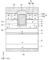
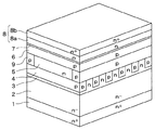
第1実施形態について説明する。本実施形態にかかるSiC半導体装置は、半導体素子として、図1および図2に示すトレンチゲート構造の反転型の縦型MOSFETが形成されたものである。これらの図に示す縦型MOSFETは、SiC半導体装置のうちのセル領域に形成されており、そのセル領域を囲むように外周耐圧構造が形成されることでSiC半導体装置が構成されているが、ここでは縦型MOSFETのみ図示してある。なお、以下では、図1および図2に示すように、縦型MOSFETの幅方向をX方向、X方向に対して交差する縦型MOSFETの奥行方向をY方向、縦型MOSFETの厚み方向もしくは深さ方向、つまりXY平面に対する法線方向をZ方向として説明する。
まず、半導体基板として、n+型基板1を用意する。そして、図示しないCVD(chemical vapor deposition)装置を用いたエピタキシャル成長により、n+型基板1の主表面上にSiCからなるn−型層2を形成する。このとき、n+型基板1の主表面上に予めn−型層2を成長させてある所謂エピ基板を用いても良い。そして、n−型層2の上にSiCからなるJFET部3をエピタキシャル成長させる。
JFET部3の表面に、マスク17を配置したのち、マスク17をパターニングして電界ブロック層4の形成予定領域を開口させる。そして、p型不純物をイオン注入することで、電界ブロック層4を形成する。その後、マスク17を除去する。
引き続き、JFET部3および電界ブロック層4の上にn型SiCをエピタキシャル成長させることで、n型電流分散層5を形成する。そして、n型電流分散層5の上に、p型ディープ層9の形成予定領域が開口する図示しないマスクを配置する。その後、マスクの上からp型不純物をイオン注入することでp型ディープ層9を形成する。なお、p型ディープ層9についてもイオン注入によって形成する例を示したが、イオン注入以外の方法によって形成することもできる。例えば、電界ブロック層4と同様に、n型電流分散層5に対して凹部を形成したのち、p型不純物層をエピタキシャル成長させ、さらにp型不純物層の平坦化を行うことで、p型ディープ層9を形成するようにしても良い。
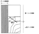
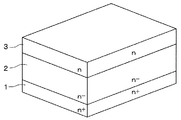
図示しないCVD装置を用いて、n型電流分散層5およびp型ディープ層9の上にp型ベース領域6とノンドープ層7およびn型ソース領域8を順にエピタキシャル成長させる。例えば、同じCVD装置内において、まずはp型ドーパントとなるガスを導入したエピタキシャル成長によってp型ディープ層9を形成する。続いて、p型ドーパントとn型ドーパントの両方のドーパントガスの導入を停止した状態でエピタキシャル成長を連続して行うことでノンドープ層7を形成する。そして、ノンドープ層7が所定膜厚に達したら、今度はn型ドーパントとなるガスを導入したエピタキシャル成長によってn型ソース領域8を形成する。このとき、n型ドーパントの導入量を調整することで、第1ソース領域8aと第2ソース領域8bのn型不純物濃度が所望の値となるように調整する。
n型ソース領域8の上にp型連結層10の形成予定位置を開口させた図示しないマスクを配置する。そして、マスクの上からp型不純物をイオン注入したのち、活性化のために1500℃以上の熱処理を行う。イオン注入する元素としては、ボロン(B)とアルミニウム(Al)のいずれか一方もしくは両方を用いている。これにより、n型ソース領域8をp型不純物のイオン注入によって打ち返してp型連結層10を形成することができる。また、p型連結層10については、p型ベース領域6に接続されるようにする必要があるため、ノンドープ層7にもp型不純物が打ち込まれるようにし、この部分もp型連結層10となるようにする。
n型ソース領域8などの上に図示しないマスクを形成したのち、マスクのうちのゲートトレンチ11の形成予定領域を開口させる。そして、マスクを用いてRIE(Reactive Ion Etching)等の異方性エッチングを行うことで、ゲートトレンチ11を形成する。
その後、マスクを除去してから例えば熱酸化を行うことによって、ゲート絶縁膜12を形成し、ゲート絶縁膜12によってゲートトレンチ11の内壁面上およびn型ソース領域8の表面上を覆う。そして、p型不純物もしくはn型不純物がドープされたPoly−Siをデポジションした後、これをエッチバックし、少なくともゲートトレンチ11内にPoly−Siを残すことでゲート電極13を形成する。これにより、トレンチゲート構造が完成する。
本発明は上記した実施形態に限定されるものではなく、特許請求の範囲に記載した範囲内において適宜変更が可能である。
7 ノンドープ層
8 n型ソース領域
8a 第1ソース領域
8b 第2ソース領域
10 p型連結層
11 ゲートトレンチ
13 ゲート電極
15 ソース電極
16 ドレイン電極
Claims (9)
- 反転型の半導体素子を備えている炭化珪素半導体装置であって、
炭化珪素で構成された第1または第2導電型の基板(1)と、
前記基板の上に形成され、前記基板よりも低不純物濃度とされた第1導電型の炭化珪素からなるドリフト層(2、3、5)と、
前記ドリフト層の上に形成された第2導電型の炭化珪素からなるベース領域(6)と、
前記ベース領域の上に形成され、前記ドリフト層よりも第1導電型不純物濃度が高くされた第1導電型の炭化珪素からなるソース領域(8)と、
前記ソース領域の表面から前記ベース領域よりも深く形成されたゲートトレンチ(11)内に、該ゲートトレンチの内壁面を覆うゲート絶縁膜(12)と該ゲート絶縁膜の上に配置されたゲート電極(13)とを備えて構成され、一方向を長手方向として複数本がストライプ状に並べられたトレンチゲート構造と、
前記ゲート電極および前記ゲート絶縁膜を覆うと共にコンタクトホールが形成された層間絶縁膜(14)と、
前記コンタクトホールを通じて、前記ソース領域にオーミック接触させられたソース電極(15)と、
前記基板の裏面側に形成されたドレイン電極(16)と、を含む前記半導体素子を備え、
前記ソース領域は、前記ベース領域側の方が前記ソース電極にオーミック接触させられる表面側よりも低不純物濃度で構成されており、
前記ベース領域と前記ソース領域との間には、キャリア濃度が5.0×10 15 /cm 3 以下とされたノンドープ層(7)が備えられている炭化珪素半導体装置。 - 前記ソース領域は、前記ベース領域側に位置する第1ソース領域(8a)と前記ソース電極にオーミック接触させられる第2ソース領域(8b)とを有した構成とされている請求項1に記載の炭化珪素半導体装置。
- 前記第2ソース領域は、厚さが0.1μm以上とされていると共に、第2導電型不純物濃度が1.0×10¹⁸〜5.0×10¹⁹/cm3とされている請求項2に記載の炭化珪素半導体装置。
- 前記第1ソース領域は、厚さが0.2〜0.5μmとされ、不純物濃度が2.0×10¹⁶〜1.0×10¹⁷/cm3とされている請求項2または3に記載の炭化珪素半導体装置。
- 前記ノンドープ層は、厚さが0.05〜0.2μmとされている請求項1ないし4のいずれか1つに記載の炭化珪素半導体装置。
- 前記ノンドープ層および前記ソース領域の合計膜厚が0.8μm以下とされている請求項1ないし5のいずれか1つに記載の炭化珪素半導体装置。
- 反転型の半導体素子を備えた炭化珪素半導体装置の製造方法であって、
炭化珪素で構成された第1または第2導電型の基板(1)を用意することと、
前記基板の上に、前記基板よりも低不純物濃度の第1導電型の炭化珪素からなるドリフト層(2、3、5)を形成することと、
前記ドリフト層の上に、第2導電型の炭化珪素からなるベース領域(6)を形成することと、
前記ベース領域の上に、前記ドリフト層よりも第1導電型不純物濃度が高くされた第1導電型の炭化珪素からなるソース領域(8)を形成することと、
前記ソース領域の表面から前記ベース領域よりも深いゲートトレンチ(11)を、一方向を長手方向としてストライプ状に複数本形成したのち、前記ゲートトレンチの内壁面にゲート絶縁膜(12)を形成すると共に、前記ゲート絶縁膜の上にゲート電極(13)を形成することでトレンチゲート構造を形成することと、
前記ソース領域に電気的に接続されるソース電極(15)を形成することと、
前記基板の裏面側にドレイン電極(16)を形成することと、を含み、
前記ベース領域を形成すること、および、前記ソース領域を形成することでは、前記ベース領域および前記ソース領域をエピタキシャル成長によって形成し、
前記ソース領域を形成することでは、前記ベース領域側より第1導電型不純物濃度が異なる第1ソース領域(8a)と前記ソース電極にオーミック接触させられる第2ソース領域(8b)とを順にエピタキシャル成長によって形成し、前記第1ソース領域を前記第2ソース領域よりも低不純物濃度で形成する炭化珪素半導体装置の製造方法。 - 前記ベース領域を形成すること、および、前記ソース領域を形成することの間に、炭化珪素で構成されるノンドープ層(7)を形成することを含み、
前記ベース領域を形成することと前記ノンドープ層を形成すること、および、前記ソース領域を形成することを連続的にエピタキシャル成長によって行い、
前記ノンドープ層を形成することでは、第1導電型ドーパントおよび第2導電型ドーパントのガス導入を停止した状態で前記エピタキシャル成長を行うことで、前記ノンドープ層を厚さ0.05〜0.2μmで形成する請求項7に記載の炭化珪素半導体装置の製造方法。 - 前記ノンドープ層を形成すること、および、前記ソース領域を形成することののち、前記ソース領域の表面側から第2導電型不純物をイオン注入することで、前記ベース領域に達して、該ベース領域と前記ソース電極とを連結する第2導電型の連結層(10)を形成することを含み、
前記連結層を形成することでは、前記連結層のうち前記第1ソース領域に対して前記第2導電型不純物をイオン注入する部分を第1領域(10a)とし、前記第2ソース領域に対して前記第2導電型不純物をイオン注入する部分を第2領域(10b)として、前記第2ソース領域の第1導電型不純物濃度の2〜10倍のドーズ量で前記第2導電型不純物をイオン注入したのち、1500℃以上の熱処理によって活性化することで前記第2領域を形成することを含んでいる請求項8に記載の炭化珪素半導体装置の製造方法。
Priority Applications (5)
| Application Number | Priority Date | Filing Date | Title |
|---|---|---|---|
| JP2017166883A JP6740986B2 (ja) | 2017-08-31 | 2017-08-31 | 炭化珪素半導体装置およびその製造方法 |
| CN201880056697.0A CN111149213B (zh) | 2017-08-31 | 2018-08-29 | 碳化硅半导体装置及其制造方法 |
| PCT/JP2018/032005 WO2019044922A1 (ja) | 2017-08-31 | 2018-08-29 | 炭化珪素半導体装置およびその製造方法 |
| US16/802,754 US11201216B2 (en) | 2017-08-31 | 2020-02-27 | Silicon carbide semiconductor device and manufacturing method of silicon carbide semiconductor device |
| US17/510,913 US11735654B2 (en) | 2017-08-31 | 2021-10-26 | Silicon carbide semiconductor device and manufacturing method of silicon carbide semiconductor device |
Applications Claiming Priority (1)
| Application Number | Priority Date | Filing Date | Title |
|---|---|---|---|
| JP2017166883A JP6740986B2 (ja) | 2017-08-31 | 2017-08-31 | 炭化珪素半導体装置およびその製造方法 |
Publications (3)
| Publication Number | Publication Date |
|---|---|
| JP2019046909A JP2019046909A (ja) | 2019-03-22 |
| JP2019046909A5 JP2019046909A5 (ja) | 2019-12-12 |
| JP6740986B2 true JP6740986B2 (ja) | 2020-08-19 |
Family
ID=65527422
Family Applications (1)
| Application Number | Title | Priority Date | Filing Date |
|---|---|---|---|
| JP2017166883A Active JP6740986B2 (ja) | 2017-08-31 | 2017-08-31 | 炭化珪素半導体装置およびその製造方法 |
Country Status (4)
| Country | Link |
|---|---|
| US (2) | US11201216B2 (ja) |
| JP (1) | JP6740986B2 (ja) |
| CN (1) | CN111149213B (ja) |
| WO (1) | WO2019044922A1 (ja) |
Families Citing this family (9)
| Publication number | Priority date | Publication date | Assignee | Title |
|---|---|---|---|---|
| JP7139596B2 (ja) * | 2017-12-06 | 2022-09-21 | 富士電機株式会社 | 半導体装置及びその製造方法 |
| US11398558B2 (en) * | 2018-06-25 | 2022-07-26 | Sumitomo Electric Industries, Ltd. | Silicon carbide semiconductor device |
| JP7140148B2 (ja) * | 2019-02-27 | 2022-09-21 | 株式会社デンソー | 炭化珪素半導体装置およびその製造方法 |
| JP7302286B2 (ja) * | 2019-05-23 | 2023-07-04 | 富士電機株式会社 | 半導体装置 |
| JP7272235B2 (ja) * | 2019-10-30 | 2023-05-12 | 株式会社デンソー | 炭化珪素半導体装置およびその製造方法 |
| JP7451981B2 (ja) | 2019-12-10 | 2024-03-19 | 富士電機株式会社 | 半導体装置 |
| CN113497124B (zh) * | 2020-04-07 | 2023-08-11 | 长鑫存储技术有限公司 | 半导体器件及其制造方法 |
| CN113964196B (zh) * | 2021-10-20 | 2023-01-20 | 重庆平创半导体研究院有限责任公司 | 一种耗尽型功率半导体结构、串联结构和加工工艺 |
| CN117810265A (zh) * | 2024-02-28 | 2024-04-02 | 湖北九峰山实验室 | 一种宽禁带半导体沟槽mosfet器件及其制造方法 |
Family Cites Families (21)
| Publication number | Priority date | Publication date | Assignee | Title |
|---|---|---|---|---|
| US6445037B1 (en) * | 2000-09-28 | 2002-09-03 | General Semiconductor, Inc. | Trench DMOS transistor having lightly doped source structure |
| US6555872B1 (en) * | 2000-11-22 | 2003-04-29 | Thunderbird Technologies, Inc. | Trench gate fermi-threshold field effect transistors |
| JP2002190595A (ja) * | 2000-12-21 | 2002-07-05 | Denso Corp | 半導体装置及びその製造方法 |
| US7652326B2 (en) | 2003-05-20 | 2010-01-26 | Fairchild Semiconductor Corporation | Power semiconductor devices and methods of manufacture |
| JP4487655B2 (ja) * | 2004-04-14 | 2010-06-23 | 株式会社デンソー | 半導体装置の製造方法 |
| JP2007005492A (ja) * | 2005-06-22 | 2007-01-11 | Sanyo Electric Co Ltd | 絶縁ゲート型半導体装置およびその製造方法 |
| WO2009061340A1 (en) * | 2007-11-09 | 2009-05-14 | Cree, Inc. | Power semiconductor devices with mesa structures and buffer layers including mesa steps |
| JP4877286B2 (ja) | 2008-07-08 | 2012-02-15 | 株式会社デンソー | 炭化珪素半導体装置およびその製造方法 |
| JP5525940B2 (ja) | 2009-07-21 | 2014-06-18 | ローム株式会社 | 半導体装置および半導体装置の製造方法 |
| CN106098539B (zh) * | 2009-09-07 | 2019-02-22 | 罗姆股份有限公司 | 半导体装置 |
| JP2012174989A (ja) | 2011-02-23 | 2012-09-10 | Toshiba Corp | 半導体装置の製造方法 |
| DE112012003111T5 (de) * | 2011-07-27 | 2014-04-10 | Toyota Jidosha Kabushiki Kaisha | Diode, Halbleitervorrichtung und Mosfet |
| JP5812029B2 (ja) * | 2012-06-13 | 2015-11-11 | 株式会社デンソー | 炭化珪素半導体装置およびその製造方法 |
| JP6146146B2 (ja) * | 2013-06-07 | 2017-06-14 | 住友電気工業株式会社 | 炭化珪素半導体装置およびその製造方法 |
| JP2015056486A (ja) * | 2013-09-11 | 2015-03-23 | 株式会社東芝 | 半導体装置およびその製造方法 |
| US20160211334A1 (en) * | 2013-10-04 | 2016-07-21 | Mitsubishi Electric Corporation | Silicon carbide semiconductor device and method for manufacturing same |
| KR20150078449A (ko) * | 2013-12-30 | 2015-07-08 | 현대자동차주식회사 | 반도체 소자 및 그 제조 방법 |
| US9825126B2 (en) | 2014-10-20 | 2017-11-21 | Mitsubishi Electric Corporation | Semiconductor device |
| JP6063915B2 (ja) * | 2014-12-12 | 2017-01-18 | 株式会社豊田中央研究所 | 逆導通igbt |
| JP6659418B2 (ja) | 2016-03-18 | 2020-03-04 | トヨタ自動車株式会社 | 半導体装置 |
| JP2018182032A (ja) | 2017-04-11 | 2018-11-15 | 富士電機株式会社 | 炭化珪素半導体装置および炭化珪素半導体装置の製造方法 |
-
2017
- 2017-08-31 JP JP2017166883A patent/JP6740986B2/ja active Active
-
2018
- 2018-08-29 WO PCT/JP2018/032005 patent/WO2019044922A1/ja active Application Filing
- 2018-08-29 CN CN201880056697.0A patent/CN111149213B/zh active Active
-
2020
- 2020-02-27 US US16/802,754 patent/US11201216B2/en active Active
-
2021
- 2021-10-26 US US17/510,913 patent/US11735654B2/en active Active
Also Published As
| Publication number | Publication date |
|---|---|
| US11201216B2 (en) | 2021-12-14 |
| WO2019044922A1 (ja) | 2019-03-07 |
| US20200203482A1 (en) | 2020-06-25 |
| US11735654B2 (en) | 2023-08-22 |
| CN111149213A (zh) | 2020-05-12 |
| US20220045172A1 (en) | 2022-02-10 |
| CN111149213B (zh) | 2023-08-11 |
| JP2019046909A (ja) | 2019-03-22 |
Similar Documents
| Publication | Publication Date | Title |
|---|---|---|
| JP6740986B2 (ja) | 炭化珪素半導体装置およびその製造方法 | |
| CN111463277B (zh) | 半导体器件 | |
| US8933466B2 (en) | Semiconductor element | |
| US8772788B2 (en) | Semiconductor element and method of manufacturing thereof | |
| WO2014038110A1 (ja) | 半導体装置 | |
| JPWO2017064949A1 (ja) | 半導体装置および半導体装置の製造方法 | |
| JP2017092368A (ja) | 半導体装置および半導体装置の製造方法 | |
| JP6099749B2 (ja) | 炭化珪素半導体装置およびその製造方法 | |
| JP6658137B2 (ja) | 半導体装置及びその製造方法 | |
| JP6988175B2 (ja) | 炭化珪素半導体装置および炭化珪素半導体装置の製造方法 | |
| JP2015072999A (ja) | 炭化珪素半導体装置 | |
| JP2012169385A (ja) | 炭化珪素半導体装置 | |
| CN112655096A (zh) | 超结碳化硅半导体装置及超结碳化硅半导体装置的制造方法 | |
| US20180040687A1 (en) | Semiconductor device and method of manufacturing semiconductor device | |
| JP2020141130A (ja) | 炭化珪素半導体装置およびその製造方法 | |
| WO2018117061A1 (ja) | 半導体装置および半導体装置の製造方法 | |
| JP2006351713A (ja) | 絶縁ゲート型半導体装置 | |
| JP7127546B2 (ja) | 半導体装置 | |
| JP2020109808A (ja) | 半導体装置 | |
| KR101887910B1 (ko) | SiC MOSFET 전력 반도체 소자 및 그 제조방법 | |
| JP2019165166A (ja) | 炭化珪素半導体装置およびその製造方法 | |
| JP2020109809A (ja) | 半導体装置 | |
| JP7167717B2 (ja) | 半導体装置 | |
| JP2022190929A (ja) | 半導体装置 | |
| JP5784860B1 (ja) | 炭化ケイ素半導体装置 |
Legal Events
| Date | Code | Title | Description |
|---|---|---|---|
| A521 | Request for written amendment filed |
Free format text: JAPANESE INTERMEDIATE CODE: A523 Effective date: 20191029 |
|
| A621 | Written request for application examination |
Free format text: JAPANESE INTERMEDIATE CODE: A621 Effective date: 20191029 |
|
| TRDD | Decision of grant or rejection written | ||
| A01 | Written decision to grant a patent or to grant a registration (utility model) |
Free format text: JAPANESE INTERMEDIATE CODE: A01 Effective date: 20200623 |
|
| A61 | First payment of annual fees (during grant procedure) |
Free format text: JAPANESE INTERMEDIATE CODE: A61 Effective date: 20200706 |
|
| R150 | Certificate of patent or registration of utility model |
Ref document number: 6740986 Country of ref document: JP Free format text: JAPANESE INTERMEDIATE CODE: R150 |
|
| R250 | Receipt of annual fees |
Free format text: JAPANESE INTERMEDIATE CODE: R250 |