EP2546865B1 - Methods of processing semiconductor wafers having silicon carbide power devices thereon - Google Patents
Methods of processing semiconductor wafers having silicon carbide power devices thereon Download PDFInfo
- Publication number
- EP2546865B1 EP2546865B1 EP12181385.1A EP12181385A EP2546865B1 EP 2546865 B1 EP2546865 B1 EP 2546865B1 EP 12181385 A EP12181385 A EP 12181385A EP 2546865 B1 EP2546865 B1 EP 2546865B1
- Authority
- EP
- European Patent Office
- Prior art keywords
- silicon carbide
- substrate
- epitaxial layer
- wafer
- layer
- Prior art date
- Legal status (The legal status is an assumption and is not a legal conclusion. Google has not performed a legal analysis and makes no representation as to the accuracy of the status listed.)
- Active
Links
- 229910010271 silicon carbide Inorganic materials 0.000 title claims description 126
- HBMJWWWQQXIZIP-UHFFFAOYSA-N silicon carbide Chemical compound [Si+]#[C-] HBMJWWWQQXIZIP-UHFFFAOYSA-N 0.000 title claims description 118
- 239000004065 semiconductor Substances 0.000 title claims description 41
- 238000000034 method Methods 0.000 title claims description 33
- 235000012431 wafers Nutrition 0.000 title description 72
- 239000000758 substrate Substances 0.000 claims description 156
- 229910052751 metal Inorganic materials 0.000 claims description 47
- 239000002184 metal Substances 0.000 claims description 47
- 238000000137 annealing Methods 0.000 claims description 19
- 238000010438 heat treatment Methods 0.000 claims description 13
- 238000005224 laser annealing Methods 0.000 claims description 12
- 238000000227 grinding Methods 0.000 claims description 10
- 238000002161 passivation Methods 0.000 claims description 9
- 238000010894 electron beam technology Methods 0.000 claims description 7
- 238000005530 etching Methods 0.000 claims description 4
- 229910003465 moissanite Inorganic materials 0.000 claims 1
- 239000010410 layer Substances 0.000 description 92
- 239000000463 material Substances 0.000 description 15
- 239000012790 adhesive layer Substances 0.000 description 12
- PXHVJJICTQNCMI-UHFFFAOYSA-N Nickel Chemical compound [Ni] PXHVJJICTQNCMI-UHFFFAOYSA-N 0.000 description 6
- 239000000853 adhesive Substances 0.000 description 5
- 230000001070 adhesive effect Effects 0.000 description 5
- 230000015572 biosynthetic process Effects 0.000 description 5
- 238000004519 manufacturing process Methods 0.000 description 5
- 239000010936 titanium Substances 0.000 description 5
- 238000002955 isolation Methods 0.000 description 4
- 229910052594 sapphire Inorganic materials 0.000 description 4
- 239000010980 sapphire Substances 0.000 description 4
- 229910052710 silicon Inorganic materials 0.000 description 4
- 239000010703 silicon Substances 0.000 description 4
- 239000002390 adhesive tape Substances 0.000 description 3
- PNEYBMLMFCGWSK-UHFFFAOYSA-N aluminium oxide Inorganic materials [O-2].[O-2].[O-2].[Al+3].[Al+3] PNEYBMLMFCGWSK-UHFFFAOYSA-N 0.000 description 3
- 238000013459 approach Methods 0.000 description 3
- 238000003486 chemical etching Methods 0.000 description 3
- 239000007943 implant Substances 0.000 description 3
- 238000001020 plasma etching Methods 0.000 description 3
- 239000000126 substance Substances 0.000 description 3
- 229910002601 GaN Inorganic materials 0.000 description 2
- 230000004888 barrier function Effects 0.000 description 2
- 239000000969 carrier Substances 0.000 description 2
- 238000005468 ion implantation Methods 0.000 description 2
- 230000031700 light absorption Effects 0.000 description 2
- 239000000395 magnesium oxide Substances 0.000 description 2
- CPLXHLVBOLITMK-UHFFFAOYSA-N magnesium oxide Inorganic materials [Mg]=O CPLXHLVBOLITMK-UHFFFAOYSA-N 0.000 description 2
- AXZKOIWUVFPNLO-UHFFFAOYSA-N magnesium;oxygen(2-) Chemical compound [O-2].[Mg+2] AXZKOIWUVFPNLO-UHFFFAOYSA-N 0.000 description 2
- 229910052759 nickel Inorganic materials 0.000 description 2
- BASFCYQUMIYNBI-UHFFFAOYSA-N platinum Chemical compound [Pt] BASFCYQUMIYNBI-UHFFFAOYSA-N 0.000 description 2
- 229910021332 silicide Inorganic materials 0.000 description 2
- 239000002904 solvent Substances 0.000 description 2
- JBRZTFJDHDCESZ-UHFFFAOYSA-N AsGa Chemical compound [As]#[Ga] JBRZTFJDHDCESZ-UHFFFAOYSA-N 0.000 description 1
- 229910001218 Gallium arsenide Inorganic materials 0.000 description 1
- JMASRVWKEDWRBT-UHFFFAOYSA-N Gallium nitride Chemical compound [Ga]#N JMASRVWKEDWRBT-UHFFFAOYSA-N 0.000 description 1
- 229910010936 LiGaO2 Inorganic materials 0.000 description 1
- XUIMIQQOPSSXEZ-UHFFFAOYSA-N Silicon Chemical compound [Si] XUIMIQQOPSSXEZ-UHFFFAOYSA-N 0.000 description 1
- RTAQQCXQSZGOHL-UHFFFAOYSA-N Titanium Chemical compound [Ti] RTAQQCXQSZGOHL-UHFFFAOYSA-N 0.000 description 1
- XLOMVQKBTHCTTD-UHFFFAOYSA-N Zinc monoxide Chemical compound [Zn]=O XLOMVQKBTHCTTD-UHFFFAOYSA-N 0.000 description 1
- 229910052782 aluminium Inorganic materials 0.000 description 1
- XAGFODPZIPBFFR-UHFFFAOYSA-N aluminium Chemical compound [Al] XAGFODPZIPBFFR-UHFFFAOYSA-N 0.000 description 1
- RNQKDQAVIXDKAG-UHFFFAOYSA-N aluminum gallium Chemical compound [Al].[Ga] RNQKDQAVIXDKAG-UHFFFAOYSA-N 0.000 description 1
- PMHQVHHXPFUNSP-UHFFFAOYSA-M copper(1+);methylsulfanylmethane;bromide Chemical compound Br[Cu].CSC PMHQVHHXPFUNSP-UHFFFAOYSA-M 0.000 description 1
- 238000005520 cutting process Methods 0.000 description 1
- UAMZXLIURMNTHD-UHFFFAOYSA-N dialuminum;magnesium;oxygen(2-) Chemical compound [O-2].[O-2].[O-2].[O-2].[Mg+2].[Al+3].[Al+3] UAMZXLIURMNTHD-UHFFFAOYSA-N 0.000 description 1
- OADDCINVIUHXGF-UHFFFAOYSA-N dialuminum;nickel(2+);oxygen(2-) Chemical compound [O-2].[O-2].[O-2].[O-2].[Al+3].[Al+3].[Ni+2] OADDCINVIUHXGF-UHFFFAOYSA-N 0.000 description 1
- 239000002019 doping agent Substances 0.000 description 1
- 238000005516 engineering process Methods 0.000 description 1
- 238000000605 extraction Methods 0.000 description 1
- 238000002513 implantation Methods 0.000 description 1
- 150000002500 ions Chemical class 0.000 description 1
- 210000003127 knee Anatomy 0.000 description 1
- YQNQTEBHHUSESQ-UHFFFAOYSA-N lithium aluminate Chemical compound [Li+].[O-][Al]=O YQNQTEBHHUSESQ-UHFFFAOYSA-N 0.000 description 1
- MNKMDLVKGZBOEW-UHFFFAOYSA-M lithium;3,4,5-trihydroxybenzoate Chemical compound [Li+].OC1=CC(C([O-])=O)=CC(O)=C1O MNKMDLVKGZBOEW-UHFFFAOYSA-M 0.000 description 1
- 238000005259 measurement Methods 0.000 description 1
- 150000002739 metals Chemical class 0.000 description 1
- 238000004377 microelectronic Methods 0.000 description 1
- 150000004767 nitrides Chemical class 0.000 description 1
- 238000004806 packaging method and process Methods 0.000 description 1
- 229910052697 platinum Inorganic materials 0.000 description 1
- 238000003825 pressing Methods 0.000 description 1
- 229910052719 titanium Inorganic materials 0.000 description 1
- 230000007704 transition Effects 0.000 description 1
Images


Classifications
-
- H—ELECTRICITY
- H01—ELECTRIC ELEMENTS
- H01L—SEMICONDUCTOR DEVICES NOT COVERED BY CLASS H10
- H01L29/00—Semiconductor devices adapted for rectifying, amplifying, oscillating or switching, or capacitors or resistors with at least one potential-jump barrier or surface barrier, e.g. PN junction depletion layer or carrier concentration layer; Details of semiconductor bodies or of electrodes thereof ; Multistep manufacturing processes therefor
-
- H—ELECTRICITY
- H01—ELECTRIC ELEMENTS
- H01L—SEMICONDUCTOR DEVICES NOT COVERED BY CLASS H10
- H01L21/00—Processes or apparatus adapted for the manufacture or treatment of semiconductor or solid state devices or of parts thereof
- H01L21/02—Manufacture or treatment of semiconductor devices or of parts thereof
- H01L21/04—Manufacture or treatment of semiconductor devices or of parts thereof the devices having at least one potential-jump barrier or surface barrier, e.g. PN junction, depletion layer or carrier concentration layer
- H01L21/0445—Manufacture or treatment of semiconductor devices or of parts thereof the devices having at least one potential-jump barrier or surface barrier, e.g. PN junction, depletion layer or carrier concentration layer the devices having semiconductor bodies comprising crystalline silicon carbide
- H01L21/048—Making electrodes
- H01L21/0485—Ohmic electrodes
-
- H—ELECTRICITY
- H01—ELECTRIC ELEMENTS
- H01L—SEMICONDUCTOR DEVICES NOT COVERED BY CLASS H10
- H01L21/00—Processes or apparatus adapted for the manufacture or treatment of semiconductor or solid state devices or of parts thereof
- H01L21/02—Manufacture or treatment of semiconductor devices or of parts thereof
- H01L21/04—Manufacture or treatment of semiconductor devices or of parts thereof the devices having at least one potential-jump barrier or surface barrier, e.g. PN junction, depletion layer or carrier concentration layer
- H01L21/0445—Manufacture or treatment of semiconductor devices or of parts thereof the devices having at least one potential-jump barrier or surface barrier, e.g. PN junction, depletion layer or carrier concentration layer the devices having semiconductor bodies comprising crystalline silicon carbide
- H01L21/048—Making electrodes
- H01L21/0495—Schottky electrodes
-
- H—ELECTRICITY
- H01—ELECTRIC ELEMENTS
- H01L—SEMICONDUCTOR DEVICES NOT COVERED BY CLASS H10
- H01L21/00—Processes or apparatus adapted for the manufacture or treatment of semiconductor or solid state devices or of parts thereof
- H01L21/02—Manufacture or treatment of semiconductor devices or of parts thereof
- H01L21/04—Manufacture or treatment of semiconductor devices or of parts thereof the devices having at least one potential-jump barrier or surface barrier, e.g. PN junction, depletion layer or carrier concentration layer
- H01L21/18—Manufacture or treatment of semiconductor devices or of parts thereof the devices having at least one potential-jump barrier or surface barrier, e.g. PN junction, depletion layer or carrier concentration layer the devices having semiconductor bodies comprising elements of Group IV of the Periodic System or AIIIBV compounds with or without impurities, e.g. doping materials
- H01L21/30—Treatment of semiconductor bodies using processes or apparatus not provided for in groups H01L21/20 - H01L21/26
- H01L21/302—Treatment of semiconductor bodies using processes or apparatus not provided for in groups H01L21/20 - H01L21/26 to change their surface-physical characteristics or shape, e.g. etching, polishing, cutting
- H01L21/304—Mechanical treatment, e.g. grinding, polishing, cutting
-
- H—ELECTRICITY
- H01—ELECTRIC ELEMENTS
- H01L—SEMICONDUCTOR DEVICES NOT COVERED BY CLASS H10
- H01L21/00—Processes or apparatus adapted for the manufacture or treatment of semiconductor or solid state devices or of parts thereof
- H01L21/02—Manufacture or treatment of semiconductor devices or of parts thereof
- H01L21/04—Manufacture or treatment of semiconductor devices or of parts thereof the devices having at least one potential-jump barrier or surface barrier, e.g. PN junction, depletion layer or carrier concentration layer
- H01L21/18—Manufacture or treatment of semiconductor devices or of parts thereof the devices having at least one potential-jump barrier or surface barrier, e.g. PN junction, depletion layer or carrier concentration layer the devices having semiconductor bodies comprising elements of Group IV of the Periodic System or AIIIBV compounds with or without impurities, e.g. doping materials
- H01L21/30—Treatment of semiconductor bodies using processes or apparatus not provided for in groups H01L21/20 - H01L21/26
- H01L21/302—Treatment of semiconductor bodies using processes or apparatus not provided for in groups H01L21/20 - H01L21/26 to change their surface-physical characteristics or shape, e.g. etching, polishing, cutting
- H01L21/306—Chemical or electrical treatment, e.g. electrolytic etching
-
- H—ELECTRICITY
- H01—ELECTRIC ELEMENTS
- H01L—SEMICONDUCTOR DEVICES NOT COVERED BY CLASS H10
- H01L21/00—Processes or apparatus adapted for the manufacture or treatment of semiconductor or solid state devices or of parts thereof
- H01L21/02—Manufacture or treatment of semiconductor devices or of parts thereof
- H01L21/04—Manufacture or treatment of semiconductor devices or of parts thereof the devices having at least one potential-jump barrier or surface barrier, e.g. PN junction, depletion layer or carrier concentration layer
- H01L21/34—Manufacture or treatment of semiconductor devices or of parts thereof the devices having at least one potential-jump barrier or surface barrier, e.g. PN junction, depletion layer or carrier concentration layer the devices having semiconductor bodies not provided for in groups H01L21/0405, H01L21/0445, H01L21/06, H01L21/16 and H01L21/18 with or without impurities, e.g. doping materials
- H01L21/42—Bombardment with radiation
- H01L21/423—Bombardment with radiation with high-energy radiation
- H01L21/425—Bombardment with radiation with high-energy radiation producing ion implantation
-
- H—ELECTRICITY
- H01—ELECTRIC ELEMENTS
- H01L—SEMICONDUCTOR DEVICES NOT COVERED BY CLASS H10
- H01L29/00—Semiconductor devices adapted for rectifying, amplifying, oscillating or switching, or capacitors or resistors with at least one potential-jump barrier or surface barrier, e.g. PN junction depletion layer or carrier concentration layer; Details of semiconductor bodies or of electrodes thereof ; Multistep manufacturing processes therefor
- H01L29/66—Types of semiconductor device ; Multistep manufacturing processes therefor
- H01L29/66007—Multistep manufacturing processes
- H01L29/66053—Multistep manufacturing processes of devices having a semiconductor body comprising crystalline silicon carbide
- H01L29/6606—Multistep manufacturing processes of devices having a semiconductor body comprising crystalline silicon carbide the devices being controllable only by variation of the electric current supplied or the electric potential applied, to one or more of the electrodes carrying the current to be rectified, amplified, oscillated or switched, e.g. two-terminal devices
-
- H—ELECTRICITY
- H01—ELECTRIC ELEMENTS
- H01L—SEMICONDUCTOR DEVICES NOT COVERED BY CLASS H10
- H01L21/00—Processes or apparatus adapted for the manufacture or treatment of semiconductor or solid state devices or of parts thereof
- H01L21/02—Manufacture or treatment of semiconductor devices or of parts thereof
- H01L21/04—Manufacture or treatment of semiconductor devices or of parts thereof the devices having at least one potential-jump barrier or surface barrier, e.g. PN junction, depletion layer or carrier concentration layer
- H01L21/18—Manufacture or treatment of semiconductor devices or of parts thereof the devices having at least one potential-jump barrier or surface barrier, e.g. PN junction, depletion layer or carrier concentration layer the devices having semiconductor bodies comprising elements of Group IV of the Periodic System or AIIIBV compounds with or without impurities, e.g. doping materials
- H01L21/26—Bombardment with radiation
- H01L21/263—Bombardment with radiation with high-energy radiation
- H01L21/268—Bombardment with radiation with high-energy radiation using electromagnetic radiation, e.g. laser radiation
-
- Y—GENERAL TAGGING OF NEW TECHNOLOGICAL DEVELOPMENTS; GENERAL TAGGING OF CROSS-SECTIONAL TECHNOLOGIES SPANNING OVER SEVERAL SECTIONS OF THE IPC; TECHNICAL SUBJECTS COVERED BY FORMER USPC CROSS-REFERENCE ART COLLECTIONS [XRACs] AND DIGESTS
- Y10—TECHNICAL SUBJECTS COVERED BY FORMER USPC
- Y10S—TECHNICAL SUBJECTS COVERED BY FORMER USPC CROSS-REFERENCE ART COLLECTIONS [XRACs] AND DIGESTS
- Y10S438/00—Semiconductor device manufacturing: process
- Y10S438/931—Silicon carbide semiconductor
Definitions
- This invention relates to microelectronic devices, and more particularly, to the fabrication of silicon carbide power devices.
- SiC substrates in SiC-based power semiconductor devices can affect the forward voltage needed to operate the devices at a given current level.
- the performance and/or operation of SiC devices such as SiC Schottky diodes, MOSFETs, BJTs, PiN diodes, n-channel IGBTs, thyristors and/or vertical JFETs may be affected by the relatively high resistance of thick SiC substrates.
- n-type, 4H-SiC substrates may account for about 1 mohm-cm 2 of the specific on-resistance of various devices.
- a p-type 4H-SiC substrate may add about 50-100 mohm-cm 2 to the device on-resistance. For this reason, it has not been practical to develop vertical devices, such as GTOs and n-channel IGBTs, on p-type SiC substrates.
- Present SiC device fabrication technology typically employs relatively thick (300-400 ⁇ m (microns)) substrates. Fabrication processing, including the backside ohmic contact anneal, may be performed on epilayers grown on the substrate. Since there may be subsequent processing steps after ohmic contact formation, the substrate is typically thick enough to provide adequate mechanical support for the epilayers. However, the thick substrate used for mechanical support may add to the electrical and/or thermal resistance of the device.
- Ohmic contacts may be formed on SiC substrates at low/room temperatures by, for example, implanting ions into a surface of a SiC wafer on which the contact is to be formed.
- the ohmic contacts may be formed by implantation of dopants into a backside of a SiC wafer.
- the doped region may be removed during the thinning, which may make the implant superfluous. Accordingly, metals deposited for ultimately forming ohmic contacts may not have ohmic properties when deposited on the substrate, as the implant may be performed in a later step.
- Ion implantation for the formation of ohmic contacts is discussed, for example, in U.S. Patent Application Serial No. 09/787,189 , and in U.S. Patent Publication No. 2002/0179910 , the disclosures of which are incorporated herein by reference in their entireties.
- WO 2005/048363 describes forming a plurality of Light Emitting Devices (LED) on a semiconductor wafer having a first thickness.
- the plurality of LEDs on the wafer are brought into contact with, and coupled to, a surface of a carrier.
- the first thickness of the wafer is reduced to a second thickness that is less than the first thickness by processing the backside of the wafer.
- the carrier is separated from the plurality of LEDs on the wafer and the wafer is cut to separate the plurality of LEDs from one another.
- US Patent Publication 2005/104072 describes forming a contact for a semiconductor device by forming a metal on a Silicon Carbide (SiC) substrate and annealing an interface location of the metal and the SiC substrate to form a metal-SiC material thereat.
- SiC Silicon Carbide
- a method of forming a silicon carbide semiconductor device as described in claim 1.
- a method of forming a silicon carbide semiconductor device not according to the invention but providing background information useful to understanding the invention including forming a semiconductor device at a first surface of a silicon carbide substrate having a first thickness and mounting a carrier substrate to the first surface of the silicon carbide substrate.
- the carrier substrate provides mechanical support to the silicon carbide substrate.
- the methods further include thinning the silicon carbide substrate to a thickness less than the first thickness, forming a metal layer on the thinned silicon carbide substrate opposite the first surface of the silicon carbide substrate, and locally annealing the metal layer to form an ohmic contact on the thinned silicon carbide substrate opposite the first surface of the silicon carbide substrate.
- the silicon carbide substrate is singulated to provide a singulated semiconductor device.
- Forming an electronic device may include forming a passivation layer on the first surface of the silicon carbide substrate, and mounting the carrier substrate to the first surface of the silicon carbide substrate may include attaching the carrier substrate to the passivation layer.
- the SiC substrate may include 4H SiC and/or 6H SiC, and laser annealing may include impinging laser light on the deposited metal layer.
- the laser light may have a wavelength of about 248 nanometers to about 308 nanometers.
- the SiC substrate may include 6H SiC, and the laser light may be applied in a single pulse that may have a duration of about 30 nanoseconds.
- the laser light may be applied at an energy of about 2.8 joules/cm 2 .
- the SiC substrate may include 4H SiC, and the laser light may be applied in a plurality of pulses.
- the laser light may be applied in about five pulses each having a duration of about 30 nanoseconds, and the laser light may be applied at an energy of about 4.2 joules/cm 2 .
- the methods may further include forming a metal overlayer on the ohmic contact.
- the metal overlayer may include an adhesion layer including Ti, a barrier layer including Ni and/or Ti/W, and a bonding layer including Ag and/or Au.
- Thinning the substrate may include thinning the substrate to a thickness of about 120 ⁇ m (microns) or less. In some examples, thinning the substrate may include thinning the substrate to a thickness of about 80 ⁇ m (microns) to about 100 ⁇ m (microns).
- Removing the silicon carbide substrate may include grinding and/or lapping the silicon carbide substrate while the carrier substrate provides mechanical support to the epitaxial layer.
- removing the silicon carbide substrate may include grinding the silicon carbide substrate using an in-feed and/or creep feed grinder while the carrier substrate provides mechanical support to the epitaxial layer.
- removing the silicon carbide substrate may include etching the silicon carbide substrate while the carrier substrate provides mechanical support to the epitaxial layer.
- Forming the ohmic contact may include forming a metal layer on the thinned silicon carbide substrate opposite the first surface of the silicon carbide substrate, and locally annealing the metal layer to form an ohmic contact on the thinned silicon carbide substrate opposite the first surface of the silicon carbide substrate.
- Locally annealing the metal layer may include locally heating the deposited metal layer to a temperature that may be sufficient to cause the metal layer to form an ohmic contact to the surface of the silicon carbide substrate opposite the first surface but that may be lower than a temperature at which the carrier substrate will detach from the silicon carbide substrate.
- n-type material has a majority equilibrium concentration of negatively charged electrons
- p-type material has a majority equilibrium concentration of positively charged holes.
- Some material may be designated with a "+" or "-" (as in n+, n-, p+, p-, n++, n--, p++, p--, or the like), to indicate a relatively larger ("+") or smaller ("- ") concentration of majority carriers compared to another layer or region.
- n-type material has a majority equilibrium concentration of negatively charged electrons
- p-type material has a majority equilibrium concentration of positively charged holes.
- Some material may be designated with a "+" or "-" (as in n+, n-, p+, p-, n++, n--, p++, p--, or the like), to indicate a relatively larger (“+”) or smaller (“- ”) concentration of majority carriers compared to another layer or region.
- such notation does not imply the existence of
- an ohmic contact can be a contact with a specific contact resistivity of less than about 10 -3 ohm-cm 2 and, in some embodiments less than about 10 -4 ohm-cm 2 .
- an example providing background information useful to understanding the invention can provide methods of processing semiconductor wafers of semiconductor devices by, for example, reducing a thickness of a silicon carbide wafer having silicon carbide semiconductor devices formed thereon by processing the wafer from a backside thereof.
- a semiconductor wafer generally has two major parallel surfaces.
- the term "backside" of a wafer refers to the major surface of the wafer opposite the surface of the wafer at which one or more semiconductor devices are formed.
- the wafer and/or associated epitaxial layers include silicon carbide of the 4H, 6H, 15R or 3C polytypes.
- the wafer and/or associated epitaxial layers may include another type of material known to those skilled in the art, such as, for example, silicon, gallium arsenide, gallium nitride, aluminum nitride, aluminum gallium nitride, magnesium oxide (MgO), magnesium aluminate (MgAl 2 O 4 ), lithium gallate (LiGaO 2 ), lithium aluminate (LiAlO 2 ), zinc oxide (ZnO), nickel aluminate (NiAl 2 O 4 ), and/or sapphire.
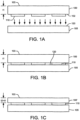
- devices 110 are illustrated in Figure 1A as including mesas, it will be appreciated that the devices may not include mesas, and that device isolation, if required, may be achieved by other methods, such as, for example, junction isolation, trench isolation, and/or implant isolation.
- the devices 110 may include, for example, silicon carbide-based power semiconductor devices such as SiC Schottky diodes, MOSFETs, BJTs, PiN diodes, n-channel IGBTs, thyristors and/or vertical JFETs.
- the devices 110 may further include silicon carbide-based GTOs and n-channel IGBTs on p-type substrates.
- the devices 110 may include other types of devices; thus, the foregoing list is not intended to be limiting.
- Figure 1A further illustrates a carrier substrate 105 on which an adhesive surface 120 is provided.
- the adhesive surface 120 may include, for example, wax and/or adhesive tape.
- the arrows in Figure 1A indicate that the front side 102 of wafer 100 (including devices 110) is brought into contact with the adhesive surface 120 on the carrier substrate 105.
- the carrier substrate 105 may include any suitable material capable of providing mechanical support for the wafer 100, including devices 110 thereon, during subsequent processing steps.
- the carrier substrate 105 may include, for example, sapphire, silicon, aluminum, alumina, and/or any other suitable material.
- a wafer 100 (including the plurality of semiconductor devices 110) and a carrier substrate 105 are coupled together via an adhesive layer 120 in contact with the plurality of semiconductor devices 110 so that the assembly can be processed by, for example, mounting the carrier substrate 105 in a grinder (not shown) so that the backside 103 of the wafer 100 can be accessed.
- the wafer 100 including the plurality of semiconductor devices 110 thereon can be coupled to the carrier substrate 105 using any technique known to those skilled in the art, such as a wax, and that an adhesive layer 120 may be applied to the plurality of semiconductor devices 110 or to the carrier substrate 105.
- contact includes direct contact as well as indirect contact where, for example, one or more intervening elements (such as the adhesive layer described above) are present between the wafer 100 and the carrier substrate 105 so that these two elements can be coupled together and the backside 103 of the wafer 100 can be processed while the wafer 100 is being supported by the carrier substrate 105.
- intervening elements such as the adhesive layer described above
- the backside 103 of the wafer 100 is processed to reduce the wafer 100 to a thickness t2, which is less than t1, to form a thinned wafer 100',
- the thickness of the wafer 100 is reduced using a grinder, such as an in-feed or creep feed grinder.
- the thickness of the wafer 100 is reduced using lapping, chemical or reactive ion etching or combinations of these approaches with or without grinding.
- etching may be used to treat the backside of the thinned wafer to reduce damage to the wafer that may result from the thinning operation. Methods of thinning a wafer are described, for example, in commonly assigned U.S. Patent Application Serial No. 10/987,135, filed November 12, 2004 by Slater et al.
- the wafer 100 is thinned to a thickness of less than about 150 ⁇ m (microns). In other examples, the wafer 100 is thinned to a thickness of less than about 120 ⁇ m (microns). In further examples, the wafer 100 is thinned to a thickness of from about 80 ⁇ m (microns) to about 100 ⁇ m (microns) or less. In some examples, the wafer 100 is thinned using an in-feed grinder or a creep-feed grinder.
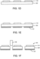
- the carrier substrate 105 can be removed from the assembly by, for example, heating the adhesive layer 120 so that the thinned wafer 100' and the plurality of semiconductor devices 110 thereon may be removed as shown in Figure 1D .
- the carrier substrate 105 can be removed from the assembly using an appropriate solvent and/or by exposing the structure to ultraviolet light.
- the adhesive layer 120 may be dissolved and/or melted to separate the carrier substrate 105 from the wafer 100'.
- ohmic contacts 107 can be formed on the backside 103 of the wafer 100' using, for example, localized annealing as discussed in U.S. Patent Application Serial No. 10/916,113, entitled “Localized Annealing of Metal-Silicon Carbide Ohmic Contacts and Devices So Formed” to Slater et al., filed August 11, 2004 , which is commonly assigned to the present assignee. It will be understood that the ohmic contacts can be formed on the thinned wafer 100' while the wafer 100' is coupled to the carrier substrate 105.
- the ohmic contacts can be formed on the thinned wafer 100' after the wafer is removed from the wafer carrier, as shown for example, in Figure 1E .
- Ohmic contacts and/or bonding pads can be formed on the plurality of semiconductor devices 110 opposite the ohmic contacts 107.
- a metal layer is formed on a back side of the SiC substrate 100' opposite the semiconductor devices 110.
- a layer of platinum, titanium, or nickel can be formed to a thickness of about 400 angstroms to about 1100 angstroms.
- the metal layer is then annealed using a localized annealing technique, such as laser annealing.
- a localized annealing technique such as laser annealing
- the laser light used to anneal the metal-SiC ohmic contacts described herein can be a laser light having a wavelength and intensity sufficient to form the metal-silicide material at the interface of the metal layer and the thinned SiC substrate 100'.
- laser annealing may be accomplished by impinging laser light having a wavelength of about 248 nanometers to about 308 nanometers at an energy of about 2.8 joules per square centimeter in a single pulse having a duration of about 30 nanoseconds.
- the laser light may have a wavelength of about 248 nanometers to about 308 nanometers and an energy of about 4.2 joules per square centimeter applied in about 5 pulses, each having a duration of about 30 nanoseconds.
- other wavelengths and energies may be used to provide annealing at the interface location of the metal layer and the SiC substrate via absorption of light including photon energies that are above the bandgap of the SiC substrate. It will be understood that pulsed and/or continuous loop lasers may also be utilized.
- Electron beam annealing may be used as an alternative to laser light. Accordingly, an electron beam may be used to anneal the interface locations of the metal layer and the SiC substrate to form the metal-SiC material thereat.
- the plurality of semiconductor devices 110 may be separated from one another by, for example, breaking the thinned wafer 100' and/or partially or completely cutting through the entire wafer 100 with a dicing saw.
- a saw blade 130 can be used to cut the wafer 100' to separate the plurality of semiconductor devices 110 for packaging. It will be understood that the saw blade 130 can cut through the entire wafer 100' to form straight edges on the thinned wafer 100' between the separated plurality of semiconductor devices 110 or substantially through the thinned wafer 100' so that the semiconductor devices 110 may be separated from one another by applying pressure along score lines formed by the saw blade 30.
- one or more layers may be formed on a substrate to a thickness such that the substrate may be removed from the layers altogether.
- the layers may include epitaxial layers grown on the substrate.
- the layers may include implanted layers.
- a substrate 100 on which one or more silicon carbide epitaxial layers 140 have been formed may be affixed to a carrier substrate 105 by an adhesive layer 120 as illustrated in Figure 2A .
- the carrier substrate 105 may include sapphire, silicon, alumina or any other suitable material, while the adhesive layer 120 may include wax, adhesive tape, or any other suitable adhesive material.
- the epitaxial layers 140 may be grown to a thickness of at least about 3 ⁇ m (microns) to about 10 ⁇ m (microns) or more.
- Ohmic contacts 107 can be formed on the epitaxial layer 140 using, for example, laser annealing as described above.
- the ohmic contacts 107 can be formed on the epitaxial layer 140 while the epitaxial layer 140 is coupled to the carrier substrate 105, as shown for example, in Figure 2C .
- the ohmic contacts 107 can be formed on the epitaxial layer 140 after the epitaxial layer 140 is removed from the carrier substrate 105.
- FIGS 3A-3J Further examples providing background information useful to understanding the invention are illustrated in Figures 3A-3J , in which the formation of Schottky diodes according to some examples is illustrated. It will be appreciated, however, that methods according to the described examples and the embodiments of the invention may be employed to fabricate many different types of power semiconductor devices, including, for example, SiC MOSFETs, BJTs, PiN diodes, n-channel IGBTs, thyristors and vertical JFETs, as well as GTOs and n-channel IGBTs on p-type substrates.
- SiC MOSFETs SiC MOSFETs
- BJTs PiN diodes
- n-channel IGBTs n-channel IGBTs
- thyristors thyristors
- vertical JFETs vertical JFETs
- an epitaxial layer 220 is formed on a substrate 210, which may have an initial thickness of about 300 ⁇ m (microns) to about 400 ⁇ m (microns).
- the epitaxial layer 220 includes n-type silicon carbide having a thickness from about 3 ⁇ m (microns) to about 10 ⁇ m (microns).
- the epitaxial layer 220 may have other thicknesses and/or conductivity types.
- the epitaxial layer 220 may include a plurality of epitaxial layers which are used in the resulting devices.
- the substrate 210 may include any suitable silicon carbide substrate.
- the substrate 210 may include an n+ 4H silicon carbide substrate that is cut 8° off-axis to the (0001) plane.
- a wafer carrier 250 is affixed to the front side of the substrate 210 by means of an adhesive layer 240.
- the wafer carrier 250 may include sapphire, silicon, alumina or any other suitable material, while the adhesive layer 240 may include wax, adhesive tape, or any other suitable adhesive material.
- the substrate 210 has an initial thickness t1 and is subsequently thinned to a second thickness t2, which is less than t1, as illustrated in Figure 3F .
- the initial thickness t1 is from about 300 ⁇ m (microns) to about 400 ⁇ m (microns), while the second thickness is from about 80 ⁇ m (microns) to about 100 ⁇ m (microns).
- the substrate 210 may be completely removed from the epitaxial layer 220.
- an ohmic contact 255 may be formed on the backside of the thinned wafer 210'.
- the ohmic contact 255 may be locally annealed in the manner described above. Localized annealing may be employed to anneal the ohmic contact 255 on the backside of the thinned wafer 210' without substantially heating the front side of the thinned wafer and the associated device structures.
- laser annealing may be employed to anneal the ohmic contact 255 on the backside of the thinned wafer 210' without causing the wafer carrier 250 to separate from the epitaxial layer 220.
- the laser light may have a wavelength of about 248 nanometers to about 308 nanometers and an energy of about 4.2 joules per square centimeter applied in about 5 pulses, each having a duration of about 30 nanoseconds.
- other wavelengths and energies may be used to provide annealing at the interface location of the metal layer and the SiC substrate via absorption of light including photon energies that are above the bandgap of the SiC substrate. It will be understood that pulse and/or continuous loop lasers may also be utilized.
- Electron beam annealing may be used as an alternative to laser light. Accordingly, an electron beam may be used to anneal the interface locations of the metal layer and the SiC substrate to form the metal-SiC material thereat.
- a backside metal overlayer 265 may be applied to the ohmic contact 255, as shown in Figure 3I .
- the backside metal overlayer 265 may include, for example, stacks of adhesion, barrier and bonding layers such as Ti/Ni/Ag and/or Ti/TiW/Au.
- the wafer carrier 250 may be removed from the epitaxial layer 220 by heating the adhesive layer 240, using an appropriate solvent to dissolve the adhesive layer 240, and/or by exposing the adhesive layer 240 to ultraviolet light.
- Figure 4 shows curves of the forward current-voltage (I-V) characteristics of 300 V 4H-SiC Schottky diodes for a device formed according to a described example method (curve 302) and a conventional SiC Schottky diode (curve 300).
- the conventional device had an approximately 400 ⁇ m (micron) thick substrate, while the device formed according to the described example method had an approximately 100 ⁇ m (micron) thick substrate.
- the current rating of the diodes was 10 A. Current-voltage measurements were taken at room temperature. As shown in Figure 4 , the forward voltage drop of the conventional diode at a forward current of 10A was about 1.3 V.
- the forward voltage drop of the diode formed according the described example method was about 1.02 V at 10A, which represents an approximately 23 % reduction in forward voltage.
- the resistive drop, which is calculated from the knee voltage (approximately 0.7 V) was reduced from about 0.6 V to about 0.3 V, which is a reduction of 50%.
Description
- This invention relates to microelectronic devices, and more particularly, to the fabrication of silicon carbide power devices.
- The thickness of silicon-carbide (SiC) substrates in SiC-based power semiconductor devices can affect the forward voltage needed to operate the devices at a given current level. In particular, the performance and/or operation of SiC devices such as SiC Schottky diodes, MOSFETs, BJTs, PiN diodes, n-channel IGBTs, thyristors and/or vertical JFETs may be affected by the relatively high resistance of thick SiC substrates. For example, n-type, 4H-SiC substrates may account for about 1 mohm-cm2 of the specific on-resistance of various devices. This may constitute about 50% of the on-resistance of a 600 V SiC Schottky diode, and/or about 90% of the on-resistance of a 300V SiC Schottky diode. A p-type 4H-SiC substrate may add about 50-100 mohm-cm2 to the device on-resistance. For this reason, it has not been practical to develop vertical devices, such as GTOs and n-channel IGBTs, on p-type SiC substrates.
- Present SiC device fabrication technology typically employs relatively thick (300-400 µm (microns)) substrates. Fabrication processing, including the backside ohmic contact anneal, may be performed on epilayers grown on the substrate. Since there may be subsequent processing steps
after ohmic contact formation, the substrate is typically thick enough to provide adequate mechanical support for the epilayers. However, the thick substrate used for mechanical support may add to the electrical and/or thermal resistance of the device. - Ohmic contacts may be formed on SiC substrates at low/room temperatures by, for example, implanting ions into a surface of a SiC wafer on which the contact is to be formed. In some conventional approaches, the ohmic contacts may be formed by implantation of dopants into a backside of a SiC wafer. However, if an implanted doped SiC substrate is thinned prior to formation of ohmic contacts, the doped region may be removed during the thinning, which may make the implant superfluous. Accordingly, metals deposited for ultimately forming ohmic contacts may not have ohmic properties when deposited on the substrate, as the implant may be performed in a later step. Ion implantation for the formation of ohmic contacts is discussed, for example, in
U.S. Patent Application Serial No. 09/787,189 , and inU.S. Patent Publication No. 2002/0179910 , the disclosures of which are incorporated herein by reference in their entireties. - International Patent Publication no.
WO 01/86727 - International Patent Publication no.
WO 2005/048363 describes forming a plurality of Light Emitting Devices (LED) on a semiconductor wafer having a first thickness. The plurality of LEDs on the wafer are brought into contact with, and coupled to, a surface of a carrier. The first thickness of the wafer is reduced to a second thickness that is less than the first thickness by processing the backside of the wafer. The carrier is separated from the plurality of LEDs on the wafer and the wafer is cut to separate the plurality of LEDs from one another. -
US Patent Publication 2005/104072 describes forming a contact for a semiconductor device by forming a metal on a Silicon Carbide (SiC) substrate and annealing an interface location of the metal and the SiC substrate to form a metal-SiC material thereat. - According to a first aspect, there is provided a method of forming a silicon carbide semiconductor device, as described in claim 1.
- A method of forming a silicon carbide semiconductor device not according to the invention but providing background information useful to understanding the invention is described, including forming a semiconductor device at a first surface of a silicon carbide substrate having a first thickness and mounting a carrier substrate to the first surface of the silicon carbide substrate. The carrier substrate provides mechanical support to the silicon carbide substrate. The methods further include thinning the silicon carbide substrate to a thickness less than the first thickness, forming a metal layer on
the thinned silicon carbide substrate opposite the first surface of the silicon carbide substrate, and locally annealing the metal layer to form an ohmic contact on the thinned silicon carbide substrate opposite the first surface of the silicon carbide substrate. The silicon carbide substrate is singulated to provide a singulated semiconductor device. - Thinning the silicon carbide substrate may include grinding and/or lapping the silicon carbide substrate while the carrier substrate
provides mechanical support to the silicon carbide substrate. In particular, thinning the silicon carbide substrate may include grinding the silicon carbide substrate using an in-feed and/or creep feed grinder while the carrier substrate provides mechanical support to the silicon carbide substrate. In some examples, thinning the silicon carbide substrate may include etching the silicon carbide substrate while the carrier substrate provides mechanical support to the silicon carbide substrate. - Forming an electronic device may include forming a passivation layer on the first surface of the silicon carbide substrate, and mounting the carrier substrate to the first surface of the silicon carbide substrate may include attaching the carrier substrate to the passivation layer.
- Locally annealing the metal layer may include locally heating the deposited metal layer to a temperature that may be sufficient to cause the metal layer to form an ohmic contact to the surface of the silicon carbide substrate opposite the first surface but that may be lower than a temperature at which the carrier substrate will detach from the silicon carbide substrate. In particular, locally heating the deposited metal layer may include laser annealing the deposited metal layer and/or electron beam annealing the deposited metal layer. Laser annealing may include impinging laser light having photon energies above a bandgap of the SiC substrate, and laser annealing may include impinging pulsed or continuous wave laser light.
- The SiC substrate may include 4H SiC and/or 6H SiC, and laser annealing may include impinging laser light on the deposited metal layer. The laser light may have a wavelength of about 248 nanometers to about 308 nanometers.
- The SiC substrate may include 6H SiC, and the laser light may be applied in a single pulse that may have a duration of about 30 nanoseconds. The laser light may be applied at an energy of about 2.8 joules/cm2.
- The SiC substrate may include 4H SiC, and the laser light may be applied in a plurality of pulses. For example, the laser light may be applied in about five pulses each having a duration of about 30 nanoseconds, and the laser light may be applied at an energy of about 4.2 joules/cm2.
- The methods may further include forming a metal overlayer on the ohmic contact. The metal overlayer may include an adhesion layer including Ti, a barrier layer including Ni and/or Ti/W, and a bonding layer including Ag and/or Au.
- Thinning the substrate may include thinning the substrate to a thickness of about 120 µm (microns) or less. In some examples, thinning the substrate may include thinning the substrate to a thickness of about 80 µm (microns) to about 100 µm (microns).
- Methods of forming a silicon carbide semiconductor device according to the invention include forming a silicon carbide epitaxial layer on a surface of a silicon carbide substrate, forming a semiconductor device at a first surface of the epitaxial layer opposite the silicon carbide substrate, and mounting a carrier substrate to the first surface of the epitaxial layer. The carrier substrate provides mechanical support to the epitaxial layer. The methods further include removing the silicon carbide substrate to expose a second surface of the epitaxial layer opposite the first surface, forming a metal layer on the second surface of the epitaxial layer, locally annealing the metal layer to form an ohmic contact on the second surface of the epitaxial layer, and separating the epitaxial layer from the carrier substrate.
- Removing the silicon carbide substrate may include grinding and/or lapping the silicon carbide substrate while the carrier substrate provides mechanical support to the epitaxial layer. In particular, removing the silicon carbide substrate may include grinding the silicon carbide substrate using an in-feed and/or creep feed grinder while the carrier substrate provides mechanical support to the epitaxial layer. In some embodiments, removing the silicon carbide substrate may include etching the silicon carbide substrate while the carrier substrate provides mechanical support to the epitaxial layer.
- Forming an electronic device may include forming a passivation layer on the first surface of the epitaxial layer, and mounting the carrier substrate to the first surface of the epitaxial layer may include attaching the carrier substrate to the passivation layer.
- Locally annealing the metal layer includes locally heating the deposited metal layer to a temperature that may be sufficient to cause the metal layer to form an ohmic contact to the surface of the silicon carbide substrate opposite the first surface but that may be lower than a temperature at which the carrier substrate will detach from the epitaxial layer.
- A further method of forming a silicon carbide semiconductor device not according to the invention but providing background information useful to understanding the invention is described, including forming a semiconductor device at a first surface of a silicon carbide substrate having a first thickness greater than about 300 µm (microns), and mounting a carrier substrate to the first surface of the silicon carbide substrate. The carrier substrate provides mechanical support to the silicon carbide substrate. The method further includes thinning the silicon carbide substrate to a thickness of less than about 150 µm (microns) and forming an ohmic contact on the thinned silicon carbide substrate opposite the first surface of the thinned silicon carbide substrate.
- Forming the ohmic contact may include forming a metal layer on the thinned silicon carbide substrate opposite the first surface of the silicon carbide substrate, and locally annealing the metal layer to form an ohmic contact on the thinned silicon carbide substrate opposite the first surface of the silicon carbide substrate.
- Locally annealing the metal layer may include locally heating the deposited metal layer to a temperature that may be sufficient to cause the metal layer to form an ohmic contact to the surface of the silicon carbide substrate opposite the first surface but that may be lower than a temperature at which the carrier substrate will detach from the silicon carbide substrate.
- Locally heating the deposited metal layer may include laser annealing the deposited metal layer and/or directing an electron beam at the metal layer.
- The accompanying drawings, which are included to provide a further understanding of the invention and are incorporated in and constitute a part of this application, illustrate certain examples providing background information useful to understanding the invention and embodiment(s) of the invention. In the drawings:
-
Figures 1A-1F are cross-sectional illustrations that illustrate methods of processing semiconductor wafers according to an example providing background information useful to understanding the invention; -
Figures 2A-2D are cross-sectional illustrations that illustrate methods of processing semiconductor wafers according to some embodiments of the invention; -
Figures 3A-3J are cross-sectional illustrations that illustrate methods of processing semiconductor wafers according to an example providing background information useful to understanding the invention; and -
Figure 4 is a graph of current versus voltage for a conventional SiC Schottky device and a SiC Schottky device formed according to some of the described examples. - The invention now will be described more fully hereinafter with reference to the accompanying drawings, in which examples providing background information useful to understanding the invention and embodiments of the invention are shown. These embodiments are provided so that this disclosure will be thorough and complete, and will fully convey the scope of the invention to those skilled in the art. In the drawings, the thickness of layers and regions are exaggerated for clarity. Like numbers refer to like elements throughout. As used herein the term "and/or" includes any and all combinations of one or more of the associated listed items.
- The terminology used herein is for the purpose of describing particular embodiments only and is not intended to be limiting of the invention. As used herein, the singular forms "a", "an" and "the" are intended to include the plural forms as well, unless the context clearly indicates otherwise. It will be further understood that the terms "comprises" and/or "comprising," when used in this specification, specify the presence of stated features, integers, steps, operations, elements, and/or components, but do not preclude the presence or addition of one or more other features, integers, steps, operations, elements, components, and/or groups thereof.
- It will be understood that when an element such as a layer, region or substrate is referred to as being "on" or extending "onto" another element, it can be directly on or extend directly onto the other element or intervening elements may also be present. In contrast, when an element is referred to as being "directly on" or extending "directly onto" another element, there are no intervening elements present. It will also be understood that when an element is referred to as being "connected" or "coupled" to another element, it can be directly connected or coupled to the other element or intervening elements may be present. In contrast, when an element is referred to as being "directly connected" or "directly coupled" to another element, there are no intervening elements present. Like numbers refer to like elements throughout the specification.
- Examples providing background information useful to understanding the invention and embodiments of the present invention are described herein with reference to cross-section (and/or plan view) illustrations that are schematic illustrations of idealized examples or embodiments. As such, variations from the shapes of the illustrations as a result, for example, of manufacturing techniques and/or tolerances, are to be expected. Thus, embodiments of the present invention should not be construed as limited to the particular shapes of regions illustrated herein but are to include deviations in shapes that result, for example, from manufacturing. For example, an etched region illustrated or described as a rectangle will, typically, have rounded or curved features. Thus, the regions illustrated in the figures are schematic in nature and their shapes are not intended to illustrate the precise shape of a region of a device and are not intended to limit the scope of the present invention.
- Unless otherwise defined, all terms (including technical and scientific terms) used herein have the same meaning as commonly understood by one of ordinary skill in the art to which this invention belongs. It will be further understood that terms, such as those defined in commonly used dictionaries, should be interpreted as having a meaning that is consistent with their meaning in the context of this specification and the relevant art and will not be interpreted in an idealized or overly formal sense unless expressly so defined herein. It will also be appreciated by those of skill in the art that references to a structure or feature that is disposed "adjacent" another feature may have portions that overlap or underlie the adjacent feature.
- Some examples and some embodiments of the invention are described with reference to semiconductor layers and/or regions which are characterized as having a conductivity type such as n-type or p-type, which refers to the majority carrier concentration in the layer and/or region. Thus, n-type material has a majority equilibrium concentration of negatively charged electrons, while p-type material has a majority equilibrium concentration of positively charged holes. Some material may be designated with a "+" or "-" (as in n+, n-, p+, p-, n++, n--, p++, p--, or the like), to indicate a relatively larger ("+") or smaller ("- ") concentration of majority carriers compared to another layer or region. However, such notation does not imply the existence of a particular concentration of majority or minority carriers in a layer or region.
- As used herein the term "ohmic contact" refers to a contact having an impedance associated therewith that is substantially given by the relationship of Impedance = V/I, where V is a voltage across the contact and I is the current, at substantially all expected operating frequencies (i.e., the impedance associated with the ohmic contact is substantially the same at all operating frequencies). For example, in some embodiments according to the invention, an ohmic contact can be a contact with a specific contact resistivity of less than about 10-3 ohm-cm2 and, in some embodiments less than about 10-4 ohm-cm2.
- As described herein in greater detail, an example providing background information useful to understanding the invention can provide methods of processing semiconductor wafers of semiconductor devices by, for example, reducing a thickness of a silicon carbide wafer having silicon carbide semiconductor devices formed thereon by processing the wafer from a backside thereof. A semiconductor wafer generally has two major parallel surfaces. As used herein, the term "backside" of a wafer refers to the major surface of the wafer opposite the surface of the wafer at which one or more semiconductor devices are formed.
- According to an example providing background information useful to understanding the invention, as shown in
Figure 1A , a wafer (i.e., a substrate) 100 may typically have a thickness (t1) of about 300 µm (microns) to about 400 µm (microns). A plurality ofsemiconductor devices 110 are formed on or at afront side 102 of thewafer 100 that is opposite abackside 103 of thewafer 100. It will be understood that the plurality ofsemiconductor devices 110 can be silicon carbide power semiconductor devices, such as PIN diodes, MOSFETs, IGBTs, etc. Thesemiconductor devices 110 may include one or more silicon carbide epitaxial layers/regions formed on thefront side 102 of thewafer 100. The layers/regions may be formed, for example, by epitaxial growth and/or by ion implantation. Thedevices 110 may include an active region having a p-n junction for bipolar operation. In examples, thedevices 110 may include majority carrier devices, such as Schottky diodes, that do not include a p-n junction. - In some embodiments according to the invention, the wafer and/or associated epitaxial layers include silicon carbide of the 4H, 6H, 15R or 3C polytypes. In examples providing background information useful to understanding the invention, the wafer and/or associated epitaxial layers may include another type of material known to those skilled in the art, such as, for example, silicon, gallium arsenide, gallium nitride, aluminum nitride, aluminum gallium nitride, magnesium oxide (MgO), magnesium aluminate (MgAl2O4), lithium gallate (LiGaO2), lithium aluminate (LiAlO2), zinc oxide (ZnO), nickel aluminate (NiAl2O4), and/or sapphire. While the
devices 110 are illustrated inFigure 1A as including mesas, it will be appreciated that the devices may not include mesas, and that device isolation, if required, may be achieved by other methods, such as, for example, junction isolation, trench isolation, and/or implant isolation. - The
devices 110 may include, for example, silicon carbide-based power semiconductor devices such as SiC Schottky diodes, MOSFETs, BJTs, PiN diodes, n-channel IGBTs, thyristors and/or vertical JFETs. Thedevices 110 may further include silicon carbide-based GTOs and n-channel IGBTs on p-type substrates. Thedevices 110 may include other types of devices; thus, the foregoing list is not intended to be limiting. -
Figure 1A further illustrates acarrier substrate 105 on which anadhesive surface 120 is provided. Theadhesive surface 120 may include, for example, wax and/or adhesive tape. The arrows inFigure 1A indicate that the
front side 102 of wafer 100 (including devices 110) is brought into contact with theadhesive surface 120 on thecarrier substrate 105. Thecarrier substrate 105 may include any suitable material capable of providing mechanical support for thewafer 100, includingdevices 110 thereon, during subsequent processing steps. Thecarrier substrate 105 may include, for example, sapphire, silicon, aluminum, alumina, and/or any other suitable material. - As shown in
Figure 1B , in some examples providing background information useful to understanding the invention, a wafer 100 (including the plurality of semiconductor devices 110) and acarrier substrate 105 are coupled together via anadhesive layer 120 in contact with the plurality ofsemiconductor devices 110 so that the assembly can be processed by, for example, mounting thecarrier substrate 105 in a grinder (not shown) so that thebackside 103 of thewafer 100 can be accessed. It will be understood that thewafer 100 including the plurality ofsemiconductor devices 110 thereon can be coupled to thecarrier substrate 105 using any technique known to those skilled in the art, such as a wax, and that anadhesive layer 120 may be applied to the plurality ofsemiconductor devices 110 or to thecarrier substrate 105. It will be further understood that the term "contact" includes direct contact as well as indirect contact where, for example, one or more intervening elements (such as the adhesive layer described above) are present between thewafer 100 and thecarrier substrate 105 so that these two elements can be coupled together and thebackside 103 of thewafer 100 can be processed while thewafer 100 is being supported by thecarrier substrate 105. - Referring to
Figure 1C , in some examples providing background information useful to understanding the invention, thebackside 103 of thewafer 100 is processed to reduce thewafer 100 to a thickness t2, which is less than t1, to form a thinned wafer 100', - In some examples, the thickness of the
wafer 100 is reduced using a grinder, such as an in-feed or creep feed grinder. In other examples, the thickness of thewafer 100 is reduced using lapping, chemical or reactive ion etching or combinations of these approaches with or without grinding. In still other examples, etching may be used to treat the backside of the thinned wafer to reduce damage to the wafer that may result from the thinning operation. Methods of thinning a wafer are described, for example, in commonly assignedU.S. Patent Application Serial No. 10/987,135, filed November 12, 2004 by Slater et al. U.S. Patent Application Serial No. 11/064,798, filed 2/23/2005 by Edmond et al , entitled "Substrate Removal Process for High Light Extraction LEDs";U.S. Patent Application Serial No. 10/951,042, filed 9/22/2004 by Edmond et al. U.S. Patent Application Serial No. 11/037,965, filed 1/18/2005 by Edmond et al. entitled "High Output Small Area Group III Nitride LEDs". - In some examples, the
wafer 100 is thinned to a thickness of less than about 150 µm (microns). In other examples, thewafer 100 is thinned to a thickness of less than about 120 µm (microns). In further examples, thewafer 100 is thinned to a thickness of from about 80 µm (microns) to about 100 µm (microns) or less. In some examples, thewafer 100 is thinned using an in-feed grinder or a creep-feed grinder. - Once the
backside 103 has been processed to sufficiently thin the wafer 100 (resulting in the formation of a thinned wafer 100'), thecarrier substrate 105 can be removed from the assembly by, for example, heating theadhesive layer 120 so that the thinned wafer 100' and the plurality ofsemiconductor devices 110 thereon may be removed as shown inFigure 1D . In other examples, thecarrier substrate 105 can be removed from the assembly using an appropriate solvent and/or by exposing the structure to ultraviolet light. For example, theadhesive layer 120 may be dissolved and/or melted to separate thecarrier substrate 105 from the wafer 100'. - Referring to
Figure 1E ,ohmic contacts 107 can be formed on thebackside 103 of the wafer 100' using, for example,
localized annealing as discussed inU.S. Patent Application Serial No. 10/916,113, entitled "Localized Annealing of Metal-Silicon Carbide Ohmic Contacts and Devices So Formed" to Slater et al., filed August 11, 2004 carrier substrate 105. In some examples, the ohmic contacts can be formed on the thinned wafer 100' after the wafer is removed from the wafer carrier, as shown for example, inFigure 1E . Ohmic contacts and/or bonding pads (not shown) can be formed on the plurality ofsemiconductor devices 110 opposite theohmic contacts 107. - To form the
ohmic contacts 107, a metal layer is formed on a back side of the SiC substrate 100' opposite thesemiconductor devices 110. In particular, a layer of platinum, titanium, or nickel can be formed to a thickness of about 400 angstroms to about 1100 angstroms. - The metal layer is then annealed using a localized annealing technique, such as laser annealing. In laser annealing, the laser light used to anneal the metal-SiC ohmic contacts described herein can be a laser light having a wavelength and intensity sufficient to form the metal-silicide material at the interface of the metal layer and the thinned SiC substrate 100'. For example, in examples using 6H SiC as the substrate, laser annealing may be accomplished by impinging laser light having a wavelength of about 248 nanometers to about 308 nanometers at an energy of about 2.8 joules per square centimeter in a single pulse having a duration of about 30 nanoseconds. In other examples where, for example, the SiC substrate is 4H SiC, the laser light may have a wavelength of about 248 nanometers to about 308 nanometers and an energy of about 4.2 joules per square centimeter applied in about 5 pulses, each having a duration of about 30 nanoseconds. In still other examples, other wavelengths and energies may be used to provide annealing at the interface location of the metal layer and the SiC substrate via absorption of light including photon energies that are above the bandgap of the SiC substrate. It will be understood that pulsed and/or continuous loop lasers may also be utilized.
- Electron beam annealing may be used as an alternative to laser light. Accordingly, an electron beam may be used to anneal the interface locations of the metal layer and the SiC substrate to form the metal-SiC material thereat.
- Referring to
Figure 1F , the plurality ofsemiconductor devices 110 may be separated from one another by, for example, breaking the thinned wafer 100' and/or partially or completely cutting through theentire wafer 100 with a dicing saw. For example, asaw blade 130 can be used to cut the wafer 100' to separate the plurality ofsemiconductor devices 110 for packaging. It will be understood that thesaw blade 130 can cut through the entire wafer 100' to form straight edges on the thinned wafer 100' between the separated plurality ofsemiconductor devices 110 or substantially through the thinned wafer 100' so that thesemiconductor devices 110 may be separated from one another by applying pressure along score lines formed by the saw blade 30. - In an embodiment of the invention, one or more layers may be formed on a substrate to a thickness such that the substrate may be removed from the layers altogether. In some embodiments, the layers may include epitaxial layers grown on the substrate. However, the layers may include implanted layers. For example, referring to the embodiments of
Figures 2A-2D , asubstrate 100 on which one or more silicon carbideepitaxial layers 140 have been formed may be affixed to acarrier substrate 105 by anadhesive layer 120 as illustrated inFigure 2A . - As in the examples of
Figures 1A-1F , thecarrier substrate 105 may include sapphire, silicon, alumina or any other suitable material, while theadhesive layer 120 may include wax, adhesive tape, or any other suitable adhesive material. In order to provide adequate mechanical stability, theepitaxial layers 140 may be grown to a thickness of at least about 3 µm (microns) to about 10 µm (microns) or more. - The
substrate 100 may be removed from theepitaxial layer 140 using a grinder, such as an in-feed or creep feed grinder. In other embodiments according to the invention, thewafer 100 may be removed by lapping, chemical or reactive ion etching or combinations of these approaches with or without grinding. A selectivity of the grinding or other thinning process may allow a transition from thesubstrate 100 to theepitaxial layer 140 to provide an end point to the thinning. -
Ohmic contacts 107 can be formed on theepitaxial layer 140 using, for example, laser annealing as described above. Theohmic contacts 107 can be formed on theepitaxial layer 140 while theepitaxial layer 140 is coupled to thecarrier substrate 105, as shown for example, inFigure 2C . However, in some embodiments according to the invention, theohmic contacts 107 can be formed on theepitaxial layer 140 after theepitaxial layer 140 is removed from thecarrier substrate 105. - The
epitaxial layer 140 may then be removed from thecarrier substrate 105 and diced, for example using a dicing saw 130, to formsingulated devices 150, as shown inFigure 2D . In some embodiments, thedevices 150 may be singulated (i.e. separated into individual devices) using a scribe-and-break process instead of and/or in addition to sawing. - Further examples providing background information useful to understanding the invention are illustrated in
Figures 3A-3J , in which the formation of Schottky diodes according to some examples is illustrated. It will be appreciated, however, that methods according to the described examples and the embodiments of the invention may be employed to fabricate many different types of power semiconductor devices, including, for example, SiC MOSFETs, BJTs, PiN diodes, n-channel IGBTs, thyristors and vertical JFETs, as well as GTOs and n-channel IGBTs on p-type substrates. - Referring to
Figure 3A , anepitaxial layer 220 is formed on asubstrate 210, which may have an initial thickness of about 300 µm (microns) to about 400 µm (microns). In the illustrated examples, theepitaxial layer 220 includes n-type silicon carbide having a thickness from about 3 µm (microns) to about 10 µm (microns). However, theepitaxial layer 220 may have other thicknesses and/or conductivity types. Theepitaxial layer 220 may include a plurality of epitaxial layers which are used in the resulting devices. Thesubstrate 210 may include any suitable silicon carbide substrate. In
some examples, thesubstrate 210 may include an n+ 4H silicon carbide substrate that is cut 8° off-axis to the (0001) plane. - A device may be defined in the
epitaxial layer 220 as follows. First, as shown inFigure 3B ,edge termination regions 225 may be implanted in theepitaxial layer 220 to define anactive device area 227 within thetermination regions 225. Metal contacts, including aSchottky contact 230 are formed on the active device area 227 (Figure 3C ). Afield passivation layer 235 is deposited on the surface of the structure. In some examples, the passivation layer may be patterned to reveal theSchottky contact 230 as illustrated inFigure 3D . However, it will be appreciated that in some examples, thepassivation layer 235 may not be patterned until a subsequent processing step, for example, after the wafer carrier has been removed. - Referring now to
Figure 3E , awafer carrier 250 is affixed to the front side of thesubstrate 210 by means of anadhesive layer 240. As described above, thewafer carrier 250 may include sapphire, silicon, alumina or any other suitable material, while theadhesive layer 240 may include wax, adhesive tape, or any other suitable adhesive material. - The backside 212 of the
substrate 210 is then thinned and/or removed by grinding, lapping, chemical or reactive ion etching or combinations of the foregoing, as described above. In the examples illustrated inFigures 3A-3J , thesubstrate 210 has an initial thickness t1 and is subsequently thinned to a second thickness t2, which is less than t1, as illustrated inFigure 3F . In some examples, the initial thickness t1 is from about 300 µm (microns) to about 400 µm (microns), while the second thickness is from about 80 µm (microns) to about 100 µm (microns). In some embodiments according to the invention, thesubstrate 210 may be completely removed from theepitaxial layer 220. - Referring to
Figure 3G , anohmic contact 255 may be formed on the backside of the thinned wafer 210'. As shown inFigure 3H , theohmic contact 255 may be locally annealed in the manner described above. Localized annealing may be employed to anneal theohmic contact 255 on the backside of the thinned wafer 210' without substantially heating the front side of the thinned wafer and the associated device structures. For example, laser annealing may be employed to anneal theohmic contact 255 on the backside of the thinned wafer 210' without causing thewafer carrier 250 to separate from theepitaxial layer 220. - It will be understood that the laser light used to anneal the metal-SiC ohmic contacts described herein can be a laser light having a wavelength and intensity sufficient to form the metal-silicide material at the interface of the metal layer and the SiC substrate. For example, in examples using 6H SiC as the substrate, laser annealing may be accomplished by impinging laser light having a wavelength of about 248 nanometers to about 308 nanometers at an energy of about 2.8 joules per square centimeter in a single pulse having a duration of about 30 nanoseconds. In other examples where, for example, the SiC substrate is 4H SiC, the laser light may have a wavelength of about 248 nanometers to about 308 nanometers and an energy of about 4.2 joules per square centimeter applied in about 5 pulses, each having a duration of about 30 nanoseconds. In still other examples, other wavelengths and energies may be used to provide annealing at the interface location of the metal layer and the SiC substrate via absorption of light including photon energies that are above the bandgap of the SiC substrate. It will be understood that pulse and/or continuous loop lasers may also be utilized.
- Electron beam annealing may be used as an alternative to laser light. Accordingly, an electron beam may be used to anneal the interface locations of the metal layer and the SiC substrate to form the metal-SiC material thereat.
- A
backside metal overlayer 265 may be applied to theohmic contact 255, as shown inFigure 3I . Thebackside metal overlayer 265 may include, for example, stacks of adhesion, barrier and bonding layers such as Ti/Ni/Ag and/or Ti/TiW/Au. - Finally, as illustrated in
Figure 3J , thewafer carrier 250 may be removed from theepitaxial layer 220 by heating theadhesive layer 240, using an appropriate solvent to dissolve theadhesive layer 240, and/or by exposing theadhesive layer 240 to ultraviolet light. - Devices formed in accordance with embodiments of the invention may exhibit reduced on-resistance. In particular, some embodiments of the invention can be used to reduce device area for a given on-resistance, which may result in higher device yield and/or lower cost for silicon carbide power devices.
- The reduction of on-resistance may be more pronounced for low voltage devices. For example,
Figure 4 shows curves of the forward current-voltage (I-V) characteristics of 300 V 4H-SiC Schottky diodes for a device formed according to a described example method (curve 302) and a conventional SiC Schottky diode (curve 300). In particular, the conventional device had an approximately 400 µm (micron) thick substrate, while the device formed according to the described example method had an approximately 100 µm (micron) thick substrate. The current rating of the diodes was 10 A. Current-voltage measurements were taken at room temperature. As shown inFigure 4 , the forward voltage drop of the conventional diode at a forward current of 10A was about 1.3 V. In contrast, the forward voltage drop of the diode formed according the described example method was about 1.02 V at 10A, which represents an approximately 23 % reduction in forward voltage. The resistive drop, which is calculated from the knee voltage (approximately 0.7 V) was reduced from about 0.6 V to about 0.3 V, which is a reduction of 50%. - In the drawings and specification, there have been disclosed typical embodiments of the invention and, although specific terms are employed, they are used in a generic and descriptive sense only and not for purposes of limitation, the scope of the invention being set forth in the following claims.
Claims (7)
- A method of forming a silicon carbide semiconductor device, comprising:forming a silicon carbide epitaxial layer (140) on a surface of a silicon carbide substrate (100), the epitaxial layer having a thickness greater than 3 µm;forming a semiconductor device (110) at a first surface of the epitaxial layer (140) opposite the silicon carbide, SiC, substrate (100);mounting a carrier substrate (105) to the first surface of the epitaxial layer (140);removing the silicon carbide substrate (100) to expose a second surface of the epitaxial layer (140) opposite the first surface while the carrier substrate (105) is providing mechanical support to the epitaxial layer (140);forming a metal layer on the second surface of the epitaxial layer (140);locally annealing the metal layer to form an ohmic contact (107) on the second surface of the epitaxial layer (140); andseparating the epitaxial layer (140) from the carrier substrate (105); andwherein locally annealing the metal layer comprises locally heating the deposited metal layer to a temperature that is sufficient to cause the metal layer to form an ohmic contact (107) to the surface of the epitaxial layer (140) opposite the first surface but that is lower than a temperature at which the carrier substrate (105) will detach from the epitaxial layer (140).
- The method of Claim 1, wherein removing the silicon carbide substrate (100) comprises grinding and/or lapping the silicon carbide substrate (100).
- The method of Claim 2, wherein removing the silicon carbide substrate (100) comprises grinding the silicon carbide substrate (100) using an in-feed and/or creep feed grinder.
- The method of Claim 1, wherein removing the silicon carbide substrate (100) comprises etching the silicon carbide substrate (100).
- The method of Claim 1, wherein forming an electronic device comprises forming a passivation layer on the first surface of the epitaxial layer (140), and wherein mounting the carrier substrate (105) to the first surface of the epitaxial layer (140) comprises attaching the carrier substrate (105) to the passivation layer.
- The method of Claim 1, wherein locally heating the deposited metal layer comprises locally heating by laser annealing the deposited metal layer.
- The method of Claim 1, wherein locally heating the deposited metal layer comprises locally heating by directing an electron beam at the metal layer.
Applications Claiming Priority (3)
| Application Number | Priority Date | Filing Date | Title |
|---|---|---|---|
| US71814005P | 2005-09-16 | 2005-09-16 | |
| PCT/US2006/035516 WO2007035333A1 (en) | 2005-09-16 | 2006-09-12 | Methods of processing semiconductor wafers having silicon carbide power devices thereon |
| EP06803439.6A EP1935007B1 (en) | 2005-09-16 | 2006-09-12 | Methods of processing semiconductor wafers having silicon carbide power devices thereon |
Related Parent Applications (3)
| Application Number | Title | Priority Date | Filing Date |
|---|---|---|---|
| EP06803439.6A Division-Into EP1935007B1 (en) | 2005-09-16 | 2006-09-12 | Methods of processing semiconductor wafers having silicon carbide power devices thereon |
| EP06803439.6A Division EP1935007B1 (en) | 2005-09-16 | 2006-09-12 | Methods of processing semiconductor wafers having silicon carbide power devices thereon |
| EP06803439.6 Division | 2006-09-12 |
Publications (3)
| Publication Number | Publication Date |
|---|---|
| EP2546865A2 EP2546865A2 (en) | 2013-01-16 |
| EP2546865A3 EP2546865A3 (en) | 2013-03-06 |
| EP2546865B1 true EP2546865B1 (en) | 2023-12-06 |
Family
ID=37671124
Family Applications (2)
| Application Number | Title | Priority Date | Filing Date |
|---|---|---|---|
| EP06803439.6A Active EP1935007B1 (en) | 2005-09-16 | 2006-09-12 | Methods of processing semiconductor wafers having silicon carbide power devices thereon |
| EP12181385.1A Active EP2546865B1 (en) | 2005-09-16 | 2006-09-12 | Methods of processing semiconductor wafers having silicon carbide power devices thereon |
Family Applications Before (1)
| Application Number | Title | Priority Date | Filing Date |
|---|---|---|---|
| EP06803439.6A Active EP1935007B1 (en) | 2005-09-16 | 2006-09-12 | Methods of processing semiconductor wafers having silicon carbide power devices thereon |
Country Status (7)
| Country | Link |
|---|---|
| US (2) | US7547578B2 (en) |
| EP (2) | EP1935007B1 (en) |
| JP (2) | JP2009509339A (en) |
| KR (2) | KR20130086057A (en) |
| CN (1) | CN101263581B (en) |
| TW (1) | TWI411041B (en) |
| WO (1) | WO2007035333A1 (en) |
Families Citing this family (90)
| Publication number | Priority date | Publication date | Assignee | Title |
|---|---|---|---|---|
| US20050104072A1 (en) * | 2003-08-14 | 2005-05-19 | Slater David B.Jr. | Localized annealing of metal-silicon carbide ohmic contacts and devices so formed |
| CN1998094B (en) * | 2004-04-07 | 2012-12-26 | 霆激技术有限公司 | Fabrication of reflective layer on semiconductor light emitting diodes |
| WO2007035333A1 (en) * | 2005-09-16 | 2007-03-29 | Cree, Inc. | Methods of processing semiconductor wafers having silicon carbide power devices thereon |
| SG133432A1 (en) * | 2005-12-20 | 2007-07-30 | Tinggi Tech Private Ltd | Localized annealing during semiconductor device fabrication |
| US8432012B2 (en) | 2006-08-01 | 2013-04-30 | Cree, Inc. | Semiconductor devices including schottky diodes having overlapping doped regions and methods of fabricating same |
| US7728402B2 (en) * | 2006-08-01 | 2010-06-01 | Cree, Inc. | Semiconductor devices including schottky diodes with controlled breakdown |
| SG140473A1 (en) | 2006-08-16 | 2008-03-28 | Tinggi Tech Private Ltd | Improvements in external light efficiency of light emitting diodes |
| WO2008020911A2 (en) | 2006-08-17 | 2008-02-21 | Cree, Inc. | High power insulated gate bipolar transistors |
| DE102006050360B4 (en) | 2006-10-25 | 2014-05-15 | Infineon Technologies Austria Ag | Method for generating an electrical contact on SiC |
| US8835987B2 (en) * | 2007-02-27 | 2014-09-16 | Cree, Inc. | Insulated gate bipolar transistors including current suppressing layers |
| US8866150B2 (en) * | 2007-05-31 | 2014-10-21 | Cree, Inc. | Silicon carbide power devices including P-type epitaxial layers and direct ohmic contacts |
| US7687825B2 (en) * | 2007-09-18 | 2010-03-30 | Cree, Inc. | Insulated gate bipolar conduction transistors (IBCTS) and related methods of fabrication |
| JP2009130266A (en) * | 2007-11-27 | 2009-06-11 | Toshiba Corp | Semiconductor substrate and semiconductor device, and method of manufacturing the same |
| US8232558B2 (en) | 2008-05-21 | 2012-07-31 | Cree, Inc. | Junction barrier Schottky diodes with current surge capability |
| JP5460975B2 (en) * | 2008-05-23 | 2014-04-02 | 株式会社デンソー | Manufacturing method of semiconductor device |
| JP5542325B2 (en) * | 2008-12-02 | 2014-07-09 | 昭和電工株式会社 | Manufacturing method of semiconductor device |
| JP5436231B2 (en) * | 2009-01-16 | 2014-03-05 | 昭和電工株式会社 | Semiconductor element manufacturing method, semiconductor element, and semiconductor device |
| US8294507B2 (en) | 2009-05-08 | 2012-10-23 | Cree, Inc. | Wide bandgap bipolar turn-off thyristor having non-negative temperature coefficient and related control circuits |
| US8193848B2 (en) | 2009-06-02 | 2012-06-05 | Cree, Inc. | Power switching devices having controllable surge current capabilities |
| US8629509B2 (en) * | 2009-06-02 | 2014-01-14 | Cree, Inc. | High voltage insulated gate bipolar transistors with minority carrier diverter |
| US20100327314A1 (en) * | 2009-06-28 | 2010-12-30 | Ping Huang | Insulated Gate Bipolar Transistor (IGBT) Collector Formed with Ge/A1 and Production Method |
| US8541787B2 (en) * | 2009-07-15 | 2013-09-24 | Cree, Inc. | High breakdown voltage wide band-gap MOS-gated bipolar junction transistors with avalanche capability |
| JP5856059B2 (en) | 2009-08-28 | 2016-02-09 | ザ クリーブランド クリニック ファウンデーション | SDF-1 delivery for treating ischemic tissue |
| US8354690B2 (en) | 2009-08-31 | 2013-01-15 | Cree, Inc. | Solid-state pinch off thyristor circuits |
| JP4924690B2 (en) | 2009-10-20 | 2012-04-25 | 株式会社デンソー | Method for manufacturing silicon carbide semiconductor device |
| US8357996B2 (en) | 2009-11-17 | 2013-01-22 | Cree, Inc. | Devices with crack stops |
| JP2011171551A (en) * | 2010-02-19 | 2011-09-01 | Toyota Motor Corp | Method of manufacturing semiconductor device |
| US9117739B2 (en) * | 2010-03-08 | 2015-08-25 | Cree, Inc. | Semiconductor devices with heterojunction barrier regions and methods of fabricating same |
| JP5554126B2 (en) * | 2010-04-06 | 2014-07-23 | 三菱電機株式会社 | Method for manufacturing SiC semiconductor device |
| US8415671B2 (en) | 2010-04-16 | 2013-04-09 | Cree, Inc. | Wide band-gap MOSFETs having a heterojunction under gate trenches thereof and related methods of forming such devices |
| JP2012004185A (en) * | 2010-06-14 | 2012-01-05 | Denso Corp | Method of manufacturing silicon carbide semiconductor device |
| WO2012035880A1 (en) * | 2010-09-16 | 2012-03-22 | 住友電気工業株式会社 | Production method for semiconductor device |
| JP2012069798A (en) * | 2010-09-24 | 2012-04-05 | Toyota Motor Corp | Method of manufacturing semiconductor device |
| JP5418466B2 (en) * | 2010-11-01 | 2014-02-19 | 住友電気工業株式会社 | Semiconductor device and manufacturing method thereof |
| US10367089B2 (en) * | 2011-03-28 | 2019-07-30 | General Electric Company | Semiconductor device and method for reduced bias threshold instability |
| US9673283B2 (en) | 2011-05-06 | 2017-06-06 | Cree, Inc. | Power module for supporting high current densities |
| US9142662B2 (en) | 2011-05-06 | 2015-09-22 | Cree, Inc. | Field effect transistor devices with low source resistance |
| US9029945B2 (en) | 2011-05-06 | 2015-05-12 | Cree, Inc. | Field effect transistor devices with low source resistance |
| JP2013026247A (en) * | 2011-07-15 | 2013-02-04 | Sumitomo Electric Ind Ltd | Manufacturing method of semiconductor device |
| DE112012003111T5 (en) | 2011-07-27 | 2014-04-10 | Toyota Jidosha Kabushiki Kaisha | Diode, semiconductor device and mosfet |
| US8664665B2 (en) | 2011-09-11 | 2014-03-04 | Cree, Inc. | Schottky diode employing recesses for elements of junction barrier array |
| US9373617B2 (en) | 2011-09-11 | 2016-06-21 | Cree, Inc. | High current, low switching loss SiC power module |
| US8618582B2 (en) | 2011-09-11 | 2013-12-31 | Cree, Inc. | Edge termination structure employing recesses for edge termination elements |
| US8680587B2 (en) | 2011-09-11 | 2014-03-25 | Cree, Inc. | Schottky diode |
| US9640617B2 (en) | 2011-09-11 | 2017-05-02 | Cree, Inc. | High performance power module |
| JP5464192B2 (en) * | 2011-09-29 | 2014-04-09 | 株式会社デンソー | Manufacturing method of semiconductor device |
| JP6158468B2 (en) | 2011-11-08 | 2017-07-05 | 富士電機株式会社 | Method and apparatus for analyzing failure location of semiconductor device |
| SG11201402547QA (en) * | 2011-11-23 | 2014-06-27 | Imec | Method for forming metal silicide layers |
| EP2787526B1 (en) * | 2011-12-02 | 2016-07-27 | Sumitomo Electric Industries, Ltd. | Semiconductor device fabrication method |
| EP2761660B1 (en) * | 2012-01-18 | 2017-09-27 | Fairchild Semiconductor Corporation | Bipolar junction transistor with spacer layer and method of manufacturing the same |
| JP5708550B2 (en) | 2012-04-03 | 2015-04-30 | 株式会社デンソー | Silicon carbide semiconductor device and manufacturing method thereof |
| US9553163B2 (en) * | 2012-04-19 | 2017-01-24 | Carnegie Mellon University | Metal-semiconductor-metal (MSM) heterojunction diode |
| CN103579127B (en) * | 2012-07-20 | 2016-02-10 | 上海华虹宏力半导体制造有限公司 | The bonding method of silicon chip |
| US20140048903A1 (en) * | 2012-08-15 | 2014-02-20 | Avogy, Inc. | Method and system for edge termination in gan materials by selective area implantation doping |
| JP6164220B2 (en) | 2012-10-23 | 2017-07-19 | 富士電機株式会社 | Manufacturing method of semiconductor device |
| JP6131605B2 (en) | 2013-01-21 | 2017-05-24 | 住友電気工業株式会社 | Method for manufacturing silicon carbide semiconductor device |
| US9875935B2 (en) * | 2013-03-08 | 2018-01-23 | Infineon Technologies Austria Ag | Semiconductor device and method for producing the same |
| JP5920275B2 (en) | 2013-04-08 | 2016-05-18 | 株式会社デンソー | Silicon carbide semiconductor device and manufacturing method thereof |
| JP6152701B2 (en) * | 2013-05-24 | 2017-06-28 | 富士電機株式会社 | Silicon carbide semiconductor device manufacturing method and silicon carbide semiconductor device |
| WO2015156381A1 (en) | 2014-04-10 | 2015-10-15 | 富士電機株式会社 | Method for processing semiconductor substrate and method for manufacturing semiconductor device in which said processing method is used |
| US8962468B1 (en) | 2014-04-23 | 2015-02-24 | United Silicon Carbide, Inc. | Formation of ohmic contacts on wide band gap semiconductors |
| ES2728101T3 (en) * | 2014-04-23 | 2019-10-22 | United Silicon Carbide Inc | Formation of ohmic contacts in broadband prohibited semiconductors |
| JP2016009706A (en) * | 2014-06-23 | 2016-01-18 | 住友電気工業株式会社 | Method of manufacturing semiconductor device, semiconductor substrate, and semiconductor device |
| JP6350106B2 (en) | 2014-08-20 | 2018-07-04 | 住友電気工業株式会社 | Silicon carbide semiconductor device |
| JP2016046449A (en) * | 2014-08-26 | 2016-04-04 | 住友重機械工業株式会社 | Semiconductor element manufacturing method |
| DE102014222203B3 (en) * | 2014-10-30 | 2016-03-10 | Infineon Technologies Ag | Check for marginal damage |
| US20180012974A1 (en) * | 2014-11-18 | 2018-01-11 | Rohm Co., Ltd. | Semiconductor device and method for manufacturing semiconductor device |
| JP2017105697A (en) * | 2015-11-26 | 2017-06-15 | 東洋炭素株式会社 | PRODUCTION METHOD OF THIN SiC WAFER, AND THIN SiC WAFER |
| CN107026075A (en) * | 2016-08-31 | 2017-08-08 | 佛山芯光半导体有限公司 | The method that laser annealing prepares carborundum Ohmic contact is strengthened using ion implanting |
| CN109791880A (en) * | 2016-10-13 | 2019-05-21 | 三菱电机株式会社 | The manufacturing method of semiconductor device |
| CN108336142B (en) * | 2017-01-20 | 2020-09-25 | 清华大学 | Thin film transistor |
| CN108336150B (en) * | 2017-01-20 | 2020-09-29 | 清华大学 | Schottky diode, Schottky diode array and preparation method of Schottky diode |
| CN108336090B (en) * | 2017-01-20 | 2020-09-08 | 清华大学 | Schottky diode and Schottky diode array |
| KR102562658B1 (en) | 2017-02-20 | 2023-08-01 | 한국전기연구원 | Method for thinning a semiconductor wafer |
| CN107706096B (en) * | 2017-11-02 | 2024-03-15 | 芯合半导体(合肥)有限公司 | Method for thinning back of silicon carbide power chip and preparing ohmic contact and product |
| US10811494B2 (en) | 2017-11-07 | 2020-10-20 | Microsemi Corporation | Method and assembly for mitigating short channel effects in silicon carbide MOSFET devices |
| DE112018005967T5 (en) | 2017-11-21 | 2020-07-30 | Microsemi Corporation | METHOD AND ARRANGEMENT FOR OHMSCONTACT IN THINNED SILICON CARBIDE DEVICES |
| US20190237644A1 (en) * | 2018-01-30 | 2019-08-01 | Mikro Mesa Technology Co., Ltd. | Light emitting device with multi-layer isolation structure |
| US10685863B2 (en) * | 2018-04-27 | 2020-06-16 | Semiconductor Components Industries, Llc | Wafer thinning systems and related methods |
| US10629686B2 (en) | 2018-08-02 | 2020-04-21 | Semiconductor Components Industries, Llc | Carbon-controlled ohmic contact layer for backside ohmic contact on a silicon carbide power semiconductor device |
| US10576585B1 (en) | 2018-12-29 | 2020-03-03 | Cree, Inc. | Laser-assisted method for parting crystalline material |
| US10562130B1 (en) | 2018-12-29 | 2020-02-18 | Cree, Inc. | Laser-assisted method for parting crystalline material |
| US11024501B2 (en) | 2018-12-29 | 2021-06-01 | Cree, Inc. | Carrier-assisted method for parting crystalline material along laser damage region |
| US10611052B1 (en) | 2019-05-17 | 2020-04-07 | Cree, Inc. | Silicon carbide wafers with relaxed positive bow and related methods |
| US11289378B2 (en) | 2019-06-13 | 2022-03-29 | Wolfspeed, Inc. | Methods for dicing semiconductor wafers and semiconductor devices made by the methods |
| IT202000004696A1 (en) * | 2020-03-05 | 2021-09-05 | St Microelectronics Srl | MANUFACTURING METHOD OF AN ELECTRONIC DEVICE IN SiC WITH REDUCED HANDLING PHASES, AND ELECTRONIC DEVICE IN SiC |
| IT202000008167A1 (en) | 2020-04-17 | 2021-10-17 | St Microelectronics Srl | DRUG ACTIVATION AND FORMATION OF OHMIC CONTACT IN AN ELECTRONIC DEVICE IN SIC, AND ELECTRONIC DEVICE IN SIC |
| US11887945B2 (en) * | 2020-09-30 | 2024-01-30 | Wolfspeed, Inc. | Semiconductor device with isolation and/or protection structures |
| CN113097068A (en) * | 2021-03-31 | 2021-07-09 | 中国科学院微电子研究所 | Method for manufacturing semiconductor device |
| CN115631994B (en) * | 2022-12-08 | 2023-02-28 | 苏州锴威特半导体股份有限公司 | Substrate thinning method and manufacturing method of silicon carbide Schottky diode |
Citations (2)
| Publication number | Priority date | Publication date | Assignee | Title |
|---|---|---|---|---|
| US20050104072A1 (en) * | 2003-08-14 | 2005-05-19 | Slater David B.Jr. | Localized annealing of metal-silicon carbide ohmic contacts and devices so formed |
| WO2005048363A2 (en) * | 2003-11-12 | 2005-05-26 | Cree, Inc. | Methods of processing semiconductor wafer backsides having light emitting devices (leds) thereon and leds so formed |
Family Cites Families (24)
| Publication number | Priority date | Publication date | Assignee | Title |
|---|---|---|---|---|
| JPS61226272A (en) * | 1985-03-29 | 1986-10-08 | Toshiba Corp | Grindstone for wafer grinding |
| JPH04321226A (en) * | 1991-04-22 | 1992-11-11 | Kawasaki Steel Corp | Wafer manufacturing apparatus |
| US5841197A (en) * | 1994-11-18 | 1998-11-24 | Adamic, Jr.; Fred W. | Inverted dielectric isolation process |
| TW311927B (en) * | 1995-07-11 | 1997-08-01 | Minnesota Mining & Mfg | |
| JP3184115B2 (en) | 1997-04-11 | 2001-07-09 | 松下電器産業株式会社 | Ohmic electrode formation method |
| US6803243B2 (en) | 2001-03-15 | 2004-10-12 | Cree, Inc. | Low temperature formation of backside ohmic contacts for vertical devices |
| US6884644B1 (en) | 1998-09-16 | 2005-04-26 | Cree, Inc. | Low temperature formation of backside ohmic contacts for vertical devices |
| KR100415490B1 (en) | 1999-01-11 | 2004-01-24 | 프라운호퍼-게젤샤프트 츄어 푀르더룽 데어 안게반텐 포르슝에.파우. | Power mos element and method for producing the same |
| US6686616B1 (en) * | 2000-05-10 | 2004-02-03 | Cree, Inc. | Silicon carbide metal-semiconductor field effect transistors |
| JP2002075940A (en) | 2000-08-25 | 2002-03-15 | Hitachi Ltd | Method for manufacturing semiconductor device |
| JP2002203822A (en) | 2000-12-28 | 2002-07-19 | Lintec Corp | Method for processing brittle member and both-side adhesive sheet |
| US20020127821A1 (en) * | 2000-12-28 | 2002-09-12 | Kazuyuki Ohya | Process for the production of thinned wafer |
| DE10121556A1 (en) * | 2001-05-03 | 2002-11-14 | Infineon Technologies Ag | Process for back grinding of wafers |
| JP4097416B2 (en) | 2001-10-26 | 2008-06-11 | 新電元工業株式会社 | Insulated gate bipolar transistor and manufacturing method thereof |
| JP2003229588A (en) * | 2002-02-01 | 2003-08-15 | Canon Inc | Method of manufacturing thin film semiconductor and method of manufacturing solar battery |
| JP2004022878A (en) | 2002-06-18 | 2004-01-22 | Matsushita Electric Ind Co Ltd | Semiconductor device and its manufacturing process |
| US20040032735A1 (en) * | 2002-08-19 | 2004-02-19 | Hsiu-O Hsu | Light source module with illumination uniformity |
| JP4360077B2 (en) * | 2002-10-16 | 2009-11-11 | 富士電機デバイステクノロジー株式会社 | Manufacturing method of semiconductor device |
| US20050025973A1 (en) * | 2003-07-25 | 2005-02-03 | Slutz David E. | CVD diamond-coated composite substrate containing a carbide-forming material and ceramic phases and method for making same |
| JP4525048B2 (en) | 2003-10-22 | 2010-08-18 | 富士電機システムズ株式会社 | Manufacturing method of semiconductor device |
| US7791061B2 (en) | 2004-05-18 | 2010-09-07 | Cree, Inc. | External extraction light emitting diode based upon crystallographic faceted surfaces |
| US7259402B2 (en) | 2004-09-22 | 2007-08-21 | Cree, Inc. | High efficiency group III nitride-silicon carbide light emitting diode |
| US8513686B2 (en) | 2004-09-22 | 2013-08-20 | Cree, Inc. | High output small area group III nitride LEDs |
| WO2007035333A1 (en) * | 2005-09-16 | 2007-03-29 | Cree, Inc. | Methods of processing semiconductor wafers having silicon carbide power devices thereon |
-
2006
- 2006-09-12 WO PCT/US2006/035516 patent/WO2007035333A1/en active Application Filing
- 2006-09-12 EP EP06803439.6A patent/EP1935007B1/en active Active
- 2006-09-12 KR KR1020137014171A patent/KR20130086057A/en active Search and Examination
- 2006-09-12 EP EP12181385.1A patent/EP2546865B1/en active Active
- 2006-09-12 KR KR1020087006207A patent/KR20080046658A/en not_active Application Discontinuation
- 2006-09-12 CN CN2006800333696A patent/CN101263581B/en active Active
- 2006-09-12 JP JP2008531253A patent/JP2009509339A/en active Pending
- 2006-09-14 US US11/531,975 patent/US7547578B2/en active Active
- 2006-09-15 TW TW095134392A patent/TWI411041B/en active
-
2009
- 2009-05-29 US US12/474,720 patent/US9349596B2/en active Active
-
2012
- 2012-05-15 JP JP2012111873A patent/JP2012178603A/en active Pending
Patent Citations (2)
| Publication number | Priority date | Publication date | Assignee | Title |
|---|---|---|---|---|
| US20050104072A1 (en) * | 2003-08-14 | 2005-05-19 | Slater David B.Jr. | Localized annealing of metal-silicon carbide ohmic contacts and devices so formed |
| WO2005048363A2 (en) * | 2003-11-12 | 2005-05-26 | Cree, Inc. | Methods of processing semiconductor wafer backsides having light emitting devices (leds) thereon and leds so formed |
Also Published As
| Publication number | Publication date |
|---|---|
| US7547578B2 (en) | 2009-06-16 |
| EP1935007B1 (en) | 2023-02-22 |
| EP2546865A2 (en) | 2013-01-16 |
| JP2012178603A (en) | 2012-09-13 |
| EP1935007A1 (en) | 2008-06-25 |
| CN101263581A (en) | 2008-09-10 |
| US9349596B2 (en) | 2016-05-24 |
| JP2009509339A (en) | 2009-03-05 |
| CN101263581B (en) | 2010-09-29 |
| KR20130086057A (en) | 2013-07-30 |
| US20070066039A1 (en) | 2007-03-22 |
| TWI411041B (en) | 2013-10-01 |
| EP2546865A3 (en) | 2013-03-06 |
| WO2007035333A1 (en) | 2007-03-29 |
| TW200717652A (en) | 2007-05-01 |
| KR20080046658A (en) | 2008-05-27 |
| US20090233418A1 (en) | 2009-09-17 |
Similar Documents
| Publication | Publication Date | Title |
|---|---|---|
| EP2546865B1 (en) | Methods of processing semiconductor wafers having silicon carbide power devices thereon | |
| EP2502270B1 (en) | Devices with crack stops | |
| EP1690301B1 (en) | Methods of processing semiconductor wafer backsides having light emitting diodes (leds) thereon | |
| US10020226B2 (en) | Method for forming a semiconductor device and a semiconductor device | |
| EP1661170B1 (en) | Localized annealing of metal-silicon carbide ohmic contacts | |
| EP2388804B1 (en) | Method for manufacturing semiconductor element | |
| EP1873817A2 (en) | Substrate having thin film of GaN joined thereon and method of fabricating the same, and a GaN-based semiconductor device and method of fabricating the same | |
| JP2019050362A (en) | Silicon carbide component and method for manufacturing the same | |
| KR20180096121A (en) | Method for thinning a semiconductor wafer |
Legal Events
| Date | Code | Title | Description |
|---|---|---|---|
| PUAI | Public reference made under article 153(3) epc to a published international application that has entered the european phase |
Free format text: ORIGINAL CODE: 0009012 |
|
| AC | Divisional application: reference to earlier application |
Ref document number: 1935007 Country of ref document: EP Kind code of ref document: P |
|
| AK | Designated contracting states |
Kind code of ref document: A2 Designated state(s): AT BE BG CH CY CZ DE DK EE ES FI FR GB GR HU IE IS IT LI LT LU LV MC NL PL PT RO SE SI SK TR |
|
| PUAL | Search report despatched |
Free format text: ORIGINAL CODE: 0009013 |
|
| AK | Designated contracting states |
Kind code of ref document: A3 Designated state(s): AT BE BG CH CY CZ DE DK EE ES FI FR GB GR HU IE IS IT LI LT LU LV MC NL PL PT RO SE SI SK TR |
|
| RIC1 | Information provided on ipc code assigned before grant |
Ipc: H01L 21/04 20060101AFI20130131BHEP Ipc: H01L 29/66 20060101ALI20130131BHEP |
|
| RIN1 | Information on inventor provided before grant (corrected) |
Inventor name: DONOFRIO, MATT Inventor name: AGARWAL, ANANT Inventor name: RYU, SEI-HYUNG |
|
| 17P | Request for examination filed |
Effective date: 20130904 |
|
| RBV | Designated contracting states (corrected) |
Designated state(s): AT BE BG CH CY CZ DE DK EE ES FI FR GB GR HU IE IS IT LI LT LU LV MC NL PL PT RO SE SI SK TR |
|
| 17Q | First examination report despatched |
Effective date: 20140521 |
|
| STAA | Information on the status of an ep patent application or granted ep patent |
Free format text: STATUS: EXAMINATION IS IN PROGRESS |
|
| APBK | Appeal reference recorded |
Free format text: ORIGINAL CODE: EPIDOSNREFNE |
|
| APBN | Date of receipt of notice of appeal recorded |
Free format text: ORIGINAL CODE: EPIDOSNNOA2E |
|
| APBR | Date of receipt of statement of grounds of appeal recorded |
Free format text: ORIGINAL CODE: EPIDOSNNOA3E |
|
| APAF | Appeal reference modified |
Free format text: ORIGINAL CODE: EPIDOSCREFNE |
|
| RAP3 | Party data changed (applicant data changed or rights of an application transferred) |
Owner name: WOLFSPEED, INC. |
|
| APBT | Appeal procedure closed |
Free format text: ORIGINAL CODE: EPIDOSNNOA9E |
|
| GRAP | Despatch of communication of intention to grant a patent |
Free format text: ORIGINAL CODE: EPIDOSNIGR1 |
|
| STAA | Information on the status of an ep patent application or granted ep patent |
Free format text: STATUS: GRANT OF PATENT IS INTENDED |
|
| INTG | Intention to grant announced |
Effective date: 20230421 |
|
| P01 | Opt-out of the competence of the unified patent court (upc) registered |
Effective date: 20230906 |
|
| GRAS | Grant fee paid |
Free format text: ORIGINAL CODE: EPIDOSNIGR3 |
|
| GRAA | (expected) grant |
Free format text: ORIGINAL CODE: 0009210 |
|
| STAA | Information on the status of an ep patent application or granted ep patent |
Free format text: STATUS: THE PATENT HAS BEEN GRANTED |
|
| AC | Divisional application: reference to earlier application |
Ref document number: 1935007 Country of ref document: EP Kind code of ref document: P |
|
| AK | Designated contracting states |
Kind code of ref document: B1 Designated state(s): AT BE BG CH CY CZ DE DK EE ES FI FR GB GR HU IE IS IT LI LT LU LV MC NL PL PT RO SE SI SK TR |
|
| REG | Reference to a national code |
Ref country code: GB Ref legal event code: FG4D |
|
| REG | Reference to a national code |
Ref country code: CH Ref legal event code: EP |
|
| REG | Reference to a national code |
Ref country code: DE Ref legal event code: R096 Ref document number: 602006060527 Country of ref document: DE |
|
| REG | Reference to a national code |
Ref country code: IE Ref legal event code: FG4D |
|
| REG | Reference to a national code |
Ref country code: LT Ref legal event code: MG9D |
|
| PG25 | Lapsed in a contracting state [announced via postgrant information from national office to epo] |
Ref country code: GR Free format text: LAPSE BECAUSE OF FAILURE TO SUBMIT A TRANSLATION OF THE DESCRIPTION OR TO PAY THE FEE WITHIN THE PRESCRIBED TIME-LIMIT Effective date: 20240307 |
|
| REG | Reference to a national code |
Ref country code: NL Ref legal event code: MP Effective date: 20231206 |
|
| PG25 | Lapsed in a contracting state [announced via postgrant information from national office to epo] |
Ref country code: LT Free format text: LAPSE BECAUSE OF FAILURE TO SUBMIT A TRANSLATION OF THE DESCRIPTION OR TO PAY THE FEE WITHIN THE PRESCRIBED TIME-LIMIT Effective date: 20231206 |