US6949772B2 - LED illumination apparatus and card-type LED illumination source - Google Patents
LED illumination apparatus and card-type LED illumination source Download PDFInfo
- Publication number
- US6949772B2 US6949772B2 US10/374,614 US37461403A US6949772B2 US 6949772 B2 US6949772 B2 US 6949772B2 US 37461403 A US37461403 A US 37461403A US 6949772 B2 US6949772 B2 US 6949772B2
- Authority
- US
- United States
- Prior art keywords
- led illumination
- card
- substrate
- illumination source
- type led
- Prior art date
- Legal status (The legal status is an assumption and is not a legal conclusion. Google has not performed a legal analysis and makes no representation as to the accuracy of the status listed.)
- Expired - Lifetime, expires
Links
Images


Classifications
-
- F—MECHANICAL ENGINEERING; LIGHTING; HEATING; WEAPONS; BLASTING
- F21—LIGHTING
- F21V—FUNCTIONAL FEATURES OR DETAILS OF LIGHTING DEVICES OR SYSTEMS THEREOF; STRUCTURAL COMBINATIONS OF LIGHTING DEVICES WITH OTHER ARTICLES, NOT OTHERWISE PROVIDED FOR
- F21V29/00—Protecting lighting devices from thermal damage; Cooling or heating arrangements specially adapted for lighting devices or systems
- F21V29/50—Cooling arrangements
- F21V29/70—Cooling arrangements characterised by passive heat-dissipating elements, e.g. heat-sinks
-
- F—MECHANICAL ENGINEERING; LIGHTING; HEATING; WEAPONS; BLASTING
- F21—LIGHTING
- F21K—NON-ELECTRIC LIGHT SOURCES USING LUMINESCENCE; LIGHT SOURCES USING ELECTROCHEMILUMINESCENCE; LIGHT SOURCES USING CHARGES OF COMBUSTIBLE MATERIAL; LIGHT SOURCES USING SEMICONDUCTOR DEVICES AS LIGHT-GENERATING ELEMENTS; LIGHT SOURCES NOT OTHERWISE PROVIDED FOR
- F21K9/00—Light sources using semiconductor devices as light-generating elements, e.g. using light-emitting diodes [LED] or lasers
- F21K9/20—Light sources comprising attachment means
- F21K9/23—Retrofit light sources for lighting devices with a single fitting for each light source, e.g. for substitution of incandescent lamps with bayonet or threaded fittings
-
- F—MECHANICAL ENGINEERING; LIGHTING; HEATING; WEAPONS; BLASTING
- F21—LIGHTING
- F21S—NON-PORTABLE LIGHTING DEVICES; SYSTEMS THEREOF; VEHICLE LIGHTING DEVICES SPECIALLY ADAPTED FOR VEHICLE EXTERIORS
- F21S6/00—Lighting devices intended to be free-standing
- F21S6/002—Table lamps, e.g. for ambient lighting
- F21S6/003—Table lamps, e.g. for ambient lighting for task lighting, e.g. for reading or desk work, e.g. angle poise lamps
-
- F—MECHANICAL ENGINEERING; LIGHTING; HEATING; WEAPONS; BLASTING
- F21—LIGHTING
- F21V—FUNCTIONAL FEATURES OR DETAILS OF LIGHTING DEVICES OR SYSTEMS THEREOF; STRUCTURAL COMBINATIONS OF LIGHTING DEVICES WITH OTHER ARTICLES, NOT OTHERWISE PROVIDED FOR
- F21V19/00—Fastening of light sources or lamp holders
- F21V19/001—Fastening of light sources or lamp holders the light sources being semiconductors devices, e.g. LEDs
- F21V19/003—Fastening of light source holders, e.g. of circuit boards or substrates holding light sources
-
- F—MECHANICAL ENGINEERING; LIGHTING; HEATING; WEAPONS; BLASTING
- F21—LIGHTING
- F21V—FUNCTIONAL FEATURES OR DETAILS OF LIGHTING DEVICES OR SYSTEMS THEREOF; STRUCTURAL COMBINATIONS OF LIGHTING DEVICES WITH OTHER ARTICLES, NOT OTHERWISE PROVIDED FOR
- F21V19/00—Fastening of light sources or lamp holders
- F21V19/04—Fastening of light sources or lamp holders with provision for changing light source, e.g. turret
-
- H—ELECTRICITY
- H01—ELECTRIC ELEMENTS
- H01L—SEMICONDUCTOR DEVICES NOT COVERED BY CLASS H10
- H01L24/00—Arrangements for connecting or disconnecting semiconductor or solid-state bodies; Methods or apparatus related thereto
- H01L24/93—Batch processes
- H01L24/95—Batch processes at chip-level, i.e. with connecting carried out on a plurality of singulated devices, i.e. on diced chips
- H01L24/97—Batch processes at chip-level, i.e. with connecting carried out on a plurality of singulated devices, i.e. on diced chips the devices being connected to a common substrate, e.g. interposer, said common substrate being separable into individual assemblies after connecting
-
- H—ELECTRICITY
- H01—ELECTRIC ELEMENTS
- H01L—SEMICONDUCTOR DEVICES NOT COVERED BY CLASS H10
- H01L33/00—Semiconductor devices with at least one potential-jump barrier or surface barrier specially adapted for light emission; Processes or apparatus specially adapted for the manufacture or treatment thereof or of parts thereof; Details thereof
- H01L33/48—Semiconductor devices with at least one potential-jump barrier or surface barrier specially adapted for light emission; Processes or apparatus specially adapted for the manufacture or treatment thereof or of parts thereof; Details thereof characterised by the semiconductor body packages
- H01L33/64—Heat extraction or cooling elements
-
- H—ELECTRICITY
- H01—ELECTRIC ELEMENTS
- H01R—ELECTRICALLY-CONDUCTIVE CONNECTIONS; STRUCTURAL ASSOCIATIONS OF A PLURALITY OF MUTUALLY-INSULATED ELECTRICAL CONNECTING ELEMENTS; COUPLING DEVICES; CURRENT COLLECTORS
- H01R12/00—Structural associations of a plurality of mutually-insulated electrical connecting elements, specially adapted for printed circuits, e.g. printed circuit boards [PCB], flat or ribbon cables, or like generally planar structures, e.g. terminal strips, terminal blocks; Coupling devices specially adapted for printed circuits, flat or ribbon cables, or like generally planar structures; Terminals specially adapted for contact with, or insertion into, printed circuits, flat or ribbon cables, or like generally planar structures
- H01R12/70—Coupling devices
- H01R12/71—Coupling devices for rigid printing circuits or like structures
- H01R12/712—Coupling devices for rigid printing circuits or like structures co-operating with the surface of the printed circuit or with a coupling device exclusively provided on the surface of the printed circuit
- H01R12/714—Coupling devices for rigid printing circuits or like structures co-operating with the surface of the printed circuit or with a coupling device exclusively provided on the surface of the printed circuit with contacts abutting directly the printed circuit; Button contacts therefore provided on the printed circuit
-
- H—ELECTRICITY
- H05—ELECTRIC TECHNIQUES NOT OTHERWISE PROVIDED FOR
- H05B—ELECTRIC HEATING; ELECTRIC LIGHT SOURCES NOT OTHERWISE PROVIDED FOR; CIRCUIT ARRANGEMENTS FOR ELECTRIC LIGHT SOURCES, IN GENERAL
- H05B45/00—Circuit arrangements for operating light-emitting diodes [LED]
-
- H—ELECTRICITY
- H05—ELECTRIC TECHNIQUES NOT OTHERWISE PROVIDED FOR
- H05B—ELECTRIC HEATING; ELECTRIC LIGHT SOURCES NOT OTHERWISE PROVIDED FOR; CIRCUIT ARRANGEMENTS FOR ELECTRIC LIGHT SOURCES, IN GENERAL
- H05B45/00—Circuit arrangements for operating light-emitting diodes [LED]
- H05B45/20—Controlling the colour of the light
-
- H—ELECTRICITY
- H05—ELECTRIC TECHNIQUES NOT OTHERWISE PROVIDED FOR
- H05B—ELECTRIC HEATING; ELECTRIC LIGHT SOURCES NOT OTHERWISE PROVIDED FOR; CIRCUIT ARRANGEMENTS FOR ELECTRIC LIGHT SOURCES, IN GENERAL
- H05B45/00—Circuit arrangements for operating light-emitting diodes [LED]
- H05B45/30—Driver circuits
- H05B45/37—Converter circuits
-
- H—ELECTRICITY
- H05—ELECTRIC TECHNIQUES NOT OTHERWISE PROVIDED FOR
- H05B—ELECTRIC HEATING; ELECTRIC LIGHT SOURCES NOT OTHERWISE PROVIDED FOR; CIRCUIT ARRANGEMENTS FOR ELECTRIC LIGHT SOURCES, IN GENERAL
- H05B45/00—Circuit arrangements for operating light-emitting diodes [LED]
- H05B45/40—Details of LED load circuits
-
- F—MECHANICAL ENGINEERING; LIGHTING; HEATING; WEAPONS; BLASTING
- F21—LIGHTING
- F21L—LIGHTING DEVICES OR SYSTEMS THEREOF, BEING PORTABLE OR SPECIALLY ADAPTED FOR TRANSPORTATION
- F21L4/00—Electric lighting devices with self-contained electric batteries or cells
-
- F—MECHANICAL ENGINEERING; LIGHTING; HEATING; WEAPONS; BLASTING
- F21—LIGHTING
- F21L—LIGHTING DEVICES OR SYSTEMS THEREOF, BEING PORTABLE OR SPECIALLY ADAPTED FOR TRANSPORTATION
- F21L4/00—Electric lighting devices with self-contained electric batteries or cells
- F21L4/005—Electric lighting devices with self-contained electric batteries or cells the device being a pocket lamp
-
- F—MECHANICAL ENGINEERING; LIGHTING; HEATING; WEAPONS; BLASTING
- F21—LIGHTING
- F21L—LIGHTING DEVICES OR SYSTEMS THEREOF, BEING PORTABLE OR SPECIALLY ADAPTED FOR TRANSPORTATION
- F21L4/00—Electric lighting devices with self-contained electric batteries or cells
- F21L4/02—Electric lighting devices with self-contained electric batteries or cells characterised by the provision of two or more light sources
- F21L4/022—Pocket lamps
- F21L4/027—Pocket lamps the light sources being a LED
-
- F—MECHANICAL ENGINEERING; LIGHTING; HEATING; WEAPONS; BLASTING
- F21—LIGHTING
- F21S—NON-PORTABLE LIGHTING DEVICES; SYSTEMS THEREOF; VEHICLE LIGHTING DEVICES SPECIALLY ADAPTED FOR VEHICLE EXTERIORS
- F21S2/00—Systems of lighting devices, not provided for in main groups F21S4/00 - F21S10/00 or F21S19/00, e.g. of modular construction
-
- F—MECHANICAL ENGINEERING; LIGHTING; HEATING; WEAPONS; BLASTING
- F21—LIGHTING
- F21S—NON-PORTABLE LIGHTING DEVICES; SYSTEMS THEREOF; VEHICLE LIGHTING DEVICES SPECIALLY ADAPTED FOR VEHICLE EXTERIORS
- F21S6/00—Lighting devices intended to be free-standing
-
- F—MECHANICAL ENGINEERING; LIGHTING; HEATING; WEAPONS; BLASTING
- F21—LIGHTING
- F21V—FUNCTIONAL FEATURES OR DETAILS OF LIGHTING DEVICES OR SYSTEMS THEREOF; STRUCTURAL COMBINATIONS OF LIGHTING DEVICES WITH OTHER ARTICLES, NOT OTHERWISE PROVIDED FOR
- F21V7/00—Reflectors for light sources
- F21V7/0083—Array of reflectors for a cluster of light sources, e.g. arrangement of multiple light sources in one plane
-
- F—MECHANICAL ENGINEERING; LIGHTING; HEATING; WEAPONS; BLASTING
- F21—LIGHTING
- F21Y—INDEXING SCHEME ASSOCIATED WITH SUBCLASSES F21K, F21L, F21S and F21V, RELATING TO THE FORM OR THE KIND OF THE LIGHT SOURCES OR OF THE COLOUR OF THE LIGHT EMITTED
- F21Y2103/00—Elongate light sources, e.g. fluorescent tubes
- F21Y2103/30—Elongate light sources, e.g. fluorescent tubes curved
- F21Y2103/33—Elongate light sources, e.g. fluorescent tubes curved annular
-
- F—MECHANICAL ENGINEERING; LIGHTING; HEATING; WEAPONS; BLASTING
- F21—LIGHTING
- F21Y—INDEXING SCHEME ASSOCIATED WITH SUBCLASSES F21K, F21L, F21S and F21V, RELATING TO THE FORM OR THE KIND OF THE LIGHT SOURCES OR OF THE COLOUR OF THE LIGHT EMITTED
- F21Y2105/00—Planar light sources
-
- F—MECHANICAL ENGINEERING; LIGHTING; HEATING; WEAPONS; BLASTING
- F21—LIGHTING
- F21Y—INDEXING SCHEME ASSOCIATED WITH SUBCLASSES F21K, F21L, F21S and F21V, RELATING TO THE FORM OR THE KIND OF THE LIGHT SOURCES OR OF THE COLOUR OF THE LIGHT EMITTED
- F21Y2105/00—Planar light sources
- F21Y2105/10—Planar light sources comprising a two-dimensional array of point-like light-generating elements
-
- F—MECHANICAL ENGINEERING; LIGHTING; HEATING; WEAPONS; BLASTING
- F21—LIGHTING
- F21Y—INDEXING SCHEME ASSOCIATED WITH SUBCLASSES F21K, F21L, F21S and F21V, RELATING TO THE FORM OR THE KIND OF THE LIGHT SOURCES OR OF THE COLOUR OF THE LIGHT EMITTED
- F21Y2115/00—Light-generating elements of semiconductor light sources
- F21Y2115/10—Light-emitting diodes [LED]
- F21Y2115/15—Organic light-emitting diodes [OLED]
-
- F—MECHANICAL ENGINEERING; LIGHTING; HEATING; WEAPONS; BLASTING
- F21—LIGHTING
- F21Y—INDEXING SCHEME ASSOCIATED WITH SUBCLASSES F21K, F21L, F21S and F21V, RELATING TO THE FORM OR THE KIND OF THE LIGHT SOURCES OR OF THE COLOUR OF THE LIGHT EMITTED
- F21Y2115/00—Light-generating elements of semiconductor light sources
- F21Y2115/20—Electroluminescent [EL] light sources
-
- H—ELECTRICITY
- H01—ELECTRIC ELEMENTS
- H01L—SEMICONDUCTOR DEVICES NOT COVERED BY CLASS H10
- H01L2224/00—Indexing scheme for arrangements for connecting or disconnecting semiconductor or solid-state bodies and methods related thereto as covered by H01L24/00
- H01L2224/01—Means for bonding being attached to, or being formed on, the surface to be connected, e.g. chip-to-package, die-attach, "first-level" interconnects; Manufacturing methods related thereto
- H01L2224/02—Bonding areas; Manufacturing methods related thereto
- H01L2224/04—Structure, shape, material or disposition of the bonding areas prior to the connecting process
- H01L2224/05—Structure, shape, material or disposition of the bonding areas prior to the connecting process of an individual bonding area
- H01L2224/0554—External layer
- H01L2224/0556—Disposition
- H01L2224/05568—Disposition the whole external layer protruding from the surface
-
- H—ELECTRICITY
- H01—ELECTRIC ELEMENTS
- H01L—SEMICONDUCTOR DEVICES NOT COVERED BY CLASS H10
- H01L2224/00—Indexing scheme for arrangements for connecting or disconnecting semiconductor or solid-state bodies and methods related thereto as covered by H01L24/00
- H01L2224/01—Means for bonding being attached to, or being formed on, the surface to be connected, e.g. chip-to-package, die-attach, "first-level" interconnects; Manufacturing methods related thereto
- H01L2224/02—Bonding areas; Manufacturing methods related thereto
- H01L2224/04—Structure, shape, material or disposition of the bonding areas prior to the connecting process
- H01L2224/05—Structure, shape, material or disposition of the bonding areas prior to the connecting process of an individual bonding area
- H01L2224/0554—External layer
- H01L2224/05573—Single external layer
-
- H—ELECTRICITY
- H01—ELECTRIC ELEMENTS
- H01L—SEMICONDUCTOR DEVICES NOT COVERED BY CLASS H10
- H01L2224/00—Indexing scheme for arrangements for connecting or disconnecting semiconductor or solid-state bodies and methods related thereto as covered by H01L24/00
- H01L2224/01—Means for bonding being attached to, or being formed on, the surface to be connected, e.g. chip-to-package, die-attach, "first-level" interconnects; Manufacturing methods related thereto
- H01L2224/02—Bonding areas; Manufacturing methods related thereto
- H01L2224/04—Structure, shape, material or disposition of the bonding areas prior to the connecting process
- H01L2224/06—Structure, shape, material or disposition of the bonding areas prior to the connecting process of a plurality of bonding areas
- H01L2224/061—Disposition
- H01L2224/06102—Disposition the bonding areas being at different heights
-
- H—ELECTRICITY
- H01—ELECTRIC ELEMENTS
- H01L—SEMICONDUCTOR DEVICES NOT COVERED BY CLASS H10
- H01L2224/00—Indexing scheme for arrangements for connecting or disconnecting semiconductor or solid-state bodies and methods related thereto as covered by H01L24/00
- H01L2224/01—Means for bonding being attached to, or being formed on, the surface to be connected, e.g. chip-to-package, die-attach, "first-level" interconnects; Manufacturing methods related thereto
- H01L2224/10—Bump connectors; Manufacturing methods related thereto
- H01L2224/15—Structure, shape, material or disposition of the bump connectors after the connecting process
- H01L2224/16—Structure, shape, material or disposition of the bump connectors after the connecting process of an individual bump connector
- H01L2224/161—Disposition
- H01L2224/16151—Disposition the bump connector connecting between a semiconductor or solid-state body and an item not being a semiconductor or solid-state body, e.g. chip-to-substrate, chip-to-passive
- H01L2224/16221—Disposition the bump connector connecting between a semiconductor or solid-state body and an item not being a semiconductor or solid-state body, e.g. chip-to-substrate, chip-to-passive the body and the item being stacked
- H01L2224/16225—Disposition the bump connector connecting between a semiconductor or solid-state body and an item not being a semiconductor or solid-state body, e.g. chip-to-substrate, chip-to-passive the body and the item being stacked the item being non-metallic, e.g. insulating substrate with or without metallisation
-
- H—ELECTRICITY
- H01—ELECTRIC ELEMENTS
- H01L—SEMICONDUCTOR DEVICES NOT COVERED BY CLASS H10
- H01L2224/00—Indexing scheme for arrangements for connecting or disconnecting semiconductor or solid-state bodies and methods related thereto as covered by H01L24/00
- H01L2224/01—Means for bonding being attached to, or being formed on, the surface to be connected, e.g. chip-to-package, die-attach, "first-level" interconnects; Manufacturing methods related thereto
- H01L2224/10—Bump connectors; Manufacturing methods related thereto
- H01L2224/15—Structure, shape, material or disposition of the bump connectors after the connecting process
- H01L2224/17—Structure, shape, material or disposition of the bump connectors after the connecting process of a plurality of bump connectors
- H01L2224/1701—Structure
- H01L2224/1703—Bump connectors having different sizes, e.g. different diameters, heights or widths
-
- H—ELECTRICITY
- H01—ELECTRIC ELEMENTS
- H01L—SEMICONDUCTOR DEVICES NOT COVERED BY CLASS H10
- H01L2224/00—Indexing scheme for arrangements for connecting or disconnecting semiconductor or solid-state bodies and methods related thereto as covered by H01L24/00
- H01L2224/01—Means for bonding being attached to, or being formed on, the surface to be connected, e.g. chip-to-package, die-attach, "first-level" interconnects; Manufacturing methods related thereto
- H01L2224/42—Wire connectors; Manufacturing methods related thereto
- H01L2224/44—Structure, shape, material or disposition of the wire connectors prior to the connecting process
- H01L2224/45—Structure, shape, material or disposition of the wire connectors prior to the connecting process of an individual wire connector
- H01L2224/45001—Core members of the connector
- H01L2224/45099—Material
- H01L2224/451—Material with a principal constituent of the material being a metal or a metalloid, e.g. boron (B), silicon (Si), germanium (Ge), arsenic (As), antimony (Sb), tellurium (Te) and polonium (Po), and alloys thereof
- H01L2224/45138—Material with a principal constituent of the material being a metal or a metalloid, e.g. boron (B), silicon (Si), germanium (Ge), arsenic (As), antimony (Sb), tellurium (Te) and polonium (Po), and alloys thereof the principal constituent melting at a temperature of greater than or equal to 950°C and less than 1550°C
- H01L2224/45144—Gold (Au) as principal constituent
-
- H—ELECTRICITY
- H01—ELECTRIC ELEMENTS
- H01L—SEMICONDUCTOR DEVICES NOT COVERED BY CLASS H10
- H01L2224/00—Indexing scheme for arrangements for connecting or disconnecting semiconductor or solid-state bodies and methods related thereto as covered by H01L24/00
- H01L2224/01—Means for bonding being attached to, or being formed on, the surface to be connected, e.g. chip-to-package, die-attach, "first-level" interconnects; Manufacturing methods related thereto
- H01L2224/42—Wire connectors; Manufacturing methods related thereto
- H01L2224/47—Structure, shape, material or disposition of the wire connectors after the connecting process
- H01L2224/48—Structure, shape, material or disposition of the wire connectors after the connecting process of an individual wire connector
- H01L2224/4805—Shape
- H01L2224/4809—Loop shape
- H01L2224/48091—Arched
-
- H—ELECTRICITY
- H01—ELECTRIC ELEMENTS
- H01L—SEMICONDUCTOR DEVICES NOT COVERED BY CLASS H10
- H01L2224/00—Indexing scheme for arrangements for connecting or disconnecting semiconductor or solid-state bodies and methods related thereto as covered by H01L24/00
- H01L2224/01—Means for bonding being attached to, or being formed on, the surface to be connected, e.g. chip-to-package, die-attach, "first-level" interconnects; Manufacturing methods related thereto
- H01L2224/42—Wire connectors; Manufacturing methods related thereto
- H01L2224/47—Structure, shape, material or disposition of the wire connectors after the connecting process
- H01L2224/48—Structure, shape, material or disposition of the wire connectors after the connecting process of an individual wire connector
- H01L2224/481—Disposition
- H01L2224/48151—Connecting between a semiconductor or solid-state body and an item not being a semiconductor or solid-state body, e.g. chip-to-substrate, chip-to-passive
- H01L2224/48221—Connecting between a semiconductor or solid-state body and an item not being a semiconductor or solid-state body, e.g. chip-to-substrate, chip-to-passive the body and the item being stacked
- H01L2224/48225—Connecting between a semiconductor or solid-state body and an item not being a semiconductor or solid-state body, e.g. chip-to-substrate, chip-to-passive the body and the item being stacked the item being non-metallic, e.g. insulating substrate with or without metallisation
- H01L2224/48227—Connecting between a semiconductor or solid-state body and an item not being a semiconductor or solid-state body, e.g. chip-to-substrate, chip-to-passive the body and the item being stacked the item being non-metallic, e.g. insulating substrate with or without metallisation connecting the wire to a bond pad of the item
-
- H—ELECTRICITY
- H01—ELECTRIC ELEMENTS
- H01L—SEMICONDUCTOR DEVICES NOT COVERED BY CLASS H10
- H01L2224/00—Indexing scheme for arrangements for connecting or disconnecting semiconductor or solid-state bodies and methods related thereto as covered by H01L24/00
- H01L2224/01—Means for bonding being attached to, or being formed on, the surface to be connected, e.g. chip-to-package, die-attach, "first-level" interconnects; Manufacturing methods related thereto
- H01L2224/42—Wire connectors; Manufacturing methods related thereto
- H01L2224/47—Structure, shape, material or disposition of the wire connectors after the connecting process
- H01L2224/48—Structure, shape, material or disposition of the wire connectors after the connecting process of an individual wire connector
- H01L2224/484—Connecting portions
- H01L2224/48463—Connecting portions the connecting portion on the bonding area of the semiconductor or solid-state body being a ball bond
- H01L2224/48465—Connecting portions the connecting portion on the bonding area of the semiconductor or solid-state body being a ball bond the other connecting portion not on the bonding area being a wedge bond, i.e. ball-to-wedge, regular stitch
-
- H—ELECTRICITY
- H01—ELECTRIC ELEMENTS
- H01L—SEMICONDUCTOR DEVICES NOT COVERED BY CLASS H10
- H01L2224/00—Indexing scheme for arrangements for connecting or disconnecting semiconductor or solid-state bodies and methods related thereto as covered by H01L24/00
- H01L2224/01—Means for bonding being attached to, or being formed on, the surface to be connected, e.g. chip-to-package, die-attach, "first-level" interconnects; Manufacturing methods related thereto
- H01L2224/42—Wire connectors; Manufacturing methods related thereto
- H01L2224/47—Structure, shape, material or disposition of the wire connectors after the connecting process
- H01L2224/49—Structure, shape, material or disposition of the wire connectors after the connecting process of a plurality of wire connectors
- H01L2224/491—Disposition
- H01L2224/49105—Connecting at different heights
- H01L2224/49107—Connecting at different heights on the semiconductor or solid-state body
-
- H—ELECTRICITY
- H01—ELECTRIC ELEMENTS
- H01L—SEMICONDUCTOR DEVICES NOT COVERED BY CLASS H10
- H01L25/00—Assemblies consisting of a plurality of individual semiconductor or other solid state devices ; Multistep manufacturing processes thereof
- H01L25/03—Assemblies consisting of a plurality of individual semiconductor or other solid state devices ; Multistep manufacturing processes thereof all the devices being of a type provided for in the same subgroup of groups H01L27/00 - H01L33/00, or in a single subclass of H10K, H10N, e.g. assemblies of rectifier diodes
- H01L25/04—Assemblies consisting of a plurality of individual semiconductor or other solid state devices ; Multistep manufacturing processes thereof all the devices being of a type provided for in the same subgroup of groups H01L27/00 - H01L33/00, or in a single subclass of H10K, H10N, e.g. assemblies of rectifier diodes the devices not having separate containers
- H01L25/075—Assemblies consisting of a plurality of individual semiconductor or other solid state devices ; Multistep manufacturing processes thereof all the devices being of a type provided for in the same subgroup of groups H01L27/00 - H01L33/00, or in a single subclass of H10K, H10N, e.g. assemblies of rectifier diodes the devices not having separate containers the devices being of a type provided for in group H01L33/00
- H01L25/0753—Assemblies consisting of a plurality of individual semiconductor or other solid state devices ; Multistep manufacturing processes thereof all the devices being of a type provided for in the same subgroup of groups H01L27/00 - H01L33/00, or in a single subclass of H10K, H10N, e.g. assemblies of rectifier diodes the devices not having separate containers the devices being of a type provided for in group H01L33/00 the devices being arranged next to each other
-
- H—ELECTRICITY
- H01—ELECTRIC ELEMENTS
- H01L—SEMICONDUCTOR DEVICES NOT COVERED BY CLASS H10
- H01L2924/00—Indexing scheme for arrangements or methods for connecting or disconnecting semiconductor or solid-state bodies as covered by H01L24/00
- H01L2924/0001—Technical content checked by a classifier
- H01L2924/00014—Technical content checked by a classifier the subject-matter covered by the group, the symbol of which is combined with the symbol of this group, being disclosed without further technical details
-
- H—ELECTRICITY
- H01—ELECTRIC ELEMENTS
- H01L—SEMICONDUCTOR DEVICES NOT COVERED BY CLASS H10
- H01L2924/00—Indexing scheme for arrangements or methods for connecting or disconnecting semiconductor or solid-state bodies as covered by H01L24/00
- H01L2924/01—Chemical elements
- H01L2924/01004—Beryllium [Be]
-
- H—ELECTRICITY
- H01—ELECTRIC ELEMENTS
- H01L—SEMICONDUCTOR DEVICES NOT COVERED BY CLASS H10
- H01L2924/00—Indexing scheme for arrangements or methods for connecting or disconnecting semiconductor or solid-state bodies as covered by H01L24/00
- H01L2924/01—Chemical elements
- H01L2924/01019—Potassium [K]
-
- H—ELECTRICITY
- H01—ELECTRIC ELEMENTS
- H01L—SEMICONDUCTOR DEVICES NOT COVERED BY CLASS H10
- H01L2924/00—Indexing scheme for arrangements or methods for connecting or disconnecting semiconductor or solid-state bodies as covered by H01L24/00
- H01L2924/01—Chemical elements
- H01L2924/01078—Platinum [Pt]
-
- H—ELECTRICITY
- H01—ELECTRIC ELEMENTS
- H01L—SEMICONDUCTOR DEVICES NOT COVERED BY CLASS H10
- H01L2924/00—Indexing scheme for arrangements or methods for connecting or disconnecting semiconductor or solid-state bodies as covered by H01L24/00
- H01L2924/01—Chemical elements
- H01L2924/01079—Gold [Au]
-
- H—ELECTRICITY
- H01—ELECTRIC ELEMENTS
- H01L—SEMICONDUCTOR DEVICES NOT COVERED BY CLASS H10
- H01L2924/00—Indexing scheme for arrangements or methods for connecting or disconnecting semiconductor or solid-state bodies as covered by H01L24/00
- H01L2924/06—Polymers
- H01L2924/078—Adhesive characteristics other than chemical
- H01L2924/0781—Adhesive characteristics other than chemical being an ohmic electrical conductor
- H01L2924/07811—Extrinsic, i.e. with electrical conductive fillers
-
- H—ELECTRICITY
- H01—ELECTRIC ELEMENTS
- H01L—SEMICONDUCTOR DEVICES NOT COVERED BY CLASS H10
- H01L2924/00—Indexing scheme for arrangements or methods for connecting or disconnecting semiconductor or solid-state bodies as covered by H01L24/00
- H01L2924/095—Indexing scheme for arrangements or methods for connecting or disconnecting semiconductor or solid-state bodies as covered by H01L24/00 with a principal constituent of the material being a combination of two or more materials provided in the groups H01L2924/013 - H01L2924/0715
- H01L2924/097—Glass-ceramics, e.g. devitrified glass
- H01L2924/09701—Low temperature co-fired ceramic [LTCC]
-
- H—ELECTRICITY
- H01—ELECTRIC ELEMENTS
- H01L—SEMICONDUCTOR DEVICES NOT COVERED BY CLASS H10
- H01L2924/00—Indexing scheme for arrangements or methods for connecting or disconnecting semiconductor or solid-state bodies as covered by H01L24/00
- H01L2924/10—Details of semiconductor or other solid state devices to be connected
- H01L2924/11—Device type
- H01L2924/12—Passive devices, e.g. 2 terminal devices
- H01L2924/1204—Optical Diode
- H01L2924/12041—LED
-
- H—ELECTRICITY
- H01—ELECTRIC ELEMENTS
- H01L—SEMICONDUCTOR DEVICES NOT COVERED BY CLASS H10
- H01L2924/00—Indexing scheme for arrangements or methods for connecting or disconnecting semiconductor or solid-state bodies as covered by H01L24/00
- H01L2924/15—Details of package parts other than the semiconductor or other solid state devices to be connected
- H01L2924/151—Die mounting substrate
- H01L2924/156—Material
- H01L2924/15786—Material with a principal constituent of the material being a non metallic, non metalloid inorganic material
- H01L2924/15787—Ceramics, e.g. crystalline carbides, nitrides or oxides
-
- H—ELECTRICITY
- H01—ELECTRIC ELEMENTS
- H01L—SEMICONDUCTOR DEVICES NOT COVERED BY CLASS H10
- H01L2924/00—Indexing scheme for arrangements or methods for connecting or disconnecting semiconductor or solid-state bodies as covered by H01L24/00
- H01L2924/15—Details of package parts other than the semiconductor or other solid state devices to be connected
- H01L2924/181—Encapsulation
-
- H—ELECTRICITY
- H01—ELECTRIC ELEMENTS
- H01L—SEMICONDUCTOR DEVICES NOT COVERED BY CLASS H10
- H01L33/00—Semiconductor devices with at least one potential-jump barrier or surface barrier specially adapted for light emission; Processes or apparatus specially adapted for the manufacture or treatment thereof or of parts thereof; Details thereof
- H01L33/02—Semiconductor devices with at least one potential-jump barrier or surface barrier specially adapted for light emission; Processes or apparatus specially adapted for the manufacture or treatment thereof or of parts thereof; Details thereof characterised by the semiconductor bodies
- H01L33/20—Semiconductor devices with at least one potential-jump barrier or surface barrier specially adapted for light emission; Processes or apparatus specially adapted for the manufacture or treatment thereof or of parts thereof; Details thereof characterised by the semiconductor bodies with a particular shape, e.g. curved or truncated substrate
-
- H—ELECTRICITY
- H01—ELECTRIC ELEMENTS
- H01R—ELECTRICALLY-CONDUCTIVE CONNECTIONS; STRUCTURAL ASSOCIATIONS OF A PLURALITY OF MUTUALLY-INSULATED ELECTRICAL CONNECTING ELEMENTS; COUPLING DEVICES; CURRENT COLLECTORS
- H01R33/00—Coupling devices specially adapted for supporting apparatus and having one part acting as a holder providing support and electrical connection via a counterpart which is structurally associated with the apparatus, e.g. lamp holders; Separate parts thereof
- H01R33/05—Two-pole devices
- H01R33/22—Two-pole devices for screw type base, e.g. for lamp
- H01R33/225—Two-pole devices for screw type base, e.g. for lamp secured to structure or printed circuit board
-
- H—ELECTRICITY
- H05—ELECTRIC TECHNIQUES NOT OTHERWISE PROVIDED FOR
- H05B—ELECTRIC HEATING; ELECTRIC LIGHT SOURCES NOT OTHERWISE PROVIDED FOR; CIRCUIT ARRANGEMENTS FOR ELECTRIC LIGHT SOURCES, IN GENERAL
- H05B45/00—Circuit arrangements for operating light-emitting diodes [LED]
- H05B45/30—Driver circuits
- H05B45/345—Current stabilisation; Maintaining constant current
-
- H—ELECTRICITY
- H05—ELECTRIC TECHNIQUES NOT OTHERWISE PROVIDED FOR
- H05B—ELECTRIC HEATING; ELECTRIC LIGHT SOURCES NOT OTHERWISE PROVIDED FOR; CIRCUIT ARRANGEMENTS FOR ELECTRIC LIGHT SOURCES, IN GENERAL
- H05B45/00—Circuit arrangements for operating light-emitting diodes [LED]
- H05B45/30—Driver circuits
- H05B45/357—Driver circuits specially adapted for retrofit LED light sources
- H05B45/3574—Emulating the electrical or functional characteristics of incandescent lamps
-
- H—ELECTRICITY
- H05—ELECTRIC TECHNIQUES NOT OTHERWISE PROVIDED FOR
- H05B—ELECTRIC HEATING; ELECTRIC LIGHT SOURCES NOT OTHERWISE PROVIDED FOR; CIRCUIT ARRANGEMENTS FOR ELECTRIC LIGHT SOURCES, IN GENERAL
- H05B45/00—Circuit arrangements for operating light-emitting diodes [LED]
- H05B45/30—Driver circuits
- H05B45/357—Driver circuits specially adapted for retrofit LED light sources
- H05B45/3578—Emulating the electrical or functional characteristics of discharge lamps
-
- H—ELECTRICITY
- H05—ELECTRIC TECHNIQUES NOT OTHERWISE PROVIDED FOR
- H05K—PRINTED CIRCUITS; CASINGS OR CONSTRUCTIONAL DETAILS OF ELECTRIC APPARATUS; MANUFACTURE OF ASSEMBLAGES OF ELECTRICAL COMPONENTS
- H05K1/00—Printed circuits
- H05K1/02—Details
- H05K1/03—Use of materials for the substrate
- H05K1/05—Insulated conductive substrates, e.g. insulated metal substrate
-
- H—ELECTRICITY
- H05—ELECTRIC TECHNIQUES NOT OTHERWISE PROVIDED FOR
- H05K—PRINTED CIRCUITS; CASINGS OR CONSTRUCTIONAL DETAILS OF ELECTRIC APPARATUS; MANUFACTURE OF ASSEMBLAGES OF ELECTRICAL COMPONENTS
- H05K1/00—Printed circuits
- H05K1/02—Details
- H05K1/11—Printed elements for providing electric connections to or between printed circuits
- H05K1/111—Pads for surface mounting, e.g. lay-out
- H05K1/112—Pads for surface mounting, e.g. lay-out directly combined with via connections
-
- H—ELECTRICITY
- H05—ELECTRIC TECHNIQUES NOT OTHERWISE PROVIDED FOR
- H05K—PRINTED CIRCUITS; CASINGS OR CONSTRUCTIONAL DETAILS OF ELECTRIC APPARATUS; MANUFACTURE OF ASSEMBLAGES OF ELECTRICAL COMPONENTS
- H05K1/00—Printed circuits
- H05K1/02—Details
- H05K1/11—Printed elements for providing electric connections to or between printed circuits
- H05K1/117—Pads along the edge of rigid circuit boards, e.g. for pluggable connectors
-
- H—ELECTRICITY
- H05—ELECTRIC TECHNIQUES NOT OTHERWISE PROVIDED FOR
- H05K—PRINTED CIRCUITS; CASINGS OR CONSTRUCTIONAL DETAILS OF ELECTRIC APPARATUS; MANUFACTURE OF ASSEMBLAGES OF ELECTRICAL COMPONENTS
- H05K2201/00—Indexing scheme relating to printed circuits covered by H05K1/00
- H05K2201/10—Details of components or other objects attached to or integrated in a printed circuit board
- H05K2201/10007—Types of components
- H05K2201/10106—Light emitting diode [LED]
Definitions
- the present invention relates to an LED (Light Emitting Diode) illumination apparatus and a card-type LED illumination source. More specifically, the present invention relates to an LED illumination apparatus that uses a card-type LED illumination source on which multiple LEDs are mounted, and also relates to such a card-type LED illumination source that can be used effectively in that LED illumination apparatus.
- LED Light Emitting Diode
- Incandescent lamps, fluorescent lamps, high-pressure discharge lamps and other types of lamps have been used as luminaries or light sources for billboards.
- an LED illumination source has been researched and developed as a new type of illumination source that could potentially replace these conventional light sources.
- An LED illumination source has a longer life than any of those conventional light sources, which is one of its advantageous features, and is widely expected to be a next-generation illumination source.
- the LED illumination source needs to be an array of multiple LED elements because a single LED element has just a small luminous flux.
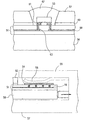
- FIGS. 1 ( a ) and 1 ( b ) illustrate configurations of two conventional LED illumination sources.
- FIGS. 2 ( a ) and 2 ( b ) illustrate cross-sectional structures of LEDs included in the two types of LED illumination sources.
- Each of these LED illumination sources includes a substrate 21 as shown in FIGS. 1 ( a ) and 1 ( b ).
- the “LED bare chip” refers to an LED that is yet to be mounted and yet to be molded with a resin, for example.
- an LED that has already been molded so as not to expose its light emitting portion but still has not been mounted yet will be herein referred to as an “LED element”.
- a plate 23 including multiple holes 23 a to transmit the light that has been emitted from the LED bare chips 22 , is provided.
- a layered resin 24 that also transmits the light emitted from the LED bare chips 22 is provided on the substrate 21 shown in FIG. 1 ( b ). That is to say, the LED bare chips 22 are covered with the resin 24 .
- the LED bare chip 22 is mounted in a bare chip state on the substrate 21 as shown in FIGS. 2 ( a ) and 2 ( b ).
- the LED bare chip 22 includes a chip substrate 31 of sapphire, SiC, GaAs or GaP, and a light emitting portion that has been formed on the chip substrate 31 .
- the light emitting portion is formed by stacking an n-type semiconductor layer 32 of GaN, for example, an active layer 33 , and a p-type semiconductor layer 34 in this order.
- the electrode 32 a of the n-type semiconductor layer 32 and the electrode 34 a of the p-type semiconductor layer 34 are electrically connected to conductive lines 21 a on the substrate 21 by way of Au wires 41 and 42 , respectively.
- this configuration of the light emitting portion is just an illustrative one.
- the LED may have a quantum well, a Bragg reflector layer, or a resonant cavity structure.
- the light that has been emitted from the LED bare chip 22 is reflected from a reflective plane 23 a , which is the inner surface of a hole (or opening) 23 b of the plate 23 , and then goes out of the element.
- the hole 23 b of the plate 23 is filled with the resin 24 so as to mold the LED bare chip 22 and the wires 41 and 42 together.
- the light that has been emitted from the LED bare chip 22 goes out of the element through the molding resin 24 .
- the LED bare chip 22 when a forward bias voltage is applied between the electrodes 32 a and 34 a of the n- and p-type semiconductor layers 32 and 34 , electrons and holes are injected into these semiconductor layers and recombine with each other. As a result of this recombination, light is created in, and emitted from, the active layer 33 .
- the light emitted from multiple LED bare chips 22 that have been mounted on the substrate, is utilized as illumination.
- the LED bare chip 22 generates a lot of heat when emitting the light.
- the heat generated is supposed to be dissipated from the substrate 21 by way of the chip substrate 31 .
- the following problems must be solved.
- the luminous flux of each one of the LED bare chips 22 is small. Accordingly, to achieve desired brightness, quite a few LED bare chips 22 need to be arranged on the substrate 21 . To avoid an excessive increase in size of the substrate even when a great number of LED bare chips 22 are arranged thereon, the LED bare chips 22 need to be mounted at an increased density.
- a current to be supplied to the LED bare chip 22 (e.g., an eddy current of about 40 mA with a current density of about 444.4 mA/mm 2 per unit area, for example) needs to be greater than a current that is supplied for normal purposes other than illumination (e.g., about 20 mA with a current density of about 222.2 mA/mm 2 per unit area for a 0.3 mm square LED bare chip, for example).
- a current that is supplied for normal purposes other than illumination e.g., about 20 mA with a current density of about 222.2 mA/mm 2 per unit area for a 0.3 mm square LED bare chip, for example.
- an increased quantity of heat is generated from the LED bare chip 22 .
- the temperature of the LED bare chip 22 (which will be herein referred to as a “bare chip temperature”) rises to reach a rather high level.
- the bare chip temperature has significant effects on the life of the LED bare chip. More specifically, it is said that when the bare chip temperature rises by 10° C., the life of an LED apparatus, including the LED bare chip 22 , should be halved.
- the heat dissipation performance should be improved, and the bare chip temperature should be decreased, compared to the conventional ones.
- the optical efficiency also needs to be increased to utilize the light, emitted from the LED bare chips 22 , as illumination as efficiently as possible, or with the waste of the optical energy minimized.
- the center portion of the substrate having the huge number of LEDs integrated thereon, gets more and more heated.
- the difference in temperature between the center and peripheral portions of the LED substrate escalates with time.
- the configuration shown in FIGS. 1 ( a ) and 2 ( a ) is adopted for an LED dot matrix display, for example.
- the plate 23 works in such a manner as to increase the contrast between the emitting and non-emitting portions of each LED.
- the substrate 21 and the plate 23 both made of the same resin, are combined together, and have substantially the same thermal expansion coefficients.
- a resin material normally has a low thermal conductivity, and easily stores the heat generated. For that reason, such a resin material cannot be used so effectively in an illumination apparatus that should always be kept ON at the maximum output power.
- the substrate itself may include a portion, which is as thick as the plate 23 and which is made of a material with a thermal conductivity that is approximately equal to the high thermal conductivity of the substrate material, instead of the plate 23 separately provided. Then, that substrate may include recesses to mount LED bare chips thereon. Even so, the heat-dissipating and uniform thermal distributing performance is also limited by the thermal conductivity of the substrate material.
- the substrate itself needs to be thick enough and the substrate to mount the LED bare chips 22 thereon cannot have a reduced thickness. For that reason, even if the substrate material has a high thermal conductivity, the heat is still stored easily in the substrate. Accordingly, when kept energized or ON for a long time with a great amount of current supplied as in an illumination apparatus, the LED bare chips, mounted around the center of the substrate, in particular, will have noticeably increased temperatures, thus creating a big temperature difference between the center and peripheral portions of the substrate. Consequently, the properties of the substrate material with the high thermal conductivity cannot be made full use of, and the heat dissipation problem is still insoluble.
- the recesses to be provided on the surface of the substrate have relatively large sizes, a sufficient space cannot be allowed to mount the LED bare chips 22 thereon and conductive line the LED bare chips 22 by the wire bonding technique.
- the optical system used should have an increased size.
- one side of the substrate 21 is covered with the molding resin 24 . Accordingly, the time it takes to cure the molding resin 24 in the center portion of the substrate is different from the time it takes to cure the same resin 24 in the peripheral portion thereof. As a result, a great residual stress is produced inside the resin. Furthermore, since the light that has been emitted from one LED bare chip 22 is absorbed into other LED bare chips 22 (i.e., self-absorption by LEDs), the light-extraction efficiency of the overall LED illumination source decreases. Moreover, since the molding resin 24 functions as a heat storage material, a temperature difference is created between the center and peripheral portions of the substrate. In that case, the thermal expansion coefficient also varies on the same substrate, thus propagating the stress of the molding resin 24 to the peripheral portion of the substrate.
- an object of the present invention is to provide an LED illumination source and LED illumination apparatus that can solve all of these problems (i.e., increasing the density of integration and improving the heat dissipation performance and optical efficiency) at the same time.
- An LED illumination apparatus includes: at least one connector to be connected to an insertable and removable card-type LED illumination source, which includes multiple LEDs that have been mounted on one surface of a substrate; and a lighting drive circuit to be electrically connected to the card-type LED illumination source by way of the connector.
- the substrate is a metal base substrate.
- An insulating layer and a conductive line pattern are provided on the surface of the metal base substrate such that the LEDs are mounted thereon.
- the LEDs have been mounted in a bare chip state on the substrate.
- feeder terminals are provided at one end of the surface of the substrate on which the LEDs have been mounted, and the center of a light outgoing region of the substrate, in which the LEDs mounted are located, is shifted from the center of the substrate.
- the LED illumination apparatus includes a thermal conductor member.
- the thermal conductor member thermally contacts with the back surface of the substrate, on which none of the LEDs is mounted, and receives heat from the back surface of the substrate.
- the area of a contact portion between the back surface of the substrate and the thermal conductor member is equal to or greater than the area of the light outgoing region of the substrate in which the LEDs mounted are located.
- the illumination apparatus further includes a feeder base for externally supplying electrical energy to the lighting drive circuit.
- the feeder base is a base for a light bulb.
- the illumination apparatus includes a housing, which transmits light emitted from the card-type LED illumination source that is connected to the connector.
- This housing may have various optical properties to reflect, refract and diffuse the light.
- the illumination apparatus includes: a receiving portion, on/from which the card-type LED illumination source is fixable and removable; and stopper means for keeping the card-type LED illumination source from dropping from the receiving portion.
- the stopper means operates in such a manner as to allow a human user to remove the card-type LED illumination source from the receiving portion with his or her fingers.
- the surface of the substrate on which the LEDs have been mounted has a substantially rectangular shape.
- the receiving portion includes a guide for getting the card-type LED illumination source slid and guided thereon. When fixed on the receiving portion, the card-type LED illumination source is supplied with electrical power from the connector and has the back surface of the substrate thereof contact thermally with the receiving portion.
- the illumination apparatus includes a movable mechanism with a fixing portion for fixing the card-type LED illumination source onto the receiving portion.
- the card-type LED illumination source is supplied with electrical power from the connector and has the back surface of the substrate thereof contact thermally with the receiving portion.
- a thermal resistance between the back surface of the substrate of the card-type LED illumination source, on which none of the LEDs is mounted, and the LEDs is 10° C./W or less.
- the illumination apparatus includes means for dissipating heat from the back surface of the substrate on which none of the LEDs is mounted.
- a card-type LED illumination source includes: a metal base substrate; and multiple LED bare chips that have been mounted on one surface of the metal base substrate.
- the card-type LED illumination source is supported so as to be insertable into, and removable from, an illumination apparatus that includes a connector and a lighting drive circuit.
- a feeder terminal is provided on the surface of the metal base substrate on which the LED bare chips have been mounted.
- an optical reflector with holes to surround the LED bare chips is provided on the surface of the metal base substrate on which the LED bare chips have been mounted, and the LED bare chips are encapsulated.
- optical lenses are fitted with the holes of the optical reflector.
- stress relaxing means is provided between the metal base substrate and the optical reflector.
- the center of the metal base substrate is shifted from the center a light outgoing region of the metal base substrate in which the LED bare chips mounted are located.
- a thermal resistance between the back surface of the metal base substrate, on which none of the LED bare chips is mounted, and the LED bare chips is 10° C./W or less.
- an insulating layer and a conductive line pattern are provided on the surface of the metal base substrate so that the LED bare chips are mounted thereon.
- the insulating layer is made of a composite material including at least an inorganic filler and a resin composition.
- the insulating layer is white.
- the illumination source includes at least two conductive line pattern layers that are stacked one upon the other with an insulating layer interposed between them.
- the illumination source has a structure for conductive lining the at least two conductive line pattern layers together at a predetermined position of the insulating layer.
- At least some of the LED bare chips are flip-chip bonded to the conductive line pattern on the metal base substrate.
- a phosphor which receives at least some of the light that has been emitted from the LED bare chips and which emits visible radiation, is provided on the metal base substrate.
- An apparatus includes a connector that supplies electrical power to the card-type LED illumination source according to any of the preferred embodiments described above.
- Another card-type LED illumination source includes multiple LED bare chips on a heat-dissipating substrate.
- Each of the LED bare chips includes a light emitting portion on a chip substrate.
- the LED bare chips are provided on the heat-dissipating substrate such that a distance between the light emitting portion and the heat-dissipating substrate is shorter than a distance between the chip substrate and the heat-dissipating substrate.
- a light outgoing facet of the chip substrate of the LED bare chip defines a slope such that a peripheral portion thereof is less tall than a center portion thereof.
- the LED bare chips are directly flip-chip bonded to the heat-dissipating substrate.
- the heat-dissipating substrate is a composite substrate.
- an optical reflector is provided on the heat-dissipating substrate so as to surround each of the LED bare chips and to control the direction of the light that has been emitted from the LED bare chip.
- FIG. 1 ( a ) is a perspective view of a conventional LED illumination source and FIG. 1 ( b ) is a perspective view of another conventional LED illumination source.
- FIG. 2 ( a ) is a partial cross-sectional view of an LED in the LED illumination source shown in FIG. 1 ( a ) and FIG. 2 ( b ) is a partial cross-sectional view of an LED in the LED illumination source shown in FIG. 1 ( b ).
- FIG. 3 ( a ) is a perspective view illustrating a portion of a planar LED illumination apparatus according to the present invention
- FIG. 3 ( b ) is a perspective view illustrating a light bulb type LED illumination apparatus according to the present invention.
- FIG. 4 ( a ) is an exploded perspective view of a card-type LED illumination source according to a specific embodiment of the present invention and FIG. 4 ( b ) is a perspective view of the LED illumination source.
- FIGS. 5 ( a ) and 5 ( b ) are cross-sectional views of an LED in card-type LED illumination sources according to two specific embodiments of the present invention.
- FIGS. 6 ( a ) and 6 ( b ) are equivalent circuit diagrams showing how multiple LEDs of the card-type LED illumination source may be connected together.
- FIGS. 7 ( a ) and 7 ( b ) show to which directions light rays emitted from LEDs go.
- FIGS. 8 ( a ) and 8 ( b ) show the results of simulations on the luminous fluxes of two types of LEDs.
- FIGS. 9 ( a ) and 9 ( b ) are cross-sectional views showing other exemplary shapes of the light outgoing facet of the chip substrate of LEDs.
- FIG. 10 is a cross-sectional view illustrating another exemplary configuration for an LED.
- FIGS. 11 ( a ) through 11 ( d ) are planar layouts showing exemplary shapes of a wafer bonding portion of the LED shown in FIG. 10 .
- FIG. 12 is an exploded perspective view illustrating another embodiment of a card-type LED illumination source according to the present invention.
- FIG. 13 illustrates a connector that may be used for the LED illumination source of the present invention.
- FIG. 14 ( a ) is a cross-sectional view illustrating a portion of the card-type LED illumination source shown in FIG. 12 in which an LED is provided
- FIG. 14 ( b ) is a cross-sectional view illustrating another portion thereof in which feeder terminals are provided.
- FIG. 15 is an equivalent circuit diagram showing how LEDs may be connected together in the card-type LED illumination source shown in FIG. 12 .
- FIG. 16 is a block diagram showing a configuration for the lighting drive circuit of an LED illumination apparatus to which the card-type LED illumination source shown in FIG. 12 is inserted.
- FIG. 17 is a planar layout illustrating an upper-level conductive line pattern of the card-type LED illumination source shown in FIG. 12 .
- FIG. 18 is a planar layout illustrating a lower-level conductive line pattern of the card-type LED illumination source shown in FIG. 12 .
- FIG. 19 ( a ) is a plan view showing a conductive line pattern of a portion to be flip-chip (FC) bonded
- FIG. 19 ( b ) is a plan view showing a conductive line pattern of a portion to be wire bonded (WB bonded)
- FIG. 19 ( c ) is a cross-sectional view of an FC-bonded LED bare chip
- FIG. 19 ( d ) is a cross-sectional view of a WB-bonded LED bare chip.
- FIG. 20 illustrates a light bulb type LED illumination apparatus as another specific embodiment of an LED illumination apparatus according to the present invention.
- FIG. 21 illustrates another light bulb type LED illumination apparatus, in which multiple card-type LED illumination sources are inserted, as still another specific embodiment of an LED illumination apparatus according to the present invention.
- FIG. 22 illustrates a desk lamp type LED illumination apparatus as yet another specific embodiment of an LED illumination apparatus according to the present invention.
- FIG. 23 illustrates another desk lamp type LED illumination apparatus, into/from which two card-type LED illumination sources are insertable and removable, as yet another specific embodiment of an LED illumination apparatus according to the present invention.
- FIG. 24 illustrates still another desk lamp type LED illumination apparatus as yet another specific embodiment of an LED illumination apparatus according to the present invention.
- FIG. 25 illustrates a flashlight or penlight type LED illumination apparatus as yet another specific embodiment of an LED illumination apparatus according to the present invention.
- FIG. 26 illustrates an LED illumination apparatus that can replace a conventional illumination apparatus using a straight-tube fluorescent lamp.
- FIG. 27 illustrates an LED illumination apparatus, which can replace a conventional illumination apparatus using a circular-tube fluorescent lamp, as yet another specific embodiment of an LED illumination apparatus according to the present invention.
- FIG. 28 illustrates a downlight type LED illumination apparatus as yet another specific embodiment of an LED illumination apparatus according to the present invention.
- FIG. 29 illustrates an optical axis shifting type LED illumination apparatus as yet another specific embodiment of an LED illumination apparatus according to the present invention.
- FIG. 30 illustrates a card-type LED illumination apparatus as yet another specific embodiment of an LED illumination apparatus according to the present invention.
- FIG. 31 illustrates a keychain type LED illumination apparatus as yet another specific embodiment of an LED illumination apparatus according to the present invention.
- An LED illumination apparatus includes: a connector to be electrically connected to an insertable and removable card-type LED illumination source; and a lighting drive circuit to be electrically connected to the card-type LED illumination source by way of the connector.
- the apparatus can radiate illumination.
- the card-type LED illumination source has a structure in which multiple LEDs are mounted on one surface of a substrate (printed circuit board) with good heat dissipation performance.
- the light source of an illumination apparatus is implemented as an insertable and removable card-type structure, thereby dissipating the heat, generated from the LEDs, much more smoothly.
- only a light source with its life ended can be replaced with a brand-new light source.
- the overall structure of the LED illumination apparatus, other than the light source can be used for a long time.
- an LED is preferably mounted as a bare chip on one surface of a substrate. This is because the heat generated from the LED is directly transmitted to the substrate and therefore the substrate can exhibit improved heat dissipation performance in that case.
- the other surface (i.e., back surface) thereof, which is opposed to the principal surface can be fully used as a heatconducting plane for heat dissipation purposes.
- the area of contact between this LED illumination apparatus and a thermal conductor member can be at least equal to, or even greater than, the area of a light outgoing region in which the LEDs are mounted.
- the back surface of the substrate, on which no LEDs are mounted is preferably made of a metal.
- the card-type LED illumination source can be used in various types of illumination apparatuses, and can be mass-produced at a reduced cost.
- the pitch of the feeder terminals may be defined to be 0.3 mm, 0.5 mm, 0.8 mm, 1.25 mm, 1.27 mm, 1.5 mm or 2.54 mm.
- Substrates for the card-type LED illumination sources are preferably mass-produced by dicing a wafer of a huge size into a great number of substrates for card-type LED illumination sources. However, the dicing process cannot be free from manufacturing errors.
- the size of the connector, into/from which the card-type LED illumination source is inserted and removed is also slightly variable during its mechanical manufacturing process. Accordingly, if the pitch between the electrodes is too small, then the feeder terminals might be short-circuited together in the connector portion of the LED illumination apparatus. For that reason, the pitch between the electrodes is preferably defined to be at least 0.8 mm.
- the LED is preferably driven with a constant current supplied rather than a constant voltage applied.
- the card-type LED light source needs the same number of ground lines as that of constant-current driving paths.
- multiple grounded feeder terminals are provided on the substrate so as to be electrically isolated from each other.
- the LED illumination apparatus to be compatible with such a card-type LED illumination source is also preferably provided with multiple grounded electrode connectors.
- the pitch between the electrodes is preferably 2 mm or less, more preferably 1.25 mm or less.
- two electrodes are preferably provided for LEDs of each color (i.e., ten electrodes in total).
- the card-type LED light source of the present invention may be designed in such a manner as to be driven either with a constant voltage applied or a constant current supplied. Alternatively, the light source may also be designed to be driven by way of multiple electrically isolated paths.
- the card-type LED light source preferably includes two or more conductive line pattern layers, which are stacked one upon the other with an insulating layer interposed between them, and preferably has a structure to interconnect the two or more conductive line pattern layers together.
- the diameter of via holes may be arbitrarily selected from the range of 100 ⁇ m to 350 ⁇ m, for example.
- the width of the feeder terminals of the card-type LED light source is preferably two or three times as large as the diameter of the via holes, and may be 200 ⁇ m to 1,050 ⁇ m, for example.
- the length of the feeder terminals is preferably defined such that the connector of the LED illumination apparatus does not directly contact with the via metals. For that reason, the feeder terminals preferably have a length of 1 mm or more, for example. To downsize the card-type LED light source, however, the length of the feeder terminals is preferably no greater than 5 mm.
- FIG. 3 ( a ) is a perspective view illustrating a portion of an LED illumination apparatus according to the present invention and shows a heat sink 19 in which multiple insertable/removable card-type LED illumination sources 10 are fitted.
- Each of the card-type LED illumination sources 10 is inserted to a predetermined position through a slot, which is provided on a side surface of the heat sink 19 .
- the heat sink 19 thermally contacts with the back surface of the card-type LED illumination source 10 inserted, thereby dissipating the heat away from the back surface of the substrate of the card-type LED illumination source 10 .
- the card-type LED illumination sources 10 When inserted in the heat sink 19 , the card-type LED illumination sources 10 are electrically connected to a connector (not shown), which is provided inside the heat sink 19 .
- the card-type LED illumination sources 10 are further connected electrically to a lighting drive circuit (not shown) by way of the connector.
- the “connector” refers to any of various types of members or components that can be electrically connected to the card-type LED illumination source through an insertable/removable mechanism. Connectors with various structures, to/from which numerous types of memory cards, for example, are inserted or removed, are on the market. According to the present invention, a connector that has substantially the same structure as any of those currently available connectors may be adopted.
- An LED illumination apparatus including such a heat sink 19 and a lighting drive circuit, can easily have a reduced thickness and can be used effectively as a planar light source. Also, if any of the card-type LED illumination sources 10 gets out of order, the non-operating card-type LED illumination source 10 may be removed from the heat sink 19 and instead a new (i.e., normally operating or non-deteriorated) card-type LED illumination source 10 may be inserted. Then, the illumination apparatus can be used continuously.
- the feeder terminals are provided on the surface of the card-type LED illumination source 10 such that the card-type LED illumination source 10 can be easily inserted or removed without using any special tool or instrument.
- the feeder terminals can be electrically contacted with, and connected to, the connector. Specific preferred structures of such a card-type LED illumination source 10 will be described in detail later.
- the heat sink 19 thermally contacts with the back surface of the substrate of the card-type LED illumination source 10 (i.e., the surface on which no LEDs are mounted). Accordingly, this heat sink 19 functions as a thermal conductor member to receive the heat from the back surface of the substrate of the card-type LED illumination source.
- Examples of other preferred thermal conductor members include a heat-dissipating sheet made of silicone grease or gel, a combination of such a heat-dissipating sheet and a heat sink, and a combination of a heat pipe and a fan.
- the casing of the LED illumination apparatus itself may also be used as a thermal conductor member.
- FIG. 3 ( b ) will be referred to.
- the LED illumination apparatus shown in FIG. 3 ( b ) is an illumination apparatus that can replace a known incandescent lamp, and includes: an adapter 20 to support the card-type LED illumination source thereon in an insertable/removable state; and a transparent housing 20 a to cover the card-type LED illumination source inserted.
- a lighting drive circuit (not shown) is provided inside the adapter 20 .
- the lower portion of the adapter 20 is a feeder base (lamp base for a light bulb) (e.g., a screw base) to externally supply electric energy to the internal lighting drive circuit.
- the shape and size of this feeder base may be the same as those of the feeder base of a normal incandescent lamp.
- the LED illumination apparatus shown in FIG. 3 ( b ) may be used by being fitted in any currently available electric light socket in which an incandescent lamp may be screwed. It should be noted that the screw base may be replaced with a pin base.
- the adapter 20 includes a slot, through which the card-type LED illumination source 10 is inserted.
- a connector (not shown) is provided at the end of the slot to electrically connect the card-type LED illumination source 10 to the lighting drive circuit.
- the slot is provided for the adapter 20 so as to insert or remove the card-type LED illumination source 10 therethrough.
- the illumination source 10 does not have to be inserted or removed in this manner.
- Other preferred embodiments of a non-slotted type will be described later.
- the card-type LED illumination source 10 shown in FIG. 3 ( b ) has such a structure as allowing the user to insert the illumination source 10 into, or remove it from, the connector easily. Accordingly, the illumination source 10 can also be easily removable from a luminaire. Since the card-type LED illumination source 10 is easily removable in this manner, the following effects can be achieved.
- a luminaire that emits a different quantity of light can be easily provided by substituting a card-type LED illumination source 10 , on which LEDs are mounted at a different density, for the existent one.
- a card-type LED illumination source 10 on which LEDs are mounted at a different density, for the existent one.
- any card-type LED illumination source 10 has deteriorated in a shorter time than expected and has almost run out of its life as light source, only the light source section can be renewed just by replacing the exhausted card-type LED illumination source 10 as in a normal light bulb or fluorescent lamp.
- each of the LEDs to be mounted on the card-type LED illumination source 10 may emit light in a color having a relatively low correlated color temperature, light in a color having a relatively high correlated color temperature, or light in a unique color such as blue, red, green or yellow, for example.
- the colors of the light emitted from the single card-type LED illumination source 10 can range from a color having a relatively low correlated color temperature to a color having a relatively high correlated color temperature.
- the card-type LED illumination source 10 is a two-wavelength type for emitting light rays in just two colors, then a light source having low color rendering performance but high optical efficiency is realized.
- the correlated color temperatures should be low, then red and cyan (or green) emissions are preferably combined with each other.
- the correlated color temperatures should be high, then blue and yellow (or orange) emissions are preferably combined with each other.
- a phosphor which is excited by a blue ray and has a peak of emission at an intermediate wavelength between blue and red parts of the visible radiation range (e.g., YAG phosphor)
- a high-efficiency light source with a general color rendering index (CRI) of 80 or more is realized.
- the card-type LED illumination source 10 is a three-wavelength type for emitting light rays in three colors, then blue, cyan (or green) and red emissions are preferably combined with each other.
- the card-type LED illumination source 10 is a four-wavelength type for emitting light rays in four colors, then blue, cyan (or green), yellow (or orange) and red emissions are preferably combined with each other.
- the four-wavelength type in particular, can be a light source with high color rendering performance, which has a general CRI of over 90. It should be noted that the present invention is also applicable for use even if the LED bare chips to be mounted emit single-color or ultraviolet rays or if white light is emitted by getting a fluophor or phosphor excited by the LED bare chips. Alternatively, the fluophor or phosphor may be included in the substrate. Furthermore, even when blue-ray-emitting LEDs, a fluophor or phosphor to be excited by a blue ray, and red-ray-emitting LEDs are combined together, high optical efficiency and high color rendering performance are realized at the same time.
- the card-type LED illumination source 10 described above has a square card shape.
- the electrodes to supply electric energy i.e., feeder terminals
- the electrodes to supply electric energy are preferably provided on the substrate of the card-type LED illumination source 10 around the region in which the LEDs are arranged.
- multiple feeder terminals are arranged beside one end (one side) of the substrate. If a large number of feeder terminals are needed, the substrate may have a rectangular shape with longer sides. In that case, the center of a cluster of LEDs (i.e., the center of the light outgoing region in which the LEDs are arranged) shifts from that of the substrate.
- the illumination source can resist the bending stress sufficiently. Also, if the corners of the rectangle are rounded, then the LED luminaire is less likely scratched by the corners of the substrate while the user is removing the card-type LED illumination source with fingers.
- a portion of the substrate may include a notch, mark, recess or protrusion to indicate the insertion direction of the card-type LED illumination source 10 clearly. Then, in fitting the card-type LED illumination source 10 in the illumination apparatus, the card-type LED illumination source 10 can be positioned accurately and easily with respect to the illumination apparatus.
- the feeder terminals are provided on the card-type LED illumination source and are connected to the connector electrodes.
- any of the following alternative configurations may be adopted.
- the feeder cable is preferably a flat cable with some flexibility.
- FIGS. 4 ( a ) and 4 ( b ) illustrate a configuration for a card-type LED illumination source according to a second specific embodiment.
- the card-type LED illumination source of this embodiment is preferably for use in the illumination apparatus shown in FIG. 3 ( a ) or 3 ( b ).
- LED bare chips 2 are mounted on one surface of a heat-dissipating substrate 1 as shown in FIG. 4 ( a ).
- the LED bare chips 2 are arranged in matrix, or in columns and rows.
- the present invention is in no way limited to this specific preferred embodiment.
- the LED bare chips 2 may be arranged in any other arbitrary pattern.
- the heat-dissipating substrate 1 with the LED bare chips 2 mounted thereon is further combined with the optical reflector 3 shown in FIG. 4 ( a ) to make the card-type LED illumination source shown in FIG. 4 ( b ).
- the optical reflector 3 includes the same number of openings (or holes) 3 b as that of the LED bare chips 2 that are arranged on the heat-dissipating substrate 1 . Thus, the light that has been emitted from the LED bare chips 2 goes out through the openings 3 b of the optical reflector 3 .
- the openings (or holes) of the optical reflector preferably have varying diameters such that the light outgoing portion thereof, which is more distant from the heat-dissipating substrate, has a greater diameter than that of their portion closer to the heat-dissipating substrate.
- an alumina composite substrate having a high thermal conductivity of about 3.2 W/(m ⁇ K) is used as the heat-dissipating substrate 1 of the card-type LED illumination source.
- the heat-dissipating substrate 1 of an alumina composite is a metal base substrate including a metal plate as a base with a thickness of 0.5 ⁇ m to 3.0 ⁇ m, for example, and an insulating layer provided on the metal plate.
- the substrate preferably has a thickness of at least 0.7 mm.
- the substrate preferably has a thickness of at most 2.0 mm.
- a thermal resistance between the back surface of the substrate of the card-type LED illumination source, on which no LED bare chips are mounted, and the LED bare chips is preferably 10° C./W or less.
- FIG. 5 ( a ) illustrates a partial cross section of an exemplary illumination source with a single insulating layer 1 c .
- FIG. 5 ( b ) illustrates a partial cross section of another exemplary illumination source with multiple (two in this case) insulating layers 1 c and 1 e.
- the heat-dissipating substrate 1 of this embodiment includes a metal plate 1 b and insulating layer(s) 1 c (and 1 e ) that has or have been bonded onto the metal plate 1 b .
- the insulating layers 1 c and 1 e are preferably made of a composite material including an inorganic filler and a resin composition.
- the total thickness of the two insulating layers 1 c and 1 e may be 100 ⁇ m to 400 ⁇ m, for example.
- FIG. 5 ( b ) illustrates an example in which two insulating layers are provided. However, the number of insulating layers may be further increased.
- the inorganic filler is preferably at least one filler that is selected from the group consisting of Al 2 O 3 , MgO, BN, SiO 2 , SiC, Si 3 N 4 and AIN.
- particles of the inorganic filler are preferably spherical.
- the resin composition in which the inorganic filler is dispersed preferably includes at least one resin that is selected from the group consisting of epoxy resin, phenol resin and cyanate resin.
- the mixture preferably includes 70 wt % to 95 wt % of inorganic filler and 5 wt % to 30 wt % of resin composition.
- the metal plate 1 b maintains the mechanical strength of the heat-dissipating substrate 1 and contributes to distributing the heat in the heat-dissipating substrate 1 as uniformly as possible. Also, the metal plate 1 b has a flat back surface. Accordingly, when the metal plate 1 b thermally contacts with a member having good thermal conductivity (e.g., a heat sink not shown), high heat dissipation effects are achieved.
- a member having good thermal conductivity e.g., a heat sink not shown
- the insulating layer 1 e on the metal plate 1 b which is the base metal of the heat-dissipating substrate 1 , may have the structure described above.
- a low-temperature-baked glass-ceramic substrate having a lower thermal conductivity than the composite material, may also be used instead.
- the insulating layer to be bonded onto the metal plate may be one of the substrates mentioned above (e.g., a ceramic substrate).
- the insulating substrate to be bonded to the metal plate is preferably thin and preferably has a strength high enough to be bonded there.
- the insulating substrate may have a thickness of 80 ⁇ m to 1,000 ⁇ m, for example. In this manner, multiple insulating layers, made of different materials or having different compositions, may be stacked on the base metal.
- conductive lines 1 a are provided and electrically isolated from the metal plate 1 b by the insulating layer(s) 1 c (and 1 e ) made of the composite material.
- the conductive lines 1 a on the first insulating layer 1 c are electrically connected to the conductive lines 1 d on the second insulating layer 1 e by way of a via metal 1 f that is provided through the first insulating layer 1 c.
- the heat-dissipating substrate 1 shown in FIG. 5 ( a ) when a number of LEDs are arranged on the same substrate to emit light rays in multiple colors (e.g., two to four colors), a simple series-parallel connection as shown in FIG. 6 ( a ) or a ladder connection as shown in FIG. 6 ( b ) is adopted for each of those colors.
- a simple series-parallel connection as shown in FIG. 6 ( a ) or a ladder connection as shown in FIG. 6 ( b ) is adopted for each of those colors.
- the LEDs can be turned ON with the variation in current-voltage characteristic thereof minimized.
- all of the LEDs that are connected in series to the disconnected LED will be turned OFF in the circuit shown in FIG. 6 ( a ).
- FIG. 6 ( a ) In the circuit shown in FIG.
- the heat-dissipating substrate 1 with the multilayer structure shown in FIG. 5 ( b ) makes it possible to arrange LEDs of electrically different systems adjacently to each other as shown in FIG. 15 .
- the presence of OFF-state LEDs or the variation in brightness is even less perceivable in this circuit configuration.
- this structure is also advantageous in mixing LED emissions in multiple colors, and makes it possible to adopt the ladder connection.
- an LED 2 in a bare chip state (i.e., LED bare chip) is directly mounted on the heat-dissipating substrate 1 .
- this LED bare chip 2 includes a light emitting portion 15 on a chip substrate 11 of sapphire.
- the light emitting portion 15 has a structure in which an n-type semiconductor layer 12 of GaN, an active layer 13 and a p-type semiconductor layer 14 are stacked one upon the other.
- the LED bare chip 2 is mounted facedown in this embodiment, i.e., such that the light emitting portion 15 is closer to the heat-dissipating substrate 1 than the chip substrate 11 is. That is to say, the electrode 14 a of the p-type semiconductor layer 14 is directly flip-chip bonded to the conductive line 1 a on the heat-dissipating substrate 1 .
- the electrode 12 a of the n-type semiconductor layer 12 is also connected to the conductive line 1 a on the heat-dissipating substrate 1 by way of a bump 16 , not wire.
- the electrodes 12 a and 14 a may also be bonded with respective bumps.
- the configuration of this embodiment in which light is allowed to go out from the chip substrate 11 and a great metal contact area can be provided under the light emitting portion 15 , is advantageous.
- a width or length of about 250 ⁇ m to about 350 ⁇ m and a thickness of about 90 ⁇ m to about 350 ⁇ m would be practical choices as sizes of each LED bare chip 2 .
- the present invention is in no way limited to these specific sizes.
- the LED bare chips 2 are flip-chip bonded to the conductive line pattern and have a width and a length of about 1 mm or more as is done in this embodiment so as to increase the quantity of light that can be extracted from a single LED bare chip 2 , then the following advantages are obtained.
- the emission produced might be intense enough near the electrodes but might be weak at a position far away from the electrodes due to the distributions of resistance and current density in the p- and n-type semiconductors that are bonded to the electrodes and fed with electric energy, which is a problem.
- this problem can be resolved by flip-chip bonding an LED bare chip of a large size and increasing the area of the electrodes of the LED bare chip to 50% or more of the overall area of the element as is done in this embodiment.
- This advantage is achieved by the unique structure of the present invention in which the light outgoing facet of an LED bare chip is opposite to the feeding surface thereof.
- each LED bare chip do not have to consist of just one pair (i.e., those provided for the p- and n-type semiconductor layers in this embodiment) but may consist of multiple pairs. Then, the variation in current density inside the LED bare chip can be reduced. If those multiple pairs of electrodes are connected by the conventional wire bonding technique, then each wire should run a long distance to reach its destination or the wire bonding process needs to be carried out an increased number of times.
- the surface of the chip substrate 11 i.e., the surface of the substrate of the LED bare chip (or the light outgoing facet), is not completely planar but has such a shape as decreasing the height from its raised center portion toward its periphery (e.g., a dome shape).
- a reflective plane 3 a that controls the direction of the light emitted from each LED bare chip 2 is provided so as to surround the LED bare chip 2 and the hole 3 b is provided for each LED bare chip 2 .
- this hole 3 b is filled with a resin 4 (e.g., epoxy, resin, silicone, or a combination thereof) to mold the LED bare chip 2 with.
- This molding resin 4 works as a lens.
- the metallic optical reflector 3 also contributes to distributing the heat uniformly in the heat-dissipating substrate 1 , thereby preventing the heat from being concentrated at the center of the heat-dissipating substrate 1 .
- the LED bare chip 2 of this embodiment may be fabricated by the following process steps, for example.
- an n-type semiconductor layer of GaN, an active layer, and a p-type semiconductor layer of GaN are deposited and stacked in this order on a sapphire wafer with a diameter of about 2 inches by a CVD process, for example, and then electrodes 12 a and 14 a are formed thereon to prepare a semiconductor wafer.
- the semiconductor wafer prepared in this manner is subjected to sand blasting and dicing process steps, thereby making a number of LED bare chips 2 .
- fine ceramic or metal particles are propelled against the sapphire side of the semiconductor wafer, thereby forming multiple isolating grooves on the sapphire side of the wafer. Thereafter, those isolating grooves are further deepened by the dicing process, thereby cuffing the wafer into multiple LED bare chips 2 . In this manner, multiple LED bare chips 2 , in which the light outgoing facet of the chip substrate 11 is raised like a dome, are obtained.
- the surface shape of the chip substrates 11 can be controlled.
- two dicing blades with cutting edges in different shapes may be used in combination. In that case, the sloped portions may be formed first by a cutting process that uses a dicing blade with one type of cutting edge and then the wafer may be fully divided into respective chips with a dicing blade having the other type of cutting edge.
- the flip-chip bonding structure is adopted and the upper surface of the LED bare chip is smaller than the lower surface thereof in this embodiment. Accordingly, there is no need to concern about the decrease in size of the upper electrode, or damage possibly done on it, during the machining process described above. Also, since no wires are provided on the upper surface of the LED bare chip, no radiation is interfered with by any wire. Accordingly, the distribution of the emission is not disturbed by, or the optical output power is not decreased by, the wires.
- a sapphire wafer is supposed to be used.
- an SiC wafer, a GaN wafer or any other wafer may also be used.
- the wafer to be used should transmit not only visible radiation but also any other radiation emitted from the LEDs.
- the LED bare chip may also be packaged with a conventional through hole element (such as a bullet type element), a surface mount (SM) device or a chip type element.
- SM surface mount
- Those LED bare chips 2 prepared in this manner are arranged in matrix on the heat-dissipating substrate 1 with the electrodes 12 a and 14 a thereof connected to the conductive lines 1 a on the heat-dissipating substrate 1 .
- the substrate 1 is covered with the optical reflector 3 and then the respective LED bare chips 2 are molded with the resin 4 .
- the holes 3 b of the optical reflector 3 may be filled with the resin 4 by a printing technique. In that case, a great number of resin lenses can be formed at the same time, i.e., mass-produced effectively.
- the LED bare chips 2 are arranged with the light emitting portion 15 thereof facing the heat-dissipating substrate 1 . Accordingly, unlike the conventional examples shown in FIGS. 1 ( a ) and 1 ( b ), no feeding wires or no wire bonding areas are needed. Thus, the space to be provided between adjacent LED bare chips 2 can be narrowed, and therefore, a greater number of LED bare chips 2 can be integrated together. This arrangement is also effectively applicable for use to realize a color mixture by using multiple LED bare chips 2 (or bare chips) that emit light rays in mutually different colors.
- the heat generated by the light emitting portion 15 is efficiently dissipated away through the heat-dissipating substrate 1 with a high thermal conductivity.
- the heat-generating, light emitting portion 15 of each LED bare chip 2 is directly bonded to the heat-dissipating substrate 1 . Accordingly, unlike the conventional examples shown in FIGS. 1 ( a ) and 1 ( b ) in which the heat is dissipated by way of the chip substrate, the heat generated by the light emitting portion 15 is directly dissipated away through the heat-dissipating substrate 1 . Thus, excellent heat dissipation performance is ensured.
- the refractive index of the chip substrate 11 (made of sapphire) of the LED bare chips 2 is different from that of the resin 4 (such as epoxy or silicone resin). Due to this difference in refractive index, a portion of the light that has been emitted from the light emitting portion 15 is totally reflected from the light outgoing facet of the chip substrate 11 . The totally reflected light is directed toward the LED bare chip 2 and cannot be used for illumination purposes. Accordingly, to utilize the produced light effectively, it is necessary to minimize this total reflection.
- FIG. 7 ( a ) shows to which direction the light goes from the LED bare chip of the present invention with a domed light outgoing facet.
- FIG. 7 ( b ) shows to which direction the light goes from a comparative example with a horizontal light outgoing facet.
- the light outgoing facet is a horizontal plane
- the light impinging onto the periphery has a large angle of incidence.
- an increased percentage of the light has an angle of incidence that reaches a critical angle (as indicated by B in FIG. 7 ( b )).
- the total reflection easily happens.
- the light outgoing facet is domed, a decreased percentage of the light has an angle of incidence that reaches the critical angle even around the periphery of the light outgoing facet. Consequently, most of the emission from the light emitting portion 15 is not totally reflected but radiated away as indicated by A in FIG. 7 ( a ).
- FIGS. 8 ( a ) and 8 ( b ) show respective results of simulations on the luminous flux of the emission of an LED bare chip 2 in which the light outgoing facet of the chip substrate 11 was molded into a dome shape (i.e., an example of the present invention) and on the luminous flux of the emission of an LED bare chip 2 in which the light outgoing facet of the chip substrate 11 was a horizontal plane (i.e., a comparative example). Comparing the results shown in FIG. 8 ( a ) and 8 ( b ), it can be seen that the luminous flux of the upwardly directed emission, available for use as illumination, was greater in the example of the present invention than in the comparative example. That is to say, the light could be extracted more efficiently in the example of the present invention.
- the present inventors confirmed via actual measurements that the light-extraction efficiency of the example of the present invention was 1.6 times as high as that of the comparative example.
- the light outgoing facet of the chip substrate 11 is domed.
- the emission can be extracted non-wastefully and can be utilized as illumination very efficiently.
- the light outgoing facet of the chip substrate 11 is domed.
- the facet may have any arbitrary shape as long as the shape can minimize the total reflection (i.e., a facet which is sloped downward from the raised center portion toward the periphery).
- a facet which is sloped downward from the raised center portion toward the periphery.
- the shape shown in FIG. 9 ( a ) in which curved surfaces are formed so as to increase its width toward the light emitting portion 15 as opposed to the example described above, or the shape shown in FIG. 9 ( b ), in which tapered surfaces are formed so as to have a constant tilt angle, may also be adopted.
- the sloped surfaces are not curved but planar or polygonal, then this effect diminishes. Accordingly, the sloped surfaces are preferably domed because the effects achieved in that case are as if a lens were included in the LED bare chip 2 itself.
- the LED bare chip 2 functions as a lens by itself, the emission of the LED bare chip 2 is concentrated toward the front of the lens while the quantity of light to be emitted through the side surfaces of the LED bare chip 2 decreases.
- an optical system including such an LED bare chip 2 should have decreased stray light components. As a result, the optical efficiency of the overall card-type LED illumination source increases.
- Examples of alternative embodiments include blue-ray-emitting and green (or cyan)-ray-emitting LEDs of GaN that have been provided on dissimilar chip substrates of SiC and GaN, for example. In that case, the chip substrates themselves have some electrical conductivity. Accordingly, instead of providing the electrodes for the n- and p-type semiconductor layers 12 and 14 that sandwich the active layer 13 between them as shown in FIGS. 5 ( a ) and 5 ( b ), the chip substrate itself may function as one of the two electrodes.
- a GaP substrate with a high transmittance to the emissions in these colors is preferably used as the chip substrate. Then, the same structure may be adopted as well.
- a similar structure may also be used if the light emitting portion of an LED bare chip of AllnGaP is wafer-bonded to a sapphire substrate with a transparent electrode or a transparent substrate of glass, for example.
- the metal electrode with openings on the bare chip may be metal-bonded (or wafer-bonded) to the metal electrode with openings on the transparent chip substrate 11 before the growth substrate is removed from the bare chip.
- the process step of removing the growth substrate from the LED bare chip is carried out after the metal bonding process step has been performed.
- the chip substrate 11 may be shaped either before or after the wafer bonding process step and either before or after the process step of removing the growth substrate from the LED bare chip.
- the transparent substrate may also be wafer-bonded to the light emitting portion of the LED bare chip even with an optically transparent adhesive means.
- the surface shape of the chip substrate 11 is defined by the sand blasting process.
- the surface shape may also be defined either by a water jet process or a selective chemical etching process.
- optical lenses having a refractive index that is approximately equal to that of the LED chip substrate 11 may be bonded together.
- the surface shape of the chip substrate 11 may also be defined by a cutting process that uses dicing blades with different cutting edges.
- the bare chips to be flip-chip bonded that have been subjected to any of these processes may be included in conventional elements such as bullet type elements or SMDs.
- the above-described structure needs no wire bonding process, and therefore, contributes to reducing the size of the optical system and increasing the efficiency thereof.
- the area of the LED electrode, which is located closer to the heat-dissipating substrate to mount the LED bare chip thereon, is preferably increased. Then, the light directed toward the mounting substrate can be reflected back and the light-extraction efficiency can be increased.
- the heat-dissipating substrate 1 does not have to be the metal base substrate such as that shown in FIG. 5 ( a ) or 5 ( b ) but may be a metal core substrate, for example.
- the heat-dissipating substrate 1 is a metal base substrate
- the lower surface of the substrate is a metal and a metallic optical reflector may be disposed on the substrate. Accordingly, the heat can be dissipated more effectively from both the upper and lower surfaces of the substrate.
- the card-type LED illumination source of this embodiment includes a metal plate 50 , a multilayer circuit board 51 , and a metallic optical reflector 52 .
- the metal plate 50 and the multilayer circuit board 51 together define one “card-type LED illumination source”.
- the metal plate 50 is the base metal of a heat-dissipating substrate.
- the metal plate 50 and the optical reflector 52 may be made of aluminum, copper, stainless steel, iron, or an alloy thereof.
- the materials of the metal plate 50 and optical reflector 52 may be different from each other. Considering the thermal conductivity, copper, aluminum, iron and stainless steel are preferred in this order. On the other hand, in view of the thermal expansion coefficient, stainless steel, iron, copper and aluminum are preferred in this order.
- An aluminum-based material is preferred because such a material is easy to handle in an anticorrosion process, for example.
- a stainless steel based material is preferably used.
- the back surface of the metal plate 50 is flat and can contact with a flat surface of a member with a good thermal conductivity (not shown).
- metal plate 50 is subjected to an insulation treatment such as electrolytic polishing, aluminization processing, electroless plating or electrolytic deposition, even direct contact of the metal plate 50 with the conductive line pattern will not create electrical short-circuit.
- an insulation treatment such as electrolytic polishing, aluminization processing, electroless plating or electrolytic deposition
- At least portions of the surface of the metal plate 50 which should reflect the light that has been radiated from the LED bare chips, are preferably subjected to a process to increase the reflectivity.
- processes to increase the reflectivity include the process of increasing the reflectivity by stacking multiple material layers with different refractive indices and the process of increasing the mirror reflection of the surface of the metal plate 50 .
- the multilayer circuit board 51 has a two-layer structure including first and second insulating layers, each of which is made of a mixture of an inorganic filler and a resin composition.
- Lower-level conductive lines are provided between the first and second insulating layers and upper-level conductive lines are provided on the second insulating layer.
- the upper- and lower-level conductive lines are electrically connected together by way of via metals that are provided through the second insulating layer.
- the holes of the optical reflector 52 are filled with an LED encapsulating resin, then concave or convex lenses may be made of the resin. Alternatively, the holes may be filled with the resin to planarize the surface of the optical reflector 52 . However, since the area of the optical reflector 52 is smaller than that of the multilayer circuit board 51 , the optical reflector 52 may be molded with a resin in its entirety. If the optical reflector 50 is completely covered with the resin, then the LED bare chips can be encapsulated more tightly.
- the connector to be provided on the illumination apparatus may include: a body 55 with a guide portion for sliding and guiding the card-type LED illumination source thereon; multiple connector electrodes 56 to be electrically connected to the card-type LED illumination source; a metal plate (or bottom plate) 57 with a good thermal conductivity; and interconnecting cords 58 for connecting the connector electrodes to a circuit such as a lighting drive circuit.
- the card-type LED illumination source When inserted into this connector, the card-type LED illumination source has its feeder terminals 54 contacted with, and connected to, their associated connector electrodes 56 . To improve the heat dissipation performance, when the card-type LED illumination source is inserted into this connector, all or part of the back surface of the metal plate 50 preferably contacts thermally with the metal plate 57 of the connector.
- the feeder terminals 54 are arranged and collected along just one of the four sides of the upper surface of the multilayer circuit board 51 as shown in FIG. 12 . Accordingly, the card-type LED illumination source is inserted into the connector by being pushed in the direction indicated by the arrow A in FIG. 12 .
- the size of the multilayer circuit board 51 is greater than that of the optical reflector 52 by the area of the region in which the feeder terminals 54 are provided. Accordingly, in this embodiment, the (optical) center of the region in which the LED bare chips 53 are arranged in matrix (i.e., light outgoing region or LED cluster region) does not correspond with the center of the substrate. Therefore, the center of the bending stress on the card-type LED illumination source does not correspond with the center of the brittle optical system, thus increasing the mechanical strength. Also, since the feeder terminals 54 are collected along one end of the substrate, the other ends of the upper surface of the multilayer circuit board 51 , corresponding to the three other sides, do not have to be completely fitted with the inside surfaces of the connector. As a result, the card-type LED illumination source may be designed more freely in respect of the shape, for example.
- the optical reflector 52 basically has the same structure as the optical reflector 3 shown in FIG. 4 ( a ), and has the same number of openings as that of the LED bare chips 53 to be arranged.
- the openings of the optical reflector 52 are preferably filled with resin lenses, with which the LED bare chips 53 are encapsulated.
- the LED bare chips 53 can be connected to the multilayer circuit board 51 more tightly. If the connection between the LED bare chips 53 and the multilayer circuit board 51 is consolidated in this manner, then screw holes may be provided through the card body of the card-type LED illumination source or portions of the edges of the card-type substrate may have screwing recesses to screw the card-type LED illumination source onto a heat-dissipating member.
- FIG. 14 ( a ) shows an LED bare chip 53 that has been flip-chip bonded with its active layer turned facedown.
- one of multiple different bonding methods is adopted according to the type of each LED bare chip 53 as will be described later.
- the LED bare chip 53 has been mounted so as to be connected to the conductive line patterns 59 of the multilayer circuit board 51 and fixed on the multilayer circuit board 51 . After the LED bare chips 53 have been mounted on the multilayer circuit board 51 , the metallic optical reflector 52 is bonded onto the multilayer circuit board 51 .
- the multilayer circuit board 51 includes the two-layer conductive line patterns 59 .
- the conductive line patterns 59 belonging to two different layers are interconnected together by via metals 63 .
- the conductive line pattern 59 on the uppermost layer is connected to the electrodes of the LED bare chip 53 by way of Au bumps 61 .
- the conductive line patterns 59 may be made of copper, nickel, aluminum or an alloy mainly composed of these metals.
- such a multilayer circuit board 51 includes insulating layers, each of which is made of a mixture of a resin composition and an inorganic filler with electrical insulating property.
- This mixture preferably includes a thermosetting resin.
- the insulating layer preferably has a thermal conductivity of 1 W/m ⁇ K to 10 W/m ⁇ K and is preferably white. If such a white insulating layer is adopted, then visible radiation is reflected by exposed portions of the insulating layer at a higher reflectivity and the optical efficiency is further improved.
- At least one filler is preferably selected from the group consisting of Al 2 O 3 , MgO, BN, SiO 2 , SiC, Si 3 N 4 and AIN with excellent thermal conductivities.
- the mean particle size of the inorganic filler is preferably within the range of 0.1 ⁇ m to 100 ⁇ m. This is because if the mean particle size is out of this range, the fill density of the filler or the heat dissipation performance of the substrate will decrease.
- thermosetting resin at least one resin is preferably selected from the group consisting of epoxy resin, phenol resin and cyanate resin. This is because the electrical insulating property, mechanical strength and heat resistance of each of these resins cured are superior to those of any other cured resin.
- the resin composition may further include an additive such as coupling agent, dispersing agent, coloring agent or release agent.
- a sample card-type LED illumination source was modeled by a method in which two sheets, each having a thickness of 160 ⁇ m and made of a composite material of an alumina filler, were used and in which a multilayer circuit board, including two insulating layers with a total thickness of 320 ⁇ m, was prepared and bonded onto a metal base of aluminum.
- a multilayer circuit board including two insulating layers with a total thickness of 320 ⁇ m
- the heat should be dissipated naturally from this sample by a heat sink in no wind condition and 64 LED bare chips with sizes of about 0.3 mm square should be driven at 40 mA, which is a current twice as much as a rated current and which has a current density of about 444 mA/mm 2 .
- the heat sink needs to have a surface area of about 300 cm 2 .
- the thermal resistance between the LED bare chips and the base metal needs to be about 10° C./W or less.
- the temperature of the LED bare chips should not exceed the range of 80° C. to 120° C. This is because the resin encapsulant (i.e., epoxy or silicone resin) of the LED bare chips would significantly deteriorate thermally and optically at a temperature exceeding that range.
- the resin encapsulant i.e., epoxy or silicone resin
- the thermal resistance is about 5° C./W or less, even a heat sink with a normal finite area, not the heat sink with an ideal big area, should realize sufficient heat dissipation in the natural air cooling condition. Furthermore, if the thermal resistance is about 2° C./W to about 1° C./W or less, even a small-sized heat sink should realize sufficient heat dissipation.
- a system with a thermal resistance of 1° C./W or less is also realizable either by reducing the thickness of the insulating layers or by using insulating layers of a boron-based composite material with a thermal conductivity of about 3 W/mK to about 5 W/mk instead of the alumina composite insulating layers with a thermal conductivity of about 2 W/mK to about 4 W/mK. In that case, similar effects are also achievable even if the area of the heat sink is further reduced.
- Each of the conductive line patterns 59 of the multilayer circuit board 51 may be defined by forming a conductive line pattern on a release carrier such as an organic film and then transferring the conductive line pattern from the release carrier onto the insulating layer.
- the conductive line pattern may be formed on the release carrier by bonding a metal foil (e.g., copper foil) onto the release carrier with an adhesive, for example, depositing a metal film on the metal foil by an electrolytic or electroless plating technique, and then patterning the metal film by a chemical etching process.
- the conductive line pattern is made of the metal foil, the surface of the insulating layer is preferably roughened to increase the adhesive strength of the metal foil.
- the conductive line pattern 59 may be formed by any other method. Also, the conductive line pattern 59 may be either inlaid in the insulating layer or adhered to the flat surface of the insulating layer.
- the via metals 63 to conductive line together the conductive line patterns 59 belonging to mutually different layers may be formed by plating the inner surface of holes (i.e., via holes or through holes) that have been provided through the insulating layer or by filling the holes with a conductive resin composition.
- the upper surface of the multilayer circuit board 51 with such a structure is mostly covered with the optical reflector 52 but is also partially exposed.
- the feeder terminals 54 are provided on the exposed region on the multilayer circuit board 51 . These feeder terminals 54 are electrically connected to the lighting drive circuit of the illumination apparatus by way of the connector, into which the card-type LED illumination source is inserted.
- An underfill (or stress relaxing layer) 60 is provided between the optical reflector 52 and the multilayer circuit board 51 .
- the underfill 60 not only relaxes the stress to be caused by the difference in thermal expansion coefficient between the metallic optical reflector 52 and the multilayer circuit board 51 but also ensures electrical insulation between the optical reflector 52 and the upper-level conductive lines on the multilayer circuit board 51 .
- All of the optical reflector 3 is preferably made of a metal.
- the substrate which will be herein referred to as a “substrate insulating layers”
- the substrate base metal By sandwiching the insulating layers as the substrate (which will be herein referred to as a “substrate insulating layers”) between the substrate base metal and the metallic reflector, heat can be dissipated from both sides of the substrate.
- the heat at the mounting side of the LEDs, heat-generating bodies can be uniformly distributed from the center portion toward the peripheral portions. Secondary effects of minimizing the warpage of the two metal plates from both sides of the substrate insulating layer are also expected as well.
- the substrate insulating layers are made of a composite material including a resin composition and an inorganic filler, then the elasticity of such a composite material can relax the stress to be placed on the two metal plates. As a result, the illumination apparatus to be kept ON at an elevated temperature to supply high power can have its reliability increased.
- the stress relaxing layer to be provided between the optical reflector and the substrate insulating layers needs to be made of a material that is different from those of the optical reflector and insulating layers.
- a gap may be created between the insulating layer and the optical reflector by providing either bumps on the conductive lines on the insulating layer or lands for bumps in addition to the conductive lines.
- the gap may be filled with either the underfill or the resin (i.e., epoxy or silicone resin) to mold the LEDs. Even so, the stress may also be relaxed. If such stress relaxing means is provided, unintentional turn OFF or decrease in reliability is avoidable even under a strict condition that stress is applied due to the thermal shock of a flashing test.
- the openings of the optical reflector 52 are closed with lenses that have been made of a molded resin 62 .
- the optical reflector 52 is preferably a metal plate of aluminum, for example.
- a plate made of any other insulating material may also be used.
- at least portion (preferably all) of the inner sidewall of the openings is preferably coated with a reflective film that is made of a material having a higher reflectivity than that of the insulating plate, e.g., a metal such as Ni, Al, Pt, Ag or Al or an alloy mainly composed of these metals.
- a metal such as Ni, Al, Pt, Ag or Al or an alloy mainly composed of these metals.
- the backing metal plate 50 does not have to be made of aluminum but may also be made of copper.
- the back surface of the metal plate 50 is preferably flat so as to contact with a good thermal conductor provided for the connector, for example, and thereby improve the heat dissipation performance.
- fins or linearly embossed portions may be provided on portions of the back surface for heat dissipation purposes. In that case, embossed portions to engage with the fins or linearly embossed portions are preferably provided on the surface of the member that will contact with the back surface of the metal plate 50 .
- those fins or linearly embossed portions to be provided on the back surface of the metal plate preferably extend in the sliding direction so as not to interfere with the sliding movement. Then, the fins or linearly embossed portions themselves function as guides and the area of contact can be increased advantageously.
- a mechanism for pressing the thermal conductor member onto the card-type LED illumination source is preferably adopted.
- Such pressure may be applied by feeder terminals with some elasticity. However, to obtain a sufficient pressure from such feeder terminals alone, the feeder terminals need to have rather strong elasticity. If a mechanical pressure to be applied to achieve electrical contact with the feeder terminals is about 50 g to about 100 g per terminal, then pressing means for applying a stronger pressure is preferably provided additionally.
- an elastic member for applying a pressure of 200 g or more to portions of the card-type LED illumination source other than the feeder terminals thereof may be provided. A number of such pressing means may be provided as well.
- the mechanical pressure to be applied to the feeder terminals does not have to be so high.
- the card-type LED illumination source can be easily inserted or removed manually with human fingers. That is to say, after having fitted the card-type LED illumination source into the connector of the LED illumination apparatus, the user can press the back surface of the substrate of the card-type LED illumination source onto the thermal conductor member strongly with the pressing means. As a result of such high pressure, the card-type LED illumination source is locked onto the LED illumination apparatus so to speak, and will not drop down from the apparatus accidentally.
- FIG. 14 ( b ) illustrates a cross section of one end of the card-type LED illumination source that is connected to the connector.
- the connector is indicated by the dashed lines. It should be noted that the card-type LED illumination source shown in FIG. 14 ( b ) is illustrated as being thinner than the counterpart shown in FIG. 14 ( a ) for convenience sake.
- the feeder terminal 54 is provided on the end of the multilayer circuit board 51 so as to be located near the connector, and is electrically connected to the conductive line pattern 59 either directly or through the via metals.
- the region of the multilayer circuit board 51 , on which the feeder terminal 54 is located, is not covered with the optical reflector 52 .
- the connector electrode 56 can easily contact with the feeder terminal 54 .
- the connector electrode 56 and feeder terminal 54 can be easily connected or disconnected electrically by inserting or removing the card-type LED illumination source into/from the connector. If a switch that senses the insertion or removal of the card-type LED illumination source is provided near the end of the connector, at which the card-type LED illumination source arrives when inserted, such that current is blocked while no card-type LED illumination source is inserted, then safety increases. In that case, such a switch may be provided under, beside or over the card.
- the connector electrodes 56 are illustrated as being visible externally. However, actual connector electrodes 56 are preferably designed such that the user cannot lay his or her fingers on the electrodes 56 as shown in FIG. 14 ( b ).
- LED bare chips each consisting of 16 LED bare chips that emit red (R), green (G), blue (B) or yellow (Y) light ray, are arranged on the same substrate.
- the dimensions of the substrate include a longer-side length of 28.5 mm, a shorter-side length of 23.5 mm and a thickness of 1.3 mm.
- the rectangular region on which the 64 LED bare chips are arranged has dimensions of 20 mm by 20 mm by 1 mm (thickness). In this example, the region on which the LEDs are arranged (i.e., the region where the reflector is present) is about 2 cm square.
- This area of the light emitting portion is approximately equalized with the bulb sizes of normal low-watt small-sized light bulbs (e.g., small spherical light bulbs or mini krypton lamps) such that the LED illumination source can replace any of these existent low-watt light bulbs.
- a small spherical light bulb can obtain a total luminous flux of about 20 lm to about 50 m at a power of about 5 W to about 10 W.
- a mini krypton lamp can obtain a total luminous flux of about 250 lm to about 500 lm at a power of about 22 W to about 38 W.
- the card-type LED illumination source is packaged in a casing having sizes corresponding to those of a beam light bulb so as to have a diameter not exceeding that of a beam type dichroic halogen lamp and if the center of the light outgoing region with the reflector (i.e., the light emitting region) is aligned with the center of the optical axis of the light bulb, then the distance from the center of the light emitting portion to the end of the longer side of the substantially square card (i.e., the side on which the feeder terminals are provided) is:
- the periphery of the substrate preferably has flat portions that can contact with the guide portions. Also, to mold the entire reflector with a resin, the periphery of the substrate preferably has regions on which no LEDs are provided. Such regions are provided on both sides of the light outgoing region having sizes of about 2 cm square. Each of those regions preferably has a width of 1 mm to 3 mm. To increase the size of these regions (or margins), the distance from the center of the light emitting portion to the end facet needs to be decreased.
- the feeder terminals are preferably provided on just one surface of the card-type LED illumination source to make the illumination source compatible with any of various insertion/removal methods. More preferably, the card-type LED illumination source is disposed such that the center of the mirror reflector (or the light outgoing region) is shifted from the geometric center of the substrate.
- the feeder terminals are preferably collected together on the light outgoing side of the substrate. Furthermore, to ensure thermal contact between the back surface of the substrate and the thermal conductor member (i.e., the heat-dissipating means) in a broad area, the card-type LED illumination source is preferably pressed not only by the feeder terminals but also by other pressing means. To get the illumination source pressed by such means, margins are preferably provided on the principal surface of the substrate for that purpose.
- the distance from the center of the light emitting portion to the end facet of the substrate with no feeder terminals may be shorter than the distance from the center of the light emitting portion to the end facet with the feeder terminals.
- the former distance may be equalized with the width of the margins to be provided on both sides of the light outgoing region. In that case, if four card-type LED illumination sources are densely arranged such that the two sides of each of the illumination sources are in contact with those of two other illumination sources, the gaps between the mirror reflectors (i.e., light outgoing regions) can be equalized with each other and can be as short as possible.
- the present inventors modeled a sample card-type LED illumination source in which the distance from the center of the light outgoing region (i.e., the center of the light emitting portion) to the end facet of the substrate (i.e., the end facet with the feeder terminals) was about 16.5 mm and in which the distance from the center of the light emitting portion to the opposite end facet of the substrate (opposite to the feeder terminal side) was about 12 mm.
- That portion has a single-layer structure locally, then electrical connection is also realized without using via metals, e.g., by wiring the upper and lower layers together.
- the other side with the feeder terminals may also have such a single-layer structure locally.
- the number of layers provided may be further increased on just portions of the substrate to design conductive line jumpers more freely. In that case, the margins described above become effective spaces.
- the feeder terminals are designed so as to have a substantially rectangular shape and have a width of 0.8 mm, a length of 2.5 mm and a pitch of 1.25 mm (i.e., distance between the centers of two adjacent feeder terminals) in view of mechanical errors to be caused when the feeder terminals are contacted with the connector electrodes or the manufacturing errors of the via metals.
- the number of feeder terminals is preferably as large as possible. In the exemplary configuration of this embodiment, 16 feeder terminals may be provided.
- the feeder terminals may be allocated to the LEDs that emit blue, green (or cyan), yellow (or orange), red and white rays and six supplementary terminals (for three paths) may be provided.
- the distance from the edge of the feeder terminals to the end facet of the substrate is defined to be at least 2 mm.
- the gap between the feeder terminals may have a three-dimensional shape, not a planar shape. That is to say, a rib may be formed by the insulating layer.
- FIG. 15 illustrates an equivalent circuit showing how 64 LED bare chips, provided for a single card-type LED illumination source, may be interconnected together.
- R (+) denotes the anode side of red-ray-emitting LED bare chips while R ( ⁇ ) denotes the cathode side of the red-ray-emitting LED bare chips.
- Y, G and B the colors
- FIG. 16 is a block diagram showing an exemplary configuration for an LED lighting drive circuit.
- the lighting drive circuit 70 of a card-type LED illumination source includes a rectifying and smoothing circuit 71 , a voltage step-down circuit 72 and constant current circuits 73 .
- the rectifying and smoothing circuit 71 is a known circuit, which is connected to an AC power supply of 100 V and which converts an alternating current into a direct current. It should be noted that the power supply does not have to be AC 100 V but may be a DC power supply.
- the rectifying and smoothing circuit 71 which is a combination of a smoothing circuit and voltage step-down circuit, may be replaced with a voltage transformer (i.e., voltage step-down and step-up transformer).
- the voltage step-down circuit 72 decreases the DC voltage to an appropriate voltage to make the LEDs emit light (e.g., 18 V).
- the constant current circuits 73 include blue, green, yellow and red LED controlling constant current circuits. Each of these LED controlling constant current circuits adjusts the current to be supplied to a group of LEDs 76 in its associated color in the card-type LED illumination source 75 to a constant value.
- the constant current circuits 73 may be electrically connected to the groups of LEDs 76 by fitting the card-type LED illumination source 75 in the connector of the illumination apparatus. More specifically, the electrical continuity is realized by bringing the feeder terminals, provided on the substrate of the card-type LED illumination source 75 , into contact with their associated feeder terminals inside the connector.
- Such a lighting drive circuit 70 includes an electrolytic capacitor as a circuit component thereof. If the temperature of the electrolytic capacitor reaches about 100° C., its life shortens significantly. For that reason, the temperature near the electrolytic capacitor should be sufficiently lower than 100° C.
- the heat generated in the card-type LED illumination source 75 is dissipated by the heat-dissipating means by way of the metal plate of the card-type LED illumination source 75 and then the heat-dissipating member of the illumination apparatus. Accordingly, the temperature near the electrolytic capacitor of the lighting drive circuit is maintained at about 80° C. or less. As a result, the life of the lighting drive circuit can also be extended.
- the groups of LEDs 76 for the colors blue, green (or cyan), yellow (or orange) and red are driven with a constant current supplied thereto, and therefore, applied with a ground potential separately.
- the number of feeder terminals to be provided for the card-type LED illumination source 75 of this embodiment is eight. Half of the eight feeder terminals function as anode electrodes while the other half functions as cathode electrodes.
- FIG. 17 illustrates a layout for the upper-level conductive line pattern of the multilayer circuit board
- FIG. 18 illustrates a layout for the lower-level conductive line pattern thereof.
- small circular regions 79 shown on the conductive lines 78 indicate the locations of the via metals to interconnect the upper- and lower-level conductive line patterns together.
- the reference numerals 78 and 79 each identify just one member for the sake of simplicity. However, it should be naturally understood that a large number of conductive lines and a large number of via metals are actually provided.
- FIGS. 19 ( a ) and 19 ( b ) respectively show the regions 85 a and 85 b on a larger scale.
- the LED bare chip is flip-chip (FC) bonded.
- the LED bare chip is wire-bonded (WB bonded).
- FIG. 19 ( c ) shows a cross section of the FC-bonded LED bare chip
- FIG. 19 ( d ) shows a cross section of the WB-bonded LED bare chip.
- the LED bare chips to emit blue or green (or cyan) light are FC bonded and the LED bare chips to emit yellow (or orange) or red light are WB bonded.
- an LED bare chip (or element) to emit the red or yellow (or orange) light (i.e., light with a relatively long wavelength)
- its multilayer structure including a light-emitting layer, is normally formed on a GaAs substrate.
- the GaAs substrate cannot transmit the red or yellow light easily, and therefore, is disposed under the light-emitting layer. Accordingly, such an LED bare chip cannot be bonded facedown.
- n and p electrodes are disposed so as to face the light-emitting layer of the LED bare chip, and are connected to the conductive lines (i.e., the upper-level conductive lines) on the multilayer circuit board by way of Au bumps.
- the conductive line pattern on the substrate is formed by plating a copper foil with nickel and then further plating the nickel with gold.
- the thickness of the copper foil is 35 ⁇ m or less.
- the conductive line pattern should be provided discretely on the substrate, the conductive line pattern was formed by an electroless plating technique under some conditions.
- nickel was plated to a thickness of about 6 ⁇ m and gold to be plated thereon was deposited to a thickness of 0.6 ⁇ m.
- a layer or a member, made of a material with a high reflectivity may be provided on the conductive line pattern or on the surface of the substrate.
- an LED bare chip (or element) to emit blue or green (or cyan) light (i.e., light with a relatively short wavelength)
- its multilayer structure including the light emitting layer
- the sapphire substrate transmits the blue or green light, and can be disposed at an arbitrary location, i.e., may be located either under or over the light-emitting layer. Since the FC bonded structure contributes more effectively to increasing the density, the blue-ray-emitting LED bare chips and green-ray-emitting LED bare chips are FC bonded on the substrate in this embodiment. In the WB-bonded structure shown in FIG.
- the n and p electrodes are provided on the back surface of the substrate and closer to the light-emitting layer of the LED bare chip, respectively.
- the p electrode is connected to the conductive line (i.e., the upper-level conductive line) on the multilayer circuit board with a bonding wire.
- the n electrode is connected to the conductive line (i.e., upper-level conductive line) on the multilayer circuit board with a conductive paste, solder, a metal bond, or an anisotropic conductive adhesive, for example.
- an underfill material may also be used as well to consolidate these bonds.
- the structures and bonding methods of the LEDs to emit light rays in those colors are not limited to those exemplified for the foregoing embodiment.
- the LEDs on the same substrate may be all bonded by a single bonding method or by three or more bonding methods.
- each of those LEDs is preferably mounted by the best bonding technique to be selected on the specific structure of the LED.
- at least the surface of the conductive line pattern on the substrate is preferably a gold layer.
- the gold layer preferably has a thickness of at least 0.5 ⁇ m, more preferably 1 ⁇ m or more.
- the location of the light-emitting layer of one LED may be different from that of the light-emitting layer of another LED. Accordingly, the geometric shape (e.g., focal point or aperture ratio) of a lens to be provided for each of those LEDs is preferably optimized according to the location of the light-emitting layer of the LED or the chromatic aberration to be caused depending on the color of the emission.
- the electrodes 80 a , 80 b , 80 c and 80 d shown in FIG. 17 are feeder terminals to supply an anode potential to the four groups of LEDs to emit red, blue, green and yellow light rays, respectively.
- the electrodes 90 a , 90 b , 90 c and 90 d are feeder terminals to supply a cathode potential (i.e., ground potential) to the four groups of LEDs to emit the red, blue, green and yellow light rays, respectively.
- the electrodes 80 a , 80 b , 80 c and 80 d are respectively connected to the conductive lines 81 a , 81 b , 81 c and 81 d shown in FIG. 18 by way of via metals.
- the electrodes 90 a , 90 b , 90 c and 90 d shown in FIG. 17 are respectively connected to the conductive lines 92 a , 92 b , 92 c and 92 d shown in FIG. 18 by way of via metals.
- a circuit that is substantially equivalent to the circuit shown in FIG. 15 is realized by the multilayer structure shown in FIGS. 17 and 18 .
- each of the conductive line patterns may naturally have any other layout and is not limited to the layout shown in FIG. 17 or 18 .
- the feeder terminals (consisting of the anode and cathode electrodes) 80 a through 80 d and 90 a through 90 d are all arranged in line in the region shown at the bottom of FIG. 17 .
- the feeder terminals are collected together near one side of the substrate, thus making it easier to connect the card-type LED illumination source to the connector.
- the ground lines can also be isolated from each other for the respective groups of LEDs to emit light rays in multiple different colors and yet the feeder terminals can be collected together by one side of the substrate. This is because the multilayer structure described above is adopted in this embodiment.
- no feeder terminals are provided on the back surface of the metal plate of the card-type LED illumination source, and the back surface of the metal plate is flat. Accordingly, a wide area of contact is ensured between this metal plate and a member with a good thermal conductivity (included in the illumination apparatus). Thus, the heat can be dissipated away more efficiently from the card-type LED illumination source.
- the area of contact is preferably equal to or greater than the area of the region in which the LEDs are arranged (i.e., the light outgoing region or LED cluster region).
- the present invention is in no way limited to this specific preferred embodiment.
- the number of colors of the emissions may be one, two or three or more than four.
- an LED bare chip that radiates multiple types of emissions or an LED bare chip to emit white light by adding a phosphor thereto may also be used. It should be noted that unless an LED bare chip to emit white light is used, an LED bare chip normally needs to be coated with a phosphor for the purpose of emitting white light.
- the phosphor if the phosphor is encapsulated in the space that is defined by the substrate and the reflector, the phosphor can be excited by the LED.
- a sheet on which a phosphor is dispersed may be attached onto the upper surface of the reflector.
- the phosphor-dispersed sheet itself and the card-type LED light source may be molded together with a transparent resin material.
- FIG. 20 illustrated is a light bulb type LED illumination apparatus.
- This LED illumination apparatus basically has the same configuration as the LED illumination apparatus shown in FIG. 3 ( b ), but is different from the counterpart shown in FIG. 3 ( b ) in the method of introducing the card-type LED illumination source into the illumination apparatus.
- the LED illumination apparatus shown in FIG. 20 is used as a combination of the body 96 of the illumination apparatus and a transparent housing 97 .
- the transparent housing 97 should be temporarily taken off the body 96 .
- a receiving portion 98 in which the card-type LED illumination source 96 is fitted, is provided on the upper surface of the body 96 .
- the body 96 further includes a fixing lid 99 , which is used to press the upper surface of the card-type LED illumination source 96 that has been fitted in the receiving portion 98 and to fix the illumination source 96 onto the receiving portion 98 .
- the fixing lid 99 is supported so as to rotate (i.e., open and close) around a shaft that is provided near one end thereof, and includes connector electrodes 99 a to contact with the feeder terminals 95 a on the card-type LED illumination source 95 . These connector electrodes 99 a are connected to a lighting drive circuit (not shown) that is provided inside the body 96 .
- the fixing lid 99 and the receiving portion 98 together function as a sort of “connector”.
- the fixing lid 99 has such a structure as exposing the light outgoing region of the card-type LED illumination source 95 that is stored in the receiving portion 98 while pressing the feeder terminals 95 a and other portions downward.
- the back surface of the substrate of the card-type LED illumination source 95 thermally contacts with the bottom of the receiving portion 98 .
- the bottom of the receiving portion 98 is preferably made of a material with a good thermal conductivity (e.g., a metal material such as aluminum).
- a good thermal conductor functions as a heat sink, which can dissipate the heat that has been generated in the card-type LED illumination source 95 and can prevent an excessive rise in temperature of the illumination source 95 .
- this illumination apparatus is constructed such that the transparent housing 97 can be easily removed, and the fixing lid 99 can be easily opened and closed, with the user's hands or fingers and without using any special tool.
- the card-type LED illumination source 95 can be easily replaced (i.e., inserted or removed).
- the transparent housing 97 may have a light diffusing property.
- the transparent housing 97 may be replaced with another housing 97 a that is made of a colorant, a phosphor or a phosphor.
- a lenticular lens 97 b or a light diffusing housing 97 c may also be used.
- a double lens, a reflector, or a housing having the functions of these optical members in combination may also be used.
- FIG. 21 illustrates another light bulb type LED illumination apparatus, in which multiple card-type LED illumination sources are fitted. The card-type LED illumination sources are pressed down and fixed by a pair of openable/closable fixing lids.
- FIGS. 20 and 21 illustrate LED illumination apparatuses that can replace a light bulb type lamp.
- an LED illumination apparatus to replace a straight-tube fluorescent lamp or a circular-tube fluorescent lamp may also be realized by using the card-type LED illumination sources of the present invention. If an LED illumination apparatus is made in a shape similar to the conventional straight-tube fluorescent lamp or circular-tube fluorescent lamp, then an LED illumination apparatus according to the present invention may be used in an existent appliance in place of the conventional straight-tube or circular-tube fluorescent lamp.
- FIG. 22 illustrates a desk lamp type LED illumination apparatus.
- the body 96 of the illumination apparatus shown in FIG. 22 also includes a receiving portion 98 to store the card-type LED illumination source 95 therein.
- This receiving portion 98 includes a guide that can be used to slide and guide the card-type LED illumination source 95 thereon.
- the card-type LED illumination source 95 may be inserted into the receiving portion 98 of this illumination apparatus with its end including the feeder terminals 95 a facing forward.
- the connection between the feeder terminals 95 a and the connector electrodes is complete. Once fitted, the card-type LED illumination source 95 is firmly fixed there due to the frictional force and will not drop accidentally.
- that contact portion is preferably made of a material with a good thermal conductivity.
- FIG. 23 illustrates another desk lamp type LED illumination apparatus, into/from which two card-type LED illumination sources are inserted or removed.
- FIG. 24 illustrates still another desk lamp type LED illumination apparatus.
- This LED illumination apparatus adopts a connector of the type shown in FIG. 21 . That is to say, the card-type LED illumination sources are fixed by fixing lids onto the illumination apparatus. The user can easily open or close these fixing lids with fingers.
- FIG. 25 illustrates another LED illumination apparatus, which is portable as a flashlight or a penlight.
- This illumination apparatus includes a slot 100 , through which the card-type LED illumination source 95 is inserted or removed.
- the card-type LED illumination source 95 may also be inserted or removed without using such a slot.
- the LED illumination apparatus shown in FIG. 25 can operate the card-type LED illumination source by a dry battery or a storage battery and has a portable structure.
- FIG. 26 illustrates an LED illumination apparatus that can replace a conventional illumination apparatus using a straight-tube fluorescent lamp.
- the body 101 of this LED illumination apparatus includes a connector, into/from which multiple card-type LED illumination sources 95 can be inserted and removed.
- the card-type LED illumination sources 95 are inserted or removed through the slot 100 of the body 101 .
- the LED illumination apparatus shown in FIG. 26 is not supposed to replace a straight-tube fluorescent lamp itself but a desk lamp type illumination apparatus that uses the straight-tube fluorescent lamp.
- FIG. 27 illustrates an LED illumination apparatus, which can replace a conventional illumination apparatus that uses a circular-tube fluorescent lamp.
- the body 102 of this LED illumination apparatus includes a connector, into/from which multiple card-type LED illumination sources 95 can be inserted and removed.
- the card-type LED illumination sources 95 are inserted or removed through the slots 100 of the body 102 .
- FIG. 28 illustrates a downlight type LED illumination apparatus.
- the LED illumination apparatus of the present invention can easily have a reduced thickness, and can be easily mounted as a downlight unit on the ceiling of a room or an automobile.
- FIG. 29 illustrates an optical axis shifting type LED illumination apparatus. If its portion including the card-type LED illumination source fitted in is rotated to an arbitrary angle around a particular axis, the light outgoing direction can be easily changed into any desired direction.
- FIG. 30 illustrates a card-type LED illumination apparatus.
- a battery with a reduced thickness such as a button battery is adopted, thereby reducing the overall thickness of the illumination apparatus itself.
- Such an LED illumination apparatus is thin and lightweight, and can be easily carried about.
- FIG. 31 illustrates a keychain type LED illumination apparatus. This LED illumination apparatus is also driven by a battery with a reduced thickness such as a button battery, has reduced size and weight, and easy to carry about conveniently.
- LED illumination apparatuses according to the present invention have been described with reference to FIGS. 20 through 31 .
- the present invention is in no way limited to these specific embodiments but may also be implemented in numerous other ways.
- card-type LED illumination sources of a standardized type are easy to popularize.
- the illumination apparatus shown in FIG. 21 is preferably designed so as to accept not so much one card-type LED illumination source with a big area as multiple card-type LED illumination sources, any of which is also insertable and removable into/from the illumination apparatus shown in FIG. 20 .
- the card-type LED illumination sources can be mass-produced and the price of a single card-type LED illumination source can be decreased easily, which is one of the most important effects to achieve.
- an applicable card-type LED illumination source changes with the type of a specific illumination apparatus or the maker who produced it, such poor compatibility should frustrate the users. For that reason, the main portions of the card-type LED illumination source preferably have standardized functions or sizes.
- each of the card-type LED illumination sources uses LED bare chips that have been mounted thereon.
- a card-type LED illumination source including an organic EL film thereon may also be used.
- the “insertable/removable card-type LED illumination source including LEDs that have been mounted on one surface of a substrate” herein also refers to a card-type LED illumination source including an organic EL film on a heat-dissipating substrate.
- the LED illumination apparatus of the present invention uses a card-type LED illumination source as an easily insertable/removable member, and therefore, has an extended life as an illumination apparatus and can replace any of the existent illumination apparatuses.
- a card-type LED illumination source having a configuration such as that shown in FIG. 12 is preferably used in such an LED illumination apparatus.
- card-type LED illumination sources for use in the LED illumination apparatus of the present invention are in no way limited to the specific embodiments described above.
- a card-type LED illumination source with any of various configurations may be inserted into, and removed from, the LED illumination apparatus of the present invention. That is to say, the present invention is not limited to the specific preferred embodiments of card-type LED illumination sources that have been described above with reference to the accompanying drawings.
- the card-type LED illumination source of the present invention is applicable for use in not just illumination apparatuses but also any other type of apparatus.
- the insertable/removable card-type LED illumination source of the present invention may be used in an appliance that should emit as bright light as the illumination apparatus or in the light source section of any other apparatus, for example.
- LED elements (preferably of a surface bonded type), obtained by molding LED bare chips, may be bonded onto the substrate. In that case, the LED elements molded are fabricated separately.
- the thermal resistance between the substrate and the LED bare chips increases.
- the substrate has the above-described structure, even the substrate with those LED elements mounted exhibits better heat dissipation performance than the conventional one. Consequently, the substrate with the LED elements integrated thereon can exhibit improved heat dissipation performance.
- the LED illumination apparatus and card-type LED light source of the present invention include: a connector to be connected to the insertable/removable card-type LED light source; and feeder terminals for the light source.
- the LED illumination apparatus further includes a lighting drive circuit.
- the card-type LED light source includes a metal base substrate and multiple LEDs. The metal base surface, which is the back surface of the substrate, thermally contacts with a portion of the illumination apparatus.
- a metal plate with openings including encapsulating resin lenses and functioning as an optical reflector and a heat spreader, is disposed on the metal base substrate.
- the LEDs, as well as the reflector, are encapsulated on the substrate.
- the LED bare chips are directly bonded onto the substrate.
- the substrate has multiple conductive line pattern layers and also has a number of feeder terminals along one side of one of its surfaces. Also, in a preferred embodiment, the feeder terminals have multiple ground electrodes.
- the LED illumination apparatus of the present invention uses an insertable/removable card shaped structure as its light source portion.
- the heat that has been generated from respective LED elements of the light source can be dissipated much more smoothly.
- only a light source with its life ended can be replaced with a brand-new light source.
- the remaining structure of the illumination apparatus, other than the light source can be used for a long time.
- the card-type LED illumination source of the present invention realizes high-density arrangement of LED elements, excellent heat dissipation performance, and significant increase in the extraction efficiency of the light generated at the same time.
- card-type LED illumination sources can be commercially viable products.
Priority Applications (5)
| Application Number | Priority Date | Filing Date | Title |
|---|---|---|---|
| US11/125,392 US7375381B2 (en) | 2001-08-09 | 2005-05-09 | LED illumination apparatus and card-type LED illumination source |
| US11/158,836 US7045828B2 (en) | 2001-08-09 | 2005-06-22 | Card-type LED illumination source |
| US11/158,646 US7259403B2 (en) | 2001-08-09 | 2005-06-22 | Card-type LED illumination source |
| US11/277,952 US7250637B2 (en) | 2001-08-09 | 2006-03-30 | Card type LED illumination source |
| US11/691,743 US20070187708A1 (en) | 2001-08-09 | 2007-03-27 | LED Illumination Apparatus and Card-Type LED Illumination Source |
Applications Claiming Priority (3)
| Application Number | Priority Date | Filing Date | Title |
|---|---|---|---|
| JP2001242857 | 2001-08-09 | ||
| JP2001-242857 | 2001-08-09 | ||
| PCT/JP2002/008151 WO2003016782A1 (en) | 2001-08-09 | 2002-08-08 | Led illuminator and card type led illuminating light source |
Related Parent Applications (1)
| Application Number | Title | Priority Date | Filing Date |
|---|---|---|---|
| PCT/JP2002/008151 Continuation WO2003016782A1 (en) | 2001-08-09 | 2002-08-08 | Led illuminator and card type led illuminating light source |
Related Child Applications (3)
| Application Number | Title | Priority Date | Filing Date |
|---|---|---|---|
| US11/125,392 Division US7375381B2 (en) | 2001-08-09 | 2005-05-09 | LED illumination apparatus and card-type LED illumination source |
| US11/158,836 Division US7045828B2 (en) | 2001-08-09 | 2005-06-22 | Card-type LED illumination source |
| US11/158,646 Division US7259403B2 (en) | 2001-08-09 | 2005-06-22 | Card-type LED illumination source |
Publications (2)
| Publication Number | Publication Date |
|---|---|
| US20030189829A1 US20030189829A1 (en) | 2003-10-09 |
| US6949772B2 true US6949772B2 (en) | 2005-09-27 |
Family
ID=19073064
Family Applications (6)
| Application Number | Title | Priority Date | Filing Date |
|---|---|---|---|
| US10/374,614 Expired - Lifetime US6949772B2 (en) | 2001-08-09 | 2003-02-26 | LED illumination apparatus and card-type LED illumination source |
| US11/125,392 Expired - Fee Related US7375381B2 (en) | 2001-08-09 | 2005-05-09 | LED illumination apparatus and card-type LED illumination source |
| US11/158,836 Expired - Lifetime US7045828B2 (en) | 2001-08-09 | 2005-06-22 | Card-type LED illumination source |
| US11/158,646 Expired - Fee Related US7259403B2 (en) | 2001-08-09 | 2005-06-22 | Card-type LED illumination source |
| US11/277,952 Expired - Lifetime US7250637B2 (en) | 2001-08-09 | 2006-03-30 | Card type LED illumination source |
| US11/691,743 Abandoned US20070187708A1 (en) | 2001-08-09 | 2007-03-27 | LED Illumination Apparatus and Card-Type LED Illumination Source |
Family Applications After (5)
| Application Number | Title | Priority Date | Filing Date |
|---|---|---|---|
| US11/125,392 Expired - Fee Related US7375381B2 (en) | 2001-08-09 | 2005-05-09 | LED illumination apparatus and card-type LED illumination source |
| US11/158,836 Expired - Lifetime US7045828B2 (en) | 2001-08-09 | 2005-06-22 | Card-type LED illumination source |
| US11/158,646 Expired - Fee Related US7259403B2 (en) | 2001-08-09 | 2005-06-22 | Card-type LED illumination source |
| US11/277,952 Expired - Lifetime US7250637B2 (en) | 2001-08-09 | 2006-03-30 | Card type LED illumination source |
| US11/691,743 Abandoned US20070187708A1 (en) | 2001-08-09 | 2007-03-27 | LED Illumination Apparatus and Card-Type LED Illumination Source |
Country Status (5)
| Country | Link |
|---|---|
| US (6) | US6949772B2 (de) |
| EP (2) | EP3078899B1 (de) |
| CN (2) | CN1464953A (de) |
| TW (1) | TW567619B (de) |
| WO (1) | WO2003016782A1 (de) |
Cited By (160)
| Publication number | Priority date | Publication date | Assignee | Title |
|---|---|---|---|---|
| US20040149998A1 (en) * | 2002-12-02 | 2004-08-05 | Henson Gordon D. | Illumination system using a plurality of light sources |
| US20040189170A1 (en) * | 2001-02-15 | 2004-09-30 | Integral Technologies, Inc. | Low cost lighting circuits manufactured from conductive loaded resin-based materials |
| US20040223339A1 (en) * | 2003-05-06 | 2004-11-11 | Ji-Mei Tsuei | Light source device |
| US20040256630A1 (en) * | 2001-08-24 | 2004-12-23 | Densen Cao | Illuminating light |
| US20050057929A1 (en) * | 2003-09-16 | 2005-03-17 | Matsushita Electric Industrial Co., Ltd. | LED lamp |
| US20050083689A1 (en) * | 2003-10-16 | 2005-04-21 | Lg Electronics Inc. | LED surface light source and projection system using the same |
| US20050117366A1 (en) * | 2003-12-02 | 2005-06-02 | Simbal John J. | Reflective light coupler |
| US20050116635A1 (en) * | 2003-12-02 | 2005-06-02 | Walson James E. | Multiple LED source and method for assembling same |
| US20050116235A1 (en) * | 2003-12-02 | 2005-06-02 | Schultz John C. | Illumination assembly |
| US20050140270A1 (en) * | 2003-12-02 | 2005-06-30 | Henson Gordon D. | Solid state light device |
| US20050207165A1 (en) * | 2001-08-09 | 2005-09-22 | Matsushita Electric Industrial Co., Ltd. | LED illumination apparatus and card-type LED illumination source |
| US20050276069A1 (en) * | 2004-05-11 | 2005-12-15 | Hitoshi Taniguchi | Liquid crystal display apparatus |
| US20060018120A1 (en) * | 2002-11-26 | 2006-01-26 | Daniel Linehan | Illuminator and production method |
| US20060028815A1 (en) * | 2004-08-03 | 2006-02-09 | Triplex Manufacturing Company | Light assembly comprising integrated passive and active illumination sources |
| US20060072344A1 (en) * | 2004-10-05 | 2006-04-06 | Kim Won-Nyun | Backlight unit |
| US20060087843A1 (en) * | 2003-01-27 | 2006-04-27 | Tatsumi Setomoto | Multichip led lighting device |
| US20060186425A1 (en) * | 2004-01-29 | 2006-08-24 | Matsushita Electric Industrial Co., Ltd. | LED lamp |
| WO2006132794A2 (en) * | 2005-06-03 | 2006-12-14 | Intex Recreation Corp. | A light-emitting device module with flip-chip configuration on a heat-dissipating substrate |
| US20060284209A1 (en) * | 2005-06-17 | 2006-12-21 | Samsung Electro-Mechanics Co., Ltd. | Light emitting device package |
| US20060292747A1 (en) * | 2005-06-27 | 2006-12-28 | Loh Ban P | Top-surface-mount power light emitter with integral heat sink |
| US20070001564A1 (en) * | 2005-06-30 | 2007-01-04 | Lg.Philips Lcd Co., Ltd. | Light emitting diode package in backlight unit for liquid crystal display device |
| US20070013090A1 (en) * | 2005-07-12 | 2007-01-18 | Shinji Takase | Method of resin-sealing and molding an optical device |
| US20070012934A1 (en) * | 2003-06-10 | 2007-01-18 | Abu-Ageel Nayef M | Method and system of LED light extraction using optical elements |
| US20070019415A1 (en) * | 2005-04-22 | 2007-01-25 | Itt Industries | LED floodlight system |
| US20070132135A1 (en) * | 2004-04-26 | 2007-06-14 | Towa Corporation | Manufacturing method of optical electronic components and optical electronic components manufactured using the same |
| US20070189007A1 (en) * | 2004-03-26 | 2007-08-16 | Keiji Nishimoto | Led mounting module, led module, manufacturing method of led mounting module, and manufacturing method of led module |
| US20070200127A1 (en) * | 2003-05-27 | 2007-08-30 | Andrews Peter S | Power surface mount light emitting die package |
| US20070247847A1 (en) * | 2006-04-21 | 2007-10-25 | Villard Russell G | Light Emitting Diode Packages |
| US20070247855A1 (en) * | 2004-10-04 | 2007-10-25 | Kabushiki Kaisha Toshiba | Light Emitting Device,Lighting Equipment or Liquid Crystal Display Device Using Such Light Emitting Device |
| US20070273290A1 (en) * | 2004-11-29 | 2007-11-29 | Ian Ashdown | Integrated Modular Light Unit |
| US20070292709A1 (en) * | 2004-08-23 | 2007-12-20 | Jitsuo Oishi | Metal-Clad White Laminate |
| US20080023718A1 (en) * | 2002-11-07 | 2008-01-31 | Matsushita Electric Industrial Co., Ltd. | Led lamp |
| US20080030974A1 (en) * | 2006-08-02 | 2008-02-07 | Abu-Ageel Nayef M | LED-Based Illumination System |
| US20080084700A1 (en) * | 2006-09-18 | 2008-04-10 | Led Lighting Fixtures, Inc. | Lighting devices, lighting assemblies, fixtures and method of using same |
| US20080084701A1 (en) * | 2006-09-21 | 2008-04-10 | Led Lighting Fixtures, Inc. | Lighting assemblies, methods of installing same, and methods of replacing lights |
| US20080087900A1 (en) * | 2004-11-24 | 2008-04-17 | Chiu-Jung Yang | Integrated-Type Led And Manufacturing Method Thereof |
| US20080112170A1 (en) * | 2006-11-14 | 2008-05-15 | Led Lighting Fixtures, Inc. | Lighting assemblies and components for lighting assemblies |
| US20080112168A1 (en) * | 2006-11-14 | 2008-05-15 | Led Lighting Fixtures, Inc. | Light engine assemblies |
| US20080121900A1 (en) * | 2006-11-24 | 2008-05-29 | Hong Kong Applied Science and Technology Research Institute Company Limited | Light emitter assembly |
| US20080121917A1 (en) * | 2006-11-15 | 2008-05-29 | The Regents Of The University Of California | High efficiency white, single or multi-color light emitting diodes (leds) by index matching structures |
| US20080157333A1 (en) * | 2007-01-03 | 2008-07-03 | Chipmos Technologies Inc. | Chip package and manufacturing method thereof |
| US20080191222A1 (en) * | 2005-08-09 | 2008-08-14 | Seoul Opto Device Co., Ltd. | Ac Light Emitting Diode and Method for Fabricating the Same |
| US20080198552A1 (en) * | 2007-02-15 | 2008-08-21 | Samsung Electro-Mechanics Co., Ltd. | Package board and method for manufacturing thereof |
| US20080265448A1 (en) * | 2004-10-07 | 2008-10-30 | Takeshi Ashida | Method transparent member, optical device using transparent member and method of manufacturing optical device |
| US20080278950A1 (en) * | 2007-05-07 | 2008-11-13 | Cree Led Lighting Solutions, Inc. | Light fixtures and lighting devices |
| US7456805B2 (en) | 2003-12-18 | 2008-11-25 | 3M Innovative Properties Company | Display including a solid state light device and method using same |
| US20080291633A1 (en) * | 2007-05-21 | 2008-11-27 | National Taiwan University | Package assembly with heat dissipating structure |
| US20080299398A1 (en) * | 2007-05-30 | 2008-12-04 | Sharp Kabushiki Kaisha | Light emitting device and method for manufacturing the same |
| US20080297058A1 (en) * | 2007-06-04 | 2008-12-04 | Applied Concepts Inc. | Method, apparatus, and system for driving LED's |
| US20080304269A1 (en) * | 2007-05-03 | 2008-12-11 | Cree Led Lighting Solutions, Inc. | Lighting fixture |
| US7514867B2 (en) | 2004-04-19 | 2009-04-07 | Panasonic Corporation | LED lamp provided with optical diffusion layer having increased thickness and method of manufacturing thereof |
| US20090095971A1 (en) * | 2007-10-16 | 2009-04-16 | Andrew Glovatsky | Wire bond led lighting unit |
| US20090108278A1 (en) * | 2007-10-31 | 2009-04-30 | Liann-Be Chang | Manufacturing Method of an Antistatic Flip Chip Substrate Connected to Several Chips |
| US20090122554A1 (en) * | 2004-11-19 | 2009-05-14 | Fujikura, Ltd. | Light-emitting element mounting substrate and manufacturing method thereof, light-emitting element module and manufacturing method thereof, display device, lighting device, and traffic light |
| US20090135581A1 (en) * | 2004-01-07 | 2009-05-28 | Tadashi Yano | Led Lamp |
| US20090154170A1 (en) * | 2007-12-18 | 2009-06-18 | Foxsemicon Integrated Technology, Inc. | Light emitting diode illuminator |
| US20090241388A1 (en) * | 2008-03-26 | 2009-10-01 | Manufacturing Resources International, Inc. | Advertising displays |
| US20090243501A1 (en) * | 2008-03-26 | 2009-10-01 | Manufacturing Resources International, Inc. | Combined serial/parallel light configuration |
| US20090283881A1 (en) * | 2008-05-14 | 2009-11-19 | Harvatek Corporation | Semiconductor chip package structure for achieving face-down electrical connection without using a wire-bonding process and method for making the same |
| US20090294780A1 (en) * | 2008-05-27 | 2009-12-03 | Intermatix Corporation | Light emitting device |
| US20090302342A1 (en) * | 2008-06-09 | 2009-12-10 | Kondo Ryosuke | Semiconductor Light-Emitting Device and Manufacturing Method |
| US20090310066A1 (en) * | 2008-06-11 | 2009-12-17 | Manufacturing Resources International, Inc. | LED tile Luminance control circuitry and display containing the same |
| US20100001648A1 (en) * | 2006-12-12 | 2010-01-07 | Inverto Nv | Led lighting that has continuous and adjustable color temperature (ct), while maintaining a high cri |
| US20100051976A1 (en) * | 2006-11-15 | 2010-03-04 | Lemnis Lighting Patent Holding B.V. | Led lighting assembly |
| US20100079990A1 (en) * | 2008-09-29 | 2010-04-01 | Rene Peter Helbing | Efficient led array |
| US20100155768A1 (en) * | 2008-03-25 | 2010-06-24 | Bridge Semiconductor Corporation | Semiconductor chip assembly with post/base heat spreader and cavity in post |
| US20100155769A1 (en) * | 2008-03-25 | 2010-06-24 | Bridge Semiconductor Corporation | Semiconductor chip assembly with base heat spreader and cavity in base |
| US20100181594A1 (en) * | 2008-03-25 | 2010-07-22 | Lin Charles W C | Semiconductor chip assembly with post/base heat spreader and cavity over post |
| US20100202129A1 (en) * | 2009-01-21 | 2010-08-12 | Abu-Ageel Nayef M | Illumination system utilizing wavelength conversion materials and light recycling |
| US20100212942A1 (en) * | 2008-02-07 | 2010-08-26 | Wei-Hsing Tuan | Fully reflective and highly thermoconductive electronic module and method of manufacturing the same |
| US20100225244A1 (en) * | 2009-03-09 | 2010-09-09 | Jeng Hua Liu | LED penlight bulb |
| US20100301372A1 (en) * | 2003-05-27 | 2010-12-02 | Cree, Inc. | Power surface mount light emitting die package |
| US7872278B2 (en) | 2006-10-11 | 2011-01-18 | Osram Gesellschaft mit beschränkter Haftung | Light emitting diode system, method for producing such a system, and backlighting device |
| US20110045172A1 (en) * | 1994-05-05 | 2011-02-24 | Donnelly Corporation | Method of forming a mirrored bent cut glass shape for vehicular exterior rearview mirror assembly |
| US7902761B2 (en) | 2008-10-03 | 2011-03-08 | Next Gen Illumination, Inc | Dimmable LED lamp |
| US20110084198A1 (en) * | 2002-09-20 | 2011-04-14 | Donnelly Corporation | Interior rearview mirror information display system for a vehicle |
| US20110090699A1 (en) * | 2008-07-07 | 2011-04-21 | Satoshi Shida | Bulb-type lighting source |
| US20110096387A1 (en) * | 2002-09-20 | 2011-04-28 | Donnelly Corporation | Reflective mirror assembly |
| CN101231975B (zh) * | 2007-01-26 | 2011-05-18 | 南茂科技股份有限公司 | 晶片封装体及其制造方法 |
| US20110128137A1 (en) * | 1994-05-05 | 2011-06-02 | Donnelly Corporation | Vehicular blind spot indicator mirror |
| US20110134553A1 (en) * | 1998-01-07 | 2011-06-09 | Donnelly Corporation | Interior rearview mirror system with forwardly-viewing camera |
| US20110147570A1 (en) * | 2002-05-03 | 2011-06-23 | Donnelly Corporation | Vehicle rearview mirror system |
| US20110166779A1 (en) * | 1999-11-24 | 2011-07-07 | Donnelly Corporation | Interior rearview mirror system |
| US20110164135A1 (en) * | 1998-01-07 | 2011-07-07 | Donnelly Corporation | Interior rearview mirror system |
| US20110169956A1 (en) * | 1997-08-25 | 2011-07-14 | Donnelly Corporation | Interior rearview mirror system for a vehicle |
| US20110198645A1 (en) * | 2010-02-12 | 2011-08-18 | Kyoung Woo Jo | Light emitting device and light emitting device package |
| US8019505B2 (en) | 2003-10-14 | 2011-09-13 | Donnelly Corporation | Vehicle information display |
| US8044412B2 (en) | 2006-01-20 | 2011-10-25 | Taiwan Semiconductor Manufacturing Company, Ltd | Package for a light emitting element |
| US8044776B2 (en) | 2000-03-02 | 2011-10-25 | Donnelly Corporation | Rear vision system for vehicle |
| US8047667B2 (en) | 2002-06-06 | 2011-11-01 | Donnelly Corporation | Vehicular interior rearview mirror system |
| US8063753B2 (en) | 1997-08-25 | 2011-11-22 | Donnelly Corporation | Interior rearview mirror system |
| US8072318B2 (en) | 2001-01-23 | 2011-12-06 | Donnelly Corporation | Video mirror system for vehicle |
| US8083386B2 (en) | 2001-01-23 | 2011-12-27 | Donnelly Corporation | Interior rearview mirror assembly with display device |
| US8095310B2 (en) | 2000-03-02 | 2012-01-10 | Donnelly Corporation | Video mirror system for a vehicle |
| US8154418B2 (en) | 2008-03-31 | 2012-04-10 | Magna Mirrors Of America, Inc. | Interior rearview mirror system |
| US8162493B2 (en) | 1999-11-24 | 2012-04-24 | Donnelly Corporation | Interior rearview mirror assembly for vehicle |
| US8179586B2 (en) | 2003-10-02 | 2012-05-15 | Donnelly Corporation | Rearview mirror assembly for vehicle |
| US8179236B2 (en) | 2000-03-02 | 2012-05-15 | Donnelly Corporation | Video mirror system suitable for use in a vehicle |
| US8194133B2 (en) | 2000-03-02 | 2012-06-05 | Donnelly Corporation | Vehicular video mirror system |
| US8240875B2 (en) | 2008-06-25 | 2012-08-14 | Cree, Inc. | Solid state linear array modules for general illumination |
| US8277059B2 (en) | 2002-09-20 | 2012-10-02 | Donnelly Corporation | Vehicular electrochromic interior rearview mirror assembly |
| US8282226B2 (en) | 2002-06-06 | 2012-10-09 | Donnelly Corporation | Interior rearview mirror system |
| US8288711B2 (en) | 1998-01-07 | 2012-10-16 | Donnelly Corporation | Interior rearview mirror system with forwardly-viewing camera and a control |
| US8294975B2 (en) | 1997-08-25 | 2012-10-23 | Donnelly Corporation | Automotive rearview mirror assembly |
| US8308331B2 (en) | 2005-06-14 | 2012-11-13 | Cree, Inc. | LED backlighting for displays |
| US8325055B2 (en) | 2003-05-19 | 2012-12-04 | Donnelly Corporation | Mirror assembly for vehicle |
| US8337071B2 (en) | 2005-12-21 | 2012-12-25 | Cree, Inc. | Lighting device |
| US20130010495A1 (en) * | 2011-07-07 | 2013-01-10 | Moon Yon Tae | Light emitting module and illumination system including the same |
| US8462204B2 (en) | 1995-05-22 | 2013-06-11 | Donnelly Corporation | Vehicular vision system |
| US20130155705A1 (en) * | 2011-12-16 | 2013-06-20 | John Patrick Peck | Led signal light with visible and infrared emission |
| US20130163261A1 (en) * | 2010-10-28 | 2013-06-27 | Japan Aviation Electronics Industry, Limited | Illumination device and connector |
| US8475028B1 (en) | 2006-09-28 | 2013-07-02 | Rockwell Collins, Inc. | LED night vision imaging system lens and backlight assembly |
| US8492777B2 (en) | 2010-04-09 | 2013-07-23 | Everlight Electronics Co., Ltd. | Light emitting diode package, lighting device and light emitting diode package substrate |
| US8503062B2 (en) | 2005-05-16 | 2013-08-06 | Donnelly Corporation | Rearview mirror element assembly for vehicle |
| US8525703B2 (en) | 1998-04-08 | 2013-09-03 | Donnelly Corporation | Interior rearview mirror system |
| US20130322088A1 (en) * | 2012-06-05 | 2013-12-05 | Foshan Nationstar Optoelectronics Co., Ltd. | Large-Angle Lens and Large-Angle Emission LED Light Source Module |
| US8629475B2 (en) | 2012-01-24 | 2014-01-14 | Cooledge Lighting Inc. | Light-emitting dies incorporating wavelength-conversion materials and related methods |
| US8648993B2 (en) | 2008-03-03 | 2014-02-11 | Manufacturing Resources International, Inc. | Combined serial/parallel light configuration and single layer PCB containing the same |
| US8651711B2 (en) | 2009-02-02 | 2014-02-18 | Apex Technologies, Inc. | Modular lighting system and method employing loosely constrained magnetic structures |
| US8669568B2 (en) | 2010-10-13 | 2014-03-11 | Interlight Optotech Corporation | Light emitting device usable for variable driving voltages |
| US8698171B2 (en) | 2005-01-10 | 2014-04-15 | Cree, Inc. | Solid state lighting component |
| US20140124802A1 (en) * | 2011-04-29 | 2014-05-08 | Kookmin University Industry Academy Cooperation Foundation | Full-color led display device and manufacturing method thereof |
| US20140133178A1 (en) * | 2012-11-09 | 2014-05-15 | Samsung Display Co., Ltd. | Backlight unit and display device having the same |
| US8727574B2 (en) | 2010-09-21 | 2014-05-20 | Federal-Mogul Corporation | LED light module with light pipe and reflectors |
| TWI455252B (zh) * | 2008-08-28 | 2014-10-01 | 玉晶光電股份有限公司 | A mold release mechanism for a light emitting diode package process |
| US8896010B2 (en) | 2012-01-24 | 2014-11-25 | Cooledge Lighting Inc. | Wafer-level flip chip device packages and related methods |
| US8907362B2 (en) | 2012-01-24 | 2014-12-09 | Cooledge Lighting Inc. | Light-emitting dies incorporating wavelength-conversion materials and related methods |
| US20150241043A1 (en) * | 2012-09-27 | 2015-08-27 | Osram Opto Semiconductors | Light-emitting element |
| US20160076749A1 (en) * | 2013-04-15 | 2016-03-17 | Osram Gmbh | Lighting system |
| US20160076724A1 (en) * | 2014-09-15 | 2016-03-17 | Valeo Vision | Light source support with integral connector |
| US9343443B2 (en) | 2014-02-05 | 2016-05-17 | Cooledge Lighting, Inc. | Light-emitting dies incorporating wavelength-conversion materials and related methods |
| US20160172554A1 (en) * | 2013-07-19 | 2016-06-16 | Koninklijke Philips N.V. | Pc led with optical element and without ssubstrate carrier |
| US20160315240A1 (en) * | 2013-12-06 | 2016-10-27 | Koninklijke Philips N.V. | Mounting assembly and lighting device |
| TWI577928B (zh) * | 2013-10-31 | 2017-04-11 | 隆達電子股份有限公司 | 發光二極體燈泡 |
| US20170234491A1 (en) * | 2004-12-17 | 2017-08-17 | Lg Innotek Co., Ltd. | Package for light emitting device and method for packaging the same |
| US10126579B2 (en) | 2013-03-14 | 2018-11-13 | Manfuacturing Resources International, Inc. | Rigid LCD assembly |
| US10191212B2 (en) | 2013-12-02 | 2019-01-29 | Manufacturing Resources International, Inc. | Expandable light guide for backlight |
| US10261362B2 (en) | 2015-09-01 | 2019-04-16 | Manufacturing Resources International, Inc. | Optical sheet tensioner |
| US10317020B1 (en) * | 2015-11-03 | 2019-06-11 | Thomas McChesney | Paint color matching light |
| US10337857B2 (en) | 2017-10-17 | 2019-07-02 | Raytheon Company | Multi-spectral boresight alignment methods and systems |
| US10431166B2 (en) | 2009-06-03 | 2019-10-01 | Manufacturing Resources International, Inc. | Dynamic dimming LED backlight |
| US10436640B2 (en) | 2017-10-17 | 2019-10-08 | Raytheon Company | Alignment assembly and method for multi-spectral optical systems |
| US10466539B2 (en) | 2013-07-03 | 2019-11-05 | Manufacturing Resources International, Inc. | Airguide backlight assembly |
| US10485113B2 (en) | 2017-04-27 | 2019-11-19 | Manufacturing Resources International, Inc. | Field serviceable and replaceable display |
| US10492252B2 (en) | 2004-02-25 | 2019-11-26 | Lynk Labs, Inc. | AC light emitting diode and AC LED drive methods and apparatus |
| US10492260B2 (en) | 2004-02-25 | 2019-11-26 | Lynk Labs, Inc. | LED lighting system |
| US10499466B1 (en) | 2004-02-25 | 2019-12-03 | Lynk Labs, Inc. | AC light emitting diode and AC LED drive methods and apparatus |
| US10499465B2 (en) | 2004-02-25 | 2019-12-03 | Lynk Labs, Inc. | High frequency multi-voltage and multi-brightness LED lighting devices and systems and methods of using same |
| US10517149B2 (en) | 2004-02-25 | 2019-12-24 | Lynk Labs, Inc. | AC light emitting diode and AC LED drive methods and apparatus |
| US10527276B2 (en) | 2014-04-17 | 2020-01-07 | Manufacturing Resources International, Inc. | Rod as a lens element for light emitting diodes |
| US10575376B2 (en) | 2004-02-25 | 2020-02-25 | Lynk Labs, Inc. | AC light emitting diode and AC LED drive methods and apparatus |
| US10649273B2 (en) | 2014-10-08 | 2020-05-12 | Manufacturing Resources International, Inc. | LED assembly for transparent liquid crystal display and static graphic |
| US11187385B2 (en) | 2005-12-16 | 2021-11-30 | Nichia Corporation | Light emitting device |
| US11284491B2 (en) | 2011-12-02 | 2022-03-22 | Lynk Labs, Inc. | Color temperature controlled and low THD LED lighting devices and systems and methods of driving the same |
| US11297705B2 (en) | 2007-10-06 | 2022-04-05 | Lynk Labs, Inc. | Multi-voltage and multi-brightness LED lighting devices and methods of using same |
| US11317495B2 (en) | 2007-10-06 | 2022-04-26 | Lynk Labs, Inc. | LED circuits and assemblies |
| US11519594B2 (en) * | 2018-01-11 | 2022-12-06 | Nippon Seiki Co., Ltd. | Display device |
| US11566759B2 (en) | 2017-08-31 | 2023-01-31 | Lynk Labs, Inc. | LED lighting system and installation methods |
| US11791442B2 (en) | 2007-10-31 | 2023-10-17 | Creeled, Inc. | Light emitting diode package and method for fabricating same |
| US11953167B2 (en) | 2011-08-18 | 2024-04-09 | Lynk Labs, Inc. | Devices and systems having AC LED circuits and methods of driving the same |
Families Citing this family (556)
| Publication number | Priority date | Publication date | Assignee | Title |
|---|---|---|---|---|
| EP1344200A1 (de) * | 2000-12-22 | 2003-09-17 | Osram Opto Semiconductors GmbH | Led-signaleinrichtung für strassenverkehrssignale |
| US7638346B2 (en) * | 2001-12-24 | 2009-12-29 | Crystal Is, Inc. | Nitride semiconductor heterostructures and related methods |
| US20060005763A1 (en) * | 2001-12-24 | 2006-01-12 | Crystal Is, Inc. | Method and apparatus for producing large, single-crystals of aluminum nitride |
| US8545629B2 (en) | 2001-12-24 | 2013-10-01 | Crystal Is, Inc. | Method and apparatus for producing large, single-crystals of aluminum nitride |
| EP1536487A4 (de) * | 2002-05-28 | 2008-02-06 | Matsushita Electric Works Ltd | Lichtemissionselement, lichtemissionseinrichtung und diese verwendende oberflächenemissionsbeleuchtungseinrichtung |
| EP3389094A1 (de) * | 2002-08-29 | 2018-10-17 | Seoul Semiconductor Co., Ltd. | Lichtemittierende vorrichtung mit lichtemittierenden elementen |
| US20040041757A1 (en) * | 2002-09-04 | 2004-03-04 | Ming-Hsiang Yang | Light emitting diode display module with high heat-dispersion and the substrate thereof |
| US20080091250A1 (en) * | 2002-09-26 | 2008-04-17 | Lumiport, Llc | Light therapy desk lamp |
| DE10245892A1 (de) * | 2002-09-30 | 2004-05-13 | Siemens Ag | Beleuchtungseinrichtung zur Hinterleuchtung einer Bildwiedergabevorrichtung |
| JP2004140185A (ja) * | 2002-10-17 | 2004-05-13 | Matsushita Electric Ind Co Ltd | 発光装置 |
| CN100352069C (zh) * | 2002-11-25 | 2007-11-28 | 松下电器产业株式会社 | Led照明光源 |
| US6922024B2 (en) * | 2002-11-25 | 2005-07-26 | Matsushita Electric Industrial Co., Ltd. | LED lamp |
| US6885033B2 (en) * | 2003-03-10 | 2005-04-26 | Cree, Inc. | Light emitting devices for light conversion and methods and semiconductor chips for fabricating the same |
| EP1627178B1 (de) * | 2003-05-05 | 2018-11-07 | GE Lighting Solutions, LLC | Lampe auf led-basis |
| US8999736B2 (en) * | 2003-07-04 | 2015-04-07 | Epistar Corporation | Optoelectronic system |
| AT501081B8 (de) * | 2003-07-11 | 2007-02-15 | Tridonic Optoelectronics Gmbh | Led sowie led-lichtquelle |
| US7235817B2 (en) * | 2003-08-07 | 2007-06-26 | Matsushita Electric Industrial Co., Ltd. | LED Lamp |
| US7502392B2 (en) * | 2003-09-12 | 2009-03-10 | Semiconductor Energy Laboratory Co., Ltd. | Laser oscillator |
| EP1670072B1 (de) * | 2003-09-19 | 2009-04-29 | Panasonic Corporation | Beleuchtungseinrichtung |
| US6982518B2 (en) | 2003-10-01 | 2006-01-03 | Enertron, Inc. | Methods and apparatus for an LED light |
| JP2005141194A (ja) * | 2003-10-14 | 2005-06-02 | Seiko Epson Corp | 補強構造体、表示装置、及び電子機器 |
| KR101097641B1 (ko) * | 2003-11-14 | 2011-12-22 | 하리손 도시바 라이팅구 가부시키가이샤 | 발광 소자의 엔클로저 및 그 제조 방법 |
| US7250611B2 (en) * | 2003-12-02 | 2007-07-31 | 3M Innovative Properties Company | LED curing apparatus and method |
| US7245279B2 (en) * | 2003-12-04 | 2007-07-17 | Xiao-Ping Wang | Linear led array |
| US7339198B2 (en) * | 2004-01-16 | 2008-03-04 | Yu-Nung Shen | Light-emitting diode chip package body and packaging method thereof |
| US7128438B2 (en) | 2004-02-05 | 2006-10-31 | Agilight, Inc. | Light display structures |
| CN100391020C (zh) * | 2004-02-26 | 2008-05-28 | 松下电器产业株式会社 | Led光源 |
| WO2005101489A2 (de) * | 2004-04-16 | 2005-10-27 | Lucea Ag | Gehäuse für led-chip und lichtquelle |
| AU2005240186B2 (en) | 2004-05-05 | 2011-02-03 | Rensselaer Polytechnic Institute | High efficiency light source using solid-state emitter and down-conversion material |
| US7837348B2 (en) | 2004-05-05 | 2010-11-23 | Rensselaer Polytechnic Institute | Lighting system using multiple colored light emitting sources and diffuser element |
| US20050259418A1 (en) * | 2004-05-18 | 2005-11-24 | Callegari Mark R | Expanded bit map display for mounting on a building surface and a method of creating same |
| US7138659B2 (en) * | 2004-05-18 | 2006-11-21 | Onscreen Technologies, Inc. | LED assembly with vented circuit board |
| JP4434840B2 (ja) * | 2004-05-31 | 2010-03-17 | キヤノン株式会社 | 照明装置および撮影装置 |
| US7361938B2 (en) | 2004-06-03 | 2008-04-22 | Philips Lumileds Lighting Company Llc | Luminescent ceramic for a light emitting device |
| KR101090751B1 (ko) * | 2004-06-29 | 2011-12-08 | 엘지디스플레이 주식회사 | 배광장치를 포함하는 액정표시장치 |
| TWI263008B (en) * | 2004-06-30 | 2006-10-01 | Ind Tech Res Inst | LED lamp |
| US7878232B2 (en) * | 2004-07-09 | 2011-02-01 | GE Lighting Solutions, LLC | Light emitting chip apparatuses with a thermally superconducting heat transfer medium for thermal management |
| DE102004036931B4 (de) * | 2004-07-29 | 2009-02-05 | Daimler Ag | Automobiler Scheinwerfer |
| AU2005272929A1 (en) * | 2004-08-09 | 2006-02-23 | Lumiport, Llc | Skin treatment phototherapy device |
| JP2006086469A (ja) | 2004-09-17 | 2006-03-30 | Matsushita Electric Ind Co Ltd | 半導体発光装置、照明モジュール、照明装置及び半導体発光装置の製造方法 |
| US7036740B2 (en) * | 2004-09-21 | 2006-05-02 | Michael Waters | Light card |
| US7896250B2 (en) | 2004-09-21 | 2011-03-01 | Michael Waters | Reading card |
| US20060097385A1 (en) | 2004-10-25 | 2006-05-11 | Negley Gerald H | Solid metal block semiconductor light emitting device mounting substrates and packages including cavities and heat sinks, and methods of packaging same |
| US7868345B2 (en) * | 2004-10-27 | 2011-01-11 | Kyocera Corporation | Light emitting device mounting substrate, light emitting device housing package, light emitting apparatus, and illuminating apparatus |
| US7329027B2 (en) * | 2004-10-29 | 2008-02-12 | Eastman Kodak Company | Heat conducting mounting fixture for solid-state lamp |
| JP2006127963A (ja) * | 2004-10-29 | 2006-05-18 | Hitachi Ltd | 配光制御デバイス |
| WO2006049086A1 (en) * | 2004-11-01 | 2006-05-11 | Matsushita Electric Industrial Co., Ltd. | Light emitting module, lighting device, and display device |
| JP2006156837A (ja) * | 2004-11-30 | 2006-06-15 | Matsushita Electric Ind Co Ltd | 半導体発光装置、発光モジュール、および照明装置 |
| JP2006186297A (ja) * | 2004-12-03 | 2006-07-13 | Toshiba Corp | 半導体発光装置及びその製造方法 |
| EP1825719B1 (de) | 2004-12-09 | 2011-06-01 | Koninklijke Philips Electronics N.V. | Beleuchtungssystem |
| JP2008523637A (ja) * | 2004-12-14 | 2008-07-03 | ソウル オプト−デバイス カンパニー リミテッド | 複数の発光セルを有する発光素子及びそれを搭載したパッケージ |
| US7322732B2 (en) | 2004-12-23 | 2008-01-29 | Cree, Inc. | Light emitting diode arrays for direct backlighting of liquid crystal displays |
| KR100695116B1 (ko) * | 2004-12-27 | 2007-03-14 | 삼성전기주식회사 | 디바이스 패키지용 솔더 |
| US9793247B2 (en) * | 2005-01-10 | 2017-10-17 | Cree, Inc. | Solid state lighting component |
| US7290713B2 (en) | 2005-01-18 | 2007-11-06 | Target Brands, Inc. | Stored-value card with sound and light |
| US7290714B2 (en) * | 2005-01-18 | 2007-11-06 | Target Brands, Inc. | Stored-value card with light |
| US20060187653A1 (en) * | 2005-02-10 | 2006-08-24 | Olsson Mark S | LED illumination devices |
| WO2006095949A1 (en) * | 2005-03-11 | 2006-09-14 | Seoul Semiconductor Co., Ltd. | Led package having an array of light emitting cells coupled in series |
| JP4890775B2 (ja) | 2005-03-23 | 2012-03-07 | パナソニック株式会社 | 発光モジュール |
| US7616849B1 (en) * | 2005-03-23 | 2009-11-10 | Simon Jerome H | Illuminating devices including uniform light distribution, multiple light sources, and multiple types of light sources |
| EP1872401B1 (de) | 2005-04-05 | 2018-09-19 | Philips Lighting Holding B.V. | Elektronische bauelementekapselung mit integriertem evaporator |
| US7336195B2 (en) * | 2005-04-07 | 2008-02-26 | Lighthouse Technologies Ltd. | Light emitting array apparatus and method of manufacture |
| JP4241658B2 (ja) * | 2005-04-14 | 2009-03-18 | シチズン電子株式会社 | 発光ダイオード光源ユニット及びそれを用いて形成した発光ダイオード光源 |
| KR101098338B1 (ko) * | 2005-04-22 | 2011-12-26 | 삼성전자주식회사 | 광학 패키지, 광학 렌즈 및 이를 갖는 백라이트 어셈블리및 표시장치 |
| JP4548219B2 (ja) * | 2005-05-25 | 2010-09-22 | パナソニック電工株式会社 | 電子部品用ソケット |
| DE102005026662A1 (de) * | 2005-05-31 | 2006-12-07 | Karl Storz Gmbh & Co. Kg | Lichtquelle für die Endoskopie oder Mikroskopie |
| DE102005025623A1 (de) * | 2005-06-03 | 2006-12-07 | Patent-Treuhand-Gesellschaft für elektrische Glühlampen mbH | LED-Leuchte und Anorndung aus Leuchtenkörper und LED-Betriebsgerät |
| US8272757B1 (en) * | 2005-06-03 | 2012-09-25 | Ac Led Lighting, L.L.C. | Light emitting diode lamp capable of high AC/DC voltage operation |
| EP1890341B1 (de) * | 2005-06-07 | 2012-07-11 | Fujikura Ltd. | Porzellanglasiertes substrat für leuchtbauelement-anbringung, leuchtbauelement-modul, beleuchtungseinrichtung, anzeige und verkehrssignaleinrichtung |
| US8272758B2 (en) | 2005-06-07 | 2012-09-25 | Oree, Inc. | Illumination apparatus and methods of forming the same |
| US8215815B2 (en) | 2005-06-07 | 2012-07-10 | Oree, Inc. | Illumination apparatus and methods of forming the same |
| US8128272B2 (en) | 2005-06-07 | 2012-03-06 | Oree, Inc. | Illumination apparatus |
| NL1029231C2 (nl) * | 2005-06-10 | 2007-01-12 | Lemnis Lighting Ip Gmbh | Verlichtingsinrichting en vaste-stof lichtbron. |
| WO2006132533A2 (en) * | 2005-06-10 | 2006-12-14 | Lemnis Lighting Ip Gmbh | Lighting arrangement and solid-state light source |
| EP1892773A4 (de) * | 2005-06-13 | 2014-07-30 | Fujikura Ltd | Leuchtelementanbringplatte, leuchtmodul und beleuchtungsvorrichtung |
| KR100638868B1 (ko) * | 2005-06-20 | 2006-10-27 | 삼성전기주식회사 | 금속 반사 층을 형성한 엘이디 패키지 및 그 제조 방법 |
| US7750359B2 (en) | 2005-06-23 | 2010-07-06 | Rensselaer Polytechnic Institute | Package design for producing white light with short-wavelength LEDS and down-conversion materials |
| US20070007558A1 (en) * | 2005-06-27 | 2007-01-11 | Mazzochette Joseph B | Light emitting diode package and method for making same |
| CA2614982A1 (en) * | 2005-07-14 | 2007-01-18 | Tir Technology Lp | Power board and plug-in lighting module |
| KR100592508B1 (ko) * | 2005-07-15 | 2006-06-26 | 한국광기술원 | 비콘 모양의 기판을 구비한 고출력 발광 다이오드 패키지 |
| TWI266125B (en) * | 2005-07-15 | 2006-11-11 | Au Optronics Corp | Direct type backlight module |
| KR100691191B1 (ko) * | 2005-07-15 | 2007-03-09 | 삼성전기주식회사 | Led를 이용한 면광원 및 이를 구비하는 lcd 백라이트유닛 |
| KR100629521B1 (ko) * | 2005-07-29 | 2006-09-28 | 삼성전자주식회사 | Led 패키지 및 그 제조방법과 이를 이용한 led어레이 모듈 |
| DE102005055293A1 (de) * | 2005-08-05 | 2007-02-15 | Osram Opto Semiconductors Gmbh | Verfahren zur Herstellung von Halbleiterchips und Dünnfilm-Halbleiterchip |
| US9497821B2 (en) | 2005-08-08 | 2016-11-15 | Jiaxing Super Lighting Electric Appliance Co., Ltd | LED tube lamp |
| KR100516123B1 (ko) * | 2005-08-30 | 2005-09-21 | 주식회사 누리플랜 | 라인형 엘이디 조명등 |
| US7550319B2 (en) * | 2005-09-01 | 2009-06-23 | E. I. Du Pont De Nemours And Company | Low temperature co-fired ceramic (LTCC) tape compositions, light emitting diode (LED) modules, lighting devices and method of forming thereof |
| JP4966199B2 (ja) | 2005-09-20 | 2012-07-04 | ルネサスエレクトロニクス株式会社 | Led光源 |
| JP2007116138A (ja) * | 2005-09-22 | 2007-05-10 | Lexedis Lighting Gmbh | 発光装置 |
| KR100616695B1 (ko) * | 2005-10-04 | 2006-08-28 | 삼성전기주식회사 | 고출력 발광 다이오드 패키지 |
| US7952108B2 (en) * | 2005-10-18 | 2011-05-31 | Finisar Corporation | Reducing thermal expansion effects in semiconductor packages |
| JP4996183B2 (ja) * | 2005-10-26 | 2012-08-08 | オリンパス株式会社 | 顕微鏡およびランプハウス |
| US20070096120A1 (en) * | 2005-10-27 | 2007-05-03 | Gelcore Llc | Lateral current GaN flip chip LED with shaped transparent substrate |
| KR20070045462A (ko) * | 2005-10-27 | 2007-05-02 | 엘지이노텍 주식회사 | 발광 다이오드 패키지 |
| TWM295339U (en) * | 2005-10-28 | 2006-08-01 | Turning Prec Ind Co Ltd | Multilayer LED package structure |
| JP5066333B2 (ja) * | 2005-11-02 | 2012-11-07 | シチズン電子株式会社 | Led発光装置。 |
| JP5371435B2 (ja) * | 2005-11-21 | 2013-12-18 | コーニンクレッカ フィリップス エヌ ヴェ | 照明装置 |
| US20090268450A1 (en) * | 2005-11-28 | 2009-10-29 | Katsutoshi Kojoh | Lighting device and method of producing the same |
| CN101331249B (zh) | 2005-12-02 | 2012-12-19 | 晶体公司 | 掺杂的氮化铝晶体及其制造方法 |
| KR100723144B1 (ko) * | 2005-12-24 | 2007-05-30 | 삼성전기주식회사 | 발광다이오드 패키지 |
| KR20070077285A (ko) * | 2006-01-23 | 2007-07-26 | 삼성전자주식회사 | 백라이트 어셈블리 및 이를 갖는 표시장치 |
| JP2007200697A (ja) * | 2006-01-26 | 2007-08-09 | Koito Mfg Co Ltd | 車輌用灯具 |
| US20070176182A1 (en) * | 2006-01-27 | 2007-08-02 | Way-Jze Wen | Structure for integrating LED circuit onto heat-dissipation substrate |
| JP2007207921A (ja) * | 2006-01-31 | 2007-08-16 | Stanley Electric Co Ltd | 表面実装型光半導体デバイスの製造方法 |
| KR100675204B1 (ko) * | 2006-02-07 | 2007-01-29 | 삼성전기주식회사 | 발광 다이오드 패키지 |
| US8097892B2 (en) * | 2006-02-14 | 2012-01-17 | Showa Denko K.K. | Light-emitting diode |
| KR101156272B1 (ko) | 2006-02-27 | 2012-06-21 | 일루미네이션 매니지먼트 솔루션스 인코퍼레이티드 | 배열, 조명 설비 및 조사 장치 |
| US8434912B2 (en) | 2006-02-27 | 2013-05-07 | Illumination Management Solutions, Inc. | LED device for wide beam generation |
| JP2007242856A (ja) * | 2006-03-08 | 2007-09-20 | Rohm Co Ltd | チップ型半導体発光素子 |
| US7892268B2 (en) * | 2006-03-23 | 2011-02-22 | Light Sciences Oncology, Inc. | PDT apparatus with high output LED for therapy and aiming |
| US9034103B2 (en) | 2006-03-30 | 2015-05-19 | Crystal Is, Inc. | Aluminum nitride bulk crystals having high transparency to ultraviolet light and methods of forming them |
| US8012257B2 (en) * | 2006-03-30 | 2011-09-06 | Crystal Is, Inc. | Methods for controllable doping of aluminum nitride bulk crystals |
| JP4922046B2 (ja) * | 2006-04-07 | 2012-04-25 | サムソン エルイーディー カンパニーリミテッド. | Ledを用いるバックライトユニット |
| CN101416323B (zh) * | 2006-04-10 | 2011-03-30 | 夏普株式会社 | Led组件和包括该led组件的照明装置和液晶显示装置 |
| US8373195B2 (en) | 2006-04-12 | 2013-02-12 | SemiLEDs Optoelectronics Co., Ltd. | Light-emitting diode lamp with low thermal resistance |
| US7863639B2 (en) * | 2006-04-12 | 2011-01-04 | Semileds Optoelectronics Co. Ltd. | Light-emitting diode lamp with low thermal resistance |
| US8425085B2 (en) * | 2006-04-16 | 2013-04-23 | Albeo Technologies, Inc. | Thermal management of LED-based lighting systems |
| US7806574B2 (en) * | 2006-04-16 | 2010-10-05 | Albeo Technologies, Inc. | Thermal management of LED-based lighting systems |
| US9335006B2 (en) | 2006-04-18 | 2016-05-10 | Cree, Inc. | Saturated yellow phosphor converted LED and blue converted red LED |
| US9084328B2 (en) | 2006-12-01 | 2015-07-14 | Cree, Inc. | Lighting device and lighting method |
| US8513875B2 (en) | 2006-04-18 | 2013-08-20 | Cree, Inc. | Lighting device and lighting method |
| KR100820529B1 (ko) | 2006-05-11 | 2008-04-08 | 엘지이노텍 주식회사 | 발광 장치 및 그 제조방법, 면 발광 장치 |
| US8033692B2 (en) | 2006-05-23 | 2011-10-11 | Cree, Inc. | Lighting device |
| US7637628B2 (en) * | 2006-06-13 | 2009-12-29 | Light-Pod, Inc. | LED light pod with modular optics and heat dissipation structure |
| TW200802957A (en) * | 2006-06-16 | 2008-01-01 | Gigno Technology Co Ltd | Light emitting diode module |
| TW200802956A (en) * | 2006-06-16 | 2008-01-01 | Gigno Technology Co Ltd | Light emitting diode module |
| US7906794B2 (en) | 2006-07-05 | 2011-03-15 | Koninklijke Philips Electronics N.V. | Light emitting device package with frame and optically transmissive element |
| US7482632B2 (en) | 2006-07-12 | 2009-01-27 | Hong Kong Applied Science And Technology Research Institute Co., Ltd. | LED assembly and use thereof |
| CN101118035B (zh) * | 2006-07-12 | 2012-03-07 | 香港应用科技研究院有限公司 | 发光组件及其使用 |
| US20080025037A1 (en) * | 2006-07-28 | 2008-01-31 | Visteon Global Technologies, Inc. | LED headlamp |
| US20080029720A1 (en) * | 2006-08-03 | 2008-02-07 | Intematix Corporation | LED lighting arrangement including light emitting phosphor |
| DE102007004303A1 (de) | 2006-08-04 | 2008-02-07 | Osram Opto Semiconductors Gmbh | Dünnfilm-Halbleiterbauelement und Bauelement-Verbund |
| US7663152B2 (en) * | 2006-08-09 | 2010-02-16 | Philips Lumileds Lighting Company, Llc | Illumination device including wavelength converting element side holding heat sink |
| TW200811393A (en) * | 2006-08-25 | 2008-03-01 | Yuan Lin | Coin-like projection lamp and illuminant unit thereof |
| EP1895602B1 (de) * | 2006-08-29 | 2019-01-23 | Toshiba Lighting & Technology Corporation | Beleuchtungsgerät mit mehreren lichtemittierenden Halbleiterbauelementen |
| KR100793581B1 (ko) * | 2006-08-29 | 2008-01-14 | 엘지이노텍 주식회사 | 백라이트 유닛 및 이를 이용한 디스플레이 장치 |
| US7338186B1 (en) * | 2006-08-30 | 2008-03-04 | Chaun-Choung Technology Corp. | Assembled structure of large-sized LED lamp |
| US7703942B2 (en) | 2006-08-31 | 2010-04-27 | Rensselaer Polytechnic Institute | High-efficient light engines using light emitting diodes |
| US8525402B2 (en) | 2006-09-11 | 2013-09-03 | 3M Innovative Properties Company | Illumination devices and methods for making the same |
| US8581393B2 (en) | 2006-09-21 | 2013-11-12 | 3M Innovative Properties Company | Thermally conductive LED assembly |
| US20080074884A1 (en) * | 2006-09-25 | 2008-03-27 | Thye Linn Mok | Compact high-intensty LED-based light source and method for making the same |
| US7952262B2 (en) | 2006-09-30 | 2011-05-31 | Ruud Lighting, Inc. | Modular LED unit incorporating interconnected heat sinks configured to mount and hold adjacent LED modules |
| US9028087B2 (en) | 2006-09-30 | 2015-05-12 | Cree, Inc. | LED light fixture |
| US20090086491A1 (en) | 2007-09-28 | 2009-04-02 | Ruud Lighting, Inc. | Aerodynamic LED Floodlight Fixture |
| US9243794B2 (en) | 2006-09-30 | 2016-01-26 | Cree, Inc. | LED light fixture with fluid flow to and from the heat sink |
| US7686469B2 (en) | 2006-09-30 | 2010-03-30 | Ruud Lighting, Inc. | LED lighting fixture |
| US7852015B1 (en) * | 2006-10-11 | 2010-12-14 | SemiLEDs Optoelectronics Co., Ltd. | Solid state lighting system and maintenance method therein |
| EP2074655B1 (de) * | 2006-10-12 | 2016-04-13 | Panasonic Intellectual Property Management Co., Ltd. | Lichtemittierende vorrichtung |
| CN101165391A (zh) * | 2006-10-17 | 2008-04-23 | 鸿富锦精密工业(深圳)有限公司 | Led光源系统及背光模组 |
| JP2010506348A (ja) * | 2006-10-19 | 2010-02-25 | パナソニック株式会社 | 発光装置とこれを用いた表示装置及び照明装置 |
| US20080103563A1 (en) * | 2006-10-26 | 2008-05-01 | Lumiport, Llc | Light therapy personal care device |
| US20080103560A1 (en) * | 2006-10-26 | 2008-05-01 | Lumiport, Llc | Ultraviolet indicator light therapy device |
| US20080119913A1 (en) * | 2006-10-26 | 2008-05-22 | Lumiport, Llc | Light therapy personal care device |
| WO2008052327A1 (en) | 2006-10-31 | 2008-05-08 | Tir Technology Lp | Lighting device package |
| US10295147B2 (en) | 2006-11-09 | 2019-05-21 | Cree, Inc. | LED array and method for fabricating same |
| US7889421B2 (en) | 2006-11-17 | 2011-02-15 | Rensselaer Polytechnic Institute | High-power white LEDs and manufacturing method thereof |
| KR20080049947A (ko) * | 2006-12-01 | 2008-06-05 | 엘지전자 주식회사 | 방송 시스템, 인터페이스 방법, 및 데이터 구조 |
| US9441793B2 (en) | 2006-12-01 | 2016-09-13 | Cree, Inc. | High efficiency lighting device including one or more solid state light emitters, and method of lighting |
| RU2453078C2 (ru) | 2006-12-11 | 2012-06-10 | Конинклейке Филипс Электроникс Н.В. | Способ и устройство для цифрового управления устройством освещения |
| US20080137308A1 (en) * | 2006-12-11 | 2008-06-12 | Magna International Inc. | Thermal Management system and method for semiconductor lighting systems |
| BRPI0720017A2 (pt) | 2006-12-11 | 2017-01-10 | Tir Technology Lp | método e sistema para controlar um ou mais elementos de emissão de luz operados por correntes diretas para gerar uma luz misturada. |
| CN101584053B (zh) * | 2006-12-21 | 2011-01-26 | 皇家飞利浦电子股份有限公司 | 载体和基于这种载体的光学半导体器件 |
| US20120326185A1 (en) * | 2006-12-22 | 2012-12-27 | Epistar Corporation | Light emitting device |
| TW200832004A (en) * | 2007-01-16 | 2008-08-01 | Chi Mei Optoelectronics Corp | Backlight module and liquid crystal display using the same |
| WO2008088838A1 (en) | 2007-01-17 | 2008-07-24 | Crystal Is, Inc. | Defect reduction in seeded aluminum nitride crystal growth |
| US9771666B2 (en) | 2007-01-17 | 2017-09-26 | Crystal Is, Inc. | Defect reduction in seeded aluminum nitride crystal growth |
| WO2008091846A2 (en) | 2007-01-22 | 2008-07-31 | Cree Led Lighting Solutions, Inc. | Illumination devices using externally interconnected arrays of light emitting devices, and methods of fabricating same |
| WO2008091837A2 (en) * | 2007-01-22 | 2008-07-31 | Cree Led Lighting Solutions, Inc. | Fault tolerant light emitters, systems incorporating fault tolerant light emitters and methods of fabricating fault tolerant light emitters |
| CN101652832B (zh) * | 2007-01-26 | 2011-06-22 | 晶体公司 | 厚的赝晶氮化物外延层 |
| US8080833B2 (en) | 2007-01-26 | 2011-12-20 | Crystal Is, Inc. | Thick pseudomorphic nitride epitaxial layers |
| DE102007004304A1 (de) | 2007-01-29 | 2008-07-31 | Osram Opto Semiconductors Gmbh | Dünnfilm-Leuchtdioden-Chip und Verfahren zur Herstellung eines Dünnfilm-Leuchtdioden-Chips |
| US8172434B1 (en) * | 2007-02-23 | 2012-05-08 | DeepSea Power and Light, Inc. | Submersible multi-color LED illumination system |
| TWM321582U (en) * | 2007-03-01 | 2007-11-01 | Edison Opto Corp | Heat sink structure for light source device |
| JP4753904B2 (ja) | 2007-03-15 | 2011-08-24 | シャープ株式会社 | 発光装置 |
| WO2008117865A1 (ja) | 2007-03-28 | 2008-10-02 | Kyocera Corporation | 照明装置および照明ユニット |
| JP2008251618A (ja) * | 2007-03-29 | 2008-10-16 | Citizen Electronics Co Ltd | 発光ダイオード及びその製造方法 |
| US20080237621A1 (en) * | 2007-03-30 | 2008-10-02 | Sharp Kabushiki Kaisha | Light emitting device and method of producing the same |
| US7859196B2 (en) | 2007-04-25 | 2010-12-28 | American Bright Lighting, Inc. | Solid state lighting apparatus |
| US7896521B2 (en) * | 2007-05-04 | 2011-03-01 | Abl Ip Holding Llc | Adjustable light distribution system |
| US20080275533A1 (en) * | 2007-05-04 | 2008-11-06 | Powell Steven D | Display apparatus for providing information and therapeutic light |
| US8510935B2 (en) * | 2007-07-10 | 2013-08-20 | Joseph C Fjelstad | Electronic assemblies without solder and methods for their manufacture |
| TWI351115B (en) * | 2007-05-18 | 2011-10-21 | Everlight Electronics Co Ltd | Light-emitting diode module and the manufacturing method thereof |
| KR20100017138A (ko) | 2007-05-21 | 2010-02-16 | 일루미네이션 매니지먼트 솔루션스 인코퍼레이티드 | 와이드 빔 생성을 위한 개선된 led 장치 및 이를 제조하는 방법 |
| US8088220B2 (en) | 2007-05-24 | 2012-01-03 | Crystal Is, Inc. | Deep-eutectic melt growth of nitride crystals |
| DE102007029213A1 (de) * | 2007-06-13 | 2008-12-18 | Leurocom Electronic Displays Gmbh | Leuchtanzeige und Verfahren zum Herstellen einer Leuchtanzeige |
| US7661842B2 (en) * | 2007-07-25 | 2010-02-16 | I-Chiun Precision Industry Co., Ltd. | Structure of a supporting assembly for surface mount device LED and manufacturing method thereof |
| BRPI0814134A2 (pt) * | 2007-07-27 | 2015-02-03 | Sharp Kk | Dispositivo de iluminação e dispositivo de vídeo utilizando o mesmo |
| KR20090015734A (ko) * | 2007-08-09 | 2009-02-12 | 엘지이노텍 주식회사 | 광원 장치 |
| US20090050910A1 (en) * | 2007-08-21 | 2009-02-26 | Edison Opto Corporation | Flat panel based light emitting diode package structure |
| KR101339768B1 (ko) * | 2007-08-30 | 2013-12-11 | 삼성전자주식회사 | 면 광원 장치 및 이를 구비하는 lcd 백라이트 유닛 |
| KR101499950B1 (ko) * | 2007-08-31 | 2015-03-09 | 엘지이노텍 주식회사 | 광원 장치 |
| DE102007044566A1 (de) * | 2007-09-07 | 2009-03-12 | Arnold & Richter Cine Technik Gmbh & Co. Betriebs Kg | Beleuchtungssystem |
| US8317358B2 (en) * | 2007-09-25 | 2012-11-27 | Enertron, Inc. | Method and apparatus for providing an omni-directional lamp having a light emitting diode light engine |
| US8240871B2 (en) * | 2007-09-27 | 2012-08-14 | Enertron, Inc. | Method and apparatus for thermally effective removable trim for light fixture |
| US7670021B2 (en) * | 2007-09-27 | 2010-03-02 | Enertron, Inc. | Method and apparatus for thermally effective trim for light fixture |
| US20090100063A1 (en) * | 2007-10-10 | 2009-04-16 | Henrik Bengtsson | System and method for obtaining location information using a networked portable electronic device |
| JP5405731B2 (ja) * | 2007-10-23 | 2014-02-05 | 日立コンシューマエレクトロニクス株式会社 | 光源モジュール |
| US7743982B2 (en) * | 2007-10-31 | 2010-06-29 | Target Brands, Inc. | Transaction product with generator |
| US7871013B2 (en) * | 2007-10-31 | 2011-01-18 | Target Brands, Inc. | Transaction product with electrical circuit |
| GB2470802B (en) * | 2007-11-16 | 2011-10-05 | Uriel Meyer Wittenberg | A silver-based thermally conductive composition for thermally coupling LED chips to heat sinks |
| CN101451688A (zh) * | 2007-11-30 | 2009-06-10 | 上海三思电子工程有限公司 | 具有模块化光源结构的led照明灯 |
| US7655954B2 (en) * | 2007-12-17 | 2010-02-02 | Ledtech Electronics Corp. | Array type light-emitting device with high color rendering index |
| US20090161369A1 (en) | 2007-12-19 | 2009-06-25 | Keren Regev | Waveguide sheet and methods for manufacturing the same |
| US7907804B2 (en) | 2007-12-19 | 2011-03-15 | Oree, Inc. | Elimination of stitch artifacts in a planar illumination area |
| US7810736B2 (en) * | 2007-12-27 | 2010-10-12 | Target Brands, Inc. | Transaction product with electrical plug |
| CN101469845B (zh) | 2007-12-29 | 2011-08-24 | 富士迈半导体精密工业(上海)有限公司 | 照明装置及其电源模组以及使用该照明装置的灯具 |
| US8536614B2 (en) | 2008-01-11 | 2013-09-17 | Industrial Technology Research Institute | Nitride semiconductor light emitting device with magnetic film |
| US7906786B2 (en) * | 2008-01-11 | 2011-03-15 | Industrial Technology Research Institute | Light emitting device |
| TW200934986A (en) * | 2008-02-01 | 2009-08-16 | jia-cheng Zhang | Structure of lamp with low-temperature characteristics |
| TWI362020B (en) * | 2008-02-05 | 2012-04-11 | Asustek Comp Inc | Illuminated sign display assembly |
| JP5495495B2 (ja) * | 2008-02-18 | 2014-05-21 | シチズン電子株式会社 | 表面実装型発光ダイオード |
| WO2009104211A1 (en) * | 2008-02-22 | 2009-08-27 | Marco Gaeta | Led lamp with replaceable light source |
| TW200937674A (en) * | 2008-02-22 | 2009-09-01 | Harvatek Corp | LED chip package structure with a multifunctional integrated chip and its packaging method |
| US7866850B2 (en) | 2008-02-26 | 2011-01-11 | Journée Lighting, Inc. | Light fixture assembly and LED assembly |
| US8231237B2 (en) * | 2008-03-05 | 2012-07-31 | Oree, Inc. | Sub-assembly and methods for forming the same |
| GB2458345B (en) * | 2008-03-12 | 2012-05-23 | Dialight Lumidrives Ltd | Method and apparatus for providing illumination |
| TW200938762A (en) * | 2008-03-14 | 2009-09-16 | xue-zhong Gao | Assembly of light emitting unit |
| JP5064278B2 (ja) * | 2008-03-25 | 2012-10-31 | 日東電工株式会社 | 光半導体素子封止用樹脂シートおよび光半導体装置 |
| WO2009130743A1 (ja) * | 2008-04-25 | 2009-10-29 | パナソニック株式会社 | 光素子用パッケージ、半導体発光装置および照明装置 |
| US8038327B1 (en) | 2008-05-06 | 2011-10-18 | Genlyte Thomas Group Llc | Color mixing luminaire |
| US8038321B1 (en) | 2008-05-06 | 2011-10-18 | Koninklijke Philips Electronics N.V. | Color mixing luminaire |
| GB0809650D0 (en) * | 2008-05-29 | 2008-07-02 | Integration Technology Ltd | LED Device and arrangement |
| CN101621101A (zh) * | 2008-06-30 | 2010-01-06 | 展晶科技(深圳)有限公司 | 发光二极管及其制造方法 |
| KR101504185B1 (ko) * | 2008-06-30 | 2015-03-19 | 서울반도체 주식회사 | 발광장치 |
| JP4366431B1 (ja) | 2008-07-30 | 2009-11-18 | シーシーエス株式会社 | 光照射装置 |
| US8301002B2 (en) | 2008-07-10 | 2012-10-30 | Oree, Inc. | Slim waveguide coupling apparatus and method |
| US8297786B2 (en) | 2008-07-10 | 2012-10-30 | Oree, Inc. | Slim waveguide coupling apparatus and method |
| US20100009621A1 (en) * | 2008-07-11 | 2010-01-14 | Hsieh Te-Hsuan | External rotor brushless dc motor driven exhaust fan |
| US8212277B2 (en) * | 2008-07-29 | 2012-07-03 | Stanley Electric Co., Ltd. | Optical semiconductor device module with power supply through uneven contacts |
| WO2010013544A1 (ja) * | 2008-07-29 | 2010-02-04 | シャープ株式会社 | 照明装置、表示装置、及びテレビ受信装置 |
| KR100958024B1 (ko) * | 2008-08-05 | 2010-05-17 | 삼성엘이디 주식회사 | 발광 다이오드 패키지 및 그 제조방법 |
| US8915610B2 (en) | 2008-08-11 | 2014-12-23 | Rohm Co., Ltd. | Lighting device |
| MX2011001685A (es) | 2008-08-14 | 2011-08-17 | Cooper Technologies Co | Dispositivos de led para la generacion de dispersion amplia de haz. |
| TW201007653A (en) * | 2008-08-15 | 2010-02-16 | Hong-Ming Chen | Ultra-thin LED display |
| TWI537900B (zh) * | 2008-08-19 | 2016-06-11 | 索爾維美國有限公司 | 使用者可組態之鑲嵌發光裝置 |
| US8288951B2 (en) | 2008-08-19 | 2012-10-16 | Plextronics, Inc. | Organic light emitting diode lighting systems |
| US8414304B2 (en) * | 2008-08-19 | 2013-04-09 | Plextronics, Inc. | Organic light emitting diode lighting devices |
| US8215787B2 (en) * | 2008-08-19 | 2012-07-10 | Plextronics, Inc. | Organic light emitting diode products |
| JP2012501049A (ja) * | 2008-08-21 | 2012-01-12 | アメリカン ブライト ライティング, インク. | Led光エンジン |
| US8058659B2 (en) | 2008-08-26 | 2011-11-15 | Albeo Technologies, Inc. | LED chip-based lighting products and methods of building |
| US8981629B2 (en) | 2008-08-26 | 2015-03-17 | Albeo Technologies, Inc. | Methods of integrating LED chips with heat sinks, and LED-based lighting assemblies made thereby |
| US9076951B2 (en) | 2008-08-26 | 2015-07-07 | Albeo Technologies, Inc. | Methods of integrating LED chips with heat sinks, and LED-based lighting assemblies made thereby |
| US10634337B2 (en) | 2014-12-05 | 2020-04-28 | Jiaxing Super Lighting Electric Appliance Co., Ltd | LED tube lamp with heat dissipation of power supply in end cap |
| US9945520B2 (en) | 2014-09-28 | 2018-04-17 | Jiaxing Super Lighting Electric Appliance Co., Ltd | LED tube lamp |
| US11131431B2 (en) | 2014-09-28 | 2021-09-28 | Jiaxing Super Lighting Electric Appliance Co., Ltd | LED tube lamp |
| US9879852B2 (en) | 2014-09-28 | 2018-01-30 | Jiaxing Super Lighting Electric Appliance Co., Ltd | LED tube lamp |
| US10021742B2 (en) | 2014-09-28 | 2018-07-10 | Jiaxing Super Lighting Electric Appliance Co., Ltd | LED tube lamp |
| US8188486B2 (en) * | 2008-09-16 | 2012-05-29 | Osram Sylvania Inc. | Optical disk for lighting module |
| US8022626B2 (en) * | 2008-09-16 | 2011-09-20 | Osram Sylvania Inc. | Lighting module |
| US8183585B2 (en) * | 2008-09-16 | 2012-05-22 | Osram Sylvania Inc. | Lighting module |
| US20100067240A1 (en) * | 2008-09-16 | 2010-03-18 | John Selverian | Optical Cup For Lighting Module |
| DE102008051044A1 (de) * | 2008-10-09 | 2010-04-15 | Osram Opto Semiconductors Gmbh | Optoelektronisches Bauteil |
| US20100098377A1 (en) * | 2008-10-16 | 2010-04-22 | Noam Meir | Light confinement using diffusers |
| US9425172B2 (en) | 2008-10-24 | 2016-08-23 | Cree, Inc. | Light emitter array |
| JP4572994B2 (ja) * | 2008-10-28 | 2010-11-04 | 東芝ライテック株式会社 | 発光モジュールおよび照明装置 |
| DE102008056923A1 (de) * | 2008-11-12 | 2010-05-27 | Osram Gesellschaft mit beschränkter Haftung | Beleuchtungsvorrichtung mit zwei Leiterplatten |
| JP5375041B2 (ja) | 2008-11-13 | 2013-12-25 | 日亜化学工業株式会社 | 発光装置およびその製造方法 |
| US20100128483A1 (en) * | 2008-11-25 | 2010-05-27 | Cooper Technologies Company | Led luminaire |
| US8256919B2 (en) * | 2008-12-03 | 2012-09-04 | Illumination Management Solutions, Inc. | LED replacement lamp and a method of replacing preexisting luminaires with LED lighting assemblies |
| US20100149805A1 (en) * | 2008-12-17 | 2010-06-17 | Fridy Joseph | Led lighting laminate with integrated cooling |
| US7946732B2 (en) * | 2009-01-19 | 2011-05-24 | Osram Sylvania Inc. | LED lamp assembly |
| TW201029230A (en) * | 2009-01-23 | 2010-08-01 | Everlight Electronics Co Ltd | Light emitting diode package |
| JP4780203B2 (ja) * | 2009-02-10 | 2011-09-28 | 日亜化学工業株式会社 | 半導体発光装置 |
| US8125127B2 (en) * | 2009-02-11 | 2012-02-28 | Anthony Mo | Reflective device for area lighting using narrow beam light emitting diodes |
| US8624527B1 (en) | 2009-03-27 | 2014-01-07 | Oree, Inc. | Independently controllable illumination device |
| JP2010250962A (ja) * | 2009-04-10 | 2010-11-04 | Toshiba Lighting & Technology Corp | 発光モジュール及び照明器具 |
| US8022641B2 (en) * | 2009-05-01 | 2011-09-20 | Focal Point, L.L.C. | Recessed LED down light |
| US8337030B2 (en) | 2009-05-13 | 2012-12-25 | Cree, Inc. | Solid state lighting devices having remote luminescent material-containing element, and lighting methods |
| US8328406B2 (en) | 2009-05-13 | 2012-12-11 | Oree, Inc. | Low-profile illumination device |
| US8440500B2 (en) * | 2009-05-20 | 2013-05-14 | Interlight Optotech Corporation | Light emitting device |
| CN101924098A (zh) * | 2009-06-09 | 2010-12-22 | 富准精密工业(深圳)有限公司 | 发光二极管模组 |
| JP5336594B2 (ja) | 2009-06-15 | 2013-11-06 | パナソニック株式会社 | 半導体発光装置、発光モジュール、および照明装置 |
| US8727597B2 (en) | 2009-06-24 | 2014-05-20 | Oree, Inc. | Illumination apparatus with high conversion efficiency and methods of forming the same |
| ATE525612T1 (de) * | 2009-07-02 | 2011-10-15 | Hagn Leone Gmbh | Led flachleuchte |
| US9048404B2 (en) * | 2009-07-06 | 2015-06-02 | Zhuo Sun | Thin flat solid state light source module |
| US20110012161A1 (en) * | 2009-07-14 | 2011-01-20 | Hung Mien-Hsia | Manufacturing methods and installation procedures which conforming to the international safety codes and regulations for ac led lamp |
| JP5585013B2 (ja) | 2009-07-14 | 2014-09-10 | 日亜化学工業株式会社 | 発光装置 |
| US8414178B2 (en) | 2009-08-12 | 2013-04-09 | Journée Lighting, Inc. | LED light module for use in a lighting assembly |
| US8598809B2 (en) | 2009-08-19 | 2013-12-03 | Cree, Inc. | White light color changing solid state lighting and methods |
| TWI354365B (en) * | 2009-08-26 | 2011-12-11 | Quasioptical led package structure for increasing | |
| JP5472793B2 (ja) * | 2009-08-31 | 2014-04-16 | 東芝ライテック株式会社 | 照明装置および照明器具 |
| US20110065218A1 (en) * | 2009-09-14 | 2011-03-17 | Bridgelux Inc. | Pre-thermal greased led array |
| CN102024710B (zh) * | 2009-09-18 | 2012-08-29 | 展晶科技(深圳)有限公司 | 光电元件的制造方法、封装结构及其封装装置 |
| CN102024387B (zh) * | 2009-09-18 | 2013-06-12 | 深圳市晶泓科技有限公司 | 一种高透明led显示模块 |
| KR20120081019A (ko) | 2009-09-30 | 2012-07-18 | 파나소닉 주식회사 | 조명장치 |
| JP5401689B2 (ja) * | 2009-10-01 | 2014-01-29 | 株式会社オプトデザイン | 照明光の色補正方法、この色補正方法を採用した光源モジュール及びこの光源モジュールを用いた照明装置 |
| JP2011081071A (ja) * | 2009-10-05 | 2011-04-21 | Hitachi Cable Ltd | 光モジュール |
| US8672518B2 (en) | 2009-10-05 | 2014-03-18 | Lighting Science Group Corporation | Low profile light and accessory kit for the same |
| US9581756B2 (en) | 2009-10-05 | 2017-02-28 | Lighting Science Group Corporation | Light guide for low profile luminaire |
| US9772099B2 (en) | 2009-10-05 | 2017-09-26 | Lighting Science Group Corporation | Low-profile lighting device and attachment members and kit comprising same |
| KR20110041401A (ko) * | 2009-10-15 | 2011-04-21 | 샤프 가부시키가이샤 | 발광 장치 및 그 제조 방법 |
| US8872214B2 (en) | 2009-10-19 | 2014-10-28 | Sharp Kabushiki Kaisha | Rod-like light-emitting device, method of manufacturing rod-like light-emitting device, backlight, illuminating device, and display device |
| TWI525287B (zh) * | 2009-10-27 | 2016-03-11 | 製陶技術股份有限公司 | 由具有led的可變規模的陶瓷二極體載體構成的陣列 |
| WO2011066421A2 (en) | 2009-11-25 | 2011-06-03 | Cooper Technologies Company | Systems, methods, and devices for sealing led light sources in a light module |
| DE102009055858A1 (de) * | 2009-11-26 | 2011-06-01 | Osram Gesellschaft mit beschränkter Haftung | Leuchtvorrichtung und Verfahren zum Aufbauen einer Leuchtvorrichtung |
| US8878454B2 (en) | 2009-12-09 | 2014-11-04 | Tyco Electronics Corporation | Solid state lighting system |
| US8210715B2 (en) * | 2009-12-09 | 2012-07-03 | Tyco Electronics Corporation | Socket assembly with a thermal management structure |
| US8235549B2 (en) * | 2009-12-09 | 2012-08-07 | Tyco Electronics Corporation | Solid state lighting assembly |
| US8845130B2 (en) * | 2009-12-09 | 2014-09-30 | Tyco Electronics Corporation | LED socket assembly |
| US8241044B2 (en) * | 2009-12-09 | 2012-08-14 | Tyco Electronics Corporation | LED socket assembly |
| US8511851B2 (en) * | 2009-12-21 | 2013-08-20 | Cree, Inc. | High CRI adjustable color temperature lighting devices |
| US8545083B2 (en) * | 2009-12-22 | 2013-10-01 | Sumita Optical Glass, Inc. | Light-emitting device, light source and method of manufacturing the same |
| JP5655302B2 (ja) * | 2009-12-24 | 2015-01-21 | 東芝ライテック株式会社 | 照明装置 |
| KR20120112733A (ko) * | 2010-01-05 | 2012-10-11 | 코닌클리즈케 필립스 일렉트로닉스 엔.브이. | 고정 회로 기판 접속 장치를 갖는 회로 기판 지지 구조물 |
| US9219206B2 (en) * | 2010-01-19 | 2015-12-22 | Lg Innotek Co., Ltd. | Package and manufacturing method of the same |
| US9518715B2 (en) | 2010-02-12 | 2016-12-13 | Cree, Inc. | Lighting devices that comprise one or more solid state light emitters |
| US8773007B2 (en) | 2010-02-12 | 2014-07-08 | Cree, Inc. | Lighting devices that comprise one or more solid state light emitters |
| US8390009B2 (en) * | 2010-02-16 | 2013-03-05 | Taiwan Semiconductor Manufacturing Company, Ltd. | Light-emitting diode (LED) package systems |
| DE102010002228A1 (de) * | 2010-02-23 | 2011-08-25 | Osram Gesellschaft mit beschränkter Haftung, 81543 | Beleuchtungsvorrichtung |
| TWI421814B (zh) * | 2010-02-24 | 2014-01-01 | Univ Southern Taiwan | 具有透明長形基材之群組式led及其組成之顯示裝置 |
| TWI416448B (zh) * | 2010-02-24 | 2013-11-21 | Univ Southern Taiwan | 具有透明片形基材之群組式led及其組成之顯示裝置 |
| US8441020B2 (en) | 2010-03-10 | 2013-05-14 | Micron Technology, Inc. | Light emitting diode wafer-level package with self-aligning features |
| US20110225818A1 (en) * | 2010-03-19 | 2011-09-22 | Shih-Bin Chiu | Method of manufacturing an led illuminator device |
| CN102201426B (zh) * | 2010-03-23 | 2016-05-04 | 展晶科技(深圳)有限公司 | 发光二极管及其制作方法 |
| ITMI20100108U1 (it) * | 2010-04-08 | 2011-10-09 | Marco Gaeta | Lampada miniaturizzata a led di potenza sostituibile |
| TWI402460B (zh) * | 2010-04-09 | 2013-07-21 | Biao Qin | LED wick and LED chip and manufacturing method |
| EP2565951B1 (de) * | 2010-04-26 | 2019-07-31 | Panasonic Intellectual Property Management Co., Ltd. | Lichtemittierende einheit und beleuchtungsvorrichtung |
| USD797980S1 (en) | 2010-05-06 | 2017-09-19 | Lighting Science Group Corporation | Low profile light |
| JP5960383B2 (ja) * | 2010-06-01 | 2016-08-02 | スリーエム イノベイティブ プロパティズ カンパニー | 接触子ホルダ |
| JP5331245B2 (ja) * | 2010-06-02 | 2013-10-30 | シャープ株式会社 | 照明装置、表示装置及びテレビ受信装置 |
| CN102269351B (zh) * | 2010-06-04 | 2013-07-10 | 泰科电子(上海)有限公司 | Led灯 |
| US20110309381A1 (en) * | 2010-06-21 | 2011-12-22 | Toshiba Lighting & Technology Corporation | Light-emitting device and lighting apparatus |
| WO2012003304A1 (en) | 2010-06-30 | 2012-01-05 | Crystal Is, Inc. | Growth of large aluminum nitride single crystals with thermal-gradient control |
| TW201202596A (en) * | 2010-07-06 | 2012-01-16 | Enerlighting Corp | Portable emergency card lighting system |
| CN102959320B (zh) * | 2010-07-08 | 2017-03-15 | 皇家飞利浦电子股份有限公司 | 引线框led照明组件 |
| DE102010031166A1 (de) * | 2010-07-09 | 2012-01-12 | Robert Bosch Gmbh | Handleuchtgerät |
| DE102010033092A1 (de) * | 2010-08-02 | 2012-02-02 | Osram Opto Semiconductors Gmbh | Optoelektronisches Leuchtmodul und Kfz-Scheinwerfer |
| US8960989B2 (en) | 2010-08-09 | 2015-02-24 | Cree, Inc. | Lighting devices with removable light engine components, lighting device elements and methods |
| US20120038291A1 (en) * | 2010-08-13 | 2012-02-16 | Ghulam Hasnain | Color temperature tunable led light source |
| AU2011293429B2 (en) | 2010-08-27 | 2014-01-16 | Elemedia Tech Of America, Llc | Solid state lighting driver with THDi bypass circuit |
| US8388198B2 (en) | 2010-09-01 | 2013-03-05 | Illumination Management Solutions, Inc. | Device and apparatus for efficient collection and re-direction of emitted radiation |
| CN102401238A (zh) * | 2010-09-13 | 2012-04-04 | 永曜光电科技股份有限公司 | 携带型插卡式的紧急照明系统 |
| DE102010045403A1 (de) * | 2010-09-15 | 2012-03-15 | Osram Opto Semiconductors Gmbh | Optoelektronisches Bauelement |
| US8371715B2 (en) * | 2010-09-21 | 2013-02-12 | Catcher Technology Co., Ltd. | LED illuminator module with high heat-dissipating efficiency and manufacturing method therefor |
| US9070851B2 (en) | 2010-09-24 | 2015-06-30 | Seoul Semiconductor Co., Ltd. | Wafer-level light emitting diode package and method of fabricating the same |
| GB2484712A (en) * | 2010-10-21 | 2012-04-25 | Optovate Ltd | Illumination Apparatus |
| DE102010043788B4 (de) * | 2010-11-11 | 2023-12-07 | Siteco Gmbh | Schaltungsanordnung zum Betreiben mindestens einer Lichtquelle und Verfahren zum Herstellen einer derartigen Schaltungsanordnung |
| DE102010055265A1 (de) * | 2010-12-20 | 2012-06-21 | Osram Opto Semiconductors Gmbh | Optoelektronisches Halbleiterbauteil |
| JP2012134253A (ja) | 2010-12-20 | 2012-07-12 | Toyoda Gosei Co Ltd | 照明用ledモジュール |
| US8652860B2 (en) | 2011-01-09 | 2014-02-18 | Bridgelux, Inc. | Packaging photon building blocks having only top side connections in a molded interconnect structure |
| US8354684B2 (en) * | 2011-01-09 | 2013-01-15 | Bridgelux, Inc. | Packaging photon building blocks having only top side connections in an interconnect structure |
| US20120188738A1 (en) * | 2011-01-25 | 2012-07-26 | Conexant Systems, Inc. | Integrated led in system-in-package module |
| JP5582048B2 (ja) * | 2011-01-28 | 2014-09-03 | 日亜化学工業株式会社 | 発光装置 |
| US9786811B2 (en) | 2011-02-04 | 2017-10-10 | Cree, Inc. | Tilted emission LED array |
| KR20120091839A (ko) * | 2011-02-10 | 2012-08-20 | 삼성전자주식회사 | 플립칩 발광소자 패키지 및 그 제조 방법 |
| JP2012186450A (ja) * | 2011-02-16 | 2012-09-27 | Rohm Co Ltd | Ledモジュール |
| US9140430B2 (en) | 2011-02-28 | 2015-09-22 | Cooper Technologies Company | Method and system for managing light from a light emitting diode |
| AU2012223464B2 (en) | 2011-02-28 | 2015-07-30 | Signify Holding B.V. | Method and system for managing light from a light emitting diode |
| US8403510B2 (en) * | 2011-03-15 | 2013-03-26 | Intellectual Discovery Co., Ltd. | Low height display using multilayer printed circuit board with a laminated panel as housing |
| JP5962102B2 (ja) * | 2011-03-24 | 2016-08-03 | 日亜化学工業株式会社 | 発光装置及びその製造方法 |
| DE102011053490A1 (de) * | 2011-04-05 | 2012-10-11 | Jb-Lighting Lichtanlagentechnik Gmbh | Scheinwerfer mit Leuchtdioden |
| DE202011000856U1 (de) | 2011-04-13 | 2011-08-10 | Flextronics Automotive Gmbh & Co.Kg | Anzeigevorrichtung für die Kühlschranktemperatur |
| US8596815B2 (en) | 2011-04-15 | 2013-12-03 | Dicon Fiberoptics Inc. | Multiple wavelength LED array illuminator for fluorescence microscopy |
| US9103540B2 (en) * | 2011-04-21 | 2015-08-11 | Optalite Technologies, Inc. | High efficiency LED lighting system with thermal diffusion |
| CN102128419A (zh) * | 2011-04-22 | 2011-07-20 | 浙江生辉照明有限公司 | 一种led光源的防击穿保护方法及led灯具 |
| FR2974671B1 (fr) * | 2011-04-28 | 2013-04-12 | Saint Gobain | Module a diodes électroluminescentes et vitrage lumineux avec un tel module a diodes |
| US8979316B2 (en) * | 2011-05-11 | 2015-03-17 | Dicon Fiberoptics Inc. | Zoom spotlight using LED array |
| DE102012009264A1 (de) * | 2011-05-19 | 2012-11-22 | Marquardt Mechatronik Gmbh | Beleuchtung für ein Hausgerät |
| CN102299213A (zh) * | 2011-06-13 | 2011-12-28 | 协鑫光电科技(张家港)有限公司 | Led多晶封装基板及其制作方法 |
| US8585243B2 (en) | 2011-06-28 | 2013-11-19 | Osram Sylvania Inc. | LED lighting apparatus, systems and methods of manufacture |
| US8480267B2 (en) * | 2011-06-28 | 2013-07-09 | Osram Sylvania Inc. | LED lighting apparatus, systems and methods of manufacture |
| USD700584S1 (en) | 2011-07-06 | 2014-03-04 | Cree, Inc. | LED component |
| US10842016B2 (en) | 2011-07-06 | 2020-11-17 | Cree, Inc. | Compact optically efficient solid state light source with integrated thermal management |
| JP2013042099A (ja) * | 2011-07-15 | 2013-02-28 | Mitsubishi Chemicals Corp | 半導体発光装置を搭載するための回路基板、発光モジュール、照明器具、及び照明システム |
| US8962359B2 (en) | 2011-07-19 | 2015-02-24 | Crystal Is, Inc. | Photon extraction from nitride ultraviolet light-emitting devices |
| JP2013026510A (ja) * | 2011-07-22 | 2013-02-04 | Rohm Co Ltd | Ledモジュールおよびledモジュールの実装構造 |
| DE102011079796B4 (de) | 2011-07-26 | 2015-08-13 | Flextronics Automotive Gmbh & Co.Kg | Verfahren zur Ermittlung von PWM-Werten für LED-Module |
| CN102287646A (zh) * | 2011-08-01 | 2011-12-21 | 深圳市众明半导体照明有限公司 | 改善光效的led灯及其光效改善方法 |
| JP2013037788A (ja) * | 2011-08-03 | 2013-02-21 | Opt Design:Kk | 発光体を用いた面照明光源装置 |
| US9081125B2 (en) | 2011-08-08 | 2015-07-14 | Quarkstar Llc | Illumination devices including multiple light emitting elements |
| US8573823B2 (en) | 2011-08-08 | 2013-11-05 | Quarkstar Llc | Solid-state luminaire |
| US9028120B2 (en) | 2011-08-08 | 2015-05-12 | Quarkstar Llc | Illumination devices including multiple light emitting elements |
| JP6144003B2 (ja) * | 2011-08-29 | 2017-06-07 | 富士通株式会社 | 配線構造及びその製造方法並びに電子装置及びその製造方法 |
| KR20130024482A (ko) * | 2011-08-31 | 2013-03-08 | 삼성코닝정밀소재 주식회사 | 수직형 발광 다이오드용 기판 |
| US9117941B2 (en) * | 2011-09-02 | 2015-08-25 | King Dragon International Inc. | LED package and method of the same |
| US20150001570A1 (en) * | 2011-09-02 | 2015-01-01 | King Dragon International Inc. | LED Package and Method of the Same |
| WO2013036561A2 (en) * | 2011-09-07 | 2013-03-14 | Cooledge Lighting, Inc. | Broad-area lighting systems |
| DE102011082533A1 (de) * | 2011-09-12 | 2013-03-14 | Hagn_Leone Gmbh | LED-Flachleuchte und Reflektor für eine LED-Flachleuchte |
| US9423119B2 (en) | 2011-09-26 | 2016-08-23 | Ideal Industries, Inc. | Device for securing a source of LED light to a heat sink surface |
| US9249955B2 (en) | 2011-09-26 | 2016-02-02 | Ideal Industries, Inc. | Device for securing a source of LED light to a heat sink surface |
| US9429309B2 (en) | 2011-09-26 | 2016-08-30 | Ideal Industries, Inc. | Device for securing a source of LED light to a heat sink surface |
| CN103890487A (zh) * | 2011-10-13 | 2014-06-25 | 欧司朗股份有限公司 | 用于光源的安装装置 |
| DE102011084795B4 (de) * | 2011-10-19 | 2013-11-07 | Osram Gmbh | Halbleiterleuchtvorrichtung mit einem galvanisch nicht-isolierten Treiber |
| DE102011084885A1 (de) * | 2011-10-20 | 2013-04-25 | Osram Gmbh | Auflage für eine Leuchtvorrichtung |
| TWI457517B (zh) * | 2011-10-26 | 2014-10-21 | Global Fiberoptics Inc | Led陣列調焦發光裝置及形成聚焦光束的方法 |
| US9054100B2 (en) * | 2011-11-01 | 2015-06-09 | Stats Chippac, Ltd. | Semiconductor die and method of forming sloped surface in photoresist layer to enhance flow of underfill material between semiconductor die and substrate |
| US8647203B2 (en) | 2011-11-04 | 2014-02-11 | Target Brands, Inc. | Transaction product with selectively illuminated buttons |
| JP5831153B2 (ja) * | 2011-11-15 | 2015-12-09 | 東芝ライテック株式会社 | スイッチング電源装置及び照明装置 |
| US8591072B2 (en) | 2011-11-16 | 2013-11-26 | Oree, Inc. | Illumination apparatus confining light by total internal reflection and methods of forming the same |
| TW201324736A (zh) * | 2011-12-08 | 2013-06-16 | Genesis Photonics Inc | 發光裝置 |
| JP6107060B2 (ja) * | 2011-12-26 | 2017-04-05 | 日亜化学工業株式会社 | 発光装置の製造方法 |
| KR20130080259A (ko) * | 2012-01-04 | 2013-07-12 | 삼성전자주식회사 | 발광장치 |
| JP5671486B2 (ja) * | 2012-01-27 | 2015-02-18 | 株式会社沖データ | 発光パネル、及びそれを備えたヘッドアップディスプレイ |
| US8568001B2 (en) | 2012-02-03 | 2013-10-29 | Tyco Electronics Corporation | LED socket assembly |
| US9698322B2 (en) * | 2012-02-07 | 2017-07-04 | Cree, Inc. | Lighting device and method of making lighting device |
| US9117991B1 (en) | 2012-02-10 | 2015-08-25 | Flextronics Ap, Llc | Use of flexible circuits incorporating a heat spreading layer and the rigidizing specific areas within such a construction by creating stiffening structures within said circuits by either folding, bending, forming or combinations thereof |
| DE102012202102A1 (de) * | 2012-02-13 | 2013-08-14 | Osram Gmbh | Leuchtvorrichtung mit Volumenstrahler-LED-Chips auf einem gemeinsamen Substrat |
| CN102610712B (zh) * | 2012-03-02 | 2014-03-26 | 杭州赛明照明电器有限公司 | 一种led封装方法及结构 |
| CN103311418B (zh) * | 2012-03-06 | 2017-05-24 | 展晶科技(深圳)有限公司 | 发光二极管模组 |
| KR101306247B1 (ko) * | 2012-05-11 | 2013-09-17 | (주)포인트엔지니어링 | 백라이트 유닛용 광소자 제조 방법 및 이에 의해 제조된 광소자와 그 어레이 |
| CN102679233A (zh) * | 2012-06-11 | 2012-09-19 | 海安县威仕重型机械有限公司 | 一种光源位置可调的led台灯 |
| CN102767806A (zh) * | 2012-06-12 | 2012-11-07 | 威力盟电子(苏州)有限公司 | 出光模拟治具 |
| US20150069432A1 (en) * | 2012-06-22 | 2015-03-12 | Lite-On Opto Technology (Changzhou) Co., Ltd. | Light-emitting structure |
| CN104952863B (zh) * | 2014-03-24 | 2018-05-15 | 光宝电子(广州)有限公司 | 发光结构 |
| US9366394B2 (en) | 2012-06-27 | 2016-06-14 | Flextronics Ap, Llc | Automotive LED headlight cooling system |
| US9356214B2 (en) | 2012-06-27 | 2016-05-31 | Flextronics Ap, Llc. | Cooling system for LED device |
| WO2014006501A1 (en) | 2012-07-03 | 2014-01-09 | Yosi Shani | Planar remote phosphor illumination apparatus |
| CN104603519B (zh) * | 2012-07-06 | 2016-08-24 | 通用电气照明解决方案有限责任公司 | 线性灯具 |
| DE102012212320A1 (de) * | 2012-07-13 | 2014-01-16 | Osram Opto Semiconductors Gmbh | Trägervorrichtung, Bauteile und Verfahren zum Herstellen von Bauteilen |
| TWI603650B (zh) * | 2012-07-18 | 2017-10-21 | 隆達電子股份有限公司 | 發光晶片及具有其之發光裝置 |
| US9006756B2 (en) * | 2012-07-26 | 2015-04-14 | Epistar Corporation | Aggregation of semiconductor devices and the method thereof |
| US8870410B2 (en) | 2012-07-30 | 2014-10-28 | Ultravision Holdings, Llc | Optical panel for LED light source |
| US9062873B2 (en) | 2012-07-30 | 2015-06-23 | Ultravision Technologies, Llc | Structure for protecting LED light source from moisture |
| US8974077B2 (en) | 2012-07-30 | 2015-03-10 | Ultravision Technologies, Llc | Heat sink for LED light source |
| JP6157022B2 (ja) * | 2012-08-07 | 2017-07-05 | フィリップス ライティング ホールディング ビー ヴィ | ヒートシンク構造を有する照明装置 |
| US20150138779A1 (en) * | 2012-08-10 | 2015-05-21 | Goldeneye, Inc. | Lightweight low profile solid state panel light source |
| US9846272B2 (en) | 2012-09-13 | 2017-12-19 | Quarkstar Llc | Illumination systems providing direct and indirect illumination |
| WO2014043369A2 (en) | 2012-09-13 | 2014-03-20 | Quarkstar Llc | Devices for workspace illumination |
| US9080739B1 (en) | 2012-09-14 | 2015-07-14 | Cooper Technologies Company | System for producing a slender illumination pattern from a light emitting diode |
| JP6024957B2 (ja) * | 2012-09-24 | 2016-11-16 | 東芝ライテック株式会社 | 発光装置および照明装置 |
| US9041019B2 (en) * | 2012-10-25 | 2015-05-26 | Flextronics Ap, Llc | Method of and device for manufacturing LED assembly using liquid molding technologies |
| JP2014096254A (ja) * | 2012-11-08 | 2014-05-22 | Kobe Steel Ltd | 車載ledランプ用ヒートシンク |
| US9200765B1 (en) | 2012-11-20 | 2015-12-01 | Cooper Technologies Company | Method and system for redirecting light emitted from a light emitting diode |
| WO2014084143A1 (ja) | 2012-11-29 | 2014-06-05 | 京セラ株式会社 | 光照射デバイス、光照射モジュールおよび印刷装置 |
| CN102969437A (zh) * | 2012-12-06 | 2013-03-13 | 上海顿格电子贸易有限公司 | Led发光元器件 |
| CN103855290A (zh) * | 2012-12-07 | 2014-06-11 | 深圳市蓝科电子有限公司 | 一种白光led光源结构 |
| TWI512229B (zh) | 2012-12-07 | 2015-12-11 | Ind Tech Res Inst | 照明裝置 |
| CN102983128A (zh) * | 2012-12-14 | 2013-03-20 | 浙江名芯半导体科技有限公司 | 一种led发光管及其制造方法 |
| ITMI20122237A1 (it) * | 2012-12-27 | 2014-06-28 | Fael Spa | Proiettore a led. |
| US9133990B2 (en) | 2013-01-31 | 2015-09-15 | Dicon Fiberoptics Inc. | LED illuminator apparatus, using multiple luminescent materials dispensed onto an array of LEDs, for improved color rendering, color mixing, and color temperature control |
| CN103978924A (zh) * | 2013-02-07 | 2014-08-13 | 李育全 | 行驶方向辅助导引系统 |
| EP2864694B1 (de) | 2013-02-08 | 2016-01-20 | Quarkstar LLC | Beleuchtungsvorrichtung für direkte und indirekte beleuchtung |
| US9565782B2 (en) | 2013-02-15 | 2017-02-07 | Ecosense Lighting Inc. | Field replaceable power supply cartridge |
| US9235039B2 (en) | 2013-02-15 | 2016-01-12 | Dicon Fiberoptics Inc. | Broad-spectrum illuminator for microscopy applications, using the emissions of luminescent materials |
| US9748460B2 (en) * | 2013-02-28 | 2017-08-29 | Flextronics Ap, Llc | LED back end assembly and method of manufacturing |
| JP6275817B2 (ja) | 2013-03-15 | 2018-02-07 | クリスタル アイエス, インコーポレーテッドCrystal Is, Inc. | 仮像電子及び光学電子装置に対する平面コンタクト |
| US9470395B2 (en) | 2013-03-15 | 2016-10-18 | Abl Ip Holding Llc | Optic for a light source |
| US9874314B2 (en) | 2013-03-27 | 2018-01-23 | Oledworks Gmbh | Retrofit organic light emitting diode (OLED) light source |
| CN105102877B (zh) * | 2013-03-27 | 2020-11-13 | Oled工厂有限责任公司 | 改装有机发光二极管(oled)光源 |
| EP2986892B1 (de) | 2013-04-19 | 2017-06-28 | Quarkstar LLC | Beleuchtungsvorrichtungen mit einstellbaren optischen elementen |
| WO2014183113A2 (en) | 2013-05-10 | 2014-11-13 | Abl Ip Holding Llc | Silicone optics |
| US9166131B2 (en) * | 2013-07-17 | 2015-10-20 | Tai-Yin Huang | Composite LED package and its application to light tubes |
| EP3422059A1 (de) | 2013-07-18 | 2019-01-02 | Quarkstar LLC | Beleuchtungsvorrichtung mit nicht zur optischen achse der vorrichtung paralleler quellenlichteinspeisung |
| WO2015031917A2 (en) * | 2013-08-26 | 2015-03-05 | Andries Johannes Joubert | A signalling device |
| KR20150031849A (ko) * | 2013-09-17 | 2015-03-25 | (주)포인트엔지니어링 | 칩 실장용 기판 및 칩 패키지 |
| US10146002B2 (en) | 2013-09-17 | 2018-12-04 | Quarkstar Llc | Luminaire with optical modifier |
| US9395067B2 (en) | 2013-10-07 | 2016-07-19 | Flextronics Ap, Llc | Method of and apparatus for enhanced thermal isolation of low-profile LED lighting fixtures |
| US9877413B2 (en) * | 2013-11-12 | 2018-01-23 | Molex, Llc | Thermally configured connector system |
| CN104684130B (zh) * | 2013-11-26 | 2017-04-19 | 四川新力光源股份有限公司 | 卡片式led驱动器及带有这种卡片式驱动器的交通运输工具 |
| JP2015103733A (ja) | 2013-11-27 | 2015-06-04 | 豊田合成株式会社 | 発光装置 |
| USD736988S1 (en) * | 2013-12-30 | 2015-08-18 | Hangzhou Hpwinner Opto Corporation | LED lens |
| USD736989S1 (en) * | 2013-12-30 | 2015-08-18 | Hangzhou Hpwinner Opto Corporation | LED lens |
| USD736990S1 (en) * | 2013-12-30 | 2015-08-18 | Hangzhou Hpwinner Opto Corporation | LED lens |
| JP6093455B2 (ja) * | 2014-01-27 | 2017-03-08 | 株式会社日立製作所 | 半導体モジュール |
| TWD173888S (zh) * | 2014-01-28 | 2016-02-21 | 璨圓光電股份有限公司 | 發光二極體晶片之部分 |
| USD745472S1 (en) * | 2014-01-28 | 2015-12-15 | Formosa Epitaxy Incorporation | Light emitting diode chip |
| USD745474S1 (en) * | 2014-01-28 | 2015-12-15 | Formosa Epitaxy Incorporation | Light emitting diode chip |
| USD757663S1 (en) * | 2014-01-28 | 2016-05-31 | Formosa Epitaxy Incorporation | Light emitting diode chip |
| TWD163754S (zh) * | 2014-01-28 | 2014-10-21 | 璨圓光電股份有限公司 | 發光二極體晶片之部分 |
| TWD164809S (zh) * | 2014-01-28 | 2014-12-11 | 璨圓光電股份有限公司 | 發光二極體晶片之部分 |
| TWD173883S (zh) * | 2014-01-28 | 2016-02-21 | 璨圓光電股份有限公司 | 發光二極體晶片之部分 |
| TWD173887S (zh) * | 2014-01-28 | 2016-02-21 | 璨圓光電股份有限公司 | 發光二極體晶片之部分 |
| KR20150097888A (ko) * | 2014-02-18 | 2015-08-27 | 삼성디스플레이 주식회사 | 백라이트 유닛 |
| US9297505B2 (en) * | 2014-03-05 | 2016-03-29 | Chris Panzella | Architectural member and decorative article with display lighting |
| JP6221888B2 (ja) | 2014-03-26 | 2017-11-01 | 豊田合成株式会社 | 発光装置及びその製造方法 |
| WO2015163075A1 (ja) * | 2014-04-23 | 2015-10-29 | シャープ株式会社 | 発光装置用基板、発光装置、及び、発光装置用基板の製造方法 |
| US10646685B2 (en) * | 2014-05-09 | 2020-05-12 | Rensselaer Polytechnic Institute | Luminous roof for NICU incubators for regulating circadian rhythms in infants and for providing high visibility of infant anatomy for healthcare staff |
| US10439111B2 (en) | 2014-05-14 | 2019-10-08 | Genesis Photonics Inc. | Light emitting device and manufacturing method thereof |
| US9997676B2 (en) | 2014-05-14 | 2018-06-12 | Genesis Photonics Inc. | Light emitting device and manufacturing method thereof |
| USD733670S1 (en) * | 2014-05-22 | 2015-07-07 | Prolight Opto Technology Corporation | LED module |
| TWI557952B (zh) | 2014-06-12 | 2016-11-11 | 新世紀光電股份有限公司 | 發光元件 |
| USD736991S1 (en) * | 2014-06-26 | 2015-08-18 | Hangzhou Hpwinner Opto Corporation | LED lens |
| USD736992S1 (en) * | 2014-06-26 | 2015-08-18 | Hangzhou Hpwinner Opto Corporation | LED lens |
| TWI641285B (zh) | 2014-07-14 | 2018-11-11 | 新世紀光電股份有限公司 | 發光模組與發光單元的製作方法 |
| JP6913460B2 (ja) * | 2014-09-26 | 2021-08-04 | 東芝ホクト電子株式会社 | 発光モジュール |
| WO2016045630A1 (en) | 2014-09-28 | 2016-03-31 | Jiaxing Super Lighting Electric Appliance Co., Ltd | Led tube lamp |
| US10560989B2 (en) | 2014-09-28 | 2020-02-11 | Jiaxing Super Lighting Electric Appliance Co., Ltd | LED tube lamp |
| US9689536B2 (en) | 2015-03-10 | 2017-06-27 | Jiaxing Super Lighting Electric Appliance Co., Ltd. | LED tube lamp |
| US9625137B2 (en) | 2014-09-28 | 2017-04-18 | Jiaxing Super Lighting Electric Appliance Co., Ltd | LED tube light with bendable circuit board |
| US10477636B1 (en) | 2014-10-28 | 2019-11-12 | Ecosense Lighting Inc. | Lighting systems having multiple light sources |
| TWD174128S (zh) * | 2014-10-28 | 2016-03-01 | 晶元光電股份有限公司 | 發光二極體元件之部分 |
| TWD180312S (zh) * | 2014-10-30 | 2016-12-21 | 晶元光電股份有限公司 | 發光二極體元件之部分 |
| KR101668353B1 (ko) * | 2014-11-03 | 2016-10-21 | (주)포인트엔지니어링 | 칩 기판 및 칩 패키지 모듈 |
| TWD180313S (zh) * | 2014-11-05 | 2016-12-21 | 晶元光電股份有限公司 | 發光二極體元件之部分 |
| EP3216332A1 (de) * | 2014-11-07 | 2017-09-13 | Sls Super Light Solutions UG (Haftungsbeschränkt) | Leuchte mit led-chip |
| TWD180314S (zh) * | 2014-11-10 | 2016-12-21 | 晶元光電股份有限公司 | 發光二極體元件之部分 |
| US10514134B2 (en) | 2014-12-05 | 2019-12-24 | Jiaxing Super Lighting Electric Appliance Co., Ltd | LED tube lamp |
| CN105674111A (zh) * | 2014-12-05 | 2016-06-15 | 嘉兴山蒲照明电器有限公司 | Led直管灯 |
| KR20160076406A (ko) * | 2014-12-22 | 2016-06-30 | 삼성디스플레이 주식회사 | 디스플레이 장치, 색변환 필름 및 그들의 제조방법 |
| US11306897B2 (en) | 2015-02-09 | 2022-04-19 | Ecosense Lighting Inc. | Lighting systems generating partially-collimated light emissions |
| US9869450B2 (en) | 2015-02-09 | 2018-01-16 | Ecosense Lighting Inc. | Lighting systems having a truncated parabolic- or hyperbolic-conical light reflector, or a total internal reflection lens; and having another light reflector |
| US9651227B2 (en) | 2015-03-03 | 2017-05-16 | Ecosense Lighting Inc. | Low-profile lighting system having pivotable lighting enclosure |
| US9651216B2 (en) | 2015-03-03 | 2017-05-16 | Ecosense Lighting Inc. | Lighting systems including asymmetric lens modules for selectable light distribution |
| US9746159B1 (en) | 2015-03-03 | 2017-08-29 | Ecosense Lighting Inc. | Lighting system having a sealing system |
| US9568665B2 (en) | 2015-03-03 | 2017-02-14 | Ecosense Lighting Inc. | Lighting systems including lens modules for selectable light distribution |
| US9897265B2 (en) | 2015-03-10 | 2018-02-20 | Jiaxing Super Lighting Electric Appliance Co., Ltd. | LED tube lamp having LED light strip |
| CN104802766B (zh) * | 2015-03-24 | 2017-01-18 | 浙江亚特电器有限公司 | 一种刮雪铲 |
| US10123603B1 (en) | 2015-03-27 | 2018-11-13 | Multek Technologies Limited | Diffuse fiber optic lighting for luggage |
| US9955587B2 (en) | 2015-04-02 | 2018-04-24 | Jiaxing Super Lighting Electric Appliance Co., Ltd. | LED tube lamp |
| US9851073B2 (en) | 2015-04-02 | 2017-12-26 | Jiaxing Super Lighting Electric Appliance Co., Ltd. | LED tube light with diffusion layer |
| US10190749B2 (en) | 2015-04-02 | 2019-01-29 | Jiaxing Super Lighting Electric Appliance Co., Ltd. | LED tube lamp |
| CN110767793A (zh) * | 2015-05-05 | 2020-02-07 | 新世纪光电股份有限公司 | 发光装置及其制作方法 |
| TWI610459B (zh) * | 2015-05-13 | 2018-01-01 | 友達光電股份有限公司 | 微型發光二極體裝置與其製造方法 |
| USD785218S1 (en) | 2015-07-06 | 2017-04-25 | Ecosense Lighting Inc. | LED luminaire having a mounting system |
| USD782094S1 (en) | 2015-07-20 | 2017-03-21 | Ecosense Lighting Inc. | LED luminaire having a mounting system |
| USD782093S1 (en) | 2015-07-20 | 2017-03-21 | Ecosense Lighting Inc. | LED luminaire having a mounting system |
| DE102015112536A1 (de) * | 2015-07-30 | 2017-02-02 | Osram Opto Semiconductors Gmbh | Optoelektronisches Steckmodul und Beleuchtungsanordnung für den Innenraum einer Fahrzeugkabine |
| US9651232B1 (en) | 2015-08-03 | 2017-05-16 | Ecosense Lighting Inc. | Lighting system having a mounting device |
| US9640108B2 (en) | 2015-08-25 | 2017-05-02 | X-Celeprint Limited | Bit-plane pulse width modulated digital display system |
| RU2623506C2 (ru) * | 2015-08-20 | 2017-06-27 | Наталья Олеговна Стёркина | Способ создания светового потока и карнизный протяжённый светильник для его осуществления |
| US10161569B2 (en) | 2015-09-02 | 2018-12-25 | Jiaxing Super Lighting Electric Appliance Co., Ltd | LED tube lamp |
| CN106549092A (zh) | 2015-09-18 | 2017-03-29 | 新世纪光电股份有限公司 | 发光装置及其制造方法 |
| US10199545B2 (en) * | 2015-09-30 | 2019-02-05 | Dai Nippon Printing Co., Ltd. | Substrate for light emitting element and module |
| DE102015120490A1 (de) * | 2015-11-26 | 2017-06-01 | Christian Engelmann | Beleuchtungssystem |
| US9478587B1 (en) | 2015-12-22 | 2016-10-25 | Dicon Fiberoptics Inc. | Multi-layer circuit board for mounting multi-color LED chips into a uniform light emitter |
| US10091446B2 (en) | 2015-12-23 | 2018-10-02 | X-Celeprint Limited | Active-matrix displays with common pixel control |
| US9930277B2 (en) | 2015-12-23 | 2018-03-27 | X-Celeprint Limited | Serial row-select matrix-addressed system |
| US9928771B2 (en) | 2015-12-24 | 2018-03-27 | X-Celeprint Limited | Distributed pulse width modulation control |
| EP3420273B1 (de) * | 2016-02-26 | 2020-10-28 | OLEDWorks LLC | Lösbarer elektrischer anschluss für flache beleuchtungsmodule |
| WO2017154314A1 (ja) * | 2016-03-05 | 2017-09-14 | アイリスオーヤマ株式会社 | 照明装置 |
| CN206439657U (zh) | 2016-03-17 | 2017-08-25 | 嘉兴山蒲照明电器有限公司 | U型led日光灯 |
| CN205944139U (zh) | 2016-03-30 | 2017-02-08 | 首尔伟傲世有限公司 | 紫外线发光二极管封装件以及包含此的发光二极管模块 |
| JP6360514B2 (ja) * | 2016-03-31 | 2018-07-18 | Hoya Candeo Optronics株式会社 | Led基板及びそれを有する光照射装置 |
| US10360846B2 (en) | 2016-05-10 | 2019-07-23 | X-Celeprint Limited | Distributed pulse-width modulation system with multi-bit digital storage and output device |
| US10054849B2 (en) * | 2016-05-17 | 2018-08-21 | Seiko Epson Corporation | Light source device and projector |
| US10453826B2 (en) | 2016-06-03 | 2019-10-22 | X-Celeprint Limited | Voltage-balanced serial iLED pixel and display |
| KR20180011398A (ko) * | 2016-07-21 | 2018-02-01 | 삼성디스플레이 주식회사 | 표시 장치 및 이의 제조 방법 |
| USD824343S1 (en) * | 2016-07-27 | 2018-07-31 | Enraytek Optoelectronics Co., Ltd. | LED chip |
| JP6729254B2 (ja) * | 2016-09-30 | 2020-07-22 | 日亜化学工業株式会社 | 発光装置及び表示装置 |
| CN107968142A (zh) | 2016-10-19 | 2018-04-27 | 新世纪光电股份有限公司 | 发光装置及其制造方法 |
| DE102016122810A1 (de) * | 2016-11-25 | 2018-05-30 | Osram Opto Semiconductors Gmbh | Bauteil mit einem lichtemittierenden halbleiterchip |
| US10832609B2 (en) | 2017-01-10 | 2020-11-10 | X Display Company Technology Limited | Digital-drive pulse-width-modulated output system |
| US20180209614A1 (en) * | 2017-01-20 | 2018-07-26 | Maxim Lighting International, Inc. | Light emitting diode assembly and method of manufacture |
| CA3060093C (en) * | 2017-04-19 | 2022-03-22 | Omachron Intellectual Property Inc. | Led light source |
| US10514489B2 (en) * | 2017-04-19 | 2019-12-24 | Omachron Intellectual Property Inc. | LED light source |
| DE102017111485A1 (de) | 2017-05-24 | 2018-11-29 | Christian Engelmann | Leuchte mit auswechselbarem LED-Modul |
| US10667396B2 (en) * | 2017-08-25 | 2020-05-26 | Tactotek Oy | Multilayer structure for hosting electronics and related method of manufacture |
| CN107575786B (zh) * | 2017-08-30 | 2019-12-13 | 东莞市闻誉实业有限公司 | 横移式出光筒 |
| CN107633777A (zh) * | 2017-10-12 | 2018-01-26 | 深圳市创显光电有限公司 | 一种led显示装置及其制造方法 |
| CN107676661A (zh) * | 2017-10-27 | 2018-02-09 | 苏州尤伦斯照明科技有限公司 | 多功能桌面整体台灯 |
| CN109994458B (zh) | 2017-11-05 | 2022-07-01 | 新世纪光电股份有限公司 | 发光装置 |
| TW202249306A (zh) | 2017-11-05 | 2022-12-16 | 新世紀光電股份有限公司 | 發光裝置 |
| US10602671B2 (en) * | 2018-01-23 | 2020-03-31 | Grow Lites, LLC | Gas-delivery light fixture and method for making and using |
| EP3582263B1 (de) * | 2018-06-15 | 2023-03-29 | Arnold & Richter Cine Technik GmbH & Co. Betriebs KG | Lichterzeugende baugruppe für einen scheinwerfer sowie scheinwerfer |
| KR20200029900A (ko) * | 2018-09-11 | 2020-03-19 | 엘지이노텍 주식회사 | 조명 모듈 및 이를 구비한 조명 어셈블리 |
| JP7151567B2 (ja) * | 2019-03-14 | 2022-10-12 | 株式会社オートネットワーク技術研究所 | 回路装置及び電子制御ユニットと回路装置との接続構造 |
| US10900839B2 (en) * | 2019-05-06 | 2021-01-26 | Behr Process Corporation | Systems and methods for illuminating paint color chip locations within a display assembly |
| US11714153B2 (en) | 2019-05-29 | 2023-08-01 | Nvision Solutions, Inc. | Remote controlled navigation/locator beacon system |
| TWI749695B (zh) * | 2019-08-13 | 2021-12-11 | 英屬開曼群島商鴻騰精密科技股份有限公司 | Cpu插座連接器 |
| DE102019217228A1 (de) | 2019-11-07 | 2021-05-12 | OSRAM Opto Semiconductors Gesellschaft mit beschränkter Haftung | Optoelektronisches bauteil und verfahren zur herstellung eines optoelektronischen bauteils |
| US11453821B2 (en) * | 2019-12-05 | 2022-09-27 | Lumileds Llc | Narrow band emitting SiAlON phosphor |
| USD967506S1 (en) * | 2020-04-08 | 2022-10-18 | Ledil Oy | Light diffuser |
| USD970092S1 (en) * | 2020-04-08 | 2022-11-15 | Ledil Oy | Light diffuser |
| ES2959125T3 (es) * | 2020-05-07 | 2024-02-20 | Signify Holding Bv | Dispositivo de iluminación |
| US11825568B2 (en) * | 2021-04-01 | 2023-11-21 | Whirlpool Corporation | Segmented thermoresistive heating system |
| CN116717759A (zh) * | 2023-05-11 | 2023-09-08 | 广州柏曼光电科技有限公司 | 一种可组装的模块化led灯具 |
Citations (6)
| Publication number | Priority date | Publication date | Assignee | Title |
|---|---|---|---|---|
| JPH034572A (ja) | 1989-06-01 | 1991-01-10 | Hidenobu Ichimatsu | リフレクター・オン・ボード方式のled表示装置用基板 |
| JPH11191641A (ja) | 1997-10-14 | 1999-07-13 | Matsushita Electron Corp | 半導体発光素子とこれを用いた半導体発光装置及びその製造方法 |
| JPH11251639A (ja) | 1998-02-27 | 1999-09-17 | Omron Corp | 半導体発光素子 |
| JP2000021209A (ja) | 1998-06-30 | 2000-01-21 | Elna Co Ltd | 発光ダイオード集合体ランプ |
| EP1059678A2 (de) | 1999-06-09 | 2000-12-13 | Sanyo Electric Co., Ltd. | Integrierte Hybridschaltungsanordnung |
| US6412971B1 (en) * | 1998-01-02 | 2002-07-02 | General Electric Company | Light source including an array of light emitting semiconductor devices and control method |
Family Cites Families (29)
| Publication number | Priority date | Publication date | Assignee | Title |
|---|---|---|---|---|
| US4173035A (en) * | 1977-12-01 | 1979-10-30 | Media Masters, Inc. | Tape strip for effecting moving light display |
| US4254453A (en) * | 1978-08-25 | 1981-03-03 | General Instrument Corporation | Alpha-numeric display array and method of manufacture |
| JPS62149180A (ja) * | 1985-12-23 | 1987-07-03 | Matsushita Electric Works Ltd | Led装置 |
| JPH033276A (ja) | 1989-05-31 | 1991-01-09 | Nippon Denyo Kk | Ledランプ |
| US5172755A (en) * | 1992-04-01 | 1992-12-22 | Digital Equipment Corporation | Arcuate profiled heatsink apparatus and method |
| JP3154846B2 (ja) * | 1992-12-11 | 2001-04-09 | 電気化学工業株式会社 | 金属ベース回路基板及びその製造方法 |
| US5655830A (en) * | 1993-12-01 | 1997-08-12 | General Signal Corporation | Lighting device |
| JPH0825689A (ja) | 1994-07-15 | 1996-01-30 | Rohm Co Ltd | Ledアレイプリントヘッドの構造 |
| US5670250A (en) * | 1995-02-24 | 1997-09-23 | Polyclad Laminates, Inc. | Circuit board prepreg with reduced dielectric constant |
| US6175084B1 (en) * | 1995-04-12 | 2001-01-16 | Denki Kagaku Kogyo Kabushiki Kaisha | Metal-base multilayer circuit substrate having a heat conductive adhesive layer |
| WO1998020528A1 (en) * | 1996-11-08 | 1998-05-14 | W.L. Gore & Associates, Inc. | METHOD FOR IMPROVING RELIABILITY OF THIN CIRCUIT SUBSTRATES BY INCREASING THE Tg OF THE SUBSTRATE |
| JP3572924B2 (ja) * | 1997-03-06 | 2004-10-06 | 松下電器産業株式会社 | 発光装置及びそれを用いた記録装置 |
| JP2000091369A (ja) * | 1998-09-11 | 2000-03-31 | Sony Corp | 半導体装置及びその製造方法 |
| JP2000174348A (ja) * | 1998-12-09 | 2000-06-23 | Matsushita Electronics Industry Corp | 半導体発光装置 |
| JP3469484B2 (ja) * | 1998-12-24 | 2003-11-25 | 株式会社東芝 | 半導体発光素子およびその製造方法 |
| US6380865B1 (en) * | 1999-04-06 | 2002-04-30 | 911 Emergency Products, Inc. | Replacement led lamp assembly and modulated power intensity for light source |
| DE19917401A1 (de) * | 1999-04-16 | 2000-10-26 | Hauke Haller | Beleuchtungskörper |
| US6489637B1 (en) * | 1999-06-09 | 2002-12-03 | Sanyo Electric Co., Ltd. | Hybrid integrated circuit device |
| JP4639569B2 (ja) * | 1999-07-02 | 2011-02-23 | 三菱瓦斯化学株式会社 | 歯牙漂白剤組成物および変色歯牙漂白方法 |
| US6367949B1 (en) * | 1999-08-04 | 2002-04-09 | 911 Emergency Products, Inc. | Par 36 LED utility lamp |
| DE29915399U1 (de) * | 1999-09-02 | 1999-12-09 | Dinnebier Licht Gmbh | Leuchtelement mit Trag- und Montagekörper, Abdeckung und Lichtquelle |
| US6227679B1 (en) * | 1999-09-16 | 2001-05-08 | Mule Lighting Inc | Led light bulb |
| US6486499B1 (en) * | 1999-12-22 | 2002-11-26 | Lumileds Lighting U.S., Llc | III-nitride light-emitting device with increased light generating capability |
| US6407411B1 (en) * | 2000-04-13 | 2002-06-18 | General Electric Company | Led lead frame assembly |
| JP2001338505A (ja) * | 2000-05-26 | 2001-12-07 | Matsushita Electric Works Ltd | 照明装置 |
| US6891200B2 (en) * | 2001-01-25 | 2005-05-10 | Matsushita Electric Industrial Co., Ltd. | Light-emitting unit, light-emitting unit assembly, and lighting apparatus produced using a plurality of light-emitting units |
| US6791119B2 (en) * | 2001-02-01 | 2004-09-14 | Cree, Inc. | Light emitting diodes including modifications for light extraction |
| CN1464953A (zh) * | 2001-08-09 | 2003-12-31 | 松下电器产业株式会社 | Led照明装置和卡型led照明光源 |
| JP3968226B2 (ja) * | 2001-09-20 | 2007-08-29 | 松下電器産業株式会社 | 発光ユニット用ジョイント基板 |
-
2002
- 2002-08-08 CN CN02802577A patent/CN1464953A/zh active Pending
- 2002-08-08 EP EP16169274.4A patent/EP3078899B1/de not_active Expired - Fee Related
- 2002-08-08 TW TW091117913A patent/TW567619B/zh not_active IP Right Cessation
- 2002-08-08 CN CNB2006101320163A patent/CN100504146C/zh not_active Expired - Fee Related
- 2002-08-08 EP EP02755890.7A patent/EP1416219B1/de not_active Expired - Fee Related
- 2002-08-08 WO PCT/JP2002/008151 patent/WO2003016782A1/ja active Application Filing
-
2003
- 2003-02-26 US US10/374,614 patent/US6949772B2/en not_active Expired - Lifetime
-
2005
- 2005-05-09 US US11/125,392 patent/US7375381B2/en not_active Expired - Fee Related
- 2005-06-22 US US11/158,836 patent/US7045828B2/en not_active Expired - Lifetime
- 2005-06-22 US US11/158,646 patent/US7259403B2/en not_active Expired - Fee Related
-
2006
- 2006-03-30 US US11/277,952 patent/US7250637B2/en not_active Expired - Lifetime
-
2007
- 2007-03-27 US US11/691,743 patent/US20070187708A1/en not_active Abandoned
Patent Citations (8)
| Publication number | Priority date | Publication date | Assignee | Title |
|---|---|---|---|---|
| JPH034572A (ja) | 1989-06-01 | 1991-01-10 | Hidenobu Ichimatsu | リフレクター・オン・ボード方式のled表示装置用基板 |
| JPH11191641A (ja) | 1997-10-14 | 1999-07-13 | Matsushita Electron Corp | 半導体発光素子とこれを用いた半導体発光装置及びその製造方法 |
| US6412971B1 (en) * | 1998-01-02 | 2002-07-02 | General Electric Company | Light source including an array of light emitting semiconductor devices and control method |
| JPH11251639A (ja) | 1998-02-27 | 1999-09-17 | Omron Corp | 半導体発光素子 |
| JP2000021209A (ja) | 1998-06-30 | 2000-01-21 | Elna Co Ltd | 発光ダイオード集合体ランプ |
| EP1059678A2 (de) | 1999-06-09 | 2000-12-13 | Sanyo Electric Co., Ltd. | Integrierte Hybridschaltungsanordnung |
| EP1059668A2 (de) | 1999-06-09 | 2000-12-13 | Sanyo Electric Co., Ltd. | Integrierte Hybridschaltungsanordnung |
| EP1059667A2 (de) | 1999-06-09 | 2000-12-13 | Sanyo Electric Co., Ltd. | Integrierte Hybridschaltungsanordnung |
Cited By (381)
| Publication number | Priority date | Publication date | Assignee | Title |
|---|---|---|---|---|
| US8511841B2 (en) | 1994-05-05 | 2013-08-20 | Donnelly Corporation | Vehicular blind spot indicator mirror |
| US20110045172A1 (en) * | 1994-05-05 | 2011-02-24 | Donnelly Corporation | Method of forming a mirrored bent cut glass shape for vehicular exterior rearview mirror assembly |
| US8164817B2 (en) | 1994-05-05 | 2012-04-24 | Donnelly Corporation | Method of forming a mirrored bent cut glass shape for vehicular exterior rearview mirror assembly |
| US20110128137A1 (en) * | 1994-05-05 | 2011-06-02 | Donnelly Corporation | Vehicular blind spot indicator mirror |
| US8559093B2 (en) | 1995-04-27 | 2013-10-15 | Donnelly Corporation | Electrochromic mirror reflective element for vehicular rearview mirror assembly |
| US8462204B2 (en) | 1995-05-22 | 2013-06-11 | Donnelly Corporation | Vehicular vision system |
| US8063753B2 (en) | 1997-08-25 | 2011-11-22 | Donnelly Corporation | Interior rearview mirror system |
| US8294975B2 (en) | 1997-08-25 | 2012-10-23 | Donnelly Corporation | Automotive rearview mirror assembly |
| US8610992B2 (en) | 1997-08-25 | 2013-12-17 | Donnelly Corporation | Variable transmission window |
| US8309907B2 (en) | 1997-08-25 | 2012-11-13 | Donnelly Corporation | Accessory system suitable for use in a vehicle and accommodating a rain sensor |
| US8100568B2 (en) | 1997-08-25 | 2012-01-24 | Donnelly Corporation | Interior rearview mirror system for a vehicle |
| US8267559B2 (en) | 1997-08-25 | 2012-09-18 | Donnelly Corporation | Interior rearview mirror assembly for a vehicle |
| US8779910B2 (en) | 1997-08-25 | 2014-07-15 | Donnelly Corporation | Interior rearview mirror system |
| US20110169956A1 (en) * | 1997-08-25 | 2011-07-14 | Donnelly Corporation | Interior rearview mirror system for a vehicle |
| US8288711B2 (en) | 1998-01-07 | 2012-10-16 | Donnelly Corporation | Interior rearview mirror system with forwardly-viewing camera and a control |
| US20110134553A1 (en) * | 1998-01-07 | 2011-06-09 | Donnelly Corporation | Interior rearview mirror system with forwardly-viewing camera |
| US20110164135A1 (en) * | 1998-01-07 | 2011-07-07 | Donnelly Corporation | Interior rearview mirror system |
| US7994471B2 (en) | 1998-01-07 | 2011-08-09 | Donnelly Corporation | Interior rearview mirror system with forwardly-viewing camera |
| US8325028B2 (en) | 1998-01-07 | 2012-12-04 | Donnelly Corporation | Interior rearview mirror system |
| US8134117B2 (en) | 1998-01-07 | 2012-03-13 | Donnelly Corporation | Vehicular having a camera, a rain sensor and a single-ball interior electrochromic mirror assembly attached at an attachment element |
| US8094002B2 (en) | 1998-01-07 | 2012-01-10 | Donnelly Corporation | Interior rearview mirror system |
| US8525703B2 (en) | 1998-04-08 | 2013-09-03 | Donnelly Corporation | Interior rearview mirror system |
| US9221399B2 (en) | 1998-04-08 | 2015-12-29 | Magna Mirrors Of America, Inc. | Automotive communication system |
| US9481306B2 (en) | 1998-04-08 | 2016-11-01 | Donnelly Corporation | Automotive communication system |
| US8884788B2 (en) | 1998-04-08 | 2014-11-11 | Donnelly Corporation | Automotive communication system |
| US9019091B2 (en) | 1999-11-24 | 2015-04-28 | Donnelly Corporation | Interior rearview mirror system |
| US10144355B2 (en) | 1999-11-24 | 2018-12-04 | Donnelly Corporation | Interior rearview mirror system for vehicle |
| US20110166779A1 (en) * | 1999-11-24 | 2011-07-07 | Donnelly Corporation | Interior rearview mirror system |
| US9376061B2 (en) | 1999-11-24 | 2016-06-28 | Donnelly Corporation | Accessory system of a vehicle |
| US9278654B2 (en) | 1999-11-24 | 2016-03-08 | Donnelly Corporation | Interior rearview mirror system for vehicle |
| US8162493B2 (en) | 1999-11-24 | 2012-04-24 | Donnelly Corporation | Interior rearview mirror assembly for vehicle |
| US8194133B2 (en) | 2000-03-02 | 2012-06-05 | Donnelly Corporation | Vehicular video mirror system |
| US8908039B2 (en) | 2000-03-02 | 2014-12-09 | Donnelly Corporation | Vehicular video mirror system |
| US8271187B2 (en) | 2000-03-02 | 2012-09-18 | Donnelly Corporation | Vehicular video mirror system |
| US8543330B2 (en) | 2000-03-02 | 2013-09-24 | Donnelly Corporation | Driver assist system for vehicle |
| US9809168B2 (en) | 2000-03-02 | 2017-11-07 | Magna Electronics Inc. | Driver assist system for vehicle |
| US8427288B2 (en) | 2000-03-02 | 2013-04-23 | Donnelly Corporation | Rear vision system for a vehicle |
| US10239457B2 (en) | 2000-03-02 | 2019-03-26 | Magna Electronics Inc. | Vehicular vision system |
| US10179545B2 (en) | 2000-03-02 | 2019-01-15 | Magna Electronics Inc. | Park-aid system for vehicle |
| US10131280B2 (en) | 2000-03-02 | 2018-11-20 | Donnelly Corporation | Vehicular video mirror system |
| US9809171B2 (en) | 2000-03-02 | 2017-11-07 | Magna Electronics Inc. | Vision system for vehicle |
| US10053013B2 (en) | 2000-03-02 | 2018-08-21 | Magna Electronics Inc. | Vision system for vehicle |
| US9315151B2 (en) | 2000-03-02 | 2016-04-19 | Magna Electronics Inc. | Driver assist system for vehicle |
| US8095310B2 (en) | 2000-03-02 | 2012-01-10 | Donnelly Corporation | Video mirror system for a vehicle |
| US8179236B2 (en) | 2000-03-02 | 2012-05-15 | Donnelly Corporation | Video mirror system suitable for use in a vehicle |
| US9783114B2 (en) | 2000-03-02 | 2017-10-10 | Donnelly Corporation | Vehicular video mirror system |
| US9019090B2 (en) | 2000-03-02 | 2015-04-28 | Magna Electronics Inc. | Vision system for vehicle |
| US8121787B2 (en) | 2000-03-02 | 2012-02-21 | Donnelly Corporation | Vehicular video mirror system |
| US8044776B2 (en) | 2000-03-02 | 2011-10-25 | Donnelly Corporation | Rear vision system for vehicle |
| US9014966B2 (en) | 2000-03-02 | 2015-04-21 | Magna Electronics Inc. | Driver assist system for vehicle |
| US8676491B2 (en) | 2000-03-02 | 2014-03-18 | Magna Electronics Inc. | Driver assist system for vehicle |
| US10272839B2 (en) | 2001-01-23 | 2019-04-30 | Magna Electronics Inc. | Rear seat occupant monitoring system for vehicle |
| US8654433B2 (en) | 2001-01-23 | 2014-02-18 | Magna Mirrors Of America, Inc. | Rearview mirror assembly for vehicle |
| US8653959B2 (en) | 2001-01-23 | 2014-02-18 | Donnelly Corporation | Video mirror system for a vehicle |
| US9694749B2 (en) | 2001-01-23 | 2017-07-04 | Magna Electronics Inc. | Trailer hitching aid system for vehicle |
| US8072318B2 (en) | 2001-01-23 | 2011-12-06 | Donnelly Corporation | Video mirror system for vehicle |
| US8083386B2 (en) | 2001-01-23 | 2011-12-27 | Donnelly Corporation | Interior rearview mirror assembly with display device |
| US9352623B2 (en) | 2001-01-23 | 2016-05-31 | Magna Electronics Inc. | Trailer hitching aid system for vehicle |
| US7268479B2 (en) * | 2001-02-15 | 2007-09-11 | Integral Technologies, Inc. | Low cost lighting circuits manufactured from conductive loaded resin-based materials |
| US20040189170A1 (en) * | 2001-02-15 | 2004-09-30 | Integral Technologies, Inc. | Low cost lighting circuits manufactured from conductive loaded resin-based materials |
| US7045828B2 (en) | 2001-08-09 | 2006-05-16 | Matsushita Electric Industrial Co., Ltd. | Card-type LED illumination source |
| US7375381B2 (en) * | 2001-08-09 | 2008-05-20 | Matsushita Electric Industrial Co., Ltd. | LED illumination apparatus and card-type LED illumination source |
| US7259403B2 (en) | 2001-08-09 | 2007-08-21 | Matsushita Electric Industrial Co., Ltd. | Card-type LED illumination source |
| US20070187708A1 (en) * | 2001-08-09 | 2007-08-16 | Matsushita Electric Industrial Co., Ltd. | LED Illumination Apparatus and Card-Type LED Illumination Source |
| US7250637B2 (en) | 2001-08-09 | 2007-07-31 | Matsushita Electric Industrial Co., Ltd. | Card type LED illumination source |
| US20060160409A1 (en) * | 2001-08-09 | 2006-07-20 | Matsushita Electric Industrial Co., Ltd. | Card type led illumination source |
| US20050242362A1 (en) * | 2001-08-09 | 2005-11-03 | Matsushita Electric Industrial Co., Ltd. | Card-type LED illumination source |
| US20050237747A1 (en) * | 2001-08-09 | 2005-10-27 | Matsushita Electric Industrial Co., Ltd. | Card-type LED illumination source |
| US20050207165A1 (en) * | 2001-08-09 | 2005-09-22 | Matsushita Electric Industrial Co., Ltd. | LED illumination apparatus and card-type LED illumination source |
| US20040256630A1 (en) * | 2001-08-24 | 2004-12-23 | Densen Cao | Illuminating light |
| US8304711B2 (en) | 2002-05-03 | 2012-11-06 | Donnelly Corporation | Vehicle rearview mirror system |
| US20110147570A1 (en) * | 2002-05-03 | 2011-06-23 | Donnelly Corporation | Vehicle rearview mirror system |
| US8106347B2 (en) | 2002-05-03 | 2012-01-31 | Donnelly Corporation | Vehicle rearview mirror system |
| US8282226B2 (en) | 2002-06-06 | 2012-10-09 | Donnelly Corporation | Interior rearview mirror system |
| US8608327B2 (en) | 2002-06-06 | 2013-12-17 | Donnelly Corporation | Automatic compass system for vehicle |
| US8177376B2 (en) | 2002-06-06 | 2012-05-15 | Donnelly Corporation | Vehicular interior rearview mirror system |
| US8465162B2 (en) | 2002-06-06 | 2013-06-18 | Donnelly Corporation | Vehicular interior rearview mirror system |
| US8465163B2 (en) | 2002-06-06 | 2013-06-18 | Donnelly Corporation | Interior rearview mirror system |
| US8047667B2 (en) | 2002-06-06 | 2011-11-01 | Donnelly Corporation | Vehicular interior rearview mirror system |
| US20110121345A1 (en) * | 2002-09-04 | 2011-05-26 | Peter Scott Andrews | Power surface mount light emitting die package |
| US8608349B2 (en) | 2002-09-04 | 2013-12-17 | Cree, Inc. | Power surface mount light emitting die package |
| US8710514B2 (en) | 2002-09-04 | 2014-04-29 | Cree, Inc. | Power surface mount light emitting die package |
| US8167463B2 (en) | 2002-09-04 | 2012-05-01 | Cree, Inc. | Power surface mount light emitting die package |
| US8622582B2 (en) | 2002-09-04 | 2014-01-07 | Cree, Inc. | Power surface mount light emitting die package |
| US8530915B2 (en) | 2002-09-04 | 2013-09-10 | Cree, Inc. | Power surface mount light emitting die package |
| US20110186897A1 (en) * | 2002-09-04 | 2011-08-04 | Loh Ban P | Power surface mount light emitting die package |
| US9878670B2 (en) | 2002-09-20 | 2018-01-30 | Donnelly Corporation | Variable reflectance mirror reflective element for exterior mirror assembly |
| US8228588B2 (en) | 2002-09-20 | 2012-07-24 | Donnelly Corporation | Interior rearview mirror information display system for a vehicle |
| US10029616B2 (en) | 2002-09-20 | 2018-07-24 | Donnelly Corporation | Rearview mirror assembly for vehicle |
| US8797627B2 (en) | 2002-09-20 | 2014-08-05 | Donnelly Corporation | Exterior rearview mirror assembly |
| US10538202B2 (en) | 2002-09-20 | 2020-01-21 | Donnelly Corporation | Method of manufacturing variable reflectance mirror reflective element for exterior mirror assembly |
| US9073491B2 (en) | 2002-09-20 | 2015-07-07 | Donnelly Corporation | Exterior rearview mirror assembly |
| US9545883B2 (en) | 2002-09-20 | 2017-01-17 | Donnelly Corporation | Exterior rearview mirror assembly |
| US8727547B2 (en) | 2002-09-20 | 2014-05-20 | Donnelly Corporation | Variable reflectance mirror reflective element for exterior mirror assembly |
| US8335032B2 (en) | 2002-09-20 | 2012-12-18 | Donnelly Corporation | Reflective mirror assembly |
| US8506096B2 (en) | 2002-09-20 | 2013-08-13 | Donnelly Corporation | Variable reflectance mirror reflective element for exterior mirror assembly |
| US9090211B2 (en) | 2002-09-20 | 2015-07-28 | Donnelly Corporation | Variable reflectance mirror reflective element for exterior mirror assembly |
| US8277059B2 (en) | 2002-09-20 | 2012-10-02 | Donnelly Corporation | Vehicular electrochromic interior rearview mirror assembly |
| US8400704B2 (en) | 2002-09-20 | 2013-03-19 | Donnelly Corporation | Interior rearview mirror system for a vehicle |
| US10363875B2 (en) | 2002-09-20 | 2019-07-30 | Donnelly Corportion | Vehicular exterior electrically variable reflectance mirror reflective element assembly |
| US10661716B2 (en) | 2002-09-20 | 2020-05-26 | Donnelly Corporation | Vehicular exterior electrically variable reflectance mirror reflective element assembly |
| US20110096387A1 (en) * | 2002-09-20 | 2011-04-28 | Donnelly Corporation | Reflective mirror assembly |
| US20110084198A1 (en) * | 2002-09-20 | 2011-04-14 | Donnelly Corporation | Interior rearview mirror information display system for a vehicle |
| US9341914B2 (en) | 2002-09-20 | 2016-05-17 | Donnelly Corporation | Variable reflectance mirror reflective element for exterior mirror assembly |
| US20080023718A1 (en) * | 2002-11-07 | 2008-01-31 | Matsushita Electric Industrial Co., Ltd. | Led lamp |
| US20060018120A1 (en) * | 2002-11-26 | 2006-01-26 | Daniel Linehan | Illuminator and production method |
| US7360924B2 (en) | 2002-12-02 | 2008-04-22 | 3M Innovative Properties Company | Illumination system using a plurality of light sources |
| US7658526B2 (en) | 2002-12-02 | 2010-02-09 | 3M Innovative Properties Company | Illumination system using a plurality of light sources |
| US20040149998A1 (en) * | 2002-12-02 | 2004-08-05 | Henson Gordon D. | Illumination system using a plurality of light sources |
| US7322718B2 (en) * | 2003-01-27 | 2008-01-29 | Matsushita Electric Industrial Co., Ltd. | Multichip LED lighting device |
| US20060087843A1 (en) * | 2003-01-27 | 2006-04-27 | Tatsumi Setomoto | Multichip led lighting device |
| US20040223339A1 (en) * | 2003-05-06 | 2004-11-11 | Ji-Mei Tsuei | Light source device |
| US7220020B2 (en) * | 2003-05-06 | 2007-05-22 | Ji-Mei Tsuei | Light source device |
| US8508384B2 (en) | 2003-05-19 | 2013-08-13 | Donnelly Corporation | Rearview mirror assembly for vehicle |
| US10166927B2 (en) | 2003-05-19 | 2019-01-01 | Donnelly Corporation | Rearview mirror assembly for vehicle |
| US9783115B2 (en) | 2003-05-19 | 2017-10-10 | Donnelly Corporation | Rearview mirror assembly for vehicle |
| US10829052B2 (en) | 2003-05-19 | 2020-11-10 | Donnelly Corporation | Rearview mirror assembly for vehicle |
| US9557584B2 (en) | 2003-05-19 | 2017-01-31 | Donnelly Corporation | Rearview mirror assembly for vehicle |
| US10449903B2 (en) | 2003-05-19 | 2019-10-22 | Donnelly Corporation | Rearview mirror assembly for vehicle |
| US11433816B2 (en) | 2003-05-19 | 2022-09-06 | Magna Mirrors Of America, Inc. | Vehicular interior rearview mirror assembly with cap portion |
| US8325055B2 (en) | 2003-05-19 | 2012-12-04 | Donnelly Corporation | Mirror assembly for vehicle |
| US20100301372A1 (en) * | 2003-05-27 | 2010-12-02 | Cree, Inc. | Power surface mount light emitting die package |
| US20070200127A1 (en) * | 2003-05-27 | 2007-08-30 | Andrews Peter S | Power surface mount light emitting die package |
| US7976186B2 (en) | 2003-05-27 | 2011-07-12 | Cree, Inc. | Power surface mount light emitting die package |
| US8188488B2 (en) | 2003-05-27 | 2012-05-29 | Cree, Inc. | Power surface mount light emitting die package |
| US7360936B2 (en) * | 2003-06-10 | 2008-04-22 | Abu-Ageel Nayef M | Method and system of LED light extraction using optical elements |
| US20070012934A1 (en) * | 2003-06-10 | 2007-01-18 | Abu-Ageel Nayef M | Method and system of LED light extraction using optical elements |
| US7204607B2 (en) * | 2003-09-16 | 2007-04-17 | Matsushita Electric Industrial Co., Ltd. | LED lamp |
| US20050057929A1 (en) * | 2003-09-16 | 2005-03-17 | Matsushita Electric Industrial Co., Ltd. | LED lamp |
| US8705161B2 (en) | 2003-10-02 | 2014-04-22 | Donnelly Corporation | Method of manufacturing a reflective element for a vehicular rearview mirror assembly |
| US8179586B2 (en) | 2003-10-02 | 2012-05-15 | Donnelly Corporation | Rearview mirror assembly for vehicle |
| US8379289B2 (en) | 2003-10-02 | 2013-02-19 | Donnelly Corporation | Rearview mirror assembly for vehicle |
| US8095260B1 (en) | 2003-10-14 | 2012-01-10 | Donnelly Corporation | Vehicle information display |
| US8170748B1 (en) | 2003-10-14 | 2012-05-01 | Donnelly Corporation | Vehicle information display system |
| US8019505B2 (en) | 2003-10-14 | 2011-09-13 | Donnelly Corporation | Vehicle information display |
| US8355839B2 (en) | 2003-10-14 | 2013-01-15 | Donnelly Corporation | Vehicle vision system with night vision function |
| US8577549B2 (en) | 2003-10-14 | 2013-11-05 | Donnelly Corporation | Information display system for a vehicle |
| US20070165403A1 (en) * | 2003-10-16 | 2007-07-19 | Park Chan Y | Led surface light source and projection system using the same |
| US7193243B2 (en) * | 2003-10-16 | 2007-03-20 | Lg Electronics Inc. | LED surface light source and projection system using the same |
| US20050083689A1 (en) * | 2003-10-16 | 2005-04-21 | Lg Electronics Inc. | LED surface light source and projection system using the same |
| US7329887B2 (en) | 2003-12-02 | 2008-02-12 | 3M Innovative Properties Company | Solid state light device |
| US7403680B2 (en) | 2003-12-02 | 2008-07-22 | 3M Innovative Properties Company | Reflective light coupler |
| US20050140270A1 (en) * | 2003-12-02 | 2005-06-30 | Henson Gordon D. | Solid state light device |
| US20050116235A1 (en) * | 2003-12-02 | 2005-06-02 | Schultz John C. | Illumination assembly |
| US20050116635A1 (en) * | 2003-12-02 | 2005-06-02 | Walson James E. | Multiple LED source and method for assembling same |
| US20050117366A1 (en) * | 2003-12-02 | 2005-06-02 | Simbal John J. | Reflective light coupler |
| US7456805B2 (en) | 2003-12-18 | 2008-11-25 | 3M Innovative Properties Company | Display including a solid state light device and method using same |
| US7791274B2 (en) | 2004-01-07 | 2010-09-07 | Panasonic Corporation | LED lamp |
| US20090135581A1 (en) * | 2004-01-07 | 2009-05-28 | Tadashi Yano | Led Lamp |
| US8405307B2 (en) | 2004-01-07 | 2013-03-26 | Panasonic Corporation | LED lamp |
| US20110006673A1 (en) * | 2004-01-07 | 2011-01-13 | Panasonic Corporation | Led lamp |
| US20060186425A1 (en) * | 2004-01-29 | 2006-08-24 | Matsushita Electric Industrial Co., Ltd. | LED lamp |
| US10499465B2 (en) | 2004-02-25 | 2019-12-03 | Lynk Labs, Inc. | High frequency multi-voltage and multi-brightness LED lighting devices and systems and methods of using same |
| US10499466B1 (en) | 2004-02-25 | 2019-12-03 | Lynk Labs, Inc. | AC light emitting diode and AC LED drive methods and apparatus |
| US10506674B2 (en) | 2004-02-25 | 2019-12-10 | Lynk Labs, Inc. | AC light emitting diode and AC LED drive methods and apparatus |
| US10492251B2 (en) | 2004-02-25 | 2019-11-26 | Lynk Labs, Inc. | AC light emitting diode and AC LED drive methods and apparatus |
| US10966298B2 (en) | 2004-02-25 | 2021-03-30 | Lynk Labs, Inc. | AC light emitting diode and AC LED drive methods and apparatus |
| US10492260B2 (en) | 2004-02-25 | 2019-11-26 | Lynk Labs, Inc. | LED lighting system |
| US10904967B2 (en) | 2004-02-25 | 2021-01-26 | Lynk Labs, Inc. | LED lighting system |
| US10492252B2 (en) | 2004-02-25 | 2019-11-26 | Lynk Labs, Inc. | AC light emitting diode and AC LED drive methods and apparatus |
| US10980092B2 (en) | 2004-02-25 | 2021-04-13 | Lynk Labs, Inc. | High frequency multi-voltage and multi-brightness LED lighting devices and systems and methods of using same |
| US11019697B2 (en) | 2004-02-25 | 2021-05-25 | Lynk Labs, Inc. | AC light emitting diode and AC led drive methods and apparatus |
| US10517149B2 (en) | 2004-02-25 | 2019-12-24 | Lynk Labs, Inc. | AC light emitting diode and AC LED drive methods and apparatus |
| US11528792B2 (en) | 2004-02-25 | 2022-12-13 | Lynk Labs, Inc. | High frequency multi-voltage and multi-brightness LED lighting devices |
| US10652979B2 (en) | 2004-02-25 | 2020-05-12 | Lynk Labs, Inc. | LED lighting system |
| US10750583B2 (en) | 2004-02-25 | 2020-08-18 | Lynk Labs, Inc. | AC light emitting diode and AC LED drive methods and apparatus |
| US11638336B2 (en) | 2004-02-25 | 2023-04-25 | Lynk Labs, Inc. | AC light emitting diode and AC LED drive methods and apparatus |
| US10555385B2 (en) | 2004-02-25 | 2020-02-04 | Lynk Labs, Inc. | LED lighting system |
| US11678420B2 (en) | 2004-02-25 | 2023-06-13 | Lynk Labs, Inc. | LED lighting system |
| US10687400B2 (en) | 2004-02-25 | 2020-06-16 | Lynk Labs, Inc. | AC light emitting diode and AC LED drive methods and apparatus |
| US10575376B2 (en) | 2004-02-25 | 2020-02-25 | Lynk Labs, Inc. | AC light emitting diode and AC LED drive methods and apparatus |
| US7621654B2 (en) | 2004-03-26 | 2009-11-24 | Panasonic Corporation | LED mounting module, LED module, manufacturing method of LED mounting module, and manufacturing method of LED module |
| US20070189007A1 (en) * | 2004-03-26 | 2007-08-16 | Keiji Nishimoto | Led mounting module, led module, manufacturing method of led mounting module, and manufacturing method of led module |
| US7514867B2 (en) | 2004-04-19 | 2009-04-07 | Panasonic Corporation | LED lamp provided with optical diffusion layer having increased thickness and method of manufacturing thereof |
| US8696951B2 (en) | 2004-04-26 | 2014-04-15 | Towa Corporation | Manufacturing method of optical electronic components and optical electronic components manufactured using the same |
| US20090258189A1 (en) * | 2004-04-26 | 2009-10-15 | Shinji Takase | Optical electronic component |
| US8193558B2 (en) | 2004-04-26 | 2012-06-05 | Towa Corporation | Optical electronic component |
| US20070132135A1 (en) * | 2004-04-26 | 2007-06-14 | Towa Corporation | Manufacturing method of optical electronic components and optical electronic components manufactured using the same |
| US20050276069A1 (en) * | 2004-05-11 | 2005-12-15 | Hitoshi Taniguchi | Liquid crystal display apparatus |
| US20060028815A1 (en) * | 2004-08-03 | 2006-02-09 | Triplex Manufacturing Company | Light assembly comprising integrated passive and active illumination sources |
| US20070292709A1 (en) * | 2004-08-23 | 2007-12-20 | Jitsuo Oishi | Metal-Clad White Laminate |
| US8642181B2 (en) * | 2004-08-23 | 2014-02-04 | Mitsubishi Gas Chemical Company, Inc. | Metal-clad white laminate |
| US20070247855A1 (en) * | 2004-10-04 | 2007-10-25 | Kabushiki Kaisha Toshiba | Light Emitting Device,Lighting Equipment or Liquid Crystal Display Device Using Such Light Emitting Device |
| US7812360B2 (en) * | 2004-10-04 | 2010-10-12 | Kabushiki Kaisha Toshiba | Light emitting device, lighting equipment or liquid crystal display device using such light emitting device |
| US7762707B2 (en) * | 2004-10-05 | 2010-07-27 | Samsung Electronics Co., Ltd | Backlight unit |
| US20060072344A1 (en) * | 2004-10-05 | 2006-04-06 | Kim Won-Nyun | Backlight unit |
| US20080265448A1 (en) * | 2004-10-07 | 2008-10-30 | Takeshi Ashida | Method transparent member, optical device using transparent member and method of manufacturing optical device |
| US8222059B2 (en) * | 2004-10-07 | 2012-07-17 | Towa Corporation | Method transparent member, optical device using transparent member and method of manufacturing optical device |
| US7866853B2 (en) * | 2004-11-19 | 2011-01-11 | Fujikura Ltd. | Light-emitting element mounting substrate and manufacturing method thereof, light-emitting element module and manufacturing method thereof, display device, lighting device, and traffic light |
| US20090122554A1 (en) * | 2004-11-19 | 2009-05-14 | Fujikura, Ltd. | Light-emitting element mounting substrate and manufacturing method thereof, light-emitting element module and manufacturing method thereof, display device, lighting device, and traffic light |
| US8282253B2 (en) | 2004-11-22 | 2012-10-09 | Donnelly Corporation | Mirror reflective element sub-assembly for exterior rearview mirror of a vehicle |
| US8143641B2 (en) * | 2004-11-24 | 2012-03-27 | Chiu-Jung Yang | Integrated-type LED and manufacturing method thereof |
| US20080087900A1 (en) * | 2004-11-24 | 2008-04-17 | Chiu-Jung Yang | Integrated-Type Led And Manufacturing Method Thereof |
| US20070273290A1 (en) * | 2004-11-29 | 2007-11-29 | Ian Ashdown | Integrated Modular Light Unit |
| US10677417B2 (en) * | 2004-12-17 | 2020-06-09 | Lg Innotek Co., Ltd. | Package for light emitting device and method for packaging the same |
| US20170234491A1 (en) * | 2004-12-17 | 2017-08-17 | Lg Innotek Co., Ltd. | Package for light emitting device and method for packaging the same |
| US8698171B2 (en) | 2005-01-10 | 2014-04-15 | Cree, Inc. | Solid state lighting component |
| US9076940B2 (en) | 2005-01-10 | 2015-07-07 | Cree, Inc. | Solid state lighting component |
| US20070019415A1 (en) * | 2005-04-22 | 2007-01-25 | Itt Industries | LED floodlight system |
| US8503062B2 (en) | 2005-05-16 | 2013-08-06 | Donnelly Corporation | Rearview mirror element assembly for vehicle |
| WO2006132794A2 (en) * | 2005-06-03 | 2006-12-14 | Intex Recreation Corp. | A light-emitting device module with flip-chip configuration on a heat-dissipating substrate |
| WO2006132794A3 (en) * | 2005-06-03 | 2007-04-19 | Intex Recreation Corp | A light-emitting device module with flip-chip configuration on a heat-dissipating substrate |
| US8308331B2 (en) | 2005-06-14 | 2012-11-13 | Cree, Inc. | LED backlighting for displays |
| US7943951B2 (en) * | 2005-06-17 | 2011-05-17 | Samsung Led Co., Ltd. | Light emitting device package |
| US20060284209A1 (en) * | 2005-06-17 | 2006-12-21 | Samsung Electro-Mechanics Co., Ltd. | Light emitting device package |
| US20060292747A1 (en) * | 2005-06-27 | 2006-12-28 | Loh Ban P | Top-surface-mount power light emitter with integral heat sink |
| US20070001564A1 (en) * | 2005-06-30 | 2007-01-04 | Lg.Philips Lcd Co., Ltd. | Light emitting diode package in backlight unit for liquid crystal display device |
| US7985357B2 (en) | 2005-07-12 | 2011-07-26 | Towa Corporation | Method of resin-sealing and molding an optical device |
| US8771563B2 (en) | 2005-07-12 | 2014-07-08 | Towa Corporation | Manufacturing method of optical electronic components and optical electronic components manufactured using the same |
| US20070013090A1 (en) * | 2005-07-12 | 2007-01-18 | Shinji Takase | Method of resin-sealing and molding an optical device |
| US8384098B2 (en) | 2005-08-09 | 2013-02-26 | Seoul Opto Device Co., Ltd. | AC light emitting diode and method for fabricating the same |
| US8952397B2 (en) | 2005-08-09 | 2015-02-10 | Seoul Viosys Co., Ltd. | AC light emitting diode and method for fabricating the same |
| US9368548B2 (en) | 2005-08-09 | 2016-06-14 | Seoul Viosys Co., Ltd. | AC light emitting diode and method for fabricating the same |
| US8901575B2 (en) * | 2005-08-09 | 2014-12-02 | Seoul Viosys Co., Ltd. | AC light emitting diode and method for fabricating the same |
| US20080191222A1 (en) * | 2005-08-09 | 2008-08-14 | Seoul Opto Device Co., Ltd. | Ac Light Emitting Diode and Method for Fabricating the Same |
| US11072288B2 (en) | 2005-09-14 | 2021-07-27 | Magna Mirrors Of America, Inc. | Vehicular exterior rearview mirror assembly with blind spot indicator element |
| US10829053B2 (en) | 2005-09-14 | 2020-11-10 | Magna Mirrors Of America, Inc. | Vehicular exterior rearview mirror assembly with blind spot indicator |
| US9694753B2 (en) | 2005-09-14 | 2017-07-04 | Magna Mirrors Of America, Inc. | Mirror reflective element sub-assembly for exterior rearview mirror of a vehicle |
| US11285879B2 (en) | 2005-09-14 | 2022-03-29 | Magna Mirrors Of America, Inc. | Vehicular exterior rearview mirror assembly with blind spot indicator element |
| US9758102B1 (en) | 2005-09-14 | 2017-09-12 | Magna Mirrors Of America, Inc. | Mirror reflective element sub-assembly for exterior rearview mirror of a vehicle |
| US8833987B2 (en) | 2005-09-14 | 2014-09-16 | Donnelly Corporation | Mirror reflective element sub-assembly for exterior rearview mirror of a vehicle |
| US10150417B2 (en) | 2005-09-14 | 2018-12-11 | Magna Mirrors Of America, Inc. | Mirror reflective element sub-assembly for exterior rearview mirror of a vehicle |
| US9045091B2 (en) | 2005-09-14 | 2015-06-02 | Donnelly Corporation | Mirror reflective element sub-assembly for exterior rearview mirror of a vehicle |
| US10308186B2 (en) | 2005-09-14 | 2019-06-04 | Magna Mirrors Of America, Inc. | Vehicular exterior rearview mirror assembly with blind spot indicator |
| US11124121B2 (en) | 2005-11-01 | 2021-09-21 | Magna Electronics Inc. | Vehicular vision system |
| US11692677B2 (en) | 2005-12-16 | 2023-07-04 | Nichia Corporation | Light emitting device |
| US11187385B2 (en) | 2005-12-16 | 2021-11-30 | Nichia Corporation | Light emitting device |
| US11421829B2 (en) | 2005-12-16 | 2022-08-23 | Nichia Corporation | Light emitting device |
| US8337071B2 (en) | 2005-12-21 | 2012-12-25 | Cree, Inc. | Lighting device |
| US8552460B2 (en) | 2006-01-20 | 2013-10-08 | Tsmc Solid State Lighting Ltd. | Package for a light emitting element |
| US8044412B2 (en) | 2006-01-20 | 2011-10-25 | Taiwan Semiconductor Manufacturing Company, Ltd | Package for a light emitting element |
| US7648257B2 (en) * | 2006-04-21 | 2010-01-19 | Cree, Inc. | Light emitting diode packages |
| US20070247847A1 (en) * | 2006-04-21 | 2007-10-25 | Villard Russell G | Light Emitting Diode Packages |
| US20080030974A1 (en) * | 2006-08-02 | 2008-02-07 | Abu-Ageel Nayef M | LED-Based Illumination System |
| US7959329B2 (en) | 2006-09-18 | 2011-06-14 | Cree, Inc. | Lighting devices, lighting assemblies, fixtures and method of using same |
| US20080084700A1 (en) * | 2006-09-18 | 2008-04-10 | Led Lighting Fixtures, Inc. | Lighting devices, lighting assemblies, fixtures and method of using same |
| US20080084701A1 (en) * | 2006-09-21 | 2008-04-10 | Led Lighting Fixtures, Inc. | Lighting assemblies, methods of installing same, and methods of replacing lights |
| US8827507B2 (en) | 2006-09-21 | 2014-09-09 | Cree, Inc. | Lighting assemblies, methods of installing same, and methods of replacing lights |
| US8475028B1 (en) | 2006-09-28 | 2013-07-02 | Rockwell Collins, Inc. | LED night vision imaging system lens and backlight assembly |
| DE102006048230B4 (de) * | 2006-10-11 | 2012-11-08 | Osram Ag | Leuchtdiodensystem, Verfahren zur Herstellung eines solchen und Hinterleuchtungseinrichtung |
| US7872278B2 (en) | 2006-10-11 | 2011-01-18 | Osram Gesellschaft mit beschränkter Haftung | Light emitting diode system, method for producing such a system, and backlighting device |
| US20080112170A1 (en) * | 2006-11-14 | 2008-05-15 | Led Lighting Fixtures, Inc. | Lighting assemblies and components for lighting assemblies |
| US9605828B2 (en) | 2006-11-14 | 2017-03-28 | Cree, Inc. | Light engine assemblies |
| US8439531B2 (en) | 2006-11-14 | 2013-05-14 | Cree, Inc. | Lighting assemblies and components for lighting assemblies |
| US20080112168A1 (en) * | 2006-11-14 | 2008-05-15 | Led Lighting Fixtures, Inc. | Light engine assemblies |
| US20080121917A1 (en) * | 2006-11-15 | 2008-05-29 | The Regents Of The University Of California | High efficiency white, single or multi-color light emitting diodes (leds) by index matching structures |
| US20100051976A1 (en) * | 2006-11-15 | 2010-03-04 | Lemnis Lighting Patent Holding B.V. | Led lighting assembly |
| US20080121900A1 (en) * | 2006-11-24 | 2008-05-29 | Hong Kong Applied Science and Technology Research Institute Company Limited | Light emitter assembly |
| US7701055B2 (en) | 2006-11-24 | 2010-04-20 | Hong Applied Science And Technology Research Institute Company Limited | Light emitter assembly |
| US20100001648A1 (en) * | 2006-12-12 | 2010-01-07 | Inverto Nv | Led lighting that has continuous and adjustable color temperature (ct), while maintaining a high cri |
| US20090321918A1 (en) * | 2007-01-03 | 2009-12-31 | Chipmos Technologies Inc. | Chip package |
| US7932531B2 (en) * | 2007-01-03 | 2011-04-26 | Chipmos Technologies Inc. | Chip package |
| US7642137B2 (en) * | 2007-01-03 | 2010-01-05 | Chipmos Technologies Inc. | Manufacturing method of chip package |
| US20080157333A1 (en) * | 2007-01-03 | 2008-07-03 | Chipmos Technologies Inc. | Chip package and manufacturing method thereof |
| CN101231975B (zh) * | 2007-01-26 | 2011-05-18 | 南茂科技股份有限公司 | 晶片封装体及其制造方法 |
| US20080198552A1 (en) * | 2007-02-15 | 2008-08-21 | Samsung Electro-Mechanics Co., Ltd. | Package board and method for manufacturing thereof |
| US7903410B2 (en) * | 2007-02-15 | 2011-03-08 | Samsung Electro-Mechanics Co., Ltd. | Package board and method for manufacturing thereof |
| US20080304269A1 (en) * | 2007-05-03 | 2008-12-11 | Cree Led Lighting Solutions, Inc. | Lighting fixture |
| US7967480B2 (en) | 2007-05-03 | 2011-06-28 | Cree, Inc. | Lighting fixture |
| US20080278950A1 (en) * | 2007-05-07 | 2008-11-13 | Cree Led Lighting Solutions, Inc. | Light fixtures and lighting devices |
| US8136965B2 (en) | 2007-05-07 | 2012-03-20 | Cree, Inc. | Light fixtures and lighting devices |
| US20080278957A1 (en) * | 2007-05-07 | 2008-11-13 | Cree Led Lighting Solutions, Inc. | Light fixtures and lighting devices |
| US10047946B2 (en) | 2007-05-07 | 2018-08-14 | Cree, Inc. | Light fixtures and lighting devices |
| US8789975B2 (en) | 2007-05-07 | 2014-07-29 | Cree, Inc. | Light fixtures and lighting devices |
| US7746644B2 (en) * | 2007-05-21 | 2010-06-29 | National Taiwan University | Package assembly with heat dissipating structure |
| US20080291633A1 (en) * | 2007-05-21 | 2008-11-27 | National Taiwan University | Package assembly with heat dissipating structure |
| US20080299398A1 (en) * | 2007-05-30 | 2008-12-04 | Sharp Kabushiki Kaisha | Light emitting device and method for manufacturing the same |
| US20080297058A1 (en) * | 2007-06-04 | 2008-12-04 | Applied Concepts Inc. | Method, apparatus, and system for driving LED's |
| US7579786B2 (en) * | 2007-06-04 | 2009-08-25 | Applied Concepts, Inc. | Method, apparatus, and system for driving LED's |
| US11729884B2 (en) | 2007-10-06 | 2023-08-15 | Lynk Labs, Inc. | LED circuits and assemblies |
| US11317495B2 (en) | 2007-10-06 | 2022-04-26 | Lynk Labs, Inc. | LED circuits and assemblies |
| US11297705B2 (en) | 2007-10-06 | 2022-04-05 | Lynk Labs, Inc. | Multi-voltage and multi-brightness LED lighting devices and methods of using same |
| US20090095971A1 (en) * | 2007-10-16 | 2009-04-16 | Andrew Glovatsky | Wire bond led lighting unit |
| US20090108278A1 (en) * | 2007-10-31 | 2009-04-30 | Liann-Be Chang | Manufacturing Method of an Antistatic Flip Chip Substrate Connected to Several Chips |
| US11791442B2 (en) | 2007-10-31 | 2023-10-17 | Creeled, Inc. | Light emitting diode package and method for fabricating same |
| US20090154170A1 (en) * | 2007-12-18 | 2009-06-18 | Foxsemicon Integrated Technology, Inc. | Light emitting diode illuminator |
| US8016454B2 (en) | 2007-12-18 | 2011-09-13 | Foxsemicon Integrated Technology, Inc. | Light emitting diode illuminator |
| US8304660B2 (en) | 2008-02-07 | 2012-11-06 | National Taiwan University | Fully reflective and highly thermoconductive electronic module and method of manufacturing the same |
| US20100212942A1 (en) * | 2008-02-07 | 2010-08-26 | Wei-Hsing Tuan | Fully reflective and highly thermoconductive electronic module and method of manufacturing the same |
| US8648993B2 (en) | 2008-03-03 | 2014-02-11 | Manufacturing Resources International, Inc. | Combined serial/parallel light configuration and single layer PCB containing the same |
| US20100155768A1 (en) * | 2008-03-25 | 2010-06-24 | Bridge Semiconductor Corporation | Semiconductor chip assembly with post/base heat spreader and cavity in post |
| US20100155769A1 (en) * | 2008-03-25 | 2010-06-24 | Bridge Semiconductor Corporation | Semiconductor chip assembly with base heat spreader and cavity in base |
| US20100181594A1 (en) * | 2008-03-25 | 2010-07-22 | Lin Charles W C | Semiconductor chip assembly with post/base heat spreader and cavity over post |
| US8193556B2 (en) * | 2008-03-25 | 2012-06-05 | Bridge Semiconductor Corporation | Semiconductor chip assembly with post/base heat spreader and cavity in post |
| US8207553B2 (en) * | 2008-03-25 | 2012-06-26 | Bridge Semiconductor Corporation | Semiconductor chip assembly with base heat spreader and cavity in base |
| US20090243501A1 (en) * | 2008-03-26 | 2009-10-01 | Manufacturing Resources International, Inc. | Combined serial/parallel light configuration |
| US20090241388A1 (en) * | 2008-03-26 | 2009-10-01 | Manufacturing Resources International, Inc. | Advertising displays |
| US8016452B2 (en) * | 2008-03-26 | 2011-09-13 | Manufacturing Resources International, Inc. | Advertising displays |
| US10175477B2 (en) | 2008-03-31 | 2019-01-08 | Magna Mirrors Of America, Inc. | Display system for vehicle |
| US8154418B2 (en) | 2008-03-31 | 2012-04-10 | Magna Mirrors Of America, Inc. | Interior rearview mirror system |
| US8508383B2 (en) | 2008-03-31 | 2013-08-13 | Magna Mirrors of America, Inc | Interior rearview mirror system |
| US20090283881A1 (en) * | 2008-05-14 | 2009-11-19 | Harvatek Corporation | Semiconductor chip package structure for achieving face-down electrical connection without using a wire-bonding process and method for making the same |
| US20090294780A1 (en) * | 2008-05-27 | 2009-12-03 | Intermatix Corporation | Light emitting device |
| US8461613B2 (en) * | 2008-05-27 | 2013-06-11 | Interlight Optotech Corporation | Light emitting device |
| US20090302342A1 (en) * | 2008-06-09 | 2009-12-10 | Kondo Ryosuke | Semiconductor Light-Emitting Device and Manufacturing Method |
| US20090310066A1 (en) * | 2008-06-11 | 2009-12-17 | Manufacturing Resources International, Inc. | LED tile Luminance control circuitry and display containing the same |
| US8764226B2 (en) | 2008-06-25 | 2014-07-01 | Cree, Inc. | Solid state array modules for general illumination |
| US8240875B2 (en) | 2008-06-25 | 2012-08-14 | Cree, Inc. | Solid state linear array modules for general illumination |
| US8337049B2 (en) | 2008-07-07 | 2012-12-25 | Panasonic Corporation | Bulb-type lighting source |
| US20110090699A1 (en) * | 2008-07-07 | 2011-04-21 | Satoshi Shida | Bulb-type lighting source |
| TWI455252B (zh) * | 2008-08-28 | 2014-10-01 | 玉晶光電股份有限公司 | A mold release mechanism for a light emitting diode package process |
| US8256929B2 (en) | 2008-09-29 | 2012-09-04 | Bridgelux, Inc. | Efficient LED array |
| US8371718B2 (en) * | 2008-09-29 | 2013-02-12 | Bridgelux, Inc. | Efficient LED array |
| US8567988B2 (en) * | 2008-09-29 | 2013-10-29 | Bridgelux, Inc. | Efficient LED array |
| US20100142196A1 (en) * | 2008-09-29 | 2010-06-10 | Bridgelux, Inc. | Efficient led array |
| US20100079990A1 (en) * | 2008-09-29 | 2010-04-01 | Rene Peter Helbing | Efficient led array |
| US7902761B2 (en) | 2008-10-03 | 2011-03-08 | Next Gen Illumination, Inc | Dimmable LED lamp |
| US20100202129A1 (en) * | 2009-01-21 | 2010-08-12 | Abu-Ageel Nayef M | Illumination system utilizing wavelength conversion materials and light recycling |
| US9709258B2 (en) | 2009-02-02 | 2017-07-18 | Apex Technologies, Inc. | Modular lighting system and method employing loosely constrained magnetic structures |
| US8651711B2 (en) | 2009-02-02 | 2014-02-18 | Apex Technologies, Inc. | Modular lighting system and method employing loosely constrained magnetic structures |
| US20100225244A1 (en) * | 2009-03-09 | 2010-09-09 | Jeng Hua Liu | LED penlight bulb |
| US10431166B2 (en) | 2009-06-03 | 2019-10-01 | Manufacturing Resources International, Inc. | Dynamic dimming LED backlight |
| US20110198645A1 (en) * | 2010-02-12 | 2011-08-18 | Kyoung Woo Jo | Light emitting device and light emitting device package |
| US8421110B2 (en) | 2010-02-12 | 2013-04-16 | Lg Innotek Co., Ltd. | Light emitting device and light emitting device package |
| US8710535B2 (en) | 2010-02-12 | 2014-04-29 | Lg Innotek Co., Ltd. | Light emitting device and light emitting device package |
| US8492777B2 (en) | 2010-04-09 | 2013-07-23 | Everlight Electronics Co., Ltd. | Light emitting diode package, lighting device and light emitting diode package substrate |
| US8727574B2 (en) | 2010-09-21 | 2014-05-20 | Federal-Mogul Corporation | LED light module with light pipe and reflectors |
| US8669568B2 (en) | 2010-10-13 | 2014-03-11 | Interlight Optotech Corporation | Light emitting device usable for variable driving voltages |
| US20130163261A1 (en) * | 2010-10-28 | 2013-06-27 | Japan Aviation Electronics Industry, Limited | Illumination device and connector |
| US9373922B2 (en) * | 2010-10-28 | 2016-06-21 | Japan Aviation Electronics Industry, Limited | LED illumination device with edge connector |
| US9059114B2 (en) * | 2011-04-29 | 2015-06-16 | Psi Co., Ltd | Full-color LED display device and manufacturing method thereof |
| US20140124802A1 (en) * | 2011-04-29 | 2014-05-08 | Kookmin University Industry Academy Cooperation Foundation | Full-color led display device and manufacturing method thereof |
| US9207389B2 (en) * | 2011-07-07 | 2015-12-08 | Lg Innotek Co., Ltd. | Light emitting module and illumination system including the same |
| US9304248B1 (en) | 2011-07-07 | 2016-04-05 | Lg Innotek Co., Ltd. | Light emitting module and illumination system including the same |
| US20130010495A1 (en) * | 2011-07-07 | 2013-01-10 | Moon Yon Tae | Light emitting module and illumination system including the same |
| US11953167B2 (en) | 2011-08-18 | 2024-04-09 | Lynk Labs, Inc. | Devices and systems having AC LED circuits and methods of driving the same |
| US11284491B2 (en) | 2011-12-02 | 2022-03-22 | Lynk Labs, Inc. | Color temperature controlled and low THD LED lighting devices and systems and methods of driving the same |
| US9423086B2 (en) * | 2011-12-16 | 2016-08-23 | Dialight Corporation | LED signal light with visible and infrared emission |
| US20130155705A1 (en) * | 2011-12-16 | 2013-06-20 | John Patrick Peck | Led signal light with visible and infrared emission |
| US9478715B2 (en) | 2012-01-24 | 2016-10-25 | Cooledge Lighting Inc. | Discrete phosphor chips for light-emitting devices and related methods |
| US8759125B2 (en) | 2012-01-24 | 2014-06-24 | Cooledge Lighting Inc. | Light-emitting dies incorporating wavelength-conversion materials and related methods |
| US9496472B2 (en) | 2012-01-24 | 2016-11-15 | Cooledge Lighting Inc. | Wafer-level flip chip device packages and related methods |
| US8785960B1 (en) | 2012-01-24 | 2014-07-22 | Cooledge Lighting Inc. | Light-emitting dies incorporating wavelength-conversion materials and related methods |
| US8629475B2 (en) | 2012-01-24 | 2014-01-14 | Cooledge Lighting Inc. | Light-emitting dies incorporating wavelength-conversion materials and related methods |
| US8896010B2 (en) | 2012-01-24 | 2014-11-25 | Cooledge Lighting Inc. | Wafer-level flip chip device packages and related methods |
| US9472732B2 (en) | 2012-01-24 | 2016-10-18 | Cooledge Lighting, Inc. | Light-emitting dies incorporating wavelength-conversion materials and related methods |
| US9236502B2 (en) | 2012-01-24 | 2016-01-12 | Cooledge Lighting, Inc. | Wafer-level flip chip device packages and related methods |
| US9190581B2 (en) | 2012-01-24 | 2015-11-17 | Cooledge Lighting Inc. | Light-emitting dies incorporating wavelength-conversion materials and related methods |
| US9184351B2 (en) | 2012-01-24 | 2015-11-10 | Cooledge Lighting Inc. | Polymeric binders incorporating light-detecting elements |
| US8748929B2 (en) | 2012-01-24 | 2014-06-10 | Cooledge Lighting Inc. | Light-emitting dies incorporating wavelength-conversion materials and related methods |
| US8907362B2 (en) | 2012-01-24 | 2014-12-09 | Cooledge Lighting Inc. | Light-emitting dies incorporating wavelength-conversion materials and related methods |
| US9276178B2 (en) | 2012-01-24 | 2016-03-01 | Cooledge Lighting, Inc. | Light-emitting dies incorporating wavelength-conversion materials and related methods |
| US8884326B2 (en) | 2012-01-24 | 2014-11-11 | Cooledge Lighting Inc. | Polymeric binders incorporating light-detecting elements and related methods |
| US8680558B1 (en) | 2012-01-24 | 2014-03-25 | Cooledge Lighting Inc. | Light-emitting dies incorporating wavelength-conversion materials and related methods |
| US20130322088A1 (en) * | 2012-06-05 | 2013-12-05 | Foshan Nationstar Optoelectronics Co., Ltd. | Large-Angle Lens and Large-Angle Emission LED Light Source Module |
| US20150241043A1 (en) * | 2012-09-27 | 2015-08-27 | Osram Opto Semiconductors | Light-emitting element |
| US10145545B2 (en) * | 2012-09-27 | 2018-12-04 | Osram Oled Gmbh | Organic light-emitting element having quick disconnect means |
| US20140133178A1 (en) * | 2012-11-09 | 2014-05-15 | Samsung Display Co., Ltd. | Backlight unit and display device having the same |
| US10126579B2 (en) | 2013-03-14 | 2018-11-13 | Manfuacturing Resources International, Inc. | Rigid LCD assembly |
| US10831050B2 (en) | 2013-03-14 | 2020-11-10 | Manufacturing Resources International, Inc. | Rigid LCD assembly |
| US10627091B2 (en) * | 2013-04-15 | 2020-04-21 | Osram Gmbh | Lighting system |
| US20160076749A1 (en) * | 2013-04-15 | 2016-03-17 | Osram Gmbh | Lighting system |
| US10466539B2 (en) | 2013-07-03 | 2019-11-05 | Manufacturing Resources International, Inc. | Airguide backlight assembly |
| US20160172554A1 (en) * | 2013-07-19 | 2016-06-16 | Koninklijke Philips N.V. | Pc led with optical element and without ssubstrate carrier |
| TWI577928B (zh) * | 2013-10-31 | 2017-04-11 | 隆達電子股份有限公司 | 發光二極體燈泡 |
| US10921510B2 (en) | 2013-12-02 | 2021-02-16 | Manufacturing Resources International, Inc. | Expandable light guide for backlight |
| US10191212B2 (en) | 2013-12-02 | 2019-01-29 | Manufacturing Resources International, Inc. | Expandable light guide for backlight |
| US20160315240A1 (en) * | 2013-12-06 | 2016-10-27 | Koninklijke Philips N.V. | Mounting assembly and lighting device |
| US10236429B2 (en) * | 2013-12-06 | 2019-03-19 | Lumileds Llc | Mounting assembly and lighting device |
| US9343443B2 (en) | 2014-02-05 | 2016-05-17 | Cooledge Lighting, Inc. | Light-emitting dies incorporating wavelength-conversion materials and related methods |
| US9343444B2 (en) | 2014-02-05 | 2016-05-17 | Cooledge Lighting, Inc. | Light-emitting dies incorporating wavelength-conversion materials and related methods |
| US10527276B2 (en) | 2014-04-17 | 2020-01-07 | Manufacturing Resources International, Inc. | Rod as a lens element for light emitting diodes |
| US20160076724A1 (en) * | 2014-09-15 | 2016-03-17 | Valeo Vision | Light source support with integral connector |
| US10649273B2 (en) | 2014-10-08 | 2020-05-12 | Manufacturing Resources International, Inc. | LED assembly for transparent liquid crystal display and static graphic |
| US11474393B2 (en) | 2014-10-08 | 2022-10-18 | Manufacturing Resources International, Inc. | Lighting assembly for electronic display and graphic |
| US11275269B2 (en) | 2015-09-01 | 2022-03-15 | Manufacturing Resources International, Inc. | Optical sheet tensioning device |
| US10768483B2 (en) | 2015-09-01 | 2020-09-08 | Manufacturing Resources International, Inc. | Optical sheet tensioning device |
| US10261362B2 (en) | 2015-09-01 | 2019-04-16 | Manufacturing Resources International, Inc. | Optical sheet tensioner |
| US11656498B2 (en) | 2015-09-01 | 2023-05-23 | Manufacturing Resources International, Inc. | Optical sheet tensioning device |
| US10317020B1 (en) * | 2015-11-03 | 2019-06-11 | Thomas McChesney | Paint color matching light |
| US10624218B2 (en) | 2017-04-27 | 2020-04-14 | Manufacturing Resources International, Inc. | Field serviceable and replaceable display assembly |
| US10716224B2 (en) | 2017-04-27 | 2020-07-14 | Manufacturing Resources International, Inc. | Field serviceable and replaceable assembly |
| US10925174B2 (en) | 2017-04-27 | 2021-02-16 | Manufacturing Resources International, Inc. | Field serviceable and replaceable assembly |
| US10485113B2 (en) | 2017-04-27 | 2019-11-19 | Manufacturing Resources International, Inc. | Field serviceable and replaceable display |
| US11822171B2 (en) | 2017-04-27 | 2023-11-21 | Manufacturing Resources International, Inc. | Field serviceable and replaceable assembly |
| US11934054B2 (en) | 2017-04-27 | 2024-03-19 | Manufacturing Resources International, Inc. | Field serviceable and replaceable assembly |
| US11032923B2 (en) | 2017-04-27 | 2021-06-08 | Manufacturing Resources International, Inc. | Field serviceable display assembly |
| US11566759B2 (en) | 2017-08-31 | 2023-01-31 | Lynk Labs, Inc. | LED lighting system and installation methods |
| US10337857B2 (en) | 2017-10-17 | 2019-07-02 | Raytheon Company | Multi-spectral boresight alignment methods and systems |
| US10436640B2 (en) | 2017-10-17 | 2019-10-08 | Raytheon Company | Alignment assembly and method for multi-spectral optical systems |
| US11519594B2 (en) * | 2018-01-11 | 2022-12-06 | Nippon Seiki Co., Ltd. | Display device |
Also Published As
| Publication number | Publication date |
|---|---|
| US20030189829A1 (en) | 2003-10-09 |
| WO2003016782A1 (en) | 2003-02-27 |
| CN1464953A (zh) | 2003-12-31 |
| US7045828B2 (en) | 2006-05-16 |
| US20060160409A1 (en) | 2006-07-20 |
| US7250637B2 (en) | 2007-07-31 |
| US20050242362A1 (en) | 2005-11-03 |
| EP3078899B1 (de) | 2020-02-12 |
| US20070187708A1 (en) | 2007-08-16 |
| EP3078899A1 (de) | 2016-10-12 |
| EP1416219A1 (de) | 2004-05-06 |
| US7375381B2 (en) | 2008-05-20 |
| US7259403B2 (en) | 2007-08-21 |
| CN100504146C (zh) | 2009-06-24 |
| CN1975239A (zh) | 2007-06-06 |
| TW567619B (en) | 2003-12-21 |
| US20050237747A1 (en) | 2005-10-27 |
| EP1416219B1 (de) | 2016-06-22 |
| EP1416219A4 (de) | 2009-06-17 |
| US20050207165A1 (en) | 2005-09-22 |
Similar Documents
| Publication | Publication Date | Title |
|---|---|---|
| US6949772B2 (en) | LED illumination apparatus and card-type LED illumination source | |
| JP3989794B2 (ja) | Led照明装置およびled照明光源 | |
| JP4180576B2 (ja) | Led照明装置およびカード型led照明光源 | |
| US10704741B2 (en) | LED filament and light bulb | |
| EP3391411B1 (de) | Led-filament | |
| JP2007059930A (ja) | Led照明装置およびカード型led照明光源 | |
| JP2005235779A (ja) | Led照明装置およびカード型led照明光源 | |
| US10976010B2 (en) | LED filament and led light bulb | |
| US7772609B2 (en) | LED package with structure and materials for high heat dissipation | |
| US7473933B2 (en) | High power LED package with universal bonding pads and interconnect arrangement | |
| US7670872B2 (en) | Method of manufacturing ceramic LED packages | |
| US10842016B2 (en) | Compact optically efficient solid state light source with integrated thermal management | |
| KR101644897B1 (ko) | 광 방출 디바이스 | |
| US10295147B2 (en) | LED array and method for fabricating same | |
| JP4160881B2 (ja) | 半導体発光装置、発光モジュール、照明装置、および半導体発光装置の製造方法 | |
| WO2012005771A2 (en) | Compact optically efficient solid state light source with integrated thermal management | |
| JP2007528588A (ja) | Led照明光源およびled照明装置 | |
| WO2006038543A2 (ja) | 発光装置及びそれを用いた照明器具または液晶表示装置 | |
| TWM327548U (en) | Light emitting semiconductor device | |
| KR20170026723A (ko) | 기판 및 이를 포함하는 광원 모듈 |
Legal Events
| Date | Code | Title | Description |
|---|---|---|---|
| AS | Assignment |
Owner name: MATSUSHITA ELECTRIC INDUSTRIAL CO., LTD., JAPAN Free format text: ASSIGNMENT OF ASSIGNORS INTEREST;ASSIGNORS:SHIMIZU, MASANORI;YANO, TADASHI;SETOMOTO, TATSUMI;AND OTHERS;REEL/FRAME:013824/0883 Effective date: 20030110 |
|
| STCF | Information on status: patent grant |
Free format text: PATENTED CASE |
|
| FEPP | Fee payment procedure |
Free format text: PAYOR NUMBER ASSIGNED (ORIGINAL EVENT CODE: ASPN); ENTITY STATUS OF PATENT OWNER: LARGE ENTITY |
|
| FPAY | Fee payment |
Year of fee payment: 4 |
|
| FPAY | Fee payment |
Year of fee payment: 8 |
|
| AS | Assignment |
Owner name: PANASONIC CORPORATION, JAPAN Free format text: CHANGE OF NAME;ASSIGNOR:MATSUSHITA ELECTRIC INDUSTRIAL CO., LTD.;REEL/FRAME:032189/0795 Effective date: 20081001 |
|
| AS | Assignment |
Owner name: EVERLIGHT ELECTRONICS CO., LTD., TAIWAN Free format text: ASSIGNMENT OF ASSIGNORS INTEREST;ASSIGNOR:PANASONIC CORPORATION;REEL/FRAME:033783/0309 Effective date: 20140825 |
|
| FPAY | Fee payment |
Year of fee payment: 12 |