EP1717859B1 - Dispositif électro-optique et dispositif électronique - Google Patents
Dispositif électro-optique et dispositif électronique Download PDFInfo
- Publication number
- EP1717859B1 EP1717859B1 EP06015168A EP06015168A EP1717859B1 EP 1717859 B1 EP1717859 B1 EP 1717859B1 EP 06015168 A EP06015168 A EP 06015168A EP 06015168 A EP06015168 A EP 06015168A EP 1717859 B1 EP1717859 B1 EP 1717859B1
- Authority
- EP
- European Patent Office
- Prior art keywords
- tft
- film
- current control
- layer
- light emitting
- Prior art date
- Legal status (The legal status is an assumption and is not a legal conclusion. Google has not performed a legal analysis and makes no representation as to the accuracy of the status listed.)
- Expired - Lifetime
Links
- 239000010410 layer Substances 0.000 claims description 146
- 239000000463 material Substances 0.000 claims description 99
- 239000000758 substrate Substances 0.000 claims description 42
- 239000012535 impurity Substances 0.000 claims description 33
- 229910052710 silicon Inorganic materials 0.000 claims description 28
- 239000010703 silicon Substances 0.000 claims description 26
- 239000004065 semiconductor Substances 0.000 claims description 22
- 239000003990 capacitor Substances 0.000 claims description 20
- 229910052751 metal Inorganic materials 0.000 claims description 18
- 239000002184 metal Substances 0.000 claims description 18
- -1 tungsten nitride Chemical class 0.000 claims description 11
- 239000011521 glass Substances 0.000 claims description 9
- 239000010409 thin film Substances 0.000 claims description 9
- VYPSYNLAJGMNEJ-UHFFFAOYSA-N silicon dioxide Inorganic materials O=[Si]=O VYPSYNLAJGMNEJ-UHFFFAOYSA-N 0.000 claims description 8
- 239000002356 single layer Substances 0.000 claims description 6
- 239000010936 titanium Substances 0.000 claims description 6
- RTAQQCXQSZGOHL-UHFFFAOYSA-N Titanium Chemical compound [Ti] RTAQQCXQSZGOHL-UHFFFAOYSA-N 0.000 claims description 5
- 239000000919 ceramic Substances 0.000 claims description 5
- 229910052719 titanium Inorganic materials 0.000 claims description 5
- 239000010453 quartz Substances 0.000 claims description 4
- 229910052721 tungsten Inorganic materials 0.000 claims description 4
- 239000010937 tungsten Substances 0.000 claims description 4
- 239000011651 chromium Substances 0.000 claims description 3
- 238000005401 electroluminescence Methods 0.000 claims description 3
- MZLGASXMSKOWSE-UHFFFAOYSA-N tantalum nitride Chemical compound [Ta]#N MZLGASXMSKOWSE-UHFFFAOYSA-N 0.000 claims description 3
- VYZAMTAEIAYCRO-UHFFFAOYSA-N Chromium Chemical compound [Cr] VYZAMTAEIAYCRO-UHFFFAOYSA-N 0.000 claims description 2
- ZOKXTWBITQBERF-UHFFFAOYSA-N Molybdenum Chemical compound [Mo] ZOKXTWBITQBERF-UHFFFAOYSA-N 0.000 claims description 2
- 229910052804 chromium Inorganic materials 0.000 claims description 2
- 239000002241 glass-ceramic Substances 0.000 claims description 2
- 229910052750 molybdenum Inorganic materials 0.000 claims description 2
- 239000011733 molybdenum Substances 0.000 claims description 2
- 150000004767 nitrides Chemical class 0.000 claims description 2
- 239000004033 plastic Substances 0.000 claims description 2
- 229920003023 plastic Polymers 0.000 claims description 2
- 229910052715 tantalum Inorganic materials 0.000 claims description 2
- GUVRBAGPIYLISA-UHFFFAOYSA-N tantalum atom Chemical compound [Ta] GUVRBAGPIYLISA-UHFFFAOYSA-N 0.000 claims description 2
- WFKWXMTUELFFGS-UHFFFAOYSA-N tungsten Chemical compound [W] WFKWXMTUELFFGS-UHFFFAOYSA-N 0.000 claims description 2
- 239000010408 film Substances 0.000 description 256
- 238000000034 method Methods 0.000 description 42
- 238000002161 passivation Methods 0.000 description 38
- 238000010586 diagram Methods 0.000 description 26
- XUIMIQQOPSSXEZ-UHFFFAOYSA-N Silicon Chemical compound [Si] XUIMIQQOPSSXEZ-UHFFFAOYSA-N 0.000 description 25
- 239000011229 interlayer Substances 0.000 description 24
- 238000004519 manufacturing process Methods 0.000 description 20
- 239000011159 matrix material Substances 0.000 description 15
- 239000000203 mixture Substances 0.000 description 14
- 238000003475 lamination Methods 0.000 description 13
- 230000008569 process Effects 0.000 description 13
- 239000011347 resin Substances 0.000 description 13
- 229920005989 resin Polymers 0.000 description 13
- 239000012298 atmosphere Substances 0.000 description 12
- 230000015572 biosynthetic process Effects 0.000 description 12
- 229910052799 carbon Inorganic materials 0.000 description 12
- 150000001875 compounds Chemical class 0.000 description 12
- 239000000126 substance Substances 0.000 description 12
- OKTJSMMVPCPJKN-UHFFFAOYSA-N Carbon Chemical compound [C] OKTJSMMVPCPJKN-UHFFFAOYSA-N 0.000 description 11
- 238000001994 activation Methods 0.000 description 11
- 229910021419 crystalline silicon Inorganic materials 0.000 description 11
- 230000005855 radiation Effects 0.000 description 11
- IJGRMHOSHXDMSA-UHFFFAOYSA-N Atomic nitrogen Chemical compound N#N IJGRMHOSHXDMSA-UHFFFAOYSA-N 0.000 description 10
- 229910052782 aluminium Inorganic materials 0.000 description 10
- 125000004429 atom Chemical group 0.000 description 10
- 238000002425 crystallisation Methods 0.000 description 10
- 230000006866 deterioration Effects 0.000 description 10
- BHEPBYXIRTUNPN-UHFFFAOYSA-N hydridophosphorus(.) (triplet) Chemical compound [PH] BHEPBYXIRTUNPN-UHFFFAOYSA-N 0.000 description 10
- 239000001257 hydrogen Substances 0.000 description 10
- 229910052739 hydrogen Inorganic materials 0.000 description 10
- 150000002739 metals Chemical class 0.000 description 10
- 230000004913 activation Effects 0.000 description 9
- 229910021417 amorphous silicon Inorganic materials 0.000 description 9
- QVGXLLKOCUKJST-UHFFFAOYSA-N atomic oxygen Chemical compound [O] QVGXLLKOCUKJST-UHFFFAOYSA-N 0.000 description 9
- 230000008025 crystallization Effects 0.000 description 9
- 230000000694 effects Effects 0.000 description 9
- 239000011368 organic material Substances 0.000 description 9
- 229910052760 oxygen Inorganic materials 0.000 description 9
- 239000001301 oxygen Substances 0.000 description 9
- 229910052581 Si3N4 Inorganic materials 0.000 description 8
- 229910052796 boron Inorganic materials 0.000 description 8
- 238000002347 injection Methods 0.000 description 8
- 239000007924 injection Substances 0.000 description 8
- 238000003860 storage Methods 0.000 description 8
- ZOXJGFHDIHLPTG-UHFFFAOYSA-N Boron Chemical compound [B] ZOXJGFHDIHLPTG-UHFFFAOYSA-N 0.000 description 7
- UFHFLCQGNIYNRP-UHFFFAOYSA-N Hydrogen Chemical compound [H][H] UFHFLCQGNIYNRP-UHFFFAOYSA-N 0.000 description 7
- 239000000853 adhesive Substances 0.000 description 7
- 230000001070 adhesive effect Effects 0.000 description 7
- XAGFODPZIPBFFR-UHFFFAOYSA-N aluminium Chemical compound [Al] XAGFODPZIPBFFR-UHFFFAOYSA-N 0.000 description 7
- 238000010438 heat treatment Methods 0.000 description 7
- 150000002500 ions Chemical class 0.000 description 7
- 238000004020 luminiscence type Methods 0.000 description 7
- 229910052757 nitrogen Inorganic materials 0.000 description 7
- 230000000191 radiation effect Effects 0.000 description 7
- 238000005070 sampling Methods 0.000 description 7
- HQVNEWCFYHHQES-UHFFFAOYSA-N silicon nitride Chemical compound N12[Si]34N5[Si]62N3[Si]51N64 HQVNEWCFYHHQES-UHFFFAOYSA-N 0.000 description 7
- 230000008901 benefit Effects 0.000 description 6
- 230000006870 function Effects 0.000 description 6
- 238000000151 deposition Methods 0.000 description 5
- 238000012545 processing Methods 0.000 description 5
- 238000004544 sputter deposition Methods 0.000 description 5
- XKRFYHLGVUSROY-UHFFFAOYSA-N Argon Chemical compound [Ar] XKRFYHLGVUSROY-UHFFFAOYSA-N 0.000 description 4
- XLOMVQKBTHCTTD-UHFFFAOYSA-N Zinc monoxide Chemical compound [Zn]=O XLOMVQKBTHCTTD-UHFFFAOYSA-N 0.000 description 4
- NIXOWILDQLNWCW-UHFFFAOYSA-N acrylic acid group Chemical group C(C=C)(=O)O NIXOWILDQLNWCW-UHFFFAOYSA-N 0.000 description 4
- QVQLCTNNEUAWMS-UHFFFAOYSA-N barium oxide Chemical compound [Ba]=O QVQLCTNNEUAWMS-UHFFFAOYSA-N 0.000 description 4
- UMIVXZPTRXBADB-UHFFFAOYSA-N benzocyclobutene Chemical compound C1=CC=C2CCC2=C1 UMIVXZPTRXBADB-UHFFFAOYSA-N 0.000 description 4
- 239000000872 buffer Substances 0.000 description 4
- 229910003460 diamond Inorganic materials 0.000 description 4
- 239000010432 diamond Substances 0.000 description 4
- 239000007789 gas Substances 0.000 description 4
- 238000005984 hydrogenation reaction Methods 0.000 description 4
- 239000011777 magnesium Substances 0.000 description 4
- TWNQGVIAIRXVLR-UHFFFAOYSA-N oxo(oxoalumanyloxy)alumane Chemical compound O=[Al]O[Al]=O TWNQGVIAIRXVLR-UHFFFAOYSA-N 0.000 description 4
- 230000035515 penetration Effects 0.000 description 4
- 230000001105 regulatory effect Effects 0.000 description 4
- 230000004044 response Effects 0.000 description 4
- 229910052814 silicon oxide Inorganic materials 0.000 description 4
- 229910045601 alloy Inorganic materials 0.000 description 3
- 239000000956 alloy Substances 0.000 description 3
- 238000000137 annealing Methods 0.000 description 3
- 239000003054 catalyst Substances 0.000 description 3
- 230000008859 change Effects 0.000 description 3
- 239000010949 copper Substances 0.000 description 3
- 239000002274 desiccant Substances 0.000 description 3
- 150000002431 hydrogen Chemical group 0.000 description 3
- 239000007788 liquid Substances 0.000 description 3
- 239000004973 liquid crystal related substance Substances 0.000 description 3
- 229920000553 poly(phenylenevinylene) Polymers 0.000 description 3
- 229910021420 polycrystalline silicon Inorganic materials 0.000 description 3
- 239000002861 polymer material Substances 0.000 description 3
- 230000009467 reduction Effects 0.000 description 3
- 229910052709 silver Inorganic materials 0.000 description 3
- 238000012546 transfer Methods 0.000 description 3
- 238000007738 vacuum evaporation Methods 0.000 description 3
- 239000004925 Acrylic resin Substances 0.000 description 2
- 241000284156 Clerodendrum quadriloculare Species 0.000 description 2
- RYGMFSIKBFXOCR-UHFFFAOYSA-N Copper Chemical compound [Cu] RYGMFSIKBFXOCR-UHFFFAOYSA-N 0.000 description 2
- PXHVJJICTQNCMI-UHFFFAOYSA-N Nickel Chemical compound [Ni] PXHVJJICTQNCMI-UHFFFAOYSA-N 0.000 description 2
- KDLHZDBZIXYQEI-UHFFFAOYSA-N Palladium Chemical compound [Pd] KDLHZDBZIXYQEI-UHFFFAOYSA-N 0.000 description 2
- XYFCBTPGUUZFHI-UHFFFAOYSA-N Phosphine Chemical compound P XYFCBTPGUUZFHI-UHFFFAOYSA-N 0.000 description 2
- 239000004952 Polyamide Substances 0.000 description 2
- 239000004642 Polyimide Substances 0.000 description 2
- BQCADISMDOOEFD-UHFFFAOYSA-N Silver Chemical compound [Ag] BQCADISMDOOEFD-UHFFFAOYSA-N 0.000 description 2
- 229910020776 SixNy Inorganic materials 0.000 description 2
- PPBRXRYQALVLMV-UHFFFAOYSA-N Styrene Chemical compound C=CC1=CC=CC=C1 PPBRXRYQALVLMV-UHFFFAOYSA-N 0.000 description 2
- 125000000217 alkyl group Chemical group 0.000 description 2
- 229910052786 argon Inorganic materials 0.000 description 2
- 125000003118 aryl group Chemical group 0.000 description 2
- 229910000149 boron phosphate Inorganic materials 0.000 description 2
- 229910052792 caesium Inorganic materials 0.000 description 2
- TVFDJXOCXUVLDH-UHFFFAOYSA-N caesium atom Chemical compound [Cs] TVFDJXOCXUVLDH-UHFFFAOYSA-N 0.000 description 2
- 239000011575 calcium Substances 0.000 description 2
- 239000000470 constituent Substances 0.000 description 2
- 230000001276 controlling effect Effects 0.000 description 2
- 229910052802 copper Inorganic materials 0.000 description 2
- ZYGHJZDHTFUPRJ-UHFFFAOYSA-N coumarin Chemical compound C1=CC=C2OC(=O)C=CC2=C1 ZYGHJZDHTFUPRJ-UHFFFAOYSA-N 0.000 description 2
- 239000013078 crystal Substances 0.000 description 2
- 230000008021 deposition Effects 0.000 description 2
- 239000007772 electrode material Substances 0.000 description 2
- 238000001704 evaporation Methods 0.000 description 2
- 230000005669 field effect Effects 0.000 description 2
- 229910003437 indium oxide Inorganic materials 0.000 description 2
- PJXISJQVUVHSOJ-UHFFFAOYSA-N indium(iii) oxide Chemical compound [O-2].[O-2].[O-2].[In+3].[In+3] PJXISJQVUVHSOJ-UHFFFAOYSA-N 0.000 description 2
- 239000011261 inert gas Substances 0.000 description 2
- 238000007733 ion plating Methods 0.000 description 2
- 238000005224 laser annealing Methods 0.000 description 2
- 229910052749 magnesium Inorganic materials 0.000 description 2
- 239000007769 metal material Substances 0.000 description 2
- 238000004806 packaging method and process Methods 0.000 description 2
- 230000003071 parasitic effect Effects 0.000 description 2
- 230000000737 periodic effect Effects 0.000 description 2
- 239000000049 pigment Substances 0.000 description 2
- 238000005268 plasma chemical vapour deposition Methods 0.000 description 2
- 229920002647 polyamide Polymers 0.000 description 2
- 229920000767 polyaniline Polymers 0.000 description 2
- 229920001721 polyimide Polymers 0.000 description 2
- 229920005591 polysilicon Polymers 0.000 description 2
- 238000007650 screen-printing Methods 0.000 description 2
- 238000007789 sealing Methods 0.000 description 2
- 238000000926 separation method Methods 0.000 description 2
- 229910010271 silicon carbide Inorganic materials 0.000 description 2
- 239000004332 silver Substances 0.000 description 2
- 238000004528 spin coating Methods 0.000 description 2
- 230000009466 transformation Effects 0.000 description 2
- 239000012780 transparent material Substances 0.000 description 2
- TVIVIEFSHFOWTE-UHFFFAOYSA-K tri(quinolin-8-yloxy)alumane Chemical compound [Al+3].C1=CN=C2C([O-])=CC=CC2=C1.C1=CN=C2C([O-])=CC=CC2=C1.C1=CN=C2C([O-])=CC=CC2=C1 TVIVIEFSHFOWTE-UHFFFAOYSA-K 0.000 description 2
- 239000011787 zinc oxide Substances 0.000 description 2
- UHXOHPVVEHBKKT-UHFFFAOYSA-N 1-(2,2-diphenylethenyl)-4-[4-(2,2-diphenylethenyl)phenyl]benzene Chemical compound C=1C=C(C=2C=CC(C=C(C=3C=CC=CC=3)C=3C=CC=CC=3)=CC=2)C=CC=1C=C(C=1C=CC=CC=1)C1=CC=CC=C1 UHXOHPVVEHBKKT-UHFFFAOYSA-N 0.000 description 1
- DIVZFUBWFAOMCW-UHFFFAOYSA-N 4-n-(3-methylphenyl)-1-n,1-n-bis[4-(n-(3-methylphenyl)anilino)phenyl]-4-n-phenylbenzene-1,4-diamine Chemical compound CC1=CC=CC(N(C=2C=CC=CC=2)C=2C=CC(=CC=2)N(C=2C=CC(=CC=2)N(C=2C=CC=CC=2)C=2C=C(C)C=CC=2)C=2C=CC(=CC=2)N(C=2C=CC=CC=2)C=2C=C(C)C=CC=2)=C1 DIVZFUBWFAOMCW-UHFFFAOYSA-N 0.000 description 1
- 229920000178 Acrylic resin Polymers 0.000 description 1
- 241001270131 Agaricus moelleri Species 0.000 description 1
- 229910000838 Al alloy Inorganic materials 0.000 description 1
- JRLALOMYZVOMRI-UHFFFAOYSA-N BPPC Chemical compound BPPC JRLALOMYZVOMRI-UHFFFAOYSA-N 0.000 description 1
- OYPRJOBELJOOCE-UHFFFAOYSA-N Calcium Chemical compound [Ca] OYPRJOBELJOOCE-UHFFFAOYSA-N 0.000 description 1
- 229910052684 Cerium Inorganic materials 0.000 description 1
- YMWUJEATGCHHMB-UHFFFAOYSA-N Dichloromethane Chemical compound ClCCl YMWUJEATGCHHMB-UHFFFAOYSA-N 0.000 description 1
- 229910052692 Dysprosium Inorganic materials 0.000 description 1
- 239000004593 Epoxy Substances 0.000 description 1
- 229910052691 Erbium Inorganic materials 0.000 description 1
- 229910052688 Gadolinium Inorganic materials 0.000 description 1
- DGAQECJNVWCQMB-PUAWFVPOSA-M Ilexoside XXIX Chemical compound C[C@@H]1CC[C@@]2(CC[C@@]3(C(=CC[C@H]4[C@]3(CC[C@@H]5[C@@]4(CC[C@@H](C5(C)C)OS(=O)(=O)[O-])C)C)[C@@H]2[C@]1(C)O)C)C(=O)O[C@H]6[C@@H]([C@H]([C@@H]([C@H](O6)CO)O)O)O.[Na+] DGAQECJNVWCQMB-PUAWFVPOSA-M 0.000 description 1
- 229910010199 LiAl Inorganic materials 0.000 description 1
- WHXSMMKQMYFTQS-UHFFFAOYSA-N Lithium Chemical compound [Li] WHXSMMKQMYFTQS-UHFFFAOYSA-N 0.000 description 1
- FYYHWMGAXLPEAU-UHFFFAOYSA-N Magnesium Chemical compound [Mg] FYYHWMGAXLPEAU-UHFFFAOYSA-N 0.000 description 1
- 229910052779 Neodymium Inorganic materials 0.000 description 1
- YNPNZTXNASCQKK-UHFFFAOYSA-N Phenanthrene Natural products C1=CC=C2C3=CC=CC=C3C=CC2=C1 YNPNZTXNASCQKK-UHFFFAOYSA-N 0.000 description 1
- 229920001609 Poly(3,4-ethylenedioxythiophene) Polymers 0.000 description 1
- ZLMJMSJWJFRBEC-UHFFFAOYSA-N Potassium Chemical compound [K] ZLMJMSJWJFRBEC-UHFFFAOYSA-N 0.000 description 1
- NRCMAYZCPIVABH-UHFFFAOYSA-N Quinacridone Chemical compound N1C2=CC=CC=C2C(=O)C2=C1C=C1C(=O)C3=CC=CC=C3NC1=C2 NRCMAYZCPIVABH-UHFFFAOYSA-N 0.000 description 1
- 229910052772 Samarium Inorganic materials 0.000 description 1
- 229910001362 Ta alloys Inorganic materials 0.000 description 1
- NRTOMJZYCJJWKI-UHFFFAOYSA-N Titanium nitride Chemical compound [Ti]#N NRTOMJZYCJJWKI-UHFFFAOYSA-N 0.000 description 1
- 229910001080 W alloy Inorganic materials 0.000 description 1
- 229910052769 Ytterbium Inorganic materials 0.000 description 1
- DGEZNRSVGBDHLK-UHFFFAOYSA-N [1,10]phenanthroline Chemical compound C1=CN=C2C3=NC=CC=C3C=CC2=C1 DGEZNRSVGBDHLK-UHFFFAOYSA-N 0.000 description 1
- LEVVHYCKPQWKOP-UHFFFAOYSA-N [Si].[Ge] Chemical compound [Si].[Ge] LEVVHYCKPQWKOP-UHFFFAOYSA-N 0.000 description 1
- 239000006096 absorbing agent Substances 0.000 description 1
- 238000010521 absorption reaction Methods 0.000 description 1
- 230000009471 action Effects 0.000 description 1
- 229910052784 alkaline earth metal Inorganic materials 0.000 description 1
- 150000001342 alkaline earth metals Chemical class 0.000 description 1
- 150000001412 amines Chemical class 0.000 description 1
- 125000003277 amino group Chemical group 0.000 description 1
- 229910003481 amorphous carbon Inorganic materials 0.000 description 1
- 230000003064 anti-oxidating effect Effects 0.000 description 1
- 229910052785 arsenic Inorganic materials 0.000 description 1
- RQNWIZPPADIBDY-UHFFFAOYSA-N arsenic atom Chemical compound [As] RQNWIZPPADIBDY-UHFFFAOYSA-N 0.000 description 1
- 125000003710 aryl alkyl group Chemical group 0.000 description 1
- 125000000732 arylene group Chemical group 0.000 description 1
- 229910052788 barium Inorganic materials 0.000 description 1
- DSAJWYNOEDNPEQ-UHFFFAOYSA-N barium atom Chemical compound [Ba] DSAJWYNOEDNPEQ-UHFFFAOYSA-N 0.000 description 1
- 125000005605 benzo group Chemical group 0.000 description 1
- 229910052790 beryllium Inorganic materials 0.000 description 1
- ATBAMAFKBVZNFJ-UHFFFAOYSA-N beryllium atom Chemical compound [Be] ATBAMAFKBVZNFJ-UHFFFAOYSA-N 0.000 description 1
- 230000005540 biological transmission Effects 0.000 description 1
- 239000004305 biphenyl Substances 0.000 description 1
- YZYDPPZYDIRSJT-UHFFFAOYSA-K boron phosphate Chemical compound [B+3].[O-]P([O-])([O-])=O YZYDPPZYDIRSJT-UHFFFAOYSA-K 0.000 description 1
- 239000005388 borosilicate glass Substances 0.000 description 1
- 229910052791 calcium Inorganic materials 0.000 description 1
- 125000000837 carbohydrate group Chemical group 0.000 description 1
- 150000001721 carbon Chemical class 0.000 description 1
- 239000000969 carrier Substances 0.000 description 1
- 230000015556 catabolic process Effects 0.000 description 1
- 238000006243 chemical reaction Methods 0.000 description 1
- 239000003795 chemical substances by application Substances 0.000 description 1
- 239000003086 colorant Substances 0.000 description 1
- 239000000356 contaminant Substances 0.000 description 1
- 238000007796 conventional method Methods 0.000 description 1
- PMHQVHHXPFUNSP-UHFFFAOYSA-M copper(1+);methylsulfanylmethane;bromide Chemical compound Br[Cu].CSC PMHQVHHXPFUNSP-UHFFFAOYSA-M 0.000 description 1
- XCJYREBRNVKWGJ-UHFFFAOYSA-N copper(II) phthalocyanine Chemical compound [Cu+2].C12=CC=CC=C2C(N=C2[N-]C(C3=CC=CC=C32)=N2)=NC1=NC([C]1C=CC=CC1=1)=NC=1N=C1[C]3C=CC=CC3=C2[N-]1 XCJYREBRNVKWGJ-UHFFFAOYSA-N 0.000 description 1
- 229960000956 coumarin Drugs 0.000 description 1
- 235000001671 coumarin Nutrition 0.000 description 1
- 238000006731 degradation reaction Methods 0.000 description 1
- 238000011161 development Methods 0.000 description 1
- 230000018109 developmental process Effects 0.000 description 1
- ZOCHARZZJNPSEU-UHFFFAOYSA-N diboron Chemical compound B#B ZOCHARZZJNPSEU-UHFFFAOYSA-N 0.000 description 1
- 238000009792 diffusion process Methods 0.000 description 1
- AJNVQOSZGJRYEI-UHFFFAOYSA-N digallium;oxygen(2-) Chemical compound [O-2].[O-2].[O-2].[Ga+3].[Ga+3] AJNVQOSZGJRYEI-UHFFFAOYSA-N 0.000 description 1
- KBQHZAAAGSGFKK-UHFFFAOYSA-N dysprosium atom Chemical compound [Dy] KBQHZAAAGSGFKK-UHFFFAOYSA-N 0.000 description 1
- 230000005685 electric field effect Effects 0.000 description 1
- 230000008030 elimination Effects 0.000 description 1
- 238000003379 elimination reaction Methods 0.000 description 1
- 239000003822 epoxy resin Substances 0.000 description 1
- UYAHIZSMUZPPFV-UHFFFAOYSA-N erbium Chemical compound [Er] UYAHIZSMUZPPFV-UHFFFAOYSA-N 0.000 description 1
- 238000005530 etching Methods 0.000 description 1
- 230000008020 evaporation Effects 0.000 description 1
- 230000002349 favourable effect Effects 0.000 description 1
- UIWYJDYFSGRHKR-UHFFFAOYSA-N gadolinium atom Chemical compound [Gd] UIWYJDYFSGRHKR-UHFFFAOYSA-N 0.000 description 1
- 229910001195 gallium oxide Inorganic materials 0.000 description 1
- 230000009477 glass transition Effects 0.000 description 1
- 229910052736 halogen Chemical group 0.000 description 1
- 150000002367 halogens Chemical group 0.000 description 1
- RBTKNAXYKSUFRK-UHFFFAOYSA-N heliogen blue Chemical compound [Cu].[N-]1C2=C(C=CC=C3)C3=C1N=C([N-]1)C3=CC=CC=C3C1=NC([N-]1)=C(C=CC=C3)C3=C1N=C([N-]1)C3=CC=CC=C3C1=N2 RBTKNAXYKSUFRK-UHFFFAOYSA-N 0.000 description 1
- 229910052734 helium Inorganic materials 0.000 description 1
- 239000001307 helium Substances 0.000 description 1
- SWQJXJOGLNCZEY-UHFFFAOYSA-N helium atom Chemical compound [He] SWQJXJOGLNCZEY-UHFFFAOYSA-N 0.000 description 1
- 239000012761 high-performance material Substances 0.000 description 1
- 150000007857 hydrazones Chemical class 0.000 description 1
- 238000007641 inkjet printing Methods 0.000 description 1
- 239000011810 insulating material Substances 0.000 description 1
- 238000005468 ion implantation Methods 0.000 description 1
- 230000001788 irregular Effects 0.000 description 1
- 229910052746 lanthanum Inorganic materials 0.000 description 1
- FZLIPJUXYLNCLC-UHFFFAOYSA-N lanthanum atom Chemical compound [La] FZLIPJUXYLNCLC-UHFFFAOYSA-N 0.000 description 1
- 238000005499 laser crystallization Methods 0.000 description 1
- 229910052744 lithium Inorganic materials 0.000 description 1
- 229910001507 metal halide Inorganic materials 0.000 description 1
- 150000005309 metal halides Chemical class 0.000 description 1
- 229910044991 metal oxide Inorganic materials 0.000 description 1
- 150000004706 metal oxides Chemical class 0.000 description 1
- QLOAVXSYZAJECW-UHFFFAOYSA-N methane;molecular fluorine Chemical compound C.FF QLOAVXSYZAJECW-UHFFFAOYSA-N 0.000 description 1
- QEFYFXOXNSNQGX-UHFFFAOYSA-N neodymium atom Chemical compound [Nd] QEFYFXOXNSNQGX-UHFFFAOYSA-N 0.000 description 1
- 229910052759 nickel Inorganic materials 0.000 description 1
- 239000012299 nitrogen atmosphere Substances 0.000 description 1
- 239000013110 organic ligand Substances 0.000 description 1
- 229910052763 palladium Inorganic materials 0.000 description 1
- 238000000059 patterning Methods 0.000 description 1
- 125000002080 perylenyl group Chemical group C1(=CC=C2C=CC=C3C4=CC=CC5=CC=CC(C1=C23)=C45)* 0.000 description 1
- CSHWQDPOILHKBI-UHFFFAOYSA-N peryrene Natural products C1=CC(C2=CC=CC=3C2=C2C=CC=3)=C3C2=CC=CC3=C1 CSHWQDPOILHKBI-UHFFFAOYSA-N 0.000 description 1
- 238000000206 photolithography Methods 0.000 description 1
- 239000002985 plastic film Substances 0.000 description 1
- 229920006255 plastic film Polymers 0.000 description 1
- 229910052696 pnictogen Inorganic materials 0.000 description 1
- 229920005668 polycarbonate resin Polymers 0.000 description 1
- 239000004431 polycarbonate resin Substances 0.000 description 1
- 229920000647 polyepoxide Polymers 0.000 description 1
- 229920002098 polyfluorene Polymers 0.000 description 1
- 229920000642 polymer Polymers 0.000 description 1
- 229920001296 polysiloxane Polymers 0.000 description 1
- 229920000123 polythiophene Polymers 0.000 description 1
- 229910052700 potassium Inorganic materials 0.000 description 1
- 239000011591 potassium Substances 0.000 description 1
- 230000002250 progressing effect Effects 0.000 description 1
- 230000001737 promoting effect Effects 0.000 description 1
- 229910052761 rare earth metal Inorganic materials 0.000 description 1
- 238000002310 reflectometry Methods 0.000 description 1
- KZUNJOHGWZRPMI-UHFFFAOYSA-N samarium atom Chemical compound [Sm] KZUNJOHGWZRPMI-UHFFFAOYSA-N 0.000 description 1
- 229910021332 silicide Inorganic materials 0.000 description 1
- FVBUAEGBCNSCDD-UHFFFAOYSA-N silicide(4-) Chemical compound [Si-4] FVBUAEGBCNSCDD-UHFFFAOYSA-N 0.000 description 1
- HBMJWWWQQXIZIP-UHFFFAOYSA-N silicon carbide Chemical compound [Si+]#[C-] HBMJWWWQQXIZIP-UHFFFAOYSA-N 0.000 description 1
- 229910052708 sodium Inorganic materials 0.000 description 1
- 239000011734 sodium Substances 0.000 description 1
- 239000000243 solution Substances 0.000 description 1
- 125000001424 substituent group Chemical group 0.000 description 1
- XOLBLPGZBRYERU-UHFFFAOYSA-N tin dioxide Chemical compound O=[Sn]=O XOLBLPGZBRYERU-UHFFFAOYSA-N 0.000 description 1
- 229910001887 tin oxide Inorganic materials 0.000 description 1
- 229910021341 titanium silicide Inorganic materials 0.000 description 1
- ODHXBMXNKOYIBV-UHFFFAOYSA-N triphenylamine Chemical compound C1=CC=CC=C1N(C=1C=CC=CC=1)C1=CC=CC=C1 ODHXBMXNKOYIBV-UHFFFAOYSA-N 0.000 description 1
- WQJQOUPTWCFRMM-UHFFFAOYSA-N tungsten disilicide Chemical compound [Si]#[W]#[Si] WQJQOUPTWCFRMM-UHFFFAOYSA-N 0.000 description 1
- 229910021342 tungsten silicide Inorganic materials 0.000 description 1
- NAWDYIZEMPQZHO-UHFFFAOYSA-N ytterbium Chemical compound [Yb] NAWDYIZEMPQZHO-UHFFFAOYSA-N 0.000 description 1
- 229910052727 yttrium Inorganic materials 0.000 description 1
- VWQVUPCCIRVNHF-UHFFFAOYSA-N yttrium atom Chemical compound [Y] VWQVUPCCIRVNHF-UHFFFAOYSA-N 0.000 description 1
Images


Classifications
-
- H—ELECTRICITY
- H01—ELECTRIC ELEMENTS
- H01L—SEMICONDUCTOR DEVICES NOT COVERED BY CLASS H10
- H01L33/00—Semiconductor devices with at least one potential-jump barrier or surface barrier specially adapted for light emission; Processes or apparatus specially adapted for the manufacture or treatment thereof or of parts thereof; Details thereof
- H01L33/02—Semiconductor devices with at least one potential-jump barrier or surface barrier specially adapted for light emission; Processes or apparatus specially adapted for the manufacture or treatment thereof or of parts thereof; Details thereof characterised by the semiconductor bodies
- H01L33/08—Semiconductor devices with at least one potential-jump barrier or surface barrier specially adapted for light emission; Processes or apparatus specially adapted for the manufacture or treatment thereof or of parts thereof; Details thereof characterised by the semiconductor bodies with a plurality of light emitting regions, e.g. laterally discontinuous light emitting layer or photoluminescent region integrated within the semiconductor body
-
- H—ELECTRICITY
- H10—SEMICONDUCTOR DEVICES; ELECTRIC SOLID-STATE DEVICES NOT OTHERWISE PROVIDED FOR
- H10K—ORGANIC ELECTRIC SOLID-STATE DEVICES
- H10K59/00—Integrated devices, or assemblies of multiple devices, comprising at least one organic light-emitting element covered by group H10K50/00
- H10K59/10—OLED displays
- H10K59/12—Active-matrix OLED [AMOLED] displays
-
- H—ELECTRICITY
- H01—ELECTRIC ELEMENTS
- H01L—SEMICONDUCTOR DEVICES NOT COVERED BY CLASS H10
- H01L27/00—Devices consisting of a plurality of semiconductor or other solid-state components formed in or on a common substrate
- H01L27/02—Devices consisting of a plurality of semiconductor or other solid-state components formed in or on a common substrate including semiconductor components specially adapted for rectifying, oscillating, amplifying or switching and having at least one potential-jump barrier or surface barrier; including integrated passive circuit elements with at least one potential-jump barrier or surface barrier
- H01L27/12—Devices consisting of a plurality of semiconductor or other solid-state components formed in or on a common substrate including semiconductor components specially adapted for rectifying, oscillating, amplifying or switching and having at least one potential-jump barrier or surface barrier; including integrated passive circuit elements with at least one potential-jump barrier or surface barrier the substrate being other than a semiconductor body, e.g. an insulating body
- H01L27/1214—Devices consisting of a plurality of semiconductor or other solid-state components formed in or on a common substrate including semiconductor components specially adapted for rectifying, oscillating, amplifying or switching and having at least one potential-jump barrier or surface barrier; including integrated passive circuit elements with at least one potential-jump barrier or surface barrier the substrate being other than a semiconductor body, e.g. an insulating body comprising a plurality of TFTs formed on a non-semiconducting substrate, e.g. driving circuits for AMLCDs
- H01L27/1218—Devices consisting of a plurality of semiconductor or other solid-state components formed in or on a common substrate including semiconductor components specially adapted for rectifying, oscillating, amplifying or switching and having at least one potential-jump barrier or surface barrier; including integrated passive circuit elements with at least one potential-jump barrier or surface barrier the substrate being other than a semiconductor body, e.g. an insulating body comprising a plurality of TFTs formed on a non-semiconducting substrate, e.g. driving circuits for AMLCDs with a particular composition or structure of the substrate
-
- H—ELECTRICITY
- H01—ELECTRIC ELEMENTS
- H01L—SEMICONDUCTOR DEVICES NOT COVERED BY CLASS H10
- H01L27/00—Devices consisting of a plurality of semiconductor or other solid-state components formed in or on a common substrate
- H01L27/02—Devices consisting of a plurality of semiconductor or other solid-state components formed in or on a common substrate including semiconductor components specially adapted for rectifying, oscillating, amplifying or switching and having at least one potential-jump barrier or surface barrier; including integrated passive circuit elements with at least one potential-jump barrier or surface barrier
- H01L27/12—Devices consisting of a plurality of semiconductor or other solid-state components formed in or on a common substrate including semiconductor components specially adapted for rectifying, oscillating, amplifying or switching and having at least one potential-jump barrier or surface barrier; including integrated passive circuit elements with at least one potential-jump barrier or surface barrier the substrate being other than a semiconductor body, e.g. an insulating body
- H01L27/1214—Devices consisting of a plurality of semiconductor or other solid-state components formed in or on a common substrate including semiconductor components specially adapted for rectifying, oscillating, amplifying or switching and having at least one potential-jump barrier or surface barrier; including integrated passive circuit elements with at least one potential-jump barrier or surface barrier the substrate being other than a semiconductor body, e.g. an insulating body comprising a plurality of TFTs formed on a non-semiconducting substrate, e.g. driving circuits for AMLCDs
- H01L27/1255—Devices consisting of a plurality of semiconductor or other solid-state components formed in or on a common substrate including semiconductor components specially adapted for rectifying, oscillating, amplifying or switching and having at least one potential-jump barrier or surface barrier; including integrated passive circuit elements with at least one potential-jump barrier or surface barrier the substrate being other than a semiconductor body, e.g. an insulating body comprising a plurality of TFTs formed on a non-semiconducting substrate, e.g. driving circuits for AMLCDs integrated with passive devices, e.g. auxiliary capacitors
-
- H—ELECTRICITY
- H01—ELECTRIC ELEMENTS
- H01L—SEMICONDUCTOR DEVICES NOT COVERED BY CLASS H10
- H01L29/00—Semiconductor devices adapted for rectifying, amplifying, oscillating or switching, or capacitors or resistors with at least one potential-jump barrier or surface barrier, e.g. PN junction depletion layer or carrier concentration layer; Details of semiconductor bodies or of electrodes thereof ; Multistep manufacturing processes therefor
- H01L29/40—Electrodes ; Multistep manufacturing processes therefor
- H01L29/41—Electrodes ; Multistep manufacturing processes therefor characterised by their shape, relative sizes or dispositions
- H01L29/423—Electrodes ; Multistep manufacturing processes therefor characterised by their shape, relative sizes or dispositions not carrying the current to be rectified, amplified or switched
- H01L29/42312—Gate electrodes for field effect devices
- H01L29/42316—Gate electrodes for field effect devices for field-effect transistors
- H01L29/4232—Gate electrodes for field effect devices for field-effect transistors with insulated gate
- H01L29/42384—Gate electrodes for field effect devices for field-effect transistors with insulated gate for thin film field effect transistors, e.g. characterised by the thickness or the shape of the insulator or the dimensions, the shape or the lay-out of the conductor
-
- H—ELECTRICITY
- H01—ELECTRIC ELEMENTS
- H01L—SEMICONDUCTOR DEVICES NOT COVERED BY CLASS H10
- H01L29/00—Semiconductor devices adapted for rectifying, amplifying, oscillating or switching, or capacitors or resistors with at least one potential-jump barrier or surface barrier, e.g. PN junction depletion layer or carrier concentration layer; Details of semiconductor bodies or of electrodes thereof ; Multistep manufacturing processes therefor
- H01L29/66—Types of semiconductor device ; Multistep manufacturing processes therefor
- H01L29/68—Types of semiconductor device ; Multistep manufacturing processes therefor controllable by only the electric current supplied, or only the electric potential applied, to an electrode which does not carry the current to be rectified, amplified or switched
- H01L29/76—Unipolar devices, e.g. field effect transistors
- H01L29/772—Field effect transistors
- H01L29/78—Field effect transistors with field effect produced by an insulated gate
- H01L29/786—Thin film transistors, i.e. transistors with a channel being at least partly a thin film
- H01L29/78606—Thin film transistors, i.e. transistors with a channel being at least partly a thin film with supplementary region or layer in the thin film or in the insulated bulk substrate supporting it for controlling or increasing the safety of the device
- H01L29/78618—Thin film transistors, i.e. transistors with a channel being at least partly a thin film with supplementary region or layer in the thin film or in the insulated bulk substrate supporting it for controlling or increasing the safety of the device characterised by the drain or the source properties, e.g. the doping structure, the composition, the sectional shape or the contact structure
- H01L29/78621—Thin film transistors, i.e. transistors with a channel being at least partly a thin film with supplementary region or layer in the thin film or in the insulated bulk substrate supporting it for controlling or increasing the safety of the device characterised by the drain or the source properties, e.g. the doping structure, the composition, the sectional shape or the contact structure with LDD structure or an extension or an offset region or characterised by the doping profile
- H01L29/78627—Thin film transistors, i.e. transistors with a channel being at least partly a thin film with supplementary region or layer in the thin film or in the insulated bulk substrate supporting it for controlling or increasing the safety of the device characterised by the drain or the source properties, e.g. the doping structure, the composition, the sectional shape or the contact structure with LDD structure or an extension or an offset region or characterised by the doping profile with a significant overlap between the lightly doped drain and the gate electrode, e.g. GOLDD
-
- H—ELECTRICITY
- H01—ELECTRIC ELEMENTS
- H01L—SEMICONDUCTOR DEVICES NOT COVERED BY CLASS H10
- H01L29/00—Semiconductor devices adapted for rectifying, amplifying, oscillating or switching, or capacitors or resistors with at least one potential-jump barrier or surface barrier, e.g. PN junction depletion layer or carrier concentration layer; Details of semiconductor bodies or of electrodes thereof ; Multistep manufacturing processes therefor
- H01L29/66—Types of semiconductor device ; Multistep manufacturing processes therefor
- H01L29/68—Types of semiconductor device ; Multistep manufacturing processes therefor controllable by only the electric current supplied, or only the electric potential applied, to an electrode which does not carry the current to be rectified, amplified or switched
- H01L29/76—Unipolar devices, e.g. field effect transistors
- H01L29/772—Field effect transistors
- H01L29/78—Field effect transistors with field effect produced by an insulated gate
- H01L29/786—Thin film transistors, i.e. transistors with a channel being at least partly a thin film
- H01L29/78645—Thin film transistors, i.e. transistors with a channel being at least partly a thin film with multiple gate
-
- H—ELECTRICITY
- H01—ELECTRIC ELEMENTS
- H01L—SEMICONDUCTOR DEVICES NOT COVERED BY CLASS H10
- H01L29/00—Semiconductor devices adapted for rectifying, amplifying, oscillating or switching, or capacitors or resistors with at least one potential-jump barrier or surface barrier, e.g. PN junction depletion layer or carrier concentration layer; Details of semiconductor bodies or of electrodes thereof ; Multistep manufacturing processes therefor
- H01L29/66—Types of semiconductor device ; Multistep manufacturing processes therefor
- H01L29/68—Types of semiconductor device ; Multistep manufacturing processes therefor controllable by only the electric current supplied, or only the electric potential applied, to an electrode which does not carry the current to be rectified, amplified or switched
- H01L29/76—Unipolar devices, e.g. field effect transistors
- H01L29/772—Field effect transistors
- H01L29/78—Field effect transistors with field effect produced by an insulated gate
- H01L29/786—Thin film transistors, i.e. transistors with a channel being at least partly a thin film
- H01L29/78696—Thin film transistors, i.e. transistors with a channel being at least partly a thin film characterised by the structure of the channel, e.g. multichannel, transverse or longitudinal shape, length or width, doping structure, or the overlap or alignment between the channel and the gate, the source or the drain, or the contacting structure of the channel
-
- H—ELECTRICITY
- H10—SEMICONDUCTOR DEVICES; ELECTRIC SOLID-STATE DEVICES NOT OTHERWISE PROVIDED FOR
- H10K—ORGANIC ELECTRIC SOLID-STATE DEVICES
- H10K50/00—Organic light-emitting devices
- H10K50/80—Constructional details
- H10K50/84—Passivation; Containers; Encapsulations
- H10K50/841—Self-supporting sealing arrangements
-
- H—ELECTRICITY
- H10—SEMICONDUCTOR DEVICES; ELECTRIC SOLID-STATE DEVICES NOT OTHERWISE PROVIDED FOR
- H10K—ORGANIC ELECTRIC SOLID-STATE DEVICES
- H10K50/00—Organic light-emitting devices
- H10K50/80—Constructional details
- H10K50/84—Passivation; Containers; Encapsulations
- H10K50/842—Containers
- H10K50/8426—Peripheral sealing arrangements, e.g. adhesives, sealants
-
- H—ELECTRICITY
- H10—SEMICONDUCTOR DEVICES; ELECTRIC SOLID-STATE DEVICES NOT OTHERWISE PROVIDED FOR
- H10K—ORGANIC ELECTRIC SOLID-STATE DEVICES
- H10K50/00—Organic light-emitting devices
- H10K50/80—Constructional details
- H10K50/84—Passivation; Containers; Encapsulations
- H10K50/846—Passivation; Containers; Encapsulations comprising getter material or desiccants
-
- H—ELECTRICITY
- H10—SEMICONDUCTOR DEVICES; ELECTRIC SOLID-STATE DEVICES NOT OTHERWISE PROVIDED FOR
- H10K—ORGANIC ELECTRIC SOLID-STATE DEVICES
- H10K59/00—Integrated devices, or assemblies of multiple devices, comprising at least one organic light-emitting element covered by group H10K50/00
- H10K59/10—OLED displays
- H10K59/12—Active-matrix OLED [AMOLED] displays
- H10K59/121—Active-matrix OLED [AMOLED] displays characterised by the geometry or disposition of pixel elements
- H10K59/1213—Active-matrix OLED [AMOLED] displays characterised by the geometry or disposition of pixel elements the pixel elements being TFTs
-
- H—ELECTRICITY
- H10—SEMICONDUCTOR DEVICES; ELECTRIC SOLID-STATE DEVICES NOT OTHERWISE PROVIDED FOR
- H10K—ORGANIC ELECTRIC SOLID-STATE DEVICES
- H10K59/00—Integrated devices, or assemblies of multiple devices, comprising at least one organic light-emitting element covered by group H10K50/00
- H10K59/10—OLED displays
- H10K59/12—Active-matrix OLED [AMOLED] displays
- H10K59/127—Active-matrix OLED [AMOLED] displays comprising two substrates, e.g. display comprising OLED array and TFT driving circuitry on different substrates
-
- H—ELECTRICITY
- H01—ELECTRIC ELEMENTS
- H01L—SEMICONDUCTOR DEVICES NOT COVERED BY CLASS H10
- H01L2924/00—Indexing scheme for arrangements or methods for connecting or disconnecting semiconductor or solid-state bodies as covered by H01L24/00
- H01L2924/0001—Technical content checked by a classifier
- H01L2924/0002—Not covered by any one of groups H01L24/00, H01L24/00 and H01L2224/00
-
- H—ELECTRICITY
- H10—SEMICONDUCTOR DEVICES; ELECTRIC SOLID-STATE DEVICES NOT OTHERWISE PROVIDED FOR
- H10K—ORGANIC ELECTRIC SOLID-STATE DEVICES
- H10K2102/00—Constructional details relating to the organic devices covered by this subclass
- H10K2102/301—Details of OLEDs
- H10K2102/302—Details of OLEDs of OLED structures
- H10K2102/3023—Direction of light emission
- H10K2102/3026—Top emission
-
- H—ELECTRICITY
- H10—SEMICONDUCTOR DEVICES; ELECTRIC SOLID-STATE DEVICES NOT OTHERWISE PROVIDED FOR
- H10K—ORGANIC ELECTRIC SOLID-STATE DEVICES
- H10K50/00—Organic light-emitting devices
- H10K50/80—Constructional details
- H10K50/84—Passivation; Containers; Encapsulations
-
- H—ELECTRICITY
- H10—SEMICONDUCTOR DEVICES; ELECTRIC SOLID-STATE DEVICES NOT OTHERWISE PROVIDED FOR
- H10K—ORGANIC ELECTRIC SOLID-STATE DEVICES
- H10K50/00—Organic light-emitting devices
- H10K50/80—Constructional details
- H10K50/87—Arrangements for heating or cooling
-
- H—ELECTRICITY
- H10—SEMICONDUCTOR DEVICES; ELECTRIC SOLID-STATE DEVICES NOT OTHERWISE PROVIDED FOR
- H10K—ORGANIC ELECTRIC SOLID-STATE DEVICES
- H10K59/00—Integrated devices, or assemblies of multiple devices, comprising at least one organic light-emitting element covered by group H10K50/00
- H10K59/10—OLED displays
- H10K59/12—Active-matrix OLED [AMOLED] displays
- H10K59/123—Connection of the pixel electrodes to the thin film transistors [TFT]
-
- H—ELECTRICITY
- H10—SEMICONDUCTOR DEVICES; ELECTRIC SOLID-STATE DEVICES NOT OTHERWISE PROVIDED FOR
- H10K—ORGANIC ELECTRIC SOLID-STATE DEVICES
- H10K59/00—Integrated devices, or assemblies of multiple devices, comprising at least one organic light-emitting element covered by group H10K50/00
- H10K59/30—Devices specially adapted for multicolour light emission
- H10K59/38—Devices specially adapted for multicolour light emission comprising colour filters or colour changing media [CCM]
Definitions
- the present invention relates to an electro-optical device, typically an EL (electroluminescence) display device formed by a semiconductor element (an element using a semiconductor thin film) made on a substrate, and to electronic equipment (an electronic device) having the electro-optical device as a display (also referred to as a display portion).
- an electro-optical device typically an EL (electroluminescence) display device formed by a semiconductor element (an element using a semiconductor thin film) made on a substrate, and to electronic equipment (an electronic device) having the electro-optical device as a display (also referred to as a display portion).
- a TFT using a polysilicon film has a higher electric field effect mobility (also referred to as mobility) than a TFT using a conventional amorous silicon film, and high speed operation is therefore possible.
- mobility also referred to as mobility
- pixel control conventionally performed by a driver circuit external to the substrate, by a driver circuit formed on the same substrate as the pixel.
- This type of active matrix display device has been in the spotlight because of the many advantage which can be obtained by incorporating various circuits and elements on the same substrate in this type of active matrix display device, such as reduced manufacturing cost, small size, increased yield, and higher throughput.
- Switching elements are formed by a TFT for each of the pixels in the active matrix display device, current control is performed by driver elements using the switching elements, and an EL layer (electroluminescence layer) is made to emit light.
- EL layer electroluminescence layer
- a drain of a switching element (T1) is connected to a gate electrode of a current control element (T2), and is also connected in parallel to a capacitor (Cs).
- the gate voltage of the current control element (T2) is maintained by the electric charge stored in the capaci tor (Cs).
- the switching element (T1) when the switching element (T1) is non-selected, the electric charge leaks through the switching element (T1) if the capacitor (Cs) is not connected (the flow of current at this point is referred to as off current), and the voltage applied to the gate electrode of the current control element (T2) becomes unable to be maintained.
- This is a problem which cannot be avoided because the switching element (T1) is formed by a transistor.
- the capacitor (Cs) is formed within the pixel, and therefore this becomes a factor in reducing the effective luminescence surface area (effective image display area) of the pixel.
- T2 current control element
- the performance required of the TFT becomes entirely different in the switching element and the current control element. In this type of case, it is difficult to ensure the performance required by all of the circuits and element with only one TFT structure.
- an object of the present invention is to provide an electro-optical device having good operation performance and high reliability, and in particular, to provide an EL display device.
- Another object of the present invention is to increase the qual i ty of electronic equipment (an electronic device) having the electro-optical device as a display by increasing the image quality of the electro-optical device.
- the present invention assigns TFTs having an optimal structure in view of the performance required by elements contained in each pixel of the EL display device. In other words, TFTs having different structures exist within the same pixel.
- the object is achieved by a light emitting device as recited in claim 1.
- an element which places the most importance on sufficiently lowering the value of the off current (such as a switching element) is given a TFT structure in which the importance is more on reducing the off current value rather than on high speed operation.
- An element which places the greatest importance on current flow (such as a current control element) is given a TFT structure in which the importance is more on current flow, and on controlling deterioration due to hot carrier injection, which becomes a conspicuous problem at the same time, rather than on reducing the value of the off current.
- the concepts of the present invention are not limited to a pixel portion, and that the present invention is characterized by the point of being able to optimize the TFT structure contained in the pixel portion and in a driver circuit portion for driving the pixel portion.
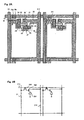
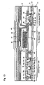
- Figs. 1 to 2B are used in explaining the preferred embodiments of the present invention. Shown in Fig. 1 is a cross sectional diagram of a pixel of an EL display device of the present invention, in Fig. 2A is its top view, and in Fig. 2B is a circuit composition. In practice, a pixel portion (image display portion) is formed with a multiple number of this type of pixel arranged in a matrix state.
- FIG. 1 shows a cross section cut along the line A-A' in the top view shown in Fig. 2A .
- Common symbols are used in Fig. 1 and in Figs. 2A and 2B , and therefore the three figures may be referenced as appropriate.
- two pixels are shown in the top view of Fig. 2A , and both have the same structure.
- Reference numeral 11 denotes a substrate
- reference numeral 12 denotes a base film in Fig. 1 .
- a glass substrate, a glass ceramic substrate, a quartz substrate, a silicon substrate, a ceramic substrate, a metallic substrate, or a plastic substrate (including a plastic film) can be used as the substrate 11.
- the base film 12 is especially effective for cases in which a substrate containing mobile ions, or a substrate having conductivity, is used, but need not be formed for a quartz substrate.
- An insulating film containing silicon may be formed as the base film 12.
- the term "insulating film containing silicon” indicates, specifically, an insulating film that contains silicon, oxygen, and nitrogen in predetermined ratios such as a silicon oxide film, a silicon nitride film, or a silicon oxynitride film (denoted by Si0 x N y ).
- TFTs Two TFTs are formed within the pixel here.
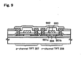
- Reference numeral 201 denotes a TFT functioning as a switching element (hereafter referred to as a switching TFT), and reference numeral 202 denotes a TFT functioning as a current control element for controlling the amount of current flowing to an EL element (hereafter referred to as a current control TFT), and both are formed by an n-channel TFT.
- the field effect mobility of the n-channel TFT is larger than the field effect mobility of a p-channel TFT, and therefore the operation speed is fast and electric current can flow easily. Further, even with the same amount of current flow, the n-channel TFT can be made smaller. The effective surface area of the display portion therefore becomes larger when using the n-channel TFT as a current control TFT, and this is preferable.
- the p-channel TFT has the advantages that hot carrier injection essentially does not become a problem, and that the off current value is low, and there are already reports of examples of using the p-channel TFT as a switching TFT and as a current control TFT.
- the present invention is characterized by the use of n-channel TFTs for all of the TFTs within all of the pixels.
- the switching TFT 201 is formed having: an active layer comprising a source region 13, a drain region 14, LDD regions 15a to 15d, a high concentration impurity region 16, and channel forming regions 17a and 17b; a gate insulating film 18; gate electrodes 19a and 19b, a first interlayer insulating film 20, a source wiring 21, and a drain wiring 22.
- the present invention is characterized in that the gate electrodes 19a and 19b become a double gate structure electrically connected by a gate wiring 211 which is formed by a different material (a material having a lower resistance than the gate electrodes 19a and 19b).
- a different material a material having a lower resistance than the gate electrodes 19a and 19b.
- a so-called multi-gate structure a structure containing an active layer having two or more channel forming regions connected in series
- the multi-gate structure is extremely effective in lowering the value of the off current, and by making the switching TFT 201 of the pixel into a multi-gate structure with the present invention, a low off current value can be realized for the switching TFT.
- the active layer is formed by a semiconductor film containing a crystal structure.
- a single crystal semiconductor film may be used, and a polycrystalline semiconductor film or a microcrystalline semiconductor film may also be used.
- the gate insulating film 18 may be formed by an insulating film containing silicon. Additionally, a conducting film can be used for all of the gate electrodes, the source wiring, and the drain wiring.
- the LDD regions 15a to 15d in the switching TFT 201 are formed so as not to overlay with the gate electrodes 19a and 19b by interposing the gate insulating film 18. This structure is extremely effective in reducing the off current value.
- an offset region (a region that comprises a semiconductor layer having the same composition as the channel forming regions, and to which a gate voltage is not applied) between the channel forming regions and the LDD regions is more preferable for reducing the off current value.
- the high concentration impurity region formed between the channel forming regions is effective in lowering the value of the off current.
- the multi-gate structure TFT as the switching TFT 201, as above, a switching element having a sufficiently low off current value is realized by the present invention.
- the gate voltage of the current control element can therefore be maintained for a sufficient amount of time (for a period from one selection until the next selection) without forming a capacitor (Cs), such as the one stated in the conventional example.
- the current control TFT 202 is formed having: an active layer comprising a source region 31, a drain region 32, an LDD region 33, and a channel forming region 34; a gate insulating film 18; a gate electrode 35; the first interlayer insulating film 20; a source wiring 36; and a drain wiring 37.
- the gate electrode 35 has a single gate structure, but a mul ti-gate structure is used according to the invention.
- the drain of the switching TFT 201 is electrically connected to the gate of the current control TFT 202.
- the gate electrode 35 of the current control TFT 202 is electrically connected to the drain region 14 of the switching TFT 201 through the drain wiring (also referred to as a connection wiring) 22.
- the source wiring 36 is connected to an electric current supply wiring 212.
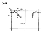
- a characteristic of the current control TFT 202 is that its channel width is larger than the channel width of the switching TFT 201. Namely, as shown in Fig. 8 , when the channel length of the switching TFT is taken as L1 and its channel width as W1, and the channel length of the current control TFT is taken as L2 and its channel width as W2, a relational expression is reached in which W2 / L2 ⁇ 5 ⁇ W1 / L1 (preferably W2 / L2 ⁇ 10 ⁇ W1 / L1). Consequently, it is possible for more current to easily flow in the current control TFT than in the switching TFT.
- the channel length L1 of the multi-gate structure switching TFT is the sum of each of the channel lengths of the two or more channel forming regions formed.
- a double gate structure is formed in the case of Fig. 8 , and therefore the sum of the channel lengths L1a and L1b, respectively, of the two channel-forming regions becomes the channel length L1 of the switching TFT.
- the channel lengths L1 and L2, and the channel widths W1 and W2 are not specifically limited to a range of values with the present invention, but it is preferable that W1 be from 0.1 to 5 ⁇ m (typically between 1 and 3 ⁇ m), and that W2 be from 0. 5 to 30 ⁇ m (typically between 2 and 10 ⁇ m). It is preferable that L1 be from 0.2 to 18 ⁇ m (typically between 2 and 15 ⁇ m), and that L2 be from 0.1 to 50 ⁇ m (typically between 1 and 20 ⁇ m) at this time.
- the channel length L in the current control TFT is set on the long side in order to prevent excessive current flow.
- W2 / L2 ⁇ 3 (more preferably W2 / L2 ⁇ 5).
- the current flow per pixel is from 0.5 to 2 ⁇ A (better between 1 and 1.5 5 ⁇ A).
- the length (width) of the LDD region formed in the switching TFT 201 is set from 0.5 to 3.5 ⁇ m, typically between 2.0 and 2.5 ⁇ m.
- the EL display device shown in Fig. 1 is characterized in that the LDD region 33 is formed between the drain region 32 and the channel forming region 34 in the current control TFT 202.
- the LDD region 33 has both a region which overlaps, and a region which does not overlap the gate electrode 35 by interposing a gate insulating film 18.
- the current control TFT 202 supplies a current for making the EL element 203 luminesce, and at the same time controls the amount supplied and makes gray scale display possible. It is therefore necessary that there is no deterioration when the current flows, and that steps are taken against deterioration due to hot carrier injection. Furthermore, when black is displayed, the current control TFT 202 is set in the off state, but if the off current value is high, then a clean black color display becomes impossible, and this invites problems such as a reduction in contrast. It is therefore necessary to suppress the value of the off current.
- the length of the LDD region which overlaps the gate electrode may be made from 0. 1 to 3 ⁇ m (preferable between 0.3 and 1. 5 ⁇ m) at this point. If it is too long, then the parasitic capacitance will become larger, and if it is too short, then the effect of preventing hot carrier will become weakened. Further, the length of the LDD region not overlapping the gate electrode may be set from 1.0 to 3.5 ⁇ m (preferable between 1.5 and 2.0 ⁇ m). If it is too long, then a sufficient current becomes unable to flow, and if it is too short, then the effect of reducing off current value becomes weakened.
- a parasitic capacitance is formed in the above structure in the region where the gate electrode and the LDD region overlap, and therefore it is preferable that this region not be formed between the source region 31 and the channel forming region 34.
- the carrier (electrons in this case) flow direction is always the same for the current control TFT, and therefore it is sufficient to form the LDD region on only the drain region side.
- the film thickness of the active layer (especially the channel forming region) of the current control TFT 202 thick (preferably from 50 to 100 nm, more preferably between 60 and 80 nm).
- the film thickness of the active layer (especially the channel forming region) thin (preferably from 20 to 50 nm, more preferably between 25 and 40 nm).
- reference numeral 41 denotes a first passivation film, and its film thickness may be set from 10 nm to 1 ⁇ m (preferably between 200 and 500 nm).
- An insulating film containing silicon in particular, preferably a silicon oxynitride film or a silicon nitride film
- the passivation film 41 plays the role of protecting the manufactured TFT from contaminant matter and moisture.
- Alkaline metals such as sodium are contained in an EL layer formed on the final TFT.
- the first passivation film 41 works as a protecting layer so that these alkaline metals (mobile ions) do not penetrate into the TFT. Note that alkaline metals and alkaline-earth metals are contained in the term 'alkaline metal' throughout this specification.
- the passivation film 41 possess a heat radiation effect, it is also effective in preventing thermal degradation of the EL layer. Note that light is emitted from the base 11 side in the Fig. 1 structure of the EL display device, and therefore it is necessary for the passivation film 41 to have light transmitting characteristics.
- a chemical compound containing at least one element selected from the group consisting of B (boron), C (carbon), and N (nitrogen), and at least one element selected from the group consisting of Al (aluminum), Si (silicon), and P (phosphorous) can be given as a light transparent material possessing heat radiation qualities.
- an aluminum nitride compound typically aluminum nitride (Al x N y ); a silicon carbide compound, typically silicon carbide (Si x C y ); a silicon nitride compound, typically si I icon nitride (Si x N y ); a boron ni tride compound, typically boron ni tride (B x N y ); or a boron phosphate compound, typically boron phosphate (B x P y ).
- an aluminum oxide compound typically aluminum oxide (Al x O y )
- Al x O y has superior light transparency characteristics, and has a thermal conductivity of 20 Wm -1 K -1 , and can be said to be a preferable material.
- These materials not only possess heat radiation qualities, but also are effective in preventing the penetration of substances such as moisture and alkaline metals.
- x and y are arbitrary integers for the above transparent materials.
- the above chemical compounds can also be combined with another element.
- nitrated aluminum oxide denoted by AlN x 0 y
- nitrogen is added to aluminum oxide.
- This material also not only possesses heat radiation qualities, but also is effective in preventing the penetration of substances such as moisture and alkaline metals.
- x and y are arbitrary integers for the above nitrated aluminum oxide.
- the materials recorded in Japanese Patent Application Laid-open JP 62090260 can also be used.
- a chemical compound containing Si, Al, N, 0, and M can also be used (note that M is a rare-earth element, preferably an element selected from the group consisting of Ce (cesium), Yb (ytterbium), Sm (samarium), Er (erbium), Y (yttrium), La (lanthanum), Gd (gadolinium), Dy (dysprosium), and Nd (neodymium)).
- Ce cesium
- Yb ytterbium
- Sm sinarium
- Er Er
- Y yttrium
- La lanthanum
- Gd gadolinium
- Dy dysprosium
- Nd neodymium
- carbon films such as a diamond thin film or amorphous carbons (especially those which have characteristics close to those of diamond; referred to as diamond-like carbon) can also be used. These have very high thermal conductivities, and are extremely effective as radiation layers. Note that if the film thickness becomes larger, there is brown banding and the transmissivity is reduced, and therefore it is preferable to use as thin a film thickness (preferably between 5 and 100 nm) as possible.
- the aim of the first passivation film 41 is in protecting the TFT from contaminating matter and from moisture, and therefore it must made so as to not lose this effect.
- a thin film made from a material possessing the above radiation effect can be used by itself, but it is effective to laminate this thin film and a thin film having shielding properties against alkaline metals and moisture (typically a silicon nitride film (Si x N y ) or a silicon oxynitride film (Si0 x N y )).
- Si x N y silicon nitride film
- Si0 x N y silicon oxynitride film
- Reference numeral 42 denotes a color filter
- reference numeral 43 denotes a fluorescent substance (also referred to as a fluorescent pigment layer). Both are a combination of the same color, and contain red (R), green (G), or blue (B).
- the color filter 42 is formed in order to increase the color purity
- the fluorescent substance 43 is formed in order to perform color transformation.
- EL display devices are roughly divided into four types of color displays: a method of forming three types of EL elements corresponding to R, G, and B; a method of combining white color luminescing EL elements with color filters; a method of combining blue or blue-green luminescing EL elements and fluorescent matter (fluorescing color change layer, CCM); and a method of using a transparent electrode as a cathode (opposing electrode) and overlapping EL elements corresponding to R, G, and B.
- the structure of Fig. 1 is an example of a case of using a combination of blue luminescing EL elements and a fluorescent substance.
- a blue color emitting luminescence layer is used as the EL element 203 here, light possessing blue color region wavelength, including ultraviolet light, is formed, and the fluorescent substance 43 is activated by the light, and made to emit red, green, or blue light. The color purity of the light is increased by the color filter 42, and this is outputted.
- a second interlayer insulating film 44 is formed by a second interlayer insulating film 44.
- a resin film is preferable as the second interlayer insulating film 44, and one such as polyimide, polyamide, acrylic, or BCB (benzocyclobutane) may be used.
- An inorganic film may, of course, also be used, provided that sufficient level ing is possible.
- the leveling of steps due to the TFT by the second interlayer insulating film 44 is extremely important.
- the EL layer formed afterward is very thin, and therefore there are cases in which poor luminescence is caused by the existence of a step. It is therefore preferable to perform leveling before forming a pixel electrode so as to be able to form the EL layer on as level a surface as possible.
- thermal radiation layer an insulating film having a high thermal radiation effect (hereafter referred to as a thermal radiation layer) on the second interlayer insulating film 44.
- This type of thermal radiation layer functions so that the heat generated by the EL element is released, so that heat is not stored in the EL element.
- the second interlayer insulating film 44 is weak with respect to heat, and the thermal radiation layer works so as not to impart bad influence due to the heat generated by the EL element.
- the thermal radiation layer can also function as a protecting layer in order that alkaline metals within the EL layer do not diffuse toward the TFT, at the same time as preventing deterioration of the EL element and the resin film due to heat, as above.
- the thermal radiation layer also functions as a protecting layer so that moisture and oxygen do not penetrate into the EL layer from the TFT.
- a carbon film such as a diamond film or a diamond-like carbon film is preferable, and in order to prevent penetration of substances such as moisture, it is more preferable to use a lamination structure of a carbon film and a silicon nitride film (or a silicon oxynitride film).
- Reference numeral 45 denotes a pixel electrode (EL element anode) made from a transparent conducting film. After opening a contact hole in the second interlayer insulating film 44 and in the first passivation film 41, the pixel electrode 45 is formed so as to be connected to the drain wiring 37 of the current control TFT 202.
- An EL layer (an organic material is preferable) 46, a cathode 47, and a protecting electrode 48 are formed in order on the pixel electrode 45.
- a single layer structure or a lamination structure can be used as the EL layer 46, but there are many cases in which the lamination structure is used.
- Various lamination structures have been proposed, combinations of layers such as a luminescence layer, an electron transporting layer, an electron injecting layer, a hole injecting layer, and a hole transporting layer, but any structure may be used for the present invention. Doping of a fluorescent pigment into the EL layer may also be performed, of course. Note that a luminescing element formed by a pixel electrode (anode), an EL layer, and a cathode is referred to as an EL element throughout this specification.
- Organic materials are widely known as such materials, and considering the driver voltage, it is preferable to use an organic material.
- the materials disclosed in the following U.S. Patents and Japanese patent applications can be used as the organic EL material:
- an organic material such as the one shown by the following general formula can be used as a hole injecting layer.
- Q is either N or a C-R (carbon chain);
- M is a metal, a metal oxide, or a metal halide;
- R is hydrogen, an alkyl, an aralkyl, an aryl, or an alkalyl ;
- T1 and T2 are unsaturated six member rings including substituent such as hydrogen, alkyl, or halogen.
- an aromatic tertiary amine can be used as an organic material hole transporting layer, preferably including the tetraaryldiamine shown by the following general formula.
- n is an integer from 1 to 4
- Ar, R 7 , R 8 , and R 9 are each various chosen aryl groups.
- a metal oxynoid compound can be used as an organic material EL layer, electron transporting layer, or electron injecting layer.
- a material such as that shown by the general formula below may be used as the metal oxinoid compound. It is possible to substitute R 2 through R 7 , and a metal oxinoid such as the following can also be used.
- R 2 through R 7 are defined as stated above; L 1 through L 5 are carbohydrate groups containing from 1 to 12 carbon elements; and both L 1 and L 2 , or both L 2 and L 3 are formed by benzo-rings. Further, a metal oxinoid such as the following may also be used.
- a polymer material as the EL material.
- Polymer materials such as the following can be given as typical polymer materials: polyparaphenylene vinylenes (PPVs); and polyfluorenes.
- PVs polyparaphenylene vinylenes
- For colorization it is preferable to use, for example, a cyano-polyphenylene vinylene in a red luminescing material; a polyphenylene vinylene in a green luminescing material; and a polyphenylene vinylene and a polyalkylphenylene in a blue luminescing material.
- organic EL materials which can be used in an ink-jet method, all of the materials recorded in JP 10012377 can be cited.
- a material containing a low work coefficient material such as magnesium (Mg), lithium (Li), cesium (Cs), barium (Ba), potassium (K), beryllium (Be), or calcium (Ca) is used as the cathode 47.
- a MgAgAl electrode, a LiAl electrode, and a LiFAI electrode can be given as other examples.
- the protecting electrode 48 is an electrode formed in order to be a protecting film against moisture from external to the cathode 47, and a material containing aluminum (Al) or silver (Ag) is used.
- the protecting electrode 48 also has a heat radiation effect.
- the EL layer is extremely weak with respect to heat, and therefore it is preferable to use vacuum evaporation (in particular, an organic molecular beam evaporation method is effective in that it forms a very thin film, on the molecular order level), sputtering, plasma CVD, spin coating, screen printing, or ion plating as the film deposition method. It is also possible to form the EL layer by an ink-jet method. For the ink jet method there is a bubble jet method using cavitation (refer to JP 05116297 ), and there is a piezo method using a piezo element (refer to JP 08290647 ), and in view of the fact that organic EL materials are weak with respect to heat, the piezo method is preferable.
- Reference numeral 49 denotes a second passivation film, and its film thickness may be set from 10 nm to 1 ⁇ m (preferable between 200 and 500 nm).
- the object of forming the second passivation film 49 is mainly to protect the EL layer 46 from moisture, but it is also good if the second passivation film 49 is made to possess a heat radiation effect, similar to the first passivation film 41.
- the same materials as used for the first passivation film 41 can therefore be used as the formation material of the second passivation film 49. Note that when an organic material is used as the EL layer 46, it deteriorates due to bonding with oxygen, and therefore it is preferable to use an insulating film which does not easily emit oxygen.
- the EL layer is weak with respect to heat, as stated above, and therefore it is preferable to perform film deposition at a low temperature as possible (preferably in the range from room temperature to 120°C). It can therefore be said that plasma CVD, sputtering, vacuum evaporation, ion plating, and solution application (spin coating) are desirable film deposition methods.
- the EL display device of the present invention has a pixel portion containing a pixel with a structure as stated above, and TFTs having differing structures in response to their function are arranged in the pixel.
- a switching TFT having a sufficiently low off current value, and a current control TFT which is strong with respect to hot carrier injection can be formed within the same pixel, and an EL display device having high reliability and which is capable of good image display can thus be formed.
- a multi-gate structure TFT is used as the switching TFT, and that it is not necessary to place limits on the structure of Fig. 1 with regard to such things as the placement of LDD regions.
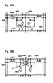
- CMOS circuit is shown as a basic circuit for the driver circuits.
- a base film 301 is formed with a 300 nm thickness on a glass substrate 300. Silicon oxynitride films are laminated as the base film 301 in embodiment 1. It is good to set the nitrogen concentration to between 10 and 25 wt% in the film contacting the glass substrate 300.
- a heat radiating layer made from the same material as that of the first passivation film 41 shown in Fig. 1 , as a portion of the base film 301.
- a large electric current flows in a current control TFT heat is easily generated, and therefore it is effective to form the heat radiating layer as close as possible to the current control TFT.
- an amorphous silicon film (not shown in the figures) is formed with a thickness of 50 nm on the base film 301 by a known deposition method. Note that it is not necessary to limit this to the amorphous silicon film, and another film may be formed provided that it is a semiconductor film containing an amorphous structure (including a microcrystalline semiconductor film). In addition, a compound semiconductor film containing an amorphous structure, such as an amorphous silicon germanium film, may also be used. Further, the film thickness may be made from 20 to 100 nm.
- the amorphous silicon film is then crystallized by a known method, forming a crystalline silicon film (also referred to as a polycrystalline silicon film or a polysilicon film) 302.
- a crystalline silicon film also referred to as a polycrystalline silicon film or a polysilicon film
- Thermal crystallization using an electric furnace, laser annealing crystallization using a laser, and lamp annealing crystallization using an infrared lamp exist as known crystallization methods. Crystallization is performed in embodiment 1 using light from an excimer laser which uses XeCl gas.
- pulse emission type excimer laser light formed into a linear shape is used in embodiment 1, but a rectangular shape may also be used, and continuous emission argon laser light and continuous emission excimer laser light can also be used.
- the crystalline silicon film is used as an active layer of the TFTs in embodiment 1, but it is also possible to use an amorphous silicon film as the active layer. However, it is necessary for a large current to flow through the current control TFT, and therefore it is more effective to use the crystalline silicon film, through which current easily flows.
- a protecting film 303 is formed on the crystalline silicon film 302 from a silicon oxide film having a thickness of 130 nm. This thickness may be chosen within the range of 100 to 200 nm (preferably between 130 and 170 nm). Furthermore, other films may also be used providing that they are insulating films containing silicon.
- the protecting film 303 is formed so that the crystalline silicon film is not directly exposed to plasma during addition of an impurity, and so that it is possible to have delicate concentration control of the impurity.
- Resist masks 304a and 304b are then formed on the protecting film 303, and an impurity element which imparts n-type conductivity (hereafter referred to as an n-type impurity element) is added.
- an impurity element which imparts n-type conductivity hereafter referred to as an n-type impurity element
- elements residing in periodic table group 15 are generally used as the n-type impurity element, and typically phosphorous or arsenic can be used.
- a plasma doping method is used, in which phosphine (PH 3 ) is plasma activated without separation of mass. and phosphorous is added at a concentration of 1 ⁇ 10 18 atoms/cm 3 in embodiment 1.
- An ion implantation method, in which separation of mass is performed, may also be used, of course.
- the dose amount is regulated so that the n-type impurity element is contained in n-type impurity regions 305 and 306, thus formed by this process, at a concentration of 2 ⁇ 10 16 to 5 ⁇ 10 19 atoms/cm 3 (typically between 5 ⁇ 10 17 and 5 ⁇ 10 18 atoms/cm 3 ).
- the protecting film 303 is removed, and activation of the added periodic table group 15 element is performed.
- a known technique of activation may be used as the means of activation, and activation is done in embodiment 1 by irradiation of excimer laser light. Both of pulse emission type laser and a continuous emission type laser may be used, and it is not necessary to place any limits on the use of excimer laser light.
- the goal is the activation of the added impurity element, and it is preferable that irradiation is performed at an energy level at which the crystalline silicon film does not melt. Note that the laser irradiation may also be performed with the protecting film 303 in place.
- Activation by heat treatment may also be performed along with activation of the impurity element by laser light.
- activation is performed by heat treatment, considering the heat resistance of the substrate, it is good to perform heat treatment on the order of 450 to 550°C.
- a boundary portion (connecting portion) with regions along the edges of the n-type impurity regions 305 and 306, namely regions along the perimeter into which the n-type impurity element, which exists in the n-type impurity regions 305 and 306, is not added, is delineated by this process. This means that, at the point when the TFTs are later completed, extremely good connections can be formed between LDD regions and channel forming regions.
- a gate insulating film 311 is formed, covering the active layers 307 to 310.
- a single layer structure or a lamination structure may be used.
- a 110 nm thick silicon oxynitride film is used in embodiment 1.
- gate electrodes 312 to 316 A conducting film with a thickness of 200 to 400 nm is formed next and patterned, forming gate electrodes 312 to 316.
- the gate electrodes and lead wirings electrically connected to the gate electrodes are formed from different materials. Specifically, a material having a lower resistance than that of the gate electrodes is used for the gate wirings. This is because a material which is capable of being micro-processed is used as the gate electrodes, and even if the gate wirings cannot be micro-processed, the material used for the wirings has low resistance.
- the gate electrodes and the gate wirings may also be formed from the same material.
- the gate wirings may be formed by a single layer conducting film, and when necessary, it is preferable to use a two layer or a three layer lamination film. All known conducting films can be used as the gate electrode material. However, as stated above, it is preferable to use a material which is capable of being micro-processed, specifically, a material which is capable of being patterned to a line width of 2 ⁇ m or less.
- a single layer film or a lamination may be used, of course.
- a lamination film made from a 50 nm thick tantalum nitride (TaN) film and a 350 nm thick Ta film is used in embodiment 1. It is good to form this film by sputtering. Furthermore, if an inert gas such as Xe or Ne is added as a sputtering gas, then film peeling due to the stress can be prevented.
- TaN tantalum nitride
- the gate electrodes 313 and 316 are formed at this time so as to overlap a portion of the n-type impurity regions 305 and 306, respectively, sandwiching the gate insulating film 311. This overlapping portion later becomes an LDD region overlapping the gate electrode.
- an n-type impurity element (phosphorous is used in embodiment 1) is added in a self-aligning manner with the gate electrodes 312 to 316 as masks, as shown in Fig. 4A .
- the addition is regulated so that phosphorous is added to impurity regions 317 to 323 thus formed at a concentration of 1/10 to 1/2 that of the impurity regions 305 and 306 (typically between 1/4 and 1/3).
- a concentration of 1 ⁇ 10 16 to 5 ⁇ 10 18 atoms/cm 3 (typically 3 ⁇ 10 17 to 3x10 18 atoms/cm 3 ) is preferable.
- Resist masks 324a to 324d are formed next to cover the gate electrodes, as shown in Fig. 4B , and an n-type impurity element (phosphorous is used in embodiment 1) is added, forming impurity regions 325 to 331 containing a high concentration of phosphorous. Ion doping using phosphine (PH 3 ) is also performed here, and is regulated so that the phosphorous concentration of these regions is from 1 ⁇ 10 20 to 1 ⁇ 10 21 atoms/cm 3 (typically between 2 ⁇ 10 20 and 5 ⁇ 10 20 atoms/cm 3 ).
- a source region or a drain region of the n-channel TFT is formed by this process, and in the switching TFT, a portion of the n-type impurity regions 320 to 322 formed by the process of Fig. 4A remains. These remaining regions correspond to the LDD regions 15a to 15d of the switching TFT in Fig. 1 .
- the resist masks 324a to 324d are removed, and a new resist mask 332 is formed.
- a p-type impurity element (boron is used in embodiment 1) is then added, forming impurity regions 333 and 334 containing a high concentration of boron.
- Boron is added here to a concentration of 3 ⁇ 10 20 to 3 ⁇ 10 21 atoms/cm 3 (typically between 5 ⁇ 10 20 and 1 ⁇ 10 21 atoms/cm 3 ) by ion doping using diborane (B 2 H 6 ).
- phosphorous has already been added to the impurity regions 333 and 334 at a concentration of 1 ⁇ 10 16 to 5 ⁇ 10 18 atoms/cm 3 , but boron is added here at a concentration of at least 3 times that of the phosphorous. Therefore, the n-type impurity regions already formed completely invert to p-type, and function as p-type impurity regions.
- the n-type and p-type impurity elements added at various concentrations are activated.
- Furnace annealing, laser annealing, or lamp annealing may be performed as a means of activation.
- Heat treatment is performed in embodiment 1 in a nitrogen atmosphere for 4 hours at 550°C in an electric furnace.
- the concentration of oxygen in the atmosphere in the above activation process be 1 ppm or less, desirably 0.1 ppm or less.
- a gate wiring 335 with a thickness of 300 nm is formed next.
- a metallic film having aluminum (Al) or copper (Cu) as its principal constituent (comprising 50 to 100% of the composition) may be used as the material of the gate wiring 335.
- the gate wiring 335 is formed with a placement so that the gate electrodes 314 and 315 of the switching TFTs (corresponding to gate electrodes 19a and 19b of Fig. 2 ) are electrically connected. (See Fig. 4D .)
- the wiring resistance of the gate wiring can be made extremely small by using this type of structure, and therefore a pixel display region (pixel portion) having a large surface area can be formed.
- the pixel structure of embodiment 1 is extremely effective because an EL display device having a screen size of a 10 inch diagonal or larger (in addition, a 30 inch or larger diagonal) is realized.
- a first interlayer insulating film 336 is formed next, as shown in Fig. 5A .
- a single layer insulating film containing silicon is used as the first interlayer insulating film 336, but a lamination film may be combined in between. Further, a film thickness of between 400 nm and 1. 5 ⁇ m may be used.
- a lamination structure of an 800 nm thick silicon oxide film on a 200 nm thick silicon oxynitride film is used in embodiment 1.
- heat treatment is performed for 1 to 12 hours at 300 to 450° C in an atmosphere containing between 3 and 100% hydrogen, performing hydrogenation.
- This process is one of hydrogen termination of dangling bonds in the semiconductor film by hydrogen which is thermally activated.
- Plasma hydrogenation (using hydrogen activated by a plasma) may also be performed as another means of hydrogenation.
- the hydrogenation step may also be inserted during the formation of the first interlayer insulating film 336. Namely, hydrogen processing may be performed as above after forming the 200 nm thick silicon oxynitride film, and then the remaining 800 nm thick silicon oxide film may be formed.
- a contact hole is formed next in the first interlayer insulating film 336, and source wirings 337 to 340, and drain wirings 341 to 343 are formed.
- Other conducting films may also be used, of course, and an alloy film containing silver, palladium, and copper may also be used.
- a first passivation film 344 is formed next with a thickness of 50 to 500 nm (typically between 200 and 300 nm).
- a 300 nm thick silicon oxynitride film is used as the first passivation film 344 in embodiment 1. This may also be substituted by a silicon nitride film. It is of course possible to use the same materials as those of the first passivation film 41 of Fig. 1 .
- a color filter 345 and a fluorescing body 346 are formed.
- Known materials may be used for these.
- they may be formed by being patterned separately, or they may be formed in succession and then patterned together.
- a method such as screen printing, ink jetting, or mask evaporation (a selective forming method using a mask material) may be used as the formation method.
- the respective film thickness may be chosen in the range of 0. 5 to 5 ⁇ m (typically between 1 and 2 ⁇ m).
- the optimal film thickness of the fluorescing body 346 varies with the material used. In other words, if it is too thin, then the color transformation efficiency becomes poor, and if it is too thick, then the step becomes large and the amount of light transmitted drops. Optimal film thicknesses must therefore be set by taking a balance of both characteristics.
- a second interlayer insulating film 347 is formed next from an organic resin.
- Materials such as polyimide, polyamide, acrylic, and BCB (benzocyclobutene) can be used as the organic resin.
- the purpose of being a leveling film is strong in the second interlayer insulating film 347, and therefore acrylic, having superior leveling characteristics, is preferable.
- An acrylic film is formed in embodiment 1 with a film thickness which can sufficiently level the step between the color filter 345 and the fluorescing body 346. This thickness is preferably from 1 to 5 ⁇ m (more preferably between 2 and 4 ⁇ m).
- a contact hole for reaching the drain wiring 343 is formed next in the second interlayer insulating film 347 and in the first passivation film 344 , and a pixel electrode 348 is formed.
- a compound of indium oxide and tin oxide is formed into 110 nm thick in embodiment 1, and patterning is performed, making the pixel electrode.
- the pixel electrode 348 becomes an anode of the EL element. Note that it is also possible to use other materials: a compound film of indium oxide and zinc oxide, or a zinc oxide film containing gallium oxide.
- embodiment 1 becomes a structure in which the pixel electrode 348 is electrically connected to the drain region 331 of the current control TFT, through the drain wiring 343. This structure has the following advantages.
- the pixel electrode 348 becomes directly connected to an organic material such as the EL layer (emitting layer) or a charge transporting layer, and therefore it is possible for the mobile ions contained in the EL layer to di ffuse throughout the pixel electrode.
- an organic material such as the EL layer (emitting layer) or a charge transporting layer
- an EL layer 349, a cathode (MgAg electrode) 350, and a protecting electrode 351 are formed in succession without exposure to the atmosphere. It is preferable, at this point, to perform heat treatment of the pixel electrode 348, completely removing all moisture, before forming the EL layer 349 and the cathode 350. Note that a known material can be used as the EL layer 349.
- the materials explained in the "embodiment mode" section of this specification can be used as the EL layer 349.
- an EL layer having a 4 layer structure of a hole injecting layer, a hole transporting layer, an emitting layer, and an electron transporting layer is used, as shown in Fig. 19 , but there are cases in which the electron transporting layer is not formed, and cases in which an electron injecting layer is also formed. Furthermore, there are also cases in which the hole injecting layer is omitted.
- these types of combinations have already been reported, and any of these constitutions may be used.
- An amine such as TPD may be used as the hole injecting layer or as the hole transporting layer, and in addition, a hydrazone (typically DEH), a sti Ibene(typically STB), or a starburst (typically m-MTDATA) can also be used.
- a starburst material which has a high glass transition temperature and is difficult to crystallize, is preferable.
- polyaniline (PAni), polythiophene (PEDOT), and copper phthalocyanine (CuPc) may also be used.
- BPPC, perylene, and DCM can be used as a red color emitting layer in the emitting layer, and in particular, the Eu complex shown by Eu(DBM) 3 (Phen) (refer to Kido, J., et. al, Appl. Phys., vol. 35, pp. L394-6, 1996 for details) is highly monochromatic, possessing a sharp emission at a wavelength of 620 nm.
- an Alq 3 (8-hydroxyquinol ine aluminum) material in which quinacridone or coumarin is added at a level of several mol% can be used as a green color emitting layer.
- a distile-arylene amino dielectric in which amino substituted DSA is added to DSA (distile-arylene dielectric) can be used as a blue color emitting layer.
- distilyl-biphenyl DPVBi
- DPVBi high performance material distilyl-biphenyl
- a 300 nm thick silicon nitride film is formed as a second passivation film 352, and this may also be formed in succession, wi thout exposure to the atmosphere, after formation of the protecting electrode 351.
- the same materials as those of the second passivation film 49 of Fig. 1 can also be used, of course, as the second passivation film 352.
- a 4 layer structure made from a hole injecting layer, a hole transporting layer, an emitting layer, and an electron injecting layer is used in embodiment 1, but there are already examples of many combinations already reported, and any of these constitutions may also be used.
- an MgAg electrode is used as the cathode of the EL element in embodiment 1, but other known materials may also be used.
- the protecting electrode 351 is formed in order to prevent deterioration of the MgAg electrode 350, and a metallic film having aluminum as its principal constituent is typical. Other materials may, of course, also be used. Furthermore, the EL layer 349 and the MgAg electrode 350 are extremely weak wi th respect to moisture, and therefore it is preferable to perform successive formation up through to the protecting electrode 351 without exposure to the atmosphere, protecting the EL layer from external air.
- the film thickness of the EL layer 349 may be from 10 to 400 nm (typically between 60 and 160 nm), and that the thickness of the MgAg electrode 350 may be from 180 to 300 nm (typically between 200 and 250 nm).
- the active matrix type EL display device with the structure shown in Fig. 5C is thus completed.
- the active matrix type EL display device of embodiment 1 shows extremely high reliability, and the operational characteristics can be raised.
- a TFT having a structure which reduces hot carrier injection as much as possible without a drop in the operation speed is used as an n-channel TFT 205 of the CMOS circuit forming the driver circuits.
- the driver circuits referred to here include circuits such as a shift register, a buffer, a level shifter, and a sampling circuit (also referred to as a transfer gate).
- signal conversion circuits such as a D/A converter circuit are also included.
- an active layer of the n-channel TFT 205 includes a source region 355, a drain region 356, an LDD region 357, and a channel forming region 358, as shown in Fig. 5C , and the LDD region 357 overlaps the gate electrode 313, sandwiching the gate insulating film 311.
- the formation of the LDD region on the drain side only is in consideration of not lowering the operation speed. Further, it is not necessary to be concerned with the value of the off current in the n-channel TFT 205, and greater emphasis may be placed on the operation speed. It is therefore preferable that the LDD region 357 completely overlap the gate electrode 313, reducing resistive components as much as possible. In other words, it is good to eliminate all offset.
- Deterioration of a p-channel TFT 206 of the CMOS circuit due to hot carrier injection is almost of no concern, and in particular, therefore, an LDD region is not formed. It is also possible, of course, to take action against hot carriers by forming an LDD region similar to that of the n-channel TFT 205.
- the sampling circuit is somewhat special when compared to the other circuits, and a large current flows in the channel forming region in both directions. Namely, the roles of the source region and the drain region change. In addition, it is necessary to suppress the value of the off current as much as possible, and with that in mind, it is preferable to arrange a TFT having functions at an intermediate level between the switching TFT and the current control TFT.
- a TFT with the structure shown in Fig. 9 is an n-type TFT forming the sampling circuit.
- This effect is as stated in the explanation of the current control TFT 202, and the case of the sampling circuit differs in the point of forming the LDD regions 901a and 901b with a shape that sandwiches a channel forming region 904.
- a pixel with the structure shown in Fig. 1 is formed, forming a pixel portion.
- the structures of a switching TFT and a current control TFT formed within the pixel have already been explained in Fig. 1 , and therefore that explanation is omitted here.
- a housing material such as a highly airtight protecting film (such as a laminar film or an ultraviolet hardened resin film) or a ceramic sealing can, so that there is no exposure to the atmosphere.
- a housing material such as a highly airtight protecting film (such as a laminar film or an ultraviolet hardened resin film) or a ceramic sealing can, so that there is no exposure to the atmosphere.
- a connector (a flexible printed circuit, FPC) for connecting between output terminals from elements or circuits formed on the substrate, and external signal terminals, is attached, completing a manufactured product.
- FPC flexible printed circuit
- the active matrix type EL display device of embodiment 1 is formed on a glass substrate 601, and is composed of a pixel portion 602, a gate side driving circuit 603, and a source side driving circuit 604.
- a switching TFT 605 of the pixel portion is an n-channel TFT, and is placed at the intersection of a gate wiring 606 connected to the gate side driving circuit 603, and a source wiring 607 of the source side driving circuit 604. Furthermore, the drain of the switching TFT 605 is electrically connected to the gate of a current control TFT 608.
- the source of the current control TFT 608 is connected to a current supply line 609, and an EL element 610 is electrically connected to the drain of the current control TFT 608.
- the current control TFT 608 is an n-channel TFT, it is preferable to connect the cathode of the EL element 610 to the drain of the current control TFT 608 at this point.
- the current control TFT 608 is a p-channel TFT, then it is preferable to connect the anode of the EL element 610 to the drain of the current control TFT 608.
- Input wirings (connection wirings) 612 and 613, and an input wiring 614 which is connected to the current supply line 609, are then formed in an external input terminal FPC 611 in order to transfer signals to the driver circuits.
- Fig. 7 Shown in Fig. 7 is one example of the circuit composition of the EL display device shown in Fig. 6 .
- the EL display device of embodiment 1 has a source side driving circuit 701, a gate side driving circuit (A) 707, a gate side driving circuit (B) 711, and a pixel portion 706.
- driver circuit is a generic term which includes source side processing circuits and gate side processing circuits.
- the source side driving circuit 701 is provided with a shift register 702, a level shifter 703, a buffer 704, and a sampling circuit (transfer gate) 705.
- the gate side driving circuit (A) 707 is provided with a shift register 708, a level shifter 709, and a buffer 710.
- the gate side driving circuit (B) 711 has a similar composition.
- the driving voltage is from 5 to 16 V (typically 10 V) for the shifter registers 702 and 708 here, and the structure shown by reference numeral 205 of Fig. 5C is suitable for an n-channel TFT used in a CMOS circuit forming the circuits.
- CMOS circuit containing the n-channel TFT 205 of Fig. 5C is suitable.
- a multi-gate structure such as a double gate structure or a triple gate structure for the gate wirings, is effective by increasing the reliability of each circuit.
- the driving voltage is between 14 and 16 V for the sampling circuit 705, but it is necessary to reduce the value of the off current because the source region and the drain region invert, and therefore a CMOS circuit containing the n-channel TFT 208 of Fig. 9 is suitable.
- the driving voltage of the pixel portion 706 is between 14 and 16 V, and a pixel with the structure shown in Fig. 1 is arranged.
- the above constitutions can be easily realized by manufacturing TFTs in accordance with the manufacturing processes shown in Figs. 3A to 5C .
- the constitution of the pixel portion and the driver circuits is shown in embodiment 1, but it is also possible to form other logic circuits, in addition to the driving circuits, on the same substrate and in accordance with the manufacturing process of embodiment 1, such as a signal divider circuit. a D/A converter circuit, an op-amp circuit, and a y compensation circuit.
- circuits such as a memory portion and a microprocessor can also be formed.
- FIG. 17A and 17B An explanation of the EL module of embodiment 1, containing the housing material, is made using Figs. 17A and 17B . Note that, when necessary, the symbols used in Figs. 6 and 7 are cited.
- a pixel portion 1701, a source side driving circuit 1702, and a gate side driving circuit 1703 are formed on a substrate (including a base film underneath a TFT) 1700.
- Various wirings from the respective driver circuits are connected to external equipment, via the FPC 611, through the input wirings 612 to 614.
- a housingmaterial 1704 is formed at this point enclosing at least the pixel portion, and preferably the driving circuits and the pixel portion.
- the housing material 1704 is of an irregular shape in which the internal size is larger than the external size of the EL element, or has a sheet shape, and is fixed to the substrate 1700 by an adhesive 1705 so as to form an airtight space jointly with the substrate 1700.
- the EL element is in a state of being completely sealed in the above airtight space, and is completely cutoff from the external atmosphere.
- a multiple number of housing materials 1704 may be formed.
- an insulating substance such as a glass or a polymer as the housing material 1704.
- amorphous glass such as borosilicate glass or quartz
- crystallized glass ceramic glass
- organic resins such as acrylic resins, styrene resins, polycarbonate resins, and epoxy res i ns
- silicone res i ns silicone res i ns.
- ceramics may also be used.
- the adhesive 1705 is an insulating material, it is also possible to use a metallic material such as a stainless alloy.
- an adhesive such as an epoxy resin or an acrylate resin as the material of the adhesive 1705.
- a thermally hardened resin or a light hardened resin can also be used as the adhesive. Note that it is necessary to use a material through which, as much as is possible, oxygen and moisture is not transmitted.
- an opening 1706 between the housing material and the substrate 1700 is preferable to fill an opening 1706 between the housing material and the substrate 1700 with an inert gas (such as argon, helium, or nitrogen).
- an inert gas such as argon, helium, or nitrogen.
- an inert liquid such as a liquid fluorinated carbon, typically perfluoroalkane.
- the materials such as those used by Japanese Patent Application Laid-open No. Hei 8-78519 may be referred to regarding inert liquids.
- the space may also be filled with a resin.
- drying agent in the opening 1706.
- Materials such as those recorded in Japanese Patent Application Laid-open No. Hei 9-148066 can be used as the drying agent.
- barium oxide may be used.
- it is effective to form an antioxidizing agent as well, not just a drying agent.
- a plural number of isolated pixels having EL elements are formed in the pixel portion, as shown in Fig. 17B , and all of the pixels have a protecting electrode 1707 as a common electrode.
- the EL layer, the cathode (MgAg electrode), and the protecting electrode in succession, without exposure to the atmosphere.
- the EL layer and the cathode are formed using the same mask material, and provided that only the protecting electrode is formed by a separate mask material, then the structure of Fig. 17B can be realized.
- the EL layer and the cathode may be formed only in the pixel portion at this point, and it is not necessary to form them on the driving circuits. There is no problem, of course, with forming them on the driving circuits, but considering the fact that alkaline metals are contained in the EL layer, it is preferable to not form it over the driving circuits.
- an input wiring 1709 is connected to the protecting electrode 1707 in a region shown by reference numeral 1708.
- the input wiring 1709 is a wiring for providing a preset voltage to the protecting electrode 1707, and is connected to the FPC 611 through a conducting paste material (typically an anisotropic conducting film) 1710.
- FIG. 18A to 18C A manufacturing process for realizing a contact structure in the region 1708 is explained here using Figs. 18A to 18C .
- Fig. 5A is obtained in accordance with the processes of embodiment 1.
- the first interlayer insulating film 336 and the gate insulating film 311 are removed from the edges of the substrate (in the region shown by reference numeral 1708 in Fig. 17B ), and the input wiring 1709 is formed on that region.
- the source wirings and the drain wirings of Fig. 5A are of course formed at the same time. (See Fig. 18A .)
- the processes of forming the EL element (pixel electrode, EL layer, and cathode formation processes) in the pixel portion are performed in this state.
- a mask material is used in the region shown in Figs. 18A to 18C at this time so that the EL element is not formed in this region.
- the protecting electrode 350 is formed using a separate mask material. The protecting electrode 350 and the input wiring 1709 are thus electrically connected. Further, the second passivation film 352 is formed, and the state of Fig. 18C is obtained.
- the contact structure of the region shown by reference numeral 1708 in Fig. 17B is thus realized by the above steps.
- the input wi r i ng 1709 is then connec ted to the FPC 611 through the opening between the housing material 1704 and the substrate 1700 (note that this is filled by the adhesive 1705; in other words, it is necessary for the thickness of the adhesive 1705 to be such that it can sufficiently level the step of the input wiring).
- Note that an explanation of the input wiring 1709 is made here, but the other input wirings 612 to 614 are also similarly connected to the FPC 611 by passing under the housing material 1704.
- Fig. 10 an example of a pixel constitution is shown in Fig. 10 which differs from the constitution shown in Fig. 2B .
- the two pixels shown in Fig. 2B are arranged wi th symmetry around the current supply line in embodiment 2. Namely, as shown in Fig. 10 , by making the current supply line 213 common between the two pixels neighboring the current supply line, the number of wirings needed can be reduced. Note that the structure of the TFTs placed inside the pixels may be left as is.
- embodiment 2 can easily be realized in accordance with the manufacturing processes of embodiment 1. and that the explanations of embodiment 1 and of Fig. 1 may be referenced regarding points such as the structure of the TFTs.
- FIG. 11 A case of forming a pixel portion having a structure which differs from that of Fig. 1 is explained using Fig. 11 in embodiment 3. Note that processes up through the formation of the second interlayer insulating film 44 may be performed in accordance with embodiment 1. Furthermore, the structures of the switching TFT 201 and the current control TFT 202, covered by the second interlayer insulating film 44, are the same as those of Fig. 1 , and their explanation is therefore omitted.
- a pixel electrode 51, a cathode 52, and an EL layer 53 are formed after forming a contact hole in the second interlayer insulating film 44 and the first passivation film 41.
- the cathode 52 and the EL layer 53 are formed in succession, without exposure to the atmosphere, by vacuum evaporation in embodiment 3, and at that time a red color emitting EL layer, a green color emittingEL layer, and a blue color emitting layer are formed selectively in separate pixels by using a mask material. Note that while only one pixel is shown in Fig. 11 . pixels with the same structure are formed corresponding to the colors of red, green, and blue, respectively, and that color display can be performed by these pixels. A known material may be employed for each EL layer color.
- a 150 nm thick aluminum alloy film (an aluminum film containing 1 wt% of titanium) is formed as the pixel electrode 51 in embodiment 3.
- it is a metallic material, any material may be used as the pixel electrode material, but it is preferable to use a material having a high reflectivity.
- a 230 nm thick MgAg electrode is used as the cathode 52, and the film thickness of the EL layer 53 is 90 nm (including, from the bottom, a 20 nm electron transporting layer, a 40 nm emitting layer, and a 30 nm hole transporting layer).
- An anode 54 made from a transparent conducting film (an ITO film in embodiment 3) is formed next with a thickness of 110 nm.
- An EL element 209 is thus formed, and if a second passivation film 55 is formed by the same materials as shown in embodiment 1, then a pixel with the structure shown in Fig. 11 is completed.
- the red, green, or blue light generated by each pixel is irradiated in the opposite direction as that of the substrate on which the TFTs are formed. For that reason, almost the entire area inside the pixel, namely the region in which the TFTs are formed, can be used as an effective emitting region. As a result, there is a sharp increase in the effective emitting surface area of the pixel, and the brightness and the contrast ratio (the ratio between light and dark) of the image are increased.
- reference numeral 1201 denotes a switching TFT, which comprises an active layer 56, a gate electrode 57a, a gate wiring 57b, a source wiring 58, and a drain wiring 59.
- reference numeral 1202 denotes a current control TFT, which comprises an active layer 60, a gate electrode 61, a source wiring 62, and a drain wiring 63.
- the source wiring 62 of the current control TFT 1202 is connected to a current supply line 64, and the drain wiring 63 is connected to an EL element 65.
- Fig. 12B shows the circuit composition of this pixel.
- the point of difference between Fig. 12A and Fig. 2A is the structure of the switchingTFT.
- the gate electrode 57a is formed with a fine I ine width between 0. 1 and 5 ⁇ m, and the active layer 56 is formed so as transverse that portion.
- the gate wiring 57b is formed so as to electrically connect the gate electrode 57a of each pixel.
- a triple gate structure which does not monopolize much surface area is thus realized.
- the current supply line 64 can be made common between neighboring pixels, as in embodiment 2, and that a structure like that of embodiment 3 may also be used. Furthermore, processes of manufacturing may be performed in accordance with those of embodiment 1.
- Fig. 13 the similar materials as those of Fig. 1 can be used in the substrate 11 and in the base film 12.
- a switching TFT 1301 and a current control TFT 1302 are then formed on the base film 12.
- the switchingTFT 1301 comprises: gate electrodes 70a and 70b; a gate wiring 71; a gate insulating film 72; a source region 73; a drain region 74; LDD regions 75a to 75d; a high concentration impurity region 76; channel forming regions 77a and 77b; channel protecting films 78a and 78b; a first interlayer insulating film 79; a source wiring 80; and a drain wiring 81.
- the current control TFT 1302 comprises: a gate electrode 82; the gate insulating film 72; a source region 83; a drain region 84; an LDD region 85; a channel forming region 86; a channel protecting film 87; a first interlayer insulatingfilm79; a source wiring 88; and a drain wiring 89.
- the gate electrode 82 is electrically connected to the drain wiring 81 of the switching TFT 1301 at this point.
- the above switching TFT 1301 and the current control TFT 1302 may be formed in accordance with a known method of manufacturing a reverse stagger type TFT.
- simi lar materials used in corresponding portions of the top gate type TFTs of embodiment 1 can be used for the materials of each portion (such as wirings, insulating films, and active layers) formed in the above TFTs.
- the channel protecting films 78a, 78b, and 87 which are not in the constitution of the top gate type TFT, may be formed by an insulating film containing silicon.
- impurity regions such as the source regions, the drain regions, and the LDD regions, they may be formed by using a photolithography technique and individually changing the impurity concentration.
- Embodiment 1 may be referred to with respect to manufacturing processes and materials for the above.
- the effect of protecting from the diffusion of mobile ions from the substrate is also very important, of course, and therefore it is preferable to use a lamination structure of a compound including Si, Al, N, 0, and M, and an insulating film containing silicon, similar to the first passivation film 41.
- the light emitted from the EL layer is radiated in the direction opposite to the substrate, and therefore it is not necessary to pay attention to the transmissivity of materials, such as the insulating film, which exist between the substrate and the pixel electrode. In other words, materials which have a somewhat low transmissivity can also be used.
- a carbon film such as one referred to as a diamond thin film, a diamond-like carbon film, or an amorphous carbon film, as the base film 12 or the first passivation film 41.
- the film thickness can be set thick, to between 100 and 500 nm, and it is possible to have a very high thermal radiating effect.
- the film thickness is set to between 5 and 100 nm.
- embodiment 7 is effective when the pixel structure shown in embodiment 3 is used, and for other constitutions, it is possible to freely combine the constitution of embodiment 7 with the constitution of any of embodiments 1 to 6.
- the amount of the off current value in the switching TFT in the pixel of the EL display device is reduced by using a mul ti-gate structure for the switching TFT, and the present invention is characterized by the elimination of the need for a storage capacitor.
- This is a device for making good use of the surface area, reserved for the storage capacitor, as an emitting region.
- the object of the present invention can be sufficiently achieved by reducing the value of the off current by using a multi-gate structure for the switching TFT, and by only shrinking the exclusive surface area of the storage capacitor.
- the different point between Fig. 14 and Fig. 1 is the existence of a storage capacitor 1401 connected to the switching TFT.
- the storage capacitor 1401 is formed by a semiconductor region (lower electrode) extended from the drain region 14 of the switching TFT 201, the gate insulating film 18, and a capacitor electrode (upper electrode) 1403.
- the capacitor electrode 1403 is formed at the same time as the gate electrodes 19a, 19b, and 35 of the TFT.
- FIG. 15A A top view is shown in Fig. 15A .
- the cross sectional diagram taken along the line A-A' in the top view of Fig. 15A corresponds to Fig. 14 .
- the capacitor electrode 1403 is electrically connected to the source region 31 of the current control TFT through a connecting wiring 1404 which is electrically connected to the capacitor electrode 1403.
- the connection wiring 1404 is formed at the same time as the source wirings 21 and 36, and the drain wirings 22 and 37.
- Fig. 15B shows the circuit constitution of the top view shown in Fig. 15A .
- embodiment 8 can be freely combined with the constitution of any of embodiments 1 to 7.
- the constitution of embodiment 8 can be freely combined with the constitution of any of embodiments 1 to 7.
- the storage capacitor is formed within the pixel, no limitations are added with regard to the TFT structure or the EL layer materials.
- Laser crystallization is used as the means of forming the crystalline silicon film 302 in embodiment 1, and a case of using a different means of crystallization is explained in embodiment 9.
- crystallization is performed using the technique recorded in JP 07130652 .
- the technique recorded in the above patent application is one of obtaining a crystalline silicon film having good crystallinity by using an element such as nickel as a catalyst for promoting crystallization.
- a process of removing the catalyst used in the crystallization may be performed.
- the catalyst may be gettered using the technique recorded in JP 10270363 or JP 08330602 .
- a TFT may be formed using the technique recorded in the specification of Japanese Patent Application Laid-open No. Hei 11-076967 by the applicant of the present invention.
- analog driving can be performed using an analog signal as an image signal
- digital driving can be performed using a digital signal
- the analog signal When analog driving is performed, the analog signal is sent to a source wiring of a switching TFT, and the analog signal, which contains gray scale information, becomes the gate voltage of a current control TFT.
- the current flowing in an EL element is then controlled by the current control TFT, the EL element emitting intensity is controlled, and gray scale display is performed.
- V ds is the voltage difference between a source region and a drain region
- V gs is the voltage difference between the source region and a gate electrode
- V th is the threshold voltage of the TFT.
- gray scale display is performed by time division driving (time ratio gray scale driving) or surface area ratio gray scale driving. Namely, by regulating the length of the emission time or the ratio of emitting surface area, color gray scales can be made to be seen visually as changing. In this case, it is preferable to operate the current control TFT in the linear region. In other words, it is preferable to operate the TFT wi thin the conditions of
- the EL element has an extremely fast response speed in comparison to a liquid crystal element, and therefore it is possible to have high speed driving. Therefore, the EL element is one which is suitable for time ratio gray scale driving, in which one frame is partitioned into a plural number of subframes and then gray scale display is performed. Furthermore, it has the advantage of the period of one frame being short, and therefore the amount of time for which the gate voltage of the current control TFT is maintained is also short, and a storage capacitor can be made smaller or eliminated.
- the present invention is a technique related to the element structure, and therefore any method of driving it may thus be used.
- Figs. 21A and 21B examples of the pixel structure of the EL display device of the present invention are shown in Figs. 21A and 21B .
- reference numeral 4701 denotes a source wiring of a switching TFT 4702
- reference numeral 4703 denotes a gate wi ring of the switching TFT 4702
- reference numeral 4704 denotes a current control TFT
- 4705 denotes an electric current supply line
- 4706 denotes a power source control TFT
- 4707 denotes a power source control gate wiring
- 4708 denotes an EL element.
- JP 11341272 may be referred to regarding the operation of the power source control TFT 4706.
- the power source control TFT 4706 is formed between the current control TFT 4704 and the EL element 4708, but a structure in which the current control TFT 4704 is formed between the power source control TFT 4706 and the EL element 4708 may also be used.
- the power source control TFT 4706 it is preferable for the power source control TFT 4706 to have the same structure as the current control TFT 4704, or for both to be formed in series by the same active layer.
- Fig. 21A is an example of a case in which the electric current supply line 4705 is common between two pixels. Namely, this is characterized in that the two pixels are formed having linear symmetry around the electric current supply line 4705. In this case, the number of electric current supply lines can be reduced, and therefore the pixel portion can be made even more high precision.
- Fig. 21B is an example of a case in which an electric current supply line 4710 is formed parallel to the gate wiring 4703, and in which a power source control gate wiring 4711 is formed parallel to the source wiring 4701.
- the structure is formed such that the electric current supply line 4710 and the gate wiring 4703 do not overlap, but provided that both are wirings formed on different layers, then they can be formed to overlap, sandwiching an insulating film.
- the exclusive surface area of the electric current supply line 4710 and the gate wiring 4703 can be shared, and the pixel section can be made even more high precision.
- Figs. 22A and 22B examples of the pixel structure of the EL display device of the present invention are shown in Figs. 22A and 22B .
- reference numeral 4801 denotes a source wiring of a switching TFT 4802
- reference numeral 4803 denotes a gate wiring of the switching TFT 4802
- reference numeral 4804 denotes a current control TFT
- 4805 denotes an electric current supply line
- 4806 denotes an erasure TFT
- 4807 denotes an erasure gate wiring
- 4808 denotes an EL element.
- Japanese Patent Application Laid-open No. Hei 11-338786 may be referred to regarding the operation of the erasure TFT 4806.
- the drain of the erasure TFT 4806 is connected to a gate of the current control TFT 4804, and it becomes possible to forcibly change the gate voltage of the current control TFT 4804.
- an n-channel TFT or a p-channel TFT may be used for the erasure TFT 4806, but it is preferable to make it the same structure as the switching TFT 4802 so that the off current value can be made smaller.
- Fig. 22A is an example of a case in which the electric current supply line 4805 is common between two pixels. Namely, this is characterized in that the two pixels are formed having linear symmetry around the electric current supply line 4805. In this case, the number of electric current supply lines can be reduced, and therefore the pixel section can be made even more high precision.
- Fig. 22B is an example of a case in which an electric current supply line 4810 is formed parallel to the gate wiring 4803, and in which an erasure gate wiring 4811 is formed parallel to the source wiring 4801.
- the structure is formed such that the electric current supply line 4810 and the gate wiring 4803 do not overlap, but provided that both are wirings formed on different layers, then they can be formed to overlap, sandwiching an insulating film.
- the exclusive surface area of the electric current supply line 4810 and the gate wiring 4803 can be shared, and the pixel section can be made even more high precision.
- the EL display device of the present invention may have a structure in which several TFTs are formed within a pixel. In embodiments 11 and 12, examples of forming three TFTs are shown, but from 4 to 6 TFTs may also be formed. It is possible to implement the present invention without placing any limitations on the structure of the pixels of the EL display device.
- Embodiment 1 may be referred to for a method of manufacturing the p-channel TFT used in embodiment 14.
- An active layer of the p-channel TFT comprises a source region 2801, a drain region 2802, and a channel forming region 2803, and the source region 2801 is connected to the source wiring 36, and the drain region 2802 is connected to the drain wiring 37.
- the anode of an EL element is connected to the current control TFT, it is preferable to use the p-channel TFT as the current control TFT.
- the external emission quantum efficiency can be increased by a great amount. By doing so, it becomes possible to make the EL element into a low power consumption, long life, and low weight EL element.
- embodiment 1 it is preferable to use an organic EL material as an EL layer, but the present invention can also be implemented using an inorganic EL material.
- inorganic EL materials have an extremely high driving voltage, and therefore a TFT which has voltage resistance characteristics that can withstand the driving voltage must be used in cases of performing analog driving.
- An active matrix type EL display device (EL module) formed by implementing the present invention has superior visibility in bright locations in comparison to a liquid crystal display device because it is a self-emitting type device. I t therefore has a wide range of uses as a direct-view type EL display (indicating a display incorporating an EL module).
- the EL display of the present invention may therefore be used as a display (display monitor) having a diagonal equal to 30 inches or greater (typically equal to 40 inches or greater) for appreciation of TV broadcasts by large screen.
- EL display such as a personal computer moni tor, a TV broadcast reception moni tor, or an advertisement display monitor
- it can be used as a display for various electronic devices.
- a video camera a digital camera; a goggle type display (head mounted display); a car navigation system; a personal computer; a portable information terminal (such as a mobile computer, a mobile telephone, or an electronic book) ; and an image playback device using a recording medium (specifically, a device which performs playback of a recording medium and is provided with a display which can display those images, such as a compact disk (CD), a laser disk (LD), or a digi tal video disk (DVD)). Examples of these electronic devices are shown in Figs. 16A to 16F .
- Fig. 16A is a personal computer, comprising a main body 2001, a casing 2002, a display portion 2003, and a keyboard 2004.
- the present invention can be used in the display portion 2003.
- Fig. 16B is a video camera, comprising a main body 2101, a display portion 2102, an audio input portion 2103, operation switches 2104, a battery 2105, and an image receiving portion 2106.
- the present invention can be used in the display portion 2102.
- Fig. 16C is a goggle display, comprising a main body 2201, a display portion 2202, and an arm portion 2203.
- the present invention can be used in the display portion 2202.
- Fig. 16D is a mobile computer, comprising a main body 2301, a camera portion 2302, an image receiving portion 2303, operation switches 2304, and a display portion 2305.
- the present invention can be used in the display portion 2305.
- Fig. 16E is an image playback device (specifically, a DVD playback device) prov i ded wi th a recording medium, comprising a main body 2401, a recording medium (such as a CD, an LD, or a DVD) 2402, operation switches 2403, a display portion (a) 2404, and a display portion (b) 2405.
- the display portion (a) is mainly used for displaying image information
- the image portion (b) is mainly used for displaying character information
- the present invention can be used in the image portion (a) and in the image portion (b).
- the present invention can be used as an image playback device provided with a recording medium in devices such as a CD playback device and game equipment.
- Fig. 16F is an EL display, containing a casing 2501, a support stand 2502, and a display portion 2503.
- the present invention can be used in the display portion 2503.
- the EL display of the present invention is especially advantageous for cases in which the screen is made large, and is favorable for displays having a diagonal greater than or equal to 10 inches (especially one which is greater than or equal to 30 inches).
- the above electronic devices are becoming more often used to display information provided through an electronic transmission circuit such as the Internet or CATV (cable television), and in particular, opportunities for displaying animation information are increasing.
- the response speed of EL materials is extremely high, and therefore EL displays are suitable for performing this type of display.
- the emitting portion of the EL display device consumes power, and therefore it is preferable to display information so as to have the emitting portion become as small as possible. Therefore, when using the EL display device in a display portion which mainly displays character information, such as a portable information terminal, in particular, a portable telephone of a car audio system, it is preferable to drive it by setting non-emitting portions as background and forming character information in emitting portions.
- Fig. 20A is a portable telephone, comprising a main body 2601, an audio output portion 2602, an audio input portion 2603, a display portion 2604, operation switches 2605, and an antenna 2606.
- the EL display device of the present invention can be used in the display portion 2604. Note that by displaying white characters in a black background in the display portion 2604, the power consumption of the portable telephone can be reduced.
- Fig. 20B is an on-board audio system (car audio system), containing a main body 2701, a display portion 2702, and operation switches 2703 and 2704.
- the EL display device of the present invention can be used in the display portion 2702.
- an on-board audio system is shown in embodiment 17, but a desktop type audio system may also be used. Note that by displaying white characters in a black background in the display portion 2702, the power consumption can be reduced.
Claims (12)
- Composant d'émission de lumière comprenant :un substrat (11),un câblage de source (21) par-dessus le substrat,un câblage de grilles (211) se coupant avec le câblage de source, par-dessus le substrat,un transistor à couches minces (TFT) de commutation (201) comprenant une couche semiconductrice et une pluralité d'électrodes de grilles (19a, 19b) comportant une couche isolante (18) intercalée entre la couche semiconductrice et la pluralité d'électrodes de grilles, dans lequel la pluralité d'électrodes de grilles du transistor TFT de commutation est reliée électriquement au câblage de grilles, et une zone de source (13) du transistor TFT de commutation est reliée électriquement au câblage de source,un transistor TFT de régulation de courant (202) relié électriquement à une zone de drain (14) du transistor TFT de commutation, etun élément électroluminescent relié électriquement au transistor TFT de régulation de courant,caractérisé en ce quele transistor TFT de régulation de courant possède une structure à grilles multiples dans laquelle le transistor TFT de régulation de courant comprend une couche semiconductrice et une pluralité d'électrodes de grilles comportant une couche isolante intercalée entre la couche semiconductrice et la pluralité d'électrodes de grilles, etdans lequel la couche semiconductrice du transistor TFT de commutation comprend une pluralité de canaux formant des zones (17a, 17b) en dessous de chacune de la pluralité d'électrodes de grilles, etdans lequel la couche semiconductrice du transistor TFT de régulation de courant comprend une pluralité de canaux formant des zones en dessous de chacune de la pluralité d'électrodes de grilles, etdans lequel la largeur de l'un de la pluralité de canaux formant des zones du transistor TFT de régulation de courant est plus grande que la largeur de l'un de la pluralité de canaux formant des zones du transistor TFT de commutation.
- Composant d'émission de lumière selon la revendication 1,
dans lequel le transistor TFT de régulation de courant est un transistor à couches minces à canal p. - Composant d'émission de lumière selon l'une des revendications 1 et 2,
dans lequel le transistor TFT de commutation est un transistor à couches minces à canal n. - Composant d'émission de lumière selon l'une des revendications 1 à 3,
dans lequel une équation W2 / L2 = 5 x W1 / L1 est établie, dans laquelle L1 est la longueur totale de la pluralité de canaux formant des zones du transistor TFT de commutation, W1 est la largeur de l'un de la pluralité de canaux formant des zones du transistor TFT de commutation, L2 est la longueur totale de la pluralité de canaux formant des zones du transistor TFT de régulation de courant et W2 est la largeur de l'un de la pluralité de canaux formant des zones du transistor TFT de régulation de courant. - Composant d'émission de lumière selon l'une des revendications 1 à 4,
dans lequel la couche semiconductrice du transistor TFT de régulation de courant comprend une zone de drain peu dopé (LDD) et au moins une partie de la zone de drain LDD se chevauche avec la pluralité d'électrodes de grilles du transistor TFT de régulation de courant. - Composant d'émission de lumière selon l'une des revendications 1 à 4,
dans lequel la couche semiconductrice du transistor TFT de commutation comprend une zone de drain LDD (15a, 15b, 15c, 15d) et la zone de drain LDD ne se chevauche pas avec la pluralité d'électrodes de grilles du transistor TFT de commutation. - Composant d'émission de lumière selon l'une des revendications 1 à 6,
dans lequel le composant d'émission de lumière est incorporé dans un dispositif électronique sélectionné à partir du groupe constitué d'un appareil de prise de vues vidéo, d'un appareil de prise de vues numérique, d'un afficheur de type globulaire, d'un système de navigation de véhicule, d'un ordinateur personnel, d'un ordinateur mobile, d'un téléphone mobile, d'un livre électronique et d'un dispositif de reproduction d'images utilisant un support d'enregistrement. - Composant d'émission de lumière selon l'une des revendications 1 à 7,
dans lequel le substrat comprend au moins un matériau sélectionné à partir du groupe constitué de verre, de vitrocéramique, de quartz, de silicium, de céramique, d'un métal et d'un plastique. - Composant d'émission de lumière selon l'une des revendications 1 à 8,
dans lequel chacune de la pluralité d'électrodes de grilles du transistor TFT de commutation et du transistor TFT de régulation de courant possède une structure monocouche, une structure à deux couches ou une structure à trois couches, et elle inclut au moins un matériau sélectionné à partir du groupe constitué de tantale, titane, molybdène, tungstène, chrome, nitrure de tantale, nitrure de tungstène et nitrure de titane. - Composant d'émission de lumière selon l'une des revendications 1 à 9,
dans lequel la couche semiconductrice comprend une zone d'impuretés (16) intercalée entre la pluralité de canaux formant des zones. - Composant d'émission de lumière selon la revendication 10,
dans lequel la zone d'impuretés est dopée avec un élément d'impuretés de type p. - Composant d'émission de lumière selon l'une des revendications 1 à 11,
dans lequel le composant d'émission de lumière comprend en outre un condensateur (1401) par-dessus le substrat, et le condensateur est relié électriquement à la pluralité d'électrodes de grilles du transistor TFT de régulation de courant et à la zone de drain du transistor TFT de commutation.
Applications Claiming Priority (2)
| Application Number | Priority Date | Filing Date | Title |
|---|---|---|---|
| JP15878799 | 1999-06-04 | ||
| EP00112035A EP1058311B1 (fr) | 1999-06-04 | 2000-06-02 | Dispositif électro-optique et dispositif électronique |
Related Parent Applications (2)
| Application Number | Title | Priority Date | Filing Date |
|---|---|---|---|
| EP00112035A Division EP1058311B1 (fr) | 1999-06-04 | 2000-06-02 | Dispositif électro-optique et dispositif électronique |
| EP00112035.1 Division | 2000-06-02 |
Publications (3)
| Publication Number | Publication Date |
|---|---|
| EP1717859A2 EP1717859A2 (fr) | 2006-11-02 |
| EP1717859A3 EP1717859A3 (fr) | 2007-04-25 |
| EP1717859B1 true EP1717859B1 (fr) | 2011-10-05 |
Family
ID=15679341
Family Applications (4)
| Application Number | Title | Priority Date | Filing Date |
|---|---|---|---|
| EP05010071.8A Expired - Lifetime EP1562231B1 (fr) | 1999-06-04 | 2000-06-02 | Dispositif électro-optique et appareil électronique |
| EP00112035A Expired - Lifetime EP1058311B1 (fr) | 1999-06-04 | 2000-06-02 | Dispositif électro-optique et dispositif électronique |
| EP06026640A Withdrawn EP1770779A3 (fr) | 1999-06-04 | 2000-06-02 | Dispositif électro-optique et dispositif électronique |
| EP06015168A Expired - Lifetime EP1717859B1 (fr) | 1999-06-04 | 2000-06-02 | Dispositif électro-optique et dispositif électronique |
Family Applications Before (3)
| Application Number | Title | Priority Date | Filing Date |
|---|---|---|---|
| EP05010071.8A Expired - Lifetime EP1562231B1 (fr) | 1999-06-04 | 2000-06-02 | Dispositif électro-optique et appareil électronique |
| EP00112035A Expired - Lifetime EP1058311B1 (fr) | 1999-06-04 | 2000-06-02 | Dispositif électro-optique et dispositif électronique |
| EP06026640A Withdrawn EP1770779A3 (fr) | 1999-06-04 | 2000-06-02 | Dispositif électro-optique et dispositif électronique |
Country Status (7)
| Country | Link |
|---|---|
| US (7) | US8853696B1 (fr) |
| EP (4) | EP1562231B1 (fr) |
| JP (1) | JP4647017B2 (fr) |
| KR (4) | KR100674581B1 (fr) |
| CN (5) | CN1808723A (fr) |
| DE (1) | DE60036436T2 (fr) |
| TW (1) | TW457728B (fr) |
Cited By (2)
| Publication number | Priority date | Publication date | Assignee | Title |
|---|---|---|---|---|
| US9300771B2 (en) | 2003-03-26 | 2016-03-29 | Semiconductor Energy Laboratory Co., Ltd. | Element substrate and light-emitting device |
| US9577016B2 (en) | 2001-11-09 | 2017-02-21 | Semiconductor Energy Laboratory Co., Ltd. | Light emitting device |
Families Citing this family (136)
| Publication number | Priority date | Publication date | Assignee | Title |
|---|---|---|---|---|
| US7126161B2 (en) | 1998-10-13 | 2006-10-24 | Semiconductor Energy Laboratory Co., Ltd. | Semiconductor device having El layer and sealing material |
| US6518594B1 (en) * | 1998-11-16 | 2003-02-11 | Semiconductor Energy Laboratory Co., Ltd. | Semiconductor devices |
| US6277679B1 (en) | 1998-11-25 | 2001-08-21 | Semiconductor Energy Laboratory Co., Ltd. | Method of manufacturing thin film transistor |
| US6512504B1 (en) * | 1999-04-27 | 2003-01-28 | Semiconductor Energy Laborayory Co., Ltd. | Electronic device and electronic apparatus |
| US8853696B1 (en) * | 1999-06-04 | 2014-10-07 | Semiconductor Energy Laboratory Co., Ltd. | Electro-optical device and electronic device |
| TW483287B (en) * | 1999-06-21 | 2002-04-11 | Semiconductor Energy Lab | EL display device, driving method thereof, and electronic equipment provided with the EL display device |
| TW556357B (en) * | 1999-06-28 | 2003-10-01 | Semiconductor Energy Lab | Method of manufacturing an electro-optical device |
| JP2001092413A (ja) * | 1999-09-24 | 2001-04-06 | Semiconductor Energy Lab Co Ltd | El表示装置および電子装置 |
| TW535454B (en) * | 1999-10-21 | 2003-06-01 | Semiconductor Energy Lab | Electro-optical device |
| US7339317B2 (en) | 2000-06-05 | 2008-03-04 | Semiconductor Energy Laboratory Co., Ltd. | Light-emitting device having triplet and singlet compound in light-emitting layers |
| US6822629B2 (en) | 2000-08-18 | 2004-11-23 | Semiconductor Energy Laboratory Co., Ltd. | Light emitting device |
| US6864628B2 (en) * | 2000-08-28 | 2005-03-08 | Semiconductor Energy Laboratory Co., Ltd. | Light emitting device comprising light-emitting layer having triplet compound and light-emitting layer having singlet compound |
| JP4014831B2 (ja) | 2000-09-04 | 2007-11-28 | 株式会社半導体エネルギー研究所 | El表示装置及びその駆動方法 |
| TW586141B (en) * | 2001-01-19 | 2004-05-01 | Semiconductor Energy Lab | Semiconductor device and method of manufacturing the same |
| US7115453B2 (en) * | 2001-01-29 | 2006-10-03 | Semiconductor Energy Laboratory Co., Ltd. | Semiconductor device and manufacturing method of the same |
| JP2002231627A (ja) * | 2001-01-30 | 2002-08-16 | Semiconductor Energy Lab Co Ltd | 光電変換装置の作製方法 |
| US6639360B2 (en) * | 2001-01-31 | 2003-10-28 | Gentex Corporation | High power radiation emitter device and heat dissipating package for electronic components |
| US7075112B2 (en) | 2001-01-31 | 2006-07-11 | Gentex Corporation | High power radiation emitter device and heat dissipating package for electronic components |
| US6724150B2 (en) * | 2001-02-01 | 2004-04-20 | Semiconductor Energy Laboratory Co., Ltd. | Display device and manufacturing method thereof |
| US7141822B2 (en) * | 2001-02-09 | 2006-11-28 | Semiconductor Energy Laboratory Co., Ltd. | Semiconductor device and method for manufacturing the same |
| JP4993810B2 (ja) * | 2001-02-16 | 2012-08-08 | 株式会社半導体エネルギー研究所 | 半導体装置の作製方法 |
| US7052943B2 (en) * | 2001-03-16 | 2006-05-30 | Semiconductor Energy Laboratory Co., Ltd. | Method of manufacturing a semiconductor device |
| US6509941B2 (en) * | 2001-03-22 | 2003-01-21 | Eastman Kodak Company | Light-producing display having high aperture ratio pixels |
| US6812081B2 (en) * | 2001-03-26 | 2004-11-02 | Semiconductor Energy Laboratory Co.,.Ltd. | Method of manufacturing semiconductor device |
| JP2002329576A (ja) * | 2001-04-27 | 2002-11-15 | Semiconductor Energy Lab Co Ltd | 発光装置およびその作製方法 |
| JP4209606B2 (ja) | 2001-08-17 | 2009-01-14 | 株式会社半導体エネルギー研究所 | 半導体装置の作製方法 |
| TWI282126B (en) | 2001-08-30 | 2007-06-01 | Semiconductor Energy Lab | Method for manufacturing semiconductor device |
| US7317205B2 (en) | 2001-09-10 | 2008-01-08 | Semiconductor Energy Laboratory Co., Ltd. | Light emitting device and method of manufacturing a semiconductor device |
| US7112517B2 (en) | 2001-09-10 | 2006-09-26 | Semiconductor Energy Laboratory Co., Ltd. | Laser treatment device, laser treatment method, and semiconductor device fabrication method |
| KR100945467B1 (ko) * | 2001-10-09 | 2010-03-05 | 가부시키가이샤 한도오따이 에네루기 켄큐쇼 | 스위칭소자, 표시장치, 그 스위칭소자를 사용한 발광장치및 반도체장치 |
| KR100477103B1 (ko) * | 2001-12-19 | 2005-03-18 | 삼성에스디아이 주식회사 | 금속유도화 측면결정화방법을 이용한 멀티플 게이트 박막트랜지스터 및 그의 제조방법 |
| US6909240B2 (en) | 2002-01-18 | 2005-06-21 | Semiconductor Energy Laboratory Co., Ltd. | Light-emitting device |
| TWI258317B (en) * | 2002-01-25 | 2006-07-11 | Semiconductor Energy Lab | A display device and method for manufacturing thereof |
| JP4017441B2 (ja) * | 2002-04-26 | 2007-12-05 | 三洋電機株式会社 | 有機elパネル及びその製造方法 |
| JP2003317971A (ja) | 2002-04-26 | 2003-11-07 | Semiconductor Energy Lab Co Ltd | 発光装置およびその作製方法 |
| JP2004063363A (ja) * | 2002-07-31 | 2004-02-26 | Semiconductor Energy Lab Co Ltd | 電界発光素子用材料、およびそれを用いた電界発光素子 |
| US7150537B2 (en) * | 2002-08-16 | 2006-12-19 | Infocus Corporation | Projection television device and screen |
| KR100915233B1 (ko) * | 2002-11-05 | 2009-09-02 | 삼성전자주식회사 | 박막 트랜지스터 어레이 기판 |
| US7374976B2 (en) * | 2002-11-22 | 2008-05-20 | Semiconductor Energy Laboratory Co., Ltd. | Method for fabricating thin film transistor |
| JP2004264634A (ja) * | 2003-03-03 | 2004-09-24 | Sanyo Electric Co Ltd | エレクトロルミネッセンス表示装置 |
| JP2004361424A (ja) * | 2003-03-19 | 2004-12-24 | Semiconductor Energy Lab Co Ltd | 素子基板、発光装置及び発光装置の駆動方法 |
| KR100543001B1 (ko) * | 2003-09-03 | 2006-01-20 | 삼성에스디아이 주식회사 | 박막 트랜지스터 및 액티브 매트릭스 평판 표시 장치 |
| US7314785B2 (en) * | 2003-10-24 | 2008-01-01 | Semiconductor Energy Laboratory Co., Ltd. | Display device and manufacturing method thereof |
| KR100741962B1 (ko) | 2003-11-26 | 2007-07-23 | 삼성에스디아이 주식회사 | 평판표시장치 |
| US7315047B2 (en) * | 2004-01-26 | 2008-01-01 | Semiconductor Energy Laboratory Co., Ltd. | Light-emitting device |
| KR100573154B1 (ko) * | 2004-06-26 | 2006-04-24 | 삼성에스디아이 주식회사 | 전계 발광 디스플레이 장치 및 이의 제조 방법 |
| KR101025846B1 (ko) * | 2004-09-13 | 2011-03-30 | 삼성전자주식회사 | 탄소나노튜브 채널을 포함하는 반도체 장치의 트랜지스터 |
| KR100699997B1 (ko) * | 2004-09-21 | 2007-03-26 | 삼성에스디아이 주식회사 | 다수개의 구동 트랜지스터와 다수개의 애노드 또는캐소드전극을 갖는 유기 전계 발광 표시장치 |
| EP1655790B1 (fr) * | 2004-10-21 | 2010-08-04 | LG Display Co., Ltd. | Dispositif électroluminescent organique et méthode de fabrication |
| US7579220B2 (en) * | 2005-05-20 | 2009-08-25 | Semiconductor Energy Laboratory Co., Ltd. | Semiconductor device manufacturing method |
| KR20060121514A (ko) * | 2005-05-24 | 2006-11-29 | 삼성전자주식회사 | 유기발광 디스플레이 및 그 제조방법 |
| US7524593B2 (en) * | 2005-08-12 | 2009-04-28 | Semiconductor Energy Laboratory Co., Ltd. | Exposure mask |
| KR100729077B1 (ko) * | 2005-11-14 | 2007-06-14 | 삼성에스디아이 주식회사 | 유기 발광 표시장치 |
| KR101404582B1 (ko) | 2006-01-20 | 2014-06-09 | 가부시키가이샤 한도오따이 에네루기 켄큐쇼 | 표시장치의 구동방법 |
| KR100685853B1 (ko) * | 2006-01-25 | 2007-02-22 | 삼성에스디아이 주식회사 | 유기전계발광표시장치 및 그 제조방법 |
| KR101277606B1 (ko) * | 2006-03-22 | 2013-06-21 | 삼성디스플레이 주식회사 | 표시 장치 및 그 제조 방법 |
| US7557498B2 (en) * | 2006-05-17 | 2009-07-07 | Tpo Displays Corp. | System for displaying images including electroluminescent device and method for fabricating the same |
| EP2034765A4 (fr) * | 2006-06-26 | 2012-06-20 | Panasonic Corp | Dispositif de radiocommunication et procédé de génération de cqi |
| DE102006060734B4 (de) | 2006-06-30 | 2014-03-06 | Lg Display Co., Ltd. | Flüssigkristalldisplay und Verfahren zu dessen Herstellung |
| KR101331803B1 (ko) * | 2006-06-30 | 2013-11-25 | 엘지디스플레이 주식회사 | 액정표시장치 및 그 제조방법 |
| KR100795801B1 (ko) * | 2006-07-19 | 2008-01-21 | 삼성에스디아이 주식회사 | 전기 영동 디스플레이 장치 |
| US7863612B2 (en) | 2006-07-21 | 2011-01-04 | Semiconductor Energy Laboratory Co., Ltd. | Display device and semiconductor device |
| JP5881926B2 (ja) | 2006-10-25 | 2016-03-09 | オスラム オーエルイーディー ゲゼルシャフト ミット ベシュレンクテル ハフツングOSRAM OLED GmbH | オプトエレクトロニクスデバイス及び該オプトエレクトロニクスデバイスを製造するための方法 |
| DE102006059168B4 (de) * | 2006-10-25 | 2022-03-17 | Pictiva Displays International Limited | Optoelektronische Vorrichtung und Verfahren zur Herstellung einer optoelektronischen Vorrichtung |
| WO2008069259A1 (fr) * | 2006-12-05 | 2008-06-12 | Semiconductor Energy Laboratory Co., Ltd. | Appareil de formation d'un film, procédé de formation d'un film, appareil de fabrication et procédé de fabrication d'un dispositif électroluminescent |
| KR101383713B1 (ko) * | 2007-03-21 | 2014-04-09 | 삼성디스플레이 주식회사 | 표시 장치 및 그 제조 방법 |
| KR101457653B1 (ko) * | 2007-03-22 | 2014-11-03 | 가부시키가이샤 한도오따이 에네루기 켄큐쇼 | 성막장치, 제조장치, 성막방법, 및 발광장치의 제조방법 |
| KR101563237B1 (ko) * | 2007-06-01 | 2015-10-26 | 가부시키가이샤 한도오따이 에네루기 켄큐쇼 | 제조장치 및 발광장치 제작방법 |
| KR20090041314A (ko) * | 2007-10-23 | 2009-04-28 | 가부시키가이샤 한도오따이 에네루기 켄큐쇼 | 증착용 기판 및 발광장치의 제조방법 |
| US8153201B2 (en) * | 2007-10-23 | 2012-04-10 | Semiconductor Energy Laboratory Co., Ltd. | Method of manufacturing light-emitting device, and evaporation donor substrate |
| KR20090041316A (ko) * | 2007-10-23 | 2009-04-28 | 가부시키가이샤 한도오따이 에네루기 켄큐쇼 | 성막 방법 및 발광 장치의 제작 방법 |
| US8425974B2 (en) * | 2007-11-29 | 2013-04-23 | Semiconductor Energy Laboratory Co., Ltd. | Evaporation donor substrate and method for manufacturing light-emitting device |
| KR101689519B1 (ko) * | 2007-12-26 | 2016-12-26 | 가부시키가이샤 한도오따이 에네루기 켄큐쇼 | 증착용 기판, 증착용 기판의 제조방법, 및 발광장치의 제조방법 |
| US8080811B2 (en) | 2007-12-28 | 2011-12-20 | Semiconductor Energy Laboratory Co., Ltd. | Method for manufacturing evaporation donor substrate and light-emitting device |
| KR101492626B1 (ko) * | 2008-01-15 | 2015-02-12 | 엘지디스플레이 주식회사 | 유기전계발광표시장치 |
| WO2009099002A1 (fr) * | 2008-02-04 | 2009-08-13 | Semiconductor Energy Laboratory Co., Ltd. | Procédé de dépôt et procédé de fabrication d'un dispositif électroluminescent |
| KR101506671B1 (ko) * | 2008-02-20 | 2015-03-27 | 삼성디스플레이 주식회사 | 유기 발광 장치 및 그 제조 방법 |
| JP2009231277A (ja) * | 2008-02-29 | 2009-10-08 | Semiconductor Energy Lab Co Ltd | 製造装置 |
| JP5416987B2 (ja) | 2008-02-29 | 2014-02-12 | 株式会社半導体エネルギー研究所 | 成膜方法及び発光装置の作製方法 |
| WO2009107548A1 (fr) * | 2008-02-29 | 2009-09-03 | Semiconductor Energy Laboratory Co., Ltd. | Procédé de dépôt et procédé de fabrication de dispositif électroluminescent |
| JP5238544B2 (ja) * | 2008-03-07 | 2013-07-17 | 株式会社半導体エネルギー研究所 | 成膜方法及び発光装置の作製方法 |
| US8182863B2 (en) * | 2008-03-17 | 2012-05-22 | Semiconductor Energy Laboratory Co., Ltd. | Deposition method and manufacturing method of light-emitting device |
| US7993945B2 (en) * | 2008-04-11 | 2011-08-09 | Semiconductor Energy Laboratory Co., Ltd. | Method for manufacturing light-emitting device |
| JP5244680B2 (ja) * | 2008-04-14 | 2013-07-24 | 株式会社半導体エネルギー研究所 | 発光装置の作製方法 |
| US8409672B2 (en) * | 2008-04-24 | 2013-04-02 | Semiconductor Energy Laboratory Co., Ltd. | Method of manufacturing evaporation donor substrate and method of manufacturing light-emitting device |
| JP5159689B2 (ja) * | 2008-04-25 | 2013-03-06 | 株式会社半導体エネルギー研究所 | 発光装置の作製方法 |
| CN101577070B (zh) * | 2008-05-05 | 2011-08-24 | 广达电脑股份有限公司 | 电子装置外壳图形显示装置 |
| JP5469950B2 (ja) * | 2008-08-08 | 2014-04-16 | 株式会社半導体エネルギー研究所 | 発光装置の作製方法 |
| US8013340B2 (en) * | 2008-09-30 | 2011-09-06 | Infineon Technologies Ag | Semiconductor device with semiconductor body and method for the production of a semiconductor device |
| US8486736B2 (en) * | 2008-10-20 | 2013-07-16 | Semiconductor Energy Laboratory Co., Ltd. | Method for manufacturing light-emitting device |
| JP5291607B2 (ja) * | 2008-12-15 | 2013-09-18 | 株式会社半導体エネルギー研究所 | 発光装置の作製方法 |
| TWI587734B (zh) * | 2009-03-26 | 2017-06-11 | 精工愛普生股份有限公司 | 有機el裝置、有機el裝置之製造方法、及電子機器 |
| KR20110041107A (ko) * | 2009-10-15 | 2011-04-21 | 삼성모바일디스플레이주식회사 | 유기전계발광표시장치 및 그의 제조 방법 |
| KR101789309B1 (ko) | 2009-10-21 | 2017-10-23 | 가부시키가이샤 한도오따이 에네루기 켄큐쇼 | 아날로그 회로 및 반도체 장치 |
| KR20120096463A (ko) * | 2009-10-21 | 2012-08-30 | 가부시키가이샤 한도오따이 에네루기 켄큐쇼 | 표시 장치 및 표시 장치를 갖는 전자 기기 |
| KR101698543B1 (ko) * | 2009-11-19 | 2017-01-23 | 엘지디스플레이 주식회사 | 유기 발광소자 및 그 제조방법 |
| JP4801794B2 (ja) | 2009-11-27 | 2011-10-26 | パナソニック株式会社 | 発光表示装置 |
| JP5573219B2 (ja) * | 2010-02-18 | 2014-08-20 | ソニー株式会社 | 薄膜トランジスタ、ならびに電子機器およびその製造方法 |
| KR101117739B1 (ko) * | 2010-03-15 | 2012-02-24 | 삼성모바일디스플레이주식회사 | 박막 트랜지스터 및 그 제조방법 |
| JP5494115B2 (ja) * | 2010-03-29 | 2014-05-14 | ソニー株式会社 | 表示装置及び電子機器 |
| CN102473737B (zh) | 2010-06-22 | 2014-07-23 | 松下电器产业株式会社 | 发光显示装置及其制造方法 |
| JP5459142B2 (ja) * | 2010-08-11 | 2014-04-02 | セイコーエプソン株式会社 | 有機el装置、有機el装置の製造方法、及び電子機器 |
| JP5508301B2 (ja) * | 2011-01-18 | 2014-05-28 | パナソニック株式会社 | 発光表示装置 |
| WO2013008765A1 (fr) | 2011-07-08 | 2013-01-17 | Semiconductor Energy Laboratory Co., Ltd. | Module électroluminescent, dispositif électroluminescent et procédé de fabrication du module électroluminescent |
| JP6077280B2 (ja) * | 2011-11-29 | 2017-02-08 | 株式会社半導体エネルギー研究所 | 表示装置及び電子機器 |
| WO2015157202A1 (fr) | 2014-04-09 | 2015-10-15 | Corning Incorporated | Article de substrat modifié de dispositif et procédés de fabrication |
| CN102789107A (zh) * | 2012-09-07 | 2012-11-21 | 深圳市华星光电技术有限公司 | 液晶显示面板 |
| KR101967600B1 (ko) * | 2012-11-09 | 2019-04-10 | 엘지디스플레이 주식회사 | 플렉서블 유기전계발광소자 및 그 제조방법 |
| US10086584B2 (en) | 2012-12-13 | 2018-10-02 | Corning Incorporated | Glass articles and methods for controlled bonding of glass sheets with carriers |
| CN103909689A (zh) * | 2013-01-07 | 2014-07-09 | 深圳富泰宏精密工业有限公司 | 陶瓷与塑料的复合体及应用该复合体的电子装置 |
| GB2514836B (en) | 2013-06-07 | 2020-04-22 | Thermo Fisher Scient Bremen Gmbh | Isotopic Pattern Recognition |
| KR20150011219A (ko) * | 2013-07-22 | 2015-01-30 | 삼성디스플레이 주식회사 | 박막 트랜지스터 및 이를 포함하는 박막 트랜지스터 기판 |
| TWI653755B (zh) * | 2013-09-12 | 2019-03-11 | 日商新力股份有限公司 | 顯示裝置、其製造方法及電子機器 |
| KR102130516B1 (ko) * | 2013-11-26 | 2020-07-06 | 엘지디스플레이 주식회사 | 산화물 박막트랜지스터 및 그 제조방법 |
| KR102185256B1 (ko) * | 2013-12-31 | 2020-12-02 | 엘지디스플레이 주식회사 | 표시장치 |
| JP6770432B2 (ja) | 2014-01-27 | 2020-10-14 | コーニング インコーポレイテッド | 薄いシートの担体との制御された結合のための物品および方法 |
| KR102128969B1 (ko) | 2014-02-17 | 2020-07-02 | 삼성디스플레이 주식회사 | 액정 표시 장치 및 그 제조 방법 |
| KR102346675B1 (ko) * | 2014-10-31 | 2022-01-04 | 삼성디스플레이 주식회사 | 디스플레이 장치 및 그 제조 방법 |
| KR102308669B1 (ko) | 2014-12-05 | 2021-10-05 | 엘지디스플레이 주식회사 | 유기전계발광 표시장치 및 그 제조방법 |
| KR20160087022A (ko) * | 2015-01-12 | 2016-07-21 | 삼성디스플레이 주식회사 | 표시패널 |
| CN104701265A (zh) * | 2015-03-27 | 2015-06-10 | 深圳市华星光电技术有限公司 | 低温多晶硅tft基板结构及其制作方法 |
| WO2016187186A1 (fr) | 2015-05-19 | 2016-11-24 | Corning Incorporated | Articles et procédés pour lier des feuilles minces à des supports |
| CN107810168A (zh) | 2015-06-26 | 2018-03-16 | 康宁股份有限公司 | 包含板材和载体的方法和制品 |
| CN105137689A (zh) * | 2015-10-16 | 2015-12-09 | 深圳市华星光电技术有限公司 | 用于改善水平亮暗线的阵列基板及液晶显示面板 |
| KR102424108B1 (ko) * | 2015-11-26 | 2022-07-25 | 엘지디스플레이 주식회사 | 박막 트랜지스터 기판 및 이를 이용한 표시장치 |
| JP6785848B2 (ja) * | 2015-12-30 | 2020-11-18 | マトソン テクノロジー インコーポレイテッドMattson Technology, Inc. | ミリ秒アニールシステムのためのガスフロー制御 |
| TW201825623A (zh) | 2016-08-30 | 2018-07-16 | 美商康寧公司 | 用於片材接合的矽氧烷電漿聚合物 |
| TWI821867B (zh) | 2016-08-31 | 2023-11-11 | 美商康寧公司 | 具以可控制式黏結的薄片之製品及製作其之方法 |
| US10700138B2 (en) * | 2017-07-13 | 2020-06-30 | Shenzhen China Star Optoelectronics Semiconductor Display Technology Co., Ltd. | Active illuminating display panels and manufacturing methods thereof comprising plural illuminating patterns providing plural color lights |
| CN107507836A (zh) * | 2017-08-02 | 2017-12-22 | 武汉华星光电技术有限公司 | 一种低温多晶硅阵列基板的制程方法以及低温多晶硅薄膜晶体管的制程方法 |
| CN111615567B (zh) | 2017-12-15 | 2023-04-14 | 康宁股份有限公司 | 用于处理基板的方法和用于制备包括粘合片材的制品的方法 |
| US10748879B2 (en) * | 2018-02-28 | 2020-08-18 | Sharp Kabushiki Kaisha | Image display device and display |
| EP3874535A1 (fr) | 2018-10-29 | 2021-09-08 | Hager-Electro Sas | Module auxiliaire de dérivation pour dispositif de protection différentielle |
| KR20210053412A (ko) | 2019-11-01 | 2021-05-12 | 삼성전자주식회사 | 이미지 센서 |
| KR20210113513A (ko) | 2020-03-06 | 2021-09-16 | 삼성디스플레이 주식회사 | 발광 표시 장치 및 그 제조 방법 |
| KR20220075103A (ko) | 2020-11-27 | 2022-06-07 | 삼성디스플레이 주식회사 | 박막 트랜지스터 기판, 표시 장치, 및 이의 제조 방법 |
Family Cites Families (249)
| Publication number | Priority date | Publication date | Assignee | Title |
|---|---|---|---|---|
| US579213A (en) * | 1896-01-31 | 1897-03-23 | Herbert | |
| US2003221A (en) * | 1929-06-24 | 1935-05-28 | Mcconway & Torley Co | Railway draft appliance |
| US4040073A (en) | 1975-08-29 | 1977-08-02 | Westinghouse Electric Corporation | Thin film transistor and display panel using the transistor |
| GB2049274B (en) | 1979-03-16 | 1983-04-27 | Sharp Kk | Moisture absorptive arrangement for a glass sealed thinfilm electroluminescent display panel |
| US4356429A (en) | 1980-07-17 | 1982-10-26 | Eastman Kodak Company | Organic electroluminescent cell |
| US4366079A (en) | 1981-02-26 | 1982-12-28 | American Cyanamid Company | Sulfonated rubrene and aqueous chemiluminescent compositions containing the same |
| US4530750A (en) | 1981-03-20 | 1985-07-23 | A. S. Laboratories, Inc. | Apparatus for coating optical fibers |
| US4523189A (en) | 1981-05-25 | 1985-06-11 | Fujitsu Limited | El display device |
| JPS58143305A (ja) | 1982-02-22 | 1983-08-25 | Hitachi Ltd | 表示パネル |
| US4539507A (en) | 1983-03-25 | 1985-09-03 | Eastman Kodak Company | Organic electroluminescent devices having improved power conversion efficiencies |
| WO1984003992A1 (fr) | 1983-03-31 | 1984-10-11 | Matsushita Electric Ind Co Ltd | Dispositif integre a film mince |
| JPS60138545A (ja) | 1983-12-26 | 1985-07-23 | Fuji Photo Film Co Ltd | 感光性組成物 |
| JPS60140088U (ja) | 1984-02-24 | 1985-09-17 | 富士通株式会社 | 表示装置の構造 |
| JPH06102530B2 (ja) | 1985-04-23 | 1994-12-14 | 三菱油化株式会社 | 黒鉛質成形体の製造方法 |
| JPH0714678B2 (ja) | 1985-08-31 | 1995-02-22 | カシオ計算機株式会社 | 装飾用パネルの製造方法 |
| JPS6290260U (fr) | 1985-11-27 | 1987-06-09 | ||
| EP0326615B1 (fr) | 1986-09-19 | 1993-11-10 | Kabushiki Kaisha Komatsu Seisakusho | Dispositif el a film mince |
| JPS63123188A (ja) | 1986-11-12 | 1988-05-26 | Hiromitsu Ishii | 移動体量計測装置 |
| US4885211A (en) | 1987-02-11 | 1989-12-05 | Eastman Kodak Company | Electroluminescent device with improved cathode |
| US4720432A (en) | 1987-02-11 | 1988-01-19 | Eastman Kodak Company | Electroluminescent device with organic luminescent medium |
| JPS63131494U (fr) | 1987-02-19 | 1988-08-29 | ||
| US4769292A (en) | 1987-03-02 | 1988-09-06 | Eastman Kodak Company | Electroluminescent device with modified thin film luminescent zone |
| JP2620240B2 (ja) | 1987-06-10 | 1997-06-11 | 株式会社日立製作所 | 液晶表示装置 |
| US5003221A (en) | 1987-08-29 | 1991-03-26 | Hoya Corporation | Electroluminescence element |
| US4975338A (en) | 1988-04-12 | 1990-12-04 | Ricoh Company, Ltd. | Thin film electroluminescence device |
| JP2653099B2 (ja) | 1988-05-17 | 1997-09-10 | セイコーエプソン株式会社 | アクティブマトリクスパネル,投写型表示装置及びビューファインダー |
| JPH0536475Y2 (fr) | 1988-05-25 | 1993-09-14 | ||
| JP2742057B2 (ja) | 1988-07-14 | 1998-04-22 | シャープ株式会社 | 薄膜elパネル |
| JPH0714678Y2 (ja) | 1988-08-12 | 1995-04-10 | バンドー化学株式会社 | 高負荷伝動用平ベルト及び該ベルトを用いたベルト伝動機構 |
| DE68920702T2 (de) | 1988-11-10 | 1995-06-14 | Toshiba Kawasaki Kk | Flüssigkristall-Anzeigevorrichtung, Farbfilter hierfür und Verfahren zur Herstellung des Farbfilters. |
| US5189405A (en) | 1989-01-26 | 1993-02-23 | Sharp Kabushiki Kaisha | Thin film electroluminescent panel |
| GB8909011D0 (en) | 1989-04-20 | 1989-06-07 | Friend Richard H | Electroluminescent devices |
| US4950950A (en) | 1989-05-18 | 1990-08-21 | Eastman Kodak Company | Electroluminescent device with silazane-containing luminescent zone |
| US5270267A (en) | 1989-05-31 | 1993-12-14 | Mitel Corporation | Curing and passivation of spin on glasses by a plasma process wherein an external polarization field is applied to the substrate |
| JPH0329291A (ja) | 1989-06-27 | 1991-02-07 | Sumitomo Bakelite Co Ltd | 有機分散型elランプ用捕水フィルム |
| US5059862A (en) | 1990-07-26 | 1991-10-22 | Eastman Kodak Company | Electroluminescent device with improved cathode |
| US5073446A (en) | 1990-07-26 | 1991-12-17 | Eastman Kodak Company | Organic electroluminescent device with stabilizing fused metal particle cathode |
| US5047687A (en) | 1990-07-26 | 1991-09-10 | Eastman Kodak Company | Organic electroluminescent device with stabilized cathode |
| US5059861A (en) | 1990-07-26 | 1991-10-22 | Eastman Kodak Company | Organic electroluminescent device with stabilizing cathode capping layer |
| US5402254B1 (en) | 1990-10-17 | 1998-09-22 | Hitachi Ltd | Liquid crystal display device with tfts in which pixel electrodes are formed in the same plane as the gate electrodes with anodized oxide films before the deposition of silicon |
| US5680185A (en) | 1990-11-26 | 1997-10-21 | Seiko Epson Corporation | Polymer dispersed liquid crystal (PDLC) display apparatus |
| DE69128876T2 (de) * | 1990-11-30 | 1998-08-06 | Sharp Kk | Dünnfilm-Halbleitervorrichtung |
| US5061617A (en) | 1990-12-07 | 1991-10-29 | Eastman Kodak Company | Process for the preparation of high chloride tabular grain emulsions |
| US5206749A (en) | 1990-12-31 | 1993-04-27 | Kopin Corporation | Liquid crystal display having essentially single crystal transistors pixels and driving circuits |
| DE69125118T2 (de) | 1990-12-15 | 1997-06-19 | Fujitsu Ltd | Verfahren zur Herstellung eines Diamant-Überzuges |
| US5661371A (en) | 1990-12-31 | 1997-08-26 | Kopin Corporation | Color filter system for light emitting display panels |
| JP2873632B2 (ja) | 1991-03-15 | 1999-03-24 | 株式会社半導体エネルギー研究所 | 半導体装置 |
| US5151632A (en) | 1991-03-22 | 1992-09-29 | General Motors Corporation | Flat panel emissive display with redundant circuit |
| JP2782020B2 (ja) | 1991-05-28 | 1998-07-30 | 株式会社半導体エネルギー研究所 | 液晶電気光学装置およびその作製方法 |
| US5151629A (en) | 1991-08-01 | 1992-09-29 | Eastman Kodak Company | Blue emitting internal junction organic electroluminescent device (I) |
| JPH0595115A (ja) | 1991-10-01 | 1993-04-16 | Nippon Telegr & Teleph Corp <Ntt> | Mosトランジスタの製造方法 |
| US5680165A (en) | 1991-10-25 | 1997-10-21 | Canon Kabushiki Kaisha | Jet recording method |
| JPH05116297A (ja) | 1991-10-25 | 1993-05-14 | Canon Inc | 噴射記録方法 |
| JP2701629B2 (ja) | 1991-11-01 | 1998-01-21 | カシオ計算機株式会社 | 液晶表示装置およびその製造方法 |
| JP2650543B2 (ja) | 1991-11-25 | 1997-09-03 | カシオ計算機株式会社 | マトリクス回路駆動装置 |
| US5294869A (en) | 1991-12-30 | 1994-03-15 | Eastman Kodak Company | Organic electroluminescent multicolor image display device |
| US5294870A (en) | 1991-12-30 | 1994-03-15 | Eastman Kodak Company | Organic electroluminescent multicolor image display device |
| JP3191061B2 (ja) | 1992-01-31 | 2001-07-23 | キヤノン株式会社 | 半導体装置及び液晶表示装置 |
| JPH0595115U (ja) | 1992-05-18 | 1993-12-24 | 河村電器産業株式会社 | 分電盤のレール取り付け機構 |
| JPH08501887A (ja) | 1992-09-11 | 1996-02-27 | コピン・コーポレーシヨン | ディスプレイ・パネルのためのカラーフィルター・システム |
| US5412493A (en) | 1992-09-25 | 1995-05-02 | Sony Corporation | Liquid crystal display device having LDD structure type thin film transistors connected in series |
| JP3343160B2 (ja) | 1992-09-25 | 2002-11-11 | ソニー株式会社 | 液晶表示装置 |
| US5859627A (en) | 1992-10-19 | 1999-01-12 | Fujitsu Limited | Driving circuit for liquid-crystal display device |
| JP3253383B2 (ja) | 1992-12-17 | 2002-02-04 | セイコーエプソン株式会社 | 液晶表示装置 |
| DE4322211A1 (de) | 1993-07-03 | 1995-01-12 | Basf Ag | Wäßrige, mehrphasige, stabile Fertigformulierung für Pflanzenschutz-Wirkstoffe und Verfahren zu ihrer Herstellung |
| FI92897C (fi) | 1993-07-20 | 1995-01-10 | Planar International Oy Ltd | Menetelmä kerrosrakenteen valmistamiseksi elektroluminenssikomponentteja varten |
| US6777763B1 (en) | 1993-10-01 | 2004-08-17 | Semiconductor Energy Laboratory Co., Ltd. | Semiconductor device and method for fabricating the same |
| JP2821347B2 (ja) | 1993-10-12 | 1998-11-05 | 日本電気株式会社 | 電流制御型発光素子アレイ |
| JPH07109573A (ja) | 1993-10-12 | 1995-04-25 | Semiconductor Energy Lab Co Ltd | ガラス基板および加熱処理方法 |
| US5552668A (en) | 1993-10-15 | 1996-09-03 | Seiko Precision Inc. | Self-waterproofing electroluminescent device |
| US5923962A (en) | 1993-10-29 | 1999-07-13 | Semiconductor Energy Laboratory Co., Ltd. | Method for manufacturing a semiconductor device |
| JP3431033B2 (ja) | 1993-10-29 | 2003-07-28 | 株式会社半導体エネルギー研究所 | 半導体作製方法 |
| TW264575B (fr) | 1993-10-29 | 1995-12-01 | Handotai Energy Kenkyusho Kk | |
| US5482896A (en) | 1993-11-18 | 1996-01-09 | Eastman Kodak Company | Light emitting device comprising an organic LED array on an ultra thin substrate and process for forming same |
| JPH07169567A (ja) | 1993-12-16 | 1995-07-04 | Idemitsu Kosan Co Ltd | 有機el素子 |
| TW277129B (fr) | 1993-12-24 | 1996-06-01 | Sharp Kk | |
| JP3153065B2 (ja) | 1993-12-27 | 2001-04-03 | 株式会社半導体エネルギー研究所 | 半導体集積回路の電極の作製方法 |
| US5798746A (en) | 1993-12-27 | 1998-08-25 | Semiconductor Energy Laboratory Co., Ltd. | Liquid crystal display device |
| US5441468A (en) * | 1994-03-04 | 1995-08-15 | Quinton Instrument Company | Resiliently mounted treadmill deck |
| JPH07249766A (ja) | 1994-03-10 | 1995-09-26 | Fujitsu Ltd | 半導体装置及びその製造方法 |
| JPH07263705A (ja) * | 1994-03-24 | 1995-10-13 | Sony Corp | 薄膜トランジスタ |
| US5445059A (en) * | 1994-03-30 | 1995-08-29 | Dyno Nobel Inc. | Method for forming paper-wrapped emulsion explosive cartridges |
| JP3192546B2 (ja) | 1994-04-15 | 2001-07-30 | シャープ株式会社 | 半導体装置およびその製造方法 |
| JP3402400B2 (ja) | 1994-04-22 | 2003-05-06 | 株式会社半導体エネルギー研究所 | 半導体集積回路の作製方法 |
| JP2701738B2 (ja) | 1994-05-17 | 1998-01-21 | 日本電気株式会社 | 有機薄膜el素子 |
| JP3312083B2 (ja) | 1994-06-13 | 2002-08-05 | 株式会社半導体エネルギー研究所 | 表示装置 |
| EP0770147A4 (fr) | 1994-08-03 | 2000-04-19 | Int Food Processing Inc | Procede pour produire du sucre raffine |
| JP2639355B2 (ja) | 1994-09-01 | 1997-08-13 | 日本電気株式会社 | 半導体装置およびその製造方法 |
| JP3254335B2 (ja) | 1994-09-08 | 2002-02-04 | 出光興産株式会社 | 有機el素子の封止方法および有機el素子 |
| JPH0875908A (ja) | 1994-09-08 | 1996-03-22 | Nippon Sheet Glass Co Ltd | 光学的2次元画像伝送装置 |
| EP0781075B1 (fr) | 1994-09-08 | 2001-12-05 | Idemitsu Kosan Company Limited | Procede d'enrobage d'un element electroluminescent organique et d'un autre element electroluminescent organique |
| JP3187254B2 (ja) | 1994-09-08 | 2001-07-11 | シャープ株式会社 | 画像表示装置 |
| JP3097945B2 (ja) | 1994-10-03 | 2000-10-10 | シャープ株式会社 | 反射型液晶表示装置の製造方法 |
| JP3471928B2 (ja) | 1994-10-07 | 2003-12-02 | 株式会社半導体エネルギー研究所 | アクティブマトリクス表示装置の駆動方法 |
| JP3240858B2 (ja) | 1994-10-19 | 2001-12-25 | ソニー株式会社 | カラー表示装置 |
| JP3062406B2 (ja) | 1994-10-26 | 2000-07-10 | 沖電気工業株式会社 | 直流型気体放電パネルのメモリ駆動方法 |
| JPH08122821A (ja) | 1994-10-28 | 1996-05-17 | Hitachi Ltd | 液晶表示装置およびその製造方法 |
| KR960019779A (ko) * | 1994-11-30 | 1996-06-17 | 엄길용 | 액정표시장치용 박막트랜지스터 및 그 제조방법 |
| US5550066A (en) * | 1994-12-14 | 1996-08-27 | Eastman Kodak Company | Method of fabricating a TFT-EL pixel |
| US5684365A (en) | 1994-12-14 | 1997-11-04 | Eastman Kodak Company | TFT-el display panel using organic electroluminescent media |
| DE69535970D1 (de) | 1994-12-14 | 2009-08-06 | Eastman Kodak Co | Elektrolumineszente Vorrichtung mit einer organischen elektrolumineszenten Schicht |
| US5703382A (en) | 1995-11-20 | 1997-12-30 | Xerox Corporation | Array having multiple channel structures with continuously doped interchannel regions |
| JP3698749B2 (ja) | 1995-01-11 | 2005-09-21 | 株式会社半導体エネルギー研究所 | 液晶セルの作製方法およびその作製装置、液晶セルの生産システム |
| JP3545078B2 (ja) | 1995-02-03 | 2004-07-21 | 三洋電機株式会社 | コードレス電話装置 |
| EP0809420B1 (fr) | 1995-02-06 | 2002-09-04 | Idemitsu Kosan Company Limited | Dispositif emetteur de lumiere en plusieurs couleurs et procede de production de ce dispositif |
| US6011607A (en) | 1995-02-15 | 2000-01-04 | Semiconductor Energy Laboratory Co., | Active matrix display with sealing material |
| TW345654B (en) | 1995-02-15 | 1998-11-21 | Handotai Energy Kenkyusho Kk | Active matrix display device |
| JP3778964B2 (ja) | 1995-02-15 | 2006-05-24 | 株式会社半導体エネルギー研究所 | アクティブマトリクス表示装置 |
| JP3630489B2 (ja) | 1995-02-16 | 2005-03-16 | 株式会社東芝 | 液晶表示装置 |
| US5640067A (en) | 1995-03-24 | 1997-06-17 | Tdk Corporation | Thin film transistor, organic electroluminescence display device and manufacturing method of the same |
| US6853083B1 (en) | 1995-03-24 | 2005-02-08 | Semiconductor Energy Laboratory Co., Ltd. | Thin film transfer, organic electroluminescence display device and manufacturing method of the same |
| KR100265179B1 (ko) | 1995-03-27 | 2000-09-15 | 야마자끼 순페이 | 반도체장치와 그의 제작방법 |
| JP3539821B2 (ja) | 1995-03-27 | 2004-07-07 | 株式会社半導体エネルギー研究所 | 半導体装置の作製方法 |
| KR100246977B1 (ko) | 1995-03-28 | 2000-03-15 | 모리시타 요이찌 | 금속 산화물 피막 저항기 |
| JPH08290647A (ja) | 1995-04-20 | 1996-11-05 | Seiko Epson Corp | カラーインクジェット記録方法 |
| US5771562A (en) | 1995-05-02 | 1998-06-30 | Motorola, Inc. | Passivation of organic devices |
| US5959598A (en) | 1995-07-20 | 1999-09-28 | The Regents Of The University Of Colorado | Pixel buffer circuits for implementing improved methods of displaying grey-scale or color images |
| JPH0945930A (ja) | 1995-07-28 | 1997-02-14 | Sony Corp | 薄膜トランジスタ及びその製造方法 |
| JP3184771B2 (ja) * | 1995-09-14 | 2001-07-09 | キヤノン株式会社 | アクティブマトリックス液晶表示装置 |
| US5688551A (en) | 1995-11-13 | 1997-11-18 | Eastman Kodak Company | Method of forming an organic electroluminescent display panel |
| TWI228625B (en) | 1995-11-17 | 2005-03-01 | Semiconductor Energy Lab | Display device |
| JPH09148066A (ja) | 1995-11-24 | 1997-06-06 | Pioneer Electron Corp | 有機el素子 |
| US5686360A (en) | 1995-11-30 | 1997-11-11 | Motorola | Passivation of organic devices |
| US5811177A (en) | 1995-11-30 | 1998-09-22 | Motorola, Inc. | Passivation of electroluminescent organic devices |
| JPH09162415A (ja) | 1995-12-09 | 1997-06-20 | Semiconductor Energy Lab Co Ltd | 半導体装置およびその作製方法 |
| TW309633B (fr) | 1995-12-14 | 1997-07-01 | Handotai Energy Kenkyusho Kk | |
| JP3188167B2 (ja) | 1995-12-15 | 2001-07-16 | 三洋電機株式会社 | 薄膜トランジスタ |
| JPH10125463A (ja) | 1995-12-28 | 1998-05-15 | Matsushita Electric Ind Co Ltd | 有機エレクトロルミネセンス素子、液晶照明装置、表示デバイス装置、および、有機エレクトロルミネセンス素子の製造方法 |
| JPH1041067A (ja) * | 1996-07-24 | 1998-02-13 | Matsushita Electric Ind Co Ltd | 有機エレクトロルミネセンス素子 |
| US6195142B1 (en) | 1995-12-28 | 2001-02-27 | Matsushita Electrical Industrial Company, Ltd. | Organic electroluminescence element, its manufacturing method, and display device using organic electroluminescence element |
| US5985740A (en) | 1996-01-19 | 1999-11-16 | Semiconductor Energy Laboratory Co., Ltd. | Method of manufacturing a semiconductor device including reduction of a catalyst |
| JP3289125B2 (ja) | 1996-03-15 | 2002-06-04 | ソニーケミカル株式会社 | 光情報記録媒体 |
| DE19712233C2 (de) | 1996-03-26 | 2003-12-11 | Lg Philips Lcd Co | Flüssigkristallanzeige und Herstellungsverfahren dafür |
| KR970070651A (ko) * | 1996-04-04 | 1997-11-07 | 김영귀 | 오토트랜스미션의 가속방지 장치 및 방법 |
| CN2291695Y (zh) | 1996-04-04 | 1998-09-16 | 张志林 | 长寿命有机薄膜电致发光屏 |
| JP3593212B2 (ja) | 1996-04-27 | 2004-11-24 | 株式会社半導体エネルギー研究所 | 表示装置 |
| US6037712A (en) | 1996-06-10 | 2000-03-14 | Tdk Corporation | Organic electroluminescence display device and producing method thereof |
| JP3036436B2 (ja) | 1996-06-19 | 2000-04-24 | セイコーエプソン株式会社 | アクティブマトリックス型有機el表示体の製造方法 |
| US6288764B1 (en) * | 1996-06-25 | 2001-09-11 | Semiconductor Energy Laboratory Co., Ltd. | Display device or electronic device having liquid crystal display panel |
| WO1998000295A1 (fr) | 1996-06-28 | 1998-01-08 | Pelikan Produktions Ag | Revetement hydrophobe pour tetes d'impression a jet d'encre |
| CN1196832A (zh) | 1996-06-28 | 1998-10-21 | 精工爱普生株式会社 | 薄膜晶体管及其制造方法和使用该薄膜晶体管的电路和液晶显示装置 |
| TW556263B (en) | 1996-07-11 | 2003-10-01 | Semiconductor Energy Lab | Semiconductor device and method of manufacturing the same |
| US6027958A (en) | 1996-07-11 | 2000-02-22 | Kopin Corporation | Transferred flexible integrated circuit |
| US5824374A (en) | 1996-07-22 | 1998-10-20 | Optical Coating Laboratory, Inc. | In-situ laser patterning of thin film layers during sequential depositing |
| US5693956A (en) | 1996-07-29 | 1997-12-02 | Motorola | Inverted oleds on hard plastic substrate |
| DE69739752D1 (de) | 1996-08-19 | 2010-03-18 | Tdk Corp | Organische elektrolumineszente Vorrichtung |
| JP2937129B2 (ja) * | 1996-08-30 | 1999-08-23 | 日本電気株式会社 | アクティブマトリクス型液晶表示装置 |
| JPH1082994A (ja) | 1996-09-09 | 1998-03-31 | Casio Comput Co Ltd | 表示装置およびその駆動方法 |
| WO1998013811A1 (fr) | 1996-09-26 | 1998-04-02 | Seiko Epson Corporation | Dispositif d'affichage |
| JPH10104663A (ja) | 1996-09-27 | 1998-04-24 | Semiconductor Energy Lab Co Ltd | 電気光学装置およびその作製方法 |
| JP4032443B2 (ja) | 1996-10-09 | 2008-01-16 | セイコーエプソン株式会社 | 薄膜トランジスタ、回路、アクティブマトリクス基板、液晶表示装置 |
| JPH10144928A (ja) * | 1996-11-08 | 1998-05-29 | Semiconductor Energy Lab Co Ltd | 半導体装置及びその作製方法 |
| JPH10154816A (ja) | 1996-11-21 | 1998-06-09 | Semiconductor Energy Lab Co Ltd | 半導体装置 |
| JP3899566B2 (ja) | 1996-11-25 | 2007-03-28 | セイコーエプソン株式会社 | 有機el表示装置の製造方法 |
| JP3392672B2 (ja) | 1996-11-29 | 2003-03-31 | 三洋電機株式会社 | 表示装置 |
| KR100229678B1 (ko) | 1996-12-06 | 1999-11-15 | 구자홍 | 박막트랜지스터 및 그의 제조방법 |
| JPH10172762A (ja) | 1996-12-11 | 1998-06-26 | Sanyo Electric Co Ltd | エレクトロルミネッセンス素子を用いた表示装置の製造方法及び表示装置 |
| JP3530362B2 (ja) | 1996-12-19 | 2004-05-24 | 三洋電機株式会社 | 自発光型画像表示装置 |
| JPH10189998A (ja) | 1996-12-20 | 1998-07-21 | Sony Corp | 表示用薄膜半導体装置及びその製造方法 |
| US5981306A (en) | 1997-09-12 | 1999-11-09 | The Trustees Of Princeton University | Method for depositing indium tin oxide layers in organic light emitting devices |
| KR100226548B1 (ko) | 1996-12-24 | 1999-10-15 | 김영환 | 웨이퍼 습식 처리 장치 |
| JP3463971B2 (ja) | 1996-12-26 | 2003-11-05 | 出光興産株式会社 | 有機アクティブel発光装置 |
| JPH10319872A (ja) | 1997-01-17 | 1998-12-04 | Xerox Corp | アクティブマトリクス有機発光ダイオード表示装置 |
| JP3353875B2 (ja) * | 1997-01-20 | 2002-12-03 | シャープ株式会社 | Soi・mos電界効果トランジスタ |
| JPH10275682A (ja) | 1997-02-03 | 1998-10-13 | Nec Corp | 有機el素子 |
| US5990615A (en) | 1997-02-03 | 1999-11-23 | Nec Corporation | Organic electroluminescent display with protective layer on cathode and an inert medium |
| US6462722B1 (en) | 1997-02-17 | 2002-10-08 | Seiko Epson Corporation | Current-driven light-emitting display apparatus and method of producing the same |
| JP3288242B2 (ja) | 1997-02-17 | 2002-06-04 | ティーディーケイ株式会社 | 有機エレクトロルミネッセンス表示装置およびその製造方法 |
| CN100533528C (zh) * | 1997-02-17 | 2009-08-26 | 精工爱普生株式会社 | 显示装置 |
| CN100362552C (zh) * | 1997-02-17 | 2008-01-16 | 精工爱普生株式会社 | 电流驱动型发光显示装置 |
| US6049167A (en) | 1997-02-17 | 2000-04-11 | Tdk Corporation | Organic electroluminescent display device, and method and system for making the same |
| TW379360B (en) | 1997-03-03 | 2000-01-11 | Semiconductor Energy Lab | Method of manufacturing a semiconductor device |
| JP3641342B2 (ja) | 1997-03-07 | 2005-04-20 | Tdk株式会社 | 半導体装置及び有機elディスプレイ装置 |
| US5952778A (en) | 1997-03-18 | 1999-09-14 | International Business Machines Corporation | Encapsulated organic light emitting device |
| JPH10268360A (ja) | 1997-03-26 | 1998-10-09 | Semiconductor Energy Lab Co Ltd | 表示装置 |
| JP3544280B2 (ja) | 1997-03-27 | 2004-07-21 | 株式会社半導体エネルギー研究所 | 半導体装置の作製方法 |
| JP3274081B2 (ja) | 1997-04-08 | 2002-04-15 | 松下電器産業株式会社 | 薄膜トランジスタの製造方法および液晶表示装置の製造方法 |
| JP3290375B2 (ja) | 1997-05-12 | 2002-06-10 | 松下電器産業株式会社 | 有機電界発光素子 |
| JP3566028B2 (ja) | 1997-05-15 | 2004-09-15 | シャープ株式会社 | 液晶表示装置及びその製造方法 |
| JP3269787B2 (ja) | 1997-05-27 | 2002-04-02 | シャープ株式会社 | 液晶表示装置 |
| JP3304287B2 (ja) | 1997-06-30 | 2002-07-22 | 出光興産株式会社 | 有機el多色発光表示装置 |
| JP3541625B2 (ja) | 1997-07-02 | 2004-07-14 | セイコーエプソン株式会社 | 表示装置及びアクティブマトリクス基板 |
| EP1021255A1 (fr) | 1997-07-11 | 2000-07-26 | Fed Corporation | Structure de fermeture hermetique pour dispositifs photo-emetteurs organiques |
| US6337492B1 (en) | 1997-07-11 | 2002-01-08 | Emagin Corporation | Serially-connected organic light emitting diode stack having conductors sandwiching each light emitting layer |
| US6198220B1 (en) | 1997-07-11 | 2001-03-06 | Emagin Corporation | Sealing structure for organic light emitting devices |
| JPH1145999A (ja) * | 1997-07-24 | 1999-02-16 | Hitachi Ltd | 半導体装置およびその製造方法ならびに画像表示装置 |
| JPH1154268A (ja) | 1997-08-08 | 1999-02-26 | Sanyo Electric Co Ltd | 有機エレクトロルミネッセンスディスプレイ装置 |
| JP3580092B2 (ja) | 1997-08-21 | 2004-10-20 | セイコーエプソン株式会社 | アクティブマトリクス型表示装置 |
| US6268071B1 (en) | 1997-08-29 | 2001-07-31 | Tdk Corporation | Organic electroluminescent device |
| JP3830238B2 (ja) | 1997-08-29 | 2006-10-04 | セイコーエプソン株式会社 | アクティブマトリクス型装置 |
| GB9718516D0 (en) | 1997-09-01 | 1997-11-05 | Cambridge Display Tech Ltd | Methods of Increasing the Efficiency of Organic Electroluminescent Devices |
| US5853905A (en) | 1997-09-08 | 1998-12-29 | Motorola, Inc. | Efficient single layer electroluminescent device |
| JPH1197705A (ja) | 1997-09-23 | 1999-04-09 | Semiconductor Energy Lab Co Ltd | 半導体集積回路 |
| JP4397439B2 (ja) | 1997-09-30 | 2010-01-13 | 株式会社半導体エネルギー研究所 | 半導体装置 |
| US6013930A (en) | 1997-09-24 | 2000-01-11 | Semiconductor Energy Laboratory Co., Ltd. | Semiconductor device having laminated source and drain regions and method for producing the same |
| US6218219B1 (en) | 1997-09-29 | 2001-04-17 | Semiconductor Energy Laboratory Co., Ltd. | Semiconductor device and fabrication method thereof |
| JP4397438B2 (ja) | 1997-09-29 | 2010-01-13 | 株式会社半導体エネルギー研究所 | 半導体装置 |
| JPH11112002A (ja) * | 1997-10-07 | 1999-04-23 | Semiconductor Energy Lab Co Ltd | 半導体装置およびその製造方法 |
| KR100249784B1 (ko) | 1997-11-20 | 2000-04-01 | 정선종 | 고분자복합막을이용한유기물혹은고분자전기발광소자의패키징방법 |
| GB9724682D0 (en) | 1997-11-21 | 1998-01-21 | Cambridge Display Tech Ltd | Electroluminescent device |
| JP2845239B1 (ja) * | 1997-12-17 | 1999-01-13 | 日本電気株式会社 | 有機薄膜elデバイスおよびその製造方法 |
| JP3543170B2 (ja) | 1998-02-24 | 2004-07-14 | カシオ計算機株式会社 | 電界発光素子及びその製造方法 |
| JPH11251059A (ja) | 1998-02-27 | 1999-09-17 | Sanyo Electric Co Ltd | カラー表示装置 |
| JPH11272235A (ja) | 1998-03-26 | 1999-10-08 | Sanyo Electric Co Ltd | エレクトロルミネッセンス表示装置の駆動回路 |
| US6268842B1 (en) | 1998-04-13 | 2001-07-31 | Semiconductor Energy Laboratory Co., Ltd. | Thin film transistor circuit and semiconductor display device using the same |
| US6111270A (en) * | 1998-04-27 | 2000-08-29 | Motorola, Inc. | Light-emitting apparatus and method of fabrication |
| TW410478B (en) | 1998-05-29 | 2000-11-01 | Lucent Technologies Inc | Thin-film transistor monolithically integrated with an organic light-emitting diode |
| US6165543A (en) | 1998-06-17 | 2000-12-26 | Nec Corporation | Method of making organic EL device and organic EL transfer base plate |
| US6146225A (en) | 1998-07-30 | 2000-11-14 | Agilent Technologies, Inc. | Transparent, flexible permeability barrier for organic electroluminescent devices |
| EP1020840B1 (fr) | 1998-08-04 | 2006-11-29 | Seiko Epson Corporation | Dispositif electro-optique et dispositif electronique |
| JP2000077191A (ja) | 1998-08-31 | 2000-03-14 | Sanyo Electric Co Ltd | 表示装置 |
| US7126161B2 (en) | 1998-10-13 | 2006-10-24 | Semiconductor Energy Laboratory Co., Ltd. | Semiconductor device having El layer and sealing material |
| US6274887B1 (en) | 1998-11-02 | 2001-08-14 | Semiconductor Energy Laboratory Co., Ltd. | Semiconductor device and manufacturing method therefor |
| JP2000148046A (ja) | 1998-11-06 | 2000-05-26 | Harness Syst Tech Res Ltd | 表示装置 |
| US6617644B1 (en) | 1998-11-09 | 2003-09-09 | Semiconductor Energy Laboratory Co., Ltd. | Semiconductor device and method of manufacturing the same |
| TW439387B (en) | 1998-12-01 | 2001-06-07 | Sanyo Electric Co | Display device |
| US6268695B1 (en) | 1998-12-16 | 2001-07-31 | Battelle Memorial Institute | Environmental barrier material for organic light emitting device and method of making |
| US6577375B1 (en) | 1998-12-28 | 2003-06-10 | Kyocera Corporation | Liquid crystal display device having particular sapphire substrates |
| JP2000223279A (ja) | 1999-01-29 | 2000-08-11 | Sanyo Electric Co Ltd | エレクトロルミネッセンス表示装置 |
| JP2000231346A (ja) | 1999-02-09 | 2000-08-22 | Sanyo Electric Co Ltd | エレクトロルミネッセンス表示装置 |
| US6674136B1 (en) | 1999-03-04 | 2004-01-06 | Semiconductor Energy Laboratory Co., Ltd. | Semiconductor device having driver circuit and pixel section provided over same substrate |
| US6531713B1 (en) | 1999-03-19 | 2003-03-11 | Semiconductor Energy Laboratory Co., Ltd. | Electro-optical device and manufacturing method thereof |
| JP4578609B2 (ja) | 1999-03-19 | 2010-11-10 | 株式会社半導体エネルギー研究所 | 電気光学装置 |
| JP2000276078A (ja) | 1999-03-23 | 2000-10-06 | Sanyo Electric Co Ltd | 有機エレクトロルミネッセンス表示装置 |
| JP2000305483A (ja) | 1999-04-20 | 2000-11-02 | Toshiba Corp | アクティブマトリクス基板の製造方法 |
| US6512504B1 (en) | 1999-04-27 | 2003-01-28 | Semiconductor Energy Laborayory Co., Ltd. | Electronic device and electronic apparatus |
| JP4298131B2 (ja) * | 1999-05-14 | 2009-07-15 | 株式会社半導体エネルギー研究所 | 液晶表示装置の作製方法 |
| US7288420B1 (en) | 1999-06-04 | 2007-10-30 | Semiconductor Energy Laboratory Co., Ltd. | Method for manufacturing an electro-optical device |
| JP4408118B2 (ja) | 1999-06-04 | 2010-02-03 | 株式会社半導体エネルギー研究所 | 表示装置 |
| TWI232595B (en) | 1999-06-04 | 2005-05-11 | Semiconductor Energy Lab | Electroluminescence display device and electronic device |
| US8853696B1 (en) | 1999-06-04 | 2014-10-07 | Semiconductor Energy Laboratory Co., Ltd. | Electro-optical device and electronic device |
| US6198225B1 (en) | 1999-06-07 | 2001-03-06 | Symetrix Corporation | Ferroelectric flat panel displays |
| TW483287B (en) * | 1999-06-21 | 2002-04-11 | Semiconductor Energy Lab | EL display device, driving method thereof, and electronic equipment provided with the EL display device |
| JP2001035659A (ja) | 1999-07-15 | 2001-02-09 | Nec Corp | 有機エレクトロルミネセント素子およびその製造方法 |
| JP3942770B2 (ja) | 1999-09-22 | 2007-07-11 | 株式会社半導体エネルギー研究所 | El表示装置及び電子装置 |
| US6413645B1 (en) | 2000-04-20 | 2002-07-02 | Battelle Memorial Institute | Ultrabarrier substrates |
| TW525122B (en) | 1999-11-29 | 2003-03-21 | Semiconductor Energy Lab | Electronic device |
| JP4831862B2 (ja) | 1999-11-30 | 2011-12-07 | 株式会社半導体エネルギー研究所 | 電子装置 |
| TW587239B (en) | 1999-11-30 | 2004-05-11 | Semiconductor Energy Lab | Electric device |
| US7768210B2 (en) | 1999-12-22 | 2010-08-03 | General Electric Company | Hybrid electroluminescent devices |
| US6307322B1 (en) | 1999-12-28 | 2001-10-23 | Sarnoff Corporation | Thin-film transistor circuitry with reduced sensitivity to variance in transistor threshold voltage |
| US6882102B2 (en) | 2000-02-29 | 2005-04-19 | Semiconductor Energy Laboratory Co., Ltd. | Light emitting device and manufacturing method thereof |
| US6492026B1 (en) | 2000-04-20 | 2002-12-10 | Battelle Memorial Institute | Smoothing and barrier layers on high Tg substrates |
| US6683333B2 (en) | 2000-07-14 | 2004-01-27 | E Ink Corporation | Fabrication of electronic circuit elements using unpatterned semiconductor layers |
| US6605826B2 (en) | 2000-08-18 | 2003-08-12 | Semiconductor Energy Laboratory Co., Ltd. | Light-emitting device and display device |
| JP2002108250A (ja) | 2000-09-29 | 2002-04-10 | Sharp Corp | アクティブマトリックス駆動型自発光表示装置及びその製造方法 |
| US7351300B2 (en) | 2001-08-22 | 2008-04-01 | Semiconductor Energy Laboratory Co., Ltd. | Peeling method and method of manufacturing semiconductor device |
| US6770502B2 (en) | 2002-04-04 | 2004-08-03 | Eastman Kodak Company | Method of manufacturing a top-emitting OLED display device with desiccant structures |
| JP5116297B2 (ja) | 2006-12-08 | 2013-01-09 | 株式会社オーディオテクニカ | 振動板組立の製造方法、エレクトレットコンデンサマイクロホンユニットおよびエレクトレットコンデンサマイクロホン |
-
2000
- 2000-05-26 US US09/578,895 patent/US8853696B1/en not_active Expired - Fee Related
- 2000-05-31 TW TW089110625A patent/TW457728B/zh not_active IP Right Cessation
- 2000-06-02 EP EP05010071.8A patent/EP1562231B1/fr not_active Expired - Lifetime
- 2000-06-02 DE DE60036436T patent/DE60036436T2/de not_active Expired - Lifetime
- 2000-06-02 EP EP00112035A patent/EP1058311B1/fr not_active Expired - Lifetime
- 2000-06-02 EP EP06026640A patent/EP1770779A3/fr not_active Withdrawn
- 2000-06-02 EP EP06015168A patent/EP1717859B1/fr not_active Expired - Lifetime
- 2000-06-03 CN CNA2005101164832A patent/CN1808723A/zh active Pending
- 2000-06-03 CN CNB2004100544295A patent/CN1327283C/zh not_active Expired - Fee Related
- 2000-06-03 CN CN2006100997171A patent/CN1874026B/zh not_active Expired - Lifetime
- 2000-06-03 CN CNB001241087A patent/CN1193435C/zh not_active Expired - Lifetime
- 2000-06-03 CN CN200510055941A patent/CN100595932C/zh not_active Expired - Lifetime
- 2000-06-05 KR KR1020000030752A patent/KR100674581B1/ko active IP Right Grant
-
2003
- 2003-10-06 US US10/678,299 patent/US8227809B2/en not_active Expired - Fee Related
-
2005
- 2005-03-09 US US11/074,687 patent/US7701134B2/en not_active Expired - Fee Related
- 2005-05-26 KR KR1020050044449A patent/KR100707887B1/ko active IP Right Grant
- 2005-10-27 US US11/258,933 patent/US7642559B2/en not_active Expired - Fee Related
-
2006
- 2006-04-20 US US11/407,145 patent/US7741775B2/en not_active Expired - Fee Related
- 2006-11-10 KR KR1020060111083A patent/KR100766905B1/ko active IP Right Grant
- 2006-11-10 KR KR1020060111084A patent/KR100707888B1/ko not_active IP Right Cessation
-
2009
- 2009-05-28 JP JP2009129442A patent/JP4647017B2/ja not_active Expired - Lifetime
-
2012
- 2012-08-02 US US13/565,226 patent/US9368680B2/en not_active Expired - Fee Related
-
2013
- 2013-09-20 US US14/032,220 patent/US9123854B2/en not_active Expired - Fee Related
Cited By (2)
| Publication number | Priority date | Publication date | Assignee | Title |
|---|---|---|---|---|
| US9577016B2 (en) | 2001-11-09 | 2017-02-21 | Semiconductor Energy Laboratory Co., Ltd. | Light emitting device |
| US9300771B2 (en) | 2003-03-26 | 2016-03-29 | Semiconductor Energy Laboratory Co., Ltd. | Element substrate and light-emitting device |
Also Published As
Similar Documents
| Publication | Publication Date | Title |
|---|---|---|
| EP1717859B1 (fr) | Dispositif électro-optique et dispositif électronique | |
| EP1058484B1 (fr) | Dispositif électro-optique avec une couche isolante | |
| US8890172B2 (en) | Method for manufacturing an electro-optical device | |
| JP2006011454A (ja) | 電気光学装置及び電子装置 |
Legal Events
| Date | Code | Title | Description |
|---|---|---|---|
| PUAI | Public reference made under article 153(3) epc to a published international application that has entered the european phase |
Free format text: ORIGINAL CODE: 0009012 |
|
| AC | Divisional application: reference to earlier application |
Ref document number: 1058311 Country of ref document: EP Kind code of ref document: P |
|
| AK | Designated contracting states |
Kind code of ref document: A2 Designated state(s): AT BE CH CY DE DK ES FI FR GB GR IE IT LI LU MC NL PT SE |
|
| AX | Request for extension of the european patent |
Extension state: AL LT LV MK RO SI |
|
| PUAL | Search report despatched |
Free format text: ORIGINAL CODE: 0009013 |
|
| AK | Designated contracting states |
Kind code of ref document: A3 Designated state(s): AT BE CH CY DE DK ES FI FR GB GR IE IT LI LU MC NL PT SE |
|
| AX | Request for extension of the european patent |
Extension state: AL LT LV MK RO SI |
|
| 17P | Request for examination filed |
Effective date: 20070420 |
|
| AKX | Designation fees paid |
Designated state(s): DE FI FR GB NL |
|
| 17Q | First examination report despatched |
Effective date: 20080527 |
|
| GRAP | Despatch of communication of intention to grant a patent |
Free format text: ORIGINAL CODE: EPIDOSNIGR1 |
|
| GRAS | Grant fee paid |
Free format text: ORIGINAL CODE: EPIDOSNIGR3 |
|
| GRAA | (expected) grant |
Free format text: ORIGINAL CODE: 0009210 |
|
| AC | Divisional application: reference to earlier application |
Ref document number: 1058311 Country of ref document: EP Kind code of ref document: P |
|
| AK | Designated contracting states |
Kind code of ref document: B1 Designated state(s): DE FI FR GB NL |
|
| REG | Reference to a national code |
Ref country code: GB Ref legal event code: FG4D |
|
| REG | Reference to a national code |
Ref country code: NL Ref legal event code: T3 |
|
| REG | Reference to a national code |
Ref country code: DE Ref legal event code: R096 Ref document number: 60046535 Country of ref document: DE Effective date: 20111201 |
|
| PLBE | No opposition filed within time limit |
Free format text: ORIGINAL CODE: 0009261 |
|
| STAA | Information on the status of an ep patent application or granted ep patent |
Free format text: STATUS: NO OPPOSITION FILED WITHIN TIME LIMIT |
|
| 26N | No opposition filed |
Effective date: 20120706 |
|
| REG | Reference to a national code |
Ref country code: DE Ref legal event code: R097 Ref document number: 60046535 Country of ref document: DE Effective date: 20120706 |
|
| REG | Reference to a national code |
Ref country code: FR Ref legal event code: PLFP Year of fee payment: 17 |
|
| PGFP | Annual fee paid to national office [announced via postgrant information from national office to epo] |
Ref country code: FI Payment date: 20160609 Year of fee payment: 17 Ref country code: GB Payment date: 20160601 Year of fee payment: 17 |
|
| PGFP | Annual fee paid to national office [announced via postgrant information from national office to epo] |
Ref country code: FR Payment date: 20160516 Year of fee payment: 17 Ref country code: NL Payment date: 20160610 Year of fee payment: 17 |
|
| PGFP | Annual fee paid to national office [announced via postgrant information from national office to epo] |
Ref country code: DE Payment date: 20170530 Year of fee payment: 18 |
|
| PG25 | Lapsed in a contracting state [announced via postgrant information from national office to epo] |
Ref country code: FI Free format text: LAPSE BECAUSE OF NON-PAYMENT OF DUE FEES Effective date: 20170602 |
|
| REG | Reference to a national code |
Ref country code: NL Ref legal event code: MM Effective date: 20170701 |
|
| GBPC | Gb: european patent ceased through non-payment of renewal fee |
Effective date: 20170602 |
|
| PG25 | Lapsed in a contracting state [announced via postgrant information from national office to epo] |
Ref country code: NL Free format text: LAPSE BECAUSE OF NON-PAYMENT OF DUE FEES Effective date: 20170701 |
|
| REG | Reference to a national code |
Ref country code: FR Ref legal event code: ST Effective date: 20180228 |
|
| PG25 | Lapsed in a contracting state [announced via postgrant information from national office to epo] |
Ref country code: GB Free format text: LAPSE BECAUSE OF NON-PAYMENT OF DUE FEES Effective date: 20170602 |
|
| PG25 | Lapsed in a contracting state [announced via postgrant information from national office to epo] |
Ref country code: FR Free format text: LAPSE BECAUSE OF NON-PAYMENT OF DUE FEES Effective date: 20170630 |
|
| REG | Reference to a national code |
Ref country code: DE Ref legal event code: R119 Ref document number: 60046535 Country of ref document: DE |
|
| PG25 | Lapsed in a contracting state [announced via postgrant information from national office to epo] |
Ref country code: DE Free format text: LAPSE BECAUSE OF NON-PAYMENT OF DUE FEES Effective date: 20190101 |