JP6025875B2 - 超小型電子パッケージを作製する方法 - Google Patents
超小型電子パッケージを作製する方法 Download PDFInfo
- Publication number
- JP6025875B2 JP6025875B2 JP2014558769A JP2014558769A JP6025875B2 JP 6025875 B2 JP6025875 B2 JP 6025875B2 JP 2014558769 A JP2014558769 A JP 2014558769A JP 2014558769 A JP2014558769 A JP 2014558769A JP 6025875 B2 JP6025875 B2 JP 6025875B2
- Authority
- JP
- Japan
- Prior art keywords
- wire
- wire bond
- substrate
- microelectronic
- bond
- Prior art date
- Legal status (The legal status is an assumption and is not a legal conclusion. Google has not performed a legal analysis and makes no representation as to the accuracy of the status listed.)
- Active
Links
Images


Classifications
-
- H—ELECTRICITY
- H10—SEMICONDUCTOR DEVICES; ELECTRIC SOLID-STATE DEVICES NOT OTHERWISE PROVIDED FOR
- H10W—GENERIC PACKAGES, INTERCONNECTIONS, CONNECTORS OR OTHER CONSTRUCTIONAL DETAILS OF DEVICES COVERED BY CLASS H10
- H10W74/00—Encapsulations, e.g. protective coatings
- H10W74/10—Encapsulations, e.g. protective coatings characterised by their shape or disposition
- H10W74/111—Encapsulations, e.g. protective coatings characterised by their shape or disposition the semiconductor body being completely enclosed
- H10W74/114—Encapsulations, e.g. protective coatings characterised by their shape or disposition the semiconductor body being completely enclosed by a substrate and the encapsulations
- H10W74/117—Encapsulations, e.g. protective coatings characterised by their shape or disposition the semiconductor body being completely enclosed by a substrate and the encapsulations the substrate having spherical bumps for external connection
-
- H—ELECTRICITY
- H10—SEMICONDUCTOR DEVICES; ELECTRIC SOLID-STATE DEVICES NOT OTHERWISE PROVIDED FOR
- H10W—GENERIC PACKAGES, INTERCONNECTIONS, CONNECTORS OR OTHER CONSTRUCTIONAL DETAILS OF DEVICES COVERED BY CLASS H10
- H10W70/00—Package substrates; Interposers; Redistribution layers [RDL]
- H10W70/01—Manufacture or treatment
- H10W70/05—Manufacture or treatment of insulating or insulated package substrates, or of interposers, or of redistribution layers
- H10W70/093—Connecting or disconnecting other interconnections thereto or therefrom, e.g. connecting bond wires or bumps
-
- H—ELECTRICITY
- H10—SEMICONDUCTOR DEVICES; ELECTRIC SOLID-STATE DEVICES NOT OTHERWISE PROVIDED FOR
- H10W—GENERIC PACKAGES, INTERCONNECTIONS, CONNECTORS OR OTHER CONSTRUCTIONAL DETAILS OF DEVICES COVERED BY CLASS H10
- H10W70/00—Package substrates; Interposers; Redistribution layers [RDL]
- H10W70/40—Leadframes
- H10W70/464—Additional interconnections in combination with leadframes
-
- H—ELECTRICITY
- H10—SEMICONDUCTOR DEVICES; ELECTRIC SOLID-STATE DEVICES NOT OTHERWISE PROVIDED FOR
- H10W—GENERIC PACKAGES, INTERCONNECTIONS, CONNECTORS OR OTHER CONSTRUCTIONAL DETAILS OF DEVICES COVERED BY CLASS H10
- H10W72/00—Interconnections or connectors in packages
- H10W72/01—Manufacture or treatment
- H10W72/019—Manufacture or treatment of bond pads
-
- H—ELECTRICITY
- H10—SEMICONDUCTOR DEVICES; ELECTRIC SOLID-STATE DEVICES NOT OTHERWISE PROVIDED FOR
- H10W—GENERIC PACKAGES, INTERCONNECTIONS, CONNECTORS OR OTHER CONSTRUCTIONAL DETAILS OF DEVICES COVERED BY CLASS H10
- H10W72/00—Interconnections or connectors in packages
- H10W72/90—Bond pads, in general
-
- H—ELECTRICITY
- H10—SEMICONDUCTOR DEVICES; ELECTRIC SOLID-STATE DEVICES NOT OTHERWISE PROVIDED FOR
- H10W—GENERIC PACKAGES, INTERCONNECTIONS, CONNECTORS OR OTHER CONSTRUCTIONAL DETAILS OF DEVICES COVERED BY CLASS H10
- H10W74/00—Encapsulations, e.g. protective coatings
- H10W74/10—Encapsulations, e.g. protective coatings characterised by their shape or disposition
- H10W74/111—Encapsulations, e.g. protective coatings characterised by their shape or disposition the semiconductor body being completely enclosed
- H10W74/114—Encapsulations, e.g. protective coatings characterised by their shape or disposition the semiconductor body being completely enclosed by a substrate and the encapsulations
-
- H—ELECTRICITY
- H10—SEMICONDUCTOR DEVICES; ELECTRIC SOLID-STATE DEVICES NOT OTHERWISE PROVIDED FOR
- H10W—GENERIC PACKAGES, INTERCONNECTIONS, CONNECTORS OR OTHER CONSTRUCTIONAL DETAILS OF DEVICES COVERED BY CLASS H10
- H10W90/00—Package configurations
-
- H—ELECTRICITY
- H10—SEMICONDUCTOR DEVICES; ELECTRIC SOLID-STATE DEVICES NOT OTHERWISE PROVIDED FOR
- H10W—GENERIC PACKAGES, INTERCONNECTIONS, CONNECTORS OR OTHER CONSTRUCTIONAL DETAILS OF DEVICES COVERED BY CLASS H10
- H10W90/00—Package configurations
- H10W90/701—Package configurations characterised by the relative positions of pads or connectors relative to package parts
-
- H—ELECTRICITY
- H10—SEMICONDUCTOR DEVICES; ELECTRIC SOLID-STATE DEVICES NOT OTHERWISE PROVIDED FOR
- H10W—GENERIC PACKAGES, INTERCONNECTIONS, CONNECTORS OR OTHER CONSTRUCTIONAL DETAILS OF DEVICES COVERED BY CLASS H10
- H10W70/00—Package substrates; Interposers; Redistribution layers [RDL]
- H10W70/60—Insulating or insulated package substrates; Interposers; Redistribution layers
-
- H—ELECTRICITY
- H10—SEMICONDUCTOR DEVICES; ELECTRIC SOLID-STATE DEVICES NOT OTHERWISE PROVIDED FOR
- H10W—GENERIC PACKAGES, INTERCONNECTIONS, CONNECTORS OR OTHER CONSTRUCTIONAL DETAILS OF DEVICES COVERED BY CLASS H10
- H10W72/00—Interconnections or connectors in packages
- H10W72/071—Connecting or disconnecting
- H10W72/0711—Apparatus therefor
- H10W72/07141—Means for applying energy, e.g. ovens or lasers
-
- H—ELECTRICITY
- H10—SEMICONDUCTOR DEVICES; ELECTRIC SOLID-STATE DEVICES NOT OTHERWISE PROVIDED FOR
- H10W—GENERIC PACKAGES, INTERCONNECTIONS, CONNECTORS OR OTHER CONSTRUCTIONAL DETAILS OF DEVICES COVERED BY CLASS H10
- H10W72/00—Interconnections or connectors in packages
- H10W72/071—Connecting or disconnecting
- H10W72/072—Connecting or disconnecting of bump connectors
- H10W72/07231—Techniques
- H10W72/07236—Soldering or alloying
-
- H—ELECTRICITY
- H10—SEMICONDUCTOR DEVICES; ELECTRIC SOLID-STATE DEVICES NOT OTHERWISE PROVIDED FOR
- H10W—GENERIC PACKAGES, INTERCONNECTIONS, CONNECTORS OR OTHER CONSTRUCTIONAL DETAILS OF DEVICES COVERED BY CLASS H10
- H10W72/00—Interconnections or connectors in packages
- H10W72/071—Connecting or disconnecting
- H10W72/075—Connecting or disconnecting of bond wires
-
- H—ELECTRICITY
- H10—SEMICONDUCTOR DEVICES; ELECTRIC SOLID-STATE DEVICES NOT OTHERWISE PROVIDED FOR
- H10W—GENERIC PACKAGES, INTERCONNECTIONS, CONNECTORS OR OTHER CONSTRUCTIONAL DETAILS OF DEVICES COVERED BY CLASS H10
- H10W72/00—Interconnections or connectors in packages
- H10W72/20—Bump connectors, e.g. solder bumps or copper pillars; Dummy bumps; Thermal bumps
- H10W72/251—Materials
- H10W72/252—Materials comprising solid metals or solid metalloids, e.g. PbSn, Ag or Cu
-
- H—ELECTRICITY
- H10—SEMICONDUCTOR DEVICES; ELECTRIC SOLID-STATE DEVICES NOT OTHERWISE PROVIDED FOR
- H10W—GENERIC PACKAGES, INTERCONNECTIONS, CONNECTORS OR OTHER CONSTRUCTIONAL DETAILS OF DEVICES COVERED BY CLASS H10
- H10W72/00—Interconnections or connectors in packages
- H10W72/20—Bump connectors, e.g. solder bumps or copper pillars; Dummy bumps; Thermal bumps
- H10W72/29—Bond pads specially adapted therefor
-
- H—ELECTRICITY
- H10—SEMICONDUCTOR DEVICES; ELECTRIC SOLID-STATE DEVICES NOT OTHERWISE PROVIDED FOR
- H10W—GENERIC PACKAGES, INTERCONNECTIONS, CONNECTORS OR OTHER CONSTRUCTIONAL DETAILS OF DEVICES COVERED BY CLASS H10
- H10W72/00—Interconnections or connectors in packages
- H10W72/50—Bond wires
- H10W72/541—Dispositions of bond wires
- H10W72/5449—Dispositions of bond wires not being orthogonal to a side surface of the chip, e.g. fan-out arrangements
-
- H—ELECTRICITY
- H10—SEMICONDUCTOR DEVICES; ELECTRIC SOLID-STATE DEVICES NOT OTHERWISE PROVIDED FOR
- H10W—GENERIC PACKAGES, INTERCONNECTIONS, CONNECTORS OR OTHER CONSTRUCTIONAL DETAILS OF DEVICES COVERED BY CLASS H10
- H10W72/00—Interconnections or connectors in packages
- H10W72/50—Bond wires
- H10W72/551—Materials of bond wires
- H10W72/552—Materials of bond wires comprising metals or metalloids, e.g. silver
- H10W72/5522—Materials of bond wires comprising metals or metalloids, e.g. silver comprising gold [Au]
-
- H—ELECTRICITY
- H10—SEMICONDUCTOR DEVICES; ELECTRIC SOLID-STATE DEVICES NOT OTHERWISE PROVIDED FOR
- H10W—GENERIC PACKAGES, INTERCONNECTIONS, CONNECTORS OR OTHER CONSTRUCTIONAL DETAILS OF DEVICES COVERED BY CLASS H10
- H10W72/00—Interconnections or connectors in packages
- H10W72/50—Bond wires
- H10W72/551—Materials of bond wires
- H10W72/552—Materials of bond wires comprising metals or metalloids, e.g. silver
- H10W72/5524—Materials of bond wires comprising metals or metalloids, e.g. silver comprising aluminium [Al]
-
- H—ELECTRICITY
- H10—SEMICONDUCTOR DEVICES; ELECTRIC SOLID-STATE DEVICES NOT OTHERWISE PROVIDED FOR
- H10W—GENERIC PACKAGES, INTERCONNECTIONS, CONNECTORS OR OTHER CONSTRUCTIONAL DETAILS OF DEVICES COVERED BY CLASS H10
- H10W72/00—Interconnections or connectors in packages
- H10W72/50—Bond wires
- H10W72/551—Materials of bond wires
- H10W72/552—Materials of bond wires comprising metals or metalloids, e.g. silver
- H10W72/5525—Materials of bond wires comprising metals or metalloids, e.g. silver comprising copper [Cu]
-
- H—ELECTRICITY
- H10—SEMICONDUCTOR DEVICES; ELECTRIC SOLID-STATE DEVICES NOT OTHERWISE PROVIDED FOR
- H10W—GENERIC PACKAGES, INTERCONNECTIONS, CONNECTORS OR OTHER CONSTRUCTIONAL DETAILS OF DEVICES COVERED BY CLASS H10
- H10W72/00—Interconnections or connectors in packages
- H10W72/50—Bond wires
- H10W72/59—Bond pads specially adapted therefor
-
- H—ELECTRICITY
- H10—SEMICONDUCTOR DEVICES; ELECTRIC SOLID-STATE DEVICES NOT OTHERWISE PROVIDED FOR
- H10W—GENERIC PACKAGES, INTERCONNECTIONS, CONNECTORS OR OTHER CONSTRUCTIONAL DETAILS OF DEVICES COVERED BY CLASS H10
- H10W72/00—Interconnections or connectors in packages
- H10W72/851—Dispositions of multiple connectors or interconnections
- H10W72/853—On the same surface
- H10W72/865—Die-attach connectors and bond wires
-
- H—ELECTRICITY
- H10—SEMICONDUCTOR DEVICES; ELECTRIC SOLID-STATE DEVICES NOT OTHERWISE PROVIDED FOR
- H10W—GENERIC PACKAGES, INTERCONNECTIONS, CONNECTORS OR OTHER CONSTRUCTIONAL DETAILS OF DEVICES COVERED BY CLASS H10
- H10W72/00—Interconnections or connectors in packages
- H10W72/851—Dispositions of multiple connectors or interconnections
- H10W72/874—On different surfaces
- H10W72/884—Die-attach connectors and bond wires
-
- H—ELECTRICITY
- H10—SEMICONDUCTOR DEVICES; ELECTRIC SOLID-STATE DEVICES NOT OTHERWISE PROVIDED FOR
- H10W—GENERIC PACKAGES, INTERCONNECTIONS, CONNECTORS OR OTHER CONSTRUCTIONAL DETAILS OF DEVICES COVERED BY CLASS H10
- H10W74/00—Encapsulations, e.g. protective coatings
-
- H—ELECTRICITY
- H10—SEMICONDUCTOR DEVICES; ELECTRIC SOLID-STATE DEVICES NOT OTHERWISE PROVIDED FOR
- H10W—GENERIC PACKAGES, INTERCONNECTIONS, CONNECTORS OR OTHER CONSTRUCTIONAL DETAILS OF DEVICES COVERED BY CLASS H10
- H10W74/00—Encapsulations, e.g. protective coatings
- H10W74/10—Encapsulations, e.g. protective coatings characterised by their shape or disposition
- H10W74/15—Encapsulations, e.g. protective coatings characterised by their shape or disposition on active surfaces of flip-chip devices, e.g. underfills
-
- H—ELECTRICITY
- H10—SEMICONDUCTOR DEVICES; ELECTRIC SOLID-STATE DEVICES NOT OTHERWISE PROVIDED FOR
- H10W—GENERIC PACKAGES, INTERCONNECTIONS, CONNECTORS OR OTHER CONSTRUCTIONAL DETAILS OF DEVICES COVERED BY CLASS H10
- H10W90/00—Package configurations
- H10W90/20—Configurations of stacked chips
- H10W90/24—Configurations of stacked chips at least one of the stacked chips being laterally offset from a neighbouring stacked chip, e.g. chip stacks having a staircase shape
-
- H—ELECTRICITY
- H10—SEMICONDUCTOR DEVICES; ELECTRIC SOLID-STATE DEVICES NOT OTHERWISE PROVIDED FOR
- H10W—GENERIC PACKAGES, INTERCONNECTIONS, CONNECTORS OR OTHER CONSTRUCTIONAL DETAILS OF DEVICES COVERED BY CLASS H10
- H10W90/00—Package configurations
- H10W90/20—Configurations of stacked chips
- H10W90/26—Configurations of stacked chips the stacked chips being of the same size without any chips being laterally offset, e.g. chip stacks having a rectangular shape
-
- H—ELECTRICITY
- H10—SEMICONDUCTOR DEVICES; ELECTRIC SOLID-STATE DEVICES NOT OTHERWISE PROVIDED FOR
- H10W—GENERIC PACKAGES, INTERCONNECTIONS, CONNECTORS OR OTHER CONSTRUCTIONAL DETAILS OF DEVICES COVERED BY CLASS H10
- H10W90/00—Package configurations
- H10W90/20—Configurations of stacked chips
- H10W90/28—Configurations of stacked chips the stacked chips having different sizes, e.g. chip stacks having a pyramidal shape
-
- H—ELECTRICITY
- H10—SEMICONDUCTOR DEVICES; ELECTRIC SOLID-STATE DEVICES NOT OTHERWISE PROVIDED FOR
- H10W—GENERIC PACKAGES, INTERCONNECTIONS, CONNECTORS OR OTHER CONSTRUCTIONAL DETAILS OF DEVICES COVERED BY CLASS H10
- H10W90/00—Package configurations
- H10W90/701—Package configurations characterised by the relative positions of pads or connectors relative to package parts
- H10W90/721—Package configurations characterised by the relative positions of pads or connectors relative to package parts of bump connectors
- H10W90/722—Package configurations characterised by the relative positions of pads or connectors relative to package parts of bump connectors between stacked chips
-
- H—ELECTRICITY
- H10—SEMICONDUCTOR DEVICES; ELECTRIC SOLID-STATE DEVICES NOT OTHERWISE PROVIDED FOR
- H10W—GENERIC PACKAGES, INTERCONNECTIONS, CONNECTORS OR OTHER CONSTRUCTIONAL DETAILS OF DEVICES COVERED BY CLASS H10
- H10W90/00—Package configurations
- H10W90/701—Package configurations characterised by the relative positions of pads or connectors relative to package parts
- H10W90/721—Package configurations characterised by the relative positions of pads or connectors relative to package parts of bump connectors
- H10W90/724—Package configurations characterised by the relative positions of pads or connectors relative to package parts of bump connectors between a chip and a stacked insulating package substrate, interposer or RDL
-
- H—ELECTRICITY
- H10—SEMICONDUCTOR DEVICES; ELECTRIC SOLID-STATE DEVICES NOT OTHERWISE PROVIDED FOR
- H10W—GENERIC PACKAGES, INTERCONNECTIONS, CONNECTORS OR OTHER CONSTRUCTIONAL DETAILS OF DEVICES COVERED BY CLASS H10
- H10W90/00—Package configurations
- H10W90/701—Package configurations characterised by the relative positions of pads or connectors relative to package parts
- H10W90/731—Package configurations characterised by the relative positions of pads or connectors relative to package parts of die-attach connectors
- H10W90/734—Package configurations characterised by the relative positions of pads or connectors relative to package parts of die-attach connectors between a chip and a stacked insulating package substrate, interposer or RDL
-
- H—ELECTRICITY
- H10—SEMICONDUCTOR DEVICES; ELECTRIC SOLID-STATE DEVICES NOT OTHERWISE PROVIDED FOR
- H10W—GENERIC PACKAGES, INTERCONNECTIONS, CONNECTORS OR OTHER CONSTRUCTIONAL DETAILS OF DEVICES COVERED BY CLASS H10
- H10W90/00—Package configurations
- H10W90/701—Package configurations characterised by the relative positions of pads or connectors relative to package parts
- H10W90/731—Package configurations characterised by the relative positions of pads or connectors relative to package parts of die-attach connectors
- H10W90/736—Package configurations characterised by the relative positions of pads or connectors relative to package parts of die-attach connectors between a chip and a stacked lead frame, conducting package substrate or heat sink
-
- H—ELECTRICITY
- H10—SEMICONDUCTOR DEVICES; ELECTRIC SOLID-STATE DEVICES NOT OTHERWISE PROVIDED FOR
- H10W—GENERIC PACKAGES, INTERCONNECTIONS, CONNECTORS OR OTHER CONSTRUCTIONAL DETAILS OF DEVICES COVERED BY CLASS H10
- H10W90/00—Package configurations
- H10W90/701—Package configurations characterised by the relative positions of pads or connectors relative to package parts
- H10W90/751—Package configurations characterised by the relative positions of pads or connectors relative to package parts of bond wires
- H10W90/752—Package configurations characterised by the relative positions of pads or connectors relative to package parts of bond wires between stacked chips
-
- H—ELECTRICITY
- H10—SEMICONDUCTOR DEVICES; ELECTRIC SOLID-STATE DEVICES NOT OTHERWISE PROVIDED FOR
- H10W—GENERIC PACKAGES, INTERCONNECTIONS, CONNECTORS OR OTHER CONSTRUCTIONAL DETAILS OF DEVICES COVERED BY CLASS H10
- H10W90/00—Package configurations
- H10W90/701—Package configurations characterised by the relative positions of pads or connectors relative to package parts
- H10W90/751—Package configurations characterised by the relative positions of pads or connectors relative to package parts of bond wires
- H10W90/754—Package configurations characterised by the relative positions of pads or connectors relative to package parts of bond wires between a chip and a stacked insulating package substrate, interposer or RDL
-
- H—ELECTRICITY
- H10—SEMICONDUCTOR DEVICES; ELECTRIC SOLID-STATE DEVICES NOT OTHERWISE PROVIDED FOR
- H10W—GENERIC PACKAGES, INTERCONNECTIONS, CONNECTORS OR OTHER CONSTRUCTIONAL DETAILS OF DEVICES COVERED BY CLASS H10
- H10W90/00—Package configurations
- H10W90/701—Package configurations characterised by the relative positions of pads or connectors relative to package parts
- H10W90/751—Package configurations characterised by the relative positions of pads or connectors relative to package parts of bond wires
- H10W90/756—Package configurations characterised by the relative positions of pads or connectors relative to package parts of bond wires between a chip and a stacked lead frame, conducting package substrate or heat sink
Landscapes
- Wire Bonding (AREA)
- Engineering & Computer Science (AREA)
- Microelectronics & Electronic Packaging (AREA)
- Manufacturing & Machinery (AREA)
- Mechanical Engineering (AREA)
Applications Claiming Priority (5)
| Application Number | Priority Date | Filing Date | Title |
|---|---|---|---|
| US13/405,125 US8372741B1 (en) | 2012-02-24 | 2012-02-24 | Method for package-on-package assembly with wire bonds to encapsulation surface |
| US13/405,125 | 2012-02-24 | ||
| US13/752,485 US8772152B2 (en) | 2012-02-24 | 2013-01-29 | Method for package-on-package assembly with wire bonds to encapsulation surface |
| US13/752,485 | 2013-01-29 | ||
| PCT/US2013/026126 WO2013126269A1 (en) | 2012-02-24 | 2013-02-14 | Method for package-on-package assembly with wire bonds to encapsulation surface |
Related Child Applications (1)
| Application Number | Title | Priority Date | Filing Date |
|---|---|---|---|
| JP2016199236A Division JP6239718B2 (ja) | 2012-02-24 | 2016-10-07 | 超小型電子パッケージを作製する方法 |
Publications (3)
| Publication Number | Publication Date |
|---|---|
| JP2015508240A JP2015508240A (ja) | 2015-03-16 |
| JP2015508240A5 JP2015508240A5 (https=) | 2015-06-18 |
| JP6025875B2 true JP6025875B2 (ja) | 2016-11-16 |
Family
ID=47631935
Family Applications (2)
| Application Number | Title | Priority Date | Filing Date |
|---|---|---|---|
| JP2014558769A Active JP6025875B2 (ja) | 2012-02-24 | 2013-02-14 | 超小型電子パッケージを作製する方法 |
| JP2016199236A Active JP6239718B2 (ja) | 2012-02-24 | 2016-10-07 | 超小型電子パッケージを作製する方法 |
Family Applications After (1)
| Application Number | Title | Priority Date | Filing Date |
|---|---|---|---|
| JP2016199236A Active JP6239718B2 (ja) | 2012-02-24 | 2016-10-07 | 超小型電子パッケージを作製する方法 |
Country Status (7)
| Country | Link |
|---|---|
| US (3) | US8372741B1 (https=) |
| EP (1) | EP2817823B1 (https=) |
| JP (2) | JP6025875B2 (https=) |
| KR (2) | KR20150135543A (https=) |
| CN (1) | CN104170083B (https=) |
| TW (2) | TWI553754B (https=) |
| WO (1) | WO2013126269A1 (https=) |
Cited By (2)
| Publication number | Priority date | Publication date | Assignee | Title |
|---|---|---|---|---|
| JP3246082B2 (ja) | 1992-06-01 | 2002-01-15 | 松下電器産業株式会社 | 加熱調理器 |
| JP3246095B2 (ja) | 1993-07-13 | 2002-01-15 | 松下電器産業株式会社 | 高周波加熱装置 |
Families Citing this family (93)
| Publication number | Priority date | Publication date | Assignee | Title |
|---|---|---|---|---|
| US8525314B2 (en) | 2004-11-03 | 2013-09-03 | Tessera, Inc. | Stacked packaging improvements |
| US8058101B2 (en) | 2005-12-23 | 2011-11-15 | Tessera, Inc. | Microelectronic packages and methods therefor |
| JP5081578B2 (ja) * | 2007-10-25 | 2012-11-28 | ローム株式会社 | 樹脂封止型半導体装置 |
| WO2009136495A1 (ja) | 2008-05-09 | 2009-11-12 | 国立大学法人九州工業大学 | チップサイズ両面接続パッケージ及びその製造方法 |
| US9941195B2 (en) | 2009-11-10 | 2018-04-10 | Taiwan Semiconductor Manufacturing Co., Ltd. | Vertical metal insulator metal capacitor |
| US9159708B2 (en) | 2010-07-19 | 2015-10-13 | Tessera, Inc. | Stackable molded microelectronic packages with area array unit connectors |
| US8482111B2 (en) | 2010-07-19 | 2013-07-09 | Tessera, Inc. | Stackable molded microelectronic packages |
| US9721872B1 (en) * | 2011-02-18 | 2017-08-01 | Amkor Technology, Inc. | Methods and structures for increasing the allowable die size in TMV packages |
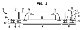
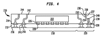
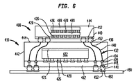
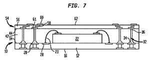
| US11830845B2 (en) | 2011-05-03 | 2023-11-28 | Tessera Llc | Package-on-package assembly with wire bonds to encapsulation surface |
| KR101128063B1 (ko) | 2011-05-03 | 2012-04-23 | 테세라, 인코포레이티드 | 캡슐화 층의 표면에 와이어 본드를 구비하는 패키지 적층형 어셈블리 |
| US8404520B1 (en) | 2011-10-17 | 2013-03-26 | Invensas Corporation | Package-on-package assembly with wire bond vias |
| US8946757B2 (en) | 2012-02-17 | 2015-02-03 | Invensas Corporation | Heat spreading substrate with embedded interconnects |
| US8372741B1 (en) | 2012-02-24 | 2013-02-12 | Invensas Corporation | Method for package-on-package assembly with wire bonds to encapsulation surface |
| US8835228B2 (en) | 2012-05-22 | 2014-09-16 | Invensas Corporation | Substrate-less stackable package with wire-bond interconnect |
| US9391008B2 (en) | 2012-07-31 | 2016-07-12 | Invensas Corporation | Reconstituted wafer-level package DRAM |
| US9502390B2 (en) | 2012-08-03 | 2016-11-22 | Invensas Corporation | BVA interposer |
| US8642393B1 (en) * | 2012-08-08 | 2014-02-04 | Taiwan Semiconductor Manufacturing Company, Ltd. | Package on package devices and methods of forming same |
| JP5972735B2 (ja) * | 2012-09-21 | 2016-08-17 | 株式会社東芝 | 半導体装置 |
| US8878353B2 (en) | 2012-12-20 | 2014-11-04 | Invensas Corporation | Structure for microelectronic packaging with bond elements to encapsulation surface |
| US9136254B2 (en) | 2013-02-01 | 2015-09-15 | Invensas Corporation | Microelectronic package having wire bond vias and stiffening layer |
| US8970023B2 (en) * | 2013-02-04 | 2015-03-03 | Taiwan Semiconductor Manufacturing Company, Ltd. | Package structure and methods of forming same |
| US8884427B2 (en) * | 2013-03-14 | 2014-11-11 | Invensas Corporation | Low CTE interposer without TSV structure |
| US9016552B2 (en) * | 2013-03-15 | 2015-04-28 | Sanmina Corporation | Method for forming interposers and stacked memory devices |
| US9446943B2 (en) | 2013-05-31 | 2016-09-20 | Stmicroelectronics S.R.L. | Wafer-level packaging of integrated devices, and manufacturing method thereof |
| US9167710B2 (en) | 2013-08-07 | 2015-10-20 | Invensas Corporation | Embedded packaging with preformed vias |
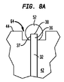
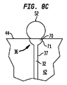
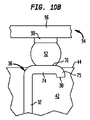
| US9685365B2 (en) | 2013-08-08 | 2017-06-20 | Invensas Corporation | Method of forming a wire bond having a free end |
| US20150076714A1 (en) | 2013-09-16 | 2015-03-19 | Invensas Corporation | Microelectronic element with bond elements to encapsulation surface |
| US9087815B2 (en) * | 2013-11-12 | 2015-07-21 | Invensas Corporation | Off substrate kinking of bond wire |
| US9082753B2 (en) * | 2013-11-12 | 2015-07-14 | Invensas Corporation | Severing bond wire by kinking and twisting |
| US9379074B2 (en) | 2013-11-22 | 2016-06-28 | Invensas Corporation | Die stacks with one or more bond via arrays of wire bond wires and with one or more arrays of bump interconnects |
| US9263394B2 (en) | 2013-11-22 | 2016-02-16 | Invensas Corporation | Multiple bond via arrays of different wire heights on a same substrate |
| US9583456B2 (en) | 2013-11-22 | 2017-02-28 | Invensas Corporation | Multiple bond via arrays of different wire heights on a same substrate |
| US9583411B2 (en) | 2014-01-17 | 2017-02-28 | Invensas Corporation | Fine pitch BVA using reconstituted wafer with area array accessible for testing |
| TWI587412B (zh) * | 2014-05-08 | 2017-06-11 | 矽品精密工業股份有限公司 | 封裝結構及其製法 |
| US10381326B2 (en) * | 2014-05-28 | 2019-08-13 | Invensas Corporation | Structure and method for integrated circuits packaging with increased density |
| US9899794B2 (en) * | 2014-06-30 | 2018-02-20 | Texas Instruments Incorporated | Optoelectronic package |
| US9449908B2 (en) | 2014-07-30 | 2016-09-20 | Taiwan Semiconductor Manufacturing Company, Ltd. | Semiconductor package system and method |
| US10319607B2 (en) * | 2014-08-22 | 2019-06-11 | Taiwan Semiconductor Manufacturing Company, Ltd. | Package-on-package structure with organic interposer |
| US9368470B2 (en) * | 2014-10-31 | 2016-06-14 | Freescale Semiconductor, Inc. | Coated bonding wire and methods for bonding using same |
| US9735084B2 (en) | 2014-12-11 | 2017-08-15 | Invensas Corporation | Bond via array for thermal conductivity |
| US9802813B2 (en) | 2014-12-24 | 2017-10-31 | Stmicroelectronics (Malta) Ltd | Wafer level package for a MEMS sensor device and corresponding manufacturing process |
| KR20160093248A (ko) * | 2015-01-29 | 2016-08-08 | 에스케이하이닉스 주식회사 | 반도체 패키지 및 제조 방법 |
| US9888579B2 (en) | 2015-03-05 | 2018-02-06 | Invensas Corporation | Pressing of wire bond wire tips to provide bent-over tips |
| US9530749B2 (en) | 2015-04-28 | 2016-12-27 | Invensas Corporation | Coupling of side surface contacts to a circuit platform |
| US9502372B1 (en) * | 2015-04-30 | 2016-11-22 | Invensas Corporation | Wafer-level packaging using wire bond wires in place of a redistribution layer |
| US9761554B2 (en) | 2015-05-07 | 2017-09-12 | Invensas Corporation | Ball bonding metal wire bond wires to metal pads |
| JP6392171B2 (ja) * | 2015-05-28 | 2018-09-19 | 新光電気工業株式会社 | 半導体装置及びその製造方法 |
| US9779940B2 (en) * | 2015-07-01 | 2017-10-03 | Zhuahai Advanced Chip Carriers & Electronic Substrate Solutions Technologies Co. Ltd. | Chip package |
| TWI620296B (zh) * | 2015-08-14 | 2018-04-01 | 矽品精密工業股份有限公司 | 電子封裝件及其製法 |
| US9806052B2 (en) * | 2015-09-15 | 2017-10-31 | Qualcomm Incorporated | Semiconductor package interconnect |
| US10490528B2 (en) | 2015-10-12 | 2019-11-26 | Invensas Corporation | Embedded wire bond wires |
| US9490222B1 (en) | 2015-10-12 | 2016-11-08 | Invensas Corporation | Wire bond wires for interference shielding |
| US10332854B2 (en) | 2015-10-23 | 2019-06-25 | Invensas Corporation | Anchoring structure of fine pitch bva |
| US10181457B2 (en) | 2015-10-26 | 2019-01-15 | Invensas Corporation | Microelectronic package for wafer-level chip scale packaging with fan-out |
| ITUB20155408A1 (it) * | 2015-11-10 | 2017-05-10 | St Microelectronics Srl | Substrato di packaging per dispositivi a semiconduttore, dispositivo e procedimento corrispondenti |
| EP3168874B1 (en) | 2015-11-11 | 2020-09-30 | Lipac Co., Ltd. | Semiconductor chip package with optical interface |
| US10043779B2 (en) | 2015-11-17 | 2018-08-07 | Invensas Corporation | Packaged microelectronic device for a package-on-package device |
| US9659848B1 (en) | 2015-11-18 | 2017-05-23 | Invensas Corporation | Stiffened wires for offset BVA |
| US9984992B2 (en) | 2015-12-30 | 2018-05-29 | Invensas Corporation | Embedded wire bond wires for vertical integration with separate surface mount and wire bond mounting surfaces |
| US9831155B2 (en) * | 2016-03-11 | 2017-11-28 | Nanya Technology Corporation | Chip package having tilted through silicon via |
| TWI602269B (zh) * | 2016-06-08 | 2017-10-11 | 力成科技股份有限公司 | 柱頂互連之封裝堆疊方法與構造 |
| JP6712050B2 (ja) * | 2016-06-21 | 2020-06-17 | 富士通株式会社 | 樹脂基板及びその製造方法、並びに回路基板及びその製造方法 |
| US9930773B2 (en) * | 2016-06-21 | 2018-03-27 | Microsoft Technology Licensing, Llc | Flexible interconnect |
| US9935075B2 (en) | 2016-07-29 | 2018-04-03 | Invensas Corporation | Wire bonding method and apparatus for electromagnetic interference shielding |
| US20180114786A1 (en) * | 2016-10-21 | 2018-04-26 | Powertech Technology Inc. | Method of forming package-on-package structure |
| US10299368B2 (en) | 2016-12-21 | 2019-05-21 | Invensas Corporation | Surface integrated waveguides and circuit structures therefor |
| TWI637536B (zh) * | 2017-02-24 | 2018-10-01 | 矽品精密工業股份有限公司 | 電子封裝結構及其製法 |
| US10522505B2 (en) | 2017-04-06 | 2019-12-31 | Advanced Semiconductor Engineering, Inc. | Semiconductor device package and method for manufacturing the same |
| US10426030B2 (en) * | 2017-04-21 | 2019-09-24 | International Business Machines Corporation | Trace/via hybrid structure multichip carrier |
| US10181447B2 (en) | 2017-04-21 | 2019-01-15 | Invensas Corporation | 3D-interconnect |
| CN108807430B (zh) * | 2017-04-28 | 2024-12-20 | 南昌欧菲光电技术有限公司 | 摄像模组及其复合式感光组件 |
| US10707635B2 (en) * | 2017-05-15 | 2020-07-07 | Current Lighting Solutions, Llc | Method for providing a wire connection to a printed circuit board |
| DE102017114771B4 (de) * | 2017-06-29 | 2022-01-27 | Pac Tech - Packaging Technologies Gmbh | Verfahren und Vorrichtung zur Herstellung einer Drahtverbindung sowie Bauelementanordnung mit Drahtverbindung |
| US20190035715A1 (en) * | 2017-07-31 | 2019-01-31 | Innolux Corporation | Package device and manufacturing method thereof |
| US10312198B2 (en) * | 2017-10-20 | 2019-06-04 | Advanced Semiconductor Engineering, Inc. | Semiconductor device package |
| US10529693B2 (en) * | 2017-11-29 | 2020-01-07 | Advanced Micro Devices, Inc. | 3D stacked dies with disparate interconnect footprints |
| US10566279B2 (en) | 2018-01-25 | 2020-02-18 | Advanced Semiconductor Engineering, Inc. | Package device, semiconductor device, and method for manufacturing the package device |
| US10727204B2 (en) | 2018-05-29 | 2020-07-28 | Advances Micro Devices, Inc. | Die stacking for multi-tier 3D integration |
| US10937755B2 (en) | 2018-06-29 | 2021-03-02 | Advanced Micro Devices, Inc. | Bond pads for low temperature hybrid bonding |
| US11139283B2 (en) * | 2018-12-22 | 2021-10-05 | Xcelsis Corporation | Abstracted NAND logic in stacks |
| DE102019215471B4 (de) * | 2019-10-09 | 2022-05-25 | Vitesco Technologies GmbH | Elektronisches Bauteil mit einer Kontaktieranordnung und Verfahren zur Herstellung eines elektronischen Bauteils |
| CN111470170B (zh) * | 2020-03-27 | 2024-11-08 | 安姆科(惠州)新材料科技有限公司 | 一种包装开口结构 |
| WO2022025128A1 (ja) * | 2020-07-29 | 2022-02-03 | 京セラ株式会社 | 回路基板及びプローブカード |
| JP2022033633A (ja) | 2020-08-17 | 2022-03-02 | キオクシア株式会社 | 半導体装置 |
| CN113764361A (zh) * | 2021-07-23 | 2021-12-07 | 上海闻泰信息技术有限公司 | 芯片封装结构及芯片封装方法 |
| EP4156253A1 (en) * | 2021-09-22 | 2023-03-29 | Infineon Technologies Austria AG | Resin encapsulated semiconductor package comprising an external recess with exposed electrical contacts and a semiconductor module using the same |
| US12362267B2 (en) * | 2021-10-13 | 2025-07-15 | Skyworks Solutions, Inc. | Electronic package and method for manufacturing an electronic package |
| US12040284B2 (en) | 2021-11-12 | 2024-07-16 | Invensas Llc | 3D-interconnect with electromagnetic interference (“EMI”) shield and/or antenna |
| CN118339930A (zh) * | 2021-12-01 | 2024-07-12 | 株式会社村田制作所 | 电路模块 |
| TWI777872B (zh) | 2021-12-14 | 2022-09-11 | 頎邦科技股份有限公司 | 半導體封裝構造及其製造方法 |
| US20240038645A1 (en) | 2022-07-26 | 2024-02-01 | Avago Technologies International Sales Pte. Limited | Semiconductor Package Interconnection Structure |
| US12417968B2 (en) * | 2022-08-04 | 2025-09-16 | Taiwan Semiconductor Manufacturing Company, Ltd. | Package structure and forming method thereof |
| CN115132687B (zh) * | 2022-09-02 | 2022-11-22 | 甬矽电子(宁波)股份有限公司 | 封装堆叠结构和封装堆叠方法 |
Family Cites Families (550)
| Publication number | Priority date | Publication date | Assignee | Title |
|---|---|---|---|---|
| DE1439262B2 (de) * | 1963-07-23 | 1972-03-30 | Siemens AG, 1000 Berlin u. 8000 München | Verfahren zum kontaktieren von halbleiterbauelementen durch thermokompression |
| US3358897A (en) * | 1964-03-31 | 1967-12-19 | Tempress Res Co | Electric lead wire bonding tools |
| US3430835A (en) | 1966-06-07 | 1969-03-04 | Westinghouse Electric Corp | Wire bonding apparatus for microelectronic components |
| US3623649A (en) | 1969-06-09 | 1971-11-30 | Gen Motors Corp | Wedge bonding tool for the attachment of semiconductor leads |
| DE2119567C2 (de) | 1970-05-05 | 1983-07-14 | International Computers Ltd., London | Elektrische Verbindungsvorrichtung und Verfahren zu ihrer Herstellung |
| DE2228703A1 (de) | 1972-06-13 | 1974-01-10 | Licentia Gmbh | Verfahren zum herstellen einer vorgegebenen lotschichtstaerke bei der fertigung von halbleiterbauelementen |
| JPS5150661A (https=) | 1974-10-30 | 1976-05-04 | Hitachi Ltd | |
| US4067104A (en) | 1977-02-24 | 1978-01-10 | Rockwell International Corporation | Method of fabricating an array of flexible metallic interconnects for coupling microelectronics components |
| US4213556A (en) | 1978-10-02 | 1980-07-22 | General Motors Corporation | Method and apparatus to detect automatic wire bonder failure |
| US4327860A (en) | 1980-01-03 | 1982-05-04 | Kulicke And Soffa Ind. Inc. | Method of making slack free wire interconnections |
| US4422568A (en) | 1981-01-12 | 1983-12-27 | Kulicke And Soffa Industries, Inc. | Method of making constant bonding wire tail lengths |
| NL184184C (nl) * | 1981-03-20 | 1989-05-01 | Philips Nv | Werkwijze voor het aanbrengen van kontaktverhogingen op kontaktplaatsen van een electronische microketen. |
| US4437604A (en) | 1982-03-15 | 1984-03-20 | Kulicke & Soffa Industries, Inc. | Method of making fine wire interconnections |
| JPS59189069A (ja) | 1983-04-12 | 1984-10-26 | Alps Electric Co Ltd | 電気部品の端子のハンダ塗布装置 |
| JPS61125062A (ja) * | 1984-11-22 | 1986-06-12 | Hitachi Ltd | ピン取付け方法およびピン取付け装置 |
| US4604644A (en) | 1985-01-28 | 1986-08-05 | International Business Machines Corporation | Solder interconnection structure for joining semiconductor devices to substrates that have improved fatigue life, and process for making |
| US4642889A (en) | 1985-04-29 | 1987-02-17 | Amp Incorporated | Compliant interconnection and method therefor |
| US5476211A (en) | 1993-11-16 | 1995-12-19 | Form Factor, Inc. | Method of manufacturing electrical contacts, using a sacrificial member |
| US5917707A (en) | 1993-11-16 | 1999-06-29 | Formfactor, Inc. | Flexible contact structure with an electrically conductive shell |
| US4716049A (en) | 1985-12-20 | 1987-12-29 | Hughes Aircraft Company | Compressive pedestal for microminiature connections |
| US4924353A (en) | 1985-12-20 | 1990-05-08 | Hughes Aircraft Company | Connector system for coupling to an integrated circuit chip |
| JPS62158338A (ja) | 1985-12-28 | 1987-07-14 | Tanaka Denshi Kogyo Kk | 半導体装置 |
| US4793814A (en) | 1986-07-21 | 1988-12-27 | Rogers Corporation | Electrical circuit board interconnect |
| US4695870A (en) | 1986-03-27 | 1987-09-22 | Hughes Aircraft Company | Inverted chip carrier |
| JPS62226307A (ja) | 1986-03-28 | 1987-10-05 | Toshiba Corp | ロボツト装置 |
| US4771930A (en) * | 1986-06-30 | 1988-09-20 | Kulicke And Soffa Industries Inc. | Apparatus for supplying uniform tail lengths |
| JPS6397941A (ja) | 1986-10-14 | 1988-04-28 | Fuji Photo Film Co Ltd | 感光材料 |
| US4955523A (en) * | 1986-12-17 | 1990-09-11 | Raychem Corporation | Interconnection of electronic components |
| DE3703694A1 (de) | 1987-02-06 | 1988-08-18 | Dynapert Delvotec Gmbh | Ball-bondverfahren und vorrichtung zur durchfuehrung derselben |
| US5195237A (en) * | 1987-05-21 | 1993-03-23 | Cray Computer Corporation | Flying leads for integrated circuits |
| JP2642359B2 (ja) | 1987-09-11 | 1997-08-20 | 株式会社日立製作所 | 半導体装置 |
| KR970003915B1 (ko) | 1987-06-24 | 1997-03-22 | 미다 가쓰시게 | 반도체 기억장치 및 그것을 사용한 반도체 메모리 모듈 |
| US5138438A (en) | 1987-06-24 | 1992-08-11 | Akita Electronics Co. Ltd. | Lead connections means for stacked tab packaged IC chips |
| US4804132A (en) | 1987-08-28 | 1989-02-14 | Difrancesco Louis | Method for cold bonding |
| US4845354A (en) | 1988-03-08 | 1989-07-04 | International Business Machines Corporation | Process control for laser wire bonding |
| JPH01313969A (ja) | 1988-06-13 | 1989-12-19 | Hitachi Ltd | 半導体装置 |
| US4998885A (en) * | 1989-10-27 | 1991-03-12 | International Business Machines Corporation | Elastomeric area array interposer |
| US5077598A (en) | 1989-11-08 | 1991-12-31 | Hewlett-Packard Company | Strain relief flip-chip integrated circuit assembly with test fixturing |
| US5095187A (en) | 1989-12-20 | 1992-03-10 | Raychem Corporation | Weakening wire supplied through a wire bonder |
| CA2034700A1 (en) | 1990-01-23 | 1991-07-24 | Masanori Nishiguchi | Substrate for packaging a semiconductor device |
| AU645283B2 (en) | 1990-01-23 | 1994-01-13 | Sumitomo Electric Industries, Ltd. | Substrate for packaging a semiconductor device |
| US5376403A (en) | 1990-02-09 | 1994-12-27 | Capote; Miguel A. | Electrically conductive compositions and methods for the preparation and use thereof |
| US5948533A (en) | 1990-02-09 | 1999-09-07 | Ormet Corporation | Vertically interconnected electronic assemblies and compositions useful therefor |
| US5083697A (en) | 1990-02-14 | 1992-01-28 | Difrancesco Louis | Particle-enhanced joining of metal surfaces |
| US4975079A (en) | 1990-02-23 | 1990-12-04 | International Business Machines Corp. | Connector assembly for chip testing |
| US4999472A (en) * | 1990-03-12 | 1991-03-12 | Neinast James E | Electric arc system for ablating a surface coating |
| US5241456A (en) | 1990-07-02 | 1993-08-31 | General Electric Company | Compact high density interconnect structure |
| US5679977A (en) | 1990-09-24 | 1997-10-21 | Tessera, Inc. | Semiconductor chip assemblies, methods of making same and components for same |
| US5148265A (en) | 1990-09-24 | 1992-09-15 | Ist Associates, Inc. | Semiconductor chip assemblies with fan-in leads |
| US5148266A (en) | 1990-09-24 | 1992-09-15 | Ist Associates, Inc. | Semiconductor chip assemblies having interposer and flexible lead |
| US5067382A (en) | 1990-11-02 | 1991-11-26 | Cray Computer Corporation | Method and apparatus for notching a lead wire attached to an IC chip to facilitate severing the wire |
| KR940001149B1 (ko) | 1991-04-16 | 1994-02-14 | 삼성전자 주식회사 | 반도체 장치의 칩 본딩 방법 |
| JPH04346436A (ja) * | 1991-05-24 | 1992-12-02 | Fujitsu Ltd | バンプ製造方法とバンプ製造装置 |
| US5316788A (en) | 1991-07-26 | 1994-05-31 | International Business Machines Corporation | Applying solder to high density substrates |
| US5203075A (en) | 1991-08-12 | 1993-04-20 | Inernational Business Machines | Method of bonding flexible circuit to cicuitized substrate to provide electrical connection therebetween using different solders |
| US5133495A (en) | 1991-08-12 | 1992-07-28 | International Business Machines Corporation | Method of bonding flexible circuit to circuitized substrate to provide electrical connection therebetween |
| WO1993004375A1 (en) | 1991-08-23 | 1993-03-04 | Nchip, Inc. | Burn-in technologies for unpackaged integrated circuits |
| US5220489A (en) | 1991-10-11 | 1993-06-15 | Motorola, Inc. | Multicomponent integrated circuit package |
| US5238173A (en) | 1991-12-04 | 1993-08-24 | Kaijo Corporation | Wire bonding misattachment detection apparatus and that detection method in a wire bonder |
| JP2931936B2 (ja) * | 1992-01-17 | 1999-08-09 | 株式会社日立製作所 | 半導体装置用リードフレームの製造方法及び半導体装置用リードフレーム並びに樹脂封止型半導体装置 |
| US5831836A (en) | 1992-01-30 | 1998-11-03 | Lsi Logic | Power plane for semiconductor device |
| US5222014A (en) | 1992-03-02 | 1993-06-22 | Motorola, Inc. | Three-dimensional multi-chip pad array carrier |
| US5438224A (en) | 1992-04-23 | 1995-08-01 | Motorola, Inc. | Integrated circuit package having a face-to-face IC chip arrangement |
| US5494667A (en) | 1992-06-04 | 1996-02-27 | Kabushiki Kaisha Hayahibara | Topically applied hair restorer containing pine extract |
| JP3151219B2 (ja) | 1992-07-24 | 2001-04-03 | テツセラ,インコーポレイテッド | 取り外し自在のリード支持体を備えた半導体接続構成体およびその製造方法 |
| US6054756A (en) | 1992-07-24 | 2000-04-25 | Tessera, Inc. | Connection components with frangible leads and bus |
| US5977618A (en) | 1992-07-24 | 1999-11-02 | Tessera, Inc. | Semiconductor connection components and methods with releasable lead support |
| US6295729B1 (en) * | 1992-10-19 | 2001-10-02 | International Business Machines Corporation | Angled flying lead wire bonding process |
| US5371654A (en) * | 1992-10-19 | 1994-12-06 | International Business Machines Corporation | Three dimensional high performance interconnection package |
| US20050062492A1 (en) * | 2001-08-03 | 2005-03-24 | Beaman Brian Samuel | High density integrated circuit apparatus, test probe and methods of use thereof |
| JP2716336B2 (ja) | 1993-03-10 | 1998-02-18 | 日本電気株式会社 | 集積回路装置 |
| JPH06268101A (ja) | 1993-03-17 | 1994-09-22 | Hitachi Ltd | 半導体装置及びその製造方法、電子装置、リ−ドフレ−ム並びに実装基板 |
| US5340771A (en) | 1993-03-18 | 1994-08-23 | Lsi Logic Corporation | Techniques for providing high I/O count connections to semiconductor dies |
| US20030048108A1 (en) * | 1993-04-30 | 2003-03-13 | Beaman Brian Samuel | Structural design and processes to control probe position accuracy in a wafer test probe assembly |
| US5811982A (en) | 1995-11-27 | 1998-09-22 | International Business Machines Corporation | High density cantilevered probe for electronic devices |
| US7368924B2 (en) * | 1993-04-30 | 2008-05-06 | International Business Machines Corporation | Probe structure having a plurality of discrete insulated probe tips projecting from a support surface, apparatus for use thereof and methods of fabrication thereof |
| JP2981385B2 (ja) | 1993-09-06 | 1999-11-22 | シャープ株式会社 | チップ部品型ledの構造及びその製造方法 |
| US5346118A (en) | 1993-09-28 | 1994-09-13 | At&T Bell Laboratories | Surface mount solder assembly of leadless integrated circuit packages to substrates |
| US6835898B2 (en) | 1993-11-16 | 2004-12-28 | Formfactor, Inc. | Electrical contact structures formed by configuring a flexible wire to have a springable shape and overcoating the wire with at least one layer of a resilient conductive material, methods of mounting the contact structures to electronic components, and applications for employing the contact structures |
| US5455390A (en) | 1994-02-01 | 1995-10-03 | Tessera, Inc. | Microelectronics unit mounting with multiple lead bonding |
| EP1213754A3 (en) | 1994-03-18 | 2005-05-25 | Hitachi Chemical Co., Ltd. | Fabrication process of semiconductor package and semiconductor package |
| US5802699A (en) | 1994-06-07 | 1998-09-08 | Tessera, Inc. | Methods of assembling microelectronic assembly with socket for engaging bump leads |
| US5615824A (en) | 1994-06-07 | 1997-04-01 | Tessera, Inc. | Soldering with resilient contacts |
| JPH07335783A (ja) | 1994-06-13 | 1995-12-22 | Fujitsu Ltd | 半導体装置及び半導体装置ユニット |
| US5468995A (en) | 1994-07-05 | 1995-11-21 | Motorola, Inc. | Semiconductor device having compliant columnar electrical connections |
| US6828668B2 (en) | 1994-07-07 | 2004-12-07 | Tessera, Inc. | Flexible lead structures and methods of making same |
| US6177636B1 (en) | 1994-12-29 | 2001-01-23 | Tessera, Inc. | Connection components with posts |
| US6117694A (en) | 1994-07-07 | 2000-09-12 | Tessera, Inc. | Flexible lead structures and methods of making same |
| US5518964A (en) | 1994-07-07 | 1996-05-21 | Tessera, Inc. | Microelectronic mounting with multiple lead deformation and bonding |
| US5989936A (en) | 1994-07-07 | 1999-11-23 | Tessera, Inc. | Microelectronic assembly fabrication with terminal formation from a conductive layer |
| US5688716A (en) | 1994-07-07 | 1997-11-18 | Tessera, Inc. | Fan-out semiconductor chip assembly |
| US5656550A (en) | 1994-08-24 | 1997-08-12 | Fujitsu Limited | Method of producing a semicondutor device having a lead portion with outer connecting terminal |
| US5659952A (en) | 1994-09-20 | 1997-08-26 | Tessera, Inc. | Method of fabricating compliant interface for semiconductor chip |
| US5541567A (en) * | 1994-10-17 | 1996-07-30 | International Business Machines Corporation | Coaxial vias in an electronic substrate |
| US5495667A (en) | 1994-11-07 | 1996-03-05 | Micron Technology, Inc. | Method for forming contact pins for semiconductor dice and interconnects |
| US5736074A (en) | 1995-06-30 | 1998-04-07 | Micro Fab Technologies, Inc. | Manufacture of coated spheres |
| US5971253A (en) | 1995-07-31 | 1999-10-26 | Tessera, Inc. | Microelectronic component mounting with deformable shell terminals |
| US5872051A (en) | 1995-08-02 | 1999-02-16 | International Business Machines Corporation | Process for transferring material to semiconductor chip conductive pads using a transfer substrate |
| US5810609A (en) | 1995-08-28 | 1998-09-22 | Tessera, Inc. | Socket for engaging bump leads on a microelectronic device and methods therefor |
| US5766987A (en) | 1995-09-22 | 1998-06-16 | Tessera, Inc. | Microelectronic encapsulation methods and equipment |
| US6211572B1 (en) | 1995-10-31 | 2001-04-03 | Tessera, Inc. | Semiconductor chip package with fan-in leads |
| JP3332308B2 (ja) | 1995-11-07 | 2002-10-07 | 新光電気工業株式会社 | 半導体装置及びその製造方法 |
| JPH09134934A (ja) | 1995-11-07 | 1997-05-20 | Sumitomo Metal Ind Ltd | 半導体パッケージ及び半導体装置 |
| US5718361A (en) | 1995-11-21 | 1998-02-17 | International Business Machines Corporation | Apparatus and method for forming mold for metallic material |
| US5731709A (en) | 1996-01-26 | 1998-03-24 | Motorola, Inc. | Method for testing a ball grid array semiconductor device and a device for such testing |
| US5994152A (en) * | 1996-02-21 | 1999-11-30 | Formfactor, Inc. | Fabricating interconnects and tips using sacrificial substrates |
| JP3146345B2 (ja) * | 1996-03-11 | 2001-03-12 | アムコー テクノロジー コリア インコーポレーティド | バンプチップスケール半導体パッケージのバンプ形成方法 |
| US6000126A (en) | 1996-03-29 | 1999-12-14 | General Dynamics Information Systems, Inc. | Method and apparatus for connecting area grid arrays to printed wire board |
| US6821821B2 (en) | 1996-04-18 | 2004-11-23 | Tessera, Inc. | Methods for manufacturing resistors using a sacrificial layer |
| DE19618227A1 (de) | 1996-05-07 | 1997-11-13 | Herbert Streckfus Gmbh | Verfahren und Vorrichtung zum Verlöten von elektronischen Bauelementen auf einer Leiterplatte |
| KR100186333B1 (ko) * | 1996-06-20 | 1999-03-20 | 문정환 | 칩 사이즈 반도체 패키지 및 그 제조방법 |
| JPH1012769A (ja) | 1996-06-24 | 1998-01-16 | Ricoh Co Ltd | 半導体装置およびその製造方法 |
| JPH10135220A (ja) * | 1996-10-29 | 1998-05-22 | Taiyo Yuden Co Ltd | バンプ形成方法 |
| JPH10135221A (ja) * | 1996-10-29 | 1998-05-22 | Taiyo Yuden Co Ltd | バンプ形成方法 |
| US6492719B2 (en) | 1999-07-30 | 2002-12-10 | Hitachi, Ltd. | Semiconductor device |
| US5976913A (en) | 1996-12-12 | 1999-11-02 | Tessera, Inc. | Microelectronic mounting with multiple lead deformation using restraining straps |
| US6133072A (en) | 1996-12-13 | 2000-10-17 | Tessera, Inc. | Microelectronic connector with planar elastomer sockets |
| US6225688B1 (en) | 1997-12-11 | 2001-05-01 | Tessera, Inc. | Stacked microelectronic assembly and method therefor |
| US6054337A (en) | 1996-12-13 | 2000-04-25 | Tessera, Inc. | Method of making a compliant multichip package |
| US6121676A (en) | 1996-12-13 | 2000-09-19 | Tessera, Inc. | Stacked microelectronic assembly and method therefor |
| JP3400279B2 (ja) * | 1997-01-13 | 2003-04-28 | 株式会社新川 | バンプ形成方法 |
| US5898991A (en) * | 1997-01-16 | 1999-05-04 | International Business Machines Corporation | Methods of fabrication of coaxial vias and magnetic devices |
| US5839191A (en) | 1997-01-24 | 1998-11-24 | Unisys Corporation | Vibrating template method of placing solder balls on the I/O pads of an integrated circuit package |
| JPH1118364A (ja) | 1997-06-27 | 1999-01-22 | Matsushita Electric Ind Co Ltd | キャプスタンモータ |
| KR100543836B1 (ko) | 1997-08-19 | 2006-01-23 | 가부시키가이샤 히타치세이사쿠쇼 | 멀티칩 모듈 구조체 및 그 제작 방법 |
| CA2213590C (en) | 1997-08-21 | 2006-11-07 | Keith C. Carroll | Flexible circuit connector and method of making same |
| JP3859318B2 (ja) | 1997-08-29 | 2006-12-20 | シチズン電子株式会社 | 電子回路のパッケージ方法 |
| US6525414B2 (en) | 1997-09-16 | 2003-02-25 | Matsushita Electric Industrial Co., Ltd. | Semiconductor device including a wiring board and semiconductor elements mounted thereon |
| JP3937265B2 (ja) | 1997-09-29 | 2007-06-27 | エルピーダメモリ株式会社 | 半導体装置 |
| JP3262531B2 (ja) | 1997-10-02 | 2002-03-04 | インターナショナル・ビジネス・マシーンズ・コーポレーション | 曲げられたフライング・リード・ワイヤ・ボンデイング・プロセス |
| JP2978861B2 (ja) | 1997-10-28 | 1999-11-15 | 九州日本電気株式会社 | モールドbga型半導体装置及びその製造方法 |
| US6038136A (en) | 1997-10-29 | 2000-03-14 | Hestia Technologies, Inc. | Chip package with molded underfill |
| JP3393800B2 (ja) | 1997-11-05 | 2003-04-07 | 新光電気工業株式会社 | 半導体装置の製造方法 |
| JPH11219984A (ja) | 1997-11-06 | 1999-08-10 | Sharp Corp | 半導体装置パッケージおよびその製造方法ならびにそのための回路基板 |
| US6222136B1 (en) | 1997-11-12 | 2001-04-24 | International Business Machines Corporation | Printed circuit board with continuous connective bumps |
| US6002168A (en) | 1997-11-25 | 1999-12-14 | Tessera, Inc. | Microelectronic component with rigid interposer |
| US6038133A (en) | 1997-11-25 | 2000-03-14 | Matsushita Electric Industrial Co., Ltd. | Circuit component built-in module and method for producing the same |
| JPH11163022A (ja) | 1997-11-28 | 1999-06-18 | Sony Corp | 半導体装置、その製造方法及び電子機器 |
| US6124546A (en) | 1997-12-03 | 2000-09-26 | Advanced Micro Devices, Inc. | Integrated circuit chip package and method of making the same |
| US6260264B1 (en) | 1997-12-08 | 2001-07-17 | 3M Innovative Properties Company | Methods for making z-axis electrical connections |
| US6052287A (en) | 1997-12-09 | 2000-04-18 | Sandia Corporation | Silicon ball grid array chip carrier |
| US5973391A (en) | 1997-12-11 | 1999-10-26 | Read-Rite Corporation | Interposer with embedded circuitry and method for using the same to package microelectronic units |
| JPH11220082A (ja) | 1998-02-03 | 1999-08-10 | Oki Electric Ind Co Ltd | 半導体装置 |
| JP3536650B2 (ja) * | 1998-02-27 | 2004-06-14 | 富士ゼロックス株式会社 | バンプ形成方法および装置 |
| JPH11260856A (ja) * | 1998-03-11 | 1999-09-24 | Matsushita Electron Corp | 半導体装置及びその製造方法並びに半導体装置の実装構造 |
| KR100260997B1 (ko) | 1998-04-08 | 2000-07-01 | 마이클 디. 오브라이언 | 반도체패키지 |
| US6329224B1 (en) | 1998-04-28 | 2001-12-11 | Tessera, Inc. | Encapsulation of microelectronic assemblies |
| US6180881B1 (en) | 1998-05-05 | 2001-01-30 | Harlan Ruben Isaak | Chip stack and method of making same |
| JPH11330134A (ja) | 1998-05-12 | 1999-11-30 | Hitachi Ltd | ワイヤボンディング方法およびその装置並びに半導体装置 |
| KR100266693B1 (ko) | 1998-05-30 | 2000-09-15 | 김영환 | 적층가능한 비지에이 반도체 칩 패키지 및 그 제조방법 |
| KR100265563B1 (ko) | 1998-06-29 | 2000-09-15 | 김영환 | 볼 그리드 어레이 패키지 및 그의 제조 방법 |
| US6414391B1 (en) | 1998-06-30 | 2002-07-02 | Micron Technology, Inc. | Module assembly for stacked BGA packages with a common bus bar in the assembly |
| US6164523A (en) | 1998-07-01 | 2000-12-26 | Semiconductor Components Industries, Llc | Electronic component and method of manufacture |
| US6399426B1 (en) | 1998-07-21 | 2002-06-04 | Miguel Albert Capote | Semiconductor flip-chip package and method for the fabrication thereof |
| US5854507A (en) | 1998-07-21 | 1998-12-29 | Hewlett-Packard Company | Multiple chip assembly |
| US6515355B1 (en) | 1998-09-02 | 2003-02-04 | Micron Technology, Inc. | Passivation layer for packaged integrated circuits |
| JP2000091383A (ja) | 1998-09-07 | 2000-03-31 | Ngk Spark Plug Co Ltd | 配線基板 |
| US6194250B1 (en) | 1998-09-14 | 2001-02-27 | Motorola, Inc. | Low-profile microelectronic package |
| US6158647A (en) | 1998-09-29 | 2000-12-12 | Micron Technology, Inc. | Concave face wire bond capillary |
| US6684007B2 (en) | 1998-10-09 | 2004-01-27 | Fujitsu Limited | Optical coupling structures and the fabrication processes |
| US6268662B1 (en) | 1998-10-14 | 2001-07-31 | Texas Instruments Incorporated | Wire bonded flip-chip assembly of semiconductor devices |
| JP3407275B2 (ja) * | 1998-10-28 | 2003-05-19 | インターナショナル・ビジネス・マシーンズ・コーポレーション | バンプ及びその形成方法 |
| US6332270B2 (en) | 1998-11-23 | 2001-12-25 | International Business Machines Corporation | Method of making high density integral test probe |
| EP1156520A4 (en) | 1999-01-29 | 2004-08-25 | Matsushita Electric Industrial Co Ltd | ASSEMBLY METHOD FOR ELECTRONIC COMPONENTS AND THEIR DEVICE |
| US6206273B1 (en) * | 1999-02-17 | 2001-03-27 | International Business Machines Corporation | Structures and processes to create a desired probetip contact geometry on a wafer test probe |
| KR100319609B1 (ko) | 1999-03-09 | 2002-01-05 | 김영환 | 와이어 어래이드 칩 사이즈 패키지 및 그 제조방법 |
| US6177729B1 (en) | 1999-04-03 | 2001-01-23 | International Business Machines Corporation | Rolling ball connector |
| US6211574B1 (en) | 1999-04-16 | 2001-04-03 | Advanced Semiconductor Engineering Inc. | Semiconductor package with wire protection and method therefor |
| US6376769B1 (en) | 1999-05-18 | 2002-04-23 | Amerasia International Technology, Inc. | High-density electronic package, and method for making same |
| US6258625B1 (en) | 1999-05-18 | 2001-07-10 | International Business Machines Corporation | Method of interconnecting electronic components using a plurality of conductive studs |
| JP3398721B2 (ja) | 1999-05-20 | 2003-04-21 | アムコー テクノロジー コリア インコーポレーティド | 半導体パッケージ及びその製造方法 |
| US6228687B1 (en) | 1999-06-28 | 2001-05-08 | Micron Technology, Inc. | Wafer-level package and methods of fabricating |
| TW417839U (en) | 1999-07-30 | 2001-01-01 | Shen Ming Tung | Stacked memory module structure and multi-layered stacked memory module structure using the same |
| JP4526651B2 (ja) * | 1999-08-12 | 2010-08-18 | 富士通セミコンダクター株式会社 | 半導体装置 |
| US6168965B1 (en) | 1999-08-12 | 2001-01-02 | Tower Semiconductor Ltd. | Method for making backside illuminated image sensor |
| JP2010192928A (ja) * | 1999-08-12 | 2010-09-02 | Fujitsu Semiconductor Ltd | 半導体装置及びその製造方法 |
| CN100381027C (zh) | 1999-09-02 | 2008-04-09 | 伊比登株式会社 | 印刷布线板及其制造方法 |
| US6867499B1 (en) | 1999-09-30 | 2005-03-15 | Skyworks Solutions, Inc. | Semiconductor packaging |
| JP3513444B2 (ja) * | 1999-10-20 | 2004-03-31 | 株式会社新川 | ピン状ワイヤ等の形成方法 |
| JP2001127246A (ja) | 1999-10-29 | 2001-05-11 | Fujitsu Ltd | 半導体装置 |
| US6362525B1 (en) | 1999-11-09 | 2002-03-26 | Cypress Semiconductor Corp. | Circuit structure including a passive element formed within a grid array substrate and method for making the same |
| JP3619410B2 (ja) | 1999-11-18 | 2005-02-09 | 株式会社ルネサステクノロジ | バンプ形成方法およびそのシステム |
| JP3798597B2 (ja) | 1999-11-30 | 2006-07-19 | 富士通株式会社 | 半導体装置 |
| JP3566156B2 (ja) * | 1999-12-02 | 2004-09-15 | 株式会社新川 | ピン状ワイヤ等の形成方法 |
| US6790757B1 (en) * | 1999-12-20 | 2004-09-14 | Agere Systems Inc. | Wire bonding method for copper interconnects in semiconductor devices |
| KR100426494B1 (ko) | 1999-12-20 | 2004-04-13 | 앰코 테크놀로지 코리아 주식회사 | 반도체 패키지 및 이것의 제조방법 |
| KR20010061849A (ko) | 1999-12-29 | 2001-07-07 | 박종섭 | 웨이퍼 레벨 패키지 |
| JP2001196407A (ja) | 2000-01-14 | 2001-07-19 | Seiko Instruments Inc | 半導体装置および半導体装置の形成方法 |
| US6710454B1 (en) | 2000-02-16 | 2004-03-23 | Micron Technology, Inc. | Adhesive layer for an electronic apparatus having multiple semiconductor devices |
| JP2001339011A (ja) | 2000-03-24 | 2001-12-07 | Shinko Electric Ind Co Ltd | 半導体装置およびその製造方法 |
| JP3980807B2 (ja) | 2000-03-27 | 2007-09-26 | 株式会社東芝 | 半導体装置及び半導体モジュール |
| JP2001274196A (ja) | 2000-03-28 | 2001-10-05 | Rohm Co Ltd | 半導体装置 |
| KR100583491B1 (ko) | 2000-04-07 | 2006-05-24 | 앰코 테크놀로지 코리아 주식회사 | 반도체패키지 및 그 제조방법 |
| US6578754B1 (en) | 2000-04-27 | 2003-06-17 | Advanpack Solutions Pte. Ltd. | Pillar connections for semiconductor chips and method of manufacture |
| US6531335B1 (en) | 2000-04-28 | 2003-03-11 | Micron Technology, Inc. | Interposers including upwardly protruding dams, semiconductor device assemblies including the interposers, and methods |
| JP2001326236A (ja) | 2000-05-12 | 2001-11-22 | Nec Kyushu Ltd | 半導体装置の製造方法 |
| JP2001326304A (ja) | 2000-05-15 | 2001-11-22 | Toshiba Corp | 半導体装置及びその製造方法 |
| US6522018B1 (en) | 2000-05-16 | 2003-02-18 | Micron Technology, Inc. | Ball grid array chip packages having improved testing and stacking characteristics |
| US6647310B1 (en) | 2000-05-30 | 2003-11-11 | Advanced Micro Devices, Inc. | Temperature control of an integrated circuit |
| US6531784B1 (en) | 2000-06-02 | 2003-03-11 | Amkor Technology, Inc. | Semiconductor package with spacer strips |
| US6560117B2 (en) | 2000-06-28 | 2003-05-06 | Micron Technology, Inc. | Packaged microelectronic die assemblies and methods of manufacture |
| US6476583B2 (en) | 2000-07-21 | 2002-11-05 | Jomahip, Llc | Automatic battery charging system for a battery back-up DC power supply |
| SE517086C2 (sv) | 2000-08-08 | 2002-04-09 | Ericsson Telefon Ab L M | Förfarande för säkring av lodkulor och eventuella komponenter, vilka är fästa på en och samma sida av ett substrat |
| US20020020898A1 (en) | 2000-08-16 | 2002-02-21 | Vu Quat T. | Microelectronic substrates with integrated devices |
| US6462575B1 (en) | 2000-08-28 | 2002-10-08 | Micron Technology, Inc. | Method and system for wafer level testing and burning-in semiconductor components |
| JP3874062B2 (ja) | 2000-09-05 | 2007-01-31 | セイコーエプソン株式会社 | 半導体装置 |
| US6507104B2 (en) | 2000-09-07 | 2003-01-14 | Siliconware Precision Industries Co., Ltd. | Semiconductor package with embedded heat-dissipating device |
| US7009297B1 (en) | 2000-10-13 | 2006-03-07 | Bridge Semiconductor Corporation | Semiconductor chip assembly with embedded metal particle |
| US6423570B1 (en) | 2000-10-18 | 2002-07-23 | Intel Corporation | Method to protect an encapsulated die package during back grinding with a solder metallization layer and devices formed thereby |
| JP4505983B2 (ja) | 2000-12-01 | 2010-07-21 | 日本電気株式会社 | 半導体装置 |
| JP3798620B2 (ja) | 2000-12-04 | 2006-07-19 | 富士通株式会社 | 半導体装置の製造方法 |
| TW511405B (en) | 2000-12-27 | 2002-11-21 | Matsushita Electric Industrial Co Ltd | Device built-in module and manufacturing method thereof |
| KR100393102B1 (ko) | 2000-12-29 | 2003-07-31 | 앰코 테크놀로지 코리아 주식회사 | 스택형 반도체패키지 |
| AUPR244801A0 (en) | 2001-01-10 | 2001-02-01 | Silverbrook Research Pty Ltd | A method and apparatus (WSM01) |
| US6388322B1 (en) | 2001-01-17 | 2002-05-14 | Aralight, Inc. | Article comprising a mechanically compliant bump |
| US6653170B1 (en) | 2001-02-06 | 2003-11-25 | Charles W. C. Lin | Semiconductor chip assembly with elongated wire ball bonded to chip and electrolessly plated to support circuit |
| JP2002280414A (ja) | 2001-03-22 | 2002-09-27 | Mitsubishi Electric Corp | 半導体装置およびその製造方法 |
| JP2002289769A (ja) | 2001-03-26 | 2002-10-04 | Matsushita Electric Ind Co Ltd | 積層型半導体装置およびその製造方法 |
| SG108245A1 (en) | 2001-03-30 | 2005-01-28 | Micron Technology Inc | Ball grid array interposer, packages and methods |
| US7115986B2 (en) | 2001-05-02 | 2006-10-03 | Micron Technology, Inc. | Flexible ball grid array chip scale packages |
| US6825552B2 (en) | 2001-05-09 | 2004-11-30 | Tessera, Inc. | Connection components with anisotropic conductive material interconnection |
| TW544826B (en) | 2001-05-18 | 2003-08-01 | Nec Electronics Corp | Flip-chip-type semiconductor device and manufacturing method thereof |
| US6930256B1 (en) | 2002-05-01 | 2005-08-16 | Amkor Technology, Inc. | Integrated circuit substrate having laser-embedded conductive patterns and method therefor |
| US6754407B2 (en) | 2001-06-26 | 2004-06-22 | Intel Corporation | Flip-chip package integrating optical and electrical devices and coupling to a waveguide on a board |
| US20030006494A1 (en) | 2001-07-03 | 2003-01-09 | Lee Sang Ho | Thin profile stackable semiconductor package and method for manufacturing |
| US6765287B1 (en) | 2001-07-27 | 2004-07-20 | Charles W. C. Lin | Three-dimensional stacked semiconductor package |
| US6451626B1 (en) | 2001-07-27 | 2002-09-17 | Charles W.C. Lin | Three-dimensional stacked semiconductor package |
| JP4023159B2 (ja) | 2001-07-31 | 2007-12-19 | ソニー株式会社 | 半導体装置の製造方法及び積層半導体装置の製造方法 |
| US6550666B2 (en) | 2001-08-21 | 2003-04-22 | Advanpack Solutions Pte Ltd | Method for forming a flip chip on leadframe semiconductor package |
| US7605479B2 (en) | 2001-08-22 | 2009-10-20 | Tessera, Inc. | Stacked chip assembly with encapsulant layer |
| US7176506B2 (en) | 2001-08-28 | 2007-02-13 | Tessera, Inc. | High frequency chip packages with connecting elements |
| US20030057544A1 (en) | 2001-09-13 | 2003-03-27 | Nathan Richard J. | Integrated assembly protocol |
| WO2003032370A2 (en) | 2001-10-09 | 2003-04-17 | Tessera, Inc. | Stacked packages |
| US6977440B2 (en) | 2001-10-09 | 2005-12-20 | Tessera, Inc. | Stacked packages |
| JP2003122611A (ja) | 2001-10-11 | 2003-04-25 | Oki Electric Ind Co Ltd | データ提供方法及びサーバ装置 |
| JP4257771B2 (ja) | 2001-10-16 | 2009-04-22 | シンジーテック株式会社 | 導電性ブレード |
| JP3875077B2 (ja) | 2001-11-16 | 2007-01-31 | 富士通株式会社 | 電子デバイス及びデバイス接続方法 |
| US20030094666A1 (en) | 2001-11-16 | 2003-05-22 | R-Tec Corporation | Interposer |
| JP2003174124A (ja) | 2001-12-04 | 2003-06-20 | Sainekkusu:Kk | 半導体装置の外部電極形成方法 |
| JP3507059B2 (ja) | 2002-06-27 | 2004-03-15 | 沖電気工業株式会社 | 積層マルチチップパッケージ |
| JP2003197669A (ja) * | 2001-12-28 | 2003-07-11 | Seiko Epson Corp | ボンディング方法及びボンディング装置 |
| TW584950B (en) | 2001-12-31 | 2004-04-21 | Megic Corp | Chip packaging structure and process thereof |
| JP3935370B2 (ja) * | 2002-02-19 | 2007-06-20 | セイコーエプソン株式会社 | バンプ付き半導体素子の製造方法、半導体装置及びその製造方法、回路基板並びに電子機器 |
| SG115456A1 (en) | 2002-03-04 | 2005-10-28 | Micron Technology Inc | Semiconductor die packages with recessed interconnecting structures and methods for assembling the same |
| US6653723B2 (en) | 2002-03-09 | 2003-11-25 | Fujitsu Limited | System for providing an open-cavity low profile encapsulated semiconductor package |
| KR100452819B1 (ko) | 2002-03-18 | 2004-10-15 | 삼성전기주식회사 | 칩 패키지 및 그 제조방법 |
| US6979230B2 (en) | 2002-03-20 | 2005-12-27 | Gabe Cherian | Light socket |
| US7323767B2 (en) | 2002-04-25 | 2008-01-29 | Micron Technology, Inc. | Standoffs for centralizing internals in packaging process |
| US7633765B1 (en) | 2004-03-23 | 2009-12-15 | Amkor Technology, Inc. | Semiconductor package including a top-surface metal layer for implementing circuit features |
| US7078822B2 (en) | 2002-06-25 | 2006-07-18 | Intel Corporation | Microelectronic device interconnects |
| JP2004047702A (ja) | 2002-07-11 | 2004-02-12 | Toshiba Corp | 半導体装置積層モジュール |
| US6756252B2 (en) | 2002-07-17 | 2004-06-29 | Texas Instrument Incorporated | Multilayer laser trim interconnect method |
| US6987032B1 (en) | 2002-07-19 | 2006-01-17 | Asat Ltd. | Ball grid array package and process for manufacturing same |
| TW549592U (en) | 2002-08-16 | 2003-08-21 | Via Tech Inc | Integrated circuit package with a balanced-part structure |
| WO2004017399A1 (en) | 2002-08-16 | 2004-02-26 | Tessera, Inc. | Microelectronic packages with self-aligning features |
| US6740546B2 (en) | 2002-08-21 | 2004-05-25 | Micron Technology, Inc. | Packaged microelectronic devices and methods for assembling microelectronic devices |
| US6964881B2 (en) | 2002-08-27 | 2005-11-15 | Micron Technology, Inc. | Multi-chip wafer level system packages and methods of forming same |
| JP3765778B2 (ja) | 2002-08-29 | 2006-04-12 | ローム株式会社 | ワイヤボンディング用キャピラリ及びこれを用いたワイヤボンディング方法 |
| JP2004095799A (ja) | 2002-08-30 | 2004-03-25 | Toshiba Corp | 半導体装置およびその製造方法 |
| US7246431B2 (en) | 2002-09-06 | 2007-07-24 | Tessera, Inc. | Methods of making microelectronic packages including folded substrates |
| US7294928B2 (en) | 2002-09-06 | 2007-11-13 | Tessera, Inc. | Components, methods and assemblies for stacked packages |
| US7071547B2 (en) | 2002-09-11 | 2006-07-04 | Tessera, Inc. | Assemblies having stacked semiconductor chips and methods of making same |
| US7229906B2 (en) * | 2002-09-19 | 2007-06-12 | Kulicke And Soffa Industries, Inc. | Method and apparatus for forming bumps for semiconductor interconnections using a wire bonding machine |
| AU2003273342A1 (en) | 2002-09-30 | 2004-04-23 | Advanced Interconnect Technologies Limited | Thermal enhanced package for block mold assembly |
| US7045884B2 (en) | 2002-10-04 | 2006-05-16 | International Rectifier Corporation | Semiconductor device package |
| TWI322448B (en) | 2002-10-08 | 2010-03-21 | Chippac Inc | Semiconductor stacked multi-package module having inverted second package |
| US6989122B1 (en) | 2002-10-17 | 2006-01-24 | National Semiconductor Corporation | Techniques for manufacturing flash-free contacts on a semiconductor package |
| TW567601B (en) | 2002-10-18 | 2003-12-21 | Siliconware Precision Industries Co Ltd | Module device of stacked semiconductor package and method for fabricating the same |
| TWI221664B (en) | 2002-11-07 | 2004-10-01 | Via Tech Inc | Structure of chip package and process thereof |
| JP2004172157A (ja) | 2002-11-15 | 2004-06-17 | Shinko Electric Ind Co Ltd | 半導体パッケージおよびパッケージスタック半導体装置 |
| JP2004172477A (ja) * | 2002-11-21 | 2004-06-17 | Kaijo Corp | ワイヤループ形状、そのワイヤループ形状を備えた半導体装置、ワイヤボンディング方法及び半導体製造装置 |
| JP4464041B2 (ja) | 2002-12-13 | 2010-05-19 | キヤノン株式会社 | 柱状構造体、柱状構造体を有する電極、及びこれらの作製方法 |
| KR100621991B1 (ko) | 2003-01-03 | 2006-09-13 | 삼성전자주식회사 | 칩 스케일 적층 패키지 |
| JP2004221257A (ja) * | 2003-01-14 | 2004-08-05 | Seiko Epson Corp | ワイヤボンディング方法及びワイヤボンディング装置 |
| US20040222518A1 (en) | 2003-02-25 | 2004-11-11 | Tessera, Inc. | Ball grid array with bumps |
| TW583757B (en) | 2003-02-26 | 2004-04-11 | Advanced Semiconductor Eng | A structure of a flip-chip package and a process thereof |
| US20040217471A1 (en) | 2003-02-27 | 2004-11-04 | Tessera, Inc. | Component and assemblies with ends offset downwardly |
| JP3885747B2 (ja) | 2003-03-13 | 2007-02-28 | 株式会社デンソー | ワイヤボンディング方法 |
| JP2004343030A (ja) | 2003-03-31 | 2004-12-02 | North:Kk | 配線回路基板とその製造方法とその配線回路基板を備えた回路モジュール |
| JP2004319892A (ja) | 2003-04-18 | 2004-11-11 | Renesas Technology Corp | 半導体装置の製造方法 |
| JP4199588B2 (ja) | 2003-04-25 | 2008-12-17 | テセラ・インターコネクト・マテリアルズ,インコーポレイテッド | 配線回路基板の製造方法、及び、この配線回路基板を用いた半導体集積回路装置の製造方法 |
| DE10320646A1 (de) | 2003-05-07 | 2004-09-16 | Infineon Technologies Ag | Elektronisches Bauteil, sowie Systemträger und Nutzen zur Herstellung desselben |
| JP2005002765A (ja) | 2003-06-11 | 2005-01-06 | Tamotsu Shimauchi | 震災非常時の脱出避難自動開き装置 |
| JP4145730B2 (ja) | 2003-06-17 | 2008-09-03 | 松下電器産業株式会社 | 半導体内蔵モジュール |
| KR100604821B1 (ko) | 2003-06-30 | 2006-07-26 | 삼성전자주식회사 | 적층형 볼 그리드 어레이 패키지 및 그 제조방법 |
| US20040262728A1 (en) | 2003-06-30 | 2004-12-30 | Sterrett Terry L. | Modular device assemblies |
| JP2005033141A (ja) | 2003-07-11 | 2005-02-03 | Sony Corp | 半導体装置及びその製造方法、疑似ウェーハ及びその製造方法、並びに半導体装置の実装構造 |
| US7227095B2 (en) * | 2003-08-06 | 2007-06-05 | Micron Technology, Inc. | Wire bonders and methods of wire-bonding |
| KR100537892B1 (ko) | 2003-08-26 | 2005-12-21 | 삼성전자주식회사 | 칩 스택 패키지와 그 제조 방법 |
| KR100546374B1 (ko) | 2003-08-28 | 2006-01-26 | 삼성전자주식회사 | 센터 패드를 갖는 적층형 반도체 패키지 및 그 제조방법 |
| US7372151B1 (en) | 2003-09-12 | 2008-05-13 | Asat Ltd. | Ball grid array package and process for manufacturing same |
| US7061096B2 (en) | 2003-09-24 | 2006-06-13 | Silicon Pipe, Inc. | Multi-surface IC packaging structures and methods for their manufacture |
| US7224056B2 (en) | 2003-09-26 | 2007-05-29 | Tessera, Inc. | Back-face and edge interconnects for lidded package |
| US7462936B2 (en) | 2003-10-06 | 2008-12-09 | Tessera, Inc. | Formation of circuitry with modification of feature height |
| JP4272968B2 (ja) | 2003-10-16 | 2009-06-03 | エルピーダメモリ株式会社 | 半導体装置および半導体チップ制御方法 |
| JP4167965B2 (ja) | 2003-11-07 | 2008-10-22 | テセラ・インターコネクト・マテリアルズ,インコーポレイテッド | 配線回路用部材の製造方法 |
| KR100564585B1 (ko) | 2003-11-13 | 2006-03-28 | 삼성전자주식회사 | 이중 스택된 bga 패키지 및 다중 스택된 bga 패키지 |
| TWI227555B (en) | 2003-11-17 | 2005-02-01 | Advanced Semiconductor Eng | Structure of chip package and the process thereof |
| KR100621992B1 (ko) | 2003-11-19 | 2006-09-13 | 삼성전자주식회사 | 이종 소자들의 웨이퍼 레벨 적층 구조와 방법 및 이를이용한 시스템-인-패키지 |
| JP2005183923A (ja) | 2003-11-28 | 2005-07-07 | Matsushita Electric Ind Co Ltd | 半導体装置およびその製造方法 |
| US7345361B2 (en) | 2003-12-04 | 2008-03-18 | Intel Corporation | Stackable integrated circuit packaging |
| JP2005175019A (ja) | 2003-12-08 | 2005-06-30 | Sharp Corp | 半導体装置及び積層型半導体装置 |
| US8970049B2 (en) | 2003-12-17 | 2015-03-03 | Chippac, Inc. | Multiple chip package module having inverted package stacked over die |
| DE10360708B4 (de) | 2003-12-19 | 2008-04-10 | Infineon Technologies Ag | Halbleitermodul mit einem Halbleiterstapel, Umverdrahtungsplatte, und Verfahren zur Herstellung derselben |
| JP4334996B2 (ja) | 2003-12-24 | 2009-09-30 | 株式会社フジクラ | 多層配線板用基材、両面配線板およびそれらの製造方法 |
| US7495644B2 (en) | 2003-12-26 | 2009-02-24 | Semiconductor Energy Laboratory Co., Ltd. | Display device and method for manufacturing display device |
| US6917098B1 (en) | 2003-12-29 | 2005-07-12 | Texas Instruments Incorporated | Three-level leadframe for no-lead packages |
| US6900530B1 (en) | 2003-12-29 | 2005-05-31 | Ramtek Technology, Inc. | Stacked IC |
| WO2005065207A2 (en) | 2003-12-30 | 2005-07-21 | Tessera, Inc. | Microelectronic packages and methods therefor |
| US7709968B2 (en) | 2003-12-30 | 2010-05-04 | Tessera, Inc. | Micro pin grid array with pin motion isolation |
| US8207604B2 (en) | 2003-12-30 | 2012-06-26 | Tessera, Inc. | Microelectronic package comprising offset conductive posts on compliant layer |
| JP2005203497A (ja) | 2004-01-14 | 2005-07-28 | Toshiba Corp | 半導体装置およびその製造方法 |
| US20050173807A1 (en) | 2004-02-05 | 2005-08-11 | Jianbai Zhu | High density vertically stacked semiconductor device |
| US8399972B2 (en) | 2004-03-04 | 2013-03-19 | Skyworks Solutions, Inc. | Overmolded semiconductor package with a wirebond cage for EMI shielding |
| US7095105B2 (en) | 2004-03-23 | 2006-08-22 | Texas Instruments Incorporated | Vertically stacked semiconductor device |
| US8092734B2 (en) | 2004-05-13 | 2012-01-10 | Aptina Imaging Corporation | Covers for microelectronic imagers and methods for wafer-level packaging of microelectronics imagers |
| US7629695B2 (en) | 2004-05-20 | 2009-12-08 | Kabushiki Kaisha Toshiba | Stacked electronic component and manufacturing method thereof |
| US6962864B1 (en) * | 2004-05-26 | 2005-11-08 | National Chung Cheng University | Wire-bonding method for chips with copper interconnects by introducing a thin layer |
| US7233057B2 (en) | 2004-05-28 | 2007-06-19 | Nokia Corporation | Integrated circuit package with optimized mold shape |
| TWI255022B (en) | 2004-05-31 | 2006-05-11 | Via Tech Inc | Circuit carrier and manufacturing process thereof |
| US7453157B2 (en) | 2004-06-25 | 2008-11-18 | Tessera, Inc. | Microelectronic packages and methods therefor |
| TWI250596B (en) | 2004-07-23 | 2006-03-01 | Ind Tech Res Inst | Wafer-level chip scale packaging method |
| JP4385329B2 (ja) | 2004-10-08 | 2009-12-16 | Okiセミコンダクタ株式会社 | 半導体装置の製造方法 |
| WO2006050691A2 (de) | 2004-11-02 | 2006-05-18 | Imasys Ag | Verlegevorrichtung, kontaktiervorrichtung, zustellsystem, verlege- und kontaktiereinheit herstellungsanlage, verfahren zur herstellung und eine transpondereinheit |
| US8525314B2 (en) | 2004-11-03 | 2013-09-03 | Tessera, Inc. | Stacked packaging improvements |
| US7750483B1 (en) * | 2004-11-10 | 2010-07-06 | Bridge Semiconductor Corporation | Semiconductor chip assembly with welded metal pillar and enlarged plated contact terminal |
| US7268421B1 (en) | 2004-11-10 | 2007-09-11 | Bridge Semiconductor Corporation | Semiconductor chip assembly with welded metal pillar that includes enlarged ball bond |
| KR100674926B1 (ko) | 2004-12-08 | 2007-01-26 | 삼성전자주식회사 | 메모리 카드 및 그 제조 방법 |
| JP4504798B2 (ja) | 2004-12-16 | 2010-07-14 | パナソニック株式会社 | 多段構成半導体モジュール |
| JP2006186086A (ja) | 2004-12-27 | 2006-07-13 | Itoo:Kk | プリント基板のはんだ付け方法およびブリッジ防止用ガイド板 |
| DE102005006333B4 (de) | 2005-02-10 | 2007-10-18 | Infineon Technologies Ag | Halbleiterbauteil mit mehreren Bondanschlüssen und gebondeten Kontaktelementen unterschiedlicher Metallzusammensetzung und Verfahren zur Herstellung desselben |
| DE102005006995B4 (de) | 2005-02-15 | 2008-01-24 | Infineon Technologies Ag | Halbleiterbauteil mit Kunstoffgehäuse und Außenanschlüssen sowie Verfahren zur Herstellung desselben |
| KR100630741B1 (ko) | 2005-03-04 | 2006-10-02 | 삼성전자주식회사 | 다중 몰딩에 의한 적층형 반도체 패키지 및 그 제조방법 |
| US7939934B2 (en) | 2005-03-16 | 2011-05-10 | Tessera, Inc. | Microelectronic packages and methods therefor |
| US7371676B2 (en) * | 2005-04-08 | 2008-05-13 | Micron Technology, Inc. | Method for fabricating semiconductor components with through wire interconnects |
| TWI284394B (en) | 2005-05-12 | 2007-07-21 | Advanced Semiconductor Eng | Lid used in package structure and the package structure of having the same |
| JP2006324553A (ja) * | 2005-05-20 | 2006-11-30 | Renesas Technology Corp | 半導体装置及びその製造方法 |
| US7216794B2 (en) * | 2005-06-09 | 2007-05-15 | Texas Instruments Incorporated | Bond capillary design for ribbon wire bonding |
| JP4322844B2 (ja) | 2005-06-10 | 2009-09-02 | シャープ株式会社 | 半導体装置および積層型半導体装置 |
| US20100078795A1 (en) | 2005-07-01 | 2010-04-01 | Koninklijke Philips Electronics, N.V. | Electronic device |
| US7476608B2 (en) * | 2005-07-14 | 2009-01-13 | Hewlett-Packard Development Company, L.P. | Electrically connecting substrate with electrical device |
| TWI263313B (en) | 2005-08-15 | 2006-10-01 | Phoenix Prec Technology Corp | Stack structure of semiconductor component embedded in supporting board |
| SG130055A1 (en) | 2005-08-19 | 2007-03-20 | Micron Technology Inc | Microelectronic devices, stacked microelectronic devices, and methods for manufacturing microelectronic devices |
| SG130066A1 (en) | 2005-08-26 | 2007-03-20 | Micron Technology Inc | Microelectronic device packages, stacked microelectronic device packages, and methods for manufacturing microelectronic devices |
| JP5522561B2 (ja) | 2005-08-31 | 2014-06-18 | マイクロン テクノロジー, インク. | マイクロ電子デバイスパッケージ、積重ね型マイクロ電子デバイスパッケージ、およびマイクロ電子デバイスを製造する方法 |
| US7675152B2 (en) | 2005-09-01 | 2010-03-09 | Texas Instruments Incorporated | Package-on-package semiconductor assembly |
| US7504716B2 (en) | 2005-10-26 | 2009-03-17 | Texas Instruments Incorporated | Structure and method of molded QFN device suitable for miniaturization, multiple rows and stacking |
| JP2007123595A (ja) | 2005-10-28 | 2007-05-17 | Nec Corp | 半導体装置及びその実装構造 |
| CN101356633B (zh) | 2005-11-01 | 2011-03-23 | Nxp股份有限公司 | 半导体裸片的封装方法以及通过该方法形成的裸片封装 |
| JP4530975B2 (ja) * | 2005-11-14 | 2010-08-25 | 株式会社新川 | ワイヤボンディング方法 |
| JP2007142042A (ja) | 2005-11-16 | 2007-06-07 | Sharp Corp | 半導体パッケージとその製造方法,半導体モジュール,および電子機器 |
| US7344917B2 (en) | 2005-11-30 | 2008-03-18 | Freescale Semiconductor, Inc. | Method for packaging a semiconductor device |
| US7307348B2 (en) | 2005-12-07 | 2007-12-11 | Micron Technology, Inc. | Semiconductor components having through wire interconnects (TWI) |
| US8058101B2 (en) | 2005-12-23 | 2011-11-15 | Tessera, Inc. | Microelectronic packages and methods therefor |
| JP4530984B2 (ja) | 2005-12-28 | 2010-08-25 | 株式会社新川 | ワイヤボンディング装置、ボンディング制御プログラム及びボンディング方法 |
| US20070190747A1 (en) | 2006-01-23 | 2007-08-16 | Tessera Technologies Hungary Kft. | Wafer level packaging to lidded chips |
| JP2007208159A (ja) | 2006-02-06 | 2007-08-16 | Hitachi Ltd | 半導体装置 |
| SG135074A1 (en) | 2006-02-28 | 2007-09-28 | Micron Technology Inc | Microelectronic devices, stacked microelectronic devices, and methods for manufacturing such devices |
| JP2007234845A (ja) * | 2006-03-01 | 2007-09-13 | Nec Corp | 半導体装置 |
| US7759782B2 (en) | 2006-04-07 | 2010-07-20 | Tessera, Inc. | Substrate for a microelectronic package and method of fabricating thereof |
| US7390700B2 (en) | 2006-04-07 | 2008-06-24 | Texas Instruments Incorporated | Packaged system of semiconductor chips having a semiconductor interposer |
| JP5598787B2 (ja) | 2006-04-17 | 2014-10-01 | マイクロンメモリジャパン株式会社 | 積層型半導体装置の製造方法 |
| US7659612B2 (en) | 2006-04-24 | 2010-02-09 | Micron Technology, Inc. | Semiconductor components having encapsulated through wire interconnects (TWI) |
| US7242081B1 (en) | 2006-04-24 | 2007-07-10 | Advanced Semiconductor Engineering Inc. | Stacked package structure |
| US7780064B2 (en) | 2006-06-02 | 2010-08-24 | Asm Technology Singapore Pte Ltd | Wire bonding method for forming low-loop profiles |
| JP4961848B2 (ja) | 2006-06-12 | 2012-06-27 | 日本電気株式会社 | 金属ポストを有する配線基板、半導体装置及び半導体装置モジュールの製造方法 |
| US20070290325A1 (en) | 2006-06-16 | 2007-12-20 | Lite-On Semiconductor Corporation | Surface mounting structure and packaging method thereof |
| US7967062B2 (en) | 2006-06-16 | 2011-06-28 | International Business Machines Corporation | Thermally conductive composite interface, cooled electronic assemblies employing the same, and methods of fabrication thereof |
| WO2008014633A1 (en) | 2006-06-29 | 2008-02-07 | Intel Corporation | Apparatus, system, and method for wireless connection in integrated circuit packages |
| KR100792352B1 (ko) | 2006-07-06 | 2008-01-08 | 삼성전기주식회사 | 패키지 온 패키지의 바텀기판 및 그 제조방법 |
| KR100800478B1 (ko) | 2006-07-18 | 2008-02-04 | 삼성전자주식회사 | 적층형 반도체 패키지 및 그의 제조방법 |
| US20080023805A1 (en) | 2006-07-26 | 2008-01-31 | Texas Instruments Incorporated | Array-Processed Stacked Semiconductor Packages |
| US8048479B2 (en) | 2006-08-01 | 2011-11-01 | Qimonda Ag | Method for placing material onto a target board by means of a transfer board |
| JP2008039502A (ja) | 2006-08-03 | 2008-02-21 | Alps Electric Co Ltd | 接触子およびその製造方法 |
| US7486525B2 (en) | 2006-08-04 | 2009-02-03 | International Business Machines Corporation | Temporary chip attach carrier |
| US7425758B2 (en) | 2006-08-28 | 2008-09-16 | Micron Technology, Inc. | Metal core foldover package structures |
| KR20080020069A (ko) | 2006-08-30 | 2008-03-05 | 삼성전자주식회사 | 반도체 패키지 및 그 제조방법 |
| KR100891516B1 (ko) | 2006-08-31 | 2009-04-06 | 주식회사 하이닉스반도체 | 적층 가능한 에프비지에이 타입 반도체 패키지와 이를이용한 적층 패키지 |
| KR100770934B1 (ko) | 2006-09-26 | 2007-10-26 | 삼성전자주식회사 | 반도체 패키지와 그를 이용한 반도체 시스템 패키지 |
| TWI336502B (en) | 2006-09-27 | 2011-01-21 | Advanced Semiconductor Eng | Semiconductor package and semiconductor device and the method of making the same |
| US7901989B2 (en) | 2006-10-10 | 2011-03-08 | Tessera, Inc. | Reconstituted wafer level stacking |
| TWI312561B (en) | 2006-10-27 | 2009-07-21 | Advanced Semiconductor Eng | Structure of package on package and method for fabricating the same |
| KR100817073B1 (ko) | 2006-11-03 | 2008-03-26 | 삼성전자주식회사 | 휨방지용 보강부재가 기판에 연결된 반도체 칩 스택 패키지 |
| US8193034B2 (en) | 2006-11-10 | 2012-06-05 | Stats Chippac, Ltd. | Semiconductor device and method of forming vertical interconnect structure using stud bumps |
| WO2008065896A1 (en) | 2006-11-28 | 2008-06-05 | Kyushu Institute Of Technology | Method for manufacturing semiconductor device having dual-face electrode structure and semiconductor device manufactured by the method |
| US8598717B2 (en) | 2006-12-27 | 2013-12-03 | Spansion Llc | Semiconductor device and method for manufacturing the same |
| JP2008166439A (ja) * | 2006-12-27 | 2008-07-17 | Spansion Llc | 半導体装置およびその製造方法 |
| KR100757345B1 (ko) | 2006-12-29 | 2007-09-10 | 삼성전자주식회사 | 플립 칩 패키지 및 그의 제조 방법 |
| US20080156518A1 (en) | 2007-01-03 | 2008-07-03 | Tessera, Inc. | Alignment and cutting of microelectronic substrates |
| TWI332702B (en) | 2007-01-09 | 2010-11-01 | Advanced Semiconductor Eng | Stackable semiconductor package and the method for making the same |
| JP5347222B2 (ja) * | 2007-01-10 | 2013-11-20 | 富士通株式会社 | 半導体装置の製造方法 |
| US7719122B2 (en) | 2007-01-11 | 2010-05-18 | Taiwan Semiconductor Manufacturing Co., Ltd. | System-in-package packaging for minimizing bond wire contamination and yield loss |
| KR100827667B1 (ko) | 2007-01-16 | 2008-05-07 | 삼성전자주식회사 | 기판 내에 반도체 칩을 갖는 반도체 패키지 및 이를제조하는 방법 |
| JP4823089B2 (ja) | 2007-01-31 | 2011-11-24 | 株式会社東芝 | 積層型半導体装置の製造方法 |
| JP5120266B6 (ja) | 2007-01-31 | 2018-06-27 | 富士通セミコンダクター株式会社 | 半導体装置及びその製造方法 |
| US8685792B2 (en) | 2007-03-03 | 2014-04-01 | Stats Chippac Ltd. | Integrated circuit package system with interposer |
| EP2135280A2 (en) | 2007-03-05 | 2009-12-23 | Tessera, Inc. | Chips having rear contacts connected by through vias to front contacts |
| US7517733B2 (en) | 2007-03-22 | 2009-04-14 | Stats Chippac, Ltd. | Leadframe design for QFN package with top terminal leads |
| TWI335070B (en) | 2007-03-23 | 2010-12-21 | Advanced Semiconductor Eng | Semiconductor package and the method of making the same |
| CN101636830B (zh) * | 2007-03-23 | 2012-07-11 | 三洋电机株式会社 | 半导体装置及其制造方法 |
| US20100103634A1 (en) | 2007-03-30 | 2010-04-29 | Takuo Funaya | Functional-device-embedded circuit board, method for manufacturing the same, and electronic equipment |
| JP4926787B2 (ja) | 2007-03-30 | 2012-05-09 | アオイ電子株式会社 | 半導体装置の製造方法 |
| US7589394B2 (en) | 2007-04-10 | 2009-09-15 | Ibiden Co., Ltd. | Interposer |
| JP5003260B2 (ja) | 2007-04-13 | 2012-08-15 | 日本電気株式会社 | 半導体装置およびその製造方法 |
| US7994622B2 (en) | 2007-04-16 | 2011-08-09 | Tessera, Inc. | Microelectronic packages having cavities for receiving microelectric elements |
| KR20080094251A (ko) | 2007-04-19 | 2008-10-23 | 삼성전자주식회사 | 웨이퍼 레벨 패키지 및 그 제조방법 |
| JP5601751B2 (ja) | 2007-04-26 | 2014-10-08 | スパンション エルエルシー | 半導体装置 |
| US20080284045A1 (en) | 2007-05-18 | 2008-11-20 | Texas Instruments Incorporated | Method for Fabricating Array-Molded Package-On-Package |
| JP2008306128A (ja) | 2007-06-11 | 2008-12-18 | Shinko Electric Ind Co Ltd | 半導体装置およびその製造方法 |
| KR100865125B1 (ko) | 2007-06-12 | 2008-10-24 | 삼성전기주식회사 | 반도체 패키지 및 그 제조방법 |
| US20080308305A1 (en) | 2007-06-15 | 2008-12-18 | Ngk Spark Plug Co., Ltd. | Wiring substrate with reinforcing member |
| US7944034B2 (en) | 2007-06-22 | 2011-05-17 | Texas Instruments Incorporated | Array molded package-on-package having redistribution lines |
| JP5179787B2 (ja) | 2007-06-22 | 2013-04-10 | ラピスセミコンダクタ株式会社 | 半導体装置及びその製造方法 |
| US7911805B2 (en) | 2007-06-29 | 2011-03-22 | Tessera, Inc. | Multilayer wiring element having pin interface |
| SG148901A1 (en) | 2007-07-09 | 2009-01-29 | Micron Technology Inc | Packaged semiconductor assemblies and methods for manufacturing such assemblies |
| KR20090007120A (ko) | 2007-07-13 | 2009-01-16 | 삼성전자주식회사 | 봉지부를 통하여 재배선을 달성하는 웨이퍼 레벨 적층형패키지 및 그 제조방법 |
| US7781877B2 (en) | 2007-08-07 | 2010-08-24 | Micron Technology, Inc. | Packaged integrated circuit devices with through-body conductive vias, and methods of making same |
| JP2009044110A (ja) | 2007-08-13 | 2009-02-26 | Elpida Memory Inc | 半導体装置及びその製造方法 |
| SG150396A1 (en) | 2007-08-16 | 2009-03-30 | Micron Technology Inc | Microelectronic die packages with leadframes, including leadframe-based interposer for stacked die packages, and associated systems and methods |
| US8039960B2 (en) | 2007-09-21 | 2011-10-18 | Stats Chippac, Ltd. | Solder bump with inner core pillar in semiconductor package |
| US8558379B2 (en) | 2007-09-28 | 2013-10-15 | Tessera, Inc. | Flip chip interconnection with double post |
| JP2009088254A (ja) | 2007-09-28 | 2009-04-23 | Toshiba Corp | 電子部品パッケージ及び電子部品パッケージの製造方法 |
| KR20090033605A (ko) | 2007-10-01 | 2009-04-06 | 삼성전자주식회사 | 적층형 반도체 패키지, 그 형성방법 및 이를 구비하는전자장치 |
| US7777351B1 (en) | 2007-10-01 | 2010-08-17 | Amkor Technology, Inc. | Thin stacked interposer package |
| US20090091009A1 (en) | 2007-10-03 | 2009-04-09 | Corisis David J | Stackable integrated circuit package |
| US8008183B2 (en) | 2007-10-04 | 2011-08-30 | Texas Instruments Incorporated | Dual capillary IC wirebonding |
| US7834464B2 (en) | 2007-10-09 | 2010-11-16 | Infineon Technologies Ag | Semiconductor chip package, semiconductor chip assembly, and method for fabricating a device |
| TWI389220B (zh) | 2007-10-22 | 2013-03-11 | 矽品精密工業股份有限公司 | 半導體封裝件及其製法 |
| TWI360207B (en) | 2007-10-22 | 2012-03-11 | Advanced Semiconductor Eng | Chip package structure and method of manufacturing |
| JP2009123863A (ja) | 2007-11-14 | 2009-06-04 | Tessera Interconnect Materials Inc | バンプ構造形成方法及びバンプ構造 |
| US20090127686A1 (en) | 2007-11-21 | 2009-05-21 | Advanced Chip Engineering Technology Inc. | Stacking die package structure for semiconductor devices and method of the same |
| KR100886100B1 (ko) | 2007-11-29 | 2009-02-27 | 앰코 테크놀로지 코리아 주식회사 | 반도체 패키지 및 그 제조 방법 |
| JP2009135398A (ja) | 2007-11-29 | 2009-06-18 | Ibiden Co Ltd | 組合せ基板 |
| US7902644B2 (en) | 2007-12-07 | 2011-03-08 | Stats Chippac Ltd. | Integrated circuit package system for electromagnetic isolation |
| US7964956B1 (en) | 2007-12-10 | 2011-06-21 | Oracle America, Inc. | Circuit packaging and connectivity |
| US8390117B2 (en) | 2007-12-11 | 2013-03-05 | Panasonic Corporation | Semiconductor device and method of manufacturing the same |
| JP2009158593A (ja) | 2007-12-25 | 2009-07-16 | Tessera Interconnect Materials Inc | バンプ構造およびその製造方法 |
| US20090170241A1 (en) | 2007-12-26 | 2009-07-02 | Stats Chippac, Ltd. | Semiconductor Device and Method of Forming the Device Using Sacrificial Carrier |
| JP5292827B2 (ja) * | 2008-01-24 | 2013-09-18 | 富士通株式会社 | 半導体装置の製造方法及び半導体装置の製造装置 |
| WO2009096950A1 (en) | 2008-01-30 | 2009-08-06 | Kulicke And Soffa Industries, Inc. | Wire loop and method of forming the wire loop |
| US8120186B2 (en) | 2008-02-15 | 2012-02-21 | Qimonda Ag | Integrated circuit and method |
| US8258015B2 (en) | 2008-02-22 | 2012-09-04 | Stats Chippac Ltd. | Integrated circuit package system with penetrable film adhesive |
| US7956456B2 (en) | 2008-02-27 | 2011-06-07 | Texas Instruments Incorporated | Thermal interface material design for enhanced thermal performance and improved package structural integrity |
| US7919871B2 (en) | 2008-03-21 | 2011-04-05 | Stats Chippac Ltd. | Integrated circuit package system for stackable devices |
| KR101501739B1 (ko) | 2008-03-21 | 2015-03-11 | 삼성전자주식회사 | 반도체 패키지 제조 방법 |
| US8072079B2 (en) | 2008-03-27 | 2011-12-06 | Stats Chippac, Ltd. | Through hole vias at saw streets including protrusions or recesses for interconnection |
| JP5043743B2 (ja) | 2008-04-18 | 2012-10-10 | ラピスセミコンダクタ株式会社 | 半導体装置の製造方法 |
| KR20090123680A (ko) | 2008-05-28 | 2009-12-02 | 주식회사 하이닉스반도체 | 적층 반도체 패키지 |
| US8021907B2 (en) | 2008-06-09 | 2011-09-20 | Stats Chippac, Ltd. | Method and apparatus for thermally enhanced semiconductor package |
| JP5639052B2 (ja) | 2008-06-16 | 2014-12-10 | テッセラ,インコーポレイテッド | ウェハレベルでの縁部の積重ね |
| US7932170B1 (en) | 2008-06-23 | 2011-04-26 | Amkor Technology, Inc. | Flip chip bump structure and fabrication method |
| TWI473553B (zh) | 2008-07-03 | 2015-02-11 | 日月光半導體製造股份有限公司 | 晶片封裝結構 |
| US7859033B2 (en) | 2008-07-09 | 2010-12-28 | Eastman Kodak Company | Wafer level processing for backside illuminated sensors |
| JP5339800B2 (ja) | 2008-07-10 | 2013-11-13 | 三菱電機株式会社 | 半導体装置の製造方法 |
| TWI372453B (en) * | 2008-09-01 | 2012-09-11 | Advanced Semiconductor Eng | Copper bonding wire, wire bonding structure and method for processing and bonding a wire |
| TWI573201B (zh) | 2008-07-18 | 2017-03-01 | 聯測總部私人有限公司 | 封裝結構性元件 |
| US8004093B2 (en) | 2008-08-01 | 2011-08-23 | Stats Chippac Ltd. | Integrated circuit package stacking system |
| US20100044860A1 (en) | 2008-08-21 | 2010-02-25 | Tessera Interconnect Materials, Inc. | Microelectronic substrate or element having conductive pads and metal posts joined thereto using bond layer |
| KR100997793B1 (ko) | 2008-09-01 | 2010-12-02 | 주식회사 하이닉스반도체 | 반도체 패키지 및 이의 제조 방법 |
| KR20100033012A (ko) | 2008-09-19 | 2010-03-29 | 주식회사 하이닉스반도체 | 반도체 패키지 및 이를 갖는 적층 반도체 패키지 |
| US7842541B1 (en) | 2008-09-24 | 2010-11-30 | Amkor Technology, Inc. | Ultra thin package and fabrication method |
| US8063475B2 (en) | 2008-09-26 | 2011-11-22 | Stats Chippac Ltd. | Semiconductor package system with through silicon via interposer |
| JPWO2010041630A1 (ja) | 2008-10-10 | 2012-03-08 | 日本電気株式会社 | 半導体装置及びその製造方法 |
| JP5185062B2 (ja) | 2008-10-21 | 2013-04-17 | パナソニック株式会社 | 積層型半導体装置及び電子機器 |
| MY149251A (en) | 2008-10-23 | 2013-07-31 | Carsem M Sdn Bhd | Wafer-level package using stud bump coated with solder |
| KR101461630B1 (ko) | 2008-11-06 | 2014-11-20 | 삼성전자주식회사 | 실장 높이는 축소되나, 솔더 접합 신뢰도는 개선되는 웨이퍼 레벨 칩 온 칩 패키지와, 패키지 온 패키지 및 그 제조방법 |
| TW201023308A (en) | 2008-12-01 | 2010-06-16 | Advanced Semiconductor Eng | Package-on-package device, semiconductor package and method for manufacturing the same |
| KR101011863B1 (ko) | 2008-12-02 | 2011-01-31 | 앰코 테크놀로지 코리아 주식회사 | 반도체 패키지 및 그 제조 방법 |
| US7642128B1 (en) | 2008-12-12 | 2010-01-05 | Stats Chippac, Ltd. | Semiconductor device and method of forming a vertical interconnect structure for 3-D FO-WLCSP |
| US7898083B2 (en) | 2008-12-17 | 2011-03-01 | Texas Instruments Incorporated | Method for low stress flip-chip assembly of fine-pitch semiconductor devices |
| US8012797B2 (en) | 2009-01-07 | 2011-09-06 | Advanced Semiconductor Engineering, Inc. | Method for forming stackable semiconductor device packages including openings with conductive bumps of specified geometries |
| JP2010199528A (ja) | 2009-01-27 | 2010-09-09 | Tatsuta System Electronics Kk | ボンディングワイヤ |
| JP2010177597A (ja) | 2009-01-30 | 2010-08-12 | Sanyo Electric Co Ltd | 半導体モジュールおよび携帯機器 |
| US20100200981A1 (en) | 2009-02-09 | 2010-08-12 | Advanced Semiconductor Engineering, Inc. | Semiconductor package and method of manufacturing the same |
| US9142586B2 (en) | 2009-02-24 | 2015-09-22 | Taiwan Semiconductor Manufacturing Company, Ltd. | Pad design for backside illuminated image sensor |
| JP2010206007A (ja) | 2009-03-04 | 2010-09-16 | Nec Corp | 半導体装置及びその製造方法 |
| JP5471605B2 (ja) | 2009-03-04 | 2014-04-16 | 日本電気株式会社 | 半導体装置及びその製造方法 |
| US8106498B2 (en) | 2009-03-05 | 2012-01-31 | Stats Chippac Ltd. | Integrated circuit packaging system with a dual board-on-chip structure and method of manufacture thereof |
| US8258010B2 (en) | 2009-03-17 | 2012-09-04 | Stats Chippac, Ltd. | Making a semiconductor device having conductive through organic vias |
| US20100244276A1 (en) | 2009-03-25 | 2010-09-30 | Lsi Corporation | Three-dimensional electronics package |
| US8194411B2 (en) | 2009-03-31 | 2012-06-05 | Hong Kong Applied Science and Technology Research Institute Co. Ltd | Electronic package with stacked modules with channels passing through metal layers of the modules |
| US20100289142A1 (en) | 2009-05-15 | 2010-11-18 | Il Kwon Shim | Integrated circuit packaging system with coin bonded interconnects and method of manufacture thereof |
| US8020290B2 (en) * | 2009-06-14 | 2011-09-20 | Jayna Sheats | Processes for IC fabrication |
| TWI379367B (en) | 2009-06-15 | 2012-12-11 | Kun Yuan Technology Co Ltd | Chip packaging method and structure thereof |
| US20100327419A1 (en) | 2009-06-26 | 2010-12-30 | Sriram Muthukumar | Stacked-chip packages in package-on-package apparatus, methods of assembling same, and systems containing same |
| JP5214554B2 (ja) | 2009-07-30 | 2013-06-19 | ラピスセミコンダクタ株式会社 | 半導体チップ内蔵パッケージ及びその製造方法、並びに、パッケージ・オン・パッケージ型半導体装置及びその製造方法 |
| US7923304B2 (en) | 2009-09-10 | 2011-04-12 | Stats Chippac Ltd. | Integrated circuit packaging system with conductive pillars and method of manufacture thereof |
| US8264091B2 (en) | 2009-09-21 | 2012-09-11 | Stats Chippac Ltd. | Integrated circuit packaging system with encapsulated via and method of manufacture thereof |
| US8390108B2 (en) | 2009-12-16 | 2013-03-05 | Stats Chippac Ltd. | Integrated circuit packaging system with stacking interconnect and method of manufacture thereof |
| US8169065B2 (en) | 2009-12-22 | 2012-05-01 | Epic Technologies, Inc. | Stackable circuit structures and methods of fabrication thereof |
| TWI392066B (zh) | 2009-12-28 | 2013-04-01 | 矽品精密工業股份有限公司 | 封裝結構及其製法 |
| US9496152B2 (en) | 2010-03-12 | 2016-11-15 | STATS ChipPAC Pte. Ltd. | Carrier system with multi-tier conductive posts and method of manufacture thereof |
| US7928552B1 (en) | 2010-03-12 | 2011-04-19 | Stats Chippac Ltd. | Integrated circuit packaging system with multi-tier conductive interconnects and method of manufacture thereof |
| KR101667656B1 (ko) | 2010-03-24 | 2016-10-20 | 삼성전자주식회사 | 패키지-온-패키지 형성방법 |
| US8624374B2 (en) | 2010-04-02 | 2014-01-07 | Advanced Semiconductor Engineering, Inc. | Semiconductor device packages with fan-out and with connecting elements for stacking and manufacturing methods thereof |
| US8278746B2 (en) | 2010-04-02 | 2012-10-02 | Advanced Semiconductor Engineering, Inc. | Semiconductor device packages including connecting elements |
| US8564141B2 (en) | 2010-05-06 | 2013-10-22 | SK Hynix Inc. | Chip unit and stack package having the same |
| US8217502B2 (en) | 2010-06-08 | 2012-07-10 | Stats Chippac Ltd. | Integrated circuit packaging system with multipart conductive pillars and method of manufacture thereof |
| US8330272B2 (en) | 2010-07-08 | 2012-12-11 | Tessera, Inc. | Microelectronic packages with dual or multiple-etched flip-chip connectors |
| KR20120007839A (ko) | 2010-07-15 | 2012-01-25 | 삼성전자주식회사 | 적층형 반도체 패키지의 제조방법 |
| US8482111B2 (en) | 2010-07-19 | 2013-07-09 | Tessera, Inc. | Stackable molded microelectronic packages |
| US8847376B2 (en) | 2010-07-23 | 2014-09-30 | Tessera, Inc. | Microelectronic elements with post-assembly planarization |
| KR101683814B1 (ko) | 2010-07-26 | 2016-12-08 | 삼성전자주식회사 | 관통 전극을 구비하는 반도체 장치 |
| US8580607B2 (en) | 2010-07-27 | 2013-11-12 | Tessera, Inc. | Microelectronic packages with nanoparticle joining |
| US8304900B2 (en) | 2010-08-11 | 2012-11-06 | Stats Chippac Ltd. | Integrated circuit packaging system with stacked lead and method of manufacture thereof |
| US8518746B2 (en) | 2010-09-02 | 2013-08-27 | Stats Chippac, Ltd. | Semiconductor device and method of forming TSV semiconductor wafer with embedded semiconductor die |
| US20120063090A1 (en) | 2010-09-09 | 2012-03-15 | Taiwan Semiconductor Manufacturing Company, Ltd. | Cooling mechanism for stacked die package and method of manufacturing the same |
| US8409922B2 (en) | 2010-09-14 | 2013-04-02 | Stats Chippac, Ltd. | Semiconductor device and method of forming leadframe interposer over semiconductor die and TSV substrate for vertical electrical interconnect |
| US20120080787A1 (en) | 2010-10-05 | 2012-04-05 | Qualcomm Incorporated | Electronic Package and Method of Making an Electronic Package |
| US8618646B2 (en) | 2010-10-12 | 2013-12-31 | Headway Technologies, Inc. | Layered chip package and method of manufacturing same |
| JP2012104790A (ja) | 2010-10-12 | 2012-05-31 | Elpida Memory Inc | 半導体装置 |
| US8263435B2 (en) | 2010-10-28 | 2012-09-11 | Stats Chippac, Ltd. | Semiconductor device and method of stacking semiconductor die in mold laser package interconnected by bumps and conductive vias |
| US8697492B2 (en) | 2010-11-02 | 2014-04-15 | Tessera, Inc. | No flow underfill |
| US8525318B1 (en) | 2010-11-10 | 2013-09-03 | Amkor Technology, Inc. | Semiconductor device and fabricating method thereof |
| KR101075241B1 (ko) | 2010-11-15 | 2011-11-01 | 테세라, 인코포레이티드 | 유전체 부재에 단자를 구비하는 마이크로전자 패키지 |
| US8502387B2 (en) | 2010-12-09 | 2013-08-06 | Stats Chippac Ltd. | Integrated circuit packaging system with vertical interconnection and method of manufacture thereof |
| US8853558B2 (en) | 2010-12-10 | 2014-10-07 | Tessera, Inc. | Interconnect structure |
| KR101215271B1 (ko) | 2010-12-29 | 2012-12-26 | 앰코 테크놀로지 코리아 주식회사 | 반도체 패키지 구조물 및 반도체 패키지 구조물의 제조 방법 |
| US20120184116A1 (en) | 2011-01-18 | 2012-07-19 | Tyco Electronics Corporation | Interposer |
| US8618659B2 (en) | 2011-05-03 | 2013-12-31 | Tessera, Inc. | Package-on-package assembly with wire bonds to encapsulation surface |
| KR101128063B1 (ko) | 2011-05-03 | 2012-04-23 | 테세라, 인코포레이티드 | 캡슐화 층의 표면에 와이어 본드를 구비하는 패키지 적층형 어셈블리 |
| US8476115B2 (en) | 2011-05-03 | 2013-07-02 | Stats Chippac, Ltd. | Semiconductor device and method of mounting cover to semiconductor die and interposer with adhesive material |
| US9006031B2 (en) | 2011-06-23 | 2015-04-14 | Stats Chippac, Ltd. | Semiconductor device and method of forming EWLB package with standoff conductive layer over encapsulant bumps |
| US8487421B2 (en) | 2011-08-01 | 2013-07-16 | Tessera, Inc. | Microelectronic package with stacked microelectronic elements and method for manufacture thereof |
| US8937309B2 (en) | 2011-08-08 | 2015-01-20 | Micron Technology, Inc. | Semiconductor die assemblies, semiconductor devices including same, and methods of fabrication |
| US20130037929A1 (en) | 2011-08-09 | 2013-02-14 | Kay S. Essig | Stackable wafer level packages and related methods |
| US20130049218A1 (en) | 2011-08-31 | 2013-02-28 | Zhiwei Gong | Semiconductor device packaging having pre-encapsulation through via formation |
| KR101800440B1 (ko) | 2011-08-31 | 2017-11-23 | 삼성전자주식회사 | 다수의 반도체 칩들을 가진 반도체 패키지 및 그 형성 방법 |
| US9177832B2 (en) | 2011-09-16 | 2015-11-03 | Stats Chippac, Ltd. | Semiconductor device and method of forming a reconfigured stackable wafer level package with vertical interconnect |
| KR101906408B1 (ko) | 2011-10-04 | 2018-10-11 | 삼성전자주식회사 | 반도체 패키지 및 그 제조 방법 |
| US8404520B1 (en) | 2011-10-17 | 2013-03-26 | Invensas Corporation | Package-on-package assembly with wire bond vias |
| US9105552B2 (en) | 2011-10-31 | 2015-08-11 | Taiwan Semiconductor Manufacturing Company, Ltd. | Package on package devices and methods of packaging semiconductor dies |
| KR101297015B1 (ko) | 2011-11-03 | 2013-08-14 | 주식회사 네패스 | 리드프레임을 이용한 팬-아웃 반도체 패키지 제조방법, 이에 의한 반도체 패키지 및 패키지 온 패키지 |
| US8912651B2 (en) | 2011-11-30 | 2014-12-16 | Taiwan Semiconductor Manufacturing Company, Ltd. | Package-on-package (PoP) structure including stud bulbs and method |
| US8680684B2 (en) | 2012-01-09 | 2014-03-25 | Invensas Corporation | Stackable microelectronic package structures |
| US9258922B2 (en) | 2012-01-18 | 2016-02-09 | Taiwan Semiconductor Manufacturing Company, Ltd. | PoP structures including through-assembly via modules |
| US8372741B1 (en) | 2012-02-24 | 2013-02-12 | Invensas Corporation | Method for package-on-package assembly with wire bonds to encapsulation surface |
| US9349706B2 (en) | 2012-02-24 | 2016-05-24 | Invensas Corporation | Method for package-on-package assembly with wire bonds to encapsulation surface |
| US20130234317A1 (en) | 2012-03-09 | 2013-09-12 | Taiwan Semiconductor Manufacturing Company, Ltd. | Packaging Methods and Packaged Semiconductor Devices |
| US9082763B2 (en) | 2012-03-15 | 2015-07-14 | Taiwan Semiconductor Manufacturing Company, Ltd. | Joint structure for substrates and methods of forming |
| US8835228B2 (en) | 2012-05-22 | 2014-09-16 | Invensas Corporation | Substrate-less stackable package with wire-bond interconnect |
| US9171790B2 (en) | 2012-05-30 | 2015-10-27 | Taiwan Semiconductor Manufacturing Company, Ltd. | Package on package devices and methods of packaging semiconductor dies |
| US9502390B2 (en) | 2012-08-03 | 2016-11-22 | Invensas Corporation | BVA interposer |
| US8828860B2 (en) | 2012-08-30 | 2014-09-09 | International Business Machines Corporation | Double solder bumps on substrates for low temperature flip chip bonding |
| KR101419597B1 (ko) | 2012-11-06 | 2014-07-14 | 앰코 테크놀로지 코리아 주식회사 | 반도체 디바이스 및 그 제조 방법 |
| US8878353B2 (en) | 2012-12-20 | 2014-11-04 | Invensas Corporation | Structure for microelectronic packaging with bond elements to encapsulation surface |
| US8940630B2 (en) | 2013-02-01 | 2015-01-27 | Invensas Corporation | Method of making wire bond vias and microelectronic package having wire bond vias |
| US9136254B2 (en) | 2013-02-01 | 2015-09-15 | Invensas Corporation | Microelectronic package having wire bond vias and stiffening layer |
| US9299670B2 (en) | 2013-03-14 | 2016-03-29 | Freescale Semiconductor, Inc. | Stacked microelectronic packages having sidewall conductors and methods for the fabrication thereof |
| US9685365B2 (en) | 2013-08-08 | 2017-06-20 | Invensas Corporation | Method of forming a wire bond having a free end |
-
2012
- 2012-02-24 US US13/405,125 patent/US8372741B1/en active Active
-
2013
- 2013-01-29 US US13/752,485 patent/US8772152B2/en active Active
- 2013-02-14 CN CN201380013536.0A patent/CN104170083B/zh active Active
- 2013-02-14 EP EP13710116.8A patent/EP2817823B1/en active Active
- 2013-02-14 KR KR1020157032865A patent/KR20150135543A/ko not_active Withdrawn
- 2013-02-14 WO PCT/US2013/026126 patent/WO2013126269A1/en not_active Ceased
- 2013-02-14 JP JP2014558769A patent/JP6025875B2/ja active Active
- 2013-02-14 KR KR1020147025992A patent/KR101571457B1/ko active Active
- 2013-02-22 TW TW102106326A patent/TWI553754B/zh active
- 2013-02-22 TW TW105127427A patent/TWI596682B/zh active
-
2016
- 2016-05-19 US US15/159,287 patent/US9691679B2/en active Active
- 2016-10-07 JP JP2016199236A patent/JP6239718B2/ja active Active
Cited By (2)
| Publication number | Priority date | Publication date | Assignee | Title |
|---|---|---|---|---|
| JP3246082B2 (ja) | 1992-06-01 | 2002-01-15 | 松下電器産業株式会社 | 加熱調理器 |
| JP3246095B2 (ja) | 1993-07-13 | 2002-01-15 | 松下電器産業株式会社 | 高周波加熱装置 |
Also Published As
| Publication number | Publication date |
|---|---|
| JP6239718B2 (ja) | 2017-11-29 |
| TW201347059A (zh) | 2013-11-16 |
| JP2015508240A (ja) | 2015-03-16 |
| CN104170083B (zh) | 2018-01-09 |
| TW201643975A (zh) | 2016-12-16 |
| US8772152B2 (en) | 2014-07-08 |
| EP2817823B1 (en) | 2018-09-12 |
| US20130224914A1 (en) | 2013-08-29 |
| US8372741B1 (en) | 2013-02-12 |
| WO2013126269A1 (en) | 2013-08-29 |
| JP2017038074A (ja) | 2017-02-16 |
| CN104170083A (zh) | 2014-11-26 |
| EP2817823A1 (en) | 2014-12-31 |
| KR101571457B1 (ko) | 2015-11-24 |
| TWI596682B (zh) | 2017-08-21 |
| US9691679B2 (en) | 2017-06-27 |
| KR20140124011A (ko) | 2014-10-23 |
| US20160260647A1 (en) | 2016-09-08 |
| TWI553754B (zh) | 2016-10-11 |
| KR20150135543A (ko) | 2015-12-02 |
Similar Documents
| Publication | Publication Date | Title |
|---|---|---|
| JP6239718B2 (ja) | 超小型電子パッケージを作製する方法 | |
| JP6291555B2 (ja) | 封止表面に至るワイヤボンドを有するパッケージ・オン・パッケージアセンブリ | |
| US9349706B2 (en) | Method for package-on-package assembly with wire bonds to encapsulation surface | |
| US8618659B2 (en) | Package-on-package assembly with wire bonds to encapsulation surface | |
| US12494453B2 (en) | Package-on-package assembly with wire bonds to encapsulation surface | |
| KR101921156B1 (ko) | 캡슐화 층의 표면에 와이어 본드를 구비하는 패키지 적층형 어셈블리 |
Legal Events
| Date | Code | Title | Description |
|---|---|---|---|
| A521 | Request for written amendment filed |
Free format text: JAPANESE INTERMEDIATE CODE: A523 Effective date: 20150421 |
|
| A621 | Written request for application examination |
Free format text: JAPANESE INTERMEDIATE CODE: A621 Effective date: 20150421 |
|
| A871 | Explanation of circumstances concerning accelerated examination |
Free format text: JAPANESE INTERMEDIATE CODE: A871 Effective date: 20150421 |
|
| A975 | Report on accelerated examination |
Free format text: JAPANESE INTERMEDIATE CODE: A971005 Effective date: 20150616 |
|
| A131 | Notification of reasons for refusal |
Free format text: JAPANESE INTERMEDIATE CODE: A131 Effective date: 20150703 |
|
| A601 | Written request for extension of time |
Free format text: JAPANESE INTERMEDIATE CODE: A601 Effective date: 20151002 |
|
| A601 | Written request for extension of time |
Free format text: JAPANESE INTERMEDIATE CODE: A601 Effective date: 20151030 |
|
| A521 | Request for written amendment filed |
Free format text: JAPANESE INTERMEDIATE CODE: A523 Effective date: 20151126 |
|
| A131 | Notification of reasons for refusal |
Free format text: JAPANESE INTERMEDIATE CODE: A131 Effective date: 20160122 |
|
| A521 | Request for written amendment filed |
Free format text: JAPANESE INTERMEDIATE CODE: A523 Effective date: 20160422 |
|
| A131 | Notification of reasons for refusal |
Free format text: JAPANESE INTERMEDIATE CODE: A131 Effective date: 20160527 |
|
| A521 | Request for written amendment filed |
Free format text: JAPANESE INTERMEDIATE CODE: A523 Effective date: 20160819 |
|
| TRDD | Decision of grant or rejection written | ||
| A01 | Written decision to grant a patent or to grant a registration (utility model) |
Free format text: JAPANESE INTERMEDIATE CODE: A01 Effective date: 20160909 |
|
| A61 | First payment of annual fees (during grant procedure) |
Free format text: JAPANESE INTERMEDIATE CODE: A61 Effective date: 20161011 |
|
| R150 | Certificate of patent or registration of utility model |
Ref document number: 6025875 Country of ref document: JP Free format text: JAPANESE INTERMEDIATE CODE: R150 |
|
| R250 | Receipt of annual fees |
Free format text: JAPANESE INTERMEDIATE CODE: R250 |
|
| R250 | Receipt of annual fees |
Free format text: JAPANESE INTERMEDIATE CODE: R250 |
|
| R250 | Receipt of annual fees |
Free format text: JAPANESE INTERMEDIATE CODE: R250 |
|
| R250 | Receipt of annual fees |
Free format text: JAPANESE INTERMEDIATE CODE: R250 |
|
| R250 | Receipt of annual fees |
Free format text: JAPANESE INTERMEDIATE CODE: R250 |
|
| R250 | Receipt of annual fees |
Free format text: JAPANESE INTERMEDIATE CODE: R250 |
|
| R250 | Receipt of annual fees |
Free format text: JAPANESE INTERMEDIATE CODE: R250 |
|
| S533 | Written request for registration of change of name |
Free format text: JAPANESE INTERMEDIATE CODE: R313533 |
|
| R350 | Written notification of registration of transfer |
Free format text: JAPANESE INTERMEDIATE CODE: R350 |