US7902644B2 - Integrated circuit package system for electromagnetic isolation - Google Patents
Integrated circuit package system for electromagnetic isolation Download PDFInfo
- Publication number
- US7902644B2 US7902644B2 US11/952,951 US95295107A US7902644B2 US 7902644 B2 US7902644 B2 US 7902644B2 US 95295107 A US95295107 A US 95295107A US 7902644 B2 US7902644 B2 US 7902644B2
- Authority
- US
- United States
- Prior art keywords
- integrated circuit
- circuit package
- leadfinger
- selectively exposed
- lead frame
- Prior art date
- Legal status (The legal status is an assumption and is not a legal conclusion. Google has not performed a legal analysis and makes no representation as to the accuracy of the status listed.)
- Active, expires
Links
- 238000002955 isolation Methods 0.000 title description 23
- 230000008878 coupling Effects 0.000 claims abstract description 12
- 238000010168 coupling process Methods 0.000 claims abstract description 12
- 238000005859 coupling reaction Methods 0.000 claims abstract description 12
- 239000011248 coating agent Substances 0.000 claims abstract description 5
- 238000000576 coating method Methods 0.000 claims abstract description 5
- 150000001875 compounds Chemical class 0.000 claims description 25
- 238000000034 method Methods 0.000 claims description 19
- PXHVJJICTQNCMI-UHFFFAOYSA-N Nickel Chemical compound [Ni] PXHVJJICTQNCMI-UHFFFAOYSA-N 0.000 claims description 10
- 238000009413 insulation Methods 0.000 claims description 8
- 238000004519 manufacturing process Methods 0.000 claims description 8
- 239000011324 bead Substances 0.000 claims description 6
- 238000000465 moulding Methods 0.000 claims description 6
- 229910052759 nickel Inorganic materials 0.000 claims description 5
- 239000004593 Epoxy Substances 0.000 claims description 4
- NIXOWILDQLNWCW-UHFFFAOYSA-N acrylic acid group Chemical group C(C=C)(=O)O NIXOWILDQLNWCW-UHFFFAOYSA-N 0.000 claims description 4
- 229910052709 silver Inorganic materials 0.000 claims description 4
- 239000004332 silver Substances 0.000 claims description 4
- RYGMFSIKBFXOCR-UHFFFAOYSA-N Copper Chemical compound [Cu] RYGMFSIKBFXOCR-UHFFFAOYSA-N 0.000 claims description 3
- BQCADISMDOOEFD-UHFFFAOYSA-N Silver Chemical compound [Ag] BQCADISMDOOEFD-UHFFFAOYSA-N 0.000 claims description 3
- 230000000903 blocking effect Effects 0.000 claims description 3
- 229910052802 copper Inorganic materials 0.000 claims description 3
- 239000010949 copper Substances 0.000 claims description 3
- JOYRKODLDBILNP-UHFFFAOYSA-N Ethyl urethane Chemical compound CCOC(N)=O JOYRKODLDBILNP-UHFFFAOYSA-N 0.000 claims 3
- 229910001092 metal group alloy Inorganic materials 0.000 claims 3
- 239000000725 suspension Substances 0.000 claims 3
- 230000008569 process Effects 0.000 description 7
- 239000004065 semiconductor Substances 0.000 description 7
- 239000002184 metal Substances 0.000 description 6
- 229910052751 metal Inorganic materials 0.000 description 6
- 239000000853 adhesive Substances 0.000 description 4
- 230000001070 adhesive effect Effects 0.000 description 4
- 238000004806 packaging method and process Methods 0.000 description 4
- 239000004020 conductor Substances 0.000 description 3
- 238000005516 engineering process Methods 0.000 description 3
- 230000009286 beneficial effect Effects 0.000 description 2
- 230000002860 competitive effect Effects 0.000 description 2
- 238000001816 cooling Methods 0.000 description 2
- 238000011161 development Methods 0.000 description 2
- 230000018109 developmental process Effects 0.000 description 2
- 239000000463 material Substances 0.000 description 2
- 238000012986 modification Methods 0.000 description 2
- 230000004048 modification Effects 0.000 description 2
- 229920005989 resin Polymers 0.000 description 2
- 239000011347 resin Substances 0.000 description 2
- 238000005476 soldering Methods 0.000 description 2
- 239000000956 alloy Substances 0.000 description 1
- 229910045601 alloy Inorganic materials 0.000 description 1
- 230000001413 cellular effect Effects 0.000 description 1
- 239000000919 ceramic Substances 0.000 description 1
- 238000004140 cleaning Methods 0.000 description 1
- 230000004069 differentiation Effects 0.000 description 1
- 230000003467 diminishing effect Effects 0.000 description 1
- 229920006336 epoxy molding compound Polymers 0.000 description 1
- 238000005530 etching Methods 0.000 description 1
- 239000011888 foil Substances 0.000 description 1
- 238000005242 forging Methods 0.000 description 1
- 230000010354 integration Effects 0.000 description 1
- 238000010030 laminating Methods 0.000 description 1
- 230000007246 mechanism Effects 0.000 description 1
- 238000010422 painting Methods 0.000 description 1
- 238000000059 patterning Methods 0.000 description 1
- 239000004033 plastic Substances 0.000 description 1
- 229920003023 plastic Polymers 0.000 description 1
- 238000007747 plating Methods 0.000 description 1
- 229920002635 polyurethane Polymers 0.000 description 1
- 239000004814 polyurethane Substances 0.000 description 1
- 238000005096 rolling process Methods 0.000 description 1
- 238000005507 spraying Methods 0.000 description 1
- 238000004544 sputter deposition Methods 0.000 description 1
- 238000009966 trimming Methods 0.000 description 1
Images


Classifications
-
- H—ELECTRICITY
- H01—ELECTRIC ELEMENTS
- H01L—SEMICONDUCTOR DEVICES NOT COVERED BY CLASS H10
- H01L21/00—Processes or apparatus adapted for the manufacture or treatment of semiconductor or solid state devices or of parts thereof
- H01L21/67—Apparatus specially adapted for handling semiconductor or electric solid state devices during manufacture or treatment thereof; Apparatus specially adapted for handling wafers during manufacture or treatment of semiconductor or electric solid state devices or components ; Apparatus not specifically provided for elsewhere
- H01L21/683—Apparatus specially adapted for handling semiconductor or electric solid state devices during manufacture or treatment thereof; Apparatus specially adapted for handling wafers during manufacture or treatment of semiconductor or electric solid state devices or components ; Apparatus not specifically provided for elsewhere for supporting or gripping
- H01L21/6835—Apparatus specially adapted for handling semiconductor or electric solid state devices during manufacture or treatment thereof; Apparatus specially adapted for handling wafers during manufacture or treatment of semiconductor or electric solid state devices or components ; Apparatus not specifically provided for elsewhere for supporting or gripping using temporarily an auxiliary support
-
- H—ELECTRICITY
- H01—ELECTRIC ELEMENTS
- H01L—SEMICONDUCTOR DEVICES NOT COVERED BY CLASS H10
- H01L23/00—Details of semiconductor or other solid state devices
- H01L23/48—Arrangements for conducting electric current to or from the solid state body in operation, e.g. leads, terminal arrangements ; Selection of materials therefor
- H01L23/488—Arrangements for conducting electric current to or from the solid state body in operation, e.g. leads, terminal arrangements ; Selection of materials therefor consisting of soldered or bonded constructions
- H01L23/495—Lead-frames or other flat leads
- H01L23/49503—Lead-frames or other flat leads characterised by the die pad
-
- H—ELECTRICITY
- H01—ELECTRIC ELEMENTS
- H01L—SEMICONDUCTOR DEVICES NOT COVERED BY CLASS H10
- H01L23/00—Details of semiconductor or other solid state devices
- H01L23/48—Arrangements for conducting electric current to or from the solid state body in operation, e.g. leads, terminal arrangements ; Selection of materials therefor
- H01L23/488—Arrangements for conducting electric current to or from the solid state body in operation, e.g. leads, terminal arrangements ; Selection of materials therefor consisting of soldered or bonded constructions
- H01L23/495—Lead-frames or other flat leads
- H01L23/49541—Geometry of the lead-frame
- H01L23/49548—Cross section geometry
-
- H—ELECTRICITY
- H01—ELECTRIC ELEMENTS
- H01L—SEMICONDUCTOR DEVICES NOT COVERED BY CLASS H10
- H01L23/00—Details of semiconductor or other solid state devices
- H01L23/552—Protection against radiation, e.g. light or electromagnetic waves
-
- H—ELECTRICITY
- H01—ELECTRIC ELEMENTS
- H01L—SEMICONDUCTOR DEVICES NOT COVERED BY CLASS H10
- H01L24/00—Arrangements for connecting or disconnecting semiconductor or solid-state bodies; Methods or apparatus related thereto
- H01L24/93—Batch processes
- H01L24/95—Batch processes at chip-level, i.e. with connecting carried out on a plurality of singulated devices, i.e. on diced chips
- H01L24/97—Batch processes at chip-level, i.e. with connecting carried out on a plurality of singulated devices, i.e. on diced chips the devices being connected to a common substrate, e.g. interposer, said common substrate being separable into individual assemblies after connecting
-
- H—ELECTRICITY
- H01—ELECTRIC ELEMENTS
- H01L—SEMICONDUCTOR DEVICES NOT COVERED BY CLASS H10
- H01L2224/00—Indexing scheme for arrangements for connecting or disconnecting semiconductor or solid-state bodies and methods related thereto as covered by H01L24/00
- H01L2224/01—Means for bonding being attached to, or being formed on, the surface to be connected, e.g. chip-to-package, die-attach, "first-level" interconnects; Manufacturing methods related thereto
- H01L2224/26—Layer connectors, e.g. plate connectors, solder or adhesive layers; Manufacturing methods related thereto
- H01L2224/31—Structure, shape, material or disposition of the layer connectors after the connecting process
- H01L2224/32—Structure, shape, material or disposition of the layer connectors after the connecting process of an individual layer connector
- H01L2224/321—Disposition
- H01L2224/32151—Disposition the layer connector connecting between a semiconductor or solid-state body and an item not being a semiconductor or solid-state body, e.g. chip-to-substrate, chip-to-passive
- H01L2224/32221—Disposition the layer connector connecting between a semiconductor or solid-state body and an item not being a semiconductor or solid-state body, e.g. chip-to-substrate, chip-to-passive the body and the item being stacked
- H01L2224/32245—Disposition the layer connector connecting between a semiconductor or solid-state body and an item not being a semiconductor or solid-state body, e.g. chip-to-substrate, chip-to-passive the body and the item being stacked the item being metallic
-
- H—ELECTRICITY
- H01—ELECTRIC ELEMENTS
- H01L—SEMICONDUCTOR DEVICES NOT COVERED BY CLASS H10
- H01L2224/00—Indexing scheme for arrangements for connecting or disconnecting semiconductor or solid-state bodies and methods related thereto as covered by H01L24/00
- H01L2224/01—Means for bonding being attached to, or being formed on, the surface to be connected, e.g. chip-to-package, die-attach, "first-level" interconnects; Manufacturing methods related thereto
- H01L2224/42—Wire connectors; Manufacturing methods related thereto
- H01L2224/47—Structure, shape, material or disposition of the wire connectors after the connecting process
- H01L2224/48—Structure, shape, material or disposition of the wire connectors after the connecting process of an individual wire connector
- H01L2224/4805—Shape
- H01L2224/4809—Loop shape
- H01L2224/48091—Arched
-
- H—ELECTRICITY
- H01—ELECTRIC ELEMENTS
- H01L—SEMICONDUCTOR DEVICES NOT COVERED BY CLASS H10
- H01L2224/00—Indexing scheme for arrangements for connecting or disconnecting semiconductor or solid-state bodies and methods related thereto as covered by H01L24/00
- H01L2224/01—Means for bonding being attached to, or being formed on, the surface to be connected, e.g. chip-to-package, die-attach, "first-level" interconnects; Manufacturing methods related thereto
- H01L2224/42—Wire connectors; Manufacturing methods related thereto
- H01L2224/47—Structure, shape, material or disposition of the wire connectors after the connecting process
- H01L2224/48—Structure, shape, material or disposition of the wire connectors after the connecting process of an individual wire connector
- H01L2224/481—Disposition
- H01L2224/48151—Connecting between a semiconductor or solid-state body and an item not being a semiconductor or solid-state body, e.g. chip-to-substrate, chip-to-passive
- H01L2224/48221—Connecting between a semiconductor or solid-state body and an item not being a semiconductor or solid-state body, e.g. chip-to-substrate, chip-to-passive the body and the item being stacked
- H01L2224/48245—Connecting between a semiconductor or solid-state body and an item not being a semiconductor or solid-state body, e.g. chip-to-substrate, chip-to-passive the body and the item being stacked the item being metallic
- H01L2224/48247—Connecting between a semiconductor or solid-state body and an item not being a semiconductor or solid-state body, e.g. chip-to-substrate, chip-to-passive the body and the item being stacked the item being metallic connecting the wire to a bond pad of the item
-
- H—ELECTRICITY
- H01—ELECTRIC ELEMENTS
- H01L—SEMICONDUCTOR DEVICES NOT COVERED BY CLASS H10
- H01L2224/00—Indexing scheme for arrangements for connecting or disconnecting semiconductor or solid-state bodies and methods related thereto as covered by H01L24/00
- H01L2224/01—Means for bonding being attached to, or being formed on, the surface to be connected, e.g. chip-to-package, die-attach, "first-level" interconnects; Manufacturing methods related thereto
- H01L2224/42—Wire connectors; Manufacturing methods related thereto
- H01L2224/47—Structure, shape, material or disposition of the wire connectors after the connecting process
- H01L2224/48—Structure, shape, material or disposition of the wire connectors after the connecting process of an individual wire connector
- H01L2224/481—Disposition
- H01L2224/48151—Connecting between a semiconductor or solid-state body and an item not being a semiconductor or solid-state body, e.g. chip-to-substrate, chip-to-passive
- H01L2224/48221—Connecting between a semiconductor or solid-state body and an item not being a semiconductor or solid-state body, e.g. chip-to-substrate, chip-to-passive the body and the item being stacked
- H01L2224/48245—Connecting between a semiconductor or solid-state body and an item not being a semiconductor or solid-state body, e.g. chip-to-substrate, chip-to-passive the body and the item being stacked the item being metallic
- H01L2224/48257—Connecting between a semiconductor or solid-state body and an item not being a semiconductor or solid-state body, e.g. chip-to-substrate, chip-to-passive the body and the item being stacked the item being metallic connecting the wire to a die pad of the item
-
- H—ELECTRICITY
- H01—ELECTRIC ELEMENTS
- H01L—SEMICONDUCTOR DEVICES NOT COVERED BY CLASS H10
- H01L2224/00—Indexing scheme for arrangements for connecting or disconnecting semiconductor or solid-state bodies and methods related thereto as covered by H01L24/00
- H01L2224/01—Means for bonding being attached to, or being formed on, the surface to be connected, e.g. chip-to-package, die-attach, "first-level" interconnects; Manufacturing methods related thereto
- H01L2224/42—Wire connectors; Manufacturing methods related thereto
- H01L2224/47—Structure, shape, material or disposition of the wire connectors after the connecting process
- H01L2224/49—Structure, shape, material or disposition of the wire connectors after the connecting process of a plurality of wire connectors
- H01L2224/491—Disposition
- H01L2224/4912—Layout
- H01L2224/49171—Fan-out arrangements
-
- H—ELECTRICITY
- H01—ELECTRIC ELEMENTS
- H01L—SEMICONDUCTOR DEVICES NOT COVERED BY CLASS H10
- H01L2224/00—Indexing scheme for arrangements for connecting or disconnecting semiconductor or solid-state bodies and methods related thereto as covered by H01L24/00
- H01L2224/73—Means for bonding being of different types provided for in two or more of groups H01L2224/10, H01L2224/18, H01L2224/26, H01L2224/34, H01L2224/42, H01L2224/50, H01L2224/63, H01L2224/71
- H01L2224/732—Location after the connecting process
- H01L2224/73251—Location after the connecting process on different surfaces
- H01L2224/73265—Layer and wire connectors
-
- H—ELECTRICITY
- H01—ELECTRIC ELEMENTS
- H01L—SEMICONDUCTOR DEVICES NOT COVERED BY CLASS H10
- H01L2224/00—Indexing scheme for arrangements for connecting or disconnecting semiconductor or solid-state bodies and methods related thereto as covered by H01L24/00
- H01L2224/93—Batch processes
- H01L2224/95—Batch processes at chip-level, i.e. with connecting carried out on a plurality of singulated devices, i.e. on diced chips
- H01L2224/97—Batch processes at chip-level, i.e. with connecting carried out on a plurality of singulated devices, i.e. on diced chips the devices being connected to a common substrate, e.g. interposer, said common substrate being separable into individual assemblies after connecting
-
- H—ELECTRICITY
- H01—ELECTRIC ELEMENTS
- H01L—SEMICONDUCTOR DEVICES NOT COVERED BY CLASS H10
- H01L23/00—Details of semiconductor or other solid state devices
- H01L23/28—Encapsulations, e.g. encapsulating layers, coatings, e.g. for protection
- H01L23/31—Encapsulations, e.g. encapsulating layers, coatings, e.g. for protection characterised by the arrangement or shape
- H01L23/3107—Encapsulations, e.g. encapsulating layers, coatings, e.g. for protection characterised by the arrangement or shape the device being completely enclosed
-
- H—ELECTRICITY
- H01—ELECTRIC ELEMENTS
- H01L—SEMICONDUCTOR DEVICES NOT COVERED BY CLASS H10
- H01L24/00—Arrangements for connecting or disconnecting semiconductor or solid-state bodies; Methods or apparatus related thereto
- H01L24/01—Means for bonding being attached to, or being formed on, the surface to be connected, e.g. chip-to-package, die-attach, "first-level" interconnects; Manufacturing methods related thereto
- H01L24/42—Wire connectors; Manufacturing methods related thereto
- H01L24/47—Structure, shape, material or disposition of the wire connectors after the connecting process
- H01L24/48—Structure, shape, material or disposition of the wire connectors after the connecting process of an individual wire connector
-
- H—ELECTRICITY
- H01—ELECTRIC ELEMENTS
- H01L—SEMICONDUCTOR DEVICES NOT COVERED BY CLASS H10
- H01L24/00—Arrangements for connecting or disconnecting semiconductor or solid-state bodies; Methods or apparatus related thereto
- H01L24/01—Means for bonding being attached to, or being formed on, the surface to be connected, e.g. chip-to-package, die-attach, "first-level" interconnects; Manufacturing methods related thereto
- H01L24/42—Wire connectors; Manufacturing methods related thereto
- H01L24/47—Structure, shape, material or disposition of the wire connectors after the connecting process
- H01L24/49—Structure, shape, material or disposition of the wire connectors after the connecting process of a plurality of wire connectors
-
- H—ELECTRICITY
- H01—ELECTRIC ELEMENTS
- H01L—SEMICONDUCTOR DEVICES NOT COVERED BY CLASS H10
- H01L24/00—Arrangements for connecting or disconnecting semiconductor or solid-state bodies; Methods or apparatus related thereto
- H01L24/73—Means for bonding being of different types provided for in two or more of groups H01L24/10, H01L24/18, H01L24/26, H01L24/34, H01L24/42, H01L24/50, H01L24/63, H01L24/71
-
- H—ELECTRICITY
- H01—ELECTRIC ELEMENTS
- H01L—SEMICONDUCTOR DEVICES NOT COVERED BY CLASS H10
- H01L2924/00—Indexing scheme for arrangements or methods for connecting or disconnecting semiconductor or solid-state bodies as covered by H01L24/00
- H01L2924/0001—Technical content checked by a classifier
- H01L2924/00014—Technical content checked by a classifier the subject-matter covered by the group, the symbol of which is combined with the symbol of this group, being disclosed without further technical details
-
- H—ELECTRICITY
- H01—ELECTRIC ELEMENTS
- H01L—SEMICONDUCTOR DEVICES NOT COVERED BY CLASS H10
- H01L2924/00—Indexing scheme for arrangements or methods for connecting or disconnecting semiconductor or solid-state bodies as covered by H01L24/00
- H01L2924/01—Chemical elements
- H01L2924/01015—Phosphorus [P]
-
- H—ELECTRICITY
- H01—ELECTRIC ELEMENTS
- H01L—SEMICONDUCTOR DEVICES NOT COVERED BY CLASS H10
- H01L2924/00—Indexing scheme for arrangements or methods for connecting or disconnecting semiconductor or solid-state bodies as covered by H01L24/00
- H01L2924/01—Chemical elements
- H01L2924/01027—Cobalt [Co]
-
- H—ELECTRICITY
- H01—ELECTRIC ELEMENTS
- H01L—SEMICONDUCTOR DEVICES NOT COVERED BY CLASS H10
- H01L2924/00—Indexing scheme for arrangements or methods for connecting or disconnecting semiconductor or solid-state bodies as covered by H01L24/00
- H01L2924/01—Chemical elements
- H01L2924/01029—Copper [Cu]
-
- H—ELECTRICITY
- H01—ELECTRIC ELEMENTS
- H01L—SEMICONDUCTOR DEVICES NOT COVERED BY CLASS H10
- H01L2924/00—Indexing scheme for arrangements or methods for connecting or disconnecting semiconductor or solid-state bodies as covered by H01L24/00
- H01L2924/01—Chemical elements
- H01L2924/01033—Arsenic [As]
-
- H—ELECTRICITY
- H01—ELECTRIC ELEMENTS
- H01L—SEMICONDUCTOR DEVICES NOT COVERED BY CLASS H10
- H01L2924/00—Indexing scheme for arrangements or methods for connecting or disconnecting semiconductor or solid-state bodies as covered by H01L24/00
- H01L2924/01—Chemical elements
- H01L2924/01047—Silver [Ag]
-
- H—ELECTRICITY
- H01—ELECTRIC ELEMENTS
- H01L—SEMICONDUCTOR DEVICES NOT COVERED BY CLASS H10
- H01L2924/00—Indexing scheme for arrangements or methods for connecting or disconnecting semiconductor or solid-state bodies as covered by H01L24/00
- H01L2924/01—Chemical elements
- H01L2924/01078—Platinum [Pt]
-
- H—ELECTRICITY
- H01—ELECTRIC ELEMENTS
- H01L—SEMICONDUCTOR DEVICES NOT COVERED BY CLASS H10
- H01L2924/00—Indexing scheme for arrangements or methods for connecting or disconnecting semiconductor or solid-state bodies as covered by H01L24/00
- H01L2924/01—Chemical elements
- H01L2924/01082—Lead [Pb]
-
- H—ELECTRICITY
- H01—ELECTRIC ELEMENTS
- H01L—SEMICONDUCTOR DEVICES NOT COVERED BY CLASS H10
- H01L2924/00—Indexing scheme for arrangements or methods for connecting or disconnecting semiconductor or solid-state bodies as covered by H01L24/00
- H01L2924/013—Alloys
- H01L2924/014—Solder alloys
-
- H—ELECTRICITY
- H01—ELECTRIC ELEMENTS
- H01L—SEMICONDUCTOR DEVICES NOT COVERED BY CLASS H10
- H01L2924/00—Indexing scheme for arrangements or methods for connecting or disconnecting semiconductor or solid-state bodies as covered by H01L24/00
- H01L2924/10—Details of semiconductor or other solid state devices to be connected
- H01L2924/11—Device type
- H01L2924/12—Passive devices, e.g. 2 terminal devices
- H01L2924/1204—Optical Diode
- H01L2924/12042—LASER
-
- H—ELECTRICITY
- H01—ELECTRIC ELEMENTS
- H01L—SEMICONDUCTOR DEVICES NOT COVERED BY CLASS H10
- H01L2924/00—Indexing scheme for arrangements or methods for connecting or disconnecting semiconductor or solid-state bodies as covered by H01L24/00
- H01L2924/10—Details of semiconductor or other solid state devices to be connected
- H01L2924/11—Device type
- H01L2924/14—Integrated circuits
-
- H—ELECTRICITY
- H01—ELECTRIC ELEMENTS
- H01L—SEMICONDUCTOR DEVICES NOT COVERED BY CLASS H10
- H01L2924/00—Indexing scheme for arrangements or methods for connecting or disconnecting semiconductor or solid-state bodies as covered by H01L24/00
- H01L2924/15—Details of package parts other than the semiconductor or other solid state devices to be connected
- H01L2924/151—Die mounting substrate
- H01L2924/153—Connection portion
- H01L2924/1532—Connection portion the connection portion being formed on the die mounting surface of the substrate
-
- H—ELECTRICITY
- H01—ELECTRIC ELEMENTS
- H01L—SEMICONDUCTOR DEVICES NOT COVERED BY CLASS H10
- H01L2924/00—Indexing scheme for arrangements or methods for connecting or disconnecting semiconductor or solid-state bodies as covered by H01L24/00
- H01L2924/15—Details of package parts other than the semiconductor or other solid state devices to be connected
- H01L2924/181—Encapsulation
- H01L2924/183—Connection portion, e.g. seal
- H01L2924/18301—Connection portion, e.g. seal being an anchoring portion, i.e. mechanical interlocking between the encapsulation resin and another package part
-
- H—ELECTRICITY
- H01—ELECTRIC ELEMENTS
- H01L—SEMICONDUCTOR DEVICES NOT COVERED BY CLASS H10
- H01L2924/00—Indexing scheme for arrangements or methods for connecting or disconnecting semiconductor or solid-state bodies as covered by H01L24/00
- H01L2924/19—Details of hybrid assemblies other than the semiconductor or other solid state devices to be connected
- H01L2924/191—Disposition
- H01L2924/19101—Disposition of discrete passive components
- H01L2924/19107—Disposition of discrete passive components off-chip wires
-
- H—ELECTRICITY
- H01—ELECTRIC ELEMENTS
- H01L—SEMICONDUCTOR DEVICES NOT COVERED BY CLASS H10
- H01L2924/00—Indexing scheme for arrangements or methods for connecting or disconnecting semiconductor or solid-state bodies as covered by H01L24/00
- H01L2924/30—Technical effects
- H01L2924/301—Electrical effects
- H01L2924/3011—Impedance
-
- H—ELECTRICITY
- H01—ELECTRIC ELEMENTS
- H01L—SEMICONDUCTOR DEVICES NOT COVERED BY CLASS H10
- H01L2924/00—Indexing scheme for arrangements or methods for connecting or disconnecting semiconductor or solid-state bodies as covered by H01L24/00
- H01L2924/30—Technical effects
- H01L2924/301—Electrical effects
- H01L2924/3025—Electromagnetic shielding
Definitions
- the present invention relates generally to integrated circuit packages, and more particularly to a system for providing electromagnetic isolation between integrated circuits.
- Modern electronic devices for example cellular phones, personal audio/video players, hand held video games, and global positioning systems, require a seamless integration of analog and digital subsystems.
- premiums are often placed on small size, complexity, and high performance.
- highly sensitive analog circuits frequently need to be placed very close to high-speed digital systems.
- High-speed digital systems can switch at more than one billion times a second. At such switching speeds, switching currents tend to be high. Thus, such high-speed digital systems can radiate energy that interferes with highly sensitive analog circuits. Interference usually takes the form of signal crosstalk. While faraday shielding has been widely used to protect highly sensitive analog circuits from interference, the traditional faraday shields tend to be expensive both in space and labor content. Furthermore, their implementation must be undertaken with great foresight to determine where to install the shields, and with great care to actually protect the analog circuits. Moreover, the traditional faraday shield is not particularly flexible.
- an integrated circuit is supplied as part of a semiconductor package having external leads for soldering, or otherwise connecting, to a printed circuit board.
- surface mount leadless packages have been widely used with integrated circuit chips.
- an integrated circuit chip is encapsulated in a ceramic or plastic housing having electrical leads that are suitable for soldering to a circuit board. Bonding conductors, which are also encapsulated in the housing, extend from the upper part of the electrical leads, which are within the package, to electrical pads on the integrated circuit chip.
- a typical prior art semiconductor package includes a lead frame, which is usually stamped out of a metal strip.
- the lead frame may include a plurality of leads held together by connectors that extend between the leads.
- the lead frame may further include a mounting pad.
- the bond conductors are welded to the electrical leads and to the electrical pads.
- the lead frame, the integrated circuit chip, and the bonding conductors are then encapsulated. Finally the leads are cut and formed as required to complete the semiconductor package.
- Another type of semiconductor package one that is a hybrid of the surface mount leadless package and a “pin-type” package, is possible.
- Such a semiconductor package has “pins” that extend from the bottom of the package. Those pins are designed to attach to pads on the surface of a printed circuit board. As electrical connections are not made along the edges of the package, adjacent semiconductor packages can abut, which allows dense packaging. While beneficial, this also increases the cross-talk problem.
- the present invention provides an integrated circuit package system comprising: providing a lead frame; forming an integrated circuit package including the lead frame; providing a selectively exposed area on the lead frame; and applying a conductive shielding layer on the integrated circuit package for coupling the selectively exposed area.
- FIG. 2 is a second cross-sectional view of the integrated circuit package system for electromagnet isolation, in an embodiment of the present invention
- FIG. 3 is a first cross-sectional view of a package mold for implementing the present invention.
- FIG. 4 is a second cross-sectional view of the package mold
- FIG. 5 is a top plan view of an integrated circuit package, in an embodiment of the present invention.
- FIG. 6 is a cross-sectional view of a singulation apparatus for the present invention.
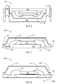
- FIG. 7 is a cross-sectional view of an integrated circuit package system for electromagnet isolation, in a first alternative embodiment of the present invention.
- FIG. 8 is a cross-sectional view of an integrated circuit package system for electromagnet isolation, in a second alternative embodiment of the present invention.
- FIG. 9 is a cross-sectional view of an integrated circuit package system for electromagnet isolation, in a third alternative embodiment of the present invention.
- FIG. 10 is a cross-sectional view of an integrated circuit package system for electromagnet isolation, in a fourth alternative embodiment of the present invention.
- FIG. 11 is a flow chart of an integrated circuit package system for manufacturing the integrated circuit package system for electromagnetic isolation, in an embodiment of the present invention.
- the term “horizontal” as used herein is defined as a plane parallel to the plane or surface of the integrated circuit, regardless of its orientation.
- the term “vertical” refers to a direction perpendicular to the horizontal as just defined. Terms, such as “above”, “below”, “bottom”, “top”, “side” (as in “sidewall”), “higher”, “lower”, “upper”, “over”, and “under”, are defined with respect to the horizontal plane.
- the term “on” means there is direct contact among elements.
- system as used herein means and refers to the method and to the apparatus of the present invention in accordance with the context in which the term is used.
- processing as used herein includes stamping, forging, patterning, exposure, development, etching, cleaning, and/or removal of the material or laser trimming as required in forming a described structure.
- FIG. 1 therein is shown a first cross-sectional view of an integrated circuit package system 100 for electromagnet isolation, in an embodiment of the present invention.
- the first cross-sectional view of the integrated circuit package system 100 depicts a lead frame 102 having a leadfinger 104 and a die attach pad 106 .
- An integrated circuit 108 may be mechanically coupled to the die attach pad 106 by an adhesive 110 , such as a die attach material.
- Electrical interconnects 112 may electrically connect the lead, 104 , the die attach pad 106 , the integrated circuit 108 , or a combination thereof.
- An insulating compound 114 such as an epoxy molding compound, may be formed around the lead frame 102 , the integrated circuit 108 and the electrical interconnects 112 .
- An insulation step 116 may be formed over the leads 104 of the lead frame 102 for isolating a signal from the integrated circuit 108 .
- a selectively exposed lead 105 that does not have the insulation step 116 covering the leadfinger 104 may be formed by blocking the insulating compound 114 .
- a conductive shielding layer 118 such as a conductive resin, a metal, a conductive foil, or a conductive film, may be coated on the insulating compound 114 .
- the conductive shielding layer 118 may be formed of a two component epoxy containing silver, copper, nickel, an alloy, or other metal.
- the conductive shielding layer 118 may also be formed of a nickel filled polyurethane or acrylic coating.
- the insulation step 116 may prevent the conductive shielding layer 118 from forming an electrical connection among the leads 104 .
- the conductive shielding layer 118 may form an electrical connection to the selectively exposed lead 105 , that do not have the insulation step 116 covering the leadfinger 104 , for coupling a voltage, such as V SS or Ground, to the conductive shielding layer 118 .
- the conductive shielding layer 118 may be applied by known methods, such as plating, sputtering, spraying, painting, rolling, or laminating.
- the conductive shielding layer 118 may be applied over all of the surfaces of the insulating compound 114 , including a lateral side 120 , and any of the leads 104 that may remain exposed.
- the conductive shielding layer 118 will electrically connect to only those of the leads 104 that are left exposed. This may greatly simplify the application and reliability of the conductive shielding layer 118 .
- the conductive shielding layer 118 By forming an electrical connection between the conductive shielding layer 118 and any of the leads 104 that are coupled to the voltage, such as V SS or ground, the conductive shielding layer 118 will also be coupled to the voltage.
- the conductive shielding layer 118 By coupling the conductive shielding layer 118 to the voltage, the conductive shielding layer 118 will isolate the integrated circuit 108 from any electromagnetic interference that may be present outside the conductive shielding layer 118 .
- the conductive shielding layer 118 may also be used to prevent any electromagnetic interference generated by the integrated circuit 108 from escaping into the system environment beyond the conductive shielding layer 118 , thus providing electromagnetic isolation to the system environment.
- FIG. 2 therein is shown a second cross-sectional view of the integrated circuit package system 100 for electromagnet isolation, in an embodiment of the present invention.
- the second cross-sectional view of the integrated circuit package system 100 depicts the lead frame 102 having the die attach pad 106 with tie bars 202 extending therefrom.
- the tie bars 202 may be electrically connected to the integrated circuit 108 by the electrical interconnects 112 .
- the insulating compound 114 may be formed on the die attach pad 106 , the integrated circuit 108 , the electrical interconnects 112 , and the tie bars 202 .
- An end surface 204 of the tie bars 202 may selectively remain exposed and therefore is not covered by the insulating compound 114 .
- the application of the conductive shielding layer 118 will form an electrical connection to the end surface 204 of the tie bars 202 .
- FIG. 3 therein is shown a first cross-sectional view of a package mold 300 for implementing the present invention.
- the first cross-sectional view of the package mold 300 depicts a mold base 302 with the lead frame 102 positioned thereon.
- the integrated circuit 108 may be mounted on the lead frame 102 with the electrical interconnects 112 coupling the integrated circuit 108 to the lead frame 102 .
- a mold chase 304 having a cavity 306 , may clamp the lead frame 102 in position for a molding process.
- the cavity 306 may have an open volume around the integrated circuit 108 and the electrical interconnects 112 .
- a mold step 308 may be formed over the lead frame 102 and open into the cavity 306 .
- FIG. 4 therein is shown a second cross-sectional view of the package mold 300 .
- the second cross-sectional view of the package mold 300 depicts the mold base 302 having an end gate 402 for forming a package base around the tie bar 202 .
- the integrated circuit 108 may be mounted on the lead frame 102 with the electrical interconnects 112 coupling the integrated circuit 108 to the lead frame 102 .
- the mold chase 304 having the cavity 306 , may clamp the lead frame 102 in position for the molding process.
- the cavity 306 may have an open volume around the integrated circuit 108 and the electrical interconnects 112 .
- the cavity 306 does not extend over the entire surface of the tie bars 202 . This configuration provides a selectively exposed area 404 on the tie bars 202 .
- FIG. 5 therein is shown a top plan view of an integrated circuit package 500 , in an embodiment of the present invention.
- the top plan view of the integrated circuit package 500 depicts the leads 104 , the die attach pad 106 , the integrated circuit 108 , the electrical interconnects 112 , and the tie bars 202 substantially encased by the insulating compound 114 .
- the selectively exposed area 404 may be formed on the tie bars 202 or on the leads 104 in a selected location or locations by blocking the insulating compound 114 during the molding of the integrated circuit package 500 .
- the selectively exposed area 404 may be available for contacting the conductive shielding layer 118 , of FIG. 1 , in a subsequent manufacturing process.
- FIG. 6 therein is shown a cross-sectional view of a singulation apparatus 600 for the present invention.
- the cross-sectional view of the singulation apparatus 600 depicts a shear base 602 for supporting a shielded package 604 .
- a shear top 606 may be used to align and stabilize a punch 608 that may perform the singulation of the shielded package 604 .
- the singulation apparatus 600 is an example only.
- the singulation process may include a saw or a shear in place of the punch 608 .
- the shielded package 604 is singulated so that the conductive shielding layer 118 is connected only to the selectively exposed areas 404 , of FIG. 4 .
- FIG. 7 therein is shown a cross-sectional view of an integrated circuit package system 700 for electromagnet isolation, in a first alternative embodiment of the present invention.
- the cross-sectional view of the integrated circuit package system 700 depicts a lead frame 702 having a die attach pad 704 , a signal lead 706 and a stepped lead 708 .
- the stepped lead 708 may be selectively formed at any position around the integrated circuit package system 700 .
- the integrated circuit 108 may be attached to the die attach pad 704 by the adhesive 110 .
- the electrical interconnects 112 may be coupled between the integrated circuit 108 , the die attach pad 704 , the signal lead 706 , the stepped lead 708 , or a combination thereof.
- the insulating compound 114 may be formed on the integrated circuit 108 , the die attach pad 704 , the signal lead 706 , and the stepped lead 708 .
- the stepped lead 708 may provide the selectively exposed areas 404 for coupling the conductive shielding layer 118 .
- the conductive shielding layer 118 will provide isolation from electromagnetic interference.
- FIG. 8 therein is shown a cross-sectional view of an integrated circuit package system 800 for electromagnet isolation, in a second alternative embodiment of the present invention.
- the cross-sectional view of the integrated circuit package system 800 depicts the lead frame 102 with the integrated circuit 108 mounted thereon.
- the electrical interconnects 112 may couple the lead frame 102 to the integrated circuit 108 .
- a conductive bead 802 such as a metal ball, a metal bump, a stud bump, a metal column, or a conductive resin, may be coupled to the leads 104 in selective locations.
- the insulating compound 114 may be formed on the lead frame 102 , the integrated circuit 108 , the electrical interconnects 112 , and the conductive bead 802 .
- a portion of the conductive bead 802 may protrude from the insulating compound 114 for providing the selectively exposed area 404 .
- the conductive bead 802 may be coupled to the leadfinger 104 for providing the voltage, such as V SS or Ground.
- FIG. 9 therein is shown a cross-sectional view of an integrated circuit package system 900 for electromagnet isolation, in a third alternative embodiment of the present invention.
- the cross-sectional view of the integrated circuit package system 900 depicts a lead frame 902 having leadfingers 904 and an inverted die attach pad 906 .
- the integrated circuit 108 may be mounted on the inverted die attach pad 906 by the adhesive 110 .
- the electrical interconnects 112 may be coupled between the leadfingers 904 , the inverted die attach pad 906 , the integrated circuit 108 , or a combination thereof.
- the insulating compound 114 may be applied on the leadfingers 904 , the inverted die attach pad 906 , the integrated circuit 108 , and the electrical interconnects 112 .
- the top portion of the inverted die attach pad 906 may protrude through the insulating compound 114 to form the selectively exposed area 404 .
- the conductive shielding layer 118 may be applied on the insulating compound 114 and the selectively exposed areas 404 .
- the inverted die attach pad 906 may be connected to the voltage through the tie bar 202 of FIG. 2 , the electrical interconnects 112 , the leadfingers 904 , or a combination thereof.
- FIG. 10 therein is shown a cross-sectional view of an integrated circuit package system 1000 for electromagnet isolation, in a fourth alternative embodiment of the present invention.
- the cross-sectional view of the integrated circuit package system 1000 depicts a lead frame 1002 having leads 1004 and an inverted die attach pad 1006 .
- the integrated circuit 108 may be mounted on the inverted die attach pad 1006 by the adhesive 110 .
- the integrated circuit 108 that may be larger than the inverted die attach pad 1006 can be mounted with an active side facing the inverted die attach pad 1006 .
- the electrical interconnects 112 may be coupled between the leads 1004 , the inverted die attach pad 1006 , the integrated circuit 108 , or a combination thereof.
- the insulating compound 114 may be applied on the leads 1004 , the inverted die attach pad 1006 , the integrated circuit 108 , and the electrical interconnects 112 .
- the top portion of the inverted die attach pad 1006 may protrude through the insulating compound 114 to form the selectively exposed area 404 .
- the conductive shielding layer 118 may be applied on the insulating compound 114 and the selectively exposed areas 404 .
- the inverted die attach pad 1006 may be connected to the voltage through the tie bar 202 of FIG. 2 , the electrical interconnects 112 , the leads 1004 , or a combination thereof.
- the inverted die attach pad 1006 may provide a cooling path for the integrated circuit package system 1000 .
- the conductive shielding layer 118 may also provide a radiant cooling heat sink as well as electromagnetic isolation.
- the system 1100 includes providing a lead frame in a block 1102 ; forming an integrated circuit package including the lead frame in a block 1104 ; providing a selectively exposed area on the lead frame in a block 1106 ; and coating a conductive shielding layer on the integrated circuit package for coupling the selectively exposed area in a block 1108 .
- the present invention may provide a thermal sinking mechanism while providing electromagnetic isolation.
- Another aspect is the present invention utilizes only standard package assembly processes, yet is extremely reliable. There is minimal thickness added to the finished package and no additional horizontal space required to implement the present invention.
- Yet another important aspect of the present invention is that it valuably supports and services the historical trend of reducing costs, simplifying systems, and increasing performance.
- the integrated circuit package system of the present invention furnishes important and heretofore unknown and unavailable solutions, capabilities, and functional aspects for providing electromagnetic isolation for integrated circuit packages.
- the resulting processes and configurations are straightforward, cost-effective, uncomplicated, highly versatile and effective, can be surprisingly and unobviously implemented by adapting known technologies, and are thus readily suited for efficiently and economically manufacturing integrated circuit devices fully compatible with conventional manufacturing processes and technologies.
- the resulting processes and configurations are straightforward, cost-effective, uncomplicated, highly versatile, accurate, sensitive, and effective, and can be implemented by adapting known components for ready, efficient, and economical manufacturing, application, and utilization.
Landscapes
- Engineering & Computer Science (AREA)
- Physics & Mathematics (AREA)
- Power Engineering (AREA)
- Computer Hardware Design (AREA)
- Microelectronics & Electronic Packaging (AREA)
- General Physics & Mathematics (AREA)
- Condensed Matter Physics & Semiconductors (AREA)
- Health & Medical Sciences (AREA)
- Electromagnetism (AREA)
- Toxicology (AREA)
- Geometry (AREA)
- Manufacturing & Machinery (AREA)
- Structures Or Materials For Encapsulating Or Coating Semiconductor Devices Or Solid State Devices (AREA)
- Lead Frames For Integrated Circuits (AREA)
- Shielding Devices Or Components To Electric Or Magnetic Fields (AREA)
Abstract
Description
Claims (18)
Priority Applications (6)
| Application Number | Priority Date | Filing Date | Title |
|---|---|---|---|
| US11/952,951 US7902644B2 (en) | 2007-12-07 | 2007-12-07 | Integrated circuit package system for electromagnetic isolation |
| SG200807692-9A SG152985A1 (en) | 2007-12-07 | 2008-10-15 | Integrated circuit package system for electromagnetic isolation |
| SG2011039864A SG172662A1 (en) | 2007-12-07 | 2008-10-15 | Integrated circuit package system forelectromagnetic isolation and method for manufacturing thereof |
| TW097140396A TWI479635B (en) | 2007-12-07 | 2008-10-22 | Integrated circuit package system for electromagnetic isolation |
| KR1020080106170A KR20090060132A (en) | 2007-12-07 | 2008-10-28 | Integrated circuit package system for electromagnetic isolation |
| US13/028,501 US8269320B2 (en) | 2007-12-07 | 2011-02-16 | Integrated circuit package system for electromagnetic isolation and method for manufacturing thereof |
Applications Claiming Priority (1)
| Application Number | Priority Date | Filing Date | Title |
|---|---|---|---|
| US11/952,951 US7902644B2 (en) | 2007-12-07 | 2007-12-07 | Integrated circuit package system for electromagnetic isolation |
Related Child Applications (1)
| Application Number | Title | Priority Date | Filing Date |
|---|---|---|---|
| US13/028,501 Continuation US8269320B2 (en) | 2007-12-07 | 2011-02-16 | Integrated circuit package system for electromagnetic isolation and method for manufacturing thereof |
Publications (2)
| Publication Number | Publication Date |
|---|---|
| US20090146268A1 US20090146268A1 (en) | 2009-06-11 |
| US7902644B2 true US7902644B2 (en) | 2011-03-08 |
Family
ID=40720767
Family Applications (2)
| Application Number | Title | Priority Date | Filing Date |
|---|---|---|---|
| US11/952,951 Active 2029-03-15 US7902644B2 (en) | 2007-12-07 | 2007-12-07 | Integrated circuit package system for electromagnetic isolation |
| US13/028,501 Active US8269320B2 (en) | 2007-12-07 | 2011-02-16 | Integrated circuit package system for electromagnetic isolation and method for manufacturing thereof |
Family Applications After (1)
| Application Number | Title | Priority Date | Filing Date |
|---|---|---|---|
| US13/028,501 Active US8269320B2 (en) | 2007-12-07 | 2011-02-16 | Integrated circuit package system for electromagnetic isolation and method for manufacturing thereof |
Country Status (4)
| Country | Link |
|---|---|
| US (2) | US7902644B2 (en) |
| KR (1) | KR20090060132A (en) |
| SG (2) | SG152985A1 (en) |
| TW (1) | TWI479635B (en) |
Cited By (52)
| Publication number | Priority date | Publication date | Assignee | Title |
|---|---|---|---|---|
| US20120119380A1 (en) * | 2010-11-15 | 2012-05-17 | Tessera, Inc. | Microelectronic package with terminals on dielectric mass |
| US20120218729A1 (en) * | 2011-02-28 | 2012-08-30 | Rf Micro Devices, Inc. | Microshield on standard qfn package |
| US20140239476A1 (en) * | 2013-02-27 | 2014-08-28 | You Ge | Semiconductor device with integral heat sink |
| US8969136B2 (en) | 2011-03-25 | 2015-03-03 | Stats Chippac Ltd. | Integrated circuit packaging system for electromagnetic interference shielding and method of manufacture thereof |
| US9041227B2 (en) | 2011-10-17 | 2015-05-26 | Invensas Corporation | Package-on-package assembly with wire bond vias |
| US9095074B2 (en) | 2012-12-20 | 2015-07-28 | Invensas Corporation | Structure for microelectronic packaging with bond elements to encapsulation surface |
| US9123664B2 (en) | 2010-07-19 | 2015-09-01 | Tessera, Inc. | Stackable molded microelectronic packages |
| US9153562B2 (en) | 2004-11-03 | 2015-10-06 | Tessera, Inc. | Stacked packaging improvements |
| US9159708B2 (en) | 2010-07-19 | 2015-10-13 | Tessera, Inc. | Stackable molded microelectronic packages with area array unit connectors |
| US9218988B2 (en) | 2005-12-23 | 2015-12-22 | Tessera, Inc. | Microelectronic packages and methods therefor |
| US9224717B2 (en) | 2011-05-03 | 2015-12-29 | Tessera, Inc. | Package-on-package assembly with wire bonds to encapsulation surface |
| US9324681B2 (en) | 2010-12-13 | 2016-04-26 | Tessera, Inc. | Pin attachment |
| US9349706B2 (en) | 2012-02-24 | 2016-05-24 | Invensas Corporation | Method for package-on-package assembly with wire bonds to encapsulation surface |
| US9391008B2 (en) | 2012-07-31 | 2016-07-12 | Invensas Corporation | Reconstituted wafer-level package DRAM |
| US9412714B2 (en) | 2014-05-30 | 2016-08-09 | Invensas Corporation | Wire bond support structure and microelectronic package including wire bonds therefrom |
| US9420704B2 (en) | 2011-02-25 | 2016-08-16 | Qorvo Us, Inc. | Connection using conductive vias |
| US9484289B2 (en) | 2013-10-18 | 2016-11-01 | Freescale Semiconductor, Inc. | Semiconductor device with heat spreader |
| US9502390B2 (en) | 2012-08-03 | 2016-11-22 | Invensas Corporation | BVA interposer |
| US9583411B2 (en) | 2014-01-17 | 2017-02-28 | Invensas Corporation | Fine pitch BVA using reconstituted wafer with area array accessible for testing |
| US9601454B2 (en) | 2013-02-01 | 2017-03-21 | Invensas Corporation | Method of forming a component having wire bonds and a stiffening layer |
| US9646917B2 (en) | 2014-05-29 | 2017-05-09 | Invensas Corporation | Low CTE component with wire bond interconnects |
| US9661739B2 (en) | 2005-08-08 | 2017-05-23 | Qorvo Us, Inc. | Electronic modules having grounded electromagnetic shields |
| US9659848B1 (en) | 2015-11-18 | 2017-05-23 | Invensas Corporation | Stiffened wires for offset BVA |
| US9685365B2 (en) | 2013-08-08 | 2017-06-20 | Invensas Corporation | Method of forming a wire bond having a free end |
| US9691679B2 (en) | 2012-02-24 | 2017-06-27 | Invensas Corporation | Method for package-on-package assembly with wire bonds to encapsulation surface |
| US9728527B2 (en) | 2013-11-22 | 2017-08-08 | Invensas Corporation | Multiple bond via arrays of different wire heights on a same substrate |
| US9735084B2 (en) | 2014-12-11 | 2017-08-15 | Invensas Corporation | Bond via array for thermal conductivity |
| US9761554B2 (en) | 2015-05-07 | 2017-09-12 | Invensas Corporation | Ball bonding metal wire bond wires to metal pads |
| US9807890B2 (en) | 2013-05-31 | 2017-10-31 | Qorvo Us, Inc. | Electronic modules having grounded electromagnetic shields |
| US9812402B2 (en) | 2015-10-12 | 2017-11-07 | Invensas Corporation | Wire bond wires for interference shielding |
| US9842745B2 (en) | 2012-02-17 | 2017-12-12 | Invensas Corporation | Heat spreading substrate with embedded interconnects |
| US9852969B2 (en) | 2013-11-22 | 2017-12-26 | Invensas Corporation | Die stacks with one or more bond via arrays of wire bond wires and with one or more arrays of bump interconnects |
| US9888579B2 (en) | 2015-03-05 | 2018-02-06 | Invensas Corporation | Pressing of wire bond wire tips to provide bent-over tips |
| US9911718B2 (en) | 2015-11-17 | 2018-03-06 | Invensas Corporation | ‘RDL-First’ packaged microelectronic device for a package-on-package device |
| US9935075B2 (en) | 2016-07-29 | 2018-04-03 | Invensas Corporation | Wire bonding method and apparatus for electromagnetic interference shielding |
| US9953904B1 (en) | 2016-10-25 | 2018-04-24 | Nxp Usa, Inc. | Electronic component package with heatsink and multiple electronic components |
| US9953914B2 (en) | 2012-05-22 | 2018-04-24 | Invensas Corporation | Substrate-less stackable package with wire-bond interconnect |
| US9984992B2 (en) | 2015-12-30 | 2018-05-29 | Invensas Corporation | Embedded wire bond wires for vertical integration with separate surface mount and wire bond mounting surfaces |
| US10008477B2 (en) | 2013-09-16 | 2018-06-26 | Invensas Corporation | Microelectronic element with bond elements to encapsulation surface |
| US10008469B2 (en) | 2015-04-30 | 2018-06-26 | Invensas Corporation | Wafer-level packaging using wire bond wires in place of a redistribution layer |
| US10026717B2 (en) | 2013-11-22 | 2018-07-17 | Invensas Corporation | Multiple bond via arrays of different wire heights on a same substrate |
| US10181457B2 (en) | 2015-10-26 | 2019-01-15 | Invensas Corporation | Microelectronic package for wafer-level chip scale packaging with fan-out |
| US10299368B2 (en) | 2016-12-21 | 2019-05-21 | Invensas Corporation | Surface integrated waveguides and circuit structures therefor |
| US10332854B2 (en) | 2015-10-23 | 2019-06-25 | Invensas Corporation | Anchoring structure of fine pitch bva |
| US10381326B2 (en) | 2014-05-28 | 2019-08-13 | Invensas Corporation | Structure and method for integrated circuits packaging with increased density |
| US10460958B2 (en) | 2013-08-07 | 2019-10-29 | Invensas Corporation | Method of manufacturing embedded packaging with preformed vias |
| US10490528B2 (en) | 2015-10-12 | 2019-11-26 | Invensas Corporation | Embedded wire bond wires |
| US10903149B2 (en) * | 2017-02-06 | 2021-01-26 | Fuji Electric Co., Ltd. | Semiconductor module, electric vehicle, and power control unit |
| US11058038B2 (en) | 2018-06-28 | 2021-07-06 | Qorvo Us, Inc. | Electromagnetic shields for sub-modules |
| US11114363B2 (en) | 2018-12-20 | 2021-09-07 | Qorvo Us, Inc. | Electronic package arrangements and related methods |
| US11127689B2 (en) | 2018-06-01 | 2021-09-21 | Qorvo Us, Inc. | Segmented shielding using wirebonds |
| US11515282B2 (en) | 2019-05-21 | 2022-11-29 | Qorvo Us, Inc. | Electromagnetic shields with bonding wires for sub-modules |
Families Citing this family (26)
| Publication number | Priority date | Publication date | Assignee | Title |
|---|---|---|---|---|
| US8507319B2 (en) * | 2007-12-07 | 2013-08-13 | Stats Chippac Ltd. | Integrated circuit package system with shield |
| US8987030B2 (en) * | 2009-08-13 | 2015-03-24 | Knowles Electronics, Llc | MEMS package and a method for manufacturing the same |
| US9399574B2 (en) | 2009-08-13 | 2016-07-26 | Knowles Electronics Llc | MEMS package and a method for manufacturing the same |
| TWI404187B (en) * | 2010-02-12 | 2013-08-01 | 矽品精密工業股份有限公司 | Quad flat non leaded package structure capable of preventing electromagnetic interference and method for forming the same |
| US8199518B1 (en) | 2010-02-18 | 2012-06-12 | Amkor Technology, Inc. | Top feature package and method |
| US8946886B1 (en) * | 2010-05-13 | 2015-02-03 | Amkor Technology, Inc. | Shielded electronic component package and method |
| US9723766B2 (en) * | 2010-09-10 | 2017-08-01 | Intersil Americas LLC | Power supply module with electromagnetic-interference (EMI) shielding, cooling, or both shielding and cooling, along two or more sides |
| US9153543B1 (en) * | 2012-01-23 | 2015-10-06 | Amkor Technology, Inc. | Shielding technique for semiconductor package including metal lid and metalized contact area |
| JP5813596B2 (en) * | 2012-08-10 | 2015-11-17 | 株式会社東芝 | Nonvolatile semiconductor memory device |
| US8853840B2 (en) * | 2013-02-21 | 2014-10-07 | Freescale Semiconductor, Inc. | Semiconductor package with inner and outer leads |
| JP5802695B2 (en) * | 2013-03-19 | 2015-10-28 | 株式会社東芝 | Semiconductor device and method for manufacturing semiconductor device |
| CN109545770B (en) * | 2013-11-20 | 2022-06-10 | 日月光半导体制造股份有限公司 | Semiconductor packaging structure |
| WO2015194435A1 (en) * | 2014-06-20 | 2015-12-23 | 株式会社村田製作所 | Circuit module and method for manufacturing same |
| KR20160036945A (en) * | 2014-09-26 | 2016-04-05 | 삼성전기주식회사 | Printed circuit board and electronic component package having the same |
| CN105070710A (en) * | 2015-09-01 | 2015-11-18 | 苏州日月新半导体有限公司 | Integrated circuit packaging body and formation method thereof |
| WO2017111830A1 (en) * | 2015-12-26 | 2017-06-29 | Intel Corporation | Rlink-ground shielding attachment structures and shadow voiding for data signal contacts of package devices; vertical ground shielding structures and shield fencing of vertical data signal interconnects of package devices; and ground shielding for electro optical module connector data signal contacts and contact pins of package devices |
| US10727085B2 (en) * | 2015-12-30 | 2020-07-28 | Texas Instruments Incorporated | Printed adhesion deposition to mitigate integrated circuit package delamination |
| KR101815754B1 (en) | 2016-03-10 | 2018-01-08 | 앰코 테크놀로지 코리아 주식회사 | Semiconductor device |
| JP6597499B2 (en) * | 2016-06-29 | 2019-10-30 | 三菱電機株式会社 | Semiconductor device and manufacturing method thereof |
| US10177095B2 (en) | 2017-03-24 | 2019-01-08 | Amkor Technology, Inc. | Semiconductor device and method of manufacturing thereof |
| US20180374798A1 (en) | 2017-06-24 | 2018-12-27 | Amkor Technology, Inc. | Semiconductor device having emi shielding structure and related methods |
| CN109686718B (en) * | 2019-01-24 | 2024-05-14 | 上海兴感半导体有限公司 | Packaging structure |
| US11342276B2 (en) | 2019-05-24 | 2022-05-24 | Amkor Technology Singapore Holding Pte. Ltd. | Semiconductor device and method of manufacturing semiconductor device |
| EP4060730A1 (en) | 2021-03-18 | 2022-09-21 | Murata Manufacturing Co., Ltd. | Shielded electronic component |
| TWI781863B (en) * | 2021-12-30 | 2022-10-21 | 宏齊科技股份有限公司 | Planar type multi-chip device |
| CN116936544B (en) * | 2023-09-18 | 2023-12-05 | 成都电科星拓科技有限公司 | Packaging structure and packaging method for solving digital-analog interference |
Citations (30)
| Publication number | Priority date | Publication date | Assignee | Title |
|---|---|---|---|---|
| US5166772A (en) | 1991-02-22 | 1992-11-24 | Motorola, Inc. | Transfer molded semiconductor device package with integral shield |
| US5223739A (en) * | 1989-09-14 | 1993-06-29 | Kabushiki Kaisha Toshiba | Plastic molded semiconductor device having waterproof cap |
| US5294826A (en) * | 1993-04-16 | 1994-03-15 | Northern Telecom Limited | Integrated circuit package and assembly thereof for thermal and EMI management |
| US5321204A (en) * | 1990-10-13 | 1994-06-14 | Gold Star Electron Co., Ltd. | Structure of charged coupled device |
| US5477008A (en) * | 1993-03-19 | 1995-12-19 | Olin Corporation | Polymer plug for electronic packages |
| US5650659A (en) * | 1995-08-04 | 1997-07-22 | National Semiconductor Corporation | Semiconductor component package assembly including an integral RF/EMI shield |
| US5656864A (en) * | 1993-09-09 | 1997-08-12 | Fujitsu Limited | Semiconductor device having upper and lower package bodies and manufacturing method thereof |
| US5679975A (en) * | 1995-12-18 | 1997-10-21 | Integrated Device Technology, Inc. | Conductive encapsulating shield for an integrated circuit |
| US5703398A (en) * | 1993-03-17 | 1997-12-30 | Fujitsu Limited | Semiconductor integrated circuit device and method of producing the semiconductor integrated circuit device |
| US6092281A (en) | 1998-08-28 | 2000-07-25 | Amkor Technology, Inc. | Electromagnetic interference shield driver and method |
| US6104085A (en) * | 1994-10-28 | 2000-08-15 | Hitachi, Ltd. | Semiconductor device and method of producing the same |
| US6312975B1 (en) * | 1998-02-10 | 2001-11-06 | Stmicroelectronics S.A. | Semiconductor package and method of manufacturing the same |
| US6368899B1 (en) * | 2000-03-08 | 2002-04-09 | Maxwell Electronic Components Group, Inc. | Electronic device packaging |
| US6432742B1 (en) * | 2000-08-17 | 2002-08-13 | St Assembly Test Services Pte Ltd. | Methods of forming drop-in heat spreader plastic ball grid array (PBGA) packages |
| US20030111728A1 (en) * | 2001-09-26 | 2003-06-19 | Thai Cao Minh | Mounting material, semiconductor device and method of manufacturing semiconductor device |
| US6603193B2 (en) | 2001-09-06 | 2003-08-05 | Silicon Bandwidth Inc. | Semiconductor package |
| US6614102B1 (en) * | 2001-05-04 | 2003-09-02 | Amkor Technology, Inc. | Shielded semiconductor leadframe package |
| US6707168B1 (en) | 2001-05-04 | 2004-03-16 | Amkor Technology, Inc. | Shielded semiconductor package with single-sided substrate and method for making the same |
| US6734539B2 (en) | 2000-12-27 | 2004-05-11 | Lucent Technologies Inc. | Stacked module package |
| US6847115B2 (en) | 2001-09-06 | 2005-01-25 | Silicon Bandwidth Inc. | Packaged semiconductor device for radio frequency shielding |
| US7187060B2 (en) | 2003-03-13 | 2007-03-06 | Sanyo Electric Co., Ltd. | Semiconductor device with shield |
| US7190066B2 (en) * | 2005-03-08 | 2007-03-13 | Taiwan Semiconductor Manufacturing Co., Ltd. | Heat spreader and package structure utilizing the same |
| US20070145539A1 (en) | 2005-12-22 | 2007-06-28 | Ken Lam | Method and system for providing an integral radio frequency shield in a molded array package |
| US7323769B2 (en) * | 2002-11-27 | 2008-01-29 | United Test And Assembly Center Ltd. | High performance chip scale leadframe package with thermal dissipating structure and annular element and method of manufacturing package |
| US7479692B2 (en) * | 2006-11-09 | 2009-01-20 | Stats Chippac Ltd. | Integrated circuit package system with heat sink |
| US7545032B2 (en) * | 2006-07-10 | 2009-06-09 | Stats Chippac Ltd. | Integrated circuit package system with stiffener |
| US20090146269A1 (en) | 2007-12-07 | 2009-06-11 | Seng Guan Chow | Integrated circuit package system with shield |
| US7576415B2 (en) * | 2007-06-15 | 2009-08-18 | Advanced Semiconductor Engineering, Inc. | EMI shielded semiconductor package |
| US7582951B2 (en) * | 2005-10-20 | 2009-09-01 | Broadcom Corporation | Methods and apparatus for improved thermal performance and electromagnetic interference (EMI) shielding in leadframe integrated circuit (IC) packages |
| US7625781B2 (en) * | 2005-02-15 | 2009-12-01 | Infineon Technologies Ag | Semiconductor device having a plastic housing and external connections and method for producing the same |
Family Cites Families (17)
| Publication number | Priority date | Publication date | Assignee | Title |
|---|---|---|---|---|
| JPS6150351A (en) * | 1984-08-20 | 1986-03-12 | Oki Electric Ind Co Ltd | Eprom device |
| US4814943A (en) * | 1986-06-04 | 1989-03-21 | Oki Electric Industry Co., Ltd. | Printed circuit devices using thermoplastic resin cover plate |
| US5939784A (en) * | 1997-09-09 | 1999-08-17 | Amkor Technology, Inc. | Shielded surface acoustical wave package |
| TW363234B (en) * | 1998-04-08 | 1999-07-01 | mei-lian Zhang | Heat and electric conductive packaging method for integrated circuit |
| AU2001272814A1 (en) * | 2000-07-25 | 2002-02-05 | Chan-Ik Park | Plastic package base, air cavity type package and their manufacturing methods |
| US6664615B1 (en) * | 2001-11-20 | 2003-12-16 | National Semiconductor Corporation | Method and apparatus for lead-frame based grid array IC packaging |
| US7026223B2 (en) * | 2002-03-28 | 2006-04-11 | M/A-Com, Inc | Hermetic electric component package |
| JP2004095572A (en) * | 2002-08-29 | 2004-03-25 | Hitachi Ltd | Semiconductor device and method for manufacturing the same |
| US7030469B2 (en) * | 2003-09-25 | 2006-04-18 | Freescale Semiconductor, Inc. | Method of forming a semiconductor package and structure thereof |
| TWI227555B (en) * | 2003-11-17 | 2005-02-01 | Advanced Semiconductor Eng | Structure of chip package and the process thereof |
| US7348663B1 (en) * | 2005-07-15 | 2008-03-25 | Asat Ltd. | Integrated circuit package and method for fabricating same |
| US8053872B1 (en) * | 2007-06-25 | 2011-11-08 | Rf Micro Devices, Inc. | Integrated shield for a no-lead semiconductor device package |
| US7262491B2 (en) * | 2005-09-06 | 2007-08-28 | Advanced Interconnect Technologies Limited | Die pad for semiconductor packages and methods of making and using same |
| EP1795496A2 (en) * | 2005-12-08 | 2007-06-13 | Yamaha Corporation | Semiconductor device for detecting pressure variations |
| US7808087B2 (en) * | 2006-06-01 | 2010-10-05 | Broadcom Corporation | Leadframe IC packages having top and bottom integrated heat spreaders |
| US8422243B2 (en) * | 2006-12-13 | 2013-04-16 | Stats Chippac Ltd. | Integrated circuit package system employing a support structure with a recess |
| US8110915B2 (en) * | 2009-10-16 | 2012-02-07 | Infineon Technologies Ag | Open cavity leadless surface mountable package for high power RF applications |
-
2007
- 2007-12-07 US US11/952,951 patent/US7902644B2/en active Active
-
2008
- 2008-10-15 SG SG200807692-9A patent/SG152985A1/en unknown
- 2008-10-15 SG SG2011039864A patent/SG172662A1/en unknown
- 2008-10-22 TW TW097140396A patent/TWI479635B/en active
- 2008-10-28 KR KR1020080106170A patent/KR20090060132A/en active Search and Examination
-
2011
- 2011-02-16 US US13/028,501 patent/US8269320B2/en active Active
Patent Citations (30)
| Publication number | Priority date | Publication date | Assignee | Title |
|---|---|---|---|---|
| US5223739A (en) * | 1989-09-14 | 1993-06-29 | Kabushiki Kaisha Toshiba | Plastic molded semiconductor device having waterproof cap |
| US5321204A (en) * | 1990-10-13 | 1994-06-14 | Gold Star Electron Co., Ltd. | Structure of charged coupled device |
| US5166772A (en) | 1991-02-22 | 1992-11-24 | Motorola, Inc. | Transfer molded semiconductor device package with integral shield |
| US5703398A (en) * | 1993-03-17 | 1997-12-30 | Fujitsu Limited | Semiconductor integrated circuit device and method of producing the semiconductor integrated circuit device |
| US5477008A (en) * | 1993-03-19 | 1995-12-19 | Olin Corporation | Polymer plug for electronic packages |
| US5294826A (en) * | 1993-04-16 | 1994-03-15 | Northern Telecom Limited | Integrated circuit package and assembly thereof for thermal and EMI management |
| US5656864A (en) * | 1993-09-09 | 1997-08-12 | Fujitsu Limited | Semiconductor device having upper and lower package bodies and manufacturing method thereof |
| US6104085A (en) * | 1994-10-28 | 2000-08-15 | Hitachi, Ltd. | Semiconductor device and method of producing the same |
| US5650659A (en) * | 1995-08-04 | 1997-07-22 | National Semiconductor Corporation | Semiconductor component package assembly including an integral RF/EMI shield |
| US5679975A (en) * | 1995-12-18 | 1997-10-21 | Integrated Device Technology, Inc. | Conductive encapsulating shield for an integrated circuit |
| US6312975B1 (en) * | 1998-02-10 | 2001-11-06 | Stmicroelectronics S.A. | Semiconductor package and method of manufacturing the same |
| US6092281A (en) | 1998-08-28 | 2000-07-25 | Amkor Technology, Inc. | Electromagnetic interference shield driver and method |
| US6368899B1 (en) * | 2000-03-08 | 2002-04-09 | Maxwell Electronic Components Group, Inc. | Electronic device packaging |
| US6432742B1 (en) * | 2000-08-17 | 2002-08-13 | St Assembly Test Services Pte Ltd. | Methods of forming drop-in heat spreader plastic ball grid array (PBGA) packages |
| US6734539B2 (en) | 2000-12-27 | 2004-05-11 | Lucent Technologies Inc. | Stacked module package |
| US6614102B1 (en) * | 2001-05-04 | 2003-09-02 | Amkor Technology, Inc. | Shielded semiconductor leadframe package |
| US6707168B1 (en) | 2001-05-04 | 2004-03-16 | Amkor Technology, Inc. | Shielded semiconductor package with single-sided substrate and method for making the same |
| US6847115B2 (en) | 2001-09-06 | 2005-01-25 | Silicon Bandwidth Inc. | Packaged semiconductor device for radio frequency shielding |
| US6603193B2 (en) | 2001-09-06 | 2003-08-05 | Silicon Bandwidth Inc. | Semiconductor package |
| US20030111728A1 (en) * | 2001-09-26 | 2003-06-19 | Thai Cao Minh | Mounting material, semiconductor device and method of manufacturing semiconductor device |
| US7323769B2 (en) * | 2002-11-27 | 2008-01-29 | United Test And Assembly Center Ltd. | High performance chip scale leadframe package with thermal dissipating structure and annular element and method of manufacturing package |
| US7187060B2 (en) | 2003-03-13 | 2007-03-06 | Sanyo Electric Co., Ltd. | Semiconductor device with shield |
| US7625781B2 (en) * | 2005-02-15 | 2009-12-01 | Infineon Technologies Ag | Semiconductor device having a plastic housing and external connections and method for producing the same |
| US7190066B2 (en) * | 2005-03-08 | 2007-03-13 | Taiwan Semiconductor Manufacturing Co., Ltd. | Heat spreader and package structure utilizing the same |
| US7582951B2 (en) * | 2005-10-20 | 2009-09-01 | Broadcom Corporation | Methods and apparatus for improved thermal performance and electromagnetic interference (EMI) shielding in leadframe integrated circuit (IC) packages |
| US20070145539A1 (en) | 2005-12-22 | 2007-06-28 | Ken Lam | Method and system for providing an integral radio frequency shield in a molded array package |
| US7545032B2 (en) * | 2006-07-10 | 2009-06-09 | Stats Chippac Ltd. | Integrated circuit package system with stiffener |
| US7479692B2 (en) * | 2006-11-09 | 2009-01-20 | Stats Chippac Ltd. | Integrated circuit package system with heat sink |
| US7576415B2 (en) * | 2007-06-15 | 2009-08-18 | Advanced Semiconductor Engineering, Inc. | EMI shielded semiconductor package |
| US20090146269A1 (en) | 2007-12-07 | 2009-06-11 | Seng Guan Chow | Integrated circuit package system with shield |
Cited By (94)
| Publication number | Priority date | Publication date | Assignee | Title |
|---|---|---|---|---|
| US9570416B2 (en) | 2004-11-03 | 2017-02-14 | Tessera, Inc. | Stacked packaging improvements |
| US9153562B2 (en) | 2004-11-03 | 2015-10-06 | Tessera, Inc. | Stacked packaging improvements |
| US9661739B2 (en) | 2005-08-08 | 2017-05-23 | Qorvo Us, Inc. | Electronic modules having grounded electromagnetic shields |
| US9218988B2 (en) | 2005-12-23 | 2015-12-22 | Tessera, Inc. | Microelectronic packages and methods therefor |
| US9984901B2 (en) | 2005-12-23 | 2018-05-29 | Tessera, Inc. | Method for making a microelectronic assembly having conductive elements |
| US9553076B2 (en) | 2010-07-19 | 2017-01-24 | Tessera, Inc. | Stackable molded microelectronic packages with area array unit connectors |
| US9570382B2 (en) | 2010-07-19 | 2017-02-14 | Tessera, Inc. | Stackable molded microelectronic packages |
| US10128216B2 (en) | 2010-07-19 | 2018-11-13 | Tessera, Inc. | Stackable molded microelectronic packages |
| US9123664B2 (en) | 2010-07-19 | 2015-09-01 | Tessera, Inc. | Stackable molded microelectronic packages |
| US9159708B2 (en) | 2010-07-19 | 2015-10-13 | Tessera, Inc. | Stackable molded microelectronic packages with area array unit connectors |
| US8637991B2 (en) * | 2010-11-15 | 2014-01-28 | Tessera, Inc. | Microelectronic package with terminals on dielectric mass |
| US20120119380A1 (en) * | 2010-11-15 | 2012-05-17 | Tessera, Inc. | Microelectronic package with terminals on dielectric mass |
| US9324681B2 (en) | 2010-12-13 | 2016-04-26 | Tessera, Inc. | Pin attachment |
| US9942994B2 (en) | 2011-02-25 | 2018-04-10 | Qorvo Us, Inc. | Connection using conductive vias |
| US9420704B2 (en) | 2011-02-25 | 2016-08-16 | Qorvo Us, Inc. | Connection using conductive vias |
| US9627230B2 (en) * | 2011-02-28 | 2017-04-18 | Qorvo Us, Inc. | Methods of forming a microshield on standard QFN package |
| US20120218729A1 (en) * | 2011-02-28 | 2012-08-30 | Rf Micro Devices, Inc. | Microshield on standard qfn package |
| US8969136B2 (en) | 2011-03-25 | 2015-03-03 | Stats Chippac Ltd. | Integrated circuit packaging system for electromagnetic interference shielding and method of manufacture thereof |
| US9224717B2 (en) | 2011-05-03 | 2015-12-29 | Tessera, Inc. | Package-on-package assembly with wire bonds to encapsulation surface |
| US11424211B2 (en) | 2011-05-03 | 2022-08-23 | Tessera Llc | Package-on-package assembly with wire bonds to encapsulation surface |
| US10593643B2 (en) | 2011-05-03 | 2020-03-17 | Tessera, Inc. | Package-on-package assembly with wire bonds to encapsulation surface |
| US9691731B2 (en) | 2011-05-03 | 2017-06-27 | Tessera, Inc. | Package-on-package assembly with wire bonds to encapsulation surface |
| US10062661B2 (en) | 2011-05-03 | 2018-08-28 | Tessera, Inc. | Package-on-package assembly with wire bonds to encapsulation surface |
| US11735563B2 (en) | 2011-10-17 | 2023-08-22 | Invensas Llc | Package-on-package assembly with wire bond vias |
| US9252122B2 (en) | 2011-10-17 | 2016-02-02 | Invensas Corporation | Package-on-package assembly with wire bond vias |
| US9041227B2 (en) | 2011-10-17 | 2015-05-26 | Invensas Corporation | Package-on-package assembly with wire bond vias |
| US9105483B2 (en) | 2011-10-17 | 2015-08-11 | Invensas Corporation | Package-on-package assembly with wire bond vias |
| US10756049B2 (en) | 2011-10-17 | 2020-08-25 | Invensas Corporation | Package-on-package assembly with wire bond vias |
| US11189595B2 (en) | 2011-10-17 | 2021-11-30 | Invensas Corporation | Package-on-package assembly with wire bond vias |
| US9761558B2 (en) | 2011-10-17 | 2017-09-12 | Invensas Corporation | Package-on-package assembly with wire bond vias |
| US9842745B2 (en) | 2012-02-17 | 2017-12-12 | Invensas Corporation | Heat spreading substrate with embedded interconnects |
| US9349706B2 (en) | 2012-02-24 | 2016-05-24 | Invensas Corporation | Method for package-on-package assembly with wire bonds to encapsulation surface |
| US9691679B2 (en) | 2012-02-24 | 2017-06-27 | Invensas Corporation | Method for package-on-package assembly with wire bonds to encapsulation surface |
| US10510659B2 (en) | 2012-05-22 | 2019-12-17 | Invensas Corporation | Substrate-less stackable package with wire-bond interconnect |
| US10170412B2 (en) | 2012-05-22 | 2019-01-01 | Invensas Corporation | Substrate-less stackable package with wire-bond interconnect |
| US9953914B2 (en) | 2012-05-22 | 2018-04-24 | Invensas Corporation | Substrate-less stackable package with wire-bond interconnect |
| US9391008B2 (en) | 2012-07-31 | 2016-07-12 | Invensas Corporation | Reconstituted wafer-level package DRAM |
| US9917073B2 (en) | 2012-07-31 | 2018-03-13 | Invensas Corporation | Reconstituted wafer-level package dram with conductive interconnects formed in encapsulant at periphery of the package |
| US9502390B2 (en) | 2012-08-03 | 2016-11-22 | Invensas Corporation | BVA interposer |
| US10297582B2 (en) | 2012-08-03 | 2019-05-21 | Invensas Corporation | BVA interposer |
| US9095074B2 (en) | 2012-12-20 | 2015-07-28 | Invensas Corporation | Structure for microelectronic packaging with bond elements to encapsulation surface |
| US9615456B2 (en) | 2012-12-20 | 2017-04-04 | Invensas Corporation | Microelectronic assembly for microelectronic packaging with bond elements to encapsulation surface |
| US9601454B2 (en) | 2013-02-01 | 2017-03-21 | Invensas Corporation | Method of forming a component having wire bonds and a stiffening layer |
| US20140239476A1 (en) * | 2013-02-27 | 2014-08-28 | You Ge | Semiconductor device with integral heat sink |
| US8901722B2 (en) * | 2013-02-27 | 2014-12-02 | Freescale Semiconductor, Inc. | Semiconductor device with integral heat sink |
| US9807890B2 (en) | 2013-05-31 | 2017-10-31 | Qorvo Us, Inc. | Electronic modules having grounded electromagnetic shields |
| US10460958B2 (en) | 2013-08-07 | 2019-10-29 | Invensas Corporation | Method of manufacturing embedded packaging with preformed vias |
| US9685365B2 (en) | 2013-08-08 | 2017-06-20 | Invensas Corporation | Method of forming a wire bond having a free end |
| US10008477B2 (en) | 2013-09-16 | 2018-06-26 | Invensas Corporation | Microelectronic element with bond elements to encapsulation surface |
| US9484289B2 (en) | 2013-10-18 | 2016-11-01 | Freescale Semiconductor, Inc. | Semiconductor device with heat spreader |
| US10026717B2 (en) | 2013-11-22 | 2018-07-17 | Invensas Corporation | Multiple bond via arrays of different wire heights on a same substrate |
| US9852969B2 (en) | 2013-11-22 | 2017-12-26 | Invensas Corporation | Die stacks with one or more bond via arrays of wire bond wires and with one or more arrays of bump interconnects |
| US10629567B2 (en) | 2013-11-22 | 2020-04-21 | Invensas Corporation | Multiple plated via arrays of different wire heights on same substrate |
| US9728527B2 (en) | 2013-11-22 | 2017-08-08 | Invensas Corporation | Multiple bond via arrays of different wire heights on a same substrate |
| USRE49987E1 (en) | 2013-11-22 | 2024-05-28 | Invensas Llc | Multiple plated via arrays of different wire heights on a same substrate |
| US10290613B2 (en) | 2013-11-22 | 2019-05-14 | Invensas Corporation | Multiple bond via arrays of different wire heights on a same substrate |
| US10529636B2 (en) | 2014-01-17 | 2020-01-07 | Invensas Corporation | Fine pitch BVA using reconstituted wafer with area array accessible for testing |
| US11404338B2 (en) | 2014-01-17 | 2022-08-02 | Invensas Corporation | Fine pitch bva using reconstituted wafer with area array accessible for testing |
| US9583411B2 (en) | 2014-01-17 | 2017-02-28 | Invensas Corporation | Fine pitch BVA using reconstituted wafer with area array accessible for testing |
| US11990382B2 (en) | 2014-01-17 | 2024-05-21 | Adeia Semiconductor Technologies Llc | Fine pitch BVA using reconstituted wafer with area array accessible for testing |
| US9837330B2 (en) | 2014-01-17 | 2017-12-05 | Invensas Corporation | Fine pitch BVA using reconstituted wafer with area array accessible for testing |
| US10381326B2 (en) | 2014-05-28 | 2019-08-13 | Invensas Corporation | Structure and method for integrated circuits packaging with increased density |
| US10032647B2 (en) | 2014-05-29 | 2018-07-24 | Invensas Corporation | Low CTE component with wire bond interconnects |
| US9646917B2 (en) | 2014-05-29 | 2017-05-09 | Invensas Corporation | Low CTE component with wire bond interconnects |
| US10475726B2 (en) | 2014-05-29 | 2019-11-12 | Invensas Corporation | Low CTE component with wire bond interconnects |
| US9947641B2 (en) | 2014-05-30 | 2018-04-17 | Invensas Corporation | Wire bond support structure and microelectronic package including wire bonds therefrom |
| US9412714B2 (en) | 2014-05-30 | 2016-08-09 | Invensas Corporation | Wire bond support structure and microelectronic package including wire bonds therefrom |
| US9735084B2 (en) | 2014-12-11 | 2017-08-15 | Invensas Corporation | Bond via array for thermal conductivity |
| US10806036B2 (en) | 2015-03-05 | 2020-10-13 | Invensas Corporation | Pressing of wire bond wire tips to provide bent-over tips |
| US9888579B2 (en) | 2015-03-05 | 2018-02-06 | Invensas Corporation | Pressing of wire bond wire tips to provide bent-over tips |
| US10008469B2 (en) | 2015-04-30 | 2018-06-26 | Invensas Corporation | Wafer-level packaging using wire bond wires in place of a redistribution layer |
| US9761554B2 (en) | 2015-05-07 | 2017-09-12 | Invensas Corporation | Ball bonding metal wire bond wires to metal pads |
| US10490528B2 (en) | 2015-10-12 | 2019-11-26 | Invensas Corporation | Embedded wire bond wires |
| US11462483B2 (en) | 2015-10-12 | 2022-10-04 | Invensas Llc | Wire bond wires for interference shielding |
| US10559537B2 (en) | 2015-10-12 | 2020-02-11 | Invensas Corporation | Wire bond wires for interference shielding |
| US9812402B2 (en) | 2015-10-12 | 2017-11-07 | Invensas Corporation | Wire bond wires for interference shielding |
| US10115678B2 (en) | 2015-10-12 | 2018-10-30 | Invensas Corporation | Wire bond wires for interference shielding |
| US10332854B2 (en) | 2015-10-23 | 2019-06-25 | Invensas Corporation | Anchoring structure of fine pitch bva |
| US10181457B2 (en) | 2015-10-26 | 2019-01-15 | Invensas Corporation | Microelectronic package for wafer-level chip scale packaging with fan-out |
| US9911718B2 (en) | 2015-11-17 | 2018-03-06 | Invensas Corporation | ‘RDL-First’ packaged microelectronic device for a package-on-package device |
| US10043779B2 (en) | 2015-11-17 | 2018-08-07 | Invensas Corporation | Packaged microelectronic device for a package-on-package device |
| US9659848B1 (en) | 2015-11-18 | 2017-05-23 | Invensas Corporation | Stiffened wires for offset BVA |
| US9984992B2 (en) | 2015-12-30 | 2018-05-29 | Invensas Corporation | Embedded wire bond wires for vertical integration with separate surface mount and wire bond mounting surfaces |
| US10325877B2 (en) | 2015-12-30 | 2019-06-18 | Invensas Corporation | Embedded wire bond wires for vertical integration with separate surface mount and wire bond mounting surfaces |
| US10658302B2 (en) | 2016-07-29 | 2020-05-19 | Invensas Corporation | Wire bonding method and apparatus for electromagnetic interference shielding |
| US9935075B2 (en) | 2016-07-29 | 2018-04-03 | Invensas Corporation | Wire bonding method and apparatus for electromagnetic interference shielding |
| US9953904B1 (en) | 2016-10-25 | 2018-04-24 | Nxp Usa, Inc. | Electronic component package with heatsink and multiple electronic components |
| US10299368B2 (en) | 2016-12-21 | 2019-05-21 | Invensas Corporation | Surface integrated waveguides and circuit structures therefor |
| US10903149B2 (en) * | 2017-02-06 | 2021-01-26 | Fuji Electric Co., Ltd. | Semiconductor module, electric vehicle, and power control unit |
| US11127689B2 (en) | 2018-06-01 | 2021-09-21 | Qorvo Us, Inc. | Segmented shielding using wirebonds |
| US11219144B2 (en) | 2018-06-28 | 2022-01-04 | Qorvo Us, Inc. | Electromagnetic shields for sub-modules |
| US11058038B2 (en) | 2018-06-28 | 2021-07-06 | Qorvo Us, Inc. | Electromagnetic shields for sub-modules |
| US11114363B2 (en) | 2018-12-20 | 2021-09-07 | Qorvo Us, Inc. | Electronic package arrangements and related methods |
| US11515282B2 (en) | 2019-05-21 | 2022-11-29 | Qorvo Us, Inc. | Electromagnetic shields with bonding wires for sub-modules |
Also Published As
| Publication number | Publication date |
|---|---|
| TW200929508A (en) | 2009-07-01 |
| US20110133316A1 (en) | 2011-06-09 |
| SG172662A1 (en) | 2011-07-28 |
| US20090146268A1 (en) | 2009-06-11 |
| KR20090060132A (en) | 2009-06-11 |
| TWI479635B (en) | 2015-04-01 |
| SG152985A1 (en) | 2009-06-29 |
| US8269320B2 (en) | 2012-09-18 |
Similar Documents
| Publication | Publication Date | Title |
|---|---|---|
| US7902644B2 (en) | Integrated circuit package system for electromagnetic isolation | |
| US8969136B2 (en) | Integrated circuit packaging system for electromagnetic interference shielding and method of manufacture thereof | |
| US8072047B2 (en) | Integrated circuit package system with shield and tie bar | |
| US8409920B2 (en) | Integrated circuit package system for package stacking and method of manufacture therefor | |
| US7884460B2 (en) | Integrated circuit packaging system with carrier and method of manufacture thereof | |
| US8067832B2 (en) | Embedded integrated circuit package system and method of manufacture thereof | |
| US8643163B2 (en) | Integrated circuit package-on-package stacking system and method of manufacture thereof | |
| US8710675B2 (en) | Integrated circuit package system with bonding lands | |
| US8501535B2 (en) | Integrated circuit package system with dual side connection and method for manufacturing thereof | |
| US8558399B2 (en) | Dual molded multi-chip package system | |
| US20070241441A1 (en) | Multichip package system | |
| US8022539B2 (en) | Integrated circuit packaging system with increased connectivity and method of manufacture thereof | |
| US8698294B2 (en) | Integrated circuit package system including wide flange leadframe | |
| US20090072363A1 (en) | Integrated circuit package-in-package system with leads | |
| US8642383B2 (en) | Dual-die package structure having dies externally and simultaneously connected via bump electrodes and bond wires | |
| US7759783B2 (en) | Integrated circuit package system employing thin profile techniques | |
| US8125076B2 (en) | Semiconductor package system with substrate heat sink | |
| US9331003B1 (en) | Integrated circuit packaging system with pre-molded leadframe and method of manufacture thereof | |
| US8471374B2 (en) | Integrated circuit package system with L-shaped leadfingers | |
| US9123712B1 (en) | Leadframe system with warp control mechanism and method of manufacture thereof | |
| US8912046B2 (en) | Integrated circuit packaging system with lead frame and method of manufacture thereof | |
| US8481420B2 (en) | Integrated circuit packaging system with lead frame stacking module and method of manufacture thereof | |
| KR20010038572A (en) | semiconductor package and its manufacturing method |
Legal Events
| Date | Code | Title | Description |
|---|---|---|---|
| AS | Assignment |
Owner name: STATS CHIPPAC LTD., SINGAPORE Free format text: ASSIGNMENT OF ASSIGNORS INTEREST;ASSIGNORS:HUANG, RUI;DO, BYUNG TAI;CHOW, SENG GUAN;AND OTHERS;REEL/FRAME:020215/0639 Effective date: 20071207 |
|
| STCF | Information on status: patent grant |
Free format text: PATENTED CASE |
|
| FPAY | Fee payment |
Year of fee payment: 4 |
|
| AS | Assignment |
Owner name: CITICORP INTERNATIONAL LIMITED, AS COMMON SECURITY AGENT, HONG KONG Free format text: SECURITY INTEREST;ASSIGNORS:STATS CHIPPAC, INC.;STATS CHIPPAC LTD.;REEL/FRAME:036288/0748 Effective date: 20150806 Owner name: CITICORP INTERNATIONAL LIMITED, AS COMMON SECURITY Free format text: SECURITY INTEREST;ASSIGNORS:STATS CHIPPAC, INC.;STATS CHIPPAC LTD.;REEL/FRAME:036288/0748 Effective date: 20150806 |
|
| AS | Assignment |
Owner name: STATS CHIPPAC PTE. LTE., SINGAPORE Free format text: CHANGE OF NAME;ASSIGNOR:STATS CHIPPAC LTD.;REEL/FRAME:038378/0292 Effective date: 20160329 |
|
| MAFP | Maintenance fee payment |
Free format text: PAYMENT OF MAINTENANCE FEE, 8TH YEAR, LARGE ENTITY (ORIGINAL EVENT CODE: M1552); ENTITY STATUS OF PATENT OWNER: LARGE ENTITY Year of fee payment: 8 |
|
| AS | Assignment |
Owner name: STATS CHIPPAC PTE. LTD. FORMERLY KNOWN AS STATS CHIPPAC LTD., SINGAPORE Free format text: RELEASE BY SECURED PARTY;ASSIGNOR:CITICORP INTERNATIONAL LIMITED, AS COMMON SECURITY AGENT;REEL/FRAME:052924/0007 Effective date: 20190503 Owner name: STATS CHIPPAC, INC., CALIFORNIA Free format text: RELEASE BY SECURED PARTY;ASSIGNOR:CITICORP INTERNATIONAL LIMITED, AS COMMON SECURITY AGENT;REEL/FRAME:052924/0007 Effective date: 20190503 |
|
| MAFP | Maintenance fee payment |
Free format text: PAYMENT OF MAINTENANCE FEE, 12TH YEAR, LARGE ENTITY (ORIGINAL EVENT CODE: M1553); ENTITY STATUS OF PATENT OWNER: LARGE ENTITY Year of fee payment: 12 |
|
| AS | Assignment |
Owner name: STATS CHIPPAC PTE.LTE., SINGAPORE Free format text: CORRECT ERROR IN ASSIGNMENT NAME FROM STATS CHIPPAC PTE. LTE. TO STATS CHIPPAC PTE. LTD. (REEL: 038378 FRAME: 0292);ASSIGNOR:STATS CHIPPAC LTD.;REEL/FRAME:064783/0896 Effective date: 20160329 |
|
| AS | Assignment |
Owner name: STATS CHIPPAC PTE. LTD., SINGAPORE Free format text: CORRECTIVE ASSIGNMENT TO CORRECT THE ASSIGNEE'S NAME ON COVERSHEET FROM STATS CHIPPAC PTE. LTE. TO STATS CHIPPAC PTE. LTD. PREVIOUSLY RECORDED ON REEL 038378 FRAME 0292. ASSIGNOR(S) HEREBY CONFIRMS THE CHANGE OF NAME;ASSIGNOR:STATS CHIPPAC LTD.;REEL/FRAME:064962/0123 Effective date: 20160329 |
|
| AS | Assignment |
Owner name: STATS CHIPPAC PTE. LTD., SINGAPORE Free format text: CORRECTIVE ASSIGNMENT TO CORRECT THE ASSIGNEE'S NAME ON COVER SHEET FROM STATS CHIPPAC PTE. LTE. TO STATS CHIPPAC PTE. LTD. PREVIOUSLY RECORDED ON REEL 064783 FRAME 0896. ASSIGNOR(S) HEREBY CONFIRMS THE CORRECTIVE CHANGE OF NAME;ASSIGNOR:STATS CHIPPAC LTD.;REEL/FRAME:065015/0917 Effective date: 20160329 |