US11219144B2 - Electromagnetic shields for sub-modules - Google Patents
Electromagnetic shields for sub-modules Download PDFInfo
- Publication number
- US11219144B2 US11219144B2 US16/390,761 US201916390761A US11219144B2 US 11219144 B2 US11219144 B2 US 11219144B2 US 201916390761 A US201916390761 A US 201916390761A US 11219144 B2 US11219144 B2 US 11219144B2
- Authority
- US
- United States
- Prior art keywords
- module
- sub
- substrate
- modules
- electromagnetic shield
- Prior art date
- Legal status (The legal status is an assumption and is not a legal conclusion. Google has not performed a legal analysis and makes no representation as to the accuracy of the status listed.)
- Active
Links
Images


Classifications
-
- H—ELECTRICITY
- H05—ELECTRIC TECHNIQUES NOT OTHERWISE PROVIDED FOR
- H05K—PRINTED CIRCUITS; CASINGS OR CONSTRUCTIONAL DETAILS OF ELECTRIC APPARATUS; MANUFACTURE OF ASSEMBLAGES OF ELECTRICAL COMPONENTS
- H05K9/00—Screening of apparatus or components against electric or magnetic fields
- H05K9/0071—Active shielding
-
- H—ELECTRICITY
- H05—ELECTRIC TECHNIQUES NOT OTHERWISE PROVIDED FOR
- H05K—PRINTED CIRCUITS; CASINGS OR CONSTRUCTIONAL DETAILS OF ELECTRIC APPARATUS; MANUFACTURE OF ASSEMBLAGES OF ELECTRICAL COMPONENTS
- H05K9/00—Screening of apparatus or components against electric or magnetic fields
- H05K9/0007—Casings
- H05K9/002—Casings with localised screening
- H05K9/0022—Casings with localised screening of components mounted on printed circuit boards [PCB]
- H05K9/0024—Shield cases mounted on a PCB, e.g. cans or caps or conformal shields
- H05K9/0026—Shield cases mounted on a PCB, e.g. cans or caps or conformal shields integrally formed from metal sheet
-
- H—ELECTRICITY
- H01—ELECTRIC ELEMENTS
- H01L—SEMICONDUCTOR DEVICES NOT COVERED BY CLASS H10
- H01L23/00—Details of semiconductor or other solid state devices
- H01L23/552—Protection against radiation, e.g. light or electromagnetic waves
-
- H—ELECTRICITY
- H05—ELECTRIC TECHNIQUES NOT OTHERWISE PROVIDED FOR
- H05K—PRINTED CIRCUITS; CASINGS OR CONSTRUCTIONAL DETAILS OF ELECTRIC APPARATUS; MANUFACTURE OF ASSEMBLAGES OF ELECTRICAL COMPONENTS
- H05K9/00—Screening of apparatus or components against electric or magnetic fields
- H05K9/0007—Casings
- H05K9/002—Casings with localised screening
- H05K9/0022—Casings with localised screening of components mounted on printed circuit boards [PCB]
- H05K9/0037—Housings with compartments containing a PCB, e.g. partitioning walls
Definitions
- the present disclosure relates to electromagnetic shields for electronic devices, and particularly to electromagnetic shields for sub-modules of electronic devices.
- EMI electromagnetic interference
- EMC electromagnetic compatibility
- EMI One way to reduce EMI to comply with FCC regulations is to electromagnetically shield the electronic modules.
- a shield is formed from a grounded conductive material that surrounds an electronic module.
- the electromagnetic emissions are electrically shorted through the grounded conductive material, thereby reducing emissions.
- emissions from another radiating element strike the exterior surface of the conductive material, a similar electrical short occurs, and the electronic module experiences reduced EMI from other electronic modules.
- the present disclosure relates to electromagnetic shields for electronic devices, and particularly to electromagnetic shields for sub-modules of electronic modules.
- Electronic modules as disclosed herein may include multiple sub-modules arranged on a substrate with an electromagnetic shield arranged to conformally cover the sub-modules as well as portions of the substrate that are uncovered by the sub-modules.
- Electromagnetic shields are disclosed that are configured to extend between sub-modules to form one or more divider walls.
- the one or more divider walls are configured to extend into the substrate to provide improved reduction of electromagnetic interference (EMI) or crosstalk between the sub-modules.
- EMI electromagnetic interference
- various electromagnetic shields may further form perimeter sidewalls that also extend into their corresponding substrates to provide improved reduction of EMI from other modules or other external sources.
- an electronic module comprises: a substrate; a first sub-module and a second sub-module arranged on a mounting surface of the substrate; and an electromagnetic shield arranged on the first sub-module and the second sub-module, wherein a portion of the electromagnetic shield is configured to extend between the first sub-module and the second sub-module to form a divider wall that extends below the mounting surface.
- the substrate may comprise a plurality of metal layers and one or more dielectric layers.
- the portion of the electromagnetic shield that is between the first sub-module and the second sub-module is configured to extend through at least a portion of a first dielectric layer of the one or more dielectric layers.
- the first sub-module comprises one or more first electronic components within a first overmold body and the second sub-module comprises one or more second electronic components within a second overmold body.
- the electromagnetic shield is configured to be conformal with the first overmold body and the second overmold body. At least one of the one or more first electronic components may comprise a wirebond connection that at least partially extends into the first overmold body.
- the electromagnetic shield is conformal over the first sub-module, the second sub-module, and a portion of the mounting surface that is uncovered by the first sub-module and the second sub-module.
- the electromagnetic shield forms a perimeter sidewall that is configured to extend into a perimeter portion of the substrate.
- the perimeter sidewall may extend to a different horizontal plane within the substrate than the divider wall. In other embodiments, the perimeter sidewall extends to a same horizontal plane within the substrate as the divider wall. In certain embodiments, the electromagnetic shield forms a plurality of divider walls between the first sub-module and the second sub-module.
- an electronic module comprises: a substrate; a first sub-module and a second sub-module arranged on a mounting surface of the substrate with an opening formed therebetween; an electromagnetic shield arranged on the first sub-module and the second sub-module, wherein a portion of the electromagnetic shield is configured to extend into the opening and along a portion of the substrate that is between the first sub-module and the second sub-module; and a fill material that is arranged on the portion of the electromagnetic shield that is in the opening.
- the fill material is configured to partially fill the opening.
- the fill material is configured to completely fill the opening.
- the fill material may comprise a conductive material.
- the first sub-module comprises one or more first electronic components within a first overmold body and the second sub-module comprises one or more second electronic components within a second overmold body.
- the fill material may comprise a same material as the first overmold body and the second overmold body.
- a plurality of openings are formed between the first sub-module and the second sub-module.
- the fill material at least partially fills the plurality of openings.
- the fill material is configured to extend below the mounting surface of the substrate.
- a method comprises: mounting a plurality of electronic components to a mounting face of a substrate structure; depositing an overmold material to cover the plurality of electronic components; removing portions of the overmold material along a plurality of first separation lines that define a plurality of modules; removing portions of the overmold material along a plurality of second separation lines that at least partially define a plurality of sub-modules within each module of the plurality of modules, the removing along the plurality of second separation lines forming openings that are configured to extend below the mounting face; and depositing an electromagnetic shield to conformally coat the plurality of sub-modules and the openings.
- the method further comprises dicing the substrate structure to singulate the plurality of modules.
- each sub-module of the plurality of sub-modules comprises an overmold body and at least one electronic component of the plurality of electronic components.
- removing portions of the overmold material along the plurality of first separation lines and the plurality of second separation lines comprises at least one of cutting, drilling, or etching.
- a plurality of overmold bodies are formed by removing portions of the overmold material along the plurality of first separation lines and the plurality of second separation lines.
- depositing the electromagnetic shield comprises conformally coating the plurality of overmold bodies.
- the electromagnetic shield may form one or more divider walls between a first sub-module and a second sub-module of the plurality of sub-modules.
- depositing the electromagnetic shield comprises sequentially depositing a first seed layer, a second layer, and a third layer.
- the first seed layer is deposited by electroless plating
- the second layer is deposited by electrolytic plating
- the third layer is deposited by electrolytic plating.
- any of the foregoing aspects, and/or various separate aspects and features as described herein, may be combined for additional advantage. Any of the various features and elements as disclosed herein may be combined with one or more other disclosed features and elements unless indicated to the contrary herein.
- FIG. 1A illustrates a representative module having one sub-module, which is covered by an overmold body according to embodiments disclosed herein.
- FIG. 1B illustrates a cross-section of the module of FIG. 1A in which an integrated electromagnetic shield is provided according to embodiments disclosed herein.
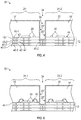
- FIG. 2A illustrates a module having two sub-modules, which are covered by an overmold body according to embodiments disclosed herein.
- FIG. 2B illustrates a cross-section of the module of FIG. 2A in which an integrated electromagnetic shield is provided according to embodiments disclosed herein.
- FIG. 3A is a top view of a meta-module at a certain state of fabrication according to embodiments disclosed herein.
- FIG. 3B is a top view of the meta-module of FIG. 3A at a subsequent state of fabrication after an overmold material has been applied to component areas of the meta-module.
- FIG. 3C is a top view of the meta-module of FIG. 3B at a subsequent state of fabrication where a plurality of overmold bodies are formed from the overmold material of FIG. 3B .
- FIG. 3D is a top view of the meta-module of FIG. 3C at a subsequent state of fabrication after an electromagnetic shield has been blanket deposited over sub-modules of the meta-module.
- FIG. 3E is a top view of two modules that have been singulated from the meta-module of FIG. 3D .
- FIG. 4 is a cross-sectional view of a representative module according to embodiments disclosed herein.
- FIG. 5 is a cross-sectional view of an alternative configuration of the module of FIG. 4 where one or more of the electronic components comprise wirebond connections.
- FIG. 6 is a cross-sectional view of a module where a perimeter sidewall of an electromagnetic shield is configured to extend into a substrate according to embodiments disclosed herein.
- FIG. 7 is a cross-sectional view of a module where one or more perimeter sidewalls of an electromagnetic shield extend below a mounting surface of a substrate and one or more divider walls of the electromagnetic shield extend to the mounting surface according to embodiments disclosed herein.
- FIG. 8 is a cross-sectional view of a module where one or more perimeter sidewalls and one or more divider walls of an electromagnetic shield extend below a mounting surface of a substrate to a same horizontal plane within the substrate according to embodiments disclosed herein.
- FIG. 9 is a cross-sectional view of a module where a fill material is applied in an opening that is formed between sub-modules of the module according to embodiments disclosed herein.
- FIG. 10A is a cross-sectional view of a module where a plurality of openings and a plurality of divider walls of an electromagnetic shield are configured between sub-modules of the module according to embodiments disclosed herein.
- FIG. 10B is a cross-sectional view of the module of FIG. 10A where the plurality of openings are filled with the fill material of FIG. 9 .
- the present disclosure relates to electromagnetic shields for electronic devices, and particularly to electromagnetic shields for sub-modules of electronic modules.
- Electronic modules as disclosed herein may include multiple sub-modules arranged on a substrate with an electromagnetic shield arranged to conformally cover the sub-modules as well as portions of the substrate that are uncovered by the sub-modules.
- Electromagnetic shields are disclosed that are configured to extend between sub-modules to form one or more divider walls.
- the one or more divider walls are configured to extend into the substrate to provide improved reduction of electromagnetic interference (EMI) or crosstalk between the sub-modules.
- EMI electromagnetic interference
- various electromagnetic shields may further form perimeter sidewalls that also extend into their corresponding substrates to provide improved reduction of EMI from other modules or other external sources.
- the present invention may be used to form one or more electromagnetic shields for corresponding component areas of a given electronic module.
- a meta-module having circuitry for two or more modules is formed on a substrate structure, which may include a laminated substrate structure.
- the circuitry for different modules is initially formed on the single meta-module.
- Each module will have one or more component areas in which the circuitry is formed.
- a metallic structure is formed on or in the substrate for each component area to be shielded on the substrate.
- the metallic structure may be formed from traces, vias, metallic layers, metallic components, plating materials, or the like, as well as any combination thereof. In one embodiment, each metallic structure extends about all or a portion of the periphery of each of the component areas to be shielded.
- a single body such as an overmold body, is then formed over all of the modules on the meta-module.
- the body is formed, at least a portion of the metallic structure for each component area to be shielded is exposed through the body by a cutting, drilling, or like operation.
- an electromagnetic shield material is applied to an exterior surface of the body of each of the component areas to be shielded and in contact with the exposed portion of the metallic structures.
- the modules are then singulated from each other to form separate modules, each of which having one or more integrally shielded component areas.
- the electromagnetic shield material is provided using an electroless plating process, which deposits a conductive seed layer on the overmold body and in contact with the exposed portions of the metallic structures. Then, an electrolytic plating process is used to deposit a second conductive layer onto the conductive seed layer. A final layer of a metallic material, such as nickel, is then deposited on top of the second conductive layer through an electrolytic plating process.
- the electromagnetic shield is provided by applying a conductive epoxy or paint to the body and in contact with the exposed portion of the metallic structures.
- the electromagnetic shield may be provided by metallized thin film-based processes, such as, for example physical vapor deposition, sputtering, evaporation, chemical vapor deposition, and/or atomic layer deposition, among others.
- the conductive layers create an integrated electromagnetic shield for one or more component areas of a module to reduce electromagnetic interference (EMI).
- EMI electromagnetic interference
- the metallic structure in the preferred embodiments is formed in whole or in part from a metallic layer grid that resides on or in the surface of the substrate. Further, the metallic structure resides along all or a portion of the periphery of one or more component areas. These embodiments lend themselves to efficient processing; however, those skilled in the art will recognize that the metallic structure to which the integrated electromagnetic shield is connected need not reside along the periphery of the component area, or be part of a metallic layer grid. Importantly, the metallic structure may take virtually any form or shape, and may reside on or in the top surface of the substrate.
- the metallic structure may merely be a single point along the top surface of the module, as well as a continuous or segmented structure that extends along all or a portion of the one or more component areas to be shielded. Accordingly, the metallic layer grid used in the following embodiments to provide a metallic structure is merely provided to illustrate the preferred embodiments, and as such, shall not limit what constitutes a metallic structure or how a metallic structure is formed according to the present invention.
- a module 10 is illustrated in FIG. 1A and FIG. 1B according to certain embodiments of the present invention.
- the module 10 has a substrate 12 , which may include a laminate structure that comprises a metallic structure formed from a metallic layer grid 14 on or in a top surface of the substrate 12 .
- the substrate 12 may comprise an epoxy laminate, such as FR-4 and the like.
- the substrate 12 may also be formed from other materials including ceramics and/or alumina.
- any metallic structure may be used; however, the preferred embodiment uses a portion of the metallic layer grid 14 to form a peripheral metallic structure. Only one section of the metallic layer grid 14 is depicted in these figures and the peripheral metallic structure is not separately labeled, as it is formed from the metallic layer grid 14 .
- the illustrated module 10 has a single component area 16 that lies within the peripheral metallic structure and in which circuitry for the module 10 is formed.
- the component area 16 may include one or more electronic components of various types depending on the application.
- the electronic components may include an electronic circuit built on its own semiconductor substrate, such as a processor, volatile memory, non-volatile memory, a radio frequency circuit, or a micro-mechanical system (MEMS) device.
- MEMS micro-mechanical system
- electronic components may include one or more electrical devices such as filters, capacitors, inductors, resistors, amplifiers, low-noise amplifiers (LNA), switching devices, transmit/receive modules, or electronic circuits having combinations thereof.
- electrical devices such as filters, capacitors, inductors, resistors, amplifiers, low-noise amplifiers (LNA), switching devices, transmit/receive modules, or electronic circuits having combinations thereof.
- a body such as an overmold body 18 or overmold material, which is formed from a dielectric material, resides over the substrate 12 and encompasses the component area 16 .
- an electromagnetic shield 20 is integrally formed over the overmold body 18 and in contact with exposed portions of the peripheral metallic structure of the metallic layer grid 14 to provide shielding from electromagnetic emissions.
- the peripheral metallic structure of the metallic layer grid 14 is coupled to ground and accordingly, the electromagnetic shield 20 is electrically grounded. In this manner, electromagnetic emissions that strike the electromagnetic shield 20 are electrically shorted to ground, thereby reducing EMI.
- a given module 10 may include any number of component areas 16 where one or more of the component areas 16 have a corresponding electromagnetic shield 20 . As illustrated in FIGS. 2A and 2B , two component areas 16 A and 16 B are positioned in the metallic layer grid 14 such that a peripheral metallic structure is provided for each of the component areas 16 A and 16 B. In certain instances, peripheral metallic structures for adjacent component areas 16 A and 16 B may share a common section of the metallic layer grid 14 .
- the illustrated module 10 has two component areas 16 A and 16 B, which lie within corresponding peripheral metallic structures and in which circuitry (not illustrated) for the module 10 is formed.
- Overmold bodies 18 reside over the substrate 12 and encompass the respective component areas 16 A and 16 B.
- one or more electromagnetic shields 20 are integrally formed over the overmold bodies 18 and in contact with exposed portions of the respective peripheral metallic structures of the metallic layer grid 14 .
- the one or more electromagnetic shields 20 encompass both component areas 16 A and 16 B and further extend between the component areas 16 A and 16 B. In the manner, EMI from outside sources and EMI between the component areas 16 A and 16 B may be reduced.
- the module 10 is configured to include multiple sub-modules, each of which includes one of the component areas 16 A or 16 B as well as the corresponding overmold body 18 and the corresponding electromagnetic shield 20 or a portion of the electromagnetic shield 20 .
- FIG. 3A is a top view of a meta-module 22 at a certain state of fabrication according to embodiments disclosed herein.
- the meta-module 22 includes a plurality of components areas 16 A and 16 B mounted on a substrate 12 to form an array. Each of the component areas 16 A and 16 B are arranged to form a different area for a plurality of sub-modules 24 .
- One or more electronic components 26 as previously described may be mounted or otherwise arranged within each of the component areas 16 A and 16 B.
- the substrate 12 may comprise a strip or an otherwise larger form of a laminate structure.
- a plurality of fiducials 28 are arranged along a perimeter of the substrate 12 and outside of the plurality of sub-modules 24 .
- Fiducials 28 have many uses in the electronics industry, including the indication of mounting locations for various electronic components or to indicate the locations of separation lines for electronic components or electronic modules during fabrication.
- the fiducials 28 are arranged to indicate the location of boundaries of each sub-module 24 .
- groups of sub-modules 24 may form modules and the fiducials 28 may be arranged to indicate dicing lines for singulation of the modules.
- FIG. 3B is a top view of the meta-module 22 of FIG. 3A at a subsequent state of fabrication after an overmold material 18 has been applied to the component areas 16 A and 16 B.
- the overmold material 18 may be blanket deposited or otherwise formed over the substrate 12 to cover each of the component areas 16 A and 16 B.
- the overmold material 18 may comprise one or more insulating or dielectric materials.
- the overmold material 18 may be configured to provide encapsulation and electrical isolation for the electronic components 26 that are mounted to the component areas 16 A and 16 B of the substrate 12 .
- FIG. 3C is a top view of the meta-module 22 of FIG. 3B at a subsequent state of fabrication where a plurality of overmold bodies 18 ′ are formed from the overmold material 18 of FIG. 3B .
- a plurality of first separation lines 30 are illustrated that define locations where a plurality of modules 32 will later be divided or singulated from the meta-module 22 .
- a plurality of second separation lines 34 are illustrated that define locations for the sub-modules 24 within each of the modules 32 after singulation. For simplicity, only a few of the first separation lines 30 and the second separation lines 34 are illustrated. It is understood that in practice, the first separation lines 30 and the second separation lines 34 may be arranged across all of the meta-module 22 .
- the first separation lines 30 and the second separation lines 34 indicate lines where portions of the overmold material ( 18 of FIG. 3B ) are subjected to a removal process.
- the removal process may include one or more of cutting, drilling, etching, or the like along each of the first separation lines 30 and the second separation lines 34 .
- the removal process may be referred to as sub-dicing as individual modules 32 are not yet separated from the meta-module 22 .
- the removal process may be performed in one or more steps along the first separation lines 30 and the second separation lines 34 .
- a sub-dicing process may be performed sequentially in rows and columns across the meta-module 22 that alternates between the first separation lines 30 and the second separation lines 34 .
- a first sub-dicing step may remove material along one of the first or second separation lines 30 , 34
- a second sub-dicing step may remove material along the other of the first or second separation lines 30 , 34 .
- each sub-module 24 includes one or more of the electronic components 26 and a separate overmold body 18 ′ that is formed from the overmold material ( 18 of FIG. 3B ). Additionally, openings that are formed along the first separation lines 30 and the second separation lines 34 may expose portions of the metallic layer grid ( 14 of FIG. 2B ) that are electrically connected to ground. While two sub-modules 24 are illustrated for each module 32 , the first separation lines 30 and the second separation lines 34 may be configured in different locations to provide different numbers of sub-modules 24 for each module 32 according to embodiments disclosed herein.
- exposed surfaces of the overmold bodies 18 ′ may be cleaned, such as by a plasma cleaning process, to remove wax or other organic compounds and materials that remain on the surface of each overmold body 18 ′.
- the plasma cleaning process subjects the surface of each overmold body 18 ′ to a reactive process gas, such as argon (Ar), oxygen (O), nitrogen (N), hydrogen (H), carbon tetrafluoride (CF 4 ), sulfur hexafluoride (SF 6 ), nitrogen tri-fluoride (NF 3 ), or the like, which effectively etches away contaminants on the exposed surface of each overmold body 18 ′.
- a reactive process gas such as argon (Ar), oxygen (O), nitrogen (N), hydrogen (H), carbon tetrafluoride (CF 4 ), sulfur hexafluoride (SF 6 ), nitrogen tri-fluoride (NF 3 ), or the like, which effectively etches away contaminants on the exposed surface of each overmold body 18 ′.
- each overmold body 18 ′ for each sub-module 24 may be roughened through an abrasion process, a desmear technique, or like process.
- a chemical roughening process is provided.
- a mask (not shown) may be positioned on the underside of the substrate 12 so that the processes described in the steps below do not interfere with any electrical contacts (not shown) that may be present on the bottom side of each sub-module 24 .
- the mask helps prevent liquids and gases from reaching these electrical contacts, which may act as input/output contacts for the modules 32 .
- a seal structure may be employed.
- FIG. 3D is a top view of the meta-module 22 of FIG. 3C at a subsequent state of fabrication after the electromagnetic shield 20 has been blanket deposited over the sub-modules 24 .
- the electromagnetic shield 20 is deposited to conformally coat the plurality of sub-modules 24 .
- the electromagnetic shield 20 may be configured to be conformal on top surfaces and sidewalls of each overmold body 18 ′ of each sub-module 24 as well as on portions of the substrate 12 that are between the sub-modules 24 .
- the electromagnetic shield 20 may be deposited as one or more layers of metal that are electrically grounded by way of exposed portions of the metallic layer grid ( 14 of FIG. 2B ) between each of the overmold bodies 18 ′.
- the electromagnetic shield 20 may comprise a single layer or a plurality of layers.
- the electromagnetic shield 20 may comprise a first layer comprising a seed layer followed by one or more additional layers.
- the seed layer may comprise a conductive material such as copper (Cu), aluminum (Al), silver (Ag), gold (Au), or combinations thereof deposited by electroless plating or the like.
- a second layer may be subsequently formed on the seed layer comprising a metal such as Cu, Al, Ag, Au, or combinations thereof deposited by electrolytic plating or the like, followed by a third layer formed on the second layer, wherein the third layer comprises a less conductive material, such as nickel (Ni) or other metals, than the seed layer or the first layer.
- the third layer may also be formed by electrolytic plating.
- the third layer may be provided to protect the seed layer and the first layer from tarnishing, corrosion, or other environmental effects. Likewise, the third layer may contribute to shielding by absorbing some electromagnetic radiation.
- the electromagnetic shield 20 may be formed with an approximate thickness in a range from about 10 microns ( ⁇ m) to about 50 ⁇ m. Greater or lesser thicknesses may also be generated. For example, in certain embodiments, the thickness of the electromagnetic shield 20 may be reduced to a range from about 5 ⁇ m to about 10 ⁇ m. In certain embodiments, the electromagnetic shield 20 may be referred to as a microshield.
- FIG. 3E is a top view of two modules 32 that have been singulated from the meta-module 22 of FIG. 3D .
- singulation includes dicing, sawing, or otherwise separating the substrate ( 12 of FIG. 3C ) along the plurality of first separation lines ( 30 of FIG. 3C ).
- each module 32 may comprise a plurality of the sub-modules 24 , and each sub-module 24 may include one or more of the electronic components 26 and an overmold body 18 ′.
- Each module 32 further includes an electromagnetic shield 20 that is arranged to cover each sub-module 24 as well as portions of the substrate 12 that are uncovered by each sub-module 24 . In this manner, each sub-module 24 is shielded from the other sub-module 24 as well as from external sources.
- FIG. 4 is a cross-sectional view of a representative module 36 according to embodiments disclosed herein.
- the module 36 includes a first sub-module 24 - 1 and a second sub-module 24 - 2 , although other numbers of sub-modules are possible without deviating from the present disclosure.
- the first and second sub-modules 24 - 1 , 24 - 2 may each comprise one or more electronic components 26 mounted on the substrate 12 that are within a corresponding overmold body 18 ′.
- the module 36 further includes the electromagnetic shield 20 that is conformal over each of the sub-modules 24 - 1 , 24 - 2 .
- the electromagnetic shield 20 conformally covers the overmold bodies 18 ′ of each sub-module 24 - 1 , 24 - 2 as well as an opening 38 that is formed between the sub-modules 24 - 1 , 24 - 2 during the removal process of the overmold material ( 18 of FIG. 3B ) performed along the second separation line 34 .
- the substrate 12 may comprise a laminate structure that includes one or more metal layers 40 - 1 to 40 - 3 and one or more dielectric layers 42 - 1 to 42 - 3 .
- One or more vias 43 may also be provided to provide electrical connections between different ones of the metal layers 40 - 1 to 40 - 3 .
- the substrate 12 may comprise a printed circuit board where the one or more metal layers 40 - 1 to 40 - 3 are laminated in an alternating configuration with the one or more dielectric layers 42 - 1 to 42 - 3 . While three metal layers 40 - 1 to 40 - 3 are illustrated, the substrate 12 may be configured with any number of metal layers. Generally, increasing the number of laminated metal layers corresponds to an increased number of electronic components that may be mounted and electrically connected on a particular laminate structure. This allows electrical connections to various electronic components 26 to be made at different horizontal planes within the substrate 12 .
- the one or more metal layers 40 - 1 to 40 - 3 may include Cu, copper foil, or the like while the one or more dielectric layers 42 - 1 to 42 - 3 may include fiber materials, glass, epoxy, glass-reinforced epoxy, ceramic materials, polymer materials and combinations thereof.
- Each of the metal layers 40 - 1 to 40 - 3 may comprise a pattern of continuous portions and discontinuous portions along the substrate 12 .
- certain ones of the electronic components 26 are mounted to different portions of the first metal layer 40 - 1 on a mounting surface 44 of the substrate 12 .
- one or more of the electronic components 26 may be flip-chip mounted on the mounting surface 44 .
- the opening 38 is configured to extend into the substrate 12 through the first metal layer 40 - 1 and the first dielectric layer 42 - 1 .
- the electromagnetic shield 20 is arranged on the first sub-module 24 - 1 and the second sub-module 24 - 2 , and a portion of the electromagnetic shield 20 is configured to extend between the first sub-module 24 - 1 and the second sub-module 24 - 2 to form one or more divider walls 20 ′ that extend below the mounting surface 44 .
- two divider walls 20 ′ may be formed in the opening 38 where each of the divider walls 20 ′ is conformal with one of the overmold bodies 18 ′.
- the electromagnetic shield 20 is configured to extend through the first metal layer 40 - 1 and the first dielectric layer 42 - 1 to contact and electrically connect with a portion of the second metal layer 40 - 2 that is electrically connected to ground.
- the opening 38 between the sub-modules 24 - 1 , 24 - 2 is formed by a removal process along the second separation line 34 .
- a width of the opening 38 measured as a distance from the first sub-module 24 - 1 to the second sub-module 24 - 2 may include a range from about 0.1 millimeters (mm) to about 3 mm, depending on the application and the removal process used to fabricate the opening 38 .
- sawing with a saw blade of a particular width may provide an opening 38 with a width that is at least equal to the width of the saw blade.
- FIG. 5 is a cross-sectional view of an alternative configuration of the module 36 of FIG. 4 where one or more of the electronic components 26 comprise wirebond connections 46 .
- the module 36 includes the first sub-module 24 - 1 and the second sub-module 24 - 2 on the substrate 12 , as well as the electromagnetic shield 20 as previously described.
- the wirebond connections 46 are configured to extend between corresponding ones of the electronic components 26 and corresponding portions of the first metal layer 40 - 1 . As illustrated, the wirebond connections 46 at least partially extend into the overmold bodies 18 ′. In this regard, the wirebond connections 46 are formed prior to the overmold bodies 18 ′ such that the overmold bodies 18 ′ provide electrical insulation and mechanical support for the wirebond connections 46 .
- wirebond connections 46 are often used in applications with higher power requirements.
- the wirebond connections 46 may provide electrical connection, thermal connection, or both between the electronic components 26 and the substrate 12 .
- the wirebond connections 46 can act as miniature antennas that facilitate undesirable leakage or interference of signals from the first sub-module 24 - 1 to the second sub-module 24 - 2 .
- the electromagnetic shield 20 including the divider walls 20 ′ are arranged to reduce or prevent such crosstalk or EMI between the sub-modules 24 - 1 , 24 - 2 with the wirebond connections 46 .
- wirebond connections 46 and flip-chip mounting of different ones of the electronic components 26 may be provided in the same sub-module 24 - 1 , 24 - 2 or module 36 .
- FIG. 6 is a cross-sectional view of a module 48 where a perimeter sidewall 20 ′′ of the electromagnetic shield 20 is configured to extend into the substrate 12 according to embodiments disclosed herein.
- the module 48 includes the first sub-module 24 - 1 and the second sub-module 24 - 2 on the substrate 12 , as well as the electromagnetic shield 20 as previously described.
- the overmold body 18 ′ for each sub-module 24 - 1 , 24 - 2 is formed by the plurality of first separation lines 30 that define perimeter borders of the module 48 and the plurality of second separation lines 34 that define each of the sub-modules 24 - 1 , 24 - 2 .
- a portion of the electromagnetic shield 20 is configured to extend between the first sub-module 24 - 1 and the second sub-module 24 - 2 to form the one or more divider walls 20 ′ that extend below the mounting surface 44 as previously described.
- the electromagnetic shield 20 forms one or more perimeter sidewalls 20 ′′ that surround the sub-modules 24 - 1 , 24 - 2 along a perimeter of the module 48 .
- at least one perimeter sidewall 20 ′′ is configured to extend into a perimeter portion of the substrate 12 .
- the substrate 12 may comprise a laminate structure that includes the one or more metal layers 40 - 1 to 40 - 3 and the one or more dielectric layers 42 - 1 to 42 - 3 .
- At least one perimeter sidewall 20 ′′ of the electromagnetic shield 20 is configured to extend below the mounting surface 44 where the one or more electronic components 26 are mounted to the substrate 12 .
- at least one of the perimeter sidewalls 20 ′′ is configured to extend through the first metal layer 40 - 1 , the first dielectric layer 42 - 1 , the second metal layer 40 - 2 , and the second dielectric layer 42 - 2 to contact a portion of the third metal layer 40 - 3 that is electrically connected to ground.
- the perimeter sidewalls 20 ′′ are grounded such that electromagnetic emissions that strike the perimeter sidewalls 20 ′′ are electrically shorted to ground.
- the electronic components 26 may be further surrounded by the electromagnetic shield 20 to provide further reduction in EMI.
- one or more of the perimeter sidewalls 20 ′′ and one or more of the divider walls 20 ′ are configured to extend below the mounting surface 44 .
- One or more of the perimeter sidewalls 20 ′′ and one or more of the divider walls 20 ′ may be configured to extend to different horizontal planes within the substrate 12 depending on the application.
- the divider walls 20 ′ are configured to extend to a horizontal plane defined by the second metal layer 40 - 2 while the perimeter sidewalls 20 ′′ are configured to extend to a different horizontal plane that is defined by the third metal layer 40 - 3 .
- the different horizontal planes may be defined by different metal layers of the substrate 12 without deviating from the present disclosure.
- FIG. 7 is a cross-sectional view of a module 50 where one or more perimeter sidewalls 20 ′′ of the electromagnetic shield 20 extend below the mounting surface 44 of the substrate 12 , and one or more divider walls 20 ′ of the electromagnetic shield 20 extend to the mounting surface 44 .
- the module 50 includes the first sub-module 24 - 1 and the second sub-module 24 - 2 on the substrate 12 , as well as the electromagnetic shield 20 as previously described.
- Each of the sub-modules 24 - 1 , 24 - 2 may include one or more of the electronic components 26 that are mounted to the mounting surface 44 of the substrate 12 .
- the substrate 12 may comprise a laminate structure that includes the one or more metal layers 40 - 1 to 40 - 3 and the one or more dielectric layers 42 - 1 to 42 - 3 as previously described.
- one or more of the perimeter sidewalls 20 ′′ and one or more of the divider walls 20 ′ of FIG. 7 are configured to extend to different horizontal planes of the substrate 12 .
- the perimeter sidewalls 20 ′′ are configured to extend through the first metal layer 40 - 1 , the first dielectric layer 42 - 1 , the second metal layer 40 - 2 , and the second dielectric layer 42 - 2 to contact a portion of the third metal layer 40 - 3 that is electrically connected to ground.
- the divider walls 20 ′ are configured to extend between the sub-modules 24 - 1 , 24 - 2 to a portion of the first metal layer 40 - 1 that is at the mounting surface 44 of the substrate 12 .
- a portion of the first metal layer 40 - 1 in contact with the divider walls 20 ′ may also be electrically connected to ground. In this manner, the divider walls 20 ′ may not be configured to extend into the substrate 12 for certain applications.
- FIG. 8 is a cross-sectional view of a module 52 where one or more perimeter sidewalls 20 ′′ and one or more divider walls 20 ′ of the electromagnetic shield 20 extend below the mounting surface 44 of the substrate 12 to the a same horizontal plane within the substrate 12 .
- the module 52 includes the first sub-module 24 - 1 and the second sub-module 24 - 2 on the substrate 12 , as well as the electromagnetic shield 20 as previously described.
- Each of the sub-modules 24 - 1 , 24 - 2 may include one or more of the electronic components 26 that are mounted to the mounting surface 44 of the substrate 12 .
- the substrate 12 may comprise a laminate structure that includes the one or more metal layers 40 - 1 to 40 - 3 and the one or more dielectric layers 42 - 1 to 42 - 3 as previously described.
- the perimeter sidewalls 20 ′′ and the divider walls 20 ′ are configured to extend through the first metal layer 40 - 1 , the first dielectric layer 42 - 1 , the second metal layer 40 - 2 , and the second dielectric layer 42 - 2 to contact portions of the third metal layer 40 - 3 that are electrically connected to ground.
- the perimeter sidewalls 20 ′′ and the divider walls 20 ′ may extend through the substrate 12 to a same horizontal plane that is within the substrate 12 .
- the same horizontal plane is defined by the third metal layer 40 - 3 .
- the perimeter sidewalls 20 ′′ and the divider walls 20 ′ may extend to a same horizontal plane that is defined by other metal layers (e.g., 40 - 2 ) of the substrate 12 .
- FIG. 9 is a cross-sectional view of a module 54 where a fill material 56 is applied in the opening 38 that is formed between the sub-modules 24 - 1 , 24 - 2 according to embodiments disclosed herein.
- the module 54 includes the first sub-module 24 - 1 and the second sub-module 24 - 2 on the substrate 12 , as well as the electromagnetic shield 20 as previously described.
- Each of the sub-modules 24 - 1 , 24 - 2 may include one or more of the electronic components 26 that are mounted on the mounting surface 44 of the substrate 12 .
- the electromagnetic shield 20 is arranged to conformally coat the overmold body 18 ′ of each sub-module 24 - 1 , 24 - 2 as well as portions of the substrate 12 that are between and uncovered by the sub-modules 24 - 1 , 24 - 2 .
- the fill material 56 may be arranged in the opening 38 between each sub-module 24 - 1 , 24 - 2 to provide structural support. In this manner, the fill material 56 may be arranged on the portion of the electromagnetic shield 20 that is in the opening 38 and along one or more portions of the divider walls 20 ′ of the electromagnetic shield 20 .
- the fill material 56 is configured to partially, but not fully fill the opening 38 and in other embodiments, the fill material 56 may completely fill the opening 38 .
- the fill material 56 may comprise one or more of an epoxy, a mold compound, and a thermoset material, among others.
- the fill material 56 comprises one or more insulating or dielectric materials.
- the fill material 56 may comprise the same material as the overmold bodies 18 ′ of each sub-module 24 - 1 , 24 - 2 .
- the fill material 56 may be formed by dispensing, molding, transfer molding, or compression molding techniques, among others.
- the fill material 56 may comprise a conductive material, such as conductive epoxy, or one or more metallized layers (not shown) formed by various plating or deposition techniques. In embodiments where the divider walls 20 ′ of the electromagnetic shield 20 extend below the mounting surface 44 of the substrate 12 , the fill material 56 may also extend below the mounting surface 44 .
- FIG. 10A is a cross-sectional view of a module 58 where a plurality of openings 38 - 1 , 38 - 2 , as well as a plurality of divider walls 20 ′- 1 to 20 ′- 4 of the electromagnetic shield 20 are configured between the sub-modules 24 - 1 , 24 - 2 according to embodiments disclosed herein.
- the module 58 includes the first sub-module 24 - 1 and the second sub-module 24 - 2 on the substrate 12 , as well as the electromagnetic shield 20 as previously described.
- Each of the sub-modules 24 - 1 , 24 - 2 may include one or more of the electronic components 26 that are mounted on the mounting surface 44 of the substrate 12 .
- FIG. 10A is a cross-sectional view of a module 58 where a plurality of openings 38 - 1 , 38 - 2 , as well as a plurality of divider walls 20 ′- 1 to 20 ′- 4 of the electromagnetic shield 20 are configured between the sub-
- the plurality of openings 38 - 1 , 38 - 2 are formed between the first sub-module 24 - 1 and the second sub-module 24 - 2 .
- the plurality of openings 38 - 1 , 38 - 2 may be formed by performing multiple removal processes that are adjacent to one another along the second separation line 34 .
- a fabrication technique may comprise passing a narrow blade saw to cut two adjacent portions of the overmold material ( 18 of FIG. 3B ) along the second separation line 34 between each of the sub-modules 24 - 1 , 24 - 2 . In this manner, the plurality of openings 38 - 1 , 38 - 2 are formed between the first and second sub-modules 24 - 1 , 24 - 2 .
- another overmold body 18 ′′ may thereby be formed between the plurality of openings 38 - 1 , 38 - 2 and between the sub-modules 24 - 1 , 24 - 2 .
- the electromagnetic shield 20 may be configured to conformally coat the overmold bodies 18 ′ of each sub-module 24 - 1 , 24 - 2 as well as the overmold body 18 ′′ that is arranged between the sub-modules 24 - 1 , 24 - 2 . In this manner, the electromagnetic shield 20 may form the plurality of divider walls 20 ′- 1 to 20 ′- 4 between the sub-modules 24 - 1 , 24 - 2 .
- the plurality of divider walls 20 ′- 1 to 20 ′- 4 may extend into the substrate 12 and below the mounting surface 44 of the substrate 12 in any of the configurations previously described.
- FIG. 10B is a cross-sectional view of the module 58 of FIG. 10A where the plurality of openings 38 - 1 to 38 - 2 are filled with the fill material 56 of FIG. 9 .
- the fill material 56 may be applied to partially or completely fill the plurality of openings 38 - 1 to 38 - 2 between each of the sub-modules 24 - 1 , 24 - 2 to provide structural support for the sub-modules 24 - 1 , 24 - 2 as well as the overmold body 18 ′′ that is arranged between the sub-modules 24 - 1 , 24 - 2 .
- the fill material 56 may be arranged to partially or completely extend along each of the plurality of divider walls 20 ′- 1 to 20 ′- 4 of the electromagnetic shield 20 .
- the fill material 56 in each of the openings 38 - 1 , 38 - 2 may also extend below the mounting surface 44 .
Abstract
Description
Claims (18)
Priority Applications (2)
| Application Number | Priority Date | Filing Date | Title |
|---|---|---|---|
| US16/390,761 US11219144B2 (en) | 2018-06-28 | 2019-04-22 | Electromagnetic shields for sub-modules |
| US16/893,941 US11058038B2 (en) | 2018-06-28 | 2020-06-05 | Electromagnetic shields for sub-modules |
Applications Claiming Priority (2)
| Application Number | Priority Date | Filing Date | Title |
|---|---|---|---|
| US201862691440P | 2018-06-28 | 2018-06-28 | |
| US16/390,761 US11219144B2 (en) | 2018-06-28 | 2019-04-22 | Electromagnetic shields for sub-modules |
Related Child Applications (1)
| Application Number | Title | Priority Date | Filing Date |
|---|---|---|---|
| US16/893,941 Division US11058038B2 (en) | 2018-06-28 | 2020-06-05 | Electromagnetic shields for sub-modules |
Publications (2)
| Publication Number | Publication Date |
|---|---|
| US20200008327A1 US20200008327A1 (en) | 2020-01-02 |
| US11219144B2 true US11219144B2 (en) | 2022-01-04 |
Family
ID=69008502
Family Applications (2)
| Application Number | Title | Priority Date | Filing Date |
|---|---|---|---|
| US16/390,761 Active US11219144B2 (en) | 2018-06-28 | 2019-04-22 | Electromagnetic shields for sub-modules |
| US16/893,941 Active US11058038B2 (en) | 2018-06-28 | 2020-06-05 | Electromagnetic shields for sub-modules |
Family Applications After (1)
| Application Number | Title | Priority Date | Filing Date |
|---|---|---|---|
| US16/893,941 Active US11058038B2 (en) | 2018-06-28 | 2020-06-05 | Electromagnetic shields for sub-modules |
Country Status (1)
| Country | Link |
|---|---|
| US (2) | US11219144B2 (en) |
Families Citing this family (5)
| Publication number | Priority date | Publication date | Assignee | Title |
|---|---|---|---|---|
| US11127689B2 (en) | 2018-06-01 | 2021-09-21 | Qorvo Us, Inc. | Segmented shielding using wirebonds |
| US11219144B2 (en) | 2018-06-28 | 2022-01-04 | Qorvo Us, Inc. | Electromagnetic shields for sub-modules |
| US11114363B2 (en) | 2018-12-20 | 2021-09-07 | Qorvo Us, Inc. | Electronic package arrangements and related methods |
| TWI727832B (en) * | 2020-06-17 | 2021-05-11 | 海華科技股份有限公司 | Wireless communication device |
| CN218514572U (en) * | 2022-07-13 | 2023-02-21 | 荣耀终端有限公司 | Circuit board, circuit board assembly and electronic equipment |
Citations (207)
| Publication number | Priority date | Publication date | Assignee | Title |
|---|---|---|---|---|
| US3566190A (en) | 1968-12-23 | 1971-02-23 | Raven Ind Inc | Industrial control system with means for releasably securing a plurality of electronic modules |
| US3907616A (en) | 1972-11-15 | 1975-09-23 | Texas Instruments Inc | Method of forming doped dielectric layers utilizing reactive plasma deposition |
| US3907617A (en) | 1971-10-22 | 1975-09-23 | Motorola Inc | Manufacture of a high voltage Schottky barrier device |
| US4680676A (en) | 1986-01-06 | 1987-07-14 | Motorola, Inc. | Portable radio housing with logic and RF shielding |
| US5329695A (en) | 1992-09-01 | 1994-07-19 | Rogers Corporation | Method of manufacturing a multilayer circuit board |
| US5389738A (en) | 1992-05-04 | 1995-02-14 | Motorola, Inc. | Tamperproof arrangement for an integrated circuit device |
| US5436203A (en) | 1994-07-05 | 1995-07-25 | Motorola, Inc. | Shielded liquid encapsulated semiconductor device and method for making the same |
| US5459368A (en) | 1993-08-06 | 1995-10-17 | Matsushita Electric Industrial Co., Ltd. | Surface acoustic wave device mounted module |
| US5473512A (en) | 1993-12-16 | 1995-12-05 | At&T Corp. | Electronic device package having electronic device boonded, at a localized region thereof, to circuit board |
| US5592391A (en) | 1993-03-05 | 1997-01-07 | International Business Machines Corporation | Faraday cage for a printed circuit card |
| US5623293A (en) | 1993-05-28 | 1997-04-22 | Brother Kogyo Kabushiki Kaisha | Contact electrode connector |
| US5639989A (en) | 1994-04-19 | 1997-06-17 | Motorola Inc. | Shielded electronic component assembly and method for making the same |
| US5646828A (en) | 1995-02-24 | 1997-07-08 | Lucent Technologies Inc. | Thin packaging of multi-chip modules with enhanced thermal/power management |
| US5650659A (en) | 1995-08-04 | 1997-07-22 | National Semiconductor Corporation | Semiconductor component package assembly including an integral RF/EMI shield |
| US5870289A (en) | 1994-12-15 | 1999-02-09 | Hitachi, Ltd. | Chip connection structure having diret through-hole connections through adhesive film and wiring substrate |
| JPH11163583A (en) | 1997-11-25 | 1999-06-18 | Citizen Electronics Co Ltd | Package for electronic parts and manufacture of the same |
| US5977626A (en) | 1998-08-12 | 1999-11-02 | Industrial Technology Research Institute | Thermally and electrically enhanced PBGA package |
| US6004180A (en) | 1997-09-30 | 1999-12-21 | Candescent Technologies Corporation | Cleaning of electron-emissive elements |
| US6011698A (en) | 1996-11-12 | 2000-01-04 | Delco Electronics Corp. | Circuit protection from radio frequency energy |
| WO2000035085A1 (en) | 1998-12-08 | 2000-06-15 | Thomson-Csf | Encapsulated surface wave component and collective method for making same |
| US6137693A (en) | 1998-07-31 | 2000-10-24 | Agilent Technologies Inc. | High-frequency electronic package with arbitrarily-shaped interconnects and integral shielding |
| US6150193A (en) | 1996-10-31 | 2000-11-21 | Amkor Technology, Inc. | RF shielded device |
| US6163454A (en) | 1999-02-22 | 2000-12-19 | Hewlett-Packard Company | Electromagnetic interference (EMI) shield for electrical components, an internal EMI barrier, and a storage enclosure for electrical/electronic components |
| US6297957B1 (en) | 1999-12-20 | 2001-10-02 | Dell Usa, L.P. | Apparatus for reducing electromagnetic emissions from a computer |
| US20020036345A1 (en) | 2000-09-27 | 2002-03-28 | Kabushiki Kaisha Toshiba | High frequency flip chip module and assembling method thereof |
| US6429386B2 (en) | 1998-12-30 | 2002-08-06 | Ncr Corporation | Imbedded die-scale interconnect for ultra-high speed digital communications |
| US20020118529A1 (en) | 2001-02-27 | 2002-08-29 | Andre Babin | System and method for shielding electronic components |
| US6448793B1 (en) | 2000-04-07 | 2002-09-10 | Rf Micro Devices, Inc. | Adaptive manufacturing of semiconductor circuits |
| US6448583B1 (en) | 1998-09-08 | 2002-09-10 | Fujitsu Limited | Optical semiconductor module, its manufacture, reflection film, its manufacture, and laser and optical devices using reflection film |
| US20020142516A1 (en) | 2001-03-07 | 2002-10-03 | David Light | Methods of bonding microelectronic elements |
| US6466416B1 (en) | 1999-08-11 | 2002-10-15 | Nec Corporation | Magnetic head, method for making the same and magnetic recording/reproducing device using the same |
| US20030011049A1 (en) | 2001-07-12 | 2003-01-16 | Custom One Design, Inc. | Interconnect circuitry, multichip module, and methods of manufacturing thereof |
| US6515870B1 (en) | 2000-11-27 | 2003-02-04 | Intel Corporation | Package integrated faraday cage to reduce electromagnetic emissions from an integrated circuit |
| US20030048581A1 (en) | 2001-09-10 | 2003-03-13 | Shigekazu Ohtomo | Thin film magnetic head and a method of producing the same |
| US6534859B1 (en) | 2002-04-05 | 2003-03-18 | St. Assembly Test Services Ltd. | Semiconductor package having heat sink attached to pre-molded cavities and method for creating the package |
| US6538196B1 (en) | 1999-10-28 | 2003-03-25 | Ericsson Inc. | Electric module structure formed with a polymer shrunk material |
| US20030062541A1 (en) | 2001-08-28 | 2003-04-03 | Michael Warner | High-frequency chip packages |
| US20030090883A1 (en) | 2001-10-18 | 2003-05-15 | Matsushita Electric Industrial Co., Ltd. | Component built-in module and method for producing the same |
| US6590152B1 (en) | 1999-08-26 | 2003-07-08 | Rohm Co., Ltd. | Electromagnetic shield cap and infrared data communication module |
| WO2003058812A1 (en) | 2001-12-28 | 2003-07-17 | Epcos Ag | Method for the hermetic encapsulation of a component |
| US6599779B2 (en) | 2001-09-24 | 2003-07-29 | St Assembly Test Service Ltd. | PBGA substrate for anchoring heat sink |
| US20030151122A1 (en) | 2002-02-08 | 2003-08-14 | Davies Robert B. | Semiconductor device and method of isolating circuit regions |
| US6613660B2 (en) | 2001-09-20 | 2003-09-02 | Advanced Micro Devices, Inc. | Metallization process sequence for a barrier metal layer |
| US6633073B2 (en) | 2001-06-29 | 2003-10-14 | Rf Micro Devices, Inc. | Method and apparatus for isolating circuits using deep substrate n-well |
| US6657592B2 (en) | 2002-04-26 | 2003-12-02 | Rf Micro Devices, Inc. | Patch antenna |
| WO2004019490A1 (en) | 2002-08-22 | 2004-03-04 | Epcos Ag | Encapsulated electronic component and production method |
| US6707168B1 (en) | 2001-05-04 | 2004-03-16 | Amkor Technology, Inc. | Shielded semiconductor package with single-sided substrate and method for making the same |
| US20040063246A1 (en) | 2002-09-17 | 2004-04-01 | Chippac, Inc. | Semiconductor multi-package module having package stacked over die-down flip chip ball grid array package and having wire bond interconnect between stacked packages |
| US6717485B2 (en) | 2002-02-19 | 2004-04-06 | Hewlett-Packard Development Company, L.P. | Interference signal decoupling using a board-level EMI shield that adheres to and conforms with printed circuit board component and board surfaces |
| US20040104473A1 (en) | 2002-06-25 | 2004-06-03 | Farnworth Warren M. | Semiconductor component having conductors with wire bondable metalization layers |
| WO2004060034A1 (en) | 2002-12-24 | 2004-07-15 | Matsushita Electric Industrial Co., Ltd. | Electronic component-built-in module |
| JP2004207352A (en) | 2002-12-24 | 2004-07-22 | Matsushita Electric Ind Co Ltd | Module comprising built-in electronic components |
| US20040178500A1 (en) * | 2003-03-13 | 2004-09-16 | Sanyo Electric Co., Ltd. | Semiconductor device and method for manufacturing same |
| US20040209434A1 (en) | 2002-04-30 | 2004-10-21 | Rf Micro Devices, Inc. | Semiconductor layer |
| US6807731B2 (en) | 2002-04-02 | 2004-10-26 | Delphi Technologies, Inc. | Method for forming an electronic assembly |
| US20040214023A1 (en) | 2003-04-25 | 2004-10-28 | Park Hyun-Ki | Electromagnetic wave shielding filter and method of manufacturing the same |
| US20040222511A1 (en) | 2002-10-15 | 2004-11-11 | Silicon Laboratories, Inc. | Method and apparatus for electromagnetic shielding of a circuit element |
| US20040232536A1 (en) | 2003-05-22 | 2004-11-25 | Yoshiaki Fukuzumi | Semiconductor device comprising magnetic element |
| US6825560B1 (en) | 2003-05-22 | 2004-11-30 | Rf Micro Devices, Inc. | Solder filler |
| JP2005039007A (en) | 2003-07-18 | 2005-02-10 | Matsushita Electric Ind Co Ltd | Module with built-in electronic component |
| JP2005109306A (en) | 2003-10-01 | 2005-04-21 | Matsushita Electric Ind Co Ltd | Electronic component package and its manufacturing method |
| US6894229B1 (en) | 2002-11-06 | 2005-05-17 | Altera Corporation | Mechanically enhanced package and method of making same |
| US6900383B2 (en) | 2001-03-19 | 2005-05-31 | Hewlett-Packard Development Company, L.P. | Board-level EMI shield that adheres to and conforms with printed circuit board component and board surfaces |
| US6946324B1 (en) | 1998-06-10 | 2005-09-20 | Asat Ltd. | Process for fabricating a leadless plastic chip carrier |
| US6947295B2 (en) | 2003-01-20 | 2005-09-20 | Benq Corporation | Ball grid array package with an electromagnetic shield connected directly to a printed circuit board |
| US20060033184A1 (en) | 2004-08-11 | 2006-02-16 | Park Hyung J | Process and lead frame for making leadless semiconductor packages |
| US7030469B2 (en) | 2003-09-25 | 2006-04-18 | Freescale Semiconductor, Inc. | Method of forming a semiconductor package and structure thereof |
| US7042398B2 (en) | 2004-06-23 | 2006-05-09 | Industrial Technology Research Institute | Apparatus of antenna with heat slug and its fabricating process |
| US20060113642A1 (en) | 2004-11-30 | 2006-06-01 | Atsunori Kajiki | Semiconductor device |
| US20060119448A1 (en) | 2004-12-07 | 2006-06-08 | Hee-Seok Lee | Printed circuit board having shield structure of signal transmission line |
| US7087462B1 (en) | 2005-06-07 | 2006-08-08 | Advanced Semiconductor Engineering, Inc. | Method for forming leadless semiconductor packages |
| US7109410B2 (en) | 2003-04-15 | 2006-09-19 | Wavezero, Inc. | EMI shielding for electronic component packaging |
| US20060223577A1 (en) | 2005-03-31 | 2006-10-05 | Ouzillou Mendy M | Techniques for partitioning radios in wireless communication systems |
| US7125744B2 (en) | 2001-03-16 | 2006-10-24 | Matsushita Electric Industrial Co., Ltd. | High-frequency module and method for manufacturing the same |
| CN1855451A (en) | 2005-04-28 | 2006-11-01 | 新光电气工业株式会社 | Semiconductor apparatus and manufacturing method thereof |
| US20060266547A1 (en) | 2005-05-25 | 2006-11-30 | Alps Electric Co., Ltd. | Shielded electronic circuit unit and method of manufacturing the same |
| US20060273467A1 (en) | 2005-06-06 | 2006-12-07 | Delphi Technologies, Inc. | Flip chip package and method of conducting heat therefrom |
| US20060273813A1 (en) | 2005-04-21 | 2006-12-07 | Stmicroelectronics Sa | Electronic circuit protection device |
| US20060274517A1 (en) | 2005-04-21 | 2006-12-07 | Stmicroelectronics Sa | Electronic circuit protection device |
| US7148574B2 (en) | 2004-04-14 | 2006-12-12 | Taiwan Semiconductor Manufacturing Co., Ltd. | Bonding pad structure and method of forming the same |
| US20070030661A1 (en) | 2005-08-08 | 2007-02-08 | Rf Micro Devices, Inc. | Conformal electromagnetic interference shield |
| US20070045248A1 (en) | 2003-05-30 | 2007-03-01 | Jochen Schein | Vacuum arc plasma thrusters with inductive energy storage driver |
| US20070058748A1 (en) | 2005-09-12 | 2007-03-15 | Lg Innotek Co., Ltd. | Front end module |
| US20070062637A1 (en) | 2005-09-15 | 2007-03-22 | Hakan Sjoedin | Electromagnetic shielding of laminate packages |
| WO2007060784A1 (en) | 2005-11-28 | 2007-05-31 | Murata Manufacturing Co., Ltd. | Circuit module and method for fabricating the same |
| US7227719B2 (en) | 2003-01-24 | 2007-06-05 | Headway Technologies, Inc. | Thin film magnetic head and method of manufacturing the same |
| US20070155053A1 (en) | 2002-09-17 | 2007-07-05 | Chippac, Inc. | Semiconductor Multi-Package Module Having Package Stacked Over Ball Grid Array Package and Having Wire Bond Interconnect Between Stacked Packages |
| US20070163802A1 (en) | 2006-01-19 | 2007-07-19 | Triquint Semiconductors, Inc. | Electronic package including an electromagnetic shield |
| US20070200210A1 (en) | 2006-02-28 | 2007-08-30 | Broadcom Corporation | Methods and apparatus for improved thermal performance and electromagnetic interference (EMI) shielding in integrated circuit (IC) packages |
| US20070221399A1 (en) | 2004-12-02 | 2007-09-27 | Murata Manufacturing Co., Ltd. | Electronic component and its manufacturing method |
| US20070222697A1 (en) | 2004-10-15 | 2007-09-27 | Caimi Frank M | Methods and Apparatuses for Adaptively Controlling Antenna Parameters to Enhance Efficiency and Maintain Antenna Size Compactness |
| WO2007132560A1 (en) | 2006-05-16 | 2007-11-22 | Kabushiki Kaisha Toshiba | High frequency device module and method for manufacturing the same |
| US20070290322A1 (en) | 2006-06-20 | 2007-12-20 | Broadcom Corporation | Thermal improvement for hotspots on dies in integrated circuit packages |
| US20080019112A1 (en) | 2004-10-28 | 2008-01-24 | Kyocera Corporation | Electronic Component Module and Radio Communications Equipment |
| US20080054421A1 (en) | 2006-08-23 | 2008-03-06 | Stats Chippac Ltd. | Integrated circuit package system with interlock |
| US7342303B1 (en) | 2006-02-28 | 2008-03-11 | Amkor Technology, Inc. | Semiconductor device having RF shielding and method therefor |
| US20080067645A1 (en) | 2006-09-20 | 2008-03-20 | Chee Seng Foong | Heat spreader for semiconductor package |
| US7348663B1 (en) | 2005-07-15 | 2008-03-25 | Asat Ltd. | Integrated circuit package and method for fabricating same |
| US20080108179A1 (en) | 2005-12-16 | 2008-05-08 | Freescale Semiconductor, Inc | Stackable molded packages and methods of making the same |
| US20080112151A1 (en) | 2004-03-04 | 2008-05-15 | Skyworks Solutions, Inc. | Overmolded electronic module with an integrated electromagnetic shield using SMT shield wall components |
| US20080139013A1 (en) | 2005-07-14 | 2008-06-12 | Matsushita Electric Industrial Co., Ltd. | Interconnecting Board and Three-Dimensional Wiring Structure Using it |
| US20080142938A1 (en) | 2006-12-13 | 2008-06-19 | Stats Chippac Ltd. | Integrated circuit package system employing a support structure with a recess |
| US20080157316A1 (en) | 2007-01-03 | 2008-07-03 | Advanced Chip Engineering Technology Inc. | Multi-chips package and method of forming the same |
| US7433203B1 (en) | 2005-11-30 | 2008-10-07 | Cisco Technology, Inc. | Techniques for providing an EMI seal for a circuit board |
| US7445968B2 (en) | 2005-12-16 | 2008-11-04 | Sige Semiconductor (U.S.), Corp. | Methods for integrated circuit module packaging and integrated circuit module packages |
| US20080308912A1 (en) | 2007-06-15 | 2008-12-18 | Advanced Semiconductor Engineering, Inc. | Emi shielded semiconductor package |
| US20080317188A1 (en) | 2007-06-22 | 2008-12-25 | Robert Bogdan Staszewski | Digital Phase Locked Loop with Integer Channel Mitigation |
| US20090000114A1 (en) | 2007-06-27 | 2009-01-01 | Rf Micro Devices, Inc. | Heat sink formed with conformal shield |
| US20090009979A1 (en) | 2006-04-27 | 2009-01-08 | Masato Mori | Substrate Joining Member and Three-Dimensional Structure Using the Same |
| US20090016039A1 (en) | 2005-01-13 | 2009-01-15 | Fujifilm Corporation | Structure And Method For Attaching Shield Case To Circuit Board, Electronic Component Module And Portable Telephone |
| US20090051011A1 (en) | 2007-08-22 | 2009-02-26 | Nec Electronics Corporation | Semiconductor device having seal ring structure and method of forming the same |
| US20090066588A1 (en) | 2007-09-11 | 2009-03-12 | Mitac Technology Corp. | Case structure of electronic device |
| US20090067149A1 (en) | 2007-09-07 | 2009-03-12 | Robert Bogursky | Electronic shielding apparatus and methods |
| US20090072357A1 (en) | 2007-09-13 | 2009-03-19 | Jinbang Tang | Integrated shielding process for precision high density module packaging |
| US20090072364A1 (en) | 2007-09-13 | 2009-03-19 | Punzalan Jeffrey D | Integrated circuit package system with leads separated from a die paddle |
| US20090079041A1 (en) | 2007-09-24 | 2009-03-26 | Stats Chippac, Ltd. | Semiconductor Package and Method of Reducing Electromagnetic Interference Between Devices |
| US20090140402A1 (en) | 2007-12-03 | 2009-06-04 | Panasonic Corporation | Semiconductor device and method for manufacturing the same |
| US7548430B1 (en) | 2002-05-01 | 2009-06-16 | Amkor Technology, Inc. | Buildup dielectric and metallization process and semiconductor package |
| WO2009099699A2 (en) | 2008-02-08 | 2009-08-13 | Freescale Semiconductor Inc. | Shielded integrated circuit pad structure |
| US20090227273A1 (en) | 2008-03-06 | 2009-09-10 | Matsushita Electric Industrial Co., Ltd. | Split analog-digital radio systems and methods |
| US20090233562A1 (en) | 2008-03-13 | 2009-09-17 | Dukhyun Kim | Systems and Methods for Transmitter Calibration |
| US7598606B2 (en) | 2005-02-22 | 2009-10-06 | Stats Chippac Ltd. | Integrated circuit package system with die and package combination |
| US20090270054A1 (en) | 2004-12-16 | 2009-10-29 | Koninklijke Philips Electronics N.V. | Direct conversion device with compensation means for a transmission path of a wireless communication equipment |
| WO2009144960A1 (en) | 2008-05-30 | 2009-12-03 | 三洋電機株式会社 | Semiconductor module, semiconductor module manufacturing method and portable apparatus |
| US20090302438A1 (en) | 2008-06-06 | 2009-12-10 | Texas Instruments Incorporated | Ic having voltage regulated integrated faraday shield |
| US7633765B1 (en) | 2004-03-23 | 2009-12-15 | Amkor Technology, Inc. | Semiconductor package including a top-surface metal layer for implementing circuit features |
| US7633170B2 (en) | 2005-01-05 | 2009-12-15 | Advanced Semiconductor Engineering, Inc. | Semiconductor device package and manufacturing method thereof |
| US7636245B2 (en) | 2007-06-25 | 2009-12-22 | Novatel Wireless, Inc. | Electronic component cover and arrangement |
| US20090315156A1 (en) | 2008-06-20 | 2009-12-24 | Harper Peter R | Packaged integrated circuit having conformal electromagnetic shields and methods to form the same |
| US7651889B2 (en) | 2007-09-13 | 2010-01-26 | Freescale Semiconductor, Inc. | Electromagnetic shield formation for integrated circuit die package |
| WO2010014103A1 (en) | 2008-07-31 | 2010-02-04 | Skyworks Solutions, Inc. | Semiconductor package with integrated interference shielding and method of manufacture therof |
| US20100032815A1 (en) | 2008-08-08 | 2010-02-11 | An Jaeseon | Semiconductor device packages with electromagnetic interference shielding |
| WO2010021262A1 (en) | 2008-08-19 | 2010-02-25 | 株式会社村田製作所 | Circuit module and method for manufacturing same |
| US7671451B2 (en) | 2004-11-12 | 2010-03-02 | Chippac, Inc. | Semiconductor package having double layer leadframe |
| US20100052125A1 (en) | 2008-08-29 | 2010-03-04 | Sanyo Electric Co., Ltd. | Resin sealing type semiconductor device and method of manufacturing the same, and lead frame |
| US20100051343A1 (en) | 2005-12-22 | 2010-03-04 | Atmel Corporation | Method for forming an integral electromagnetic radiation shield in an electronic package |
| US20100123233A1 (en) | 2008-11-18 | 2010-05-20 | In Sang Yoon | Integrated circuit package system and method of package stacking |
| US7745910B1 (en) * | 2007-07-10 | 2010-06-29 | Amkor Technology, Inc. | Semiconductor device having RF shielding and method therefor |
| US7772046B2 (en) | 2008-06-04 | 2010-08-10 | Stats Chippac, Ltd. | Semiconductor device having electrical devices mounted to IPD structure and method for shielding electromagnetic interference |
| US20100207258A1 (en) | 2009-02-19 | 2010-08-19 | Advanced Semiconductor Engineering, Inc. | Chip package and manufacturing method thereof |
| US20100224992A1 (en) | 2009-03-06 | 2010-09-09 | Mcconnelee Paul Alan | System and method for stacked die embedded chip build-up |
| US20100279730A1 (en) | 2009-05-01 | 2010-11-04 | Nokia Siemens Networks Oy | Filter system for use in co-site and control method thereof |
| US7829981B2 (en) | 2008-07-21 | 2010-11-09 | Advanced Semiconductor Engineering, Inc. | Semiconductor device packages with electromagnetic interference shielding |
| US20110014880A1 (en) | 2007-10-14 | 2011-01-20 | Nicolson Sean T | System and method for a single chip direct conversion transceiver in silicon |
| US20110017263A1 (en) | 2007-09-05 | 2011-01-27 | Solaria Corporation | Method and device for fabricating a solar cell using an interface pattern for a packaged design |
| TW201108360A (en) | 2009-08-31 | 2011-03-01 | Advanced Semiconductor Eng | Package structure and package process |
| US7902643B2 (en) | 2006-08-31 | 2011-03-08 | Micron Technology, Inc. | Microfeature workpieces having interconnects and conductive backplanes, and associated systems and methods |
| US7902644B2 (en) | 2007-12-07 | 2011-03-08 | Stats Chippac Ltd. | Integrated circuit package system for electromagnetic isolation |
| US20110084368A1 (en) | 2004-03-04 | 2011-04-14 | Skyworks Solutions, Inc. | Overmolded semiconductor package with a wirebond cage for emi shielding |
| US20110085314A1 (en) | 2007-08-16 | 2011-04-14 | Michael Franz | Electrical circuit system and method for producing an electrical circuit system |
| US20110084378A1 (en) | 2008-07-31 | 2011-04-14 | Skyworks Solutions, Inc. | Semiconductor package with integrated interference shielding and method of manufacture thereof |
| US7928538B2 (en) | 2006-10-04 | 2011-04-19 | Texas Instruments Incorporated | Package-level electromagnetic interference shielding |
| US20110114369A1 (en) | 2009-11-16 | 2011-05-19 | Sang Youp Lee | Heat dissipating substrate and method of manufacturing the same |
| US20110182048A1 (en) | 2008-07-17 | 2011-07-28 | Walter Roethlingshoefer | Electronic assembly and method for its manufacture |
| US7989928B2 (en) | 2008-02-05 | 2011-08-02 | Advanced Semiconductor Engineering Inc. | Semiconductor device packages with electromagnetic interference shielding |
| JP2011523120A (en) | 2008-05-07 | 2011-08-04 | タジツ トランスファー リミテッド ライアビリティ カンパニー | Deletion in data file transfer framework |
| US8013258B2 (en) | 2008-06-11 | 2011-09-06 | Mediatek Inc. | Shielding device |
| US8053872B1 (en) | 2007-06-25 | 2011-11-08 | Rf Micro Devices, Inc. | Integrated shield for a no-lead semiconductor device package |
| US8062930B1 (en) | 2005-08-08 | 2011-11-22 | Rf Micro Devices, Inc. | Sub-module conformal electromagnetic interference shield |
| TW201142965A (en) | 2010-03-18 | 2011-12-01 | Stats Chippac Ltd | Integrated circuit package system with package stacking and method of manufacture thereof |
| US20110298109A1 (en) | 2010-06-02 | 2011-12-08 | Stats Chippac, Ltd. | Semiconductor device and method of forming prefabricated emi shielding frame with cavities containing penetrable material over semiconductor die |
| US20110298110A1 (en) | 2010-06-04 | 2011-12-08 | Stats Chippac, Ltd. | Semiconductor Device and Method of Forming Thermally Conductive Layer Between Semiconductor Die and Build-Up Interconnect Structure |
| US20110298670A1 (en) | 2010-06-04 | 2011-12-08 | Lg Electronics Inc. | Mobile terminal and method for fabricating antenna of mobile terminal |
| US8084300B1 (en) | 2010-11-24 | 2011-12-27 | Unisem (Mauritius) Holdings Limited | RF shielding for a singulated laminate semiconductor device package |
| US20110316657A1 (en) | 2010-06-28 | 2011-12-29 | Qualcomm Incorporated | Three Dimensional Wire Bond Inductor and Transformer |
| US20120002377A1 (en) | 2010-06-30 | 2012-01-05 | William French | Galvanic isolation transformer |
| US8093690B2 (en) | 2008-10-31 | 2012-01-10 | Advanced Semiconductor Engineering, Inc. | Chip package and manufacturing method thereof |
| US8093691B1 (en) | 2009-07-14 | 2012-01-10 | Amkor Technology, Inc. | System and method for RF shielding of a semiconductor package |
| US20120025356A1 (en) | 2010-08-02 | 2012-02-02 | Kuo-Hsien Liao | Semiconductor device packages having electromagnetic interference shielding and related methods |
| US8110441B2 (en) | 2008-09-25 | 2012-02-07 | Stats Chippac, Ltd. | Method of electrically connecting a shielding layer to ground through a conductive via disposed in peripheral region around semiconductor die |
| US20120044653A1 (en) | 2010-08-18 | 2012-02-23 | Rf Micro Devices, Inc. | Compartmentalized shielding of selected components |
| US20120074538A1 (en) | 2010-09-23 | 2012-03-29 | Siliconware Precision Industries Co., Ltd. | Package structure with esd and emi preventing functions |
| US20120075821A1 (en) | 2010-09-24 | 2012-03-29 | Reza Argenty Pagaila | Integrated circuit packaging system with a shield and method of manufacture thereof |
| US20120126378A1 (en) | 2010-11-24 | 2012-05-24 | Unisem (Mauritius ) Holdings Limited | Semiconductor device package with electromagnetic shielding |
| US20120139640A1 (en) | 2010-12-03 | 2012-06-07 | Nxp B.V. | Bond wire transformer |
| US20120182706A1 (en) | 2011-01-14 | 2012-07-19 | Rf Micro Devices, Inc. | Stacked shield compartments for electronic components |
| US20120218729A1 (en) | 2011-02-28 | 2012-08-30 | Rf Micro Devices, Inc. | Microshield on standard qfn package |
| US20120217048A1 (en) | 2005-08-08 | 2012-08-30 | Rf Micro Devices, Inc. | Electronic modules having grounded electromagnetic shields |
| US20120217624A1 (en) | 2011-02-25 | 2012-08-30 | Rf Micro Devices, Inc. | Connection using conductive vias |
| US8268677B1 (en) | 2011-03-08 | 2012-09-18 | Stats Chippac, Ltd. | Semiconductor device and method of forming shielding layer over semiconductor die mounted to TSV interposer |
| US20120270371A1 (en) | 2006-10-02 | 2012-10-25 | Newport Fab, Llc Dba Jazz Semiconductor | Method for Encapsulating Microelectronic Devices |
| US20120286415A1 (en) | 2011-05-13 | 2012-11-15 | Takae Sakai | Method of producing semiconductor module and semiconductor module |
| JP5254446B2 (en) | 2008-08-11 | 2013-08-07 | クゥアルコム・インコーポレイテッド | Technology to improve the Q of a loaded balun |
| US8507319B2 (en) | 2007-12-07 | 2013-08-13 | Stats Chippac Ltd. | Integrated circuit package system with shield |
| US8552539B1 (en) | 2004-11-17 | 2013-10-08 | Amkor Technology, Inc. | Shielded package having shield lid |
| US20130324069A1 (en) | 2012-05-31 | 2013-12-05 | Skyworks Solutions, Inc. | Via density and placement in radio frequency shielding applications |
| US8664774B1 (en) | 2010-04-09 | 2014-03-04 | Lattice Semiconductor Corporation | Bondwire configuration for reduced crosstalk |
| US20140077349A1 (en) | 2012-09-14 | 2014-03-20 | Leo M. Higgins, III | Thermally Enhanced Package with Lid Heat Spreader |
| US20140097007A1 (en) | 2012-10-09 | 2014-04-10 | Ngk Spark Plug Co., Ltd. | Wiring substrate and method for producing the same |
| US20140182920A1 (en) | 2012-12-27 | 2014-07-03 | Shinko Electric Industries Co., Ltd. | Wiring substrate |
| US20140262442A1 (en) | 2013-03-15 | 2014-09-18 | Murata Manufacturing Co., Ltd. | Module and method of manufacturing the same |
| US20140268587A1 (en) | 2013-03-15 | 2014-09-18 | Murata Manufacturing Co., Ltd. | Module and method of manufacturing the same |
| US20140307394A1 (en) | 2013-04-16 | 2014-10-16 | Skyworks Solutions, Inc. | Apparatus and methods related to conformal coating implemented with surface mount devices |
| US20140355222A1 (en) | 2013-05-31 | 2014-12-04 | Rf Micro Devices, Inc. | Electronic modules having grounded electromagnetic shields |
| US20150091157A9 (en) | 2010-05-26 | 2015-04-02 | Stats Chippac, Ltd. | Semiconductor Device and Method of Making an Embedded Wafer Level Ball Grid Array (EWLB) Package on Package (POP) Device With a Slotted Metal Carrier Interposer |
| US20150170986A1 (en) | 2013-12-12 | 2015-06-18 | Freescale Semiconductor, Inc. | Semiconductor package having an isolation wall to reduce electromagnetic coupling |
| US20160087588A1 (en) | 2014-09-19 | 2016-03-24 | Freescale Semiconductor, Inc. | Packaged rf amplifier devices with grounded isolation structures and methods of manufacture thereof |
| US20160148882A1 (en) | 2008-05-28 | 2016-05-26 | Stats Chippac, Ltd. | Semiconductor Device and Method of Forming Holes in Substrate to Interconnect Top Shield and Ground Shield |
| US20160211222A1 (en) | 2013-06-27 | 2016-07-21 | Freescale Semiconductor, Inc. | Semiconductor packages having wire bond wall to reduce coupling |
| US20170117230A1 (en) | 2015-10-22 | 2017-04-27 | Avago Technologies General Ip (Singapore) Pte. Ltd. | Circuit package with segmented external shield to provide internal shielding between electronic components |
| US20170118877A1 (en) | 2015-10-22 | 2017-04-27 | Avago Technologies General Ip (Singapore) Pte. Ltd. | Circuit package with bond wires to provide internal shielding between electronic components |
| US20170127581A1 (en) | 2015-10-30 | 2017-05-04 | Avago Technologies General Ip (Singapore) Pte. Ltd | Circuit package with internal and external shielding |
| US20170133326A1 (en) | 2015-06-01 | 2017-05-11 | Qorvo Us, Inc. | Wafer level fan-out with electromagnetic shielding |
| US20170194281A1 (en) | 2015-12-30 | 2017-07-06 | Invensas Corporatoin | Embedded wire bond wires for vertical integration with separate surface mount and wire bond mounting surfaces |
| US20180033764A1 (en) | 2016-07-29 | 2018-02-01 | Invensas Corporation | Wire Bonding Method and Apparatus for Electromagnetic Interference Shielding |
| US20180130755A1 (en) | 2016-09-30 | 2018-05-10 | Avago Technologies General Ip (Singapore) Pte. Ltd. | Systems and methods for providing electromagnetic interference (emi) compartment shielding for components disposed inside of system electronic packages |
| US20190371738A1 (en) | 2018-06-01 | 2019-12-05 | Qorvo Us, Inc. | Segmented shielding using wirebonds |
Family Cites Families (2)
| Publication number | Priority date | Publication date | Assignee | Title |
|---|---|---|---|---|
| US11219144B2 (en) | 2018-06-28 | 2022-01-04 | Qorvo Us, Inc. | Electromagnetic shields for sub-modules |
| US11114363B2 (en) | 2018-12-20 | 2021-09-07 | Qorvo Us, Inc. | Electronic package arrangements and related methods |
-
2019
- 2019-04-22 US US16/390,761 patent/US11219144B2/en active Active
-
2020
- 2020-06-05 US US16/893,941 patent/US11058038B2/en active Active
Patent Citations (285)
| Publication number | Priority date | Publication date | Assignee | Title |
|---|---|---|---|---|
| US3566190A (en) | 1968-12-23 | 1971-02-23 | Raven Ind Inc | Industrial control system with means for releasably securing a plurality of electronic modules |
| US3907617A (en) | 1971-10-22 | 1975-09-23 | Motorola Inc | Manufacture of a high voltage Schottky barrier device |
| US3907616A (en) | 1972-11-15 | 1975-09-23 | Texas Instruments Inc | Method of forming doped dielectric layers utilizing reactive plasma deposition |
| US4680676A (en) | 1986-01-06 | 1987-07-14 | Motorola, Inc. | Portable radio housing with logic and RF shielding |
| US5406630A (en) | 1992-05-04 | 1995-04-11 | Motorola, Inc. | Tamperproof arrangement for an integrated circuit device |
| US5389738A (en) | 1992-05-04 | 1995-02-14 | Motorola, Inc. | Tamperproof arrangement for an integrated circuit device |
| US5329695A (en) | 1992-09-01 | 1994-07-19 | Rogers Corporation | Method of manufacturing a multilayer circuit board |
| US5592391A (en) | 1993-03-05 | 1997-01-07 | International Business Machines Corporation | Faraday cage for a printed circuit card |
| US5623293A (en) | 1993-05-28 | 1997-04-22 | Brother Kogyo Kabushiki Kaisha | Contact electrode connector |
| US5459368A (en) | 1993-08-06 | 1995-10-17 | Matsushita Electric Industrial Co., Ltd. | Surface acoustic wave device mounted module |
| US5473512A (en) | 1993-12-16 | 1995-12-05 | At&T Corp. | Electronic device package having electronic device boonded, at a localized region thereof, to circuit board |
| US5639989A (en) | 1994-04-19 | 1997-06-17 | Motorola Inc. | Shielded electronic component assembly and method for making the same |
| US5436203A (en) | 1994-07-05 | 1995-07-25 | Motorola, Inc. | Shielded liquid encapsulated semiconductor device and method for making the same |
| US5870289A (en) | 1994-12-15 | 1999-02-09 | Hitachi, Ltd. | Chip connection structure having diret through-hole connections through adhesive film and wiring substrate |
| US5646828A (en) | 1995-02-24 | 1997-07-08 | Lucent Technologies Inc. | Thin packaging of multi-chip modules with enhanced thermal/power management |
| US5650659A (en) | 1995-08-04 | 1997-07-22 | National Semiconductor Corporation | Semiconductor component package assembly including an integral RF/EMI shield |
| US6150193A (en) | 1996-10-31 | 2000-11-21 | Amkor Technology, Inc. | RF shielded device |
| US6011698A (en) | 1996-11-12 | 2000-01-04 | Delco Electronics Corp. | Circuit protection from radio frequency energy |
| US6004180A (en) | 1997-09-30 | 1999-12-21 | Candescent Technologies Corporation | Cleaning of electron-emissive elements |
| JPH11163583A (en) | 1997-11-25 | 1999-06-18 | Citizen Electronics Co Ltd | Package for electronic parts and manufacture of the same |
| US6946324B1 (en) | 1998-06-10 | 2005-09-20 | Asat Ltd. | Process for fabricating a leadless plastic chip carrier |
| US6137693A (en) | 1998-07-31 | 2000-10-24 | Agilent Technologies Inc. | High-frequency electronic package with arbitrarily-shaped interconnects and integral shielding |
| US5977626A (en) | 1998-08-12 | 1999-11-02 | Industrial Technology Research Institute | Thermally and electrically enhanced PBGA package |
| US6448583B1 (en) | 1998-09-08 | 2002-09-10 | Fujitsu Limited | Optical semiconductor module, its manufacture, reflection film, its manufacture, and laser and optical devices using reflection film |
| WO2000035085A1 (en) | 1998-12-08 | 2000-06-15 | Thomson-Csf | Encapsulated surface wave component and collective method for making same |
| US20040103509A1 (en) | 1998-12-08 | 2004-06-03 | Agnes Bidard | Encapsulated surface acoustic wave component and method of collective fabrication |
| US6429386B2 (en) | 1998-12-30 | 2002-08-06 | Ncr Corporation | Imbedded die-scale interconnect for ultra-high speed digital communications |
| US6163454A (en) | 1999-02-22 | 2000-12-19 | Hewlett-Packard Company | Electromagnetic interference (EMI) shield for electrical components, an internal EMI barrier, and a storage enclosure for electrical/electronic components |
| US6466416B1 (en) | 1999-08-11 | 2002-10-15 | Nec Corporation | Magnetic head, method for making the same and magnetic recording/reproducing device using the same |
| US6590152B1 (en) | 1999-08-26 | 2003-07-08 | Rohm Co., Ltd. | Electromagnetic shield cap and infrared data communication module |
| US6538196B1 (en) | 1999-10-28 | 2003-03-25 | Ericsson Inc. | Electric module structure formed with a polymer shrunk material |
| US6297957B1 (en) | 1999-12-20 | 2001-10-02 | Dell Usa, L.P. | Apparatus for reducing electromagnetic emissions from a computer |
| US6448793B1 (en) | 2000-04-07 | 2002-09-10 | Rf Micro Devices, Inc. | Adaptive manufacturing of semiconductor circuits |
| US20020036345A1 (en) | 2000-09-27 | 2002-03-28 | Kabushiki Kaisha Toshiba | High frequency flip chip module and assembling method thereof |
| US6515870B1 (en) | 2000-11-27 | 2003-02-04 | Intel Corporation | Package integrated faraday cage to reduce electromagnetic emissions from an integrated circuit |
| US20020118529A1 (en) | 2001-02-27 | 2002-08-29 | Andre Babin | System and method for shielding electronic components |
| US20020142516A1 (en) | 2001-03-07 | 2002-10-03 | David Light | Methods of bonding microelectronic elements |
| US7125744B2 (en) | 2001-03-16 | 2006-10-24 | Matsushita Electric Industrial Co., Ltd. | High-frequency module and method for manufacturing the same |
| US6900383B2 (en) | 2001-03-19 | 2005-05-31 | Hewlett-Packard Development Company, L.P. | Board-level EMI shield that adheres to and conforms with printed circuit board component and board surfaces |
| US6707168B1 (en) | 2001-05-04 | 2004-03-16 | Amkor Technology, Inc. | Shielded semiconductor package with single-sided substrate and method for making the same |
| US6633073B2 (en) | 2001-06-29 | 2003-10-14 | Rf Micro Devices, Inc. | Method and apparatus for isolating circuits using deep substrate n-well |
| US6838750B2 (en) | 2001-07-12 | 2005-01-04 | Custom One Design, Inc. | Interconnect circuitry, multichip module, and methods of manufacturing thereof |
| US20050153061A1 (en) | 2001-07-12 | 2005-07-14 | Custom One Design, Inc. | Interconnect circuitry, multichip module, and methods for making them |
| US20030011049A1 (en) | 2001-07-12 | 2003-01-16 | Custom One Design, Inc. | Interconnect circuitry, multichip module, and methods of manufacturing thereof |
| US20030062541A1 (en) | 2001-08-28 | 2003-04-03 | Michael Warner | High-frequency chip packages |
| US20050046001A1 (en) | 2001-08-28 | 2005-03-03 | Tessera, Inc | High-frequency chip packages |
| US20040238934A1 (en) | 2001-08-28 | 2004-12-02 | Tessera, Inc. | High-frequency chip packages |
| US20030048581A1 (en) | 2001-09-10 | 2003-03-13 | Shigekazu Ohtomo | Thin film magnetic head and a method of producing the same |
| US6791795B2 (en) | 2001-09-10 | 2004-09-14 | Hitachi, Ltd. | Thin film magnetic head having inductive write portion features that provide high recording field strength |
| US6613660B2 (en) | 2001-09-20 | 2003-09-02 | Advanced Micro Devices, Inc. | Metallization process sequence for a barrier metal layer |
| US6599779B2 (en) | 2001-09-24 | 2003-07-29 | St Assembly Test Service Ltd. | PBGA substrate for anchoring heat sink |
| US20030090883A1 (en) | 2001-10-18 | 2003-05-15 | Matsushita Electric Industrial Co., Ltd. | Component built-in module and method for producing the same |
| WO2003058812A1 (en) | 2001-12-28 | 2003-07-17 | Epcos Ag | Method for the hermetic encapsulation of a component |
| US7259041B2 (en) | 2001-12-28 | 2007-08-21 | Epcos Ag | Method for the hermetic encapsulation of a component |
| US20030151122A1 (en) | 2002-02-08 | 2003-08-14 | Davies Robert B. | Semiconductor device and method of isolating circuit regions |
| US7109817B2 (en) | 2002-02-19 | 2006-09-19 | Hewlett-Packard Development Company, L.P. | Interference signal decoupling on a printed circuit board |
| US6717485B2 (en) | 2002-02-19 | 2004-04-06 | Hewlett-Packard Development Company, L.P. | Interference signal decoupling using a board-level EMI shield that adheres to and conforms with printed circuit board component and board surfaces |
| US6807731B2 (en) | 2002-04-02 | 2004-10-26 | Delphi Technologies, Inc. | Method for forming an electronic assembly |
| US6534859B1 (en) | 2002-04-05 | 2003-03-18 | St. Assembly Test Services Ltd. | Semiconductor package having heat sink attached to pre-molded cavities and method for creating the package |
| US6657592B2 (en) | 2002-04-26 | 2003-12-02 | Rf Micro Devices, Inc. | Patch antenna |
| US20040209434A1 (en) | 2002-04-30 | 2004-10-21 | Rf Micro Devices, Inc. | Semiconductor layer |
| US7548430B1 (en) | 2002-05-01 | 2009-06-16 | Amkor Technology, Inc. | Buildup dielectric and metallization process and semiconductor package |
| US6887787B2 (en) | 2002-06-25 | 2005-05-03 | Micron Technology, Inc. | Method for fabricating semiconductor components with conductors having wire bondable metalization layers |
| US20040104473A1 (en) | 2002-06-25 | 2004-06-03 | Farnworth Warren M. | Semiconductor component having conductors with wire bondable metalization layers |
| US20060151203A1 (en) | 2002-08-22 | 2006-07-13 | Hans Krueger | Encapsulated electronic component and production method |
| WO2004019490A1 (en) | 2002-08-22 | 2004-03-04 | Epcos Ag | Encapsulated electronic component and production method |
| US20070155053A1 (en) | 2002-09-17 | 2007-07-05 | Chippac, Inc. | Semiconductor Multi-Package Module Having Package Stacked Over Ball Grid Array Package and Having Wire Bond Interconnect Between Stacked Packages |
| US20040063246A1 (en) | 2002-09-17 | 2004-04-01 | Chippac, Inc. | Semiconductor multi-package module having package stacked over die-down flip chip ball grid array package and having wire bond interconnect between stacked packages |
| US20040222511A1 (en) | 2002-10-15 | 2004-11-11 | Silicon Laboratories, Inc. | Method and apparatus for electromagnetic shielding of a circuit element |
| US6894229B1 (en) | 2002-11-06 | 2005-05-17 | Altera Corporation | Mechanically enhanced package and method of making same |
| US6998532B2 (en) | 2002-12-24 | 2006-02-14 | Matsushita Electric Industrial Co., Ltd. | Electronic component-built-in module |
| WO2004060034A1 (en) | 2002-12-24 | 2004-07-15 | Matsushita Electric Industrial Co., Ltd. | Electronic component-built-in module |
| JP2004207352A (en) | 2002-12-24 | 2004-07-22 | Matsushita Electric Ind Co Ltd | Module comprising built-in electronic components |
| US6947295B2 (en) | 2003-01-20 | 2005-09-20 | Benq Corporation | Ball grid array package with an electromagnetic shield connected directly to a printed circuit board |
| US7227719B2 (en) | 2003-01-24 | 2007-06-05 | Headway Technologies, Inc. | Thin film magnetic head and method of manufacturing the same |
| US20040178500A1 (en) * | 2003-03-13 | 2004-09-16 | Sanyo Electric Co., Ltd. | Semiconductor device and method for manufacturing same |
| US7187060B2 (en) | 2003-03-13 | 2007-03-06 | Sanyo Electric Co., Ltd. | Semiconductor device with shield |
| US7109410B2 (en) | 2003-04-15 | 2006-09-19 | Wavezero, Inc. | EMI shielding for electronic component packaging |
| US7443693B2 (en) | 2003-04-15 | 2008-10-28 | Wavezero, Inc. | Electromagnetic interference shielding for a printed circuit board |
| US20040214023A1 (en) | 2003-04-25 | 2004-10-28 | Park Hyun-Ki | Electromagnetic wave shielding filter and method of manufacturing the same |
| US6825560B1 (en) | 2003-05-22 | 2004-11-30 | Rf Micro Devices, Inc. | Solder filler |
| US20040232536A1 (en) | 2003-05-22 | 2004-11-25 | Yoshiaki Fukuzumi | Semiconductor device comprising magnetic element |
| US20070045248A1 (en) | 2003-05-30 | 2007-03-01 | Jochen Schein | Vacuum arc plasma thrusters with inductive energy storage driver |
| JP2005039007A (en) | 2003-07-18 | 2005-02-10 | Matsushita Electric Ind Co Ltd | Module with built-in electronic component |
| US7030469B2 (en) | 2003-09-25 | 2006-04-18 | Freescale Semiconductor, Inc. | Method of forming a semiconductor package and structure thereof |
| JP2005109306A (en) | 2003-10-01 | 2005-04-21 | Matsushita Electric Ind Co Ltd | Electronic component package and its manufacturing method |
| US20110084368A1 (en) | 2004-03-04 | 2011-04-14 | Skyworks Solutions, Inc. | Overmolded semiconductor package with a wirebond cage for emi shielding |
| US8071431B2 (en) | 2004-03-04 | 2011-12-06 | Skyworks Solutions, Inc. | Overmolded semiconductor package with a wirebond cage for EMI shielding |
| US20080112151A1 (en) | 2004-03-04 | 2008-05-15 | Skyworks Solutions, Inc. | Overmolded electronic module with an integrated electromagnetic shield using SMT shield wall components |
| US7633765B1 (en) | 2004-03-23 | 2009-12-15 | Amkor Technology, Inc. | Semiconductor package including a top-surface metal layer for implementing circuit features |
| US7148574B2 (en) | 2004-04-14 | 2006-12-12 | Taiwan Semiconductor Manufacturing Co., Ltd. | Bonding pad structure and method of forming the same |
| US20070042593A1 (en) | 2004-04-14 | 2007-02-22 | Taiwan Semiconductor Manufacturing Co., Ltd, | Bonding pad structure and method of forming the same |
| US7042398B2 (en) | 2004-06-23 | 2006-05-09 | Industrial Technology Research Institute | Apparatus of antenna with heat slug and its fabricating process |
| US7087461B2 (en) | 2004-08-11 | 2006-08-08 | Advanced Semiconductor Engineering, Inc. | Process and lead frame for making leadless semiconductor packages |
| US20060033184A1 (en) | 2004-08-11 | 2006-02-16 | Park Hyung J | Process and lead frame for making leadless semiconductor packages |
| US20070222697A1 (en) | 2004-10-15 | 2007-09-27 | Caimi Frank M | Methods and Apparatuses for Adaptively Controlling Antenna Parameters to Enhance Efficiency and Maintain Antenna Size Compactness |
| US20080019112A1 (en) | 2004-10-28 | 2008-01-24 | Kyocera Corporation | Electronic Component Module and Radio Communications Equipment |
| US7701728B2 (en) | 2004-10-28 | 2010-04-20 | Kyocera Corporation | Electronic component module and radio comunications equipment |
| US7671451B2 (en) | 2004-11-12 | 2010-03-02 | Chippac, Inc. | Semiconductor package having double layer leadframe |
| US8552539B1 (en) | 2004-11-17 | 2013-10-08 | Amkor Technology, Inc. | Shielded package having shield lid |
| US20060113642A1 (en) | 2004-11-30 | 2006-06-01 | Atsunori Kajiki | Semiconductor device |
| US20070221399A1 (en) | 2004-12-02 | 2007-09-27 | Murata Manufacturing Co., Ltd. | Electronic component and its manufacturing method |
| US7330084B2 (en) | 2004-12-07 | 2008-02-12 | Samsung Electronics Co., Ltd. | Printed circuit board having a bond wire shield structure for a signal transmission line |
| US20060119448A1 (en) | 2004-12-07 | 2006-06-08 | Hee-Seok Lee | Printed circuit board having shield structure of signal transmission line |
| US20090270054A1 (en) | 2004-12-16 | 2009-10-29 | Koninklijke Philips Electronics N.V. | Direct conversion device with compensation means for a transmission path of a wireless communication equipment |
| US7700411B2 (en) | 2005-01-05 | 2010-04-20 | Advanced Semiconductor Engineering, Inc. | Semiconductor device package and manufacturing method |
| US7633170B2 (en) | 2005-01-05 | 2009-12-15 | Advanced Semiconductor Engineering, Inc. | Semiconductor device package and manufacturing method thereof |
| US20090016039A1 (en) | 2005-01-13 | 2009-01-15 | Fujifilm Corporation | Structure And Method For Attaching Shield Case To Circuit Board, Electronic Component Module And Portable Telephone |
| US7598606B2 (en) | 2005-02-22 | 2009-10-06 | Stats Chippac Ltd. | Integrated circuit package system with die and package combination |
| US20060223577A1 (en) | 2005-03-31 | 2006-10-05 | Ouzillou Mendy M | Techniques for partitioning radios in wireless communication systems |
| US20060274517A1 (en) | 2005-04-21 | 2006-12-07 | Stmicroelectronics Sa | Electronic circuit protection device |
| EP1715520B1 (en) | 2005-04-21 | 2010-03-03 | St Microelectronics S.A. | Device for protecting an electronic circuit |
| US7643311B2 (en) | 2005-04-21 | 2010-01-05 | Stmicroelectronics Sa | Electronic circuit protection device |
| US20060273813A1 (en) | 2005-04-21 | 2006-12-07 | Stmicroelectronics Sa | Electronic circuit protection device |
| KR20060113412A (en) | 2005-04-28 | 2006-11-02 | 신꼬오덴기 고교 가부시키가이샤 | Semiconductor apparatus and manufacturing method thereof |
| US20060244131A1 (en) | 2005-04-28 | 2006-11-02 | Shinko Electric Industries Co., Ltd. | Semiconductor apparatus and manufacturing method thereof |
| CN1855451A (en) | 2005-04-28 | 2006-11-01 | 新光电气工业株式会社 | Semiconductor apparatus and manufacturing method thereof |
| US7514772B2 (en) | 2005-04-28 | 2009-04-07 | Shinko Electric Industries Co., Ltd. | Method of manufacturing a semiconductor apparatus |
| EP1717857A2 (en) | 2005-04-28 | 2006-11-02 | Shinko Electric Industries Co., Ltd. | Semiconductor apparatus and manufacturing method thereof |
| US20060266547A1 (en) | 2005-05-25 | 2006-11-30 | Alps Electric Co., Ltd. | Shielded electronic circuit unit and method of manufacturing the same |
| JP2006332255A (en) | 2005-05-25 | 2006-12-07 | Alps Electric Co Ltd | Electronic circuit unit and its manufacturing method |
| US7478474B2 (en) | 2005-05-25 | 2009-01-20 | Alps Electric Co., Ltd. | Method of manufacturing shielded electronic circuit units |
| US20060273467A1 (en) | 2005-06-06 | 2006-12-07 | Delphi Technologies, Inc. | Flip chip package and method of conducting heat therefrom |
| US7087462B1 (en) | 2005-06-07 | 2006-08-08 | Advanced Semiconductor Engineering, Inc. | Method for forming leadless semiconductor packages |
| US20080139013A1 (en) | 2005-07-14 | 2008-06-12 | Matsushita Electric Industrial Co., Ltd. | Interconnecting Board and Three-Dimensional Wiring Structure Using it |
| US7348663B1 (en) | 2005-07-15 | 2008-03-25 | Asat Ltd. | Integrated circuit package and method for fabricating same |
| US9661739B2 (en) | 2005-08-08 | 2017-05-23 | Qorvo Us, Inc. | Electronic modules having grounded electromagnetic shields |
| US20070030661A1 (en) | 2005-08-08 | 2007-02-08 | Rf Micro Devices, Inc. | Conformal electromagnetic interference shield |
| US20120217048A1 (en) | 2005-08-08 | 2012-08-30 | Rf Micro Devices, Inc. | Electronic modules having grounded electromagnetic shields |
| US7451539B2 (en) | 2005-08-08 | 2008-11-18 | Rf Micro Devices, Inc. | Method of making a conformal electromagnetic interference shield |
| US8062930B1 (en) | 2005-08-08 | 2011-11-22 | Rf Micro Devices, Inc. | Sub-module conformal electromagnetic interference shield |
| US20150124421A1 (en) | 2005-08-08 | 2015-05-07 | Rf Micro Devices, Inc. | Electronic modules having grounded electromagnetic shields |
| US8959762B2 (en) | 2005-08-08 | 2015-02-24 | Rf Micro Devices, Inc. | Method of manufacturing an electronic module |
| US20070058748A1 (en) | 2005-09-12 | 2007-03-15 | Lg Innotek Co., Ltd. | Front end module |
| EP1764834B1 (en) | 2005-09-15 | 2009-03-04 | Infineon Technologies AG | Electromagnetic shielding of packages with a laminate substrate |
| US20070062637A1 (en) | 2005-09-15 | 2007-03-22 | Hakan Sjoedin | Electromagnetic shielding of laminate packages |
| US7665201B2 (en) | 2005-09-15 | 2010-02-23 | Infineon Technologies Ag | Method for manufacturing electronic modules |
| US7488903B2 (en) | 2005-11-28 | 2009-02-10 | Murata Manufacturing Co., Ltd. | Method for manufacturing circuit modules and circuit module |
| WO2007060784A1 (en) | 2005-11-28 | 2007-05-31 | Murata Manufacturing Co., Ltd. | Circuit module and method for fabricating the same |
| US20080210462A1 (en) | 2005-11-28 | 2008-09-04 | Murata Manufacturing Co., Ltd. | Method for manufacturing circuit modules and circuit module |
| US7433203B1 (en) | 2005-11-30 | 2008-10-07 | Cisco Technology, Inc. | Techniques for providing an EMI seal for a circuit board |
| US7445968B2 (en) | 2005-12-16 | 2008-11-04 | Sige Semiconductor (U.S.), Corp. | Methods for integrated circuit module packaging and integrated circuit module packages |
| US20080108179A1 (en) | 2005-12-16 | 2008-05-08 | Freescale Semiconductor, Inc | Stackable molded packages and methods of making the same |
| US20100051343A1 (en) | 2005-12-22 | 2010-03-04 | Atmel Corporation | Method for forming an integral electromagnetic radiation shield in an electronic package |
| US20070163802A1 (en) | 2006-01-19 | 2007-07-19 | Triquint Semiconductors, Inc. | Electronic package including an electromagnetic shield |
| US7342303B1 (en) | 2006-02-28 | 2008-03-11 | Amkor Technology, Inc. | Semiconductor device having RF shielding and method therefor |
| US20070200210A1 (en) | 2006-02-28 | 2007-08-30 | Broadcom Corporation | Methods and apparatus for improved thermal performance and electromagnetic interference (EMI) shielding in integrated circuit (IC) packages |
| US20090009979A1 (en) | 2006-04-27 | 2009-01-08 | Masato Mori | Substrate Joining Member and Three-Dimensional Structure Using the Same |
| US7635918B2 (en) | 2006-05-16 | 2009-12-22 | Kabushiki Kaisha Toshiba | High frequency device module and manufacturing method thereof |
| JP2007311396A (en) | 2006-05-16 | 2007-11-29 | Toshiba Corp | High frequency element module |
| WO2007132560A1 (en) | 2006-05-16 | 2007-11-22 | Kabushiki Kaisha Toshiba | High frequency device module and method for manufacturing the same |
| US20070290322A1 (en) | 2006-06-20 | 2007-12-20 | Broadcom Corporation | Thermal improvement for hotspots on dies in integrated circuit packages |
| US20080054421A1 (en) | 2006-08-23 | 2008-03-06 | Stats Chippac Ltd. | Integrated circuit package system with interlock |
| US7902643B2 (en) | 2006-08-31 | 2011-03-08 | Micron Technology, Inc. | Microfeature workpieces having interconnects and conductive backplanes, and associated systems and methods |
| US20080067645A1 (en) | 2006-09-20 | 2008-03-20 | Chee Seng Foong | Heat spreader for semiconductor package |
| US20120270371A1 (en) | 2006-10-02 | 2012-10-25 | Newport Fab, Llc Dba Jazz Semiconductor | Method for Encapsulating Microelectronic Devices |
| US7928538B2 (en) | 2006-10-04 | 2011-04-19 | Texas Instruments Incorporated | Package-level electromagnetic interference shielding |
| US20080142938A1 (en) | 2006-12-13 | 2008-06-19 | Stats Chippac Ltd. | Integrated circuit package system employing a support structure with a recess |
| US20080157316A1 (en) | 2007-01-03 | 2008-07-03 | Advanced Chip Engineering Technology Inc. | Multi-chips package and method of forming the same |
| US20080224306A1 (en) | 2007-01-03 | 2008-09-18 | Wen-Kun Yang | Multi-chips package and method of forming the same |
| US20080308912A1 (en) | 2007-06-15 | 2008-12-18 | Advanced Semiconductor Engineering, Inc. | Emi shielded semiconductor package |
| US20080317188A1 (en) | 2007-06-22 | 2008-12-25 | Robert Bogdan Staszewski | Digital Phase Locked Loop with Integer Channel Mitigation |
| US8349659B1 (en) | 2007-06-25 | 2013-01-08 | Rf Micro Devices, Inc. | Integrated shield for a no-lead semiconductor device package |
| US8053872B1 (en) | 2007-06-25 | 2011-11-08 | Rf Micro Devices, Inc. | Integrated shield for a no-lead semiconductor device package |
| US7636245B2 (en) | 2007-06-25 | 2009-12-22 | Novatel Wireless, Inc. | Electronic component cover and arrangement |
| US20090002970A1 (en) | 2007-06-27 | 2009-01-01 | Rf Micro Devices, Inc. | Conformal shielding process using process gases |
| US20090000114A1 (en) | 2007-06-27 | 2009-01-01 | Rf Micro Devices, Inc. | Heat sink formed with conformal shield |
| US8061012B2 (en) | 2007-06-27 | 2011-11-22 | Rf Micro Devices, Inc. | Method of manufacturing a module |
| US8296941B2 (en) | 2007-06-27 | 2012-10-30 | Rf Micro Devices, Inc. | Conformal shielding employing segment buildup |
| US20090002971A1 (en) | 2007-06-27 | 2009-01-01 | Rf Micro Devices, Inc. | Bottom side support structure for conformal shielding process |
| US20090025211A1 (en) | 2007-06-27 | 2009-01-29 | Rf Micro Devices, Inc. | Isolated conformal shielding |
| US8409658B2 (en) | 2007-06-27 | 2013-04-02 | Rf Micro Devices, Inc. | Conformal shielding process using flush structures |
| US20110038136A1 (en) | 2007-06-27 | 2011-02-17 | Rf Micro Devices, Inc. | Backside seal for conformal shielding process |
| US8296938B2 (en) | 2007-06-27 | 2012-10-30 | Rf Micro Devices, Inc. | Method for forming an electronic module having backside seal |
| US8720051B2 (en) | 2007-06-27 | 2014-05-13 | Rf Micro Devices, Inc. | Conformal shielding process using process gases |
| US20090000816A1 (en) | 2007-06-27 | 2009-01-01 | Rf Micro Devices, Inc. | Conformal shielding process using flush structures |
| US20090002972A1 (en) | 2007-06-27 | 2009-01-01 | Rf Micro Devices, Inc. | Backside seal for conformal shielding process |
| US20110235282A1 (en) | 2007-06-27 | 2011-09-29 | Rf Micro Devices, Inc. | Conformal shielding process using process gases |
| US8434220B2 (en) | 2007-06-27 | 2013-05-07 | Rf Micro Devices, Inc. | Heat sink formed with conformal shield |
| US8359739B2 (en) | 2007-06-27 | 2013-01-29 | Rf Micro Devices, Inc. | Process for manufacturing a module |
| US8220145B2 (en) | 2007-06-27 | 2012-07-17 | Rf Micro Devices, Inc. | Isolated conformal shielding |
| US20100199492A1 (en) | 2007-06-27 | 2010-08-12 | Rf Micro Devices, Inc. | Conformal shielding employing segment buildup |
| US20110225803A1 (en) | 2007-06-27 | 2011-09-22 | Rf Micro Devices, Inc. | Conformal shielding employing segment buildup |
| US8186048B2 (en) | 2007-06-27 | 2012-05-29 | Rf Micro Devices, Inc. | Conformal shielding process using process gases |
| US20090002969A1 (en) | 2007-06-27 | 2009-01-01 | Rf Micro Devices, Inc. | Field barrier structures within a conformal shield |
| US8614899B2 (en) | 2007-06-27 | 2013-12-24 | Rf Micro Devices, Inc. | Field barrier structures within a conformal shield |
| US20090000815A1 (en) | 2007-06-27 | 2009-01-01 | Rf Micro Devices, Inc. | Conformal shielding employing segment buildup |
| US7745910B1 (en) * | 2007-07-10 | 2010-06-29 | Amkor Technology, Inc. | Semiconductor device having RF shielding and method therefor |
| US20110085314A1 (en) | 2007-08-16 | 2011-04-14 | Michael Franz | Electrical circuit system and method for producing an electrical circuit system |
| US20090051011A1 (en) | 2007-08-22 | 2009-02-26 | Nec Electronics Corporation | Semiconductor device having seal ring structure and method of forming the same |
| US20110017263A1 (en) | 2007-09-05 | 2011-01-27 | Solaria Corporation | Method and device for fabricating a solar cell using an interface pattern for a packaged design |
| US20090067149A1 (en) | 2007-09-07 | 2009-03-12 | Robert Bogursky | Electronic shielding apparatus and methods |
| US20090066588A1 (en) | 2007-09-11 | 2009-03-12 | Mitac Technology Corp. | Case structure of electronic device |
| US20090072364A1 (en) | 2007-09-13 | 2009-03-19 | Punzalan Jeffrey D | Integrated circuit package system with leads separated from a die paddle |
| US20110003435A1 (en) | 2007-09-13 | 2011-01-06 | Freescale Semiconductor, Inc. | Electromagnetic shield formation for integrated circuit die package |
| US7651889B2 (en) | 2007-09-13 | 2010-01-26 | Freescale Semiconductor, Inc. | Electromagnetic shield formation for integrated circuit die package |
| US20090072357A1 (en) | 2007-09-13 | 2009-03-19 | Jinbang Tang | Integrated shielding process for precision high density module packaging |
| US20090079041A1 (en) | 2007-09-24 | 2009-03-26 | Stats Chippac, Ltd. | Semiconductor Package and Method of Reducing Electromagnetic Interference Between Devices |
| US20110014880A1 (en) | 2007-10-14 | 2011-01-20 | Nicolson Sean T | System and method for a single chip direct conversion transceiver in silicon |
| US20090140402A1 (en) | 2007-12-03 | 2009-06-04 | Panasonic Corporation | Semiconductor device and method for manufacturing the same |
| US7902644B2 (en) | 2007-12-07 | 2011-03-08 | Stats Chippac Ltd. | Integrated circuit package system for electromagnetic isolation |
| US8507319B2 (en) | 2007-12-07 | 2013-08-13 | Stats Chippac Ltd. | Integrated circuit package system with shield |
| US7989928B2 (en) | 2008-02-05 | 2011-08-02 | Advanced Semiconductor Engineering Inc. | Semiconductor device packages with electromagnetic interference shielding |
| WO2009099699A2 (en) | 2008-02-08 | 2009-08-13 | Freescale Semiconductor Inc. | Shielded integrated circuit pad structure |
| US20090227273A1 (en) | 2008-03-06 | 2009-09-10 | Matsushita Electric Industrial Co., Ltd. | Split analog-digital radio systems and methods |
| US20090233562A1 (en) | 2008-03-13 | 2009-09-17 | Dukhyun Kim | Systems and Methods for Transmitter Calibration |
| JP2011523120A (en) | 2008-05-07 | 2011-08-04 | タジツ トランスファー リミテッド ライアビリティ カンパニー | Deletion in data file transfer framework |
| US20160148882A1 (en) | 2008-05-28 | 2016-05-26 | Stats Chippac, Ltd. | Semiconductor Device and Method of Forming Holes in Substrate to Interconnect Top Shield and Ground Shield |
| WO2009144960A1 (en) | 2008-05-30 | 2009-12-03 | 三洋電機株式会社 | Semiconductor module, semiconductor module manufacturing method and portable apparatus |
| US7772046B2 (en) | 2008-06-04 | 2010-08-10 | Stats Chippac, Ltd. | Semiconductor device having electrical devices mounted to IPD structure and method for shielding electromagnetic interference |
| US20090302438A1 (en) | 2008-06-06 | 2009-12-10 | Texas Instruments Incorporated | Ic having voltage regulated integrated faraday shield |
| US8013258B2 (en) | 2008-06-11 | 2011-09-06 | Mediatek Inc. | Shielding device |
| US20090315156A1 (en) | 2008-06-20 | 2009-12-24 | Harper Peter R | Packaged integrated circuit having conformal electromagnetic shields and methods to form the same |
| US20110182048A1 (en) | 2008-07-17 | 2011-07-28 | Walter Roethlingshoefer | Electronic assembly and method for its manufacture |
| US7829981B2 (en) | 2008-07-21 | 2010-11-09 | Advanced Semiconductor Engineering, Inc. | Semiconductor device packages with electromagnetic interference shielding |
| US8987889B2 (en) | 2008-07-31 | 2015-03-24 | Skyworks Solutions, Inc. | Semiconductor package with integrated interference shielding and method of manufacture thereof |
| WO2010014103A1 (en) | 2008-07-31 | 2010-02-04 | Skyworks Solutions, Inc. | Semiconductor package with integrated interference shielding and method of manufacture therof |
| US8748230B2 (en) | 2008-07-31 | 2014-06-10 | Skyworks Solutions, Inc. | Semiconductor package with integrated interference shielding and method of manufacture thereof |
| US20140353807A1 (en) | 2008-07-31 | 2014-12-04 | Skyworks Solutions, Inc. | Semiconductor package with integrated interference shielding and method of manufacture thereof |
| US20110084378A1 (en) | 2008-07-31 | 2011-04-14 | Skyworks Solutions, Inc. | Semiconductor package with integrated interference shielding and method of manufacture thereof |
| US8373264B2 (en) | 2008-07-31 | 2013-02-12 | Skyworks Solutions, Inc. | Semiconductor package with integrated interference shielding and method of manufacture thereof |
| US20100032815A1 (en) | 2008-08-08 | 2010-02-11 | An Jaeseon | Semiconductor device packages with electromagnetic interference shielding |
| US8410584B2 (en) | 2008-08-08 | 2013-04-02 | Advanced Semiconductor Engineering, Inc. | Semiconductor device packages with electromagnetic interference shielding |
| JP5254446B2 (en) | 2008-08-11 | 2013-08-07 | クゥアルコム・インコーポレイテッド | Technology to improve the Q of a loaded balun |
| WO2010021262A1 (en) | 2008-08-19 | 2010-02-25 | 株式会社村田製作所 | Circuit module and method for manufacturing same |
| US20100052125A1 (en) | 2008-08-29 | 2010-03-04 | Sanyo Electric Co., Ltd. | Resin sealing type semiconductor device and method of manufacturing the same, and lead frame |
| US8110441B2 (en) | 2008-09-25 | 2012-02-07 | Stats Chippac, Ltd. | Method of electrically connecting a shielding layer to ground through a conductive via disposed in peripheral region around semiconductor die |
| US8093690B2 (en) | 2008-10-31 | 2012-01-10 | Advanced Semiconductor Engineering, Inc. | Chip package and manufacturing method thereof |
| US20100123233A1 (en) | 2008-11-18 | 2010-05-20 | In Sang Yoon | Integrated circuit package system and method of package stacking |
| US20100207258A1 (en) | 2009-02-19 | 2010-08-19 | Advanced Semiconductor Engineering, Inc. | Chip package and manufacturing method thereof |
| US20100224992A1 (en) | 2009-03-06 | 2010-09-09 | Mcconnelee Paul Alan | System and method for stacked die embedded chip build-up |
| US20100279730A1 (en) | 2009-05-01 | 2010-11-04 | Nokia Siemens Networks Oy | Filter system for use in co-site and control method thereof |
| US8093691B1 (en) | 2009-07-14 | 2012-01-10 | Amkor Technology, Inc. | System and method for RF shielding of a semiconductor package |
| TW201108360A (en) | 2009-08-31 | 2011-03-01 | Advanced Semiconductor Eng | Package structure and package process |
| US20110114369A1 (en) | 2009-11-16 | 2011-05-19 | Sang Youp Lee | Heat dissipating substrate and method of manufacturing the same |
| TW201142965A (en) | 2010-03-18 | 2011-12-01 | Stats Chippac Ltd | Integrated circuit package system with package stacking and method of manufacture thereof |
| US8664774B1 (en) | 2010-04-09 | 2014-03-04 | Lattice Semiconductor Corporation | Bondwire configuration for reduced crosstalk |
| US20150091157A9 (en) | 2010-05-26 | 2015-04-02 | Stats Chippac, Ltd. | Semiconductor Device and Method of Making an Embedded Wafer Level Ball Grid Array (EWLB) Package on Package (POP) Device With a Slotted Metal Carrier Interposer |
| US20110298109A1 (en) | 2010-06-02 | 2011-12-08 | Stats Chippac, Ltd. | Semiconductor device and method of forming prefabricated emi shielding frame with cavities containing penetrable material over semiconductor die |
| US20110298110A1 (en) | 2010-06-04 | 2011-12-08 | Stats Chippac, Ltd. | Semiconductor Device and Method of Forming Thermally Conductive Layer Between Semiconductor Die and Build-Up Interconnect Structure |
| US20110298670A1 (en) | 2010-06-04 | 2011-12-08 | Lg Electronics Inc. | Mobile terminal and method for fabricating antenna of mobile terminal |
| US20110316657A1 (en) | 2010-06-28 | 2011-12-29 | Qualcomm Incorporated | Three Dimensional Wire Bond Inductor and Transformer |
| US20120002377A1 (en) | 2010-06-30 | 2012-01-05 | William French | Galvanic isolation transformer |
| US20120025356A1 (en) | 2010-08-02 | 2012-02-02 | Kuo-Hsien Liao | Semiconductor device packages having electromagnetic interference shielding and related methods |
| US20120044653A1 (en) | 2010-08-18 | 2012-02-23 | Rf Micro Devices, Inc. | Compartmentalized shielding of selected components |
| US9137934B2 (en) | 2010-08-18 | 2015-09-15 | Rf Micro Devices, Inc. | Compartmentalized shielding of selected components |
| US20120074538A1 (en) | 2010-09-23 | 2012-03-29 | Siliconware Precision Industries Co., Ltd. | Package structure with esd and emi preventing functions |
| US20120075821A1 (en) | 2010-09-24 | 2012-03-29 | Reza Argenty Pagaila | Integrated circuit packaging system with a shield and method of manufacture thereof |
| US8861221B2 (en) | 2010-09-24 | 2014-10-14 | Stats Chippac Ltd. | Integrated circuit packaging system with a shield and method of manufacture thereof |
| US8084300B1 (en) | 2010-11-24 | 2011-12-27 | Unisem (Mauritius) Holdings Limited | RF shielding for a singulated laminate semiconductor device package |
| US20120126378A1 (en) | 2010-11-24 | 2012-05-24 | Unisem (Mauritius ) Holdings Limited | Semiconductor device package with electromagnetic shielding |
| US9048020B2 (en) | 2010-12-03 | 2015-06-02 | Nxp, B.V. | Bond wire transformer |
| US20120139640A1 (en) | 2010-12-03 | 2012-06-07 | Nxp B.V. | Bond wire transformer |
| US20120182706A1 (en) | 2011-01-14 | 2012-07-19 | Rf Micro Devices, Inc. | Stacked shield compartments for electronic components |
| US8835226B2 (en) | 2011-02-25 | 2014-09-16 | Rf Micro Devices, Inc. | Connection using conductive vias |
| US20150296631A1 (en) | 2011-02-25 | 2015-10-15 | Rf Micro Devices, Inc. | Connection using conductive vias |
| US20140340859A1 (en) | 2011-02-25 | 2014-11-20 | Rf Micro Devices, Inc. | Connection using conductive vias |
| US20120217624A1 (en) | 2011-02-25 | 2012-08-30 | Rf Micro Devices, Inc. | Connection using conductive vias |
| US9627230B2 (en) | 2011-02-28 | 2017-04-18 | Qorvo Us, Inc. | Methods of forming a microshield on standard QFN package |
| US20120218729A1 (en) | 2011-02-28 | 2012-08-30 | Rf Micro Devices, Inc. | Microshield on standard qfn package |
| US8268677B1 (en) | 2011-03-08 | 2012-09-18 | Stats Chippac, Ltd. | Semiconductor device and method of forming shielding layer over semiconductor die mounted to TSV interposer |
| US20120286415A1 (en) | 2011-05-13 | 2012-11-15 | Takae Sakai | Method of producing semiconductor module and semiconductor module |
| US20130324069A1 (en) | 2012-05-31 | 2013-12-05 | Skyworks Solutions, Inc. | Via density and placement in radio frequency shielding applications |
| US20140077349A1 (en) | 2012-09-14 | 2014-03-20 | Leo M. Higgins, III | Thermally Enhanced Package with Lid Heat Spreader |
| US20140097007A1 (en) | 2012-10-09 | 2014-04-10 | Ngk Spark Plug Co., Ltd. | Wiring substrate and method for producing the same |
| US20140182920A1 (en) | 2012-12-27 | 2014-07-03 | Shinko Electric Industries Co., Ltd. | Wiring substrate |
| US20140268587A1 (en) | 2013-03-15 | 2014-09-18 | Murata Manufacturing Co., Ltd. | Module and method of manufacturing the same |
| US20140262442A1 (en) | 2013-03-15 | 2014-09-18 | Murata Manufacturing Co., Ltd. | Module and method of manufacturing the same |
| US20140307394A1 (en) | 2013-04-16 | 2014-10-16 | Skyworks Solutions, Inc. | Apparatus and methods related to conformal coating implemented with surface mount devices |
| US20140355222A1 (en) | 2013-05-31 | 2014-12-04 | Rf Micro Devices, Inc. | Electronic modules having grounded electromagnetic shields |
| US9978691B2 (en) | 2013-06-27 | 2018-05-22 | Nxp Usa, Inc. | Semiconductor packages having wire bond wall to reduce coupling |
| US20160211222A1 (en) | 2013-06-27 | 2016-07-21 | Freescale Semiconductor, Inc. | Semiconductor packages having wire bond wall to reduce coupling |
| US9450547B2 (en) | 2013-12-12 | 2016-09-20 | Freescale Semiconductor, Inc. | Semiconductor package having an isolation wall to reduce electromagnetic coupling |
| US20150170986A1 (en) | 2013-12-12 | 2015-06-18 | Freescale Semiconductor, Inc. | Semiconductor package having an isolation wall to reduce electromagnetic coupling |
| US9589927B2 (en) | 2014-09-19 | 2017-03-07 | Nxp Usa, Inc. | Packaged RF amplifier devices with grounded isolation structures and methods of manufacture thereof |
| US20160087588A1 (en) | 2014-09-19 | 2016-03-24 | Freescale Semiconductor, Inc. | Packaged rf amplifier devices with grounded isolation structures and methods of manufacture thereof |
| US20170133326A1 (en) | 2015-06-01 | 2017-05-11 | Qorvo Us, Inc. | Wafer level fan-out with electromagnetic shielding |
| US20170117230A1 (en) | 2015-10-22 | 2017-04-27 | Avago Technologies General Ip (Singapore) Pte. Ltd. | Circuit package with segmented external shield to provide internal shielding between electronic components |
| US20170118877A1 (en) | 2015-10-22 | 2017-04-27 | Avago Technologies General Ip (Singapore) Pte. Ltd. | Circuit package with bond wires to provide internal shielding between electronic components |
| US20170127581A1 (en) | 2015-10-30 | 2017-05-04 | Avago Technologies General Ip (Singapore) Pte. Ltd | Circuit package with internal and external shielding |
| US20170194281A1 (en) | 2015-12-30 | 2017-07-06 | Invensas Corporatoin | Embedded wire bond wires for vertical integration with separate surface mount and wire bond mounting surfaces |
| US20180033764A1 (en) | 2016-07-29 | 2018-02-01 | Invensas Corporation | Wire Bonding Method and Apparatus for Electromagnetic Interference Shielding |
| US9935075B2 (en) | 2016-07-29 | 2018-04-03 | Invensas Corporation | Wire bonding method and apparatus for electromagnetic interference shielding |
| US20180130755A1 (en) | 2016-09-30 | 2018-05-10 | Avago Technologies General Ip (Singapore) Pte. Ltd. | Systems and methods for providing electromagnetic interference (emi) compartment shielding for components disposed inside of system electronic packages |
| US20190371738A1 (en) | 2018-06-01 | 2019-12-05 | Qorvo Us, Inc. | Segmented shielding using wirebonds |
Non-Patent Citations (126)
| Title |
|---|
| Advisory Action for U.S. Appl. No. 12/797,381, dated Jul. 17, 2013, 3 pages. |
| Advisory Action for U.S. Appl. No. 13/034,755, dated Mar. 4, 2014, 3 pages. |
| Advisory Action for U.S. Appl. No. 13/034,787, dated Feb. 26, 2014, 4 pages. |
| Advisory Action for U.S. Appl. No. 13/034,787, dated Jan. 27, 2014, 4 pages. |
| Advisory Action for U.S. Appl. No. 13/034,787, dated May 17, 2013, 3 pages. |
| Advisory Action for U.S. Appl. No. 13/036,272, dated Feb. 5, 2016, 3 pages. |
| Advisory Action for U.S. Appl. No. 13/036,272, dated Jan. 8, 2015, 3 pages. |
| Advisory Action for U.S. Appl. No. 13/189,838, dated Aug. 28, 2014, 2 pages. |
| Advisory Action for U.S. Appl. No. 13/906,892, dated Jun. 15, 2016, 2 pages. |
| Advisory Action for U.S. Appl. No. 13/906,892, dated Mar. 14, 2017, 3 pages. |
| Advisory Action for U.S. Appl. No. 13/906,892, dated Nov. 28, 2016, 3 pages. |
| Advisory Action for U.S. Appl. No. 16/372,910, dated Oct. 27, 2020, 3 pages. |
| Author Unknown, "Cho-Shield Conductive Coatings," Chomerics: A Division of Parker Hannifin Corporation, Dec. 8, 2000, 3 pages, Retrieved from: http://www.chomerics.com/products/choshield_coatings.htm. |
| Author Unknown, "Cho-Shield Conductive Coatings," Chomerics—EMI Products, Copyright: 2001, 1 page, Retrieved from http://www.chomerics.com/products/choshield_coatings.htm. |
| Author Unknown, "Fractional-N RF Synthesizer with Modulator and Digital IF Filter (RF6001)," RF Micro Devices: Part of the Polaris Total Radio Solution, 2005, 2 pages. |
| Corrected Notice of Allowability for U.S. Appl. No. 13/034,787, dated Jul. 29, 2014, 5 pages. |
| Corrected Notice of Allowability for U.S. Appl. No. 14/447,847, dated Jul. 15, 2016, 4 pages. |
| Decision on Appeal for U.S. Appl. No. 12/797,381, dated Mar. 11, 2016, 6 pages. |
| Examination Report for Indian Patent Application No. 8469/DELNP/2009, dated Apr. 11, 2017, 7 pages. |
| Examiner's Answer for U.S. Appl. No. 12/797,381, dated Dec. 31, 2013, 6 pages. |
| Final Office Action for U.S. Appl. No. 11/435,913, dated Aug. 15, 2008, 8 pages. |
| Final Office Action for U.S. Appl. No. 11/435,913, dated Nov. 17, 2009, 8 pages. |
| Final Office Action for U.S. Appl. No. 11/952,484, dated Oct. 5, 2010, 19 pages. |
| Final Office Action for U.S. Appl. No. 11/952,513, dated Oct. 26, 2011, 16 pages. |
| Final Office Action for U.S. Appl. No. 11/952,592, dated Apr. 16, 2010, 8 pages. |
| Final Office Action for U.S. Appl. No. 11/952,592, dated Feb. 24, 2011, 9 pages. |
| Final Office Action for U.S. Appl. No. 11/952,592, dated Jan. 18, 2012, 10 pages. |
| Final Office Action for U.S. Appl. No. 11/952,617, dated Feb. 16, 2012, 7 pages. |
| Final Office Action for U.S. Appl. No. 11/952,617, dated Nov. 20, 2009, 16 pages. |
| Final Office Action for U.S. Appl. No. 11/952,634, dated Dec. 23, 2010, 8 pages. |
| Final Office Action for U.S. Appl. No. 11/952,634, dated Feb. 1, 2011, 7 pages. |
| Final Office Action for U.S. Appl. No. 12/797,381, dated May 16, 2013, 19 pages. |
| Final Office Action for U.S. Appl. No. 13/034,755, dated Jan. 31, 2014, 10 pages. |
| Final Office Action for U.S. Appl. No. 13/034,787, dated Mar. 19, 2013, 9 pages. |
| Final Office Action for U.S. Appl. No. 13/034,787, dated Nov. 15, 2013, 12 pages. |
| Final Office Action for U.S. Appl. No. 13/036,272, dated Nov. 19, 2015, 9 pages. |
| Final Office Action for U.S. Appl. No. 13/036,272, dated Oct. 20, 2014, 6 pages. |
| Final Office Action for U.S. Appl. No. 13/117,284, dated Feb. 29, 2012, 8 pages. |
| Final Office Action for U.S. Appl. No. 13/189,838, dated Feb. 20, 2015, 13 pages. |
| Final Office Action for U.S. Appl. No. 13/189,838, dated Jun. 19, 2014, 10 pages. |
| Final Office Action for U.S. Appl. No. 13/906,892, dated Aug. 26, 2016, 11 pages. |
| Final Office Action for U.S. Appl. No. 13/906,892, dated Dec. 15, 2016, 11 pages. |
| Final Office Action for U.S. Appl. No. 13/906,892, dated Feb. 11, 2016, 10 pages. |
| Final Office Action for U.S. Appl. No. 14/447,847, dated Dec. 11, 2015, 8 pages. |
| Final Office Action for U.S. Appl. No. 14/447,847, dated Sep. 14, 2015, 8 pages. |
| Final Office Action for U.S. Appl. No. 14/595,401, dated Oct. 6, 2016, 15 pages. |
| Final Office Action for U.S. Appl. No. 16/372,910, dated Aug. 13, 2020, 13 pages. |
| Hearing Notice for Indian Patent Application No. 8469/DELNP/2009, dated Dec. 26, 2019, 3 pages. |
| International Preliminary Report on Patentability and Written Opinion for International Patent Application No. PCT/US2008/068153, dated Jan. 5, 2010, 6 pages. |
| International Preliminary Report on Patentability for International Patent Application No. PCT/US2019/066721, dated Jul. 1, 2021, 10 pages. |
| International Search Report and Written Opinion for International Patent Application No. PCT/US2019/066721, dated Apr. 24, 2020, 16 pages. |
| International Search Report for PCT/US2008/068153, dated Dec. 9, 2008, 3 pages. |
| Non-Final Office Action for U.S. Appl. No. 11/435,913, dated Jan. 7, 2008, 7 pages. |
| Non-Final Office Action for U.S. Appl. No. 11/435,913, dated Mar. 2, 2009, 8 pages. |
| Non-Final Office Action for U.S. Appl. No. 11/435,913, dated May 21, 2010, 5 pages. |
| Non-Final Office Action for U.S. Appl. No. 11/768,014, dated Jan. 21, 2009, 9 pages. |
| Non-Final Office Action for U.S. Appl. No. 11/952,484, dated Jan. 8, 2010, 17 pages. |
| Non-Final Office Action for U.S. Appl. No. 11/952,484, dated Oct. 27, 2011, 22 pages. |
| Non-Final Office Action for U.S. Appl. No. 11/952,513, dated May 10, 2011, 19 pages. |
| Non-Final Office Action for U.S. Appl. No. 11/952,545, dated Oct. 23, 2009, 12 pages. |
| Non-Final Office Action for U.S. Appl. No. 11/952,592, dated Dec. 15, 2010, 9 pages. |
| Non-Final Office Action for U.S. Appl. No. 11/952,592, dated Jul. 28, 2009, 7 pages. |
| Non-Final Office Action for U.S. Appl. No. 11/952,592, dated Jun. 12, 2012, 10 pages. |
| Non-Final Office Action for U.S. Appl. No. 11/952,592, dated Sep. 19, 2011, 9 pages. |
| Non-Final Office Action for U.S. Appl. No. 11/952,617, dated Jul. 28, 2011, 9 pages. |
| Non-Final Office Action for U.S. Appl. No. 11/952,617, dated Sep. 26, 2008, 10 pages. |
| Non-Final Office Action for U.S. Appl. No. 11/952,634, dated Jul. 21, 2010, 7 pages. |
| Non-Final Office Action for U.S. Appl. No. 11/952,634, dated Jun. 13, 2011, 7 pages. |
| Non-Final Office Action for U.S. Appl. No. 11/952,670, dated Jun. 22, 2011, 4 pages. |
| Non-Final Office Action for U.S. Appl. No. 11/952,670, dated May 27, 2010, 6 pages. |
| Non-Final Office Action for U.S. Appl. No. 11/952,690, dated Mar. 25, 2010, 9 pages. |
| Non-Final Office Action for U.S. Appl. No. 12/766,347, dated Jun. 29, 2012, 11 pages. |
| Non-Final Office Action for U.S. Appl. No. 12/797,381, dated Jan. 8, 2013, 20 pages. |
| Non-Final Office Action for U.S. Appl. No. 13/034,755, dated Aug. 15, 2013, 6 pages. |
| Non-Final Office Action for U.S. Appl. No. 13/034,787, dated Aug. 9, 2013, 9 pages. |
| Non-Final Office Action for U.S. Appl. No. 13/034,787, dated Jan. 16, 2013, 9 pages. |
| Non-Final Office Action for U.S. Appl. No. 13/036,272, dated Apr. 14, 2015, 7 pages. |
| Non-Final Office Action for U.S. Appl. No. 13/036,272, dated Apr. 8, 2016, 7 pages. |
| Non-Final Office Action for U.S. Appl. No. 13/117,284, dated Nov. 9, 2011, 12 pages. |
| Non-Final Office Action for U.S. Appl. No. 13/189,838, dated Mar. 14, 2014, 14 pages. |
| Non-Final Office Action for U.S. Appl. No. 13/189,838, dated Oct. 28, 2014, 11 pages. |
| Non-Final Office Action for U.S. Appl. No. 13/415,643, dated Jan. 3, 2013, 17 pages. |
| Non-Final Office Action for U.S. Appl. No. 13/906,892, dated Apr. 3, 2017, 9 pages. |
| Non-Final Office Action for U.S. Appl. No. 13/906,892, dated Aug. 10, 2015, 10 pages. |
| Non-Final Office Action for U.S. Appl. No. 14/447,847, dated May 7, 2015, 7 pages. |
| Non-Final Office Action for U.S. Appl. No. 14/595,401, dated Mar. 28, 2016, 14 pages. |
| Non-Final Office Action for U.S. Appl. No. 14/750,384, dated Aug. 10, 2017, 9 pages. |
| Non-Final Office Action for U.S. Appl. No. 16/372,910, dated Dec. 31, 2020, 13 pages. |
| Non-Final Office Action for U.S. Appl. No. 16/372,910, dated Mar. 30, 2020, 13 pages. |
| Non-Final Office Action for U.S. Appl. No. 16/417,815, dated Mar. 22, 2021, 15 pages. |
| Non-Final Office Action for U.S. Appl. No. 16/417,815, dated Sep. 16, 2020, 14 pages. |
| Non-Final Office Action for U.S. Appl. No. 16/579,080, dated Dec. 10, 2020, 9 pages. |
| Non-Final Office Action for U.S. Appl. No. 16/893,941, dated Sep. 23, 2020, 8 pages. |
| Non-Final Office for U.S. Appl. No. 11/768,014, dated Jul. 10, 2009, 7 pages. |
| Non-Final Office for U.S. Appl. No. 11/768,014, dated Mar. 25, 2010, 9 pages. |
| Non-Final Rejection for U.S. Appl. No. 12/913,364, dated Feb. 13, 2012, 6 pages. |
| Notice of Allowance for U.S. Appl. No. 11/199,319, dated Oct. 2, 2008, 6 pages. |
| Notice of Allowance for U.S. Appl. No. 11/952,513, dated Mar. 6, 2012, 9 pages. |
| Notice of Allowance for U.S. Appl. No. 11/952,592, dated Aug. 6, 2012, 7 pages. |
| Notice of Allowance for U.S. Appl. No. 11/952,617, dated Jan. 8, 2013, 8 pages. |
| Notice of Allowance for U.S. Appl. No. 11/952,617, dated Jun. 4, 2012, 9 pages. |
| Notice of Allowance for U.S. Appl. No. 11/952,670, dated Aug. 24, 2012, 7 pages. |
| Notice of Allowance for U.S. Appl. No. 11/952,670, dated Oct. 21, 2009, 6 pages. |
| Notice of Allowance for U.S. Appl. No. 11/952,690, dated Aug. 30, 2010, 9 pages. |
| Notice of Allowance for U.S. Appl. No. 12/913,364, dated Jun. 8, 2012, 8 pages. |
| Notice of Allowance for U.S. Appl. No. 13/034,755, dated Oct. 17, 2014, 7 pages. |
| Notice of Allowance for U.S. Appl. No. 13/034,787, dated May 1, 2014, 9 pages. |
| Notice of Allowance for U.S. Appl. No. 13/036,272, dated Sep. 30, 2016, 5 pages. |
| Notice of Allowance for U.S. Appl. No. 13/117,284, dated May 1, 2012, 8 pages. |
| Notice of Allowance for U.S. Appl. No. 13/151,499, dated Dec. 19, 2013, 8 pages. |
| Notice of Allowance for U.S. Appl. No. 13/187,814, dated Sep. 10, 2012, 8 pages. |
| Notice of Allowance for U.S. Appl. No. 13/189,838, dated Jul. 30, 2015, 5 pages. |
| Notice of Allowance for U.S. Appl. No. 13/189,838, dated May 4, 2015, 8 pages. |
| Notice of Allowance for U.S. Appl. No. 13/415,643, dated Aug. 15, 2013, 8 pages. |
| Notice of Allowance for U.S. Appl. No. 13/906,892, dated May 19, 2017, 9 pages. |
| Notice of Allowance for U.S. Appl. No. 14/447,847, dated Feb. 29, 2016, 7 pages. |
| Notice of Allowance for U.S. Appl. No. 14/447,847, dated Mar. 31, 2016, 7 pages. |
| Notice of Allowance for U.S. Appl. No. 14/595,401, dated Jan. 6, 2017, 8 pages. |
| Notice of Allowance for U.S. Appl. No. 14/750,384, dated Nov. 22, 2017, 8 pages. |
| Notice of Allowance for U.S. Appl. No. 16/372,910, dated May 18, 2021, 8 pages. |
| Notice of Allowance for U.S. Appl. No. 16/390,761, dated Aug. 27, 2021, 7 pages. |
| Notice of Allowance for U.S. Appl. No. 16/579,080, dated Apr. 22, 2021, 7 pages. |
| Notice of Allowance for U.S. Appl. No. 16/893,941, dated Feb. 26, 2021, 7 pages. |
| Office Action for Chinese Patent Application No. 200880104171.1, dated Jun. 2, 2011, 20 pages. |
| Quayle Action for U.S. Appl. No. 13/415,643, dated Jul. 11, 2013, 6 pages. |
| Second Office Action for Chinese Patent Application No. 200880104171.1, dated Feb. 16, 2012, 8 pages. |
Also Published As
| Publication number | Publication date |
|---|---|
| US11058038B2 (en) | 2021-07-06 |
| US20200305314A1 (en) | 2020-09-24 |
| US20200008327A1 (en) | 2020-01-02 |
Similar Documents
| Publication | Publication Date | Title |
|---|---|---|
| US11058038B2 (en) | Electromagnetic shields for sub-modules | |
| US8062930B1 (en) | Sub-module conformal electromagnetic interference shield | |
| US9226435B2 (en) | Printed circuit board with integral radio-frequency shields | |
| US7451539B2 (en) | Method of making a conformal electromagnetic interference shield | |
| US8720051B2 (en) | Conformal shielding process using process gases | |
| US9137934B2 (en) | Compartmentalized shielding of selected components | |
| US8053872B1 (en) | Integrated shield for a no-lead semiconductor device package | |
| US9793223B2 (en) | Semiconductor package and method of manufacturing the same | |
| US20070267725A1 (en) | Semiconductor chip, method of manufacturing the semiconductor chip and semiconductor chip package | |
| US20100109132A1 (en) | Chip package and manufacturing method thereof | |
| US20230075555A1 (en) | Electromagnetic shields with bonding wires for sub-modules | |
| US20090243012A1 (en) | Electromagnetic interference shield structures for semiconductor components | |
| KR20190115388A (en) | Electronic component module and manufacturing mehthod therof | |
| KR102004774B1 (en) | Method for manufacturing semiconductor package | |
| US11792914B2 (en) | Circuit board assembly and manufacturing method thereof | |
| US10461043B1 (en) | Method of manufacturing an electromagnetic shield | |
| KR20130065196A (en) | Semiconductor package | |
| KR20110133822A (en) | Method for manufacturing high frequency package |
Legal Events
| Date | Code | Title | Description |
|---|---|---|---|
| AS | Assignment |
Owner name: QORVO US, INC., NORTH CAROLINA Free format text: ASSIGNMENT OF ASSIGNORS INTEREST;ASSIGNORS:LEAR, KELLY M.;MORRIS, THOMAS SCOTT;MILLER, JEFFREY;AND OTHERS;SIGNING DATES FROM 20190416 TO 20190422;REEL/FRAME:048958/0626 |
|
| FEPP | Fee payment procedure |
Free format text: ENTITY STATUS SET TO UNDISCOUNTED (ORIGINAL EVENT CODE: BIG.); ENTITY STATUS OF PATENT OWNER: LARGE ENTITY |
|
| STPP | Information on status: patent application and granting procedure in general |
Free format text: NON FINAL ACTION MAILED |
|
| STPP | Information on status: patent application and granting procedure in general |
Free format text: RESPONSE TO NON-FINAL OFFICE ACTION ENTERED AND FORWARDED TO EXAMINER |
|
| STPP | Information on status: patent application and granting procedure in general |
Free format text: NOTICE OF ALLOWANCE MAILED -- APPLICATION RECEIVED IN OFFICE OF PUBLICATIONS |
|
| STPP | Information on status: patent application and granting procedure in general |
Free format text: PUBLICATIONS -- ISSUE FEE PAYMENT VERIFIED |
|
| STCF | Information on status: patent grant |
Free format text: PATENTED CASE |
|
| STPP | Information on status: patent application and granting procedure in general |
Free format text: NON FINAL ACTION MAILED |
|
| STPP | Information on status: patent application and granting procedure in general |
Free format text: RESPONSE TO NON-FINAL OFFICE ACTION ENTERED AND FORWARDED TO EXAMINER |
|
| STPP | Information on status: patent application and granting procedure in general |
Free format text: FINAL REJECTION MAILED |
|
| STPP | Information on status: patent application and granting procedure in general |
Free format text: ADVISORY ACTION MAILED |
|
| STPP | Information on status: patent application and granting procedure in general |
Free format text: DOCKETED NEW CASE - READY FOR EXAMINATION |
|
| STPP | Information on status: patent application and granting procedure in general |
Free format text: NON FINAL ACTION MAILED |
|
| STPP | Information on status: patent application and granting procedure in general |
Free format text: RESPONSE TO NON-FINAL OFFICE ACTION ENTERED AND FORWARDED TO EXAMINER |
|
| STPP | Information on status: patent application and granting procedure in general |
Free format text: NOTICE OF ALLOWANCE MAILED -- APPLICATION RECEIVED IN OFFICE OF PUBLICATIONS |
|
| STPP | Information on status: patent application and granting procedure in general |
Free format text: NOTICE OF ALLOWANCE MAILED -- APPLICATION RECEIVED IN OFFICE OF PUBLICATIONS |
|
| STPP | Information on status: patent application and granting procedure in general |
Free format text: PUBLICATIONS -- ISSUE FEE PAYMENT VERIFIED |
|
| STCF | Information on status: patent grant |
Free format text: PATENTED CASE |