JP3953460B2 - リソグラフィ投影装置 - Google Patents
リソグラフィ投影装置 Download PDFInfo
- Publication number
- JP3953460B2 JP3953460B2 JP2003417260A JP2003417260A JP3953460B2 JP 3953460 B2 JP3953460 B2 JP 3953460B2 JP 2003417260 A JP2003417260 A JP 2003417260A JP 2003417260 A JP2003417260 A JP 2003417260A JP 3953460 B2 JP3953460 B2 JP 3953460B2
- Authority
- JP
- Japan
- Prior art keywords
- sealing member
- edge sealing
- substrate
- edge
- substrate table
- Prior art date
- Legal status (The legal status is an assumption and is not a legal conclusion. Google has not performed a legal analysis and makes no representation as to the accuracy of the status listed.)
- Expired - Fee Related
Links
Images


Classifications
-
- G—PHYSICS
- G03—PHOTOGRAPHY; CINEMATOGRAPHY; ANALOGOUS TECHNIQUES USING WAVES OTHER THAN OPTICAL WAVES; ELECTROGRAPHY; HOLOGRAPHY
- G03F—PHOTOMECHANICAL PRODUCTION OF TEXTURED OR PATTERNED SURFACES, e.g. FOR PRINTING, FOR PROCESSING OF SEMICONDUCTOR DEVICES; MATERIALS THEREFOR; ORIGINALS THEREFOR; APPARATUS SPECIALLY ADAPTED THEREFOR
- G03F7/00—Photomechanical, e.g. photolithographic, production of textured or patterned surfaces, e.g. printing surfaces; Materials therefor, e.g. comprising photoresists; Apparatus specially adapted therefor
- G03F7/70—Microphotolithographic exposure; Apparatus therefor
- G03F7/70216—Mask projection systems
- G03F7/70341—Details of immersion lithography aspects, e.g. exposure media or control of immersion liquid supply
-
- G—PHYSICS
- G03—PHOTOGRAPHY; CINEMATOGRAPHY; ANALOGOUS TECHNIQUES USING WAVES OTHER THAN OPTICAL WAVES; ELECTROGRAPHY; HOLOGRAPHY
- G03F—PHOTOMECHANICAL PRODUCTION OF TEXTURED OR PATTERNED SURFACES, e.g. FOR PRINTING, FOR PROCESSING OF SEMICONDUCTOR DEVICES; MATERIALS THEREFOR; ORIGINALS THEREFOR; APPARATUS SPECIALLY ADAPTED THEREFOR
- G03F7/00—Photomechanical, e.g. photolithographic, production of textured or patterned surfaces, e.g. printing surfaces; Materials therefor, e.g. comprising photoresists; Apparatus specially adapted therefor
- G03F7/20—Exposure; Apparatus therefor
-
- G—PHYSICS
- G03—PHOTOGRAPHY; CINEMATOGRAPHY; ANALOGOUS TECHNIQUES USING WAVES OTHER THAN OPTICAL WAVES; ELECTROGRAPHY; HOLOGRAPHY
- G03F—PHOTOMECHANICAL PRODUCTION OF TEXTURED OR PATTERNED SURFACES, e.g. FOR PRINTING, FOR PROCESSING OF SEMICONDUCTOR DEVICES; MATERIALS THEREFOR; ORIGINALS THEREFOR; APPARATUS SPECIALLY ADAPTED THEREFOR
- G03F7/00—Photomechanical, e.g. photolithographic, production of textured or patterned surfaces, e.g. printing surfaces; Materials therefor, e.g. comprising photoresists; Apparatus specially adapted therefor
- G03F7/70—Microphotolithographic exposure; Apparatus therefor
- G03F7/70691—Handling of masks or workpieces
- G03F7/707—Chucks, e.g. chucking or un-chucking operations or structural details
-
- G—PHYSICS
- G03—PHOTOGRAPHY; CINEMATOGRAPHY; ANALOGOUS TECHNIQUES USING WAVES OTHER THAN OPTICAL WAVES; ELECTROGRAPHY; HOLOGRAPHY
- G03F—PHOTOMECHANICAL PRODUCTION OF TEXTURED OR PATTERNED SURFACES, e.g. FOR PRINTING, FOR PROCESSING OF SEMICONDUCTOR DEVICES; MATERIALS THEREFOR; ORIGINALS THEREFOR; APPARATUS SPECIALLY ADAPTED THEREFOR
- G03F7/00—Photomechanical, e.g. photolithographic, production of textured or patterned surfaces, e.g. printing surfaces; Materials therefor, e.g. comprising photoresists; Apparatus specially adapted therefor
- G03F7/70—Microphotolithographic exposure; Apparatus therefor
- G03F7/708—Construction of apparatus, e.g. environment aspects, hygiene aspects or materials
- G03F7/7085—Detection arrangement, e.g. detectors of apparatus alignment possibly mounted on wafers, exposure dose, photo-cleaning flux, stray light, thermal load
-
- G—PHYSICS
- G03—PHOTOGRAPHY; CINEMATOGRAPHY; ANALOGOUS TECHNIQUES USING WAVES OTHER THAN OPTICAL WAVES; ELECTROGRAPHY; HOLOGRAPHY
- G03F—PHOTOMECHANICAL PRODUCTION OF TEXTURED OR PATTERNED SURFACES, e.g. FOR PRINTING, FOR PROCESSING OF SEMICONDUCTOR DEVICES; MATERIALS THEREFOR; ORIGINALS THEREFOR; APPARATUS SPECIALLY ADAPTED THEREFOR
- G03F7/00—Photomechanical, e.g. photolithographic, production of textured or patterned surfaces, e.g. printing surfaces; Materials therefor, e.g. comprising photoresists; Apparatus specially adapted therefor
- G03F7/70—Microphotolithographic exposure; Apparatus therefor
- G03F7/708—Construction of apparatus, e.g. environment aspects, hygiene aspects or materials
- G03F7/70858—Environment aspects, e.g. pressure of beam-path gas, temperature
- G03F7/70866—Environment aspects, e.g. pressure of beam-path gas, temperature of mask or workpiece
Description
−放射線の投影ビームを供給する放射線システムと、
−パターニング手段を支持する支持構造とを備え、パターニング手段は、所望のパターンに従って投影ビームにパターン形成する働きをし、さらに、
−基板を保持する基板テーブルと、
−パターン形成したビームを基板の標的部分に投影する投影システムと、
−前記投影システムの最終要素と、前記基板テーブル上に配置されたオブジェクトとの間の空間を、液体で少なくとも部分的に充填する液体供給システムとからなるリソグラフィ投影装置に関する。
−マスク。マスクの概念はリソグラフィでよく知られ、バイナリ、交互位相ずれ、および減衰位相ずれ、さらに様々な複合マスク・タイプなどのマスク・タイプを含む。このようなマスクを放射線ビームに配置すると、マスク上のパターンに従いマスクに衝突する放射線の選択的透過(透過性マスクの場合)または反射(反射性マスクの場合)が生じる。マスクの場合、支持構造は概ねマスク・テーブルであり、これによりマスクを入射放射ビームの所望の位置に保持でき、所望に応じてビームに対して移動できることが保証される。
−プログラマブル・ミラー・アレイ。このような装置の一例は、粘弾性制御層および反射性表面を有するマトリックス・アドレス指定可能表面である。このような装置の元となる原理は、(例えば)反射性表面のアドレス指定された区域は、屈折光として入射光を反射し、アドレス指定されない区域は非屈折光として入射光を反射することである。適切なフィルタを使用すると、前記非屈折光を反射ビームから除去し、屈折光のみを残すことができ、この方法で、ビームはマトリックス・アドレス指定可能表面のアドレス指定パターンに従ってパターン形成される。プログラマブル・ミラー・アレイの代替実施例は、微小なミラーのマトリックス構成を使用し、各ミラーは、局所化した適切な電界を与えるか、圧電起動手段を使用することによって軸線の周囲で個々に傾斜させることができる。この場合もミラーはマトリックス・アドレス指定可能であり、したがってアドレス指定されたミラーは、アドレス指定されないミラーとは異なる方向に放射ビームを反射し、この方法により、反射ビームはマトリックス・アドレス指定可能ミラーのアドレス指定パターンに従ってパターン形成される。必要なマトリックス・アドレス指定は、適切な電子的手段を使用して実施することができる。上述した状況の双方で、パターニング手段は、1つまたは複数のプログラマブル・ミラー・アレイを備えることができる。本明細書で言及するミラー・アレイに関する詳細な情報は、例えば米国特許第5,296,891号および米国特許第5,523,193号および国際PCT特許出願第98/38597号および第98/33096号で収集することができ、これらは参照により本明細書に組み込まれる。プログラマブル・ミラー・アレイの場合、前記支持構造は、必要に応じて固定するか動作可能なフレームまたはテーブルなどとして実現してもよい。
−プログラマブルLCDアレイ。このような構造の一例が米国特許第5,229,872号で与えられ、これは参照により本明細書に組み込まれる。上記と同様、この場合の支持構造は、必要に応じて固定するか動作可能なフレームまたはテーブルなどとして実現してもよい。
−少なくとも部分的に放射線感受性材料の層で覆われた基板を提供するステップと、
−放射線システムを使用して放射線の投影ビームを提供するステップと、
−放射線のパターン形成されたビームを放射線感受性材料の層の標的部分に投影するステップと、
−基板テーブル上のオブジェクトと、前記投影ステップで使用した投影システムの最終要素との間の空間を少なくとも部分的に充填するため、液体を提供するステップとを含み、
1次表面がオブジェクトの1次表面とほぼ同一平面上にある状態で、オブジェクトの縁の少なくとも一部を囲む縁密封部材を設け、前記液体を前記オブジェクトおよび/または縁密封部材の局所的区域に提供するか、
オブジェクトの縁を少なくとも部分的に囲む縁密封部材、および縁密封部材とオブジェクト間のギャップを横切って延在し、オブジェクトに接触するさらなる縁密封部材を設けるか、
オブジェクトの縁を少なくとも部分的に囲む縁密封部材を設け、オブジェクトの前記投影システムとは反対の側で、縁密封部材とオブジェクト間のギャップに真空または液体を与えるか、
液体がいずれかの側にある状態で、オブジェクトと投影システムの最終要素の間の空間に中間プレートを設けるか、
投影システムの最終要素と前記基板テーブル間の空間の境界の少なくとも一部に沿って延在する部材を設け、部材と投影システムの最終要素との間で基板テーブルから延在する毛管を設けることを特徴とする方法が提供される。
図1は、本発明の特定の実施例によるリソグラフィ投影装置を概略的に示す。装置は、
−この特定のケースでは放射線源LAも含む、放射線の投影ビームPB(DUV放射線など)を供給する放射線システムEx、ILと、
−マスクMA(レチクルなど)を保持するためにマスク・ホルダを設け、アイテムPLに対してマスクを正確に位置決めするための第1位置決め手段PMに接続された第1オブジェクト・テーブル(マスク・テーブル)MTと、
−基板W(レジスト被覆したシリコン・ウェーハなど)を保持するために基板ホルダを設け、アイテムPLに対して基板を正確に位置決めするための第2位置決め手段PWに接続された第2オブジェクト・テーブル(基板テーブル)WTと、
−マスクMAの照射部分を基板Wの標的部分C(例えば1つまたは複数のダイを備える)に撮像する投影システム(「レンズ」)PL(屈折システムなど)とを備える。
本明細書で示すように、装置は透過性タイプ(例えば透過性マスクを有する)である。しかし、概して例えば屈折タイプ(例えば屈折性マスクを有する)でもよい。あるいは、装置は、上述したようなタイプのプログラマブル・ミラー・アレイのような別種のパターニング手段を使用してもよい。
1.ステップ・モードでは、マスク・テーブルMTは基本的に静止状態に維持され、マスク像全体を1回で(つまり1つの「フラッシュ」で)標的部分Cに投影する。次に、ビームPBで異なる標的部分Cを照射できるよう、基板テーブルWTをxおよび/またはy方向にシフトさせる。
2.走査モードでは、基本的に同じシナリオが当てはまるが、1つの「フラッシュ」で所与の標的部分Cを露光しない。代わりに、マスク・テーブルMTは速度vで所与の方向(いわゆる「走査方向」、例えばy方向)に動作可能であり、したがって投影ビームPBがマスク像を走査して、それと同時に基板テーブルWTが速度V=Mvで同方向または逆方向に同時に移動し、ここでMはレンズPLの倍率(通常はM=1/4または1/5)である。この方法で、解像度を妥協することなく、比較的大きい標的部分Cを露光することができる。
第2実施例は図4から図6で図示され、以下の説明以外は第1実施例と同じ、または同様である。
第3実施例は図7に図示され、以下の説明以外は第1実施例と同じ、または同様である。
第4実施例は図8および図9に図示され、以下の説明以外は第1実施例と同じ、または同様である。
第5実施例は図109に図示され、以下の説明以外は第1実施例と同じ、または同様である。
図11は、以下の説明以外は第1実施例と同じ、または同様である本発明の第6実施例を示す。
本発明の第7実施例について、図12から図15に関して説明する。第7実施例は、以下の説明以外は第1実施例と同じ、または同様である。
図16は、以下の説明以外は第1実施例と同じ、または同様である本発明の第8実施例を示す。
第9実施例について図17に関して説明する。図17で示す解決法は、基板Wの縁部分の撮像に伴う問題の幾つかを回避するとともに、基板Wと同じ条件で透過像センサ(TIS)220を投影レンズPLで照射することができる。
図18は、本明細書で説明した他の任意の実施例に適切可能であり、突然の液体損の前に浸漬液が広がり得るギャップのサイズを増加させるのに効果的な液体供給システムの変形を示す。
h=(2σcosθ)/(rgρ)
ここでσは界面張力、θは液体と毛管w間の接触角、ρは液体の密度である。cosθをプラスにする(つまり毛管の内面をコーティングなどによって疎水性にする)と、毛管は、ギャップからの高さhの液体部分を支持することができ、したがってこれがまたがるギャップを大きくすることができる。
図19は、以下の説明以外は第1実施例と同じである第11実施例を示す。
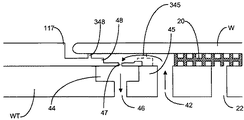
第12実施例について、図20および図21に関して説明する。第12実施例では、基板テーブルWTに封止されるのはセンサ220である。図20および図21で図示した両方のバージョンで、縁密封部材117と基板220の縁との間のギャップに入るような浸漬液を全て除去するため、開口通路47および室44でギャップの近傍に真空46を設ける。
Claims (35)
- −放射線の投影ビームを供給する放射線システムと、
−パターン形成手段を支持する支持構造とを備え、パターン形成手段は、所望のパターンに従って投影ビームにパターン形成する働きをし、さらに、
−基板を保持する基板テーブルと、
−パターン形成したビームを基板の標的部分に投影する投影システムと、
−前記投影システムの最終要素と、基板テーブル上に配置されたオブジェクト間の空間を液体で少なくとも部分的に充填する液体供給システムとを備え、
前記基板テーブルが、さらに、オブジェクトの縁を少なくとも部分的に囲む縁密封部材と、前記縁密封部材と前記投影システムとは反対側にあるオブジェクトとの間のギャップに真空または液体を供給するよう配置された真空孔または液体供給孔とを備えることを特徴とするリソグラフィ投影装置。 - 前記基板テーブルが、さらに、前記真空孔の半径方向内側に配置された流路を備え、前記流路が気体源に接続され、したがって前記真空源を起動すると、前記流路から前記真空源へと半径方向外向きの気体流を確立することができる、請求項1に記載の装置。
- 前記基板に接触する節が、前記流路の半径方向外側、および前記真空孔の内側に存在する、請求項2に記載の装置。
- 前記基板テーブルが、さらに、オブジェクトの下に延在し、前記真空孔の半径方向外側にある孔を備える、請求項1から3いずれか1項に記載の装置。
- 前記部分が、前記オブジェクトに向かって延在し、それによって前記オブジェクトを少なくとも部分的に支持する部品を有する、請求項4に記載の装置。
- 前記節および/または部分および/または部品が、前記基板を支持するピンプル・テーブルの部品である、請求項3から5いずれか1項に記載の装置。
- さらに、前記基板テーブル内に、前記真空孔を介して前記ギャップと、および前記真空源と流体接続する区画を備える、請求項1から6いずれか1項に記載の装置。
- 前記真空孔が環状である、請求項1から7いずれか1項に記載の装置。
- 前記真空孔が不連続である、請求項1から8いずれか1項に記載の装置。
- 前記真空孔が連続している、請求項1から8いずれか1項に記載の装置。
- 前記真空孔が、縁密封部材の縁部分に隣接して配置される、請求項1から10いずれか1項に記載の装置。
- −放射線の投影ビームを共有する放射線システムと、
−パターン形成手段を支持する支持構造とを備え、パターン形成手段が、所望のパターンに従って投影ビームにパターン形成する働きをし、さらに、
−基板を保持する基板テーブルと、
−パターン形成したビームを基板の標的部分に投影する投影システムと、
−前記投影システムの最終要素と、基板テーブル上に配置されたオブジェクト間の空間を液体で少なくとも部分的に充填する液体供給システムとを備え、
前記基板テーブルが、さらに、オブジェクトの縁を少なくとも部分的に囲み、前記投影システムに面してオブジェクトの1次表面とほぼ同一平面上にある1次表面を提供する縁密封部材を備え、前記液体供給システムが、前記オブジェクトおよび/または前記縁密封部材および/または基板の局所的区域に液体を供給することを特徴とするリソグラフィ投影装置。 - 前記縁密封部材およびオブジェクトが、相互に対して動作可能に装着される、請求項12に記載の装置。
- 前記縁密封部材が、前記縁密封部材とオブジェクト間の距離を変動するため、前記縁密封部材の前記1次表面にほぼ平行な面で動作可能である、請求項12または13に記載の装置。
- 前記基板テーブルが、さらに、装置の光軸にほぼ平行な方向で、前記基板テーブルの残りの部分に対して前記縁密封部材を動作させるアクチュエータを備える、請求項12、13または14に記載の装置。
- 前記アクチュエータがウェッジ部材を備え、これは、前記縁密封部材の前記1次表面にほぼ平行な方向に動作すると、前記縁密封部材を前記基板テーブルの残りの部分に対して、装置の光軸にほぼ平行な方向で動作させるのに効果的である、請求項15に記載の装置。
- 前記ウェッジが、起動力を除去すると、前記ウェッジの摩擦係数によって所定の位置にロックされるよう配置される、請求項16に記載の装置。
- 前記基板テーブルが、さらに、前記縁密封部材およびオブジェクトの縁部分の近傍で、前記縁密封部材およびオブジェクトの前記投影システムとは反対側にある疎水性層を備える、請求項12から17いずれか1項に記載の装置。
- 前記液体が、前記疎水性層との間に90°より大きい接触角を有する、請求項18に記載の装置。
- 前記縁密封部材が、前記縁密封部材の1次表面と同一平面上にある上面を有し、前記装置の光軸に向かって延在する突起を有する、請求項12から19いずれか1項に記載の装置。
- 前記基板テーブルが、さらに、光軸の方向で前記縁密封部材およびオブジェクトの両方に突き当たるか、または少なくとも部分的に重畳するギャップ密封部材を備える、請求項12から20いずれか1項に記載の装置。
- 前記ギャップ密封部材が、前記1次表面と接触し、それによって前記縁密封部材とオブジェクト間のギャップに広がるためのものである、請求項21に記載の装置。
- 前記ギャップ密封部材が内縁および外縁を有し、前記縁の少なくとも一方がテーパ状になり、したがってギャップ密封部材の縁密封部材またはオブジェクトの1次表面に面していない表面の距離が、ギャップ密封部材の縁に向かって減少する、請求項21または22に記載の装置。
- 前記基板テーブルが、さらに、前記ギャップ密封部材を所定の位置に保持するため、前記縁密封部材の前記1次表面に真空孔を備える、請求項21から23いずれか1項に記載の装置。
- 前記基板テーブルが、前記基板テーブルの残りの部分に対して前記オブジェクトの1次表面の距離を変動させる手段を含む、請求項12から24いずれか1項に記載の装置。
- −放射線の投影ビームを共有する放射線システムと、
−パターン形成手段を支持する支持構造とを備え、パターン形成手段が、所望のパターンに従って投影ビームにパターン形成する働きをし、さらに、
−基板を保持する基板テーブルと、
−パターン形成したビームを基板の標的部分に投影する投影システムと、
−前記投影システムの最終要素と、基板テーブル上に配置されたオブジェクト間の空間を液体で少なくとも部分的に充填する液体供給システムとを備え、
前記基板テーブルが、さらに、オブジェクトの縁を少なくとも部分的に囲む縁密封部材と、前記縁密封部材とオブジェクト間のギャップにまたがって延在し、オブジェクトと接触するさらなる縁密封部材とを備えることを特徴とするリソグラフィ投影装置。 - 前記さらなる縁密封部材が可撓性である、請求項26に記載の装置。
- 前記さらなる可撓性の縁密封部材を前記縁密封部材に取り付ける、請求項27に記載の装置。
- 前記さらなる可撓性の縁密封部材が、真空源に接続され、前記縁密封部材から遠位側のその端部に隣接する孔を有し、したがって前記真空源を起動すると、オブジェクトに作用する真空源によって発生した力により、前記さらなる可撓性縁密封部材が、上方向に屈曲可能で、オブジェクトと接触し、それによって前記さらなる可撓性縁密封部材とオブジェクトとの間に密封を形成する、請求項26、27または28に記載の装置。
- さらに、前記オブジェクトの下で前記基板テーブルに取り付けられ、取付点から半径方向外側に自由端がある第2のさらなる可撓性縁密封部材を備える、請求項26または27に記載の装置。
- 前記さらなる可撓性縁密封部材が、前記縁密封部材とオブジェクトの間に配置され、前記縁密封部材およびオブジェクトの前記1次表面とほぼ同一平面上にある表面を有する、請求項26または27に記載の装置。
- 前記さらなる可撓性縁密封部材が、その1次表面の反対側の表面にあるオブジェクトと接触するよう形成される、請求項31に記載の装置。
- 前記さらなる可撓性縁密封部材が、オブジェクトを前記基板テーブル上に保持している場合に、前記基板テーブルから離れる力をオブジェクトに加えるのに有効である、請求項31または32に記載の装置。
- 撮像すべき前記オブジェクトが基板またはセンサである、請求項1から33いずれか1項に記載の装置。
- 前記縁密封部材、または前記第1または第2のさらなる縁密封部材を、前記オブジェクトの周囲で前記オブジェクトに接着する、請求項1から34いずれか1項に記載の装置。
Applications Claiming Priority (2)
| Application Number | Priority Date | Filing Date | Title |
|---|---|---|---|
| EP02257822 | 2002-11-12 | ||
| EP03253636 | 2003-06-09 |
Related Child Applications (1)
| Application Number | Title | Priority Date | Filing Date |
|---|---|---|---|
| JP2007065471A Division JP4553913B2 (ja) | 2002-11-12 | 2007-03-14 | リソグラフィ投影装置 |
Publications (2)
| Publication Number | Publication Date |
|---|---|
| JP2004289127A JP2004289127A (ja) | 2004-10-14 |
| JP3953460B2 true JP3953460B2 (ja) | 2007-08-08 |
Family
ID=32852221
Family Applications (4)
| Application Number | Title | Priority Date | Filing Date |
|---|---|---|---|
| JP2003417260A Expired - Fee Related JP3953460B2 (ja) | 2002-11-12 | 2003-11-11 | リソグラフィ投影装置 |
| JP2007065471A Expired - Fee Related JP4553913B2 (ja) | 2002-11-12 | 2007-03-14 | リソグラフィ投影装置 |
| JP2010102149A Expired - Fee Related JP5005793B2 (ja) | 2002-11-12 | 2010-04-27 | リソグラフィ投影装置 |
| JP2012027270A Expired - Fee Related JP5400910B2 (ja) | 2002-11-12 | 2012-02-10 | リソグラフィ投影装置 |
Family Applications After (3)
| Application Number | Title | Priority Date | Filing Date |
|---|---|---|---|
| JP2007065471A Expired - Fee Related JP4553913B2 (ja) | 2002-11-12 | 2007-03-14 | リソグラフィ投影装置 |
| JP2010102149A Expired - Fee Related JP5005793B2 (ja) | 2002-11-12 | 2010-04-27 | リソグラフィ投影装置 |
| JP2012027270A Expired - Fee Related JP5400910B2 (ja) | 2002-11-12 | 2012-02-10 | リソグラフィ投影装置 |
Country Status (6)
| Country | Link |
|---|---|
| US (10) | US7199858B2 (ja) |
| JP (4) | JP3953460B2 (ja) |
| KR (1) | KR100588124B1 (ja) |
| CN (2) | CN100568101C (ja) |
| SG (1) | SG121819A1 (ja) |
| TW (1) | TWI251127B (ja) |
Families Citing this family (367)
| Publication number | Priority date | Publication date | Assignee | Title |
|---|---|---|---|---|
| US7240679B2 (en) * | 2002-09-30 | 2007-07-10 | Lam Research Corporation | System for substrate processing with meniscus, vacuum, IPA vapor, drying manifold |
| US7110081B2 (en) | 2002-11-12 | 2006-09-19 | Asml Netherlands B.V. | Lithographic apparatus and device manufacturing method |
| DE60335595D1 (de) * | 2002-11-12 | 2011-02-17 | Asml Netherlands Bv | Lithographischer Apparat mit Immersion und Verfahren zur Herstellung einer Vorrichtung |
| US10503084B2 (en) | 2002-11-12 | 2019-12-10 | Asml Netherlands B.V. | Lithographic apparatus and device manufacturing method |
| SG121818A1 (en) | 2002-11-12 | 2006-05-26 | Asml Netherlands Bv | Lithographic apparatus and device manufacturing method |
| US9482966B2 (en) | 2002-11-12 | 2016-11-01 | Asml Netherlands B.V. | Lithographic apparatus and device manufacturing method |
| SG121819A1 (en) | 2002-11-12 | 2006-05-26 | Asml Netherlands Bv | Lithographic apparatus and device manufacturing method |
| SG121822A1 (en) * | 2002-11-12 | 2006-05-26 | Asml Netherlands Bv | Lithographic apparatus and device manufacturing method |
| US7372541B2 (en) * | 2002-11-12 | 2008-05-13 | Asml Netherlands B.V. | Lithographic apparatus and device manufacturing method |
| EP1571698A4 (en) * | 2002-12-10 | 2006-06-21 | Nikon Corp | EXPOSURE APPARATUS, EXPOSURE METHOD, AND DEVICE MANUFACTURING METHOD |
| SG150388A1 (en) | 2002-12-10 | 2009-03-30 | Nikon Corp | Exposure apparatus and method for producing device |
| CN100446179C (zh) * | 2002-12-10 | 2008-12-24 | 株式会社尼康 | 曝光设备和器件制造法 |
| US7242455B2 (en) * | 2002-12-10 | 2007-07-10 | Nikon Corporation | Exposure apparatus and method for producing device |
| SG171468A1 (en) * | 2002-12-10 | 2011-06-29 | Nikon Corp | Exposure apparatus and method for producing device |
| JP4352874B2 (ja) * | 2002-12-10 | 2009-10-28 | 株式会社ニコン | 露光装置及びデバイス製造方法 |
| US7948604B2 (en) * | 2002-12-10 | 2011-05-24 | Nikon Corporation | Exposure apparatus and method for producing device |
| US7514699B2 (en) | 2002-12-19 | 2009-04-07 | Koninklijke Philips Electronics N.V. | Method and device for irradiating spots on a layer |
| DE10261775A1 (de) | 2002-12-20 | 2004-07-01 | Carl Zeiss Smt Ag | Vorrichtung zur optischen Vermessung eines Abbildungssystems |
| EP3301511A1 (en) | 2003-02-26 | 2018-04-04 | Nikon Corporation | Exposure apparatus, exposure method, and method for producing device |
| KR20050110033A (ko) * | 2003-03-25 | 2005-11-22 | 가부시키가이샤 니콘 | 노광 장치 및 디바이스 제조 방법 |
| KR101176817B1 (ko) * | 2003-04-07 | 2012-08-24 | 가부시키가이샤 니콘 | 노광장치 및 디바이스 제조방법 |
| EP2270597B1 (en) | 2003-04-09 | 2017-11-01 | Nikon Corporation | Exposure method and apparatus and device manufacturing method |
| KR20110104084A (ko) * | 2003-04-09 | 2011-09-21 | 가부시키가이샤 니콘 | 액침 리소그래피 유체 제어 시스템 |
| WO2004090633A2 (en) * | 2003-04-10 | 2004-10-21 | Nikon Corporation | An electro-osmotic element for an immersion lithography apparatus |
| SG2012050829A (en) | 2003-04-10 | 2015-07-30 | Nippon Kogaku Kk | Environmental system including vacuum scavange for an immersion lithography apparatus |
| CN1771463A (zh) * | 2003-04-10 | 2006-05-10 | 株式会社尼康 | 用于沉浸光刻装置收集液体的溢出通道 |
| EP3062152B1 (en) | 2003-04-10 | 2017-12-20 | Nikon Corporation | Environmental system including vaccum scavenge for an immersion lithography apparatus |
| KR101324818B1 (ko) | 2003-04-11 | 2013-11-01 | 가부시키가이샤 니콘 | 액침 리소그래피에 의한 광학기기의 세정방법 |
| KR101697896B1 (ko) | 2003-04-11 | 2017-01-18 | 가부시키가이샤 니콘 | 액침 리소그래피 머신에서 웨이퍼 교환동안 투영 렌즈 아래의 갭에서 액침 액체를 유지하는 장치 및 방법 |
| JP4582089B2 (ja) * | 2003-04-11 | 2010-11-17 | 株式会社ニコン | 液浸リソグラフィ用の液体噴射回収システム |
| EP1614000B1 (en) * | 2003-04-17 | 2012-01-18 | Nikon Corporation | Immersion lithographic apparatus |
| TWI295414B (en) | 2003-05-13 | 2008-04-01 | Asml Netherlands Bv | Lithographic apparatus and device manufacturing method |
| JP4552853B2 (ja) * | 2003-05-15 | 2010-09-29 | 株式会社ニコン | 露光装置及びデバイス製造方法 |
| TWI463533B (zh) * | 2003-05-23 | 2014-12-01 | 尼康股份有限公司 | An exposure method, an exposure apparatus, and an element manufacturing method |
| TW201806001A (zh) | 2003-05-23 | 2018-02-16 | 尼康股份有限公司 | 曝光裝置及元件製造方法 |
| KR20150036794A (ko) * | 2003-05-28 | 2015-04-07 | 가부시키가이샤 니콘 | 노광 방법, 노광 장치, 및 디바이스 제조 방법 |
| TWI347741B (en) * | 2003-05-30 | 2011-08-21 | Asml Netherlands Bv | Lithographic apparatus and device manufacturing method |
| US7213963B2 (en) | 2003-06-09 | 2007-05-08 | Asml Netherlands B.V. | Lithographic apparatus and device manufacturing method |
| EP2261741A3 (en) | 2003-06-11 | 2011-05-25 | ASML Netherlands B.V. | Lithographic apparatus and device manufacturing method |
| US7317504B2 (en) * | 2004-04-08 | 2008-01-08 | Asml Netherlands B.V. | Lithographic apparatus and device manufacturing method |
| TW200511388A (en) | 2003-06-13 | 2005-03-16 | Nikon Corp | Exposure method, substrate stage, exposure apparatus and method for manufacturing device |
| KR101475634B1 (ko) | 2003-06-19 | 2014-12-22 | 가부시키가이샤 니콘 | 노광 장치 및 디바이스 제조방법 |
| US6867844B2 (en) * | 2003-06-19 | 2005-03-15 | Asml Holding N.V. | Immersion photolithography system and method using microchannel nozzles |
| US6809794B1 (en) * | 2003-06-27 | 2004-10-26 | Asml Holding N.V. | Immersion photolithography system and method using inverted wafer-projection optics interface |
| DE60321779D1 (de) * | 2003-06-30 | 2008-08-07 | Asml Netherlands Bv | Lithographischer Apparat und Verfahren zur Herstellung eines Artikels |
| EP1639391A4 (en) * | 2003-07-01 | 2009-04-29 | Nikon Corp | USE OF FLUIDS SPECIFIED ISOTOPICALLY AS OPTICAL ELEMENTS |
| JP4697138B2 (ja) * | 2003-07-08 | 2011-06-08 | 株式会社ニコン | 液浸リソグラフィ装置、液浸リソグラフィ方法、デバイス製造方法 |
| WO2005006418A1 (ja) | 2003-07-09 | 2005-01-20 | Nikon Corporation | 露光装置及びデバイス製造方法 |
| ATE489724T1 (de) * | 2003-07-09 | 2010-12-15 | Nikon Corp | Belichtungsvorrichtung und verfahren zur bauelementherstellung |
| ATE513309T1 (de) * | 2003-07-09 | 2011-07-15 | Nikon Corp | Belichtungsvorrichtung und verfahren zur bauelementeherstellung |
| US7738074B2 (en) | 2003-07-16 | 2010-06-15 | Asml Netherlands B.V. | Lithographic apparatus and device manufacturing method |
| EP1500982A1 (en) | 2003-07-24 | 2005-01-26 | ASML Netherlands B.V. | Lithographic apparatus and device manufacturing method |
| WO2005010960A1 (ja) * | 2003-07-25 | 2005-02-03 | Nikon Corporation | 投影光学系の検査方法および検査装置、ならびに投影光学系の製造方法 |
| CN102043350B (zh) | 2003-07-28 | 2014-01-29 | 株式会社尼康 | 曝光装置、器件制造方法、及曝光装置的控制方法 |
| EP1503244A1 (en) * | 2003-07-28 | 2005-02-02 | ASML Netherlands B.V. | Lithographic projection apparatus and device manufacturing method |
| US7326522B2 (en) | 2004-02-11 | 2008-02-05 | Asml Netherlands B.V. | Device manufacturing method and a substrate |
| US7779781B2 (en) | 2003-07-31 | 2010-08-24 | Asml Netherlands B.V. | Lithographic apparatus and device manufacturing method |
| KR101288632B1 (ko) | 2003-08-21 | 2013-07-22 | 가부시키가이샤 니콘 | 노광 장치, 노광 방법 및 디바이스 제조 방법 |
| US8149381B2 (en) | 2003-08-26 | 2012-04-03 | Nikon Corporation | Optical element and exposure apparatus |
| KR101094114B1 (ko) * | 2003-08-26 | 2011-12-15 | 가부시키가이샤 니콘 | 광학소자 및 노광장치 |
| KR101477850B1 (ko) * | 2003-08-29 | 2014-12-30 | 가부시키가이샤 니콘 | 액체회수장치, 노광장치, 노광방법 및 디바이스 제조방법 |
| TWI245163B (en) | 2003-08-29 | 2005-12-11 | Asml Netherlands Bv | Lithographic apparatus and device manufacturing method |
| EP2261740B1 (en) | 2003-08-29 | 2014-07-09 | ASML Netherlands BV | Lithographic apparatus |
| TWI263859B (en) | 2003-08-29 | 2006-10-11 | Asml Netherlands Bv | Lithographic apparatus and device manufacturing method |
| WO2005022616A1 (ja) * | 2003-08-29 | 2005-03-10 | Nikon Corporation | 露光装置及びデバイス製造方法 |
| CN100394244C (zh) * | 2003-09-03 | 2008-06-11 | 株式会社尼康 | 为浸没光刻提供流体的装置和方法 |
| EP1660925B1 (en) * | 2003-09-03 | 2015-04-29 | Nikon Corporation | Apparatus and method for providing fluid for immersion lithography |
| WO2005029559A1 (ja) * | 2003-09-19 | 2005-03-31 | Nikon Corporation | 露光装置及びデバイス製造方法 |
| US7158211B2 (en) * | 2003-09-29 | 2007-01-02 | Asml Netherlands B.V. | Lithographic apparatus and device manufacturing method |
| EP1519231B1 (en) * | 2003-09-29 | 2005-12-21 | ASML Netherlands B.V. | Lithographic apparatus and device manufacturing method |
| KR101441840B1 (ko) * | 2003-09-29 | 2014-11-04 | 가부시키가이샤 니콘 | 노광장치, 노광방법 및 디바이스 제조방법 |
| JP4319188B2 (ja) | 2003-10-08 | 2009-08-26 | 株式会社蔵王ニコン | 基板搬送装置及び基板搬送方法、露光装置及び露光方法、デバイス製造装置及びデバイス製造方法 |
| KR20060126949A (ko) | 2003-10-08 | 2006-12-11 | 가부시키가이샤 니콘 | 기판 반송 장치와 기판 반송 방법, 노광 장치와 노광 방법,및 디바이스 제조 방법 |
| JP2005136364A (ja) * | 2003-10-08 | 2005-05-26 | Zao Nikon Co Ltd | 基板搬送装置、露光装置、並びにデバイス製造方法 |
| TW201738932A (zh) | 2003-10-09 | 2017-11-01 | Nippon Kogaku Kk | 曝光裝置及曝光方法、元件製造方法 |
| EP1524558A1 (en) * | 2003-10-15 | 2005-04-20 | ASML Netherlands B.V. | Lithographic apparatus and device manufacturing method |
| EP1524557A1 (en) * | 2003-10-15 | 2005-04-20 | ASML Netherlands B.V. | Lithographic apparatus and device manufacturing method |
| US7352433B2 (en) | 2003-10-28 | 2008-04-01 | Asml Netherlands B.V. | Lithographic apparatus and device manufacturing method |
| US7411653B2 (en) * | 2003-10-28 | 2008-08-12 | Asml Netherlands B.V. | Lithographic apparatus |
| TWI569308B (zh) | 2003-10-28 | 2017-02-01 | 尼康股份有限公司 | 照明光學裝置、曝光裝置、曝光方法以及元件製造 方法 |
| JP2005159322A (ja) * | 2003-10-31 | 2005-06-16 | Nikon Corp | 定盤、ステージ装置及び露光装置並びに露光方法 |
| CN100461336C (zh) * | 2003-10-31 | 2009-02-11 | 株式会社尼康 | 曝光装置以及器件制造方法 |
| US7528929B2 (en) * | 2003-11-14 | 2009-05-05 | Asml Netherlands B.V. | Lithographic apparatus and device manufacturing method |
| TWI385414B (zh) | 2003-11-20 | 2013-02-11 | 尼康股份有限公司 | 光學照明裝置、照明方法、曝光裝置、曝光方法以及元件製造方法 |
| US7545481B2 (en) | 2003-11-24 | 2009-06-09 | Asml Netherlands B.V. | Lithographic apparatus and device manufacturing method |
| WO2005054953A2 (en) * | 2003-11-24 | 2005-06-16 | Carl-Zeiss Smt Ag | Holding device for an optical element in an objective |
| TWI605315B (zh) | 2003-12-03 | 2017-11-11 | Nippon Kogaku Kk | Exposure device, exposure method, and device manufacturing method |
| CN1890779B (zh) * | 2003-12-03 | 2011-06-08 | 株式会社尼康 | 曝光装置、曝光方法和器件制造方法 |
| JP4513534B2 (ja) * | 2003-12-03 | 2010-07-28 | 株式会社ニコン | 露光装置及び露光方法、デバイス製造方法 |
| JP2005175016A (ja) * | 2003-12-08 | 2005-06-30 | Canon Inc | 基板保持装置およびそれを用いた露光装置ならびにデバイス製造方法 |
| JPWO2005057635A1 (ja) * | 2003-12-15 | 2007-07-05 | 株式会社ニコン | 投影露光装置及びステージ装置、並びに露光方法 |
| US20070081133A1 (en) * | 2004-12-14 | 2007-04-12 | Niikon Corporation | Projection exposure apparatus and stage unit, and exposure method |
| JP4720506B2 (ja) * | 2003-12-15 | 2011-07-13 | 株式会社ニコン | ステージ装置、露光装置、及び露光方法 |
| WO2005059977A1 (ja) * | 2003-12-16 | 2005-06-30 | Nikon Corporation | ステージ装置、露光装置、及び露光方法 |
| US7589818B2 (en) * | 2003-12-23 | 2009-09-15 | Asml Netherlands B.V. | Lithographic apparatus, alignment apparatus, device manufacturing method, and a method of converting an apparatus |
| US7394521B2 (en) * | 2003-12-23 | 2008-07-01 | Asml Netherlands B.V. | Lithographic apparatus and device manufacturing method |
| JP2005191394A (ja) * | 2003-12-26 | 2005-07-14 | Canon Inc | 露光方法及び装置 |
| WO2005067013A1 (ja) * | 2004-01-05 | 2005-07-21 | Nikon Corporation | 露光装置、露光方法及びデバイス製造方法 |
| JP4572539B2 (ja) * | 2004-01-19 | 2010-11-04 | 株式会社ニコン | 露光装置及び露光方法、デバイス製造方法 |
| ATE459898T1 (de) * | 2004-01-20 | 2010-03-15 | Zeiss Carl Smt Ag | Belichtungsvorrichtung und messeinrichtung für eine projektionslinse |
| US7589822B2 (en) | 2004-02-02 | 2009-09-15 | Nikon Corporation | Stage drive method and stage unit, exposure apparatus, and device manufacturing method |
| KR101377815B1 (ko) | 2004-02-03 | 2014-03-26 | 가부시키가이샤 니콘 | 노광 장치 및 디바이스 제조 방법 |
| KR101579361B1 (ko) * | 2004-02-04 | 2015-12-21 | 가부시키가이샤 니콘 | 노광 장치, 노광 방법 및 디바이스 제조 방법 |
| TWI609410B (zh) | 2004-02-06 | 2017-12-21 | 尼康股份有限公司 | 光學照明裝置、曝光裝置、曝光方法以及元件製造方法 |
| US7050146B2 (en) | 2004-02-09 | 2006-05-23 | Asml Netherlands B.V. | Lithographic apparatus and device manufacturing method |
| US20070030467A1 (en) * | 2004-02-19 | 2007-02-08 | Nikon Corporation | Exposure apparatus, exposure method, and device fabricating method |
| WO2005081290A1 (ja) * | 2004-02-19 | 2005-09-01 | Nikon Corporation | 露光装置及びデバイス製造方法 |
| US20070166639A1 (en) * | 2004-02-20 | 2007-07-19 | Takayuki Araki | Laminated resist used for immersion lithography |
| JP4622340B2 (ja) * | 2004-03-04 | 2011-02-02 | 株式会社ニコン | 露光装置、デバイス製造方法 |
| JP4973754B2 (ja) * | 2004-03-04 | 2012-07-11 | 株式会社ニコン | 露光方法及び露光装置、デバイス製造方法 |
| JP2005259870A (ja) * | 2004-03-10 | 2005-09-22 | Nikon Corp | 基板保持装置、ステージ装置及び露光装置並びに露光方法 |
| JP4671051B2 (ja) * | 2004-03-25 | 2011-04-13 | 株式会社ニコン | 露光装置及び露光方法、並びにデバイス製造方法 |
| TW201816844A (zh) | 2004-03-25 | 2018-05-01 | 日商尼康股份有限公司 | 曝光裝置、曝光方法、及元件製造方法 |
| US7034917B2 (en) * | 2004-04-01 | 2006-04-25 | Asml Netherlands B.V. | Lithographic apparatus, device manufacturing method and device manufactured thereby |
| JP2005302880A (ja) * | 2004-04-08 | 2005-10-27 | Canon Inc | 液浸式露光装置 |
| US7898642B2 (en) | 2004-04-14 | 2011-03-01 | Asml Netherlands B.V. | Lithographic apparatus and device manufacturing method |
| US7379159B2 (en) | 2004-05-03 | 2008-05-27 | Asml Netherlands B.V. | Lithographic apparatus and device manufacturing method |
| EP1747499A2 (en) * | 2004-05-04 | 2007-01-31 | Nikon Corporation | Apparatus and method for providing fluid for immersion lithography |
| US7616383B2 (en) | 2004-05-18 | 2009-11-10 | Asml Netherlands B.V. | Lithographic apparatus and device manufacturing method |
| US7486381B2 (en) * | 2004-05-21 | 2009-02-03 | Asml Netherlands B.V. | Lithographic apparatus and device manufacturing method |
| JP4517341B2 (ja) * | 2004-06-04 | 2010-08-04 | 株式会社ニコン | 露光装置、ノズル部材、及びデバイス製造方法 |
| EP1768169B9 (en) * | 2004-06-04 | 2013-03-06 | Nikon Corporation | Exposure apparatus, exposure method, and device producing method |
| US7796274B2 (en) | 2004-06-04 | 2010-09-14 | Carl Zeiss Smt Ag | System for measuring the image quality of an optical imaging system |
| JP4826146B2 (ja) * | 2004-06-09 | 2011-11-30 | 株式会社ニコン | 露光装置、デバイス製造方法 |
| KR101421915B1 (ko) | 2004-06-09 | 2014-07-22 | 가부시키가이샤 니콘 | 노광 장치 및 디바이스 제조 방법 |
| CN102290365B (zh) * | 2004-06-09 | 2015-01-21 | 尼康股份有限公司 | 基板保持装置、具备其之曝光装置及方法、元件制造方法 |
| KR101556454B1 (ko) * | 2004-06-10 | 2015-10-13 | 가부시키가이샤 니콘 | 노광 장치, 노광 방법 및 디바이스 제조 방법 |
| US8373843B2 (en) | 2004-06-10 | 2013-02-12 | Nikon Corporation | Exposure apparatus, exposure method, and method for producing device |
| JP5130609B2 (ja) * | 2004-06-10 | 2013-01-30 | 株式会社ニコン | 露光装置及び露光方法、並びにデバイス製造方法 |
| US8508713B2 (en) * | 2004-06-10 | 2013-08-13 | Nikon Corporation | Exposure apparatus, exposure method, and method for producing device |
| KR101505756B1 (ko) * | 2004-06-10 | 2015-03-26 | 가부시키가이샤 니콘 | 노광 장치, 노광 방법, 및 디바이스 제조 방법 |
| US8717533B2 (en) * | 2004-06-10 | 2014-05-06 | Nikon Corporation | Exposure apparatus, exposure method, and method for producing device |
| US20070222959A1 (en) * | 2004-06-10 | 2007-09-27 | Nikon Corporation | Exposure apparatus, exposure method, and method for producing device |
| US7481867B2 (en) | 2004-06-16 | 2009-01-27 | Edwards Limited | Vacuum system for immersion photolithography |
| US8698998B2 (en) * | 2004-06-21 | 2014-04-15 | Nikon Corporation | Exposure apparatus, method for cleaning member thereof, maintenance method for exposure apparatus, maintenance device, and method for producing device |
| KR101378688B1 (ko) * | 2004-06-21 | 2014-03-27 | 가부시키가이샤 니콘 | 노광 장치 및 디바이스 제조 방법 |
| EP3462241A1 (en) * | 2004-06-21 | 2019-04-03 | Nikon Corporation | Exposure apparatus, exposure method and method for producing a device |
| US7501226B2 (en) * | 2004-06-23 | 2009-03-10 | Taiwan Semiconductor Manufacturing Co., Ltd. | Immersion lithography system with wafer sealing mechanisms |
| US7517639B2 (en) | 2004-06-23 | 2009-04-14 | Taiwan Semiconductor Manufacturing Co., Ltd. | Seal ring arrangements for immersion lithography systems |
| US7463330B2 (en) | 2004-07-07 | 2008-12-09 | Asml Netherlands B.V. | Lithographic apparatus and device manufacturing method |
| DE102004033208B4 (de) * | 2004-07-09 | 2010-04-01 | Vistec Semiconductor Systems Gmbh | Vorrichtung zur Inspektion eines mikroskopischen Bauteils mit einem Immersionsobjektiv |
| KR101433491B1 (ko) * | 2004-07-12 | 2014-08-22 | 가부시키가이샤 니콘 | 노광 장치 및 디바이스 제조 방법 |
| US7161663B2 (en) * | 2004-07-22 | 2007-01-09 | Asml Netherlands B.V. | Lithographic apparatus |
| ATE470235T1 (de) * | 2004-08-03 | 2010-06-15 | Nikon Corp | Belichtungsgeräte, belichtungsverfahren und bauelemente-herstellungsverfahren |
| US7304715B2 (en) | 2004-08-13 | 2007-12-04 | Asml Netherlands B.V. | Lithographic apparatus and device manufacturing method |
| JP4983257B2 (ja) * | 2004-08-18 | 2012-07-25 | 株式会社ニコン | 露光装置、デバイス製造方法、計測部材、及び計測方法 |
| US7701550B2 (en) | 2004-08-19 | 2010-04-20 | Asml Netherlands B.V. | Lithographic apparatus and device manufacturing method |
| US20060044533A1 (en) * | 2004-08-27 | 2006-03-02 | Asmlholding N.V. | System and method for reducing disturbances caused by movement in an immersion lithography system |
| EP1796143B1 (en) * | 2004-09-01 | 2011-11-23 | Nikon Corporation | Substrate holder, stage apparatus, and exposure apparatus |
| EP1804279A4 (en) * | 2004-09-17 | 2008-04-09 | Nikon Corp | SUBSTRATE FOR EXPOSURE, EXPOSURE METHOD AND COMPONENT MANUFACTURING METHOD |
| SG10201801998TA (en) | 2004-09-17 | 2018-04-27 | Nikon Corp | Substrate holding device, exposure apparatus, and device manufacturing method |
| US7522261B2 (en) * | 2004-09-24 | 2009-04-21 | Asml Netherlands B.V. | Lithographic apparatus and device manufacturing method |
| US7355674B2 (en) * | 2004-09-28 | 2008-04-08 | Asml Netherlands B.V. | Lithographic apparatus, device manufacturing method and computer program product |
| US7894040B2 (en) * | 2004-10-05 | 2011-02-22 | Asml Netherlands B.V. | Lithographic apparatus and device manufacturing method |
| US7209213B2 (en) * | 2004-10-07 | 2007-04-24 | Asml Netherlands B.V. | Lithographic apparatus and device manufacturing method |
| JP4625673B2 (ja) * | 2004-10-15 | 2011-02-02 | 株式会社東芝 | 露光方法及び露光装置 |
| US7456929B2 (en) * | 2004-10-15 | 2008-11-25 | Nikon Corporation | Exposure apparatus and device manufacturing method |
| US7119876B2 (en) * | 2004-10-18 | 2006-10-10 | Asml Netherlands B.V. | Lithographic apparatus and device manufacturing method |
| US7379155B2 (en) * | 2004-10-18 | 2008-05-27 | Asml Netherlands B.V. | Lithographic apparatus and device manufacturing method |
| WO2006047127A1 (en) * | 2004-10-21 | 2006-05-04 | Saint-Gobain Ceramics & Plastics, Inc. | Optical lens elements, semiconductor lithographic patterning apparatus, and methods for processing semiconductor devices |
| CN101044594B (zh) * | 2004-10-26 | 2010-05-12 | 株式会社尼康 | 衬底处理方法、曝光装置及器件制造方法 |
| WO2006049134A1 (ja) * | 2004-11-01 | 2006-05-11 | Nikon Corporation | 露光装置及びデバイス製造方法 |
| US7423720B2 (en) | 2004-11-12 | 2008-09-09 | Asml Netherlands B.V. | Lithographic apparatus and device manufacturing method |
| US7251013B2 (en) | 2004-11-12 | 2007-07-31 | Asml Netherlands B.V. | Lithographic apparatus and device manufacturing method |
| US7414699B2 (en) * | 2004-11-12 | 2008-08-19 | Asml Netherlands B.V. | Lithographic apparatus and device manufacturing method |
| US7583357B2 (en) | 2004-11-12 | 2009-09-01 | Asml Netherlands B.V. | Lithographic apparatus and device manufacturing method |
| US7411657B2 (en) | 2004-11-17 | 2008-08-12 | Asml Netherlands B.V. | Lithographic apparatus and device manufacturing method |
| US7230681B2 (en) * | 2004-11-18 | 2007-06-12 | International Business Machines Corporation | Method and apparatus for immersion lithography |
| US7362412B2 (en) * | 2004-11-18 | 2008-04-22 | International Business Machines Corporation | Method and apparatus for cleaning a semiconductor substrate in an immersion lithography system |
| TWI654661B (zh) * | 2004-11-18 | 2019-03-21 | 日商尼康股份有限公司 | 位置測量方法、位置控制方法、測量方法、裝載方法、曝光方法及曝光裝置、及元件製造方法 |
| WO2006054719A1 (ja) * | 2004-11-19 | 2006-05-26 | Nikon Corporation | メンテナンス方法、露光方法、露光装置及びデバイス製造方法 |
| US7145630B2 (en) * | 2004-11-23 | 2006-12-05 | Asml Netherlands B.V. | Lithographic apparatus and device manufacturing method |
| US7161654B2 (en) * | 2004-12-02 | 2007-01-09 | Asml Netherlands B.V. | Lithographic apparatus and device manufacturing method |
| US7256121B2 (en) * | 2004-12-02 | 2007-08-14 | Texas Instruments Incorporated | Contact resistance reduction by new barrier stack process |
| US7446850B2 (en) * | 2004-12-03 | 2008-11-04 | Asml Netherlands B.V. | Lithographic apparatus and device manufacturing method |
| US7397533B2 (en) * | 2004-12-07 | 2008-07-08 | Asml Netherlands B.V. | Lithographic apparatus and device manufacturing method |
| US7196770B2 (en) * | 2004-12-07 | 2007-03-27 | Asml Netherlands B.V. | Prewetting of substrate before immersion exposure |
| US7248334B2 (en) * | 2004-12-07 | 2007-07-24 | Asml Netherlands B.V. | Sensor shield |
| US7365827B2 (en) * | 2004-12-08 | 2008-04-29 | Asml Netherlands B.V. | Lithographic apparatus and device manufacturing method |
| US7352440B2 (en) | 2004-12-10 | 2008-04-01 | Asml Netherlands B.V. | Substrate placement in immersion lithography |
| EP2995997B1 (en) * | 2004-12-15 | 2017-08-30 | Nikon Corporation | Exposure apparatus, exposure method, and device fabricating method |
| US7403261B2 (en) | 2004-12-15 | 2008-07-22 | Asml Netherlands B.V. | Lithographic apparatus and device manufacturing method |
| US7528931B2 (en) | 2004-12-20 | 2009-05-05 | Asml Netherlands B.V. | Lithographic apparatus and device manufacturing method |
| JP2006173527A (ja) * | 2004-12-20 | 2006-06-29 | Sony Corp | 露光装置 |
| US7880860B2 (en) | 2004-12-20 | 2011-02-01 | Asml Netherlands B.V. | Lithographic apparatus and device manufacturing method |
| US7405805B2 (en) * | 2004-12-28 | 2008-07-29 | Asml Netherlands B.V. | Lithographic apparatus and device manufacturing method |
| US7491661B2 (en) * | 2004-12-28 | 2009-02-17 | Asml Netherlands B.V. | Device manufacturing method, top coat material and substrate |
| US20060147821A1 (en) | 2004-12-30 | 2006-07-06 | Asml Netherlands B.V. | Lithographic apparatus and device manufacturing method |
| US7450217B2 (en) * | 2005-01-12 | 2008-11-11 | Asml Netherlands B.V. | Exposure apparatus, coatings for exposure apparatus, lithographic apparatus, device manufacturing method, and device manufactured thereby |
| DE602006012746D1 (de) * | 2005-01-14 | 2010-04-22 | Asml Netherlands Bv | Lithografische Vorrichtung und Herstellungsverfahren |
| SG124351A1 (en) | 2005-01-14 | 2006-08-30 | Asml Netherlands Bv | Lithographic apparatus and device manufacturing method |
| JP2006202825A (ja) * | 2005-01-18 | 2006-08-03 | Jsr Corp | 液浸型露光装置 |
| WO2006078292A1 (en) * | 2005-01-21 | 2006-07-27 | Nikon Corporation | Offset partial ring seal in immersion lithographic system |
| KR101427056B1 (ko) | 2005-01-31 | 2014-08-05 | 가부시키가이샤 니콘 | 노광 장치 및 디바이스 제조 방법 |
| US8692973B2 (en) * | 2005-01-31 | 2014-04-08 | Nikon Corporation | Exposure apparatus and method for producing device |
| CN101128775B (zh) * | 2005-02-10 | 2012-07-25 | Asml荷兰有限公司 | 浸没液体、曝光装置及曝光方法 |
| US20070258068A1 (en) * | 2005-02-17 | 2007-11-08 | Hiroto Horikawa | Exposure Apparatus, Exposure Method, and Device Fabricating Method |
| US8018573B2 (en) | 2005-02-22 | 2011-09-13 | Asml Netherlands B.V. | Lithographic apparatus and device manufacturing method |
| US7224431B2 (en) * | 2005-02-22 | 2007-05-29 | Asml Netherlands B.V. | Lithographic apparatus and device manufacturing method |
| US7378025B2 (en) | 2005-02-22 | 2008-05-27 | Asml Netherlands B.V. | Fluid filtration method, fluid filtered thereby, lithographic apparatus and device manufacturing method |
| JP2006270057A (ja) * | 2005-02-28 | 2006-10-05 | Canon Inc | 露光装置 |
| US7428038B2 (en) * | 2005-02-28 | 2008-09-23 | Asml Netherlands B.V. | Lithographic apparatus, device manufacturing method and apparatus for de-gassing a liquid |
| US7282701B2 (en) | 2005-02-28 | 2007-10-16 | Asml Netherlands B.V. | Sensor for use in a lithographic apparatus |
| US7324185B2 (en) * | 2005-03-04 | 2008-01-29 | Asml Netherlands B.V. | Lithographic apparatus and device manufacturing method |
| US7684010B2 (en) * | 2005-03-09 | 2010-03-23 | Asml Netherlands B.V. | Lithographic apparatus, device manufacturing method, seal structure, method of removing an object and a method of sealing |
| JP4844186B2 (ja) * | 2005-03-18 | 2011-12-28 | 株式会社ニコン | プレート部材、基板保持装置、露光装置及び露光方法、並びにデバイス製造方法 |
| US7330238B2 (en) * | 2005-03-28 | 2008-02-12 | Asml Netherlands, B.V. | Lithographic apparatus, immersion projection apparatus and device manufacturing method |
| US7411654B2 (en) | 2005-04-05 | 2008-08-12 | Asml Netherlands B.V. | Lithographic apparatus and device manufacturing method |
| US7291850B2 (en) * | 2005-04-08 | 2007-11-06 | Asml Netherlands B.V. | Lithographic apparatus and device manufacturing method |
| USRE43576E1 (en) | 2005-04-08 | 2012-08-14 | Asml Netherlands B.V. | Dual stage lithographic apparatus and device manufacturing method |
| US20060232753A1 (en) * | 2005-04-19 | 2006-10-19 | Asml Holding N.V. | Liquid immersion lithography system with tilted liquid flow |
| KR101466533B1 (ko) | 2005-04-25 | 2014-11-27 | 가부시키가이샤 니콘 | 노광 방법, 노광 장치 및 액체 공급 방법 |
| US8236467B2 (en) * | 2005-04-28 | 2012-08-07 | Nikon Corporation | Exposure method, exposure apparatus, and device manufacturing method |
| JP4752320B2 (ja) * | 2005-04-28 | 2011-08-17 | 株式会社ニコン | 基板保持装置及び露光装置、基板保持方法、露光方法、並びにデバイス製造方法 |
| US7317507B2 (en) * | 2005-05-03 | 2008-01-08 | Asml Netherlands B.V. | Lithographic apparatus and device manufacturing method |
| US8248577B2 (en) | 2005-05-03 | 2012-08-21 | Asml Netherlands B.V. | Lithographic apparatus and device manufacturing method |
| US7433016B2 (en) | 2005-05-03 | 2008-10-07 | Asml Netherlands B.V. | Lithographic apparatus and device manufacturing method |
| KR101524964B1 (ko) | 2005-05-12 | 2015-06-01 | 가부시키가이샤 니콘 | 투영 광학계, 노광 장치 및 노광 방법 |
| JP2006339448A (ja) | 2005-06-02 | 2006-12-14 | Canon Inc | 受光ユニットを有する露光装置 |
| US7751027B2 (en) | 2005-06-21 | 2010-07-06 | Asml Netherlands B.V. | Lithographic apparatus and device manufacturing method |
| US7652746B2 (en) * | 2005-06-21 | 2010-01-26 | Asml Netherlands B.V. | Lithographic apparatus and device manufacturing method |
| JP4708876B2 (ja) * | 2005-06-21 | 2011-06-22 | キヤノン株式会社 | 液浸露光装置 |
| US7834974B2 (en) | 2005-06-28 | 2010-11-16 | Asml Netherlands B.V. | Lithographic apparatus and device manufacturing method |
| US7474379B2 (en) | 2005-06-28 | 2009-01-06 | Asml Netherlands B.V. | Lithographic apparatus and device manufacturing method |
| US7468779B2 (en) * | 2005-06-28 | 2008-12-23 | Asml Netherlands B.V. | Lithographic apparatus and device manufacturing method |
| US7170583B2 (en) * | 2005-06-29 | 2007-01-30 | Asml Netherlands B.V. | Lithographic apparatus immersion damage control |
| US7535644B2 (en) * | 2005-08-12 | 2009-05-19 | Asml Netherlands B.V. | Lens element, lithographic apparatus, device manufacturing method, and device manufactured thereby |
| US8054445B2 (en) * | 2005-08-16 | 2011-11-08 | Asml Netherlands B.V. | Lithographic apparatus and device manufacturing method |
| US7751026B2 (en) * | 2005-08-25 | 2010-07-06 | Nikon Corporation | Apparatus and method for recovering fluid for immersion lithography |
| US7357768B2 (en) * | 2005-09-22 | 2008-04-15 | William Marshall | Recliner exerciser |
| US8202460B2 (en) * | 2005-09-22 | 2012-06-19 | International Business Machines Corporation | Microelectronic substrate having removable edge extension element |
| JP3997244B2 (ja) * | 2005-10-04 | 2007-10-24 | キヤノン株式会社 | 露光装置及びデバイス製造方法 |
| JP3997245B2 (ja) * | 2005-10-04 | 2007-10-24 | キヤノン株式会社 | 露光装置及びデバイス製造方法 |
| US7411658B2 (en) | 2005-10-06 | 2008-08-12 | Asml Netherlands B.V. | Lithographic apparatus and device manufacturing method |
| JP4125315B2 (ja) * | 2005-10-11 | 2008-07-30 | キヤノン株式会社 | 露光装置及びデバイス製造方法 |
| JP2007123525A (ja) * | 2005-10-27 | 2007-05-17 | Toshiba Corp | 液浸露光装置及び半導体装置の製造方法 |
| JPWO2007055237A1 (ja) * | 2005-11-09 | 2009-04-30 | 株式会社ニコン | 露光装置及び露光方法、並びにデバイス製造方法 |
| US7804577B2 (en) | 2005-11-16 | 2010-09-28 | Asml Netherlands B.V. | Lithographic apparatus |
| US7864292B2 (en) * | 2005-11-16 | 2011-01-04 | Asml Netherlands B.V. | Lithographic apparatus and device manufacturing method |
| US7656501B2 (en) * | 2005-11-16 | 2010-02-02 | Asml Netherlands B.V. | Lithographic apparatus |
| US7633073B2 (en) | 2005-11-23 | 2009-12-15 | Asml Netherlands B.V. | Lithographic apparatus and device manufacturing method |
| US7773195B2 (en) * | 2005-11-29 | 2010-08-10 | Asml Holding N.V. | System and method to increase surface tension and contact angle in immersion lithography |
| US8125610B2 (en) | 2005-12-02 | 2012-02-28 | ASML Metherlands B.V. | Method for preventing or reducing contamination of an immersion type projection apparatus and an immersion type lithographic apparatus |
| US20070124987A1 (en) * | 2005-12-05 | 2007-06-07 | Brown Jeffrey K | Electronic pest control apparatus |
| KR100768849B1 (ko) * | 2005-12-06 | 2007-10-22 | 엘지전자 주식회사 | 계통 연계형 연료전지 시스템의 전원공급장치 및 방법 |
| KR101704310B1 (ko) | 2005-12-08 | 2017-02-07 | 가부시키가이샤 니콘 | 기판 보지 장치, 노광 장치, 노광 방법 및 디바이스 제조 방법 |
| US7420194B2 (en) * | 2005-12-27 | 2008-09-02 | Asml Netherlands B.V. | Lithographic apparatus and substrate edge seal |
| US7839483B2 (en) * | 2005-12-28 | 2010-11-23 | Asml Netherlands B.V. | Lithographic apparatus, device manufacturing method and a control system |
| US7649611B2 (en) | 2005-12-30 | 2010-01-19 | Asml Netherlands B.V. | Lithographic apparatus and device manufacturing method |
| WO2007083592A1 (ja) * | 2006-01-17 | 2007-07-26 | Nikon Corporation | 基板保持装置及び露光装置、並びにデバイス製造方法 |
| US7446859B2 (en) * | 2006-01-27 | 2008-11-04 | International Business Machines Corporation | Apparatus and method for reducing contamination in immersion lithography |
| JP2007201252A (ja) * | 2006-01-27 | 2007-08-09 | Canon Inc | 露光装置及びデバイス製造方法 |
| US20070177119A1 (en) * | 2006-02-02 | 2007-08-02 | Keiko Chiba | Exposure apparatus and device manufacturing method |
| US20070182943A1 (en) * | 2006-02-06 | 2007-08-09 | Francis Goodwin | Debris apparatus, system, and method |
| US7787101B2 (en) * | 2006-02-16 | 2010-08-31 | International Business Machines Corporation | Apparatus and method for reducing contamination in immersion lithography |
| US7893047B2 (en) * | 2006-03-03 | 2011-02-22 | Arch Chemicals, Inc. | Biocide composition comprising pyrithione and pyrrole derivatives |
| US8045134B2 (en) | 2006-03-13 | 2011-10-25 | Asml Netherlands B.V. | Lithographic apparatus, control system and device manufacturing method |
| US7310132B2 (en) * | 2006-03-17 | 2007-12-18 | Asml Netherlands B.V. | Lithographic apparatus and device manufacturing method |
| US7760324B2 (en) * | 2006-03-20 | 2010-07-20 | Asml Netherlands B.V. | Lithographic apparatus and device manufacturing method |
| JP2007266074A (ja) * | 2006-03-27 | 2007-10-11 | Toshiba Corp | 半導体装置の製造方法及び液浸リソグラフィーシステム |
| US8027019B2 (en) | 2006-03-28 | 2011-09-27 | Asml Netherlands B.V. | Lithographic apparatus and device manufacturing method |
| JP2007266504A (ja) | 2006-03-29 | 2007-10-11 | Canon Inc | 露光装置 |
| EP1843206B1 (en) * | 2006-04-06 | 2012-09-05 | ASML Netherlands B.V. | Lithographic apparatus and device manufacturing method |
| US9477158B2 (en) * | 2006-04-14 | 2016-10-25 | Asml Netherlands B.V. | Lithographic apparatus and device manufacturing method |
| DE102006021797A1 (de) | 2006-05-09 | 2007-11-15 | Carl Zeiss Smt Ag | Optische Abbildungseinrichtung mit thermischer Dämpfung |
| US8144305B2 (en) * | 2006-05-18 | 2012-03-27 | Asml Netherlands B.V. | Lithographic apparatus and device manufacturing method |
| US7969548B2 (en) * | 2006-05-22 | 2011-06-28 | Asml Netherlands B.V. | Lithographic apparatus and lithographic apparatus cleaning method |
| SG172607A1 (en) * | 2006-05-22 | 2011-07-28 | Nikon Corp | Exposure method and apparatus, maintenance method, and device manufacturing method |
| US20070273856A1 (en) | 2006-05-25 | 2007-11-29 | Nikon Corporation | Apparatus and methods for inhibiting immersion liquid from flowing below a substrate |
| JP2008034801A (ja) * | 2006-06-30 | 2008-02-14 | Canon Inc | 露光装置およびデバイス製造方法 |
| US8570484B2 (en) | 2006-08-30 | 2013-10-29 | Nikon Corporation | Immersion exposure apparatus, device manufacturing method, cleaning method, and cleaning member to remove foreign substance using liquid |
| WO2008029884A1 (fr) | 2006-09-08 | 2008-03-13 | Nikon Corporation | Dispositif et procédé de nettoyage, et procédé de fabrication du dispositif |
| US7946303B2 (en) * | 2006-09-29 | 2011-05-24 | Lam Research Corporation | Carrier for reducing entrance and/or exit marks left by a substrate-processing meniscus |
| US20080100812A1 (en) * | 2006-10-26 | 2008-05-01 | Nikon Corporation | Immersion lithography system and method having a wafer chuck made of a porous material |
| US8208116B2 (en) * | 2006-11-03 | 2012-06-26 | Taiwan Semiconductor Manufacturing Company, Ltd. | Immersion lithography system using a sealed wafer bath |
| US8253922B2 (en) | 2006-11-03 | 2012-08-28 | Taiwan Semiconductor Manufacturing Company, Ltd. | Immersion lithography system using a sealed wafer bath |
| US8237085B2 (en) * | 2006-11-17 | 2012-08-07 | Semiconductor Energy Laboratory Co., Ltd. | Beam homogenizer, laser irradiation apparatus, and laser irradiation method |
| US8045135B2 (en) * | 2006-11-22 | 2011-10-25 | Asml Netherlands B.V. | Lithographic apparatus with a fluid combining unit and related device manufacturing method |
| US8013975B2 (en) * | 2006-12-01 | 2011-09-06 | Nikon Corporation | Exposure apparatus, exposure method, and method for producing device |
| US20080156356A1 (en) | 2006-12-05 | 2008-07-03 | Nikon Corporation | Cleaning liquid, cleaning method, liquid generating apparatus, exposure apparatus, and device fabricating method |
| US8634053B2 (en) | 2006-12-07 | 2014-01-21 | Asml Netherlands B.V. | Lithographic apparatus and device manufacturing method |
| US9632425B2 (en) | 2006-12-07 | 2017-04-25 | Asml Holding N.V. | Lithographic apparatus, a dryer and a method of removing liquid from a surface |
| US7791709B2 (en) * | 2006-12-08 | 2010-09-07 | Asml Netherlands B.V. | Substrate support and lithographic process |
| US20080137055A1 (en) * | 2006-12-08 | 2008-06-12 | Asml Netherlands B.V. | Lithographic apparatus and device manufacturing method |
| JP2008147577A (ja) * | 2006-12-13 | 2008-06-26 | Canon Inc | 露光装置及びデバイス製造方法 |
| US8416383B2 (en) | 2006-12-13 | 2013-04-09 | Asml Netherlands B.V. | Lithographic apparatus and method |
| US8634052B2 (en) | 2006-12-13 | 2014-01-21 | Asml Netherlands B.V. | Lithographic apparatus and method involving a ring to cover a gap between a substrate and a substrate table |
| US7755740B2 (en) * | 2007-02-07 | 2010-07-13 | Canon Kabushiki Kaisha | Exposure apparatus |
| US8817226B2 (en) | 2007-02-15 | 2014-08-26 | Asml Holding N.V. | Systems and methods for insitu lens cleaning using ozone in immersion lithography |
| US8654305B2 (en) | 2007-02-15 | 2014-02-18 | Asml Holding N.V. | Systems and methods for insitu lens cleaning in immersion lithography |
| US20080198348A1 (en) * | 2007-02-20 | 2008-08-21 | Nikon Corporation | Apparatus and methods for minimizing force variation from immersion liquid in lithography systems |
| US7692765B2 (en) | 2007-02-21 | 2010-04-06 | Asml Netherlands B.V. | Lithographic apparatus and method of removing liquid |
| US8760621B2 (en) | 2007-03-12 | 2014-06-24 | Asml Netherlands B.V. | Lithographic apparatus and method |
| US8237911B2 (en) | 2007-03-15 | 2012-08-07 | Nikon Corporation | Apparatus and methods for keeping immersion fluid adjacent to an optical assembly during wafer exchange in an immersion lithography machine |
| US7866330B2 (en) * | 2007-05-04 | 2011-01-11 | Asml Netherlands B.V. | Cleaning device, a lithographic apparatus and a lithographic apparatus cleaning method |
| US9013672B2 (en) * | 2007-05-04 | 2015-04-21 | Asml Netherlands B.V. | Cleaning device, a lithographic apparatus and a lithographic apparatus cleaning method |
| US8011377B2 (en) | 2007-05-04 | 2011-09-06 | Asml Netherlands B.V. | Cleaning device and a lithographic apparatus cleaning method |
| US8947629B2 (en) * | 2007-05-04 | 2015-02-03 | Asml Netherlands B.V. | Cleaning device, a lithographic apparatus and a lithographic apparatus cleaning method |
| KR20100031694A (ko) | 2007-05-28 | 2010-03-24 | 가부시키가이샤 니콘 | 노광 장치, 디바이스 제조 방법, 세정 장치, 및 클리닝 방법 그리고 노광 방법 |
| US8514365B2 (en) * | 2007-06-01 | 2013-08-20 | Asml Netherlands B.V. | Lithographic apparatus and device manufacturing method |
| US20080304025A1 (en) * | 2007-06-08 | 2008-12-11 | Taiwan Semiconductor Manufacturing Company, Ltd. | Apparatus and method for immersion lithography |
| US8264662B2 (en) * | 2007-06-18 | 2012-09-11 | Taiwan Semiconductor Manufacturing Company, Ltd. | In-line particle detection for immersion lithography |
| US20090009733A1 (en) * | 2007-07-06 | 2009-01-08 | Canon Kabushiki Kaisha | Exposure apparatus |
| TWI514090B (zh) * | 2007-07-13 | 2015-12-21 | Mapper Lithography Ip Bv | 微影系統及用於支撐晶圓的晶圓台 |
| US8705010B2 (en) * | 2007-07-13 | 2014-04-22 | Mapper Lithography Ip B.V. | Lithography system, method of clamping and wafer table |
| JP4961299B2 (ja) | 2007-08-08 | 2012-06-27 | キヤノン株式会社 | 露光装置およびデバイス製造方法 |
| US8144309B2 (en) * | 2007-09-05 | 2012-03-27 | Asml Netherlands B.V. | Imprint lithography |
| US8681308B2 (en) * | 2007-09-13 | 2014-03-25 | Asml Netherlands B.V. | Lithographic apparatus and device manufacturing method |
| US8451427B2 (en) | 2007-09-14 | 2013-05-28 | Nikon Corporation | Illumination optical system, exposure apparatus, optical element and manufacturing method thereof, and device manufacturing method |
| NL1035942A1 (nl) * | 2007-09-27 | 2009-03-30 | Asml Netherlands Bv | Lithographic Apparatus and Method of Cleaning a Lithographic Apparatus. |
| JP5267029B2 (ja) | 2007-10-12 | 2013-08-21 | 株式会社ニコン | 照明光学装置、露光装置及びデバイスの製造方法 |
| WO2009050976A1 (en) | 2007-10-16 | 2009-04-23 | Nikon Corporation | Illumination optical system, exposure apparatus, and device manufacturing method |
| CN101681125B (zh) | 2007-10-16 | 2013-08-21 | 株式会社尼康 | 照明光学系统、曝光装置以及元件制造方法 |
| US8379187B2 (en) | 2007-10-24 | 2013-02-19 | Nikon Corporation | Optical unit, illumination optical apparatus, exposure apparatus, and device manufacturing method |
| US9116346B2 (en) | 2007-11-06 | 2015-08-25 | Nikon Corporation | Illumination apparatus, illumination method, exposure apparatus, and device manufacturing method |
| NL1036194A1 (nl) * | 2007-12-03 | 2009-06-04 | Asml Netherlands Bv | Lithographic apparatus and device manufacturing method. |
| NL1036211A1 (nl) | 2007-12-03 | 2009-06-04 | Asml Netherlands Bv | Lithographic Apparatus and Device Manufacturing Method. |
| NL1036187A1 (nl) * | 2007-12-03 | 2009-06-04 | Asml Netherlands Bv | Lithographic apparatus and device manufacturing method. |
| NL1036186A1 (nl) * | 2007-12-03 | 2009-06-04 | Asml Netherlands Bv | Lithographic apparatus and device manufacturing method. |
| JP5369443B2 (ja) | 2008-02-05 | 2013-12-18 | 株式会社ニコン | ステージ装置、露光装置、露光方法、及びデバイス製造方法 |
| US20090218743A1 (en) * | 2008-02-29 | 2009-09-03 | Nikon Corporation | Substrate holding apparatus, exposure apparatus, exposing method, device fabricating method, plate member, and wall |
| KR101448152B1 (ko) * | 2008-03-26 | 2014-10-07 | 삼성전자주식회사 | 수직 포토게이트를 구비한 거리측정 센서 및 그를 구비한입체 컬러 이미지 센서 |
| NL1036709A1 (nl) * | 2008-04-24 | 2009-10-27 | Asml Netherlands Bv | Lithographic apparatus and a method of operating the apparatus. |
| JP5097166B2 (ja) * | 2008-05-28 | 2012-12-12 | エーエスエムエル ネザーランズ ビー.ブイ. | リソグラフィ装置及び装置の動作方法 |
| CN101910817B (zh) | 2008-05-28 | 2016-03-09 | 株式会社尼康 | 照明光学系统、曝光装置以及器件制造方法 |
| EP2131242A1 (en) * | 2008-06-02 | 2009-12-09 | ASML Netherlands B.V. | Substrate table, lithographic apparatus and device manufacturing method |
| NL1036924A1 (nl) * | 2008-06-02 | 2009-12-03 | Asml Netherlands Bv | Substrate table, lithographic apparatus and device manufacturing method. |
| NL2003363A (en) * | 2008-09-10 | 2010-03-15 | Asml Netherlands Bv | Lithographic apparatus, method of manufacturing an article for a lithographic apparatus and device manufacturing method. |
| NL2003470A (en) * | 2008-10-07 | 2010-04-08 | Asml Netherlands Bv | Lithographic apparatus and device manufacturing method. |
| US8477284B2 (en) | 2008-10-22 | 2013-07-02 | Nikon Corporation | Apparatus and method to control vacuum at porous material using multiple porous materials |
| US8634055B2 (en) * | 2008-10-22 | 2014-01-21 | Nikon Corporation | Apparatus and method to control vacuum at porous material using multiple porous materials |
| NL2003575A (en) | 2008-10-29 | 2010-05-03 | Asml Netherlands Bv | Lithographic apparatus and device manufacturing method. |
| NL2003638A (en) * | 2008-12-03 | 2010-06-07 | Asml Netherlands Bv | Lithographic apparatus and device manufacturing method. |
| JP2010140958A (ja) * | 2008-12-09 | 2010-06-24 | Canon Inc | 露光装置及びデバイス製造方法 |
| EP2196857A3 (en) * | 2008-12-09 | 2010-07-21 | ASML Netherlands BV | Lithographic apparatus and device manufacturing method |
| NL2004807A (en) * | 2009-06-30 | 2011-01-04 | Asml Netherlands Bv | Substrate table for a lithographic apparatus, litographic apparatus, method of using a substrate table and device manufacturing method. |
| US8913230B2 (en) * | 2009-07-02 | 2014-12-16 | Canon Nanotechnologies, Inc. | Chucking system with recessed support feature |
| JP5767221B2 (ja) * | 2009-08-07 | 2015-08-19 | カール・ツァイス・エスエムティー・ゲーエムベーハー | 少なくとも2つの鏡面を有するミラーを製造する方法、マイクロリソグラフィ用投影露光装置のミラー、及び投影露光装置 |
| NL2005126A (en) * | 2009-09-21 | 2011-03-22 | Asml Netherlands Bv | Lithographic apparatus, coverplate and device manufacturing method. |
| NL2005207A (en) * | 2009-09-28 | 2011-03-29 | Asml Netherlands Bv | Heat pipe, lithographic apparatus and device manufacturing method. |
| NL1038213C2 (en) * | 2010-03-04 | 2012-10-08 | Mapper Lithography Ip Bv | Substrate support structure, clamp preparation unit, and lithography system. |
| NL2006203A (en) * | 2010-03-16 | 2011-09-19 | Asml Netherlands Bv | Cover for a substrate table, substrate table for a lithographic apparatus, lithographic apparatus, and device manufacturing method. |
| NL2006244A (en) * | 2010-03-16 | 2011-09-19 | Asml Netherlands Bv | Lithographic apparatus, cover for use in a lithographic apparatus and method for designing a cover for use in a lithographic apparatus. |
| EP2381310B1 (en) | 2010-04-22 | 2015-05-06 | ASML Netherlands BV | Fluid handling structure and lithographic apparatus |
| JP5313293B2 (ja) * | 2010-05-19 | 2013-10-09 | エーエスエムエル ネザーランズ ビー.ブイ. | リソグラフィ装置、リソグラフィ装置で使用する流体ハンドリング構造およびデバイス製造方法 |
| NL2007768A (en) | 2010-12-14 | 2012-06-18 | Asml Netherlands Bv | Substrate holder, lithographic apparatus, device manufacturing method, and method of manufacturing a substrate holder. |
| NL2007802A (en) | 2010-12-21 | 2012-06-25 | Asml Netherlands Bv | A substrate table, a lithographic apparatus and a device manufacturing method. |
| JP2012134290A (ja) * | 2010-12-21 | 2012-07-12 | Nikon Corp | 露光装置、露光装置のステージ製造方法及びデバイス製造方法 |
| NL2008980A (en) | 2011-07-11 | 2013-01-14 | Asml Netherlands Bv | A fluid handling structure, a lithographic apparatus and a device manufacturing method. |
| NL2008979A (en) | 2011-07-11 | 2013-01-14 | Asml Netherlands Bv | A fluid handling structure, a lithographic apparatus and a device manufacturing method. |
| JP5778093B2 (ja) | 2011-08-10 | 2015-09-16 | エーエスエムエル ネザーランズ ビー.ブイ. | 基板テーブルアセンブリ、液浸リソグラフィ装置及びデバイス製造方法 |
| WO2013178438A1 (en) * | 2012-05-29 | 2013-12-05 | Asml Netherlands B.V. | Object holder and lithographic apparatus |
| CN107367907B (zh) * | 2012-05-29 | 2019-05-03 | Asml荷兰有限公司 | 支撑装置、光刻装置和器件制造方法 |
| JP2014045090A (ja) * | 2012-08-27 | 2014-03-13 | Toshiba Corp | 液浸露光装置 |
| JP6171293B2 (ja) * | 2012-09-13 | 2017-08-02 | 株式会社ニコン | 露光装置及びデバイス製造方法 |
| US9177849B2 (en) * | 2012-12-18 | 2015-11-03 | Intermolecular, Inc. | Chuck for mounting a semiconductor wafer for liquid immersion processing |
| US10361097B2 (en) * | 2012-12-31 | 2019-07-23 | Globalwafers Co., Ltd. | Apparatus for stressing semiconductor substrates |
| CN107004574B (zh) * | 2014-12-12 | 2020-06-30 | 佳能株式会社 | 基板保持装置、光刻设备以及物品制造方法 |
| JP6751759B2 (ja) * | 2015-12-08 | 2020-09-09 | エーエスエムエル ネザーランズ ビー.ブイ. | 基板テーブル、リソグラフィ装置、及びリソグラフィ装置を操作する方法 |
| CN108292109B (zh) * | 2015-12-15 | 2020-05-12 | Asml荷兰有限公司 | 衬底保持器、光刻设备及制造器件的方法 |
| EP3455677A1 (en) | 2016-05-12 | 2019-03-20 | ASML Netherlands B.V. | Extraction body for lithographic apparatus |
| US10978332B2 (en) * | 2016-10-05 | 2021-04-13 | Prilit Optronics, Inc. | Vacuum suction apparatus |
| JP6477793B2 (ja) * | 2017-07-05 | 2019-03-06 | 株式会社ニコン | 露光装置及びデバイス製造方法 |
| CN111213093A (zh) * | 2017-10-12 | 2020-05-29 | Asml荷兰有限公司 | 用于在光刻设备中使用的衬底支架 |
| US10907787B2 (en) | 2018-10-18 | 2021-02-02 | Marche International Llc | Light engine and method of simulating a flame |
| CN112304572B (zh) * | 2019-07-30 | 2022-01-28 | 华为技术有限公司 | 波前标定方法和装置 |
| WO2023143909A1 (en) * | 2022-01-31 | 2023-08-03 | Asml Netherlands B.V. | Substrate table, lithographic apparatus, sticker, cover ring and method of operating a lithographic apparatus |
Family Cites Families (305)
| Publication number | Priority date | Publication date | Assignee | Title |
|---|---|---|---|---|
| DE242880C (ja) | ||||
| DE206607C (ja) | ||||
| DE224448C (ja) | ||||
| DE221563C (ja) | ||||
| GB1242527A (en) * | 1967-10-20 | 1971-08-11 | Kodak Ltd | Optical instruments |
| US3573975A (en) * | 1968-07-10 | 1971-04-06 | Ibm | Photochemical fabrication process |
| US4280054A (en) | 1979-04-30 | 1981-07-21 | Varian Associates, Inc. | X-Y Work table |
| ATE1462T1 (de) | 1979-07-27 | 1982-08-15 | Werner W. Dr. Tabarelli | Optisches lithographieverfahren und einrichtung zum kopieren eines musters auf eine halbleiterscheibe. |
| JPS5645021A (en) | 1979-09-19 | 1981-04-24 | Hitachi Ltd | Moving apparatus |
| FR2474708B1 (fr) | 1980-01-24 | 1987-02-20 | Dme | Procede de microphotolithographie a haute resolution de traits |
| US4396164A (en) * | 1980-04-11 | 1983-08-02 | Minolta Camera Kabushiki Kaisha | Easy loading mechanism for cameras |
| JPS5754317A (en) * | 1980-09-19 | 1982-03-31 | Hitachi Ltd | Method and device for forming pattern |
| US4346164A (en) * | 1980-10-06 | 1982-08-24 | Werner Tabarelli | Photolithographic method for the manufacture of integrated circuits |
| US4509852A (en) * | 1980-10-06 | 1985-04-09 | Werner Tabarelli | Apparatus for the photolithographic manufacture of integrated circuit elements |
| JPS57117238A (en) | 1981-01-14 | 1982-07-21 | Nippon Kogaku Kk <Nikon> | Exposing and baking device for manufacturing integrated circuit with illuminometer |
| US4390273A (en) * | 1981-02-17 | 1983-06-28 | Censor Patent-Und Versuchsanstalt | Projection mask as well as a method and apparatus for the embedding thereof and projection printing system |
| JPS57153433A (en) | 1981-03-18 | 1982-09-22 | Hitachi Ltd | Manufacturing device for semiconductor |
| JPS58202448A (ja) | 1982-05-21 | 1983-11-25 | Hitachi Ltd | 露光装置 |
| DD206607A1 (de) | 1982-06-16 | 1984-02-01 | Mikroelektronik Zt Forsch Tech | Verfahren und vorrichtung zur beseitigung von interferenzeffekten |
| JPS5919912A (ja) | 1982-07-26 | 1984-02-01 | Hitachi Ltd | 液浸距離保持装置 |
| DD242880A1 (de) | 1983-01-31 | 1987-02-11 | Kuch Karl Heinz | Einrichtung zur fotolithografischen strukturuebertragung |
| DD221563A1 (de) | 1983-09-14 | 1985-04-24 | Mikroelektronik Zt Forsch Tech | Immersionsobjektiv fuer die schrittweise projektionsabbildung einer maskenstruktur |
| DD224448A1 (de) | 1984-03-01 | 1985-07-03 | Zeiss Jena Veb Carl | Einrichtung zur fotolithografischen strukturuebertragung |
| JPS6265326A (ja) | 1985-09-18 | 1987-03-24 | Hitachi Ltd | 露光装置 |
| JPS6265326U (ja) | 1985-10-16 | 1987-04-23 | ||
| JPS62121417A (ja) | 1985-11-22 | 1987-06-02 | Hitachi Ltd | 液浸対物レンズ装置 |
| JPS62121417U (ja) | 1986-01-24 | 1987-08-01 | ||
| JPS63157419A (ja) | 1986-12-22 | 1988-06-30 | Toshiba Corp | 微細パタ−ン転写装置 |
| JPS63157419U (ja) | 1987-03-31 | 1988-10-14 | ||
| US5040020A (en) * | 1988-03-31 | 1991-08-13 | Cornell Research Foundation, Inc. | Self-aligned, high resolution resonant dielectric lithography |
| US5523193A (en) * | 1988-05-31 | 1996-06-04 | Texas Instruments Incorporated | Method and apparatus for patterning and imaging member |
| JPH0228312A (ja) * | 1988-07-18 | 1990-01-30 | Nikon Corp | 露光装置 |
| JPH03209479A (ja) | 1989-09-06 | 1991-09-12 | Sanee Giken Kk | 露光方法 |
| WO1991017483A1 (de) * | 1990-05-02 | 1991-11-14 | Fraunhofer-Gesellschaft zur Förderung der angewandten Forschung e.V. | Belichtungsvorrichtung |
| US5121256A (en) * | 1991-03-14 | 1992-06-09 | The Board Of Trustees Of The Leland Stanford Junior University | Lithography system employing a solid immersion lens |
| JPH04305915A (ja) | 1991-04-02 | 1992-10-28 | Nikon Corp | 密着型露光装置 |
| JPH04305917A (ja) | 1991-04-02 | 1992-10-28 | Nikon Corp | 密着型露光装置 |
| US5243195A (en) | 1991-04-25 | 1993-09-07 | Nikon Corporation | Projection exposure apparatus having an off-axis alignment system and method of alignment therefor |
| JP3218478B2 (ja) | 1992-09-04 | 2001-10-15 | 株式会社ニコン | 投影露光装置及び方法 |
| JPH0562877A (ja) | 1991-09-02 | 1993-03-12 | Yasuko Shinohara | 光によるlsi製造縮小投影露光装置の光学系 |
| US6078380A (en) | 1991-10-08 | 2000-06-20 | Nikon Corporation | Projection exposure apparatus and method involving variation and correction of light intensity distributions, detection and control of imaging characteristics, and control of exposure |
| US5229872A (en) * | 1992-01-21 | 1993-07-20 | Hughes Aircraft Company | Exposure device including an electrically aligned electronic mask for micropatterning |
| JPH05251544A (ja) | 1992-03-05 | 1993-09-28 | Fujitsu Ltd | 搬送装置 |
| JPH05304072A (ja) | 1992-04-08 | 1993-11-16 | Nec Corp | 半導体装置の製造方法 |
| JPH06124873A (ja) | 1992-10-09 | 1994-05-06 | Canon Inc | 液浸式投影露光装置 |
| JP2753930B2 (ja) * | 1992-11-27 | 1998-05-20 | キヤノン株式会社 | 液浸式投影露光装置 |
| JP2520833B2 (ja) * | 1992-12-21 | 1996-07-31 | 東京エレクトロン株式会社 | 浸漬式の液処理装置 |
| JP3747958B2 (ja) | 1995-04-07 | 2006-02-22 | 株式会社ニコン | 反射屈折光学系 |
| JPH07220990A (ja) | 1994-01-28 | 1995-08-18 | Hitachi Ltd | パターン形成方法及びその露光装置 |
| US5528118A (en) | 1994-04-01 | 1996-06-18 | Nikon Precision, Inc. | Guideless stage with isolated reaction stage |
| US5874820A (en) | 1995-04-04 | 1999-02-23 | Nikon Corporation | Window frame-guided stage mechanism |
| US5517344A (en) * | 1994-05-20 | 1996-05-14 | Prime View Hk Limited | System for protection of drive circuits formed on a substrate of a liquid crystal display |
| US5633968A (en) | 1994-07-18 | 1997-05-27 | Sheem; Sang K. | Face-lock interconnection means for optical fibers and other optical components and manufacturing methods of the same |
| US5623853A (en) | 1994-10-19 | 1997-04-29 | Nikon Precision Inc. | Precision motion stage with single guide beam and follower stage |
| JPH08171054A (ja) | 1994-12-16 | 1996-07-02 | Nikon Corp | 反射屈折光学系 |
| JPH08316125A (ja) | 1995-05-19 | 1996-11-29 | Hitachi Ltd | 投影露光方法及び露光装置 |
| JPH08316124A (ja) * | 1995-05-19 | 1996-11-29 | Hitachi Ltd | 投影露光方法及び露光装置 |
| JP3287761B2 (ja) | 1995-06-19 | 2002-06-04 | 日本電信電話株式会社 | 真空吸着装置および加工装置 |
| US5883704A (en) | 1995-08-07 | 1999-03-16 | Nikon Corporation | Projection exposure apparatus wherein focusing of the apparatus is changed by controlling the temperature of a lens element of the projection optical system |
| JPH09184787A (ja) | 1995-12-28 | 1997-07-15 | Olympus Optical Co Ltd | 光学レンズ用解析評価装置 |
| EP0824722B1 (en) * | 1996-03-06 | 2001-07-25 | Asm Lithography B.V. | Differential interferometer system and lithographic step-and-scan apparatus provided with such a system |
| KR970067585A (ko) | 1996-03-25 | 1997-10-13 | 오노 시게오 | 결상특성의 측정방법 및 투영노광방법 |
| JPH1020195A (ja) | 1996-06-28 | 1998-01-23 | Nikon Corp | 反射屈折光学系 |
| US6104687A (en) * | 1996-08-26 | 2000-08-15 | Digital Papyrus Corporation | Method and apparatus for coupling an optical lens to a disk through a coupling medium having a relatively high index of refraction |
| JPH1092728A (ja) | 1996-09-11 | 1998-04-10 | Canon Inc | 基板保持装置およびこれを用いた露光装置 |
| US5825043A (en) | 1996-10-07 | 1998-10-20 | Nikon Precision Inc. | Focusing and tilting adjustment system for lithography aligner, manufacturing apparatus or inspection apparatus |
| JPH10135316A (ja) | 1996-10-28 | 1998-05-22 | Sony Corp | 薄板状基板の真空吸着方法及びその真空吸着テーブル装置 |
| JPH10160582A (ja) | 1996-12-02 | 1998-06-19 | Nikon Corp | 透過波面測定用干渉計 |
| EP0890136B9 (en) * | 1996-12-24 | 2003-12-10 | ASML Netherlands B.V. | Two-dimensionally balanced positioning device with two object holders, and lithographic device provided with such a positioning device |
| DE69711929T2 (de) | 1997-01-29 | 2002-09-05 | Micronic Laser Systems Ab Taeb | Verfahren und gerät zur erzeugung eines musters auf einem mit fotoresist beschichteten substrat mittels fokusiertem laserstrahl |
| JP3612920B2 (ja) | 1997-02-14 | 2005-01-26 | ソニー株式会社 | 光学記録媒体の原盤作製用露光装置 |
| SE509062C2 (sv) | 1997-02-28 | 1998-11-30 | Micronic Laser Systems Ab | Dataomvandlingsmetod för en laserskrivare med flera strålar för mycket komplexa mikrokolitografiska mönster |
| US6262796B1 (en) | 1997-03-10 | 2001-07-17 | Asm Lithography B.V. | Positioning device having two object holders |
| JPH10255319A (ja) | 1997-03-12 | 1998-09-25 | Hitachi Maxell Ltd | 原盤露光装置及び方法 |
| JP3747566B2 (ja) | 1997-04-23 | 2006-02-22 | 株式会社ニコン | 液浸型露光装置 |
| JP3817836B2 (ja) | 1997-06-10 | 2006-09-06 | 株式会社ニコン | 露光装置及びその製造方法並びに露光方法及びデバイス製造方法 |
| JPH1116816A (ja) | 1997-06-25 | 1999-01-22 | Nikon Corp | 投影露光装置、該装置を用いた露光方法、及び該装置を用いた回路デバイスの製造方法 |
| US5900354A (en) * | 1997-07-03 | 1999-05-04 | Batchelder; John Samuel | Method for optical inspection and lithography |
| JP3495891B2 (ja) | 1997-10-22 | 2004-02-09 | 株式会社湯山製作所 | 薬剤分割包装装置 |
| JPH11176727A (ja) | 1997-12-11 | 1999-07-02 | Nikon Corp | 投影露光装置 |
| EP1039511A4 (en) | 1997-12-12 | 2005-03-02 | Nikon Corp | PROJECTION EXPOSURE PROCESSING METHOD AND PROJECTION APPARATUS |
| WO1999039375A1 (fr) | 1998-01-29 | 1999-08-05 | Nikon Corporation | Luxmetre et systeme d'exposition |
| JPH11239758A (ja) | 1998-02-26 | 1999-09-07 | Dainippon Screen Mfg Co Ltd | 基板処理装置 |
| WO1999049504A1 (fr) * | 1998-03-26 | 1999-09-30 | Nikon Corporation | Procede et systeme d'exposition par projection |
| US5997963A (en) * | 1998-05-05 | 1999-12-07 | Ultratech Stepper, Inc. | Microchamber |
| WO1999060361A1 (fr) | 1998-05-19 | 1999-11-25 | Nikon Corporation | Instrument et procede de mesure d'aberrations, appareil et procede de sensibilisation par projection incorporant cet instrument, et procede de fabrication de dispositifs associe |
| JP2000058436A (ja) | 1998-08-11 | 2000-02-25 | Nikon Corp | 投影露光装置及び露光方法 |
| JP2000097616A (ja) | 1998-09-22 | 2000-04-07 | Nikon Corp | 干渉計 |
| US6333775B1 (en) | 1999-01-13 | 2001-12-25 | Euv Llc | Extreme-UV lithography vacuum chamber zone seal |
| JP3796369B2 (ja) | 1999-03-24 | 2006-07-12 | キヤノン株式会社 | 干渉計を搭載した投影露光装置 |
| TWI242111B (en) * | 1999-04-19 | 2005-10-21 | Asml Netherlands Bv | Gas bearings for use in vacuum chambers and their application in lithographic projection apparatus |
| TW552480B (en) * | 1999-04-19 | 2003-09-11 | Asml Netherlands Bv | Moveable support in a vacuum chamber and its application in lithographic projection apparatus |
| EP1077393A2 (en) | 1999-08-19 | 2001-02-21 | Canon Kabushiki Kaisha | Substrate attracting and holding system for use in exposure apparatus |
| DE69930398T2 (de) | 1999-09-20 | 2006-10-19 | Nikon Corp. | Belichtungssystem mit einem parallelen Verbindungsmechanismus und Belichtungsverfahren |
| JP4504479B2 (ja) | 1999-09-21 | 2010-07-14 | オリンパス株式会社 | 顕微鏡用液浸対物レンズ |
| JP2001118773A (ja) | 1999-10-18 | 2001-04-27 | Nikon Corp | ステージ装置及び露光装置 |
| WO2001048800A1 (fr) | 1999-12-24 | 2001-07-05 | Ebara Corporation | Procede et appareil de traitement de tranche de semi-conducteur |
| US7187503B2 (en) * | 1999-12-29 | 2007-03-06 | Carl Zeiss Smt Ag | Refractive projection objective for immersion lithography |
| US6995930B2 (en) * | 1999-12-29 | 2006-02-07 | Carl Zeiss Smt Ag | Catadioptric projection objective with geometric beam splitting |
| US6494955B1 (en) | 2000-02-15 | 2002-12-17 | Applied Materials, Inc. | Ceramic substrate support |
| JP2001242300A (ja) * | 2000-03-02 | 2001-09-07 | Sony Corp | 電子ビーム照射装置 |
| JP2001272604A (ja) * | 2000-03-27 | 2001-10-05 | Olympus Optical Co Ltd | 液浸対物レンズおよびそれを用いた光学装置 |
| US20020041377A1 (en) | 2000-04-25 | 2002-04-11 | Nikon Corporation | Aerial image measurement method and unit, optical properties measurement method and unit, adjustment method of projection optical system, exposure method and apparatus, making method of exposure apparatus, and device manufacturing method |
| WO2001084241A1 (en) | 2000-05-03 | 2001-11-08 | Silicon Valley Group, Inc. | Non-contact seal using purge gas |
| JP2001358056A (ja) | 2000-06-15 | 2001-12-26 | Canon Inc | 露光装置 |
| TW591653B (en) * | 2000-08-08 | 2004-06-11 | Koninkl Philips Electronics Nv | Method of manufacturing an optically scannable information carrier |
| JP2002071513A (ja) | 2000-08-28 | 2002-03-08 | Nikon Corp | 液浸系顕微鏡対物レンズ用干渉計および液浸系顕微鏡対物レンズの評価方法 |
| JP4692862B2 (ja) | 2000-08-28 | 2011-06-01 | 株式会社ニコン | 検査装置、該検査装置を備えた露光装置、およびマイクロデバイスの製造方法 |
| TW497013B (en) * | 2000-09-07 | 2002-08-01 | Asm Lithography Bv | Method for calibrating a lithographic projection apparatus and apparatus capable of applying such a method |
| JP4112790B2 (ja) | 2000-09-25 | 2008-07-02 | 英二 安田 | フトン籠形成用型枠手段及びそれを用いた施工方法 |
| JP2002170754A (ja) | 2000-11-30 | 2002-06-14 | Nikon Corp | 露光装置、光学特性検出方法及び露光方法 |
| JP2002170765A (ja) | 2000-12-04 | 2002-06-14 | Nikon Corp | ステージ装置及び露光装置 |
| KR100866818B1 (ko) * | 2000-12-11 | 2008-11-04 | 가부시키가이샤 니콘 | 투영광학계 및 이 투영광학계를 구비한 노광장치 |
| AU2002245395A1 (en) | 2001-02-07 | 2002-08-19 | University Of Rochester | A system and method for high resolution optical imaging, data storage, lithography, and inspection |
| EP1231513A1 (en) * | 2001-02-08 | 2002-08-14 | Asm Lithography B.V. | Lithographic projection apparatus with adjustable focal surface |
| EP1231514A1 (en) | 2001-02-13 | 2002-08-14 | Asm Lithography B.V. | Measurement of wavefront aberrations in a lithographic projection apparatus |
| US20060285100A1 (en) | 2001-02-13 | 2006-12-21 | Nikon Corporation | Exposure apparatus and exposure method, and device manufacturing method |
| JP4921644B2 (ja) | 2001-02-27 | 2012-04-25 | オリンパス株式会社 | 波面測定装置および波面測定方法 |
| US20020123040A1 (en) * | 2001-03-01 | 2002-09-05 | Feldman Sanford H. | Novel guinea pig adenovirus antigen |
| JP2002296005A (ja) | 2001-03-29 | 2002-10-09 | Nikon Corp | アライメント方法、点回折干渉計測装置、及び該装置を用いた高精度投影レンズ製造方法 |
| WO2002091078A1 (en) | 2001-05-07 | 2002-11-14 | Massachusetts Institute Of Technology | Methods and apparatus employing an index matching medium |
| US6598974B2 (en) | 2001-05-08 | 2003-07-29 | Johnson & Johnson Vision Care, Inc. | Method and apparatus for measuring wavefront aberrations |
| JP2002358556A (ja) | 2001-05-31 | 2002-12-13 | Omron Corp | 媒体計数装置および紙葉類処理装置 |
| US6600547B2 (en) * | 2001-09-24 | 2003-07-29 | Nikon Corporation | Sliding seal |
| US6801301B2 (en) | 2001-10-12 | 2004-10-05 | Canon Kabushiki Kaisha | Exposure apparatus |
| CN1791839A (zh) | 2001-11-07 | 2006-06-21 | 应用材料有限公司 | 光点格栅阵列光刻机 |
| US6842256B2 (en) | 2001-11-15 | 2005-01-11 | Zygo Corporation | Compensating for effects of variations in gas refractivity in interferometers |
| JP2003158173A (ja) * | 2001-11-20 | 2003-05-30 | Oki Electric Ind Co Ltd | ウェハホルダ |
| US6730175B2 (en) | 2002-01-22 | 2004-05-04 | Applied Materials, Inc. | Ceramic substrate support |
| DE10229818A1 (de) * | 2002-06-28 | 2004-01-15 | Carl Zeiss Smt Ag | Verfahren zur Fokusdetektion und Abbildungssystem mit Fokusdetektionssystem |
| US7092069B2 (en) | 2002-03-08 | 2006-08-15 | Carl Zeiss Smt Ag | Projection exposure method and projection exposure system |
| DE10210899A1 (de) * | 2002-03-08 | 2003-09-18 | Zeiss Carl Smt Ag | Refraktives Projektionsobjektiv für Immersions-Lithographie |
| EP1494267A4 (en) | 2002-04-09 | 2008-01-30 | Nikon Corp | EXPOSURE METHOD, EXPOSURE DEVICE, AND METHOD OF MANUFACTURING THE DEVICE |
| JP3958993B2 (ja) | 2002-05-14 | 2007-08-15 | 東京エレクトロン株式会社 | 液処理装置および液処理方法 |
| US20040011780A1 (en) | 2002-07-22 | 2004-01-22 | Applied Materials, Inc. | Method for achieving a desired process uniformity by modifying surface topography of substrate heater |
| KR20050035890A (ko) | 2002-08-23 | 2005-04-19 | 가부시키가이샤 니콘 | 투영 광학계, 포토리소그래피 방법, 노광 장치 및 그 이용방법 |
| US7092231B2 (en) | 2002-08-23 | 2006-08-15 | Asml Netherlands B.V. | Chuck, lithographic apparatus and device manufacturing method |
| US7383843B2 (en) * | 2002-09-30 | 2008-06-10 | Lam Research Corporation | Method and apparatus for processing wafer surfaces using thin, high velocity fluid layer |
| US6988326B2 (en) | 2002-09-30 | 2006-01-24 | Lam Research Corporation | Phobic barrier meniscus separation and containment |
| US7093375B2 (en) * | 2002-09-30 | 2006-08-22 | Lam Research Corporation | Apparatus and method for utilizing a meniscus in substrate processing |
| US6954993B1 (en) * | 2002-09-30 | 2005-10-18 | Lam Research Corporation | Concentric proximity processing head |
| US7367345B1 (en) | 2002-09-30 | 2008-05-06 | Lam Research Corporation | Apparatus and method for providing a confined liquid for immersion lithography |
| US6788477B2 (en) * | 2002-10-22 | 2004-09-07 | Taiwan Semiconductor Manufacturing Co., Ltd. | Apparatus for method for immersion lithography |
| SG121818A1 (en) | 2002-11-12 | 2006-05-26 | Asml Netherlands Bv | Lithographic apparatus and device manufacturing method |
| US7110081B2 (en) * | 2002-11-12 | 2006-09-19 | Asml Netherlands B.V. | Lithographic apparatus and device manufacturing method |
| SG121822A1 (en) | 2002-11-12 | 2006-05-26 | Asml Netherlands Bv | Lithographic apparatus and device manufacturing method |
| SG121819A1 (en) * | 2002-11-12 | 2006-05-26 | Asml Netherlands Bv | Lithographic apparatus and device manufacturing method |
| CN101470360B (zh) | 2002-11-12 | 2013-07-24 | Asml荷兰有限公司 | 光刻装置和器件制造方法 |
| US9482966B2 (en) * | 2002-11-12 | 2016-11-01 | Asml Netherlands B.V. | Lithographic apparatus and device manufacturing method |
| DE60335595D1 (de) | 2002-11-12 | 2011-02-17 | Asml Netherlands Bv | Lithographischer Apparat mit Immersion und Verfahren zur Herstellung einer Vorrichtung |
| SG131766A1 (en) | 2002-11-18 | 2007-05-28 | Asml Netherlands Bv | Lithographic apparatus and device manufacturing method |
| DE10253679A1 (de) | 2002-11-18 | 2004-06-03 | Infineon Technologies Ag | Optische Einrichtung zur Verwendung bei einem Lithographie-Verfahren, insbesondere zur Herstellung eines Halbleiter-Bauelements, sowie optisches Lithographieverfahren |
| DE60319658T2 (de) | 2002-11-29 | 2009-04-02 | Asml Netherlands B.V. | Lithographischer Apparat und Verfahren zur Herstellung einer Vorrichtung |
| DE10258718A1 (de) * | 2002-12-09 | 2004-06-24 | Carl Zeiss Smt Ag | Projektionsobjektiv, insbesondere für die Mikrolithographie, sowie Verfahren zur Abstimmung eines Projektionsobjektives |
| EP1571698A4 (en) | 2002-12-10 | 2006-06-21 | Nikon Corp | EXPOSURE APPARATUS, EXPOSURE METHOD, AND DEVICE MANUFACTURING METHOD |
| JP4529433B2 (ja) | 2002-12-10 | 2010-08-25 | 株式会社ニコン | 露光装置及び露光方法、デバイス製造方法 |
| KR20050085236A (ko) | 2002-12-10 | 2005-08-29 | 가부시키가이샤 니콘 | 노광 장치 및 디바이스 제조 방법 |
| TW200421444A (en) | 2002-12-10 | 2004-10-16 | Nippon Kogaku Kk | Optical device and projecting exposure apparatus using such optical device |
| WO2004053957A1 (ja) | 2002-12-10 | 2004-06-24 | Nikon Corporation | 面位置検出装置、露光方法、及びデバイス製造方法 |
| JP4352874B2 (ja) | 2002-12-10 | 2009-10-28 | 株式会社ニコン | 露光装置及びデバイス製造方法 |
| SG171468A1 (en) | 2002-12-10 | 2011-06-29 | Nikon Corp | Exposure apparatus and method for producing device |
| CN100429748C (zh) | 2002-12-10 | 2008-10-29 | 株式会社尼康 | 曝光装置和器件制造方法 |
| US6992750B2 (en) * | 2002-12-10 | 2006-01-31 | Canon Kabushiki Kaisha | Exposure apparatus and method |
| AU2003302831A1 (en) | 2002-12-10 | 2004-06-30 | Nikon Corporation | Exposure method, exposure apparatus and method for manufacturing device |
| SG150388A1 (en) | 2002-12-10 | 2009-03-30 | Nikon Corp | Exposure apparatus and method for producing device |
| CN100446179C (zh) | 2002-12-10 | 2008-12-24 | 株式会社尼康 | 曝光设备和器件制造法 |
| DE10257766A1 (de) | 2002-12-10 | 2004-07-15 | Carl Zeiss Smt Ag | Verfahren zur Einstellung einer gewünschten optischen Eigenschaft eines Projektionsobjektivs sowie mikrolithografische Projektionsbelichtungsanlage |
| JP4232449B2 (ja) | 2002-12-10 | 2009-03-04 | 株式会社ニコン | 露光方法、露光装置、及びデバイス製造方法 |
| JP4184346B2 (ja) | 2002-12-13 | 2008-11-19 | コーニンクレッカ フィリップス エレクトロニクス エヌ ヴィ | 層上のスポットを照射するための方法及び装置における液体除去 |
| US7010958B2 (en) | 2002-12-19 | 2006-03-14 | Asml Holding N.V. | High-resolution gas gauge proximity sensor |
| US7514699B2 (en) | 2002-12-19 | 2009-04-07 | Koninklijke Philips Electronics N.V. | Method and device for irradiating spots on a layer |
| CN100385535C (zh) | 2002-12-19 | 2008-04-30 | 皇家飞利浦电子股份有限公司 | 照射光敏层上斑点的方法和装置 |
| US7112727B2 (en) * | 2002-12-20 | 2006-09-26 | Peotec Seeds S.R.L. | Mutant allele of tomato |
| US6781670B2 (en) | 2002-12-30 | 2004-08-24 | Intel Corporation | Immersion lithography |
| US7090964B2 (en) | 2003-02-21 | 2006-08-15 | Asml Holding N.V. | Lithographic printing with polarized light |
| US7206059B2 (en) | 2003-02-27 | 2007-04-17 | Asml Netherlands B.V. | Stationary and dynamic radial transverse electric polarizer for high numerical aperture systems |
| US6943941B2 (en) | 2003-02-27 | 2005-09-13 | Asml Netherlands B.V. | Stationary and dynamic radial transverse electric polarizer for high numerical aperture systems |
| US7029832B2 (en) | 2003-03-11 | 2006-04-18 | Samsung Electronics Co., Ltd. | Immersion lithography methods using carbon dioxide |
| US20050164522A1 (en) | 2003-03-24 | 2005-07-28 | Kunz Roderick R. | Optical fluids, and systems and methods of making and using the same |
| KR20110104084A (ko) | 2003-04-09 | 2011-09-21 | 가부시키가이샤 니콘 | 액침 리소그래피 유체 제어 시스템 |
| EP3062152B1 (en) | 2003-04-10 | 2017-12-20 | Nikon Corporation | Environmental system including vaccum scavenge for an immersion lithography apparatus |
| SG2012050829A (en) | 2003-04-10 | 2015-07-30 | Nippon Kogaku Kk | Environmental system including vacuum scavange for an immersion lithography apparatus |
| WO2004090633A2 (en) | 2003-04-10 | 2004-10-21 | Nikon Corporation | An electro-osmotic element for an immersion lithography apparatus |
| CN1771463A (zh) | 2003-04-10 | 2006-05-10 | 株式会社尼康 | 用于沉浸光刻装置收集液体的溢出通道 |
| JP4582089B2 (ja) | 2003-04-11 | 2010-11-17 | 株式会社ニコン | 液浸リソグラフィ用の液体噴射回収システム |
| KR101324818B1 (ko) | 2003-04-11 | 2013-11-01 | 가부시키가이샤 니콘 | 액침 리소그래피에 의한 광학기기의 세정방법 |
| KR101697896B1 (ko) | 2003-04-11 | 2017-01-18 | 가부시키가이샤 니콘 | 액침 리소그래피 머신에서 웨이퍼 교환동안 투영 렌즈 아래의 갭에서 액침 액체를 유지하는 장치 및 방법 |
| EP1614000B1 (en) | 2003-04-17 | 2012-01-18 | Nikon Corporation | Immersion lithographic apparatus |
| JP4146755B2 (ja) | 2003-05-09 | 2008-09-10 | 松下電器産業株式会社 | パターン形成方法 |
| JP4025683B2 (ja) | 2003-05-09 | 2007-12-26 | 松下電器産業株式会社 | パターン形成方法及び露光装置 |
| EP1477856A1 (en) | 2003-05-13 | 2004-11-17 | ASML Netherlands B.V. | Lithographic apparatus and device manufacturing method |
| TWI295414B (en) | 2003-05-13 | 2008-04-01 | Asml Netherlands Bv | Lithographic apparatus and device manufacturing method |
| CN1307456C (zh) | 2003-05-23 | 2007-03-28 | 佳能株式会社 | 投影光学系统、曝光装置及器件的制造方法 |
| TW201806001A (zh) | 2003-05-23 | 2018-02-16 | 尼康股份有限公司 | 曝光裝置及元件製造方法 |
| JP2005277363A (ja) | 2003-05-23 | 2005-10-06 | Nikon Corp | 露光装置及びデバイス製造方法 |
| KR20150036794A (ko) | 2003-05-28 | 2015-04-07 | 가부시키가이샤 니콘 | 노광 방법, 노광 장치, 및 디바이스 제조 방법 |
| JP5143331B2 (ja) | 2003-05-28 | 2013-02-13 | 株式会社ニコン | 露光方法及び露光装置、並びにデバイス製造方法 |
| TWI347741B (en) | 2003-05-30 | 2011-08-21 | Asml Netherlands Bv | Lithographic apparatus and device manufacturing method |
| US7213963B2 (en) * | 2003-06-09 | 2007-05-08 | Asml Netherlands B.V. | Lithographic apparatus and device manufacturing method |
| EP2261741A3 (en) | 2003-06-11 | 2011-05-25 | ASML Netherlands B.V. | Lithographic apparatus and device manufacturing method |
| US7317504B2 (en) | 2004-04-08 | 2008-01-08 | Asml Netherlands B.V. | Lithographic apparatus and device manufacturing method |
| JP4054285B2 (ja) | 2003-06-12 | 2008-02-27 | 松下電器産業株式会社 | パターン形成方法 |
| JP4084710B2 (ja) | 2003-06-12 | 2008-04-30 | 松下電器産業株式会社 | パターン形成方法 |
| TW200511388A (en) * | 2003-06-13 | 2005-03-16 | Nikon Corp | Exposure method, substrate stage, exposure apparatus and method for manufacturing device |
| US6867844B2 (en) | 2003-06-19 | 2005-03-15 | Asml Holding N.V. | Immersion photolithography system and method using microchannel nozzles |
| KR101475634B1 (ko) * | 2003-06-19 | 2014-12-22 | 가부시키가이샤 니콘 | 노광 장치 및 디바이스 제조방법 |
| JP4084712B2 (ja) | 2003-06-23 | 2008-04-30 | 松下電器産業株式会社 | パターン形成方法 |
| JP4029064B2 (ja) | 2003-06-23 | 2008-01-09 | 松下電器産業株式会社 | パターン形成方法 |
| JP2005019616A (ja) | 2003-06-25 | 2005-01-20 | Canon Inc | 液浸式露光装置 |
| JP4343597B2 (ja) * | 2003-06-25 | 2009-10-14 | キヤノン株式会社 | 露光装置及びデバイス製造方法 |
| EP1491956B1 (en) | 2003-06-27 | 2006-09-06 | ASML Netherlands B.V. | Lithographic apparatus and device manufacturing method |
| EP1498778A1 (en) | 2003-06-27 | 2005-01-19 | ASML Netherlands B.V. | Lithographic apparatus and device manufacturing method |
| JP3862678B2 (ja) | 2003-06-27 | 2006-12-27 | キヤノン株式会社 | 露光装置及びデバイス製造方法 |
| US6809794B1 (en) | 2003-06-27 | 2004-10-26 | Asml Holding N.V. | Immersion photolithography system and method using inverted wafer-projection optics interface |
| EP1494074A1 (en) | 2003-06-30 | 2005-01-05 | ASML Netherlands B.V. | Lithographic apparatus and device manufacturing method |
| EP1639391A4 (en) | 2003-07-01 | 2009-04-29 | Nikon Corp | USE OF FLUIDS SPECIFIED ISOTOPICALLY AS OPTICAL ELEMENTS |
| JP4697138B2 (ja) * | 2003-07-08 | 2011-06-08 | 株式会社ニコン | 液浸リソグラフィ装置、液浸リソグラフィ方法、デバイス製造方法 |
| US7738074B2 (en) * | 2003-07-16 | 2010-06-15 | Asml Netherlands B.V. | Lithographic apparatus and device manufacturing method |
| US7384149B2 (en) | 2003-07-21 | 2008-06-10 | Asml Netherlands B.V. | Lithographic projection apparatus, gas purging method and device manufacturing method and purge gas supply system |
| EP1500982A1 (en) * | 2003-07-24 | 2005-01-26 | ASML Netherlands B.V. | Lithographic apparatus and device manufacturing method |
| US7006209B2 (en) | 2003-07-25 | 2006-02-28 | Advanced Micro Devices, Inc. | Method and apparatus for monitoring and controlling imaging in immersion lithography systems |
| WO2005010960A1 (ja) * | 2003-07-25 | 2005-02-03 | Nikon Corporation | 投影光学系の検査方法および検査装置、ならびに投影光学系の製造方法 |
| EP1503244A1 (en) | 2003-07-28 | 2005-02-02 | ASML Netherlands B.V. | Lithographic projection apparatus and device manufacturing method |
| US7175968B2 (en) * | 2003-07-28 | 2007-02-13 | Asml Netherlands B.V. | Lithographic apparatus, device manufacturing method and a substrate |
| US7326522B2 (en) * | 2004-02-11 | 2008-02-05 | Asml Netherlands B.V. | Device manufacturing method and a substrate |
| US7884964B2 (en) * | 2003-08-05 | 2011-02-08 | Xerox Corporation | Methods and systems for controlling out-of-gamut memory and index colors |
| US7061578B2 (en) * | 2003-08-11 | 2006-06-13 | Advanced Micro Devices, Inc. | Method and apparatus for monitoring and controlling imaging in immersion lithography systems |
| US7579135B2 (en) | 2003-08-11 | 2009-08-25 | Taiwan Semiconductor Manufacturing Company, Ltd. | Lithography apparatus for manufacture of integrated circuits |
| US7700267B2 (en) | 2003-08-11 | 2010-04-20 | Taiwan Semiconductor Manufacturing Company, Ltd. | Immersion fluid for immersion lithography, and method of performing immersion lithography |
| US7085075B2 (en) * | 2003-08-12 | 2006-08-01 | Carl Zeiss Smt Ag | Projection objectives including a plurality of mirrors with lenses ahead of mirror M3 |
| US6844206B1 (en) | 2003-08-21 | 2005-01-18 | Advanced Micro Devices, Llp | Refractive index system monitor and control for immersion lithography |
| US7070915B2 (en) * | 2003-08-29 | 2006-07-04 | Tokyo Electron Limited | Method and system for drying a substrate |
| WO2005022616A1 (ja) | 2003-08-29 | 2005-03-10 | Nikon Corporation | 露光装置及びデバイス製造方法 |
| US6954256B2 (en) | 2003-08-29 | 2005-10-11 | Asml Netherlands B.V. | Gradient immersion lithography |
| US7014966B2 (en) * | 2003-09-02 | 2006-03-21 | Advanced Micro Devices, Inc. | Method and apparatus for elimination of bubbles in immersion medium in immersion lithography systems |
| EP1660925B1 (en) | 2003-09-03 | 2015-04-29 | Nikon Corporation | Apparatus and method for providing fluid for immersion lithography |
| JP3870182B2 (ja) * | 2003-09-09 | 2007-01-17 | キヤノン株式会社 | 露光装置及びデバイス製造方法 |
| US6961186B2 (en) * | 2003-09-26 | 2005-11-01 | Takumi Technology Corp. | Contact printing using a magnified mask image |
| KR101441840B1 (ko) | 2003-09-29 | 2014-11-04 | 가부시키가이샤 니콘 | 노광장치, 노광방법 및 디바이스 제조방법 |
| US7369217B2 (en) * | 2003-10-03 | 2008-05-06 | Micronic Laser Systems Ab | Method and device for immersion lithography |
| US7678527B2 (en) * | 2003-10-16 | 2010-03-16 | Intel Corporation | Methods and compositions for providing photoresist with improved properties for contacting liquids |
| JP2007525824A (ja) | 2003-11-05 | 2007-09-06 | ディーエスエム アイピー アセッツ ビー.ブイ. | マイクロチップを製造するための方法および装置 |
| US7924397B2 (en) * | 2003-11-06 | 2011-04-12 | Taiwan Semiconductor Manufacturing Company, Ltd. | Anti-corrosion layer on objective lens for liquid immersion lithography applications |
| US7545481B2 (en) | 2003-11-24 | 2009-06-09 | Asml Netherlands B.V. | Lithographic apparatus and device manufacturing method |
| WO2005054953A2 (en) | 2003-11-24 | 2005-06-16 | Carl-Zeiss Smt Ag | Holding device for an optical element in an objective |
| JP4188810B2 (ja) * | 2003-11-26 | 2008-12-03 | 富士フイルム株式会社 | カメラ付携帯機器 |
| US7125652B2 (en) | 2003-12-03 | 2006-10-24 | Advanced Micro Devices, Inc. | Immersion lithographic process using a conforming immersion medium |
| JP2005175016A (ja) * | 2003-12-08 | 2005-06-30 | Canon Inc | 基板保持装置およびそれを用いた露光装置ならびにデバイス製造方法 |
| JP5106858B2 (ja) | 2003-12-15 | 2012-12-26 | カール・ツァイス・エスエムティー・ゲーエムベーハー | 高開口数と平面状端面とを有する投影対物レンズ |
| WO2005106589A1 (en) | 2004-05-04 | 2005-11-10 | Carl Zeiss Smt Ag | Microlithographic projection exposure apparatus and immersion liquid therefore |
| KR100965330B1 (ko) | 2003-12-15 | 2010-06-22 | 칼 짜이스 에스엠티 아게 | 적어도 한 개의 액체 렌즈를 가진 마이크로리소그래피 투사대물렌즈로서의 대물렌즈 |
| US20050185269A1 (en) | 2003-12-19 | 2005-08-25 | Carl Zeiss Smt Ag | Catadioptric projection objective with geometric beam splitting |
| US7460206B2 (en) | 2003-12-19 | 2008-12-02 | Carl Zeiss Smt Ag | Projection objective for immersion lithography |
| WO2005059645A2 (en) | 2003-12-19 | 2005-06-30 | Carl Zeiss Smt Ag | Microlithography projection objective with crystal elements |
| US7394521B2 (en) | 2003-12-23 | 2008-07-01 | Asml Netherlands B.V. | Lithographic apparatus and device manufacturing method |
| US7589818B2 (en) * | 2003-12-23 | 2009-09-15 | Asml Netherlands B.V. | Lithographic apparatus, alignment apparatus, device manufacturing method, and a method of converting an apparatus |
| US7119884B2 (en) | 2003-12-24 | 2006-10-10 | Asml Netherlands B.V. | Lithographic apparatus and device manufacturing method |
| US20050147920A1 (en) * | 2003-12-30 | 2005-07-07 | Chia-Hui Lin | Method and system for immersion lithography |
| US7088422B2 (en) * | 2003-12-31 | 2006-08-08 | International Business Machines Corporation | Moving lens for immersion optical lithography |
| JP4371822B2 (ja) * | 2004-01-06 | 2009-11-25 | キヤノン株式会社 | 露光装置 |
| JP4429023B2 (ja) * | 2004-01-07 | 2010-03-10 | キヤノン株式会社 | 露光装置及びデバイス製造方法 |
| US20050153424A1 (en) * | 2004-01-08 | 2005-07-14 | Derek Coon | Fluid barrier with transparent areas for immersion lithography |
| JP5420821B2 (ja) | 2004-01-14 | 2014-02-19 | カール・ツァイス・エスエムティー・ゲーエムベーハー | 反射屈折投影対物レンズ |
| KR101295439B1 (ko) | 2004-01-16 | 2013-08-09 | 칼 짜이스 에스엠티 게엠베하 | 편광변조 광학소자 |
| WO2005069078A1 (en) | 2004-01-19 | 2005-07-28 | Carl Zeiss Smt Ag | Microlithographic projection exposure apparatus with immersion projection lens |
| ATE459898T1 (de) | 2004-01-20 | 2010-03-15 | Zeiss Carl Smt Ag | Belichtungsvorrichtung und messeinrichtung für eine projektionslinse |
| US7026259B2 (en) * | 2004-01-21 | 2006-04-11 | International Business Machines Corporation | Liquid-filled balloons for immersion lithography |
| US7391501B2 (en) * | 2004-01-22 | 2008-06-24 | Intel Corporation | Immersion liquids with siloxane polymer for immersion lithography |
| EP1723467A2 (en) | 2004-02-03 | 2006-11-22 | Rochester Institute of Technology | Method of photolithography using a fluid and a system thereof |
| EP1716454A1 (en) | 2004-02-09 | 2006-11-02 | Carl Zeiss SMT AG | Projection objective for a microlithographic projection exposure apparatus |
| JP4018647B2 (ja) | 2004-02-09 | 2007-12-05 | キヤノン株式会社 | 投影露光装置およびデバイス製造方法 |
| US7050146B2 (en) * | 2004-02-09 | 2006-05-23 | Asml Netherlands B.V. | Lithographic apparatus and device manufacturing method |
| US20070165198A1 (en) | 2004-02-13 | 2007-07-19 | Carl Zeiss Smt Ag | Projection objective for a microlithographic projection exposure apparatus |
| EP1721201A1 (en) | 2004-02-18 | 2006-11-15 | Corning Incorporated | Catadioptric imaging system for high numerical aperture imaging with deep ultraviolet light |
| US20050205108A1 (en) * | 2004-03-16 | 2005-09-22 | Taiwan Semiconductor Manufacturing Co., Ltd. | Method and system for immersion lithography lens cleaning |
| US7027125B2 (en) * | 2004-03-25 | 2006-04-11 | International Business Machines Corporation | System and apparatus for photolithography |
| US7084960B2 (en) * | 2004-03-29 | 2006-08-01 | Intel Corporation | Lithography using controlled polarization |
| US7227619B2 (en) * | 2004-04-01 | 2007-06-05 | Asml Netherlands B.V. | Lithographic apparatus and device manufacturing method |
| US7034917B2 (en) * | 2004-04-01 | 2006-04-25 | Asml Netherlands B.V. | Lithographic apparatus, device manufacturing method and device manufactured thereby |
| US7295283B2 (en) * | 2004-04-02 | 2007-11-13 | Asml Netherlands B.V. | Lithographic apparatus and device manufacturing method |
| WO2005098504A1 (en) | 2004-04-08 | 2005-10-20 | Carl Zeiss Smt Ag | Imaging system with mirror group |
| US7898642B2 (en) | 2004-04-14 | 2011-03-01 | Asml Netherlands B.V. | Lithographic apparatus and device manufacturing method |
| US7271878B2 (en) | 2004-04-22 | 2007-09-18 | International Business Machines Corporation | Wafer cell for immersion lithography |
| US7244665B2 (en) | 2004-04-29 | 2007-07-17 | Micron Technology, Inc. | Wafer edge ring structures and methods of formation |
| US7379159B2 (en) | 2004-05-03 | 2008-05-27 | Asml Netherlands B.V. | Lithographic apparatus and device manufacturing method |
| EP1747499A2 (en) | 2004-05-04 | 2007-01-31 | Nikon Corporation | Apparatus and method for providing fluid for immersion lithography |
| US7091502B2 (en) | 2004-05-12 | 2006-08-15 | Taiwan Semiconductor Manufacturing, Co., Ltd. | Apparatus and method for immersion lithography |
| KR101639964B1 (ko) | 2004-05-17 | 2016-07-14 | 칼 짜이스 에스엠티 게엠베하 | 중간이미지를 갖는 카타디옵트릭 투사 대물렌즈를 포함하는 투사 노광 시스템 |
| US7616383B2 (en) | 2004-05-18 | 2009-11-10 | Asml Netherlands B.V. | Lithographic apparatus and device manufacturing method |
| US7486381B2 (en) | 2004-05-21 | 2009-02-03 | Asml Netherlands B.V. | Lithographic apparatus and device manufacturing method |
| US7796274B2 (en) | 2004-06-04 | 2010-09-14 | Carl Zeiss Smt Ag | System for measuring the image quality of an optical imaging system |
| JP4913041B2 (ja) | 2004-06-04 | 2012-04-11 | カール・ツァイス・エスエムティー・ゲーエムベーハー | 強度変化の補償を伴う投影系及びそのための補償素子 |
| CN102290365B (zh) | 2004-06-09 | 2015-01-21 | 尼康股份有限公司 | 基板保持装置、具备其之曝光装置及方法、元件制造方法 |
| US7532310B2 (en) * | 2004-10-22 | 2009-05-12 | Asml Netherlands B.V. | Apparatus, method for supporting and/or thermally conditioning a substrate, a support table, and a chuck |
| US7411657B2 (en) | 2004-11-17 | 2008-08-12 | Asml Netherlands B.V. | Lithographic apparatus and device manufacturing method |
| US7420194B2 (en) * | 2005-12-27 | 2008-09-02 | Asml Netherlands B.V. | Lithographic apparatus and substrate edge seal |
| WO2007083592A1 (ja) | 2006-01-17 | 2007-07-26 | Nikon Corporation | 基板保持装置及び露光装置、並びにデバイス製造方法 |
| US7760324B2 (en) | 2006-03-20 | 2010-07-20 | Asml Netherlands B.V. | Lithographic apparatus and device manufacturing method |
| DE112008003277T5 (de) | 2007-12-06 | 2011-01-05 | Shin-Etsu Handotai Co., Ltd. | Suszeptor für das Dampfphasenwachstum und Dampfphasenwachstumsvorrichtung |
| NL1036835A1 (nl) | 2008-05-08 | 2009-11-11 | Asml Netherlands Bv | Lithographic Apparatus and Method. |
| JP5251544B2 (ja) | 2009-01-27 | 2013-07-31 | 日本電気株式会社 | 画像処理装置、画像処理方法および画像処理プログラム |
| US20120196242A1 (en) | 2011-01-27 | 2012-08-02 | Applied Materials, Inc. | Substrate support with heater and rapid temperature change |
| US10242890B2 (en) | 2011-08-08 | 2019-03-26 | Applied Materials, Inc. | Substrate support with heater |
| US20130087309A1 (en) | 2011-10-11 | 2013-04-11 | Applied Materials, Inc. | Substrate support with temperature control |
| KR20160113724A (ko) | 2014-02-07 | 2016-09-30 | 어플라이드 머티어리얼스, 인코포레이티드 | Dsa에서의 보우형 웨이퍼들에 대한 척킹 능력 |
-
2003
- 2003-11-11 SG SG200306759A patent/SG121819A1/en unknown
- 2003-11-11 CN CNB2003101233284A patent/CN100568101C/zh not_active Expired - Lifetime
- 2003-11-11 TW TW092131520A patent/TWI251127B/zh not_active IP Right Cessation
- 2003-11-11 KR KR1020030079619A patent/KR100588124B1/ko active IP Right Grant
- 2003-11-11 CN CN2009102060966A patent/CN101713932B/zh not_active Expired - Lifetime
- 2003-11-11 JP JP2003417260A patent/JP3953460B2/ja not_active Expired - Fee Related
- 2003-11-12 US US10/705,804 patent/US7199858B2/en not_active Expired - Lifetime
-
2006
- 2006-06-08 US US11/448,990 patent/US7593092B2/en active Active
-
2007
- 2007-02-26 US US11/710,408 patent/US7593093B2/en not_active Expired - Lifetime
- 2007-03-14 JP JP2007065471A patent/JP4553913B2/ja not_active Expired - Fee Related
-
2009
- 2009-07-30 US US12/512,754 patent/US9057967B2/en active Active
-
2010
- 2010-02-02 US US12/698,938 patent/US8472002B2/en not_active Expired - Fee Related
- 2010-04-27 JP JP2010102149A patent/JP5005793B2/ja not_active Expired - Fee Related
- 2010-08-04 US US12/850,472 patent/US8558989B2/en not_active Expired - Fee Related
-
2012
- 2012-02-10 JP JP2012027270A patent/JP5400910B2/ja not_active Expired - Fee Related
-
2015
- 2015-04-30 US US14/701,236 patent/US9366972B2/en not_active Expired - Lifetime
-
2016
- 2016-06-09 US US15/178,522 patent/US9740107B2/en not_active Expired - Fee Related
-
2017
- 2017-07-18 US US15/653,435 patent/US10191389B2/en not_active Expired - Fee Related
-
2018
- 2018-12-21 US US16/229,102 patent/US10788755B2/en not_active Expired - Lifetime
Also Published As
Similar Documents
| Publication | Publication Date | Title |
|---|---|---|
| JP3953460B2 (ja) | リソグラフィ投影装置 | |
| EP1429188B1 (en) | Lithographic projection apparatus | |
| JP4199699B2 (ja) | リソグラフィ装置及びデバイス製造方法 | |
| US8860926B2 (en) | Lithographic apparatus and device manufacturing method | |
| JP4146828B2 (ja) | リソグラフィ装置およびデバイス製造方法 |
Legal Events
| Date | Code | Title | Description |
|---|---|---|---|
| RD03 | Notification of appointment of power of attorney |
Free format text: JAPANESE INTERMEDIATE CODE: A7423 Effective date: 20060904 |
|
| A977 | Report on retrieval |
Free format text: JAPANESE INTERMEDIATE CODE: A971007 Effective date: 20061213 |
|
| A131 | Notification of reasons for refusal |
Free format text: JAPANESE INTERMEDIATE CODE: A131 Effective date: 20061218 |
|
| A521 | Written amendment |
Free format text: JAPANESE INTERMEDIATE CODE: A523 Effective date: 20070314 |
|
| TRDD | Decision of grant or rejection written | ||
| A01 | Written decision to grant a patent or to grant a registration (utility model) |
Free format text: JAPANESE INTERMEDIATE CODE: A01 Effective date: 20070410 |
|
| A61 | First payment of annual fees (during grant procedure) |
Free format text: JAPANESE INTERMEDIATE CODE: A61 Effective date: 20070424 |
|
| R150 | Certificate of patent or registration of utility model |
Ref document number: 3953460 Country of ref document: JP Free format text: JAPANESE INTERMEDIATE CODE: R150 Free format text: JAPANESE INTERMEDIATE CODE: R150 |
|
| RD05 | Notification of revocation of power of attorney |
Free format text: JAPANESE INTERMEDIATE CODE: A7425 Effective date: 20070530 |
|
| A072 | Dismissal of procedure [no reply to invitation to correct request for examination] |
Free format text: JAPANESE INTERMEDIATE CODE: A072 Effective date: 20070907 |
|
| FPAY | Renewal fee payment (event date is renewal date of database) |
Free format text: PAYMENT UNTIL: 20110511 Year of fee payment: 4 |
|
| R250 | Receipt of annual fees |
Free format text: JAPANESE INTERMEDIATE CODE: R250 |
|
| FPAY | Renewal fee payment (event date is renewal date of database) |
Free format text: PAYMENT UNTIL: 20120511 Year of fee payment: 5 |
|
| R250 | Receipt of annual fees |
Free format text: JAPANESE INTERMEDIATE CODE: R250 |
|
| FPAY | Renewal fee payment (event date is renewal date of database) |
Free format text: PAYMENT UNTIL: 20130511 Year of fee payment: 6 |
|
| R250 | Receipt of annual fees |
Free format text: JAPANESE INTERMEDIATE CODE: R250 |
|
| FPAY | Renewal fee payment (event date is renewal date of database) |
Free format text: PAYMENT UNTIL: 20130511 Year of fee payment: 6 |
|
| R250 | Receipt of annual fees |
Free format text: JAPANESE INTERMEDIATE CODE: R250 |
|
| R250 | Receipt of annual fees |
Free format text: JAPANESE INTERMEDIATE CODE: R250 |
|
| R250 | Receipt of annual fees |
Free format text: JAPANESE INTERMEDIATE CODE: R250 |
|
| R250 | Receipt of annual fees |
Free format text: JAPANESE INTERMEDIATE CODE: R250 |
|
| R250 | Receipt of annual fees |
Free format text: JAPANESE INTERMEDIATE CODE: R250 |
|
| R250 | Receipt of annual fees |
Free format text: JAPANESE INTERMEDIATE CODE: R250 |
|
| R250 | Receipt of annual fees |
Free format text: JAPANESE INTERMEDIATE CODE: R250 |
|
| S802 | Written request for registration of partial abandonment of right |
Free format text: JAPANESE INTERMEDIATE CODE: R311802 |
|
| R350 | Written notification of registration of transfer |
Free format text: JAPANESE INTERMEDIATE CODE: R350 |
|
| R250 | Receipt of annual fees |
Free format text: JAPANESE INTERMEDIATE CODE: R250 |
|
| LAPS | Cancellation because of no payment of annual fees |