JP3953460B2 - Lithographic projection apparatus - Google Patents
Lithographic projection apparatus Download PDFInfo
- Publication number
- JP3953460B2 JP3953460B2 JP2003417260A JP2003417260A JP3953460B2 JP 3953460 B2 JP3953460 B2 JP 3953460B2 JP 2003417260 A JP2003417260 A JP 2003417260A JP 2003417260 A JP2003417260 A JP 2003417260A JP 3953460 B2 JP3953460 B2 JP 3953460B2
- Authority
- JP
- Japan
- Prior art keywords
- sealing member
- edge sealing
- substrate
- edge
- substrate table
- Prior art date
- Legal status (The legal status is an assumption and is not a legal conclusion. Google has not performed a legal analysis and makes no representation as to the accuracy of the status listed.)
- Expired - Fee Related
Links
Images


Classifications
-
- G—PHYSICS
- G03—PHOTOGRAPHY; CINEMATOGRAPHY; ANALOGOUS TECHNIQUES USING WAVES OTHER THAN OPTICAL WAVES; ELECTROGRAPHY; HOLOGRAPHY
- G03F—PHOTOMECHANICAL PRODUCTION OF TEXTURED OR PATTERNED SURFACES, e.g. FOR PRINTING, FOR PROCESSING OF SEMICONDUCTOR DEVICES; MATERIALS THEREFOR; ORIGINALS THEREFOR; APPARATUS SPECIALLY ADAPTED THEREFOR
- G03F7/00—Photomechanical, e.g. photolithographic, production of textured or patterned surfaces, e.g. printing surfaces; Materials therefor, e.g. comprising photoresists; Apparatus specially adapted therefor
- G03F7/70—Microphotolithographic exposure; Apparatus therefor
- G03F7/70216—Mask projection systems
- G03F7/70341—Details of immersion lithography aspects, e.g. exposure media or control of immersion liquid supply
-
- G—PHYSICS
- G03—PHOTOGRAPHY; CINEMATOGRAPHY; ANALOGOUS TECHNIQUES USING WAVES OTHER THAN OPTICAL WAVES; ELECTROGRAPHY; HOLOGRAPHY
- G03F—PHOTOMECHANICAL PRODUCTION OF TEXTURED OR PATTERNED SURFACES, e.g. FOR PRINTING, FOR PROCESSING OF SEMICONDUCTOR DEVICES; MATERIALS THEREFOR; ORIGINALS THEREFOR; APPARATUS SPECIALLY ADAPTED THEREFOR
- G03F7/00—Photomechanical, e.g. photolithographic, production of textured or patterned surfaces, e.g. printing surfaces; Materials therefor, e.g. comprising photoresists; Apparatus specially adapted therefor
- G03F7/20—Exposure; Apparatus therefor
-
- G—PHYSICS
- G03—PHOTOGRAPHY; CINEMATOGRAPHY; ANALOGOUS TECHNIQUES USING WAVES OTHER THAN OPTICAL WAVES; ELECTROGRAPHY; HOLOGRAPHY
- G03F—PHOTOMECHANICAL PRODUCTION OF TEXTURED OR PATTERNED SURFACES, e.g. FOR PRINTING, FOR PROCESSING OF SEMICONDUCTOR DEVICES; MATERIALS THEREFOR; ORIGINALS THEREFOR; APPARATUS SPECIALLY ADAPTED THEREFOR
- G03F7/00—Photomechanical, e.g. photolithographic, production of textured or patterned surfaces, e.g. printing surfaces; Materials therefor, e.g. comprising photoresists; Apparatus specially adapted therefor
- G03F7/70—Microphotolithographic exposure; Apparatus therefor
- G03F7/70691—Handling of masks or workpieces
- G03F7/707—Chucks, e.g. chucking or un-chucking operations or structural details
-
- G—PHYSICS
- G03—PHOTOGRAPHY; CINEMATOGRAPHY; ANALOGOUS TECHNIQUES USING WAVES OTHER THAN OPTICAL WAVES; ELECTROGRAPHY; HOLOGRAPHY
- G03F—PHOTOMECHANICAL PRODUCTION OF TEXTURED OR PATTERNED SURFACES, e.g. FOR PRINTING, FOR PROCESSING OF SEMICONDUCTOR DEVICES; MATERIALS THEREFOR; ORIGINALS THEREFOR; APPARATUS SPECIALLY ADAPTED THEREFOR
- G03F7/00—Photomechanical, e.g. photolithographic, production of textured or patterned surfaces, e.g. printing surfaces; Materials therefor, e.g. comprising photoresists; Apparatus specially adapted therefor
- G03F7/70—Microphotolithographic exposure; Apparatus therefor
- G03F7/708—Construction of apparatus, e.g. environment aspects, hygiene aspects or materials
- G03F7/7085—Detection arrangement, e.g. detectors of apparatus alignment possibly mounted on wafers, exposure dose, photo-cleaning flux, stray light, thermal load
-
- G—PHYSICS
- G03—PHOTOGRAPHY; CINEMATOGRAPHY; ANALOGOUS TECHNIQUES USING WAVES OTHER THAN OPTICAL WAVES; ELECTROGRAPHY; HOLOGRAPHY
- G03F—PHOTOMECHANICAL PRODUCTION OF TEXTURED OR PATTERNED SURFACES, e.g. FOR PRINTING, FOR PROCESSING OF SEMICONDUCTOR DEVICES; MATERIALS THEREFOR; ORIGINALS THEREFOR; APPARATUS SPECIALLY ADAPTED THEREFOR
- G03F7/00—Photomechanical, e.g. photolithographic, production of textured or patterned surfaces, e.g. printing surfaces; Materials therefor, e.g. comprising photoresists; Apparatus specially adapted therefor
- G03F7/70—Microphotolithographic exposure; Apparatus therefor
- G03F7/708—Construction of apparatus, e.g. environment aspects, hygiene aspects or materials
- G03F7/70858—Environment aspects, e.g. pressure of beam-path gas, temperature
- G03F7/70866—Environment aspects, e.g. pressure of beam-path gas, temperature of mask or workpiece
Description
本発明は、
−放射線の投影ビームを供給する放射線システムと、
−パターニング手段を支持する支持構造とを備え、パターニング手段は、所望のパターンに従って投影ビームにパターン形成する働きをし、さらに、
−基板を保持する基板テーブルと、
−パターン形成したビームを基板の標的部分に投影する投影システムと、
−前記投影システムの最終要素と、前記基板テーブル上に配置されたオブジェクトとの間の空間を、液体で少なくとも部分的に充填する液体供給システムとからなるリソグラフィ投影装置に関する。
The present invention
A radiation system for supplying a projection beam of radiation;
A support structure for supporting the patterning means, the patterning means serving to pattern the projection beam according to a desired pattern;
A substrate table for holding the substrate;
A projection system for projecting the patterned beam onto a target portion of the substrate;
A lithographic projection apparatus comprising a liquid supply system for at least partially filling a space between a final element of the projection system and an object arranged on the substrate table with a liquid.
「パターニング手段」という用語は、本明細書で使用すると、基板の標的部分に生成すべきパターンに対応し、パターン形成した断面を、入射放射線ビームに与えるために使用することができる手段を指すよう広義に解釈され、「ライトバルブ」という用語も、この文脈で使用することができる。概して、前記パターンは、集積回路または他のデバイス(以下参照)など、標的部分に生成するデバイスの特定の機能層に対応する。このようなパターニング手段の例は以下を含む。
−マスク。マスクの概念はリソグラフィでよく知られ、バイナリ、交互位相ずれ、および減衰位相ずれ、さらに様々な複合マスク・タイプなどのマスク・タイプを含む。このようなマスクを放射線ビームに配置すると、マスク上のパターンに従いマスクに衝突する放射線の選択的透過(透過性マスクの場合)または反射(反射性マスクの場合)が生じる。マスクの場合、支持構造は概ねマスク・テーブルであり、これによりマスクを入射放射ビームの所望の位置に保持でき、所望に応じてビームに対して移動できることが保証される。
−プログラマブル・ミラー・アレイ。このような装置の一例は、粘弾性制御層および反射性表面を有するマトリックス・アドレス指定可能表面である。このような装置の元となる原理は、(例えば)反射性表面のアドレス指定された区域は、屈折光として入射光を反射し、アドレス指定されない区域は非屈折光として入射光を反射することである。適切なフィルタを使用すると、前記非屈折光を反射ビームから除去し、屈折光のみを残すことができ、この方法で、ビームはマトリックス・アドレス指定可能表面のアドレス指定パターンに従ってパターン形成される。プログラマブル・ミラー・アレイの代替実施例は、微小なミラーのマトリックス構成を使用し、各ミラーは、局所化した適切な電界を与えるか、圧電起動手段を使用することによって軸線の周囲で個々に傾斜させることができる。この場合もミラーはマトリックス・アドレス指定可能であり、したがってアドレス指定されたミラーは、アドレス指定されないミラーとは異なる方向に放射ビームを反射し、この方法により、反射ビームはマトリックス・アドレス指定可能ミラーのアドレス指定パターンに従ってパターン形成される。必要なマトリックス・アドレス指定は、適切な電子的手段を使用して実施することができる。上述した状況の双方で、パターニング手段は、1つまたは複数のプログラマブル・ミラー・アレイを備えることができる。本明細書で言及するミラー・アレイに関する詳細な情報は、例えば米国特許第5,296,891号および米国特許第5,523,193号および国際PCT特許出願第98/38597号および第98/33096号で収集することができ、これらは参照により本明細書に組み込まれる。プログラマブル・ミラー・アレイの場合、前記支持構造は、必要に応じて固定するか動作可能なフレームまたはテーブルなどとして実現してもよい。
−プログラマブルLCDアレイ。このような構造の一例が米国特許第5,229,872号で与えられ、これは参照により本明細書に組み込まれる。上記と同様、この場合の支持構造は、必要に応じて固定するか動作可能なフレームまたはテーブルなどとして実現してもよい。
The term “patterning means” as used herein refers to a means that corresponds to a pattern to be generated on a target portion of a substrate and can be used to impart a patterned cross section to an incident radiation beam. Interpreted broadly, the term “light valve” can also be used in this context. In general, the pattern corresponds to a particular functional layer in a device being created in the target portion, such as an integrated circuit or other device (see below). Examples of such patterning means include:
-Mask. The concept of a mask is well known in lithography and includes mask types such as binary, alternating phase shift, and attenuated phase shift, as well as various composite mask types. When such a mask is placed in the radiation beam, selective transmission (in the case of a transmissive mask) or reflection (in the case of a reflective mask) of radiation impinging on the mask according to the pattern on the mask occurs. In the case of a mask, the support structure is generally a mask table, which ensures that the mask can be held in the desired position of the incident radiation beam and can be moved relative to the beam as desired.
A programmable mirror array. One example of such a device is a matrix-addressable surface having a viscoelastic control layer and a reflective surface. The underlying principle of such a device is that (for example) addressed areas of a reflective surface reflect incident light as refracted light, and non-addressed areas reflect incident light as non-refracted light. is there. With a suitable filter, the non-refracted light can be removed from the reflected beam, leaving only the refracted light, and in this way the beam is patterned according to the addressing pattern of the matrix-addressable surface. An alternative embodiment of a programmable mirror array uses a micromirror matrix configuration, where each mirror is individually tilted around its axis by providing a suitable localized electric field or by using piezoelectric actuation means Can be made. Again, the mirror is matrix-addressable, so the addressed mirror reflects the radiation beam in a different direction than the non-addressed mirror, and in this way the reflected beam is reflected by the matrix-addressable mirror. Patterned according to the addressing pattern. The required matrix addressing can be performed using suitable electronic means. In both of the situations described above, the patterning means can comprise one or more programmable mirror arrays. Detailed information regarding the mirror arrays referred to herein can be found in, for example, US Pat. No. 5,296,891 and US Pat. No. 5,523,193 and International PCT Patent Applications Nos. 98/38597 and 98/33096. Which are incorporated herein by reference. In the case of a programmable mirror array, the support structure may be implemented as a frame or table that is fixed or operable as required.
-Programmable LCD array. An example of such a structure is given in US Pat. No. 5,229,872, which is incorporated herein by reference. As described above, the support structure in this case may be realized as a frame or a table that is fixed or operable as necessary.
単純にするため、本明細書ではこれ以降、特定の箇所で、マスクおよびマスク・テーブルに関わる例を特に指向するが、このような場合に検討される一般原理は、以上で記述したようなパターニング手段という、より広義の文脈で考慮されたい。 For simplicity, the remainder of this document will be particularly directed to examples involving masks and mask tables at specific locations, but the general principles considered in such a case are the patterning described above. Consider in the broader context of means.
リソグラフィ投影装置は、例えば集積回路(IC)の製造に使用することができる。このような場合、パターニング手段は、ICの個々の層に対応する回路パターンを生成してよく、このパターンを、放射線感受性材料(レジスト)の層で被覆した基板(シリコン・ウェーハ)上の標的部分(例えば1つまたは複数のダイを備える)に撮像することができる。概して、1枚のウェーハが、1回に1つずつ投影システムを介して連続的に放射される隣接標的部分の全ネットワークを含む。マスク・テーブル上のマスクによるパターン形成を使用するこの装置では、2つの異なるタイプの機械を区別することができる。一方のタイプのリソグラフィ投影装置では、マスク・パターン全体を1回で標的部分に曝露させることにより、各標的部分に照射し、このような装置は通常、ウェーハ・ステッパと呼ばれる。一般に走査ステップ式装置と呼ばれる代替装置では、投影ビームの下で任意の基準方向(「走査」方向)でマスク・パターンを漸進的に走査しながら、この方向に平行または逆平行に基板テーブルを同期走査することにより、各標的部分に照射する。概して、投影システムは倍率M(概ね<1)を有するので、基板テーブルを走査する速度Vは、係数Mにマスク・テーブルを走査する速度を掛ける値となる。本明細書で説明するようなリソグラフィ装置に関する詳細な情報は、例えば参照により本明細書に組み込まれる米国特許第6,046,792号で収集することができる。 Lithographic projection apparatus can be used, for example, in the manufacture of integrated circuits (ICs). In such a case, the patterning means may generate a circuit pattern corresponding to an individual layer of the IC, and this pattern is a target portion on a substrate (silicon wafer) covered with a layer of radiation sensitive material (resist). (E.g. comprising one or more dies). In general, a single wafer will contain a whole network of adjacent target portions that are successively emitted via the projection system, one at a time. In this apparatus using patterning with a mask on a mask table, two different types of machines can be distinguished. In one type of lithographic projection apparatus, each target portion is irradiated by exposing the entire mask pattern to the target portion in one go; such an apparatus is commonly referred to as a wafer stepper. An alternative device, commonly referred to as a scanning stepping device, synchronizes the substrate table parallel or anti-parallel to this direction while progressively scanning the mask pattern in any reference direction (“scan” direction) under the projection beam Each target portion is irradiated by scanning. In general, since the projection system has a magnification factor M (generally <1), the speed V at which the substrate table is scanned is a factor of the factor M times the speed at which the mask table is scanned. Detailed information regarding lithographic apparatus as described herein can be gathered, for example, in US Pat. No. 6,046,792, incorporated herein by reference.
リソグラフィ投影装置を使用する製造プロセスでは、少なくとも部分的に放射線感受性材料(レジスト)の層で覆われた基板に、(例えばマスクの)パターンを撮像する。この撮像ステップの前に、基板にはプライミング、レジスト被覆およびソフト・ベークなどの様々な手順を実施してよい。露光後、基板は、撮像した特徴の現像前ベーク(PEB)、現像、ハード・ベークおよび測定/検査など、他の手順を実施することができる。この一連の手順は、例えばICなど、デバイスの個々の層にパターン形成するためのベースとして使用する。このようなパターン形成した層は、次にエッチング、イオン注入(ドーピング)、メタライゼーション、酸化、化学機械的研磨などの様々なプロセスを実施することができ、これらは全て、個々の層を仕上げるよう意図されている。数層が必要な場合は、手順全体またはその変形を新しい層ごとに反復しなければならない。最終的に、アレイ状のデバイスが基板(ウェーハ)上に存在する。次にこれらのデバイスを、ダイシングまたはソーイングなどの技術によって相互から分離し、ここで個々のデバイスをキャリア上に装着したり、ピンに接続したりすることができる。このようなプロセスに関するさらなる情報は、例えば参照により本明細書に組み込まれるPeter van Zant著の「Microchip Fabrication: A Practical Guide to Semiconductor Processing」第3版(McGraw Hill Publishing Co., 1997, ISBN 0-07-067250-4)という著書から獲得することができる。 In a manufacturing process using a lithographic projection apparatus, a pattern (eg in a mask) is imaged onto a substrate that is at least partially covered by a layer of radiation-sensitive material (resist). Prior to this imaging step, the substrate may be subjected to various procedures such as priming, resist coating and soft baking. After exposure, the substrate can be subjected to other procedures such as pre-development bake (PEB), development, hard bake and measurement / inspection of the imaged features. This series of procedures is used as a base for patterning individual layers of the device, such as an IC. Such patterned layers can then be subjected to various processes such as etching, ion implantation (doping), metallization, oxidation, chemical mechanical polishing, etc., all of which complete the individual layers. Is intended. If several layers are required, the entire procedure or variations thereof must be repeated for each new layer. Finally, an array of devices are present on the substrate (wafer). These devices can then be separated from each other by techniques such as dicing or sawing, where individual devices can be mounted on a carrier or connected to pins. Further information on such processes can be found, for example, in the third edition of “Microchip Fabrication: A Practical Guide to Semiconductor Processing” by Peter van Zant (McGraw Hill Publishing Co., 1997, ISBN 0-07, incorporated herein by reference). -067250-4) can be obtained from the book.
単純にするため、投影システムをこれ以降「レンズ」と呼ぶが、この用語は、例えば屈折光学系、反射光学系および反射屈折光学系など、様々なタイプの投影システムを含むものと広義に解釈されたい。放射線システムは、投影放射ビームを配向、成形、または制御するため、これらの設計タイプのいずれかにより動作するコンポーネントも含むことができ、このようなコンポーネントは、以下で集合的または単独で「レンズ」とも呼ぶことができる。さらに、リソグラフィ装置は、2つ以上の基板テーブル(および/または2つ以上のマスク・テーブル)を有するタイプでもよい。このような「複数ステージ」のデバイスでは、追加テーブルを平行にして使用するか、1つまたは複数のテーブルで予備ステップを実施しながら、1つまたは複数のテーブルを露光に使用する。二重ステージ・リソグラフィ装置は、例えば参照により本明細書に組み込まれる米国特許第5,969,441号および国際特許第98/40791号に記載されている。 For simplicity, the projection system is hereinafter referred to as a “lens”, but the term is broadly interpreted to include various types of projection systems, such as refractive optics, reflective optics, and catadioptric systems. I want. The radiation system may also include components that operate according to any of these design types to direct, shape, or control the projection radiation beam, such components being collectively or singularly “lenses” below. It can also be called. Further, the lithographic apparatus may be of a type having two or more substrate tables (and / or two or more mask tables). In such “multi-stage” devices, additional tables are used in parallel, or one or more tables are used for exposure while preliminary steps are performed on one or more tables. Dual stage lithographic apparatus are described, for example, in US Pat. No. 5,969,441 and International Patent No. 98/40791 which are incorporated herein by reference.
リソグラフィ投影装置の基板は、投影レンズの最終的光学要素と基板との間の空間を充填するよう、水などの比較的高い屈折率を有する液体に浸漬するよう提案されている。この要点は、露光放射線が空気または真空中より液体中にて短い波長を有するので、より小さい機構を撮像できることである。(液体の効果は、システムの有効NAを増加するものとしても考えることができる。) It has been proposed that the substrate of the lithographic projection apparatus be immersed in a liquid having a relatively high refractive index, such as water, so as to fill the space between the final optical element of the projection lens and the substrate. The main point is that smaller mechanisms can be imaged because the exposure radiation has a shorter wavelength in liquid than in air or vacuum. (The effect of the liquid can also be thought of as increasing the effective NA of the system.)
しかし、基板または基板と基板テーブルを液体槽に浸漬すること(例えば参照により全体として本明細書に組み込まれる米国特許第4,509,852号参照)は、走査露光中に加速しなければならない大量の液体があるということになる。それには、追加の、またはさらに強力なモータが必要であり、液体中の乱流が、予測不能な望ましくない効果をもたらすことがある。 However, immersing the substrate or substrate and substrate table in a liquid bath (see, eg, US Pat. No. 4,509,852, which is incorporated herein by reference in its entirety), must be accelerated during a scanning exposure. There will be no liquid. This requires an additional or even more powerful motor and turbulence in the liquid can have unpredictable and undesirable effects.
提案されている解決法の一つは、液体供給システムが、基板の局所化した区域のみ、および投影システムの最終要素と基板との間に液体を供給することである(基板は概ね、投影システムの最終要素より大きい表面積を有する)。これを配置するよう提案された一つの方法が、国際特許第99/49504号で開示され、これは参照により全体として本明細書に組み込まれる。図22および図23で示すように、液体は、少なくとも1つの入口INによって基板へと、好ましくは最終要素に対する基板の動作方向に沿って供給され、投影システム下を通過した後、少なくとも1つの出口OUTによって除去される。つまり、基板を要素の下で−X方向にて走査しながら、液体を要素の+X側で供給し、−X側で除去する。図23は、入口INを介して液体を供給し、低圧源に接続された出口OUTによって要素の他方側で除去する構成を概略的に示す。図22の図では、液体を最終要素に対して基板の動作方向に沿って供給するが、こうである必要はない。最終要素の周囲に配置された入口および出口の様々な方向および数が可能であり、一例が図23で示され、ここでは最終要素の周囲に規則的なパターンで各側に4組の入口と出口がある。 One proposed solution is that the liquid supply system supplies liquid only in a localized area of the substrate and between the final element of the projection system and the substrate (the substrate is generally a projection system). Having a surface area greater than the final element of). One method proposed to arrange this is disclosed in WO 99/49504, which is hereby incorporated by reference in its entirety. As shown in FIGS. 22 and 23, liquid is supplied to the substrate by at least one inlet IN, preferably along the direction of movement of the substrate relative to the final element, and after passing under the projection system, at least one outlet. Removed by OUT. That is, as the substrate is scanned under the element in the -X direction, liquid is supplied on the + X side of the element and removed on the -X side. FIG. 23 schematically shows a configuration in which liquid is supplied via inlet IN and removed on the other side of the element by outlet OUT connected to a low pressure source. In the illustration of FIG. 22, liquid is supplied to the final element along the direction of movement of the substrate, but this need not be the case. Various orientations and numbers of inlets and outlets arranged around the final element are possible, an example is shown in FIG. 23, where there are four sets of inlets on each side in a regular pattern around the final element. There is an exit.
このシステム、および基板の局所的区域および投影システムの最終要素と基板との間にのみ液体を供給する他のシステムでは、基板の縁部分を撮像し、局所的区域が基板の縁を横切る時に、液体供給システムからの液体が大量に失われるという困難が生じることがある。 In this system, and other systems that supply liquid only between the local area of the substrate and the final element of the projection system and the substrate, when the edge portion of the substrate is imaged and the local area crosses the edge of the substrate, Difficulties can arise where a large amount of liquid from the liquid supply system is lost.
基板の縁部分の露光中に供給システムからの液体損失を最少にするリソグラフィ投影装置を提供することが、本発明の目的である。 It is an object of the present invention to provide a lithographic projection apparatus that minimizes liquid loss from the supply system during exposure of the edge portion of the substrate.
以上およびその他の目的は、本発明により、最初のパラグラフで規定されたようなリソグラフィ装置で、前記テーブルが、さらに、オブジェクトの縁を少なくとも部分的に囲み、オブジェクトの1次表面とほぼ同一平面上にある前記投影システムに面する1次表面を提供する縁密封部材を備え、液体供給システムが、前記オブジェクトおよび/または前記縁密封部材および/または基板の局所的区域に液体を供給することを特徴とする装置で達成される。 These and other objects are achieved in accordance with the invention in a lithographic apparatus as defined in the first paragraph, wherein the table further surrounds at least partially the edge of the object and is substantially flush with the primary surface of the object. An edge sealing member providing a primary surface facing the projection system at a liquid supply system, wherein the liquid supply system supplies liquid to the object and / or the edge sealing member and / or a local area of the substrate. This is achieved with the device.
オブジェクトが基板である場合、縁密封部材は、基板テーブル上にあって、使用時に基板を配置すべき位置を囲む、例えば基板が保持されるチャックまたはピンプル・テーブルを囲むためのものである。この方法で、基板を縁密封部材の縁のすぐ近傍に配置することができ、したがって基板の縁が投影レンズの下で移動する間、空間から液体が突然失われることがない。液体が流れる大きいギャップがないからである。縁密封部材は、基板テーブルの一体部品でも、基板テーブルの残りの部分に対して動作自在に装着してもよい。後者の場合では、オブジェクトの高さまたは厚さの変動に対応するため、つまり縁密封部材の1次表面がオブジェクトも1次表面とほぼ同一平面上にあることを保証するため、縁密封部材とオブジェクトとの間のギャップを変動させたり、縁密封部材の1次表面の高さを変動させたりできるよう、構成することができる。オブジェクトは、センサ、例えば投影ビーム・センサでもよい。 Where the object is a substrate, the edge sealing member is on the substrate table and encloses the position where the substrate is to be placed in use, for example to enclose a chuck or pimple table on which the substrate is held. In this way, the substrate can be placed in the immediate vicinity of the edge of the edge sealing member so that no liquid is suddenly lost from the space while the edge of the substrate moves under the projection lens. This is because there is no large gap through which the liquid flows. The edge sealing member may be operably attached to the rest of the substrate table, either as an integral part of the substrate table. In the latter case, in order to accommodate variations in the height or thickness of the object, i.e. to ensure that the primary surface of the edge sealing member is also substantially flush with the primary surface, The gap between the object and the height of the primary surface of the edge sealing member can be changed. The object may be a sensor, for example a projection beam sensor.
基板テーブルは、さらに、光軸の方向にて縁密封部材とオブジェクトとの両方に突き当たるか、これと部分的に重畳するギャップ密封部材を備えることが好ましい。例えば、この方法で、縁密封部材の内縁と基板の外縁との間のサイズ不一致のせいで、縁密封部材と(オブジェクトとしての)基板間にあるギャップ(基板の直径のわずかな変動に対応する必要がある)を、ギャップ密封部材で覆うことができる。これにより、縁密封部材と基板との間にあるギャップへの液体損の量がさらに減少する。ギャップ密封部材は、1次表面と接触し、それによって縁密封部材とオブジェクト間のギャップにまたがるものであることが好ましい。 The substrate table preferably further comprises a gap sealing member that abuts or partially overlaps both the edge sealing member and the object in the direction of the optical axis. For example, in this manner, a gap (as an object) between the edge sealing member and the substrate (as an object) (accommodates slight variations in substrate diameter) due to a size mismatch between the inner edge of the edge sealing member and the outer edge of the substrate. Can be covered with a gap sealing member. This further reduces the amount of liquid loss to the gap between the edge sealing member and the substrate. Preferably, the gap sealing member is in contact with the primary surface, thereby spanning the gap between the edge sealing member and the object.
ギャップ密封部材が内縁および外縁を有する場合、縁密封部材またはオブジェクトに面さないギャップ密封部材の厚さが、ギャップ密封部材の縁に向かって減少するよう、縁の少なくとも1つにテーパを設けることができる。これは、液体供給システムが、オブジェクトと縁密封部材間のギャップ上を滑らかに動作することに役立つ。 When the gap sealing member has an inner edge and an outer edge, the edge sealing member or the gap sealing member facing away from the object is tapered toward at least one of the edges so that the thickness of the gap sealing member decreases toward the edge of the gap sealing member. Can do. This helps the liquid supply system operate smoothly over the gap between the object and the edge sealing member.
ギャップ密封部材を所定の位置に着脱式に保持する1つの方法は、基板テーブルに、前記縁密封部材の1次表面の真空孔を設けることである。 One way to detachably hold the gap sealing member in place is to provide a vacuum hole in the primary surface of the edge sealing member in the substrate table.
縁密封部材とオブジェクト間のギャップへと逃げる液体の量を最少にする別の方法は、基板テーブルに、投影システムに対して縁密封部材およびオブジェクトとは反対側にて、前記縁密封部材およびオブジェクトの縁部分に面する疎水性層を設けることである。このような疎水性層は、疎水性を呈する任意の材料、例えばテフロン(登録商標)、シリコンゴムまたは他のプラスチック材料でよい。有機コーティングより耐放射線性が優れているので、無機コーティングが概ね好ましい。液体は、疎水性層との間に90°より大きい接触角を有することが好ましい。これは、液体がギャップに滲む可能性を低下させる。 Another method for minimizing the amount of liquid that escapes into the gap between the edge sealing member and the object is to place the edge sealing member and object on the substrate table opposite the edge sealing member and object relative to the projection system. Providing a hydrophobic layer facing the edge portion. Such a hydrophobic layer may be any material that exhibits hydrophobicity, such as Teflon, silicone rubber, or other plastic material. Inorganic coatings are generally preferred because they have better radiation resistance than organic coatings. The liquid preferably has a contact angle of greater than 90 ° with the hydrophobic layer. This reduces the likelihood that liquid will bleed into the gap.
上述した目的を達成するための代替方法は、最初のパラグラフで規定されたようなリソグラフィ装置で、前記基板テーブルが、さらに、オブジェクトの縁を少なくとも部分的に囲む縁密封部材と、前記縁密封部材とオブジェクト間のギャップを横断して延在し、オブジェクトに接触するさらなる縁密封部材とを備えることを特徴とする装置を設けることである。 An alternative method for achieving the above-described object is a lithographic apparatus as defined in the first paragraph, wherein the substrate table further comprises an edge sealing member at least partially surrounding the edge of the object, and the edge sealing member And a further edge sealing member extending across the gap between the objects and contacting the object.
この方法で、縁密封部材とオブジェクト間のギャップは閉鎖され、したがって液体供給システムからの液体が通過できる縁密封部材とオブジェクト間のギャップがなくなる。これは、さらなる縁密封部材が可撓性である場合に特にそうであり、その場合、さらなる縁密封部材とオブジェクト間の密封を改善することができる。 In this way, the gap between the edge sealing member and the object is closed, thus eliminating the gap between the edge sealing member and the object through which liquid from the liquid supply system can pass. This is especially true when the further edge sealing member is flexible, in which case the sealing between the further edge sealing member and the object can be improved.
可撓性のさらなる縁密封部材は、縁密封部材に取り付けられて、前記縁密封部材から遠位側のその端部に隣接して真空源に接続されたポートを有し、したがって前記真空源を起動すると、前記可撓性のさらなる縁密封部材が上方向に屈曲可能で、オブジェクトに接触し、それによってオブジェクトに作用する真空源によって生成された力のため、前記可撓性のさらなる縁密封部材とオブジェクト間に密封を形成することが好ましい。これにより、可撓性のさらなる縁密封部材を起動して、オブジェクトと接触させ、オブジェクトから離れるよう停止することができる。真空を与えると、可撓性のさらなる縁密封部材とオブジェクト間に良好な密封が確保される。 A flexible further edge sealing member has a port attached to the edge sealing member and connected to a vacuum source adjacent to its end distally from the edge sealing member, and thus the vacuum source. Upon activation, the flexible further edge sealing member is bendable in the upward direction and due to the force generated by the vacuum source that contacts the object and thereby acts on the object, the flexible further edge sealing member It is preferable to form a seal between the object and the object. This allows the flexible further edge sealing member to be activated and brought into contact with the object and stopped away from the object. Applying a vacuum ensures a good seal between the flexible additional edge sealing member and the object.
代替実施例では、表面が、縁密封部材およびオブジェクトの1次表面とほぼ同一平面である状態で、可撓性のさらなる縁密封部材を、縁密封部材とオブジェクトの間に配置する。この方法で、縁密封部材とオブジェクト間のギャップを密封することができ、したがって少量の液体しかギャップに入ることができない。可撓性のさらなる縁密封部材は、1次表面とは反対側の表面でオブジェクトに接触するよう形成することが好ましく、オブジェクト・テーブル上でオブジェクトを保持する場合に、オブジェクト・テーブルから離れるようオブジェクトに力を加えるのに効果的であるので有利である。この方法で、特にオブジェクトが基板である場合、可撓性のさらなる縁密封部材は、基板の露光後に基板テーブルから基板を外すのに役立つことができる。 In an alternative embodiment, a flexible additional edge sealing member is disposed between the edge sealing member and the object, with the surface being substantially flush with the edge sealing member and the primary surface of the object. In this way, the gap between the edge sealing member and the object can be sealed, so that only a small amount of liquid can enter the gap. The flexible further edge sealing member is preferably formed to contact the object on the surface opposite the primary surface, and the object is moved away from the object table when holding the object on the object table. This is advantageous because it is effective in applying force to In this way, especially when the object is a substrate, a flexible additional edge sealing member can help to remove the substrate from the substrate table after exposure of the substrate.
最初のパラグラフで規定されたようなリソグラフィ装置で、オブジェクトの縁部分における液体損の問題に対応する代替方法は、基板テーブルに、オブジェクトの縁を少なくとも部分的に囲む縁密封部材と、前記投影システムとは反対の側で前記縁密封部材とオブジェクト間のギャップに真空または液体を提供するよう配置された真空孔または液体供給孔を設けることである。 In a lithographic apparatus as defined in the first paragraph, an alternative method for dealing with the problem of liquid loss at the edge portion of the object is the substrate table, an edge sealing member at least partially surrounding the edge of the object, and the projection system And providing a vacuum hole or liquid supply hole arranged on the opposite side to provide a vacuum or liquid in the gap between the edge sealing member and the object.
液体供給システムの場合は、液体が、投影レンズとオブジェクト間の空間から、縁密封部材とオブジェクト間のギャップへと入ることができない。ギャップが既に液体で充填されているからである。真空の代替法を使用する場合は、そのギャップに入る液体が全て除去され、再利用することができる。真空供給の措置は、液体供給システムのガス密封部材を使用して、液体を投影レンズとオブジェクト間の空間に保持する場合に有利である。これは、ギャップへと入る液体ばかりでなく、ガス密封部材からのガスも全て除去できるからである。 In the case of a liquid supply system, liquid cannot enter the gap between the edge sealing member and the object from the space between the projection lens and the object. This is because the gap is already filled with liquid. If a vacuum alternative is used, any liquid entering the gap can be removed and reused. The vacuum supply measure is advantageous when the liquid supply system gas sealing member is used to hold the liquid in the space between the projection lens and the object. This is because not only the liquid entering the gap but also all the gas from the gas sealing member can be removed.
さらに、真空孔の半径方向内側に配置された流路、つまり真空源を起動すると、前記流路から前記真空源に向かう半径方向外側へのガスの流れを確立できるよう、ガス源に接続された流路が有利である。このようなガス流を使用して、オブジェクトの非浸漬側に到達した液体が全て、ガス流に捕捉され、真空源に向かって移送されることを保証することができる。 Further, when the flow path arranged inside the vacuum hole in the radial direction, that is, the vacuum source is activated, the gas flow is established from the flow path toward the vacuum source toward the outside in the radial direction. A flow path is advantageous. Such a gas flow can be used to ensure that any liquid that reaches the non-immersive side of the object is captured in the gas flow and transferred towards the vacuum source.
本発明の目的は、本発明により、最初のパラグラフで規定されたようなリソグラフィ装置で、前記基板テーブルが、さらに、前記投影システムとオブジェクト間の中間プレートを支持し、オブジェクトと接触しない支持表面を備えることを特徴とする装置によっても達成することができる。 The object of the present invention is according to the invention in a lithographic apparatus as defined in the first paragraph, wherein the substrate table further supports a support surface that supports the intermediate plate between the projection system and the object and does not contact the object. It can also be achieved by an apparatus characterized by comprising.
この方法で、全体的サイズがオブジェクトより大きい中間プレートを使用することができ、したがって例えばオブジェクトの端部分の撮像中に、縁でギャップを通る液体損の問題がないよう、液体供給システムが中間プレートの中央部分に位置する。このようなシステムでは、ビームを感知する透過像センサ(TIS)を設けることも可能であり、中間プレートをセンサと前記投影システムの間に配置することができる。したがって、投影像センサが、基板を撮像するのと同じ状態でビームを検出することが可能である。したがって、投影ビームを基板上に適正に集束するよう、基板テーブルをさらに正確に配置できる点で、これは有利である。 In this way, it is possible to use an intermediate plate whose overall size is larger than the object, so that the liquid supply system has an intermediate plate so that there is no problem of liquid loss through the gap at the edge, for example during imaging of the edge of the object Located in the center of In such a system, it is also possible to provide a transmission image sensor (TIS) that senses the beam, and an intermediate plate can be placed between the sensor and the projection system. Therefore, the projection image sensor can detect the beam in the same state as when imaging the substrate. Thus, this is advantageous in that the substrate table can be more accurately positioned to properly focus the projection beam on the substrate.
本発明の目的は、本発明により、最初のパラグラフで規定されたようなリソグラフィ装置で、さらに、前記投影システムの最終要素と前記基板テーブル間の前記空間の境界の少なくとも一部に沿って延在する液体供給システムの部材と、前記基板テーブルから延在し、前記部材と前記投影システムの前記最終要素との間に配置される毛管とを備えることを特徴とする装置でも達成することができる。 The object of the invention is according to the invention a lithographic apparatus as defined in the first paragraph, and further extending along at least part of the boundary of the space between the final element of the projection system and the substrate table. It can also be achieved with an apparatus characterized in that it comprises a member of the liquid supply system to be used and a capillary extending from the substrate table and arranged between the member and the final element of the projection system.
この方法で、毛管作用が液体のギャップへの広がりに役立つので、破局的液体損が発生する前に、オブジェクトの縁により大きいギャップが広がることができる。 In this way, capillary action helps spread the liquid into the gap, so that a larger gap can be spread at the edge of the object before catastrophic liquid loss occurs.
毛管の内部コーティングは疎水性で、装置は、前記空間内の前記液体と前記毛管との間に電位差を与える手段を備えることが好ましい。この方法で、液体損のためにさらに大きいギャップにまたがることができる。 Preferably, the inner coating of the capillary is hydrophobic and the device comprises means for applying a potential difference between the liquid in the space and the capillary. In this way, larger gaps can be spanned due to liquid loss.
本発明のさらなる態様によると、デバイス製造方法で、
−少なくとも部分的に放射線感受性材料の層で覆われた基板を提供するステップと、
−放射線システムを使用して放射線の投影ビームを提供するステップと、
−放射線のパターン形成されたビームを放射線感受性材料の層の標的部分に投影するステップと、
−基板テーブル上のオブジェクトと、前記投影ステップで使用した投影システムの最終要素との間の空間を少なくとも部分的に充填するため、液体を提供するステップとを含み、
1次表面がオブジェクトの1次表面とほぼ同一平面上にある状態で、オブジェクトの縁の少なくとも一部を囲む縁密封部材を設け、前記液体を前記オブジェクトおよび/または縁密封部材の局所的区域に提供するか、
オブジェクトの縁を少なくとも部分的に囲む縁密封部材、および縁密封部材とオブジェクト間のギャップを横切って延在し、オブジェクトに接触するさらなる縁密封部材を設けるか、
オブジェクトの縁を少なくとも部分的に囲む縁密封部材を設け、オブジェクトの前記投影システムとは反対の側で、縁密封部材とオブジェクト間のギャップに真空または液体を与えるか、
液体がいずれかの側にある状態で、オブジェクトと投影システムの最終要素の間の空間に中間プレートを設けるか、
投影システムの最終要素と前記基板テーブル間の空間の境界の少なくとも一部に沿って延在する部材を設け、部材と投影システムの最終要素との間で基板テーブルから延在する毛管を設けることを特徴とする方法が提供される。
According to a further aspect of the present invention, in a device manufacturing method,
Providing a substrate at least partially covered by a layer of radiation sensitive material;
Providing a projection beam of radiation using a radiation system;
Projecting a patterned beam of radiation onto a target portion of a layer of radiation sensitive material;
Providing a liquid to at least partially fill a space between an object on the substrate table and a final element of the projection system used in the projection step;
An edge sealing member is provided that surrounds at least a portion of the edge of the object with the primary surface being substantially coplanar with the primary surface of the object, and the liquid is applied to a local area of the object and / or edge sealing member. Or provide
Providing an edge sealing member at least partially surrounding the edge of the object and a further edge sealing member extending across the gap between the edge sealing member and the object and contacting the object;
Providing an edge sealing member that at least partially surrounds the edge of the object and applying a vacuum or liquid to the gap between the edge sealing member and the object on the opposite side of the object from the projection system;
With an intermediate plate in the space between the object and the final element of the projection system, with the liquid on either side,
Providing a member extending along at least a portion of a boundary of a space between the final element of the projection system and the substrate table, and providing a capillary extending from the substrate table between the member and the final element of the projection system. A featured method is provided.
本明細書では、本発明による装置をICの製造に使用することに特に言及しているが、このような装置は、他の多くの用途が可能であることを明示的に理解されたい。例えば、集積光学システム、磁気ドメイン・メモリの案内および検出パターン、液晶表示パネル、薄膜磁気ヘッドなどに使用してもよい。このような代替用途に関して、本明細書で「レチクル」、「ウェーハ」または「ダイ」という用語を使用する場合、それはそれぞれより一般的な「マスク」、「基板」および「標的部分」という用語に置換するものと考えるべきことが当業者には理解される。 Although particular reference is made herein to the use of the device according to the invention in the manufacture of ICs, it should be expressly understood that such a device is capable of many other applications. For example, it may be used in integrated optical systems, magnetic domain memory guide and detection patterns, liquid crystal display panels, thin film magnetic heads, and the like. With respect to such alternative applications, where the terms “reticle”, “wafer” or “die” are used herein, they are more commonly referred to as “mask”, “substrate” and “target portion” respectively. Those skilled in the art will understand that they should be considered as replacements.
本明細書では、「放射線」および「ビーム」という用語は、紫外線(例えば波長が365、248、193、157または126nm)を含む全タイプの電磁放射線を含むよう使用される。 As used herein, the terms “radiation” and “beam” are used to include all types of electromagnetic radiation, including ultraviolet light (eg, wavelengths 365, 248, 193, 157 or 126 nm).
次に、本発明の実施形態について、添付概略図を参照しながら、例示によってのみ説明する。 Embodiments of the present invention will now be described by way of example only with reference to the accompanying schematic drawings.
図では、対応する参照記号は対応する部品を示す。 In the figure, corresponding reference symbols indicate corresponding parts.
実施例1
図1は、本発明の特定の実施例によるリソグラフィ投影装置を概略的に示す。装置は、
−この特定のケースでは放射線源LAも含む、放射線の投影ビームPB(DUV放射線など)を供給する放射線システムEx、ILと、
−マスクMA(レチクルなど)を保持するためにマスク・ホルダを設け、アイテムPLに対してマスクを正確に位置決めするための第1位置決め手段PMに接続された第1オブジェクト・テーブル(マスク・テーブル)MTと、
−基板W(レジスト被覆したシリコン・ウェーハなど)を保持するために基板ホルダを設け、アイテムPLに対して基板を正確に位置決めするための第2位置決め手段PWに接続された第2オブジェクト・テーブル(基板テーブル)WTと、
−マスクMAの照射部分を基板Wの標的部分C(例えば1つまたは複数のダイを備える)に撮像する投影システム(「レンズ」)PL(屈折システムなど)とを備える。
本明細書で示すように、装置は透過性タイプ(例えば透過性マスクを有する)である。しかし、概して例えば屈折タイプ(例えば屈折性マスクを有する)でもよい。あるいは、装置は、上述したようなタイプのプログラマブル・ミラー・アレイのような別種のパターニング手段を使用してもよい。
Example 1
FIG. 1 schematically depicts a lithographic projection apparatus according to a particular embodiment of the invention. The device
A radiation system Ex, IL for supplying a projection beam PB of radiation (such as DUV radiation), which in this particular case also includes a radiation source LA;
A first object table (mask table) provided with a mask holder for holding a mask MA (reticle etc.) and connected to a first positioning means PM for accurately positioning the mask with respect to the item PL MT,
A second object table (provided with a substrate holder for holding the substrate W (such as a resist-coated silicon wafer) and connected to a second positioning means PW for accurately positioning the substrate with respect to the item PL; Substrate table) WT;
A projection system (“lens”) PL (such as a refraction system) that images the irradiated portion of the mask MA onto a target portion C of the substrate W (eg comprising one or more dies);
As shown herein, the device is of a transmissive type (eg having a transmissive mask). However, it may generally be of a refractive type (for example having a refractive mask). Alternatively, the apparatus may use another type of patterning means such as a programmable mirror array of the type described above.
ソースLA(エキシマ・レーザなど)は放射線ビームを生成する。このビームを、直接、または例えばビーム拡張器Exなどの調整手段を横断した後、照明システム(照明装置)ILに供給する。照明装置ILは、ビームの強度分布の外径および/または内径範囲(一般にそれぞれ外部σおよび内部σと呼ぶ)を設定する調節手段AMを備えてもよい。また、これは概して、集積器INおよびコンデンサCOなどの様々な他のコンポーネントを備える。この方法で、マスクMAに衝突するビームPBは、その断面に所望の強度分布を有する。 A source LA (such as an excimer laser) generates a radiation beam. This beam is supplied to the illumination system (illuminator) IL, either directly or after traversing an adjustment means such as a beam expander Ex. The illumination device IL may include adjusting means AM for setting an outer diameter and / or an inner diameter range (generally referred to as an external σ and an internal σ, respectively) of the intensity distribution of the beam. It also generally comprises various other components such as an integrator IN and a capacitor CO. In this way, the beam PB impinging on the mask MA has a desired intensity distribution in its cross section.
図1に関して、ソースLAは、(ソースLAが例えば水銀灯の場合によくあるように)リソグラフィ投影装置のハウジング内でよいが、リソグラフィ投影装置から離れていてもよく、これが生成する放射線ビームを(例えば適切な配向ミラーの助けで)装置内に導いてもよく、後者の場合は、往々にして、ソースLAがエキシマ・レーザであることに留意されたい。本発明および請求の範囲は、これらのシナリオ両方を含む。 With reference to FIG. 1, the source LA may be within the housing of the lithographic projection apparatus (as is often the case when the source LA is, for example, a mercury lamp) but may be remote from the lithographic projection apparatus to produce a radiation beam that it produces (eg Note that in the latter case, the source LA is often an excimer laser (with the aid of a suitable orientation mirror). The present invention and claims include both of these scenarios.
ビームPBはその後、マスク・テーブルMT上に保持されたマスクMAと交差する。マスクMAを横切ると、ビームPBはレンズPLを通過し、これはビームPBを基板Wの標的部分Cに集束する。第2位置決め手段(および干渉計測定手段IF)の助けにより、基板テーブルWTを、例えばビームPBの路の異なる標的部分Cに位置決めするよう、正確に移動させることができる。同様に、第1位置決め手段を使用して、例えばマスク・ライブラリからマスクMAを機械的に取り出した後、または走査中に、ビームPBの路に対してマスクMAを正確に位置決めすることができる。概して、オブジェクト・テーブルMT、WTの動作は、図1には明示的に図示されていない長ストローク・モジュール(コース位置決め)および短ストローク・モジュール(微細位置決め)の助けにより実現される。しかし、ウェーハ・ステッパの場合、(走査ステップ式装置とは異なり)マスク・テーブルMTを短ストローク・アクチュエータに接続するだけ、またはこれに固定すればよい。 The beam PB then intersects with the mask MA held on the mask table MT. When traversing the mask MA, the beam PB passes through the lens PL, which focuses the beam PB onto the target portion C of the substrate W. With the help of the second positioning means (and the interferometer measuring means IF), the substrate table WT can be accurately moved, for example to position it at a different target portion C in the path of the beam PB. Similarly, the first positioning means can be used to accurately position the mask MA with respect to the path of the beam PB, for example after mechanical removal of the mask MA from the mask library or during a scan. In general, the operation of the object tables MT, WT is realized with the aid of a long stroke module (course positioning) and a short stroke module (fine positioning) not explicitly shown in FIG. However, in the case of a wafer stepper (as opposed to a scanning step device), the mask table MT need only be connected to or fixed to a short stroke actuator.
図示の装置は、2つの異なるモードで使用することができる。
1.ステップ・モードでは、マスク・テーブルMTは基本的に静止状態に維持され、マスク像全体を1回で(つまり1つの「フラッシュ」で)標的部分Cに投影する。次に、ビームPBで異なる標的部分Cを照射できるよう、基板テーブルWTをxおよび/またはy方向にシフトさせる。
2.走査モードでは、基本的に同じシナリオが当てはまるが、1つの「フラッシュ」で所与の標的部分Cを露光しない。代わりに、マスク・テーブルMTは速度vで所与の方向(いわゆる「走査方向」、例えばy方向)に動作可能であり、したがって投影ビームPBがマスク像を走査して、それと同時に基板テーブルWTが速度V=Mvで同方向または逆方向に同時に移動し、ここでMはレンズPLの倍率(通常はM=1/4または1/5)である。この方法で、解像度を妥協することなく、比較的大きい標的部分Cを露光することができる。
The depicted apparatus can be used in two different modes.
1. In step mode, the mask table MT is basically kept stationary, and projects the entire mask image onto the target portion C at once (ie with one “flash”). The substrate table WT is then shifted in the x and / or y direction so that a different target portion C can be irradiated with the beam PB.
2. In scan mode, basically the same scenario applies, but one “flash” does not expose a given target portion C. Instead, the mask table MT can be operated at a velocity v in a given direction (so-called “scan direction”, eg the y direction), so that the projection beam PB scans the mask image and at the same time the substrate table WT Moving simultaneously in the same direction or in the opposite direction at a speed V = Mv, where M is the magnification of the lens PL (usually M = 1/4 or 1/5). In this way, a relatively large target portion C can be exposed without compromising resolution.
図2は、投影システムPLと、基板ステージWT上に配置された基板Wとの間の液体リザーバ10を示す。液体リザーバ10は、入口/出口ダクト13を介して提供された水などの比較的高い屈折率を有する液体11で充填される。液体は、投影ビームの放射線が、空気中または真空中より液体中で短い波長であるという効果を有し、それによってさらに小さい機構を解像することができる。投影システムの解像限度は、特に投影ビームの波長およびシステムの開口数によって決定されることが、よく知られている。液体の存在は、有効開口数を増加させるとも見なすことができる。さらに、固定された開口数では、液体が焦点深度を増大させるのに効果的である。
FIG. 2 shows the
リザーバ10は、投影レンズPLの像フィールドの周囲で基板Wの好ましくは非接触の密封を形成し、したがって液体は、投影システムPLに面する基板の1次表面と、投影システムPLの最終光学要素との間の空間充填に限定される。リザーバは、投影レンズPLの最終要素の下および周囲に配置された密封部材12によって形成される。したがって、液体供給システムは、基板の局所的区域にのみ液体を提供する。密封部材12は、投影システムの最終要素と基板間の空間を液体で充填するための液体供給システムの一部を形成する。この液体は、投影レンズの下および密封部材12内の空間に入る。密封部材12は、投影レンズの底要素の少し上に延在することが好ましく、液体は、最終要素より上に上がり、したがって液体のバッファが提供される。密封部材12は、その上端が投影システムまたはその最終要素の形状と非常に一致し、例えば円形でもよい内周を有する。底部では、内周が像フィールドの形状、例えば長方形と非常に一致するが、そうである必要はない。密封部材は、投影システムに対してXY面でほぼ静止するが、Z方向(光軸の方向)には多少の相対的動作があってよい。密封部材と基板の表面との間に密封が形成される。この密封は、非接触密封であることが好ましく、気体密封でよい。
The
液体11は、密封装置16によってリザーバ10内に限定される。図2で示すように、密封装置は非接触密封、つまり気体密封である。気体密封は、加圧状態で入口15を介して密封部材12と基板Wとの間のギャップに供給され、第1出口14によって抽出される空気または合成空気などの気体で形成される。気体入口15への過剰圧力、第1出口14への負圧レベルまたは圧力不足およびギャップの幾何学的形状は、液体11を限定する装置の光軸に向かって内側へと高速の空気流があるよう構成される。
図22および図23も、入口IN、出口OUT、基板Wおよび投影レンズPLの最終要素によって画定された液体リザーバを示す。図2の液体供給システムと同様、図22および図23で示した液体供給システムは、入口INおよび出口OUTを備え、投影システムの最終要素と基板との間の局所的区域で基板の1次表面に液体を供給し、基板の縁で液体損を経験することがある。 22 and 23 also show the liquid reservoir defined by the inlet IN, the outlet OUT, the substrate W and the final elements of the projection lens PL. Similar to the liquid supply system of FIG. 2, the liquid supply system shown in FIGS. 22 and 23 comprises an inlet IN and an outlet OUT, and the primary surface of the substrate in a localized area between the final element of the projection system and the substrate. The liquid may be supplied to the substrate and experience liquid loss at the edge of the substrate.
したがって、この実施例についてここでは、液体供給システムは、図2および図22および図23に関して説明した通りのものを備えることができる。 Thus, for this embodiment, the liquid supply system can comprise as described with respect to FIGS. 2, 22 and 23.
図2、図22および図23で示した液体供給構成の問題は、基板Wの縁部分の撮像時に発生する。これは、基板Wの縁を投影システムPLの下に配置すると、液体供給システムの限定的な壁(基板W)の1つ(図示のように底部)が除去され、それによって液体が逃げられるからである。しかし、本発明は、他の任意のタイプの液体供給システムに使用することができる。 The problem of the liquid supply configuration shown in FIGS. 2, 22, and 23 occurs when the edge portion of the substrate W is imaged. This is because placing the edge of the substrate W under the projection system PL removes one of the limited walls (substrate W) (bottom as shown) of the liquid supply system, thereby allowing the liquid to escape. It is. However, the present invention can be used with any other type of liquid supply system.
図3は、液体供給システムからの浸漬液体の破局的損失がない状態で、基板Wの縁部分を撮像できる方法を示す。これは、基板テーブルWT上にカバー・プレートまたは縁密封部材17を設けることによって達成される。縁密封部材17は、基板Wの上部1次表面とほぼ同一平面上にある(図示で)上部1次表面を有して、基板Wの縁に非常に隣接し、したがって基板の縁が投影レンズPLの下で動作しても、液体の突然の損失はない。それでも、ギャップへの多少の液体損が発生することがある。言うまでもなく、投影システムに対面し、ほぼ同一平面上にあるのが縁密封部材および基板の下面であるよう、図2および図3で示した構造全体を逆さまにして配置した構成もある。したがって、投影システムPLに面する表面を、上面ではなく1次表面と呼ぶ。本明細書で上面および下面と言うのは、それぞれ逆さまの構成での下面および上面も指すと見なすことが適切である。
FIG. 3 shows how the edge portion of the substrate W can be imaged without catastrophic loss of immersion liquid from the liquid supply system. This is accomplished by providing a cover plate or
このシステムでは、液体供給システム(例えばリザーバ10)は、基板2の縁上に配置し、それでも基板Wから完全に離して移動させることができる。これによって、基板Wの縁部分を撮像することができる。 In this system, the liquid supply system (eg reservoir 10) can be placed on the edge of the substrate 2 and still be moved completely away from the substrate W. As a result, the edge portion of the substrate W can be imaged.
縁密封部材17は、(図4で縁密封部材117として図示されているように)基板テーブルWTの一体部品を形成するか、例えば負圧吸引を使用するか、電磁力を使用して、基板テーブルの残りの部分に対して一時的に装着することができる。縁密封部材17は、基板Wの1次表面とほぼ同一平面上になるよう、縁密封部材17の1次表面が基板テーブルWTより上になる高さを調節できるように、(図5および図6で示すように)基板テーブルの残りの部分に対して移動可能であることが好ましい。この方法で、異なる厚さの基板Wに同じ縁密封部材17を使用することができる(厚さの公差は、約25μmであるが、実施例は約0.2mmまでの変動に対応することができる)。縁密封部材17の位置決め機構は、圧電素子または電磁気、ウォーム・ギアなどを使用してもよい。適切な機構について、以下で説明する第2実施例に関連して説明する。
The
縁密封部材17は、幾つかの個々の区画で形成し、それぞれが基板Wの縁の一部を囲んでもよい。
The
実施例2
第2実施例は図4から図6で図示され、以下の説明以外は第1実施例と同じ、または同様である。
Example 2
The second embodiment is illustrated in FIGS. 4 to 6 and is the same as or similar to the first embodiment except for the following description.
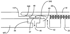
図4および図5の実施例では、縁液体供給システムが、孔40を介してリザーバ30に液体を供給する。リザーバ30中の液体は、任意選択で液体供給システム中の浸漬液と同じである。リザーバ30は、基板Wの投影レンズとは反対側に配置され、基板Wの縁および縁密封部材17、117の縁に隣接する。図5では、縁密封部材17は、基板テーブルWTとは別個の要素で構成され、図4では、縁密封部材117は、基板テーブルWTの一体部分によって提供される。図4で最も明白に見られるように、基板Wは、いわゆるピンプル・テーブル20によって基板テーブルWT上に支持される。ピンプル・テーブル20は複数の突起を備え、その上に基板Wが載る。基板Wは、例えば基板テーブルWTの頂面へと基板を吸引する負圧源などによって、所定の位置に保持される。リザーバ30を使用すると、基板Wの縁を撮像する時(つまり投影レンズ下で液体供給システム中の液体が基板の縁を横切る時)、液体は液体供給システムから、縁密封部材17、117と基板2間のギャップに逃げることができない。その空間が既に液体で充填されているからである。
In the embodiment of FIGS. 4 and 5, the edge liquid supply system supplies liquid to the
基板テーブルWTの残りの部分に対して縁密封部材17を移動させ、図5に図示された機構170を、図6で詳細に示す。縁密封部材17をこの方法で移動させる理由は、その1次表面を基板Wの1次表面とほぼ同一平面上にできるようにするためである。これによって、液体供給システムは基板Wの縁部分上で滑らかに移動することができ、したがって液体供給システムの底部内周は、一部は基板Wの1次表面上の位置に、一部は縁密封部材17の1次表面上に移動することができる。
The
レベル・センサ(図示せず)を使用して、基板Wおよび縁密封部材17の1次表面の相対的高さを検出する。レベル・センサの結果に基づき、縁密封部材17の1次表面の高さを調節するため、制御信号をアクチュエータ171に送信する。閉ループ・アクチュエータもこの目的に使用することができる。
A level sensor (not shown) is used to detect the relative heights of the primary surfaces of the substrate W and the
アクチュエータ171は、シャフト176を回転させる回転モータである。シャフト176は、モータ171に対して遠位側の端部で円形ディスクに接続される。シャフト176は、ディスクの中心から離れて接続される。ディスクは、ウェッジ部分172の円形窪みに配置される。玉軸受けを使用して、円形ディスクとウェッジ部分172の窪みの側部との摩擦量を軽減してもよい。モータ171は、板ばね177によって所定の位置に保持される。モータを起動すると、ウェッジ部分は、ディスク内でのシャフトの偏心位置のため、図示のように左右に(つまりウェッジ部分の傾斜の方向に)駆動される。モータは、ばね177によるウェッジ部分172の動作の方向と同じ方向には動作することができない。
The
ウェッジ部分172が図6で示すように左右に移動するにつれ、その上面175(縁密封部材17の1次表面に対して傾斜しているウェッジの表面)が、縁密封部材17の底部に固定されたさらなるウェッジ部材173の底部傾斜面に接触する。縁密封部材71は、ウェッジ部材17の動作方向に動作することができず、したがってウェッジ部材172が左および右に移動すると、縁密封部材17はそれぞれ下降および上昇する。縁密封部材17は基板テーブルWTに向かって多少のバイアスが必要なことがある。
As the
さらなるウェッジ部材173は、例えばウェッジ172の動作方向に対して直角に配置された棒など、代替形状で置換できることは明白である。ウェッジ部材172とさらなるウェッジ部材172との摩擦係数が、ウェッジ角度の正接より大きい場合は、アクチュエータ170が自動制動手段になり、ウェッジ部材172を所定の位置に保持するため、それに力を加える必要がない。これは、アクチュエータ171を起動していない場合に、システムが安定するので有利である。機構170の正確さは、数μmのオーダーである。
It is clear that the
特に縁密封部材117が基板テーブルWTの一体部品である場合に、縁密封部材17、117と基板の1次表面をほぼ同一平面上にできるよう、基板Wまたは基板Wを支持する部材の高さを調節する機構を設けてもよい。
In particular, when the
実施例3
第3実施例は図7に図示され、以下の説明以外は第1実施例と同じ、または同様である。
Example 3
The third embodiment is illustrated in FIG. 7 and is the same as or similar to the first embodiment except for the following description.
この実施例について、基板テーブルWTの一体部品である縁密封部材117に関連して説明する。しかし、この実施例は、基板テーブルWTに対して動作可能な縁密封部材17にも等しく適用することができる。この実施例では、不可欠なことではないが、縁密封部材17が、基板の1次表面と同一平面上にある上面を有するが、こうすることが好ましい。真空源に接続された真空孔46を、基板Wの投影システムとは反対側で、縁密封部材117および基板Wの縁部分の下および近傍に設ける。孔46は環状で、連続溝で形成することが好ましいが、不連続、つまり別個の幾つかの開口を円形パターンで配置してもよい。最も単純な形態では、実施例は、孔46を介してその真空源だけで働くことができる。しかし、基本的概念は、第3実施例の第1バージョンを例証し、図7aで詳細に図示された基板テーブルWTを設けることによって改善することができる。
This embodiment will be described in relation to the
基板テーブルSTの部分48が、縁密封部分117の縁から内側に延在し、したがって基板Wの投影システムとは反対側で基板テーブルWの下に配置される。部分48と基板Wの間のギャップを通して漏出する浸漬液体は、孔46を介して真空源へと引きつけられる。流路42を、真空源の半径方向内側で、これも基板Wの下に設け、気体源に接続する。これは、大気圧より高い圧力の気体でも、単純に流路42を大気に対して開放してもよい。これによって、基板Wの下で、基板Wの下にある基板テーブルWTの部分48とピンプル・テーブル20との間に半径方向外側への空気の流れが生じる。(ピンプル・テーブル20は、基板を所定の位置に保持するため、自身の真空源を有する。)このような空気の流れがあるので、縁密封部材117と基板Wとの間に逃げる液体があっても、真空源と流体接続した環状区画44(断面がほぼ3×3mm)へと引きつけられる。区画44は、ギャップに対して開いた環状孔47と真空源に接続された孔46との間に配置される。区画は、周辺に均一な流れを確立するのに役立つ。流路42は、連続環状溝(ダクトの広がりとして図示)に接続される。区画44、孔47および/または流路42の溝は、環状である必要はなく、他の適切な形状または構成でよい。
A
作業中の1つの実施例では、基板テーブルWTの部分48と基板W間のギャップは、最大100μmのオーダーであり(しかしギャップは存在しなくても、つまりゼロでもよい)、これにより、毛管現象によって液体がギャップを高速で流れることが防止される。流路42に接続された溝と区画44との間で基板テーブルWTの部分45の高さは、基板Wの底部とその部分45との間の距離(図7にて距離D1で図示)が、通常は100μmのオーダーになるような高さであり、0.5バール未満の圧力損で、少なくとも1m/秒の領域での均一な気体流が達成できるよう選択される。このような構成により、ギャップD1を通過し、ピンプル・テーブル20と干渉する液体が、存在しても非常に少ししかないことが保証される。他の値でも作用する。
In one working example, the gap between the
図7aで示した第3実施例の第1バージョンは、基板Wが外側に10mm程度屈曲することがある。図7aで見られるように、上述したように部分45が基板Wの下へ、基板Wを支持する場所へと延在できても、この区域は全く支持されていない。しかし、まさしく外径で、基板Wの重量と、基板Wと基板テーブルWTの部分48間にある水の毛管力とが両方とも、なお基板Wの縁を屈曲させることができる。これが有害であることは明白である。この問題に対する解決法が図7bから図7dに図示され、これは第3実施例の第2から第4バージョンを示す。同様の参照番号が同じ機構に使用されている。
In the first version of the third embodiment shown in FIG. 7a, the substrate W may be bent outward by about 10 mm. As can be seen in FIG. 7a, even though the
図7bで示す第2では、部分48が、基板Wの周の縁およびその近傍に(円形パターンで)配置された少なくとも1組の節348を有する。節348が別個であるので、浸漬液はなお、部分48と基板Wの間に滲入することができるが、基板Wの重量は、少なくとも1組の節348によって支持される。節348は、ピンプル・テーブル20の節より高さが小さいことが好ましく、これは節348の近傍の縁において基板Wにかかる力と比較して、ピンプル・テーブル20の真空22によって生じる基板Wへの下方向の力の差を補償する。計算には、節の剛性を考慮にいれ、節が好ましいのでZerodurなどの低膨脹ガラスから製造されている場合、これはピンプル・テーブル20の節より約80nm低くなければならない。部分48と基板Wの底部との間のギャップは、約20μmであることが好ましい。
In the second shown in FIG. 7b, the
図7bのバージョンでは、部分45は第1バージョンと形状が類似している。しかし、代替品は、部分45の上に配置されたリングまたは円形パターンの節345を有する。節345の離散的性質のため、流路42からの気体を区画44に吸引することができる。この節345も、ピンプル・テーブル20の節より約80nm低い。節345間のギャップD1は約50μmであることが好ましい。節345は、ピンプル・テーブル20によって形成することができ、必ずしも基板テーブルWTの一部である必要はない。
In the version of FIG. 7b, the
上記の第3実施例の2つのバージョンから、通路42および47によって形成された空気密封は、完全に基板テーブルWTによって、完全にピンプル・テーブル20によって、または両者の組合せによって形成できることが明白になる。図7cおよび図7dは、第3実施例のさらなる2つのバージョンを示す。図7cは、空気密封をピンプル・テーブル20の部材によって形成する第3実施例の第3バージョンを示す。第1および第2バージョンの部分45は、ピンプル・テーブル2045の環状部分から形成され、第1および第2バージョンの部分48は、ピンプル・テーブル20の環状部分2048によって形成される。42および47と等しい通路2042、2047を、部分2045、2048の間に形成する。しかし、気体流の一部のみが2本の通路2042、2047を通って流れ、図示のように、ピンプル・テーブル20の外縁の下に漏れる浸漬液体のさらなる進入を阻止するのに有効な一部の気体が、ピンプル・テーブル20の下を流れる。この構成は、必要な正確な寸法が全てピンプル・テーブル20で作成され、基板テーブルWTが複雑な溝を一切含まないので有利である。
From the two versions of the third embodiment above, it becomes clear that the air seal formed by the
図7dで示した第3実施例の第4バージョンでは、流入通路42が設けられず、気体がピンプル・テーブル20から環状孔47内へ流れる。このバージョンは、ピンプル・テーブル20が自身の真空源を必要としないので、基板Wとピンプル・テーブル20間でさらに安定した圧力を経験するという点で有利である。さらに、第3バージョンで必要とした余分な通路2042が必要でなく、通路2042しか要求されない。したがって、1つの真空源が、漏れている浸漬液体を除去することと、基板を所定の位置に保持することとの両方に効果的である。外方向への気体流を確立できるよう、ピンプル・テーブル20の下に気体源を必要とすることがある(そのためには、ピンプル・テーブルの下で基板テーブルにあるさらに一般的な真空孔を使用できるようである)。
In the fourth version of the third embodiment shown in FIG. 7 d, the
第3実施例の各バージョンの様々な特徴は、ピンプル・テーブルの中心から真空46への半径方向外向きの気体流が達成される限り、組み合わせることができる。
The various features of each version of the third embodiment can be combined as long as a radially outward gas flow from the center of the pimple table to the
実施例4
第4実施例は図8および図9に図示され、以下の説明以外は第1実施例と同じ、または同様である。
Example 4
The fourth embodiment is shown in FIGS. 8 and 9, and is the same as or similar to the first embodiment except for the following description.
この実施例を、基板テーブルWTの一体部品である縁密封部材117に関して説明する。しかし、この実施例は、基板テーブルWTに対して移動可能な縁密封部材17にも等しく適用可能である。
This embodiment will be described with respect to the
図8aで示すようなこの実施例の第1バージョンでは、さらなる縁密封部材500を使用して、縁密封部材117と基板W間を架橋する。さらなる縁密封部材を縁密封部材117に取り付ける。さらなる縁密封部材500を、基板Wの1次表面とは反対の表面に当てて、着脱式に取り付ける。この実施例では、さらなる縁密封部材500は、基板Wの下面に接触するよう起動可能な可撓性縁密封部材でよい。可撓性縁密封部材500を停止すると、これは重力で基板から落下する。これを達成する方法を図9で示し、以下で説明する。
In a first version of this embodiment as shown in FIG. 8a, a further
さらなる縁密封部材500は、液体供給システムからの浸漬液体全てが基板Wの下の空間に入ることを防止するわけでなく、この理由から、低圧源に接続された孔46を、縁密封部材117の縁に隣接する基板W、およびこの実施例の一部または全てのバージョンの基板Wの下に設けることができる。言うまでもなく、基板の下にある区域の設計は、第3実施例のそれと同じでよい。
The additional
基板Wではなく、基板テーブル上にある透過像センサ(TIS)などのセンサに、同じシステムを使用することができる。センサの場合、センサは移動しないので、縁密封部材500を、例えば接着剤などを使用してセンサに永久的に取り付けることができる。
The same system can be used for a sensor such as a transmission image sensor (TIS) on the substrate table rather than the substrate W. In the case of a sensor, since the sensor does not move, the
さらに、縁密封部材500は、底面ではなくオブジェクトの上面(投影システムに近い方の表面)と係合するよう配置することができる。また、さらなる縁密封部材500を、図8aで示すように、縁密封部材117の下ではなく、縁密封部材117の上面に、またはその付近に取り付けてもよい。
Furthermore, the
この実施例の第2バージョンを図8bに示す。2つのさらなる縁密封部材500a、500bを使用する。第1の縁密封部材500aは、第1バージョンと同じである。第2の縁密封部材500bは、基板テーブル20に、つまり基板Wの下に取り付けて、これは自由端が取付点から半径方向外側に延在する。第2のさらなる縁密封部材500bは、第1のさらなる縁密封部材500aを基板Wに締め付ける。圧縮ガスを使用して、第2のさらなる縁密封部材500bを変形するか、動作させることができる。
A second version of this embodiment is shown in FIG. Two additional
この実施例の第3バージョンを図8cに示す。第3バージョンは、第2バージョンと同じであるが、第1のさらなる縁密封部材500cが第2のさらなる縁密封部材500dを基板Wに締め付ける。これにより、例えば第2バージョンの圧縮ガスが不必要になる。
A third version of this embodiment is shown in FIG. The third version is the same as the second version, but the first further
この実施例も、真空に接続しても、接続しなくても、第2のさらなる縁密封部材500b、500dでのみ作用することが理解される。
It will be appreciated that this embodiment also works only with the second further
次に、さらなる縁密封部材500、500a、500b、500c、500dを変形する様々な方法について、実施例の第1バージョンに関連して説明する。
Various methods of deforming the further
図9から見られるように、流路510をさらなる可撓性縁密封部材500(好ましくは環状のリング)の長手方向に形成し、さらなる可撓性縁密封部材の投影システムに面する上面、および基板Wの下側に1つまたは複数の別個の孔を設ける。真空源515をダクト510に接続することにより、さらなる可撓性縁密封部材を吸引にて基板Wに突き合わせることができる。真空源515を切断するか、オフに切り換えると、さらなる可撓性縁密封部材500は重力および/または孔46からの圧力で落下し、図9の点線で示した位置になる。
As can be seen from FIG. 9, the
代替実施例では、基板をピンプル・テーブル20に載せて、さらなる可撓性縁密封部材500が弾性変形すると、これが基板Wに接触するよう、さらなる可撓性縁密封部材500を機械的予荷重で形成し、したがって基板Wに上方向の力を加えて、密封を作成する。
In an alternative embodiment, the substrate is placed on the pimple table 20 and the additional flexible
さらなる代替品では、さらなる可撓性縁密封部材500を、孔46にかかる加圧気体によって発生した過剰圧力によって基板Wに押し付ける。
In a further alternative, a further flexible
さらなる可撓性縁密封部材500は、可撓性で放射線および浸漬液体に耐性があり、汚染しない任意の材料、例えば鋼、Al2O3などのガラス、SiCなどのセラミック材料、シリコン、テフロン(登録商標)、低膨脹ガラス(例えばZerodur(TM)またはULE(TM))、炭素繊維エポキシまたはクォーツから下降することができ、通常は10から500μmの厚さ、好ましくは30から200μm、またはガラスの場合、50から150μmの厚さである。この材料および寸法のさらなる可撓性縁密封部材500では、ダクト510に加える必要がある典型的圧力は、約0.1から0.6バールである。
The further flexible
実施例5
第5実施例は図109に図示され、以下の説明以外は第1実施例と同じ、または同様である。
Example 5
The fifth embodiment is illustrated in FIG. 109 and is the same as or similar to the first embodiment except for the following description.
この実施例を、基板テーブルWTの一体部品である縁密封部材117に関して説明する。しかし、この実施例は、基板テーブルWTに対して動作可能な縁密封部材17にも等しく適用可能である。
This embodiment will be described with respect to the
第5実施例では、縁密封部材117と基板W間のギャップは、さらなる縁密封部材50で充填される。さらなる縁密封部材は、基板2および縁密封部材117の1次表面とほぼ同一平面上にある上面を有する。さらなる可撓性縁密封部材50は、可撓性材料で作成され、したがって基板Wの直径および基板Wの厚さにおける微小な変動は、さらなる可撓性縁密封部材50の屈曲によって対応することができる。投影レンズの下で液体供給システム内の液体が基板の縁の上を通過する時、液体は基板Wと、さらなる可撓性縁密封部材50と縁密封部材117との間に逃げることができない。これらの要素の縁が相互に密着しているからである。さらに、基板Wおよび縁密封部材117の1次表面、およびさらなる可撓性縁密封部材50の上面がほぼ同一平面上にあるので、液体供給システムが基板Wの縁上を通過しても、その動作は不調にならず、したがって液体供給システム内に妨害力が発生しない。
In the fifth embodiment, the gap between the
図10で見られるように、さらなる可撓性縁密封部材50は、基板Wの1次表面とは反対の基板Wの表面に、縁部分にて接触する。この接触は2つの機能を有する。第1に、さらなる可撓性縁密封部材50と基板W間の流体密封が改善される。第2に、さらなる可撓性縁密封部材50が、ピンプル・テーブル20から離れる方向で基板Wに力を加える。基板2を、例えば負圧吸引などによって基板テーブルWT上に保持する場合、基板を基板テーブル上に確実に保持することができる。しかし、真空源をオフにするか、切断すると、さらなる可撓性縁密封部材50によって基板W上に生成された力は、基板Wを押して基板テーブルWTから離すのに効果的であり、それによって基板Wの装填および取り外しを補助する。
As seen in FIG. 10, a further flexible
さらなる可撓性縁密封部材50は、PTFEなど、放射線および浸漬液体に耐性がある材料で作成する。
The further flexible
実施例6
図11は、以下の説明以外は第1実施例と同じ、または同様である本発明の第6実施例を示す。
Example 6
FIG. 11 shows a sixth embodiment of the present invention which is the same as or similar to the first embodiment except for the following description.
この実施例を、基板テーブルWTの一体部品である縁密封部材117に関して説明する。しかし、この実施例は、基板テーブルWTに対して動作可能な縁密封部材17にも等しく適用可能である。
This embodiment will be described with respect to the
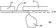
第6実施例は、ピンプル・テーブル20を、基板Wと縁密封部材117の間で液体供給システムから切り離せる方法を示す。これは、大気65に露出した開口を、基板Wの縁と、基板Wを基板テーブルWT上に保持し、ピンプル・テーブル20を伴う真空との間に配置することによって実行する。
The sixth embodiment shows how the pimple table 20 can be separated from the liquid supply system between the substrate W and the
基板Wの投影システムとは反対側で、基板の縁の下に配置された層60は、基板Wと層60の間に約1μmのギャップを生じ、テフロン(登録商標)、シリコンゴム、または他のプラスチック材料などの疎水性である任意の材料で構成される。耐放射線性が優れているので、無機材料が好ましい。この方法で、液体供給システムが基板Wの縁上に配置された場合に、基板Wと縁密封部材117間のギャップに入る液体が跳ね返され、したがって有効密封が形成され、液体はピンプル・テーブル20に入らない。浸漬液体は、疎水性層60との間に少なくとも90°の接触角を有することが好ましい。
On the opposite side of the substrate W from the projection system, the
実施例7
本発明の第7実施例について、図12から図15に関して説明する。第7実施例は、以下の説明以外は第1実施例と同じ、または同様である。
Example 7
A seventh embodiment of the present invention will be described with reference to FIGS. The seventh embodiment is the same as or similar to the first embodiment except for the following description.
第7実施例では、図12で示すように縁密封部材17は環状で、中心穴は円形基板Wより直径が大きい。基板Wおよび縁密封部材17の形状は、縁密封部材17の中心穴が基板Wの外径より大きい限り、変更してよい。この方法で、縁密封部材17は基板W直径の変動に対応することができる。
In the seventh embodiment, as shown in FIG. 12, the
縁密封部材17は、基板テーブルWT上で動作可能であり、したがって液体供給システムが、露光のために基板Wの縁部分に向かって動作する場合、縁密封部材17を、露光すべき基板Wのその縁部分にぴったり突き当たるよう動作させることができる。これは図13で最もよく図示され、ここでは基板Wの左手側が露光されるところである。
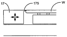
The
図14で明白に図示されたように、縁密封部材17は、基板Wの1次表面の面と、好ましくはZ方向(つまり装置の光軸の方向)との両方で動作可能である。この方法で、縁密封部材17を、必要に応じて基板Wの縁へと移動させることができ、1次表面が基板Wの1次表面とほぼ同一平面上になるよう、その上部(1次)表面の高さを調節することができる。これによって、液体供給システムは、基板Wの縁の撮像時にも、リザーバ内に浸漬液を効果的に含むことができる。
As clearly shown in FIG. 14, the
図14には、縁密封部材17の1次表面と同一平面上にある上面を有する突起175も図示されている。つまり、縁密封部材17の1次表面が基板Wに隣接する縁上に出っ張り、したがって突起が装置の光軸に向かって延在する。図14で見られるように、これによって、基板Wの縁がわずかに湾曲していても(つまり基板Wの縁が1次表面に直角でなくても)基板Wと縁密封部材17の1次表面間のギャップを最小にすることができる。
Also shown in FIG. 14 is a
縁密封部材17と基板W間のギャップを改善または削減する別の方法は、基板2に近い方の縁密封部材17の縁と基板Wとの間にさらなる(可撓性)縁密封部材177を設けることである。これを図15で示す。これは、突起175があってもなくても実行することができる。さらなる可撓性縁密封部材177は、基板Wとの間で密封を形成するよう、基板Wの縁の周囲で変形することができる。さらなる可撓性縁密封部材177を縁密封部材17に取り付ける。さらなる可撓性縁密封部材177は、基板Wおよび縁密封部材17の1次表面とほぼ同一平面上にある上面を有する。
Another way to improve or reduce the gap between the
実施例8
図16は、以下の説明以外は第1実施例と同じ、または同様である本発明の第8実施例を示す。
Example 8
FIG. 16 shows an eighth embodiment of the present invention which is the same as or similar to the first embodiment except for the following description.
この実施例を、基板テーブルWTの一体部品である縁密封部材117に関して説明する。しかし、この実施例は、基板テーブルWTに対して動作可能な縁密封部材17にも等しく適用可能である。
This embodiment will be described with respect to the
図16で見られるように、第8実施例は、縁密封部材117と基板W間のギャップに架橋するさらなる縁密封部材100を含む。この場合、さらなる縁密封部材100は、基板をよび縁密封部材117の1次表面上に配置されて、基板Wと縁密封部材117間のギャップにまたがるギャップ密封部材である。したがって、基板Wが円形の場合、ギャップ密封部材100も円形(環状)になる。
As seen in FIG. 16, the eighth embodiment includes a further
ギャップ密封部材100は、真空105をその下側に加えることによって所定の位置に保持することができる(これは縁密封部材117の1次表面の真空孔を通して曝露する真空源である)。基板Wと縁密封部材117間のギャップがギャップ密封手段100によって覆われているので、液体供給システムは、液体を損失することなく、基板Wの縁上を通過することができる。ギャップ密封部材100は、標準的な基板および基板の取扱い法を使用できるよう、基板ハンドラによって所定の位置に配置し、除去することができる。あるいは、ギャップ密封部材100は、投影システムPLで保持し、適切な機構(例えば基板取扱いロボット)によって所定の位置に配置し、除去することができる。ギャップ密封部材100は、真空源によって変形しないよう十分に剛性でなければならない。ギャップ密封部材100は、液体供給システムと接触しないよう、50μm未満、好ましくは30または20、さらには10μm未満の厚さであると有利であるが、可能な限り薄くしなければならない。
The
ギャップ密封部材100には、ギャップ密封部材100の厚さが縁に向かって減少するテーパ状縁110を設けると有利である。ギャップ密封部材の完全な厚さまでこのように漸進的に遷移すると、ギャップ密封部材100上を通過する場合に、液体供給システムの干渉が確実に減少する。
The
同じ方法の密封を、センサ、例えば透過像センサなどの他のオブジェクトにも使用することができる。その場合、オブジェクトは移動する必要がないので、ギャップ密封部材100を、浸漬液中で熔解しない接着剤で、(いずれかの端部の)所定の位置に接着することができる。あるいは接着剤は、縁密封部材117とオブジェクトとギャップ密封部材100との接合部に配置してもよい。
The same method of sealing can be used for other objects such as sensors, for example transmission image sensors. In that case, since the object does not need to move, the
さらに、ギャップ密封部材100は、オブジェクトおよび縁密封部材117の出っ張りの下に配置することができる。オブジェクトには、必要に応じて出っ張りを形成してもよい。
Further, the
ギャップ密封部材100は、オブジェクトの上にあっても下にあっても、縁密封部材117と接触する表面にある1つの開口からオブジェクトと接触する表面にある別の開口まで、自身を通って設けた通路を有することができる。真空105と流体連絡する1つの開口を配置することにより、ギャップ密封部材100を所定の位置にしっかり保持することができる。
The
実施例9
第9実施例について図17に関して説明する。図17で示す解決法は、基板Wの縁部分の撮像に伴う問題の幾つかを回避するとともに、基板Wと同じ条件で透過像センサ(TIS)220を投影レンズPLで照射することができる。
Example 9
A ninth embodiment will be described with reference to FIG. The solution shown in FIG. 17 avoids some of the problems associated with imaging of the edge portion of the substrate W and can irradiate the transmission image sensor (TIS) 220 with the projection lens PL under the same conditions as the substrate W.
第9実施例は、第1実施例に関して説明した液体供給システムを使用する。しかし、液体供給システム中の浸漬液を、下側に基板Wを有する投影レンズの下に限定するのではなく、液体は、液体供給システムと基板Wとの間に配置された中間プレート210によって限定される。中間プレート210とTIS220と基板Wとの間の空間222、215も液体111で充填される。これは、図示のように個々の孔230、240を介して2つの別個の空間液体供給システムによって実行するか、孔230、240を介して同じ空間液体供給システムによって実行することができる。したがって、基板Wと中間プレート210間の空間215、および透過像センサ220と中間プレート210間の空間220は、両方とも液体で充填され、基板Wおよび透過像センサは両方とも、同じ条件で照明することができる。部分200は、真空源によって所定の位置に保持できる中間プレート210に、1つまたは複数の支持表面を提供する。
The ninth embodiment uses the liquid supply system described with respect to the first embodiment. However, rather than limiting the immersion liquid in the liquid supply system below the projection lens with the substrate W underneath, the liquid is limited by an
中間プレート210は、基板をよび透過像センサ220を全て覆うようなサイズで作成する。したがって、基板Wの縁を撮像する場合でも、または透過像センサを投影レンズPLの下に配置する場合も、液体供給システムは縁を横断する必要がない。透過像センサ220と基板Wの上面はほぼ同一平面上にある。
The
中間プレート210は着脱式でよい。例えば、基板取扱いロボットまたは他の適切な機構によって所定の位置に配置し、除去することができる。
The
実施例10
図18は、本明細書で説明した他の任意の実施例に適切可能であり、突然の液体損の前に浸漬液が広がり得るギャップのサイズを増加させるのに効果的な液体供給システムの変形を示す。
Example 10
FIG. 18 is applicable to any of the other embodiments described herein and is a variation of the liquid supply system that is effective to increase the size of the gap where immersion liquid can spread before sudden liquid loss. Indicates.
複数の毛管600を液体供給システム(例えば密封部材12)と投影レンズPLの間に設ける。この毛管は、概ね上方向に、つまり基板Wから離れる方向に延在する。毛管が半径rを有すると、毛管が支持できる液体膜の厚さhは、下式によって与えられる。
h=(2σcosθ)/(rgρ)
ここでσは界面張力、θは液体と毛管w間の接触角、ρは液体の密度である。cosθをプラスにする(つまり毛管の内面をコーティングなどによって疎水性にする)と、毛管は、ギャップからの高さhの液体部分を支持することができ、したがってこれがまたがるギャップを大きくすることができる。
A plurality of
h = (2σ cos θ) / (rgρ)
Here, σ is the interfacial tension, θ is the contact angle between the liquid and the capillary w, and ρ is the density of the liquid. When cos θ is made positive (ie, the inner surface of the capillary is made hydrophobic, such as by coating), the capillary can support the liquid portion at a height h from the gap, and thus increase the gap that it spans. .
疎水性被膜毛管と液体との間に電圧を印加することにより、cosθを約ゼロへと減少させることができ、これによって(上式1により)毛管600を通る液体の自由な流れが可能になり、したがって毛管の長さを小さくしておくことにより、投影レンズ下の液体供給システムから短時間で液体を除去することができる。これは、液体を清浄に維持するのに有利である。基板Wの縁を撮像する場合は、ギャップにまたがれるよう電圧を除去することができる。基板Wから液体膜を持ち上げるため、基板Wの縁を疎水性材料で被覆することが提案される(または基板材料自体が疎水性であるので、基板Wの縁のレジストを除去することができる)。 By applying a voltage between the hydrophobic coated capillary and the liquid, cos θ can be reduced to about zero, thereby allowing free flow of liquid through the capillary 600 (according to Equation 1 above). Therefore, by reducing the length of the capillary, the liquid can be removed from the liquid supply system under the projection lens in a short time. This is advantageous for keeping the liquid clean. When imaging the edge of the substrate W, the voltage can be removed so as to straddle the gap. In order to lift the liquid film from the substrate W, it is proposed to coat the edge of the substrate W with a hydrophobic material (or the substrate material itself is hydrophobic so that the resist on the edge of the substrate W can be removed). .
毛管600は、ほぼ円形の断面でほぼ直線のダクト、または他の形状のダクトによって設けることができる。例えば、毛管は多孔質材料の空隙で構成してもよい。 The capillary 600 may be provided by a substantially straight duct with a substantially circular cross section, or other shaped duct. For example, the capillary may be composed of voids in a porous material.
上述した実施例は全て、基板Wの縁の周囲を密封するのに使用することができる。基板テーブルWT上にある他のオブジェクトも、同様の方法で密封する必要があることもある。例えば、透過像センサ、結合レンズ干渉計およびスキャナ(波面センサ)およびスポット・センサ・プレートなど、液体を通して投影ビームで照明するセンサおよび/またはマークを含むセンサなどである。このようなオブジェクトには、レベリングおよび位置合わせセンサおよび/またはマークなど、非投影放射線ビームで照明するセンサおよび/またはマークもある。このような場合、液体供給システムは、全てのオブジェクトを覆うよう液体を供給することができる。上記の実施例はいずれも、この目的に使用することができる。場合によっては、オブジェクトを基板テーブルWTから外す必要がない。というのは、基板Wとは異なり、センサは基板テーブルWTから外す必要がないからである。このような場合は、上記の実施例を適宜変形することができる(例えば、密封を可動式にする必要がない)。 All the embodiments described above can be used to seal around the edge of the substrate W. Other objects on the substrate table WT may need to be sealed in a similar manner. Examples include transmission image sensors, coupled lens interferometers and scanners (wavefront sensors) and sensors that illuminate with a projection beam through a liquid and / or sensors that include marks. Such objects also include sensors and / or marks that illuminate with a non-projection radiation beam, such as leveling and alignment sensors and / or marks. In such a case, the liquid supply system can supply liquid to cover all objects. Any of the above embodiments can be used for this purpose. In some cases, it is not necessary to remove the object from the substrate table WT. This is because, unlike the substrate W, the sensor does not have to be removed from the substrate table WT. In such a case, the above-described embodiment can be modified as appropriate (for example, the sealing need not be movable).
各実施例を、適宜、他の1つまたは複数の実施例と組み合わせてもよい。さらに、実現可能および/または適切であれば、各実施例(および任意の適切な実施例の組合せ)を、縁密封部材17、117なしに図2および図19および図20の液体供給システムに適用するだけでよい。
Each embodiment may be combined with one or more other embodiments as appropriate. Further, each embodiment (and any suitable combination of embodiments), if feasible and / or appropriate, applies to the liquid supply system of FIGS. 2, 19 and 20 without
縁密封部材117およびセンサ220の上部最外縁の形状は、変更することができる。例えば、出っ張った縁密封部材117、または実際に出っ張っているセンサ220の外縁を設けると有利なこともある。あるいは、センサ220の上部外隅が有用なこともある。
The shapes of the outermost edges of the
実施例11
図19は、以下の説明以外は第1実施例と同じである第11実施例を示す。
Example 11
FIG. 19 shows an eleventh embodiment which is the same as the first embodiment except for the following description.
第11実施例では、基板テーブルWT上のオブジェクトは、透過像センサ(TIS)などのセンサ220である。浸漬液がセンサ220の下に滲入するのを防止するため、浸漬流体で溶解せず、これに反応しない接着剤ビード700を、縁密封部材117とセンサ220の間に配置する。接着剤は、使用中の浸漬流体で覆われる。
In the eleventh embodiment, the object on the substrate table WT is a
実施例12
第12実施例について、図20および図21に関して説明する。第12実施例では、基板テーブルWTに封止されるのはセンサ220である。図20および図21で図示した両方のバージョンで、縁密封部材117と基板220の縁との間のギャップに入るような浸漬液を全て除去するため、開口通路47および室44でギャップの近傍に真空46を設ける。
Example 12
A twelfth embodiment will be described with reference to FIGS. In the twelfth embodiment, it is the
図20のバージョンでは、真空46を、オブジェクト220の出っ張り部分の下で基板テーブルWTに提供する。基板テーブルSTの内側に突き出した出っ張り部分に通路47を設ける。任意選択で、基板テーブルWTとオブジェクト220の間に突出する部分の最内縁に接着剤ビード700を配置する。接着剤ビード700を設けない場合は、オブジェクト220の下からの気体流が、センサ220と基板テーブルWT間のギャップの密封に役立つ。
In the version of FIG. 20, a
図21のバージョンでは、内側に突き出した縁密封部材117の下で、オブジェクト自体に真空46、区画44および通路47を設ける。この場合も、オブジェクト220と基板テーブルWTの間に通路47の半径方向外側へと接着剤ビードを設ける選択肢がある。
In the version of FIG. 21, the object itself is provided with a
本発明の特定の実施例について以上で説明してきたが、本発明は記述以外の方法で実践できることが理解される。特に、本発明は、他のタイプの液体供給システム、特に局所的液体区域システムにも適用可能である。密封部材の解決法を使用する場合は、気体密封以外の密封を使用する解決法でよい。説明は、本発明を制限するものではない。 While specific embodiments of the invention have been described above, it will be appreciated that the invention may be practiced otherwise than as described. In particular, the present invention is applicable to other types of liquid supply systems, particularly local liquid area systems. If a sealing member solution is used, a solution using a seal other than a gas seal may be used. The description is not intended to limit the invention.
Claims (35)
−パターン形成手段を支持する支持構造とを備え、パターン形成手段は、所望のパターンに従って投影ビームにパターン形成する働きをし、さらに、
−基板を保持する基板テーブルと、
−パターン形成したビームを基板の標的部分に投影する投影システムと、
−前記投影システムの最終要素と、基板テーブル上に配置されたオブジェクト間の空間を液体で少なくとも部分的に充填する液体供給システムとを備え、
前記基板テーブルが、さらに、オブジェクトの縁を少なくとも部分的に囲む縁密封部材と、前記縁密封部材と前記投影システムとは反対側にあるオブジェクトとの間のギャップに真空または液体を供給するよう配置された真空孔または液体供給孔とを備えることを特徴とするリソグラフィ投影装置。 A radiation system for supplying a projection beam of radiation;
A support structure for supporting the patterning means, the patterning means serving to pattern the projection beam according to a desired pattern;
A substrate table for holding the substrate;
A projection system for projecting the patterned beam onto a target portion of the substrate;
-A final element of the projection system and a liquid supply system that at least partially fills a space between objects arranged on the substrate table with liquid;
Wherein the substrate table further arranged to deliver the edge sealing member surrounding the edge of the object at least in part, a vacuum or liquid to the gap between the object on the opposite side to the edge sealing member and the projection system A lithographic projection apparatus, comprising: a vacuum hole or a liquid supply hole.
−パターン形成手段を支持する支持構造とを備え、パターン形成手段が、所望のパターンに従って投影ビームにパターン形成する働きをし、さらに、
−基板を保持する基板テーブルと、
−パターン形成したビームを基板の標的部分に投影する投影システムと、
−前記投影システムの最終要素と、基板テーブル上に配置されたオブジェクト間の空間を液体で少なくとも部分的に充填する液体供給システムとを備え、
前記基板テーブルが、さらに、オブジェクトの縁を少なくとも部分的に囲み、前記投影システムに面してオブジェクトの1次表面とほぼ同一平面上にある1次表面を提供する縁密封部材を備え、前記液体供給システムが、前記オブジェクトおよび/または前記縁密封部材および/または基板の局所的区域に液体を供給することを特徴とするリソグラフィ投影装置。 A radiation system sharing a projection beam of radiation;
A support structure for supporting the patterning means, wherein the patterning means serves to pattern the projection beam according to a desired pattern;
A substrate table for holding the substrate;
A projection system for projecting the patterned beam onto a target portion of the substrate;
-A final element of the projection system and a liquid supply system that at least partially fills a space between objects arranged on the substrate table with liquid;
The substrate table further comprises an edge sealing member that at least partially surrounds an edge of the object and provides a primary surface facing the projection system and substantially coplanar with the primary surface of the object; A lithographic projection apparatus, wherein a supply system supplies a liquid to a local area of the object and / or the edge sealing member and / or the substrate.
−パターン形成手段を支持する支持構造とを備え、パターン形成手段が、所望のパターンに従って投影ビームにパターン形成する働きをし、さらに、
−基板を保持する基板テーブルと、
−パターン形成したビームを基板の標的部分に投影する投影システムと、
−前記投影システムの最終要素と、基板テーブル上に配置されたオブジェクト間の空間を液体で少なくとも部分的に充填する液体供給システムとを備え、
前記基板テーブルが、さらに、オブジェクトの縁を少なくとも部分的に囲む縁密封部材と、前記縁密封部材とオブジェクト間のギャップにまたがって延在し、オブジェクトと接触するさらなる縁密封部材とを備えることを特徴とするリソグラフィ投影装置。 A radiation system sharing a projection beam of radiation;
A support structure for supporting the patterning means, wherein the patterning means serves to pattern the projection beam according to a desired pattern;
A substrate table for holding the substrate;
A projection system for projecting the patterned beam onto a target portion of the substrate;
-A final element of the projection system and a liquid supply system that at least partially fills a space between objects arranged on the substrate table with liquid;
The substrate table further comprises an edge sealing member that at least partially surrounds an edge of the object, and a further edge sealing member that extends across the gap between the edge sealing member and the object and contacts the object. A lithographic projection apparatus.
Applications Claiming Priority (2)
| Application Number | Priority Date | Filing Date | Title |
|---|---|---|---|
| EP02257822 | 2002-11-12 | ||
| EP03253636 | 2003-06-09 |
Related Child Applications (1)
| Application Number | Title | Priority Date | Filing Date |
|---|---|---|---|
| JP2007065471A Division JP4553913B2 (en) | 2002-11-12 | 2007-03-14 | Lithographic projection apparatus |
Publications (2)
| Publication Number | Publication Date |
|---|---|
| JP2004289127A JP2004289127A (en) | 2004-10-14 |
| JP3953460B2 true JP3953460B2 (en) | 2007-08-08 |
Family
ID=32852221
Family Applications (4)
| Application Number | Title | Priority Date | Filing Date |
|---|---|---|---|
| JP2003417260A Expired - Fee Related JP3953460B2 (en) | 2002-11-12 | 2003-11-11 | Lithographic projection apparatus |
| JP2007065471A Expired - Fee Related JP4553913B2 (en) | 2002-11-12 | 2007-03-14 | Lithographic projection apparatus |
| JP2010102149A Expired - Fee Related JP5005793B2 (en) | 2002-11-12 | 2010-04-27 | Lithographic projection apparatus |
| JP2012027270A Expired - Fee Related JP5400910B2 (en) | 2002-11-12 | 2012-02-10 | Lithographic projection apparatus |
Family Applications After (3)
| Application Number | Title | Priority Date | Filing Date |
|---|---|---|---|
| JP2007065471A Expired - Fee Related JP4553913B2 (en) | 2002-11-12 | 2007-03-14 | Lithographic projection apparatus |
| JP2010102149A Expired - Fee Related JP5005793B2 (en) | 2002-11-12 | 2010-04-27 | Lithographic projection apparatus |
| JP2012027270A Expired - Fee Related JP5400910B2 (en) | 2002-11-12 | 2012-02-10 | Lithographic projection apparatus |
Country Status (6)
| Country | Link |
|---|---|
| US (10) | US7199858B2 (en) |
| JP (4) | JP3953460B2 (en) |
| KR (1) | KR100588124B1 (en) |
| CN (2) | CN100568101C (en) |
| SG (1) | SG121819A1 (en) |
| TW (1) | TWI251127B (en) |
Families Citing this family (367)
| Publication number | Priority date | Publication date | Assignee | Title |
|---|---|---|---|---|
| US7240679B2 (en) * | 2002-09-30 | 2007-07-10 | Lam Research Corporation | System for substrate processing with meniscus, vacuum, IPA vapor, drying manifold |
| US9482966B2 (en) * | 2002-11-12 | 2016-11-01 | Asml Netherlands B.V. | Lithographic apparatus and device manufacturing method |
| CN100568101C (en) | 2002-11-12 | 2009-12-09 | Asml荷兰有限公司 | Lithographic equipment and device making method |
| US10503084B2 (en) | 2002-11-12 | 2019-12-10 | Asml Netherlands B.V. | Lithographic apparatus and device manufacturing method |
| DE60335595D1 (en) * | 2002-11-12 | 2011-02-17 | Asml Netherlands Bv | Immersion lithographic apparatus and method of making a device |
| KR100585476B1 (en) | 2002-11-12 | 2006-06-07 | 에이에스엠엘 네델란즈 비.브이. | Lithographic Apparatus and Device Manufacturing Method |
| US7110081B2 (en) | 2002-11-12 | 2006-09-19 | Asml Netherlands B.V. | Lithographic apparatus and device manufacturing method |
| SG121822A1 (en) * | 2002-11-12 | 2006-05-26 | Asml Netherlands Bv | Lithographic apparatus and device manufacturing method |
| US7372541B2 (en) * | 2002-11-12 | 2008-05-13 | Asml Netherlands B.V. | Lithographic apparatus and device manufacturing method |
| US7242455B2 (en) * | 2002-12-10 | 2007-07-10 | Nikon Corporation | Exposure apparatus and method for producing device |
| US7948604B2 (en) * | 2002-12-10 | 2011-05-24 | Nikon Corporation | Exposure apparatus and method for producing device |
| WO2004053955A1 (en) * | 2002-12-10 | 2004-06-24 | Nikon Corporation | Exposure system and device producing method |
| JP4352874B2 (en) * | 2002-12-10 | 2009-10-28 | 株式会社ニコン | Exposure apparatus and device manufacturing method |
| SG171468A1 (en) * | 2002-12-10 | 2011-06-29 | Nikon Corp | Exposure apparatus and method for producing device |
| AU2003289271A1 (en) * | 2002-12-10 | 2004-06-30 | Nikon Corporation | Exposure apparatus, exposure method and method for manufacturing device |
| SG150388A1 (en) * | 2002-12-10 | 2009-03-30 | Nikon Corp | Exposure apparatus and method for producing device |
| US7514699B2 (en) | 2002-12-19 | 2009-04-07 | Koninklijke Philips Electronics N.V. | Method and device for irradiating spots on a layer |
| DE10261775A1 (en) | 2002-12-20 | 2004-07-01 | Carl Zeiss Smt Ag | Device for the optical measurement of an imaging system |
| KR101381538B1 (en) | 2003-02-26 | 2014-04-04 | 가부시키가이샤 니콘 | Exposure apparatus and method, and method of manufacturing device |
| WO2004086470A1 (en) | 2003-03-25 | 2004-10-07 | Nikon Corporation | Exposure system and device production method |
| WO2004090956A1 (en) | 2003-04-07 | 2004-10-21 | Nikon Corporation | Exposure apparatus and method for manufacturing device |
| KR101124179B1 (en) | 2003-04-09 | 2012-03-27 | 가부시키가이샤 니콘 | Exposure method and apparatus, and device manufacturing method |
| KR20110104084A (en) * | 2003-04-09 | 2011-09-21 | 가부시키가이샤 니콘 | Immersion lithography fluid control system |
| WO2004090633A2 (en) * | 2003-04-10 | 2004-10-21 | Nikon Corporation | An electro-osmotic element for an immersion lithography apparatus |
| EP2950148B1 (en) | 2003-04-10 | 2016-09-21 | Nikon Corporation | Environmental system including vaccum scavenge for an immersion lithography apparatus |
| KR101129213B1 (en) * | 2003-04-10 | 2012-03-27 | 가부시키가이샤 니콘 | Run-off path to collect liquid for an immersion lithography apparatus |
| KR101431938B1 (en) * | 2003-04-10 | 2014-08-19 | 가부시키가이샤 니콘 | Environmental system including a transport region for an immersion lithography apparatus |
| SG139736A1 (en) * | 2003-04-11 | 2008-02-29 | Nikon Corp | Apparatus having an immersion fluid system configured to maintain immersion fluid in a gap adjacent an optical assembly |
| SG2013077797A (en) * | 2003-04-11 | 2017-02-27 | Nippon Kogaku Kk | Cleanup method for optics in immersion lithography |
| WO2004092830A2 (en) | 2003-04-11 | 2004-10-28 | Nikon Corporation | Liquid jet and recovery system for immersion lithography |
| EP1614000B1 (en) | 2003-04-17 | 2012-01-18 | Nikon Corporation | Immersion lithographic apparatus |
| TWI295414B (en) * | 2003-05-13 | 2008-04-01 | Asml Netherlands Bv | Lithographic apparatus and device manufacturing method |
| KR20060009356A (en) * | 2003-05-15 | 2006-01-31 | 가부시키가이샤 니콘 | Exposure apparatus and method for manufacturing device |
| TWI503865B (en) | 2003-05-23 | 2015-10-11 | 尼康股份有限公司 | A method of manufacturing an exposure apparatus and an element |
| TWI463533B (en) | 2003-05-23 | 2014-12-01 | 尼康股份有限公司 | An exposure method, an exposure apparatus, and an element manufacturing method |
| KR20110110320A (en) * | 2003-05-28 | 2011-10-06 | 가부시키가이샤 니콘 | Exposure method, exposure device, and device manufacturing method |
| TWI347741B (en) * | 2003-05-30 | 2011-08-21 | Asml Netherlands Bv | Lithographic apparatus and device manufacturing method |
| US7213963B2 (en) | 2003-06-09 | 2007-05-08 | Asml Netherlands B.V. | Lithographic apparatus and device manufacturing method |
| EP1486827B1 (en) | 2003-06-11 | 2011-11-02 | ASML Netherlands B.V. | Lithographic apparatus and device manufacturing method |
| US7317504B2 (en) * | 2004-04-08 | 2008-01-08 | Asml Netherlands B.V. | Lithographic apparatus and device manufacturing method |
| EP3104396B1 (en) | 2003-06-13 | 2018-03-21 | Nikon Corporation | Exposure method, substrate stage, exposure apparatus, and device manufacturing method |
| KR101265450B1 (en) * | 2003-06-19 | 2013-05-16 | 가부시키가이샤 니콘 | Exposure device and device producing method |
| US6867844B2 (en) | 2003-06-19 | 2005-03-15 | Asml Holding N.V. | Immersion photolithography system and method using microchannel nozzles |
| US6809794B1 (en) * | 2003-06-27 | 2004-10-26 | Asml Holding N.V. | Immersion photolithography system and method using inverted wafer-projection optics interface |
| DE60321779D1 (en) * | 2003-06-30 | 2008-08-07 | Asml Netherlands Bv | Lithographic apparatus and method for making an article |
| US7236232B2 (en) * | 2003-07-01 | 2007-06-26 | Nikon Corporation | Using isotopically specified fluids as optical elements |
| JP4697138B2 (en) * | 2003-07-08 | 2011-06-08 | 株式会社ニコン | Immersion lithography apparatus, immersion lithography method, and device manufacturing method |
| EP2264531B1 (en) | 2003-07-09 | 2013-01-16 | Nikon Corporation | Exposure apparatus and device manufacturing method |
| KR101296501B1 (en) | 2003-07-09 | 2013-08-13 | 가부시키가이샤 니콘 | Exposure apparatus and method for manufacturing device |
| CN102944981A (en) * | 2003-07-09 | 2013-02-27 | 株式会社尼康 | Exposure apparatus, and device fabricating method |
| US7738074B2 (en) | 2003-07-16 | 2010-06-15 | Asml Netherlands B.V. | Lithographic apparatus and device manufacturing method |
| EP1500982A1 (en) | 2003-07-24 | 2005-01-26 | ASML Netherlands B.V. | Lithographic apparatus and device manufacturing method |
| JP4524669B2 (en) * | 2003-07-25 | 2010-08-18 | 株式会社ニコン | Projection optical system inspection method and inspection apparatus |
| US7326522B2 (en) | 2004-02-11 | 2008-02-05 | Asml Netherlands B.V. | Device manufacturing method and a substrate |
| CN102323724B (en) * | 2003-07-28 | 2014-08-13 | 株式会社尼康 | Liquid immersion exposure apparatus, producing method thereof, exposure apparatus and device producing method |
| EP1503244A1 (en) | 2003-07-28 | 2005-02-02 | ASML Netherlands B.V. | Lithographic projection apparatus and device manufacturing method |
| US7779781B2 (en) | 2003-07-31 | 2010-08-24 | Asml Netherlands B.V. | Lithographic apparatus and device manufacturing method |
| WO2005020299A1 (en) | 2003-08-21 | 2005-03-03 | Nikon Corporation | Exposure apparatus, exposure method, and device producing method |
| EP2284615B1 (en) * | 2003-08-26 | 2013-01-16 | Nikon Corporation | Exposure apparatus |
| US8149381B2 (en) | 2003-08-26 | 2012-04-03 | Nikon Corporation | Optical element and exposure apparatus |
| TWI263859B (en) | 2003-08-29 | 2006-10-11 | Asml Netherlands Bv | Lithographic apparatus and device manufacturing method |
| TWI245163B (en) | 2003-08-29 | 2005-12-11 | Asml Netherlands Bv | Lithographic apparatus and device manufacturing method |
| KR101345020B1 (en) * | 2003-08-29 | 2013-12-26 | 가부시키가이샤 니콘 | Liquid recovery apparatus exposure apparatus exposure method and device production method |
| EP2261740B1 (en) | 2003-08-29 | 2014-07-09 | ASML Netherlands BV | Lithographic apparatus |
| CN101303536B (en) * | 2003-08-29 | 2011-02-09 | 株式会社尼康 | Exposure apparatus and device producing method |
| CN101430508B (en) | 2003-09-03 | 2011-08-10 | 株式会社尼康 | Device and method for supplying fluid for immersion lithography |
| CN100394244C (en) * | 2003-09-03 | 2008-06-11 | 株式会社尼康 | Apparatus and method for providing fluid for immersion lithography |
| WO2005029559A1 (en) * | 2003-09-19 | 2005-03-31 | Nikon Corporation | Exposure apparatus and device producing method |
| DE60302897T2 (en) * | 2003-09-29 | 2006-08-03 | Asml Netherlands B.V. | Lithographic apparatus and method of making a device |
| US7158211B2 (en) * | 2003-09-29 | 2007-01-02 | Asml Netherlands B.V. | Lithographic apparatus and device manufacturing method |
| KR101335736B1 (en) | 2003-09-29 | 2013-12-02 | 가부시키가이샤 니콘 | Exposure apparatus, exposure method, and device manufacturing method |
| JP4335213B2 (en) | 2003-10-08 | 2009-09-30 | 株式会社蔵王ニコン | Substrate transport apparatus, exposure apparatus, and device manufacturing method |
| JP2005136364A (en) * | 2003-10-08 | 2005-05-26 | Zao Nikon Co Ltd | Substrate carrying device, exposure device and device manufacturing method |
| KR101361892B1 (en) | 2003-10-08 | 2014-02-12 | 가부시키가이샤 자오 니콘 | Substrate carrying apparatus, substrate carrying method, exposure apparatus, exposure method, and method for producing device |
| TWI553701B (en) | 2003-10-09 | 2016-10-11 | 尼康股份有限公司 | Exposure apparatus and exposure method, component manufacturing method |
| EP1524558A1 (en) * | 2003-10-15 | 2005-04-20 | ASML Netherlands B.V. | Lithographic apparatus and device manufacturing method |
| EP1524557A1 (en) * | 2003-10-15 | 2005-04-20 | ASML Netherlands B.V. | Lithographic apparatus and device manufacturing method |
| US7352433B2 (en) | 2003-10-28 | 2008-04-01 | Asml Netherlands B.V. | Lithographic apparatus and device manufacturing method |
| US7411653B2 (en) | 2003-10-28 | 2008-08-12 | Asml Netherlands B.V. | Lithographic apparatus |
| TWI474132B (en) | 2003-10-28 | 2015-02-21 | 尼康股份有限公司 | Optical illumination device, projection exposure device, exposure method and device manufacturing method |
| JP2005159322A (en) * | 2003-10-31 | 2005-06-16 | Nikon Corp | Surface plate, stage apparatus, exposure device and exposing method |
| EP3392713A1 (en) | 2003-10-31 | 2018-10-24 | Nikon Corporation | Immersion exposure apparatus and method |
| US7528929B2 (en) | 2003-11-14 | 2009-05-05 | Asml Netherlands B.V. | Lithographic apparatus and device manufacturing method |
| TWI612338B (en) | 2003-11-20 | 2018-01-21 | 尼康股份有限公司 | Optical illuminating apparatus, exposure device, exposure method, and device manufacturing method |
| WO2005054953A2 (en) * | 2003-11-24 | 2005-06-16 | Carl-Zeiss Smt Ag | Holding device for an optical element in an objective |
| US7545481B2 (en) | 2003-11-24 | 2009-06-09 | Asml Netherlands B.V. | Lithographic apparatus and device manufacturing method |
| EP3139214B1 (en) | 2003-12-03 | 2019-01-30 | Nikon Corporation | Exposure apparatus, exposure method, and device manufacturing method |
| JP4513534B2 (en) * | 2003-12-03 | 2010-07-28 | 株式会社ニコン | Exposure apparatus, exposure method, and device manufacturing method |
| CN1890779B (en) * | 2003-12-03 | 2011-06-08 | 株式会社尼康 | Exposure apparatus, exposure method, device producing method |
| JP2005175016A (en) * | 2003-12-08 | 2005-06-30 | Canon Inc | Substrate holding device, exposure device using the same, and method of manufacturing device |
| KR101111363B1 (en) * | 2003-12-15 | 2012-04-12 | 가부시키가이샤 니콘 | Projection exposure apparatus, stage apparatus, and exposure method |
| KR101281397B1 (en) * | 2003-12-15 | 2013-07-02 | 가부시키가이샤 니콘 | Stage system, exposure apparatus and exposure method |
| US20070081133A1 (en) * | 2004-12-14 | 2007-04-12 | Niikon Corporation | Projection exposure apparatus and stage unit, and exposure method |
| JP4600286B2 (en) * | 2003-12-16 | 2010-12-15 | 株式会社ニコン | Stage apparatus, exposure apparatus, and exposure method |
| US7394521B2 (en) * | 2003-12-23 | 2008-07-01 | Asml Netherlands B.V. | Lithographic apparatus and device manufacturing method |
| US7589818B2 (en) * | 2003-12-23 | 2009-09-15 | Asml Netherlands B.V. | Lithographic apparatus, alignment apparatus, device manufacturing method, and a method of converting an apparatus |
| JP2005191394A (en) * | 2003-12-26 | 2005-07-14 | Canon Inc | Exposing method and equipment |
| ATE467902T1 (en) * | 2004-01-05 | 2010-05-15 | Nikon Corp | EXPOSURE DEVICE, EXPOSURE METHOD AND COMPONENT PRODUCTION METHOD |
| JP4572539B2 (en) * | 2004-01-19 | 2010-11-04 | 株式会社ニコン | Exposure apparatus, exposure method, and device manufacturing method |
| EP1706793B1 (en) | 2004-01-20 | 2010-03-03 | Carl Zeiss SMT AG | Exposure apparatus and measuring device for a projection lens |
| US7589822B2 (en) | 2004-02-02 | 2009-09-15 | Nikon Corporation | Stage drive method and stage unit, exposure apparatus, and device manufacturing method |
| KR101276392B1 (en) | 2004-02-03 | 2013-06-19 | 가부시키가이샤 니콘 | Exposure apparatus and method of producing device |
| EP3267469B1 (en) * | 2004-02-04 | 2018-08-15 | Nikon Corporation | Exposure apparatus, exposure method, and method for producing device |
| TWI360837B (en) | 2004-02-06 | 2012-03-21 | Nikon Corp | Polarization changing device, optical illumination |
| US7050146B2 (en) | 2004-02-09 | 2006-05-23 | Asml Netherlands B.V. | Lithographic apparatus and device manufacturing method |
| US20070030467A1 (en) * | 2004-02-19 | 2007-02-08 | Nikon Corporation | Exposure apparatus, exposure method, and device fabricating method |
| WO2005081290A1 (en) * | 2004-02-19 | 2005-09-01 | Nikon Corporation | Exposure apparatus and method of producing the device |
| WO2005081063A1 (en) * | 2004-02-20 | 2005-09-01 | Daikin Industries, Ltd. | Resist laminate used for immersion lithography |
| JP4973754B2 (en) * | 2004-03-04 | 2012-07-11 | 株式会社ニコン | Exposure method, exposure apparatus, and device manufacturing method |
| JP4622340B2 (en) * | 2004-03-04 | 2011-02-02 | 株式会社ニコン | Exposure apparatus and device manufacturing method |
| JP2005259870A (en) * | 2004-03-10 | 2005-09-22 | Nikon Corp | Substrate retainer, stage device, exposing device and exposing method |
| TWI628697B (en) | 2004-03-25 | 2018-07-01 | 尼康股份有限公司 | Exposure apparatus, and device manufacturing method |
| WO2005093792A1 (en) * | 2004-03-25 | 2005-10-06 | Nikon Corporation | Exposure equipment, exposure method and device manufacturing method |
| US7034917B2 (en) * | 2004-04-01 | 2006-04-25 | Asml Netherlands B.V. | Lithographic apparatus, device manufacturing method and device manufactured thereby |
| JP2005302880A (en) * | 2004-04-08 | 2005-10-27 | Canon Inc | Immersion aligner |
| US7898642B2 (en) | 2004-04-14 | 2011-03-01 | Asml Netherlands B.V. | Lithographic apparatus and device manufacturing method |
| US7379159B2 (en) | 2004-05-03 | 2008-05-27 | Asml Netherlands B.V. | Lithographic apparatus and device manufacturing method |
| WO2005111722A2 (en) | 2004-05-04 | 2005-11-24 | Nikon Corporation | Apparatus and method for providing fluid for immersion lithography |
| US7616383B2 (en) | 2004-05-18 | 2009-11-10 | Asml Netherlands B.V. | Lithographic apparatus and device manufacturing method |
| US7486381B2 (en) * | 2004-05-21 | 2009-02-03 | Asml Netherlands B.V. | Lithographic apparatus and device manufacturing method |
| KR101264936B1 (en) * | 2004-06-04 | 2013-05-15 | 가부시키가이샤 니콘 | Exposure apparatus exposure method and device producing method |
| KR101257960B1 (en) | 2004-06-04 | 2013-04-24 | 칼 짜이스 에스엠테 게엠베하 | System for measuring the image quality of an optical imaging system |
| JP4517341B2 (en) * | 2004-06-04 | 2010-08-04 | 株式会社ニコン | Exposure apparatus, nozzle member, and device manufacturing method |
| JP4826146B2 (en) * | 2004-06-09 | 2011-11-30 | 株式会社ニコン | Exposure apparatus and device manufacturing method |
| KR101433496B1 (en) * | 2004-06-09 | 2014-08-22 | 가부시키가이샤 니콘 | Exposure system and device production method |
| SG10201710046XA (en) * | 2004-06-09 | 2018-01-30 | Nippon Kogaku Kk | Substrate holding device, exposure apparatus having same, exposure method, method for producing device, and liquid repellent plate |
| US8482716B2 (en) * | 2004-06-10 | 2013-07-09 | Nikon Corporation | Exposure apparatus, exposure method, and method for producing device |
| US8373843B2 (en) | 2004-06-10 | 2013-02-12 | Nikon Corporation | Exposure apparatus, exposure method, and method for producing device |
| US20070222959A1 (en) * | 2004-06-10 | 2007-09-27 | Nikon Corporation | Exposure apparatus, exposure method, and method for producing device |
| CN101685269B (en) * | 2004-06-10 | 2011-09-14 | 尼康股份有限公司 | Exposure apparatus and device producing method |
| US8508713B2 (en) * | 2004-06-10 | 2013-08-13 | Nikon Corporation | Exposure apparatus, exposure method, and method for producing device |
| JP5130609B2 (en) * | 2004-06-10 | 2013-01-30 | 株式会社ニコン | Exposure apparatus, exposure method, and device manufacturing method |
| US8717533B2 (en) * | 2004-06-10 | 2014-05-06 | Nikon Corporation | Exposure apparatus, exposure method, and method for producing device |
| US7481867B2 (en) * | 2004-06-16 | 2009-01-27 | Edwards Limited | Vacuum system for immersion photolithography |
| WO2005124833A1 (en) * | 2004-06-21 | 2005-12-29 | Nikon Corporation | Exposure device, exposure device member cleaning method, exposure device maintenance method, maintenance device, and device manufacturing method |
| KR101378688B1 (en) * | 2004-06-21 | 2014-03-27 | 가부시키가이샤 니콘 | Exposure equipment and device manufacturing method |
| US8698998B2 (en) | 2004-06-21 | 2014-04-15 | Nikon Corporation | Exposure apparatus, method for cleaning member thereof, maintenance method for exposure apparatus, maintenance device, and method for producing device |
| US7517639B2 (en) | 2004-06-23 | 2009-04-14 | Taiwan Semiconductor Manufacturing Co., Ltd. | Seal ring arrangements for immersion lithography systems |
| US7501226B2 (en) * | 2004-06-23 | 2009-03-10 | Taiwan Semiconductor Manufacturing Co., Ltd. | Immersion lithography system with wafer sealing mechanisms |
| US7463330B2 (en) | 2004-07-07 | 2008-12-09 | Asml Netherlands B.V. | Lithographic apparatus and device manufacturing method |
| DE102004033208B4 (en) * | 2004-07-09 | 2010-04-01 | Vistec Semiconductor Systems Gmbh | Device for inspecting a microscopic component with an immersion objective |
| KR101202230B1 (en) | 2004-07-12 | 2012-11-16 | 가부시키가이샤 니콘 | Exposure equipment and device manufacturing method |
| US7161663B2 (en) * | 2004-07-22 | 2007-01-09 | Asml Netherlands B.V. | Lithographic apparatus |
| ATE470235T1 (en) * | 2004-08-03 | 2010-06-15 | Nikon Corp | EXPOSURE DEVICES, EXPOSURE PROCESSES AND COMPONENT PRODUCTION PROCESSES |
| US7304715B2 (en) | 2004-08-13 | 2007-12-04 | Asml Netherlands B.V. | Lithographic apparatus and device manufacturing method |
| WO2006019124A1 (en) * | 2004-08-18 | 2006-02-23 | Nikon Corporation | Exposure apparatus and device manufacturing method |
| US7701550B2 (en) | 2004-08-19 | 2010-04-20 | Asml Netherlands B.V. | Lithographic apparatus and device manufacturing method |
| US20060044533A1 (en) * | 2004-08-27 | 2006-03-02 | Asmlholding N.V. | System and method for reducing disturbances caused by movement in an immersion lithography system |
| JP4779973B2 (en) * | 2004-09-01 | 2011-09-28 | 株式会社ニコン | Substrate holder, stage apparatus, and exposure apparatus |
| KR101106496B1 (en) | 2004-09-17 | 2012-01-20 | 가부시키가이샤 니콘 | Substrate holding apparatus, exposure apparatus and device manufacturing method |
| EP1804279A4 (en) * | 2004-09-17 | 2008-04-09 | Nikon Corp | Substrate for exposure, exposure method and device manufacturing method |
| US7522261B2 (en) * | 2004-09-24 | 2009-04-21 | Asml Netherlands B.V. | Lithographic apparatus and device manufacturing method |
| US7355674B2 (en) | 2004-09-28 | 2008-04-08 | Asml Netherlands B.V. | Lithographic apparatus, device manufacturing method and computer program product |
| US7894040B2 (en) * | 2004-10-05 | 2011-02-22 | Asml Netherlands B.V. | Lithographic apparatus and device manufacturing method |
| US7209213B2 (en) * | 2004-10-07 | 2007-04-24 | Asml Netherlands B.V. | Lithographic apparatus and device manufacturing method |
| EP1806772B1 (en) * | 2004-10-15 | 2014-08-06 | Nikon Corporation | Exposure apparatus and device manufacturing method |
| JP4625673B2 (en) * | 2004-10-15 | 2011-02-02 | 株式会社東芝 | Exposure method and exposure apparatus |
| US7379155B2 (en) * | 2004-10-18 | 2008-05-27 | Asml Netherlands B.V. | Lithographic apparatus and device manufacturing method |
| US7119876B2 (en) * | 2004-10-18 | 2006-10-10 | Asml Netherlands B.V. | Lithographic apparatus and device manufacturing method |
| WO2006047127A1 (en) * | 2004-10-21 | 2006-05-04 | Saint-Gobain Ceramics & Plastics, Inc. | Optical lens elements, semiconductor lithographic patterning apparatus, and methods for processing semiconductor devices |
| KR101236120B1 (en) * | 2004-10-26 | 2013-02-28 | 가부시키가이샤 니콘 | Substrate processing method, exposure apparatus and method for manufacturing device |
| SG157357A1 (en) * | 2004-11-01 | 2009-12-29 | Nikon Corp | Exposure apparatus and device fabricating method |
| US7423720B2 (en) | 2004-11-12 | 2008-09-09 | Asml Netherlands B.V. | Lithographic apparatus and device manufacturing method |
| US7583357B2 (en) | 2004-11-12 | 2009-09-01 | Asml Netherlands B.V. | Lithographic apparatus and device manufacturing method |
| US7251013B2 (en) | 2004-11-12 | 2007-07-31 | Asml Netherlands B.V. | Lithographic apparatus and device manufacturing method |
| US7414699B2 (en) * | 2004-11-12 | 2008-08-19 | Asml Netherlands B.V. | Lithographic apparatus and device manufacturing method |
| US7411657B2 (en) | 2004-11-17 | 2008-08-12 | Asml Netherlands B.V. | Lithographic apparatus and device manufacturing method |
| US7362412B2 (en) * | 2004-11-18 | 2008-04-22 | International Business Machines Corporation | Method and apparatus for cleaning a semiconductor substrate in an immersion lithography system |
| US7230681B2 (en) * | 2004-11-18 | 2007-06-12 | International Business Machines Corporation | Method and apparatus for immersion lithography |
| TWI536429B (en) * | 2004-11-18 | 2016-06-01 | 尼康股份有限公司 | A position measuring method, a position control method, a measuring method, a loading method, an exposure method and an exposure apparatus, and a device manufacturing method |
| KR101166008B1 (en) * | 2004-11-19 | 2012-07-18 | 가부시키가이샤 니콘 | Maintenance method, exposure method, exposure apparatus, and device producing method |
| US7145630B2 (en) * | 2004-11-23 | 2006-12-05 | Asml Netherlands B.V. | Lithographic apparatus and device manufacturing method |
| US7256121B2 (en) * | 2004-12-02 | 2007-08-14 | Texas Instruments Incorporated | Contact resistance reduction by new barrier stack process |
| US7161654B2 (en) * | 2004-12-02 | 2007-01-09 | Asml Netherlands B.V. | Lithographic apparatus and device manufacturing method |
| US7446850B2 (en) * | 2004-12-03 | 2008-11-04 | Asml Netherlands B.V. | Lithographic apparatus and device manufacturing method |
| US7248334B2 (en) * | 2004-12-07 | 2007-07-24 | Asml Netherlands B.V. | Sensor shield |
| US7397533B2 (en) * | 2004-12-07 | 2008-07-08 | Asml Netherlands B.V. | Lithographic apparatus and device manufacturing method |
| US7196770B2 (en) * | 2004-12-07 | 2007-03-27 | Asml Netherlands B.V. | Prewetting of substrate before immersion exposure |
| US7365827B2 (en) * | 2004-12-08 | 2008-04-29 | Asml Netherlands B.V. | Lithographic apparatus and device manufacturing method |
| US7352440B2 (en) * | 2004-12-10 | 2008-04-01 | Asml Netherlands B.V. | Substrate placement in immersion lithography |
| US7403261B2 (en) * | 2004-12-15 | 2008-07-22 | Asml Netherlands B.V. | Lithographic apparatus and device manufacturing method |
| WO2006064851A1 (en) * | 2004-12-15 | 2006-06-22 | Nikon Corporation | Substrate holding apparatus, exposure apparatus and device manufacturing method |
| JP2006173527A (en) * | 2004-12-20 | 2006-06-29 | Sony Corp | Exposure equipment |
| US7880860B2 (en) | 2004-12-20 | 2011-02-01 | Asml Netherlands B.V. | Lithographic apparatus and device manufacturing method |
| US7528931B2 (en) | 2004-12-20 | 2009-05-05 | Asml Netherlands B.V. | Lithographic apparatus and device manufacturing method |
| US7405805B2 (en) * | 2004-12-28 | 2008-07-29 | Asml Netherlands B.V. | Lithographic apparatus and device manufacturing method |
| US7491661B2 (en) * | 2004-12-28 | 2009-02-17 | Asml Netherlands B.V. | Device manufacturing method, top coat material and substrate |
| US20060147821A1 (en) | 2004-12-30 | 2006-07-06 | Asml Netherlands B.V. | Lithographic apparatus and device manufacturing method |
| US7450217B2 (en) * | 2005-01-12 | 2008-11-11 | Asml Netherlands B.V. | Exposure apparatus, coatings for exposure apparatus, lithographic apparatus, device manufacturing method, and device manufactured thereby |
| SG124359A1 (en) | 2005-01-14 | 2006-08-30 | Asml Netherlands Bv | Lithographic apparatus and device manufacturing method |
| SG124351A1 (en) | 2005-01-14 | 2006-08-30 | Asml Netherlands Bv | Lithographic apparatus and device manufacturing method |
| JP2006202825A (en) * | 2005-01-18 | 2006-08-03 | Jsr Corp | Immersion type exposure device |
| WO2006078292A1 (en) * | 2005-01-21 | 2006-07-27 | Nikon Corporation | Offset partial ring seal in immersion lithographic system |
| US8692973B2 (en) * | 2005-01-31 | 2014-04-08 | Nikon Corporation | Exposure apparatus and method for producing device |
| WO2006080516A1 (en) * | 2005-01-31 | 2006-08-03 | Nikon Corporation | Exposure apparatus and method for manufacturing device |
| KR101140755B1 (en) | 2005-02-10 | 2012-05-03 | 에이에스엠엘 네델란즈 비.브이. | Immersion liquid, exposure apparatus, and exposure process |
| US20070258068A1 (en) * | 2005-02-17 | 2007-11-08 | Hiroto Horikawa | Exposure Apparatus, Exposure Method, and Device Fabricating Method |
| US7224431B2 (en) * | 2005-02-22 | 2007-05-29 | Asml Netherlands B.V. | Lithographic apparatus and device manufacturing method |
| US7378025B2 (en) | 2005-02-22 | 2008-05-27 | Asml Netherlands B.V. | Fluid filtration method, fluid filtered thereby, lithographic apparatus and device manufacturing method |
| US8018573B2 (en) | 2005-02-22 | 2011-09-13 | Asml Netherlands B.V. | Lithographic apparatus and device manufacturing method |
| US7282701B2 (en) * | 2005-02-28 | 2007-10-16 | Asml Netherlands B.V. | Sensor for use in a lithographic apparatus |
| JP2006270057A (en) * | 2005-02-28 | 2006-10-05 | Canon Inc | Aligner |
| US7428038B2 (en) | 2005-02-28 | 2008-09-23 | Asml Netherlands B.V. | Lithographic apparatus, device manufacturing method and apparatus for de-gassing a liquid |
| US7324185B2 (en) | 2005-03-04 | 2008-01-29 | Asml Netherlands B.V. | Lithographic apparatus and device manufacturing method |
| US7684010B2 (en) * | 2005-03-09 | 2010-03-23 | Asml Netherlands B.V. | Lithographic apparatus, device manufacturing method, seal structure, method of removing an object and a method of sealing |
| JP4844186B2 (en) * | 2005-03-18 | 2011-12-28 | 株式会社ニコン | Plate member, substrate holding apparatus, exposure apparatus and exposure method, and device manufacturing method |
| US7330238B2 (en) * | 2005-03-28 | 2008-02-12 | Asml Netherlands, B.V. | Lithographic apparatus, immersion projection apparatus and device manufacturing method |
| US7411654B2 (en) | 2005-04-05 | 2008-08-12 | Asml Netherlands B.V. | Lithographic apparatus and device manufacturing method |
| USRE43576E1 (en) | 2005-04-08 | 2012-08-14 | Asml Netherlands B.V. | Dual stage lithographic apparatus and device manufacturing method |
| US7291850B2 (en) * | 2005-04-08 | 2007-11-06 | Asml Netherlands B.V. | Lithographic apparatus and device manufacturing method |
| US20060232753A1 (en) * | 2005-04-19 | 2006-10-19 | Asml Holding N.V. | Liquid immersion lithography system with tilted liquid flow |
| KR101396620B1 (en) | 2005-04-25 | 2014-05-16 | 가부시키가이샤 니콘 | Exposure method, exposure apparatus and device manufacturing method |
| JP4752320B2 (en) * | 2005-04-28 | 2011-08-17 | 株式会社ニコン | Substrate holding apparatus and exposure apparatus, substrate holding method, exposure method, and device manufacturing method |
| KR20070122445A (en) | 2005-04-28 | 2007-12-31 | 가부시키가이샤 니콘 | Exposure method, exposure apparatus and device manufacturing method |
| US7317507B2 (en) * | 2005-05-03 | 2008-01-08 | Asml Netherlands B.V. | Lithographic apparatus and device manufacturing method |
| US7433016B2 (en) | 2005-05-03 | 2008-10-07 | Asml Netherlands B.V. | Lithographic apparatus and device manufacturing method |
| US8248577B2 (en) | 2005-05-03 | 2012-08-21 | Asml Netherlands B.V. | Lithographic apparatus and device manufacturing method |
| KR101455551B1 (en) | 2005-05-12 | 2014-10-27 | 가부시키가이샤 니콘 | Projection optical system, exposure apparatus and exposure method |
| JP2006339448A (en) | 2005-06-02 | 2006-12-14 | Canon Inc | Exposure device with photodetection unit |
| US7751027B2 (en) | 2005-06-21 | 2010-07-06 | Asml Netherlands B.V. | Lithographic apparatus and device manufacturing method |
| JP4708876B2 (en) * | 2005-06-21 | 2011-06-22 | キヤノン株式会社 | Immersion exposure equipment |
| US7652746B2 (en) * | 2005-06-21 | 2010-01-26 | Asml Netherlands B.V. | Lithographic apparatus and device manufacturing method |
| US7468779B2 (en) * | 2005-06-28 | 2008-12-23 | Asml Netherlands B.V. | Lithographic apparatus and device manufacturing method |
| US7474379B2 (en) | 2005-06-28 | 2009-01-06 | Asml Netherlands B.V. | Lithographic apparatus and device manufacturing method |
| US7834974B2 (en) * | 2005-06-28 | 2010-11-16 | Asml Netherlands B.V. | Lithographic apparatus and device manufacturing method |
| US7170583B2 (en) * | 2005-06-29 | 2007-01-30 | Asml Netherlands B.V. | Lithographic apparatus immersion damage control |
| US7535644B2 (en) * | 2005-08-12 | 2009-05-19 | Asml Netherlands B.V. | Lens element, lithographic apparatus, device manufacturing method, and device manufactured thereby |
| US8054445B2 (en) * | 2005-08-16 | 2011-11-08 | Asml Netherlands B.V. | Lithographic apparatus and device manufacturing method |
| US7751026B2 (en) * | 2005-08-25 | 2010-07-06 | Nikon Corporation | Apparatus and method for recovering fluid for immersion lithography |
| US8202460B2 (en) * | 2005-09-22 | 2012-06-19 | International Business Machines Corporation | Microelectronic substrate having removable edge extension element |
| US7357768B2 (en) * | 2005-09-22 | 2008-04-15 | William Marshall | Recliner exerciser |
| JP3997245B2 (en) * | 2005-10-04 | 2007-10-24 | キヤノン株式会社 | Exposure apparatus and device manufacturing method |
| JP3997244B2 (en) * | 2005-10-04 | 2007-10-24 | キヤノン株式会社 | Exposure apparatus and device manufacturing method |
| US7411658B2 (en) | 2005-10-06 | 2008-08-12 | Asml Netherlands B.V. | Lithographic apparatus and device manufacturing method |
| JP4125315B2 (en) * | 2005-10-11 | 2008-07-30 | キヤノン株式会社 | Exposure apparatus and device manufacturing method |
| JP2007123525A (en) * | 2005-10-27 | 2007-05-17 | Toshiba Corp | Immersion exposure device and manufacturing method of semiconductor device |
| TW200719095A (en) * | 2005-11-09 | 2007-05-16 | Nikon Corp | Exposure apparatus, exposure method and device manufacturing method |
| US7804577B2 (en) | 2005-11-16 | 2010-09-28 | Asml Netherlands B.V. | Lithographic apparatus |
| US7864292B2 (en) | 2005-11-16 | 2011-01-04 | Asml Netherlands B.V. | Lithographic apparatus and device manufacturing method |
| US7656501B2 (en) * | 2005-11-16 | 2010-02-02 | Asml Netherlands B.V. | Lithographic apparatus |
| US7633073B2 (en) | 2005-11-23 | 2009-12-15 | Asml Netherlands B.V. | Lithographic apparatus and device manufacturing method |
| US7773195B2 (en) * | 2005-11-29 | 2010-08-10 | Asml Holding N.V. | System and method to increase surface tension and contact angle in immersion lithography |
| US8125610B2 (en) * | 2005-12-02 | 2012-02-28 | ASML Metherlands B.V. | Method for preventing or reducing contamination of an immersion type projection apparatus and an immersion type lithographic apparatus |
| US20070124987A1 (en) * | 2005-12-05 | 2007-06-07 | Brown Jeffrey K | Electronic pest control apparatus |
| KR100768849B1 (en) * | 2005-12-06 | 2007-10-22 | 엘지전자 주식회사 | Power supply apparatus and method for line conection type fuel cell system |
| WO2007066758A1 (en) | 2005-12-08 | 2007-06-14 | Nikon Corporation | Substrate holding device, exposure device, exposure method, and device fabrication method |
| US7420194B2 (en) * | 2005-12-27 | 2008-09-02 | Asml Netherlands B.V. | Lithographic apparatus and substrate edge seal |
| US7839483B2 (en) * | 2005-12-28 | 2010-11-23 | Asml Netherlands B.V. | Lithographic apparatus, device manufacturing method and a control system |
| US7649611B2 (en) | 2005-12-30 | 2010-01-19 | Asml Netherlands B.V. | Lithographic apparatus and device manufacturing method |
| WO2007083592A1 (en) * | 2006-01-17 | 2007-07-26 | Nikon Corporation | Substrate holding apparatus, exposure apparatus, and device production method |
| US7446859B2 (en) * | 2006-01-27 | 2008-11-04 | International Business Machines Corporation | Apparatus and method for reducing contamination in immersion lithography |
| JP2007201252A (en) * | 2006-01-27 | 2007-08-09 | Canon Inc | Exposure apparatus, and device manufacturing method |
| US20070177119A1 (en) * | 2006-02-02 | 2007-08-02 | Keiko Chiba | Exposure apparatus and device manufacturing method |
| US20070182943A1 (en) * | 2006-02-06 | 2007-08-09 | Francis Goodwin | Debris apparatus, system, and method |
| US7787101B2 (en) * | 2006-02-16 | 2010-08-31 | International Business Machines Corporation | Apparatus and method for reducing contamination in immersion lithography |
| US7893047B2 (en) * | 2006-03-03 | 2011-02-22 | Arch Chemicals, Inc. | Biocide composition comprising pyrithione and pyrrole derivatives |
| US8045134B2 (en) | 2006-03-13 | 2011-10-25 | Asml Netherlands B.V. | Lithographic apparatus, control system and device manufacturing method |
| US7310132B2 (en) * | 2006-03-17 | 2007-12-18 | Asml Netherlands B.V. | Lithographic apparatus and device manufacturing method |
| US7760324B2 (en) * | 2006-03-20 | 2010-07-20 | Asml Netherlands B.V. | Lithographic apparatus and device manufacturing method |
| JP2007266074A (en) * | 2006-03-27 | 2007-10-11 | Toshiba Corp | Fabrication process of semiconductor device and oil immersion lithography system |
| US8027019B2 (en) * | 2006-03-28 | 2011-09-27 | Asml Netherlands B.V. | Lithographic apparatus and device manufacturing method |
| JP2007266504A (en) | 2006-03-29 | 2007-10-11 | Canon Inc | Exposure device |
| EP1843206B1 (en) * | 2006-04-06 | 2012-09-05 | ASML Netherlands B.V. | Lithographic apparatus and device manufacturing method |
| US9477158B2 (en) | 2006-04-14 | 2016-10-25 | Asml Netherlands B.V. | Lithographic apparatus and device manufacturing method |
| DE102006021797A1 (en) | 2006-05-09 | 2007-11-15 | Carl Zeiss Smt Ag | Optical imaging device with thermal damping |
| US8144305B2 (en) * | 2006-05-18 | 2012-03-27 | Asml Netherlands B.V. | Lithographic apparatus and device manufacturing method |
| JP2008004928A (en) * | 2006-05-22 | 2008-01-10 | Nikon Corp | Exposure method and apparatus, maintenance method, and device manufacturing method |
| US7969548B2 (en) * | 2006-05-22 | 2011-06-28 | Asml Netherlands B.V. | Lithographic apparatus and lithographic apparatus cleaning method |
| US20070273856A1 (en) | 2006-05-25 | 2007-11-29 | Nikon Corporation | Apparatus and methods for inhibiting immersion liquid from flowing below a substrate |
| JP2008034801A (en) * | 2006-06-30 | 2008-02-14 | Canon Inc | Exposure apparatus and device manufacturing method |
| WO2008026593A1 (en) | 2006-08-30 | 2008-03-06 | Nikon Corporation | Exposure apparatus, device production method, cleaning method, and cleaning member |
| KR20090060270A (en) | 2006-09-08 | 2009-06-11 | 가부시키가이샤 니콘 | Cleaning member, cleaning method and device manufacturing method |
| US7946303B2 (en) * | 2006-09-29 | 2011-05-24 | Lam Research Corporation | Carrier for reducing entrance and/or exit marks left by a substrate-processing meniscus |
| US20080100812A1 (en) * | 2006-10-26 | 2008-05-01 | Nikon Corporation | Immersion lithography system and method having a wafer chuck made of a porous material |
| US8208116B2 (en) | 2006-11-03 | 2012-06-26 | Taiwan Semiconductor Manufacturing Company, Ltd. | Immersion lithography system using a sealed wafer bath |
| US8253922B2 (en) | 2006-11-03 | 2012-08-28 | Taiwan Semiconductor Manufacturing Company, Ltd. | Immersion lithography system using a sealed wafer bath |
| US8237085B2 (en) * | 2006-11-17 | 2012-08-07 | Semiconductor Energy Laboratory Co., Ltd. | Beam homogenizer, laser irradiation apparatus, and laser irradiation method |
| US8045135B2 (en) | 2006-11-22 | 2011-10-25 | Asml Netherlands B.V. | Lithographic apparatus with a fluid combining unit and related device manufacturing method |
| US8013975B2 (en) * | 2006-12-01 | 2011-09-06 | Nikon Corporation | Exposure apparatus, exposure method, and method for producing device |
| US20080156356A1 (en) | 2006-12-05 | 2008-07-03 | Nikon Corporation | Cleaning liquid, cleaning method, liquid generating apparatus, exposure apparatus, and device fabricating method |
| US9632425B2 (en) | 2006-12-07 | 2017-04-25 | Asml Holding N.V. | Lithographic apparatus, a dryer and a method of removing liquid from a surface |
| US8634053B2 (en) | 2006-12-07 | 2014-01-21 | Asml Netherlands B.V. | Lithographic apparatus and device manufacturing method |
| US7791709B2 (en) * | 2006-12-08 | 2010-09-07 | Asml Netherlands B.V. | Substrate support and lithographic process |
| US20080137055A1 (en) * | 2006-12-08 | 2008-06-12 | Asml Netherlands B.V. | Lithographic apparatus and device manufacturing method |
| JP2008147577A (en) * | 2006-12-13 | 2008-06-26 | Canon Inc | Exposure apparatus, and method of manufacturing device |
| US8634052B2 (en) * | 2006-12-13 | 2014-01-21 | Asml Netherlands B.V. | Lithographic apparatus and method involving a ring to cover a gap between a substrate and a substrate table |
| US8416383B2 (en) * | 2006-12-13 | 2013-04-09 | Asml Netherlands B.V. | Lithographic apparatus and method |
| US7755740B2 (en) * | 2007-02-07 | 2010-07-13 | Canon Kabushiki Kaisha | Exposure apparatus |
| US8817226B2 (en) | 2007-02-15 | 2014-08-26 | Asml Holding N.V. | Systems and methods for insitu lens cleaning using ozone in immersion lithography |
| US8654305B2 (en) | 2007-02-15 | 2014-02-18 | Asml Holding N.V. | Systems and methods for insitu lens cleaning in immersion lithography |
| US20080198348A1 (en) * | 2007-02-20 | 2008-08-21 | Nikon Corporation | Apparatus and methods for minimizing force variation from immersion liquid in lithography systems |
| US7692765B2 (en) * | 2007-02-21 | 2010-04-06 | Asml Netherlands B.V. | Lithographic apparatus and method of removing liquid |
| US8760621B2 (en) | 2007-03-12 | 2014-06-24 | Asml Netherlands B.V. | Lithographic apparatus and method |
| US8237911B2 (en) | 2007-03-15 | 2012-08-07 | Nikon Corporation | Apparatus and methods for keeping immersion fluid adjacent to an optical assembly during wafer exchange in an immersion lithography machine |
| US7900641B2 (en) * | 2007-05-04 | 2011-03-08 | Asml Netherlands B.V. | Cleaning device and a lithographic apparatus cleaning method |
| US8947629B2 (en) * | 2007-05-04 | 2015-02-03 | Asml Netherlands B.V. | Cleaning device, a lithographic apparatus and a lithographic apparatus cleaning method |
| US7866330B2 (en) * | 2007-05-04 | 2011-01-11 | Asml Netherlands B.V. | Cleaning device, a lithographic apparatus and a lithographic apparatus cleaning method |
| US8011377B2 (en) | 2007-05-04 | 2011-09-06 | Asml Netherlands B.V. | Cleaning device and a lithographic apparatus cleaning method |
| KR20100031694A (en) | 2007-05-28 | 2010-03-24 | 가부시키가이샤 니콘 | Exposure apparatus, device manufacturing method, cleaning device, cleaning method and exposure method |
| US8514365B2 (en) * | 2007-06-01 | 2013-08-20 | Asml Netherlands B.V. | Lithographic apparatus and device manufacturing method |
| US20080304025A1 (en) * | 2007-06-08 | 2008-12-11 | Taiwan Semiconductor Manufacturing Company, Ltd. | Apparatus and method for immersion lithography |
| US8264662B2 (en) * | 2007-06-18 | 2012-09-11 | Taiwan Semiconductor Manufacturing Company, Ltd. | In-line particle detection for immersion lithography |
| US20090009733A1 (en) * | 2007-07-06 | 2009-01-08 | Canon Kabushiki Kaisha | Exposure apparatus |
| TWI450047B (en) * | 2007-07-13 | 2014-08-21 | Mapper Lithography Ip Bv | Lithography ststem, method of clamping and wafer table |
| US8705010B2 (en) | 2007-07-13 | 2014-04-22 | Mapper Lithography Ip B.V. | Lithography system, method of clamping and wafer table |
| JP4961299B2 (en) | 2007-08-08 | 2012-06-27 | キヤノン株式会社 | Exposure apparatus and device manufacturing method |
| US8144309B2 (en) * | 2007-09-05 | 2012-03-27 | Asml Netherlands B.V. | Imprint lithography |
| US8681308B2 (en) | 2007-09-13 | 2014-03-25 | Asml Netherlands B.V. | Lithographic apparatus and device manufacturing method |
| US8451427B2 (en) | 2007-09-14 | 2013-05-28 | Nikon Corporation | Illumination optical system, exposure apparatus, optical element and manufacturing method thereof, and device manufacturing method |
| NL1035942A1 (en) * | 2007-09-27 | 2009-03-30 | Asml Netherlands Bv | Lithographic Apparatus and Method of Cleaning a Lithographic Apparatus. |
| JP5267029B2 (en) | 2007-10-12 | 2013-08-21 | 株式会社ニコン | Illumination optical apparatus, exposure apparatus, and device manufacturing method |
| CN101681123B (en) | 2007-10-16 | 2013-06-12 | 株式会社尼康 | Illumination optical system, exposure apparatus, and device manufacturing method |
| CN101681125B (en) | 2007-10-16 | 2013-08-21 | 株式会社尼康 | Illumination optical system, exposure apparatus, and device manufacturing method |
| US8379187B2 (en) | 2007-10-24 | 2013-02-19 | Nikon Corporation | Optical unit, illumination optical apparatus, exposure apparatus, and device manufacturing method |
| US9116346B2 (en) | 2007-11-06 | 2015-08-25 | Nikon Corporation | Illumination apparatus, illumination method, exposure apparatus, and device manufacturing method |
| NL1036211A1 (en) | 2007-12-03 | 2009-06-04 | Asml Netherlands Bv | Lithographic Apparatus and Device Manufacturing Method. |
| NL1036194A1 (en) * | 2007-12-03 | 2009-06-04 | Asml Netherlands Bv | Lithographic apparatus and device manufacturing method. |
| NL1036187A1 (en) * | 2007-12-03 | 2009-06-04 | Asml Netherlands Bv | Lithographic apparatus and device manufacturing method. |
| NL1036186A1 (en) * | 2007-12-03 | 2009-06-04 | Asml Netherlands Bv | Lithographic apparatus and device manufacturing method. |
| JP5369443B2 (en) | 2008-02-05 | 2013-12-18 | 株式会社ニコン | Stage apparatus, exposure apparatus, exposure method, and device manufacturing method |
| US20090218743A1 (en) * | 2008-02-29 | 2009-09-03 | Nikon Corporation | Substrate holding apparatus, exposure apparatus, exposing method, device fabricating method, plate member, and wall |
| KR101448152B1 (en) * | 2008-03-26 | 2014-10-07 | 삼성전자주식회사 | Distance measuring sensor having vertical photogate and three dimensional color image sensor having the same |
| NL1036709A1 (en) * | 2008-04-24 | 2009-10-27 | Asml Netherlands Bv | Lithographic apparatus and a method of operating the apparatus. |
| JP5097166B2 (en) * | 2008-05-28 | 2012-12-12 | エーエスエムエル ネザーランズ ビー.ブイ. | Lithographic apparatus and method of operating the apparatus |
| KR101695034B1 (en) | 2008-05-28 | 2017-01-10 | 가부시키가이샤 니콘 | Inspection device for spatial light modulator, illuminating optical system, exposure device, inspecting method, method for adjusting illuminating optical system, illuminating method, exposure method, and device manufacturing method |
| EP2131242A1 (en) * | 2008-06-02 | 2009-12-09 | ASML Netherlands B.V. | Substrate table, lithographic apparatus and device manufacturing method |
| NL1036924A1 (en) * | 2008-06-02 | 2009-12-03 | Asml Netherlands Bv | Substrate table, lithographic apparatus and device manufacturing method. |
| NL2003363A (en) * | 2008-09-10 | 2010-03-15 | Asml Netherlands Bv | Lithographic apparatus, method of manufacturing an article for a lithographic apparatus and device manufacturing method. |
| NL2003470A (en) * | 2008-10-07 | 2010-04-08 | Asml Netherlands Bv | Lithographic apparatus and device manufacturing method. |
| US8477284B2 (en) * | 2008-10-22 | 2013-07-02 | Nikon Corporation | Apparatus and method to control vacuum at porous material using multiple porous materials |
| US8634055B2 (en) * | 2008-10-22 | 2014-01-21 | Nikon Corporation | Apparatus and method to control vacuum at porous material using multiple porous materials |
| NL2003575A (en) | 2008-10-29 | 2010-05-03 | Asml Netherlands Bv | Lithographic apparatus and device manufacturing method. |
| NL2003638A (en) | 2008-12-03 | 2010-06-07 | Asml Netherlands Bv | Lithographic apparatus and device manufacturing method. |
| EP2196857A3 (en) * | 2008-12-09 | 2010-07-21 | ASML Netherlands BV | Lithographic apparatus and device manufacturing method |
| JP2010140958A (en) * | 2008-12-09 | 2010-06-24 | Canon Inc | Exposure apparatus, and device manufacturing method |
| NL2004807A (en) | 2009-06-30 | 2011-01-04 | Asml Netherlands Bv | Substrate table for a lithographic apparatus, litographic apparatus, method of using a substrate table and device manufacturing method. |
| US8913230B2 (en) * | 2009-07-02 | 2014-12-16 | Canon Nanotechnologies, Inc. | Chucking system with recessed support feature |
| JP5767221B2 (en) | 2009-08-07 | 2015-08-19 | カール・ツァイス・エスエムティー・ゲーエムベーハー | Method of manufacturing mirror having at least two mirror surfaces, mirror of projection exposure apparatus for microlithography, and projection exposure apparatus |
| NL2005126A (en) * | 2009-09-21 | 2011-03-22 | Asml Netherlands Bv | Lithographic apparatus, coverplate and device manufacturing method. |
| NL2005207A (en) * | 2009-09-28 | 2011-03-29 | Asml Netherlands Bv | Heat pipe, lithographic apparatus and device manufacturing method. |
| NL1038213C2 (en) * | 2010-03-04 | 2012-10-08 | Mapper Lithography Ip Bv | Substrate support structure, clamp preparation unit, and lithography system. |
| NL2006203A (en) * | 2010-03-16 | 2011-09-19 | Asml Netherlands Bv | Cover for a substrate table, substrate table for a lithographic apparatus, lithographic apparatus, and device manufacturing method. |
| NL2006244A (en) * | 2010-03-16 | 2011-09-19 | Asml Netherlands Bv | Lithographic apparatus, cover for use in a lithographic apparatus and method for designing a cover for use in a lithographic apparatus. |
| EP2381310B1 (en) | 2010-04-22 | 2015-05-06 | ASML Netherlands BV | Fluid handling structure and lithographic apparatus |
| JP5313293B2 (en) | 2010-05-19 | 2013-10-09 | エーエスエムエル ネザーランズ ビー.ブイ. | Lithographic apparatus, fluid handling structure used in lithographic apparatus, and device manufacturing method |
| NL2007768A (en) * | 2010-12-14 | 2012-06-18 | Asml Netherlands Bv | Substrate holder, lithographic apparatus, device manufacturing method, and method of manufacturing a substrate holder. |
| JP2012134290A (en) * | 2010-12-21 | 2012-07-12 | Nikon Corp | Exposure equipment, stage manufacturing method of the same, and device manufacturing method |
| NL2007802A (en) | 2010-12-21 | 2012-06-25 | Asml Netherlands Bv | A substrate table, a lithographic apparatus and a device manufacturing method. |
| NL2008979A (en) | 2011-07-11 | 2013-01-14 | Asml Netherlands Bv | A fluid handling structure, a lithographic apparatus and a device manufacturing method. |
| NL2008980A (en) | 2011-07-11 | 2013-01-14 | Asml Netherlands Bv | A fluid handling structure, a lithographic apparatus and a device manufacturing method. |
| JP5778093B2 (en) | 2011-08-10 | 2015-09-16 | エーエスエムエル ネザーランズ ビー.ブイ. | Substrate table assembly, immersion lithographic apparatus and device manufacturing method |
| EP2856262B1 (en) * | 2012-05-29 | 2019-09-25 | ASML Netherlands B.V. | Support apparatus, lithographic apparatus and device manufacturing method |
| KR102054322B1 (en) | 2012-05-29 | 2019-12-10 | 에이에스엠엘 네델란즈 비.브이. | Object holder and lithographic apparatus |
| JP2014045090A (en) * | 2012-08-27 | 2014-03-13 | Toshiba Corp | Immersion exposure apparatus |
| JP6171293B2 (en) * | 2012-09-13 | 2017-08-02 | 株式会社ニコン | Exposure apparatus and device manufacturing method |
| US9177849B2 (en) * | 2012-12-18 | 2015-11-03 | Intermolecular, Inc. | Chuck for mounting a semiconductor wafer for liquid immersion processing |
| US9583363B2 (en) | 2012-12-31 | 2017-02-28 | Sunedison Semiconductor Limited (Uen201334164H) | Processes and apparatus for preparing heterostructures with reduced strain by radial distension |
| KR102005649B1 (en) * | 2014-12-12 | 2019-10-01 | 캐논 가부시끼가이샤 | Substrate holding apparatus, lithography apparatus, and article manufacturing method |
| JP6751759B2 (en) * | 2015-12-08 | 2020-09-09 | エーエスエムエル ネザーランズ ビー.ブイ. | How to operate board tables, lithographic equipment, and lithographic equipment |
| NL2017698A (en) * | 2015-12-15 | 2017-06-26 | Asml Netherlands Bv | A Substrate Holder, a Lithographic Apparatus and Method of Manufacturing Devices |
| US10705426B2 (en) | 2016-05-12 | 2020-07-07 | Asml Netherlands B.V. | Extraction body for lithographic apparatus |
| US10978332B2 (en) * | 2016-10-05 | 2021-04-13 | Prilit Optronics, Inc. | Vacuum suction apparatus |
| JP6477793B2 (en) * | 2017-07-05 | 2019-03-06 | 株式会社ニコン | Exposure apparatus and device manufacturing method |
| JP7015910B2 (en) * | 2017-10-12 | 2022-02-03 | エーエスエムエル ネザーランズ ビー.ブイ. | Board holder used in lithography equipment |
| US10907787B2 (en) | 2018-10-18 | 2021-02-02 | Marche International Llc | Light engine and method of simulating a flame |
| CN112304572B (en) * | 2019-07-30 | 2022-01-28 | 华为技术有限公司 | Wavefront calibration method and device |
| WO2023143909A1 (en) * | 2022-01-31 | 2023-08-03 | Asml Netherlands B.V. | Substrate table, lithographic apparatus, sticker, cover ring and method of operating a lithographic apparatus |
Family Cites Families (305)
| Publication number | Priority date | Publication date | Assignee | Title |
|---|---|---|---|---|
| DE224448C (en) | ||||
| DE206607C (en) | ||||
| DE221563C (en) | ||||
| DE242880C (en) | ||||
| GB1242527A (en) | 1967-10-20 | 1971-08-11 | Kodak Ltd | Optical instruments |
| US3573975A (en) | 1968-07-10 | 1971-04-06 | Ibm | Photochemical fabrication process |
| US4280054A (en) | 1979-04-30 | 1981-07-21 | Varian Associates, Inc. | X-Y Work table |
| ATE1462T1 (en) | 1979-07-27 | 1982-08-15 | Werner W. Dr. Tabarelli | OPTICAL LITHOGRAPHY PROCESS AND DEVICE FOR COPYING A PATTERN ONTO A SEMICONDUCTOR DISC. |
| JPS5645021A (en) | 1979-09-19 | 1981-04-24 | Hitachi Ltd | Moving apparatus |
| FR2474708B1 (en) | 1980-01-24 | 1987-02-20 | Dme | HIGH-RESOLUTION MICROPHOTOLITHOGRAPHY PROCESS |
| US4396164A (en) * | 1980-04-11 | 1983-08-02 | Minolta Camera Kabushiki Kaisha | Easy loading mechanism for cameras |
| JPS5754317A (en) | 1980-09-19 | 1982-03-31 | Hitachi Ltd | Method and device for forming pattern |
| US4346164A (en) | 1980-10-06 | 1982-08-24 | Werner Tabarelli | Photolithographic method for the manufacture of integrated circuits |
| US4509852A (en) * | 1980-10-06 | 1985-04-09 | Werner Tabarelli | Apparatus for the photolithographic manufacture of integrated circuit elements |
| JPS57117238A (en) | 1981-01-14 | 1982-07-21 | Nippon Kogaku Kk <Nikon> | Exposing and baking device for manufacturing integrated circuit with illuminometer |
| US4390273A (en) | 1981-02-17 | 1983-06-28 | Censor Patent-Und Versuchsanstalt | Projection mask as well as a method and apparatus for the embedding thereof and projection printing system |
| JPS57153433A (en) | 1981-03-18 | 1982-09-22 | Hitachi Ltd | Manufacturing device for semiconductor |
| JPS58202448A (en) | 1982-05-21 | 1983-11-25 | Hitachi Ltd | Exposing device |
| DD206607A1 (en) | 1982-06-16 | 1984-02-01 | Mikroelektronik Zt Forsch Tech | METHOD AND DEVICE FOR ELIMINATING INTERFERENCE EFFECTS |
| JPS5919912A (en) | 1982-07-26 | 1984-02-01 | Hitachi Ltd | Immersion distance holding device |
| DD242880A1 (en) | 1983-01-31 | 1987-02-11 | Kuch Karl Heinz | DEVICE FOR PHOTOLITHOGRAPHIC STRUCTURAL TRANSMISSION |
| DD221563A1 (en) | 1983-09-14 | 1985-04-24 | Mikroelektronik Zt Forsch Tech | IMMERSIONS OBJECTIVE FOR THE STEP-BY-STEP PROJECTION IMAGING OF A MASK STRUCTURE |
| DD224448A1 (en) | 1984-03-01 | 1985-07-03 | Zeiss Jena Veb Carl | DEVICE FOR PHOTOLITHOGRAPHIC STRUCTURAL TRANSMISSION |
| JPS6265326A (en) | 1985-09-18 | 1987-03-24 | Hitachi Ltd | Exposure device |
| JPS6265326U (en) | 1985-10-16 | 1987-04-23 | ||
| JPS62121417A (en) | 1985-11-22 | 1987-06-02 | Hitachi Ltd | Liquid-immersion objective lens device |
| JPS62121417U (en) | 1986-01-24 | 1987-08-01 | ||
| JPS63157419A (en) | 1986-12-22 | 1988-06-30 | Toshiba Corp | Fine pattern transfer apparatus |
| JPS63157419U (en) | 1987-03-31 | 1988-10-14 | ||
| US5040020A (en) | 1988-03-31 | 1991-08-13 | Cornell Research Foundation, Inc. | Self-aligned, high resolution resonant dielectric lithography |
| US5523193A (en) | 1988-05-31 | 1996-06-04 | Texas Instruments Incorporated | Method and apparatus for patterning and imaging member |
| JPH0228312A (en) * | 1988-07-18 | 1990-01-30 | Nikon Corp | Aligner |
| JPH03209479A (en) | 1989-09-06 | 1991-09-12 | Sanee Giken Kk | Exposure method |
| DE59105735D1 (en) | 1990-05-02 | 1995-07-20 | Fraunhofer Ges Forschung | EXPOSURE DEVICE. |
| US5121256A (en) | 1991-03-14 | 1992-06-09 | The Board Of Trustees Of The Leland Stanford Junior University | Lithography system employing a solid immersion lens |
| JPH04305917A (en) | 1991-04-02 | 1992-10-28 | Nikon Corp | Adhesion type exposure device |
| JPH04305915A (en) | 1991-04-02 | 1992-10-28 | Nikon Corp | Adhesion type exposure device |
| US5243195A (en) | 1991-04-25 | 1993-09-07 | Nikon Corporation | Projection exposure apparatus having an off-axis alignment system and method of alignment therefor |
| JP3218478B2 (en) | 1992-09-04 | 2001-10-15 | 株式会社ニコン | Projection exposure apparatus and method |
| JPH0562877A (en) | 1991-09-02 | 1993-03-12 | Yasuko Shinohara | Optical system for lsi manufacturing contraction projection aligner by light |
| US6078380A (en) | 1991-10-08 | 2000-06-20 | Nikon Corporation | Projection exposure apparatus and method involving variation and correction of light intensity distributions, detection and control of imaging characteristics, and control of exposure |
| US5229872A (en) | 1992-01-21 | 1993-07-20 | Hughes Aircraft Company | Exposure device including an electrically aligned electronic mask for micropatterning |
| JPH05251544A (en) | 1992-03-05 | 1993-09-28 | Fujitsu Ltd | Conveyor |
| JPH05304072A (en) | 1992-04-08 | 1993-11-16 | Nec Corp | Manufacture of semiconductor device |
| JPH06124873A (en) | 1992-10-09 | 1994-05-06 | Canon Inc | Liquid-soaking type projection exposure apparatus |
| JP2753930B2 (en) * | 1992-11-27 | 1998-05-20 | キヤノン株式会社 | Immersion type projection exposure equipment |
| JP2520833B2 (en) * | 1992-12-21 | 1996-07-31 | 東京エレクトロン株式会社 | Immersion type liquid treatment device |
| JP3747958B2 (en) | 1995-04-07 | 2006-02-22 | 株式会社ニコン | Catadioptric optics |
| JPH07220990A (en) | 1994-01-28 | 1995-08-18 | Hitachi Ltd | Pattern forming method and exposure apparatus therefor |
| US5874820A (en) | 1995-04-04 | 1999-02-23 | Nikon Corporation | Window frame-guided stage mechanism |
| US5528118A (en) | 1994-04-01 | 1996-06-18 | Nikon Precision, Inc. | Guideless stage with isolated reaction stage |
| US5517344A (en) | 1994-05-20 | 1996-05-14 | Prime View Hk Limited | System for protection of drive circuits formed on a substrate of a liquid crystal display |
| US5633968A (en) | 1994-07-18 | 1997-05-27 | Sheem; Sang K. | Face-lock interconnection means for optical fibers and other optical components and manufacturing methods of the same |
| US5623853A (en) | 1994-10-19 | 1997-04-29 | Nikon Precision Inc. | Precision motion stage with single guide beam and follower stage |
| JPH08171054A (en) | 1994-12-16 | 1996-07-02 | Nikon Corp | Reflection refraction optical system |
| JPH08316125A (en) | 1995-05-19 | 1996-11-29 | Hitachi Ltd | Method and apparatus for projection exposing |
| JPH08316124A (en) | 1995-05-19 | 1996-11-29 | Hitachi Ltd | Method and apparatus for projection exposing |
| JP3287761B2 (en) | 1995-06-19 | 2002-06-04 | 日本電信電話株式会社 | Vacuum suction equipment and processing equipment |
| US5883704A (en) | 1995-08-07 | 1999-03-16 | Nikon Corporation | Projection exposure apparatus wherein focusing of the apparatus is changed by controlling the temperature of a lens element of the projection optical system |
| JPH09184787A (en) | 1995-12-28 | 1997-07-15 | Olympus Optical Co Ltd | Analysis/evaluation device for optical lens |
| EP0824722B1 (en) | 1996-03-06 | 2001-07-25 | Asm Lithography B.V. | Differential interferometer system and lithographic step-and-scan apparatus provided with such a system |
| KR970067585A (en) | 1996-03-25 | 1997-10-13 | 오노 시게오 | Measurement method of projection characteristics and projection exposure method |
| JPH1020195A (en) | 1996-06-28 | 1998-01-23 | Nikon Corp | Cata-dioptric system |
| US6104687A (en) | 1996-08-26 | 2000-08-15 | Digital Papyrus Corporation | Method and apparatus for coupling an optical lens to a disk through a coupling medium having a relatively high index of refraction |
| JPH1092728A (en) | 1996-09-11 | 1998-04-10 | Canon Inc | Device for holding substrate and aligner using the same |
| US5825043A (en) * | 1996-10-07 | 1998-10-20 | Nikon Precision Inc. | Focusing and tilting adjustment system for lithography aligner, manufacturing apparatus or inspection apparatus |
| JPH10135316A (en) | 1996-10-28 | 1998-05-22 | Sony Corp | Vacuum chucking method for thin substrate and vacuum chuck table apparatus therefor |
| JPH10160582A (en) | 1996-12-02 | 1998-06-19 | Nikon Corp | Interferometer for measuring transmitted wave front |
| JP2000505958A (en) | 1996-12-24 | 2000-05-16 | コーニンクレッカ フィリップス エレクトロニクス エヌ ヴィ | Two-dimensional balance positioning device having two article holders and lithographic device having this positioning device |
| JP4126096B2 (en) | 1997-01-29 | 2008-07-30 | マイクロニック レーザー システムズ アクチボラゲット | Method and apparatus for fabricating structures by focused laser radiation on a substrate having a photosensitive coating |
| JP3612920B2 (en) | 1997-02-14 | 2005-01-26 | ソニー株式会社 | Exposure apparatus for producing an optical recording medium master |
| SE509062C2 (en) | 1997-02-28 | 1998-11-30 | Micronic Laser Systems Ab | Data conversion method for a multi-beam laser printer for very complex microcolytographic designs |
| DE69829614T2 (en) | 1997-03-10 | 2006-03-09 | Asml Netherlands B.V. | LITHOGRAPHY DEVICE WITH A POSITIONING DEVICE WITH TWO OBJECTS |
| JPH10255319A (en) | 1997-03-12 | 1998-09-25 | Hitachi Maxell Ltd | Master disk exposure device and method therefor |
| JP3747566B2 (en) | 1997-04-23 | 2006-02-22 | 株式会社ニコン | Immersion exposure equipment |
| JP3817836B2 (en) | 1997-06-10 | 2006-09-06 | 株式会社ニコン | EXPOSURE APPARATUS, ITS MANUFACTURING METHOD, EXPOSURE METHOD, AND DEVICE MANUFACTURING METHOD |
| JPH1116816A (en) | 1997-06-25 | 1999-01-22 | Nikon Corp | Projection aligner, method for exposure with the device, and method for manufacturing circuit device using the device |
| US5900354A (en) | 1997-07-03 | 1999-05-04 | Batchelder; John Samuel | Method for optical inspection and lithography |
| JP3495891B2 (en) | 1997-10-22 | 2004-02-09 | 株式会社湯山製作所 | Pharmaceutical division packaging device |
| JPH11176727A (en) | 1997-12-11 | 1999-07-02 | Nikon Corp | Projection aligner |
| AU1505699A (en) | 1997-12-12 | 1999-07-05 | Nikon Corporation | Projection exposure method and projection aligner |
| WO1999039375A1 (en) | 1998-01-29 | 1999-08-05 | Nikon Corporation | Illumination meter and exposure system |
| JPH11239758A (en) | 1998-02-26 | 1999-09-07 | Dainippon Screen Mfg Co Ltd | Substrate treatment apparatus |
| AU2747999A (en) * | 1998-03-26 | 1999-10-18 | Nikon Corporation | Projection exposure method and system |
| US5997963A (en) | 1998-05-05 | 1999-12-07 | Ultratech Stepper, Inc. | Microchamber |
| AU3849199A (en) | 1998-05-19 | 1999-12-06 | Nikon Corporation | Aberration measuring instrument and measuring method, projection exposure apparatus provided with the instrument and device-manufacturing method using the measuring method, and exposure method |
| JP2000058436A (en) | 1998-08-11 | 2000-02-25 | Nikon Corp | Projection aligner and exposure method |
| JP2000097616A (en) | 1998-09-22 | 2000-04-07 | Nikon Corp | Interferometer |
| US6333775B1 (en) | 1999-01-13 | 2001-12-25 | Euv Llc | Extreme-UV lithography vacuum chamber zone seal |
| JP3796369B2 (en) | 1999-03-24 | 2006-07-12 | キヤノン株式会社 | Projection exposure system with interferometer |
| TWI242111B (en) | 1999-04-19 | 2005-10-21 | Asml Netherlands Bv | Gas bearings for use in vacuum chambers and their application in lithographic projection apparatus |
| TW552480B (en) | 1999-04-19 | 2003-09-11 | Asml Netherlands Bv | Moveable support in a vacuum chamber and its application in lithographic projection apparatus |
| US6809802B1 (en) | 1999-08-19 | 2004-10-26 | Canon Kabushiki Kaisha | Substrate attracting and holding system for use in exposure apparatus |
| KR100699241B1 (en) | 1999-09-20 | 2007-03-27 | 가부시키가이샤 니콘 | Parallel link mechanism, exposure system and method of manufacturing the same, and method of manufacturing devices |
| JP4504479B2 (en) | 1999-09-21 | 2010-07-14 | オリンパス株式会社 | Immersion objective lens for microscope |
| JP2001118773A (en) | 1999-10-18 | 2001-04-27 | Nikon Corp | Stage device and exposure system |
| EP1174912A4 (en) | 1999-12-24 | 2009-11-25 | Ebara Corp | Semiconductor wafer processing apparatus and processing method |
| US6995930B2 (en) * | 1999-12-29 | 2006-02-07 | Carl Zeiss Smt Ag | Catadioptric projection objective with geometric beam splitting |
| US7187503B2 (en) * | 1999-12-29 | 2007-03-06 | Carl Zeiss Smt Ag | Refractive projection objective for immersion lithography |
| US6494955B1 (en) | 2000-02-15 | 2002-12-17 | Applied Materials, Inc. | Ceramic substrate support |
| JP2001242300A (en) * | 2000-03-02 | 2001-09-07 | Sony Corp | Electron beam irradiation device |
| JP2001272604A (en) | 2000-03-27 | 2001-10-05 | Olympus Optical Co Ltd | Immersion objective lens and optical device using the same |
| US20020041377A1 (en) | 2000-04-25 | 2002-04-11 | Nikon Corporation | Aerial image measurement method and unit, optical properties measurement method and unit, adjustment method of projection optical system, exposure method and apparatus, making method of exposure apparatus, and device manufacturing method |
| KR100833275B1 (en) | 2000-05-03 | 2008-05-28 | 에이에스엠엘 유에스, 인크. | Non-contact seal using purge gas |
| JP2001358056A (en) | 2000-06-15 | 2001-12-26 | Canon Inc | Exposure apparatus |
| TW591653B (en) | 2000-08-08 | 2004-06-11 | Koninkl Philips Electronics Nv | Method of manufacturing an optically scannable information carrier |
| JP4692862B2 (en) | 2000-08-28 | 2011-06-01 | 株式会社ニコン | Inspection apparatus, exposure apparatus provided with the inspection apparatus, and method for manufacturing microdevice |
| JP2002071513A (en) | 2000-08-28 | 2002-03-08 | Nikon Corp | Interferometer for immersion microscope objective and evaluation method of the immersion microscope objective |
| TW497013B (en) | 2000-09-07 | 2002-08-01 | Asm Lithography Bv | Method for calibrating a lithographic projection apparatus and apparatus capable of applying such a method |
| JP4112790B2 (en) | 2000-09-25 | 2008-07-02 | 英二 安田 | Forming means for forming futon ridges and construction method using the same |
| JP2002170754A (en) | 2000-11-30 | 2002-06-14 | Nikon Corp | Exposure system, method of detecting optical characteristic, and exposure method |
| JP2002170765A (en) | 2000-12-04 | 2002-06-14 | Nikon Corp | Stage system and exposure system |
| KR100866818B1 (en) | 2000-12-11 | 2008-11-04 | 가부시키가이샤 니콘 | Projection optical system and exposure apparatus comprising the same |
| US7526158B2 (en) | 2001-02-07 | 2009-04-28 | University Of Rochester | System and method for high resolution optical imaging, data storage, lithography, and inspection |
| EP1231513A1 (en) | 2001-02-08 | 2002-08-14 | Asm Lithography B.V. | Lithographic projection apparatus with adjustable focal surface |
| US20060285100A1 (en) | 2001-02-13 | 2006-12-21 | Nikon Corporation | Exposure apparatus and exposure method, and device manufacturing method |
| EP1231514A1 (en) | 2001-02-13 | 2002-08-14 | Asm Lithography B.V. | Measurement of wavefront aberrations in a lithographic projection apparatus |
| JP4921644B2 (en) | 2001-02-27 | 2012-04-25 | オリンパス株式会社 | Wavefront measuring apparatus and wavefront measuring method |
| US20020123040A1 (en) * | 2001-03-01 | 2002-09-05 | Feldman Sanford H. | Novel guinea pig adenovirus antigen |
| JP2002296005A (en) | 2001-03-29 | 2002-10-09 | Nikon Corp | Aligning method, point diffraction interference measuring instrument, and high-accuracy projection lens manufacturing method using the same instrument |
| WO2002091078A1 (en) | 2001-05-07 | 2002-11-14 | Massachusetts Institute Of Technology | Methods and apparatus employing an index matching medium |
| US6598974B2 (en) | 2001-05-08 | 2003-07-29 | Johnson & Johnson Vision Care, Inc. | Method and apparatus for measuring wavefront aberrations |
| JP2002358556A (en) | 2001-05-31 | 2002-12-13 | Omron Corp | Medium counter and paper sheet processor |
| US6600547B2 (en) | 2001-09-24 | 2003-07-29 | Nikon Corporation | Sliding seal |
| US6801301B2 (en) | 2001-10-12 | 2004-10-05 | Canon Kabushiki Kaisha | Exposure apparatus |
| US6897941B2 (en) | 2001-11-07 | 2005-05-24 | Applied Materials, Inc. | Optical spot grid array printer |
| US6842256B2 (en) | 2001-11-15 | 2005-01-11 | Zygo Corporation | Compensating for effects of variations in gas refractivity in interferometers |
| JP2003158173A (en) * | 2001-11-20 | 2003-05-30 | Oki Electric Ind Co Ltd | Wafer holder |
| US6730175B2 (en) | 2002-01-22 | 2004-05-04 | Applied Materials, Inc. | Ceramic substrate support |
| DE10229818A1 (en) | 2002-06-28 | 2004-01-15 | Carl Zeiss Smt Ag | Focus detection method and imaging system with focus detection system |
| DE10210899A1 (en) | 2002-03-08 | 2003-09-18 | Zeiss Carl Smt Ag | Refractive projection lens for immersion lithography |
| US7092069B2 (en) | 2002-03-08 | 2006-08-15 | Carl Zeiss Smt Ag | Projection exposure method and projection exposure system |
| JPWO2003085708A1 (en) | 2002-04-09 | 2005-08-18 | 株式会社ニコン | Exposure method, exposure apparatus, and device manufacturing method |
| JP3958993B2 (en) | 2002-05-14 | 2007-08-15 | 東京エレクトロン株式会社 | Liquid processing apparatus and liquid processing method |
| US20040011780A1 (en) | 2002-07-22 | 2004-01-22 | Applied Materials, Inc. | Method for achieving a desired process uniformity by modifying surface topography of substrate heater |
| TWI242691B (en) | 2002-08-23 | 2005-11-01 | Nikon Corp | Projection optical system and method for photolithography and exposure apparatus and method using same |
| US7092231B2 (en) | 2002-08-23 | 2006-08-15 | Asml Netherlands B.V. | Chuck, lithographic apparatus and device manufacturing method |
| US7367345B1 (en) | 2002-09-30 | 2008-05-06 | Lam Research Corporation | Apparatus and method for providing a confined liquid for immersion lithography |
| US7093375B2 (en) * | 2002-09-30 | 2006-08-22 | Lam Research Corporation | Apparatus and method for utilizing a meniscus in substrate processing |
| US6954993B1 (en) * | 2002-09-30 | 2005-10-18 | Lam Research Corporation | Concentric proximity processing head |
| US6988326B2 (en) | 2002-09-30 | 2006-01-24 | Lam Research Corporation | Phobic barrier meniscus separation and containment |
| US7383843B2 (en) * | 2002-09-30 | 2008-06-10 | Lam Research Corporation | Method and apparatus for processing wafer surfaces using thin, high velocity fluid layer |
| US6788477B2 (en) | 2002-10-22 | 2004-09-07 | Taiwan Semiconductor Manufacturing Co., Ltd. | Apparatus for method for immersion lithography |
| US7110081B2 (en) | 2002-11-12 | 2006-09-19 | Asml Netherlands B.V. | Lithographic apparatus and device manufacturing method |
| DE60335595D1 (en) | 2002-11-12 | 2011-02-17 | Asml Netherlands Bv | Immersion lithographic apparatus and method of making a device |
| CN100568101C (en) | 2002-11-12 | 2009-12-09 | Asml荷兰有限公司 | Lithographic equipment and device making method |
| KR100585476B1 (en) * | 2002-11-12 | 2006-06-07 | 에이에스엠엘 네델란즈 비.브이. | Lithographic Apparatus and Device Manufacturing Method |
| US9482966B2 (en) * | 2002-11-12 | 2016-11-01 | Asml Netherlands B.V. | Lithographic apparatus and device manufacturing method |
| CN101349876B (en) | 2002-11-12 | 2010-12-01 | Asml荷兰有限公司 | Immersion lithographic apparatus and device manufacturing method |
| SG121822A1 (en) | 2002-11-12 | 2006-05-26 | Asml Netherlands Bv | Lithographic apparatus and device manufacturing method |
| DE10253679A1 (en) | 2002-11-18 | 2004-06-03 | Infineon Technologies Ag | Optical arrangement used in the production of semiconductor components comprises a lens system arranged behind a mask, and a medium having a specified refractive index lying between the mask and the lens system |
| SG131766A1 (en) | 2002-11-18 | 2007-05-28 | Asml Netherlands Bv | Lithographic apparatus and device manufacturing method |
| TWI255971B (en) | 2002-11-29 | 2006-06-01 | Asml Netherlands Bv | Lithographic apparatus and device manufacturing method |
| DE10258718A1 (en) | 2002-12-09 | 2004-06-24 | Carl Zeiss Smt Ag | Projection lens, in particular for microlithography, and method for tuning a projection lens |
| EP1571696A4 (en) | 2002-12-10 | 2008-03-26 | Nikon Corp | Exposure apparatus and method for manufacturing device |
| JP4232449B2 (en) | 2002-12-10 | 2009-03-04 | 株式会社ニコン | Exposure method, exposure apparatus, and device manufacturing method |
| SG171468A1 (en) | 2002-12-10 | 2011-06-29 | Nikon Corp | Exposure apparatus and method for producing device |
| AU2003289271A1 (en) | 2002-12-10 | 2004-06-30 | Nikon Corporation | Exposure apparatus, exposure method and method for manufacturing device |
| WO2004053951A1 (en) | 2002-12-10 | 2004-06-24 | Nikon Corporation | Exposure method, exposure apparatus and method for manufacturing device |
| DE10257766A1 (en) | 2002-12-10 | 2004-07-15 | Carl Zeiss Smt Ag | Method for setting a desired optical property of a projection lens and microlithographic projection exposure system |
| JP4529433B2 (en) | 2002-12-10 | 2010-08-25 | 株式会社ニコン | Exposure apparatus, exposure method, and device manufacturing method |
| CN1717776A (en) | 2002-12-10 | 2006-01-04 | 株式会社尼康 | Optical device and projection exposure apparatus using such optical device |
| EP1429190B1 (en) | 2002-12-10 | 2012-05-09 | Canon Kabushiki Kaisha | Exposure apparatus and method |
| SG150388A1 (en) | 2002-12-10 | 2009-03-30 | Nikon Corp | Exposure apparatus and method for producing device |
| AU2003302830A1 (en) | 2002-12-10 | 2004-06-30 | Nikon Corporation | Exposure apparatus and method for manufacturing device |
| JP4352874B2 (en) | 2002-12-10 | 2009-10-28 | 株式会社ニコン | Exposure apparatus and device manufacturing method |
| WO2004053955A1 (en) | 2002-12-10 | 2004-06-24 | Nikon Corporation | Exposure system and device producing method |
| AU2003289272A1 (en) | 2002-12-10 | 2004-06-30 | Nikon Corporation | Surface position detection apparatus, exposure method, and device porducing method |
| DE60326384D1 (en) | 2002-12-13 | 2009-04-09 | Koninkl Philips Electronics Nv | LIQUID REMOVAL IN A PROCESS AND DEVICE FOR IRRADIATING STAIN ON A LAYER |
| US7010958B2 (en) | 2002-12-19 | 2006-03-14 | Asml Holding N.V. | High-resolution gas gauge proximity sensor |
| WO2004057590A1 (en) | 2002-12-19 | 2004-07-08 | Koninklijke Philips Electronics N.V. | Method and device for irradiating spots on a layer |
| US7514699B2 (en) | 2002-12-19 | 2009-04-07 | Koninklijke Philips Electronics N.V. | Method and device for irradiating spots on a layer |
| US7112727B2 (en) * | 2002-12-20 | 2006-09-26 | Peotec Seeds S.R.L. | Mutant allele of tomato |
| US6781670B2 (en) | 2002-12-30 | 2004-08-24 | Intel Corporation | Immersion lithography |
| TWI247339B (en) | 2003-02-21 | 2006-01-11 | Asml Holding Nv | Lithographic printing with polarized light |
| US6943941B2 (en) | 2003-02-27 | 2005-09-13 | Asml Netherlands B.V. | Stationary and dynamic radial transverse electric polarizer for high numerical aperture systems |
| US7206059B2 (en) | 2003-02-27 | 2007-04-17 | Asml Netherlands B.V. | Stationary and dynamic radial transverse electric polarizer for high numerical aperture systems |
| US7029832B2 (en) | 2003-03-11 | 2006-04-18 | Samsung Electronics Co., Ltd. | Immersion lithography methods using carbon dioxide |
| US20050164522A1 (en) | 2003-03-24 | 2005-07-28 | Kunz Roderick R. | Optical fluids, and systems and methods of making and using the same |
| KR20110104084A (en) | 2003-04-09 | 2011-09-21 | 가부시키가이샤 니콘 | Immersion lithography fluid control system |
| WO2004090633A2 (en) | 2003-04-10 | 2004-10-21 | Nikon Corporation | An electro-osmotic element for an immersion lithography apparatus |
| KR101129213B1 (en) | 2003-04-10 | 2012-03-27 | 가부시키가이샤 니콘 | Run-off path to collect liquid for an immersion lithography apparatus |
| EP2950148B1 (en) | 2003-04-10 | 2016-09-21 | Nikon Corporation | Environmental system including vaccum scavenge for an immersion lithography apparatus |
| KR101431938B1 (en) | 2003-04-10 | 2014-08-19 | 가부시키가이샤 니콘 | Environmental system including a transport region for an immersion lithography apparatus |
| SG2013077797A (en) | 2003-04-11 | 2017-02-27 | Nippon Kogaku Kk | Cleanup method for optics in immersion lithography |
| WO2004092830A2 (en) | 2003-04-11 | 2004-10-28 | Nikon Corporation | Liquid jet and recovery system for immersion lithography |
| SG139736A1 (en) | 2003-04-11 | 2008-02-29 | Nikon Corp | Apparatus having an immersion fluid system configured to maintain immersion fluid in a gap adjacent an optical assembly |
| EP1614000B1 (en) | 2003-04-17 | 2012-01-18 | Nikon Corporation | Immersion lithographic apparatus |
| JP4146755B2 (en) | 2003-05-09 | 2008-09-10 | 松下電器産業株式会社 | Pattern formation method |
| JP4025683B2 (en) | 2003-05-09 | 2007-12-26 | 松下電器産業株式会社 | Pattern forming method and exposure apparatus |
| TWI295414B (en) | 2003-05-13 | 2008-04-01 | Asml Netherlands Bv | Lithographic apparatus and device manufacturing method |
| EP1477856A1 (en) | 2003-05-13 | 2004-11-17 | ASML Netherlands B.V. | Lithographic apparatus and device manufacturing method |
| JP2005277363A (en) | 2003-05-23 | 2005-10-06 | Nikon Corp | Exposure device and device manufacturing method |
| TWI503865B (en) | 2003-05-23 | 2015-10-11 | 尼康股份有限公司 | A method of manufacturing an exposure apparatus and an element |
| TWI282487B (en) | 2003-05-23 | 2007-06-11 | Canon Kk | Projection optical system, exposure apparatus, and device manufacturing method |
| JP5143331B2 (en) | 2003-05-28 | 2013-02-13 | 株式会社ニコン | Exposure method, exposure apparatus, and device manufacturing method |
| KR20110110320A (en) | 2003-05-28 | 2011-10-06 | 가부시키가이샤 니콘 | Exposure method, exposure device, and device manufacturing method |
| TWI347741B (en) | 2003-05-30 | 2011-08-21 | Asml Netherlands Bv | Lithographic apparatus and device manufacturing method |
| US7213963B2 (en) | 2003-06-09 | 2007-05-08 | Asml Netherlands B.V. | Lithographic apparatus and device manufacturing method |
| US7317504B2 (en) | 2004-04-08 | 2008-01-08 | Asml Netherlands B.V. | Lithographic apparatus and device manufacturing method |
| EP1486827B1 (en) | 2003-06-11 | 2011-11-02 | ASML Netherlands B.V. | Lithographic apparatus and device manufacturing method |
| JP4054285B2 (en) | 2003-06-12 | 2008-02-27 | 松下電器産業株式会社 | Pattern formation method |
| JP4084710B2 (en) | 2003-06-12 | 2008-04-30 | 松下電器産業株式会社 | Pattern formation method |
| EP3104396B1 (en) * | 2003-06-13 | 2018-03-21 | Nikon Corporation | Exposure method, substrate stage, exposure apparatus, and device manufacturing method |
| KR101265450B1 (en) * | 2003-06-19 | 2013-05-16 | 가부시키가이샤 니콘 | Exposure device and device producing method |
| US6867844B2 (en) | 2003-06-19 | 2005-03-15 | Asml Holding N.V. | Immersion photolithography system and method using microchannel nozzles |
| JP4084712B2 (en) | 2003-06-23 | 2008-04-30 | 松下電器産業株式会社 | Pattern formation method |
| JP4029064B2 (en) | 2003-06-23 | 2008-01-09 | 松下電器産業株式会社 | Pattern formation method |
| JP2005019616A (en) | 2003-06-25 | 2005-01-20 | Canon Inc | Immersion type exposure apparatus |
| JP4343597B2 (en) * | 2003-06-25 | 2009-10-14 | キヤノン株式会社 | Exposure apparatus and device manufacturing method |
| US6809794B1 (en) | 2003-06-27 | 2004-10-26 | Asml Holding N.V. | Immersion photolithography system and method using inverted wafer-projection optics interface |
| JP3862678B2 (en) | 2003-06-27 | 2006-12-27 | キヤノン株式会社 | Exposure apparatus and device manufacturing method |
| DE60308161T2 (en) | 2003-06-27 | 2007-08-09 | Asml Netherlands B.V. | Lithographic apparatus and method for making an article |
| EP1498778A1 (en) | 2003-06-27 | 2005-01-19 | ASML Netherlands B.V. | Lithographic apparatus and device manufacturing method |
| EP1494074A1 (en) | 2003-06-30 | 2005-01-05 | ASML Netherlands B.V. | Lithographic apparatus and device manufacturing method |
| US7236232B2 (en) | 2003-07-01 | 2007-06-26 | Nikon Corporation | Using isotopically specified fluids as optical elements |
| JP4697138B2 (en) * | 2003-07-08 | 2011-06-08 | 株式会社ニコン | Immersion lithography apparatus, immersion lithography method, and device manufacturing method |
| US7738074B2 (en) * | 2003-07-16 | 2010-06-15 | Asml Netherlands B.V. | Lithographic apparatus and device manufacturing method |
| US7384149B2 (en) | 2003-07-21 | 2008-06-10 | Asml Netherlands B.V. | Lithographic projection apparatus, gas purging method and device manufacturing method and purge gas supply system |
| EP1500982A1 (en) * | 2003-07-24 | 2005-01-26 | ASML Netherlands B.V. | Lithographic apparatus and device manufacturing method |
| US7006209B2 (en) | 2003-07-25 | 2006-02-28 | Advanced Micro Devices, Inc. | Method and apparatus for monitoring and controlling imaging in immersion lithography systems |
| JP4524669B2 (en) * | 2003-07-25 | 2010-08-18 | 株式会社ニコン | Projection optical system inspection method and inspection apparatus |
| EP1503244A1 (en) | 2003-07-28 | 2005-02-02 | ASML Netherlands B.V. | Lithographic projection apparatus and device manufacturing method |
| US7326522B2 (en) * | 2004-02-11 | 2008-02-05 | Asml Netherlands B.V. | Device manufacturing method and a substrate |
| US7175968B2 (en) * | 2003-07-28 | 2007-02-13 | Asml Netherlands B.V. | Lithographic apparatus, device manufacturing method and a substrate |
| US7884964B2 (en) * | 2003-08-05 | 2011-02-08 | Xerox Corporation | Methods and systems for controlling out-of-gamut memory and index colors |
| US7579135B2 (en) | 2003-08-11 | 2009-08-25 | Taiwan Semiconductor Manufacturing Company, Ltd. | Lithography apparatus for manufacture of integrated circuits |
| US7061578B2 (en) * | 2003-08-11 | 2006-06-13 | Advanced Micro Devices, Inc. | Method and apparatus for monitoring and controlling imaging in immersion lithography systems |
| US7700267B2 (en) | 2003-08-11 | 2010-04-20 | Taiwan Semiconductor Manufacturing Company, Ltd. | Immersion fluid for immersion lithography, and method of performing immersion lithography |
| US7085075B2 (en) | 2003-08-12 | 2006-08-01 | Carl Zeiss Smt Ag | Projection objectives including a plurality of mirrors with lenses ahead of mirror M3 |
| US6844206B1 (en) | 2003-08-21 | 2005-01-18 | Advanced Micro Devices, Llp | Refractive index system monitor and control for immersion lithography |
| CN101303536B (en) | 2003-08-29 | 2011-02-09 | 株式会社尼康 | Exposure apparatus and device producing method |
| US6954256B2 (en) | 2003-08-29 | 2005-10-11 | Asml Netherlands B.V. | Gradient immersion lithography |
| US7070915B2 (en) | 2003-08-29 | 2006-07-04 | Tokyo Electron Limited | Method and system for drying a substrate |
| US7014966B2 (en) | 2003-09-02 | 2006-03-21 | Advanced Micro Devices, Inc. | Method and apparatus for elimination of bubbles in immersion medium in immersion lithography systems |
| CN101430508B (en) | 2003-09-03 | 2011-08-10 | 株式会社尼康 | Device and method for supplying fluid for immersion lithography |
| JP3870182B2 (en) * | 2003-09-09 | 2007-01-17 | キヤノン株式会社 | Exposure apparatus and device manufacturing method |
| US6961186B2 (en) * | 2003-09-26 | 2005-11-01 | Takumi Technology Corp. | Contact printing using a magnified mask image |
| KR101335736B1 (en) | 2003-09-29 | 2013-12-02 | 가부시키가이샤 니콘 | Exposure apparatus, exposure method, and device manufacturing method |
| US7369217B2 (en) | 2003-10-03 | 2008-05-06 | Micronic Laser Systems Ab | Method and device for immersion lithography |
| US7678527B2 (en) * | 2003-10-16 | 2010-03-16 | Intel Corporation | Methods and compositions for providing photoresist with improved properties for contacting liquids |
| WO2005050324A2 (en) | 2003-11-05 | 2005-06-02 | Dsm Ip Assets B.V. | A method and apparatus for producing microchips |
| US7924397B2 (en) * | 2003-11-06 | 2011-04-12 | Taiwan Semiconductor Manufacturing Company, Ltd. | Anti-corrosion layer on objective lens for liquid immersion lithography applications |
| US7545481B2 (en) * | 2003-11-24 | 2009-06-09 | Asml Netherlands B.V. | Lithographic apparatus and device manufacturing method |
| WO2005054953A2 (en) | 2003-11-24 | 2005-06-16 | Carl-Zeiss Smt Ag | Holding device for an optical element in an objective |
| JP4188810B2 (en) * | 2003-11-26 | 2008-12-03 | 富士フイルム株式会社 | Mobile device with camera |
| US7125652B2 (en) | 2003-12-03 | 2006-10-24 | Advanced Micro Devices, Inc. | Immersion lithographic process using a conforming immersion medium |
| JP2005175016A (en) | 2003-12-08 | 2005-06-30 | Canon Inc | Substrate holding device, exposure device using the same, and method of manufacturing device |
| US7385764B2 (en) | 2003-12-15 | 2008-06-10 | Carl Zeiss Smt Ag | Objectives as a microlithography projection objective with at least one liquid lens |
| WO2005106589A1 (en) | 2004-05-04 | 2005-11-10 | Carl Zeiss Smt Ag | Microlithographic projection exposure apparatus and immersion liquid therefore |
| EP1697798A2 (en) | 2003-12-15 | 2006-09-06 | Carl Zeiss SMT AG | Projection objective having a high aperture and a planar end surface |
| WO2005059645A2 (en) | 2003-12-19 | 2005-06-30 | Carl Zeiss Smt Ag | Microlithography projection objective with crystal elements |
| US20050185269A1 (en) | 2003-12-19 | 2005-08-25 | Carl Zeiss Smt Ag | Catadioptric projection objective with geometric beam splitting |
| US7460206B2 (en) | 2003-12-19 | 2008-12-02 | Carl Zeiss Smt Ag | Projection objective for immersion lithography |
| US7589818B2 (en) * | 2003-12-23 | 2009-09-15 | Asml Netherlands B.V. | Lithographic apparatus, alignment apparatus, device manufacturing method, and a method of converting an apparatus |
| US7394521B2 (en) * | 2003-12-23 | 2008-07-01 | Asml Netherlands B.V. | Lithographic apparatus and device manufacturing method |
| US7119884B2 (en) | 2003-12-24 | 2006-10-10 | Asml Netherlands B.V. | Lithographic apparatus and device manufacturing method |
| US20050147920A1 (en) * | 2003-12-30 | 2005-07-07 | Chia-Hui Lin | Method and system for immersion lithography |
| US7088422B2 (en) * | 2003-12-31 | 2006-08-08 | International Business Machines Corporation | Moving lens for immersion optical lithography |
| JP4371822B2 (en) * | 2004-01-06 | 2009-11-25 | キヤノン株式会社 | Exposure equipment |
| JP4429023B2 (en) * | 2004-01-07 | 2010-03-10 | キヤノン株式会社 | Exposure apparatus and device manufacturing method |
| US20050153424A1 (en) * | 2004-01-08 | 2005-07-14 | Derek Coon | Fluid barrier with transparent areas for immersion lithography |
| KR101407204B1 (en) * | 2004-01-14 | 2014-06-13 | 칼 짜이스 에스엠티 게엠베하 | Projection objective |
| KR101165862B1 (en) | 2004-01-16 | 2012-07-17 | 칼 짜이스 에스엠티 게엠베하 | Polarization-modulating optical element |
| WO2005069078A1 (en) | 2004-01-19 | 2005-07-28 | Carl Zeiss Smt Ag | Microlithographic projection exposure apparatus with immersion projection lens |
| EP1706793B1 (en) | 2004-01-20 | 2010-03-03 | Carl Zeiss SMT AG | Exposure apparatus and measuring device for a projection lens |
| US7026259B2 (en) * | 2004-01-21 | 2006-04-11 | International Business Machines Corporation | Liquid-filled balloons for immersion lithography |
| US7391501B2 (en) * | 2004-01-22 | 2008-06-24 | Intel Corporation | Immersion liquids with siloxane polymer for immersion lithography |
| US8852850B2 (en) | 2004-02-03 | 2014-10-07 | Rochester Institute Of Technology | Method of photolithography using a fluid and a system thereof |
| WO2005076084A1 (en) | 2004-02-09 | 2005-08-18 | Carl Zeiss Smt Ag | Projection objective for a microlithographic projection exposure apparatus |
| US7050146B2 (en) * | 2004-02-09 | 2006-05-23 | Asml Netherlands B.V. | Lithographic apparatus and device manufacturing method |
| JP4018647B2 (en) | 2004-02-09 | 2007-12-05 | キヤノン株式会社 | Projection exposure apparatus and device manufacturing method |
| JP2007522508A (en) | 2004-02-13 | 2007-08-09 | カール・ツアイス・エスエムテイ・アーゲー | Projection objective for a microlithographic projection exposure apparatus |
| CN1922528A (en) | 2004-02-18 | 2007-02-28 | 康宁股份有限公司 | Catadioptric imaging system for high numerical aperture imaging with deep ultraviolet light |
| US20050205108A1 (en) * | 2004-03-16 | 2005-09-22 | Taiwan Semiconductor Manufacturing Co., Ltd. | Method and system for immersion lithography lens cleaning |
| US7027125B2 (en) * | 2004-03-25 | 2006-04-11 | International Business Machines Corporation | System and apparatus for photolithography |
| US7084960B2 (en) * | 2004-03-29 | 2006-08-01 | Intel Corporation | Lithography using controlled polarization |
| US7227619B2 (en) * | 2004-04-01 | 2007-06-05 | Asml Netherlands B.V. | Lithographic apparatus and device manufacturing method |
| US7034917B2 (en) * | 2004-04-01 | 2006-04-25 | Asml Netherlands B.V. | Lithographic apparatus, device manufacturing method and device manufactured thereby |
| US7295283B2 (en) * | 2004-04-02 | 2007-11-13 | Asml Netherlands B.V. | Lithographic apparatus and device manufacturing method |
| WO2005098504A1 (en) | 2004-04-08 | 2005-10-20 | Carl Zeiss Smt Ag | Imaging system with mirror group |
| US7898642B2 (en) | 2004-04-14 | 2011-03-01 | Asml Netherlands B.V. | Lithographic apparatus and device manufacturing method |
| US7271878B2 (en) | 2004-04-22 | 2007-09-18 | International Business Machines Corporation | Wafer cell for immersion lithography |
| US7244665B2 (en) | 2004-04-29 | 2007-07-17 | Micron Technology, Inc. | Wafer edge ring structures and methods of formation |
| US7379159B2 (en) | 2004-05-03 | 2008-05-27 | Asml Netherlands B.V. | Lithographic apparatus and device manufacturing method |
| WO2005111722A2 (en) | 2004-05-04 | 2005-11-24 | Nikon Corporation | Apparatus and method for providing fluid for immersion lithography |
| US7091502B2 (en) | 2004-05-12 | 2006-08-15 | Taiwan Semiconductor Manufacturing, Co., Ltd. | Apparatus and method for immersion lithography |
| KR20170028451A (en) | 2004-05-17 | 2017-03-13 | 칼 짜이스 에스엠티 게엠베하 | Catadioptric projection objective with intermediate images |
| US7616383B2 (en) | 2004-05-18 | 2009-11-10 | Asml Netherlands B.V. | Lithographic apparatus and device manufacturing method |
| US7486381B2 (en) | 2004-05-21 | 2009-02-03 | Asml Netherlands B.V. | Lithographic apparatus and device manufacturing method |
| WO2005119369A1 (en) | 2004-06-04 | 2005-12-15 | Carl Zeiss Smt Ag | Projection system with compensation of intensity variatons and compensation element therefor |
| KR101257960B1 (en) | 2004-06-04 | 2013-04-24 | 칼 짜이스 에스엠테 게엠베하 | System for measuring the image quality of an optical imaging system |
| SG10201710046XA (en) | 2004-06-09 | 2018-01-30 | Nippon Kogaku Kk | Substrate holding device, exposure apparatus having same, exposure method, method for producing device, and liquid repellent plate |
| US7532310B2 (en) * | 2004-10-22 | 2009-05-12 | Asml Netherlands B.V. | Apparatus, method for supporting and/or thermally conditioning a substrate, a support table, and a chuck |
| US7411657B2 (en) * | 2004-11-17 | 2008-08-12 | Asml Netherlands B.V. | Lithographic apparatus and device manufacturing method |
| US7420194B2 (en) * | 2005-12-27 | 2008-09-02 | Asml Netherlands B.V. | Lithographic apparatus and substrate edge seal |
| WO2007083592A1 (en) | 2006-01-17 | 2007-07-26 | Nikon Corporation | Substrate holding apparatus, exposure apparatus, and device production method |
| US7760324B2 (en) | 2006-03-20 | 2010-07-20 | Asml Netherlands B.V. | Lithographic apparatus and device manufacturing method |
| WO2009072252A1 (en) | 2007-12-06 | 2009-06-11 | Shin-Etsu Handotai Co., Ltd. | Susceptor for vapor phase epitaxy and vapor phase epitaxy apparatus |
| NL1036835A1 (en) | 2008-05-08 | 2009-11-11 | Asml Netherlands Bv | Lithographic Apparatus and Method. |
| JP5251544B2 (en) | 2009-01-27 | 2013-07-31 | 日本電気株式会社 | Image processing apparatus, image processing method, and image processing program |
| US20120196242A1 (en) | 2011-01-27 | 2012-08-02 | Applied Materials, Inc. | Substrate support with heater and rapid temperature change |
| US10242890B2 (en) | 2011-08-08 | 2019-03-26 | Applied Materials, Inc. | Substrate support with heater |
| US20130087309A1 (en) | 2011-10-11 | 2013-04-11 | Applied Materials, Inc. | Substrate support with temperature control |
| WO2015119744A1 (en) | 2014-02-07 | 2015-08-13 | Applied Materials, Inc. | Chucking capability for bowed wafers on dsa |
-
2003
- 2003-11-11 CN CNB2003101233284A patent/CN100568101C/en not_active Expired - Lifetime
- 2003-11-11 KR KR1020030079619A patent/KR100588124B1/en active IP Right Grant
- 2003-11-11 SG SG200306759A patent/SG121819A1/en unknown
- 2003-11-11 TW TW092131520A patent/TWI251127B/en not_active IP Right Cessation
- 2003-11-11 CN CN2009102060966A patent/CN101713932B/en not_active Expired - Lifetime
- 2003-11-11 JP JP2003417260A patent/JP3953460B2/en not_active Expired - Fee Related
- 2003-11-12 US US10/705,804 patent/US7199858B2/en not_active Expired - Lifetime
-
2006
- 2006-06-08 US US11/448,990 patent/US7593092B2/en active Active
-
2007
- 2007-02-26 US US11/710,408 patent/US7593093B2/en not_active Expired - Lifetime
- 2007-03-14 JP JP2007065471A patent/JP4553913B2/en not_active Expired - Fee Related
-
2009
- 2009-07-30 US US12/512,754 patent/US9057967B2/en active Active
-
2010
- 2010-02-02 US US12/698,938 patent/US8472002B2/en not_active Expired - Fee Related
- 2010-04-27 JP JP2010102149A patent/JP5005793B2/en not_active Expired - Fee Related
- 2010-08-04 US US12/850,472 patent/US8558989B2/en not_active Expired - Fee Related
-
2012
- 2012-02-10 JP JP2012027270A patent/JP5400910B2/en not_active Expired - Fee Related
-
2015
- 2015-04-30 US US14/701,236 patent/US9366972B2/en not_active Expired - Lifetime
-
2016
- 2016-06-09 US US15/178,522 patent/US9740107B2/en not_active Expired - Fee Related
-
2017
- 2017-07-18 US US15/653,435 patent/US10191389B2/en not_active Expired - Fee Related
-
2018
- 2018-12-21 US US16/229,102 patent/US10788755B2/en not_active Expired - Lifetime
Also Published As
Similar Documents
| Publication | Publication Date | Title |
|---|---|---|
| JP3953460B2 (en) | Lithographic projection apparatus | |
| EP1429188B1 (en) | Lithographic projection apparatus | |
| JP4199699B2 (en) | Lithographic apparatus and device manufacturing method | |
| US8860926B2 (en) | Lithographic apparatus and device manufacturing method | |
| JP4146828B2 (en) | Lithographic apparatus and device manufacturing method |
Legal Events
| Date | Code | Title | Description |
|---|---|---|---|
| RD03 | Notification of appointment of power of attorney |
Free format text: JAPANESE INTERMEDIATE CODE: A7423 Effective date: 20060904 |
|
| A977 | Report on retrieval |
Free format text: JAPANESE INTERMEDIATE CODE: A971007 Effective date: 20061213 |
|
| A131 | Notification of reasons for refusal |
Free format text: JAPANESE INTERMEDIATE CODE: A131 Effective date: 20061218 |
|
| A521 | Written amendment |
Free format text: JAPANESE INTERMEDIATE CODE: A523 Effective date: 20070314 |
|
| TRDD | Decision of grant or rejection written | ||
| A01 | Written decision to grant a patent or to grant a registration (utility model) |
Free format text: JAPANESE INTERMEDIATE CODE: A01 Effective date: 20070410 |
|
| A61 | First payment of annual fees (during grant procedure) |
Free format text: JAPANESE INTERMEDIATE CODE: A61 Effective date: 20070424 |
|
| R150 | Certificate of patent or registration of utility model |
Ref document number: 3953460 Country of ref document: JP Free format text: JAPANESE INTERMEDIATE CODE: R150 Free format text: JAPANESE INTERMEDIATE CODE: R150 |
|
| RD05 | Notification of revocation of power of attorney |
Free format text: JAPANESE INTERMEDIATE CODE: A7425 Effective date: 20070530 |
|
| A072 | Dismissal of procedure [no reply to invitation to correct request for examination] |
Free format text: JAPANESE INTERMEDIATE CODE: A072 Effective date: 20070907 |
|
| FPAY | Renewal fee payment (event date is renewal date of database) |
Free format text: PAYMENT UNTIL: 20110511 Year of fee payment: 4 |
|
| R250 | Receipt of annual fees |
Free format text: JAPANESE INTERMEDIATE CODE: R250 |
|
| FPAY | Renewal fee payment (event date is renewal date of database) |
Free format text: PAYMENT UNTIL: 20120511 Year of fee payment: 5 |
|
| R250 | Receipt of annual fees |
Free format text: JAPANESE INTERMEDIATE CODE: R250 |
|
| FPAY | Renewal fee payment (event date is renewal date of database) |
Free format text: PAYMENT UNTIL: 20130511 Year of fee payment: 6 |
|
| R250 | Receipt of annual fees |
Free format text: JAPANESE INTERMEDIATE CODE: R250 |
|
| FPAY | Renewal fee payment (event date is renewal date of database) |
Free format text: PAYMENT UNTIL: 20130511 Year of fee payment: 6 |
|
| R250 | Receipt of annual fees |
Free format text: JAPANESE INTERMEDIATE CODE: R250 |
|
| R250 | Receipt of annual fees |
Free format text: JAPANESE INTERMEDIATE CODE: R250 |
|
| R250 | Receipt of annual fees |
Free format text: JAPANESE INTERMEDIATE CODE: R250 |
|
| R250 | Receipt of annual fees |
Free format text: JAPANESE INTERMEDIATE CODE: R250 |
|
| R250 | Receipt of annual fees |
Free format text: JAPANESE INTERMEDIATE CODE: R250 |
|
| R250 | Receipt of annual fees |
Free format text: JAPANESE INTERMEDIATE CODE: R250 |
|
| R250 | Receipt of annual fees |
Free format text: JAPANESE INTERMEDIATE CODE: R250 |
|
| S802 | Written request for registration of partial abandonment of right |
Free format text: JAPANESE INTERMEDIATE CODE: R311802 |
|
| R350 | Written notification of registration of transfer |
Free format text: JAPANESE INTERMEDIATE CODE: R350 |
|
| R250 | Receipt of annual fees |
Free format text: JAPANESE INTERMEDIATE CODE: R250 |
|
| LAPS | Cancellation because of no payment of annual fees |