JP4371822B2 - Exposure equipment - Google Patents
Exposure equipment Download PDFInfo
- Publication number
- JP4371822B2 JP4371822B2 JP2004000827A JP2004000827A JP4371822B2 JP 4371822 B2 JP4371822 B2 JP 4371822B2 JP 2004000827 A JP2004000827 A JP 2004000827A JP 2004000827 A JP2004000827 A JP 2004000827A JP 4371822 B2 JP4371822 B2 JP 4371822B2
- Authority
- JP
- Japan
- Prior art keywords
- liquid
- temperature
- wafer
- optical system
- chuck
- Prior art date
- Legal status (The legal status is an assumption and is not a legal conclusion. Google has not performed a legal analysis and makes no representation as to the accuracy of the status listed.)
- Expired - Fee Related
Links
Images


Classifications
-
- G—PHYSICS
- G03—PHOTOGRAPHY; CINEMATOGRAPHY; ANALOGOUS TECHNIQUES USING WAVES OTHER THAN OPTICAL WAVES; ELECTROGRAPHY; HOLOGRAPHY
- G03F—PHOTOMECHANICAL PRODUCTION OF TEXTURED OR PATTERNED SURFACES, e.g. FOR PRINTING, FOR PROCESSING OF SEMICONDUCTOR DEVICES; MATERIALS THEREFOR; ORIGINALS THEREFOR; APPARATUS SPECIALLY ADAPTED THEREFOR
- G03F7/00—Photomechanical, e.g. photolithographic, production of textured or patterned surfaces, e.g. printing surfaces; Materials therefor, e.g. comprising photoresists; Apparatus specially adapted therefor
- G03F7/70—Microphotolithographic exposure; Apparatus therefor
- G03F7/70216—Mask projection systems
- G03F7/70341—Details of immersion lithography aspects, e.g. exposure media or control of immersion liquid supply
-
- G—PHYSICS
- G03—PHOTOGRAPHY; CINEMATOGRAPHY; ANALOGOUS TECHNIQUES USING WAVES OTHER THAN OPTICAL WAVES; ELECTROGRAPHY; HOLOGRAPHY
- G03B—APPARATUS OR ARRANGEMENTS FOR TAKING PHOTOGRAPHS OR FOR PROJECTING OR VIEWING THEM; APPARATUS OR ARRANGEMENTS EMPLOYING ANALOGOUS TECHNIQUES USING WAVES OTHER THAN OPTICAL WAVES; ACCESSORIES THEREFOR
- G03B27/00—Photographic printing apparatus
- G03B27/32—Projection printing apparatus, e.g. enlarger, copying camera
- G03B27/52—Details
-
- G—PHYSICS
- G03—PHOTOGRAPHY; CINEMATOGRAPHY; ANALOGOUS TECHNIQUES USING WAVES OTHER THAN OPTICAL WAVES; ELECTROGRAPHY; HOLOGRAPHY
- G03F—PHOTOMECHANICAL PRODUCTION OF TEXTURED OR PATTERNED SURFACES, e.g. FOR PRINTING, FOR PROCESSING OF SEMICONDUCTOR DEVICES; MATERIALS THEREFOR; ORIGINALS THEREFOR; APPARATUS SPECIALLY ADAPTED THEREFOR
- G03F7/00—Photomechanical, e.g. photolithographic, production of textured or patterned surfaces, e.g. printing surfaces; Materials therefor, e.g. comprising photoresists; Apparatus specially adapted therefor
- G03F7/70—Microphotolithographic exposure; Apparatus therefor
- G03F7/708—Construction of apparatus, e.g. environment aspects, hygiene aspects or materials
- G03F7/70858—Environment aspects, e.g. pressure of beam-path gas, temperature
- G03F7/70866—Environment aspects, e.g. pressure of beam-path gas, temperature of mask or workpiece
- G03F7/70875—Temperature, e.g. temperature control of masks or workpieces via control of stage temperature
Description
本発明は、一般にマスクのパターンを投影光学系によって基板に露光する露光装置及びその露光装置を用いた半導体チップ、液晶パネル等の各種デバイスの製造方法に関し、特に、投影光学系と基板との間に満たした液体を介した光により基板を露光する露光装置及びその露光装置を用いたデバイス製造方法に関する。 The present invention generally relates to an exposure apparatus that exposes a mask pattern onto a substrate using a projection optical system, and a method of manufacturing various devices such as a semiconductor chip and a liquid crystal panel using the exposure apparatus, and in particular, between the projection optical system and the substrate. The present invention relates to an exposure apparatus that exposes a substrate with light through a liquid filled with the above and a device manufacturing method using the exposure apparatus.
集積回路の微細化に伴い、露光装置における露光波長の短波長化と投影光学系の開口数の増大が求められているが、短波長化は投影光学系に使用される硝材の種類に限度があるため、実質的に露光波長を短くする方法として、投影光学系と基板との間に満たした液体を介した光により基板を露光する液浸露光が提案されている。そして、その液浸露光方法としては、投影光学系の先端部のレンズの周囲に液体の供給と回収を行なうノズルを配し、ウエハと投影光学系の先端部のレンズの間にだけ液体を満たす方法(所謂ローカルフィル方式、例えば、特許文献1参照。)と、ウエハ全体を液体の中に浸す方法(例えば、特許文献2参照。)とがある。
特許文献1には所定の温度に調整された液体を投影光学系とウエハとの間に流すことが開示されているが、液体とウエハとに温度差があるとウエハ上に局所的な熱歪みが発生し、液体の屈折率が変化することにより解像度の低下を招き、結果として露光装置の歩留りの低下を生じさせるという問題がある。 Patent Document 1 discloses that a liquid adjusted to a predetermined temperature is allowed to flow between the projection optical system and the wafer. However, if there is a temperature difference between the liquid and the wafer, local thermal distortion is generated on the wafer. Occurs, and the refractive index of the liquid changes, leading to a decrease in resolution, resulting in a decrease in the yield of the exposure apparatus.
また、特許文献2の方法のようにウエハ全体を液体に浸せば、液体とウエハの温度差の問題は、多少解決するが、装置が大掛かりなものになるとともに、ステージが移動する際に液体表面が波立って、ステージの位置決め性能に悪影響を及ぼしたり、液体が跳ねて周囲に飛散したりするという問題があった。
Further, if the entire wafer is immersed in a liquid as in the method of
そこで、本発明の例示的な目的は、投影光学系とウエハの間に供給される液浸用の液体の熱歪の発生を容易に低減することが可能な露光装置を提供することにある。 Accordingly, an exemplary object of the present invention is to provide an exposure apparatus capable of easily reducing the occurrence of thermal distortion of an immersion liquid supplied between a projection optical system and a wafer.
上記目的を達成するために、本発明の一側面としての露光装置は、マスクのパターンを基板に投影する投影光学系を備え、前記投影光学系と前記基板の一部分との間のみに満たされた液体を介して前記基板を露光する露光装置において、前記基板を吸着保持するチャックと、前記チャックが持つ流路に流した液体を、前記投影光学系と前記基板との間に供給する液体供給装置と、を有し、前記液体の温度は前記液体が前記流路を通過することにより前記チャックと等しくなり、前記チャックと等しい温度の前記液体が前記投影光学系と前記基板との間に供給されることを特徴とする。 In order to achieve the above object, an exposure apparatus according to one aspect of the present invention includes a projection optical system that projects a mask pattern onto a substrate, and is filled only between the projection optical system and a portion of the substrate. In an exposure apparatus that exposes the substrate through a liquid, a liquid supply device that supplies a liquid that has flowed through a flow path of the chuck between the projection optical system and the substrate, by chucking and holding the substrate And the temperature of the liquid becomes equal to the chuck when the liquid passes through the flow path, and the liquid having the same temperature as the chuck is supplied between the projection optical system and the substrate. It is characterized by that.
本発明の更なる目的又はその他の特徴は、以下、添付の図面を参照して説明される好ましい実施例等によって明らかにされるであろう。 Further objects and other features of the present invention will be made clear by the preferred embodiments described below with reference to the accompanying drawings.
従来よりも、性能の良い露光装置を提供することができる。 It is possible to provide an exposure apparatus with better performance than before.
以下に、本発明の実施の形態を添付の図面に基づいて詳細に説明する。 Embodiments of the present invention will be described below in detail with reference to the accompanying drawings.
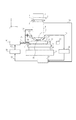
図1は、本発明の実施例1の露光装置の構成図である。本実施例の露光装置は、ウエハと投影光学系の間にだけ液体を満たす方法(所謂ローカルフィル方式)を用いるものである。図中、1は回路パターンが形成された原版としてのマスク(レチクル)、2は感光剤が塗布され、マスク1上の回路パターンが露光・転写される基板としてのウエハ、3はシャッタ及び調光装置等を備え、不図示の光源からの光でマスクを照明する照明光学系、4はウエハ2にマスク1のパターンを投影する投影光学系、5はマスク1を保持し、所定の位置に位置決めするためのマスクステージ、6はマスク1を位置決めするため、及びマスク像をウエハ2上に既に転写されている回路パターンに合致させるためのアライメント光学系である。7は投影光学系4の一部であり、その投影光学系の先端にあり、液体19を介してウエハ2と対向する光学素子(最もウエハに近い光学素子)である。8はウエハ2を保持するための保持部材としてのウエハチャック、9はウエハ2のθ(z軸回りの回転)方向位置の補正機能、ウエハ2のz位置の調整機能、及びウエハ2の傾きを補正するためのチルト機能を有する微動ステージであり、ウエハ2を所定の位置に位置決めするためのXYステージ10上に配置される。11はXYステージが載置されるベース定盤、12は微動ステージ9上にx及びy方向(y方向は不図示)に取り付けられ、微動ステージ9の位置を計測するためにレーザ干渉計13からの光を反射する参照ミラーである。
FIG. 1 is a block diagram of an exposure apparatus according to the first embodiment of the present invention. The exposure apparatus of this embodiment uses a method (so-called local fill method) in which a liquid is filled only between the wafer and the projection optical system. In the figure, 1 is a mask (reticle) as an original plate on which a circuit pattern is formed, 2 is a wafer as a substrate to which a circuit pattern on the mask 1 is exposed and transferred, and 3 is a shutter and light control. An illumination optical system that illuminates the mask with light from a light source (not shown), 4 is a projection optical system that projects the pattern of the mask 1 onto the
15は液体を供給するための液体供給ユニット、17dは液体供給ユニット15から供給される液体をウエハチャック8に導入する液体供給配管、17cはウエハチャック8の内部又はその近傍に配置されたの流路を流れた液体を投影光学系4に近接して配置された液体供給ノズル18へと導く液体供給配管であり、これらが液体供給装置を構成する。
15 is a liquid supply unit for supplying a liquid, 17d is a liquid supply pipe for introducing the liquid supplied from the
20は投影光学系4に近接して配置された液体回収ノズル、21は液体回収ノズル20と液体回収ユニット22を結ぶ液体回収配管であり、これらが液体回収装置を構成する。
次に、上記構成の装置の実際の動作、作用、及び効果等を説明する。露光をする際には、あらかじめ感光剤を塗布してあるウエハ2を不図示の搬送装置によってウエハチャック8上に搬送する。ウエハチャック8に載せられたウエハ2は、真空吸着もしくは静電吸着によって固定されることにより、平面矯正されるともに、ウエハチャック8の温度と略同一の温度になる。続いて、液体供給ユニット15から液体の供給が開始されると、液体19はウエハチャック8の内部の流路(不図示)を通過することにより、ウエハチャック8と略等しい温度になった後、液体供給ノズル18から吐出される。この結果、液体19とウエハ2の間に温度差が低減され、局所的な熱歪みの発生が抑制されることになる。続いて、余分な液体がウエハ2上の露光に関係しないエリアに溢れないように、液体回収ノズル20から液体回収ユニット22への液体19の回収も開始される。ウエハ2と投影光学系4の光学素子7の間に液体19が満たされ、液体19の供給と回収が安定すると投影光学系4の光学素子7と液体19の間も熱平衡状態となり、通常のドライ系の露光装置と同様の方法で、ウエハ2の精密位置決め(アライメント、フォーカス等)と露光が行なわれる。ステップ・アンド・スキャン動作により、ウエハ2の全面の露光が完了すると、液体供給ユニット15からの液体の供給が停止される。そして、液体回収ノズル20からの、ウエハ2と投影光学系4の光学素子7の間の液体19の回収が終わると、ウエハチャック8の真空吸着もしくは静電吸着が解除されて、不図示の搬送系によりウエハ2が露光装置から搬出される。
Next, the actual operation, action, effect and the like of the apparatus having the above configuration will be described. When performing exposure, the
本実施例においては、ウエハチャック8の流路を通過させることで、ウエハチャック8の温度(ウエハ2の温度)と略同じ温度となった液体を、液体19として投影光学系4とウエハ2との間に供給しているので、液体19とウエハ2の間に温度差が低減でき、解像度の低下を防ぐことができる。
In the present embodiment, the liquid that has become substantially the same temperature as the temperature of the wafer chuck 8 (the temperature of the wafer 2) by passing through the flow path of the
図2は、本発明の実施例2に係る露光装置の構成図である。図1と同じ番号が付されている部材は実施例1で示したものと同様の部材を示している。ここでは、図1の露光装置との違いについて説明する。
FIG. 2 is a block diagram of an exposure apparatus according to
14はウエハチャック8の温度を計測するための温度センサである。本実施例では、ウエハチャック8の温度がウエハ2の温度と略等しいという前提のもとでウエハチャックの温度を計測してウエハ2の温度を間接的に計測しているが、ウエハチャック8のウエハ2が載置される場所の近傍に温度センサ14を配置することによりウエハ2の温度を直接的に計測しても良い(以下の実施例におけるセンサも同様)。
25はウエハチャックを略一定の温度に保つために所定の温度に調整された温調水を供給・回収するウエハチャック温度調整装置で、ウエハチャック温調水供給配管23と、ウエハチャック温調水回収配管24とを持つ。ウエハチャック温度調整装置25により所定の温度となるように調整された温調水は、ウエハチャック温調水供給配管23、ウエハチャック8内の実施例1における液体が通る流路とは異なる流路(不図示)、ウエハチャック温調水回収配管24を循環する。
Reference numeral 25 denotes a wafer chuck temperature adjusting device that supplies and recovers temperature adjusted water adjusted to a predetermined temperature in order to keep the wafer chuck at a substantially constant temperature. The wafer chuck temperature adjusted
実施例1と同様に、液体を事前にウエハチャック8の内部を通過させて投影光学系とウエハの間に供給することにより、ウエハチャック8に保持されたウエハ2と略同一の温度にして供給することができる。
Similarly to the first embodiment, the liquid is supplied between the projection optical system and the wafer through the interior of the
なお、ウエハ2の温度を変えたい場合は、ウエハチャック温度調整装置25により前記温調水の設定温度を変えることによって変更することができ、それに伴って投影光学系とウエハの間に供給される液体19の温度も自動的にその変化後の温度となる。他の動作は実施例1と同様である。
If the temperature of the
なお、本実施例においては温度調整装置として、温調水を流すものを用いたが、ペリチェ素子等のその他の公知の手段を用いても良い。また、流路に水を流すのではなく、その他の液体や気体を流すこととしても良い。 In the present embodiment, the temperature adjusting device is one that supplies temperature-controlled water, but other known means such as a Peltier element may be used. Moreover, it is good also as flowing other liquid and gas instead of flowing water into a flow path.
図3は、本発明の実施例3に係る露光装置の構成図である。図1と同じ番号が付されている部材は実施例1で示したものと同様の部材を示している。ここでは、図1との違いについて説明する。14は図2と同じく、ウエハチャック8の温度を計測するための温度センサ、16は温度センサ14の出力に応じて、液体供給装置により供給される液体の温度をウエハチャック8の温度と等しくなるように調整する液体温度調整ユニット、17a及び17bは液体供給配管で、液体供給ユニット15及び液体温度調整ユニット16と液体供給ノズル18とを結ぶ。本実施例では、液体供給ユニット15から供給された液体は、液体温度調整ユニット16によってウエハチャック8と略等しい温度に調整された後に、液体供給ノズル18から吐出される。他の動作は実施例1と同様である。
FIG. 3 is a block diagram of an exposure apparatus according to Embodiment 3 of the present invention. Members denoted by the same reference numerals as those in FIG. 1 are similar to those shown in the first embodiment. Here, differences from FIG. 1 will be described. As in FIG. 2, 14 is a temperature sensor for measuring the temperature of the
本実施例においては、ウエハチャック8の温度(ウエハ2の温度)と略同じ温度となった液体を、液体19として投影光学系4とウエハ2との間に供給しているので、液体19とウエハ2の間に温度差が低減でき、解像度の低下を防ぐことができる。
In the present embodiment, since the liquid having a temperature substantially equal to the temperature of the wafer chuck 8 (the temperature of the wafer 2) is supplied as the liquid 19 between the projection optical system 4 and the
図4は、本発明の実施例4に係る露光装置の構成図である。図3と同じ番号が付されている部材は実施例3で示したものと同様の部材を示している。図3との違いは、液体温度調整ユニット16とウエハチャック8とを液体供給配管17bで接続し、ウエハチャック8と液体供給ノズル18とを液体供給配管17cで接続したところである。この構成において、実施例3の場合と動作が異なるところは、ウエハチャック8の温度と等しくなるように液体温度調整ユニット16により温度調整された液体を、更に、ウエハチャック8の内部を循環させてから液体供給ノズル18へ供給するようにしている点である。これにより、液体供給ノズル18から吐出される液体19の温度を、よりウエハ2の温度と等しくすることができる。なお、ウエハ2の温度を変えたい場合は、液体温度調整ユニット16により液体19の設定温度を変えることによって、実施例2と同様に変更することができる。
FIG. 4 is a block diagram of an exposure apparatus according to Embodiment 4 of the present invention. Members denoted by the same reference numerals as those in FIG. 3 are members similar to those shown in the third embodiment. The difference from FIG. 3 is that the liquid
図5は、本発明の第5の実施例に係る液浸型露光装置の構成図である。図4と同じ番号が付されている部材は実施例4で示したものと同様の部材を示している。ここでは、図4との違いについて説明する。 FIG. 5 is a block diagram of an immersion type exposure apparatus according to the fifth embodiment of the present invention. Members denoted by the same reference numerals as those in FIG. 4 are members similar to those shown in the fourth embodiment. Here, differences from FIG. 4 will be described.
26は液体19のバイパス配管で、ウエハチャック8の内部又はその近傍に配置された流路を循環した液体の一部を分岐して、27の液体再生ユニットへと導く。液体再生ユニット27は液体回収ユニット22からの液体も導入され、内部で露光時の汚れや微細な気泡などの除去が行なわれることにより、液体を再度供給可能な状態にする。28は液体再生ユニット27で再生された液体19を液体供給ユニット15に導く液体再供給配管である。これらが、液体回収装置を構成している。
29は液体供給配管17cに設けられた液体供給制御バルブで、液体19の供給量を液体供給ユニット15からの指示により制御する。
A liquid
本実施例の動作について説明する。液体供給ユニット15は常に液体19の供給を続けているが、非露光時は液体供給制御バルブ29は閉状態にあるため、液体は液体バイパス配管26を介してそのまま液体再生ユニット27へと送られ、液体再供給配管28により液体供給ユニット15に戻る。従って、液体温度調整ユニット16により所定の温度に制御された液体が常に露光装置内を循環している状態にある。実施例1で説明したように、露光時のみウエハ2と投影光学系4の光学素子7の間に液体19を供給するために、液体供給ユニット15の指示により液体供給制御バルブ29が開かれ、供給ノズル18よりウエハ2と等しい温度の液体19が供給される。露光が終了すると、再び液体供給ユニット15の指示により液体供給バルブ29が閉じられる。なお、液体19の回収動作については、実施例1に述べた通りである。また、ウエハ2の温度を変えたい場合は、実施例4と同様、液体温度調整ユニット16により液体の設定温度を変えることによって変更することができる。
The operation of this embodiment will be described. Although the
図6は、本発明の実施例6に係る露光装置の構成図である。図5と同じ番号が付されている部材は実施例5で示したものと同様の部材を示している。ここでは、図5との違いについて説明する。
FIG. 6 is a block diagram of an exposure apparatus according to
30はウエハチャック8の内部を循環した液体19の一部を分岐させ、投影光学系4に導く、投影光学系温調供給配管である。31は投影光学系4の内部の流路(不図示)を循環した液体19を液体再生装置27へと導く投影光学系温調回収配管である。
実施例5との違いは、ウエハチャック8の内部を循環した液体19を投影光学系4の内部又はその近傍にも循環させることにより、露光時に液体19を介して接することになるウエハ2と投影光学系4(レンズ7)と液体19の3者の温度を常に等しい状態となるようにしている点である。これにより、投影光学系4と液体19の間の温度差もなくすことができ、両者の温度差によりウエハ2に局所的な熱歪みが発生することを防止できる。
The difference from the fifth embodiment is that the liquid 19 circulated in the
なお、投影光学系4の先端の光学素子7の近傍にのみ流路を設ける構成としても良く、更に、ウエハ2の温度を変えたい場合は、実施例4と同様、液体温度調整ユニット16により液体の設定温度を変えることによって変更することができる。
Note that the flow path may be provided only in the vicinity of the
本実施例では、ウエハと液体の温度差だけでなく、光学素子7と液体の温度差も低減することができるので、熱歪みが発生を更に低減することができ、露光装置の解像性能の悪化を防止することができる。
In this embodiment, not only the temperature difference between the wafer and the liquid but also the temperature difference between the
以上、説明したように、上記の実施例の露光装置は、ウエハと液体の温度差による熱歪みが発生することを防止する効果を有する。 As described above, the exposure apparatus of the above embodiment has an effect of preventing the occurrence of thermal distortion due to the temperature difference between the wafer and the liquid.
また、温度調整された液体を、基板保持部材(ウエハチャック)の内部を通過させてから投影光学系と基板(ウエハ)の間に供給するようにすることで、基板保持手段用の温度調整手段と液浸用液体の温度調整手段とを兼用することができ、装置構成が簡単になるという効果も有する。 Further, the temperature-adjusted liquid is supplied between the projection optical system and the substrate (wafer) after passing through the inside of the substrate-holding member (wafer chuck), so that the temperature adjusting means for the substrate holding means And the temperature adjusting means of the immersion liquid can also be used, and the apparatus configuration can be simplified.
さらに、投影光学系(の光学素子)の温度も液浸用液体の温度と略等しくなるようにすることで、露光時のウエハ、液体、投影光学系(の光学素子)の3者の温度差を低減し、温度差による熱歪みが発生して歩留りが低下することを防止する効果を有する。 Furthermore, the temperature of the projection optical system (the optical element) is made substantially equal to the temperature of the immersion liquid, so that the temperature difference between the three of the wafer, the liquid, and the projection optical system (the optical element) during exposure is increased. And the effect of preventing the yield from being lowered due to the occurrence of thermal distortion due to the temperature difference.
なお、以上の説明は、ステップ・アンド・スキャン型の露光装置について説明したが、ステップ・アンド・リピート型の露光装置にも同様に適用でき、同様の効果を得ることができる。 Although the above description has been made on the step-and-scan type exposure apparatus, it can be similarly applied to a step-and-repeat type exposure apparatus, and the same effect can be obtained.
また、各実施例の露光装置の構成部材を他の実施例の露光装置に適用することも、もちろん可能である。 Of course, the constituent members of the exposure apparatus of each embodiment can be applied to the exposure apparatuses of other embodiments.
次に、上記実施例に記載の露光装置を利用したデバイスの製造方法の実施例を説明する。 Next, an embodiment of a device manufacturing method using the exposure apparatus described in the above embodiment will be described.
図7はデバイス(ICやLSI等の半導体チップ、液晶パネルやCCD)の製造フローを示す。ステップ1(回路設計)ではデバイスの回路設計を行なう。ステップ2(マスク製作)では設計した回路パターンを形成したマスク(レチクル)を製作する。一方、ステップ3(ウエハ製造)ではシリコン等の材料を用いて基板としてウエハを製造する。ステップ4(ウエハプロセス)は前工程と呼ばれ、上記用意したマスクとウエハとを用いて、リソグラフィー技術によってウエハに実際の回路を形成する。次のステップ5(組み立て)は後工程と呼ばれ、ステップ4よって作成されたウエハを用いてチップ化する工程であり、アッセンブリ工程(ダイシング、ボンディング)、パッケージング工程(チップ封入)等の工程を含む。ステップ6(検査)ではステップ5で作成されたデバイスの動作確認テスト、耐久性テスト等の検査を行なう。こうした工程を経てデバイスが完成し、これが出荷(ステップ7)される。
FIG. 7 shows a manufacturing flow of a device (a semiconductor chip such as an IC or LSI, a liquid crystal panel or a CCD). In step 1 (circuit design), the device circuit is designed. In step 2 (mask production), a mask (reticle) on which the designed circuit pattern is formed is produced. On the other hand, in step 3 (wafer manufacture), a wafer is manufactured as a substrate using a material such as silicon. Step 4 (wafer process) is called a pre-process, and an actual circuit is formed on the wafer by lithography using the prepared mask and wafer. The next step 5 (assembly) is called a post-process, and is a process for forming a chip using the wafer created in step 4, and the assembly process (dicing, bonding), packaging process (chip encapsulation) and the like are performed. Including. In step 6 (inspection), inspections such as an operation confirmation test and a durability test of the device created in
図8は上記ウエハプロセスの詳細なフローを示す。ステップ11(酸化)ではウエハの表面を酸化させる。ステップ12ではウエハの表面に絶縁膜を形成する。ステップ13(電極形成)ではウエハ上に電極を蒸着によって形成する。ステップ14(イオン打ち込み)ではウエハにイオンを打ち込む。ステップ15(レジスト処理)ではウエハにレジスト(感材)を塗布する。ステップ16(露光)では上記の実施例に記載の露光装置によってマスクの回路パタ−ンの像でウエハを露光する。ステップ17(現像)では露光したウエハを現像する。ステップ18(エッチング)では現像したレジスト以外の部分を削り取る。ステップ19(レジスト剥離)ではエッチングが済んで不要となったレジストを取り除く。これらステップを繰り返し行なうことによりウエハ上に回路パタ−ンが形成される。
FIG. 8 shows a detailed flow of the wafer process. In step 11 (oxidation), the wafer surface is oxidized. In
本実施例の製造方法を用いれば、従来は難しかった高集積度のデバイスを製造することが可能になる。 By using the manufacturing method of this embodiment, it becomes possible to manufacture a highly integrated device, which has been difficult in the past.
以上、本発明の好ましい実施例について説明したが、本発明はこれらの実施例に限定されないことはいうまでもなく、その要旨の範囲内で種々の変形及び変更が可能である。 The preferred embodiments of the present invention have been described above, but the present invention is not limited to these embodiments, and various modifications and changes can be made within the scope of the gist.
1 マスク
2 ウエハ
3 照明光学系
4 投影光学系
5 マスクステージ
6 アライメント光学系
8 ウエハチャック
9 微動ステージ
10 XYステージ
11 ベース定盤
12 参照ミラー
13 レーザ干渉計
14 温度センサ
15 液体供給ユニット
16 液体温度調整ユニット
17a〜17d 液体供給配管
18 液体供給ノズル
19 液体
20 液体回収ノズル
21 液体回収配管
22 液体回収ユニット
23 ウエハチャック温調水供給配管
24 ウエハチャック温調水回収配管
25 ウエハチャック温度調整装置
26 液体バイパス配管
27 液体再生ユニット
28 液体再供給配管
29 液体供給量制御バルブ
30 投影光学系温調供給配管
31 投影光学系温調回収配管
DESCRIPTION OF SYMBOLS 1
Claims (6)
前記基板を吸着保持するチャックと、
前記チャックが持つ流路に流した液体を、前記投影光学系と前記基板との間に供給する液体供給装置と、を有し、
前記液体の温度は前記液体が前記流路を通過することにより前記チャックと等しくなり、前記チャックと等しい温度の前記液体が前記投影光学系と前記基板との間に供給されることを特徴とする露光装置。 In an exposure apparatus that includes a projection optical system that projects a mask pattern onto a substrate, and that exposes the substrate through a liquid filled only between the projection optical system and a portion of the substrate,
A chuck for sucking and holding the substrate;
A liquid supply device for supplying the liquid flowing in the flow path of the chuck between the projection optical system and the substrate,
The temperature of the liquid becomes equal to the chuck when the liquid passes through the flow path, and the liquid having the same temperature as the chuck is supplied between the projection optical system and the substrate. Exposure device.
前記温度調整装置は、前記第2の流路に流体を流すことにより前記チャックの温度を調整することを特徴とする請求項2記載の露光装置。 The chuck has a second flow path different from the flow path,
3. The exposure apparatus according to claim 2 , wherein the temperature adjusting device adjusts the temperature of the chuck by flowing a fluid through the second flow path.
前記液体供給装置は、前記センサの出力に基づいて前記チャックの流路に供給する液体の温度を調整する温度調整ユニットを有することを特徴とする請求項1記載の露光装置。 A sensor for detecting the temperature of the chuck;
The liquid supply device, an exposure apparatus according to claim 1, wherein a temperature adjusting unit for adjusting the temperature of the liquid supplied to the flow path of the chuck based on the output of the sensor.
前記液体供給装置は、前記チャックが持つ流路を流れた液体を、前記投影光学系が持つ流路にも流すことを特徴とする請求項1記載の露光装置。 The projection optical system has a flow path provided in the vicinity of a lens facing the substrate through the liquid of the projection optical system,
The liquid supply device, the liquid flowing through the flow path in which the chuck has exposure apparatus according to claim 1, wherein also to flow in the flow path with said projection optical system.
Priority Applications (3)
| Application Number | Priority Date | Filing Date | Title |
|---|---|---|---|
| JP2004000827A JP4371822B2 (en) | 2004-01-06 | 2004-01-06 | Exposure equipment |
| US11/030,515 US7382434B2 (en) | 2004-01-06 | 2005-01-05 | Exposure apparatus and device manufacturing method |
| US12/060,393 US7719659B2 (en) | 2004-01-06 | 2008-04-01 | Exposure apparatus and device manufacturing method |
Applications Claiming Priority (1)
| Application Number | Priority Date | Filing Date | Title |
|---|---|---|---|
| JP2004000827A JP4371822B2 (en) | 2004-01-06 | 2004-01-06 | Exposure equipment |
Publications (3)
| Publication Number | Publication Date |
|---|---|
| JP2005197384A JP2005197384A (en) | 2005-07-21 |
| JP2005197384A5 JP2005197384A5 (en) | 2009-09-17 |
| JP4371822B2 true JP4371822B2 (en) | 2009-11-25 |
Family
ID=34708978
Family Applications (1)
| Application Number | Title | Priority Date | Filing Date |
|---|---|---|---|
| JP2004000827A Expired - Fee Related JP4371822B2 (en) | 2004-01-06 | 2004-01-06 | Exposure equipment |
Country Status (2)
| Country | Link |
|---|---|
| US (2) | US7382434B2 (en) |
| JP (1) | JP4371822B2 (en) |
Families Citing this family (98)
| Publication number | Priority date | Publication date | Assignee | Title |
|---|---|---|---|---|
| KR100588124B1 (en) * | 2002-11-12 | 2006-06-09 | 에이에스엠엘 네델란즈 비.브이. | Lithographic Apparatus and Device Manufacturing Method |
| US10503084B2 (en) | 2002-11-12 | 2019-12-10 | Asml Netherlands B.V. | Lithographic apparatus and device manufacturing method |
| US9482966B2 (en) | 2002-11-12 | 2016-11-01 | Asml Netherlands B.V. | Lithographic apparatus and device manufacturing method |
| CN100470367C (en) | 2002-11-12 | 2009-03-18 | Asml荷兰有限公司 | Lithographic apparatus and device manufacturing method |
| US7372541B2 (en) * | 2002-11-12 | 2008-05-13 | Asml Netherlands B.V. | Lithographic apparatus and device manufacturing method |
| DE10261775A1 (en) * | 2002-12-20 | 2004-07-01 | Carl Zeiss Smt Ag | Device for the optical measurement of an imaging system |
| TWI621923B (en) | 2003-02-26 | 2018-04-21 | Nikon Corp | Exposure apparatus, exposure method, and component manufacturing method |
| EP1610361B1 (en) | 2003-03-25 | 2014-05-21 | Nikon Corporation | Exposure system and device production method |
| KR101176817B1 (en) * | 2003-04-07 | 2012-08-24 | 가부시키가이샤 니콘 | Exposure apparatus and method for manufacturing device |
| JP4488004B2 (en) * | 2003-04-09 | 2010-06-23 | 株式会社ニコン | Immersion lithography fluid control system |
| KR101886027B1 (en) | 2003-04-10 | 2018-09-06 | 가부시키가이샤 니콘 | Environmental system including vaccum scavange for an immersion lithography apparatus |
| JP4656057B2 (en) * | 2003-04-10 | 2011-03-23 | 株式会社ニコン | Electro-osmotic element for immersion lithography equipment |
| KR101238142B1 (en) * | 2003-04-10 | 2013-02-28 | 가부시키가이샤 니콘 | Environmental system including a transport region for an immersion lithography apparatus |
| EP3352010A1 (en) * | 2003-04-10 | 2018-07-25 | Nikon Corporation | Run-off path to collect liquid for an immersion lithography apparatus |
| KR101697896B1 (en) | 2003-04-11 | 2017-01-18 | 가부시키가이샤 니콘 | Apparatus and method for maintaining immersion fluid in the gap under the projection lens during wafer exchange in an immersion lithography machine |
| JP4837556B2 (en) | 2003-04-11 | 2011-12-14 | 株式会社ニコン | Optical element cleaning method in immersion lithography |
| WO2004092830A2 (en) * | 2003-04-11 | 2004-10-28 | Nikon Corporation | Liquid jet and recovery system for immersion lithography |
| WO2004095135A2 (en) * | 2003-04-17 | 2004-11-04 | Nikon Corporation | Optical arrangement of autofocus elements for use with immersion lithography |
| TWI295414B (en) * | 2003-05-13 | 2008-04-01 | Asml Netherlands Bv | Lithographic apparatus and device manufacturing method |
| EP1624481A4 (en) * | 2003-05-15 | 2008-01-30 | Nikon Corp | Exposure apparatus and method for manufacturing device |
| TW201806001A (en) | 2003-05-23 | 2018-02-16 | 尼康股份有限公司 | Exposure device and device manufacturing method |
| TWI463533B (en) * | 2003-05-23 | 2014-12-01 | 尼康股份有限公司 | An exposure method, an exposure apparatus, and an element manufacturing method |
| KR101618419B1 (en) * | 2003-05-28 | 2016-05-04 | 가부시키가이샤 니콘 | Exposure method, exposure device, and device manufacturing method |
| US7213963B2 (en) * | 2003-06-09 | 2007-05-08 | Asml Netherlands B.V. | Lithographic apparatus and device manufacturing method |
| US7684008B2 (en) * | 2003-06-11 | 2010-03-23 | Asml Netherlands B.V. | Lithographic apparatus and device manufacturing method |
| EP3104396B1 (en) * | 2003-06-13 | 2018-03-21 | Nikon Corporation | Exposure method, substrate stage, exposure apparatus, and device manufacturing method |
| TWI540612B (en) | 2003-06-19 | 2016-07-01 | 尼康股份有限公司 | An exposure apparatus, an exposure method, and an element manufacturing method |
| EP1639391A4 (en) * | 2003-07-01 | 2009-04-29 | Nikon Corp | Using isotopically specified fluids as optical elements |
| EP2466383B1 (en) * | 2003-07-08 | 2014-11-19 | Nikon Corporation | Wafer table for immersion lithography |
| EP2264531B1 (en) | 2003-07-09 | 2013-01-16 | Nikon Corporation | Exposure apparatus and device manufacturing method |
| WO2005006418A1 (en) * | 2003-07-09 | 2005-01-20 | Nikon Corporation | Exposure apparatus and method for manufacturing device |
| DE602004030247D1 (en) * | 2003-07-09 | 2011-01-05 | Nippon Kogaku Kk | EXPOSURE DEVICE AND METHOD FOR MANUFACTURING THE CONSTRUCTION |
| JP4524669B2 (en) | 2003-07-25 | 2010-08-18 | 株式会社ニコン | Projection optical system inspection method and inspection apparatus |
| EP1503244A1 (en) * | 2003-07-28 | 2005-02-02 | ASML Netherlands B.V. | Lithographic projection apparatus and device manufacturing method |
| KR101343720B1 (en) | 2003-07-28 | 2013-12-20 | 가부시키가이샤 니콘 | Exposure apparatus device producing method and exposure apparatus controlling method |
| US7779781B2 (en) | 2003-07-31 | 2010-08-24 | Asml Netherlands B.V. | Lithographic apparatus and device manufacturing method |
| TWI263859B (en) * | 2003-08-29 | 2006-10-11 | Asml Netherlands Bv | Lithographic apparatus and device manufacturing method |
| JP4325622B2 (en) * | 2003-08-29 | 2009-09-02 | 株式会社ニコン | Exposure apparatus and device manufacturing method |
| KR101238114B1 (en) | 2003-09-03 | 2013-02-27 | 가부시키가이샤 니콘 | Apparatus and method for providing fluid for immersion lithography |
| WO2005029559A1 (en) * | 2003-09-19 | 2005-03-31 | Nikon Corporation | Exposure apparatus and device producing method |
| TWI525660B (en) | 2003-09-29 | 2016-03-11 | 尼康股份有限公司 | An exposure apparatus and an exposure method, and an element manufacturing method |
| WO2005036621A1 (en) | 2003-10-08 | 2005-04-21 | Zao Nikon Co., Ltd. | Substrate carrying apparatus, substrate carrying method, exposure apparatus, exposure method, and method for producing device |
| JP2005136364A (en) * | 2003-10-08 | 2005-05-26 | Zao Nikon Co Ltd | Substrate carrying device, exposure device and device manufacturing method |
| JP4335213B2 (en) | 2003-10-08 | 2009-09-30 | 株式会社蔵王ニコン | Substrate transport apparatus, exposure apparatus, and device manufacturing method |
| TWI553701B (en) * | 2003-10-09 | 2016-10-11 | 尼康股份有限公司 | Exposure apparatus and exposure method, component manufacturing method |
| US7411653B2 (en) | 2003-10-28 | 2008-08-12 | Asml Netherlands B.V. | Lithographic apparatus |
| EP1531362A3 (en) * | 2003-11-13 | 2007-07-25 | Matsushita Electric Industrial Co., Ltd. | Semiconductor manufacturing apparatus and pattern formation method |
| JP4295712B2 (en) | 2003-11-14 | 2009-07-15 | エーエスエムエル ネザーランズ ビー.ブイ. | Lithographic apparatus and apparatus manufacturing method |
| CN102163004B (en) * | 2003-12-03 | 2014-04-09 | 株式会社尼康 | Exposure apparatus, exposure method and device producing method |
| US20070081133A1 (en) * | 2004-12-14 | 2007-04-12 | Niikon Corporation | Projection exposure apparatus and stage unit, and exposure method |
| JPWO2005057635A1 (en) * | 2003-12-15 | 2007-07-05 | 株式会社ニコン | Projection exposure apparatus, stage apparatus, and exposure method |
| KR101681852B1 (en) * | 2003-12-15 | 2016-12-01 | 가부시키가이샤 니콘 | Stage system, exposure apparatus and exposure method |
| JP4371822B2 (en) * | 2004-01-06 | 2009-11-25 | キヤノン株式会社 | Exposure equipment |
| KR101204157B1 (en) * | 2004-01-20 | 2012-11-22 | 칼 짜이스 에스엠테 게엠베하 | Microlithographic projection exposure apparatus and measuring device for a projection lens |
| US7589822B2 (en) | 2004-02-02 | 2009-09-15 | Nikon Corporation | Stage drive method and stage unit, exposure apparatus, and device manufacturing method |
| US7990516B2 (en) | 2004-02-03 | 2011-08-02 | Nikon Corporation | Immersion exposure apparatus and device manufacturing method with liquid detection apparatus |
| KR101942136B1 (en) | 2004-02-04 | 2019-01-24 | 가부시키가이샤 니콘 | Exposure apparatus, exposure method, and device producing method |
| JP5167572B2 (en) * | 2004-02-04 | 2013-03-21 | 株式会社ニコン | Exposure apparatus, exposure method, and device manufacturing method |
| TW201816844A (en) | 2004-03-25 | 2018-05-01 | 日商尼康股份有限公司 | Exposure apparatus, exposure method, and device manufacturing method |
| EP1747499A2 (en) | 2004-05-04 | 2007-01-31 | Nikon Corporation | Apparatus and method for providing fluid for immersion lithography |
| US7616383B2 (en) | 2004-05-18 | 2009-11-10 | Asml Netherlands B.V. | Lithographic apparatus and device manufacturing method |
| KR101257960B1 (en) | 2004-06-04 | 2013-04-24 | 칼 짜이스 에스엠테 게엠베하 | System for measuring the image quality of an optical imaging system |
| WO2005122218A1 (en) * | 2004-06-09 | 2005-12-22 | Nikon Corporation | Exposure system and device production method |
| US7463330B2 (en) | 2004-07-07 | 2008-12-09 | Asml Netherlands B.V. | Lithographic apparatus and device manufacturing method |
| ATE441937T1 (en) | 2004-07-12 | 2009-09-15 | Nikon Corp | EXPOSURE DEVICE AND COMPONENT PRODUCTION METHOD |
| WO2006019124A1 (en) * | 2004-08-18 | 2006-02-23 | Nikon Corporation | Exposure apparatus and device manufacturing method |
| US7701550B2 (en) * | 2004-08-19 | 2010-04-20 | Asml Netherlands B.V. | Lithographic apparatus and device manufacturing method |
| US7397533B2 (en) | 2004-12-07 | 2008-07-08 | Asml Netherlands B.V. | Lithographic apparatus and device manufacturing method |
| US7880860B2 (en) * | 2004-12-20 | 2011-02-01 | Asml Netherlands B.V. | Lithographic apparatus and device manufacturing method |
| EP1843387A4 (en) * | 2005-01-25 | 2010-01-13 | Jsr Corp | Immersion exposure system, and recycle method and supply method of liquid for immersion exposure |
| US8692973B2 (en) * | 2005-01-31 | 2014-04-08 | Nikon Corporation | Exposure apparatus and method for producing device |
| WO2006080516A1 (en) | 2005-01-31 | 2006-08-03 | Nikon Corporation | Exposure apparatus and method for manufacturing device |
| US7282701B2 (en) * | 2005-02-28 | 2007-10-16 | Asml Netherlands B.V. | Sensor for use in a lithographic apparatus |
| JP4072543B2 (en) * | 2005-03-18 | 2008-04-09 | キヤノン株式会社 | Immersion exposure apparatus and device manufacturing method |
| USRE43576E1 (en) | 2005-04-08 | 2012-08-14 | Asml Netherlands B.V. | Dual stage lithographic apparatus and device manufacturing method |
| KR101555707B1 (en) | 2005-04-18 | 2015-09-25 | 가부시키가이샤 니콘 | Exposure device exposure method and device manufacturing method |
| US7357768B2 (en) * | 2005-09-22 | 2008-04-15 | William Marshall | Recliner exerciser |
| US20070124987A1 (en) * | 2005-12-05 | 2007-06-07 | Brown Jeffrey K | Electronic pest control apparatus |
| KR100768849B1 (en) * | 2005-12-06 | 2007-10-22 | 엘지전자 주식회사 | Power supply apparatus and method for line conection type fuel cell system |
| KR20080071552A (en) * | 2005-12-06 | 2008-08-04 | 가부시키가이샤 니콘 | Exposure method, exposure apparatus, and method for manufacturing device |
| US7649611B2 (en) | 2005-12-30 | 2010-01-19 | Asml Netherlands B.V. | Lithographic apparatus and device manufacturing method |
| DE102006021797A1 (en) | 2006-05-09 | 2007-11-15 | Carl Zeiss Smt Ag | Optical imaging device with thermal damping |
| US7826030B2 (en) * | 2006-09-07 | 2010-11-02 | Asml Netherlands B.V. | Lithographic apparatus and device manufacturing method |
| WO2008053918A1 (en) * | 2006-10-31 | 2008-05-08 | Nikon Corporation | Liquid holding apparatus, liquid holding method, exposure apparatus, exposure method and device manufacturing method |
| US8817226B2 (en) | 2007-02-15 | 2014-08-26 | Asml Holding N.V. | Systems and methods for insitu lens cleaning using ozone in immersion lithography |
| US8654305B2 (en) * | 2007-02-15 | 2014-02-18 | Asml Holding N.V. | Systems and methods for insitu lens cleaning in immersion lithography |
| US8237911B2 (en) | 2007-03-15 | 2012-08-07 | Nikon Corporation | Apparatus and methods for keeping immersion fluid adjacent to an optical assembly during wafer exchange in an immersion lithography machine |
| US9025126B2 (en) | 2007-07-31 | 2015-05-05 | Nikon Corporation | Exposure apparatus adjusting method, exposure apparatus, and device fabricating method |
| US8681308B2 (en) * | 2007-09-13 | 2014-03-25 | Asml Netherlands B.V. | Lithographic apparatus and device manufacturing method |
| JP4964904B2 (en) * | 2008-01-23 | 2012-07-04 | エーエスエムエル ホールディング エヌ.ブイ. | Immersion lithography apparatus having an immersion fluid recirculation system |
| JP5369443B2 (en) | 2008-02-05 | 2013-12-18 | 株式会社ニコン | Stage apparatus, exposure apparatus, exposure method, and device manufacturing method |
| KR101448152B1 (en) * | 2008-03-26 | 2014-10-07 | 삼성전자주식회사 | Distance measuring sensor having vertical photogate and three dimensional color image sensor having the same |
| JP5097166B2 (en) | 2008-05-28 | 2012-12-12 | エーエスエムエル ネザーランズ ビー.ブイ. | Lithographic apparatus and method of operating the apparatus |
| JP2010098172A (en) * | 2008-10-17 | 2010-04-30 | Canon Inc | Liquid recovery device, exposure device and device manufacturing method |
| MX2012007581A (en) * | 2009-12-28 | 2012-07-30 | Pioneer Hi Bred Int | Sorghum fertility restorer genotypes and methods of marker-assisted selection. |
| EP2381310B1 (en) | 2010-04-22 | 2015-05-06 | ASML Netherlands BV | Fluid handling structure and lithographic apparatus |
| JP2018531410A (en) | 2015-10-06 | 2018-10-25 | エーエスエムエル ホールディング エヌ.ブイ. | Chuck and clamp for holding an object of a lithographic apparatus and method for controlling the temperature of an object held by a clamp of a lithographic apparatus |
| CN113490884A (en) * | 2019-02-11 | 2021-10-08 | Asml荷兰有限公司 | Lithographic apparatus and method with thermal control system |
Family Cites Families (19)
| Publication number | Priority date | Publication date | Assignee | Title |
|---|---|---|---|---|
| US4509852A (en) * | 1980-10-06 | 1985-04-09 | Werner Tabarelli | Apparatus for the photolithographic manufacture of integrated circuit elements |
| EP0357423B1 (en) * | 1988-09-02 | 1995-03-15 | Canon Kabushiki Kaisha | An exposure apparatus |
| JP3253675B2 (en) * | 1991-07-04 | 2002-02-04 | 株式会社東芝 | Charged beam irradiation apparatus and method |
| US5430303A (en) * | 1992-07-01 | 1995-07-04 | Nikon Corporation | Exposure apparatus |
| JP2753930B2 (en) * | 1992-11-27 | 1998-05-20 | キヤノン株式会社 | Immersion type projection exposure equipment |
| JP3747566B2 (en) * | 1997-04-23 | 2006-02-22 | 株式会社ニコン | Immersion exposure equipment |
| WO1999027568A1 (en) * | 1997-11-21 | 1999-06-03 | Nikon Corporation | Projection aligner and projection exposure method |
| AU2747999A (en) | 1998-03-26 | 1999-10-18 | Nikon Corporation | Projection exposure method and system |
| US6105589A (en) * | 1999-01-11 | 2000-08-22 | Vane; Ronald A. | Oxidative cleaning method and apparatus for electron microscopes using an air plasma as an oxygen radical source |
| JP2000277415A (en) * | 1999-03-25 | 2000-10-06 | Canon Inc | Aligner |
| US6394109B1 (en) * | 1999-04-13 | 2002-05-28 | Applied Materials, Inc. | Method and apparatus for removing carbon contamination in a sub-atmospheric charged particle beam lithography system |
| US6614505B2 (en) * | 2001-01-10 | 2003-09-02 | Asml Netherlands B.V. | Lithographic projection apparatus, device manufacturing method, and device manufactured thereby |
| DE60323927D1 (en) * | 2002-12-13 | 2008-11-20 | Asml Netherlands Bv | Lithographic apparatus and method of making a device |
| JP4488004B2 (en) * | 2003-04-09 | 2010-06-23 | 株式会社ニコン | Immersion lithography fluid control system |
| KR101886027B1 (en) * | 2003-04-10 | 2018-09-06 | 가부시키가이샤 니콘 | Environmental system including vaccum scavange for an immersion lithography apparatus |
| JP4837556B2 (en) * | 2003-04-11 | 2011-12-14 | 株式会社ニコン | Optical element cleaning method in immersion lithography |
| US7061579B2 (en) * | 2003-11-13 | 2006-06-13 | Asml Netherlands B.V. | Lithographic apparatus and device manufacturing method |
| JP4371822B2 (en) * | 2004-01-06 | 2009-11-25 | キヤノン株式会社 | Exposure equipment |
| US7271878B2 (en) * | 2004-04-22 | 2007-09-18 | International Business Machines Corporation | Wafer cell for immersion lithography |
-
2004
- 2004-01-06 JP JP2004000827A patent/JP4371822B2/en not_active Expired - Fee Related
-
2005
- 2005-01-05 US US11/030,515 patent/US7382434B2/en not_active Expired - Fee Related
-
2008
- 2008-04-01 US US12/060,393 patent/US7719659B2/en not_active Expired - Fee Related
Also Published As
| Publication number | Publication date |
|---|---|
| US20080186463A1 (en) | 2008-08-07 |
| US7382434B2 (en) | 2008-06-03 |
| US20050146695A1 (en) | 2005-07-07 |
| US7719659B2 (en) | 2010-05-18 |
| JP2005197384A (en) | 2005-07-21 |
Similar Documents
| Publication | Publication Date | Title |
|---|---|---|
| JP4371822B2 (en) | Exposure equipment | |
| US7256868B2 (en) | Projection exposure apparatus, device manufacturing method, and sensor unit | |
| KR100727516B1 (en) | Exposure apparatus and device manufacturing method | |
| US9086636B2 (en) | Optical arrangement of autofocus elements for use with immersion lithography | |
| US7180574B2 (en) | Exposure apparatus and method | |
| JP4362867B2 (en) | Exposure apparatus and device manufacturing method | |
| JP4974049B2 (en) | Exposure method, exposure apparatus, and device manufacturing method | |
| KR20060129387A (en) | Exposure apparatus and exposure method, and device producing method | |
| EP1670040B1 (en) | Projection exposure apparatus, projection exposure method, and device manufacturing method | |
| KR101560007B1 (en) | Method for adjusting exposure apparatus exposure apparatus and device manufacturing method | |
| JPWO2010050240A1 (en) | Exposure apparatus, exposure method, and device manufacturing method | |
| JP2008244386A (en) | Aberration measuring method, exposure system, and method of manufacturing device | |
| JP4072543B2 (en) | Immersion exposure apparatus and device manufacturing method | |
| US7803516B2 (en) | Exposure method, device manufacturing method using the same, exposure apparatus, and substrate processing method and apparatus | |
| KR20080074043A (en) | Exposure apparatus | |
| JP2010034605A (en) | Aligner, and method of manufacturing device | |
| JP2011124415A (en) | Exposure apparatus, exposure method, and method of manufacturing device | |
| JP2009099694A (en) | Exposure device and method for manufacturing device | |
| JP2010027683A (en) | Exposure apparatus, exposure method, and production method of device | |
| JP2009026910A (en) | Exposure method, exposure apparatus and production method of device |
Legal Events
| Date | Code | Title | Description |
|---|---|---|---|
| A521 | Request for written amendment filed |
Free format text: JAPANESE INTERMEDIATE CODE: A523 Effective date: 20061218 |
|
| A621 | Written request for application examination |
Free format text: JAPANESE INTERMEDIATE CODE: A621 Effective date: 20061218 |
|
| A521 | Request for written amendment filed |
Free format text: JAPANESE INTERMEDIATE CODE: A523 Effective date: 20090731 |
|
| TRDD | Decision of grant or rejection written | ||
| A01 | Written decision to grant a patent or to grant a registration (utility model) |
Free format text: JAPANESE INTERMEDIATE CODE: A01 Effective date: 20090825 |
|
| A01 | Written decision to grant a patent or to grant a registration (utility model) |
Free format text: JAPANESE INTERMEDIATE CODE: A01 |
|
| A61 | First payment of annual fees (during grant procedure) |
Free format text: JAPANESE INTERMEDIATE CODE: A61 Effective date: 20090901 |
|
| FPAY | Renewal fee payment (event date is renewal date of database) |
Free format text: PAYMENT UNTIL: 20120911 Year of fee payment: 3 |
|
| R150 | Certificate of patent or registration of utility model |
Free format text: JAPANESE INTERMEDIATE CODE: R150 |
|
| LAPS | Cancellation because of no payment of annual fees |