EP1861519B1 - Method of forming silicon oxide containing films - Google Patents
Method of forming silicon oxide containing films Download PDFInfo
- Publication number
- EP1861519B1 EP1861519B1 EP06725128A EP06725128A EP1861519B1 EP 1861519 B1 EP1861519 B1 EP 1861519B1 EP 06725128 A EP06725128 A EP 06725128A EP 06725128 A EP06725128 A EP 06725128A EP 1861519 B1 EP1861519 B1 EP 1861519B1
- Authority
- EP
- European Patent Office
- Prior art keywords
- reaction chamber
- ozone
- oxygen
- gas
- compound
- Prior art date
- Legal status (The legal status is an assumption and is not a legal conclusion. Google has not performed a legal analysis and makes no representation as to the accuracy of the status listed.)
- Expired - Lifetime
Links
Images


Classifications
-
- C—CHEMISTRY; METALLURGY
- C23—COATING METALLIC MATERIAL; COATING MATERIAL WITH METALLIC MATERIAL; CHEMICAL SURFACE TREATMENT; DIFFUSION TREATMENT OF METALLIC MATERIAL; COATING BY VACUUM EVAPORATION, BY SPUTTERING, BY ION IMPLANTATION OR BY CHEMICAL VAPOUR DEPOSITION, IN GENERAL; INHIBITING CORROSION OF METALLIC MATERIAL OR INCRUSTATION IN GENERAL
- C23C—COATING METALLIC MATERIAL; COATING MATERIAL WITH METALLIC MATERIAL; SURFACE TREATMENT OF METALLIC MATERIAL BY DIFFUSION INTO THE SURFACE, BY CHEMICAL CONVERSION OR SUBSTITUTION; COATING BY VACUUM EVAPORATION, BY SPUTTERING, BY ION IMPLANTATION OR BY CHEMICAL VAPOUR DEPOSITION, IN GENERAL
- C23C16/00—Chemical coating by decomposition of gaseous compounds, without leaving reaction products of surface material in the coating, i.e. chemical vapour deposition [CVD] processes
- C23C16/22—Chemical coating by decomposition of gaseous compounds, without leaving reaction products of surface material in the coating, i.e. chemical vapour deposition [CVD] processes characterised by the deposition of inorganic material, other than metallic material
- C23C16/30—Deposition of compounds, mixtures or solid solutions, e.g. borides, carbides, nitrides
- C23C16/40—Oxides
- C23C16/401—Oxides containing silicon
- C23C16/402—Silicon dioxide
-
- H—ELECTRICITY
- H10—SEMICONDUCTOR DEVICES; ELECTRIC SOLID-STATE DEVICES NOT OTHERWISE PROVIDED FOR
- H10P—GENERIC PROCESSES OR APPARATUS FOR THE MANUFACTURE OR TREATMENT OF DEVICES COVERED BY CLASS H10
- H10P14/00—Formation of materials, e.g. in the shape of layers or pillars
- H10P14/60—Formation of materials, e.g. in the shape of layers or pillars of insulating materials
- H10P14/69—Inorganic materials
- H10P14/692—Inorganic materials composed of oxides, glassy oxides or oxide-based glasses
- H10P14/6921—Inorganic materials composed of oxides, glassy oxides or oxide-based glasses containing silicon
- H10P14/69215—Inorganic materials composed of oxides, glassy oxides or oxide-based glasses containing silicon the material being a silicon oxide, e.g. SiO2
-
- H—ELECTRICITY
- H10—SEMICONDUCTOR DEVICES; ELECTRIC SOLID-STATE DEVICES NOT OTHERWISE PROVIDED FOR
- H10P—GENERIC PROCESSES OR APPARATUS FOR THE MANUFACTURE OR TREATMENT OF DEVICES COVERED BY CLASS H10
- H10P14/00—Formation of materials, e.g. in the shape of layers or pillars
- H10P14/60—Formation of materials, e.g. in the shape of layers or pillars of insulating materials
- H10P14/66—Formation of materials, e.g. in the shape of layers or pillars of insulating materials characterised by the type of materials
- H10P14/668—Formation of materials, e.g. in the shape of layers or pillars of insulating materials characterised by the type of materials the materials being characterised by the deposition precursor materials
- H10P14/6681—Formation of materials, e.g. in the shape of layers or pillars of insulating materials characterised by the type of materials the materials being characterised by the deposition precursor materials the precursor containing a compound comprising Si
- H10P14/6687—Formation of materials, e.g. in the shape of layers or pillars of insulating materials characterised by the type of materials the materials being characterised by the deposition precursor materials the precursor containing a compound comprising Si the compound comprising silicon and nitrogen
- H10P14/6689—Formation of materials, e.g. in the shape of layers or pillars of insulating materials characterised by the type of materials the materials being characterised by the deposition precursor materials the precursor containing a compound comprising Si the compound comprising silicon and nitrogen the compound being a silazane
-
- H—ELECTRICITY
- H10—SEMICONDUCTOR DEVICES; ELECTRIC SOLID-STATE DEVICES NOT OTHERWISE PROVIDED FOR
- H10P—GENERIC PROCESSES OR APPARATUS FOR THE MANUFACTURE OR TREATMENT OF DEVICES COVERED BY CLASS H10
- H10P14/00—Formation of materials, e.g. in the shape of layers or pillars
- H10P14/60—Formation of materials, e.g. in the shape of layers or pillars of insulating materials
- H10P14/63—Formation of materials, e.g. in the shape of layers or pillars of insulating materials characterised by the formation processes
- H10P14/6326—Deposition processes
- H10P14/6328—Deposition from the gas or vapour phase
- H10P14/6334—Deposition from the gas or vapour phase using decomposition or reaction of gaseous or vapour phase compounds, i.e. chemical vapour deposition
- H10P14/6336—Deposition from the gas or vapour phase using decomposition or reaction of gaseous or vapour phase compounds, i.e. chemical vapour deposition in the presence of a plasma [PECVD]
-
- H—ELECTRICITY
- H10—SEMICONDUCTOR DEVICES; ELECTRIC SOLID-STATE DEVICES NOT OTHERWISE PROVIDED FOR
- H10P—GENERIC PROCESSES OR APPARATUS FOR THE MANUFACTURE OR TREATMENT OF DEVICES COVERED BY CLASS H10
- H10P14/00—Formation of materials, e.g. in the shape of layers or pillars
- H10P14/60—Formation of materials, e.g. in the shape of layers or pillars of insulating materials
- H10P14/63—Formation of materials, e.g. in the shape of layers or pillars of insulating materials characterised by the formation processes
- H10P14/6326—Deposition processes
- H10P14/6328—Deposition from the gas or vapour phase
- H10P14/6334—Deposition from the gas or vapour phase using decomposition or reaction of gaseous or vapour phase compounds, i.e. chemical vapour deposition
- H10P14/6339—Deposition from the gas or vapour phase using decomposition or reaction of gaseous or vapour phase compounds, i.e. chemical vapour deposition deposition by cyclic CVD, e.g. ALD, ALE or pulsed CVD
-
- H—ELECTRICITY
- H10—SEMICONDUCTOR DEVICES; ELECTRIC SOLID-STATE DEVICES NOT OTHERWISE PROVIDED FOR
- H10P—GENERIC PROCESSES OR APPARATUS FOR THE MANUFACTURE OR TREATMENT OF DEVICES COVERED BY CLASS H10
- H10P14/00—Formation of materials, e.g. in the shape of layers or pillars
- H10P14/60—Formation of materials, e.g. in the shape of layers or pillars of insulating materials
- H10P14/66—Formation of materials, e.g. in the shape of layers or pillars of insulating materials characterised by the type of materials
- H10P14/668—Formation of materials, e.g. in the shape of layers or pillars of insulating materials characterised by the type of materials the materials being characterised by the deposition precursor materials
- H10P14/6681—Formation of materials, e.g. in the shape of layers or pillars of insulating materials characterised by the type of materials the materials being characterised by the deposition precursor materials the precursor containing a compound comprising Si
- H10P14/6682—Formation of materials, e.g. in the shape of layers or pillars of insulating materials characterised by the type of materials the materials being characterised by the deposition precursor materials the precursor containing a compound comprising Si the compound being a silane, e.g. disilane, methylsilane or chlorosilane
-
- H—ELECTRICITY
- H10—SEMICONDUCTOR DEVICES; ELECTRIC SOLID-STATE DEVICES NOT OTHERWISE PROVIDED FOR
- H10P—GENERIC PROCESSES OR APPARATUS FOR THE MANUFACTURE OR TREATMENT OF DEVICES COVERED BY CLASS H10
- H10P14/00—Formation of materials, e.g. in the shape of layers or pillars
- H10P14/60—Formation of materials, e.g. in the shape of layers or pillars of insulating materials
- H10P14/66—Formation of materials, e.g. in the shape of layers or pillars of insulating materials characterised by the type of materials
- H10P14/668—Formation of materials, e.g. in the shape of layers or pillars of insulating materials characterised by the type of materials the materials being characterised by the deposition precursor materials
- H10P14/6681—Formation of materials, e.g. in the shape of layers or pillars of insulating materials characterised by the type of materials the materials being characterised by the deposition precursor materials the precursor containing a compound comprising Si
- H10P14/6684—Formation of materials, e.g. in the shape of layers or pillars of insulating materials characterised by the type of materials the materials being characterised by the deposition precursor materials the precursor containing a compound comprising Si the compound comprising silicon and oxygen
- H10P14/6686—Formation of materials, e.g. in the shape of layers or pillars of insulating materials characterised by the type of materials the materials being characterised by the deposition precursor materials the precursor containing a compound comprising Si the compound comprising silicon and oxygen the compound being a molecule comprising at least one silicon-oxygen bond and the compound having hydrogen or an organic group attached to the silicon or oxygen, e.g. a siloxane
-
- H—ELECTRICITY
- H10—SEMICONDUCTOR DEVICES; ELECTRIC SOLID-STATE DEVICES NOT OTHERWISE PROVIDED FOR
- H10P—GENERIC PROCESSES OR APPARATUS FOR THE MANUFACTURE OR TREATMENT OF DEVICES COVERED BY CLASS H10
- H10P14/00—Formation of materials, e.g. in the shape of layers or pillars
- H10P14/60—Formation of materials, e.g. in the shape of layers or pillars of insulating materials
- H10P14/66—Formation of materials, e.g. in the shape of layers or pillars of insulating materials characterised by the type of materials
- H10P14/668—Formation of materials, e.g. in the shape of layers or pillars of insulating materials characterised by the type of materials the materials being characterised by the deposition precursor materials
- H10P14/6681—Formation of materials, e.g. in the shape of layers or pillars of insulating materials characterised by the type of materials the materials being characterised by the deposition precursor materials the precursor containing a compound comprising Si
- H10P14/6687—Formation of materials, e.g. in the shape of layers or pillars of insulating materials characterised by the type of materials the materials being characterised by the deposition precursor materials the precursor containing a compound comprising Si the compound comprising silicon and nitrogen
-
- H—ELECTRICITY
- H10—SEMICONDUCTOR DEVICES; ELECTRIC SOLID-STATE DEVICES NOT OTHERWISE PROVIDED FOR
- H10P—GENERIC PROCESSES OR APPARATUS FOR THE MANUFACTURE OR TREATMENT OF DEVICES COVERED BY CLASS H10
- H10P14/00—Formation of materials, e.g. in the shape of layers or pillars
- H10P14/60—Formation of materials, e.g. in the shape of layers or pillars of insulating materials
- H10P14/69—Inorganic materials
- H10P14/692—Inorganic materials composed of oxides, glassy oxides or oxide-based glasses
- H10P14/6921—Inorganic materials composed of oxides, glassy oxides or oxide-based glasses containing silicon
- H10P14/6922—Inorganic materials composed of oxides, glassy oxides or oxide-based glasses containing silicon the material containing Si, O and at least one of H, N, C, F or other non-metal elements, e.g. SiOC, SiOC:H or SiONC
Definitions
- the invention relates to a method of forming silicon oxide containing films using a silicon precursor and an oxidant gas.
- a passivation film such as SiN is formed on the gate electrode of each MOS transistor.
- This SiN film deposited on top and on side surface of the gate electrodes (such as polycrystalline silicon or metallic layers) in order to increase the breakdown voltage of each transistor.
- SiN films deposited at temperatures below 400°C have usually poorer film qualities.
- SiO 2 films to reinforce SiN film properties ("dual spacer") and thereby make effective electrical barrier layers to improve significantly the device performances.
- SiO 2 films are used as STI (shallow trench insulation), inter layer dielectric (ILD) layers, passivation layers, etch-stop layers and attempts are made to find a deposition process of these SiO 2 layers at low temperature, i.e. below 400°C.
- the deposition of a very (20-50 A thick) thin films performed at low deposition temperatures should not lead to the oxidation of the metal electrode and should be perfectly uniform all along the gate, and an atomic layer deposition process is the most suitable such a requirement.
- conformal films should be deposited with high deposition rate (several hundred A per minute) below 500°C.
- the inventors believe that the presence of a large number of hydrogen atoms bonded to the silicon atom in the Si precursor and of oxygen or oxygen containing gas to generate the SiO 2 fim, probably also generates moisture (H 2 O) formation which then reacts with Si to make SiOH.
- the silicon containing compound shall have preferably a high purity regarding hydrogen containing residues to limit H 2 O generation, preferably it shall contain less than 100 ppm of H 2 or H containing compounds.
- US 2005/0048204 discloses a method for the fabrication of silicon nitride, silicon oxynitride and silicon oxide films by CVD.
- WO 2004/017383 relates to low temperature CVD and ALD processes for forming silicon oxide and/or silicon oxynitride from silicon organic precursors and ozone.
- a method of forming a silicon oxide containing film comprising the steps of: a) providing a substrate into a reaction chamber; b) injecting into the reaction chamber, through an ALD process, at least one silicon containing compound selected from the group consisting of: BDEAS Bis(diethylamino)silane SiH 2 (NEt 2 ) 2 , BDMAS Bis(dimethylamino)silane SiH 2 (NMe 2 ) 2 , TriDMAS Tris(dimethylamino)silane SiH(NMe 2 ) 3 ; c) injecting into the reaction chamber, through an ALD process, a gas mixture comprising oxygen and ozone with a ratio ozone to oxygen below 20% vol., preferably 5% to 20% vol; d) reacting at a temperature below 400°C into the reaction chamber at least one of the silicon containing compounds and at least one of the ozone containing gases in order to obtain the silicon oxide containing film deposited onto the substrate;
- the substrate is heated in the reaction chamber after its introduction, preferably up to the reaction chamber temperature, prior to carrying out steps b), c), d) and/or e).
- At least one compound or the at least one oxygen containing gas is on the surface of the substrate prior to the injection of another compound and/or at least one oxygen containing gas.
- each compound and/or oxygen containing gas injection is followed by the injection of a purge gas, such as an inert gas, into the reaction chamber, while more preferably compounds and/or gas injections are repeated until the desired SiO 2 containing film thickness is obtained.
- a purge gas such as an inert gas
- the pressure inside the reaction chamber shall be preferably below 100 Torr (133 kPa), more preferably below 2 Torr (266 Pa).
- the H content in the SiO 2 containing film is less than 8.10 21 atoms/cc.
- the oxygen/ozone gas mixture is diluted into an inert gas, preferably nitrogen.
- the silicon containing compound shall comprise less than 100 ppm of H 2 .
- This invention also provides a method of forming silicon oxide films that inhibits or prevents OH bond introduction during film formation at low temperatures not higher than 500°C, wherein the thickness of the silicon oxide film is easily controlled and the silicon oxide film is highly reliable, for example, reducing the leakage current when applied to a gate electrode side surface.
- the method of the invention also provides a SiO 2 film, particularly when deposited using the ALD process with nitrogen purge between each injection, has a very high conformality (i.e. the ability to deposit uniform films in the top and the bottom of a trench) useful in gap-fill applications or for capacitors electrode for DRAM, i.e. films which fill out all the cavities on a surface and provide a uniform SiO 2 layer.
- the method according to the invention for forming silicon oxide films is described in details herein below. It comprises:
- the alkylaminosilane is adsorbed on the surface of the substrate (at the initial stage, this step prevents the possible oxidation of the underlying metal electrode during the introduction of the oxygen source).
- an oxygen source which may consist of an oxygen/ozone gas mixture (typically: 5-20% vol. of ozone in oxygen), oxygen, moisture and/or hydrogen peroxide (H 2 O 2 ) or a combination thereof, is introduced by pulses.
- a cycle then consists of one pulse of the aminosilane, one pulse of purging gas, one pulse of the oxygen containing gas, one pulse of purging gas.
- the number of cycles is determined by the targeted thickness, taking into account the deposition rate per cycle obtained at given experimental conditions.
- the deposition temperature can be as low as room temperature and up to 500°C, with an operating pressure of 0.1-100 Torr (13 to 13300Pa).
- High quality films, with very low carbon and hydrogen contents, are preferably deposited between 200 and 400°C at a pressure between 0.1-10 Torr (13 to 1330Pa).
- the method according to the invention is carried out as follows:
- the gas within the chamber is first purged by feeding an inert gas into the reaction chamber under reduced pressure at a substrate temperature of 50 to 400°C. Then, while at the same temperature and under reduced pressure, a pulse of a gaseous silicon compound is delivered into the reaction chamber and a very thin layer of this silicon compound is formed on the treatment substrate by adsorption. This is followed by feeding an inert gas into the reaction chamber in order to purge therefrom unreacted (unadsorbed) silicon compound, after which a pulse of oxygen-containing gas is delivered into the reaction chamber.
- the ozone-containing gas oxidizes the very thin layer of silicon compound adsorbed on the substrate, thereby forming a very thin layer of silicon oxide and inert gas is injected into the reaction chamber to purge unreacted products.
- a silicon oxide film is formed on to the substrate at the desired thickness, by repeating this sequence of inert gas purge, gaseous silicon compound pulse, inert gas purge, and oxygen-containing mixed gas pulse.
- the substrate shall be a silicon wafer (or SOI) used for the manufacture of semiconductor devices, or layers deposited thereon, or a glass substrate used for the manufacture of liquid crystal display devices, or layers deposited thereon.
- a semiconductor substrate on which a gate electrode has been formed is used as the substrate in particular when the silicon oxide film is used for the purpose of improving the gate breakdown voltage.
- the reduced pressure in the chamber is preferably comprised between 0.1 to 1000 torr (13Pa to 1330 kPa) and more preferably 1 to 10 torr (133 to 1330 Pa).
- the substrate temperature shall be preferably at least 50°C and at most 500°C, more preferably comprised between 200 and 400°C, while 250 to 350°C is even more preferred.
- the inert gas used with the method of the invention shall be preferably nitrogen, argon and/or helium.
- the silicon compound is preferably pulsed into the reaction chamber from, for example, a cylinder when it is gaseous at ambient temperature.
- the silicon compound is a liquid at ambient temperature, as in the case of TEOS, it can be pulsed into the chamber using a bubbler technique.
- a solution of the silicon compound is placed in a container, heated as needed, entrained in an inert gas (for example, nitrogen, argon, helium) by bubbling the inert gas therethrough using an inert gas bubbler tube placed in the container, and is introduced into the chamber.
- an inert gas for example, nitrogen, argon, helium
- a combination of a liquid mass flow controller and a vaporizer can also be used.
- the oxygen-containing mixed gas oxidizes the silicon compound and converts it into silicon oxide.
- This mixed gas can be exemplified by a mixed gas of ozone and oxygen and by a mixed gas of ozone plus oxygen plus an inert gas such as nitrogen, argon, or helium.
- the ozone concentration in this mixed gas is 0.1 to 20% vol.
- An ozone concentration less than 0.1 % vol. creates the likelihood of problems with effecting a thorough oxidation of the monoatomic layer of the silicon compound at low temperatures.
- An ozone concentration above 20% creates the likelihood of problems with handling due to the associated toxicity, instability and hazardousness of ozone.
- a pulse of gaseous silicon compound can be delivered into the reaction chamber, for example, for 0.1 to 10 seconds at a flow rate of 1.0 to 100 sccm.
- the pulse of oxygen-containing gas can be delivered into the reaction chamber, for example, for 0.1 to 10 seconds at a flow rate of 10 to 1000 sccm.
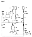
- the film-forming apparatus is provided with a reaction chamber 11; a nitrogen gas cylinder 12, which is a source of an inert gas feed (for example, nitrogen gas); an Si compound gas cylinder 13, which is a source of a feed of gaseous Si compound; and an oxygen cylinder 14, which is a source of an oxygen gas feed.
- a susceptor (not shown) is disposed within the reaction chamber 11 and one semiconductor substrate (not shown), for example, a silicon substrate, is mounted thereon.
- a heater is provided within the susceptor in order to heat the semiconductor substrate to the specified reaction temperature.
- the heater in a batch-type apparatus may have a different structure from the heater in a single-wafer apparatus.
- the nitrogen gas cylinder 12 is connected through a line L1 to the reaction chamber 11.
- a shutoff valve V1 and a flow rate controller, for example, a mass flow controller MFC1 are provided in the line L1 in the order given considered from the upstream side.
- a shutoff valve V2 is also provided in the line L1 in the vicinity of the reaction chamber 11.
- An exhaust line L2 that extends to a vacuum pump PMP is provided at the bottom of the reaction chamber 11.
- a pressure gauge PG1, a butterfly valve BV for backpressure control, and a shutoff valve V3 are provided in the line L2 in the order given considered from the upstream side.
- the vacuum pump PMP is connected through a line L3 to a detoxification apparatus 15.
- This detoxification apparatus 15 can be, for example, a combustion-type detoxification apparatus or a dry-type detoxification apparatus, in correspondence to the gas species and levels thereof.
- the Si compound gas cylinder 13 is connected through a line L4 to the line L1 upstream from the shutoff valve V2 (between the shutoff valve V2 and the mass flow controller MFC1 ).
- a shutoff valve V4, a mass flow controller MFC2, a pressure gauge PG2, and a shutoff valve V5 are disposed in the line L4 in the order given considered from the upstream side.
- the line L4 branches upstream from the pressure gauge PG2 and the resulting branch line L4' is connected to the exhaust line L2 upstream from the vacuum pump PMP (between the vacuum pump PMP and the shutoff valve V3).
- a shutoff valve V5' is provided in the branch line L4'. The states of the shutoff valves V5 and V5' are synchronized in such a manner that when one is open the other is closed.
- the oxygen cylinder 14 is provided with a line L5 that extends to an ozone generator 16; this line L5 is provided with a shutoff valve V6 and a mass flow controller MFC3 in the order given considered from the upstream side.
- the ozone generator 16 is connected through a line L6 with the line L1 upstream from the shutoff valve V2 (between the shutoff valve V2 and the mass flow controller MFC1 ).
- An ozone concentration sensor OCS, a pressure gauge PG3, and a shutoff valve V7 are provided in the line L6 in the order given considered from the upstream side.
- the line L6 is also branched upstream from the pressure gauge PG3, and the resulting branch line L6' is connected to the exhaust line L2 upstream from the vacuum pump PMP (between the vacuum pump PMP and the shutoff valve V3).
- a shutoff valve V7' is provided in the branch line L6'. The states of the shutoff valves V7 and V7' are synchronized in such a manner that when one is open the other is closed.
- a mixed gas of oxygen and ozone produced by the ozone generator 16 flows into the line L6.
- control of the ozone concentration in the mixed gas depends mainly on pressure and the power applied to the ozone generator 16.
- the ozone concentration is controlled by measuring the ozone level with an ozone concentration sensor OCS disposed in the line L6 and subjecting the applied power and vessel pressure of the ozone generator 16 to feedback control based on this measured value.
- a treatment substrate for example, a semiconductor wafer (not shown), is mounted on the susceptor within the reaction chamber 11 and the wafer is heated to 50 to 400°C by a temperature regulator incorporated in the susceptor.
- the shutoff valves V5 and V7 are closed and the other shutoff valves V1 to V4, V6, V5', and V7' are all open.
- the closed control valves are shown filled in black in Figure 1 , while the open control valves are shown in white.
- the status of the shutoff valves in the following description is shown in the same manner.
- nitrogen gas is introduced from the nitrogen gas cylinder 12 through the line L1 and into the reaction chamber 11 under feed flow rate control by the mass flow controller MFC1.
- a nitrogen gas purge is thereby carried out at a desired vacuum (for example, 0.1 to 1000 torr (13Pa to 1330 kPa)) by exhausting the gas within the reaction chamber 11 and feeding nitrogen gas into the reaction chamber 11 and the interior of the reaction chamber 11 is substituted by nitrogen gas.
- Si compound gas is continuously fed into the line L4 from the Si compound gas cylinder 13 under feed flow rate control by the mass flow controller MFC2.
- the shutoff valve V5 which resides in the line L4 that connects to the line L1 that extends to the reaction chamber 11
- the shutoff valve V5' which resides in the branch line L4' that connects to the exhaust line L2 is open, and as a result this Si compound gas is not fed into the reaction chamber 11 during the nitrogen gas purge step, but rather is exhausted by feed through the lines L4 and L4' into the exhaust line L2.
- oxygen gas is continuously fed through the line L5 from the oxygen gas cylinder 14 to the ozone generator 16 under feed flow rate control by the mass flow controller MFC3.
- a desired power level is applied to the ozone generator 16, and oxygen containing ozone at a desired concentration (the mixed gas) is fed into the line L6 from the ozone generator 16 while measuring the ozone level with the ozone concentration sensor OCS provided in the line L6, through which the mixed gas of ozone and oxygen flows, and exercising feedback control of the applied power and the vessel pressure of the ozone generator 16 based on the resulting measured value.
- shutoff valve V7 which resides in the line L6 that connects to the line L1 that extends to the reaction chamber 11, is closed and the shutoff valve V7', which resides in the branch line L6' that connects to the exhaust line L2, is open, and as a result this ozone + oxygen mixed gas is not fed into the reaction chamber 11 during the nitrogen gas purge step, but rather is exhausted by feed through the lines L6 and L6' into the exhaust line L2.
- shutoff valve V5' in the branch line L4' is closed and, in synchrony with this operation, the shutoff valve V5 in the line L4 is opened, as shown in Figure 2 .
- the status of each of these shutoff valves V5 and V5 ' is then reversed.
- Si compound gas from the Si compound gas cylinder 13 is fed under flow rate control from the line L4 into the line L1 and is pulsed into the reaction chamber 11 along with nitrogen gas. This pulse results in the adsorption of an approximately monomolecular layer of the Si compound on the heated surface of the semiconductor wafer mounted on the susceptor in the reaction chamber 11.
- a nitrogen gas purge is carried out as in Figure 1 by reversing the status of the shutoff valves V5 and V5' in the line L4 and the branch line L4' from the status in Figure 2 .
- the unreacted Si compound remaining in the reaction chamber 11 is exhausted by means of the nitrogen gas and the interior of the reaction chamber 11 is again substituted by nitrogen gas.
- shutoff valve V7' in the branch line L6' is closed and, in synchrony with this operation, the shutoff valve V7 in the line L6 is opened, as shown in Figure 3 .
- the status of each of these shutoff valves V7 and V7' is then reversed.
- the mixed gas of ozone and oxygen, supra is fed from the line L6 into the line L1 and is pulsed into the reaction chamber 11 along with nitrogen gas.
- the Si compound adsorbed on the heated surface of the semiconductor wafer mounted on the susceptor in the reaction chamber 11 is oxidized by the ozone + oxygen mixed gas, resulting in the formation on the surface of the semiconductor wafer of a silicon oxide film in the form of an approximately monomolecular layer.
- a silicon oxide film of desired thickness is formed on the surface of the semiconductor wafer by repeating these steps of 1) nitrogen gas purge, 2) Si compound gas pulse, 3) nitrogen gas purge, and 4) ozone + oxygen mixed gas pulse.
- a nitrogen gas purge is carried out as in Figure 1 by reversing the status of the shutoff valves V7 and V7' in the line L6 and the branch line L6' from the status in Figure 3 .
- reaction by-products and the unreacted ozone + oxygen mixed gas remaining in the reaction chamber 11 are exhausted by means of the nitrogen gas and the interior of the reaction chamber 11 is again substituted by nitrogen gas.
- Si compound that is gaseous at ambient temperature is used as an example of the gaseous Si compound in silicon oxide film formation using the film-forming apparatus shown in Figures 1 to 3 and described above.
- gaseous Si compound can still be introduced into the reaction chamber 11 using a bubbler procedure.
- a bubbler is provided in place of the Si compound gas cylinder 13 shown in Figures 1 to 3 and this bubbler is connected to a branch line branched off upstream from the valve V1 in the nitrogen gas-carrying line L1, making it possible to repeat the steps of 1) nitrogen gas purge, 2) Si compound gas pulse, 3) nitrogen gas purge, and 4) ozone + oxygen mixed gas pulse.
- an inert gas for example, nitrogen gas
- an inert gas for example, nitrogen gas
- purge after the oxidation reaction makes it possible to prevent the adsorption of moisture within the reaction chamber by the silicon oxide film that has been formed.
- This enables the formation of an excellent silicon oxide film for which OH bond introduction has been inhibited or prevented.
- Such a silicon oxide film has, for example, an excellent performance with regard to low leakage current.
- the Si compound adsorbed on the surface of the treatment substrate is oxidized by a pulse of a mixed gas containing a suitable amount of ozone (for example, a concentration of 5 to 20%), oxidation to the surface of the treatment substrate, which has been confirmed for the use of ozone-containing mixed gas by CVD methods, can be prevented. There is little effect on the treatment substrate since the required amount of this ozone-containing mixed gas is introduced as a pulse at low temperatures. This makes it possible to submit a treatment substrate bearing a film intolerant to high temperatures or an easily oxidizable metal film or metal silicide film to formation of a silicon oxide film according to the embodiment.
- a suitable amount of ozone for example, a concentration of 5 to 20%
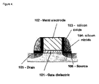
- On fig. 4 is illustrated a side view of a MOS transistor comprising a SiO2 layer according to the invention.
- the gate 101 On the wafer 100, above the respective drain 105 and source 106 is located the gate 101 in the gate dielectric material with the metal electrode 102 deposited above 101.
- Protective silicon oxide films 103 are laterally placed on the lateral ends of the gate 101 and metal gate electrode 102.
- SiO 2 films 103 are also deposited on the top of the source 106 and the drain 105.
- the chamber was a hot-wall reactor heated by conventional heater.
- the ozonizer produced the ozone and its concentration was approximately 150 g/m 3 at -0.01 MPaG.
- BDEAS Bis(diethylamino)silane, SiH 2 (NEt 2 ) 2
- Experimental conditions were:
- SiO 2 films were obtained on Si wafer. Depositions at 200, 250, 300, 350 and 400°C were carried out. The deposited films did include neither nitrogen nor carbon according to in-depth analysis by Auger.
Landscapes
- Chemical & Material Sciences (AREA)
- Organic Chemistry (AREA)
- Engineering & Computer Science (AREA)
- Chemical Kinetics & Catalysis (AREA)
- Materials Engineering (AREA)
- General Chemical & Material Sciences (AREA)
- Mechanical Engineering (AREA)
- Metallurgy (AREA)
- Inorganic Chemistry (AREA)
- Formation Of Insulating Films (AREA)
- Chemical Vapour Deposition (AREA)
- Life Sciences & Earth Sciences (AREA)
- Wood Science & Technology (AREA)
- Health & Medical Sciences (AREA)
- Medicinal Chemistry (AREA)
- Polymers & Plastics (AREA)
- Insulated Gate Type Field-Effect Transistor (AREA)
- Silicon Compounds (AREA)
Applications Claiming Priority (2)
| Application Number | Priority Date | Filing Date | Title |
|---|---|---|---|
| JP2005077608A JP2006261434A (ja) | 2005-03-17 | 2005-03-17 | シリコン酸化膜の形成方法 |
| PCT/EP2006/060829 WO2006097525A2 (en) | 2005-03-17 | 2006-03-17 | Method of forming silicon oxide containing films |
Publications (2)
| Publication Number | Publication Date |
|---|---|
| EP1861519A2 EP1861519A2 (en) | 2007-12-05 |
| EP1861519B1 true EP1861519B1 (en) | 2010-09-22 |
Family
ID=36764030
Family Applications (1)
| Application Number | Title | Priority Date | Filing Date |
|---|---|---|---|
| EP06725128A Expired - Lifetime EP1861519B1 (en) | 2005-03-17 | 2006-03-17 | Method of forming silicon oxide containing films |
Country Status (9)
| Country | Link |
|---|---|
| US (2) | US8227032B2 (enExample) |
| EP (1) | EP1861519B1 (enExample) |
| JP (3) | JP2006261434A (enExample) |
| KR (6) | KR20140069192A (enExample) |
| CN (1) | CN101171366A (enExample) |
| AT (1) | ATE482301T1 (enExample) |
| DE (1) | DE602006017042D1 (enExample) |
| TW (2) | TWI515794B (enExample) |
| WO (1) | WO2006097525A2 (enExample) |
Families Citing this family (474)
| Publication number | Priority date | Publication date | Assignee | Title |
|---|---|---|---|---|
| JP2006261434A (ja) * | 2005-03-17 | 2006-09-28 | L'air Liquide Sa Pour L'etude & L'exploitation Des Procede S Georges Claude | シリコン酸化膜の形成方法 |
| US7875556B2 (en) | 2005-05-16 | 2011-01-25 | Air Products And Chemicals, Inc. | Precursors for CVD silicon carbo-nitride and silicon nitride films |
| US8187678B2 (en) * | 2006-02-13 | 2012-05-29 | Stc.Unm | Ultra-thin microporous/hybrid materials |
| US7875312B2 (en) * | 2006-05-23 | 2011-01-25 | Air Products And Chemicals, Inc. | Process for producing silicon oxide films for organoaminosilane precursors |
| US8530361B2 (en) | 2006-05-23 | 2013-09-10 | Air Products And Chemicals, Inc. | Process for producing silicon and oxide films from organoaminosilane precursors |
| US8232176B2 (en) | 2006-06-22 | 2012-07-31 | Applied Materials, Inc. | Dielectric deposition and etch back processes for bottom up gapfill |
| JP5258229B2 (ja) * | 2006-09-28 | 2013-08-07 | 東京エレクトロン株式会社 | 成膜方法および成膜装置 |
| JP5193527B2 (ja) * | 2006-09-28 | 2013-05-08 | 東京エレクトロン株式会社 | シリコン酸化膜の形成方法、シリコン酸化膜の形成装置及びプログラム |
| JP2008266711A (ja) * | 2007-04-19 | 2008-11-06 | Fuji Electric Systems Co Ltd | 真空成膜設備 |
| US20090041952A1 (en) * | 2007-08-10 | 2009-02-12 | Asm Genitech Korea Ltd. | Method of depositing silicon oxide films |
| KR100888186B1 (ko) * | 2007-08-31 | 2009-03-10 | 주식회사 테스 | 절연막 형성 방법 |
| CN101889331A (zh) * | 2007-09-18 | 2010-11-17 | 乔治洛德方法研究和开发液化空气有限公司 | 形成含硅膜的方法 |
| JP5015705B2 (ja) * | 2007-09-18 | 2012-08-29 | ルネサスエレクトロニクス株式会社 | 層間絶縁膜形成方法、層間絶縁膜、半導体デバイス、および半導体製造装置 |
| US7867923B2 (en) * | 2007-10-22 | 2011-01-11 | Applied Materials, Inc. | High quality silicon oxide films by remote plasma CVD from disilane precursors |
| US8501637B2 (en) | 2007-12-21 | 2013-08-06 | Asm International N.V. | Silicon dioxide thin films by ALD |
| JP5306691B2 (ja) * | 2008-04-01 | 2013-10-02 | 株式会社日立国際電気 | 半導体装置の製造方法、基板処理方法および基板処理装置 |
| US8357435B2 (en) | 2008-05-09 | 2013-01-22 | Applied Materials, Inc. | Flowable dielectric equipment and processes |
| JP2009295621A (ja) * | 2008-06-02 | 2009-12-17 | Panasonic Corp | 半導体装置及びその製造方法 |
| JP2010103495A (ja) * | 2008-09-29 | 2010-05-06 | Adeka Corp | 半導体デバイス、その製造装置及び製造方法 |
| JP5518499B2 (ja) * | 2009-02-17 | 2014-06-11 | 株式会社日立国際電気 | 半導体デバイスの製造方法および基板処理装置 |
| US8703624B2 (en) * | 2009-03-13 | 2014-04-22 | Air Products And Chemicals, Inc. | Dielectric films comprising silicon and methods for making same |
| US9394608B2 (en) | 2009-04-06 | 2016-07-19 | Asm America, Inc. | Semiconductor processing reactor and components thereof |
| US8980382B2 (en) | 2009-12-02 | 2015-03-17 | Applied Materials, Inc. | Oxygen-doping for non-carbon radical-component CVD films |
| US8741788B2 (en) | 2009-08-06 | 2014-06-03 | Applied Materials, Inc. | Formation of silicon oxide using non-carbon flowable CVD processes |
| US8802201B2 (en) * | 2009-08-14 | 2014-08-12 | Asm America, Inc. | Systems and methods for thin-film deposition of metal oxides using excited nitrogen-oxygen species |
| US8449942B2 (en) | 2009-11-12 | 2013-05-28 | Applied Materials, Inc. | Methods of curing non-carbon flowable CVD films |
| JP5616737B2 (ja) * | 2009-11-20 | 2014-10-29 | 株式会社日立国際電気 | 半導体装置の製造方法、基板処理方法および基板処理装置 |
| CN102687252A (zh) | 2009-12-30 | 2012-09-19 | 应用材料公司 | 以可变的氮/氢比所制造的自由基来生长介电薄膜的方法 |
| US8329262B2 (en) | 2010-01-05 | 2012-12-11 | Applied Materials, Inc. | Dielectric film formation using inert gas excitation |
| JP2013517616A (ja) | 2010-01-06 | 2013-05-16 | アプライド マテリアルズ インコーポレイテッド | 酸化物ライナを使用する流動可能な誘電体 |
| SG182333A1 (en) | 2010-01-07 | 2012-08-30 | Applied Materials Inc | In-situ ozone cure for radical-component cvd |
| CN102844848A (zh) | 2010-03-05 | 2012-12-26 | 应用材料公司 | 通过自由基成分化学气相沉积的共形层 |
| US8236708B2 (en) * | 2010-03-09 | 2012-08-07 | Applied Materials, Inc. | Reduced pattern loading using bis(diethylamino)silane (C8H22N2Si) as silicon precursor |
| US9611544B2 (en) | 2010-04-15 | 2017-04-04 | Novellus Systems, Inc. | Plasma activated conformal dielectric film deposition |
| US9997357B2 (en) | 2010-04-15 | 2018-06-12 | Lam Research Corporation | Capped ALD films for doping fin-shaped channel regions of 3-D IC transistors |
| US9373500B2 (en) | 2014-02-21 | 2016-06-21 | Lam Research Corporation | Plasma assisted atomic layer deposition titanium oxide for conformal encapsulation and gapfill applications |
| US9892917B2 (en) | 2010-04-15 | 2018-02-13 | Lam Research Corporation | Plasma assisted atomic layer deposition of multi-layer films for patterning applications |
| US9390909B2 (en) | 2013-11-07 | 2016-07-12 | Novellus Systems, Inc. | Soft landing nanolaminates for advanced patterning |
| US9257274B2 (en) | 2010-04-15 | 2016-02-09 | Lam Research Corporation | Gapfill of variable aspect ratio features with a composite PEALD and PECVD method |
| US8956983B2 (en) | 2010-04-15 | 2015-02-17 | Novellus Systems, Inc. | Conformal doping via plasma activated atomic layer deposition and conformal film deposition |
| US8728956B2 (en) | 2010-04-15 | 2014-05-20 | Novellus Systems, Inc. | Plasma activated conformal film deposition |
| US8637411B2 (en) | 2010-04-15 | 2014-01-28 | Novellus Systems, Inc. | Plasma activated conformal dielectric film deposition |
| US9076646B2 (en) | 2010-04-15 | 2015-07-07 | Lam Research Corporation | Plasma enhanced atomic layer deposition with pulsed plasma exposure |
| JP2011243620A (ja) * | 2010-05-14 | 2011-12-01 | Tokyo Electron Ltd | 成膜方法および成膜装置 |
| US8912353B2 (en) | 2010-06-02 | 2014-12-16 | Air Products And Chemicals, Inc. | Organoaminosilane precursors and methods for depositing films comprising same |
| US8343881B2 (en) | 2010-06-04 | 2013-01-01 | Applied Materials, Inc. | Silicon dioxide layer deposited with BDEAS |
| US8580699B2 (en) * | 2010-09-10 | 2013-11-12 | Applied Materials, Inc. | Embedded catalyst for atomic layer deposition of silicon oxide |
| US9685320B2 (en) | 2010-09-23 | 2017-06-20 | Lam Research Corporation | Methods for depositing silicon oxide |
| US9285168B2 (en) | 2010-10-05 | 2016-03-15 | Applied Materials, Inc. | Module for ozone cure and post-cure moisture treatment |
| US8664127B2 (en) | 2010-10-15 | 2014-03-04 | Applied Materials, Inc. | Two silicon-containing precursors for gapfill enhancing dielectric liner |
| JP5544343B2 (ja) * | 2010-10-29 | 2014-07-09 | 東京エレクトロン株式会社 | 成膜装置 |
| US8460753B2 (en) | 2010-12-09 | 2013-06-11 | Air Products And Chemicals, Inc. | Methods for depositing silicon dioxide or silicon oxide films using aminovinylsilanes |
| JP2012138500A (ja) * | 2010-12-27 | 2012-07-19 | Tokyo Electron Ltd | タングステン膜又は酸化タングステン膜上への酸化シリコン膜の成膜方法及び成膜装置 |
| US9460913B2 (en) | 2010-12-27 | 2016-10-04 | Tokyo Electron Limited | Film-forming method for forming silicon oxide film on tungsten film or tungsten oxide film |
| US9466476B2 (en) | 2010-12-27 | 2016-10-11 | Tokyo Electron Limited | Film-forming method for forming silicon oxide film on tungsten film or tungsten oxide film |
| US10283321B2 (en) | 2011-01-18 | 2019-05-07 | Applied Materials, Inc. | Semiconductor processing system and methods using capacitively coupled plasma |
| US8450191B2 (en) | 2011-01-24 | 2013-05-28 | Applied Materials, Inc. | Polysilicon films by HDP-CVD |
| EP2484801B1 (en) * | 2011-02-07 | 2017-08-23 | L'air Liquide, Societe Anonyme Pour L'etude Et L'exploitation Des Procedes Georges Claude | Method of deposition of Al2O3/SiO2 stacks, from TMA or TEA and silicon precursors |
| EP2484803B1 (en) * | 2011-02-07 | 2017-03-29 | L'air Liquide, Societe Anonyme Pour L'etude Et L'exploitation Des Procedes Georges Claude | Method of deposition of Al2O3/SiO2 stacks, from aluminium and silicon precursors |
| WO2012107138A1 (en) * | 2011-02-07 | 2012-08-16 | L'air Liquide, Societe Anonyme Pour L'etude Et L'exploitation Des Procedes Georges Claude | METHOD OF DEPOSITION OF Al2O3/SiO2 STACKS, FROM ALUMINIUM AND SILICON PRECURSORS |
| EP2484802B1 (en) * | 2011-02-07 | 2017-03-29 | L'Air Liquide Société Anonyme pour l'Etude et l'Exploitation des Procédés Georges Claude | Method of deposition of Al2O3/SiO2 stacks from DMAI and silicon precursors |
| US8716154B2 (en) | 2011-03-04 | 2014-05-06 | Applied Materials, Inc. | Reduced pattern loading using silicon oxide multi-layers |
| US8647993B2 (en) | 2011-04-11 | 2014-02-11 | Novellus Systems, Inc. | Methods for UV-assisted conformal film deposition |
| DE102011016935A1 (de) * | 2011-04-13 | 2012-10-18 | Osram Opto Semiconductors Gmbh | Verfahren zur Herstellung eines Licht emittierenden Halbleiterbauelements und Licht emittierendes Halbleiterbauelement |
| US8445078B2 (en) | 2011-04-20 | 2013-05-21 | Applied Materials, Inc. | Low temperature silicon oxide conversion |
| US8771807B2 (en) | 2011-05-24 | 2014-07-08 | Air Products And Chemicals, Inc. | Organoaminosilane precursors and methods for making and using same |
| US8466073B2 (en) | 2011-06-03 | 2013-06-18 | Applied Materials, Inc. | Capping layer for reduced outgassing |
| US9312155B2 (en) | 2011-06-06 | 2016-04-12 | Asm Japan K.K. | High-throughput semiconductor-processing apparatus equipped with multiple dual-chamber modules |
| JP2013008828A (ja) * | 2011-06-24 | 2013-01-10 | Taiyo Nippon Sanso Corp | シリコン絶縁膜の形成方法 |
| US9404178B2 (en) | 2011-07-15 | 2016-08-02 | Applied Materials, Inc. | Surface treatment and deposition for reduced outgassing |
| US20130023129A1 (en) | 2011-07-20 | 2013-01-24 | Asm America, Inc. | Pressure transmitter for a semiconductor processing environment |
| US8617989B2 (en) | 2011-09-26 | 2013-12-31 | Applied Materials, Inc. | Liner property improvement |
| US8551891B2 (en) | 2011-10-04 | 2013-10-08 | Applied Materials, Inc. | Remote plasma burn-in |
| US9017481B1 (en) | 2011-10-28 | 2015-04-28 | Asm America, Inc. | Process feed management for semiconductor substrate processing |
| US9128218B2 (en) | 2011-12-29 | 2015-09-08 | Visera Technologies Company Limited | Microlens structure and fabrication method thereof |
| US8592328B2 (en) | 2012-01-20 | 2013-11-26 | Novellus Systems, Inc. | Method for depositing a chlorine-free conformal sin film |
| TWI496932B (zh) * | 2012-03-09 | 2015-08-21 | 氣體產品及化學品股份公司 | 用於顯示裝置的阻絕物材料 |
| WO2014015237A1 (en) | 2012-07-20 | 2014-01-23 | L'air Liquide, Societe Anonyme Pour L'etude Et L'exploitation Des Procedes Georges Claude | Organosilane precursors for ald/cvd silicon-containing film applications |
| KR20140026724A (ko) * | 2012-08-23 | 2014-03-06 | 주식회사 원익아이피에스 | 박막 제조 방법 및 기판 처리 장치 |
| US8889566B2 (en) | 2012-09-11 | 2014-11-18 | Applied Materials, Inc. | Low cost flowable dielectric films |
| US10714315B2 (en) | 2012-10-12 | 2020-07-14 | Asm Ip Holdings B.V. | Semiconductor reaction chamber showerhead |
| US9355839B2 (en) | 2012-10-23 | 2016-05-31 | Lam Research Corporation | Sub-saturated atomic layer deposition and conformal film deposition |
| SG2013083654A (en) | 2012-11-08 | 2014-06-27 | Novellus Systems Inc | Methods for depositing films on sensitive substrates |
| SG2013083241A (en) | 2012-11-08 | 2014-06-27 | Novellus Systems Inc | Conformal film deposition for gapfill |
| US9018108B2 (en) | 2013-01-25 | 2015-04-28 | Applied Materials, Inc. | Low shrinkage dielectric films |
| US20160376700A1 (en) | 2013-02-01 | 2016-12-29 | Asm Ip Holding B.V. | System for treatment of deposition reactor |
| EP2770526B1 (en) | 2013-02-22 | 2018-10-03 | IMEC vzw | Oxygen monolayer on a semiconductor |
| JP2014209558A (ja) * | 2013-03-27 | 2014-11-06 | 東京エレクトロン株式会社 | シリコン酸化膜の形成方法、及び、シリコン酸化膜の形成装置 |
| JP5998101B2 (ja) * | 2013-05-24 | 2016-09-28 | 株式会社日立国際電気 | 半導体装置の製造方法、基板処理装置及びプログラム |
| JP6154215B2 (ja) | 2013-06-28 | 2017-06-28 | 株式会社日立国際電気 | 半導体装置の製造方法、基板処理装置およびプログラム |
| US9382268B1 (en) | 2013-07-19 | 2016-07-05 | American Air Liquide, Inc. | Sulfur containing organosilane precursors for ALD/CVD silicon-containing film applications |
| TW201509799A (zh) | 2013-07-19 | 2015-03-16 | Air Liquide | 用於ald/cvd含矽薄膜應用之六配位含矽前驅物 |
| CN103450801A (zh) * | 2013-09-09 | 2013-12-18 | 南京工业大学 | 一种制备微纳米硅基超疏水涂层的方法及其用途 |
| JP2014064039A (ja) * | 2013-12-25 | 2014-04-10 | Tokyo Electron Ltd | 成膜方法および成膜装置 |
| US9214334B2 (en) | 2014-02-18 | 2015-12-15 | Lam Research Corporation | High growth rate process for conformal aluminum nitride |
| US10683571B2 (en) | 2014-02-25 | 2020-06-16 | Asm Ip Holding B.V. | Gas supply manifold and method of supplying gases to chamber using same |
| US11015245B2 (en) | 2014-03-19 | 2021-05-25 | Asm Ip Holding B.V. | Gas-phase reactor and system having exhaust plenum and components thereof |
| EP3151286B1 (en) * | 2014-05-29 | 2021-12-08 | Kyocera Corporation | Solar cell element, method for manufacturing same and solar cell module |
| RU2586265C2 (ru) * | 2014-07-04 | 2016-06-10 | Федеральное Государственное Бюджетное Образовательное Учреждение Высшего Профессионального Образования "Дагестанский Государственный Технический Университет" (Дгту) | Способ осаждения тонких пленок на поверхности подложек для изготовления солнечных элементов |
| US9869017B2 (en) * | 2014-07-10 | 2018-01-16 | Applied Materials, Inc. | H2/O2 side inject to improve process uniformity for low temperature oxidation process |
| US9412581B2 (en) | 2014-07-16 | 2016-08-09 | Applied Materials, Inc. | Low-K dielectric gapfill by flowable deposition |
| US10858737B2 (en) | 2014-07-28 | 2020-12-08 | Asm Ip Holding B.V. | Showerhead assembly and components thereof |
| US9478438B2 (en) | 2014-08-20 | 2016-10-25 | Lam Research Corporation | Method and apparatus to deposit pure titanium thin film at low temperature using titanium tetraiodide precursor |
| US9478411B2 (en) | 2014-08-20 | 2016-10-25 | Lam Research Corporation | Method to tune TiOx stoichiometry using atomic layer deposited Ti film to minimize contact resistance for TiOx/Ti based MIS contact scheme for CMOS |
| US9890456B2 (en) | 2014-08-21 | 2018-02-13 | Asm Ip Holding B.V. | Method and system for in situ formation of gas-phase compounds |
| US9214333B1 (en) | 2014-09-24 | 2015-12-15 | Lam Research Corporation | Methods and apparatuses for uniform reduction of the in-feature wet etch rate of a silicon nitride film formed by ALD |
| WO2016054566A1 (en) | 2014-10-02 | 2016-04-07 | L'air Liquide, Societe Anonyme Pour L'etude Et L'exploitation Des Procedes Georges Claude | Organodisilane precursors for ald/cvd silicon-containing film applications |
| US10941490B2 (en) | 2014-10-07 | 2021-03-09 | Asm Ip Holding B.V. | Multiple temperature range susceptor, assembly, reactor and system including the susceptor, and methods of using the same |
| SG11201703196WA (en) | 2014-10-24 | 2017-05-30 | Versum Materials Us Llc | Compositions and methods using same for deposition of silicon-containing films |
| US9564312B2 (en) | 2014-11-24 | 2017-02-07 | Lam Research Corporation | Selective inhibition in atomic layer deposition of silicon-containing films |
| US9589790B2 (en) | 2014-11-24 | 2017-03-07 | Lam Research Corporation | Method of depositing ammonia free and chlorine free conformal silicon nitride film |
| EP3029175A1 (en) * | 2014-12-05 | 2016-06-08 | Basf Se | Process for the production of porous thin films |
| WO2016094711A2 (en) | 2014-12-13 | 2016-06-16 | L'air Liquide, Societe Anonyme Pour L'etude Et L'exploitation Des Procedes Georges Claude | Organosilane precursors for ald/cvd silicon-containing film applications and methods of using the same |
| US9472392B2 (en) | 2015-01-30 | 2016-10-18 | Applied Materials, Inc. | Step coverage dielectric |
| US10276355B2 (en) | 2015-03-12 | 2019-04-30 | Asm Ip Holding B.V. | Multi-zone reactor, system including the reactor, and method of using the same |
| US10566187B2 (en) | 2015-03-20 | 2020-02-18 | Lam Research Corporation | Ultrathin atomic layer deposition film accuracy thickness control |
| US9502238B2 (en) | 2015-04-03 | 2016-11-22 | Lam Research Corporation | Deposition of conformal films by atomic layer deposition and atomic layer etch |
| US10458018B2 (en) | 2015-06-26 | 2019-10-29 | Asm Ip Holding B.V. | Structures including metal carbide material, devices including the structures, and methods of forming same |
| US10526701B2 (en) | 2015-07-09 | 2020-01-07 | Lam Research Corporation | Multi-cycle ALD process for film uniformity and thickness profile modulation |
| US9601693B1 (en) | 2015-09-24 | 2017-03-21 | Lam Research Corporation | Method for encapsulating a chalcogenide material |
| US11365481B2 (en) * | 2015-10-06 | 2022-06-21 | City University Of Hong Kong | Homogeneous and transparent protective coatings for precious metals and copper alloys |
| US10211308B2 (en) | 2015-10-21 | 2019-02-19 | Asm Ip Holding B.V. | NbMC layers |
| WO2017070190A1 (en) * | 2015-10-23 | 2017-04-27 | Applied Materials, Inc. | Bottom-up gap-fill by surface poisoning treatment |
| US9786491B2 (en) | 2015-11-12 | 2017-10-10 | Asm Ip Holding B.V. | Formation of SiOCN thin films |
| US9786492B2 (en) | 2015-11-12 | 2017-10-10 | Asm Ip Holding B.V. | Formation of SiOCN thin films |
| US11515144B2 (en) * | 2015-12-10 | 2022-11-29 | Applied Materials, Inc. | In-situ film annealing with spatial atomic layer deposition |
| US11139308B2 (en) | 2015-12-29 | 2021-10-05 | Asm Ip Holding B.V. | Atomic layer deposition of III-V compounds to form V-NAND devices |
| GB201523156D0 (en) * | 2015-12-31 | 2016-02-17 | Pilkington Group Ltd | High strength glass containers |
| US10529554B2 (en) | 2016-02-19 | 2020-01-07 | Asm Ip Holding B.V. | Method for forming silicon nitride film selectively on sidewalls or flat surfaces of trenches |
| US10343920B2 (en) | 2016-03-18 | 2019-07-09 | Asm Ip Holding B.V. | Aligned carbon nanotubes |
| US10190213B2 (en) | 2016-04-21 | 2019-01-29 | Asm Ip Holding B.V. | Deposition of metal borides |
| US10865475B2 (en) | 2016-04-21 | 2020-12-15 | Asm Ip Holding B.V. | Deposition of metal borides and silicides |
| US10032628B2 (en) | 2016-05-02 | 2018-07-24 | Asm Ip Holding B.V. | Source/drain performance through conformal solid state doping |
| US10367080B2 (en) | 2016-05-02 | 2019-07-30 | Asm Ip Holding B.V. | Method of forming a germanium oxynitride film |
| KR102378021B1 (ko) | 2016-05-06 | 2022-03-23 | 에이에스엠 아이피 홀딩 비.브이. | SiOC 박막의 형성 |
| US11453943B2 (en) | 2016-05-25 | 2022-09-27 | Asm Ip Holding B.V. | Method for forming carbon-containing silicon/metal oxide or nitride film by ALD using silicon precursor and hydrocarbon precursor |
| WO2018005376A1 (en) | 2016-06-28 | 2018-01-04 | Applied Materials, Inc. | Cvd based oxide-metal multi structure for 3d nand memory devices |
| US9773643B1 (en) | 2016-06-30 | 2017-09-26 | Lam Research Corporation | Apparatus and method for deposition and etch in gap fill |
| US10062563B2 (en) | 2016-07-01 | 2018-08-28 | Lam Research Corporation | Selective atomic layer deposition with post-dose treatment |
| US9859151B1 (en) | 2016-07-08 | 2018-01-02 | Asm Ip Holding B.V. | Selective film deposition method to form air gaps |
| US10612137B2 (en) | 2016-07-08 | 2020-04-07 | Asm Ip Holdings B.V. | Organic reactants for atomic layer deposition |
| US10714385B2 (en) | 2016-07-19 | 2020-07-14 | Asm Ip Holding B.V. | Selective deposition of tungsten |
| KR102532607B1 (ko) | 2016-07-28 | 2023-05-15 | 에이에스엠 아이피 홀딩 비.브이. | 기판 가공 장치 및 그 동작 방법 |
| US9812320B1 (en) | 2016-07-28 | 2017-11-07 | Asm Ip Holding B.V. | Method and apparatus for filling a gap |
| US9887082B1 (en) | 2016-07-28 | 2018-02-06 | Asm Ip Holding B.V. | Method and apparatus for filling a gap |
| US10629435B2 (en) | 2016-07-29 | 2020-04-21 | Lam Research Corporation | Doped ALD films for semiconductor patterning applications |
| US10074543B2 (en) | 2016-08-31 | 2018-09-11 | Lam Research Corporation | High dry etch rate materials for semiconductor patterning applications |
| US10037884B2 (en) | 2016-08-31 | 2018-07-31 | Lam Research Corporation | Selective atomic layer deposition for gapfill using sacrificial underlayer |
| US9865455B1 (en) | 2016-09-07 | 2018-01-09 | Lam Research Corporation | Nitride film formed by plasma-enhanced and thermal atomic layer deposition process |
| US10643826B2 (en) | 2016-10-26 | 2020-05-05 | Asm Ip Holdings B.V. | Methods for thermally calibrating reaction chambers |
| US11532757B2 (en) | 2016-10-27 | 2022-12-20 | Asm Ip Holding B.V. | Deposition of charge trapping layers |
| US10714350B2 (en) | 2016-11-01 | 2020-07-14 | ASM IP Holdings, B.V. | Methods for forming a transition metal niobium nitride film on a substrate by atomic layer deposition and related semiconductor device structures |
| US10229833B2 (en) | 2016-11-01 | 2019-03-12 | Asm Ip Holding B.V. | Methods for forming a transition metal nitride film on a substrate by atomic layer deposition and related semiconductor device structures |
| US10454029B2 (en) | 2016-11-11 | 2019-10-22 | Lam Research Corporation | Method for reducing the wet etch rate of a sin film without damaging the underlying substrate |
| US10832908B2 (en) | 2016-11-11 | 2020-11-10 | Lam Research Corporation | Self-aligned multi-patterning process flow with ALD gapfill spacer mask |
| US10134579B2 (en) | 2016-11-14 | 2018-11-20 | Lam Research Corporation | Method for high modulus ALD SiO2 spacer |
| KR102546317B1 (ko) | 2016-11-15 | 2023-06-21 | 에이에스엠 아이피 홀딩 비.브이. | 기체 공급 유닛 및 이를 포함하는 기판 처리 장치 |
| FR3059339B1 (fr) * | 2016-11-29 | 2020-02-28 | Commissariat A L'energie Atomique Et Aux Energies Alternatives | Procede de formation de films de dioxyde de silicium |
| US10186420B2 (en) | 2016-11-29 | 2019-01-22 | Asm Ip Holding B.V. | Formation of silicon-containing thin films |
| KR102762543B1 (ko) | 2016-12-14 | 2025-02-05 | 에이에스엠 아이피 홀딩 비.브이. | 기판 처리 장치 |
| US11447861B2 (en) | 2016-12-15 | 2022-09-20 | Asm Ip Holding B.V. | Sequential infiltration synthesis apparatus and a method of forming a patterned structure |
| US11581186B2 (en) | 2016-12-15 | 2023-02-14 | Asm Ip Holding B.V. | Sequential infiltration synthesis apparatus |
| KR102700194B1 (ko) | 2016-12-19 | 2024-08-28 | 에이에스엠 아이피 홀딩 비.브이. | 기판 처리 장치 |
| US10269558B2 (en) | 2016-12-22 | 2019-04-23 | Asm Ip Holding B.V. | Method of forming a structure on a substrate |
| US10867788B2 (en) | 2016-12-28 | 2020-12-15 | Asm Ip Holding B.V. | Method of forming a structure on a substrate |
| US11390950B2 (en) | 2017-01-10 | 2022-07-19 | Asm Ip Holding B.V. | Reactor system and method to reduce residue buildup during a film deposition process |
| US10655221B2 (en) | 2017-02-09 | 2020-05-19 | Asm Ip Holding B.V. | Method for depositing oxide film by thermal ALD and PEALD |
| US10468261B2 (en) | 2017-02-15 | 2019-11-05 | Asm Ip Holding B.V. | Methods for forming a metallic film on a substrate by cyclical deposition and related semiconductor device structures |
| US10529563B2 (en) | 2017-03-29 | 2020-01-07 | Asm Ip Holdings B.V. | Method for forming doped metal oxide films on a substrate by cyclical deposition and related semiconductor device structures |
| US10847529B2 (en) | 2017-04-13 | 2020-11-24 | Asm Ip Holding B.V. | Substrate processing method and device manufactured by the same |
| KR102457289B1 (ko) | 2017-04-25 | 2022-10-21 | 에이에스엠 아이피 홀딩 비.브이. | 박막 증착 방법 및 반도체 장치의 제조 방법 |
| US10504901B2 (en) | 2017-04-26 | 2019-12-10 | Asm Ip Holding B.V. | Substrate processing method and device manufactured using the same |
| CN110546302B (zh) | 2017-05-05 | 2022-05-27 | Asm Ip 控股有限公司 | 用于受控形成含氧薄膜的等离子体增强沉积方法 |
| US10770286B2 (en) | 2017-05-08 | 2020-09-08 | Asm Ip Holdings B.V. | Methods for selectively forming a silicon nitride film on a substrate and related semiconductor device structures |
| US10892156B2 (en) | 2017-05-08 | 2021-01-12 | Asm Ip Holding B.V. | Methods for forming a silicon nitride film on a substrate and related semiconductor device structures |
| TWI782021B (zh) * | 2017-05-28 | 2022-11-01 | 美商應用材料股份有限公司 | 有機及混合有機無機層的選擇性分子層沉積 |
| US12040200B2 (en) | 2017-06-20 | 2024-07-16 | Asm Ip Holding B.V. | Semiconductor processing apparatus and methods for calibrating a semiconductor processing apparatus |
| US11306395B2 (en) | 2017-06-28 | 2022-04-19 | Asm Ip Holding B.V. | Methods for depositing a transition metal nitride film on a substrate by atomic layer deposition and related deposition apparatus |
| US10685834B2 (en) | 2017-07-05 | 2020-06-16 | Asm Ip Holdings B.V. | Methods for forming a silicon germanium tin layer and related semiconductor device structures |
| KR20190009245A (ko) | 2017-07-18 | 2019-01-28 | 에이에스엠 아이피 홀딩 비.브이. | 반도체 소자 구조물 형성 방법 및 관련된 반도체 소자 구조물 |
| US10541333B2 (en) | 2017-07-19 | 2020-01-21 | Asm Ip Holding B.V. | Method for depositing a group IV semiconductor and related semiconductor device structures |
| US11018002B2 (en) | 2017-07-19 | 2021-05-25 | Asm Ip Holding B.V. | Method for selectively depositing a Group IV semiconductor and related semiconductor device structures |
| US11374112B2 (en) | 2017-07-19 | 2022-06-28 | Asm Ip Holding B.V. | Method for depositing a group IV semiconductor and related semiconductor device structures |
| US10590535B2 (en) | 2017-07-26 | 2020-03-17 | Asm Ip Holdings B.V. | Chemical treatment, deposition and/or infiltration apparatus and method for using the same |
| TWI815813B (zh) | 2017-08-04 | 2023-09-21 | 荷蘭商Asm智慧財產控股公司 | 用於分配反應腔內氣體的噴頭總成 |
| US10770336B2 (en) | 2017-08-08 | 2020-09-08 | Asm Ip Holding B.V. | Substrate lift mechanism and reactor including same |
| US10692741B2 (en) | 2017-08-08 | 2020-06-23 | Asm Ip Holdings B.V. | Radiation shield |
| US11139191B2 (en) | 2017-08-09 | 2021-10-05 | Asm Ip Holding B.V. | Storage apparatus for storing cassettes for substrates and processing apparatus equipped therewith |
| US10249524B2 (en) | 2017-08-09 | 2019-04-02 | Asm Ip Holding B.V. | Cassette holder assembly for a substrate cassette and holding member for use in such assembly |
| US11769682B2 (en) | 2017-08-09 | 2023-09-26 | Asm Ip Holding B.V. | Storage apparatus for storing cassettes for substrates and processing apparatus equipped therewith |
| US11830730B2 (en) | 2017-08-29 | 2023-11-28 | Asm Ip Holding B.V. | Layer forming method and apparatus |
| KR102491945B1 (ko) | 2017-08-30 | 2023-01-26 | 에이에스엠 아이피 홀딩 비.브이. | 기판 처리 장치 |
| US11295980B2 (en) | 2017-08-30 | 2022-04-05 | Asm Ip Holding B.V. | Methods for depositing a molybdenum metal film over a dielectric surface of a substrate by a cyclical deposition process and related semiconductor device structures |
| US11056344B2 (en) | 2017-08-30 | 2021-07-06 | Asm Ip Holding B.V. | Layer forming method |
| KR102401446B1 (ko) | 2017-08-31 | 2022-05-24 | 에이에스엠 아이피 홀딩 비.브이. | 기판 처리 장치 |
| KR102229705B1 (ko) * | 2017-09-05 | 2021-03-18 | 가부시키가이샤 알박 | 반도체 장치를 제조하기 위한 방법 및 반도체 장치 |
| US10269559B2 (en) | 2017-09-13 | 2019-04-23 | Lam Research Corporation | Dielectric gapfill of high aspect ratio features utilizing a sacrificial etch cap layer |
| KR102630301B1 (ko) | 2017-09-21 | 2024-01-29 | 에이에스엠 아이피 홀딩 비.브이. | 침투성 재료의 순차 침투 합성 방법 처리 및 이를 이용하여 형성된 구조물 및 장치 |
| US10844484B2 (en) | 2017-09-22 | 2020-11-24 | Asm Ip Holding B.V. | Apparatus for dispensing a vapor phase reactant to a reaction chamber and related methods |
| US10658205B2 (en) | 2017-09-28 | 2020-05-19 | Asm Ip Holdings B.V. | Chemical dispensing apparatus and methods for dispensing a chemical to a reaction chamber |
| US10403504B2 (en) | 2017-10-05 | 2019-09-03 | Asm Ip Holding B.V. | Method for selectively depositing a metallic film on a substrate |
| US10319588B2 (en) | 2017-10-10 | 2019-06-11 | Asm Ip Holding B.V. | Method for depositing a metal chalcogenide on a substrate by cyclical deposition |
| EP3476973B1 (en) * | 2017-10-25 | 2026-04-22 | L'Air Liquide, Société Anonyme pour l'Etude et l'Exploitation des Procédés Georges Claude | Process chamber and method for purging the same |
| US10923344B2 (en) | 2017-10-30 | 2021-02-16 | Asm Ip Holding B.V. | Methods for forming a semiconductor structure and related semiconductor structures |
| KR102443047B1 (ko) | 2017-11-16 | 2022-09-14 | 에이에스엠 아이피 홀딩 비.브이. | 기판 처리 장치 방법 및 그에 의해 제조된 장치 |
| US10910262B2 (en) | 2017-11-16 | 2021-02-02 | Asm Ip Holding B.V. | Method of selectively depositing a capping layer structure on a semiconductor device structure |
| US11022879B2 (en) | 2017-11-24 | 2021-06-01 | Asm Ip Holding B.V. | Method of forming an enhanced unexposed photoresist layer |
| JP7214724B2 (ja) | 2017-11-27 | 2023-01-30 | エーエスエム アイピー ホールディング ビー.ブイ. | バッチ炉で利用されるウェハカセットを収納するための収納装置 |
| TWI791689B (zh) | 2017-11-27 | 2023-02-11 | 荷蘭商Asm智慧財產控股私人有限公司 | 包括潔淨迷你環境之裝置 |
| US10991573B2 (en) | 2017-12-04 | 2021-04-27 | Asm Ip Holding B.V. | Uniform deposition of SiOC on dielectric and metal surfaces |
| US10872771B2 (en) | 2018-01-16 | 2020-12-22 | Asm Ip Holding B. V. | Method for depositing a material film on a substrate within a reaction chamber by a cyclical deposition process and related device structures |
| KR102695659B1 (ko) | 2018-01-19 | 2024-08-14 | 에이에스엠 아이피 홀딩 비.브이. | 플라즈마 보조 증착에 의해 갭 충진 층을 증착하는 방법 |
| TWI799494B (zh) | 2018-01-19 | 2023-04-21 | 荷蘭商Asm 智慧財產控股公司 | 沈積方法 |
| USD903477S1 (en) | 2018-01-24 | 2020-12-01 | Asm Ip Holdings B.V. | Metal clamp |
| US11018047B2 (en) | 2018-01-25 | 2021-05-25 | Asm Ip Holding B.V. | Hybrid lift pin |
| USD880437S1 (en) | 2018-02-01 | 2020-04-07 | Asm Ip Holding B.V. | Gas supply plate for semiconductor manufacturing apparatus |
| US11081345B2 (en) | 2018-02-06 | 2021-08-03 | Asm Ip Holding B.V. | Method of post-deposition treatment for silicon oxide film |
| US10896820B2 (en) | 2018-02-14 | 2021-01-19 | Asm Ip Holding B.V. | Method for depositing a ruthenium-containing film on a substrate by a cyclical deposition process |
| US11685991B2 (en) | 2018-02-14 | 2023-06-27 | Asm Ip Holding B.V. | Method for depositing a ruthenium-containing film on a substrate by a cyclical deposition process |
| US10731249B2 (en) | 2018-02-15 | 2020-08-04 | Asm Ip Holding B.V. | Method of forming a transition metal containing film on a substrate by a cyclical deposition process, a method for supplying a transition metal halide compound to a reaction chamber, and related vapor deposition apparatus |
| KR102636427B1 (ko) | 2018-02-20 | 2024-02-13 | 에이에스엠 아이피 홀딩 비.브이. | 기판 처리 방법 및 장치 |
| US10975470B2 (en) | 2018-02-23 | 2021-04-13 | Asm Ip Holding B.V. | Apparatus for detecting or monitoring for a chemical precursor in a high temperature environment |
| US11473195B2 (en) | 2018-03-01 | 2022-10-18 | Asm Ip Holding B.V. | Semiconductor processing apparatus and a method for processing a substrate |
| KR102899918B1 (ko) | 2018-03-02 | 2025-12-12 | 램 리써치 코포레이션 | 가수분해를 사용한 선택적인 증착 |
| US11629406B2 (en) | 2018-03-09 | 2023-04-18 | Asm Ip Holding B.V. | Semiconductor processing apparatus comprising one or more pyrometers for measuring a temperature of a substrate during transfer of the substrate |
| US11114283B2 (en) | 2018-03-16 | 2021-09-07 | Asm Ip Holding B.V. | Reactor, system including the reactor, and methods of manufacturing and using same |
| KR102646467B1 (ko) | 2018-03-27 | 2024-03-11 | 에이에스엠 아이피 홀딩 비.브이. | 기판 상에 전극을 형성하는 방법 및 전극을 포함하는 반도체 소자 구조 |
| US11230766B2 (en) | 2018-03-29 | 2022-01-25 | Asm Ip Holding B.V. | Substrate processing apparatus and method |
| US11088002B2 (en) | 2018-03-29 | 2021-08-10 | Asm Ip Holding B.V. | Substrate rack and a substrate processing system and method |
| KR102501472B1 (ko) | 2018-03-30 | 2023-02-20 | 에이에스엠 아이피 홀딩 비.브이. | 기판 처리 방법 |
| KR102600229B1 (ko) | 2018-04-09 | 2023-11-10 | 에이에스엠 아이피 홀딩 비.브이. | 기판 지지 장치, 이를 포함하는 기판 처리 장치 및 기판 처리 방법 |
| TWI843623B (zh) | 2018-05-08 | 2024-05-21 | 荷蘭商Asm Ip私人控股有限公司 | 藉由循環沉積製程於基板上沉積氧化物膜之方法及相關裝置結構 |
| US12025484B2 (en) | 2018-05-08 | 2024-07-02 | Asm Ip Holding B.V. | Thin film forming method |
| US12272527B2 (en) | 2018-05-09 | 2025-04-08 | Asm Ip Holding B.V. | Apparatus for use with hydrogen radicals and method of using same |
| KR20190129718A (ko) | 2018-05-11 | 2019-11-20 | 에이에스엠 아이피 홀딩 비.브이. | 기판 상에 피도핑 금속 탄화물 막을 형성하는 방법 및 관련 반도체 소자 구조 |
| KR102596988B1 (ko) | 2018-05-28 | 2023-10-31 | 에이에스엠 아이피 홀딩 비.브이. | 기판 처리 방법 및 그에 의해 제조된 장치 |
| US11718913B2 (en) | 2018-06-04 | 2023-08-08 | Asm Ip Holding B.V. | Gas distribution system and reactor system including same |
| TWI840362B (zh) | 2018-06-04 | 2024-05-01 | 荷蘭商Asm Ip私人控股有限公司 | 水氣降低的晶圓處置腔室 |
| US11286562B2 (en) | 2018-06-08 | 2022-03-29 | Asm Ip Holding B.V. | Gas-phase chemical reactor and method of using same |
| US10797133B2 (en) | 2018-06-21 | 2020-10-06 | Asm Ip Holding B.V. | Method for depositing a phosphorus doped silicon arsenide film and related semiconductor device structures |
| KR102568797B1 (ko) | 2018-06-21 | 2023-08-21 | 에이에스엠 아이피 홀딩 비.브이. | 기판 처리 시스템 |
| US11499222B2 (en) | 2018-06-27 | 2022-11-15 | Asm Ip Holding B.V. | Cyclic deposition methods for forming metal-containing material and films and structures including the metal-containing material |
| TWI871083B (zh) | 2018-06-27 | 2025-01-21 | 荷蘭商Asm Ip私人控股有限公司 | 用於形成含金屬材料之循環沉積製程 |
| KR102686758B1 (ko) | 2018-06-29 | 2024-07-18 | 에이에스엠 아이피 홀딩 비.브이. | 박막 증착 방법 및 반도체 장치의 제조 방법 |
| US10612136B2 (en) | 2018-06-29 | 2020-04-07 | ASM IP Holding, B.V. | Temperature-controlled flange and reactor system including same |
| US10755922B2 (en) | 2018-07-03 | 2020-08-25 | Asm Ip Holding B.V. | Method for depositing silicon-free carbon-containing film as gap-fill layer by pulse plasma-assisted deposition |
| US10388513B1 (en) | 2018-07-03 | 2019-08-20 | Asm Ip Holding B.V. | Method for depositing silicon-free carbon-containing film as gap-fill layer by pulse plasma-assisted deposition |
| US10767789B2 (en) | 2018-07-16 | 2020-09-08 | Asm Ip Holding B.V. | Diaphragm valves, valve components, and methods for forming valve components |
| US11053591B2 (en) | 2018-08-06 | 2021-07-06 | Asm Ip Holding B.V. | Multi-port gas injection system and reactor system including same |
| US10883175B2 (en) | 2018-08-09 | 2021-01-05 | Asm Ip Holding B.V. | Vertical furnace for processing substrates and a liner for use therein |
| US10829852B2 (en) | 2018-08-16 | 2020-11-10 | Asm Ip Holding B.V. | Gas distribution device for a wafer processing apparatus |
| US11430674B2 (en) | 2018-08-22 | 2022-08-30 | Asm Ip Holding B.V. | Sensor array, apparatus for dispensing a vapor phase reactant to a reaction chamber and related methods |
| US11024523B2 (en) | 2018-09-11 | 2021-06-01 | Asm Ip Holding B.V. | Substrate processing apparatus and method |
| KR102707956B1 (ko) | 2018-09-11 | 2024-09-19 | 에이에스엠 아이피 홀딩 비.브이. | 박막 증착 방법 |
| US11049751B2 (en) | 2018-09-14 | 2021-06-29 | Asm Ip Holding B.V. | Cassette supply system to store and handle cassettes and processing apparatus equipped therewith |
| CN110970344B (zh) | 2018-10-01 | 2024-10-25 | Asmip控股有限公司 | 衬底保持设备、包含所述设备的系统及其使用方法 |
| US11232963B2 (en) | 2018-10-03 | 2022-01-25 | Asm Ip Holding B.V. | Substrate processing apparatus and method |
| KR102592699B1 (ko) | 2018-10-08 | 2023-10-23 | 에이에스엠 아이피 홀딩 비.브이. | 기판 지지 유닛 및 이를 포함하는 박막 증착 장치와 기판 처리 장치 |
| US10847365B2 (en) | 2018-10-11 | 2020-11-24 | Asm Ip Holding B.V. | Method of forming conformal silicon carbide film by cyclic CVD |
| US10811256B2 (en) | 2018-10-16 | 2020-10-20 | Asm Ip Holding B.V. | Method for etching a carbon-containing feature |
| KR102546322B1 (ko) | 2018-10-19 | 2023-06-21 | 에이에스엠 아이피 홀딩 비.브이. | 기판 처리 장치 및 기판 처리 방법 |
| KR102605121B1 (ko) | 2018-10-19 | 2023-11-23 | 에이에스엠 아이피 홀딩 비.브이. | 기판 처리 장치 및 기판 처리 방법 |
| USD948463S1 (en) | 2018-10-24 | 2022-04-12 | Asm Ip Holding B.V. | Susceptor for semiconductor substrate supporting apparatus |
| US12378665B2 (en) | 2018-10-26 | 2025-08-05 | Asm Ip Holding B.V. | High temperature coatings for a preclean and etch apparatus and related methods |
| US11087997B2 (en) | 2018-10-31 | 2021-08-10 | Asm Ip Holding B.V. | Substrate processing apparatus for processing substrates |
| KR102748291B1 (ko) | 2018-11-02 | 2024-12-31 | 에이에스엠 아이피 홀딩 비.브이. | 기판 지지 유닛 및 이를 포함하는 기판 처리 장치 |
| US11572620B2 (en) | 2018-11-06 | 2023-02-07 | Asm Ip Holding B.V. | Methods for selectively depositing an amorphous silicon film on a substrate |
| US11031242B2 (en) | 2018-11-07 | 2021-06-08 | Asm Ip Holding B.V. | Methods for depositing a boron doped silicon germanium film |
| US10847366B2 (en) | 2018-11-16 | 2020-11-24 | Asm Ip Holding B.V. | Methods for depositing a transition metal chalcogenide film on a substrate by a cyclical deposition process |
| US10818758B2 (en) | 2018-11-16 | 2020-10-27 | Asm Ip Holding B.V. | Methods for forming a metal silicate film on a substrate in a reaction chamber and related semiconductor device structures |
| US12040199B2 (en) | 2018-11-28 | 2024-07-16 | Asm Ip Holding B.V. | Substrate processing apparatus for processing substrates |
| US11217444B2 (en) | 2018-11-30 | 2022-01-04 | Asm Ip Holding B.V. | Method for forming an ultraviolet radiation responsive metal oxide-containing film |
| KR102636428B1 (ko) | 2018-12-04 | 2024-02-13 | 에이에스엠 아이피 홀딩 비.브이. | 기판 처리 장치를 세정하는 방법 |
| US11158513B2 (en) | 2018-12-13 | 2021-10-26 | Asm Ip Holding B.V. | Methods for forming a rhenium-containing film on a substrate by a cyclical deposition process and related semiconductor device structures |
| JP7504584B2 (ja) | 2018-12-14 | 2024-06-24 | エーエスエム・アイピー・ホールディング・ベー・フェー | 窒化ガリウムの選択的堆積を用いてデバイス構造体を形成する方法及びそのためのシステム |
| TWI866480B (zh) | 2019-01-17 | 2024-12-11 | 荷蘭商Asm Ip 私人控股有限公司 | 藉由循環沈積製程於基板上形成含過渡金屬膜之方法 |
| KR102727227B1 (ko) | 2019-01-22 | 2024-11-07 | 에이에스엠 아이피 홀딩 비.브이. | 기판 처리 장치 |
| CN111524788B (zh) | 2019-02-01 | 2023-11-24 | Asm Ip私人控股有限公司 | 氧化硅的拓扑选择性膜形成的方法 |
| KR20200102357A (ko) | 2019-02-20 | 2020-08-31 | 에이에스엠 아이피 홀딩 비.브이. | 3-d nand 응용의 플러그 충진체 증착용 장치 및 방법 |
| TWI845607B (zh) | 2019-02-20 | 2024-06-21 | 荷蘭商Asm Ip私人控股有限公司 | 用來填充形成於基材表面內之凹部的循環沉積方法及設備 |
| KR102626263B1 (ko) | 2019-02-20 | 2024-01-16 | 에이에스엠 아이피 홀딩 비.브이. | 처리 단계를 포함하는 주기적 증착 방법 및 이를 위한 장치 |
| TWI873122B (zh) | 2019-02-20 | 2025-02-21 | 荷蘭商Asm Ip私人控股有限公司 | 填充一基板之一表面內所形成的一凹槽的方法、根據其所形成之半導體結構、及半導體處理設備 |
| TWI842826B (zh) | 2019-02-22 | 2024-05-21 | 荷蘭商Asm Ip私人控股有限公司 | 基材處理設備及處理基材之方法 |
| KR102782593B1 (ko) | 2019-03-08 | 2025-03-14 | 에이에스엠 아이피 홀딩 비.브이. | SiOC 층을 포함한 구조체 및 이의 형성 방법 |
| KR102762833B1 (ko) | 2019-03-08 | 2025-02-04 | 에이에스엠 아이피 홀딩 비.브이. | SiOCN 층을 포함한 구조체 및 이의 형성 방법 |
| KR102858005B1 (ko) | 2019-03-08 | 2025-09-09 | 에이에스엠 아이피 홀딩 비.브이. | 실리콘 질화물 층을 선택적으로 증착하는 방법, 및 선택적으로 증착된 실리콘 질화물 층을 포함하는 구조체 |
| CN113557589B (zh) * | 2019-03-20 | 2025-05-13 | 应用材料公司 | 在热氧化物品质的低温生长厚氧化物膜的方法 |
| JP2020167398A (ja) | 2019-03-28 | 2020-10-08 | エーエスエム・アイピー・ホールディング・ベー・フェー | ドアオープナーおよびドアオープナーが提供される基材処理装置 |
| KR102809999B1 (ko) | 2019-04-01 | 2025-05-19 | 에이에스엠 아이피 홀딩 비.브이. | 반도체 소자를 제조하는 방법 |
| KR102897355B1 (ko) | 2019-04-19 | 2025-12-08 | 에이에스엠 아이피 홀딩 비.브이. | 층 형성 방법 및 장치 |
| KR20200125453A (ko) | 2019-04-24 | 2020-11-04 | 에이에스엠 아이피 홀딩 비.브이. | 기상 반응기 시스템 및 이를 사용하는 방법 |
| SG11202111962QA (en) | 2019-05-01 | 2021-11-29 | Lam Res Corp | Modulated atomic layer deposition |
| KR102869364B1 (ko) | 2019-05-07 | 2025-10-10 | 에이에스엠 아이피 홀딩 비.브이. | 비정질 탄소 중합체 막을 개질하는 방법 |
| KR102929471B1 (ko) | 2019-05-07 | 2026-02-20 | 에이에스엠 아이피 홀딩 비.브이. | 딥 튜브가 있는 화학물질 공급원 용기 |
| KR102929472B1 (ko) | 2019-05-10 | 2026-02-20 | 에이에스엠 아이피 홀딩 비.브이. | 표면 상에 재료를 증착하는 방법 및 본 방법에 따라 형성된 구조 |
| JP7612342B2 (ja) | 2019-05-16 | 2025-01-14 | エーエスエム・アイピー・ホールディング・ベー・フェー | ウェハボートハンドリング装置、縦型バッチ炉および方法 |
| JP7598201B2 (ja) | 2019-05-16 | 2024-12-11 | エーエスエム・アイピー・ホールディング・ベー・フェー | ウェハボートハンドリング装置、縦型バッチ炉および方法 |
| USD947913S1 (en) | 2019-05-17 | 2022-04-05 | Asm Ip Holding B.V. | Susceptor shaft |
| USD975665S1 (en) | 2019-05-17 | 2023-01-17 | Asm Ip Holding B.V. | Susceptor shaft |
| SG11202112912TA (en) * | 2019-05-21 | 2021-12-30 | Versum Materials Us Llc | Compositions and methods using same for thermal deposition silicon-containing films |
| USD935572S1 (en) | 2019-05-24 | 2021-11-09 | Asm Ip Holding B.V. | Gas channel plate |
| US12237175B2 (en) | 2019-06-04 | 2025-02-25 | Lam Research Corporation | Polymerization protective liner for reactive ion etch in patterning |
| USD922229S1 (en) | 2019-06-05 | 2021-06-15 | Asm Ip Holding B.V. | Device for controlling a temperature of a gas supply unit |
| KR20200141002A (ko) | 2019-06-06 | 2020-12-17 | 에이에스엠 아이피 홀딩 비.브이. | 배기 가스 분석을 포함한 기상 반응기 시스템을 사용하는 방법 |
| JP2022534793A (ja) | 2019-06-07 | 2022-08-03 | ラム リサーチ コーポレーション | 原子層堆積時における膜特性の原位置制御 |
| KR102918757B1 (ko) | 2019-06-10 | 2026-01-28 | 에이에스엠 아이피 홀딩 비.브이. | 석영 에피택셜 챔버를 세정하는 방법 |
| KR20200143254A (ko) | 2019-06-11 | 2020-12-23 | 에이에스엠 아이피 홀딩 비.브이. | 개질 가스를 사용하여 전자 구조를 형성하는 방법, 상기 방법을 수행하기 위한 시스템, 및 상기 방법을 사용하여 형성되는 구조 |
| USD944946S1 (en) | 2019-06-14 | 2022-03-01 | Asm Ip Holding B.V. | Shower plate |
| USD931978S1 (en) | 2019-06-27 | 2021-09-28 | Asm Ip Holding B.V. | Showerhead vacuum transport |
| KR102911421B1 (ko) | 2019-07-03 | 2026-01-12 | 에이에스엠 아이피 홀딩 비.브이. | 기판 처리 장치용 온도 제어 조립체 및 이를 사용하는 방법 |
| JP7499079B2 (ja) | 2019-07-09 | 2024-06-13 | エーエスエム・アイピー・ホールディング・ベー・フェー | 同軸導波管を用いたプラズマ装置、基板処理方法 |
| CN112216646B (zh) | 2019-07-10 | 2026-02-10 | Asmip私人控股有限公司 | 基板支撑组件及包括其的基板处理装置 |
| KR102895115B1 (ko) | 2019-07-16 | 2025-12-03 | 에이에스엠 아이피 홀딩 비.브이. | 기판 처리 장치 |
| KR102860110B1 (ko) | 2019-07-17 | 2025-09-16 | 에이에스엠 아이피 홀딩 비.브이. | 실리콘 게르마늄 구조를 형성하는 방법 |
| TWI826704B (zh) | 2019-07-17 | 2023-12-21 | 荷蘭商Asm Ip私人控股有限公司 | 自由基輔助引燃電漿系統和方法 |
| US11643724B2 (en) | 2019-07-18 | 2023-05-09 | Asm Ip Holding B.V. | Method of forming structures using a neutral beam |
| TWI839544B (zh) | 2019-07-19 | 2024-04-21 | 荷蘭商Asm Ip私人控股有限公司 | 形成形貌受控的非晶碳聚合物膜之方法 |
| KR102903090B1 (ko) | 2019-07-19 | 2025-12-19 | 에이에스엠 아이피 홀딩 비.브이. | 토폴로지-제어된 비정질 탄소 중합체 막을 형성하는 방법 |
| CN112309843B (zh) | 2019-07-29 | 2026-01-23 | Asmip私人控股有限公司 | 实现高掺杂剂掺入的选择性沉积方法 |
| KR20210015655A (ko) | 2019-07-30 | 2021-02-10 | 에이에스엠 아이피 홀딩 비.브이. | 기판 처리 장치 및 방법 |
| CN112309900B (zh) | 2019-07-30 | 2025-11-04 | Asmip私人控股有限公司 | 基板处理设备 |
| CN112309899B (zh) | 2019-07-30 | 2025-11-14 | Asmip私人控股有限公司 | 基板处理设备 |
| US11587814B2 (en) | 2019-07-31 | 2023-02-21 | Asm Ip Holding B.V. | Vertical batch furnace assembly |
| US11587815B2 (en) | 2019-07-31 | 2023-02-21 | Asm Ip Holding B.V. | Vertical batch furnace assembly |
| US11227782B2 (en) | 2019-07-31 | 2022-01-18 | Asm Ip Holding B.V. | Vertical batch furnace assembly |
| KR20210018759A (ko) | 2019-08-05 | 2021-02-18 | 에이에스엠 아이피 홀딩 비.브이. | 화학물질 공급원 용기를 위한 액체 레벨 센서 |
| KR20220042442A (ko) | 2019-08-06 | 2022-04-05 | 램 리써치 코포레이션 | 실리콘-함유 막들의 열적 원자 층 증착 (thermal atomic layer deposition) |
| KR20210018761A (ko) | 2019-08-09 | 2021-02-18 | 에이에스엠 아이피 홀딩 비.브이. | 냉각 장치를 포함한 히터 어셈블리 및 이를 사용하는 방법 |
| USD965044S1 (en) | 2019-08-19 | 2022-09-27 | Asm Ip Holding B.V. | Susceptor shaft |
| USD965524S1 (en) | 2019-08-19 | 2022-10-04 | Asm Ip Holding B.V. | Susceptor support |
| JP7810514B2 (ja) | 2019-08-21 | 2026-02-03 | エーエスエム・アイピー・ホールディング・ベー・フェー | 成膜原料混合ガス生成装置及び成膜装置 |
| USD949319S1 (en) | 2019-08-22 | 2022-04-19 | Asm Ip Holding B.V. | Exhaust duct |
| USD940837S1 (en) | 2019-08-22 | 2022-01-11 | Asm Ip Holding B.V. | Electrode |
| USD979506S1 (en) | 2019-08-22 | 2023-02-28 | Asm Ip Holding B.V. | Insulator |
| KR20210024423A (ko) | 2019-08-22 | 2021-03-05 | 에이에스엠 아이피 홀딩 비.브이. | 홀을 구비한 구조체를 형성하기 위한 방법 |
| USD930782S1 (en) | 2019-08-22 | 2021-09-14 | Asm Ip Holding B.V. | Gas distributor |
| US11286558B2 (en) | 2019-08-23 | 2022-03-29 | Asm Ip Holding B.V. | Methods for depositing a molybdenum nitride film on a surface of a substrate by a cyclical deposition process and related semiconductor device structures including a molybdenum nitride film |
| KR102928101B1 (ko) | 2019-08-23 | 2026-02-13 | 에이에스엠 아이피 홀딩 비.브이. | 비스(디에틸아미노)실란을 사용하여 peald에 의해 개선된 품질을 갖는 실리콘 산화물 막을 증착하기 위한 방법 |
| KR102868968B1 (ko) | 2019-09-03 | 2025-10-10 | 에이에스엠 아이피 홀딩 비.브이. | 칼코지나이드 막 및 상기 막을 포함한 구조체를 증착하기 위한 방법 및 장치 |
| KR102806450B1 (ko) | 2019-09-04 | 2025-05-12 | 에이에스엠 아이피 홀딩 비.브이. | 희생 캡핑 층을 이용한 선택적 증착 방법 |
| KR102733104B1 (ko) | 2019-09-05 | 2024-11-22 | 에이에스엠 아이피 홀딩 비.브이. | 기판 처리 장치 |
| US12469693B2 (en) | 2019-09-17 | 2025-11-11 | Asm Ip Holding B.V. | Method of forming a carbon-containing layer and structure including the layer |
| US11562901B2 (en) | 2019-09-25 | 2023-01-24 | Asm Ip Holding B.V. | Substrate processing method |
| CN112593212B (zh) | 2019-10-02 | 2023-12-22 | Asm Ip私人控股有限公司 | 通过循环等离子体增强沉积工艺形成拓扑选择性氧化硅膜的方法 |
| KR102948143B1 (ko) | 2019-10-08 | 2026-04-07 | 에이에스엠 아이피 홀딩 비.브이. | 활성 종을 이용하기 위한 가스 분배 어셈블리를 포함한 반응기 시스템 및 이를 사용하는 방법 |
| TWI846953B (zh) | 2019-10-08 | 2024-07-01 | 荷蘭商Asm Ip私人控股有限公司 | 基板處理裝置 |
| TW202128273A (zh) | 2019-10-08 | 2021-08-01 | 荷蘭商Asm Ip私人控股有限公司 | 氣體注入系統、及將材料沉積於反應室內之基板表面上的方法 |
| TWI846966B (zh) | 2019-10-10 | 2024-07-01 | 荷蘭商Asm Ip私人控股有限公司 | 形成光阻底層之方法及包括光阻底層之結構 |
| US12009241B2 (en) | 2019-10-14 | 2024-06-11 | Asm Ip Holding B.V. | Vertical batch furnace assembly with detector to detect cassette |
| TWI834919B (zh) | 2019-10-16 | 2024-03-11 | 荷蘭商Asm Ip私人控股有限公司 | 氧化矽之拓撲選擇性膜形成之方法 |
| US11637014B2 (en) | 2019-10-17 | 2023-04-25 | Asm Ip Holding B.V. | Methods for selective deposition of doped semiconductor material |
| KR102845724B1 (ko) | 2019-10-21 | 2025-08-13 | 에이에스엠 아이피 홀딩 비.브이. | 막을 선택적으로 에칭하기 위한 장치 및 방법 |
| US11996292B2 (en) | 2019-10-25 | 2024-05-28 | Asm Ip Holding B.V. | Methods for filling a gap feature on a substrate surface and related semiconductor structures |
| US11646205B2 (en) | 2019-10-29 | 2023-05-09 | Asm Ip Holding B.V. | Methods of selectively forming n-type doped material on a surface, systems for selectively forming n-type doped material, and structures formed using same |
| KR102890638B1 (ko) | 2019-11-05 | 2025-11-25 | 에이에스엠 아이피 홀딩 비.브이. | 도핑된 반도체 층을 갖는 구조체 및 이를 형성하기 위한 방법 및 시스템 |
| US11501968B2 (en) | 2019-11-15 | 2022-11-15 | Asm Ip Holding B.V. | Method for providing a semiconductor device with silicon filled gaps |
| KR102861314B1 (ko) | 2019-11-20 | 2025-09-17 | 에이에스엠 아이피 홀딩 비.브이. | 기판의 표면 상에 탄소 함유 물질을 증착하는 방법, 상기 방법을 사용하여 형성된 구조물, 및 상기 구조물을 형성하기 위한 시스템 |
| KR20210065848A (ko) | 2019-11-26 | 2021-06-04 | 에이에스엠 아이피 홀딩 비.브이. | 제1 유전체 표면과 제2 금속성 표면을 포함한 기판 상에 타겟 막을 선택적으로 형성하기 위한 방법 |
| CN112951697B (zh) | 2019-11-26 | 2025-07-29 | Asmip私人控股有限公司 | 基板处理设备 |
| CN120432376A (zh) | 2019-11-29 | 2025-08-05 | Asm Ip私人控股有限公司 | 基板处理设备 |
| CN112885692B (zh) | 2019-11-29 | 2025-08-15 | Asmip私人控股有限公司 | 基板处理设备 |
| JP7527928B2 (ja) | 2019-12-02 | 2024-08-05 | エーエスエム・アイピー・ホールディング・ベー・フェー | 基板処理装置、基板処理方法 |
| KR20210070898A (ko) | 2019-12-04 | 2021-06-15 | 에이에스엠 아이피 홀딩 비.브이. | 기판 처리 장치 |
| US11885013B2 (en) | 2019-12-17 | 2024-01-30 | Asm Ip Holding B.V. | Method of forming vanadium nitride layer and structure including the vanadium nitride layer |
| US11482414B2 (en) * | 2019-12-18 | 2022-10-25 | L'Air Liquide, Société Anonyme pour l'Etude et l'Exploitation des Procédés Georges Claude | Ultra-low temperature ALD to form high-quality Si-containing film |
| KR102943768B1 (ko) | 2019-12-19 | 2026-03-26 | 에이에스엠 아이피 홀딩 비.브이. | 기판 상의 갭 피처를 충진하는 방법 및 이와 관련된 반도체 소자 구조 |
| JP7730637B2 (ja) | 2020-01-06 | 2025-08-28 | エーエスエム・アイピー・ホールディング・ベー・フェー | ガス供給アセンブリ、その構成要素、およびこれを含む反応器システム |
| TWI887322B (zh) | 2020-01-06 | 2025-06-21 | 荷蘭商Asm Ip私人控股有限公司 | 反應器系統、抬升銷、及處理方法 |
| US11993847B2 (en) | 2020-01-08 | 2024-05-28 | Asm Ip Holding B.V. | Injector |
| KR102882467B1 (ko) | 2020-01-16 | 2025-11-05 | 에이에스엠 아이피 홀딩 비.브이. | 고 종횡비 피처를 형성하는 방법 |
| US12142479B2 (en) | 2020-01-17 | 2024-11-12 | Asm Ip Holding B.V. | Formation of SiOCN thin films |
| US12341005B2 (en) | 2020-01-17 | 2025-06-24 | Asm Ip Holding B.V. | Formation of SiCN thin films |
| KR102675856B1 (ko) | 2020-01-20 | 2024-06-17 | 에이에스엠 아이피 홀딩 비.브이. | 박막 형성 방법 및 박막 표면 개질 방법 |
| TWI889744B (zh) | 2020-01-29 | 2025-07-11 | 荷蘭商Asm Ip私人控股有限公司 | 污染物捕集系統、及擋板堆疊 |
| TW202513845A (zh) | 2020-02-03 | 2025-04-01 | 荷蘭商Asm Ip私人控股有限公司 | 半導體裝置結構及其形成方法 |
| KR20210100010A (ko) | 2020-02-04 | 2021-08-13 | 에이에스엠 아이피 홀딩 비.브이. | 대형 물품의 투과율 측정을 위한 방법 및 장치 |
| US11776846B2 (en) | 2020-02-07 | 2023-10-03 | Asm Ip Holding B.V. | Methods for depositing gap filling fluids and related systems and devices |
| KR102916725B1 (ko) | 2020-02-13 | 2026-01-23 | 에이에스엠 아이피 홀딩 비.브이. | 수광 장치를 포함하는 기판 처리 장치 및 수광 장치의 교정 방법 |
| KR20210103953A (ko) | 2020-02-13 | 2021-08-24 | 에이에스엠 아이피 홀딩 비.브이. | 가스 분배 어셈블리 및 이를 사용하는 방법 |
| US11781243B2 (en) | 2020-02-17 | 2023-10-10 | Asm Ip Holding B.V. | Method for depositing low temperature phosphorous-doped silicon |
| TWI895326B (zh) | 2020-02-28 | 2025-09-01 | 荷蘭商Asm Ip私人控股有限公司 | 專用於零件清潔的系統 |
| KR102943116B1 (ko) | 2020-03-04 | 2026-03-23 | 에이에스엠 아이피 홀딩 비.브이. | 반응기 시스템용 정렬 고정구 |
| JP7386732B2 (ja) * | 2020-03-06 | 2023-11-27 | 東京エレクトロン株式会社 | 成膜方法 |
| KR20210116240A (ko) | 2020-03-11 | 2021-09-27 | 에이에스엠 아이피 홀딩 비.브이. | 조절성 접합부를 갖는 기판 핸들링 장치 |
| US11876356B2 (en) | 2020-03-11 | 2024-01-16 | Asm Ip Holding B.V. | Lockout tagout assembly and system and method of using same |
| KR102775390B1 (ko) | 2020-03-12 | 2025-02-28 | 에이에스엠 아이피 홀딩 비.브이. | 타겟 토폴로지 프로파일을 갖는 층 구조를 제조하기 위한 방법 |
| US12173404B2 (en) | 2020-03-17 | 2024-12-24 | Asm Ip Holding B.V. | Method of depositing epitaxial material, structure formed using the method, and system for performing the method |
| KR102755229B1 (ko) | 2020-04-02 | 2025-01-14 | 에이에스엠 아이피 홀딩 비.브이. | 박막 형성 방법 |
| TWI887376B (zh) | 2020-04-03 | 2025-06-21 | 荷蘭商Asm Ip私人控股有限公司 | 半導體裝置的製造方法 |
| TWI888525B (zh) | 2020-04-08 | 2025-07-01 | 荷蘭商Asm Ip私人控股有限公司 | 用於選擇性蝕刻氧化矽膜之設備及方法 |
| KR20210128343A (ko) | 2020-04-15 | 2021-10-26 | 에이에스엠 아이피 홀딩 비.브이. | 크롬 나이트라이드 층을 형성하는 방법 및 크롬 나이트라이드 층을 포함하는 구조 |
| US11821078B2 (en) | 2020-04-15 | 2023-11-21 | Asm Ip Holding B.V. | Method for forming precoat film and method for forming silicon-containing film |
| US11996289B2 (en) | 2020-04-16 | 2024-05-28 | Asm Ip Holding B.V. | Methods of forming structures including silicon germanium and silicon layers, devices formed using the methods, and systems for performing the methods |
| KR102901748B1 (ko) | 2020-04-21 | 2025-12-17 | 에이에스엠 아이피 홀딩 비.브이. | 기판을 처리하기 위한 방법 |
| TW202539998A (zh) | 2020-04-24 | 2025-10-16 | 荷蘭商Asm Ip私人控股有限公司 | 包含釩化合物之組成物與容器及用於穩定釩化合物之方法及系統 |
| KR20210132600A (ko) | 2020-04-24 | 2021-11-04 | 에이에스엠 아이피 홀딩 비.브이. | 바나듐, 질소 및 추가 원소를 포함한 층을 증착하기 위한 방법 및 시스템 |
| KR102934380B1 (ko) | 2020-04-24 | 2026-03-05 | 에이에스엠 아이피 홀딩 비.브이. | 바나듐 보라이드 및 바나듐 포스파이드 층을 포함한 구조체를 형성하는 방법 |
| CN113555279A (zh) | 2020-04-24 | 2021-10-26 | Asm Ip私人控股有限公司 | 形成含氮化钒的层的方法及包含其的结构 |
| KR102866804B1 (ko) | 2020-04-24 | 2025-09-30 | 에이에스엠 아이피 홀딩 비.브이. | 냉각 가스 공급부를 포함한 수직형 배치 퍼니스 어셈블리 |
| KR102783898B1 (ko) | 2020-04-29 | 2025-03-18 | 에이에스엠 아이피 홀딩 비.브이. | 고체 소스 전구체 용기 |
| KR20210134869A (ko) | 2020-05-01 | 2021-11-11 | 에이에스엠 아이피 홀딩 비.브이. | Foup 핸들러를 이용한 foup의 빠른 교환 |
| JP7726664B2 (ja) | 2020-05-04 | 2025-08-20 | エーエスエム・アイピー・ホールディング・ベー・フェー | 基板を処理するための基板処理システム |
| JP7736446B2 (ja) | 2020-05-07 | 2025-09-09 | エーエスエム・アイピー・ホールディング・ベー・フェー | 同調回路を備える反応器システム |
| KR102788543B1 (ko) | 2020-05-13 | 2025-03-27 | 에이에스엠 아이피 홀딩 비.브이. | 반응기 시스템용 레이저 정렬 고정구 |
| KR102936676B1 (ko) | 2020-05-15 | 2026-03-10 | 에이에스엠 아이피 홀딩 비.브이. | 다중 전구체를 사용하여 실리콘 게르마늄 균일도를 제어하기 위한 방법 |
| KR102905441B1 (ko) | 2020-05-19 | 2025-12-30 | 에이에스엠 아이피 홀딩 비.브이. | 기판 처리 장치 |
| CN111755320A (zh) * | 2020-05-20 | 2020-10-09 | 嘉兴市轩禾园艺技术有限公司 | 多晶硅功能膜、制备方法及其用途 |
| KR102795476B1 (ko) | 2020-05-21 | 2025-04-11 | 에이에스엠 아이피 홀딩 비.브이. | 다수의 탄소 층을 포함한 구조체 및 이를 형성하고 사용하는 방법 |
| KR20210145079A (ko) | 2020-05-21 | 2021-12-01 | 에이에스엠 아이피 홀딩 비.브이. | 기판을 처리하기 위한 플랜지 및 장치 |
| TWI873343B (zh) | 2020-05-22 | 2025-02-21 | 荷蘭商Asm Ip私人控股有限公司 | 用於在基材上形成薄膜之反應系統 |
| KR20210146802A (ko) | 2020-05-26 | 2021-12-06 | 에이에스엠 아이피 홀딩 비.브이. | 붕소 및 갈륨을 함유한 실리콘 게르마늄 층을 증착하는 방법 |
| TWI876048B (zh) | 2020-05-29 | 2025-03-11 | 荷蘭商Asm Ip私人控股有限公司 | 基板處理方法 |
| TW202212620A (zh) | 2020-06-02 | 2022-04-01 | 荷蘭商Asm Ip私人控股有限公司 | 處理基板之設備、形成膜之方法、及控制用於處理基板之設備之方法 |
| CN111816556B (zh) * | 2020-06-03 | 2024-01-23 | 中国科学院微电子研究所 | 晶体管及制备方法 |
| KR20210156219A (ko) | 2020-06-16 | 2021-12-24 | 에이에스엠 아이피 홀딩 비.브이. | 붕소를 함유한 실리콘 게르마늄 층을 증착하는 방법 |
| TWI797640B (zh) | 2020-06-18 | 2023-04-01 | 法商液態空氣喬治斯克勞帝方法研究開發股份有限公司 | 基於矽之自組裝單層組成物及使用該組成物之表面製備 |
| TWI908816B (zh) | 2020-06-24 | 2025-12-21 | 荷蘭商Asm Ip私人控股有限公司 | 形成含矽層之方法 |
| TWI873359B (zh) | 2020-06-30 | 2025-02-21 | 荷蘭商Asm Ip私人控股有限公司 | 基板處理方法 |
| US12431354B2 (en) | 2020-07-01 | 2025-09-30 | Asm Ip Holding B.V. | Silicon nitride and silicon oxide deposition methods using fluorine inhibitor |
| KR102707957B1 (ko) | 2020-07-08 | 2024-09-19 | 에이에스엠 아이피 홀딩 비.브이. | 기판 처리 방법 |
| KR20220010438A (ko) | 2020-07-17 | 2022-01-25 | 에이에스엠 아이피 홀딩 비.브이. | 포토리소그래피에 사용하기 위한 구조체 및 방법 |
| TWI878570B (zh) | 2020-07-20 | 2025-04-01 | 荷蘭商Asm Ip私人控股有限公司 | 用於沉積鉬層之方法及系統 |
| KR20220011092A (ko) | 2020-07-20 | 2022-01-27 | 에이에스엠 아이피 홀딩 비.브이. | 전이 금속층을 포함하는 구조체를 형성하기 위한 방법 및 시스템 |
| US12598930B2 (en) | 2020-07-23 | 2026-04-07 | Lam Research Corporation | Conformal thermal CVD with controlled film properties and high deposition rate |
| TW202219303A (zh) | 2020-07-27 | 2022-05-16 | 荷蘭商Asm Ip私人控股有限公司 | 薄膜沉積製程 |
| CN115735261A (zh) | 2020-07-28 | 2023-03-03 | 朗姆研究公司 | 含硅膜中的杂质减量 |
| KR20220020210A (ko) | 2020-08-11 | 2022-02-18 | 에이에스엠 아이피 홀딩 비.브이. | 기판 상에 티타늄 알루미늄 카바이드 막 구조체 및 관련 반도체 구조체를 증착하는 방법 |
| KR102915124B1 (ko) | 2020-08-14 | 2026-01-19 | 에이에스엠 아이피 홀딩 비.브이. | 기판 처리 방법 |
| US12040177B2 (en) | 2020-08-18 | 2024-07-16 | Asm Ip Holding B.V. | Methods for forming a laminate film by cyclical plasma-enhanced deposition processes |
| TWI911263B (zh) | 2020-08-25 | 2026-01-11 | 荷蘭商Asm Ip私人控股有限公司 | 清潔基板的方法、選擇性沉積的方法、及反應器系統 |
| TW202534193A (zh) | 2020-08-26 | 2025-09-01 | 荷蘭商Asm Ip私人控股有限公司 | 形成金屬氧化矽層及金屬氮氧化矽層的方法 |
| TWI911265B (zh) | 2020-08-27 | 2026-01-11 | 荷蘭商Asm Ip私人控股有限公司 | 形成圖案化結構的方法、操控機械特性的方法、及裝置結構 |
| TWI904232B (zh) | 2020-09-10 | 2025-11-11 | 荷蘭商Asm Ip私人控股有限公司 | 沉積間隙填充流體之方法及相關系統和裝置 |
| USD990534S1 (en) | 2020-09-11 | 2023-06-27 | Asm Ip Holding B.V. | Weighted lift pin |
| KR20220036866A (ko) * | 2020-09-16 | 2022-03-23 | 에이에스엠 아이피 홀딩 비.브이. | 실리콘 산화물 증착 방법 |
| USD1012873S1 (en) | 2020-09-24 | 2024-01-30 | Asm Ip Holding B.V. | Electrode for semiconductor processing apparatus |
| TWI889903B (zh) | 2020-09-25 | 2025-07-11 | 荷蘭商Asm Ip私人控股有限公司 | 基板處理方法 |
| US12009224B2 (en) | 2020-09-29 | 2024-06-11 | Asm Ip Holding B.V. | Apparatus and method for etching metal nitrides |
| TW202229612A (zh) | 2020-10-06 | 2022-08-01 | 荷蘭商Asm Ip私人控股有限公司 | 在部件的側壁上形成氮化矽的方法及系統 |
| KR20220045900A (ko) | 2020-10-06 | 2022-04-13 | 에이에스엠 아이피 홀딩 비.브이. | 실리콘 함유 재료를 증착하기 위한 증착 방법 및 장치 |
| CN114293174A (zh) | 2020-10-07 | 2022-04-08 | Asm Ip私人控股有限公司 | 气体供应单元和包括气体供应单元的衬底处理设备 |
| KR102855834B1 (ko) | 2020-10-14 | 2025-09-04 | 에이에스엠 아이피 홀딩 비.브이. | 단차형 구조 상에 재료를 증착하는 방법 |
| KR102873665B1 (ko) | 2020-10-15 | 2025-10-17 | 에이에스엠 아이피 홀딩 비.브이. | 반도체 소자의 제조 방법, 및 ether-cat을 사용하는 기판 처리 장치 |
| TW202217037A (zh) | 2020-10-22 | 2022-05-01 | 荷蘭商Asm Ip私人控股有限公司 | 沉積釩金屬的方法、結構、裝置及沉積總成 |
| TW202223136A (zh) | 2020-10-28 | 2022-06-16 | 荷蘭商Asm Ip私人控股有限公司 | 用於在基板上形成層之方法、及半導體處理系統 |
| TW202229620A (zh) | 2020-11-12 | 2022-08-01 | 特文特大學 | 沉積系統、用於控制反應條件之方法、沉積方法 |
| TW202229795A (zh) | 2020-11-23 | 2022-08-01 | 荷蘭商Asm Ip私人控股有限公司 | 具注入器之基板處理設備 |
| TW202235649A (zh) | 2020-11-24 | 2022-09-16 | 荷蘭商Asm Ip私人控股有限公司 | 填充間隙之方法與相關之系統及裝置 |
| TW202235675A (zh) | 2020-11-30 | 2022-09-16 | 荷蘭商Asm Ip私人控股有限公司 | 注入器、及基板處理設備 |
| KR20220077875A (ko) | 2020-12-02 | 2022-06-09 | 에이에스엠 아이피 홀딩 비.브이. | 샤워헤드 어셈블리용 세정 고정구 |
| US12255053B2 (en) | 2020-12-10 | 2025-03-18 | Asm Ip Holding B.V. | Methods and systems for depositing a layer |
| US12159788B2 (en) | 2020-12-14 | 2024-12-03 | Asm Ip Holding B.V. | Method of forming structures for threshold voltage control |
| CN114639631A (zh) | 2020-12-16 | 2022-06-17 | Asm Ip私人控股有限公司 | 跳动和摆动测量固定装置 |
| TW202232639A (zh) | 2020-12-18 | 2022-08-16 | 荷蘭商Asm Ip私人控股有限公司 | 具有可旋轉台的晶圓處理設備 |
| KR20220090435A (ko) | 2020-12-22 | 2022-06-29 | 에이에스엠 아이피 홀딩 비.브이. | 전구체 캡슐, 용기 및 방법 |
| KR20220090438A (ko) | 2020-12-22 | 2022-06-29 | 에이에스엠 아이피 홀딩 비.브이. | 전이금속 증착 방법 |
| TW202226899A (zh) | 2020-12-22 | 2022-07-01 | 荷蘭商Asm Ip私人控股有限公司 | 具匹配器的電漿處理裝置 |
| WO2022168301A1 (ja) * | 2021-02-08 | 2022-08-11 | 株式会社日立ハイテク | ガス供給装置、真空処理装置及びガス供給方法 |
| WO2022208621A1 (ja) * | 2021-03-29 | 2022-10-06 | 株式会社日立ハイテク | ガス供給制御装置 |
| USD981973S1 (en) | 2021-05-11 | 2023-03-28 | Asm Ip Holding B.V. | Reactor wall for substrate processing apparatus |
| USD980813S1 (en) | 2021-05-11 | 2023-03-14 | Asm Ip Holding B.V. | Gas flow control plate for substrate processing apparatus |
| USD980814S1 (en) | 2021-05-11 | 2023-03-14 | Asm Ip Holding B.V. | Gas distributor for substrate processing apparatus |
| USD1023959S1 (en) | 2021-05-11 | 2024-04-23 | Asm Ip Holding B.V. | Electrode for substrate processing apparatus |
| US12473633B2 (en) | 2021-07-09 | 2025-11-18 | Lam Research Corporation | Plasma enhanced atomic layer deposition of silicon-containing films |
| USD990441S1 (en) | 2021-09-07 | 2023-06-27 | Asm Ip Holding B.V. | Gas flow control plate |
| USD1099184S1 (en) | 2021-11-29 | 2025-10-21 | Asm Ip Holding B.V. | Weighted lift pin |
| USD1060598S1 (en) | 2021-12-03 | 2025-02-04 | Asm Ip Holding B.V. | Split showerhead cover |
| US20240410053A1 (en) * | 2021-12-20 | 2024-12-12 | Lam Research Corporation | Conformal silicon oxide deposition using aminosilane and chlorosilane precursors |
| CN114318292B (zh) * | 2021-12-31 | 2024-03-29 | 中储粮成都储藏研究院有限公司 | 一种利用化学气相沉积法包覆阻燃性膜层的方法 |
| WO2023168082A1 (en) * | 2022-03-04 | 2023-09-07 | Entegris, Inc. | Process for preparing silicon-rich silicon nitride films |
| JPWO2023190386A1 (enExample) | 2022-03-29 | 2023-10-05 | ||
| CN120077162A (zh) | 2022-10-11 | 2025-05-30 | 住友精化株式会社 | 含硅膜前体、含硅膜形成用的组合物、含硫硅氧烷的制造方法以及含硅膜的制造方法 |
| JP2024086458A (ja) * | 2022-12-16 | 2024-06-27 | キオクシア株式会社 | 半導体装置およびその製造方法 |
| EP4690280A1 (en) * | 2023-05-19 | 2026-02-11 | Versum Materials US, LLC | Area selective deposition of dielectric film on silicon containing surfaces utilizing alcohols |
Citations (1)
| Publication number | Priority date | Publication date | Assignee | Title |
|---|---|---|---|---|
| US5632868A (en) * | 1994-08-24 | 1997-05-27 | Ebara Corporation | Method and apparatus for generating ozone and methods of its use |
Family Cites Families (70)
| Publication number | Priority date | Publication date | Assignee | Title |
|---|---|---|---|---|
| US3596370A (en) * | 1969-12-11 | 1971-08-03 | Gen Electric | Thin film capacitor |
| US4181751A (en) | 1978-05-24 | 1980-01-01 | Hughes Aircraft Company | Process for the preparation of low temperature silicon nitride films by photochemical vapor deposition |
| US4597003A (en) * | 1983-12-01 | 1986-06-24 | Harry E. Aine | Chemical etching of a semiconductive wafer by undercutting an etch stopped layer |
| US4592132A (en) * | 1984-12-07 | 1986-06-03 | Hughes Aircraft Company | Process for fabricating multi-level-metal integrated circuits at high yields |
| JPH01143221A (ja) | 1987-11-27 | 1989-06-05 | Nec Corp | 絶縁薄膜の製造方法 |
| JP2637265B2 (ja) * | 1990-06-28 | 1997-08-06 | 株式会社東芝 | 窒化珪素膜の形成方法 |
| US5204141A (en) * | 1991-09-18 | 1993-04-20 | Air Products And Chemicals, Inc. | Deposition of silicon dioxide films at temperatures as low as 100 degree c. by lpcvd using organodisilane sources |
| JP3149223B2 (ja) * | 1991-10-07 | 2001-03-26 | 東京エレクトロン株式会社 | 成膜方法 |
| JPH05175132A (ja) * | 1991-12-20 | 1993-07-13 | Kojundo Chem Lab Co Ltd | 半導体装置のケイ素酸化膜の製造法 |
| JPH06132276A (ja) * | 1992-10-22 | 1994-05-13 | Kawasaki Steel Corp | 半導体膜形成方法 |
| JPH06132284A (ja) * | 1992-10-22 | 1994-05-13 | Kawasaki Steel Corp | 半導体装置の保護膜形成方法 |
| JP2684942B2 (ja) * | 1992-11-30 | 1997-12-03 | 日本電気株式会社 | 化学気相成長法と化学気相成長装置および多層配線の製造方法 |
| US5304398A (en) | 1993-06-03 | 1994-04-19 | Watkins Johnson Company | Chemical vapor deposition of silicon dioxide using hexamethyldisilazane |
| US5413813A (en) | 1993-11-23 | 1995-05-09 | Enichem S.P.A. | CVD of silicon-based ceramic materials on internal surface of a reactor |
| US5424095A (en) | 1994-03-07 | 1995-06-13 | Eniricerche S.P.A. | Ceramic vapor deposited coating using a steam-containing carrier gas and non-alkoxy silane precursors |
| JP3432997B2 (ja) * | 1996-04-23 | 2003-08-04 | 株式会社東芝 | 半導体装置に使用する絶縁膜 |
| US5728602A (en) | 1996-06-03 | 1998-03-17 | Vlsi Technology, Inc. | Semiconductor wafer manufacturing process with high-flow-rate low-pressure purge cycles |
| US5874368A (en) * | 1997-10-02 | 1999-02-23 | Air Products And Chemicals, Inc. | Silicon nitride from bis(tertiarybutylamino)silane |
| GB9723222D0 (en) * | 1997-11-04 | 1998-01-07 | Pilkington Plc | Coating glass |
| US6660656B2 (en) * | 1998-02-11 | 2003-12-09 | Applied Materials Inc. | Plasma processes for depositing low dielectric constant films |
| JP2002514004A (ja) * | 1998-05-01 | 2002-05-14 | セシュー ビー デス | 化学蒸着によって堆積された酸化物/有機ポリマー多層薄膜 |
| US6087262A (en) * | 1998-11-09 | 2000-07-11 | United Microelectronics Corp. | Method for manufacturing shallow trench isolation structure |
| US6153261A (en) * | 1999-05-28 | 2000-11-28 | Applied Materials, Inc. | Dielectric film deposition employing a bistertiarybutylaminesilane precursor |
| FI118804B (fi) * | 1999-12-03 | 2008-03-31 | Asm Int | Menetelmä oksidikalvojen kasvattamiseksi |
| US6348420B1 (en) * | 1999-12-23 | 2002-02-19 | Asm America, Inc. | Situ dielectric stacks |
| KR100803770B1 (ko) * | 2000-03-07 | 2008-02-15 | 에이에스엠 인터내셔널 엔.브이. | 구배(graded)박막 |
| JP4371543B2 (ja) * | 2000-06-29 | 2009-11-25 | 日本電気株式会社 | リモートプラズマcvd装置及び膜形成方法 |
| US6818250B2 (en) * | 2000-06-29 | 2004-11-16 | The Regents Of The University Of Colorado | Method for forming SIO2 by chemical vapor deposition at room temperature |
| JP4693970B2 (ja) | 2000-09-14 | 2011-06-01 | 株式会社トリケミカル研究所 | ゲート酸化膜形成方法 |
| JP3409290B2 (ja) * | 2000-09-18 | 2003-05-26 | 株式会社トリケミカル研究所 | ゲート酸化膜形成材料 |
| US6969539B2 (en) * | 2000-09-28 | 2005-11-29 | President And Fellows Of Harvard College | Vapor deposition of metal oxides, silicates and phosphates, and silicon dioxide |
| US6391803B1 (en) * | 2001-06-20 | 2002-05-21 | Samsung Electronics Co., Ltd. | Method of forming silicon containing thin films by atomic layer deposition utilizing trisdimethylaminosilane |
| US6531412B2 (en) * | 2001-08-10 | 2003-03-11 | International Business Machines Corporation | Method for low temperature chemical vapor deposition of low-k films using selected cyclosiloxane and ozone gases for semiconductor applications |
| JP2003166060A (ja) * | 2001-11-30 | 2003-06-13 | L'air Liquide Sa Pour L'etude & L'exploitation Des Procede S Georges Claude | Cvd法によるシリコン窒化物膜、シリコンオキシ窒化物膜、またはシリコン酸化物膜の製造方法 |
| JP3941099B2 (ja) | 2001-12-19 | 2007-07-04 | ソニー株式会社 | 薄膜形成方法 |
| US6843858B2 (en) * | 2002-04-02 | 2005-01-18 | Applied Materials, Inc. | Method of cleaning a semiconductor processing chamber |
| KR100425478B1 (ko) * | 2002-04-04 | 2004-03-30 | 삼성전자주식회사 | 금속 도전층을 포함한 반도체소자의 제조방법 |
| JP4007044B2 (ja) * | 2002-04-19 | 2007-11-14 | ソニー株式会社 | 原子層蒸着法を用いた薄膜形成方法 |
| KR100505668B1 (ko) * | 2002-07-08 | 2005-08-03 | 삼성전자주식회사 | 원자층 증착 방법에 의한 실리콘 산화막 형성 방법 |
| TW200422424A (en) | 2002-08-18 | 2004-11-01 | Asml Us Inc | Low temperature deposition of silicon oxides and oxynitrides |
| TW200408015A (en) | 2002-08-18 | 2004-05-16 | Asml Us Inc | Atomic layer deposition of high K metal silicates |
| US6797643B2 (en) | 2002-10-23 | 2004-09-28 | Applied Materials Inc. | Plasma enhanced CVD low k carbon-doped silicon oxide film deposition using VHF-RF power |
| KR100463633B1 (ko) | 2002-11-12 | 2004-12-29 | 주식회사 아이피에스 | 하프늄 화합물을 이용한 박막증착방법 |
| JP4290421B2 (ja) | 2002-12-27 | 2009-07-08 | Necエレクトロニクス株式会社 | 半導体装置及びその製造方法 |
| JP3909320B2 (ja) * | 2003-01-27 | 2007-04-25 | 三菱マテリアル株式会社 | 有機金属化学気相成長法用原料の合成方法 |
| US7229703B2 (en) * | 2003-03-31 | 2007-06-12 | Dai Nippon Printing Co. Ltd. | Gas barrier substrate |
| US20040198069A1 (en) * | 2003-04-04 | 2004-10-07 | Applied Materials, Inc. | Method for hafnium nitride deposition |
| JP4354732B2 (ja) | 2003-04-17 | 2009-10-28 | レール・リキード−ソシエテ・アノニム・プール・レテュード・エ・レクスプロワタシオン・デ・プロセデ・ジョルジュ・クロード | 気相成長法によるシリコン窒化物膜の製造方法 |
| JP4717335B2 (ja) | 2003-06-30 | 2011-07-06 | 弘 中山 | 膜形成方法、膜、及び素子 |
| JP4290508B2 (ja) | 2003-08-08 | 2009-07-08 | 有限会社幸文堂 | 連結式印具及び印具 |
| JP4059183B2 (ja) * | 2003-10-07 | 2008-03-12 | ソニー株式会社 | 絶縁体薄膜の製造方法 |
| JP2005159316A (ja) | 2003-10-30 | 2005-06-16 | Tokyo Electron Ltd | 半導体装置の製造方法及び成膜装置並びに記憶媒体 |
| TW200526804A (en) * | 2003-10-30 | 2005-08-16 | Tokyo Electron Ltd | Method of manufacturing semiconductor device, film-forming apparatus, and storage medium |
| JP2005191482A (ja) | 2003-12-26 | 2005-07-14 | Semiconductor Leading Edge Technologies Inc | 半導体装置及びその製造方法 |
| JP2005197561A (ja) * | 2004-01-09 | 2005-07-21 | Hitachi Kokusai Electric Inc | 基板処理装置 |
| US7098150B2 (en) * | 2004-03-05 | 2006-08-29 | Air Liquide America L.P. | Method for novel deposition of high-k MSiON dielectric films |
| JP2006016641A (ja) | 2004-06-30 | 2006-01-19 | L'air Liquide Sa Pour L'etude & L'exploitation Des Procede S Georges Claude | 金属シリコンオキサイドの製造方法、金属シリコンオキシナイトライドの製造方法、およびシリコンドープされた金属ナイトライドの製造方法 |
| JP4595702B2 (ja) * | 2004-07-15 | 2010-12-08 | 東京エレクトロン株式会社 | 成膜方法、成膜装置及び記憶媒体 |
| JP2006261434A (ja) | 2005-03-17 | 2006-09-28 | L'air Liquide Sa Pour L'etude & L'exploitation Des Procede S Georges Claude | シリコン酸化膜の形成方法 |
| US7473655B2 (en) * | 2005-06-17 | 2009-01-06 | Applied Materials, Inc. | Method for silicon based dielectric chemical vapor deposition |
| US7601652B2 (en) | 2005-06-21 | 2009-10-13 | Applied Materials, Inc. | Method for treating substrates and films with photoexcitation |
| JP4554446B2 (ja) | 2005-06-21 | 2010-09-29 | ルネサスエレクトロニクス株式会社 | 半導体装置の製造方法 |
| US20070010072A1 (en) * | 2005-07-09 | 2007-01-11 | Aviza Technology, Inc. | Uniform batch film deposition process and films so produced |
| US7875312B2 (en) * | 2006-05-23 | 2011-01-25 | Air Products And Chemicals, Inc. | Process for producing silicon oxide films for organoaminosilane precursors |
| US7498273B2 (en) * | 2006-05-30 | 2009-03-03 | Applied Materials, Inc. | Formation of high quality dielectric films of silicon dioxide for STI: usage of different siloxane-based precursors for harp II—remote plasma enhanced deposition processes |
| TWI462179B (zh) | 2006-09-28 | 2014-11-21 | 東京威力科創股份有限公司 | 用以形成氧化矽膜之成膜方法與裝置 |
| US20080207007A1 (en) | 2007-02-27 | 2008-08-28 | Air Products And Chemicals, Inc. | Plasma Enhanced Cyclic Chemical Vapor Deposition of Silicon-Containing Films |
| CN101889331A (zh) | 2007-09-18 | 2010-11-17 | 乔治洛德方法研究和开发液化空气有限公司 | 形成含硅膜的方法 |
| US8197915B2 (en) * | 2009-04-01 | 2012-06-12 | Asm Japan K.K. | Method of depositing silicon oxide film by plasma enhanced atomic layer deposition at low temperature |
| US8236708B2 (en) * | 2010-03-09 | 2012-08-07 | Applied Materials, Inc. | Reduced pattern loading using bis(diethylamino)silane (C8H22N2Si) as silicon precursor |
-
2005
- 2005-03-17 JP JP2005077608A patent/JP2006261434A/ja active Pending
-
2006
- 2006-03-16 TW TW102133860A patent/TWI515794B/zh active
- 2006-03-16 TW TW095108926A patent/TWI435387B/zh active
- 2006-03-17 KR KR1020147010408A patent/KR20140069192A/ko not_active Ceased
- 2006-03-17 AT AT06725128T patent/ATE482301T1/de not_active IP Right Cessation
- 2006-03-17 CN CNA2006800149039A patent/CN101171366A/zh active Pending
- 2006-03-17 KR KR1020127002046A patent/KR101248358B1/ko not_active Expired - Lifetime
- 2006-03-17 KR KR1020157009322A patent/KR101547093B1/ko not_active Expired - Lifetime
- 2006-03-17 WO PCT/EP2006/060829 patent/WO2006097525A2/en not_active Ceased
- 2006-03-17 US US11/908,707 patent/US8227032B2/en active Active
- 2006-03-17 EP EP06725128A patent/EP1861519B1/en not_active Expired - Lifetime
- 2006-03-17 KR KR1020097019562A patent/KR20090107090A/ko not_active Ceased
- 2006-03-17 DE DE602006017042T patent/DE602006017042D1/de not_active Expired - Lifetime
- 2006-03-17 JP JP2008501327A patent/JP5329218B2/ja not_active Expired - Lifetime
- 2006-03-17 KR KR1020137004043A patent/KR20130027573A/ko not_active Ceased
- 2006-03-17 KR KR1020077023846A patent/KR100961805B1/ko not_active Expired - Lifetime
-
2012
- 2012-07-12 US US13/547,876 patent/US8613976B2/en not_active Expired - Lifetime
- 2012-11-20 JP JP2012254063A patent/JP5631958B2/ja not_active Expired - Lifetime
Patent Citations (1)
| Publication number | Priority date | Publication date | Assignee | Title |
|---|---|---|---|---|
| US5632868A (en) * | 1994-08-24 | 1997-05-27 | Ebara Corporation | Method and apparatus for generating ozone and methods of its use |
Also Published As
| Publication number | Publication date |
|---|---|
| KR20120044992A (ko) | 2012-05-08 |
| KR101547093B1 (ko) | 2015-08-24 |
| WO2006097525A2 (en) | 2006-09-21 |
| ATE482301T1 (de) | 2010-10-15 |
| JP5329218B2 (ja) | 2013-10-30 |
| JP2006261434A (ja) | 2006-09-28 |
| CN101171366A (zh) | 2008-04-30 |
| JP2008533731A (ja) | 2008-08-21 |
| KR101248358B1 (ko) | 2013-04-03 |
| KR20130027573A (ko) | 2013-03-15 |
| TWI435387B (zh) | 2014-04-21 |
| WO2006097525A3 (en) | 2006-11-23 |
| KR20140069192A (ko) | 2014-06-09 |
| JP2013070077A (ja) | 2013-04-18 |
| KR20070114393A (ko) | 2007-12-03 |
| US8227032B2 (en) | 2012-07-24 |
| KR20150047631A (ko) | 2015-05-04 |
| TW200707582A (en) | 2007-02-16 |
| US8613976B2 (en) | 2013-12-24 |
| TWI515794B (zh) | 2016-01-01 |
| KR20090107090A (ko) | 2009-10-12 |
| JP5631958B2 (ja) | 2014-11-26 |
| KR100961805B1 (ko) | 2010-06-08 |
| TW201403715A (zh) | 2014-01-16 |
| US20120276292A1 (en) | 2012-11-01 |
| US20090232985A1 (en) | 2009-09-17 |
| DE602006017042D1 (de) | 2010-11-04 |
| EP1861519A2 (en) | 2007-12-05 |
Similar Documents
| Publication | Publication Date | Title |
|---|---|---|
| EP1861519B1 (en) | Method of forming silicon oxide containing films | |
| US20090075490A1 (en) | Method of forming silicon-containing films | |
| US9487861B2 (en) | Substrate processing apparatus capable of forming films including at least two different elements | |
| KR101361676B1 (ko) | 반도체 장치의 제조 방법, 기판 처리 방법 및 기판 처리 장치 | |
| US20050136693A1 (en) | Thermal processing unit and thermal processing method |
Legal Events
| Date | Code | Title | Description |
|---|---|---|---|
| PUAI | Public reference made under article 153(3) epc to a published international application that has entered the european phase |
Free format text: ORIGINAL CODE: 0009012 |
|
| 17P | Request for examination filed |
Effective date: 20071017 |
|
| AK | Designated contracting states |
Kind code of ref document: A2 Designated state(s): AT BE BG CH CY CZ DE DK EE ES FI FR GB GR HU IE IS IT LI LT LU LV MC NL PL PT RO SE SI SK TR |
|
| 17Q | First examination report despatched |
Effective date: 20080124 |
|
| DAX | Request for extension of the european patent (deleted) | ||
| GRAP | Despatch of communication of intention to grant a patent |
Free format text: ORIGINAL CODE: EPIDOSNIGR1 |
|
| RIN1 | Information on inventor provided before grant (corrected) |
Inventor name: SUZUKI, IKUO Inventor name: DUSSARRAT, CHRISTIAN Inventor name: TSUKADA, ERI Inventor name: GATINEAU, JULIEN Inventor name: YANAGITA, KAZUTAKA |
|
| GRAS | Grant fee paid |
Free format text: ORIGINAL CODE: EPIDOSNIGR3 |
|
| GRAA | (expected) grant |
Free format text: ORIGINAL CODE: 0009210 |
|
| AK | Designated contracting states |
Kind code of ref document: B1 Designated state(s): AT BE BG CH CY CZ DE DK EE ES FI FR GB GR HU IE IS IT LI LT LU LV MC NL PL PT RO SE SI SK TR |
|
| REG | Reference to a national code |
Ref country code: GB Ref legal event code: FG4D |
|
| REG | Reference to a national code |
Ref country code: CH Ref legal event code: EP |
|
| REG | Reference to a national code |
Ref country code: IE Ref legal event code: FG4D |
|
| REF | Corresponds to: |
Ref document number: 602006017042 Country of ref document: DE Date of ref document: 20101104 Kind code of ref document: P |
|
| PG25 | Lapsed in a contracting state [announced via postgrant information from national office to epo] |
Ref country code: AT Free format text: LAPSE BECAUSE OF FAILURE TO SUBMIT A TRANSLATION OF THE DESCRIPTION OR TO PAY THE FEE WITHIN THE PRESCRIBED TIME-LIMIT Effective date: 20100922 Ref country code: LT Free format text: LAPSE BECAUSE OF FAILURE TO SUBMIT A TRANSLATION OF THE DESCRIPTION OR TO PAY THE FEE WITHIN THE PRESCRIBED TIME-LIMIT Effective date: 20100922 Ref country code: FI Free format text: LAPSE BECAUSE OF FAILURE TO SUBMIT A TRANSLATION OF THE DESCRIPTION OR TO PAY THE FEE WITHIN THE PRESCRIBED TIME-LIMIT Effective date: 20100922 |
|
| REG | Reference to a national code |
Ref country code: NL Ref legal event code: VDEP Effective date: 20100922 |
|
| LTIE | Lt: invalidation of european patent or patent extension |
Effective date: 20100922 |
|
| PG25 | Lapsed in a contracting state [announced via postgrant information from national office to epo] |
Ref country code: SI Free format text: LAPSE BECAUSE OF FAILURE TO SUBMIT A TRANSLATION OF THE DESCRIPTION OR TO PAY THE FEE WITHIN THE PRESCRIBED TIME-LIMIT Effective date: 20100922 Ref country code: PL Free format text: LAPSE BECAUSE OF FAILURE TO SUBMIT A TRANSLATION OF THE DESCRIPTION OR TO PAY THE FEE WITHIN THE PRESCRIBED TIME-LIMIT Effective date: 20100922 |
|
| PG25 | Lapsed in a contracting state [announced via postgrant information from national office to epo] |
Ref country code: GR Free format text: LAPSE BECAUSE OF FAILURE TO SUBMIT A TRANSLATION OF THE DESCRIPTION OR TO PAY THE FEE WITHIN THE PRESCRIBED TIME-LIMIT Effective date: 20101223 Ref country code: SE Free format text: LAPSE BECAUSE OF FAILURE TO SUBMIT A TRANSLATION OF THE DESCRIPTION OR TO PAY THE FEE WITHIN THE PRESCRIBED TIME-LIMIT Effective date: 20100922 Ref country code: LV Free format text: LAPSE BECAUSE OF FAILURE TO SUBMIT A TRANSLATION OF THE DESCRIPTION OR TO PAY THE FEE WITHIN THE PRESCRIBED TIME-LIMIT Effective date: 20100922 |
|
| PG25 | Lapsed in a contracting state [announced via postgrant information from national office to epo] |
Ref country code: CZ Free format text: LAPSE BECAUSE OF FAILURE TO SUBMIT A TRANSLATION OF THE DESCRIPTION OR TO PAY THE FEE WITHIN THE PRESCRIBED TIME-LIMIT Effective date: 20100922 Ref country code: RO Free format text: LAPSE BECAUSE OF FAILURE TO SUBMIT A TRANSLATION OF THE DESCRIPTION OR TO PAY THE FEE WITHIN THE PRESCRIBED TIME-LIMIT Effective date: 20100922 Ref country code: EE Free format text: LAPSE BECAUSE OF FAILURE TO SUBMIT A TRANSLATION OF THE DESCRIPTION OR TO PAY THE FEE WITHIN THE PRESCRIBED TIME-LIMIT Effective date: 20100922 Ref country code: PT Free format text: LAPSE BECAUSE OF FAILURE TO SUBMIT A TRANSLATION OF THE DESCRIPTION OR TO PAY THE FEE WITHIN THE PRESCRIBED TIME-LIMIT Effective date: 20110124 Ref country code: NL Free format text: LAPSE BECAUSE OF FAILURE TO SUBMIT A TRANSLATION OF THE DESCRIPTION OR TO PAY THE FEE WITHIN THE PRESCRIBED TIME-LIMIT Effective date: 20100922 Ref country code: IS Free format text: LAPSE BECAUSE OF FAILURE TO SUBMIT A TRANSLATION OF THE DESCRIPTION OR TO PAY THE FEE WITHIN THE PRESCRIBED TIME-LIMIT Effective date: 20110122 Ref country code: SK Free format text: LAPSE BECAUSE OF FAILURE TO SUBMIT A TRANSLATION OF THE DESCRIPTION OR TO PAY THE FEE WITHIN THE PRESCRIBED TIME-LIMIT Effective date: 20100922 |
|
| PG25 | Lapsed in a contracting state [announced via postgrant information from national office to epo] |
Ref country code: ES Free format text: LAPSE BECAUSE OF FAILURE TO SUBMIT A TRANSLATION OF THE DESCRIPTION OR TO PAY THE FEE WITHIN THE PRESCRIBED TIME-LIMIT Effective date: 20110102 |
|
| PLBE | No opposition filed within time limit |
Free format text: ORIGINAL CODE: 0009261 |
|
| STAA | Information on the status of an ep patent application or granted ep patent |
Free format text: STATUS: NO OPPOSITION FILED WITHIN TIME LIMIT |
|
| 26N | No opposition filed |
Effective date: 20110623 |
|
| PG25 | Lapsed in a contracting state [announced via postgrant information from national office to epo] |
Ref country code: DK Free format text: LAPSE BECAUSE OF FAILURE TO SUBMIT A TRANSLATION OF THE DESCRIPTION OR TO PAY THE FEE WITHIN THE PRESCRIBED TIME-LIMIT Effective date: 20100922 |
|
| REG | Reference to a national code |
Ref country code: DE Ref legal event code: R097 Ref document number: 602006017042 Country of ref document: DE Effective date: 20110623 |
|
| PG25 | Lapsed in a contracting state [announced via postgrant information from national office to epo] |
Ref country code: MC Free format text: LAPSE BECAUSE OF NON-PAYMENT OF DUE FEES Effective date: 20110331 |
|
| REG | Reference to a national code |
Ref country code: CH Ref legal event code: PL |
|
| GBPC | Gb: european patent ceased through non-payment of renewal fee |
Effective date: 20110317 |
|
| REG | Reference to a national code |
Ref country code: IE Ref legal event code: MM4A |
|
| PG25 | Lapsed in a contracting state [announced via postgrant information from national office to epo] |
Ref country code: CH Free format text: LAPSE BECAUSE OF NON-PAYMENT OF DUE FEES Effective date: 20110331 Ref country code: LI Free format text: LAPSE BECAUSE OF NON-PAYMENT OF DUE FEES Effective date: 20110331 Ref country code: IE Free format text: LAPSE BECAUSE OF NON-PAYMENT OF DUE FEES Effective date: 20110317 |
|
| PG25 | Lapsed in a contracting state [announced via postgrant information from national office to epo] |
Ref country code: GB Free format text: LAPSE BECAUSE OF NON-PAYMENT OF DUE FEES Effective date: 20110317 |
|
| PG25 | Lapsed in a contracting state [announced via postgrant information from national office to epo] |
Ref country code: LU Free format text: LAPSE BECAUSE OF NON-PAYMENT OF DUE FEES Effective date: 20110317 Ref country code: CY Free format text: LAPSE BECAUSE OF FAILURE TO SUBMIT A TRANSLATION OF THE DESCRIPTION OR TO PAY THE FEE WITHIN THE PRESCRIBED TIME-LIMIT Effective date: 20100922 |
|
| PG25 | Lapsed in a contracting state [announced via postgrant information from national office to epo] |
Ref country code: BG Free format text: LAPSE BECAUSE OF FAILURE TO SUBMIT A TRANSLATION OF THE DESCRIPTION OR TO PAY THE FEE WITHIN THE PRESCRIBED TIME-LIMIT Effective date: 20101222 Ref country code: TR Free format text: LAPSE BECAUSE OF FAILURE TO SUBMIT A TRANSLATION OF THE DESCRIPTION OR TO PAY THE FEE WITHIN THE PRESCRIBED TIME-LIMIT Effective date: 20100922 |
|
| PG25 | Lapsed in a contracting state [announced via postgrant information from national office to epo] |
Ref country code: HU Free format text: LAPSE BECAUSE OF FAILURE TO SUBMIT A TRANSLATION OF THE DESCRIPTION OR TO PAY THE FEE WITHIN THE PRESCRIBED TIME-LIMIT Effective date: 20100922 |
|
| REG | Reference to a national code |
Ref country code: FR Ref legal event code: PLFP Year of fee payment: 11 |
|
| REG | Reference to a national code |
Ref country code: FR Ref legal event code: PLFP Year of fee payment: 12 |
|
| REG | Reference to a national code |
Ref country code: FR Ref legal event code: PLFP Year of fee payment: 13 |
|
| PGFP | Annual fee paid to national office [announced via postgrant information from national office to epo] |
Ref country code: DE Payment date: 20250319 Year of fee payment: 20 |
|
| PGFP | Annual fee paid to national office [announced via postgrant information from national office to epo] |
Ref country code: BE Payment date: 20250319 Year of fee payment: 20 |
|
| PGFP | Annual fee paid to national office [announced via postgrant information from national office to epo] |
Ref country code: FR Payment date: 20250325 Year of fee payment: 20 |
|
| PGFP | Annual fee paid to national office [announced via postgrant information from national office to epo] |
Ref country code: IT Payment date: 20250320 Year of fee payment: 20 |
|
| REG | Reference to a national code |
Ref country code: DE Ref legal event code: R071 Ref document number: 602006017042 Country of ref document: DE |
|
| REG | Reference to a national code |
Ref country code: BE Ref legal event code: MK Effective date: 20260317 |