EP1255240B1 - Active matrix electroluminescent display with two TFTs and storage capacitor in each pixel - Google Patents
Active matrix electroluminescent display with two TFTs and storage capacitor in each pixel Download PDFInfo
- Publication number
- EP1255240B1 EP1255240B1 EP02076495A EP02076495A EP1255240B1 EP 1255240 B1 EP1255240 B1 EP 1255240B1 EP 02076495 A EP02076495 A EP 02076495A EP 02076495 A EP02076495 A EP 02076495A EP 1255240 B1 EP1255240 B1 EP 1255240B1
- Authority
- EP
- European Patent Office
- Prior art keywords
- electrode
- gate
- tft
- display apparatus
- scanning
- Prior art date
- Legal status (The legal status is an assumption and is not a legal conclusion. Google has not performed a legal analysis and makes no representation as to the accuracy of the status listed.)
- Expired - Lifetime
Links
- 239000003990 capacitor Substances 0.000 title claims description 52
- 239000011159 matrix material Substances 0.000 title claims description 17
- 239000010408 film Substances 0.000 claims description 92
- 239000004065 semiconductor Substances 0.000 claims description 33
- 239000000758 substrate Substances 0.000 claims description 33
- 239000010409 thin film Substances 0.000 claims description 19
- 229920006395 saturated elastomer Polymers 0.000 claims description 3
- 230000003111 delayed effect Effects 0.000 claims description 2
- 238000002347 injection Methods 0.000 description 22
- 239000007924 injection Substances 0.000 description 22
- 238000000034 method Methods 0.000 description 18
- 238000009413 insulation Methods 0.000 description 17
- 241000581364 Clinitrachus argentatus Species 0.000 description 15
- 229910052782 aluminium Inorganic materials 0.000 description 11
- XAGFODPZIPBFFR-UHFFFAOYSA-N aluminium Chemical compound [Al] XAGFODPZIPBFFR-UHFFFAOYSA-N 0.000 description 11
- 238000010586 diagram Methods 0.000 description 11
- 239000004973 liquid crystal related substance Substances 0.000 description 11
- WHXSMMKQMYFTQS-UHFFFAOYSA-N Lithium Chemical compound [Li] WHXSMMKQMYFTQS-UHFFFAOYSA-N 0.000 description 10
- 229910052744 lithium Inorganic materials 0.000 description 10
- 229910052751 metal Inorganic materials 0.000 description 7
- 239000002184 metal Substances 0.000 description 7
- XUIMIQQOPSSXEZ-UHFFFAOYSA-N Silicon Chemical compound [Si] XUIMIQQOPSSXEZ-UHFFFAOYSA-N 0.000 description 6
- 238000010276 construction Methods 0.000 description 6
- 238000006731 degradation reaction Methods 0.000 description 6
- 229910052710 silicon Inorganic materials 0.000 description 6
- 239000010703 silicon Substances 0.000 description 6
- 230000015556 catabolic process Effects 0.000 description 5
- 238000004519 manufacturing process Methods 0.000 description 5
- 238000000059 patterning Methods 0.000 description 5
- 230000008569 process Effects 0.000 description 5
- BOTDANWDWHJENH-UHFFFAOYSA-N Tetraethyl orthosilicate Chemical compound CCO[Si](OCC)(OCC)OCC BOTDANWDWHJENH-UHFFFAOYSA-N 0.000 description 4
- 230000008901 benefit Effects 0.000 description 4
- 238000005401 electroluminescence Methods 0.000 description 4
- 239000012535 impurity Substances 0.000 description 4
- 230000003071 parasitic effect Effects 0.000 description 4
- 230000007547 defect Effects 0.000 description 3
- 238000002513 implantation Methods 0.000 description 3
- 239000000463 material Substances 0.000 description 3
- 230000002093 peripheral effect Effects 0.000 description 3
- 238000000623 plasma-assisted chemical vapour deposition Methods 0.000 description 3
- 239000002243 precursor Substances 0.000 description 3
- OYPRJOBELJOOCE-UHFFFAOYSA-N Calcium Chemical compound [Ca] OYPRJOBELJOOCE-UHFFFAOYSA-N 0.000 description 2
- MYMOFIZGZYHOMD-UHFFFAOYSA-N Dioxygen Chemical compound O=O MYMOFIZGZYHOMD-UHFFFAOYSA-N 0.000 description 2
- VYPSYNLAJGMNEJ-UHFFFAOYSA-N Silicium dioxide Chemical compound O=[Si]=O VYPSYNLAJGMNEJ-UHFFFAOYSA-N 0.000 description 2
- 230000002159 abnormal effect Effects 0.000 description 2
- 229910021417 amorphous silicon Inorganic materials 0.000 description 2
- 230000015572 biosynthetic process Effects 0.000 description 2
- 229910052791 calcium Inorganic materials 0.000 description 2
- 239000011575 calcium Substances 0.000 description 2
- 238000000576 coating method Methods 0.000 description 2
- 230000007423 decrease Effects 0.000 description 2
- 229910001882 dioxygen Inorganic materials 0.000 description 2
- 230000006872 improvement Effects 0.000 description 2
- 238000005224 laser annealing Methods 0.000 description 2
- 239000011344 liquid material Substances 0.000 description 2
- -1 phosphorus ions Chemical class 0.000 description 2
- 229910021420 polycrystalline silicon Inorganic materials 0.000 description 2
- 230000009467 reduction Effects 0.000 description 2
- 229910052814 silicon oxide Inorganic materials 0.000 description 2
- ZOKXTWBITQBERF-UHFFFAOYSA-N Molybdenum Chemical compound [Mo] ZOKXTWBITQBERF-UHFFFAOYSA-N 0.000 description 1
- 229910052581 Si3N4 Inorganic materials 0.000 description 1
- RTAQQCXQSZGOHL-UHFFFAOYSA-N Titanium Chemical compound [Ti] RTAQQCXQSZGOHL-UHFFFAOYSA-N 0.000 description 1
- 230000009471 action Effects 0.000 description 1
- 229910052796 boron Inorganic materials 0.000 description 1
- 239000011248 coating agent Substances 0.000 description 1
- 230000000295 complement effect Effects 0.000 description 1
- 230000008878 coupling Effects 0.000 description 1
- 238000010168 coupling process Methods 0.000 description 1
- 238000005859 coupling reaction Methods 0.000 description 1
- 238000002425 crystallisation Methods 0.000 description 1
- 230000008025 crystallization Effects 0.000 description 1
- 230000006866 deterioration Effects 0.000 description 1
- 230000000694 effects Effects 0.000 description 1
- 238000007689 inspection Methods 0.000 description 1
- 230000000873 masking effect Effects 0.000 description 1
- 229910052750 molybdenum Inorganic materials 0.000 description 1
- 239000011733 molybdenum Substances 0.000 description 1
- 238000004806 packaging method and process Methods 0.000 description 1
- 229910052698 phosphorus Inorganic materials 0.000 description 1
- 239000011574 phosphorus Substances 0.000 description 1
- 230000000704 physical effect Effects 0.000 description 1
- 230000002265 prevention Effects 0.000 description 1
- 230000002940 repellent Effects 0.000 description 1
- 239000005871 repellent Substances 0.000 description 1
- HQVNEWCFYHHQES-UHFFFAOYSA-N silicon nitride Chemical compound N12[Si]34N5[Si]62N3[Si]51N64 HQVNEWCFYHHQES-UHFFFAOYSA-N 0.000 description 1
- 239000007790 solid phase Substances 0.000 description 1
- 239000002904 solvent Substances 0.000 description 1
- 238000004528 spin coating Methods 0.000 description 1
- 230000007480 spreading Effects 0.000 description 1
- 238000004544 sputter deposition Methods 0.000 description 1
- 239000013589 supplement Substances 0.000 description 1
- 229910052715 tantalum Inorganic materials 0.000 description 1
- GUVRBAGPIYLISA-UHFFFAOYSA-N tantalum atom Chemical compound [Ta] GUVRBAGPIYLISA-UHFFFAOYSA-N 0.000 description 1
- 229910052719 titanium Inorganic materials 0.000 description 1
- 239000010936 titanium Substances 0.000 description 1
- WFKWXMTUELFFGS-UHFFFAOYSA-N tungsten Chemical compound [W] WFKWXMTUELFFGS-UHFFFAOYSA-N 0.000 description 1
- 229910052721 tungsten Inorganic materials 0.000 description 1
- 239000010937 tungsten Substances 0.000 description 1
- 239000002699 waste material Substances 0.000 description 1
- XLYOFNOQVPJJNP-UHFFFAOYSA-N water Substances O XLYOFNOQVPJJNP-UHFFFAOYSA-N 0.000 description 1
Images


Classifications
-
- G—PHYSICS
- G09—EDUCATION; CRYPTOGRAPHY; DISPLAY; ADVERTISING; SEALS
- G09G—ARRANGEMENTS OR CIRCUITS FOR CONTROL OF INDICATING DEVICES USING STATIC MEANS TO PRESENT VARIABLE INFORMATION
- G09G3/00—Control arrangements or circuits, of interest only in connection with visual indicators other than cathode-ray tubes
- G09G3/20—Control arrangements or circuits, of interest only in connection with visual indicators other than cathode-ray tubes for presentation of an assembly of a number of characters, e.g. a page, by composing the assembly by combination of individual elements arranged in a matrix no fixed position being assigned to or needed to be assigned to the individual characters or partial characters
- G09G3/22—Control arrangements or circuits, of interest only in connection with visual indicators other than cathode-ray tubes for presentation of an assembly of a number of characters, e.g. a page, by composing the assembly by combination of individual elements arranged in a matrix no fixed position being assigned to or needed to be assigned to the individual characters or partial characters using controlled light sources
- G09G3/30—Control arrangements or circuits, of interest only in connection with visual indicators other than cathode-ray tubes for presentation of an assembly of a number of characters, e.g. a page, by composing the assembly by combination of individual elements arranged in a matrix no fixed position being assigned to or needed to be assigned to the individual characters or partial characters using controlled light sources using electroluminescent panels
- G09G3/32—Control arrangements or circuits, of interest only in connection with visual indicators other than cathode-ray tubes for presentation of an assembly of a number of characters, e.g. a page, by composing the assembly by combination of individual elements arranged in a matrix no fixed position being assigned to or needed to be assigned to the individual characters or partial characters using controlled light sources using electroluminescent panels semiconductive, e.g. using light-emitting diodes [LED]
- G09G3/3208—Control arrangements or circuits, of interest only in connection with visual indicators other than cathode-ray tubes for presentation of an assembly of a number of characters, e.g. a page, by composing the assembly by combination of individual elements arranged in a matrix no fixed position being assigned to or needed to be assigned to the individual characters or partial characters using controlled light sources using electroluminescent panels semiconductive, e.g. using light-emitting diodes [LED] organic, e.g. using organic light-emitting diodes [OLED]
- G09G3/3225—Control arrangements or circuits, of interest only in connection with visual indicators other than cathode-ray tubes for presentation of an assembly of a number of characters, e.g. a page, by composing the assembly by combination of individual elements arranged in a matrix no fixed position being assigned to or needed to be assigned to the individual characters or partial characters using controlled light sources using electroluminescent panels semiconductive, e.g. using light-emitting diodes [LED] organic, e.g. using organic light-emitting diodes [OLED] using an active matrix
- G09G3/3233—Control arrangements or circuits, of interest only in connection with visual indicators other than cathode-ray tubes for presentation of an assembly of a number of characters, e.g. a page, by composing the assembly by combination of individual elements arranged in a matrix no fixed position being assigned to or needed to be assigned to the individual characters or partial characters using controlled light sources using electroluminescent panels semiconductive, e.g. using light-emitting diodes [LED] organic, e.g. using organic light-emitting diodes [OLED] using an active matrix with pixel circuitry controlling the current through the light-emitting element
-
- G—PHYSICS
- G09—EDUCATION; CRYPTOGRAPHY; DISPLAY; ADVERTISING; SEALS
- G09G—ARRANGEMENTS OR CIRCUITS FOR CONTROL OF INDICATING DEVICES USING STATIC MEANS TO PRESENT VARIABLE INFORMATION
- G09G3/00—Control arrangements or circuits, of interest only in connection with visual indicators other than cathode-ray tubes
- G09G3/20—Control arrangements or circuits, of interest only in connection with visual indicators other than cathode-ray tubes for presentation of an assembly of a number of characters, e.g. a page, by composing the assembly by combination of individual elements arranged in a matrix no fixed position being assigned to or needed to be assigned to the individual characters or partial characters
- G09G3/22—Control arrangements or circuits, of interest only in connection with visual indicators other than cathode-ray tubes for presentation of an assembly of a number of characters, e.g. a page, by composing the assembly by combination of individual elements arranged in a matrix no fixed position being assigned to or needed to be assigned to the individual characters or partial characters using controlled light sources
- G09G3/30—Control arrangements or circuits, of interest only in connection with visual indicators other than cathode-ray tubes for presentation of an assembly of a number of characters, e.g. a page, by composing the assembly by combination of individual elements arranged in a matrix no fixed position being assigned to or needed to be assigned to the individual characters or partial characters using controlled light sources using electroluminescent panels
- G09G3/32—Control arrangements or circuits, of interest only in connection with visual indicators other than cathode-ray tubes for presentation of an assembly of a number of characters, e.g. a page, by composing the assembly by combination of individual elements arranged in a matrix no fixed position being assigned to or needed to be assigned to the individual characters or partial characters using controlled light sources using electroluminescent panels semiconductive, e.g. using light-emitting diodes [LED]
- G09G3/3208—Control arrangements or circuits, of interest only in connection with visual indicators other than cathode-ray tubes for presentation of an assembly of a number of characters, e.g. a page, by composing the assembly by combination of individual elements arranged in a matrix no fixed position being assigned to or needed to be assigned to the individual characters or partial characters using controlled light sources using electroluminescent panels semiconductive, e.g. using light-emitting diodes [LED] organic, e.g. using organic light-emitting diodes [OLED]
- G09G3/3266—Details of drivers for scan electrodes
-
- H—ELECTRICITY
- H10—SEMICONDUCTOR DEVICES; ELECTRIC SOLID-STATE DEVICES NOT OTHERWISE PROVIDED FOR
- H10K—ORGANIC ELECTRIC SOLID-STATE DEVICES
- H10K59/00—Integrated devices, or assemblies of multiple devices, comprising at least one organic light-emitting element covered by group H10K50/00
- H10K59/10—OLED displays
- H10K59/12—Active-matrix OLED [AMOLED] displays
- H10K59/122—Pixel-defining structures or layers, e.g. banks
-
- G—PHYSICS
- G09—EDUCATION; CRYPTOGRAPHY; DISPLAY; ADVERTISING; SEALS
- G09G—ARRANGEMENTS OR CIRCUITS FOR CONTROL OF INDICATING DEVICES USING STATIC MEANS TO PRESENT VARIABLE INFORMATION
- G09G2300/00—Aspects of the constitution of display devices
- G09G2300/04—Structural and physical details of display devices
- G09G2300/0404—Matrix technologies
- G09G2300/0408—Integration of the drivers onto the display substrate
-
- G—PHYSICS
- G09—EDUCATION; CRYPTOGRAPHY; DISPLAY; ADVERTISING; SEALS
- G09G—ARRANGEMENTS OR CIRCUITS FOR CONTROL OF INDICATING DEVICES USING STATIC MEANS TO PRESENT VARIABLE INFORMATION
- G09G2300/00—Aspects of the constitution of display devices
- G09G2300/04—Structural and physical details of display devices
- G09G2300/0404—Matrix technologies
- G09G2300/0417—Special arrangements specific to the use of low carrier mobility technology
-
- G—PHYSICS
- G09—EDUCATION; CRYPTOGRAPHY; DISPLAY; ADVERTISING; SEALS
- G09G—ARRANGEMENTS OR CIRCUITS FOR CONTROL OF INDICATING DEVICES USING STATIC MEANS TO PRESENT VARIABLE INFORMATION
- G09G2300/00—Aspects of the constitution of display devices
- G09G2300/04—Structural and physical details of display devices
- G09G2300/0421—Structural details of the set of electrodes
- G09G2300/0426—Layout of electrodes and connections
-
- G—PHYSICS
- G09—EDUCATION; CRYPTOGRAPHY; DISPLAY; ADVERTISING; SEALS
- G09G—ARRANGEMENTS OR CIRCUITS FOR CONTROL OF INDICATING DEVICES USING STATIC MEANS TO PRESENT VARIABLE INFORMATION
- G09G2300/00—Aspects of the constitution of display devices
- G09G2300/04—Structural and physical details of display devices
- G09G2300/0439—Pixel structures
- G09G2300/0465—Improved aperture ratio, e.g. by size reduction of the pixel circuit, e.g. for improving the pixel density or the maximum displayable luminance or brightness
-
- G—PHYSICS
- G09—EDUCATION; CRYPTOGRAPHY; DISPLAY; ADVERTISING; SEALS
- G09G—ARRANGEMENTS OR CIRCUITS FOR CONTROL OF INDICATING DEVICES USING STATIC MEANS TO PRESENT VARIABLE INFORMATION
- G09G2300/00—Aspects of the constitution of display devices
- G09G2300/08—Active matrix structure, i.e. with use of active elements, inclusive of non-linear two terminal elements, in the pixels together with light emitting or modulating elements
- G09G2300/0809—Several active elements per pixel in active matrix panels
- G09G2300/0842—Several active elements per pixel in active matrix panels forming a memory circuit, e.g. a dynamic memory with one capacitor
- G09G2300/0847—Several active elements per pixel in active matrix panels forming a memory circuit, e.g. a dynamic memory with one capacitor being a dynamic memory without any storage capacitor, i.e. with use of parasitic capacitances as storage elements
-
- G—PHYSICS
- G09—EDUCATION; CRYPTOGRAPHY; DISPLAY; ADVERTISING; SEALS
- G09G—ARRANGEMENTS OR CIRCUITS FOR CONTROL OF INDICATING DEVICES USING STATIC MEANS TO PRESENT VARIABLE INFORMATION
- G09G2300/00—Aspects of the constitution of display devices
- G09G2300/08—Active matrix structure, i.e. with use of active elements, inclusive of non-linear two terminal elements, in the pixels together with light emitting or modulating elements
- G09G2300/0876—Supplementary capacities in pixels having special driving circuits and electrodes instead of being connected to common electrode or ground; Use of additional capacitively coupled compensation electrodes
-
- G—PHYSICS
- G09—EDUCATION; CRYPTOGRAPHY; DISPLAY; ADVERTISING; SEALS
- G09G—ARRANGEMENTS OR CIRCUITS FOR CONTROL OF INDICATING DEVICES USING STATIC MEANS TO PRESENT VARIABLE INFORMATION
- G09G2310/00—Command of the display device
- G09G2310/02—Addressing, scanning or driving the display screen or processing steps related thereto
- G09G2310/0243—Details of the generation of driving signals
- G09G2310/0254—Control of polarity reversal in general, other than for liquid crystal displays
- G09G2310/0256—Control of polarity reversal in general, other than for liquid crystal displays with the purpose of reversing the voltage across a light emitting or modulating element within a pixel
-
- G—PHYSICS
- G09—EDUCATION; CRYPTOGRAPHY; DISPLAY; ADVERTISING; SEALS
- G09G—ARRANGEMENTS OR CIRCUITS FOR CONTROL OF INDICATING DEVICES USING STATIC MEANS TO PRESENT VARIABLE INFORMATION
- G09G2310/00—Command of the display device
- G09G2310/02—Addressing, scanning or driving the display screen or processing steps related thereto
- G09G2310/0262—The addressing of the pixel, in a display other than an active matrix LCD, involving the control of two or more scan electrodes or two or more data electrodes, e.g. pixel voltage dependent on signals of two data electrodes
-
- G—PHYSICS
- G09—EDUCATION; CRYPTOGRAPHY; DISPLAY; ADVERTISING; SEALS
- G09G—ARRANGEMENTS OR CIRCUITS FOR CONTROL OF INDICATING DEVICES USING STATIC MEANS TO PRESENT VARIABLE INFORMATION
- G09G2310/00—Command of the display device
- G09G2310/02—Addressing, scanning or driving the display screen or processing steps related thereto
- G09G2310/0264—Details of driving circuits
- G09G2310/0283—Arrangement of drivers for different directions of scanning
-
- G—PHYSICS
- G09—EDUCATION; CRYPTOGRAPHY; DISPLAY; ADVERTISING; SEALS
- G09G—ARRANGEMENTS OR CIRCUITS FOR CONTROL OF INDICATING DEVICES USING STATIC MEANS TO PRESENT VARIABLE INFORMATION
- G09G2310/00—Command of the display device
- G09G2310/06—Details of flat display driving waveforms
-
- G—PHYSICS
- G09—EDUCATION; CRYPTOGRAPHY; DISPLAY; ADVERTISING; SEALS
- G09G—ARRANGEMENTS OR CIRCUITS FOR CONTROL OF INDICATING DEVICES USING STATIC MEANS TO PRESENT VARIABLE INFORMATION
- G09G2320/00—Control of display operating conditions
- G09G2320/04—Maintaining the quality of display appearance
- G09G2320/043—Preventing or counteracting the effects of ageing
-
- G—PHYSICS
- G09—EDUCATION; CRYPTOGRAPHY; DISPLAY; ADVERTISING; SEALS
- G09G—ARRANGEMENTS OR CIRCUITS FOR CONTROL OF INDICATING DEVICES USING STATIC MEANS TO PRESENT VARIABLE INFORMATION
- G09G2330/00—Aspects of power supply; Aspects of display protection and defect management
- G09G2330/02—Details of power systems and of start or stop of display operation
- G09G2330/021—Power management, e.g. power saving
-
- G—PHYSICS
- G09—EDUCATION; CRYPTOGRAPHY; DISPLAY; ADVERTISING; SEALS
- G09G—ARRANGEMENTS OR CIRCUITS FOR CONTROL OF INDICATING DEVICES USING STATIC MEANS TO PRESENT VARIABLE INFORMATION
- G09G3/00—Control arrangements or circuits, of interest only in connection with visual indicators other than cathode-ray tubes
- G09G3/006—Electronic inspection or testing of displays and display drivers, e.g. of LED or LCD displays
-
- G—PHYSICS
- G09—EDUCATION; CRYPTOGRAPHY; DISPLAY; ADVERTISING; SEALS
- G09G—ARRANGEMENTS OR CIRCUITS FOR CONTROL OF INDICATING DEVICES USING STATIC MEANS TO PRESENT VARIABLE INFORMATION
- G09G3/00—Control arrangements or circuits, of interest only in connection with visual indicators other than cathode-ray tubes
- G09G3/20—Control arrangements or circuits, of interest only in connection with visual indicators other than cathode-ray tubes for presentation of an assembly of a number of characters, e.g. a page, by composing the assembly by combination of individual elements arranged in a matrix no fixed position being assigned to or needed to be assigned to the individual characters or partial characters
- G09G3/22—Control arrangements or circuits, of interest only in connection with visual indicators other than cathode-ray tubes for presentation of an assembly of a number of characters, e.g. a page, by composing the assembly by combination of individual elements arranged in a matrix no fixed position being assigned to or needed to be assigned to the individual characters or partial characters using controlled light sources
- G09G3/30—Control arrangements or circuits, of interest only in connection with visual indicators other than cathode-ray tubes for presentation of an assembly of a number of characters, e.g. a page, by composing the assembly by combination of individual elements arranged in a matrix no fixed position being assigned to or needed to be assigned to the individual characters or partial characters using controlled light sources using electroluminescent panels
- G09G3/32—Control arrangements or circuits, of interest only in connection with visual indicators other than cathode-ray tubes for presentation of an assembly of a number of characters, e.g. a page, by composing the assembly by combination of individual elements arranged in a matrix no fixed position being assigned to or needed to be assigned to the individual characters or partial characters using controlled light sources using electroluminescent panels semiconductive, e.g. using light-emitting diodes [LED]
- G09G3/3208—Control arrangements or circuits, of interest only in connection with visual indicators other than cathode-ray tubes for presentation of an assembly of a number of characters, e.g. a page, by composing the assembly by combination of individual elements arranged in a matrix no fixed position being assigned to or needed to be assigned to the individual characters or partial characters using controlled light sources using electroluminescent panels semiconductive, e.g. using light-emitting diodes [LED] organic, e.g. using organic light-emitting diodes [OLED]
- G09G3/3225—Control arrangements or circuits, of interest only in connection with visual indicators other than cathode-ray tubes for presentation of an assembly of a number of characters, e.g. a page, by composing the assembly by combination of individual elements arranged in a matrix no fixed position being assigned to or needed to be assigned to the individual characters or partial characters using controlled light sources using electroluminescent panels semiconductive, e.g. using light-emitting diodes [LED] organic, e.g. using organic light-emitting diodes [OLED] using an active matrix
- G09G3/3258—Control arrangements or circuits, of interest only in connection with visual indicators other than cathode-ray tubes for presentation of an assembly of a number of characters, e.g. a page, by composing the assembly by combination of individual elements arranged in a matrix no fixed position being assigned to or needed to be assigned to the individual characters or partial characters using controlled light sources using electroluminescent panels semiconductive, e.g. using light-emitting diodes [LED] organic, e.g. using organic light-emitting diodes [OLED] using an active matrix with pixel circuitry controlling the voltage across the light-emitting element
-
- H—ELECTRICITY
- H10—SEMICONDUCTOR DEVICES; ELECTRIC SOLID-STATE DEVICES NOT OTHERWISE PROVIDED FOR
- H10K—ORGANIC ELECTRIC SOLID-STATE DEVICES
- H10K2102/00—Constructional details relating to the organic devices covered by this subclass
- H10K2102/301—Details of OLEDs
- H10K2102/302—Details of OLEDs of OLED structures
- H10K2102/3023—Direction of light emission
- H10K2102/3026—Top emission
-
- H—ELECTRICITY
- H10—SEMICONDUCTOR DEVICES; ELECTRIC SOLID-STATE DEVICES NOT OTHERWISE PROVIDED FOR
- H10K—ORGANIC ELECTRIC SOLID-STATE DEVICES
- H10K50/00—Organic light-emitting devices
- H10K50/80—Constructional details
- H10K50/805—Electrodes
- H10K50/81—Anodes
-
- H—ELECTRICITY
- H10—SEMICONDUCTOR DEVICES; ELECTRIC SOLID-STATE DEVICES NOT OTHERWISE PROVIDED FOR
- H10K—ORGANIC ELECTRIC SOLID-STATE DEVICES
- H10K50/00—Organic light-emitting devices
- H10K50/80—Constructional details
- H10K50/805—Electrodes
- H10K50/82—Cathodes
- H10K50/828—Transparent cathodes, e.g. comprising thin metal layers
-
- H—ELECTRICITY
- H10—SEMICONDUCTOR DEVICES; ELECTRIC SOLID-STATE DEVICES NOT OTHERWISE PROVIDED FOR
- H10K—ORGANIC ELECTRIC SOLID-STATE DEVICES
- H10K50/00—Organic light-emitting devices
- H10K50/80—Constructional details
- H10K50/86—Arrangements for improving contrast, e.g. preventing reflection of ambient light
- H10K50/865—Arrangements for improving contrast, e.g. preventing reflection of ambient light comprising light absorbing layers, e.g. light-blocking layers
-
- H—ELECTRICITY
- H10—SEMICONDUCTOR DEVICES; ELECTRIC SOLID-STATE DEVICES NOT OTHERWISE PROVIDED FOR
- H10K—ORGANIC ELECTRIC SOLID-STATE DEVICES
- H10K59/00—Integrated devices, or assemblies of multiple devices, comprising at least one organic light-emitting element covered by group H10K50/00
- H10K59/10—OLED displays
- H10K59/12—Active-matrix OLED [AMOLED] displays
- H10K59/121—Active-matrix OLED [AMOLED] displays characterised by the geometry or disposition of pixel elements
- H10K59/1213—Active-matrix OLED [AMOLED] displays characterised by the geometry or disposition of pixel elements the pixel elements being TFTs
-
- H—ELECTRICITY
- H10—SEMICONDUCTOR DEVICES; ELECTRIC SOLID-STATE DEVICES NOT OTHERWISE PROVIDED FOR
- H10K—ORGANIC ELECTRIC SOLID-STATE DEVICES
- H10K59/00—Integrated devices, or assemblies of multiple devices, comprising at least one organic light-emitting element covered by group H10K50/00
- H10K59/10—OLED displays
- H10K59/12—Active-matrix OLED [AMOLED] displays
- H10K59/131—Interconnections, e.g. wiring lines or terminals
-
- H—ELECTRICITY
- H10—SEMICONDUCTOR DEVICES; ELECTRIC SOLID-STATE DEVICES NOT OTHERWISE PROVIDED FOR
- H10K—ORGANIC ELECTRIC SOLID-STATE DEVICES
- H10K59/00—Integrated devices, or assemblies of multiple devices, comprising at least one organic light-emitting element covered by group H10K50/00
- H10K59/80—Constructional details
- H10K59/805—Electrodes
- H10K59/8051—Anodes
-
- H—ELECTRICITY
- H10—SEMICONDUCTOR DEVICES; ELECTRIC SOLID-STATE DEVICES NOT OTHERWISE PROVIDED FOR
- H10K—ORGANIC ELECTRIC SOLID-STATE DEVICES
- H10K59/00—Integrated devices, or assemblies of multiple devices, comprising at least one organic light-emitting element covered by group H10K50/00
- H10K59/80—Constructional details
- H10K59/805—Electrodes
- H10K59/8052—Cathodes
- H10K59/80524—Transparent cathodes, e.g. comprising thin metal layers
-
- H—ELECTRICITY
- H10—SEMICONDUCTOR DEVICES; ELECTRIC SOLID-STATE DEVICES NOT OTHERWISE PROVIDED FOR
- H10K—ORGANIC ELECTRIC SOLID-STATE DEVICES
- H10K71/00—Manufacture or treatment specially adapted for the organic devices covered by this subclass
- H10K71/10—Deposition of organic active material
- H10K71/12—Deposition of organic active material using liquid deposition, e.g. spin coating
- H10K71/13—Deposition of organic active material using liquid deposition, e.g. spin coating using printing techniques, e.g. ink-jet printing or screen printing
- H10K71/135—Deposition of organic active material using liquid deposition, e.g. spin coating using printing techniques, e.g. ink-jet printing or screen printing using ink-jet printing
Definitions
- the present invention relates to an active matrix type display apparatus including luminescent elements such as EL (Electro-luminescence) elements or LED (Light Emitting Diode) elements which emit light by driving current flowing in thin films of organic semiconductors or the like, and also including thin film transistors (hereinafter TFT's) to control the emitting operation of these luminescent elements. More particularly, the present invention relates to a technique of driving each element formed in this type of display apparatus.
- luminescent elements such as EL (Electro-luminescence) elements or LED (Light Emitting Diode) elements which emit light by driving current flowing in thin films of organic semiconductors or the like
- TFT's thin film transistors
- Fig. 18 is a block diagram illustrating an active matrix type display apparatus incorporating organic thin film EL-elements of an electric charge filling type, as an example of these types of display apparatuses.
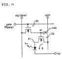
- Each pixel 7 comprises a first TFT 20 in which a scanning signal is supplied to the gate electrode (a first gate electrode) through the scanning gate, a holding capacitor “cap” which holds an image signal supplied from the data line “sig” via the first TFT 20, a second TFT 30 in which the image signal held by the holding capacitor “cap” is supplied to the gate electrode (a second gate electrode), and an luminescent element 40 (indicated as a resistor) into which the driving current flows from the common power supply line “com” when the element 40 is electrically connected to the common power supply line “com” through the second TFT 30.
- both the first TFT 20 and the second TFT 30 are conventionally formed, as with an N channel type TFT or a P channel type TFT, as shown in an equivalent circuit diagram of Fig. 19 from the viewpoint of simplifying the production process, for example, in the case of an N channel type.
- N channel type as an example, as shown in Figs. 20 (A) and (B)
- the scanning signal "Sgate” supplied through the scanning line “gate” has become higher in potential to turn the first TFT 20 "on”
- the second TFT 30 is held in the "on” state.
- the driving current keeps flowing from a pixel electrode 41 to an opposite electrode "op" in the direction indicated by the arrow "E” and consequently, the luminescent element 40 keeps emitting (the “on” state).
- the image signal "data" which is lower than the intermediate between the potential of the common power supply line “com” and the potential of the opposite electrode "op"
- the scanning signal "Sgate” supplied through the scanning line “gate” has become higher in its potential to turn the first TFT 20 “on”
- the second TFT 30 is turned “off” and consequently, the luminescent element 40 is turned “off” (the "off” state).
- a semiconductor thin film, an insulating thin film, an electrode, etc., which constitute each element, are formed by thin films deposited on the substrate.
- a low-temperature process is often used to form the thin films. Therefore the quality of the thin film is poor, as is evidenced by the frequent defects caused by a physical-property difference between a thin film and a bulk, which result in problems such as an electrical breakdown, and wherein time-degradation is apt to arise in the TFT and similar devices.
- time-degradation can be suppressed not only in the liquid crystal but also in the TFT, because the light modulation element is driven by AC power.
- the display apparatus 1A incorporating luminescent elements of the current controlling type time-degradation is more often encountered in the TFT than in the liquid crystal display apparatus insofar as the apparatus is essentially driven by D.C. power.
- the power consumption is small because the light modulation element is controlled by the voltage which causes the current flow in each element to be only momentary.
- a constant driving current is required to keep the luminescent element "on”, and this results in high power consumption and the risk of the frequent occurrence of electrical breakdown and time-degradation.
- the liquid crystal can be AC-driven by one TFT per one pixel.
- the luminescent element 40 is DC-driven by two TFTs 20, 30 per one pixel. This raises the driving voltage, and exacerbates the aforementioned problems, such as electrical breakdown and time-degradation. For example, as shown in Fig.
- the gate voltage "Vgsw” of the first TFT when selecting a pixel, corresponds to the potential difference between the potential equal to the higher potential of the scanning signal "Sgate” and the potential of the potential-holding electrode “st" (the potential of the holding capacitor “cap” or the potential of the gate electrode of the second TFT 30). Therefore when the potential of the potential-holding electrode “st” and, hence, the gate voltage "Vgcur” of the second TFT 30 are raised to make the luminescent element 40 emit in a high luminance, the gate voltage "Vgsw” of the first TFT 20 is lowered correspondingly. Therefore, the greater amplitude of the scanning signal "Sgate” has to be employed, requiring the higher driving voltage in the display apparatus 1A.
- an object of the present invention is to provide a display apparatus, which improves display image quality as well as suppresses power consumption, electric breakdown and deterioration with time by reducing the driving voltage, relying upon a driving method which takes into account the conduction types of TFTs used for controlling emission operations of the current-driven light-luminescent elements so as to reduce the driving voltage, which improves both the display image quality and characteristics such as power consumption, breakdown and time-degradation.
- EP 0112700A discloses a display device in which each pixel comprises first and second thin film transistors, a capacitor and a liquid crystal element. The features of the preamble of claim 1 are disclosed by this document.
- a display apparatus comprising a substrate having arranged thereon:
- the potential of the image signal applied to the gate electrode of the second transistor can be shifted in the direction to increase a luminance, without increasing the amplitude of the image signal.
- An organic semiconductor film can be used as the emitting thin films for example.
- the second transistor can be arranged to be driven in the saturated region to prevent an abnormal current from being generated in the luminescent element, which would result in the generation of a cross-talk, etc., at another pixel because of the voltage drop, or the like.
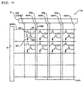
- Fig. 1 is a schematic block diagram schematically illustrating a general layout of a display apparatus
- Fig. 2 is an equivalent circuit diagram of an active matrix formed therein.
- the center portion of a transparent substrate 10 as a basic body is a display portion 2 .
- an inspection circuit 5 and a driving circuit 3 at the data side, which outputs an image signal to a data line "sig", are formed respectively.
- driving circuits 4 at the scanning side which output scanning signals to a scanning line "gate", are formed.
- a complementary type TFT comprising a shift register circuit, a level shifter circuit, an analogue switch circuit, etc. is formed by an N type TFT and a P type TFT.
- a plurality of the scanning lines "gate” and a plurality of the data lines "sig”, which extend in a direction that intersects the direction in which the scanning lines "gate” extend, are formed on the transparent substrate 10, in the same way as in an active matrix substrate of a liquid crystal display apparatus.
- many pixels 7 are formed in a matrix form by the crossing of the data lines "sig” and the scanning lines "gate".
- a first TFT 20 is formed, in which a scanning signal is supplied to a gate electrode 21 (a first gate electrode) through the scanning line "gate".
- a gate electrode 21 a first gate electrode
- One side of a source-drain region of the TFT 20 is electrically connected to the data line "sig", while the other side of the source-drain region is electrically connected to a potential-holding electrode “st". That is, a capacitor line “dine” is formed parallel to the scanning line "gate” and a holding capacitor “cap” is formed between the capacitor line “cline” and the potential-holding electrode “st". Accordingly, when the first TFT 20 is selected by the scanning signal and turned to "on", an image signal, which is supplied from the data line "sig” and forwarded through the first TFT 20, is written in the holding capacitor "cap".
- a gate electrode 31 (a second gate electrode) of the second TFT 30 is electrically connected to the potential-holding electrode "st". While one side of the source-drain region of the second TFT 30 is connected to a common power supply line "com”, the other side of the source-drain region is electrically connected to one of electrodes (a pixel electrode, as will be referred to below) of a luminescent element 40.
- the common power supply line "com” is held at a constant potential.
- the driving current flows through the current route formed by the luminescent element 40, the second TFT 30 and the common power supply line "com"
- the flow of the current stops when the second TFT 30 is turned “off” .
- the image signal which is supplied from the data line "sig" and forwarded through the first TFT, is written into the holding capacitor "cap”.
- the potential of the gate electrode of the second TFT 30 is held at equal to that of the image signal by the holding capacitor "cap”, even if the first TFT 20 is turned “off”, the second TFT 30 remains “on”. Therefore, the driving current in the luminescent element 40 keeps flowing and this pixel remains illuminated. This state will be maintained until new image data is written into the holding capacitor "cap” and the second TFT 30 turns “off”.
- the common power supply line "com”, the pixel 7 and the data line "sig" various arrangements are possible with the common power supply line "com", the pixel 7 and the data line "sig".
- a plurality of the pixels 7, having the luminescent elements 40 power supply, in which the driving current is supplied via common power supply line "com” are disposed on both sides of the common power supply line "com”.
- Two data lines "sig” are arranged at the side of these pixels 7 opposite to the common power supply line "com”. That is, a unit including data line "sig", a pixel group connected to this data line, a piece of common power supply line "com”, another pixel group connected to this common power supply line and another data line "sig” which supplies the pixel signals to this pixel group, is repeated in the direction that the scanning line "gate" extends.
- Each common power supply line “com” supplies driving currents to two lines of the pixels 7.
- the first TFTs 20, the second TFTs 30 and the luminescent elements 40 are disposed symmetrically with respect to the common power supply line "com” in order to make the electrical connection between these elements and each of wiring layers easier.
- each pixel 7 in the display apparatus 1 formed as described above will be explained in detail with reference to Figs. 3 to 6.
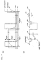
- Fig. 3 is an enlarged plan view showing three pixels 7 of a plurality of pixels 7 formed in the display apparatus 1 .
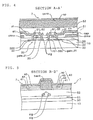
- Fig. 4, Fig. 5 and Fig. 6 are section views taken on line A-A', B-B' and C-C' of Fig. 3, respectively.
- a silicon film 200 is formed on the transparent substrate 10 per each pixel 7 to form the first TFT 20, as shown in Fig. 4.
- a gate insulating film 50 is formed on the surface of the silicon film 200.
- the gate electrode 21 (a portion of the scanning line "gate") is formed on the surface of the gate-insulating film 50.
- the source-drain regions 22 and 23 are formed by self-alignment with respect to the gate electrode 21.
- On the front side of the gate insulating film 50 a first inner-layer-insulating film 51 is formed.
- the source drain-regions 22 and 23 are electrically connected to the data line "sig" and the potential-holding electrode "st", respectively, through contact holes 61 and 62 formed in the inner-layer-insulating film.
- the capacitor line “dine” is formed in the same inner-layer as the scanning line “gate” and the gate electrode 21 (between the gate-insulating film 50 and the first inner-layer-insulation film 51).
- An extension “st1" of the potential-holding electrode “st” overlays on this capacitor line “dine” through the first inner-layer-insulation thin film 51.
- the capacitor line "cline” and the extension “st1" of the potential holding electrode “st” form the holding capacitor "cap” incorporating the first inner-layer-insulation film 51 as a dielectric film.
- a second inner-layer-insulation thin film 52 is formed on the front side of the potential-holding electrode "st" and on that of the data line "sig.
- a silicon film 300 is formed on the transparent substrate 10 to form the second TFT 30, spreading across two pixels, which sandwich the common power supply line "com” therebetween.
- the gate insulating film 50 is formed on the surface of the silicon film 300.
- the gate electrodes 31, corresponding to each pixel 7, are formed on the surface of the gate insulating film 50, sandwiching the common power supply line "com”, and the source-drain regions 32 and 33 are formed by self-alignment with respect to the gate electrodes 31.
- the first inner-layer-insulation film 51 is formed on the front side of the gate insulating film 50.
- a source drain-region 32 is electrically connected to a junction electrode 35 through a contact hole 63 formed on the first inner-layer-insulation film 51.
- the common power supply line "com” is electrically connected to a portion of the source-drain region 33, which is common between two of the pixels provided at the center of the silicon film 300, through a contact hole 64 of the first inner-layer-insulation film 51.
- the second inner-layer-insulation film 52 is formed on the surfaces of the common power supply line "com” and the junction electrode 35.
- the second inner-layer-insulation film 52 is formed on the surfaces of the second inner-layer-insulation film 52.
- a pixel electrode 41 is formed that includes an ITO film. This pixel electrode 41 is electrically connected to the junction electrode 35 through a contact hole 65 formed on the second inner-layer-insulation film 52, and then electrically connected to the source drain region 32 of the second TFT 30 through the junction electrode 35.
- the pixel electrode 41 comprising the ITO film constitutes one electrode (the positive electrode) of the luminescent element 40, as shown in Fig. 7 (A).
- a hole injection layer 42 and an organic semiconductor film 43, as an emitting thin film are laminated.
- an opposite electrode "op" (the negative electrode) comprising a metal film, such as a lithium-containing aluminum film or a calcium film, is formed on the surface of the organic semiconductor film 43.
- This opposite electrode "op” is to be a common electrode formed entirely, or in striped patterns, on the transparent substrate 10, and is held at a constant potential.
- the driving current flows in the reverse direction to the luminescent element 40 that is shown in Fig.
- the luminescent element 40 may be formed as shown in Fig. 7 (B).
- the pixel electrode 41 (the negative electrode) comprising the ITO film, the lithium-containing aluminum electrode 45, which is very thin to be almost transparent, the organic semiconductor layer 43, the hole injection layer 42, the ITO film layer 46 and the opposite electrode "op" (the positive electrode), comprising a metal film such as the aluminum containing lithium film or the calcium film, are laminated in this order from bottom to top layer.
- the driving current of opposite polarity flows in each of the luminescent elements 40 shown in Figs.
- any of the luminescent elements 40 shown in Figs. 7 (A) and (B) has the pixel electrode 41 comprising the ITO film in the under-layer side (the substrate side). Light is emitted from the backside of the transparent substrate 10 through the pixel electrode 41 and the transparent substrate 10, as shown by the arrow "h ⁇ ".
- the luminescent element 40 when the luminescent element 40 is formed as shown in Figs. 8 (A) and (B), light is emitted from the front side of the transparent substrate 10 through the opposite electrode "op", as shown by the arrow "h ⁇ ". That is, as shown in Fig. 8 (A), the organic semiconductor layer 43 and the hole injection layer 42 are laminated on the surface of the pixel electrode 41 (the negative electrode) comprising a metal film, such as aluminum containing lithium. Further, the opposite electrode “op” comprising the ITO film (the positive electrode) is formed on the surface of the hole injection layer 42. This opposite electrode “op” is also a common electrode formed entirely, or in striped patterns, and is held at a constant potential.
- the luminescent element 40 may be formed as shown in Fig. 8 (B).
- This luminescent element 40 is formed by the pixel electrode 41 (the positive electrode) comprising the metal thin film such as aluminum containing lithium, the ITO film layer 46, the hole injection layer 42, the organic semiconductor layer 43, the lithium-containing aluminum electrode 45, which is very thin to be almost transparent, and the opposite electrode "op" (the negative electrode), comprising the ITO film, which are laminated from bottom to top in this order.
- the manufacturing process is not complicated, even if the top-and-bottom positional relationship is reversed, provided that the hole injection layer 42 and the organic semiconductor layer 43 are formed inside of a bank layer "bank” by an ink jet method as described below. Further, in the case that the lithium-containing aluminum electrode 45, which is very thin to be almost transparent, and the ITO film layer 46 are added, there is no obstacle to displaying images, even if the lithium-containing aluminum electrode 45 is laminated in the same region of the pixel electrode 41 or if the ITO film 46 is laminated in the same region of the opposite electrode "op".
- the lithium-containing aluminum electrode 45 and the pixel electrode 41 can be patterned, either separately or simultaneously, using the same resist-mask.
- the ITO film layer 46 and the opposite electrode “op” can be patterned, either separately or simultaneously, using the same resist-mask.
- the lithium-containing aluminum electrode 45 and the ITO film layer 46 may be formed only at the inside region of the bank layer "bank” as a matter of course.
- the opposite electrode "op" may be formed by the ITO film, and the pixel electrode 41 may be formed by the metal film. In any case, light is emitted from the transparent ITO film.
- the voltage is applied across the opposite electrode "op" as the positive electrode, and the pixel electrode 41 as the negative electrode, of the luminescent element 40 formed as described above.
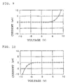
- Fig. 9 ampere-volt characteristics of the luminescent element 40 shown in Fig. 7 (A) and Fig. 8(B)
- Fig. 10 ampere-volt characteristics of the luminescent element 40 shown in Fig. 7 (B) and Fig. 8(A)
- the current through the organic semiconductor layer 43 increases suddenly in the region where the applied voltage (x-axis/the potential of the opposite electrode "op" to the pixel electrode 41) rises above the threshold value and there is "on-state", i.e., the low resistance state.
- the luminescent element 40 emits light as the electro-luminescence element or as the LED element. This emitting light from the luminescent element 40 is reflected by the opposite electrode "op” and is emitted through the transparent pixel electrode 41 and the transparent substrate 10. In contrast, in the region where the applied voltage (x-axis/the potential of the opposite electrode "op” to the pixel electrode 41) drops below the threshold voltage, the "off-state", i.e., the high resistance state is provided, and the current through the organic semiconductor layer 43 (the driving current) stops. Consequently the light luminescent element 40 is turned “off".
- the threshold voltages in the examples shown in Figs. 9 and 10 are approximately +2 V and approximately -2 V, respectively.
- the hole injection layer 42 may be omitted. There may be a case that without incorporating the hole injection layer 42, an electron injection layer is formed at the opposite position to where the hole injection layer 42 is formed with respect to the organic semiconductor layer 43. Further, both the hole injection layer 42 and the electron injection layer may be incorporated.
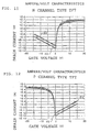
- the TFTs (the first TFT 20 and the second TFT 30 shown in Fig. 2) for controlling light emission of the luminescent element 40 that is formed as described above, the ampere-volt characteristics of N channel type and P channel type TFTs are shown in Figs. 11 and 12, respectively (in any of the Figures, examples of the drain voltages are 4V and 8V are shown).
- the TFT operates "ON-OFF" control action depending on the gate voltage applied across the gate electrode. That is, when the gate voltage rises over the threshold voltage, the TFT will be in "on-state” (the low resistance state) to increase the drain current. In contrast, when the gate voltage decreases below the threshold voltage, the TFT will be "off-state” (the high resistance state) to reduce the drain current.
- Fig. 13 is a diagrammatic flow sectional view illustrating the steps for forming each component of the display apparatus 1 under a temperature condition below 600 °C.
- a groundwork protection film (not shown in figure) comprising a silicon oxide film ranging about 2000 to 5000 ⁇ in thickness is formed, as needed, on the transparent substrate 10 by a plasma enhanced CVD method utilizing TEOS (tetraethoxysilane) or oxygen gas, etc., as a material. Then, after the substrate temperature is set at 350 °C, a semiconductor film 100 comprising an amorphous silicon film ranging about 300 to 700 ⁇ thick is formed on the surface of the groundwork protection film by a plasma enhanced CVD method.
- TEOS tetraethoxysilane
- the semiconductor film 100 comprising the amorphous silicon film is subjected to crystallization such as laser annealing or a solid-phase growth method to crystallize the semiconductor film 100 into a poly-silicon film.
- the laser annealing utilizes, for example, an excimer laser line beam having a long side of 400 mm, and its output power is, for example, 200 mJ/cm 2 .
- the line beams are scanned so that the line beams overlap with each other at portions corresponding to 90% of the peak laser power in the short side.
- the semiconductor film 100 is formed into semiconductor films 200, 300, shaped as islands, and on the surface of them, the gate insulating film 50 comprising a silicon oxide film or a silicon nitride film, ranging about 600 to 1500 ⁇ in thickness, is formed by a plasma enhanced CVD method utilizing TEOS (tetraethoxysilane) or oxygen gas, etc., as a material.
- TEOS tetraethoxysilane
- oxygen gas etc.
- a conductive film comprising a metal film, such as aluminum, tantalum, molybdenum, titanium, tungsten, etc. is formed by a sputtering method
- the gate electrodes 21 and 31, as portions of the scanning lines "gate” are formed by a patterning.
- the capacitor line "cline” is also formed.
- reference number 310 indicates an extensional part of the gate electrode 31.
- the source-drain regions 22, 23, 32, and 33 are formed by self-alignment with respect to the gate electrodes 21 and 31 on the silicon films 200 and 300.
- the portions where the impurity is not implanted are channel regions 27 and 37.
- a different conduction type TFT may be formed on the same substrate, as will be described later. In this case, in the impurity implantation step, the impurity implantation will be performed masking a region to form the opposite conduction type TFT.
- the second inner-layer-insulation film 52 is formed, and the contact hole 65 is formed at the place corresponding to the junction electrode 35 in this inner-layer insulation film. Then, after the conductive film is formed all over the surface of the second inner-layer insulation film 52, patterning is performed, and the pixel electrode 41 is formed to electrically connect the conductive film to the source-drain region 32 of the second TFT 30 through the contact hole 65.
- a bank layer "bank” is formed, leaving this resist to surround the regions for forming the organic semiconductor film 43 of the luminescent element 40 and the hole injection layer 42.
- this producing process can be applied only by forming the bank layer "bank” in a shape adapted thereto.
- Liquid material(a precursor), for forming the organic semiconductor film 43 is injected into an inner region of the bank layer “bank” from an inkjet-head "IJ” to form the organic semiconductor film 43 in the inner region of the bank layer "bank”.
- liquid material (a precursor) for forming the hole injection layer 42 is injected into an inner region of the bank layer “bank” from the inkjet-head "IJ” to form the hole injection layer 42.
- the layer is water repellent.
- the precursors of the organic semiconductor film 43 and the hole injection layer 42 utilize a hydrophilic solvent, the coating region of the organic semiconductor film 43 is strictly defined by the bank layer "bank", and the region cannot extend off to an adjacent pixel.
- the organic semiconductor film 43 or the hole injection layer 42 can be formed within a predetermined region by a coating method, such as a spin coating method, even if the ink jet method is not employed.
- the forming regions of the organic semiconductor films 43 have the same inter-center pitch P between adjacent pixels 7 lying along the extending direction of the scanning line "gate". Therefore, as indicated in the arrow "Q", there is an advantage that the material of the organic semiconductor film 43, etc. can be injected by an ink jet head "IJ" simply with the same pitch along the extending direction of the scanning line "gate". The same pitch injection also simplifies a device for transferring the ink jet head "IJ" while facilitating the improvement of injection accuracy.
- the opposite electrode "op” is formed on the front side of the transparent substrate 10.
- the opposite electrode "op” may be formed either on the entire surface or in a striped shape. In the latter, the patterning will be performed after the film is formed on the entire front side of the transparent substrate 10, and then patterning it into the striped shape.
- the TFTs are also formed in the driving circuit at the data side 3 or the driving circuit at the scanning side 4, as shown in Fig. 1.
- This forming process of the TFTs employs all or a part of the steps for the TFT formation in the above described pixel 7. Therefore, the TFTs of the driving circuit are provided in the same inner-layer that the TFTs of the pixel 7 are formed in.
- the bank layer "bank” comprises a black and insulating resist
- the resist is left as it is to be utilized as a black matrix "BM” and an insulating layer for reducing a parasitic capacitance.
- the bank layer “bank” is also formed in the peripheral region of the transparent substrate 10 (hatched area in the figure).
- the bank layer "bank” is disposed between the wiring layer of the driving circuit and the opposite electrode "op", even if the opposite electrode "op” and the forming regions of these driving circuits are overlapped. Therefore, the prevention of the driving circuits 3,4 from the parasitic capacitance can be achieved so as to reduce the load of the driving circuit at the data side 3, resulting in providing reduced electric consumption or speeding up the display operation.
- the bank layer “bank” is formed so as to overlap with the data line "sig".
- the bank layer “bank” is disposed between the data line "sig” and the opposite electrode "op", and consequently, it is possible to prevent the parasitic capacitance in the data line "sig". This results in the reduction of the load of the driving circuit, providing a reduction of the electric consumption or a speeding up of the display operation.
- the bank layer "bank” is preferably also formed in the region where the pixel electrode 41 and the junction electrode 35 overlap. That is, as shown in Fig. 6(B), if the bank layer "bank” is not formed at the region where the pixel electrode and the junction electrode 35 overlap, even when the organic semiconductor film 43 emits light by the driving current across the pixel electrode 51 and the opposite electrode op, the light cannot be emitted and does not contribute to the display operation. This is because the light gets in between the junction electrode 35 and the opposite electrode "op".
- the driving current equivalent to the light, that does not contribute to the display operation may be called an ineffective current with respect to display.
- the bank layer “bank” works as a black matrix to improve the display image quality, such as a luminance and a contrast ratio. That is, in the display apparatus according to this example, since the opposite electrode "op" is formed in a striped shape on the entire surface, or on a broad region, of the front side of the transparent substrate 10, reflected light from the opposite electrode "op” reduces the contrast ratio.
- the bank layer "bank”, which prevents the parasitic capacitance includes a black resist, with the forming region of the organic semiconductor film 43 defined, there is an advantage that the bank layer "bank”, working also as the black matrix, blocks useless light reflected from the opposite electrode "op", and it results in increasing the contrast ratio.
- the emitting region can be defined by self-alignment utilizing the bank layer "bank”, a margin for alignment required for the emitting region is not necessary. This margin has been the problem when another metal layer, etc., is used as the black matrix instead of the bank layer "bank”.
- the present invention can be applied to various types of active matrix substrates as well as the above described structure.
- the invention can be applied to the display apparatus 1A, wherein, as described in reference to Fig. 18, a unit comprising a data line "sig", a common power supply line “com” and a line of the pixels 7 is repeated in the direction of the scanning line "gate” on a transparent substrate 1.
- the holding capacitor “cap” may be formed between the common power supply line “com” and the potential-holding electrode “st” without the capacitor line.
- an extended portion 310 of the gate electrode 31 to connect electrically the potential-holding electrode “st” and the gate electrode 31 is expanded to the under-layer of the common power supply line "com” to form the holding capacitor "cap”.
- This holding capacitor “cap” has the first inner-layer-insulation film 51 which is located between the extended portion 310 and the common power supply line "com” for a dielectric film.
- Figure 14 is abbreviated, it may be formed utilizing a poly-silicon film for forming the TFT, and it also may be formed with the ahead scanning line other than the capacitor line and the common power supply line.
- a pulse may be supplied to one of electrodes of the holding capacitor "cap".
- the electrode receiving the pulse is opposite to the other, which is electrically connected to the gate electrode of the second TFT 30.
- the potential of this pulse is opposite to the selecting pulse of the scanning signal "gate", and the pulse is supplied to the electrode with a delay behind the selecting pulse.
- one of the electrodes of the holding capacitor "cap”, which is opposite to the one which is electrically connected to the gate electrode of the second TFT 30 through the potential-holding electrode "st", is formed by the capacitor line "cline”, which is extended in parallel with the scanning line "gate”.
- this capacitor line “cline” is formed such that the potential “stg” is supplied to the capacitor line “cline” with a delay behind the selecting pulse “Pgate” of the scanning signal “Sgate".
- the potential “stg” supplied to the capacitor line “cline” includes the pulse signal "Pstg", and the polarity of which is opposite to the polarity of the selecting pulse.
- the pulse signal "Pstg” shifts the potential of the image signal "data” utilising a capacitive coupling of the holding capacitor “cap”. Therefore, signals are held in the holding capacitor “cap” at the "off-state” pixel 7, corresponding to the potential obtained by adding the potential of the pulse signal "Pstg” to the potential of the image signal "data”. Due to the high "on” resistance of the first TFT 20, it is difficult to completely write the signals in the higher potential side of the image signals "data” within a limited time. In the case of the embodiment, a shortage of the writing capacity results in no emitting of the pixel. However, in accordance with the embodiment 4, it is possible to supplement the writing of the image signal "data" to the holding capacitor "cap", even though the maximum range of the potential in the driving signal is not expanded.
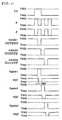
- Figs. 21 (A) and (B) illustrate a circuit block diagram and a voltage waveform chart of the gate electrode in the direction of the scanning of the gate line respectively.
- the second TFT 30 is operated at the saturated region, it is possible to prevent an abnormal current flow in the luminescent element 40, utilizing a weak constant-current characteristic.
- the organic semiconductor film, etc., forming the luminescent element 40 can possibly have pinhole defects, even though this does not cause a complete short circuit across the electrodes of the luminescent element 40, due to the restricted current in the luminescent element with the defect.
- the second TFT 30 is operated at the linear region, it is possible to prevent the display operation from being affected by unevenness of the threshold voltage.
- the TFT may be formed in a bottom gate type as well as in a top gate type, and the production method is not limited to a low temperature process in producing the TFT.
Landscapes
- Engineering & Computer Science (AREA)
- Physics & Mathematics (AREA)
- Computer Hardware Design (AREA)
- General Physics & Mathematics (AREA)
- Theoretical Computer Science (AREA)
- Microelectronics & Electronic Packaging (AREA)
- Electroluminescent Light Sources (AREA)
- Control Of Indicators Other Than Cathode Ray Tubes (AREA)
- Control Of El Displays (AREA)
- Devices For Indicating Variable Information By Combining Individual Elements (AREA)
Applications Claiming Priority (7)
| Application Number | Priority Date | Filing Date | Title |
|---|---|---|---|
| JP3247497 | 1997-02-17 | ||
| JP3247497 | 1997-02-17 | ||
| JP23635197 | 1997-09-01 | ||
| JP23635197 | 1997-09-01 | ||
| JP23635397 | 1997-09-01 | ||
| JP23635397 | 1997-09-01 | ||
| EP98902263A EP0895219B1 (en) | 1997-02-17 | 1998-02-17 | Display device |
Related Parent Applications (1)
| Application Number | Title | Priority Date | Filing Date |
|---|---|---|---|
| EP98902263A Division EP0895219B1 (en) | 1997-02-17 | 1998-02-17 | Display device |
Publications (2)
| Publication Number | Publication Date |
|---|---|
| EP1255240A1 EP1255240A1 (en) | 2002-11-06 |
| EP1255240B1 true EP1255240B1 (en) | 2005-02-16 |
Family
ID=27287719
Family Applications (7)
| Application Number | Title | Priority Date | Filing Date |
|---|---|---|---|
| EP02076495A Expired - Lifetime EP1255240B1 (en) | 1997-02-17 | 1998-02-17 | Active matrix electroluminescent display with two TFTs and storage capacitor in each pixel |
| EP03076312A Expired - Lifetime EP1359789B1 (en) | 1997-02-17 | 1998-02-17 | Display apparatus |
| EP03076313A Ceased EP1336953A3 (en) | 1997-02-17 | 1998-02-17 | Active matrix electroluminescent display with two tft's and storage capacitor |
| EP98902263A Expired - Lifetime EP0895219B1 (en) | 1997-02-17 | 1998-02-17 | Display device |
| EP07075433A Withdrawn EP1830343A3 (en) | 1997-02-17 | 1998-02-17 | Structure of a driving circuit for an electroluminescent display |
| EP07075434A Expired - Lifetime EP1830344B1 (en) | 1997-02-17 | 1998-02-17 | Structure of a pixel driving circuit for an electroluminescent display |
| EP07075432A Expired - Lifetime EP1830342B1 (en) | 1997-02-17 | 1998-02-17 | Pixel driving circuit for an electroluminescent display |
Family Applications After (6)
| Application Number | Title | Priority Date | Filing Date |
|---|---|---|---|
| EP03076312A Expired - Lifetime EP1359789B1 (en) | 1997-02-17 | 1998-02-17 | Display apparatus |
| EP03076313A Ceased EP1336953A3 (en) | 1997-02-17 | 1998-02-17 | Active matrix electroluminescent display with two tft's and storage capacitor |
| EP98902263A Expired - Lifetime EP0895219B1 (en) | 1997-02-17 | 1998-02-17 | Display device |
| EP07075433A Withdrawn EP1830343A3 (en) | 1997-02-17 | 1998-02-17 | Structure of a driving circuit for an electroluminescent display |
| EP07075434A Expired - Lifetime EP1830344B1 (en) | 1997-02-17 | 1998-02-17 | Structure of a pixel driving circuit for an electroluminescent display |
| EP07075432A Expired - Lifetime EP1830342B1 (en) | 1997-02-17 | 1998-02-17 | Pixel driving circuit for an electroluminescent display |
Country Status (8)
| Country | Link |
|---|---|
| US (11) | US6522315B2 (ko) |
| EP (7) | EP1255240B1 (ko) |
| JP (3) | JP3528182B2 (ko) |
| KR (9) | KR100539291B1 (ko) |
| CN (4) | CN1506929B (ko) |
| DE (2) | DE69829084T2 (ko) |
| TW (2) | TW491985B (ko) |
| WO (1) | WO1998036407A1 (ko) |
Cited By (5)
| Publication number | Priority date | Publication date | Assignee | Title |
|---|---|---|---|---|
| US8471262B2 (en) | 1999-02-23 | 2013-06-25 | Semiconductor Energy Laboratory Co., Ltd. | Semiconductor device and fabrication method thereof |
| US8735874B2 (en) | 2011-02-14 | 2014-05-27 | Semiconductor Energy Laboratory Co., Ltd. | Light-emitting device, display device, and method for manufacturing the same |
| US9087476B2 (en) | 2000-01-17 | 2015-07-21 | Semiconductor Energy Laboratory Co., Ltd. | Display system and electrical appliance |
| US9293545B2 (en) | 2008-11-07 | 2016-03-22 | Semiconductor Energy Laboratory Co., Ltd. | Semiconductor device |
| US9419066B2 (en) | 2000-02-03 | 2016-08-16 | Semiconductor Energy Laboratory Co., Ltd. | Light-emitting device and method of manufacturing the same |
Families Citing this family (312)
| Publication number | Priority date | Publication date | Assignee | Title |
|---|---|---|---|---|
| US6462722B1 (en) * | 1997-02-17 | 2002-10-08 | Seiko Epson Corporation | Current-driven light-emitting display apparatus and method of producing the same |
| DE69825402T2 (de) * | 1997-03-12 | 2005-08-04 | Seiko Epson Corp. | Pixelschaltung, anzeigevorrichtung und elektronische apparatur mit stromgesteuerter lichtemittierender vorrichtung |
| JP3520396B2 (ja) | 1997-07-02 | 2004-04-19 | セイコーエプソン株式会社 | アクティブマトリクス基板と表示装置 |
| JP3541625B2 (ja) * | 1997-07-02 | 2004-07-14 | セイコーエプソン株式会社 | 表示装置及びアクティブマトリクス基板 |
| CN100517424C (zh) * | 1997-08-21 | 2009-07-22 | 精工爱普生株式会社 | 显示装置 |
| JP3580092B2 (ja) * | 1997-08-21 | 2004-10-20 | セイコーエプソン株式会社 | アクティブマトリクス型表示装置 |
| KR100244185B1 (ko) * | 1997-09-18 | 2000-02-01 | 구자홍 | 유기전계발광소자 및 그 제조방법 |
| US6489952B1 (en) * | 1998-11-17 | 2002-12-03 | Semiconductor Energy Laboratory Co., Ltd. | Active matrix type semiconductor display device |
| JP2005166687A (ja) * | 1998-12-01 | 2005-06-23 | Sanyo Electric Co Ltd | カラーel表示装置 |
| TW439387B (en) * | 1998-12-01 | 2001-06-07 | Sanyo Electric Co | Display device |
| JP2000227771A (ja) * | 1998-12-01 | 2000-08-15 | Sanyo Electric Co Ltd | カラーel表示装置 |
| JP2000227770A (ja) * | 1998-12-01 | 2000-08-15 | Sanyo Electric Co Ltd | カラーel表示装置 |
| JP2005209656A (ja) * | 1998-12-01 | 2005-08-04 | Sanyo Electric Co Ltd | カラーel表示装置 |
| TW468269B (en) * | 1999-01-28 | 2001-12-11 | Semiconductor Energy Lab | Serial-to-parallel conversion circuit, and semiconductor display device employing the same |
| JP2000231346A (ja) * | 1999-02-09 | 2000-08-22 | Sanyo Electric Co Ltd | エレクトロルミネッセンス表示装置 |
| JP4637315B2 (ja) * | 1999-02-24 | 2011-02-23 | 株式会社半導体エネルギー研究所 | 表示装置 |
| US6858898B1 (en) * | 1999-03-23 | 2005-02-22 | Semiconductor Energy Laboratory Co., Ltd. | Semiconductor device and method for manufacturing the same |
| US8853696B1 (en) * | 1999-06-04 | 2014-10-07 | Semiconductor Energy Laboratory Co., Ltd. | Electro-optical device and electronic device |
| US7288420B1 (en) * | 1999-06-04 | 2007-10-30 | Semiconductor Energy Laboratory Co., Ltd. | Method for manufacturing an electro-optical device |
| JP4627822B2 (ja) * | 1999-06-23 | 2011-02-09 | 株式会社半導体エネルギー研究所 | 表示装置 |
| JP4472073B2 (ja) | 1999-09-03 | 2010-06-02 | 株式会社半導体エネルギー研究所 | 表示装置及びその作製方法 |
| JP2001093666A (ja) * | 1999-09-22 | 2001-04-06 | Sharp Corp | 有機ledディスプレイおよびその製造方法 |
| JP2001109404A (ja) * | 1999-10-01 | 2001-04-20 | Sanyo Electric Co Ltd | El表示装置 |
| JP4854840B2 (ja) * | 1999-10-12 | 2012-01-18 | 株式会社半導体エネルギー研究所 | 発光装置の作製方法 |
| TW468283B (en) * | 1999-10-12 | 2001-12-11 | Semiconductor Energy Lab | EL display device and a method of manufacturing the same |
| TW591584B (en) * | 1999-10-21 | 2004-06-11 | Semiconductor Energy Lab | Active matrix type display device |
| US6580094B1 (en) * | 1999-10-29 | 2003-06-17 | Semiconductor Energy Laboratory Co., Ltd. | Electro luminescence display device |
| JP2001148291A (ja) * | 1999-11-19 | 2001-05-29 | Sony Corp | 表示装置及びその製造方法 |
| TW525122B (en) * | 1999-11-29 | 2003-03-21 | Semiconductor Energy Lab | Electronic device |
| TW587239B (en) * | 1999-11-30 | 2004-05-11 | Semiconductor Energy Lab | Electric device |
| US6750835B2 (en) | 1999-12-27 | 2004-06-15 | Semiconductor Energy Laboratory Co., Ltd. | Image display device and driving method thereof |
| JP4212079B2 (ja) * | 2000-01-11 | 2009-01-21 | ローム株式会社 | 表示装置およびその駆動方法 |
| TW507258B (en) | 2000-02-29 | 2002-10-21 | Semiconductor Systems Corp | Display device and method for fabricating the same |
| TW577241B (en) * | 2000-03-28 | 2004-02-21 | Sanyo Electric Co | Display device |
| GB2360870A (en) * | 2000-03-31 | 2001-10-03 | Seiko Epson Corp | Driver circuit for organic electroluminescent device |
| TWI282457B (en) | 2000-04-06 | 2007-06-11 | Chi Mei Optoelectronics Corp | Liquid crystal display component with defect restore ability and restoring method of defect |
| TW521237B (en) | 2000-04-18 | 2003-02-21 | Semiconductor Energy Lab | Light emitting device |
| US6847341B2 (en) * | 2000-04-19 | 2005-01-25 | Semiconductor Energy Laboratory Co., Ltd. | Electronic device and method of driving the same |
| US6611108B2 (en) * | 2000-04-26 | 2003-08-26 | Semiconductor Energy Laboratory Co., Ltd. | Electronic device and driving method thereof |
| US7633471B2 (en) * | 2000-05-12 | 2009-12-15 | Semiconductor Energy Laboratory Co., Ltd. | Light-emitting device and electric appliance |
| US8610645B2 (en) | 2000-05-12 | 2013-12-17 | Semiconductor Energy Laboratory Co., Ltd. | Display device |
| JP3723747B2 (ja) | 2000-06-16 | 2005-12-07 | 松下電器産業株式会社 | 表示装置およびその駆動方法 |
| US6738034B2 (en) | 2000-06-27 | 2004-05-18 | Hitachi, Ltd. | Picture image display device and method of driving the same |
| JP2002083689A (ja) * | 2000-06-29 | 2002-03-22 | Semiconductor Energy Lab Co Ltd | 発光装置 |
| WO2002005255A1 (en) | 2000-07-07 | 2002-01-17 | Seiko Epson Corporation | Current driven electrooptical device, e.g. organic electroluminescent display, with complementary driving transistors to counteract threshold voltage variation |
| KR20020032570A (ko) | 2000-07-07 | 2002-05-03 | 구사마 사부로 | 유기 전계 발광 표시장치용 전류 샘플링 회로 |
| KR100344810B1 (ko) * | 2000-07-26 | 2002-07-20 | 엘지전자주식회사 | 고전압소자를 이용한 전류구동회로 |
| US6879110B2 (en) * | 2000-07-27 | 2005-04-12 | Semiconductor Energy Laboratory Co., Ltd. | Method of driving display device |
| US6864628B2 (en) | 2000-08-28 | 2005-03-08 | Semiconductor Energy Laboratory Co., Ltd. | Light emitting device comprising light-emitting layer having triplet compound and light-emitting layer having singlet compound |
| JP2002185813A (ja) * | 2000-08-31 | 2002-06-28 | Matsushita Electric Ind Co Ltd | 高圧偏向回路 |
| US7315295B2 (en) * | 2000-09-29 | 2008-01-01 | Seiko Epson Corporation | Driving method for electro-optical device, electro-optical device, and electronic apparatus |
| JP4925528B2 (ja) * | 2000-09-29 | 2012-04-25 | 三洋電機株式会社 | 表示装置 |
| JP3972354B2 (ja) | 2000-10-17 | 2007-09-05 | セイコーエプソン株式会社 | アクティブマトリクス基板及び液晶表示装置の製造方法 |
| SG114502A1 (en) * | 2000-10-24 | 2005-09-28 | Semiconductor Energy Lab | Light emitting device and method of driving the same |
| JP2002200936A (ja) * | 2000-11-06 | 2002-07-16 | Semiconductor Energy Lab Co Ltd | 表示装置及び車両 |
| JP2002162644A (ja) * | 2000-11-27 | 2002-06-07 | Hitachi Ltd | 液晶表示装置 |
| JP2002169509A (ja) * | 2000-11-30 | 2002-06-14 | Sanyo Electric Co Ltd | 平面表示パネルの駆動方法及び有機エレクトロルミネッセンス表示パネルの駆動方法 |
| US7088330B2 (en) * | 2000-12-25 | 2006-08-08 | Sharp Kabushiki Kaisha | Active matrix substrate, display device and method for driving the display device |
| JP3757797B2 (ja) * | 2001-01-09 | 2006-03-22 | 株式会社日立製作所 | 有機ledディスプレイおよびその駆動方法 |
| US6825496B2 (en) | 2001-01-17 | 2004-11-30 | Semiconductor Energy Laboratory Co., Ltd. | Light emitting device |
| JP3989718B2 (ja) * | 2001-01-18 | 2007-10-10 | シャープ株式会社 | メモリ一体型表示素子 |
| TW525402B (en) | 2001-01-18 | 2003-03-21 | Semiconductor Energy Lab | Process for producing a light emitting device |
| JP2002244617A (ja) * | 2001-02-15 | 2002-08-30 | Sanyo Electric Co Ltd | 有機el画素回路 |
| US6720198B2 (en) * | 2001-02-19 | 2004-04-13 | Semiconductor Energy Laboratory Co., Ltd. | Light emitting device and manufacturing method thereof |
| SG143946A1 (en) | 2001-02-19 | 2008-07-29 | Semiconductor Energy Lab | Light emitting device and method of manufacturing the same |
| US7301279B2 (en) * | 2001-03-19 | 2007-11-27 | Semiconductor Energy Laboratory Co., Ltd. | Light-emitting apparatus and method of manufacturing the same |
| WO2002077958A1 (fr) | 2001-03-22 | 2002-10-03 | Canon Kabushiki Kaisha | Circuit servant a alimenter un element d'emission lumineuse a matrice active |
| JP3608614B2 (ja) | 2001-03-28 | 2005-01-12 | 株式会社日立製作所 | 表示装置 |
| JP3612494B2 (ja) | 2001-03-28 | 2005-01-19 | 株式会社日立製作所 | 表示装置 |
| JP3608613B2 (ja) | 2001-03-28 | 2005-01-12 | 株式会社日立製作所 | 表示装置 |
| JP4801278B2 (ja) * | 2001-04-23 | 2011-10-26 | 株式会社半導体エネルギー研究所 | 発光装置及びその作製方法 |
| TW540020B (en) * | 2001-06-06 | 2003-07-01 | Semiconductor Energy Lab | Image display device and driving method thereof |
| TWI283427B (en) * | 2001-07-12 | 2007-07-01 | Semiconductor Energy Lab | Display device using electron source elements and method of driving same |
| KR100448448B1 (ko) * | 2001-07-12 | 2004-09-13 | 주식회사 디알텍 | X선 센서용 스위칭소자 및 그 제조방법 |
| US7088052B2 (en) * | 2001-09-07 | 2006-08-08 | Semiconductor Energy Laboratory Co., Ltd. | Light emitting device and method of driving the same |
| JP4149168B2 (ja) | 2001-11-09 | 2008-09-10 | 株式会社半導体エネルギー研究所 | 発光装置 |
| CN101009322B (zh) * | 2001-11-09 | 2012-06-27 | 株式会社半导体能源研究所 | 发光器件 |
| US20030103022A1 (en) * | 2001-11-09 | 2003-06-05 | Yukihiro Noguchi | Display apparatus with function for initializing luminance data of optical element |
| US7483001B2 (en) | 2001-11-21 | 2009-01-27 | Seiko Epson Corporation | Active matrix substrate, electro-optical device, and electronic device |
| JP3983037B2 (ja) * | 2001-11-22 | 2007-09-26 | 株式会社半導体エネルギー研究所 | 発光装置およびその作製方法 |
| US6949883B2 (en) | 2001-12-06 | 2005-09-27 | Seiko Epson Corporation | Electro-optical device and an electronic apparatus |
| CN1245703C (zh) * | 2001-12-11 | 2006-03-15 | 精工爱普生株式会社 | 显示装置及其电子机器 |
| JP4314820B2 (ja) * | 2001-12-11 | 2009-08-19 | セイコーエプソン株式会社 | 表示装置及び電子機器 |
| JP2003186437A (ja) * | 2001-12-18 | 2003-07-04 | Sanyo Electric Co Ltd | 表示装置 |
| JP2003255899A (ja) * | 2001-12-28 | 2003-09-10 | Sanyo Electric Co Ltd | 表示装置 |
| JP2003195810A (ja) * | 2001-12-28 | 2003-07-09 | Casio Comput Co Ltd | 駆動回路、駆動装置及び光学要素の駆動方法 |
| US6747639B2 (en) * | 2001-12-28 | 2004-06-08 | Osram Opto Semiconductors Gmbh | Voltage-source thin film transistor driver for active matrix displays |
| US7224333B2 (en) | 2002-01-18 | 2007-05-29 | Semiconductor Energy Laboratory Co. Ltd. | Display device and driving method thereof |
| JP3953330B2 (ja) | 2002-01-25 | 2007-08-08 | 三洋電機株式会社 | 表示装置 |
| JP3723507B2 (ja) | 2002-01-29 | 2005-12-07 | 三洋電機株式会社 | 駆動回路 |
| JP2003308030A (ja) | 2002-02-18 | 2003-10-31 | Sanyo Electric Co Ltd | 表示装置 |
| KR100892945B1 (ko) | 2002-02-22 | 2009-04-09 | 삼성전자주식회사 | 액티브 매트릭스형 유기전계발광 표시장치 및 그 제조방법 |
| JP2003258094A (ja) | 2002-03-05 | 2003-09-12 | Sanyo Electric Co Ltd | 配線構造、その製造方法、および表示装置 |
| JP2003330387A (ja) | 2002-03-05 | 2003-11-19 | Sanyo Electric Co Ltd | 表示装置 |
| JP2003332058A (ja) | 2002-03-05 | 2003-11-21 | Sanyo Electric Co Ltd | エレクトロルミネッセンスパネルおよびその製造方法 |
| JP3671012B2 (ja) * | 2002-03-07 | 2005-07-13 | 三洋電機株式会社 | 表示装置 |
| CN100517422C (zh) | 2002-03-07 | 2009-07-22 | 三洋电机株式会社 | 配线结构、其制造方法、以及光学设备 |
| JP3837344B2 (ja) | 2002-03-11 | 2006-10-25 | 三洋電機株式会社 | 光学素子およびその製造方法 |
| JP3957535B2 (ja) * | 2002-03-14 | 2007-08-15 | 株式会社半導体エネルギー研究所 | 発光装置の駆動方法、電子機器 |
| JP4360918B2 (ja) | 2002-03-20 | 2009-11-11 | コーニンクレッカ フィリップス エレクトロニクス エヌ ヴィ | アクティブマトリクスエレクトロルミネッセンス表示装置及びその製造方法 |
| US7208760B2 (en) | 2002-03-20 | 2007-04-24 | Koninklijke Philips Electronics N.V. | Active matrix electroluminescent display devices, and their manufacture |
| JP5067999B2 (ja) | 2002-03-20 | 2012-11-07 | ティーピーオー ホンコン ホールディング リミテッド | アクティブマトリクス表示装置及びその製造方法 |
| KR101037118B1 (ko) * | 2002-04-03 | 2011-05-26 | 가부시키가이샤 한도오따이 에네루기 켄큐쇼 | 발광장치 |
| JP3989763B2 (ja) * | 2002-04-15 | 2007-10-10 | 株式会社半導体エネルギー研究所 | 半導体表示装置 |
| US7579771B2 (en) * | 2002-04-23 | 2009-08-25 | Semiconductor Energy Laboratory Co., Ltd. | Light emitting device and method of manufacturing the same |
| JP2004004788A (ja) | 2002-04-24 | 2004-01-08 | Seiko Epson Corp | 電子素子の制御回路、電子回路、電気光学装置、電気光学装置の駆動方法、及び電子機器、並びに電子素子の制御方法 |
| JP3637911B2 (ja) | 2002-04-24 | 2005-04-13 | セイコーエプソン株式会社 | 電子装置、電子機器、および電子装置の駆動方法 |
| US7786496B2 (en) | 2002-04-24 | 2010-08-31 | Semiconductor Energy Laboratory Co., Ltd. | Semiconductor device and method of manufacturing same |
| JP2003317971A (ja) | 2002-04-26 | 2003-11-07 | Semiconductor Energy Lab Co Ltd | 発光装置およびその作製方法 |
| JP3918642B2 (ja) * | 2002-06-07 | 2007-05-23 | カシオ計算機株式会社 | 表示装置及びその駆動方法 |
| US7897979B2 (en) * | 2002-06-07 | 2011-03-01 | Semiconductor Energy Laboratory Co., Ltd. | Light emitting device and manufacturing method thereof |
| JP4046015B2 (ja) | 2002-06-07 | 2008-02-13 | セイコーエプソン株式会社 | 電子回路、電子装置、電気光学装置及び電子機器 |
| JP2004070293A (ja) * | 2002-06-12 | 2004-03-04 | Seiko Epson Corp | 電子装置、電子装置の駆動方法及び電子機器 |
| JP4610843B2 (ja) | 2002-06-20 | 2011-01-12 | カシオ計算機株式会社 | 表示装置及び表示装置の駆動方法 |
| JP3700714B2 (ja) | 2002-06-21 | 2005-09-28 | セイコーエプソン株式会社 | 電気光学装置及び電子機器 |
| JP4216008B2 (ja) * | 2002-06-27 | 2009-01-28 | 株式会社半導体エネルギー研究所 | 発光装置およびその作製方法、ならびに前記発光装置を有するビデオカメラ、デジタルカメラ、ゴーグル型ディスプレイ、カーナビゲーション、パーソナルコンピュータ、dvdプレーヤー、電子遊技機器、または携帯情報端末 |
| JP4001066B2 (ja) * | 2002-07-18 | 2007-10-31 | セイコーエプソン株式会社 | 電気光学装置、配線基板及び電子機器 |
| SG130013A1 (en) * | 2002-07-25 | 2007-03-20 | Semiconductor Energy Lab | Method of fabricating light emitting device |
| JP4123084B2 (ja) * | 2002-07-31 | 2008-07-23 | セイコーエプソン株式会社 | 電子回路、電気光学装置、及び電子機器 |
| JP2004126523A (ja) * | 2002-07-31 | 2004-04-22 | Seiko Epson Corp | 電子回路、電気光学装置及び電子機器 |
| US7352133B2 (en) * | 2002-08-05 | 2008-04-01 | Semiconductor Energy Laboratory Co., Ltd. | Light emitting device |
| JP4103500B2 (ja) * | 2002-08-26 | 2008-06-18 | カシオ計算機株式会社 | 表示装置及び表示パネルの駆動方法 |
| US7291970B2 (en) * | 2002-09-11 | 2007-11-06 | Semiconductor Energy Laboratory Co., Ltd. | Light-emitting apparatus with improved bank structure |
| JP4122949B2 (ja) * | 2002-11-29 | 2008-07-23 | セイコーエプソン株式会社 | 電気光学装置、アクティブマトリクス基板及び電子機器 |
| KR100521272B1 (ko) | 2002-12-20 | 2005-10-12 | 삼성에스디아이 주식회사 | 휘도가 개선된 유기전계 발광표시장치 |
| JP4373086B2 (ja) * | 2002-12-27 | 2009-11-25 | 株式会社半導体エネルギー研究所 | 発光装置 |
| US6936960B2 (en) * | 2003-01-10 | 2005-08-30 | Eastman Kodak Company | OLED displays having improved contrast |
| JP4048969B2 (ja) * | 2003-02-12 | 2008-02-20 | セイコーエプソン株式会社 | 電気光学装置の駆動方法及び電子機器 |
| JP3952965B2 (ja) * | 2003-02-25 | 2007-08-01 | カシオ計算機株式会社 | 表示装置及び表示装置の駆動方法 |
| WO2004086343A1 (ja) * | 2003-03-26 | 2004-10-07 | Semiconductor Energy Laboratory Co., Ltd. | 素子基板及び発光装置 |
| JP4197287B2 (ja) * | 2003-03-28 | 2008-12-17 | シャープ株式会社 | 表示装置 |
| JP4273809B2 (ja) * | 2003-03-31 | 2009-06-03 | セイコーエプソン株式会社 | 電気光学装置及び電子機器 |
| KR100762026B1 (ko) * | 2003-03-31 | 2007-09-28 | 비오이 하이디스 테크놀로지 주식회사 | 액정표시장치 |
| JP4016962B2 (ja) | 2003-05-19 | 2007-12-05 | セイコーエプソン株式会社 | 電気光学装置、電気光学装置の駆動方法 |
| US20040257352A1 (en) * | 2003-06-18 | 2004-12-23 | Nuelight Corporation | Method and apparatus for controlling |
| CA2443206A1 (en) | 2003-09-23 | 2005-03-23 | Ignis Innovation Inc. | Amoled display backplanes - pixel driver circuits, array architecture, and external compensation |
| JP4488709B2 (ja) * | 2003-09-29 | 2010-06-23 | 三洋電機株式会社 | 有機elパネル |
| JP4443179B2 (ja) | 2003-09-29 | 2010-03-31 | 三洋電機株式会社 | 有機elパネル |
| KR20060090681A (ko) * | 2003-10-03 | 2006-08-14 | 코닌클리케 필립스 일렉트로닉스 엔.브이. | 전기영동 디스플레이 유닛 |
| JP4165478B2 (ja) | 2003-11-07 | 2008-10-15 | セイコーエプソン株式会社 | 発光装置及び電子機器 |
| KR100666549B1 (ko) * | 2003-11-27 | 2007-01-09 | 삼성에스디아이 주식회사 | 유기전계 발광표시장치 및 그의 구동방법 |
| TWI233457B (en) * | 2003-12-23 | 2005-06-01 | Ind Tech Res Inst | Method of forming poly-silicon crystallization |
| JP4203656B2 (ja) * | 2004-01-16 | 2009-01-07 | カシオ計算機株式会社 | 表示装置及び表示パネルの駆動方法 |
| JP4131243B2 (ja) * | 2004-02-06 | 2008-08-13 | セイコーエプソン株式会社 | 電気光学装置の製造方法、電気光学装置、及び電子機器 |
| CN100353560C (zh) * | 2004-02-12 | 2007-12-05 | 友达光电股份有限公司 | 有机发光显示面板 |
| US20050200294A1 (en) * | 2004-02-24 | 2005-09-15 | Naugler W. E.Jr. | Sidelight illuminated flat panel display and touch panel input device |
| US20050200292A1 (en) * | 2004-02-24 | 2005-09-15 | Naugler W. E.Jr. | Emissive display device having sensing for luminance stabilization and user light or touch screen input |
| US20050200296A1 (en) * | 2004-02-24 | 2005-09-15 | Naugler W. E.Jr. | Method and device for flat panel emissive display using shielded or partially shielded sensors to detect user screen inputs |
| JP4665419B2 (ja) * | 2004-03-30 | 2011-04-06 | カシオ計算機株式会社 | 画素回路基板の検査方法及び検査装置 |
| JP2005292503A (ja) * | 2004-03-31 | 2005-10-20 | Dainippon Printing Co Ltd | 有機el表示装置 |
| US20050243023A1 (en) * | 2004-04-06 | 2005-11-03 | Damoder Reddy | Color filter integrated with sensor array for flat panel display |
| US7129938B2 (en) * | 2004-04-12 | 2006-10-31 | Nuelight Corporation | Low power circuits for active matrix emissive displays and methods of operating the same |
| KR100589324B1 (ko) | 2004-05-11 | 2006-06-14 | 삼성에스디아이 주식회사 | 발광 표시 장치 및 그 구동 방법 |
| KR100637164B1 (ko) | 2004-06-26 | 2006-10-20 | 삼성에스디아이 주식회사 | 능동 구동형 전계발광 디스플레이 장치 |
| KR100578812B1 (ko) * | 2004-06-29 | 2006-05-11 | 삼성에스디아이 주식회사 | 발광 표시 장치 |
| CA2472671A1 (en) | 2004-06-29 | 2005-12-29 | Ignis Innovation Inc. | Voltage-programming scheme for current-driven amoled displays |
| US20060007204A1 (en) * | 2004-06-29 | 2006-01-12 | Damoder Reddy | System and method for a long-life luminance feedback stabilized display panel |
| JP5364227B2 (ja) * | 2004-07-16 | 2013-12-11 | 株式会社半導体エネルギー研究所 | 読み取り機能付き表示装置及びそれを用いた電子機器 |
| KR100590042B1 (ko) * | 2004-08-30 | 2006-06-14 | 삼성에스디아이 주식회사 | 발광 표시 장치, 그 구동방법 및 신호구동장치 |
| EP2299782B1 (en) * | 2004-09-13 | 2016-11-23 | Semiconductor Energy Laboratory Co, Ltd. | Light emitting layer device |
| JP4517804B2 (ja) * | 2004-09-29 | 2010-08-04 | カシオ計算機株式会社 | ディスプレイパネル |
| KR100583519B1 (ko) * | 2004-10-28 | 2006-05-25 | 삼성에스디아이 주식회사 | 주사 구동부 및 그를 이용한 발광표시장치 |
| KR100688799B1 (ko) * | 2004-11-17 | 2007-03-02 | 삼성에스디아이 주식회사 | 발광 표시장치, 발광 표시장치의 구동 방법 및 화소회로의구동방법 |
| JP4437110B2 (ja) | 2004-11-17 | 2010-03-24 | 三星モバイルディスプレイ株式會社 | 有機発光表示装置,有機発光表示装置の駆動方法及び画素回路の駆動方法 |
| KR101216377B1 (ko) | 2004-12-06 | 2012-12-31 | 가부시키가이샤 한도오따이 에네루기 켄큐쇼 | 반도체 장치 |
| CA2490858A1 (en) | 2004-12-07 | 2006-06-07 | Ignis Innovation Inc. | Driving method for compensated voltage-programming of amoled displays |
| US10012678B2 (en) | 2004-12-15 | 2018-07-03 | Ignis Innovation Inc. | Method and system for programming, calibrating and/or compensating, and driving an LED display |
| US9799246B2 (en) | 2011-05-20 | 2017-10-24 | Ignis Innovation Inc. | System and methods for extraction of threshold and mobility parameters in AMOLED displays |
| US8599191B2 (en) | 2011-05-20 | 2013-12-03 | Ignis Innovation Inc. | System and methods for extraction of threshold and mobility parameters in AMOLED displays |
| WO2006063448A1 (en) | 2004-12-15 | 2006-06-22 | Ignis Innovation Inc. | Method and system for programming, calibrating and driving a light emitting device display |
| US9275579B2 (en) | 2004-12-15 | 2016-03-01 | Ignis Innovation Inc. | System and methods for extraction of threshold and mobility parameters in AMOLED displays |
| US9171500B2 (en) | 2011-05-20 | 2015-10-27 | Ignis Innovation Inc. | System and methods for extraction of parasitic parameters in AMOLED displays |
| US10013907B2 (en) | 2004-12-15 | 2018-07-03 | Ignis Innovation Inc. | Method and system for programming, calibrating and/or compensating, and driving an LED display |
| US20140111567A1 (en) | 2005-04-12 | 2014-04-24 | Ignis Innovation Inc. | System and method for compensation of non-uniformities in light emitting device displays |
| US8576217B2 (en) | 2011-05-20 | 2013-11-05 | Ignis Innovation Inc. | System and methods for extraction of threshold and mobility parameters in AMOLED displays |
| US9280933B2 (en) | 2004-12-15 | 2016-03-08 | Ignis Innovation Inc. | System and methods for extraction of threshold and mobility parameters in AMOLED displays |
| KR100624317B1 (ko) * | 2004-12-24 | 2006-09-19 | 삼성에스디아이 주식회사 | 주사 구동부 및 이를 이용한 발광 표시장치와 그의 구동방법 |
| KR101142996B1 (ko) | 2004-12-31 | 2012-05-08 | 재단법인서울대학교산학협력재단 | 표시 장치 및 그 구동 방법 |
| CA2496642A1 (en) | 2005-02-10 | 2006-08-10 | Ignis Innovation Inc. | Fast settling time driving method for organic light-emitting diode (oled) displays based on current programming |
| JP2006310741A (ja) * | 2005-03-30 | 2006-11-09 | Seiko Epson Corp | 半導体装置の製造方法及び半導体装置 |
| KR100645700B1 (ko) | 2005-04-28 | 2006-11-14 | 삼성에스디아이 주식회사 | 주사 구동부 및 이를 이용한 발광 표시장치와 그의 구동방법 |
| CN102663977B (zh) | 2005-06-08 | 2015-11-18 | 伊格尼斯创新有限公司 | 用于驱动发光器件显示器的方法和系统 |
| JP4773777B2 (ja) * | 2005-08-30 | 2011-09-14 | グローバル・オーエルイーディー・テクノロジー・リミテッド・ライアビリティ・カンパニー | アクティブマトリクス型表示装置 |
| CA2518276A1 (en) | 2005-09-13 | 2007-03-13 | Ignis Innovation Inc. | Compensation technique for luminance degradation in electro-luminance devices |
| EP1777689B1 (en) * | 2005-10-18 | 2016-08-10 | Semiconductor Energy Laboratory Co., Ltd. | Semiconductor device, and display device and electronic equipment each having the same |
| TWI419105B (zh) * | 2005-12-20 | 2013-12-11 | Thomson Licensing | 顯示面板之驅動方法 |
| TWI294254B (en) * | 2006-01-02 | 2008-03-01 | Au Optronics Corp | Pixel structure organic electro-luminescence displaying unit and repairing method thereo |
| US9269322B2 (en) | 2006-01-09 | 2016-02-23 | Ignis Innovation Inc. | Method and system for driving an active matrix display circuit |
| EP1971975B1 (en) | 2006-01-09 | 2015-10-21 | Ignis Innovation Inc. | Method and system for driving an active matrix display circuit |
| US9489891B2 (en) | 2006-01-09 | 2016-11-08 | Ignis Innovation Inc. | Method and system for driving an active matrix display circuit |
| EP1808844B1 (en) * | 2006-01-13 | 2012-10-31 | Semiconductor Energy Laboratory Co., Ltd. | Display device |
| US8138075B1 (en) | 2006-02-06 | 2012-03-20 | Eberlein Dietmar C | Systems and methods for the manufacture of flat panel devices |
| JP5224702B2 (ja) * | 2006-03-13 | 2013-07-03 | キヤノン株式会社 | 画素回路、及び当該画素回路を有する画像表示装置 |
| EP2263951B1 (en) * | 2006-03-31 | 2012-07-11 | Graphic Packaging International, Inc. | Microwavable construct for heating, browning and crisping rounded food items |
| JP5397219B2 (ja) | 2006-04-19 | 2014-01-22 | イグニス・イノベーション・インコーポレイテッド | アクティブマトリックス表示装置用の安定な駆動スキーム |
| JP4361549B2 (ja) * | 2006-06-09 | 2009-11-11 | 株式会社日立製作所 | 表示装置 |
| JP2007329417A (ja) * | 2006-06-09 | 2007-12-20 | Seiko Epson Corp | 半導体装置、電気光学装置、電子機器及び半導体装置の製造方法 |
| US8446394B2 (en) * | 2006-06-16 | 2013-05-21 | Visam Development L.L.C. | Pixel circuits and methods for driving pixels |
| US20080062090A1 (en) * | 2006-06-16 | 2008-03-13 | Roger Stewart | Pixel circuits and methods for driving pixels |
| US7679586B2 (en) * | 2006-06-16 | 2010-03-16 | Roger Green Stewart | Pixel circuits and methods for driving pixels |
| JP5092306B2 (ja) | 2006-08-02 | 2012-12-05 | ソニー株式会社 | 表示装置および画素回路のレイアウト方法 |
| CA2556961A1 (en) | 2006-08-15 | 2008-02-15 | Ignis Innovation Inc. | Oled compensation technique based on oled capacitance |
| KR101277975B1 (ko) * | 2006-09-07 | 2013-06-27 | 엘지디스플레이 주식회사 | 쉬프트 레지스터 및 이를 구비한 데이터 드라이버,액정표시장치 |
| JP4259592B2 (ja) * | 2006-09-13 | 2009-04-30 | セイコーエプソン株式会社 | 電気光学装置および電子機器 |
| JP4259556B2 (ja) * | 2006-09-13 | 2009-04-30 | セイコーエプソン株式会社 | 電気光学装置および電子機器 |
| US8988328B2 (en) * | 2006-11-30 | 2015-03-24 | Sharp Kabushiki Kaisha | Display device configured to supply a driving current in accordance with a signal voltage selected based on a temperature dependency of the driving current and driving method thereof |
| JP4757186B2 (ja) * | 2006-12-28 | 2011-08-24 | キヤノン株式会社 | 有機発光素子アレイおよび有機発光素子アレイパッケージ |
| KR100805599B1 (ko) * | 2007-03-16 | 2008-02-20 | 삼성에스디아이 주식회사 | 유기전계발광표시장치 및 그의 제조방법 |
| KR101293570B1 (ko) * | 2007-03-21 | 2013-08-06 | 삼성디스플레이 주식회사 | 박막 트랜지스터 및 이를 포함하는 유기 발광 표시 장치 |
| TWI412125B (zh) * | 2007-07-17 | 2013-10-11 | Creator Technology Bv | 電子元件及電子元件之製法 |
| JP5179806B2 (ja) * | 2007-08-31 | 2013-04-10 | 株式会社ジャパンディスプレイイースト | 表示装置 |
| WO2009127065A1 (en) | 2008-04-18 | 2009-10-22 | Ignis Innovation Inc. | System and driving method for light emitting device display |
| CA2637343A1 (en) | 2008-07-29 | 2010-01-29 | Ignis Innovation Inc. | Improving the display source driver |
| JP2010104861A (ja) * | 2008-10-28 | 2010-05-13 | Seiko Epson Corp | 液状体の吐出方法、カラーフィルタの製造方法および有機el装置の製造方法 |
| JP2010122355A (ja) * | 2008-11-18 | 2010-06-03 | Canon Inc | 表示装置及びカメラ |
| US9370075B2 (en) | 2008-12-09 | 2016-06-14 | Ignis Innovation Inc. | System and method for fast compensation programming of pixels in a display |
| CA2669367A1 (en) | 2009-06-16 | 2010-12-16 | Ignis Innovation Inc | Compensation technique for color shift in displays |
| US9384698B2 (en) | 2009-11-30 | 2016-07-05 | Ignis Innovation Inc. | System and methods for aging compensation in AMOLED displays |
| US9311859B2 (en) | 2009-11-30 | 2016-04-12 | Ignis Innovation Inc. | Resetting cycle for aging compensation in AMOLED displays |
| CA2688870A1 (en) | 2009-11-30 | 2011-05-30 | Ignis Innovation Inc. | Methode and techniques for improving display uniformity |
| US10319307B2 (en) | 2009-06-16 | 2019-06-11 | Ignis Innovation Inc. | Display system with compensation techniques and/or shared level resources |
| US8633873B2 (en) | 2009-11-12 | 2014-01-21 | Ignis Innovation Inc. | Stable fast programming scheme for displays |
| US10996258B2 (en) | 2009-11-30 | 2021-05-04 | Ignis Innovation Inc. | Defect detection and correction of pixel circuits for AMOLED displays |
| US8803417B2 (en) | 2009-12-01 | 2014-08-12 | Ignis Innovation Inc. | High resolution pixel architecture |
| CA2687631A1 (en) * | 2009-12-06 | 2011-06-06 | Ignis Innovation Inc | Low power driving scheme for display applications |
| KR101309863B1 (ko) | 2009-12-14 | 2013-09-16 | 엘지디스플레이 주식회사 | 발광 표시 장치 및 그 제조 방법 |
| US10163401B2 (en) | 2010-02-04 | 2018-12-25 | Ignis Innovation Inc. | System and methods for extracting correlation curves for an organic light emitting device |
| US20140313111A1 (en) | 2010-02-04 | 2014-10-23 | Ignis Innovation Inc. | System and methods for extracting correlation curves for an organic light emitting device |
| US10176736B2 (en) | 2010-02-04 | 2019-01-08 | Ignis Innovation Inc. | System and methods for extracting correlation curves for an organic light emitting device |
| US9881532B2 (en) | 2010-02-04 | 2018-01-30 | Ignis Innovation Inc. | System and method for extracting correlation curves for an organic light emitting device |
| US10089921B2 (en) | 2010-02-04 | 2018-10-02 | Ignis Innovation Inc. | System and methods for extracting correlation curves for an organic light emitting device |
| CA2692097A1 (en) | 2010-02-04 | 2011-08-04 | Ignis Innovation Inc. | Extracting correlation curves for light emitting device |
| CA2696778A1 (en) * | 2010-03-17 | 2011-09-17 | Ignis Innovation Inc. | Lifetime, uniformity, parameter extraction methods |
| CN102473737B (zh) * | 2010-06-22 | 2014-07-23 | 松下电器产业株式会社 | 发光显示装置及其制造方法 |
| CN102346997B (zh) * | 2010-08-04 | 2014-07-16 | 群康科技(深圳)有限公司 | 像素结构及显示器的驱动方法 |
| US8907991B2 (en) | 2010-12-02 | 2014-12-09 | Ignis Innovation Inc. | System and methods for thermal compensation in AMOLED displays |
| US8552440B2 (en) | 2010-12-24 | 2013-10-08 | Semiconductor Energy Laboratory Co., Ltd. | Lighting device |
| WO2012086662A1 (en) | 2010-12-24 | 2012-06-28 | Semiconductor Energy Laboratory Co., Ltd. | Lighting device |
| JP5993141B2 (ja) * | 2010-12-28 | 2016-09-14 | 株式会社半導体エネルギー研究所 | 記憶装置 |
| CN103262656B (zh) | 2010-12-28 | 2016-08-24 | 株式会社半导体能源研究所 | 发光单元、发光装置以及照明装置 |
| CN102156368A (zh) * | 2011-01-18 | 2011-08-17 | 京东方科技集团股份有限公司 | 薄膜晶体管液晶显示阵列基板及其制造方法 |
| US9516713B2 (en) | 2011-01-25 | 2016-12-06 | Semiconductor Energy Laboratory Co., Ltd. | Light-emitting device |
| JP5925511B2 (ja) | 2011-02-11 | 2016-05-25 | 株式会社半導体エネルギー研究所 | 発光ユニット、発光装置、照明装置 |
| US8772795B2 (en) | 2011-02-14 | 2014-07-08 | Semiconductor Energy Laboratory Co., Ltd. | Light-emitting device and lighting device |
| US9886899B2 (en) | 2011-05-17 | 2018-02-06 | Ignis Innovation Inc. | Pixel Circuits for AMOLED displays |
| US20140368491A1 (en) | 2013-03-08 | 2014-12-18 | Ignis Innovation Inc. | Pixel circuits for amoled displays |
| US9351368B2 (en) | 2013-03-08 | 2016-05-24 | Ignis Innovation Inc. | Pixel circuits for AMOLED displays |
| US9530349B2 (en) | 2011-05-20 | 2016-12-27 | Ignis Innovations Inc. | Charged-based compensation and parameter extraction in AMOLED displays |
| US9466240B2 (en) | 2011-05-26 | 2016-10-11 | Ignis Innovation Inc. | Adaptive feedback system for compensating for aging pixel areas with enhanced estimation speed |
| EP2715710B1 (en) | 2011-05-27 | 2017-10-18 | Ignis Innovation Inc. | Systems and methods for aging compensation in amoled displays |
| CN106898307B (zh) | 2011-05-28 | 2021-04-27 | 伊格尼斯创新公司 | 在以交错模式实施的显示器上显示图像的方法 |
| JP5316590B2 (ja) * | 2011-06-07 | 2013-10-16 | パナソニック株式会社 | El表示装置 |
| KR101917753B1 (ko) * | 2011-06-24 | 2018-11-13 | 가부시키가이샤 한도오따이 에네루기 켄큐쇼 | 표시 장치 |
| JP5442678B2 (ja) * | 2011-08-12 | 2014-03-12 | 株式会社ジャパンディスプレイ | 表示装置 |
| KR101810048B1 (ko) * | 2011-09-22 | 2017-12-19 | 삼성디스플레이 주식회사 | 유기 발광 표시 장치 |
| JP6077280B2 (ja) * | 2011-11-29 | 2017-02-08 | 株式会社半導体エネルギー研究所 | 表示装置及び電子機器 |
| US9324268B2 (en) | 2013-03-15 | 2016-04-26 | Ignis Innovation Inc. | Amoled displays with multiple readout circuits |
| US10089924B2 (en) | 2011-11-29 | 2018-10-02 | Ignis Innovation Inc. | Structural and low-frequency non-uniformity compensation |
| JP5209109B2 (ja) * | 2011-12-21 | 2013-06-12 | 株式会社ジャパンディスプレイイースト | 表示装置 |
| US8937632B2 (en) | 2012-02-03 | 2015-01-20 | Ignis Innovation Inc. | Driving system for active-matrix displays |
| JP5380560B2 (ja) * | 2012-02-08 | 2014-01-08 | 株式会社半導体エネルギー研究所 | 表示装置、半導体装置、表示モジュール及び電子機器 |
| US9747834B2 (en) | 2012-05-11 | 2017-08-29 | Ignis Innovation Inc. | Pixel circuits including feedback capacitors and reset capacitors, and display systems therefore |
| US8922544B2 (en) | 2012-05-23 | 2014-12-30 | Ignis Innovation Inc. | Display systems with compensation for line propagation delay |
| JP2013068964A (ja) * | 2012-11-30 | 2013-04-18 | Panasonic Corp | El表示装置 |
| US9336717B2 (en) | 2012-12-11 | 2016-05-10 | Ignis Innovation Inc. | Pixel circuits for AMOLED displays |
| US9786223B2 (en) | 2012-12-11 | 2017-10-10 | Ignis Innovation Inc. | Pixel circuits for AMOLED displays |
| US9366920B2 (en) * | 2013-01-02 | 2016-06-14 | Lg Display Co., Ltd. | Liquid crystal display device and fabricating method thereof |
| CN108665836B (zh) | 2013-01-14 | 2021-09-03 | 伊格尼斯创新公司 | 补偿测量的器件电流相对于参考电流的偏差的方法和系统 |
| US9830857B2 (en) | 2013-01-14 | 2017-11-28 | Ignis Innovation Inc. | Cleaning common unwanted signals from pixel measurements in emissive displays |
| US9721505B2 (en) | 2013-03-08 | 2017-08-01 | Ignis Innovation Inc. | Pixel circuits for AMOLED displays |
| CA2894717A1 (en) | 2015-06-19 | 2016-12-19 | Ignis Innovation Inc. | Optoelectronic device characterization in array with shared sense line |
| EP2779147B1 (en) | 2013-03-14 | 2016-03-02 | Ignis Innovation Inc. | Re-interpolation with edge detection for extracting an aging pattern for AMOLED displays |
| JP5991490B2 (ja) | 2013-03-22 | 2016-09-14 | 株式会社ジャパンディスプレイ | 有機エレクトロルミネッセンス表示装置 |
| WO2014174427A1 (en) | 2013-04-22 | 2014-10-30 | Ignis Innovation Inc. | Inspection system for oled display panels |
| KR102173707B1 (ko) | 2013-05-31 | 2020-11-04 | 삼성디스플레이 주식회사 | 박막 트랜지스터 및 이를 포함하는 유기 발광 표시 장치 |
| CN105474296B (zh) | 2013-08-12 | 2017-08-18 | 伊格尼斯创新公司 | 一种使用图像数据来驱动显示器的方法及装置 |
| JP6223126B2 (ja) * | 2013-10-30 | 2017-11-01 | キヤノン株式会社 | 発光素子の駆動回路、露光ヘッド及び画像形成装置 |
| US9741282B2 (en) | 2013-12-06 | 2017-08-22 | Ignis Innovation Inc. | OLED display system and method |
| US9761170B2 (en) | 2013-12-06 | 2017-09-12 | Ignis Innovation Inc. | Correction for localized phenomena in an image array |
| US9502653B2 (en) | 2013-12-25 | 2016-11-22 | Ignis Innovation Inc. | Electrode contacts |
| DE102015206281A1 (de) | 2014-04-08 | 2015-10-08 | Ignis Innovation Inc. | Anzeigesystem mit gemeinsam genutzten Niveauressourcen für tragbare Vorrichtungen |
| JP6521610B2 (ja) * | 2014-11-10 | 2019-05-29 | 株式会社ジャパンディスプレイ | 画像表示装置 |
| CA2873476A1 (en) | 2014-12-08 | 2016-06-08 | Ignis Innovation Inc. | Smart-pixel display architecture |
| US20170352312A1 (en) * | 2014-12-18 | 2017-12-07 | Joled Inc. | Display device |
| CA2879462A1 (en) | 2015-01-23 | 2016-07-23 | Ignis Innovation Inc. | Compensation for color variation in emissive devices |
| CA2886862A1 (en) | 2015-04-01 | 2016-10-01 | Ignis Innovation Inc. | Adjusting display brightness for avoiding overheating and/or accelerated aging |
| CA2889870A1 (en) | 2015-05-04 | 2016-11-04 | Ignis Innovation Inc. | Optical feedback system |
| JP6131289B2 (ja) * | 2015-05-08 | 2017-05-17 | 株式会社ジャパンディスプレイ | 表示装置 |
| CA2892714A1 (en) | 2015-05-27 | 2016-11-27 | Ignis Innovation Inc | Memory bandwidth reduction in compensation system |
| CN104880879A (zh) | 2015-06-19 | 2015-09-02 | 京东方科技集团股份有限公司 | Coa阵列基板及其制造方法、显示装置 |
| CA2898282A1 (en) | 2015-07-24 | 2017-01-24 | Ignis Innovation Inc. | Hybrid calibration of current sources for current biased voltage progra mmed (cbvp) displays |
| US10657895B2 (en) | 2015-07-24 | 2020-05-19 | Ignis Innovation Inc. | Pixels and reference circuits and timing techniques |
| US10373554B2 (en) | 2015-07-24 | 2019-08-06 | Ignis Innovation Inc. | Pixels and reference circuits and timing techniques |
| CA2900170A1 (en) | 2015-08-07 | 2017-02-07 | Gholamreza Chaji | Calibration of pixel based on improved reference values |
| CA2908285A1 (en) | 2015-10-14 | 2017-04-14 | Ignis Innovation Inc. | Driver with multiple color pixel structure |
| US10431643B2 (en) * | 2016-01-14 | 2019-10-01 | Samsung Display Co., Ltd. | Display panel |
| JP6764248B2 (ja) | 2016-04-26 | 2020-09-30 | 株式会社Joled | アクティブマトリクス表示装置 |
| JP6867737B2 (ja) * | 2016-08-30 | 2021-05-12 | ソニーセミコンダクタソリューションズ株式会社 | 表示装置及び電子機器 |
| KR102642017B1 (ko) * | 2016-11-30 | 2024-02-28 | 엘지디스플레이 주식회사 | 유기 발광 표시 장치 |
| US20190096967A1 (en) * | 2017-09-25 | 2019-03-28 | Shenzhen China Star Optoelectronics Semiconductor Display Technology Co., Ltd. | Organic electroluminescent display apparatus |
| KR102591768B1 (ko) * | 2018-07-17 | 2023-10-20 | 삼성디스플레이 주식회사 | 표시 장치 |
| US11296156B2 (en) * | 2018-11-28 | 2022-04-05 | Lg Display Co., Ltd. | Organic light emitting diode device |
| WO2020208774A1 (ja) * | 2019-04-11 | 2020-10-15 | シャープ株式会社 | 発光素子および表示装置 |
| US11063495B2 (en) | 2019-07-01 | 2021-07-13 | Nidec Motor Corporation | Heatsink clamp for multiple electronic components |
| CN110609188B (zh) * | 2019-09-25 | 2022-07-15 | 潍柴动力股份有限公司 | 油量计量单元老化的检测方法、装置及设备 |
| CN110676298B (zh) * | 2019-09-30 | 2022-06-03 | 昆山国显光电有限公司 | 阵列基板及oled显示面板 |
| KR102159131B1 (ko) | 2020-01-30 | 2020-09-23 | 김재곤 | 기름 순환 정제 기능 및 튀김 기름 분리 기능을 일체형으로 갖는 튀김장치 |
| KR102159137B1 (ko) | 2020-01-30 | 2020-09-23 | 김재곤 | 기름 순환 정제 기능을 갖는 튀김장치 |
| KR102159125B1 (ko) | 2020-03-06 | 2020-09-23 | 김재곤 | 튀김 기름 순환 정제 기능 및 기름 유출 방지 기능을 갖는 튀김장치 |
| KR20220079760A (ko) * | 2020-12-04 | 2022-06-14 | 삼성디스플레이 주식회사 | 디스플레이 장치 |
| KR102485139B1 (ko) | 2021-06-17 | 2023-01-04 | 김재곤 | 기름 순환 정제 기능 및 튀김 기름 분리 기능을 갖는 튀김장치 |
| KR20240043892A (ko) * | 2022-09-27 | 2024-04-04 | 삼성디스플레이 주식회사 | 표시 장치 및 그 제조 방법 |
Family Cites Families (119)
| Publication number | Priority date | Publication date | Assignee | Title |
|---|---|---|---|---|
| US599073A (en) * | 1898-02-15 | Pump-head | ||
| US4042854A (en) * | 1975-11-21 | 1977-08-16 | Westinghouse Electric Corporation | Flat panel display device with integral thin film transistor control system |
| US4087792A (en) | 1977-03-03 | 1978-05-02 | Westinghouse Electric Corp. | Electro-optic display system |
| FR2488016A1 (fr) * | 1980-07-29 | 1982-02-05 | Thomson Csf | Module elementaire pour panneau d'affichage matriciel et panneau d'affichage comportant un tel module |
| JPS58140781A (ja) * | 1982-02-17 | 1983-08-20 | 株式会社日立製作所 | 画像表示装置 |
| JPS59112700A (ja) | 1982-12-17 | 1984-06-29 | 松下電器産業株式会社 | プリント基板の防水装置 |
| JPS59119390A (ja) * | 1982-12-25 | 1984-07-10 | 株式会社東芝 | 薄膜トランジスタ回路 |
| JPS6159474A (ja) | 1984-08-31 | 1986-03-26 | 株式会社日立製作所 | アクティブマトリクスディスプレイ |
| JPS61255384A (ja) | 1985-05-09 | 1986-11-13 | 富士通株式会社 | 薄膜トランジスタマトリツクスとその製造方法 |
| JPS6241193A (ja) | 1985-08-15 | 1987-02-23 | 清水建設株式会社 | クレ−ンブ−ム接近判別方法 |
| JPS62229952A (ja) | 1986-03-31 | 1987-10-08 | Toshiba Corp | Mis型半導体集積回路装置 |
| JPS63170682A (ja) | 1986-10-03 | 1988-07-14 | セイコーエプソン株式会社 | アクテイブマトリクス基板 |
| JP2679036B2 (ja) | 1986-12-18 | 1997-11-19 | 富士通株式会社 | ガス放電パネルの製造方法 |
| JPS6432236A (en) | 1987-07-28 | 1989-02-02 | Seiko Instr & Electronics | X driver for matrix panel display |
| JP2653099B2 (ja) | 1988-05-17 | 1997-09-10 | セイコーエプソン株式会社 | アクティブマトリクスパネル,投写型表示装置及びビューファインダー |
| EP0349265A3 (en) | 1988-06-27 | 1990-03-14 | EASTMAN KODAK COMPANY (a New Jersey corporation) | Electroluminescent devices |
| JP2568659B2 (ja) | 1988-12-12 | 1997-01-08 | 松下電器産業株式会社 | 表示装置の駆動方法 |
| US5095461A (en) | 1988-12-28 | 1992-03-10 | Kabushiki Kaisha Toshiba | Erase circuitry for a non-volatile semiconductor memory device |
| JPH03168617A (ja) * | 1989-11-28 | 1991-07-22 | Matsushita Electric Ind Co Ltd | 表示装置の駆動方法 |
| JP2734464B2 (ja) | 1990-02-28 | 1998-03-30 | 出光興産株式会社 | エレクトロルミネッセンス素子及びその製造方法 |
| JPH03269995A (ja) | 1990-03-16 | 1991-12-02 | Ricoh Co Ltd | 電界発光素子の作製方法 |
| JP2616153B2 (ja) | 1990-06-20 | 1997-06-04 | 富士ゼロックス株式会社 | El発光装置 |
| JP3062552B2 (ja) | 1990-08-27 | 2000-07-10 | セイコーエプソン株式会社 | 液晶表示装置及びその検査方法 |
| JP3202219B2 (ja) | 1990-09-18 | 2001-08-27 | 株式会社東芝 | El表示装置 |
| JPH04161984A (ja) | 1990-10-26 | 1992-06-05 | Opt Tec Corp | 多重グレイレベルを有する大型映像表示ボードシステム |
| JPH04264527A (ja) | 1991-02-20 | 1992-09-21 | Sharp Corp | アクティブマトリクス基板 |
| JP2873632B2 (ja) * | 1991-03-15 | 1999-03-24 | 株式会社半導体エネルギー研究所 | 半導体装置 |
| US6713783B1 (en) * | 1991-03-15 | 2004-03-30 | Semiconductor Energy Laboratory Co., Ltd. | Compensating electro-optical device including thin film transistors |
| JPH04311066A (ja) | 1991-04-09 | 1992-11-02 | Seiko Epson Corp | 半導体装置の製造方法 |
| DE69225105T2 (de) | 1991-10-04 | 1999-01-07 | Toshiba Kawasaki Kk | Flüssigkristallanzeigegerät |
| JPH05107557A (ja) | 1991-10-15 | 1993-04-30 | Kyocera Corp | 液晶表示装置 |
| JP2784615B2 (ja) | 1991-10-16 | 1998-08-06 | 株式会社半導体エネルギー研究所 | 電気光学表示装置およびその駆動方法 |
| US5276380A (en) * | 1991-12-30 | 1994-01-04 | Eastman Kodak Company | Organic electroluminescent image display device |
| JPH05210089A (ja) * | 1992-01-31 | 1993-08-20 | Sharp Corp | アクティブマトリクス表示装置及びその駆動方法 |
| JP2946921B2 (ja) | 1992-03-10 | 1999-09-13 | 日本電気株式会社 | 低電力駆動回路 |
| JP2850072B2 (ja) | 1992-05-13 | 1999-01-27 | セイコーインスツルメンツ株式会社 | 半導体装置 |
| US5302966A (en) | 1992-06-02 | 1994-04-12 | David Sarnoff Research Center, Inc. | Active matrix electroluminescent display and method of operation |
| JP3328654B2 (ja) | 1992-07-15 | 2002-09-30 | 昭和電工株式会社 | 有機薄膜エレクトロルミネッセント素子 |
| GB9215929D0 (en) | 1992-07-27 | 1992-09-09 | Cambridge Display Tech Ltd | Electroluminescent devices |
| JP3343968B2 (ja) * | 1992-12-14 | 2002-11-11 | ソニー株式会社 | バイポーラ型半導体装置およびその製造方法 |
| JPH06186416A (ja) | 1992-12-21 | 1994-07-08 | Toray Ind Inc | カラーフィルタとその製造方法 |
| JPH06230745A (ja) | 1993-02-05 | 1994-08-19 | Fuji Xerox Co Ltd | El発光装置及びその駆動方法 |
| KR0140041B1 (ko) * | 1993-02-09 | 1998-06-15 | 쯔지 하루오 | 표시 장치용 전압 발생 회로, 공통 전극 구동 회로, 신호선 구동 회로 및 계조 전압 발생 회로 |
| DE69419070T2 (de) * | 1993-05-14 | 1999-11-18 | Sharp Kk | Steuerungsverfahren für Anzeigevorrichtung |
| JPH06325869A (ja) * | 1993-05-18 | 1994-11-25 | Mitsubishi Kasei Corp | 有機電界発光パネル |
| JPH07120722A (ja) * | 1993-06-30 | 1995-05-12 | Sharp Corp | 液晶表示素子およびその駆動方法 |
| JP2821347B2 (ja) | 1993-10-12 | 1998-11-05 | 日本電気株式会社 | 電流制御型発光素子アレイ |
| JPH07122362A (ja) | 1993-10-22 | 1995-05-12 | Mitsubishi Chem Corp | 有機電界発光パネル |
| JPH07128639A (ja) * | 1993-11-04 | 1995-05-19 | Sharp Corp | 表示装置 |
| JP3451291B2 (ja) | 1993-11-25 | 2003-09-29 | カシオ計算機株式会社 | 電界発光素子とその製造方法 |
| JP3463362B2 (ja) | 1993-12-28 | 2003-11-05 | カシオ計算機株式会社 | 電界発光素子の製造方法および電界発光素子 |
| JPH0845663A (ja) * | 1994-02-09 | 1996-02-16 | Nec Kansai Ltd | El素子点灯装置 |
| JP3488735B2 (ja) | 1994-03-03 | 2004-01-19 | 三菱電機株式会社 | 半導体装置 |
| US5701055A (en) * | 1994-03-13 | 1997-12-23 | Pioneer Electronic Corporation | Organic electoluminescent display panel and method for manufacturing the same |
| JP3813217B2 (ja) | 1995-03-13 | 2006-08-23 | パイオニア株式会社 | 有機エレクトロルミネッセンスディスプレイパネルの製造方法 |
| JP2701738B2 (ja) * | 1994-05-17 | 1998-01-21 | 日本電気株式会社 | 有機薄膜el素子 |
| JP3312083B2 (ja) * | 1994-06-13 | 2002-08-05 | 株式会社半導体エネルギー研究所 | 表示装置 |
| US5508532A (en) * | 1994-06-16 | 1996-04-16 | Semiconductor Energy Laboratory Co., Ltd. | Semiconductor device with braded silicon nitride |
| US5525867A (en) * | 1994-08-05 | 1996-06-11 | Hughes Aircraft Company | Electroluminescent display with integrated drive circuitry |
| JP2689917B2 (ja) * | 1994-08-10 | 1997-12-10 | 日本電気株式会社 | アクティブマトリクス型電流制御型発光素子の駆動回路 |
| US5714968A (en) * | 1994-08-09 | 1998-02-03 | Nec Corporation | Current-dependent light-emitting element drive circuit for use in active matrix display device |
| US5463279A (en) * | 1994-08-19 | 1995-10-31 | Planar Systems, Inc. | Active matrix electroluminescent cell design |
| TW289097B (ko) * | 1994-08-24 | 1996-10-21 | Hitachi Ltd | |
| US5587329A (en) * | 1994-08-24 | 1996-12-24 | David Sarnoff Research Center, Inc. | Method for fabricating a switching transistor having a capacitive network proximate a drift region |
| US5818068A (en) * | 1994-09-22 | 1998-10-06 | Sharp Kabushiki Kaisha | Thin film transistor circuit and an active matrix type display device |
| JPH08129360A (ja) | 1994-10-31 | 1996-05-21 | Tdk Corp | エレクトロルミネセンス表示装置 |
| JP3467334B2 (ja) | 1994-10-31 | 2003-11-17 | Tdk株式会社 | エレクトロルミネセンス表示装置 |
| JPH08129358A (ja) | 1994-10-31 | 1996-05-21 | Tdk Corp | エレクトロルミネセンス表示装置 |
| EP0717445B1 (en) | 1994-12-14 | 2009-06-24 | Eastman Kodak Company | An electroluminescent device having an organic electroluminescent layer |
| US5684365A (en) * | 1994-12-14 | 1997-11-04 | Eastman Kodak Company | TFT-el display panel using organic electroluminescent media |
| US5550066A (en) * | 1994-12-14 | 1996-08-27 | Eastman Kodak Company | Method of fabricating a TFT-EL pixel |
| JP3545078B2 (ja) | 1995-02-03 | 2004-07-21 | 三洋電機株式会社 | コードレス電話装置 |
| JP3401356B2 (ja) * | 1995-02-21 | 2003-04-28 | パイオニア株式会社 | 有機エレクトロルミネッセンスディスプレイパネルとその製造方法 |
| JPH08241057A (ja) | 1995-03-03 | 1996-09-17 | Tdk Corp | 画像表示装置 |
| US5693962A (en) * | 1995-03-22 | 1997-12-02 | Motorola | Full color organic light emitting diode array |
| US5640067A (en) * | 1995-03-24 | 1997-06-17 | Tdk Corporation | Thin film transistor, organic electroluminescence display device and manufacturing method of the same |
| US6853083B1 (en) | 1995-03-24 | 2005-02-08 | Semiconductor Energy Laboratory Co., Ltd. | Thin film transfer, organic electroluminescence display device and manufacturing method of the same |
| US5644327A (en) * | 1995-06-07 | 1997-07-01 | David Sarnoff Research Center, Inc. | Tessellated electroluminescent display having a multilayer ceramic substrate |
| JP3636777B2 (ja) | 1995-07-04 | 2005-04-06 | Tdk株式会社 | 画像表示装置 |
| JP3744980B2 (ja) | 1995-07-27 | 2006-02-15 | 株式会社半導体エネルギー研究所 | 半導体装置 |
| JPH0943640A (ja) | 1995-07-31 | 1997-02-14 | Sony Corp | 液晶表示装置 |
| JPH09106887A (ja) * | 1995-08-09 | 1997-04-22 | Citizen Watch Co Ltd | 有機エレクトロルミネセンス素子およびその駆動方法 |
| JP3124230B2 (ja) * | 1995-08-11 | 2001-01-15 | 株式会社沖データ | 駆動装置 |
| US5748160A (en) * | 1995-08-21 | 1998-05-05 | Mororola, Inc. | Active driven LED matrices |
| JPH0980412A (ja) | 1995-09-13 | 1997-03-28 | Canon Inc | 液晶表示装置の製造方法 |
| JP3892068B2 (ja) | 1995-10-20 | 2007-03-14 | 株式会社日立製作所 | 画像表示装置 |
| US6268895B1 (en) * | 1995-10-27 | 2001-07-31 | Sharp Kabushiki Kaisha | Liquid crystal display device having light shield in periphery of display |
| TW329500B (en) * | 1995-11-14 | 1998-04-11 | Handotai Energy Kenkyusho Kk | Electro-optical device |
| JPH09146119A (ja) | 1995-11-27 | 1997-06-06 | Sanyo Electric Co Ltd | 液晶表示装置 |
| US6294799B1 (en) * | 1995-11-27 | 2001-09-25 | Semiconductor Energy Laboratory Co., Ltd. | Semiconductor device and method of fabricating same |
| TW309633B (ko) | 1995-12-14 | 1997-07-01 | Handotai Energy Kenkyusho Kk | |
| JP3645379B2 (ja) * | 1996-01-19 | 2005-05-11 | 株式会社半導体エネルギー研究所 | 半導体装置の作製方法 |
| JP3645378B2 (ja) | 1996-01-19 | 2005-05-11 | 株式会社半導体エネルギー研究所 | 半導体装置の作製方法 |
| JP3417514B2 (ja) * | 1996-04-09 | 2003-06-16 | 株式会社日立製作所 | 液晶表示装置 |
| US6157356A (en) * | 1996-04-12 | 2000-12-05 | International Business Machines Company | Digitally driven gray scale operation of active matrix OLED displays |
| JPH09281508A (ja) | 1996-04-12 | 1997-10-31 | Semiconductor Energy Lab Co Ltd | 液晶表示装置およびその作製方法 |
| JP3036436B2 (ja) * | 1996-06-19 | 2000-04-24 | セイコーエプソン株式会社 | アクティブマトリックス型有機el表示体の製造方法 |
| US5714838A (en) | 1996-09-20 | 1998-02-03 | International Business Machines Corporation | Optically transparent diffusion barrier and top electrode in organic light emitting diode structures |
| KR100393039B1 (ko) | 1996-11-20 | 2003-10-17 | 삼성에스디아이 주식회사 | 액정표시소자 |
| JP3899566B2 (ja) * | 1996-11-25 | 2007-03-28 | セイコーエプソン株式会社 | 有機el表示装置の製造方法 |
| DE69739633D1 (de) | 1996-11-28 | 2009-12-10 | Casio Computer Co Ltd | Anzeigevorrichtung |
| US5949188A (en) * | 1996-12-18 | 1999-09-07 | Hage Gmbh & Co. Kg | Electroluminescent display device with continuous base electrode |
| JP3530362B2 (ja) * | 1996-12-19 | 2004-05-24 | 三洋電機株式会社 | 自発光型画像表示装置 |
| US5990629A (en) | 1997-01-28 | 1999-11-23 | Casio Computer Co., Ltd. | Electroluminescent display device and a driving method thereof |
| JPH10214060A (ja) * | 1997-01-28 | 1998-08-11 | Casio Comput Co Ltd | 電界発光表示装置およびその駆動方法 |
| US5869929A (en) * | 1997-02-04 | 1999-02-09 | Idemitsu Kosan Co., Ltd. | Multicolor luminescent device |
| US6462722B1 (en) * | 1997-02-17 | 2002-10-08 | Seiko Epson Corporation | Current-driven light-emitting display apparatus and method of producing the same |
| DE69825402T2 (de) * | 1997-03-12 | 2005-08-04 | Seiko Epson Corp. | Pixelschaltung, anzeigevorrichtung und elektronische apparatur mit stromgesteuerter lichtemittierender vorrichtung |
| WO1998048322A1 (fr) * | 1997-04-22 | 1998-10-29 | Matsushita Electric Industrial Co., Ltd. | Afficheur a cristaux liquides a fonction de lecture d'image, procede de lecture d'image et procede de fabrication associe |
| JP3520396B2 (ja) | 1997-07-02 | 2004-04-19 | セイコーエプソン株式会社 | アクティブマトリクス基板と表示装置 |
| JP3830238B2 (ja) * | 1997-08-29 | 2006-10-04 | セイコーエプソン株式会社 | アクティブマトリクス型装置 |
| TW439387B (en) * | 1998-12-01 | 2001-06-07 | Sanyo Electric Co | Display device |
| JP4073107B2 (ja) | 1999-03-18 | 2008-04-09 | 三洋電機株式会社 | アクティブ型el表示装置 |
| TW480727B (en) * | 2000-01-11 | 2002-03-21 | Semiconductor Energy Laboratro | Semiconductor display device |
| US6528950B2 (en) | 2000-04-06 | 2003-03-04 | Semiconductor Energy Laboratory Co., Ltd. | Electronic device and driving method |
| JP3695308B2 (ja) * | 2000-10-27 | 2005-09-14 | 日本電気株式会社 | アクティブマトリクス有機el表示装置及びその製造方法 |
| US7173612B2 (en) * | 2000-12-08 | 2007-02-06 | Matsushita Electric Industrial Co., Ltd. | EL display device providing means for delivery of blanking signals to pixel elements |
| JP2004296303A (ja) * | 2003-03-27 | 2004-10-21 | Seiko Epson Corp | 電気光学装置、その製造方法および電子機器 |
| JP3915806B2 (ja) | 2003-11-11 | 2007-05-16 | セイコーエプソン株式会社 | 電気光学装置および電子機器 |
-
1998
- 1998-02-17 EP EP02076495A patent/EP1255240B1/en not_active Expired - Lifetime
- 1998-02-17 EP EP03076312A patent/EP1359789B1/en not_active Expired - Lifetime
- 1998-02-17 EP EP03076313A patent/EP1336953A3/en not_active Ceased
- 1998-02-17 TW TW087102170A patent/TW491985B/zh not_active IP Right Cessation
- 1998-02-17 EP EP98902263A patent/EP0895219B1/en not_active Expired - Lifetime
- 1998-02-17 KR KR10-2003-7002330A patent/KR100539291B1/ko active IP Right Grant
- 1998-02-17 EP EP07075433A patent/EP1830343A3/en not_active Withdrawn
- 1998-02-17 CN CN031205046A patent/CN1506929B/zh not_active Expired - Lifetime
- 1998-02-17 CN CNB031205038A patent/CN100533528C/zh not_active Expired - Lifetime
- 1998-02-17 KR KR1019980708210A patent/KR100541253B1/ko active IP Right Grant
- 1998-02-17 EP EP07075434A patent/EP1830344B1/en not_active Expired - Lifetime
- 1998-02-17 KR KR1020057017877A patent/KR100586715B1/ko active IP Right Grant
- 1998-02-17 US US09/171,224 patent/US6522315B2/en not_active Expired - Lifetime
- 1998-02-17 KR KR10-2005-7002798A patent/KR100509241B1/ko active IP Right Grant
- 1998-02-17 EP EP07075432A patent/EP1830342B1/en not_active Expired - Lifetime
- 1998-02-17 JP JP53136098A patent/JP3528182B2/ja not_active Expired - Lifetime
- 1998-02-17 KR KR10-2003-7002329A patent/KR100509240B1/ko active IP Right Grant
- 1998-02-17 DE DE69829084T patent/DE69829084T2/de not_active Expired - Lifetime
- 1998-02-17 TW TW090129069A patent/TW578130B/zh not_active IP Right Cessation
- 1998-02-17 KR KR1020037002332A patent/KR100539988B1/ko active IP Right Grant
- 1998-02-17 CN CNB031205054A patent/CN100538790C/zh not_active Expired - Lifetime
- 1998-02-17 KR KR1020057017879A patent/KR100588271B1/ko active IP Right Grant
- 1998-02-17 KR KR1020057017878A patent/KR100585261B1/ko active IP Right Grant
- 1998-02-17 DE DE69841721T patent/DE69841721D1/de not_active Expired - Lifetime
- 1998-02-17 WO PCT/JP1998/000656 patent/WO1998036407A1/ja not_active Application Discontinuation
- 1998-02-17 KR KR1020057017875A patent/KR100544821B1/ko active IP Right Grant
- 1998-02-17 CN CNB988001497A patent/CN100341042C/zh not_active Expired - Lifetime
-
2002
- 2002-02-11 US US10/068,890 patent/US6839045B2/en not_active Expired - Lifetime
- 2002-10-10 US US10/267,834 patent/US7221339B2/en not_active Expired - Fee Related
-
2003
- 2003-07-24 US US10/625,617 patent/US7253793B2/en not_active Expired - Fee Related
-
2006
- 2006-08-17 US US11/505,457 patent/US8354978B2/en not_active Expired - Lifetime
- 2006-08-17 US US11/505,450 patent/US7710364B2/en not_active Expired - Fee Related
- 2006-08-17 US US11/505,459 patent/US8154199B2/en not_active Expired - Fee Related
-
2008
- 2008-06-10 US US12/155,813 patent/US20080246700A1/en not_active Abandoned
- 2008-08-11 JP JP2008206695A patent/JP5120141B2/ja not_active Expired - Lifetime
-
2009
- 2009-04-02 JP JP2009089815A patent/JP5018819B2/ja not_active Expired - Lifetime
- 2009-10-27 US US12/606,775 patent/US8247967B2/en not_active Expired - Fee Related
- 2009-11-13 US US12/618,229 patent/US7880696B2/en not_active Expired - Fee Related
-
2012
- 2012-06-08 US US13/492,586 patent/US20120299902A1/en not_active Abandoned
Cited By (11)
| Publication number | Priority date | Publication date | Assignee | Title |
|---|---|---|---|---|
| US8471262B2 (en) | 1999-02-23 | 2013-06-25 | Semiconductor Energy Laboratory Co., Ltd. | Semiconductor device and fabrication method thereof |
| US8558241B2 (en) | 1999-02-23 | 2013-10-15 | Semiconductor Energy Laboratory Co., Ltd. | Semiconductor device and fabrication method thereof |
| US8575619B2 (en) | 1999-02-23 | 2013-11-05 | Semiconductor Energy Laboratory Co., Ltd. | Semiconductor device and fabrication method thereof |
| US9431431B2 (en) | 1999-02-23 | 2016-08-30 | Semiconductor Energy Laboratory Co., Ltd. | Semiconductor device and fabrication method thereof |
| US9087476B2 (en) | 2000-01-17 | 2015-07-21 | Semiconductor Energy Laboratory Co., Ltd. | Display system and electrical appliance |
| US9368089B2 (en) | 2000-01-17 | 2016-06-14 | Semiconductor Energy Laboratory Co., Ltd. | Display system and electrical appliance |
| US9419066B2 (en) | 2000-02-03 | 2016-08-16 | Semiconductor Energy Laboratory Co., Ltd. | Light-emitting device and method of manufacturing the same |
| US9293545B2 (en) | 2008-11-07 | 2016-03-22 | Semiconductor Energy Laboratory Co., Ltd. | Semiconductor device |
| US8735874B2 (en) | 2011-02-14 | 2014-05-27 | Semiconductor Energy Laboratory Co., Ltd. | Light-emitting device, display device, and method for manufacturing the same |
| US8871536B2 (en) | 2011-02-14 | 2014-10-28 | Semiconductor Energy Laboratory Co., Ltd. | Light-emitting device, display device, and method for manufacturing the same |
| US9281497B2 (en) | 2011-02-14 | 2016-03-08 | Semiconductor Energy Laboratory Co., Ltd. | Light-emitting device, display device, and method for manufacturing the same |
Also Published As
Similar Documents
| Publication | Publication Date | Title |
|---|---|---|
| EP1255240B1 (en) | Active matrix electroluminescent display with two TFTs and storage capacitor in each pixel | |
| JP2004031356A (ja) | 表示装置 |
Legal Events
| Date | Code | Title | Description |
|---|---|---|---|
| PUAI | Public reference made under article 153(3) epc to a published international application that has entered the european phase |
Free format text: ORIGINAL CODE: 0009012 |
|
| 17P | Request for examination filed |
Effective date: 20020501 |
|
| AC | Divisional application: reference to earlier application |
Ref document number: 895219 Country of ref document: EP |
|
| AK | Designated contracting states |
Kind code of ref document: A1 Designated state(s): DE FR GB NL |
|
| 17Q | First examination report despatched |
Effective date: 20030522 |
|
| AKX | Designation fees paid |
Designated state(s): DE FR GB NL |
|
| GRAP | Despatch of communication of intention to grant a patent |
Free format text: ORIGINAL CODE: EPIDOSNIGR1 |
|
| RTI1 | Title (correction) |
Free format text: ACTIVE MATRIX ELECTROLUMINESCENT DISPLAY WITH TWO TFTS AND STORAGE CAPACITOR IN EACH PIXEL |
|
| GRAS | Grant fee paid |
Free format text: ORIGINAL CODE: EPIDOSNIGR3 |
|
| GRAA | (expected) grant |
Free format text: ORIGINAL CODE: 0009210 |
|
| AC | Divisional application: reference to earlier application |
Ref document number: 0895219 Country of ref document: EP Kind code of ref document: P |
|
| AK | Designated contracting states |
Kind code of ref document: B1 Designated state(s): DE FR GB NL |
|
| PG25 | Lapsed in a contracting state [announced via postgrant information from national office to epo] |
Ref country code: NL Free format text: LAPSE BECAUSE OF FAILURE TO SUBMIT A TRANSLATION OF THE DESCRIPTION OR TO PAY THE FEE WITHIN THE PRESCRIBED TIME-LIMIT Effective date: 20050216 |
|
| REG | Reference to a national code |
Ref country code: GB Ref legal event code: FG4D |
|
| REF | Corresponds to: |
Ref document number: 69829084 Country of ref document: DE Date of ref document: 20050324 Kind code of ref document: P |
|
| NLV1 | Nl: lapsed or annulled due to failure to fulfill the requirements of art. 29p and 29m of the patents act | ||
| ET | Fr: translation filed | ||
| PLBE | No opposition filed within time limit |
Free format text: ORIGINAL CODE: 0009261 |
|
| STAA | Information on the status of an ep patent application or granted ep patent |
Free format text: STATUS: NO OPPOSITION FILED WITHIN TIME LIMIT |
|
| 26N | No opposition filed |
Effective date: 20051117 |
|
| REG | Reference to a national code |
Ref country code: DE Ref legal event code: R082 Ref document number: 69829084 Country of ref document: DE Representative=s name: WEICKMANN & WEICKMANN, DE |
|
| REG | Reference to a national code |
Ref country code: DE Ref legal event code: R081 Ref document number: 69829084 Country of ref document: DE Owner name: INTELLECTUAL KEYSTONE TECHNOLOGY LLC, US Free format text: FORMER OWNER: SEIKO EPSON CORP., TOKYO, JP Effective date: 20130807 Ref country code: DE Ref legal event code: R082 Ref document number: 69829084 Country of ref document: DE Representative=s name: WEICKMANN & WEICKMANN, DE Effective date: 20130807 Ref country code: DE Ref legal event code: R081 Ref document number: 69829084 Country of ref document: DE Owner name: INTELLECTUAL KEYSTONE TECHNOLOGY LLC, WILMINGT, US Free format text: FORMER OWNER: SEIKO EPSON CORP., TOKYO, JP Effective date: 20130807 Ref country code: DE Ref legal event code: R082 Ref document number: 69829084 Country of ref document: DE Representative=s name: PATENTANWAELTE WEICKMANN & WEICKMANN, DE Effective date: 20130807 Ref country code: DE Ref legal event code: R082 Ref document number: 69829084 Country of ref document: DE Representative=s name: WEICKMANN & WEICKMANN PATENTANWAELTE - RECHTSA, DE Effective date: 20130807 Ref country code: DE Ref legal event code: R082 Ref document number: 69829084 Country of ref document: DE Representative=s name: WEICKMANN & WEICKMANN PATENT- UND RECHTSANWAEL, DE Effective date: 20130807 |
|
| REG | Reference to a national code |
Ref country code: FR Ref legal event code: TP Owner name: INTELLECTUAL KEYSTONE TECHNOLOGY LLC, US Effective date: 20130827 |
|
| REG | Reference to a national code |
Ref country code: GB Ref legal event code: 732E Free format text: REGISTERED BETWEEN 20130919 AND 20130925 |
|
| REG | Reference to a national code |
Ref country code: FR Ref legal event code: PLFP Year of fee payment: 19 |
|
| REG | Reference to a national code |
Ref country code: FR Ref legal event code: PLFP Year of fee payment: 20 |
|
| PGFP | Annual fee paid to national office [announced via postgrant information from national office to epo] |
Ref country code: FR Payment date: 20170126 Year of fee payment: 20 Ref country code: DE Payment date: 20170120 Year of fee payment: 20 |
|
| PGFP | Annual fee paid to national office [announced via postgrant information from national office to epo] |
Ref country code: GB Payment date: 20170123 Year of fee payment: 20 |
|
| REG | Reference to a national code |
Ref country code: DE Ref legal event code: R071 Ref document number: 69829084 Country of ref document: DE |
|
| REG | Reference to a national code |
Ref country code: GB Ref legal event code: PE20 Expiry date: 20180216 |
|
| PG25 | Lapsed in a contracting state [announced via postgrant information from national office to epo] |
Ref country code: GB Free format text: LAPSE BECAUSE OF EXPIRATION OF PROTECTION Effective date: 20180216 |