US9275579B2 - System and methods for extraction of threshold and mobility parameters in AMOLED displays - Google Patents
System and methods for extraction of threshold and mobility parameters in AMOLED displays Download PDFInfo
- Publication number
- US9275579B2 US9275579B2 US14/253,422 US201414253422A US9275579B2 US 9275579 B2 US9275579 B2 US 9275579B2 US 201414253422 A US201414253422 A US 201414253422A US 9275579 B2 US9275579 B2 US 9275579B2
- Authority
- US
- United States
- Prior art keywords
- voltage
- oled
- pixel
- transistor
- current
- Prior art date
- Legal status (The legal status is an assumption and is not a legal conclusion. Google has not performed a legal analysis and makes no representation as to the accuracy of the status listed.)
- Active
Links
Images


Classifications
-
- G—PHYSICS
- G09—EDUCATION; CRYPTOGRAPHY; DISPLAY; ADVERTISING; SEALS
- G09G—ARRANGEMENTS OR CIRCUITS FOR CONTROL OF INDICATING DEVICES USING STATIC MEANS TO PRESENT VARIABLE INFORMATION
- G09G3/00—Control arrangements or circuits, of interest only in connection with visual indicators other than cathode-ray tubes
- G09G3/20—Control arrangements or circuits, of interest only in connection with visual indicators other than cathode-ray tubes for presentation of an assembly of a number of characters, e.g. a page, by composing the assembly by combination of individual elements arranged in a matrix no fixed position being assigned to or needed to be assigned to the individual characters or partial characters
- G09G3/22—Control arrangements or circuits, of interest only in connection with visual indicators other than cathode-ray tubes for presentation of an assembly of a number of characters, e.g. a page, by composing the assembly by combination of individual elements arranged in a matrix no fixed position being assigned to or needed to be assigned to the individual characters or partial characters using controlled light sources
- G09G3/30—Control arrangements or circuits, of interest only in connection with visual indicators other than cathode-ray tubes for presentation of an assembly of a number of characters, e.g. a page, by composing the assembly by combination of individual elements arranged in a matrix no fixed position being assigned to or needed to be assigned to the individual characters or partial characters using controlled light sources using electroluminescent panels
- G09G3/32—Control arrangements or circuits, of interest only in connection with visual indicators other than cathode-ray tubes for presentation of an assembly of a number of characters, e.g. a page, by composing the assembly by combination of individual elements arranged in a matrix no fixed position being assigned to or needed to be assigned to the individual characters or partial characters using controlled light sources using electroluminescent panels semiconductive, e.g. using light-emitting diodes [LED]
- G09G3/3208—Control arrangements or circuits, of interest only in connection with visual indicators other than cathode-ray tubes for presentation of an assembly of a number of characters, e.g. a page, by composing the assembly by combination of individual elements arranged in a matrix no fixed position being assigned to or needed to be assigned to the individual characters or partial characters using controlled light sources using electroluminescent panels semiconductive, e.g. using light-emitting diodes [LED] organic, e.g. using organic light-emitting diodes [OLED]
- G09G3/3225—Control arrangements or circuits, of interest only in connection with visual indicators other than cathode-ray tubes for presentation of an assembly of a number of characters, e.g. a page, by composing the assembly by combination of individual elements arranged in a matrix no fixed position being assigned to or needed to be assigned to the individual characters or partial characters using controlled light sources using electroluminescent panels semiconductive, e.g. using light-emitting diodes [LED] organic, e.g. using organic light-emitting diodes [OLED] using an active matrix
- G09G3/3258—Control arrangements or circuits, of interest only in connection with visual indicators other than cathode-ray tubes for presentation of an assembly of a number of characters, e.g. a page, by composing the assembly by combination of individual elements arranged in a matrix no fixed position being assigned to or needed to be assigned to the individual characters or partial characters using controlled light sources using electroluminescent panels semiconductive, e.g. using light-emitting diodes [LED] organic, e.g. using organic light-emitting diodes [OLED] using an active matrix with pixel circuitry controlling the voltage across the light-emitting element
-
- G—PHYSICS
- G09—EDUCATION; CRYPTOGRAPHY; DISPLAY; ADVERTISING; SEALS
- G09G—ARRANGEMENTS OR CIRCUITS FOR CONTROL OF INDICATING DEVICES USING STATIC MEANS TO PRESENT VARIABLE INFORMATION
- G09G3/00—Control arrangements or circuits, of interest only in connection with visual indicators other than cathode-ray tubes
- G09G3/20—Control arrangements or circuits, of interest only in connection with visual indicators other than cathode-ray tubes for presentation of an assembly of a number of characters, e.g. a page, by composing the assembly by combination of individual elements arranged in a matrix no fixed position being assigned to or needed to be assigned to the individual characters or partial characters
- G09G3/22—Control arrangements or circuits, of interest only in connection with visual indicators other than cathode-ray tubes for presentation of an assembly of a number of characters, e.g. a page, by composing the assembly by combination of individual elements arranged in a matrix no fixed position being assigned to or needed to be assigned to the individual characters or partial characters using controlled light sources
- G09G3/30—Control arrangements or circuits, of interest only in connection with visual indicators other than cathode-ray tubes for presentation of an assembly of a number of characters, e.g. a page, by composing the assembly by combination of individual elements arranged in a matrix no fixed position being assigned to or needed to be assigned to the individual characters or partial characters using controlled light sources using electroluminescent panels
- G09G3/32—Control arrangements or circuits, of interest only in connection with visual indicators other than cathode-ray tubes for presentation of an assembly of a number of characters, e.g. a page, by composing the assembly by combination of individual elements arranged in a matrix no fixed position being assigned to or needed to be assigned to the individual characters or partial characters using controlled light sources using electroluminescent panels semiconductive, e.g. using light-emitting diodes [LED]
- G09G3/3208—Control arrangements or circuits, of interest only in connection with visual indicators other than cathode-ray tubes for presentation of an assembly of a number of characters, e.g. a page, by composing the assembly by combination of individual elements arranged in a matrix no fixed position being assigned to or needed to be assigned to the individual characters or partial characters using controlled light sources using electroluminescent panels semiconductive, e.g. using light-emitting diodes [LED] organic, e.g. using organic light-emitting diodes [OLED]
- G09G3/3225—Control arrangements or circuits, of interest only in connection with visual indicators other than cathode-ray tubes for presentation of an assembly of a number of characters, e.g. a page, by composing the assembly by combination of individual elements arranged in a matrix no fixed position being assigned to or needed to be assigned to the individual characters or partial characters using controlled light sources using electroluminescent panels semiconductive, e.g. using light-emitting diodes [LED] organic, e.g. using organic light-emitting diodes [OLED] using an active matrix
- G09G3/3233—Control arrangements or circuits, of interest only in connection with visual indicators other than cathode-ray tubes for presentation of an assembly of a number of characters, e.g. a page, by composing the assembly by combination of individual elements arranged in a matrix no fixed position being assigned to or needed to be assigned to the individual characters or partial characters using controlled light sources using electroluminescent panels semiconductive, e.g. using light-emitting diodes [LED] organic, e.g. using organic light-emitting diodes [OLED] using an active matrix with pixel circuitry controlling the current through the light-emitting element
- G09G3/3241—Control arrangements or circuits, of interest only in connection with visual indicators other than cathode-ray tubes for presentation of an assembly of a number of characters, e.g. a page, by composing the assembly by combination of individual elements arranged in a matrix no fixed position being assigned to or needed to be assigned to the individual characters or partial characters using controlled light sources using electroluminescent panels semiconductive, e.g. using light-emitting diodes [LED] organic, e.g. using organic light-emitting diodes [OLED] using an active matrix with pixel circuitry controlling the current through the light-emitting element the current through the light-emitting element being set using a data current provided by the data driver, e.g. by using a two-transistor current mirror
- G09G3/325—Control arrangements or circuits, of interest only in connection with visual indicators other than cathode-ray tubes for presentation of an assembly of a number of characters, e.g. a page, by composing the assembly by combination of individual elements arranged in a matrix no fixed position being assigned to or needed to be assigned to the individual characters or partial characters using controlled light sources using electroluminescent panels semiconductive, e.g. using light-emitting diodes [LED] organic, e.g. using organic light-emitting diodes [OLED] using an active matrix with pixel circuitry controlling the current through the light-emitting element the current through the light-emitting element being set using a data current provided by the data driver, e.g. by using a two-transistor current mirror the data current flowing through the driving transistor during a setting phase, e.g. by using a switch for connecting the driving transistor to the data driver
-
- G—PHYSICS
- G09—EDUCATION; CRYPTOGRAPHY; DISPLAY; ADVERTISING; SEALS
- G09G—ARRANGEMENTS OR CIRCUITS FOR CONTROL OF INDICATING DEVICES USING STATIC MEANS TO PRESENT VARIABLE INFORMATION
- G09G2300/00—Aspects of the constitution of display devices
- G09G2300/04—Structural and physical details of display devices
- G09G2300/0421—Structural details of the set of electrodes
- G09G2300/0426—Layout of electrodes and connections
-
- G—PHYSICS
- G09—EDUCATION; CRYPTOGRAPHY; DISPLAY; ADVERTISING; SEALS
- G09G—ARRANGEMENTS OR CIRCUITS FOR CONTROL OF INDICATING DEVICES USING STATIC MEANS TO PRESENT VARIABLE INFORMATION
- G09G2300/00—Aspects of the constitution of display devices
- G09G2300/08—Active matrix structure, i.e. with use of active elements, inclusive of non-linear two terminal elements, in the pixels together with light emitting or modulating elements
- G09G2300/0809—Several active elements per pixel in active matrix panels
- G09G2300/0814—Several active elements per pixel in active matrix panels used for selection purposes, e.g. logical AND for partial update
-
- G—PHYSICS
- G09—EDUCATION; CRYPTOGRAPHY; DISPLAY; ADVERTISING; SEALS
- G09G—ARRANGEMENTS OR CIRCUITS FOR CONTROL OF INDICATING DEVICES USING STATIC MEANS TO PRESENT VARIABLE INFORMATION
- G09G2300/00—Aspects of the constitution of display devices
- G09G2300/08—Active matrix structure, i.e. with use of active elements, inclusive of non-linear two terminal elements, in the pixels together with light emitting or modulating elements
- G09G2300/0809—Several active elements per pixel in active matrix panels
- G09G2300/0819—Several active elements per pixel in active matrix panels used for counteracting undesired variations, e.g. feedback or autozeroing
-
- G—PHYSICS
- G09—EDUCATION; CRYPTOGRAPHY; DISPLAY; ADVERTISING; SEALS
- G09G—ARRANGEMENTS OR CIRCUITS FOR CONTROL OF INDICATING DEVICES USING STATIC MEANS TO PRESENT VARIABLE INFORMATION
- G09G2300/00—Aspects of the constitution of display devices
- G09G2300/08—Active matrix structure, i.e. with use of active elements, inclusive of non-linear two terminal elements, in the pixels together with light emitting or modulating elements
- G09G2300/088—Active matrix structure, i.e. with use of active elements, inclusive of non-linear two terminal elements, in the pixels together with light emitting or modulating elements using a non-linear two-terminal element
-
- G—PHYSICS
- G09—EDUCATION; CRYPTOGRAPHY; DISPLAY; ADVERTISING; SEALS
- G09G—ARRANGEMENTS OR CIRCUITS FOR CONTROL OF INDICATING DEVICES USING STATIC MEANS TO PRESENT VARIABLE INFORMATION
- G09G2310/00—Command of the display device
- G09G2310/02—Addressing, scanning or driving the display screen or processing steps related thereto
- G09G2310/0264—Details of driving circuits
- G09G2310/0272—Details of drivers for data electrodes, the drivers communicating data to the pixels by means of a current
-
- G—PHYSICS
- G09—EDUCATION; CRYPTOGRAPHY; DISPLAY; ADVERTISING; SEALS
- G09G—ARRANGEMENTS OR CIRCUITS FOR CONTROL OF INDICATING DEVICES USING STATIC MEANS TO PRESENT VARIABLE INFORMATION
- G09G2320/00—Control of display operating conditions
- G09G2320/02—Improving the quality of display appearance
- G09G2320/0252—Improving the response speed
-
- G—PHYSICS
- G09—EDUCATION; CRYPTOGRAPHY; DISPLAY; ADVERTISING; SEALS
- G09G—ARRANGEMENTS OR CIRCUITS FOR CONTROL OF INDICATING DEVICES USING STATIC MEANS TO PRESENT VARIABLE INFORMATION
- G09G2320/00—Control of display operating conditions
- G09G2320/02—Improving the quality of display appearance
- G09G2320/029—Improving the quality of display appearance by monitoring one or more pixels in the display panel, e.g. by monitoring a fixed reference pixel
- G09G2320/0295—Improving the quality of display appearance by monitoring one or more pixels in the display panel, e.g. by monitoring a fixed reference pixel by monitoring each display pixel
-
- G—PHYSICS
- G09—EDUCATION; CRYPTOGRAPHY; DISPLAY; ADVERTISING; SEALS
- G09G—ARRANGEMENTS OR CIRCUITS FOR CONTROL OF INDICATING DEVICES USING STATIC MEANS TO PRESENT VARIABLE INFORMATION
- G09G2320/00—Control of display operating conditions
- G09G2320/04—Maintaining the quality of display appearance
- G09G2320/043—Preventing or counteracting the effects of ageing
- G09G2320/045—Compensation of drifts in the characteristics of light emitting or modulating elements
-
- G—PHYSICS
- G09—EDUCATION; CRYPTOGRAPHY; DISPLAY; ADVERTISING; SEALS
- G09G—ARRANGEMENTS OR CIRCUITS FOR CONTROL OF INDICATING DEVICES USING STATIC MEANS TO PRESENT VARIABLE INFORMATION
- G09G2320/00—Control of display operating conditions
- G09G2320/04—Maintaining the quality of display appearance
- G09G2320/043—Preventing or counteracting the effects of ageing
- G09G2320/048—Preventing or counteracting the effects of ageing using evaluation of the usage time
-
- G—PHYSICS
- G09—EDUCATION; CRYPTOGRAPHY; DISPLAY; ADVERTISING; SEALS
- G09G—ARRANGEMENTS OR CIRCUITS FOR CONTROL OF INDICATING DEVICES USING STATIC MEANS TO PRESENT VARIABLE INFORMATION
- G09G2320/00—Control of display operating conditions
- G09G2320/06—Adjustment of display parameters
- G09G2320/066—Adjustment of display parameters for control of contrast
-
- G—PHYSICS
- G09—EDUCATION; CRYPTOGRAPHY; DISPLAY; ADVERTISING; SEALS
- G09G—ARRANGEMENTS OR CIRCUITS FOR CONTROL OF INDICATING DEVICES USING STATIC MEANS TO PRESENT VARIABLE INFORMATION
- G09G2320/00—Control of display operating conditions
- G09G2320/06—Adjustment of display parameters
- G09G2320/0666—Adjustment of display parameters for control of colour parameters, e.g. colour temperature
-
- G—PHYSICS
- G09—EDUCATION; CRYPTOGRAPHY; DISPLAY; ADVERTISING; SEALS
- G09G—ARRANGEMENTS OR CIRCUITS FOR CONTROL OF INDICATING DEVICES USING STATIC MEANS TO PRESENT VARIABLE INFORMATION
- G09G2320/00—Control of display operating conditions
- G09G2320/06—Adjustment of display parameters
- G09G2320/0673—Adjustment of display parameters for control of gamma adjustment, e.g. selecting another gamma curve
-
- G—PHYSICS
- G09—EDUCATION; CRYPTOGRAPHY; DISPLAY; ADVERTISING; SEALS
- G09G—ARRANGEMENTS OR CIRCUITS FOR CONTROL OF INDICATING DEVICES USING STATIC MEANS TO PRESENT VARIABLE INFORMATION
- G09G2320/00—Control of display operating conditions
- G09G2320/06—Adjustment of display parameters
- G09G2320/0693—Calibration of display systems
Definitions
- the present invention relates generally to a method and system for programming, calibrating and driving a light emitting device display.
- the invention relates to active matrix organic light emitting device (AMOLED) displays, and particularly extracting parameters of the pixel circuits and light emitting devices in such displays.
- AMOLED active matrix organic light emitting device
- AMOLED active matrix organic light emitting device
- the quality of output in an OLED-based pixel is affected by the properties of the drive transistor, which is typically fabricated from materials including but not limited to amorphous silicon, polysilicon, or metal oxide, as well as the OLED itself.
- the drive transistor which is typically fabricated from materials including but not limited to amorphous silicon, polysilicon, or metal oxide, as well as the OLED itself.
- threshold voltage and mobility of the drive transistor tend to change as the pixel ages.
- changes in these parameters must be compensated for by adjusting the programming voltage. In order to do so, such parameters must be extracted from the driver circuit.
- the addition of components to extract such parameters in a simple driver circuit requires more space on a display substrate for the drive circuitry and thereby reduces the amount of aperture or area of light emission from the OLED.
- the I-V characteristic of a thin film drive transistor depends on mobility and threshold voltage which are a function of the materials used to fabricate the transistor.
- mobility and threshold voltage are a function of the materials used to fabricate the transistor.
- different thin film transistor devices implemented across the display panel may demonstrate non-uniform behavior due to aging and process variations in mobility and threshold voltage. Accordingly, for a constant voltage, each device may have a different drain current.
- An extreme example may be where one device could have low threshold-voltage and low mobility compared to a second device with high threshold-voltage and high mobility.
- non-uniformity parameters i.e. threshold voltage, V th , and mobility, ⁇
- V th threshold voltage
- ⁇ mobility
- a system and method for extracting a parasitic capacitance value from a pixel circuit including a light emitting device, a drive device to provide a programmable drive current to the light emitting device, a programming input, and a storage device to store a programming signal.
- the system and method includes determining the biasing voltage of an internal node of the pixel circuit during a driving cycle for a desired measurement level, and modifying voltages of the pixel circuit that do not affect said biasing voltage to eliminate unwanted cross talk.
- the biasing voltage is determined by measuring the voltage at an internal node, or by calculating the voltage at the internal node.
- the biasing voltage is controlled by the light emitting device during the driving cycle, and by a monitor line during the measuring, and the voltage of the light emitting device is determined during the driving cycle for a given current.
- the light emitting device may be an organic light emitting diode (OLED), and the OLED voltage determined by extracting an OLED voltage for a known current from an OLED model, or by applying a known current to the OLED and measuring the resulting voltage.
- OLED organic light emitting diode
- FIG. 1 is a flow chart showing a process for calibration-scheduling in accordance with an embodiment of the present invention
- FIG. 2 is a diagram showing an example of a system structure for implementing the calibration-scheduling of FIG. 1 ;
- FIG. 3 is a diagram showing a system architecture for a voltage-extracting, programming and driving in accordance with an embodiment of the present invention
- FIG. 4 is a diagram showing an example of the extracting, programming and driving system of FIG. 3 and a pixel circuit
- FIG. 5 is a diagram showing a further example of the extracting, programming and driving system of FIG. 3 and a pixel circuit;
- FIG. 6 is a diagram showing a further example of the extracting, programming and driving system of FIG. 3 and a pixel circuit;
- FIG. 7 is a diagram showing a further example of the extracting, programming and driving system of FIG. 3 and a pixel circuit;
- FIG. 8 is a diagram showing a pixel circuit to which a step-calibration driving in accordance with an embodiment of the present invention is applied;
- FIG. 9 is a diagram showing an example of a driver and extraction block and the driving transistor of FIG. 8 ;
- FIG. 10 is a diagram showing an example of an extraction algorithm implemented by a DPU block of FIG. 9 ;
- FIG. 11 is a diagram showing a further example of the extraction algorithm implemented by the DPU block of FIG. 9 ;
- FIG. 12 is a timing diagram showing an example of waveforms for the step-calibration driving
- FIG. 13 is a timing diagram showing a further example of waveforms for the step-calibration driving
- FIG. 14 is a diagram showing a pixel circuit to which the step-calibration driving is applicable.
- FIG. 15 is a graph showing the results of simulation for the step-calibration driving
- FIG. 16 is a diagram showing an example of a system architecture for the step-calibration driving with a display array
- FIG. 17 is a timing diagram showing an example of waveforms applied to the system architecture of FIG. 16 ;
- FIG. 18 is a timing diagram showing an example of waveforms for a voltage/current extraction
- FIG. 19 is a timing diagram showing a further example of waveforms for the voltage/current extraction.
- FIG. 20 is a diagram showing a pixel circuit to which the voltage/current extraction of FIG. 19 is applicable;
- FIG. 21 is a timing diagram showing a further example of waveforms for the voltage/current extraction.
- FIG. 22 is a diagram showing a pixel circuit to which the voltage/current extraction of FIG. 21 is applicable;
- FIG. 23 is a diagram showing a mirror based pixel circuit to which OLED removing in accordance with an embodiment of the present invention is applied;
- FIG. 24 is a diagram showing a programming path of FIG. 23 when applying the OLED removing
- FIG. 25 is a diagram showing an example of a system architecture for the OLED removing.
- FIG. 26 is a graph showing the simulation result for the voltage on IDATA line for different threshold voltage.
- FIG. 27 is a block diagram of an AMOLED display with compensation control
- FIG. 28 is a circuit diagram of a data extraction circuit for a two-transistor pixel in the AMOLED display in FIG. 27 ;
- FIG. 29A is a signal timing diagram of the signals to the data extraction circuit to extract the threshold voltage and mobility of an n-type drive transistor in FIG. 28 ;
- FIG. 29B is a signal timing diagram of the signals to the data extraction circuit to extract the characteristic voltage of the OLED in FIG. 28 with an n-type drive transistor;
- FIG. 29C is a signal timing diagram of the signals to the data extraction circuit for a direct read to extract the threshold voltage of an n-type drive transistor in FIG. 28 ;
- FIG. 30A is a signal timing diagram of the signals to the data extraction circuit to extract the threshold voltage and mobility of a p-type drive transistor in FIG. 28 ;
- FIG. 30B is a signal timing diagram of the signals to the data extraction circuit to extract the characteristic voltage of the OLED in FIG. 28 with a p-type drive transistor;
- FIG. 30C is a signal timing diagram of the signals to the data extraction circuit for a direct read to extract the threshold voltage of a p-type drive transistor in FIG. 28 ;
- FIG. 30D is a signal timing diagram of the signals to the data extraction circuit for a direct read of the OLED turn-on voltage using either an n-type or p-type drive transistor in FIG. 28 .
- FIG. 31 is a circuit diagram of a data extraction circuit for a three-transistor drive circuit for a pixel in the AMOLED display in FIG. 27 for extraction of parameters;
- FIG. 32A is a signal timing diagram of the signals to the data extraction circuit to extract the threshold voltage and mobility of the drive transistor in FIG. 31 ;
- FIG. 32B is a signal timing diagram of the signals to the data extraction circuit to extract the characteristic voltage of the OLED in FIG. 31 ;
- FIG. 32C is a signal timing diagram of the signals to the data extraction circuit for a direct read to extract the threshold voltage of the drive transistor in FIG. 31 ;
- FIG. 32D is a signal timing diagram of the signals to the data extraction circuit for a direct read to extract the characteristic voltage of the OLED in FIG. 31 ;
- FIG. 33 is a flow diagram of the extraction cycle to readout the characteristics of the drive transistor and the OLED of a pixel circuit in an AMOLED display;
- FIG. 34 is a flow diagram of different parameter extraction cycles and final applications.
- FIG. 35 is a block diagram and chart of the components of a data extraction system.
- FIG. 36 is a signal timing diagram of the signals to the data extraction circuit to extract the threshold voltage and mobility of the drive transistor in a modified version of the circuit in FIG. 31 ;
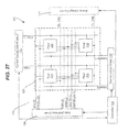
- FIG. 37 is a signal timing diagram of the signals to the data extraction circuit to extract the characteristic voltage of the OLED in a modified version of the circuit in FIG. 5 ;
- FIG. 38 is a circuit diagram of a data extraction circuit for reading the pixel charge from a drive circuit for a pixel in the AMOLED display in FIG. 27 .
- FIG. 39 is a signal timing diagram of the signals to the data extraction circuit of FIG. 38 for reading pixel status by initializing the nodes externally;
- FIG. 40 is a flow diagram for reading the pixel status in the circuit of FIG. 38 by initializing the nodes externally;
- FIG. 41 is a signal timing diagram of the signals to the data extraction circuit of FIG. 38 for reading pixel status by initializing the nodes internally;
- FIG. 42 is a flow diagram for reading the pixel status in the circuit of FIG. 38 by initializing the nodes internally;
- FIG. 43 is a circuit diagram of a pair of circuits like the circuit of FIG. 38 used with a common monitor line for reading the pixel charge from two different pixels in the AMOLED display in FIG. 27 ;
- FIG. 44 is a signal timing diagram of the signals to the data extraction circuit of FIG. 17 for reading pixel charge when the monitor line is shared.
- FIG. 45 is a flow diagram for reading the pixel status of a pair of circuits like the circuit of FIG. 43 , with a common monitor line.
- FIG. 46A is a schematic circuit diagram of a modified pixel circuit.
- FIG. 46B is a timing diagram illustrating the operation of the pixel circuit of FIG. 46A with charge-based compensation.
- FIG. 47 is a timing diagram illustrating operation of the pixel circuit of FIG. 46A to obtain a readout of a parameter of the drive transistor.
- FIG. 48 is a timing diagram illustrating operation of the pixel circuit of FIG. 46A to obtain a readout of a parameter of the OLED.
- FIG. 49 is a timing diagram illustrating a modified operation of the pixel circuit of FIG. 46A to obtain a readout of a parameter of the OLED.
- FIG. 50 is a diagrammatic illustration of a pixel circuit with current measurement capability.
- FIG. 51 is a schematic circuit diagram of a pixel circuit that provides access to an internal node.
- FIG. 52 is a diagrammatic illustration of an OLED display pixel circuit with charge readout capability.
- Embodiments of the present invention are described using a pixel including a light emitting device and a plurality of transistors.
- the light emitting device may be an organic light emitting diode (OLED). It is noted that “pixel” and “pixel circuit” may be used interchangeably.
- FIG. 1 illustrates a process for a calibration-scheduling in accordance with an embodiment of the present invention. According to this technique, the pixels are calibrated based on their aging and/or usage during the normal operation of the display array.
- a linked list of pixels is generated in step S 2 .
- the linked list contains an identification of a pixel with high brightness for calibration.
- the linked list is used to schedule the priority in calibration.
- step S 4 “n” is chosen based on the display size and expected instability with time (e.g. shift in characteristics of transistors and light emitting device). “n” represents the number of pixels that are calibrated in each programming cycle. “n” may be one or more than one.
- the step S 6 includes steps S 8 -S 16 .
- the steps S 8 -S 16 are implemented on a selected column of the display array.
- step S 8 “n” pixels in the selected column are selected from the beginning of the linked list, hereinafter referred to as “Selected Pixels”.
- step S 10 “Calibration Mode” is enabled for the Selected Pixels, and “Normal Operation Mode” is enabled for the rest of the pixels in the selected column of the display array.
- step S 12 all pixels in the selected column are programmed by a voltage source driver (e.g. 28 of FIG. 2 ) which is connected to a data line of the pixel.
- a voltage source driver e.g. 28 of FIG. 2
- ⁇ V compensation memory For the Selected Pixels, current flowing through the data line is monitored during the programming cycle. For the pixels other than the Selected Pixels in the selected column, the corresponding programming voltage is boosted using data stored in a memory (e.g. 34 of FIG. 2 ), hereinafter referred to as “ ⁇ V compensation memory”.
- step S 14 the monitored current is compared with the expected current that must flow through the data line. Then, a calibration data curve for the Selected Pixels is generated. The AV compensation memory is updated based on the calibration data curve.
- the calibration data curve stored in the ⁇ V compensation memory for a pixel will be used to boost programming voltage for that pixel in the next programming cycles when that pixel is in the Normal Operation Mode.
- step S 16 the identifications of the Selected Pixels are sent to the end of the linked list.
- the Selected Pixels have the lowest priority in the linked list for calibration.
- the linked list will provide a sorted priority list of pixels that must be calibrated. It is noted that in the description, the term “linked list” and the term “priority list” may be used interchangeably.
- the operation goes back (S 18 ) to the step S 8 .
- the next programming cycle starts.
- a new column in the display array is activated (selected), and, new “n” pixels in the new activated column are selected from the top of the linked list.
- the ⁇ V compensation memory is updated using the calibration data obtained for the new Selected Pixels.
- K 1%/hr
- e 0.1%
- n>0.14 which implies that it is needed to calibrate once in 5 programming cycles.
- the frequency of calibration can be reduced automatically as the display ages, since shifts in characteristics will become slower as the time progresses.
- the pixels that are selected for calibration can be programmed with different currents depending on display data. The only condition is that their programming current is larger than a reference current. Therefore, the calibration can be performed at multiple brightness levels for one pixel to achieve higher accuracy.
- the linked list is described in detail.
- the pixels with high brightness for calibration are listed.
- the display data is used to determine the pixels with high brightness for calibration. Calibration at low currents is slow and often not accurate. In addition, maximum shift in characteristics occurs for pixels with high current.
- the pixels which must be programmed with currents higher than a threshold current I TH , are selected and stored in the linked list.
- the calibration-scheduling technique described above is applicable to any current programmed pixels, for example, but not limited to, a current mirror based pixel.
- FIG. 2 illustrates an example of a system structure for implementing the calibration-scheduling of FIG. 1 .
- a system 30 of FIG. 2 for implementing calibration-scheduling algorithm is provided to a display array 10 having a plurality of pixel circuits 12 .
- the pixel circuit 12 is a current programmed pixel circuit, such as, but not limited to a current mirror based pixel.
- the pixel circuits 12 are arranged in row and column.
- the pixel circuit 12 may include an OLED and a plurality of transistors (e.g. TFTs).
- the transistor may be fabricated using amorphous silicon, nano/micro crystalline silicon, poly silicon, organic semiconductors technologies (e.g. organic TFT), NMOS/PMOS technology or CMOS technology (e.g. MOSFET).
- the display array 10 may be an AMOLED display array.
- the pixel circuit 12 is operated by a gate line 14 connected to a gate driver 20 , a data line 16 connected to a voltage data driver 28 , and a power line connected to a power supply 24 .
- a gate line 14 connected to a gate driver 20
- a data line 16 connected to a voltage data driver 28
- a power line connected to a power supply 24 .
- FIG. 2 two data lines, two gate lines and two power lines are shown as an example. It is apparent that more than two data lines, two gate lines and two power lines may be provided to the display array 10 .
- the system 30 includes a calibration scheduler and memory block 32 for controlling programming and calibration of the display array 10 , and a ⁇ V compensation memory 34 for storing ⁇ V compensation voltage (value).
- a column of the display array 10 is selected.
- the calibration scheduler and memory block 32 enables Normal Operation Mode or Calibration Mode for the selected column (i.e., data line) during that programming cycle.
- the system 30 further includes a monitoring system for monitoring and measuring a pixel current.
- the monitoring system includes switches 36 and 38 and a voltage sensor 40 with an accurate resistor 42 .
- the switches 36 and 38 are provided for each data line as an example.
- the system 30 further includes a generator for generating ⁇ V compensation voltage based on the monitoring result.
- the generator includes an analog/digital converter (A/D) 44 , a comparator 46 , and a translator 48 .
- the A/D 44 converts the analog output of the voltage sensor 40 into a digital output.
- the comparator 46 compares the digital output to an output from the translator 48 .
- the translator 48 implements function f(V) on a digital data input 52 .
- the translator 48 converts the current data input 52 to the voltage data input through f(v).
- the result of the comparison by the comparator 46 is stored in the ⁇ V compensation memory 34 .
- the system 30 further includes an adder 50 for adding the digital data input 52 and the ⁇ V compensation voltage stored in the ⁇ V compensation memory 34 .
- the voltage data driver 28 drives a data line based on the output of the adder 50 .
- the programming data for the data line is adjusted by adding the ⁇ V compensation voltage.
- the switch 36 When the calibration scheduler and memory block 32 enables the Normal Operation Mode for a selected data line, the switch 36 is activated. The voltage output from the voltage data driver 28 is directly applied to the pixel on that data line.
- the switch 38 When the calibration scheduler and memory block 32 enables the Calibration Mode for that data line, the switch 38 is activated. The voltage is applied to the pixel on that data line through the accurate resistor 42 . The voltage drop across the resistor 42 at the final stages of the programming time (i.e. when initial transients are finished) is measured by the voltage sensor 40 . The voltage drop monitored by the voltage sensor 40 is converted to digital data by the A/D 44 . The resulting value of the voltage drop is proportional to the current flowing through the pixel if the pixel is a current programmed pixel circuit. This value is compared by the comparator 46 to the expected value obtained by the translator 48 .
- the difference between the expected value and the measured value is stored in the AV compensation memory 34 , and will be used for a subsequent programming cycle. The difference will be used to adjust the data voltage for programming of that pixel in future.
- the calibration scheduler and memory block 32 may include the linked list described above. In the beginning, the linked list is generated automatically. It may be just a list of pixels. However, during the operation it is modified.
- the calibration of the pixel circuits with high brightness guarantees the high speed and accurate calibration that is needed in large or small area displays.
- the display array 10 is driven using a voltage programming technique, it is fast and can be used for high-resolution and large area displays.
- the applications of the calibration-scheduling technique ranges from electroluminescent devices used for cellphones, personal organizers, monitors, TVs, to large area display boards.
- the system 30 monitors and measures voltage drop which depends on time dependent parameters of the pixel, and generates a desirable programming data.
- the time dependent parameters of the pixel may be extracted by any mechanisms other than that of FIG. 2 .
- a further technique for programming, extracting time dependent parameters of a pixel and driving the pixel is described in detail with reference to FIGS. 3-7 .
- This technique includes voltage-extracting for calibration. Programming data is calibrated with the extracted information, resulting in a stable pixel current over time. Using this technique, the aging of the pixel is extracted.
- FIG. 3 illustrates a system architecture for implementing a voltage-extracting, programming and driving in accordance with an embodiment of the present invention.
- the system of FIG. 3 implements the voltage-extracting and programming to a current mode pixel circuit 60 .
- the pixel circuit 60 includes a light emitting device and a plurality of transistors having a driving transistor (not shown).
- the transistors may be TFTs.
- the pixel circuit 60 is selected by a select line SEL and is driven by DATA on a data line 61 .
- a voltage source 62 is provided to write a programming voltage V P into the pixel circuit 60 .
- a current-controlled voltage source (CCVS) 63 having a positive node and a negative node is provided to convert the current on the data line 61 to a voltage Vext.
- a display controller and scheduler 64 operates the pixel circuit 60 . The display controller and scheduler 64 monitors an extracted voltage Vext output from the CCVS 63 and then controls the voltage source 62 .
- I Line represents the current on the data line 61
- I pixel represents a pixel current
- V T represents the threshold voltage of the driving transistor included in the pixel circuit 60
- the gain parameter in the TFT characteristics
- the display controller and scheduler 64 determines the amount of shift in the threshold voltage.
- the programming voltage V P is modified with the extracted information.
- the extraction procedure can be implemented for one or several pixels during each frame time.
- FIG. 4 illustrates an example of a system for the voltage-extracting, programming and driving of FIG. 3 , which is employed with a top-emission current-cell pixel circuit 70 .
- the pixel circuit 70 includes an OLED 71 , a storage capacitor 72 , a driving transistor 73 and switch transistors 74 and 75 .
- the transistors 73 , 74 and 75 may be n-type TFTs. However, these transistors 73 , 74 and 75 may be p-type transistors.
- the voltage-extracting and programming technique applied to the pixel circuit 70 is also applicable to a pixel circuit having p-type transistors.
- the driving transistor 73 is connected to a data line 76 through the switch transistor 75 , and is connected to the OLED 71 , and also is connected to the storage capacitor 72 through the switch transistor 74 .
- the gate terminal of the driving transistor 73 is connected to the storage capacitor 72 .
- the gate terminals of the switch transistors 74 and 75 are connected to a select line SEL.
- the OLED 71 is connected to a voltage supply electrode or line VDD.
- the pixel circuit 70 is selected by the select line SEL and is driven by DATA on the data line 76 .
- a current conveyor (CC) 77 has X, Y and Z terminals, and is used to extract a current on the data line 76 without loading it.
- a voltage source 78 applies programming voltage to the Y terminal of the CC 77 .
- the X terminal is forced by feedback to have the same voltage as that of the Y terminal.
- the current on the X terminal is duplicated into the Z terminal of the CC 77 .
- a current-controlled voltage source (CCVS) 79 has a positive node and a negative node. The CCVS 79 converts the current on the Z terminal of the CC 77 into a voltage Vext.
- Vext is provided to the display controller and scheduler 64 of FIG. 3 , where the threshold voltage of the driving transistor 73 is extracted.
- the display controller and scheduler 64 controls the voltage source 78 based on the extracted threshold voltage.
- FIG. 5 illustrates a further example of a system for the voltage-extracting, programming, and driving of FIG. 3 , which is employed with a bottom-emission current-cell pixel circuit 80 .
- the pixel circuit 80 includes an OLED 81 , a storage capacitor 82 , a driving transistor 83 , and switch transistors 84 and 85 .
- the transistors 83 , 84 and 85 may be n-type TFTs. However, these transistors 83 , 84 and 85 may be p-type transistors.
- the driving transistor 83 is connected to a data line 86 through the switch transistor 85 , and is connected to the OLED 81 , and also is connected to the storage capacitor 82 .
- the gate terminal of the driving transistor 83 is connected to a voltage supply line VDD through the switch transistor 84 .
- the gate terminals of the switch transistors 84 and 85 are connected to a select line SEL.
- the pixel circuit 80 is selected by the select line SEL and is driven by DATA on the data line 86 .
- a current conveyor (CC) 87 has X, Y and Z terminals, and is used to extract a current on the data line 86 without loading it.
- a voltage source 88 applies a negative programming voltage at the Y terminal of the CC 87 .
- the X terminal is forced by feedback to have the same voltage as that of the Y terminal.
- the current on the X terminal is duplicated into the Z terminal of the CC 87 .
- a current-controlled voltage source (CCVS) 89 has a positive node and a negative node. The CCVS 89 converts the current of the Z terminal of the CC 87 into a voltage Vext.
- Vext is provided to the display controller and scheduler 64 of FIG. 3 , where the threshold voltage of the driving transistor 83 is extracted.
- the display controller and scheduler 64 controls the voltage source 88 based on the extracted threshold voltage.
- FIG. 6 illustrates a further example of a system for the voltage-extracting, programming and driving of FIG. 3 , which is employed with a top-emission current-mirror pixel circuit 90 .
- the pixel circuit 90 includes an OLED 91 , a storage capacitor 92 , mirror transistors 93 and 94 , and switch transistors 95 and 96 .
- the transistors 93 , 94 , 95 and 96 may be n-type TFTs. However, these transistors 93 , 94 , 95 and 96 may be p-type transistors.
- the mirror transistor 93 is connected to a data line 97 through the switch transistor 95 , and is connected to the storage capacitor 92 through the switch transistor 96 .
- the gate terminals of the mirror transistors 93 and 94 are connected to the storage capacitor 92 and the switch transistor 96 .
- the mirror transistor 94 is connected to a voltage supply electrode or line VDD through the OLED 91 .
- the gate terminals of the switch transistors 85 and 86 are connected to a select line SEL.
- the pixel circuit 90 is selected by the select line SEL and is driven by DATA on the data line 97 .
- a current conveyor (CC) 98 has X, Y and Z terminals, and is used to extract the current of the data line 97 without loading it.
- a voltage source 99 applies a positive programming voltage at the Y terminal of the CC 98 .
- the X terminal is forced by feedback to have the same voltage as the voltage of the Y terminal.
- the current on the X terminal is duplicated into the Z terminal of the CC 98 .
- a current-controlled voltage source (CCVS) 100 has a positive node and a negative node. The CCVS 100 converts a current on the Z terminal of the CC 98 into a voltage Vext.
- Vext is provided to the display controller and scheduler 64 of FIG. 3 , where the threshold voltage of the driving transistor 93 is extracted.
- the display controller and scheduler 64 controls the voltage source 99 based on the extracted threshold voltage.
- FIG. 7 illustrates a further example of a system for the voltage-extracting, programming and driving of FIG. 3 , which is employed with a bottom-emission current-minor pixel circuit 110 .
- the pixel circuit 110 includes an OLED 111 , a storage capacitor 112 , mirror transistors 113 and 116 , and switch transistors 114 and 115 .
- the transistors 113 , 114 , 115 and 116 may be n-type TFTs. However, these transistors 113 , 114 , 115 and 116 may be p-type transistors.
- the mirror transistor 113 is connected to a data line 117 through the switch transistor 114 , and is connected to the storage capacitor 112 through the switch transistor 115 .
- the gate terminals of the mirror transistors 113 and 116 are connected to the storage capacitor 112 and the switch transistor 115 .
- the minor transistor 116 is connected to a voltage supply line VDD.
- the mirror transistors 113 , 116 and the storage capacitor 112 are connected to the OLED 111 .
- the gate terminals of the switch transistors 114 and 115 are connected to a select line SEL.
- the pixel circuit 110 is selected by the select line SEL and is driven by DATA on the data line 117 .
- a current conveyor (CC) 118 has X, Y and Z terminals, and is used to extract the current of the data line 117 without loading it.
- a voltage source 119 applies a positive programming voltage at the Y terminal of the CC 118 .
- the X terminal is forced by feedback to have the same voltage as the voltage of the Y terminal of the CC 118 .
- the current on the X terminal is duplicated into the Z terminal of the CC 118 .
- a current-controlled voltage source (CCVS) 120 has a positive node and a negative node. The 120 converts the current on the Z terminal of the CC 118 into a voltage Vext.
- Vext is provided to the display controller and scheduler 64 of FIG. 3 , where the threshold voltage of the driving transistor 113 is extracted.
- the display controller and scheduler 64 controls the voltage source 119 based on the extracted threshold voltage.
- time dependent parameters of a pixel e.g. threshold shift
- the programming voltage can be calibrated with the extracted information, resulting in a stable pixel current over time. Since the voltage of the OLED (i.e. 71 of FIG. 4 , 81 of FIG. 5 , 91 of FIG. 6 , 111 of FIG. 7 ) affects the current directly, the voltage-extracting driving technique described above can also be used to extract OLED degradation as well as the threshold shift.
- the voltage-extracting technique described above can be used with any current-mode pixel circuit, including current-mirror and current-cell pixel circuit architectures, and are applicable to the display array 10 of FIG. 2 .
- a stable current independent of pixel aging under prolonged display operation can be provided using the extracted information.
- the display operating lifetime is efficiently improved.
- the transistors in the pixel circuits of FIGS. 3-7 may be fabricated using amorphous silicon, nano/micro crystalline silicon, poly silicon, organic semiconductors technologies (e.g. organic TFT), NMOS/PMOS technology or CMOS technology (e.g. MOSFET).
- the pixel circuits of FIGS. 3-7 may form AMOLED display arrays.
- a further technique for programming, extracting time dependent parameters of a pixel and driving the pixel is described in detail with reference to FIGS. 8-17 .
- the technique includes a step-calibration driving technique.
- information on the aging of a pixel e.g. threshold shift
- the extracted information will be used to generate a stable pixel current/luminance.
- the resolution of the extracted aging is defined by display drivers.
- the dynamic effects are compensated since the pixel aging is extracted under operating condition, which is similar to the driving cycle.
- FIG. 8 illustrates a pixel circuit 160 to which a step-calibration driving in accordance with an embodiment of the present invention is applied.
- the pixel circuit 160 includes an OLED 161 , a storage capacitor 162 , and a driving transistor 163 and switch transistors 164 and 165 .
- the pixel circuit 160 is a current-programmed, 3-TFT pixel circuit.
- a plurality of the pixel circuits 160 may form an AMOLED display.
- the transistors 163 , 164 and 165 are n-type TFTs. However, the transistors 163 , 164 and 165 may be p-type TFTs.
- the step-calibration driving technique applied to the pixel circuit 160 is also applicable to a pixel circuit having p-type transistors.
- the transistors 163 , 164 and 165 may be fabricated using amorphous silicon, nano/micro crystalline silicon, poly silicon, organic semiconductors technologies (e.g. organic TFT), NMOS/PMOS technology or CMOS technology (e.g. MOSFET).
- the gate terminal of the driving transistor 163 is connected to a signal line VDATA through the switch transistor 164 , and also connected to the storage capacitor 162 .
- the source terminal of the driving transistor 163 is connected to a common ground.
- the drain terminal of the driving transistor 163 is connected to a monitor line MONITOR through the switch transistor 165 , and also is connected to the cathode electrode of the OLED 161 .
- the gate terminal of the switch transistor 164 is connected to a select line SELL.
- the source terminal of the switch transistor 164 is connected to the gate terminal of the driving transistor 163 , and is connected to the storage capacitor 162 .
- the drain terminal of the switch transistor 164 is connected to VDATA.
- the gate terminal of the switch transistor 165 is connected to a select line SEL 2 .
- the source terminal of the switch transistor 165 is connected to MONITOR.
- the drain terminal of the switch transistor 165 is connected to the drain terminal of the driving transistor 163 and the cathode electrode of the OLED 161 .
- the anode electrode of the OLED 161 is connected to a voltage supply electrode or line VDD.
- the transistors 163 and 164 and the storage capacitor 162 are connected at node A 3 .
- the transistors 163 and 165 and the OLED 161 are connected at node B 3 .
- FIG. 9 illustrates an example of a driver and extraction block 170 along with the driving transistor 163 of FIG. 8 .
- each of Rs 171 a and Rs 171 b represents the ON resistance of the switch transistors (e.g. 164 , 165 of FIG. 8 ).
- Cs represents the storage capacitor of the pixel
- C OLED represents the OLED capacitance
- CP represents the line parasitic capacitance.
- the OLED is presented as a capacitance.
- a block 173 is used to extract the threshold voltage of the driving transistor, during the extraction cycle.
- the block 173 may be a current sense amplifier (SA) or a current comparator. In the description, the block 173 is referred to as “SA block 173 ”.
- the output of the SA block 173 (i.e. Triggers of FIG. 10 , 11 ) becomes one. If the current of the MONITOR line is less than the reference current (IREF), the output of the SA block 173 becomes zero.
- the SA block 173 can be shared between few columns result in less overhead. Also, the calibration of the pixel circuit can be done one at a time, so the extraction circuits can be shared between the all columns.
- a data process unit (DPU) block 172 is provided to control the programming cycle, contrast, and brightness, to perform the calibration procedure and to control the driving cycle.
- the DPU block 172 implements extraction algorithm to extract (estimate) the threshold voltage of the driving transistor based on the output from the SA block 173 , and controls a driver 174 which is connected to the driving transistor 163 .
- FIG. 10 illustrates an example of the extraction algorithm implemented by the DPU block 172 of FIG. 9 .
- the algorithm of FIG. 10 is in a part of the DPU block 172 .
- V T (i, j) represents the extracted threshold voltage for the pixel (i, j) at the previous extraction cycle
- V S represents the resolution of the driver 174
- “i” represents a row of a pixel array
- “j” represents a column of a pixel array.
- Trigger conveys the comparison results of the SA block 173 of FIG. 9 .
- Less_state 180 determines the situation in which the actual V T of the pixel is less than the predicted V T (V TM )
- Equal_state 181 determines the situation in which the predicted V T (V TM ) and the actual V T of the pixel are equal
- Great state 182 determines the situation in which the actual V T of the pixel is greater than the predicted V T (V TM ).
- the DPU block 172 of FIG. 9 determines an intermediate threshold voltage V TM as follows:
- FIG. 11 illustrates a further example of the extraction algorithm implemented by the DPU block 172 of FIG. 9 .
- the algorithm of FIG. 11 is in a part of the DPU block 172 of FIG. 9 .
- V T (i, j) represents the extracted threshold voltage for the pixel (i, j) at the previous extraction cycle
- V S represents the resolution of the driver 174
- “i” represents a row of a pixel array
- “j” represents a column of a pixel array.
- Trigger conveys the comparison results of the SA block 173 .
- Vres represents the step that will be added/subtracted to the predicted V T (V TM ) in order achieve the actual V T of the pixel
- A represents the reduction gain of a prediction step
- K represents the increase gain of the prediction step.
- FIG. 11 The operation of FIG. 11 is the same as that of FIG. 10 , except that it has gain extra states L2 and G2 for rapid extraction of abrupt changes. In the gain states, the step size is increased to follow the changes more rapidly. L1 and G1 are the transition states which define the V T change is abrupt or normal.
- FIG. 12 illustrates an example of waveforms applied to the pixel circuit 160 of FIG. 8 .
- V call V B +V TM
- V DR V P +V T (i, j)+V REF
- V B represents the bias voltage during the extraction cycle
- V TM is defined based on the algorithm shown in FIG. 10 or 11
- V P represents a programming voltage
- V T (i, j) represents the extracted threshold voltage at the previous extraction cycle
- V REF represents the source voltage of the driving transistor during the programming cycle.
- the operation of the pixel circuit 160 includes operating cycles X 51 , X 52 , X 53 , and X 54 .
- an extraction cycle is separated from a programming cycle.
- the extraction cycle includes X 51 and X 52
- the programming cycle includes X 53 .
- X 54 is a driving cycle.
- node A 3 is charged to (V P +V T ) where V P is a programming voltage and V T is the threshold voltage of the driving transistor 163 .
- V cal is V B ⁇ V TM in which V B is a bias voltage, and V TM the predicted V T , and V REF should be larger than V DD ⁇ V OLED0 where V OLED0 is the ON voltage of the OLED 161 .
- VGS represents the gate-source voltage of the driving transistor 163
- ⁇ V B , ⁇ V TM , ⁇ V T2 and ⁇ V H are the dynamic effects depending on V B , V TM , V T2 and V H , respectively.
- V T2 represents the threshold voltage of the switch transistor 164
- V H represents the change in the voltage of SELL at the beginning of second operating cycle X 52 when it goes to zero.
- the SA block 173 is tuned to sense the current larger than ⁇ (V B ) 2 , so that the gate-source voltage of the driving transistor 163 is larger than (V B +V T ), where ⁇ is the gain parameter in the I-V characteristic of the driving transistor 163 .
- V TM and the extracted threshold voltage V T (i, j) for the pixel (i, j) converge to:
- the pixel current becomes independent of the static and dynamic effects of the threshold voltage shift.
- FIG. 12 the extraction cycle and the programming cycle are shown as separated cycles. However, the extraction cycle and the programming cycle may be merged as shown in FIG. 13 .
- FIG. 13 illustrates a further example of waveforms applied to the pixel circuit 160 of FIG. 8 .
- the operation of the pixel circuit 160 includes operating cycles X 61 , X 62 and X 63 . Programming and extraction cycles are merged into the operating cycles X 61 and X 62 .
- the operating cycle X 63 is a driving cycle.
- the pixel current is compared with the desired current, and the threshold voltage of the driving transistor is extracted with the algorithm of FIG. 10 or 11 .
- SEL 1 and SEL 2 are shown in FIG. 8 .
- a signal select line e.g. SEL 1
- SEL 1 of FIG. 12 stays at high in the second operating cycle X 52 , and the VGS remains at (V B +V TM ). Therefore, the dynamic effects are not detected.
- the step-calibration driving technique described above is applicable to the pixel circuit 190 of FIG. 14 .
- the pixel circuit 190 includes an OLED 191 , a storage capacitor 192 , and a driving transistor 193 and switch transistors 194 and 195 .
- the pixel circuit 190 is a current-programmed, 3-TFT pixel circuit.
- a plurality of the pixel circuits 190 may form an AMOLED display.
- the transistors 193 , 194 and 195 are n-type TFTs. However, the transistors 193 , 194 and 195 may be p-type TFTs.
- the step-calibration driving technique applied to the pixel circuit 190 is also applicable to a pixel circuit having p-type transistors.
- the transistors 193 , 194 and 195 may be fabricated using amorphous silicon, nano/micro crystalline silicon, poly silicon, organic semiconductors technologies (e.g. organic TFT), NMOS/PMOS technology or CMOS technology (e.g. MOSFET).
- the gate terminal of the driving transistor 193 is connected to a signal line VDATA through the switch transistor 194 , and also connected to the storage capacitor 192 .
- the source terminal of the driving transistor 193 is connected to the anode electrode of the OLED 191 , and is connected to a monitor line MONITOR through the switch transistor 195 .
- the drain terminal of the driving transistor 193 is connected to a voltage supply line VDD.
- the gate terminals of the transistors 194 and 195 are connected to select lines SEL 1 and SEL 2 , respectively.
- the transistors 193 and 194 and the storage capacitor 192 are connected at node A 4 .
- the transistor 195 , the OLED 191 and the storage capacitor 192 are connected at node B 4 .
- the structure of the pixel circuit 190 is similar to that of FIG. 8 , except that the OLED 191 is at the source terminal of the driving transistor 193 .
- the operation of the pixel circuit 190 is the same as that of FIG. 12 or 13 .
- the extracted data is independent of the ground bouncing. Also, during the programming cycle (X 53 or X 61 ), the source terminal of the drive TFT is forced to VREF, the gate-source voltage of the drive TFT becomes independent of the ground bouncing. As a result of these conditions, the pixel current is independent of ground bouncing.
- FIG. 15 illustrates the results of simulation for the step-calibration driving technique.
- “Case I” represents an operation of FIG. 8 where SELL goes to zero in the second operating cycle (X 52 of FIG. 12 );
- “Case II” represents an operation of FIG. 8 where SEL 1 stays at high in the second operating cycle.
- ⁇ V TR is the minimum detectable shift in the threshold voltage of the driving transistor (e.g. 163 of FIG. 8 )
- ⁇ V T2R is the minimum detectable shift in the threshold voltage of the switch transistor (e.g. 164 of FIG. 8 )
- In is the pixel current of the pixel during the driving cycle.
- the pixel current of Case II is smaller than that of Case I for a given programming voltage due to the dynamic effects of the threshold voltage shift. Also, the pixel current of Case II increases as the threshold voltage of the driving transistor increases (a), and decreases as the threshold voltage of the switch transistor decreases (b). However, the pixel current of Case I is stable. The maximum error induced in the pixel current is less than %0.5 for any shift in the threshold voltage of the driving and switch TFTs. It is obvious that ⁇ V T2R is larger than ⁇ V TR because the effect of a shift in VT on the pixel current is dominant. These two parameters are controlled by the resolution (V S ) of the driver (e.g. 174 of FIG. 9 ), and the SNR of the SA block (e.g.
- the extraction cycles e.g. X 51 , X 52 of FIG. 12
- the major operating cycles become the other programming cycle (e.g. X 53 of FIG. 12 ) and the driving cycle (e.g. X 54 of FIG. 12 ).
- the programming time reduces significantly, providing for high-resolution, large-area AMOLED displays where a high-speed programming is prerequisite.
- FIG. 16 illustrates an example of a system architecture for the step-calibration driving with a display array 200 .
- the display array 200 includes a plurality of the pixel circuits (e.g. 160 of FIG. 8 or 190 of FIG. 14 ).
- a gate driver 202 for selecting the pixel circuits, a drivers/SAs block 204 , and a data process and calibration unit block 206 are provided to the display array 200 .
- the drivers/SAs block 204 includes the driver 174 and the SA block 173 of FIG. 9 .
- the data process and calibration unit block 206 includes the DPU block 172 of FIG. 9 .
- “Calibration” in FIG. 16 includes the calibration data from a calibration memory 208 , and may include some user defined constants for setting up calibration data processing.
- the contrast and the brightness inputs are used to adjust the contrast and the brightness of the panel by the user.
- gamma-correction data is defined based on the OLED characteristic and human eye. The gamma-correction input is used to adjust the pixel luminance for human eyes.
- the calibration memory 208 stores the extracted threshold voltage V T (i, j) and the state s(i, j) of each pixel.
- a memory 210 stores the other required data for the normal operation of a display including gamma correction, resolution, contrast, and etc.
- the DPU block performs the normal tasks assigned to a controller and scheduler in a display. Besides, the algorithm of FIG. 10 or 11 is added to it to perform the calibration.
- FIG. 17 illustrates an example of waveforms applied to the system architecture of FIG. 16 .
- each of ROW[ 1 ], ROW[ 2 ], and ROW[ 3 ] represents a row of the display array 200
- “E” represents an extraction operation
- “P” represents a programming operation
- “D” represents a driving operation. It is noted that the extraction cycles (E) are not required to be done for all the frame cycle. Therefore, after a long time interval (extraction interval), the extraction is repeated for a pixel.
- ⁇ F n ⁇ P + ⁇ E
- ⁇ F . the frame time
- ⁇ P the time required to write the pixel data into the storage capacitor (e.g. 162 of FIG. 8 )
- ⁇ E the extraction time
- n the number of row in the display array (e.g. 200 of FIG. 16 ).
- ⁇ F ( n+m ) ⁇ P
- m the timing required for the extraction cycles in the scale of programming cycle timing ( ⁇ P ).
- step-calibration driving technique described above is applicable to any current-programmed pixel circuit other than those of FIGS. 8 and 14 .
- the time dependent parameter(s) of a pixel such as threshold shift
- the programming-voltage is calibrated with the extracted information, resulting in a stable pixel current over time. Further, a stable current independent of the pixel aging under prolonged display operation can be is provided to the pixel circuit, which efficiently improves the display operating lifetime.
- a technique for programming, extracting time dependent parameters of a pixel and driving the pixel in accordance with a further embodiment of the present invention is described in detail.
- the technique includes extracting information on the aging of a pixel (e.g. OLED luminance) by monitoring OLED voltage or OLED current, and generating luminance.
- the programming voltage is calibrated with the extracted information, resulting in stable brightness over time.
- the programming voltage can be modified by the OLED voltage/current to provide a constant brightness.
- the voltage/current of the OLED ( 161 of FIG. 8 or 191 of FIG. 14 ) is extracted while SEL 2 is high. Since the OLED voltage or current has been reported to be correlated with the brightness degradation in the OLED, the programming voltage can be modified by the OLED voltage to provide a constant brightness.
- FIG. 18 illustrates an example of waveforms for the voltage/current extraction.
- the waveforms of FIG. 18 are applicable to the pixel circuit 160 of FIG. 8 and the pixel circuit 190 of FIG. 14 to extract OLED voltage/current.
- the operation of FIG. 18 includes operating cycles X 71 , X 72 and X 73 .
- the operating cycles X 71 and X 72 are an OLED extraction cycle.
- the operating cycle X 73 is one of the operating cycles shown in FIGS. 12 and 13 .
- SEL 1 and SEL 2 are high, and VDATA is zero.
- the gate-source voltage of the driving transistor e.g. 163 of FIG. 8
- a current or voltage is applied to the OLED ( 161 of FIG. 8 ) through the MONITOR line.
- SEL 2 is high and SELL is low.
- the OLED voltage or current is extracted through the MONITOR line using the algorithm presented in FIG. 10 or 11 . This waveform can be combined with any other driving waveform.
- the algorithm of FIGS. 10 and 11 is used to predict the aging data, i.e. V T shift, based on the comparison results (current with current or voltage with voltage).
- the algorithm of FIGS. 10 and 11 is applicable to predict the shift in the OLED voltage V OLED by replacing V T with the V OLED and the comparison result of OLED current/voltage with a reference current/voltage.
- the system architecture shown in FIG. 9 is used to compensate for the threshold shift.
- the OLED data is also extracted when the architecture of FIG. 9 , i.e. DPU 172 , block 173 , driver 174 , is used. This data can be used to compensate for the OLED shift.
- the operating cycle X 73 can be any operating cycle including the programming cycle. This depends on the status of the panel after OLED extraction. If it is during the operation, then X 73 is the programming cycle of the waveforms in FIGS. 12 and 13 .
- the OLED voltage can be extracted during the driving cycle X 55 /X 63 of FIG. 12 / 13 .
- the SEL 2 of FIG. 8 or 14 goes to a high voltage, and so the voltage of the OLED can be read back through the MONITOR for a specific pixel current.
- FIG. 19 illustrates a further example of waveforms for the voltage/current extraction.
- FIG. 20 illustrates a pixel circuit 220 to which the voltage/current extraction of FIG. 19 is applied.
- the pixel circuit 220 includes an OLED 221 , a storage capacitor 222 , and a driving transistor 223 and switch transistors 224 and 225 .
- a plurality of the pixel circuits 220 may form an AMOLED display.
- the transistors 223 , 224 and 225 are n-type TFTs. However, the transistors 223 , 224 and 225 may be p-type TFTs.
- the voltage/current extraction technique applied to the pixel circuit 220 is also applicable to a pixel circuit having p-type transistors.
- the transistors 223 , 224 and 225 may be fabricated using amorphous silicon, nano/micro crystalline silicon, poly silicon, organic semiconductors technologies (e.g. organic TFT), NMOS/PMOS technology or CMOS technology (e.g. MOSFET).
- the gate terminal of the driving transistor 223 is connected to the source terminal of the switch transistor 224 , and also connected to the storage capacitor 222 .
- the one terminal of the driving transistor 223 is connected to a common ground.
- the other terminal of the driving transistor 223 is connected to a monitor and data line MONITOR/DATA through the switch transistor 235 , and is also connected to the cathode electrode of the OLED 221 .
- the gate terminal of the switch transistor 224 is connected to a select line SELL.
- the one terminal of the switch transistor 224 is connected to the gate terminal of the driving transistor 223 , and is connected to the storage capacitor 222 .
- the other terminal of the switch transistor 224 is connected to the cathode electrode of the OLED 221 .
- the gate terminal of the switch transistor 225 is connected to a select line SEL 2 .
- the one terminal of the switch transistor 225 is connected to MONITOR/DATA.
- the other terminal of the switch transistor 225 is connected to the driving transistor 223 and the cathode electrode of the OLED 221 .
- the anode electrode of the OLED 221 is connected to a voltage supply electrode or line VDD.
- the transistors 223 and 224 and the storage capacitor 222 are connected at node A 5 .
- the transistors 223 and 225 and the OLED 221 are connected at node B 5 .
- the pixel circuit 220 is similar to the pixel circuit 160 of FIG. 8 . However, in the pixel circuit 220 , the MONITOR/DATA line is used for monitoring and programming purpose.
- the operation of the pixel circuit 220 includes operating cycles X 81 , X 82 and X 83 .
- a current or voltage is applied to the OLED through the MONITOR/DATA line, and its voltage or current is extracted.
- the shift in the OLED voltage is extracted using the algorithm presented in FIG. 10 or 11 based on the monitored voltage or current. This waveform can be combined with any driving waveform.
- the operating cycle X 83 can be any operating cycle including the programming cycle. This depends on the status of the panel after OLED extraction.
- the OLED voltage/current can be extracted during the driving cycle of the pixel circuit 220 of FIG. 20 after it is programmed for a constant current using any driving technique.
- the SEL 2 goes to a high voltage, and so the voltage of the OLED can be read back through the MONITOR/DATA line for a specific pixel current.
- FIG. 21 illustrates a further example of waveforms for the voltage/current extraction technique.
- FIG. 22 illustrates a pixel circuit 230 to which the voltage/current extraction of FIG. 21 is applied.
- the waveforms of FIG. 21 is also applicable to the pixel circuit 160 of FIG. 8 to extract OLED voltage/current.
- the pixel circuit 230 includes an OLED 231 , a storage capacitor 232 , and a driving transistor 233 and switch transistors 234 and 235 .
- a plurality of the pixel circuits 230 may form an AMOLED display.
- the transistors 233 , 234 and 235 are n-type TFTs. However, the transistors 233 , 234 and 235 may be p-type TFTs.
- the voltage/current extraction technique applied to the pixel circuit 230 is also applicable to a pixel circuit having p-type transistors.
- the transistors 233 , 234 and 235 may be fabricated using amorphous silicon, nano/micro crystalline silicon, poly silicon, organic semiconductors technologies (e.g. organic TFT), NMOS/PMOS technology or CMOS technology (e.g. MOSFET).
- the gate terminal of the driving transistor 233 is connected to the source terminal of the switch transistor 234 , and also connected to the storage capacitor 232 .
- the one terminal of the driving transistor 233 is connected to a voltage supply line VDD.
- the other terminal of the driving transistor 233 is connected to a monitor and data line MONITOR/DATA through the switch transistor 235 , and is also connected to the anode electrode of the OLED 231 .
- the gate terminal of the switch transistor 234 is connected to a select line SELL.
- the one terminal of the switch transistor 234 is connected to the gate terminal of the driving transistor 233 , and is connected to the storage capacitor 232 .
- the other terminal of the switch transistor 234 is connected to VDD.
- the gate terminal of the switch transistor 225 is connected to a select line SEL 2 .
- the one terminal of the switch transistor 235 is connected to MONITOR/DATA.
- the other terminal of the switch transistor 235 is connected to the driving transistor 233 and the anode electrode of the OLED 231 .
- the anode electrode of the OLED 231 is connected to VDD.
- the transistors 233 and 234 and the storage capacitor 232 are connected at node A 6 .
- the transistors 233 and 235 and the OLED 231 are connected at node B 5 .
- the pixel circuit 230 is similar to the pixel circuit 190 of FIG. 14 . However, in the pixel circuit 230 , the MONITOR/DATA line is used for monitoring and programming purpose.
- FIG. 22 the operation of FIG. 22 includes operating cycles X 91 , X 92 and X 93 .
- SEL 1 and SEL 2 are high and VDD goes to zero.
- the gate-source voltage of the driving transistor e.g. 233 of FIG. 21 .
- a current is applied to the OLED (e.g. 231 of FIG. 21 ) through the MONITOR/DATA line, and its voltage (current) is extracted.
- the shift in the OLED voltage is extracted using the algorithm presented in FIG. 10 or 11 based on the monitored voltage or current. This waveform can be combined with any other driving waveform.
- the operating cycle X 93 can be any operating cycle including the programming cycle. This depends on the status of the panel after OLED extraction.
- the OLED voltage can be extracted during the driving cycle of the pixel circuit 230 of FIG. 21 after it is programmed for a constant current using any driving technique.
- the SEL 2 goes to a high voltage, and so the voltage of the OLED can be read back through the MONITOR/DATA line for a specific pixel current.
- the OLED characteristics improve under negative bias stress.
- a negative bias related to the stress history of the pixel extracted from the OLED voltage/current, can be applied to the OLED during the time in which the display is not operating. This method can be used for any pixel circuit presented herein.
- a pixel circuit can provide stable brightness that is independent of pixel aging under prolonged display operation, to efficiently improve the display operating lifetime.
- This technique includes removing OLED from a programming path during a programming cycle.
- This technique can be adopted in hybrid driving technique to extract information on the precise again of a pixel, e.g. the actual threshold voltage shift/mismatch of the driving transistor.
- the light emitting device is turned off during the programming/calibration cycle so that it prevents the unwanted emission and effect of the light emitting device on the pixel aging.
- This technique can be applied to any current mirror pixel circuit fabricated in any technology including poly silicon, amorphous silicon, crystalline silicon, and organic materials.
- FIG. 23 illustrates a mirror based pixel circuit 250 to which a technique for removing OLED from a programming path during a programming cycle is applied.
- the pixel circuit 250 includes an OLED 251 , a storage capacitor 252 , a programming transistor 253 , a driving transistor 254 , and switch transistors 255 and 256 .
- the gate terminals of the transistors 253 and 254 are connected to IDATA through the switch transistors 255 and 256 .
- the transistors 253 , 254 , 255 and 256 are n-type TFTs. However, the transistors 253 , 254 , 255 and 256 may be p-type TFTs.
- the OLED removing technique applied to the pixel circuit 250 is also applicable to a pixel circuit having p-type transistors.
- the transistors 253 , 254 , 255 and 256 may be fabricated using amorphous silicon, nano/micro crystalline silicon, poly silicon, organic semiconductors technologies (e.g. organic TFT), NMOS/PMOS technology or CMOS technology (e.g. MOSFET).
- the transistors 253 , 254 and 256 and the storage capacitor 252 are connected at node A 10 .
- the transistors 253 and 254 , the OLED 251 and the storage capacitor 252 are connected at node B 10 .
- VDD is brought into a lower voltage. This ensures the OLED 251 to be removed from a programming path as shown in FIG. 24 .
- SEL is high and VDD goes to a reference voltage (Vref) in which the OLED 251 is reversely biased. Therefore, the OLED 251 is removed from the current path during the programming cycle.
- the pixel circuit 250 may be programmed with scaled current through IDATA without experiencing unwanted emission.
- the pixel circuit 250 may be programmed with current and using one of the techniques describe above.
- the voltage of the IDATA line is read back to extract the threshold voltage of the mirror transistor 253 which is the same as threshold voltage of the driving transistor 254 .
- the pixel circuit 250 may be programmed with voltage through the IDATA line, using one of the techniques describe above.
- the current of the IDATA line is read back to extract the threshold voltage of the mirror transistor 253 which is the same as threshold voltage of the driving transistor 254 .
- the reference voltage Vref is chosen so that the voltage at node B 10 becomes smaller than the ON voltage of the OLED 251 . As a result, the OLED 251 turns off and the unwanted emission is zero.
- the voltage of the IDATA line includes V P +V T + ⁇ VT (3) where V P includes the drain-source voltage of the driving transistor 254 and the gate-source voltage of the transistor 253 , V T is the threshold voltage of the transistor 253 ( 254 ), and ⁇ V T is the V T shift/mismatch.
- VDD goes to its original value, and so voltage at node B 10 goes to the OLED voltage VOLED.
- SEL is low.
- the gate voltage of the transistor 254 / 253 is fixed and stored in the storage capacitor 252 , since the switch transistors 255 and 256 are off. Therefore, the pixel current during the driving cycle becomes independent of the threshold voltage V T .
- the OLED removing technique can be adopted in hybrid driving technique to extract the V T -shift or V T -mismatch. From (3), if the pixel is programmed with the current, the only variant parameter in the voltage of the DATA line is the V T shift/mismatch ( ⁇ V T ). Therefore, ⁇ V T can be extracted and the programming data can be calibrated with ⁇ V T .
- FIG. 25 illustrates an example of a system architecture for implementing the OLED removing technique.
- a display array 260 includes a plurality of pixel circuits, e.g. pixel circuit 250 of FIG. 26 .
- a display controller and scheduler 262 controls and schedules the operation of the display array 260 .
- a driver 264 provides operation voltages to the pixel circuit. The driver provides the operation voltage(s) to the pixel circuit based on instructions/commands from the display controller and scheduler 262 such that the OLED is removed from a programming path of the pixel circuit, as described above.
- the controller and scheduler 262 may include functionality of the display controller and scheduler 64 of FIG. 3 , or may include functionality of the data process and calibration unit 206 of FIG. 16 .
- the system of FIG. 25 may have any of these functionalities, the calibration-scheduling described above, the voltage/current extraction described above, or combinations thereof.
- the simulation result for the voltage on IDATA line for different V T is illustrated in FIG. 26 .
- the voltage of the IDATA line includes the shift in the threshold voltage of the transistors 253 and 254 .
- the programming current is 1 ⁇ A.
- each of the transistors shown in FIGS. 4 - 8 , 14 , 20 , 21 , 23 and 24 can be replaced with a p-type transistor using the concept of complementary circuits.
- FIG. 27 is an electronic display system 100 having an active matrix area or pixel array 102 in which an n ⁇ m array of pixels 104 are arranged in a row and column configuration. For ease of illustration, only two rows and two columns are shown.
- a peripheral area 106 External to the active matrix area of the pixel array 102 is a peripheral area 106 where peripheral circuitry for driving and controlling the pixel array 102 are disposed.
- the peripheral circuitry includes an address or gate driver circuit 108 , a data or source driver circuit 110 , a controller 112 , and an optional supply voltage (e.g., Vdd) driver 114 .
- the controller 112 controls the gate, source, and supply voltage drivers 108 , 110 , 114 .
- the gate driver 108 under control of the controller 112 , operates on address or select lines SEL[i], SEL[i+1], and so forth, one for each row of pixels 104 in the pixel array 102 .
- the gate or address driver circuit 108 can also optionally operate on global select lines GSEL[j] and optionally /GSEL[j], which operate on multiple rows of pixels 104 in the pixel array 102 , such as every two rows of pixels 104 .
- the source driver circuit 110 under control of the controller 112 , operates on voltage data lines Vdata[k], Vdata[k+1], and so forth, one for each column of pixels 104 in the pixel array 102 .
- the voltage data lines carry voltage programming information to each pixel 104 indicative of the brightness of each light emitting device in the pixel 104 .
- a storage element, such as a capacitor, in each pixel 104 stores the voltage programming information until an emission or driving cycle turns on the light emitting device.
- the optional supply voltage driver 114 under control of the controller 112 , controls a supply voltage (EL_Vdd) line, one for each row or column of pixels 104 in the pixel array 102 .
- the display system 100 further includes a current supply and readout circuit 120 , which reads output data from data output lines, VD [k], VD [k+1], and so forth, one for each column of pixels 104 in the pixel array 102 .
- each pixel 104 in the display system 100 needs to be programmed with information indicating the brightness of the light emitting device in the pixel 104 .
- a frame defines the time period that includes: (i) a programming cycle or phase during which each and every pixel in the display system 100 is programmed with a programming voltage indicative of a brightness; and (ii) a driving or emission cycle or phase during which each light emitting device in each pixel is turned on to emit light at a brightness commensurate with the programming voltage stored in a storage element.
- a frame is thus one of many still images that compose a complete moving picture displayed on the display system 100 .
- row-by-row programming a row of pixels is programmed and then driven before the next row of pixels is programmed and driven.
- frame-by-frame programming all rows of pixels in the display system 100 are programmed first, and all rows of pixels are driven at once. Either scheme can employ a brief vertical blanking time at the beginning or end of each frame during which the pixels are neither programmed nor driven.
- the components located outside of the pixel array 102 may be disposed in a peripheral area 106 around the pixel array 102 on the same physical substrate on which the pixel array 102 is disposed. These components include the gate driver 108 , the source driver 110 , the optional supply voltage driver 114 , and a current supply and readout circuit 120 . Alternately, some of the components in the peripheral area 106 may be disposed on the same substrate as the pixel array 102 while other components are disposed on a different substrate, or all of the components in the peripheral area can be disposed on a substrate different from the substrate on which the pixel array 102 is disposed. Together, the gate driver 108 , the source driver 110 , and the supply voltage driver 114 make up a display driver circuit.
- the display driver circuit in some configurations can include the gate driver 108 and the source driver 110 but not the supply voltage control 114 .
- MOS metal oxide semiconductor
- I D 1 2 ⁇ ⁇ ⁇ ⁇ C ox ⁇ W L ⁇ ( V GS - V th ) 2
- I D is the drain current
- V GS is the voltage difference applied between gate and source terminals of the transistor.
- the thin film transistor devices implemented across the display system 100 demonstrate non-uniform behavior due to aging and process variations in mobility (p) and threshold voltage (V th ).
- FIG. 28 shows a data extraction system 200 including a two-transistor (2T) driver circuit 202 and a readout circuit 204 .
- the supply voltage control 114 is optional in a display system with 2T pixel circuit 104 .
- the readout circuit 204 is part of the current supply and readout circuit 120 and gathers data from a column of pixels 104 as shown in FIG. 27 .
- the readout circuit 204 includes a charge pump circuit 206 and a switch-box circuit 208 .
- a voltage source 210 provides the supply voltage to the driver circuit 202 through the switch-box circuit 208 .
- the charge-pump and switch-box circuits 206 and 208 are implemented on the top or bottom side of the array 102 such as in the voltage drive 114 and the current supply and readout circuit 120 in FIG. 27 . This is achieved by either direct fabrication on the same substrate as the pixel array 102 or by bonding a microchip on the substrate or a flex as a hybrid solution.
- the driver circuit 202 includes a drive transistor 220 , an organic light emitting device 222 , a drain storage capacitor 224 , a source storage capacitor 226 , and a select transistor 228 .
- a supply line 212 provides the supply voltage and also a monitor path (for the readout circuit 204 ) to a column of driver circuits such as the driver circuit 202 .
- a select line input 230 is coupled to the gate of the select transistor 228 .
- a programming data input 232 is coupled to the gate of the drive transistor 220 through the select transistor 228 .
- the drain of the drive transistor 220 is coupled to the supply voltage line 212 and the source of the drive transistor 220 is coupled to the OLED 222 .
- the select transistor 228 controls the coupling of the programming input 230 to the gate of the drive transistor 220 .
- the source storage capacitor 226 is coupled between the gate and the source of the drive transistor 220 .
- the drain storage capacitor 224 is coupled between the gate and the drain of the drive transistor 220 .
- the OLED 222 has a parasitic capacitance that is modeled as a capacitor 240 .
- the supply voltage line 212 also has a parasitic capacitance that is modeled as a capacitor 242 .
- the drive transistor 220 in this example is a thin film transistor that is fabricated from amorphous silicon. Of course other materials such as polysilicon or metal oxide may be used.
- a node 244 is the circuit node where the source of the drive transistor 220 and the anode of the OLED 222 are coupled together.
- the drive transistor 220 is an n-type transistor.
- the system 200 may be used with a p-type drive transistor in place of the n-type drive transistor 220 as will be explained below.
- the readout circuit 204 includes the charge-pump circuit 206 and the switch-box circuit 208 .
- the charge-pump circuit 206 includes an amplifier 250 having a positive and negative input.
- the negative input of the amplifier 250 is coupled to a capacitor 252 (C m ) in parallel with a switch 254 in a negative feedback loop to an output 256 of the amplifier 250 .
- the switch 254 (S 4 ) is utilized to discharge the capacitor 252 C int during the pre-charge phase.
- the positive input of the amplifier 250 is coupled to a common mode voltage input 258 (VCM).
- VCM common mode voltage input 258
- the output 256 of the amplifier 250 is indicative of various extracted parameters of the drive transistor 220 and OLED 222 as will be explained below.
- the switch-box circuit 208 includes several switches 260 , 262 and 264 (S 1 , S 2 and S 3 ) to steer current to and from the pixel driver circuit 202 .
- the switch 260 (S 1 ) is used during the reset phase to provide a discharge path to ground.
- the switch 262 (S 2 ) provides the supply connection during normal operation of the pixel 104 and also during the integration phase of readout.
- the switch 264 (S 3 ) is used to isolate the charge-pump circuit 206 from the supply line voltage 212 (VD).
- the general readout concept for the two transistor pixel driver circuit 202 for each of the pixels 104 comes from the fact that the charge stored on the parasitic capacitance represented by the capacitor 240 across the OLED 222 has useful information of the threshold voltage and mobility of the drive transistor 220 and the turn-on voltage of the OLED 222 .
- the extraction of such parameters may be used for various applications. For example, such parameters may be used to modify the programming data for the pixels 104 to compensate for pixel variations and maintain image quality. Such parameters may also be used to pre-age the pixel array 102 . The parameters may also be used to evaluate the process yield for the fabrication of the pixel array 102 .
- V Data the programming data input 232
- the transient settling of such devices which is a function of both the threshold voltage and mobility, is considered. Assuming that the threshold voltage deviation among the TFT devices such as the drive transistor 220 is compensated, the voltage of the node 244 sampled at a constant interval after the beginning of integration is a function of mobility only of the TFT device such as the drive transistor 220 of interest.
- FIG. 29A-3C are signal timing diagrams of the control signals applied to the components in FIG. 28 to extract parameters such as voltage threshold and mobility from the drive transistor 220 and the turn on voltage of the OLED 222 in the drive circuit 200 assuming the drive transistor 220 is an n-type transistor.
- Such control signals could be applied by the controller 112 to the source driver 110 , the gate driver 108 and the current supply and readout circuit 120 in FIG. 27 .
- FIG. 29A is a timing diagram showing the signals applied to the extraction circuit 200 to extract the threshold voltage and mobility from the drive transistor 220 .
- FIG. 29A includes a signal 302 for the select input 230 in FIG.
- a signal 304 ( ⁇ 1 ) to the switch 260 a signal 306 ( ⁇ 2 ) for the switch 262 , a signal 308 ( ⁇ 3 ) for the switch 264 , a signal 310 ( ⁇ 4 ) for the switch 254 , a programming voltage signal 312 for the programming data input 232 in FIG. 28 , a voltage 314 of the node 244 in FIG. 28 and an output voltage signal 316 for the output 256 of the amplifier 250 in FIG. 28 .
- FIG. 29A shows the four phases of the readout process, a reset phase 320 , an integration phase 322 , a pre-charge phase 324 and a read phase 326 .
- the process starts by activating a high select signal 302 to the select input 230 .
- the select signal 302 will be kept high throughout the readout process as shown in FIG. 29A .
- the input signal 304 ( ⁇ 1 ) to the switch 260 is set high in order to provide a discharge path to ground.
- the signals 306 , 308 and 310 ( ⁇ 2 , ⁇ 3 , ⁇ 4) to the switches 262 , 264 and 250 are kept low in this phase.
- a high enough voltage level (V RST — TFT ) is applied to the programming data input 232 (V Data ) to maximize the current flow through the drive transistor 220 . Consequently, the voltage at the node 244 in FIG. 28 is discharged to ground to get ready for the next cycle.
- the signal 304 ( ⁇ 2 ) to the switch 262 stays high which provides a charging path from the voltage source 210 through the switch 262 .
- the signals 304 , 308 and 310 ( ⁇ 1 , ⁇ 3 , ⁇ 4 ) to the switches 260 , 264 and 250 are kept low in this phase.
- the programming voltage input 232 (V Data ) is set to a voltage level (V INT — TFT ) such that once the capacitor 240 (C oled ) is fully charged, the voltage at the node 244 is less than the turn-on voltage of the OLED 222 . This condition will minimize any interference from the OLED 222 during the reading of the drive transistor 220 .
- the signal 312 to the programming voltage input 232 (V Data ) is lowered to V OFF in order to isolate the charge on the capacitor 240 (C oled ) from the rest of the circuit.
- the charge stored on capacitor 240 (C oled ) will be a function of the threshold voltage of the drive transistor 220 .
- the voltage at the node 244 will experience an incomplete settling and the stored charge on the capacitor 240 (C oled ) will be a function of both the threshold voltage and mobility of the drive transistor 220 . Accordingly, it is feasible to extract both parameters by taking two separate readings with short and long integration phases.
- the signals 304 and 306 ( ⁇ 1 , ⁇ 2 ) to switches 260 and 262 are set low.
- the amplifier 250 is set in a unity feedback configuration.
- the signal 308 ( ⁇ 3 ) to the switch 264 goes high when the signal 306 ( ⁇ 2 ) to the switch 262 is set low.
- the switch 264 is closed, the parasitic capacitance 242 of the supply line is precharged to the common mode voltage, VCM.
- VCM common mode voltage
- the signals 304 , 306 and 310 ( ⁇ 1 , ⁇ 2 , ⁇ 4 ) to the switches 260 , 262 and 254 are set low.
- the signal 308 ( ⁇ 3 ) to the switch 264 is kept high to provide a charge transfer path from the drive circuit 202 to the charge-pump amplifier 250 .
- a high enough voltage 312 (V RD — TFT ) is applied to the programming voltage input 232 (V Data ) to minimize the channel resistance of the drive transistor 220 . If the integration cycle is long enough, the accumulated charge on the capacitor 252 (C int ) is not a function of integration time. Accordingly, the output voltage of the charge-pump amplifier 250 in this case is equal to:
- V out - C oled C int ⁇ ( V Data - V th )
- the accumulated charge on the capacitor 252 (C int ) is given by:
- V out - 1 C int ⁇ ⁇ T int ⁇ i D ⁇ ( V GS , V th , ⁇ ) ⁇ d t
- the threshold voltage and the mobility of the drive transistor 220 may be extracted by reading the output voltage 256 of the amplifier 250 in the middle and at the end of the read phase 326 .
- FIG. 29B is a timing diagram for the reading process of the threshold turn-on voltage parameter of the OLED 222 in FIG. 28 .
- the reading process of the OLED 222 also includes four phases, a reset phase 340 , an integration phase 342 , a pre-charge phase 344 and a read phase 346 .
- the reading process for OLED starts by activating the select input 230 with a high select signal 302 .
- the timing of the signals 304 , 306 , 308 , and 310 ( ⁇ 1 , ⁇ 2 , ⁇ 3 , ⁇ 4 ) to the switches 260 , 262 , 264 and 254 is the same as the read process for the drive transistor 220 in FIG. 29A .
- a programming signal 332 for the programming input 232 , a signal 334 for the node 244 and an output signal 336 for the output of the amplifier 250 are different from the signals in FIG. 29A .
- V RST — OLED a high enough voltage level 332
- V Data programming data input 232
- the signal 306 ( ⁇ 2 ) to the switch 262 stays high which provides a charging path from the voltage source 210 through the switch 262 .
- the programming voltage input 232 (V Data ) is set to a voltage level 332 (V INT — OLED ) such that once the capacitor 240 (C oled ) is fully charged, the voltage at the node 244 is greater than the turn-on voltage of the OLED 222 .
- the drive transistor 220 is driving a constant current through the OLED 222 .
- the drive transistor 220 is turned off by the signal 332 to the programming input 232 .
- the capacitor 240 (C oled ) is allowed to discharge until it reaches the turn-on voltage of OLED 222 by the end of the pre-charge phase 344 .
- V RD high enough voltage 332
- V Data programming voltage input 232
- the output voltage 256 of the charge-pump amplifier 250 at the end of the read phase is given by:
- V out - C oled C int ⁇ V ON , oled
- the signal 308 ( ⁇ 3 ) to the switch 264 is kept high to provide a charge transfer path from the drive circuit 202 to the charge-pump amplifier 250 .
- the output voltage signal 336 may be used to determine the turn-on voltage of the OLED 220 .
- FIG. 29C is a timing diagram for the direct reading of the drive transistor 220 using the extraction circuit 200 in FIG. 28 .
- the direct reading process has a reset phase 350 , a pre-charge phase 352 and an integrate/read phase 354 .
- the readout process is initiated by activating the select input 230 in FIG. 28 .
- the select signal 302 to the select input 230 is kept high throughout the readout process as shown in FIG. 29C .
- the signals 364 and 366 ( ⁇ 1 , ⁇ 2 ) for the switches 260 and 262 are inactive in this readout process.
- the signals 368 and 370 ( ⁇ 3 , ⁇ 4 ) for the switches 264 and 254 are set high in order to provide a discharge path to virtual ground.
- a high enough voltage 372 (V RST — TFT ) is applied to the programming input 232 (V Data ) to maximize the current flow through the drive transistor 220 . Consequently, the node 244 is discharged to the common-mode voltage 374 (VCM RST ) to get ready for the next cycle.
- the drive transistor 220 is turned off by applying an off voltage 372 (V OFF ) to the programming input 232 in FIG. 28 .
- the common-mode voltage input 258 to the positive input of the amplifier 250 is raised to VCM RD in order to precharge the line capacitance.
- the signal 370 ( ⁇ 4 ) to the switch 254 is turned off to prepare the charge-pump amplifier 250 for the next cycle.
- the programming voltage input 232 (V Data ) is raised to V INT — TFT 372 to turn the drive transistor 220 on.
- the capacitor 240 (C OLED ) starts to accumulate the charge until V Data minus the voltage at the node 244 is equal to the threshold voltage of the drive transistor 220 .
- a proportional charge is accumulated in the capacitor 252 (C INT ). Accordingly, at the end of the read cycle 356 , the output voltage 376 at the output 256 of the amplifier 250 is a function of the threshold voltage which is given by:
- V out C oled C int ⁇ ( V Data - V th )
- the threshold voltage of the drive transistor 220 may be determined by the output voltage of the amplifier 250 .
- the drive transistor 220 in FIG. 28 may be a p-type transistor.
- FIG. 30A-4C are signal timing diagrams of the signals applied to the components in FIG. 28 to extract voltage threshold and mobility from the drive transistor 220 and the OLED 222 when the drive transistor 220 is a p-type transistor.
- the source of the drive transistor 220 is coupled to the supply line 212 (VD) and the drain of the drive transistor 220 is coupled to the OLED 222 .
- FIG. 30A is a timing diagram showing the signals applied to the extraction circuit 200 to extract the threshold voltage and mobility from the drive transistor 220 when the drive transistor 220 is a p-type transistor.
- FIG. 30A shows voltage signals 402 - 416 for the select input 232 , the switches 260 , 262 , 264 and 254 , the programming data input 230 , the voltage at the node 244 and the output voltage 256 in FIG. 28 .
- the data extraction is performed in three phases, a reset phase 420 , an integrate/pre-charge phase 422 , and a read phase 424 .
- the select signal 402 is active low and kept low throughout the readout phases 420 , 422 and 424 .
- the signals 404 and 406 ( ⁇ 1 , ⁇ 2 ) to the switches 260 and 262 are kept low (inactive).
- the signals 408 and 410 ( ⁇ 3 , ⁇ 4 ) at the switches 264 and 254 are set to high in order to charge the node 244 to a reset common mode voltage level VCM rst .
- the common-mode voltage input 258 on the charge-pump input 258 (VCM rst ) should be low enough to keep the OLED 222 off.
- the programming data input 232 V Data is set to a low enough value 412 (V RST — TFT ) to provide maximum charging current through the driver transistor 220 .
- the common-mode voltage on the common voltage input 258 is reduced to VCM int and the programming input 232 (V Data ) is increased to a level 412 (V INT — TFT ) such that the drive transistor 220 will conduct in the reverse direction. If the allocated time for this phase is long enough, the voltage at the node 244 will decline until the gate to source voltage of the drive transistor 220 reaches the threshold voltage of the drive transistor 220 . Before the end of this cycle, the signal 410 ( ⁇ 4 ) to the switch 254 goes low in order to prepare the charge-pump amplifier 250 for the read phase 424 .
- the read phase 424 is initiated by decreasing the signal 412 at the programming input 232 (V Data ) to V RD — TFT so as to turn the drive transistor 220 on.
- the charge stored on the capacitor 240 (C OLED ) is now transferred to the capacitor 254 (C INT ).
- the signal 408 ( ⁇ 3 ) to the switch 264 is set to low in order to isolate the charge-pump amplifier 250 from the drive circuit 202 .
- the output voltage signal 416 V out from the amplifier output 256 is now a function of the threshold voltage of the drive transistor 220 given by:
- V out - C oled C int ⁇ ( V INT_TFT - V th )
- FIG. 30B is a timing diagram for the in-pixel extraction of the threshold voltage of the OLED 222 in FIG. 28 assuming that the drive transistor 220 is a p-type transistor.
- the extraction process is very similar to the timing of signals to the extraction circuit 200 for an n-type drive transistor in FIG. 29A .
- FIG. 30B shows voltage signals 432 - 446 for the select input 230 , the switches 260 , 262 , 264 and 254 , the programming data input 232 , the voltage at the node 244 and the amplifier output 256 in FIG. 28 .
- the extraction process includes a reset phase 450 , an integration phase 452 , a pre-charge phase 454 and a read phase 456 .
- the major difference in this readout cycle in comparison to the readout cycle in FIG. 30A is the voltage levels of the signal 442 to the programming data input 232 (V Data ) that are applied to the driver circuit 210 in each readout phase.
- V Data programming data input
- the select signal 430 to the select input 232 is active low.
- the select input 232 is kept low throughout the readout process as shown in FIG. 30B .
- the readout process starts by first resetting the capacitor 240 (C OLED ) in the reset phase 450 .
- the signal 434 ( ⁇ 1 ) to the switch 260 is set high to provide a discharge path to ground.
- the signal 442 to the programming input 232 (V Data ) is lowered to V RST — OLED in order to turn the drive transistor 220 on.
- the signals 434 and 436 ( ⁇ 1 , ⁇ 2 ) to the switches 260 and 262 are set to off and on states respectively, to provide a charging path to the OLED 222 .
- the capacitor 240 (C OLED ) is allowed to charge until the voltage 444 at node 244 goes beyond the threshold voltage of the OLED 222 to turn it on.
- the voltage signal 442 to the programming input 232 (V Data ) is raised to V OFF to turn the drive transistor 220 off.
- the accumulated charge on the capacitor 240 (C OLED ) is discharged into the OLED 222 until the voltage 444 at the node 244 reaches the threshold voltage of the OLED 222 .
- the signals 434 and 436 ( ⁇ 1 , ⁇ 2 ) to the switches 260 and 262 are turned off while the signals 438 and 440 ( ⁇ 3 , ⁇ 4 ) to the switches 264 and 254 are set on. This provides the condition for the amplifier 250 to precharge the supply line 212 (VD) to the common mode voltage input 258 (VCM) provided at the positive input of the amplifier 250 .
- the signal 430 ( 4 ) to the switch 254 is turned off to prepare the charge-pump amplifier 250 for the read phase 456 .
- the read phase 456 is initiated by turning the drive transistor 220 on when the voltage 442 to the programming input 232 (V Data ) is lowered to V RD — OLED .
- the charge stored on the capacitor 240 (C OLED ) is now transferred to the capacitor 254 (C INT ) which builds up the output voltage 446 at the output 256 of the amplifier 250 as a function of the threshold voltage of the OLED 220 .
- FIG. 30C is a signal timing diagram for the direct extraction of the threshold voltage of the drive transistor 220 in the extraction system 200 in FIG. 28 when the drive transistor 220 is a p-type transistor.
- FIG. 30C shows voltage signals 462 - 476 for the select input 230 , the switches 260 , 262 , 264 and 254 , the programming data input 232 , the voltage at the node 244 and the output voltage 256 in FIG. 28 .
- the extraction process includes a pre-charge phase 480 and an integration phase 482 .
- a dedicated final read phase 484 is illustrated which may be eliminated if the output of charge-pump amplifier 250 is sampled at the end of the integrate phase 482 .
- the extraction process is initiated by simultaneous pre-charging of the drain storage capacitor 224 , the source storage capacitor 226 , the capacitor 240 (C OLED ) and the capacitor 242 in FIG. 28 .
- the signals 462 , 468 and 470 to the select line input 230 and the switches 264 and 254 are activated as shown in FIG. 30C .
- the signals 404 and 406 ( ⁇ 1 , ⁇ 2 ) to the switches 260 and 262 are kept low.
- the voltage level of common mode voltage input 258 (VCM) determines the voltage on the supply line 212 and hence the voltage at the node 244 .
- the common mode voltage (VCM) should be low enough such that the OLED 222 does not turn on.
- the voltage 472 to the programming input 232 (V Data ) is set to a level (V RST — TFT ) low enough to turn the transistor 220 on.
- the signal 470 ( ⁇ 4 ) to the switch 254 is turned off in order to allow the charge-pump amplifier 250 to integrate the current through the drive transistor 220 .
- the output voltage 256 of the charge-pump amplifier 250 will incline at a constant rate which is a function of the threshold voltage of the drive transistor 220 and its gate-to-source voltage.
- the signal 468 ( ⁇ 3 ) to the switch 264 is turned off to isolate the charge-pump amplifier 250 from the driver circuit 220 . Accordingly, the output voltage 256 of the amplifier 250 is given by:
- V out I TFT ⁇ T int C int
- I TFT is the drain current of the drive transistor 220 which is a function of the mobility and (V CM ⁇ V Data ⁇
- T int is the length of the integration time.
- the signal 468 ( ⁇ 3 ) to the switch 264 is kept low to isolate the charge-pump amplifier 250 from the driver circuit 202 .
- the output voltage 256 which is a function of the mobility and threshold voltage of the drive transistor 220 , may be sampled any time during the read phase 484 .
- FIG. 30D is a timing diagram for the direct reading of the OLED 222 in FIG. 28 .
- the drive transistor 220 When the drive transistor 220 is turned on with a high enough gate-to-source voltage it may be utilized as an analog switch to access the anode terminal of the OLED 222 .
- the voltage at the node 244 is essentially equal to the voltage on the supply line 212 (VD). Accordingly, the drive current through the drive transistor 220 will only be a function of the turn-on voltage of the OLED 222 and the voltage that is set on the supply line 212 .
- the drive current may be provided by the charge-pump amplifier 250 .
- the output voltage 256 of the integrator circuit 206 is a measure of how much the OLED 222 has aged.
- FIG. 30D is a timing diagram showing the signals applied to the extraction circuit 200 to extract the turn-on voltage from the OLED 222 via a direct read.
- FIG. 30D shows the three phases of the readout process, a pre-charge phase 486 , an integrate phase 487 and a read phase 488 .
- FIG. 30D includes a signal 489 n or 489 p for the select input 230 in FIG.
- a signal 490 ( ⁇ 1 ) to the switch 260 a signal 491 ( ⁇ 2 ) for the switch 262 , a signal 492 ( ⁇ 3 ) for the switch 264 , a signal 493 ( ⁇ 4 ) for the switch 254 , a programming voltage signal 494 n or 494 p for the programming data input 232 in FIG. 28 , a voltage 495 of the node 244 in FIG. 28 and an output voltage signal 496 for the output 256 of the amplifier 250 in FIG. 28 .
- the process starts by activating the select signal corresponding to the desired row of pixels in array 102 .
- the select signal 489 n is active high for an n-type select transistor and active low for a p-type select transistor.
- a high select signal 489 n is applied to the select input 230 in the case of an n-type drive transistor.
- a low signal 489 p is applied to the select input 230 in the case of a p-type drive transistor for the drive transistor 220 .
- the select signal 489 n or 489 p will be kept active during the pre-charge and integrate cycles 486 and 487 .
- the ⁇ 1 and ⁇ 2 inputs 490 and 491 are inactive in this readout method.
- the switch signals 492 ⁇ 3 and 493 ⁇ 4 are set high in order to provide a signal path such that the parasitic capacitance 242 of the supply line (C r ) and the voltage at the node 244 are pre-charged to the common-mode voltage (VCM OLED ) provided to the non-inverting terminal of the amplifier 250 .
- a high enough drive voltage signal 494 n or 494 p (V ON — nTFT or V ON — pTFT ) is applied to the data input 232 (V Data ) to operate the drive transistor 220 as an analog switch. Consequently, the supply voltage 212 VD and the node 244 are pre-charged to the common-mode voltage (VCM OLED ) to get ready for the next cycle.
- VCM OLED common-mode voltage
- the switch input 493 ⁇ 4 is turned off in order to allow the charge-pump module 206 to integrate the current of the OLED 222 .
- the output voltage 496 of the charge-pump module 206 will incline at a constant rate which is a function of the turn-on voltage of the OLED 222 and the voltage 495 set on the node 244 , i.e. VCM OLED .
- the switch signal 492 ⁇ 3 is turned off to isolate the charge-pump module 206 from the pixel circuit 202 . From this instant beyond, the output voltage is constant until the charge-pump module 206 is reset for another reading.
- the output voltage of the integrator is given by:
- V out I OLED ⁇ T int C int which is a measure of how much the OLED has aged.
- T int in this equation is the time interval between the falling edge of the switch signal 493 ( ⁇ 4 ) to the falling edge of the switch signal 492 ( ⁇ 3 ).
- the data extraction system 500 includes a drive circuit 502 and a readout circuit 504 .
- the readout circuit 504 is part of the current supply and readout circuit 120 and gathers data from a column of pixels 104 as shown in FIG. 27 and includes a charge pump circuit 506 and a switch-box circuit 508 .
- a voltage source 510 provides the supply voltage (VDD) to the drive circuit 502 .
- the charge-pump and switch-box circuits 506 and 508 are implemented on the top or bottom side of the array 102 such as in the voltage drive 114 and the current supply and readout circuit 120 in FIG. 27 . This is achieved by either direct fabrication on the same substrate as for the array 102 or by bonding a microchip on the substrate or a flex as a hybrid solution.
- the drive circuit 502 includes a drive transistor 520 , an organic light emitting device 522 , a drain storage capacitor 524 , a source storage capacitor 526 and a select transistor 528 .
- a select line input 530 is coupled to the gate of the select transistor 528 .
- a programming input 532 is coupled through the select transistor 528 to the gate of the drive transistor 220 .
- the select line input 530 is also coupled to the gate of an output transistor 534 .
- the output transistor 534 is coupled to the source of the drive transistor 520 and a voltage monitoring output line 536 .
- the drain of the drive transistor 520 is coupled to the supply voltage source 510 and the source of the drive transistor 520 is coupled to the OLED 522 .
- the source storage capacitor 526 is coupled between the gate and the source of the drive transistor 520 .
- the drain storage capacitor 524 is coupled between the gate and the drain of the drive transistor 520 .
- the OLED 522 has a parasitic capacitance that is modeled as a capacitor 540 .
- the monitor output voltage line 536 also has a parasitic capacitance that is modeled as a capacitor 542 .
- the drive transistor 520 in this example is a thin film transistor that is fabricated from amorphous silicon.
- a voltage node 544 is the point between the source terminal of the drive transistor 520 and the OLED 522 .
- the drive transistor 520 is an n-type transistor.
- the system 500 may be implemented with a p-type drive transistor in place of the drive transistor 520 .
- the readout circuit 504 includes the charge-pump circuit 506 and the switch-box circuit 508 .
- the charge-pump circuit 506 includes an amplifier 550 which has a capacitor 552 (C int ) in a negative feedback loop.
- a switch 554 (S 4 ) is utilized to discharge the capacitor 552 C int during the pre-charge phase.
- the amplifier 550 has a negative input coupled to the capacitor 552 and the switch 554 and a positive input coupled to a common mode voltage input 558 (VCM).
- VCM common mode voltage input 558
- the amplifier 550 has an output 556 that is indicative of various extracted factors of the drive transistor 520 and OLED 522 as will be explained below.
- the switch-box circuit 508 includes several switches 560 , 562 and 564 to direct the current to and from the drive circuit 502 .
- the switch 560 is used during the reset phase to provide the discharge path to ground.
- the switch 562 provides the supply connection during normal operation of the pixel 104 and also during the integration phase of the readout process.
- the switch 564 is used to isolate the charge-pump circuit 506 from the supply line voltage source 510 .
- the readout is normally performed through the monitor line 536 .
- the readout can also be taken through the voltage supply line from the supply voltage source 510 similar to the process of timing signals in FIG. 29A-3C .
- Accurate timing of the input signals ( ⁇ 1 - ⁇ 4 ) to the switches 560 , 562 , 564 and 554 , the select input 530 and the programming voltage input 532 (V Data ) is used to control the performance of the readout circuit 500 .
- Certain voltage levels are applied to the programming data input 532 (V Data ) and the common mode voltage input 558 (VCM) during each phase of readout process.
- the three transistor drive circuit 502 may be programmed differentially through the programming voltage input 532 and the monitoring output 536 . Accordingly, the reset and pre-charge phases may be merged together to form a reset/pre-charge phase and which is followed by an integrate phase and a read phase.
- FIG. 32A is a timing diagram of the signals involving the extraction of the threshold voltage and mobility of the drive transistor 520 in FIG. 31 .
- the timing diagram includes voltage signals 602 - 618 for the select input 530 , the switches 560 , 562 , 564 and 554 , the programming voltage input 532 , the voltage at the gate of the drive transistor 520 , the voltage at the node 544 and the output voltage 556 in FIG. 31 .
- the readout process in FIG. 32A has a pre-charge phase 620 , an integrate phase 622 and a read phase 624 . The readout process initiates by simultaneous precharging of the drain capacitor 524 , the source capacitor 526 , and the parasitic capacitors 540 and 542 .
- the select line voltage 602 and the signals 608 and 610 ( ⁇ 3 , ⁇ 4 ) to the switches 564 and 554 are activated as shown in FIG. 32A .
- the signals 604 and 606 ( ⁇ 1 , ⁇ 2 ) to the switches 560 and 562 remain low throughout the readout cycle.
- the voltage level of the common mode input 558 determines the voltage on the output monitor line 536 and hence the voltage at the node 544 .
- the voltage to the common mode input 558 (VCM TFT ) should be low enough such that the OLED 522 does not turn on.
- V Data the voltage signal 612 to the programming voltage input 532 (V Data ) is high enough (V RST — TFT ) to turn the drive transistor 520 on, and also low enough such that the OLED 522 always stays off.
- the voltage 602 to the select input 530 is deactivated to allow a charge to be stored on the capacitor 540 (C OLED ).
- the voltage at the node 544 will start to rise and the gate voltage of the drive transistor 520 will follow that with a ratio of the capacitance value of the source capacitor 526 over the capacitance of the source capacitor 526 and the drain capacitor 524 [C S1 /(C S1 +C S2 )].
- the charging will complete once the difference between the gate voltage of the drive transistor 520 and the voltage at node 544 is equal to the threshold voltage of the drive transistor 520 .
- the signal 610 ( ⁇ 4 ) to the switch 554 is turned off to prepare the charge-pump amplifier 550 for the read phase 624 .
- the signal 602 to the select input 530 is activated once more.
- the voltage signal 612 on the programming input 532 (V RD — TFT ) is low enough to keep the drive transistor 520 off.
- the charge stored on the capacitor 240 (C OLED ) is now transferred to the capacitor 254 (C INT ) and creates an output voltage 618 proportional to the threshold voltage of the drive transistor 520 :
- V out - C oled C int ⁇ ( V G - V th )
- the signal 608 ( ⁇ 3 ) to the switch 564 turns off to isolate the charge-pump circuit 506 from the drive circuit 502 .
- FIG. 32B is a timing diagram for the input signals for extraction of the turn-on voltage of the OLED 522 in FIG. 31 .
- FIG. 32B includes voltage signals 632 - 650 for the select input 530 , the switches 560 , 562 , 564 and 554 , the programming voltage input 532 , the voltage at the gate of the drive transistor 520 , the voltage at the node 544 , the common mode voltage input 558 , and the output voltage 556 in FIG. 31 .
- the readout process in FIG. 32B has a pre-charge phase 652 , an integrate phase 654 and a read phase 656 . Similar to the readout for the drive transistor 220 in FIG.
- the readout process starts with simultaneous precharging of the drain capacitor 524 , the source capacitor 526 , and the parasitic capacitors 540 and 542 in the pre-charge phase 652 .
- the signal 632 to the select input 530 and the signals 638 and 640 ( ⁇ 3 , ⁇ 4 ) to the switches 564 and 554 are activated as shown in FIG. 32B .
- the signals 634 and 636 ( ⁇ 1 , ⁇ 2 ) remain low throughout the readout cycle.
- the input voltage 648 (VCM Pre ) to the common mode voltage input 258 should be high enough such that the OLED 522 is turned on.
- the voltage 642 (V Pre — OLED ) to the programming input 532 (V Data ) is low enough to keep the drive transistor 520 off.
- the signal 632 to the select input 530 is deactivated to allow a charge to be stored on the capacitor 540 (C OLED ).
- the voltage at the node 544 will start to fall and the gate voltage of the drive transistor 520 will follow with a ratio of the capacitance value of the source capacitor 526 over the capacitance of the source capacitor 526 and the drain capacitor 524 [C S1 /(C S1 +C S2 )].
- the discharging will complete once the voltage at node 544 reaches the ON voltage (V OLED ) of the OLED 522 .
- the signal 640 ( ⁇ 4 ) to the switch 554 is turned off to prepare the charge-pump circuit 506 for the read phase 656 .
- the signal 632 to the select input 530 is activated once more.
- the voltage 642 on the (V RD — OLED ) programming input 532 should be low enough to keep the drive transistor 520 off.
- the charge stored on the capacitor 540 (C OLED ) is then transferred to the capacitor 552 (C INT ) creating an output voltage 650 at the amplifier output 556 proportional to the ON voltage of the OLED 522 .
- V out - C oled C int ⁇ V ON , oled
- the signal 638 ( ⁇ 3 ) turns off before the end of the read phase 656 to isolate the charge-pump circuit 508 from the drive circuit 502 .
- the monitor output transistor 534 provides a direct path for linear integration of the current for the drive transistor 520 or the OLED 522 .
- the readout may be carried out in a pre-charge and integrate cycle.
- FIG. 32C shows timing diagrams for the input signals for an additional final read phase which may be eliminated if the output of charge-pump circuit 508 is sampled at the of the integrate phase.
- FIG. 32C includes voltage signals 660 - 674 for the select input 530 , the switches 560 , 562 , 564 and 554 , the programming voltage input 532 , the voltage at the node 544 , and the output voltage 556 in FIG. 31 .
- the readout process in FIG. 32C therefore has a pre-charge phase 676 , an integrate phase 678 and an optional read phase 680 .
- the direct integration readout process of the n-type drive transistor 520 in FIG. 31 as shown in FIG. 32C is initiated by simultaneous precharging of the drain capacitor 524 , the source capacitor 526 , and the parasitic capacitors 540 and 542 .
- the signal 660 to the select input 530 and the signals 666 and 668 ( ⁇ 3 , ⁇ 4 ) to the switches 564 and 554 are activated as shown in FIG. 32C .
- the signals 662 and 664 ( ⁇ 1 , ⁇ 2 ) to the switches 560 and 562 remain low throughout the readout cycle.
- the voltage level of the common mode voltage input 558 (VCM) determines the voltage on the monitor output line 536 and hence the voltage at the node 544 .
- the voltage signal (VCM TFT ) of the common mode voltage input 558 is low enough such that the OLED 522 does not turn on.
- the signal 670 (V ON — TFT ) to the programming input 532 (V Data ) is high enough to turn the drive transistor 520 on.
- the signal 668 ( ⁇ 4 ) to the switch 554 is turned off in order to allow the charge-pump amplifier 550 to integrate the current from the drive transistor 520 .
- the output voltage 674 of the charge-pump amplifier 550 declines at a constant rate which is a function of the threshold voltage, mobility and the gate-to-source voltage of the drive transistor 520 .
- the signal 666 ( ⁇ 3 ) to the switch 564 is turned off to isolate the charge-pump circuit 508 from the drive circuit 502 . Accordingly, the output voltage is given by:
- V out - I TFT ⁇ T int C int
- I TFT is the drain current of drive transistor 520 which is a function of the mobility and (V Data ⁇ V CM ⁇ V th ).
- T int is the length of the integration time.
- the output voltage 674 which is a function of the mobility and threshold voltage of the drive transistor 520 , may be sampled any time during the read phase 680 .
- FIG. 32D shows a timing diagram of input signals for the direct reading of the on (threshold) voltage of the OLED 522 in FIG. 31 .
- FIG. 32D includes voltage signals 682 - 696 for the select input 530 , the switches 560 , 562 , 564 and 554 , the programming voltage input 532 , the voltage at the node 544 , and the output voltage 556 in FIG. 31 .
- the readout process in FIG. 32C has a pre-charge phase 697 , an integrate phase 698 and an optional read phase 699 .
- the readout process in FIG. 32D is initiated by simultaneous precharging of the drain capacitor 524 , the source capacitor 526 , and the parasitic capacitors 540 and 542 .
- the signal 682 to the select input 530 and the signals 688 and 690 ( ⁇ 3 , ⁇ 4 ) to the switches 564 and 554 are activated as shown in FIG. 32D .
- the signals 684 and 686 ( ⁇ 1 , ⁇ 2 ) remain low throughout the readout cycle.
- the voltage level of the common mode voltage input 558 (VCM) determines the voltage on the monitor output line 536 and hence the voltage at the node 544 .
- the voltage signal (VCM OLED ) of the common mode voltage input 558 is high enough such to turn the OLED 522 on.
- the signal 692 (V OFF — TFT ) of the programming input 532 (V Data ) is low enough to keep the drive transistor 520 off.
- the signal 690 ( ⁇ 4 ) to the switch 552 is turned off in order to allow the charge-pump amplifier 550 to integrate the current from the OLED 522 .
- the output voltage 696 of the charge-pump amplifier 550 will incline at a constant rate which is a function of the threshold voltage and the voltage across the OLED 522 .
- the signal 668 ( ⁇ 3 ) to the switch 564 is turned off to isolate the charge-pump circuit 508 from the drive circuit 502 . Accordingly, the output voltage is given by:
- V out I OLED ⁇ T int C int
- I OLED is the OLED current which is a function of (V CM ⁇ V th )
- T int is the length of the integration time.
- the output voltage which is a function of the threshold voltage of the OLED 522 , may be sampled any time during the read phase 699 .
- the controller 112 in FIG. 27 may be conveniently implemented using one or more general purpose computer systems, microprocessors, digital signal processors, micro-controllers, application specific integrated circuits (ASIC), programmable logic devices (PLD), field programmable logic devices (FPLD), field programmable gate arrays (FPGA) and the like, programmed according to the teachings as described and illustrated herein, as will be appreciated by those skilled in the computer, software and networking arts.
- ASIC application specific integrated circuits
- PLD programmable logic devices
- FPLD field programmable logic devices
- FPGA field programmable gate arrays
- controllers may also be implemented on a computer system or systems that extend across any network environment using any suitable interface mechanisms and communications technologies including, for example telecommunications in any suitable form (e.g., voice, modem, and the like), Public Switched Telephone Network (PSTNs), Packet Data Networks (PDNs), the Internet, intranets, a combination thereof, and the like.
- PSTNs Public Switched Telephone Network
- PDNs Packet Data Networks
- the Internet intranets, a combination thereof, and the like.
- the flow diagram in FIG. 33 is representative of example machine readable instructions for determining the threshold voltages and mobility of a simple driver circuit that allows maximum aperture for a pixel 104 in FIG. 27 .
- the machine readable instructions comprise an algorithm for execution by: (a) a processor, (b) a controller, and/or (c) one or more other suitable processing device(s).
- the algorithm may be embodied in software stored on tangible media such as, for example, a flash memory, a CD-ROM, a floppy disk, a hard drive, a digital video (versatile) disk (DVD), or other memory devices, but persons of ordinary skill in the art will readily appreciate that the entire algorithm and/or parts thereof could alternatively be executed by a device other than a processor and/or embodied in firmware or dedicated hardware in a well known manner (e.g., it may be implemented by an application specific integrated circuit (ASIC), a programmable logic device (PLD), a field programmable logic device (FPLD), a field programmable gate array (FPGA), discrete logic, etc.).
- ASIC application specific integrated circuit
- PLD programmable logic device
- FPLD field programmable logic device
- FPGA field programmable gate array
- any or all of the components of the extraction sequence could be implemented by software, hardware, and/or firmware.
- some or all of the machine readable instructions represented by the flowchart of FIG. 33 may be implemented manually.
- the example algorithm is described with reference to the flowchart illustrated in FIG. 33 , persons of ordinary skill in the art will readily appreciate that many other methods of implementing the example machine readable instructions may alternatively be used.
- the order of execution of the blocks may be changed, and/or some of the blocks described may be changed, eliminated, or combined.
- a pixel 104 under study is selected by turning the corresponding select and programming lines on ( 700 ). Once the pixel 104 is selected, the readout is performed in four phases. The readout process begins by first discharging the parasitic capacitance across the OLED (C oled ) in the reset phase ( 702 ). Next, the drive transistor is turned on for a certain amount of time which allows some charge to be accumulated on the capacitance across the OLED C oled ( 704 ). In the integrate phase, the select transistor is turned off to isolate the charge on the capacitance across the OLED C oled and then the line parasitic capacitance (C P ) is precharged to a known voltage level ( 706 ).
- the drive transistor is turned on again to allow the charge on the capacitance across the OLED C oled to be transferred to the charge-pump amplifier output in a read phase ( 708 ).
- the amplifier's output represent a quantity which is a function of mobility and threshold voltage.
- the readout process is completed by deselecting the pixel to prevent interference while other pixels are being calibrated ( 710 ).
- FIG. 34 is a flow diagram of different extraction cycles and parameter applications for pixel circuits such as the two transistor circuit in FIG. 28 and the three transistor circuit in FIG. 31 .
- One process is an in-pixel integration that involves charge transfer ( 800 ). A charge relevant to the parameter of interest is accumulated in the internal capacitance of the pixel ( 802 ). The charge is then transferred to the external read-out circuit such as the charge-pump or integrator to establish a proportional voltage ( 804 ).
- Another process is an off-pixel integration or direct integration ( 810 ). The device current is directly integrated by the external read-out circuit such as the charge-pump or integrator circuit ( 812 ).
- the generated voltage is post-processed to resolve the parameter of interest such as threshold voltage or mobility of the drive transistor or the turn-on voltage of the OLED ( 820 ).
- the extracted parameters may be then used for various applications ( 822 ). Examples of using the parameters include modifying the programming data according to the extracted parameters to compensate for pixel variations ( 824 ). Another example is to pre-age the panel of pixels ( 826 ). Another example is to evaluate the process yield of the panel of pixels after fabrication ( 828 ).
- FIG. 35 is a block diagram and chart of the components of a data extraction system that includes a pixel circuit 900 , a switch box 902 and a readout circuit 904 that may be a charge pump/integrator.
- the building components ( 910 ) of the pixel circuit 900 include an emission device such as an OLED, a drive device such as a drive transistor, a storage device such as a capacitor and access switches such as a select switch.
- the building components 912 of the switch box 902 include a set of electronic switches that may be controlled by external control signals.
- the building components 914 of the readout circuit 904 include an amplifier, a capacitor and a reset switch.
- the parameters of interest may be stored as represented by the box 920 .
- the parameters of interest in this example may include the threshold voltage of the drive transistor, the mobility of the drive transistor and the turn-on voltage of the OLED.
- the functions of the switch box 902 are represented by the box 922 .
- the functions include steering current in and out of the pixel circuit 900 , providing a discharge path between the pixel circuit 900 and the charge-pump of the readout circuit 904 and isolating the charge-pump of the readout circuit 904 from the pixel circuit 900 .
- the functions of the readout circuit 904 are represented by the box 924 .
- One function includes transferring a charge from the internal capacitance of the pixel circuit 900 to the capacitor of the readout circuit 904 to generate a voltage proportional to that charge in the case of in-pixel integration as in steps 800 - 804 in FIG. 34 .
- Another function includes integrating the current of the drive transistor or the OLED of the pixel circuit 900 over a certain time in order to generate a voltage proportional to the current as in steps 810 - 814 of FIG. 34 .
- FIG. 36 is a timing diagram of the signals involving the extraction of the threshold voltage and mobility of the drive transistor 520 in a modified version of the circuit of FIG. 31 in which the output transistor 534 has its gate connected to a separate control signal line RD rather than the SEL line.
- the readout process in FIG. 36 has a pre-charge phase 1001 , an integrate phase 1002 and a read phase 1003 .
- the voltages V A and V B at the gate and source of the drive transistor 520 are reset to initial voltages by having both the SEL and RD signals high.
- the signal RD goes low, the gate voltage V A remains at V int , and the voltage V B at the source (node 544 ) is charged back to a voltage which is a function of TFT characteristics (including mobility and threshold voltage), e.g., (V init ⁇ V T ). If the integrate phase 1002 is long enough, the voltage V B will be a function of threshold voltage (V T ) only.
- the signal SEL is low, V A drops to (V init +Vb ⁇ Vt) and V B drops to Vb.
- the charge is transferred from the total capacitance C T at node 544 to the integrated capacitor (C int ) 552 in the readout circuit 504 .
- the output voltage V out can be read using an Analog-to-Digital Convertor (ADC) at the output of the charge amplifier 550 .
- ADC Analog-to-Digital Convertor
- a comparator can be used to compare the output voltage with a reference voltage while adjusting V init until the two voltages become the same.
- the reference voltage may be created by sampling the line without any pixel connected to the line during one phase and sampling the pixel charge in another phase.
- FIG. 37 is a timing diagram for the input signals for extraction of the turn-on voltage of the OLED 522 in the modified version of the circuit of FIG. 31 .
- FIG. 38 is a circuit diagram of a pixel circuit for reading the pixel status by initializing the nodes externally.
- the drive transistor T 1 has a drain connected to a supply voltage Vdd, a source connected to an OLED D 1 , and a gate connected to a Vdata line via a switching transistor T 2 .
- the gate of the transistor T 2 is connected to a write line WR.
- a storage capacitor Cs is connected between a node A (between the gate of the drive transistor T 1 and the transistor T 2 ) and a node B (between the source of the drive transistor T 1 and the OLED).
- a read transistor T 3 couples the node B to a Monitor line and is controlled by the signal on a read line RD.
- FIG. 39 is a timing diagram that illustrates an operation of the circuit of FIG. 38 that initializes the nodes externally.
- the drive transistor T 1 is programmed with an OFF voltage V 0 , and the OLED voltage is set externally to Vrst via the Monitor line.
- the read signal RD turns off the transistor T 3 , and so the OLED voltage is discharged through the OLED D 1 until the OLED turns off (creating the OLED on voltage threshold).
- the OFF voltage of the OLED is transferred to an external readout circuit (e.g., using a charge amplifier) via the Monitor line.
- FIG. 40 is a flow chart illustrating the reading of the pixel status by initializing the nodes externally.
- the internal nodes are reset so that at least one pixel component is ON.
- the second step provides time for the internal/external nodes to settle to a desired state, e.g., the OFF state.
- the third step reads the OFF state values of the internal nodes.
- FIG. 41 is a timing diagram that illustrates a modified operation of the circuit of FIG. 38 , still initializing the nodes internally.
- the drive transistor T 1 is programmed with an ON voltage V 1 .
- the OLED voltage rises to a voltage higher than its ON voltage threshold.
- the drive transistor T 1 is programmed with an OFF voltage V 0 , and so the OLED voltage is discharged through the OLED D 1 until the OLED turns off (creating the OLED ON voltage threshold).
- the OLED ON voltage threshold is transferred to an external readout circuit (e.g., using a charge amplifier).
- FIG. 42 is a flow chart illustrating the reading of the pixel status by initializing the nodes internally.
- the first step turns on the selected pixels for measurement so that the internal/external nodes settle to the ON state.
- the second step turns off the selected pixels so that the internal/external nodes settle to the OFF state.
- the third step reads the OFF state values of the internal nodes.
- FIG. 43 is a circuit diagram illustrating two of the pixel circuits shown in FIG. 38 connected to a common Monitor line via the respective read transistors T 3 of the two circuits
- FIG. 44 is a timing diagram illustrating the operation of the combined circuits for reading the pixel charges with the shared Monitor line.
- the pixels are programmed with OFF voltages V 01 and V 03 , and the OLED voltage is reset to VB 0 .
- the read signal RD is OFF, and the pixel intended for measurement is programmed with an ON voltage V 1 while the other pixel stays in an OFF state.
- the OLED voltage of the pixel selected for measurement is higher than its ON threshold voltage, while the other pixel connected to the Monitor line stays in the reset state.
- the pixel programmed with an ON voltage is also turned off by being programmed with an OFF voltage V 02 .
- the OLED voltage of the selected pixel discharges to its ON threshold voltage.
- the OLED voltage is read back.
- FIG. 45 is a flow chart illustrating the reading of the pixel status with a shared Monitor line.
- the first step turns off all the pixels and resets the internal/external nodes.
- the second step turns on the selected pixels for measurement so that the internal/external nodes are set to an ON state.
- the third step turns off the selected pixels so that the internal/external nodes settle to an OFF state.
- the fourth step reads the OFF state values of the internal nodes.
- FIG. 46A illustrates a pixel circuit in which a line Vdata is coupled to a node A via a switching transistor T 2 , and a line Monitor/Vref is coupled to a node B via a readout transistor T 3 .
- Node A is connected to the gate of a drive transistor T 1 and to one side of a storage capacitor Cs.
- FIG. 46B is a timing diagram for operation of the circuit of FIG. 46A using charge-based compensation.
- Node B is connected to the source of the drive transistor T 1 and to the other side of the capacitor Cs, as well as the drain of a switching transistor T 4 connected between the source of the drive transistor and a supply voltage source Vdd.
- the operation in this case is as follows:
- a reference voltage Vref is supplied to node A from the line Vdata via the switching transistor T 2 , and node B is supplied with a programming voltage Vp from the Monitor/Vdata line via the read transistor T 3 .
- the operation in this case is as follows:
- FIG. 47 is a timing diagram for operation of the circuit of FIG. 46A to produce a readout of the current and/or the voltage of the drive transistor T 1 .
- the pixel is programmed either with or without a discharge period. If there is a discharge period, it can be a short time to partially discharge the capacitor C S , or it can be long enough to discharge the capacitor C S until the drive transistor T 1 is off.
- the current of the drive transistor T 1 can be read by applying a fixed voltage during the readout time, or the voltage created by the drive transistor T 1 acting as an amplifier can be read by applying a fixed current from the line Monitor/Vref through the read transistor T 3 .
- the voltage created at the node B as a result of discharge can be read back. This voltage is representative of the threshold voltage of the drive transistor T 1 .
- FIG. 48 is a timing diagram for operation of the circuit of FIG. 46A to produce a readout of the OLED voltage.
- the pixel circuit is programmed so that the drive transistor T 1 acts as a switch (with a high ON voltage), and the current or voltage of the OLED is measured through the transistors T 1 and T 3 .
- several current/voltage points are measured by changing the voltage at node A and node B, and from the equation between the currents and voltages, the voltage of the OLED can be extracted.
- the OLED voltage affects the current of the drive transistor T 1 more if that transistor is operating in the linear regime; thus, by having current points in the linear and saturation operation regimes of the drive transistor T 1 , one can extract the OLED voltage from the voltage-current relationship of the transistor T 1 .
- the pixels that are not selected for OLED measurement are turned OFF by applying an OFF voltage to their drive transistors T 1 .
- FIG. 49 is a timing diagram for a modified operation of the circuit of FIG. 46A to produce a readout of the OLED voltage, as follows:
- FIG. 50 illustrates a circuit for extracting the parasitic capacitance from a pixel circuit using external compensation.
- the internal nodes of the pixels are different during the measurement and driving cycles. Therefore, the effect of parasitic capacitance will not be extracted properly.
- Another technique is to extract the parasitic effect experimentally. For example, one can subtract the two set of measurements, and add the difference to other measurements by a gain. The gain can be extracted experimentally. For example, the scaled difference can be added to a measurement set done for a panel for a specific gray scale. The scaling factor can be adjusted experimentally until the image on the panel meets the specifications. This scaling factor can be used as a fixed parameter for all the other panels after that.
- FIG. 50 shows a pixel with a readout line for measuring the pixel current.
- the voltage of the readout line is controlled by a measurement unit bias voltage (V B ).
- FIG. 51 illustrates a pixel circuit that can be used for current measurement.
- the pixel is programmed with a calibrated programming voltage V cal , and a monitor line is set to a reference voltage V ref .
- the current of a drive transistor T 1 is measured by turning on a transistor T 3 with a control signal RD.
- the voltage at node B is at V oled
- the voltage at node A changes from V cal to V cal +(V oled ⁇ V ref )C S /(C P +C S )
- V cal is the calibrated programming voltage
- C P is the total parasitic capacitance at node A
- V ref is the monitor voltage during programming.
- the gate-source voltage V GS of the drive transistor is different during the programming cycle (V P ⁇ V ref ) and the driving cycle [(V P ⁇ V ref )C S /(C P +C S ) ⁇ V oled C P /(C P +C S )]. Therefore, the current during programming and measurement is different from the driving current due to parasitic capacitance which will affect the compensation, especially if there is significant mobility variation in the drive transistor T 1 .
- V B the gate-source voltage V GS during measurement will be [(V P ⁇ V ref ) C S /(C P +C S ) ⁇ V B C P /(C P +C S )].
- V B1 and V B2 Two different V B 's can be used to extract the value of the parasitic capacitance C P .
- the voltage V P is the same and the current for the two cases will be different.
- V B1 ⁇ V B2 the difference will be (V B1 ⁇ V B2 ) C P /(C P +C S ).
- C P can be extracted since all the parameters are known.
- FIG. 52 A pixel with charge readout capability is illustrated in FIG. 52 .
- an internal capacitor is charged and then the charge is transferred to a charge integrator, or a current is integrated by a charge readout circuit.
- the method described above can be used to extract the parasitic capacitance.
- two different integration times may be used to extract the parasitic capacitance, in addition to adjusting voltages directly.
- the OLED capacitance can be used to integrate the pixel current internally, and then a charge-pump amplifier can be used to transfer it externally.
- the method described above can be used to change voltages.
- the effect of parasitic parameters on the pixel current becomes greater.
- the measurement with the longer integration time results in a larger voltage at node B, and thus is more affected by the parasitic parameters.
- the charge values and the pixel equations can be used to extract the parasitic parameters. Another method is to make sure the normalized measured charge with the integration time is the same for both cases by adjusting the programming voltage. The difference between the two voltages can then be used to extract the parasitic capacitances, as discussed above.
- the measurement biasing is preferably very close to the driving condition. The process is as follows:
- the above process can be repeated for any pixel circuits and any signals selected for measurement.
- the above process can be performed to measure the drive TFT current on the pixel circuit depicted in FIG. 51 as follows:
Abstract
Description
I Line =I pixel=β(V P −V T)2 (1)
where ILine represents the current on the
V T =V P−(I Line/β)0.5 (2)
- (A1) When s(i, j)Less_state (180), the actual threshold voltage is less than VT(i, j), VTM is set to (VT(i, j)−VS).
- (A2) When s(i, j)=Equal_state (181), the actual threshold voltage is equal to VT(i, j), VTM is set to VT (i, j).
- (A3) When s(i, j)=Greater_state (182), the actual threshold voltage is greater than VT(i, j), VTM is set to (VT(i, j)±VS).
- where s(i, j) represents the previous state of the pixel (i, j) stored in a calibration memory (e.g. 208 of
FIG. 16 ).
VGS=V B =V TM +ΔV B +ΔV TM −ΔV T2 −ΔV H
where VGS represents the gate-source voltage of the driving
where Cg2 represents the gate capacitance of the
VGS=V P +V T
τF =n·τ P+τE
where τF. represents the frame time, τP represents the time required to write the pixel data into the storage capacitor (e.g. 162 of
τF=(n+m)·τP
where m represents the timing required for the extraction cycles in the scale of programming cycle timing (τP).
VP+VT+ΔVT (3)
where VP includes the drain-source voltage of the driving
where ID is the drain current and VGS is the voltage difference applied between gate and source terminals of the transistor. The thin film transistor devices implemented across the
I D(i,j) =f(μi,j V th i,j)
where i and j are the coordinates (row and column) of a pixel in an n×m array of pixels such as the array of
For a shortened integration time, the accumulated charge on the capacitor 252 (Cint) is given by:
Consequently, the
Hence, the threshold voltage and the mobility of the
The signal 308 (φ3) to the
As indicated by the above equation, in the case of the direct reading, the output voltage has a positive polarity. Thus, the threshold voltage of the
where ITFT is the drain current of the
which is a measure of how much the OLED has aged. Tint in this equation is the time interval between the falling edge of the switch signal 493 (φ4) to the falling edge of the switch signal 492 (φ3).
Before the end of the
The signal 638 (φ3) turns off before the end of the
where ITFT is the drain current of drive transistor 520 which is a function of the mobility and (VData−VCM−Vth). Tint is the length of the integration time. The
where IOLED is the OLED current which is a function of (VCM−Vth), and Tint is the length of the integration time. The output voltage, which is a function of the threshold voltage of the
-
- 1. During a programming cycle, the pixel is programmed with a programming voltage VP supplied to node A from the line Vdata via the transistor T2, and node B is connected to a reference voltage Vref from line VMonitor/Vref via the transistor T3.
- 2. During a discharge cycle, a read signal RD turns off the transistor T3, and so the voltage at node B is adjusted to partially compensate for variation (or aging) of the drive transistor T1.
- 3. During a driving phase, a write signal WR turns off the transistor T2, and after a delay (that can be zero), a signal EM turns on the transistor T4 to connect the supply voltage Vdd to the drive transistor T1. Thus, the current of the drive transistor T1 is controlled by the voltage stored in a capacitor CS, and the same current goes to the OLED.
-
- 1. During the programming cycle, the node A is charged to the reference voltage Vref supplied from the line Vdata via the transistor T2, and node B is supplied with a programming voltage Vp from the line monitor/Vref via the transistor T3.
- 2. During the discharge cycle, the read signal RD turns off the transistor T3, and so the voltage at node B is adjusted to partially compensate for variation (or aging) of the drive transistor T1.
- 3. During the drive phase, the write signal WR turns off the transistor T2, and after a delay (that can be zero), the signal EM turns on the transistor T4 to connect the supply voltage Vdd to the drive transistor T1. Thus, the current of the drive transistor T1 is controlled by the voltage stored in the storage capacitor CS, and the same current goes to the OLED.
-
- 1. The OLED is charged with an ON voltage during a reset phase.
- 2. The signal Vdata turns off the drive transistor T1 during a discharge phase, and so the OLED voltage is discharged through the OLED to an OFF voltage.
- 3. The OFF voltage of the OLED is read back through the drive transistor T1 and the read transistor T3 during a readout phase.
-
- 1. Measure the pixel in state one with a set of voltages/currents (either external voltages/currents or internal voltages/currents).
- 2. Measure the pixel in state two with a different set of voltages/currents (either external voltages/currents or internal voltages/currents).
- 3. Based on a pixel model that includes the parasitic parameters, extract the parasitic parameters from the previous two measurements (if more measurements are needed for the model,
repeat step 2 for different sets of voltages/currents).
-
- 1) Measure or calculate the biasing voltages of the internal node during a driving cycle for a desired measurement level. For example, if the desired measurement value is 1 uA out of the drive TFT, the internal node voltages are calculated (measured or simulated) during the driving cycle where the drive TFT provides 1 uA.
- 2) Modify the voltages that are not affecting the measurement to eliminate the unwanted cross talk.
- 3) If needed, remove the unwanted signals that affecting the unwanted measurement signal by double sampling.
-
- 1) Here, the biasing level of node A is defined by the data voltage, and the biasing condition of the node B is controlled by the OLED during the driving and by the monitor line during the measurement. So the OLED voltage is calculated or measured during the driving cycle for a given current. To calculate the OLED voltage, an OLED model can be used to extract the OLED voltage for a given current. To measure the OLED voltage, a known current is applied to each OLED, and the resulting voltage is measured, or reference samples can be used.
- 2) After the OLED voltage is obtained either by measurement or calculation, the monitor line can be set to that level during the measurement. In one method, one can raise the VSS to a higher voltage to assure the OLED is OFF during the measurement, so that the OLED will not turn ON and contaminate the TFT current.
- 3) In another method, the OLED current is measured while the TFT is off and then the contaminated TFT current is measured. The subtraction of the two can result in TFT current.
Claims (9)
Priority Applications (3)
| Application Number | Priority Date | Filing Date | Title |
|---|---|---|---|
| US14/253,422 US9275579B2 (en) | 2004-12-15 | 2014-04-15 | System and methods for extraction of threshold and mobility parameters in AMOLED displays |
| US14/261,755 US9280933B2 (en) | 2004-12-15 | 2014-04-25 | System and methods for extraction of threshold and mobility parameters in AMOLED displays |
| DE102015206815.3A DE102015206815A1 (en) | 2014-04-15 | 2015-04-15 | System and method for extracting threshold and mobility parameters in Amoled displays |
Applications Claiming Priority (19)
| Application Number | Priority Date | Filing Date | Title |
|---|---|---|---|
| CA2490860 | 2004-12-15 | ||
| CA002490860A CA2490860A1 (en) | 2004-12-15 | 2004-12-15 | Real-time calibration scheduling method and algorithm for amoled displays |
| CA2503237 | 2005-04-08 | ||
| CA 2503237 CA2503237A1 (en) | 2005-04-08 | 2005-04-08 | Step calibration driving method and circuit for amoled displays |
| CA002509201A CA2509201A1 (en) | 2005-06-08 | 2005-06-08 | Oled luminance degradation compensation technique |
| CA2509201 | 2005-06-08 | ||
| US11/304,162 US7619597B2 (en) | 2004-12-15 | 2005-12-15 | Method and system for programming, calibrating and driving a light emitting device display |
| US12/571,968 US8259044B2 (en) | 2004-12-15 | 2009-10-01 | Method and system for programming, calibrating and driving a light emitting device display |
| US13/112,468 US8576217B2 (en) | 2011-05-20 | 2011-05-20 | System and methods for extraction of threshold and mobility parameters in AMOLED displays |
| US13/568,784 US8736524B2 (en) | 2004-12-15 | 2012-08-07 | Method and system for programming, calibrating and driving a light emitting device display |
| US13/835,124 US8599191B2 (en) | 2011-05-20 | 2013-03-15 | System and methods for extraction of threshold and mobility parameters in AMOLED displays |
| US13/950,795 US9093029B2 (en) | 2011-05-20 | 2013-07-25 | System and methods for extraction of threshold and mobility parameters in AMOLED displays |
| US201361859963P | 2013-07-30 | 2013-07-30 | |
| US201361869327P | 2013-08-23 | 2013-08-23 | |
| US14/076,336 US9171500B2 (en) | 2011-05-20 | 2013-11-11 | System and methods for extraction of parasitic parameters in AMOLED displays |
| US14/093,758 US9799246B2 (en) | 2011-05-20 | 2013-12-02 | System and methods for extraction of threshold and mobility parameters in AMOLED displays |
| US14/157,031 US8994625B2 (en) | 2004-12-15 | 2014-01-16 | Method and system for programming, calibrating and driving a light emitting device display |
| US14/175,493 US8816946B2 (en) | 2004-12-15 | 2014-02-07 | Method and system for programming, calibrating and driving a light emitting device display |
| US14/253,422 US9275579B2 (en) | 2004-12-15 | 2014-04-15 | System and methods for extraction of threshold and mobility parameters in AMOLED displays |
Related Parent Applications (2)
| Application Number | Title | Priority Date | Filing Date |
|---|---|---|---|
| US14/093,758 Continuation-In-Part US9799246B2 (en) | 2004-12-15 | 2013-12-02 | System and methods for extraction of threshold and mobility parameters in AMOLED displays |
| US14/175,493 Continuation-In-Part US8816946B2 (en) | 2004-12-15 | 2014-02-07 | Method and system for programming, calibrating and driving a light emitting device display |
Related Child Applications (2)
| Application Number | Title | Priority Date | Filing Date |
|---|---|---|---|
| US13/835,124 Continuation-In-Part US8599191B2 (en) | 2004-12-15 | 2013-03-15 | System and methods for extraction of threshold and mobility parameters in AMOLED displays |
| US14/261,755 Continuation-In-Part US9280933B2 (en) | 2004-12-15 | 2014-04-25 | System and methods for extraction of threshold and mobility parameters in AMOLED displays |
Publications (2)
| Publication Number | Publication Date |
|---|---|
| US20140225883A1 US20140225883A1 (en) | 2014-08-14 |
| US9275579B2 true US9275579B2 (en) | 2016-03-01 |
Family
ID=51297155
Family Applications (1)
| Application Number | Title | Priority Date | Filing Date |
|---|---|---|---|
| US14/253,422 Active US9275579B2 (en) | 2004-12-15 | 2014-04-15 | System and methods for extraction of threshold and mobility parameters in AMOLED displays |
Country Status (1)
| Country | Link |
|---|---|
| US (1) | US9275579B2 (en) |
Cited By (4)
| Publication number | Priority date | Publication date | Assignee | Title |
|---|---|---|---|---|
| US20060208961A1 (en) * | 2005-02-10 | 2006-09-21 | Arokia Nathan | Driving circuit for current programmed organic light-emitting diode displays |
| US9685114B2 (en) * | 2012-12-11 | 2017-06-20 | Ignis Innovation Inc. | Pixel circuits for AMOLED displays |
| US10319744B2 (en) | 2009-10-21 | 2019-06-11 | Semiconductor Energy Laboratory Co., Ltd. | Analog circuit and semiconductor device |
| US10769991B2 (en) | 2017-11-02 | 2020-09-08 | Samsung Display Co., Ltd. | Display device |
Families Citing this family (19)
| Publication number | Priority date | Publication date | Assignee | Title |
|---|---|---|---|---|
| US9886899B2 (en) | 2011-05-17 | 2018-02-06 | Ignis Innovation Inc. | Pixel Circuits for AMOLED displays |
| US20140368491A1 (en) | 2013-03-08 | 2014-12-18 | Ignis Innovation Inc. | Pixel circuits for amoled displays |
| US9183779B2 (en) * | 2012-02-23 | 2015-11-10 | Broadcom Corporation | AMOLED light sensing |
| CA2894717A1 (en) * | 2015-06-19 | 2016-12-19 | Ignis Innovation Inc. | Optoelectronic device characterization in array with shared sense line |
| CN103310732B (en) * | 2013-06-09 | 2015-06-03 | 京东方科技集团股份有限公司 | Pixel circuit, driving method thereof and display device |
| US10482814B2 (en) * | 2014-08-20 | 2019-11-19 | Joled Inc. | Display device and method for driving same |
| TWI563489B (en) * | 2015-02-24 | 2016-12-21 | Au Optronics Corp | Display and operation method thereof |
| KR102360222B1 (en) * | 2015-06-16 | 2022-02-10 | 삼성디스플레이 주식회사 | Organic light emitting display device and driving method thereof |
| CN106997747B (en) * | 2017-05-27 | 2019-01-01 | 京东方科技集团股份有限公司 | A kind of organic light emitting display panel and display device |
| CN107093403B (en) * | 2017-06-30 | 2019-03-15 | 深圳市华星光电技术有限公司 | The compensation method of pixel-driving circuit for OLED display panel |
| KR102502723B1 (en) * | 2017-11-02 | 2023-02-23 | 삼성디스플레이 주식회사 | Display device |
| KR102473211B1 (en) * | 2017-11-03 | 2022-12-05 | 삼성디스플레이 주식회사 | Display device |
| CN107831945A (en) * | 2017-11-30 | 2018-03-23 | 北京集创北方科技股份有限公司 | Electronic equipment, display system and its integrated control device, safe verification method |
| KR20200019529A (en) * | 2018-08-14 | 2020-02-24 | 삼성전자주식회사 | Display driving circuit and operating method thereof |
| US10984712B2 (en) * | 2018-12-10 | 2021-04-20 | Sharp Kabushiki Kaisha | TFT pixel circuit for OLED external compensation using an adjusted data voltage for component compensation |
| CN109686314B (en) * | 2019-03-01 | 2021-01-29 | 京东方科技集团股份有限公司 | Pixel circuit, display substrate and display device |
| CN110956928B (en) * | 2019-12-25 | 2021-04-30 | 厦门天马微电子有限公司 | Organic light emitting display device and driving method thereof |
| CN111583864B (en) * | 2020-06-11 | 2021-09-03 | 京东方科技集团股份有限公司 | Display driving circuit, driving method thereof and display device |
| CN115985237B (en) * | 2023-03-17 | 2023-07-21 | 合肥集创微电子科技有限公司 | Driving circuit, chip, display device and electronic device |
Citations (468)
| Publication number | Priority date | Publication date | Assignee | Title |
|---|---|---|---|---|
| US3506851A (en) | 1966-12-14 | 1970-04-14 | North American Rockwell | Field effect transistor driver using capacitor feedback |
| US3774055A (en) | 1972-01-24 | 1973-11-20 | Nat Semiconductor Corp | Clocked bootstrap inverter circuit |
| US4090096A (en) | 1976-03-31 | 1978-05-16 | Nippon Electric Co., Ltd. | Timing signal generator circuit |
| US4160934A (en) | 1977-08-11 | 1979-07-10 | Bell Telephone Laboratories, Incorporated | Current control circuit for light emitting diode |
| US4354162A (en) | 1981-02-09 | 1982-10-12 | National Semiconductor Corporation | Wide dynamic range control amplifier with offset correction |
| EP0158366B1 (en) | 1984-04-13 | 1990-01-24 | Sharp Kabushiki Kaisha | Color liquid-crystal display apparatus |
| US4943956A (en) | 1988-04-25 | 1990-07-24 | Yamaha Corporation | Driving apparatus |
| US4996523A (en) | 1988-10-20 | 1991-02-26 | Eastman Kodak Company | Electroluminescent storage display with improved intensity driver circuits |
| CA1294034C (en) | 1985-01-09 | 1992-01-07 | Hiromu Hosokawa | Color uniformity compensation apparatus for cathode ray tubes |
| JPH04158570A (en) | 1990-10-22 | 1992-06-01 | Seiko Epson Corp | Structure of semiconductor device and manufacture thereof |
| US5153420A (en) | 1990-11-28 | 1992-10-06 | Xerox Corporation | Timing independent pixel-scale light sensing apparatus |
| JPH0442619Y2 (en) | 1987-07-10 | 1992-10-08 | ||
| CA2109951A1 (en) | 1991-05-24 | 1992-11-26 | Robert Hotto | Dc integrating display driver employing pixel status memories |
| US5198803A (en) | 1990-06-06 | 1993-03-30 | Opto Tech Corporation | Large scale movie display system with multiple gray levels |
| US5204661A (en) | 1990-12-13 | 1993-04-20 | Xerox Corporation | Input/output pixel circuit and array of such circuits |
| US5266515A (en) | 1992-03-02 | 1993-11-30 | Motorola, Inc. | Fabricating dual gate thin film transistors |
| JPH06314977A (en) | 1993-04-28 | 1994-11-08 | Nec Ic Microcomput Syst Ltd | Current output type d/a converter circuit |
| US5489918A (en) | 1991-06-14 | 1996-02-06 | Rockwell International Corporation | Method and apparatus for dynamically and adjustably generating active matrix liquid crystal display gray level voltages |
| US5498880A (en) | 1995-01-12 | 1996-03-12 | E. I. Du Pont De Nemours And Company | Image capture panel using a solid state device |
| US5557342A (en) | 1993-07-06 | 1996-09-17 | Hitachi, Ltd. | Video display apparatus for displaying a plurality of video signals having different scanning frequencies and a multi-screen display system using the video display apparatus |
| US5572444A (en) | 1992-08-19 | 1996-11-05 | Mtl Systems, Inc. | Method and apparatus for automatic performance evaluation of electronic display devices |
| JPH08340243A (en) | 1995-06-14 | 1996-12-24 | Canon Inc | Bias circuit |
| US5589847A (en) | 1991-09-23 | 1996-12-31 | Xerox Corporation | Switched capacitor analog circuits using polysilicon thin film technology |
| JPH0990405A (en) | 1995-09-21 | 1997-04-04 | Sharp Corp | Thin-film transistor |
| US5619033A (en) | 1995-06-07 | 1997-04-08 | Xerox Corporation | Layered solid state photodiode sensor array |
| US5648276A (en) | 1993-05-27 | 1997-07-15 | Sony Corporation | Method and apparatus for fabricating a thin film semiconductor device |
| US5670973A (en) | 1993-04-05 | 1997-09-23 | Cirrus Logic, Inc. | Method and apparatus for compensating crosstalk in liquid crystal displays |
| US5691783A (en) | 1993-06-30 | 1997-11-25 | Sharp Kabushiki Kaisha | Liquid crystal display device and method for driving the same |
| US5714968A (en) | 1994-08-09 | 1998-02-03 | Nec Corporation | Current-dependent light-emitting element drive circuit for use in active matrix display device |
| US5723950A (en) | 1996-06-10 | 1998-03-03 | Motorola | Pre-charge driver for light emitting devices and method |
| US5745660A (en) | 1995-04-26 | 1998-04-28 | Polaroid Corporation | Image rendering system and method for generating stochastic threshold arrays for use therewith |
| US5744824A (en) | 1994-06-15 | 1998-04-28 | Sharp Kabushiki Kaisha | Semiconductor device method for producing the same and liquid crystal display including the same |
| US5748160A (en) | 1995-08-21 | 1998-05-05 | Mororola, Inc. | Active driven LED matrices |
| JPH10254410A (en) | 1997-03-12 | 1998-09-25 | Pioneer Electron Corp | Organic electroluminescent display device, and driving method therefor |
| US5815303A (en) | 1997-06-26 | 1998-09-29 | Xerox Corporation | Fault tolerant projective display having redundant light modulators |
| WO1998048403A1 (en) | 1997-04-23 | 1998-10-29 | Sarnoff Corporation | Active matrix light emitting diode pixel structure and method |
| US5870071A (en) | 1995-09-07 | 1999-02-09 | Frontec Incorporated | LCD gate line drive circuit |
| US5874803A (en) | 1997-09-09 | 1999-02-23 | The Trustees Of Princeton University | Light emitting device with stack of OLEDS and phosphor downconverter |
| US5880582A (en) | 1996-09-04 | 1999-03-09 | Sumitomo Electric Industries, Ltd. | Current mirror circuit and reference voltage generating and light emitting element driving circuits using the same |
| US5903248A (en) | 1997-04-11 | 1999-05-11 | Spatialight, Inc. | Active matrix display having pixel driving circuits with integrated charge pumps |
| US5917280A (en) | 1997-02-03 | 1999-06-29 | The Trustees Of Princeton University | Stacked organic light emitting devices |
| US5923794A (en) | 1996-02-06 | 1999-07-13 | Polaroid Corporation | Current-mediated active-pixel image sensing device with current reset |
| JPH11202295A (en) | 1998-01-09 | 1999-07-30 | Seiko Epson Corp | Driving circuit for electro-optical device, electro-optical device, and electronic equipment |
| JPH11219146A (en) | 1997-09-29 | 1999-08-10 | Mitsubishi Chemical Corp | Active matrix light emitting diode picture element structure and method |
| JPH11231805A (en) | 1998-02-10 | 1999-08-27 | Sanyo Electric Co Ltd | Display device |
| US5945972A (en) | 1995-11-30 | 1999-08-31 | Kabushiki Kaisha Toshiba | Display device |
| US5949398A (en) | 1996-04-12 | 1999-09-07 | Thomson Multimedia S.A. | Select line driver for a display matrix with toggling backplane |
| US5952789A (en) | 1997-04-14 | 1999-09-14 | Sarnoff Corporation | Active matrix organic light emitting diode (amoled) display pixel structure and data load/illuminate circuit therefor |
| US5952991A (en) | 1996-11-14 | 1999-09-14 | Kabushiki Kaisha Toshiba | Liquid crystal display |
| WO1999048079A1 (en) | 1998-03-19 | 1999-09-23 | Holloman Charles J | Analog driver for led or similar display element |
| JPH11282419A (en) | 1998-03-31 | 1999-10-15 | Nec Corp | Element driving device and method and image display device |
| US5982104A (en) | 1995-12-26 | 1999-11-09 | Pioneer Electronic Corporation | Driver for capacitive light-emitting device with degradation compensated brightness control |
| US5990629A (en) | 1997-01-28 | 1999-11-23 | Casio Computer Co., Ltd. | Electroluminescent display device and a driving method thereof |
| US6023259A (en) | 1997-07-11 | 2000-02-08 | Fed Corporation | OLED active matrix using a single transistor current mode pixel design |
| JP2000056847A (en) | 1998-08-14 | 2000-02-25 | Nec Corp | Constant current driving circuit |
| JP2000081607A (en) | 1998-09-04 | 2000-03-21 | Denso Corp | Matrix type liquid crystal display device |
| CA2242720C (en) | 1998-07-09 | 2000-05-16 | Ibm Canada Limited-Ibm Canada Limitee | Programmable led driver |
| US6069365A (en) | 1997-11-25 | 2000-05-30 | Alan Y. Chow | Optical processor based imaging system |
| CA2354018A1 (en) | 1998-12-14 | 2000-06-22 | Alan Richard | Portable microdisplay system |
| US6177915B1 (en) | 1990-06-11 | 2001-01-23 | International Business Machines Corporation | Display system having section brightness control and method of operating system |
| WO2001027910A1 (en) | 1999-10-12 | 2001-04-19 | Koninklijke Philips Electronics N.V. | Led display device |
| US6229506B1 (en) | 1997-04-23 | 2001-05-08 | Sarnoff Corporation | Active matrix light emitting diode pixel structure and concomitant method |
| JP2001134217A (en) | 1999-11-09 | 2001-05-18 | Tdk Corp | Driving device for organic el element |
| US20010002703A1 (en) | 1999-11-30 | 2001-06-07 | Jun Koyama | Electric device |
| US6246180B1 (en) | 1999-01-29 | 2001-06-12 | Nec Corporation | Organic el display device having an improved image quality |
| US6252248B1 (en) | 1998-06-08 | 2001-06-26 | Sanyo Electric Co., Ltd. | Thin film transistor and display |
| US6259424B1 (en) | 1998-03-04 | 2001-07-10 | Victor Company Of Japan, Ltd. | Display matrix substrate, production method of the same and display matrix circuit |
| US6262589B1 (en) | 1998-05-25 | 2001-07-17 | Asia Electronics, Inc. | TFT array inspection method and device |
| JP2001195014A (en) | 2000-01-14 | 2001-07-19 | Tdk Corp | Driving device for organic el element |
| US20010009283A1 (en) | 2000-01-26 | 2001-07-26 | Tatsuya Arao | Semiconductor device and method of manufacturing the semiconductor device |
| US6271825B1 (en) | 1996-04-23 | 2001-08-07 | Rainbow Displays, Inc. | Correction methods for brightness in electronic display |
| WO2001063587A2 (en) | 2000-02-22 | 2001-08-30 | Sarnoff Corporation | A method and apparatus for calibrating display devices and automatically compensating for loss in their efficiency over time |
| EP1130565A1 (en) | 1999-07-14 | 2001-09-05 | Sony Corporation | Current drive circuit and display comprising the same, pixel circuit, and drive method |
| US20010024181A1 (en) | 2000-01-17 | 2001-09-27 | Ibm | Liquid-crystal display, liquid-crystal control circuit, flicker inhibition method, and liquid-crystal driving method |
| US20010026257A1 (en) | 2000-03-27 | 2001-10-04 | Hajime Kimura | Electro-optical device |
| US6304039B1 (en) | 2000-08-08 | 2001-10-16 | E-Lite Technologies, Inc. | Power supply for illuminating an electro-luminescent panel |
| US20010030323A1 (en) | 2000-03-29 | 2001-10-18 | Sony Corporation | Thin film semiconductor apparatus and method for driving the same |
| US6307322B1 (en) | 1999-12-28 | 2001-10-23 | Sarnoff Corporation | Thin-film transistor circuitry with reduced sensitivity to variance in transistor threshold voltage |
| US6310962B1 (en) | 1997-08-20 | 2001-10-30 | Samsung Electronics Co., Ltd. | MPEG2 moving picture encoding/decoding system |
| US20010035863A1 (en) | 2000-04-26 | 2001-11-01 | Hajime Kimura | Electronic device and driving method thereof |
| US20010040541A1 (en) | 1997-09-08 | 2001-11-15 | Kiyoshi Yoneda | Semiconductor device having laser-annealed semiconductor device, display device and liquid crystal display device |
| US6320325B1 (en) | 2000-11-06 | 2001-11-20 | Eastman Kodak Company | Emissive display with luminance feedback from a representative pixel |
| US20010043173A1 (en) | 1997-09-04 | 2001-11-22 | Ronald Roy Troutman | Field sequential gray in active matrix led display using complementary transistor pixel circuits |
| US6323631B1 (en) | 2001-01-18 | 2001-11-27 | Sunplus Technology Co., Ltd. | Constant current driver with auto-clamped pre-charge function |
| US20010045929A1 (en) | 2000-01-21 | 2001-11-29 | Prache Olivier F. | Gray scale pixel driver for electronic display and method of operation therefor |
| US20010052606A1 (en) | 2000-05-22 | 2001-12-20 | Koninklijke Philips Electronics N.V. | Display device |
| US20010052940A1 (en) | 2000-02-01 | 2001-12-20 | Yoshio Hagihara | Solid-state image-sensing device |
| US20020000576A1 (en) | 2000-06-22 | 2002-01-03 | Kazutaka Inukai | Display device |
| EP1111577A3 (en) | 1999-12-24 | 2002-01-16 | Sanyo Electric Co., Ltd. | Improvements in power consumption of display apparatus during still image display mode |
| US20020011796A1 (en) | 2000-05-08 | 2002-01-31 | Semiconductor Energy Laboratory Co., Ltd. | Light-emitting device, and electric device using the same |
| US20020012057A1 (en) | 2000-05-26 | 2002-01-31 | Hajime Kimura | MOS sensor and drive method thereof |
| US20020011799A1 (en) | 2000-04-06 | 2002-01-31 | Semiconductor Energy Laboratory Co., Ltd. | Electronic device and driving method |
| US20020014851A1 (en) | 2000-06-05 | 2002-02-07 | Ya-Hsiang Tai | Apparatus and method of testing an organic light emitting diode array |
| US20020018034A1 (en) | 2000-07-31 | 2002-02-14 | Shigeru Ohki | Display color temperature corrected lighting apparatus and flat plane display apparatus |
| JP2002055654A (en) | 2000-08-10 | 2002-02-20 | Nec Corp | Electroluminescence display |
| US6356029B1 (en) | 1999-10-02 | 2002-03-12 | U.S. Philips Corporation | Active matrix electroluminescent display device |
| US20020030190A1 (en) | 1998-12-03 | 2002-03-14 | Hisashi Ohtani | Electro-optical device and semiconductor circuit |
| JP2002091376A (en) | 2000-06-27 | 2002-03-27 | Hitachi Ltd | Picture display device and driving method therefor |
| US6373454B1 (en) | 1998-06-12 | 2002-04-16 | U.S. Philips Corporation | Active matrix electroluminescent display devices |
| US20020047565A1 (en) | 2000-07-28 | 2002-04-25 | Wintest Corporation | Apparatus and method for evaluating organic EL display |
| US20020052086A1 (en) | 2000-10-31 | 2002-05-02 | Mitsubishi Denki Kabushiki Kaisha | Semiconductor device and method of manufacturing same |
| US6384804B1 (en) * | 1998-11-25 | 2002-05-07 | Lucent Techonologies Inc. | Display comprising organic smart pixels |
| US6392617B1 (en) | 1999-10-27 | 2002-05-21 | Agilent Technologies, Inc. | Active matrix light emitting diode display |
| US20020084463A1 (en) | 2001-01-04 | 2002-07-04 | International Business Machines Corporation | Low-power organic light emitting diode pixel circuit |
| US6417825B1 (en) | 1998-09-29 | 2002-07-09 | Sarnoff Corporation | Analog active matrix emissive display |
| US20020101172A1 (en) | 2001-01-02 | 2002-08-01 | Bu Lin-Kai | Oled active driving system with current feedback |
| US20020105279A1 (en) | 2001-02-08 | 2002-08-08 | Hajime Kimura | Light emitting device and electronic equipment using the same |
| CA2436451A1 (en) | 2001-02-05 | 2002-08-15 | International Business Machines Corporation | Liquid crystal display device |
| US6437106B1 (en) | 1999-06-24 | 2002-08-20 | Abbott Laboratories | Process for preparing 6-o-substituted erythromycin derivatives |
| US20020117722A1 (en) | 1999-05-12 | 2002-08-29 | Kenichi Osada | Semiconductor integrated circuit device |
| US6445369B1 (en) | 1998-02-20 | 2002-09-03 | The University Of Hong Kong | Light emitting diode dot matrix display system with audio output |
| US20020122308A1 (en) | 2001-03-05 | 2002-09-05 | Fuji Xerox Co., Ltd. | Apparatus for driving light emitting element and system for driving light emitting element |
| TW502233B (en) | 1999-06-17 | 2002-09-11 | Sony Corp | Image display apparatus |
| JP2002278513A (en) | 2001-03-19 | 2002-09-27 | Sharp Corp | Electro-optical device |
| US20020158666A1 (en) | 2001-04-27 | 2002-10-31 | Munehiro Azami | Semiconductor device |
| US20020158587A1 (en) | 2001-02-15 | 2002-10-31 | Naoaki Komiya | Organic EL pixel circuit |
| US20020158823A1 (en) | 1997-10-31 | 2002-10-31 | Matthew Zavracky | Portable microdisplay system |
| US20020167474A1 (en) | 2001-05-09 | 2002-11-14 | Everitt James W. | Method of providing pulse amplitude modulation for OLED display drivers |
| JP2002333862A (en) | 2001-02-21 | 2002-11-22 | Semiconductor Energy Lab Co Ltd | Light emission device and electronic equipment |
| US20020181276A1 (en) | 2001-06-01 | 2002-12-05 | Semiconductor Energy Laboratory Co., Ltd. | Method of repairing a light-emitting device, and method of manufacturing a light -emitting device |
| US20020180369A1 (en) | 2001-02-21 | 2002-12-05 | Jun Koyama | Light emitting device and electronic appliance |
| US20020180721A1 (en) | 1997-03-12 | 2002-12-05 | Mutsumi Kimura | Pixel circuit display apparatus and electronic apparatus equipped with current driving type light-emitting device |
| US20020186214A1 (en) | 2001-06-05 | 2002-12-12 | Eastman Kodak Company | Method for saving power in an organic electroluminescent display using white light emitting elements |
| US20020190924A1 (en) | 2001-01-19 | 2002-12-19 | Mitsuru Asano | Active matrix display |
| US20020190971A1 (en) | 2001-04-27 | 2002-12-19 | Kabushiki Kaisha Toshiba | Display apparatus, digital-to-analog conversion circuit and digital-to-analog conversion method |
| US20020195968A1 (en) | 2001-06-22 | 2002-12-26 | International Business Machines Corporation | Oled current drive pixel circuit |
| US20020195967A1 (en) | 2001-06-22 | 2002-12-26 | Kim Sung Ki | Electro-luminescence panel |
| US6501098B2 (en) | 1998-11-25 | 2002-12-31 | Semiconductor Energy Laboratory Co, Ltd. | Semiconductor device |
| US6501466B1 (en) | 1999-11-18 | 2002-12-31 | Sony Corporation | Active matrix type display apparatus and drive circuit thereof |
| US20030020413A1 (en) | 2001-07-27 | 2003-01-30 | Masanobu Oomura | Active matrix display |
| US20030030603A1 (en) | 2001-08-09 | 2003-02-13 | Nec Corporation | Drive circuit for display device |
| US6522315B2 (en) | 1997-02-17 | 2003-02-18 | Seiko Epson Corporation | Display apparatus |
| US6525683B1 (en) | 2001-09-19 | 2003-02-25 | Intel Corporation | Nonlinearly converting a signal to compensate for non-uniformities and degradations in a display |
| US20030043088A1 (en) | 2001-08-31 | 2003-03-06 | Booth Lawrence A. | Compensating organic light emitting device displays for color variations |
| JP2003076331A (en) | 2001-08-31 | 2003-03-14 | Seiko Epson Corp | Display device and electronic equipment |
| US20030057895A1 (en) | 2001-09-07 | 2003-03-27 | Semiconductor Energy Laboratory Co., Ltd. | Light emitting device and method of driving the same |
| US20030058226A1 (en) | 1994-08-22 | 2003-03-27 | Bertram William K. | Reduced noise touch screen apparatus and method |
| US6542138B1 (en) | 1999-09-11 | 2003-04-01 | Koninklijke Philips Electronics N.V. | Active matrix electroluminescent display device |
| US20030062524A1 (en) | 2001-08-29 | 2003-04-03 | Hajime Kimura | Light emitting device, method of driving a light emitting device, element substrate, and electronic equipment |
| US20030071821A1 (en) * | 2001-10-11 | 2003-04-17 | Sundahl Robert C. | Luminance compensation for emissive displays |
| US20030076048A1 (en) | 2001-10-23 | 2003-04-24 | Rutherford James C. | Organic electroluminescent display device driving method and apparatus |
| JP2003124519A (en) | 2001-10-11 | 2003-04-25 | Sharp Corp | Light emitting diode drive circuit and optical transmitter using the same |
| US6555420B1 (en) | 1998-08-31 | 2003-04-29 | Semiconductor Energy Laboratory Co., Ltd. | Semiconductor device and process for producing semiconductor device |
| US20030090447A1 (en) | 2001-09-21 | 2003-05-15 | Hajime Kimura | Display device and driving method thereof |
| US20030090481A1 (en) | 2001-11-13 | 2003-05-15 | Hajime Kimura | Display device and method for driving the same |
| US20030107560A1 (en) | 2001-01-15 | 2003-06-12 | Akira Yumoto | Active-matrix display, active-matrix organic electroluminescent display, and methods of driving them |
| US6580408B1 (en) | 1999-06-03 | 2003-06-17 | Lg. Philips Lcd Co., Ltd. | Electro-luminescent display including a current mirror |
| US20030111966A1 (en) | 2001-12-19 | 2003-06-19 | Yoshiro Mikami | Image display apparatus |
| TW538650B (en) | 2000-09-29 | 2003-06-21 | Seiko Epson Corp | Driving method for electro-optical device, electro-optical device, and electronic apparatus |
| US6583398B2 (en) | 1999-12-14 | 2003-06-24 | Koninklijke Philips Electronics N.V. | Image sensor |
| JP2003177709A (en) | 2001-12-13 | 2003-06-27 | Seiko Epson Corp | Pixel circuit for light emitting element |
| US20030122813A1 (en) | 2001-12-28 | 2003-07-03 | Pioneer Corporation | Panel display driving device and driving method |
| US6594606B2 (en) | 2001-05-09 | 2003-07-15 | Clare Micronix Integrated Systems, Inc. | Matrix element voltage sensing for precharge |
| WO2003063124A1 (en) | 2002-01-17 | 2003-07-31 | Nec Corporation | Semiconductor device incorporating matrix type current load driving circuits, and driving method thereof |
| US20030142088A1 (en) | 2001-10-19 | 2003-07-31 | Lechevalier Robert | Method and system for precharging OLED/PLED displays with a precharge latency |
| EP1335430A1 (en) | 2002-02-12 | 2003-08-13 | Eastman Kodak Company | A flat-panel light emitting pixel with luminance feedback |
| EP1194013B1 (en) | 2000-09-29 | 2003-09-10 | Eastman Kodak Company | A flat-panel display with luminance feedback |
| US20030174152A1 (en) | 2002-02-04 | 2003-09-18 | Yukihiro Noguchi | Display apparatus with function which makes gradiation control easier |
| JP2003271095A (en) | 2002-03-14 | 2003-09-25 | Nec Corp | Driving circuit for current control element and image display device |
| US20030185438A1 (en) | 1997-09-16 | 2003-10-02 | Olympus Optical Co., Ltd. | Color image processing apparatus |
| CN1448908A (en) | 2002-03-29 | 2003-10-15 | 精工爱普生株式会社 | Electronic device, method for driving electronic device, electrooptical device and electronic apparatus |
| US20030197663A1 (en) | 2001-12-27 | 2003-10-23 | Lee Han Sang | Electroluminescent display panel and method for operating the same |
| US6639244B1 (en) | 1999-01-11 | 2003-10-28 | Semiconductor Energy Laboratory Co., Ltd. | Semiconductor device and method of fabricating the same |
| JP2003308046A (en) | 2002-02-18 | 2003-10-31 | Sanyo Electric Co Ltd | Display device |
| JP2003317944A (en) | 2002-04-26 | 2003-11-07 | Seiko Epson Corp | Electro-optic element and electronic apparatus |
| EP1372136A1 (en) | 2002-06-12 | 2003-12-17 | Seiko Epson Corporation | Scan driver and a column driver for active matrix display device and corresponding method |
| US20030230980A1 (en) | 2002-06-18 | 2003-12-18 | Forrest Stephen R | Very low voltage, high efficiency phosphorescent oled in a p-i-n structure |
| US20030231148A1 (en) | 2002-06-14 | 2003-12-18 | Chun-Hsu Lin | Brightness correction apparatus and method for plasma display |
| US20030230141A1 (en) | 2002-06-18 | 2003-12-18 | Gilmour Daniel A. | Optical fuel level sensor |
| WO2003077231A3 (en) | 2002-03-13 | 2003-12-24 | Koninkl Philips Electronics Nv | Two sided display device |
| GB2389951A (en) | 2002-06-18 | 2003-12-24 | Cambridge Display Tech Ltd | Display driver circuits for active matrix OLED displays |
| JP2004004675A (en) | 2002-03-29 | 2004-01-08 | Seiko Epson Corp | Electronic device, driving method for the same, electro-optical device, and electronic apparatus |
| US6677713B1 (en) | 2002-08-28 | 2004-01-13 | Au Optronics Corporation | Driving circuit and method for light emitting device |
| EP1381019A1 (en) | 2002-07-10 | 2004-01-14 | Pioneer Corporation | Automatic luminance adjustment device and method |
| US6680580B1 (en) | 2002-09-16 | 2004-01-20 | Au Optronics Corporation | Driving circuit and method for light emitting device |
| US6687266B1 (en) | 2002-11-08 | 2004-02-03 | Universal Display Corporation | Organic light emitting materials and devices |
| US6690344B1 (en) | 1999-05-14 | 2004-02-10 | Ngk Insulators, Ltd. | Method and apparatus for driving device and display |
| US6690000B1 (en) | 1998-12-02 | 2004-02-10 | Nec Corporation | Image sensor |
| US20040032380A1 (en) * | 2002-08-07 | 2004-02-19 | Tohoku Pioneer Corporation | Device for and method of driving luminescent display panel |
| US6697057B2 (en) | 2000-10-27 | 2004-02-24 | Semiconductor Energy Laboratory Co., Ltd. | Display device and method of driving the same |
| CA2498136A1 (en) | 2002-09-09 | 2004-03-18 | Matthew Stevenson | Organic electronic device having improved homogeneity |
| EP1028471A3 (en) | 1999-02-09 | 2004-03-31 | SANYO ELECTRIC Co., Ltd. | Electroluminescence display device |
| US20040066357A1 (en) | 2002-09-02 | 2004-04-08 | Canon Kabushiki Kaisha | Drive circuit, display apparatus, and information display apparatus |
| US20040070557A1 (en) | 2002-10-11 | 2004-04-15 | Mitsuru Asano | Active-matrix display device and method of driving the same |
| US20040070565A1 (en) | 2001-12-05 | 2004-04-15 | Nayar Shree K | Method and apparatus for displaying images |
| US6724151B2 (en) | 2001-11-06 | 2004-04-20 | Lg. Philips Lcd Co., Ltd. | Apparatus and method of driving electro luminescence panel |
| WO2004003877A3 (en) | 2002-06-27 | 2004-04-22 | Casio Computer Co Ltd | Current drive apparatus and drive method thereof, and electroluminescent display apparatus using the circuit |
| WO2004034364A1 (en) | 2002-10-08 | 2004-04-22 | Koninklijke Philips Electronics N.V. | Electroluminescent display devices |
| US20040090186A1 (en) | 2002-11-08 | 2004-05-13 | Tohoku Pioneer Corporation | Drive methods and drive devices for active type light emitting display panel |
| US20040090400A1 (en) | 2002-11-05 | 2004-05-13 | Yoo Juhn Suk | Data driving apparatus and method of driving organic electro luminescence display panel |
| US6738034B2 (en) | 2000-06-27 | 2004-05-18 | Hitachi, Ltd. | Picture image display device and method of driving the same |
| US6738035B1 (en) | 1997-09-22 | 2004-05-18 | Nongqiang Fan | Active matrix LCD based on diode switches and methods of improving display uniformity of same |
| US20040095297A1 (en) | 2002-11-20 | 2004-05-20 | International Business Machines Corporation | Nonlinear voltage controlled current source with feedback circuit |
| JP2004145197A (en) | 2002-10-28 | 2004-05-20 | Mitsubishi Electric Corp | Display device and display panel |
| US20040100427A1 (en) | 2002-08-07 | 2004-05-27 | Seiko Epson Corporation | Electronic circuit, electro-optical device, method for driving electro-optical device and electronic apparatus |
| US6753834B2 (en) | 2001-03-30 | 2004-06-22 | Hitachi, Ltd. | Display device and driving method thereof |
| US6753655B2 (en) | 2002-09-19 | 2004-06-22 | Industrial Technology Research Institute | Pixel structure for an active matrix OLED |
| US6756952B1 (en) | 1998-03-05 | 2004-06-29 | Jean-Claude Decaux | Light display panel control |
| US6756741B2 (en) | 2002-07-12 | 2004-06-29 | Au Optronics Corp. | Driving circuit for unit pixel of organic light emitting displays |
| US6756985B1 (en) | 1998-06-18 | 2004-06-29 | Matsushita Electric Industrial Co., Ltd. | Image processor and image display |
| US20040135749A1 (en) | 2003-01-14 | 2004-07-15 | Eastman Kodak Company | Compensating for aging in OLED devices |
| US20040140982A1 (en) | 2003-01-21 | 2004-07-22 | Pate Michael A. | Image projection with display-condition compensation |
| US20040145547A1 (en) | 2003-01-21 | 2004-07-29 | Oh Choon-Yul | Luminescent display, and driving method and pixel circuit thereof, and display device |
| US6771028B1 (en) | 2003-04-30 | 2004-08-03 | Eastman Kodak Company | Drive circuitry for four-color organic light-emitting device |
| US20040150594A1 (en) | 2002-07-25 | 2004-08-05 | Semiconductor Energy Laboratory Co., Ltd. | Display device and drive method therefor |
| US20040150592A1 (en) | 2003-01-10 | 2004-08-05 | Eastman Kodak Company | Correction of pixels in an organic EL display device |
| US20040150595A1 (en) | 2002-12-12 | 2004-08-05 | Seiko Epson Corporation | Electro-optical device, method of driving electro-optical device, and electronic apparatus |
| US20040155841A1 (en) | 2002-11-27 | 2004-08-12 | Seiko Epson Corporation | Electro-optical device, method of driving electro-optical device, and electronic apparatus |
| US6777888B2 (en) | 2001-03-21 | 2004-08-17 | Canon Kabushiki Kaisha | Drive circuit to be used in active matrix type light-emitting element array |
| WO2004047058A3 (en) | 2002-11-21 | 2004-08-19 | Koninkl Philips Electronics Nv | Method of improving the output uniformity of a display device |
| US6781567B2 (en) | 2000-09-29 | 2004-08-24 | Seiko Epson Corporation | Driving method for electro-optical device, electro-optical device, and electronic apparatus |
| EP1450341A1 (en) | 2001-09-25 | 2004-08-25 | Matsushita Electric Industrial Co., Ltd. | El display panel and el display apparatus comprising it |
| US20040174347A1 (en) | 2003-03-07 | 2004-09-09 | Wein-Town Sun | Data driver and related method used in a display device for saving space |
| US20040174354A1 (en) | 2003-02-24 | 2004-09-09 | Shinya Ono | Display apparatus controlling brightness of current-controlled light emitting element |
| US20040178743A1 (en) | 2002-12-16 | 2004-09-16 | Eastman Kodak Company | Color OLED display system having improved performance |
| US20040196275A1 (en) | 2002-07-09 | 2004-10-07 | Casio Computer Co., Ltd. | Driving device, display apparatus using the same, and driving method therefor |
| JP2004287345A (en) | 2003-03-25 | 2004-10-14 | Casio Comput Co Ltd | Display driving device and display device, and driving control method thereof |
| US6806638B2 (en) | 2002-12-27 | 2004-10-19 | Au Optronics Corporation | Display of active matrix organic light emitting diode and fabricating method |
| US20040207615A1 (en) | 1999-07-14 | 2004-10-21 | Akira Yumoto | Current drive circuit and display device using same pixel circuit, and drive method |
| US6815975B2 (en) | 2002-05-21 | 2004-11-09 | Wintest Corporation | Inspection method and inspection device for active matrix substrate, inspection program used therefor, and information storage medium |
| CA2522396A1 (en) | 2003-04-25 | 2004-11-11 | Visioneered Image Systems, Inc. | Led illumination source/display with individual led brightness monitoring capability and calibration method |
| US20040227697A1 (en) | 2003-05-14 | 2004-11-18 | Canon Kabushiki Kaisha | Signal processing apparatus, signal processing method, correction value generation apparatus, correction value generation method, and display apparatus manufacturing method |
| US20040239596A1 (en) | 2003-02-19 | 2004-12-02 | Shinya Ono | Image display apparatus using current-controlled light emitting element |
| KR20040100887A (en) | 2003-05-19 | 2004-12-02 | 세이코 엡슨 가부시키가이샤 | Electrooptical device and driving device thereof |
| WO2004104975A1 (en) | 2003-05-23 | 2004-12-02 | Sony Corporation | Pixel circuit, display unit, and pixel circuit drive method |
| US6828950B2 (en) | 2000-08-10 | 2004-12-07 | Semiconductor Energy Laboratory Co., Ltd. | Display device and method of driving the same |
| US20040246019A1 (en) * | 2003-05-21 | 2004-12-09 | International Business Machines Corporation | Inspection device and inspection method for active matrix panel, and manufacturing method for active matrix organic light emitting diode panel |
| US20040252089A1 (en) | 2003-05-16 | 2004-12-16 | Shinya Ono | Image display apparatus controlling brightness of current-controlled light emitting element |
| US20040257313A1 (en) | 2003-04-15 | 2004-12-23 | Samsung Oled Co., Ltd. | Method and apparatus for driving electro-luminescence display panel designed to perform efficient booting |
| US20040257355A1 (en) | 2003-06-18 | 2004-12-23 | Nuelight Corporation | Method and apparatus for controlling an active matrix display |
| US20040263445A1 (en) | 2001-01-29 | 2004-12-30 | Semiconductor Energy Laboratory Co., Ltd, A Japan Corporation | Light emitting device |
| US20040263541A1 (en) | 2003-06-30 | 2004-12-30 | Fujitsu Hitachi Plasma Display Limited | Display apparatus and display driving method for effectively eliminating the occurrence of a moving image false contour |
| US20050007392A1 (en) | 2003-05-28 | 2005-01-13 | Seiko Epson Corporation | Electro-optical device, method of driving electro-optical device, and electronic apparatus |
| US20050007357A1 (en) | 2003-05-19 | 2005-01-13 | Sony Corporation | Pixel circuit, display device, and driving method of pixel circuit |
| US20050007355A1 (en) | 2003-05-26 | 2005-01-13 | Seiko Epson Corporation | Display apparatus, display method and method of manufacturing a display apparatus |
| US20050017650A1 (en) | 2003-07-24 | 2005-01-27 | Fryer Christopher James Newton | Control of electroluminescent displays |
| US20050024081A1 (en) | 2003-07-29 | 2005-02-03 | Kuo Kuang I. | Testing apparatus and method for thin film transistor display array |
| US20050024393A1 (en) | 2003-07-28 | 2005-02-03 | Canon Kabushiki Kaisha | Image forming apparatus and method of controlling image forming apparatus |
| US6853371B2 (en) | 2000-09-18 | 2005-02-08 | Sanyo Electric Co., Ltd. | Display device |
| US20050030267A1 (en) | 2003-08-07 | 2005-02-10 | Gino Tanghe | Method and system for measuring and controlling an OLED display element for improved lifetime and light output |
| JP2005057217A (en) | 2003-08-07 | 2005-03-03 | Renesas Technology Corp | Semiconductor integrated circuit device |
| US20050057484A1 (en) | 2003-09-15 | 2005-03-17 | Diefenbaugh Paul S. | Automatic image luminance control with backlight adjustment |
| CA2443206A1 (en) | 2003-09-23 | 2005-03-23 | Ignis Innovation Inc. | Amoled display backplanes - pixel driver circuits, array architecture, and external compensation |
| US6873117B2 (en) | 2002-09-30 | 2005-03-29 | Pioneer Corporation | Display panel and display device |
| US20050067971A1 (en) | 2003-09-29 | 2005-03-31 | Michael Gillis Kane | Pixel circuit for an active matrix organic light-emitting diode display |
| US20050067970A1 (en) | 2003-09-26 | 2005-03-31 | International Business Machines Corporation | Active-matrix light emitting display and method for obtaining threshold voltage compensation for same |
| US20050068270A1 (en) | 2003-09-17 | 2005-03-31 | Hiroki Awakura | Display apparatus and display control method |
| WO2005029456A1 (en) | 2003-09-23 | 2005-03-31 | Ignis Innovation Inc. | Circuit and method for driving an array of light emitting pixels |
| US20050068275A1 (en) | 2003-09-29 | 2005-03-31 | Kane Michael Gillis | Driver circuit, as for an OLED display |
| US6876346B2 (en) | 2000-09-29 | 2005-04-05 | Sanyo Electric Co., Ltd. | Thin film transistor for supplying power to element to be driven |
| EP1521203A2 (en) | 2003-10-02 | 2005-04-06 | Alps Electric Co., Ltd. | Capacitance detector circuit, capacitance detector method and fingerprint sensor using the same |
| US20050073264A1 (en) | 2003-09-29 | 2005-04-07 | Shoichiro Matsumoto | Organic EL panel |
| US20050083323A1 (en) | 2003-10-21 | 2005-04-21 | Tohoku Pioneer Corporation | Light emitting display device |
| US6885356B2 (en) | 2000-07-18 | 2005-04-26 | Nec Electronics Corporation | Active-matrix type display device |
| US20050088103A1 (en) | 2003-10-28 | 2005-04-28 | Hitachi., Ltd. | Image display device |
| US20050110420A1 (en) | 2003-11-25 | 2005-05-26 | Eastman Kodak Company | OLED display with aging compensation |
| US20050110807A1 (en) | 2003-11-21 | 2005-05-26 | Au Optronics Company, Ltd. | Method for displaying images on electroluminescence devices with stressed pixels |
| US6900485B2 (en) | 2003-04-30 | 2005-05-31 | Hynix Semiconductor Inc. | Unit pixel in CMOS image sensor with enhanced reset efficiency |
| US6903734B2 (en) | 2000-12-22 | 2005-06-07 | Lg.Philips Lcd Co., Ltd. | Discharging apparatus for liquid crystal display |
| WO2005055185A1 (en) | 2003-11-25 | 2005-06-16 | Eastman Kodak Company | Aceing compensation in an oled display |
| WO2005022498A3 (en) | 2003-09-02 | 2005-06-16 | Koninkl Philips Electronics Nv | Active matrix display devices |
| US6909243B2 (en) | 2002-05-17 | 2005-06-21 | Semiconductor Energy Laboratory Co., Ltd. | Light-emitting device and method of driving the same |
| US6911964B2 (en) | 2002-11-07 | 2005-06-28 | Duke University | Frame buffer pixel circuit for liquid crystal display |
| US6911960B1 (en) | 1998-11-30 | 2005-06-28 | Sanyo Electric Co., Ltd. | Active-type electroluminescent display |
| US20050140610A1 (en) | 2002-03-14 | 2005-06-30 | Smith Euan C. | Display driver circuits |
| US20050140598A1 (en) | 2003-12-30 | 2005-06-30 | Kim Chang Y. | Electro-luminescence display device and driving method thereof |
| US6914448B2 (en) | 2002-03-15 | 2005-07-05 | Sanyo Electric Co., Ltd. | Transistor circuit |
| US6919871B2 (en) | 2003-04-01 | 2005-07-19 | Samsung Sdi Co., Ltd. | Light emitting display, display panel, and driving method thereof |
| US20050156831A1 (en) | 2002-04-23 | 2005-07-21 | Semiconductor Energy Laboratory Co., Ltd. | Light emitting device and production system of the same |
| US20050168416A1 (en) | 2004-01-30 | 2005-08-04 | Nec Electronics Corporation | Display apparatus, and driving circuit for the same |
| US20050179626A1 (en) | 2004-02-12 | 2005-08-18 | Canon Kabushiki Kaisha | Drive circuit and image forming apparatus using the same |
| US20050185200A1 (en) | 2003-05-15 | 2005-08-25 | Zih Corp | Systems, methods, and computer program products for converting between color gamuts associated with different image processing devices |
| US6937215B2 (en) | 2003-11-03 | 2005-08-30 | Wintek Corporation | Pixel driving circuit of an organic light emitting diode display panel |
| US6937220B2 (en) | 2001-09-25 | 2005-08-30 | Sharp Kabushiki Kaisha | Active matrix display panel and image display device adapting same |
| US20050200575A1 (en) | 2004-03-10 | 2005-09-15 | Yang-Wan Kim | Light emission display, display panel, and driving method thereof |
| US6947022B2 (en) | 2002-02-11 | 2005-09-20 | National Semiconductor Corporation | Display line drivers and method for signal propagation delay compensation |
| US20050206590A1 (en) | 2002-03-05 | 2005-09-22 | Nec Corporation | Image display and Its control method |
| US20050212787A1 (en) | 2004-03-24 | 2005-09-29 | Sanyo Electric Co., Ltd. | Display apparatus that controls luminance irregularity and gradation irregularity, and method for controlling said display apparatus |
| US20050219184A1 (en) | 1999-04-30 | 2005-10-06 | E Ink Corporation | Methods for driving electro-optic displays, and apparatus for use therein |
| US6954194B2 (en) | 2002-04-04 | 2005-10-11 | Sanyo Electric Co., Ltd. | Semiconductor device and display apparatus |
| US6956547B2 (en) | 2001-06-30 | 2005-10-18 | Lg.Philips Lcd Co., Ltd. | Driving circuit and method of driving an organic electroluminescence device |
| US20050248515A1 (en) | 2004-04-28 | 2005-11-10 | Naugler W E Jr | Stabilized active matrix emissive display |
| US20050269960A1 (en) | 2004-06-07 | 2005-12-08 | Kyocera Corporation | Display with current controlled light-emitting device |
| US20050269959A1 (en) | 2004-06-02 | 2005-12-08 | Sony Corporation | Pixel circuit, active matrix apparatus and display apparatus |
| US6975332B2 (en) | 2004-03-08 | 2005-12-13 | Adobe Systems Incorporated | Selecting a transfer function for a display device |
| US20050280766A1 (en) | 2002-09-16 | 2005-12-22 | Koninkiljke Phillips Electronics Nv | Display device |
| US20050280615A1 (en) | 2004-06-16 | 2005-12-22 | Eastman Kodak Company | Method and apparatus for uniformity and brightness correction in an oled display |
| US20050285822A1 (en) | 2004-06-29 | 2005-12-29 | Damoder Reddy | High-performance emissive display device for computers, information appliances, and entertainment systems |
| CA2472671A1 (en) | 2004-06-29 | 2005-12-29 | Ignis Innovation Inc. | Voltage-programming scheme for current-driven amoled displays |
| US20050285825A1 (en) | 2004-06-29 | 2005-12-29 | Ki-Myeong Eom | Light emitting display and driving method thereof |
| US20060001613A1 (en) | 2002-06-18 | 2006-01-05 | Routley Paul R | Display driver circuits for electroluminescent displays, using constant current generators |
| US20060007072A1 (en) | 2004-06-02 | 2006-01-12 | Samsung Electronics Co., Ltd. | Display device and driving method thereof |
| US20060012311A1 (en) | 2004-07-12 | 2006-01-19 | Sanyo Electric Co., Ltd. | Organic electroluminescent display device |
| US20060012310A1 (en) | 2004-07-16 | 2006-01-19 | Zhining Chen | Circuit for driving an electronic component and method of operating an electronic device having the circuit |
| US20060015272A1 (en) | 2002-11-06 | 2006-01-19 | Andrea Giraldo | Inspecting method and apparatus for a led matrix display |
| US20060022305A1 (en) | 2004-07-30 | 2006-02-02 | Atsuhiro Yamashita | Active-matrix-driven display device |
| US6995510B2 (en) | 2001-12-07 | 2006-02-07 | Hitachi Cable, Ltd. | Light-emitting unit and method for producing same as well as lead frame used for producing light-emitting unit |
| US20060027807A1 (en) | 2001-02-16 | 2006-02-09 | Arokia Nathan | Pixel current driver for organic light emitting diode displays |
| US20060030084A1 (en) | 2002-08-24 | 2006-02-09 | Koninklijke Philips Electronics, N.V. | Manufacture of electronic devices comprising thin-film circuit elements |
| US20060038762A1 (en) | 2004-08-21 | 2006-02-23 | Chen-Jean Chou | Light emitting device display circuit and drive method thereof |
| US20060066533A1 (en) | 2004-09-27 | 2006-03-30 | Toshihiro Sato | Display device and the driving method of the same |
| US7023408B2 (en) | 2003-03-21 | 2006-04-04 | Industrial Technology Research Institute | Pixel circuit for active matrix OLED and driving method |
| US7027078B2 (en) | 2002-10-31 | 2006-04-11 | Oce Printing Systems Gmbh | Method, control circuit, computer program product and printing device for an electrophotographic process with temperature-compensated discharge depth regulation |
| US20060077135A1 (en) | 2004-10-08 | 2006-04-13 | Eastman Kodak Company | Method for compensating an OLED device for aging |
| US20060077142A1 (en) | 2004-10-08 | 2006-04-13 | Oh-Kyong Kwon | Digital/analog converter, display device using the same, and display panel and driving method thereof |
| CN1760945A (en) | 2004-08-02 | 2006-04-19 | 冲电气工业株式会社 | Display panel driving circuit and driving method |
| US20060082523A1 (en) | 2004-10-18 | 2006-04-20 | Hong-Ru Guo | Active organic electroluminescence display panel module and driving module thereof |
| US7034793B2 (en) | 2001-05-23 | 2006-04-25 | Au Optronics Corporation | Liquid crystal display device |
| US20060092185A1 (en) | 2004-10-19 | 2006-05-04 | Seiko Epson Corporation | Electro-optical device, method of driving the same, and electronic apparatus |
| US20060097631A1 (en) | 2004-11-10 | 2006-05-11 | Samsung Sdi Co., Ltd. | Double-sided light emitting organic electroluminescence display device and fabrication method thereof |
| US20060097628A1 (en) | 2004-11-08 | 2006-05-11 | Mi-Sook Suh | Flat panel display |
| US20060103611A1 (en) | 2004-11-17 | 2006-05-18 | Choi Sang M | Organic light emitting display and method of driving the same |
| WO2006053424A1 (en) | 2004-11-16 | 2006-05-26 | Ignis Innovation Inc. | System and driving method for active matrix light emitting device display |
| US7057359B2 (en) | 2003-10-28 | 2006-06-06 | Au Optronics Corporation | Method and apparatus for controlling driving current of illumination source in a display system |
| US7061451B2 (en) | 2001-02-21 | 2006-06-13 | Semiconductor Energy Laboratory Co., Ltd, | Light emitting device and electronic device |
| WO2006063448A1 (en) | 2004-12-15 | 2006-06-22 | Ignis Innovation Inc. | Method and system for programming, calibrating and driving a light emitting device display |
| US7071932B2 (en) | 2001-11-20 | 2006-07-04 | Toppoly Optoelectronics Corporation | Data voltage current drive amoled pixel circuit |
| US20060149493A1 (en) | 2004-12-01 | 2006-07-06 | Sanjiv Sambandan | Method and system for calibrating a light emitting device display |
| US20060170623A1 (en) | 2004-12-15 | 2006-08-03 | Naugler W E Jr | Feedback based apparatus, systems and methods for controlling emissive pixels using pulse width modulation and voltage modulation techniques |
| US7088051B1 (en) | 2005-04-08 | 2006-08-08 | Eastman Kodak Company | OLED display with control |
| US20060176250A1 (en) | 2004-12-07 | 2006-08-10 | Arokia Nathan | Method and system for programming and driving active matrix light emitting devcie pixel |
| WO2006084360A1 (en) | 2005-02-10 | 2006-08-17 | Ignis Innovation Inc. | Driving circuit for current programmed organic light-emitting diode displays |
| CA2438577C (en) | 2001-02-16 | 2006-08-22 | Ignis Innovation Inc. | Pixel current driver for organic light emitting diode displays |
| US20060208971A1 (en) | 2003-05-02 | 2006-09-21 | Deane Steven C | Active matrix oled display device with threshold voltage drift compensation |
| US7112820B2 (en) | 2003-06-20 | 2006-09-26 | Au Optronics Corp. | Stacked capacitor having parallel interdigitized structure for use in thin film transistor liquid crystal display |
| US20060214888A1 (en) | 2004-09-20 | 2006-09-28 | Oliver Schneider | Method and circuit arrangement for the ageing compensation of an organic light-emitting diode and circuit arrangement |
| US7116058B2 (en) | 2004-11-30 | 2006-10-03 | Wintek Corporation | Method of improving the stability of active matrix OLED displays driven by amorphous silicon thin-film transistors |
| US7122835B1 (en) | 1999-04-07 | 2006-10-17 | Semiconductor Energy Laboratory Co., Ltd. | Electrooptical device and a method of manufacturing the same |
| US20060232522A1 (en) | 2005-04-14 | 2006-10-19 | Roy Philippe L | Active-matrix display, the emitters of which are supplied by voltage-controlled current generators |
| US7127380B1 (en) | 2000-11-07 | 2006-10-24 | Alliant Techsystems Inc. | System for performing coupled finite analysis |
| US7129914B2 (en) | 2001-12-20 | 2006-10-31 | Koninklijke Philips Electronics N. V. | Active matrix electroluminescent display device |
| US20060244697A1 (en) | 2005-04-28 | 2006-11-02 | Lee Jae S | Light emitting display device and method of driving the same |
| US20060261841A1 (en) | 2004-08-20 | 2006-11-23 | Koninklijke Philips Electronics N.V. | Data signal driver for light emitting display |
| US20060273997A1 (en) | 2005-04-12 | 2006-12-07 | Ignis Innovation, Inc. | Method and system for compensation of non-uniformities in light emitting device displays |
| US20060284801A1 (en) | 2005-06-20 | 2006-12-21 | Lg Philips Lcd Co., Ltd. | Driving circuit for organic light emitting diode, display device using the same and driving method of organic light emitting diode display device |
| US20060284895A1 (en) | 2005-06-15 | 2006-12-21 | Marcu Gabriel G | Dynamic gamma correction |
| US20060290618A1 (en) | 2003-09-05 | 2006-12-28 | Masaharu Goto | Display panel conversion data deciding method and measuring apparatus |
| US20070001937A1 (en) | 2005-06-30 | 2007-01-04 | Lg. Philips Lcd Co., Ltd. | Organic light emitting diode display |
| US20070008268A1 (en) | 2005-06-25 | 2007-01-11 | Lg. Philips Lcd Co., Ltd. | Organic light emitting diode display |
| US20070008251A1 (en) | 2005-07-07 | 2007-01-11 | Makoto Kohno | Method of correcting nonuniformity of pixels in an oled |
| US20070008297A1 (en) | 2005-04-20 | 2007-01-11 | Bassetti Chester F | Method and apparatus for image based power control of drive circuitry of a display pixel |
| US7164417B2 (en) | 2001-03-26 | 2007-01-16 | Eastman Kodak Company | Dynamic controller for active-matrix displays |
| WO2007003877A3 (en) | 2005-06-30 | 2007-03-08 | Dry Ice Ltd | Cooling receptacle |
| US20070057874A1 (en) | 2003-07-03 | 2007-03-15 | Thomson Licensing S.A. | Display device and control circuit for a light modulator |
| US20070076226A1 (en) | 2003-11-04 | 2007-04-05 | Koninklijke Philips Electronics N.V. | Smart clipper for mobile displays |
| US20070080905A1 (en) | 2003-05-07 | 2007-04-12 | Toshiba Matsushita Display Technology Co., Ltd. | El display and its driving method |
| US20070080906A1 (en) | 2003-10-02 | 2007-04-12 | Pioneer Corporation | Display apparatus with active matrix display panel, and method for driving same |
| US20070097041A1 (en) | 2005-10-28 | 2007-05-03 | Samsung Electronics Co., Ltd | Display device and driving method thereof |
| US20070097038A1 (en) | 2001-09-28 | 2007-05-03 | Shunpei Yamazaki | Light emitting device and electronic apparatus using the same |
| EP1784055A2 (en) | 2005-10-17 | 2007-05-09 | Semiconductor Energy Laboratory Co., Ltd. | Lighting system |
| US20070115221A1 (en) | 2003-11-13 | 2007-05-24 | Dirk Buchhauser | Full-color organic display with color filter technology and suitable white emissive material and applications thereof |
| US7227519B1 (en) | 1999-10-04 | 2007-06-05 | Matsushita Electric Industrial Co., Ltd. | Method of driving display panel, luminance correction device for display panel, and driving device for display panel |
| WO2007079572A1 (en) | 2006-01-09 | 2007-07-19 | Ignis Innovation Inc. | Method and system for driving an active matrix display circuit |
| US7248236B2 (en) | 2001-02-16 | 2007-07-24 | Ignis Innovation Inc. | Organic light emitting diode display having shield electrodes |
| CA2526782C (en) | 2004-12-15 | 2007-08-21 | Ignis Innovation Inc. | Method and system for programming, calibrating and driving a light emitting device display |
| US20070236517A1 (en) | 2004-04-15 | 2007-10-11 | Tom Kimpe | Method and Device for Improving Spatial and Off-Axis Display Standard Conformance |
| US20070236440A1 (en) | 2006-04-06 | 2007-10-11 | Emagin Corporation | OLED active matrix cell designed for optimal uniformity |
| US20070241999A1 (en) | 2006-04-14 | 2007-10-18 | Toppoly Optoelectronics Corp. | Systems for displaying images involving reduced mura |
| WO2007120849A2 (en) | 2006-04-13 | 2007-10-25 | Leadis Technology, Inc. | Method and apparatus for managing and uniformly maintaining pixel circuitry in a flat panel display |
| US20070273294A1 (en) | 2006-05-23 | 2007-11-29 | Canon Kabushiki Kaisha | Organic elecroluminescence display apparatus, method of producing the same, and method of repairing a defect |
| US20070285359A1 (en) | 2006-05-16 | 2007-12-13 | Shinya Ono | Display apparatus |
| US7310092B2 (en) | 2002-04-24 | 2007-12-18 | Seiko Epson Corporation | Electronic apparatus, electronic system, and driving method for electronic apparatus |
| US20070290958A1 (en) | 2006-06-16 | 2007-12-20 | Eastman Kodak Company | Method and apparatus for averaged luminance and uniformity correction in an amoled display |
| US20070296672A1 (en) | 2006-06-22 | 2007-12-27 | Lg.Philips Lcd Co., Ltd. | Organic light-emitting diode display device and driving method thereof |
| US7315295B2 (en) | 2000-09-29 | 2008-01-01 | Seiko Epson Corporation | Driving method for electro-optical device, electro-optical device, and electronic apparatus |
| US20080001525A1 (en) | 2006-06-30 | 2008-01-03 | Au Optronics Corporation | Arrangements of color pixels for full color OLED |
| US20080001544A1 (en) | 2002-12-11 | 2008-01-03 | Hitachi Displays, Ltd. | Organic Light-Emitting Display Device |
| EP1879169A1 (en) | 2006-07-14 | 2008-01-16 | Barco N.V. | Aging compensation for display boards comprising light emitting elements |
| EP1879172A1 (en) | 2006-07-14 | 2008-01-16 | Barco NV | Aging compensation for display boards comprising light emitting elements |
| US7321348B2 (en) | 2000-05-24 | 2008-01-22 | Eastman Kodak Company | OLED display with aging compensation |
| US20080036708A1 (en) | 2006-08-10 | 2008-02-14 | Casio Computer Co., Ltd. | Display apparatus and method for driving the same, and display driver and method for driving the same |
| CA2541531C (en) | 2005-04-12 | 2008-02-19 | Ignis Innovation Inc. | Method and system for compensation of non-uniformities in light emitting device displays |
| US20080042942A1 (en) | 2006-04-19 | 2008-02-21 | Seiko Epson Corporation | Electro-optical device, method for driving electro-optical device, and electronic apparatus |
| US20080042948A1 (en) | 2006-08-17 | 2008-02-21 | Sony Corporation | Display device and electronic equipment |
| US7339560B2 (en) | 2004-02-12 | 2008-03-04 | Au Optronics Corporation | OLED pixel |
| US20080055209A1 (en) | 2006-08-30 | 2008-03-06 | Eastman Kodak Company | Method and apparatus for uniformity and brightness correction in an amoled display |
| US20080074413A1 (en) | 2006-09-26 | 2008-03-27 | Casio Computer Co., Ltd. | Display apparatus, display driving apparatus and method for driving same |
| US7355574B1 (en) | 2007-01-24 | 2008-04-08 | Eastman Kodak Company | OLED display with aging and efficiency compensation |
| US20080088648A1 (en) | 2006-08-15 | 2008-04-17 | Ignis Innovation Inc. | Oled luminance degradation compensation |
| CA2550102C (en) | 2005-07-06 | 2008-04-29 | Ignis Innovation Inc. | Method and system for driving a pixel circuit in an active matrix display |
| US7368868B2 (en) | 2003-02-13 | 2008-05-06 | Fujifilm Corporation | Active matrix organic EL display panel |
| US20080111766A1 (en) | 2006-11-13 | 2008-05-15 | Sony Corporation | Display device, method for driving the same, and electronic apparatus |
| US20080116787A1 (en) | 2006-11-17 | 2008-05-22 | Au Optronics Corporation | Pixel structure of active matrix organic light emitting display and fabrication method thereof |
| US20080150847A1 (en) | 2006-12-21 | 2008-06-26 | Hyung-Soo Kim | Organic light emitting display |
| US20080158115A1 (en) | 2005-04-04 | 2008-07-03 | Koninklijke Philips Electronics, N.V. | Led Display System |
| US7411571B2 (en) | 2004-08-13 | 2008-08-12 | Lg Display Co., Ltd. | Organic light emitting display |
| US20080198103A1 (en) | 2007-02-20 | 2008-08-21 | Sony Corporation | Display device and driving method thereof |
| US20080211749A1 (en) | 2004-04-27 | 2008-09-04 | Thomson Licensing Sa | Method for Grayscale Rendition in Am-Oled |
| US20080231625A1 (en) | 2007-03-22 | 2008-09-25 | Sony Corporation | Display apparatus and drive method thereof and electronic device |
| US20080231562A1 (en) | 2007-03-22 | 2008-09-25 | Oh-Kyong Kwon | Organic light emitting display and driving method thereof |
| US20080231558A1 (en) | 2007-03-20 | 2008-09-25 | Leadis Technology, Inc. | Emission control in aged active matrix oled display using voltage ratio or current ratio with temperature compensation |
| US20080252571A1 (en) | 2005-09-29 | 2008-10-16 | Koninklijke Philips Electronics, N.V. | Method of Compensating an Aging Process of an Illumination Device |
| CA2567076C (en) | 2004-06-29 | 2008-10-21 | Ignis Innovation Inc. | Voltage-programming scheme for current-driven amoled displays |
| US20080290805A1 (en) | 2002-06-07 | 2008-11-27 | Casio Computer Co., Ltd. | Display device and its driving method |
| US20080297055A1 (en) | 2007-05-30 | 2008-12-04 | Sony Corporation | Cathode potential controller, self light emission display device, electronic apparatus, and cathode potential controlling method |
| US7474285B2 (en) | 2002-05-17 | 2009-01-06 | Semiconductor Energy Laboratory Co., Ltd. | Display apparatus and driving method thereof |
| US20090058772A1 (en) | 2007-09-04 | 2009-03-05 | Samsung Electronics Co., Ltd. | Organic light emitting display and method for driving the same |
| US7528812B2 (en) | 2001-09-07 | 2009-05-05 | Panasonic Corporation | EL display apparatus, driving circuit of EL display apparatus, and image display apparatus |
| WO2009055920A1 (en) | 2007-10-29 | 2009-05-07 | Ignis Innovation Inc. | High aperture ratio pixel layout for display device |
| US20090121994A1 (en) | 2005-03-15 | 2009-05-14 | Hidekazu Miyata | Display Device, Liquid Crystal Monitor, Liquid Crystal Television Receiver, and Display Method |
| US7535449B2 (en) | 2003-02-12 | 2009-05-19 | Seiko Epson Corporation | Method of driving electro-optical device and electronic apparatus |
| US20090146926A1 (en) | 2007-12-05 | 2009-06-11 | Si-Duk Sung | Driving apparatus and driving method for an organic light emitting device |
| US20090160743A1 (en) | 2007-12-21 | 2009-06-25 | Sony Corporation | Self-luminous display device and driving method of the same |
| US20090174628A1 (en) | 2008-01-04 | 2009-07-09 | Tpo Display Corp. | OLED display, information device, and method for displaying an image in OLED display |
| US20090184901A1 (en) | 2008-01-18 | 2009-07-23 | Samsung Sdi Co., Ltd. | Organic light emitting display and driving method thereof |
| US7569849B2 (en) | 2001-02-16 | 2009-08-04 | Ignis Innovation Inc. | Pixel driver circuit and pixel circuit having the pixel driver circuit |
| US20090195483A1 (en) | 2008-02-06 | 2009-08-06 | Leadis Technology, Inc. | Using standard current curves to correct non-uniformity in active matrix emissive displays |
| US20090201231A1 (en) | 2008-02-13 | 2009-08-13 | Toshiba Matsushita Display Technology Co., Ltd. | El display device |
| US20090201281A1 (en) | 2005-09-12 | 2009-08-13 | Cambridge Display Technology Limited | Active Matrix Display Drive Control Systems |
| US7576718B2 (en) | 2003-11-28 | 2009-08-18 | Seiko Epson Corporation | Display apparatus and method of driving the same |
| US20090206764A1 (en) | 2006-05-18 | 2009-08-20 | Thomson Licensing | Driver for Controlling a Light Emitting Element, in Particular an Organic Light Emitting Diode |
| US7580012B2 (en) | 2004-11-22 | 2009-08-25 | Samsung Mobile Display Co., Ltd. | Pixel and light emitting display using the same |
| US20090213046A1 (en) | 2008-02-22 | 2009-08-27 | Lg Display Co., Ltd. | Organic light emitting diode display and method of driving the same |
| US7589707B2 (en) | 2004-09-24 | 2009-09-15 | Chen-Jean Chou | Active matrix light emitting device display pixel circuit and drive method |
| US20090244046A1 (en) | 2008-03-26 | 2009-10-01 | Fujifilm Corporation | Pixel circuit, display apparatus, and pixel circuit drive control method |
| US7609239B2 (en) | 2006-03-16 | 2009-10-27 | Princeton Technology Corporation | Display control system of a display panel and control method thereof |
| US7619594B2 (en) | 2005-05-23 | 2009-11-17 | Au Optronics Corp. | Display unit, array display and display panel utilizing the same and control method thereof |
| US20100004891A1 (en) | 2006-03-07 | 2010-01-07 | The Boeing Company | Method of analysis of effects of cargo fire on primary aircraft structure temperatures |
| US20100026725A1 (en) | 2006-08-31 | 2010-02-04 | Cambridge Display Technology Limited | Display Drive Systems |
| US20100039458A1 (en) | 2008-04-18 | 2010-02-18 | Ignis Innovation Inc. | System and driving method for light emitting device display |
| US20100039422A1 (en) | 2008-08-18 | 2010-02-18 | Fujifilm Corporation | Display apparatus and drive control method for the same |
| WO2010023270A1 (en) | 2008-09-01 | 2010-03-04 | Barco N.V. | Method and system for compensating ageing effects in light emitting diode display devices |
| US20100060911A1 (en) | 2008-09-11 | 2010-03-11 | Apple Inc. | Methods and apparatus for color uniformity |
| US20100079419A1 (en) | 2008-09-30 | 2010-04-01 | Makoto Shibusawa | Active matrix display |
| US20100165002A1 (en) | 2008-12-26 | 2010-07-01 | Jiyoung Ahn | Liquid crystal display |
| US20100194670A1 (en) | 2006-06-16 | 2010-08-05 | Cok Ronald S | OLED Display System Compensating for Changes Therein |
| US20100207960A1 (en) | 2009-02-13 | 2010-08-19 | Tom Kimpe | Devices and methods for reducing artefacts in display devices by the use of overdrive |
| US20100225630A1 (en) | 2009-03-03 | 2010-09-09 | Levey Charles I | Electroluminescent subpixel compensated drive signal |
| US20100251295A1 (en) | 2009-03-31 | 2010-09-30 | At&T Intellectual Property I, L.P. | System and Method to Create a Media Content Summary Based on Viewer Annotations |
| US20100277400A1 (en) | 2009-05-01 | 2010-11-04 | Leadis Technology, Inc. | Correction of aging in amoled display |
| US7847764B2 (en) | 2007-03-15 | 2010-12-07 | Global Oled Technology Llc | LED device compensation method |
| US20100315319A1 (en) | 2009-06-12 | 2010-12-16 | Cok Ronald S | Display with pixel arrangement |
| US7859492B2 (en) | 2005-06-15 | 2010-12-28 | Global Oled Technology Llc | Assuring uniformity in the output of an OLED |
| US20110063197A1 (en) | 2009-09-14 | 2011-03-17 | Bo-Yong Chung | Pixel circuit and organic light emitting display apparatus including the same |
| US20110069051A1 (en) | 2009-09-18 | 2011-03-24 | Sony Corporation | Display |
| US20110069089A1 (en) | 2009-09-23 | 2011-03-24 | Microsoft Corporation | Power management for organic light-emitting diode (oled) displays |
| US20110074750A1 (en) | 2009-09-29 | 2011-03-31 | Leon Felipe A | Electroluminescent device aging compensation with reference subpixels |
| US7924249B2 (en) | 2006-02-10 | 2011-04-12 | Ignis Innovation Inc. | Method and system for light emitting device displays |
| US7932883B2 (en) | 2005-04-21 | 2011-04-26 | Koninklijke Philips Electronics N.V. | Sub-pixel mapping |
| US20110109610A1 (en) | 2009-11-09 | 2011-05-12 | Sony Corporation | Display device and electronic apparatus |
| WO2011064761A1 (en) | 2009-11-30 | 2011-06-03 | Ignis Innovation Inc. | System and methods for aging compensation in amoled displays |
| WO2011067729A2 (en) | 2009-12-01 | 2011-06-09 | Ignis Innovation Inc. | High resolution pixel architecture |
| US20110149166A1 (en) | 2009-12-23 | 2011-06-23 | Anthony Botzas | Color correction to compensate for displays' luminance and chrominance transfer characteristics |
| US7969390B2 (en) | 2005-09-15 | 2011-06-28 | Semiconductor Energy Laboratory Co., Ltd. | Display device and driving method thereof |
| US20110169798A1 (en) | 2009-09-08 | 2011-07-14 | Au Optronics Corp. | Active Matrix Organic Light Emitting Diode (OLED) Display, Pixel Circuit and Data Current Writing Method Thereof |
| US7994712B2 (en) | 2008-04-22 | 2011-08-09 | Samsung Electronics Co., Ltd. | Organic light emitting display device having one or more color presenting pixels each with spaced apart color characteristics |
| US20110227964A1 (en) | 2010-03-17 | 2011-09-22 | Ignis Innovation Inc. | Lifetime uniformity parameter extraction methods |
| US8049420B2 (en) | 2008-12-19 | 2011-11-01 | Samsung Electronics Co., Ltd. | Organic emitting device |
| US20110273399A1 (en) | 2010-05-04 | 2011-11-10 | Samsung Electronics Co., Ltd. | Method and apparatus controlling touch sensing system and touch sensing system employing same |
| US20110293480A1 (en) | 2006-10-06 | 2011-12-01 | Ric Investments, Llc | Sensor that compensates for deterioration of a luminescable medium |
| US20120056558A1 (en) | 2010-09-02 | 2012-03-08 | Chimei Innolux Corporation | Display device and electronic device using the same |
| US20120062565A1 (en) | 2009-03-06 | 2012-03-15 | Henry Fuchs | Methods, systems, and computer readable media for generating autostereo three-dimensional views of a scene for a plurality of viewpoints using a pseudo-random hole barrier |
| US8223177B2 (en) | 2005-07-06 | 2012-07-17 | Ignis Innovation Inc. | Method and system for driving a pixel circuit in an active matrix display |
| US8264431B2 (en) | 2003-10-23 | 2012-09-11 | Massachusetts Institute Of Technology | LED array with photodetector |
| WO2012160471A1 (en) | 2011-05-20 | 2012-11-29 | Ignis Innovation Inc. | System and methods for extraction of threshold and mobility parameters in amoled displays |
| WO2012160424A1 (en) | 2011-05-26 | 2012-11-29 | Ignis Innovation Inc. | Adaptive feedback system for compensating for aging pixel areas with enhanced estimation speed |
| US20120299978A1 (en) | 2011-05-27 | 2012-11-29 | Ignis Innovation Inc. | Systems and methods for aging compensation in amoled displays |
| WO2012164474A2 (en) | 2011-05-28 | 2012-12-06 | Ignis Innovation Inc. | System and method for fast compensation programming of pixels in a display |
| US8345069B2 (en) | 2008-06-23 | 2013-01-01 | Sony Corporation | Display apparatus, driving method for display apparatus and electronic apparatus |
| US20130112960A1 (en) | 2009-12-01 | 2013-05-09 | Ignis Innovation Inc. | High resolution pixel architecture |
| US20130127924A1 (en) | 2011-11-18 | 2013-05-23 | Samsung Mobile Display Co., Ltd. | Method for controlling brightness in a display device and the display device using the same |
| US20130135272A1 (en) | 2011-11-25 | 2013-05-30 | Jaeyeol Park | System and method for calibrating display device using transfer functions |
| US20130162617A1 (en) | 2011-12-26 | 2013-06-27 | Lg Display Co., Ltd. | Organic light emitting diode display device and method for sensing characteristic parameters of pixel driving circuits |
| US20130201173A1 (en) | 2011-05-20 | 2013-08-08 | Ignis Innovation Inc. | System and methods for extraction of threshold and mobility parameters in amoled displays |
| CA2773699A1 (en) | 2012-04-10 | 2013-10-10 | Ignis Innovation Inc | External calibration system for amoled displays |
| US20130321671A1 (en) | 2012-05-31 | 2013-12-05 | Apple Inc. | Systems and method for reducing fixed pattern noise in image data |
| EP1469448B1 (en) | 2001-12-28 | 2015-10-21 | Panasonic Intellectual Property Corporation of America | Organic el display luminance control method and luminance control circuit |
| CN102656621B (en) | 2009-11-12 | 2016-02-03 | 伊格尼斯创新公司 | For effective programming of active display and quickly calibrated scheme and the constant current source/heavy for active display |
-
2014
- 2014-04-15 US US14/253,422 patent/US9275579B2/en active Active
Patent Citations (579)
| Publication number | Priority date | Publication date | Assignee | Title |
|---|---|---|---|---|
| US3506851A (en) | 1966-12-14 | 1970-04-14 | North American Rockwell | Field effect transistor driver using capacitor feedback |
| US3774055A (en) | 1972-01-24 | 1973-11-20 | Nat Semiconductor Corp | Clocked bootstrap inverter circuit |
| US4090096A (en) | 1976-03-31 | 1978-05-16 | Nippon Electric Co., Ltd. | Timing signal generator circuit |
| US4160934A (en) | 1977-08-11 | 1979-07-10 | Bell Telephone Laboratories, Incorporated | Current control circuit for light emitting diode |
| US4354162A (en) | 1981-02-09 | 1982-10-12 | National Semiconductor Corporation | Wide dynamic range control amplifier with offset correction |
| EP0158366B1 (en) | 1984-04-13 | 1990-01-24 | Sharp Kabushiki Kaisha | Color liquid-crystal display apparatus |
| CA1294034C (en) | 1985-01-09 | 1992-01-07 | Hiromu Hosokawa | Color uniformity compensation apparatus for cathode ray tubes |
| JPH0442619Y2 (en) | 1987-07-10 | 1992-10-08 | ||
| US4943956A (en) | 1988-04-25 | 1990-07-24 | Yamaha Corporation | Driving apparatus |
| US4996523A (en) | 1988-10-20 | 1991-02-26 | Eastman Kodak Company | Electroluminescent storage display with improved intensity driver circuits |
| US5198803A (en) | 1990-06-06 | 1993-03-30 | Opto Tech Corporation | Large scale movie display system with multiple gray levels |
| US6177915B1 (en) | 1990-06-11 | 2001-01-23 | International Business Machines Corporation | Display system having section brightness control and method of operating system |
| JPH04158570A (en) | 1990-10-22 | 1992-06-01 | Seiko Epson Corp | Structure of semiconductor device and manufacture thereof |
| US5153420A (en) | 1990-11-28 | 1992-10-06 | Xerox Corporation | Timing independent pixel-scale light sensing apparatus |
| US5204661A (en) | 1990-12-13 | 1993-04-20 | Xerox Corporation | Input/output pixel circuit and array of such circuits |
| CA2109951A1 (en) | 1991-05-24 | 1992-11-26 | Robert Hotto | Dc integrating display driver employing pixel status memories |
| US5489918A (en) | 1991-06-14 | 1996-02-06 | Rockwell International Corporation | Method and apparatus for dynamically and adjustably generating active matrix liquid crystal display gray level voltages |
| US5589847A (en) | 1991-09-23 | 1996-12-31 | Xerox Corporation | Switched capacitor analog circuits using polysilicon thin film technology |
| US5266515A (en) | 1992-03-02 | 1993-11-30 | Motorola, Inc. | Fabricating dual gate thin film transistors |
| US5572444A (en) | 1992-08-19 | 1996-11-05 | Mtl Systems, Inc. | Method and apparatus for automatic performance evaluation of electronic display devices |
| US5670973A (en) | 1993-04-05 | 1997-09-23 | Cirrus Logic, Inc. | Method and apparatus for compensating crosstalk in liquid crystal displays |
| JPH06314977A (en) | 1993-04-28 | 1994-11-08 | Nec Ic Microcomput Syst Ltd | Current output type d/a converter circuit |
| US5648276A (en) | 1993-05-27 | 1997-07-15 | Sony Corporation | Method and apparatus for fabricating a thin film semiconductor device |
| US5691783A (en) | 1993-06-30 | 1997-11-25 | Sharp Kabushiki Kaisha | Liquid crystal display device and method for driving the same |
| US5557342A (en) | 1993-07-06 | 1996-09-17 | Hitachi, Ltd. | Video display apparatus for displaying a plurality of video signals having different scanning frequencies and a multi-screen display system using the video display apparatus |
| US5744824A (en) | 1994-06-15 | 1998-04-28 | Sharp Kabushiki Kaisha | Semiconductor device method for producing the same and liquid crystal display including the same |
| US5714968A (en) | 1994-08-09 | 1998-02-03 | Nec Corporation | Current-dependent light-emitting element drive circuit for use in active matrix display device |
| US20030058226A1 (en) | 1994-08-22 | 2003-03-27 | Bertram William K. | Reduced noise touch screen apparatus and method |
| US5498880A (en) | 1995-01-12 | 1996-03-12 | E. I. Du Pont De Nemours And Company | Image capture panel using a solid state device |
| US5745660A (en) | 1995-04-26 | 1998-04-28 | Polaroid Corporation | Image rendering system and method for generating stochastic threshold arrays for use therewith |
| US5619033A (en) | 1995-06-07 | 1997-04-08 | Xerox Corporation | Layered solid state photodiode sensor array |
| JPH08340243A (en) | 1995-06-14 | 1996-12-24 | Canon Inc | Bias circuit |
| US5748160A (en) | 1995-08-21 | 1998-05-05 | Mororola, Inc. | Active driven LED matrices |
| US5870071A (en) | 1995-09-07 | 1999-02-09 | Frontec Incorporated | LCD gate line drive circuit |
| JPH0990405A (en) | 1995-09-21 | 1997-04-04 | Sharp Corp | Thin-film transistor |
| US5945972A (en) | 1995-11-30 | 1999-08-31 | Kabushiki Kaisha Toshiba | Display device |
| US5982104A (en) | 1995-12-26 | 1999-11-09 | Pioneer Electronic Corporation | Driver for capacitive light-emitting device with degradation compensated brightness control |
| US5923794A (en) | 1996-02-06 | 1999-07-13 | Polaroid Corporation | Current-mediated active-pixel image sensing device with current reset |
| US5949398A (en) | 1996-04-12 | 1999-09-07 | Thomson Multimedia S.A. | Select line driver for a display matrix with toggling backplane |
| US6271825B1 (en) | 1996-04-23 | 2001-08-07 | Rainbow Displays, Inc. | Correction methods for brightness in electronic display |
| US5723950A (en) | 1996-06-10 | 1998-03-03 | Motorola | Pre-charge driver for light emitting devices and method |
| US5880582A (en) | 1996-09-04 | 1999-03-09 | Sumitomo Electric Industries, Ltd. | Current mirror circuit and reference voltage generating and light emitting element driving circuits using the same |
| US5952991A (en) | 1996-11-14 | 1999-09-14 | Kabushiki Kaisha Toshiba | Liquid crystal display |
| US5990629A (en) | 1997-01-28 | 1999-11-23 | Casio Computer Co., Ltd. | Electroluminescent display device and a driving method thereof |
| CA2249592C (en) | 1997-01-28 | 2002-05-21 | Casio Computer Co., Ltd. | Active matrix electroluminescent display device and a driving method thereof |
| US5917280A (en) | 1997-02-03 | 1999-06-29 | The Trustees Of Princeton University | Stacked organic light emitting devices |
| US6522315B2 (en) | 1997-02-17 | 2003-02-18 | Seiko Epson Corporation | Display apparatus |
| US20030063081A1 (en) | 1997-03-12 | 2003-04-03 | Seiko Epson Corporation | Pixel circuit, display apparatus and electronic apparatus equipped with current driving type light-emitting device |
| US20020180721A1 (en) | 1997-03-12 | 2002-12-05 | Mutsumi Kimura | Pixel circuit display apparatus and electronic apparatus equipped with current driving type light-emitting device |
| JPH10254410A (en) | 1997-03-12 | 1998-09-25 | Pioneer Electron Corp | Organic electroluminescent display device, and driving method therefor |
| US6518962B2 (en) | 1997-03-12 | 2003-02-11 | Seiko Epson Corporation | Pixel circuit display apparatus and electronic apparatus equipped with current driving type light-emitting device |
| US5903248A (en) | 1997-04-11 | 1999-05-11 | Spatialight, Inc. | Active matrix display having pixel driving circuits with integrated charge pumps |
| US5952789A (en) | 1997-04-14 | 1999-09-14 | Sarnoff Corporation | Active matrix organic light emitting diode (amoled) display pixel structure and data load/illuminate circuit therefor |
| US6229506B1 (en) | 1997-04-23 | 2001-05-08 | Sarnoff Corporation | Active matrix light emitting diode pixel structure and concomitant method |
| WO1998048403A1 (en) | 1997-04-23 | 1998-10-29 | Sarnoff Corporation | Active matrix light emitting diode pixel structure and method |
| JP2002514320A (en) | 1997-04-23 | 2002-05-14 | サーノフ コーポレイション | Active matrix light emitting diode pixel structure and method |
| US5815303A (en) | 1997-06-26 | 1998-09-29 | Xerox Corporation | Fault tolerant projective display having redundant light modulators |
| US6023259A (en) | 1997-07-11 | 2000-02-08 | Fed Corporation | OLED active matrix using a single transistor current mode pixel design |
| US6310962B1 (en) | 1997-08-20 | 2001-10-30 | Samsung Electronics Co., Ltd. | MPEG2 moving picture encoding/decoding system |
| US20010043173A1 (en) | 1997-09-04 | 2001-11-22 | Ronald Roy Troutman | Field sequential gray in active matrix led display using complementary transistor pixel circuits |
| US20010040541A1 (en) | 1997-09-08 | 2001-11-15 | Kiyoshi Yoneda | Semiconductor device having laser-annealed semiconductor device, display device and liquid crystal display device |
| US5874803A (en) | 1997-09-09 | 1999-02-23 | The Trustees Of Princeton University | Light emitting device with stack of OLEDS and phosphor downconverter |
| US20030185438A1 (en) | 1997-09-16 | 2003-10-02 | Olympus Optical Co., Ltd. | Color image processing apparatus |
| US6738035B1 (en) | 1997-09-22 | 2004-05-18 | Nongqiang Fan | Active matrix LCD based on diode switches and methods of improving display uniformity of same |
| US6229508B1 (en) | 1997-09-29 | 2001-05-08 | Sarnoff Corporation | Active matrix light emitting diode pixel structure and concomitant method |
| JPH11219146A (en) | 1997-09-29 | 1999-08-10 | Mitsubishi Chemical Corp | Active matrix light emitting diode picture element structure and method |
| US6618030B2 (en) | 1997-09-29 | 2003-09-09 | Sarnoff Corporation | Active matrix light emitting diode pixel structure and concomitant method |
| US20010024186A1 (en) | 1997-09-29 | 2001-09-27 | Sarnoff Corporation | Active matrix light emitting diode pixel structure and concomitant method |
| US6909419B2 (en) | 1997-10-31 | 2005-06-21 | Kopin Corporation | Portable microdisplay system |
| US20020158823A1 (en) | 1997-10-31 | 2002-10-31 | Matthew Zavracky | Portable microdisplay system |
| US6069365A (en) | 1997-11-25 | 2000-05-30 | Alan Y. Chow | Optical processor based imaging system |
| JPH11202295A (en) | 1998-01-09 | 1999-07-30 | Seiko Epson Corp | Driving circuit for electro-optical device, electro-optical device, and electronic equipment |
| JPH11231805A (en) | 1998-02-10 | 1999-08-27 | Sanyo Electric Co Ltd | Display device |
| US6445369B1 (en) | 1998-02-20 | 2002-09-03 | The University Of Hong Kong | Light emitting diode dot matrix display system with audio output |
| US6259424B1 (en) | 1998-03-04 | 2001-07-10 | Victor Company Of Japan, Ltd. | Display matrix substrate, production method of the same and display matrix circuit |
| US6756952B1 (en) | 1998-03-05 | 2004-06-29 | Jean-Claude Decaux | Light display panel control |
| CA2368386C (en) | 1998-03-19 | 2004-08-17 | Charles J. Holloman | Analog driver for led or similar display element |
| US6097360A (en) | 1998-03-19 | 2000-08-01 | Holloman; Charles J | Analog driver for LED or similar display element |
| WO1999048079A1 (en) | 1998-03-19 | 1999-09-23 | Holloman Charles J | Analog driver for led or similar display element |
| US6288696B1 (en) | 1998-03-19 | 2001-09-11 | Charles J Holloman | Analog driver for led or similar display element |
| JPH11282419A (en) | 1998-03-31 | 1999-10-15 | Nec Corp | Element driving device and method and image display device |
| US6091203A (en) | 1998-03-31 | 2000-07-18 | Nec Corporation | Image display device with element driving device for matrix drive of multiple active elements |
| TW473622B (en) | 1998-05-25 | 2002-01-21 | Asia Electronics Inc | TFT array inspection method and apparatus |
| US6262589B1 (en) | 1998-05-25 | 2001-07-17 | Asia Electronics, Inc. | TFT array inspection method and device |
| US6252248B1 (en) | 1998-06-08 | 2001-06-26 | Sanyo Electric Co., Ltd. | Thin film transistor and display |
| US6373454B1 (en) | 1998-06-12 | 2002-04-16 | U.S. Philips Corporation | Active matrix electroluminescent display devices |
| US6756985B1 (en) | 1998-06-18 | 2004-06-29 | Matsushita Electric Industrial Co., Ltd. | Image processor and image display |
| US6144222A (en) | 1998-07-09 | 2000-11-07 | International Business Machines Corporation | Programmable LED driver |
| CA2242720C (en) | 1998-07-09 | 2000-05-16 | Ibm Canada Limited-Ibm Canada Limitee | Programmable led driver |
| JP2000056847A (en) | 1998-08-14 | 2000-02-25 | Nec Corp | Constant current driving circuit |
| US6555420B1 (en) | 1998-08-31 | 2003-04-29 | Semiconductor Energy Laboratory Co., Ltd. | Semiconductor device and process for producing semiconductor device |
| JP2000081607A (en) | 1998-09-04 | 2000-03-21 | Denso Corp | Matrix type liquid crystal display device |
| US6417825B1 (en) | 1998-09-29 | 2002-07-09 | Sarnoff Corporation | Analog active matrix emissive display |
| US6384804B1 (en) * | 1998-11-25 | 2002-05-07 | Lucent Techonologies Inc. | Display comprising organic smart pixels |
| US6501098B2 (en) | 1998-11-25 | 2002-12-31 | Semiconductor Energy Laboratory Co, Ltd. | Semiconductor device |
| US6911960B1 (en) | 1998-11-30 | 2005-06-28 | Sanyo Electric Co., Ltd. | Active-type electroluminescent display |
| US6690000B1 (en) | 1998-12-02 | 2004-02-10 | Nec Corporation | Image sensor |
| US20020030190A1 (en) | 1998-12-03 | 2002-03-14 | Hisashi Ohtani | Electro-optical device and semiconductor circuit |
| CA2354018A1 (en) | 1998-12-14 | 2000-06-22 | Alan Richard | Portable microdisplay system |
| US6639244B1 (en) | 1999-01-11 | 2003-10-28 | Semiconductor Energy Laboratory Co., Ltd. | Semiconductor device and method of fabricating the same |
| US6246180B1 (en) | 1999-01-29 | 2001-06-12 | Nec Corporation | Organic el display device having an improved image quality |
| EP1028471A3 (en) | 1999-02-09 | 2004-03-31 | SANYO ELECTRIC Co., Ltd. | Electroluminescence display device |
| US6940214B1 (en) | 1999-02-09 | 2005-09-06 | Sanyo Electric Co., Ltd. | Electroluminescence display device |
| US7122835B1 (en) | 1999-04-07 | 2006-10-17 | Semiconductor Energy Laboratory Co., Ltd. | Electrooptical device and a method of manufacturing the same |
| US20050219184A1 (en) | 1999-04-30 | 2005-10-06 | E Ink Corporation | Methods for driving electro-optic displays, and apparatus for use therein |
| US20020117722A1 (en) | 1999-05-12 | 2002-08-29 | Kenichi Osada | Semiconductor integrated circuit device |
| US6690344B1 (en) | 1999-05-14 | 2004-02-10 | Ngk Insulators, Ltd. | Method and apparatus for driving device and display |
| US6580408B1 (en) | 1999-06-03 | 2003-06-17 | Lg. Philips Lcd Co., Ltd. | Electro-luminescent display including a current mirror |
| US6583775B1 (en) | 1999-06-17 | 2003-06-24 | Sony Corporation | Image display apparatus |
| TW502233B (en) | 1999-06-17 | 2002-09-11 | Sony Corp | Image display apparatus |
| US6437106B1 (en) | 1999-06-24 | 2002-08-20 | Abbott Laboratories | Process for preparing 6-o-substituted erythromycin derivatives |
| EP1130565A1 (en) | 1999-07-14 | 2001-09-05 | Sony Corporation | Current drive circuit and display comprising the same, pixel circuit, and drive method |
| US20040207615A1 (en) | 1999-07-14 | 2004-10-21 | Akira Yumoto | Current drive circuit and display device using same pixel circuit, and drive method |
| US6859193B1 (en) | 1999-07-14 | 2005-02-22 | Sony Corporation | Current drive circuit and display device using the same, pixel circuit, and drive method |
| US6693610B2 (en) | 1999-09-11 | 2004-02-17 | Koninklijke Philips Electronics N.V. | Active matrix electroluminescent display device |
| US6542138B1 (en) | 1999-09-11 | 2003-04-01 | Koninklijke Philips Electronics N.V. | Active matrix electroluminescent display device |
| US6356029B1 (en) | 1999-10-02 | 2002-03-12 | U.S. Philips Corporation | Active matrix electroluminescent display device |
| US7227519B1 (en) | 1999-10-04 | 2007-06-05 | Matsushita Electric Industrial Co., Ltd. | Method of driving display panel, luminance correction device for display panel, and driving device for display panel |
| WO2001027910A1 (en) | 1999-10-12 | 2001-04-19 | Koninklijke Philips Electronics N.V. | Led display device |
| US6392617B1 (en) | 1999-10-27 | 2002-05-21 | Agilent Technologies, Inc. | Active matrix light emitting diode display |
| JP2001134217A (en) | 1999-11-09 | 2001-05-18 | Tdk Corp | Driving device for organic el element |
| US6501466B1 (en) | 1999-11-18 | 2002-12-31 | Sony Corporation | Active matrix type display apparatus and drive circuit thereof |
| US20010002703A1 (en) | 1999-11-30 | 2001-06-07 | Jun Koyama | Electric device |
| US6583398B2 (en) | 1999-12-14 | 2003-06-24 | Koninklijke Philips Electronics N.V. | Image sensor |
| EP1111577A3 (en) | 1999-12-24 | 2002-01-16 | Sanyo Electric Co., Ltd. | Improvements in power consumption of display apparatus during still image display mode |
| US6307322B1 (en) | 1999-12-28 | 2001-10-23 | Sarnoff Corporation | Thin-film transistor circuitry with reduced sensitivity to variance in transistor threshold voltage |
| JP2001195014A (en) | 2000-01-14 | 2001-07-19 | Tdk Corp | Driving device for organic el element |
| US20010024181A1 (en) | 2000-01-17 | 2001-09-27 | Ibm | Liquid-crystal display, liquid-crystal control circuit, flicker inhibition method, and liquid-crystal driving method |
| US20010045929A1 (en) | 2000-01-21 | 2001-11-29 | Prache Olivier F. | Gray scale pixel driver for electronic display and method of operation therefor |
| US20010009283A1 (en) | 2000-01-26 | 2001-07-26 | Tatsuya Arao | Semiconductor device and method of manufacturing the semiconductor device |
| US20010052940A1 (en) | 2000-02-01 | 2001-12-20 | Yoshio Hagihara | Solid-state image-sensing device |
| US6414661B1 (en) | 2000-02-22 | 2002-07-02 | Sarnoff Corporation | Method and apparatus for calibrating display devices and automatically compensating for loss in their efficiency over time |
| WO2001063587A2 (en) | 2000-02-22 | 2001-08-30 | Sarnoff Corporation | A method and apparatus for calibrating display devices and automatically compensating for loss in their efficiency over time |
| US6475845B2 (en) | 2000-03-27 | 2002-11-05 | Semiconductor Energy Laboratory Co., Ltd. | Electro-optical device |
| US20010026257A1 (en) | 2000-03-27 | 2001-10-04 | Hajime Kimura | Electro-optical device |
| US20010030323A1 (en) | 2000-03-29 | 2001-10-18 | Sony Corporation | Thin film semiconductor apparatus and method for driving the same |
| US20020011799A1 (en) | 2000-04-06 | 2002-01-31 | Semiconductor Energy Laboratory Co., Ltd. | Electronic device and driving method |
| US20010035863A1 (en) | 2000-04-26 | 2001-11-01 | Hajime Kimura | Electronic device and driving method thereof |
| US20020011796A1 (en) | 2000-05-08 | 2002-01-31 | Semiconductor Energy Laboratory Co., Ltd. | Light-emitting device, and electric device using the same |
| US6806857B2 (en) | 2000-05-22 | 2004-10-19 | Koninklijke Philips Electronics N.V. | Display device |
| US20010052606A1 (en) | 2000-05-22 | 2001-12-20 | Koninklijke Philips Electronics N.V. | Display device |
| CN1381032A (en) | 2000-05-22 | 2002-11-20 | 皇家菲利浦电子有限公司 | Active matrix electroluminescent display device |
| US7321348B2 (en) | 2000-05-24 | 2008-01-22 | Eastman Kodak Company | OLED display with aging compensation |
| US20020012057A1 (en) | 2000-05-26 | 2002-01-31 | Hajime Kimura | MOS sensor and drive method thereof |
| US20020014851A1 (en) | 2000-06-05 | 2002-02-07 | Ya-Hsiang Tai | Apparatus and method of testing an organic light emitting diode array |
| US20020000576A1 (en) | 2000-06-22 | 2002-01-03 | Kazutaka Inukai | Display device |
| JP2002091376A (en) | 2000-06-27 | 2002-03-27 | Hitachi Ltd | Picture display device and driving method therefor |
| US6738034B2 (en) | 2000-06-27 | 2004-05-18 | Hitachi, Ltd. | Picture image display device and method of driving the same |
| US6885356B2 (en) | 2000-07-18 | 2005-04-26 | Nec Electronics Corporation | Active-matrix type display device |
| US20020047565A1 (en) | 2000-07-28 | 2002-04-25 | Wintest Corporation | Apparatus and method for evaluating organic EL display |
| US20020018034A1 (en) | 2000-07-31 | 2002-02-14 | Shigeru Ohki | Display color temperature corrected lighting apparatus and flat plane display apparatus |
| US6304039B1 (en) | 2000-08-08 | 2001-10-16 | E-Lite Technologies, Inc. | Power supply for illuminating an electro-luminescent panel |
| US6531827B2 (en) | 2000-08-10 | 2003-03-11 | Nec Corporation | Electroluminescence display which realizes high speed operation and high contrast |
| US20020067134A1 (en) | 2000-08-10 | 2002-06-06 | Shingo Kawashima | Electroluminescence display which realizes high speed operation and high contrast |
| JP2002055654A (en) | 2000-08-10 | 2002-02-20 | Nec Corp | Electroluminescence display |
| US6828950B2 (en) | 2000-08-10 | 2004-12-07 | Semiconductor Energy Laboratory Co., Ltd. | Display device and method of driving the same |
| US6853371B2 (en) | 2000-09-18 | 2005-02-08 | Sanyo Electric Co., Ltd. | Display device |
| US6876346B2 (en) | 2000-09-29 | 2005-04-05 | Sanyo Electric Co., Ltd. | Thin film transistor for supplying power to element to be driven |
| TW538650B (en) | 2000-09-29 | 2003-06-21 | Seiko Epson Corp | Driving method for electro-optical device, electro-optical device, and electronic apparatus |
| US20040032382A1 (en) | 2000-09-29 | 2004-02-19 | Cok Ronald S. | Flat-panel display with luminance feedback |
| US6781567B2 (en) | 2000-09-29 | 2004-08-24 | Seiko Epson Corporation | Driving method for electro-optical device, electro-optical device, and electronic apparatus |
| US7064733B2 (en) | 2000-09-29 | 2006-06-20 | Eastman Kodak Company | Flat-panel display with luminance feedback |
| EP1194013B1 (en) | 2000-09-29 | 2003-09-10 | Eastman Kodak Company | A flat-panel display with luminance feedback |
| US7315295B2 (en) | 2000-09-29 | 2008-01-01 | Seiko Epson Corporation | Driving method for electro-optical device, electro-optical device, and electronic apparatus |
| US6697057B2 (en) | 2000-10-27 | 2004-02-24 | Semiconductor Energy Laboratory Co., Ltd. | Display device and method of driving the same |
| US20020052086A1 (en) | 2000-10-31 | 2002-05-02 | Mitsubishi Denki Kabushiki Kaisha | Semiconductor device and method of manufacturing same |
| US6320325B1 (en) | 2000-11-06 | 2001-11-20 | Eastman Kodak Company | Emissive display with luminance feedback from a representative pixel |
| US7127380B1 (en) | 2000-11-07 | 2006-10-24 | Alliant Techsystems Inc. | System for performing coupled finite analysis |
| US6903734B2 (en) | 2000-12-22 | 2005-06-07 | Lg.Philips Lcd Co., Ltd. | Discharging apparatus for liquid crystal display |
| US6433488B1 (en) | 2001-01-02 | 2002-08-13 | Chi Mei Optoelectronics Corp. | OLED active driving system with current feedback |
| US20020101172A1 (en) | 2001-01-02 | 2002-08-01 | Bu Lin-Kai | Oled active driving system with current feedback |
| US6580657B2 (en) | 2001-01-04 | 2003-06-17 | International Business Machines Corporation | Low-power organic light emitting diode pixel circuit |
| US20020084463A1 (en) | 2001-01-04 | 2002-07-04 | International Business Machines Corporation | Low-power organic light emitting diode pixel circuit |
| US20030179626A1 (en) | 2001-01-04 | 2003-09-25 | International Business Machines Corporation | Low-power organic light emitting diode pixel circuit |
| US6777712B2 (en) | 2001-01-04 | 2004-08-17 | International Business Machines Corporation | Low-power organic light emitting diode pixel circuit |
| CA2432530C (en) | 2001-01-04 | 2007-03-20 | International Business Machines Corporation | Low-power organic light emitting diode pixel circuit |
| US20030107560A1 (en) | 2001-01-15 | 2003-06-12 | Akira Yumoto | Active-matrix display, active-matrix organic electroluminescent display, and methods of driving them |
| US6323631B1 (en) | 2001-01-18 | 2001-11-27 | Sunplus Technology Co., Ltd. | Constant current driver with auto-clamped pre-charge function |
| US20020190924A1 (en) | 2001-01-19 | 2002-12-19 | Mitsuru Asano | Active matrix display |
| US20040263445A1 (en) | 2001-01-29 | 2004-12-30 | Semiconductor Energy Laboratory Co., Ltd, A Japan Corporation | Light emitting device |
| CA2436451A1 (en) | 2001-02-05 | 2002-08-15 | International Business Machines Corporation | Liquid crystal display device |
| US20040263444A1 (en) | 2001-02-08 | 2004-12-30 | Semiconductor Energy Laboratory Co., Ltd. | Light emitting device and electronic equipment using the same |
| US20020105279A1 (en) | 2001-02-08 | 2002-08-08 | Hajime Kimura | Light emitting device and electronic equipment using the same |
| US20020158587A1 (en) | 2001-02-15 | 2002-10-31 | Naoaki Komiya | Organic EL pixel circuit |
| US6924602B2 (en) | 2001-02-15 | 2005-08-02 | Sanyo Electric Co., Ltd. | Organic EL pixel circuit |
| CA2438577C (en) | 2001-02-16 | 2006-08-22 | Ignis Innovation Inc. | Pixel current driver for organic light emitting diode displays |
| US7569849B2 (en) | 2001-02-16 | 2009-08-04 | Ignis Innovation Inc. | Pixel driver circuit and pixel circuit having the pixel driver circuit |
| US7248236B2 (en) | 2001-02-16 | 2007-07-24 | Ignis Innovation Inc. | Organic light emitting diode display having shield electrodes |
| US7414600B2 (en) | 2001-02-16 | 2008-08-19 | Ignis Innovation Inc. | Pixel current driver for organic light emitting diode displays |
| US20060027807A1 (en) | 2001-02-16 | 2006-02-09 | Arokia Nathan | Pixel current driver for organic light emitting diode displays |
| US20020180369A1 (en) | 2001-02-21 | 2002-12-05 | Jun Koyama | Light emitting device and electronic appliance |
| US7061451B2 (en) | 2001-02-21 | 2006-06-13 | Semiconductor Energy Laboratory Co., Ltd, | Light emitting device and electronic device |
| JP2002333862A (en) | 2001-02-21 | 2002-11-22 | Semiconductor Energy Lab Co Ltd | Light emission device and electronic equipment |
| US20020122308A1 (en) | 2001-03-05 | 2002-09-05 | Fuji Xerox Co., Ltd. | Apparatus for driving light emitting element and system for driving light emitting element |
| JP2002278513A (en) | 2001-03-19 | 2002-09-27 | Sharp Corp | Electro-optical device |
| US6777888B2 (en) | 2001-03-21 | 2004-08-17 | Canon Kabushiki Kaisha | Drive circuit to be used in active matrix type light-emitting element array |
| US7164417B2 (en) | 2001-03-26 | 2007-01-16 | Eastman Kodak Company | Dynamic controller for active-matrix displays |
| US6753834B2 (en) | 2001-03-30 | 2004-06-22 | Hitachi, Ltd. | Display device and driving method thereof |
| US6975142B2 (en) | 2001-04-27 | 2005-12-13 | Semiconductor Energy Laboratory Co., Ltd. | Semiconductor device |
| US20020158666A1 (en) | 2001-04-27 | 2002-10-31 | Munehiro Azami | Semiconductor device |
| US20020190971A1 (en) | 2001-04-27 | 2002-12-19 | Kabushiki Kaisha Toshiba | Display apparatus, digital-to-analog conversion circuit and digital-to-analog conversion method |
| US6594606B2 (en) | 2001-05-09 | 2003-07-15 | Clare Micronix Integrated Systems, Inc. | Matrix element voltage sensing for precharge |
| US20020167474A1 (en) | 2001-05-09 | 2002-11-14 | Everitt James W. | Method of providing pulse amplitude modulation for OLED display drivers |
| US7034793B2 (en) | 2001-05-23 | 2006-04-25 | Au Optronics Corporation | Liquid crystal display device |
| US20020181276A1 (en) | 2001-06-01 | 2002-12-05 | Semiconductor Energy Laboratory Co., Ltd. | Method of repairing a light-emitting device, and method of manufacturing a light -emitting device |
| US20020186214A1 (en) | 2001-06-05 | 2002-12-12 | Eastman Kodak Company | Method for saving power in an organic electroluminescent display using white light emitting elements |
| US6734636B2 (en) | 2001-06-22 | 2004-05-11 | International Business Machines Corporation | OLED current drive pixel circuit |
| US20020195967A1 (en) | 2001-06-22 | 2002-12-26 | Kim Sung Ki | Electro-luminescence panel |
| WO2003001496A1 (en) | 2001-06-22 | 2003-01-03 | Ibm Corporation | Oled current drive pixel circuit |
| US20020195968A1 (en) | 2001-06-22 | 2002-12-26 | International Business Machines Corporation | Oled current drive pixel circuit |
| US6956547B2 (en) | 2001-06-30 | 2005-10-18 | Lg.Philips Lcd Co., Ltd. | Driving circuit and method of driving an organic electroluminescence device |
| US6693388B2 (en) | 2001-07-27 | 2004-02-17 | Canon Kabushiki Kaisha | Active matrix display |
| US20030020413A1 (en) | 2001-07-27 | 2003-01-30 | Masanobu Oomura | Active matrix display |
| US20030030603A1 (en) | 2001-08-09 | 2003-02-13 | Nec Corporation | Drive circuit for display device |
| US6809706B2 (en) | 2001-08-09 | 2004-10-26 | Nec Corporation | Drive circuit for display device |
| US20030062524A1 (en) | 2001-08-29 | 2003-04-03 | Hajime Kimura | Light emitting device, method of driving a light emitting device, element substrate, and electronic equipment |
| US7027015B2 (en) | 2001-08-31 | 2006-04-11 | Intel Corporation | Compensating organic light emitting device displays for color variations |
| JP2003076331A (en) | 2001-08-31 | 2003-03-14 | Seiko Epson Corp | Display device and electronic equipment |
| US20030043088A1 (en) | 2001-08-31 | 2003-03-06 | Booth Lawrence A. | Compensating organic light emitting device displays for color variations |
| US20030057895A1 (en) | 2001-09-07 | 2003-03-27 | Semiconductor Energy Laboratory Co., Ltd. | Light emitting device and method of driving the same |
| US7088052B2 (en) | 2001-09-07 | 2006-08-08 | Semiconductor Energy Laboratory Co., Ltd. | Light emitting device and method of driving the same |
| US7528812B2 (en) | 2001-09-07 | 2009-05-05 | Panasonic Corporation | EL display apparatus, driving circuit of EL display apparatus, and image display apparatus |
| US20050179628A1 (en) | 2001-09-07 | 2005-08-18 | Semiconductor Energy Laboratory Co., Ltd. | Light emitting device and method of driving the same |
| US6525683B1 (en) | 2001-09-19 | 2003-02-25 | Intel Corporation | Nonlinearly converting a signal to compensate for non-uniformities and degradations in a display |
| US20030090447A1 (en) | 2001-09-21 | 2003-05-15 | Hajime Kimura | Display device and driving method thereof |
| US6937220B2 (en) | 2001-09-25 | 2005-08-30 | Sharp Kabushiki Kaisha | Active matrix display panel and image display device adapting same |
| EP1450341A1 (en) | 2001-09-25 | 2004-08-25 | Matsushita Electric Industrial Co., Ltd. | El display panel and el display apparatus comprising it |
| US20050057580A1 (en) | 2001-09-25 | 2005-03-17 | Atsuhiro Yamano | El display panel and el display apparatus comprising it |
| US20070097038A1 (en) | 2001-09-28 | 2007-05-03 | Shunpei Yamazaki | Light emitting device and electronic apparatus using the same |
| JP2003124519A (en) | 2001-10-11 | 2003-04-25 | Sharp Corp | Light emitting diode drive circuit and optical transmitter using the same |
| US20030071821A1 (en) * | 2001-10-11 | 2003-04-17 | Sundahl Robert C. | Luminance compensation for emissive displays |
| US20030142088A1 (en) | 2001-10-19 | 2003-07-31 | Lechevalier Robert | Method and system for precharging OLED/PLED displays with a precharge latency |
| US20030156101A1 (en) | 2001-10-19 | 2003-08-21 | Lechevalier Robert | Adaptive control boost current method and apparatus |
| US6943500B2 (en) | 2001-10-19 | 2005-09-13 | Clare Micronix Integrated Systems, Inc. | Matrix element precharge voltage adjusting apparatus and method |
| US20030076048A1 (en) | 2001-10-23 | 2003-04-24 | Rutherford James C. | Organic electroluminescent display device driving method and apparatus |
| US6724151B2 (en) | 2001-11-06 | 2004-04-20 | Lg. Philips Lcd Co., Ltd. | Apparatus and method of driving electro luminescence panel |
| US20030090481A1 (en) | 2001-11-13 | 2003-05-15 | Hajime Kimura | Display device and method for driving the same |
| US7071932B2 (en) | 2001-11-20 | 2006-07-04 | Toppoly Optoelectronics Corporation | Data voltage current drive amoled pixel circuit |
| US20040070565A1 (en) | 2001-12-05 | 2004-04-15 | Nayar Shree K | Method and apparatus for displaying images |
| US6995510B2 (en) | 2001-12-07 | 2006-02-07 | Hitachi Cable, Ltd. | Light-emitting unit and method for producing same as well as lead frame used for producing light-emitting unit |
| US20030122745A1 (en) | 2001-12-13 | 2003-07-03 | Seiko Epson Corporation | Pixel circuit for light emitting element |
| JP2003177709A (en) | 2001-12-13 | 2003-06-27 | Seiko Epson Corp | Pixel circuit for light emitting element |
| US20030111966A1 (en) | 2001-12-19 | 2003-06-19 | Yoshiro Mikami | Image display apparatus |
| US7129914B2 (en) | 2001-12-20 | 2006-10-31 | Koninklijke Philips Electronics N. V. | Active matrix electroluminescent display device |
| US20030197663A1 (en) | 2001-12-27 | 2003-10-23 | Lee Han Sang | Electroluminescent display panel and method for operating the same |
| WO2003058594A1 (en) | 2001-12-28 | 2003-07-17 | Pioneer Corporation | Panel display driving device and driving method |
| EP1469448B1 (en) | 2001-12-28 | 2015-10-21 | Panasonic Intellectual Property Corporation of America | Organic el display luminance control method and luminance control circuit |
| US7274363B2 (en) | 2001-12-28 | 2007-09-25 | Pioneer Corporation | Panel display driving device and driving method |
| US20030122813A1 (en) | 2001-12-28 | 2003-07-03 | Pioneer Corporation | Panel display driving device and driving method |
| US20050145891A1 (en) | 2002-01-17 | 2005-07-07 | Nec Corporation | Semiconductor device provided with matrix type current load driving circuits, and driving method thereof |
| WO2003063124A1 (en) | 2002-01-17 | 2003-07-31 | Nec Corporation | Semiconductor device incorporating matrix type current load driving circuits, and driving method thereof |
| US20030174152A1 (en) | 2002-02-04 | 2003-09-18 | Yukihiro Noguchi | Display apparatus with function which makes gradiation control easier |
| US6947022B2 (en) | 2002-02-11 | 2005-09-20 | National Semiconductor Corporation | Display line drivers and method for signal propagation delay compensation |
| US6720942B2 (en) | 2002-02-12 | 2004-04-13 | Eastman Kodak Company | Flat-panel light emitting pixel with luminance feedback |
| US20030151569A1 (en) | 2002-02-12 | 2003-08-14 | Eastman Kodak Company | Flat-panel light emitting pixel with luminance feedback |
| EP1335430A1 (en) | 2002-02-12 | 2003-08-13 | Eastman Kodak Company | A flat-panel light emitting pixel with luminance feedback |
| JP2003308046A (en) | 2002-02-18 | 2003-10-31 | Sanyo Electric Co Ltd | Display device |
| US7876294B2 (en) | 2002-03-05 | 2011-01-25 | Nec Corporation | Image display and its control method |
| US20050206590A1 (en) | 2002-03-05 | 2005-09-22 | Nec Corporation | Image display and Its control method |
| WO2003077231A3 (en) | 2002-03-13 | 2003-12-24 | Koninkl Philips Electronics Nv | Two sided display device |
| JP2003271095A (en) | 2002-03-14 | 2003-09-25 | Nec Corp | Driving circuit for current control element and image display device |
| US20050140610A1 (en) | 2002-03-14 | 2005-06-30 | Smith Euan C. | Display driver circuits |
| US6914448B2 (en) | 2002-03-15 | 2005-07-05 | Sanyo Electric Co., Ltd. | Transistor circuit |
| CN1448908A (en) | 2002-03-29 | 2003-10-15 | 精工爱普生株式会社 | Electronic device, method for driving electronic device, electrooptical device and electronic apparatus |
| US6806497B2 (en) | 2002-03-29 | 2004-10-19 | Seiko Epson Corporation | Electronic device, method for driving the electronic device, electro-optical device, and electronic equipment |
| JP2004004675A (en) | 2002-03-29 | 2004-01-08 | Seiko Epson Corp | Electronic device, driving method for the same, electro-optical device, and electronic apparatus |
| US20040108518A1 (en) | 2002-03-29 | 2004-06-10 | Seiko Epson Corporation | Electronic device, method for driving the electronic device, electro-optical device, and electronic equipment |
| US6954194B2 (en) | 2002-04-04 | 2005-10-11 | Sanyo Electric Co., Ltd. | Semiconductor device and display apparatus |
| US20050156831A1 (en) | 2002-04-23 | 2005-07-21 | Semiconductor Energy Laboratory Co., Ltd. | Light emitting device and production system of the same |
| US7310092B2 (en) | 2002-04-24 | 2007-12-18 | Seiko Epson Corporation | Electronic apparatus, electronic system, and driving method for electronic apparatus |
| JP2003317944A (en) | 2002-04-26 | 2003-11-07 | Seiko Epson Corp | Electro-optic element and electronic apparatus |
| US7474285B2 (en) | 2002-05-17 | 2009-01-06 | Semiconductor Energy Laboratory Co., Ltd. | Display apparatus and driving method thereof |
| US6909243B2 (en) | 2002-05-17 | 2005-06-21 | Semiconductor Energy Laboratory Co., Ltd. | Light-emitting device and method of driving the same |
| US6815975B2 (en) | 2002-05-21 | 2004-11-09 | Wintest Corporation | Inspection method and inspection device for active matrix substrate, inspection program used therefor, and information storage medium |
| US20080117144A1 (en) | 2002-05-21 | 2008-05-22 | Daiju Nakano | Inspection device and inspection method for active matrix panel, and manufacturing method for active matrix organic light emitting diode panel |
| US20080290805A1 (en) | 2002-06-07 | 2008-11-27 | Casio Computer Co., Ltd. | Display device and its driving method |
| EP1372136A1 (en) | 2002-06-12 | 2003-12-17 | Seiko Epson Corporation | Scan driver and a column driver for active matrix display device and corresponding method |
| US20030231148A1 (en) | 2002-06-14 | 2003-12-18 | Chun-Hsu Lin | Brightness correction apparatus and method for plasma display |
| US6668645B1 (en) | 2002-06-18 | 2003-12-30 | Ti Group Automotive Systems, L.L.C. | Optical fuel level sensor |
| US20030230980A1 (en) | 2002-06-18 | 2003-12-18 | Forrest Stephen R | Very low voltage, high efficiency phosphorescent oled in a p-i-n structure |
| US20030230141A1 (en) | 2002-06-18 | 2003-12-18 | Gilmour Daniel A. | Optical fuel level sensor |
| US20060038758A1 (en) | 2002-06-18 | 2006-02-23 | Routley Paul R | Display driver circuits |
| US7800558B2 (en) | 2002-06-18 | 2010-09-21 | Cambridge Display Technology Limited | Display driver circuits for electroluminescent displays, using constant current generators |
| US20060001613A1 (en) | 2002-06-18 | 2006-01-05 | Routley Paul R | Display driver circuits for electroluminescent displays, using constant current generators |
| GB2389951A (en) | 2002-06-18 | 2003-12-24 | Cambridge Display Tech Ltd | Display driver circuits for active matrix OLED displays |
| WO2004003877A3 (en) | 2002-06-27 | 2004-04-22 | Casio Computer Co Ltd | Current drive apparatus and drive method thereof, and electroluminescent display apparatus using the circuit |
| US20040263437A1 (en) | 2002-06-27 | 2004-12-30 | Casio Computer Co., Ltd. | Current drive circuit and drive method thereof, and electroluminescent display apparatus using the circuit |
| US20040196275A1 (en) | 2002-07-09 | 2004-10-07 | Casio Computer Co., Ltd. | Driving device, display apparatus using the same, and driving method therefor |
| CA2463653C (en) | 2002-07-09 | 2009-03-10 | Casio Computer Co., Ltd. | Driving device, display apparatus using the same, and driving method therefor |
| EP1381019A1 (en) | 2002-07-10 | 2004-01-14 | Pioneer Corporation | Automatic luminance adjustment device and method |
| US7245277B2 (en) | 2002-07-10 | 2007-07-17 | Pioneer Corporation | Display panel and display device |
| US6756741B2 (en) | 2002-07-12 | 2004-06-29 | Au Optronics Corp. | Driving circuit for unit pixel of organic light emitting displays |
| US20040150594A1 (en) | 2002-07-25 | 2004-08-05 | Semiconductor Energy Laboratory Co., Ltd. | Display device and drive method therefor |
| US20040032380A1 (en) * | 2002-08-07 | 2004-02-19 | Tohoku Pioneer Corporation | Device for and method of driving luminescent display panel |
| US20040100427A1 (en) | 2002-08-07 | 2004-05-27 | Seiko Epson Corporation | Electronic circuit, electro-optical device, method for driving electro-optical device and electronic apparatus |
| US20060030084A1 (en) | 2002-08-24 | 2006-02-09 | Koninklijke Philips Electronics, N.V. | Manufacture of electronic devices comprising thin-film circuit elements |
| US6677713B1 (en) | 2002-08-28 | 2004-01-13 | Au Optronics Corporation | Driving circuit and method for light emitting device |
| US20040066357A1 (en) | 2002-09-02 | 2004-04-08 | Canon Kabushiki Kaisha | Drive circuit, display apparatus, and information display apparatus |
| CA2498136A1 (en) | 2002-09-09 | 2004-03-18 | Matthew Stevenson | Organic electronic device having improved homogeneity |
| US20040183759A1 (en) | 2002-09-09 | 2004-09-23 | Matthew Stevenson | Organic electronic device having improved homogeneity |
| US6680580B1 (en) | 2002-09-16 | 2004-01-20 | Au Optronics Corporation | Driving circuit and method for light emitting device |
| US20050280766A1 (en) | 2002-09-16 | 2005-12-22 | Koninkiljke Phillips Electronics Nv | Display device |
| US6753655B2 (en) | 2002-09-19 | 2004-06-22 | Industrial Technology Research Institute | Pixel structure for an active matrix OLED |
| US6873117B2 (en) | 2002-09-30 | 2005-03-29 | Pioneer Corporation | Display panel and display device |
| US7554512B2 (en) | 2002-10-08 | 2009-06-30 | Tpo Displays Corp. | Electroluminescent display devices |
| WO2004034364A1 (en) | 2002-10-08 | 2004-04-22 | Koninklijke Philips Electronics N.V. | Electroluminescent display devices |
| US20040070557A1 (en) | 2002-10-11 | 2004-04-15 | Mitsuru Asano | Active-matrix display device and method of driving the same |
| JP2004145197A (en) | 2002-10-28 | 2004-05-20 | Mitsubishi Electric Corp | Display device and display panel |
| US7027078B2 (en) | 2002-10-31 | 2006-04-11 | Oce Printing Systems Gmbh | Method, control circuit, computer program product and printing device for an electrophotographic process with temperature-compensated discharge depth regulation |
| US20040090400A1 (en) | 2002-11-05 | 2004-05-13 | Yoo Juhn Suk | Data driving apparatus and method of driving organic electro luminescence display panel |
| US20060015272A1 (en) | 2002-11-06 | 2006-01-19 | Andrea Giraldo | Inspecting method and apparatus for a led matrix display |
| US7423617B2 (en) | 2002-11-06 | 2008-09-09 | Tpo Displays Corp. | Light emissive element having pixel sensing circuit |
| US6911964B2 (en) | 2002-11-07 | 2005-06-28 | Duke University | Frame buffer pixel circuit for liquid crystal display |
| EP1418566A3 (en) | 2002-11-08 | 2007-08-22 | Tohoku Pioneer Corporation | Drive methods and drive devices for active type light emitting display panel |
| US7193589B2 (en) | 2002-11-08 | 2007-03-20 | Tohoku Pioneer Corporation | Drive methods and drive devices for active type light emitting display panel |
| US20040090186A1 (en) | 2002-11-08 | 2004-05-13 | Tohoku Pioneer Corporation | Drive methods and drive devices for active type light emitting display panel |
| US6687266B1 (en) | 2002-11-08 | 2004-02-03 | Universal Display Corporation | Organic light emitting materials and devices |
| US20040095297A1 (en) | 2002-11-20 | 2004-05-20 | International Business Machines Corporation | Nonlinear voltage controlled current source with feedback circuit |
| WO2004047058A3 (en) | 2002-11-21 | 2004-08-19 | Koninkl Philips Electronics Nv | Method of improving the output uniformity of a display device |
| US20040155841A1 (en) | 2002-11-27 | 2004-08-12 | Seiko Epson Corporation | Electro-optical device, method of driving electro-optical device, and electronic apparatus |
| US20080001544A1 (en) | 2002-12-11 | 2008-01-03 | Hitachi Displays, Ltd. | Organic Light-Emitting Display Device |
| US20040150595A1 (en) | 2002-12-12 | 2004-08-05 | Seiko Epson Corporation | Electro-optical device, method of driving electro-optical device, and electronic apparatus |
| EP1429312B1 (en) | 2002-12-12 | 2007-11-28 | Seiko Epson Corporation | Electro-optical device, method of driving electro optical device, and electronic apparatus |
| US20040178743A1 (en) | 2002-12-16 | 2004-09-16 | Eastman Kodak Company | Color OLED display system having improved performance |
| US6806638B2 (en) | 2002-12-27 | 2004-10-19 | Au Optronics Corporation | Display of active matrix organic light emitting diode and fabricating method |
| US20040150592A1 (en) | 2003-01-10 | 2004-08-05 | Eastman Kodak Company | Correction of pixels in an organic EL display device |
| US20040135749A1 (en) | 2003-01-14 | 2004-07-15 | Eastman Kodak Company | Compensating for aging in OLED devices |
| US20040145547A1 (en) | 2003-01-21 | 2004-07-29 | Oh Choon-Yul | Luminescent display, and driving method and pixel circuit thereof, and display device |
| US20040140982A1 (en) | 2003-01-21 | 2004-07-22 | Pate Michael A. | Image projection with display-condition compensation |
| US7535449B2 (en) | 2003-02-12 | 2009-05-19 | Seiko Epson Corporation | Method of driving electro-optical device and electronic apparatus |
| EP1594347B1 (en) | 2003-02-13 | 2010-12-08 | FUJIFILM Corporation | Display apparatus and manufacturing method thereof |
| US7368868B2 (en) | 2003-02-13 | 2008-05-06 | Fujifilm Corporation | Active matrix organic EL display panel |
| US20040239596A1 (en) | 2003-02-19 | 2004-12-02 | Shinya Ono | Image display apparatus using current-controlled light emitting element |
| US7358941B2 (en) | 2003-02-19 | 2008-04-15 | Kyocera Corporation | Image display apparatus using current-controlled light emitting element |
| US20040174354A1 (en) | 2003-02-24 | 2004-09-09 | Shinya Ono | Display apparatus controlling brightness of current-controlled light emitting element |
| US20040174347A1 (en) | 2003-03-07 | 2004-09-09 | Wein-Town Sun | Data driver and related method used in a display device for saving space |
| US7023408B2 (en) | 2003-03-21 | 2006-04-04 | Industrial Technology Research Institute | Pixel circuit for active matrix OLED and driving method |
| JP2004287345A (en) | 2003-03-25 | 2004-10-14 | Casio Comput Co Ltd | Display driving device and display device, and driving control method thereof |
| US6919871B2 (en) | 2003-04-01 | 2005-07-19 | Samsung Sdi Co., Ltd. | Light emitting display, display panel, and driving method thereof |
| EP1465143B1 (en) | 2003-04-01 | 2006-09-27 | Samsung SDI Co., Ltd. | Light emitting display, display panel, and driving method thereof |
| US20040257313A1 (en) | 2003-04-15 | 2004-12-23 | Samsung Oled Co., Ltd. | Method and apparatus for driving electro-luminescence display panel designed to perform efficient booting |
| CA2522396A1 (en) | 2003-04-25 | 2004-11-11 | Visioneered Image Systems, Inc. | Led illumination source/display with individual led brightness monitoring capability and calibration method |
| US6771028B1 (en) | 2003-04-30 | 2004-08-03 | Eastman Kodak Company | Drive circuitry for four-color organic light-emitting device |
| US6900485B2 (en) | 2003-04-30 | 2005-05-31 | Hynix Semiconductor Inc. | Unit pixel in CMOS image sensor with enhanced reset efficiency |
| US20060208971A1 (en) | 2003-05-02 | 2006-09-21 | Deane Steven C | Active matrix oled display device with threshold voltage drift compensation |
| US20070080905A1 (en) | 2003-05-07 | 2007-04-12 | Toshiba Matsushita Display Technology Co., Ltd. | El display and its driving method |
| US20040227697A1 (en) | 2003-05-14 | 2004-11-18 | Canon Kabushiki Kaisha | Signal processing apparatus, signal processing method, correction value generation apparatus, correction value generation method, and display apparatus manufacturing method |
| US20050185200A1 (en) | 2003-05-15 | 2005-08-25 | Zih Corp | Systems, methods, and computer program products for converting between color gamuts associated with different image processing devices |
| US20040252089A1 (en) | 2003-05-16 | 2004-12-16 | Shinya Ono | Image display apparatus controlling brightness of current-controlled light emitting element |
| US20040257353A1 (en) | 2003-05-19 | 2004-12-23 | Seiko Epson Corporation | Electro-optical device and driving device thereof |
| US20050007357A1 (en) | 2003-05-19 | 2005-01-13 | Sony Corporation | Pixel circuit, display device, and driving method of pixel circuit |
| KR20040100887A (en) | 2003-05-19 | 2004-12-02 | 세이코 엡슨 가부시키가이샤 | Electrooptical device and driving device thereof |
| US20070075727A1 (en) | 2003-05-21 | 2007-04-05 | International Business Machines Corporation | Inspection device and inspection method for active matrix panel, and manufacturing method for active matrix organic light emitting diode panel |
| US20040246019A1 (en) * | 2003-05-21 | 2004-12-09 | International Business Machines Corporation | Inspection device and inspection method for active matrix panel, and manufacturing method for active matrix organic light emitting diode panel |
| US20070057873A1 (en) | 2003-05-23 | 2007-03-15 | Sony Corporation | Pixel circuit, display unit, and pixel circuit drive method |
| WO2004104975A1 (en) | 2003-05-23 | 2004-12-02 | Sony Corporation | Pixel circuit, display unit, and pixel circuit drive method |
| US20050007355A1 (en) | 2003-05-26 | 2005-01-13 | Seiko Epson Corporation | Display apparatus, display method and method of manufacturing a display apparatus |
| US20050007392A1 (en) | 2003-05-28 | 2005-01-13 | Seiko Epson Corporation | Electro-optical device, method of driving electro-optical device, and electronic apparatus |
| US7106285B2 (en) | 2003-06-18 | 2006-09-12 | Nuelight Corporation | Method and apparatus for controlling an active matrix display |
| US20070069998A1 (en) | 2003-06-18 | 2007-03-29 | Naugler W Edward Jr | Method and apparatus for controlling pixel emission |
| US20040257355A1 (en) | 2003-06-18 | 2004-12-23 | Nuelight Corporation | Method and apparatus for controlling an active matrix display |
| US7112820B2 (en) | 2003-06-20 | 2006-09-26 | Au Optronics Corp. | Stacked capacitor having parallel interdigitized structure for use in thin film transistor liquid crystal display |
| US20040263541A1 (en) | 2003-06-30 | 2004-12-30 | Fujitsu Hitachi Plasma Display Limited | Display apparatus and display driving method for effectively eliminating the occurrence of a moving image false contour |
| US20070057874A1 (en) | 2003-07-03 | 2007-03-15 | Thomson Licensing S.A. | Display device and control circuit for a light modulator |
| US7119493B2 (en) | 2003-07-24 | 2006-10-10 | Pelikon Limited | Control of electroluminescent displays |
| US20050017650A1 (en) | 2003-07-24 | 2005-01-27 | Fryer Christopher James Newton | Control of electroluminescent displays |
| US20050024393A1 (en) | 2003-07-28 | 2005-02-03 | Canon Kabushiki Kaisha | Image forming apparatus and method of controlling image forming apparatus |
| US7102378B2 (en) | 2003-07-29 | 2006-09-05 | Primetech International Corporation | Testing apparatus and method for thin film transistor display array |
| US20050024081A1 (en) | 2003-07-29 | 2005-02-03 | Kuo Kuang I. | Testing apparatus and method for thin film transistor display array |
| US20050030267A1 (en) | 2003-08-07 | 2005-02-10 | Gino Tanghe | Method and system for measuring and controlling an OLED display element for improved lifetime and light output |
| JP2005057217A (en) | 2003-08-07 | 2005-03-03 | Renesas Technology Corp | Semiconductor integrated circuit device |
| US7262753B2 (en) | 2003-08-07 | 2007-08-28 | Barco N.V. | Method and system for measuring and controlling an OLED display element for improved lifetime and light output |
| WO2005022498A3 (en) | 2003-09-02 | 2005-06-16 | Koninkl Philips Electronics Nv | Active matrix display devices |
| US20060290618A1 (en) | 2003-09-05 | 2006-12-28 | Masaharu Goto | Display panel conversion data deciding method and measuring apparatus |
| US20050057484A1 (en) | 2003-09-15 | 2005-03-17 | Diefenbaugh Paul S. | Automatic image luminance control with backlight adjustment |
| US20050068270A1 (en) | 2003-09-17 | 2005-03-31 | Hiroki Awakura | Display apparatus and display control method |
| US20070080908A1 (en) | 2003-09-23 | 2007-04-12 | Arokia Nathan | Circuit and method for driving an array of light emitting pixels |
| US20070182671A1 (en) | 2003-09-23 | 2007-08-09 | Arokia Nathan | Pixel driver circuit |
| US7978187B2 (en) | 2003-09-23 | 2011-07-12 | Ignis Innovation Inc. | Circuit and method for driving an array of light emitting pixels |
| CA2443206A1 (en) | 2003-09-23 | 2005-03-23 | Ignis Innovation Inc. | Amoled display backplanes - pixel driver circuits, array architecture, and external compensation |
| WO2005029456A1 (en) | 2003-09-23 | 2005-03-31 | Ignis Innovation Inc. | Circuit and method for driving an array of light emitting pixels |
| WO2005029455A1 (en) | 2003-09-23 | 2005-03-31 | Ignis Innovation Inc. | Pixel driver circuit |
| US20050067970A1 (en) | 2003-09-26 | 2005-03-31 | International Business Machines Corporation | Active-matrix light emitting display and method for obtaining threshold voltage compensation for same |
| US7038392B2 (en) | 2003-09-26 | 2006-05-02 | International Business Machines Corporation | Active-matrix light emitting display and method for obtaining threshold voltage compensation for same |
| US20050073264A1 (en) | 2003-09-29 | 2005-04-07 | Shoichiro Matsumoto | Organic EL panel |
| US7633470B2 (en) | 2003-09-29 | 2009-12-15 | Michael Gillis Kane | Driver circuit, as for an OLED display |
| US20050067971A1 (en) | 2003-09-29 | 2005-03-31 | Michael Gillis Kane | Pixel circuit for an active matrix organic light-emitting diode display |
| US20050068275A1 (en) | 2003-09-29 | 2005-03-31 | Kane Michael Gillis | Driver circuit, as for an OLED display |
| US20070080906A1 (en) | 2003-10-02 | 2007-04-12 | Pioneer Corporation | Display apparatus with active matrix display panel, and method for driving same |
| EP1521203A2 (en) | 2003-10-02 | 2005-04-06 | Alps Electric Co., Ltd. | Capacitance detector circuit, capacitance detector method and fingerprint sensor using the same |
| US20050083323A1 (en) | 2003-10-21 | 2005-04-21 | Tohoku Pioneer Corporation | Light emitting display device |
| US8264431B2 (en) | 2003-10-23 | 2012-09-11 | Massachusetts Institute Of Technology | LED array with photodetector |
| US20050088103A1 (en) | 2003-10-28 | 2005-04-28 | Hitachi., Ltd. | Image display device |
| US7057359B2 (en) | 2003-10-28 | 2006-06-06 | Au Optronics Corporation | Method and apparatus for controlling driving current of illumination source in a display system |
| US6937215B2 (en) | 2003-11-03 | 2005-08-30 | Wintek Corporation | Pixel driving circuit of an organic light emitting diode display panel |
| US20070076226A1 (en) | 2003-11-04 | 2007-04-05 | Koninklijke Philips Electronics N.V. | Smart clipper for mobile displays |
| US20070115221A1 (en) | 2003-11-13 | 2007-05-24 | Dirk Buchhauser | Full-color organic display with color filter technology and suitable white emissive material and applications thereof |
| US20050110807A1 (en) | 2003-11-21 | 2005-05-26 | Au Optronics Company, Ltd. | Method for displaying images on electroluminescence devices with stressed pixels |
| US6995519B2 (en) | 2003-11-25 | 2006-02-07 | Eastman Kodak Company | OLED display with aging compensation |
| CN1886774B (en) | 2003-11-25 | 2010-08-04 | 全球Oled科技有限责任公司 | OLED display with aging compensation |
| US20050110420A1 (en) | 2003-11-25 | 2005-05-26 | Eastman Kodak Company | OLED display with aging compensation |
| US7224332B2 (en) | 2003-11-25 | 2007-05-29 | Eastman Kodak Company | Method of aging compensation in an OLED display |
| WO2005055185A1 (en) | 2003-11-25 | 2005-06-16 | Eastman Kodak Company | Aceing compensation in an oled display |
| US7576718B2 (en) | 2003-11-28 | 2009-08-18 | Seiko Epson Corporation | Display apparatus and method of driving the same |
| US20050140598A1 (en) | 2003-12-30 | 2005-06-30 | Kim Chang Y. | Electro-luminescence display device and driving method thereof |
| US20050168416A1 (en) | 2004-01-30 | 2005-08-04 | Nec Electronics Corporation | Display apparatus, and driving circuit for the same |
| US20070001939A1 (en) | 2004-01-30 | 2007-01-04 | Nec Electronics Corporation | Display apparatus, and driving circuit for the same |
| US7339560B2 (en) | 2004-02-12 | 2008-03-04 | Au Optronics Corporation | OLED pixel |
| US20050179626A1 (en) | 2004-02-12 | 2005-08-18 | Canon Kabushiki Kaisha | Drive circuit and image forming apparatus using the same |
| US7502000B2 (en) | 2004-02-12 | 2009-03-10 | Canon Kabushiki Kaisha | Drive circuit and image forming apparatus using the same |
| US6975332B2 (en) | 2004-03-08 | 2005-12-13 | Adobe Systems Incorporated | Selecting a transfer function for a display device |
| US20050200575A1 (en) | 2004-03-10 | 2005-09-15 | Yang-Wan Kim | Light emission display, display panel, and driving method thereof |
| US20050212787A1 (en) | 2004-03-24 | 2005-09-29 | Sanyo Electric Co., Ltd. | Display apparatus that controls luminance irregularity and gradation irregularity, and method for controlling said display apparatus |
| US20070236517A1 (en) | 2004-04-15 | 2007-10-11 | Tom Kimpe | Method and Device for Improving Spatial and Off-Axis Display Standard Conformance |
| US20080211749A1 (en) | 2004-04-27 | 2008-09-04 | Thomson Licensing Sa | Method for Grayscale Rendition in Am-Oled |
| US20050248515A1 (en) | 2004-04-28 | 2005-11-10 | Naugler W E Jr | Stabilized active matrix emissive display |
| US20050269959A1 (en) | 2004-06-02 | 2005-12-08 | Sony Corporation | Pixel circuit, active matrix apparatus and display apparatus |
| US20060007072A1 (en) | 2004-06-02 | 2006-01-12 | Samsung Electronics Co., Ltd. | Display device and driving method thereof |
| US20070103419A1 (en) | 2004-06-02 | 2007-05-10 | Sony Corporation | Pixel circuit, active matrix apparatus and display apparatus |
| US20050269960A1 (en) | 2004-06-07 | 2005-12-08 | Kyocera Corporation | Display with current controlled light-emitting device |
| US20050280615A1 (en) | 2004-06-16 | 2005-12-22 | Eastman Kodak Company | Method and apparatus for uniformity and brightness correction in an oled display |
| CA2472671A1 (en) | 2004-06-29 | 2005-12-29 | Ignis Innovation Inc. | Voltage-programming scheme for current-driven amoled displays |
| US20050285822A1 (en) | 2004-06-29 | 2005-12-29 | Damoder Reddy | High-performance emissive display device for computers, information appliances, and entertainment systems |
| US8232939B2 (en) | 2004-06-29 | 2012-07-31 | Ignis Innovation, Inc. | Voltage-programming scheme for current-driven AMOLED displays |
| CA2567076C (en) | 2004-06-29 | 2008-10-21 | Ignis Innovation Inc. | Voltage-programming scheme for current-driven amoled displays |
| US8115707B2 (en) | 2004-06-29 | 2012-02-14 | Ignis Innovation Inc. | Voltage-programming scheme for current-driven AMOLED displays |
| US20050285825A1 (en) | 2004-06-29 | 2005-12-29 | Ki-Myeong Eom | Light emitting display and driving method thereof |
| US20060007249A1 (en) | 2004-06-29 | 2006-01-12 | Damoder Reddy | Method for operating and individually controlling the luminance of each pixel in an emissive active-matrix display device |
| WO2006000101A1 (en) | 2004-06-29 | 2006-01-05 | Ignis Innovation Inc. | Voltage-programming scheme for current-driven amoled displays |
| US20060012311A1 (en) | 2004-07-12 | 2006-01-19 | Sanyo Electric Co., Ltd. | Organic electroluminescent display device |
| US20060012310A1 (en) | 2004-07-16 | 2006-01-19 | Zhining Chen | Circuit for driving an electronic component and method of operating an electronic device having the circuit |
| US20060022305A1 (en) | 2004-07-30 | 2006-02-02 | Atsuhiro Yamashita | Active-matrix-driven display device |
| CN1760945A (en) | 2004-08-02 | 2006-04-19 | 冲电气工业株式会社 | Display panel driving circuit and driving method |
| US7411571B2 (en) | 2004-08-13 | 2008-08-12 | Lg Display Co., Ltd. | Organic light emitting display |
| US20060261841A1 (en) | 2004-08-20 | 2006-11-23 | Koninklijke Philips Electronics N.V. | Data signal driver for light emitting display |
| US20060038762A1 (en) | 2004-08-21 | 2006-02-23 | Chen-Jean Chou | Light emitting device display circuit and drive method thereof |
| US7656370B2 (en) | 2004-09-20 | 2010-02-02 | Novaled Ag | Method and circuit arrangement for the ageing compensation of an organic light-emitting diode and circuit arrangement |
| US20060214888A1 (en) | 2004-09-20 | 2006-09-28 | Oliver Schneider | Method and circuit arrangement for the ageing compensation of an organic light-emitting diode and circuit arrangement |
| US7589707B2 (en) | 2004-09-24 | 2009-09-15 | Chen-Jean Chou | Active matrix light emitting device display pixel circuit and drive method |
| US20060066533A1 (en) | 2004-09-27 | 2006-03-30 | Toshihiro Sato | Display device and the driving method of the same |
| US20060077135A1 (en) | 2004-10-08 | 2006-04-13 | Eastman Kodak Company | Method for compensating an OLED device for aging |
| US20060077142A1 (en) | 2004-10-08 | 2006-04-13 | Oh-Kyong Kwon | Digital/analog converter, display device using the same, and display panel and driving method thereof |
| US20060082523A1 (en) | 2004-10-18 | 2006-04-20 | Hong-Ru Guo | Active organic electroluminescence display panel module and driving module thereof |
| US20060092185A1 (en) | 2004-10-19 | 2006-05-04 | Seiko Epson Corporation | Electro-optical device, method of driving the same, and electronic apparatus |
| US20060097628A1 (en) | 2004-11-08 | 2006-05-11 | Mi-Sook Suh | Flat panel display |
| US20060097631A1 (en) | 2004-11-10 | 2006-05-11 | Samsung Sdi Co., Ltd. | Double-sided light emitting organic electroluminescence display device and fabrication method thereof |
| WO2006053424A1 (en) | 2004-11-16 | 2006-05-26 | Ignis Innovation Inc. | System and driving method for active matrix light emitting device display |
| US20060103611A1 (en) | 2004-11-17 | 2006-05-18 | Choi Sang M | Organic light emitting display and method of driving the same |
| US7580012B2 (en) | 2004-11-22 | 2009-08-25 | Samsung Mobile Display Co., Ltd. | Pixel and light emitting display using the same |
| US7116058B2 (en) | 2004-11-30 | 2006-10-03 | Wintek Corporation | Method of improving the stability of active matrix OLED displays driven by amorphous silicon thin-film transistors |
| US20060149493A1 (en) | 2004-12-01 | 2006-07-06 | Sanjiv Sambandan | Method and system for calibrating a light emitting device display |
| US20060176250A1 (en) | 2004-12-07 | 2006-08-10 | Arokia Nathan | Method and system for programming and driving active matrix light emitting devcie pixel |
| US7619597B2 (en) | 2004-12-15 | 2009-11-17 | Ignis Innovation Inc. | Method and system for programming, calibrating and driving a light emitting device display |
| US20060170623A1 (en) | 2004-12-15 | 2006-08-03 | Naugler W E Jr | Feedback based apparatus, systems and methods for controlling emissive pixels using pulse width modulation and voltage modulation techniques |
| US20130027381A1 (en) | 2004-12-15 | 2013-01-31 | Ignis Innovation Inc. | Method and system for programming, calibrating and driving a light emitting device display |
| WO2006063448A1 (en) | 2004-12-15 | 2006-06-22 | Ignis Innovation Inc. | Method and system for programming, calibrating and driving a light emitting device display |
| CA2526782C (en) | 2004-12-15 | 2007-08-21 | Ignis Innovation Inc. | Method and system for programming, calibrating and driving a light emitting device display |
| US8259044B2 (en) | 2004-12-15 | 2012-09-04 | Ignis Innovation Inc. | Method and system for programming, calibrating and driving a light emitting device display |
| WO2006084360A1 (en) | 2005-02-10 | 2006-08-17 | Ignis Innovation Inc. | Driving circuit for current programmed organic light-emitting diode displays |
| EP1854338A1 (en) | 2005-02-10 | 2007-11-14 | Ignis Innovation Inc. | Driving circuit for current programmed organic light-emitting diode displays |
| US20060208961A1 (en) | 2005-02-10 | 2006-09-21 | Arokia Nathan | Driving circuit for current programmed organic light-emitting diode displays |
| US20090121994A1 (en) | 2005-03-15 | 2009-05-14 | Hidekazu Miyata | Display Device, Liquid Crystal Monitor, Liquid Crystal Television Receiver, and Display Method |
| US20080158115A1 (en) | 2005-04-04 | 2008-07-03 | Koninklijke Philips Electronics, N.V. | Led Display System |
| US7088051B1 (en) | 2005-04-08 | 2006-08-08 | Eastman Kodak Company | OLED display with control |
| US20060273997A1 (en) | 2005-04-12 | 2006-12-07 | Ignis Innovation, Inc. | Method and system for compensation of non-uniformities in light emitting device displays |
| US20110199395A1 (en) | 2005-04-12 | 2011-08-18 | Ignis Innovation Inc. | System and method for compensation of non-uniformities in light emitting device displays |
| CA2541531C (en) | 2005-04-12 | 2008-02-19 | Ignis Innovation Inc. | Method and system for compensation of non-uniformities in light emitting device displays |
| US20060232522A1 (en) | 2005-04-14 | 2006-10-19 | Roy Philippe L | Active-matrix display, the emitters of which are supplied by voltage-controlled current generators |
| US20070008297A1 (en) | 2005-04-20 | 2007-01-11 | Bassetti Chester F | Method and apparatus for image based power control of drive circuitry of a display pixel |
| US7932883B2 (en) | 2005-04-21 | 2011-04-26 | Koninklijke Philips Electronics N.V. | Sub-pixel mapping |
| US20060244697A1 (en) | 2005-04-28 | 2006-11-02 | Lee Jae S | Light emitting display device and method of driving the same |
| US7619594B2 (en) | 2005-05-23 | 2009-11-17 | Au Optronics Corp. | Display unit, array display and display panel utilizing the same and control method thereof |
| US7859492B2 (en) | 2005-06-15 | 2010-12-28 | Global Oled Technology Llc | Assuring uniformity in the output of an OLED |
| US20060284895A1 (en) | 2005-06-15 | 2006-12-21 | Marcu Gabriel G | Dynamic gamma correction |
| US20060284801A1 (en) | 2005-06-20 | 2006-12-21 | Lg Philips Lcd Co., Ltd. | Driving circuit for organic light emitting diode, display device using the same and driving method of organic light emitting diode display device |
| US20070008268A1 (en) | 2005-06-25 | 2007-01-11 | Lg. Philips Lcd Co., Ltd. | Organic light emitting diode display |
| WO2007003877A3 (en) | 2005-06-30 | 2007-03-08 | Dry Ice Ltd | Cooling receptacle |
| US20070001937A1 (en) | 2005-06-30 | 2007-01-04 | Lg. Philips Lcd Co., Ltd. | Organic light emitting diode display |
| US8223177B2 (en) | 2005-07-06 | 2012-07-17 | Ignis Innovation Inc. | Method and system for driving a pixel circuit in an active matrix display |
| CA2550102C (en) | 2005-07-06 | 2008-04-29 | Ignis Innovation Inc. | Method and system for driving a pixel circuit in an active matrix display |
| US20070008251A1 (en) | 2005-07-07 | 2007-01-11 | Makoto Kohno | Method of correcting nonuniformity of pixels in an oled |
| US20090201281A1 (en) | 2005-09-12 | 2009-08-13 | Cambridge Display Technology Limited | Active Matrix Display Drive Control Systems |
| US7969390B2 (en) | 2005-09-15 | 2011-06-28 | Semiconductor Energy Laboratory Co., Ltd. | Display device and driving method thereof |
| US20080252571A1 (en) | 2005-09-29 | 2008-10-16 | Koninklijke Philips Electronics, N.V. | Method of Compensating an Aging Process of an Illumination Device |
| EP1784055A2 (en) | 2005-10-17 | 2007-05-09 | Semiconductor Energy Laboratory Co., Ltd. | Lighting system |
| US20070097041A1 (en) | 2005-10-28 | 2007-05-03 | Samsung Electronics Co., Ltd | Display device and driving method thereof |
| US20080088549A1 (en) | 2006-01-09 | 2008-04-17 | Arokia Nathan | Method and system for driving an active matrix display circuit |
| WO2007079572A1 (en) | 2006-01-09 | 2007-07-19 | Ignis Innovation Inc. | Method and system for driving an active matrix display circuit |
| US7924249B2 (en) | 2006-02-10 | 2011-04-12 | Ignis Innovation Inc. | Method and system for light emitting device displays |
| US20100004891A1 (en) | 2006-03-07 | 2010-01-07 | The Boeing Company | Method of analysis of effects of cargo fire on primary aircraft structure temperatures |
| US7609239B2 (en) | 2006-03-16 | 2009-10-27 | Princeton Technology Corporation | Display control system of a display panel and control method thereof |
| US20070236440A1 (en) | 2006-04-06 | 2007-10-11 | Emagin Corporation | OLED active matrix cell designed for optimal uniformity |
| WO2007120849A2 (en) | 2006-04-13 | 2007-10-25 | Leadis Technology, Inc. | Method and apparatus for managing and uniformly maintaining pixel circuitry in a flat panel display |
| US20080048951A1 (en) | 2006-04-13 | 2008-02-28 | Naugler Walter E Jr | Method and apparatus for managing and uniformly maintaining pixel circuitry in a flat panel display |
| US20070241999A1 (en) | 2006-04-14 | 2007-10-18 | Toppoly Optoelectronics Corp. | Systems for displaying images involving reduced mura |
| US20080042942A1 (en) | 2006-04-19 | 2008-02-21 | Seiko Epson Corporation | Electro-optical device, method for driving electro-optical device, and electronic apparatus |
| US20070285359A1 (en) | 2006-05-16 | 2007-12-13 | Shinya Ono | Display apparatus |
| US20090206764A1 (en) | 2006-05-18 | 2009-08-20 | Thomson Licensing | Driver for Controlling a Light Emitting Element, in Particular an Organic Light Emitting Diode |
| US20070273294A1 (en) | 2006-05-23 | 2007-11-29 | Canon Kabushiki Kaisha | Organic elecroluminescence display apparatus, method of producing the same, and method of repairing a defect |
| US20100194670A1 (en) | 2006-06-16 | 2010-08-05 | Cok Ronald S | OLED Display System Compensating for Changes Therein |
| US20070290958A1 (en) | 2006-06-16 | 2007-12-20 | Eastman Kodak Company | Method and apparatus for averaged luminance and uniformity correction in an amoled display |
| US20070296672A1 (en) | 2006-06-22 | 2007-12-27 | Lg.Philips Lcd Co., Ltd. | Organic light-emitting diode display device and driving method thereof |
| US20080001525A1 (en) | 2006-06-30 | 2008-01-03 | Au Optronics Corporation | Arrangements of color pixels for full color OLED |
| EP1879169A1 (en) | 2006-07-14 | 2008-01-16 | Barco N.V. | Aging compensation for display boards comprising light emitting elements |
| EP1879172A1 (en) | 2006-07-14 | 2008-01-16 | Barco NV | Aging compensation for display boards comprising light emitting elements |
| US20080036708A1 (en) | 2006-08-10 | 2008-02-14 | Casio Computer Co., Ltd. | Display apparatus and method for driving the same, and display driver and method for driving the same |
| US8279143B2 (en) | 2006-08-15 | 2012-10-02 | Ignis Innovation Inc. | OLED luminance degradation compensation |
| US8026876B2 (en) | 2006-08-15 | 2011-09-27 | Ignis Innovation Inc. | OLED luminance degradation compensation |
| US20130057595A1 (en) | 2006-08-15 | 2013-03-07 | Ignis Innovation Inc. | Oled luminance degradation compensation |
| US20080088648A1 (en) | 2006-08-15 | 2008-04-17 | Ignis Innovation Inc. | Oled luminance degradation compensation |
| US20080042948A1 (en) | 2006-08-17 | 2008-02-21 | Sony Corporation | Display device and electronic equipment |
| US20080055209A1 (en) | 2006-08-30 | 2008-03-06 | Eastman Kodak Company | Method and apparatus for uniformity and brightness correction in an amoled display |
| US20100026725A1 (en) | 2006-08-31 | 2010-02-04 | Cambridge Display Technology Limited | Display Drive Systems |
| US20080074413A1 (en) | 2006-09-26 | 2008-03-27 | Casio Computer Co., Ltd. | Display apparatus, display driving apparatus and method for driving same |
| US20110293480A1 (en) | 2006-10-06 | 2011-12-01 | Ric Investments, Llc | Sensor that compensates for deterioration of a luminescable medium |
| US20080111766A1 (en) | 2006-11-13 | 2008-05-15 | Sony Corporation | Display device, method for driving the same, and electronic apparatus |
| US20080116787A1 (en) | 2006-11-17 | 2008-05-22 | Au Optronics Corporation | Pixel structure of active matrix organic light emitting display and fabrication method thereof |
| US20080150847A1 (en) | 2006-12-21 | 2008-06-26 | Hyung-Soo Kim | Organic light emitting display |
| US7355574B1 (en) | 2007-01-24 | 2008-04-08 | Eastman Kodak Company | OLED display with aging and efficiency compensation |
| US20080198103A1 (en) | 2007-02-20 | 2008-08-21 | Sony Corporation | Display device and driving method thereof |
| US7847764B2 (en) | 2007-03-15 | 2010-12-07 | Global Oled Technology Llc | LED device compensation method |
| US8077123B2 (en) | 2007-03-20 | 2011-12-13 | Leadis Technology, Inc. | Emission control in aged active matrix OLED display using voltage ratio or current ratio with temperature compensation |
| US20080231558A1 (en) | 2007-03-20 | 2008-09-25 | Leadis Technology, Inc. | Emission control in aged active matrix oled display using voltage ratio or current ratio with temperature compensation |
| US20080231625A1 (en) | 2007-03-22 | 2008-09-25 | Sony Corporation | Display apparatus and drive method thereof and electronic device |
| US20080231562A1 (en) | 2007-03-22 | 2008-09-25 | Oh-Kyong Kwon | Organic light emitting display and driving method thereof |
| US20080297055A1 (en) | 2007-05-30 | 2008-12-04 | Sony Corporation | Cathode potential controller, self light emission display device, electronic apparatus, and cathode potential controlling method |
| US20090058772A1 (en) | 2007-09-04 | 2009-03-05 | Samsung Electronics Co., Ltd. | Organic light emitting display and method for driving the same |
| WO2009055920A1 (en) | 2007-10-29 | 2009-05-07 | Ignis Innovation Inc. | High aperture ratio pixel layout for display device |
| US20090146926A1 (en) | 2007-12-05 | 2009-06-11 | Si-Duk Sung | Driving apparatus and driving method for an organic light emitting device |
| US7868859B2 (en) | 2007-12-21 | 2011-01-11 | Sony Corporation | Self-luminous display device and driving method of the same |
| US20090160743A1 (en) | 2007-12-21 | 2009-06-25 | Sony Corporation | Self-luminous display device and driving method of the same |
| US20090174628A1 (en) | 2008-01-04 | 2009-07-09 | Tpo Display Corp. | OLED display, information device, and method for displaying an image in OLED display |
| US20090184901A1 (en) | 2008-01-18 | 2009-07-23 | Samsung Sdi Co., Ltd. | Organic light emitting display and driving method thereof |
| US20090195483A1 (en) | 2008-02-06 | 2009-08-06 | Leadis Technology, Inc. | Using standard current curves to correct non-uniformity in active matrix emissive displays |
| US20090201231A1 (en) | 2008-02-13 | 2009-08-13 | Toshiba Matsushita Display Technology Co., Ltd. | El display device |
| US20090213046A1 (en) | 2008-02-22 | 2009-08-27 | Lg Display Co., Ltd. | Organic light emitting diode display and method of driving the same |
| US20090244046A1 (en) | 2008-03-26 | 2009-10-01 | Fujifilm Corporation | Pixel circuit, display apparatus, and pixel circuit drive control method |
| US20100039458A1 (en) | 2008-04-18 | 2010-02-18 | Ignis Innovation Inc. | System and driving method for light emitting device display |
| US7994712B2 (en) | 2008-04-22 | 2011-08-09 | Samsung Electronics Co., Ltd. | Organic light emitting display device having one or more color presenting pixels each with spaced apart color characteristics |
| US8345069B2 (en) | 2008-06-23 | 2013-01-01 | Sony Corporation | Display apparatus, driving method for display apparatus and electronic apparatus |
| US20100039422A1 (en) | 2008-08-18 | 2010-02-18 | Fujifilm Corporation | Display apparatus and drive control method for the same |
| WO2010023270A1 (en) | 2008-09-01 | 2010-03-04 | Barco N.V. | Method and system for compensating ageing effects in light emitting diode display devices |
| US20100060911A1 (en) | 2008-09-11 | 2010-03-11 | Apple Inc. | Methods and apparatus for color uniformity |
| US20100079419A1 (en) | 2008-09-30 | 2010-04-01 | Makoto Shibusawa | Active matrix display |
| US8049420B2 (en) | 2008-12-19 | 2011-11-01 | Samsung Electronics Co., Ltd. | Organic emitting device |
| US20100165002A1 (en) | 2008-12-26 | 2010-07-01 | Jiyoung Ahn | Liquid crystal display |
| US20100207960A1 (en) | 2009-02-13 | 2010-08-19 | Tom Kimpe | Devices and methods for reducing artefacts in display devices by the use of overdrive |
| US20100225630A1 (en) | 2009-03-03 | 2010-09-09 | Levey Charles I | Electroluminescent subpixel compensated drive signal |
| US20120062565A1 (en) | 2009-03-06 | 2012-03-15 | Henry Fuchs | Methods, systems, and computer readable media for generating autostereo three-dimensional views of a scene for a plurality of viewpoints using a pseudo-random hole barrier |
| US20100251295A1 (en) | 2009-03-31 | 2010-09-30 | At&T Intellectual Property I, L.P. | System and Method to Create a Media Content Summary Based on Viewer Annotations |
| US20100277400A1 (en) | 2009-05-01 | 2010-11-04 | Leadis Technology, Inc. | Correction of aging in amoled display |
| US20100315319A1 (en) | 2009-06-12 | 2010-12-16 | Cok Ronald S | Display with pixel arrangement |
| US20110169798A1 (en) | 2009-09-08 | 2011-07-14 | Au Optronics Corp. | Active Matrix Organic Light Emitting Diode (OLED) Display, Pixel Circuit and Data Current Writing Method Thereof |
| US20110063197A1 (en) | 2009-09-14 | 2011-03-17 | Bo-Yong Chung | Pixel circuit and organic light emitting display apparatus including the same |
| US20110069051A1 (en) | 2009-09-18 | 2011-03-24 | Sony Corporation | Display |
| US20110069089A1 (en) | 2009-09-23 | 2011-03-24 | Microsoft Corporation | Power management for organic light-emitting diode (oled) displays |
| US8339386B2 (en) | 2009-09-29 | 2012-12-25 | Global Oled Technology Llc | Electroluminescent device aging compensation with reference subpixels |
| WO2011041224A1 (en) | 2009-09-29 | 2011-04-07 | Global Oled Technology Llc | Electroluminescent device aging compensation with reference subpixels |
| US20110074750A1 (en) | 2009-09-29 | 2011-03-31 | Leon Felipe A | Electroluminescent device aging compensation with reference subpixels |
| US20110109610A1 (en) | 2009-11-09 | 2011-05-12 | Sony Corporation | Display device and electronic apparatus |
| CN102656621B (en) | 2009-11-12 | 2016-02-03 | 伊格尼斯创新公司 | For effective programming of active display and quickly calibrated scheme and the constant current source/heavy for active display |
| WO2011064761A1 (en) | 2009-11-30 | 2011-06-03 | Ignis Innovation Inc. | System and methods for aging compensation in amoled displays |
| WO2011067729A2 (en) | 2009-12-01 | 2011-06-09 | Ignis Innovation Inc. | High resolution pixel architecture |
| US20130112960A1 (en) | 2009-12-01 | 2013-05-09 | Ignis Innovation Inc. | High resolution pixel architecture |
| US20110149166A1 (en) | 2009-12-23 | 2011-06-23 | Anthony Botzas | Color correction to compensate for displays' luminance and chrominance transfer characteristics |
| US20110227964A1 (en) | 2010-03-17 | 2011-09-22 | Ignis Innovation Inc. | Lifetime uniformity parameter extraction methods |
| US20110273399A1 (en) | 2010-05-04 | 2011-11-10 | Samsung Electronics Co., Ltd. | Method and apparatus controlling touch sensing system and touch sensing system employing same |
| US20120056558A1 (en) | 2010-09-02 | 2012-03-08 | Chimei Innolux Corporation | Display device and electronic device using the same |
| WO2012160471A1 (en) | 2011-05-20 | 2012-11-29 | Ignis Innovation Inc. | System and methods for extraction of threshold and mobility parameters in amoled displays |
| US20130201173A1 (en) | 2011-05-20 | 2013-08-08 | Ignis Innovation Inc. | System and methods for extraction of threshold and mobility parameters in amoled displays |
| WO2012160424A1 (en) | 2011-05-26 | 2012-11-29 | Ignis Innovation Inc. | Adaptive feedback system for compensating for aging pixel areas with enhanced estimation speed |
| WO2012164475A2 (en) | 2011-05-27 | 2012-12-06 | Ignis Innovation Inc. | Systems and methods for aging compensation in amoled displays |
| US20120299978A1 (en) | 2011-05-27 | 2012-11-29 | Ignis Innovation Inc. | Systems and methods for aging compensation in amoled displays |
| WO2012164474A2 (en) | 2011-05-28 | 2012-12-06 | Ignis Innovation Inc. | System and method for fast compensation programming of pixels in a display |
| US20130127924A1 (en) | 2011-11-18 | 2013-05-23 | Samsung Mobile Display Co., Ltd. | Method for controlling brightness in a display device and the display device using the same |
| US20130135272A1 (en) | 2011-11-25 | 2013-05-30 | Jaeyeol Park | System and method for calibrating display device using transfer functions |
| US20130162617A1 (en) | 2011-12-26 | 2013-06-27 | Lg Display Co., Ltd. | Organic light emitting diode display device and method for sensing characteristic parameters of pixel driving circuits |
| CA2773699A1 (en) | 2012-04-10 | 2013-10-10 | Ignis Innovation Inc | External calibration system for amoled displays |
| US20130321671A1 (en) | 2012-05-31 | 2013-12-05 | Apple Inc. | Systems and method for reducing fixed pattern noise in image data |
Non-Patent Citations (125)
| Title |
|---|
| Ahnood et al.: "Effect of threshold voltage instability on field effect mobility in thin film transistors deduced from constant current measurements"; dated Aug. 2009. |
| Alexander et al.: "Pixel circuits and drive schemes for glass and elastic AMOLED displays"; dated Jul. 2005 (9 pages). |
| Alexander et al.: "Unique Electrical Measurement Technology for Compensation, Inspection, and Process Diagnostics of AMOLED HDTV"; dated May 2010 (4 pages). |
| Ashtiani et al.: "AMOLED Pixel Circuit With Electronic Compensation of Luminance Degradation"; dated Mar. 2007 (4 pages). |
| Chaji et al.: "A Current-Mode Comparator for Digital Calibration of Amorphous Silicon AMOLED Displays"; dated Jul. 2008 (5 pages). |
| Chaji et al.: "A fast settling current driver based on the CCII for AMOLED displays"; dated Dec. 2009 (6 pages). |
| Chaji et al.: "A Low-Cost Stable Amorphous Silicon AMOLED Display with Full V~T- and V~O~L~E~D Shift Compensation"; dated May 2007 (4 pages). |
| Chaji et al.: "A Low-Cost Stable Amorphous Silicon AMOLED Display with Full V˜T- and V˜O˜L˜E˜D Shift Compensation"; dated May 2007 (4 pages). |
| Chaji et al.: "A low-power driving scheme for a-Si:H active-matrix organic light-emitting diode displays"; dated Jun. 2005 (4 pages). |
| Chaji et al.: "A low-power high-performance digital circuit for deep submicron technologies"; dated Jun. 2005 (4 pages). |
| Chaji et al.: "A novel a-Si:H AMOLED pixel circuit based on short-term stress stability of a-Si:H TFTs"; dated Oct. 2005 (3 pages). |
| Chaji et al.: "A Novel Driving Scheme and Pixel Circuit for AMOLED Displays"; dated Jun. 2006 (4 pages). |
| Chaji et al.: "A Novel Driving Scheme for High Resolution Large-area a-Si:H AMOLED displays"; dated Aug. 2005 (3 pages). |
| Chaji et al.: "A Stable Voltage-Programmed Pixel Circuit for a-Si:H AMOLED Displays"; dated Dec. 2006 (12 pages). |
| Chaji et al.: "A Sub-muA fast-settling current-programmed pixel circuit for AMOLED displays"; dated Sep. 2007. |
| Chaji et al.: "A Sub-μA fast-settling current-programmed pixel circuit for AMOLED displays"; dated Sep. 2007. |
| Chaji et al.: "An Enhanced and Simplified Optical Feedback Pixel Circuit for AMOLED Displays"; dated Oct. 2006. |
| Chaji et al.: "Compensation technique for DC and transient instability of thin film transistor circuits for large-area devices"; dated Aug. 2008. |
| Chaji et al.: "Driving scheme for stable operation of 2-TFT a-Si AMOLED pixel"; dated Apr. 2005 (2 pages). |
| Chaji et al.: "Dynamic-effect compensating technique for stable a-Si:H AMOLED displays"; dated Aug. 2005 (4 pages). |
| Chaji et al.: "Electrical Compensation of OLED Luminance Degradation"; dated Dec. 2007 (3 pages). |
| Chaji et al.: "eUTDSP: a design study of a new VLIW-based DSP architecture"; dated My 2003 (4 pages). |
| Chaji et al.: "Fast and Offset-Leakage Insensitive Current-Mode Line Driver for Active Matrix Displays and Sensors"; dated Feb. 2009 (8 pages). |
| Chaji et al.: "High Speed Low Power Adder Design With a New Logic Style: Pseudo Dynamic Logic (SDL)"; dated Oct. 2001 (4 pages). |
| Chaji et al.: "High-precision, fast current source for large-area current-programmed a-Si flat panels"; dated Sep. 2006 (4 pages). |
| Chaji et al.: "Low-Cost AMOLED Television with IGNIS Compensating Technology"; dated May 2008 (4 pages). |
| Chaji et al.: "Low-Cost Stable a-Si:H AMOLED Display for Portable Applications"; dated Jun. 2006 (4 pages). |
| Chaji et al.: "Low-Power Low-Cost Voltage-Programmed a-Si:H AMOLED Display"; dated Jun. 2008 (5 pages). |
| Chaji et al.: "Merged phototransistor pixel with enhanced near infrared response and flicker noise reduction for biomolecular imaging"; dated Nov. 2008 (3 pages). |
| Chaji et al.: "Parallel Addressing Scheme for Voltage-Programmed Active-Matrix OLED Displays"; dated May 2007 (6 pages). |
| Chaji et al.: "Pseudo dynamic logic (SDL): a high-speed and low-power dynamic logic family"; dated 2002 (4 pages). |
| Chaji et al.: "Stable a-Si:H circuits based on short-term stress stability of amorphous silicon thin film transistors"; dated May 2006 (4 pages). |
| Chaji et al.: "Stable Pixel Circuit for Small-Area High-Resolution a-Si:H AMOLED Displays"; dated Oct. 2008 (6 pages). |
| Chaji et al.: "Stable RGBW AMOLED display with OLED degradation compensation using electrical feedback"; dated Feb. 2010 (2 pages). |
| Chaji et al.: "Thin-Film Transistor Integration for Biomedical Imaging and AMOLED Displays"; dated 2008 (177 pages). |
| European Search Report for Application No. EP 01 11 22313 dated Sep. 14, 2005 (4 pages). |
| European Search Report for Application No. EP 04 78 6661 dated Mar. 9, 2009. |
| European Search Report for Application No. EP 05 75 9141 dated Oct. 30, 2009 (2 pages). |
| European Search Report for Application No. EP 05 81 9617 dated Jan. 30, 2009. |
| European Search Report for Application No. EP 06 70 5133 dated Jul. 18, 2008. |
| European Search Report for Application No. EP 06 72 1798 dated Nov. 12, 2009 (2 pages). |
| European Search Report for Application No. EP 07 71 0608.6 dated Mar. 19, 2010 (7 pages). |
| European Search Report for Application No. EP 07 71 9579 dated May 20, 2009. |
| European Search Report for Application No. EP 07 81 5784 dated Jul. 20, 2010 (2 pages). |
| European Search Report for Application No. EP 10 16 6143, dated Sep. 3, 2010 (2 pages). |
| European Search Report for Application No. EP 10 83 4294.0-1903, dated Apr. 8, 2013, (9 pages). |
| European Search Report for Application No. PCT/CA2006/000177 dated Jun. 2, 2006. |
| European Supplementary Search Report for Application No. EP 04 78 6662 dated Jan. 19, 2007 (2 pages). |
| Europena Search Report EP12789753; Snorre Aunet: Switched Capacitors Circuits: University of Oslo, Retrieved from the Internet: HTTP://www.uio.no/studier/emner/matnat/ifi/INF4420/v11/undervisningsmaterials/INF4420-V11-0308-1.pdf, 32 pages, dated Sep. 9, 2014. |
| Extended European Search Report for Application No. 11 73 9485.8 mailed Aug. 6, 2013(14 pages). |
| Extended European Search Report for Application No. EP 09 73 3076.5, mailed Apr. 27, (13 pages). |
| Extended European Search Report for Application No. EP 11 16 8677.0, mailed Nov. 29, 2012, (13 page). |
| Extended European Search Report for Application No. EP 11 19 1641.7 mailed Jul. 11, 2012 (14 pages). |
| Fossum, Eric R.. "Active Pixel Sensors: Are CCD's Dinosaurs?" SPIE: Symposium on Electronic Imaging Feb. 1, 1993 (13 pages). |
| Goh et al., "A New a-Si:H Thin-Film Transistor Pixel Circuit for Active-Matrix Organic Light-Emitting Diodes", IEEE Electron Device Letters, vol. 24, No. 9, Sep. 2003, pp. 583-585. |
| International Preliminary Report on Patentability for Application No. PCT/CA2005/001007 dated Oct. 16, 2006, 4 pages. |
| International Search Report for Application No. PCT/CA2004/001741 dated Feb. 21, 2005. |
| International Search Report for Application No. PCT/CA2004/001742, Canadian Patent Office, dated Feb. 21, 2005 (2 pages). |
| International Search Report for Application No. PCT/CA2005/001007 dated Oct. 18, 2005. |
| International Search Report for Application No. PCT/CA2005/001897, mailed Mar. 21, 2006 (2 pages). |
| International Search Report for Application No. PCT/CA2007/000652 dated Jul. 25, 2007. |
| International Search Report for Application No. PCT/CA2009/000501, mailed Jul. 30, 2009 (4 pages). |
| International Search Report for Application No. PCT/CA2009/001769, dated Apr. 8, 2010 (3 pages). |
| International Search Report for Application No. PCT/IB2010/055481, dated Apr. 7, 2011, 3 pages. |
| International Search Report for Application No. PCT/IB2010/055486, Dated Apr. 19, 2011, 5 pages. |
| International Search Report for Application No. PCT/IB2010/055541 filed Dec. 1, 2010, dated May 26, 2011; 5 pages. |
| International Search Report for Application No. PCT/IB2011/050502, dated Jun. 27, 2011 (6 pages). |
| International Search Report for Application No. PCT/IB2011/051103, dated Jul. 8, 2011, 3 pages. |
| International Search Report for Application No. PCT/IB2011/055135, Canadian Patent Office, dated Apr. 16, 2012 (5 pages). |
| International Search Report for Application No. PCT/IB2012/052372, mailed Sep. 12, 2012 (3 pages). |
| International Search Report for Application No. PCT/IB2013/054251, Canadian Intellectual Property Office, dated Sep. 11, 2013; (4 pages). |
| International Search Report for Application No. PCT/IB2014/058244, Canadian Intellectual Property Office, dated Apr. 11, 2014; (6 pages). |
| International Search Report for Application No. PCT/IB2014/059753, Canadian Intellectual Property Office, dated Jun. 23, 2014; (6 pages). |
| International Search Report for Application No. PCT/JP02/09668, mailed Dec. 3, 2002, (4 pages). |
| International Search Report, PCT/IB2014/066655, 5 pages, date of mailing Mar. 11, 2015. |
| International Written Opinion for Application No. PCT/CA2004/001742, Canadian Patent Office, dated Feb. 21, 2005 (5 pages). |
| International Written Opinion for Application No. PCT/CA2005/001897, mailed Mar. 21, 2006 (4 pages). |
| International Written Opinion for Application No. PCT/CA2009/000501 mailed Jul. 30, 2009 (6 pages). |
| International Written Opinion for Application No. PCT/IB2010/055481, dated Apr. 7, 2011, 6 pages. |
| International Written Opinion for Application No. PCT/IB2010/055486, Dated Apr. 19, 2011, 8 pages. |
| International Written Opinion for Application No. PCT/IB2010/055541, dated May 26, 2011; 6 pages. |
| International Written Opinion for Application No. PCT/IB2011/050502, dated Jun. 27, 2011 (7 pages). |
| International Written Opinion for Application No. PCT/IB2011/051103, dated Jul. 8, 2011, 6 pages. |
| International Written Opinion for Application No. PCT/IB2011/055135, Canadian Patent Office, dated Apr. 16, 2012 (5 pages). |
| International Written Opinion for Application No. PCT/IB2012/052372, mailed Sep. 12, 2012 (6 pages). |
| International Written Opinion for Application No. PCT/IB2013/054251, Canadian Intellectual Property Office, dated Sep. 11, 2013; (5 pages). |
| International Written Opinion, PCT/IB2014/066655, 6 pages, date of mailing Mar. 11, 2015. |
| Jafarabadiashtiani et al.: "A New Driving Method for a-Si AMOLED Displays Based on Voltage Feedback"; dated 2005 (4 pages). |
| Kanicki, J., et al. "Amorphous Silicon Thin-Film Transistors Based Active-Matrix Organic Light-Emitting Displays." Asia Display: International Display Workshops, Sep. 2001 (pp. 315-318). |
| Karim, K. S., et al. "Amorphous Silicon Active Pixel Sensor Readout Circuit for Digital Imaging." IEEE: Transactions on Electron Devices. vol. 50, No. 1, Jan. 2003 (pp. 200-208). |
| Lee et al.: "Ambipolar Thin-Film Transistors Fabricated by PECVD Nanocrystalline Silicon"; dated 2006. |
| Lee, Wonbok: "Thermal Management in Microprocessor Chips and Dynamic Backlight Control in Liquid Crystal Displays", Ph.D. Dissertation, University of Southern California (124 pages). |
| Liu et al., "Innovative Voltage Driving Pixel Circuit Using Organic Thin-Film Transistor for AMOLEDs", Journal of Display Technology, vol. 5, No. 5, Jun. 2009, pp. 224-228. |
| Ma E Y et al.: "Organic light emitting diode/thin film transistor integration for foldable displays" dated Sep. 15, 1997(4 pages). |
| Matsueda y et al.: "35.1: 2.5-in. AMOLED with Integrated 6-bit Gamma Compensated Digital Data Driver"; dated May 2004. |
| Mendes E., et al. "A High Resolution Switch-Current Memory Base Cell." IEEE. Circuits and Systems. vol. 2, Aug. 1999 (pp. 718-721). |
| Nathan A. et al., "Thin Film imaging technology on glass and plastic" ICM 2000, proceedings of the 12 international conference on microelectronics, dated Oct. 31, 2001 (4 pages). |
| Nathan et al., "Amorphous Silicon Thin Film Transistor Circuit Integration for Organic LED Displays on Glass and Plastic", IEEE Journal of Solid-State Circuits, vol. 39, No. 9, Sep. 2004, pp. 1477-1486. |
| Nathan et al.: "Backplane Requirements for active Matrix Organic Light Emitting Diode Displays,"; dated 2006 (16 pages). |
| Nathan et al.: "Call for papers second international workshop on compact thin-film transistor (TFT) modeling for circuit simulation"; dated Sep. 2009 (1 page). |
| Nathan et al.: "Driving schemes for a-Si and LTPS AMOLED displays"; dated Dec. 2005 (11 pages). |
| Nathan et al.: "Invited Paper: a-Si for AMOLED-Meeting the Performance and Cost Demands of Display Applications (Cell Phone to HDTV)"; dated 2006 (4 pages). |
| Office Action in Japanese patent application No. JP2006-527247 dated Mar. 15, 2010. (8 pages). |
| Office Action in Japanese patent application No. JP2007-545796 dated Sep. 5, 2011. (8 pages). |
| Partial European Search Report for Application No. EP 11 168 677.0, mailed Sep. 22, 2011 (5 pages). |
| Partial European Search Report for Application No. EP 11 19 1641.7, mailed Mar. 20, 2012 (8 pages). |
| Philipp: "Charge transfer sensing" Sensor Review, vol. 19, No. 2, Dec. 31, 1999, 10 pages. |
| Rafati et al.: "Comparison of a 17 b multiplier in Dual-rail domino and in Dual-rail D L (D L) logic styles"; dated 2002 (4 pages). |
| Safavian et al.: "3-TFT active pixel sensor with correlated double sampling readout circuit for real-time medical x-ray imaging"; dated Jun. 2006 (4 pages). |
| Safavian et al.: "A novel current scaling active pixel sensor with correlated double sampling readout circuit for real time medical x-ray imaging"; dated May 2007 (7 pages). |
| Safavian et al.: "A novel hybrid active-passive pixel with correlated double sampling CMOS readout circuit for medical x-ray imaging"; dated May 2008 (4 pages). |
| Safavian et al.: "Self-compensated a-Si:H detector with current-mode readout circuit for digital X-ray fluoroscopy"; dated Aug. 2005 (4 pages). |
| Safavian et al.: "TFT active image sensor with current-mode readout circuit for digital x-ray fluoroscopy [5969D-82]"; dated Sep. 2005 (9 pages). |
| Safavian et al.: "Three-TFT image sensor for real-time digital X-ray imaging"; dated Feb. 2, 2006 (2 pages). |
| Search Report for Taiwan Invention Patent Application No. 093128894 dated May 1, 2012. (1 page). |
| Search Report for Taiwan Invention Patent Application No. 94144535 dated Nov. 1, 2012. (1 page). |
| Singh, et al., "Current Conveyor: Novel Universal Active Block", Samriddhi, S-JPSET vol. I, Issue 1, 2010, pp. 41-48. |
| Smith, Lindsay I., "A tutorial on Principal Components Analysis," dated Feb. 26, 2001 (27 pages). |
| Spindler et al., System Considerations for RGBW OLED Displays, Journal of the SID 14/1, 2006, pp. 37-48. |
| Stewart M. et al., "Polysilicon TFT technology for active matrix OLED displays" IEEE transactions on electron devices, vol. 48, No. 5, dated May 2001 (7 pages). |
| Vygranenko et al.: "Stability of indium-oxide thin-film transistors by reactive ion beam assisted deposition"; dated 2009. |
| Wang et al.: "Indium oxides by reactive ion beam assisted evaporation: From material study to device application"; dated Mar. 2009 (6 pages). |
| Written Opinion for Application No. PCT/IB2014/059753, Canadian Intellectual Property Office, dated Jun. 12, 2014 (6 pages). |
| Yi He et al., "Current-Source a-Si:H Thin Film Transistor Circuit for Active-Matrix Organic Light-Emitting Displays", IEEE Electron Device Letters, vol. 21, No. 12, Dec. 2000, pp. 590-592. |
| Yu, Jennifer: "Improve OLED Technology for Display", Ph.D. Dissertation, Massachusetts Institute of Technology, Sep. 2008 (151 pages). |
Cited By (11)
| Publication number | Priority date | Publication date | Assignee | Title |
|---|---|---|---|---|
| US20060208961A1 (en) * | 2005-02-10 | 2006-09-21 | Arokia Nathan | Driving circuit for current programmed organic light-emitting diode displays |
| US10078984B2 (en) * | 2005-02-10 | 2018-09-18 | Ignis Innovation Inc. | Driving circuit for current programmed organic light-emitting diode displays |
| US10319744B2 (en) | 2009-10-21 | 2019-06-11 | Semiconductor Energy Laboratory Co., Ltd. | Analog circuit and semiconductor device |
| US10957714B2 (en) | 2009-10-21 | 2021-03-23 | Semiconductor Energy Laboratory Co., Ltd. | Analog circuit and semiconductor device |
| US9685114B2 (en) * | 2012-12-11 | 2017-06-20 | Ignis Innovation Inc. | Pixel circuits for AMOLED displays |
| US20200027396A1 (en) * | 2012-12-11 | 2020-01-23 | Ignis Innovation Inc. | Pixel circuits for amoled displays |
| US10810940B2 (en) * | 2012-12-11 | 2020-10-20 | Ignis Innovation Inc. | Pixel circuits for AMOLED displays |
| US11074863B2 (en) * | 2012-12-11 | 2021-07-27 | Ignis Innovation Inc. | Pixel circuits for AMOLED displays |
| US10769991B2 (en) | 2017-11-02 | 2020-09-08 | Samsung Display Co., Ltd. | Display device |
| US11587505B2 (en) | 2017-11-02 | 2023-02-21 | Samsung Display Co., Ltd. | Display device |
| US11900871B2 (en) | 2017-11-02 | 2024-02-13 | Samsung Display Co., Ltd. | Display device |
Also Published As
| Publication number | Publication date |
|---|---|
| US20140225883A1 (en) | 2014-08-14 |
Similar Documents
| Publication | Publication Date | Title |
|---|---|---|
| US9275579B2 (en) | System and methods for extraction of threshold and mobility parameters in AMOLED displays | |
| US11164519B2 (en) | Charged-based compensation and parameter extraction in AMOLED displays | |
| US9280933B2 (en) | System and methods for extraction of threshold and mobility parameters in AMOLED displays | |
| US10325537B2 (en) | System and methods for extraction of threshold and mobility parameters in AMOLED displays | |
| US9970964B2 (en) | Method and system for programming, calibrating and driving a light emitting device display | |
| US20180005559A1 (en) | System and methods for extraction of threshold and mobility parameters in amoled displays | |
| US8599191B2 (en) | System and methods for extraction of threshold and mobility parameters in AMOLED displays | |
| US9171500B2 (en) | System and methods for extraction of parasitic parameters in AMOLED displays | |
| CN107993614B (en) | Method and system for extracting circuit parameters from pixel circuits | |
| CN107967897B (en) | Pixel circuit and method for extracting circuit parameters and providing in-pixel compensation | |
| US10713986B2 (en) | System and methods for extraction of threshold and mobility parameters in AMOLED displays |
Legal Events
| Date | Code | Title | Description |
|---|---|---|---|
| AS | Assignment |
Owner name: IGNIS INNOVATION INC., CANADA Free format text: ASSIGNMENT OF ASSIGNORS INTEREST;ASSIGNORS:CHAJI, GHOLAMREZA;NGAN, RICKY YIK HEI;ZAHIROVIC, NINO;AND OTHERS;REEL/FRAME:033148/0125 Effective date: 20140618 |
|
| STCF | Information on status: patent grant |
Free format text: PATENTED CASE |
|
| FEPP | Fee payment procedure |
Free format text: ENTITY STATUS SET TO UNDISCOUNTED (ORIGINAL EVENT CODE: BIG.) |
|
| MAFP | Maintenance fee payment |
Free format text: PAYMENT OF MAINTENANCE FEE, 4TH YEAR, LARGE ENTITY (ORIGINAL EVENT CODE: M1551); ENTITY STATUS OF PATENT OWNER: LARGE ENTITY Year of fee payment: 4 |
|
| AS | Assignment |
Owner name: IGNIS INNOVATION INC., VIRGIN ISLANDS, BRITISH Free format text: ASSIGNMENT OF ASSIGNORS INTEREST;ASSIGNOR:IGNIS INNOVATION INC.;REEL/FRAME:063706/0406 Effective date: 20230331 |
|
| MAFP | Maintenance fee payment |
Free format text: PAYMENT OF MAINTENANCE FEE, 8TH YEAR, LARGE ENTITY (ORIGINAL EVENT CODE: M1552); ENTITY STATUS OF PATENT OWNER: LARGE ENTITY Year of fee payment: 8 |