EP1168539A1 - Nitridhalbleiterlaserelement - Google Patents
Nitridhalbleiterlaserelement Download PDFInfo
- Publication number
- EP1168539A1 EP1168539A1 EP00906695A EP00906695A EP1168539A1 EP 1168539 A1 EP1168539 A1 EP 1168539A1 EP 00906695 A EP00906695 A EP 00906695A EP 00906695 A EP00906695 A EP 00906695A EP 1168539 A1 EP1168539 A1 EP 1168539A1
- Authority
- EP
- European Patent Office
- Prior art keywords
- layer
- nitride semiconductor
- thickness
- laser device
- stripe
- Prior art date
- Legal status (The legal status is an assumption and is not a legal conclusion. Google has not performed a legal analysis and makes no representation as to the accuracy of the status listed.)
- Granted
Links
Images


Classifications
-
- H—ELECTRICITY
- H01—ELECTRIC ELEMENTS
- H01S—DEVICES USING THE PROCESS OF LIGHT AMPLIFICATION BY STIMULATED EMISSION OF RADIATION [LASER] TO AMPLIFY OR GENERATE LIGHT; DEVICES USING STIMULATED EMISSION OF ELECTROMAGNETIC RADIATION IN WAVE RANGES OTHER THAN OPTICAL
- H01S5/00—Semiconductor lasers
- H01S5/30—Structure or shape of the active region; Materials used for the active region
-
- B—PERFORMING OPERATIONS; TRANSPORTING
- B82—NANOTECHNOLOGY
- B82Y—SPECIFIC USES OR APPLICATIONS OF NANOSTRUCTURES; MEASUREMENT OR ANALYSIS OF NANOSTRUCTURES; MANUFACTURE OR TREATMENT OF NANOSTRUCTURES
- B82Y20/00—Nanooptics, e.g. quantum optics or photonic crystals
-
- H—ELECTRICITY
- H01—ELECTRIC ELEMENTS
- H01S—DEVICES USING THE PROCESS OF LIGHT AMPLIFICATION BY STIMULATED EMISSION OF RADIATION [LASER] TO AMPLIFY OR GENERATE LIGHT; DEVICES USING STIMULATED EMISSION OF ELECTROMAGNETIC RADIATION IN WAVE RANGES OTHER THAN OPTICAL
- H01S5/00—Semiconductor lasers
- H01S5/20—Structure or shape of the semiconductor body to guide the optical wave ; Confining structures perpendicular to the optical axis, e.g. index or gain guiding, stripe geometry, broad area lasers, gain tailoring, transverse or lateral reflectors, special cladding structures, MQW barrier reflection layers
- H01S5/22—Structure or shape of the semiconductor body to guide the optical wave ; Confining structures perpendicular to the optical axis, e.g. index or gain guiding, stripe geometry, broad area lasers, gain tailoring, transverse or lateral reflectors, special cladding structures, MQW barrier reflection layers having a ridge or stripe structure
- H01S5/223—Buried stripe structure
- H01S5/2231—Buried stripe structure with inner confining structure only between the active layer and the upper electrode
-
- H—ELECTRICITY
- H01—ELECTRIC ELEMENTS
- H01S—DEVICES USING THE PROCESS OF LIGHT AMPLIFICATION BY STIMULATED EMISSION OF RADIATION [LASER] TO AMPLIFY OR GENERATE LIGHT; DEVICES USING STIMULATED EMISSION OF ELECTROMAGNETIC RADIATION IN WAVE RANGES OTHER THAN OPTICAL
- H01S5/00—Semiconductor lasers
- H01S5/30—Structure or shape of the active region; Materials used for the active region
- H01S5/32—Structure or shape of the active region; Materials used for the active region comprising PN junctions, e.g. hetero- or double- heterostructures
- H01S5/323—Structure or shape of the active region; Materials used for the active region comprising PN junctions, e.g. hetero- or double- heterostructures in AIIIBV compounds, e.g. AlGaAs-laser, InP-based laser
- H01S5/32308—Structure or shape of the active region; Materials used for the active region comprising PN junctions, e.g. hetero- or double- heterostructures in AIIIBV compounds, e.g. AlGaAs-laser, InP-based laser emitting light at a wavelength less than 900 nm
- H01S5/32341—Structure or shape of the active region; Materials used for the active region comprising PN junctions, e.g. hetero- or double- heterostructures in AIIIBV compounds, e.g. AlGaAs-laser, InP-based laser emitting light at a wavelength less than 900 nm blue laser based on GaN or GaP
-
- H—ELECTRICITY
- H01—ELECTRIC ELEMENTS
- H01S—DEVICES USING THE PROCESS OF LIGHT AMPLIFICATION BY STIMULATED EMISSION OF RADIATION [LASER] TO AMPLIFY OR GENERATE LIGHT; DEVICES USING STIMULATED EMISSION OF ELECTROMAGNETIC RADIATION IN WAVE RANGES OTHER THAN OPTICAL
- H01S5/00—Semiconductor lasers
- H01S5/30—Structure or shape of the active region; Materials used for the active region
- H01S5/34—Structure or shape of the active region; Materials used for the active region comprising quantum well or superlattice structures, e.g. single quantum well [SQW] lasers, multiple quantum well [MQW] lasers or graded index separate confinement heterostructure [GRINSCH] lasers
- H01S5/343—Structure or shape of the active region; Materials used for the active region comprising quantum well or superlattice structures, e.g. single quantum well [SQW] lasers, multiple quantum well [MQW] lasers or graded index separate confinement heterostructure [GRINSCH] lasers in AIIIBV compounds, e.g. AlGaAs-laser, InP-based laser
- H01S5/34333—Structure or shape of the active region; Materials used for the active region comprising quantum well or superlattice structures, e.g. single quantum well [SQW] lasers, multiple quantum well [MQW] lasers or graded index separate confinement heterostructure [GRINSCH] lasers in AIIIBV compounds, e.g. AlGaAs-laser, InP-based laser with a well layer based on Ga(In)N or Ga(In)P, e.g. blue laser
-
- H—ELECTRICITY
- H01—ELECTRIC ELEMENTS
- H01S—DEVICES USING THE PROCESS OF LIGHT AMPLIFICATION BY STIMULATED EMISSION OF RADIATION [LASER] TO AMPLIFY OR GENERATE LIGHT; DEVICES USING STIMULATED EMISSION OF ELECTROMAGNETIC RADIATION IN WAVE RANGES OTHER THAN OPTICAL
- H01S2304/00—Special growth methods for semiconductor lasers
-
- H—ELECTRICITY
- H01—ELECTRIC ELEMENTS
- H01S—DEVICES USING THE PROCESS OF LIGHT AMPLIFICATION BY STIMULATED EMISSION OF RADIATION [LASER] TO AMPLIFY OR GENERATE LIGHT; DEVICES USING STIMULATED EMISSION OF ELECTROMAGNETIC RADIATION IN WAVE RANGES OTHER THAN OPTICAL
- H01S5/00—Semiconductor lasers
- H01S5/04—Processes or apparatus for excitation, e.g. pumping, e.g. by electron beams
- H01S5/042—Electrical excitation ; Circuits therefor
- H01S5/0425—Electrodes, e.g. characterised by the structure
- H01S5/04252—Electrodes, e.g. characterised by the structure characterised by the material
-
- H—ELECTRICITY
- H01—ELECTRIC ELEMENTS
- H01S—DEVICES USING THE PROCESS OF LIGHT AMPLIFICATION BY STIMULATED EMISSION OF RADIATION [LASER] TO AMPLIFY OR GENERATE LIGHT; DEVICES USING STIMULATED EMISSION OF ELECTROMAGNETIC RADIATION IN WAVE RANGES OTHER THAN OPTICAL
- H01S5/00—Semiconductor lasers
- H01S5/04—Processes or apparatus for excitation, e.g. pumping, e.g. by electron beams
- H01S5/042—Electrical excitation ; Circuits therefor
- H01S5/0425—Electrodes, e.g. characterised by the structure
- H01S5/04256—Electrodes, e.g. characterised by the structure characterised by the configuration
- H01S5/04257—Electrodes, e.g. characterised by the structure characterised by the configuration having positive and negative electrodes on the same side of the substrate
-
- H—ELECTRICITY
- H01—ELECTRIC ELEMENTS
- H01S—DEVICES USING THE PROCESS OF LIGHT AMPLIFICATION BY STIMULATED EMISSION OF RADIATION [LASER] TO AMPLIFY OR GENERATE LIGHT; DEVICES USING STIMULATED EMISSION OF ELECTROMAGNETIC RADIATION IN WAVE RANGES OTHER THAN OPTICAL
- H01S5/00—Semiconductor lasers
- H01S5/06—Arrangements for controlling the laser output parameters, e.g. by operating on the active medium
- H01S5/065—Mode locking; Mode suppression; Mode selection ; Self pulsating
- H01S5/0651—Mode control
- H01S5/0653—Mode suppression, e.g. specific multimode
- H01S5/0655—Single transverse or lateral mode emission
-
- H—ELECTRICITY
- H01—ELECTRIC ELEMENTS
- H01S—DEVICES USING THE PROCESS OF LIGHT AMPLIFICATION BY STIMULATED EMISSION OF RADIATION [LASER] TO AMPLIFY OR GENERATE LIGHT; DEVICES USING STIMULATED EMISSION OF ELECTROMAGNETIC RADIATION IN WAVE RANGES OTHER THAN OPTICAL
- H01S5/00—Semiconductor lasers
- H01S5/20—Structure or shape of the semiconductor body to guide the optical wave ; Confining structures perpendicular to the optical axis, e.g. index or gain guiding, stripe geometry, broad area lasers, gain tailoring, transverse or lateral reflectors, special cladding structures, MQW barrier reflection layers
- H01S5/2004—Confining in the direction perpendicular to the layer structure
- H01S5/2018—Optical confinement, e.g. absorbing-, reflecting- or waveguide-layers
- H01S5/2031—Optical confinement, e.g. absorbing-, reflecting- or waveguide-layers characterized by special waveguide layers, e.g. asymmetric waveguide layers or defined bandgap discontinuities
-
- H—ELECTRICITY
- H01—ELECTRIC ELEMENTS
- H01S—DEVICES USING THE PROCESS OF LIGHT AMPLIFICATION BY STIMULATED EMISSION OF RADIATION [LASER] TO AMPLIFY OR GENERATE LIGHT; DEVICES USING STIMULATED EMISSION OF ELECTROMAGNETIC RADIATION IN WAVE RANGES OTHER THAN OPTICAL
- H01S5/00—Semiconductor lasers
- H01S5/20—Structure or shape of the semiconductor body to guide the optical wave ; Confining structures perpendicular to the optical axis, e.g. index or gain guiding, stripe geometry, broad area lasers, gain tailoring, transverse or lateral reflectors, special cladding structures, MQW barrier reflection layers
- H01S5/22—Structure or shape of the semiconductor body to guide the optical wave ; Confining structures perpendicular to the optical axis, e.g. index or gain guiding, stripe geometry, broad area lasers, gain tailoring, transverse or lateral reflectors, special cladding structures, MQW barrier reflection layers having a ridge or stripe structure
- H01S5/2205—Structure or shape of the semiconductor body to guide the optical wave ; Confining structures perpendicular to the optical axis, e.g. index or gain guiding, stripe geometry, broad area lasers, gain tailoring, transverse or lateral reflectors, special cladding structures, MQW barrier reflection layers having a ridge or stripe structure comprising special burying or current confinement layers
- H01S5/2214—Structure or shape of the semiconductor body to guide the optical wave ; Confining structures perpendicular to the optical axis, e.g. index or gain guiding, stripe geometry, broad area lasers, gain tailoring, transverse or lateral reflectors, special cladding structures, MQW barrier reflection layers having a ridge or stripe structure comprising special burying or current confinement layers based on oxides or nitrides
- H01S5/2216—Structure or shape of the semiconductor body to guide the optical wave ; Confining structures perpendicular to the optical axis, e.g. index or gain guiding, stripe geometry, broad area lasers, gain tailoring, transverse or lateral reflectors, special cladding structures, MQW barrier reflection layers having a ridge or stripe structure comprising special burying or current confinement layers based on oxides or nitrides nitrides
-
- H—ELECTRICITY
- H01—ELECTRIC ELEMENTS
- H01S—DEVICES USING THE PROCESS OF LIGHT AMPLIFICATION BY STIMULATED EMISSION OF RADIATION [LASER] TO AMPLIFY OR GENERATE LIGHT; DEVICES USING STIMULATED EMISSION OF ELECTROMAGNETIC RADIATION IN WAVE RANGES OTHER THAN OPTICAL
- H01S5/00—Semiconductor lasers
- H01S5/20—Structure or shape of the semiconductor body to guide the optical wave ; Confining structures perpendicular to the optical axis, e.g. index or gain guiding, stripe geometry, broad area lasers, gain tailoring, transverse or lateral reflectors, special cladding structures, MQW barrier reflection layers
- H01S5/22—Structure or shape of the semiconductor body to guide the optical wave ; Confining structures perpendicular to the optical axis, e.g. index or gain guiding, stripe geometry, broad area lasers, gain tailoring, transverse or lateral reflectors, special cladding structures, MQW barrier reflection layers having a ridge or stripe structure
- H01S5/223—Buried stripe structure
-
- H—ELECTRICITY
- H01—ELECTRIC ELEMENTS
- H01S—DEVICES USING THE PROCESS OF LIGHT AMPLIFICATION BY STIMULATED EMISSION OF RADIATION [LASER] TO AMPLIFY OR GENERATE LIGHT; DEVICES USING STIMULATED EMISSION OF ELECTROMAGNETIC RADIATION IN WAVE RANGES OTHER THAN OPTICAL
- H01S5/00—Semiconductor lasers
- H01S5/30—Structure or shape of the active region; Materials used for the active region
- H01S5/32—Structure or shape of the active region; Materials used for the active region comprising PN junctions, e.g. hetero- or double- heterostructures
- H01S5/3211—Structure or shape of the active region; Materials used for the active region comprising PN junctions, e.g. hetero- or double- heterostructures characterised by special cladding layers, e.g. details on band-discontinuities
- H01S5/3213—Structure or shape of the active region; Materials used for the active region comprising PN junctions, e.g. hetero- or double- heterostructures characterised by special cladding layers, e.g. details on band-discontinuities asymmetric clading layers
Definitions
- This invention relates to a nitride semiconductor laser device and particularly, to a laser device having an effective refractive index type narrow stripe ridge structure, which is used in an optical information processing field and can realize a continuous-wave operation at a high power without a kink.
- the layer light source having a short wavelength is longed for as a light source for a large amount media such as DVD and as a light source for communication.
- the applicators reported a nitride semiconductor layer device having a lifetime of ten thousand hours or more under room-temperature continuous-wave operation of in the single mode at the wavelength of 403.7 nm.
- the nitride semiconductor device which can realize continuous-wave oscillation is to raise the power of the device, in order to put the device to practical use and expand the application fields. And a longer lifetime of stable continuos-wave oscillation must be realized.
- the semiconductor laser device which is used as a light source for the mass storage optical disk such as DVD requires sufficient optical power to enable recording and regenerating. And in such a semiconductor layer device, the stable lateral mode of oscillation is required. Concretely, the oscillation at 5mW and 30mW is required as optical power during recording and regenerating. And under such an oscillation, there is needed no kink in the electric current - optical power characteristics.
- the first object of the present invention is to provide a semiconductor laser device in which the stable lateral mode of the basic oscillation mode can be achieved in the region of from relatively low optical power to the high optical power and there is no kink in the current-optical power characteristics in such a region.
- the object can be accomplished by the effective refractive index type nitride semiconductor laser device comprising an active layer and at least a p-side cladding layer and a p-side contact layer which are laminated in turn on the active layer, wherein the waveguide region of a stripe structure is provided by etching from the p-side contact layer to above the active layer, characterized in that the stripe width providing by etching is within the narrow stripe range of 1 to 3 ⁇ m and the etching depth is above the active layer and below the remaining thickness of the p-side cladding layer of 0.1 ⁇ m.
- the waveguide having such stripe width and depth enables the basic mode emission having a stable lateral mode and there is no kink in the wide light output power range, resulting in a semiconductor laser device having a longer lifetime under continuous-wave operation.
- the insulating film other than Si oxide is formed on the both side surfaces of the stripe which has been exposed by said etching or the flat surface of the nitride semiconductor continuing with said side surfaces, and an electrode is formed on the p-side contact layer which is the uppermost layer of the stripe via said insulating film.
- the insulating property between the positive electrode and p-side cladding layer is improved and particularly, the light output power is enhanced. That is, the effect tends to be remarkable as the driving current increases. Therefore, the device having less leak current and a high reliability can be obtained.
- the stripe width is 1.2 to 2 ⁇ m.
- This nitride semiconductor device has a refractive index waveguide structure in which the lateral mode is stable in the high light output power region, for example, in the region exceeding 5mW, therefore, a basic (single) mode emission is further improved to enable the emission without kink in the wide light output power range.
- said insulating film other than Si oxide may include at least one among an oxide containing at least one element selected from the group consisting of Ti, V, Zr, Nb, Hf and Ta, and SiN, BN, SiC and AlN. Said insulating film gives the device a high reliability.
- the waveguide region having a stripe structure in this laser device is formed by the following steps, resulting in the nitride semiconductor laser device having a extremely good precision and a good yield.
- the method comprises a first step of laminating a p-side contact layer containing the second p-type nitride semiconductor on the p-side cladding layer containing the first p-type nitride semiconductor and thereafter, forming a first protective film in the stripe structure on the surface of the p-side contact layer; a second step of etching the nitride semiconductor in the part on which the first protective film is not formed via the protective film so as to form a waveguide region having a stripe structure just under the protective film; a third step of, after the second step, forming a second protective film made of the material other than that of the first protective film and having an insulating property on the side surface of the stripe waveguide and the flat surface of the nitride semiconductor layers which has been exposed by etching; and the
- the laser device in order to apply the laser device to the laser light source as mentioned above, it is needed to improve the properties, particularly optical properties of the laser device, that is, to improve the waveguide of the semiconductor laser, for example, to improve the aspect ratio and the far-field pattern and prevent the leakage of light.
- said laser device having a longer lifetime is an effective refractive index waveguide type and it is needed to realize a high-precision control of the lateral mode.
- the effective refractive index changes depending on the etching depth, stripe height and the like. Such a structure change effects on the device properties extremely.
- the second object of the present invention is to improve the beam shape, that is, the aspect ratio in the F.F.P (far-field pattern).
- the laser device is applied to the optical disk system or the laser printer, the laser light is corrected and adjusted by each optical system.
- the correction optical system is a large-scale one, therefore, the design, manufacturing and the loss via the optical system is a large problem.
- the measures to control light leakage which has been a problem since a prior time is needed, because the light leakage appears as a ripple in the laser device and causes the problem of noise in the laser device application.
- the above-mentioned second object is accomplished by the effective refractive index type nitride semiconductor laser device comprising an active layer and at least a p-side optical waveguide layer, a p-side cladding layer and a p-side contact layer which are laminated on the active layer, wherein the waveguide region of a stripe structure is provided by etching from the side of the p-side contact layer to a position above the active layer, characterized in that said p-side optical waveguide layer comprises a projection part of a narrow stripe structure and a p-type nitride semiconductor layer on the projection part and the projection part of the p-side optical waveguide layer has a thickness of not more than 1 ⁇ m.
- the p-side optical waveguide layer having a thickness of not more than 1 ⁇ m comprises a projection part of a stripe structure and therefore, the horizontal lateral mode which has not yet realized can be controlled, with the result that the laser emission with a good aspect ratio can be obtained. That is, in this laser device, the laser emission of a good beam shape can be obtained under continuous-wave operation in the single mode. And since the projection part of the n-side optical waveguide layer and the p-type nitride semiconductor layer on the projection part is a stripe ridge waveguide formed by etching from the p-type nitride semiconductor layer, the ridge waveguide can be formed highly productively. And the etching depth is the p-side optical waveguide layer in this case, the laser emission of a beam shape can be obtained.
- the p-side optical waveguide layer in the projection part has a thickness in the range of not less than 1500 angstroms and not more than 4000 angstroms. This is because both the laser emission of a good beam shape and a good output property can be achieved at the same time.
- F.F.P. in the horizontal direction (x direction) is not less than 10 ° and good broadening can be achieved.
- the aspect ratio is within the range where the easy correction by means of the external optical system is possible, so as to make it easy to apply the laser device to optical information equipment.
- the p-side optical waveguide layer has a thickness of not less than 500 angstroms and not more than 1000 angstroms in the region except the projection part, a good stripe waveguide region can be formed and the laser device of a good beam shape can be obtained highly productively.
- F.F.P in the horizontal direction is within 12 ° to 20 ° and the aspect ratio is about 2.0 and moreover, about 1.5.
- the stripe width of the projection part is within the range of not less than 1 ⁇ m and not more than 3 ⁇ m, the laser device is obtained in which good single lateral mode emission can be observed.
- the height of the projection part in said p-side optical waveguide layer is not less than 100 angstroms, the laser device of a good beam shape can be obtained. Preferably, the height thereof is not less than 500 angstroms. Single mode emission can be observed even at a high output power. Therefore, enough reliability required for the application of the laser device can be secured.
- the p-side optical waveguide may be made of In x Ga 1-x N (0 ⁇ x ⁇ 1), thereby a good waveguide can be formed, resulting in a laser device having good device properties.
- the third object of the present invention is to provide a laser device of a good beam shape by making the thickness of the p-side optical waveguide layer different from that of the n-side optical waveguide layer.
- the third object of the invention is accomplished by the effective refractive index type nitride semiconductor laser device comprising an active layer and at least n- and p-side optical waveguide layers, n- and p-side cladding layers and n- and p-side contact layers which are laminated respectively on both sides of the active layer, wherein the waveguide region of a stripe structure is provided by etching from the side of the p-side contact layer to a position above the active layer, characterized in that the thickness of said p-side optical waveguide layer is larger than that of the n-side optical waveguide layer.
- the present invention good optical confinement can be achieved and ripples can be decreased without increase of threshold current. And in the manufacturing steps, when the stripe waveguide and the like is formed by etching and the etching depth is downto the p-side optical waveguide layer, the etching precision can be enhanced compared with in the past.
- the p-side optical waveguide layer comprises a projection part of a stripe structure and a p-type nitride semiconductor layer on the projection part, and the thickness of the p-side optical waveguide layer is not more than 1 ⁇ m.
- the stripe waveguide region can be formed and a good control of lateral mode can be achieved.
- the difference of the effective refractive index is formed effectively, and therefore, the beam shape of the light, particularly the spread of the light of the far-field pattern in the direction parallel to the junction plane can be improved compared with in the past.
- the aspect ratio is good for the application of the device.
- the enhancement of the optical properties suppresses the threshold current to the same extent or the more than in the prior and enables the long lifetime emission, while conventional various properties relating to the emission is maintained.
- the projection part of the p-side optical waveguide layer and the p-type nitride semiconductor layer on the projection part is a ridge waveguide of a stripe structure formed by etching from the p-type nitride semiconductor layer. Since the ridge waveguide is formed in the p-side optical waveguide layer, the threshold current can be decreased and a long lifetime and stable single mode emission can be realized. Moreover, the optical confinement in the lateral mode is good and the laser emission having a good aspect ratio can be obtained.
- the p-side optical waveguide layer preferably has a thickness of not less than 2500 angstroms. This is because for in guiding waves of the laser emission, the effective refractive index functions more effectively and the optical confinement in the horizontally lateral mode is better, resulting in the laser emission with a stable and good aspect ratio.
- the thickness of the region of the p-side optical waveguide layer except the projection part is preferably not more than 500 angstroms and not less than 1000 angstroms. This is because the laser devices can be manufactured in the stable state, the dispersion of devices is small and the yield of manufacture can be increased.
- the stripe width of the projection part is preferably not less than 1 ⁇ m and not more than 3 ⁇ m.
- the p-side optical waveguide layer is made of In x Ga 1-x N (0 ⁇ x ⁇ 1) and a good optical waveguide can be formed.
- the fourth object of the present invention is to enhance the output power and reliability of the laser device according to the present invention.
- Fourth object of the present invention is to provide an effective refractive index type nitride semiconductor laser device comprising an active layer with at least a p-side first cladding layer, a p-side optical guide layer, a p-side second cladding layer and a p-side contact layer stacked thereon, while the layers from the side of the p-side contact layer to a position above the active layer are etched thereby to form a stripe-shaped waveguide region, made by applying the structure of the present invention to a semiconductor laser device having a first cladding layer for carrier confinement and a second cladding layer for light confinement formed from the side near the active layer and an optical guide layer provided between the first cladding layer and the second cladding layer, wherein the p-side optical guide layer has a protruding portion having narrow stripe shape and a p-type nitride semiconductor layer being formed on the protruding portion, and the protruding portion of the p-side optical guide layer has a thickness of
- the p-side first cladding layer is a carrier confinement layer made of Al y Ga 1-y N (0 ⁇ y ⁇ 0.5) and the p-side second cladding layer is a light confinement layer made of Al z Ga 1-z N (0 ⁇ z ⁇ 0.5: y > z)
- the p-side first cladding layer is preferably made of Al y Ga 1-y N (0 ⁇ y ⁇ 0.35).
- the p-side first cladding layer also preferably includes at least two layers, with the first layer being made of Al x Ga 1-x N formed in nitrogen atmosphere and the second layer being made of Al x Ga 1-x N formed in hydrogen atmosphere.
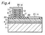
- the etching operation employed to form the stripe-shaped waveguide region in the present invention is such an. etching operation that forms a ridge waveguide having a cross section, for example, as shown in Fig. 1, that will be described in detail below following the p-side cladding layer and the p-side contact layer.
- the nitride semiconductor laser device of the present invention comprises an active layer with at least the p-side first cladding layer and the p-side second cladding layer stacked thereon successively, while the layers are etched from the p-side contact layer side thereby to form the stripe-shaped waveguide region.
- the active layer and the p-side cladding layer there is required no particular layer between the active layer and the p-side cladding layer, although a guide layer and/or a cap layer (in case the cap layer is provided separately from the cladding layer, the cap layer means the first cladding layer for carrier confinement and the cladding layer means the second cladding layer for light confinement) are provided as shown in the example described later.
- the p-side cladding layer is formed directly on the active layer, the p-side cladding layer is etched in a zone ranging from the interface between the p-side cladding layer and the active layer to a position where thickness of the p-side cladding layer is 0.1 ⁇ m, thereby to form the stripe-shaped waveguide region.
- etching may be effected up to the layer provided between the p-side cladding layer and the active layer as long as it is below the position where thickness of the p-side cladding layer is 0.1 ⁇ m and is above the light emitting layer.
- the waveguide region is preferably formed to such a depth that is capable of avoiding the deterioration, while the waveguide region is formed to such a depth that does not reach the p-side cap layer in the device structure shown in the drawing.
- the active layer may be of either single or multiple quantum well structure, and the layer may be doped with n-type or p-type impurity. InGaN is preferably used for the active layer or quantum well layer of the quantum well structure that constitutes the active layer.
- a nitride semiconductor layer that includes Al is preferably used.
- This layer may also comprise either a single layer or multiple layers, and specifically may have super lattice structure including AlGaN and GaN stacked one on another alternately as described in the examples. Moreover, this layer may be either doped with a p-type impurity or undoped.
- the cladding layer is preferably made of GaN doped with a p-type impurity.
- the p-side contact layer of the present invention is formed on the p-side cladding layer so that good ohmic contact with the electrodes is obtained.
- the laser device of the present invention becomes capable of oscillating in stable transverse mode in the fundamental (single) mode by controlling the with of the stripe in a range from 1 to 3 ⁇ m.
- Width of the stripe less than 1 ⁇ m makes it difficult to form the stripe and a width larger than 3 ⁇ m makes the transverse mode oscillation likely to occur in multiple modes.
- oscillating in stable transverse mode cannot be achieved when the width of the stripe is outside the range described above.
- the width is preferably controlled within a range from 1.2 to 2 ⁇ m, that improves the stability of the transverse mode oscillation in a region of higher optical output.
- the waveguide region according to the present invention will be described in detail below.
- Etching for the formation of the stripe-shaped waveguide region is done to a depth above the active layer and below a position where thickness of the p-side cladding layer from the active layer side is 0.1 ⁇ m, More specifically, the stripe-shaped waveguide region is formed by etching and the position of the nitride semiconductor that continues to both side faces of the stripe shows the depth of etching.
- the plane of the nitride semiconductor exposed by the etching is controlled to be below (direction of active layer) position where thickness of the p-side cladding layer is 0.1 ⁇ m in the direction of thickness and above (in the direction of the p-side contact layer) the active layer.
- the etching is done in the direction from the bottom end face of the p-side cladding layer toward the p-side contact layer deeper than the position of 0.1 ⁇ m (in the direction of active layer) and such a depth that the active layer is not exposed, thereby forming the stripe-shaped waveguide region.
- the statement of being below a position where thickness of the p-side cladding layer is 0.1 ⁇ m means a zone including the position of 0.1 ⁇ m. This is because, when the waveguide is formed by etching to a depth that does not reach the active layer, service life of the device is improved greatly, particularly in a region of higher optical output, exceeding 5mW, and oscillation over a longer period of time is made possible.
- the stripe is formed by etching in the direction of thickness of the p-side cladding layer (in the direction of the p-side contact layer) to the active layer side beyond 0.1 ⁇ m, stable oscillation in the transverse mode can be achieved in a wider range of optical output, specifically in a range up to several tens of milliwatts, providing current-optical output characteristic free of kink in this range.
- the laser device of the present invention that has the stripe-shaped waveguide region with the width of stripe and the etching depth being set as described above, is capable of stable oscillation in the single fundamental transverse mode without kink in a region of relatively high optical output from the moment of starting the laser oscillation, and provides a service life of such a practical level as over ten thousand hours with output of 5mW, or over one thousand hours with output of 30mW.
- the plane of the nitride semiconductor is exposed by etching to form the stripe-shaped waveguide region, so that the plane of the nitride semiconductor is formed in continuity with the stripe side faces. Therefore, position of the nitride semiconductor plane indicates the depth of etching for forming the stripe-shaped waveguide region.
- the position where thickness of the p-side cladding layer is 0.1 ⁇ m that represents the etching depth described above means a position 0.1 ⁇ m away from the bottom end face of the p-side cladding layer (active layer side) in the direction of the p-side contact layer, a position where film thickness is 0.1 ⁇ m away from the surface where the p-side cladding layer begins to grow, and meaning that the plane of the nitride semiconductor exposed by the etching is formed at a position where thickness of the p-side cladding layer in the waveguide region is 0.1 ⁇ m or less.
- the interface between the active layer and the p-side cladding layer There is no limitation as to the interface between the active layer and the p-side cladding layer. These layers may be in contact with each other, or separated by a p-side cap layer (first cladding layer for carrier confinement) and a p-side optical guide layer formed therebetween as in an embodiment described later.
- the active layer may be of quantum well structure, either single quantum well structure or multiple quantum well structure. Being located above the active layer means such a depth that does not reach a layer to be formed following a barrier layer/well layer formed at the last constituting the quantum well structure.
- Resonance wavelength of the nitride semiconductor of the present invention is preferably in a range from 400 to 900 ⁇ m which allows it to decrease the drive current by controlling the reflectivity of the mirrors located at both ends.
- the nitride semiconductor laser device of the present invention has high reliability, since insulation films made of a material other than Si oxide are formed on both side faces of the stripe exposed by etching and on the plane of the n-side optical guide layer that continues with the side faces, and electrodes are formed via the insulation film on the p-side contact layer surface that is the top layer of the stripe. This is because it has been difficult to form the layer with sufficiently reliable insulation by using an insulation film made of SiO 2 that is in common use, thus resulting in a device of lower reliability with increased threshold. Such a problem is solved by the use of the insulation film made of a material other than silicon oxide, with another advantage of having favorable effect on the stability of the transverse mode oscillation.
- the insulation film made of the material other than silicon oxide may be made of at least one kind of an oxide selected from among a group consisting of Ti, V, Zr, Nb, Hf and Ta and compounds BN, SiC and AlN, which makes it possible to obtain a laser device having high reliability. Also because the stripe is formed in a process to be described later, the stripe-shaped waveguide region with the range described above can be formed with good accuracy. For the insulation film, a thickness in a range from 500 to 5000 ⁇ is sufficient.
- the laser device of the present invention achieves good device characteristics by providing the stripe-shaped waveguide region.
- the stripe-shaped waveguide region of the laser device of the present invention can also be formed accurately and with a high yield of production, by forming the stripe in the process described below.
- the production process is as follows.
- the stripe formed by etching there is no limitation to the shape of the stripe formed by etching.
- the stripe may have a cross section of mesa of which width increases with depth as shown in Fig. 1, or inverted mesa of which width decreases with depth, or a rectangle of which width remains substantially constant.
- the cross section has a shape of mesa that tends to achieve stable transverse mode with oscillation in the fundamental mode.
- a pair of positive and negative electrodes are formed on the same side of a substrate of different kind as shown in Figs.1 and 2, an n-side contact layer that constitutes the negative electrode is exposed by etching to that depth and then etching to form the stripe-shaped waveguide region is carried out.
- Fig. 3 is a schematic sectional view showing a nitride semiconductor wafer for explaining the process of forming the electrodes of the present invention.
- the sectional view is along a direction perpendicular to the stripe-shaped waveguide region formed by etching, namely parallel to the resonance plane.
- a first protective film 61 of a stripe shape is formed on the p-side contact layer 13 that is located at the top.
- the first protective film 61 is not required to have insulating property, and may be made of any material that has difference in the etching rate from the nitride semiconductor.
- Si oxide including SiO 2
- photoresist may be used.
- a material that is more easily dissolved in an acid than a second protective film is used, in order to ensure a difference in solubility from the second protective film to be formed later.
- hydrofluoric acid is preferably used, and Si oxide is preferably used as a material that can be easily dissolved in hydrofluoric acid.
- Stripe width (W) of the first protective film is controlled within a range from 3 ⁇ m to 1 ⁇ m. Stripe width of the first protective film 61 corresponds substantially to the stripe width in the waveguide region.
- Figs.3A and 3B show specific processes of forming the first protective film 61.
- the first protective film 61 is formed over substantially the entire surface of the p-side contact layer 13, and then a third protective film 63 of stripe shape is formed on the first protective film 61.
- the first protective film 61 is etched with the third protective film 63 left remaining on, followed by the removal of the third protective film 63, thereby forming the first protective film 61 of stripe shape shown in Fig. 3C.
- the etching may also be done from the p-side contact layer 13 side by changing the gas or the means of etching, with the third protective film 63 left remaining on.
- the first protective film 61 of stripe shape shown in Fig. 3C may also be formed by employing lift-off process. That is, a photoresist film having apertures of stripe configuration is formed and the first protective film is formed over the entire surface of the photoresist film, followed by dissolving and removing the photoresist, thereby leaving only the first protective film that is in contact with the p-side contact layer.
- lift-off process stripe of better shape with substantially vertical end face can be formed through the etching process shown in Figs.3A and 3B.
- etching is done via the first protective film 61 from the p-side contact layer 13 in the portion where the first protective film 61 is not formed, thereby forming the stripe-shaped waveguide region that corresponds to the configuration of the protective film right below the first protective film 61.
- Structure and characteristics of the laser device vary depending on the position where etching is to be stopped.
- etching such as RIE (reactive ion etching)
- a gas of fluorine compound such as CF 4
- CF 4 a gas of fluorine compound
- use of gas of a chlorine compound such as Cl 2 , CCl 4 and SiCl 4 that are frequently used for other III-V group compound semiconductors is desirable because higher selectivity with respect to the Si oxide can be achieved, for etching the nitride semiconductor.
- the second protective film 62 that is made of a material different from that of the first protective film 61 is formed on the side faces of the stripe-shaped waveguide region and on the plane of the nitride semiconductor (p-side cladding layer 12 in Fig. 3E) that is exposed by etching. Because the first protective film 61 is made of a material different from that of the second protective film 62, the etching proceeds selectively with respect to the first protective film 61.
- the second protective film 62 can be formed that continues to both the surface of the p-type cladding layer 12 (nitride semiconductor plane exposed by etching) and the side faces of the stripe as shown in Fig. 3F. High insulation performance can be maintained by forming the second protective film continuously. Moreover, since forming the second protective film 62 continuously over the first protective film 61 enables it to form the film with uniform thickness on the p-side cladding layer 12, unevenness in the film thickness is unlikely to occur and current concentration due to unevenness in the film thickness can be prevented from occurring.
- etching in the second process is stopped amid the p-side cladding layer 12
- the second protective film is formed on the plane of the nitride semiconductor layer where etching is stopped, provided that the etching is stopped below the p-side cladding layer 12 while the second protective film 62 is formed on the plane of the p-side cladding layer 12 in Fig. 3E.
- the second protective film is made of a material other than SiO 2 , preferably made of at least one kind of oxide that includes at least one element selected from among a group consisting of Ti, V, Zr, Nb, Hf and Ta and at least one kind among compounds SiN, BN, SiC and AlN.
- a material other than SiO 2 preferably made of at least one kind of oxide that includes at least one element selected from among a group consisting of Ti, V, Zr, Nb, Hf and Ta and at least one kind among compounds SiN, BN, SiC and AlN.
- some of these materials have some solubility to hydrofluoric acid, fairly higher reliability than that of SiO 2 can be achieved by forming the insulation layer of the laser device in the form of embedded layer.
- Thin films formed from oxides in a vapor phase process such as PVD or CVD tend to have lower reliability with respect to the insulation performance of the thin oxide film, since it is difficult to make the element and oxygen react in stoichiometrical proportions in forming an oxide.
- the oxides of the elements described above, BN, SiC and AlN selected according to the present invention have reliability with respect to the insulation performance that is higher than that of Si oxide. Further, when an oxide having a refractive index lower than that of the nitride semiconductor (for example, other than SiC) is selected, an embedded layer that is very favorable for the laser device can be obtained.
- the second protective film 62 having uniform thickness can be formed as shown in Fig. 3F by removing the first protective film 61 in the lift-off process.
- the first protective film 61 is removed as shown in Fig. 3F. Then as shown in Fig. 3G, a p electrode electrically connecting to the p-side contact layer is formed on the second protective film 62 and on the p-side contact layer 13.
- the second protective layer is formed earlier, there is no need to restrict the formation of the p electrode only on the contact layer of small stripe width and, instead, the p electrode may be formed over a large area.
- an electrode that combines the functions of ohmic electrode and bonding electrode can be formed together by selecting an electrode material that also provides ohmic contact.
- the second protective film is made of a material other than SiO 2 thereby achieving selectivity with respect to the first protective film. Also because the nitride semiconductor is not etched after forming the second protective film, there occurs no problem of difference in the etching rate between the second protective film and the nitride semiconductor.
- the nitride semiconductor laser device of the present invention comprises an n-type nitride semiconductor layer, an active layer and a p-type nitride semiconductor layer stacked on a substrate, and has ridge structure of stripe shape formed by etching from the p-type nitride semiconductor side.
- the nitride semiconductor laser device of the present invention has a ridge waveguide formed on the p-side optical guide layer upward over the active layer. That is, an n-side optical guide layer made of n-type nitride semiconductor, the active layer and the p-side optical guide layer made of p-type nitride semiconductor are stacked on the substrate, wherein the p-side optical guide layer has a protruding portion of stripe shape and a stripe-shaped waveguide region.
- the laser device of the present invention is a refractive index guiding type laser device having the stripe-shaped waveguide region.
- the laser device of the present invention is made by stacking the n-side optical guide layer made of the n-type nitride semiconductor, the active layer, the p-side optical guide layer made of the p-type nitride semiconductor and a p-type nitride semiconductor layer, then part of the p-type nitride semiconductor layer and part of the p-side optical guide layer are removed by etching from the p-type nitride semiconductor layer side, thereby forming the stripe structure. Since height of the protruding portion of the p-side optical guide layer is determined by the depth of etching, controllability of the depth of etching is improved over the prior art as will be described later. It is important to carry out etching to such a depth that does not reach the active layer, and etching in the present invention is carried out to the position of the p-side optical guide layer.
- the shape of the protruding portion of the p-side optical guide layer or the shape of the stripe-shaped ridge waveguide are not limited to mesa or inverted mesa configuration, mesa configuration is preferable because of the tendency thereof to allow better control of the transverse mode oscillation.
- etching the nitride semiconductor layer such as the formation of the p-side optical guide layer or the ridge waveguide
- processes as wet etching and dry etching may be employed.
- dry etching for example, there are reactive ion etching, (RIE), reactive ion beam etching, (RIBE), electron cyclotron etching (ECR), ion beam etching and other processes, and the nitride semiconductor layer can be etched by any of these processes by selecting a proper etching gas.
- the waveguide is formed by such a structure as the active layer is sandwiched by the n-side optical guide layer and the p-side optical guide layer.
- the laser device of the present invention has the stripe-shaped waveguide region formed by providing the p-side optical guide layer with the protruding portion of stripe shape.
- the p-side optical guide layer has the protruding portion of stripe shape, and the p-type nitride semiconductor layer is formed on the protruding portion thereby to form the laser device.
- the laser device has the ridge waveguide formed with the p-side optical guide layer.
- the protruding portion is formed by etching from the p-type nitride semiconductor side as described above, while stopping the etching process in the p-side optical guide layer.
- the p-side optical guide layer has the protruding portion of stripe shape and thickness thereof (at the protruding portion) is 1 ⁇ m or less. Thickness here refers to the thickness of growing the p-side optical guide layer.
- the protruding portion is formed by the etching process described above after forming the p-side optical guide layer
- the protruding portion is formed by removing a part of the p-side optical guide layer of the predetermined thickness, and consequently thickness of the p-side optical guide layer becomes equal to thickness of the protruding portion.
- Thickness of the p-side optical guide layer namely thickness of the protruding portion, is preferably in a range from 1.500 ⁇ to 4000 ⁇ inclusive.
- the ridge waveguide and the protruding portion When forming the ridge waveguide and the protruding portion by etching, productivity must be taken into consideration. As the depth of etching increases, variability among the devices provided on a wafer increases which must be avoided. Specifically, when the protruding portion of stripe shape (ridge structure) is formed by etching to a depth greater than 0.7 ⁇ m, the problem described above suddenly becomes predominant, and therefore the etching is preferably restricted to a smaller depth.
- the ridge height is controlled in the present invention, and the laser device is preferably formed within the range described above.
- the ridge height refers to the height of the p-type nitride semiconductor, that is formed on the protruding portion, from the plane of the p-side optical guide layer in a region other than the protruding portion, namely the plane being exposed by etching and continuing to the side face of the protruding portion.
- Height of the protruding portion refers to the height of the top surface of the protruding portion from the plane; while the top surface of the p-type nitride semiconductor layer is the starting position of etching.
- the p-side optical guide layer is etched to such a depth that leaves a region of thickness of 500 ⁇ or more, preferably in a range from 500 ⁇ to 1500 ⁇ to remain, in forming the protruding portion of the p-side optical guide layer.
- the thickness is set to within a range from 500 ⁇ to 1000 ⁇ , which improves the oscillation at the threshold and the controllability of the transverse mode of the laser device.
- the composition of the p-side optical guide layer that is required only to be made of nitride semiconductor and have such an energy band gap that is sufficient to form the waveguide, and may have either single layer or multiple layer structure.
- undoped GaN is used for wavelengths from 370 to 470 nm
- a multiple layer structure of InGaN/GaN is used for longer wavelengths.
- total thickness thereof namely thickness of the region interposed between the two guide layers, is preferably 6000 ⁇ or less, or more preferably 4500 ⁇ or less.
- the threshold current of oscillation increases abruptly thereby making it extremely difficult to achieve continuous oscillation in the fundamental mode.
- the total thickness of the waveguide is less than 4500 ⁇ , such an increase in the threshold current of oscillation is suppressed thus making it possible to achieve continuous oscillation in the fundamental mode with longer service life.
- the n-side optical guide layer may be formed to substantially the same thickness as the p-side optical guide layer in such a structure as to sandwich the active layer with the two guide layers.
- the n-side optical guide layer is preferably formed by growing GaN, InGaN, and specifically such a multiple layer structure may be employed as undoped GaN, InGaN with the proportion of In decreasing toward the active layer, and GaN are stacked alternately.
- InGaN means a ternary mixed crystal.
- the p-type nitride semiconductor layer formed on the p-side optical guide layer comprises the p-side cladding layer, the p-side contact layer and the like being stacked one on another as shown in the embodiment. Accordingly, in the present invention, the p-type nitride semiconductor layer formed on the protruding portion of the p-side optical guide layer is formed in the shape of stripe, thereby forming the ridge waveguide.
- a cap layer may be formed between the optical guide layer and the active layer.
- a p-side cap layer made of Al x Ga 1-x N (0 ⁇ x ⁇ 1) doped with a p-type impurity is formed between the active layer and the p-side optical guide layer.
- the structure having the protruding portion of stripe shape provided on the p-side optical guide layer, further the structure having the ridge waveguide is preferable in such a case, too.
- the stripe width of the ridge waveguide, or the stripe width of the protruding portion of the p-side optical guide layer in a range from 1 to 3 ⁇ m inclusive. Within this range, oscillation in the single transverse mode can be achieved in relatively good condition, and stable control of the beam profile with high accuracy (good F.F.P.) can be achieved as the ridge waveguide is formed with the p-side optical guide layer.
- the width is less than 1 ⁇ m, it becomes difficult to produce the ridge structure of stripe shape or the protruding portion, resulting in a decreased yield of production.
- the width is larger than 3 ⁇ m, it becomes difficult to control the horizontal transverse mode.
- the nitride semiconductor used to make the nitride semiconductor laser device of the present invention may be In x Al y Ga 1-x-y N (0 ⁇ x ⁇ 1, 0 ⁇ y ⁇ 1, 0 ⁇ x + y ⁇ 1), in the form of ternary mixed crystal. quarternary mixed crystal or the like as well as gallium nitride. According to the present invention, it is preferable to make the laser device formed on the substrate from the nitride semiconductor of the composition described above, since it achieves the best control of the transverse mode and beam profile of the laser beam.
- Horizontal direction (x direction) in F.F.P. refers to a direction (direction of arrow d in the drawing) parallel to the junction plane (or pn junction plane) shown in Fig. 11, and the transverse mode in this direction is called the horizontal transverse mode.
- Fig. 11 is a schematic diagram for explaining the optical characteristic of the laser device of the present invention, particularly the spot shape at the light emerging plane and the far field image (F.F.P.) (A).
- the spot shape (a) at the light emerging plane spreads in the direction parallel to the junction plane, with a narrow angle in x direction in F.F.P. within 10°C and poor aspect ratio.
- the longitudinal direction of the spot profile lies in the horizontal direction similarly to the prior art as shown in the drawing, spread in the longitudinal direction is narrower and the angle in x direction in F.F.P. (A) increases to 12°C or up to 20°C, with satisfactory aspect ratio of around 2.0.
- the laser device has the stripe-shaped waveguide region that has good effective refractive index that is formed by means of the p-side optical guide layer which has the protruding portion of stripe shape, as described above.
- the thickness of the p-side optical guide layer, or the total thickness of the p-side optical guide layer and the n-side optical guide layer is increased compared to the prior art, as described above, spread of the beam in direction a (y direction) perpendicular to the junction plane in the drawing is suppressed due to the decreasing effect of diffraction, which also contributes to the improvement of the optical characteristic, particularly the aspect ratio, of the laser device of the present invention.
- the nitride semiconductor laser device of the present invention has such a structure as the n-side optical guide layer made of n-type nitride semiconductor, the active layer and the p-side optical guide layer made of p-type nitride semiconductor are stacked on the substrate, similarly to that of the second embodiment shown in Fig. 17, except that the thickness of the p-side optical guide layer is larger than the thickness of the n-side optical guide layer.
- the nitride semiconductor laser device of the present invention is made by sandwiching the active layer with the p-side optical guide layer and the n-side optical guide layer thereby to form the waveguide, while the thickness of the p-side optical guide layer is made larger than the thickness of the n-side optical guide layer, so that good laser beam can be achieved.
- This is for the purpose of extracting good laser beam by differentiating the thickness between the p-side optical guide layer and the n-side optical guide layer that sandwich the active layer, thereby shifting the light' distribution from the gain distribution in the direction of thickness and changing the transverse mode control from that of the prior art.
- the effect of light confinement is also enhanced thereby suppressing the occurrence of ripple.
- the nitride semiconductor laser device of the present invention has the structure of refractive index guiding type, where control of the transverse mode is enhanced by providing the stripe-shaped waveguide region in addition to such a structural feature that the thickness of the optical guide layers is asymmetrical with respect to the active layer interposed therebetween. That is, the n-side optical guide layer made of n-type nitride semiconductor, the active layer and the p-side optical guide layer made of p-type nitride semiconductor are stacked on the substrate, wherein the p-side optical guide layer has a protruding portion of stripe shape and the stripe-shaped waveguide region is procvided.
- the laser device of the present invention has the p-type nitride semiconductor layer formed on the protruding portion, and is specifically a refractive index guiding type laser device having the stripe-shaped waveguide region.
- the laser device of the present invention is made by stacking the n-side optical guide layer made of the n-type nitride semiconductor, the active layer, the p-side optical guide layer made of the p-type nitride semiconductor and the p-type nitride semiconductor layer, while a part of the p-type nitride semiconductor layer and a part of the p-side optical guide layer are removed by etching from the p-type nitride semiconductor layer side, thereby forming the stripe structure. Since the height of the protruding portion of the p-side optical guide layer is determined by the depth of etching, controllability of the depth of etching is improved over the prior art as will be described later. It is important to carry out etching to such a depth that does not reach the active layer, and etching in the present invention is carried out to the position of the p-side optical guide layer.
- the shape of the protruding portion of the p-side optical guide layer or the shape of the stripe-shaped ridge waveguide are not limited to mesa or inverted mesa configuration, mesa configuration is preferable because of the tendency thereof to allow control of good transverse mode.
- etching the nitride semiconductor such as the formation of p-side optical guide layer or the ridge waveguide
- processes as wet etching and dry etching may be employed.
- dry etching for example, there are reactive ion etching (RIE), reactive ion beam etching, (RIBE), electron cyclotron etching (ECR), ion beam etching and other processes, and nitride semiconductor can be etched by any of these processes by selecting a proper etching gas.
- RIE reactive ion etching
- RIBE reactive ion beam etching
- ECR electron cyclotron etching
- nitride semiconductor can be etched by any of these processes by selecting a proper etching gas.
- the waveguide is formed by such a structure as the active layer is sandwiched with the n-side optical guide layer and the p-side optical guide layer.
- the laser device of the present invention has the stripe-shaped waveguide region formed by providing the p-side optical guide layer with the protruding portion of stripe shape.
- the n-side optical guide layer and the p-side optical guide layer that sandwich the active layer have different thicknesses, with the p-side optical guide layer being made thicker.
- the p-side optical guide layer has the protruding portion of stripe shape, and the p-type nitride semiconductor is formed on the protruding portion thereby to form the laser device having the stripe-shaped waveguide region.
- the laser device has the ridge waveguide formed with the p-side optical guide layer.
- the protruding portion is formed by etching from the p-type nitride semiconductor layer side as described above, while stopping the etching process in the p-side optical guide layer.
- Thickness of the p-side optical guide layer here refers to the thickness of growing the p-side optical guide layer.
- the protruding portion is formed by the etching process described above after forming the p-side optical guide layer, the protruding portion is formed by removing a part of the p-side optical guide layer of the predetermined thickness, and consequently the thickness of the p-side optical guide layer becomes equal to the thickness of the protruding portion.
- the thickness of the p-side optical guide layer is greater than 1 ⁇ m, the value of threshold greatly increases to make laser oscillation very difficult and, even when the laser can oscillate, the laser device has extremely short service life.
- the thickness of the p-side optical guide layer is made not larger than 1 ⁇ m. More preferably, the thickness of the p-side optical guide layer, namely the thickness of the protruding portion, is in a range from 1500 ⁇ to 5000 ⁇ inclusive. This is because, when the thickness is less than 1500 ⁇ , good F.F.P. of laser light cannot be achieved and, when the thickness is larger than 5000 ⁇ , threshold current of oscillation tends to increase. Specifically, when the thickness is less than 1500 ⁇ , horizontal transverse mode cannot be controlled sufficiently, while F.F.P. becomes a beam profile of 10°C or larger in x direction, resulting in an aspect ratio that is higher than 2.0.
- the ridge waveguide and the protruding portion When forming the ridge waveguide and the protruding portion by etching, productivity must be taken into consideration. As the depth of etching increases, variability in accuracy among the devices provided on the wafer increases which must be avoided. Specifically, when the protruding portion of stripe shape (ridge structure) is formed by etching to a depth greater than 0.7 ⁇ m, the problem described above suddenly becomes predominant, and therefore the etching is preferably restricted to a smaller depth.
- the ridge height is controlled in the present invention, and the laser device is preferably formed within the range described above.
- Height of the protruding portion refers to the height of the protruding portion from the plane of the p-side optical guide layer in a region other than the protruding portion, namely the plane being exposed by etching and continuing to the side face of the protruding portion.
- the ridge height refers to the height of the p-type nitride semiconductor layer formed on the protruding portion from the plane while the top surface of the p-type nitride semiconductor layer is the starting position of etching.
- the height of the protruding portion in the p-side optical guide layer since it causes the threshold current of oscillation to decrease. That is, increasing the depth of etching improves the stability of the output, thereby making a great contribution to the application of the laser device. Specifically, even when the output increases, such effects are obtained as achieving stable oscillation in the single mode, while suppressing the deterioration of the device because of the favorable threshold current of oscillation and achieving continuous oscillation with a longer service life.
- the height of the protruding portion by setting the height of the protruding portion not less than 100 ⁇ , the laser device having satisfactory beam profile is obtained.
- the height is preferably 500 ⁇ or larger, which makes it possible to oscillate in the single mode even with a high output. Thus reliability required for the applications of the laser device is sufficiently ensured.
- the p-side optical guide layer is etched to such a depth that leaves a region of thickness of 500 ⁇ or more, preferably in a range from 500 ⁇ to 1000 ⁇ to remain, during formation of the protruding portion of the p-side optical guide layer.
- the composition of the p-side optical guide layer that is required only to be made of nitride semiconductor and have an energy band gap sufficient to form the waveguide, and may have either single layer or multiple layer structure.
- undoped GaN is used for wavelengths from 370 to 470 nm
- a multiple layer structure of InGaN/GaN is used for longer wavelengths.
- total thickness thereof namely thickness of the region interposed between the two guide layers, is preferably 5000 ⁇ or less, and more preferably 4500 ⁇ or less. This is because, when the total thickness of the waveguide is greater than 5000 ⁇ , the threshold current of oscillation increases abruptly thereby making it extremely difficult to achieve continuous oscillation in the fundamental mode. When the total thickness of the waveguide is less than 4500 ⁇ , such an increase in the threshold current of oscillation is suppressed thus making it possible to achieve continuous oscillation in the fundamental mode with longer service life.
- the n-side optical guide layer is thinner than the p-side optical guide layer, and what is required is only that the waveguide has such a structure as the active layer is sandwiched with the two guide layers.
- the n-side optical guide layer is preferably formed by growing GaN, InGaN, and specifically such a multiple-layer structure may be employed as undoped GaN, InGaN wile the proportion of In in the mixed crystal decreases toward the active layer, and GaN are stacked alternately.
- InGaN refers to a ternary mixed crystal where In is included in GaN.
- the p-type nitride semiconductor layer formed on the p-side optical guide layer comprises the p-side cladding layer, the p-side contact layer and the like stacked one on another as shown in the embodiment. Accordingly, in the present invention, the p-type nitride semiconductor layer formed on the protruding portion of the p-side optical guide layer is formed in the shape of stripe, thereby forming the ridge waveguide.
- a cap layer may be formed between the optical guide layer and the active layer.
- a p-side cap layer made of Al x Ga 1-x N (0 ⁇ x ⁇ 1) doped with a p-type impurity is formed between the active layer and the p-side optical guide layer.
- the ridge waveguide is preferably formed in such a structure that has the protruding portion of stripe shape being provided on the p-side optical guide layer.
- the stripe width of the ridge waveguide, or the stripe width of the protruding portion of the p-side optical guide layer in a range from 1 to 3 ⁇ m inclusive. Within this range, oscillation in the single transverse mode can be achieved in relatively good condition, and stable control of the beam profile with high accuracy (good F.F.P.) can be achieved as the ridge waveguide is formed with the p-side optical guide layer.
- the width is less than 1 ⁇ m, it becomes difficult to produce the ridge structure of stripe shape or the protruding portion, resulting in a decreased yield of production.
- the width is larger than 3 ⁇ m, it becomes difficult to control the horizontal transverse mode.
- the nitride semiconductor used to make the nitride semiconductor laser device of the present invention may be In x Al y Ga 1-x-y N (0 ⁇ x ⁇ 1, 0 ⁇ y ⁇ 1, 0 ⁇ x + y ⁇ 1), in the form of ternary mixed crystal, quarternary mixed crystal or the like as well as gallium nitride. According to the present invention, it is preferable to make the laser device formed on the substrate from the nitride semiconductor of the composition described above, since it achieves the best control of the transverse mode and beam profile of the laser beam.
- Horizontal direction (x direction) in F.F.P. refers to a direction parallel to the junction plane (or pn junction plane), and x direction (d) of far field image (F.F.P.) (A) shown in Fig. 20, while the transverse mode in this direction is called the horizontal transverse mode.
- the optical guide layers that sandwich the active layer are made in such an asymmetrical structure as the p-side optical guide layer is made thicker than the n-side optical guide layer, wherein light distribution in the waveguide region sandwiched by the two optical guide layers is shifted from that of the laser device of the prior art, namely the light distribution and the gain distribution are shifted thereby to control the transverse mode by a method different from that of the prior art, thereby to obtain the laser beam of the desired beam profile.
- the p-side optical guide layer has the protruding portion of stripe shape, thereby to form the stripe-shaped waveguide region and achieve the effective refractive index distribution as described above.
- laser spot (a) that is the emerging light is shifted to the side of the p-side optical guide layer 109 that has the protruding portion of stripe shape, thereby achieving satisfactory control of the horizontal transverse mode, as shown in Fig. 20.
- the aspect ratio is greatly improved over that of the prior art because of the satisfactory control of the horizontal transverse mode in the present invention, compared to the laser device of stripe structure of the prior art having narrow F.F.P. in the horizontal direction (x direction) and aspect ratio of 3 or higher.
- the active layer is made of nitride semiconductor that includes In, for example ternary mixed crystal of InGaN
- the laser device of the present invention since laser light is obtained through waveguide that is different from that of the prior art because of the p-side optical guide layer being thicker among the optical guide layers sandwiching the active layer as described above, loss by the light diffusive substance is decreased so as to compensate for the increase in the threshold current due to the increased thickness of the optical guide layer.
- the light distribution in the waveguide shifts from the gain distribution in the direction of thickness, so that light is distributed and guided in a place offset from the region (active layer) including the light diffusive substance.
- the loss due to the diffusion of light decreases thus making it possible to oscillate with threshold current similar to or less than that of the prior art.
- the tendency of the threshold current to increase is restricted by increasing the thickness of the optical guide layer, particularly the thickness of the p-side optical guide layer over the prior art, thereby decreasing the loss due to the diffusion of light in the present invention, so that the laser device of good beam profile can be obtained with a threshold current similar to that of the prior art.
- the spot (a) in the emerging surface is spread in the direction parallel to the junction plane and the angle in x direction (d) in F.F.P. is as small as 10°C or less with poor aspect ratio.
- the longitudinal direction of the spot profile lies in the horizontal direction similarly to the prior art as shown in the drawing, spread in the longitudinal direction is narrower and the angle in x direction in F.F.P. (A) increases to 12°C or up to 20°C, with satisfactory aspect ratio of around 2.0.
- the laser device has the stripe-shaped waveguide region that has good effective refractive index which is formed by means of the p-side optical guide layer having the protruding portion of stripe shape, as described above.
- the thickness of the p-side optical guide layer, or the total thickness of the p-side optical guide layer and the n-side optical guide layer is increased compared to the prior art, as described above, spread of the beam in a direction (y direction) perpendicular to the junction plane in the drawing is suppressed due to the decreasing effect of diffraction, which also contributes to the improvement of the optical characteristic, particularly the aspect ratio, of the laser device of the present invention.
- the p-type cap layer namely the first cladding layer for light confinement is formed on the active layer.
- the p-type first cladding layer is preferably made of Al d Ga 1-d N (0 ⁇ d ⁇ 1) doped with Mg, with the value of d being set in a range from 0.1 to 0.5 inclusive, and more preferably 0.35 or less. Crystal mixing proportion described above is used for the first cladding layer of the present invention, of which detail will be described later.
- Total thickness of the p-type first cladding layer is set in a range from 10 to 1000 ⁇ inclusive, and preferably in a range from 20 to 400 ⁇ inclusive.
- the reason for setting the thickness of the p-type first cladding layer in this range is as follows.
- the carrier confinement function can be effectively achieved when the p-type first cladding layer is made of AlGaN, the AlGaN layer has larger bulk resistance than gallium nitride semiconductor that does not include Al. Thus it is necessary to suppress the increase in the resistance of the light emitting device due to the formation of the p-type first cladding layer, which is the reason for setting the thickness within 1000 ⁇ and preferably within 400 ⁇ .
- Major function of the p-type first cladding layer is to confine the carriers as described above.
- thickness of the layer is set to 10 ⁇ or more, and preferably 20 ⁇ or more.
- the carriers can be effectively confined within the active layer 6, and the bulk resistance can be restricted to a low level.
- Concentration of Mg with which the p-type first cladding layer is doped is preferably in a range from 1 ⁇ 10 19 /cm 3 to 1 ⁇ 10 21 /cm 3 .
- Mg diffuses into the p-type guide layer that is grown in the undope process described later, in addition to a decrease in the bulk resistance, and Mg can be included with a concentration from 1 ⁇ 10 16 /cm 3 to 1 ⁇ 10 18 /cm 3 in the p-type guide layer that is a relatively thin layer.
- the p-type first cladding layer of this embodiment may be formed from two layers of a first p-type nitride semiconductor layer made of Al a Ga 1-a N and a second p-type nitride semiconductor layer made of Al b Ga 1-b N formed thereon, the present invention is not limited to this configuration.
- the p-type first cladding layer may also be formed from more than two layers or, for example, the second nitride semiconductor layer may comprise a plurality of layers stacked one on another.
- the proportion of Al included in the mixed crystal of the layers there is no limitation to the proportion of Al included in the mixed crystal of the layers.
- the first p-type nitride semiconductor layer made of Al a Ga 1-a N decomposition of the active layer can be effectively suppressed by setting the proportion a of Al included in the mixed crystal to 0 or larger in the first p-type nitride semiconductor.
- good offset from the active layer can be provided (potential barrier can be formed) and satisfactory injection of carriers without carrier overflow can be achieved by setting the proportions a and b of Al included in the mixed crystal preferably larger than 0.1, more preferably 0.2 or larger in the first p-type nitride semiconductor layer and the second p-type nitride semiconductor layer.
- it is desirable that the firstp-type nitride semiconductor and the second p-type nitride semiconductor have the same composition, namely a b.
- the first p-type nitride semiconductor layer and the second p-type nitride semiconductor layer can be formed under stable condition with high accuracy.
- the second p-type nitride semiconductor layer it is preferable to grow the second p-type nitride semiconductor layer at a temperature higher than that for the first p-type nitride semiconductor layer.
- the first p-type nitride semiconductor layer is preferably grown at 800 °C or higher temperature, more preferably around 850 to 950°C, similar to the temperature at which the active layer is grown.
- Growing temperature of the second p-type nitride semiconductor layer is set preferably about 100°C higher than the growing temperature of the active layer, for example, which makes it possible to form the AlGaN layer of good crystallinity.
- the first p-type nitride semiconductor layer and the second p-type nitride semiconductor layer are preferably grown in substantially the same atmosphere as that for the active layer, which makes it possible to prevent the active layer from being decomposed.
- the second p-type nitride semiconductor layer is grown in such an atmosphere that is favorable for forming a good offset.
- the first p-type nitride semiconductor layer can have the function to prevent the active layer from being decomposed, and the second p-type nitride semiconductor layer can achieve good offset, due to the difference in the conditions of growing the crystals in the two layers.
- the layers having the functions described above can be formed by growing the first p-type nitride semiconductor layer in N 2 atmosphere and the second p-type nitride semiconductor layer in H 2 atmosphere, resulting in the device having good light emitting characteristic.
- the p-type first cladding layer is formed from at least two layers, it is preferable that thickness of the first p-type nitride semiconductor layer is set in a range from 10 to 100 ⁇ , and thickness of the second p-type nitride semiconductor layer is set in a range from 10 to 300 ⁇ , for the purpose of restricting the increase in Vf (forward voltage) of the light emitting element due to the formation of the p-type first cladding layer.
- Vf forward voltage
- thickness of the first p-type nitride semiconductor layer is set in a range from 10 to 30 ⁇
- thickness of the second p-type nitride semiconductor layer is set in a range from 10 to 100 ⁇
- the p-type guide layer is grown on the p-type first cladding layer.
- the p-type guide layer is preferably formed by growing a nitride semiconductor layer made of undoped GaN. Thickness is preferably in a range from 0.1 to 0.07 ⁇ m. When the thickness is in this range, the threshold can be decreased. While the p-type guide layer is grown as an undoped layer as described above, Mg included as the dopant in the p-type first cladding layer 7 diffuses so that Mg is included with a concentration in a range from 1 ⁇ 10 16 /cm 3 to 1 ⁇ 10 18 /cm 3 .
- the p-type second cladding layer is formed on the p-type guide layer similarly to the embodiment described above, thereby achieving light confinement.
- Fig. 2 is a sectional view showing the structure of the laser device according to an example of the present invention. In this drawing, the device which is cut in the perpendicular direction to the stripe waveguide is shown. Example 1 will be described with reference to Fig. 1.
- An auxiliary substrate made of C-face sapphire of one-inch ⁇ was set in the MOVPE reactor and the temperature was adjusted to 500 °C.
- a buffer layer made of GaN which had a thickness of about 200 angstroms was grown using trimethylgallium (TMG) and ammonia (NH 3 ).
- a nitride semiconductor layer 4 made of undoped GaN was grown to the thickness of 4 ⁇ m. This layer acts as an underlying layer for growth of each layer which constitutes a device structure.
- an n-side contact layer 5 made of GaN doped with Si to 3 ⁇ 10 18 /cm 3 was grown to the thickness of 4 ⁇ m at 1050 °C.
- a crack preventing layer 6 made of In 0.06 Ga 0.94 N was grown to the thickness of 0.15 ⁇ m. This crack preventing layer may be omitted.
- a layer made of undoped Al 0.16 Ga 0.84 N was grown to the thickness of 25 angstroms using TMA (trimethylaluminium), TMG and ammonia. Subsequently, TMA was stopped and the silane gas was flown. A layer made of n-type GaN doped with Si to 1 ⁇ 10 19 /cm 3 was .grown to the thickness of 25 angstroms. These layers were laminated alternately to form a super lattice layer, resulting in an n-side cladding layer 7 in a super lattice structure with a total thickness of 1.2 ⁇ m.
- n-side optical waveguide layer 8 made of undoped GaN was grown to the thickness of 0.1 ⁇ m at 1050 °C.
- the n-side optical waveguide layer 8 may be doped with an n-type impurity.
- a barrier layer made of In 0.05 Ga 0.95 N doped with Si was grown to the thickness of 100 angstroms.
- a well layer made of undoped In 0.2 Ga 0.8 N was grown to the thickness of 40 angstroms.
- Two barrier layers and two well layers were laminated alternately and at the last, a barrier layer was laminated, with the result that the active layer in the multiple quantum well structure (MQW) having a total thickness of 380 angstroms was obtained.
- the active layer may be undoped like in this example and may be doped with an n-type impurity and/or a p-type impurity.
- Both of the well layer and the barrier layer may be doped with an impurity, or either one may be doped. And when only barrier layer is doped with an n-type impurity, the threshold tends to decrease.
- a p-side capping layer 7 made of Al 0.3 Ga 0.7 N doped with Mg to 1 ⁇ 10 20 /cm 3 and having a band gap energy larger than that of the p-side optical waveguide layer 11 was grown to the thickness of 300 angstroms, using TMG, TMA, ammonia and Cp2Mg (cyclopentadienyl magnesium).
- a p-side optical waveguide layer 11 made of undoped GaN and having a band gap energy lower than that of the p-side capping layer 10 was grown to the thickness of 0.1 ⁇ m.
- This p-side optical waveguide layer 8 was undoped, that is, intentionally undoped, but due to the diffusion of Mg from the adjacent p-side first cladding layer and p-side second cladding layer, the real concentration of Mg was 5 ⁇ 10 16 /cm 3 , resulting in the layer doped with Mg.
- a layer made of undoped Al 0.16 Ga 0.84 N was grown to the thickness of 25 angstroms.
- Cp2Mg and TMA were stopped and a layer made of undoped GaN was grown to the thickness of 25 angstroms.
- a p-side cladding layer 12 in a super lattice structure was grown to a total thickness of 0.6 ⁇ m.
- the p-side cladding layer is a super lattice layer formed by laminating nitride semiconductor layers at least one of which contains Al and which have different band gap energies from each other, either one layer may be doped with an impurity in a larger amount, what is called modulation doping, with the result that the crystallinity tends to increase. But both layers may be doped in the same amout.
- the cladding layer 12 is preferably in the super lattice structure including a nitride semiconductor layer containing Al, preferably Al X Ga 1-X N (0 ⁇ X ⁇ 1). More preferably, the cladding layer 12 is in the super lattice structure formed by laminating GaN and AlGAN.
- the mixing proportion of Al in the entire cladding layer can be increased and then, the refractive index of the cladding layer itself decreases. Moreover, the band gap energy becomes large, resulting in the decrease of the threshold. Further, the number of the pits occurring in the cladding layer in the super lattice structure is smaller than that not in the super lattice structure, resulting in the decrease of the provability of the short circuit.
- a p-side contact layer 13 made of p-type GaN doped with Mg to 1 ⁇ 10 20 /cm 3 was grown to the thickness of 150 angstroms.
- the p-side contact layer may be made of p-type In X Al Y Ga 1-X-Y N (0 ⁇ X, 0 ⁇ Y, X+Y ⁇ 1) and preferably, the p-side contact layer may be made of GaN doped with Mg, thereby most preferable ohmic contact with the p-electrode 20 can be obtained.
- the contact layer 13 is a layer where an electrode is formed, it is desirable that the carrier concentration is as high as not less than 1 ⁇ 10 17 /cm 3 . If the carrier concentration is less than 1 ⁇ 10 17 /cm 3 , it is difficult to obtain a good ohmic contact with the electrode. If the composition of the contact layer is GaN, it is easy to obtain a good ohmic contact with the electrode material.
- the resulting wafer on which the nitride semiconductor had been grown was removed out of the reactor.
- a protective film of SiO 2 was formed on the top surface of the p-side contact layer which was an uppermost layer and etching was conducted with SiC 14 gas by RIE (reactive ion etching), to expose the surface of the n-side contact layer 5 on which an n-electrode was to be formed, as shown in Fig. 1.
- SiO 2 is most preferable as a protective film so as to etch the nitride semiconductor deeply.
- a method for forming a waveguide region in the stripe geometry as described above will be described in details in the following part.
- a first protective film 61 made of Si oxide (mainly, SiO 2 ) was formed to the thickness of 0.5 ⁇ m on the almost entire surface of the uppermost p-side contact layer 13 with PVD apparatus.
- a mask of a predetermined shape was placed on the first protective film 61 and a third protective film 63 made of photo resist having a stripe width of 2 ⁇ m and a thickness of 1 ⁇ m was formed.
- said first protective film was etched by CF 4 gas with a RIE (reactive ion etching) apparatus to have a stripe structure using the third protective film 63 as a mask. Thereafter, only the photo resist was removed by the treatment with an etchant to form a first protective film 61 having a stripe width of 2 ⁇ m on the p-side contact layer 13, as shown in Fig.3C.
- RIE reactive ion etching
- the p-side contact layer 13 and the p-side cladding layer 12 were again etched using SiCl 4 gas with the RIE to form a ridge stripe as a stripe waveguide region having such a thickness that the thickness of the p-side cladding layer was 0.01 ⁇ m.
- a second protective film 62 made of Zr oxide (mainly ZrO 2 ) having thickness of 0.5 ⁇ m a was formed continuously on the first protective film 61 and on the p-side cladding layer 12 which had been exposed by etching.
- the wafer was treated at 600 °C.
- the heat treatment may be conducted at the temperature of not less than 300 °C, preferably not less than 400 °C and not more than the decomposition temperature of the nitride semiconductor (1200 °C), with the result that the second protective film becomes difficult to dissolve in the material (hydrofluoric acid) for dissolving the first protective film. Therefore, the heat treatment step is further desirably added.
- the wafer was soaked in hydrofluoric acid and as shown in Fig. 3F, the first protective film 61 was removed using a lift-off method.
- a p-electrode 20 made of Ni/Au was formed on the surface of the p-side contact layer which had been exposed by removing the first protective film 61 on said p-side contact layer 13.
- the p-electrode 20 had a stripe width of 100 ⁇ m and was formed in a manner to extend over the second protective film 62, as shown in this drawing.
- an n-electrode 21 made of Ti/Al was formed parallel to the stripe on the exposed surface of the n-side contact layer 5.
- output (pad) electrode 22 and 23 made of Ni-Ti-Au (1000 angstroms-1000 angstroms-8000 angstroms) were formed, respectively, on the p- and n-electrode.
- the resulting laser device was set on the heat sink and each pad electrode was connected by wire-bonding.
- the laser oscillation was tried at room temperature.
- the continuous oscillation at a wavelength of 400 nm to 420 nm was observed at the threshold current density of 2.9 kA/cm 2 at room temperature. Further the current was raised and thereby, the light output power was raised.
- the current-light output power characteristics were obtained under the condition that the transverse mode was a basic mode (a single mode). As shown in Fig. 5, no kinks occurred even at 5mW and further, no kinks occurred even when the light output power was raised to 30mW, the transverse mode being stable. And also, the device lifetime was tested.
- the continuous oscillation of not less than ten thousand hours was observed at 5mW of the output power. In some devices, the continuous oscillation of more than one thousand hours was also observed even at 30mW of the light output power. Thus, even when the light output power was increased in the single transverse mode (basic mode), the stable transverse mode could be obtained. Therefore, such a laser can be applied to the optical disk for recording and reproducing.
- the laser device was fabricated in the same manner as in Example 1, except that the etching depth for the formation of the stripe waveguide region was such that the thickness of the p-side cladding layer was 0.1 ⁇ m, that is, the flat surface of the nitride semiconductor which had been exposed by etching (the exposed surface of the p-side cladding layer) was at 0.1 ⁇ m from the interface between the p-side cladding layer and the p-side optical waveguide layer in the direction toward the p-side contact layer.
- the resulting laser device had a similar property to that in Example 1 at relatively lower light output power, as shown in Fig. 5 which shows the current - light output power properties. But kinks were observed near 20mW.
- the transverse mode was unstable in the high output region as compared with in Example 1.
- the device lifetime was more than ten thousand hours at the output of 5mW.
- the laser device was fabricated in the same manner as in Example 1, except that the etching depth for the formation of the stripe waveguide region was such that the thickness of the p-side cladding layer was 0.05 ⁇ m, that is, the flat surface of the nitride semiconductor which had been exposed by etching (the exposed surface of the p-side cladding layer) was at 0.05 ⁇ m from the interface between the p-side cladding layer and the p-side optical waveguide layer in the direction toward the p-side contact layer.
- the resulting laser device showed a little less stability in the transverse mode, particularly in the output power region of not less than 20mW, as compared with in Example 1. The stability in the transverse mode was better than in Example 2.
- Fig. 6 shows the change of the driving current with respect to the operating time at 5mW and at 70 °C. As shown in Fig. 6, the change of the driving current in Example 3 is largely different form that in Comparative Example 3 in the transition region of from the initial deterioration to the point where the deterioration rate is constant. The driving current value at which the deterioration rate is constant is lower and the deterioration rate (the slop of the linear part in the drawing) is also lower than in Comparative Example 3.
- the laser device as shown in Fig. 1, was fabricated in the same manner as in Example 1, except that the etching depth was such that the thickness of the p-side cladding layer was 0.1 ⁇ m, that is, the flat surface of the nitride semiconductor which had been exposed by etching was at the point where the almost entire p-side optical waveguide layer was removed, that is, at 0.03 ⁇ m from the interface between the p-side capping layer and the active layer and the second protective film was not formed.
- the resulting laser device had a similar stability of the transverse mode during the increase of the optical output power to that in Example 3. There were no kinks occurring in the relatively wide region. The device lifetime was more than ten thousand hours at 5mW of output power.
- the laser device was fabricated in the same manner as in Example 4, except that the etching depth was such that the thickness of the p-side cladding layer was 0.05 ⁇ m
- the resulting laser device had a similar stability of the transverse mode to that in Example 4.
- the laser device had a long lifetime.
- the laser device was fabricated in the same manner as in Example 1, except that the ridge width was 1.2 ⁇ m.
- the resulting laser had almost similar properties to those in Example 1. There were no kinks occurring in the wide region of a few mW to a few tens mW and the device lifetime was long.
- the laser device was fabricated in the same manner as in Example 4, except that the etching depth was such that the thickness of the p-side cladding layer was 0.2 ⁇ m
- the transverse mode was unstable.
- the devices were of uneven stability. Small number of devices had no kinks at the output power up to 5mW.
- the device lifetime was good to some extent, but the lifetime was not long as compared with in Example 2.
- the laser device was fabricated in the same manner as in Example 1, except that the etching depth was such that the etching reached the active layer, that is, that the etching reached the part in the active layer at a slight distance from the interface between the active layer and the p-side capping layer.
- the resulting devices ware of uneven lifetime. But the lifetime of most devices was decreased largely as compared with in each example. Most devices had a lifetime of about 100 hours at 5mW operation.
- the laser device was fabricated in the same manner as in Example 1, except that the etching reached the n-side contact layer 7.
- the resulting laser device had a short lifetime like in Comparative Example 2.
- the results were shown in Fig. 6.
- Fig. 6 showed that at 70 °C and at the output power of 5mW, the driving current increased largely before the deterioration rate was stabilized and the deterioration rate was high, showing that the lifetime properties were not good.
- the transverse mode was unstable and the devices were of uneven properties. Such a trend became remarkable as the optical output power increased.
- the laser device was fabricated in the same manner as in Example 1, except that the ridge width was 3.5 ⁇ m.
- the transverse mode was unstable and the devices were of uneven stability in the transverse mode.
- Kinks occurred in the range of 3 to 10mW in the almost all devices.
- Fig. 17 is a sectional view showing the structure of the laser device according to an example of the present invention.
- the layered structure which is cut in the perpendicular direction to the projected stripe region is shown.
- Example 7 will be described with reference to Fig. 17.
- a sapphire substrate having its principal surface represented by a C-face was used as a substrate.
- the orientation flat face was represented by an A-face.
- the substrate on which the nitride semiconductor is to be grown may be an auxiliary substrate made of the material other than nitride semiconductor, such as SiC, ZnO, spinel (MgAl 2 O 4 ), GaAs and the like, as well as sapphire (its principal surface represented by C-face, R-face and A-face), which are known to be used for growing the nitride semiconductor.
- the nitride semiconductor may be grown directly on the substrate made of nitride semiconductor such as GaN.
- An auxiliary substrate 101 made of C-face sapphire of one-inch ⁇ was set in the MOVPE reactor and the temperature was adjusted to 500 °C.
- a buffer layer made of GaN which had a thickness of about 200 angstroms was grown using trimethylgallium (TMG) and ammonia (NH 3 ).
- an underlying layer 103 made of undoped GaN was grown to the thickness of 4 ⁇ m.
- This layer acts as a substrate for growth of each layer which constitutes a device structure.
- the underlying layer is preferably formed which acts a low-temperature grown buffer layer and a substrate for nitride semiconductor.
- an n-side contact layer 104 made of GaN doped with Si to 3 ⁇ 10 18 /cm 3 was grown to the thickness of 4 ⁇ m on the nitride semiconductor substrate 101 at 1050 °C.
- a crack preventing layer 105 made of In 0.06 Ga 0.94 N was grown to the thickness of 0.15 ⁇ m. This crack preventing layer may be omitted.
- a layer made of undoped Al 0.16 Ga 0.84 N was grown to the thickness of 25 angstroms using TMA (trimethylaluminium), TMG and ammonia. Subsequently, TMA was stopped and the silane gas was flown. A layer made of n-type GaN doped with Si to 1 ⁇ 10 19 /cm 3 was grown to the thickness of 25 angstroms. These layers were laminated alternately to form a super lattice layer, resulting in an n-side cladding layer 106 in a super lattice structure with a total thickness of 1.2 ⁇ m.
- n-side optical waveguide layer 107 made of undoped GaN was grown to the thickness of 0.2 ⁇ m at 1050 °C.
- the n-side optical waveguide layer 107 may be doped with an n-type impurity.
- a barrier layer made of In 0.05 Ga 0.95 N doped with Si was grown to the thickness of 100 angstroms.
- a well layer made of undoped In 0.2 Ga 0.8 N was grown to the thickness of 40 angstroms.
- Two barrier layers and two well layers were laminated alternately and at the last, a barrier layer was laminated, with the result that the active layer in the multiple quantum well structure (MQW). having a total thickness of 380 angstroms was obtained.
- the active layer may be undoped like in this example and may be doped with an n-type impurity and/or a p-type impurity.
- Both of the well layer and the barrier layer may be doped with an impurity, or either one may be doped. And when only barrier layer is doped with an n-type impurity, the threshold tends to decrease.
- a p-side capping layer 109 made of Al 0.3 Ga 0.7 N doped with Mg to 1 ⁇ 10 20 /cm 3 and having a band gap energy larger than that of the p-side optical waveguide layer 11 was grown to the thickness of 300 .angstroms, using TMG, TMA, ammonia and Cp2Mg (cyclopentadienylmagnesium).
- a p-side optical waveguide layer 110 made of undoped GaN and having a band gap energy lower than that of the p-side capping layer 10 was grown to the thickness of 0.2 ⁇ m.
- This p-side optical waveguide layer 110 is undoped, that is, intentionally undoped, but due to the diffusion of Mg from the adjacent p-side first cladding layer and p-side second cladding layer, the real concentration of Mg is 5 ⁇ 10 16 /cm 3 , resulting in the layer doped with Mg.
- a layer made of undoped Al 0.16 Ga 0.84 N was grown to the thickness of 25 angstroms.
- Cp2Mg and TMA were stopped and a layer made of undoped GaN was grown to the thickness of 25 angstroms.
- a p-side cladding layer 111 in a super lattice structure was grown to a total thickness of 0.6 ⁇ m.
- the p-side cladding layer is a super lattice layer formed by laminating nitride semiconductor layers at least one of which contains Al and which have different band gap energies from each other, either one layer may be doped with an impurity in a larger amount, what is called modulation doping, with the result that the crystallinity tends to increase. But both layers may be doped in the same amount.
- the cladding layer 111 is preferably in the super lattice structure including a nitride semiconductor layer containing Al, preferably Al X Ga 1-X N (0 ⁇ X ⁇ 1). More preferably, the cladding layer 12 is in the super lattice structure formed by laminating GaN and AlGAN.
- the mixing proportion of Al in the entire cladding layer can be increased and then, the refractive index of the cladding layer itself decreases. Moreover, the band gap energy becomes large, resulting in the decrease of the threshold. Further, the pits occurring in the cladding layer in the super lattice structure decreases, as compared with not in the super lattice structure, resulting in the decrease of the provability of the short circuit.
- a p-side contact layer 112 made of p-type GaN doped with Mg to 1 ⁇ 10 20 /cm 3 was grown to the thickness of 150 angstroms.
- the p-side contact layer may be made of p-type In X Al Y Ga 1-X-Y N (0 ⁇ X, 0 ⁇ Y, X+Y ⁇ 1) and preferably, the p-side contact layer may be made of GaN doped with Mg, thereby most preferable ohmic contact with the p-electrode 20 can be obtained.
- the contact layer 112 is a layer where an electrode is formed, it is desirable that the carrier concentration is as high as not less than 1 ⁇ 10 17 /cm 3 . If the carrier concentration is less than 1 ⁇ 10 17 /cm 3 , it is difficult to obtain a good ohmic contact with the electrode. If the composition of the contact layer is GaN, it is easy to obtain a good ohmic contact with the electrode material.
- the resulting wafer on which the nitride semiconductor had been grown was removed out of the reactor.
- a protective film of SiO 2 was formed on the top surface of the p-side contact layer which was an uppermost layer and etching was conducted with SiC 14 gas using RIE (reactive ion etching), to expose the surface of the n-side contact layer 104 on which an n-electrode was to be formed, as shown in Fig.17.
- SiO 2 is most preferable as a protective film so as to etch the nitride semiconductor deeply.
- a method for forming a waveguide region in the stripe geometry will be described in details in the following part.
- a first protective film 161 made of Si oxide (mainly, SiO 2 ) was formed to the thickness of 0.5 ⁇ m on the almost entire surface of the uppermost p-side contact layer 112 with PVD apparatus.
- a mask of a predetermined shape was placed on the first protective film 161 and a third protective film 163 made of photo resist having a stripe width of 2 ⁇ m and a thickness of 1 ⁇ m was formed.
- the insulting properties of the first protective film are of no importance.
- the first protective film 161 may be made of any material which has a different etching rate from that of the nitride semiconductor.
- the first protective film may be made of Si oxide (including SiO 2 ), photo resist and the like.
- the material which has an acid solubility larger than that of the second protective film to be formed later may be selected, so as to provide the solubility difference between the first and second protective films.
- the acid may be preferably hydrofluoric acid and therefore, Si oxide may preferably be used as a material that is easy to dissolve in hydrofluoric acid.
- said first protective film 163 was etched by CF 4 gas with a RIE (reactive ion etching) apparatus to have a stripe structure using the third protective film 163 as a mask. Thereafter, only the photo resist was removed by the treatment with an etchant to form a first protective film 161 having a stripe width of 2 ⁇ m on the p-side contact layer 112, as shown in Fig.19C.
- RIE reactive ion etching
- the p-side contact layer 112, the p-side cladding layer 111 and the p-side optical waveguide layer 110 were again etched using SiCl 4 gas with the RIE to form a ridge stripe as a stripe waveguide.
- region having such a thickness that the thickness of the etched region (the region except the projected portion) of the p-side optical waveguide layer was 1000 angstroms.
- a second protective film 162 made of Zr oxide (mainly ZrO 2 ) was formed to the thickness of 0.5 ⁇ m continuously on the first protective film 161 and on the p-side optical waveguide layer 111 which had been exposed by etching (the region except the projected portion).
- the second protective film may be made of the material other than SiO 2 , preferably at least one selected from oxide containing at least one element selected from the group consisting of Ti, V, Zr, Nb, Hf and Ta, SiN, BN, SiC and AlN. Most preferably, the second protective film may be made of oxide of Zr or Hf, BN, or SiC. Some of these materials may dissolve a little in hydrofluoric acid. If these materials are used as an insulating layer of the laser device, they act as a buried layer in a more reliable manner than SiO 2 . When the oxide thin films are formed in gas phase like PVD and CVD, it is difficult to obtain oxides in which the element and oxygen are reacted in equivalent amounts.
- the insulting properties of the oxide thin film tend to be insufficient in reliability.
- the oxides of said element selected in the above-mentioned manner by means of PVD or CVD, BN, SiC, AlN tend to have a better reliability to the insulating property than that of Si oxides.
- an oxide having a refractive index smaller than that of the nitride semiconductor for example, one other than SiC
- the first protective film 61 is made of Si oxide, the Si oxide is selectively dissolved in hydrofluoric acid. Therefore, when, as shown in Fig.
- the second protective film is formed continuously on the side surface of the stripe waveguide, on the flat surface where the stripe is formed (etch stopping layer), and on the surface of the first protective film 161, the second film having an even thickness with respect to the flat surface can be formed by removing only the first protective film 161 by means of lift-off method.
- the wafer was treated at 600 °C.
- the heat treatment may be conducted at the temperature of not less than 300 °C, preferably not less than 400 °C and not more than the decomposition temperature of the nitride semiconductor (1200 °C), with the result that the second protective film becomes difficult to dissolve in the material (hydrofluoric acid) for dissolving the first protective film. Therefore, the heat treatment step is further desirably added.
- the wafer was soaked in hydrofluoric acid and as shown in Fig. 19F, the first protective film 161 was removed using a lift-off method.
- a p-electrode 120 made of Ni/Au was formed on the surface of the p-side contact layer which had been exposed by removing the first protective film 161 on said p-side contact layer 112.
- the p-electrode 120 had a stripe width of 100 ⁇ m and was formed in a manner to extend over the second protective film 162, as shown in this drawing.
- an n-electrode 121 made of Ti/Al was formed parallel to the stripe on the exposed surface of the n-side contact layer 5.
- output (pad) electrode 122 and 123 made of Ni-Ti-Au (1000 angstroms-1000 angstroms-8000 angstroms) were formed, respectively, on the p- and n-electrode.
- the resulting laser device was set on the heat sink and each electrode was connected by wire-bonding.
- the laser oscillation was tried at room temperature.
- the continuous oscillation in the single transverse mode at a wavelength of 400 nm to 420 nm was observed at the threshold current density of 2.9 kA/cm 2 at room temperature.
- F.F.P. of the laser emission was measured.
- the horizontal transverse mode of 15 to 25 ° was obtained in the horizontal direction.
- the horizontal transverse mode was as good as in Comparative Example 5.
- the aspect ratio was about 1.5.
- the light confinement was enhanced due to the optical waveguide layer having a large thickness and the occurrence of ripples could be prevented drastically as compared with in Comparative Example 5.
- the laser device was fabricated in the same manner as in Example 7, except that the thickness of the n-side optical waveguide layer and the p-side optical waveguide layer was 2500 angstroms.
- the horizontal transverse mode of the resulting device could be controlled to the same extent as in Example 7.
- F.F.P. was 18 ° in the horizontal direction.
- the occurrence of ripples could be prevented to the same extent as in Example 7.
- the emission properties were a little worse than those in Example 7.
- the device lifetime was also shortened. It is supposed that this is because the total thickness of the waveguide comprising both optical waveguide layers on the either side of an active layer exceeds 4500 angstroms by far and approaches 6000 angstroms.
- both optical waveguide layers, particularly the p-side optical waveguide layer is thickened, the etching is easier to be controlled and the yield of manufacturing can be enhanced. And also, unevenness in the output properties of the laser devices can be decreased and good laser devices can be manufactured.
- the thickness of both optical wavegude layer is increased to 3000, 3500 and 4000 angstroms, the oscillation threshold current tends to increase. Particularly, when the thickness exceeds 3500 angstroms, such an ascending tendency is remarkable and the device lifetime tends to decrease. Therefore, the thickness of the p-side optical waveguide layer is preferably not more than 3500 angstroms, more preferably not more than 2500 angstroms, with the result that a good laser emission can be realized and the oscillation properties can be sufficient.
- the laser device was fabricated in the same manner as in Example 7, except that the thickness of both optical waveguide layers was 1500 angstroms.
- An expanse of beam in x direction in F.F.P. was about 13 ° , which was a little narrower than that in Example 7, and the aspect ratio was 1.8, which was a little worse than that in Example 7.
- the threshold current was almost same value and the output properties were preferable.
- the lifetime was long.
- the laser device was fabricated in the same manner as in Example 7, except that the etching depth at the time when the projected portion was formed by etching was such that the thickness of the p-side optical waveguide layer was 500 angstroms.
- the threshold current of the resulting device decreased as compared in Example 7.
- the output properties of the device were good.
- An expanse of beam of the laser was 14 ° and the value was almost the same.
- the effective refractive index difference could function in a good manner.
- the laser device was fabricated in the same manner as in Example 7, except that the etching was conducted in a such a manner that the height of the projected portion of the p-side optical waveguide layer was 500 angstroms, that is, the thickness of the p-side optical waveguide layer to be etched (the region except the projected portion) was 1500 angstroms.
- the threshold current increased and the output properties were worse as compared with in Example 7. But the increase of the threshold current was a little and the laser device could be used in practice.
- the region except the projected portion had a large thickness, the yield of the manufacturing increased and the unevenness in the output properties among devices decreased.
- the laser device was fabricated in the same manner as in Example 7, except that the stripe width of the p-side optical waveguide layer was 3 ⁇ m.
- the control of the horizontal transverse mode was worse than in Example 1.
- the aspect ratio in F.F.P. was about 2 and worse than that in Example 7.
- the stability of oscillation in the single transverse mode was worse and the ratio of defective devices in which kinks occurred was increased as compared with in Example 7.
- the stripe width is more preferably in the range of 2 ⁇ m ⁇ 0.5 ⁇ m (between 1.5 ⁇ m and 2.5 ⁇ m), with the result that the unevenness in the control of the transverse mode among devices can be decreased, the aspect ratio of the laser emission is good and the oscillation in a single mode can be realized.
- the laser device having a longer wavelength than that in Example 11, in the concrete, not less than 470 nm will be described in the following part, as an embodiment of the present invention.
- a buffer layer 2 made of GaN was grown the thickness of 200 angstroms and an underlying layer 103 made of undoped GaN was grown to the thickness of 4 ⁇ m in the same manner as in Example 7.
- an n-side contact layer 104 made of GaN doped with Si to 3 ⁇ 10 18 /cm 3 was grown to the thickness of 4.5 ⁇ m and the middle layer made of Si doped In 0.3 Ga 0.7 N was grown instead of the crack preventing layer 105. This middle layer may be omitted.
- a layer made of undoped Al 0.15 Ga 0.85 N was grown to the thickness of 25 angstroms using TMA (trimethylaluminium), TMG and ammonia. Subsequently, TMA was stopped and the silane gas was flown. A layer made of n-type GaN doped with Si to 1 ⁇ 10 19 /cm 3 was grown to the thickness of 25 angstroms. These layers were laminated alternately to form a super lattice layer, resulting in an n-side cladding layer 106 in a super lattice structure with a total thickness of 0.2 to 1.5 ⁇ m, preferably 0.7 ⁇ m.
- the n-side cladding layer is in the super lattice structure including the nitride semiconductor containing Al, preferably Al X Ga 1-X N (0 ⁇ X ⁇ 1), more preferably formed by laminating GaN and AlGaN.
- the super lattice structure either one layer is doped with an impurity in a larger amount, that is, modulation doping is conducted, with the result that the crystallinity tends to increase. But both layers may be doped in the similar amount.
- the silane gas was stopped and TMI is flown.
- An undoped In 0.1 Ga 0.9 N layer was grown to to the thickness of 10 angstroms at 850 °C to 950 °C , preferably at 880 °C .
- TMI was stopped and an undoped GaN layer was grown to the thickness of 10 angstroms.
- TMI was flown and at 750 to 800°C, preferably 820 °C, an well layer made of undoped In 0.3 Ga 0.7 N was grown to the thickness of 30 angstroms and the capping layer made of undoped In 0.3 Ga 0.7 N was grown to the thickness of 10 angstroms. And then, a barrier layer made of undoped In 0.1 Ga 0.9 N was grown to the thickness of 60 angstroms at 850 to 950 °C, preferably at 880 °C. These three layers were referred to as one set.
- the active layer 108 was formed by laminating 6 sets of layers.
- a capping layer 109 made of p-type Al 0.3 Ga 0.7 N doped with Mg to 1 ⁇ 10 20 /cm 3 was grown to the thickness of not less than 10 angstroms and not more than 0.1 ⁇ m, preferably 100 angstroms.
- TMA was stopped and TMI was flown.
- an undoped In 0.1 Ga 0.9 N layer was grown to the thickness of 10 angstroms.
- TMI was stopped and a layer made of GaN doped with Mg to 1 ⁇ 10 18 /cm 3 to 3 ⁇ 10 18 /cm 3 was grown to the thickness of 10 angstroms.
- These layers were laminated alternately to form an super lattice layer, resulting in a p-side optical waveguide layer 110 in a super lattice structure having a total thickness of 50 to 2500 angstroms, preferably 500 to 800 angstroms, more preferably 750 angstroms.
- TMA was flown and at 850 to 1050 °C, a layer made of undoped Al 0.16 Ga 0.84 N was grown to the thickness of 25 angstroms. Subsequently, TMA was stopped and a layer made of GaN doped with Mg to 3 ⁇ 10 18 /cm 3 to 5 ⁇ 10 18 /cm 3 was grown to the thickness of 25 angstroms.
- these layers were laminated alternately to form a p-side cladding layer 111 in a super lattice structure having a total thickness of 0.6 to 1.5 ⁇ m, preferably 0.7 ⁇ m.
- a p-side contact layer 112 made of p-type GaN doped with Mg to 1 ⁇ 10 20 /cm 3 was grown to the thickness of 150 angstroms.
- the p-side contact layer may be made of p-type In X Al Y Ga 1-X-Y N (0 ⁇ X, 0 ⁇ Y, X+Y ⁇ 1) and preferably, the p-side contact layer may be made of GaN doped with Mg or InGaN, thereby most preferable ohmic contact with the p-electrode 20 can be obtained.
- the contact layer 112 is a layer where an electrode is formed, it is desirable that the carrier concentration is as high as not less than 1 ⁇ 10 18 /cm 3 . If the carrier concentration is less than 1 ⁇ 10 18 /cm 3 , it is difficult to obtain a good ohmic contact with the electrode. If the composition of the contact layer is GaN or InGaN, or the contact layer is a super lattice layer containing GaN or InGanN, it is easy to obtain a good ohmic contact with the electrode material.
- the etching was conducted in the same manner as in Example 7 to expose the surface of the n-side contact layer 104. Further, the stripe ridge waveguide was formed. And an n-electrode 121, p-electrode 120, dielectric multi-layered film 164, output electrodes 122 and 123 were formed to fabricate the laser device.
- the continuous oscillation at a wavelength of 470 nm was observed at the threshold current density of 2.0 kA/cm 2 and the threshold voltage of 4.0 V. The lifetime was not less than 1000.hours.
- An expansion in the horizontal direction (x direction) of the beam was as large as about 17 ° and the aspect ratio was as good as about 1.5. Even the laser device having a long wavelength could emit a good laser light and have an low oscillation threshold current and a long lifetime.
- Each layer of the laser device structure was laminated in the same manner as in Example 11, except that the thickness of the p-side optical waveguide layer was 1000 angstroms. Subsequently, the ridge waveguide was formed by etching in the same manner as in Example 7 to obtain a laser device. The etching depth was such that the etched region of the p-type optical waveguide layer (region except the projected portion) had a thickness of 500 angstrom. The ridge stripe was formed by providing a projected portion on the p-side optical waveguide layer.
- the continuous oscillation at a wavelength of 470 nm was observed at the threshold current density of 2.0 kA/cm 2 and the threshold voltage of 4.0 V.
- the lifetime was not less than 1000 hours.
- An expansion in the horizontal direction (x direction) of the beam was as large as about 17 ° and the aspect ratio was as good as about 1.5. Even the laser device having a long wavelength could emit a good laser light and have an low oscillation threshold current and a long lifetime.
- the laser device was fabricated in the same manner as in Example 7, except that the thickness of the p-side optical waveguide layer and the n-side optical waveguide layer was 1000 angstroms.
- the resulting laser device had an oscillation threshold current similar to that in Example 7. But an expanse in the x direction in F.F.P. was as narrow as about 8° and the aspect ratio was about 3.
- the laser device was fabricated in the same manner as in Example 7, except that after each layer was laminated, the stripe ridge waveguide was formed by etching down to the point where the thickness of the p-side cladding layer was 0.1 ⁇ m and providing the stripe projected portion on the p-side cladding layer.
- the resulting laser device showed worse output properties and a much shorter lifetime as compared with in Example 7.
- Fig. 12 shows the change in device properties with respect to the etching depth or the height of the stripe projected portion of the p-side optical waveguide layer, based on the laser device of Example 13.
- the p-side optical waveguide layer has a larger thickness between both optical waveguide layers on the either side of the active layer.
- Fig. 12 shows the change in the threshold current and in the aspect ratio with the respect to the etching depth, on the basis of the structure in which a p-side capping layer, p-side waveguide layer and p-side optical waveguide layer are laminated.
- the ridge structure is formed by etching down to the point in the p-side optical waveguide layer, that is, when there is provided a stripe projected portion in the p-side optical waveguide layer, the oscillation can be realized at a good threshold current and the aspect ratio of the laser beam tends to approach 1. This is because, as shown in Fig.
- the emitted light moves to the side of the stripe projected portion of the p-side optical waveguide layer and thereby, a good effective refractive index can be realized. Therefore, the confinement in the horizontal transverse mode can function effectively.
- the laser device in which the beam shape in the x direction in F.F.P. is not less than 10°, preferably 12 to 20° and the aspect ratio is good can be obtained.
- the thickness of the region except the projected portion of the p-side optical waveguide layer decreases, that is, as the height of the projected portion increases, the threshold current and the aspect ratio tend to decrease. Therefore, the height of the projected portion is preferably controlled to be within the above-mentioned range.
- Fig. 18 is a sectional view showing the structure of the laser device according to an example of the present invention.
- the layered structure which is cut in the perpendicular direction to the projected stripe region is shown.
- Example 13 will be described with reference to Fig. 18.
- a sapphire substrate having its principal surface represented by a (0001)C-face was used as a substrate.
- the orientation flat face was represented by an A-face.
- the substrate on which the nitride semiconductor is to be grown may be an auxiliary substrate made of the material other than nitride semiconductor, such as SiC, ZnO, spinel (MgAl 2 O 4 ), GaAs and the like, as well as sapphire (its principal surface represented by C-face, R-face and A-face), which are known to be used for growing the nitride semiconductor.
- the nitride semiconductor may grown directly on the substrate made of nitride semiconductor.
- An auxiliary substrate 1 made of C-face sapphire of one-inch ⁇ was set in the MOVPE reactor and the temperature was adjusted to 500 °C.
- a buffer layer made of GaN which had a thickness of about 200 angstroms was grown using trimethylgallium (TMG) and ammonia (NH 3 ).
- an underlying layer 103 made of undoped GaN was grown to the thickness of 4 ⁇ m.
- This layer acts as a substrate for growth of each layer that constitutes a device structure.
- the underlying layer is preferably formed which acts a low-temperature grown buffer layer and a substrate for nitride semiconductor.
- an n-side contact layer 104 made of GaN doped with Si to 3 ⁇ 10 18 /cm 3 was grown to the thickness of 4 ⁇ m on the nitride semiconductor substrate 101 at 1050 °C.
- a crack preventing layer 105 made of In 0.06 Ga 0.94 N was grown to the thickness of 0.15 ⁇ m. This crack preventing layer may be omitted.
- a layer made of undoped Al 0.16 Ga 0.84 N was grown to the thickness of 25 angstroms using TMA (trimethylaluminium), TMG and ammonia. Subsequently, TMA was stopped and the silane gas was flown. A layer made of n-type GaN doped with Si to 1 ⁇ 10 19 /cm 3 was grown to the thickness of 25 angstroms. These layers were laminated alternately to form a super lattice layer, resulting in an n-side cladding layer 106 in a super lattice structure with a total thickness of 1.2 ⁇ m.
- n-side optical waveguide layer 107 made of undoped GaN was grown to the thickness of 1000 angstroms at 1050 °C.
- the n-side optical waveguide layer 107 may be doped with an n-type impurity.
- a barrier layer made of In 0.05 Ga 0.95 N doped with Si was grown to the thickness of 100 angstroms.
- a well layer made of undoped In 0.2 Ga 0.8 N was grown to the thickness of 40 angstroms.
- Two barrier layers and two well layers were laminated alternately and at the last, a barrier layer was laminated, with the result that the active layer in the multiple quantum well structure (MQW) having a total thickness of 380 angstroms was obtained.
- the active layer may be undoped like in this example and may be doped with an n-type impurity and/or a p-type impurity.
- Both of the well layer and the barrier layer may be doped with an impurity, or either one may be doped. And when only barrier layer is doped with an n-type impurity, the threshold tends to decrease.
- a p-side capping layer 109 made of Al 0.3 Ga 0.7 N doped with Mg to 1 ⁇ 10 20 /cm 3 and having a band gap energy larger than that of the p-side optical waveguide layer 111 was grown to the thickness of 300 angstroms, using TMG, TMA, ammonia and Cp2Mg (cyclopentadienyl magnesium).
- a p-side optical waveguide layer 110 made of undoped GaN and having a band gap energy lower than that of the p-side capping layer 10 was grown to the thickness of 2500 angstroms.
- a layer made of undoped Al 0.16 Ga 0.84 N was grown to the thickness of 25 angstroms.
- Cp2Mg and TMA were stopped and a layer made of undoped GaN was grown to the thickness of 25 angstroms.
- a p-side cladding layer 111 in a super lattice structure was grown to a total thickness of 0.6 ⁇ m.
- the p-side cladding layer is a super lattice layer formed by laminating nitride semiconductor layers at least one of which contains Al and which have different band gap energies from each other, either one layer may be doped with an impurity in a larger amount, what is called modulation doping, with the result that the crystallinity tends to increase. But both layers may be doped in the same amount.
- the cladding layer 111 is preferably in the super lattice structure including a nitride semiconductor layer containing Al, preferably Al X Ga 1-X N (0 ⁇ X ⁇ 1). More preferably, the cladding layer 111 is in the super lattice structure formed by laminating GaN and AlGAN.
- the mixing proportion of Al in the entire cladding layer can be increased and then, the refractive index of the cladding layer itself decreases. Moreover, the band gap energy becomes large, resulting in the decrease of the threshold. Further, the pits occurring in the cladding layer in the super lattice structure decreases, as compared with not in the super lattice structure, resulting in the decrease of the provability of the short circuit.
- a p-side contact layer 112 made of p-type GaN doped with Mg to 1 ⁇ 10 20 /cm 3 was grown to the thickness of 150 angstroms.
- the p-side contact layer may be made of p-type In X Al Y Ga 1-X-Y N (0 ⁇ X, 0 ⁇ Y, X+Y ⁇ 1) and preferably, the p-side contact layer may be made of GaN doped with Mg, thereby most preferable ohmic contact with the p-electrode 20 can be obtained.
- the contact layer 112 is a layer where an electrode is formed, it is desirable that the carrier concentration is as high as not less than 1 ⁇ 10 17 /cm 3 . If the carrier concentration is less than 1 ⁇ 10 17 /cm 3 , it is difficult to obtain a good ohmic contact with the electrode. If the composition of the contact layer is GaN, it is easy to obtain a good ohmic contact with the electrode material.
- the resulting wafer on which the nitride semiconductor had been grown was removed out of the reactor.
- a protective film of SiO 2 was formed on the top surface of the p-side contact layer which was an uppermost layer and etching was conducted with SiCl 4 gas using RIE (reactive ion etching), to expose the surface of the n-side contact layer 4 on which an n-electrode was to be formed, as shown in Fig. 18.
- SiO 2 is most preferable as a protective film so as to etch the nitride semiconductor deeply.
- a first protective film 161 made of Si oxide (mainly, SiO 2 ) was formed to the thickness of 0.5 ⁇ m on the almost entire surface of the uppermost p-side contact layer 112 with PVD apparatus.
- a mask of a predetermined shape was placed on the first protective film 161 and a third protective film 163 made of photo resist having a stripe width of 2 ⁇ m and a thickness of 1 ⁇ m was formed.
- the insulting properties of the first protective film are of no importance.
- the first protective film 161 may be made of any material that has a different etching rate from that of the nitride semiconductor.
- the first protective film may be made of Si oxide (including SiO 2 ), photo resist and the like.
- the material that has an acid solubility larger than that of the second protective film to be formed later may be selected, so as to provide the solubility difference between the first and second protective films.
- the acid may be preferably hydrofluoric acid and therefore, Si oxide may preferably be used as a material that is easy to dissolve in hydrofluoric acid.
- said first protective film 163 was etched by CF 4 gas with a RIE (reactive ion etching) apparatus using the third protective film 163 as a mask to have a stripe structure. Thereafter, only the photo resist was removed by the treatment with an etchant to form a first protective film 161 having a stripe width of 2 ⁇ m on the p-side contact layer 112, as shown in Fig. 19C.
- RIE reactive ion etching
- the p-side contact layer 112, the p-side cladding layer 111 and the p-side optical waveguide layer 110 were again etched using SiCl 4 gas with the RIE to form a ridge stripe as a stripe waveguide region having such a thickness that the thickness of the etched region (the region except the projected portion) of the p-side optical waveguide layer was 1000 angstroms.
- a second protective film 162 made of Zr oxide (mainly ZrO 2 ) was formed to the thickness of 0.5 ⁇ m continuously on the first protective film 161 and on the p-side optical waveguide layer 111 which had been exposed by etching (the region except the projected portion).
- the second protective film may be made of the material other than SiO 2 , preferably at least one selected from oxide containing at least one element selected from the group consisting of Ti, V, Zr, Nb, Hf and Ta, SiN, BN, SiC and AlN. Most preferably, the second protective film may be made of oxide of Zr or Hf, BN, or SiC. Some of these materials may dissolve a little in hydrofluoric acid. If these materials are used as an insulating layer of the laser device, they act as a buried layer in a more reliable manner than SiO 2 . When the oxide thin films are formed in gas phase like PVD and CVD, it is difficult to obtain oxides in which the element and oxygen are reacted in equivalent amounts.
- the insulting properties of the oxide thin film tend to be insufficient in reliability.
- the oxides of said element selected in the above-mentioned manner by means of PVD or CVD, BN, SiC, AlN tend to have a better reliability to the insulating property than that of Si oxides.
- an oxide having a refractive index smaller than that of the nitride semiconductor for example, one other than SiC
- the first protective film 61 is made of Si oxide, the Si oxide is selectively dissolved in hydrofluoric acid. Therefore, when, as shown in Fig.
- the second protective film is formed continuously on the side surface of the stripe waveguide, on the flat surface where the stripe is formed (etch stopping layer), and on the surface of the first protective film 161, the second film having an even thickness with respect to the flat surface can be formed by removing only the first protective film 161 by means of lift-off method.
- the wafer was treated at 600 °C.
- the heat treatment may be conducted at the temperature of not less than 300 °C, preferably not less than 400 °C and not more than the decomposition temperature of the nitride semiconductor (1200 °C), with the result that the second protective film becomes difficult to dissolve in the material (hydrofluoric acid) for dissolving the first protective film. Therefore, the heat treatment step is further desirably added.
- the wafer was soaked in hydrofluoric acid and as shown in Fig. 19F, the first protective film 161 was removed using a lift-off method.
- a p-electrode 120 made of Ni/Au was formed on the surface of the p-side contact layer which had been exposed by removing the first protective film 161 on said p-side contact layer 112.
- the p-electrode 120 had a stripe width of 100 ⁇ m and was formed in a manner to extend over the second protective film 162, as shown in this drawing.
- an n-electrode 121 made of Ti/Al was formed parallel to the stripe on the exposed surface of the n-side contact layer 105.
- a mask was placed in the desired region on the surface which had been exposed by etching to form an n-electrode to provide an output electrode for the p- and n-electrodes and a dielectric multi-layered film 164 made of SiO 2 and TiO 2 was formed.
- output (pad) electrodes 122 and 123 made of Ni-Ti-Au 1000 angstroms-1000 angstroms-8000 angstroms
- the resulting laser device was set on the heat sink and each electrode was connected by wire-bonding.
- the laser oscillation was tried at room temperature.
- the continuous oscillation in the single transverse mode at a wavelength of 400 nm to 420 nm was observed at the threshold current density of 2.9 kA/cm 2 at room temperature.
- F.F.P. of the laser emission was measured.
- the horizontal transverse mode of 16 to 20 ° was obtained in the horizontal direction.
- the horizontal transverse mode was as good as in Comparative Example 5.
- the aspect ratio was about 2.
- the light confinement was enhanced due to the optical waveguide layer having a large thickness and the occurrence of ripples could be prevented drastically as compared with in Comparative Example 1.
- the laser device was fabricated in the same manner as in Example 13, except that the n-side optical waveguide layer had a thickness of 2000 angstroms.
- the control in the transverse mode was a little worse than that in Example 13.
- F.F.P. was 14 ° in the x direction.
- the aspect ratio was 2.
- the device characteristics were enhanced extremely as compared in Comparative Example 7. Since the aspect ratio was not more than 2.5, it was easier to apply the resulting laser device to the optical information equipment.
- the light confinement was as good as in Example 13. The occurrence of ripples could be prevented drastically.
- the threshold current increased as compared with in Example 13.
- the device was worse than that in Example 13.
- the laser device was fabricated in the same manner as in Example 13, except that the thickness of the p-side optical waveguide layer was 3000 angstroms and the thickness of the region except the projected portion was 1000 angstroms, that is, the etching was conducted in such a manner that the p-side optical waveguide layer had a thickness of 1000 angstroms.
- the resulting laser device as good a laser emission as in Example 13 was obtained.
- the expansion of the beam in the x direction of F.F.P. was 18° .
- the aspect ratio was 1.4 and was enough to put to the practical use.
- the threshold current increased and the device lifetime tended to decrease.
- the beam shape of the emitted light was as good as that in Example 13. It is supposed that this is because the sum of the thickness of both optical waveguide layers between which the active layer was sandwiched exceeded 5000 angstroms.
- the laser device was fabricated in the same manner as in Example 13, except that the stripe width of the projected portion of the p-side optical waveguide layer, that is, the width of the ridge waveguide in the stripe structure was 3 ⁇ m.
- the control in the horizontal transverse mode was worse than that in Example 13.
- the aspect ration of F.F.P. was 2 and was worse than that in Example 13.
- the stability of the emission in the single transverse mode was worse than that in Example 13 and the ratio of the defective devices in which kinks occurred tended to increase.
- the stripe width is more preferably within the range of 2 ⁇ m ⁇ 0.5 ⁇ m (between 1.5 ⁇ m and 2.5 ⁇ m), with the result that devices are of a little uneven controllability in the transverse mode, the aspect ratio of the laser emission is good and the laser device can emit in the single mode.
- the laser device having a wavelength longer than that in Example 13, concretely of not less than 480 nm will be described in the following part.
- a buffer layer 2 having a thickness of 200 angstroms, an underlying layer 103 made of undoped GaN which had a thickness of 4 ⁇ m, an n-side contact layer 104 made of GaN doped with Si to 1 ⁇ 10 18 /cm 3 which had a thickness of 4.5 ⁇ m and a middle layer 105 made of Si doped In 0.3 Ga 0.7 N were grown on the auxiliary substrate 101 made of c-face sapphire.
- the middle layer may be omitted.
- a layer made of undoped Al 0.15 Ga 0.85 N was grown to the thickness of 25 angstroms using TMG, ammonia and TMA (trimethylaluminium). Subsequently, TMA was stopped and the silane gas was flown. A layer made of n-type GaN doped with Si to 1 ⁇ 10 19 /cm 3 was grown to the thickness of 25 angstroms. These layers were laminated alternately to form a super lattice layer, resulting in an n-side cladding layer 106 in a super lattice structure with a total thickness of 1.2 ⁇ m.
- the n-side cladding layer may be preferably in the super lattice structure including a layer made of nitride semiconductor containing Al, preferably Al X Ga 1-X N (0 ⁇ X ⁇ 1). More preferably, the n-side cladding layer may be in the super lattice structure formed by laminating GaN and AlGaN. In the super lattice structure, either one layer may be doped with an impurity in a larger amount, what is called modulation doping, with the result that the crystallinity tends to increase. Both layers may be doped in the similar amount.
- an n-side optical waveguide layer 107 in the super lattice structure having a total thickness of 50 to 2500 angstroms, preferably 500 to 800 angstroms, more preferably 750 angstroms.
- TMI was flown and a well layer made of undoped In 0.4 Ga 0.6 N was grown to the thickness of 30 angstroms at 750 to 850 °C , preferably at 820 °C. Then, a capping layer made of undoped In 0.3 Ga 0.7 N was grown to the thickness of 10 angstroms. Thereafter, a barrier layer made of undoped In 0.1 Ga 0.9 N was grown to the thickness of 60 angstroms at 850°C to 950 °C, preferably at 880 °C. These three layers were referred to as one set.
- the active layer 108 was formed by laminating 6 sets of layers.
- a capping layer 109 made of p-type Al 0.3 Ga 0.7 N doped with Mg to 1 ⁇ 10 20 /cm 3 was grown to the thickness of not less than 10 angstroms and not more than 0.1 ⁇ m , preferably 100 angstroms.
- TMA was stopped and TMI was flown.
- an undoped In 0.1 Ga 0.9 N layer was grown to the thickness of 10 angstroms.
- TMI was stopped and a layer made of GaN doped with Mg to 1 ⁇ 10 18 /cm 3 to 3 ⁇ 10 18 /cm 3 was grown to the thickness of 10 angstroms.
- These layers were laminated alternately to form an super lattice layer, resulting in a p-side optical waveguide layer 110 in a super lattice structure having a total thickness of 50 to 2500 angstroms, preferably 500 to 800 angstroms, more preferably 750 angstroms.
- TMA was flown and at 850 to 1050 °C , a layer made of undoped Al 0.15 Ga 0.85 N was grown to the thickness of 25 angstroms. Subsequently, TMA was stopped and a layer made of GaN doped with Mg to 3 ⁇ 10 18 /cm 3 to 5 ⁇ 10 18 /cm 3 was grown to the thickness of 25 angstroms.
- these layers were laminated alternately to form a p-side cladding layer 111 in a super lattice structure having a total thickness of 0.2 to 1.5 ⁇ m, preferably 0.7 ⁇ m.
- a p-side contact layer 112 made of p-type GaN doped with Mg to 1 ⁇ 10 20 /cm 3 was grown to the thickness of 150 angstroms.
- the p-side contact layer may be made of p-type In X Al Y Ga 1-X-Y N (0 ⁇ X, 0 ⁇ Y, X+Y ⁇ 1) and preferably, the p-side contact layer may be made of GaN doped with Mg or InGaN, thereby most preferable ohmic contact with the p-electrode 20 can be obtained.
- the contact layer 112 is a layer where an electrode is formed, it is desirable that the carrier concentration is as high as not less than 1 ⁇ 10 18 /cm 3 . If the carrier concentration is less than 1 ⁇ 10 18 /cm 3 , it is difficult to obtain a good ohmic contact with the electrode. If the composition of the contact layer is GaN or InGaN, or the contact layer is a super lattice layer containing GaN or InGanN, it is easy to obtain a good ohmic contact with the electrode material.
- the etching was conducted in the same manner as in Example 13 to expose the surface of the n-side contact layer 4. Further, the stripe ridge waveguide was formed. And an n-electrode 121, p-electrode 120, dielectric layered film 164, output electrodes 122 and 123 were formed to fabricate the laser device.
- the continuous oscillation at a wavelength of 480 nm was observed at the threshold current density of 2.0 kA/cm 2 and the threshold voltage of 4.0 V. The lifetime was not less than 1000 hours.
- An expansion in the horizontal direction (x direction) of the beam was as large as about 17 ° and the aspect ratio was as good as about 1.5. Even the laser device having a long wavelength could emit a good laser light and have an low oscillation threshold current and a long lifetime.
- Each layer of the laser device structure was laminated in the same manner as in Example 17, except that the thickness of the p-side optical waveguide layer was 2000 angstroms. Subsequently, the ridge waveguide was formed by etching in the same manner as in Example 13 to obtain a laser device. The etching depth was such that the etched region of the p-type optical waveguide layer (region except the projected portion) had a thickness of 1500 angstrom. The ridge stripe was formed by providing a projected portion on the p-side optical waveguide layer.
- the continuous oscillation at a wavelength of 470 nm was observed at the threshold current density of 2.0 kA/cm 2 and the threshold voltage of 4.0 V.
- the lifetime was not less than 1000 hours.
- An expansion in the horizontal direction (x direction) of the beam was as large as about 17 ° and the aspect ratio was as good as about 1.5. Even the laser device having a long wavelength could emit a good laser light and have an low oscillation threshold current and a long lifetime.
- the laser device was fabricated in the same manner as in Example 13, except that the thickness of the p-side optical waveguide layer and the n-side optical waveguide layer was 1000 angstroms.
- the resulting laser device had an oscillation threshold current similar to that in Example 7. But an expanse in the x direction in F.F.P. was as narrow as about 8° and the aspect ratio was about 3.2 .
- the layers of an n-side contact layer to a p-side contact layer which are listed in Table 1 were laminated sequentially on the substrate.
- the stripe waveguide was formed by etching. Further, the n-side contact layer was exposed and the p- and n- electrodes were formed on the contact layer, so as to fabricate a laser device as shown in Fig. 13.
- the etching depth for the formation of the stripe waveguide was below the point where the thickness of the p-side second cladding layer was less than 0.1 ⁇ m (in the direction getting closer to the active layer) and above the active layer (the depth not reaching the active layer).
- the driving current tended to increase drastically as compared with a laser device comprising an optical waveguide layer and a p-side first cladding layer. In some devices, the driving current was near 100 mA.
- the uppermost barrier layer and the lowermost barrier layer have a thickness of 300 angstroms and the other barrier layers have a thickness of 150 angstroms.
- p-side second cladding layer 111 a Al 0.16 Ga 0.84 N layer having a thickness of 25 angstroms and a Mg (1 ⁇ 10 19 /cm 3 ) doped GaN layer having a thickness of 25 angstroms are laminated alternately total thickness : 0.6 ⁇ m p-side contact layer 112 Mg (1 ⁇ 10 19 /cm 3 ) doped GaN
- the layers of an n-side contact layer to a p-side contact layer which are listed in Table 2 were laminated sequentially on the substrate.
- the stripe waveguide was formed by etching. Further, the n-side contact layer was exposed and the p- and n- electrodes were formed on the contact layer, so as to fabricate a laser device as shown in Fig. 14.
- the etching depth for the formation of the stripe waveguide was below the point where the thickness of the p-side second cladding layer was less than 0.1 ⁇ m (in the direction getting closer to the active layer) and above the active layer (the depth not reaching the active layer).
- the driving current tended to decrease by 10 to 20 mA as compared with in Modified Example 1.
- the uppermost barrier layer and the lowermost barrier layer have a thickness of 300 angstroms and the other layers have a thickness of 150 angstroms.
- total thickness 1020 angstroms p-side first cladding layer 109 Mg (1 ⁇ 10 20 /cm 3 ) doped Al 0.3 Ga 0.7 N thickness : 100 angstroms p-side second cladding layer 111 a Al 0.16 Ga 0.84 N layer having a thickness of 25 angstroms and a Mg (1 ⁇ 10 19 /cm 3 ) doped GaN layer having a thickness of 25 angstroms are laminated alternately total thickness : 0.6 ⁇ m p-side contact layer 112 Mg (1 ⁇ 10 19 /cm 3 ) doped GaN
- the layers of an n-side contact layer to a p-side contact layer which are listed in Table 2 were laminated sequentially on the substrate.
- the stripe waveguide was formed by etching. Further, the n-side contact layer was exposed and the p- and n- electrodes were formed on the contact layer, so as to fabricate a laser device as shown in Fig. 15.
- the etching depth for the formation of the stripe waveguide was below the point where the thickness of the p-side second cladding layer was less than 0.1 ⁇ m (in the direction getting closer to the active layer) and above the active layer (the depth not reaching the active layer).
- the stripe ridge waveguide was formed in such a manner that the etching depth reached the optical waveguide layer 110.
- the driving voltage Vf tended to decrease as compared with for the laser device comprising a p-side first cladding layer, but the threshold current tended to increase 5 to 6 times higher. Therefore, most laser devices tended to show no oscillation.
- total thickness 420 angstroms p-side optical waveguide layer 110 Mg (5 ⁇ 10 16 /cm 3 ) doped GaN thickness : 0.2 ⁇ m p-side second cladding layer 111 a Al 0.15 Ga 0.85 N layer having a thickness of 25 angstroms and a Mg (1 ⁇ 10 19 /cm 3 ) doped GaN layer having a thickness of 25 angstroms . are laminated alternately total thickness : 0.7 ⁇ m p-side contact layer 112 Mg (1 ⁇ 10 20 /cm 3 ) doped GaN
- the following layer construction may be preferable for the emission at a wavelength of not less than 450 nm, concretely of 450 to 520 nm, that is, at a long wavelength of blue to green color.
- the present invention is not limited to this wavelength range.
- the active layer is in the quantum well structure comprising an well layer made of InGaN and barrier layers on the either side of said well layer, which have a band gap energy larger than that of the well layer.
- a well layer made InGaN and a barrier layer made of AlGaInN having a mixed crystal ratio or a composition different from that of the well layer are used.
- a single quantum well structure (SQW) of barrier layer/well layer/barrier layer or a multi quantum well structure (MQW) formed by laminating a well layer and a barrier layer repeatedly have been used. But since the mixed crystal ratio or the composition is different between the .
- the temperature suitable to grow the layer is different between said layers, with the resulted that the growth tends to be difficult.
- the barrier layer is grown on the well layer at a higher temperature than that when the well layer is grown.
- the temperature when the temperature is raised for growth of the barrier layer, In is decomposed, resulting in a broad emission peak.
- the temperature must be raised to grow the other layers (a cladding layer and a waveguide layer) having a good crystallinity after the formation of the active layer. As the oscillation wavelength becomes long, such a growth difficulty tends to be obvious. It is preferable to provide a middle layer in the above-mentioned wavelength range.
- the above-mentioned middle layer can resolve the problem due to the raise of temperature.
- the middle layer When the middle layer is provided, the above-mentioned decomposition of In becomes partial. And the middle layer shows an uneven surface. These are the reasons why the driving voltage and the threshold voltage decreases drastically.
- This middle layer may be provided between the well layer and the barrier layer and may have a band gap energy larger than that of the barrier layer. If the active layer is in the MQW structure, it is necessary that the middle layer is formed on at least one well layer. It is preferable that the middle layers are formed on the all well layers, so as to solve the above-mentioned problem about the all barrier layers formed on the well layers.
- the thickness of the middle layer may be preferably smaller than that of the barrier layer and be within the range of one atomic layer to 100 angstroms. When the thickness of the middle layer exceeds 100 angstroms, a miniband is formed between the middle layer and the barrier layer and the oscillation characteristics tend to become worse. In this case, the thickness of the barrier layer is within the range of 10 angstroms to 400 angstroms.
- the composition of the middle layer may be preferably Al u Ga 1-u N (0 ⁇ u ⁇ 1), thereby the above-mentioned partial decomposition of In and the surface state of the middle layer can induce the drastic decrease of the driving voltage and threshold voltage. More preferably, the middle layer may be made of Al v Ga 1-v N (0.3 ⁇ v ⁇ 1) to decrease the above-mentioned driving voltage and threshold voltage more drastically.
- the layers of an n-side contact layer to a p-side contact layer which are listed in Table 4 were laminated sequentially on the substrate.
- the stripe ridge waveguide having a stripe width of 1.8 ⁇ m was formed by etching from the p-side contact layer side to the depth where the thickness of the p-side first cladding layer was 500 angstroms.
- the other constructions were the same as in Examples.
- the n-side contact layer was exposed and the p- and n-electrodes were formed on the contact layer. Then, the chip was removed out so as to obtain a laser device.
- the wavelength was 450 nm and the continuous oscillation of not less than 1000 hours was observed at the threshold current density of 2.0 kA/ cm 2 at room temperature.
- the device lifetime and the controllability in the transverse mode were superior to those in the laser device in which the etching depth during the formation of the stripe waveguide was over the point where the thickness of the p-side second cladding layer was 1 ⁇ m.
- the controllability in the transverse mode and the aspect ratio in F.F.P. of the resulting laser device were also superior to those of the laser device in which the etching depth was below the point where the thickness of the p-side second cladding layer was 1 ⁇ m and did not reach the p-side optical waveguide layer.
- total thickness 580 angstroms p-side first cladding layer 109 Mg (1 ⁇ 10 20 /cm 3 ) doped GaN thickness : 100 angstroms p-side optical waveguide layer 110 Mg (5 ⁇ 10 16 /cm 3 ) doped GaN thickness : 0.1 ⁇ m p-side second cladding layer 111 an undoped Al 0.2 Ga 0.8 N layer having a thickness of 25 angstroms and a Mg (1 ⁇ 10 19 /cm 3 ) doped GaN layer having a thickness of 25 angstroms are laminated alternately total thickness : 0.6 ⁇ m p-side contact layer 112 Mg (1 ⁇ 10 20 /cm 3 ) doped GaN thickness : 150 angstroms *1 : The well layer (W) is grown at 820 °C and the middle layer (M) and the barrier layer (B) are grown at 880 °C.
- 108a designates a middle layer, 108b a well layer and 108 c a barrier layer.
- the laser device was fabricated in the same manner as in Modified Example 4, except that the device structure laminated on the substrate was in the following one.
- the oscillation wavelength was 510 nm. And a good laser device was obtained.
- the device characteristics tended to decrease a little as compared with in Modified Example 4, since the active layer in the MQW structure was change into that in the SQW structure.
- the middle layer of the active layer was made of GaN, the effect due to the provided middle layer tended to decrease.
- total thickness 360 angstroms p-side first cladding layer 109 Mg (1 ⁇ 10 20 /cm 3 ) doped GaN thickness : 100 angstroms p-side optical waveguide layer 110 Mg (5 ⁇ 10 16 /cm 3 ) doped GaN thickness : 0.1 ⁇ m p-side second cladding layer 111 a Al 0.2 Ga 0.8 N layer having a thickness of 25 angstroms and a Mg (1 ⁇ 10 19 /cm 3 ) doped GaN layer having a thickness of 25 angstroms are laminated alternately total thickness : 0.6 ⁇ m p-side contact layer 112 Mg (1 ⁇ 10 20 /cm 3 ) doped GaN thickness : 150 angstroms *2 : The well layer (W) is grown at 820 °C and the middle layer (M) and the barrier layer (B) are grown at 880 °C.
- the laser device of a short wavelength can be realized.
- the laser devices according to the present invention can be applied to write and read light sources for DVD, CD and the like and light sources for communication such as optical fiber and the industrial applicability is very wide.
Landscapes
- Physics & Mathematics (AREA)
- Optics & Photonics (AREA)
- Condensed Matter Physics & Semiconductors (AREA)
- General Physics & Mathematics (AREA)
- Electromagnetism (AREA)
- Chemical & Material Sciences (AREA)
- Engineering & Computer Science (AREA)
- Nanotechnology (AREA)
- Life Sciences & Earth Sciences (AREA)
- Biophysics (AREA)
- Geometry (AREA)
- Crystallography & Structural Chemistry (AREA)
- Semiconductor Lasers (AREA)
- Peptides Or Proteins (AREA)
- Luminescent Compositions (AREA)
- Processes Of Treating Macromolecular Substances (AREA)
Applications Claiming Priority (9)
| Application Number | Priority Date | Filing Date | Title |
|---|---|---|---|
| JP5721199 | 1999-03-04 | ||
| JP5721199 | 1999-03-04 | ||
| JP15764699A JP3446660B2 (ja) | 1999-06-04 | 1999-06-04 | 窒化物半導体発光素子 |
| JP15764699 | 1999-06-04 | ||
| JP16350099 | 1999-06-10 | ||
| JP16349999 | 1999-06-10 | ||
| JP16349999 | 1999-06-10 | ||
| JP16350099 | 1999-06-10 | ||
| PCT/JP2000/001308 WO2000052796A1 (fr) | 1999-03-04 | 2000-03-03 | Element de laser semiconducteur au nitrure |
Publications (3)
| Publication Number | Publication Date |
|---|---|
| EP1168539A1 true EP1168539A1 (de) | 2002-01-02 |
| EP1168539A4 EP1168539A4 (de) | 2006-08-09 |
| EP1168539B1 EP1168539B1 (de) | 2009-12-16 |
Family
ID=27463465
Family Applications (1)
| Application Number | Title | Priority Date | Filing Date |
|---|---|---|---|
| EP00906695A Expired - Lifetime EP1168539B1 (de) | 1999-03-04 | 2000-03-03 | Nitridhalbleiterlaserelement |
Country Status (7)
| Country | Link |
|---|---|
| US (3) | US6711191B1 (de) |
| EP (1) | EP1168539B1 (de) |
| KR (2) | KR100683875B1 (de) |
| AT (1) | ATE452445T1 (de) |
| DE (1) | DE60043536D1 (de) |
| TW (2) | TWI247466B (de) |
| WO (1) | WO2000052796A1 (de) |
Cited By (4)
| Publication number | Priority date | Publication date | Assignee | Title |
|---|---|---|---|---|
| WO2002084831A1 (en) * | 2001-04-12 | 2002-10-24 | Nichia Corporation | Gallium nitride compound semiconductor element |
| US6738175B2 (en) | 1999-12-13 | 2004-05-18 | Nichia Corporation | Light emitting device |
| US7119378B2 (en) | 2000-07-07 | 2006-10-10 | Nichia Corporation | Nitride semiconductor device |
| US7358522B2 (en) | 2001-11-05 | 2008-04-15 | Nichia Corporation | Semiconductor device |
Families Citing this family (197)
| Publication number | Priority date | Publication date | Assignee | Title |
|---|---|---|---|---|
| US7212556B1 (en) * | 1999-02-17 | 2007-05-01 | Matsushita Electric Industrial Co., Ltd. | Semiconductor laser device optical disk apparatus and optical integrated unit |
| US10470985B2 (en) | 1999-11-12 | 2019-11-12 | The Procter & Gamble Company | Method of protecting teeth against erosion |
| EP1276186B1 (de) * | 2000-02-16 | 2016-12-07 | Nichia Corporation | Verfahren zur herstellung eines nitrid-halbleiterlaserbauelements |
| US7103082B2 (en) * | 2001-05-31 | 2006-09-05 | Nichia Corporation | Semiconductor laser element |
| JP3912044B2 (ja) * | 2001-06-06 | 2007-05-09 | 豊田合成株式会社 | Iii族窒化物系化合物半導体発光素子の製造方法 |
| US7160388B2 (en) | 2001-06-06 | 2007-01-09 | Nichia Corporation | Process and apparatus for obtaining bulk monocrystalline gallium-containing nitride |
| CN1505843B (zh) * | 2001-06-15 | 2010-05-05 | 克里公司 | 在SiC衬底上形成的GaN基LED |
| US6977953B2 (en) * | 2001-07-27 | 2005-12-20 | Sanyo Electric Co., Ltd. | Nitride-based semiconductor light-emitting device and method of fabricating the same |
| JP4097601B2 (ja) * | 2001-10-26 | 2008-06-11 | アンモノ・スプウカ・ジ・オグラニチョノン・オドポヴィエドニアウノシツィオン | 窒化物半導体レーザ素子、及びその製造方法 |
| CA2464083C (en) * | 2001-10-26 | 2011-08-02 | Ammono Sp. Z O.O. | Substrate for epitaxy |
| WO2003077391A1 (fr) * | 2002-03-08 | 2003-09-18 | Matsushita Electric Industrial Co., Ltd. | Laser a semi-conducteur et procede de fabrication de ce laser |
| US20030189215A1 (en) | 2002-04-09 | 2003-10-09 | Jong-Lam Lee | Method of fabricating vertical structure leds |
| US20060138431A1 (en) * | 2002-05-17 | 2006-06-29 | Robert Dwilinski | Light emitting device structure having nitride bulk single crystal layer |
| JP4416648B2 (ja) * | 2002-05-17 | 2010-02-17 | アンモノ・スプウカ・ジ・オグラニチョノン・オドポヴィエドニアウノシツィオン | 発光素子の製造方法 |
| JP4403067B2 (ja) * | 2002-05-17 | 2010-01-20 | アンモノ・スプウカ・ジ・オグラニチョノン・オドポヴィエドニアウノシツィオン | 超臨界アンモニアを用いるバルク単結晶生産設備 |
| US6841802B2 (en) | 2002-06-26 | 2005-01-11 | Oriol, Inc. | Thin film light emitting diode |
| US7112821B2 (en) * | 2002-08-09 | 2006-09-26 | Lg Electronics Inc. | Surface-emitting type light-emitting diode and fabrication method thereof |
| US7076130B2 (en) * | 2002-09-11 | 2006-07-11 | Adc Telecommunications, Inc. | Semiconductor optical device having asymmetric ridge waveguide and method of making same |
| US6927412B2 (en) * | 2002-11-21 | 2005-08-09 | Ricoh Company, Ltd. | Semiconductor light emitter |
| US7811380B2 (en) * | 2002-12-11 | 2010-10-12 | Ammono Sp. Z O.O. | Process for obtaining bulk mono-crystalline gallium-containing nitride |
| EP1581675B1 (de) | 2002-12-11 | 2009-10-14 | AMMONO Sp. z o.o. | Schabloneartiges substrat und verfahren zu seiner herstellung |
| JP5183012B2 (ja) * | 2002-12-20 | 2013-04-17 | クリー インコーポレイテッド | メサ構造および多重パッシベーション層を備える半導体デバイスならびに関連するデバイスの形成方法 |
| US20060289049A1 (en) * | 2003-06-26 | 2006-12-28 | Rj Mears, Llc | Semiconductor Device Having a Semiconductor-on-Insulator (SOI) Configuration and Including a Superlattice on a Thin Semiconductor Layer |
| US20060273299A1 (en) * | 2003-06-26 | 2006-12-07 | Rj Mears, Llc | Method for making a semiconductor device including a dopant blocking superlattice |
| US7598515B2 (en) * | 2003-06-26 | 2009-10-06 | Mears Technologies, Inc. | Semiconductor device including a strained superlattice and overlying stress layer and related methods |
| US20070010040A1 (en) * | 2003-06-26 | 2007-01-11 | Rj Mears, Llc | Method for Making a Semiconductor Device Including a Strained Superlattice Layer Above a Stress Layer |
| US20070015344A1 (en) * | 2003-06-26 | 2007-01-18 | Rj Mears, Llc | Method for Making a Semiconductor Device Including a Strained Superlattice Between at Least One Pair of Spaced Apart Stress Regions |
| US7612366B2 (en) * | 2003-06-26 | 2009-11-03 | Mears Technologies, Inc. | Semiconductor device including a strained superlattice layer above a stress layer |
| US7531828B2 (en) * | 2003-06-26 | 2009-05-12 | Mears Technologies, Inc. | Semiconductor device including a strained superlattice between at least one pair of spaced apart stress regions |
| US20050282330A1 (en) * | 2003-06-26 | 2005-12-22 | Rj Mears, Llc | Method for making a semiconductor device including a superlattice having at least one group of substantially undoped layers |
| US7535041B2 (en) * | 2003-06-26 | 2009-05-19 | Mears Technologies, Inc. | Method for making a semiconductor device including regions of band-engineered semiconductor superlattice to reduce device-on resistance |
| US20060231857A1 (en) * | 2003-06-26 | 2006-10-19 | Rj Mears, Llc | Method for making a semiconductor device including a memory cell with a negative differential resistance (ndr) device |
| US7446002B2 (en) * | 2003-06-26 | 2008-11-04 | Mears Technologies, Inc. | Method for making a semiconductor device comprising a superlattice dielectric interface layer |
| US20050279991A1 (en) * | 2003-06-26 | 2005-12-22 | Rj Mears, Llc | Semiconductor device including a superlattice having at least one group of substantially undoped layers |
| US20060220118A1 (en) * | 2003-06-26 | 2006-10-05 | Rj Mears, Llc | Semiconductor device including a dopant blocking superlattice |
| US7153763B2 (en) | 2003-06-26 | 2006-12-26 | Rj Mears, Llc | Method for making a semiconductor device including band-engineered superlattice using intermediate annealing |
| US7659539B2 (en) | 2003-06-26 | 2010-02-09 | Mears Technologies, Inc. | Semiconductor device including a floating gate memory cell with a superlattice channel |
| US7045813B2 (en) * | 2003-06-26 | 2006-05-16 | Rj Mears, Llc | Semiconductor device including a superlattice with regions defining a semiconductor junction |
| US7586116B2 (en) * | 2003-06-26 | 2009-09-08 | Mears Technologies, Inc. | Semiconductor device having a semiconductor-on-insulator configuration and a superlattice |
| US7227174B2 (en) * | 2003-06-26 | 2007-06-05 | Rj Mears, Llc | Semiconductor device including a superlattice and adjacent semiconductor layer with doped regions defining a semiconductor junction |
| US7586165B2 (en) * | 2003-06-26 | 2009-09-08 | Mears Technologies, Inc. | Microelectromechanical systems (MEMS) device including a superlattice |
| US20060267130A1 (en) * | 2003-06-26 | 2006-11-30 | Rj Mears, Llc | Semiconductor Device Including Shallow Trench Isolation (STI) Regions with a Superlattice Therebetween |
| US20070063185A1 (en) * | 2003-06-26 | 2007-03-22 | Rj Mears, Llc | Semiconductor device including a front side strained superlattice layer and a back side stress layer |
| US20070020833A1 (en) * | 2003-06-26 | 2007-01-25 | Rj Mears, Llc | Method for Making a Semiconductor Device Including a Channel with a Non-Semiconductor Layer Monolayer |
| US7229902B2 (en) * | 2003-06-26 | 2007-06-12 | Rj Mears, Llc | Method for making a semiconductor device including a superlattice with regions defining a semiconductor junction |
| US20060243964A1 (en) * | 2003-06-26 | 2006-11-02 | Rj Mears, Llc | Method for making a semiconductor device having a semiconductor-on-insulator configuration and a superlattice |
| US6897472B2 (en) * | 2003-06-26 | 2005-05-24 | Rj Mears, Llc | Semiconductor device including MOSFET having band-engineered superlattice |
| US7202494B2 (en) * | 2003-06-26 | 2007-04-10 | Rj Mears, Llc | FINFET including a superlattice |
| US20060292765A1 (en) * | 2003-06-26 | 2006-12-28 | Rj Mears, Llc | Method for Making a FINFET Including a Superlattice |
| US7045377B2 (en) * | 2003-06-26 | 2006-05-16 | Rj Mears, Llc | Method for making a semiconductor device including a superlattice and adjacent semiconductor layer with doped regions defining a semiconductor junction |
| US20070020860A1 (en) * | 2003-06-26 | 2007-01-25 | Rj Mears, Llc | Method for Making Semiconductor Device Including a Strained Superlattice and Overlying Stress Layer and Related Methods |
| US7514328B2 (en) * | 2003-06-26 | 2009-04-07 | Mears Technologies, Inc. | Method for making a semiconductor device including shallow trench isolation (STI) regions with a superlattice therebetween |
| US7491587B2 (en) * | 2003-06-26 | 2009-02-17 | Mears Technologies, Inc. | Method for making a semiconductor device having a semiconductor-on-insulator (SOI) configuration and including a superlattice on a thin semiconductor layer |
| US7531829B2 (en) * | 2003-06-26 | 2009-05-12 | Mears Technologies, Inc. | Semiconductor device including regions of band-engineered semiconductor superlattice to reduce device-on resistance |
| US20070063186A1 (en) * | 2003-06-26 | 2007-03-22 | Rj Mears, Llc | Method for making a semiconductor device including a front side strained superlattice layer and a back side stress layer |
| US7531850B2 (en) * | 2003-06-26 | 2009-05-12 | Mears Technologies, Inc. | Semiconductor device including a memory cell with a negative differential resistance (NDR) device |
| US20060011905A1 (en) * | 2003-06-26 | 2006-01-19 | Rj Mears, Llc | Semiconductor device comprising a superlattice dielectric interface layer |
| JP2005033021A (ja) * | 2003-07-04 | 2005-02-03 | Sumitomo Electric Ind Ltd | 半導体光素子及びその製造方法 |
| US7061022B1 (en) * | 2003-08-26 | 2006-06-13 | United States Of America As Represented By The Secretary Of The Army | Lateral heat spreading layers for epi-side up ridge waveguide semiconductor lasers |
| JP4326297B2 (ja) * | 2003-09-30 | 2009-09-02 | シャープ株式会社 | モノリシック多波長レーザ素子およびその製造方法 |
| JP4200892B2 (ja) * | 2003-12-18 | 2008-12-24 | ソニー株式会社 | 半導体発光装置の製造方法 |
| KR100678854B1 (ko) * | 2004-04-13 | 2007-02-05 | 엘지이노텍 주식회사 | 발광 다이오드 및 그 제조방법 |
| TWI258183B (en) * | 2004-04-28 | 2006-07-11 | Showa Denko Kk | Compound semiconductor light-emitting device |
| EP1769105B1 (de) * | 2004-06-11 | 2014-05-14 | Ammono S.A. | Massiver einkristalliner galliumnitridkristall und herstellungsverfahren dafür |
| JP2006005167A (ja) * | 2004-06-17 | 2006-01-05 | Sumitomo Electric Ind Ltd | 半導体光素子 |
| KR100611491B1 (ko) * | 2004-08-26 | 2006-08-10 | 엘지이노텍 주식회사 | 질화물 반도체 발광소자 및 그 제조방법 |
| KR100818522B1 (ko) | 2004-08-31 | 2008-03-31 | 삼성전기주식회사 | 레이저 다이오드의 제조방법 |
| PL371405A1 (pl) * | 2004-11-26 | 2006-05-29 | Ammono Sp.Z O.O. | Sposób wytwarzania objętościowych monokryształów metodą wzrostu na zarodku |
| US10374120B2 (en) * | 2005-02-18 | 2019-08-06 | Koninklijke Philips N.V. | High efficiency solar cells utilizing wafer bonding and layer transfer to integrate non-lattice matched materials |
| KR100631414B1 (ko) * | 2005-05-19 | 2006-10-04 | 삼성전기주식회사 | 반도체 발광 다이오드 및 그 제조방법 |
| JP4720637B2 (ja) * | 2005-09-07 | 2011-07-13 | セイコーエプソン株式会社 | 光素子及びその製造方法 |
| WO2007029859A1 (en) * | 2005-09-08 | 2007-03-15 | Showa Denko K.K. | Electrode for semiconductor light emitting device |
| JP4535997B2 (ja) * | 2005-12-09 | 2010-09-01 | シャープ株式会社 | 窒化物半導体レーザ素子およびその製造方法 |
| US20070158640A1 (en) * | 2005-12-22 | 2007-07-12 | Rj Mears, Llc | Electronic device including a poled superlattice having a net electrical dipole moment |
| US7517702B2 (en) * | 2005-12-22 | 2009-04-14 | Mears Technologies, Inc. | Method for making an electronic device including a poled superlattice having a net electrical dipole moment |
| WO2007096939A1 (ja) * | 2006-02-20 | 2007-08-30 | Fujitsu Limited | 光半導体装置とその製造方法 |
| WO2007098138A2 (en) * | 2006-02-21 | 2007-08-30 | Mears Technologies, Inc. | Semiconductor device comprising a lattice matching layer and associated methods |
| US20070243703A1 (en) * | 2006-04-14 | 2007-10-18 | Aonex Technololgies, Inc. | Processes and structures for epitaxial growth on laminate substrates |
| JP4872450B2 (ja) * | 2006-05-12 | 2012-02-08 | 日立電線株式会社 | 窒化物半導体発光素子 |
| JP2008066476A (ja) * | 2006-09-06 | 2008-03-21 | Toshiba Corp | 半導体レーザ装置 |
| US9318327B2 (en) * | 2006-11-28 | 2016-04-19 | Cree, Inc. | Semiconductor devices having low threading dislocations and improved light extraction and methods of making the same |
| US7781827B2 (en) | 2007-01-24 | 2010-08-24 | Mears Technologies, Inc. | Semiconductor device with a vertical MOSFET including a superlattice and related methods |
| US7928425B2 (en) * | 2007-01-25 | 2011-04-19 | Mears Technologies, Inc. | Semiconductor device including a metal-to-semiconductor superlattice interface layer and related methods |
| US7880161B2 (en) | 2007-02-16 | 2011-02-01 | Mears Technologies, Inc. | Multiple-wavelength opto-electronic device including a superlattice |
| US7863066B2 (en) * | 2007-02-16 | 2011-01-04 | Mears Technologies, Inc. | Method for making a multiple-wavelength opto-electronic device including a superlattice |
| US7732301B1 (en) * | 2007-04-20 | 2010-06-08 | Pinnington Thomas Henry | Bonded intermediate substrate and method of making same |
| US7812339B2 (en) * | 2007-04-23 | 2010-10-12 | Mears Technologies, Inc. | Method for making a semiconductor device including shallow trench isolation (STI) regions with maskless superlattice deposition following STI formation and related structures |
| US7615389B2 (en) * | 2007-05-31 | 2009-11-10 | Corning Incorporated | GaN lasers on ALN substrates and methods of fabrication |
| US20090278233A1 (en) * | 2007-07-26 | 2009-11-12 | Pinnington Thomas Henry | Bonded intermediate substrate and method of making same |
| DE102007051315B4 (de) * | 2007-09-24 | 2018-04-05 | Osram Opto Semiconductors Gmbh | Strahlungsemittierendes Bauelement |
| TW200925678A (en) * | 2007-12-05 | 2009-06-16 | Univ Nat Central | Structure applying optical limit guide layer |
| JP2009164234A (ja) * | 2007-12-28 | 2009-07-23 | Rohm Co Ltd | 窒化物半導体レーザ素子 |
| JP5085369B2 (ja) * | 2008-02-18 | 2012-11-28 | 日本オクラロ株式会社 | 窒化物半導体発光装置及びその製造方法 |
| JP2009212386A (ja) * | 2008-03-05 | 2009-09-17 | Mitsubishi Electric Corp | 半導体光素子の製造方法 |
| WO2010065163A2 (en) * | 2008-06-05 | 2010-06-10 | Soraa, Inc. | Highly polarized white light source by combining blue led on semipolar or nonpolar gan with yellow led on semipolar or nonpolar gan |
| US8847249B2 (en) * | 2008-06-16 | 2014-09-30 | Soraa, Inc. | Solid-state optical device having enhanced indium content in active regions |
| US8143148B1 (en) | 2008-07-14 | 2012-03-27 | Soraa, Inc. | Self-aligned multi-dielectric-layer lift off process for laser diode stripes |
| US8259769B1 (en) | 2008-07-14 | 2012-09-04 | Soraa, Inc. | Integrated total internal reflectors for high-gain laser diodes with high quality cleaved facets on nonpolar/semipolar GaN substrates |
| US8805134B1 (en) | 2012-02-17 | 2014-08-12 | Soraa Laser Diode, Inc. | Methods and apparatus for photonic integration in non-polar and semi-polar oriented wave-guided optical devices |
| US8284810B1 (en) | 2008-08-04 | 2012-10-09 | Soraa, Inc. | Solid state laser device using a selected crystal orientation in non-polar or semi-polar GaN containing materials and methods |
| WO2010017148A1 (en) | 2008-08-04 | 2010-02-11 | Soraa, Inc. | White light devices using non-polar or semipolar gallium containing materials and phosphors |
| US8422525B1 (en) | 2009-03-28 | 2013-04-16 | Soraa, Inc. | Optical device structure using miscut GaN substrates for laser applications |
| US8837545B2 (en) | 2009-04-13 | 2014-09-16 | Soraa Laser Diode, Inc. | Optical device structure using GaN substrates and growth structures for laser applications |
| US8254425B1 (en) | 2009-04-17 | 2012-08-28 | Soraa, Inc. | Optical device structure using GaN substrates and growth structures for laser applications |
| US8294179B1 (en) | 2009-04-17 | 2012-10-23 | Soraa, Inc. | Optical device structure using GaN substrates and growth structures for laser applications |
| DE112010001615T5 (de) | 2009-04-13 | 2012-08-02 | Soraa, Inc. | Stuktur eines optischen Elements unter Verwendung von GaN-Substraten für Laseranwendungen |
| US8242522B1 (en) * | 2009-05-12 | 2012-08-14 | Soraa, Inc. | Optical device structure using non-polar GaN substrates and growth structures for laser applications in 481 nm |
| US8634442B1 (en) | 2009-04-13 | 2014-01-21 | Soraa Laser Diode, Inc. | Optical device structure using GaN substrates for laser applications |
| US8416825B1 (en) | 2009-04-17 | 2013-04-09 | Soraa, Inc. | Optical device structure using GaN substrates and growth structure for laser applications |
| US20100270547A1 (en) * | 2009-04-27 | 2010-10-28 | University Of Seoul Industry Cooperation Foundation | Semiconductor device |
| US8253145B2 (en) * | 2009-04-29 | 2012-08-28 | University Of Seoul Industry Cooperation Foundation | Semiconductor device having strong excitonic binding |
| US8247887B1 (en) | 2009-05-29 | 2012-08-21 | Soraa, Inc. | Method and surface morphology of non-polar gallium nitride containing substrates |
| US9250044B1 (en) | 2009-05-29 | 2016-02-02 | Soraa Laser Diode, Inc. | Gallium and nitrogen containing laser diode dazzling devices and methods of use |
| US8427590B2 (en) | 2009-05-29 | 2013-04-23 | Soraa, Inc. | Laser based display method and system |
| US9800017B1 (en) | 2009-05-29 | 2017-10-24 | Soraa Laser Diode, Inc. | Laser device and method for a vehicle |
| US9829780B2 (en) | 2009-05-29 | 2017-11-28 | Soraa Laser Diode, Inc. | Laser light source for a vehicle |
| US8509275B1 (en) | 2009-05-29 | 2013-08-13 | Soraa, Inc. | Gallium nitride based laser dazzling device and method |
| US10108079B2 (en) | 2009-05-29 | 2018-10-23 | Soraa Laser Diode, Inc. | Laser light source for a vehicle |
| EP2461436B1 (de) | 2009-07-31 | 2020-05-27 | Nichia Corporation | Nitridhalbleiterlaserdiode |
| US20110056429A1 (en) * | 2009-08-21 | 2011-03-10 | Soraa, Inc. | Rapid Growth Method and Structures for Gallium and Nitrogen Containing Ultra-Thin Epitaxial Structures for Devices |
| US8314429B1 (en) | 2009-09-14 | 2012-11-20 | Soraa, Inc. | Multi color active regions for white light emitting diode |
| US8750342B1 (en) | 2011-09-09 | 2014-06-10 | Soraa Laser Diode, Inc. | Laser diodes with scribe structures |
| US8355418B2 (en) | 2009-09-17 | 2013-01-15 | Soraa, Inc. | Growth structures and method for forming laser diodes on {20-21} or off cut gallium and nitrogen containing substrates |
| US9293644B2 (en) | 2009-09-18 | 2016-03-22 | Soraa, Inc. | Power light emitting diode and method with uniform current density operation |
| US9583678B2 (en) | 2009-09-18 | 2017-02-28 | Soraa, Inc. | High-performance LED fabrication |
| DE112010003700T5 (de) | 2009-09-18 | 2013-02-28 | Soraa, Inc. | Power-leuchtdiode und verfahren mit stromdichtebetrieb |
| US8933644B2 (en) | 2009-09-18 | 2015-01-13 | Soraa, Inc. | LED lamps with improved quality of light |
| EP2518783B1 (de) * | 2009-12-21 | 2016-04-13 | Kabushiki Kaisha Toshiba | Lichtemittierendes nitridhalbleiterbauelement und verfahren zu seiner herstellung |
| KR100999779B1 (ko) * | 2010-02-01 | 2010-12-08 | 엘지이노텍 주식회사 | 발광소자, 발광소자의 제조방법 및 발광소자 패키지 |
| US20110182056A1 (en) * | 2010-06-23 | 2011-07-28 | Soraa, Inc. | Quantum Dot Wavelength Conversion for Optical Devices Using Nonpolar or Semipolar Gallium Containing Materials |
| US10147850B1 (en) | 2010-02-03 | 2018-12-04 | Soraa, Inc. | System and method for providing color light sources in proximity to predetermined wavelength conversion structures |
| US8905588B2 (en) | 2010-02-03 | 2014-12-09 | Sorra, Inc. | System and method for providing color light sources in proximity to predetermined wavelength conversion structures |
| US9927611B2 (en) | 2010-03-29 | 2018-03-27 | Soraa Laser Diode, Inc. | Wearable laser based display method and system |
| JP2011210951A (ja) * | 2010-03-30 | 2011-10-20 | Sanyo Electric Co Ltd | 窒化物系半導体レーザ素子 |
| JP2011233783A (ja) * | 2010-04-28 | 2011-11-17 | Mitsubishi Heavy Ind Ltd | 半導体発光素子、半導体発光素子の保護膜及びその作製方法 |
| US8451876B1 (en) | 2010-05-17 | 2013-05-28 | Soraa, Inc. | Method and system for providing bidirectional light sources with broad spectrum |
| JP5707772B2 (ja) * | 2010-08-06 | 2015-04-30 | 日亜化学工業株式会社 | 窒化物半導体レーザ素子及びその製造方法 |
| DE102010040767B4 (de) * | 2010-09-14 | 2014-01-30 | Forschungsverbund Berlin E.V. | Laserdiode mit hoher Effizienz und hoher Augensicherheit |
| US8816319B1 (en) | 2010-11-05 | 2014-08-26 | Soraa Laser Diode, Inc. | Method of strain engineering and related optical device using a gallium and nitrogen containing active region |
| US8975615B2 (en) | 2010-11-09 | 2015-03-10 | Soraa Laser Diode, Inc. | Method of fabricating optical devices using laser treatment of contact regions of gallium and nitrogen containing material |
| US9048170B2 (en) | 2010-11-09 | 2015-06-02 | Soraa Laser Diode, Inc. | Method of fabricating optical devices using laser treatment |
| US9318875B1 (en) | 2011-01-24 | 2016-04-19 | Soraa Laser Diode, Inc. | Color converting element for laser diode |
| US9595813B2 (en) | 2011-01-24 | 2017-03-14 | Soraa Laser Diode, Inc. | Laser package having multiple emitters configured on a substrate member |
| US9025635B2 (en) | 2011-01-24 | 2015-05-05 | Soraa Laser Diode, Inc. | Laser package having multiple emitters configured on a support member |
| US9093820B1 (en) | 2011-01-25 | 2015-07-28 | Soraa Laser Diode, Inc. | Method and structure for laser devices using optical blocking regions |
| US9236530B2 (en) | 2011-04-01 | 2016-01-12 | Soraa, Inc. | Miscut bulk substrates |
| US9287684B2 (en) | 2011-04-04 | 2016-03-15 | Soraa Laser Diode, Inc. | Laser package having multiple emitters with color wheel |
| US9646827B1 (en) | 2011-08-23 | 2017-05-09 | Soraa, Inc. | Method for smoothing surface of a substrate containing gallium and nitrogen |
| JP5668647B2 (ja) * | 2011-09-06 | 2015-02-12 | 豊田合成株式会社 | Iii族窒化物半導体発光素子およびその製造方法 |
| US8971370B1 (en) | 2011-10-13 | 2015-03-03 | Soraa Laser Diode, Inc. | Laser devices using a semipolar plane |
| US9020003B1 (en) | 2012-03-14 | 2015-04-28 | Soraa Laser Diode, Inc. | Group III-nitride laser diode grown on a semi-polar orientation of gallium and nitrogen containing substrates |
| US9343871B1 (en) | 2012-04-05 | 2016-05-17 | Soraa Laser Diode, Inc. | Facet on a gallium and nitrogen containing laser diode |
| US9800016B1 (en) | 2012-04-05 | 2017-10-24 | Soraa Laser Diode, Inc. | Facet on a gallium and nitrogen containing laser diode |
| US10559939B1 (en) | 2012-04-05 | 2020-02-11 | Soraa Laser Diode, Inc. | Facet on a gallium and nitrogen containing laser diode |
| US9099843B1 (en) | 2012-07-19 | 2015-08-04 | Soraa Laser Diode, Inc. | High operating temperature laser diodes |
| US8971368B1 (en) | 2012-08-16 | 2015-03-03 | Soraa Laser Diode, Inc. | Laser devices having a gallium and nitrogen containing semipolar surface orientation |
| DE102012111512B4 (de) * | 2012-11-28 | 2021-11-04 | OSRAM Opto Semiconductors Gesellschaft mit beschränkter Haftung | Halbleiterstreifenlaser |
| KR20140073351A (ko) * | 2012-12-06 | 2014-06-16 | 엘지이노텍 주식회사 | 발광 소자 |
| US9761763B2 (en) | 2012-12-21 | 2017-09-12 | Soraa, Inc. | Dense-luminescent-materials-coated violet LEDs |
| US9166372B1 (en) | 2013-06-28 | 2015-10-20 | Soraa Laser Diode, Inc. | Gallium nitride containing laser device configured on a patterned substrate |
| US9410664B2 (en) | 2013-08-29 | 2016-08-09 | Soraa, Inc. | Circadian friendly LED light source |
| CN103515495B (zh) * | 2013-09-13 | 2016-10-19 | 华灿光电股份有限公司 | 一种GaN基发光二极管芯片的生长方法 |
| TW201513397A (zh) * | 2013-09-26 | 2015-04-01 | Lextar Electronics Corp | 發光二極體之製造方法 |
| US9520695B2 (en) | 2013-10-18 | 2016-12-13 | Soraa Laser Diode, Inc. | Gallium and nitrogen containing laser device having confinement region |
| US9379525B2 (en) | 2014-02-10 | 2016-06-28 | Soraa Laser Diode, Inc. | Manufacturable laser diode |
| US9368939B2 (en) | 2013-10-18 | 2016-06-14 | Soraa Laser Diode, Inc. | Manufacturable laser diode formed on C-plane gallium and nitrogen material |
| US9362715B2 (en) | 2014-02-10 | 2016-06-07 | Soraa Laser Diode, Inc | Method for manufacturing gallium and nitrogen bearing laser devices with improved usage of substrate material |
| US9275996B2 (en) | 2013-11-22 | 2016-03-01 | Mears Technologies, Inc. | Vertical semiconductor devices including superlattice punch through stop layer and related methods |
| WO2015077580A1 (en) | 2013-11-22 | 2015-05-28 | Mears Technologies, Inc. | Semiconductor devices including superlattice depletion layer stack and related methods |
| US9209596B1 (en) | 2014-02-07 | 2015-12-08 | Soraa Laser Diode, Inc. | Manufacturing a laser diode device from a plurality of gallium and nitrogen containing substrates |
| US9520697B2 (en) | 2014-02-10 | 2016-12-13 | Soraa Laser Diode, Inc. | Manufacturable multi-emitter laser diode |
| US9871350B2 (en) | 2014-02-10 | 2018-01-16 | Soraa Laser Diode, Inc. | Manufacturable RGB laser diode source |
| WO2015191561A1 (en) | 2014-06-09 | 2015-12-17 | Mears Technologies, Inc. | Semiconductor devices with enhanced deterministic doping and related methods |
| US9564736B1 (en) | 2014-06-26 | 2017-02-07 | Soraa Laser Diode, Inc. | Epitaxial growth of p-type cladding regions using nitrogen gas for a gallium and nitrogen containing laser diode |
| US9246311B1 (en) | 2014-11-06 | 2016-01-26 | Soraa Laser Diode, Inc. | Method of manufacture for an ultraviolet laser diode |
| US9722046B2 (en) | 2014-11-25 | 2017-08-01 | Atomera Incorporated | Semiconductor device including a superlattice and replacement metal gate structure and related methods |
| CN105720154B (zh) * | 2014-12-05 | 2018-11-02 | 广东量晶光电科技有限公司 | 一种led外延片及其制造方法 |
| US9653642B1 (en) | 2014-12-23 | 2017-05-16 | Soraa Laser Diode, Inc. | Manufacturable RGB display based on thin film gallium and nitrogen containing light emitting diodes |
| US9666677B1 (en) | 2014-12-23 | 2017-05-30 | Soraa Laser Diode, Inc. | Manufacturable thin film gallium and nitrogen containing devices |
| US9941359B2 (en) | 2015-05-15 | 2018-04-10 | Atomera Incorporated | Semiconductor devices with superlattice and punch-through stop (PTS) layers at different depths and related methods |
| US9721790B2 (en) | 2015-06-02 | 2017-08-01 | Atomera Incorporated | Method for making enhanced semiconductor structures in single wafer processing chamber with desired uniformity control |
| US11437775B2 (en) | 2015-08-19 | 2022-09-06 | Kyocera Sld Laser, Inc. | Integrated light source using a laser diode |
| US10879673B2 (en) | 2015-08-19 | 2020-12-29 | Soraa Laser Diode, Inc. | Integrated white light source using a laser diode and a phosphor in a surface mount device package |
| US10938182B2 (en) | 2015-08-19 | 2021-03-02 | Soraa Laser Diode, Inc. | Specialized integrated light source using a laser diode |
| US11437774B2 (en) | 2015-08-19 | 2022-09-06 | Kyocera Sld Laser, Inc. | High-luminous flux laser-based white light source |
| US9787963B2 (en) | 2015-10-08 | 2017-10-10 | Soraa Laser Diode, Inc. | Laser lighting having selective resolution |
| US9558939B1 (en) | 2016-01-15 | 2017-01-31 | Atomera Incorporated | Methods for making a semiconductor device including atomic layer structures using N2O as an oxygen source |
| TWI603498B (zh) | 2016-07-05 | 2017-10-21 | 隆達電子股份有限公司 | 側面發光雷射元件 |
| US10771155B2 (en) | 2017-09-28 | 2020-09-08 | Soraa Laser Diode, Inc. | Intelligent visible light with a gallium and nitrogen containing laser source |
| US10222474B1 (en) | 2017-12-13 | 2019-03-05 | Soraa Laser Diode, Inc. | Lidar systems including a gallium and nitrogen containing laser light source |
| US10551728B1 (en) | 2018-04-10 | 2020-02-04 | Soraa Laser Diode, Inc. | Structured phosphors for dynamic lighting |
| JP7295371B2 (ja) | 2018-08-31 | 2023-06-21 | 日亜化学工業株式会社 | 半導体レーザ素子 |
| US11239637B2 (en) | 2018-12-21 | 2022-02-01 | Kyocera Sld Laser, Inc. | Fiber delivered laser induced white light system |
| US11421843B2 (en) | 2018-12-21 | 2022-08-23 | Kyocera Sld Laser, Inc. | Fiber-delivered laser-induced dynamic light system |
| US11884202B2 (en) | 2019-01-18 | 2024-01-30 | Kyocera Sld Laser, Inc. | Laser-based fiber-coupled white light system |
| US10903623B2 (en) | 2019-05-14 | 2021-01-26 | Soraa Laser Diode, Inc. | Method and structure for manufacturable large area gallium and nitrogen containing substrate |
| US11228158B2 (en) | 2019-05-14 | 2022-01-18 | Kyocera Sld Laser, Inc. | Manufacturable laser diodes on a large area gallium and nitrogen containing substrate |
Citations (3)
| Publication number | Priority date | Publication date | Assignee | Title |
|---|---|---|---|---|
| EP0772249A2 (de) * | 1995-11-06 | 1997-05-07 | Nichia Chemical Industries, Ltd. | Halbleitervorrichtung aus einer Nitridverbindung |
| JPH09232685A (ja) * | 1996-02-27 | 1997-09-05 | Toshiba Corp | 半導体発光装置 |
| WO1998044606A1 (en) * | 1997-03-27 | 1998-10-08 | Sharp Kabushiki Kaisha | Compound semiconductor laser |
Family Cites Families (339)
| Publication number | Priority date | Publication date | Assignee | Title |
|---|---|---|---|---|
| NL6405927A (de) | 1963-06-07 | 1964-12-08 | ||
| DE1614574A1 (de) | 1967-08-04 | 1970-10-29 | Siemens Ag | Halbleiterbauelement,insbesondere Halbleiterbauelement mit pn-UEbergang |
| FR1597033A (de) | 1968-06-19 | 1970-06-22 | ||
| DE1789061A1 (de) | 1968-09-30 | 1971-12-23 | Siemens Ag | Laserdiode |
| DE1913676A1 (de) | 1969-03-18 | 1970-09-24 | Siemens Ag | Verfahren zum Abscheiden von Schichten aus halbleitendem bzw. isolierendem Material aus einem stroemenden Reaktionsgas auf erhitzte Halbleiterkristalle bzw. zum Dotieren solcher Kristalle aus einem stroemenden dotierenden Gas |
| US4020791A (en) | 1969-06-30 | 1977-05-03 | Siemens Aktiengesellschaft | Apparatus for indiffusing dopants into semiconductor material |
| US4404265A (en) | 1969-10-01 | 1983-09-13 | Rockwell International Corporation | Epitaxial composite and method of making |
| US3853974A (en) | 1970-04-06 | 1974-12-10 | Siemens Ag | Method of producing a hollow body of semiconductor material |
| DE2033444C3 (de) | 1970-07-06 | 1979-02-15 | Siemens Ag | Vorrichtung zum Eindiffundieren von Dotierstoffen in Scheiben aus Halbleitermaterial |
| FR2110317B1 (de) | 1970-10-09 | 1975-04-18 | Siemens Ag | |
| DE2125085C3 (de) | 1971-05-19 | 1979-02-22 | Siemens Ag, 1000 Berlin Und 8000 Muenchen | Vorrichtung zum Herstellen von einseitig geschlossenen Rohren aus Halbleitermaterial |
| DE2158257A1 (de) | 1971-11-24 | 1973-05-30 | Siemens Ag | Anordnung zum herstellen von einseitig geschlossenen rohren aus halbleitermaterial |
| US3941647A (en) | 1973-03-08 | 1976-03-02 | Siemens Aktiengesellschaft | Method of producing epitaxially semiconductor layers |
| US3819974A (en) | 1973-03-12 | 1974-06-25 | D Stevenson | Gallium nitride metal-semiconductor junction light emitting diode |
| DE2346198A1 (de) | 1973-07-27 | 1975-05-07 | Siemens Ag | Verfahren zur herstellung gelb leuchtender galliumphosphid-dioden |
| DE2340225A1 (de) | 1973-08-08 | 1975-02-20 | Siemens Ag | Verfahren zum herstellen von aus halbleitermaterial bestehenden, direkt beheizbaren hohlkoerpern |
| IE39673B1 (en) | 1973-10-02 | 1978-12-06 | Siemens Ag | Improvements in or relating to semiconductor luminescence diodes |
| FR2251104B1 (de) | 1973-11-14 | 1978-08-18 | Siemens Ag | |
| US4062035A (en) | 1975-02-05 | 1977-12-06 | Siemens Aktiengesellschaft | Luminescent diode |
| DE2528192C3 (de) | 1975-06-24 | 1979-02-01 | Siemens Ag, 1000 Berlin Und 8000 Muenchen | Vorrichtung zum Abscheiden von elementarem Silicium auf einen aus elementarem Silicium bestehenden stabförmigen Trägerkörper |
| US4098223A (en) | 1976-05-03 | 1978-07-04 | Siemens Aktiengesellschaft | Apparatus for heat treating semiconductor wafers |
| DE2644208C3 (de) | 1976-09-30 | 1981-04-30 | Siemens AG, 1000 Berlin und 8000 München | Verfahren zur Herstellung einer einkristallinen Schicht auf einer Unterlage |
| DE2643893C3 (de) | 1976-09-29 | 1981-01-08 | Siemens Ag, 1000 Berlin Und 8000 Muenchen | Verfahren zur Herstellung einer mit einer Struktur versehenen Schicht auf einem Substrat |
| US4113381A (en) | 1976-11-18 | 1978-09-12 | Hewlett-Packard Company | Surveying instrument and method |
| US4108539A (en) | 1976-11-18 | 1978-08-22 | Hewlett-Packard Company | Reflecting lens system |
| DE2716143A1 (de) | 1977-04-12 | 1978-10-19 | Siemens Ag | Lichtemittierendes halbleiterbauelement |
| US4154625A (en) | 1977-11-16 | 1979-05-15 | Bell Telephone Laboratories, Incorporated | Annealing of uncapped compound semiconductor materials by pulsed energy deposition |
| DE2910723A1 (de) | 1979-03-19 | 1980-09-25 | Siemens Ag | Verfahren zum herstellen von epitaktischen halbleitermaterialschichten auf einkristallinen substraten nach der fluessigphasen-schiebe-epitaxie |
| DE3003285A1 (de) | 1980-01-30 | 1981-08-06 | Siemens AG, 1000 Berlin und 8000 München | Verfahren zum herstellen niederohmiger, einkristalliner metall- oder legierungsschichten auf substraten |
| DE3016778A1 (de) | 1980-04-30 | 1981-11-05 | Siemens AG, 1000 Berlin und 8000 München | Laser-diode |
| US4423349A (en) | 1980-07-16 | 1983-12-27 | Nichia Denshi Kagaku Co., Ltd. | Green fluorescence-emitting material and a fluorescent lamp provided therewith |
| DE3208638A1 (de) | 1982-03-10 | 1983-09-22 | Siemens AG, 1000 Berlin und 8000 München | Lumineszenzdiode aus siliziumkarbid |
| JPS58158972A (ja) | 1982-03-16 | 1983-09-21 | Toshiba Corp | 半導体装置の製造方法 |
| DE3210086A1 (de) | 1982-03-19 | 1983-09-22 | Siemens AG, 1000 Berlin und 8000 München | Lumineszenzdiode, geeignet als drucksensor |
| DE3227263C2 (de) | 1982-07-21 | 1984-05-30 | Siemens AG, 1000 Berlin und 8000 München | Verfahren zur Herstellung einer planaren Avalanche-Fotodiode mit langwelliger Empfindlichkeitsgrenze über 1,3 μ |
| JPS59129486A (ja) * | 1983-01-14 | 1984-07-25 | Toshiba Corp | 半導体レーザ装置の製造方法 |
| US4568206A (en) | 1983-04-25 | 1986-02-04 | Nichia Seimitsu Kogyo Co., Ltd. | Retainer for ball bearing |
| DE3328902A1 (de) | 1983-08-10 | 1985-02-28 | Siemens AG, 1000 Berlin und 8000 München | Display mit einer anzahl lichtemittierender halbleiter-bauelemente |
| DE3338335A1 (de) | 1983-10-21 | 1985-05-09 | Siemens AG, 1000 Berlin und 8000 München | Verfahren zum herstellen von grossflaechigen siliziumkristallkoerpern fuer solarzellen |
| DE3413667A1 (de) | 1984-04-11 | 1985-10-17 | Siemens AG, 1000 Berlin und 8000 München | Verfahren zum einjustieren einer an einem ende eines optischen wellenleiters vorgesehenen koppeloptik auf einen halbleiterlaser und vorrichtung zur durchfuehrung des verfahrens |
| DE3421215A1 (de) | 1984-06-07 | 1985-12-12 | Aeg-Telefunken Ag, 1000 Berlin Und 6000 Frankfurt | Verfahren zur erzeugung von ingaasp und ingaas - doppelheterostrukturlasern und -led's mittels fluessigphasenepitaxie fuer einen wellenlaengenbereich von (lambda) = 1,2 (my)m bis 1,7 (my)m |
| US4599244A (en) | 1984-07-11 | 1986-07-08 | Siemens Aktiengesellschaft | Method large-area silicon bodies |
| US4722088A (en) | 1984-09-14 | 1988-01-26 | Siemens Aktiengesellschaft | Semiconductor laser for high optical output power with reduced mirror heating |
| DE3434741A1 (de) | 1984-09-21 | 1986-04-03 | Siemens AG, 1000 Berlin und 8000 München | Verkoppelte laserdioden-anordnung |
| DE3435148A1 (de) | 1984-09-25 | 1986-04-03 | Siemens AG, 1000 Berlin und 8000 München | Laserdiode mit vergrabener aktiver schicht und mit seitlicher strombegrezung durch selbstjustierten pn-uebergang sowie verfahren zur herstellung einer solchen laserdiode |
| US4683574A (en) | 1984-09-26 | 1987-07-28 | Siemens Aktiengesellschaft | Semiconductor laser diode with buried hetero-structure |
| DE3580738D1 (de) | 1984-10-03 | 1991-01-10 | Siemens Ag | Verfahren zur integrierten herstellung eines dfb-lasers mit angekoppeltem streifenwellenleiter auf einem substrat. |
| US4615766A (en) | 1985-02-27 | 1986-10-07 | International Business Machines Corporation | Silicon cap for annealing gallium arsenide |
| DE3610333A1 (de) | 1985-04-19 | 1986-11-27 | Siemens AG, 1000 Berlin und 8000 München | Verfahren zur herstellung eines oberflaechengitters mit einer bestimmten gitterkonstanten auf einem tieferliegenden oberflaechenbereich einer mesastruktur |
| US4959174A (en) | 1985-05-18 | 1990-09-25 | Nichia Kagaku Kogyo K.K. | Phosphor which emits light by the excitation of X-ray |
| JPS62246988A (ja) | 1986-04-18 | 1987-10-28 | Nichia Chem Ind Ltd | X線螢光体及びこれを用いたx線増感紙 |
| US5250366A (en) | 1985-05-18 | 1993-10-05 | Nichia Kagaku Kogyo K.K. | Phosphor which emits light by the excitation of X-ray, and a X-ray intensifying screen using the phosphor |
| DE3531734A1 (de) | 1985-09-05 | 1987-03-12 | Siemens Ag | Einrichtung zur positionierung eines halbleiterlasers mit selbstjustierender wirkung fuer eine anzukoppelnde glasfaser |
| DE3532821A1 (de) | 1985-09-13 | 1987-03-26 | Siemens Ag | Leuchtdiode (led) mit sphaerischer linse |
| DE3534017A1 (de) | 1985-09-24 | 1987-03-26 | Siemens Ag | Verfahren zum ankoppeln einer laserdiode an einen monomode-lichtwellenleiter und eine anordnung aus einer laserdiode und einem daran angekoppelten lichtwellenleiter |
| EP0236713A3 (de) | 1986-02-10 | 1988-06-29 | Siemens Aktiengesellschaft | Laserdiode |
| EP0237812A3 (de) | 1986-03-20 | 1988-06-29 | Siemens Aktiengesellschaft | Halbleiterlaser-Array mit gebündelter Abstrahlung |
| DE3611167A1 (de) | 1986-04-03 | 1987-10-08 | Siemens Ag | Array mit verkoppelten optischen wellenleitern |
| US4818722A (en) | 1986-09-29 | 1989-04-04 | Siemens Aktiengesellschaft | Method for generating a strip waveguide |
| JPH0662943B2 (ja) | 1986-10-06 | 1994-08-17 | 日亜化学工業株式会社 | 放射線増感紙用螢光体 |
| US4911102A (en) | 1987-01-31 | 1990-03-27 | Toyoda Gosei Co., Ltd. | Process of vapor growth of gallium nitride and its apparatus |
| US5218216A (en) | 1987-01-31 | 1993-06-08 | Toyoda Gosei Co., Ltd. | Gallium nitride group semiconductor and light emitting diode comprising it and the process of producing the same |
| JPS63224252A (ja) | 1987-02-06 | 1988-09-19 | シーメンス、アクチエンゲゼルシヤフト | 導波路−ホトダイオードアレー |
| EP0279404B1 (de) | 1987-02-20 | 1992-05-06 | Siemens Aktiengesellschaft | Lasersenderanordnung |
| JPH0630242B2 (ja) | 1987-03-04 | 1994-04-20 | 陽一 峰松 | 高分子材料の人工促進暴露試験用の紫外線螢光ランプ |
| DE3810245A1 (de) | 1987-03-27 | 1988-10-06 | Japan Incubator Inc | Lichtemittierendes element und verfahren zu seiner herstellung |
| DE3711617A1 (de) | 1987-04-07 | 1988-10-27 | Siemens Ag | Monolithisch integrierte wellenleiter-fotodioden-fet-kombination |
| US4855118A (en) | 1987-04-15 | 1989-08-08 | Nichia Kagaku Kogyo K.K. | Method of producing fluorapatite |
| JPH0774333B2 (ja) | 1987-06-29 | 1995-08-09 | 日亜化学工業株式会社 | 発光組成物 |
| DE3727546A1 (de) | 1987-08-18 | 1989-03-02 | Siemens Ag | Lichtverstaerker mit ringfoermig gefuehrter strahlung, insbesondere ringlaser-diode |
| DE3731312C2 (de) | 1987-09-17 | 1997-02-13 | Siemens Ag | Verfahren zum Vereinzeln von monolithisch hergestellten Laserdioden |
| EP0309744A3 (de) | 1987-09-29 | 1989-06-28 | Siemens Aktiengesellschaft | Anordnung mit einem flächig sich erstreckenden Dünnfilmwellenleiter |
| US4960728A (en) | 1987-10-05 | 1990-10-02 | Texas Instruments Incorporated | Homogenization anneal of II-VI compounds |
| DE8713875U1 (de) | 1987-10-15 | 1988-02-18 | Siemens Ag, 1000 Berlin Und 8000 Muenchen, De | |
| US4945394A (en) | 1987-10-26 | 1990-07-31 | North Carolina State University | Bipolar junction transistor on silicon carbide |
| US4947218A (en) | 1987-11-03 | 1990-08-07 | North Carolina State University | P-N junction diodes in silicon carbide |
| GB2212658B (en) | 1987-11-13 | 1992-02-12 | Plessey Co Plc | Solid state light source |
| JP2663483B2 (ja) | 1988-02-29 | 1997-10-15 | 勝 西川 | レジストパターン形成方法 |
| DE3867834D1 (de) | 1988-03-09 | 1992-02-27 | Hewlett Packard Gmbh | Ausgangsverstaerker. |
| US4864369A (en) | 1988-07-05 | 1989-09-05 | Hewlett-Packard Company | P-side up double heterojunction AlGaAs light-emitting diode |
| US4904618A (en) | 1988-08-22 | 1990-02-27 | Neumark Gertrude F | Process for doping crystals of wide band gap semiconductors |
| US5252499A (en) | 1988-08-15 | 1993-10-12 | Rothschild G F Neumark | Wide band-gap semiconductors having low bipolar resistivity and method of formation |
| DE68929145T2 (de) | 1988-08-15 | 2000-06-15 | Gertrude F Neumark | Dotierungsverfahren für Halbleiterkristalle mit grosser Bandlücke |
| DE3836802A1 (de) | 1988-10-28 | 1990-05-03 | Siemens Ag | Halbleiterlaseranordnung fuer hohe ausgangsleistungen im lateralen grundmodus |
| US4990466A (en) | 1988-11-01 | 1991-02-05 | Siemens Corporate Research, Inc. | Method for fabricating index-guided semiconductor laser |
| DE3838016A1 (de) | 1988-11-09 | 1990-05-10 | Siemens Ag | Halbleiterlaser im system gaa1inas |
| US4987576A (en) | 1988-11-30 | 1991-01-22 | Siemens Aktiengesellschaft | Electrically tunable semiconductor laser with ridge waveguide |
| US4982314A (en) | 1988-12-09 | 1991-01-01 | Nichia Kagaku Kogyo K.K. | Power source circuit apparatus for electro-luminescence device |
| US4907534A (en) | 1988-12-09 | 1990-03-13 | Siemens Aktiengesellschaft | Gas distributor for OMVPE Growth |
| US5027168A (en) | 1988-12-14 | 1991-06-25 | Cree Research, Inc. | Blue light emitting diode formed in silicon carbide |
| US5061972A (en) | 1988-12-14 | 1991-10-29 | Cree Research, Inc. | Fast recovery high temperature rectifying diode formed in silicon carbide |
| US4918497A (en) | 1988-12-14 | 1990-04-17 | Cree Research, Inc. | Blue light emitting diode formed in silicon carbide |
| CA2008176A1 (en) | 1989-01-25 | 1990-07-25 | John W. Palmour | Silicon carbide schottky diode and method of making same |
| JP2704181B2 (ja) | 1989-02-13 | 1998-01-26 | 日本電信電話株式会社 | 化合物半導体単結晶薄膜の成長方法 |
| JPH0636349B2 (ja) | 1989-02-22 | 1994-05-11 | 日亜化学工業株式会社 | 紫外線反射層を有する蛍光ランプ |
| JP3026087B2 (ja) | 1989-03-01 | 2000-03-27 | 豊田合成株式会社 | 窒化ガリウム系化合物半導体の気相成長方法 |
| DE59009909D1 (de) | 1989-04-19 | 1996-01-11 | Siemens Ag | Vorrichtung mit einem Tiegel in einer Effusionszelle einer Molekularstrahlepitaxieanlage. |
| US5160492A (en) | 1989-04-24 | 1992-11-03 | Hewlett-Packard Company | Buried isolation using ion implantation and subsequent epitaxial growth |
| JP2809692B2 (ja) | 1989-04-28 | 1998-10-15 | 株式会社東芝 | 半導体発光素子およびその製造方法 |
| JP2809691B2 (ja) | 1989-04-28 | 1998-10-15 | 株式会社東芝 | 半導体レーザ |
| US5049779A (en) | 1989-05-02 | 1991-09-17 | Nichia Kagaku Kogyo K.K. | Phosphor composition used for fluorescent lamp and fluorescent lamp using the same |
| EP0405214A3 (en) | 1989-06-27 | 1991-06-05 | Siemens Aktiengesellschaft | Pin-fet combination with buried p-type layer |
| US4985742A (en) | 1989-07-07 | 1991-01-15 | University Of Colorado Foundation, Inc. | High temperature semiconductor devices having at least one gallium nitride layer |
| JPH0357288A (ja) | 1989-07-17 | 1991-03-12 | Siemens Ag | 半導体レーザーを有するデバイスおよびその使用方法 |
| US5119540A (en) | 1990-07-24 | 1992-06-09 | Cree Research, Inc. | Apparatus for eliminating residual nitrogen contamination in epitaxial layers of silicon carbide and resulting product |
| JPH07116429B2 (ja) | 1989-08-25 | 1995-12-13 | 日亜化学工業株式会社 | 顔料付き蛍光体 |
| US4966862A (en) | 1989-08-28 | 1990-10-30 | Cree Research, Inc. | Method of production of light emitting diodes |
| US4946547A (en) | 1989-10-13 | 1990-08-07 | Cree Research, Inc. | Method of preparing silicon carbide surfaces for crystal growth |
| US5366834A (en) | 1989-11-15 | 1994-11-22 | Nichia Kagaku Kogyo K.K. | Method of manufacturing a cathode ray tube phosphor screen |
| US5019746A (en) | 1989-12-04 | 1991-05-28 | Hewlett-Packard Company | Prefabricated wire leadframe for optoelectronic devices |
| US5008735A (en) | 1989-12-07 | 1991-04-16 | General Instrument Corporation | Packaged diode for high temperature operation |
| US5077145A (en) | 1989-12-26 | 1991-12-31 | Nichia Kagaku Kogyo K.K. | Phosphor for x-ray intensifying screen and x-ray intensifying screen |
| JP2778178B2 (ja) * | 1990-01-31 | 1998-07-23 | 日本電気株式会社 | 半導体レーザ |
| DE69126152T2 (de) | 1990-02-28 | 1997-11-13 | Toyoda Gosei Kk | Lichtemittierende Halbleitervorrichtung mit Gallium-Nitrid-Verbindung |
| US5278433A (en) | 1990-02-28 | 1994-01-11 | Toyoda Gosei Co., Ltd. | Light-emitting semiconductor device using gallium nitride group compound with double layer structures for the n-layer and/or the i-layer |
| US5210051A (en) | 1990-03-27 | 1993-05-11 | Cree Research, Inc. | High efficiency light emitting diodes from bipolar gallium nitride |
| JPH075883B2 (ja) | 1990-04-21 | 1995-01-25 | 日亜化学工業株式会社 | 蛍光体の再生方法 |
| ATE119678T1 (de) | 1990-05-28 | 1995-03-15 | Siemens Ag | Optoelektronischer schaltkreis. |
| JP3078821B2 (ja) | 1990-05-30 | 2000-08-21 | 豊田合成株式会社 | 半導体のドライエッチング方法 |
| US5185207A (en) | 1990-08-12 | 1993-02-09 | Nichia Kagaku Kogyo K.K. | Phosphor for cathode ray tube and surface treatment method for the phosphor |
| JP2784255B2 (ja) | 1990-10-02 | 1998-08-06 | 日亜化学工業株式会社 | 蛍光体及びそれを用いた放電ランプ |
| EP0479298B1 (de) | 1990-10-02 | 1995-08-02 | Nichia Kagaku Kogyo K.K. | Phosphorzusammensetzung, Phosphor-Überzugszusammensetzung, Entladungslampe und Herstellungsverfahren derselben |
| US5200022A (en) | 1990-10-03 | 1993-04-06 | Cree Research, Inc. | Method of improving mechanically prepared substrate surfaces of alpha silicon carbide for deposition of beta silicon carbide thereon and resulting product |
| JPH04144294A (ja) * | 1990-10-05 | 1992-05-18 | Seiko Epson Corp | 半導体レーザ |
| US5334277A (en) | 1990-10-25 | 1994-08-02 | Nichia Kagaky Kogyo K.K. | Method of vapor-growing semiconductor crystal and apparatus for vapor-growing the same |
| US5433169A (en) | 1990-10-25 | 1995-07-18 | Nichia Chemical Industries, Ltd. | Method of depositing a gallium nitride-based III-V group compound semiconductor crystal layer |
| US5281830A (en) | 1990-10-27 | 1994-01-25 | Toyoda Gosei Co., Ltd. | Light-emitting semiconductor device using gallium nitride group compound |
| US5208878A (en) | 1990-11-28 | 1993-05-04 | Siemens Aktiengesellschaft | Monolithically integrated laser-diode-waveguide combination |
| US5155062A (en) | 1990-12-20 | 1992-10-13 | Cree Research, Inc. | Method for silicon carbide chemical vapor deposition using levitated wafer system |
| JP3160914B2 (ja) | 1990-12-26 | 2001-04-25 | 豊田合成株式会社 | 窒化ガリウム系化合物半導体レーザダイオード |
| US5290393A (en) | 1991-01-31 | 1994-03-01 | Nichia Kagaku Kogyo K.K. | Crystal growth method for gallium nitride-based compound semiconductor |
| US5146465A (en) | 1991-02-01 | 1992-09-08 | Apa Optics, Inc. | Aluminum gallium nitride laser |
| JP2786952B2 (ja) | 1991-02-27 | 1998-08-13 | 株式会社豊田中央研究所 | 窒化ガリウム系化合物半導体発光素子およびその製造方法 |
| US5093576A (en) | 1991-03-15 | 1992-03-03 | Cree Research | High sensitivity ultraviolet radiation detector |
| US5202777A (en) | 1991-05-31 | 1993-04-13 | Hughes Aircraft Company | Liquid crystal light value in combination with cathode ray tube containing a far-red emitting phosphor |
| US5264713A (en) | 1991-06-14 | 1993-11-23 | Cree Research, Inc. | Junction field-effect transistor formed in silicon carbide |
| US5270554A (en) | 1991-06-14 | 1993-12-14 | Cree Research, Inc. | High power high frequency metal-semiconductor field-effect transistor formed in silicon carbide |
| US5164798A (en) | 1991-07-05 | 1992-11-17 | Hewlett-Packard Company | Diffusion control of P-N junction location in multilayer heterostructure light emitting devices |
| US5260960A (en) | 1991-07-26 | 1993-11-09 | Siemens Aktiengesellschaft | Tunable semiconductor laser on a semi-insulating substrate |
| US5182670A (en) | 1991-08-30 | 1993-01-26 | Apa Optics, Inc. | Narrow band algan filter |
| US5467291A (en) | 1991-09-09 | 1995-11-14 | Hewlett-Packard Company | Measurement-based system for modeling and simulation of active semiconductor devices over an extended operating frequency range |
| JP2666228B2 (ja) | 1991-10-30 | 1997-10-22 | 豊田合成株式会社 | 窒化ガリウム系化合物半導体発光素子 |
| US5306662A (en) | 1991-11-08 | 1994-04-26 | Nichia Chemical Industries, Ltd. | Method of manufacturing P-type compound semiconductor |
| US5465249A (en) | 1991-11-26 | 1995-11-07 | Cree Research, Inc. | Nonvolatile random access memory device having transistor and capacitor made in silicon carbide substrate |
| JP3352712B2 (ja) | 1991-12-18 | 2002-12-03 | 浩 天野 | 窒化ガリウム系半導体素子及びその製造方法 |
| JP2770629B2 (ja) | 1991-12-26 | 1998-07-02 | 日亜化学工業株式会社 | 陰極線管用蛍光体及びその表面処理方法 |
| US5233204A (en) | 1992-01-10 | 1993-08-03 | Hewlett-Packard Company | Light-emitting diode with a thick transparent layer |
| US5312560A (en) | 1992-03-19 | 1994-05-17 | Nichia Chemical Industries, Ltd. | Rare earth phosphor |
| EP0562143B1 (de) | 1992-03-27 | 1997-06-25 | Nichia Kagaku Kogyo K.K. | Festkörperbildwandler |
| JP3244529B2 (ja) | 1992-04-16 | 2002-01-07 | アジレント・テクノロジーズ・インク | 面発光型第2高調波生成素子 |
| US5394005A (en) | 1992-05-05 | 1995-02-28 | General Electric Company | Silicon carbide photodiode with improved short wavelength response and very low leakage current |
| US5459107A (en) | 1992-06-05 | 1995-10-17 | Cree Research, Inc. | Method of obtaining high quality silicon dioxide passivation on silicon carbide and resulting passivated structures |
| US5612260A (en) | 1992-06-05 | 1997-03-18 | Cree Research, Inc. | Method of obtaining high quality silicon dioxide passivation on silicon carbide and resulting passivated structures |
| US5252839A (en) | 1992-06-10 | 1993-10-12 | Hewlett-Packard Company | Superluminescent light-emitting diode with reverse biased absorber |
| US5343316A (en) | 1992-06-30 | 1994-08-30 | Nichia Chemical Industries, Ltd. | Phosphor for use in a cathode-ray tube and display device using one |
| DE69333250T2 (de) | 1992-07-23 | 2004-09-16 | Toyoda Gosei Co., Ltd. | Lichtemittierende Vorrichtung aus einer Verbindung der Galliumnitridgruppe |
| US5724062A (en) | 1992-08-05 | 1998-03-03 | Cree Research, Inc. | High resolution, high brightness light emitting diode display and method and producing the same |
| US5359345A (en) | 1992-08-05 | 1994-10-25 | Cree Research, Inc. | Shuttered and cycled light emitting diode display and method of producing the same |
| US5265792A (en) | 1992-08-20 | 1993-11-30 | Hewlett-Packard Company | Light source and technique for mounting light emitting diodes |
| DE59308636D1 (de) | 1992-08-28 | 1998-07-09 | Siemens Ag | Leuchtdiode |
| US5323022A (en) | 1992-09-10 | 1994-06-21 | North Carolina State University | Platinum ohmic contact to p-type silicon carbide |
| DE4323814A1 (de) | 1992-09-25 | 1994-03-31 | Siemens Ag | MIS-Feldeffekttransistor |
| US5381103A (en) | 1992-10-13 | 1995-01-10 | Cree Research, Inc. | System and method for accelerated degradation testing of semiconductor devices |
| JP2657743B2 (ja) | 1992-10-29 | 1997-09-24 | 豊田合成株式会社 | 窒素−3族元素化合物半導体発光素子 |
| US5578839A (en) | 1992-11-20 | 1996-11-26 | Nichia Chemical Industries, Ltd. | Light-emitting gallium nitride-based compound semiconductor device |
| US5506421A (en) | 1992-11-24 | 1996-04-09 | Cree Research, Inc. | Power MOSFET in silicon carbide |
| US5687391A (en) | 1992-12-11 | 1997-11-11 | Vibrametrics, Inc. | Fault tolerant multipoint control and data collection system |
| US5858277A (en) | 1992-12-23 | 1999-01-12 | Osram Sylvania Inc. | Aqueous phosphor coating suspension for lamps |
| KR100286699B1 (ko) | 1993-01-28 | 2001-04-16 | 오가와 에이지 | 질화갈륨계 3-5족 화합물 반도체 발광디바이스 및 그 제조방법 |
| JPH06264054A (ja) | 1993-03-11 | 1994-09-20 | Nichia Chem Ind Ltd | 陰極線管用蛍光体の製造方法 |
| US5376580A (en) | 1993-03-19 | 1994-12-27 | Hewlett-Packard Company | Wafer bonding of light emitting diode layers |
| JPH06326350A (ja) | 1993-05-12 | 1994-11-25 | Nichia Chem Ind Ltd | 赤外可視変換素子 |
| US5416342A (en) | 1993-06-23 | 1995-05-16 | Cree Research, Inc. | Blue light-emitting diode with high external quantum efficiency |
| US5539217A (en) | 1993-08-09 | 1996-07-23 | Cree Research, Inc. | Silicon carbide thyristor |
| US5404282A (en) | 1993-09-17 | 1995-04-04 | Hewlett-Packard Company | Multiple light emitting diode module |
| US5338944A (en) | 1993-09-22 | 1994-08-16 | Cree Research, Inc. | Blue light-emitting diode with degenerate junction structure |
| US5390210A (en) | 1993-11-22 | 1995-02-14 | Hewlett-Packard Company | Semiconductor laser that generates second harmonic light with attached nonlinear crystal |
| US5363390A (en) | 1993-11-22 | 1994-11-08 | Hewlett-Packard Company | Semiconductor laser that generates second harmonic light by means of a nonlinear crystal in the laser cavity |
| US5846844A (en) | 1993-11-29 | 1998-12-08 | Toyoda Gosei Co., Ltd. | Method for producing group III nitride compound semiconductor substrates using ZnO release layers |
| US5393993A (en) | 1993-12-13 | 1995-02-28 | Cree Research, Inc. | Buffer structure between silicon carbide and gallium nitride and resulting semiconductor devices |
| US5433533A (en) | 1993-12-20 | 1995-07-18 | Nichia Precision Industry Co., Ltd. | Shield plate for bearing |
| JPH07202265A (ja) | 1993-12-27 | 1995-08-04 | Toyoda Gosei Co Ltd | Iii族窒化物半導体の製造方法 |
| TW289837B (de) | 1994-01-18 | 1996-11-01 | Hwelett Packard Co | |
| DE59500334D1 (de) | 1994-01-19 | 1997-07-31 | Siemens Ag | Abstimmbare Laserdiode |
| US5514627A (en) | 1994-01-24 | 1996-05-07 | Hewlett-Packard Company | Method and apparatus for improving the performance of light emitting diodes |
| JPH07240561A (ja) | 1994-02-23 | 1995-09-12 | Hewlett Packard Co <Hp> | Ii−vi族系半導体レーザおよびその製造方法 |
| JP2980302B2 (ja) * | 1994-03-02 | 1999-11-22 | 日本電気株式会社 | 半導体レーザ |
| US5656832A (en) | 1994-03-09 | 1997-08-12 | Kabushiki Kaisha Toshiba | Semiconductor heterojunction device with ALN buffer layer of 3nm-10nm average film thickness |
| US5923118A (en) | 1997-03-07 | 1999-07-13 | Osram Sylvania Inc. | Neon gas discharge lamp providing white light with improved phospher |
| JPH07263748A (ja) | 1994-03-22 | 1995-10-13 | Toyoda Gosei Co Ltd | 3族窒化物半導体発光素子及びその製造方法 |
| US5604763A (en) | 1994-04-20 | 1997-02-18 | Toyoda Gosei Co., Ltd. | Group III nitride compound semiconductor laser diode and method for producing same |
| JP2698796B2 (ja) | 1994-04-20 | 1998-01-19 | 豊田合成株式会社 | 3族窒化物半導体発光素子 |
| DE69503299T2 (de) | 1994-04-20 | 1999-01-21 | Toyoda Gosei Kk | Galliumnitrid-Diodenlaser und Verfahren zu seiner Herstellung |
| JP3426699B2 (ja) | 1994-04-27 | 2003-07-14 | 住友化学工業株式会社 | 不飽和カルボン酸及びその誘導体からなる重合体の製造方法 |
| US5808592A (en) | 1994-04-28 | 1998-09-15 | Toyoda Gosei Co., Ltd. | Integrated light-emitting diode lamp and method of producing the same |
| US5376303A (en) | 1994-06-10 | 1994-12-27 | Nichia Chemical Industries, Ltd. | Long Decay phoaphors |
| US5497012A (en) | 1994-06-15 | 1996-03-05 | Hewlett-Packard Company | Unipolar band minima devices |
| JP3717196B2 (ja) | 1994-07-19 | 2005-11-16 | 豊田合成株式会社 | 発光素子 |
| JPH0832112A (ja) | 1994-07-20 | 1996-02-02 | Toyoda Gosei Co Ltd | 3族窒化物半導体発光素子 |
| US5604135A (en) | 1994-08-12 | 1997-02-18 | Cree Research, Inc. | Method of forming green light emitting diode in silicon carbide |
| US5650641A (en) | 1994-09-01 | 1997-07-22 | Toyoda Gosei Co., Ltd. | Semiconductor device having group III nitride compound and enabling control of emission color, and flat display comprising such device |
| EP0703649B1 (de) | 1994-09-14 | 2003-01-15 | Matsushita Electric Industrial Co., Ltd. | Verfahren zur Stabilisierung der Ausgangsleistung von höheren harmonischen Wellen und Laserlichtquelle mit kurzer Wellenlänge die dasselbe benutzt |
| US5686737A (en) | 1994-09-16 | 1997-11-11 | Cree Research, Inc. | Self-aligned field-effect transistor for high frequency applications |
| US5523589A (en) | 1994-09-20 | 1996-06-04 | Cree Research, Inc. | Vertical geometry light emitting diode with group III nitride active layer and extended lifetime |
| US5592501A (en) | 1994-09-20 | 1997-01-07 | Cree Research, Inc. | Low-strain laser structures with group III nitride active layers |
| JP2666237B2 (ja) | 1994-09-20 | 1997-10-22 | 豊田合成株式会社 | 3族窒化物半導体発光素子 |
| US5631190A (en) | 1994-10-07 | 1997-05-20 | Cree Research, Inc. | Method for producing high efficiency light-emitting diodes and resulting diode structures |
| GB9421329D0 (en) | 1994-10-22 | 1994-12-07 | Bt & D Technologies Ltd | Laser bias control system |
| FR2726126A1 (fr) | 1994-10-24 | 1996-04-26 | Mitsubishi Electric Corp | Procede de fabrication de dispositifs a diodes electroluminescentes a lumiere visible |
| US5892787A (en) | 1994-10-27 | 1999-04-06 | Hewlett-Packard Company | N-drive, p-common light-emitting devices fabricated on an n-type substrate and method of making same |
| US5892784A (en) | 1994-10-27 | 1999-04-06 | Hewlett-Packard Company | N-drive p-common surface emitting laser fabricated on n+ substrate |
| US5491712A (en) | 1994-10-31 | 1996-02-13 | Lin; Hong | Integration of surface emitting laser and photodiode for monitoring power output of surface emitting laser |
| US5679153A (en) | 1994-11-30 | 1997-10-21 | Cree Research, Inc. | Method for reducing micropipe formation in the epitaxial growth of silicon carbide and resulting silicon carbide structures |
| US5777350A (en) | 1994-12-02 | 1998-07-07 | Nichia Chemical Industries, Ltd. | Nitride semiconductor light-emitting device |
| DE19581430D2 (de) | 1994-12-27 | 1997-08-21 | Siemens Ag | Verfahren zum Herstellen von mit Bor dotiertem , einkristallinem Siliciumcarbid |
| US5585648A (en) | 1995-02-03 | 1996-12-17 | Tischler; Michael A. | High brightness electroluminescent device, emitting in the green to ultraviolet spectrum, and method of making the same |
| US5661074A (en) | 1995-02-03 | 1997-08-26 | Advanced Technology Materials, Inc. | High brightness electroluminescent device emitting in the green to ultraviolet spectrum and method of making the same |
| DE19508222C1 (de) | 1995-03-08 | 1996-06-05 | Siemens Ag | Optoelektronischer Wandler und Herstellverfahren |
| JPH08264833A (ja) | 1995-03-10 | 1996-10-11 | Hewlett Packard Co <Hp> | 発光ダイオード |
| US5850410A (en) | 1995-03-16 | 1998-12-15 | Fujitsu Limited | Semiconductor laser and method for fabricating the same |
| DE69637304T2 (de) | 1995-03-17 | 2008-08-07 | Toyoda Gosei Co., Ltd. | Lichtemittierende Halbleitervorrichtung bestehend aus einer III-V Nitridverbindung |
| JP3773282B2 (ja) | 1995-03-27 | 2006-05-10 | 豊田合成株式会社 | 窒化ガリウム系化合物半導体の電極形成方法 |
| DE19511593C2 (de) | 1995-03-29 | 1997-02-13 | Siemens Ag | Mikrooptische Vorrichtung |
| US5670798A (en) | 1995-03-29 | 1997-09-23 | North Carolina State University | Integrated heterostructures of Group III-V nitride semiconductor materials including epitaxial ohmic contact non-nitride buffer layer and methods of fabricating same |
| JP3728332B2 (ja) * | 1995-04-24 | 2005-12-21 | シャープ株式会社 | 化合物半導体発光素子 |
| JP3691544B2 (ja) | 1995-04-28 | 2005-09-07 | アジレント・テクノロジーズ・インク | 面発光レーザの製造方法 |
| US5739554A (en) | 1995-05-08 | 1998-04-14 | Cree Research, Inc. | Double heterojunction light emitting diode with gallium nitride active layer |
| US5659568A (en) | 1995-05-23 | 1997-08-19 | Hewlett-Packard Company | Low noise surface emitting laser for multimode optical link applications |
| JP3405049B2 (ja) | 1995-05-29 | 2003-05-12 | 日亜化学工業株式会社 | 残光性ランプ |
| TW304310B (de) | 1995-05-31 | 1997-05-01 | Siemens Ag | |
| US5596595A (en) | 1995-06-08 | 1997-01-21 | Hewlett-Packard Company | Current and heat spreading transparent layers for surface-emitting lasers |
| US5625202A (en) | 1995-06-08 | 1997-04-29 | University Of Central Florida | Modified wurtzite structure oxide compounds as substrates for III-V nitride compound semiconductor epitaxial thin film growth |
| JP2839077B2 (ja) | 1995-06-15 | 1998-12-16 | 日本電気株式会社 | 窒化ガリウム系化合物半導体発光素子 |
| US5785404A (en) | 1995-06-29 | 1998-07-28 | Siemens Microelectronics, Inc. | Localized illumination device |
| US5903016A (en) | 1995-06-30 | 1999-05-11 | Siemens Components, Inc. | Monolithic linear optocoupler |
| DE19524655A1 (de) | 1995-07-06 | 1997-01-09 | Huang Kuo Hsin | LED-Struktur |
| US5999552A (en) | 1995-07-19 | 1999-12-07 | Siemens Aktiengesellschaft | Radiation emitter component |
| DE19527536A1 (de) | 1995-07-27 | 1997-01-30 | Siemens Ag | Verfahren zum Herstellen von Siliciumcarbid-Einkristallen |
| US5919422A (en) | 1995-07-28 | 1999-07-06 | Toyoda Gosei Co., Ltd. | Titanium dioxide photo-catalyzer |
| DE19629920B4 (de) | 1995-08-10 | 2006-02-02 | LumiLeds Lighting, U.S., LLC, San Jose | Licht-emittierende Diode mit einem nicht-absorbierenden verteilten Braggreflektor |
| US5900650A (en) | 1995-08-31 | 1999-05-04 | Kabushiki Kaisha Toshiba | Semiconductor device and method of manufacturing the same |
| US5621749A (en) | 1995-09-06 | 1997-04-15 | Hewlett-Packard Company | Praseodymium-doped fluoride fiber upconversion laser for the generation of blue light |
| DE19533116A1 (de) | 1995-09-07 | 1997-03-13 | Siemens Ag | Treiberschaltung für eine Leuchtdiode |
| DE19536463C2 (de) | 1995-09-29 | 2002-02-07 | Infineon Technologies Ag | Verfahren zum Herstellen einer Mehrzahl von Laserdiodenbauelementen |
| US5986317A (en) | 1995-09-29 | 1999-11-16 | Infineon Technologies Corporation | Optical semiconductor device having plural encapsulating layers |
| DE19536438A1 (de) | 1995-09-29 | 1997-04-03 | Siemens Ag | Halbleiterbauelement und Herstellverfahren |
| US5642375A (en) | 1995-10-26 | 1997-06-24 | Hewlett-Packard Company | Passively-locked external optical cavity |
| US5727014A (en) | 1995-10-31 | 1998-03-10 | Hewlett-Packard Company | Vertical-cavity surface-emitting laser generating light with a defined direction of polarization |
| US5592578A (en) | 1995-11-01 | 1997-01-07 | Hewlett-Packard Company | Peripheral optical element for redirecting light from an LED |
| US5707139A (en) | 1995-11-01 | 1998-01-13 | Hewlett-Packard Company | Vertical cavity surface emitting laser arrays for illumination |
| US5972801A (en) | 1995-11-08 | 1999-10-26 | Cree Research, Inc. | Process for reducing defects in oxide layers on silicon carbide |
| TW425722B (en) | 1995-11-27 | 2001-03-11 | Sumitomo Chemical Co | Group III-V compound semiconductor and light-emitting device |
| US5635146A (en) | 1995-11-30 | 1997-06-03 | Osram Sylvania Inc. | Method for the dissolution and purification of tantalum pentoxide |
| US5724376A (en) | 1995-11-30 | 1998-03-03 | Hewlett-Packard Company | Transparent substrate vertical cavity surface emitting lasers fabricated by semiconductor wafer bonding |
| EP0781619A1 (de) | 1995-12-15 | 1997-07-02 | Cree Research, Inc. | Verfahren zur Herstellung von Siliciumkarbidscheiden aus Siliciumkarbideinkristallen |
| US5917202A (en) | 1995-12-21 | 1999-06-29 | Hewlett-Packard Company | Highly reflective contacts for light emitting semiconductor devices |
| FR2742926B1 (fr) | 1995-12-22 | 1998-02-06 | Alsthom Cge Alcatel | Procede et dispositif de preparation de faces de laser |
| US5991160A (en) | 1995-12-27 | 1999-11-23 | Infineon Technologies Corporation | Surface mount LED alphanumeric display |
| US5855924A (en) | 1995-12-27 | 1999-01-05 | Siemens Microelectronics, Inc. | Closed-mold for LED alphanumeric displays |
| JP3778840B2 (ja) | 1995-12-28 | 2006-05-24 | 三洋電機株式会社 | 半導体レーザ素子とその製造方法 |
| US5812105A (en) | 1996-06-10 | 1998-09-22 | Cree Research, Inc. | Led dot matrix drive method and apparatus |
| US5828684A (en) | 1995-12-29 | 1998-10-27 | Xerox Corporation | Dual polarization quantum well laser in the 200 to 600 nanometers range |
| DE19600306C1 (de) | 1996-01-05 | 1997-04-10 | Siemens Ag | Halbleiter-Bauelement, insb. mit einer optoelektronischen Schaltung bzw. Anordnung |
| AU1531797A (en) | 1996-01-24 | 1997-08-20 | Cree Research, Inc. | Mesa schottky diode with guard ring |
| US5835514A (en) | 1996-01-25 | 1998-11-10 | Hewlett-Packard Company | Laser-based controlled-intensity light source using reflection from a convex surface and method of making same |
| US5771254A (en) | 1996-01-25 | 1998-06-23 | Hewlett-Packard Company | Integrated controlled intensity laser-based light source |
| US5923690A (en) | 1996-01-25 | 1999-07-13 | Matsushita Electric Industrial Co., Ltd. | Semiconductor laser device |
| US5809050A (en) | 1996-01-25 | 1998-09-15 | Hewlett-Packard Company | Integrated controlled intensity laser-based light source using diffraction, scattering and transmission |
| US5761229A (en) | 1996-01-25 | 1998-06-02 | Hewlett-Packard Company | Integrated controlled intensity laser-based light source |
| US5718760A (en) | 1996-02-05 | 1998-02-17 | Cree Research, Inc. | Growth of colorless silicon carbide crystals |
| JP3441329B2 (ja) * | 1996-02-26 | 2003-09-02 | 株式会社東芝 | 窒化ガリウム系半導体素子 |
| US5811931A (en) | 1996-03-04 | 1998-09-22 | Hewlett Packard Company | Capped edge emitter |
| JP3336599B2 (ja) * | 1996-03-11 | 2002-10-21 | 日亜化学工業株式会社 | 窒化物半導体レーザ素子 |
| US5867516A (en) | 1996-03-12 | 1999-02-02 | Hewlett-Packard Company | Vertical cavity surface emitting laser with reduced turn-on jitter and increased single-mode output |
| US5684623A (en) | 1996-03-20 | 1997-11-04 | Hewlett Packard Company | Narrow-band tunable optical source |
| US5779924A (en) | 1996-03-22 | 1998-07-14 | Hewlett-Packard Company | Ordered interface texturing for a light emitting device |
| JP3431389B2 (ja) * | 1996-03-25 | 2003-07-28 | 日亜化学工業株式会社 | 窒化物半導体レーザ素子 |
| US5861190A (en) | 1996-03-25 | 1999-01-19 | Hewlett-Packard Co. | Arrangement for growing a thin dielectric layer on a semiconductor wafer at low temperatures |
| US6072818A (en) | 1996-03-28 | 2000-06-06 | Fuji Photo Film Co., Ltd. | Semiconductor light emission device |
| JP3727106B2 (ja) | 1996-04-17 | 2005-12-14 | 豊田合成株式会社 | 3族窒化物半導体レーザダイオードの製造方法 |
| JP3209096B2 (ja) | 1996-05-21 | 2001-09-17 | 豊田合成株式会社 | 3族窒化物化合物半導体発光素子 |
| DE19621124A1 (de) | 1996-05-24 | 1997-11-27 | Siemens Ag | Optoelektronischer Wandler und dessen Herstellungsverfahren |
| US5719409A (en) | 1996-06-06 | 1998-02-17 | Cree Research, Inc. | Silicon carbide metal-insulator semiconductor field effect transistor |
| KR100629544B1 (ko) | 1996-06-26 | 2006-09-27 | 오스람 게젤샤프트 미트 베쉬랭크터 하프퉁 | 발광 변환 소자를 포함하는 발광 반도체 소자 |
| DE19638667C2 (de) | 1996-09-20 | 2001-05-17 | Osram Opto Semiconductors Gmbh | Mischfarbiges Licht abstrahlendes Halbleiterbauelement mit Lumineszenzkonversionselement |
| JP2919362B2 (ja) | 1996-06-26 | 1999-07-12 | 日本電気株式会社 | 低速電子線励起蛍光表示装置およびその製造方法 |
| US5777433A (en) | 1996-07-11 | 1998-07-07 | Hewlett-Packard Company | High refractive index package material and a light emitting device encapsulated with such material |
| US5925898A (en) | 1996-07-18 | 1999-07-20 | Siemens Aktiengesellschaft | Optoelectronic transducer and production methods |
| US5818861A (en) | 1996-07-19 | 1998-10-06 | Hewlett-Packard Company | Vertical cavity surface emitting laser with low band gap highly doped contact layer |
| TW383508B (en) | 1996-07-29 | 2000-03-01 | Nichia Kagaku Kogyo Kk | Light emitting device and display |
| US5805624A (en) | 1996-07-30 | 1998-09-08 | Hewlett-Packard Company | Long-wavelength infra-red vertical cavity surface-emitting laser on a gallium arsenide substrate |
| JPH1056236A (ja) | 1996-08-08 | 1998-02-24 | Toyoda Gosei Co Ltd | 3族窒化物半導体レーザ素子 |
| US5729029A (en) | 1996-09-06 | 1998-03-17 | Hewlett-Packard Company | Maximizing electrical doping while reducing material cracking in III-V nitride semiconductor devices |
| JP3742203B2 (ja) * | 1996-09-09 | 2006-02-01 | 株式会社東芝 | 半導体レーザ |
| EP0831343B1 (de) | 1996-09-19 | 2005-06-15 | Infineon Technologies AG | Optischer Wellenleiter und Verfahren zu seiner Herstellung |
| JP3898786B2 (ja) * | 1996-10-11 | 2007-03-28 | 三菱電機株式会社 | 半導体デバイス |
| DE19645035C1 (de) | 1996-10-31 | 1998-04-30 | Siemens Ag | Mehrfarbiges Licht abstrahlende Bildanzeigevorrichtung |
| US5724373A (en) | 1996-11-15 | 1998-03-03 | Hewlett-Packard Company | Microphotonic acousto-optic tunable laser |
| US5835522A (en) | 1996-11-19 | 1998-11-10 | Hewlett-Packard Co. | Robust passively-locked optical cavity system |
| DE19649650B4 (de) | 1996-11-29 | 2005-02-24 | Siemens Ag | Oberflächenmontierbares strahlungsemittierendes Halbleiterbauelement |
| US5966393A (en) | 1996-12-13 | 1999-10-12 | The Regents Of The University Of California | Hybrid light-emitting sources for efficient and cost effective white lighting and for full-color applications |
| DE19652528A1 (de) | 1996-12-17 | 1998-06-18 | Siemens Ag | LED mit allseitiger Lichtauskopplung |
| DE19652548C1 (de) | 1996-12-17 | 1998-03-12 | Siemens Ag | Verfahren zur Herstellung stickstoffhaltiger III-V-Halbleiterschichten |
| US5838707A (en) | 1996-12-27 | 1998-11-17 | Motorola, Inc. | Ultraviolet/visible light emitting vertical cavity surface emitting laser and method of fabrication |
| US5741724A (en) | 1996-12-27 | 1998-04-21 | Motorola | Method of growing gallium nitride on a spinel substrate |
| KR100660152B1 (ko) * | 1997-01-09 | 2006-12-21 | 니치아 카가쿠 고교 가부시키가이샤 | 질화물반도체소자 |
| US5868837A (en) | 1997-01-17 | 1999-02-09 | Cornell Research Foundation, Inc. | Low temperature method of preparing GaN single crystals |
| JPH10215031A (ja) | 1997-01-30 | 1998-08-11 | Hewlett Packard Co <Hp> | 半導体レーザ素子 |
| JP3679914B2 (ja) * | 1997-02-12 | 2005-08-03 | 株式会社東芝 | 半導体発光装置及びその製造方法 |
| JPH10242074A (ja) | 1997-02-21 | 1998-09-11 | Hewlett Packard Co <Hp> | 窒化物半導体素子製造方法 |
| JPH10242565A (ja) * | 1997-02-21 | 1998-09-11 | Pioneer Electron Corp | 半導体レーザ |
| TW353202B (en) | 1997-02-28 | 1999-02-21 | Hewlett Packard Co | Scribe and break of hard-to-scribe materials |
| DE69834415T2 (de) * | 1997-03-07 | 2006-11-16 | Sharp K.K. | Lichtemittierendes galliumnitridhalbleiterelement mit einer aktiven schicht mit multiplexquantentrogstruktur und halbleiterlaserlichtquellenvorrichtung |
| JPH10256645A (ja) * | 1997-03-12 | 1998-09-25 | Matsushita Electric Ind Co Ltd | 半導体発光素子およびその製造方法 |
| SG63757A1 (en) | 1997-03-12 | 1999-03-30 | Hewlett Packard Co | Adding impurities to improve the efficiency of allngan quantum well led's |
| KR100357360B1 (ko) | 1997-03-21 | 2002-10-19 | 신닛뽄세이테쯔 카부시키카이샤 | 가압 전로 제강법 |
| US6217662B1 (en) | 1997-03-24 | 2001-04-17 | Cree, Inc. | Susceptor designs for silicon carbide thin films |
| US5927995A (en) | 1997-04-09 | 1999-07-27 | Hewlett-Packard Company | Reduction of threading dislocations by amorphization and recrystallization |
| US5923946A (en) | 1997-04-17 | 1999-07-13 | Cree Research, Inc. | Recovery of surface-ready silicon carbide substrates |
| US6011279A (en) | 1997-04-30 | 2000-01-04 | Cree Research, Inc. | Silicon carbide field controlled bipolar switch |
| US5741431A (en) | 1997-05-15 | 1998-04-21 | Industrial Technology Research Institute | Laser assisted cryoetching |
| JP3957359B2 (ja) * | 1997-05-21 | 2007-08-15 | シャープ株式会社 | 窒化ガリウム系化合物半導体発光素子及びその製造方法 |
| US6100586A (en) | 1997-05-23 | 2000-08-08 | Agilent Technologies, Inc. | Low voltage-drop electrical contact for gallium (aluminum, indium) nitride |
| US6121633A (en) | 1997-06-12 | 2000-09-19 | Cree Research, Inc. | Latch-up free power MOS-bipolar transistor |
| US5969378A (en) | 1997-06-12 | 1999-10-19 | Cree Research, Inc. | Latch-up free power UMOS-bipolar transistor |
| US5847507A (en) | 1997-07-14 | 1998-12-08 | Hewlett-Packard Company | Fluorescent dye added to epoxy of light emitting diode lens |
| JP3822318B2 (ja) * | 1997-07-17 | 2006-09-20 | 株式会社東芝 | 半導体発光素子及びその製造方法 |
| KR19990014304A (ko) * | 1997-07-30 | 1999-02-25 | 아사구사 나오유끼 | 반도체 레이저, 반도체 발광 소자 및 그 제조 방법 |
| CA2299379C (en) | 1997-08-29 | 2006-05-30 | Cree, Inc. | Robust group iii nitride light emitting diode for high reliability in standard applications |
| US5958295A (en) | 1997-09-24 | 1999-09-28 | Osram Sylvania Inc. | Terbium-activated rare earth oxysulfide phosphor with enhanced blue emission |
| US5879587A (en) | 1997-09-24 | 1999-03-09 | Osram Sylvania Inc. | Terbium-activated rare earth oxysulfide phosphor with enhanced green:blue emission ratio |
| US5879588A (en) | 1997-09-24 | 1999-03-09 | Osram Sylvania Inc. | Terbium-activated gadolinium oxysulfide phosphor with reduced blue emission |
| JP3955367B2 (ja) | 1997-09-30 | 2007-08-08 | フィリップス ルミレッズ ライティング カンパニー リミテッド ライアビリティ カンパニー | 光半導体素子およびその製造方法 |
| US5972781A (en) | 1997-09-30 | 1999-10-26 | Siemens Aktiengesellschaft | Method for producing semiconductor chips |
| US6201262B1 (en) | 1997-10-07 | 2001-03-13 | Cree, Inc. | Group III nitride photonic devices on silicon carbide substrates with conductive buffer interlay structure |
| US5935705A (en) | 1997-10-15 | 1999-08-10 | National Science Council Of Republic Of China | Crystalline Six Cy Nz with a direct optical band gap of 3.8 eV |
| US5920766A (en) | 1998-01-07 | 1999-07-06 | Xerox Corporation | Red and blue stacked laser diode array by wafer fusion |
| JP2000031599A (ja) * | 1998-07-14 | 2000-01-28 | Sony Corp | 窒化物系iii−v族化合物半導体レーザ |
| US5959316A (en) | 1998-09-01 | 1999-09-28 | Hewlett-Packard Company | Multiple encapsulation of phosphor-LED devices |
-
2000
- 2000-03-03 DE DE60043536T patent/DE60043536D1/de not_active Expired - Lifetime
- 2000-03-03 KR KR1020017011276A patent/KR100683875B1/ko active IP Right Grant
- 2000-03-03 KR KR1020057003707A patent/KR100683877B1/ko active IP Right Grant
- 2000-03-03 EP EP00906695A patent/EP1168539B1/de not_active Expired - Lifetime
- 2000-03-03 US US09/519,440 patent/US6711191B1/en not_active Expired - Lifetime
- 2000-03-03 WO PCT/JP2000/001308 patent/WO2000052796A1/ja active IP Right Grant
- 2000-03-03 AT AT00906695T patent/ATE452445T1/de not_active IP Right Cessation
- 2000-03-04 TW TW093117362A patent/TWI247466B/zh not_active IP Right Cessation
- 2000-03-04 TW TW089103882A patent/TWI235501B/zh not_active IP Right Cessation
-
2003
- 2003-11-04 US US10/700,270 patent/US7015053B2/en not_active Expired - Lifetime
-
2005
- 2005-11-28 US US11/287,339 patent/US7496124B2/en not_active Expired - Fee Related
Patent Citations (3)
| Publication number | Priority date | Publication date | Assignee | Title |
|---|---|---|---|---|
| EP0772249A2 (de) * | 1995-11-06 | 1997-05-07 | Nichia Chemical Industries, Ltd. | Halbleitervorrichtung aus einer Nitridverbindung |
| JPH09232685A (ja) * | 1996-02-27 | 1997-09-05 | Toshiba Corp | 半導体発光装置 |
| WO1998044606A1 (en) * | 1997-03-27 | 1998-10-08 | Sharp Kabushiki Kaisha | Compound semiconductor laser |
Non-Patent Citations (4)
| Title |
|---|
| ELISEEV P G ET AL: "Analysis of the mode internal coupling in InGaAs/GaAs laser diodes" LASER PHYSICS, MOSCOW, RU, vol. 4, no. 3, May 1994 (1994-05), pages 485-492, XP009019824 ISSN: 1054-660X * |
| NAKAMURA SHUJI ET AL: "Continuous-wave operation of InGaN/GaN/AlGaN-based laser diodes grown on GaN substrates" APPLIED PHYSICS LETTERS, AIP, AMERICAN INSTITUTE OF PHYSICS, MELVILLE, NY, US, vol. 72, no. 16, 20 April 1998 (1998-04-20), pages 2014-2016, XP012020035 ISSN: 0003-6951 * |
| PATENT ABSTRACTS OF JAPAN vol. 1998, no. 01, 30 January 1998 (1998-01-30) -& JP 09 232685 A (TOSHIBA CORP), 5 September 1997 (1997-09-05) * |
| See also references of WO0052796A1 * |
Cited By (12)
| Publication number | Priority date | Publication date | Assignee | Title |
|---|---|---|---|---|
| US6738175B2 (en) | 1999-12-13 | 2004-05-18 | Nichia Corporation | Light emitting device |
| US7119378B2 (en) | 2000-07-07 | 2006-10-10 | Nichia Corporation | Nitride semiconductor device |
| US7646009B2 (en) | 2000-07-07 | 2010-01-12 | Nichia Corporation | Nitride semiconductor device |
| US7750337B2 (en) | 2000-07-07 | 2010-07-06 | Nichia Corporation | Nitride semiconductor device |
| US8309948B2 (en) | 2000-07-07 | 2012-11-13 | Nichia Corporation | Nitride semiconductor device |
| US8698126B2 (en) | 2000-07-07 | 2014-04-15 | Nichia Corporation | Nitride semiconductor device |
| US9130121B2 (en) | 2000-07-07 | 2015-09-08 | Nichia Corporation | Nitride semiconductor device |
| US9444011B2 (en) | 2000-07-07 | 2016-09-13 | Nichia Corporation | Nitride semiconductor device |
| WO2002084831A1 (en) * | 2001-04-12 | 2002-10-24 | Nichia Corporation | Gallium nitride compound semiconductor element |
| US7230263B2 (en) | 2001-04-12 | 2007-06-12 | Nichia Corporation | Gallium nitride compound semiconductor element |
| US7358522B2 (en) | 2001-11-05 | 2008-04-15 | Nichia Corporation | Semiconductor device |
| US7667226B2 (en) | 2001-11-05 | 2010-02-23 | Nichia Corporation | Semiconductor device |
Also Published As
| Publication number | Publication date |
|---|---|
| KR100683877B1 (ko) | 2007-02-15 |
| DE60043536D1 (de) | 2010-01-28 |
| TWI247466B (en) | 2006-01-11 |
| US20040101986A1 (en) | 2004-05-27 |
| US20060078022A1 (en) | 2006-04-13 |
| WO2000052796A1 (fr) | 2000-09-08 |
| KR20010112304A (ko) | 2001-12-20 |
| EP1168539B1 (de) | 2009-12-16 |
| KR20050046747A (ko) | 2005-05-18 |
| KR100683875B1 (ko) | 2007-02-15 |
| TWI235501B (en) | 2005-07-01 |
| US7015053B2 (en) | 2006-03-21 |
| US6711191B1 (en) | 2004-03-23 |
| ATE452445T1 (de) | 2010-01-15 |
| TW200423508A (en) | 2004-11-01 |
| US7496124B2 (en) | 2009-02-24 |
| EP1168539A4 (de) | 2006-08-09 |
Similar Documents
| Publication | Publication Date | Title |
|---|---|---|
| EP1168539B1 (de) | Nitridhalbleiterlaserelement | |
| US7709281B2 (en) | Semiconductor laser device and method of manufacturing the same | |
| US20020001864A1 (en) | Semiconductor device, semiconductor laser, their manufacturing methods and etching methods | |
| US20040041156A1 (en) | Nitride semiconductor light emitting element and production thereof | |
| JP3716974B2 (ja) | 半導体レーザ素子及びその製造方法 | |
| JP3487251B2 (ja) | 窒化物半導体レーザ素子 | |
| JP4991025B2 (ja) | 窒化物半導体レーザ素子 | |
| JP2002314203A (ja) | 3族窒化物半導体レーザ及びその製造方法 | |
| JP3685682B2 (ja) | 窒化物半導体レーザ素子 | |
| JP4639571B2 (ja) | 窒化物半導体レーザ素子およびその製造方法 | |
| JP2002171028A (ja) | レーザ素子 | |
| JP4045792B2 (ja) | 窒化物半導体レーザ素子 | |
| JP3878707B2 (ja) | 窒化物系半導体レーザ素子の製造方法 | |
| JPH11330607A (ja) | 半導体レーザおよびその製造方法 | |
| JP3334624B2 (ja) | 窒化物半導体レーザ素子 | |
| JP4815734B2 (ja) | 窒化物半導体レーザ素子 | |
| JP3925066B2 (ja) | 窒化物半導体レーザ素子 | |
| JP3849876B2 (ja) | 半導体レーザ素子及びその製造方法 | |
| JP2002009398A (ja) | 窒化物半導体素子、窒化物半導体レーザ素子及びその製造方法 | |
| JP3893614B2 (ja) | 窒化物半導体レーザ素子のストライプ導波路の側面及び窒化物半導体層の平面に絶縁性の保護膜を形成する方法 | |
| JP2001345519A (ja) | レーザ素子 | |
| JP2011054786A (ja) | 半導体レーザ |
Legal Events
| Date | Code | Title | Description |
|---|---|---|---|
| PUAI | Public reference made under article 153(3) epc to a published international application that has entered the european phase |
Free format text: ORIGINAL CODE: 0009012 |
|
| 17P | Request for examination filed |
Effective date: 20011004 |
|
| AK | Designated contracting states |
Kind code of ref document: A1 Designated state(s): AT BE CH CY DE DK ES FI FR GB GR IE IT LI LU MC NL PT SE |
|
| A4 | Supplementary search report drawn up and despatched |
Effective date: 20060706 |
|
| 17Q | First examination report despatched |
Effective date: 20061120 |
|
| GRAP | Despatch of communication of intention to grant a patent |
Free format text: ORIGINAL CODE: EPIDOSNIGR1 |
|
| GRAS | Grant fee paid |
Free format text: ORIGINAL CODE: EPIDOSNIGR3 |
|
| GRAA | (expected) grant |
Free format text: ORIGINAL CODE: 0009210 |
|
| AK | Designated contracting states |
Kind code of ref document: B1 Designated state(s): AT BE CH CY DE DK ES FI FR GB GR IE IT LI LU MC NL PT SE |
|
| REG | Reference to a national code |
Ref country code: GB Ref legal event code: FG4D |
|
| REG | Reference to a national code |
Ref country code: CH Ref legal event code: EP |
|
| REG | Reference to a national code |
Ref country code: IE Ref legal event code: FG4D |
|
| REF | Corresponds to: |
Ref document number: 60043536 Country of ref document: DE Date of ref document: 20100128 Kind code of ref document: P |
|
| REG | Reference to a national code |
Ref country code: NL Ref legal event code: T3 |
|
| PG25 | Lapsed in a contracting state [announced via postgrant information from national office to epo] |
Ref country code: FI Free format text: LAPSE BECAUSE OF FAILURE TO SUBMIT A TRANSLATION OF THE DESCRIPTION OR TO PAY THE FEE WITHIN THE PRESCRIBED TIME-LIMIT Effective date: 20091216 Ref country code: SE Free format text: LAPSE BECAUSE OF FAILURE TO SUBMIT A TRANSLATION OF THE DESCRIPTION OR TO PAY THE FEE WITHIN THE PRESCRIBED TIME-LIMIT Effective date: 20091216 |
|
| PG25 | Lapsed in a contracting state [announced via postgrant information from national office to epo] |
Ref country code: AT Free format text: LAPSE BECAUSE OF FAILURE TO SUBMIT A TRANSLATION OF THE DESCRIPTION OR TO PAY THE FEE WITHIN THE PRESCRIBED TIME-LIMIT Effective date: 20091216 |
|
| PG25 | Lapsed in a contracting state [announced via postgrant information from national office to epo] |
Ref country code: ES Free format text: LAPSE BECAUSE OF FAILURE TO SUBMIT A TRANSLATION OF THE DESCRIPTION OR TO PAY THE FEE WITHIN THE PRESCRIBED TIME-LIMIT Effective date: 20100327 Ref country code: PT Free format text: LAPSE BECAUSE OF FAILURE TO SUBMIT A TRANSLATION OF THE DESCRIPTION OR TO PAY THE FEE WITHIN THE PRESCRIBED TIME-LIMIT Effective date: 20100416 |
|
| PG25 | Lapsed in a contracting state [announced via postgrant information from national office to epo] |
Ref country code: BE Free format text: LAPSE BECAUSE OF FAILURE TO SUBMIT A TRANSLATION OF THE DESCRIPTION OR TO PAY THE FEE WITHIN THE PRESCRIBED TIME-LIMIT Effective date: 20091216 |
|
| PLBE | No opposition filed within time limit |
Free format text: ORIGINAL CODE: 0009261 |
|
| STAA | Information on the status of an ep patent application or granted ep patent |
Free format text: STATUS: NO OPPOSITION FILED WITHIN TIME LIMIT |
|
| PG25 | Lapsed in a contracting state [announced via postgrant information from national office to epo] |
Ref country code: MC Free format text: LAPSE BECAUSE OF NON-PAYMENT OF DUE FEES Effective date: 20100331 Ref country code: CY Free format text: LAPSE BECAUSE OF FAILURE TO SUBMIT A TRANSLATION OF THE DESCRIPTION OR TO PAY THE FEE WITHIN THE PRESCRIBED TIME-LIMIT Effective date: 20091216 Ref country code: GR Free format text: LAPSE BECAUSE OF FAILURE TO SUBMIT A TRANSLATION OF THE DESCRIPTION OR TO PAY THE FEE WITHIN THE PRESCRIBED TIME-LIMIT Effective date: 20100317 |
|
| REG | Reference to a national code |
Ref country code: CH Ref legal event code: PL |
|
| 26N | No opposition filed |
Effective date: 20100917 |
|
| PG25 | Lapsed in a contracting state [announced via postgrant information from national office to epo] |
Ref country code: DK Free format text: LAPSE BECAUSE OF FAILURE TO SUBMIT A TRANSLATION OF THE DESCRIPTION OR TO PAY THE FEE WITHIN THE PRESCRIBED TIME-LIMIT Effective date: 20091216 Ref country code: IE Free format text: LAPSE BECAUSE OF NON-PAYMENT OF DUE FEES Effective date: 20100303 |
|
| PG25 | Lapsed in a contracting state [announced via postgrant information from national office to epo] |
Ref country code: LI Free format text: LAPSE BECAUSE OF NON-PAYMENT OF DUE FEES Effective date: 20100331 Ref country code: CH Free format text: LAPSE BECAUSE OF NON-PAYMENT OF DUE FEES Effective date: 20100331 |
|
| PG25 | Lapsed in a contracting state [announced via postgrant information from national office to epo] |
Ref country code: IT Free format text: LAPSE BECAUSE OF FAILURE TO SUBMIT A TRANSLATION OF THE DESCRIPTION OR TO PAY THE FEE WITHIN THE PRESCRIBED TIME-LIMIT Effective date: 20091216 |
|
| PG25 | Lapsed in a contracting state [announced via postgrant information from national office to epo] |
Ref country code: LU Free format text: LAPSE BECAUSE OF NON-PAYMENT OF DUE FEES Effective date: 20100303 |
|
| REG | Reference to a national code |
Ref country code: FR Ref legal event code: PLFP Year of fee payment: 17 |
|
| REG | Reference to a national code |
Ref country code: FR Ref legal event code: PLFP Year of fee payment: 18 |
|
| REG | Reference to a national code |
Ref country code: FR Ref legal event code: PLFP Year of fee payment: 19 |
|
| PGFP | Annual fee paid to national office [announced via postgrant information from national office to epo] |
Ref country code: NL Payment date: 20190214 Year of fee payment: 20 |
|
| PGFP | Annual fee paid to national office [announced via postgrant information from national office to epo] |
Ref country code: GB Payment date: 20190227 Year of fee payment: 20 Ref country code: DE Payment date: 20190219 Year of fee payment: 20 |
|
| PGFP | Annual fee paid to national office [announced via postgrant information from national office to epo] |
Ref country code: FR Payment date: 20190213 Year of fee payment: 20 |
|
| REG | Reference to a national code |
Ref country code: DE Ref legal event code: R071 Ref document number: 60043536 Country of ref document: DE |
|
| REG | Reference to a national code |
Ref country code: GB Ref legal event code: PE20 Expiry date: 20200302 |
|
| PG25 | Lapsed in a contracting state [announced via postgrant information from national office to epo] |
Ref country code: GB Free format text: LAPSE BECAUSE OF EXPIRATION OF PROTECTION Effective date: 20200302 |
|
| REG | Reference to a national code |
Ref country code: NL Ref legal event code: MK Effective date: 20200302 |