EP0372880A2 - Zusammensetzung für eine Schaltungsverbindung, Verbindungsverfahren mit dieser Zusamensetzung und verbundene Struktur für Halbleiterchips - Google Patents
Zusammensetzung für eine Schaltungsverbindung, Verbindungsverfahren mit dieser Zusamensetzung und verbundene Struktur für Halbleiterchips Download PDFInfo
- Publication number
- EP0372880A2 EP0372880A2 EP89312607A EP89312607A EP0372880A2 EP 0372880 A2 EP0372880 A2 EP 0372880A2 EP 89312607 A EP89312607 A EP 89312607A EP 89312607 A EP89312607 A EP 89312607A EP 0372880 A2 EP0372880 A2 EP 0372880A2
- Authority
- EP
- European Patent Office
- Prior art keywords
- connection
- adhesive
- particles
- circuit
- pressure
- Prior art date
- Legal status (The legal status is an assumption and is not a legal conclusion. Google has not performed a legal analysis and makes no representation as to the accuracy of the status listed.)
- Granted
Links
- 239000000203 mixture Substances 0.000 title claims abstract description 66
- 239000004065 semiconductor Substances 0.000 title claims description 74
- 238000000034 method Methods 0.000 title claims description 50
- 239000002245 particle Substances 0.000 claims abstract description 199
- 239000000853 adhesive Substances 0.000 claims abstract description 108
- 230000001070 adhesive effect Effects 0.000 claims abstract description 108
- 239000003795 chemical substances by application Substances 0.000 claims abstract description 21
- 239000003822 epoxy resin Substances 0.000 claims abstract description 21
- 229920000647 polyepoxide Polymers 0.000 claims abstract description 21
- 239000000758 substrate Substances 0.000 claims abstract description 11
- 239000004823 Reactive adhesive Substances 0.000 claims description 14
- 238000012360 testing method Methods 0.000 claims description 12
- VEXZGXHMUGYJMC-UHFFFAOYSA-M Chloride anion Chemical compound [Cl-] VEXZGXHMUGYJMC-UHFFFAOYSA-M 0.000 claims description 8
- 230000008569 process Effects 0.000 claims description 6
- XLYOFNOQVPJJNP-UHFFFAOYSA-N water Substances O XLYOFNOQVPJJNP-UHFFFAOYSA-N 0.000 claims description 6
- 238000007725 thermal activation Methods 0.000 claims description 5
- 230000006835 compression Effects 0.000 claims 1
- 238000007906 compression Methods 0.000 claims 1
- 239000011248 coating agent Substances 0.000 abstract description 17
- 238000000576 coating method Methods 0.000 abstract description 17
- 239000000463 material Substances 0.000 description 56
- 239000010410 layer Substances 0.000 description 50
- 239000010408 film Substances 0.000 description 23
- 239000011824 nuclear material Substances 0.000 description 23
- 238000003825 pressing Methods 0.000 description 21
- PXHVJJICTQNCMI-UHFFFAOYSA-N Nickel Chemical compound [Ni] PXHVJJICTQNCMI-UHFFFAOYSA-N 0.000 description 20
- 229910052751 metal Inorganic materials 0.000 description 16
- 239000002184 metal Substances 0.000 description 16
- YXFVVABEGXRONW-UHFFFAOYSA-N Toluene Chemical compound CC1=CC=CC=C1 YXFVVABEGXRONW-UHFFFAOYSA-N 0.000 description 15
- 238000006243 chemical reaction Methods 0.000 description 15
- 238000010438 heat treatment Methods 0.000 description 14
- 230000008859 change Effects 0.000 description 12
- 238000010586 diagram Methods 0.000 description 11
- 229910052759 nickel Inorganic materials 0.000 description 11
- 239000000126 substance Substances 0.000 description 11
- 229910052802 copper Inorganic materials 0.000 description 10
- 239000010949 copper Substances 0.000 description 10
- 229910052737 gold Inorganic materials 0.000 description 10
- 239000010931 gold Substances 0.000 description 10
- 229910003437 indium oxide Inorganic materials 0.000 description 10
- PJXISJQVUVHSOJ-UHFFFAOYSA-N indium(iii) oxide Chemical compound [O-2].[O-2].[O-2].[In+3].[In+3] PJXISJQVUVHSOJ-UHFFFAOYSA-N 0.000 description 10
- 239000011521 glass Substances 0.000 description 9
- 229910000679 solder Inorganic materials 0.000 description 9
- RYGMFSIKBFXOCR-UHFFFAOYSA-N Copper Chemical compound [Cu] RYGMFSIKBFXOCR-UHFFFAOYSA-N 0.000 description 8
- VYPSYNLAJGMNEJ-UHFFFAOYSA-N Silicium dioxide Chemical compound O=[Si]=O VYPSYNLAJGMNEJ-UHFFFAOYSA-N 0.000 description 8
- 229920005989 resin Polymers 0.000 description 8
- 239000011347 resin Substances 0.000 description 8
- -1 solicon oxide Inorganic materials 0.000 description 8
- 239000000243 solution Substances 0.000 description 8
- 239000004593 Epoxy Substances 0.000 description 7
- IISBACLAFKSPIT-UHFFFAOYSA-N bisphenol A Chemical compound C=1C=C(O)C=CC=1C(C)(C)C1=CC=C(O)C=C1 IISBACLAFKSPIT-UHFFFAOYSA-N 0.000 description 7
- 150000001875 compounds Chemical class 0.000 description 7
- 230000003247 decreasing effect Effects 0.000 description 7
- PCHJSUWPFVWCPO-UHFFFAOYSA-N gold Chemical compound [Au] PCHJSUWPFVWCPO-UHFFFAOYSA-N 0.000 description 7
- 229910052709 silver Inorganic materials 0.000 description 7
- 230000007423 decrease Effects 0.000 description 6
- 239000006185 dispersion Substances 0.000 description 6
- 238000007772 electroless plating Methods 0.000 description 6
- BQCADISMDOOEFD-UHFFFAOYSA-N Silver Chemical compound [Ag] BQCADISMDOOEFD-UHFFFAOYSA-N 0.000 description 5
- 239000002585 base Substances 0.000 description 5
- 239000011247 coating layer Substances 0.000 description 5
- 238000011156 evaluation Methods 0.000 description 5
- 230000006870 function Effects 0.000 description 5
- 239000004850 liquid epoxy resins (LERs) Substances 0.000 description 5
- 238000007747 plating Methods 0.000 description 5
- 229920002635 polyurethane Polymers 0.000 description 5
- 239000004332 silver Substances 0.000 description 5
- 239000007787 solid Substances 0.000 description 5
- 238000003860 storage Methods 0.000 description 5
- 239000004793 Polystyrene Substances 0.000 description 4
- 238000001994 activation Methods 0.000 description 4
- 230000004913 activation Effects 0.000 description 4
- 230000015572 biosynthetic process Effects 0.000 description 4
- 230000007797 corrosion Effects 0.000 description 4
- 238000005260 corrosion Methods 0.000 description 4
- 229920001971 elastomer Polymers 0.000 description 4
- 239000000945 filler Substances 0.000 description 4
- 150000002460 imidazoles Chemical class 0.000 description 4
- 238000009413 insulation Methods 0.000 description 4
- 238000004519 manufacturing process Methods 0.000 description 4
- 229920003986 novolac Polymers 0.000 description 4
- 239000004814 polyurethane Substances 0.000 description 4
- 239000000377 silicon dioxide Substances 0.000 description 4
- 239000002904 solvent Substances 0.000 description 4
- 229920003002 synthetic resin Polymers 0.000 description 4
- 239000000057 synthetic resin Substances 0.000 description 4
- 229920001169 thermoplastic Polymers 0.000 description 4
- 229930185605 Bisphenol Natural products 0.000 description 3
- ISWSIDIOOBJBQZ-UHFFFAOYSA-N Phenol Chemical compound OC1=CC=CC=C1 ISWSIDIOOBJBQZ-UHFFFAOYSA-N 0.000 description 3
- 239000004743 Polypropylene Substances 0.000 description 3
- 229910052782 aluminium Inorganic materials 0.000 description 3
- 239000000919 ceramic Substances 0.000 description 3
- 239000011651 chromium Substances 0.000 description 3
- 230000000052 comparative effect Effects 0.000 description 3
- 239000002131 composite material Substances 0.000 description 3
- 238000009472 formulation Methods 0.000 description 3
- 230000006872 improvement Effects 0.000 description 3
- 239000007788 liquid Substances 0.000 description 3
- 150000002739 metals Chemical class 0.000 description 3
- 229920001721 polyimide Polymers 0.000 description 3
- 229920001155 polypropylene Polymers 0.000 description 3
- 229920002223 polystyrene Polymers 0.000 description 3
- 238000002360 preparation method Methods 0.000 description 3
- 230000009257 reactivity Effects 0.000 description 3
- 230000008929 regeneration Effects 0.000 description 3
- 238000011069 regeneration method Methods 0.000 description 3
- 239000005060 rubber Substances 0.000 description 3
- 230000035939 shock Effects 0.000 description 3
- 239000004416 thermosoftening plastic Substances 0.000 description 3
- KUBDPQJOLOUJRM-UHFFFAOYSA-N 2-(chloromethyl)oxirane;4-[2-(4-hydroxyphenyl)propan-2-yl]phenol Chemical compound ClCC1CO1.C=1C=C(O)C=CC=1C(C)(C)C1=CC=C(O)C=C1 KUBDPQJOLOUJRM-UHFFFAOYSA-N 0.000 description 2
- OKTJSMMVPCPJKN-UHFFFAOYSA-N Carbon Chemical compound [C] OKTJSMMVPCPJKN-UHFFFAOYSA-N 0.000 description 2
- BRLQWZUYTZBJKN-UHFFFAOYSA-N Epichlorohydrin Chemical compound ClCC1CO1 BRLQWZUYTZBJKN-UHFFFAOYSA-N 0.000 description 2
- 229920000459 Nitrile rubber Polymers 0.000 description 2
- 230000002159 abnormal effect Effects 0.000 description 2
- 230000003213 activating effect Effects 0.000 description 2
- 239000000654 additive Substances 0.000 description 2
- 239000012790 adhesive layer Substances 0.000 description 2
- 230000002411 adverse Effects 0.000 description 2
- XAGFODPZIPBFFR-UHFFFAOYSA-N aluminium Chemical compound [Al] XAGFODPZIPBFFR-UHFFFAOYSA-N 0.000 description 2
- 239000006286 aqueous extract Substances 0.000 description 2
- PXKLMJQFEQBVLD-UHFFFAOYSA-N bisphenol F Chemical compound C1=CC(O)=CC=C1CC1=CC=C(O)C=C1 PXKLMJQFEQBVLD-UHFFFAOYSA-N 0.000 description 2
- 150000001638 boron Chemical class 0.000 description 2
- 229910052799 carbon Inorganic materials 0.000 description 2
- 125000003178 carboxy group Chemical group [H]OC(*)=O 0.000 description 2
- 239000003054 catalyst Substances 0.000 description 2
- 239000000460 chlorine Substances 0.000 description 2
- 229910052804 chromium Inorganic materials 0.000 description 2
- 238000013329 compounding Methods 0.000 description 2
- 239000003431 cross linking reagent Substances 0.000 description 2
- 230000000694 effects Effects 0.000 description 2
- 230000003028 elevating effect Effects 0.000 description 2
- 238000005530 etching Methods 0.000 description 2
- 229940042795 hydrazides for tuberculosis treatment Drugs 0.000 description 2
- 125000002887 hydroxy group Chemical group [H]O* 0.000 description 2
- 239000012535 impurity Substances 0.000 description 2
- 239000004615 ingredient Substances 0.000 description 2
- 239000011810 insulating material Substances 0.000 description 2
- 150000002500 ions Chemical class 0.000 description 2
- 229910052745 lead Inorganic materials 0.000 description 2
- 230000007774 longterm Effects 0.000 description 2
- 239000003094 microcapsule Substances 0.000 description 2
- 229920003023 plastic Polymers 0.000 description 2
- 239000004033 plastic Substances 0.000 description 2
- 239000005056 polyisocyanate Substances 0.000 description 2
- 229920001228 polyisocyanate Polymers 0.000 description 2
- 238000006116 polymerization reaction Methods 0.000 description 2
- 238000007639 printing Methods 0.000 description 2
- 230000009467 reduction Effects 0.000 description 2
- 230000001105 regulatory effect Effects 0.000 description 2
- 238000004904 shortening Methods 0.000 description 2
- 230000008961 swelling Effects 0.000 description 2
- 229910052715 tantalum Inorganic materials 0.000 description 2
- 150000003512 tertiary amines Chemical class 0.000 description 2
- 239000010409 thin film Substances 0.000 description 2
- 229910052718 tin Inorganic materials 0.000 description 2
- YYGNTYWPHWGJRM-UHFFFAOYSA-N (6E,10E,14E,18E)-2,6,10,15,19,23-hexamethyltetracosa-2,6,10,14,18,22-hexaene Chemical compound CC(C)=CCCC(C)=CCCC(C)=CCCC=C(C)CCC=C(C)CCC=C(C)C YYGNTYWPHWGJRM-UHFFFAOYSA-N 0.000 description 1
- DHKHKXVYLBGOIT-UHFFFAOYSA-N 1,1-Diethoxyethane Chemical compound CCOC(C)OCC DHKHKXVYLBGOIT-UHFFFAOYSA-N 0.000 description 1
- JYEUMXHLPRZUAT-UHFFFAOYSA-N 1,2,3-triazine Chemical compound C1=CN=NN=C1 JYEUMXHLPRZUAT-UHFFFAOYSA-N 0.000 description 1
- VZXTWGWHSMCWGA-UHFFFAOYSA-N 1,3,5-triazine-2,4-diamine Chemical compound NC1=NC=NC(N)=N1 VZXTWGWHSMCWGA-UHFFFAOYSA-N 0.000 description 1
- HNSDLXPSAYFUHK-UHFFFAOYSA-N 1,4-bis(2-ethylhexyl) sulfosuccinate Chemical compound CCCCC(CC)COC(=O)CC(S(O)(=O)=O)C(=O)OCC(CC)CCCC HNSDLXPSAYFUHK-UHFFFAOYSA-N 0.000 description 1
- XQUPVDVFXZDTLT-UHFFFAOYSA-N 1-[4-[[4-(2,5-dioxopyrrol-1-yl)phenyl]methyl]phenyl]pyrrole-2,5-dione Chemical compound O=C1C=CC(=O)N1C(C=C1)=CC=C1CC1=CC=C(N2C(C=CC2=O)=O)C=C1 XQUPVDVFXZDTLT-UHFFFAOYSA-N 0.000 description 1
- KXGFMDJXCMQABM-UHFFFAOYSA-N 2-methoxy-6-methylphenol Chemical compound [CH]OC1=CC=CC([CH])=C1O KXGFMDJXCMQABM-UHFFFAOYSA-N 0.000 description 1
- QTWJRLJHJPIABL-UHFFFAOYSA-N 2-methylphenol;3-methylphenol;4-methylphenol Chemical compound CC1=CC=C(O)C=C1.CC1=CC=CC(O)=C1.CC1=CC=CC=C1O QTWJRLJHJPIABL-UHFFFAOYSA-N 0.000 description 1
- 229910052582 BN Inorganic materials 0.000 description 1
- PZNSFCLAULLKQX-UHFFFAOYSA-N Boron nitride Chemical compound N#B PZNSFCLAULLKQX-UHFFFAOYSA-N 0.000 description 1
- ZTQSAGDEMFDKMZ-UHFFFAOYSA-N Butyraldehyde Chemical compound CCCC=O ZTQSAGDEMFDKMZ-UHFFFAOYSA-N 0.000 description 1
- UGOHYRPZULNXTK-UHFFFAOYSA-N CCC1=NC=CN1.O=C1NC(=O)NC(=O)N1 Chemical compound CCC1=NC=CN1.O=C1NC(=O)NC(=O)N1 UGOHYRPZULNXTK-UHFFFAOYSA-N 0.000 description 1
- ZAMOUSCENKQFHK-UHFFFAOYSA-N Chlorine atom Chemical compound [Cl] ZAMOUSCENKQFHK-UHFFFAOYSA-N 0.000 description 1
- VYZAMTAEIAYCRO-UHFFFAOYSA-N Chromium Chemical compound [Cr] VYZAMTAEIAYCRO-UHFFFAOYSA-N 0.000 description 1
- 229920001651 Cyanoacrylate Polymers 0.000 description 1
- 239000004641 Diallyl-phthalate Substances 0.000 description 1
- 108010010803 Gelatin Proteins 0.000 description 1
- 229920006385 Geon Polymers 0.000 description 1
- 239000004640 Melamine resin Substances 0.000 description 1
- 229920000877 Melamine resin Polymers 0.000 description 1
- MWCLLHOVUTZFKS-UHFFFAOYSA-N Methyl cyanoacrylate Chemical compound COC(=O)C(=C)C#N MWCLLHOVUTZFKS-UHFFFAOYSA-N 0.000 description 1
- CTQNGGLPUBDAKN-UHFFFAOYSA-N O-Xylene Chemical compound CC1=CC=CC=C1C CTQNGGLPUBDAKN-UHFFFAOYSA-N 0.000 description 1
- 101150003085 Pdcl gene Proteins 0.000 description 1
- 239000004642 Polyimide Substances 0.000 description 1
- 229920002472 Starch Polymers 0.000 description 1
- BHEOSNUKNHRBNM-UHFFFAOYSA-N Tetramethylsqualene Natural products CC(=C)C(C)CCC(=C)C(C)CCC(C)=CCCC=C(C)CCC(C)C(=C)CCC(C)C(C)=C BHEOSNUKNHRBNM-UHFFFAOYSA-N 0.000 description 1
- 229910021626 Tin(II) chloride Inorganic materials 0.000 description 1
- 229920001807 Urea-formaldehyde Polymers 0.000 description 1
- 230000005856 abnormality Effects 0.000 description 1
- 239000006096 absorbing agent Substances 0.000 description 1
- 239000011354 acetal resin Substances 0.000 description 1
- 239000002253 acid Substances 0.000 description 1
- 238000005054 agglomeration Methods 0.000 description 1
- 230000002776 aggregation Effects 0.000 description 1
- 150000001298 alcohols Chemical class 0.000 description 1
- 125000002723 alicyclic group Chemical group 0.000 description 1
- 239000003513 alkali Substances 0.000 description 1
- 239000000956 alloy Substances 0.000 description 1
- 125000003277 amino group Chemical group 0.000 description 1
- 229910052787 antimony Inorganic materials 0.000 description 1
- 239000003963 antioxidant agent Substances 0.000 description 1
- 230000003078 antioxidant effect Effects 0.000 description 1
- 238000000149 argon plasma sintering Methods 0.000 description 1
- 150000004982 aromatic amines Chemical class 0.000 description 1
- 230000004888 barrier function Effects 0.000 description 1
- 229920005601 base polymer Polymers 0.000 description 1
- 230000006399 behavior Effects 0.000 description 1
- QUDWYFHPNIMBFC-UHFFFAOYSA-N bis(prop-2-enyl) benzene-1,2-dicarboxylate Chemical compound C=CCOC(=O)C1=CC=CC=C1C(=O)OCC=C QUDWYFHPNIMBFC-UHFFFAOYSA-N 0.000 description 1
- 229910052793 cadmium Inorganic materials 0.000 description 1
- 239000000378 calcium silicate Substances 0.000 description 1
- 229910052918 calcium silicate Inorganic materials 0.000 description 1
- OYACROKNLOSFPA-UHFFFAOYSA-N calcium;dioxido(oxo)silane Chemical compound [Ca+2].[O-][Si]([O-])=O OYACROKNLOSFPA-UHFFFAOYSA-N 0.000 description 1
- 150000001244 carboxylic acid anhydrides Chemical class 0.000 description 1
- 230000003197 catalytic effect Effects 0.000 description 1
- 239000001913 cellulose Substances 0.000 description 1
- 229920002678 cellulose Polymers 0.000 description 1
- 239000013043 chemical agent Substances 0.000 description 1
- 229910052801 chlorine Inorganic materials 0.000 description 1
- 239000004020 conductor Substances 0.000 description 1
- 238000010276 construction Methods 0.000 description 1
- 230000008602 contraction Effects 0.000 description 1
- 230000001276 controlling effect Effects 0.000 description 1
- 238000001816 cooling Methods 0.000 description 1
- 230000010485 coping Effects 0.000 description 1
- 239000007822 coupling agent Substances 0.000 description 1
- 229930003836 cresol Natural products 0.000 description 1
- 230000007547 defect Effects 0.000 description 1
- 230000002950 deficient Effects 0.000 description 1
- 230000000994 depressogenic effect Effects 0.000 description 1
- 238000007598 dipping method Methods 0.000 description 1
- 239000012769 display material Substances 0.000 description 1
- 238000009826 distribution Methods 0.000 description 1
- PRAKJMSDJKAYCZ-UHFFFAOYSA-N dodecahydrosqualene Natural products CC(C)CCCC(C)CCCC(C)CCCCC(C)CCCC(C)CCCC(C)C PRAKJMSDJKAYCZ-UHFFFAOYSA-N 0.000 description 1
- 239000000806 elastomer Substances 0.000 description 1
- 239000012789 electroconductive film Substances 0.000 description 1
- 238000009713 electroplating Methods 0.000 description 1
- 230000002708 enhancing effect Effects 0.000 description 1
- 229920006332 epoxy adhesive Polymers 0.000 description 1
- 125000003700 epoxy group Chemical group 0.000 description 1
- 238000000605 extraction Methods 0.000 description 1
- 238000001914 filtration Methods 0.000 description 1
- 238000010285 flame spraying Methods 0.000 description 1
- 125000000524 functional group Chemical group 0.000 description 1
- 239000007849 furan resin Substances 0.000 description 1
- 230000004927 fusion Effects 0.000 description 1
- 229920000159 gelatin Polymers 0.000 description 1
- 239000008273 gelatin Substances 0.000 description 1
- 235000019322 gelatine Nutrition 0.000 description 1
- 235000011852 gelatine desserts Nutrition 0.000 description 1
- 230000005484 gravity Effects 0.000 description 1
- 125000000623 heterocyclic group Chemical group 0.000 description 1
- 238000007654 immersion Methods 0.000 description 1
- 239000003112 inhibitor Substances 0.000 description 1
- 238000002347 injection Methods 0.000 description 1
- 239000007924 injection Substances 0.000 description 1
- 229910010272 inorganic material Inorganic materials 0.000 description 1
- 239000011147 inorganic material Substances 0.000 description 1
- 230000010354 integration Effects 0.000 description 1
- 230000009545 invasion Effects 0.000 description 1
- 238000004255 ion exchange chromatography Methods 0.000 description 1
- 238000007733 ion plating Methods 0.000 description 1
- 229910052742 iron Inorganic materials 0.000 description 1
- 239000012948 isocyanate Substances 0.000 description 1
- 150000002513 isocyanates Chemical class 0.000 description 1
- 238000010030 laminating Methods 0.000 description 1
- 238000003475 lamination Methods 0.000 description 1
- 239000011133 lead Substances 0.000 description 1
- 239000004973 liquid crystal related substance Substances 0.000 description 1
- 229910052748 manganese Inorganic materials 0.000 description 1
- 238000005259 measurement Methods 0.000 description 1
- 238000002844 melting Methods 0.000 description 1
- 230000008018 melting Effects 0.000 description 1
- 229910001092 metal group alloy Inorganic materials 0.000 description 1
- 229910044991 metal oxide Inorganic materials 0.000 description 1
- 239000002923 metal particle Substances 0.000 description 1
- 150000007522 mineralic acids Chemical class 0.000 description 1
- 229910052750 molybdenum Inorganic materials 0.000 description 1
- 229920005615 natural polymer Polymers 0.000 description 1
- 230000003287 optical effect Effects 0.000 description 1
- 239000013307 optical fiber Substances 0.000 description 1
- 239000011368 organic material Substances 0.000 description 1
- AFEQENGXSMURHA-UHFFFAOYSA-N oxiran-2-ylmethanamine Chemical compound NCC1CO1 AFEQENGXSMURHA-UHFFFAOYSA-N 0.000 description 1
- 125000000466 oxiranyl group Chemical group 0.000 description 1
- 229910052763 palladium Inorganic materials 0.000 description 1
- 239000011236 particulate material Substances 0.000 description 1
- 229920001568 phenolic resin Polymers 0.000 description 1
- 239000005011 phenolic resin Substances 0.000 description 1
- 150000002989 phenols Chemical class 0.000 description 1
- 229920006287 phenoxy resin Polymers 0.000 description 1
- 239000013034 phenoxy resin Substances 0.000 description 1
- 238000000206 photolithography Methods 0.000 description 1
- 229910052697 platinum Inorganic materials 0.000 description 1
- 229920002037 poly(vinyl butyral) polymer Polymers 0.000 description 1
- 229920006122 polyamide resin Polymers 0.000 description 1
- 229920000728 polyester Polymers 0.000 description 1
- 229920001225 polyester resin Polymers 0.000 description 1
- 239000004645 polyester resin Substances 0.000 description 1
- 239000009719 polyimide resin Substances 0.000 description 1
- 229920000642 polymer Polymers 0.000 description 1
- 229920006324 polyoxymethylene Polymers 0.000 description 1
- 229920005749 polyurethane resin Polymers 0.000 description 1
- 239000000843 powder Substances 0.000 description 1
- 230000002265 prevention Effects 0.000 description 1
- 230000002787 reinforcement Effects 0.000 description 1
- 239000000523 sample Substances 0.000 description 1
- 238000007789 sealing Methods 0.000 description 1
- 238000007873 sieving Methods 0.000 description 1
- 229910052710 silicon Inorganic materials 0.000 description 1
- 229920002379 silicone rubber Polymers 0.000 description 1
- 239000004945 silicone rubber Substances 0.000 description 1
- 239000010944 silver (metal) Substances 0.000 description 1
- 239000002356 single layer Substances 0.000 description 1
- 239000011343 solid material Substances 0.000 description 1
- 238000004544 sputter deposition Methods 0.000 description 1
- 229940031439 squalene Drugs 0.000 description 1
- TUHBEKDERLKLEC-UHFFFAOYSA-N squalene Natural products CC(=CCCC(=CCCC(=CCCC=C(/C)CCC=C(/C)CC=C(C)C)C)C)C TUHBEKDERLKLEC-UHFFFAOYSA-N 0.000 description 1
- 235000011150 stannous chloride Nutrition 0.000 description 1
- 239000008107 starch Substances 0.000 description 1
- 235000019698 starch Nutrition 0.000 description 1
- 229920003048 styrene butadiene rubber Polymers 0.000 description 1
- 229920000468 styrene butadiene styrene block copolymer Polymers 0.000 description 1
- GUVRBAGPIYLISA-UHFFFAOYSA-N tantalum atom Chemical compound [Ta] GUVRBAGPIYLISA-UHFFFAOYSA-N 0.000 description 1
- 150000003573 thiols Chemical class 0.000 description 1
- 239000011135 tin Substances 0.000 description 1
- AXZWODMDQAVCJE-UHFFFAOYSA-L tin(II) chloride (anhydrous) Chemical compound [Cl-].[Cl-].[Sn+2] AXZWODMDQAVCJE-UHFFFAOYSA-L 0.000 description 1
- 239000006097 ultraviolet radiation absorber Substances 0.000 description 1
- 238000007740 vapor deposition Methods 0.000 description 1
- 125000000391 vinyl group Chemical group [H]C([*])=C([H])[H] 0.000 description 1
- 229920002554 vinyl polymer Polymers 0.000 description 1
- 229910052724 xenon Inorganic materials 0.000 description 1
- FHNFHKCVQCLJFQ-UHFFFAOYSA-N xenon atom Chemical compound [Xe] FHNFHKCVQCLJFQ-UHFFFAOYSA-N 0.000 description 1
- 239000008096 xylene Substances 0.000 description 1
- 229910052725 zinc Inorganic materials 0.000 description 1
Images


Classifications
-
- H—ELECTRICITY
- H01—ELECTRIC ELEMENTS
- H01L—SEMICONDUCTOR DEVICES NOT COVERED BY CLASS H10
- H01L23/00—Details of semiconductor or other solid state devices
- H01L23/52—Arrangements for conducting electric current within the device in operation from one component to another, i.e. interconnections, e.g. wires, lead frames
-
- H—ELECTRICITY
- H01—ELECTRIC ELEMENTS
- H01L—SEMICONDUCTOR DEVICES NOT COVERED BY CLASS H10
- H01L24/00—Arrangements for connecting or disconnecting semiconductor or solid-state bodies; Methods or apparatus related thereto
- H01L24/80—Methods for connecting semiconductor or other solid state bodies using means for bonding being attached to, or being formed on, the surface to be connected
- H01L24/83—Methods for connecting semiconductor or other solid state bodies using means for bonding being attached to, or being formed on, the surface to be connected using a layer connector
-
- H—ELECTRICITY
- H01—ELECTRIC ELEMENTS
- H01B—CABLES; CONDUCTORS; INSULATORS; SELECTION OF MATERIALS FOR THEIR CONDUCTIVE, INSULATING OR DIELECTRIC PROPERTIES
- H01B1/00—Conductors or conductive bodies characterised by the conductive materials; Selection of materials as conductors
- H01B1/20—Conductive material dispersed in non-conductive organic material
-
- H—ELECTRICITY
- H01—ELECTRIC ELEMENTS
- H01L—SEMICONDUCTOR DEVICES NOT COVERED BY CLASS H10
- H01L21/00—Processes or apparatus adapted for the manufacture or treatment of semiconductor or solid state devices or of parts thereof
- H01L21/02—Manufacture or treatment of semiconductor devices or of parts thereof
- H01L21/04—Manufacture or treatment of semiconductor devices or of parts thereof the devices having at least one potential-jump barrier or surface barrier, e.g. PN junction, depletion layer or carrier concentration layer
- H01L21/50—Assembly of semiconductor devices using processes or apparatus not provided for in a single one of the subgroups H01L21/06 - H01L21/326, e.g. sealing of a cap to a base of a container
- H01L21/56—Encapsulations, e.g. encapsulation layers, coatings
- H01L21/563—Encapsulation of active face of flip-chip device, e.g. underfilling or underencapsulation of flip-chip, encapsulation preform on chip or mounting substrate
-
- H—ELECTRICITY
- H01—ELECTRIC ELEMENTS
- H01L—SEMICONDUCTOR DEVICES NOT COVERED BY CLASS H10
- H01L23/00—Details of semiconductor or other solid state devices
- H01L23/48—Arrangements for conducting electric current to or from the solid state body in operation, e.g. leads, terminal arrangements ; Selection of materials therefor
- H01L23/482—Arrangements for conducting electric current to or from the solid state body in operation, e.g. leads, terminal arrangements ; Selection of materials therefor consisting of lead-in layers inseparably applied to the semiconductor body
- H01L23/4827—Materials
- H01L23/4828—Conductive organic material or pastes, e.g. conductive adhesives, inks
-
- H—ELECTRICITY
- H01—ELECTRIC ELEMENTS
- H01L—SEMICONDUCTOR DEVICES NOT COVERED BY CLASS H10
- H01L23/00—Details of semiconductor or other solid state devices
- H01L23/48—Arrangements for conducting electric current to or from the solid state body in operation, e.g. leads, terminal arrangements ; Selection of materials therefor
- H01L23/488—Arrangements for conducting electric current to or from the solid state body in operation, e.g. leads, terminal arrangements ; Selection of materials therefor consisting of soldered or bonded constructions
- H01L23/498—Leads, i.e. metallisations or lead-frames on insulating substrates, e.g. chip carriers
- H01L23/49866—Leads, i.e. metallisations or lead-frames on insulating substrates, e.g. chip carriers characterised by the materials
- H01L23/49883—Leads, i.e. metallisations or lead-frames on insulating substrates, e.g. chip carriers characterised by the materials the conductive materials containing organic materials or pastes, e.g. for thick films
-
- H—ELECTRICITY
- H01—ELECTRIC ELEMENTS
- H01L—SEMICONDUCTOR DEVICES NOT COVERED BY CLASS H10
- H01L24/00—Arrangements for connecting or disconnecting semiconductor or solid-state bodies; Methods or apparatus related thereto
- H01L24/01—Means for bonding being attached to, or being formed on, the surface to be connected, e.g. chip-to-package, die-attach, "first-level" interconnects; Manufacturing methods related thereto
- H01L24/02—Bonding areas ; Manufacturing methods related thereto
- H01L24/04—Structure, shape, material or disposition of the bonding areas prior to the connecting process
- H01L24/05—Structure, shape, material or disposition of the bonding areas prior to the connecting process of an individual bonding area
-
- H—ELECTRICITY
- H01—ELECTRIC ELEMENTS
- H01L—SEMICONDUCTOR DEVICES NOT COVERED BY CLASS H10
- H01L24/00—Arrangements for connecting or disconnecting semiconductor or solid-state bodies; Methods or apparatus related thereto
- H01L24/01—Means for bonding being attached to, or being formed on, the surface to be connected, e.g. chip-to-package, die-attach, "first-level" interconnects; Manufacturing methods related thereto
- H01L24/26—Layer connectors, e.g. plate connectors, solder or adhesive layers; Manufacturing methods related thereto
- H01L24/28—Structure, shape, material or disposition of the layer connectors prior to the connecting process
- H01L24/29—Structure, shape, material or disposition of the layer connectors prior to the connecting process of an individual layer connector
-
- H—ELECTRICITY
- H05—ELECTRIC TECHNIQUES NOT OTHERWISE PROVIDED FOR
- H05K—PRINTED CIRCUITS; CASINGS OR CONSTRUCTIONAL DETAILS OF ELECTRIC APPARATUS; MANUFACTURE OF ASSEMBLAGES OF ELECTRICAL COMPONENTS
- H05K3/00—Apparatus or processes for manufacturing printed circuits
- H05K3/30—Assembling printed circuits with electric components, e.g. with resistor
- H05K3/32—Assembling printed circuits with electric components, e.g. with resistor electrically connecting electric components or wires to printed circuits
- H05K3/321—Assembling printed circuits with electric components, e.g. with resistor electrically connecting electric components or wires to printed circuits by conductive adhesives
- H05K3/323—Assembling printed circuits with electric components, e.g. with resistor electrically connecting electric components or wires to printed circuits by conductive adhesives by applying an anisotropic conductive adhesive layer over an array of pads
-
- H—ELECTRICITY
- H01—ELECTRIC ELEMENTS
- H01L—SEMICONDUCTOR DEVICES NOT COVERED BY CLASS H10
- H01L2224/00—Indexing scheme for arrangements for connecting or disconnecting semiconductor or solid-state bodies and methods related thereto as covered by H01L24/00
- H01L2224/01—Means for bonding being attached to, or being formed on, the surface to be connected, e.g. chip-to-package, die-attach, "first-level" interconnects; Manufacturing methods related thereto
- H01L2224/02—Bonding areas; Manufacturing methods related thereto
- H01L2224/04—Structure, shape, material or disposition of the bonding areas prior to the connecting process
- H01L2224/0401—Bonding areas specifically adapted for bump connectors, e.g. under bump metallisation [UBM]
-
- H—ELECTRICITY
- H01—ELECTRIC ELEMENTS
- H01L—SEMICONDUCTOR DEVICES NOT COVERED BY CLASS H10
- H01L2224/00—Indexing scheme for arrangements for connecting or disconnecting semiconductor or solid-state bodies and methods related thereto as covered by H01L24/00
- H01L2224/01—Means for bonding being attached to, or being formed on, the surface to be connected, e.g. chip-to-package, die-attach, "first-level" interconnects; Manufacturing methods related thereto
- H01L2224/02—Bonding areas; Manufacturing methods related thereto
- H01L2224/04—Structure, shape, material or disposition of the bonding areas prior to the connecting process
- H01L2224/05—Structure, shape, material or disposition of the bonding areas prior to the connecting process of an individual bonding area
- H01L2224/0554—External layer
- H01L2224/0556—Disposition
- H01L2224/05571—Disposition the external layer being disposed in a recess of the surface
-
- H—ELECTRICITY
- H01—ELECTRIC ELEMENTS
- H01L—SEMICONDUCTOR DEVICES NOT COVERED BY CLASS H10
- H01L2224/00—Indexing scheme for arrangements for connecting or disconnecting semiconductor or solid-state bodies and methods related thereto as covered by H01L24/00
- H01L2224/01—Means for bonding being attached to, or being formed on, the surface to be connected, e.g. chip-to-package, die-attach, "first-level" interconnects; Manufacturing methods related thereto
- H01L2224/26—Layer connectors, e.g. plate connectors, solder or adhesive layers; Manufacturing methods related thereto
- H01L2224/27—Manufacturing methods
- H01L2224/274—Manufacturing methods by blanket deposition of the material of the layer connector
-
- H—ELECTRICITY
- H01—ELECTRIC ELEMENTS
- H01L—SEMICONDUCTOR DEVICES NOT COVERED BY CLASS H10
- H01L2224/00—Indexing scheme for arrangements for connecting or disconnecting semiconductor or solid-state bodies and methods related thereto as covered by H01L24/00
- H01L2224/01—Means for bonding being attached to, or being formed on, the surface to be connected, e.g. chip-to-package, die-attach, "first-level" interconnects; Manufacturing methods related thereto
- H01L2224/26—Layer connectors, e.g. plate connectors, solder or adhesive layers; Manufacturing methods related thereto
- H01L2224/28—Structure, shape, material or disposition of the layer connectors prior to the connecting process
- H01L2224/29—Structure, shape, material or disposition of the layer connectors prior to the connecting process of an individual layer connector
- H01L2224/29001—Core members of the layer connector
- H01L2224/29099—Material
- H01L2224/2919—Material with a principal constituent of the material being a polymer, e.g. polyester, phenolic based polymer, epoxy
-
- H—ELECTRICITY
- H01—ELECTRIC ELEMENTS
- H01L—SEMICONDUCTOR DEVICES NOT COVERED BY CLASS H10
- H01L2224/00—Indexing scheme for arrangements for connecting or disconnecting semiconductor or solid-state bodies and methods related thereto as covered by H01L24/00
- H01L2224/01—Means for bonding being attached to, or being formed on, the surface to be connected, e.g. chip-to-package, die-attach, "first-level" interconnects; Manufacturing methods related thereto
- H01L2224/26—Layer connectors, e.g. plate connectors, solder or adhesive layers; Manufacturing methods related thereto
- H01L2224/28—Structure, shape, material or disposition of the layer connectors prior to the connecting process
- H01L2224/29—Structure, shape, material or disposition of the layer connectors prior to the connecting process of an individual layer connector
- H01L2224/29001—Core members of the layer connector
- H01L2224/29099—Material
- H01L2224/29198—Material with a principal constituent of the material being a combination of two or more materials in the form of a matrix with a filler, i.e. being a hybrid material, e.g. segmented structures, foams
- H01L2224/29298—Fillers
- H01L2224/29299—Base material
- H01L2224/293—Base material with a principal constituent of the material being a metal or a metalloid, e.g. boron [B], silicon [Si], germanium [Ge], arsenic [As], antimony [Sb], tellurium [Te] and polonium [Po], and alloys thereof
- H01L2224/29338—Base material with a principal constituent of the material being a metal or a metalloid, e.g. boron [B], silicon [Si], germanium [Ge], arsenic [As], antimony [Sb], tellurium [Te] and polonium [Po], and alloys thereof the principal constituent melting at a temperature of greater than or equal to 950°C and less than 1550°C
- H01L2224/29339—Silver [Ag] as principal constituent
-
- H—ELECTRICITY
- H01—ELECTRIC ELEMENTS
- H01L—SEMICONDUCTOR DEVICES NOT COVERED BY CLASS H10
- H01L2224/00—Indexing scheme for arrangements for connecting or disconnecting semiconductor or solid-state bodies and methods related thereto as covered by H01L24/00
- H01L2224/01—Means for bonding being attached to, or being formed on, the surface to be connected, e.g. chip-to-package, die-attach, "first-level" interconnects; Manufacturing methods related thereto
- H01L2224/26—Layer connectors, e.g. plate connectors, solder or adhesive layers; Manufacturing methods related thereto
- H01L2224/28—Structure, shape, material or disposition of the layer connectors prior to the connecting process
- H01L2224/29—Structure, shape, material or disposition of the layer connectors prior to the connecting process of an individual layer connector
- H01L2224/29001—Core members of the layer connector
- H01L2224/29099—Material
- H01L2224/29198—Material with a principal constituent of the material being a combination of two or more materials in the form of a matrix with a filler, i.e. being a hybrid material, e.g. segmented structures, foams
- H01L2224/29298—Fillers
- H01L2224/29299—Base material
- H01L2224/293—Base material with a principal constituent of the material being a metal or a metalloid, e.g. boron [B], silicon [Si], germanium [Ge], arsenic [As], antimony [Sb], tellurium [Te] and polonium [Po], and alloys thereof
- H01L2224/29338—Base material with a principal constituent of the material being a metal or a metalloid, e.g. boron [B], silicon [Si], germanium [Ge], arsenic [As], antimony [Sb], tellurium [Te] and polonium [Po], and alloys thereof the principal constituent melting at a temperature of greater than or equal to 950°C and less than 1550°C
- H01L2224/29355—Nickel [Ni] as principal constituent
-
- H—ELECTRICITY
- H01—ELECTRIC ELEMENTS
- H01L—SEMICONDUCTOR DEVICES NOT COVERED BY CLASS H10
- H01L2224/00—Indexing scheme for arrangements for connecting or disconnecting semiconductor or solid-state bodies and methods related thereto as covered by H01L24/00
- H01L2224/01—Means for bonding being attached to, or being formed on, the surface to be connected, e.g. chip-to-package, die-attach, "first-level" interconnects; Manufacturing methods related thereto
- H01L2224/26—Layer connectors, e.g. plate connectors, solder or adhesive layers; Manufacturing methods related thereto
- H01L2224/28—Structure, shape, material or disposition of the layer connectors prior to the connecting process
- H01L2224/29—Structure, shape, material or disposition of the layer connectors prior to the connecting process of an individual layer connector
- H01L2224/29001—Core members of the layer connector
- H01L2224/29099—Material
- H01L2224/29198—Material with a principal constituent of the material being a combination of two or more materials in the form of a matrix with a filler, i.e. being a hybrid material, e.g. segmented structures, foams
- H01L2224/29298—Fillers
- H01L2224/29299—Base material
- H01L2224/29386—Base material with a principal constituent of the material being a non metallic, non metalloid inorganic material
-
- H—ELECTRICITY
- H01—ELECTRIC ELEMENTS
- H01L—SEMICONDUCTOR DEVICES NOT COVERED BY CLASS H10
- H01L2224/00—Indexing scheme for arrangements for connecting or disconnecting semiconductor or solid-state bodies and methods related thereto as covered by H01L24/00
- H01L2224/01—Means for bonding being attached to, or being formed on, the surface to be connected, e.g. chip-to-package, die-attach, "first-level" interconnects; Manufacturing methods related thereto
- H01L2224/26—Layer connectors, e.g. plate connectors, solder or adhesive layers; Manufacturing methods related thereto
- H01L2224/28—Structure, shape, material or disposition of the layer connectors prior to the connecting process
- H01L2224/29—Structure, shape, material or disposition of the layer connectors prior to the connecting process of an individual layer connector
- H01L2224/29001—Core members of the layer connector
- H01L2224/29099—Material
- H01L2224/29198—Material with a principal constituent of the material being a combination of two or more materials in the form of a matrix with a filler, i.e. being a hybrid material, e.g. segmented structures, foams
- H01L2224/29298—Fillers
- H01L2224/29299—Base material
- H01L2224/2939—Base material with a principal constituent of the material being a polymer, e.g. polyester, phenolic based polymer, epoxy
-
- H—ELECTRICITY
- H01—ELECTRIC ELEMENTS
- H01L—SEMICONDUCTOR DEVICES NOT COVERED BY CLASS H10
- H01L2224/00—Indexing scheme for arrangements for connecting or disconnecting semiconductor or solid-state bodies and methods related thereto as covered by H01L24/00
- H01L2224/01—Means for bonding being attached to, or being formed on, the surface to be connected, e.g. chip-to-package, die-attach, "first-level" interconnects; Manufacturing methods related thereto
- H01L2224/26—Layer connectors, e.g. plate connectors, solder or adhesive layers; Manufacturing methods related thereto
- H01L2224/28—Structure, shape, material or disposition of the layer connectors prior to the connecting process
- H01L2224/29—Structure, shape, material or disposition of the layer connectors prior to the connecting process of an individual layer connector
- H01L2224/29001—Core members of the layer connector
- H01L2224/29099—Material
- H01L2224/29198—Material with a principal constituent of the material being a combination of two or more materials in the form of a matrix with a filler, i.e. being a hybrid material, e.g. segmented structures, foams
- H01L2224/29298—Fillers
- H01L2224/29399—Coating material
- H01L2224/294—Coating material with a principal constituent of the material being a metal or a metalloid, e.g. boron [B], silicon [Si], germanium [Ge], arsenic [As], antimony [Sb], tellurium [Te] and polonium [Po], and alloys thereof
-
- H—ELECTRICITY
- H01—ELECTRIC ELEMENTS
- H01L—SEMICONDUCTOR DEVICES NOT COVERED BY CLASS H10
- H01L2224/00—Indexing scheme for arrangements for connecting or disconnecting semiconductor or solid-state bodies and methods related thereto as covered by H01L24/00
- H01L2224/01—Means for bonding being attached to, or being formed on, the surface to be connected, e.g. chip-to-package, die-attach, "first-level" interconnects; Manufacturing methods related thereto
- H01L2224/26—Layer connectors, e.g. plate connectors, solder or adhesive layers; Manufacturing methods related thereto
- H01L2224/28—Structure, shape, material or disposition of the layer connectors prior to the connecting process
- H01L2224/29—Structure, shape, material or disposition of the layer connectors prior to the connecting process of an individual layer connector
- H01L2224/29001—Core members of the layer connector
- H01L2224/29099—Material
- H01L2224/29198—Material with a principal constituent of the material being a combination of two or more materials in the form of a matrix with a filler, i.e. being a hybrid material, e.g. segmented structures, foams
- H01L2224/29298—Fillers
- H01L2224/29499—Shape or distribution of the fillers
-
- H—ELECTRICITY
- H01—ELECTRIC ELEMENTS
- H01L—SEMICONDUCTOR DEVICES NOT COVERED BY CLASS H10
- H01L2224/00—Indexing scheme for arrangements for connecting or disconnecting semiconductor or solid-state bodies and methods related thereto as covered by H01L24/00
- H01L2224/01—Means for bonding being attached to, or being formed on, the surface to be connected, e.g. chip-to-package, die-attach, "first-level" interconnects; Manufacturing methods related thereto
- H01L2224/26—Layer connectors, e.g. plate connectors, solder or adhesive layers; Manufacturing methods related thereto
- H01L2224/31—Structure, shape, material or disposition of the layer connectors after the connecting process
- H01L2224/32—Structure, shape, material or disposition of the layer connectors after the connecting process of an individual layer connector
- H01L2224/321—Disposition
- H01L2224/32151—Disposition the layer connector connecting between a semiconductor or solid-state body and an item not being a semiconductor or solid-state body, e.g. chip-to-substrate, chip-to-passive
- H01L2224/32221—Disposition the layer connector connecting between a semiconductor or solid-state body and an item not being a semiconductor or solid-state body, e.g. chip-to-substrate, chip-to-passive the body and the item being stacked
- H01L2224/32225—Disposition the layer connector connecting between a semiconductor or solid-state body and an item not being a semiconductor or solid-state body, e.g. chip-to-substrate, chip-to-passive the body and the item being stacked the item being non-metallic, e.g. insulating substrate with or without metallisation
-
- H—ELECTRICITY
- H01—ELECTRIC ELEMENTS
- H01L—SEMICONDUCTOR DEVICES NOT COVERED BY CLASS H10
- H01L2224/00—Indexing scheme for arrangements for connecting or disconnecting semiconductor or solid-state bodies and methods related thereto as covered by H01L24/00
- H01L2224/73—Means for bonding being of different types provided for in two or more of groups H01L2224/10, H01L2224/18, H01L2224/26, H01L2224/34, H01L2224/42, H01L2224/50, H01L2224/63, H01L2224/71
- H01L2224/732—Location after the connecting process
- H01L2224/73201—Location after the connecting process on the same surface
- H01L2224/73203—Bump and layer connectors
-
- H—ELECTRICITY
- H01—ELECTRIC ELEMENTS
- H01L—SEMICONDUCTOR DEVICES NOT COVERED BY CLASS H10
- H01L2224/00—Indexing scheme for arrangements for connecting or disconnecting semiconductor or solid-state bodies and methods related thereto as covered by H01L24/00
- H01L2224/80—Methods for connecting semiconductor or other solid state bodies using means for bonding being attached to, or being formed on, the surface to be connected
- H01L2224/81—Methods for connecting semiconductor or other solid state bodies using means for bonding being attached to, or being formed on, the surface to be connected using a bump connector
- H01L2224/8112—Aligning
- H01L2224/81136—Aligning involving guiding structures, e.g. spacers or supporting members
-
- H—ELECTRICITY
- H01—ELECTRIC ELEMENTS
- H01L—SEMICONDUCTOR DEVICES NOT COVERED BY CLASS H10
- H01L2224/00—Indexing scheme for arrangements for connecting or disconnecting semiconductor or solid-state bodies and methods related thereto as covered by H01L24/00
- H01L2224/80—Methods for connecting semiconductor or other solid state bodies using means for bonding being attached to, or being formed on, the surface to be connected
- H01L2224/81—Methods for connecting semiconductor or other solid state bodies using means for bonding being attached to, or being formed on, the surface to be connected using a bump connector
- H01L2224/818—Bonding techniques
- H01L2224/81801—Soldering or alloying
-
- H—ELECTRICITY
- H01—ELECTRIC ELEMENTS
- H01L—SEMICONDUCTOR DEVICES NOT COVERED BY CLASS H10
- H01L2224/00—Indexing scheme for arrangements for connecting or disconnecting semiconductor or solid-state bodies and methods related thereto as covered by H01L24/00
- H01L2224/80—Methods for connecting semiconductor or other solid state bodies using means for bonding being attached to, or being formed on, the surface to be connected
- H01L2224/82—Methods for connecting semiconductor or other solid state bodies using means for bonding being attached to, or being formed on, the surface to be connected by forming build-up interconnects at chip-level, e.g. for high density interconnects [HDI]
- H01L2224/8236—Bonding interfaces of the semiconductor or solid state body
- H01L2224/82365—Shape, e.g. interlocking features
-
- H—ELECTRICITY
- H01—ELECTRIC ELEMENTS
- H01L—SEMICONDUCTOR DEVICES NOT COVERED BY CLASS H10
- H01L2224/00—Indexing scheme for arrangements for connecting or disconnecting semiconductor or solid-state bodies and methods related thereto as covered by H01L24/00
- H01L2224/80—Methods for connecting semiconductor or other solid state bodies using means for bonding being attached to, or being formed on, the surface to be connected
- H01L2224/83—Methods for connecting semiconductor or other solid state bodies using means for bonding being attached to, or being formed on, the surface to be connected using a layer connector
- H01L2224/831—Methods for connecting semiconductor or other solid state bodies using means for bonding being attached to, or being formed on, the surface to be connected using a layer connector the layer connector being supplied to the parts to be connected in the bonding apparatus
- H01L2224/83101—Methods for connecting semiconductor or other solid state bodies using means for bonding being attached to, or being formed on, the surface to be connected using a layer connector the layer connector being supplied to the parts to be connected in the bonding apparatus as prepeg comprising a layer connector, e.g. provided in an insulating plate member
-
- H—ELECTRICITY
- H01—ELECTRIC ELEMENTS
- H01L—SEMICONDUCTOR DEVICES NOT COVERED BY CLASS H10
- H01L2224/00—Indexing scheme for arrangements for connecting or disconnecting semiconductor or solid-state bodies and methods related thereto as covered by H01L24/00
- H01L2224/80—Methods for connecting semiconductor or other solid state bodies using means for bonding being attached to, or being formed on, the surface to be connected
- H01L2224/83—Methods for connecting semiconductor or other solid state bodies using means for bonding being attached to, or being formed on, the surface to be connected using a layer connector
- H01L2224/838—Bonding techniques
- H01L2224/8385—Bonding techniques using a polymer adhesive, e.g. an adhesive based on silicone, epoxy, polyimide, polyester
- H01L2224/83851—Bonding techniques using a polymer adhesive, e.g. an adhesive based on silicone, epoxy, polyimide, polyester being an anisotropic conductive adhesive
-
- H—ELECTRICITY
- H01—ELECTRIC ELEMENTS
- H01L—SEMICONDUCTOR DEVICES NOT COVERED BY CLASS H10
- H01L2924/00—Indexing scheme for arrangements or methods for connecting or disconnecting semiconductor or solid-state bodies as covered by H01L24/00
- H01L2924/01—Chemical elements
- H01L2924/01005—Boron [B]
-
- H—ELECTRICITY
- H01—ELECTRIC ELEMENTS
- H01L—SEMICONDUCTOR DEVICES NOT COVERED BY CLASS H10
- H01L2924/00—Indexing scheme for arrangements or methods for connecting or disconnecting semiconductor or solid-state bodies as covered by H01L24/00
- H01L2924/01—Chemical elements
- H01L2924/01006—Carbon [C]
-
- H—ELECTRICITY
- H01—ELECTRIC ELEMENTS
- H01L—SEMICONDUCTOR DEVICES NOT COVERED BY CLASS H10
- H01L2924/00—Indexing scheme for arrangements or methods for connecting or disconnecting semiconductor or solid-state bodies as covered by H01L24/00
- H01L2924/01—Chemical elements
- H01L2924/01011—Sodium [Na]
-
- H—ELECTRICITY
- H01—ELECTRIC ELEMENTS
- H01L—SEMICONDUCTOR DEVICES NOT COVERED BY CLASS H10
- H01L2924/00—Indexing scheme for arrangements or methods for connecting or disconnecting semiconductor or solid-state bodies as covered by H01L24/00
- H01L2924/01—Chemical elements
- H01L2924/01012—Magnesium [Mg]
-
- H—ELECTRICITY
- H01—ELECTRIC ELEMENTS
- H01L—SEMICONDUCTOR DEVICES NOT COVERED BY CLASS H10
- H01L2924/00—Indexing scheme for arrangements or methods for connecting or disconnecting semiconductor or solid-state bodies as covered by H01L24/00
- H01L2924/01—Chemical elements
- H01L2924/01013—Aluminum [Al]
-
- H—ELECTRICITY
- H01—ELECTRIC ELEMENTS
- H01L—SEMICONDUCTOR DEVICES NOT COVERED BY CLASS H10
- H01L2924/00—Indexing scheme for arrangements or methods for connecting or disconnecting semiconductor or solid-state bodies as covered by H01L24/00
- H01L2924/01—Chemical elements
- H01L2924/01019—Potassium [K]
-
- H—ELECTRICITY
- H01—ELECTRIC ELEMENTS
- H01L—SEMICONDUCTOR DEVICES NOT COVERED BY CLASS H10
- H01L2924/00—Indexing scheme for arrangements or methods for connecting or disconnecting semiconductor or solid-state bodies as covered by H01L24/00
- H01L2924/01—Chemical elements
- H01L2924/0102—Calcium [Ca]
-
- H—ELECTRICITY
- H01—ELECTRIC ELEMENTS
- H01L—SEMICONDUCTOR DEVICES NOT COVERED BY CLASS H10
- H01L2924/00—Indexing scheme for arrangements or methods for connecting or disconnecting semiconductor or solid-state bodies as covered by H01L24/00
- H01L2924/01—Chemical elements
- H01L2924/01024—Chromium [Cr]
-
- H—ELECTRICITY
- H01—ELECTRIC ELEMENTS
- H01L—SEMICONDUCTOR DEVICES NOT COVERED BY CLASS H10
- H01L2924/00—Indexing scheme for arrangements or methods for connecting or disconnecting semiconductor or solid-state bodies as covered by H01L24/00
- H01L2924/01—Chemical elements
- H01L2924/01025—Manganese [Mn]
-
- H—ELECTRICITY
- H01—ELECTRIC ELEMENTS
- H01L—SEMICONDUCTOR DEVICES NOT COVERED BY CLASS H10
- H01L2924/00—Indexing scheme for arrangements or methods for connecting or disconnecting semiconductor or solid-state bodies as covered by H01L24/00
- H01L2924/01—Chemical elements
- H01L2924/01027—Cobalt [Co]
-
- H—ELECTRICITY
- H01—ELECTRIC ELEMENTS
- H01L—SEMICONDUCTOR DEVICES NOT COVERED BY CLASS H10
- H01L2924/00—Indexing scheme for arrangements or methods for connecting or disconnecting semiconductor or solid-state bodies as covered by H01L24/00
- H01L2924/01—Chemical elements
- H01L2924/01029—Copper [Cu]
-
- H—ELECTRICITY
- H01—ELECTRIC ELEMENTS
- H01L—SEMICONDUCTOR DEVICES NOT COVERED BY CLASS H10
- H01L2924/00—Indexing scheme for arrangements or methods for connecting or disconnecting semiconductor or solid-state bodies as covered by H01L24/00
- H01L2924/01—Chemical elements
- H01L2924/0103—Zinc [Zn]
-
- H—ELECTRICITY
- H01—ELECTRIC ELEMENTS
- H01L—SEMICONDUCTOR DEVICES NOT COVERED BY CLASS H10
- H01L2924/00—Indexing scheme for arrangements or methods for connecting or disconnecting semiconductor or solid-state bodies as covered by H01L24/00
- H01L2924/01—Chemical elements
- H01L2924/01033—Arsenic [As]
-
- H—ELECTRICITY
- H01—ELECTRIC ELEMENTS
- H01L—SEMICONDUCTOR DEVICES NOT COVERED BY CLASS H10
- H01L2924/00—Indexing scheme for arrangements or methods for connecting or disconnecting semiconductor or solid-state bodies as covered by H01L24/00
- H01L2924/01—Chemical elements
- H01L2924/01042—Molybdenum [Mo]
-
- H—ELECTRICITY
- H01—ELECTRIC ELEMENTS
- H01L—SEMICONDUCTOR DEVICES NOT COVERED BY CLASS H10
- H01L2924/00—Indexing scheme for arrangements or methods for connecting or disconnecting semiconductor or solid-state bodies as covered by H01L24/00
- H01L2924/01—Chemical elements
- H01L2924/01046—Palladium [Pd]
-
- H—ELECTRICITY
- H01—ELECTRIC ELEMENTS
- H01L—SEMICONDUCTOR DEVICES NOT COVERED BY CLASS H10
- H01L2924/00—Indexing scheme for arrangements or methods for connecting or disconnecting semiconductor or solid-state bodies as covered by H01L24/00
- H01L2924/01—Chemical elements
- H01L2924/01047—Silver [Ag]
-
- H—ELECTRICITY
- H01—ELECTRIC ELEMENTS
- H01L—SEMICONDUCTOR DEVICES NOT COVERED BY CLASS H10
- H01L2924/00—Indexing scheme for arrangements or methods for connecting or disconnecting semiconductor or solid-state bodies as covered by H01L24/00
- H01L2924/01—Chemical elements
- H01L2924/01049—Indium [In]
-
- H—ELECTRICITY
- H01—ELECTRIC ELEMENTS
- H01L—SEMICONDUCTOR DEVICES NOT COVERED BY CLASS H10
- H01L2924/00—Indexing scheme for arrangements or methods for connecting or disconnecting semiconductor or solid-state bodies as covered by H01L24/00
- H01L2924/01—Chemical elements
- H01L2924/0105—Tin [Sn]
-
- H—ELECTRICITY
- H01—ELECTRIC ELEMENTS
- H01L—SEMICONDUCTOR DEVICES NOT COVERED BY CLASS H10
- H01L2924/00—Indexing scheme for arrangements or methods for connecting or disconnecting semiconductor or solid-state bodies as covered by H01L24/00
- H01L2924/01—Chemical elements
- H01L2924/01051—Antimony [Sb]
-
- H—ELECTRICITY
- H01—ELECTRIC ELEMENTS
- H01L—SEMICONDUCTOR DEVICES NOT COVERED BY CLASS H10
- H01L2924/00—Indexing scheme for arrangements or methods for connecting or disconnecting semiconductor or solid-state bodies as covered by H01L24/00
- H01L2924/01—Chemical elements
- H01L2924/01054—Xenon [Xe]
-
- H—ELECTRICITY
- H01—ELECTRIC ELEMENTS
- H01L—SEMICONDUCTOR DEVICES NOT COVERED BY CLASS H10
- H01L2924/00—Indexing scheme for arrangements or methods for connecting or disconnecting semiconductor or solid-state bodies as covered by H01L24/00
- H01L2924/01—Chemical elements
- H01L2924/0106—Neodymium [Nd]
-
- H—ELECTRICITY
- H01—ELECTRIC ELEMENTS
- H01L—SEMICONDUCTOR DEVICES NOT COVERED BY CLASS H10
- H01L2924/00—Indexing scheme for arrangements or methods for connecting or disconnecting semiconductor or solid-state bodies as covered by H01L24/00
- H01L2924/01—Chemical elements
- H01L2924/01073—Tantalum [Ta]
-
- H—ELECTRICITY
- H01—ELECTRIC ELEMENTS
- H01L—SEMICONDUCTOR DEVICES NOT COVERED BY CLASS H10
- H01L2924/00—Indexing scheme for arrangements or methods for connecting or disconnecting semiconductor or solid-state bodies as covered by H01L24/00
- H01L2924/01—Chemical elements
- H01L2924/01075—Rhenium [Re]
-
- H—ELECTRICITY
- H01—ELECTRIC ELEMENTS
- H01L—SEMICONDUCTOR DEVICES NOT COVERED BY CLASS H10
- H01L2924/00—Indexing scheme for arrangements or methods for connecting or disconnecting semiconductor or solid-state bodies as covered by H01L24/00
- H01L2924/01—Chemical elements
- H01L2924/01078—Platinum [Pt]
-
- H—ELECTRICITY
- H01—ELECTRIC ELEMENTS
- H01L—SEMICONDUCTOR DEVICES NOT COVERED BY CLASS H10
- H01L2924/00—Indexing scheme for arrangements or methods for connecting or disconnecting semiconductor or solid-state bodies as covered by H01L24/00
- H01L2924/01—Chemical elements
- H01L2924/01079—Gold [Au]
-
- H—ELECTRICITY
- H01—ELECTRIC ELEMENTS
- H01L—SEMICONDUCTOR DEVICES NOT COVERED BY CLASS H10
- H01L2924/00—Indexing scheme for arrangements or methods for connecting or disconnecting semiconductor or solid-state bodies as covered by H01L24/00
- H01L2924/01—Chemical elements
- H01L2924/01082—Lead [Pb]
-
- H—ELECTRICITY
- H01—ELECTRIC ELEMENTS
- H01L—SEMICONDUCTOR DEVICES NOT COVERED BY CLASS H10
- H01L2924/00—Indexing scheme for arrangements or methods for connecting or disconnecting semiconductor or solid-state bodies as covered by H01L24/00
- H01L2924/013—Alloys
- H01L2924/014—Solder alloys
-
- H—ELECTRICITY
- H01—ELECTRIC ELEMENTS
- H01L—SEMICONDUCTOR DEVICES NOT COVERED BY CLASS H10
- H01L2924/00—Indexing scheme for arrangements or methods for connecting or disconnecting semiconductor or solid-state bodies as covered by H01L24/00
- H01L2924/06—Polymers
- H01L2924/0665—Epoxy resin
-
- H—ELECTRICITY
- H01—ELECTRIC ELEMENTS
- H01L—SEMICONDUCTOR DEVICES NOT COVERED BY CLASS H10
- H01L2924/00—Indexing scheme for arrangements or methods for connecting or disconnecting semiconductor or solid-state bodies as covered by H01L24/00
- H01L2924/06—Polymers
- H01L2924/078—Adhesive characteristics other than chemical
- H01L2924/07802—Adhesive characteristics other than chemical not being an ohmic electrical conductor
-
- H—ELECTRICITY
- H01—ELECTRIC ELEMENTS
- H01L—SEMICONDUCTOR DEVICES NOT COVERED BY CLASS H10
- H01L2924/00—Indexing scheme for arrangements or methods for connecting or disconnecting semiconductor or solid-state bodies as covered by H01L24/00
- H01L2924/06—Polymers
- H01L2924/078—Adhesive characteristics other than chemical
- H01L2924/0781—Adhesive characteristics other than chemical being an ohmic electrical conductor
-
- H—ELECTRICITY
- H01—ELECTRIC ELEMENTS
- H01L—SEMICONDUCTOR DEVICES NOT COVERED BY CLASS H10
- H01L2924/00—Indexing scheme for arrangements or methods for connecting or disconnecting semiconductor or solid-state bodies as covered by H01L24/00
- H01L2924/095—Indexing scheme for arrangements or methods for connecting or disconnecting semiconductor or solid-state bodies as covered by H01L24/00 with a principal constituent of the material being a combination of two or more materials provided in the groups H01L2924/013 - H01L2924/0715
- H01L2924/097—Glass-ceramics, e.g. devitrified glass
- H01L2924/09701—Low temperature co-fired ceramic [LTCC]
-
- H—ELECTRICITY
- H01—ELECTRIC ELEMENTS
- H01L—SEMICONDUCTOR DEVICES NOT COVERED BY CLASS H10
- H01L2924/00—Indexing scheme for arrangements or methods for connecting or disconnecting semiconductor or solid-state bodies as covered by H01L24/00
- H01L2924/15—Details of package parts other than the semiconductor or other solid state devices to be connected
- H01L2924/151—Die mounting substrate
- H01L2924/1515—Shape
- H01L2924/15151—Shape the die mounting substrate comprising an aperture, e.g. for underfilling, outgassing, window type wire connections
-
- H—ELECTRICITY
- H05—ELECTRIC TECHNIQUES NOT OTHERWISE PROVIDED FOR
- H05K—PRINTED CIRCUITS; CASINGS OR CONSTRUCTIONAL DETAILS OF ELECTRIC APPARATUS; MANUFACTURE OF ASSEMBLAGES OF ELECTRICAL COMPONENTS
- H05K2201/00—Indexing scheme relating to printed circuits covered by H05K1/00
- H05K2201/02—Fillers; Particles; Fibers; Reinforcement materials
- H05K2201/0203—Fillers and particles
- H05K2201/0206—Materials
- H05K2201/0221—Insulating particles having an electrically conductive coating
-
- H—ELECTRICITY
- H05—ELECTRIC TECHNIQUES NOT OTHERWISE PROVIDED FOR
- H05K—PRINTED CIRCUITS; CASINGS OR CONSTRUCTIONAL DETAILS OF ELECTRIC APPARATUS; MANUFACTURE OF ASSEMBLAGES OF ELECTRICAL COMPONENTS
- H05K2201/00—Indexing scheme relating to printed circuits covered by H05K1/00
- H05K2201/02—Fillers; Particles; Fibers; Reinforcement materials
- H05K2201/0203—Fillers and particles
- H05K2201/0206—Materials
- H05K2201/0233—Deformable particles
-
- H—ELECTRICITY
- H05—ELECTRIC TECHNIQUES NOT OTHERWISE PROVIDED FOR
- H05K—PRINTED CIRCUITS; CASINGS OR CONSTRUCTIONAL DETAILS OF ELECTRIC APPARATUS; MANUFACTURE OF ASSEMBLAGES OF ELECTRICAL COMPONENTS
- H05K2201/00—Indexing scheme relating to printed circuits covered by H05K1/00
- H05K2201/10—Details of components or other objects attached to or integrated in a printed circuit board
- H05K2201/10613—Details of electrical connections of non-printed components, e.g. special leads
- H05K2201/10621—Components characterised by their electrical contacts
- H05K2201/10674—Flip chip
-
- H—ELECTRICITY
- H05—ELECTRIC TECHNIQUES NOT OTHERWISE PROVIDED FOR
- H05K—PRINTED CIRCUITS; CASINGS OR CONSTRUCTIONAL DETAILS OF ELECTRIC APPARATUS; MANUFACTURE OF ASSEMBLAGES OF ELECTRICAL COMPONENTS
- H05K2203/00—Indexing scheme relating to apparatus or processes for manufacturing printed circuits covered by H05K3/00
- H05K2203/11—Treatments characterised by their effect, e.g. heating, cooling, roughening
- H05K2203/1163—Chemical reaction, e.g. heating solder by exothermic reaction
-
- H—ELECTRICITY
- H05—ELECTRIC TECHNIQUES NOT OTHERWISE PROVIDED FOR
- H05K—PRINTED CIRCUITS; CASINGS OR CONSTRUCTIONAL DETAILS OF ELECTRIC APPARATUS; MANUFACTURE OF ASSEMBLAGES OF ELECTRICAL COMPONENTS
- H05K3/00—Apparatus or processes for manufacturing printed circuits
- H05K3/30—Assembling printed circuits with electric components, e.g. with resistor
- H05K3/32—Assembling printed circuits with electric components, e.g. with resistor electrically connecting electric components or wires to printed circuits
- H05K3/321—Assembling printed circuits with electric components, e.g. with resistor electrically connecting electric components or wires to printed circuits by conductive adhesives
Definitions
- This invention relates to a composition for circuit connection used for electrically connecting up-and-down confronting circuits and bonding and fixing them, as well as to a circuit-connecting method using said composition and a connected structure of semiconductor chips.
- connecting materials anisotropically electroconductive adhesive and film
- an anisotropically electroconductive adhesive which contains electrically conductive particles in an insulating adhesive in an amount enough to form electroconductive route only in the direction of thickness when volume is decreased in the direction of thickness by applying a pressure.
- an adhesive material layer is provided between the confronting circuits and pressure is applied or heat and pressure are applied to the adhesive layer, whereby the up and down circuits are electrically connected and adjacent circuits are insulated and the circuits are bonded and fixed in this state.
- thermoplastic composition comprising styrene-butadiene-styrene block copolymer or the like as a base polymer has been used from the viewpoint of convenience at the time of use.
- electroconductive material and adhesive undergo nearly equal expansion and shrinkage upon temperature change of connected part and therefore the electroconductive material satisfactorily follows the change in the gap between connected circuits so that the change in connection resistance is small.
- reliability of connection can be greatly improved as compared with the case using a rigid electroconductive material different from adhesive in thermal expansion coefficient and elastic modulus.
- connection resistance is attributed to that a slow reaction progresses between adhesive and curing agent during storage of connecting material to decrease fluidity of the adhesive and thereby the insulating adhesive becomes unable to be sufficiently removed from surface of electroconductive particle or to that a curing reaction of adhesive takes place upon the heating or pressing to enhance viscosity of the adhesive before the conductive particles come into a sufficient contact with circuit and thereby the electroconductive particles and circuits are connected in a state of insufficient contact. It has been found that such an insufficient contact is particularly remarkable when the electroconductive particle is a pressure-deformable particle.
- the connected part must be removed by a forcible means such as swelling and peeling by the use of solvent or chemical agent such as acid, alkali or the like or peeling-off by means of knife.
- Japanese Patent Application Kokai (Laid-Open) No. 51-101469 disclosed a method for electrically connecting and bonding the bump provided on semiconductor chip to the connection terminal of the corresponding base board through intermediation of the electroconductive particles contained in anisotropic electroconductive adhesive
- Japanese Patent Application Kokai (laid-Open) No. 61-194731 disclosed a method for electrically connecting and bonding an electrode depressed from the surface of protecting layer provided on semiconductor chip to a bump provided on connecting terminal of circuit board by the use of an insulating adhesive or an anisotropic electroconductive adhesive by pressing and mutually contacting them.
- the methods for electrically connecting a semiconductor chip to circuit board by the use of a connecting material disclosed in Japanese Patent Application Nos. 51-101469 and 61-194731 are quite excellent methods because they enable to realize an areal connection by adhesive, and thereby they can cope with the tendency of decreasing the size of instruments and making circuits finer.
- a protruding or projecting electrode made of gold or solder and having a height of about 5 to 30 microns must be formed on at least one of the electrode of semiconductor chip and connection terminal of circuit board. Formation of uniform bumps on many fine circuits, generally having a line width of several to several tens microns, is disadvantageous in that it requires to provide a clean room of large scale and to use complicated high techniques such as formation of barrier metal layer, photolithography, plating, etching and the like, and it consumes a large quantity of expensive metals.
- the main surface of semiconductor chip, not forming bump, is covered with an insulating material such as inorganic material (e.g. solicon oxide, boron nitride and the like) or polyimide type organic material (hereinafter, this layer of insulating material is referred to as "protecting layer"), and the electrode surface of semiconductor chip is usually provided concavely as compared with the level of this main surface.
- an insulating material such as inorganic material (e.g. solicon oxide, boron nitride and the like) or polyimide type organic material (hereinafter, this layer of insulating material is referred to as "protecting layer"
- a bump for carrying out connection by the use of a connecting material such as anisotropic electroconductive adhesive or the like, a bump must be formed on at least one of the electrode part of semiconductor chip and connection terminal of circuit board as has been mentioned above. If no bump is formed on them (hereinafter, this state is referred to as "bumpless state"), connection has been impossible hitherto for the following reason. That is, in the electrode part, the electrode part is concave as compared with the level of main surface, so that the anisotropic electroconductive adhesive present in said part undergoes no pressure and its volume does not decrease even at the time of pressing for connection and hence no electricity-conducting route can be formed in the direction of thickness (from an electrode to an electrode). In the protecting layer part, pressure is concentrated into the contact part of particles, so that in case of usual rigid electroconductive particles breakage of semiconductor chip and protecting layer takes place.
- connection at a small-area part such as bump is insufficient in reliability.
- the area of connection part in bump is usually as small as 100 micron square or less and the number of bumps on one chip is usually 100 or more, and the area of bump is more and more decreasing, aiming at higher fineness. If the amount of conductive particle is increased for the sake of improving the reliability of connection in minute area, short-circuit takes place between adjacent bumps. Thus, there has been a limit in the reliability of connection in minute area.
- the conductive particle is a rigid particle such as carbon or nickel particle
- the pressure applied at the time of connection causes breakage of semiconductor chip due to stress or causes breakage in the protecting layer of circuit, and thereby the function of semiconductor chip is lost.
- connection is realized by the mutual contact of minute concavities and convexities, so that reliability of connection is deteriorated by the unevennesses in the flatness of circuit on board and bump height of semiconductor chip.
- This invention provides a composition for circuit connection having a stable connection resistance and a high reliability, as well as a method for connecting circuits with said composition and a connected structure of semiconductor chips.
- composition for circuit connection comprising:
- This invention further provides a composition containing a gap regulator (a material for regulating the gap between connected circuits) suitable for use in this system, a method for connecting circuits by the use of such a composition, and a connected structure of semiconductor and circuit base board.
- a gap regulator a material for regulating the gap between connected circuits
- This invention still further provides a process for connecting circuits, which comprises placing the composition mentioned above between circuits facing oppositely, conducting electric current passing test for both circuits while pressing in an uncured state of the composition, and curing the composition under pressure to obtain electrical connection.
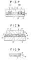
- Figure 1 is a sectional diagram illustrating the state of circuit connection part using the composition of this invention
- Figure 2 is a schematic graph illustrating the viscosity change of adhesive at the time of circuit connection; wherein (a) to (c) in Figures 1 and 2 are symbols denoting the steps in the connection.
- the mark (a) illustrates a state that a connecting material consisting of reactive adhesive 1, coated particles 2 and pressure-deformable electroconductive particles 3 having a greater particle diameter than that of coated particle 2 is formed between the up and down circuits 4 and 5.
- connecting material on circuit As the means for the formation of connecting material on circuit, coating or printing process can be adopted when the connecting material is a liquid, while putting a connecting material on circuit can be adopted when the connecting material is a solid material such as a film.
- the mark (b) illustrates a state that viscosity of the reactive adhesive 1 has descended due to the temperature elevation caused by the heating and pressing at the time of connection and the pressure-deformable electroconductive particles 3 has been deformed by the pressure between circuits 4 and 5.
- coated particles 2 are less susceptible to deformation than pressure-deformable electroconductive particles 3 because the former are smaller than the latter in particle diameter. Further, since they are dispersed in adhesive, heat conduction from circuit is slow. Thus, coated particles 2 are difficult to break, and their nuclear material (curing agent) keeps inert.
- the mark (c) illustrates the state that a period of time has passed after the heating and pressing at the time of connection. Due to the lapse of time, coated particles 2 reach a higher temperature and the coating layer is broken due to swelling pressure of nuclear material and melting of film, as the result of which the nuclear material (curing agent) comes into contact or is integrated with reactive adhesive 1. Thus, viscosity of adhesive ascends, and the adhesive is transformed into a cured adhesive 6 meanwhile. At this time, the pressure-deformable electroconductive particles 3 existing between up and down circuits 4 and 5 have already been deformed and can sufficiently be contacted with the circuits, and they can be immobilized in this state by the cured adhesive 6.
- rigid particles 7 of which particle diameter is smaller than that of pressure-deformable electroconductive particle 3, such as electroconductive particle made of nickel, silver or the like or insulating particle such as spherical or milled fibrous particle made of ceramic, glass, silica or the like or particle of rigid resin, can be used either alone or in combination as shown in Figure 3 as a gap regulating material between up and down circuits 4 and 5.
- the rigid particle 7 is preferably a uniform particle having a sharp particle size distribution, and its amount is appropriately selected from a range of 15% by volume or less based on the reactive adhesive. If its amount exceeds 15% by volume, adhesive force to circuit is deteriorated.
- D ⁇ nd/ ⁇ n (1) wherein n is number of particles having a particle diameter of d.
- electron microscopic method As the method for visually examining the particles, electron microscopic method, optical microscopic method, call counter method, light scattering method and the like are generally adopted. In this invention, electron microscopic method is used. When the particle has some aspect ratio, d expresses the longer diameter.
- the materials which can be used as reactive adhesive (A) of this invention include synthetic resins such as epoxy resin, urea resin, melamine resin, guanamine resin, phenolic resin, xylene resin, furan resin, diallyl phthalate resin, bis-maleimide resin, triazine resin, polyester resin, polyurethane resin, polyvinyl butyral resin, phenoxy resin, polyamide resin, polyimide resin, cyanoacrylate resin and the like and rubbers or elastomers having a functional group such as carboxyl group, hydroxyl group, vinyl group, amino group, epoxy group or the like.
- These reactive adhesives can be used either alone or in the form of a mixture of two or more members.
- the so-called epoxy adhesives i.e. epoxy resin itself or adhesive compositions comprising an epoxy resin as at least one ingredient thereof, are preferable because they are rapid-curing and can give a cured product well balanced in many properties.
- Typical examples of said epoxy resin include bisphenol type epoxy resin derived from epichlorohydrin and bisphenol A, bisphenol F or the like and epoxy novolac resin derived from epichlorohydrin and phenol novolac or cresol novolac.
- epoxy compounds having two or more oxirane rings in one molecule such as glycidylamine, glycidyl ester, alicyclic epoxy compounds, heterocyclic epoxy compounds and the like are also usable.
- epoxy compounds can be used either alone or in the form of a mixture of two or more members.
- a combined use of a liquid epoxy resin and a solid epoxy resin is desirable from the viewpoint of film-formability and fluidity-controllability at the time of connection.
- Combined use of an epoxy compound and a thermoplastic polymer is also desirable from the viewpoint of giving flexibility to adhesive.
- the so-called high-purity epoxy compound of which impurity ions (Na+, K+, Cl ⁇ , S42 ⁇ , etc.) content and hydrolyzable chlorine content have been reduced to 300 ppm or below respectively
- curing accelerator and curing catalyst may be incorporated, and curing agent and crosslinking agent may also be incorporated so far as their addition does not exercise an adverse influence upon shelf stability of adhesive.
- the adhesive may also contain general additives such as solvent, dispersing medium, tackifier, filler, ultraviolet absorber, autoxidant, polymerization inhibitor, coupling agent, and the like.
- Coated particle (B) comprisies a curing agent as a nucleus which is substantially covered with a thin film of an polymeric substance such as polyurethane, polystyrene, gelatin, polyisocyanate or the like, an inorganic substance such as calcium silicate or the like, or a metal such as nickel, copper or the like. Its mean particle diameter must be smaller than that of pressure-deformable electroconductive particle 3 not yet deformed, and it is preferably 80% or below and more preferably 50% or below as compared with that of 3. Though the shape of coated particle (B) is not critical, a smaller aspect ratio is more desirable because it gives a more uniform reactivity. As the curing agent used as nuclear material, substances known as curing agent of reactive adhesive (A) can be used in an appropriate amount.
- curing agents which can be used for epoxy resin include aliphatic amines, aromatic amines, carboxylic acid anhydrides, thiols, alcohols, phenols, isocyanates, tertiary amines, boron complexes, inorganic acids, hydrazides, imidazoles, and modified products thereof.
- tertiary amines, boron complexes, hydrazides and imidazoles are preferable, because they bring about a rapid cure, are excellent in connection workability and less require the stoichiometric consideration owing to their ion-polymerization type catalytic performance. They can be used either alone or in the form of a mixture of two or more members.
- the curing reaction using the coated particle should be completed at the time of connection. Practically, however, it is enough for the purpose if the reaction can progress to such an extent that the deformation of deformable electroconductive particles can be maintained between circuits, because a post-cure may be carried out in this state.
- thermal activation type of coated particle in which the coating film is broken at a predetermined temperature is more desirable than pressure activation type of coated particle in which coating film is broken by a pressure, because the former gives a more uniform reaction system than the latter.
- Coated particles having a thermal activation temperature of 40°C to 250°C can be used in this invention. If this temperature is lower than 40°C, the coated particle tends to be activated in the course of storage, and therefore such a product must be stored with cooling. If the temperature is higher than 250°C, a high temperature must be applied at the time of connection, which tends to thermally injure the neighboring materials.
- the thermal activation temperature is preferably 70°C to 200°C, and more preferably 100°C to 170°C.
- the thermal activation temperature referred to in this invention means the exothermic peak temperature measured by elevating the temperature of adhesive composition 1 from ambient temperature at a rate of 10°C/minute in a differential scanning calorimeter (DSC).
- DSC differential scanning calorimeter
- the pressure-deformable electroconductive particle (C) is a particle prepared by coating the surface of a polymeric material such as polystyrene, epoxy resin or the like with an electroconductive metallic thin layer 9 made of a metal such as nickel, gold, silver, copper, solder or the like having a thickness of, for example, 1 micron or below as shown in Figure 4. As has been mentioned above, its particle diameter must be greater than that of coated particle (B).
- This pressure-deformable electroconductive particle must change its form under the condition of heating and pressing at the time of connection.
- a temperature of 250°C or below and a pressure of 100 kg/cm2 or below are usually adopted. Since a higher temperature and a higher pressure have a greater tendency of thermally injuring the circuit material and the like, a temperature of 200°C or below and a pressure of 50 gk/cm2 or below are preferable.
- plastics such as polystyrene, epoxy resin and the like, rubbers such as styrene-butadiene rubber, silicone rubber and the like, and natural polymers such as cellulose, starch, squalene and the like can be used. These materials are used as main component of the nuclear material, and various additives such as crosslinking agent, curing agent, antioxidant and the like may optionally be added thereto.
- the metal constituting the thin layer 9 a variety of electrically conductive metals, metallic oxides, alloys and the like can be used.
- said metal examples include Zn, Al, Sb, Au, Ag, Sn, Fe, Cu, Pb, Ni, Pd, Pt and the like, and they may be used either alone or in the form of a composite material (e.g. solder). Further, for special purposes such as control of hardness and surface tension or improvement of adhesion, other metals such as Mo, Mn, Cd, Si, Ta, Cr and the like and their compounds may be added thereto.
- Ni, Ag, Au, Sn, Cu and Pb are preferred. These materials are used either as a single layer or as a multi-layer.
- metal thin layer 9 on polymeric nuclear material 8 dry methods such as vapor deposition, sputtering, ion plating, flame spraying and the like and plating methods such as fluidized bed method, electroless plating method and the like can be used.
- electroless plating method is particularly preferable, because it uses a wet dispersed system and therefore can give a coating layer of uniform thickness.
- Thickness of metal thin layer is usually 0.01 to 5 microns and preferably 0.05 to 1.0 micron.
- the term "thickness" used herein involves thickness of the substrate layer, too. If thickness of coating layer is too small, electrical conductivity lowers. If the thickness is too great, the polymeric nuclear material at the time of circuit connection becomes difficult to deform, so that reliability of connection is deteriorated.
- the pressure-deformable electroconductive particle 3 of this invention not only the above-mentioned polymeric nuclear material/metallic thin layer structure but also some thermally fusible metal particles can be used, so far as they can be deformed under the condition of heating and pressing without breaking protecting layer 13 of semiconductor chip.
- connection When pressure-deformable electroconductive particle 3 is used for circuit connection, the connection can follow the expansion and contraction between circuits 4 and 5 for the reasons that the polymeric nuclear material is deformed by the pressure or by the heat and pressure applied at the time of connection so that the pressure-deformable electroconductive particles press one another to maintain a sufficient contact area and that the polymeric nuclear material is close to the adhesive in rigidity and thermal expansion coefficient and the metallic thin layer has so a small thickness of 1 micron or below and therefore is deformable.
- reliability of connection is markedly improved for a long period of time even if temperature is changed in the period.
- the pressure-deformable electroconductive particle of this invention has preferably a mean particle diameter of 0.01 to 100 microns. If the mean particle diameter is smaller than 0.01 micron, surface area of the particle is too great and particle-particle contact is excessively promoted due to agglomeration, as the result of which insulation between adjacent two circuits can be deteriorated.
- the mean particle diameter exceeds 100 microns, insulation between adjacent two circuits can be deteriorated when the circuits are fine and particles exist between adjacent circuits.
- preferable mean particle diameter is 1 to 50 microns.
- the shape of the pressure-deformable electroconductive particle is not critical, so far as its mean particle diameter is in the above-mentioned range. For obtaining a good anisotropic conductivity, however, pressure-deformable electroconductive particles having as small an aspect ratio as possible are preferable. For example, pressure-deformable electroconductive particles having a spherical or conical shape are preferable.
- These pressure-deformable electroconductive particles may be used either alone or in combination of two or more kinds.
- the pressure-deformable electroconductive particle of this invention is used in an amount of 0.1 to 15% by volume based on the volume of the adhesive component. Although a good anisotropic electroconductivity can be exhibited so far as its amount is in the range of 0.1 to 15% by volume, conductivity in the direction of thickness is deteriorated if its amount is smaller than 0.1% by volume and insulation between neighboring circuits is deteriorated if its amount exceeds 15% by volume in order to obtain a highly reliable anisotropic electroconductivity.
- the amount of pressure-deformable electroconductive particle in the range of 1 to 10% by volume.
- the chlorine ion concentration in the aqueous extract solution obtained by dipping a composition for circuit connection of this invention into pure water and treating it at 100°C for 10 hours should be 15 ppm or below, and preferably 5 ppm or below, based on the weight of the composition.
- lowering the chlorine ion concentration in aqueous extract solution is desirable from the view-point of workability of connection, because it improves reaction velocity of composition and thereby lowers connection temperature and shortens the time period necessary for connection, as has been mentioned above.
- FIGS 5 and 6 are sectional diagrams illustrating one embodiment of this invention.
- Semiconductor chip 11 is IC, LSI, chip condenser, or the like.
- electrode 12 made of aluminum, copper, nickel or the like or additionally having a layer of gold thereon is formed either concavely or on the nearly same level as the main surface 10 of protecting layer 13.
- the wiring of semiconductor chip may be used as it is, if desired.
- a case that the depth of electrode is comparable to thickness of protecting layer corresponds to a case in which protecting layer 13 is formed in the necessary part by the use of the so-called thin-film making technique such as CVD, or a case in which wiring circuit is not covered by protecting layer.
- Board 14 is made of glass, synthetic resin, metal ceramic or their composite material and has circuit 15 made of gold, silver, copper, aluminum, chromium, tantalum, indium oxide (ITO) or the like.
- Board 14 can have a structure of Figure 5 where the central part is removed (e.g. film carrier or the so-called TAB) or a continuous structure of Figure 6 (e.g. glass circuit), for example.
- Figure 7 is a sectional diagram illustrating a case in which a semiconductor chip having concave electrode 12 is connected to circuit 15 formed on synthetic resin film substrate 14 by the use of silver paste.
- a structure in which the central part is swollen is often formed in the circuits using silver paste or when the conditions of etching are not appropriate at the time of circuit preparation.
- circuit 15 is swollen in its central part.
- protecting layer 13 functions as a dam, and pressure-deformable electroconductive particles 3 cannot flow into the insulated circuit at the time of pressing.
- a good electrical continuity is obtained and a high insulation can be realized between protecting layer 13 and board 14.
- Figure 7 (a) and (b) demonstrate that pressure-deformable electroconductive particles 3 existing between electrode connection parts 12 and 15 may be any of monodispersed particle (a) and agglomerated particle (b).
- a composition for circuit connection of this invention is placed between semiconductor chip 11 and board 14 and positions of electrode 12 and circuit 15 are adjusted, after which the whole is heated and pressed.
- ultraviolet irradiation or ultrasonic vibration may optionally be used in combination at the time of connection. This is effective for shortening the curing time of adhesive and removing the pollution on the surfaces to be bonded.
- This invention provides a structure in which particles deformable under the condition of heating and pressing at the time of connection are used as the conductive particles in an adhesive for circuit connection and the particles are immobilized by means of adhesive at the time of connection. Since the deformable particles can change their form in accordance with the unevenness of bonding surface, the deformable particles can give an electrical connection even when no bump is present in the electrical connection part, because the deformable particles function similarly to bump. In addition, the connecting work can be simplified because the unevenness in the depth of electrode from the protecting layer can be neglected.
- the deformable electroconductive particles are lower in strength than the materials constituting semiconductor chip and protecting layer, the semiconductor chip and protecting layer are not broken by the heat and pressure applied at the time of connection. Accordingly, a high density connection having an insulating property between adjacent two circuits and conductive only in the direction of up-and-down electrodes can be realized by appropriately selecting particle diameter of conductive particle and its amount. Thus, bumpless connection of semiconductor chips which has hitherto been impossible can be realized.
- the connecting part is formed from solder
- the conductive particle contains a polymeric substance as its nuclear material and the surface metallic layer has a very small thickness. Since it is close to adhesive in elastic modulus and thermal expansion coefficient because both the materials belong to polymeric substances, the connection layer made of anisotropically conductive adhesive behaves as an excellent stress-absorber to the thermal shock, owing to which the reliability of connection is improved.
- the connected structure obtained above may be sealed with other synthetic resin or ceramic. This is desirable from the viewpoint of mechanical reinforcement of connected part and formation of moisture-proofing layer.
- FIG 8 is a sectional diagram illustrating one embodiment of this invention.
- semiconductor chip 11 On semiconductor chip 11, an number of electrodes 17, 17′ (typically, bumps) made of gold or solder protruded from the main surface are formed.
- circuit 15 is connected to semiconductor bumps 17, 17′ through intermediation of circuit connection composition placed on circuit 15. At this time, their whole under surface except for the connecting part of bump of semiconductor chip is covered with insulating adhesive 16.
- the insulating adhesive 16 must cover at least the semiconductor chip side of the surface on which bumps 17 and 17′ are formed.
- a circuit connection composition 18 of this invention is formed on a board 14 having circuit 15.
- the composition is liquid, it is formed by coating or printing.
- the composition is solid, it is mounted on board and pressed or heated and pressed.
- insulating adhesive 16 is constructed on the bump (17, 17′) side of semiconductor chip 11. Thereafter, both the adhesive surfaces are confronted each other and pressed or heated and pressed to integrate the both adhesive surfaces. According to this invention, an insulating adhesive layer can be formed relatively easily.
- only the protruded electrode part may be connected to composition 18 by controlling thickness of base board or height of bumps 17 and 17′, so as to form a gap in the semiconductor chip 11 side.
- an insulating adhesive 16 is formed in the part of gap. It is formed by immersion in insulating adhesive 16, injection of insulating adhesive under pressure or reduced pressure, etc.
- semiconductor chip and board are connected by placing a double layer film constructed of a circuit-connecting composition 18 and an insulating adhesive 16 so that the circuit connecting composition layer faces the board and applying thereto pressure or heat and pressure.
- the double layer film is prepared by, for example, constructing a layer of circuit connecting composition 18 consisting of adhesive 1, coated particle 2 and pressure-deformable conductive particle 3 by the method of coating or the like onto a peelable film, followed by, for example, coating an insulating adhesive 16 thereon. Otherwise, it is prepared by roll-laminating both the films.
- insulating adhesive 16 at the time of connection is at least comparable to or greater than that of the circuit-connecting composition 18 in order to promote the contact between the tips of bumps 17, 17′ and circuit-connecting composition 18.
- a good connection can be achieved when thickness of insulating adhesive 16 is not greater than the height of bumps 17, 17′, preferably not higher than a height giving a volume excepting the bumps 17 and 17′.
- Thickness of the circuit connecting composition 18 is preferably comparable to the particle diameter of the conductive particle contained in the composition or smaller than it, because in this state the conductive particles can effectively contribute to the electrical continuity.
- the connected part is made into a double layer structure consisting of a layer of circuit-connecting composition 18 contributing to electroconductivity and a layer of insulating adhesive 16.
- connection resolution can be improved to a great extent, and short-circuit between adjacent circuits can be eliminated in the connection of fine circuits of semiconductor chips.
- the tip surface of bumps 17, 17′ comes into contact with the pressure-deformable electroconductive particle 3 contained in circuit-connecting composition 18 and functions as concavity-convexity forming material on electrode, so that reliability of connection in minute area can be improved.
- connection parts 13 and 15 Between the connection parts 13 and 15, the existence of insulating adhesive 16 prevents the leakage between adjacent bumps 17 and 17′.
- electroconductive particles can be packed at a higher density than in the prior techniques and thereby reliability of connection in minute area can be improved.
- composition 18 and insulating adhesive 16 constitute separate phases as shown in Figure 8. However, if both the materials exist as a solution or mixture in the space between bumps, concentration of conductive particle 3 decreases relatively, and this state is more preferable.
- the bump (17, 17′)-carrying surface (connection surface of chip side) is covered with insulating adhesive 16 containing no conductive particle.
- This insulating adhesive 16 functions as a buffer layer under the pressure applied at the time of connection and prevents the chip from breakage.
- the insulating adhesive 16 also exhibits an effect of sealing agent and is effective for prevention of water invasion and improvement of moisture resistance. Further, since the pressure-deformable electroconductive particle 3 areally contacts with circuit and it is approximately equal to nuclear material of conductive particle in thermal expansion coefficient and elastic modulus, reliability of connection is remarkably improved.
- the connected structure of semiconductor chip of this invention greatly contributes to the field of high density fitting such as display materials (e.g. liquid crystal, ELI fluorescent display tube and the like), IC card, printer and the like, in each of bumpless and bump-carrying semiconductor chips.
- display materials e.g. liquid crystal, ELI fluorescent display tube and the like
- IC card e.g. IC card, printer and the like
- a method which comprises temporarily forming the construction of this invention by patting the uncured (B stage) composition on wafer electrode surface for the sake of temporary fixation at the time of dividing the wafer into chips or for preventing electrostatic breakage or for testing electrical continuity, followed by forming a chip therefrom to obtain a structure of this invention is also desirable from the viewpoint of shortening the process.
- pressure-deformable electroconductive particle 3 is preferentially deformed because its particle diameter is larger than that of coated particle 2 and preferentially accepts the pressure at the time of connection.
- reactive adhesive 1 has already decreased its viscosity due to the high temperature and therefore is easily removable from the surface of pressure-deformable electroconductive particle 3.
- the pressure-deformable electroconductive particle 3 can freely change its form while keeping contact with circuit. Since coated particle 2 has a smaller particle diameter than pressure-deformable electroconductive particle 3, it reaches high temperature later than pressure-deformable electroconductive particle 3, and at this high temperature the protecting layer is broken or molten and the nuclear material or the curing agent comes into contact with reactive adhesive 1. Due to the high temperature, the curing reaction progresses rapidly.
- the pressure-deformable electroconductive particles can be immobilized between circuits while keeping their deformed state, which makes their contact with circuit sufficient and thereby enables to realize a stable connection free from dispersion of contact resistance.
- the technique of this invention is applicable to the fields requiring high connection reliability such as electrical connection between semiconductor chip and circuit on board, and the like.
- Epikote 1002 bisphenol type epoxy resin, manufactured by Yuka Shell Epoxy Co., Ltd.
- Nipol 1072 carboxyl-modified nitrile rubber, manufactured by Nippon Geon Co., Ltd.
- Novacure (a dispersion prepared by coating and micro-encapsulating modified imidazole used as a nuclear material with crosslinked polyurethane to obtain microcapsule having a mean particle diameter of 2.5 microns and dispersing the microcapsules into a liquid epoxy resin; manufactured by Asahi Chemical Industry Co., Ltd.) was used.
- the surface of a cured product of flexible epoxy resin having a spherical shape was subjected to electroless plating to obtain a particle having a particle diameter of 5.2 microns (referred to as "EP-M"). Thickness of the nickel layer was 0.1 micron.
- the above-mentioned materials (1)-(3) were compounded at a compounding ratio shown in Table 1, and the solution thus obtained was coated onto a biaxially stretched polypropylene film (50 microns) and dried at 90°C for 15 minutes to obtain a film-form connecting material having a thickness of 25 microns.
- all the connecting materials thus prepared were aged at 50°C for 20 hours and thereafter evaluated.
- the concentration of extracted chlorine ion after extraction with pure water at 100°C for 10 hours was 13 ppm, as measured by ion chromatography using Dionex 2010i.
- 1.5 mg of the connecting material was weighed out and its temperature was elevated at a rate of 10°C/minute in DSC (Du Pont 1090). The exotherm peak temperature was 148°C.
- a flexible circuit board having 250 copper circuits each having a line width of 70 microns, a pitch of 140 microns and a thickness of 35 microns was connected to a glass plate having a thickness of 1.1 mm and having a thin layer of indium oxide (ITO) on its whole area (surface resistance 30 ohms/ ⁇ ) by heating and pressing them (170°C -20 kg/cm2 for 30 seconds) at a connection width of 3 mm.
- the adhesive surface of connecting material was first applied onto FPC, at 100°C, 5 kg/cm2 for 3 seconds, and thereafter the separator (polypropylene film) was peeled off and connection to ITO was carried out.
- the connected circuit thus obtained was evaluated to obtain the results shown in Table 1.
- connection resistance is expressed by average value ( x ) and maximum (Max) determined by measuring the resistance of adjacent circuits by means of multimeter.
- Example 1 thickness of the connecting part was as small as about 1 micron, and a good connection resistance was obtained.
- Example 1 Since the coating film of the coated particle used in Example 1 was made of crosslinked polyurethane, it was resistant to toluene so that no trouble appeared in the production. When the product was aged at 50°C for 20 hours in order to evaluate its behavior in longterm storage, good properties were observed.
- Example 1 The procedure of Example 1 was repeated, except that spherical silica having a particle diameter of 2 microns (manufactured by Catalysts & Chemicals Ind. Co., Ltd.) was additionally added to the connecting material.
- spherical silica having a particle diameter of 2 microns manufactured by Catalysts & Chemicals Ind. Co., Ltd.
- Example 2 The product was evaluated in the same manner as in Example 1. It was found that thickness of connection was controllable by changing the particle diameter of the spherical silica. The spherical silica behaved as a gap regulator to give good connection characteristics. It is considered that the method of this example will be more effective when the pressure-deformable electroconductive particle is particularly easily deformable.
- Example 1 The procedure of Example 1 was repeated, except that the adhesive component was altered. That is, Bylon 300 (thermoplastic polyester having hydroxyl and carboxyl groups, manufactured by Toyobo Co., Ltd.), Epikote 828 (bisphenol A type liquid epoxy resin manufactured by Yuka Shell Co., Ltd.) and Colonate L (polyisocyanate, manufactured by Nippon Polyurethane Co., Ltd.) were used at a compounding ratio of 70/30/1.
- Bylon 300 thermoplastic polyester having hydroxyl and carboxyl groups, manufactured by Toyobo Co., Ltd.
- Epikote 828 bisphenol A type liquid epoxy resin manufactured by Yuka Shell Co., Ltd.
- Colonate L polyisocyanate, manufactured by Nippon Polyurethane Co., Ltd.
- the adhesive system was different from that of Example 1. As shown in Table 1, good connection characteristics were achieved.
- Example 1 the same adhesive as in Example 1 was used, while coated particle and pressure-deformable electroconductive particle were different from those of Example 1.
- Curezole 2MZ-OK (2-ethylimidazole-isocyanuric acid adduct, mp ca. 250°C, manufactured by Shikoku Chemical Ind. Co., Ltd.) was fractionated by sieving to obtain powdery curing agent materials having mean particle diameters of 4.7 microns and 15 microns, respectively. Each of the powdery materials was forcibly stirred in toluene as a pretreatment for the sake of defatting and making the particles more coarse. By filtering off the toluene, pretreated nuclear materials (curing agents) were obtained.
- the powdery material was dispersed into Circuit prep 3316 (PdCl + Cl + HCl + SnCl2 type activating treating solution, manufactured by Nippon Electroplating Engineers Co., Ltd.) and stirred at 25°C for 20 minutes for sake of activation, after which it was washed with water and filtered to obtain a nuclear material having activated surface.
- Circuit prep 3316 PdCl + Cl + HCl + SnCl2 type activating treating solution, manufactured by Nippon Electroplating Engineers Co., Ltd.
- the nuclear material having been subjected to activating treatment was dipped in Circuitprep 5501 (electroless plating solution manufactured by Nippon Electroless Plating Engineers Co., Ltd) and forcibly stirred at 30°C for 30 minutes. After allowing it to stand for a predetermined period of time, it was washed with water and dried to obtain a particulate material having a copper coating layer (about 0.1 micron in thickness as measured by sectional examination using scanning electron microscope) on the nuclear material.
- Circuitprep 5501 electroless plating solution manufactured by Nippon Electroless Plating Engineers Co., Ltd
- a nickel layer was formed on the surface of crosslinked polystyrene particle (PSt) having a mean particle diameter of 10 microns by the method of electroless plating, after which a substituting plating using gold was carried out.
- PSt-M crosslinked polystyrene particle
- specific gravity 2.0 a metal plated plastic particle having a metal coating layer of about 0.2 micron
- Table 1 illustrates the results of evaluation carried out in the same manner as in Example 1.
- Examples 4 and 5 are cases in which the pressure-deformable electroconductive particle both had a mean particle diameter of 10.4 microns before deformation, while coated particle of Example 4 had a mean particle diameter of 4.2 microns and that of Example 5 had a mean particle diameter of 7.2 microns.
- the thickness after connection was as small as 2 to 3 microns and the electroconductive particles were sufficiently deformed, so that connection resistance was also low in both x and Max, and the results were good.
- Example 4 a metal was used as coating material of coated particle. Owing to it, the coated particle was resistant to the influence of solvent present in adhesive and showed only a small viscosity change at the time of producing connecting material, so that the production was easy to practice. After the connection, the coating metal functioned as a conductive material and exhibited no adverse influence.
- particle diameter of coated particle was 15.2 microns, which was greater than the mean particle diameter of pressure-deformable electroconductive particle (10.4 microns).
- thickness after connection hardly decreased, and the connection resistance was unstable.
- the connecting material used in this example had a similar formulation to that of Example 2, although the coated particle used in this example was a powder of curing agent only subjected to no coating treatment.
- connection resistance was very unstable. This was probably due to that curing reaction of adhesive progressed in course of storage (at 50°C for 20 hours) and therefore the adhesive had nearly lost fluidity at the time of circuit connection.
- Quatlex 1010 bisphenol type epoxy resin, manufactured by Dow Chemicals Co., Ltd.
- Quatlex 2010 novolac phenol type epoxy resin manufactured by Dow Chemicals Corp.
- flexibilizing agent for epoxy resin Butyral 3000K (polyvinyl acetal resin, manufactured by Denki Kagaku Kogyo K.K.) was blended with the epoxy resin at a ratio of 30% by weight (weight of solid component) based on the epoxy resin, and a 40% (solid component) solution in toluene was prepared.
- Novacure HX-3741HP (a dispersion prepared by coating a modified imidazole as a nuclear material with a polyurethane type material to obtain a particle material having a mean particle diameter of 4.5 microns and then dispersing the particle material into a high purity liquid epoxy resin; manufactured by Asahi Chemical Industry Co., Ltd.) was selected in Examples 6-8, while HX-3741 (a dispersion of the same curing agent as above in general purpose type liquid epoxy resin) was used in Referential Example 1.
- Example 2 In the same manner as in Example 1, a film of anisotropic electroconductive adhesive having a thickness of 17 microns was prepared.
- Example 7 As compared with Referential Example 1, Examples 6 and 8 were lower in chlorine ion concentration (1/10 or below) and DSC peak temperature was about 30°C lower, demonstrating that decrease in the concentration of chlorine ion brought about an improvement in reactivity. In Example 7, the same gap regulator as in Example 2 was used. ExamPles 6 to 8 all exhibited good connection resistance.
- Examples 6-8 all exhibited a Max resistance of 10 ohms or below and showed only a small change in connection resistance, while Referential Example 1 exhibited as high a Max resistance of 30 ohms and showed a greater change in connection resistance than in Examples 6-8. This is probably for the reasons that, in Examples 6-8, reactivity was higher and therefore curing reaction progressed more sufficiently than in Referential Example 1, and that corrosion of electrode surface in the connected part was prevented by the lowered concentration of chlorine ion in Examples 6-8.
- a semiconductor chip (5 mm square, thickness 0.5 mm, with 200 electrodes of 50 microns square formed in four sides of main surface, electrode distance 50 microns in the shortest part, thickness of protecting layer 10.2 and 0 micron in Examples 9, 10 and 11, respectively) and a circuit glass board having an ITO (indium oxide) circuit corresponding to the above-mentioned electrode arrangement were prepared.
- ITO indium oxide
- a film-form connecting material composed of the circuit-connecting adhesive composition of Example 1 was placed between the semiconductor chip and the circuit, and the whole was heated and pressed at 170°C, 30 kg/cm2 for 30 seconds to cure the adhesive. Thus, a connected structure was obtained.
- Example 10 The same semiconductor chip as used in Example 10 was connected to a TAB tape having 15 microns copper circuit on a 75 microns polyimide film.
- the circuit-connecting composition and the conditions of connection were the same as in Example 10. In this case, too, a good connection could be achieved.
- connection was carried out by a simple method which comprises pressing or heating and pressing the electrode part of semiconductor chip and circuit part of board without forming any bump on them, and this makes it possible to carry out a high-reliability bumpless connection of semiconductor chips, and thereby to simplify the process to a great extent.
- circuit-connecting composition and the insulating adhesive are film-form materials. As have been mentioned above, these materials may also have a liquid or other form.
- a circuit baord was prepared by forming, on a glass plate, an ITO circuit having connection terminals of which arrangement corresponded to that of bumps (protruded electrode) of semiconductor chip (5 mm square, thickness 0.5 mm, with 200 bumps (20 microns in height) formed on the four sides of the main surface).
- a circuit-connecting composition a film-form composition having a thickness of 7 microns and the same formulation as in Example 3 (initial viscosity 1 x 10⁴ poises at 170°C) was prepared. It was applied onto the circuit of glass board at room temperature under a pressure of 5 kg/cm2 in 5 seconds.
- Example 1 a composition of Example 1 from which the pressure-deformable electroconductive particle was subtracted (thickness 20 microns, initial viscosity 2 x 10² poises at 170°C) was applied to semiconductor chip surface at room temperature under a pressure of 5 kg/cm2 in 5 seconds.
- Both the adhesive surfaces were adjusted to correct position and connected together by heating and pressing them at 170°C under 30 kg/cm2 for 30 seconds.
- the latent curing agent was activated to cure the adhesive.
- connection between a semiconductor chip having a high density electrode and a circuit could be practised with a high reliability. Further, if a double layer film consisting of circuit-connecting composition and insulating adhesive is used, a more simple and convenient connection of semiconductor chip can be realized.
- a film-form product having a thickness of 20 microns and having the formulation of Example 6 was used.
- a circuit board was prepared by forming, on a glass plate, an ITO/Cr circuit having connection terminals corresponding to the arrangement of bumps of semiconductor chip (5 mm square, height 0.5 mm, with 100 gold bumps formed on the four sides of its main surface).
- the film-form product was applied onto the circuit board. After peeling off the polypropylene film, the positions of the bumps of semiconductor chip and the terminals of board were adjusted under microscope so as to mount 10 semiconductor chips on one sheet of circuit board. While heating and pressing the whole at 80°C under a pressure of 20 kg/cm2 (film is uncurved), the state of electrical continuity was examined by means of multimeter at a current of 10 micro-amperes, using measurement probe.
- a continuity test could be effected by applying pressure at a temperature lower than the activation temperature of curing agent present in adhesive where the adhesive kept uncurved.
- continuity test can be effected before full bonding or in the state that the adhesive is not yet cured, which makes regeneration of defect part quite conveniently and easily. This is quite advantageous for labor saving of process and reduction of cost.
- the particle diameter of pressure-deformable electroconductive particle is made larger than that of coated particle in the connecting material.
- the thickness after connection can be controlled by the combined use of rigid particle.
- this invention can provide a circuit-connecting composition quite advantageously applicable to the connection of electronic parts such as circuit board, semiconductor and the like of which circuits are becoming finer more and more today.
Applications Claiming Priority (8)
| Application Number | Priority Date | Filing Date | Title |
|---|---|---|---|
| JP307618/88 | 1988-12-05 | ||
| JP30761888 | 1988-12-05 | ||
| JP554089 | 1989-01-12 | ||
| JP554189 | 1989-01-12 | ||
| JP5540/89 | 1989-01-12 | ||
| JP5541/89 | 1989-01-12 | ||
| JP69973/89 | 1989-03-22 | ||
| JP6997389 | 1989-03-22 |
Publications (3)
| Publication Number | Publication Date |
|---|---|
| EP0372880A2 true EP0372880A2 (de) | 1990-06-13 |
| EP0372880A3 EP0372880A3 (en) | 1990-08-16 |
| EP0372880B1 EP0372880B1 (de) | 1993-12-15 |
Family
ID=27454313
Family Applications (1)
| Application Number | Title | Priority Date | Filing Date |
|---|---|---|---|
| EP89312607A Expired - Lifetime EP0372880B1 (de) | 1988-12-05 | 1989-12-04 | Zusammensetzung für eine Schaltungsverbindung, Verbindungsverfahren mit dieser Zusamensetzung und verbundene Struktur für Halbleiterchips |
Country Status (5)
| Country | Link |
|---|---|
| US (2) | US5001542A (de) |
| EP (1) | EP0372880B1 (de) |
| JP (1) | JP2586154B2 (de) |
| KR (1) | KR930002935B1 (de) |
| DE (1) | DE68911495T2 (de) |
Cited By (16)
| Publication number | Priority date | Publication date | Assignee | Title |
|---|---|---|---|---|
| EP0588609A1 (de) * | 1992-09-15 | 1994-03-23 | Texas Instruments Incorporated | Ballkontaktierung für Flip-Chip-Anordnungen |
| WO1994024704A1 (en) * | 1993-04-12 | 1994-10-27 | Bolger Justin C | Area bonding conductive adhesive preforms |
| EP0696055A2 (de) | 1994-07-27 | 1996-02-07 | Smiths Industries Public Limited Company | Elektronischer Zusammenbau und Behandlungsverfahren |
| WO1998014995A1 (de) * | 1996-09-30 | 1998-04-09 | Robert Bosch Gmbh | Verfahren zur flip-chip-montage |
| WO2000057469A1 (fr) * | 1999-03-23 | 2000-09-28 | Citizen Watch Co., Ltd. | Structure et procédé de montage de semi-conducteur |
| WO2000079475A2 (en) * | 1999-06-17 | 2000-12-28 | Nissha Printing Co., Ltd. | High-reliability touch panel |
| US6365500B1 (en) * | 1994-05-06 | 2002-04-02 | Industrial Technology Research Institute | Composite bump bonding |
| EP1213751A2 (de) * | 2000-11-30 | 2002-06-12 | Philips Corporate Intellectual Property GmbH | Halbleiterbaugruppe mit einer Verbindungsstruktur |
| WO2004106454A2 (en) * | 2003-05-23 | 2004-12-09 | National Starch And Chemical Investment Holding Corporation | Foamable underfill encapsulant |
| US6881611B1 (en) | 1996-07-12 | 2005-04-19 | Fujitsu Limited | Method and mold for manufacturing semiconductor device, semiconductor device and method for mounting the device |
| EP1748478A2 (de) * | 2005-07-27 | 2007-01-31 | Palo Alto Research Institute Incorporated | Selbstorganisierte Anschlussteilchen |
| US7504331B2 (en) | 2005-07-27 | 2009-03-17 | Palo Alto Research Center Incorporated | Method of fabricating self-assembled electrical interconnections |
| US7525194B2 (en) | 2005-07-27 | 2009-04-28 | Palo Alto Research Center Incorporated | System including self-assembled interconnections |
| EP2056406A1 (de) * | 2006-08-25 | 2009-05-06 | Hitachi Chemical Company, Ltd. | Schaltungsverbindungsmaterial, verbindungsstruktur für ein schaltungsglied damit und herstellungsverfahren dafür |
| US7879956B2 (en) | 1997-03-31 | 2011-02-01 | Hitachi Chemical Company, Ltd. | Circuit-connecting material and circuit terminal connected structure and connecting method |
| US20210298181A1 (en) * | 2020-03-17 | 2021-09-23 | Innolux Corporation | Electronic device |
Families Citing this family (216)
| Publication number | Priority date | Publication date | Assignee | Title |
|---|---|---|---|---|
| JP3181283B2 (ja) * | 1989-08-07 | 2001-07-03 | 株式会社日立製作所 | はんだ接続された電子回路装置とはんだ接続方法並びに金メッキ接続端子用はんだ |
| JP2633366B2 (ja) * | 1989-11-24 | 1997-07-23 | 株式会社日立製作所 | 計算機モジュール用リードレスチップキャリア |
| US5175610A (en) * | 1990-05-09 | 1992-12-29 | Kabushiki Kaisha Toshiba | Resin molded type semiconductor device having a metallic plate support |
| US5140405A (en) * | 1990-08-30 | 1992-08-18 | Micron Technology, Inc. | Semiconductor assembly utilizing elastomeric single axis conductive interconnect |
| US5148265A (en) | 1990-09-24 | 1992-09-15 | Ist Associates, Inc. | Semiconductor chip assemblies with fan-in leads |
| US5866951A (en) * | 1990-10-12 | 1999-02-02 | Robert Bosch Gmbh | Hybrid circuit with an electrically conductive adhesive |
| CA2059020C (en) * | 1991-01-09 | 1998-08-18 | Kohji Kimbara | Polyimide multilayer wiring board and method of producing same |
| JPH04332404A (ja) * | 1991-05-07 | 1992-11-19 | Nec Corp | 異方性導電材料及びこれを用いた集積回路素子の接続方法 |
| WO1992022090A1 (en) * | 1991-06-03 | 1992-12-10 | Motorola, Inc. | Thermally conductive electronic assembly |
| JP2931477B2 (ja) * | 1991-06-07 | 1999-08-09 | シャープ株式会社 | 薄膜磁気ヘッド構造体およびその製造方法 |
| US5523137A (en) * | 1991-07-24 | 1996-06-04 | Tomoegawa Paper Co., Ltd. | Adhesive paper for tape automated bonding |
| US5218234A (en) * | 1991-12-23 | 1993-06-08 | Motorola, Inc. | Semiconductor device with controlled spread polymeric underfill |
| US5977575A (en) * | 1992-04-27 | 1999-11-02 | Seiko Instruments Inc. | Semiconductor sensor device comprised of plural sensor chips connected to function as a unit |
| US5281684A (en) * | 1992-04-30 | 1994-01-25 | Motorola, Inc. | Solder bumping of integrated circuit die |
| US5261593A (en) * | 1992-08-19 | 1993-11-16 | Sheldahl, Inc. | Direct application of unpackaged integrated circuit to flexible printed circuit |
| US6077725A (en) * | 1992-09-03 | 2000-06-20 | Lucent Technologies Inc | Method for assembling multichip modules |
| US5436503A (en) * | 1992-11-18 | 1995-07-25 | Matsushita Electronics Corporation | Semiconductor device and method of manufacturing the same |
| US5550408A (en) * | 1992-11-18 | 1996-08-27 | Matsushita Electronics Corporation | Semiconductor device |
| US5448165A (en) * | 1993-01-08 | 1995-09-05 | Integrated Device Technology, Inc. | Electrically tested and burned-in semiconductor die and method for producing same |
| JPH06232188A (ja) * | 1993-01-29 | 1994-08-19 | Nec Corp | 半田材の製造方法 |
| US5346558A (en) * | 1993-06-28 | 1994-09-13 | W. R. Grace & Co.-Conn. | Solderable anisotropically conductive composition and method of using same |
| US5385869A (en) * | 1993-07-22 | 1995-01-31 | Motorola, Inc. | Semiconductor chip bonded to a substrate and method of making |
| JP3180863B2 (ja) * | 1993-07-27 | 2001-06-25 | 富士電機株式会社 | 加圧接触形半導体装置およびその組立方法 |
| JP2007053107A (ja) * | 1993-07-29 | 2007-03-01 | Hitachi Chem Co Ltd | フィルム状回路接続材料 |
| JP3445641B2 (ja) * | 1993-07-30 | 2003-09-08 | 株式会社デンソー | 半導体装置 |
| US5436745A (en) * | 1994-02-23 | 1995-07-25 | Ois Optical Imaging Systems, Inc. | Flex circuit board for liquid crystal display |
| TW305860B (de) * | 1994-03-15 | 1997-05-21 | Toray Industries | |
| US5468917A (en) * | 1994-03-23 | 1995-11-21 | International Business Machines Corporation | Circuitized structure including flexible circuit with elastomeric member bonded thereto |
| US5463190A (en) * | 1994-04-04 | 1995-10-31 | Motorola, Inc. | Electrically conductive adhesive |
| TW277152B (de) * | 1994-05-10 | 1996-06-01 | Hitachi Chemical Co Ltd | |
| WO1996005614A1 (en) * | 1994-08-12 | 1996-02-22 | Fraunhofer-Gesellschaft zur Förderung der angewandten Forschung e.V. | Flip chip bonding with non-conductive adhesive |
| AU3415095A (en) * | 1994-09-06 | 1996-03-27 | Sheldahl, Inc. | Printed circuit substrate having unpackaged integrated circuit chips directly mounted thereto and method of manufacture |
| US6169328B1 (en) | 1994-09-20 | 2001-01-02 | Tessera, Inc | Semiconductor chip assembly |
| US6870272B2 (en) * | 1994-09-20 | 2005-03-22 | Tessera, Inc. | Methods of making microelectronic assemblies including compliant interfaces |
| US5659952A (en) * | 1994-09-20 | 1997-08-26 | Tessera, Inc. | Method of fabricating compliant interface for semiconductor chip |
| JPH08102218A (ja) * | 1994-09-30 | 1996-04-16 | Nec Corp | 異方性導電フィルム |
| EP0710058A3 (de) * | 1994-10-14 | 1997-07-09 | Samsung Display Devices Co Ltd | Kurzschlussverhinderung zwischen elektrisch leitenden Teilen |
| US5565261A (en) * | 1994-10-31 | 1996-10-15 | Motorola, Inc. | Selective call radio having a ceramic substrate for circuit device interconnection |
| US5685939A (en) * | 1995-03-10 | 1997-11-11 | Minnesota Mining And Manufacturing Company | Process for making a Z-axis adhesive and establishing electrical interconnection therewith |
| DE19512725C1 (de) * | 1995-04-05 | 1996-09-12 | Orga Kartensysteme Gmbh | Ausweiskarte o.dgl. in Form einer Chipkarte |
| US5644168A (en) * | 1995-05-03 | 1997-07-01 | Texas Instruments Incorporated | Mechanical interlocking of fillers and epoxy/resin |
| CN1123067C (zh) * | 1995-05-22 | 2003-10-01 | 日立化成工业株式会社 | 具有与布线基板电连接的半导体芯片的半导体器件 |
| AU6487996A (en) | 1995-07-10 | 1997-02-10 | Minnesota Mining And Manufacturing Company | Screen printable adhesive compositions |
| US20010028953A1 (en) * | 1998-11-16 | 2001-10-11 | 3M Innovative Properties Company | Adhesive compositions and methods of use |
| US5971253A (en) | 1995-07-31 | 1999-10-26 | Tessera, Inc. | Microelectronic component mounting with deformable shell terminals |
| US5932339A (en) * | 1995-08-22 | 1999-08-03 | Bridgestone Corporation | Anisotropically electricity conductive film comprising thermosetting adhesive agent and electrically conductive particles |
| JPH11510649A (ja) * | 1995-08-29 | 1999-09-14 | ミネソタ・マイニング・アンド・マニュファクチャリング・カンパニー | 接着剤接合した電子デバイス用の変形可能な基板アセンブリ |
| KR100206866B1 (ko) * | 1995-10-19 | 1999-07-01 | 구본준 | 반도체 장치 |
| KR100201383B1 (ko) * | 1995-10-19 | 1999-06-15 | 구본준 | 인터페이스 조립체를 구비한 유에프비지에이 패키지 |
| KR0157905B1 (ko) * | 1995-10-19 | 1998-12-01 | 문정환 | 반도체 장치 |
| US6211572B1 (en) * | 1995-10-31 | 2001-04-03 | Tessera, Inc. | Semiconductor chip package with fan-in leads |
| US6284563B1 (en) * | 1995-10-31 | 2001-09-04 | Tessera, Inc. | Method of making compliant microelectronic assemblies |
| US5783867A (en) * | 1995-11-06 | 1998-07-21 | Ford Motor Company | Repairable flip-chip undercoating assembly and method and material for same |
| JP3292437B2 (ja) * | 1995-11-16 | 2002-06-17 | 松下電器産業株式会社 | 導通接着方法 |
| JP3343317B2 (ja) * | 1995-12-04 | 2002-11-11 | 松下電器産業株式会社 | 半導体ユニット及びその半導体素子の実装方法 |
| JPH09157552A (ja) * | 1995-12-07 | 1997-06-17 | Shinto Paint Co Ltd | 任意の色調が作製可能な水希釈性導電性塗料組成物 |
| US6008072A (en) * | 1995-12-27 | 1999-12-28 | Industrial Technology Research Institute | Tape automated bonding method |
| US5861661A (en) * | 1995-12-27 | 1999-01-19 | Industrial Technology Research Institute | Composite bump tape automated bonded structure |
| US6194780B1 (en) | 1995-12-27 | 2001-02-27 | Industrial Technology Research Institute | Tape automated bonding method and bonded structure |
| US5749997A (en) * | 1995-12-27 | 1998-05-12 | Industrial Technology Research Institute | Composite bump tape automated bonding method and bonded structure |
| JP2951882B2 (ja) | 1996-03-06 | 1999-09-20 | 松下電器産業株式会社 | 半導体装置の製造方法及びこれを用いて製造した半導体装置 |
| JP3409957B2 (ja) * | 1996-03-06 | 2003-05-26 | 松下電器産業株式会社 | 半導体ユニット及びその形成方法 |
| KR100206893B1 (ko) * | 1996-03-11 | 1999-07-01 | 구본준 | 반도체 패키지 및 그 제조방법 |
| US5723369A (en) * | 1996-03-14 | 1998-03-03 | Lsi Logic Corporation | Method of flip chip assembly |
| US6384333B1 (en) | 1996-05-21 | 2002-05-07 | Micron Technology, Inc. | Underfill coating for LOC package |
| US5733800A (en) | 1996-05-21 | 1998-03-31 | Micron Technology, Inc. | Underfill coating for LOC package |
| JPH1084014A (ja) * | 1996-07-19 | 1998-03-31 | Shinko Electric Ind Co Ltd | 半導体装置の製造方法 |
| US6034331A (en) * | 1996-07-23 | 2000-03-07 | Hitachi Chemical Company, Ltd. | Connection sheet and electrode connection structure for electrically interconnecting electrodes facing each other, and method using the connection sheet |
| US5682066A (en) * | 1996-08-12 | 1997-10-28 | Motorola, Inc. | Microelectronic assembly including a transparent encapsulant |
| JP3284262B2 (ja) * | 1996-09-05 | 2002-05-20 | セイコーエプソン株式会社 | 液晶表示装置及びそれを用いた電子機器 |
| JP2848357B2 (ja) * | 1996-10-02 | 1999-01-20 | 日本電気株式会社 | 半導体装置の実装方法およびその実装構造 |
| US6635514B1 (en) * | 1996-12-12 | 2003-10-21 | Tessera, Inc. | Compliant package with conductive elastomeric posts |
| US5840215A (en) * | 1996-12-16 | 1998-11-24 | Shell Oil Company | Anisotropic conductive adhesive compositions |
| US5760337A (en) * | 1996-12-16 | 1998-06-02 | Shell Oil Company | Thermally reworkable binders for flip-chip devices |
| US5912282A (en) * | 1996-12-16 | 1999-06-15 | Shell Oil Company | Die attach adhesive compositions |
| EP1448033A1 (de) * | 1996-12-27 | 2004-08-18 | Matsushita Electric Industrial Co., Ltd. | Verfahren und Vorrichtung zum Befestigen eines elektronischen Bauteils auf einer Leiterplatte |
| US6461890B1 (en) | 1996-12-27 | 2002-10-08 | Rohm Co., Ltd. | Structure of semiconductor chip suitable for chip-on-board system and methods of fabricating and mounting the same |
| JP3543902B2 (ja) * | 1997-01-17 | 2004-07-21 | ヘンケル ロックタイト コーポレイション | 半導体装置の実装構造および実装方法 |
| US6316528B1 (en) | 1997-01-17 | 2001-11-13 | Loctite (R&D) Limited | Thermosetting resin compositions |
| US6274389B1 (en) | 1997-01-17 | 2001-08-14 | Loctite (R&D) Ltd. | Mounting structure and mounting process from semiconductor devices |
| JP2853692B2 (ja) * | 1997-02-07 | 1999-02-03 | 日本電気株式会社 | 半導体装置 |
| JP3925746B2 (ja) * | 1997-02-14 | 2007-06-06 | 日立化成工業株式会社 | 回路板 |
| CN1218439C (zh) * | 1997-02-27 | 2005-09-07 | 精工爱普生株式会社 | 连接结构体、液晶装置、电子装置和各向异性导电性粘接剂及其制造方法 |
| JP3349058B2 (ja) * | 1997-03-21 | 2002-11-20 | ローム株式会社 | 複数のicチップを備えた半導体装置の構造 |
| EP1542273B1 (de) | 1997-03-31 | 2013-09-25 | Hitachi Chemical Co., Ltd. | Material zur Verbindung von Leiterplatten, Stromkreisverbindungsstruktur mit einem Anschlussteil und Verfahren zur Verbindung |
| KR100589449B1 (ko) * | 1997-04-17 | 2006-06-14 | 세키스이가가쿠 고교가부시키가이샤 | 전자회로부품 |
| JPH10294423A (ja) | 1997-04-17 | 1998-11-04 | Nec Corp | 半導体装置 |
| US5903056A (en) * | 1997-04-21 | 1999-05-11 | Lucent Technologies Inc. | Conductive polymer film bonding technique |
| EP1025587A4 (de) * | 1997-07-21 | 2000-10-04 | Aguila Technologies Inc | Halbleiter-flipchippackung und herstellungsverfahren dafür |
| JP3678547B2 (ja) * | 1997-07-24 | 2005-08-03 | ソニーケミカル株式会社 | 多層異方導電性接着剤およびその製造方法 |
| US6064120A (en) * | 1997-08-21 | 2000-05-16 | Micron Technology, Inc. | Apparatus and method for face-to-face connection of a die face to a substrate with polymer electrodes |
| US6646354B2 (en) * | 1997-08-22 | 2003-11-11 | Micron Technology, Inc. | Adhesive composition and methods for use in packaging applications |
| US6353268B1 (en) | 1997-08-22 | 2002-03-05 | Micron Technology, Inc. | Semiconductor die attachment method and apparatus |
| JP4051730B2 (ja) * | 1997-08-27 | 2008-02-27 | 日立化成工業株式会社 | Icチップ接続用接着フィルム |
| KR100539060B1 (ko) * | 1997-10-28 | 2007-04-25 | 소니 케미카루 가부시키가이샤 | 이방도전성접착제및접착용막 |
| TW463336B (en) * | 1997-11-19 | 2001-11-11 | Matsushita Electric Ind Co Ltd | Method for planarizing circuit board and method for manufacturing semiconductor device |
| JP3652488B2 (ja) | 1997-12-18 | 2005-05-25 | Tdk株式会社 | 樹脂パッケージの製造方法 |
| US5861678A (en) * | 1997-12-23 | 1999-01-19 | Micron Technology, Inc. | Method and system for attaching semiconductor dice to substrates |
| US6468830B1 (en) * | 1998-01-26 | 2002-10-22 | Tessera, Inc. | Compliant semiconductor package with anisotropic conductive material interconnects and methods therefor |
| US6315856B1 (en) * | 1998-03-19 | 2001-11-13 | Kabushiki Kaisha Toshiba | Method of mounting electronic component |
| US6157085A (en) * | 1998-04-07 | 2000-12-05 | Citizen Watch Co., Ltd. | Semiconductor device for preventing exfoliation from occurring between a semiconductor chip and a resin substrate |
| JPH11329310A (ja) * | 1998-05-20 | 1999-11-30 | Futaba Corp | アクティブマトリクス駆動蛍光表示管及びその製造方法 |
| US6489183B1 (en) | 1998-07-17 | 2002-12-03 | Micron Technology, Inc. | Method of manufacturing a taped semiconductor device |
| US6117797A (en) * | 1998-09-03 | 2000-09-12 | Micron Technology, Inc. | Attachment method for heat sinks and devices involving removal of misplaced encapsulant |
| US6329832B1 (en) | 1998-10-05 | 2001-12-11 | Micron Technology, Inc. | Method for in-line testing of flip-chip semiconductor assemblies |
| DE69936089T2 (de) * | 1998-10-22 | 2008-01-10 | Sony Chemicals Corp. | Anisotropisch leitfähiger Kleber und Klebefilm |
| JP4085536B2 (ja) * | 1998-11-09 | 2008-05-14 | 株式会社日本自動車部品総合研究所 | 電気機器およびその製造方法並びに圧接型半導体装置 |
| US6426566B1 (en) * | 1998-12-02 | 2002-07-30 | Seiko Epson Corporation | Anisotropic conductor film, semiconductor chip, and method of packaging |
| US6535393B2 (en) * | 1998-12-04 | 2003-03-18 | Micron Technology, Inc. | Electrical device allowing for increased device densities |
| TW444236B (en) * | 1998-12-17 | 2001-07-01 | Charles Wen Chyang Lin | Bumpless flip chip assembly with strips and via-fill |
| JP4036555B2 (ja) * | 1999-01-14 | 2008-01-23 | 松下電器産業株式会社 | 実装構造体の製造方法および実装構造体 |
| US6225704B1 (en) * | 1999-02-12 | 2001-05-01 | Shin-Etsu Chemical Co., Ltd. | Flip-chip type semiconductor device |
| US6208031B1 (en) * | 1999-03-12 | 2001-03-27 | Fraivillig Technologies | Circuit fabrication using a particle filled adhesive |
| US6177729B1 (en) * | 1999-04-03 | 2001-01-23 | International Business Machines Corporation | Rolling ball connector |
| JP3872648B2 (ja) * | 1999-05-12 | 2007-01-24 | 株式会社ルネサステクノロジ | 半導体装置およびその製造方法並びに電子装置 |
| US6429238B1 (en) * | 1999-06-10 | 2002-08-06 | Shin-Etsu Chemical Co., Ltd. | Flip-chip type semiconductor device sealing material and flip-chip type semiconductor device |
| US6492738B2 (en) * | 1999-09-02 | 2002-12-10 | Micron Technology, Inc. | Apparatus and methods of testing and assembling bumped devices using an anisotropically conductive layer |
| CN1156533C (zh) * | 1999-10-06 | 2004-07-07 | 日东电工株式会社 | 半导体密封用树脂组合物和使用它的半导体装置及制法 |
| DE19947914A1 (de) * | 1999-10-06 | 2001-04-12 | Abb Research Ltd | Verfahren zum Weichlöten von Komponenten und weichgelötete Anordnung |
| US6373142B1 (en) * | 1999-11-15 | 2002-04-16 | Lsi Logic Corporation | Method of adding filler into a non-filled underfill system by using a highly filled fillet |
| JP4513147B2 (ja) * | 1999-12-02 | 2010-07-28 | 日立化成工業株式会社 | 回路接続方法 |
| DE60025760T2 (de) * | 1999-12-03 | 2006-08-03 | Bridgestone Corp. | Anisotrop-leitender film |
| US6198170B1 (en) * | 1999-12-16 | 2001-03-06 | Conexant Systems, Inc. | Bonding pad and support structure and method for their fabrication |
| US6710454B1 (en) * | 2000-02-16 | 2004-03-23 | Micron Technology, Inc. | Adhesive layer for an electronic apparatus having multiple semiconductor devices |
| US6890065B1 (en) | 2000-07-25 | 2005-05-10 | Lexmark International, Inc. | Heater chip for an inkjet printhead |
| JP2002121526A (ja) * | 2000-10-17 | 2002-04-26 | Shin Etsu Polymer Co Ltd | 絶縁性接着剤、異方導電接着剤、及びヒートシールコネクタ |
| AU3409702A (en) * | 2000-10-24 | 2002-05-06 | Nanopierce Technologies Inc | Method and materials for printing particle-enhanced electrical contacts |
| US6776859B1 (en) | 2000-11-27 | 2004-08-17 | Saturn Electronics & Engineering, Inc. | Anisotropic bonding system and method using dynamic feedback |
| US6770965B2 (en) * | 2000-12-28 | 2004-08-03 | Ngk Spark Plug Co., Ltd. | Wiring substrate using embedding resin |
| DE10103294C1 (de) * | 2001-01-25 | 2002-10-31 | Siemens Ag | Träger mit einer Metallfläche und mindestens ein darauf angeordneter Chip, insbesondere Leistungshalbleiter |
| US7122908B2 (en) * | 2001-02-01 | 2006-10-17 | Micron Technology, Inc. | Electronic device package |
| DE10108081B4 (de) * | 2001-02-20 | 2006-01-12 | Infineon Technologies Ag | Anordnung eines Halbleiterchips auf einem Substrat |
| DE10109083B4 (de) * | 2001-02-24 | 2006-07-13 | Conti Temic Microelectronic Gmbh | Elektronische Baugruppe |
| DE10112232A1 (de) * | 2001-03-07 | 2002-09-19 | Deutsch Zentr Luft & Raumfahrt | Verfahren zur Herstellung einer mehrschichtigen Elektrode oder Elektrodenverbundeinheit und Gasdiffusionselektrode |
| US6825552B2 (en) * | 2001-05-09 | 2004-11-30 | Tessera, Inc. | Connection components with anisotropic conductive material interconnection |
| JP2002358825A (ja) * | 2001-05-31 | 2002-12-13 | Hitachi Chem Co Ltd | 異方導電性接着フィルム |
| DE10133959B4 (de) * | 2001-07-18 | 2006-08-17 | Infineon Technologies Ag | Elektronisches Bauteil mit Halbleiterchip |
| EP1282162A3 (de) * | 2001-08-03 | 2005-02-02 | Matsushita Electric Industrial Co., Ltd. | Verfahren und Apparat zum Herstellen von Halbleiterpackungen |
| JP3758610B2 (ja) * | 2002-06-20 | 2006-03-22 | 三井金属鉱業株式会社 | 電子部品実装用フィルムキャリアテープ |
| JP5274744B2 (ja) * | 2002-09-30 | 2013-08-28 | 日立化成株式会社 | フィルム状接着剤及びこれを用いた半導体装置 |
| US6936644B2 (en) * | 2002-10-16 | 2005-08-30 | Cookson Electronics, Inc. | Releasable microcapsule and adhesive curing system using the same |
| JP3533665B1 (ja) | 2002-12-17 | 2004-05-31 | オムロン株式会社 | 電子部品モジュールの製造方法、並びに電磁波読み取り可能なデータキャリアの製造方法。 |
| JP2006518944A (ja) * | 2003-02-25 | 2006-08-17 | テッセラ,インコーポレイテッド | バンプを有するボールグリッドアレー |
| JP3981341B2 (ja) * | 2003-05-27 | 2007-09-26 | 住友ベークライト株式会社 | 異方導電性接着剤 |
| US20050110161A1 (en) * | 2003-10-07 | 2005-05-26 | Hiroyuki Naito | Method for mounting semiconductor chip and semiconductor chip-mounted board |
| US20050110126A1 (en) * | 2003-11-25 | 2005-05-26 | Kai-Chiang Wu | Chip adhesive |
| JP2005194393A (ja) * | 2004-01-07 | 2005-07-21 | Hitachi Chem Co Ltd | 回路接続用接着フィルム及び回路接続構造体 |
| JP4337570B2 (ja) | 2004-02-10 | 2009-09-30 | 株式会社デンソー | センサ装置およびその製造方法 |
| JP4343049B2 (ja) * | 2004-07-13 | 2009-10-14 | 富士通株式会社 | ハードディスクドライブのキャリッジアセンブリ |
| JP4659420B2 (ja) * | 2004-09-28 | 2011-03-30 | 京セラ株式会社 | 表示装置 |
| JP4381272B2 (ja) * | 2004-10-01 | 2009-12-09 | ソニーケミカル&インフォメーションデバイス株式会社 | 異方性導電接着剤及びそれを用いた異方性導電接着剤シート |
| JP2006108523A (ja) * | 2004-10-08 | 2006-04-20 | Hitachi Chem Co Ltd | 異方性導電フィルムを用いた電気部品の接続方法 |
| US8163120B2 (en) | 2005-01-28 | 2012-04-24 | Emulsion Technology Co., Ltd. | Adhesive for production of IC card, process for producing IC card, and IC card |
| JP2006233200A (ja) * | 2005-01-31 | 2006-09-07 | Asahi Kasei Electronics Co Ltd | 異方性導電性接着フィルム |
| JP2006233203A (ja) * | 2005-01-31 | 2006-09-07 | Asahi Kasei Electronics Co Ltd | 異方導電性接着剤フィルム |
| JP2006233202A (ja) * | 2005-01-31 | 2006-09-07 | Asahi Kasei Electronics Co Ltd | 回路接続用異方導電性接着フィルム |
| JP2007009176A (ja) * | 2005-01-31 | 2007-01-18 | Asahi Kasei Electronics Co Ltd | 異方導電性接着フィルム |
| JP2006233201A (ja) * | 2005-01-31 | 2006-09-07 | Asahi Kasei Electronics Co Ltd | 異方性導電接着フィルム |
| US7999379B2 (en) * | 2005-02-25 | 2011-08-16 | Tessera, Inc. | Microelectronic assemblies having compliancy |
| JP4155289B2 (ja) * | 2005-08-08 | 2008-09-24 | エプソンイメージングデバイス株式会社 | 電気光学装置及び電子機器 |
| KR100725364B1 (ko) * | 2005-09-06 | 2007-06-07 | 삼성전자주식회사 | 반도체 칩 패키지 및 그 제조 방법 |
| US7550846B2 (en) * | 2005-12-21 | 2009-06-23 | Palo Alto Research Center | Conductive bump with a plurality of contact elements |
| KR101139984B1 (ko) | 2005-12-26 | 2012-05-02 | 히다치 가세고교 가부시끼가이샤 | 접착제 조성물, 회로 접속 재료 및 회로 부재의 접속 구조 |
| JP2007217503A (ja) * | 2006-02-15 | 2007-08-30 | Asahi Kasei Electronics Co Ltd | 異方導電性接着フィルム |
| JP2007224111A (ja) * | 2006-02-22 | 2007-09-06 | Asahi Kasei Electronics Co Ltd | 異方導電性接着シート及びその製造方法 |
| JP2007224112A (ja) * | 2006-02-22 | 2007-09-06 | Asahi Kasei Electronics Co Ltd | 異方導電性接着シート及びその製造方法 |
| US20070213429A1 (en) * | 2006-03-10 | 2007-09-13 | Chih-Min Cheng | Anisotropic conductive adhesive |
| US7626262B2 (en) * | 2006-06-14 | 2009-12-01 | Infineon Technologies Ag | Electrically conductive connection, electronic component and method for their production |
| US7491762B2 (en) * | 2006-07-03 | 2009-02-17 | Milliken & Company | Compositions comprising metal salts of hexahydrophthalic acid and methods of employing such compositions in polyolefin resins |
| EP2073316A4 (de) * | 2006-09-26 | 2010-07-21 | Hitachi Chemical Co Ltd | Anisotrope leitfähige kleberzusammensetzung, anisotroper leitfähiger film, schaltungsglied-verbindungsstruktur und verfahren zum herstellen beschichteter partikel |
| CN101522751B (zh) * | 2006-10-06 | 2012-07-04 | 日立化成工业株式会社 | 电子部件密封用液态树脂组合物及使用其的电子部件装置 |
| US20100133486A1 (en) * | 2006-10-17 | 2010-06-03 | Hitachi Chemical Company, Ltd. | Coated particle and method for producing the same, anisotropic conductive adhesive composition using coated particle, and anisotropic conductive adhesive film |
| US7749886B2 (en) | 2006-12-20 | 2010-07-06 | Tessera, Inc. | Microelectronic assemblies having compliancy and methods therefor |
| JP4922800B2 (ja) * | 2007-03-19 | 2012-04-25 | 株式会社東芝 | 電子機器の製造方法 |
| US7562562B2 (en) * | 2007-05-08 | 2009-07-21 | Wisconsin Alumni Research Foundation | Method and device for detecting a material |
| JP5010990B2 (ja) * | 2007-06-06 | 2012-08-29 | ソニーケミカル&インフォメーションデバイス株式会社 | 接続方法 |
| CN101690416B (zh) * | 2007-07-27 | 2013-02-13 | 积水化成品工业株式会社 | 防静电用具 |
| CN101822131B (zh) | 2007-10-15 | 2012-01-11 | 日立化成工业株式会社 | 电路连接用粘接膜以及电路连接结构体 |
| JP2009105276A (ja) | 2007-10-24 | 2009-05-14 | Omron Corp | 半導体チップの実装方法及び半導体搭載用配線基板 |
| JP2009147231A (ja) * | 2007-12-17 | 2009-07-02 | Hitachi Chem Co Ltd | 実装方法、半導体チップ、及び半導体ウエハ |
| US7910838B2 (en) * | 2008-04-03 | 2011-03-22 | Advanced Interconnections Corp. | Solder ball interface |
| JP2009258341A (ja) * | 2008-04-16 | 2009-11-05 | Japan Aviation Electronics Industry Ltd | 光モジュール、光電変換器 |
| US7939945B2 (en) | 2008-04-30 | 2011-05-10 | Intel Corporation | Electrically conductive fluid interconnects for integrated circuit devices |
| US20100085715A1 (en) * | 2008-10-07 | 2010-04-08 | Motorola, Inc. | Printed electronic component assembly enabled by low temperature processing |
| KR20100104911A (ko) * | 2009-03-19 | 2010-09-29 | 삼성전자주식회사 | 반도체 패키지 |
| US8705906B2 (en) * | 2009-04-23 | 2014-04-22 | Korea Electronics Technology Institute | Photoelectric conversion module |
| JP2010258302A (ja) * | 2009-04-27 | 2010-11-11 | Texas Instr Japan Ltd | 超音波フリップチップ実装方法およびそれに用いられる基板 |
| JP4905502B2 (ja) * | 2009-05-21 | 2012-03-28 | 日立化成工業株式会社 | 回路板の製造方法及び回路接続材料 |
| JP2010007076A (ja) * | 2009-08-07 | 2010-01-14 | Hitachi Chem Co Ltd | 異方導電性接着フィルム |
| JP2010004067A (ja) * | 2009-09-16 | 2010-01-07 | Hitachi Chem Co Ltd | 回路接続材料 |
| US20110253943A1 (en) | 2010-04-19 | 2011-10-20 | Trillion Science, Inc. | One part epoxy resin including a low profile additive |
| KR20130077816A (ko) * | 2010-04-22 | 2013-07-09 | 세키스이가가쿠 고교가부시키가이샤 | 이방성 도전 재료 및 접속 구조체 |
| JP5539039B2 (ja) * | 2010-06-03 | 2014-07-02 | デクセリアルズ株式会社 | 異方性導電フィルム及びその製造方法 |
| JP2012199544A (ja) * | 2011-03-09 | 2012-10-18 | Sekisui Chem Co Ltd | 異方性導電ペースト、接続構造体及び接続構造体の製造方法 |
| JP2013023671A (ja) * | 2011-07-26 | 2013-02-04 | Sumitomo Electric Ind Ltd | フィルム状異方導電性接着剤及びその検査方法 |
| JP5626179B2 (ja) * | 2011-10-24 | 2014-11-19 | 日立化成株式会社 | フィルム状接着剤及びこれを用いた半導体装置 |
| KR101381118B1 (ko) * | 2011-11-04 | 2014-04-04 | 제일모직주식회사 | 이방 전도성 접착 필름용 조성물 및 이를 이용한 이방 전도성 접착 필름 |
| KR20130059291A (ko) | 2011-11-28 | 2013-06-05 | 닛토덴코 가부시키가이샤 | 언더필재 및 반도체 장치의 제조 방법 |
| KR20130091521A (ko) * | 2012-02-08 | 2013-08-19 | 삼성디스플레이 주식회사 | 이방성 도전층을 포함하는 미세 전자 소자 및 미세 전자 소자 형성 방법 |
| CN104508067B (zh) | 2012-05-29 | 2018-12-25 | 康派特科学院 | 各向同性导电粘接剂 |
| GB201212489D0 (en) * | 2012-07-13 | 2012-08-29 | Conpart As | Improvements in conductive adhesives |
| JP6066643B2 (ja) * | 2012-09-24 | 2017-01-25 | デクセリアルズ株式会社 | 異方性導電接着剤 |
| JP2014065766A (ja) * | 2012-09-24 | 2014-04-17 | Dexerials Corp | 異方性導電接着剤 |
| CN105143376A (zh) | 2013-02-07 | 2015-12-09 | 兆科学公司 | 包括丙烯酸类嵌段共聚物的单组分环氧树脂 |
| KR20140109102A (ko) * | 2013-03-05 | 2014-09-15 | 삼성디스플레이 주식회사 | 이방성도전필름 및 이를 갖는 표시장치 |
| WO2015046326A1 (ja) * | 2013-09-26 | 2015-04-02 | デクセリアルズ株式会社 | 発光装置、異方性導電接着剤、発光装置製造方法 |
| DE102013219688B3 (de) * | 2013-09-30 | 2015-02-05 | Robert Bosch Gmbh | Wärmeleitfähiges Verbindungsmittel, Verbindungsanordnung und Verfahren zum Herstellen einer wärmeleitenden Verbindung |
| JP6390106B2 (ja) * | 2014-02-04 | 2018-09-19 | 日立化成株式会社 | 電子デバイス用接着剤及び電子デバイスの接着方法 |
| JP6432416B2 (ja) * | 2014-04-14 | 2018-12-05 | 日亜化学工業株式会社 | 半導体装置 |
| KR101797723B1 (ko) | 2014-12-08 | 2017-11-14 | 셍기 테크놀로지 코. 엘티디. | 접착용 수지 조성물, 접착용 필름 및 연성 금속 적층체 |
| US9472531B2 (en) | 2015-02-06 | 2016-10-18 | Semigear, Inc. | Device packaging facility and method, and device processing apparatus utilizing phthalate |
| US9824998B2 (en) | 2015-02-06 | 2017-11-21 | Semigear, Inc. | Device packaging facility and method, and device processing apparatus utilizing DEHT |
| DE102017107715B4 (de) | 2017-04-10 | 2022-03-03 | Infineon Technologies Ag | Magnetisches Sensor-Package und Verfahren zur Herstellung eines magnetischen Sensor-Packages |
| US10923365B2 (en) * | 2018-10-28 | 2021-02-16 | Richwave Technology Corp. | Connection structure and method for forming the same |
| GB2584106B (en) * | 2019-05-21 | 2024-03-27 | Pragmatic Printing Ltd | Flexible electronic structure |
| CN110970153B (zh) * | 2019-11-29 | 2021-06-04 | 维沃移动通信有限公司 | 导电膜及电子设备 |
Citations (7)
| Publication number | Priority date | Publication date | Assignee | Title |
|---|---|---|---|---|
| GB2089126A (en) * | 1980-12-10 | 1982-06-16 | Hitachi Ltd | Semiconductor device and process for producing the same |
| FR2505543A1 (fr) * | 1981-05-11 | 1982-11-12 | Sumitomo Chemical Co | Pate conductrice de l'electricite et circuit electronique ayant des composants relies par une pate conductrice |
| US4423435A (en) * | 1980-10-27 | 1983-12-27 | Texas Instruments Incorporated | Assembly of an electronic device on an insulative substrate |
| EP0110307A2 (de) * | 1982-11-24 | 1984-06-13 | Samsung Electronics Co., Ltd. | Halbleiterwürfel-Hefttechnik und Verbindung dafür |
| EP0205686A1 (de) * | 1985-06-13 | 1986-12-30 | Kidd, Inc. | Elektroleitende Paste zum Bonden eines Halbleiterwürfels |
| US4654752A (en) * | 1984-12-04 | 1987-03-31 | Kyle James C | Terminal assembly and method of making terminal assembly |
| EP0242025A1 (de) * | 1986-02-14 | 1987-10-21 | Hitachi Chemical Co., Ltd. | Anisotrope elektrizitätsleitende Klebstoffzusammensetzung, Verfahren zum Verbinden von Stromkreisen und die so erhaltenen Stromkreise |
Family Cites Families (16)
| Publication number | Priority date | Publication date | Assignee | Title |
|---|---|---|---|---|
| JPS51101469A (en) * | 1975-03-04 | 1976-09-07 | Suwa Seikosha Kk | Shusekikairono chitsupugaihaisenhoho |
| JPS5821350A (ja) * | 1981-07-30 | 1983-02-08 | Seiko Epson Corp | 半導体集積回路の実装構造 |
| JPS5959720A (ja) * | 1982-09-29 | 1984-04-05 | Asahi Chem Ind Co Ltd | 新規な一成分型エポキシ樹脂用硬化剤 |
| US4731282A (en) * | 1983-10-14 | 1988-03-15 | Hitachi Chemical Co., Ltd. | Anisotropic-electroconductive adhesive film |
| JPS6174205A (ja) * | 1984-09-17 | 1986-04-16 | ダイソー株式会社 | 異方導電性組成物 |
| JPS60177018A (ja) * | 1984-02-23 | 1985-09-11 | Matsushita Electric Works Ltd | エポキシ樹脂組成物 |
| JPS60180132A (ja) * | 1984-10-29 | 1985-09-13 | Seiko Epson Corp | 半導体チツプの接続構造 |
| JPS61173471A (ja) * | 1985-01-28 | 1986-08-05 | シャープ株式会社 | 熱圧着コネクタ− |
| JPS61221279A (ja) * | 1985-03-28 | 1986-10-01 | Nippon Retsuku Kk | 金属及びフレキシブルフイルム用一液型絶縁性接着剤 |
| JPS62101042A (ja) * | 1985-10-28 | 1987-05-11 | Minolta Camera Co Ltd | Icチツプの基板への搭載構造 |
| JPS6288378U (de) * | 1985-11-22 | 1987-06-05 | ||
| JPH0765023B2 (ja) * | 1985-12-13 | 1995-07-12 | ソニーケミカル株式会社 | フィルム状導電異方性接着剤 |
| JPS62188184A (ja) * | 1986-02-14 | 1987-08-17 | 日立化成工業株式会社 | 異方導電性を有する回路接続用接着剤組成物および接着フイルム並びにこれらを用いた回路の接続方法 |
| JPS62206772A (ja) * | 1986-03-06 | 1987-09-11 | 日立化成工業株式会社 | 回路の接続構造体 |
| JPS62193623U (de) * | 1986-05-30 | 1987-12-09 | ||
| EP0265077A3 (de) * | 1986-09-25 | 1989-03-08 | Sheldahl, Inc. | Ein Anisotropisches Klebemittel zum Verbinden elektrischer Bauelemente |
-
1989
- 1989-11-30 US US07/443,169 patent/US5001542A/en not_active Expired - Lifetime
- 1989-12-04 DE DE89312607T patent/DE68911495T2/de not_active Expired - Lifetime
- 1989-12-04 JP JP1314647A patent/JP2586154B2/ja not_active Expired - Lifetime
- 1989-12-04 EP EP89312607A patent/EP0372880B1/de not_active Expired - Lifetime
- 1989-12-05 KR KR1019890018000A patent/KR930002935B1/ko not_active IP Right Cessation
-
1991
- 1991-03-19 US US07/671,472 patent/US5120665A/en not_active Expired - Lifetime
Patent Citations (7)
| Publication number | Priority date | Publication date | Assignee | Title |
|---|---|---|---|---|
| US4423435A (en) * | 1980-10-27 | 1983-12-27 | Texas Instruments Incorporated | Assembly of an electronic device on an insulative substrate |
| GB2089126A (en) * | 1980-12-10 | 1982-06-16 | Hitachi Ltd | Semiconductor device and process for producing the same |
| FR2505543A1 (fr) * | 1981-05-11 | 1982-11-12 | Sumitomo Chemical Co | Pate conductrice de l'electricite et circuit electronique ayant des composants relies par une pate conductrice |
| EP0110307A2 (de) * | 1982-11-24 | 1984-06-13 | Samsung Electronics Co., Ltd. | Halbleiterwürfel-Hefttechnik und Verbindung dafür |
| US4654752A (en) * | 1984-12-04 | 1987-03-31 | Kyle James C | Terminal assembly and method of making terminal assembly |
| EP0205686A1 (de) * | 1985-06-13 | 1986-12-30 | Kidd, Inc. | Elektroleitende Paste zum Bonden eines Halbleiterwürfels |
| EP0242025A1 (de) * | 1986-02-14 | 1987-10-21 | Hitachi Chemical Co., Ltd. | Anisotrope elektrizitätsleitende Klebstoffzusammensetzung, Verfahren zum Verbinden von Stromkreisen und die so erhaltenen Stromkreise |
Non-Patent Citations (1)
| Title |
|---|
| IEEE TRANSACTIONS ON COMPONENTS, HYBRIDS AND MANUFACTURING TECHNOLOGY, vol. CHMT-7, no. 4, December 1984, pages 394-398, IEEE, New York, US; J.C. BOLGER et al.: "Die attach in Hi-Rel P-dips: Polyimides or Low chloride epoxies? * |
Cited By (31)
| Publication number | Priority date | Publication date | Assignee | Title |
|---|---|---|---|---|
| KR100317756B1 (ko) * | 1992-09-15 | 2002-03-20 | 윌리엄 비. 켐플러 | 플립칩디바이스의볼접촉부 |
| EP0588609A1 (de) * | 1992-09-15 | 1994-03-23 | Texas Instruments Incorporated | Ballkontaktierung für Flip-Chip-Anordnungen |
| WO1994024704A1 (en) * | 1993-04-12 | 1994-10-27 | Bolger Justin C | Area bonding conductive adhesive preforms |
| US5667884A (en) * | 1993-04-12 | 1997-09-16 | Bolger; Justin C. | Area bonding conductive adhesive preforms |
| US5840417A (en) * | 1993-04-12 | 1998-11-24 | Bolger; Justin C. | Multilayer electrical devices comprising area bonding conductive adhesive preforms |
| US6365500B1 (en) * | 1994-05-06 | 2002-04-02 | Industrial Technology Research Institute | Composite bump bonding |
| EP0696055A2 (de) | 1994-07-27 | 1996-02-07 | Smiths Industries Public Limited Company | Elektronischer Zusammenbau und Behandlungsverfahren |
| EP0696055A3 (de) * | 1994-07-27 | 1997-05-02 | Smiths Industries Plc | Elektronischer Zusammenbau und Behandlungsverfahren |
| US6881611B1 (en) | 1996-07-12 | 2005-04-19 | Fujitsu Limited | Method and mold for manufacturing semiconductor device, semiconductor device and method for mounting the device |
| WO1998014995A1 (de) * | 1996-09-30 | 1998-04-09 | Robert Bosch Gmbh | Verfahren zur flip-chip-montage |
| US8142605B2 (en) | 1997-03-31 | 2012-03-27 | Hitachi Chemical Company, Ltd. | Circuit-connecting material and circuit terminal connected structure and connecting method |
| US7879956B2 (en) | 1997-03-31 | 2011-02-01 | Hitachi Chemical Company, Ltd. | Circuit-connecting material and circuit terminal connected structure and connecting method |
| US7968196B2 (en) | 1997-03-31 | 2011-06-28 | Hitachi Chemical Company, Ltd. | Circuit-connecting material and circuit terminal connected structure and connecting method |
| US7967943B2 (en) | 1997-03-31 | 2011-06-28 | Hitachi Chemical Company, Ltd. | Circuit-connecting material and circuit terminal connected structure and connecting method |
| WO2000057469A1 (fr) * | 1999-03-23 | 2000-09-28 | Citizen Watch Co., Ltd. | Structure et procédé de montage de semi-conducteur |
| WO2000079475A3 (en) * | 1999-06-17 | 2001-07-12 | Nissha Printing | High-reliability touch panel |
| WO2000079475A2 (en) * | 1999-06-17 | 2000-12-28 | Nissha Printing Co., Ltd. | High-reliability touch panel |
| US6847355B1 (en) | 1999-06-17 | 2005-01-25 | Nissha Printing Co., Ltd. | High-reliability touch panel |
| EP1213751A2 (de) * | 2000-11-30 | 2002-06-12 | Philips Corporate Intellectual Property GmbH | Halbleiterbaugruppe mit einer Verbindungsstruktur |
| EP1213751A3 (de) * | 2000-11-30 | 2004-04-21 | Philips Intellectual Property & Standards GmbH | Halbleiterbaugruppe mit einer Verbindungsstruktur |
| WO2004106454A2 (en) * | 2003-05-23 | 2004-12-09 | National Starch And Chemical Investment Holding Corporation | Foamable underfill encapsulant |
| WO2004106454A3 (en) * | 2003-05-23 | 2005-03-03 | Nat Starch Chem Invest | Foamable underfill encapsulant |
| US7525194B2 (en) | 2005-07-27 | 2009-04-28 | Palo Alto Research Center Incorporated | System including self-assembled interconnections |
| US7662708B2 (en) | 2005-07-27 | 2010-02-16 | Palo Alto Research Center Incorporated | Self-assembled interconnection particles |
| US7504331B2 (en) | 2005-07-27 | 2009-03-17 | Palo Alto Research Center Incorporated | Method of fabricating self-assembled electrical interconnections |
| EP1748478A3 (de) * | 2005-07-27 | 2007-05-09 | Palo Alto Research Institute Incorporated | Selbstorganisierte Anschlussteilchen |
| EP1748478A2 (de) * | 2005-07-27 | 2007-01-31 | Palo Alto Research Institute Incorporated | Selbstorganisierte Anschlussteilchen |
| EP2056406A1 (de) * | 2006-08-25 | 2009-05-06 | Hitachi Chemical Company, Ltd. | Schaltungsverbindungsmaterial, verbindungsstruktur für ein schaltungsglied damit und herstellungsverfahren dafür |
| EP2056406A4 (de) * | 2006-08-25 | 2010-09-08 | Hitachi Chemical Co Ltd | Schaltungsverbindungsmaterial, verbindungsstruktur für ein schaltungsglied damit und herstellungsverfahren dafür |
| US20210298181A1 (en) * | 2020-03-17 | 2021-09-23 | Innolux Corporation | Electronic device |
| US11510321B2 (en) * | 2020-03-17 | 2022-11-22 | Innolux Corporation | Electronic device |
Also Published As
| Publication number | Publication date |
|---|---|
| DE68911495T2 (de) | 1994-04-07 |
| EP0372880B1 (de) | 1993-12-15 |
| US5120665A (en) | 1992-06-09 |
| KR900010986A (ko) | 1990-07-11 |
| JPH0329207A (ja) | 1991-02-07 |
| US5001542A (en) | 1991-03-19 |
| DE68911495D1 (de) | 1994-01-27 |
| EP0372880A3 (en) | 1990-08-16 |
| JP2586154B2 (ja) | 1997-02-26 |
| KR930002935B1 (ko) | 1993-04-15 |
Similar Documents
| Publication | Publication Date | Title |
|---|---|---|
| US5001542A (en) | Composition for circuit connection, method for connection using the same, and connected structure of semiconductor chips | |
| US7879445B2 (en) | Adhesive for bonding circuit members, circuit board and process for its production | |
| EP0914027B1 (de) | Klebefilm zum verbinden einer schaltung und einer leiterplatte | |
| US7341642B2 (en) | Manufacturing method for electric device | |
| KR100568491B1 (ko) | 반도체부품 접착제 | |
| JP4053744B2 (ja) | 半導体装置用接着剤組成物およびそれを用いた半導体装置用接着シート | |
| JP4178565B2 (ja) | 回路部材接続用接着剤 | |
| JPH10226769A (ja) | フィルム状接着剤及び接続方法 | |
| JP3581618B2 (ja) | 導電性微粒子、異方性導電接着剤及び導電接続構造体 | |
| JP4440352B2 (ja) | 回路部材接続用接着剤 | |
| JP4514840B2 (ja) | 回路部材接続用接着剤 | |
| JP2007113012A (ja) | 回路部材接続用接着剤 | |
| JP4031545B2 (ja) | 接着剤 | |
| JPH1021740A (ja) | 異方導電性組成物及びフィルム | |
| JPH09162235A (ja) | Icチップの実装方法及び接続部材 | |
| JPH10251610A (ja) | 回路部材接続用接着剤 | |
| JPH0773066B2 (ja) | 回路の接続部材 | |
| JPH09306231A (ja) | 導電性微粒子及び基板 | |
| JP3660787B2 (ja) | 異方導電性組成物 | |
| JPH10294422A (ja) | 電子部品実装法 | |
| JP2004220916A (ja) | 回路接続用接着剤組成物、これを用いた回路端子の接続方法及び回路端子の接続構造 | |
| JP3505321B2 (ja) | 導電性微粒子及び基板 | |
| JP5378261B2 (ja) | 回路部材接続用接着剤 | |
| JPH11219980A (ja) | 電子部品装置 | |
| Wu et al. | Self-alignment feasibility study and contact resistance improvement of electrically conductive adhesives (ECAs) |
Legal Events
| Date | Code | Title | Description |
|---|---|---|---|
| PUAI | Public reference made under article 153(3) epc to a published international application that has entered the european phase |
Free format text: ORIGINAL CODE: 0009012 |
|
| AK | Designated contracting states |
Kind code of ref document: A2 Designated state(s): DE FR GB NL |
|
| PUAL | Search report despatched |
Free format text: ORIGINAL CODE: 0009013 |
|
| AK | Designated contracting states |
Kind code of ref document: A3 Designated state(s): DE FR GB NL |
|
| 17P | Request for examination filed |
Effective date: 19901221 |
|
| 17Q | First examination report despatched |
Effective date: 19920825 |
|
| GRAA | (expected) grant |
Free format text: ORIGINAL CODE: 0009210 |
|
| AK | Designated contracting states |
Kind code of ref document: B1 Designated state(s): DE FR GB NL |
|
| REF | Corresponds to: |
Ref document number: 68911495 Country of ref document: DE Date of ref document: 19940127 |
|
| ET | Fr: translation filed | ||
| PLBE | No opposition filed within time limit |
Free format text: ORIGINAL CODE: 0009261 |
|
| STAA | Information on the status of an ep patent application or granted ep patent |
Free format text: STATUS: NO OPPOSITION FILED WITHIN TIME LIMIT |
|
| 26N | No opposition filed | ||
| REG | Reference to a national code |
Ref country code: GB Ref legal event code: IF02 |
|
| PGFP | Annual fee paid to national office [announced via postgrant information from national office to epo] |
Ref country code: NL Payment date: 20081215 Year of fee payment: 20 |
|
| PGFP | Annual fee paid to national office [announced via postgrant information from national office to epo] |
Ref country code: FR Payment date: 20081212 Year of fee payment: 20 |
|
| PGFP | Annual fee paid to national office [announced via postgrant information from national office to epo] |
Ref country code: DE Payment date: 20081127 Year of fee payment: 20 |
|
| PGFP | Annual fee paid to national office [announced via postgrant information from national office to epo] |
Ref country code: GB Payment date: 20081203 Year of fee payment: 20 |
|
| REG | Reference to a national code |
Ref country code: GB Ref legal event code: PE20 Expiry date: 20091203 |
|
| NLV7 | Nl: ceased due to reaching the maximum lifetime of a patent |
Effective date: 20091204 |
|
| PG25 | Lapsed in a contracting state [announced via postgrant information from national office to epo] |
Ref country code: NL Free format text: LAPSE BECAUSE OF EXPIRATION OF PROTECTION Effective date: 20091204 |
|
| PG25 | Lapsed in a contracting state [announced via postgrant information from national office to epo] |
Ref country code: GB Free format text: LAPSE BECAUSE OF EXPIRATION OF PROTECTION Effective date: 20091203 |