JP2010258302A - 超音波フリップチップ実装方法およびそれに用いられる基板 - Google Patents
超音波フリップチップ実装方法およびそれに用いられる基板 Download PDFInfo
- Publication number
- JP2010258302A JP2010258302A JP2009108287A JP2009108287A JP2010258302A JP 2010258302 A JP2010258302 A JP 2010258302A JP 2009108287 A JP2009108287 A JP 2009108287A JP 2009108287 A JP2009108287 A JP 2009108287A JP 2010258302 A JP2010258302 A JP 2010258302A
- Authority
- JP
- Japan
- Prior art keywords
- substrate
- ultrasonic
- semiconductor chip
- conductor patterns
- electrode
- Prior art date
- Legal status (The legal status is an assumption and is not a legal conclusion. Google has not performed a legal analysis and makes no representation as to the accuracy of the status listed.)
- Pending
Links
Images


Classifications
-
- H—ELECTRICITY
- H05—ELECTRIC TECHNIQUES NOT OTHERWISE PROVIDED FOR
- H05K—PRINTED CIRCUITS; CASINGS OR CONSTRUCTIONAL DETAILS OF ELECTRIC APPARATUS; MANUFACTURE OF ASSEMBLAGES OF ELECTRICAL COMPONENTS
- H05K3/00—Apparatus or processes for manufacturing printed circuits
- H05K3/30—Assembling printed circuits with electric components, e.g. with resistor
- H05K3/32—Assembling printed circuits with electric components, e.g. with resistor electrically connecting electric components or wires to printed circuits
- H05K3/328—Assembling printed circuits with electric components, e.g. with resistor electrically connecting electric components or wires to printed circuits by welding
-
- H—ELECTRICITY
- H01—ELECTRIC ELEMENTS
- H01L—SEMICONDUCTOR DEVICES NOT COVERED BY CLASS H10
- H01L23/00—Details of semiconductor or other solid state devices
- H01L23/48—Arrangements for conducting electric current to or from the solid state body in operation, e.g. leads, terminal arrangements ; Selection of materials therefor
- H01L23/488—Arrangements for conducting electric current to or from the solid state body in operation, e.g. leads, terminal arrangements ; Selection of materials therefor consisting of soldered or bonded constructions
- H01L23/498—Leads, i.e. metallisations or lead-frames on insulating substrates, e.g. chip carriers
- H01L23/49838—Geometry or layout
-
- H—ELECTRICITY
- H01—ELECTRIC ELEMENTS
- H01L—SEMICONDUCTOR DEVICES NOT COVERED BY CLASS H10
- H01L24/00—Arrangements for connecting or disconnecting semiconductor or solid-state bodies; Methods or apparatus related thereto
- H01L24/80—Methods for connecting semiconductor or other solid state bodies using means for bonding being attached to, or being formed on, the surface to be connected
- H01L24/81—Methods for connecting semiconductor or other solid state bodies using means for bonding being attached to, or being formed on, the surface to be connected using a bump connector
-
- H—ELECTRICITY
- H01—ELECTRIC ELEMENTS
- H01L—SEMICONDUCTOR DEVICES NOT COVERED BY CLASS H10
- H01L24/00—Arrangements for connecting or disconnecting semiconductor or solid-state bodies; Methods or apparatus related thereto
- H01L24/93—Batch processes
- H01L24/95—Batch processes at chip-level, i.e. with connecting carried out on a plurality of singulated devices, i.e. on diced chips
- H01L24/97—Batch processes at chip-level, i.e. with connecting carried out on a plurality of singulated devices, i.e. on diced chips the devices being connected to a common substrate, e.g. interposer, said common substrate being separable into individual assemblies after connecting
-
- H—ELECTRICITY
- H05—ELECTRIC TECHNIQUES NOT OTHERWISE PROVIDED FOR
- H05K—PRINTED CIRCUITS; CASINGS OR CONSTRUCTIONAL DETAILS OF ELECTRIC APPARATUS; MANUFACTURE OF ASSEMBLAGES OF ELECTRICAL COMPONENTS
- H05K1/00—Printed circuits
- H05K1/02—Details
- H05K1/11—Printed elements for providing electric connections to or between printed circuits
- H05K1/111—Pads for surface mounting, e.g. lay-out
-
- H—ELECTRICITY
- H01—ELECTRIC ELEMENTS
- H01L—SEMICONDUCTOR DEVICES NOT COVERED BY CLASS H10
- H01L2224/00—Indexing scheme for arrangements for connecting or disconnecting semiconductor or solid-state bodies and methods related thereto as covered by H01L24/00
- H01L2224/01—Means for bonding being attached to, or being formed on, the surface to be connected, e.g. chip-to-package, die-attach, "first-level" interconnects; Manufacturing methods related thereto
- H01L2224/02—Bonding areas; Manufacturing methods related thereto
- H01L2224/04—Structure, shape, material or disposition of the bonding areas prior to the connecting process
- H01L2224/05—Structure, shape, material or disposition of the bonding areas prior to the connecting process of an individual bonding area
- H01L2224/0554—External layer
- H01L2224/0556—Disposition
- H01L2224/05568—Disposition the whole external layer protruding from the surface
-
- H—ELECTRICITY
- H01—ELECTRIC ELEMENTS
- H01L—SEMICONDUCTOR DEVICES NOT COVERED BY CLASS H10
- H01L2224/00—Indexing scheme for arrangements for connecting or disconnecting semiconductor or solid-state bodies and methods related thereto as covered by H01L24/00
- H01L2224/01—Means for bonding being attached to, or being formed on, the surface to be connected, e.g. chip-to-package, die-attach, "first-level" interconnects; Manufacturing methods related thereto
- H01L2224/02—Bonding areas; Manufacturing methods related thereto
- H01L2224/04—Structure, shape, material or disposition of the bonding areas prior to the connecting process
- H01L2224/05—Structure, shape, material or disposition of the bonding areas prior to the connecting process of an individual bonding area
- H01L2224/0554—External layer
- H01L2224/05573—Single external layer
-
- H—ELECTRICITY
- H01—ELECTRIC ELEMENTS
- H01L—SEMICONDUCTOR DEVICES NOT COVERED BY CLASS H10
- H01L2224/00—Indexing scheme for arrangements for connecting or disconnecting semiconductor or solid-state bodies and methods related thereto as covered by H01L24/00
- H01L2224/01—Means for bonding being attached to, or being formed on, the surface to be connected, e.g. chip-to-package, die-attach, "first-level" interconnects; Manufacturing methods related thereto
- H01L2224/02—Bonding areas; Manufacturing methods related thereto
- H01L2224/04—Structure, shape, material or disposition of the bonding areas prior to the connecting process
- H01L2224/05—Structure, shape, material or disposition of the bonding areas prior to the connecting process of an individual bonding area
- H01L2224/0554—External layer
- H01L2224/05599—Material
- H01L2224/056—Material with a principal constituent of the material being a metal or a metalloid, e.g. boron [B], silicon [Si], germanium [Ge], arsenic [As], antimony [Sb], tellurium [Te] and polonium [Po], and alloys thereof
- H01L2224/05617—Material with a principal constituent of the material being a metal or a metalloid, e.g. boron [B], silicon [Si], germanium [Ge], arsenic [As], antimony [Sb], tellurium [Te] and polonium [Po], and alloys thereof the principal constituent melting at a temperature of greater than or equal to 400°C and less than 950°C
- H01L2224/05624—Aluminium [Al] as principal constituent
-
- H—ELECTRICITY
- H01—ELECTRIC ELEMENTS
- H01L—SEMICONDUCTOR DEVICES NOT COVERED BY CLASS H10
- H01L2224/00—Indexing scheme for arrangements for connecting or disconnecting semiconductor or solid-state bodies and methods related thereto as covered by H01L24/00
- H01L2224/01—Means for bonding being attached to, or being formed on, the surface to be connected, e.g. chip-to-package, die-attach, "first-level" interconnects; Manufacturing methods related thereto
- H01L2224/10—Bump connectors; Manufacturing methods related thereto
- H01L2224/11—Manufacturing methods
- H01L2224/113—Manufacturing methods by local deposition of the material of the bump connector
- H01L2224/1133—Manufacturing methods by local deposition of the material of the bump connector in solid form
- H01L2224/1134—Stud bumping, i.e. using a wire-bonding apparatus
-
- H—ELECTRICITY
- H01—ELECTRIC ELEMENTS
- H01L—SEMICONDUCTOR DEVICES NOT COVERED BY CLASS H10
- H01L2224/00—Indexing scheme for arrangements for connecting or disconnecting semiconductor or solid-state bodies and methods related thereto as covered by H01L24/00
- H01L2224/01—Means for bonding being attached to, or being formed on, the surface to be connected, e.g. chip-to-package, die-attach, "first-level" interconnects; Manufacturing methods related thereto
- H01L2224/10—Bump connectors; Manufacturing methods related thereto
- H01L2224/12—Structure, shape, material or disposition of the bump connectors prior to the connecting process
- H01L2224/13—Structure, shape, material or disposition of the bump connectors prior to the connecting process of an individual bump connector
- H01L2224/13001—Core members of the bump connector
- H01L2224/13099—Material
- H01L2224/131—Material with a principal constituent of the material being a metal or a metalloid, e.g. boron [B], silicon [Si], germanium [Ge], arsenic [As], antimony [Sb], tellurium [Te] and polonium [Po], and alloys thereof
- H01L2224/13138—Material with a principal constituent of the material being a metal or a metalloid, e.g. boron [B], silicon [Si], germanium [Ge], arsenic [As], antimony [Sb], tellurium [Te] and polonium [Po], and alloys thereof the principal constituent melting at a temperature of greater than or equal to 950°C and less than 1550°C
- H01L2224/13144—Gold [Au] as principal constituent
-
- H—ELECTRICITY
- H01—ELECTRIC ELEMENTS
- H01L—SEMICONDUCTOR DEVICES NOT COVERED BY CLASS H10
- H01L2224/00—Indexing scheme for arrangements for connecting or disconnecting semiconductor or solid-state bodies and methods related thereto as covered by H01L24/00
- H01L2224/01—Means for bonding being attached to, or being formed on, the surface to be connected, e.g. chip-to-package, die-attach, "first-level" interconnects; Manufacturing methods related thereto
- H01L2224/10—Bump connectors; Manufacturing methods related thereto
- H01L2224/15—Structure, shape, material or disposition of the bump connectors after the connecting process
- H01L2224/16—Structure, shape, material or disposition of the bump connectors after the connecting process of an individual bump connector
- H01L2224/161—Disposition
- H01L2224/16151—Disposition the bump connector connecting between a semiconductor or solid-state body and an item not being a semiconductor or solid-state body, e.g. chip-to-substrate, chip-to-passive
- H01L2224/16221—Disposition the bump connector connecting between a semiconductor or solid-state body and an item not being a semiconductor or solid-state body, e.g. chip-to-substrate, chip-to-passive the body and the item being stacked
- H01L2224/16225—Disposition the bump connector connecting between a semiconductor or solid-state body and an item not being a semiconductor or solid-state body, e.g. chip-to-substrate, chip-to-passive the body and the item being stacked the item being non-metallic, e.g. insulating substrate with or without metallisation
-
- H—ELECTRICITY
- H01—ELECTRIC ELEMENTS
- H01L—SEMICONDUCTOR DEVICES NOT COVERED BY CLASS H10
- H01L2224/00—Indexing scheme for arrangements for connecting or disconnecting semiconductor or solid-state bodies and methods related thereto as covered by H01L24/00
- H01L2224/01—Means for bonding being attached to, or being formed on, the surface to be connected, e.g. chip-to-package, die-attach, "first-level" interconnects; Manufacturing methods related thereto
- H01L2224/26—Layer connectors, e.g. plate connectors, solder or adhesive layers; Manufacturing methods related thereto
- H01L2224/31—Structure, shape, material or disposition of the layer connectors after the connecting process
- H01L2224/32—Structure, shape, material or disposition of the layer connectors after the connecting process of an individual layer connector
- H01L2224/321—Disposition
- H01L2224/32151—Disposition the layer connector connecting between a semiconductor or solid-state body and an item not being a semiconductor or solid-state body, e.g. chip-to-substrate, chip-to-passive
- H01L2224/32221—Disposition the layer connector connecting between a semiconductor or solid-state body and an item not being a semiconductor or solid-state body, e.g. chip-to-substrate, chip-to-passive the body and the item being stacked
- H01L2224/32225—Disposition the layer connector connecting between a semiconductor or solid-state body and an item not being a semiconductor or solid-state body, e.g. chip-to-substrate, chip-to-passive the body and the item being stacked the item being non-metallic, e.g. insulating substrate with or without metallisation
-
- H—ELECTRICITY
- H01—ELECTRIC ELEMENTS
- H01L—SEMICONDUCTOR DEVICES NOT COVERED BY CLASS H10
- H01L2224/00—Indexing scheme for arrangements for connecting or disconnecting semiconductor or solid-state bodies and methods related thereto as covered by H01L24/00
- H01L2224/01—Means for bonding being attached to, or being formed on, the surface to be connected, e.g. chip-to-package, die-attach, "first-level" interconnects; Manufacturing methods related thereto
- H01L2224/42—Wire connectors; Manufacturing methods related thereto
- H01L2224/47—Structure, shape, material or disposition of the wire connectors after the connecting process
- H01L2224/48—Structure, shape, material or disposition of the wire connectors after the connecting process of an individual wire connector
- H01L2224/481—Disposition
- H01L2224/48151—Connecting between a semiconductor or solid-state body and an item not being a semiconductor or solid-state body, e.g. chip-to-substrate, chip-to-passive
- H01L2224/48221—Connecting between a semiconductor or solid-state body and an item not being a semiconductor or solid-state body, e.g. chip-to-substrate, chip-to-passive the body and the item being stacked
- H01L2224/48225—Connecting between a semiconductor or solid-state body and an item not being a semiconductor or solid-state body, e.g. chip-to-substrate, chip-to-passive the body and the item being stacked the item being non-metallic, e.g. insulating substrate with or without metallisation
- H01L2224/48227—Connecting between a semiconductor or solid-state body and an item not being a semiconductor or solid-state body, e.g. chip-to-substrate, chip-to-passive the body and the item being stacked the item being non-metallic, e.g. insulating substrate with or without metallisation connecting the wire to a bond pad of the item
-
- H—ELECTRICITY
- H01—ELECTRIC ELEMENTS
- H01L—SEMICONDUCTOR DEVICES NOT COVERED BY CLASS H10
- H01L2224/00—Indexing scheme for arrangements for connecting or disconnecting semiconductor or solid-state bodies and methods related thereto as covered by H01L24/00
- H01L2224/73—Means for bonding being of different types provided for in two or more of groups H01L2224/10, H01L2224/18, H01L2224/26, H01L2224/34, H01L2224/42, H01L2224/50, H01L2224/63, H01L2224/71
- H01L2224/732—Location after the connecting process
- H01L2224/73201—Location after the connecting process on the same surface
- H01L2224/73203—Bump and layer connectors
- H01L2224/73204—Bump and layer connectors the bump connector being embedded into the layer connector
-
- H—ELECTRICITY
- H01—ELECTRIC ELEMENTS
- H01L—SEMICONDUCTOR DEVICES NOT COVERED BY CLASS H10
- H01L2224/00—Indexing scheme for arrangements for connecting or disconnecting semiconductor or solid-state bodies and methods related thereto as covered by H01L24/00
- H01L2224/73—Means for bonding being of different types provided for in two or more of groups H01L2224/10, H01L2224/18, H01L2224/26, H01L2224/34, H01L2224/42, H01L2224/50, H01L2224/63, H01L2224/71
- H01L2224/732—Location after the connecting process
- H01L2224/73251—Location after the connecting process on different surfaces
- H01L2224/73265—Layer and wire connectors
-
- H—ELECTRICITY
- H01—ELECTRIC ELEMENTS
- H01L—SEMICONDUCTOR DEVICES NOT COVERED BY CLASS H10
- H01L2224/00—Indexing scheme for arrangements for connecting or disconnecting semiconductor or solid-state bodies and methods related thereto as covered by H01L24/00
- H01L2224/80—Methods for connecting semiconductor or other solid state bodies using means for bonding being attached to, or being formed on, the surface to be connected
- H01L2224/81—Methods for connecting semiconductor or other solid state bodies using means for bonding being attached to, or being formed on, the surface to be connected using a bump connector
- H01L2224/812—Applying energy for connecting
- H01L2224/81201—Compression bonding
- H01L2224/81205—Ultrasonic bonding
-
- H—ELECTRICITY
- H01—ELECTRIC ELEMENTS
- H01L—SEMICONDUCTOR DEVICES NOT COVERED BY CLASS H10
- H01L2224/00—Indexing scheme for arrangements for connecting or disconnecting semiconductor or solid-state bodies and methods related thereto as covered by H01L24/00
- H01L2224/80—Methods for connecting semiconductor or other solid state bodies using means for bonding being attached to, or being formed on, the surface to be connected
- H01L2224/81—Methods for connecting semiconductor or other solid state bodies using means for bonding being attached to, or being formed on, the surface to be connected using a bump connector
- H01L2224/818—Bonding techniques
- H01L2224/81801—Soldering or alloying
-
- H—ELECTRICITY
- H01—ELECTRIC ELEMENTS
- H01L—SEMICONDUCTOR DEVICES NOT COVERED BY CLASS H10
- H01L2224/00—Indexing scheme for arrangements for connecting or disconnecting semiconductor or solid-state bodies and methods related thereto as covered by H01L24/00
- H01L2224/93—Batch processes
- H01L2224/95—Batch processes at chip-level, i.e. with connecting carried out on a plurality of singulated devices, i.e. on diced chips
- H01L2224/97—Batch processes at chip-level, i.e. with connecting carried out on a plurality of singulated devices, i.e. on diced chips the devices being connected to a common substrate, e.g. interposer, said common substrate being separable into individual assemblies after connecting
-
- H—ELECTRICITY
- H01—ELECTRIC ELEMENTS
- H01L—SEMICONDUCTOR DEVICES NOT COVERED BY CLASS H10
- H01L24/00—Arrangements for connecting or disconnecting semiconductor or solid-state bodies; Methods or apparatus related thereto
- H01L24/01—Means for bonding being attached to, or being formed on, the surface to be connected, e.g. chip-to-package, die-attach, "first-level" interconnects; Manufacturing methods related thereto
- H01L24/10—Bump connectors ; Manufacturing methods related thereto
- H01L24/12—Structure, shape, material or disposition of the bump connectors prior to the connecting process
- H01L24/13—Structure, shape, material or disposition of the bump connectors prior to the connecting process of an individual bump connector
-
- H—ELECTRICITY
- H01—ELECTRIC ELEMENTS
- H01L—SEMICONDUCTOR DEVICES NOT COVERED BY CLASS H10
- H01L24/00—Arrangements for connecting or disconnecting semiconductor or solid-state bodies; Methods or apparatus related thereto
- H01L24/01—Means for bonding being attached to, or being formed on, the surface to be connected, e.g. chip-to-package, die-attach, "first-level" interconnects; Manufacturing methods related thereto
- H01L24/42—Wire connectors; Manufacturing methods related thereto
- H01L24/47—Structure, shape, material or disposition of the wire connectors after the connecting process
- H01L24/48—Structure, shape, material or disposition of the wire connectors after the connecting process of an individual wire connector
-
- H—ELECTRICITY
- H01—ELECTRIC ELEMENTS
- H01L—SEMICONDUCTOR DEVICES NOT COVERED BY CLASS H10
- H01L24/00—Arrangements for connecting or disconnecting semiconductor or solid-state bodies; Methods or apparatus related thereto
- H01L24/73—Means for bonding being of different types provided for in two or more of groups H01L24/10, H01L24/18, H01L24/26, H01L24/34, H01L24/42, H01L24/50, H01L24/63, H01L24/71
-
- H—ELECTRICITY
- H01—ELECTRIC ELEMENTS
- H01L—SEMICONDUCTOR DEVICES NOT COVERED BY CLASS H10
- H01L2924/00—Indexing scheme for arrangements or methods for connecting or disconnecting semiconductor or solid-state bodies as covered by H01L24/00
- H01L2924/0001—Technical content checked by a classifier
- H01L2924/00014—Technical content checked by a classifier the subject-matter covered by the group, the symbol of which is combined with the symbol of this group, being disclosed without further technical details
-
- H—ELECTRICITY
- H01—ELECTRIC ELEMENTS
- H01L—SEMICONDUCTOR DEVICES NOT COVERED BY CLASS H10
- H01L2924/00—Indexing scheme for arrangements or methods for connecting or disconnecting semiconductor or solid-state bodies as covered by H01L24/00
- H01L2924/01—Chemical elements
- H01L2924/01005—Boron [B]
-
- H—ELECTRICITY
- H01—ELECTRIC ELEMENTS
- H01L—SEMICONDUCTOR DEVICES NOT COVERED BY CLASS H10
- H01L2924/00—Indexing scheme for arrangements or methods for connecting or disconnecting semiconductor or solid-state bodies as covered by H01L24/00
- H01L2924/01—Chemical elements
- H01L2924/01006—Carbon [C]
-
- H—ELECTRICITY
- H01—ELECTRIC ELEMENTS
- H01L—SEMICONDUCTOR DEVICES NOT COVERED BY CLASS H10
- H01L2924/00—Indexing scheme for arrangements or methods for connecting or disconnecting semiconductor or solid-state bodies as covered by H01L24/00
- H01L2924/01—Chemical elements
- H01L2924/01013—Aluminum [Al]
-
- H—ELECTRICITY
- H01—ELECTRIC ELEMENTS
- H01L—SEMICONDUCTOR DEVICES NOT COVERED BY CLASS H10
- H01L2924/00—Indexing scheme for arrangements or methods for connecting or disconnecting semiconductor or solid-state bodies as covered by H01L24/00
- H01L2924/01—Chemical elements
- H01L2924/01023—Vanadium [V]
-
- H—ELECTRICITY
- H01—ELECTRIC ELEMENTS
- H01L—SEMICONDUCTOR DEVICES NOT COVERED BY CLASS H10
- H01L2924/00—Indexing scheme for arrangements or methods for connecting or disconnecting semiconductor or solid-state bodies as covered by H01L24/00
- H01L2924/01—Chemical elements
- H01L2924/01029—Copper [Cu]
-
- H—ELECTRICITY
- H01—ELECTRIC ELEMENTS
- H01L—SEMICONDUCTOR DEVICES NOT COVERED BY CLASS H10
- H01L2924/00—Indexing scheme for arrangements or methods for connecting or disconnecting semiconductor or solid-state bodies as covered by H01L24/00
- H01L2924/01—Chemical elements
- H01L2924/01033—Arsenic [As]
-
- H—ELECTRICITY
- H01—ELECTRIC ELEMENTS
- H01L—SEMICONDUCTOR DEVICES NOT COVERED BY CLASS H10
- H01L2924/00—Indexing scheme for arrangements or methods for connecting or disconnecting semiconductor or solid-state bodies as covered by H01L24/00
- H01L2924/01—Chemical elements
- H01L2924/01074—Tungsten [W]
-
- H—ELECTRICITY
- H01—ELECTRIC ELEMENTS
- H01L—SEMICONDUCTOR DEVICES NOT COVERED BY CLASS H10
- H01L2924/00—Indexing scheme for arrangements or methods for connecting or disconnecting semiconductor or solid-state bodies as covered by H01L24/00
- H01L2924/01—Chemical elements
- H01L2924/01078—Platinum [Pt]
-
- H—ELECTRICITY
- H01—ELECTRIC ELEMENTS
- H01L—SEMICONDUCTOR DEVICES NOT COVERED BY CLASS H10
- H01L2924/00—Indexing scheme for arrangements or methods for connecting or disconnecting semiconductor or solid-state bodies as covered by H01L24/00
- H01L2924/01—Chemical elements
- H01L2924/01079—Gold [Au]
-
- H—ELECTRICITY
- H01—ELECTRIC ELEMENTS
- H01L—SEMICONDUCTOR DEVICES NOT COVERED BY CLASS H10
- H01L2924/00—Indexing scheme for arrangements or methods for connecting or disconnecting semiconductor or solid-state bodies as covered by H01L24/00
- H01L2924/01—Chemical elements
- H01L2924/01082—Lead [Pb]
-
- H—ELECTRICITY
- H01—ELECTRIC ELEMENTS
- H01L—SEMICONDUCTOR DEVICES NOT COVERED BY CLASS H10
- H01L2924/00—Indexing scheme for arrangements or methods for connecting or disconnecting semiconductor or solid-state bodies as covered by H01L24/00
- H01L2924/10—Details of semiconductor or other solid state devices to be connected
- H01L2924/102—Material of the semiconductor or solid state bodies
- H01L2924/1025—Semiconducting materials
- H01L2924/10251—Elemental semiconductors, i.e. Group IV
- H01L2924/10253—Silicon [Si]
-
- H—ELECTRICITY
- H01—ELECTRIC ELEMENTS
- H01L—SEMICONDUCTOR DEVICES NOT COVERED BY CLASS H10
- H01L2924/00—Indexing scheme for arrangements or methods for connecting or disconnecting semiconductor or solid-state bodies as covered by H01L24/00
- H01L2924/10—Details of semiconductor or other solid state devices to be connected
- H01L2924/11—Device type
- H01L2924/14—Integrated circuits
-
- H—ELECTRICITY
- H01—ELECTRIC ELEMENTS
- H01L—SEMICONDUCTOR DEVICES NOT COVERED BY CLASS H10
- H01L2924/00—Indexing scheme for arrangements or methods for connecting or disconnecting semiconductor or solid-state bodies as covered by H01L24/00
- H01L2924/15—Details of package parts other than the semiconductor or other solid state devices to be connected
- H01L2924/151—Die mounting substrate
- H01L2924/153—Connection portion
- H01L2924/1531—Connection portion the connection portion being formed only on the surface of the substrate opposite to the die mounting surface
- H01L2924/15311—Connection portion the connection portion being formed only on the surface of the substrate opposite to the die mounting surface being a ball array, e.g. BGA
-
- H—ELECTRICITY
- H01—ELECTRIC ELEMENTS
- H01L—SEMICONDUCTOR DEVICES NOT COVERED BY CLASS H10
- H01L2924/00—Indexing scheme for arrangements or methods for connecting or disconnecting semiconductor or solid-state bodies as covered by H01L24/00
- H01L2924/15—Details of package parts other than the semiconductor or other solid state devices to be connected
- H01L2924/181—Encapsulation
-
- H—ELECTRICITY
- H05—ELECTRIC TECHNIQUES NOT OTHERWISE PROVIDED FOR
- H05K—PRINTED CIRCUITS; CASINGS OR CONSTRUCTIONAL DETAILS OF ELECTRIC APPARATUS; MANUFACTURE OF ASSEMBLAGES OF ELECTRICAL COMPONENTS
- H05K2201/00—Indexing scheme relating to printed circuits covered by H05K1/00
- H05K2201/09—Shape and layout
- H05K2201/09209—Shape and layout details of conductors
- H05K2201/09372—Pads and lands
- H05K2201/09418—Special orientation of pads, lands or terminals of component, e.g. radial or polygonal orientation
-
- H—ELECTRICITY
- H05—ELECTRIC TECHNIQUES NOT OTHERWISE PROVIDED FOR
- H05K—PRINTED CIRCUITS; CASINGS OR CONSTRUCTIONAL DETAILS OF ELECTRIC APPARATUS; MANUFACTURE OF ASSEMBLAGES OF ELECTRICAL COMPONENTS
- H05K2201/00—Indexing scheme relating to printed circuits covered by H05K1/00
- H05K2201/10—Details of components or other objects attached to or integrated in a printed circuit board
- H05K2201/10613—Details of electrical connections of non-printed components, e.g. special leads
- H05K2201/10621—Components characterised by their electrical contacts
- H05K2201/10674—Flip chip
-
- H—ELECTRICITY
- H05—ELECTRIC TECHNIQUES NOT OTHERWISE PROVIDED FOR
- H05K—PRINTED CIRCUITS; CASINGS OR CONSTRUCTIONAL DETAILS OF ELECTRIC APPARATUS; MANUFACTURE OF ASSEMBLAGES OF ELECTRICAL COMPONENTS
- H05K2203/00—Indexing scheme relating to apparatus or processes for manufacturing printed circuits covered by H05K3/00
- H05K2203/02—Details related to mechanical or acoustic processing, e.g. drilling, punching, cutting, using ultrasound
- H05K2203/0285—Using ultrasound, e.g. for cleaning, soldering or wet treatment
-
- Y—GENERAL TAGGING OF NEW TECHNOLOGICAL DEVELOPMENTS; GENERAL TAGGING OF CROSS-SECTIONAL TECHNOLOGIES SPANNING OVER SEVERAL SECTIONS OF THE IPC; TECHNICAL SUBJECTS COVERED BY FORMER USPC CROSS-REFERENCE ART COLLECTIONS [XRACs] AND DIGESTS
- Y02—TECHNOLOGIES OR APPLICATIONS FOR MITIGATION OR ADAPTATION AGAINST CLIMATE CHANGE
- Y02P—CLIMATE CHANGE MITIGATION TECHNOLOGIES IN THE PRODUCTION OR PROCESSING OF GOODS
- Y02P70/00—Climate change mitigation technologies in the production process for final industrial or consumer products
- Y02P70/50—Manufacturing or production processes characterised by the final manufactured product
-
- Y—GENERAL TAGGING OF NEW TECHNOLOGICAL DEVELOPMENTS; GENERAL TAGGING OF CROSS-SECTIONAL TECHNOLOGIES SPANNING OVER SEVERAL SECTIONS OF THE IPC; TECHNICAL SUBJECTS COVERED BY FORMER USPC CROSS-REFERENCE ART COLLECTIONS [XRACs] AND DIGESTS
- Y10—TECHNICAL SUBJECTS COVERED BY FORMER USPC
- Y10T—TECHNICAL SUBJECTS COVERED BY FORMER US CLASSIFICATION
- Y10T29/00—Metal working
- Y10T29/49—Method of mechanical manufacture
- Y10T29/49002—Electrical device making
- Y10T29/49117—Conductor or circuit manufacturing
- Y10T29/49124—On flat or curved insulated base, e.g., printed circuit, etc.
- Y10T29/4913—Assembling to base an electrical component, e.g., capacitor, etc.
Abstract
【課題】半導体チップと基板間の電極の接合状態にバラツキの少ない超音波フリップチップ実装方法を提供する。
【解決手段】超音波フリップチップ実装方法は、半導体チップ100の一方の主面に複数のバンプ電極106を形成するステップと、バンプ電極106を、基板上の対応する電極パターン132に接触させ半導体チップに超音波振動を印加するステップとを含む。ここで、電極パターン132は、超音波の振動方向Vに対して斜め方向に配向されている。これにより、電極パターン132の超音波振動に寄与し得る実効的な幅W1(W1>W)を得る。
【選択図】図8
【解決手段】超音波フリップチップ実装方法は、半導体チップ100の一方の主面に複数のバンプ電極106を形成するステップと、バンプ電極106を、基板上の対応する電極パターン132に接触させ半導体チップに超音波振動を印加するステップとを含む。ここで、電極パターン132は、超音波の振動方向Vに対して斜め方向に配向されている。これにより、電極パターン132の超音波振動に寄与し得る実効的な幅W1(W1>W)を得る。
【選択図】図8
Description
本発明は、超音波フリップチップ実装方法およびそれに用いられる基板に関し、特に、基板上に形成される電極パターンの配列に関する。
携帯電話、携帯型コンピュータ、その他の小型電子機器の高機能化に伴い、電子機器に搭載される半導体チップの高集積化、狭ピッチ化が進んでいる。高集積化、狭ピッチ化された半導体チップを実装する技術の一つに、ベアチップを基板に接続するフリップチップ実装がある。フリップチップ実装では、半導体チップの集積回路面である主面に形成されたバンプ電極を、基板上に形成された導電性材料からなる電極パターンに対向させて直接接続させている。このようなフリップチップ実装は、半導体チップの電極をボンディングワイヤで基板に接続する方法に置き換わるものである。
フリップチップ実装において、半導体チップのバンプ電極を基板上の電極パターンに接合する方法として、超音波振動を利用した圧着または熱圧着がある。典型的な超音波振動による接合方法は、半導体チップのバンプ電極を基板上の電極パターンに対向させ、一定荷重が加わるようにバンプ電極を電極パターンに押圧し、その状態から半導体チップに超音波振動を印加するステップを含んでいる。このような超音波フリップチップ接合は、低温度での直接接合が可能でありかつ短時間で多数のバンプ電極を接合することができるという利点を有する。
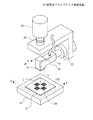
特許文献1は、接合条件としての押圧力と超音波振動状態の時間的変化を表示可能な超音波フリップチップ実装装置を開示している。図1は、特許文献1などに開示される典型的な超音波フリップチップ実装装置の構成を示す斜視図である。超音波フリップチップ実装装置10は、基板12を支持するステージ14、接合ツール18の吸着面に通じるエア流路16が形成された超音波ホーン20、超音波ホーン20に超音波振動を与える超音波振動子22、荷重センサ24を含み接合ツール18をZ方向に移動させる押圧部26を含んで構成される。半導体チップSは、その一面が接合ツール18の吸着面によって吸着され、ステージ14上の基板12に対し位置決めされる。押圧部26によって接合ツール18がZ方向に下降され、半導体チップSのバンプ電極が基板12上に形成された電極パターン12A、12Bに一定荷重で押圧される。この押圧と同時またはそれから一定時間後に、超音波振動子22により超音波ホーン20を介して半導体チップSに超音波振動が印加され、半導体チップSのバンプ電極が基板12上の電極パターン12A、12Bに金属間結合される。超音波振動子22は、電気エネルギーを機械エネルギーに変換するエネルギー変換器であり、例えば圧電素子などによって構成される。
また、特許文献2は、超音波フリップチップによる半導体チップの接合を確実にするため、予め基板上にアンダーフィル樹脂を供給し、次いで半導体チップの超音波フリップチップ接合を行う。このとき、半導体チップの側面には、粗面部が形成されており、超音波振動によりアンダーフィル樹脂が半導体チップの側面を這い上がるのを抑制している。
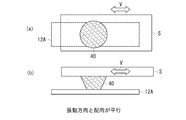
従来の超音波フリップチップ実装方法には、次のような課題がある。図1において、超音波振動子22が振動方向Vに振動するとき、ステージ14の振動方向Vと平行な方向をX方向、それに直交する方向をY方向とする。図2は、ステージ上に搭載された基板をX−Y平面で表した平面図である。同図に示すように、基板12の主面には、半導体チップのバンプ電極に接合される複数の電極パターン12Aおよび12Bが形成されている。電極パターン12Aおよび12Bは、長手方向および短手方向を有する矩形状パターンであり、電極パターン12Aは、その長手方向がX方向に延在し、電極パターン12Bは、その長手方向がY方向に延在している。言い換えれば、電極パターン12Aは、振動方向Vに平行に配向され、電極パターン12Bは、振動方向Vと垂直な方向に配向されている。
図3Aは、電極パターンの配向と振動方向Vが平行であるときの超音波振動の印加状態を示し、同図(a)は、模式的な平面図、同図(b)は模式的な側面図である。ここで、バンプ電極40は、半導体チップSに形成された円錐系のAuバンプである。半導体チップSに振動方向Vの超音波が印加されると、これに伴い、バンプ電極40が振動方向Vに振動をする。電極パターン12Aは、振動方向Vと平行に配向されているため、バンプ電極40は、電極パターン12Aの配向に沿って振動する。従って、電極パターン12Aは、バンプ電極40が振動するのに十分な領域を提供し得るため、超音波エネルギーの伝達効率が良く、その結果、バンプ電極40と電極パターン12Aの接合は良好である。
他方、図3Bは、電極パターンの配向が振動方向Vに直交するときの超音波振動の印加状態を示している。電極パターン12Bの幅Wは、バンプ電極40の狭ピッチに対応するため一定値以下に制限され、例えば、バンプ電極40の外径に等しいかそれよりも幾分だけ大きい。半導体チップSに超音波が印加されると、バンプ電極40は、電極パターン12Bの短手方向に振動する。電極パターン12Bは、短手方向に十分な幅Wを有していないため、バンプ電極40が振動するのに十分な領域を提供することができず、超音波エネルギーの伝達効率が悪くなる。このため、良好な接合状態を得るためには、より多くの超音波エネルギーを必要とする。従って、振動方向Vに一致する電極パターン12Aと振動方向Vに直交する電極パターン12Bとが1つの半導体チップ内に混在すると、半導体チップのバンプ電極と電極パターン12A、12Bの接合状態にバラツキが生じてしまう。
本発明は、このような従来の課題を解決し、半導体チップと基板間の電極の接合状態にバラツキの少ない超音波フリップチップ実装方法およびそれに用いられる基板を提供することを目的とする。
本発明に係る超音波フリップチップ実装方法は、半導体チップの一方の主面に複数の突起状の電極を形成するステップと、前記複数の突起状の電極を、基板上の対応する複数の導体パターンにそれぞれ接触させ、半導体チップに超音波振動を印加して前記複数の突起状の電極を前記複数の導体パターンに接合するステップとを含み、前記複数の導体パターンは、超音波の振動方向に対して斜め方向に配向されている。
好ましくは、前記複数の導体パターンのすべてが同一の配向角θで配向されている。好ましくは、配向角θは、45度である。また、前記複数の導体パターンの第1組は、前記振動方向に対して配向角が45度であり、前記複数の導体パターンの第2組は、前記振動方向と垂直方向に対して配向角が45度であってもよい。好ましくは、前記導体パターンは、長手方向と短手方向とを有する矩形状パターンであり、長手方向が前記振動方向またはそれと垂直方向に対して45度である。好ましくは、前記複数の突起状の電極は、Auバンプであり、前記導体パターンは、銅リードである。
本発明に係る基板は、半導体チップの一方の主面に形成された複数の突起状の電極を超音波フリップチップ接合するときに用いられるものであり、基板上には、前記複数の突起状の電極に対応する複数の導体パターンが形成され、複数の導体パターンは、半導体チップに印加される超音波の振動方向に対して斜め方向に配向されている。好ましくは、前記複数の導体パターンの配向角は、45度である。好ましくは、数の突起状の電極が接合されるべき前記複数の導体パターンのすべては、同一の配向角を有する。また、前記複数の導体パターンの第1組は、前記振動方向に対して配向角が45度であり、前記複数の導体パターンの第2組の導体パターンは、前記振動方向と垂直な方向に対して配向角が45度であってもよい。
本発明によれば、複数の導体パターンが超音波の振動方向に対して斜め方向に配向されているため、従来の振動方向に平行または垂直に配向される導体パターンと比較して、超音波エネルギーの伝達効率のバラツキが抑制され、従って、半導体チップの突起状の電極と導体パターン間の接合状態のバラツキを抑制することができる。
以下、本発明の実施形態について図面を参照して詳細に説明する。なお、図面に記載された形状およびスケールは、発明の理解を容易にするために強調されており、必ずしも実際の製品と一致しないことに留意すべきである。
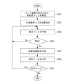
図4は、本発明の実施例に係る超音波フリップチップ実装工程を示すフローチャートである。先ず、回路素子が形成されたシリコン基板から矩形状の半導体チップを切断し、切断された半導体チップを基板上に超音波振動を利用してフリップチップ接合する(ステップS101)。フリップチップ接合は、好ましくは半導体チップと基板とを一定の温度に保持した状態で行われる。
次に、基板と半導体チップの間にアンダーフィル用樹脂が供給される(ステップS102)。アンダーフィル用樹脂は、液状化された状態で、例えば半導体チップの外周に沿って供給される。供給されたアンダーフィル用樹脂は、毛細管現象等により半導体チップの奥部にまで進行し、その後、硬化することで、半導体チップと基板間の接合を補強する。
次に、基板の裏面、すなわち半導体チップが接合された面と反対側の面にバンプ等の外部端子が接続され(ステップS103)、最後に、半導体チップ毎に対応するように基板を切断して個々の半導体装置を得る(ステップS104)。
次に、超音波フリップチップ接合の詳細について説明する。図5は、超音波フリップチップ接合のフローであり、図6は、半導体チップと基板の接合状態を説明するための概略断面図、図7は、基板の平面図である。また、超音波フリップチップ実装は、図1に示すような超音波フリップチップ実装装置を用いて行われる。
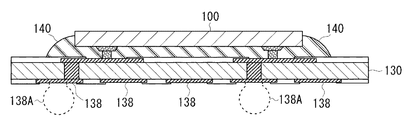
先ず、バンプ電極が形成された半導体チップを用意する(ステップS201)。図6に示すように、半導体チップ100の回路形成面である主面102には、アルミニウム等から形成される複数の電極パッド104が2次元的に配置形成され、例えば、電極パッド104は、50μmのピッチで440個配列される。これらの電極パッド104上には、突起状のバンプ電極106が形成される。バンプ電極106は、例えば、ボンディングツールを用いて形成されたAuスタッドバンプであり、その直径は約35μmである。バンプ電極は、上記の方法以外にも、メッキ等のプロセスを用いて形成することができる。
次に、超音波ホーンの接合ツール110の吸着面に半導体チップの一面を吸着させ、半導体チップ100をステージ上の基板130に位置決めする(ステップS202)。基板130は、その上面に導電領域としてCu等の電極パターン132が形成され、電極パターン132は、半導体チップ100の電極パッド104またはバンプ電極106と対応する位置に形成されている。電極パターン132は、内部配線136を介して基板裏面に形成される外部電極138に接続される。外部電極138には、例えば、BGA用またはCSP用のはんだボール等の外部端子を接続することができる。なお、電極パターン132上には、Au等のバンプ134を形成するようにしてもよい。
基板上の電極パターン132は、図7に示すように、超音波振動子の振動方向VがX方向またはY方向であるとき、X方向またはY方向に対して配向角θで配向される。ここで、配向角θとは、電極パターンの長手方向が延在する方向とX方向またはY方向との成す角と定義する。図7に示す電極パターン132A、132Bは、1つの半導体チップのバンプ電極に対応するものである。電極パターン132Aは、X方向と配向角θで延在する矩形状パターンであり、電極パターン132Bは、Y方向と配向角θで延在する矩形状パターンである。つまり、電極パターン132Aと電極パターン132Bは、長手方向の延在する方向が互いに直交する。好ましくは、基板上の接合されるすべての電極パターンが配向角θ=45度を満足するように形成される。
半導体チップ100と基板130との位置決めが完了すると、次に、半導体チップ100が基板130に接近するように接合ツール110を下降させ(ステップS203)、荷重センサの検出結果をモニタしながらバンプ電極106を対応する電極パターン132A、132Bに押圧させる(ステップS204)。バンプ電極106が電極パターン132A、132Bに押圧されたら、超音波振動子に電気信号を与え、一定時間、超音波振動を半導体チップ100に印加する(ステップS205)。
図8は、配向角θ=45度のときの超音波振動の印加状態を説明する図であり、同図(a)は、バンプ電極106と電極パターン132の関係を示す模式的平面図、同図(b)は、それらの模式的側面図である。振動方向Vに対して配向角が斜め45度であるため、振動方向Vの電極パターン132の実効的な幅W1は、W1=√2×Wとなり、バンプ電極106の振動を受け取るに十分な領域または面積を提供することができる。その結果、従来の図2に示すXおよびY方向に配列された電極パターンのときよりも、超音波エネルギーの伝達効率が改善され、バンプ電極106と電極パターン132との間の良好な接合を得ることができる。好ましくは、基板上の接合されるすべての電極パターンの配向角θを45度にすることで、バンプ電極と電極パターン間でバラツキの少ないほぼ均一な接合を得ることができる。
半導体チップへの超音波振動の印加が終了すると、接合ツール110は上昇され(ステップS206)、次の半導体チップについて同様の超音波フリップチップ接合が行われる(ステップS207)。
図9は、基板130上に複数の半導体チップ100が超音波フリップチップ接合され、それらが配列された様子を示している。ここでは1つの基板130上に多数の半導体チップ100を超音波フリップチップ接合したが、1つの基板130上に1つの半導体チップをフリップチップ接合するものであってもよい。
図10は、図9に示す基板から個々の半導体チップを切断したときの半導体装置の断面を示している。超音波フリップチップ接合を補強するために、基板130と半導体チップ100との間にはアンダーフィル用樹脂140が充填されている。外部電極138は、そのまま外部端子として用いることができるが、外部電極138にバンプ138Aを接続しても良い。
次に、超音波フリップチップ接合の他の例について説明する。上記した例は、ベアチップである半導体チップ100を基板130に超音波フリップチップ接合したが、半導体チップの代わりに半導体パッケージを接合してもよい。図11は、BGAまたはCSPなどの表面実装用の半導体パッケージ200を基板210に超音波フリップチップ接合するときの断面構造を示している。
半導体パッケージ200は、パッケージの裏面202に2次元的に配列される複数の外部端子204を備えている。外部端子204は、例えば、はんだボールである。基板210の上面には、外部端子204に対応して複数の導電性ランドパターン212が形成され、導電性ランドパターン212は、内部配線214を介して基板裏面の外部電極216に接続される。好ましくは、すべての導電性ランドパターン212は、超音波の振動方向Vに対し配向角θ=45で配向され、これらの導電性ランドパターン212に外部端子204が超音波フリップチップ接合される。
さらに、超音波フリップチップ接合は、半導体パッケージ間の接合に適用されるものであってもよい。すなわち、半導体パッケージ上に半導体パッケージを搭載する、パッケージ・オン・パッケージ(POP)に適用することができる。
図12に示すように、下部の半導体パッケージ300は、多層配線基板302と、多層配線基板302の裏面に形成された複数のはんだボール304と、多層配線基板302の上面に形成されたモールド樹脂306とを備えている。半導体チップ310は、基板302上にダイアタッチ308を介して取り付けられ、半導体チップ310の電極は、ボンディングワイヤ312により基板上の銅パターン314に接続される。モールド樹脂306は、半導体チップ310およびボンディングワイヤ312を含む領域を封止している。銅パターン314は、多層配線基板302の内部配線を介してはんだボール304に接続される。また、銅パターン314は、超音波の振動方向Vに対して配向角が45度で配向されている。
下部の半導体パッケージ300上に、上部の半導体パッケージ400が搭載される。上部の半導体パッケージ400は、例えば基板402の上面に半導体チップ404、406を積層し、これらの半導体チップ404、406がモールド樹脂408によって封止されている。基板402の裏面には、その4方向に2列のはんだボール410が形成されている。これらのはんだボール410が、基板302の上面に形成された銅パターン314に超音波接合される。
以上のように、本発明の好ましい実施の形態について詳述したが、本発明は、特定の実施形態に限定されるものではなく、特許請求の範囲に記載された本発明の要旨の範囲内において、種々の変形・変更が可能である。
上記実施例では、図7に示すように、基板上のすべての電極パターン132A、132Bが振動方向Vに関し配向角θが45度となる例を示した。すべての電極パターンの配向角が45度であれば、電極パターンの形成が容易となり、しかもすべての電極パターンの実効的な幅W1を均一にすることができるという利点がある。但し、電極パターンの配向角θは、必ずしも45度に限定されるものではなく、0<θ<90であれば、従来のXおよびY方向の配向される電極パターンよりも実効的な幅W1を大きくすることができる。
さらに、基板上の接合されるべき電極パターンのすべてが同一の配向角であることが望ましいが、超音波振動に寄与することができる電極パターンの幅Wを十分に広くとることができる場合には、そのような一部の電極パターンをX方向またはY方向に配向するようにしてもよい。
さらに、電極パターンの形状は、長手方向と短手方向を有するパターンであればよく、必ずしも矩形状に限定されない。例えば、楕円状や多角形状であってもよい。さらに、基板上に形成される電極パターンは、必ずしもすべてが同一パターン形状でなくてもよい。なお、上記した導電性ランドパターン212や銅リード314は、電極パターンに含まれる一例である。
また上記実施例では、バンプ電極としてAuバンプを例示したが、超音波接合に用いることができる他の導電性材料から形成されたバンプ電極を用いることも可能である。さらに、バンプ電極の形成方法は、特に制限されるものではなく、ボンディングツール、メッキ等の種々の方法を用いることができる。さらに、バンプ電極の形状は、必要に応じて適宜選択し得るものである。
本発明に係る超音波フリップチップ実装方法は、小型化、高密度化、狭ピッチ化された半導体チップや半導体装置の表面実装に利用することができる。
12:基板
14:ステージ
18:接合ツール
20:超音波ホーン
22:超音波振動子
12A、12B:電極パターン
100:半導体チップ
102:回路形成面
104;電極パッド
106:バンプ電極
110:接合ツール
130:基板
132、132A、132B:電極パターン
136:内部配線
138:外部電極
14:ステージ
18:接合ツール
20:超音波ホーン
22:超音波振動子
12A、12B:電極パターン
100:半導体チップ
102:回路形成面
104;電極パッド
106:バンプ電極
110:接合ツール
130:基板
132、132A、132B:電極パターン
136:内部配線
138:外部電極
Claims (10)
- 半導体チップの一方の主面に複数の突起状の電極を形成するステップと、
前記複数の突起状の電極を、基板上の対応する複数の導体パターンにそれぞれ接触させ、半導体チップに超音波振動を印加して前記複数の突起状の電極を前記複数の導体パターンに接合するステップとを含み、
前記複数の導体パターンは、超音波の振動方向に対して斜め方向に配向されている、
超音波フリップチップ実装方法。 - 前記複数の導体パターンのすべてが同一の配向角θで配向されている、請求項1に記載の実装方法。
- 配向角θは、45度である、請求項2に記載の実装方法。
- 前記複数の導体パターンの第1組は、前記振動方向に対して配向角が45度であり、前記複数の導体パターンの第2組は、前記振動方向と垂直方向に対して配向角が45度である、請求項2または3に記載の実装方法。
- 前記導体パターンは、長手方向と短手方向とを有する矩形状パターンであり、長手方向が前記振動方向またはそれと垂直方向に対して45度である、請求項1ないし4いずれか1つに記載の実装方法。
- 前記複数の突起状の電極は、Auバンプであり、前記導体パターンは、銅リードである、請求項1ないし4いずれか1つに記載の実装方法。
- 半導体チップの一方の主面に形成された複数の突起状の電極を超音波フリップチップ接合するときに用いられる基板であって、
基板上には、前記複数の突起状の電極に対応する複数の導体パターンが形成され、複数の導体パターンは、半導体チップに印加される超音波の振動方向に対して斜め方向に配向されている、基板。 - 前記複数の導体パターンの配向角は、45度である、請求項7に記載の基板。
- 前記複数の突起状の電極が接合されるべき前記複数の導体パターンのすべては、同一の配向角を有する、請求項7または8に記載の基板。
- 前記複数の導体パターンの第1組は、前記振動方向に対して配向角が45度であり、前記複数の導体パターンの第2組の導体パターンは、前記振動方向と垂直な方向に対して配向角が45度である、請求項8または9に記載の基板。
Priority Applications (2)
| Application Number | Priority Date | Filing Date | Title |
|---|---|---|---|
| JP2009108287A JP2010258302A (ja) | 2009-04-27 | 2009-04-27 | 超音波フリップチップ実装方法およびそれに用いられる基板 |
| US12/766,679 US20100269333A1 (en) | 2009-04-27 | 2010-04-23 | Method for Mounting Flip Chip and Substrate Used Therein |
Applications Claiming Priority (1)
| Application Number | Priority Date | Filing Date | Title |
|---|---|---|---|
| JP2009108287A JP2010258302A (ja) | 2009-04-27 | 2009-04-27 | 超音波フリップチップ実装方法およびそれに用いられる基板 |
Publications (1)
| Publication Number | Publication Date |
|---|---|
| JP2010258302A true JP2010258302A (ja) | 2010-11-11 |
Family
ID=42990790
Family Applications (1)
| Application Number | Title | Priority Date | Filing Date |
|---|---|---|---|
| JP2009108287A Pending JP2010258302A (ja) | 2009-04-27 | 2009-04-27 | 超音波フリップチップ実装方法およびそれに用いられる基板 |
Country Status (2)
| Country | Link |
|---|---|
| US (1) | US20100269333A1 (ja) |
| JP (1) | JP2010258302A (ja) |
Cited By (2)
| Publication number | Priority date | Publication date | Assignee | Title |
|---|---|---|---|---|
| KR20150021355A (ko) * | 2013-08-20 | 2015-03-02 | 삼성전자주식회사 | 비대칭 전극 배치 구조를 갖는 반도체 소자 |
| KR20190130699A (ko) * | 2018-05-14 | 2019-11-25 | 삼성디스플레이 주식회사 | 표시 장치 |
Families Citing this family (1)
| Publication number | Priority date | Publication date | Assignee | Title |
|---|---|---|---|---|
| KR102152906B1 (ko) * | 2018-11-20 | 2020-09-09 | 세메스 주식회사 | 본딩 장치 및 본딩 방법 |
Citations (2)
| Publication number | Priority date | Publication date | Assignee | Title |
|---|---|---|---|---|
| JP2001135674A (ja) * | 1999-11-05 | 2001-05-18 | Murata Mfg Co Ltd | 電子部品の実装方法 |
| JP2002158258A (ja) * | 2000-11-17 | 2002-05-31 | Sony Corp | 半導体装置、及び半導体装置の製造方法 |
Family Cites Families (7)
| Publication number | Priority date | Publication date | Assignee | Title |
|---|---|---|---|---|
| US5001542A (en) * | 1988-12-05 | 1991-03-19 | Hitachi Chemical Company | Composition for circuit connection, method for connection using the same, and connected structure of semiconductor chips |
| JPH04354398A (ja) * | 1991-05-31 | 1992-12-08 | Internatl Business Mach Corp <Ibm> | 配線基板及びその製造方法 |
| JP3877016B2 (ja) * | 1996-07-05 | 2007-02-07 | スター精密株式会社 | 樹脂ケースの超音波溶着方法 |
| US6583364B1 (en) * | 1999-08-26 | 2003-06-24 | Sony Chemicals Corp. | Ultrasonic manufacturing apparatuses, multilayer flexible wiring boards and processes for manufacturing multilayer flexible wiring boards |
| JP3904936B2 (ja) * | 2001-03-02 | 2007-04-11 | 富士通株式会社 | 半導体装置の製造方法 |
| US20040021230A1 (en) * | 2002-08-05 | 2004-02-05 | Macronix International Co., Ltd. | Ultra thin stacking packaging device |
| JP4175197B2 (ja) * | 2003-06-27 | 2008-11-05 | 株式会社デンソー | フリップチップ実装構造 |
-
2009
- 2009-04-27 JP JP2009108287A patent/JP2010258302A/ja active Pending
-
2010
- 2010-04-23 US US12/766,679 patent/US20100269333A1/en not_active Abandoned
Patent Citations (2)
| Publication number | Priority date | Publication date | Assignee | Title |
|---|---|---|---|---|
| JP2001135674A (ja) * | 1999-11-05 | 2001-05-18 | Murata Mfg Co Ltd | 電子部品の実装方法 |
| JP2002158258A (ja) * | 2000-11-17 | 2002-05-31 | Sony Corp | 半導体装置、及び半導体装置の製造方法 |
Cited By (4)
| Publication number | Priority date | Publication date | Assignee | Title |
|---|---|---|---|---|
| KR20150021355A (ko) * | 2013-08-20 | 2015-03-02 | 삼성전자주식회사 | 비대칭 전극 배치 구조를 갖는 반도체 소자 |
| KR102163723B1 (ko) | 2013-08-20 | 2020-10-08 | 삼성전자주식회사 | 비대칭 전극 배치 구조를 갖는 반도체 소자 |
| KR20190130699A (ko) * | 2018-05-14 | 2019-11-25 | 삼성디스플레이 주식회사 | 표시 장치 |
| KR102507222B1 (ko) | 2018-05-14 | 2023-03-07 | 삼성디스플레이 주식회사 | 표시 장치 |
Also Published As
| Publication number | Publication date |
|---|---|
| US20100269333A1 (en) | 2010-10-28 |
Similar Documents
| Publication | Publication Date | Title |
|---|---|---|
| EP2852974B1 (en) | Method of making a substrate-less stackable package with wire-bond interconnect | |
| JP2008166439A (ja) | 半導体装置およびその製造方法 | |
| US7064425B2 (en) | Semiconductor device circuit board, and electronic equipment | |
| JP2003243436A (ja) | バンプの形成方法、バンプ付き半導体素子及びその製造方法、半導体装置及びその製造方法、回路基板並びに電子機器 | |
| JP2003115560A (ja) | 半導体装置、積層半導体装置、半導体装置の製造方法及び積層半導体装置の製造方法 | |
| JP2005019895A (ja) | フリップチップ実装構造 | |
| JP2009099697A (ja) | 半導体装置及びその製造方法 | |
| KR20010098592A (ko) | 반도체패키지 및 그 제조방법 | |
| US20030155405A1 (en) | Semiconductor device and method of manufacturing the same, circuit board, and electronic equipment | |
| TWI278079B (en) | Pillar grid array package | |
| JP2010258302A (ja) | 超音波フリップチップ実装方法およびそれに用いられる基板 | |
| JP5476891B2 (ja) | 超音波フリップチップ実装方法および超音波実装装置 | |
| JP2000150560A (ja) | バンプ形成方法及びバンプ形成用ボンディングツール、半導体ウエーハ、半導体チップ及び半導体装置並びにこれらの製造方法、回路基板並びに電子機器 | |
| JP2005123542A (ja) | 半導体装置のパッケージ構造およびパッケージ化方法 | |
| JP2010147225A (ja) | 半導体装置及びその製造方法 | |
| JP3824545B2 (ja) | 配線基板、それを用いた半導体装置、それらの製造方法 | |
| JP5637249B2 (ja) | 超音波接合方法 | |
| JP2008311347A (ja) | 半導体モジュール及びその製造方法 | |
| JP2004207292A (ja) | ワイヤボンディング方法、半導体装置及びその製造方法、回路基板並びに電子機器 | |
| JP2000124251A (ja) | 半導体装置及びその製造方法、回路基板並びに電子機器 | |
| JP2007250749A (ja) | 半導体装置、電子機器及び半導体装置の製造方法 | |
| JP2004014637A (ja) | 半導体装置及びワイヤボンディング方法 | |
| JP2002299374A (ja) | 半導体装置及びその製造方法 | |
| JP2008021712A (ja) | 半導体モジュールならびにその製造方法 | |
| JP2008021710A (ja) | 半導体モジュールならびにその製造方法 |
Legal Events
| Date | Code | Title | Description |
|---|---|---|---|
| A621 | Written request for application examination |
Free format text: JAPANESE INTERMEDIATE CODE: A621 Effective date: 20120423 |
|
| A977 | Report on retrieval |
Free format text: JAPANESE INTERMEDIATE CODE: A971007 Effective date: 20130129 |
|
| A131 | Notification of reasons for refusal |
Free format text: JAPANESE INTERMEDIATE CODE: A131 Effective date: 20130205 |
|
| A02 | Decision of refusal |
Free format text: JAPANESE INTERMEDIATE CODE: A02 Effective date: 20130723 |