JP5564212B2 - 半導体装置の作製方法、及び半導体装置 - Google Patents
半導体装置の作製方法、及び半導体装置 Download PDFInfo
- Publication number
- JP5564212B2 JP5564212B2 JP2009182980A JP2009182980A JP5564212B2 JP 5564212 B2 JP5564212 B2 JP 5564212B2 JP 2009182980 A JP2009182980 A JP 2009182980A JP 2009182980 A JP2009182980 A JP 2009182980A JP 5564212 B2 JP5564212 B2 JP 5564212B2
- Authority
- JP
- Japan
- Prior art keywords
- film
- thin film
- layer
- film transistor
- substrate
- Prior art date
- Legal status (The legal status is an assumption and is not a legal conclusion. Google has not performed a legal analysis and makes no representation as to the accuracy of the status listed.)
- Active
Links
- 239000004065 semiconductor Substances 0.000 title claims description 225
- 238000004519 manufacturing process Methods 0.000 title claims description 40
- 239000000758 substrate Substances 0.000 claims description 147
- 238000000034 method Methods 0.000 claims description 110
- 230000015572 biosynthetic process Effects 0.000 claims description 63
- RTAQQCXQSZGOHL-UHFFFAOYSA-N Titanium Chemical compound [Ti] RTAQQCXQSZGOHL-UHFFFAOYSA-N 0.000 claims description 32
- 229910052719 titanium Inorganic materials 0.000 claims description 32
- 239000010936 titanium Substances 0.000 claims description 32
- 238000005530 etching Methods 0.000 claims description 31
- 239000011701 zinc Substances 0.000 claims description 28
- 229910052733 gallium Inorganic materials 0.000 claims description 27
- 229910052738 indium Inorganic materials 0.000 claims description 27
- 229910052725 zinc Inorganic materials 0.000 claims description 27
- 239000000203 mixture Substances 0.000 claims description 16
- GYHNNYVSQQEPJS-UHFFFAOYSA-N Gallium Chemical compound [Ga] GYHNNYVSQQEPJS-UHFFFAOYSA-N 0.000 claims description 12
- HCHKCACWOHOZIP-UHFFFAOYSA-N Zinc Chemical compound [Zn] HCHKCACWOHOZIP-UHFFFAOYSA-N 0.000 claims description 12
- APFVFJFRJDLVQX-UHFFFAOYSA-N indium atom Chemical compound [In] APFVFJFRJDLVQX-UHFFFAOYSA-N 0.000 claims description 12
- 238000009832 plasma treatment Methods 0.000 claims description 7
- 239000010408 film Substances 0.000 description 433
- 239000010410 layer Substances 0.000 description 356
- 239000010409 thin film Substances 0.000 description 253
- 238000004544 sputter deposition Methods 0.000 description 63
- 239000011241 protective layer Substances 0.000 description 50
- 239000004973 liquid crystal related substance Substances 0.000 description 48
- 239000012298 atmosphere Substances 0.000 description 42
- VYPSYNLAJGMNEJ-UHFFFAOYSA-N Silicium dioxide Chemical compound O=[Si]=O VYPSYNLAJGMNEJ-UHFFFAOYSA-N 0.000 description 39
- 230000008569 process Effects 0.000 description 34
- 238000012545 processing Methods 0.000 description 34
- 229910052814 silicon oxide Inorganic materials 0.000 description 32
- 239000000463 material Substances 0.000 description 31
- QVGXLLKOCUKJST-UHFFFAOYSA-N atomic oxygen Chemical compound [O] QVGXLLKOCUKJST-UHFFFAOYSA-N 0.000 description 25
- 230000006870 function Effects 0.000 description 25
- 239000001301 oxygen Substances 0.000 description 25
- 229910052760 oxygen Inorganic materials 0.000 description 25
- 229910052782 aluminium Inorganic materials 0.000 description 24
- 229910052581 Si3N4 Inorganic materials 0.000 description 22
- XAGFODPZIPBFFR-UHFFFAOYSA-N aluminium Chemical compound [Al] XAGFODPZIPBFFR-UHFFFAOYSA-N 0.000 description 22
- HQVNEWCFYHHQES-UHFFFAOYSA-N silicon nitride Chemical compound N12[Si]34N5[Si]62N3[Si]51N64 HQVNEWCFYHHQES-UHFFFAOYSA-N 0.000 description 22
- 239000000123 paper Substances 0.000 description 20
- 229910052751 metal Inorganic materials 0.000 description 17
- 239000002245 particle Substances 0.000 description 17
- 238000005401 electroluminescence Methods 0.000 description 16
- 239000011159 matrix material Substances 0.000 description 16
- 239000002184 metal Substances 0.000 description 16
- 238000012546 transfer Methods 0.000 description 16
- 238000010438 heat treatment Methods 0.000 description 15
- 239000007789 gas Substances 0.000 description 14
- XLOMVQKBTHCTTD-UHFFFAOYSA-N Zinc monoxide Chemical compound [Zn]=O XLOMVQKBTHCTTD-UHFFFAOYSA-N 0.000 description 11
- 229910052710 silicon Inorganic materials 0.000 description 11
- XKRFYHLGVUSROY-UHFFFAOYSA-N Argon Chemical compound [Ar] XKRFYHLGVUSROY-UHFFFAOYSA-N 0.000 description 10
- IJGRMHOSHXDMSA-UHFFFAOYSA-N Atomic nitrogen Chemical compound N#N IJGRMHOSHXDMSA-UHFFFAOYSA-N 0.000 description 10
- XUIMIQQOPSSXEZ-UHFFFAOYSA-N Silicon Chemical compound [Si] XUIMIQQOPSSXEZ-UHFFFAOYSA-N 0.000 description 10
- 239000012535 impurity Substances 0.000 description 10
- 239000010703 silicon Substances 0.000 description 10
- 239000011521 glass Substances 0.000 description 9
- 239000003094 microcapsule Substances 0.000 description 9
- 239000004020 conductor Substances 0.000 description 8
- 229910052736 halogen Inorganic materials 0.000 description 8
- 150000002367 halogens Chemical class 0.000 description 8
- 239000001257 hydrogen Substances 0.000 description 8
- 229910052739 hydrogen Inorganic materials 0.000 description 8
- 229910003437 indium oxide Inorganic materials 0.000 description 8
- PJXISJQVUVHSOJ-UHFFFAOYSA-N indium(iii) oxide Chemical compound [O-2].[O-2].[O-2].[In+3].[In+3] PJXISJQVUVHSOJ-UHFFFAOYSA-N 0.000 description 8
- 229920005989 resin Polymers 0.000 description 8
- 239000011347 resin Substances 0.000 description 8
- 230000004888 barrier function Effects 0.000 description 7
- -1 hydrogen compound Chemical class 0.000 description 7
- AMGQUBHHOARCQH-UHFFFAOYSA-N indium;oxotin Chemical compound [In].[Sn]=O AMGQUBHHOARCQH-UHFFFAOYSA-N 0.000 description 7
- 239000007769 metal material Substances 0.000 description 7
- 239000010453 quartz Substances 0.000 description 7
- 239000000565 sealant Substances 0.000 description 7
- 239000002356 single layer Substances 0.000 description 7
- ZOKXTWBITQBERF-UHFFFAOYSA-N Molybdenum Chemical compound [Mo] ZOKXTWBITQBERF-UHFFFAOYSA-N 0.000 description 6
- 229910052786 argon Inorganic materials 0.000 description 6
- 230000005684 electric field Effects 0.000 description 6
- 239000000945 filler Substances 0.000 description 6
- 229910052750 molybdenum Inorganic materials 0.000 description 6
- 239000011733 molybdenum Substances 0.000 description 6
- 238000005268 plasma chemical vapour deposition Methods 0.000 description 6
- 229920003023 plastic Polymers 0.000 description 6
- 239000004033 plastic Substances 0.000 description 6
- GWEVSGVZZGPLCZ-UHFFFAOYSA-N Titan oxide Chemical compound O=[Ti]=O GWEVSGVZZGPLCZ-UHFFFAOYSA-N 0.000 description 5
- 239000002585 base Substances 0.000 description 5
- 239000003990 capacitor Substances 0.000 description 5
- 229920001940 conductive polymer Polymers 0.000 description 5
- 239000000428 dust Substances 0.000 description 5
- 150000002500 ions Chemical class 0.000 description 5
- 238000001755 magnetron sputter deposition Methods 0.000 description 5
- 230000007246 mechanism Effects 0.000 description 5
- 229910052757 nitrogen Inorganic materials 0.000 description 5
- QGLKJKCYBOYXKC-UHFFFAOYSA-N nonaoxidotritungsten Chemical compound O=[W]1(=O)O[W](=O)(=O)O[W](=O)(=O)O1 QGLKJKCYBOYXKC-UHFFFAOYSA-N 0.000 description 5
- 230000003647 oxidation Effects 0.000 description 5
- 238000007254 oxidation reaction Methods 0.000 description 5
- 230000003071 parasitic effect Effects 0.000 description 5
- 229920002120 photoresistant polymer Polymers 0.000 description 5
- 238000005546 reactive sputtering Methods 0.000 description 5
- 238000009751 slip forming Methods 0.000 description 5
- 239000012798 spherical particle Substances 0.000 description 5
- OGIDPMRJRNCKJF-UHFFFAOYSA-N titanium oxide Inorganic materials [Ti]=O OGIDPMRJRNCKJF-UHFFFAOYSA-N 0.000 description 5
- 229910001930 tungsten oxide Inorganic materials 0.000 description 5
- 239000011787 zinc oxide Substances 0.000 description 5
- VYZAMTAEIAYCRO-UHFFFAOYSA-N Chromium Chemical compound [Cr] VYZAMTAEIAYCRO-UHFFFAOYSA-N 0.000 description 4
- 239000004642 Polyimide Substances 0.000 description 4
- NIXOWILDQLNWCW-UHFFFAOYSA-N acrylic acid group Chemical group C(C=C)(=O)O NIXOWILDQLNWCW-UHFFFAOYSA-N 0.000 description 4
- 230000008901 benefit Effects 0.000 description 4
- 229910052804 chromium Inorganic materials 0.000 description 4
- 239000011651 chromium Substances 0.000 description 4
- 238000011109 contamination Methods 0.000 description 4
- 238000001816 cooling Methods 0.000 description 4
- 238000000151 deposition Methods 0.000 description 4
- 230000006866 deterioration Effects 0.000 description 4
- 238000010586 diagram Methods 0.000 description 4
- 230000002349 favourable effect Effects 0.000 description 4
- 238000007667 floating Methods 0.000 description 4
- 238000003780 insertion Methods 0.000 description 4
- 230000037431 insertion Effects 0.000 description 4
- 239000007788 liquid Substances 0.000 description 4
- CPLXHLVBOLITMK-UHFFFAOYSA-N magnesium oxide Inorganic materials [Mg]=O CPLXHLVBOLITMK-UHFFFAOYSA-N 0.000 description 4
- 239000000395 magnesium oxide Substances 0.000 description 4
- AXZKOIWUVFPNLO-UHFFFAOYSA-N magnesium;oxygen(2-) Chemical compound [O-2].[Mg+2] AXZKOIWUVFPNLO-UHFFFAOYSA-N 0.000 description 4
- 229910044991 metal oxide Inorganic materials 0.000 description 4
- 150000004706 metal oxides Chemical class 0.000 description 4
- 238000005192 partition Methods 0.000 description 4
- 229920006267 polyester film Polymers 0.000 description 4
- 229920001721 polyimide Polymers 0.000 description 4
- XLYOFNOQVPJJNP-UHFFFAOYSA-N water Chemical compound O XLYOFNOQVPJJNP-UHFFFAOYSA-N 0.000 description 4
- YVTHLONGBIQYBO-UHFFFAOYSA-N zinc indium(3+) oxygen(2-) Chemical compound [O--].[Zn++].[In+3] YVTHLONGBIQYBO-UHFFFAOYSA-N 0.000 description 4
- RYGMFSIKBFXOCR-UHFFFAOYSA-N Copper Chemical compound [Cu] RYGMFSIKBFXOCR-UHFFFAOYSA-N 0.000 description 3
- 206010021143 Hypoxia Diseases 0.000 description 3
- DGAQECJNVWCQMB-PUAWFVPOSA-M Ilexoside XXIX Chemical compound C[C@@H]1CC[C@@]2(CC[C@@]3(C(=CC[C@H]4[C@]3(CC[C@@H]5[C@@]4(CC[C@@H](C5(C)C)OS(=O)(=O)[O-])C)C)[C@@H]2[C@]1(C)O)C)C(=O)O[C@H]6[C@@H]([C@H]([C@@H]([C@H](O6)CO)O)O)O.[Na+] DGAQECJNVWCQMB-PUAWFVPOSA-M 0.000 description 3
- ATJFFYVFTNAWJD-UHFFFAOYSA-N Tin Chemical compound [Sn] ATJFFYVFTNAWJD-UHFFFAOYSA-N 0.000 description 3
- 239000003795 chemical substances by application Substances 0.000 description 3
- 238000005229 chemical vapour deposition Methods 0.000 description 3
- 239000000460 chlorine Substances 0.000 description 3
- 229910052802 copper Inorganic materials 0.000 description 3
- 239000010949 copper Substances 0.000 description 3
- PMHQVHHXPFUNSP-UHFFFAOYSA-M copper(1+);methylsulfanylmethane;bromide Chemical compound Br[Cu].CSC PMHQVHHXPFUNSP-UHFFFAOYSA-M 0.000 description 3
- 239000013078 crystal Substances 0.000 description 3
- 230000008021 deposition Effects 0.000 description 3
- AJNVQOSZGJRYEI-UHFFFAOYSA-N digallium;oxygen(2-) Chemical compound [O-2].[O-2].[O-2].[Ga+3].[Ga+3] AJNVQOSZGJRYEI-UHFFFAOYSA-N 0.000 description 3
- 230000000694 effects Effects 0.000 description 3
- 230000003287 optical effect Effects 0.000 description 3
- 150000002894 organic compounds Chemical class 0.000 description 3
- TWNQGVIAIRXVLR-UHFFFAOYSA-N oxo(oxoalumanyloxy)alumane Chemical compound O=[Al]O[Al]=O TWNQGVIAIRXVLR-UHFFFAOYSA-N 0.000 description 3
- SIWVEOZUMHYXCS-UHFFFAOYSA-N oxo(oxoyttriooxy)yttrium Chemical compound O=[Y]O[Y]=O SIWVEOZUMHYXCS-UHFFFAOYSA-N 0.000 description 3
- 229920002620 polyvinyl fluoride Polymers 0.000 description 3
- 230000001681 protective effect Effects 0.000 description 3
- 230000009467 reduction Effects 0.000 description 3
- 239000003566 sealing material Substances 0.000 description 3
- 229910052708 sodium Inorganic materials 0.000 description 3
- 239000011734 sodium Substances 0.000 description 3
- 229910052718 tin Inorganic materials 0.000 description 3
- 229910018072 Al 2 O 3 Inorganic materials 0.000 description 2
- 229910017073 AlLi Inorganic materials 0.000 description 2
- CURLTUGMZLYLDI-UHFFFAOYSA-N Carbon dioxide Chemical compound O=C=O CURLTUGMZLYLDI-UHFFFAOYSA-N 0.000 description 2
- ZAMOUSCENKQFHK-UHFFFAOYSA-N Chlorine atom Chemical compound [Cl] ZAMOUSCENKQFHK-UHFFFAOYSA-N 0.000 description 2
- MYMOFIZGZYHOMD-UHFFFAOYSA-N Dioxygen Chemical compound O=O MYMOFIZGZYHOMD-UHFFFAOYSA-N 0.000 description 2
- PXGOKWXKJXAPGV-UHFFFAOYSA-N Fluorine Chemical compound FF PXGOKWXKJXAPGV-UHFFFAOYSA-N 0.000 description 2
- UFHFLCQGNIYNRP-UHFFFAOYSA-N Hydrogen Chemical compound [H][H] UFHFLCQGNIYNRP-UHFFFAOYSA-N 0.000 description 2
- FYYHWMGAXLPEAU-UHFFFAOYSA-N Magnesium Chemical compound [Mg] FYYHWMGAXLPEAU-UHFFFAOYSA-N 0.000 description 2
- 229910017947 MgOx Inorganic materials 0.000 description 2
- 238000006124 Pilkington process Methods 0.000 description 2
- 239000004952 Polyamide Substances 0.000 description 2
- 230000002411 adverse Effects 0.000 description 2
- 239000005407 aluminoborosilicate glass Substances 0.000 description 2
- 239000005354 aluminosilicate glass Substances 0.000 description 2
- 238000004458 analytical method Methods 0.000 description 2
- 229910052788 barium Inorganic materials 0.000 description 2
- DSAJWYNOEDNPEQ-UHFFFAOYSA-N barium atom Chemical compound [Ba] DSAJWYNOEDNPEQ-UHFFFAOYSA-N 0.000 description 2
- 239000005388 borosilicate glass Substances 0.000 description 2
- DQXBYHZEEUGOBF-UHFFFAOYSA-N but-3-enoic acid;ethene Chemical compound C=C.OC(=O)CC=C DQXBYHZEEUGOBF-UHFFFAOYSA-N 0.000 description 2
- 229910052791 calcium Inorganic materials 0.000 description 2
- 239000011575 calcium Substances 0.000 description 2
- 230000015556 catabolic process Effects 0.000 description 2
- 230000001413 cellular effect Effects 0.000 description 2
- 239000000919 ceramic Substances 0.000 description 2
- 230000008859 change Effects 0.000 description 2
- 229910052801 chlorine Inorganic materials 0.000 description 2
- 238000004891 communication Methods 0.000 description 2
- 239000002131 composite material Substances 0.000 description 2
- 230000007423 decrease Effects 0.000 description 2
- 238000006731 degradation reaction Methods 0.000 description 2
- 238000001784 detoxification Methods 0.000 description 2
- 238000009792 diffusion process Methods 0.000 description 2
- 229910001882 dioxygen Inorganic materials 0.000 description 2
- 238000007599 discharging Methods 0.000 description 2
- KPUWHANPEXNPJT-UHFFFAOYSA-N disiloxane Chemical class [SiH3]O[SiH3] KPUWHANPEXNPJT-UHFFFAOYSA-N 0.000 description 2
- 239000005038 ethylene vinyl acetate Substances 0.000 description 2
- 230000005281 excited state Effects 0.000 description 2
- 239000000284 extract Substances 0.000 description 2
- 239000005262 ferroelectric liquid crystals (FLCs) Substances 0.000 description 2
- 239000011152 fibreglass Substances 0.000 description 2
- 239000011737 fluorine Substances 0.000 description 2
- 229910052731 fluorine Inorganic materials 0.000 description 2
- 229910001195 gallium oxide Inorganic materials 0.000 description 2
- 239000011261 inert gas Substances 0.000 description 2
- 238000002347 injection Methods 0.000 description 2
- 239000007924 injection Substances 0.000 description 2
- 229910010272 inorganic material Inorganic materials 0.000 description 2
- 238000003475 lamination Methods 0.000 description 2
- 229910052749 magnesium Inorganic materials 0.000 description 2
- 239000011777 magnesium Substances 0.000 description 2
- 239000011859 microparticle Substances 0.000 description 2
- 229910021421 monocrystalline silicon Inorganic materials 0.000 description 2
- AHLBNYSZXLDEJQ-FWEHEUNISA-N orlistat Chemical compound CCCCCCCCCCC[C@H](OC(=O)[C@H](CC(C)C)NC=O)C[C@@H]1OC(=O)[C@H]1CCCCCC AHLBNYSZXLDEJQ-FWEHEUNISA-N 0.000 description 2
- 238000007500 overflow downdraw method Methods 0.000 description 2
- 239000000049 pigment Substances 0.000 description 2
- 229920001200 poly(ethylene-vinyl acetate) Polymers 0.000 description 2
- 229920002037 poly(vinyl butyral) polymer Polymers 0.000 description 2
- 229920002647 polyamide Polymers 0.000 description 2
- 229920000915 polyvinyl chloride Polymers 0.000 description 2
- 239000004800 polyvinyl chloride Substances 0.000 description 2
- 238000007639 printing Methods 0.000 description 2
- 238000004549 pulsed laser deposition Methods 0.000 description 2
- 238000001552 radio frequency sputter deposition Methods 0.000 description 2
- 239000003870 refractory metal Substances 0.000 description 2
- 239000002904 solvent Substances 0.000 description 2
- 125000006850 spacer group Chemical group 0.000 description 2
- 238000004528 spin coating Methods 0.000 description 2
- 239000000126 substance Substances 0.000 description 2
- 229910052715 tantalum Inorganic materials 0.000 description 2
- GUVRBAGPIYLISA-UHFFFAOYSA-N tantalum atom Chemical compound [Ta] GUVRBAGPIYLISA-UHFFFAOYSA-N 0.000 description 2
- JBQYATWDVHIOAR-UHFFFAOYSA-N tellanylidenegermanium Chemical compound [Te]=[Ge] JBQYATWDVHIOAR-UHFFFAOYSA-N 0.000 description 2
- 229920001187 thermosetting polymer Polymers 0.000 description 2
- 210000003462 vein Anatomy 0.000 description 2
- 238000001039 wet etching Methods 0.000 description 2
- 239000004925 Acrylic resin Substances 0.000 description 1
- 229920000178 Acrylic resin Polymers 0.000 description 1
- ZOXJGFHDIHLPTG-UHFFFAOYSA-N Boron Chemical compound [B] ZOXJGFHDIHLPTG-UHFFFAOYSA-N 0.000 description 1
- 206010052128 Glare Diseases 0.000 description 1
- BQCADISMDOOEFD-UHFFFAOYSA-N Silver Chemical compound [Ag] BQCADISMDOOEFD-UHFFFAOYSA-N 0.000 description 1
- NRTOMJZYCJJWKI-UHFFFAOYSA-N Titanium nitride Chemical compound [Ti]#N NRTOMJZYCJJWKI-UHFFFAOYSA-N 0.000 description 1
- QCWXUUIWCKQGHC-UHFFFAOYSA-N Zirconium Chemical compound [Zr] QCWXUUIWCKQGHC-UHFFFAOYSA-N 0.000 description 1
- 230000001133 acceleration Effects 0.000 description 1
- 239000003513 alkali Substances 0.000 description 1
- 229910052783 alkali metal Inorganic materials 0.000 description 1
- 150000001340 alkali metals Chemical class 0.000 description 1
- 229910045601 alloy Inorganic materials 0.000 description 1
- 239000000956 alloy Substances 0.000 description 1
- 150000001408 amides Chemical class 0.000 description 1
- UMIVXZPTRXBADB-UHFFFAOYSA-N benzocyclobutene Chemical compound C1=CC=C2CCC2=C1 UMIVXZPTRXBADB-UHFFFAOYSA-N 0.000 description 1
- 230000002457 bidirectional effect Effects 0.000 description 1
- 239000011230 binding agent Substances 0.000 description 1
- 230000000903 blocking effect Effects 0.000 description 1
- 229910052796 boron Inorganic materials 0.000 description 1
- BRPQOXSCLDDYGP-UHFFFAOYSA-N calcium oxide Chemical compound [O-2].[Ca+2] BRPQOXSCLDDYGP-UHFFFAOYSA-N 0.000 description 1
- 239000000292 calcium oxide Substances 0.000 description 1
- ODINCKMPIJJUCX-UHFFFAOYSA-N calcium oxide Inorganic materials [Ca]=O ODINCKMPIJJUCX-UHFFFAOYSA-N 0.000 description 1
- 239000001569 carbon dioxide Substances 0.000 description 1
- 229910002092 carbon dioxide Inorganic materials 0.000 description 1
- 239000000969 carrier Substances 0.000 description 1
- 238000004140 cleaning Methods 0.000 description 1
- 238000000576 coating method Methods 0.000 description 1
- 238000004040 coloring Methods 0.000 description 1
- 150000001875 compounds Chemical class 0.000 description 1
- 229920001577 copolymer Polymers 0.000 description 1
- 238000013461 design Methods 0.000 description 1
- 238000001514 detection method Methods 0.000 description 1
- 238000009826 distribution Methods 0.000 description 1
- 238000001312 dry etching Methods 0.000 description 1
- 230000009977 dual effect Effects 0.000 description 1
- 238000005538 encapsulation Methods 0.000 description 1
- 239000003822 epoxy resin Substances 0.000 description 1
- 239000004744 fabric Substances 0.000 description 1
- 230000005669 field effect Effects 0.000 description 1
- 239000011888 foil Substances 0.000 description 1
- 229910052732 germanium Inorganic materials 0.000 description 1
- GNPVGFCGXDBREM-UHFFFAOYSA-N germanium atom Chemical compound [Ge] GNPVGFCGXDBREM-UHFFFAOYSA-N 0.000 description 1
- PCHJSUWPFVWCPO-UHFFFAOYSA-N gold Chemical compound [Au] PCHJSUWPFVWCPO-UHFFFAOYSA-N 0.000 description 1
- 229910052737 gold Inorganic materials 0.000 description 1
- 239000010931 gold Substances 0.000 description 1
- 230000005283 ground state Effects 0.000 description 1
- 229910052735 hafnium Inorganic materials 0.000 description 1
- VBJZVLUMGGDVMO-UHFFFAOYSA-N hafnium atom Chemical compound [Hf] VBJZVLUMGGDVMO-UHFFFAOYSA-N 0.000 description 1
- 229910000449 hafnium oxide Inorganic materials 0.000 description 1
- WIHZLLGSGQNAGK-UHFFFAOYSA-N hafnium(4+);oxygen(2-) Chemical compound [O-2].[O-2].[Hf+4] WIHZLLGSGQNAGK-UHFFFAOYSA-N 0.000 description 1
- 239000003779 heat-resistant material Substances 0.000 description 1
- 230000005525 hole transport Effects 0.000 description 1
- 150000002431 hydrogen Chemical class 0.000 description 1
- 150000002484 inorganic compounds Chemical class 0.000 description 1
- 239000011147 inorganic material Substances 0.000 description 1
- 239000011810 insulating material Substances 0.000 description 1
- 239000012212 insulator Substances 0.000 description 1
- 238000010030 laminating Methods 0.000 description 1
- 239000000696 magnetic material Substances 0.000 description 1
- 238000000838 magnetophoresis Methods 0.000 description 1
- 229910021645 metal ion Inorganic materials 0.000 description 1
- 238000002156 mixing Methods 0.000 description 1
- 229910000476 molybdenum oxide Inorganic materials 0.000 description 1
- 239000012299 nitrogen atmosphere Substances 0.000 description 1
- 238000007645 offset printing Methods 0.000 description 1
- 239000012788 optical film Substances 0.000 description 1
- 239000011368 organic material Substances 0.000 description 1
- PQQKPALAQIIWST-UHFFFAOYSA-N oxomolybdenum Chemical compound [Mo]=O PQQKPALAQIIWST-UHFFFAOYSA-N 0.000 description 1
- 238000004806 packaging method and process Methods 0.000 description 1
- 238000000059 patterning Methods 0.000 description 1
- 230000035515 penetration Effects 0.000 description 1
- 239000012071 phase Substances 0.000 description 1
- 238000007747 plating Methods 0.000 description 1
- 229920000767 polyaniline Polymers 0.000 description 1
- 229920000647 polyepoxide Polymers 0.000 description 1
- 229920000128 polypyrrole Polymers 0.000 description 1
- 229920001296 polysiloxane Polymers 0.000 description 1
- 229920000123 polythiophene Polymers 0.000 description 1
- 238000005215 recombination Methods 0.000 description 1
- 230000006798 recombination Effects 0.000 description 1
- 230000004044 response Effects 0.000 description 1
- 229910052706 scandium Inorganic materials 0.000 description 1
- SIXSYDAISGFNSX-UHFFFAOYSA-N scandium atom Chemical compound [Sc] SIXSYDAISGFNSX-UHFFFAOYSA-N 0.000 description 1
- 238000007650 screen-printing Methods 0.000 description 1
- 238000007789 sealing Methods 0.000 description 1
- 229920002050 silicone resin Polymers 0.000 description 1
- 229910052709 silver Inorganic materials 0.000 description 1
- 239000004332 silver Substances 0.000 description 1
- 238000010583 slow cooling Methods 0.000 description 1
- 238000003980 solgel method Methods 0.000 description 1
- 239000000243 solution Substances 0.000 description 1
- 238000005477 sputtering target Methods 0.000 description 1
- 239000010935 stainless steel Substances 0.000 description 1
- 229910001220 stainless steel Inorganic materials 0.000 description 1
- 208000024891 symptom Diseases 0.000 description 1
- 239000013077 target material Substances 0.000 description 1
- 229910052716 thallium Inorganic materials 0.000 description 1
- BKVIYDNLLOSFOA-UHFFFAOYSA-N thallium Chemical compound [Tl] BKVIYDNLLOSFOA-UHFFFAOYSA-N 0.000 description 1
- 238000002230 thermal chemical vapour deposition Methods 0.000 description 1
- XOLBLPGZBRYERU-UHFFFAOYSA-N tin dioxide Chemical compound O=[Sn]=O XOLBLPGZBRYERU-UHFFFAOYSA-N 0.000 description 1
- 229910001887 tin oxide Inorganic materials 0.000 description 1
- 230000007704 transition Effects 0.000 description 1
- 238000002834 transmittance Methods 0.000 description 1
- 230000007723 transport mechanism Effects 0.000 description 1
- 238000007740 vapor deposition Methods 0.000 description 1
- 239000012808 vapor phase Substances 0.000 description 1
- 229910052727 yttrium Inorganic materials 0.000 description 1
- VWQVUPCCIRVNHF-UHFFFAOYSA-N yttrium atom Chemical compound [Y] VWQVUPCCIRVNHF-UHFFFAOYSA-N 0.000 description 1
- 229910052726 zirconium Inorganic materials 0.000 description 1
Images


Classifications
-
- H—ELECTRICITY
- H01—ELECTRIC ELEMENTS
- H01L—SEMICONDUCTOR DEVICES NOT COVERED BY CLASS H10
- H01L29/00—Semiconductor devices adapted for rectifying, amplifying, oscillating or switching, or capacitors or resistors with at least one potential-jump barrier or surface barrier, e.g. PN junction depletion layer or carrier concentration layer; Details of semiconductor bodies or of electrodes thereof ; Multistep manufacturing processes therefor
- H01L29/66—Types of semiconductor device ; Multistep manufacturing processes therefor
- H01L29/68—Types of semiconductor device ; Multistep manufacturing processes therefor controllable by only the electric current supplied, or only the electric potential applied, to an electrode which does not carry the current to be rectified, amplified or switched
- H01L29/76—Unipolar devices, e.g. field effect transistors
- H01L29/772—Field effect transistors
- H01L29/78—Field effect transistors with field effect produced by an insulated gate
- H01L29/786—Thin film transistors, i.e. transistors with a channel being at least partly a thin film
- H01L29/78696—Thin film transistors, i.e. transistors with a channel being at least partly a thin film characterised by the structure of the channel, e.g. multichannel, transverse or longitudinal shape, length or width, doping structure, or the overlap or alignment between the channel and the gate, the source or the drain, or the contacting structure of the channel
-
- H—ELECTRICITY
- H01—ELECTRIC ELEMENTS
- H01L—SEMICONDUCTOR DEVICES NOT COVERED BY CLASS H10
- H01L21/00—Processes or apparatus adapted for the manufacture or treatment of semiconductor or solid state devices or of parts thereof
- H01L21/02—Manufacture or treatment of semiconductor devices or of parts thereof
- H01L21/02104—Forming layers
- H01L21/02107—Forming insulating materials on a substrate
- H01L21/02109—Forming insulating materials on a substrate characterised by the type of layer, e.g. type of material, porous/non-porous, pre-cursors, mixtures or laminates
- H01L21/02112—Forming insulating materials on a substrate characterised by the type of layer, e.g. type of material, porous/non-porous, pre-cursors, mixtures or laminates characterised by the material of the layer
- H01L21/02123—Forming insulating materials on a substrate characterised by the type of layer, e.g. type of material, porous/non-porous, pre-cursors, mixtures or laminates characterised by the material of the layer the material containing silicon
- H01L21/02164—Forming insulating materials on a substrate characterised by the type of layer, e.g. type of material, porous/non-porous, pre-cursors, mixtures or laminates characterised by the material of the layer the material containing silicon the material being a silicon oxide, e.g. SiO2
-
- H—ELECTRICITY
- H01—ELECTRIC ELEMENTS
- H01L—SEMICONDUCTOR DEVICES NOT COVERED BY CLASS H10
- H01L21/00—Processes or apparatus adapted for the manufacture or treatment of semiconductor or solid state devices or of parts thereof
- H01L21/02—Manufacture or treatment of semiconductor devices or of parts thereof
- H01L21/02104—Forming layers
- H01L21/02107—Forming insulating materials on a substrate
- H01L21/02296—Forming insulating materials on a substrate characterised by the treatment performed before or after the formation of the layer
- H01L21/02318—Forming insulating materials on a substrate characterised by the treatment performed before or after the formation of the layer post-treatment
- H01L21/02321—Forming insulating materials on a substrate characterised by the treatment performed before or after the formation of the layer post-treatment introduction of substances into an already existing insulating layer
- H01L21/02323—Forming insulating materials on a substrate characterised by the treatment performed before or after the formation of the layer post-treatment introduction of substances into an already existing insulating layer introduction of oxygen
-
- H—ELECTRICITY
- H01—ELECTRIC ELEMENTS
- H01L—SEMICONDUCTOR DEVICES NOT COVERED BY CLASS H10
- H01L21/00—Processes or apparatus adapted for the manufacture or treatment of semiconductor or solid state devices or of parts thereof
- H01L21/02—Manufacture or treatment of semiconductor devices or of parts thereof
- H01L21/02104—Forming layers
- H01L21/02365—Forming inorganic semiconducting materials on a substrate
- H01L21/02518—Deposited layers
- H01L21/02521—Materials
- H01L21/02565—Oxide semiconducting materials not being Group 12/16 materials, e.g. ternary compounds
-
- H—ELECTRICITY
- H01—ELECTRIC ELEMENTS
- H01L—SEMICONDUCTOR DEVICES NOT COVERED BY CLASS H10
- H01L21/00—Processes or apparatus adapted for the manufacture or treatment of semiconductor or solid state devices or of parts thereof
- H01L21/02—Manufacture or treatment of semiconductor devices or of parts thereof
- H01L21/04—Manufacture or treatment of semiconductor devices or of parts thereof the devices having at least one potential-jump barrier or surface barrier, e.g. PN junction, depletion layer or carrier concentration layer
- H01L21/18—Manufacture or treatment of semiconductor devices or of parts thereof the devices having at least one potential-jump barrier or surface barrier, e.g. PN junction, depletion layer or carrier concentration layer the devices having semiconductor bodies comprising elements of Group IV of the Periodic System or AIIIBV compounds with or without impurities, e.g. doping materials
- H01L21/30—Treatment of semiconductor bodies using processes or apparatus not provided for in groups H01L21/20 - H01L21/26
- H01L21/31—Treatment of semiconductor bodies using processes or apparatus not provided for in groups H01L21/20 - H01L21/26 to form insulating layers thereon, e.g. for masking or by using photolithographic techniques; After treatment of these layers; Selection of materials for these layers
- H01L21/3205—Deposition of non-insulating-, e.g. conductive- or resistive-, layers on insulating layers; After-treatment of these layers
- H01L21/321—After treatment
- H01L21/3213—Physical or chemical etching of the layers, e.g. to produce a patterned layer from a pre-deposited extensive layer
- H01L21/32139—Physical or chemical etching of the layers, e.g. to produce a patterned layer from a pre-deposited extensive layer using masks
-
- H—ELECTRICITY
- H01—ELECTRIC ELEMENTS
- H01L—SEMICONDUCTOR DEVICES NOT COVERED BY CLASS H10
- H01L21/00—Processes or apparatus adapted for the manufacture or treatment of semiconductor or solid state devices or of parts thereof
- H01L21/02—Manufacture or treatment of semiconductor devices or of parts thereof
- H01L21/04—Manufacture or treatment of semiconductor devices or of parts thereof the devices having at least one potential-jump barrier or surface barrier, e.g. PN junction, depletion layer or carrier concentration layer
- H01L21/34—Manufacture or treatment of semiconductor devices or of parts thereof the devices having at least one potential-jump barrier or surface barrier, e.g. PN junction, depletion layer or carrier concentration layer the devices having semiconductor bodies not provided for in groups H01L21/0405, H01L21/0445, H01L21/06, H01L21/16 and H01L21/18 with or without impurities, e.g. doping materials
- H01L21/46—Treatment of semiconductor bodies using processes or apparatus not provided for in groups H01L21/428
- H01L21/461—Treatment of semiconductor bodies using processes or apparatus not provided for in groups H01L21/428 to change their surface-physical characteristics or shape, e.g. etching, polishing, cutting
- H01L21/465—Chemical or electrical treatment, e.g. electrolytic etching
- H01L21/467—Chemical or electrical treatment, e.g. electrolytic etching using masks
-
- H—ELECTRICITY
- H01—ELECTRIC ELEMENTS
- H01L—SEMICONDUCTOR DEVICES NOT COVERED BY CLASS H10
- H01L21/00—Processes or apparatus adapted for the manufacture or treatment of semiconductor or solid state devices or of parts thereof
- H01L21/02—Manufacture or treatment of semiconductor devices or of parts thereof
- H01L21/04—Manufacture or treatment of semiconductor devices or of parts thereof the devices having at least one potential-jump barrier or surface barrier, e.g. PN junction, depletion layer or carrier concentration layer
- H01L21/34—Manufacture or treatment of semiconductor devices or of parts thereof the devices having at least one potential-jump barrier or surface barrier, e.g. PN junction, depletion layer or carrier concentration layer the devices having semiconductor bodies not provided for in groups H01L21/0405, H01L21/0445, H01L21/06, H01L21/16 and H01L21/18 with or without impurities, e.g. doping materials
- H01L21/46—Treatment of semiconductor bodies using processes or apparatus not provided for in groups H01L21/428
- H01L21/461—Treatment of semiconductor bodies using processes or apparatus not provided for in groups H01L21/428 to change their surface-physical characteristics or shape, e.g. etching, polishing, cutting
- H01L21/4763—Deposition of non-insulating, e.g. conductive -, resistive -, layers on insulating layers; After-treatment of these layers
- H01L21/47635—After-treatment of these layers
-
- H—ELECTRICITY
- H01—ELECTRIC ELEMENTS
- H01L—SEMICONDUCTOR DEVICES NOT COVERED BY CLASS H10
- H01L27/00—Devices consisting of a plurality of semiconductor or other solid-state components formed in or on a common substrate
- H01L27/02—Devices consisting of a plurality of semiconductor or other solid-state components formed in or on a common substrate including semiconductor components specially adapted for rectifying, oscillating, amplifying or switching and having at least one potential-jump barrier or surface barrier; including integrated passive circuit elements with at least one potential-jump barrier or surface barrier
- H01L27/12—Devices consisting of a plurality of semiconductor or other solid-state components formed in or on a common substrate including semiconductor components specially adapted for rectifying, oscillating, amplifying or switching and having at least one potential-jump barrier or surface barrier; including integrated passive circuit elements with at least one potential-jump barrier or surface barrier the substrate being other than a semiconductor body, e.g. an insulating body
- H01L27/1214—Devices consisting of a plurality of semiconductor or other solid-state components formed in or on a common substrate including semiconductor components specially adapted for rectifying, oscillating, amplifying or switching and having at least one potential-jump barrier or surface barrier; including integrated passive circuit elements with at least one potential-jump barrier or surface barrier the substrate being other than a semiconductor body, e.g. an insulating body comprising a plurality of TFTs formed on a non-semiconducting substrate, e.g. driving circuits for AMLCDs
- H01L27/1222—Devices consisting of a plurality of semiconductor or other solid-state components formed in or on a common substrate including semiconductor components specially adapted for rectifying, oscillating, amplifying or switching and having at least one potential-jump barrier or surface barrier; including integrated passive circuit elements with at least one potential-jump barrier or surface barrier the substrate being other than a semiconductor body, e.g. an insulating body comprising a plurality of TFTs formed on a non-semiconducting substrate, e.g. driving circuits for AMLCDs with a particular composition, shape or crystalline structure of the active layer
- H01L27/1225—Devices consisting of a plurality of semiconductor or other solid-state components formed in or on a common substrate including semiconductor components specially adapted for rectifying, oscillating, amplifying or switching and having at least one potential-jump barrier or surface barrier; including integrated passive circuit elements with at least one potential-jump barrier or surface barrier the substrate being other than a semiconductor body, e.g. an insulating body comprising a plurality of TFTs formed on a non-semiconducting substrate, e.g. driving circuits for AMLCDs with a particular composition, shape or crystalline structure of the active layer with semiconductor materials not belonging to the group IV of the periodic table, e.g. InGaZnO
-
- H—ELECTRICITY
- H01—ELECTRIC ELEMENTS
- H01L—SEMICONDUCTOR DEVICES NOT COVERED BY CLASS H10
- H01L29/00—Semiconductor devices adapted for rectifying, amplifying, oscillating or switching, or capacitors or resistors with at least one potential-jump barrier or surface barrier, e.g. PN junction depletion layer or carrier concentration layer; Details of semiconductor bodies or of electrodes thereof ; Multistep manufacturing processes therefor
- H01L29/02—Semiconductor bodies ; Multistep manufacturing processes therefor
- H01L29/06—Semiconductor bodies ; Multistep manufacturing processes therefor characterised by their shape; characterised by the shapes, relative sizes, or dispositions of the semiconductor regions ; characterised by the concentration or distribution of impurities within semiconductor regions
- H01L29/0684—Semiconductor bodies ; Multistep manufacturing processes therefor characterised by their shape; characterised by the shapes, relative sizes, or dispositions of the semiconductor regions ; characterised by the concentration or distribution of impurities within semiconductor regions characterised by the shape, relative sizes or dispositions of the semiconductor regions or junctions between the regions
- H01L29/0692—Surface layout
-
- H—ELECTRICITY
- H01—ELECTRIC ELEMENTS
- H01L—SEMICONDUCTOR DEVICES NOT COVERED BY CLASS H10
- H01L29/00—Semiconductor devices adapted for rectifying, amplifying, oscillating or switching, or capacitors or resistors with at least one potential-jump barrier or surface barrier, e.g. PN junction depletion layer or carrier concentration layer; Details of semiconductor bodies or of electrodes thereof ; Multistep manufacturing processes therefor
- H01L29/02—Semiconductor bodies ; Multistep manufacturing processes therefor
- H01L29/06—Semiconductor bodies ; Multistep manufacturing processes therefor characterised by their shape; characterised by the shapes, relative sizes, or dispositions of the semiconductor regions ; characterised by the concentration or distribution of impurities within semiconductor regions
- H01L29/10—Semiconductor bodies ; Multistep manufacturing processes therefor characterised by their shape; characterised by the shapes, relative sizes, or dispositions of the semiconductor regions ; characterised by the concentration or distribution of impurities within semiconductor regions with semiconductor regions connected to an electrode not carrying current to be rectified, amplified or switched and such electrode being part of a semiconductor device which comprises three or more electrodes
- H01L29/1025—Channel region of field-effect devices
- H01L29/1029—Channel region of field-effect devices of field-effect transistors
- H01L29/1033—Channel region of field-effect devices of field-effect transistors with insulated gate, e.g. characterised by the length, the width, the geometric contour or the doping structure
-
- H—ELECTRICITY
- H01—ELECTRIC ELEMENTS
- H01L—SEMICONDUCTOR DEVICES NOT COVERED BY CLASS H10
- H01L29/00—Semiconductor devices adapted for rectifying, amplifying, oscillating or switching, or capacitors or resistors with at least one potential-jump barrier or surface barrier, e.g. PN junction depletion layer or carrier concentration layer; Details of semiconductor bodies or of electrodes thereof ; Multistep manufacturing processes therefor
- H01L29/02—Semiconductor bodies ; Multistep manufacturing processes therefor
- H01L29/12—Semiconductor bodies ; Multistep manufacturing processes therefor characterised by the materials of which they are formed
- H01L29/24—Semiconductor bodies ; Multistep manufacturing processes therefor characterised by the materials of which they are formed including, apart from doping materials or other impurities, only semiconductor materials not provided for in groups H01L29/16, H01L29/18, H01L29/20, H01L29/22
-
- H—ELECTRICITY
- H01—ELECTRIC ELEMENTS
- H01L—SEMICONDUCTOR DEVICES NOT COVERED BY CLASS H10
- H01L29/00—Semiconductor devices adapted for rectifying, amplifying, oscillating or switching, or capacitors or resistors with at least one potential-jump barrier or surface barrier, e.g. PN junction depletion layer or carrier concentration layer; Details of semiconductor bodies or of electrodes thereof ; Multistep manufacturing processes therefor
- H01L29/02—Semiconductor bodies ; Multistep manufacturing processes therefor
- H01L29/12—Semiconductor bodies ; Multistep manufacturing processes therefor characterised by the materials of which they are formed
- H01L29/26—Semiconductor bodies ; Multistep manufacturing processes therefor characterised by the materials of which they are formed including, apart from doping materials or other impurities, elements provided for in two or more of the groups H01L29/16, H01L29/18, H01L29/20, H01L29/22, H01L29/24, e.g. alloys
- H01L29/263—Amorphous materials
-
- H—ELECTRICITY
- H01—ELECTRIC ELEMENTS
- H01L—SEMICONDUCTOR DEVICES NOT COVERED BY CLASS H10
- H01L29/00—Semiconductor devices adapted for rectifying, amplifying, oscillating or switching, or capacitors or resistors with at least one potential-jump barrier or surface barrier, e.g. PN junction depletion layer or carrier concentration layer; Details of semiconductor bodies or of electrodes thereof ; Multistep manufacturing processes therefor
- H01L29/40—Electrodes ; Multistep manufacturing processes therefor
- H01L29/41—Electrodes ; Multistep manufacturing processes therefor characterised by their shape, relative sizes or dispositions
- H01L29/417—Electrodes ; Multistep manufacturing processes therefor characterised by their shape, relative sizes or dispositions carrying the current to be rectified, amplified or switched
- H01L29/41725—Source or drain electrodes for field effect devices
- H01L29/41733—Source or drain electrodes for field effect devices for thin film transistors with insulated gate
-
- H—ELECTRICITY
- H01—ELECTRIC ELEMENTS
- H01L—SEMICONDUCTOR DEVICES NOT COVERED BY CLASS H10
- H01L29/00—Semiconductor devices adapted for rectifying, amplifying, oscillating or switching, or capacitors or resistors with at least one potential-jump barrier or surface barrier, e.g. PN junction depletion layer or carrier concentration layer; Details of semiconductor bodies or of electrodes thereof ; Multistep manufacturing processes therefor
- H01L29/40—Electrodes ; Multistep manufacturing processes therefor
- H01L29/41—Electrodes ; Multistep manufacturing processes therefor characterised by their shape, relative sizes or dispositions
- H01L29/423—Electrodes ; Multistep manufacturing processes therefor characterised by their shape, relative sizes or dispositions not carrying the current to be rectified, amplified or switched
- H01L29/42312—Gate electrodes for field effect devices
- H01L29/42316—Gate electrodes for field effect devices for field-effect transistors
- H01L29/4232—Gate electrodes for field effect devices for field-effect transistors with insulated gate
- H01L29/42364—Gate electrodes for field effect devices for field-effect transistors with insulated gate characterised by the insulating layer, e.g. thickness or uniformity
-
- H—ELECTRICITY
- H01—ELECTRIC ELEMENTS
- H01L—SEMICONDUCTOR DEVICES NOT COVERED BY CLASS H10
- H01L29/00—Semiconductor devices adapted for rectifying, amplifying, oscillating or switching, or capacitors or resistors with at least one potential-jump barrier or surface barrier, e.g. PN junction depletion layer or carrier concentration layer; Details of semiconductor bodies or of electrodes thereof ; Multistep manufacturing processes therefor
- H01L29/40—Electrodes ; Multistep manufacturing processes therefor
- H01L29/41—Electrodes ; Multistep manufacturing processes therefor characterised by their shape, relative sizes or dispositions
- H01L29/423—Electrodes ; Multistep manufacturing processes therefor characterised by their shape, relative sizes or dispositions not carrying the current to be rectified, amplified or switched
- H01L29/42312—Gate electrodes for field effect devices
- H01L29/42316—Gate electrodes for field effect devices for field-effect transistors
- H01L29/4232—Gate electrodes for field effect devices for field-effect transistors with insulated gate
- H01L29/42384—Gate electrodes for field effect devices for field-effect transistors with insulated gate for thin film field effect transistors, e.g. characterised by the thickness or the shape of the insulator or the dimensions, the shape or the lay-out of the conductor
-
- H—ELECTRICITY
- H01—ELECTRIC ELEMENTS
- H01L—SEMICONDUCTOR DEVICES NOT COVERED BY CLASS H10
- H01L29/00—Semiconductor devices adapted for rectifying, amplifying, oscillating or switching, or capacitors or resistors with at least one potential-jump barrier or surface barrier, e.g. PN junction depletion layer or carrier concentration layer; Details of semiconductor bodies or of electrodes thereof ; Multistep manufacturing processes therefor
- H01L29/40—Electrodes ; Multistep manufacturing processes therefor
- H01L29/43—Electrodes ; Multistep manufacturing processes therefor characterised by the materials of which they are formed
- H01L29/45—Ohmic electrodes
-
- H—ELECTRICITY
- H01—ELECTRIC ELEMENTS
- H01L—SEMICONDUCTOR DEVICES NOT COVERED BY CLASS H10
- H01L29/00—Semiconductor devices adapted for rectifying, amplifying, oscillating or switching, or capacitors or resistors with at least one potential-jump barrier or surface barrier, e.g. PN junction depletion layer or carrier concentration layer; Details of semiconductor bodies or of electrodes thereof ; Multistep manufacturing processes therefor
- H01L29/40—Electrodes ; Multistep manufacturing processes therefor
- H01L29/43—Electrodes ; Multistep manufacturing processes therefor characterised by the materials of which they are formed
- H01L29/49—Metal-insulator-semiconductor electrodes, e.g. gates of MOSFET
- H01L29/4908—Metal-insulator-semiconductor electrodes, e.g. gates of MOSFET for thin film semiconductor, e.g. gate of TFT
-
- H—ELECTRICITY
- H01—ELECTRIC ELEMENTS
- H01L—SEMICONDUCTOR DEVICES NOT COVERED BY CLASS H10
- H01L29/00—Semiconductor devices adapted for rectifying, amplifying, oscillating or switching, or capacitors or resistors with at least one potential-jump barrier or surface barrier, e.g. PN junction depletion layer or carrier concentration layer; Details of semiconductor bodies or of electrodes thereof ; Multistep manufacturing processes therefor
- H01L29/40—Electrodes ; Multistep manufacturing processes therefor
- H01L29/43—Electrodes ; Multistep manufacturing processes therefor characterised by the materials of which they are formed
- H01L29/49—Metal-insulator-semiconductor electrodes, e.g. gates of MOSFET
- H01L29/495—Metal-insulator-semiconductor electrodes, e.g. gates of MOSFET the conductor material next to the insulator being a simple metal, e.g. W, Mo
-
- H—ELECTRICITY
- H01—ELECTRIC ELEMENTS
- H01L—SEMICONDUCTOR DEVICES NOT COVERED BY CLASS H10
- H01L29/00—Semiconductor devices adapted for rectifying, amplifying, oscillating or switching, or capacitors or resistors with at least one potential-jump barrier or surface barrier, e.g. PN junction depletion layer or carrier concentration layer; Details of semiconductor bodies or of electrodes thereof ; Multistep manufacturing processes therefor
- H01L29/40—Electrodes ; Multistep manufacturing processes therefor
- H01L29/43—Electrodes ; Multistep manufacturing processes therefor characterised by the materials of which they are formed
- H01L29/49—Metal-insulator-semiconductor electrodes, e.g. gates of MOSFET
- H01L29/51—Insulating materials associated therewith
- H01L29/511—Insulating materials associated therewith with a compositional variation, e.g. multilayer structures
- H01L29/513—Insulating materials associated therewith with a compositional variation, e.g. multilayer structures the variation being perpendicular to the channel plane
-
- H—ELECTRICITY
- H01—ELECTRIC ELEMENTS
- H01L—SEMICONDUCTOR DEVICES NOT COVERED BY CLASS H10
- H01L29/00—Semiconductor devices adapted for rectifying, amplifying, oscillating or switching, or capacitors or resistors with at least one potential-jump barrier or surface barrier, e.g. PN junction depletion layer or carrier concentration layer; Details of semiconductor bodies or of electrodes thereof ; Multistep manufacturing processes therefor
- H01L29/40—Electrodes ; Multistep manufacturing processes therefor
- H01L29/43—Electrodes ; Multistep manufacturing processes therefor characterised by the materials of which they are formed
- H01L29/49—Metal-insulator-semiconductor electrodes, e.g. gates of MOSFET
- H01L29/51—Insulating materials associated therewith
- H01L29/518—Insulating materials associated therewith the insulating material containing nitrogen, e.g. nitride, oxynitride, nitrogen-doped material
-
- H—ELECTRICITY
- H01—ELECTRIC ELEMENTS
- H01L—SEMICONDUCTOR DEVICES NOT COVERED BY CLASS H10
- H01L29/00—Semiconductor devices adapted for rectifying, amplifying, oscillating or switching, or capacitors or resistors with at least one potential-jump barrier or surface barrier, e.g. PN junction depletion layer or carrier concentration layer; Details of semiconductor bodies or of electrodes thereof ; Multistep manufacturing processes therefor
- H01L29/66—Types of semiconductor device ; Multistep manufacturing processes therefor
- H01L29/66007—Multistep manufacturing processes
- H01L29/66075—Multistep manufacturing processes of devices having semiconductor bodies comprising group 14 or group 13/15 materials
- H01L29/66227—Multistep manufacturing processes of devices having semiconductor bodies comprising group 14 or group 13/15 materials the devices being controllable only by the electric current supplied or the electric potential applied, to an electrode which does not carry the current to be rectified, amplified or switched, e.g. three-terminal devices
- H01L29/66409—Unipolar field-effect transistors
- H01L29/66477—Unipolar field-effect transistors with an insulated gate, i.e. MISFET
- H01L29/66742—Thin film unipolar transistors
-
- H—ELECTRICITY
- H01—ELECTRIC ELEMENTS
- H01L—SEMICONDUCTOR DEVICES NOT COVERED BY CLASS H10
- H01L29/00—Semiconductor devices adapted for rectifying, amplifying, oscillating or switching, or capacitors or resistors with at least one potential-jump barrier or surface barrier, e.g. PN junction depletion layer or carrier concentration layer; Details of semiconductor bodies or of electrodes thereof ; Multistep manufacturing processes therefor
- H01L29/66—Types of semiconductor device ; Multistep manufacturing processes therefor
- H01L29/66007—Multistep manufacturing processes
- H01L29/66969—Multistep manufacturing processes of devices having semiconductor bodies not comprising group 14 or group 13/15 materials
-
- H—ELECTRICITY
- H01—ELECTRIC ELEMENTS
- H01L—SEMICONDUCTOR DEVICES NOT COVERED BY CLASS H10
- H01L29/00—Semiconductor devices adapted for rectifying, amplifying, oscillating or switching, or capacitors or resistors with at least one potential-jump barrier or surface barrier, e.g. PN junction depletion layer or carrier concentration layer; Details of semiconductor bodies or of electrodes thereof ; Multistep manufacturing processes therefor
- H01L29/66—Types of semiconductor device ; Multistep manufacturing processes therefor
- H01L29/68—Types of semiconductor device ; Multistep manufacturing processes therefor controllable by only the electric current supplied, or only the electric potential applied, to an electrode which does not carry the current to be rectified, amplified or switched
- H01L29/76—Unipolar devices, e.g. field effect transistors
- H01L29/772—Field effect transistors
- H01L29/78—Field effect transistors with field effect produced by an insulated gate
- H01L29/786—Thin film transistors, i.e. transistors with a channel being at least partly a thin film
- H01L29/78606—Thin film transistors, i.e. transistors with a channel being at least partly a thin film with supplementary region or layer in the thin film or in the insulated bulk substrate supporting it for controlling or increasing the safety of the device
- H01L29/78618—Thin film transistors, i.e. transistors with a channel being at least partly a thin film with supplementary region or layer in the thin film or in the insulated bulk substrate supporting it for controlling or increasing the safety of the device characterised by the drain or the source properties, e.g. the doping structure, the composition, the sectional shape or the contact structure
-
- H—ELECTRICITY
- H01—ELECTRIC ELEMENTS
- H01L—SEMICONDUCTOR DEVICES NOT COVERED BY CLASS H10
- H01L29/00—Semiconductor devices adapted for rectifying, amplifying, oscillating or switching, or capacitors or resistors with at least one potential-jump barrier or surface barrier, e.g. PN junction depletion layer or carrier concentration layer; Details of semiconductor bodies or of electrodes thereof ; Multistep manufacturing processes therefor
- H01L29/66—Types of semiconductor device ; Multistep manufacturing processes therefor
- H01L29/68—Types of semiconductor device ; Multistep manufacturing processes therefor controllable by only the electric current supplied, or only the electric potential applied, to an electrode which does not carry the current to be rectified, amplified or switched
- H01L29/76—Unipolar devices, e.g. field effect transistors
- H01L29/772—Field effect transistors
- H01L29/78—Field effect transistors with field effect produced by an insulated gate
- H01L29/786—Thin film transistors, i.e. transistors with a channel being at least partly a thin film
- H01L29/78606—Thin film transistors, i.e. transistors with a channel being at least partly a thin film with supplementary region or layer in the thin film or in the insulated bulk substrate supporting it for controlling or increasing the safety of the device
- H01L29/78633—Thin film transistors, i.e. transistors with a channel being at least partly a thin film with supplementary region or layer in the thin film or in the insulated bulk substrate supporting it for controlling or increasing the safety of the device with a light shield
-
- H—ELECTRICITY
- H01—ELECTRIC ELEMENTS
- H01L—SEMICONDUCTOR DEVICES NOT COVERED BY CLASS H10
- H01L29/00—Semiconductor devices adapted for rectifying, amplifying, oscillating or switching, or capacitors or resistors with at least one potential-jump barrier or surface barrier, e.g. PN junction depletion layer or carrier concentration layer; Details of semiconductor bodies or of electrodes thereof ; Multistep manufacturing processes therefor
- H01L29/66—Types of semiconductor device ; Multistep manufacturing processes therefor
- H01L29/68—Types of semiconductor device ; Multistep manufacturing processes therefor controllable by only the electric current supplied, or only the electric potential applied, to an electrode which does not carry the current to be rectified, amplified or switched
- H01L29/76—Unipolar devices, e.g. field effect transistors
- H01L29/772—Field effect transistors
- H01L29/78—Field effect transistors with field effect produced by an insulated gate
- H01L29/786—Thin film transistors, i.e. transistors with a channel being at least partly a thin film
- H01L29/7869—Thin film transistors, i.e. transistors with a channel being at least partly a thin film having a semiconductor body comprising an oxide semiconductor material, e.g. zinc oxide, copper aluminium oxide, cadmium stannate
- H01L29/78693—Thin film transistors, i.e. transistors with a channel being at least partly a thin film having a semiconductor body comprising an oxide semiconductor material, e.g. zinc oxide, copper aluminium oxide, cadmium stannate the semiconducting oxide being amorphous
-
- H—ELECTRICITY
- H01—ELECTRIC ELEMENTS
- H01L—SEMICONDUCTOR DEVICES NOT COVERED BY CLASS H10
- H01L2924/00—Indexing scheme for arrangements or methods for connecting or disconnecting semiconductor or solid-state bodies as covered by H01L24/00
- H01L2924/01—Chemical elements
- H01L2924/01022—Titanium [Ti]
-
- H—ELECTRICITY
- H01—ELECTRIC ELEMENTS
- H01L—SEMICONDUCTOR DEVICES NOT COVERED BY CLASS H10
- H01L2924/00—Indexing scheme for arrangements or methods for connecting or disconnecting semiconductor or solid-state bodies as covered by H01L24/00
- H01L2924/049—Nitrides composed of metals from groups of the periodic table
- H01L2924/0504—14th Group
- H01L2924/05042—Si3N4
Description
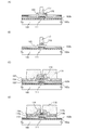
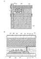
本実施の形態では、In、Ga、及びZnを含む酸化物半導体層を用い、半導体層とソース電極層及びドレイン電極層との間にバッファ層を設け、チャネル保護層を設けた逆スタガ型(ボトムゲート構造)の薄膜トランジスタの作製工程について、図1及び図2を用いて説明する。
本実施の形態では、上記実施の形態1とは別の構造のバッファ層に有するIGZO半導体層を用いた逆スタガ型(ボトムゲート構造)薄膜トランジスタの作製工程について、図3及び図4を用いて説明する。また、本実施の形態において、実施の形態1と同じものについては同じ符号を用い、詳細な説明を省略する。
本実施の形態では、複数のチャネル形成領域を接続した構造を有するIGZO半導体層を用いた薄膜トランジスタの作製方法について、図5を用いて説明する。
ここでは、少なくともゲート絶縁膜と酸化物半導体層の積層を大気に触れることなく、連続成膜を行う逆スタガ型の薄膜トランジスタの作製例を以下に示す。ここでは、連続成膜を行う工程までの工程を示し、その後の工程は、実施の形態1乃至3のいずれか一に従って薄膜トランジスタを作製すればよい。
また、成膜方法として、成膜中にターゲット物質とスパッタガス成分とを化学反応させてそれらの化合物薄膜を形成するリアクティブスパッタ法や、成膜中に基板にも電圧をかけるバイアススパッタ法もある。
本実施の形態では、同一基板上に少なくとも駆動回路の一部と、画素部に配置する薄膜トランジスタを作製する例について以下に説明する。
本発明の一態様を適用した薄膜トランジスタを作製し、該薄膜トランジスタを画素部、さらには駆動回路に用いて表示機能を有する半導体装置(表示装置ともいう)を作製することができる。また、本発明の一態様を適用した薄膜トランジスタを用いた駆動回路の一部または全体を、画素部と同じ基板上に一体形成し、システムオンパネルを形成することができる。
本実施の形態では、本発明の一態様を適用した半導体装置として電子ペーパーの例を示す。
本実施の形態では、本発明の一態様を適用した半導体装置として発光表示装置の例を示す。表示装置の有する表示素子としては、ここではエレクトロルミネッセンスを利用する発光素子を用いて示す。エレクトロルミネッセンスを利用する発光素子は、発光材料が有機化合物であるか、無機化合物であるかによって区別され、一般的に、前者は有機EL素子、後者は無機EL素子と呼ばれている。
次に、本発明の一態様を適用した半導体装置を搭載した表示パネルの構成について、以下に示す。本実施の形態では、表示素子として液晶素子を有する液晶表示装置の一形態である液晶表示パネル(液晶パネルともいう)、表示素子として発光素子を有する半導体装置の一形態である発光表示パネル(発光パネルともいう)について説明する。
本発明に係る半導体装置は、さまざまな電子機器(遊技機も含む)に適用することができる。電子機器としては、例えば、テレビジョン装置(テレビ、またはテレビジョン受信機ともいう)、コンピュータ用などのモニタ、電子ペーパー、デジタルカメラ、デジタルビデオカメラ、デジタルフォトフレーム、携帯電話機(携帯電話、携帯電話装置ともいう)、携帯型ゲーム機、携帯情報端末、音響再生装置、パチンコ機などの大型ゲーム機などが挙げられる。特に、実施の形態6〜実施の形態9で示したように、本発明に係る薄膜トランジスタを液晶表示装置、発光装置、電気泳動方式表示装置などに適用することにより、電子機器の表示部に用いることができる。以下に具体的に例示する。
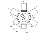
81 搬送ロボット
82 カセット室
83 ゲートバルブ
84 ゲートバルブ
85 ゲートバルブ
86 ゲートバルブ
87 ゲートバルブ
88 ゲートバルブ
89 処理室
90 処理室
91 処理室
92 処理室
93 処理室
94 基板
100 基板
102a ゲート絶縁膜
102b ゲート絶縁膜
103 半導体膜
104 膜
105 導電膜
106 絶縁膜
111 ゲート電極層
111a ゲート電極層
113 半導体層
114a バッファ層
114c 層
115a ドレイン電極層
115c 導電層
116 チャネル保護層
116a チャネル保護層
117 レジストマスク
118 レジストマスク
200 基板
201 薄膜トランジスタ
202 ソース配線層
203 ゲート配線層
204 容量配線層
211 絶縁層
212 絶縁層
213 絶縁層
255 電極層
260 液晶表示素子
261 絶縁層
262 液晶層
263 絶縁層
264 着色層
265 電極層
266 基板
267 偏光板
268 偏光板
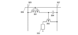
301 薄膜トランジスタ
302 薄膜トランジスタ
303 発光素子
304 容量素子
305 ソース配線層
306 ゲート配線層
307 電源線
311 絶縁層
312 絶縁層
313 絶縁層
320 電極層
321 隔壁
322 電界発光層
323 電極層
324 発光素子
581 薄膜トランジスタ
585 絶縁層
587 電極層
587a 電極層
588 電極層
589 球形粒子
590a 黒色領域
590b 白色領域
594 キャビティ
595 充填材
1000 携帯電話機
1001 筐体
1002 表示部
1003 操作ボタン
1004 外部接続ポート
1005 スピーカ
1006 マイク
1601 ポスター
1602 車内広告
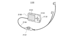
2100 デジタルプレーヤー
2130 本体
2131 表示部
2132 メモリ部
2133 操作部
2134 イヤホン
2137 制御部
2600 TFT基板
2601 対向基板
2602 シール材
2603 画素部
2604 表示素子
2605 着色層
2606 偏光板
2607 偏光板
2608 配線回路部
2609 フレキシブル配線基板
2610 冷陰極管
2611 反射板
2612 回路基板
2613 拡散板
2700 電子書籍
2701 筐体
2703 筐体
2705 表示部
2707 表示部
2711 軸部
2721 電源
2723 操作キー
2725 スピーカ
4001 基板
4002 画素部
4003 信号線駆動回路
4004 走査線駆動回路
4005 シール材
4006 基板
4008 液晶層
4010 薄膜トランジスタ
4011 薄膜トランジスタ
4013 液晶素子
4015 接続端子
4016 配線
4018 FPC
4019 異方性導電膜
4030 画素電極層
4031 対向電極層
4032 絶縁層
4501 基板
4502 画素部
4503a 信号線駆動回路
4504a 走査線駆動回路
4505 シール材
4506 基板
4507 充填材
4509 薄膜トランジスタ
4510 薄膜トランジスタ
4511 発光素子
4515 接続端子
4516 配線
4517 電極層
4518a FPC
4519 異方性導電膜
5300 基板
5301 画素部
5302 走査線駆動回路
5303 信号線駆動回路
5400 基板
5401 画素部
5402 走査線駆動回路
5403 信号線駆動回路
5404 走査線駆動回路
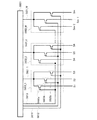
5501 配線
5502 配線
5503 配線
5504 配線
5505 配線
5506 配線
5543 ノード
5544 ノード
5571 薄膜トランジスタ
5572 薄膜トランジスタ
5573 薄膜トランジスタ
5574 薄膜トランジスタ
5575 薄膜トランジスタ
5576 薄膜トランジスタ
5577 薄膜トランジスタ
5578 薄膜トランジスタ
5601 ドライバIC
5602 スイッチ群
5603a 薄膜トランジスタ
5603b 薄膜トランジスタ
5603c 薄膜トランジスタ
5611 配線
5612 配線
5613 配線
5621 配線
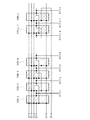
5703a タイミング
5703b タイミング
5703c タイミング
5711 配線
5712 配線
5713 配線
5714 配線
5715 配線
5716 配線
5717 配線
5721 信号
5803a タイミング
5803b タイミング
5803c タイミング
5821 信号
7001 駆動用TFT
7002 発光素子
7003 陰極
7004 発光層
7005 陽極
7011 駆動用TFT
7012 発光素子
7013 陰極
7014 発光層
7015 陽極
7016 遮蔽膜
7017 導電膜
7021 駆動用TFT
7022 発光素子
7023 陰極
7024 発光層
7025 陽極
7027 導電膜
9600 テレビジョン装置
9601 筐体
9603 表示部
9605 スタンド
9607 表示部
9609 操作キー
9610 リモコン操作機
9700 デジタルフォトフレーム
9701 筐体
9703 表示部
Claims (5)
- 基板上に、ゲート電極層を形成し、
前記ゲート電極層上に、ゲート絶縁膜を形成し、
前記ゲート絶縁膜上に、インジウム、ガリウム、及び亜鉛を含む酸化物半導体膜を形成し、
前記酸化物半導体膜のチャネル形成領域上に、絶縁膜を形成し、
前記酸化物半導体膜上の、チタンを含む酸化物を介して、導電膜を形成し、
前記導電膜上に、レジストマスクを形成し、
前記レジストマスクを用いて、前記導電膜と、前記チタンを含む酸化物と、前記酸化物半導体膜とをエッチングして、前記導電膜を、前記チタンを含む酸化物より後退させ、
前記酸化物半導体膜を加熱することを特徴とする半導体装置の作製方法。 - 基板上に、ゲート電極層を形成し、
前記ゲート電極層上に、ゲート絶縁膜を形成し、
前記ゲート絶縁膜上に、インジウム、ガリウム、及び亜鉛を含み、
前記亜鉛の組成比が、前記インジウムの組成比よりも小さく、
かつ前記亜鉛の組成比が、前記ガリウムの組成比よりも小さい、酸化物半導体膜を形成し、
前記酸化物半導体膜のチャネル形成領域上に、絶縁膜を形成し、
前記酸化物半導体膜上の、チタンを含む酸化物を介して、導電膜を形成し、
前記導電膜上に、レジストマスクを形成し、
前記レジストマスクを用いて、前記導電膜と、前記チタンを含む酸化物と、前記酸化物半導体膜とをエッチングして、前記導電膜を、前記チタンを含む酸化物より後退させ、
前記酸化物半導体膜を加熱することを特徴とする半導体装置の作製方法。 - 請求項1又は請求項2において、
前記基板を無バイアス状態として、前記酸化物半導体膜に、プラズマ処理を行うことを特徴とする半導体装置の作製方法。 - ゲート電極層と、
前記ゲート電極層上の、ゲート絶縁膜と、
前記ゲート絶縁膜上の、インジウム、ガリウム、及び亜鉛を含む酸化物半導体膜と、
前記酸化物半導体膜のチャネル形成領域上の、絶縁膜と、
前記酸化物半導体膜上の、第1の導電膜と、
前記酸化物半導体膜上の、第2の導電膜と、
前記酸化物半導体膜と、前記第1の導電膜との間の、第1のチタンを含む酸化物と、
前記酸化物半導体膜と、前記第2の導電膜との間の、第2のチタンを含む酸化物と、を有し、
前記第1のチタンを含む酸化物は、前記第1の導電膜の下端部より、延在した下端部を有し、
前記第2のチタンを含む酸化物は、前記第2の導電膜の下端部より、延在した下端部を有することを特徴とする半導体装置。 - ゲート電極層と、
前記ゲート電極層上の、ゲート絶縁膜と、
前記ゲート絶縁膜上の、インジウム、ガリウム、及び亜鉛を含む酸化物半導体膜と、
前記酸化物半導体膜のチャネル形成領域上の、絶縁膜と、
前記酸化物半導体膜上の、第1の導電膜と、
前記酸化物半導体膜上の、第2の導電膜と、
前記酸化物半導体膜と、前記第1の導電膜との間の、第1のチタンを含む酸化物と、
前記酸化物半導体膜と、前記第2の導電膜との間の、第2のチタンを含む酸化物と、を有し、
前記第1のチタンを含む酸化物は、前記第1導電膜の下端部より、延在した下端部を有し、
前記第2のチタンを含む酸化物は、前記第2導電膜の下端部より、延在した下端部を有し、
前記酸化物半導体膜において、
前記亜鉛の組成比は、前記インジウムの組成比よりも小さく、
かつ前記亜鉛の組成比は、前記ガリウムの組成比よりも小さいことを特徴とする半導体装置。
Priority Applications (1)
| Application Number | Priority Date | Filing Date | Title |
|---|---|---|---|
| JP2009182980A JP5564212B2 (ja) | 2008-08-08 | 2009-08-06 | 半導体装置の作製方法、及び半導体装置 |
Applications Claiming Priority (3)
| Application Number | Priority Date | Filing Date | Title |
|---|---|---|---|
| JP2008206006 | 2008-08-08 | ||
| JP2008206006 | 2008-08-08 | ||
| JP2009182980A JP5564212B2 (ja) | 2008-08-08 | 2009-08-06 | 半導体装置の作製方法、及び半導体装置 |
Related Child Applications (1)
| Application Number | Title | Priority Date | Filing Date |
|---|---|---|---|
| JP2014123252A Division JP2014187390A (ja) | 2008-08-08 | 2014-06-16 | 半導体装置 |
Publications (3)
| Publication Number | Publication Date |
|---|---|
| JP2010062549A JP2010062549A (ja) | 2010-03-18 |
| JP2010062549A5 JP2010062549A5 (ja) | 2013-01-17 |
| JP5564212B2 true JP5564212B2 (ja) | 2014-07-30 |
Family
ID=41653315
Family Applications (7)
| Application Number | Title | Priority Date | Filing Date |
|---|---|---|---|
| JP2009182980A Active JP5564212B2 (ja) | 2008-08-08 | 2009-08-06 | 半導体装置の作製方法、及び半導体装置 |
| JP2014123252A Withdrawn JP2014187390A (ja) | 2008-08-08 | 2014-06-16 | 半導体装置 |
| JP2015185481A Active JP6412842B2 (ja) | 2008-08-08 | 2015-09-18 | 半導体装置 |
| JP2017113570A Active JP6423918B2 (ja) | 2008-08-08 | 2017-06-08 | 半導体装置 |
| JP2018197501A Active JP6687703B2 (ja) | 2008-08-08 | 2018-10-19 | 半導体装置の作製方法 |
| JP2020066946A Withdrawn JP2020107911A (ja) | 2008-08-08 | 2020-04-02 | 半導体装置の作製方法 |
| JP2022010945A Withdrawn JP2022044772A (ja) | 2008-08-08 | 2022-01-27 | 半導体装置及び半導体装置の作製方法 |
Family Applications After (6)
| Application Number | Title | Priority Date | Filing Date |
|---|---|---|---|
| JP2014123252A Withdrawn JP2014187390A (ja) | 2008-08-08 | 2014-06-16 | 半導体装置 |
| JP2015185481A Active JP6412842B2 (ja) | 2008-08-08 | 2015-09-18 | 半導体装置 |
| JP2017113570A Active JP6423918B2 (ja) | 2008-08-08 | 2017-06-08 | 半導体装置 |
| JP2018197501A Active JP6687703B2 (ja) | 2008-08-08 | 2018-10-19 | 半導体装置の作製方法 |
| JP2020066946A Withdrawn JP2020107911A (ja) | 2008-08-08 | 2020-04-02 | 半導体装置の作製方法 |
| JP2022010945A Withdrawn JP2022044772A (ja) | 2008-08-08 | 2022-01-27 | 半導体装置及び半導体装置の作製方法 |
Country Status (4)
| Country | Link |
|---|---|
| US (8) | US8343817B2 (ja) |
| JP (7) | JP5564212B2 (ja) |
| KR (7) | KR101678370B1 (ja) |
| TW (4) | TWI642113B (ja) |
Families Citing this family (151)
| Publication number | Priority date | Publication date | Assignee | Title |
|---|---|---|---|---|
| TWI597850B (zh) | 2008-07-31 | 2017-09-01 | 半導體能源研究所股份有限公司 | 半導體裝置的製造方法 |
| US8945981B2 (en) | 2008-07-31 | 2015-02-03 | Semiconductor Energy Laboratory Co., Ltd. | Semiconductor device and manufacturing method thereof |
| JP5608347B2 (ja) * | 2008-08-08 | 2014-10-15 | 株式会社半導体エネルギー研究所 | 半導体装置及び半導体装置の作製方法 |
| TWI642113B (zh) | 2008-08-08 | 2018-11-21 | 半導體能源研究所股份有限公司 | 半導體裝置的製造方法 |
| JP5480554B2 (ja) * | 2008-08-08 | 2014-04-23 | 株式会社半導体エネルギー研究所 | 半導体装置 |
| TWI487104B (zh) | 2008-11-07 | 2015-06-01 | Semiconductor Energy Lab | 半導體裝置和其製造方法 |
| US8114720B2 (en) | 2008-12-25 | 2012-02-14 | Semiconductor Energy Laboratory Co., Ltd. | Semiconductor device and manufacturing method thereof |
| JP4752927B2 (ja) * | 2009-02-09 | 2011-08-17 | ソニー株式会社 | 薄膜トランジスタおよび表示装置 |
| US8247276B2 (en) * | 2009-02-20 | 2012-08-21 | Semiconductor Energy Laboratory Co., Ltd. | Thin film transistor, method for manufacturing the same, and semiconductor device |
| DE102009038589B4 (de) * | 2009-08-26 | 2014-11-20 | Heraeus Materials Technology Gmbh & Co. Kg | TFT-Struktur mit Cu-Elektroden |
| US8115883B2 (en) | 2009-08-27 | 2012-02-14 | Semiconductor Energy Laboratory Co., Ltd. | Display device and method for manufacturing the same |
| JP5458102B2 (ja) * | 2009-09-04 | 2014-04-02 | 株式会社東芝 | 薄膜トランジスタの製造方法 |
| KR101843558B1 (ko) | 2009-10-09 | 2018-03-30 | 가부시키가이샤 한도오따이 에네루기 켄큐쇼 | 시프트 레지스터, 표시 장치, 및 그 구동 방법 |
| WO2011048959A1 (en) | 2009-10-21 | 2011-04-28 | Semiconductor Energy Laboratory Co., Ltd. | Semiconductor device and method for manufacturing the same |
| KR101812683B1 (ko) * | 2009-10-21 | 2017-12-27 | 가부시키가이샤 한도오따이 에네루기 켄큐쇼 | 반도체 장치 제작방법 |
| KR102142450B1 (ko) | 2009-10-30 | 2020-08-10 | 가부시키가이샤 한도오따이 에네루기 켄큐쇼 | 반도체 장치 및 반도체 장치의 제작방법 |
| WO2011052382A1 (en) | 2009-10-30 | 2011-05-05 | Semiconductor Energy Laboratory Co., Ltd. | Semiconductor device and method for manufacturing the same |
| KR101623961B1 (ko) * | 2009-12-02 | 2016-05-26 | 삼성전자주식회사 | 트랜지스터와 그 제조방법 및 트랜지스터를 포함하는 전자소자 |
| WO2011074407A1 (en) | 2009-12-18 | 2011-06-23 | Semiconductor Energy Laboratory Co., Ltd. | Semiconductor device and method for manufacturing the same |
| KR102008754B1 (ko) * | 2010-01-24 | 2019-08-09 | 가부시키가이샤 한도오따이 에네루기 켄큐쇼 | 표시 장치와 이의 제조 방법 |
| KR101819197B1 (ko) * | 2010-02-05 | 2018-02-28 | 가부시키가이샤 한도오따이 에네루기 켄큐쇼 | 반도체 장치, 및 반도체 장치의 제조 방법 |
| KR20120130763A (ko) | 2010-02-05 | 2012-12-03 | 가부시키가이샤 한도오따이 에네루기 켄큐쇼 | 반도체 장치 및 반도체 장치의 제조 방법 |
| KR20110093113A (ko) | 2010-02-11 | 2011-08-18 | 삼성전자주식회사 | 박막 트랜지스터 기판 및 이의 제조 방법 |
| KR101627136B1 (ko) * | 2010-02-19 | 2016-06-07 | 삼성디스플레이 주식회사 | 박막 트랜지스터 기판, 이의 제조 방법 및 이를 포함하는 표시 장치 |
| WO2011105183A1 (en) * | 2010-02-26 | 2011-09-01 | Semiconductor Energy Laboratory Co., Ltd. | Method for manufacturing semiconductor element and deposition apparatus |
| KR102219398B1 (ko) | 2010-02-26 | 2021-02-25 | 가부시키가이샤 한도오따이 에네루기 켄큐쇼 | 반도체 장치 |
| KR20130008037A (ko) * | 2010-03-05 | 2013-01-21 | 가부시키가이샤 한도오따이 에네루기 켄큐쇼 | 반도체 장치를 제작하는 방법 |
| US8431496B2 (en) * | 2010-03-05 | 2013-04-30 | Semiconductor Energy Labortory Co., Ltd. | Semiconductor device and manufacturing method thereof |
| CN102822980B (zh) | 2010-03-26 | 2015-12-16 | 株式会社半导体能源研究所 | 半导体装置的制造方法 |
| JP5577796B2 (ja) * | 2010-03-31 | 2014-08-27 | 凸版印刷株式会社 | 薄膜トランジスタ及びその製造方法 |
| WO2011122299A1 (en) | 2010-03-31 | 2011-10-06 | Semiconductor Energy Laboratory Co., Ltd. | Driving method of liquid crystal display device |
| JP5791934B2 (ja) * | 2010-04-02 | 2015-10-07 | 株式会社半導体エネルギー研究所 | 半導体装置の作製方法 |
| WO2011122363A1 (en) * | 2010-04-02 | 2011-10-06 | Semiconductor Energy Laboratory Co., Ltd. | Semiconductor device |
| KR101391964B1 (ko) * | 2010-04-02 | 2014-05-07 | 가부시키가이샤 한도오따이 에네루기 켄큐쇼 | 반도체 장치 |
| JP2011222767A (ja) * | 2010-04-09 | 2011-11-04 | Sony Corp | 薄膜トランジスタならびに表示装置および電子機器 |
| US8653514B2 (en) | 2010-04-09 | 2014-02-18 | Semiconductor Energy Laboratory Co., Ltd. | Semiconductor device and method for manufacturing the same |
| KR20130045418A (ko) | 2010-04-23 | 2013-05-03 | 가부시키가이샤 한도오따이 에네루기 켄큐쇼 | 반도체 장치의 제작 방법 |
| CN102859705B (zh) * | 2010-04-23 | 2015-12-09 | 株式会社半导体能源研究所 | 半导体装置及半导体装置的制造方法 |
| KR101800844B1 (ko) | 2010-04-23 | 2017-11-23 | 가부시키가이샤 한도오따이 에네루기 켄큐쇼 | 반도체 장치의 제작 방법 |
| WO2011135987A1 (en) * | 2010-04-28 | 2011-11-03 | Semiconductor Energy Laboratory Co., Ltd. | Method for manufacturing semiconductor device |
| KR101806271B1 (ko) * | 2010-05-14 | 2017-12-07 | 가부시키가이샤 한도오따이 에네루기 켄큐쇼 | 반도체 장치의 제작 방법 |
| US9496405B2 (en) | 2010-05-20 | 2016-11-15 | Semiconductor Energy Laboratory Co., Ltd. | Method for manufacturing semiconductor device including step of adding cation to oxide semiconductor layer |
| WO2011155502A1 (en) | 2010-06-11 | 2011-12-15 | Semiconductor Energy Laboratory Co., Ltd. | Semiconductor device and method for manufacturing the same |
| US8552425B2 (en) | 2010-06-18 | 2013-10-08 | Semiconductor Energy Laboratory Co., Ltd. | Semiconductor device |
| US8441010B2 (en) * | 2010-07-01 | 2013-05-14 | Semiconductor Energy Laboratory Co., Ltd. | Semiconductor device |
| KR102354354B1 (ko) * | 2010-07-02 | 2022-01-20 | 가부시키가이샤 한도오따이 에네루기 켄큐쇼 | 반도체 장치 및 그 제작 방법 |
| US8642380B2 (en) | 2010-07-02 | 2014-02-04 | Semiconductor Energy Laboratory Co., Ltd. | Manufacturing method of semiconductor device |
| KR101671952B1 (ko) * | 2010-07-23 | 2016-11-04 | 삼성디스플레이 주식회사 | 표시 기판 및 이의 제조 방법 |
| JP5917035B2 (ja) * | 2010-07-26 | 2016-05-11 | 株式会社半導体エネルギー研究所 | 半導体装置 |
| US8422272B2 (en) | 2010-08-06 | 2013-04-16 | Semiconductor Energy Laboratory Co., Ltd. | Semiconductor device and driving method thereof |
| CN107947763B (zh) | 2010-08-06 | 2021-12-28 | 株式会社半导体能源研究所 | 半导体集成电路 |
| KR101701212B1 (ko) * | 2010-08-11 | 2017-02-02 | 삼성디스플레이 주식회사 | 박막 트랜지스터 기판 및 이의 제조 방법 |
| JP5806043B2 (ja) * | 2010-08-27 | 2015-11-10 | 株式会社半導体エネルギー研究所 | 半導体装置の作製方法 |
| KR101346874B1 (ko) | 2010-08-30 | 2014-01-02 | 샤프 가부시키가이샤 | 반도체 장치 및 그 제조 방법 |
| US8766253B2 (en) * | 2010-09-10 | 2014-07-01 | Semiconductor Energy Laboratory Co., Ltd. | Semiconductor device |
| US8871565B2 (en) * | 2010-09-13 | 2014-10-28 | Semiconductor Energy Laboratory Co., Ltd. | Method for manufacturing semiconductor device |
| JP5782695B2 (ja) * | 2010-09-29 | 2015-09-24 | 凸版印刷株式会社 | 薄膜トランジスタ、薄膜トランジスタを備える画像表示装置、薄膜トランジスタの製造方法、画像表示装置の製造方法 |
| KR20120037838A (ko) * | 2010-10-12 | 2012-04-20 | 삼성전자주식회사 | 트랜지스터 및 이를 포함하는 전자소자 |
| US8569754B2 (en) | 2010-11-05 | 2013-10-29 | Semiconductor Energy Laboratory Co., Ltd. | Semiconductor device and manufacturing method thereof |
| KR101457833B1 (ko) | 2010-12-03 | 2014-11-05 | 가부시키가이샤 한도오따이 에네루기 켄큐쇼 | 반도체 장치 |
| CN106887449B (zh) * | 2010-12-07 | 2021-11-05 | 佛罗里达大学研究基金会 | 一种显示面板 |
| JP5707914B2 (ja) * | 2010-12-13 | 2015-04-30 | ソニー株式会社 | 酸化物半導体を用いる装置、表示装置、及び、電子機器 |
| US8536571B2 (en) * | 2011-01-12 | 2013-09-17 | Semiconductor Energy Laboratory Co., Ltd. | Manufacturing method of semiconductor device |
| JP5977523B2 (ja) | 2011-01-12 | 2016-08-24 | 株式会社半導体エネルギー研究所 | トランジスタの作製方法 |
| JP5982125B2 (ja) * | 2011-01-12 | 2016-08-31 | 株式会社半導体エネルギー研究所 | 半導体装置の作製方法 |
| JP5766467B2 (ja) | 2011-03-02 | 2015-08-19 | 株式会社東芝 | 薄膜トランジスタ及びその製造方法、表示装置 |
| US9646829B2 (en) * | 2011-03-04 | 2017-05-09 | Semiconductor Energy Laboratory Co., Ltd. | Manufacturing method of semiconductor device |
| US8927329B2 (en) | 2011-03-30 | 2015-01-06 | Semiconductor Energy Laboratory Co., Ltd. | Method for manufacturing oxide semiconductor device with improved electronic properties |
| US8541266B2 (en) | 2011-04-01 | 2013-09-24 | Semiconductor Energy Laboratory Co., Ltd. | Method for manufacturing semiconductor device |
| US9093538B2 (en) * | 2011-04-08 | 2015-07-28 | Semiconductor Energy Laboratory Co., Ltd. | Semiconductor device and method for manufacturing the same |
| US9478668B2 (en) * | 2011-04-13 | 2016-10-25 | Semiconductor Energy Laboratory Co., Ltd. | Oxide semiconductor film and semiconductor device |
| JP6076617B2 (ja) * | 2011-05-13 | 2017-02-08 | 株式会社半導体エネルギー研究所 | 表示装置 |
| TWI514572B (zh) * | 2011-06-10 | 2015-12-21 | E Ink Holdings Inc | 金屬氧化物半導體電晶體 |
| US8673426B2 (en) | 2011-06-29 | 2014-03-18 | Semiconductor Energy Laboratory Co., Ltd. | Driver circuit, method of manufacturing the driver circuit, and display device including the driver circuit |
| JP6078063B2 (ja) * | 2011-07-13 | 2017-02-08 | アプライド マテリアルズ インコーポレイテッドApplied Materials,Incorporated | 薄膜トランジスタデバイスの製造方法 |
| KR101934977B1 (ko) * | 2011-08-02 | 2019-03-19 | 삼성디스플레이 주식회사 | 박막 트랜지스터 표시판 및 그 제조 방법 |
| JP6128775B2 (ja) * | 2011-08-19 | 2017-05-17 | 株式会社半導体エネルギー研究所 | 半導体装置 |
| US9252279B2 (en) * | 2011-08-31 | 2016-02-02 | Semiconductor Energy Laboratory Co., Ltd. | Semiconductor device and manufacturing method thereof |
| CN102315130B (zh) * | 2011-09-21 | 2014-11-26 | 深圳市华星光电技术有限公司 | 薄膜场效应晶体管及其制作方法 |
| US9018629B2 (en) * | 2011-10-13 | 2015-04-28 | Semiconductor Energy Laboratory Co., Ltd. | Semiconductor device and method for manufacturing semiconductor device |
| KR20130043063A (ko) | 2011-10-19 | 2013-04-29 | 가부시키가이샤 한도오따이 에네루기 켄큐쇼 | 반도체 장치 및 반도체 장치의 제작 방법 |
| KR102072244B1 (ko) | 2011-11-30 | 2020-01-31 | 가부시키가이샤 한도오따이 에네루기 켄큐쇼 | 반도체 장치 및 반도체 장치의 제작 방법 |
| US8969867B2 (en) | 2012-01-18 | 2015-03-03 | Semiconductor Energy Laboratory Co., Ltd. | Semiconductor device |
| KR101308809B1 (ko) * | 2012-01-20 | 2013-09-13 | 경희대학교 산학협력단 | 산화물 반도체 박막 트랜지스터 제조방법 및 이를 이용한 능동구동 디스플레이 장치, 능동구동 센서장치 |
| KR101318418B1 (ko) * | 2012-01-30 | 2013-10-15 | 서울대학교산학협력단 | 박막 트랜지스터 및 이의 제조 방법 |
| KR101969567B1 (ko) * | 2012-04-17 | 2019-04-16 | 엘지디스플레이 주식회사 | 금속 산화물 반도체를 포함하는 박막 트랜지스터 기판 및 그 제조 방법 |
| KR101697841B1 (ko) * | 2012-04-20 | 2017-01-18 | 샤프 가부시키가이샤 | 표시 장치 |
| US8658444B2 (en) | 2012-05-16 | 2014-02-25 | International Business Machines Corporation | Semiconductor active matrix on buried insulator |
| KR101957976B1 (ko) * | 2012-06-13 | 2019-03-15 | 엘지디스플레이 주식회사 | 평판 표시장치용 박막 트랜지스터 기판 |
| CN102738007B (zh) * | 2012-07-02 | 2014-09-03 | 京东方科技集团股份有限公司 | 一种薄膜晶体管的制造方法及阵列基板的制造方法 |
| JP6155823B2 (ja) * | 2012-07-12 | 2017-07-05 | Jsr株式会社 | 有機el素子、感放射線性樹脂組成物および硬化膜 |
| JP2014199899A (ja) | 2012-08-10 | 2014-10-23 | 株式会社半導体エネルギー研究所 | 半導体装置 |
| KR20140026257A (ko) * | 2012-08-23 | 2014-03-05 | 가부시키가이샤 한도오따이 에네루기 켄큐쇼 | 표시 장치 |
| JP6204145B2 (ja) | 2012-10-23 | 2017-09-27 | 株式会社半導体エネルギー研究所 | 半導体装置 |
| WO2014065343A1 (en) | 2012-10-24 | 2014-05-01 | Semiconductor Energy Laboratory Co., Ltd. | Semiconductor device |
| WO2014071343A1 (en) | 2012-11-05 | 2014-05-08 | University Of Florida Research Foundation, Inc. | Brightness compensation in a display |
| TWI605593B (zh) | 2012-11-15 | 2017-11-11 | 半導體能源研究所股份有限公司 | 半導體裝置 |
| US9231002B2 (en) | 2013-05-03 | 2016-01-05 | Semiconductor Energy Laboratory Co., Ltd. | Display device and electronic device |
| US9704894B2 (en) | 2013-05-10 | 2017-07-11 | Semiconductor Energy Laboratory Co., Ltd. | Display device including pixel electrode including oxide |
| KR102090289B1 (ko) * | 2013-05-30 | 2020-04-16 | 삼성디스플레이 주식회사 | 산화물 스퍼터링 타겟, 이를 이용한 박막 트랜지스터 및 그 제조 방법 |
| JP6410496B2 (ja) * | 2013-07-31 | 2018-10-24 | 株式会社半導体エネルギー研究所 | マルチゲート構造のトランジスタ |
| JP6238660B2 (ja) * | 2013-09-19 | 2017-11-29 | 国立大学法人北陸先端科学技術大学院大学 | 薄膜トランジスタ及び薄膜トランジスタの製造方法 |
| DE102013111501B4 (de) * | 2013-10-18 | 2024-02-08 | Universität Stuttgart | Dünnschichttransistor und Verfahren zu seiner Herstellung |
| KR102232539B1 (ko) * | 2013-11-13 | 2021-03-29 | 삼성디스플레이 주식회사 | 박막 트랜지스터, 이를 포함하는 표시 기판 및 박막 트랜지스터의 제조 방법 |
| KR102192084B1 (ko) * | 2013-11-25 | 2020-12-16 | 삼성전자주식회사 | 트랜지스터와 그 제조방법 및 트랜지스터를 포함하는 전자소자 |
| KR20150060448A (ko) * | 2013-11-26 | 2015-06-03 | 삼성디스플레이 주식회사 | 박막 트랜지스터 표시판 및 이의 제조 방법 |
| KR20150062186A (ko) | 2013-11-28 | 2015-06-08 | 삼성디스플레이 주식회사 | 박막 트랜지스터 표시판 및 그 제조 방법 |
| TWI666770B (zh) * | 2013-12-19 | 2019-07-21 | 日商半導體能源研究所股份有限公司 | 半導體裝置 |
| US9722049B2 (en) * | 2013-12-23 | 2017-08-01 | Intermolecular, Inc. | Methods for forming crystalline IGZO with a seed layer |
| CN103762178A (zh) * | 2013-12-25 | 2014-04-30 | 深圳市华星光电技术有限公司 | 一种低温多晶硅薄膜晶体管及其制造方法 |
| US20150187956A1 (en) * | 2013-12-26 | 2015-07-02 | Intermolecular Inc. | IGZO Devices with Increased Drive Current and Methods for Forming the Same |
| JP6506545B2 (ja) | 2013-12-27 | 2019-04-24 | 株式会社半導体エネルギー研究所 | 半導体装置 |
| TWI536464B (zh) | 2014-01-15 | 2016-06-01 | 友達光電股份有限公司 | 電晶體及其製造方法 |
| KR101536174B1 (ko) * | 2014-02-11 | 2015-07-14 | 연세대학교 산학협력단 | 산소 확산을 억제할 수 있는 반도체 소자 제조 방법 |
| US20150380563A1 (en) * | 2014-06-26 | 2015-12-31 | Samsung Display Co., Ltd. | Display apparatus and method for manufacturing the same |
| TWI560781B (en) * | 2014-09-10 | 2016-12-01 | Au Optronics Corp | Method for fabricating thin film transistor and apparatus thereof |
| US9722091B2 (en) | 2014-09-12 | 2017-08-01 | Semiconductor Energy Laboratory Co., Ltd. | Method for manufacturing semiconductor device |
| TWI581317B (zh) | 2014-11-14 | 2017-05-01 | 群創光電股份有限公司 | 薄膜電晶體基板及具備該薄膜電晶體基板之顯示面板 |
| CN105655344B (zh) * | 2014-11-14 | 2019-02-05 | 群创光电股份有限公司 | 薄膜晶体管基板及具备该薄膜晶体管基板的显示面板 |
| CN107004603B (zh) * | 2014-11-28 | 2021-03-09 | 夏普株式会社 | 半导体装置及其制造方法 |
| TW201624678A (zh) * | 2014-12-27 | 2016-07-01 | 中華映管股份有限公司 | 主動元件及其製作方法 |
| US9941324B2 (en) * | 2015-04-28 | 2018-04-10 | Nlt Technologies, Ltd. | Semiconductor device, method of manufacturing semiconductor device, photodiode array, and imaging apparatus |
| US9837547B2 (en) * | 2015-05-22 | 2017-12-05 | Semiconductor Energy Laboratory Co., Ltd. | Semiconductor device comprising oxide conductor and display device including the semiconductor device |
| CN106298876A (zh) * | 2015-05-25 | 2017-01-04 | 鸿富锦精密工业(深圳)有限公司 | 薄膜晶体管及其制造方法 |
| JP2017084549A (ja) * | 2015-10-27 | 2017-05-18 | 株式会社ジャパンディスプレイ | 表示装置 |
| JP6607013B2 (ja) * | 2015-12-08 | 2019-11-20 | 株式会社リコー | 電界効果型トランジスタ、表示素子、画像表示装置、及びシステム |
| CN105572990B (zh) * | 2015-12-21 | 2019-07-12 | 武汉华星光电技术有限公司 | 阵列基板及其制造方法、液晶显示面板 |
| US9806179B2 (en) * | 2016-01-14 | 2017-10-31 | Hon Hai Precision Industry Co., Ltd. | Method for fabricating conducting structure and thin film transistor array panel |
| JP2017143135A (ja) * | 2016-02-09 | 2017-08-17 | 株式会社ジャパンディスプレイ | 薄膜トランジスタ |
| WO2017149413A1 (en) * | 2016-03-04 | 2017-09-08 | Semiconductor Energy Laboratory Co., Ltd. | Semiconductor device and manufacturing method thereof |
| JP6668455B2 (ja) | 2016-04-01 | 2020-03-18 | 株式会社半導体エネルギー研究所 | 酸化物半導体膜の作製方法 |
| US11302717B2 (en) * | 2016-04-08 | 2022-04-12 | Semiconductor Energy Laboratory Co., Ltd. | Transistor and method for manufacturing the same |
| WO2018006412A1 (en) * | 2016-07-08 | 2018-01-11 | Boe Technology Group Co., Ltd. | Thin film transistor, gate drive on array and display apparatus having the same, and fabricating method thereof |
| KR102612734B1 (ko) * | 2016-07-29 | 2023-12-13 | 엘지디스플레이 주식회사 | 표시장치 |
| JP2019523565A (ja) * | 2016-08-29 | 2019-08-22 | シェンジェン ロイオル テクノロジーズ カンパニー リミテッドShenzhen Royole Technologies Co., Ltd. | 薄膜トランジスタの製造方法 |
| CN106206428A (zh) * | 2016-09-05 | 2016-12-07 | 上海天马微电子有限公司 | 阵列基板及其制作方法、显示面板 |
| KR102343573B1 (ko) * | 2017-05-26 | 2021-12-28 | 삼성디스플레이 주식회사 | 플렉서블 디스플레이 장치 |
| CN107464830A (zh) * | 2017-07-18 | 2017-12-12 | 武汉华星光电半导体显示技术有限公司 | 阵列基板及制作方法、显示面板 |
| US11049887B2 (en) | 2017-11-10 | 2021-06-29 | Applied Materials, Inc. | Layer stack for display applications |
| TW201919130A (zh) * | 2017-11-13 | 2019-05-16 | 友達光電股份有限公司 | 畫素結構、半導體結構的製造方法及半導體元件的製造方法 |
| CN108281489A (zh) * | 2018-01-30 | 2018-07-13 | 京东方科技集团股份有限公司 | 一种薄膜晶体管及其制备方法、阵列基板、显示面板 |
| WO2019150224A1 (ja) * | 2018-02-01 | 2019-08-08 | 株式会社半導体エネルギー研究所 | 表示装置および電子機器 |
| CN108598004A (zh) * | 2018-03-21 | 2018-09-28 | 福建华佳彩有限公司 | 一种igzo阵列基板的制备方法及igzo阵列基板 |
| CN108987485B (zh) * | 2018-08-24 | 2021-10-29 | 合肥鑫晟光电科技有限公司 | 薄膜晶体管及其制造方法、显示装置 |
| US11169424B2 (en) * | 2019-03-18 | 2021-11-09 | Sharp Kabushiki Kaisha | Display device |
| CN110112212A (zh) * | 2019-04-25 | 2019-08-09 | 深圳市华星光电技术有限公司 | 薄膜晶体管和阵列基板 |
| US11335716B2 (en) | 2019-12-24 | 2022-05-17 | Taiwan Semiconductor Manufacturing Company, Ltd. | Photosensing pixel, image sensor and method of fabricating the same |
| CN111370311B (zh) * | 2020-03-17 | 2021-08-03 | 深圳市华星光电半导体显示技术有限公司 | 显示面板及其制备方法 |
| WO2022120746A1 (zh) * | 2020-12-10 | 2022-06-16 | 昆山龙腾光电股份有限公司 | 阵列基板及其制作方法和显示面板 |
| CN112713196A (zh) * | 2020-12-11 | 2021-04-27 | 广州国显科技有限公司 | 一种薄膜晶体管及其制备方法和阵列基板 |
| CN113707556A (zh) * | 2021-08-13 | 2021-11-26 | Tcl华星光电技术有限公司 | 一种薄膜晶体管的制作方法、薄膜晶体管以及显示装置 |
Family Cites Families (164)
| Publication number | Priority date | Publication date | Assignee | Title |
|---|---|---|---|---|
| JPS60198861A (ja) | 1984-03-23 | 1985-10-08 | Fujitsu Ltd | 薄膜トランジスタ |
| JPH0244256B2 (ja) | 1987-01-28 | 1990-10-03 | Kagaku Gijutsucho Mukizaishitsu Kenkyushocho | Ingazn2o5deshimesarerurotsuhoshokeinosojokozoojusurukagobutsuoyobisonoseizoho |
| JPH0244258B2 (ja) | 1987-02-24 | 1990-10-03 | Kagaku Gijutsucho Mukizaishitsu Kenkyushocho | Ingazn3o6deshimesarerurotsuhoshokeinosojokozoojusurukagobutsuoyobisonoseizoho |
| JPH0244260B2 (ja) | 1987-02-24 | 1990-10-03 | Kagaku Gijutsucho Mukizaishitsu Kenkyushocho | Ingazn5o8deshimesarerurotsuhoshokeinosojokozoojusurukagobutsuoyobisonoseizoho |
| JPS63210023A (ja) | 1987-02-24 | 1988-08-31 | Natl Inst For Res In Inorg Mater | InGaZn↓4O↓7で示される六方晶系の層状構造を有する化合物およびその製造法 |
| JPH0244262B2 (ja) | 1987-02-27 | 1990-10-03 | Kagaku Gijutsucho Mukizaishitsu Kenkyushocho | Ingazn6o9deshimesarerurotsuhoshokeinosojokozoojusurukagobutsuoyobisonoseizoho |
| JPH0244263B2 (ja) | 1987-04-22 | 1990-10-03 | Kagaku Gijutsucho Mukizaishitsu Kenkyushocho | Ingazn7o10deshimesarerurotsuhoshokeinosojokozoojusurukagobutsuoyobisonoseizoho |
| JP2692914B2 (ja) * | 1988-12-19 | 1997-12-17 | 三洋電機株式会社 | 薄膜トランジスタの製造方法 |
| US5766344A (en) * | 1991-09-21 | 1998-06-16 | Semiconductor Energy Laboratory Co., Ltd. | Method for forming a semiconductor |
| JPH05251705A (ja) | 1992-03-04 | 1993-09-28 | Fuji Xerox Co Ltd | 薄膜トランジスタ |
| US5473168A (en) | 1993-04-30 | 1995-12-05 | Sharp Kabushiki Kaisha | Thin film transistor |
| JPH06314789A (ja) * | 1993-04-30 | 1994-11-08 | Sharp Corp | 薄膜トランジスタ |
| JP3479375B2 (ja) | 1995-03-27 | 2003-12-15 | 科学技術振興事業団 | 亜酸化銅等の金属酸化物半導体による薄膜トランジスタとpn接合を形成した金属酸化物半導体装置およびそれらの製造方法 |
| KR100394896B1 (ko) | 1995-08-03 | 2003-11-28 | 코닌클리케 필립스 일렉트로닉스 엔.브이. | 투명스위칭소자를포함하는반도체장치 |
| JP3625598B2 (ja) | 1995-12-30 | 2005-03-02 | 三星電子株式会社 | 液晶表示装置の製造方法 |
| JPH09270517A (ja) * | 1996-03-29 | 1997-10-14 | Casio Comput Co Ltd | 薄膜トランジスタの製造方法 |
| KR100301803B1 (ko) | 1998-06-05 | 2001-09-22 | 김영환 | 박막트랜지스터 및 그의 제조방법 |
| JP4170454B2 (ja) | 1998-07-24 | 2008-10-22 | Hoya株式会社 | 透明導電性酸化物薄膜を有する物品及びその製造方法 |
| USRE39452E1 (en) | 1998-08-28 | 2007-01-02 | Fujitsu Limited | TFT substrate with low contact resistance and damage resistant terminals |
| JP3288637B2 (ja) * | 1998-08-28 | 2002-06-04 | 富士通株式会社 | Ito膜接続構造、tft基板及びその製造方法 |
| US6297519B1 (en) | 1998-08-28 | 2001-10-02 | Fujitsu Limited | TFT substrate with low contact resistance and damage resistant terminals |
| JP2000101091A (ja) * | 1998-09-28 | 2000-04-07 | Sharp Corp | 薄膜トランジスタ |
| JP2000150861A (ja) | 1998-11-16 | 2000-05-30 | Tdk Corp | 酸化物薄膜 |
| JP3276930B2 (ja) | 1998-11-17 | 2002-04-22 | 科学技術振興事業団 | トランジスタ及び半導体装置 |
| TW460731B (en) | 1999-09-03 | 2001-10-21 | Ind Tech Res Inst | Electrode structure and production method of wide viewing angle LCD |
| JP4562835B2 (ja) * | 1999-11-05 | 2010-10-13 | 株式会社半導体エネルギー研究所 | 半導体装置の作製方法 |
| JP4118485B2 (ja) * | 2000-03-13 | 2008-07-16 | 株式会社半導体エネルギー研究所 | 半導体装置の作製方法 |
| JP4089858B2 (ja) | 2000-09-01 | 2008-05-28 | 国立大学法人東北大学 | 半導体デバイス |
| KR20020038482A (ko) | 2000-11-15 | 2002-05-23 | 모리시타 요이찌 | 박막 트랜지스터 어레이, 그 제조방법 및 그것을 이용한표시패널 |
| JP3997731B2 (ja) | 2001-03-19 | 2007-10-24 | 富士ゼロックス株式会社 | 基材上に結晶性半導体薄膜を形成する方法 |
| JP2002289857A (ja) * | 2001-03-23 | 2002-10-04 | Toshiba Corp | マトリクスアレイ基板の製造方法 |
| JP2002289859A (ja) | 2001-03-23 | 2002-10-04 | Minolta Co Ltd | 薄膜トランジスタ |
| JP2002368229A (ja) * | 2001-04-04 | 2002-12-20 | Canon Inc | 半導体装置、及びその製造方法、並びに放射線検出装置 |
| US6794682B2 (en) | 2001-04-04 | 2004-09-21 | Canon Kabushiki Kaisha | Semiconductor device, method for manufacturing the same, and radiation detector |
| JP2002324904A (ja) * | 2001-04-24 | 2002-11-08 | Matsushita Electric Ind Co Ltd | 薄膜トランジスタ及びその形成方法 |
| JP2002373867A (ja) | 2001-06-14 | 2002-12-26 | Idemitsu Kosan Co Ltd | 半導体素子用導電性薄膜、半導体素子及びそれらの製造方法 |
| JP2003092271A (ja) * | 2001-07-13 | 2003-03-28 | Seiko Epson Corp | 半導体装置及びその製造方法 |
| JP4090716B2 (ja) | 2001-09-10 | 2008-05-28 | 雅司 川崎 | 薄膜トランジスタおよびマトリクス表示装置 |
| JP3925839B2 (ja) | 2001-09-10 | 2007-06-06 | シャープ株式会社 | 半導体記憶装置およびその試験方法 |
| JP4164562B2 (ja) | 2002-09-11 | 2008-10-15 | 独立行政法人科学技術振興機構 | ホモロガス薄膜を活性層として用いる透明薄膜電界効果型トランジスタ |
| EP1443130B1 (en) | 2001-11-05 | 2011-09-28 | Japan Science and Technology Agency | Natural superlattice homologous single crystal thin film, method for preparation thereof, and device using said single crystal thin film |
| JP4083486B2 (ja) | 2002-02-21 | 2008-04-30 | 独立行政法人科学技術振興機構 | LnCuO(S,Se,Te)単結晶薄膜の製造方法 |
| CN1445821A (zh) | 2002-03-15 | 2003-10-01 | 三洋电机株式会社 | ZnO膜和ZnO半导体层的形成方法、半导体元件及其制造方法 |
| JP3933591B2 (ja) | 2002-03-26 | 2007-06-20 | 淳二 城戸 | 有機エレクトロルミネッセント素子 |
| US7339187B2 (en) | 2002-05-21 | 2008-03-04 | State Of Oregon Acting By And Through The Oregon State Board Of Higher Education On Behalf Of Oregon State University | Transistor structures |
| JP2004022625A (ja) | 2002-06-13 | 2004-01-22 | Murata Mfg Co Ltd | 半導体デバイス及び該半導体デバイスの製造方法 |
| US7105868B2 (en) | 2002-06-24 | 2006-09-12 | Cermet, Inc. | High-electron mobility transistor with zinc oxide |
| US7067843B2 (en) | 2002-10-11 | 2006-06-27 | E. I. Du Pont De Nemours And Company | Transparent oxide semiconductor thin film transistors |
| JP4166105B2 (ja) | 2003-03-06 | 2008-10-15 | シャープ株式会社 | 半導体装置およびその製造方法 |
| JP2004273732A (ja) | 2003-03-07 | 2004-09-30 | Sharp Corp | アクティブマトリクス基板およびその製造方法 |
| JP4108633B2 (ja) | 2003-06-20 | 2008-06-25 | シャープ株式会社 | 薄膜トランジスタおよびその製造方法ならびに電子デバイス |
| US7262463B2 (en) | 2003-07-25 | 2007-08-28 | Hewlett-Packard Development Company, L.P. | Transistor including a deposited channel region having a doped portion |
| JP4507540B2 (ja) * | 2003-09-12 | 2010-07-21 | カシオ計算機株式会社 | 薄膜トランジスタ |
| JP2005108930A (ja) | 2003-09-29 | 2005-04-21 | Sony Corp | 薄膜トランジスタの製造方法および薄膜トランジスタ |
| JP2005108931A (ja) * | 2003-09-29 | 2005-04-21 | Sony Corp | 表示装置の製造方法および表示装置 |
| US7282782B2 (en) | 2004-03-12 | 2007-10-16 | Hewlett-Packard Development Company, L.P. | Combined binary oxide semiconductor device |
| US7145174B2 (en) | 2004-03-12 | 2006-12-05 | Hewlett-Packard Development Company, Lp. | Semiconductor device |
| US7297977B2 (en) | 2004-03-12 | 2007-11-20 | Hewlett-Packard Development Company, L.P. | Semiconductor device |
| EP2413366B1 (en) | 2004-03-12 | 2017-01-11 | Japan Science And Technology Agency | A switching element of LCDs or organic EL displays |
| JP4461873B2 (ja) * | 2004-03-29 | 2010-05-12 | カシオ計算機株式会社 | 亜鉛酸化物の加工方法および薄膜トランジスタの製造方法 |
| US7211825B2 (en) | 2004-06-14 | 2007-05-01 | Yi-Chi Shih | Indium oxide-based thin film transistors and circuits |
| JP2006005116A (ja) | 2004-06-17 | 2006-01-05 | Casio Comput Co Ltd | 膜形成方法、半導体膜、及び積層絶縁膜 |
| JP2006100760A (ja) | 2004-09-02 | 2006-04-13 | Casio Comput Co Ltd | 薄膜トランジスタおよびその製造方法 |
| JP4974500B2 (ja) * | 2004-09-15 | 2012-07-11 | 株式会社半導体エネルギー研究所 | 半導体装置、モジュール及び電子機器 |
| CN101044627B (zh) | 2004-09-15 | 2012-02-08 | 株式会社半导体能源研究所 | 半导体器件 |
| US7285501B2 (en) | 2004-09-17 | 2007-10-23 | Hewlett-Packard Development Company, L.P. | Method of forming a solution processed device |
| JP4610285B2 (ja) | 2004-09-30 | 2011-01-12 | 株式会社半導体エネルギー研究所 | 液晶表示装置の作製方法 |
| US7298084B2 (en) | 2004-11-02 | 2007-11-20 | 3M Innovative Properties Company | Methods and displays utilizing integrated zinc oxide row and column drivers in conjunction with organic light emitting diodes |
| KR100953596B1 (ko) | 2004-11-10 | 2010-04-21 | 캐논 가부시끼가이샤 | 발광장치 |
| JP5138163B2 (ja) | 2004-11-10 | 2013-02-06 | キヤノン株式会社 | 電界効果型トランジスタ |
| CN101057338B (zh) | 2004-11-10 | 2011-03-16 | 佳能株式会社 | 采用无定形氧化物的场效应晶体管 |
| JP5126730B2 (ja) | 2004-11-10 | 2013-01-23 | キヤノン株式会社 | 電界効果型トランジスタの製造方法 |
| US7791072B2 (en) | 2004-11-10 | 2010-09-07 | Canon Kabushiki Kaisha | Display |
| US7829444B2 (en) | 2004-11-10 | 2010-11-09 | Canon Kabushiki Kaisha | Field effect transistor manufacturing method |
| US7453065B2 (en) | 2004-11-10 | 2008-11-18 | Canon Kabushiki Kaisha | Sensor and image pickup device |
| US7863611B2 (en) | 2004-11-10 | 2011-01-04 | Canon Kabushiki Kaisha | Integrated circuits utilizing amorphous oxides |
| CN101057339B (zh) | 2004-11-10 | 2012-12-26 | 佳能株式会社 | 无定形氧化物和场效应晶体管 |
| JP4569295B2 (ja) | 2004-12-28 | 2010-10-27 | カシオ計算機株式会社 | 薄膜トランジスタおよびその製造方法 |
| US7579224B2 (en) | 2005-01-21 | 2009-08-25 | Semiconductor Energy Laboratory Co., Ltd. | Method for manufacturing a thin film semiconductor device |
| TWI569441B (zh) | 2005-01-28 | 2017-02-01 | 半導體能源研究所股份有限公司 | 半導體裝置,電子裝置,和半導體裝置的製造方法 |
| TWI472037B (zh) | 2005-01-28 | 2015-02-01 | Semiconductor Energy Lab | 半導體裝置,電子裝置,和半導體裝置的製造方法 |
| US7858451B2 (en) | 2005-02-03 | 2010-12-28 | Semiconductor Energy Laboratory Co., Ltd. | Electronic device, semiconductor device and manufacturing method thereof |
| US7948171B2 (en) | 2005-02-18 | 2011-05-24 | Semiconductor Energy Laboratory Co., Ltd. | Light emitting device |
| US20060197092A1 (en) | 2005-03-03 | 2006-09-07 | Randy Hoffman | System and method for forming conductive material on a substrate |
| US8681077B2 (en) | 2005-03-18 | 2014-03-25 | Semiconductor Energy Laboratory Co., Ltd. | Semiconductor device, and display device, driving method and electronic apparatus thereof |
| WO2006105077A2 (en) | 2005-03-28 | 2006-10-05 | Massachusetts Institute Of Technology | Low voltage thin film transistor with high-k dielectric material |
| US7645478B2 (en) | 2005-03-31 | 2010-01-12 | 3M Innovative Properties Company | Methods of making displays |
| US8300031B2 (en) | 2005-04-20 | 2012-10-30 | Semiconductor Energy Laboratory Co., Ltd. | Semiconductor device comprising transistor having gate and drain connected through a current-voltage conversion element |
| JP2006344849A (ja) | 2005-06-10 | 2006-12-21 | Casio Comput Co Ltd | 薄膜トランジスタ |
| US7691666B2 (en) | 2005-06-16 | 2010-04-06 | Eastman Kodak Company | Methods of making thin film transistors comprising zinc-oxide-based semiconductor materials and transistors made thereby |
| US7402506B2 (en) | 2005-06-16 | 2008-07-22 | Eastman Kodak Company | Methods of making thin film transistors comprising zinc-oxide-based semiconductor materials and transistors made thereby |
| US7507618B2 (en) | 2005-06-27 | 2009-03-24 | 3M Innovative Properties Company | Method for making electronic devices using metal oxide nanoparticles |
| KR100711890B1 (ko) | 2005-07-28 | 2007-04-25 | 삼성에스디아이 주식회사 | 유기 발광표시장치 및 그의 제조방법 |
| JP2007059128A (ja) | 2005-08-23 | 2007-03-08 | Canon Inc | 有機el表示装置およびその製造方法 |
| JP4850457B2 (ja) | 2005-09-06 | 2012-01-11 | キヤノン株式会社 | 薄膜トランジスタ及び薄膜ダイオード |
| JP4981282B2 (ja) * | 2005-09-06 | 2012-07-18 | キヤノン株式会社 | 薄膜トランジスタの製造方法 |
| JP4280736B2 (ja) | 2005-09-06 | 2009-06-17 | キヤノン株式会社 | 半導体素子 |
| JP2007073705A (ja) | 2005-09-06 | 2007-03-22 | Canon Inc | 酸化物半導体チャネル薄膜トランジスタおよびその製造方法 |
| JP5116225B2 (ja) | 2005-09-06 | 2013-01-09 | キヤノン株式会社 | 酸化物半導体デバイスの製造方法 |
| JP5006598B2 (ja) * | 2005-09-16 | 2012-08-22 | キヤノン株式会社 | 電界効果型トランジスタ |
| JP5078246B2 (ja) | 2005-09-29 | 2012-11-21 | 株式会社半導体エネルギー研究所 | 半導体装置、及び半導体装置の作製方法 |
| EP3614442A3 (en) * | 2005-09-29 | 2020-03-25 | Semiconductor Energy Laboratory Co., Ltd. | Semiconductor device having oxide semiconductor layer and manufactoring method thereof |
| JP5064747B2 (ja) | 2005-09-29 | 2012-10-31 | 株式会社半導体エネルギー研究所 | 半導体装置、電気泳動表示装置、表示モジュール、電子機器、及び半導体装置の作製方法 |
| JP2007109918A (ja) * | 2005-10-14 | 2007-04-26 | Toppan Printing Co Ltd | トランジスタおよびその製造方法 |
| JP5037808B2 (ja) * | 2005-10-20 | 2012-10-03 | キヤノン株式会社 | アモルファス酸化物を用いた電界効果型トランジスタ、及び該トランジスタを用いた表示装置 |
| KR20090115222A (ko) | 2005-11-15 | 2009-11-04 | 가부시키가이샤 한도오따이 에네루기 켄큐쇼 | 반도체장치 제조방법 |
| JP5089139B2 (ja) | 2005-11-15 | 2012-12-05 | 株式会社半導体エネルギー研究所 | 半導体装置の作製方法 |
| JP5250929B2 (ja) * | 2005-11-30 | 2013-07-31 | 凸版印刷株式会社 | トランジスタおよびその製造方法 |
| JP2007157916A (ja) * | 2005-12-02 | 2007-06-21 | Idemitsu Kosan Co Ltd | Tft基板及びtft基板の製造方法 |
| TWI292281B (en) | 2005-12-29 | 2008-01-01 | Ind Tech Res Inst | Pixel structure of active organic light emitting diode and method of fabricating the same |
| US7867636B2 (en) | 2006-01-11 | 2011-01-11 | Murata Manufacturing Co., Ltd. | Transparent conductive film and method for manufacturing the same |
| JP4977478B2 (ja) | 2006-01-21 | 2012-07-18 | 三星電子株式会社 | ZnOフィルム及びこれを用いたTFTの製造方法 |
| JP5000290B2 (ja) * | 2006-01-31 | 2012-08-15 | 出光興産株式会社 | Tft基板及びtft基板の製造方法 |
| US7576394B2 (en) | 2006-02-02 | 2009-08-18 | Kochi Industrial Promotion Center | Thin film transistor including low resistance conductive thin films and manufacturing method thereof |
| JP5015470B2 (ja) | 2006-02-15 | 2012-08-29 | 財団法人高知県産業振興センター | 薄膜トランジスタ及びその製法 |
| US7977169B2 (en) | 2006-02-15 | 2011-07-12 | Kochi Industrial Promotion Center | Semiconductor device including active layer made of zinc oxide with controlled orientations and manufacturing method thereof |
| JP5110803B2 (ja) | 2006-03-17 | 2012-12-26 | キヤノン株式会社 | 酸化物膜をチャネルに用いた電界効果型トランジスタ及びその製造方法 |
| JP2007250982A (ja) | 2006-03-17 | 2007-09-27 | Canon Inc | 酸化物半導体を用いた薄膜トランジスタ及び表示装置 |
| KR20070101595A (ko) | 2006-04-11 | 2007-10-17 | 삼성전자주식회사 | ZnO TFT |
| KR100785038B1 (ko) | 2006-04-17 | 2007-12-12 | 삼성전자주식회사 | 비정질 ZnO계 TFT |
| KR101206033B1 (ko) * | 2006-04-18 | 2012-11-28 | 삼성전자주식회사 | ZnO 반도체 박막의 제조방법 및 이를 이용한박막트랜지스터 및 그 제조방법 |
| JP4215068B2 (ja) * | 2006-04-26 | 2009-01-28 | エプソンイメージングデバイス株式会社 | 電気光学装置および電子機器 |
| US20070252928A1 (en) | 2006-04-28 | 2007-11-01 | Toppan Printing Co., Ltd. | Structure, transmission type liquid crystal display, reflection type display and manufacturing method thereof |
| JP5312728B2 (ja) * | 2006-04-28 | 2013-10-09 | 凸版印刷株式会社 | 表示装置およびその製造方法 |
| JP4200458B2 (ja) * | 2006-05-10 | 2008-12-24 | ソニー株式会社 | 薄膜トランジスタの製造方法 |
| JP2007311404A (ja) * | 2006-05-16 | 2007-11-29 | Fuji Electric Holdings Co Ltd | 薄膜トランジスタの製造方法 |
| JP5028033B2 (ja) | 2006-06-13 | 2012-09-19 | キヤノン株式会社 | 酸化物半導体膜のドライエッチング方法 |
| JP4999400B2 (ja) | 2006-08-09 | 2012-08-15 | キヤノン株式会社 | 酸化物半導体膜のドライエッチング方法 |
| JP4609797B2 (ja) | 2006-08-09 | 2011-01-12 | Nec液晶テクノロジー株式会社 | 薄膜デバイス及びその製造方法 |
| KR100787455B1 (ko) | 2006-08-09 | 2007-12-26 | 삼성에스디아이 주식회사 | 투명 박막 트랜지스터의 제조방법 |
| JP5128792B2 (ja) | 2006-08-31 | 2013-01-23 | 財団法人高知県産業振興センター | 薄膜トランジスタの製法 |
| JP4332545B2 (ja) | 2006-09-15 | 2009-09-16 | キヤノン株式会社 | 電界効果型トランジスタ及びその製造方法 |
| JP5164357B2 (ja) | 2006-09-27 | 2013-03-21 | キヤノン株式会社 | 半導体装置及び半導体装置の製造方法 |
| JP4274219B2 (ja) | 2006-09-27 | 2009-06-03 | セイコーエプソン株式会社 | 電子デバイス、有機エレクトロルミネッセンス装置、有機薄膜半導体装置 |
| JP2008085091A (ja) * | 2006-09-28 | 2008-04-10 | Sony Corp | 薄膜トランジスタの製造方法、薄膜トランジスタ、および表示装置 |
| US7622371B2 (en) | 2006-10-10 | 2009-11-24 | Hewlett-Packard Development Company, L.P. | Fused nanocrystal thin film semiconductor and method |
| US7772021B2 (en) * | 2006-11-29 | 2010-08-10 | Samsung Electronics Co., Ltd. | Flat panel displays comprising a thin-film transistor having a semiconductive oxide in its channel and methods of fabricating the same for use in flat panel displays |
| JP2008140684A (ja) | 2006-12-04 | 2008-06-19 | Toppan Printing Co Ltd | カラーelディスプレイおよびその製造方法 |
| JP5305630B2 (ja) | 2006-12-05 | 2013-10-02 | キヤノン株式会社 | ボトムゲート型薄膜トランジスタの製造方法及び表示装置の製造方法 |
| KR101146574B1 (ko) | 2006-12-05 | 2012-05-16 | 캐논 가부시끼가이샤 | 산화물 반도체를 이용한 박막 트랜지스터의 제조방법 및 표시장치 |
| WO2008069255A1 (en) | 2006-12-05 | 2008-06-12 | Canon Kabushiki Kaisha | Method for manufacturing thin film transistor using oxide semiconductor and display apparatus |
| KR20080052107A (ko) * | 2006-12-07 | 2008-06-11 | 엘지전자 주식회사 | 산화물 반도체층을 구비한 박막 트랜지스터 |
| KR101303578B1 (ko) | 2007-01-05 | 2013-09-09 | 삼성전자주식회사 | 박막 식각 방법 |
| KR100787464B1 (ko) | 2007-01-08 | 2007-12-26 | 삼성에스디아이 주식회사 | 박막 트랜지스터, 및 그 제조방법 |
| US8207063B2 (en) | 2007-01-26 | 2012-06-26 | Eastman Kodak Company | Process for atomic layer deposition |
| KR100858088B1 (ko) * | 2007-02-28 | 2008-09-10 | 삼성전자주식회사 | 박막 트랜지스터 및 그 제조 방법 |
| KR100851215B1 (ko) | 2007-03-14 | 2008-08-07 | 삼성에스디아이 주식회사 | 박막 트랜지스터 및 이를 이용한 유기 전계 발광표시장치 |
| JP5244331B2 (ja) | 2007-03-26 | 2013-07-24 | 出光興産株式会社 | 非晶質酸化物半導体薄膜、その製造方法、薄膜トランジスタの製造方法、電界効果型トランジスタ、発光装置、表示装置及びスパッタリングターゲット |
| US7795613B2 (en) | 2007-04-17 | 2010-09-14 | Toppan Printing Co., Ltd. | Structure with transistor |
| KR101325053B1 (ko) | 2007-04-18 | 2013-11-05 | 삼성디스플레이 주식회사 | 박막 트랜지스터 기판 및 이의 제조 방법 |
| KR20080094300A (ko) | 2007-04-19 | 2008-10-23 | 삼성전자주식회사 | 박막 트랜지스터 및 그 제조 방법과 박막 트랜지스터를포함하는 평판 디스플레이 |
| KR101334181B1 (ko) | 2007-04-20 | 2013-11-28 | 삼성전자주식회사 | 선택적으로 결정화된 채널층을 갖는 박막 트랜지스터 및 그제조 방법 |
| CN101663762B (zh) | 2007-04-25 | 2011-09-21 | 佳能株式会社 | 氧氮化物半导体 |
| KR101334182B1 (ko) | 2007-05-28 | 2013-11-28 | 삼성전자주식회사 | ZnO 계 박막 트랜지스터의 제조방법 |
| KR101345376B1 (ko) | 2007-05-29 | 2013-12-24 | 삼성전자주식회사 | ZnO 계 박막 트랜지스터 및 그 제조방법 |
| US7682882B2 (en) * | 2007-06-20 | 2010-03-23 | Samsung Electronics Co., Ltd. | Method of manufacturing ZnO-based thin film transistor |
| KR101270174B1 (ko) * | 2007-12-03 | 2013-05-31 | 삼성전자주식회사 | 산화물 반도체 박막 트랜지스터의 제조방법 |
| JP5215158B2 (ja) | 2007-12-17 | 2013-06-19 | 富士フイルム株式会社 | 無機結晶性配向膜及びその製造方法、半導体デバイス |
| US8945981B2 (en) * | 2008-07-31 | 2015-02-03 | Semiconductor Energy Laboratory Co., Ltd. | Semiconductor device and manufacturing method thereof |
| TWI597850B (zh) * | 2008-07-31 | 2017-09-01 | 半導體能源研究所股份有限公司 | 半導體裝置的製造方法 |
| JP5616038B2 (ja) * | 2008-07-31 | 2014-10-29 | 株式会社半導体エネルギー研究所 | 半導体装置の作製方法 |
| TWI642113B (zh) * | 2008-08-08 | 2018-11-21 | 半導體能源研究所股份有限公司 | 半導體裝置的製造方法 |
| JP4623179B2 (ja) | 2008-09-18 | 2011-02-02 | ソニー株式会社 | 薄膜トランジスタおよびその製造方法 |
| JP5451280B2 (ja) | 2008-10-09 | 2014-03-26 | キヤノン株式会社 | ウルツ鉱型結晶成長用基板およびその製造方法ならびに半導体装置 |
-
2009
- 2009-08-04 TW TW106120385A patent/TWI642113B/zh active
- 2009-08-04 TW TW102124904A patent/TWI518800B/zh active
- 2009-08-04 TW TW098126277A patent/TWI424506B/zh active
- 2009-08-04 TW TW103139362A patent/TWI637444B/zh active
- 2009-08-05 US US12/535,713 patent/US8343817B2/en active Active
- 2009-08-06 JP JP2009182980A patent/JP5564212B2/ja active Active
- 2009-08-07 KR KR1020090072669A patent/KR101678370B1/ko active IP Right Grant
-
2012
- 2012-12-26 US US13/727,056 patent/US8729547B2/en active Active
-
2013
- 2013-07-10 KR KR1020130080977A patent/KR101470300B1/ko active IP Right Grant
-
2014
- 2014-04-24 US US14/260,598 patent/US8946703B2/en active Active
- 2014-06-16 JP JP2014123252A patent/JP2014187390A/ja not_active Withdrawn
- 2014-07-22 KR KR1020140092548A patent/KR101558198B1/ko active IP Right Grant
- 2014-10-31 US US14/529,529 patent/US9166058B2/en active Active
-
2015
- 2015-05-14 US US14/712,254 patent/US9236456B2/en active Active
- 2015-09-18 JP JP2015185481A patent/JP6412842B2/ja active Active
- 2015-11-19 US US14/945,937 patent/US9437748B2/en active Active
-
2016
- 2016-02-22 KR KR1020160020433A patent/KR101634098B1/ko active IP Right Grant
- 2016-06-20 KR KR1020160076439A patent/KR101685451B1/ko active IP Right Grant
- 2016-09-01 US US15/254,529 patent/US9793416B2/en active Active
- 2016-12-01 KR KR1020160162494A patent/KR101805381B1/ko active IP Right Grant
-
2017
- 2017-06-08 JP JP2017113570A patent/JP6423918B2/ja active Active
- 2017-10-03 US US15/723,479 patent/US10205030B2/en active Active
- 2017-11-29 KR KR1020170161185A patent/KR20170138070A/ko not_active Application Discontinuation
-
2018
- 2018-10-19 JP JP2018197501A patent/JP6687703B2/ja active Active
-
2020
- 2020-04-02 JP JP2020066946A patent/JP2020107911A/ja not_active Withdrawn
-
2022
- 2022-01-27 JP JP2022010945A patent/JP2022044772A/ja not_active Withdrawn
Also Published As
Similar Documents
| Publication | Publication Date | Title |
|---|---|---|
| JP6423918B2 (ja) | 半導体装置 | |
| JP6487013B2 (ja) | 半導体装置 | |
| JP6225216B2 (ja) | 半導体装置 |
Legal Events
| Date | Code | Title | Description |
|---|---|---|---|
| A521 | Request for written amendment filed |
Free format text: JAPANESE INTERMEDIATE CODE: A523 Effective date: 20111220 |
|
| A621 | Written request for application examination |
Free format text: JAPANESE INTERMEDIATE CODE: A621 Effective date: 20111220 |
|
| A521 | Request for written amendment filed |
Free format text: JAPANESE INTERMEDIATE CODE: A523 Effective date: 20121121 |
|
| A977 | Report on retrieval |
Free format text: JAPANESE INTERMEDIATE CODE: A971007 Effective date: 20130919 |
|
| A131 | Notification of reasons for refusal |
Free format text: JAPANESE INTERMEDIATE CODE: A131 Effective date: 20130924 |
|
| A521 | Request for written amendment filed |
Free format text: JAPANESE INTERMEDIATE CODE: A523 Effective date: 20131001 |
|
| A131 | Notification of reasons for refusal |
Free format text: JAPANESE INTERMEDIATE CODE: A131 Effective date: 20140107 |
|
| A521 | Request for written amendment filed |
Free format text: JAPANESE INTERMEDIATE CODE: A523 Effective date: 20140122 |
|
| TRDD | Decision of grant or rejection written | ||
| A01 | Written decision to grant a patent or to grant a registration (utility model) |
Free format text: JAPANESE INTERMEDIATE CODE: A01 Effective date: 20140610 |
|
| A61 | First payment of annual fees (during grant procedure) |
Free format text: JAPANESE INTERMEDIATE CODE: A61 Effective date: 20140616 |
|
| R150 | Certificate of patent or registration of utility model |
Ref document number: 5564212 Country of ref document: JP Free format text: JAPANESE INTERMEDIATE CODE: R150 |
|
| R250 | Receipt of annual fees |
Free format text: JAPANESE INTERMEDIATE CODE: R250 |
|
| R250 | Receipt of annual fees |
Free format text: JAPANESE INTERMEDIATE CODE: R250 |
|
| R250 | Receipt of annual fees |
Free format text: JAPANESE INTERMEDIATE CODE: R250 |
|
| R250 | Receipt of annual fees |
Free format text: JAPANESE INTERMEDIATE CODE: R250 |
|
| R250 | Receipt of annual fees |
Free format text: JAPANESE INTERMEDIATE CODE: R250 |
|
| R250 | Receipt of annual fees |
Free format text: JAPANESE INTERMEDIATE CODE: R250 |
|
| R250 | Receipt of annual fees |
Free format text: JAPANESE INTERMEDIATE CODE: R250 |