EP2789466A1 - Druckmaterialbehälter und auf dem Druckmaterial montierte Platte - Google Patents
Druckmaterialbehälter und auf dem Druckmaterial montierte Platte Download PDFInfo
- Publication number
- EP2789466A1 EP2789466A1 EP14171179.6A EP14171179A EP2789466A1 EP 2789466 A1 EP2789466 A1 EP 2789466A1 EP 14171179 A EP14171179 A EP 14171179A EP 2789466 A1 EP2789466 A1 EP 2789466A1
- Authority
- EP
- European Patent Office
- Prior art keywords
- terminal
- terminals
- printing material
- board
- material container
- Prior art date
- Legal status (The legal status is an assumption and is not a legal conclusion. Google has not performed a legal analysis and makes no representation as to the accuracy of the status listed.)
- Granted
Links
Images


Classifications
-
- B—PERFORMING OPERATIONS; TRANSPORTING
- B41—PRINTING; LINING MACHINES; TYPEWRITERS; STAMPS
- B41J—TYPEWRITERS; SELECTIVE PRINTING MECHANISMS, i.e. MECHANISMS PRINTING OTHERWISE THAN FROM A FORME; CORRECTION OF TYPOGRAPHICAL ERRORS
- B41J2/00—Typewriters or selective printing mechanisms characterised by the printing or marking process for which they are designed
- B41J2/005—Typewriters or selective printing mechanisms characterised by the printing or marking process for which they are designed characterised by bringing liquid or particles selectively into contact with a printing material
- B41J2/01—Ink jet
- B41J2/17—Ink jet characterised by ink handling
- B41J2/175—Ink supply systems ; Circuit parts therefor
- B41J2/17503—Ink cartridges
- B41J2/17526—Electrical contacts to the cartridge
-
- B—PERFORMING OPERATIONS; TRANSPORTING
- B41—PRINTING; LINING MACHINES; TYPEWRITERS; STAMPS
- B41J—TYPEWRITERS; SELECTIVE PRINTING MECHANISMS, i.e. MECHANISMS PRINTING OTHERWISE THAN FROM A FORME; CORRECTION OF TYPOGRAPHICAL ERRORS
- B41J2/00—Typewriters or selective printing mechanisms characterised by the printing or marking process for which they are designed
- B41J2/005—Typewriters or selective printing mechanisms characterised by the printing or marking process for which they are designed characterised by bringing liquid or particles selectively into contact with a printing material
- B41J2/01—Ink jet
- B41J2/17—Ink jet characterised by ink handling
- B41J2/175—Ink supply systems ; Circuit parts therefor
- B41J2/17503—Ink cartridges
- B41J2/1752—Mounting within the printer
-
- B—PERFORMING OPERATIONS; TRANSPORTING
- B41—PRINTING; LINING MACHINES; TYPEWRITERS; STAMPS
- B41J—TYPEWRITERS; SELECTIVE PRINTING MECHANISMS, i.e. MECHANISMS PRINTING OTHERWISE THAN FROM A FORME; CORRECTION OF TYPOGRAPHICAL ERRORS
- B41J2/00—Typewriters or selective printing mechanisms characterised by the printing or marking process for which they are designed
- B41J2/005—Typewriters or selective printing mechanisms characterised by the printing or marking process for which they are designed characterised by bringing liquid or particles selectively into contact with a printing material
- B41J2/01—Ink jet
- B41J2/17—Ink jet characterised by ink handling
- B41J2/175—Ink supply systems ; Circuit parts therefor
- B41J2/17503—Ink cartridges
- B41J2/17526—Electrical contacts to the cartridge
- B41J2/1753—Details of contacts on the cartridge, e.g. protection of contacts
-
- B—PERFORMING OPERATIONS; TRANSPORTING
- B41—PRINTING; LINING MACHINES; TYPEWRITERS; STAMPS
- B41J—TYPEWRITERS; SELECTIVE PRINTING MECHANISMS, i.e. MECHANISMS PRINTING OTHERWISE THAN FROM A FORME; CORRECTION OF TYPOGRAPHICAL ERRORS
- B41J2/00—Typewriters or selective printing mechanisms characterised by the printing or marking process for which they are designed
- B41J2/005—Typewriters or selective printing mechanisms characterised by the printing or marking process for which they are designed characterised by bringing liquid or particles selectively into contact with a printing material
- B41J2/01—Ink jet
- B41J2/17—Ink jet characterised by ink handling
- B41J2/175—Ink supply systems ; Circuit parts therefor
- B41J2/17503—Ink cartridges
- B41J2/17543—Cartridge presence detection or type identification
- B41J2/17546—Cartridge presence detection or type identification electronically
-
- B—PERFORMING OPERATIONS; TRANSPORTING
- B41—PRINTING; LINING MACHINES; TYPEWRITERS; STAMPS
- B41J—TYPEWRITERS; SELECTIVE PRINTING MECHANISMS, i.e. MECHANISMS PRINTING OTHERWISE THAN FROM A FORME; CORRECTION OF TYPOGRAPHICAL ERRORS
- B41J2/00—Typewriters or selective printing mechanisms characterised by the printing or marking process for which they are designed
- B41J2/005—Typewriters or selective printing mechanisms characterised by the printing or marking process for which they are designed characterised by bringing liquid or particles selectively into contact with a printing material
- B41J2/01—Ink jet
- B41J2/17—Ink jet characterised by ink handling
- B41J2/175—Ink supply systems ; Circuit parts therefor
- B41J2/17566—Ink level or ink residue control
-
- B—PERFORMING OPERATIONS; TRANSPORTING
- B41—PRINTING; LINING MACHINES; TYPEWRITERS; STAMPS
- B41J—TYPEWRITERS; SELECTIVE PRINTING MECHANISMS, i.e. MECHANISMS PRINTING OTHERWISE THAN FROM A FORME; CORRECTION OF TYPOGRAPHICAL ERRORS
- B41J2/00—Typewriters or selective printing mechanisms characterised by the printing or marking process for which they are designed
- B41J2/005—Typewriters or selective printing mechanisms characterised by the printing or marking process for which they are designed characterised by bringing liquid or particles selectively into contact with a printing material
- B41J2/01—Ink jet
- B41J2/17—Ink jet characterised by ink handling
- B41J2/175—Ink supply systems ; Circuit parts therefor
- B41J2/17503—Ink cartridges
- B41J2/17553—Outer structure
-
- B—PERFORMING OPERATIONS; TRANSPORTING
- B41—PRINTING; LINING MACHINES; TYPEWRITERS; STAMPS
- B41J—TYPEWRITERS; SELECTIVE PRINTING MECHANISMS, i.e. MECHANISMS PRINTING OTHERWISE THAN FROM A FORME; CORRECTION OF TYPOGRAPHICAL ERRORS
- B41J2/00—Typewriters or selective printing mechanisms characterised by the printing or marking process for which they are designed
- B41J2/005—Typewriters or selective printing mechanisms characterised by the printing or marking process for which they are designed characterised by bringing liquid or particles selectively into contact with a printing material
- B41J2/01—Ink jet
- B41J2/135—Nozzles
- B41J2/14—Structure thereof only for on-demand ink jet heads
- B41J2002/14491—Electrical connection
-
- B—PERFORMING OPERATIONS; TRANSPORTING
- B41—PRINTING; LINING MACHINES; TYPEWRITERS; STAMPS
- B41J—TYPEWRITERS; SELECTIVE PRINTING MECHANISMS, i.e. MECHANISMS PRINTING OTHERWISE THAN FROM A FORME; CORRECTION OF TYPOGRAPHICAL ERRORS
- B41J2/00—Typewriters or selective printing mechanisms characterised by the printing or marking process for which they are designed
- B41J2/005—Typewriters or selective printing mechanisms characterised by the printing or marking process for which they are designed characterised by bringing liquid or particles selectively into contact with a printing material
- B41J2/01—Ink jet
- B41J2/17—Ink jet characterised by ink handling
- B41J2/175—Ink supply systems ; Circuit parts therefor
- B41J2/17566—Ink level or ink residue control
- B41J2002/17579—Measuring electrical impedance for ink level indication
-
- Y—GENERAL TAGGING OF NEW TECHNOLOGICAL DEVELOPMENTS; GENERAL TAGGING OF CROSS-SECTIONAL TECHNOLOGIES SPANNING OVER SEVERAL SECTIONS OF THE IPC; TECHNICAL SUBJECTS COVERED BY FORMER USPC CROSS-REFERENCE ART COLLECTIONS [XRACs] AND DIGESTS
- Y10—TECHNICAL SUBJECTS COVERED BY FORMER USPC
- Y10S—TECHNICAL SUBJECTS COVERED BY FORMER USPC CROSS-REFERENCE ART COLLECTIONS [XRACs] AND DIGESTS
- Y10S439/00—Electrical connectors
- Y10S439/9241—Contacts arranged for sequential connection
Definitions
- the present invention relates in general to a printing material container containing a printing material and a board mounted on the printing material container, and relates in particular to an arrangement for a plurality of terminals disposed on these components.
- ink cartridges used in ink jet printers or other printing apparatus with a device, for example, a memory for storing information relating to the ink.
- a high voltage circuit e.g. a remaining ink level sensor using a piezoelectric element
- the ink cartridge and the printing apparatus are electrically connected through terminals.
- a structure for preventing the information storage medium from shorting and becoming damaged due to a drop of liquid being deposited on the terminals connecting the printing apparatus with the storage medium furnished to the ink cartridge is proposed.
- the technologies mentioned above do not contemplate an ink cartridge having equipped with a plurality of devices, for example, a memory and a high voltage circuit, with terminals for one device and the terminals for another device.
- a memory and a high voltage circuit With this kind of cartridge, there was a risk that shorting could occur between a terminal for the one device and the terminal for the another device. Such shorting caused the problem of possible damage to the ink cartridge or to the printing apparatus in which the ink cartridge is attached.
- This problem is not limited to ink cartridges, but is a problem common to receptacles containing other printing materials, for example, toner.
- An advantage of some aspects of the present invention is to provide a printing material container having a plurality of devices, wherein damage to the printing material container and the printing apparatus caused by shorting between terminals can be prevented or reduced.
- a first aspect of the invention provides a printing material container detachably attachable to a printing apparatus having a plurality of apparatus-side terminals.
- the printing material container pertaining to the first aspect of the invention comprises a first device, a second device and a terminal group that includes a plurality of first terminals, at least one second terminal and at least one third terminal.
- the plurality of first terminals are connected to the first device and respectively include a first contact portion for contacting a corresponding terminal among the plurality of apparatus-side terminals.
- the at least one second terminal is connected to the second device and includes a second contact portion for contacting a corresponding terminal among the plurality of apparatus-side terminals.
- the at least one third terminal is for the detection of shorting between the at least one second terminal and the at least one third terminal and includes a third contact portion for contacting a corresponding terminal among the plurality of apparatus-side terminals.
- the at least one second contact portion, the plurality of the first contact portions, and the at least one third contact portion are arranged so as to form one or multiple rows.
- the at least one second contact portion is arranged at an end of one row among the one or multiple rows.
- the second contact portions of the second terminals connected to the second device are arranged at the ends, whereby other contact portions adjacent to the second contact portions are fewer in number, and consequently the second terminals have less likelihood of shorting to terminals include other contact portions. Accordingly, damage to the printing material container or printing apparatus caused by such shorting can be prevented or reduced.
- a second aspect of the invention provides printing material container detachably mountable to a printing apparatus having a plurality of apparatus-side terminals.
- the printing material container pertaining to the second aspect of the invention comprises a first device, a second device, a group of terminals for connection to the apparatus-side terminals and comprising a plurality of first terminals, at least one second terminal, and at least one third terminal.
- the plurality of first terminals are connected to the first device.
- the at least one second terminal is connected to the second device.
- At least a portion of the at least one third terminal is arranged relative to at least a portion of the at least one second terminal, without a said first terminal therebetween in at least one direction, for the detection of shorting between the at least one second terminal and the at least one third terminal.
- At least a portion of the at least one third terminal is arranged relative to at least a portion of the at least one second terminal, without a said first terminal therebetween in at least one direction.
- shorting between the portion of the at least one third terminal and the potion of the at least one second terminal have a greater tendency to occur than shorting between the first terminal and the second terminal.
- it is highly likely that the shorting between the portion of the at least one third terminal and the potion of the at least one second terminal also occurs, and is detected as anomaly.
- damage to the printing material container or printing apparatus caused by a shorting between the first terminal and the second terminal can be prevented or reduced.
- a third aspect of the invention provides a printing material container detachably mountable to a printing apparatus having a plurality of apparatus-side terminals.
- the printing material container pertaining to the third aspect of the invention comprises a first device, a second device, a group of terminals for connection to the apparatus-side terminals and comprising a plurality of first terminals, at least one second terminal, and at least one third terminal.
- the plurality of first terminals are connected to the first device.
- the at least one second terminal is connected to the second device.
- the at least one third terminal is for the detection of shorting between the at least one second terminal and the at least one third terminal. At least a portion of the at least one third terminal is located adjacently to at least a portion of the at least one second terminal in at least one direction.
- At least a portion of the at least one third terminal is located adjacently to at least a portion of the at least one second terminal.
- shorting between the portion of the at least one third terminal and the potion of the at least one second terminal have a greater tendency to occur than shorting between the first terminal and the second terminal.
- it is highly likely that the shorting between the portion of the at least one third terminal and the potion of the at least one second terminal also occurs, and is detected as anomaly.
- damage to the printing material container or printing apparatus caused by a shorting between the first terminal and the second terminal can be prevented or reduced.
- a fourth aspect of the invention provides printing material container detachably mountable to a printing apparatus having a apparatus-side terminal group.
- the apparatus-side terminal group includes a plurality of first apparatus-side terminals, a plurality of second apparatus-side terminals, and a plurality of third apparatus-side terminals. Terminals within the apparatus-side terminal group are arranged so as to form a first row and second row.
- the plurality of second apparatus-side terminals are respectively arranged at each end of the first row and the third apparatus-side terminals are respectively arranged at each end of the second row.
- Each of the second apparatus-side terminals is adjacent to any of the third apparatus-side terminals.
- the printing material container pertaining to the fourth aspect of the invention comprises a first device, a second device, a group of terminals comprising a plurality of first terminals, at least one second terminal, and at least one third terminal.
- the plurality of first terminals are connected to the first device and are respectively contactable to a corresponding terminal among the first apparatus-side terminals.
- the at least one second terminal is connected to the second device and is respectively contactable to a corresponding terminal among the second apparatus-side terminals.
- the at least one third terminal is for the detection of shorting between the at least one second terminal and the at least one third terminal and is respectively contactable to a corresponding terminal among the third apparatus-side terminals.
- the printing material container pertaining to the fourth aspect of the invention can afford working effects analogous to those of the printing material container pertaining to the first aspect.
- the printing material container pertaining to the fourth aspect of the invention may be reduced to practice in various forms, in the same manner as the printing material container which pertaining to the first aspect.
- a fifth aspect of the invention provides a printing material container detachably attachable to a printing apparatus having a plurality of apparatus-side terminals.
- the printing material container pertaining to the fifth aspect of the invention comprises a first device, a second device, and a terminal group that includes a plurality of first terminals, at least one second terminal and at least one third terminal.
- the plurality of first terminals are connected to the first device.
- the at least one second terminal is connected to the second device.
- the at least one third terminal is for the detection of shorting between the at least one second terminal and the at least one third terminal.
- Each of the terminals has an circumferential edge, a portion of the circumferential edge of the third terminal facing a portion of the circumferential edge of the second terminal and a portion of the circumferential edge of the one first terminal facing another portion of the circumferential edge of the second terminal.
- the length of the portion of circumferential edge of the third terminal is longer than that of the portion of the circumferential edge of the one first terminal.
- the length of the portion of circumferential edge of the third terminal is longer than that of the portion of the circumferential edge of the one first terminal.
- shorting between the third terminal and the second terminal have a greater tendency to occur than shorting between the first terminal and the second terminal. Accordingly, in the event that the shorting between the first terminal and the second terminal occurs by a drop of ink or foreign matter, it is highly likely that the shorting between the portion of the at least one third terminal and the potion of the at least one second terminal also occurs, and is detected as anomaly. As a result, damage to the printing material container or printing apparatus caused by a shorting between the first terminal and the second terminal can be prevented or reduced.
- a sixth aspect of the invention provides a board mountable on a printing material container detachably attachable to a printing apparatus that has a plurality of apparatus-side terminals.
- the printing material container has second device.
- the board pertaining to the sixth aspect of the invention comprises a first device and a terminal group that includes a plurality of first terminals, at least one second terminal and at least one third terminal.
- the plurality of first terminals are connected to the first device and respectively include a first contact portion for contacting a corresponding terminal among the plurality of apparatus-side terminals.
- the at least one second terminal is connectable to the second device and includes a second contact portion for contacting a corresponding terminal among the plurality of apparatus-side terminals.
- the at least one third terminal is for the detection of shorting between the at least one second terminal and the at least one third terminal and includes a third contact portion for contacting a corresponding terminal among the plurality of apparatus-side terminals.
- the at least one second contact portion, the plurality of the first contact portions, and the at least one third contact portion are arranged so as to form one or multiple rows.
- the at least one second contact portion is arranged at an end of one row among the one or multiple rows.
- a seventh aspect of the invention provides a board mountable on a printing material container detachably attachable to a printing apparatus that has a plurality of apparatus-side terminals.
- the printing material container has second device.
- the board pertaining to the seventh aspect of the invention comprises a first device and a group of terminals for connection to the apparatus-side terminals and comprising a plurality of first terminals, at least one second terminal, and at least one third terminal.
- the plurality of first terminals are connected to the first device.
- the at least one second terminal is connected to the second device.
- At least a portion of the at least one third terminal is arranged relative to at least a portion of the at least one second terminal, without a said first terminal therebetween in at least one direction, for the detection of shorting between the at least one second terminal and the at least one third terminal.
- a eighth aspect of the invention provides a board mountable on a printing material container detachably attachable to a printing apparatus that has a plurality of apparatus-side terminals.
- the printing material container has second device.
- the board pertaining to the eighth aspect of the invention comprises a first device and a group of terminals for connection to the apparatus-side terminals and comprising a plurality of first terminals, at least one second terminal, and at least one third terminal.
- the plurality of first terminals are connected to the first device.
- the at least one second terminal is connected to the second device.
- the at least one third terminal is for the detection of shorting between the at least one second terminal and the at least one third terminal. At least a portion of the at least one third terminal is located adjacently to at least a portion of the at least one second terminal in at least one direction.
- a ninth aspect of the invention provides a board mountable on a printing material container detachably attachable to a printing apparatus having a apparatus-side terminal group that includes a plurality of first apparatus-side terminals, a plurality of second apparatus-side terminals, and a plurality of third apparatus-side terminals. Terminals within the apparatus-side terminal group are arranged so as to form a first row and second row. The plurality of second apparatus-side terminals are respectively arranged at each end of the first row and the third apparatus-side terminals are respectively arranged at each end of the second row. Each of the second apparatus-side terminals is adjacent to any of the third apparatus-side terminals.
- the printing material container has second device.
- the board pertaining to the ninth aspect of the invention comprises a first device and a group of terminals comprising a plurality of first terminals, at least one second terminal, and at least one third terminal.
- the plurality of first terminals are connected to the first device and are respectively contactable to a corresponding terminal among the first apparatus-side terminals.
- the at least one second terminal is connected to the second device and is respectively contactable to a corresponding terminal among the second apparatus-side terminals.
- the at least one third terminal is for the detection of shorting between the at least one second terminal and the at least one third terminal and is respectively contactable to a corresponding terminal among the third apparatus-side terminals.
- a tenth aspect of the invention provides a board mountable on a printing material container detachably attachable to a printing apparatus that has a plurality of apparatus-side terminals.
- the printing material container has second device.
- the board pertaining to the tenth aspect of the invention comprises a first device and a terminal group that includes a plurality of first terminals, at least one second terminal and at least one third terminal.
- the plurality of first terminals are connected to the first device.
- the at least one second terminal is connected to the second device.
- the at least one third terminal is for the detection of shorting between the at least one second terminal and the at least one third terminal.
- Each of the terminals has an circumferential edge, a portion of the circumferential edge of the third terminal facing a portion of the circumferential edge of the second terminal and a portion of the circumferential edge of the one first terminal facing another portion of the circumferential edge of the second terminal.
- the length of the portion of circumferential edge of the third terminal is longer than that of the portion of the circumferential edge of the one first terminal.
- An eleventh aspect of the invention provides a board mountable on a printing material container detachably attachable to a printing apparatus that has a plurality of apparatus-side terminals.
- the printing material container has a second device.
- the board pertaining to the eleventh aspect of the invention comprises a first device and a terminal group that includes at least a plurality of first terminals, at least one cut-out portions into which a respective second terminal mounted on the printing material container can be inserted and at least one third terminal.
- the plurality of first terminals are connectable to the first device and respectively include a first contact portion for contacting a corresponding terminal among the plurality of apparatus-side terminals.
- the at least one second terminal is connectable to the second device and includes a second contact portion for contacting a corresponding terminal among the plurality of apparatus-side-terminals.
- the at least one third terminal is for the detection of shorting between the at least one second terminal and the at least one third terminal and includes a third contact portion for contacting a corresponding terminal among the plurality of apparatus-side terminals.
- the at least one third contact portion is located adjacently to the at least one second contact portion.
- the at least one second contact portion, the plurality of the first contact portions, and the at least one third contact portion are arranged so as to form one or multiple rows.
- the at least one second contact portion is arranged at an end of one row among the one or multiple rows.
- a twelfth aspect of the invention provides a board connectable to a printing apparatus that has a plurality of apparatus-side terminals.
- the board pertaining to the twelfth aspect of the invention comprises a terminal group that includes a plurality of first terminals, at least one second terminal and at least one third terminal.
- the plurality of first terminals are connected to a first device and respectively include a first contact portion for contacting a corresponding terminal among the plurality of apparatus-side terminals.
- the at least one second terminal is connectable to a second device and includes a second contact portion for contacting a corresponding terminal among the plurality of apparatus-side terminals.
- the at least one third terminal is for the detection of shorting between the at least one second terminal and the at least one third terminal and includes a third contact portion for contacting a corresponding terminal among the plurality of apparatus-side terminals.
- the at least one second contact portion, the plurality of the first contact portions, and the at least one third contact portion are arranged so as to form one or multiple rows.
- the at least one second contact portion is arranged at an end of one row among the one or multiple rows.
- the boards pertaining to the sixth to the twelfth aspects of the invention can afford working effects analogous to those of the printing material container pertaining to the first to the fifth aspects respectively.
- the boards pertaining to the sixth to eleventh aspects may be reduced to practice in various forms, in the same manner as the printing material container pertaining to the first to the fifth aspects respectively.
- FIG. 1 shows a perspective view of the construction of the printing apparatus pertaining to an embodiment of the invention.
- the printing apparatus 1000 has a sub-scan feed mechanism, a main scan feed mechanism, and a head drive mechanism.
- the sub-scan feed mechanism carries the printing paper P in the sub-scanning direction using a paper feed roller 10 powered by a paper feed motor, not shown.
- the main scan feed mechanism uses the power of a carriage motor 2 to reciprocate in the main scanning direction a carriage 3 connected to a drive belt.
- the head drive mechanism drives a print head 5 mounted on the carriage 3, to eject ink and form dots.
- the printing apparatus 1000 additionally comprises a main control circuit 40 for controlling the various mechanisms mentioned above.
- the main control circuit 40 is connected to the carriage 3 via a flexible cable 37.
- the carriage 3 comprises a holder 4, the print head 5 mentioned above, and a carriage circuit, described later.
- the holder 4 is designed for attachment of a number of ink cartridges, described later, and is situated on the upper face of the print head 5.
- the holder 4 is designed for attachment of four ink cartridges, e.g. individual attachment of four types of ink cartridge containing black, yellow, magenta, and cyan ink.
- Four openable and closable covers 11 are attached to the holder 4 for each attached ink cartridge.
- ink supply needles 6 for supplying ink from the ink cartridges to the print head 5.
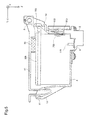
- FIG. 2 shows a perspective view of the construction of the ink cartridge pertaining to the embodiment.
- FIGS. 3A-B show diagrams of the construction of the board pertaining to the embodiment.
- FIG. 4 shows an illustration showing attachment of the ink cartridge in the holder.
- FIG. 5 shows an illustration showing the ink cartridge attached to the holder.
- the ink cartridge 100 attached to the holder 4 comprises a housing 101 containing ink, a lid 102 providing closure to the opening of the housing 101, a board 200, and a sensor 104.
- an ink supply orifice 110 into which the aforementioned ink supply needle 6 inserts when ink cartridge 100 is attached to the holder 4.
- a flared section 103 At the upper edge of the front face FR of the housing 101 there is formed a flared section 103.
- a recess 105 On the lower side of the center of the front face FR of the housing 101 there is formed a recess 105 bounded by upper and lower ribs 107, 106.
- the aforementioned board 200 fits into this recess 105.
- the sensor 104 is located in the region posterior to the board 200. The sensor 104 is used to detect remaining ink level, as will be described later.
- FIG. 3A depicts the arrangement on the surface of the board 200. This surface is the face that is exposed to the outside when the board 200 is mounted on the ink cartridge 100.
- FIG. 3B depicts the board 200 viewed from the side.
- a boss slot 201 is formed at the upper edge of the board 200
- a boss hole 202 is formed at the lower edge of the board 200.
- bosses 108 and 109 formed on the lower face of the recess 105 mate with the boss slot 201 and the boss hole 202 respectively.
- the distal ends of the bosses 108 and 109 are crushed to effect caulking.
- the board 200 is secured within the recess 105 thereby.
- the cover 11 is designed to be rotatable about a rotating shaft 9. With the cover 11 rotated upward to the open position, when the ink cartridge 100 is being attached to the holder, the flared section 103 of the ink cartridge is received by a projection 14 of the cover 11. When the cover 11 is closed from this position, the projection 14 rotates downward, and the ink cartridge 100 descends downward (in the Z direction in FIG. 4 ). When the cover 11 is completely closed, a hook 18 of the cover 11 interlocks with a hook 16 of the holder 4. With the cover 11 completely closed, the ink cartridge 100 is secured pressed against the holder 4 by an elastic member 20.
- the ink supply needle 6 inserts into the ink supply orifice 110 of the ink cartridge 100, and the ink contained in the ink cartridge 100 is supplied to the printing apparatus 1000 via the ink supply needle 6.
- the ink cartridge 100 is attached to the holder 4 by means of inserting it so as to move in the forward direction of the Z axis in FIG. 4 and FIG. 5 .
- the forward direction of the Z axis in FIG. 4 and FIG. 5 shall also be referred to as insertion direction of the ink cartridge 100.
- the arrow R in FIG. 3 (a) indicates the insertion direction of the ink cartridge 100 discussed above.
- the board 200 comprises a memory 203 disposed on its back face, and a terminal group composed of nine terminals 210 -290 disposed on its front face.
- the memory 203 stores information relating to the ink contained in the ink cartridge 100.
- the terminals 210 -290 are generally rectangular in shape, and are arranged in two rows generally orthogonal to the insertion direction R. Of the two rows, the row on the insertion direction R side, i.e. the row situated on the lower side in FIG.
- each of the terminals 210 -290 contains in its center portion a contact portion CP for contacting a corresponding terminal among the plurality of apparatus-side terminals, described later.
- the terminals 210 -240 forming the upper row and the terminals 250 -290 forming the lower row are arranged differently from one another, constituting a so-called staggered arrangement, so that the terminal centers do not line up with one another in the insertion direction R.
- the contact portions CP of the terminals 210 -240 forming the upper row and the contact portions CP of the terminals 250 -290 forming the lower row are similarly arranged differently from one another, constituting a so-called staggered arrangement.
- the first sensor drive terminal 250 is situated adjacently to two other terminals (the reset terminal 260 and the first short detection terminal 210), and of these, the first short detection terminal 210 for detecting shorting is positioned closest to the first sensor drive terminal 250.
- the second sensor drive terminal 290 is situated adjacently to two other terminals (the second short detection terminal 240 and the data terminal 280), and of these, the second short detection terminal 240 for detecting shorting is positioned closest to the second sensor drive terminal 290.
- the contact portion CP of the first sensor drive terminal 250 is situated adjacently to the contact portions CP of two other terminals (the reset terminal 260 and the first short detection terminal 210).
- the contact portion CP of the second sensor drive terminal 290 is situated adjacently to the contact portions CP of two other terminals (the second short detection terminal 240 and the data terminal 280).
- the first sensor drive terminal 250 and the second sensor drive terminal 290 are situated at the ends of the lower row, i.e. at the outermost positions in the lower row.
- the lower row is composed of a greater number of terminals than the upper row, and the length of the lower row in the direction orthogonal to the insertion direction R is greater than the length of the upper row, and consequently of all the terminals 210 -290 contained in the upper and lower rows, the first sensor drive terminal 250 and the second sensor drive terminal 290 are situated at the outermost positions viewed in the direction orthogonal to the insertion direction R.
- the contact portion CP of the first sensor drive terminal 250 and the contact portion CP of the second sensor drive terminal 290 are respectively situated at the ends of the lower row formed by the contact portions CP of the terminals, i.e., at the outermost positions in the lower row.
- the contact portion CP of the first sensor drive terminal 250 and the contact portion CP of the second sensor drive terminal 290 are situated at the outermost positions viewed in the direction orthogonal to the insertion direction R.
- the first short detection terminal 210 and the second short detection terminal 240 are respectively situated at the ends of the upper row, i.e., at the outermost positions in the upper row.
- the contact portion CP of the first short detection terminal 210 and the contact portion CP of the second short detection terminal 240 are similarly located at the ends of the upper row formed by the contact portions CP of the terminals, i.e. at the outermost positions in the upper row.
- the terminals 220, 230, 260, 270 and 280 connected to the memory 203 are situated between the first short detection terminal 210 and the first sensor drive terminal 250, and the second short detection terminal 240 and the second sensor drive terminal 290, located to either side.
- the board 200 has width of approximately 12.8 mm in the insertion direction R, width of the approximately 10.1 mm in the direction orthogonal to the insertion direction R, and thickness of approximately 0.71 mm.
- the terminals 210 - 290 each have width of approximately 1.8 mm in the insertion direction R and width of approximately 1.05 mm in the direction orthogonal to the insertion direction R.
- the dimension values given here are merely exemplary, with differences on the order of ⁇ 0.5 mm being acceptable, for example.
- the spacing between adjacent terminals in a given row (the lower row or the upper row), for example the interval K between the first short detection terminal 210 and the ground terminal 220, is 1 mm for example.
- the interval J between the upper row and the lower row is about 0.2 mm.
- differences on the order of ⁇ 0.3 mm are acceptable, for example.
- the terminals 210 -290 of the board 200 are electrically connected to a carriage circuit 500 via a contact mechanism 400 disposed on the holder 4.
- the contact mechanism 400 shall be described briefly making reference to FIGS. 6A-B .
- FIGS. 6A-B show schematics of the construction of the contact mechanism 400.
- the contact mechanism 400 has multiple slits 401, 402 of two types that differ in depth, formed in alternating fashion at substantially constant pitch in correspondence with the terminals 210 -290 on the board 200.
- a contact forming member 403, 404 endowed with electrical conductivity and resistance.
- the end exposed to the inside of the holder is placed in resilient contact with a corresponding terminal among the terminals 210 -290 on the board 200.
- portions 410 -490 which are the portions of the contact forming members 403 and 404 that contact the terminals 210 -290 are shown.
- the portions 410 -490 that contact the terminals 210 -290 function as apparatus-side terminals for electrically connecting the printing apparatus 1000 with the terminals 210 -290.
- the portions 410 -490 that contact the terminals 210 -290 shall hereinafter be termed apparatus-side terminals 410 -490.
- the apparatus-side terminals 410 -490 With the ink cartridge 100 attached to the holder 4, the apparatus-side terminals 410 -490 respectively contact the contact portions CP of the terminals 210 -290 described above ( FIG. 3A ).
- each contact forming member 403 and 404 the end lying exposed on the exterior of the holder 4 is placed in resilient contact with a corresponding terminal among the terminals 510 -590 furnished to the carriage circuit 500.
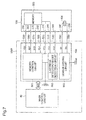
- FIG. 7 shows a brief diagram of the electrical arrangement of the ink cartridge and the printing apparatus.
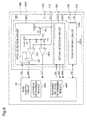
- FIG. 8 shows a brief diagram of the electrical arrangement, focusing on the cartridge detection/short detection circuit.
- the ground terminal 220, the power supply terminal 230, the reset terminal 260, the clock terminal 270 and the data terminal 280 are electrically connected to the memory 203.
- the memory 203 is, for example, EEPROM comprising serially accessed memory cells, and performing data read/write operations in sync with a clock signal.
- the ground terminal 220 is grounded via a terminal 520 on the printing apparatus 1000 side.
- the reset terminal 260 is electrically connected to a terminal 560 of the carriage circuit 500, and is used to supply a reset signal RST to the memory 203 from the carriage circuit 500.
- the clock terminal 270 is electrically connected to a terminal 570 of the carriage circuit 500, and is used to supply the clock signal CLK to the memory 203 from the carriage circuit 500.
- the data terminal 280 is electrically connected to a terminal 580 of the carriage circuit 500, and is used for exchange of data signals SDA between the carriage circuit 500 and the memory 203.
- first short detection terminal 210 the second short detection terminal 240, or both are electrically connected with the ground terminal 220.
- first short detection terminal 220 is electrically connected to the ground terminal 220.
- the first short detection terminal 210 and the second short detection terminal 240 are electrically connected respectively to the terminals 510, 540 of the carriage circuit 500, and used for cartridge detection and short detection, described later.
- a piezoelectric element is used as the sensor 104.
- the remaining ink level can be detected by applying driving voltage to the piezoelectric element to induce the piezoelectric element to vibrate through the inverse piezoelectric effect, and measuring the vibration frequency of the voltage produced by the piezoelectric effect of the residual vibration.
- this vibration frequency represents the characteristic frequency of the surrounding structures (.e.g. the housing 101 and ink) that vibrate together with the piezoelectric element.
- the characteristic frequency changes depending on the amount of ink remaining within the ink cartridge, so the remaining ink level can be detected by measuring this vibration frequency.
- the second sensor drive terminal 290 is electrically connected to one electrode of the piezoelectric element used as the sensor 104, and the first sensor drive terminal 250 is electrically connected to the other electrode. These terminals 250, 290 are used for exchange of sensor driving voltage and output signals from the sensor 104, between the carriage circuit 500 and the sensor 104.
- the carriage circuit 500 comprises a memory control circuit 501, a cartridge detection/short detection circuit 502, and a sensor driving circuit 503.
- the memory control circuit 501 is a circuit connected to the terminals 530, 560, 570, 580 of the carriage circuit 500 mentioned above, and used to control the memory 203 of the ink cartridge 100 to perform data read/write operations.
- the memory control circuit 501 and the memory 203 are low-voltage circuits driven at relatively low voltage (in the embodiment, a maximum of about 3.3 V).
- the memory control circuit 501 can employ a known design, and as such need not be described in detail here.
- the sensor driving circuit 503 is a circuit connected to the terminals 590 and 550 of the carriage circuit 500, and used to control the driving voltage output from these terminals 590 and 550 to drive the sensor 104, causing the sensor 104 to detect the remaining ink level.
- the driving voltage has a generally trapezoidal shape, and contains relatively high voltage (in the embodiment, about 36 V).
- the sensor driving circuit 503 and the sensor 104 are high-voltage circuits using relatively high voltage via the terminals 590 and 550.
- the sensor driving circuit 503 is composed of a logic circuit for example, but need not be described in detail herein.
- the cartridge detection/short detection circuit 502 is a low-voltage circuit driven using relatively low voltage (in the embodiment, a maximum of about 3.3V). As depicted in FIG. 8 , the cartridge detection/short detection circuit 502 comprises a first detection circuit 5021 and a second detection circuit 5022. The first detection circuit 5021 is connected to the terminal 510 of the carriage circuit 500. The first detection circuit 5021 has a cartridge detection function for detecting whether there is contact between the terminal 510 and the first short detection terminal 210 of the board 200, and a short detection function for detecting shorting of the terminal 510 to the terminals 550 and 590 which output high voltage.
- the first detection circuit 5021 has a reference voltage V_ref1 applied to one end of two series-connected resistors R2, R3, with the other end being grounded, thereby maintaining the potential at point P1 and P2 in FIG. 4 at V_ref1 and V_ref2, respectively.
- V_ref1 shall be termed the short detection voltage
- V_ref2 shall be termed the cartridge detection voltage.
- the short detection voltage V_ref1 is set to 6.5 V
- the cartridge detection voltage V_ref2 is set to 2.5 V.
- the short detection voltage V_ref1 (6.5 V) is input to the negative input pin of a first Op-Amp OP1
- the cartridge detection voltage V_ref2 (2.5 V) is input to the negative input pin of a second Op-Amp OP2.
- the potential of the terminal 510 is input to the positive input pins of the first Op-Amp OP1 and the second Op-Amp OP2.
- These two Op-Amps function as a comparator, outputting a High signal when the potential input to the negative input pin is higher than the potential input to the positive input pin, and conversely outputting a Low signal when the potential input to the negative input pin is lower than the potential input to the positive input pin.
- the terminal 510 is connected to a 3.3 V power supply VDD 3.3 via a transistor TR1.
- the potential of the terminal 510 will be set at about 3 V.
- the terminal 510 comes into contact with the first short detection terminal 210 of the board 200 described previously.
- a short detection enable signal EN is input from the main control circuit 40 to the other input pin of the AND circuit AA.
- the first detection circuit 5021 outputs the High signal from the Op-Amp OP1 as a short detection signal AB1. That is, execution of the short detection function of the first detection circuit 5021 is controlled by means of the short detection enable signal EN of the main control circuit 40.
- the short detection signal AB1 from the AND circuit AA is output to the main control circuit 40, as well as being output to the base pin of the transistor TR1 via resistance R1.
- the transistor TR1 it is possible to prevent high voltage from being applied to the power supply VDD 3.3 via the terminal 510 when a short is detected (when the short detection signal AB1 is HI).
- the second detection circuit 5022 has a cartridge detection function for detecting whether there is contact between the terminal 540 and the second short detection terminal 240 of the board 200, and a short detection function for detecting shorting of the terminal 540 to the terminals 550 and 590 which output high voltage. Since the second detection circuit 5022 has the same arrangement as the first detection circuit 5021, a detailed illustration and description need not be provided here.
- the cartridge detection signal output by the second detection circuit 5022 shall be denoted as CS2, and the short detection signal as AB2.
- the carriage circuit 500 corresponding to a single ink cartridge 100 has been described above.
- four of the cartridge detection/short detection circuits 502 described above will be provided, at each of the attachment locations for the four ink cartridges 100.
- a single sensor driving circuit 503 is provided, and a single sensor driving circuit 503 is connectable to each of the sensors 104 of the ink cartridges 100 attached at the four attachment locations by means of a switch(not shown).
- the memory control circuit 501 is a single circuit responsible for processes relating to the four ink cartridges.
- the main control circuit 40 is a computer of known design comprising a central processing unit (CPU), a read-only memory (ROM), and a random access memory (RAM). As noted, the main control circuit 40 controls the entire printer; in FIG. 8 , however, only those elements necessary for description of the embodiment are selectively illustrated, and the following description refers to the illustrated arrangement.
- the main control circuit 40 comprises a cartridge determining module M50 and a remaining ink level determining module M60. On the basis of the received cartridge detection signals CS1, CS2, the cartridge determining module M50 executes a cartridge determination process, described later.
- the remaining ink level determining module M60 controls the sensor driving circuit 503, and executes a remaining ink level detection process, described later.
- FIG. 9 shows a flowchart depicting the processing routine of the cartridge determination process.
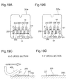
- FIGS. 10A-C show illustrations depicting three types of terminal lines on the board 200.
- the board 200 Before turning to the cartridge determination process, the board 200 will be described further with reference to FIG. 10 .
- the board 200 mentioned previously comes in three types, depending on the wiring pattern of the first short detection terminal 210, the second short detection terminal 240, and the ground terminal 220. These three types are designated respectively as Type A, Type B, and Type C.
- the Type A board 200 is arranged with the first short detection terminal 210 and the ground terminal 220 electrically connected by a conducting line 207, while the second short detection terminal 240 and the ground terminal 220 are not electrically connected.
- FIG. 10A the Type A board 200 is arranged with the first short detection terminal 210 and the ground terminal 220 electrically connected by a conducting line 207, while the second short detection terminal 240 and the ground terminal 220 are not electrically connected.
- the Type B board 200 is arranged with both the first short detection terminal 210 and the second short detection terminal 240 electrically connected with the ground terminal 220 by a conducting line 207.
- the Type C board 200 is arranged with the second short detection terminal 240 and the ground terminal 220 electrically connected by a conducting line 207, while the first short detection terminal 210 and the ground terminal 220 are not electrically connected.
- a board 200 of predetermined type, selected with reference to ink type or ink quantity for example, is disposed on the ink cartridge 100.
- a Type A board 200 could be disposed on an L size cartridge containing a large quantity of ink; a Type B board 200 could be disposed on an M size cartridge containing a standard quantity of ink; and a Type C board 200 could be disposed on an S size cartridge containing a small quantity of ink.
- the cartridge determining module M50 of the main control circuit 40 constantly receives from the cartridge detection/short detection circuit 502 the cartridge detection signals CS1, CS2 for each of the four attachment locations of the holder 4, and using these signals executes the cartridge determination process for each of the attachment locations.
- the cartridge determining module M50 When the cartridge determining module M50 initiates the cartridge determination process for a selected attachment location, the cartridge determining module M50 first ascertains whether the cartridge detection signal CS1 from the cartridge detection/short detection circuit 502 in the selected attachment location is a Low signal (Step S102). Next, the cartridge determining module M50 ascertains whether the cartridge detection signal CS2 in the selected attachment location is a Low signal (Step S104 or S106). If as a result the cartridge detection signals CS1 and CS2 are both Low signals (Step S102: YES and Step S104: YES), the cartridge determining module M50 decides that the ink cartridge 100 attached to the selected attachment location is furnished with the Type B board 200 (Step S108).
- the cartridge determining module M50 in the event that the cartridge detection signal CS1 is a Low signal and the cartridge detection signal CS2 is a High signal (Step S102: YES and Step S104: NO), decides that the ink cartridge is furnished with the Type A board 200 (Step S110); or in the event that the cartridge detection signal CS1 is a High signal and the cartridge detection signal CS2 is a Low signal (Step S102: NO and Step S104: YES), decides that the ink cartridge is furnished with the Type C board 200 described above (Step S112).
- Step S102 NO and Step S104: NO
- the cartridge determining module M50 decides that no cartridge is attached to the selected attachment location (Step S114). In this way, the cartridge determining module M50 determines whether an ink cartridge 100 is attached, and if so what type, for each of the four attachment locations.
- FIG. 11 shows a flowchart depicting the processing routine of the remaining ink level detection process.
- FIGS. 12A-C show timing charts depicting temporal change in the shorting-detection enable signal and sensor voltage during execution of the remaining ink level detection process;
- the remaining ink level determining module M60 of the main control circuit 40 in the event that the remaining ink level in the ink cartridge 100 attached at any of the attachment locations of the holder 4 is to be detected, first sets to High the short detection enable signal EN to all of the cartridge detection/short detection circuits 502 (Step S202).
- the short detection function is enabled in all of the cartridge detection/short detection circuits 502, and if voltage above the reference voltage V_ref1 (6.5 V) is applied to the aforementioned terminal 520 and terminal 540, are able to output High signals as the short detection signals AB1, AB2.
- a state in which the short detection enable signal EN are High signals is a state in which shorting of the terminal 510 or terminal 540 to the terminal 550 or terminal 590 is monitored.
- the remaining ink level determining module M60 instructs the sensor driving circuit 503 to output driving voltage from the terminal 550 or terminal 590 to the sensor 104, and detect the remaining ink level output (Step S204).
- the sensor driving circuit 503 receives an instruction signal from the remaining ink level determining module M60
- the sensor driving circuit 503 outputs driving voltage from either the terminal 550 or the terminal 590, the voltage being applied to the piezoelectric element which constitutes the sensor 104 of the ink cartridge 100, charging the piezoelectric element and causing it to distort by means of the inverse piezoelectric effect.
- the sensor driving circuit 503 subsequently drops the applied voltage, whereupon the charge built up in the piezoelectric element is discharged, causing the piezoelectric element to vibrate.
- the driving voltage is the voltage shown during time interval T1.
- the driving voltage fluctuates between the reference voltage and the maximum voltage Vs in such a way as to describe a trapezoidal shape.
- the maximum voltage Vs is set to relatively high voltage (e.g. about 36 V).
- the sensor driving circuit 503 detects the voltage produced by the piezoelectric effect as a result of vibration of the piezoelectric element (in FIG.
- this vibration frequency represents the characteristic frequency of the surrounding structures (the housing 101 and ink) that vibrate together with the piezoelectric element, and changes depending on the amount of ink remaining within the ink cartridge 100, so the remaining ink level can be detected by measuring this vibration frequency.
- the sensor driving circuit 503 outputs the detected result to the remaining ink level determining module M60 of the main control circuit 40.
- the remaining ink level determining module M60 When the remaining ink level determining module M60 receives the detected result from the sensor driving circuit 503, the remaining ink level determining module M60 brings the short detection enable signal EN, which was previously set to a High signal in Step S202, back to a Low signal (Step S206), and terminates the process.
- the interval that the remaining ink level is being detected is a state in which the short detection enable signal EN is set to a High signal to enable short detection. In other words, remaining ink level is detected while the occurrence of shorting is being monitored by the cartridge detection/short detection circuit 502.
- Step S204 The process carried out in the event that, during execution of detection of the remaining ink level (Step S204), the remaining ink level determining module M60 receives a High signal as the short detection signal AB1 or AB2, e.g. shorting is detected shall be described here.
- FIG. 11 a flowchart of the interrupt processing routine when shorting is detected is shown as well.
- the short detection enable signal EN is currently set to High, at the instant that the sensor driving voltage goes above the short detection voltage V_ref1 (6.5 V), a High signal will be output as the short detection signals AB1, AB2 from the cartridge detection/short detection circuit 502.
- the remaining ink level determining module M60 receives either of these short detection signals AB1, AB2, the remaining ink level determining module M60 suspends detection of remaining ink level, and executes the interrupt processing when shorting is detected.
- the remaining ink level determining module M60 immediately instructs the sensor driving circuit 503 to suspend the output of sensor driving voltage (Step S208).
- the remaining ink level determining module M60 without carrying out remaining ink level detection process to its conclusion, brings the short detection enable signal EN back to a Low signal (Step S206) to terminate the process.
- the main control circuit 40 may take some countermeasure, such as notifying the user of the shorting.
- FIG. 12A depicts change of the detection enable signal EN through time.
- FIG. 12B depicts sensor voltage in the event that neither the terminal 510 nor the terminal 540 is shorting to the terminal that outputs the sensor driving voltage of the terminals 550 and 590, so that the remaining ink level detection process is being executed normally.
- FIG. 12C depicts sensor voltage in the event that the terminal 510 or the terminal 540 is shorting to the terminal that, of the terminals 550 and 590, outputs the sensor driving voltage.
- the detection enable signal EN is a High signal.
- Vs is set at 36 V.
- the sensor voltage drops at the instant that it goes above the short detection voltage V_ref1 (6.5 V). This is due to the fact that, at the instant that the sensor voltage goes above the short detection voltage V_ref1 (6.5 V), a High signal is output as the short detection signal AB1 or AB2 from the cartridge detection/short detection circuit 502 to the remaining ink level determining module M60, and the remaining ink level determining module M60 receiving this signal immediately drops the sensor driving voltage.
- FIG. 13 shows an illustration of a scenario of shorting.
- the likely scenario for shorting to other terminals by the terminals 550 and 590 which output the sensor driving voltage is, for example, the case depicted in FIG. 13 , in which an electrically conductive ink drop S1 or a water drop S2 formed by condensation has become deposited on the board 200 of the ink cartridge 100, bridging the gap between the first sensor drive terminal 250 or the second sensor drive terminal 290 and another terminal or terminals on the board 200, producing shorting.
- ink drop S1 that has adhered to the surface of the carriage 3 or ink supply needle 6 disperses and adheres as shown in FIG. 13 by the motion of attaching or detaching of ink cartridge 100.
- the terminal 550 that outputs the sensor driving voltage when the ink cartridge 100 is attached, the terminal 550 that outputs the sensor driving voltage, for example, will short to another terminal 510, 520, or 560 of the carriage circuit 500 via the first sensor drive terminal 250 and the terminals ( FIG. 13 : terminals 210, 220, 260) bridged by the ink drop S1 to the sensor drive terminal 250.
- the terminal 590 that outputs the sensor driving voltage will short to another terminal 540 of the carriage circuit 500 via the second sensor drive terminal 290 and the second short detection terminal 240 ( FIG. 13 ) bridged by the water drop S2 to the second sensor drive terminal 290, for example.
- Such a shorting is caused by various factor as well as the adhesion of the ink drop.
- the shorting may be caused by trapping electrically conducting object, for example, paper clip on carriage 3.
- the shorting also may be caused by adhesion to terminals of the electrically conducting material, for example, skin oil of user.
- the first sensor drive terminal 250 and the second sensor drive terminal 290 which apply the driving voltage to the sensor are arranged at the two ends of the terminal group, so the number of adjacent terminals is small. As a result, the likelihood of the first sensor drive terminal 250 and the second sensor drive terminal 290 shorting to other terminals is low.
- the shorting will be detected by the aforementioned cartridge detection/short detection circuit 502. For example, shorting of the first sensor drive terminal 250 to another terminal caused by the ink drop S1 infiltrating from the first sensor drive terminal 250 side will be detected instantly and the output of sensor driving voltage will be suspend, preventing or reducing damage to the memory 203 and the printing apparatus 1000 circuits (the memory control circuit 501 and the cartridge detection/short detection circuit 502) caused by the shorting.
- the first short detection terminal 210 is adjacent to the first sensor drive terminal 250 and situated closest to the first sensor drive terminal 250. Consequently, in the event that the first sensor drive terminal 250 should short to another terminal or terminals due to the ink drop S1 or the water drop S2, there is a high likelihood that the first sensor drive terminal 250 will short to the first short detection terminal 210 as well. Consequently, shorting of the first sensor drive terminal 250 to another terminal can be detected more reliably.
- the first short detection terminal 210 is also used by the cartridge detection/short detection circuit 502 to determine whether an ink cartridge 100 is attached, as well as to determine the type of attached ink cartridge 100.
- the number of terminals on the board 200 can be kept down, and it becomes possible to reduce the number of board 200 manufacturing steps and the number of parts for the board 200.
- the second short detection terminal 240 is the terminal situated closest to the second sensor drive terminal 290.
- the first sensor drive terminal 250 and the first short detection terminal 210 on the one hand, and the second sensor drive terminal 290 and the second short detection terminal 240 on the other, are situated at the ends of the terminal group so that the other terminals (220, 230, 260 -270) lie between them. Consequently, if foreign matter (the ink drop S1, water drop S2 etc.) should infiltrate from either side as indicated by the arrows in FIG. 13 , this infiltration can be detected before it infiltrates as far as the other terminals (220, 230, 260 -270). Consequently, damage to the circuits of the memory 203 and the printing apparatus 1000 due to infiltration of foreign matter can be prevented or reduced.
- foreign matter the ink drop S1, water drop S2 etc.
- the first sensor drive terminal 250 and the second sensor drive terminal 290 are arranged in the row on the insertion direction R side (lower row).
- the terminals 250, 290 to which sensor driving voltage including high voltage is applied are situated to the back in the insertion direction, there is less likelihood that ink drops or foreign matter (e.g. a paperclip) will infiltrate to the location of these terminals 250, 290.
- damage to the circuits of the memory 203 and the printing apparatus 1000 caused by infiltration of foreign matter can be prevented or reduced.
- the terminal group of the board 200 is arranged in a staggered pattern. As a result, unwanted contact of the terminals of the ink cartridge 100 with the terminals of the printing apparatus 1000 (the contact forming members 403, 404 mentioned previously) during the attachment operation can be prevented or reduced.
- FIGS. 14A -16B show first diagrams depicting boards pertaining to variations.
- FIGS. 15A-C show second diagrams depicting boards pertaining to variations.
- FIGS. 16A-B show third diagrams depicting boards pertaining to variations.
- the first short detection terminal 210 is similar to the first short detection terminal 210 of the board 200 of the embodiment, but has at its lower end an extended portion that reaches into proximity with the lower edge of the lower row.
- the extended portion is positioned between the first sensor drive terminal 250 and the reset terminal 260 of the lower row.
- the first sensor drive terminal 250 and terminal other than the first short detection terminal 210 are shorting, there is a high possibility that the first sensor drive terminal 250 and the first short detection terminal 210 are shorting and the sensor driving voltage is suspended. Accordingly, problems caused by shorting of the first sensor drive terminal 250 to another terminal (in the example of FIG. 14A , the reset terminal 260) can be prevented or reduced.
- the second short detection terminal 240 of the board 200b is also similar in shape to the first short detection terminal 210 mentioned above, and shorting of the second sensor drive terminal 290 to another terminal will also be detected more reliably.
- the board 200c depicted in FIG. 14B has, in addition to the arrangement of the board 200b described above, also has an extended portion located at the upper side of the first sensor drive terminal 250, and reaching into proximity with the upper edge of the upper row.
- an ink drop S4 as depicted in FIG. 14 (b)
- shorting of the short detection terminal 210 to the extended portion of the first sensor drive terminal 250 will be detected.
- the first sensor drive terminal 250 and terminal other than the first short detection terminal 210 are shorting, there is a high possibility that the first sensor drive terminal 250 and the first short detection terminal 210 are shorting and the sensor driving voltage is suspended. Accordingly, problems caused by shorting of the first sensor drive terminal 250 to another terminal can be prevented or reduced.
- the second sensor drive terminal 290 of the board 200c is also similar in shape to the first sensor drive terminal 250 mentioned above, and infiltration of an ink drop from the end, at the end at which the second sensor drive terminal 290 is situated, can be detected instantly.
- the board 200d depicted in FIG. 14C differs from the board 200 of the embodiment in that there is no second short detection terminal 240.
- the second short detection terminal 240 does not carry out detection of contact by means of the cartridge detection/short detection circuit 502 (since there is no shorting to the ground terminal 220). Consequently, in the case of the Type A board 200, the second short detection terminal 240 is used for short detection only and accordingly can be dispensed with.
- the first short detection terminal 210 is at the location closest to the first sensor drive terminal 250, when the first sensor drive terminal 250 and terminal other than the first short detection terminal 210 are shorting, there is a high possibility that the first sensor drive terminal 250 and the first short detection terminal 210 are shorting and the sensor driving voltage is suspended. Infiltration of an ink drop to second sensor drive terminal 290 side will also be detected to a certain extent.
- the symbol CP represents the location of contact with the contact forming member 403 that would contact the second short detection terminal 240 if the second short detection terminal 240 were present (i.e. the contact forming member 403 corresponding to the terminal 540 of the carriage circuit 500).
- the second short detection terminal 240 Even in the case that the second short detection terminal 240 is absent, if a shorting should occur between the second sensor drive terminal 290 and the contact forming member 403 corresponding to the terminal 540 of the carriage circuit 500 due to an ink drop S5, infiltration of the ink drop S5 will be detected. Similarly, in the case of a Type C board 200, the first short detection terminal 210 may be dispensed with.
- the first sensor drive terminal 250 and the first short detection terminal 210 have elongated shape reaching from the vicinity of the upper edge of the upper row to the vicinity of the lower edge of the lower row.
- the terminals of this shape can contact the corresponding contact forming portions 403 arranged in a staggered pattern.
- first short detection terminal 210 is located between first sensor drive terminal 250 and terminal other than the first short detection terminal 210. Accordingly, when the first sensor drive terminal 250 and terminal other than the first short detection terminal 210 are shorting, there is a high possibility that the first sensor drive terminal 250 and the first short detection terminal 210 are shorting and the sensor driving voltage is suspended.
- the second sensor drive terminal 290 and the second short detection terminal 240 of the board 200e have shape similar to the first sensor drive terminal 250 and the first short detection terminal 210 described above. Accordingly, when the second sensor drive terminal 290 and terminal other than the second short detection terminal 240 are shorting, there is a high possibility that the second sensor drive terminal 290 and the second short detection terminal 240 are shorting. As a result, the possibility preventing or reducing the problems caused by shorting of the sensor drive terminal 250, 290 to another terminal becomes higher.
- the terminal which corresponds to the first short detection terminal 210 and the ground terminal 220 in the board 200 pertaining to the embodiment is an integral terminal 215 wherein these two terminals are integrally formed as a single member.
- This board 200f can be used in place of the Type A or Type B board 200 ( FIG. 10 ) whose first short detection terminal 210 and ground terminal 220 are shorted. With the board 200f, the need is obviated for a line between the first short detection terminal 210 and the ground terminal 220, which was required in the case of in the board 200 pertaining to the embodiment, so the board 200 requires fewer process steps and fewer parts.
- the terminals 210 -240 of the upper row each have shape similar to the first short detection terminal 210 of the board 200b described previously. Specifically, each of the terminals 210 -240 has an extended portion situated at the lower edge of the corresponding terminal of the board 200 pertaining to the embodiment and reaching into proximity with the lower edge of the lower row.
- the terminals 250 -290 of the lower row of the board 200g are similar in shape to the first sensor drive terminal 250 of the board 200c described earlier. Specifically, the each of the terminals 250 -290 has an extended portion situated at the upper edge of the corresponding terminal of the board 200 pertaining to the embodiment and reaching into proximity with the upper edge of the upper row.
- the terminals 210 -290 of the board 200g are arranged so as to form a terminal group composed of a single row of terminals of generally oar shape of in mutually different arrangement, rather than being arranged in two rows.
- the first sensor drive terminal 250 and the second sensor drive terminal 290 to which the high-voltage sensor driving voltage is applied are positioned at the two ends of the single row of the terminal group, with the first short detection terminal 210 and the second short detection terminal 240 respectively arranged adjacently inward from the first sensor drive terminal 250 and the second sensor drive terminal 290.
- an ink drop or foreign matter infiltrating from either end can be detected immediately at the point in time that shorting occurs between the first sensor drive terminal 250 and the short detection terminal 210, or between the second sensor drive terminal 290 and the second short detection terminal 240.
- the first sensor drive terminal 250 or the second sensor drive terminal 290 should short to another terminal, in the case where the shorting is due to an ink drop or the like, the likelihood is extremely high that shorting between the first sensor drive terminal 250 and the short detection terminal 210, or between the second sensor drive terminal 290 and the second short detection terminal 240, will occur at the same time. Consequently, shorting of the first sensor drive terminal 250 or the second sensor drive terminal 290 to another terminal can be detected reliably. As a result, damage to the memory 203 and the printing apparatus 1000 circuits (the memory control circuit 501 and the cartridge detection/short detection circuit 502) caused by the shorting can be prevented or minimized.
- the terminals 210 -290 have elongated shape extending over a distance equivalent to two rows of the board 200 pertaining to the embodiment, in a manner similar to the first sensor drive terminal 250 and the first short detection terminal 210 of the board 200e described previously.
- the terminals of this shape as the contact locations are indicated by the symbol cp in FIG. 15C , can contact the corresponding contact forming portions 403 arranged in a staggered pattern.
- the terminals 210 -290 are arranged so as to form a single row in the orthogonal direction to the insertion direction R, in a manner similar to the board 200g described above. Also, like the board 200g, the first sensor drive terminal 250 and the second sensor drive terminal 290 to which the high-voltage sensor driving voltage is applied are positioned at the two ends of the single row of terminals, with the first short detection terminal 210 and the second short detection terminal 240 respectively arranged adjacently inward from the first sensor drive terminal 250 and the second sensor drive terminal 290. As a result, the board 200h affords advantages analogous to those of the board 200g described above.
- the first short detection terminal 210 of the board 200i depicted in FIG. 16A has a shape that is longer on the left side in the drawing, as compared to the first short detection terminal 210 of the board 200 pertaining to the embodiment. Additionally, the first short detection terminal 210 of the board 200i has an extended portion reaching from the left edge portion to the vicinity of the lower edge of the lower row. The extended portion is situated to the left of the first sensor drive terminal 250 in the lower row. In other words, the extended portion is disposed to further from the middle of the terminal group in a direction substantially orthogonal to the insertion direction R than the first sensor drive terminal 250.
- the first short detection terminal 210 is situated outwardly (to the left side) of the first sensor drive terminal 250, when viewed in terms of the contact portion CP of the terminal, of the contact portions CP of all of the terminals 210 -290 the contact portion CP of the first sensor drive terminal 250 is the one situated at the outermost position (left side), in the same manner as in the embodiment. Also, shorting between the first sensor drive terminal 250 and the first short detection terminal 210 that includes the contact portion CP adjacent to the contact portion CP of the first sensor drive terminal 250 is detected. Accordingly, the board 200i pertaining to this variation affords advantages similar to the board 200 pertaining to the embodiment.
- the length of a first portion that is a portion adjacent to the circumferential edge of the first short detection terminal 210 among the circumferential edge of the first sensor drive terminal 250 becomes long. As shown in FIG. 16B , the length of the first portion is longer than that of a second portion that is a portion adjacent to the circumferential edge of the reset terminal 260 among the among the circumferential edge of the first sensor drive terminal 250.
- the reset terminal 260 are shorting, there is a high possibility that the first sensor drive terminal 250 and the first short detection terminal 210 are shorting. Accordingly, the sensor driving voltage is suspended and problems caused by shorting of the first sensor drive terminal 250 to another terminal can be prevented or reduced with higher probability.
- the first short detection terminal 210 of the board 200p in FIG. 16C has the longer extended portion than the first short detection terminal 210 of the board 200i.
- the extended portion of the first short detection terminal 210 of the board 200p extends from upper left to lower right of the first sensor drive terminal 250 along the circumferential edge of the first sensor drive terminal 250.
- the length of the first portion in the board 200p is longer than that in the board 200i. Accordingly, when the first sensor drive terminal 250 and terminal other than the first short detection terminal 210 are shorting, there is a higher possibility the sensor driving voltage is suspended and problems caused by shorting of the first sensor drive terminal 250 to another terminal can be prevented or reduced.
- the first short detection terminal 210 of the board 200q in FIG. 16D has the longer extended portion than the first short detection terminal 210 of the board 200i and 200p.
- the extended portion of the first short detection terminal 210 of the board 200q extends from upper left through lower to upper right of the first sensor drive terminal 250 along the circumferential edge of the first sensor drive terminal 250.
- the first short detection terminal 210 is formed so as to surround the first sensor drive terminal 250 completely.
- the length of the first portion in the board 200q is longer than that in the board 200i and 200p. Accordingly, when the first sensor drive terminal 250 and terminal other than the first short detection terminal 210 are shorting, there is a higher possibility the sensor driving voltage is suspended and problems caused by shorting of the first sensor drive terminal 250 to another terminal can be prevented or reduced.
- board 200i, 200p, 200q are added the direction in which the portion of the first short detection terminal 210 is located adjacently to a portion of the sensor drive terminal 250 by providing the extended portion of the first short detection terminal 210.
- the extended potion of the first short detection terminal 210 located adjacently to left border of the first sensor drive terminal 250 in a lateral direction towards an edge of the ink cartridge 100, and the first short detection terminal 210 itself is located adjacently to upper border of the first sensor drive terminal 250 in opposite direction of the insertion direction R.
- the extended potion of the first short detection terminal 210 is located adjacently to lower border of the first sensor drive terminal 250 in the insertion direction R. Furthermore, about board 200q, the extended potion of the first short detection terminal 210 is located adjacently to right border of the first sensor drive terminal 250 in lateral direction away from an edge of the ink cartridge 100. In other words, about board 200q, at least a potion of the first short detection terminal 210 is located adjacently to the first sensor drive terminal 250 in all direction.
- the extended portion of the first short detection terminal 210 adds the direction in which the first short detection terminal 210 and the first sensor drive terminal 250 are adjacent each other, and prevents or reduces problems caused by shorting of the first sensor drive terminal 250 to another terminal with much high probability.
- the boards 200i, 200p, 200q pertaining to this variation only the first short detection terminal 210 on the left side is furnished with a structure having the extended portion described above, but it would be possible to furnish the second short detection terminal 240 on the right side with a structure having an extended portion, in addition to the first short detection terminal 210 or instead of the first short detection terminal 210. In this case as well, there are afforded advantages analogous to those of the boards 200i, 200p, 200q pertaining to this variation.
- the board 200j depicted in FIG. 16B has an integral terminal 215 wherein the first short detection terminal 210 and the ground terminal 220 in the board 200 pertaining to the embodiment are integrally formed as a single member.
- the integral terminal 215 of the board 200j differs in shape from the integral terminal 215 of the board 200f described previously.
- the integral terminal 215 of the board 200j like the first short detection terminal 210 of the board 200i described in Variation 8, has a shape elongated on the left side, and has an extended portion reaching from the left edge portion to the vicinity of the lower edge of the lower row. In this case, advantages analogous to those of the board 200i pertaining to Variation 8 are attained, while reducing the number of production steps and parts needed for the board.
- FIGS. 17A -18D show diagrams depicting the construction around boards of ink cartridges pertaining to variations.
- FIGS. 18A-D show cross sections A-A to D-D in FIG. 17 .
- the board 200k depicted in FIG. 17A is furnished with seven terminals 210 -240 and 260 -280, out of the nine terminals 210 -290 furnished to the board 200 of the embodiment. Out of the nine terminals 210 -290 furnished to the board 200 of the embodiment, the board 200k lacks the first sensor drive terminal 250 and the second sensor drive terminal 290.
- the board 200k pertaining to this variation is furnished with notches NT1 or NT2 situated in zones that include the locations where the first sensor drive terminal 250 and the second sensor drive terminal 290 were disposed on the board 200 pertaining to the embodiment.
- the notches may have the shape indicated by the solid lines NT1, or the shape indicated by the broken lines NT2, in FIG. 17A .
- Terminals 150 and 190 having function similar to the first sensor drive terminal 250 and the second sensor drive terminal 290 of the board 200 in the embodiment are arranged on the housing 101 situated to the rear of the board 200k. Naturally, with the ink cartridge 100 attached to the holder 4, these terminals 150 and 190 are situated at locations contacting the corresponding apparatus-side terminals 450 and 490.
- FIG. 18A A-A cross section viewed in FIG. 17A is depicted in FIG. 18A .
- a depressed portion DE formed by a gap between the notch NT1 of the board 200k and the terminal 150, is situated between the terminal 150 and the adjacent terminals 260, 210 (in FIG. 18A , the reset terminal 260 is shown). While omitted from the drawing, a similar depressed portion DE is situated between the terminal 190 and the adjacent terminals 280, 240.
- the board 200m depicted in FIG. 17B is instead furnished with through-holes HL situated at locations corresponding to the locations where the first sensor drive terminal 250 and the second sensor drive terminal 290 are situated on the board 200 pertaining to the embodiment.
- B-B cross section viewed in FIG. 17B is depicted in FIG. 18B .
- Other arrangements of the ink cartridge 100 pertaining to Variation 11 are the same as those of the ink cartridge 100 pertaining to Variation 10.
- depressed portions DE are situated between the terminals 150, 190 and the adjacent terminals. Accordingly, the ink cartridge 100 pertaining to this variation affords advantages analogous to those of the ink cartridge 100 pertaining to Variation 10.
- FIGS. 19A-D show fourth diagrams depicting boards pertaining to variations.
- the board 200r includes the upper row formed by four terminals and the lower row formed by five terminals, as with the board 200 pertaining to the embodiment. Arrangement and function of the terminals 210 - 290 forming the upper row and the lower row of board 200r is the same as those of the terminals of board 200 in the embodiment, so the detailed description thereof is omitted.
- the board 200r shown in FIG. 19A has the dummy terminals DT between the upper row and the lower row and on the underside (the insertion direction side) of the lower row.
- the dummy terminals DT for example, are made of the same material as other terminal 210-290.
- FIG. 19C shows E-E cross-section including dummy terminals DT.
- the dummy terminals DT has about the same thickness as other terminal 210-290.
- the dummy terminals DT are for scraping away foreign object adherent on the contact forming members 403, for example, dust when ink cartridge 100 is attached or detached. This enables to prevent foreign object from being brought to the terminal to be contacted by contact forming member 403 (for example, the first sensor drive terminal 250 in FIG. 19C ) when ink cartridge 100 is attached or detached, and to prevent contact failure between the terminal and the contact forming member 403.
- the board 200r shown in FIG. 19A has the dummy terminal DT between the first sensor drive terminal 250 and the short detection terminal 210, so you can't say first sensor drive terminal 250 is located adjacent to first short detection terminal 210.
- the dummy terminals DT is not connected to memory 203 and not connected to the apparatus-side terminals 510-590 on printing apparatus 1000. Therefore, the shorting between the first sensor drive terminal 250 and the dummy terminals DT never cause any problem. Accordingly, the board 200r can afford working effects analogous to the board 200 pertaining to the embodiment.
- first sensor drive terminal 250 is not located adjacent to first short detection terminal 210 in a precise sense, at least a portion of the first short detection terminal 210 is arranged relative to at least a portion of the first sensor drive terminal 250, without a terminal connected to memory 203 (terminal 220, 230, 260-280) therebetween in at least one direction, for the detection of shorting between the first sensor drive terminal 250 and the first short detection terminal 210.
- the first sensor drive terminal 250 is substantially located adjacent to first short detection terminal 210.
- the output of sensor driving voltage is suspend and damage to the circuits of the memory 203 and the printing apparatus 1000 caused by shorting can be prevented or reduced.
- FIG. 2 shows a perspective view of the construction of the ink cartridge pertaining to the variation 13.
- FIG 21 shows a picture of the ink cartridge pertaining to the variation 13 being attached to the printer.
- Ink cartridge 100b pertaining to Variation 13 is configured for installation in an "off carriage" type printer, i.e., one in which the ink cartridge is not installed on a carriage.
- Off carriage type printers are typically large-scale printers; the ink cartridges employed in such large-scale printers are typically larger in size than the ink cartridges employed in on-carriage type printers.
- Ink cartridge 100b comprises a housing 1001 containing ink, a board mounting portion 1050 for mounting board 200, an ink feed orifice 1020 for supplying ink from a housing 1001 to the printer; an air feed orifice 1030 allowing intake of air into ink cartridge 100b to allow smooth flow of ink; and guide portions 1040 for installation in the printer.
- the exterior dimensions of ink cartridge 100b are such that the side thereof (i.e. the depth direction) extending perpendicular to the side on which the guide portions 1040, etc. are formed (i.e. the width direction) is longer than the width direction.
- the relationship of the depth-wise dimension to the width-wise dimension of board 200, expressed as a ratio of the two, is 15 : 1 or greater, for example.
- board 200 is positioned by means of boss hole 202 and boss slot 201, and secured on the board mounting portion 1050 of ink cartridge 100b.
- the guide portions 1040 of ink cartridge 100b guide the guide pins 2040 on the printer so that the board mounting portion 1050, ink feed orifice 1020, and air feed orifice 1030 are appropriately contacted/coupled with a contact pin 2050, ink feed orifice 2020, and air feed orifice 2030 on the printer.
- the insertion direction of ink cartridge 100b is indicated by arrow R in FIG. 21 .
- the insertion direction R on board 200 in this variation is the same as that in the above-mentioned embodiment.
- Ink cartridge 100b used for off carriage type printer pertaining to this variation can prevent or reduce problems caused by shorting of the first sensor drive terminal 250 to another terminal as in the case of the embodiment and variations described above.
- Configuration of the ink cartridge for "on carriage” type printer shown in FIG. 2 is one example among many. Configuration of the ink cartridge for "on carriage” type printer is not limited to this. Other configuration of the ink cartridge for "on carriage” type printer shall be described as Variation 14 with reference to FIGS. 22 -24 .
- FIG 22 shows a first diagram of the construction of the ink cartridge pertaining to Variation 14.
- FIG 23 shows a second diagram of the construction of the ink cartridge pertaining to variation 14.
- FIG 24 shows a third diagram of the construction of the ink cartridge pertaining to Variation 14.
- the ink cartridge 100b pertaining to Variation 14 includes housing 101b, board 200 and sensor 104b.
- the board 200 is mounted on the lower side (Z-axis plus direction side) of the front face (Y-axis plus direction side face) of the housing 101 as with ink cartridge 100 in the embodiment. Configuration of the board 200 is identical with the board 200 in the embodiment.
- the sensor 104b is embedded in the side wall of the housing 101b and used for detection of remaining ink level.
- Hook 120b that engages with catching part of the holder 4b when the ink cartridge 100b is attached to the holder 4b is mounted on the upper side of the front face of the housing 101b. Hook 120b fixates the Ink cartridge 100b to the holder 4b.
- the insertion direction when the ink cartridge 100b is attached to the holder 4b is a direction of arrow R in FIG. 22 (Z-axis plus direction) as with the ink cartridge 100 in the embodiment.
- the housing 101b has displacement preventers PO1-PO4 on the side portion (x-axis direction side) of housing 101b close to the board 200.
- the displacement preventers PO1-PO4 comes into contact with or close to a corresponding potion of the side wall of the holder 4b when the ink cartridge 100b is attached to the holder 4b. This prevents the ink cartridge 100b from moving in X-axial direction from its ideal position on the holder 4b.
- the displacement preventers PO1 and PO2 are located on the upper side of the board 200 and prevent the upper side of the 100b from swinging in X-axial direction taking the ink supply orifice 110b as an axis of rotation.
- the displacement preventers PO3 and PO4 are lateral to the terminals 210 -290 on the board 200 ( FIG. 3 ) and keep the terminals 210 -290 in the correct position so as to contact the corresponding apparatus-side terminal 410 -490 correctly.
- the electrical arrangements of the ink cartridge 100b pertaining to Variation 14 is identical with those of the ink cartridge 100 pertaining to above-embodiment described with reference to FIG. 7 . So, the description thereof is omitted.
- the ink cartridge 100b pertaining to Variation 14 affords the following working effects in addition to the same working effects as the ink cartridge 100 pertaining to the embodiment. Since the ink cartridge 100b has the displacement preventers PO1-PO4, it can prevent or reduce the position displacement when the ink cartridge 100b is attached to the holder 4b. Especially, since the displacement preventers PO3 and PO4 are lateral to the terminals 210 -290 on the board 200, accuracy of positioning of the terminals 210 - 290 relative to the corresponding apparatus-side terminals can be improved. Further, as described with reference to FIG.
- the sensor drive terminal 250 and the second sensor drive terminal 290 are arranged at each end of the terminals 210 -290, that is , the sensor drive terminal 250 and the second sensor drive terminal 290 are closest to the displacement preventers PO4 and PO4 respectively. This lead to improvement of accuracy of positioning of the sensor drive terminal 250 and the second sensor drive terminal 290. Therefore, the false contact between the terminals 250, 290 to which high voltage is applied and one of the non-corresponding apparatus-side terminals can be prevented or reduced.
- one of the boards 200b-200s shown in FIGS. 14 -19 can be mounted on the ink cartridge 100b shown in FIG. 22-24 .
- porous elements PO may be disposed within the depressed portions DE in Variation 10 and Variation 11 described above, i.e. between the terminals 150, 190 and the board.
- ink drops or condensed water which can easily cause shorting of the terminals 150, 190 to other terminals, can be effectively absorbed by the porous elements PO. Accordingly, this design also affords advantages analogous to those of Variation 10 and Variation 11 discussed above.
- the ink cartridge 100 is furnished with a sensor 104 (piezoelectric element) and memory 203 as the plurality of the devices; however, the plurality of the devices are not limited to a sensor 104 and memory 203.
- the sensor 104 may be a sensor of a type that detects the properties or level of ink by means of applying voltage to the ink within an ink cartridge 100, and measuring its resistance.
- the sensor 104 is mounted on the housing 101 and the memory 203 is mounted on the board 200.
- the arrangements of the plurality of the devices are not limited to those in the embodiment.
- the memory 203 and the board 200 may be separate, and the memory 203 and the board 200 may be installed on the housing 101 individually.
- the plurality of the devices may be integrated into a circuit board or a single module.
- the circuit board or the single module may be mounted on the housing 101 or the board 200. It's preferred that terminals connected to a device to which relatively high voltage among the plurality of the devices are arranged in positions of the first sensor drive terminal 250 and the second sensor drive terminal 290 described above, and terminals connected to a device to which relatively low voltage among the plurality of the devices are arranged in positions of the terminals 220, 230, 260-280. In this case, damage to the ink cartridge 100 and the printing apparatus 1000 caused by shorting between the terminal connected to the device to which relatively high voltage and the terminal connected to the device to which relatively low voltage can be prevented or reduced.
- terminals for memory 203 (220, 230, 260-280) and two terminals for sensor 104 (250, 290) are employed, however, other number of terminals may be employed due to the specification of the device.
- the terminal connected to the device to which relatively high voltage may be one. In this case, such terminal may be arranged in a position of any of the terminals 250, 290 described above.
- the invention is implemented in an ink cartridge 100, implementation thereof is not limited to ink cartridges, with implementation in a similar manner to receptacles containing other types of printing material, such as toner, being possible as well.
- portions of these arrangements implemented through hardware could instead be implemented through software, and conversely portions implemented through software could instead be implemented through hardware.
Priority Applications (4)
| Application Number | Priority Date | Filing Date | Title |
|---|---|---|---|
| EP22167793.3A EP4063132B1 (de) | 2005-12-26 | 2006-12-22 | Druckmaterialbehälter und verwendung des druckmaterialbehälters |
| EP23197166.4A EP4272968A3 (de) | 2005-12-26 | 2006-12-22 | Druckmaterialbehälter und verwendung des druckmaterialbehälters |
| EP20182047.9A EP3744529B1 (de) | 2005-12-26 | 2006-12-22 | Druckmaterialbehälterplatte |
| EP16182416.4A EP3115213A1 (de) | 2005-12-26 | 2006-12-22 | Druckmaterialbehälter und auf dem druckmaterialbehälter montierte platte |
Applications Claiming Priority (5)
| Application Number | Priority Date | Filing Date | Title |
|---|---|---|---|
| JP2005372028 | 2005-12-26 | ||
| JP2006220751A JP4144637B2 (ja) | 2005-12-26 | 2006-08-11 | 印刷材収容体、基板、印刷装置および印刷材収容体を準備する方法 |
| EP06256540.3A EP1800872B2 (de) | 2005-12-26 | 2006-12-22 | Tintenbehälter und Platine darauf montiert |
| EP10184458.7A EP2277707B2 (de) | 2005-12-26 | 2006-12-22 | Tintenbehälter und Platine darauf montiert |
| EP09156202A EP2080622B1 (de) | 2005-12-26 | 2006-12-22 | Tintenbehälter und Platine darauf montiert |
Related Parent Applications (5)
| Application Number | Title | Priority Date | Filing Date |
|---|---|---|---|
| EP09156202A Division EP2080622B1 (de) | 2005-12-26 | 2006-12-22 | Tintenbehälter und Platine darauf montiert |
| EP10184458.7A Division EP2277707B2 (de) | 2005-12-26 | 2006-12-22 | Tintenbehälter und Platine darauf montiert |
| EP10184458.7A Division-Into EP2277707B2 (de) | 2005-12-26 | 2006-12-22 | Tintenbehälter und Platine darauf montiert |
| EP06256540.3A Division-Into EP1800872B2 (de) | 2005-12-26 | 2006-12-22 | Tintenbehälter und Platine darauf montiert |
| EP06256540.3A Division EP1800872B2 (de) | 2005-12-26 | 2006-12-22 | Tintenbehälter und Platine darauf montiert |
Related Child Applications (5)
| Application Number | Title | Priority Date | Filing Date |
|---|---|---|---|
| EP22167793.3A Division EP4063132B1 (de) | 2005-12-26 | 2006-12-22 | Druckmaterialbehälter und verwendung des druckmaterialbehälters |
| EP23197166.4A Division EP4272968A3 (de) | 2005-12-26 | 2006-12-22 | Druckmaterialbehälter und verwendung des druckmaterialbehälters |
| EP16182416.4A Division-Into EP3115213A1 (de) | 2005-12-26 | 2006-12-22 | Druckmaterialbehälter und auf dem druckmaterialbehälter montierte platte |
| EP16182416.4A Division EP3115213A1 (de) | 2005-12-26 | 2006-12-22 | Druckmaterialbehälter und auf dem druckmaterialbehälter montierte platte |
| EP20182047.9A Division EP3744529B1 (de) | 2005-12-26 | 2006-12-22 | Druckmaterialbehälterplatte |
Publications (3)
| Publication Number | Publication Date |
|---|---|
| EP2789466A1 true EP2789466A1 (de) | 2014-10-15 |
| EP2789466B1 EP2789466B1 (de) | 2016-09-07 |
| EP2789466B8 EP2789466B8 (de) | 2016-12-07 |
Family
ID=37758994
Family Applications (11)
| Application Number | Title | Priority Date | Filing Date |
|---|---|---|---|
| EP22167793.3A Active EP4063132B1 (de) | 2005-12-26 | 2006-12-22 | Druckmaterialbehälter und verwendung des druckmaterialbehälters |
| EP14171179.6A Revoked EP2789466B8 (de) | 2005-12-26 | 2006-12-22 | Druckmaterialbehälter und auf dem Druckmaterial montierte Platte |
| EP06256540.3A Active EP1800872B2 (de) | 2005-12-26 | 2006-12-22 | Tintenbehälter und Platine darauf montiert |
| EP20182047.9A Active EP3744529B1 (de) | 2005-12-26 | 2006-12-22 | Druckmaterialbehälterplatte |
| EP16182416.4A Withdrawn EP3115213A1 (de) | 2005-12-26 | 2006-12-22 | Druckmaterialbehälter und auf dem druckmaterialbehälter montierte platte |
| EP09156203A Active EP2082882B1 (de) | 2005-12-26 | 2006-12-22 | Tintenbehälter und Platine darauf montiert |
| EP09180529.1A Active EP2177363B3 (de) | 2005-12-26 | 2006-12-22 | Tintenbehälter und Platine darauf montiert |
| EP10184458.7A Active EP2277707B2 (de) | 2005-12-26 | 2006-12-22 | Tintenbehälter und Platine darauf montiert |
| EP23197166.4A Pending EP4272968A3 (de) | 2005-12-26 | 2006-12-22 | Druckmaterialbehälter und verwendung des druckmaterialbehälters |
| EP09156202A Revoked EP2080622B1 (de) | 2005-12-26 | 2006-12-22 | Tintenbehälter und Platine darauf montiert |
| EP10184551.9A Active EP2295251B2 (de) | 2005-12-26 | 2006-12-22 | Verwendung eines Bedruckstoffbehälters und Verwendung einer mit Druckgerät verbindbaren Platine |
Family Applications Before (1)
| Application Number | Title | Priority Date | Filing Date |
|---|---|---|---|
| EP22167793.3A Active EP4063132B1 (de) | 2005-12-26 | 2006-12-22 | Druckmaterialbehälter und verwendung des druckmaterialbehälters |
Family Applications After (9)
| Application Number | Title | Priority Date | Filing Date |
|---|---|---|---|
| EP06256540.3A Active EP1800872B2 (de) | 2005-12-26 | 2006-12-22 | Tintenbehälter und Platine darauf montiert |
| EP20182047.9A Active EP3744529B1 (de) | 2005-12-26 | 2006-12-22 | Druckmaterialbehälterplatte |
| EP16182416.4A Withdrawn EP3115213A1 (de) | 2005-12-26 | 2006-12-22 | Druckmaterialbehälter und auf dem druckmaterialbehälter montierte platte |
| EP09156203A Active EP2082882B1 (de) | 2005-12-26 | 2006-12-22 | Tintenbehälter und Platine darauf montiert |
| EP09180529.1A Active EP2177363B3 (de) | 2005-12-26 | 2006-12-22 | Tintenbehälter und Platine darauf montiert |
| EP10184458.7A Active EP2277707B2 (de) | 2005-12-26 | 2006-12-22 | Tintenbehälter und Platine darauf montiert |
| EP23197166.4A Pending EP4272968A3 (de) | 2005-12-26 | 2006-12-22 | Druckmaterialbehälter und verwendung des druckmaterialbehälters |
| EP09156202A Revoked EP2080622B1 (de) | 2005-12-26 | 2006-12-22 | Tintenbehälter und Platine darauf montiert |
| EP10184551.9A Active EP2295251B2 (de) | 2005-12-26 | 2006-12-22 | Verwendung eines Bedruckstoffbehälters und Verwendung einer mit Druckgerät verbindbaren Platine |
Country Status (33)
| Country | Link |
|---|---|
| US (18) | US7562958B2 (de) |
| EP (11) | EP4063132B1 (de) |
| JP (1) | JP4144637B2 (de) |
| KR (4) | KR101030894B1 (de) |
| CN (5) | CN101712238B (de) |
| AR (5) | AR058636A1 (de) |
| AT (1) | ATE499214T1 (de) |
| AU (2) | AU2009213080A1 (de) |
| BR (3) | BRPI0620599B1 (de) |
| CA (6) | CA2676243A1 (de) |
| CL (4) | CL2009001777A1 (de) |
| DE (11) | DE202006021031U1 (de) |
| DK (6) | DK2295251T4 (de) |
| EG (1) | EG25747A (de) |
| ES (8) | ES2326246B1 (de) |
| FR (2) | FR2900866B1 (de) |
| GB (6) | GB2454331B (de) |
| HK (6) | HK1108864A1 (de) |
| HR (3) | HRP20080244B1 (de) |
| IL (1) | IL180236A (de) |
| IT (1) | ITTO20060921A1 (de) |
| MA (1) | MA30254B1 (de) |
| MX (1) | MXPA06015251A (de) |
| MY (5) | MY144386A (de) |
| NO (2) | NO344189B1 (de) |
| NZ (5) | NZ552094A (de) |
| PL (7) | PL2789466T3 (de) |
| PT (5) | PT2082882E (de) |
| RU (4) | RU2472625C2 (de) |
| SG (4) | SG153844A1 (de) |
| TW (5) | TWI334829B (de) |
| WO (1) | WO2007077747A1 (de) |
| ZA (1) | ZA200806197B (de) |
Cited By (1)
| Publication number | Priority date | Publication date | Assignee | Title |
|---|---|---|---|---|
| EP2789466B1 (de) | 2005-12-26 | 2016-09-07 | Seiko Epson Corporation | Druckmaterialbehälter und auf dem Druckmaterial montierte Platte |
Families Citing this family (137)
| Publication number | Priority date | Publication date | Assignee | Title |
|---|---|---|---|---|
| GB2433053B (en) * | 2004-09-01 | 2008-08-13 | Seiko Epson Corp | Printing material container |
| KR100765762B1 (ko) * | 2005-10-15 | 2007-10-15 | 삼성전자주식회사 | 하이브리드 화상형성장치 |
| UA108344C2 (uk) | 2005-12-26 | 2015-04-27 | Контейнер з матеріалом для друкування і плата, яка встановлюється на контейнері з матеріалом для друкування | |
| JP4488237B2 (ja) * | 2006-02-22 | 2010-06-23 | セイコーエプソン株式会社 | コネクタ |
| TWI341494B (en) * | 2007-02-07 | 2011-05-01 | Mstar Semiconductor Inc | Label paper with rfid function and rfid tag writing apparatus |
| CN102350880B (zh) * | 2007-03-28 | 2014-08-06 | 兄弟工业株式会社 | 墨盒、墨盒组以及墨盒确定系统 |
| DE102007021545B4 (de) * | 2007-05-08 | 2011-07-28 | Polysius AG, 59269 | Vorrichtung und Verfahren zum Sichten von Aufgabegut und Mahlanlage |
| JP5151841B2 (ja) * | 2007-10-01 | 2013-02-27 | セイコーエプソン株式会社 | 液体噴射装置、および、液体噴射装置の制御方法 |
| US7758138B2 (en) * | 2007-10-01 | 2010-07-20 | Seiko Epson Corporation | Liquid jetting apparatus and control method configured to reduce effects of electrical fluctuations |
| JP5151372B2 (ja) * | 2007-10-01 | 2013-02-27 | セイコーエプソン株式会社 | 液体噴射装置、および、液体噴射装置の制御方法 |
| GB0720139D0 (en) * | 2007-10-12 | 2007-11-28 | Videojet Technologies Inc | Ink jet printing |
| JP5206506B2 (ja) * | 2008-03-13 | 2013-06-12 | セイコーエプソン株式会社 | 装着装置、基板、液体情報を変更する方法 |
| JP5083250B2 (ja) * | 2008-03-13 | 2012-11-28 | セイコーエプソン株式会社 | 液体容器、基板、液体情報を変更する方法 |
| TWI385077B (zh) * | 2008-06-02 | 2013-02-11 | Microjet Technology Co Ltd | 供墨容器之退出機構及其所適用之列印機構 |
| US8388123B2 (en) * | 2008-06-08 | 2013-03-05 | Hewlett-Packard Development Company, L.P. | Fluid cartridge having feature to clear bracket riser surfaces |
| JPWO2010004742A1 (ja) * | 2008-07-11 | 2011-12-22 | セイコーエプソン株式会社 | 液体容器、液体噴射装置、および、液体噴射システム |
| WO2010004743A1 (ja) * | 2008-07-11 | 2010-01-14 | セイコーエプソン株式会社 | 液体容器、液体噴射装置、および、液体噴射システム |
| JP2010083111A (ja) * | 2008-10-02 | 2010-04-15 | Riso Kagaku Corp | インクカートリッジの着脱機構及び着脱制御方法 |
| CN101885270B (zh) * | 2009-05-13 | 2012-09-05 | 珠海纳思达企业管理有限公司 | 一种喷墨打印机上的适配器及与之配套使用的墨盒 |
| CN201511595U (zh) * | 2009-05-13 | 2010-06-23 | 肖彪 | 一种喷墨打印机上的适配器及与之配套使用的墨盒 |
| AU2014202105B2 (en) * | 2009-05-15 | 2016-02-25 | Seiko Epson Corporation | Recording material supply system, circuit board, structure, and ink cartridge for recording material consumption device |
| US8540347B2 (en) | 2009-05-15 | 2013-09-24 | Seiko Epson Corporation | Recording material delivery system for recording material-consuming apparatus; circuit board; structural body; and ink cartridge |
| JP2011011482A (ja) * | 2009-07-03 | 2011-01-20 | Brother Industries Ltd | 液体供給装置 |
| JP5521604B2 (ja) * | 2010-02-12 | 2014-06-18 | セイコーエプソン株式会社 | 端子間接続構造、液体収容容器、及び液体収容容器の組立方法 |
| JP5521605B2 (ja) * | 2010-02-12 | 2014-06-18 | セイコーエプソン株式会社 | 端子間接続構造、液体収容容器、及び液体収容容器の組立方法 |
| DE112010005580A5 (de) | 2010-05-20 | 2013-03-21 | Pelikan Hardcopy Production Ag | Druckmaterialbehälter und Kontaktvorrichtung |
| EP2752716B1 (de) | 2010-06-11 | 2018-12-19 | Ricoh Company, Ltd. | Informationsspeichervorrichtung, entnehmbare vorrichtung, entwicklerbehälter und bilderzeugungsvorrichtung |
| JP5776385B2 (ja) | 2010-09-03 | 2015-09-09 | セイコーエプソン株式会社 | 印刷装置 |
| JP5630157B2 (ja) * | 2010-09-03 | 2014-11-26 | セイコーエプソン株式会社 | 印刷装置 |
| JP5720148B2 (ja) * | 2010-09-03 | 2015-05-20 | セイコーエプソン株式会社 | 印刷材カートリッジ、及び、印刷材供給システム |
| US8764172B2 (en) * | 2010-09-03 | 2014-07-01 | Seiko Epson Corporation | Printing apparatus, printing material cartridge, adaptor for printing material container, and circuit board |
| JP5874160B2 (ja) | 2010-09-03 | 2016-03-02 | セイコーエプソン株式会社 | 液体収容容器を着脱可能なホルダー |
| JP5750849B2 (ja) * | 2010-09-03 | 2015-07-22 | セイコーエプソン株式会社 | 印刷装置、カートリッジセット、及び、アダプターセット |
| JP5541029B2 (ja) * | 2010-09-16 | 2014-07-09 | セイコーエプソン株式会社 | 印刷装置、印刷材カートリッジ、回路基板およびアダプター |
| JP5541030B2 (ja) * | 2010-09-16 | 2014-07-09 | セイコーエプソン株式会社 | 印刷装置、印刷材カートリッジ、回路基板およびアダプター |
| US8449055B2 (en) | 2010-09-30 | 2013-05-28 | Brother Kogyo Kabushiki Kaisha | Ink cartridge and recording apparatus |
| JP5703666B2 (ja) * | 2010-09-30 | 2015-04-22 | ブラザー工業株式会社 | インクカートリッジ及び記録装置 |
| JP5796443B2 (ja) | 2010-09-30 | 2015-10-21 | ブラザー工業株式会社 | インクカートリッジ及び記録装置 |
| US8496309B2 (en) | 2010-09-30 | 2013-07-30 | Brother Kogyo Kabushiki Kaisha | Recording apparatus capable of detecting residual amount of ink in ink cartridge |
| JP5817445B2 (ja) | 2010-11-19 | 2015-11-18 | セイコーエプソン株式会社 | 回路基板 |
| GB201021458D0 (en) * | 2010-12-17 | 2011-02-02 | Tf3 Ltd | Hair styling device |
| US8596771B2 (en) * | 2011-03-30 | 2013-12-03 | Brother Kogyo Kabushiki Kaisha | Printing-liquid cartridge and recording apparatus using the same |
| JP5382044B2 (ja) | 2011-03-31 | 2014-01-08 | ブラザー工業株式会社 | 記録装置 |
| JP5760701B2 (ja) * | 2011-05-30 | 2015-08-12 | セイコーエプソン株式会社 | 印刷装置 |
| US9108423B2 (en) * | 2011-05-31 | 2015-08-18 | Funai Electric Co., Ltd. | Consumable supply item with fluid sensing for micro-fluid applications |
| JP5810643B2 (ja) * | 2011-06-06 | 2015-11-11 | セイコーエプソン株式会社 | 印刷装置 |
| JP5853436B2 (ja) * | 2011-06-23 | 2016-02-09 | セイコーエプソン株式会社 | 印刷装置 |
| DE102011052211A1 (de) | 2011-07-27 | 2013-01-31 | Brother Kogyo Kabushiki Kaisha | Flüssigkeitsbehälter und Bildaufzeichnungsvorrichtung |
| US8801161B2 (en) | 2011-07-27 | 2014-08-12 | Brother Kogyo Kabushiki Kaisha | Liquid cartridge, image recording device, and substrate |
| EP2551115B1 (de) | 2011-07-27 | 2014-09-10 | Brother Kogyo Kabushiki Kaisha | Flüssigkeitskartusche und Bildaufzeichnungsvorrichtung |
| CN102896902B (zh) * | 2011-07-28 | 2015-04-01 | 兄弟工业株式会社 | 液体盒和图像记录装置 |
| JP5861313B2 (ja) | 2011-08-24 | 2016-02-16 | セイコーエプソン株式会社 | 印刷装置 |
| JP5866865B2 (ja) * | 2011-08-24 | 2016-02-24 | セイコーエプソン株式会社 | 印刷装置およびその制御方法 |
| JP5866867B2 (ja) * | 2011-08-24 | 2016-02-24 | セイコーエプソン株式会社 | 印刷装置およびその制御方法 |
| US8678553B2 (en) * | 2011-09-09 | 2014-03-25 | Brother Kogyo Kabushiki Kaisha | Recording apparatus and printing fluid cartridge set |
| JP5884408B2 (ja) * | 2011-10-28 | 2016-03-15 | セイコーエプソン株式会社 | 印刷装置及び印刷装置用回路基板 |
| CN103085486B (zh) * | 2011-11-02 | 2015-11-25 | 珠海艾派克微电子有限公司 | 电路基板、成像盒、成像装置及电路基板的供电方法 |
| JP5915094B2 (ja) * | 2011-11-04 | 2016-05-11 | セイコーエプソン株式会社 | 印刷装置 |
| US8708745B2 (en) * | 2011-11-07 | 2014-04-29 | Apple Inc. | Dual orientation electronic connector |
| US8857956B2 (en) | 2011-12-06 | 2014-10-14 | Brother Kogyo Kabushiki Kaisha | Cartridges and recording apparatuses |
| TWI491242B (zh) * | 2011-12-08 | 2015-07-01 | Cal Comp Electronics & Comm Co | 掃描裝置 |
| JP2013129138A (ja) * | 2011-12-22 | 2013-07-04 | Brother Industries Ltd | 回路基板及び液体供給ユニット |
| JP5929168B2 (ja) * | 2011-12-22 | 2016-06-01 | ブラザー工業株式会社 | 印刷流体カートリッジ |
| JP5929169B2 (ja) | 2011-12-22 | 2016-06-01 | ブラザー工業株式会社 | 印刷流体カートリッジ |
| US9039153B2 (en) | 2012-01-12 | 2015-05-26 | Seiko Epson Corporation | Printing apparatus and printing material supply system |
| EP2635441B1 (de) * | 2012-01-12 | 2015-01-14 | Seiko Epson Corporation | Kartusche und druckmaterialzufuhrsystem |
| US8708469B2 (en) | 2012-01-12 | 2014-04-29 | Seiko Epson Corporation | Cartridge and printing material supply system |
| GB2499105B (en) * | 2012-01-12 | 2014-09-17 | Seiko Epson Corp | Cartridge and printing material supply system |
| US8915582B2 (en) | 2012-01-12 | 2014-12-23 | Seiko Epson Corporation | Cartridge and printing material supply system |
| US8297739B1 (en) | 2012-03-02 | 2012-10-30 | Seiko Epson Corporation | Cartridge and printing material supply system |
| JP5862319B2 (ja) * | 2012-01-23 | 2016-02-16 | セイコーエプソン株式会社 | 回路装置及び印刷装置 |
| JP5998494B2 (ja) * | 2012-02-01 | 2016-09-28 | セイコーエプソン株式会社 | 回路基板、印刷材収容体及び印刷装置 |
| JP5998495B2 (ja) * | 2012-02-01 | 2016-09-28 | セイコーエプソン株式会社 | 回路基板、印刷材収容体及び印刷装置 |
| JP6010956B2 (ja) * | 2012-03-23 | 2016-10-19 | セイコーエプソン株式会社 | 回路基板、印刷材収容体及び印刷装置 |
| DE102012103021A1 (de) | 2012-04-05 | 2013-10-10 | Pelikan Hardcopy Production Ag | Druckmaterialbehälter oder Adapter zur Aufnahme und/oder Kontaktierung eines Druckmaterialbehälters in einem Aufzeichnungsgerät |
| JP6019697B2 (ja) * | 2012-04-19 | 2016-11-02 | ブラザー工業株式会社 | 印刷流体収容装置及び印刷流体供給装置 |
| JP2015531712A (ja) | 2012-09-14 | 2015-11-05 | 船井電機株式会社 | ページ幅、微小流体排出ヘッドのためのカートリッジ排出装置 |
| DE102013113039A1 (de) | 2012-11-26 | 2014-05-28 | Pelikan Hardcopy Production Ag | Druckmaterialbehälter oder Adapter zur Aufnahme und/oder Kontaktierung eines Druckmaterialbehälters in einem Aufzeichnungsgerät |
| JP6142519B2 (ja) * | 2012-12-14 | 2017-06-07 | ブラザー工業株式会社 | 印刷流体供給装置及び印刷流体カートリッジ |
| CN103101317B (zh) * | 2012-12-17 | 2015-09-30 | 珠海艾派克微电子有限公司 | 一种用于打印机上的墨盒芯片及包含该芯片的墨盒 |
| CN104175721B (zh) * | 2013-05-22 | 2016-09-28 | 珠海艾派克微电子有限公司 | 墨盒芯片短路检测方法、芯片、墨盒和记录设备 |
| SG11201602100TA (en) * | 2013-09-18 | 2016-04-28 | Canon Kk | Ink cartridge, and inkjet printer |
| CN103600587B (zh) * | 2013-11-25 | 2015-12-16 | 珠海诚威电子有限公司 | 一种打印机墨盒及其芯片 |
| CN103802483B (zh) * | 2013-12-26 | 2016-08-31 | 珠海艾派克微电子有限公司 | 一种墨盒、墨盒芯片及芯片短路检测方法 |
| CN103753962B (zh) * | 2013-12-26 | 2016-06-22 | 珠海艾派克微电子有限公司 | 一种成像盒、成像盒芯片及其短路规避方法 |
| JP6286214B2 (ja) * | 2014-01-27 | 2018-02-28 | 前田 剛志 | インク収納容器 |
| JP2015205437A (ja) | 2014-04-18 | 2015-11-19 | 船井電機株式会社 | プリンタ |
| DE202014004040U1 (de) | 2014-05-13 | 2014-05-22 | 3T Supplies Ag | Verbrauchsmaterialkassette mit Kontaktanordnung |
| CN104441982A (zh) * | 2014-11-10 | 2015-03-25 | 中山铭祺电子科技有限公司 | 一种用于再生打印耗材的通用芯片及通信验证方法 |
| CN104442010B (zh) * | 2014-12-01 | 2016-06-22 | 珠海艾派克微电子有限公司 | 修复芯片、墨盒、打印机及修复芯片连接稳定性检测方法 |
| JP6435957B2 (ja) | 2015-03-27 | 2018-12-12 | ブラザー工業株式会社 | 液体カートリッジ |
| JP6413881B2 (ja) | 2015-03-27 | 2018-10-31 | ブラザー工業株式会社 | 液体カートリッジ |
| JP6447300B2 (ja) * | 2015-03-27 | 2019-01-09 | ブラザー工業株式会社 | 液体カートリッジ |
| JP6447299B2 (ja) | 2015-03-27 | 2019-01-09 | ブラザー工業株式会社 | 液体カートリッジ |
| JP6424704B2 (ja) | 2015-03-27 | 2018-11-21 | ブラザー工業株式会社 | 液体カートリッジ |
| JP2016203403A (ja) * | 2015-04-16 | 2016-12-08 | セイコーエプソン株式会社 | 回路基板、印刷材収容体および印刷装置 |
| CN104842662B (zh) * | 2015-05-22 | 2017-01-04 | 杭州旗捷科技有限公司 | 打印设备、打印材料容器及其芯片、前两者的电连接结构 |
| DE102015009612A1 (de) | 2015-07-24 | 2017-01-26 | Kmp Printtechnik Ag | Druckmaterialpatrone sowie Drucker mit einer solchen Druckmaterialpatrone |
| DE102015010677A1 (de) * | 2015-08-12 | 2017-02-16 | Kmp Printtechnik Ag | Druckmaterialpatrone sowie Drucker mit einer solchen Druckmaterialpatrone |
| EP3187338A1 (de) | 2015-10-19 | 2017-07-05 | Peco Print GmbH | Druckmaterialbehälter und platine |
| ES2856760T3 (es) | 2015-11-10 | 2021-09-28 | Artech Gmbh Design Production In Plastic | Contenedor de material de impresión con detección de cortocircuito |
| EP3392045B1 (de) * | 2015-12-14 | 2023-07-05 | Zhuhai Ninestar Management Co., Ltd. | Tintenstrahldruckerchip und tintenstrahldrucker |
| JP6651856B2 (ja) * | 2016-01-08 | 2020-02-19 | セイコーエプソン株式会社 | 液体消費装置およびその組立方法 |
| JP6836113B2 (ja) * | 2016-02-26 | 2021-02-24 | セイコーエプソン株式会社 | 記録装置 |
| US10252536B2 (en) * | 2016-02-26 | 2019-04-09 | Seiko Epson Corporation | Recording apparatus |
| CN105564039B (zh) * | 2016-03-07 | 2017-11-03 | 珠海天威飞马打印耗材有限公司 | 墨盒芯片和墨盒 |
| CN108698409A (zh) * | 2016-03-31 | 2018-10-23 | 惠普发展公司有限责任合伙企业 | 打印盒安装区域 |
| WO2017194132A1 (en) * | 2016-05-12 | 2017-11-16 | Hewlett-Packard Development Company, L P | Data units for build material identification in additive manufacturing |
| JP2018015984A (ja) * | 2016-07-28 | 2018-02-01 | セイコーエプソン株式会社 | 記録装置 |
| CN107718888B (zh) * | 2016-08-12 | 2019-10-18 | 珠海纳思达企业管理有限公司 | 墨盒及喷墨打印机 |
| JP6930104B2 (ja) | 2016-12-28 | 2021-09-01 | ブラザー工業株式会社 | 印刷流体カートリッジ及びシステム |
| CN206471573U (zh) * | 2017-01-17 | 2017-09-05 | 富誉电子科技(淮安)有限公司 | 电连接器 |
| JP2018174281A (ja) * | 2017-03-31 | 2018-11-08 | ブラザー工業株式会社 | 回路基板、液体カートリッジ及び記憶装置 |
| US11052666B2 (en) * | 2017-06-01 | 2021-07-06 | Hewlett-Packard Development Company, L.P. | Printhead carriages with mechanical protectors |
| EP3444118A1 (de) * | 2017-08-14 | 2019-02-20 | Artech GmbH design + production in plastic | Platine für eine druckerpatrone; druckerpatrone und drucksystem |
| CN207790032U (zh) * | 2017-10-12 | 2018-08-31 | 珠海纳思达企业管理有限公司 | 芯片及墨盒 |
| EP3820708A4 (de) * | 2018-07-13 | 2022-02-09 | Hewlett-Packard Development Company, L.P. | Fluidversorgungen |
| JP2020023109A (ja) * | 2018-08-07 | 2020-02-13 | キヤノン株式会社 | 印刷装置及び印刷装置の制御方法 |
| JP7390368B2 (ja) * | 2018-10-03 | 2023-12-01 | メムジェット テクノロジー リミテッド | 2段階pcb係合式印刷モジュール |
| AU2018452257B2 (en) | 2018-12-03 | 2022-12-01 | Hewlett-Packard Development Company, L.P. | Logic circuitry |
| WO2021080607A1 (en) | 2019-10-25 | 2021-04-29 | Hewlett-Packard Development Company, L.P. | Logic circuitry package |
| PL3681723T3 (pl) | 2018-12-03 | 2021-11-22 | Hewlett-Packard Development Company, L.P. | Obwód logiczny |
| US11338586B2 (en) | 2018-12-03 | 2022-05-24 | Hewlett-Packard Development Company, L.P. | Logic circuitry |
| EP4235494A3 (de) | 2018-12-03 | 2023-09-20 | Hewlett-Packard Development Company, L.P. | Logische schaltung |
| CN113165391A (zh) | 2018-12-03 | 2021-07-23 | 惠普发展公司,有限责任合伙企业 | 逻辑电路 |
| US10894423B2 (en) | 2018-12-03 | 2021-01-19 | Hewlett-Packard Development Company, L.P. | Logic circuitry |
| KR20210087978A (ko) | 2018-12-03 | 2021-07-13 | 휴렛-팩커드 디벨롭먼트 컴퍼니, 엘.피. | 로직 회로 |
| JP6995252B1 (ja) | 2018-12-03 | 2022-02-09 | ヒューレット-パッカード デベロップメント カンパニー エル.ピー. | 論理回路 |
| BR112021010672A2 (pt) | 2018-12-03 | 2021-08-24 | Hewlett-Packard Development Company, L.P. | Circuitos lógicos |
| US20210213746A1 (en) | 2018-12-03 | 2021-07-15 | Hewlett-Packard Development Company, L.P. | Logic circuitry package |
| CN111845095B (zh) * | 2019-07-05 | 2021-09-07 | 珠海艾派克微电子有限公司 | 成像盒及应用于成像盒上的芯片 |
| CN113968081A (zh) | 2020-07-23 | 2022-01-25 | 杭州旗捷科技有限公司 | 电路板及其制备方法、电路器件及其制备方法、打印材料容器组件 |
| US11607887B2 (en) * | 2020-07-30 | 2023-03-21 | Keyence Corporation | Inkjet recording device and cartridge |
| CA3197077A1 (en) * | 2020-10-30 | 2022-05-05 | Ronald Chang | Diagnostic assay system with replaceable processing modules and remote monitoring |
| JP7176609B2 (ja) * | 2021-12-28 | 2022-11-22 | セイコーエプソン株式会社 | 基板 |
| US11535037B1 (en) | 2021-12-28 | 2022-12-27 | Seiko Epson Corporation | Device, board, liquid accommodation container, and printing system |
| US11922241B1 (en) * | 2023-03-13 | 2024-03-05 | Ricoh Company, Ltd. | Printer calibration mechanism |
Citations (5)
| Publication number | Priority date | Publication date | Assignee | Title |
|---|---|---|---|---|
| DE2148519A1 (de) | 1971-09-29 | 1973-04-05 | Ottensener Eisenwerk Gmbh | Verfahren und vorrichtung zum erwaermen und boerdeln von ronden |
| EP0412459A2 (de) * | 1989-08-05 | 1991-02-13 | Canon Kabushiki Kaisha | Tintenstrahlaufzeichnungsgerät unt Tintenkassette dafür |
| EP1219437A2 (de) * | 2000-12-26 | 2002-07-03 | Seiko Epson Corporation | Anschlüsse für Leiterplatte |
| US20040155913A1 (en) * | 2002-08-12 | 2004-08-12 | Yasuhiko Kosugi | Container for printing material and detector used for container |
| EP1481744A1 (de) | 2003-05-27 | 2004-12-01 | Feldbinder & Beckmann Fahrzeugbau GmbH & Co. KG | Verfahren und Vorrichtung zur Herstellung eines Formteiles, sowie Formteil, insbesondere ein Behälterboden |
Family Cites Families (136)
| Publication number | Priority date | Publication date | Assignee | Title |
|---|---|---|---|---|
| US4739352A (en) | 1983-09-09 | 1988-04-19 | Itek Graphix Corp. | Electronic control of imaging system |
| US4683481A (en) | 1985-12-06 | 1987-07-28 | Hewlett-Packard Company | Thermal ink jet common-slotted ink feed printhead |
| JP2594912B2 (ja) | 1986-02-12 | 1997-03-26 | キヤノン株式会社 | インクカートリッジおよび記録装置 |
| JPH01289948A (ja) * | 1988-05-17 | 1989-11-21 | Minolta Camera Co Ltd | フィルム容器 |
| JPH029645A (ja) | 1988-06-28 | 1990-01-12 | Nec Home Electron Ltd | サーマルラインプリンタ |
| EP0672528B1 (de) | 1989-01-28 | 2000-04-26 | Canon Kabushiki Kaisha | Tintenstrahlkopf, Tintenbehälter und Tintenstrahlvorrichtung |
| JP2933347B2 (ja) | 1989-03-20 | 1999-08-09 | ヒューレット・パッカード・カンパニー | インクジェット印刷ヘッド |
| US5049898A (en) | 1989-03-20 | 1991-09-17 | Hewlett-Packard Company | Printhead having memory element |
| JP2925209B2 (ja) | 1990-01-16 | 1999-07-28 | 富士通株式会社 | サーマルプリンタの制御方式 |
| JPH05246032A (ja) * | 1992-03-05 | 1993-09-24 | Canon Inc | インクジェット記録ヘッドおよび該記録ヘッドを搭載した記録装置 |
| US5648806A (en) | 1992-04-02 | 1997-07-15 | Hewlett-Packard Company | Stable substrate structure for a wide swath nozzle array in a high resolution inkjet printer |
| US5278584A (en) | 1992-04-02 | 1994-01-11 | Hewlett-Packard Company | Ink delivery system for an inkjet printhead |
| US5644660A (en) * | 1992-04-09 | 1997-07-01 | Picturetel Corporation | Method and apparatus for efficiently transmitting forced updates in a moving picture codec |
| JP2839995B2 (ja) | 1992-10-14 | 1998-12-24 | キヤノン株式会社 | 記録装置 |
| US5381099A (en) | 1993-03-02 | 1995-01-10 | Unisys Corporation | Streak detection for ink-jet printer with obnically connected segment pairs |
| JPH06320818A (ja) | 1993-05-13 | 1994-11-22 | Mitsubishi Electric Corp | プリンタ装置 |
| JPH0752411A (ja) | 1993-08-17 | 1995-02-28 | Ricoh Co Ltd | 記録装置 |
| JPH0760954A (ja) * | 1993-08-30 | 1995-03-07 | Canon Inc | インクジェット記録装置 |
| JPH07309018A (ja) | 1994-05-19 | 1995-11-28 | Brother Ind Ltd | インクジェット記録装置 |
| JP3437336B2 (ja) | 1994-07-29 | 2003-08-18 | キヤノン株式会社 | 印字装置 |
| AU3241795A (en) * | 1994-08-09 | 1996-03-07 | Encad, Inc. | Printer ink cartridge |
| US5646660A (en) | 1994-08-09 | 1997-07-08 | Encad, Inc. | Printer ink cartridge with drive logic integrated circuit |
| US5610635A (en) * | 1994-08-09 | 1997-03-11 | Encad, Inc. | Printer ink cartridge with memory storage capacity |
| US5699091A (en) | 1994-12-22 | 1997-12-16 | Hewlett-Packard Company | Replaceable part with integral memory for usage, calibration and other data |
| US6065824A (en) | 1994-12-22 | 2000-05-23 | Hewlett-Packard Company | Method and apparatus for storing information on a replaceable ink container |
| US5646600A (en) | 1995-01-12 | 1997-07-08 | General Electric Company | Instrument for detecting potential future failures of valves in critical control systems |
| JPH08221158A (ja) | 1995-02-20 | 1996-08-30 | Tokimec Inc | 電源回路 |
| US6130695A (en) | 1995-04-27 | 2000-10-10 | Hewlett-Packard Company | Ink delivery system adapter |
| US6017118A (en) | 1995-04-27 | 2000-01-25 | Hewlett-Packard Company | High performance ink container with efficient construction |
| US5940095A (en) | 1995-09-27 | 1999-08-17 | Lexmark International, Inc. | Ink jet print head identification circuit with serial out, dynamic shift registers |
| US5710582A (en) | 1995-12-07 | 1998-01-20 | Xerox Corporation | Hybrid ink jet printer |
| WO1997023352A1 (fr) | 1995-12-25 | 1997-07-03 | Seiko Epson Corporation | Appareil d'enregistrement a jet d'encre pour cartouche d'encre |
| CA2250080C (en) | 1996-03-20 | 2010-06-15 | Immunomedics, Inc. | Humanization of an anti-carcinoembryonic antigen anti-idiotype antibody and use as a tumor vaccine and for targeting applications |
| US5751311A (en) | 1996-03-29 | 1998-05-12 | Xerox Corporation | Hybrid ink jet printer with alignment of scanning printheads to pagewidth printbar |
| US6164743A (en) | 1996-04-17 | 2000-12-26 | Hewlett-Packard Company | Ink container with an inductive ink level sense |
| US5736997A (en) | 1996-04-29 | 1998-04-07 | Lexmark International, Inc. | Thermal ink jet printhead driver overcurrent protection scheme |
| US5930553A (en) | 1997-04-25 | 1999-07-27 | Hewlett-Packard Company | Image forming and office automation device consumable with memory |
| US6074042A (en) | 1997-06-04 | 2000-06-13 | Hewlett-Packard Company | Ink container having a guide feature for insuring reliable fluid, air and electrical connections to a printing system |
| WO1998004414A1 (en) | 1996-07-30 | 1998-02-05 | Philips Electronics N.V. | Printing device |
| FR2751916B1 (fr) | 1996-08-02 | 2000-11-17 | Seiko Epson Corp | Cartouche d'encres et appareil d'impression |
| JP3646431B2 (ja) | 1996-09-13 | 2005-05-11 | ブラザー工業株式会社 | 印字装置 |
| US5788388A (en) * | 1997-01-21 | 1998-08-04 | Hewlett-Packard Company | Ink jet cartridge with ink level detection |
| US6168262B1 (en) | 1997-01-30 | 2001-01-02 | Hewlett-Packard Company | Electrical interconnect for replaceable ink containers |
| US6151039A (en) * | 1997-06-04 | 2000-11-21 | Hewlett-Packard Company | Ink level estimation using drop count and ink level sense |
| US6585359B1 (en) * | 1997-06-04 | 2003-07-01 | Hewlett-Packard Development Company, L.P. | Ink container providing pressurized ink with ink level sensor |
| EP1219448B1 (de) | 1997-06-04 | 2006-04-05 | Hewlett-Packard Company | Tintenzuführsystemadapter |
| US6183056B1 (en) | 1997-10-28 | 2001-02-06 | Hewlett-Packard Company | Thermal inkjet printhead and printer energy control apparatus and method |
| US6290333B1 (en) | 1997-10-28 | 2001-09-18 | Hewlett-Packard Company | Multiple power interconnect arrangement for inkjet printhead |
| US6536871B1 (en) | 1997-11-05 | 2003-03-25 | Hewlett-Packard Company | Reliable flex circuit interconnect on inkjet print cartridge |
| JPH11312554A (ja) | 1998-04-28 | 1999-11-09 | Canon Inc | 電気コネクタおよびその接続構造、ユニット制御装置ならびにユニット装置 |
| US6039428A (en) | 1998-05-13 | 2000-03-21 | Hewlett-Packard Company | Method for improving ink jet printer reliability in the presence of ink shorts |
| ES2341675T3 (es) * | 1998-05-18 | 2010-06-24 | Seiko Epson Corporation | Aparato de impresion de chorro de tinta y cartucho de tinta correspondiente. |
| JP3945015B2 (ja) | 1998-05-19 | 2007-07-18 | ブラザー工業株式会社 | インクジェット式記録装置の接点構造 |
| US6155664A (en) * | 1998-06-19 | 2000-12-05 | Lexmark International, Inc. | Off-carrier inkjet print supply with memory |
| US6161915A (en) * | 1998-06-19 | 2000-12-19 | Lexmark International, Inc | Identification of thermal inkjet printer cartridges |
| JP2000006413A (ja) | 1998-06-23 | 2000-01-11 | Canon Inc | 記録装置 |
| US6431678B2 (en) * | 1998-09-01 | 2002-08-13 | Hewlett-Packard Company | Ink leakage detecting apparatus |
| US6280017B1 (en) | 1998-10-27 | 2001-08-28 | Canon Kabushiki Kaisha | Recording apparatus |
| JP2000198190A (ja) | 1998-10-27 | 2000-07-18 | Canon Inc | 記録装置、及びカ―トリッジ搭載部材への電気基板の取付方法 |
| MY125897A (en) | 1998-11-02 | 2006-08-30 | Seiko Epson Corp | Ink cartridge and printer using the same |
| JP4314702B2 (ja) | 1998-11-26 | 2009-08-19 | セイコーエプソン株式会社 | 印刷装置、書込方法およびプリンタ |
| EP1013426B1 (de) * | 1998-12-14 | 2007-12-19 | Eastman Kodak Company | Kurzschlussnachweis für einen Tintenstrahldruckkopf |
| US6435668B1 (en) | 1999-02-19 | 2002-08-20 | Hewlett-Packard Company | Warming device for controlling the temperature of an inkjet printhead |
| US6705694B1 (en) | 1999-02-19 | 2004-03-16 | Hewlett-Packard Development Company, Lp. | High performance printing system and protocol |
| US6318828B1 (en) | 1999-02-19 | 2001-11-20 | Hewlett-Packard Company | System and method for controlling firing operations of an inkjet printhead |
| US7383727B2 (en) | 1999-05-20 | 2008-06-10 | Seiko Epson Corporation | Liquid cotainer having a liquid consumption detecting device therein |
| JP3965865B2 (ja) | 1999-05-20 | 2007-08-29 | セイコーエプソン株式会社 | 液体検出用の取付モジュール体、液体容器およびインクカートリッジ |
| JP3755755B2 (ja) * | 1999-07-14 | 2006-03-15 | セイコーエプソン株式会社 | インクカートリッジおよびこれを用いたインクジェット式記録装置並びに同装置へのインクカートリッジの装着可否判定方法。 |
| CN1338106A (zh) | 1999-10-04 | 2002-02-27 | 精工爱普生株式会社 | 半导体集成电路、具有该半导体集成电路的墨盒以及装载该墨盒的喷墨记录装置 |
| US6155678A (en) | 1999-10-06 | 2000-12-05 | Lexmark International, Inc. | Replaceable ink cartridge for ink jet pen |
| US6260942B1 (en) * | 1999-10-22 | 2001-07-17 | Lexmark International, Inc. | Sensor and method for detecting protective tape on a printer cartridge |
| AU778214B2 (en) | 1999-12-17 | 2004-11-25 | Ishihara Sangyo Kaisha Ltd. | Titanium dioxide pigment and method for production thereof |
| WO2001053104A1 (fr) | 2000-01-21 | 2001-07-26 | Seiko Epson Corporation | Cartouche d'encre pour dispositif d'enregistrement et dispositif d'enregistrement a jet d'encre |
| US6658880B1 (en) | 2000-02-04 | 2003-12-09 | S.F.T. Services Sa | Method and device for depolluting combustion gases |
| US6431670B1 (en) | 2000-02-14 | 2002-08-13 | Hewlett-Packard Company | Ink level sensing method and apparatus |
| KR100439616B1 (ko) * | 2000-05-18 | 2004-07-12 | 세이코 엡슨 가부시키가이샤 | 설치 구조체, 모듈체, 및 액체 용기 |
| MY127696A (en) | 2000-05-18 | 2006-12-29 | Seiko Epson Corp | Method and apparatus for detecting consumption of ink |
| JP4081963B2 (ja) | 2000-06-30 | 2008-04-30 | セイコーエプソン株式会社 | 記憶装置および記憶装置に対するアクセス方法 |
| DE60141830D1 (de) | 2000-07-07 | 2010-05-27 | Seiko Epson Corp | Flüssigkeitsbehälter, tintenstrahlaufzeichnungsappapparats, vorrichtung und verfahren zur detektion des flüssigkeitsverbrauchs |
| US6454405B1 (en) | 2000-07-12 | 2002-09-24 | Fusion Uv Systems, Inc. | Apparatus and method for curing UV curable ink, coating or adhesive applied with an ink-jet applicator |
| JP2002079655A (ja) | 2000-09-06 | 2002-03-19 | Canon Inc | インクジェット記録ヘッドおよびインクジェット記録装置 |
| JP2002154222A (ja) | 2000-11-17 | 2002-05-28 | Seiko Epson Corp | インクジェット式記録装置及び同装置の制御装置 |
| US6648434B2 (en) | 2001-03-08 | 2003-11-18 | Hewlett-Packard Development Company, L.P. | Digitally compensated pressure ink level sense system and method |
| JP4123739B2 (ja) | 2001-06-19 | 2008-07-23 | セイコーエプソン株式会社 | 印刷記録材容器の識別システムおよび識別方法 |
| US6578940B2 (en) | 2001-07-25 | 2003-06-17 | Hewlett-Packard Development Company, L.P. | System for ink short protection |
| US7101021B2 (en) | 2001-07-30 | 2006-09-05 | Seiko Epson Corporation | Connection apparatus for circuit board, ink jet type recording apparatus using the same, IC chip and ink cartridge having IC chip |
| JP3975854B2 (ja) | 2001-07-30 | 2007-09-12 | セイコーエプソン株式会社 | 回路基板及びこれを用いたインクカートリッジ |
| KR100543452B1 (ko) * | 2003-04-18 | 2006-01-23 | 삼성전자주식회사 | 부분 프로그램에 따른 프로그램 디스터브를 방지할 수있는 플래시 메모리 장치 |
| JP3596871B2 (ja) | 2001-09-28 | 2004-12-02 | キヤノン株式会社 | 液体収納容器 |
| DE60214813T2 (de) * | 2001-11-26 | 2007-09-13 | Seiko Epson Corp. | Tintenpatrone und Tintenstrahldruckvorrichtung mit einer derartigen Tintenpatrone |
| US6554382B1 (en) | 2002-03-19 | 2003-04-29 | Hewlett-Packard Development Company, L.P. | Ink container electrical resistance ink level sensing mechanism and method for determining ink level information |
| JP3666491B2 (ja) * | 2002-03-29 | 2005-06-29 | セイコーエプソン株式会社 | インクカートリッジ及び記録装置 |
| JP2003291367A (ja) | 2002-04-02 | 2003-10-14 | Sony Corp | 液体残量表示装置 |
| JP2004050573A (ja) | 2002-07-18 | 2004-02-19 | Seiko Epson Corp | インクジェット式記録装置およびインクカートリッジ |
| ATE367272T1 (de) * | 2002-08-12 | 2007-08-15 | Seiko Epson Corp | Druckmaterialbehälter, detektionstechnik für die information über das druckmaterial in dem behälter und technik zur nachrichtenübertragung zwischen dem behälter und dem drückgerät |
| JP4539054B2 (ja) * | 2002-08-12 | 2010-09-08 | セイコーエプソン株式会社 | 印刷材の収容容器およびその検出装置 |
| JP2004090638A (ja) | 2002-08-12 | 2004-03-25 | Seiko Epson Corp | 印刷材の収容容器、収容容器において印刷材に関する検出を行なう装置および収容容器と印刷装置との間で情報をやりとりする方法 |
| DE20321504U1 (de) | 2002-11-26 | 2007-08-30 | Seiko Epson Corp. | Tintenkartusche und Aufzeichnungseinrichtung |
| JP3624950B2 (ja) | 2002-11-26 | 2005-03-02 | セイコーエプソン株式会社 | インクカートリッジ |
| EP1593941A4 (de) * | 2003-02-07 | 2007-05-16 | Seiko Epson Corp | Behälter für verbrauchsvorräte mit der fähigkeit zur messung der restmenge an verbrauchsvorräten |
| JP3945410B2 (ja) | 2003-02-07 | 2007-07-18 | セイコーエプソン株式会社 | 消耗品の残存量を計測可能な消耗品容器 |
| US6719397B1 (en) | 2003-02-07 | 2004-04-13 | International United Technology Co., Ltd. | Ink jet printhead identification circuit and method |
| US7571973B2 (en) | 2003-03-22 | 2009-08-11 | Hewlett-Packard Development Company, L.P. | Monitoring fluid short conditions for fluid-ejection devices |
| JP2004310312A (ja) | 2003-04-04 | 2004-11-04 | Ricoh Co Ltd | 電子装置 |
| CN101054026A (zh) * | 2003-06-26 | 2007-10-17 | 精工爱普生株式会社 | 可测量消耗品剩余量的消耗品容器 |
| US7452062B2 (en) | 2003-07-18 | 2008-11-18 | Seiko Epson Corporation | Liquid container with structure for controlling leaked liquid |
| JP4596757B2 (ja) | 2003-08-05 | 2010-12-15 | キヤノン株式会社 | 記録ヘッド試験装置 |
| US7101029B2 (en) | 2003-10-31 | 2006-09-05 | Hewlett-Packard Development Company, L.P. | Interconnect circuit |
| US7137690B2 (en) | 2003-10-31 | 2006-11-21 | Hewlett-Packard Development Company, L.P. | Interconnect circuit |
| US7032994B2 (en) | 2003-10-31 | 2006-04-25 | Hewlett-Packard Development Company, L.P. | Interconnect circuit |
| US7278722B2 (en) | 2003-11-25 | 2007-10-09 | Brother Kogyo Kabushiki Kaisha | Ink cartridge |
| JP2005161764A (ja) | 2003-12-04 | 2005-06-23 | Canon Inc | 回路基板及び該回路基板を用いるインクジェット記録装置 |
| MXPA04012681A (es) † | 2003-12-26 | 2005-07-01 | Canon Kk | Recipiente para liquido y sistema de suministro de liquido. |
| US7163274B2 (en) | 2003-12-29 | 2007-01-16 | Industrial Technology Research Institute | Inkjet dispensing apparatus |
| US7237864B2 (en) | 2004-02-06 | 2007-07-03 | Hewlett-Packard Development Company, L.P. | Fluid ejection device identification |
| JP4470525B2 (ja) | 2004-03-02 | 2010-06-02 | ソニー株式会社 | 容器識別装置及び容器識別機能を有する液体吐出装置 |
| JP4497989B2 (ja) | 2004-04-09 | 2010-07-07 | キヤノン株式会社 | 液体吐出カートリッジ |
| CN100496980C (zh) | 2004-06-02 | 2009-06-10 | 佳能株式会社 | 头基板、记录头、头盒及记录装置 |
| JP2005343037A (ja) | 2004-06-03 | 2005-12-15 | Canon Inc | インクジェット記録用のインク残量検出モジュール、該インク残量検出モジュールを備えたインクタンク、およびインクジェット記録装置 |
| SE528373C2 (sv) | 2004-08-25 | 2006-10-31 | Smarttrust Ab | Förfarande och system för apparathantering |
| JP3948470B2 (ja) * | 2004-09-01 | 2007-07-25 | セイコーエプソン株式会社 | 回路基板の端子 |
| GB2433053B (en) | 2004-09-01 | 2008-08-13 | Seiko Epson Corp | Printing material container |
| CN1993226B (zh) | 2004-09-01 | 2010-06-02 | 精工爱普生株式会社 | 印刷装置 |
| JP4506384B2 (ja) | 2004-09-28 | 2010-07-21 | セイコーエプソン株式会社 | パターン形成方法、配線基板の製造方法、及び電子機器 |
| JP2006181717A (ja) | 2004-12-24 | 2006-07-13 | Canon Inc | 液体収納容器、該容器を用いる液体供給システムおよび記録装置、前記容器用回路モジュールおよび基板、並びに液体収納カートリッジ |
| JP2006220751A (ja) | 2005-02-08 | 2006-08-24 | Sharp Corp | プロジェクタ |
| GB2424997B (en) | 2005-03-31 | 2007-06-13 | Seiko Epson Corp | Liquid Container And Circuit Board For Liquid Container |
| JP4710582B2 (ja) | 2005-12-12 | 2011-06-29 | セイコーエプソン株式会社 | インクカートリッジ |
| JP2006326935A (ja) | 2005-05-24 | 2006-12-07 | Star Micronics Co Ltd | プリンタの保護装置 |
| UA108344C2 (uk) | 2005-12-26 | 2015-04-27 | Контейнер з матеріалом для друкування і плата, яка встановлюється на контейнері з матеріалом для друкування | |
| JP4144637B2 (ja) † | 2005-12-26 | 2008-09-03 | セイコーエプソン株式会社 | 印刷材収容体、基板、印刷装置および印刷材収容体を準備する方法 |
| US8540347B2 (en) * | 2009-05-15 | 2013-09-24 | Seiko Epson Corporation | Recording material delivery system for recording material-consuming apparatus; circuit board; structural body; and ink cartridge |
| JP5776385B2 (ja) * | 2010-09-03 | 2015-09-09 | セイコーエプソン株式会社 | 印刷装置 |
| JP5750849B2 (ja) * | 2010-09-03 | 2015-07-22 | セイコーエプソン株式会社 | 印刷装置、カートリッジセット、及び、アダプターセット |
| JP6402507B2 (ja) * | 2014-06-25 | 2018-10-10 | セイコーエプソン株式会社 | 流体噴射装置 |
| DE102019118351A1 (de) | 2019-07-08 | 2021-01-14 | Kiekert Aktiengesellschaft | Aufstellvorrichtung für ein kraftfahrzeug |
-
2006
- 2006-08-11 JP JP2006220751A patent/JP4144637B2/ja active Active
- 2006-12-12 CA CA2676243A patent/CA2676243A1/en not_active Abandoned
- 2006-12-12 CA CA2571008A patent/CA2571008C/en active Active
- 2006-12-12 CA CA2812003A patent/CA2812003C/en active Active
- 2006-12-12 CA CA2676093A patent/CA2676093C/en active Active
- 2006-12-12 CA CA2706902A patent/CA2706902C/en active Active
- 2006-12-12 CA CA2882656A patent/CA2882656C/en active Active
- 2006-12-14 KR KR1020097007206A patent/KR101030894B1/ko active IP Right Grant
- 2006-12-14 KR KR1020097007207A patent/KR101023273B1/ko active IP Right Grant
- 2006-12-14 WO PCT/JP2006/325448 patent/WO2007077747A1/en active Application Filing
- 2006-12-14 RU RU2008134924/12A patent/RU2472625C2/ru active
- 2006-12-14 BR BRPI0620599A patent/BRPI0620599B1/pt active IP Right Grant
- 2006-12-14 KR KR1020087018870A patent/KR101039182B1/ko active IP Right Grant
- 2006-12-14 KR KR1020087018372A patent/KR100899492B1/ko active IP Right Grant
- 2006-12-14 RU RU2008130897/12A patent/RU2401205C2/ru active
- 2006-12-14 BR BRPI0622252-8A patent/BRPI0622252A2/pt not_active Application Discontinuation
- 2006-12-14 BR BRPI0622253-6A patent/BRPI0622253A2/pt not_active Application Discontinuation
- 2006-12-15 NZ NZ552094A patent/NZ552094A/en unknown
- 2006-12-15 NZ NZ576068A patent/NZ576068A/en unknown
- 2006-12-15 NZ NZ576069A patent/NZ576069A/en unknown
- 2006-12-15 NZ NZ586422A patent/NZ586422A/en unknown
- 2006-12-15 NZ NZ564406A patent/NZ564406A/en unknown
- 2006-12-15 US US11/611,641 patent/US7562958B2/en active Active
- 2006-12-18 SG SG200904256-5A patent/SG153844A1/en unknown
- 2006-12-18 SG SG2012003257A patent/SG177987A1/en unknown
- 2006-12-18 SG SG200904255-7A patent/SG153843A1/en unknown
- 2006-12-18 SG SG200608798-5A patent/SG133544A1/en unknown
- 2006-12-19 ES ES200603218A patent/ES2326246B1/es active Active
- 2006-12-20 TW TW096150637A patent/TWI334829B/zh active
- 2006-12-20 TW TW098145708A patent/TWI457245B/zh active
- 2006-12-20 TW TW095148002A patent/TWI314902B/zh active
- 2006-12-20 TW TW099126391A patent/TWI395671B/zh not_active IP Right Cessation
- 2006-12-20 MX MXPA06015251A patent/MXPA06015251A/es active IP Right Grant
- 2006-12-20 TW TW103132494A patent/TWI560075B/zh active
- 2006-12-21 MY MYPI20091706A patent/MY144386A/en unknown
- 2006-12-21 IL IL180236A patent/IL180236A/en active IP Right Grant
- 2006-12-21 MY MYPI20064732A patent/MY139023A/en unknown
- 2006-12-21 MY MYPI2010006297A patent/MY145688A/en unknown
- 2006-12-21 AR ARP060105747A patent/AR058636A1/es not_active Application Discontinuation
- 2006-12-21 DE DE202006021031U patent/DE202006021031U1/de not_active Expired - Lifetime
- 2006-12-21 MY MYPI2012002131A patent/MY179838A/en unknown
- 2006-12-21 DE DE202006020739U patent/DE202006020739U1/de not_active Expired - Lifetime
- 2006-12-21 DE DE202006020805U patent/DE202006020805U1/de not_active Expired - Lifetime
- 2006-12-21 DE DE202006020730U patent/DE202006020730U1/de not_active Expired - Lifetime
- 2006-12-21 DE DE202006021195U patent/DE202006021195U1/de not_active Expired - Lifetime
- 2006-12-21 DE DE102006063064.5A patent/DE102006063064B3/de active Active
- 2006-12-21 DE DE102006060705.8A patent/DE102006060705B4/de not_active Revoked
- 2006-12-21 DE DE202006021227U patent/DE202006021227U1/de not_active Expired - Lifetime
- 2006-12-21 DE DE102006062972.8A patent/DE102006062972C5/de active Active
- 2006-12-21 MY MYPI20091705A patent/MY149476A/en unknown
- 2006-12-22 PL PL14171179T patent/PL2789466T3/pl unknown
- 2006-12-22 DK DK10184551.9T patent/DK2295251T4/da active
- 2006-12-22 DK DK10184458.7T patent/DK2277707T3/da active
- 2006-12-22 EP EP22167793.3A patent/EP4063132B1/de active Active
- 2006-12-22 ES ES10184458T patent/ES2505332T5/es active Active
- 2006-12-22 EP EP14171179.6A patent/EP2789466B8/de not_active Revoked
- 2006-12-22 GB GB0819699A patent/GB2454331B/en active Active
- 2006-12-22 EP EP06256540.3A patent/EP1800872B2/de active Active
- 2006-12-22 ES ES20182047T patent/ES2914056T3/es active Active
- 2006-12-22 PT PT09156203T patent/PT2082882E/pt unknown
- 2006-12-22 GB GB0819698A patent/GB2456854B/en active Active
- 2006-12-22 PT PT09180529T patent/PT2177363E/pt unknown
- 2006-12-22 GB GB0804841A patent/GB2447150B/en active Active
- 2006-12-22 ES ES14171179.6T patent/ES2642134T3/es active Active
- 2006-12-22 DE DE602006020360T patent/DE602006020360D1/de active Active
- 2006-12-22 IT IT000921A patent/ITTO20060921A1/it unknown
- 2006-12-22 DK DK06256540.3T patent/DK1800872T4/en active
- 2006-12-22 PT PT06256540T patent/PT1800872E/pt unknown
- 2006-12-22 EP EP20182047.9A patent/EP3744529B1/de active Active
- 2006-12-22 PL PL06256540T patent/PL1800872T5/pl unknown
- 2006-12-22 EP EP16182416.4A patent/EP3115213A1/de not_active Withdrawn
- 2006-12-22 GB GB0922617.6A patent/GB2465293C/en active Active
- 2006-12-22 GB GB0822539A patent/GB2455209B8/en active Active
- 2006-12-22 DK DK09156202.5T patent/DK2080622T3/da active
- 2006-12-22 ES ES06256540T patent/ES2326278T5/es active Active
- 2006-12-22 AT AT09156202T patent/ATE499214T1/de active
- 2006-12-22 PT PT101844587T patent/PT2277707E/pt unknown
- 2006-12-22 GB GB0625839A patent/GB2433473C2/en active Active
- 2006-12-22 PL PL09156203T patent/PL2082882T3/pl unknown
- 2006-12-22 EP EP09156203A patent/EP2082882B1/de active Active
- 2006-12-22 EP EP09180529.1A patent/EP2177363B3/de active Active
- 2006-12-22 EP EP10184458.7A patent/EP2277707B2/de active Active
- 2006-12-22 PL PL10184551T patent/PL2295251T3/pl unknown
- 2006-12-22 ES ES09180529.1T patent/ES2387759T7/es active Active
- 2006-12-22 ES ES10184551T patent/ES2435965T5/es active Active
- 2006-12-22 PL PL09180529T patent/PL2177363T6/pl unknown
- 2006-12-22 EP EP23197166.4A patent/EP4272968A3/de active Pending
- 2006-12-22 PL PL10184458T patent/PL2277707T3/pl unknown
- 2006-12-22 PL PL09156202T patent/PL2080622T3/pl unknown
- 2006-12-22 ES ES09156203T patent/ES2390062T3/es active Active
- 2006-12-22 DK DK09180529.1T patent/DK2177363T3/da active
- 2006-12-22 EP EP09156202A patent/EP2080622B1/de not_active Revoked
- 2006-12-22 FR FR0655925A patent/FR2900866B1/fr active Active
- 2006-12-22 DK DK09156203.3T patent/DK2082882T3/da active
- 2006-12-22 PT PT101845519T patent/PT2295251E/pt unknown
- 2006-12-22 EP EP10184551.9A patent/EP2295251B2/de active Active
- 2006-12-22 DE DE602006007793.9T patent/DE602006007793C5/de active Active
- 2006-12-25 CN CN2009102243539A patent/CN101712238B/zh active Active
- 2006-12-25 CN CN200910224354.3A patent/CN101712239B/zh active Active
- 2006-12-25 CN CN201210048655.7A patent/CN102615987B/zh active Active
- 2006-12-25 CN CN201210048662.7A patent/CN102615988B/zh active Active
- 2006-12-25 CN CN201210048666.5A patent/CN102602155B/zh active Active
-
2007
- 2007-12-20 HK HK07113930.9A patent/HK1108864A1/xx unknown
-
2008
- 2008-02-29 US US12/040,308 patent/US7484825B2/en active Active
- 2008-06-03 HR HRP20080244AA patent/HRP20080244B1/hr active IP Right Grant
- 2008-06-09 NO NO20082573A patent/NO344189B1/no not_active IP Right Cessation
- 2008-06-25 EG EG2008061090A patent/EG25747A/xx active
- 2008-07-16 ZA ZA2008/06197A patent/ZA200806197B/en unknown
- 2008-07-23 MA MA31139A patent/MA30254B1/fr unknown
- 2008-10-13 NO NO20084283A patent/NO20084283L/no not_active Application Discontinuation
- 2008-10-24 US US12/257,827 patent/US20090051746A1/en not_active Abandoned
- 2008-10-24 US US12/257,914 patent/US8366233B2/en active Active
- 2008-11-18 AR ARP080105012A patent/AR069353A2/es not_active Application Discontinuation
- 2008-11-18 AR ARP080105011A patent/AR069352A2/es not_active Application Discontinuation
- 2008-12-19 AR ARP080105559A patent/AR069840A2/es not_active Application Discontinuation
-
2009
- 2009-01-28 HR HRP20090052AA patent/HRP20090052B1/hr active IP Right Grant
- 2009-02-11 HK HK09101252.2A patent/HK1124286A1/xx not_active IP Right Cessation
- 2009-05-29 FR FR0953587A patent/FR2941168A1/fr active Pending
- 2009-08-13 RU RU2009130956/08U patent/RU97088U1/ru active
- 2009-08-26 CL CL2009001777A patent/CL2009001777A1/es unknown
- 2009-08-26 CL CL2009001776A patent/CL2009001776A1/es unknown
- 2009-09-11 AU AU2009213080A patent/AU2009213080A1/en not_active Abandoned
- 2009-09-29 HK HK09108986.0A patent/HK1130737A1/xx not_active IP Right Cessation
- 2009-11-04 AU AU2009233643A patent/AU2009233643B2/en active Active
- 2009-12-01 HK HK09111235.3A patent/HK1133414A1/xx not_active IP Right Cessation
- 2009-12-23 HK HK09112095.0A patent/HK1134918A1/xx not_active IP Right Cessation
-
2010
- 2010-07-12 AR ARP100102519A patent/AR077255A2/es active IP Right Grant
- 2010-09-28 HK HK10109238.1A patent/HK1142854A1/xx unknown
-
2011
- 2011-07-22 CL CL2011001779A patent/CL2011001779A1/es unknown
- 2011-07-22 CL CL2011001780A patent/CL2011001780A1/es unknown
- 2011-12-20 US US13/331,577 patent/US8382250B2/en active Active
-
2012
- 2012-09-07 RU RU2012138471/12A patent/RU2605892C2/ru active
- 2012-09-10 US US13/608,658 patent/US8454116B2/en active Active
-
2013
- 2013-05-24 US US13/902,171 patent/US8794749B2/en active Active
-
2014
- 2014-02-28 US US14/194,120 patent/US8801163B2/en active Active
- 2014-07-16 US US14/332,973 patent/US8882513B1/en active Active
- 2014-10-20 US US14/518,618 patent/US9180675B2/en active Active
-
2015
- 2015-01-15 HR HRP20150053AA patent/HRP20150053B1/hr active IP Right Grant
- 2015-10-26 US US14/922,889 patent/US9381750B2/en active Active
-
2016
- 2016-06-02 US US15/171,793 patent/US9505226B2/en active Active
- 2016-10-24 US US15/332,070 patent/US10259230B2/en not_active Expired - Fee Related
-
2019
- 2019-02-28 US US16/289,094 patent/US10625510B2/en active Active
-
2020
- 2020-03-19 US US16/824,546 patent/US10836173B2/en active Active
- 2020-09-29 US US17/036,780 patent/US11279138B2/en active Active
-
2022
- 2022-02-11 US US17/670,177 patent/US11667126B2/en active Active
-
2023
- 2023-04-25 US US18/138,979 patent/US11945231B2/en active Active
Patent Citations (5)
| Publication number | Priority date | Publication date | Assignee | Title |
|---|---|---|---|---|
| DE2148519A1 (de) | 1971-09-29 | 1973-04-05 | Ottensener Eisenwerk Gmbh | Verfahren und vorrichtung zum erwaermen und boerdeln von ronden |
| EP0412459A2 (de) * | 1989-08-05 | 1991-02-13 | Canon Kabushiki Kaisha | Tintenstrahlaufzeichnungsgerät unt Tintenkassette dafür |
| EP1219437A2 (de) * | 2000-12-26 | 2002-07-03 | Seiko Epson Corporation | Anschlüsse für Leiterplatte |
| US20040155913A1 (en) * | 2002-08-12 | 2004-08-12 | Yasuhiko Kosugi | Container for printing material and detector used for container |
| EP1481744A1 (de) | 2003-05-27 | 2004-12-01 | Feldbinder & Beckmann Fahrzeugbau GmbH & Co. KG | Verfahren und Vorrichtung zur Herstellung eines Formteiles, sowie Formteil, insbesondere ein Behälterboden |
Cited By (1)
| Publication number | Priority date | Publication date | Assignee | Title |
|---|---|---|---|---|
| EP2789466B1 (de) | 2005-12-26 | 2016-09-07 | Seiko Epson Corporation | Druckmaterialbehälter und auf dem Druckmaterial montierte Platte |
Also Published As
Similar Documents
| Publication | Publication Date | Title |
|---|---|---|
| EP2789466B1 (de) | Druckmaterialbehälter und auf dem Druckmaterial montierte Platte | |
| AU2015202901B2 (en) | Printing material container | |
| AU2013219239B2 (en) | Printing material container |
Legal Events
| Date | Code | Title | Description |
|---|---|---|---|
| PUAI | Public reference made under article 153(3) epc to a published international application that has entered the european phase |
Free format text: ORIGINAL CODE: 0009012 |
|
| 17P | Request for examination filed |
Effective date: 20140703 |
|
| AC | Divisional application: reference to earlier application |
Ref document number: 1800872 Country of ref document: EP Kind code of ref document: P Ref document number: 2080622 Country of ref document: EP Kind code of ref document: P Ref document number: 2277707 Country of ref document: EP Kind code of ref document: P |
|
| AK | Designated contracting states |
Kind code of ref document: A1 Designated state(s): AT BE BG CH CY CZ DE DK EE ES FI FR GB GR HU IE IS IT LI LT LU LV MC NL PL PT RO SE SI SK TR |
|
| TPAC | Observations filed by third parties |
Free format text: ORIGINAL CODE: EPIDOSNTIPA |
|
| GRAP | Despatch of communication of intention to grant a patent |
Free format text: ORIGINAL CODE: EPIDOSNIGR1 |
|
| INTG | Intention to grant announced |
Effective date: 20151013 |
|
| GRAP | Despatch of communication of intention to grant a patent |
Free format text: ORIGINAL CODE: EPIDOSNIGR1 |
|
| INTG | Intention to grant announced |
Effective date: 20160311 |
|
| GRAS | Grant fee paid |
Free format text: ORIGINAL CODE: EPIDOSNIGR3 |
|
| GRAA | (expected) grant |
Free format text: ORIGINAL CODE: 0009210 |
|
| AC | Divisional application: reference to earlier application |
Ref document number: 1800872 Country of ref document: EP Kind code of ref document: P Ref document number: 2080622 Country of ref document: EP Kind code of ref document: P Ref document number: 2277707 Country of ref document: EP Kind code of ref document: P |
|
| AK | Designated contracting states |
Kind code of ref document: B1 Designated state(s): AT BE BG CH CY CZ DE DK EE ES FI FR GB GR HU IE IS IT LI LT LU LV MC NL PL PT RO SE SI SK TR |
|
| REG | Reference to a national code |
Ref country code: GB Ref legal event code: FG4D |
|
| REG | Reference to a national code |
Ref country code: CH Ref legal event code: EP |
|
| REG | Reference to a national code |
Ref country code: CH Ref legal event code: NV Representative=s name: PATENTANWAELTE SCHAAD, BALASS, MENZL AND PARTN, CH |
|
| RBV | Designated contracting states (corrected) |
Designated state(s): AT BE BG CH CY CZ DE DK EE ES FI FR GR HU IE IS IT LI LT LU LV MC NL PL PT RO SE SI SK TR |
|
| REG | Reference to a national code |
Ref country code: IE Ref legal event code: FG4D |
|
| REG | Reference to a national code |
Ref country code: AT Ref legal event code: REF Ref document number: 826476 Country of ref document: AT Kind code of ref document: T Effective date: 20161015 |
|
| REG | Reference to a national code |
Ref country code: DE Ref legal event code: R096 Ref document number: 602006050243 Country of ref document: DE |
|
| REG | Reference to a national code |
Ref country code: NL Ref legal event code: FP |
|
| REG | Reference to a national code |
Ref country code: FR Ref legal event code: PLFP Year of fee payment: 11 |
|
| REG | Reference to a national code |
Ref country code: SE Ref legal event code: TRGR |
|
| REG | Reference to a national code |
Ref country code: LT Ref legal event code: MG4D |
|
| PG25 | Lapsed in a contracting state [announced via postgrant information from national office to epo] |
Ref country code: LT Free format text: LAPSE BECAUSE OF FAILURE TO SUBMIT A TRANSLATION OF THE DESCRIPTION OR TO PAY THE FEE WITHIN THE PRESCRIBED TIME-LIMIT Effective date: 20160907 Ref country code: FI Free format text: LAPSE BECAUSE OF FAILURE TO SUBMIT A TRANSLATION OF THE DESCRIPTION OR TO PAY THE FEE WITHIN THE PRESCRIBED TIME-LIMIT Effective date: 20160907 |
|
| REG | Reference to a national code |
Ref country code: AT Ref legal event code: MK05 Ref document number: 826476 Country of ref document: AT Kind code of ref document: T Effective date: 20160907 |
|
| PG25 | Lapsed in a contracting state [announced via postgrant information from national office to epo] |
Ref country code: GR Free format text: LAPSE BECAUSE OF FAILURE TO SUBMIT A TRANSLATION OF THE DESCRIPTION OR TO PAY THE FEE WITHIN THE PRESCRIBED TIME-LIMIT Effective date: 20161208 Ref country code: LV Free format text: LAPSE BECAUSE OF FAILURE TO SUBMIT A TRANSLATION OF THE DESCRIPTION OR TO PAY THE FEE WITHIN THE PRESCRIBED TIME-LIMIT Effective date: 20160907 |
|
| PG25 | Lapsed in a contracting state [announced via postgrant information from national office to epo] |
Ref country code: EE Free format text: LAPSE BECAUSE OF FAILURE TO SUBMIT A TRANSLATION OF THE DESCRIPTION OR TO PAY THE FEE WITHIN THE PRESCRIBED TIME-LIMIT Effective date: 20160907 Ref country code: RO Free format text: LAPSE BECAUSE OF FAILURE TO SUBMIT A TRANSLATION OF THE DESCRIPTION OR TO PAY THE FEE WITHIN THE PRESCRIBED TIME-LIMIT Effective date: 20160907 |
|
| PG25 | Lapsed in a contracting state [announced via postgrant information from national office to epo] |
Ref country code: PT Free format text: LAPSE BECAUSE OF FAILURE TO SUBMIT A TRANSLATION OF THE DESCRIPTION OR TO PAY THE FEE WITHIN THE PRESCRIBED TIME-LIMIT Effective date: 20170109 Ref country code: CZ Free format text: LAPSE BECAUSE OF FAILURE TO SUBMIT A TRANSLATION OF THE DESCRIPTION OR TO PAY THE FEE WITHIN THE PRESCRIBED TIME-LIMIT Effective date: 20160907 Ref country code: SK Free format text: LAPSE BECAUSE OF FAILURE TO SUBMIT A TRANSLATION OF THE DESCRIPTION OR TO PAY THE FEE WITHIN THE PRESCRIBED TIME-LIMIT Effective date: 20160907 Ref country code: AT Free format text: LAPSE BECAUSE OF FAILURE TO SUBMIT A TRANSLATION OF THE DESCRIPTION OR TO PAY THE FEE WITHIN THE PRESCRIBED TIME-LIMIT Effective date: 20160907 Ref country code: BE Free format text: LAPSE BECAUSE OF FAILURE TO SUBMIT A TRANSLATION OF THE DESCRIPTION OR TO PAY THE FEE WITHIN THE PRESCRIBED TIME-LIMIT Effective date: 20160907 Ref country code: IS Free format text: LAPSE BECAUSE OF FAILURE TO SUBMIT A TRANSLATION OF THE DESCRIPTION OR TO PAY THE FEE WITHIN THE PRESCRIBED TIME-LIMIT Effective date: 20170107 Ref country code: BG Free format text: LAPSE BECAUSE OF FAILURE TO SUBMIT A TRANSLATION OF THE DESCRIPTION OR TO PAY THE FEE WITHIN THE PRESCRIBED TIME-LIMIT Effective date: 20161207 |
|
| REG | Reference to a national code |
Ref country code: DE Ref legal event code: R026 Ref document number: 602006050243 Country of ref document: DE |
|
| PLBI | Opposition filed |
Free format text: ORIGINAL CODE: 0009260 |
|
| PLBI | Opposition filed |
Free format text: ORIGINAL CODE: 0009260 |
|
| PLAX | Notice of opposition and request to file observation + time limit sent |
Free format text: ORIGINAL CODE: EPIDOSNOBS2 |
|
| 26 | Opposition filed |
Opponent name: ZHUHAI NINESTAR MANAGEMENT CO., LTD Effective date: 20170606 |
|
| 26 | Opposition filed |
Opponent name: CZERWONKA, ALFRED Effective date: 20170607 |
|
| PG25 | Lapsed in a contracting state [announced via postgrant information from national office to epo] |
Ref country code: DK Free format text: LAPSE BECAUSE OF FAILURE TO SUBMIT A TRANSLATION OF THE DESCRIPTION OR TO PAY THE FEE WITHIN THE PRESCRIBED TIME-LIMIT Effective date: 20160907 |
|
| PG25 | Lapsed in a contracting state [announced via postgrant information from national office to epo] |
Ref country code: SI Free format text: LAPSE BECAUSE OF FAILURE TO SUBMIT A TRANSLATION OF THE DESCRIPTION OR TO PAY THE FEE WITHIN THE PRESCRIBED TIME-LIMIT Effective date: 20160907 |
|
| PG25 | Lapsed in a contracting state [announced via postgrant information from national office to epo] |
Ref country code: MC Free format text: LAPSE BECAUSE OF FAILURE TO SUBMIT A TRANSLATION OF THE DESCRIPTION OR TO PAY THE FEE WITHIN THE PRESCRIBED TIME-LIMIT Effective date: 20160907 |
|
| REG | Reference to a national code |
Ref country code: IE Ref legal event code: MM4A |
|
| PG25 | Lapsed in a contracting state [announced via postgrant information from national office to epo] |
Ref country code: LU Free format text: LAPSE BECAUSE OF NON-PAYMENT OF DUE FEES Effective date: 20161222 |
|
| REG | Reference to a national code |
Ref country code: FR Ref legal event code: PLFP Year of fee payment: 12 |
|
| REG | Reference to a national code |
Ref country code: ES Ref legal event code: FG2A Ref document number: 2642134 Country of ref document: ES Kind code of ref document: T3 Effective date: 20171115 |
|
| PLBB | Reply of patent proprietor to notice(s) of opposition received |
Free format text: ORIGINAL CODE: EPIDOSNOBS3 |
|
| PG25 | Lapsed in a contracting state [announced via postgrant information from national office to epo] |
Ref country code: IE Free format text: LAPSE BECAUSE OF NON-PAYMENT OF DUE FEES Effective date: 20161222 |
|
| PG25 | Lapsed in a contracting state [announced via postgrant information from national office to epo] |
Ref country code: HU Free format text: LAPSE BECAUSE OF FAILURE TO SUBMIT A TRANSLATION OF THE DESCRIPTION OR TO PAY THE FEE WITHIN THE PRESCRIBED TIME-LIMIT; INVALID AB INITIO Effective date: 20061222 |
|
| PG25 | Lapsed in a contracting state [announced via postgrant information from national office to epo] |
Ref country code: CY Free format text: LAPSE BECAUSE OF FAILURE TO SUBMIT A TRANSLATION OF THE DESCRIPTION OR TO PAY THE FEE WITHIN THE PRESCRIBED TIME-LIMIT Effective date: 20160907 |
|
| PG25 | Lapsed in a contracting state [announced via postgrant information from national office to epo] |
Ref country code: TR Free format text: LAPSE BECAUSE OF FAILURE TO SUBMIT A TRANSLATION OF THE DESCRIPTION OR TO PAY THE FEE WITHIN THE PRESCRIBED TIME-LIMIT Effective date: 20160907 |
|
| PGFP | Annual fee paid to national office [announced via postgrant information from national office to epo] |
Ref country code: SE Payment date: 20181211 Year of fee payment: 13 Ref country code: DE Payment date: 20181211 Year of fee payment: 13 |
|
| PGFP | Annual fee paid to national office [announced via postgrant information from national office to epo] |
Ref country code: FR Payment date: 20181121 Year of fee payment: 13 Ref country code: CH Payment date: 20181217 Year of fee payment: 13 |
|
| RDAE | Information deleted related to despatch of communication that patent is revoked |
Free format text: ORIGINAL CODE: EPIDOSDREV1 |
|
| RDAF | Communication despatched that patent is revoked |
Free format text: ORIGINAL CODE: EPIDOSNREV1 |
|
| STAA | Information on the status of an ep patent application or granted ep patent |
Free format text: STATUS: THE PATENT HAS BEEN GRANTED |
|
| PGFP | Annual fee paid to national office [announced via postgrant information from national office to epo] |
Ref country code: IT Payment date: 20181220 Year of fee payment: 13 Ref country code: ES Payment date: 20190103 Year of fee payment: 13 |
|
| APBM | Appeal reference recorded |
Free format text: ORIGINAL CODE: EPIDOSNREFNO |
|
| APBP | Date of receipt of notice of appeal recorded |
Free format text: ORIGINAL CODE: EPIDOSNNOA2O |
|
| APAH | Appeal reference modified |
Free format text: ORIGINAL CODE: EPIDOSCREFNO |
|
| REG | Reference to a national code |
Ref country code: DE Ref legal event code: R064 Ref document number: 602006050243 Country of ref document: DE Ref country code: DE Ref legal event code: R103 Ref document number: 602006050243 Country of ref document: DE |
|
| APBU | Appeal procedure closed |
Free format text: ORIGINAL CODE: EPIDOSNNOA9O |
|
| RDAG | Patent revoked |
Free format text: ORIGINAL CODE: 0009271 |
|
| STAA | Information on the status of an ep patent application or granted ep patent |
Free format text: STATUS: PATENT REVOKED |
|
| REG | Reference to a national code |
Ref country code: CH Ref legal event code: PL |
|
| 27W | Patent revoked |
Effective date: 20190731 |
|
| PGFP | Annual fee paid to national office [announced via postgrant information from national office to epo] |
Ref country code: NL Payment date: 20191114 Year of fee payment: 14 |
|
| PGFP | Annual fee paid to national office [announced via postgrant information from national office to epo] |
Ref country code: PL Payment date: 20191122 Year of fee payment: 14 |
|
| REG | Reference to a national code |
Ref country code: SE Ref legal event code: ECNC |