EP1484799B1 - Nonvolatile memory device comprising a switching device and a resistant material and method of manufacturing the same - Google Patents
Nonvolatile memory device comprising a switching device and a resistant material and method of manufacturing the same Download PDFInfo
- Publication number
- EP1484799B1 EP1484799B1 EP04253135A EP04253135A EP1484799B1 EP 1484799 B1 EP1484799 B1 EP 1484799B1 EP 04253135 A EP04253135 A EP 04253135A EP 04253135 A EP04253135 A EP 04253135A EP 1484799 B1 EP1484799 B1 EP 1484799B1
- Authority
- EP
- European Patent Office
- Prior art keywords
- data storage
- material layer
- storage material
- voltage
- resistance
- Prior art date
- Legal status (The legal status is an assumption and is not a legal conclusion. Google has not performed a legal analysis and makes no representation as to the accuracy of the status listed.)
- Expired - Lifetime
Links
- 238000004519 manufacturing process Methods 0.000 title claims description 14
- 239000000463 material Substances 0.000 title description 32
- 239000010410 layer Substances 0.000 claims description 172
- 238000013500 data storage Methods 0.000 claims description 166
- 239000011232 storage material Substances 0.000 claims description 125
- 239000011229 interlayer Substances 0.000 claims description 19
- 239000000758 substrate Substances 0.000 claims description 17
- 229910000314 transition metal oxide Inorganic materials 0.000 claims description 13
- 238000000034 method Methods 0.000 claims description 10
- 238000000151 deposition Methods 0.000 claims 1
- GWEVSGVZZGPLCZ-UHFFFAOYSA-N Titan oxide Chemical compound O=[Ti]=O GWEVSGVZZGPLCZ-UHFFFAOYSA-N 0.000 description 12
- 238000010586 diagram Methods 0.000 description 5
- GNTDGMZSJNCJKK-UHFFFAOYSA-N divanadium pentaoxide Chemical compound O=[V](=O)O[V](=O)=O GNTDGMZSJNCJKK-UHFFFAOYSA-N 0.000 description 4
- ZKATWMILCYLAPD-UHFFFAOYSA-N niobium pentoxide Chemical compound O=[Nb](=O)O[Nb](=O)=O ZKATWMILCYLAPD-UHFFFAOYSA-N 0.000 description 4
- 230000000052 comparative effect Effects 0.000 description 3
- 230000007423 decrease Effects 0.000 description 3
- 230000010354 integration Effects 0.000 description 3
- XLOMVQKBTHCTTD-UHFFFAOYSA-N Zinc monoxide Chemical compound [Zn]=O XLOMVQKBTHCTTD-UHFFFAOYSA-N 0.000 description 2
- OKTJSMMVPCPJKN-UHFFFAOYSA-N Carbon Chemical compound [C] OKTJSMMVPCPJKN-UHFFFAOYSA-N 0.000 description 1
- PXGOKWXKJXAPGV-UHFFFAOYSA-N Fluorine Chemical compound FF PXGOKWXKJXAPGV-UHFFFAOYSA-N 0.000 description 1
- UFHFLCQGNIYNRP-UHFFFAOYSA-N Hydrogen Chemical compound [H][H] UFHFLCQGNIYNRP-UHFFFAOYSA-N 0.000 description 1
- XUIMIQQOPSSXEZ-UHFFFAOYSA-N Silicon Chemical compound [Si] XUIMIQQOPSSXEZ-UHFFFAOYSA-N 0.000 description 1
- 239000000956 alloy Substances 0.000 description 1
- 229910052787 antimony Inorganic materials 0.000 description 1
- WATWJIUSRGPENY-UHFFFAOYSA-N antimony atom Chemical compound [Sb] WATWJIUSRGPENY-UHFFFAOYSA-N 0.000 description 1
- QVGXLLKOCUKJST-UHFFFAOYSA-N atomic oxygen Chemical compound [O] QVGXLLKOCUKJST-UHFFFAOYSA-N 0.000 description 1
- 229910052799 carbon Inorganic materials 0.000 description 1
- 230000002860 competitive effect Effects 0.000 description 1
- 230000003247 decreasing effect Effects 0.000 description 1
- 238000005530 etching Methods 0.000 description 1
- 229910052731 fluorine Inorganic materials 0.000 description 1
- 239000011737 fluorine Substances 0.000 description 1
- 229910052739 hydrogen Inorganic materials 0.000 description 1
- 239000001257 hydrogen Substances 0.000 description 1
- 239000012535 impurity Substances 0.000 description 1
- 229910052758 niobium Inorganic materials 0.000 description 1
- 239000010955 niobium Substances 0.000 description 1
- GUCVJGMIXFAOAE-UHFFFAOYSA-N niobium atom Chemical compound [Nb] GUCVJGMIXFAOAE-UHFFFAOYSA-N 0.000 description 1
- 229910000484 niobium oxide Inorganic materials 0.000 description 1
- URLJKFSTXLNXLG-UHFFFAOYSA-N niobium(5+);oxygen(2-) Chemical compound [O-2].[O-2].[O-2].[O-2].[O-2].[Nb+5].[Nb+5] URLJKFSTXLNXLG-UHFFFAOYSA-N 0.000 description 1
- 229910052760 oxygen Inorganic materials 0.000 description 1
- 239000001301 oxygen Substances 0.000 description 1
- 239000004065 semiconductor Substances 0.000 description 1
- 229910052710 silicon Inorganic materials 0.000 description 1
- 239000010703 silicon Substances 0.000 description 1
- 229910052717 sulfur Inorganic materials 0.000 description 1
Images


Classifications
-
- G—PHYSICS
- G11—INFORMATION STORAGE
- G11C—STATIC STORES
- G11C11/00—Digital stores characterised by the use of particular electric or magnetic storage elements; Storage elements therefor
- G11C11/02—Digital stores characterised by the use of particular electric or magnetic storage elements; Storage elements therefor using magnetic elements
- G11C11/14—Digital stores characterised by the use of particular electric or magnetic storage elements; Storage elements therefor using magnetic elements using thin-film elements
- G11C11/15—Digital stores characterised by the use of particular electric or magnetic storage elements; Storage elements therefor using magnetic elements using thin-film elements using multiple magnetic layers
-
- G—PHYSICS
- G11—INFORMATION STORAGE
- G11C—STATIC STORES
- G11C13/00—Digital stores characterised by the use of storage elements not covered by groups G11C11/00, G11C23/00, or G11C25/00
- G11C13/0002—Digital stores characterised by the use of storage elements not covered by groups G11C11/00, G11C23/00, or G11C25/00 using resistive RAM [RRAM] elements
- G11C13/0007—Digital stores characterised by the use of storage elements not covered by groups G11C11/00, G11C23/00, or G11C25/00 using resistive RAM [RRAM] elements comprising metal oxide memory material, e.g. perovskites
-
- H—ELECTRICITY
- H10—SEMICONDUCTOR DEVICES; ELECTRIC SOLID-STATE DEVICES NOT OTHERWISE PROVIDED FOR
- H10B—ELECTRONIC MEMORY DEVICES
- H10B63/00—Resistance change memory devices, e.g. resistive RAM [ReRAM] devices
- H10B63/20—Resistance change memory devices, e.g. resistive RAM [ReRAM] devices comprising selection components having two electrodes, e.g. diodes
-
- H—ELECTRICITY
- H10—SEMICONDUCTOR DEVICES; ELECTRIC SOLID-STATE DEVICES NOT OTHERWISE PROVIDED FOR
- H10B—ELECTRONIC MEMORY DEVICES
- H10B63/00—Resistance change memory devices, e.g. resistive RAM [ReRAM] devices
- H10B63/30—Resistance change memory devices, e.g. resistive RAM [ReRAM] devices comprising selection components having three or more electrodes, e.g. transistors
-
- H—ELECTRICITY
- H10—SEMICONDUCTOR DEVICES; ELECTRIC SOLID-STATE DEVICES NOT OTHERWISE PROVIDED FOR
- H10N—ELECTRIC SOLID-STATE DEVICES NOT OTHERWISE PROVIDED FOR
- H10N70/00—Solid-state devices having no potential barriers, and specially adapted for rectifying, amplifying, oscillating or switching
- H10N70/20—Multistable switching devices, e.g. memristors
-
- H—ELECTRICITY
- H10—SEMICONDUCTOR DEVICES; ELECTRIC SOLID-STATE DEVICES NOT OTHERWISE PROVIDED FOR
- H10N—ELECTRIC SOLID-STATE DEVICES NOT OTHERWISE PROVIDED FOR
- H10N70/00—Solid-state devices having no potential barriers, and specially adapted for rectifying, amplifying, oscillating or switching
- H10N70/801—Constructional details of multistable switching devices
- H10N70/821—Device geometry
- H10N70/826—Device geometry adapted for essentially vertical current flow, e.g. sandwich or pillar type devices
-
- H—ELECTRICITY
- H10—SEMICONDUCTOR DEVICES; ELECTRIC SOLID-STATE DEVICES NOT OTHERWISE PROVIDED FOR
- H10N—ELECTRIC SOLID-STATE DEVICES NOT OTHERWISE PROVIDED FOR
- H10N70/00—Solid-state devices having no potential barriers, and specially adapted for rectifying, amplifying, oscillating or switching
- H10N70/801—Constructional details of multistable switching devices
- H10N70/881—Switching materials
- H10N70/883—Oxides or nitrides
- H10N70/8833—Binary metal oxides, e.g. TaOx
-
- G—PHYSICS
- G11—INFORMATION STORAGE
- G11C—STATIC STORES
- G11C2213/00—Indexing scheme relating to G11C13/00 for features not covered by this group
- G11C2213/30—Resistive cell, memory material aspects
- G11C2213/32—Material having simple binary metal oxide structure
-
- G—PHYSICS
- G11—INFORMATION STORAGE
- G11C—STATIC STORES
- G11C2213/00—Indexing scheme relating to G11C13/00 for features not covered by this group
- G11C2213/70—Resistive array aspects
- G11C2213/79—Array wherein the access device being a transistor
Definitions
- the present invention relates to a nonvolatile memory, and more particularly, to a nonvolatile memory device comprising a transistor and a resistant material in which data is written and a method of manufacturing the nonvolatile memory device.
- An example of a conventional memory device that consists of one transistor and one resistant material is a parameter random access memory (PRAM).
- the resistant material used in the PRAM is a calcogenide material.
- the calcogenide material may be in an amorphous or crystalline state depending on a manufacturing temperature.
- the resistance of the calcogenide material is high when it is amorphous and is low when it is crystalline.
- the PRAM is a nonvolatile memory device that reads and writes data by changing the state of the calcogenide resistant material.
- US 3761896 discloses a nonvolatile memory device in which the cells comprise switchable bistable resistors.
- Each bistable resistor has a layered structure comprising antimony, niobium oxide and niobium.
- the bistable resistors are switched by applying predetermined positive and negative voltages.
- Embodiments use semiconductor alloy materials such as a TeGbSe system, with or without Ni and/or Se, together with a filament combining layer made of a material "which includes carbon, fluorine, oxygen, silicon and hydrogen".
- a filament combining layer made of a material "which includes carbon, fluorine, oxygen, silicon and hydrogen".
- the data both in the presence of and in the absence of a filament combining layer shows the use, for example, of positive 2V pulses to set one resistance and positive 6V pulses to set another resistance.
- a nonvolatile memory device according to claim 1 and a method of manufacturing a nonvolatile memory device according to claim 6.
- An upper electrode and a lower electrode may be formed on the upper and lower surfaces of the data storage material layer, respectively.
- An interlayer insulating layer may be formed between the lower electrode and the substrate, a contact hole that exposes the drain is formed in the interlayer insulating layer, and the contact hole may be filled with a conductive plug.
- the conventional DRAM manufacturing process can be used since the transition metal oxide layer is used as the resistant material.
- productivity increases and production costs are lowered.
- the memory characteristic of the resistant material does not change, even though its size is reduced due to higher integration density, since the data is read and written using changes in resistance of the resistant material.
- data written to the resistant material layer can be non-destructively read, the resistant material remains in the same state as before data reading, and an operation voltage is lowered. Thus, after data is read, a restoring process is not required.
- the present invention thus provides a nonvolatile memory device having one switching device, for example, a transistor (Tr) or diode, and one resistant material, and a method of manufacturing the nonvolatile memory device which can be mass produced at lower production costs.
- a memory characteristic of the resistant material does not directly influence the degree of integration of the memory device.
- FIG. 1 is a cross-section of a nonvolatile memory device according to an embodiment of the present invention.
- a nonvolatile memory device having one transistor and one resistant material includes a substrate 40, a transistor which is formed on the substrate 40, and a data storage unit S which is connected to a portion of the transistor.
- the transistor is formed on an upper surface of the substrate 40 and includes a source 42 and a drain 44 doped with conductive impurities, and gate stacking materials 48 and 50 on a channel 46 between the source 42 and the drain 44.
- the gate stacking materials 48 and 50 consist of a gate insulating layer 48 and a gate electrode 50.
- the data storage unit S is formed on the drain 44.
- the data storage unit S includes a lower electrode 52 directly contacting the drain 44, a data storage material layer 54 stacked on the lower electrode 52, and an upper electrode 56 stacked on the data storage material layer 54.
- the data storage material layer 54 is a variable resistant material layer in which resistance is changed according to a size and direction of voltage or current pulse.
- the variable resistant material layer that can be used as the data storage material 54 is preferable to be a transition metal oxide layer such as NiO, V 2 O 5 , ZnO, Nb 2 O 5 , TiO 2 , WO 3 , CoO layers etc.
- the transition metal oxide layer has a noticeable characteristic. That is, if a specific voltage or current value is applied to the transition metal oxide layer and thus the transition metal oxide layer has the specific value, the transition metal oxide layer maintains the specific value until a new specific value is applied. This characteristic of the transition metal oxide layer will be explained in detail later.
- An interlayer insulating layer 60 covering the transistor surrounding the data storage unit S is formed on the substrate 40.
- a section of the interlayer insulating layer 60 formed on the upper electrode 56 is removed to expose an upper surface of the upper electrode 56.
- a plate electrode 58, which is stacked on the interlayer insulating layer 60, is connected to the front of the exposed surface of the upper electrode 56.
- the plate electrode 58 and the upper electrode 56 may be formed of the same material.
- a current amplifier 61 is connected to the drain 44 and senses and amplifies a drain current Id.
- FIG. 2 is a circuit diagram of the nonvolatile memory device of FIG. 1 .
- Tr denotes the transistor
- Rv denotes a changeable resistant material corresponding to the data storage material layer 54.
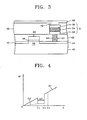
- FIG. 3 is a cross-sectional view of a variation of the nonvolatile memory device shown in FIG. 1 according to the present invention.
- a first interlayer insulating layer 62 covering a source 42, gate stacking materials 48 and 50, and a drain 44 is formed on a substrate 40 and has a flat upper surface.
- a contact hole h1 is formed in the first interlayer insulating layer 62.
- the drain 44 is exposed through the contact hole h1.
- the contact hole h1 is filled with a conductive plug 64.
- the data storage unit S is formed on the first interlayer insulating layer 62 covering the conductive plug 64.
- a second interlayer insulating layer 66 covering the data storage unit S is formed on the first interlayer insulating layer 62.
- a via hole h2 is formed in the second interlayer insulating 66 such that the upper electrode 56 of the data storage unit S is exposed. where an upper electrode 56 of the data storage unit S is exposed.
- a plate electrode 58 filling the via hole h2 is formed on the second interlayer insulating layer 66.
- the elements of the data storage unit S need not be a stacked type.
- the lower electrode 52 of the data storage unit S may have a cylindrical shape and the data storage material layer 54 may be formed on the surface of the lower electrode 52.
- the lower electrode 52 may be a columnar shape and the data storage material layer 54 may be formed on the upper surface of the lower electrode 52.
- FIG. 4 is a graph illustrating current-voltage characteristic of the data storage unit S when the data storage material layer 54 is an NiO layer
- FIG. 5 is a comparative example graph illustrating current-voltage characteristic of the data storage unit S when the data storage material layer 54 is a TiO 2 layer.
- a horizontal axis indicates a voltage applied to the data storage unit S and a vertical axis indicates a drain current Id flowing between the source 42 and the drain 44.
- a first graph G1 illustrates a case where the resistance of the data storage unit S, i.e., the resistance of the data storage material layer 54, is lowered
- a second graph G2 illustrates a case where the resistance of the data storage material layer 54 has an increased value.
- the drain current Id is changed in proportional to the voltage applied to the data storage material layer 54.
- V 1 >O first voltage
- V 2 >V 1 second voltage
- the resistance of the data storage material 54 is dramatically increased while a voltage in the range of A V (V 1 ⁇ V 2 ) is applied to the data storage material layer 54.
- the resistance of the data storage material layer 54 dramatically decreases.
- the change of the drain current Id is the same as the change occurring when the first voltage V 1 is applied to the data storage material 54.
- the change of the drain current Id of the data storage material layer 54 is proportional to the applied voltage and is the same as when a lower voltage than the first voltage V 1 is applied thereto.
- the current of the data storage material layer 54 varies depending on a voltage applied thereto, i.e., whether the voltage applied thereto is greater or smaller than the first voltage V 1 .
- the data storage material layer 54 has a current (resistance) value as illustrated in the first graph G1 (hereinafter, this is called the first case).
- the data storage material layer 54 has a second resistance, which is greater than the first resistance, as illustrated in FIG. 4 , and a voltage smaller than the first voltage V 1 is applied to the data storage material layer 54, the data storage material layer 54 has a current value as illustrated in the second graph G2 (hereinafter, this is called the second case).
- the current measured at the predetermined voltage in the second case is much less than that measured in the first case.
- the resistance is much larger in the second case. This means that these two different currents can be measured from the data storage material layer 54 at a predetermined voltage smaller than the first voltage V 1 .
- the two current values respectively correspond to data " 0 " and " 1 " written in the data storage material layer 54.
- the first case corresponds to data " 1 " being stored in the data storage material layer 54 and the second case corresponds to data " 0 " being stored in the data storage material layer 54.
- the data values "0" and " 1" for the first and second cases are optionally designated. That is, the first case may corresponding to data "0" being stored in the data storage material layer 54 and the second case may correspond to data " 1 " being stored in the data storage material layer 54.
- the voltage-current characteristics of the data storage material layer 54 differ from the voltage-current characteristics illustrated in FIG. 4 .
- third and fifth graphs G3 and G5 illustrate voltage-current characteristics when a negative voltage, that is, a voltage smaller than a fifth voltage V 5 (
- Fourth and sixth graphs G4 and G6 illustrate voltage-current characteristics when a positive voltage, that is, one larger than a fourth voltage V4 (V ⁇ V4 >0), is applied to the data storage unit S and the resistance of the data storage material layer 54 dramatically increases.
- the voltage-current characteristics of the data storage material layer 54 become those illustrated in the fourth graph G4 when the voltage is positive and become those illustrated in the sixth graph G6 when the voltage is negative.
- the data storage material layer 54 maintains a high resistance until the fifth voltage V 5 is applied to the data storage unit S (hereinafter, this is called the third case).
- the fourth case after a voltage smaller than the fifth voltage V 5 is applied to the data storage unit S, the voltage-current characteristics of the data storage material layer 54 become those illustrated in the fifth graph G5 when the voltage is negative and those illustrated in the third graph G3 when the voltage is positive.
- the data storage material layer 54 maintains a low resistance until the fourth voltage V 4 is applied to the data storage unit S (hereinafter, this is called the fourth case).
- the data storage material layer 54 has two different currents (or resistances) in the range between the fifth voltage V 5 which is negative and the fourth voltage V 4 which is positive. This means that the data storage material layer 54 has the two different states in the above voltage range and one of the two different states may correspond to data " 1 " and the other may correspond to data " 0 " being stored in the data storage material layer 54.
- the two states of the data storage material layer 54 are determined as a voltage larger than the fourth voltage V 4 or smaller than the fifth voltage V 5 is applied to the data storage unit S. However, since the voltage applied to the data storage material layer 54 to detect these states is smaller than the fourth voltage V 4 or larger than the fifth voltage V 5 , the data storage material layer 54 maintains its initial state even after the state is detected. That is, data stored in the data storage material layer 54 is maintained even after the pertinent data is read.
- FIGS. 6 and 7 illustrate examples of voltage pulses applied to the data storage unit S to write data in the data storage material layer 54 and read or erase the data written in the data storage material layer 54.
- FIG. 6 illustrates a voltage pulse applied to the data storage material layer 54 when it is a NiO layer
- FIG. 7 illustrates a voltage pulse applied to the data storage material layer 54 when it is a TiO 2 layer.
- a second write voltage pulse V w2 is applied to the data storage material layer 54 in order to write data, for example " 1 ", in the data storage material layer 54.
- the second write voltage pulse V W2 has a value corresponding to the third voltage V 3 of FIG. 4 .
- a third read voltage pulse V R3 is applied to the data storage material layer 54 to read the data "1 " stored in the data storage material layer 54.
- the third read voltage pulse V R3 has a voltage that is lower than the first voltage V 1 of FIG. 4 .
- the resistance of the data storage material layer 54 is in a low state. This low state is maintained when a voltage smaller than the first voltage V 1 is applied to the data storage material layer 54.
- the third read voltage pulse V R3 which is smaller than the first voltage V 1
- a current through the data storage material layer 54 is a lot larger than the current when a voltage between the first voltage V 1 and the second voltage V 2 is applied to the data storage material layer 54. This result reveals that the data " 1" is written in the data storage material layer 54.
- a third write voltage pulse V E2 is applied to the data storage material layer 54 in order to write data, for example " 0 ", in the data storage material layer 54.
- the third write voltage pulse V E2 has a voltage between the first and second voltages V 1 and V 2 . Therefore, when the third write voltage pulse V E2 , that is smaller than the second write voltage pulse V w2 , is applied to the data storage material layer 54, the resistance of the data storage material layer 54 dramatically increases (see FIG. 4 ).
- the data storage material layer 54 remains in this state when a voltage pulse applied to the data storage material layer 54 is lower than the first voltage V 1 (see the second graph G2 of FIG. 4 ).
- a fourth read voltage pulse V R4 When a fourth read voltage pulse V R4 is applied to the data storage material layer 54 to read the data " 0 " from the data storage material layer 54.
- the fourth read voltage pulse V R4 has a voltage that is lower than the first voltage V 1 of FIG. 4 .
- the current measured from the data storage material layer 54 is a lot smaller than the current measured when the data " 1 " is read.
- the data stored in the data storage material layer 54 is erased by simply applying a voltage pulse that has an opposite polarity to one applied when writing the data to the data storage unit S.
- a first write voltage pulse V W1 is applied to the data storage material layer 54 in order to write a predetermined data, for example " 1 ", in the data storage material layer 54.
- a first read voltage pulse V R1 is applied to the data storage unit S to read the data " 1 " stored in the data storage material layer 54 by applying the first write voltage pulse V W1 .
- the first read voltage pulse V R1 which is lower than the first write voltage pulse V W1 , has a voltage higher than zero and lower than fourth voltage V 4 .
- the resistance characteristics of the data storage material layer 54 do not change since the first read voltage pulse V R1 has a voltage that not only lower than the first write voltage pulse V W1 , but also has the same polarity as the first write voltage pulse V W1 .
- the first read voltage pulse V R1 is applied to the data storage material layer 54 , the data written in the data storage material layer 54 is not damaged and destroyed.
- the resistance of the data storage material layer 54 at the fifth voltage V 5 dramatically decreases. Accordingly, the fifth voltage V 5 can be used to erase the data written in the data storage material layer 54 by applying the first write voltage pulse V W1 .
- V E1 denotes a first erase voltage pulse corresponding to the fifth voltage V 5 . If the first erase voltage pulse V E1 (
- a second read voltage pulse V R2 is applied to the data storage material layer 54 to read data " 0 " from the data storage material layer 54.
- the second read voltage pulse V R2 is lower than an absolute value of the voltage of the first erase voltage pulse V E1 (V R2 ⁇
- the data storage material layer 54 has a different current value depending on the voltage applied thereto to write data. Accordingly, the data written in the data storage material layer 54 can be precisely read. In addition, since a voltage applied to read data from the data storage material layer 54 is lower than the voltage applied to write data thereto, the data state of the data storage material layer 54 can be maintained constantly even after the data is read. Thus, a refresh process that is conducted in the conventional memory device after data reading is not required.
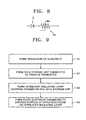
- FIG. 8 is a circuit diagram of a nonvolatile memory device comprising one diode D and one variable resistant material Rv, that is, 1 D-1 R.
- a transistor is formed on the substrate 40 in step S1.
- the data storage unit S connected to the drain 44 of the transistor is formed on the substrate 40 by sequentially forming the lower electrode 52, the data storage material layer 54, and the upper electrode 56 on the drain 44 of the substrate 40.
- the data storage material layer 54 may be formed of a transition metal oxide layer having a resistance that varies according to the applied voltage. For instance, a NiO, V 2 O 5 , ZnO, Nb 2 O 5 , TiO 2 , WO 3 , or CoO layer may be used.
- the interlayer insulating layer 60 covering the transistor and the data storage unit S is formed on the substrate 40.
- step S4 the upper electrode of the data storage unit S is exposed and the plate electrode 58 is formed on an exposed portion of the upper electrode 56 of the data storage unit S and the interlayer insulating layer 60.
- the plate electrode 58 may be substituted with a plate pad that contacts all upper electrodes included in data storage units of all cells (not shown).
- the contact hole h1 may be filled with the conductive plug 64. Additionally, the data storage unit S contacting the conductive plug 64 may be formed on the first interlayer insulating layer 62.
- the lower electrode 52 and the data storage material layer 54 may be formed in a non-stack type rather than a stack type.
- the data storage unit S connected to the diode may be formed on the substrate 40.
- the data storage unit S may be formed in the same way as described above.
- the nonvolatile memory device including 1T-1R or 1D-1R, comprises a transition metal oxide layer, which has the voltage-current characteristic as illustrated in FIG. 4 and is easy to process, as the resistant material in which the data is stored. Therefore, the conventional DRAM manufacturing process can be used and an increased productivity along with lowered production costs can be achieved. Furthermore, memory characteristics of the resistant material do not change even though the size of the resistant material is reduced due to a high integration density. This is because that the data is written or read using changes in resistance of the resistant material. Also, because data written in the resistant material is read non-destructively, the state of the resistant material remains constant even after the data is read and a lower operation voltage is applied. Thus, a refresh process that is conducted in the conventional memory device after data reading is not required.
Landscapes
- Engineering & Computer Science (AREA)
- Chemical & Material Sciences (AREA)
- Materials Engineering (AREA)
- Computer Hardware Design (AREA)
- Semiconductor Memories (AREA)
- Thin Film Transistor (AREA)
Priority Applications (2)
| Application Number | Priority Date | Filing Date | Title |
|---|---|---|---|
| EP09179704A EP2164104A3 (en) | 2003-06-03 | 2004-05-27 | Nonvolatile memory device comprising a switching device and a resistant material and method of manufacturing the same |
| EP08155548A EP1947696B1 (en) | 2003-06-03 | 2004-05-27 | Nonvolatile memory device comprising a switching device and a resistant material and method of manufacturing the same |
Applications Claiming Priority (2)
| Application Number | Priority Date | Filing Date | Title |
|---|---|---|---|
| KR2003035562 | 2003-06-03 | ||
| KR1020030035562A KR100773537B1 (ko) | 2003-06-03 | 2003-06-03 | 한 개의 스위칭 소자와 한 개의 저항체를 포함하는비휘발성 메모리 장치 및 그 제조 방법 |
Related Child Applications (3)
| Application Number | Title | Priority Date | Filing Date |
|---|---|---|---|
| EP08155548A Division EP1947696B1 (en) | 2003-06-03 | 2004-05-27 | Nonvolatile memory device comprising a switching device and a resistant material and method of manufacturing the same |
| EP08155548.4 Division-Into | 2008-05-01 | ||
| EP09179704.3 Division-Into | 2009-12-17 |
Publications (3)
| Publication Number | Publication Date |
|---|---|
| EP1484799A2 EP1484799A2 (en) | 2004-12-08 |
| EP1484799A3 EP1484799A3 (en) | 2006-06-14 |
| EP1484799B1 true EP1484799B1 (en) | 2010-03-10 |
Family
ID=33157373
Family Applications (3)
| Application Number | Title | Priority Date | Filing Date |
|---|---|---|---|
| EP08155548A Expired - Lifetime EP1947696B1 (en) | 2003-06-03 | 2004-05-27 | Nonvolatile memory device comprising a switching device and a resistant material and method of manufacturing the same |
| EP09179704A Withdrawn EP2164104A3 (en) | 2003-06-03 | 2004-05-27 | Nonvolatile memory device comprising a switching device and a resistant material and method of manufacturing the same |
| EP04253135A Expired - Lifetime EP1484799B1 (en) | 2003-06-03 | 2004-05-27 | Nonvolatile memory device comprising a switching device and a resistant material and method of manufacturing the same |
Family Applications Before (2)
| Application Number | Title | Priority Date | Filing Date |
|---|---|---|---|
| EP08155548A Expired - Lifetime EP1947696B1 (en) | 2003-06-03 | 2004-05-27 | Nonvolatile memory device comprising a switching device and a resistant material and method of manufacturing the same |
| EP09179704A Withdrawn EP2164104A3 (en) | 2003-06-03 | 2004-05-27 | Nonvolatile memory device comprising a switching device and a resistant material and method of manufacturing the same |
Country Status (6)
| Country | Link |
|---|---|
| US (2) | US8164130B2 (zh) |
| EP (3) | EP1947696B1 (zh) |
| JP (1) | JP4511249B2 (zh) |
| KR (1) | KR100773537B1 (zh) |
| CN (2) | CN101794807A (zh) |
| DE (1) | DE602004025877D1 (zh) |
Cited By (2)
| Publication number | Priority date | Publication date | Assignee | Title |
|---|---|---|---|---|
| US7834338B2 (en) | 2005-11-23 | 2010-11-16 | Sandisk 3D Llc | Memory cell comprising nickel-cobalt oxide switching element |
| US8507315B2 (en) | 2007-06-29 | 2013-08-13 | Sandisk 3D Llc | Memory cell that employs a selectively grown reversible resistance-switching element and methods of forming the same |
Families Citing this family (175)
| Publication number | Priority date | Publication date | Assignee | Title |
|---|---|---|---|---|
| CN100358147C (zh) * | 2000-08-14 | 2007-12-26 | 矩阵半导体公司 | 密集阵列和电荷存储器件及其制造方法 |
| DE10255117A1 (de) * | 2002-11-26 | 2004-06-17 | Infineon Technologies Ag | Halbleiterspeichereinrichtung sowie Verfahren zu deren Herstellung |
| KR100773537B1 (ko) | 2003-06-03 | 2007-11-07 | 삼성전자주식회사 | 한 개의 스위칭 소자와 한 개의 저항체를 포함하는비휘발성 메모리 장치 및 그 제조 방법 |
| KR101051704B1 (ko) * | 2004-04-28 | 2011-07-25 | 삼성전자주식회사 | 저항 구배를 지닌 다층막을 이용한 메모리 소자 |
| FR2887149B1 (fr) * | 2005-06-17 | 2007-08-03 | Galderma Sa | Procede de solubilisation du metronidazole |
| KR100593448B1 (ko) * | 2004-09-10 | 2006-06-28 | 삼성전자주식회사 | 전이금속 산화막을 데이터 저장 물질막으로 채택하는비휘발성 기억 셀들 및 그 제조방법들 |
| US7405465B2 (en) | 2004-09-29 | 2008-07-29 | Sandisk 3D Llc | Deposited semiconductor structure to minimize n-type dopant diffusion and method of making |
| KR100738070B1 (ko) * | 2004-11-06 | 2007-07-12 | 삼성전자주식회사 | 한 개의 저항체와 한 개의 트랜지스터를 지닌 비휘발성메모리 소자 |
| KR100657911B1 (ko) * | 2004-11-10 | 2006-12-14 | 삼성전자주식회사 | 한 개의 저항체와 한 개의 다이오드를 지닌 비휘발성메모리 소자 |
| KR100593750B1 (ko) | 2004-11-10 | 2006-06-28 | 삼성전자주식회사 | 이성분계 금속 산화막을 데이터 저장 물질막으로 채택하는교차점 비휘발성 기억소자 및 그 제조방법 |
| KR100576369B1 (ko) * | 2004-11-23 | 2006-05-03 | 삼성전자주식회사 | 전이 금속 산화막을 데이타 저장 물질막으로 채택하는비휘발성 기억소자의 프로그램 방법 |
| KR100682908B1 (ko) * | 2004-12-21 | 2007-02-15 | 삼성전자주식회사 | 두개의 저항체를 지닌 비휘발성 메모리 소자 |
| KR100693409B1 (ko) * | 2005-01-14 | 2007-03-12 | 광주과학기술원 | 산화막의 저항변화를 이용한 비휘발성 기억소자 및 그제조방법 |
| KR100682926B1 (ko) * | 2005-01-31 | 2007-02-15 | 삼성전자주식회사 | 저항체를 이용한 비휘발성 메모리 소자 및 그 제조방법 |
| KR100657956B1 (ko) * | 2005-04-06 | 2006-12-14 | 삼성전자주식회사 | 다치 저항체 메모리 소자와 그 제조 및 동작 방법 |
| US7812404B2 (en) | 2005-05-09 | 2010-10-12 | Sandisk 3D Llc | Nonvolatile memory cell comprising a diode and a resistance-switching material |
| KR100695150B1 (ko) * | 2005-05-12 | 2007-03-14 | 삼성전자주식회사 | 금속-절연체 변환 물질을 이용한 트랜지스터 및 그 제조방법 |
| JP5190182B2 (ja) * | 2005-05-31 | 2013-04-24 | 株式会社半導体エネルギー研究所 | 半導体装置 |
| US20060273298A1 (en) * | 2005-06-02 | 2006-12-07 | Matrix Semiconductor, Inc. | Rewriteable memory cell comprising a transistor and resistance-switching material in series |
| JP4843259B2 (ja) * | 2005-06-10 | 2011-12-21 | シャープ株式会社 | 可変抵抗素子の製造方法 |
| JP4783070B2 (ja) * | 2005-06-24 | 2011-09-28 | シャープ株式会社 | 半導体記憶装置及びその製造方法 |
| KR100723872B1 (ko) * | 2005-06-30 | 2007-05-31 | 한국전자통신연구원 | 급격한 금속-절연체 전이를 이용한 메모리소자 및 그동작방법 |
| KR100622268B1 (ko) * | 2005-07-04 | 2006-09-11 | 한양대학교 산학협력단 | ReRAM 소자용 다층 이원산화박막의 형성방법 |
| US7955515B2 (en) * | 2005-07-11 | 2011-06-07 | Sandisk 3D Llc | Method of plasma etching transition metal oxides |
| JP3889023B2 (ja) * | 2005-08-05 | 2007-03-07 | シャープ株式会社 | 可変抵抗素子とその製造方法並びにそれを備えた記憶装置 |
| JP5019821B2 (ja) * | 2005-08-12 | 2012-09-05 | 株式会社半導体エネルギー研究所 | 半導体装置 |
| KR101369864B1 (ko) * | 2005-08-12 | 2014-03-05 | 가부시키가이샤 한도오따이 에네루기 켄큐쇼 | 반도체장치 및 그 제조방법 |
| JP4854233B2 (ja) | 2005-08-15 | 2012-01-18 | 独立行政法人産業技術総合研究所 | スイッチング素子 |
| US7521705B2 (en) | 2005-08-15 | 2009-04-21 | Micron Technology, Inc. | Reproducible resistance variable insulating memory devices having a shaped bottom electrode |
| KR101100427B1 (ko) * | 2005-08-24 | 2011-12-30 | 삼성전자주식회사 | 이온 전도층을 포함하는 불휘발성 반도체 메모리 장치와 그제조 및 동작 방법 |
| US7601995B2 (en) | 2005-10-27 | 2009-10-13 | Infineon Technologies Ag | Integrated circuit having resistive memory cells |
| US8222917B2 (en) * | 2005-11-03 | 2012-07-17 | Agate Logic, Inc. | Impedance matching and trimming apparatuses and methods using programmable resistance devices |
| KR100668348B1 (ko) | 2005-11-11 | 2007-01-12 | 삼성전자주식회사 | 비휘발성 메모리 소자 및 그 제조방법 |
| US7816659B2 (en) * | 2005-11-23 | 2010-10-19 | Sandisk 3D Llc | Devices having reversible resistivity-switching metal oxide or nitride layer with added metal |
| JP4061328B2 (ja) * | 2005-12-02 | 2008-03-19 | シャープ株式会社 | 可変抵抗素子及びその製造方法 |
| JP4939324B2 (ja) * | 2005-12-02 | 2012-05-23 | シャープ株式会社 | 可変抵抗素子及びその製造方法 |
| JP4017650B2 (ja) * | 2005-12-02 | 2007-12-05 | シャープ株式会社 | 可変抵抗素子及びその製造方法 |
| JP3989506B2 (ja) * | 2005-12-27 | 2007-10-10 | シャープ株式会社 | 可変抵抗素子とその製造方法ならびにそれを備えた半導体記憶装置 |
| KR100684908B1 (ko) | 2006-01-09 | 2007-02-22 | 삼성전자주식회사 | 다수 저항 상태를 갖는 저항 메모리 요소, 저항 메모리 셀및 그 동작 방법 그리고 상기 저항 메모리 요소를 적용한데이터 처리 시스템 |
| US7714315B2 (en) | 2006-02-07 | 2010-05-11 | Qimonda North America Corp. | Thermal isolation of phase change memory cells |
| KR100718155B1 (ko) * | 2006-02-27 | 2007-05-14 | 삼성전자주식회사 | 두 개의 산화층을 이용한 비휘발성 메모리 소자 |
| CN101395716B (zh) | 2006-03-08 | 2011-11-02 | 松下电器产业株式会社 | 非易失性存储元件、非易失性存储装置、以及它们的制造方法 |
| KR101176543B1 (ko) * | 2006-03-10 | 2012-08-28 | 삼성전자주식회사 | 저항성 메모리소자 |
| TWI462099B (zh) * | 2006-03-31 | 2014-11-21 | Sandisk 3D Llc | 非揮發性記憶體單元、整體三維記憶體陣列及用於程式化所述記憶體陣列之方法 |
| US7808810B2 (en) | 2006-03-31 | 2010-10-05 | Sandisk 3D Llc | Multilevel nonvolatile memory cell comprising a resistivity-switching oxide or nitride and an antifuse |
| US7829875B2 (en) | 2006-03-31 | 2010-11-09 | Sandisk 3D Llc | Nonvolatile rewritable memory cell comprising a resistivity-switching oxide or nitride and an antifuse |
| US7875871B2 (en) | 2006-03-31 | 2011-01-25 | Sandisk 3D Llc | Heterojunction device comprising a semiconductor and a resistivity-switching oxide or nitride |
| JP4699932B2 (ja) * | 2006-04-13 | 2011-06-15 | パナソニック株式会社 | 抵抗変化素子とそれを用いた抵抗変化型メモリならびにその製造方法 |
| JP4857014B2 (ja) * | 2006-04-19 | 2012-01-18 | パナソニック株式会社 | 抵抗変化素子とそれを用いた抵抗変化型メモリ |
| KR101213702B1 (ko) * | 2006-04-21 | 2012-12-18 | 삼성전자주식회사 | 비휘발성 메모리 소자, 그 동작 방법, 및 그 제조 방법 |
| KR101239962B1 (ko) | 2006-05-04 | 2013-03-06 | 삼성전자주식회사 | 하부 전극 상에 형성된 버퍼층을 포함하는 가변 저항메모리 소자 |
| US20070267621A1 (en) * | 2006-05-19 | 2007-11-22 | Infineon Technologies Ag | Resistive memory device |
| KR101206034B1 (ko) | 2006-05-19 | 2012-11-28 | 삼성전자주식회사 | 산소결핍 금속산화물을 이용한 비휘발성 메모리 소자 및 그제조방법 |
| KR100818271B1 (ko) * | 2006-06-27 | 2008-03-31 | 삼성전자주식회사 | 펄스전압을 인가하는 비휘발성 메모리 소자의 문턱 스위칭동작 방법 |
| KR100738116B1 (ko) * | 2006-07-06 | 2007-07-12 | 삼성전자주식회사 | 가변 저항 물질을 포함하는 비휘발성 메모리 소자 |
| JP5263856B2 (ja) * | 2006-07-26 | 2013-08-14 | 独立行政法人産業技術総合研究所 | スイッチング素子及びその製造方法 |
| US7964869B2 (en) | 2006-08-25 | 2011-06-21 | Panasonic Corporation | Memory element, memory apparatus, and semiconductor integrated circuit |
| US8232175B2 (en) * | 2006-09-14 | 2012-07-31 | Spansion Llc | Damascene metal-insulator-metal (MIM) device with improved scaleability |
| JP4655019B2 (ja) * | 2006-10-04 | 2011-03-23 | セイコーエプソン株式会社 | 可変抵抗素子 |
| CN101174672A (zh) | 2006-10-04 | 2008-05-07 | 旺宏电子股份有限公司 | 存储单元及其制程 |
| US7524722B2 (en) | 2006-10-12 | 2009-04-28 | Macronix International Co., Ltd. | Resistance type memory device and fabricating method and operating method thereof |
| WO2008050716A1 (fr) | 2006-10-24 | 2008-05-02 | Panasonic Corporation | Mémoire non volatile à semi-conducteurs et procédé de fabrication associé |
| JP5156023B2 (ja) * | 2006-11-08 | 2013-03-06 | シメトリックス・コーポレーション | 相関電子メモリ |
| KR100816759B1 (ko) * | 2006-11-09 | 2008-03-25 | 삼성전자주식회사 | 가변저항 스토리지를 갖는 비휘발성 기억 장치 및 동작방법 |
| KR101206036B1 (ko) | 2006-11-16 | 2012-11-28 | 삼성전자주식회사 | 전이 금속 고용체를 포함하는 저항성 메모리 소자 및 그제조 방법 |
| WO2008059701A1 (ja) | 2006-11-17 | 2008-05-22 | Panasonic Corporation | 不揮発性記憶素子、不揮発性記憶装置、不揮発性半導体装置、および不揮発性記憶素子の製造方法 |
| JP4167298B2 (ja) | 2006-11-20 | 2008-10-15 | 松下電器産業株式会社 | 不揮発性半導体記憶装置およびその製造方法 |
| KR100846502B1 (ko) * | 2006-11-21 | 2008-07-17 | 삼성전자주식회사 | 비휘발성 메모리소자 및 그 제조방법 |
| KR100982424B1 (ko) * | 2006-11-28 | 2010-09-15 | 삼성전자주식회사 | 저항 메모리 소자의 제조 방법 |
| KR101136870B1 (ko) | 2006-11-30 | 2012-04-20 | 후지쯔 가부시끼가이샤 | 저항 기억 소자의 제조 방법 |
| JP5007725B2 (ja) * | 2006-12-19 | 2012-08-22 | 富士通株式会社 | 抵抗変化素子の製造方法 |
| WO2008075412A1 (ja) * | 2006-12-19 | 2008-06-26 | Fujitsu Limited | 抵抗変化素子及びその製造方法 |
| WO2008075413A1 (ja) * | 2006-12-19 | 2008-06-26 | Fujitsu Limited | 抵抗変化素子及びその製造方法 |
| CN101569011A (zh) | 2006-12-28 | 2009-10-28 | 松下电器产业株式会社 | 电阻变化型元件、电阻变化型存储装置和电阻变化型装置 |
| CN101501851B (zh) | 2006-12-28 | 2010-11-17 | 松下电器产业株式会社 | 电阻变化型元件和电阻变化型存储装置 |
| KR20080064353A (ko) * | 2007-01-04 | 2008-07-09 | 삼성전자주식회사 | 저항 메모리 소자 및 그 제조 방법 |
| JP2008182154A (ja) * | 2007-01-26 | 2008-08-07 | Nippon Telegr & Teleph Corp <Ntt> | メモリ装置 |
| JP2008182156A (ja) * | 2007-01-26 | 2008-08-07 | Nippon Telegr & Teleph Corp <Ntt> | 金属酸化物素子及びその製造方法 |
| US7704789B2 (en) | 2007-02-05 | 2010-04-27 | Intermolecular, Inc. | Methods for forming resistive switching memory elements |
| US7972897B2 (en) | 2007-02-05 | 2011-07-05 | Intermolecular, Inc. | Methods for forming resistive switching memory elements |
| WO2008097742A1 (en) * | 2007-02-05 | 2008-08-14 | Interolecular, Inc. | Methods for forming resistive switching memory elements |
| US7678607B2 (en) | 2007-02-05 | 2010-03-16 | Intermolecular, Inc. | Methods for forming resistive switching memory elements |
| KR101054321B1 (ko) * | 2007-03-01 | 2011-08-05 | 후지쯔 가부시끼가이샤 | 반도체 장치 및 그 제조 방법 |
| US8097878B2 (en) | 2007-03-05 | 2012-01-17 | Intermolecular, Inc. | Nonvolatile memory elements with metal-deficient resistive-switching metal oxides |
| US7629198B2 (en) | 2007-03-05 | 2009-12-08 | Intermolecular, Inc. | Methods for forming nonvolatile memory elements with resistive-switching metal oxides |
| JP5345052B2 (ja) * | 2007-03-23 | 2013-11-20 | 富士通株式会社 | 抵抗記憶素子及び不揮発性半導体記憶装置 |
| US8058636B2 (en) | 2007-03-29 | 2011-11-15 | Panasonic Corporation | Variable resistance nonvolatile memory apparatus |
| US7960224B2 (en) | 2007-04-03 | 2011-06-14 | Macronix International Co., Ltd. | Operation method for multi-level switching of metal-oxide based RRAM |
| WO2008126366A1 (ja) | 2007-04-09 | 2008-10-23 | Panasonic Corporation | 抵抗変化型素子、不揮発性スイッチング素子、および抵抗変化型記憶装置 |
| WO2008132899A1 (ja) * | 2007-04-17 | 2008-11-06 | Nec Corporation | 抵抗変化素子及び該抵抗変化素子を含む半導体装置 |
| WO2008140979A1 (en) | 2007-05-09 | 2008-11-20 | Intermolecular, Inc. | Resistive-switching nonvolatile memory elements |
| JP4967176B2 (ja) * | 2007-05-10 | 2012-07-04 | シャープ株式会社 | 可変抵抗素子とその製造方法及び不揮発性半導体記憶装置 |
| KR101350979B1 (ko) | 2007-05-11 | 2014-01-14 | 삼성전자주식회사 | 저항성 메모리 소자 및 그 제조 방법 |
| US8148711B2 (en) | 2007-05-18 | 2012-04-03 | Panasonic Corporation | Nonvolatile memory element, manufacturing method thereof, and nonvolatile semiconductor apparatus using nonvolatile memory element |
| US8173989B2 (en) * | 2007-05-30 | 2012-05-08 | Samsung Electronics Co., Ltd. | Resistive random access memory device and methods of manufacturing and operating the same |
| EP2063467B1 (en) | 2007-06-05 | 2011-05-04 | Panasonic Corporation | Nonvolatile storage element, its manufacturing method, and nonvolatile semiconductor device using the nonvolatile storage element |
| JP5624463B2 (ja) * | 2007-06-29 | 2014-11-12 | サンディスクスリーディー,エルエルシー | 選択付着による可逆的抵抗スイッチング素子を使用するメモリセルおよびその形成方法 |
| US7846785B2 (en) | 2007-06-29 | 2010-12-07 | Sandisk 3D Llc | Memory cell that employs a selectively deposited reversible resistance-switching element and methods of forming the same |
| US7902537B2 (en) | 2007-06-29 | 2011-03-08 | Sandisk 3D Llc | Memory cell that employs a selectively grown reversible resistance-switching element and methods of forming the same |
| US8233308B2 (en) | 2007-06-29 | 2012-07-31 | Sandisk 3D Llc | Memory cell that employs a selectively deposited reversible resistance-switching element and methods of forming the same |
| TWI402980B (zh) | 2007-07-20 | 2013-07-21 | Macronix Int Co Ltd | 具有緩衝層之電阻式記憶結構 |
| KR101482814B1 (ko) | 2007-07-25 | 2015-01-14 | 인터몰레큘러 인코퍼레이티드 | 다중상태 비휘발성 메모리 소자 |
| WO2009015298A2 (en) | 2007-07-25 | 2009-01-29 | Intermolecular, Inc. | Nonvolatile memory elements |
| JP5012312B2 (ja) * | 2007-08-15 | 2012-08-29 | ソニー株式会社 | 記憶装置の駆動方法 |
| KR101060793B1 (ko) * | 2007-10-15 | 2011-08-30 | 파나소닉 주식회사 | 비휘발성 기억 소자 및 이 비휘발성 기억 소자를 이용한 비휘발성 반도체 장치 |
| JP5284270B2 (ja) * | 2007-10-30 | 2013-09-11 | パナソニック株式会社 | 不揮発性半導体記憶装置およびその製造方法 |
| US8345462B2 (en) | 2007-12-05 | 2013-01-01 | Macronix International Co., Ltd. | Resistive memory and method for manufacturing the same |
| JP2009141225A (ja) * | 2007-12-07 | 2009-06-25 | Sharp Corp | 可変抵抗素子、可変抵抗素子の製造方法、不揮発性半導体記憶装置 |
| US7759201B2 (en) * | 2007-12-17 | 2010-07-20 | Sandisk 3D Llc | Method for fabricating pitch-doubling pillar structures |
| US7706169B2 (en) * | 2007-12-27 | 2010-04-27 | Sandisk 3D Llc | Large capacity one-time programmable memory cell using metal oxides |
| US7764534B2 (en) * | 2007-12-28 | 2010-07-27 | Sandisk 3D Llc | Two terminal nonvolatile memory using gate controlled diode elements |
| JP4607252B2 (ja) * | 2008-02-25 | 2011-01-05 | パナソニック株式会社 | 抵抗変化素子の駆動方法およびそれを用いた抵抗変化型記憶装置 |
| JP4549401B2 (ja) * | 2008-03-11 | 2010-09-22 | 富士通株式会社 | 抵抗記憶素子の製造方法 |
| JP5488458B2 (ja) * | 2008-04-07 | 2014-05-14 | 日本電気株式会社 | 抵抗変化素子及びその製造方法 |
| US7981592B2 (en) * | 2008-04-11 | 2011-07-19 | Sandisk 3D Llc | Double patterning method |
| US7786015B2 (en) * | 2008-04-28 | 2010-08-31 | Sandisk 3D Llc | Method for fabricating self-aligned complementary pillar structures and wiring |
| JPWO2009142165A1 (ja) * | 2008-05-20 | 2011-09-29 | 日本電気株式会社 | 半導体装置およびその製造方法 |
| US7732235B2 (en) | 2008-06-30 | 2010-06-08 | Sandisk 3D Llc | Method for fabricating high density pillar structures by double patterning using positive photoresist |
| US7781269B2 (en) * | 2008-06-30 | 2010-08-24 | Sandisk 3D Llc | Triangle two dimensional complementary patterning of pillars |
| US7981742B2 (en) * | 2008-07-02 | 2011-07-19 | Macronic International Co., Ltd. | Semiconductor device, data element thereof and method of fabricating the same |
| WO2010004705A1 (ja) | 2008-07-11 | 2010-01-14 | パナソニック株式会社 | 不揮発性記憶素子およびその製造方法、並びにその不揮発性記憶素子を用いた不揮発性半導体装置 |
| WO2010038442A1 (ja) * | 2008-09-30 | 2010-04-08 | パナソニック株式会社 | 抵抗変化素子の駆動方法、初期処理方法、及び不揮発性記憶装置 |
| WO2010038423A1 (ja) * | 2008-10-01 | 2010-04-08 | パナソニック株式会社 | 不揮発性記憶素子並びにそれを用いた不揮発性記憶装置 |
| US8076056B2 (en) * | 2008-10-06 | 2011-12-13 | Sandisk 3D Llc | Method of making sub-resolution pillar structures using undercutting technique |
| KR20100041155A (ko) | 2008-10-13 | 2010-04-22 | 삼성전자주식회사 | 저항성 메모리 소자 |
| US8080443B2 (en) * | 2008-10-27 | 2011-12-20 | Sandisk 3D Llc | Method of making pillars using photoresist spacer mask |
| WO2010064446A1 (ja) | 2008-12-04 | 2010-06-10 | パナソニック株式会社 | 不揮発性記憶素子及び不揮発性記憶装置 |
| US8114765B2 (en) | 2008-12-31 | 2012-02-14 | Sandisk 3D Llc | Methods for increased array feature density |
| US8084347B2 (en) * | 2008-12-31 | 2011-12-27 | Sandisk 3D Llc | Resist feature and removable spacer pitch doubling patterning method for pillar structures |
| US7846756B2 (en) * | 2008-12-31 | 2010-12-07 | Sandisk 3D Llc | Nanoimprint enhanced resist spacer patterning method |
| WO2010086916A1 (ja) * | 2009-01-29 | 2010-08-05 | パナソニック株式会社 | 抵抗変化素子およびその製造方法 |
| JP2010177624A (ja) * | 2009-02-02 | 2010-08-12 | Toshiba Corp | 半導体記憶装置 |
| US8445886B2 (en) | 2009-02-02 | 2013-05-21 | Panasonic Corporation | Nonvolatile memory element, nonvolatile memory device, nonvolatile semiconductor device, and method of manufacturing nonvolatile memory element |
| WO2010090002A1 (ja) * | 2009-02-04 | 2010-08-12 | パナソニック株式会社 | 不揮発性記憶素子 |
| WO2010103649A1 (ja) | 2009-03-12 | 2010-09-16 | 富士通株式会社 | 複合抵抗変化素子及びその製造方法 |
| CN102047422B (zh) * | 2009-03-25 | 2013-04-24 | 松下电器产业株式会社 | 电阻变化元件的驱动方法以及非易失性存储装置 |
| JP2010251529A (ja) * | 2009-04-16 | 2010-11-04 | Sony Corp | 半導体記憶装置およびその製造方法 |
| US8488362B2 (en) | 2009-04-29 | 2013-07-16 | Macronix International Co., Ltd. | Graded metal oxide resistance based semiconductor memory device |
| JP5287544B2 (ja) | 2009-06-25 | 2013-09-11 | ソニー株式会社 | 不揮発性メモリの記録方法及び不揮発性メモリ |
| JP5016699B2 (ja) | 2009-12-16 | 2012-09-05 | シャープ株式会社 | 不揮発性半導体記憶装置及びその製造方法 |
| KR20110072921A (ko) | 2009-12-23 | 2011-06-29 | 삼성전자주식회사 | 메모리소자 및 그 동작방법 |
| KR20110074354A (ko) | 2009-12-24 | 2011-06-30 | 삼성전자주식회사 | 메모리소자 및 그 동작방법 |
| JP5120967B2 (ja) * | 2009-12-25 | 2013-01-16 | シャープ株式会社 | 可変抵抗素子 |
| JP5039857B2 (ja) * | 2009-12-28 | 2012-10-03 | パナソニック株式会社 | 記憶装置およびその製造方法 |
| US7923305B1 (en) | 2010-01-12 | 2011-04-12 | Sandisk 3D Llc | Patterning method for high density pillar structures |
| US8026178B2 (en) * | 2010-01-12 | 2011-09-27 | Sandisk 3D Llc | Patterning method for high density pillar structures |
| WO2011096194A1 (ja) | 2010-02-02 | 2011-08-11 | パナソニック株式会社 | 抵抗変化素子の駆動方法、初期処理方法、及び不揮発性記憶装置 |
| KR20110101983A (ko) | 2010-03-10 | 2011-09-16 | 삼성전자주식회사 | 바이폴라 메모리셀 및 이를 포함하는 메모리소자 |
| CN102484114B (zh) | 2010-07-08 | 2014-10-15 | 松下电器产业株式会社 | 非易失性半导体存储装置及其制造方法 |
| US8264868B2 (en) | 2010-10-25 | 2012-09-11 | Hewlett-Packard Development Company, L.P. | Memory array with metal-insulator transition switching devices |
| CN102064276B (zh) * | 2010-11-01 | 2014-06-04 | 华中科技大学 | 一种非对称相变存储器单元及器件 |
| US8699258B2 (en) | 2011-01-21 | 2014-04-15 | Macronix International Co., Ltd. | Verification algorithm for metal-oxide resistive memory |
| US9153319B2 (en) | 2011-03-14 | 2015-10-06 | Panasonic Intellectual Property Management Co., Ltd. | Method for driving nonvolatile memory element, and nonvolatile memory device having a variable resistance element |
| US8951829B2 (en) | 2011-04-01 | 2015-02-10 | Micron Technology, Inc. | Resistive switching in memory cells |
| WO2012172773A1 (ja) | 2011-06-13 | 2012-12-20 | パナソニック株式会社 | 抵抗変化素子の駆動方法、及び不揮発性記憶装置 |
| WO2013157261A1 (ja) | 2012-04-20 | 2013-10-24 | パナソニック株式会社 | 不揮発性記憶素子の駆動方法および不揮発性記憶装置 |
| JP2014032724A (ja) * | 2012-08-03 | 2014-02-20 | Sharp Corp | 半導体記憶装置 |
| US9231204B2 (en) * | 2012-09-28 | 2016-01-05 | Intel Corporation | Low voltage embedded memory having conductive oxide and electrode stacks |
| TWI513074B (zh) * | 2013-01-08 | 2015-12-11 | Nat Univ Tsing Hua | 電阻式記憶體 |
| JP5830655B2 (ja) | 2013-04-30 | 2015-12-09 | パナソニックIpマネジメント株式会社 | 不揮発性記憶素子の駆動方法 |
| CN103367639B (zh) * | 2013-07-25 | 2015-09-09 | 福州大学 | 一种氧化锌纳米线低功耗阻变存储器及其制备方法 |
| CN103682100B (zh) * | 2013-12-06 | 2016-04-06 | 南昌大学 | 氧化锌/聚甲基丙烯酸甲酯/硫氰酸亚铜结构的数据存储器及制备方法 |
| CN103985816B (zh) * | 2014-05-28 | 2016-09-14 | 淮阴师范学院 | 一种铝/铁掺杂非晶碳膜/铝纳米薄膜记忆电阻存储器件及其制备方法 |
| TWI548127B (zh) * | 2014-09-19 | 2016-09-01 | 華邦電子股份有限公司 | 電阻式隨機存取記憶體 |
| CN105448948B (zh) * | 2014-09-30 | 2019-01-11 | 华邦电子股份有限公司 | 电阻式随机存取存储器 |
| CN107155371B (zh) | 2014-12-18 | 2021-06-25 | 英特尔公司 | 包括局部丝状沟道的电阻性存储器单元、包括其的器件、以及制造其的方法 |
| US20170117464A1 (en) * | 2015-10-22 | 2017-04-27 | Winbond Electronics Corp. | Resistive random access memory device |
| CN109791791B (zh) | 2017-09-12 | 2023-03-28 | 新唐科技日本株式会社 | 非易失性存储装置、以及驱动方法 |
| CN109698213A (zh) * | 2017-10-20 | 2019-04-30 | 联华电子股份有限公司 | 半导体结构及其制作方法 |
| JP7308026B2 (ja) | 2018-12-26 | 2023-07-13 | ヌヴォトンテクノロジージャパン株式会社 | 抵抗変化型不揮発性記憶素子及びそれを用いた抵抗変化型不揮発性記憶装置 |
| US11424407B2 (en) * | 2020-09-02 | 2022-08-23 | Winbond Electronics Corp. | Resistive random access memory and method of manufacturing the same |
| US11462267B2 (en) | 2020-12-07 | 2022-10-04 | Rockwell Collins, Inc. | System and device including memristor material |
| US11469373B2 (en) * | 2020-09-10 | 2022-10-11 | Rockwell Collins, Inc. | System and device including memristor material |
| US11456418B2 (en) | 2020-09-10 | 2022-09-27 | Rockwell Collins, Inc. | System and device including memristor materials in parallel |
| US11631808B2 (en) | 2020-12-07 | 2023-04-18 | Rockwell Collins, Inc. | System and device including memristor material |
Citations (2)
| Publication number | Priority date | Publication date | Assignee | Title |
|---|---|---|---|---|
| JPS6242582A (ja) * | 1985-08-20 | 1987-02-24 | Matsushita Electric Ind Co Ltd | 非線形抵抗素子及びその製造方法 |
| WO1994024707A1 (en) * | 1993-04-12 | 1994-10-27 | Energy Conversion Devices, Inc. | Electrically erasable, directly overwritable, multibit single cell memory elements and arrays fabricated therefrom |
Family Cites Families (52)
| Publication number | Priority date | Publication date | Assignee | Title |
|---|---|---|---|---|
| US3761896A (en) * | 1972-04-18 | 1973-09-25 | Ibm | Memory array of cells containing bistable switchable resistors |
| US4472296A (en) * | 1982-06-21 | 1984-09-18 | Iowa State University Research Foundation, Inc. | Bulk, polycrystalline switching materials for threshold and/or memory switching |
| JPS63226981A (ja) | 1987-03-16 | 1988-09-21 | Fujitsu Ltd | 超伝導集積回路装置およびその製造方法 |
| JPH0258264A (ja) | 1988-08-23 | 1990-02-27 | Matsushita Electric Ind Co Ltd | メモリー素子 |
| FR2636481B1 (fr) * | 1988-09-14 | 1990-11-30 | Sgs Thomson Microelectronics | Diode active integrable |
| WO1993004506A1 (en) | 1991-08-19 | 1993-03-04 | Energy Conversion Devices, Inc. | Electrically erasable, directly overwritable, multibit single cell memory elements and arrays fabricated therefrom |
| KR970009616B1 (en) * | 1993-12-31 | 1997-06-14 | Hyundai Electronics Ind | Fabricating method of semiconductor device |
| US5751012A (en) * | 1995-06-07 | 1998-05-12 | Micron Technology, Inc. | Polysilicon pillar diode for use in a non-volatile memory cell |
| US5640343A (en) * | 1996-03-18 | 1997-06-17 | International Business Machines Corporation | Magnetic memory array using magnetic tunnel junction devices in the memory cells |
| US6461982B2 (en) * | 1997-02-27 | 2002-10-08 | Micron Technology, Inc. | Methods for forming a dielectric film |
| JP3236262B2 (ja) * | 1998-06-16 | 2001-12-10 | 松下電器産業株式会社 | 強誘電体メモリ装置 |
| US6586790B2 (en) * | 1998-07-24 | 2003-07-01 | Kabushiki Kaisha Toshiba | Semiconductor device and method for manufacturing the same |
| GB9902993D0 (en) | 1999-02-11 | 1999-03-31 | Univ Strathclyde | Low pressure chemical vapour deposition of titanium dioxide |
| WO2000049659A1 (en) * | 1999-02-17 | 2000-08-24 | International Business Machines Corporation | Microelectronic device for storing information and method thereof |
| US6151241A (en) * | 1999-05-19 | 2000-11-21 | Symetrix Corporation | Ferroelectric memory with disturb protection |
| US6297539B1 (en) | 1999-07-19 | 2001-10-02 | Sharp Laboratories Of America, Inc. | Doped zirconia, or zirconia-like, dielectric film transistor structure and deposition method for same |
| JP2001148465A (ja) * | 1999-11-18 | 2001-05-29 | Nec Corp | 半導体装置の製造方法 |
| TW508658B (en) * | 2000-05-15 | 2002-11-01 | Asm Microchemistry Oy | Process for producing integrated circuits |
| US20020036313A1 (en) * | 2000-06-06 | 2002-03-28 | Sam Yang | Memory cell capacitor structure and method of formation |
| US6605311B2 (en) * | 2000-06-22 | 2003-08-12 | The Procter & Gamble Company | Insoluble protein particles |
| JP4050446B2 (ja) * | 2000-06-30 | 2008-02-20 | 株式会社東芝 | 固体磁気メモリ |
| JP2002176150A (ja) * | 2000-09-27 | 2002-06-21 | Canon Inc | 磁気抵抗効果を用いた不揮発固体メモリ素子およびメモリとその記録再生方法 |
| JP4223189B2 (ja) * | 2000-12-26 | 2009-02-12 | 富士通マイクロエレクトロニクス株式会社 | 半導体装置及びその製造方法 |
| US6358756B1 (en) * | 2001-02-07 | 2002-03-19 | Micron Technology, Inc. | Self-aligned, magnetoresistive random-access memory (MRAM) structure utilizing a spacer containment scheme |
| JP3892736B2 (ja) * | 2001-03-29 | 2007-03-14 | 株式会社東芝 | 半導体記憶装置 |
| DE10128482A1 (de) * | 2001-06-12 | 2003-01-02 | Infineon Technologies Ag | Halbleiterspeichereinrichtung sowie Verfahren zu deren Herstellung |
| US7135734B2 (en) * | 2001-08-30 | 2006-11-14 | Micron Technology, Inc. | Graded composition metal oxide tunnel barrier interpoly insulators |
| US6773929B2 (en) * | 2001-09-14 | 2004-08-10 | Hynix Semiconductor Inc. | Ferroelectric memory device and method for manufacturing the same |
| CN100448049C (zh) | 2001-09-25 | 2008-12-31 | 独立行政法人科学技术振兴机构 | 使用固体电解质的电气元件和存储装置及其制造方法 |
| KR20030034500A (ko) * | 2001-10-23 | 2003-05-09 | 주식회사 하이닉스반도체 | 마그네틱 램 |
| DE60137788D1 (de) * | 2001-12-27 | 2009-04-09 | St Microelectronics Srl | Architektur einer nichtflüchtigen Phasenwechsel -Speichermatrix |
| US6667900B2 (en) * | 2001-12-28 | 2003-12-23 | Ovonyx, Inc. | Method and apparatus to operate a memory cell |
| US6891749B2 (en) * | 2002-02-20 | 2005-05-10 | Micron Technology, Inc. | Resistance variable ‘on ’ memory |
| US6847535B2 (en) * | 2002-02-20 | 2005-01-25 | Micron Technology, Inc. | Removable programmable conductor memory card and associated read/write device and method of operation |
| WO2003079463A2 (en) * | 2002-03-15 | 2003-09-25 | Axon Technologies Corporation | Programmable structure, an array including the structure, and methods of forming the same |
| US20030189851A1 (en) * | 2002-04-09 | 2003-10-09 | Brandenberger Sarah M. | Non-volatile, multi-level memory device |
| JP4103497B2 (ja) * | 2002-04-18 | 2008-06-18 | ソニー株式会社 | 記憶装置とその製造方法および使用方法、半導体装置とその製造方法 |
| US6850432B2 (en) * | 2002-08-20 | 2005-02-01 | Macronix International Co., Ltd. | Laser programmable electrically readable phase-change memory method and device |
| US6583003B1 (en) * | 2002-09-26 | 2003-06-24 | Sharp Laboratories Of America, Inc. | Method of fabricating 1T1R resistive memory array |
| US7205562B2 (en) * | 2002-12-13 | 2007-04-17 | Intel Corporation | Phase change memory and method therefor |
| US6795338B2 (en) * | 2002-12-13 | 2004-09-21 | Intel Corporation | Memory having access devices using phase change material such as chalcogenide |
| US7589343B2 (en) * | 2002-12-13 | 2009-09-15 | Intel Corporation | Memory and access device and method therefor |
| US6887523B2 (en) | 2002-12-20 | 2005-05-03 | Sharp Laboratories Of America, Inc. | Method for metal oxide thin film deposition via MOCVD |
| US7042052B2 (en) * | 2003-02-10 | 2006-05-09 | Micron Technology, Inc. | Transistor constructions and electronic devices |
| KR100773537B1 (ko) | 2003-06-03 | 2007-11-07 | 삼성전자주식회사 | 한 개의 스위칭 소자와 한 개의 저항체를 포함하는비휘발성 메모리 장치 및 그 제조 방법 |
| KR101051704B1 (ko) * | 2004-04-28 | 2011-07-25 | 삼성전자주식회사 | 저항 구배를 지닌 다층막을 이용한 메모리 소자 |
| KR100651656B1 (ko) * | 2004-11-29 | 2006-12-01 | 한국과학기술연구원 | 투명전도성 산화물 전극 접촉 재료를 갖는 상변화 메모리 셀 |
| KR100585175B1 (ko) * | 2005-01-31 | 2006-05-30 | 삼성전자주식회사 | 화학 기상 증착법에 의한 GeSbTe 박막의 제조방법 |
| US20070132049A1 (en) * | 2005-12-12 | 2007-06-14 | Stipe Barry C | Unipolar resistance random access memory (RRAM) device and vertically stacked architecture |
| KR100718155B1 (ko) * | 2006-02-27 | 2007-05-14 | 삼성전자주식회사 | 두 개의 산화층을 이용한 비휘발성 메모리 소자 |
| KR101054321B1 (ko) * | 2007-03-01 | 2011-08-05 | 후지쯔 가부시끼가이샤 | 반도체 장치 및 그 제조 방법 |
| KR100809724B1 (ko) * | 2007-03-02 | 2008-03-06 | 삼성전자주식회사 | 터널링층을 구비한 바이폴라 스위칭 타입의 비휘발성메모리소자 |
-
2003
- 2003-06-03 KR KR1020030035562A patent/KR100773537B1/ko active IP Right Grant
-
2004
- 2004-05-25 US US10/852,287 patent/US8164130B2/en not_active Expired - Lifetime
- 2004-05-27 EP EP08155548A patent/EP1947696B1/en not_active Expired - Lifetime
- 2004-05-27 EP EP09179704A patent/EP2164104A3/en not_active Withdrawn
- 2004-05-27 DE DE602004025877T patent/DE602004025877D1/de not_active Expired - Lifetime
- 2004-05-27 EP EP04253135A patent/EP1484799B1/en not_active Expired - Lifetime
- 2004-06-02 JP JP2004164659A patent/JP4511249B2/ja active Active
- 2004-06-02 CN CN201010114820A patent/CN101794807A/zh active Pending
- 2004-06-02 CN CN2004100465448A patent/CN1574363B/zh active Active
-
2007
- 2007-01-18 US US11/654,626 patent/US8101983B2/en not_active Expired - Fee Related
Patent Citations (2)
| Publication number | Priority date | Publication date | Assignee | Title |
|---|---|---|---|---|
| JPS6242582A (ja) * | 1985-08-20 | 1987-02-24 | Matsushita Electric Ind Co Ltd | 非線形抵抗素子及びその製造方法 |
| WO1994024707A1 (en) * | 1993-04-12 | 1994-10-27 | Energy Conversion Devices, Inc. | Electrically erasable, directly overwritable, multibit single cell memory elements and arrays fabricated therefrom |
Cited By (3)
| Publication number | Priority date | Publication date | Assignee | Title |
|---|---|---|---|---|
| US7834338B2 (en) | 2005-11-23 | 2010-11-16 | Sandisk 3D Llc | Memory cell comprising nickel-cobalt oxide switching element |
| US8507315B2 (en) | 2007-06-29 | 2013-08-13 | Sandisk 3D Llc | Memory cell that employs a selectively grown reversible resistance-switching element and methods of forming the same |
| US8809114B2 (en) | 2007-06-29 | 2014-08-19 | Sandisk 3D Llc | Memory cell that employs a selectively grown reversible resistance-switching element and methods of forming the same |
Also Published As
| Publication number | Publication date |
|---|---|
| DE602004025877D1 (de) | 2010-04-22 |
| CN1574363B (zh) | 2011-08-10 |
| CN1574363A (zh) | 2005-02-02 |
| EP2164104A3 (en) | 2010-04-21 |
| EP2164104A2 (en) | 2010-03-17 |
| EP1484799A3 (en) | 2006-06-14 |
| US20070114587A1 (en) | 2007-05-24 |
| EP1947696A1 (en) | 2008-07-23 |
| JP4511249B2 (ja) | 2010-07-28 |
| KR100773537B1 (ko) | 2007-11-07 |
| US8101983B2 (en) | 2012-01-24 |
| JP2004363604A (ja) | 2004-12-24 |
| CN101794807A (zh) | 2010-08-04 |
| US20040245557A1 (en) | 2004-12-09 |
| US8164130B2 (en) | 2012-04-24 |
| EP1947696B1 (en) | 2011-07-06 |
| KR20040104967A (ko) | 2004-12-14 |
| EP1484799A2 (en) | 2004-12-08 |
Similar Documents
| Publication | Publication Date | Title |
|---|---|---|
| EP1484799B1 (en) | Nonvolatile memory device comprising a switching device and a resistant material and method of manufacturing the same | |
| EP1657753B1 (en) | Nonvolatile memory device including one resistor and one diode | |
| KR100682908B1 (ko) | 두개의 저항체를 지닌 비휘발성 메모리 소자 | |
| US7521704B2 (en) | Memory device using multi-layer with a graded resistance change | |
| US8058636B2 (en) | Variable resistance nonvolatile memory apparatus | |
| US7821809B2 (en) | Nonvolatile memory device and method including resistor and transistor | |
| EP1686624B1 (en) | Method of fabricating a nonvolatile memory device made of electric resistance material | |
| JPWO2006137111A1 (ja) | 不揮発性半導体記憶装置及びその書き込み方法 | |
| CN103715197A (zh) | 具有单位单元作为单一器件的存储器件及其制造方法 | |
| JP5171955B2 (ja) | 多値抵抗変化型メモリ | |
| KR100902510B1 (ko) | 한 개의 스위칭 소자와 한 개의 저항체를 포함하는비휘발성 메모리 장치 | |
| KR20080009315A (ko) | 불휘발성 반도체 기억 장치 및 그 기입 방법 |
Legal Events
| Date | Code | Title | Description |
|---|---|---|---|
| PUAI | Public reference made under article 153(3) epc to a published international application that has entered the european phase |
Free format text: ORIGINAL CODE: 0009012 |
|
| AK | Designated contracting states |
Kind code of ref document: A2 Designated state(s): AT BE BG CH CY CZ DE DK EE ES FI FR GB GR HU IE IT LI LU MC NL PL PT RO SE SI SK TR |
|
| AX | Request for extension of the european patent |
Extension state: AL HR LT LV MK |
|
| PUAL | Search report despatched |
Free format text: ORIGINAL CODE: 0009013 |
|
| AK | Designated contracting states |
Kind code of ref document: A3 Designated state(s): AT BE BG CH CY CZ DE DK EE ES FI FR GB GR HU IE IT LI LU MC NL PL PT RO SE SI SK TR |
|
| AX | Request for extension of the european patent |
Extension state: AL HR LT LV MK |
|
| 17P | Request for examination filed |
Effective date: 20060726 |
|
| 17Q | First examination report despatched |
Effective date: 20060908 |
|
| AKX | Designation fees paid |
Designated state(s): DE FR GB |
|
| 17Q | First examination report despatched |
Effective date: 20060908 |
|
| GRAP | Despatch of communication of intention to grant a patent |
Free format text: ORIGINAL CODE: EPIDOSNIGR1 |
|
| GRAS | Grant fee paid |
Free format text: ORIGINAL CODE: EPIDOSNIGR3 |
|
| GRAA | (expected) grant |
Free format text: ORIGINAL CODE: 0009210 |
|
| AK | Designated contracting states |
Kind code of ref document: B1 Designated state(s): DE FR GB |
|
| REG | Reference to a national code |
Ref country code: GB Ref legal event code: FG4D |
|
| REF | Corresponds to: |
Ref document number: 602004025877 Country of ref document: DE Date of ref document: 20100422 Kind code of ref document: P |
|
| PLBE | No opposition filed within time limit |
Free format text: ORIGINAL CODE: 0009261 |
|
| STAA | Information on the status of an ep patent application or granted ep patent |
Free format text: STATUS: NO OPPOSITION FILED WITHIN TIME LIMIT |
|
| 26N | No opposition filed |
Effective date: 20101213 |
|
| REG | Reference to a national code |
Ref country code: FR Ref legal event code: PLFP Year of fee payment: 13 |
|
| REG | Reference to a national code |
Ref country code: FR Ref legal event code: PLFP Year of fee payment: 14 |
|
| REG | Reference to a national code |
Ref country code: FR Ref legal event code: PLFP Year of fee payment: 15 |
|
| REG | Reference to a national code |
Ref country code: DE Ref legal event code: R079 Ref document number: 602004025877 Country of ref document: DE Free format text: PREVIOUS MAIN CLASS: H01L0027240000 Ipc: H10B0063000000 |
|
| REG | Reference to a national code |
Ref country code: FR Ref legal event code: PLFP Year of fee payment: 20 |
|
| P01 | Opt-out of the competence of the unified patent court (upc) registered |
Effective date: 20230520 |
|
| PGFP | Annual fee paid to national office [announced via postgrant information from national office to epo] |
Ref country code: FR Payment date: 20230411 Year of fee payment: 20 Ref country code: DE Payment date: 20230404 Year of fee payment: 20 |
|
| PGFP | Annual fee paid to national office [announced via postgrant information from national office to epo] |
Ref country code: GB Payment date: 20230406 Year of fee payment: 20 |