JP6938552B2 - 窒化タンタルで終端されるウェハ貫通ビアを含むパワーアンプモジュールおよび関連するシステム、デバイスおよび方法 - Google Patents
窒化タンタルで終端されるウェハ貫通ビアを含むパワーアンプモジュールおよび関連するシステム、デバイスおよび方法 Download PDFInfo
- Publication number
- JP6938552B2 JP6938552B2 JP2019034419A JP2019034419A JP6938552B2 JP 6938552 B2 JP6938552 B2 JP 6938552B2 JP 2019034419 A JP2019034419 A JP 2019034419A JP 2019034419 A JP2019034419 A JP 2019034419A JP 6938552 B2 JP6938552 B2 JP 6938552B2
- Authority
- JP
- Japan
- Prior art keywords
- power amplifier
- layer
- collector
- substrate
- bipolar transistor
- Prior art date
- Legal status (The legal status is an assumption and is not a legal conclusion. Google has not performed a legal analysis and makes no representation as to the accuracy of the status listed.)
- Active
Links
Images


Classifications
-
- H—ELECTRICITY
- H03—ELECTRONIC CIRCUITRY
- H03F—AMPLIFIERS
- H03F3/00—Amplifiers with only discharge tubes or only semiconductor devices as amplifying elements
- H03F3/20—Power amplifiers, e.g. Class B amplifiers, Class C amplifiers
- H03F3/21—Power amplifiers, e.g. Class B amplifiers, Class C amplifiers with semiconductor devices only
- H03F3/213—Power amplifiers, e.g. Class B amplifiers, Class C amplifiers with semiconductor devices only in integrated circuits
-
- H—ELECTRICITY
- H03—ELECTRONIC CIRCUITRY
- H03F—AMPLIFIERS
- H03F3/00—Amplifiers with only discharge tubes or only semiconductor devices as amplifying elements
- H03F3/189—High-frequency amplifiers, e.g. radio frequency amplifiers
- H03F3/19—High-frequency amplifiers, e.g. radio frequency amplifiers with semiconductor devices only
-
- H—ELECTRICITY
- H03—ELECTRONIC CIRCUITRY
- H03F—AMPLIFIERS
- H03F1/00—Details of amplifiers with only discharge tubes, only semiconductor devices or only unspecified devices as amplifying elements
- H03F1/30—Modifications of amplifiers to reduce influence of variations of temperature or supply voltage or other physical parameters
-
- H—ELECTRICITY
- H03—ELECTRONIC CIRCUITRY
- H03F—AMPLIFIERS
- H03F1/00—Details of amplifiers with only discharge tubes, only semiconductor devices or only unspecified devices as amplifying elements
- H03F1/02—Modifications of amplifiers to raise the efficiency, e.g. gliding Class A stages, use of an auxiliary oscillation
- H03F1/0205—Modifications of amplifiers to raise the efficiency, e.g. gliding Class A stages, use of an auxiliary oscillation in transistor amplifiers
-
- H—ELECTRICITY
- H03—ELECTRONIC CIRCUITRY
- H03F—AMPLIFIERS
- H03F1/00—Details of amplifiers with only discharge tubes, only semiconductor devices or only unspecified devices as amplifying elements
- H03F1/30—Modifications of amplifiers to reduce influence of variations of temperature or supply voltage or other physical parameters
- H03F1/301—Modifications of amplifiers to reduce influence of variations of temperature or supply voltage or other physical parameters in MOSFET amplifiers
-
- H—ELECTRICITY
- H03—ELECTRONIC CIRCUITRY
- H03F—AMPLIFIERS
- H03F3/00—Amplifiers with only discharge tubes or only semiconductor devices as amplifying elements
- H03F3/189—High-frequency amplifiers, e.g. radio frequency amplifiers
-
- H—ELECTRICITY
- H03—ELECTRONIC CIRCUITRY
- H03F—AMPLIFIERS
- H03F3/00—Amplifiers with only discharge tubes or only semiconductor devices as amplifying elements
- H03F3/189—High-frequency amplifiers, e.g. radio frequency amplifiers
- H03F3/19—High-frequency amplifiers, e.g. radio frequency amplifiers with semiconductor devices only
- H03F3/195—High-frequency amplifiers, e.g. radio frequency amplifiers with semiconductor devices only in integrated circuits
-
- H—ELECTRICITY
- H03—ELECTRONIC CIRCUITRY
- H03F—AMPLIFIERS
- H03F3/00—Amplifiers with only discharge tubes or only semiconductor devices as amplifying elements
- H03F3/20—Power amplifiers, e.g. Class B amplifiers, Class C amplifiers
- H03F3/21—Power amplifiers, e.g. Class B amplifiers, Class C amplifiers with semiconductor devices only
-
- H—ELECTRICITY
- H03—ELECTRONIC CIRCUITRY
- H03F—AMPLIFIERS
- H03F3/00—Amplifiers with only discharge tubes or only semiconductor devices as amplifying elements
- H03F3/20—Power amplifiers, e.g. Class B amplifiers, Class C amplifiers
- H03F3/24—Power amplifiers, e.g. Class B amplifiers, Class C amplifiers of transmitter output stages
- H03F3/245—Power amplifiers, e.g. Class B amplifiers, Class C amplifiers of transmitter output stages with semiconductor devices only
-
- H—ELECTRICITY
- H03—ELECTRONIC CIRCUITRY
- H03F—AMPLIFIERS
- H03F3/00—Amplifiers with only discharge tubes or only semiconductor devices as amplifying elements
- H03F3/60—Amplifiers in which coupling networks have distributed constants, e.g. with waveguide resonators
-
- H—ELECTRICITY
- H10—SEMICONDUCTOR DEVICES; ELECTRIC SOLID-STATE DEVICES NOT OTHERWISE PROVIDED FOR
- H10D—INORGANIC ELECTRIC SEMICONDUCTOR DEVICES
- H10D10/00—Bipolar junction transistors [BJT]
- H10D10/01—Manufacture or treatment
- H10D10/021—Manufacture or treatment of heterojunction BJTs [HBT]
-
- H—ELECTRICITY
- H10—SEMICONDUCTOR DEVICES; ELECTRIC SOLID-STATE DEVICES NOT OTHERWISE PROVIDED FOR
- H10D—INORGANIC ELECTRIC SEMICONDUCTOR DEVICES
- H10D10/00—Bipolar junction transistors [BJT]
- H10D10/80—Heterojunction BJTs
- H10D10/821—Vertical heterojunction BJTs
-
- H—ELECTRICITY
- H10—SEMICONDUCTOR DEVICES; ELECTRIC SOLID-STATE DEVICES NOT OTHERWISE PROVIDED FOR
- H10D—INORGANIC ELECTRIC SEMICONDUCTOR DEVICES
- H10D30/00—Field-effect transistors [FET]
- H10D30/80—FETs having rectifying junction gate electrodes
- H10D30/87—FETs having Schottky gate electrodes, e.g. metal-semiconductor FETs [MESFET]
-
- H—ELECTRICITY
- H10—SEMICONDUCTOR DEVICES; ELECTRIC SOLID-STATE DEVICES NOT OTHERWISE PROVIDED FOR
- H10D—INORGANIC ELECTRIC SEMICONDUCTOR DEVICES
- H10D62/00—Semiconductor bodies, or regions thereof, of devices having potential barriers
- H10D62/10—Shapes, relative sizes or dispositions of the regions of the semiconductor bodies; Shapes of the semiconductor bodies
- H10D62/13—Semiconductor regions connected to electrodes carrying current to be rectified, amplified or switched, e.g. source or drain regions
- H10D62/137—Collector regions of BJTs
- H10D62/138—Pedestal collectors
-
- H—ELECTRICITY
- H10—SEMICONDUCTOR DEVICES; ELECTRIC SOLID-STATE DEVICES NOT OTHERWISE PROVIDED FOR
- H10D—INORGANIC ELECTRIC SEMICONDUCTOR DEVICES
- H10D62/00—Semiconductor bodies, or regions thereof, of devices having potential barriers
- H10D62/60—Impurity distributions or concentrations
-
- H—ELECTRICITY
- H10—SEMICONDUCTOR DEVICES; ELECTRIC SOLID-STATE DEVICES NOT OTHERWISE PROVIDED FOR
- H10D—INORGANIC ELECTRIC SEMICONDUCTOR DEVICES
- H10D62/00—Semiconductor bodies, or regions thereof, of devices having potential barriers
- H10D62/80—Semiconductor bodies, or regions thereof, of devices having potential barriers characterised by the materials
- H10D62/82—Heterojunctions
- H10D62/824—Heterojunctions comprising only Group III-V materials heterojunctions, e.g. GaN/AlGaN heterojunctions
-
- H—ELECTRICITY
- H10—SEMICONDUCTOR DEVICES; ELECTRIC SOLID-STATE DEVICES NOT OTHERWISE PROVIDED FOR
- H10D—INORGANIC ELECTRIC SEMICONDUCTOR DEVICES
- H10D84/00—Integrated devices formed in or on semiconductor substrates that comprise only semiconducting layers, e.g. on Si wafers or on GaAs-on-Si wafers
- H10D84/01—Manufacture or treatment
- H10D84/0107—Integrating at least one component covered by H10D12/00 or H10D30/00 with at least one component covered by H10D8/00, H10D10/00 or H10D18/00, e.g. integrating IGFETs with BJTs
- H10D84/0109—Integrating at least one component covered by H10D12/00 or H10D30/00 with at least one component covered by H10D8/00, H10D10/00 or H10D18/00, e.g. integrating IGFETs with BJTs the at least one component covered by H10D12/00 or H10D30/00 being a MOS device
-
- H—ELECTRICITY
- H10—SEMICONDUCTOR DEVICES; ELECTRIC SOLID-STATE DEVICES NOT OTHERWISE PROVIDED FOR
- H10D—INORGANIC ELECTRIC SEMICONDUCTOR DEVICES
- H10D84/00—Integrated devices formed in or on semiconductor substrates that comprise only semiconducting layers, e.g. on Si wafers or on GaAs-on-Si wafers
- H10D84/01—Manufacture or treatment
- H10D84/02—Manufacture or treatment characterised by using material-based technologies
- H10D84/03—Manufacture or treatment characterised by using material-based technologies using Group IV technology, e.g. silicon technology or silicon-carbide [SiC] technology
- H10D84/038—Manufacture or treatment characterised by using material-based technologies using Group IV technology, e.g. silicon technology or silicon-carbide [SiC] technology using silicon technology, e.g. SiGe
-
- H—ELECTRICITY
- H10—SEMICONDUCTOR DEVICES; ELECTRIC SOLID-STATE DEVICES NOT OTHERWISE PROVIDED FOR
- H10D—INORGANIC ELECTRIC SEMICONDUCTOR DEVICES
- H10D84/00—Integrated devices formed in or on semiconductor substrates that comprise only semiconducting layers, e.g. on Si wafers or on GaAs-on-Si wafers
- H10D84/40—Integrated devices formed in or on semiconductor substrates that comprise only semiconducting layers, e.g. on Si wafers or on GaAs-on-Si wafers characterised by the integration of at least one component covered by groups H10D12/00 or H10D30/00 with at least one component covered by groups H10D10/00 or H10D18/00, e.g. integration of IGFETs with BJTs
- H10D84/401—Combinations of FETs or IGBTs with BJTs
-
- H—ELECTRICITY
- H10—SEMICONDUCTOR DEVICES; ELECTRIC SOLID-STATE DEVICES NOT OTHERWISE PROVIDED FOR
- H10D—INORGANIC ELECTRIC SEMICONDUCTOR DEVICES
- H10D88/00—Three-dimensional [3D] integrated devices
- H10D88/01—Manufacture or treatment
-
- H—ELECTRICITY
- H10—SEMICONDUCTOR DEVICES; ELECTRIC SOLID-STATE DEVICES NOT OTHERWISE PROVIDED FOR
- H10P—GENERIC PROCESSES OR APPARATUS FOR THE MANUFACTURE OR TREATMENT OF DEVICES COVERED BY CLASS H10
- H10P54/00—Cutting or separating of wafers, substrates or parts of devices
-
- H—ELECTRICITY
- H10—SEMICONDUCTOR DEVICES; ELECTRIC SOLID-STATE DEVICES NOT OTHERWISE PROVIDED FOR
- H10P—GENERIC PROCESSES OR APPARATUS FOR THE MANUFACTURE OR TREATMENT OF DEVICES COVERED BY CLASS H10
- H10P74/00—Testing or measuring during manufacture or treatment of wafers, substrates or devices
- H10P74/20—Testing or measuring during manufacture or treatment of wafers, substrates or devices characterised by the properties tested or measured, e.g. structural or electrical properties
- H10P74/207—Electrical properties, e.g. testing or measuring of resistance, deep levels or capacitance-voltage characteristics
-
- H—ELECTRICITY
- H10—SEMICONDUCTOR DEVICES; ELECTRIC SOLID-STATE DEVICES NOT OTHERWISE PROVIDED FOR
- H10W—GENERIC PACKAGES, INTERCONNECTIONS, CONNECTORS OR OTHER CONSTRUCTIONAL DETAILS OF DEVICES COVERED BY CLASS H10
- H10W20/00—Interconnections in chips, wafers or substrates
- H10W20/01—Manufacture or treatment
- H10W20/021—Manufacture or treatment of interconnections within wafers or substrates
- H10W20/023—Manufacture or treatment of interconnections within wafers or substrates the interconnections being through-semiconductor vias
- H10W20/0234—Manufacture or treatment of interconnections within wafers or substrates the interconnections being through-semiconductor vias comprising etching via holes that stop on pads or on electrodes
-
- H—ELECTRICITY
- H10—SEMICONDUCTOR DEVICES; ELECTRIC SOLID-STATE DEVICES NOT OTHERWISE PROVIDED FOR
- H10W—GENERIC PACKAGES, INTERCONNECTIONS, CONNECTORS OR OTHER CONSTRUCTIONAL DETAILS OF DEVICES COVERED BY CLASS H10
- H10W20/00—Interconnections in chips, wafers or substrates
- H10W20/01—Manufacture or treatment
- H10W20/021—Manufacture or treatment of interconnections within wafers or substrates
- H10W20/023—Manufacture or treatment of interconnections within wafers or substrates the interconnections being through-semiconductor vias
- H10W20/0242—Manufacture or treatment of interconnections within wafers or substrates the interconnections being through-semiconductor vias comprising etching via holes from the back sides of the chips, wafers or substrates
-
- H—ELECTRICITY
- H10—SEMICONDUCTOR DEVICES; ELECTRIC SOLID-STATE DEVICES NOT OTHERWISE PROVIDED FOR
- H10W—GENERIC PACKAGES, INTERCONNECTIONS, CONNECTORS OR OTHER CONSTRUCTIONAL DETAILS OF DEVICES COVERED BY CLASS H10
- H10W20/00—Interconnections in chips, wafers or substrates
- H10W20/20—Interconnections within wafers or substrates, e.g. through-silicon vias [TSV]
-
- H—ELECTRICITY
- H10—SEMICONDUCTOR DEVICES; ELECTRIC SOLID-STATE DEVICES NOT OTHERWISE PROVIDED FOR
- H10W—GENERIC PACKAGES, INTERCONNECTIONS, CONNECTORS OR OTHER CONSTRUCTIONAL DETAILS OF DEVICES COVERED BY CLASS H10
- H10W20/00—Interconnections in chips, wafers or substrates
- H10W20/40—Interconnections external to wafers or substrates, e.g. back-end-of-line [BEOL] metallisations or vias connecting to gate electrodes
- H10W20/41—Interconnections external to wafers or substrates, e.g. back-end-of-line [BEOL] metallisations or vias connecting to gate electrodes characterised by their conductive parts
- H10W20/425—Barrier, adhesion or liner layers
-
- H—ELECTRICITY
- H10—SEMICONDUCTOR DEVICES; ELECTRIC SOLID-STATE DEVICES NOT OTHERWISE PROVIDED FOR
- H10W—GENERIC PACKAGES, INTERCONNECTIONS, CONNECTORS OR OTHER CONSTRUCTIONAL DETAILS OF DEVICES COVERED BY CLASS H10
- H10W42/00—Arrangements for protection of devices
- H10W42/20—Arrangements for protection of devices protecting against electromagnetic or particle radiation, e.g. light, X-rays, gamma-rays or electrons
- H10W42/261—Arrangements for protection of devices protecting against electromagnetic or particle radiation, e.g. light, X-rays, gamma-rays or electrons characterised by their shapes or dispositions
- H10W42/276—Arrangements for protection of devices protecting against electromagnetic or particle radiation, e.g. light, X-rays, gamma-rays or electrons characterised by their shapes or dispositions the arrangements being on an external surface of the package, e.g. on the outer surface of an encapsulation
-
- H—ELECTRICITY
- H10—SEMICONDUCTOR DEVICES; ELECTRIC SOLID-STATE DEVICES NOT OTHERWISE PROVIDED FOR
- H10W—GENERIC PACKAGES, INTERCONNECTIONS, CONNECTORS OR OTHER CONSTRUCTIONAL DETAILS OF DEVICES COVERED BY CLASS H10
- H10W44/00—Electrical arrangements for controlling or matching impedance
- H10W44/20—Electrical arrangements for controlling or matching impedance at high-frequency [HF] or radio frequency [RF]
-
- H—ELECTRICITY
- H10—SEMICONDUCTOR DEVICES; ELECTRIC SOLID-STATE DEVICES NOT OTHERWISE PROVIDED FOR
- H10W—GENERIC PACKAGES, INTERCONNECTIONS, CONNECTORS OR OTHER CONSTRUCTIONAL DETAILS OF DEVICES COVERED BY CLASS H10
- H10W70/00—Package substrates; Interposers; Redistribution layers [RDL]
- H10W70/01—Manufacture or treatment
- H10W70/05—Manufacture or treatment of insulating or insulated package substrates, or of interposers, or of redistribution layers
- H10W70/092—Adapting interconnections, e.g. making engineering charges, repairing
-
- H—ELECTRICITY
- H10—SEMICONDUCTOR DEVICES; ELECTRIC SOLID-STATE DEVICES NOT OTHERWISE PROVIDED FOR
- H10W—GENERIC PACKAGES, INTERCONNECTIONS, CONNECTORS OR OTHER CONSTRUCTIONAL DETAILS OF DEVICES COVERED BY CLASS H10
- H10W70/00—Package substrates; Interposers; Redistribution layers [RDL]
- H10W70/01—Manufacture or treatment
- H10W70/05—Manufacture or treatment of insulating or insulated package substrates, or of interposers, or of redistribution layers
- H10W70/093—Connecting or disconnecting other interconnections thereto or therefrom, e.g. connecting bond wires or bumps
-
- H—ELECTRICITY
- H10—SEMICONDUCTOR DEVICES; ELECTRIC SOLID-STATE DEVICES NOT OTHERWISE PROVIDED FOR
- H10W—GENERIC PACKAGES, INTERCONNECTIONS, CONNECTORS OR OTHER CONSTRUCTIONAL DETAILS OF DEVICES COVERED BY CLASS H10
- H10W70/00—Package substrates; Interposers; Redistribution layers [RDL]
- H10W70/01—Manufacture or treatment
- H10W70/05—Manufacture or treatment of insulating or insulated package substrates, or of interposers, or of redistribution layers
- H10W70/097—Cleaning
-
- H—ELECTRICITY
- H10—SEMICONDUCTOR DEVICES; ELECTRIC SOLID-STATE DEVICES NOT OTHERWISE PROVIDED FOR
- H10W—GENERIC PACKAGES, INTERCONNECTIONS, CONNECTORS OR OTHER CONSTRUCTIONAL DETAILS OF DEVICES COVERED BY CLASS H10
- H10W70/00—Package substrates; Interposers; Redistribution layers [RDL]
- H10W70/40—Leadframes
- H10W70/479—Leadframes on or in insulating or insulated package substrates, interposers, or redistribution layers
-
- H—ELECTRICITY
- H10—SEMICONDUCTOR DEVICES; ELECTRIC SOLID-STATE DEVICES NOT OTHERWISE PROVIDED FOR
- H10W—GENERIC PACKAGES, INTERCONNECTIONS, CONNECTORS OR OTHER CONSTRUCTIONAL DETAILS OF DEVICES COVERED BY CLASS H10
- H10W70/00—Package substrates; Interposers; Redistribution layers [RDL]
- H10W70/60—Insulating or insulated package substrates; Interposers; Redistribution layers
- H10W70/62—Insulating or insulated package substrates; Interposers; Redistribution layers characterised by their interconnections
- H10W70/63—Vias, e.g. via plugs
- H10W70/635—Through-vias
-
- H—ELECTRICITY
- H10—SEMICONDUCTOR DEVICES; ELECTRIC SOLID-STATE DEVICES NOT OTHERWISE PROVIDED FOR
- H10W—GENERIC PACKAGES, INTERCONNECTIONS, CONNECTORS OR OTHER CONSTRUCTIONAL DETAILS OF DEVICES COVERED BY CLASS H10
- H10W70/00—Package substrates; Interposers; Redistribution layers [RDL]
- H10W70/60—Insulating or insulated package substrates; Interposers; Redistribution layers
- H10W70/62—Insulating or insulated package substrates; Interposers; Redistribution layers characterised by their interconnections
- H10W70/65—Shapes or dispositions of interconnections
- H10W70/658—Shapes or dispositions of interconnections for devices provided for in groups H10D8/00 - H10D48/00
-
- H—ELECTRICITY
- H10—SEMICONDUCTOR DEVICES; ELECTRIC SOLID-STATE DEVICES NOT OTHERWISE PROVIDED FOR
- H10W—GENERIC PACKAGES, INTERCONNECTIONS, CONNECTORS OR OTHER CONSTRUCTIONAL DETAILS OF DEVICES COVERED BY CLASS H10
- H10W70/00—Package substrates; Interposers; Redistribution layers [RDL]
- H10W70/60—Insulating or insulated package substrates; Interposers; Redistribution layers
- H10W70/62—Insulating or insulated package substrates; Interposers; Redistribution layers characterised by their interconnections
- H10W70/66—Conductive materials thereof
-
- H—ELECTRICITY
- H10—SEMICONDUCTOR DEVICES; ELECTRIC SOLID-STATE DEVICES NOT OTHERWISE PROVIDED FOR
- H10W—GENERIC PACKAGES, INTERCONNECTIONS, CONNECTORS OR OTHER CONSTRUCTIONAL DETAILS OF DEVICES COVERED BY CLASS H10
- H10W72/00—Interconnections or connectors in packages
-
- H—ELECTRICITY
- H10—SEMICONDUCTOR DEVICES; ELECTRIC SOLID-STATE DEVICES NOT OTHERWISE PROVIDED FOR
- H10W—GENERIC PACKAGES, INTERCONNECTIONS, CONNECTORS OR OTHER CONSTRUCTIONAL DETAILS OF DEVICES COVERED BY CLASS H10
- H10W72/00—Interconnections or connectors in packages
- H10W72/01—Manufacture or treatment
- H10W72/0198—Manufacture or treatment batch processes
-
- H—ELECTRICITY
- H10—SEMICONDUCTOR DEVICES; ELECTRIC SOLID-STATE DEVICES NOT OTHERWISE PROVIDED FOR
- H10W—GENERIC PACKAGES, INTERCONNECTIONS, CONNECTORS OR OTHER CONSTRUCTIONAL DETAILS OF DEVICES COVERED BY CLASS H10
- H10W74/00—Encapsulations, e.g. protective coatings
- H10W74/01—Manufacture or treatment
- H10W74/016—Manufacture or treatment using moulds
-
- H—ELECTRICITY
- H10—SEMICONDUCTOR DEVICES; ELECTRIC SOLID-STATE DEVICES NOT OTHERWISE PROVIDED FOR
- H10W—GENERIC PACKAGES, INTERCONNECTIONS, CONNECTORS OR OTHER CONSTRUCTIONAL DETAILS OF DEVICES COVERED BY CLASS H10
- H10W74/00—Encapsulations, e.g. protective coatings
- H10W74/10—Encapsulations, e.g. protective coatings characterised by their shape or disposition
- H10W74/111—Encapsulations, e.g. protective coatings characterised by their shape or disposition the semiconductor body being completely enclosed
- H10W74/129—Encapsulations, e.g. protective coatings characterised by their shape or disposition the semiconductor body being completely enclosed forming a chip-scale package [CSP]
-
- H—ELECTRICITY
- H10—SEMICONDUCTOR DEVICES; ELECTRIC SOLID-STATE DEVICES NOT OTHERWISE PROVIDED FOR
- H10W—GENERIC PACKAGES, INTERCONNECTIONS, CONNECTORS OR OTHER CONSTRUCTIONAL DETAILS OF DEVICES COVERED BY CLASS H10
- H10W90/00—Package configurations
- H10W90/701—Package configurations characterised by the relative positions of pads or connectors relative to package parts
-
- H—ELECTRICITY
- H03—ELECTRONIC CIRCUITRY
- H03F—AMPLIFIERS
- H03F1/00—Details of amplifiers with only discharge tubes, only semiconductor devices or only unspecified devices as amplifying elements
- H03F1/56—Modifications of input or output impedances, not otherwise provided for
- H03F1/565—Modifications of input or output impedances, not otherwise provided for using inductive elements
-
- H—ELECTRICITY
- H03—ELECTRONIC CIRCUITRY
- H03F—AMPLIFIERS
- H03F2200/00—Indexing scheme relating to amplifiers
- H03F2200/387—A circuit being added at the output of an amplifier to adapt the output impedance of the amplifier
-
- H—ELECTRICITY
- H03—ELECTRONIC CIRCUITRY
- H03F—AMPLIFIERS
- H03F2200/00—Indexing scheme relating to amplifiers
- H03F2200/451—Indexing scheme relating to amplifiers the amplifier being a radio frequency amplifier
-
- H—ELECTRICITY
- H03—ELECTRONIC CIRCUITRY
- H03F—AMPLIFIERS
- H03F2200/00—Indexing scheme relating to amplifiers
- H03F2200/48—Indexing scheme relating to amplifiers the output of the amplifier being coupled out by a capacitor
-
- H—ELECTRICITY
- H03—ELECTRONIC CIRCUITRY
- H03F—AMPLIFIERS
- H03F2200/00—Indexing scheme relating to amplifiers
- H03F2200/555—A voltage generating circuit being realised for biasing different circuit elements
-
- H—ELECTRICITY
- H03—ELECTRONIC CIRCUITRY
- H03F—AMPLIFIERS
- H03F3/00—Amplifiers with only discharge tubes or only semiconductor devices as amplifying elements
- H03F3/181—Low-frequency amplifiers, e.g. audio preamplifiers
- H03F3/183—Low-frequency amplifiers, e.g. audio preamplifiers with semiconductor devices only
- H03F3/187—Low-frequency amplifiers, e.g. audio preamplifiers with semiconductor devices only in integrated circuits
-
- H—ELECTRICITY
- H03—ELECTRONIC CIRCUITRY
- H03F—AMPLIFIERS
- H03F3/00—Amplifiers with only discharge tubes or only semiconductor devices as amplifying elements
- H03F3/34—DC amplifiers in which all stages are DC-coupled
- H03F3/343—DC amplifiers in which all stages are DC-coupled with semiconductor devices only
- H03F3/347—DC amplifiers in which all stages are DC-coupled with semiconductor devices only in integrated circuits
-
- H—ELECTRICITY
- H03—ELECTRONIC CIRCUITRY
- H03F—AMPLIFIERS
- H03F3/00—Amplifiers with only discharge tubes or only semiconductor devices as amplifying elements
- H03F3/45—Differential amplifiers
-
- H—ELECTRICITY
- H10—SEMICONDUCTOR DEVICES; ELECTRIC SOLID-STATE DEVICES NOT OTHERWISE PROVIDED FOR
- H10D—INORGANIC ELECTRIC SEMICONDUCTOR DEVICES
- H10D1/00—Resistors, capacitors or inductors
- H10D1/40—Resistors
- H10D1/43—Resistors having PN junctions
-
- H—ELECTRICITY
- H10—SEMICONDUCTOR DEVICES; ELECTRIC SOLID-STATE DEVICES NOT OTHERWISE PROVIDED FOR
- H10D—INORGANIC ELECTRIC SEMICONDUCTOR DEVICES
- H10D10/00—Bipolar junction transistors [BJT]
- H10D10/80—Heterojunction BJTs
-
- H—ELECTRICITY
- H10—SEMICONDUCTOR DEVICES; ELECTRIC SOLID-STATE DEVICES NOT OTHERWISE PROVIDED FOR
- H10D—INORGANIC ELECTRIC SEMICONDUCTOR DEVICES
- H10D30/00—Field-effect transistors [FET]
- H10D30/01—Manufacture or treatment
- H10D30/061—Manufacture or treatment of FETs having Schottky gates
- H10D30/0612—Manufacture or treatment of FETs having Schottky gates of lateral single-gate Schottky FETs
-
- H—ELECTRICITY
- H10—SEMICONDUCTOR DEVICES; ELECTRIC SOLID-STATE DEVICES NOT OTHERWISE PROVIDED FOR
- H10D—INORGANIC ELECTRIC SEMICONDUCTOR DEVICES
- H10D62/00—Semiconductor bodies, or regions thereof, of devices having potential barriers
- H10D62/10—Shapes, relative sizes or dispositions of the regions of the semiconductor bodies; Shapes of the semiconductor bodies
- H10D62/124—Shapes, relative sizes or dispositions of the regions of semiconductor bodies or of junctions between the regions
-
- H—ELECTRICITY
- H10—SEMICONDUCTOR DEVICES; ELECTRIC SOLID-STATE DEVICES NOT OTHERWISE PROVIDED FOR
- H10D—INORGANIC ELECTRIC SEMICONDUCTOR DEVICES
- H10D62/00—Semiconductor bodies, or regions thereof, of devices having potential barriers
- H10D62/10—Shapes, relative sizes or dispositions of the regions of the semiconductor bodies; Shapes of the semiconductor bodies
- H10D62/17—Semiconductor regions connected to electrodes not carrying current to be rectified, amplified or switched, e.g. channel regions
- H10D62/177—Base regions of bipolar transistors, e.g. BJTs or IGBTs
-
- H—ELECTRICITY
- H10—SEMICONDUCTOR DEVICES; ELECTRIC SOLID-STATE DEVICES NOT OTHERWISE PROVIDED FOR
- H10D—INORGANIC ELECTRIC SEMICONDUCTOR DEVICES
- H10D62/00—Semiconductor bodies, or regions thereof, of devices having potential barriers
- H10D62/80—Semiconductor bodies, or regions thereof, of devices having potential barriers characterised by the materials
- H10D62/85—Semiconductor bodies, or regions thereof, of devices having potential barriers characterised by the materials being Group III-V materials, e.g. GaAs
-
- H—ELECTRICITY
- H10—SEMICONDUCTOR DEVICES; ELECTRIC SOLID-STATE DEVICES NOT OTHERWISE PROVIDED FOR
- H10D—INORGANIC ELECTRIC SEMICONDUCTOR DEVICES
- H10D84/00—Integrated devices formed in or on semiconductor substrates that comprise only semiconducting layers, e.g. on Si wafers or on GaAs-on-Si wafers
- H10D84/01—Manufacture or treatment
- H10D84/02—Manufacture or treatment characterised by using material-based technologies
- H10D84/05—Manufacture or treatment characterised by using material-based technologies using Group III-V technology
-
- H—ELECTRICITY
- H10—SEMICONDUCTOR DEVICES; ELECTRIC SOLID-STATE DEVICES NOT OTHERWISE PROVIDED FOR
- H10D—INORGANIC ELECTRIC SEMICONDUCTOR DEVICES
- H10D84/00—Integrated devices formed in or on semiconductor substrates that comprise only semiconducting layers, e.g. on Si wafers or on GaAs-on-Si wafers
- H10D84/80—Integrated devices formed in or on semiconductor substrates that comprise only semiconducting layers, e.g. on Si wafers or on GaAs-on-Si wafers characterised by the integration of at least one component covered by groups H10D12/00 or H10D30/00, e.g. integration of IGFETs
- H10D84/82—Integrated devices formed in or on semiconductor substrates that comprise only semiconducting layers, e.g. on Si wafers or on GaAs-on-Si wafers characterised by the integration of at least one component covered by groups H10D12/00 or H10D30/00, e.g. integration of IGFETs of only field-effect components
- H10D84/83—Integrated devices formed in or on semiconductor substrates that comprise only semiconducting layers, e.g. on Si wafers or on GaAs-on-Si wafers characterised by the integration of at least one component covered by groups H10D12/00 or H10D30/00, e.g. integration of IGFETs of only field-effect components of only insulated-gate FETs [IGFET]
- H10D84/85—Complementary IGFETs, e.g. CMOS
-
- H—ELECTRICITY
- H10—SEMICONDUCTOR DEVICES; ELECTRIC SOLID-STATE DEVICES NOT OTHERWISE PROVIDED FOR
- H10W—GENERIC PACKAGES, INTERCONNECTIONS, CONNECTORS OR OTHER CONSTRUCTIONAL DETAILS OF DEVICES COVERED BY CLASS H10
- H10W44/00—Electrical arrangements for controlling or matching impedance
- H10W44/20—Electrical arrangements for controlling or matching impedance at high-frequency [HF] or radio frequency [RF]
- H10W44/203—Electrical connections
- H10W44/206—Wires
-
- H—ELECTRICITY
- H10—SEMICONDUCTOR DEVICES; ELECTRIC SOLID-STATE DEVICES NOT OTHERWISE PROVIDED FOR
- H10W—GENERIC PACKAGES, INTERCONNECTIONS, CONNECTORS OR OTHER CONSTRUCTIONAL DETAILS OF DEVICES COVERED BY CLASS H10
- H10W44/00—Electrical arrangements for controlling or matching impedance
- H10W44/20—Electrical arrangements for controlling or matching impedance at high-frequency [HF] or radio frequency [RF]
- H10W44/203—Electrical connections
- H10W44/209—Vertical interconnections, e.g. vias
-
- H—ELECTRICITY
- H10—SEMICONDUCTOR DEVICES; ELECTRIC SOLID-STATE DEVICES NOT OTHERWISE PROVIDED FOR
- H10W—GENERIC PACKAGES, INTERCONNECTIONS, CONNECTORS OR OTHER CONSTRUCTIONAL DETAILS OF DEVICES COVERED BY CLASS H10
- H10W44/00—Electrical arrangements for controlling or matching impedance
- H10W44/20—Electrical arrangements for controlling or matching impedance at high-frequency [HF] or radio frequency [RF]
- H10W44/226—Electrical arrangements for controlling or matching impedance at high-frequency [HF] or radio frequency [RF] for HF amplifiers
- H10W44/231—Arrangements for applying bias
-
- H—ELECTRICITY
- H10—SEMICONDUCTOR DEVICES; ELECTRIC SOLID-STATE DEVICES NOT OTHERWISE PROVIDED FOR
- H10W—GENERIC PACKAGES, INTERCONNECTIONS, CONNECTORS OR OTHER CONSTRUCTIONAL DETAILS OF DEVICES COVERED BY CLASS H10
- H10W44/00—Electrical arrangements for controlling or matching impedance
- H10W44/20—Electrical arrangements for controlling or matching impedance at high-frequency [HF] or radio frequency [RF]
- H10W44/226—Electrical arrangements for controlling or matching impedance at high-frequency [HF] or radio frequency [RF] for HF amplifiers
- H10W44/234—Arrangements for impedance matching
-
- H—ELECTRICITY
- H10—SEMICONDUCTOR DEVICES; ELECTRIC SOLID-STATE DEVICES NOT OTHERWISE PROVIDED FOR
- H10W—GENERIC PACKAGES, INTERCONNECTIONS, CONNECTORS OR OTHER CONSTRUCTIONAL DETAILS OF DEVICES COVERED BY CLASS H10
- H10W70/00—Package substrates; Interposers; Redistribution layers [RDL]
- H10W70/60—Insulating or insulated package substrates; Interposers; Redistribution layers
- H10W70/67—Insulating or insulated package substrates; Interposers; Redistribution layers characterised by their insulating layers or insulating parts
- H10W70/69—Insulating materials thereof
-
- H—ELECTRICITY
- H10—SEMICONDUCTOR DEVICES; ELECTRIC SOLID-STATE DEVICES NOT OTHERWISE PROVIDED FOR
- H10W—GENERIC PACKAGES, INTERCONNECTIONS, CONNECTORS OR OTHER CONSTRUCTIONAL DETAILS OF DEVICES COVERED BY CLASS H10
- H10W72/00—Interconnections or connectors in packages
- H10W72/071—Connecting or disconnecting
- H10W72/075—Connecting or disconnecting of bond wires
- H10W72/07531—Techniques
- H10W72/07532—Compression bonding, e.g. thermocompression bonding
- H10W72/07533—Ultrasonic bonding, e.g. thermosonic bonding
-
- H—ELECTRICITY
- H10—SEMICONDUCTOR DEVICES; ELECTRIC SOLID-STATE DEVICES NOT OTHERWISE PROVIDED FOR
- H10W—GENERIC PACKAGES, INTERCONNECTIONS, CONNECTORS OR OTHER CONSTRUCTIONAL DETAILS OF DEVICES COVERED BY CLASS H10
- H10W72/00—Interconnections or connectors in packages
- H10W72/071—Connecting or disconnecting
- H10W72/075—Connecting or disconnecting of bond wires
- H10W72/07551—Connecting or disconnecting of bond wires characterised by changes in properties of the bond wires during the connecting
- H10W72/07552—Connecting or disconnecting of bond wires characterised by changes in properties of the bond wires during the connecting changes in structures or sizes
-
- H—ELECTRICITY
- H10—SEMICONDUCTOR DEVICES; ELECTRIC SOLID-STATE DEVICES NOT OTHERWISE PROVIDED FOR
- H10W—GENERIC PACKAGES, INTERCONNECTIONS, CONNECTORS OR OTHER CONSTRUCTIONAL DETAILS OF DEVICES COVERED BY CLASS H10
- H10W72/00—Interconnections or connectors in packages
- H10W72/50—Bond wires
- H10W72/521—Structures or relative sizes of bond wires
- H10W72/527—Multiple bond wires having different sizes
-
- H—ELECTRICITY
- H10—SEMICONDUCTOR DEVICES; ELECTRIC SOLID-STATE DEVICES NOT OTHERWISE PROVIDED FOR
- H10W—GENERIC PACKAGES, INTERCONNECTIONS, CONNECTORS OR OTHER CONSTRUCTIONAL DETAILS OF DEVICES COVERED BY CLASS H10
- H10W72/00—Interconnections or connectors in packages
- H10W72/50—Bond wires
- H10W72/531—Shapes of wire connectors
- H10W72/536—Shapes of wire connectors the connected ends being ball-shaped
-
- H—ELECTRICITY
- H10—SEMICONDUCTOR DEVICES; ELECTRIC SOLID-STATE DEVICES NOT OTHERWISE PROVIDED FOR
- H10W—GENERIC PACKAGES, INTERCONNECTIONS, CONNECTORS OR OTHER CONSTRUCTIONAL DETAILS OF DEVICES COVERED BY CLASS H10
- H10W72/00—Interconnections or connectors in packages
- H10W72/50—Bond wires
- H10W72/531—Shapes of wire connectors
- H10W72/5363—Shapes of wire connectors the connected ends being wedge-shaped
-
- H—ELECTRICITY
- H10—SEMICONDUCTOR DEVICES; ELECTRIC SOLID-STATE DEVICES NOT OTHERWISE PROVIDED FOR
- H10W—GENERIC PACKAGES, INTERCONNECTIONS, CONNECTORS OR OTHER CONSTRUCTIONAL DETAILS OF DEVICES COVERED BY CLASS H10
- H10W72/00—Interconnections or connectors in packages
- H10W72/50—Bond wires
- H10W72/541—Dispositions of bond wires
- H10W72/5445—Dispositions of bond wires being orthogonal to a side surface of the chip, e.g. parallel arrangements
-
- H—ELECTRICITY
- H10—SEMICONDUCTOR DEVICES; ELECTRIC SOLID-STATE DEVICES NOT OTHERWISE PROVIDED FOR
- H10W—GENERIC PACKAGES, INTERCONNECTIONS, CONNECTORS OR OTHER CONSTRUCTIONAL DETAILS OF DEVICES COVERED BY CLASS H10
- H10W72/00—Interconnections or connectors in packages
- H10W72/50—Bond wires
- H10W72/541—Dispositions of bond wires
- H10W72/547—Dispositions of multiple bond wires
- H10W72/5475—Dispositions of multiple bond wires multiple bond wires connected to common bond pads at both ends of the wires
-
- H—ELECTRICITY
- H10—SEMICONDUCTOR DEVICES; ELECTRIC SOLID-STATE DEVICES NOT OTHERWISE PROVIDED FOR
- H10W—GENERIC PACKAGES, INTERCONNECTIONS, CONNECTORS OR OTHER CONSTRUCTIONAL DETAILS OF DEVICES COVERED BY CLASS H10
- H10W72/00—Interconnections or connectors in packages
- H10W72/50—Bond wires
- H10W72/551—Materials of bond wires
- H10W72/552—Materials of bond wires comprising metals or metalloids, e.g. silver
- H10W72/5522—Materials of bond wires comprising metals or metalloids, e.g. silver comprising gold [Au]
-
- H—ELECTRICITY
- H10—SEMICONDUCTOR DEVICES; ELECTRIC SOLID-STATE DEVICES NOT OTHERWISE PROVIDED FOR
- H10W—GENERIC PACKAGES, INTERCONNECTIONS, CONNECTORS OR OTHER CONSTRUCTIONAL DETAILS OF DEVICES COVERED BY CLASS H10
- H10W72/00—Interconnections or connectors in packages
- H10W72/50—Bond wires
- H10W72/551—Materials of bond wires
- H10W72/552—Materials of bond wires comprising metals or metalloids, e.g. silver
- H10W72/5525—Materials of bond wires comprising metals or metalloids, e.g. silver comprising copper [Cu]
-
- H—ELECTRICITY
- H10—SEMICONDUCTOR DEVICES; ELECTRIC SOLID-STATE DEVICES NOT OTHERWISE PROVIDED FOR
- H10W—GENERIC PACKAGES, INTERCONNECTIONS, CONNECTORS OR OTHER CONSTRUCTIONAL DETAILS OF DEVICES COVERED BY CLASS H10
- H10W72/00—Interconnections or connectors in packages
- H10W72/50—Bond wires
- H10W72/59—Bond pads specially adapted therefor
-
- H—ELECTRICITY
- H10—SEMICONDUCTOR DEVICES; ELECTRIC SOLID-STATE DEVICES NOT OTHERWISE PROVIDED FOR
- H10W—GENERIC PACKAGES, INTERCONNECTIONS, CONNECTORS OR OTHER CONSTRUCTIONAL DETAILS OF DEVICES COVERED BY CLASS H10
- H10W72/00—Interconnections or connectors in packages
- H10W72/90—Bond pads, in general
- H10W72/921—Structures or relative sizes of bond pads
- H10W72/923—Bond pads having multiple stacked layers
-
- H—ELECTRICITY
- H10—SEMICONDUCTOR DEVICES; ELECTRIC SOLID-STATE DEVICES NOT OTHERWISE PROVIDED FOR
- H10W—GENERIC PACKAGES, INTERCONNECTIONS, CONNECTORS OR OTHER CONSTRUCTIONAL DETAILS OF DEVICES COVERED BY CLASS H10
- H10W72/00—Interconnections or connectors in packages
- H10W72/90—Bond pads, in general
- H10W72/931—Shapes of bond pads
- H10W72/932—Plan-view shape, i.e. in top view
-
- H—ELECTRICITY
- H10—SEMICONDUCTOR DEVICES; ELECTRIC SOLID-STATE DEVICES NOT OTHERWISE PROVIDED FOR
- H10W—GENERIC PACKAGES, INTERCONNECTIONS, CONNECTORS OR OTHER CONSTRUCTIONAL DETAILS OF DEVICES COVERED BY CLASS H10
- H10W72/00—Interconnections or connectors in packages
- H10W72/90—Bond pads, in general
- H10W72/951—Materials of bond pads
- H10W72/952—Materials of bond pads comprising metals or metalloids, e.g. PbSn, Ag or Cu
-
- H—ELECTRICITY
- H10—SEMICONDUCTOR DEVICES; ELECTRIC SOLID-STATE DEVICES NOT OTHERWISE PROVIDED FOR
- H10W—GENERIC PACKAGES, INTERCONNECTIONS, CONNECTORS OR OTHER CONSTRUCTIONAL DETAILS OF DEVICES COVERED BY CLASS H10
- H10W74/00—Encapsulations, e.g. protective coatings
-
- H—ELECTRICITY
- H10—SEMICONDUCTOR DEVICES; ELECTRIC SOLID-STATE DEVICES NOT OTHERWISE PROVIDED FOR
- H10W—GENERIC PACKAGES, INTERCONNECTIONS, CONNECTORS OR OTHER CONSTRUCTIONAL DETAILS OF DEVICES COVERED BY CLASS H10
- H10W90/00—Package configurations
- H10W90/701—Package configurations characterised by the relative positions of pads or connectors relative to package parts
- H10W90/751—Package configurations characterised by the relative positions of pads or connectors relative to package parts of bond wires
- H10W90/754—Package configurations characterised by the relative positions of pads or connectors relative to package parts of bond wires between a chip and a stacked insulating package substrate, interposer or RDL
-
- H—ELECTRICITY
- H10—SEMICONDUCTOR DEVICES; ELECTRIC SOLID-STATE DEVICES NOT OTHERWISE PROVIDED FOR
- H10W—GENERIC PACKAGES, INTERCONNECTIONS, CONNECTORS OR OTHER CONSTRUCTIONAL DETAILS OF DEVICES COVERED BY CLASS H10
- H10W90/00—Package configurations
- H10W90/701—Package configurations characterised by the relative positions of pads or connectors relative to package parts
- H10W90/751—Package configurations characterised by the relative positions of pads or connectors relative to package parts of bond wires
- H10W90/755—Package configurations characterised by the relative positions of pads or connectors relative to package parts of bond wires between a chip and a laterally-adjacent insulating package substrate, interpose or RDL
Landscapes
- Engineering & Computer Science (AREA)
- Power Engineering (AREA)
- Microelectronics & Electronic Packaging (AREA)
- Bipolar Transistors (AREA)
- Bipolar Integrated Circuits (AREA)
- Physics & Mathematics (AREA)
- Semiconductor Integrated Circuits (AREA)
- Health & Medical Sciences (AREA)
- Toxicology (AREA)
- Electromagnetism (AREA)
- Geometry (AREA)
- Amplifiers (AREA)
- Internal Circuitry In Semiconductor Integrated Circuit Devices (AREA)
- Wire Bonding (AREA)
- Junction Field-Effect Transistors (AREA)
- Design And Manufacture Of Integrated Circuits (AREA)
Description
この出願は、2012年6月14日に出願された米国仮特許出願番号第61/659,848号の優先権の利益を主張する。
1.発明の分野
この発明は、一般にパワーアンプに関し、特にパワーアンプモジュールに関する。より具体的には、この発明は、実施の最良の形態に従って以下に記載される特定の実施形態に限定されることなく、無線通信において使用されるパワーアンプモジュールに関し、関連するシステム、デバイスおよび方法を含む。
パワーアンプは、アンテナを介する送信のためにRF信号を増幅するようモバイルデバイスに含まれ得る。たとえば、グローバルシステム・フォー・モバイルコミュニケーションズ(Global System for Mobile Communications(GSM(登録商標)))、符号分割
多重アクセス(code division multiple access(CDMA))、および広帯域符号分割
多重アクセス(wideband code division multiple access(W−CDMA))システムにおいて見られるような時分割多重アクセス(time division multiple access(TDMA
))アーキテクチャを有するモバイルデバイスにおいて、パワーアンプは相対的に電力が低いRF信号を増幅するために使用され得る。所望の送信電力レベルはユーザが基地局および/またはモバイル環境からどれくらい離れているかに依存し得るので、RF信号の増幅を管理することは重要であり得る。パワーアンプはさらに、割り当てられる受信時間スロットの間に送信からの信号干渉を防ぐために、時間にわたってRF信号の電力レベルを調整することを支援するよう使用され得る。
ボンディングされて、そのパッケージとのRFICの電気的接続を形成する。しかしながら、金の価格の上昇により、Ni/Au表面めっきに関連付けられるパッケージングコストが増加している。
ロ接合バイポーラトランジスタ(HBT)を使用して作り出され得る。多くのHBTパワーアンプは、ダイオードスタックバイアス構成を使用する。このようないくつかの構成では、ダイオードスタックバイアス構成は、アンプの実質的な零入力電流の変化につながり得るデバイスベータ(device beta)に対する感度を示す。さらに、零入力電流の変化は
、性能パラメータに影響を与え得、製品歩留りを低下させ得る。
EM))のような顧客がどのパワーアンプを購入するべきかを決める測定基準になり得る。たとえば、あるレベルより下のPAEを有するパワーアンプは、当該顧客の製品へのPAEの影響により、顧客によって購入されない場合がある。PAEが低ければ、たとえば携帯電話のような電子デバイスの電池寿命を低減することになり得る。しかしながら、PAEの向上は、リニアリティに悪影響を与えることの代償として得られ得る。同様に、リニアリティを改善すると、PAEの減少が引き起され得る。同時に、顧客は高いリニアリティとおよび高いPAEとを有するパワーアンプを望む。
送信線は、たとえばパッケージング基板またはプリント回路基板(PCB)上といった、さまざまな文脈において実現され得る。多層ラミネートPCBまたはパッケージ基板は、無線周波数(RF)用途において広範囲に使用される。
り高価なNiAuまたはより損失が高くあまり高価でないNiPdAuといった、さまざまな異なる仕上げめっきを使用し得る。したがって、RF送信線のためのコスト効率の良い高性能技術について必要性が存在する。
する。
I.イントロダクション
パワーアンプは、相対的に低い電力を有する無線周波数(RF)信号の電力を増強し得る。その後、増強されたRF信号は、送信機のアンテナを駆動するようなさまざまな目的に使用され得る。
る携帯電話において、パワーアンプは、RF信号を増幅するために使用され得る。
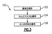
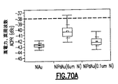
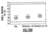
ニッケル/パラジウム/金(Ni/Pd/Au)表面めっき材料をRFIC製品に使用することによってRFICパッケージングのコストを低減するようシステムおよび方法が開示される。コストを低減するために、Ni/Pd/Au表面めっきにおける金層は、Ni/Au表面めっきにおける金層より薄い。しかしながら、Ni/Pd/Auは、パラジウムおよび金層が薄いこととニッケルの強磁性とにより、Ni/Auよりはるかに高い無線周波数シート抵抗を有する。これは、実効電流シート厚さの低減と、RF信号について密集する電流の増加とに寄与し、いくつかの実施形態では、Ni/Pd/Auめっき表面を通って伝わるRF信号についてRF損失が、Ni/Auめっき表面を通って伝わるRF信号について発見されるよりも大きくなる。これらの損失は、製品性能および歩留りに影響を与え得る。
ウム層および金層がない少なくとも1つの縁部および少なくとも1つの側壁を有する。
ニッケル/パラジウム/金(Ni/Pd/Au)の表面めっき材料をRFIC製品に使用することによってRFICパッケージングのコストを低減するようシステムおよび方法が開示される。コストを低減するために、Ni/Pd/Au表面めっきにおける金層は、Ni/Au表面めっきにおける金層より薄い。しかしながら、Ni/Pd/Auは、パラジウムおよび金層が薄いこととニッケルの強磁性とにより、Ni/Auよりはるかに高い無線周波数シート抵抗を有する。これは、実効電流シート厚さの低減と、RF信号について密集する電流の増加とに寄与し、いくつかの実施形態では、Ni/Pd/Auめっき表面を通って伝わるRF信号についてRF損失が、Ni/Auめっき表面を通って伝わるRF信号について発見されるよりも大きくなる。これらの損失は、製品性能および歩留りに影響を与え得る。
れたワイヤーボンディングエリアのトレース縁部および側壁上を流れている。RF電流の大部分がトレース縁部および側壁上を流れているので、トレース縁部および側壁にめっきすることはRF損失にさらに寄与することになる。RF損失を低減するために、いくつかの実施形態は、はんだマスクを再構成して、トレース縁部および側壁がNi/Pd/Au表面仕上げによってめっきされないようにワイヤーボンディングエリアにおいてトレース縁部および側壁を覆う。ワイヤーボンディングエリアの周りのNi/Pd/Auめっきがない銅トレース縁部および側壁は、Ni/Pd/Auワイヤーボンドパッドの周りにRF電流のための低い抵抗性のパスを提供し、したがって、RFIC基板のNi/Pd/Au表面めっきに関連付けられるRF信号損失を低減する。
グパッドおよび第2のボンディングパッドを形成することと、第1のボンディングパッドと第2のボンディングパッドとの間で電流を伝導する導電パスを提供するよう基板上にトレースを形成することとを含む。トレースは、第1のボンディングパッドに関連付けられる上部信号パスと、第2のボンディングパッドに関連付けられる下部信号パスとを有する。上記方法はさらに、第1のボンディングパッドに第1のリードを電気的に接続することと、第2のボンディングパッドに第2のリードを電気的に接続することと、オンダイ受動コンポーネントが第1のリードに電気的に接続するとともに出力信号が第2のリードに電気的に接続するように電子回路デバイスを構成することとを含む。これにより、電流が第1のボンディングパッドから離れるように方向付けされる。
請求項に記載されるイノベーションは各々いくつかの局面を有し、当該局面のいずれもその望ましい属性について単独で原因となることはない。この発明の範囲を限定することなく、いくつかの顕著な特徴がここで簡潔に議論される。
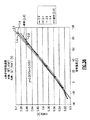
の勾配のない同じトランジスタと比較して、バイポーラトランジスタのBvCEXを増加するように構成され得る。さまざまな実施形態において、第1の勾配におけるドーピング濃度は、第1のコレクタ領域のドーピング濃度より約1桁小さいドーピング濃度から第1のコレクタ領域のドーピング濃度未満までの勾配がある。これらの実施形態のうちのいくつかに従うと、第2の勾配におけるドーピング濃度は、第1の勾配におけるほぼ最大のドーピング濃度から第2の勾配の下のサブコレクタのドーピング濃度よりも少なくとも約1桁小さいドーピング濃度までの勾配がある。いくつかの実施形態において、第1の勾配は、第1のコレクタ領域に隣接するとともに第1のコレクタ領域の厚さの約2倍より大きい厚さを有する第2のコレクタ領域にわたる。ある実施形態に従うと、第2の勾配は、第1のコレクタ領域の厚さより大きく第2のコレクタ領域の厚さより小さい厚さを有する第3のコレクタ領域にわたる。さまざまな実施形態において、コレクタは本質的に、第1のコレクタ領域、第2のコレクタ領域および第3のコレクタ領域からなる。いくつかの実施形態に従うと、バイポーラトランジスタはさらに、コレクタの下にサブコレクタを含む。ある実施形態に従うと、第1の勾配は第2の勾配と境界を接しており、ドーピング濃度は、第1の勾配と第2の勾配との境界の両側上でほぼ同じである。
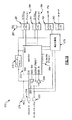
この発明のいくつかの実施形態に従うと、本開示のこの局面は、単一のデジタル制御インターフェイスダイ内において、無線周波数フロントエンド(radio frequency front end(RFFE))シリアルインターフェイスと、汎用入力/出力(GPIO)インターフ
ェイスとの両方を提供するために使用され得るデュアルモード制御インターフェイスに関する。ある実施形態では、デュアルモード制御インターフェイスまたはデジタル制御インターフェイスは、パワーアンプと通信し得る。さらに、デュアルモード制御インターフェイスは、パワーアンプのモードをセットするために使用され得る。
インアクティブ状態にセットされる場合、デュアルモード制御インターフェイスは汎用入力/出力(GPIO)インターフェイスを提供するように構成される。さらに、デュアルモード制御インターフェイスは、イネーブルレベルシフタおよびモードレベルシフタにイネーブル信号およびモード信号をそれぞれ提供するように構成される組合せ論理ブロックを含む。さらに、デュアルモード制御インターフェイスは、VIO信号に基づいて、イネーブルレベルシフタおよびモードレベルシフタにそれぞれ提供するべきイネーブル信号およびモード信号を選択するように構成されるパワーオンリセットを含む。
本発明のこの局面に関するいくつかの実現例において、本開示は、ベータのようなダイ依存パラメータを効果的に感知するようアンプダイ上の受動デバイスを利用し、かつ、零入力電流変化のような関連付けられる効果を補償して性能を改善および/または製品の部分間の変化を低減するパワーアンプ(PA)構成に関する。そのいくつかの実施形態では、このようなPA構成は、シリコンバイアスダイおよびHBTアンプダイを含み得る。従来、シリコンダイは、PAダイのための基準電流を生成しており、当該基準電流は、PAダイの温度に関して実質的に一定であり、本質的に離散的抵抗器の公差だけのみ変化する。
半導体構造の実施形態は、基板の上に位置し半導体材料を含むコレクタ層を含むヘテロ接合バイポーラトランジスタ(HBT)と、基板の上に位置する電界効果トランジスタ(
FET)とを含み、当該FETは、HBTのコレクタ層を形成する半導体材料に形成されるチャンネルを含む。
FETを含み得る。第1のFETはpFETを含み得、第2のFETはnFETを含み得る。
多くの状況において、パワーアンプ(PA)のような無線周波数(RF)デバイスのコストを低減することが望ましい。プロセスステップを取り除くことおよび/または余分な処理ステップを含んでいない「フリー」のデバイスを使用することは、このようなコストの低減がどのように達成され得るかについての例である。本願明細書において以下にさらに詳細に記載されるように、半導体抵抗器はそのような有利なコストの低減を提供し得る。さらに本願明細書において記載されるように、他の利点も半導体抵抗器により実現され得る。たとえば、利用可能な抵抗値に依存して、抵抗器実装面積がより小さくなり得、これにより、ダイサイズの縮小を支援し得る。このようなダイサイズの低減によって、さらにコストを低減することができる。別の例では、いくつかの半導体抵抗器は、当該抵抗器を形成するのと同じ半導体材料の状態に敏感であり得る。
たFETを含むBIFET(BIFET INCLUDING A FET HAVING INCREASED LINEARITY AND MANUFACTURABILITY)という名称を有する米国特許番号第6,906,359号と、HBTおよびFETを有する構造に関するデバイスおよび方法(DEVICES AND METHODOLOGIES RELATED TO STRUCTURES HAVING HBT AND FET)という名称を有するPCT公開番号WO2012/061632号とを含むがこれらに限定されない。
望ましい特徴を含み得る。別の例において、抵抗器のサイズは、可能な抵抗値のこのような範囲(たとえば約8オーム/sq(たとえばサブコレクタ)から約1,000オーム/sq(たとえば、注入されたベース層)のシート抵抗)により、望ましい態様で最適化または構成され得る。さらに別の例では、どの抵抗器が選択されるかに依存して(たとえば、デバイス上の第3の端子にバイアスがどのようにかけられるかを修正することにより)、抵抗器のRFロールオフが選択および/または調整され得る。
この開示の1つの局面は、パワーアンプダイ、負荷線および高調波終端回路を含むパワーアンプモジュールである。パワーアンプダイは、パワーアンプ入力で入力信号を増幅するとともにパワーアンプ出力で増幅出力信号を生成するように構成される1つ以上のパワーアンプを含む。パワーアンプダイはさらに複数の出力ピンを有する。負荷線は、増幅出力信号の基本周波数で、パワーアンプ出力にてインピーダンスを整合するように構成される。負荷線は、パワーアンプダイの外部で、パワーアンプダイの複数の出力ピンの1つ以上の第1の群に電気的に結合される。高調波終端回路は負荷線と別個である。高調波終端回路は、増幅出力信号の高調波周波数に対応する位相で終端するように構成される。高調波終端回路は、パワーアンプダイの外部で、パワーアンプダイの複数の出力ピンの1つ以上の他のピンの第2の群に電気的に結合される。
。
受け取るとともに増幅出力信号を生成するように構成されるパワーアンプを含み、上記方法はさらに、パワーアンプダイとパッケージング基板上の第1の導電性トレースとの間に第1の配線を形成することを含み、第1の配線は、増幅出力信号の基本周波数のインピーダンスを整合するように構成される第1の終端回路に含まれ、上記方法はさらに、パワーアンプダイとパッケージング基板上の第2の導電性トレースとの間に第2の配線を形成することを含み、第2の配線は第1の配線と別個であり、第1の導電性トレースは第2の導電性トレースと別個であり、第2の配線は、増幅出力信号の高調波に対応する位相で終端するように構成される第2の終端回路に含まれる。
この開示の1つの局面は、無線周波数(RF)回路における使用のために構成される無線周波数(RF)送信線である。RF送信線は、ボンディング層と、バリア層および拡散バリア層と、導電層とを含む。ボンディング層はボンディング面を有し、RF信号を受け取るように構成される。バリア層は汚染物質がボンディング層を入るのを防止するように構成される。バリア層はボンディング層に隣接する。拡散バリア層は汚染物質がボンディング層を入るのを防止するように構成される。拡散バリア層はバリア層に隣接する。拡散バリア層は、受取られたRF信号が拡散バリア層を貫通して、拡散バリア層に隣接する導電層に到ることを可能にする厚さを有する。
拡散バリア層はニッケルであり得る。これらの実現例のうちのいくつかにおいて、拡散バリア層の厚さは、約0.04μm〜約0.7μmの範囲であり得る。多くの実現例に従うと、拡散バリア層の厚さは約0.5μm以下であり得る。ある実現例に従うと、拡散バリア層の厚さは約0.35μm以下であり得る。いくつかの実現例に従うと、拡散バリア層の厚さは約0.75μmであり得る。
信号を送信するように構成される。さまざまな実現例に従うと、送信線はRFスイッチからフィルタにRF信号を送信するように構成される。
以下であり得る。さまざまな実現例において、拡散バリア層の厚さは、約0.45GHzの周波数でのニッケルの表皮厚さ未満であり得る。ある実現例に従うと、導電層は銅を含み得る。いくつかの実現例において、拡散バリア層の厚さは、約0.45GHzの周波数での材料の表皮厚さ未満であり得る。
開示を要約する目的のために、本発明のある局面、利点および新規な特徴が本願明細書において記載された。必ずしもすべてのこのような利点が本発明のこれらの局面の任意の特定の実施形態に従って達成されなくてもよいということが理解されるべきである。したがって本発明は、この開示の全体において教示または示唆され得る他の利点を必ずしも達成することなく、本願明細書全体において教示される1つの利点または利点の群を達成または最適化する態様で実施または実行されてもよい。
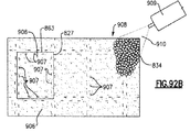
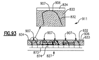
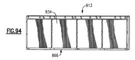
窒化タンタルで終端されたウェハ貫通ビアのための装置および方法が、本開示の他の局面、特徴または特性の1つ以上と組み合わされて本願明細書において記載および解釈される。そのある実現例では、窒化タンタル(TaN)終端層が砒化ガリウム(GaAs)ウェハの第1の側または表側上に形成され、金の導電層がTaN終端層の上に形成される。その後、ウェハ貫通ビアが、GaAsウェハの第2の側または裏側へとエッチングされ、GaAsウェハおよびTaN終端層の第1または内側部分を貫通するよう延在して金の導電層に達する。ここで組み合わされて解釈されるある実現例において、ウェハ貫通ビアは、ニッケルバナジウム(NiV)バリア層、金のシード層および銅層でめっきされる。ウェハ貫通ビアの形成の間、TaN終端層の第2の部分または外側部分は、金の導電層と銅層との間の界面を取り囲みGaAsウェハへの銅の拡散を抑制するように維持および構成される。
この開示の1つの局面はビア配置を決定する方法である。この方法は、無線周波数(RF)コンポーネントの周りのビアの初期配置について電磁干渉データを取得することを含む。RFコンポーネントは第1の導電層と第2の導電層との間に位置決めされる。ビアは第1の導電層と第2の導電層との間の接続に含まれる。ビアと第1および第2の導電層とは、RFコンポーネントの周りのRFアイソレーション構造の少なくとも部分を形成する。上記方法はさらに、初期配置についての電磁干渉データに少なくとも部分的に基づいて、ビアの更新配置を決定することを含む。
ーネントの少なくとも2つの異なる動作モードについて取得され得る。
または受信することを促進するように構成される。パッケージモジュールはアンテナと通信している。パッケージモジュールは、接地平面を有する基板と、パッケージモジュールの周辺に沿って配置される基板における複数のビアとを含む。複数のビアのビア同士の間隔は、低放射エリアにおいてよりもホットスポットにおいて、パッケージモジュールの周辺に沿ってより近い。パッケージモジュールは、基板の主面に結合されるRF回路を含む。パッケージモジュールはさらに、RF回路の上に配置される第2の導電層を含む。第2の導電層は、接地平面、複数のビアおよび第2の導電層がRF回路の周りにRFアイソレーション構造の少なくとも部分を形成するように、複数のビアに電気的に結合される。他のモジュールはパッケージモジュールと通信する。
本発明のこの局面の特徴および実施形態は、半導体デバイスパッケージと、デバイスパッケージに電磁干渉シールドを集積するためにワイヤーボンドプロセス技術を使用する、当該半導体デバイスパッケージを作製する方法とに関する。一実施形態において、ワイヤーボンドプロセスは、デバイスの周りに位置決めされるとともにデバイスの上および下の導電層に結合されるワイヤーボンドばねを形成するために使用され、これにより、デバイスの周りに電磁干渉シールドを形成する。以下にさらに議論されるように、ワイヤーボンドばねの形状およびワイヤーボンドばねによって作り出されるばね効果によって、堅牢な製造プロセスが可能になり、モールドされたパッケージの上部での導電層とパッケージの基板における接地平面との間に信頼性のある電気的接続が作り出される。これらのワイヤーボンドばねの使用により、任意のオーバーモールドされるデバイスに適用され得る集積された電磁干渉シールディングのための柔軟なソリューションが提供される。
配置することは、モールドコンパウンドの表面上に、銀が充填されたエポキシの層を塗布することを含む。
間の界面の少なくとも部分を囲むように構成される窒化タンタル終端領域を含んでもよい。
もよい。
ンプモジュールの周辺に沿って配置される所望の数のワイヤーボンドとを有するRFアイソレーション構造をさらに含んでもよく、複数のビアは、パワーアンプモジュールの第1の領域において、パワーアンプモジュールの第2の領域よりも高い密度を有しており、第1の領域は、第2の領域より高い電磁干渉に関連付けられる。
2012年6月14日に出願された「プロセスで補償されたHBTパワーアンプバイアス回路および方法(PROCESS-COMPENSATED HBT POWER AMPLIFIER BIAS CIRCUITS AND METHODS)」という名称を有する米国仮特許出願第61/659,701号と、2012年6月1
4日に出願された「半導体抵抗器を有するRFパワーアンプ(RF POWER AMPLIFIERS HAVING SEMICONDUCTOR RESISTORS)」という名称を有する米国仮特許出願第61/659,834号とのすべての開示を参照によって援用する。
と、2012年4月30日に出願された「勾配を有するバイポーラトランジスタを有するコレクタ(BIPOLAR TRANSISTOR HAVING COLLECTOR WITH GRADING)」という名称を有する米国特許出願番号第13/460,521号と、2012年10月23日に出願された「2モード汎用入力/出力インターフェイスを有するデュアルモードパワーアンプ制御インターフェイス(DUAL MODE POWER AMPLIFIER CONTROL INTERFACE WITH A TWO-MODE GENERAL PURPOSE INPUT/OUTPUT INTERFACE)」という名称を有する米国特許出願番号第13/658,488号と、2012年10月23日に出願された「3モード汎用入力/出力インターフェイスを有するデュアルモードパワーアンプ制御インターフェイス(DUAL MODE POWER AMPLIFIER CONTROL INTERFACE WITH A THREE-MODE GENERAL PURPOSE INPUT/OUTPUT INTERFACE)」という名称を有する米国特許出願番号第13/658,522号と、2011年7月8日に出願された「信号パス終端(SIGNAL PATH TERMINATION)」という名称を
有する米国特許出願番号第13/543,472号と、2010年11月4日に出願された「バイポーラおよびFETデバイス構造(BIPOLAR AND FET DEVICE STRUCTURE)」という名称を有する米国特許出願番号第12/939,474号と、2011年11月3日に出願された「HBTおよびFETを有する構造に関するデバイスおよび方法(DEVICES AND METHODOLOGIES RELATED TO STRUCTURES HAVING HBT AND FET)」という名称を有する米国特許出願番号第13/288,427号と、2012年5月4日に出願された「高性能無線周波数用途のための送信線(TRANSMISSION LINE FOR HIGH PERFORMANCE RADIO FREQUENCY APPLICATIONS)」という名称を有する米国特許出願番号第13/464,775号
と、2012年5月31日に出願された「無線周波数シールディング用途におけるビア密度および配置(VIA DENSITY AND PLACEMENT IN RADIO FREQUENCY SHIELDING APPLICATIONS)」という名称を有する米国特許出願番号第13/485,572号と、2013年5
月14日に出願された「集積回路モジュールのために電磁干渉シールディングを提供するためのシステムおよび方法(SYSTEMS AND METHODS FOR PROVIDING ELECTROMAGNETIC INTERFERENCE SHIELDING FOR INTEGRATED CIRCUIT MODULES)」という名称を有する米国特許
出願番号第13/893,605号と、2013年5月14日に出願された「集積回路モジュールのために電磁干渉を制御するためのシステムおよび方法(SYSTEMS AND METHODS FOR CONTROLLING ELECTROMAGNETIC INTERFERENCE FOR INTEGRATED CIRCUIT MODULES)」
という名称を有する米国特許出願番号第13/893,614号と、2013年5月29日に出願された「金属ペイント層を有する半導体パッケージ(SEMICONDUCTOR PACKAGE HAVING A METAL PAINT LAYER)」という名称を有する米国特許出願番号第13/904,566号とのすべての開示を参照によって援用する。
I.イントロダクション
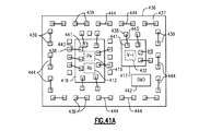
ここで図1を参照して、本発明に従った例示的なモジュール101の概略的なブロック図が示される。モジュール101は、望ましいレベルおよび/または範囲のリニアリティおよび望ましいPAEを達成し得る。モジュール101は、パワーアンプシステムのいくつかまたはすべてを含み得る。モジュール101は、マルチチップモジュールおよび/またはパワーアンプモジュールと称され得る。モジュール101は、基板102、パワーアンプダイ103を含む1つ以上のダイ、1つ以上の回路要素、整合ネットワーク104など、またはそれらの任意の組合せを含み得る。図1に示されるように、1つ以上のダイは、パワーアンプダイ103と、パワーアンプバイアス制御ダイ104のようなコントローラダイとを含み得る。
103は有利なことに、入力整合ネットワーク、(ドライバアンプと称され得る)第1のパワーアンプ段、段間整合ネットワーク、(出力アンプと称され得る)第2のパワーアンプ段、バイアス回路、またはその任意の組合せを含み得る。当業者であれば、パワーアンプダイが1つ以上のパワーアンプ段を含み得るということを理解するべきである。さらに、本願明細書のある実現例では、入力整合ネットワークおよび/または段間整合ネットワークは、パワーアンプダイ103の外部であり得る。図1はモジュール101において1つのパワーアンプダイ103を示すが、さらに、本発明の他の実現例では、2つ以上のパワーアンプダイがモジュール101に含まれてもよいということが理解されるべきである。
いくつかの実施形態において、たとえばNi/Pd/Auめっきのような高RF損失のめっきに関連付けられるRF損失を低減するために、はんだマスクは、ワイヤーボンドエリアの縁部および側壁がめっきされるのを防止するように再構成される。ワイヤーボンドエリアの縁部および側壁をNi/Pd/Auめっきのような高RF損失のめっきが存在しないままにすることによって、高抵抗率材料の周りを流れるようRF電流のためのパスが提供され、これにより、高抵抗率めっき材料に関連付けられるRF信号損失が低減される。上に示されるように、パワーアンプモジュールおよび当該パワーアンプモジュールが使用されるデバイスの性能をさらに改善するために、本発明のこれらの局面は、本願明細書の他の局面と組み合わされてもよい。
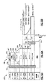
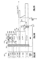
に取り付けられ得る。ワイヤーボンドパッド113および114は、ボンドエリア119、側壁117および縁部118を含む。
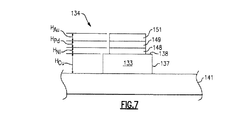
のNi/Pd/Auワイヤーボンドパッド113の断面が示される。図2の114のようなモジュールにおける任意の他のボンドパッドに該当し得る、図4に示されるようなNi/Pd/Auワイヤーボンドパッド113は、ニッケル層127、パラジウム層128および金層129を含む。
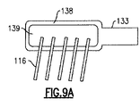
ヤーボンドパッドである。他の実施形態では、たとえば1つ、2つ、3つ、4つ、5つまたは6つより多いといった他の数のワイヤー116が、ワイヤーボンドパッド134および136に取り付けられ得る。ワイヤーボンドパッド136は、ボンドエリア139、側壁137および縁部138を含む。
たとえばニッケル/パラジウム/金(Ni/Pd/Au)めっきのような高RF損失めっきに関連付けられる無線周波数(RF)損失を低減するために、キャパシタ、抵抗器またはインダクタのような、無線周波数集積回路(RFIC)に関連付けられるオンダイ受動デバイスは、RFICのRF信号出力に対してRF上側信号パスに配置される。RF上側信号パスにオンダイ受動デバイスを配置することによって、RF電流は、受動デバイスのボンディングパッドの高RF損失めっき材料を直接的に通過しない。上に示されるように、パワーアンプモジュールおよび当該パワーアンプモジュールが使用されるデバイスの性能をさらに改善するために、本発明のこれらの局面は、本願明細書の他の局面と組み合わされてもよい。
公知である多くのプロセスが存在しており、その例として、たとえば、エピタキシー、マスキングおよびエッチング、拡散、イオン注入、ポリシリコンの蒸着、誘電体の作製、リソグラフィおよびエッチング、薄膜の蒸着、金属化、ガラス絶縁、ならびにウェハ上の各ダイのプロービングおよびトリミングなどがある。
示されるように、ワイヤーボンディングパッド182および183は、めっきされた縁部および側壁を有するよう形成される。別の実施形態では、ワイヤーボンディングパッド182および183は、表面めっき材料が存在しない縁部および側壁を有するよう形成される。
本開示のこのセクションは、ヘテロ接合バイポーラトランジスタのような、コレクタに
おいて少なくとも1つの勾配を有するバイポーラトランジスタに関する。この開示の1つの局面は、ベースとの接合部において高いドーピング濃度を有するとともに、ドーピング濃度がベースから離れるにつれて増加する少なくとも1つの勾配を有するコレクタを含むバイポーラトランジスタである。本願明細書のいくつかの実施形態では、高いドーピング濃度は少なくとも約3×1016cm3であり得る。ある実施形態に従うと、コレクタは2つの勾配を含む。このようなバイポーラトランジスタはたとえばパワーアンプにおいて実現され得る。上に示されるように、パワーアンプモジュールおよび当該パワーアンプモジュールが使用されるデバイスの性能をより良く改善するために、本発明のこれらの局面は、本願明細書の他の局面と組み合わされてもよい。
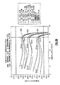
1016cm−3〜9×1016cm−3、約3×1016cm−3〜8×1016cm−3、約3×1016cm−3〜7×1016cm−3、約3×1016cm−3〜6×1016cm−3、約3×1016cm−3〜5×1016cm−3、約4×1016cm−3〜9×1016cm−3、約4×1016cm−3〜8×1016cm−3、約4×1016cm−3〜7×1016cm−3、約4×1016cm−3〜6×1016cm−3、約4×1016cm−3〜5×1016cm−3、約5×1016cm−3〜9×1016cm−3、約5×1016cm−3〜8×1016cm−3、約5×1016cm−3〜7×1016cm−3、約5×1016cm−3〜6×1016cm−3、約6×1016cm−3〜9×1016cm−3、約6×1016cm−3〜8×1016cm−3、約6×1016cm−3〜7×1016cm−3、約7×1016cm−3〜9×1016cm−3、約7×1016cm−3〜8×1016cm−3、または約8×1016cm−3〜9×1016cm−3といった範囲のうちの1つの範囲内にあるように選択され得る。
から1400Åまでの範囲に選択され得る。いくつかの実現例では、ベース196の厚さは、約500Åから900Åまでの範囲に選択され得る。本願明細書において開示される範囲から選択される如何なるベース厚さも、本願明細書において開示される範囲から選択されるベースドーピング濃度のいずれとも組み合わせて実現され得る。一例として、ベース196のドーピング濃度は、5.5×1019cm−3であり得、厚さは500Åであり得る。図12Aのバイポーラトランジスタ189において、厚さはエミッタ203と第1のコレクタ領域196との間の最も短い距離であり得る。
れ得る。いくつかの実施形態では、バイポーラトランジスタ189がほぼ一定のベータ値を有し得るように、ガンメル数はほぼ一定であり得る。たとえば、選択された範囲内でベース196の厚さを増加すると、ベース196のドーピング濃度が対応して減少し得、ガンメル数がほぼ一定に保持される。別の例として、選択された範囲内でベース196の厚さを減少させると、ベース196のドーピング濃度が対応して増加し得、ガンメル数がほぼ一定に保持される。ベース196の厚さの低減およびベース196のドーピングの増加によって起こり得る、ベース196に関連付けられる抵抗値の変化は有意でない。たとえば、ベース196の厚さを900Åから500Åに変更し、ベース196のドーピング濃度を4×1019cm−3から5.5×1019cm−3に変更することによって、ベース196の抵抗に有意な影響は与えられ得ない。
が理解されるべきである。さらに、本願明細書において記載されるバイポーラトランジスタのいずれにおいても、n型ドーピングおよびp型ドーピングは、当該トランジスタのいくつかまたはすべて取り替えられ得る。したがって、本願明細書において記載される特徴の任意の組合せは、NPNトランジスタおよび/またはPNPトランジスタに適用され得る。
、いくつかの実施形態において、コレクタ領域は2つの勾配を有し得る。コレクタ領域の少なくとも1つの勾配は、バイポーラトランジスタのRFゲインを増加し、および/または、バイポーラトランジスタの耐久性を増加し得る。たとえば、少なくとも1つの勾配は、第1のコレクタ領域における高いドーピング濃度に起因するバイポーラトランジスタのゲインの減少のいくつかまたはすべてを補償し得る。ブロック224では、高いドーピング濃度を有する異なるコレクタ領域はベースに当接して形成され得る。高いドーピング濃度は、たとえば少なくとも約3.0×1016cm−3といった、本願明細書において記載される第1のコレクタ領域197のドーピング濃度のいずれかであり得る。さらに高いドーピング濃度および第1のコレクタ領域の厚さは、ともに1つ以上の第2のチャンネルリニアリティ測定値を改善し得る。
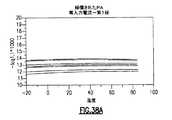
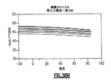
イアス信号は、PAダイ228上、モジュール226におけるPAダイ228の外側、またはモジュール226の外部で生成され得る。第1段パワーアンプ232は、RF入力を増幅し、段間整合回路233を介して第2段パワーアンプ234に増幅されたRF入力を提供し得る。段間整合回路233は、第2段バイアス信号を受け取り得る。第2段バイアス信号は、PAダイ228上、モジュール226におけるPAダイ228の外側、またはモジュール226の外部で生成され得る。第2段パワーアンプ234は、増幅されたRF出力信号を生成し得る。
帯電話にとって望ましい通話時間の利点を提供し得る。モジュール226は、高電力付加効率により、ハイスピードダウンリンクパケットアクセス(High Speed Downlink Packet
Access(HSDPA))、ハイスピードアップリンクパケットアクセス(High Speed Uplink Packet Access(HSUPA))、ロングタームエボリューション(Long Term Evolution(LTE))データ伝送の厳格なスペクトルリニアリティ要件を満たし得る。方向
性結合器は、モジュール226に集積され得、したがって外部結合器の必要性を除去できる。
Integrated Circuit(MMIC))において実施されるパワーアンプダイであり得る。
MMICは、オンボードのバイアス回路網と、入力整合ネットワーク231および段間整合ネットワーク233とを含み得る。出力整合ネットワーク229は、効率および電力性能を増加および/または最適化するよう、モジュール226のパッケージ内でダイ228と別個に実施される50オームの負荷を有し得る。
望ましくあり得る。パワーアンプはさらに、割り当てられた受信時間スロットの間の送信からの信号干渉を防止するよう、時間にわたってRF信号の電力レベルを調整することを支援するために使用され得る。パワーアンプモジュールは、1つ以上のパワーアンプを含み得る。
動車、ステレオシステム、DVDプレーヤ、CDプレーヤ、VCR、MP3プレーヤ、ラジオ、カムコーダ、カメラ、デジタルカメラ、ポータブルメモリチップ、洗濯機、乾燥機、洗濯/乾燥機、コピー機、ファクシミリマシン、スキャナ、多機能周辺機器、腕時計、時計などを含み得るがこれらに限定されない。コンシューマエレクトロニクス製品の部分は、RF送信線を含むマルチチップモジュール、パワーアンプモジュール、RF送信線を含む集積回路、RF送信線を含む基板など、またはその任意の組合せを含み得る。さらに、電子デバイスの他の例はまた、メモリチップ、メモリモジュール、光学ネットワークまたは他の通信ネットワークの回路、およびディスクドライバ回路を含み得るがこれらに限定されない。さらに、電子デバイスは未完成の製品を含み得る。
本願明細書のいくつかの実施形態に従うと、本開示のこのセクションは、単一のデジタル制御インターフェイスダイ内における、無線周波数フロントエンド(radio frequency front end(RFFE))シリアルインターフェイスと、3モード汎用入力/出力(three-mode general purpose input/output(GPIO))インターフェイスとの両方を提供するために使用され得るデュアルモード制御インターフェイスに関する。ある実施形態では、デュアルモード制御インターフェイスまたはデジタル制御インターフェイスは、パワーアンプと通信し得る。さらに、デュアルモード制御インターフェイスは、パワーアンプのモードをセットするために使用され得る。上に示されるように、パワーアンプモジュールおよび当該パワーアンプモジュールが使用されるデバイスの性能をさらに改善するために、本発明のこれらの局面は、本願明細書の他の局面と組み合わされてもよい。
IOインターフェイスのうちの一方のみを実現するダイと同じに維持され得る。
図18は、本発明の局面に従ったワイヤレスデバイス248の実施形態を示す。本開示の用途はワイヤレスデバイスに限定されず、パワーアンプを有するまたはパワーアンプを有さない任意のタイプの電子デバイスに適用され得る。たとえば、実施形態は、パワーアンプを含み得る有線デバイス、天候感知デバイス、レーダ、ソナー、マイクロ波オーブンおよび任意の他のデバイスに適用され得る。さらに本発明の実施形態は、フロントエンドインターフェイスを介して制御される1つ以上のコンポーネントを含み得るデバイスに適用され得る。たとえば本開示の実施形態は、例示すると、パワーアンプ供給調整に使用され得るスイッチモード電源(Switch Mode Power Supply(SMPS))デバイス、アンテナスイッチモジュール(Antenna Switch Module(ASM))、およびアンテナ負荷調整
モジュールに適用され得る。本開示は、ワイヤレスデバイスまたはパワーアンプの制御に限定されないが、議論を単純化するために、多くの実施形態は、ワイヤレスデバイス248およびパワーアンプモジュール249に関して記載される。
ィングの変更を必要とすることなく、インターフェイスが同じ構成要素のダイ上に共存し得るように複数のタイプのフロントエンドインターフェイスをサポートし得る。さらに、いくつかの実施形態において、デジタル制御インターフェイス253は、インターフェイスピンの数を増加させることなく、または、ワイヤレスデバイス248による使用のために露出した接続点を増加させることなく、複数のフロントエンドインターフェイスをサポートし得る。多くの実施形態において有利なことに、デジタル制御インターフェイス253を修正することなく、デジタル制御インターフェイス253は、異なるインターフェイス規格をサポートするデバイスと共に使用され得る。たとえば、図18の示されるデジタル制御インターフェイス253は、デジタル制御インターフェイス253を修正することなく、MIPI(登録商標)RFFE、GPIOまたはこれら2つの組合せをサポートするデバイスと共に使用され得る。
制御インターフェイス253と通信し得、デジタル制御インターフェイス253にパワーアンプモジュール249のセッティングを修正させ得る。たとえば、ワイヤレスデバイス248は、デジタル−アナログコンバータ(DAC)264、ディスプレイプロセッサ266、中央プロセッサ267、ユーザインターフェイスプロセッサ268、アナログ−デジタルコンバータ269およびメモリ271を含み得る。
図19は、本開示の局面に従った、デジタル制御インターフェイス272として識別されるデジタル制御インターフェイスの特定の実施形態を示す。デジタル制御インターフェイス272は、RFFEシリアルインターフェイスおよびGPIOインターフェイスの両方を含む。ある実施形態において有利なことに、デジタル制御インターフェイス272は、RFFEシリアルインターフェイスおよびGPIOインターフェイスのうちの1つを含む制御インターフェイスと同じ数のピンを有する同じサイズのパッケージにおいて実現され得る。チップのサイズを広げることなく単一のチップ内に複数のインターフェイスタイプを組み合わせることができることは、3mm×3mmモジュールを必要とし得る用途といった、小さいパッケージを使用または必要とする用途に特に有利である。
ず、デジタル制御インターフェイス272はGPIOインターフェイスとして機能するように構成される。他方、いくつかの実施形態において、VIOピン274が、論理ハイにセットされるか、または電源に直接的もしくは間接的に接続される場合、RFFEコア273には電力が提供され、デジタル制御インターフェイス272はRFFEシリアルインターフェイスとして機能するように構成される。
変であり得る。いくつかの設計では、各レベルシフタ281が、異なるデフォルト値または信号に関連付けられ得ることが可能である。代替的には、各レベルシフタ281は、同じデフォルト値または信号に関連付けられ得る。
。同様に、RFFEコア273は、RFFEコア273のData Outからのデータをデータ/イネーブルピン277に提供し得る。バッファ288および289によって図19に示されるように、データ入力およびデータ出力の両方はバッファされ得る。いくつかの実施形態では、バッファはトライステートバッファであってもよい。いくつかの実現例では、RFFEコア273のOutput Enableは、Data OutおよびData Inの両方が、データ/イネーブルピン277へおよびデータ/イネーブルピン277から同じラインを共有することを可能にするようバッファ288および289を制御するように構成される。したがっていくつかの例では、RFFEコア273からデータを読み出す際、バッファ288はデータフローを有効にする一方、バッファ289はデータフローを防止するかまたは高インピーダンスにセットされる。同様にいくつかの例では、RFFEコア273にデータを書き込む際、バッファ289はデータフローを有効にする一方、バッファ288はデータフローを防止するかまたは高インピーダンスにセットされる。
ーブルピン277からデータ信号を受け取り得る。いくつかの場合では、アドレス信号の後、データ信号が受け取られる。代替的には、データ信号はアドレス信号の前に受け取られてもよい。さらに、デジタル制御インターフェイス272が別個のアドレスピン(図示せず)を含む実施形態では、RFFEコア273は、アドレス信号およびデータ信号を少なくとも部分的に並列に受け取り得る。
図20は、本発明の局面に従った、レベルシフタ291の実施形態を示す。レベルシフタ281、282および283の実施形態は、レベルシフタ291と同等または実質的に同等であり得る。いくつかの実現例では、レベルシフタ281、282および283は、レベルシフタ291と設計が異なり得る。しかしながら、レベルシフタの各々は、入力信号の電圧を修正することが可能である。いくつかの場合では、入力信号の電圧は、図19のVccピン287で提供される電圧と整合するようシフトまたは修正される。他の場合では、入力信号の電圧は、入力電圧とVccピン287で提供される電圧との間の範囲内でシフトまたは修正される。
図21は、本開示の局面に従った、デジタル制御インターフェイスの動作についてのプ
ロセス301のフローチャートを示す。プロセス301は、RFFEシリアルインターフェイスおよびGPIOインターフェイスとして動作するように構成される任意のタイプのデジタル制御インターフェイスによって実行され得る。たとえば、プロセス301は、図18のデジタル制御インターフェイス253および図19のデジタル制御インターフェイス272によって実行され得る。さらに、プロセス301は、いくつかの実施形態において、異なるインターフェイスモードで動作するように構成される任意のタイプのデジタル制御インターフェイスによって実行され得る。議論を単純化するために、プロセス301は、図19のデジタル制御インターフェイス272によって実現されるものとして記載されるが、プロセス301の実現はこのようなものに限定されない。
ることと、デジタル制御インターフェイス272内で信号のフローを調節することとを含む。
252に提供され得、その後、パワーアンプコントローラ252は、RFFEレベルシフタ281からの受信信号に少なくとも部分的に基づいてパワーアンプ251を構成し得る。デジタル制御インターフェイス272がGPIOインターフェイスとして動作している場合、RFFEレベルシフタ281の出力は、デフォルト値またはデフォルトピン284で受け取った信号に少なくとも部分的に基づき得る。対照的に、デジタル制御インターフェイス272がRFFEシリアルインターフェイスとして動作している場合、RFFEレベルシフタ281の出力は、RFFEコア273に関連付けられるレジスタに格納された値を含む、RFFEコア273から受け取られた値または信号に少なくとも部分的に基づき得る。いくつかの実施形態では、ブロック322、323および324の1つ以上は随意であってもよい。たとえば、デジタル制御インターフェイス272がGPIOインターフェイスとして動作している場合、レベルシフタ281はパワーアンプ251またはパワーアンプコントローラ252に値を提供しなくてもよい。
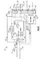
図22は、本発明の局面に従って実現される、ワイヤレスデバイス326と称されるワイヤレスデバイスの代替的な実施形態を示す。本願明細書のいくつかの実現例では、ワイヤレスデバイス248に関して上で記載された実施形態のうちのいくつかまたはすべては、ワイヤレスデバイス326に適用され得る。
Cバスであり得る。いくつかの実現例では、デジタル制御インターフェイス253に関して上で記載された実施形態のうちのいくつかまたはすべては、デジタル制御インターフェイス331に適用され得る。
インターフェイス331を修正することなく、デジタル制御インターフェイス331は、異なるインターフェイス規格をサポートするデバイスと共に使用され得る。たとえば、図22の示されるデジタル制御インターフェイス331は、デジタル制御インターフェイスを修正することなく、シリアルインターフェイス、GPIOインターフェイスまたはこれら2つの組合せをサポートするデバイスと共に使用され得る。いくつか場合では、デジタル制御インターフェイス331は、動作の間、異なるインターフェイスタイプの間で切り替わり得る。
図23は、本発明のある局面に従って実現される、図22のデジタル制御インターフェイス331の実施形態を示す。いくつかの実現例では、デジタル制御インターフェイス253およびデジタル制御インターフェイス272に関して上で記載された実施形態のうちのいくつかまたはすべては、デジタル制御インターフェイス331に適用され得る。
。
の1つ以上のコンポーネントが、アクティブであるか、または、GPIOインターフェイスを提供するよう動作し得る。たとえば、いくつかの実現例では、組合せ論理ブロック356は、パワーオンリセット354によって制御されるマルチプレクサを含み得る。さらにこの例では、組合せ論理ブロック356は、デジタル制御インターフェイス331の動作モードに基づき、したがって、パワーオンリセット354によって出力される値に基づき、レベルシフタ358および359に異なる信号を提供し得る。したがってこの例では、パワーオンリセット354は一般にシリアルインターフェイス332の部分であるが、デジタル制御インターフェイスがGPIOインターフェイスモードにある場合、パワーオンリセット354は、GPIOインターフェイスの部分として機能し得る。同様にこの例では、組合せ論理ブロック356と、レベルシフタ358および359とは一般に、GPIOインターフェイス333の部分であるが、デジタル制御インターフェイス331がシリアルインターフェイスモードである場合、組合せ論理ブロック356ならびにレベルシフタ358および359の1つ以上は、シリアルインターフェイスを提供するのを補助するよう動作し得る。
正し得る。
ト(図示せず)を含み得る。ある状況では、レジスタのセットは未知の値にセットされ得る。たとえば、最初にワイヤレスデバイス326に電力が供給される際に、レジスタのセットは未知の値にセットされ得る。第2の例として、VIOピン351が、シリアルインターフェイスコア349のための電源と、シリアルインターフェイスモードとGPIOインターフェイスモードとの間のモード選択器との両方として機能する実現例において、デジタル制御インターフェイス331がGPIOインターフェイスからRFFEシリアルインターフェイスに最初に遷移する場合に、レジスタのセットは未知の値にセットされ得る。シリアルインターフェイスコア349に電力が最初に供給される場合またはシリアルインターフェイスコア349がリセット状態から出る場合にレジスタが既知の値にセットされることを保証するために、シリアルインターフェイスコア349は、レジスタのセットの各々の値を、ストラップドデフォルト362のセットによって提供される値にセットするように構成され得る。ある実現例では、図19のストラップドデフォルト286は、デフォルトピン361に提供される値と同等であり得る。
ジスタ値またはシリアルインターフェイスコア349のレジスタに関連付けられる信号をシリアルインターフェイスレベルシフタ357に提供することを含み得る。
図24は、図23に示され、本発明の局面に従って実現される組合せ論理ブロック356の実施形態のさらなる詳細を示す。上述したように、組合せ論理ブロック356は、レベルシフタ358および359にイネーブル信号とモード信号とをそれぞれ出力するように構成され得る。さらに、組合せ論理ブロック356は、イネーブル信号およびモード信号が、シリアルインターフェイスコア349から受け取られた入力またはクロック/モードピン352およびデータ/イネーブルピン353から受け取られた入力に基づくかどうかを決定する論理を含む。いくつかの場合では、デジタル制御インターフェイス331がGPIOインターフェイスとして動作している場合、イネーブル信号およびモード信号は、クロック/モードピン352およびデータ/イネーブルピン353から入力信号を受け取る付加的な論理またはデバイス(図示せず)を介して受け取られた入力に基づき得る。同様に、いくつかの場合では、デジタル制御インターフェイス331がシリアルインターフェイスとして動作している場合、イネーブル信号およびモード信号は、シリアルインターフェイスコア349から信号を受け取る付加的な論理またはデバイス(図示せず)を介して受け取られた入力に基づき得る。いくつかの場合では、付加的な論理またはデバイスは、組合せ論理ブロック356に信号を提供する前に、信号を処理し得る。
により、組合せ論理ブロック356と通信する1つ以上のデバイス(たとえばパワーアンプコントローラ329、パワーアンプ328など)のRF性能局面を低下させ得るクロックエネルギーの量を制限する。いくつかの場合には、ANDゲートは、1つ以上の信号の同期を可能にする遅延を導入し得る。ある実施形態では、ANDゲートは随意であってもよい。
次に図25を参照して、ここで本発明のさらなる局面に従って実現されるデジタル制御インターフェイス383として参照されるデジタル制御インターフェイスの別の実施形態が示される。いくつかの場合には、デジタル制御インターフェイス383は、(図22に示される)ワイヤレスデバイス326の(図23に示される)デジタル制御インターフェイス331を置換し得る。いくつかの実現例では、デジタル制御インターフェイス253、デジタル制御インターフェイス272およびデジタル制御インターフェイス331に関して上で記載された実施形態のうちのいくつかまたはすべては、このデジタル制御インターフェイス383に適用され得る。議論を単純化するために、デジタル制御インターフェイス331とデジタル制御インターフェイス383との間の共通の要素は以下では繰り返されない。
0ピン384およびデータ/モード1ピン386を含み得る。ピン384および386は、デジタル制御インターフェイス331のピン352および353と同様に、それぞれ構成され得る。しかしながら、デジタル制御インターフェイス383がGPIOインターフェイスとして構成される場合、クロック/モード0ピン384は組合せ論理ブロック388に第1のモード信号を提供し得、クロック/モード1ピン386は組合せ論理ブロック388に第2のモード信号を提供し得る。
図26は、本発明のさらに別の局面に従って実現され得る、ここで組合せ論理ブロック388として指定される本発明の組合せ論理ブロックの代替的な実施形態を示す。いくつかの実施形態では、組合せ論理ブロック388は、組合せ論理ブロック356に関して上で記載した特性、機構または機能のうちのいくつかまたはすべてを含み得る。
、マルチプレクサ401は、シリアルイネーブル入力396を介してシリアルインターフェイスコア349から受け取られたイネーブル信号を出力する。デジタル制御インターフェイス383がGPIOインターフェイスとして構成される場合、マルチプレクサ401は、クロック/モード0入力393およびデータ/モード1入力394から受け取られた信号の論理和に基づくイネーブル信号を出力する。論理和は、図26に示されるORゲート407を介して得られ得る。しかしながら、たとえばNORゲートとインバータとを使用することにより、他の論理的な同等物が可能である。
ッティングは、それぞれモード0レベルシフタ389およびモード1レベルシフタ391へのモード0信号およびモード1信号の出力に基づくパワーアンプコントローラ329のセッティングに対応する。

いくつかの実施形態では、デジタル制御インターフェイスは、VIO信号を受け取るように構成される電圧入力/出力(VIO)ピンを含む。さらに、デジタル制御インターフェイスは、シリアルインターフェイスを提供するように構成されるフロントエンドコアを含み得る。フロントエンドコアは、VIO信号が第1の論理レベルを満たす場合、アクティブ状態にあり得、VIO信号が第2の論理レベルを満たす場合、インアクティブ状態にあり得る。さらに、デジタル制御インターフェイスは、フロントエンドコアがインアクティブ状態にセットされる場合に、汎用入力/出力(GPIO)インターフェイスを提供するように構成され得る。さらに、デジタル制御インターフェイスは、イネーブルレベルシフタにイネーブル信号を提供し、モードレベルシフタにモード信号を提供するように構成
される組合せ論理ブロックを含み得る。さらに、デジタル制御インターフェイスはクロック/モードピンおよびデータ/イネーブルピンを含み得る。クロック/モードピンは、フロントエンドコアがアクティブ状態にセットされる場合にフロントエンドコアにクロック信号を提供し、フロントエンドコアがインアクティブ状態にセットされる場合に組合せ論理ブロックにモード信号を提供するように構成され得る。データ/イネーブルピンは、フロントエンドコアがアクティブ状態にセットされる場合にフロントエンドコアにデータ信号を提供し、フロントエンドコアがインアクティブ状態にセットされる場合に組合せ論理ブロックにイネーブル信号を提供するように構成され得る。さらにデジタル制御インターフェイスは、VIO信号に基づいて、イネーブルレベルシフタおよびモードレベルシフタにそれぞれ提供されるイネーブル信号およびモード信号の源を選択するように構成されるパワーオンリセットを含み得る。いくつかの実現例によると、フロントエンドコアは無線周波数フロントエンド(RFFE)コアを含む。
、フロントエンドコアから受け取られ得る。VIO信号が論理ローであるという決定に応答して、この方法は、イネーブル入力からの第2のイネーブル信号を組合せ論理ブロックに提供し、モード入力からの第2のモード信号を組合せ論理ブロックに提供し、イネーブルレベルシフタおよびモードレベルシフタに出力するべき第2のイネーブル信号および第2のモード信号を組合せ論理ブロックにて選択することにより、汎用入力/出力(GPIO)インターフェイスとして機能するようデジタル制御インターフェイスを構成することを含み得る。
パワーアンプに制御信号を提供するように構成されるパワーアンプコントローラとを含む。当該制御信号は、パワーアンプの動作モードを特定し得る。
決定に応答して、リセット状態からアクティブ状態にシリアルインターフェイスコアを再構成することを含む。シリアルインターフェイスコアをリセット状態からアクティブ状態に再構成することは、シリアルインターフェイスコアの内部レジスタのセットをデフォルト値に構成することを含み得る。
、ワイヤレスデバイスは、パワーアンプモジュールに電力を供給するように構成される電源と、パワーアンプモジュールのモード選択器に制御信号を提供するように構成されるトランシーバとを含み得る。
本開示のこのセクションは、パワーアンプにバイアスをかけるためのシステムに関し、当該パワーアンプは第1のダイと第2のダイとを含んでおり、第1のダイは、パワーアンプ回路と、第1のダイの1つ以上の状態に依存する電気特性を有する受動コンポーネントとを含み、第2のダイは、第1のダイの受動コンポーネントの電気特性の測定に少なくとも部分的に基づいてバイアス信号を生成するように構成されるバイアス信号生成回路を含む。上に示されるように、本発明のこれらの局面は、本願明細書の他の局面と組み合わせ
られて、パワーアンプモジュール、およびそれらが使用されるデバイスの性能をさらに改善し得る。
適用され得る。ダイオードスタックトポロジ以外の代替的なバイアスアプローチが使用され得るが、これらのアプローチはしばしば、帯域幅を損ない得、ノイズを劣化し得、および/または、外部の受動コンポーネントを必要とし得る。
流源433および434が第1および第2のPA段415aおよび415bにバイアス信号を提供することを促進するように示されている。本願明細書に記載されるように、このようなバイアス信号は、HBT PAダイ416の1つ以上の状態の変化について補償され得る。絶対温度比例(proportional-to-absolute-temperature(PTAT))電圧基準431および基準抵抗器412に関連してV−I回路432がどのように構成および動作され得るかの例が、本願明細書において以下により詳細に記載される。
式2Cでは、右側のパラメータはエミッタに関係付けられており、したがって、ベースプロセスに亘って著しくは変化し得ない。したがって、(HBTの場合にRbおよびβの変化のほとんどが発生する)ベースにおける変化について、ベータパラメータβおよびベース抵抗Rbが、実質的に同一または同様の態様で応答し得るので、これら2つのパラメータの比率は概して一定であり得る。したがって、Rbにおける変化の測定によって、ベースにおいて発生する変化について、βの変化に関する情報が提供され得る。
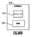
41と、パッケージング基板437上に形成されたコンタクトパッド438との間に形成され得る。いくつかの実施形態では、1つ以上の表面実装デバイス(surface mounted device(SMD))442は、モジュール436のさまざまな機能を促進するためにパッケージング基板437に実装され得る。
受取られた信号を処理するよう公知の態様で構成および操作され得るトランシーバ454からそれぞれのRF信号を受け取り得る。トランシーバ454は、ユーザに好適なデータおよび/または音声信号とトランシーバ454に好適なRF信号との間の変換を提供するように構成されるベースバンドサブシステム453と連携動作するように示される。トランシーバ454はさらに、ワイヤレスデバイスの動作のための電力を管理するように構成される電力管理コンポーネント451に接続されることが示される。このような電力管理はさらに、ベースバンドサブシステム453およびPAモジュール436の動作を制御し得る。
ず)にルーティングされることが示される。
本開示のこのセクションは、ヘテロ接合バイポーラトランジスタ(HBT)および電界効果トランジスタ(FET)を含む半導体構造に関し、当該ヘテロ接合バイポーラトランジスタ(HBT)は、基板の上に位置し、半導体材料を含むコレクタ層を含み、当該電界効果トランジスタ(FET)は基板の上に位置し、HBTのコレクタ層を形成する半導体材料に形成されるチャンネルを有する。いくつかの実現例では、第2のFETが、基板の上に位置するように設けられ得、HBTのエミッタを形成する半導体材料に形成されるチャンネルを含むように構成され得る。前述の特徴の1つ以上が、ダイ、パッケージモジュールおよびワイヤレスデバイスといったデバイスにおいて実現され得る。本願明細書の技術の当業者であれば、本発明のこれらの局面は、本願明細書の他の局面と組み合わせられて、パワーアンプモジュール、およびそれらが使用されるデバイスの性能をさらに改善し
得るということが容易に理解されるはずである。
たは任意の他の技術を使用して形成され得る。さらに、以下に記載されるさまざまな半導体層の厚さは近似であり、記載されるよりも薄いまたは厚い範囲でもよい。同様に、本願明細書において以下に記載されるドープされた半導体層のドーピングレベルは相対的である。
実現例に関係する特定の情報を含んでいる。当業者であれば、本発明は本願において具体的に議論されるのと異なる態様で実現されてもよいということを認識するであろう。
。
され得る。
ンタクト498はプラチナゴールド(「PtAu」)または他の適切な金属を含み得、当該技術において公知の態様で形成され得る。ゲートコンタクト494は、ソースコンタクト層492とドレインコンタクト層493との間に形成されるギャップ496において、エッチストップ層セグメント491上に配置され、適切な金属または金属の組合せを含み得る。ギャップ496は、InGaAsの層およびGaAsの層を選択的にエッチングし、かつ、エッチストップ層セグメント491上で停止するよう適切なエッチング化学作用を利用することにより、形成され得る。ギャップ496が形成された後、ゲートコンタクト494は、当該技術において公知の態様でエッチストップ層セグメント491上に形成され得る。一実施形態では、FET463はエンハンスメントモードFETであり得、ゲートコンタクト494は、ライトドープされたP型GaAs層セグメント489上に直接的に形成され得る。その実施形態において、適切なエッチング化学作用が、エッチストップ層セグメント491を選択的にエッチングし、かつ、ライトドープされたP型GaAs層セグメント489上で停止するよう利用され得る。
ゲートコンタクト508が形成され、これにより、pFET503のためのバックゲートが作り出される。バックゲートコンタクト508は、ヘビードープされたN型GaAs層セグメント526の上に堆積およびパターニングされ得る適切な金属または金属の組合せから形成され得る。
プロセスの使用により、ライトドープされたN型GaAs層セグメント539上に形成され得る。本願明細書の実施形態では、第2の随意のエッチストップ層セグメント543は、約10nmと約15nmとの間の厚さを有し得る。ある実施形態において、nFET504は、エンハンスメントモードFETであり得、エッチストップ層セグメント543は、10nm未満の厚さを有し得る。
むよう形成され得る。いくつかの実施形態では、このようなチャンネル領域は、p−GaAs層(図43における489および図44における529)を含む、本願明細書において開示される1つ以上の層を含み得る。いくつかの実現例では、HBT(たとえばベース、エミッタおよびコンタクト)とFET(たとえばソース、ドレインおよびコンタクト)とに関連付けられる他の構造が形成され得る。
では、エミッタキャップ層(たとえばn−GaAs)がエミッタ層上に形成され得る。ブロック576では、第2のエッチストップ層(たとえばn−またはp−InGaP)がエミッタキャップ層上に形成され得る。ブロック577では、エミッタのための底部コンタクト層(たとえばn+GaAs)が第2のエッチストップ層上に形成され得る。ブロック578では、エミッタのための上部コンタクト層(たとえばInGaAs)が、底部コンタクト層上に形成され得る。ブロック579では、エミッタ、ベースおよびコレクタのためのコンタクトが図43および図44のHBT構成(462,502)のようなHBT構成を与えるように形成され得る。
多くの状況において、パワーアンプ(PA)のような無線周波数(RF)デバイスのコストを低減することが望ましい。プロセスステップを取り除くことおよび/または余分な処理ステップを含んでいない「フリー」のデバイスを使用することは、このようなコスト削減がどのように達成され得るかについての例である。本願明細書に記載され、かつ、本願明細書の他の局面に関係付けられるこの開示の全体にわたって記載されるように、このような有利なコスト削減を半導体抵抗器が提供することができる。さらに本願明細書において記載されるように、他の利点も半導体抵抗器により実現され得る。たとえば、利用可能な抵抗値に依存して、抵抗器実装面積がより小さくなり得、これにより、ダイサイズの縮小を支援し得る。このようなダイサイズの低減によって、さらにコストを低減することができる。別の例では、いくつかの半導体抵抗器は、当該抵抗器を形成するのと同じ半導体材料の状態に敏感であり得る。上に示されるように、本発明のこれらの局面は、本願明細書の他の局面と組み合わされて、パワーアンプモジュール、およびそれらが使用されるデバイスの性能をさらに改善し得る。
域634を含み得る。このような抵抗領域は、たとえばn+GaAsから形成され得、分離機構638および639によってHBT622およびダイ618の他の部分から分離され得る。電気コンタクト640は、半導体抵抗器621が回路において利用され得るように抵抗領域634上に形成され得る。
とえば631、632および633)の形成の間に形成され得る。
このような概念は、図57Aにおいて概略的に示されており、図57Aでは、ダイ618が、複数の層を有するスタックデバイスを含むよう示される。このような複数の層の中には、選択された層651が存在し、その上(集合的に652として示される)および/またはその下に集合的に649として示される付加的な層が存在し得る。選択された層651に対応する抵抗領域654を形成するために、層653または653として集合的に示される層はそれぞれ、対応する下部分649の形成の間に形成され得る。その後、所望の抵抗領域654は、選択された層651の形成の間に形成され得る。スタック648の上部分652が形成される必要がある場合、抵抗領域654はそのような形成ステップの間にマスクされ得る。このようなステップが完了すると、当該マスクは電気コンタクト656の形成を可能にするよう取り除かれ得る。その後、コンタクト656を有する、結果得られた抵抗領域654は、半導体抵抗器621を形成する。
、かつ、本願の明細書の部分と考えられるべき米国特許番号第5,378,922号において発見され得る。
器621に関連付けられるこのようなパラメータは、トランジスタ648および抵抗器の両方に共通の状態に追随し得る。このような状態の追跡およびその用途の例は、上記セクションVIに存在する。
しい特徴を含み得る。別の例において、抵抗器のサイズは、可能な抵抗値のこのような範囲(たとえば約8オーム/sq(たとえばサブコレクタ)から約1,000オーム/sq(たとえば、注入されたベース層)のシート抵抗)により、望ましい態様で最適化または構成され得る。さらに別の例では、どの抵抗器が選択されるかに依存して、(たとえば、デバイス上の第3の端子にバイアスがどのようにかけられるかを修正することにより)抵抗器のRFロールオフが選択および/または調整され得る。
の変換を提供するように構成されるベースバンドサブシステム453と連携動作するように示される。トランシーバ454はさらに、ワイヤレスデバイスの動作のための電力を管理するように構成される電力管理コンポーネント451に接続されることが示される。このような電力管理はさらに、ベースバンドサブシステム453およびモジュール436の動作を制御し得る。
ず)にルーティングされることが示される。
本開示のこのセクションは、負荷線と分離している高調波終端回路に関する。一実施形態では、負荷線は、パワーアンプ出力の基本周波数にてパワーアンプ出力でのインピーダンスを整合するように構成されており、高調波終端回路は、パワーアンプ出力の高調波周波数に対応する位相で終端するように構成される。ある実施形態に従うと、負荷線および高調波終端回路は、パワーアンプダイの異なる出力ピンを介してパワーアンプダイの外部のパワーアンプ出力に電気的に結合され得る。これに加えてさらに、本願明細書の技術における当業者であれば、パワーアンプモジュールおよびそれらが使用されるデバイスの性能をより良好に改善するために、本発明のこれらの局面は本願明細書の他の局面と組み合されてもよいということが容易に理解されるはずである。
ーボンドが誘導性回路要素として機能し得、パッケージング基板に結合される1つ以上のキャパシタと直列に結合され得る。
し得、放散される熱量が低減され得、別個の終端回路が反射を防止している信号の信号品質が増加され得、またはその任意の組合せがあり得る。このセクションに記載される、信号パス終端のための方法、システム、および装置は、この開示の全体にわたって開示されるこの発明の他の局面と組み合わされると、さらに別の利点および改善が達成され得る。
ここで図61Aを参照して、概略的なブロック図において、本発明の特徴を有利に含むよう実現され得るワイヤレスデバイス661が示される。本願明細書において記載される信号の2つ以上の周波数成分の反射を防止するためのシステム、方法、装置、およびシステムのいずれも、ワイヤレスデバイスまたはモバイルデバイスのようなさまざまな電子デバイスにおいて実現され得る。ワイヤレスデバイス661の例は、携帯電話(たとえばスマートフォン)と、ラップトップと、タブレットコンピュータと、携帯情報端末(PDA)と、電子ブックリーダと、ポータブルデジタルメディアプレーヤと、現在既知または将来達成されるその他のこのようなデバイスとを含むがこれらに限定されない。たとえばワイヤレスデバイス661は、たとえば、グローバルシステム・フォー・モバイル(GSM)、符号分割多重アクセス(CDMA)、3G、4G、ロングタームエボリューション(LTE)など、またはそれらの任意の組み合わせを使用して通信するように構成されるマルチバンド/マルチモード携帯電話のようなマルチバンドおよび/またはマルチモードデバイスであり得る。
能を示し得る。
装置上で一連の動作を行なわせ、これにより、コンピュータまたは他のプログラマブル装置上で実行する命令によってフローチャートおよび/またはブロック図のブロックにおいて特定される動作を実現するための動作が提供されるような、コンピュータによって実現されるプロセスが作り出される。
信規格、またはその任意の組合せを含む。示されるように、トランシーバ682は、2.5Gモジュール676および3G/4Gフロントエンドモジュール677に電気的に結合される。2.5Gモジュール676および3G/4Gフロントエンドモジュール677におけるパワーアンプは、相対的に低い電力を有するRF信号の電力を増強し得る。その後、増強されたRF信号は、メインアンテナ673を駆動するよう使用され得る。そのようなパワーアンプは、入力および/または出力にて反射および/またはノイズを低減するた
めに、本願明細書において記載される終端回路のうちのいずれかを含み得る。スイッチモジュール674は選択的に、2.5Gモジュール676および3G/4Gフロントエンドモジュール677におけるパワーアンプをメインアンテナ673に電気的に結合し得る。スイッチモジュール674は、所望の送信パスにメインアンテナ673を電気的に接続し得る。
図61Cは、パワーアンプモジュール696の概略的なブロック図である。例示的な目的のために、パワーアンプダイを有するパワーアンプモジュールが議論されるが、本願明細書において記載される原理および利点は、任意の好適なダイおよび/または任意の好適な電子モジュールに適用され得るということが理解されるべきである。パワーアンプモジュール696は、パワーアンプシステムのいくつかまたはすべてを含み得る。パワーアンプモジュール696は、ある実現例において、マルチチップモジュールと称され得る。パワーアンプモジュール696は、パッケージング基板697、1つ以上のパワーアンプダイ698、整合ネットワーク699、1つ以上の他のダイ700、およびパッケージング基板697に結合される1つ以上の回路要素701など、またはその任意の組合せを含み得る。
基板697は、パワーアンプモジュール696が電話基板のような回路基板に実装される場合に、ダイおよび/または他のコンポーネントを支持し、外部の回路網への電気的接続性を提供するように構成される多層基板であり得る。したがって基板697は、ダイおよび/または別個の受動コンポーネントのような複数のコンポーネントを受け入れるように構成され得る。基板697は、仕上げめっきを有するラミネート基板であり得る。
るのを防止するように選択され得る。これにより、PAE、パワーアンプリニアリティ、パワーアンプが仕様内で動作する帯域幅、FOMなど、またはその任意の組合せが有利に増加され得る。整合ネットワーク699に含まれ得る終端回路は、本願明細書において以下により詳細に記載される。
本願明細書において使用されるように、終端回路は、RF信号のような信号の電力の一部が反射されるのを防止するように構成される回路を指し得る。終端回路は、インピーダンスを整合することによって、信号の反射を低減および/または最小限にするように構成され得る。これにより、PAEおよび/またはパワーアンプゲインが増加され得る。終端回路はたとえば、ノードにて基本周波数のインピーダンスを整合するように構成される負荷線と、1つ以上の高調波終端回路とを含み得る。
および出力高調波終端回路711の入力に結合される。
ような1つ以上の容量性回路要素に直列にワイヤーボンドのような配線を結合し得る。終端回路の実効キャパシタンスは、出力基本終端回路709が反射するのを防止するように構成される信号の所望の周波数成分とは異なる、出力ピン721での信号パス上の信号の別の所望の周波数成分の反射を防止するよう選択され得る。ある実現例では、異なる終端回路は、基板697上に、それぞれの終端回路にインダクタンスおよび/またはキャパシタンスを加え得る異なる導電性トレースを含み得る。異なる導電性トレースは、選択された周波数で各導電性トレースが所望の終端を提供し得るように互いに別個かつ独立して構成され得る。終端回路の実効インダクタンスおよび実効キャパシタンスは、パワーアンプモジュール696のリニアリティおよび/またはPAEを増加させるよう、互いに組み合わせて構成され得る。
8nはダイ733上に含まれ得る。さらに、任意の好適な数の入力終端回路743a〜743nおよび/または出力終端回路747a〜747nは、電子システム732に含まれ得る。いくつかの実現例において、別個の入力終端回路743a〜743nおよび/または別個の出力終端回路747a〜747nの数は、終端するべき所望の数の高調波周波数成分に基づいて選択され得る。
このセクションにおいて上に記載された実施形態のうちのいくつかは、パワーアンプを含むワイヤレスデバイスに関連して例を提供している。しかしながら、実施形態の原理および利点は、信号の2つ以上の異なる周波数成分の反射を防止するように構成される2つ以上の別個の終端回路について必要性を有する任意の他のシステムまたは装置に使用され得る。たとえば、別個の終端回路は、パワーアンプの代わりに、周波数逓倍器のような逓倍器および/またはミキサーに関連して実現され得る。別の例として、別個の終端回路は、基本周波数成分および高調波周波数成分のような2つ以上の異なる周波数成分のために終端回路を分離することが望ましい、信号パス上の任意の点で実現され得る。
ォン)、電話、基地局、フェムトセル、レーダ、WiFi(登録商標)規格に従って通信するように構成されるデバイス、テレビ、コンピュータモニタ、コンピュータ、ハンドヘルドコンピュータ、タブレットコンピュータ、ラップトップコンピュータ、携帯情報端末(PDA)、電子レンジ、冷蔵庫、自動車、ステレオシステム、DVDプレーヤ、CDプレーヤ、VCR、MP3プレーヤ、ラジオ、カムコーダ、カメラ、デジタルカメラ、ポータブルメモリチップ、洗濯機、乾燥機、洗濯/乾燥機、コピー機、ファクシミリマシン、スキャナ、多機能周辺機器、腕時計、時計などを含み得るがこれらに限定されない。コンシューマエレクトロニクス製品の部分は、マルチチップモジュール、パワーアンプモジュール、2つ以上の終端回路を含む集積回路、および1つ以上の回路要素を含むパッケージング基板などを含み得る。さらに、電子デバイスの他の例はまた、メモリチップ、メモリモジュール、光学ネットワークまたは他の通信ネットワークの回路、およびディスクドライバ回路を含み得るがこれらに限定されない。さらに、電子デバイスは未完成の製品を含み得る。
本開示のこのセクションは、高性能無線周波数(RF)用途のための送信線に関する。1つのこのような送信線は、RF信号を受け取るように構成されるボンディング層と、バリア層と、拡散バリア層と、拡散バリア層に隣接した導電層とを含み得る。拡散バリア層は、受け取られたRF信号が拡散バリア層を貫通して導電層に到ることを可能にする厚さを有し得る。本願明細書のある実現例では、拡散バリア層はニッケルであり得る。これらの実現例のいくつかでは、送信線は、金のボンディング層、パラジウムのバリア層、およびニッケルの拡散バリア層を含み得る。上に示されるように、本発明のこれらの局面は、本願明細書の他の局面と組み合わせられて、パワーアンプモジュール、およびそれらが使用されるデバイスの性能をさらに改善し得る。
電圧制御発振器(voltage controlled oscillator(VCO))、フィルタ、スイッチお
よび全体のトランシーバといったほとんどのRFブロックは、半導体技術を使用して実現され得る。
CM))および/またはシステムインパッケージ(system in package(SiP))アセ
ンブリ技術が、RFモジュール用途において、低コスト、小さいサイズ、および/または高性能を達成するよう使用され得る。
Ni/無電解Pd/浸漬Auは、特に周波数が高いほど、露出した(仕上げめっきされた)エリアにおける導電体損失を増加し得る。
ここで、図67Aを参照して、本願明細書のいくつかの実施形態に従った送信線757の断面が示される。図67Aに示される断面は、送信線757のいくつかまたはすべての断面を示し得る。送信線757は、ボンディング層758、バリア層759、拡散バリア層761および導電層762を含み得る。送信線757は、RF回路において実現され得るとともに、RF信号を送信するために構成され得る。送信線757は、ラミネート基板上で実施され得る。いくつかの実現例に従うと、ボンディング層758、バリア層759および拡散バリア層761が仕上げめっきとみなされ得、導電層762がワイヤーとみなされ得る。いくつかの実現例では、送信線757は、少なくとも約5μm、10μm、15μm、20μm、25μm、50μm、75μm、100μm、250μmまたは500μmの長さであり得る。
の主面に直接的に接触し得る。図67Aに示されるように、バリア層759は、ボンディング層758と拡散バリア層761との間に存在し得る。バリア層759はパラジウムを含み得る。いくつかの実現例では、パラジウムバリア層の厚さは、約0.03μm〜0.15μmの範囲から選択され得る。ある実現例に従うと、パラジウムのバリア層の厚さは約0.1μmであり得る。
、0.45μm、0.4μm、0.35μm、0.3μm、0.25μm、0.2μm、0.15μm、0.1μm、0.09μm、0.05μm、または0.04μm未満であり得る。ある実現例では、ニッケル拡散バリア層の厚さは、約0.04μm〜0.7μm、約0.05μm〜0.7μm、約0.1μm〜0.7μm、約0.2μm〜0.7μm、約0.04μm〜0.5μm、約0.05μm〜0.5μm、約0.09μm〜0.5μm、約0.04μm〜0.16μm、約0.05μm〜0.15μm、約0.1μm〜0.75μm、約0.2μm〜0.5μm、約0.14μm〜0.23μm、約0.09μm〜0.21μm、約0.04μm〜0.2μm、約0.05μm〜0.5μm、約0.15μm〜0.5μm、または約0.1μm〜0.2μmといった範囲のうちの1つから選択され得る。一例として、ニッケル拡散バリア層の厚さは約0.1μmであり得る。これらの例示的な実現例のすべてにおいて、ニッケル拡散バリア層は0でない厚さを有する。
上述したように、送信線757の拡散バリア層761は、材料を含み、RF信号が導電層において伝播することが可能であるように十分に小さい厚さを有し得る。したがって、拡散バリア層761は、所望の周波数の材料の表皮厚さ未満である厚さを有し得る。表皮厚さは式5によって表わすことができる。
る電流の周波数を表わし得る。
GHz、5GHz、12GHzまたは20GHzの信号の大部分は、ニッケルにおいて伝わるはずである。ニッケルの厚さが、約0.45GHzから20GHzの周波数範囲における表皮厚さよりも大きいので、この周波数範囲における信号はニッケル層を貫通するはずはない。表皮厚さは、周波数が高いほど、小さくなるはずであるので、20GHzより大きい周波数の信号もニッケル層を貫通するはずはない。したがって、金のボンディング面を介して5μmのニッケル厚さを有するNiPdAu送信線に電気的に結合されるRF信号の大部分は、ニッケルにおいて伝播するはずである。
いくつかの実現例において、送信線757は、ワイヤーボンドを介してダイのピンに電気的に結合され得る。ワイヤーのような導電体は、送信線757にRF信号を提供し得る。図68Aは、図67Aの送信線757にボンディングされるワイヤーの例を示す。図68Aに示されるように、送信線757は基板772上に含まれ得る。ダイ774も基板772に結合され得る。ワイヤー763は、送信線757のボンディング層758のボンディング面をダイ774に電気的に接続し得る。これにより、送信線757はボンディング層758のボンディング面にてRF信号を受け取り得る。ワイヤー763は、ボールボンド764、ネック766、スパン767、ヒール768、ステッチボンド769(代替的にはウェッジボンド)、またはその任意の組合せを含み得る。
ステッチリフト障害モード(stitch lift failure mode)を有するべきでないということを特定する。
図68Bは、図67Aの送信線757を含む基板772の例を示す。基板772は1つ以上の送信線757を含み得る。基板772は、本願明細書において記載される基板の特徴の任意の組合せを含み得る。たとえば、基板772はNiPdAu仕上げめっきを含むラミネート基板であり得る。
0.1μmのニッケル厚さを有するNiPdAuめっき技術は、コストを削減し得る。このめっき技術はさらに、RF性能を改善または最小RF性能の影響を有し得る。上で議論されたデータおよび計算によって示されるように、0.1μmのニッケル厚さを有するNiPdAuめっきにおいて、はんだぬれ性および/またはワイヤーボンディング性を維持しつつ、金層、パラジウム層およびニッケル層において伝わるRF信号の量が低減され得るとともに、ラミネート上で銅層のような導電層においてRFエネルギーが増加および/または最大化され得る。他の実験のデータは、仕上げめっき(信号のすべてが銅層において伝わる)が最も低い挿入損失を提供しないことを示す。
合、たとえば、以前に議論された計算およびデータによって示されるように、ニッケル層が信号の周波数の表皮厚さより厚い場合、RF信号はニッケル層を貫通し得ない。ニッケル厚さがニッケルの表皮厚さ(たとえば、約0.1μm)未満にまで低減される場合、RF信号はニッケル、パラジウムおよび金めっき層を貫通し得る。従って、RF信号エネルギーの大部分は銅層に存在するはずである。金、パラジウムおよびニッケルと比較して、銅はRF損失が有意に低い。0.1μmの厚さのニッケルを有するNiPdAu仕上げめっきを有する送信線におけるRFは、電解NiAuおよび/または無電解NiAu仕上げめっきを有する同等な伝送におけるRF損失未満であり得る。したがって、全体的な電気性能は、0.1μmの厚さのニッケルを有するNiPdAu仕上げめっきを使用することにより、改善され得る。いくつかの実現例では、出力整合ネットワーク損失は、1.9GHzにて約0.8dBから0.5dBに低減され得、これにより、PA電力付加効率が約3%改善され得る。これは、0.1μmの厚さのニッケルを有するNiPdAu仕上げめっきを含む製品の有意な歩留り向上および/または競争力の増大につながり得る。
図69は、図67Aの送信線757を含み得るモジュール770の概略的なブロック図である。モジュール770は、いくつかの実現例では、マルチチップモジュールおよび/またはパワーアンプモジュールと称され得る。モジュール770は、基板772(たとえばパッケージング基板)、ダイ774(たとえばパワーアンプダイ)、整合ネットワーク775など、またはその任意の組合せを含み得る。示されていないが、モジュール770は、いくつかの実現例において、基板772に結合される1つ以上の他のダイおよび/または1つ以上の回路要素を含み得る。当該1つ以上の他のダイはたとえば、パワーアンプバイアス回路および/または直流−直流(DC−DC)コンバータを含み得るコントローラダイを含み得る。パッケージング基板上に実装される例示的な回路要素はたとえば、インダクタ、キャパシタ、インピーダンス整合ネットワークなど、またはその任意の組合せを含み得る。
river amplifier(DA))と称され得る)、段間整合ネットワーク778、第2段パワ
ーアンプ779(出力アンプ(output amplifier(OA))と称され得る)、第1段パワーアンプ777にバイアスをかけるように構成される第1段バイアス回路780、第2段パワーアンプ779にバイアスをかけるように構成される第2段バイアス回路781、またはその任意の組合せを含み得る。パワーアンプは、第1段パワーアンプ777および第2段パワーアンプ779を含み得る。RF入力信号は、入力整合ネットワーク776を介して第1段パワーアンプ777に提供され得る。第1段パワーアンプ777は、RF入力を増幅し、段間整合回路778を介して第2段パワーアンプ779に増幅されたRF入力を提供し得る。第2段パワーアンプ779は、増幅されたRF出力信号を生成し得る。
スピードアップリンクパケットアクセス(High Speed Uplink Packet Access(HSUP
A))、ロングタームエボリューション(Long Term Evolution(LTE))データ伝送
の厳格なスペクトルリニアリティ要件を満たし得る。方向性結合器は、モジュール770に集積され得、したがって外部結合器の必要性を除去できる。
図70A〜図70Dは、図67Aの送信線と、図69のモジュールにおいて実現される他の送信線との間の関係を示すグラフである。図69に示されるとともに図69を参照して説明されたモジュール770に機能的に類似しているモジュールが、上記の表2〜表4を参照して記載された3つの送信線を用いてテストされた。NiAu送信線は、5.5μmのニッケル厚さを有した。2つのNiPdAu送信線仕上げめっきはそれぞれ、6μmおよび0.1μmの異なるニッケル厚さを有する。テストされた送信線は、約25μmの厚さを有する銅の導電層を含む。別の態様では、テストされた送信線は、上記の表2〜表4を参照して記載された層厚みおよび他の特性を有する。
図71は、図67Aの送信線757を介して互いに結合される2つの無線周波数(RF)コンポーネントの概略的なブロック図である。図72A〜図72Fは、図67Aの送信線757を介して互いに電気的に結合され得るさまざまなコンポーネントの概略的なブロック図である。示されるコンポーネントは、たとえば図69に関連して記載されるように、本願明細書において記載される基板の特徴の任意の組合せを含む基板772に結合され得る。一例として、基板772は仕上げめっきを有し得る。代替的または付加的には、さまざまなコンポーネントは、図73を参照して記載されたモバイルデバイス788のようなモバイルデバイスに含まれ得る。
例において、送信線757は、フィルタ786の出力をRFスイッチ784に送信するように構成される。図72Fにおいて示される実現例において、送信線757は、フィルタ786の出力をアンテナ787に送信するように構成される。
本願明細書において記載されるシステム、方法、および装置のいずれも、ワイヤレスデバイスとも称され得るモバイルデバイスのようなさまざまな電子デバイスにおいて実現され得る。図73は、図67Aの送信線を含む例示的なモバイルデバイス788の概略的なブロック図である。モバイルデバイス788の例は、携帯電話(たとえばスマートフォン)と、ラップトップと、タブレットコンピュータと、携帯情報端末(PDA)と、電子ブックリーダと、ポータブルデジタルメディアプレーヤとを含むがこれらに限定されない。たとえばモバイルデバイス788は、たとえば、グローバルシステム・フォー・モバイル(GSM)、符号分割多重アクセス(CDMA)、3G、4Gおよび/またはロングタームエボリューション(LTE)を使用して通信するように構成されるマルチバンド/マルチモード携帯電話のようなマルチバンドおよび/またはマルチモードデバイスであり得る。
このセクションにおいて上で記載された実施形態のうちのいくつかにより、携帯電話のような、パワーアンプを含むモジュールおよび/または電子デバイスに関係する例が提供された。しかしながら、当該実施形態の原理および利点は、高性能RF送信線の必要性を有する任意の他のシステムまたは装置に使用され得る。
窒化タンタルで終端されるウェハ終端ビアのための装置および方法が本願明細書において記載される。ある実現例では、窒化タンタル(TaN)終端層が、砒化ガリウム(GaAs)ウェハの第1の側または表側上に形成され、金の導電層が当該TaN終端層の上に形成される。その後、ウェハ貫通ビアが、GaAsウェハおよびTaN終端層の第1または内側部を貫通するよう延在して金の導電層に到達するように、GaAsウェハの第2の側または裏側へとエッチングされる。ある実現例において、ウェハ貫通ビアは、ニッケル
バナジウム(NiV)バリア層、金のシード層および銅層でめっきされる。ウェハ貫通ビアの形成の間、TaN終端層の第2または外側部は、GaAsウェハへの銅の拡散を抑制するために金の導電層と銅層との間の界面を取り囲むように維持および構成される。
、導電層809の一部は、TaN終端層807の上に形成される。導電層809は、窒化珪素終端層を使用するスキームに対して、TaN終端層807への接着の改善を有し得る。
むように構成されている。TaN終端層807は、ウェハ貫通ビア802の近傍の基板803の部分をパッシベートし、バリア層812を通過してマイグレートする銅が基板803に到達するのを抑制することにより、銅マイグレーションを低減し得る。一実施形態において、導電層809と銅層814との間の界面を囲むTaN終端層807の部分は、少なくとも10μmの幅を有する。
このセクションにおいて議論される本開示の局面は、パッケージモジュールのRFアイソレーション構造の部分を形成するビアの位置および/または密度の決定と、その結果得られるRFアイソレーション構造とに関する。電磁干渉(EMI)データから、RFアイソレーション構造のEMI性能を著しく低下させることなくビア密度が増加および/または減少され得る位置が識別され得る。ある実施形態において、当該EMIデータに基づい
て、1つ以上のビアがパッケージモジュールの選択されるエリアに付加および/または除去され得る。上に示されるように、パワーアンプモジュールおよび当該パワーアンプモジュールが使用されるデバイスの性能をさらに改善するために、本発明のこれらの局面は、本願明細書の他の局面と組み合わされてもよい。
F回路の文脈において記載されるが、本願明細書において記載される1つ以上の特徴は、非RFコンポーネントを伴うパッケージング用途において利用され得る。同様に、本願明細書において記載される1つ以上の特徴は、EMアイソレーション機能なしで、パッケージング用途において利用され得る。本願明細書において記載される1つ以上の特徴が、ワイヤーボンドを含まないアイソレーション構造に適用され得るということが理解されるべきである。
32は、図76Bに示される方位において、プリント回路基板825の上に配置され得る。オーバーモールド構造833は、ワイヤーボンド832を封入し得る。たとえば図89および図90を参照して、オーバーモールド構造833に関するさらなる詳細が以下に提供される。ワイヤーボンド832は、導電層834に電気的に接続され得る。
う構成される2セットの例示的なコンタクトパッド867が存在する。コンタクトパッドは、裏面869上に配置されるモジュールのコンタクトパッドおよび/または接地コンタクトパッド829のうちのいくつかに電気的に接続され得る。さらに、複数のEMアイソレーションワイヤーボンド(図示せず)の形成を可能にするように構成される複数のワイヤーボンドパッド828が境界863内に存在する。ワイヤーボンドパッド828は、(接地平面のような)電気的基準面831に電気的に接続され得る。ワイヤーボンドパッド828と(点線874として示される)接地平面831との間のこのような接続は、多くの態様で達成され得る。たとえば、図76Bに示されるように、複数のビア823および/または1つ以上のレーストラック824が、ワイヤーボンドパッド828と接地平面873との間の電気的接続の少なくとも部分を形成し得る。図76Bのビア823および/またはレーストラック824は、モジュールにおいてRF回路の周りに図76AのRFアイソレーション構造818の一部を形成し得る。いくつかの実施形態において、接地平面831,873は、裏面869に配置される接地コンタクトパッド829に接続されてもよく、接続されなくてもよい。
る。
イズが所与のシールドエリアに入るまたは出るのを防止することを含み得るということが理解されるであろう。したがって、さらに、説明の目的で、分離(アイソレーション)およびシールドという用語は、適切なように交換可能に使用され得るということが理解されるべきである。たとえば、シールドされているRFコンポーネントは、別の源からのRF信号のいくつかまたは実質的にすべてがRFコンポーネントに達することをブロックされている状況を含み得る。別の例として、分離されているRFコンポーネントは、RF信号のいくつかまたは実質的にすべて(たとえばノイズまたは能動的に生成された信号)が別のデバイスから達することがブロックされている状況を含み得る。もし、文脈が別の態様を示していなければ、遮蔽および分離(アイソレーション)という用語の各々は、上記の機能のいずれかまたは両方を含み得るということが理解されるべきである。
概して対称なアーチ形のワイヤーボンドが、示された非対称のワイヤーボンドの代わりにまたはそれと組み合わせてRFシールディングワイヤーボンドとして使用され得る。いくつかの実施形態において、RFシールディングワイヤーボンドは必ずしもループ形状を形成し、モジュール基板の表面上に両端を有する必要はない。たとえば、一端部がモジュール基板の表面上にあり他端部が(上部導電層に接続するために)当該表面の上に位置決めされるワイヤー延在部も利用され得る。
ないモジュールより大きいわけではない。したがって、集積されたRFシールディング機能性を有するモジュールは、外部RFシールド構造が必要ではないので、有利なことに、よりコンパクトな組み立てられた回路基板を与え得る。さらに、このパッケージモジュールフォームによって、操作およびアセンブリプロセスの間に、より容易にモジュールが扱われることが可能になる。
Fアイソレーション機能はたとえば、電子ワイヤレスデバイス931における別のコンポーネント939からのRFの影響(矢印936)からRFコンポーネント938を分離すること、ワイヤレスデバイス931の外部の外部RF源(矢印937)からRFコンポーネント938を分離すること、ならびに/または、RFコンポーネント938からのRF信号および/またはノイズからの電磁放射(矢印941および942)がワイヤレスデバイス931における他のコンポーネント939および/もしくは電子ワイヤレスデバイス931の外部の外部RF源(図示せず)に到達するのを防止することである。RFコンポーネント938は、RF信号を送信および/または受信するように構成される1つ以上の回路要素を含み得る。RFコンポーネントの非限定的な例は、パワーアンプ、電圧制御発振器、フィルタ、およびスイッチなどを含む。たとえば、図76Aに示される実施形態において、RFコンポーネントは高帯域部分819および/または低帯域部分821を含み得る。
途に関連付けられ得る。ある実施形態に従うと、EMIデータはパッケージモジュールの2つ以上の動作モードに対応し得る。たとえばEMIデータは、高帯域動作モードと、パッケージモジュールが高帯域動作モードにおいてよりも低い周波数帯内で動作する低帯域動作モードとに対応し得る。異なるRFアイソレーションについての考慮が、動作の異なる周波数帯に適用し得る。たとえば、周波数が高いほど、RF信号の波長はより小さくなり得る。結果として、パッケージモジュールの高帯域部分の近傍においてビア同士がより近くにあるのが望ましくあり得る。別の例として、EMIデータは、低電力動作モードおよび高電力動作モードに対応し得る。初期ビア配置は、ある実現例に従って、如何なるビアもRFシールディングを提供することのないRFコンポーネントに対応し得る。代替的には、初期ビア配置は、RFコンポーネントの周りに配置される少なくとも1つのビアの任意の他の配置に対応し得る。ある実現例において、初期配置は、パッケージモジュールの特定のサイズに含まれ得る最大数のビアに対応し得る。
値に関連付けられるパッケージモジュールの1つ以上のエリアが識別され得る。さらに別の例において、最も低いEMI値を有するエリアが識別され得る。
発生し得る。
ルにおける領域B1およびC1に対応するパッケージモジュールの位置といった、相対的に高いEMIに対応するパッケージモジュールの位置で発生し得る。
プロファイルのようなEMIデータ、および/または、このようなEMIデータに由来するデータを含み得る。外部放射に対して感度が高いパッケージモジュールのエリアは、相対的に高いEMIに関連付けられるパッケージモジュールのエリアと同様に処理され得る。たとえば、ブロック951では、これらのエリアにおけるビア密度はブロック951において増加され得る。代替的または付加的には、外部放射に対して感度の低いパッケージモジュールのエリアは、相対的に低いEMIに関連付けられるパッケージモジュールのエリアと同様に処理される。外部放射に対して感度の高いエリアは、たとえば、パワーアンプモジュールの出力整合ネットワーク(OMN)エリアおよび/またはVCOの出力を含み得る。対照的に、外部放射に対して感度が高くないエリアは、たとえば、入力エリアおよび/またはDCパスを含み得る。
得る。
プトップコンピュータ、携帯情報端末(PDA)、電子レンジ、冷蔵庫、自動車、ステレオシステム、DVDプレーヤ、CDプレーヤ、VCR、MP3プレーヤ、ラジオ、カムコーダ、カメラ、デジタルカメラ、ポータブルメモリチップ、洗濯機、乾燥機、洗濯/乾燥機、コピー機、ファクシミリマシン、スキャナ、多機能周辺機器、腕時計、時計などを含み得るがこれらに限定されない。コンシューマエレクトロニクス製品の部分は、RFアイソレーション構造を含むマルチチップモジュール、パワーアンプモジュール、RFアイソレーション構造を含む集積回路、RFアイソレーション構造の部分を形成するよう用いられ得るビアを含む基板など、またはその任意の組合せを含み得る。さらに、電子デバイスの他の例はまた、メモリチップ、メモリモジュール、光学ネットワークまたは他の通信ネットワークの回路、およびディスクドライバ回路を含み得るがこれらに限定されない。さらに、電子デバイスは未完成の製品を含み得る。
本開示のこのセクションは、半導体モジュールパッケージのための集積された電磁干渉(EMI)シールドに関する。集積されたEMIシールドは、パッケージの基板における接地平面と、パッケージモールドコンパウンドの上部上に印刷された導電層との間に電気的に接続される複数のワイヤーボンドばねを含む。ワイヤーボンドばねは、ワイヤーボンドばねの上部と導電層の上部との間に接触電気的接続を提供するばね効果を引き起こす規定される形状を有する。ワイヤーボンドばねは、モジュールパッケージにおいて、パッケージに含まれるデバイスのすべてまたはいくつかの周りの任意の位置に、それらのデバイスの周りに完全なEMIシールドを作り出すよう位置決めされ得る。これに加えてさらに、繰り返されるように、本願明細書の技術における当業者であれば、パワーアンプモジュールおよびそれらが使用されるデバイスの性能をさらに改善するために、このセクションで論じられる本発明のこれらの特定の局面は本願明細書の任意またはすべての他の局面と組み合されてもよいということが容易に理解されるはずである。
び/もしくは誘電体の層を堆積することを含む)などといった動作を含み得る。したがって、モジュールの組み立ては図103において単一のステップ956として示されるが、同時に、異なる時間に、および/または異なる位置において行なわれてもよい複数のステップを含んでもよいということが理解されるべきである。更に、ステップ954がステップ956の部分と考えられ得るということが理解されるべきである。
ち接地平面に電気的に結合されない)ままであってもよい。
き出し、その後、基板上のパッドにボンドワイヤーの他端を接続することにより、ワイヤーボンディングマシンを使用して形成される。本発明の実施形態に従ったワイヤーボンドばね972は、同様の技術を使用して形成され得るが、ワイヤーボンディングマシンのX軸およびY軸の移動を操作することにより、ワイヤーループが、以下に議論されるワイヤーボンドばねの所望のばね効果および他の特性を提供するユニークな形状に処理される。
、デバイスは、下側モールドチェイスに配置され、上側モールドチェイスは下側モールドチェイス上へと下げられてデバイスの周りのキャビティをシールし、図105および図106Aのようにモールドコンパウンド974がキャビティへ流される。ワイヤーボンドパッド968から頂部987まで測定されたワイヤーボンドばね972の高さは、モールドコンパウンド974の予想または設計された厚さよりわずかに高くされてもよい。トランスファーモールド処理(図103のステップ958)の間、図110に示されるように、ワイヤーボンドばね972は、下げられる上側モールドチェイス993によって圧縮される。一例において、頂部がワイヤーボンドばねの最も高い点であるので、上側モールドチェイス993はワイヤーボンドばね972の頂部987にまず接触する。屈曲ゾーン986によって提供されるワイヤーボンドばね972のばね定数と、屈曲ゾーンの実質的に上での頂部987の位置決めとにより、図110に示されるように、ワイヤーボンドばねは、上側モールドチェイス993の表面に接したままである。ワイヤーボンドばね972の形状によって提供されるこのばね効果は、集積されたEMIシールドの堅牢な製造を可能にするが、これは、ワイヤーボンドばねの上部がモールドチェイスの表面に接したままにすることによって、モールドコンパウンドの薄層だけが、ワイヤーボンドばねの上部を覆い得、そのため、ワイヤーボンドばねの上部が、アブレーション処理(ステップ959)の後、容易にかつ確実に露出され得るからである。一例において、ワイヤーボンドばね972は、鉛直方向に大きなばね範囲を有しており、モールドコンパウンドの厚さと、トランスファーモールド処理の間に発生し得る基板厚さおよび反りとにおける変化に起因する、完成した高さの変化を吸収することができる。ワイヤーボンドばねの高さは、上側モールドチェイス993が下げられる際にワイヤーボンドばねが圧縮されるように十分に高くなるように選択され得るが、下げられる上側モールドチェイスがワイヤーボンドばねを押しつぶすほどは高くない。したがって、ワイヤーボンドばねは、下げられる上側モールドチェイス993を収容するのに必要な変形の量がワイヤーボンドばねのばね能力を超えるほど高くあるべきでない。同様に、ワイヤーボンドばねが十分に高くない場合、トランスファーモールド処理の後、ワイヤーボンドばねの上部は、モールドコンパウンドの上面に接触または十分に近くに存在し得ず、したがって、アブレーション処理(図103のステップ959)によって露出され得ず、または、モールドコンパウンドの上面に接するようにワイヤーボンドばねの上部を保持するために十分な弾性変形(ばね効果)を示し得ない。一例において、ワイヤーボンドばね972の高さは、モールドコンパウンドの設計された厚さより約90ミクロン高い。しかしながら、ワイヤーボンドばねは、たとえば、ワイヤーボンドばねを形成するよう用いられる金属、モールド材料、および他の同様の要因といった要因に依存して異なる高さを有してもよいということが理解されるべきである。
ールドコンパウンド974上で見ることができる。ワイヤーボンドばねを含むパッケージの製造およびシミュレートされた例は、約400ミクロンの平均露出長さ994と約962ミクロンの最小露出長さとを有するよう作られた。これらの例は、従来のワイヤーボンドループ(図106Aにおける966)と比較して約10xの、ワイヤーの露出長さにおける改善を示す。この増加した接触エリアは、集積されたEMIシールドに堅牢および低抵抗の電気的接続を提供する。更に、たとえばコストを低減するために、金ではなく、銅のような材料がワイヤーボンドばねに使用される場合、銅は金よりも低い導電率を有するので、大きな接触エリアが特に重要であり得る。さらに、ワイヤーボンドばねの露出領域と導電層975との間の接続を行うためにはんだが使用されない(当該接続は2つの導電体間の接触のみによってなされている)ので、接触エリアが大きいほど、当該接続はより信頼性が高くなり得る。
り、モジュールに加えるコスト、重量および/またはサイズが最小である完全に集積されたEMIシールドを提供するよう使用され得る。ワイヤーボンドばねは、低コストで、堅牢であり、任意の付加的または特定化されたアセンブリ機器の調達を必要としない従来の処理技術を使用して処理され得る。
この開示の全体にわたって本発明のさまざまな実施形態および関連する特徴、局面、ならびに特性が記載されたが、本願明細書に記載される任意のそれぞれの発明の範囲内であるさらに多くの実施形態および実現例が可能であるということは当業者には明白であろう。たとえば、本願明細書の発明は、上に記載された材料、プロセス技術、デバイスまたはシステムに限定されない。さらに、本願明細書の発明は、集積回路、パワーアンプ、パワーアンプモジュール、およびそれらが使用されるワイヤレスデバイスの性能をさらに改善するために、この開示の全体にわたって記載される本発明の任意の他の数の関連する局面、選択された局面、または好適な局面との所望の組み合わせで、個々に、または、別の態様では組み合わされ、集積され、組み立てられ、もしくは一緒に連結されてもよい。
、または異なる時間に行なわれてもよい。
Claims (19)
- パワーアンプモジュールであって、
無線周波数信号を増幅するように構成されたパワーアンプを備え、前記パワーアンプは、半導体基板の表側にあるNPN型のヘテロ接合バイポーラトランジスタと、前記半導体基板の前記表側にあるp型電界効果トランジスタとを含み、前記ヘテロ接合バイポーラトランジスタと前記p型電界効果トランジスタとは、前記半導体基板に形成された分離領域によって互いに分離され、かつ、空間的に互いに分離され、前記ヘテロ接合バイポーラトランジスタは、p型コレクタサブ層と、n型コレクタサブ層とを含むコレクタ層を含み、前記p型コレクタサブ層は、前記n型コレクタサブ層と、前記ヘテロ接合バイポーラトランジスタのベースとの間にあり、前記p型電界効果トランジスタは、前記p型コレクタサブ層と同じ材料の半導体部を含み、前記半導体部は、前記p型電界効果トランジスタのチャネルに相当し、
窒化タンタルで終端されるウェハ貫通ビアと、
前記半導体基板の前記表側とは反対側になる前記半導体基板の裏側にある導電層とをさらに備え、前記導電層は、前記窒化タンタルで終端されるウェハ貫通ビア内の金属層によって前記パワーアンプに電気的に接続される、パワーアンプモジュール。 - 前記p型電界効果トランジスタは、前記n型コレクタサブ層と同じ材料の第2の半導体部を含む、請求項1に記載のパワーアンプモジュール。
- 前記ヘテロ接合バイポーラトランジスタは、前記ベースと、前記コレクタ層および前記ベースの間に配置されたエッチストップとを含む、請求項1に記載のパワーアンプモジュール。
- 前記半導体基板の前記表側にあるn型電界効果トランジスタをさらに備え、前記ヘテロ接合バイポーラトランジスタはエミッタ積層体を含み、前記n型電界効果トランジスタは、前記エミッタ積層体の層と同じ材料の半導体部を含み、前記n型電界効果トランジスタの前記半導体部は、前記n型電界効果トランジスタのチャネルに対応する、請求項1に記載のパワーアンプモジュール。
- 前記金属層は、バリア層、前記バリア層の上に形成されたシード層、および前記シード層の上に形成された銅層を含み、前記窒化タンタルで終端されるウェハ貫通ビアの窒化タンタル終端部は、前記銅層から前記半導体基板への銅の拡散を抑制するように構成される、請求項1に記載のパワーアンプモジュール。
- 前記導電層は銅を含み、接地平面として構成される、請求項1に記載のパワーアンプモジュール。
- 前記半導体基板は砒化ガリウム基板である、請求項1に記載のパワーアンプモジュール。
- 前記金属層は、バリア層、前記バリア層の上に形成されたシード層、および前記シード層の上に形成された銅層を含む、請求項7に記載のパワーアンプモジュール。
- 前記窒化タンタルで終端されるウェハ貫通ビアの窒化タンタル終端部は、砒化ガリウム基板の前記表側にある前記銅層と金属層との間の界面を取り囲む、請求項8に記載のパワーアンプモジュール。
- 前記砒化ガリウム基板は、200μm未満の厚みを有する、請求項7に記載のパワーアンプモジュール。
- パワーアンプモジュールであって、
無線周波数信号を増幅するように構成されたパワーアンプを備え、前記パワーアンプは、半導体基板の表側にあるNPN型のヘテロ接合バイポーラトランジスタと、前記半導体基板の前記表側にある電界効果トランジスタとを含み、前記ヘテロ接合バイポーラトランジスタと前記電界効果トランジスタとは、前記半導体基板に形成された分離領域によって互いに分離され、かつ、空間的に互いに分離され、前記ヘテロ接合バイポーラトランジスタは、p型コレクタサブ層と、n型コレクタサブ層とを含むコレクタ層を含み、前記電界効果トランジスタは、前記電界効果トランジスタのチャネルに相当する、前記p型コレクタサブ層と同じ材料の半導体部を含み、
前記半導体基板を貫通するように延在し、前記半導体基板の前記表側に窒化タンタル終端部を有するウェハ貫通ビアと、
前記半導体基板の裏側にある導電層とをさらに備え、前記導電層は、前記ウェハ貫通ビア内の金属層によって前記パワーアンプに電気的に接続される、パワーアンプモジュール。 - 前記p型コレクタサブ層は、p型砒化ガリウムである、請求項11に記載のパワーアンプモジュール。
- 前記電界効果トランジスタは、前記n型コレクタサブ層と同じ材料の第2の半導体部を含む、請求項11に記載のパワーアンプモジュール。
- 前記金属層は、バリア層、前記バリア層の上に形成されたシード層、および前記シード層の上に形成された銅層を含む、請求項11に記載のパワーアンプモジュール。
- 前記窒化タンタルで終端されるウェハ貫通ビアの窒化タンタル終端部は、前記銅層から前記半導体基板への銅の拡散を抑制するように構成される、請求項14に記載のパワーアンプモジュール。
- パワーアンプモジュールであって、
無線周波数信号を増幅するように構成されたパワーアンプを備え、前記パワーアンプは、砒化ガリウム基板の表側にあるNPN型のヘテロ接合バイポーラトランジスタと、前記砒化ガリウム基板の前記表側にあるp型電界効果トランジスタとを含み、前記ヘテロ接合バイポーラトランジスタと前記p型電界効果トランジスタとは、前記砒化ガリウム基板に形成された分離領域によって互いに分離され、かつ、空間的に互いに分離され、前記ヘテロ接合バイポーラトランジスタは、ベースと、n型砒化ガリウムの第1のコレクタ層と、前記第1のコレクタ層と前記ベースとの間にある、前記p型砒化ガリウムの第2のコレクタ層と、エミッタとを含み、前記p型電界効果トランジスタは、前記p型電界効果トランジスタのチャネルに相当するp型砒化ガリウム部を含み、
前記砒化ガリウム基板の前記表側とは反対側になる前記砒化ガリウム基板の裏側にある接地平面と、
前記砒化ガリウム基板を貫通するように延在するウェハ貫通ビアとをさらに備え、前記ウェハ貫通ビアは、前記ウェハ貫通ビア内の銅層と、前記砒化ガリウム基板の前記表側にある窒化タンタル終端部とを有し、前記ヘテロ接合バイポーラトランジスタの前記エミッタは、前記銅層によって前記接地平面に電気的に接続される、パワーアンプモジュール。 - 前記p型電界効果トランジスタは、n型砒化ガリウム部を含む、請求項16に記載のパワーアンプモジュール。
- 前記ヘテロ接合バイポーラトランジスタの前記第2のコレクタ層と前記ヘテロ接合バイポーラトランジスタのベースとの間に配置されたエッチストップをさらに備える、請求項16に記載のパワーアンプモジュール。
- 前記窒化タンタル終端部は、前記砒化ガリウム基板の前記表側にある前記銅層と金属層との間の界面を取り囲む、請求項16に記載のパワーアンプモジュール。
Applications Claiming Priority (3)
| Application Number | Priority Date | Filing Date | Title |
|---|---|---|---|
| US201261659848P | 2012-06-14 | 2012-06-14 | |
| US61/659,848 | 2012-06-14 | ||
| JP2018113493A JP6490857B2 (ja) | 2012-06-14 | 2018-06-14 | パワーアンプモジュールを含む関連するシステム、デバイス、および方法 |
Related Parent Applications (1)
| Application Number | Title | Priority Date | Filing Date |
|---|---|---|---|
| JP2018113493A Division JP6490857B2 (ja) | 2012-06-14 | 2018-06-14 | パワーアンプモジュールを含む関連するシステム、デバイス、および方法 |
Publications (2)
| Publication Number | Publication Date |
|---|---|
| JP2019135766A JP2019135766A (ja) | 2019-08-15 |
| JP6938552B2 true JP6938552B2 (ja) | 2021-09-22 |
Family
ID=49758734
Family Applications (6)
| Application Number | Title | Priority Date | Filing Date |
|---|---|---|---|
| JP2015517439A Active JP5893800B2 (ja) | 2012-06-14 | 2013-06-13 | パワーアンプモジュールを含む関連するシステム、デバイス、および方法 |
| JP2016004190A Pending JP2016122846A (ja) | 2012-06-14 | 2016-01-13 | パワーアンプモジュールを含む関連するシステム、デバイス、および方法 |
| JP2016154503A Active JP6092452B2 (ja) | 2012-06-14 | 2016-08-05 | パワーアンプモジュールを含む関連するシステム、デバイス、および方法 |
| JP2017194425A Active JP6383853B2 (ja) | 2012-06-14 | 2017-10-04 | パワーアンプモジュールを含む関連するシステム、デバイス、および方法 |
| JP2018113493A Active JP6490857B2 (ja) | 2012-06-14 | 2018-06-14 | パワーアンプモジュールを含む関連するシステム、デバイス、および方法 |
| JP2019034419A Active JP6938552B2 (ja) | 2012-06-14 | 2019-02-27 | 窒化タンタルで終端されるウェハ貫通ビアを含むパワーアンプモジュールおよび関連するシステム、デバイスおよび方法 |
Family Applications Before (5)
| Application Number | Title | Priority Date | Filing Date |
|---|---|---|---|
| JP2015517439A Active JP5893800B2 (ja) | 2012-06-14 | 2013-06-13 | パワーアンプモジュールを含む関連するシステム、デバイス、および方法 |
| JP2016004190A Pending JP2016122846A (ja) | 2012-06-14 | 2016-01-13 | パワーアンプモジュールを含む関連するシステム、デバイス、および方法 |
| JP2016154503A Active JP6092452B2 (ja) | 2012-06-14 | 2016-08-05 | パワーアンプモジュールを含む関連するシステム、デバイス、および方法 |
| JP2017194425A Active JP6383853B2 (ja) | 2012-06-14 | 2017-10-04 | パワーアンプモジュールを含む関連するシステム、デバイス、および方法 |
| JP2018113493A Active JP6490857B2 (ja) | 2012-06-14 | 2018-06-14 | パワーアンプモジュールを含む関連するシステム、デバイス、および方法 |
Country Status (7)
| Country | Link |
|---|---|
| US (12) | US9041472B2 (ja) |
| EP (2) | EP2862273B1 (ja) |
| JP (6) | JP5893800B2 (ja) |
| KR (7) | KR102250612B1 (ja) |
| CN (2) | CN103597742A (ja) |
| TW (10) | TWI699965B (ja) |
| WO (1) | WO2013188712A1 (ja) |
Families Citing this family (171)
| Publication number | Priority date | Publication date | Assignee | Title |
|---|---|---|---|---|
| US8940598B2 (en) * | 2010-11-03 | 2015-01-27 | Texas Instruments Incorporated | Low temperature coefficient resistor in CMOS flow |
| US8983406B2 (en) | 2011-07-08 | 2015-03-17 | Skyworks Solutions, Inc. | Signal path termination |
| US9679869B2 (en) | 2011-09-02 | 2017-06-13 | Skyworks Solutions, Inc. | Transmission line for high performance radio frequency applications |
| US8719459B2 (en) | 2011-10-24 | 2014-05-06 | Skyworks Solutions, Inc. | Dual mode power amplifier control interface with a three-mode general purpose input/output interface |
| KR101767718B1 (ko) | 2011-11-04 | 2017-08-11 | 스카이워크스 솔루션즈, 인코포레이티드 | 전력 증폭기들에 대한 장치 및 방법 |
| US9876478B2 (en) | 2011-11-04 | 2018-01-23 | Skyworks Solutions, Inc. | Apparatus and methods for wide local area network power amplifiers |
| US9467940B2 (en) * | 2011-11-11 | 2016-10-11 | Skyworks Solutions, Inc. | Flip-chip linear power amplifier with high power added efficiency |
| KR102250612B1 (ko) * | 2012-06-14 | 2021-05-10 | 스카이워크스 솔루션즈, 인코포레이티드 | 고조파 종단 회로를 포함하는 전력 증폭기 모듈 및 관련된 시스템, 장치, 및 방법 |
| CN104508975B (zh) | 2012-06-14 | 2018-02-16 | 天工方案公司 | 工艺补偿的hbt功率放大器偏置电路和方法 |
| US9449128B2 (en) * | 2012-11-29 | 2016-09-20 | The Mathworks, Inc. | Automatic computation of fundamental frequencies and maximum harmonic orders for radio frequency systems |
| US9444498B2 (en) * | 2012-12-03 | 2016-09-13 | Broadcom Corporation | Repartitioned transceiver using silicon-on-insulator |
| US11004694B1 (en) * | 2012-12-29 | 2021-05-11 | Monolithic 3D Inc. | 3D semiconductor device and structure |
| US11087995B1 (en) * | 2012-12-29 | 2021-08-10 | Monolithic 3D Inc. | 3D semiconductor device and structure |
| CA2814303A1 (en) | 2013-04-26 | 2014-10-26 | Cellphone-Mate, Inc. | Apparatus and methods for radio frequency signal boosters |
| US9419568B2 (en) * | 2013-06-03 | 2016-08-16 | Skyworks Solutions, Inc. | Circuits and methods related to power amplifier efficiency based on multi-harmonic approximation |
| US9508635B2 (en) * | 2013-06-27 | 2016-11-29 | STATS ChipPAC Pte. Ltd. | Methods of forming conductive jumper traces |
| WO2015028839A1 (en) * | 2013-08-29 | 2015-03-05 | Freescale Semiconductor, Inc. | Integrated solid state microwave power generation modules |
| US9590569B2 (en) * | 2014-05-06 | 2017-03-07 | Skyworks Solutions, Inc. | Systems, circuits and methods related to low power efficiency improvement in multi-mode multi-band power amplifiers |
| US9192048B1 (en) | 2014-06-20 | 2015-11-17 | Avago Technologies General Ip (Singapore) Pte. Ltd. | Bonding pad for printed circuit board and semiconductor chip package using same |
| US9602064B2 (en) * | 2014-06-28 | 2017-03-21 | Skyworks Solutions, Inc. | Switchable feedback circuit for radio-frequency power amplifiers |
| EP2980801A1 (en) | 2014-07-28 | 2016-02-03 | Fraunhofer-Gesellschaft zur Förderung der angewandten Forschung e.V. | Method for estimating noise in an audio signal, noise estimator, audio encoder, audio decoder, and system for transmitting audio signals |
| US9356560B2 (en) | 2014-08-01 | 2016-05-31 | Qualcomm Incorporated | Multi-mode integrated power amplifier |
| US9685918B2 (en) * | 2014-08-04 | 2017-06-20 | Skyworks Solutions, Inc. | Voltage mode power combiner for radio frequency linear power amplifier |
| US9780730B2 (en) * | 2014-09-19 | 2017-10-03 | Mitsubishi Electric Research Laboratories, Inc. | Wideband self-envelope tracking RF power amplifier |
| TWI572171B (zh) * | 2014-10-29 | 2017-02-21 | 絡達科技股份有限公司 | 多模多頻前端裝置 |
| US11508834B2 (en) | 2014-11-27 | 2022-11-22 | Murata Manufacturing Co., Ltd. | Compound semiconductor device |
| US10868155B2 (en) | 2014-11-27 | 2020-12-15 | Murata Manufacturing Co., Ltd. | Compound semiconductor device |
| JP6071009B2 (ja) | 2014-11-27 | 2017-02-01 | 株式会社村田製作所 | 化合物半導体装置 |
| GB2533767B (en) * | 2014-12-16 | 2019-06-19 | Leonardo Mw Ltd | Integrated circuits and methods of manufacturing. |
| CN105720966B (zh) * | 2014-12-18 | 2020-12-11 | 马维尔亚洲私人有限公司 | 具有备用电路单元的集成电路 |
| US9698736B2 (en) | 2014-12-30 | 2017-07-04 | Skyworks Solutions, Inc. | Compression control through power amplifier load adjustment |
| US10102327B2 (en) * | 2014-12-31 | 2018-10-16 | Stmicroelectronics, Inc. | Integrated circuit layout wiring for multi-core chips |
| US10097182B2 (en) | 2014-12-31 | 2018-10-09 | Stmicroelectronics, Inc. | Integrated circuit layout wiring for multi-core chips |
| US10484826B2 (en) * | 2015-02-06 | 2019-11-19 | International Mobile Iot Corp. | System and device for internet of things |
| US9654155B2 (en) * | 2015-02-15 | 2017-05-16 | Skyworks Solutions, Inc. | Cascode amplifier segmentation for enhanced thermal ruggedness |
| US9698734B2 (en) | 2015-02-15 | 2017-07-04 | Skyworks Solutions, Inc. | Power amplification system with adjustable common base bias |
| CN109120233B (zh) * | 2015-02-15 | 2022-07-01 | 天工方案公司 | 射频放大系统、装置和方法 |
| JP2016149743A (ja) | 2015-02-15 | 2016-08-18 | スカイワークス ソリューションズ, インコーポレイテッドSkyworks Solutions, Inc. | 整合ネットワークの排除によりサイズが低減された電力増幅器 |
| US9893684B2 (en) * | 2015-02-15 | 2018-02-13 | Skyworks Solutions, Inc. | Radio-frequency power amplifiers driven by boost converter |
| US10483926B2 (en) | 2015-02-15 | 2019-11-19 | Skyworks Solutions, Inc. | Power amplifier module with power supply control |
| US20160270725A1 (en) * | 2015-03-16 | 2016-09-22 | Jeffrey Allen Gray | Wearable lactate threshold monitor |
| US9882538B2 (en) * | 2015-03-24 | 2018-01-30 | Skyworks Solutions, Inc. | Distributed output matching network for a radio frequency power amplifier module |
| US9741834B2 (en) * | 2015-04-02 | 2017-08-22 | Qorvo Us, Inc. | Heterojunction bipolar transistor architecture |
| US9443567B1 (en) * | 2015-04-16 | 2016-09-13 | Intel Corporation | High speed sense amplifier latch with low power rail-to-rail input common mode range |
| US20170003733A1 (en) * | 2015-04-30 | 2017-01-05 | Skyworks Solutions, Inc. | Power amplifier with general purpose input output module |
| US9859358B2 (en) * | 2015-05-26 | 2018-01-02 | Altera Corporation | On-die capacitor (ODC) structure |
| US9608615B2 (en) | 2015-06-12 | 2017-03-28 | Cypress Semiconductor Corporation | Negative high voltage hot switching circuit |
| US9899970B2 (en) * | 2015-06-18 | 2018-02-20 | Eridan Communications, Inc. | Current enhanced driver for high-power solid-state radio frequency power amplifiers |
| US9543900B1 (en) | 2015-06-19 | 2017-01-10 | Qualcomm Incorporated | Switchable supply and tunable load impedance power amplifier |
| US9496969B1 (en) * | 2015-06-26 | 2016-11-15 | Freescale Semiconductor, Inc. | Double integrator pulse wave shaper apparatus, system and method |
| WO2017006553A1 (ja) * | 2015-07-08 | 2017-01-12 | 日本電気株式会社 | プリント配線基板 |
| US9881884B2 (en) * | 2015-08-14 | 2018-01-30 | Taiwan Semiconductor Manufacturing Co., Ltd. | Semiconductor device structure and method for forming the same |
| US9722771B2 (en) * | 2015-09-30 | 2017-08-01 | Skyworks Solutions, Inc. | Parallel use of serial controls in improved wireless devices and power amplifier modules |
| TWI588507B (zh) * | 2015-10-14 | 2017-06-21 | 國立成功大學 | 具定位功能之射頻傳能裝置及射頻能量獵能裝置及具定位功能之射頻傳能方法 |
| KR20170056391A (ko) * | 2015-11-13 | 2017-05-23 | 삼성전기주식회사 | 프론트 엔드 모듈 |
| US9806674B2 (en) | 2015-12-14 | 2017-10-31 | Murata Manufacturing Co., Ltd. | Power amplifier circuit |
| JP2017112588A (ja) * | 2015-12-14 | 2017-06-22 | 株式会社村田製作所 | 電力増幅回路 |
| US11335651B2 (en) * | 2015-12-22 | 2022-05-17 | Intel Corporation | Microelectronic devices designed with compound semiconductor devices and integrated on an inter die fabric |
| US9905678B2 (en) | 2016-02-17 | 2018-02-27 | Qorvo Us, Inc. | Semiconductor device with multiple HBTs having different emitter ballast resistances |
| US9653410B1 (en) * | 2016-03-15 | 2017-05-16 | Nxp Usa, Inc. | Transistor with shield structure, packaged device, and method of manufacture |
| US9964591B2 (en) | 2016-04-19 | 2018-05-08 | International Business Machines Corporation | Implementing decreased scan data interdependence in on product multiple input signature register (OPMISR) through PRPG control rotation |
| JP6620656B2 (ja) * | 2016-04-20 | 2019-12-18 | 三菱電機株式会社 | 集積回路 |
| JP2017200183A (ja) * | 2016-04-29 | 2017-11-02 | スカイワークス ソリューションズ, インコーポレイテッドSkyworks Solutions, Inc. | 遮蔽されたダイバーシティ受信モジュール |
| US9923524B2 (en) * | 2016-07-20 | 2018-03-20 | Qualcomm Incorporated | Digital pre-distortion for multi-antenna systems |
| JP2018019231A (ja) * | 2016-07-27 | 2018-02-01 | 株式会社村田製作所 | 電力増幅モジュール |
| US10880116B2 (en) * | 2016-07-28 | 2020-12-29 | Skyworks Solutions, Inc. | Multi mode interface and detection circuit |
| US10218310B2 (en) * | 2016-09-09 | 2019-02-26 | Skyworks Solutions, Inc. | Power amplifier systems with differential ground |
| US10374555B2 (en) * | 2016-09-14 | 2019-08-06 | Skyworks Solutions, Inc. | Radio-frequency amplifier having active gain bypass circuit |
| US10103135B2 (en) * | 2016-09-23 | 2018-10-16 | Qualcomm Incorporated | Backside ground plane for integrated circuit |
| US10177569B2 (en) * | 2016-09-28 | 2019-01-08 | Infineon Technologies Ag | System and method for power supply ripple compensation |
| US10230335B2 (en) * | 2016-09-30 | 2019-03-12 | Skyworks Solutions, Inc. | Temperature compensated power amplifier gain |
| TWM538242U (zh) * | 2016-10-13 | 2017-03-11 | 華星光通科技股份有限公司 | 雙端驅動式高頻次基板結構及包含其的高頻傳輸結構 |
| CN106549638A (zh) | 2016-10-31 | 2017-03-29 | 唯捷创芯(天津)电子技术股份有限公司 | 一种抑制谐波与杂散的射频功率放大器、芯片及通信终端 |
| TWI633710B (zh) * | 2017-01-17 | 2018-08-21 | 台達電子工業股份有限公司 | 具極化追蹤之射頻傳能裝置、具定位與極化追蹤之射頻傳能裝置、射頻獵能裝置及其射頻傳能方法 |
| US20180213608A1 (en) * | 2017-01-20 | 2018-07-26 | Applied Materials, Inc. | Electrostatic chuck with radio frequency isolated heaters |
| JP2018152714A (ja) * | 2017-03-13 | 2018-09-27 | 株式会社村田製作所 | 電力増幅モジュール |
| US10432247B2 (en) * | 2017-03-20 | 2019-10-01 | Intel IP Corporation | Sequence triggering in RF front-ends |
| US10461705B2 (en) * | 2017-03-27 | 2019-10-29 | Skyworks Solutions, Inc. | Apparatus and methods for oscillation suppression of cascode power amplifiers |
| JP6571124B2 (ja) * | 2017-03-30 | 2019-09-04 | 太陽誘電株式会社 | 電子部品モジュールの製造方法 |
| JP2020113559A (ja) * | 2017-03-30 | 2020-07-27 | 株式会社村田製作所 | 回路モジュール |
| US10666200B2 (en) * | 2017-04-04 | 2020-05-26 | Skyworks Solutions, Inc. | Apparatus and methods for bias switching of power amplifiers |
| US10439558B2 (en) * | 2017-04-28 | 2019-10-08 | Skyworks Solutions, Inc. | Apparatus and methods for power amplifiers with positive envelope feedback |
| US10418994B1 (en) * | 2017-07-12 | 2019-09-17 | Xilinx, Inc. | Circuit for and method of extending the bandwidth of a termination block |
| US10381988B2 (en) * | 2017-09-15 | 2019-08-13 | Qualcomm Incorporated | Methods and apparatuses for ruggedizing a power amplifier against breakdown using harmonic tuning |
| US10141303B1 (en) * | 2017-09-20 | 2018-11-27 | Cree, Inc. | RF amplifier package with biasing strip |
| CN107707207A (zh) * | 2017-09-21 | 2018-02-16 | 深圳市万联航通电子科技有限公司 | 多频多制式射频功率放大器 |
| US10276920B2 (en) * | 2017-09-28 | 2019-04-30 | Taiwan Semiconductor Manufacturing Co., Ltd. | Package structure, electronic device and method of fabricating package structure |
| WO2019066977A1 (en) * | 2017-09-29 | 2019-04-04 | Intel Corporation | FIRST-LEVEL THIN-LEVEL INTERCONNECTIONS DEFINED BY AUTOCATALYTIC METAL FOR LITHOGRAPHIC INTERCONNECTION HOLES |
| CN109617531B (zh) * | 2017-10-04 | 2023-08-25 | 株式会社村田制作所 | 功率放大电路 |
| JP2019068404A (ja) * | 2017-10-04 | 2019-04-25 | 株式会社村田製作所 | 電力増幅回路 |
| GB2567227A (en) | 2017-10-06 | 2019-04-10 | Heyday Integrated Circuits | Galvanically isolated gate drive circuit with power transfer |
| JP2019079872A (ja) | 2017-10-23 | 2019-05-23 | 株式会社村田製作所 | 半導体装置 |
| CN109712943B (zh) * | 2017-10-26 | 2020-11-20 | 联发科技股份有限公司 | 半导体封装组件 |
| US10250197B1 (en) | 2017-11-06 | 2019-04-02 | Nxp Usa, Inc. | Multiple-stage power amplifiers implemented with multiple semiconductor technologies |
| EP3480945A1 (en) | 2017-11-06 | 2019-05-08 | NXP USA, Inc. | Multiple-stage power amplifiers implemented with multiple semiconductor technologies |
| WO2019103899A1 (en) | 2017-11-27 | 2019-05-31 | Skyworks Solutions, Inc. | Wideband power combiner and splitter |
| US10554177B2 (en) | 2017-11-27 | 2020-02-04 | Skyworks Solutions, Inc. | Quadrature combined doherty amplifiers |
| DE102017222284A1 (de) * | 2017-12-08 | 2019-06-13 | Robert Bosch Gmbh | Feldeffekttransistoranordnung sowie Verfahren zum Einstellen eines Drain-Stroms eines Feldeffekttransistors |
| CN110277204B (zh) * | 2018-03-14 | 2021-12-10 | 国巨电子(中国)有限公司 | 分流电阻器及其制造方法 |
| US10530306B2 (en) | 2018-04-13 | 2020-01-07 | Nxp Usa, Inc. | Hybrid power amplifier circuit or system with combination low-pass and high-pass interstage circuitry and method of operating same |
| US10727894B2 (en) | 2018-04-30 | 2020-07-28 | Skyworks Solutions, Inc. | Front end systems with switched termination for enhanced intermodulation distortion performance |
| US10541653B2 (en) * | 2018-05-18 | 2020-01-21 | Nxp Usa, Inc. | Broadband power transistor devices and amplifiers with input-side harmonic termination circuits and methods of manufacture |
| US10972055B2 (en) | 2018-06-15 | 2021-04-06 | Skyworks Solutions, Inc. | Integrated doherty power amplifier |
| US10593619B1 (en) | 2018-08-28 | 2020-03-17 | Nsp Usa, Inc. | Transistor shield structure, packaged device, and method of manufacture |
| WO2020061234A1 (en) | 2018-09-19 | 2020-03-26 | Akash Systems, Inc. | Systems and methods for satellite communication |
| US10643676B2 (en) * | 2018-09-28 | 2020-05-05 | Western Digital Technologies, Inc. | Series resistance in transmission lines for die-to-die communication |
| US11024541B2 (en) * | 2018-10-04 | 2021-06-01 | Qorvo Us, Inc. | Process for molding a back side wafer singulation guide |
| JP7102525B2 (ja) * | 2018-11-29 | 2022-07-19 | コステックシス カンパニー リミテッド | 入出力回路が内蔵された電力増幅器用パッケージの製造方法 |
| JP6900947B2 (ja) * | 2018-12-28 | 2021-07-14 | 株式会社村田製作所 | 高周波モジュールおよび通信装置 |
| US11082021B2 (en) | 2019-03-06 | 2021-08-03 | Skyworks Solutions, Inc. | Advanced gain shaping for envelope tracking power amplifiers |
| US11245432B2 (en) | 2019-03-06 | 2022-02-08 | Skyworks Solutions, Inc. | Radio frequency device with integrated antenna tuner and multiplexer |
| JP2020156048A (ja) * | 2019-03-22 | 2020-09-24 | 株式会社村田製作所 | 電力増幅回路 |
| US11373959B2 (en) * | 2019-04-19 | 2022-06-28 | Skyworks Solutions, Inc. | Shielding for flip chip devices |
| US11916517B2 (en) | 2019-04-23 | 2024-02-27 | Skyworks Solutions, Inc. | Saturation detection of power amplifiers |
| US10727792B1 (en) * | 2019-06-27 | 2020-07-28 | Echowell Electronic Co., Ltd. | Vacuum tube and transistor amplifier natural sound field tone dividing system |
| TWI705742B (zh) | 2019-07-25 | 2020-09-21 | 緯創資通股份有限公司 | 電路板結構及其佈局結構 |
| CN110444890B (zh) * | 2019-08-01 | 2021-02-02 | 大连交通大学 | 一种天线匹配电路 |
| WO2021061851A1 (en) | 2019-09-27 | 2021-04-01 | Skyworks Solutions, Inc. | Power amplifier bias modulation for low bandwidth envelope tracking |
| JP2021061577A (ja) * | 2019-10-09 | 2021-04-15 | 株式会社村田製作所 | 高周波モジュールおよび通信装置 |
| JP7532760B2 (ja) * | 2019-10-21 | 2024-08-14 | 富士通株式会社 | 半導体装置及び半導体装置の製造方法 |
| US11264954B2 (en) | 2019-11-14 | 2022-03-01 | Analog Devices, Inc. | Thermal temperature sensors for power amplifiers |
| US11282923B2 (en) | 2019-12-09 | 2022-03-22 | Qorvo Us, Inc. | Bipolar transistor |
| TWI742935B (zh) * | 2019-12-20 | 2021-10-11 | 日商村田製作所股份有限公司 | 功率放大模組 |
| US11817832B2 (en) | 2020-01-03 | 2023-11-14 | Skyworks Solutions, Inc. | Power amplifier output matching |
| FR3107628B1 (fr) * | 2020-02-21 | 2022-12-02 | St Microelectronics Grenoble 2 | Compensation de dérive |
| TWI785503B (zh) * | 2020-03-11 | 2022-12-01 | 日商村田製作所股份有限公司 | Rf電路模組及其製造方法 |
| JP2021158556A (ja) * | 2020-03-27 | 2021-10-07 | 株式会社村田製作所 | 高周波モジュールおよび通信装置 |
| JP2021164022A (ja) * | 2020-03-31 | 2021-10-11 | 株式会社村田製作所 | 高周波モジュール及び通信装置 |
| US11545404B2 (en) * | 2020-05-06 | 2023-01-03 | Qualcomm Incorporated | III-V compound semiconductor dies with stress-treated inactive surfaces to avoid packaging-induced fractures, and related methods |
| TWI767243B (zh) * | 2020-05-29 | 2022-06-11 | 矽品精密工業股份有限公司 | 電子封裝件 |
| US11482975B2 (en) | 2020-06-05 | 2022-10-25 | Skyworks Solutions, Inc. | Power amplifiers with adaptive bias for envelope tracking applications |
| US11855595B2 (en) | 2020-06-05 | 2023-12-26 | Skyworks Solutions, Inc. | Composite cascode power amplifiers for envelope tracking applications |
| US11575020B2 (en) * | 2020-06-22 | 2023-02-07 | Teledyne Scientific & Imaging, Llc | Method of forming a bipolar transistor with a vertical collector contact |
| US11302645B2 (en) | 2020-06-30 | 2022-04-12 | Western Digital Technologies, Inc. | Printed circuit board compensation structure for high bandwidth and high die-count memory stacks |
| US11764738B2 (en) | 2020-09-24 | 2023-09-19 | Analog Devices International Unlimited Company | Segmented power amplifier arrangements with feedforward adaptive bias circuits |
| US11558158B2 (en) * | 2020-11-10 | 2023-01-17 | Intel Corporation | Methods and devices for dynamically avoiding radio frequency interference |
| WO2022102284A1 (ja) * | 2020-11-13 | 2022-05-19 | 株式会社村田製作所 | 高周波モジュール及び通信装置 |
| JP2022080639A (ja) * | 2020-11-18 | 2022-05-30 | 株式会社村田製作所 | 半導体装置 |
| WO2022124035A1 (ja) * | 2020-12-11 | 2022-06-16 | 株式会社村田製作所 | 高周波モジュールおよび通信装置 |
| CN116601757B (zh) * | 2020-12-11 | 2025-07-22 | 株式会社村田制作所 | 高频模块和通信装置 |
| JP7641492B2 (ja) * | 2020-12-17 | 2025-03-07 | 株式会社村田製作所 | 電力増幅装置及びrf回路モジュール |
| JP7547987B2 (ja) * | 2020-12-18 | 2024-09-10 | 株式会社村田製作所 | 電力増幅器 |
| KR20220120350A (ko) * | 2021-02-23 | 2022-08-30 | 삼성전자주식회사 | 증폭기 모듈을 포함하는 통신 회로와 그것을 포함한 전자 장치 |
| US12142577B2 (en) | 2021-03-03 | 2024-11-12 | Qualcomm Technologies, Inc. | Package comprising metal layer configured for electromagnetic interference shield and heat dissipation |
| US11423204B1 (en) * | 2021-04-14 | 2022-08-23 | Taiwan Semiconductor Manufacturing Company Limited | System and method for back side signal routing |
| US20220360223A1 (en) * | 2021-05-04 | 2022-11-10 | Epirus, Inc. | Systems and methods for dynamically adjusting parameters of an active electrical device |
| KR102342056B1 (ko) | 2021-06-07 | 2021-12-22 | 정현인 | 반사 집광 입체시트 |
| US20230075505A1 (en) * | 2021-09-03 | 2023-03-09 | Wolfspeed, Inc. | Metal pillar connection topologies for heterogeneous packaging |
| US12362267B2 (en) | 2021-10-13 | 2025-07-15 | Skyworks Solutions, Inc. | Electronic package and method for manufacturing an electronic package |
| CN115995687B (zh) * | 2021-10-20 | 2026-03-31 | 群创光电股份有限公司 | 电子装置 |
| US12588555B2 (en) | 2021-10-28 | 2026-03-24 | Skyworks Solutions, Inc. | Dual sided molded package with varying interconnect pad sizes and varying exposed solderable area |
| US12542568B2 (en) | 2021-11-08 | 2026-02-03 | Skyworks Solutions, Inc. | Power rugged filter module |
| US12525934B2 (en) * | 2022-03-17 | 2026-01-13 | Skyworks Solutions, Inc. | Power amplifiers with broadband matching networks |
| US12575073B2 (en) | 2022-03-30 | 2026-03-10 | Skyworks Solutions, Inc. | Electromagnetic interference (EMI) shielded integrated device package |
| US11990695B2 (en) | 2022-05-10 | 2024-05-21 | Apple Inc. | Method of reliably bonding solid metal piece to rigid PCB |
| US12580537B2 (en) | 2022-07-11 | 2026-03-17 | Skyworks Solutions, Inc. | Saturation detection bandwidth enhancement using virtual grounds |
| KR20250071240A (ko) * | 2022-09-02 | 2025-05-21 | 센젠 메리트 테크놀로지 씨오., 엘티디 | 마이크로파 발생 장치 및 무화 설비 |
| US12483213B2 (en) | 2022-09-30 | 2025-11-25 | Skyworks Solutions, Inc. | Systems and methods for pulse shaping voltage transitions in envelope tracking systems |
| US12580535B2 (en) * | 2022-09-30 | 2026-03-17 | Intel Corporation | Apparatus, system, and method of a multi-mode power amplifier |
| KR20240078796A (ko) * | 2022-11-28 | 2024-06-04 | 삼성전자주식회사 | 무선 주파수 프런트 엔드의 손상을 방지할 수 있는 전자 장치와 이를 포함하는 전자 시스템 |
| GB2625392B (en) * | 2022-12-15 | 2025-02-19 | Cirrus Logic Int Semiconductor Ltd | Reduction of artefacts in multi-channel systems |
| US12543574B2 (en) | 2023-04-14 | 2026-02-03 | Allegro Microsystems, Llc | Voltage-isolated integrated circuit packages |
| US12557668B2 (en) | 2023-04-27 | 2026-02-17 | Allegro Microsystems, Llc | High voltage integrated circuit packages with diagonalized lead configuration and method of making the same |
| US12267071B2 (en) | 2023-06-01 | 2025-04-01 | Allegro Microsystems, Llc | Desaturation circuit having temperature compensation |
| US12499958B2 (en) | 2023-06-08 | 2025-12-16 | Taiwan Semiconductor Manufacturing Company, Ltd. | SRAM internal DFT circuit without output hold degradation |
| US12339729B2 (en) | 2023-09-29 | 2025-06-24 | Apple Inc. | General purpose input/output (GPIO) supply harvesting |
| CN117394808B (zh) * | 2023-12-06 | 2024-03-26 | 烟台睿创微纳技术股份有限公司 | 一种功率放大器 |
| CN121055105A (zh) * | 2024-05-24 | 2025-12-02 | 荣耀终端股份有限公司 | 电连接件及电子设备 |
| CN118629880B (zh) * | 2024-08-09 | 2024-11-29 | 广州美维电子有限公司 | 一种功率芯片烧结模块制作方法及功率芯片烧结模块、载板冶具 |
| US12526012B1 (en) | 2024-09-26 | 2026-01-13 | Allegro Microsystems, Llc | Wireless power transmission with channel redundancy |
| CN119416720B (zh) * | 2024-10-23 | 2025-06-27 | 中国电子产品可靠性与环境试验研究所((工业和信息化部电子第五研究所)(中国赛宝实验室)) | 双极型运算放大器的可靠性预计模型的构建方法和装置 |
Family Cites Families (323)
| Publication number | Priority date | Publication date | Assignee | Title |
|---|---|---|---|---|
| US3721746A (en) | 1971-10-01 | 1973-03-20 | Motorola Inc | Shielding techniques for r.f. circuitry |
| US4151637A (en) | 1978-02-07 | 1979-05-01 | Universal Instruments Corporation | Dip component lead cut and clinch apparatus |
| US4241497A (en) | 1979-01-11 | 1980-12-30 | The Singer Company | P.C. Board lead trimming method |
| US4245385A (en) | 1979-07-09 | 1981-01-20 | Universal Instruments Corporation | Radial lead component insertion machine |
| US4447945A (en) | 1980-05-01 | 1984-05-15 | Contact Systems, Inc. | Cut and clinch mechanism for use in electrical component assembly apparatus |
| JPS6114599A (ja) | 1984-06-30 | 1986-01-22 | 日本碍子株式会社 | 廃棄物の連続溶融装置 |
| GB8510621D0 (en) | 1985-04-26 | 1985-06-05 | Pickering Electronics Ltd | Potted electronic components |
| FR2598258B1 (fr) | 1986-04-30 | 1988-10-07 | Aix Les Bains Composants | Procede d'encapsulation de circuits integres. |
| JPS63185177A (ja) * | 1987-01-27 | 1988-07-30 | Sony Corp | 周波数変調回路 |
| JPS63224358A (ja) | 1987-03-13 | 1988-09-19 | Toshiba Corp | 高周波用パワ−増幅器 |
| JPH01125856A (ja) * | 1987-11-11 | 1989-05-18 | Hitachi Ltd | 半導体装置 |
| JP2667863B2 (ja) * | 1988-03-23 | 1997-10-27 | 株式会社日立製作所 | バイポーラトランジスタの製造方法 |
| JPH01264261A (ja) * | 1988-04-15 | 1989-10-20 | Toshiba Corp | ヘテロ接合バイポーラトランジスタ |
| JPH0368166A (ja) * | 1989-08-05 | 1991-03-25 | Matsushita Electric Ind Co Ltd | 化合物半導体装置 |
| JPH03165058A (ja) | 1989-11-24 | 1991-07-17 | Mitsubishi Electric Corp | 半導体装置 |
| US5049979A (en) | 1990-06-18 | 1991-09-17 | Microelectronics And Computer Technology Corporation | Combined flat capacitor and tab integrated circuit chip and method |
| JPH0458596A (ja) | 1990-06-28 | 1992-02-25 | Nippon Telegr & Teleph Corp <Ntt> | 電磁シールド方法 |
| US5095285A (en) * | 1990-08-31 | 1992-03-10 | Texas Instruments Incorporated | Monolithically realizable harmonic trapping circuit |
| JP2510311Y2 (ja) | 1990-09-27 | 1996-09-11 | 株式会社アイチコーポレーション | 高所作業車のレベリング装置 |
| US5166772A (en) | 1991-02-22 | 1992-11-24 | Motorola, Inc. | Transfer molded semiconductor device package with integral shield |
| US5266819A (en) | 1991-05-13 | 1993-11-30 | Rockwell International Corporation | Self-aligned gallium arsenide/aluminum gallium arsenide collector-up heterojunction bipolar transistors capable of microwave applications and method |
| US5166864A (en) | 1991-05-17 | 1992-11-24 | Hughes Aircraft Company | Protected circuit card assembly and process |
| GB9126616D0 (en) | 1991-12-16 | 1992-02-12 | Texas Instruments Ltd | Improvements in or relating to amplifiers |
| EP0628215A4 (en) | 1992-02-25 | 1995-03-15 | Microunity Systems Eng | BIPOLAR TRANSISTOR WITHOUT CHURCH EFFECT. |
| US5303412A (en) | 1992-03-13 | 1994-04-12 | Massachusetts Institute Of Technology | Composite direct digital synthesizer |
| FR2693770B1 (fr) | 1992-07-15 | 1994-10-14 | Europ Propulsion | Moteur à plasma à dérive fermée d'électrons. |
| JP3323544B2 (ja) * | 1992-08-21 | 2002-09-09 | 株式会社日立製作所 | 半導体装置 |
| US5268315A (en) | 1992-09-04 | 1993-12-07 | Tektronix, Inc. | Implant-free heterojunction bioplar transistor integrated circuit process |
| US5378922A (en) | 1992-09-30 | 1995-01-03 | Rockwell International Corporation | HBT with semiconductor ballasting |
| US5300895A (en) | 1992-10-01 | 1994-04-05 | Texas Instruments Incorporated | Method for terminating harmonics of transistors |
| US5249728A (en) | 1993-03-10 | 1993-10-05 | Atmel Corporation | Bumpless bonding process having multilayer metallization |
| US5355016A (en) | 1993-05-03 | 1994-10-11 | Motorola, Inc. | Shielded EPROM package |
| JPH0746007A (ja) * | 1993-07-28 | 1995-02-14 | Matsushita Electric Ind Co Ltd | 電力用基板および高周波用電力増幅器 |
| US5428508A (en) | 1994-04-29 | 1995-06-27 | Motorola, Inc. | Method for providing electromagnetic shielding of an electrical circuit |
| US5445976A (en) | 1994-08-09 | 1995-08-29 | Texas Instruments Incorporated | Method for producing bipolar transistor having reduced base-collector capacitance |
| US5521406A (en) * | 1994-08-31 | 1996-05-28 | Texas Instruments Incorporated | Integrated circuit with improved thermal impedance |
| US5581115A (en) | 1994-10-07 | 1996-12-03 | National Semiconductor Corporation | Bipolar transistors using isolated selective doping to improve performance characteristics |
| JPH08222885A (ja) | 1995-02-16 | 1996-08-30 | Sumise Device:Kk | パッケージの電磁遮蔽膜及びその成形方法 |
| JP3368451B2 (ja) | 1995-03-17 | 2003-01-20 | 富士通株式会社 | 回路基板の製造方法と回路検査装置 |
| US6242842B1 (en) | 1996-12-16 | 2001-06-05 | Siemens Matsushita Components Gmbh & Co. Kg | Electrical component, in particular saw component operating with surface acoustic waves, and a method for its production |
| JPH09213730A (ja) | 1996-02-01 | 1997-08-15 | Matsushita Electron Corp | 高周波用モジュール基板およびそれを用いた高周波電力増幅モジュール |
| US5748042A (en) | 1996-07-26 | 1998-05-05 | Motorola, Inc. | Method for altering a difference frequency signal and amplifier circuit thereof |
| US6108726A (en) | 1996-09-13 | 2000-08-22 | Advanced Micro Devices. Inc. | Reducing the pin count within a switching element through the use of a multiplexer |
| SE511426C2 (sv) | 1996-10-28 | 1999-09-27 | Ericsson Telefon Ab L M | Anordning och förfarande vid avskärmning av elektronik |
| US6150193A (en) | 1996-10-31 | 2000-11-21 | Amkor Technology, Inc. | RF shielded device |
| US5834975A (en) * | 1997-03-12 | 1998-11-10 | Rockwell Science Center, Llc | Integrated variable gain power amplifier and method |
| JP3462760B2 (ja) | 1997-09-04 | 2003-11-05 | 三洋電機株式会社 | 分布定数回路、高周波回路、バイアス印加回路およびインピーダンス調整方法 |
| US6028011A (en) | 1997-10-13 | 2000-02-22 | Matsushita Electric Industrial Co., Ltd. | Method of forming electric pad of semiconductor device and method of forming solder bump |
| US6350951B1 (en) | 1997-12-29 | 2002-02-26 | Intel Corporation | Electric shielding of on-board devices |
| US6566596B1 (en) | 1997-12-29 | 2003-05-20 | Intel Corporation | Magnetic and electric shielding of on-board devices |
| TW401724B (en) | 1998-01-27 | 2000-08-11 | Hitachi Cable | Wiring board, semiconductor, electronic device, and circuit board for electronic parts |
| US6075995A (en) | 1998-01-30 | 2000-06-13 | Conexant Systems, Inc. | Amplifier module with two power amplifiers for dual band cellular phones |
| US6759597B1 (en) | 1998-02-02 | 2004-07-06 | International Business Machines Corporation | Wire bonding to dual metal covered pad surfaces |
| JP3594482B2 (ja) * | 1998-04-02 | 2004-12-02 | 三菱電機株式会社 | ヘテロ接合バイポーラトランジスタ |
| WO2000003478A1 (en) | 1998-07-08 | 2000-01-20 | Hitachi, Ltd. | High-frequency power amplifier module |
| US6586782B1 (en) | 1998-07-30 | 2003-07-01 | Skyworks Solutions, Inc. | Transistor layout having a heat dissipative emitter |
| US6236071B1 (en) | 1998-07-30 | 2001-05-22 | Conexant Systems, Inc. | Transistor having a novel layout and an emitter having more than one feed point |
| US6137693A (en) | 1998-07-31 | 2000-10-24 | Agilent Technologies Inc. | High-frequency electronic package with arbitrarily-shaped interconnects and integral shielding |
| US6233440B1 (en) | 1998-08-05 | 2001-05-15 | Triquint Semiconductor, Inc. | RF power amplifier with variable bias current |
| US6092281A (en) | 1998-08-28 | 2000-07-25 | Amkor Technology, Inc. | Electromagnetic interference shield driver and method |
| AU2341900A (en) | 1998-09-03 | 2000-04-10 | Lockheed Martin Corporation | Automated fuel tank assembly system and method |
| US6202294B1 (en) | 1998-09-25 | 2001-03-20 | Lucent Technologies Inc. | EMI/RFI shield assembly cover removal tool |
| JP3888785B2 (ja) * | 1998-09-28 | 2007-03-07 | 三菱電機株式会社 | 高周波電力増幅器 |
| JP3275851B2 (ja) | 1998-10-13 | 2002-04-22 | 松下電器産業株式会社 | 高周波集積回路 |
| US6885275B1 (en) | 1998-11-12 | 2005-04-26 | Broadcom Corporation | Multi-track integrated spiral inductor |
| US6275687B1 (en) | 1998-11-30 | 2001-08-14 | Conexant Systems, Inc. | Apparatus and method for implementing a low-noise amplifier and mixer |
| US6455354B1 (en) | 1998-12-30 | 2002-09-24 | Micron Technology, Inc. | Method of fabricating tape attachment chip-on-board assemblies |
| US6201454B1 (en) | 1999-03-30 | 2001-03-13 | The Whitaker Corporation | Compensation structure for a bond wire at high frequency operation |
| JP2000307289A (ja) | 1999-04-19 | 2000-11-02 | Nec Corp | 電子部品組立体 |
| US6362089B1 (en) | 1999-04-19 | 2002-03-26 | Motorola, Inc. | Method for processing a semiconductor substrate having a copper surface disposed thereon and structure formed |
| US6563145B1 (en) | 1999-04-19 | 2003-05-13 | Chang Charles E | Methods and apparatus for a composite collector double heterojunction bipolar transistor |
| US6194968B1 (en) | 1999-05-10 | 2001-02-27 | Tyco Electronics Logistics Ag | Temperature and process compensating circuit and controller for an RF power amplifier |
| US7265618B1 (en) | 2000-05-04 | 2007-09-04 | Matsushita Electric Industrial Co., Ltd. | RF power amplifier having high power-added efficiency |
| US6462436B1 (en) | 1999-08-13 | 2002-10-08 | Avaya Technology Corp. | Economical packaging for EMI shields on PCB |
| JP2001127071A (ja) * | 1999-08-19 | 2001-05-11 | Hitachi Ltd | 半導体装置及びその製造方法 |
| US6593658B2 (en) | 1999-09-09 | 2003-07-15 | Siliconware Precision Industries, Co., Ltd. | Chip package capable of reducing moisture penetration |
| JP3859403B2 (ja) | 1999-09-22 | 2006-12-20 | 株式会社東芝 | 半導体装置及びその製造方法 |
| US6534192B1 (en) | 1999-09-24 | 2003-03-18 | Lucent Technologies Inc. | Multi-purpose finish for printed wiring boards and method of manufacture of such boards |
| FR2799337B1 (fr) | 1999-10-05 | 2002-01-11 | St Microelectronics Sa | Procede de realisation de connexions electriques sur la surface d'un boitier semi-conducteur a gouttes de connexion electrique |
| US20070176287A1 (en) | 1999-11-05 | 2007-08-02 | Crowley Sean T | Thin integrated circuit device packages for improved radio frequency performance |
| JP2001177060A (ja) | 1999-12-14 | 2001-06-29 | Nec Corp | モノリシック集積回路装置及びその製造方法 |
| US6236274B1 (en) * | 2000-01-04 | 2001-05-22 | Industrial Technology Research Institute | Second harmonic terminations for high efficiency radio frequency dual-band power amplifier |
| US6601124B1 (en) | 2000-02-14 | 2003-07-29 | International Business Machines Corporation | Universal interface for selectively coupling to a computer port type and method therefor |
| US6559517B2 (en) | 2000-04-27 | 2003-05-06 | En Jun Zhu | Structure for a semiconductor device |
| US6956283B1 (en) | 2000-05-16 | 2005-10-18 | Peterson Kenneth A | Encapsulants for protecting MEMS devices during post-packaging release etch |
| US6573599B1 (en) | 2000-05-26 | 2003-06-03 | Skyworks Solutions, Inc. | Electrical contact for compound semiconductor device and method for forming same |
| TW455964B (en) | 2000-07-18 | 2001-09-21 | Siliconware Precision Industries Co Ltd | Multi-chip module package structure with stacked chips |
| DE10193456T1 (de) | 2000-08-18 | 2002-10-24 | Mitsubishi Electric Corp | Abgeschirmter Draht, Verfahren zur Herstellung eines abgeschirmten Drahtes und Leuchtvorrichtung für eine Entladungslampe, welche den abgeschirmten Draht verwendet |
| US6757181B1 (en) | 2000-08-22 | 2004-06-29 | Skyworks Solutions, Inc. | Molded shield structures and method for their fabrication |
| CN1168204C (zh) | 2000-09-09 | 2004-09-22 | 王仲季 | 动态同步电压偏置功率放大器 |
| US6858522B1 (en) | 2000-09-28 | 2005-02-22 | Skyworks Solutions, Inc. | Electrical contact for compound semiconductor device and method for forming same |
| US6426881B1 (en) | 2000-10-04 | 2002-07-30 | Arthur A. Kurz | Shielding arrangement for inter-component shielding in electronic devices |
| DE10152408A1 (de) | 2000-10-25 | 2002-05-16 | Matsushita Electric Industrial Co Ltd | System und Verfahren zur Bauteilmontage |
| US7345327B2 (en) | 2000-11-27 | 2008-03-18 | Kopin Corporation | Bipolar transistor |
| AU2002219895A1 (en) | 2000-11-27 | 2002-06-03 | Kopin Corporation | Bipolar transistor with lattice matched base layer |
| US6847060B2 (en) | 2000-11-27 | 2005-01-25 | Kopin Corporation | Bipolar transistor with graded base layer |
| US6577199B2 (en) | 2000-12-07 | 2003-06-10 | Ericsson, Inc. | Harmonic matching network for a saturated amplifier |
| US6445069B1 (en) | 2001-01-22 | 2002-09-03 | Flip Chip Technologies, L.L.C. | Electroless Ni/Pd/Au metallization structure for copper interconnect substrate and method therefor |
| US7379475B2 (en) | 2002-01-25 | 2008-05-27 | Nvidia Corporation | Communications processor |
| WO2002061591A1 (fr) | 2001-01-31 | 2002-08-08 | Hitachi,Ltd | Systeme de traitement de donnees et processeur de donnees |
| US6900383B2 (en) | 2001-03-19 | 2005-05-31 | Hewlett-Packard Development Company, L.P. | Board-level EMI shield that adheres to and conforms with printed circuit board component and board surfaces |
| US7333778B2 (en) | 2001-03-21 | 2008-02-19 | Ericsson Inc. | System and method for current-mode amplitude modulation |
| US6548364B2 (en) * | 2001-03-29 | 2003-04-15 | Sharp Laboratories Of America, Inc. | Self-aligned SiGe HBT BiCMOS on SOI substrate and method of fabricating the same |
| JP2002319589A (ja) * | 2001-04-20 | 2002-10-31 | Hitachi Ltd | 半導体装置およびこれを用いた電力増幅器 |
| US6459104B1 (en) | 2001-05-10 | 2002-10-01 | Newport Fab | Method for fabricating lateral PNP heterojunction bipolar transistor and related structure |
| WO2002096166A1 (en) | 2001-05-18 | 2002-11-28 | Corporation For National Research Initiatives | Radio frequency microelectromechanical systems (mems) devices on low-temperature co-fired ceramic (ltcc) substrates |
| US6678513B2 (en) | 2001-05-31 | 2004-01-13 | Skyworks Solutions, Inc. | Non-linear transistor circuits with thermal stability |
| US20030002271A1 (en) | 2001-06-27 | 2003-01-02 | Nokia Corporation | Integrated EMC shield for integrated circuits and multiple chip modules |
| JP2003023239A (ja) | 2001-07-05 | 2003-01-24 | Sumitomo Electric Ind Ltd | 回路基板とその製造方法及び高出力モジュール |
| US6855992B2 (en) | 2001-07-24 | 2005-02-15 | Motorola Inc. | Structure and method for fabricating configurable transistor devices utilizing the formation of a compliant substrate for materials used to form the same |
| JP2003051567A (ja) * | 2001-08-03 | 2003-02-21 | Sony Corp | 高周波モジュール用基板装置及びその製造方法、並びに高周波モジュール装置及びその製造方法 |
| US6856007B2 (en) | 2001-08-28 | 2005-02-15 | Tessera, Inc. | High-frequency chip packages |
| US6573558B2 (en) | 2001-09-07 | 2003-06-03 | Power Integrations, Inc. | High-voltage vertical transistor with a multi-layered extended drain structure |
| JP3507828B2 (ja) * | 2001-09-11 | 2004-03-15 | シャープ株式会社 | ヘテロ接合バイポーラトランジスタ及びその製造方法 |
| US6750546B1 (en) | 2001-11-05 | 2004-06-15 | Skyworks Solutions, Inc. | Flip-chip leadframe package |
| US6486549B1 (en) | 2001-11-10 | 2002-11-26 | Bridge Semiconductor Corporation | Semiconductor module with encapsulant base |
| JP3674780B2 (ja) | 2001-11-29 | 2005-07-20 | ユーディナデバイス株式会社 | 高周波半導体装置 |
| US6656809B2 (en) | 2002-01-15 | 2003-12-02 | International Business Machines Corporation | Method to fabricate SiGe HBTs with controlled current gain and improved breakdown voltage characteristics |
| US6605825B1 (en) | 2002-02-14 | 2003-08-12 | Innovative Technology Licensing, Llc | Bipolar transistor characterization apparatus with lateral test probe pads |
| US6797995B2 (en) | 2002-02-14 | 2004-09-28 | Rockwell Scientific Licensing, Llc | Heterojunction bipolar transistor with InGaAs contact and etch stop layer for InP sub-collector |
| TWI239578B (en) | 2002-02-21 | 2005-09-11 | Advanced Semiconductor Eng | Manufacturing process of bump |
| US6621140B1 (en) | 2002-02-25 | 2003-09-16 | Rf Micro Devices, Inc. | Leadframe inductors |
| JP2003249607A (ja) | 2002-02-26 | 2003-09-05 | Seiko Epson Corp | 半導体装置及びその製造方法、回路基板並びに電子機器 |
| EP1490907A1 (en) | 2002-03-21 | 2004-12-29 | Koninklijke Philips Electronics N.V. | Power amplifier device |
| TW538481B (en) | 2002-06-04 | 2003-06-21 | Univ Nat Cheng Kung | InGaP/AlGaAs/GaAs hetero-junction bipolar transistor with zero conduction band discontinuity |
| US6806767B2 (en) * | 2002-07-09 | 2004-10-19 | Anadigics, Inc. | Power amplifier with load switching circuit |
| JP3663397B2 (ja) * | 2002-08-30 | 2005-06-22 | 株式会社東芝 | 高周波電力増幅器 |
| KR100922423B1 (ko) | 2002-09-06 | 2009-10-16 | 페어차일드코리아반도체 주식회사 | 바이폴라 트랜지스터 및 그 제조방법 |
| US6731174B2 (en) | 2002-09-12 | 2004-05-04 | Motorola, Inc. | Radio frequency power amplifier device |
| US6949776B2 (en) | 2002-09-26 | 2005-09-27 | Rockwell Scientific Licensing, Llc | Heterojunction bipolar transistor with dielectric assisted planarized contacts and method for fabricating |
| US20040188712A1 (en) | 2002-10-08 | 2004-09-30 | Eic Corporation | Heterojunction bipolar transistor having non-uniformly doped collector for improved safe-operating area |
| US6994901B1 (en) | 2002-11-12 | 2006-02-07 | Dana Corporation | Heat shield having a fold-over edge crimp with variable width and method of making same |
| US6819011B2 (en) | 2002-11-14 | 2004-11-16 | Fyre Storm, Inc. | Switching power converter controller with watchdog timer |
| US7333788B2 (en) | 2002-12-20 | 2008-02-19 | Texas Instruments Incorporated | Method for calibrating automatic gain control in wireless devices |
| TW200411871A (en) | 2002-12-30 | 2004-07-01 | Advanced Semiconductor Eng | Thermal-enhance package and manufacturing method thereof |
| TW565009U (en) | 2003-01-20 | 2003-12-01 | Benq Corp | Electronic module having ball grid array |
| TWI235469B (en) | 2003-02-07 | 2005-07-01 | Siliconware Precision Industries Co Ltd | Thermally enhanced semiconductor package with EMI shielding |
| US6873043B2 (en) | 2003-03-10 | 2005-03-29 | Delphi Technologies, Inc. | Electronic assembly having electrically-isolated heat-conductive structure |
| JP2004289640A (ja) * | 2003-03-24 | 2004-10-14 | Ube Ind Ltd | 半導体回路 |
| KR100531373B1 (ko) | 2003-03-28 | 2005-11-28 | 엘지전자 주식회사 | 전력 증폭기 |
| CN100454533C (zh) | 2003-04-15 | 2009-01-21 | 波零公司 | 用于电子元件封装的emi屏蔽 |
| US6797996B1 (en) | 2003-05-27 | 2004-09-28 | Matsushita Electric Industrial Co., Ltd. | Compound semiconductor device and method for fabricating the same |
| US7038250B2 (en) | 2003-05-28 | 2006-05-02 | Kabushiki Kaisha Toshiba | Semiconductor device suited for a high frequency amplifier |
| CN1810068A (zh) | 2003-06-19 | 2006-07-26 | 波零公司 | 印刷电路板的emi吸收屏蔽 |
| US20050001316A1 (en) | 2003-07-01 | 2005-01-06 | Motorola, Inc. | Corrosion-resistant bond pad and integrated device |
| US6974776B2 (en) | 2003-07-01 | 2005-12-13 | Freescale Semiconductor, Inc. | Activation plate for electroless and immersion plating of integrated circuits |
| US20070220499A1 (en) | 2003-07-23 | 2007-09-20 | Silicon Laboratories Inc. | USB tool stick with multiple processors |
| US6858887B1 (en) | 2003-07-30 | 2005-02-22 | Innovative Technology Licensing Llc | BJT device configuration and fabrication method with reduced emitter width |
| US7170394B2 (en) | 2003-07-31 | 2007-01-30 | Agilent Technologies, Inc. | Remote current sensing and communication over single pair of power feed wires |
| TW200518345A (en) * | 2003-08-08 | 2005-06-01 | Renesas Tech Corp | Semiconductor device |
| US7088009B2 (en) | 2003-08-20 | 2006-08-08 | Freescale Semiconductor, Inc. | Wirebonded assemblage method and apparatus |
| US7030469B2 (en) | 2003-09-25 | 2006-04-18 | Freescale Semiconductor, Inc. | Method of forming a semiconductor package and structure thereof |
| US7409200B2 (en) * | 2003-10-08 | 2008-08-05 | Sige Semiconductor Inc. | Module integration integrated circuits |
| JP2005143079A (ja) | 2003-10-14 | 2005-06-02 | Matsushita Electric Ind Co Ltd | 高周波電力増幅器 |
| US6906359B2 (en) | 2003-10-22 | 2005-06-14 | Skyworks Solutions, Inc. | BiFET including a FET having increased linearity and manufacturability |
| US7145385B2 (en) | 2003-12-05 | 2006-12-05 | Telefonaktiebolaget Lm Ericsson (Publ) | Single chip power amplifier and envelope modulator |
| CN1914791A (zh) | 2003-12-05 | 2007-02-14 | 艾利森电话股份有限公司 | 单芯片功率放大器和包络调制器 |
| US7502601B2 (en) | 2003-12-22 | 2009-03-10 | Black Sand Technologies, Inc. | Power amplifier with digital power control and associated methods |
| KR100586737B1 (ko) | 2003-12-26 | 2006-06-08 | 한국전자통신연구원 | SOI 기판 위에 구현된 NMOS 소자, PMOS 소자및 SiGe BiCMOS 소자 및 그 제조 방법 |
| US7284170B2 (en) | 2004-01-05 | 2007-10-16 | Texas Instruments Incorporated | JTAG circuit transferring data between devices on TMS terminals |
| US8159048B2 (en) | 2004-01-30 | 2012-04-17 | Triquint Semiconductor, Inc. | Bipolar junction transistor geometry |
| JP2005217887A (ja) | 2004-01-30 | 2005-08-11 | Matsushita Electric Ind Co Ltd | 可変利得回路 |
| US20080112151A1 (en) | 2004-03-04 | 2008-05-15 | Skyworks Solutions, Inc. | Overmolded electronic module with an integrated electromagnetic shield using SMT shield wall components |
| US7198987B1 (en) | 2004-03-04 | 2007-04-03 | Skyworks Solutions, Inc. | Overmolded semiconductor package with an integrated EMI and RFI shield |
| US8399972B2 (en) | 2004-03-04 | 2013-03-19 | Skyworks Solutions, Inc. | Overmolded semiconductor package with a wirebond cage for EMI shielding |
| US20100253435A1 (en) | 2004-03-18 | 2010-10-07 | Ikuroh Ichitsubo | Rf power amplifier circuit utilizing bondwires in impedance matching |
| JP2004248323A (ja) | 2004-04-23 | 2004-09-02 | Matsushita Electric Works Ltd | テレビスイッチモジュールのアンプ回路 |
| US6974724B2 (en) | 2004-04-28 | 2005-12-13 | Nokia Corporation | Shielded laminated structure with embedded chips |
| US7900065B2 (en) | 2004-06-04 | 2011-03-01 | Broadcom Corporation | Method and system for monitoring module power status in a communication device |
| JP2006013566A (ja) | 2004-06-22 | 2006-01-12 | Renesas Technology Corp | 高周波電力増幅用電子部品 |
| US7687886B2 (en) | 2004-08-19 | 2010-03-30 | Microlink Devices, Inc. | High on-state breakdown heterojunction bipolar transistor |
| JP4843611B2 (ja) | 2004-10-01 | 2011-12-21 | デ,ロシェモント,エル.,ピエール | セラミックアンテナモジュール及びその製造方法 |
| US7943861B2 (en) * | 2004-10-14 | 2011-05-17 | Ibiden Co., Ltd. | Printed wiring board and method for manufacturing printed wiring board |
| TW200616093A (en) * | 2004-10-20 | 2006-05-16 | Kopin Corp | Bipolar transistor with graded base layer |
| US7142058B2 (en) | 2004-11-09 | 2006-11-28 | Freescale Semiconductor, Inc. | On-chip temperature compensation circuit for an electronic device |
| US7288940B2 (en) | 2004-12-06 | 2007-10-30 | Analog Devices, Inc. | Galvanically isolated signal conditioning system |
| US7238565B2 (en) | 2004-12-08 | 2007-07-03 | International Business Machines Corporation | Methodology for recovery of hot carrier induced degradation in bipolar devices |
| JP2006180151A (ja) | 2004-12-22 | 2006-07-06 | Renesas Technology Corp | 電力増幅モジュールおよびその製造方法 |
| US20060138650A1 (en) | 2004-12-28 | 2006-06-29 | Freescale Semiconductor, Inc. | Integrated circuit packaging device and method for matching impedance |
| US7633170B2 (en) | 2005-01-05 | 2009-12-15 | Advanced Semiconductor Engineering, Inc. | Semiconductor device package and manufacturing method thereof |
| EP1843849A2 (en) | 2005-01-12 | 2007-10-17 | Inverness Medical Switzerland GmbH | A method of producing a microfluidic device and microfluidic devices |
| US8081928B2 (en) | 2005-02-03 | 2011-12-20 | Peregrine Semiconductor Corporation | Canceling harmonics in semiconductor RF switches |
| US7640379B2 (en) | 2005-02-12 | 2009-12-29 | Broadcom Corporation | System method for I/O pads in mobile multimedia processor (MMP) that has bypass mode wherein data is passed through without being processed by MMP |
| US7288991B2 (en) | 2005-02-17 | 2007-10-30 | Skyworks Solutions, Inc. | Power control circuit for accurate control of power amplifier output power |
| JP4843229B2 (ja) | 2005-02-23 | 2011-12-21 | 株式会社東芝 | 半導体装置の製造方法 |
| US7563713B2 (en) | 2005-02-23 | 2009-07-21 | Teledyne Scientific & Imaging, Llc | Semiconductor devices having plated contacts, and methods of manufacturing the same |
| JP4558539B2 (ja) | 2005-03-09 | 2010-10-06 | 日立協和エンジニアリング株式会社 | 電子回路用基板、電子回路、電子回路用基板の製造方法および電子回路の製造方法 |
| US7546402B2 (en) | 2005-03-24 | 2009-06-09 | Sunplus Technology Co., Ltd. | Optical storage system comprising interface for transferring data |
| KR100677816B1 (ko) | 2005-03-28 | 2007-02-02 | 산요덴키가부시키가이샤 | 능동 소자 및 스위치 회로 장치 |
| JP2006279316A (ja) * | 2005-03-28 | 2006-10-12 | Sanyo Electric Co Ltd | スイッチ回路装置 |
| TW200637139A (en) | 2005-04-06 | 2006-10-16 | Richwave Technology Corp | Adaptive linear biasing circuit |
| US20060255102A1 (en) | 2005-05-11 | 2006-11-16 | Snyder Rick B | Technique for defining a wettable solder joint area for an electronic assembly substrate |
| JP2007031826A (ja) * | 2005-06-23 | 2007-02-08 | Hitachi Chem Co Ltd | 接続用端子、およびこれを有する半導体搭載用基板 |
| JP5106758B2 (ja) | 2005-06-28 | 2012-12-26 | ローム株式会社 | 半導体装置 |
| FR2888664B1 (fr) | 2005-07-18 | 2008-05-02 | Centre Nat Rech Scient | Procede de realisation d'un transistor bipolaire a heterojonction |
| US7372334B2 (en) | 2005-07-26 | 2008-05-13 | Infineon Technologies Ag | Output match transistor |
| US7439098B2 (en) * | 2005-09-09 | 2008-10-21 | Advanced Semiconductor Engineering, Inc. | Semiconductor package for encapsulating multiple dies and method of manufacturing the same |
| US20070057731A1 (en) | 2005-09-15 | 2007-03-15 | Le Phuong T | On-chip harmonic termination for RF power amplifier applications |
| US20070093229A1 (en) | 2005-10-20 | 2007-04-26 | Takehiko Yamakawa | Complex RF device and method for manufacturing the same |
| KR101205324B1 (ko) | 2005-11-25 | 2012-11-28 | 삼성전자주식회사 | 직렬 인터페이스 방식을 갖는 시스템의 전력을 제어하는방법 |
| KR100746824B1 (ko) | 2005-12-16 | 2007-08-06 | 동부일렉트로닉스 주식회사 | 반도체 소자의 패드 구조 및 그 형성 방법 |
| JP2007173624A (ja) | 2005-12-22 | 2007-07-05 | Matsushita Electric Ind Co Ltd | ヘテロ接合バイポーラトランジスタ及びその製造方法 |
| US7411458B2 (en) * | 2006-02-01 | 2008-08-12 | Motorola, Inc. | Method and apparatus for controlling an output voltage in a power amplifier |
| JP2007221080A (ja) * | 2006-02-14 | 2007-08-30 | Zycube:Kk | 半導体装置およびその製造方法 |
| KR101260066B1 (ko) | 2006-02-17 | 2013-04-30 | 삼성전자주식회사 | 직렬 및 병렬 인터페이스들을 포함하는 컴퓨터 시스템 |
| JP2007221490A (ja) | 2006-02-17 | 2007-08-30 | Renesas Technology Corp | ヘテロ接合バイポーラトランジスタを用いたrfパワーモジュール |
| JP4892253B2 (ja) | 2006-02-28 | 2012-03-07 | ルネサスエレクトロニクス株式会社 | 電子装置 |
| US7692295B2 (en) * | 2006-03-31 | 2010-04-06 | Intel Corporation | Single package wireless communication device |
| US7844286B1 (en) | 2006-03-31 | 2010-11-30 | At&T Mobility Ii Llc | Emergency notification system for a portable device |
| CA2650532C (en) | 2006-04-24 | 2014-06-17 | Parkervision, Inc. | Systems and methods of rf power transmission, modulation, and amplification |
| US8310060B1 (en) | 2006-04-28 | 2012-11-13 | Utac Thai Limited | Lead frame land grid array |
| TW200849556A (en) | 2006-06-14 | 2008-12-16 | Nxp Bv | Semiconductor device and method of manufacturing such a device |
| US7598827B2 (en) * | 2006-06-19 | 2009-10-06 | Maxim Integrated Products | Harmonic termination of power amplifiers using BAW filter output matching circuits |
| US20070296583A1 (en) | 2006-06-21 | 2007-12-27 | Broadcom Corporation, A California Corporation | Integrated circuit assembly including RFID and components thereof |
| JP2008010552A (ja) * | 2006-06-28 | 2008-01-17 | Nec Electronics Corp | パワーアンプモジュール |
| JP2008013586A (ja) | 2006-06-30 | 2008-01-24 | Pentel Corp | ボールペン用油性インキ組成物 |
| US20080014678A1 (en) | 2006-07-14 | 2008-01-17 | Texas Instruments Incorporated | System and method of attenuating electromagnetic interference with a grounded top film |
| US8160518B2 (en) | 2006-08-10 | 2012-04-17 | Freescale Semiconductor, Inc. | Multi-mode transceiver having tunable harmonic termination circuit and method therefor |
| TWI370515B (en) * | 2006-09-29 | 2012-08-11 | Megica Corp | Circuit component |
| CN101162928A (zh) | 2006-10-13 | 2008-04-16 | 松下电器产业株式会社 | 高频功率放大器 |
| KR100781905B1 (ko) * | 2006-10-25 | 2007-12-04 | 한국전자통신연구원 | 헤테로 정션 바이폴라 트랜지스터를 포함하는 이미지 센서및 그 제조 방법 |
| JP5160071B2 (ja) * | 2006-11-16 | 2013-03-13 | ルネサスエレクトロニクス株式会社 | ヘテロ接合バイポーラトランジスタ |
| US7729674B2 (en) * | 2007-01-09 | 2010-06-01 | Skyworks Solutions, Inc. | Multiband or multimode receiver with shared bias circuit |
| US8274162B2 (en) | 2007-01-20 | 2012-09-25 | Triquint Semiconductor, Inc. | Apparatus and method for reduced delamination of an integrated circuit module |
| US7605651B2 (en) * | 2007-01-25 | 2009-10-20 | Skyworks Solutions, Inc. | Multimode amplifier for operation in linear and saturated modes |
| US7643800B2 (en) | 2007-01-30 | 2010-01-05 | Broadcom Corporation | Transmit power management for a communication device and method for use therewith |
| WO2008093477A1 (ja) | 2007-01-30 | 2008-08-07 | Renesas Technology Corp. | Rf増幅装置 |
| WO2008093626A1 (ja) * | 2007-02-01 | 2008-08-07 | Murata Manufacturing Co., Ltd. | チップ素子およびその製造方法 |
| US7867806B2 (en) | 2007-02-26 | 2011-01-11 | Flextronics Ap, Llc | Electronic component structure and method of making |
| US7554407B2 (en) | 2007-03-07 | 2009-06-30 | Fairchild Semiconductor Corporation | Multi-mode power amplifier with low gain variation over temperature |
| US7898066B1 (en) | 2007-05-25 | 2011-03-01 | Amkor Technology, Inc. | Semiconductor device having EMI shielding and method therefor |
| US8010149B2 (en) * | 2007-05-29 | 2011-08-30 | Broadcom Corporation | Multi-mode IC with multiple processing cores |
| JP4524298B2 (ja) | 2007-06-04 | 2010-08-11 | パナソニック株式会社 | 半導体装置の製造方法 |
| US20080307240A1 (en) | 2007-06-08 | 2008-12-11 | Texas Instruments Incorporated | Power management electronic circuits, systems, and methods and processes of manufacture |
| US8299572B2 (en) | 2007-06-20 | 2012-10-30 | Skyworks Solutions, Inc | Semiconductor die with backside passive device integration |
| TWI346449B (en) * | 2007-08-16 | 2011-08-01 | Ind Tech Res Inst | Power amplifier circuit for multi-frequencies and multi-modes and method for operating the same |
| US7928574B2 (en) | 2007-08-22 | 2011-04-19 | Texas Instruments Incorporated | Semiconductor package having buss-less substrate |
| US8049531B2 (en) | 2007-09-14 | 2011-11-01 | Agate Logic, Inc. | General purpose input/output system and method |
| GB2453115A (en) | 2007-09-25 | 2009-04-01 | Filtronic Compound Semiconduct | HBT and FET BiFET hetrostructure and substrate with etch stop layers |
| US7911803B2 (en) | 2007-10-16 | 2011-03-22 | International Business Machines Corporation | Current distribution structure and method |
| US8359071B2 (en) | 2007-10-31 | 2013-01-22 | Hewlett-Packard Development Company, L.P. | Power management techniques for a universal serial bus |
| US8060681B2 (en) | 2007-11-27 | 2011-11-15 | Microsoft Corporation | Interface protocol and API for a wireless transceiver |
| US7911271B1 (en) * | 2007-12-14 | 2011-03-22 | Pengcheng Jia | Hybrid broadband power amplifier with capacitor matching network |
| US7978031B2 (en) | 2008-01-31 | 2011-07-12 | Tdk Corporation | High frequency module provided with power amplifier |
| JP5204499B2 (ja) * | 2008-01-31 | 2013-06-05 | 京セラ株式会社 | 増幅器 |
| US7733118B2 (en) | 2008-03-06 | 2010-06-08 | Micron Technology, Inc. | Devices and methods for driving a signal off an integrated circuit |
| JP5042894B2 (ja) * | 2008-03-19 | 2012-10-03 | 松田産業株式会社 | 電子部品およびその製造方法 |
| JP5131540B2 (ja) * | 2008-05-20 | 2013-01-30 | 株式会社村田製作所 | Rf電力増幅器およびrf電力増幅装置 |
| US8237229B2 (en) | 2008-05-22 | 2012-08-07 | Stmicroelectronics Inc. | Method and apparatus for buried-channel semiconductor device |
| US7618846B1 (en) | 2008-06-16 | 2009-11-17 | Stats Chippac, Ltd. | Semiconductor device and method of forming shielding along a profile disposed in peripheral region around the device |
| US7852281B2 (en) | 2008-06-30 | 2010-12-14 | Intel Corporation | Integrated high performance package systems for mm-wave array applications |
| US8324721B2 (en) * | 2008-07-01 | 2012-12-04 | Texas Instruments Incorporated | Integrated shunt resistor with external contact in a semiconductor package |
| US7872523B2 (en) | 2008-07-01 | 2011-01-18 | Mks Instruments, Inc. | Radio frequency (RF) envelope pulsing using phase switching of switch-mode power amplifiers |
| WO2010014103A1 (en) | 2008-07-31 | 2010-02-04 | Skyworks Solutions, Inc. | Semiconductor package with integrated interference shielding and method of manufacture therof |
| US8373264B2 (en) | 2008-07-31 | 2013-02-12 | Skyworks Solutions, Inc. | Semiconductor package with integrated interference shielding and method of manufacture thereof |
| EP2321901B1 (en) * | 2008-09-01 | 2019-08-07 | Telefonaktiebolaget LM Ericsson (publ) | Hybrid class amplifier |
| US7974306B2 (en) | 2008-09-06 | 2011-07-05 | Universal Scientific Industrial (Shanghai) Co., Ltd. | Signal transferring device |
| US7782134B2 (en) | 2008-09-09 | 2010-08-24 | Quantance, Inc. | RF power amplifier system with impedance modulation |
| JP5405785B2 (ja) | 2008-09-19 | 2014-02-05 | ルネサスエレクトロニクス株式会社 | 半導体装置 |
| US7755107B2 (en) * | 2008-09-24 | 2010-07-13 | Skyworks Solutions, Inc. | Bipolar/dual FET structure including enhancement and depletion mode FETs with isolated channels |
| US7948064B2 (en) | 2008-09-30 | 2011-05-24 | Infineon Technologies Ag | System on a chip with on-chip RF shield |
| CN101478292A (zh) | 2008-11-25 | 2009-07-08 | 锐迪科微电子(上海)有限公司 | 射频功率放大器电路芯片 |
| US8129824B1 (en) | 2008-12-03 | 2012-03-06 | Amkor Technology, Inc. | Shielding for a semiconductor package |
| JP2010171037A (ja) | 2009-01-20 | 2010-08-05 | Renesas Technology Corp | 半導体装置 |
| TW201034540A (en) | 2009-03-02 | 2010-09-16 | Chung-Cheng Wang | A printing circuit board and manufacturing method(s) for making the same of |
| KR20100103015A (ko) | 2009-03-12 | 2010-09-27 | 엘지이노텍 주식회사 | 리드 프레임 및 그 제조방법 |
| TWI578811B (zh) | 2009-03-12 | 2017-04-11 | 內數位專利控股公司 | 執行分量載波特定再配置方法及裝置 |
| US8026745B2 (en) | 2009-03-16 | 2011-09-27 | Apple Inc. | Input/output driver with controlled transistor voltages |
| JP2010219210A (ja) * | 2009-03-16 | 2010-09-30 | Renesas Electronics Corp | 半導体装置およびその製造方法 |
| CN101505178B (zh) | 2009-03-17 | 2013-01-23 | 京信通信系统(中国)有限公司 | 一种包络检波装置及其方法 |
| JP5714564B2 (ja) * | 2009-03-30 | 2015-05-07 | クゥアルコム・インコーポレイテッドQualcomm Incorporated | 上部ポストパッシベーション技術および底部構造技術を使用する集積回路チップ |
| JP5241599B2 (ja) * | 2009-05-14 | 2013-07-17 | 三菱電機株式会社 | 高調波終端回路 |
| US9203361B2 (en) | 2009-05-18 | 2015-12-01 | Telefonaktiebolaget L M Ericsson (Publ) | Harmonic control apparatus and related radio frequency devices and base stations |
| JP2010278521A (ja) * | 2009-05-26 | 2010-12-09 | Mitsubishi Electric Corp | 電力増幅器 |
| TWI406497B (zh) | 2009-06-02 | 2013-08-21 | Richwave Technology Corp | 具溫度和輸出功率補償機制之功率放大器積體電路 |
| US8378485B2 (en) | 2009-07-13 | 2013-02-19 | Lsi Corporation | Solder interconnect by addition of copper |
| US8667317B1 (en) | 2009-09-17 | 2014-03-04 | Rf Micro Devices, Inc. | Circuitry including an RF front end circuit |
| US8110915B2 (en) | 2009-10-16 | 2012-02-07 | Infineon Technologies Ag | Open cavity leadless surface mountable package for high power RF applications |
| US8301106B2 (en) | 2010-02-10 | 2012-10-30 | Javelin Semiconductor, Inc. | Stacked CMOS power amplifier and RF coupler devices and related methods |
| US7994862B1 (en) | 2010-02-11 | 2011-08-09 | Sige Semiconductor Inc. | Circuit and method of temperature dependent power amplifier biasing |
| US8542061B2 (en) | 2010-04-20 | 2013-09-24 | Rf Micro Devices, Inc. | Charge pump based power amplifier envelope power supply and bias power supply |
| US8559898B2 (en) | 2010-04-20 | 2013-10-15 | Rf Micro Devices, Inc. | Embedded RF PA temperature compensating bias transistor |
| US8571492B2 (en) | 2010-04-20 | 2013-10-29 | Rf Micro Devices, Inc. | DC-DC converter current sensing |
| US8565694B2 (en) | 2010-04-20 | 2013-10-22 | Rf Micro Devices, Inc. | Split current current digital-to-analog converter (IDAC) for dynamic device switching (DDS) of an RF PA stage |
| US8154345B2 (en) | 2010-06-03 | 2012-04-10 | Skyworks Solutions, Inc. | Apparatus and method for current sensing using a wire bond |
| US20110298435A1 (en) * | 2010-06-07 | 2011-12-08 | Skyworks Solutions, Inc. | Apparatus and method for voltage distribution |
| US8164387B1 (en) | 2010-06-30 | 2012-04-24 | Triquint Semiconductor, Inc. | Simultaneous harmonic termination in a push-pull power amplifier |
| TWM394582U (en) | 2010-07-26 | 2010-12-11 | Acsip Technology Corp | Antenna module |
| JP5952998B2 (ja) * | 2010-07-26 | 2016-07-13 | 住友電工デバイス・イノベーション株式会社 | 半導体装置の製造方法 |
| TW201212228A (en) * | 2010-09-13 | 2012-03-16 | Visual Photonics Epitaxy Co Ltd | Heterojunction Bipolar Transistor structure with GaPSbAs base |
| US8357263B2 (en) | 2010-10-05 | 2013-01-22 | Skyworks Solutions, Inc. | Apparatus and methods for electrical measurements in a plasma etcher |
| US8188575B2 (en) | 2010-10-05 | 2012-05-29 | Skyworks Solutions, Inc. | Apparatus and method for uniform metal plating |
| US8611834B2 (en) | 2010-11-01 | 2013-12-17 | Cree, Inc. | Matching network for transmission circuitry |
| US20120112243A1 (en) | 2010-11-04 | 2012-05-10 | Zampardi Peter J | Bipolar and FET Device Structure |
| US9105488B2 (en) | 2010-11-04 | 2015-08-11 | Skyworks Solutions, Inc. | Devices and methodologies related to structures having HBT and FET |
| KR20120053332A (ko) | 2010-11-17 | 2012-05-25 | 삼성전자주식회사 | 반도체 패키지 및 이의 제조 방법 |
| US8797103B2 (en) | 2010-12-07 | 2014-08-05 | Skyworks Solutions, Inc. | Apparatus and methods for capacitive load reduction |
| US8598950B2 (en) * | 2010-12-14 | 2013-12-03 | Skyworks Solutions, Inc. | Apparatus and methods for capacitive load reduction |
| US8415805B2 (en) | 2010-12-17 | 2013-04-09 | Skyworks Solutions, Inc. | Etched wafers and methods of forming the same |
| WO2012088300A2 (en) * | 2010-12-22 | 2012-06-28 | Skyworks Solutions, Inc. | Power amplifier control circuit |
| WO2012118896A2 (en) | 2011-03-03 | 2012-09-07 | Skyworks Solutions, Inc. | Apparatus and methods related to wire bond pads and reducing impact of high rf loss plating |
| US8889995B2 (en) | 2011-03-03 | 2014-11-18 | Skyworks Solutions, Inc. | Wire bond pad system and method |
| US8686537B2 (en) | 2011-03-03 | 2014-04-01 | Skyworks Solutions, Inc. | Apparatus and methods for reducing impact of high RF loss plating |
| US9092393B2 (en) | 2011-03-11 | 2015-07-28 | Skyworks Solutions, Inc. | Dual mode serial/parallel interface and use thereof in improved wireless devices and switching components |
| US8938566B2 (en) | 2011-03-17 | 2015-01-20 | American Megatrends, Inc. | Data storage system for managing serial interface configuration based on detected activity |
| US20120293520A1 (en) | 2011-05-19 | 2012-11-22 | Qualcomm Mems Technologies, Inc. | Piezoelectric resonators with configurations having no ground connections to enhance electromechanical coupling |
| US20120326211A1 (en) | 2011-06-23 | 2012-12-27 | Stevens Kevin S | Bipolar high electron mobility transistor and methods of forming same |
| US8983406B2 (en) | 2011-07-08 | 2015-03-17 | Skyworks Solutions, Inc. | Signal path termination |
| US9679869B2 (en) * | 2011-09-02 | 2017-06-13 | Skyworks Solutions, Inc. | Transmission line for high performance radio frequency applications |
| US8417200B1 (en) | 2011-09-30 | 2013-04-09 | Broadcom Corporation | Wideband power efficient high transmission power radio frequency (RF) transmitter |
| US8719459B2 (en) | 2011-10-24 | 2014-05-06 | Skyworks Solutions, Inc. | Dual mode power amplifier control interface with a three-mode general purpose input/output interface |
| US9876478B2 (en) | 2011-11-04 | 2018-01-23 | Skyworks Solutions, Inc. | Apparatus and methods for wide local area network power amplifiers |
| KR101767718B1 (ko) | 2011-11-04 | 2017-08-11 | 스카이워크스 솔루션즈, 인코포레이티드 | 전력 증폭기들에 대한 장치 및 방법 |
| US9467940B2 (en) | 2011-11-11 | 2016-10-11 | Skyworks Solutions, Inc. | Flip-chip linear power amplifier with high power added efficiency |
| US9054065B2 (en) | 2012-04-30 | 2015-06-09 | Skyworks Solutions, Inc. | Bipolar transistor having collector with grading |
| JP6086458B2 (ja) | 2012-05-25 | 2017-03-01 | デイヴィッド イー. バッハ, | 車輪付き車両の浮揚力を増加させるための装置及び方法 |
| US8948712B2 (en) | 2012-05-31 | 2015-02-03 | Skyworks Solutions, Inc. | Via density and placement in radio frequency shielding applications |
| CN104508975B (zh) | 2012-06-14 | 2018-02-16 | 天工方案公司 | 工艺补偿的hbt功率放大器偏置电路和方法 |
| KR102250612B1 (ko) | 2012-06-14 | 2021-05-10 | 스카이워크스 솔루션즈, 인코포레이티드 | 고조파 종단 회로를 포함하는 전력 증폭기 모듈 및 관련된 시스템, 장치, 및 방법 |
| US8884700B2 (en) | 2013-01-17 | 2014-11-11 | Raytheon Company | Integrated circuit chip temperature sensor |
| JP2014217014A (ja) | 2013-04-30 | 2014-11-17 | 株式会社東芝 | 無線装置 |
| JP6312207B2 (ja) | 2014-06-18 | 2018-04-18 | コニカミノルタ株式会社 | 用紙加湿装置及び画像形成システム |
| JP2016154503A (ja) | 2015-02-25 | 2016-09-01 | 株式会社クラレ | 減塩醤油の製造方法 |
-
2013
- 2013-06-13 KR KR1020207013020A patent/KR102250612B1/ko active Active
- 2013-06-13 JP JP2015517439A patent/JP5893800B2/ja active Active
- 2013-06-13 CN CN201380001003.0A patent/CN103597742A/zh active Pending
- 2013-06-13 KR KR1020157037048A patent/KR20160006257A/ko not_active Ceased
- 2013-06-13 KR KR1020187033462A patent/KR101983959B1/ko active Active
- 2013-06-13 US US13/917,384 patent/US9041472B2/en active Active
- 2013-06-13 KR KR1020197014682A patent/KR20190058711A/ko not_active Ceased
- 2013-06-13 KR KR1020157001695A patent/KR101921686B1/ko active Active
- 2013-06-13 KR KR1020157000990A patent/KR101584042B1/ko active Active
- 2013-06-13 EP EP13805010.9A patent/EP2862273B1/en active Active
- 2013-06-13 EP EP19151718.4A patent/EP3567629A3/en active Pending
- 2013-06-13 WO PCT/US2013/045742 patent/WO2013188712A1/en not_active Ceased
- 2013-06-13 CN CN201410509826.0A patent/CN104410373B/zh active Active
- 2013-06-13 KR KR1020157037045A patent/KR101680511B1/ko active Active
- 2013-06-14 TW TW108136044A patent/TWI699965B/zh active
- 2013-06-14 TW TW106121307A patent/TWI606691B/zh active
- 2013-06-14 TW TW107137343A patent/TWI678883B/zh active
- 2013-06-14 TW TW107114161A patent/TWI649962B/zh active
- 2013-06-14 TW TW106128336A patent/TWI617133B/zh active
- 2013-06-14 TW TW102121263A patent/TWI554026B/zh active
- 2013-06-14 TW TW105120210A patent/TWI578694B/zh active
- 2013-06-14 TW TW106114952A patent/TWI601377B/zh active
- 2013-06-14 TW TW105141670A patent/TWI601376B/zh active
- 2013-06-14 TW TW106139581A patent/TWI631817B/zh active
-
2015
- 2015-04-14 US US14/686,559 patent/US9660584B2/en active Active
- 2015-04-14 US US14/686,666 patent/US9692357B2/en active Active
- 2015-04-14 US US14/686,585 patent/US9520835B2/en active Active
-
2016
- 2016-01-13 JP JP2016004190A patent/JP2016122846A/ja active Pending
- 2016-08-05 JP JP2016154503A patent/JP6092452B2/ja active Active
- 2016-09-08 US US15/260,015 patent/US9755592B2/en active Active
- 2016-09-08 US US15/260,097 patent/US9847755B2/en active Active
- 2016-09-08 US US15/259,995 patent/US9887668B2/en active Active
-
2017
- 2017-04-07 US US15/482,321 patent/US10090812B2/en active Active
- 2017-10-04 JP JP2017194425A patent/JP6383853B2/ja active Active
-
2018
- 2018-06-14 JP JP2018113493A patent/JP6490857B2/ja active Active
- 2018-08-16 US US16/104,114 patent/US10771024B2/en active Active
-
2019
- 2019-02-27 JP JP2019034419A patent/JP6938552B2/ja active Active
-
2020
- 2020-07-30 US US16/943,336 patent/US11451199B2/en active Active
-
2022
- 2022-08-17 US US17/820,497 patent/US12143077B2/en active Active
-
2024
- 2024-09-24 US US18/895,114 patent/US20250030386A1/en active Pending
Also Published As
Similar Documents
| Publication | Publication Date | Title |
|---|---|---|
| JP6938552B2 (ja) | 窒化タンタルで終端されるウェハ貫通ビアを含むパワーアンプモジュールおよび関連するシステム、デバイスおよび方法 | |
| HK1205596B (en) | Power amplifier modules including related systems, devices, and methods |
Legal Events
| Date | Code | Title | Description |
|---|---|---|---|
| A521 | Request for written amendment filed |
Free format text: JAPANESE INTERMEDIATE CODE: A523 Effective date: 20190311 |
|
| A621 | Written request for application examination |
Free format text: JAPANESE INTERMEDIATE CODE: A621 Effective date: 20190311 |
|
| A871 | Explanation of circumstances concerning accelerated examination |
Free format text: JAPANESE INTERMEDIATE CODE: A871 Effective date: 20190311 |
|
| A975 | Report on accelerated examination |
Free format text: JAPANESE INTERMEDIATE CODE: A971005 Effective date: 20190604 |
|
| A131 | Notification of reasons for refusal |
Free format text: JAPANESE INTERMEDIATE CODE: A131 Effective date: 20190611 |
|
| A521 | Request for written amendment filed |
Free format text: JAPANESE INTERMEDIATE CODE: A523 Effective date: 20190909 |
|
| A131 | Notification of reasons for refusal |
Free format text: JAPANESE INTERMEDIATE CODE: A131 Effective date: 20191119 |
|
| A601 | Written request for extension of time |
Free format text: JAPANESE INTERMEDIATE CODE: A601 Effective date: 20200218 |
|
| A601 | Written request for extension of time |
Free format text: JAPANESE INTERMEDIATE CODE: A601 Effective date: 20200420 |
|
| A02 | Decision of refusal |
Free format text: JAPANESE INTERMEDIATE CODE: A02 Effective date: 20200804 |
|
| A521 | Request for written amendment filed |
Free format text: JAPANESE INTERMEDIATE CODE: A523 Effective date: 20201203 |
|
| C60 | Trial request (containing other claim documents, opposition documents) |
Free format text: JAPANESE INTERMEDIATE CODE: C60 Effective date: 20201203 |
|
| A911 | Transfer to examiner for re-examination before appeal (zenchi) |
Free format text: JAPANESE INTERMEDIATE CODE: A911 Effective date: 20201214 |
|
| C21 | Notice of transfer of a case for reconsideration by examiners before appeal proceedings |
Free format text: JAPANESE INTERMEDIATE CODE: C21 Effective date: 20201215 |
|
| A912 | Re-examination (zenchi) completed and case transferred to appeal board |
Free format text: JAPANESE INTERMEDIATE CODE: A912 Effective date: 20210305 |
|
| C211 | Notice of termination of reconsideration by examiners before appeal proceedings |
Free format text: JAPANESE INTERMEDIATE CODE: C211 Effective date: 20210309 |
|
| C22 | Notice of designation (change) of administrative judge |
Free format text: JAPANESE INTERMEDIATE CODE: C22 Effective date: 20210413 |
|
| C23 | Notice of termination of proceedings |
Free format text: JAPANESE INTERMEDIATE CODE: C23 Effective date: 20210629 |
|
| C03 | Trial/appeal decision taken |
Free format text: JAPANESE INTERMEDIATE CODE: C03 Effective date: 20210803 |
|
| C30A | Notification sent |
Free format text: JAPANESE INTERMEDIATE CODE: C3012 Effective date: 20210803 |
|
| A61 | First payment of annual fees (during grant procedure) |
Free format text: JAPANESE INTERMEDIATE CODE: A61 Effective date: 20210901 |
|
| R150 | Certificate of patent or registration of utility model |
Ref document number: 6938552 Country of ref document: JP Free format text: JAPANESE INTERMEDIATE CODE: R150 |
|
| R250 | Receipt of annual fees |
Free format text: JAPANESE INTERMEDIATE CODE: R250 |
|
| R250 | Receipt of annual fees |
Free format text: JAPANESE INTERMEDIATE CODE: R250 |