JP6938552B2 - Power amplifier modules and related systems, devices and methods including wafer penetration vias terminated with tantalum nitride - Google Patents
Power amplifier modules and related systems, devices and methods including wafer penetration vias terminated with tantalum nitride Download PDFInfo
- Publication number
- JP6938552B2 JP6938552B2 JP2019034419A JP2019034419A JP6938552B2 JP 6938552 B2 JP6938552 B2 JP 6938552B2 JP 2019034419 A JP2019034419 A JP 2019034419A JP 2019034419 A JP2019034419 A JP 2019034419A JP 6938552 B2 JP6938552 B2 JP 6938552B2
- Authority
- JP
- Japan
- Prior art keywords
- power amplifier
- layer
- collector
- substrate
- bipolar transistor
- Prior art date
- Legal status (The legal status is an assumption and is not a legal conclusion. Google has not performed a legal analysis and makes no representation as to the accuracy of the status listed.)
- Active
Links
Images


Classifications
-
- H—ELECTRICITY
- H03—ELECTRONIC CIRCUITRY
- H03F—AMPLIFIERS
- H03F3/00—Amplifiers with only discharge tubes or only semiconductor devices as amplifying elements
- H03F3/20—Power amplifiers, e.g. Class B amplifiers, Class C amplifiers
- H03F3/21—Power amplifiers, e.g. Class B amplifiers, Class C amplifiers with semiconductor devices only
- H03F3/213—Power amplifiers, e.g. Class B amplifiers, Class C amplifiers with semiconductor devices only in integrated circuits
-
- H—ELECTRICITY
- H03—ELECTRONIC CIRCUITRY
- H03F—AMPLIFIERS
- H03F3/00—Amplifiers with only discharge tubes or only semiconductor devices as amplifying elements
- H03F3/189—High-frequency amplifiers, e.g. radio frequency amplifiers
- H03F3/19—High-frequency amplifiers, e.g. radio frequency amplifiers with semiconductor devices only
-
- H—ELECTRICITY
- H03—ELECTRONIC CIRCUITRY
- H03F—AMPLIFIERS
- H03F1/00—Details of amplifiers with only discharge tubes, only semiconductor devices or only unspecified devices as amplifying elements
- H03F1/30—Modifications of amplifiers to reduce influence of variations of temperature or supply voltage or other physical parameters
-
- H—ELECTRICITY
- H03—ELECTRONIC CIRCUITRY
- H03F—AMPLIFIERS
- H03F1/00—Details of amplifiers with only discharge tubes, only semiconductor devices or only unspecified devices as amplifying elements
- H03F1/02—Modifications of amplifiers to raise the efficiency, e.g. gliding Class A stages, use of an auxiliary oscillation
- H03F1/0205—Modifications of amplifiers to raise the efficiency, e.g. gliding Class A stages, use of an auxiliary oscillation in transistor amplifiers
-
- H—ELECTRICITY
- H03—ELECTRONIC CIRCUITRY
- H03F—AMPLIFIERS
- H03F1/00—Details of amplifiers with only discharge tubes, only semiconductor devices or only unspecified devices as amplifying elements
- H03F1/30—Modifications of amplifiers to reduce influence of variations of temperature or supply voltage or other physical parameters
- H03F1/301—Modifications of amplifiers to reduce influence of variations of temperature or supply voltage or other physical parameters in MOSFET amplifiers
-
- H—ELECTRICITY
- H03—ELECTRONIC CIRCUITRY
- H03F—AMPLIFIERS
- H03F3/00—Amplifiers with only discharge tubes or only semiconductor devices as amplifying elements
- H03F3/189—High-frequency amplifiers, e.g. radio frequency amplifiers
-
- H—ELECTRICITY
- H03—ELECTRONIC CIRCUITRY
- H03F—AMPLIFIERS
- H03F3/00—Amplifiers with only discharge tubes or only semiconductor devices as amplifying elements
- H03F3/189—High-frequency amplifiers, e.g. radio frequency amplifiers
- H03F3/19—High-frequency amplifiers, e.g. radio frequency amplifiers with semiconductor devices only
- H03F3/195—High-frequency amplifiers, e.g. radio frequency amplifiers with semiconductor devices only in integrated circuits
-
- H—ELECTRICITY
- H03—ELECTRONIC CIRCUITRY
- H03F—AMPLIFIERS
- H03F3/00—Amplifiers with only discharge tubes or only semiconductor devices as amplifying elements
- H03F3/20—Power amplifiers, e.g. Class B amplifiers, Class C amplifiers
- H03F3/21—Power amplifiers, e.g. Class B amplifiers, Class C amplifiers with semiconductor devices only
-
- H—ELECTRICITY
- H03—ELECTRONIC CIRCUITRY
- H03F—AMPLIFIERS
- H03F3/00—Amplifiers with only discharge tubes or only semiconductor devices as amplifying elements
- H03F3/20—Power amplifiers, e.g. Class B amplifiers, Class C amplifiers
- H03F3/24—Power amplifiers, e.g. Class B amplifiers, Class C amplifiers of transmitter output stages
- H03F3/245—Power amplifiers, e.g. Class B amplifiers, Class C amplifiers of transmitter output stages with semiconductor devices only
-
- H—ELECTRICITY
- H03—ELECTRONIC CIRCUITRY
- H03F—AMPLIFIERS
- H03F3/00—Amplifiers with only discharge tubes or only semiconductor devices as amplifying elements
- H03F3/60—Amplifiers in which coupling networks have distributed constants, e.g. with waveguide resonators
-
- H—ELECTRICITY
- H10—SEMICONDUCTOR DEVICES; ELECTRIC SOLID-STATE DEVICES NOT OTHERWISE PROVIDED FOR
- H10D—INORGANIC ELECTRIC SEMICONDUCTOR DEVICES
- H10D10/00—Bipolar junction transistors [BJT]
- H10D10/01—Manufacture or treatment
- H10D10/021—Manufacture or treatment of heterojunction BJTs [HBT]
-
- H—ELECTRICITY
- H10—SEMICONDUCTOR DEVICES; ELECTRIC SOLID-STATE DEVICES NOT OTHERWISE PROVIDED FOR
- H10D—INORGANIC ELECTRIC SEMICONDUCTOR DEVICES
- H10D10/00—Bipolar junction transistors [BJT]
- H10D10/80—Heterojunction BJTs
- H10D10/821—Vertical heterojunction BJTs
-
- H—ELECTRICITY
- H10—SEMICONDUCTOR DEVICES; ELECTRIC SOLID-STATE DEVICES NOT OTHERWISE PROVIDED FOR
- H10D—INORGANIC ELECTRIC SEMICONDUCTOR DEVICES
- H10D30/00—Field-effect transistors [FET]
- H10D30/80—FETs having rectifying junction gate electrodes
- H10D30/87—FETs having Schottky gate electrodes, e.g. metal-semiconductor FETs [MESFET]
-
- H—ELECTRICITY
- H10—SEMICONDUCTOR DEVICES; ELECTRIC SOLID-STATE DEVICES NOT OTHERWISE PROVIDED FOR
- H10D—INORGANIC ELECTRIC SEMICONDUCTOR DEVICES
- H10D62/00—Semiconductor bodies, or regions thereof, of devices having potential barriers
- H10D62/10—Shapes, relative sizes or dispositions of the regions of the semiconductor bodies; Shapes of the semiconductor bodies
- H10D62/13—Semiconductor regions connected to electrodes carrying current to be rectified, amplified or switched, e.g. source or drain regions
- H10D62/137—Collector regions of BJTs
- H10D62/138—Pedestal collectors
-
- H—ELECTRICITY
- H10—SEMICONDUCTOR DEVICES; ELECTRIC SOLID-STATE DEVICES NOT OTHERWISE PROVIDED FOR
- H10D—INORGANIC ELECTRIC SEMICONDUCTOR DEVICES
- H10D62/00—Semiconductor bodies, or regions thereof, of devices having potential barriers
- H10D62/60—Impurity distributions or concentrations
-
- H—ELECTRICITY
- H10—SEMICONDUCTOR DEVICES; ELECTRIC SOLID-STATE DEVICES NOT OTHERWISE PROVIDED FOR
- H10D—INORGANIC ELECTRIC SEMICONDUCTOR DEVICES
- H10D62/00—Semiconductor bodies, or regions thereof, of devices having potential barriers
- H10D62/80—Semiconductor bodies, or regions thereof, of devices having potential barriers characterised by the materials
- H10D62/82—Heterojunctions
- H10D62/824—Heterojunctions comprising only Group III-V materials heterojunctions, e.g. GaN/AlGaN heterojunctions
-
- H—ELECTRICITY
- H10—SEMICONDUCTOR DEVICES; ELECTRIC SOLID-STATE DEVICES NOT OTHERWISE PROVIDED FOR
- H10D—INORGANIC ELECTRIC SEMICONDUCTOR DEVICES
- H10D84/00—Integrated devices formed in or on semiconductor substrates that comprise only semiconducting layers, e.g. on Si wafers or on GaAs-on-Si wafers
- H10D84/01—Manufacture or treatment
- H10D84/0107—Integrating at least one component covered by H10D12/00 or H10D30/00 with at least one component covered by H10D8/00, H10D10/00 or H10D18/00, e.g. integrating IGFETs with BJTs
- H10D84/0109—Integrating at least one component covered by H10D12/00 or H10D30/00 with at least one component covered by H10D8/00, H10D10/00 or H10D18/00, e.g. integrating IGFETs with BJTs the at least one component covered by H10D12/00 or H10D30/00 being a MOS device
-
- H—ELECTRICITY
- H10—SEMICONDUCTOR DEVICES; ELECTRIC SOLID-STATE DEVICES NOT OTHERWISE PROVIDED FOR
- H10D—INORGANIC ELECTRIC SEMICONDUCTOR DEVICES
- H10D84/00—Integrated devices formed in or on semiconductor substrates that comprise only semiconducting layers, e.g. on Si wafers or on GaAs-on-Si wafers
- H10D84/01—Manufacture or treatment
- H10D84/02—Manufacture or treatment characterised by using material-based technologies
- H10D84/03—Manufacture or treatment characterised by using material-based technologies using Group IV technology, e.g. silicon technology or silicon-carbide [SiC] technology
- H10D84/038—Manufacture or treatment characterised by using material-based technologies using Group IV technology, e.g. silicon technology or silicon-carbide [SiC] technology using silicon technology, e.g. SiGe
-
- H—ELECTRICITY
- H10—SEMICONDUCTOR DEVICES; ELECTRIC SOLID-STATE DEVICES NOT OTHERWISE PROVIDED FOR
- H10D—INORGANIC ELECTRIC SEMICONDUCTOR DEVICES
- H10D84/00—Integrated devices formed in or on semiconductor substrates that comprise only semiconducting layers, e.g. on Si wafers or on GaAs-on-Si wafers
- H10D84/40—Integrated devices formed in or on semiconductor substrates that comprise only semiconducting layers, e.g. on Si wafers or on GaAs-on-Si wafers characterised by the integration of at least one component covered by groups H10D12/00 or H10D30/00 with at least one component covered by groups H10D10/00 or H10D18/00, e.g. integration of IGFETs with BJTs
- H10D84/401—Combinations of FETs or IGBTs with BJTs
-
- H—ELECTRICITY
- H10—SEMICONDUCTOR DEVICES; ELECTRIC SOLID-STATE DEVICES NOT OTHERWISE PROVIDED FOR
- H10D—INORGANIC ELECTRIC SEMICONDUCTOR DEVICES
- H10D88/00—Three-dimensional [3D] integrated devices
- H10D88/01—Manufacture or treatment
-
- H—ELECTRICITY
- H10—SEMICONDUCTOR DEVICES; ELECTRIC SOLID-STATE DEVICES NOT OTHERWISE PROVIDED FOR
- H10P—GENERIC PROCESSES OR APPARATUS FOR THE MANUFACTURE OR TREATMENT OF DEVICES COVERED BY CLASS H10
- H10P54/00—Cutting or separating of wafers, substrates or parts of devices
-
- H—ELECTRICITY
- H10—SEMICONDUCTOR DEVICES; ELECTRIC SOLID-STATE DEVICES NOT OTHERWISE PROVIDED FOR
- H10P—GENERIC PROCESSES OR APPARATUS FOR THE MANUFACTURE OR TREATMENT OF DEVICES COVERED BY CLASS H10
- H10P74/00—Testing or measuring during manufacture or treatment of wafers, substrates or devices
- H10P74/20—Testing or measuring during manufacture or treatment of wafers, substrates or devices characterised by the properties tested or measured, e.g. structural or electrical properties
- H10P74/207—Electrical properties, e.g. testing or measuring of resistance, deep levels or capacitance-voltage characteristics
-
- H—ELECTRICITY
- H10—SEMICONDUCTOR DEVICES; ELECTRIC SOLID-STATE DEVICES NOT OTHERWISE PROVIDED FOR
- H10W—GENERIC PACKAGES, INTERCONNECTIONS, CONNECTORS OR OTHER CONSTRUCTIONAL DETAILS OF DEVICES COVERED BY CLASS H10
- H10W20/00—Interconnections in chips, wafers or substrates
- H10W20/01—Manufacture or treatment
- H10W20/021—Manufacture or treatment of interconnections within wafers or substrates
- H10W20/023—Manufacture or treatment of interconnections within wafers or substrates the interconnections being through-semiconductor vias
- H10W20/0234—Manufacture or treatment of interconnections within wafers or substrates the interconnections being through-semiconductor vias comprising etching via holes that stop on pads or on electrodes
-
- H—ELECTRICITY
- H10—SEMICONDUCTOR DEVICES; ELECTRIC SOLID-STATE DEVICES NOT OTHERWISE PROVIDED FOR
- H10W—GENERIC PACKAGES, INTERCONNECTIONS, CONNECTORS OR OTHER CONSTRUCTIONAL DETAILS OF DEVICES COVERED BY CLASS H10
- H10W20/00—Interconnections in chips, wafers or substrates
- H10W20/01—Manufacture or treatment
- H10W20/021—Manufacture or treatment of interconnections within wafers or substrates
- H10W20/023—Manufacture or treatment of interconnections within wafers or substrates the interconnections being through-semiconductor vias
- H10W20/0242—Manufacture or treatment of interconnections within wafers or substrates the interconnections being through-semiconductor vias comprising etching via holes from the back sides of the chips, wafers or substrates
-
- H—ELECTRICITY
- H10—SEMICONDUCTOR DEVICES; ELECTRIC SOLID-STATE DEVICES NOT OTHERWISE PROVIDED FOR
- H10W—GENERIC PACKAGES, INTERCONNECTIONS, CONNECTORS OR OTHER CONSTRUCTIONAL DETAILS OF DEVICES COVERED BY CLASS H10
- H10W20/00—Interconnections in chips, wafers or substrates
- H10W20/20—Interconnections within wafers or substrates, e.g. through-silicon vias [TSV]
-
- H—ELECTRICITY
- H10—SEMICONDUCTOR DEVICES; ELECTRIC SOLID-STATE DEVICES NOT OTHERWISE PROVIDED FOR
- H10W—GENERIC PACKAGES, INTERCONNECTIONS, CONNECTORS OR OTHER CONSTRUCTIONAL DETAILS OF DEVICES COVERED BY CLASS H10
- H10W20/00—Interconnections in chips, wafers or substrates
- H10W20/40—Interconnections external to wafers or substrates, e.g. back-end-of-line [BEOL] metallisations or vias connecting to gate electrodes
- H10W20/41—Interconnections external to wafers or substrates, e.g. back-end-of-line [BEOL] metallisations or vias connecting to gate electrodes characterised by their conductive parts
- H10W20/425—Barrier, adhesion or liner layers
-
- H—ELECTRICITY
- H10—SEMICONDUCTOR DEVICES; ELECTRIC SOLID-STATE DEVICES NOT OTHERWISE PROVIDED FOR
- H10W—GENERIC PACKAGES, INTERCONNECTIONS, CONNECTORS OR OTHER CONSTRUCTIONAL DETAILS OF DEVICES COVERED BY CLASS H10
- H10W42/00—Arrangements for protection of devices
- H10W42/20—Arrangements for protection of devices protecting against electromagnetic or particle radiation, e.g. light, X-rays, gamma-rays or electrons
- H10W42/261—Arrangements for protection of devices protecting against electromagnetic or particle radiation, e.g. light, X-rays, gamma-rays or electrons characterised by their shapes or dispositions
- H10W42/276—Arrangements for protection of devices protecting against electromagnetic or particle radiation, e.g. light, X-rays, gamma-rays or electrons characterised by their shapes or dispositions the arrangements being on an external surface of the package, e.g. on the outer surface of an encapsulation
-
- H—ELECTRICITY
- H10—SEMICONDUCTOR DEVICES; ELECTRIC SOLID-STATE DEVICES NOT OTHERWISE PROVIDED FOR
- H10W—GENERIC PACKAGES, INTERCONNECTIONS, CONNECTORS OR OTHER CONSTRUCTIONAL DETAILS OF DEVICES COVERED BY CLASS H10
- H10W44/00—Electrical arrangements for controlling or matching impedance
- H10W44/20—Electrical arrangements for controlling or matching impedance at high-frequency [HF] or radio frequency [RF]
-
- H—ELECTRICITY
- H10—SEMICONDUCTOR DEVICES; ELECTRIC SOLID-STATE DEVICES NOT OTHERWISE PROVIDED FOR
- H10W—GENERIC PACKAGES, INTERCONNECTIONS, CONNECTORS OR OTHER CONSTRUCTIONAL DETAILS OF DEVICES COVERED BY CLASS H10
- H10W70/00—Package substrates; Interposers; Redistribution layers [RDL]
- H10W70/01—Manufacture or treatment
- H10W70/05—Manufacture or treatment of insulating or insulated package substrates, or of interposers, or of redistribution layers
- H10W70/092—Adapting interconnections, e.g. making engineering charges, repairing
-
- H—ELECTRICITY
- H10—SEMICONDUCTOR DEVICES; ELECTRIC SOLID-STATE DEVICES NOT OTHERWISE PROVIDED FOR
- H10W—GENERIC PACKAGES, INTERCONNECTIONS, CONNECTORS OR OTHER CONSTRUCTIONAL DETAILS OF DEVICES COVERED BY CLASS H10
- H10W70/00—Package substrates; Interposers; Redistribution layers [RDL]
- H10W70/01—Manufacture or treatment
- H10W70/05—Manufacture or treatment of insulating or insulated package substrates, or of interposers, or of redistribution layers
- H10W70/093—Connecting or disconnecting other interconnections thereto or therefrom, e.g. connecting bond wires or bumps
-
- H—ELECTRICITY
- H10—SEMICONDUCTOR DEVICES; ELECTRIC SOLID-STATE DEVICES NOT OTHERWISE PROVIDED FOR
- H10W—GENERIC PACKAGES, INTERCONNECTIONS, CONNECTORS OR OTHER CONSTRUCTIONAL DETAILS OF DEVICES COVERED BY CLASS H10
- H10W70/00—Package substrates; Interposers; Redistribution layers [RDL]
- H10W70/01—Manufacture or treatment
- H10W70/05—Manufacture or treatment of insulating or insulated package substrates, or of interposers, or of redistribution layers
- H10W70/097—Cleaning
-
- H—ELECTRICITY
- H10—SEMICONDUCTOR DEVICES; ELECTRIC SOLID-STATE DEVICES NOT OTHERWISE PROVIDED FOR
- H10W—GENERIC PACKAGES, INTERCONNECTIONS, CONNECTORS OR OTHER CONSTRUCTIONAL DETAILS OF DEVICES COVERED BY CLASS H10
- H10W70/00—Package substrates; Interposers; Redistribution layers [RDL]
- H10W70/40—Leadframes
- H10W70/479—Leadframes on or in insulating or insulated package substrates, interposers, or redistribution layers
-
- H—ELECTRICITY
- H10—SEMICONDUCTOR DEVICES; ELECTRIC SOLID-STATE DEVICES NOT OTHERWISE PROVIDED FOR
- H10W—GENERIC PACKAGES, INTERCONNECTIONS, CONNECTORS OR OTHER CONSTRUCTIONAL DETAILS OF DEVICES COVERED BY CLASS H10
- H10W70/00—Package substrates; Interposers; Redistribution layers [RDL]
- H10W70/60—Insulating or insulated package substrates; Interposers; Redistribution layers
- H10W70/62—Insulating or insulated package substrates; Interposers; Redistribution layers characterised by their interconnections
- H10W70/63—Vias, e.g. via plugs
- H10W70/635—Through-vias
-
- H—ELECTRICITY
- H10—SEMICONDUCTOR DEVICES; ELECTRIC SOLID-STATE DEVICES NOT OTHERWISE PROVIDED FOR
- H10W—GENERIC PACKAGES, INTERCONNECTIONS, CONNECTORS OR OTHER CONSTRUCTIONAL DETAILS OF DEVICES COVERED BY CLASS H10
- H10W70/00—Package substrates; Interposers; Redistribution layers [RDL]
- H10W70/60—Insulating or insulated package substrates; Interposers; Redistribution layers
- H10W70/62—Insulating or insulated package substrates; Interposers; Redistribution layers characterised by their interconnections
- H10W70/65—Shapes or dispositions of interconnections
- H10W70/658—Shapes or dispositions of interconnections for devices provided for in groups H10D8/00 - H10D48/00
-
- H—ELECTRICITY
- H10—SEMICONDUCTOR DEVICES; ELECTRIC SOLID-STATE DEVICES NOT OTHERWISE PROVIDED FOR
- H10W—GENERIC PACKAGES, INTERCONNECTIONS, CONNECTORS OR OTHER CONSTRUCTIONAL DETAILS OF DEVICES COVERED BY CLASS H10
- H10W70/00—Package substrates; Interposers; Redistribution layers [RDL]
- H10W70/60—Insulating or insulated package substrates; Interposers; Redistribution layers
- H10W70/62—Insulating or insulated package substrates; Interposers; Redistribution layers characterised by their interconnections
- H10W70/66—Conductive materials thereof
-
- H—ELECTRICITY
- H10—SEMICONDUCTOR DEVICES; ELECTRIC SOLID-STATE DEVICES NOT OTHERWISE PROVIDED FOR
- H10W—GENERIC PACKAGES, INTERCONNECTIONS, CONNECTORS OR OTHER CONSTRUCTIONAL DETAILS OF DEVICES COVERED BY CLASS H10
- H10W72/00—Interconnections or connectors in packages
-
- H—ELECTRICITY
- H10—SEMICONDUCTOR DEVICES; ELECTRIC SOLID-STATE DEVICES NOT OTHERWISE PROVIDED FOR
- H10W—GENERIC PACKAGES, INTERCONNECTIONS, CONNECTORS OR OTHER CONSTRUCTIONAL DETAILS OF DEVICES COVERED BY CLASS H10
- H10W72/00—Interconnections or connectors in packages
- H10W72/01—Manufacture or treatment
- H10W72/0198—Manufacture or treatment batch processes
-
- H—ELECTRICITY
- H10—SEMICONDUCTOR DEVICES; ELECTRIC SOLID-STATE DEVICES NOT OTHERWISE PROVIDED FOR
- H10W—GENERIC PACKAGES, INTERCONNECTIONS, CONNECTORS OR OTHER CONSTRUCTIONAL DETAILS OF DEVICES COVERED BY CLASS H10
- H10W74/00—Encapsulations, e.g. protective coatings
- H10W74/01—Manufacture or treatment
- H10W74/016—Manufacture or treatment using moulds
-
- H—ELECTRICITY
- H10—SEMICONDUCTOR DEVICES; ELECTRIC SOLID-STATE DEVICES NOT OTHERWISE PROVIDED FOR
- H10W—GENERIC PACKAGES, INTERCONNECTIONS, CONNECTORS OR OTHER CONSTRUCTIONAL DETAILS OF DEVICES COVERED BY CLASS H10
- H10W74/00—Encapsulations, e.g. protective coatings
- H10W74/10—Encapsulations, e.g. protective coatings characterised by their shape or disposition
- H10W74/111—Encapsulations, e.g. protective coatings characterised by their shape or disposition the semiconductor body being completely enclosed
- H10W74/129—Encapsulations, e.g. protective coatings characterised by their shape or disposition the semiconductor body being completely enclosed forming a chip-scale package [CSP]
-
- H—ELECTRICITY
- H10—SEMICONDUCTOR DEVICES; ELECTRIC SOLID-STATE DEVICES NOT OTHERWISE PROVIDED FOR
- H10W—GENERIC PACKAGES, INTERCONNECTIONS, CONNECTORS OR OTHER CONSTRUCTIONAL DETAILS OF DEVICES COVERED BY CLASS H10
- H10W90/00—Package configurations
- H10W90/701—Package configurations characterised by the relative positions of pads or connectors relative to package parts
-
- H—ELECTRICITY
- H03—ELECTRONIC CIRCUITRY
- H03F—AMPLIFIERS
- H03F1/00—Details of amplifiers with only discharge tubes, only semiconductor devices or only unspecified devices as amplifying elements
- H03F1/56—Modifications of input or output impedances, not otherwise provided for
- H03F1/565—Modifications of input or output impedances, not otherwise provided for using inductive elements
-
- H—ELECTRICITY
- H03—ELECTRONIC CIRCUITRY
- H03F—AMPLIFIERS
- H03F2200/00—Indexing scheme relating to amplifiers
- H03F2200/387—A circuit being added at the output of an amplifier to adapt the output impedance of the amplifier
-
- H—ELECTRICITY
- H03—ELECTRONIC CIRCUITRY
- H03F—AMPLIFIERS
- H03F2200/00—Indexing scheme relating to amplifiers
- H03F2200/451—Indexing scheme relating to amplifiers the amplifier being a radio frequency amplifier
-
- H—ELECTRICITY
- H03—ELECTRONIC CIRCUITRY
- H03F—AMPLIFIERS
- H03F2200/00—Indexing scheme relating to amplifiers
- H03F2200/48—Indexing scheme relating to amplifiers the output of the amplifier being coupled out by a capacitor
-
- H—ELECTRICITY
- H03—ELECTRONIC CIRCUITRY
- H03F—AMPLIFIERS
- H03F2200/00—Indexing scheme relating to amplifiers
- H03F2200/555—A voltage generating circuit being realised for biasing different circuit elements
-
- H—ELECTRICITY
- H03—ELECTRONIC CIRCUITRY
- H03F—AMPLIFIERS
- H03F3/00—Amplifiers with only discharge tubes or only semiconductor devices as amplifying elements
- H03F3/181—Low-frequency amplifiers, e.g. audio preamplifiers
- H03F3/183—Low-frequency amplifiers, e.g. audio preamplifiers with semiconductor devices only
- H03F3/187—Low-frequency amplifiers, e.g. audio preamplifiers with semiconductor devices only in integrated circuits
-
- H—ELECTRICITY
- H03—ELECTRONIC CIRCUITRY
- H03F—AMPLIFIERS
- H03F3/00—Amplifiers with only discharge tubes or only semiconductor devices as amplifying elements
- H03F3/34—DC amplifiers in which all stages are DC-coupled
- H03F3/343—DC amplifiers in which all stages are DC-coupled with semiconductor devices only
- H03F3/347—DC amplifiers in which all stages are DC-coupled with semiconductor devices only in integrated circuits
-
- H—ELECTRICITY
- H03—ELECTRONIC CIRCUITRY
- H03F—AMPLIFIERS
- H03F3/00—Amplifiers with only discharge tubes or only semiconductor devices as amplifying elements
- H03F3/45—Differential amplifiers
-
- H—ELECTRICITY
- H10—SEMICONDUCTOR DEVICES; ELECTRIC SOLID-STATE DEVICES NOT OTHERWISE PROVIDED FOR
- H10D—INORGANIC ELECTRIC SEMICONDUCTOR DEVICES
- H10D1/00—Resistors, capacitors or inductors
- H10D1/40—Resistors
- H10D1/43—Resistors having PN junctions
-
- H—ELECTRICITY
- H10—SEMICONDUCTOR DEVICES; ELECTRIC SOLID-STATE DEVICES NOT OTHERWISE PROVIDED FOR
- H10D—INORGANIC ELECTRIC SEMICONDUCTOR DEVICES
- H10D10/00—Bipolar junction transistors [BJT]
- H10D10/80—Heterojunction BJTs
-
- H—ELECTRICITY
- H10—SEMICONDUCTOR DEVICES; ELECTRIC SOLID-STATE DEVICES NOT OTHERWISE PROVIDED FOR
- H10D—INORGANIC ELECTRIC SEMICONDUCTOR DEVICES
- H10D30/00—Field-effect transistors [FET]
- H10D30/01—Manufacture or treatment
- H10D30/061—Manufacture or treatment of FETs having Schottky gates
- H10D30/0612—Manufacture or treatment of FETs having Schottky gates of lateral single-gate Schottky FETs
-
- H—ELECTRICITY
- H10—SEMICONDUCTOR DEVICES; ELECTRIC SOLID-STATE DEVICES NOT OTHERWISE PROVIDED FOR
- H10D—INORGANIC ELECTRIC SEMICONDUCTOR DEVICES
- H10D62/00—Semiconductor bodies, or regions thereof, of devices having potential barriers
- H10D62/10—Shapes, relative sizes or dispositions of the regions of the semiconductor bodies; Shapes of the semiconductor bodies
- H10D62/124—Shapes, relative sizes or dispositions of the regions of semiconductor bodies or of junctions between the regions
-
- H—ELECTRICITY
- H10—SEMICONDUCTOR DEVICES; ELECTRIC SOLID-STATE DEVICES NOT OTHERWISE PROVIDED FOR
- H10D—INORGANIC ELECTRIC SEMICONDUCTOR DEVICES
- H10D62/00—Semiconductor bodies, or regions thereof, of devices having potential barriers
- H10D62/10—Shapes, relative sizes or dispositions of the regions of the semiconductor bodies; Shapes of the semiconductor bodies
- H10D62/17—Semiconductor regions connected to electrodes not carrying current to be rectified, amplified or switched, e.g. channel regions
- H10D62/177—Base regions of bipolar transistors, e.g. BJTs or IGBTs
-
- H—ELECTRICITY
- H10—SEMICONDUCTOR DEVICES; ELECTRIC SOLID-STATE DEVICES NOT OTHERWISE PROVIDED FOR
- H10D—INORGANIC ELECTRIC SEMICONDUCTOR DEVICES
- H10D62/00—Semiconductor bodies, or regions thereof, of devices having potential barriers
- H10D62/80—Semiconductor bodies, or regions thereof, of devices having potential barriers characterised by the materials
- H10D62/85—Semiconductor bodies, or regions thereof, of devices having potential barriers characterised by the materials being Group III-V materials, e.g. GaAs
-
- H—ELECTRICITY
- H10—SEMICONDUCTOR DEVICES; ELECTRIC SOLID-STATE DEVICES NOT OTHERWISE PROVIDED FOR
- H10D—INORGANIC ELECTRIC SEMICONDUCTOR DEVICES
- H10D84/00—Integrated devices formed in or on semiconductor substrates that comprise only semiconducting layers, e.g. on Si wafers or on GaAs-on-Si wafers
- H10D84/01—Manufacture or treatment
- H10D84/02—Manufacture or treatment characterised by using material-based technologies
- H10D84/05—Manufacture or treatment characterised by using material-based technologies using Group III-V technology
-
- H—ELECTRICITY
- H10—SEMICONDUCTOR DEVICES; ELECTRIC SOLID-STATE DEVICES NOT OTHERWISE PROVIDED FOR
- H10D—INORGANIC ELECTRIC SEMICONDUCTOR DEVICES
- H10D84/00—Integrated devices formed in or on semiconductor substrates that comprise only semiconducting layers, e.g. on Si wafers or on GaAs-on-Si wafers
- H10D84/80—Integrated devices formed in or on semiconductor substrates that comprise only semiconducting layers, e.g. on Si wafers or on GaAs-on-Si wafers characterised by the integration of at least one component covered by groups H10D12/00 or H10D30/00, e.g. integration of IGFETs
- H10D84/82—Integrated devices formed in or on semiconductor substrates that comprise only semiconducting layers, e.g. on Si wafers or on GaAs-on-Si wafers characterised by the integration of at least one component covered by groups H10D12/00 or H10D30/00, e.g. integration of IGFETs of only field-effect components
- H10D84/83—Integrated devices formed in or on semiconductor substrates that comprise only semiconducting layers, e.g. on Si wafers or on GaAs-on-Si wafers characterised by the integration of at least one component covered by groups H10D12/00 or H10D30/00, e.g. integration of IGFETs of only field-effect components of only insulated-gate FETs [IGFET]
- H10D84/85—Complementary IGFETs, e.g. CMOS
-
- H—ELECTRICITY
- H10—SEMICONDUCTOR DEVICES; ELECTRIC SOLID-STATE DEVICES NOT OTHERWISE PROVIDED FOR
- H10W—GENERIC PACKAGES, INTERCONNECTIONS, CONNECTORS OR OTHER CONSTRUCTIONAL DETAILS OF DEVICES COVERED BY CLASS H10
- H10W44/00—Electrical arrangements for controlling or matching impedance
- H10W44/20—Electrical arrangements for controlling or matching impedance at high-frequency [HF] or radio frequency [RF]
- H10W44/203—Electrical connections
- H10W44/206—Wires
-
- H—ELECTRICITY
- H10—SEMICONDUCTOR DEVICES; ELECTRIC SOLID-STATE DEVICES NOT OTHERWISE PROVIDED FOR
- H10W—GENERIC PACKAGES, INTERCONNECTIONS, CONNECTORS OR OTHER CONSTRUCTIONAL DETAILS OF DEVICES COVERED BY CLASS H10
- H10W44/00—Electrical arrangements for controlling or matching impedance
- H10W44/20—Electrical arrangements for controlling or matching impedance at high-frequency [HF] or radio frequency [RF]
- H10W44/203—Electrical connections
- H10W44/209—Vertical interconnections, e.g. vias
-
- H—ELECTRICITY
- H10—SEMICONDUCTOR DEVICES; ELECTRIC SOLID-STATE DEVICES NOT OTHERWISE PROVIDED FOR
- H10W—GENERIC PACKAGES, INTERCONNECTIONS, CONNECTORS OR OTHER CONSTRUCTIONAL DETAILS OF DEVICES COVERED BY CLASS H10
- H10W44/00—Electrical arrangements for controlling or matching impedance
- H10W44/20—Electrical arrangements for controlling or matching impedance at high-frequency [HF] or radio frequency [RF]
- H10W44/226—Electrical arrangements for controlling or matching impedance at high-frequency [HF] or radio frequency [RF] for HF amplifiers
- H10W44/231—Arrangements for applying bias
-
- H—ELECTRICITY
- H10—SEMICONDUCTOR DEVICES; ELECTRIC SOLID-STATE DEVICES NOT OTHERWISE PROVIDED FOR
- H10W—GENERIC PACKAGES, INTERCONNECTIONS, CONNECTORS OR OTHER CONSTRUCTIONAL DETAILS OF DEVICES COVERED BY CLASS H10
- H10W44/00—Electrical arrangements for controlling or matching impedance
- H10W44/20—Electrical arrangements for controlling or matching impedance at high-frequency [HF] or radio frequency [RF]
- H10W44/226—Electrical arrangements for controlling or matching impedance at high-frequency [HF] or radio frequency [RF] for HF amplifiers
- H10W44/234—Arrangements for impedance matching
-
- H—ELECTRICITY
- H10—SEMICONDUCTOR DEVICES; ELECTRIC SOLID-STATE DEVICES NOT OTHERWISE PROVIDED FOR
- H10W—GENERIC PACKAGES, INTERCONNECTIONS, CONNECTORS OR OTHER CONSTRUCTIONAL DETAILS OF DEVICES COVERED BY CLASS H10
- H10W70/00—Package substrates; Interposers; Redistribution layers [RDL]
- H10W70/60—Insulating or insulated package substrates; Interposers; Redistribution layers
- H10W70/67—Insulating or insulated package substrates; Interposers; Redistribution layers characterised by their insulating layers or insulating parts
- H10W70/69—Insulating materials thereof
-
- H—ELECTRICITY
- H10—SEMICONDUCTOR DEVICES; ELECTRIC SOLID-STATE DEVICES NOT OTHERWISE PROVIDED FOR
- H10W—GENERIC PACKAGES, INTERCONNECTIONS, CONNECTORS OR OTHER CONSTRUCTIONAL DETAILS OF DEVICES COVERED BY CLASS H10
- H10W72/00—Interconnections or connectors in packages
- H10W72/071—Connecting or disconnecting
- H10W72/075—Connecting or disconnecting of bond wires
- H10W72/07531—Techniques
- H10W72/07532—Compression bonding, e.g. thermocompression bonding
- H10W72/07533—Ultrasonic bonding, e.g. thermosonic bonding
-
- H—ELECTRICITY
- H10—SEMICONDUCTOR DEVICES; ELECTRIC SOLID-STATE DEVICES NOT OTHERWISE PROVIDED FOR
- H10W—GENERIC PACKAGES, INTERCONNECTIONS, CONNECTORS OR OTHER CONSTRUCTIONAL DETAILS OF DEVICES COVERED BY CLASS H10
- H10W72/00—Interconnections or connectors in packages
- H10W72/071—Connecting or disconnecting
- H10W72/075—Connecting or disconnecting of bond wires
- H10W72/07551—Connecting or disconnecting of bond wires characterised by changes in properties of the bond wires during the connecting
- H10W72/07552—Connecting or disconnecting of bond wires characterised by changes in properties of the bond wires during the connecting changes in structures or sizes
-
- H—ELECTRICITY
- H10—SEMICONDUCTOR DEVICES; ELECTRIC SOLID-STATE DEVICES NOT OTHERWISE PROVIDED FOR
- H10W—GENERIC PACKAGES, INTERCONNECTIONS, CONNECTORS OR OTHER CONSTRUCTIONAL DETAILS OF DEVICES COVERED BY CLASS H10
- H10W72/00—Interconnections or connectors in packages
- H10W72/50—Bond wires
- H10W72/521—Structures or relative sizes of bond wires
- H10W72/527—Multiple bond wires having different sizes
-
- H—ELECTRICITY
- H10—SEMICONDUCTOR DEVICES; ELECTRIC SOLID-STATE DEVICES NOT OTHERWISE PROVIDED FOR
- H10W—GENERIC PACKAGES, INTERCONNECTIONS, CONNECTORS OR OTHER CONSTRUCTIONAL DETAILS OF DEVICES COVERED BY CLASS H10
- H10W72/00—Interconnections or connectors in packages
- H10W72/50—Bond wires
- H10W72/531—Shapes of wire connectors
- H10W72/536—Shapes of wire connectors the connected ends being ball-shaped
-
- H—ELECTRICITY
- H10—SEMICONDUCTOR DEVICES; ELECTRIC SOLID-STATE DEVICES NOT OTHERWISE PROVIDED FOR
- H10W—GENERIC PACKAGES, INTERCONNECTIONS, CONNECTORS OR OTHER CONSTRUCTIONAL DETAILS OF DEVICES COVERED BY CLASS H10
- H10W72/00—Interconnections or connectors in packages
- H10W72/50—Bond wires
- H10W72/531—Shapes of wire connectors
- H10W72/5363—Shapes of wire connectors the connected ends being wedge-shaped
-
- H—ELECTRICITY
- H10—SEMICONDUCTOR DEVICES; ELECTRIC SOLID-STATE DEVICES NOT OTHERWISE PROVIDED FOR
- H10W—GENERIC PACKAGES, INTERCONNECTIONS, CONNECTORS OR OTHER CONSTRUCTIONAL DETAILS OF DEVICES COVERED BY CLASS H10
- H10W72/00—Interconnections or connectors in packages
- H10W72/50—Bond wires
- H10W72/541—Dispositions of bond wires
- H10W72/5445—Dispositions of bond wires being orthogonal to a side surface of the chip, e.g. parallel arrangements
-
- H—ELECTRICITY
- H10—SEMICONDUCTOR DEVICES; ELECTRIC SOLID-STATE DEVICES NOT OTHERWISE PROVIDED FOR
- H10W—GENERIC PACKAGES, INTERCONNECTIONS, CONNECTORS OR OTHER CONSTRUCTIONAL DETAILS OF DEVICES COVERED BY CLASS H10
- H10W72/00—Interconnections or connectors in packages
- H10W72/50—Bond wires
- H10W72/541—Dispositions of bond wires
- H10W72/547—Dispositions of multiple bond wires
- H10W72/5475—Dispositions of multiple bond wires multiple bond wires connected to common bond pads at both ends of the wires
-
- H—ELECTRICITY
- H10—SEMICONDUCTOR DEVICES; ELECTRIC SOLID-STATE DEVICES NOT OTHERWISE PROVIDED FOR
- H10W—GENERIC PACKAGES, INTERCONNECTIONS, CONNECTORS OR OTHER CONSTRUCTIONAL DETAILS OF DEVICES COVERED BY CLASS H10
- H10W72/00—Interconnections or connectors in packages
- H10W72/50—Bond wires
- H10W72/551—Materials of bond wires
- H10W72/552—Materials of bond wires comprising metals or metalloids, e.g. silver
- H10W72/5522—Materials of bond wires comprising metals or metalloids, e.g. silver comprising gold [Au]
-
- H—ELECTRICITY
- H10—SEMICONDUCTOR DEVICES; ELECTRIC SOLID-STATE DEVICES NOT OTHERWISE PROVIDED FOR
- H10W—GENERIC PACKAGES, INTERCONNECTIONS, CONNECTORS OR OTHER CONSTRUCTIONAL DETAILS OF DEVICES COVERED BY CLASS H10
- H10W72/00—Interconnections or connectors in packages
- H10W72/50—Bond wires
- H10W72/551—Materials of bond wires
- H10W72/552—Materials of bond wires comprising metals or metalloids, e.g. silver
- H10W72/5525—Materials of bond wires comprising metals or metalloids, e.g. silver comprising copper [Cu]
-
- H—ELECTRICITY
- H10—SEMICONDUCTOR DEVICES; ELECTRIC SOLID-STATE DEVICES NOT OTHERWISE PROVIDED FOR
- H10W—GENERIC PACKAGES, INTERCONNECTIONS, CONNECTORS OR OTHER CONSTRUCTIONAL DETAILS OF DEVICES COVERED BY CLASS H10
- H10W72/00—Interconnections or connectors in packages
- H10W72/50—Bond wires
- H10W72/59—Bond pads specially adapted therefor
-
- H—ELECTRICITY
- H10—SEMICONDUCTOR DEVICES; ELECTRIC SOLID-STATE DEVICES NOT OTHERWISE PROVIDED FOR
- H10W—GENERIC PACKAGES, INTERCONNECTIONS, CONNECTORS OR OTHER CONSTRUCTIONAL DETAILS OF DEVICES COVERED BY CLASS H10
- H10W72/00—Interconnections or connectors in packages
- H10W72/90—Bond pads, in general
- H10W72/921—Structures or relative sizes of bond pads
- H10W72/923—Bond pads having multiple stacked layers
-
- H—ELECTRICITY
- H10—SEMICONDUCTOR DEVICES; ELECTRIC SOLID-STATE DEVICES NOT OTHERWISE PROVIDED FOR
- H10W—GENERIC PACKAGES, INTERCONNECTIONS, CONNECTORS OR OTHER CONSTRUCTIONAL DETAILS OF DEVICES COVERED BY CLASS H10
- H10W72/00—Interconnections or connectors in packages
- H10W72/90—Bond pads, in general
- H10W72/931—Shapes of bond pads
- H10W72/932—Plan-view shape, i.e. in top view
-
- H—ELECTRICITY
- H10—SEMICONDUCTOR DEVICES; ELECTRIC SOLID-STATE DEVICES NOT OTHERWISE PROVIDED FOR
- H10W—GENERIC PACKAGES, INTERCONNECTIONS, CONNECTORS OR OTHER CONSTRUCTIONAL DETAILS OF DEVICES COVERED BY CLASS H10
- H10W72/00—Interconnections or connectors in packages
- H10W72/90—Bond pads, in general
- H10W72/951—Materials of bond pads
- H10W72/952—Materials of bond pads comprising metals or metalloids, e.g. PbSn, Ag or Cu
-
- H—ELECTRICITY
- H10—SEMICONDUCTOR DEVICES; ELECTRIC SOLID-STATE DEVICES NOT OTHERWISE PROVIDED FOR
- H10W—GENERIC PACKAGES, INTERCONNECTIONS, CONNECTORS OR OTHER CONSTRUCTIONAL DETAILS OF DEVICES COVERED BY CLASS H10
- H10W74/00—Encapsulations, e.g. protective coatings
-
- H—ELECTRICITY
- H10—SEMICONDUCTOR DEVICES; ELECTRIC SOLID-STATE DEVICES NOT OTHERWISE PROVIDED FOR
- H10W—GENERIC PACKAGES, INTERCONNECTIONS, CONNECTORS OR OTHER CONSTRUCTIONAL DETAILS OF DEVICES COVERED BY CLASS H10
- H10W90/00—Package configurations
- H10W90/701—Package configurations characterised by the relative positions of pads or connectors relative to package parts
- H10W90/751—Package configurations characterised by the relative positions of pads or connectors relative to package parts of bond wires
- H10W90/754—Package configurations characterised by the relative positions of pads or connectors relative to package parts of bond wires between a chip and a stacked insulating package substrate, interposer or RDL
-
- H—ELECTRICITY
- H10—SEMICONDUCTOR DEVICES; ELECTRIC SOLID-STATE DEVICES NOT OTHERWISE PROVIDED FOR
- H10W—GENERIC PACKAGES, INTERCONNECTIONS, CONNECTORS OR OTHER CONSTRUCTIONAL DETAILS OF DEVICES COVERED BY CLASS H10
- H10W90/00—Package configurations
- H10W90/701—Package configurations characterised by the relative positions of pads or connectors relative to package parts
- H10W90/751—Package configurations characterised by the relative positions of pads or connectors relative to package parts of bond wires
- H10W90/755—Package configurations characterised by the relative positions of pads or connectors relative to package parts of bond wires between a chip and a laterally-adjacent insulating package substrate, interpose or RDL
Landscapes
- Engineering & Computer Science (AREA)
- Power Engineering (AREA)
- Microelectronics & Electronic Packaging (AREA)
- Bipolar Transistors (AREA)
- Bipolar Integrated Circuits (AREA)
- Physics & Mathematics (AREA)
- Semiconductor Integrated Circuits (AREA)
- Health & Medical Sciences (AREA)
- Toxicology (AREA)
- Electromagnetism (AREA)
- Geometry (AREA)
- Amplifiers (AREA)
- Internal Circuitry In Semiconductor Integrated Circuit Devices (AREA)
- Wire Bonding (AREA)
- Junction Field-Effect Transistors (AREA)
- Design And Manufacture Of Integrated Circuits (AREA)
Description
関連出願への相互参照
この出願は、2012年6月14日に出願された米国仮特許出願番号第61/659,848号の優先権の利益を主張する。
Cross-reference to related applications This application claims the priority benefit of US Provisional Patent Application No. 61 / 659,848 filed June 14, 2012.
背景
1.発明の分野
この発明は、一般にパワーアンプに関し、特にパワーアンプモジュールに関する。より具体的には、この発明は、実施の最良の形態に従って以下に記載される特定の実施形態に限定されることなく、無線通信において使用されるパワーアンプモジュールに関し、関連するシステム、デバイスおよび方法を含む。
2.関連技術の説明
パワーアンプは、アンテナを介する送信のためにRF信号を増幅するようモバイルデバイスに含まれ得る。たとえば、グローバルシステム・フォー・モバイルコミュニケーションズ(Global System for Mobile Communications(GSM(登録商標)))、符号分割
多重アクセス(code division multiple access(CDMA))、および広帯域符号分割
多重アクセス(wideband code division multiple access(W−CDMA))システムにおいて見られるような時分割多重アクセス(time division multiple access(TDMA
))アーキテクチャを有するモバイルデバイスにおいて、パワーアンプは相対的に電力が低いRF信号を増幅するために使用され得る。所望の送信電力レベルはユーザが基地局および/またはモバイル環境からどれくらい離れているかに依存し得るので、RF信号の増幅を管理することは重要であり得る。パワーアンプはさらに、割り当てられる受信時間スロットの間に送信からの信号干渉を防ぐために、時間にわたってRF信号の電力レベルを調整することを支援するよう使用され得る。
2. Description of Related Techniques Power amplifiers may be included in mobile devices to amplify RF signals for transmission through the antenna. For example, Global System for Mobile Communications (GSM®), code division multiple access (CDMA), and wideband code division multiple access. (W-CDMA)) Time division multiple access (TDMA) as seen in systems
)) In mobile devices with architecture, power amplifiers can be used to amplify RF signals with relatively low power. It can be important to manage the amplification of RF signals, as the desired transmit power level can depend on how far the user is from the base station and / or mobile environment. The power amplifier can also be used to assist in adjusting the power level of the RF signal over time to prevent signal interference from transmission during the allotted receive time slot.
パワーアンプの電力消費と、それに関連付けられる電力付加効率(power added efficiency(PAE))とは、重要な考慮対象になり得る。音声、データおよびシステム制御のための無線通信の提供に関連付けられる絶えず増加する要求を鑑みると、パワーアンプ、パワーアンプモジュール、およびデバイス、ならびにそれに関するシステムおよび方法の改善について必要性が存在する。更に、電力効率が改善したパワーアンプについて必要性が存在する。 The power consumption of a power amplifier and its associated power added efficiency (PAE) can be important considerations. Given the ever-increasing demands associated with providing wireless communications for voice, data and system control, there is a need for improvements in power amplifiers, power amplifier modules and devices, and systems and methods associated therewith. In addition, there is a need for power amplifiers with improved power efficiency.
本発明のある特定の局面は、集積回路パッケージングの分野に関し、より特定的には、無線周波数(RF)集積回路(IC)をパッケージングするためのワイヤーボンドパッドを形成するシステムおよび方法に関する。 Certain aspects of the invention relate to the field of integrated circuit packaging, and more specifically to systems and methods of forming wire bond pads for packaging radio frequency (RF) integrated circuits (ICs).
IC作製の当業者には公知のように、シリコンまたは他の半導体ウェハは集積回路へと作製される。ICは、誘電体および金属トレースの層を有する担体または基板にボンディングおよび電気的に接続され、使用のためにパッケージにされる。表面めっき材料が、銅トレースの上部層上にめっきされ、これにより、ICと基板との間に電気接続点が提供され、ICが外部の世界とインターフェイス接続することが可能になる。従来、ニッケル/金(Ni/Au)がRFIC製品のための標準的な表面めっき材料であり、ある状況では、RFICは、基板の表面上にめっきされたNi/Auワイヤーボンドパッドにワイヤー
ボンディングされて、そのパッケージとのRFICの電気的接続を形成する。しかしながら、金の価格の上昇により、Ni/Au表面めっきに関連付けられるパッケージングコストが増加している。
Silicon or other semiconductor wafers are made into integrated circuits, as is known to those skilled in the art of making ICs. The IC is bonded and electrically connected to a carrier or substrate having a layer of dielectric and metal traces and packaged for use. A surface plating material is plated on the top layer of the copper trace, which provides an electrical connection point between the IC and the substrate, allowing the IC to interface with the outside world. Traditionally, nickel / gold (Ni / Au) has been the standard surface plating material for RFIC products, and in some situations RFIC is wire bonded to a Ni / Au wire bond pad plated on the surface of the substrate. To form an electrical connection of the RFIC with the package. However, rising gold prices have increased the packaging costs associated with Ni / Au surface plating.
本発明の他の特定の局面は、集積回路レイアウトおよびパッケージングの分野に関し、より特定的には、無線周波数(RF)集積回路(IC)のレイアウトおよびパッケージングのシステムおよび方法に関する。 Other specific aspects of the invention relate to the field of integrated circuit layout and packaging, and more specifically to radio frequency (RF) integrated circuit (IC) layout and packaging systems and methods.
この発明のさらに他の局面は、より特定的には、バイポーラトランジスタと、バイポーラトランジスタを含む製品とに関する。ヘテロ接合バイポーラトランジスタ(HBT)のようなバイポーラトランジスタは、幅広いさまざまな用途において実現される。このようなバイポーラトランジスタは、砒化ガリウム(GaAs)基板のような半導体基板上に形成され得る。バイポーラトランジスタについての1つの例示的な用途はパワーアンプシステムにおけるものである。技術が発展するにつれて、パワーアンプシステムの仕様について満たすべき要求がより大きくなっている。 Yet another aspect of the invention relates more specifically to bipolar transistors and products comprising bipolar transistors. Bipolar transistors such as heterojunction bipolar transistors (HBTs) are realized in a wide variety of applications. Such bipolar transistors can be formed on semiconductor substrates such as gallium arsenide (GaAs) substrates. One exemplary application for bipolar transistors is in power amplifier systems. As technology evolves, there are greater requirements to meet the specifications of power amplifier systems.
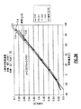
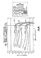
上で示されたように、パワーアンプの性能の1つの局面はリニアリティである。リニアリティ性能の測定値には、隣接チャンネル電力比(ACPR1)および代替チャンネル電力比(ACPR2)のようなチャンネル電力比、ならびに/または、隣接チャンネル漏洩電力比(ACLR1)および代替チャンネル漏洩電力比率(ACLR2)のようなチャンネル漏洩電力比が含まれ得る。ACPR2およびACLR2は、第2のチャンネルリニアリティ測定値と称され得る。ACPR2およびACLR2の値は、対象の周波数からの約1.98MHzのオフセットでの測定値に対応し得る。 As shown above, one aspect of power amplifier performance is linearity. Linearity performance measurements include channel power ratios such as adjacent channel power ratio (ACPR1) and alternative channel power ratio (ACPR2), and / or adjacent channel leakage power ratio (ACLR1) and alternative channel leakage power ratio (ACLR2). ) May include channel leakage power ratios. ACPR2 and ACLR2 can be referred to as second channel linearity measurements. The ACPR2 and ACLR2 values may correspond to measurements at an offset of approximately 1.98 MHz from the frequency of interest.
従来、文献におけるほとんどの刊行物は、ACPR1およびACLR1リニアリティの測定値に注目しており、ACRP2またはACLR2に関してほとんど何も発表されていない。特にRFゲインに関係する他のシステム仕様を満足させつつ、産業からの最近のACPR2およびACLR2のシステム仕様を満足させるのは特に難しい。したがって、パワーアンプシステムのような、バイポーラトランジスタを含むシステムにおけるリニアリティの改善について必要性が存在する。 Traditionally, most publications in the literature have focused on measurements of ACPR1 and ACLR1 linearity, with little publication regarding ACRP2 or ACLR2. It is particularly difficult to satisfy the recent ACPR2 and ACLR2 system specifications from industry, while satisfying other system specifications specifically related to RF gain. Therefore, there is a need for improved linearity in systems that include bipolar transistors, such as power amplifier systems.
本開示のさらに別の局面は、パワーアンプのためのデュアルモードデジタル制御インターフェイスに関する。 Yet another aspect of the disclosure relates to a dual mode digital control interface for a power amplifier.
ワイヤレスデバイスを含む多くの電子デバイスは、フロントエンドコンポーネントによって制御またはセットされる1つ以上のコンポーネントを有し得る。たとえばパワーアンプは、パワーアンプコントローラによってセットまたは構成され得る。いくつかの場合には、パワーアンプコントローラ自体が、デバイスの状態に基づいて、別のインターフェイスコンポーネントによって制御または構成され得る。 Many electronic devices, including wireless devices, may have one or more components controlled or set by front-end components. For example, a power amplifier can be set or configured by a power amplifier controller. In some cases, the power amplifier controller itself may be controlled or configured by another interface component based on the state of the device.
異なる団体によってデバイス内のさまざまなコンポーネントが作り出されることがしばしばある。異なる団体によって設計される場合があるコンポーネント間の相互運用性を促進するために、異なるタイプのデバイスおよびコンポーネントについてしばしば規格が採用される。技術が進歩するにつれて、規格は変化し得るか、または新しい規格が採用され得る。いくつかの場合では、新しい規格は古い規格と互換性をもたない。 Different organizations often create different components within a device. Standards are often adopted for different types of devices and components to promote interoperability between components that may be designed by different bodies. As technology advances, standards can change or new standards can be adopted. In some cases, the new standard is not compatible with the old standard.
本発明のさらに他の局面は、ヘテロ接合バイポーラトランジスタ(HBT)パワーアンプバイアス回路に関する。パワーアンプは典型的に、入力信号を強めて入力信号より有意に大きい出力信号を作り出す能動素子である。多くのタイプのパワーアンプが存在し、パワーアンプを作り出す多くの方法が存在する。たとえば、いくつかのパワーアンプはヘテ
ロ接合バイポーラトランジスタ(HBT)を使用して作り出され得る。多くのHBTパワーアンプは、ダイオードスタックバイアス構成を使用する。このようないくつかの構成では、ダイオードスタックバイアス構成は、アンプの実質的な零入力電流の変化につながり得るデバイスベータ(device beta)に対する感度を示す。さらに、零入力電流の変化は
、性能パラメータに影響を与え得、製品歩留りを低下させ得る。
Yet another aspect of the invention relates to a heterojunction bipolar transistor (HBT) power amplifier bias circuit. A power amplifier is typically an active element that intensifies the input signal to produce an output signal that is significantly larger than the input signal. There are many types of power amplifiers, and there are many ways to create power amplifiers. For example, some power amplifiers can be made using heterojunction bipolar transistors (HBTs). Many HBT power amplifiers use a diode stack bias configuration. In some such configurations, the diode stack bias configuration exhibits sensitivity to device beta, which can lead to a substantial zero input current change in the amplifier. In addition, changes in zero input current can affect performance parameters and reduce product yield.
本発明のさらなる局面は、いくつかの半導体材料システムでは、単一の半導体ダイ上で異なるデバイス技術を組み合わせてハイブリッド構造を形成することが可能であるという理解に関する。たとえば、ある材料システムでは、単一の基板上でヘテロ接合バイポーラトランジスタ(HBT)を電界効果トランジスタ(FET)と集積することが可能であり、これにより、BiFETと呼ばれるものが作製される。RFパワーアンプのようなデバイスは、設計の柔軟性を向上するようBiFET技術を使用して作製され得る。結果として、HBTおよびFETを含むBiFETパワーアンプには、バイポーラトランジスタパワーアンプより低い基準電圧で動作するよう設計されるという利点がある。デバイス製造業者にとって特に関心のあることに、砒化ガリウム(GaAs)HBTプロセスにFETを集積することにより形成され得るハイパワーBiFETアンプがある。しかしながら、GaAsHBTプロセスにFETを集積する以前の試みで得られたのは、n型FETデバイスのみであった。 A further aspect of the invention relates to the understanding that in some semiconductor material systems it is possible to combine different device technologies on a single semiconductor die to form a hybrid structure. For example, in some material systems, heterojunction bipolar transistors (HBTs) can be integrated with field effect transistors (FETs) on a single substrate, creating what is called a BiFET. Devices such as RF power amplifiers can be made using BiFET technology to increase design flexibility. As a result, BiFET power amplifiers, including HBTs and FETs, have the advantage of being designed to operate at lower reference voltages than bipolar transistor power amplifiers. Of particular interest to device manufacturers are high power BiFET amplifiers that can be formed by integrating FETs in a gallium arsenide (GaAs) HBT process. However, only n-type FET devices have been obtained in previous attempts to integrate FETs in the GaAsHBT process.
したがって、p型FETデバイスを含み、相補的なn型およびp型FETデバイスを含んでもよいBiFETデバイス構造を得ることが望ましい。 Therefore, it is desirable to obtain a BiFET device structure that includes a p-type FET device and may include complementary n-type and p-type FET devices.
また、本願明細書において開示される改善された技術のさらに他の局面は、信号の高調波成分の終端に関する。無線周波数(RF)用途のような相対的に高周波数用途では、望まれない信号反射および/またはノイズが発生し得る。このような望まれない信号反射および/またはノイズは、信号の基本周波数および/または信号の基本周波数の高調波のような他の周波数で発生し得る。信号反射および/またはノイズの影響を低減するために、インピーダンス整合が実施され得る。望まれない信号反射および/またはノイズを最小限にすることが有利である1つの例示的な用途は、パワーアンプシステムである。 Yet another aspect of the improved technique disclosed herein relates to the termination of harmonic components of a signal. In relatively high frequency applications such as radio frequency (RF) applications, unwanted signal reflections and / or noise can occur. Such unwanted signal reflections and / or noise can occur at other frequencies, such as the fundamental frequency of the signal and / or the harmonics of the fundamental frequency of the signal. Impedance matching can be performed to reduce the effects of signal reflection and / or noise. One exemplary application in which it is advantageous to minimize unwanted signal reflections and / or noise is a power amplifier system.
電力付加効率(PAE)は、パワーアンプを評価するための1つの測定基準である。さらにリニアリティは、パワーアンプを評価するための別の測定基準である。PAEおよび/またはリニアリティは、相手先商標製造会社(original equipment manufacturer(O
EM))のような顧客がどのパワーアンプを購入するべきかを決める測定基準になり得る。たとえば、あるレベルより下のPAEを有するパワーアンプは、当該顧客の製品へのPAEの影響により、顧客によって購入されない場合がある。PAEが低ければ、たとえば携帯電話のような電子デバイスの電池寿命を低減することになり得る。しかしながら、PAEの向上は、リニアリティに悪影響を与えることの代償として得られ得る。同様に、リニアリティを改善すると、PAEの減少が引き起され得る。同時に、顧客は高いリニアリティとおよび高いPAEとを有するパワーアンプを望む。
Power added efficiency (PAE) is one metric for evaluating power amplifiers. In addition, linearity is another metric for evaluating power amplifiers. PAE and / or linearity is an original equipment manufacturer (O).
It can be a metric for customers like EM)) to decide which power amplifier to buy. For example, a power amplifier having a PAE below a certain level may not be purchased by the customer due to the influence of the PAE on the customer's product. A low PAE can reduce the battery life of electronic devices such as mobile phones. However, an improvement in PAE can be obtained at the cost of adversely affecting linearity. Similarly, improving linearity can cause a decrease in PAE. At the same time, customers want a power amplifier with high linearity and high PAE.
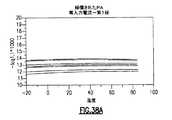
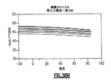
パワーアンプの出力での負荷線は、PAEおよびリニアリティの両方に影響を与え得る。いくつかの従来のパワーアンプシステムは、パワーアンプ出力信号の基本周波数でのパワーアンプ出力のインピーダンスを整合し、さらに高調波終端を行なうよう負荷線を含んでいる。しかしながら、PAEおよびリニアリティの両方を最適化する態様で高調波の終端を含みつつ、パワーアンプ出力の基本周波数のインピーダンスを整合することは困難であると判明している。したがって、パワーアンプのリニアリティおよびPAEの両方を改善する必要性が存在する。 The load line at the output of the power amplifier can affect both PAE and linearity. Some conventional power amplifier systems include load lines to match the impedance of the power amplifier output at the fundamental frequency of the power amplifier output signal and to perform harmonic termination. However, it has proved difficult to match the impedance of the fundamental frequency of the power amplifier output while including the termination of the harmonics in a manner that optimizes both PAE and linearity. Therefore, there is a need to improve both the linearity and PAE of the power amplifier.
ここで、本発明のさらに別の局面は、高性能無線周波数用途のための送信線に関する。
送信線は、たとえばパッケージング基板またはプリント回路基板(PCB)上といった、さまざまな文脈において実現され得る。多層ラミネートPCBまたはパッケージ基板は、無線周波数(RF)用途において広範囲に使用される。
Here, yet another aspect of the present invention relates to transmission lines for high performance radio frequency applications.
Transmission lines can be implemented in a variety of contexts, such as on a packaging board or printed circuit board (PCB). Multilayer laminated PCBs or packaged substrates are widely used in radio frequency (RF) applications.
パワーアンプ、低ノイズアンプ(LNA)、ミキサー、電圧制御発振器(VCO)、フィルタ、スイッチおよび全体のトランシーバといったRF回路は、半導体技術を使用して実現されている。しかしながら、RFモジュール(たとえばパワーアンプ、スイッチおよび/またはフィルタを含むRFフロントエンドモジュール)では、異なる半導体技術で異なるブロックが実現されるため、単一チップ集積化は実際的ではない場合がある。たとえばパワーアンプは、GaAsプロセスによって形成され得る一方、関連する制御および/またはバイアス回路網はCMOSプロセスによって形成され得る。 RF circuits such as power amplifiers, low noise amplifiers (LNAs), mixers, voltage controlled oscillators (VCOs), filters, switches and overall transceivers are implemented using semiconductor technology. However, in RF modules (eg RF front-end modules including power amplifiers, switches and / or filters), single chip integration may not be practical because different blocks are realized with different semiconductor technologies. For example, a power amplifier can be formed by a GaAs process, while the associated control and / or bias network can be formed by a CMOS process.
長い送信線および/または他のオンチップ受動素子が大きなチップエリアを使用し得る。その結果、マルチチップモジュール(MCM)および/またはシステムインパッケージ(SiP)アセンブリ技術が用いられ得、RFモジュールにおいて低コスト、小さいサイズおよび/または高性能を達成する。ラミネート技術は、送信線がラミネート基板上で実現されるMCMアセンブリのために使用され得る。このような送信線における導体損失は、MCMにおける要素のいずれの性能にも有意な影響を及ぼし得る。したがって、ラミネートめっき技術は、RF性能に著しく影響を与え得る。 Long transmission lines and / or other on-chip passive elements can use a large chip area. As a result, multi-chip module (MCM) and / or system-in-package (SiP) assembly techniques can be used to achieve low cost, small size and / or high performance in RF modules. Laminating techniques can be used for MCM assemblies where transmission lines are realized on a laminated substrate. Conductor loss in such transmission lines can have a significant effect on the performance of any of the elements in MCM. Therefore, laminating plating techniques can significantly affect RF performance.
ラミネート技術のコストは、性能および/またはアセンブリの必要性について選択材料によって決定され得る。送信線にRF回路素子を接続するために金(Au)ワイヤーボンディングを使用するRF SiPは、(たとえばAuがより厚いので)より損失が低くよ
り高価なNiAuまたはより損失が高くあまり高価でないNiPdAuといった、さまざまな異なる仕上げめっきを使用し得る。したがって、RF送信線のためのコスト効率の良い高性能技術について必要性が存在する。
The cost of laminating technology can be determined by the material of choice in terms of performance and / or assembly needs. RF SiPs that use gold (Au) wire bonding to connect RF circuit elements to the transmit line are less lossy and more expensive NiAu (because Au is thicker, for example) or more lossy and less expensive NiPdAu. , A variety of different finish platings can be used. Therefore, there is a need for cost-effective and high performance technology for RF transmit lines.
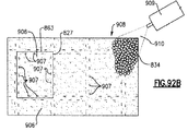
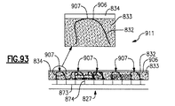
さらに別の局面は、窒化タンタルで終端されるウェハ貫通ビアのための装置および方法に関する。ある実現例では、窒化タンタル(TaN)終端層が砒化ガリウム(GaAs)ウェハの第1の側または表側上に形成され、金の導電層がTaN終端層の上に形成される。その後、ウェハ貫通ビアが、GaAsウェハの第2の側または裏側へとエッチングされ、GaAsウェハおよびTaN終端層の第1または内側部分を貫通するよう延在して金の導電層に達する。ある実現例では、ウェハ貫通ビアは、ニッケルバナジウム(NiV)バリア層、金のシード層および銅層でめっきされる。ウェハ貫通ビアの形成の間、TaN終端層の第2の部分または外側部分は、金の導電層と銅層との間の界面を取り囲みGaAsウェハへの銅の拡散を抑制するように維持および構成される。 Yet another aspect relates to equipment and methods for wafer penetration vias terminated with tantalum nitride. In one embodiment, a tantalum nitride (TaN) termination layer is formed on the first or front side of a gallium arsenide (GaAs) wafer, and a conductive layer of gold is formed on top of the TaN termination layer. The wafer penetrating vias are then etched to the second or back side of the GaAs wafer and extend through the first or inner portion of the GaAs wafer and the TaN termination layer to reach the gold conductive layer. In one embodiment, the wafer penetration vias are plated with a nickel vanadium (NiV) barrier layer, a gold seed layer and a copper layer. During the formation of the through-wafer vias, the second or outer portion of the TaN termination layer surrounds the interface between the gold conductive layer and the copper layer and is maintained and configured to prevent the diffusion of copper into the GaAs wafer. Will be done.
TaNで終端されるウェハ貫通ビアは、窒化珪素の終端とスパッタリングされたバリア層とを使用するスキームと比較して、金属接着の改善および銅マイグレーションの低減を提供することができる。更に、ウェハ貫通ビアを終端するのにTaN終端層を使用するある実現例では、作製を変更することなく、または、GaAsウェハの表側上に形成されるトランジスタ構造に関連付けられるリソグラフィマスクを変更することなく、ウェハ貫通ビアの場所または位置が移動されることが可能になり得る。トランジスタに関連付けられるリソグラフィマスクを変更することなくウェハ貫通ビアを移動可能に構成することにより、設計の柔軟性が高められ得、ならびに/または、ウェハ貫通ビアを含む集積回路の設計の増加する修正もしくはテープアウトに関連付けられる時間およびコストが低減され得る。 Wafer penetration vias terminated with TaN can provide improved metal adhesion and reduced copper migration compared to schemes that use silicon nitride termination and a sputtered barrier layer. In addition, in one embodiment where a TaN termination layer is used to terminate the wafer penetration vias, the fabrication is unchanged or the lithography mask associated with the transistor structure formed on the front side of the GaAs wafer is modified. Instead, it may be possible to move the location or position of the wafer penetration vias. By configuring the wafer penetration vias to be movable without changing the lithography mask associated with the transistor, design flexibility can be increased and / or an increasing modification or modification of the design of the integrated circuit containing the wafer penetration vias. The time and cost associated with tape-out can be reduced.
上記に加えて、本開示のさらに別の局面は、パッケージ半導体構造に関し、より特定的には、無線周波数(RF)アイソレーションおよび/または電磁放射を提供する構造に関
する。
In addition to the above, yet another aspect of the present disclosure relates to packaged semiconductor structures, and more specifically to structures that provide radio frequency (RF) isolation and / or electromagnetic radiation.
パッケージ半導体コンポーネントは、パッケージ内に集積シールド技術を含み得る。「ファラデー遮蔽」と称され得るシールドを形成するために、上部導電層がビアによって底部導電層に電気的に接続され得る。たとえば、底部導電層は、接地平面であり得、ビアは上部導電層を接地に接続し得る。ビアは、上部導電層と底部導電層との間の電気的接続を提供し得るとともに、それ自体、シールドの一部として機能し得る。しかしながら、ビアは当該パッケージにおいて有意な量の面積を使用し得る。同時に、ビアはシールドの接地接続の強さに影響を与え得る。 Packaged semiconductor components may include integrated shielding technology within the package. The top conductive layer can be electrically connected to the bottom conductive layer by vias to form a shield that can be referred to as a "Faraday shield". For example, the bottom conductive layer can be a ground plane and the vias can connect the top conductive layer to ground. The vias can provide an electrical connection between the top conductive layer and the bottom conductive layer and can also function as part of the shield itself. However, vias can use a significant amount of area in the package. At the same time, vias can affect the strength of the shield's ground connection.
上記に加えてさらに、この発明の付加的な局面は、半導体デバイスパッケージに関し、より特定的には、半導体デバイスのための電磁および/または無線干渉シールドに関する。 In addition to the above, an additional aspect of the invention relates to semiconductor device packages, and more specifically to electromagnetic and / or radio interference shields for semiconductor devices.
適切なデバイス性能を維持するために、無線周波数(RF)通信システムにおいて、他のRFデバイスによって生成される電磁(無線周波数)干渉(EMI)からRFデバイスを隔離する一般的な必要性が存在する。同様に、RFデバイスは一般に、環境から受けるまたは環境に送られる電磁干渉から隔離される必要がある。 In order to maintain proper device performance, there is a general need in radio frequency (RF) communication systems to isolate RF devices from electromagnetic (radio frequency) interference (EMI) generated by other RF devices. .. Similarly, RF devices generally need to be isolated from electromagnetic interference received or sent from the environment.
このような電磁干渉からRFデバイスを隔離する従来の方法は、典型的に「缶」と称される接地された金属筐体でRFデバイスを覆うことである。しかしながら、このソリューションは高価であり、設計の柔軟性を欠く。さらに、金属缶はプリント回路基板上のデバイス実装面積に有意なサイズを加え得、さらにプリント回路基板に重量を加え得る。 A conventional method of isolating an RF device from such electromagnetic interference is to cover the RF device with a grounded metal enclosure, typically referred to as a "can." However, this solution is expensive and lacks design flexibility. In addition, the metal can can add significant size to the device mounting area on the printed circuit board and can add weight to the printed circuit board.
本願明細書のさまざまな以下のセクションにおいてさらに詳細に記載される機能、属性または特性の1つ以上を実現することによって、パワーアンプシステムにおいて望ましいリニアリティおよびPAEが達成され得る。さらに、以下の開示に記載される1つ以上の機能をパワーアンプシステムにおいて実現することにより、パワーアンプが評価される望ましいFOMおよび/または他の測定基準が達成され得る。本願明細書のいくつかの機能は、例示的な目的のためにパワーアンプモジュールに関して記載されるが、当業者であれば、本願明細書において記載される原理および利点は、パワーアンプダイ、パワーアンプダイとともに使用される基板、パワーアンプを含む無線通信デバイス、および如何なる類似技術における当業者にも明白である任意および全ての他の用途といった、パワーアンプシステムの他の部分に適用することができるということを理解するであろう。 Desirable linearity and PAE can be achieved in a power amplifier system by achieving one or more of the functions, attributes or characteristics described in more detail in the various following sections of the specification. In addition, by implementing one or more of the functions described in the disclosure below in a power amplifier system, the desired FOM and / or other metric on which the power amplifier is evaluated can be achieved. Some functions of the present specification are described with respect to the power amplifier module for exemplary purposes, but those skilled in the art will appreciate the principles and advantages described herein of power amplifier dies, power amplifiers. It can be applied to other parts of the power amplifier system, such as substrates used with dies, wireless communication devices including power amplifiers, and any and all other applications apparent to those skilled in the art in any similar technology. You will understand that.
概要
I.イントロダクション
パワーアンプは、相対的に低い電力を有する無線周波数(RF)信号の電力を増強し得る。その後、増強されたRF信号は、送信機のアンテナを駆動するようなさまざまな目的に使用され得る。
Overview I. Introduction Power amplifiers can enhance the power of radio frequency (RF) signals that have relatively low power. The enhanced RF signal can then be used for a variety of purposes, such as driving a transmitter antenna.
パワーアンプはさまざまなRFワイヤレス通信デバイスにおいて使用され得る。一例として、パワーアンプは送信のためにRF信号を増幅するために携帯電話に含まれ得る。たとえば、グローバルシステム・フォー・モバイルコミュニケーションズ(Global System for Mobile Communications(GSM(登録商標))、符号分割多重アクセス(code division multiple access(CDMA))、および広帯域符号分割多重アクセス(wideband code division multiple access(W−CDMA))システムにおいて見られるような時分割多重アクセス(time division multiple access(TDMA))アーキテクチャを有す
る携帯電話において、パワーアンプは、RF信号を増幅するために使用され得る。
Power amplifiers can be used in a variety of RF wireless communication devices. As an example, a power amplifier can be included in a mobile phone to amplify an RF signal for transmission. For example, Global System for Mobile Communications (GSM®), code division multiple access (CDMA), and wideband code division multiple access (wideband code division multiple access). In mobile phones with a time division multiple access (TDMA) architecture as seen in W-CDMA)) systems, power amplifiers can be used to amplify RF signals.
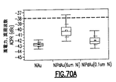
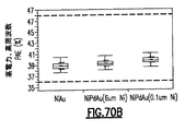
電力付加効率(PAE)は、パワーアンプを評価するための1つの測定基準である。リニアリティは、パワーアンプを評価するための別の測定基準である。PAEおよび/またはリニアリティは、顧客がどのパワーアンプを購入するか決める測定基準であり得る。たとえば、あるレベルより下のPAEを有するパワーアンプは、顧客の製品へのPAEの影響により、顧客によって購入されない場合がある。PAEが低ければ、たとえば携帯電話のようなモバイルデバイスの電池寿命を低減することになり得る。リニアリティはたとえば、隣接チャンネル電力比(ACPR)および/または代替チャンネル電力比(ACPR2)によって測定され得る。高いPAEおよび高いリニアリティを同時に達成するのは困難であり得る。しかしながら、顧客は典型的に高いPAEと高リニアリティとを望む。性能指数(FOM)は、PAEおよびリニアリティの両方を反映し得る1つの測定基準である。 Power added efficiency (PAE) is one metric for evaluating power amplifiers. Linearity is another metric for evaluating power amplifiers. PAE and / or linearity can be a metric that determines which power amplifier a customer buys. For example, a power amplifier with a PAE below a certain level may not be purchased by the customer due to the influence of the PAE on the customer's product. A low PAE can reduce the battery life of mobile devices such as mobile phones. Linearity can be measured, for example, by the adjacent channel power ratio (ACPR) and / or the alternative channel power ratio (ACPR2). Achieving high PAE and high linearity at the same time can be difficult. However, customers typically want high PAE and high linearity. Figure of merit (FOM) is a measure that can reflect both PAE and linearity.
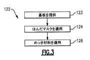
II.ワイヤーボンドパッドシステムおよび関連する方法
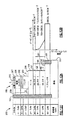
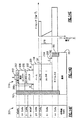
ニッケル/パラジウム/金(Ni/Pd/Au)表面めっき材料をRFIC製品に使用することによってRFICパッケージングのコストを低減するようシステムおよび方法が開示される。コストを低減するために、Ni/Pd/Au表面めっきにおける金層は、Ni/Au表面めっきにおける金層より薄い。しかしながら、Ni/Pd/Auは、パラジウムおよび金層が薄いこととニッケルの強磁性とにより、Ni/Auよりはるかに高い無線周波数シート抵抗を有する。これは、実効電流シート厚さの低減と、RF信号について密集する電流の増加とに寄与し、いくつかの実施形態では、Ni/Pd/Auめっき表面を通って伝わるRF信号についてRF損失が、Ni/Auめっき表面を通って伝わるRF信号について発見されるよりも大きくなる。これらの損失は、製品性能および歩留りに影響を与え得る。
II. Wire Bond Pad Systems and Related Methods Systems and methods are disclosed to reduce the cost of RFIC packaging by using nickel / palladium / gold (Ni / Pd / Au) surface plating materials in RFIC products. In order to reduce the cost, the gold layer in Ni / Pd / Au surface plating is thinner than the gold layer in Ni / Au surface plating. However, Ni / Pd / Au has a much higher radio frequency sheet resistance than Ni / Au due to the thin palladium and gold layers and the ferromagnetic nature of nickel. This contributes to a reduction in the effective current sheet thickness and an increase in the dense current for the RF signal, and in some embodiments the RF loss for the RF signal transmitted through the Ni / Pd / Au plated surface. It will be larger than found for RF signals transmitted through the Ni / Au plated surface. These losses can affect product performance and yield.
RFICのためのより低コストのNi/Pd/Au表面めっきに関連付けられるRF損失を低減するために、さらに別のシステムおよび方法が開示される。設計レイアウトのいくつかの実施形態において、ワイヤーボンディングエリアにおけるRF線/トレース表面、縁部および側壁は、めっき処理に対して開放されており、したがって、Ni/Pd/Au表面仕上げによりめっきされる。めっきされたワイヤーボンディングエリアを通って伝わるRF電流に対する表皮効果および渦電流効果により、RF電流の大部分は、めっきされたワイヤーボンディングエリアのトレース縁部および側壁上を流れている。RF電流の大部分がトレース縁部および側壁上を流れているので、トレース縁部および側壁にめっきすることはRF損失にさらに寄与することになる。RF損失を低減するために、いくつかの実施形態は、はんだマスクを再構成して、トレース縁部および側壁がNi/Pd/Au表面仕上げによってめっきされないようにワイヤーボンディングエリアにおいてトレース縁部および側壁を覆う。ワイヤーボンディングエリアの周りのNi/Pd/Auめっきがない銅トレース縁部および側壁は、Ni/Pd/Auワイヤーボンドパッドの周りにRF電流のための低い抵抗性のパスを提供し、したがって、RFIC基板のNi/Pd/Au表面めっきに関連付けられるRF信号損失を低減する。 Yet another system and method is disclosed to reduce the RF loss associated with lower cost Ni / Pd / Au surface plating for RFIC. In some embodiments of the design layout, the RF line / trace surface, edges and sidewalls in the wire bonding area are open to the plating process and are therefore plated with a Ni / Pd / Au surface finish. Due to the skin and eddy current effects on RF currents transmitted through the plated wire bonding areas, most of the RF currents flow over the trace edges and sidewalls of the plated wire bonding areas. Plating on the trace edges and sidewalls will further contribute to RF loss, as most of the RF current is flowing over the trace edges and sidewalls. To reduce RF loss, some embodiments reconfigure the solder mask so that the trace edges and sidewalls are not plated with the Ni / Pd / Au surface finish in the wire bonding area. Cover. Copper trace edges and sidewalls without Ni / Pd / Au plating around the wire bonding area provide a low resistance path for RF currents around the Ni / Pd / Au wire bonding pad and therefore RFIC. It reduces the RF signal loss associated with the Ni / Pd / Au surface plating of the substrate.
ある実施形態は、無線周波数集積回路(RFIC)モジュールを作製する方法に関し、当該方法は、少なくとも1つの銅トレースを有する基板を提供することを含み、当該銅トレースはワイヤーボンディング面を有する。上記方法はさらに、銅トレースのボンディング面の直上に、ワイヤーボンディングパッドのためのはんだマスク開口部を形成することを含み、当該ワイヤーボンディングパッドは少なくとも1つの縁部および少なくとも1つの側壁を有する。上記方法はさらに、ワイヤーボンディングパッドの少なくとも1つの縁部および少なくとも1つの側壁の直上に、はんだマスクを形成することと、ニッケル/パラジウム/金ワイヤーボンディングパッドを形成するよう、ニッケル層で銅トレースにめっきし、パラジウム層でニッケル層にめっきし、金層でパラジウム層にめっきすることとを含む。ニッケル/パラジウム/金ワイヤーボンディングパッドは、ニッケル層、パラジ
ウム層および金層がない少なくとも1つの縁部および少なくとも1つの側壁を有する。
One embodiment relates to a method of making a radio frequency integrated circuit (RFIC) module, which method comprises providing a substrate having at least one copper trace, the copper trace having a wire bonding surface. The method further comprises forming a solder mask opening for a wire bonding pad just above the bonding surface of the copper trace, the wire bonding pad having at least one edge and at least one side wall. The method further forms a solder mask just above at least one edge and at least one side wall of the wire bonding pad, and a nickel layer on the copper trace to form a nickel / palladium / gold wire bonding pad. This includes plating, plating the nickel layer with a palladium layer, and plating the palladium layer with a gold layer. Nickel / palladium / gold wire bonding pads have at least one edge and at least one side wall without a nickel layer, a palladium layer and a gold layer.
多くの実施形態に従うと、当該開示は、無線周波数集積回路(RFIC)モジュールのためのワイヤーボンディングパッドに関する。ワイヤーボンディングパッドは、銅トレースのワイヤーボンディング面の上にめっきされたニッケル層を含み、銅トレースは、RFICモジュールの基板の上面上に形成される。ワイヤーボンディングパッドはさらに、ニッケル層の上にめっきされたパラジウム層と、パラジウム層の上にめっきされた金層とを含む。ワイヤーボンディングパッドは、ワイヤーボンドエリアと、ワイヤーボンドエリアに隣接している少なくとも1つの縁部と、少なくとも1つの縁部に隣接している少なくとも1つの側壁とを有し、少なくとも1つの縁部および少なくとも1つの側壁にはニッケル層、パラジウム層および金層が存在しない。 According to many embodiments, the disclosure relates to wire bonding pads for radio frequency integrated circuit (RFIC) modules. The wire bonding pad contains a nickel layer plated on the wire bonding surface of the copper trace, and the copper trace is formed on the top surface of the substrate of the RFIC module. The wire bonding pad further includes a palladium layer plated on the nickel layer and a gold layer plated on the palladium layer. The wire bonding pad has a wire bond area, at least one edge adjacent to the wire bond area, and at least one side wall adjacent to at least one edge, with at least one edge and the wire bonding pad. There are no nickel, palladium and gold layers on at least one side wall.
さまざまな実施形態に従うと、無線周波数集積回路(RFIC)モジュールを作製するための装置は、少なくとも1つの銅トレースを有する基板を提供するための手段を含み、銅トレースはワイヤーボンディング面を有し、上記装置はさらに、ワイヤーボンディングパッドのためのはんだマスク開口部を銅トレースのボンディング面の直上に形成するための手段を含み、ワイヤーボンディングパッドは少なくとも1つの縁部および少なくとも1つの側壁を有する。上記装置はさらに、ワイヤーボンディングパッドの少なくとも1つの縁部および少なくとも1つの側壁の直上にはんだマスクを形成するための手段と、ニッケル/パラジウム/金ワイヤーボンディングパッドを形成するよう、ニッケル層で銅トレースにめっきするための手段と、パラジウム層でニッケル層にめっきするための手段と、金層でパラジウム層にめっきするための手段とを含む。ニッケル/パラジウム/金ワイヤーボンディングパッドは、ニッケル層、パラジウム層および金層が存在しない少なくとも1つの縁部および少なくとも1つの側壁を有する。 According to various embodiments, the apparatus for making a radio frequency integrated circuit (RFIC) module includes means for providing a substrate having at least one copper trace, the copper trace having a wire bonding surface. The device further includes means for forming a solder mask opening for the wire bonding pad just above the bonding surface of the copper trace, the wire bonding pad having at least one edge and at least one side wall. The device further comprises a means for forming a solder mask just above at least one edge and at least one side wall of the wire bonding pad and a copper trace with a nickel layer to form a nickel / palladium / gold wire bonding pad. A means for plating a nickel layer with a palladium layer, a means for plating a nickel layer with a gold layer, and a means for plating a palladium layer with a gold layer. Nickel / palladium / gold wire bonding pads have at least one edge and at least one side wall in the absence of a nickel layer, a palladium layer and a gold layer.
開示を要約する目的のために、本発明のある局面、利点および新規な特徴が本願明細書において記載された。必ずしもすべてのこのような利点が本発明の任意の特定の実施形態に従って達成されなくてもよいということが理解されるべきである。したがって本発明は、本願明細書において教示または示唆され得る他の利点を必ずしも達成することなく、本願明細書において教示される1つの利点または利点の群を達成または最適化する態様で実施または実行されてもよい。 For the purposes of summarizing the disclosure, certain aspects, advantages and novel features of the invention are described herein. It should be understood that not all such advantages need not be achieved according to any particular embodiment of the invention. The present invention is therefore implemented or implemented in a manner that achieves or optimizes one benefit or group of benefits taught herein, without necessarily achieving other benefits taught or suggested herein. You may.
III.高RF損失のめっきの影響を低減するための装置および方法
ニッケル/パラジウム/金(Ni/Pd/Au)の表面めっき材料をRFIC製品に使用することによってRFICパッケージングのコストを低減するようシステムおよび方法が開示される。コストを低減するために、Ni/Pd/Au表面めっきにおける金層は、Ni/Au表面めっきにおける金層より薄い。しかしながら、Ni/Pd/Auは、パラジウムおよび金層が薄いこととニッケルの強磁性とにより、Ni/Auよりはるかに高い無線周波数シート抵抗を有する。これは、実効電流シート厚さの低減と、RF信号について密集する電流の増加とに寄与し、いくつかの実施形態では、Ni/Pd/Auめっき表面を通って伝わるRF信号についてRF損失が、Ni/Auめっき表面を通って伝わるRF信号について発見されるよりも大きくなる。これらの損失は、製品性能および歩留りに影響を与え得る。
III. Equipment and methods for reducing the effects of high RF loss plating Systems and systems to reduce the cost of RFIC packaging by using nickel / palladium / gold (Ni / Pd / Au) surface plating materials in RFIC products. The method is disclosed. In order to reduce the cost, the gold layer in Ni / Pd / Au surface plating is thinner than the gold layer in Ni / Au surface plating. However, Ni / Pd / Au has a much higher radio frequency sheet resistance than Ni / Au due to the thin palladium and gold layers and the ferromagnetic nature of nickel. This contributes to a reduction in the effective current sheet thickness and an increase in the dense current for the RF signal, and in some embodiments the RF loss for the RF signal transmitted through the Ni / Pd / Au plated surface. It will be larger than found for RF signals transmitted through the Ni / Au plated surface. These losses can affect product performance and yield.
RFICのためのより低コストのNi/Pd/Au表面めっきに関連付けられるRF損失を低減するために、さらに別のシステムおよび方法が開示される。設計レイアウトのいくつかの実施形態において、ワイヤーボンディングエリアにおけるRF線/トレース表面、縁部および側壁は、めっき処理に対して開放されており、したがって、Ni/Pd/Au表面仕上げによりめっきされる。めっきされたワイヤーボンディングエリアを通って伝わるRF電流に対する表皮効果および渦電流効果により、RF電流の大部分は、めっきさ
れたワイヤーボンディングエリアのトレース縁部および側壁上を流れている。RF電流の大部分がトレース縁部および側壁上を流れているので、トレース縁部および側壁にめっきすることはRF損失にさらに寄与することになる。RF損失を低減するために、いくつかの実施形態は、はんだマスクを再構成して、トレース縁部および側壁がNi/Pd/Au表面仕上げによってめっきされないようにワイヤーボンディングエリアにおいてトレース縁部および側壁を覆う。ワイヤーボンディングエリアの周りのNi/Pd/Auめっきがない銅トレース縁部および側壁は、Ni/Pd/Auワイヤーボンドパッドの周りにRF電流のための低い抵抗性のパスを提供し、したがって、RFIC基板のNi/Pd/Au表面めっきに関連付けられるRF信号損失を低減する。
Yet another system and method is disclosed to reduce the RF loss associated with lower cost Ni / Pd / Au surface plating for RFIC. In some embodiments of the design layout, the RF line / trace surface, edges and sidewalls in the wire bonding area are open to the plating process and are therefore plated with a Ni / Pd / Au surface finish. Due to the skin and eddy current effects on RF currents transmitted through the plated wire bonding areas, most of the RF currents flow over the trace edges and sidewalls of the plated wire bonding areas. Plating on the trace edges and sidewalls will further contribute to RF loss, as most of the RF current is flowing over the trace edges and sidewalls. To reduce RF loss, some embodiments reconfigure the solder mask so that the trace edges and sidewalls are not plated with the Ni / Pd / Au surface finish in the wire bonding area. Cover. Copper trace edges and sidewalls without Ni / Pd / Au plating around the wire bonding area provide a low resistance path for RF currents around the Ni / Pd / Au wire bonding pad and therefore RFIC. It reduces the RF signal loss associated with the Ni / Pd / Au surface plating of the substrate.
さらに、RFICのオンダイキャパシタ、抵抗器、インダクタまたは他の受動デバイスの高いRF損失のボンディングパッドに関連付けられるRF損失を低減するようシステムおよび方法が開示される。いくつかの実施形態において、RFICはオンダイキャパシタ、抵抗器、インダクタまたは他の受動デバイスを含む。キャパシタまたは受動デバイスは、RF電流を伝える銅トレースにボンディングされる。たとえばNi/Pd/Auボンディングパッドのような高いRF損失のボンディングパッドがRFICモジュールの回路トレースに受動デバイスを接続するために使用される場合、高いRF損失のボンディングパッドは、RF電流が当該ボンディングパッドを通って流れる際に、RF信号損失を作り出す。RFICのRF信号出力に対してRF上部トレースにオンダイキャパシタ、抵抗器、インダクタまたは他の受動デバイスを配置することにより、オンダイ受動デバイスのボンディングパッドに関連付けられるRF損失が低減される。 In addition, systems and methods are disclosed to reduce the RF loss associated with high RF loss bonding pads of RFIC on-die capacitors, resistors, inductors or other passive devices. In some embodiments, RFICs include on-die capacitors, resistors, inductors or other passive devices. Capacitors or passive devices are bonded to copper traces that carry RF current. When a high RF loss bonding pad, such as a Ni / Pd / Au bonding pad, is used to connect a passive device to the circuit trace of an RFIC module, the high RF loss bonding pad will have an RF current of that bonding pad. Creates RF signal loss as it flows through. Placing an on-die capacitor, resistor, inductor or other passive device on the RF top trace for the RF signal output of the RFIC reduces the RF loss associated with the bonding pad of the on-die passive device.
ある実施形態において、信号損失を低減するように構成される電子回路モジュールが開示される。当該モジュールは、出力信号と、それに関連付けられる電流とを有する電子回路デバイスを含む。電子回路デバイスは、第1のリードと、第2のリードと、オンダイ(on-die)受動コンポーネントを有する集積回路ダイとを含む。電子回路モジュールは、電流を伝導するためのトレースを含む基板をさらに含む。トレースは、第1のリードに電気的に接続される上部信号パス上の第1のボンディングパッドと、第2のリードに電気的に接続される下部信号パス上の第2のボンディングパッドとを有する。電子回路デバイスは、オンダイ受動コンポーネントが第1のリードに電気的に接続するとともに出力信号が第2のリードに電気的に接続するように構成される。これにより、電流が第1のボンディングパッドから離れるように方向付けされる。ある実施形態において、電子回路モジュールは無線周波数集積回路モジュールであり、信号損失は無線周波数信号損失である。別の実施形態において、電子回路デバイスは無線周波数電子回路デバイスであり、出力信号は無線周波数出力信号であり、電流は無線周波数電流である。 In certain embodiments, electronic circuit modules configured to reduce signal loss are disclosed. The module includes an electronic circuit device having an output signal and an associated current. Electronic circuit devices include a first lead, a second lead, and an integrated circuit die with on-die passive components. The electronic circuit module further includes a substrate containing traces for conducting current. The trace has a first bonding pad on the upper signal path that is electrically connected to the first lead and a second bonding pad on the lower signal path that is electrically connected to the second lead. .. The electronic circuit device is configured such that the on-die passive component is electrically connected to the first lead and the output signal is electrically connected to the second lead. This directs the current away from the first bonding pad. In certain embodiments, the electronic circuit module is a radio frequency integrated circuit module and the signal loss is the radio frequency signal loss. In another embodiment, the electronic circuit device is a radio frequency electronic circuit device, the output signal is a radio frequency output signal, and the current is a radio frequency current.
多くの実施形態に従うと、電子回路デバイスは信号損失を低減するように構成される。当該デバイスは、オンダイ受動コンポーネントを有する集積回路ダイと、関連付けられる電流を有する出力信号と、基板上のトレースの上部信号パス上に配置される第1のボンディングパッドに電気的に接続される第1のリードと、トレース上の下部信号パスに配置される第2のボンディングパッドに電気的に接続される第2のリードとを含む。電子回路デバイスは、オンダイ受動コンポーネントが第1のリードに電気的に接続するとともに出力信号が第2のリードに電気的に接続するように構成される。これにより、電流が第1のボンディングパッドから離れるように方向付けされる。 According to many embodiments, electronic circuit devices are configured to reduce signal loss. The device is electrically connected to an integrated circuit die with on-die passive components, an output signal with associated current, and a first bonding pad located on the top signal path of the trace on the substrate. Leads and a second lead that is electrically connected to a second bonding pad located in the lower signal path on the trace. The electronic circuit device is configured such that the on-die passive component is electrically connected to the first lead and the output signal is electrically connected to the second lead. This directs the current away from the first bonding pad.
さまざまな実施形態に従って、電子回路モジュールにおいて信号損失を低減するための方法が開示される。上記方法は、オンダイ受動コンポーネントを有する集積回路ダイを含む電子回路デバイスを作製することと、電子回路デバイスからの出力信号を生成することとを含む。出力信号は、関連付けられる電流を有する。上記方法はさらに、電子回路デバイス上に第1のリードおよび第2のリードを形成することと、基板上に第1のボンディン
グパッドおよび第2のボンディングパッドを形成することと、第1のボンディングパッドと第2のボンディングパッドとの間で電流を伝導する導電パスを提供するよう基板上にトレースを形成することとを含む。トレースは、第1のボンディングパッドに関連付けられる上部信号パスと、第2のボンディングパッドに関連付けられる下部信号パスとを有する。上記方法はさらに、第1のボンディングパッドに第1のリードを電気的に接続することと、第2のボンディングパッドに第2のリードを電気的に接続することと、オンダイ受動コンポーネントが第1のリードに電気的に接続するとともに出力信号が第2のリードに電気的に接続するように電子回路デバイスを構成することとを含む。これにより、電流が第1のボンディングパッドから離れるように方向付けされる。
According to various embodiments, methods for reducing signal loss in electronic circuit modules are disclosed. The method comprises making an electronic circuit device that includes an integrated circuit die with on-die passive components and generating an output signal from the electronic circuit device. The output signal has an associated current. The method further comprises forming a first lead and a second lead on an electronic circuit device, forming a first bonding pad and a second bonding pad on a substrate, and a first bonding pad. Includes forming a trace on the substrate to provide a conductive path that conducts current between the and the second bonding pad. The trace has an upper signal path associated with the first bonding pad and a lower signal path associated with the second bonding pad. The method further comprises electrically connecting the first lead to the first bonding pad, electrically connecting the second lead to the second bonding pad, and having the on-die passive component first. This includes configuring the electronic circuit device so that it is electrically connected to the lead and the output signal is electrically connected to the second lead. This directs the current away from the first bonding pad.
ある実施形態において、電子回路モジュールにおける信号損失を低減するための装置が開示される。上記装置は、オンダイ受動コンポーネントを有する集積回路ダイを含む電子回路デバイスを作製するための手段と、電子回路デバイスからの出力信号を生成するための手段とを含む。出力信号は、関連付けられる電流を有する。上記装置はさらに、電子回路デバイス上に第1のリードおよび第2のリードを形成するための手段と、基板上に第1のボンディングパッドおよび第2のボンディングパッドを形成するための手段と、第1のボンディングパッドと第2のボンディングパッドとの間で電流を伝導する導電パスを提供するよう、基板上にトレースを形成するための手段とを含む。トレースは、第1のボンディングパッドに関連付けられる上部信号パスと、第2のボンディングパッドに関連付けられる下部信号パスとを有する。上記装置はさらに、第1のボンディングパッドに第1のリードを電気的に接続するための手段と、第2のボンディングパッドに第2のリードを電気的に接続するための手段と、オンダイ受動コンポーネントが第1のリードに電気的に接続するとともに出力信号が第2のリードに電気的に接続するように電子回路デバイスを構成するための手段とを含む。これにより、電流が第1のボンディングパッドから離れるように方向付けされる。 In certain embodiments, devices for reducing signal loss in electronic circuit modules are disclosed. The device includes means for making an electronic circuit device including an integrated circuit die with on-die passive components and means for generating an output signal from the electronic circuit device. The output signal has an associated current. The device further comprises a means for forming a first lead and a second lead on an electronic circuit device, a means for forming a first bonding pad and a second bonding pad on a substrate, and a first. Includes means for forming traces on the substrate to provide a conductive path that conducts current between the first bonding pad and the second bonding pad. The trace has an upper signal path associated with the first bonding pad and a lower signal path associated with the second bonding pad. The device further comprises means for electrically connecting the first lead to the first bonding pad, means for electrically connecting the second lead to the second bonding pad, and an on-die passive component. Includes means for configuring the electronic circuit device such that the output signal is electrically connected to the first lead and the output signal is electrically connected to the second lead. This directs the current away from the first bonding pad.
開示を要約する目的のために、本発明のある局面、利点および新規な特徴が本願明細書において記載された。必ずしもすべてのこのような利点が本発明の任意の特定の実施形態に従って達成されなくてもよいということが理解されるべきである。したがって本発明は、本願明細書において教示または示唆され得る他の利点を必ずしも達成することなく、本願明細書において教示される1つの利点または利点の群を達成または最適化する態様で実施または実行されてもよい。 For the purposes of summarizing the disclosure, certain aspects, advantages and novel features of the invention are described herein. It should be understood that not all such advantages need not be achieved according to any particular embodiment of the invention. The present invention is therefore implemented or implemented in a manner that achieves or optimizes one benefit or group of benefits taught herein, without necessarily achieving other benefits taught or suggested herein. You may.
IV.勾配を有するコレクタを有するバイポーラトランジスタ
請求項に記載されるイノベーションは各々いくつかの局面を有し、当該局面のいずれもその望ましい属性について単独で原因となることはない。この発明の範囲を限定することなく、いくつかの顕著な特徴がここで簡潔に議論される。
IV. Bipolar Transistors with Gradient Collectors Each of the innovations described in the claims has several aspects, none of which is solely responsible for its desired attributes. Without limiting the scope of the invention, some salient features are briefly discussed here.
この開示の1つの局面は、コレクタ、コレクタの上に配置されるベースおよびエミッタを含むバイポーラトランジスタである。コレクタは、ベースに当接する第1のコレクタ領域において、少なくとも約3×1016cm−3のドーピング濃度を有する。コレクタはさらに、第1のコレクタ領域の下に他のコレクタ領域を有する。当該他のコレクタ領域は、ドーピング濃度が第1のコレクタ領域から離れるにつれて増加する少なくとも1つの勾配を含む。 One aspect of this disclosure is a collector, a bipolar transistor containing a base and an emitter located on top of the collector. The collector has a doping concentration of at least about 3 × 1016 cm-3 in the first collector region abutting the base. The collector further has another collector area below the first collector area. The other collector region includes at least one gradient in which the doping concentration increases as it moves away from the first collector region.
ある実施形態において、他のコレクタ領域は、第1の勾配と、第1の勾配においてとは異なった割合でドーピング濃度がベースから離れるにつれて増加する第2の勾配とを含む。これらの実施形態のうちのいくつかに従うと、バイポーラトランジスタは、約833MHzを中心とする周波数帯内の周波数で少なくとも約29dBmのゲインを有し得る。多くの実施形態に従うと、バイポーラトランジスタの第2の勾配は、同じ電流密度で、第2
の勾配のない同じトランジスタと比較して、バイポーラトランジスタのBvCEXを増加するように構成され得る。さまざまな実施形態において、第1の勾配におけるドーピング濃度は、第1のコレクタ領域のドーピング濃度より約1桁小さいドーピング濃度から第1のコレクタ領域のドーピング濃度未満までの勾配がある。これらの実施形態のうちのいくつかに従うと、第2の勾配におけるドーピング濃度は、第1の勾配におけるほぼ最大のドーピング濃度から第2の勾配の下のサブコレクタのドーピング濃度よりも少なくとも約1桁小さいドーピング濃度までの勾配がある。いくつかの実施形態において、第1の勾配は、第1のコレクタ領域に隣接するとともに第1のコレクタ領域の厚さの約2倍より大きい厚さを有する第2のコレクタ領域にわたる。ある実施形態に従うと、第2の勾配は、第1のコレクタ領域の厚さより大きく第2のコレクタ領域の厚さより小さい厚さを有する第3のコレクタ領域にわたる。さまざまな実施形態において、コレクタは本質的に、第1のコレクタ領域、第2のコレクタ領域および第3のコレクタ領域からなる。いくつかの実施形態に従うと、バイポーラトランジスタはさらに、コレクタの下にサブコレクタを含む。ある実施形態に従うと、第1の勾配は第2の勾配と境界を接しており、ドーピング濃度は、第1の勾配と第2の勾配との境界の両側上でほぼ同じである。
In some embodiments, the other collector region comprises a first gradient and a second gradient that increases as the doping concentration moves away from the base at a different rate than in the first gradient. According to some of these embodiments, the bipolar transistor may have a gain of at least about 29 dBm at frequencies within the frequency band centered around about 833 MHz. According to many embodiments, the second gradient of the bipolar transistor is the second with the same current density.
It may be configured to increase the BvCEX of the bipolar transistor as compared to the same transistor with no gradient. In various embodiments, the doping concentration in the first gradient ranges from a doping concentration about an order of magnitude less than the doping concentration in the first collector region to less than the doping concentration in the first collector region. According to some of these embodiments, the doping concentration in the second gradient is at least about an order of magnitude greater than the doping concentration of the subcollector below the second gradient from the nearly maximum doping concentration in the first gradient. There is a gradient to a small doping concentration. In some embodiments, the first gradient spans a second collector region that is adjacent to the first collector region and has a thickness greater than about twice the thickness of the first collector region. According to certain embodiments, the second gradient extends over a third collector region having a thickness greater than the thickness of the first collector region and less than the thickness of the second collector region. In various embodiments, the collector essentially comprises a first collector region, a second collector region and a third collector region. According to some embodiments, the bipolar transistor further includes a sub-collector under the collector. According to certain embodiments, the first gradient borders the second gradient and the doping concentration is approximately the same on both sides of the boundary between the first gradient and the second gradient.
ある実施形態において、第1のコレクタ領域の厚さは約1000Å〜2000Åの範囲から選択される。これらの実施形態のうちのいくつかに従うと、第1のコレクタ領域のドーピング濃度は、約3×1016cm−3〜9×1016cm−3の範囲から選択される。 In certain embodiments, the thickness of the first collector region is selected from the range of about 1000 Å to 2000 Å. According to some of these embodiments, the doping concentration of the first collector region is selected from the range of about 3 × 10 16 cm -3 to 9 × 10 16 cm -3.
多くの実施形態に従うと、第1のコレクタ領域のドーピング濃度は、少なくとも約6×1016cm−3である。 According to many embodiments, the doping concentration of the first collector region is at least about 6 × 10 16 cm -3 .
いくつかの実施形態に従うと、ベースは約1400Å未満の厚さを有する。これらの実施形態のうちのいくつかにおいて、ベースは、約3.5×1019cm−3〜7×1019cm−3の範囲から選択されるドーピング濃度を有する。
According to some embodiments, the base has a thickness of less than about 1400 Å. In some of these embodiments, the base has a doping concentration selected from the range of about 3.5 × 10 19
多くの実施形態において、バイポーラトランジスタはヘテロ接合バイポーラトランジスタ(HBT)である。 In many embodiments, the bipolar transistor is a heterojunction bipolar transistor (HBT).
いくつかの実施形態によれば、バイポーラトランジスタはGaAsトランジスタである。 According to some embodiments, the bipolar transistor is a GaAs transistor.
この開示の別の局面はバイポーラトランジスタを含むパワーアンプモジュールである。バイポーラトランジスタはコレクタ、ベースおよびエミッタを有する。ベースとの接合部でのコレクタのドーピング濃度は、パワーアンプが約65dBc以下の代替チャンネル電力比(ACPR2)を有するようなドーピング濃度である。さらに、コレクタは少なくとも、ドーピング濃度がベースから離れるにつれて増加する第1の勾配を有する。 Another aspect of this disclosure is a power amplifier module that includes a bipolar transistor. Bipolar transistors have collectors, bases and emitters. The doping concentration of the collector at the junction with the base is such that the power amplifier has an alternative channel power ratio (ACPR2) of about 65 dBc or less. In addition, the collector has at least a first gradient that increases as the doping concentration moves away from the base.
ある実施形態に従うと、ACPR2は、約833MHzを中心にする周波数帯内でパワーアンプが動作する場合、約65dBc以下である。 According to certain embodiments, ACPR2 is about 65 dBc or less when the power amplifier operates in a frequency band centered around about 833 MHz.
多くの実施形態において、コレクタはさらに、第1の勾配よりベースから離れた第2の勾配を含む。いくつかの実施形態に従うと、第2の勾配は、同じ電流密度で、第2の勾配のない同じトランジスタと比較してバイポーラトランジスタのBvCEXを増加するように構成される。 In many embodiments, the collector further includes a second gradient that is further away from the base than the first gradient. According to some embodiments, the second gradient is configured to increase the BvCEX of the bipolar transistor at the same current density as compared to the same transistor without the second gradient.
多くの実施形態に従うと、ベースとの接合部でのコレクタにおけるドーピング濃度は、少なくとも約3×1016cm−3である。 According to many embodiments, the doping concentration in the collector at the junction with the base is at least about 3 × 10 16 cm -3 .
ある実施形態において、コレクタは、ベースに当接し、少なくとも約3×1016cm−3の実質的に平坦なドーピング濃度と約1000Å〜2000Åの範囲から選択される厚さとを有する第1の領域を含む。これらの実施形態のうちのいくつかに従うと、コレクタの第1の領域におけるドーピング濃度は、約3×1016cm−3〜9×1016cm−3の範囲において選択される。 In certain embodiments, the collector abuts a first region with a substantially flat doping concentration of at least about 3 × 10 16 cm -3 and a thickness selected from the range of about 1000 Å to 2000 Å. include. According to some of these embodiments, the doping concentration in the first region of the collector is selected in the range of about 3 × 10 16 cm -3 to 9 × 10 16 cm -3.
この開示のさらなる局面は、コレクタ、コレクタに当接するベースおよびエミッタを有するバイポーラトランジスタを含むパワーアンプダイである。コレクタは、ベースとの接合部において、少なくとも約3×1016cm−3のドーピング濃度を有する。さらに、コレクタは少なくとも、ドーピング濃度がベースから離れるにつれて増加する第1の勾配を有する。 A further aspect of this disclosure is a power amplifier die comprising a collector, a bipolar transistor having a base and an emitter abutting on the collector. The collector has a doping concentration of at least about 3 × 10 16 cm -3 at the junction with the base. In addition, the collector has at least a first gradient that increases as the doping concentration moves away from the base.
この開示の別の局面は、アンテナ、電池およびパワーアンプを含むモバイルデバイスである。パワーアンプは、コレクタ、ベースおよびエミッタを有するヘテロ接合バイポーラトランジスタを含む。コレクタは、ベースに当接し、少なくとも約3×1016cm−3の第1のドーピング濃度を有する第1のコレクタ領域を含む。コレクタはさらに、第1のコレクタ領域に隣接し、ドーピング濃度がベースから離れるにつれて増加する第1の勾配を有する第2のコレクタ領域を含む。コレクタはさらに、第2のコレクタ領域に隣接し、ドーピング濃度が第1の勾配とは異なる割合でベースから離れるにつれて増加する第2の勾配を有する第3のコレクタ領域を含む。第1のドーピング濃度、第1の勾配および第2の勾配は、パワーアンプのリニアリティを改善するように構成される。 Another aspect of this disclosure is mobile devices, including antennas, batteries and power amplifiers. The power amplifier includes a heterojunction bipolar transistor having a collector, a base and an emitter. The collector includes a first collector region that is in contact with the base and has a first doping concentration of at least about 3 × 10 16 cm -3. The collector further comprises a second collector region that is adjacent to the first collector region and has a first gradient that increases as the doping concentration moves away from the base. The collector further comprises a third collector region adjacent to the second collector region and having a second gradient in which the doping concentration increases away from the base at a different rate than the first gradient. The first doping concentration, the first gradient and the second gradient are configured to improve the linearity of the power amplifier.
この開示のさらに別の局面はバイポーラトランジスタを形成する方法である。当該方法は、サブコレクタを形成することと、サブコレクタから離れるにつれて減少するドーピング濃度を有する少なくとも1つの勾配を有するコレクタ領域を形成することと、バイポーラトランジスタのベースに隣接、当接し、ベースとの界面で少なくとも約3×1016cm−3のドーピング濃度を有する異なるコレクタ領域を形成することとを含む。 Yet another aspect of this disclosure is the method of forming a bipolar transistor. The method involves forming a sub-collector, forming a collector region with at least one gradient having a doping concentration that decreases with distance from the sub-collector, and adjoining, abutting, and contacting the base of the bipolar transistor. Includes forming different collector regions with a doping concentration of at least about 3 × 10 16 cm -3 at the interface.
開示を要約する目的のために、本発明のある局面、利点および新規な特徴が本願明細書において記載された。必ずしもすべてのこのような利点が本発明の任意の特定の実施形態に従って達成されなくてもよいということが理解されるべきである。したがって本発明は、本願明細書において教示または示唆され得る他の利点を必ずしも達成することなく、本願明細書において教示される1つの利点または利点の群を達成または最適化する態様で実施または実行されてもよい。 For the purposes of summarizing the disclosure, certain aspects, advantages and novel features of the invention are described herein. It should be understood that not all such advantages need not be achieved according to any particular embodiment of the invention. The present invention is therefore implemented or implemented in a manner that achieves or optimizes one benefit or group of benefits taught herein, without necessarily achieving other benefits taught or suggested herein. You may.
V.3モードの入力/出力インターフェイスを有するデュアルモードパワーアンプ制御
この発明のいくつかの実施形態に従うと、本開示のこの局面は、単一のデジタル制御インターフェイスダイ内において、無線周波数フロントエンド(radio frequency front end(RFFE))シリアルインターフェイスと、汎用入力/出力(GPIO)インターフ
ェイスとの両方を提供するために使用され得るデュアルモード制御インターフェイスに関する。ある実施形態では、デュアルモード制御インターフェイスまたはデジタル制御インターフェイスは、パワーアンプと通信し得る。さらに、デュアルモード制御インターフェイスは、パワーアンプのモードをセットするために使用され得る。
V. Dual Mode Power Amplifier Control with Three Mode Input / Output Interfaces According to some embodiments of the invention, this aspect of the present disclosure is a radio frequency front within a single digital control interface die. With respect to a dual mode control interface that can be used to provide both an end (RFFE)) serial interface and a general purpose input / output (GPIO) interface. In certain embodiments, the dual mode control interface or digital control interface may communicate with the power amplifier. In addition, a dual mode control interface can be used to set the mode of the power amplifier.
ある実施形態に従うと、デュアルモード制御インターフェイスは、RFFEシリアルインターフェイスを提供するように構成されるRFFEコアを含む。さらに、デュアルモード制御インターフェイスは、VIO信号を受け取るように構成される電圧入力/出力(VIO)ピンを含む。このVIO信号は、アクティブ状態およびインアクティブ状態のうちの1つにRFFEコアの動作モードがセットされるかどうかを決定する。RFFEコアが
インアクティブ状態にセットされる場合、デュアルモード制御インターフェイスは汎用入力/出力(GPIO)インターフェイスを提供するように構成される。さらに、デュアルモード制御インターフェイスは、イネーブルレベルシフタおよびモードレベルシフタにイネーブル信号およびモード信号をそれぞれ提供するように構成される組合せ論理ブロックを含む。さらに、デュアルモード制御インターフェイスは、VIO信号に基づいて、イネーブルレベルシフタおよびモードレベルシフタにそれぞれ提供するべきイネーブル信号およびモード信号を選択するように構成されるパワーオンリセットを含む。
According to certain embodiments, the dual mode control interface comprises an RFFE core configured to provide an RFFE serial interface. In addition, the dual mode control interface includes voltage input / output (VIO) pins configured to receive VIO signals. This VIO signal determines whether the operating mode of the RFFE core is set to one of the active and inactive states. When the RFFE core is set to the inactive state, the dual mode control interface is configured to provide a general purpose input / output (GPIO) interface. In addition, the dual-mode control interface includes a combinatory logic block configured to provide enable and mode signals to the enable and mode shifters, respectively. In addition, the dual mode control interface includes a power-on reset configured to select the enable and mode signals to be provided to the enable level shifter and mode level shifter, respectively, based on the VIO signal.
いくつかの実現例の場合、デュアルモードインターフェイスは、RFFEコアがアクティブ状態にセットされる場合にはRFFEコアにクロック信号を提供し、RFFEコアがインアクティブ状態にセットされる場合には組合せ論理ブロックにモード信号を提供する構成されるクロック/モードピンを含む。さらに、デュアルモードインターフェイスは、RFFEコアがアクティブ状態にセットされる場合にRFFEコアにデータ信号を提供し、RFFEコアがインアクティブ状態にセットされる場合に組合せ論理ブロックにイネーブル信号を提供するように構成されるデータ/イネーブルピンを含む。 In some implementations, the dual-mode interface provides a clock signal to the RFFE core when it is set to the active state, and a combinatory logic block when the RFFE core is set to the inactive state. Includes configured clock / mode pins that provide a mode signal to. In addition, the dual-mode interface now provides a data signal to the RFFE core when the RFFE core is set to the active state and an enable signal to the combinatory logic block when the RFFE core is set to the inactive state. Contains configured data / enable pins.
いくつかの変形例において、データ/イネーブルピンはさらにRFFEコアにアドレス信号を提供するように構成され、アドレス信号はRFFEコアのレジスタに関連付けられる。 In some variations, the data / enable pin is further configured to provide an address signal to the RFFE core, which is associated with a register in the RFFE core.
本願明細書のいくつかの他の関連する実施形態に従うと、デュアルモードインターフェイスは複数のレベルシフタを含む。複数のレベルシフタの各レベルシフタはRFFEコアからレジスタ信号を受け取るように構成され得る。レジスタ信号は、RFFEコアに関連付けられる複数のレジスタのうちの1つに格納される値に関連付けられ得る。 According to some other related embodiments herein, the dual mode interface comprises multiple level shifters. Each level shifter of the plurality of level shifters may be configured to receive a register signal from the RFFE core. The register signal can be associated with a value stored in one of a plurality of registers associated with the RFFE core.
VI.プロセスで補償されたHBTパワーアンプバイアス回路および関連する方法
本発明のこの局面に関するいくつかの実現例において、本開示は、ベータのようなダイ依存パラメータを効果的に感知するようアンプダイ上の受動デバイスを利用し、かつ、零入力電流変化のような関連付けられる効果を補償して性能を改善および/または製品の部分間の変化を低減するパワーアンプ(PA)構成に関する。そのいくつかの実施形態では、このようなPA構成は、シリコンバイアスダイおよびHBTアンプダイを含み得る。従来、シリコンダイは、PAダイのための基準電流を生成しており、当該基準電流は、PAダイの温度に関して実質的に一定であり、本質的に離散的抵抗器の公差だけのみ変化する。
VI. Process Compensated HBT Power Amplifier Bias Circuits and Related Methods In some implementations of this aspect of the invention, the present disclosure is a passive device on an amplifier die to effectively sense die-dependent parameters such as beta. It relates to a power amplifier (PA) configuration that utilizes, and compensates for associated effects such as zero input current changes to improve performance and / or reduce changes between parts of the product. In some embodiments, such a PA configuration may include a silicon bias die and an HBT amplifier die. Traditionally, silicon dies have generated a reference current for the PA die, which is substantially constant with respect to the temperature of the PA die and changes essentially only by the tolerance of the discrete resistors.
本発明のいくつかの実現例では、このような離散的基準抵抗器は、HBTダイ上の集積された抵抗器と置換され得る。そのいくつかの実施形態では、この集積された抵抗器は、HBTデバイスのベース材料を用いて形成され得、プロセスベータに追随するシート抵抗特性を示し得る。そのような抵抗に基づいて、基準電流は、ベータに追随し、ベータに対する「ダイオードスタック」の感度をキャンセルまたは低減するように構成され得る。 In some implementations of the invention, such a discrete reference resistor can be replaced with an integrated resistor on the HBT die. In some embodiments thereof, the integrated resistor can be formed using the base material of the HBT device and can exhibit sheet resistance properties that follow the process beta. Based on such resistance, the reference current can be configured to follow the beta and cancel or reduce the sensitivity of the "diode stack" to the beta.
それに関連する他の実施形態において、前述のベース抵抗器(Rb)タイプは、基準抵抗器の両端に加えられる電圧が環境温度とともに増加するようにシリコン制御ダイ内のバイアス生成回路網によって補償され得る高温係数を与えるように構成され得る。アンプに与えられる得られた基準電流は、選択された範囲の環境温度にわたって実質的に一定であり得、実質的にHBTプロセスベータに追随し得る。 In other embodiments related thereto, the aforementioned base resistor (Rb) type may be compensated by a bias generation network in the silicon control die such that the voltage applied across the reference resistor increases with ambient temperature. It can be configured to give a high temperature factor. The resulting reference current applied to the amplifier can be substantially constant over a selected range of ambient temperatures and can substantially follow the HBT process beta.
VII.HBTおよびFETを有する構造のためのデバイスおよび方法
半導体構造の実施形態は、基板の上に位置し半導体材料を含むコレクタ層を含むヘテロ接合バイポーラトランジスタ(HBT)と、基板の上に位置する電界効果トランジスタ(
FET)とを含み、当該FETは、HBTのコレクタ層を形成する半導体材料に形成されるチャンネルを含む。
VII. Devices and Methods for Structures with HBTs and FETs Embodiments of semiconductor structures include a heterojunction bipolar transistor (HBT) located on a substrate and containing a collector layer containing semiconductor materials, and a field effect transistor located on the substrate. Transistor (
FET), which includes channels formed in the semiconductor material forming the collector layer of the HBT.
本発明のこの局面のいくつかの実施形態において、HBTのコレクタ層およびFETのチャンネルを形成する半導体材料は、p型の砒化ガリウムを含み得る。いくつかの実施形態において、半導体構造はさらに、HBTのコレクタ層およびFETのチャンネルの上に位置するエッチストップ層セグメントを含み得る。いくつかの実施形態において、このようなエッチストップ層は、インジウム砒化ガリウム(InGaAs)またはインジウムりん化ガリウム(InGaP)を含み得、10ナノメートル(nm)と15nmとの間の厚さ範囲を有し得る。他の厚さ範囲も実現され得る。いくつかの実施形態において、このようなエッチストップ層は、たとえばFETのチャンネル層に対してエッチング選択性を有する任意の材料を含み得る。そのような材料は、前述の例示的な材料のInGaAsまたはInGaPと同様の結果を達成するよう、適切な厚さでまたは適切な厚さの範囲内で実現され得る。 In some embodiments of this aspect of the invention, the semiconductor material forming the HBT collector layer and FET channels may include p-type gallium arsenide. In some embodiments, the semiconductor structure may further include an etch stop layer segment located above the collector layer of the HBT and the channel of the FET. In some embodiments, such an etch stop layer may comprise indium gallium arsenide (InGaAs) or indium phosphide gallium phosphide (InGaP), having a thickness range between 10 nanometers (nm) and 15 nm. Can be. Other thickness ranges can also be realized. In some embodiments, such an etch stop layer may include, for example, any material that has etching selectivity with respect to the channel layer of the FET. Such materials can be realized at or within the appropriate thickness to achieve results similar to InGaAs or InGaP of the exemplary materials described above.
本願明細書の他の実施形態に従うと、本開示は、基板の上に位置するコレクタ層と、基板の上に位置するエミッタ層とを含むヘテロ接合バイポーラトランジスタ(HBT)を有する半導体構造に関する。コレクタ層は第1の導電型(P)の第1の半導体材料を含み、エミッタ層は、第2の導電型(N)の第2の半導体材料を含む。半導体構造は、基板の上に位置する第1の電界効果トランジスタ(FET)をさらに含む。第1のFETは、HBTのコレクタ層を形成する第1の半導体材料に形成されるチャンネルを含む。半導体構造は、基板の上に位置する第2の電界効果トランジスタ(FET)をさらに含む。第2のFETは、HBTのエミッタ層を形成する第2の半導体材料に形成されるチャンネルを含む。 According to other embodiments of the present specification, the present disclosure relates to a semiconductor structure having a heterojunction bipolar transistor (HBT) including a collector layer located on a substrate and an emitter layer located on the substrate. The collector layer contains a first conductive type (P) first semiconductor material, and the emitter layer contains a second conductive type (N) second semiconductor material. The semiconductor structure further includes a first field effect transistor (FET) located on the substrate. The first FET includes a channel formed in the first semiconductor material forming the collector layer of the HBT. The semiconductor structure further includes a second field effect transistor (FET) located on the substrate. The second FET includes a channel formed in the second semiconductor material forming the emitter layer of the HBT.
本願明細書のいくつかの実施形態において、HBTのコレクタ層および第1のFETのチャンネルを形成する第1の半導体材料はp型の砒化ガリウムを含み得、HBTのエミッタ層および第2のFETのチャンネルを形成する第2の半導体材料はn型砒化ガリウムを含み得る。いくつかの実施形態において、半導体構造はさらに、HBTのコレクタ層および第1のFETのチャンネルの上に位置する第1のエッチストップ層セグメントと、HBTのエミッタ層および第2のFETのチャンネルの上に位置する第2のエッチストップ層セグメントとを含み得る。第1のエッチストップ層セグメントおよび第2のエッチストップ層セグメントは、インジウム砒化ガリウム(InGaAs)またはインジウムりん化ガリウム(InGaP)を含み得、10ナノメートル(nm)と15nmとの間の厚さ範囲を有し得る。他の厚さ範囲も実現され得る。いくつかの実施形態において、このようなエッチストップ層は、たとえば第1および第2のFETのチャンネル層に対してエッチング選択性を有する任意の材料を含み得る。そのような材料は、前述の例示的な材料のInGaAsまたはInGaPと同様の結果を達成するよう、適切な厚さでまたは適切な厚さの範囲内で実現され得る。 In some embodiments of the present specification, the first semiconductor material forming the HBT collector layer and the channel of the first FET may include p-type gallium arsenide, which is the emitter layer of the HBT and the second FET. The second semiconductor material forming the channel may include n-type gallium arsenide. In some embodiments, the semiconductor structure is further above a first etch stop layer segment located above the HBT collector layer and first FET channel, and above the HBT emitter layer and second FET channel. It may include a second etch stop layer segment located at. The first etch stop layer segment and the second etch stop layer segment may include indium gallium arsenide (InGaAs) or gallium indium phosphide (InGaP) and have a thickness range between 10 nanometers (nm) and 15 nm. Can have. Other thickness ranges can also be realized. In some embodiments, such an etch stop layer may include any material that has etching selectivity with respect to, for example, the channel layers of the first and second FETs. Such materials can be realized at or within the appropriate thickness to achieve results similar to InGaAs or InGaP of the exemplary materials described above.
多くの実現例において、本開示は、基板の上に位置するコレクタ層と、基板の上に位置するエミッタ層とを含むヘテロ接合バイポーラトランジスタ(HBT)を形成することを含む方法に関する。コレクタ層は第1の導電型(P)の第1の半導体材料を含み、エミッタ層は、第2の導電型(N)の第2の半導体材料を含む。上記方法は、基板の上に第1の電界効果トランジスタ(FET)を形成することをさらに含む。第1のFETは、HBTのコレクタ層を形成する第1の半導体材料に形成されるチャンネルを含む。上記方法は、基板の上に第2の電界効果トランジスタ(FET)を形成することをさらに含む。第2のFETは、HBTのエミッタ層を形成する第2の半導体材料に形成されるチャンネルを含む。 In many implementations, the present disclosure relates to a method comprising forming a heterojunction bipolar transistor (HBT) comprising a collector layer located on a substrate and an emitter layer located on the substrate. The collector layer contains a first conductive type (P) first semiconductor material, and the emitter layer contains a second conductive type (N) second semiconductor material. The method further comprises forming a first field effect transistor (FET) on the substrate. The first FET includes a channel formed in the first semiconductor material forming the collector layer of the HBT. The method further comprises forming a second field effect transistor (FET) on the substrate. The second FET includes a channel formed in the second semiconductor material forming the emitter layer of the HBT.
いくつかの実現例において、HBTのコレクタ層および第1のFETのチャンネルを形成する第1の半導体材料はp型の砒化ガリウムを含み得、HBTのエミッタ層および第2のFETのチャンネルを形成する第2の半導体材料はn型砒化ガリウムを含み得る。いくつかの実現例において、上記方法はさらに、HBTのコレクタ層および第1のFETのチャンネルの上に第1のエッチストップ層セグメントを形成することと、HBTのエミッタ層および第2のFETのチャンネルの上に第2のエッチストップ層セグメントを形成することとを含み得る。第1のエッチストップ層セグメントおよび第2のエッチストップ層セグメントは、インジウム砒化ガリウム(InGaAs)またはインジウムりん化ガリウム(InGaP)を含み得、10ナノメートル(nm)と15nmとの間の厚さ範囲を有し得る。 In some implementations, the first semiconductor material forming the HBT collector layer and the first FET channel may contain p-type gallium arsenide, forming the HBT emitter layer and the second FET channel. The second semiconductor material may include n-type gallium arsenide. In some implementations, the method further forms a first etch stop layer segment over the collector layer of the HBT and the channel of the first FET, and the emitter layer of the HBT and the channel of the second FET. It may include forming a second etch stop layer segment on top of it. The first etch stop layer segment and the second etch stop layer segment may include indium gallium arsenide (InGaAs) or gallium indium phosphide (InGaP) and have a thickness range between 10 nanometers (nm) and 15 nm. Can have.
いくつかの実現例に従うと、本開示は、基板の上に位置するコレクタ層を含むヘテロ接合バイポーラトランジスタ(HBT)を形成することを含む方法に関する。コレクタ層は半導体材料を含む。上記方法は、基板の上に位置する電界効果トランジスタ(FET)を形成することをさらに含む。当該FETは、HBTのコレクタ層を形成する半導体材料に形成されるチャンネルを含む。 Following some implementations, the present disclosure relates to methods involving the formation of heterojunction bipolar transistors (HBTs) that include a collector layer located on a substrate. The collector layer contains a semiconductor material. The method further comprises forming a field effect transistor (FET) located on a substrate. The FET includes channels formed in the semiconductor material forming the collector layer of the HBT.
いくつかの実現例において、HBTのコレクタ層およびFETのチャンネルを形成する半導体材料は、p型の砒化ガリウムを含み得る。いくつかの実現例において、上記方法はさらに、HBTのコレクタ層およびFETのチャンネルの上に位置するエッチストップ層セグメントを形成することを含み得る。当該エッチストップ層は、インジウム砒化ガリウム(InGaAs)またはインジウムりん化ガリウム(InGaP)を含み得、10ナノメートル(nm)と15nmとの間の厚さ範囲を有し得る。 In some implementations, the semiconductor material forming the HBT collector layer and FET channels may include p-type gallium arsenide. In some implementations, the method may further include forming an etch stop layer segment located above the collector layer of the HBT and the channel of the FET. The etch stop layer may include indium gallium arsenide (InGaAs) or indium phosphide gallium (InGaP) and may have a thickness range between 10 nanometers (nm) and 15 nm.
いくつかの実施形態に従うと、本開示は集積回路(IC)を有するダイに関する。上記ダイは、無線周波数(RF)信号を処理するように構成される回路を含む。上記ダイはさらに、回路の動作を促進するように構成される、ヘテロ接合バイポーラトランジスタ(HBT)および電界効果トランジスタ(FET)のアセンブリを含む。HBTは、基板の上に位置する半導体材料を含むコレクタ層を含む。FETは、基板の上に位置するとともに、HBTのコレクタ層を形成する半導体材料に形成されるチャンネルを含む。 According to some embodiments, the present disclosure relates to dies having integrated circuits (ICs). The die comprises a circuit configured to process a radio frequency (RF) signal. The die further includes an assembly of heterojunction bipolar transistors (HBTs) and field effect transistors (FETs) that are configured to facilitate the operation of the circuit. The HBT includes a collector layer containing a semiconductor material located on a substrate. The FET is located on the substrate and includes channels formed in the semiconductor material forming the collector layer of the HBT.
いくつかの実施形態において、RF信号を処理するように構成される回路は、パワーアンプ回路、パワーアンプ回路のためのコントローラ回路、またはスイッチング回路のためのコントローラを含み得る。いくつかの実施形態において、アセンブリはさらに、基板の上に位置するチャンネルを有し、かつ、HBTのエミッタと同じ半導体材料で形成される第2のFETを含み得る。第1のFETはpFETを含み得、第2のFETはnFETを含み得る。いくつかの実施形態において、基板は砒化ガリウム(GaAs)を含み得る。 In some embodiments, the circuit configured to process the RF signal may include a power amplifier circuit, a controller circuit for a power amplifier circuit, or a controller for a switching circuit. In some embodiments, the assembly may further include a second FET having a channel located on the substrate and made of the same semiconductor material as the emitter of the HBT. The first FET may include a pFET and the second FET may include an nFET. In some embodiments, the substrate may include gallium arsenide (GaAs).
多くの実施形態において、本開示は無線周波数(RF)デバイスのためのパッケージモジュールに関する。上記モジュールは、パッケージング基板と、ダイ上に形成され、パッケージング基板上に実装される集積回路(IC)とを含む。上記ICは、ICの動作を促進するように構成される、ヘテロ接合バイポーラトランジスタ(HBT)および電界効果トランジスタ(FET)のアセンブリを含む。HBTは、ダイ基板の上に位置する半導体材料を含むコレクタ層を含む。FETは、ダイ基板の上に位置するとともに、HBTのコレクタ層を形成する半導体材料に形成されるチャンネルを含む。上記モジュールは、ICへの電力の移送と、ICへのRF信号の移送およびICからのRF信号の移送とを促進するように構成される1つ以上の接続をさらに含む。 In many embodiments, the present disclosure relates to package modules for radio frequency (RF) devices. The module includes a packaging substrate and an integrated circuit (IC) formed on a die and mounted on the packaging substrate. The IC includes an assembly of heterojunction bipolar transistors (HBTs) and field effect transistors (FETs) that are configured to facilitate the operation of the IC. The HBT includes a collector layer containing a semiconductor material located on a die substrate. The FET is located on the die substrate and includes channels formed in the semiconductor material forming the collector layer of the HBT. The module further includes one or more connections configured to facilitate the transfer of power to and from the IC and the transfer of RF signals to and from the IC.
本願明細書の他の関連する実施形態に従うと、アセンブリはさらに、ダイ基板の上に位置するチャンネルを有し、かつ、HBTのエミッタと同じ半導体材料で形成される第2の
FETを含み得る。第1のFETはpFETを含み得、第2のFETはnFETを含み得る。
According to other related embodiments herein, the assembly may further include a second FET that has a channel located on the die substrate and is made of the same semiconductor material as the emitter of the HBT. The first FET may include a pFET and the second FET may include an nFET.
これに関するいくつかの他の実施形態に従うと、本開示は、アンテナと、アンテナから受け取られたRF信号を処理するように構成されるとともにアンテナを介する送信のための無線周波数集積回路(RFIC)とを有するワイヤレスデバイスに関する。ワイヤレスデバイスは、RF信号を増幅するように構成されるパワーアンプ(PA)回路をさらに含む。PA回路は、ヘテロ接合バイポーラトランジスタ(HBT)および電界効果トランジスタ(FET)のアセンブリを含む。HBTは、基板の上に位置する半導体材料を含むコレクタ層を含む。FETは、基板の上に位置するとともに、HBTのコレクタ層を形成する半導体材料に形成されるチャンネルを含む。 According to some other embodiments in this regard, the present disclosure includes an antenna and a radio frequency integrated circuit (RFIC) configured to process the RF signal received from the antenna and for transmission through the antenna. With respect to wireless devices with. The wireless device further includes a power amplifier (PA) circuit configured to amplify the RF signal. The PA circuit includes an assembly of heterojunction bipolar transistors (HBTs) and field effect transistors (FETs). The HBT includes a collector layer containing a semiconductor material located on a substrate. The FET is located on the substrate and includes channels formed in the semiconductor material forming the collector layer of the HBT.
本願明細書のいくつかのさらなる他の関連する実施形態において、PAは、バイポーラトランジスタPAより低い基準電圧で動作することが可能であるハイパワーBiFETアンプとして動作するように構成され得る。いくつかの実施形態において、基板は砒化ガリウム(GaAs)を含み得る。 In some further other related embodiments herein, the PA may be configured to operate as a high power BiFET amplifier capable of operating at a lower reference voltage than the bipolar transistor PA. In some embodiments, the substrate may include gallium arsenide (GaAs).
他の実施形態も提供される。本発明の他のシステム、方法、特徴および利点は、以下の図面および詳細な説明を検討する際に、当業者に明白になるであろう。すべてのこのような付加的なシステム、方法、特徴および利点は、この説明の中に含まれ、本発明の範囲内にあり、添付の請求の範囲によって保護されることが意図される。 Other embodiments are also provided. Other systems, methods, features and advantages of the present invention will become apparent to those skilled in the art when reviewing the drawings and detailed description below. All such additional systems, methods, features and advantages are included in this description, are within the scope of the invention and are intended to be protected by the appended claims.
VIII.半導体抵抗器を有するRFパワーアンプ
多くの状況において、パワーアンプ(PA)のような無線周波数(RF)デバイスのコストを低減することが望ましい。プロセスステップを取り除くことおよび/または余分な処理ステップを含んでいない「フリー」のデバイスを使用することは、このようなコストの低減がどのように達成され得るかについての例である。本願明細書において以下にさらに詳細に記載されるように、半導体抵抗器はそのような有利なコストの低減を提供し得る。さらに本願明細書において記載されるように、他の利点も半導体抵抗器により実現され得る。たとえば、利用可能な抵抗値に依存して、抵抗器実装面積がより小さくなり得、これにより、ダイサイズの縮小を支援し得る。このようなダイサイズの低減によって、さらにコストを低減することができる。別の例では、いくつかの半導体抵抗器は、当該抵抗器を形成するのと同じ半導体材料の状態に敏感であり得る。
VIII. RF power amplifiers with semiconductor resistors In many situations it is desirable to reduce the cost of radio frequency (RF) devices such as power amplifiers (PAs). Eliminating process steps and / or using "free" devices that do not include extra processing steps is an example of how such cost reductions can be achieved. As described in more detail below herein, semiconductor resistors can provide such an advantageous cost reduction. Further, as described herein, other advantages may also be realized by the semiconductor resistor. For example, depending on the resistance value available, the resistor mounting area can be smaller, which can help reduce die size. By reducing the die size in this way, the cost can be further reduced. In another example, some semiconductor resistors may be sensitive to the state of the same semiconductor material that forms the resistor.
本発明のこの局面のいくつかの実現例において、半導体ダイおよびその上のICに関連付けられる薄膜(たとえばTaN)抵抗器のうちのいくつかまたはすべてが半導体抵抗器と置換され得る。いくつかの実現例において、このような半導体抵抗器は、ヘテロ接合バイポーラトランジスタ(HBT)のような層スタックデバイスを形成する実際の層の1つ以上から作製され得る。このような抵抗器は、HBTが作られる際、余分な処理ステップなしで作製され得る。多くのこのような抵抗器がスタックの異なる層から作製され得る(たとえばHBTのエミッタ層、ベース層、およびイオン注入されたベース層)ので、抵抗値の柔軟性およびダイサイズの低減が可能である。 In some implementations of this aspect of the invention, some or all of the thin film (eg, TaN) resistors associated with the semiconductor die and the IC on it can be replaced with semiconductor resistors. In some implementations, such semiconductor resistors can be made from one or more of the actual layers forming a layer stack device such as a heterojunction bipolar transistor (HBT). Such resistors can be made without extra processing steps when the HBT is made. Many such resistors can be made from different layers of the stack (eg, HBT emitter layers, base layers, and ion-implanted base layers), allowing resistance value flexibility and reduced die size. ..
本願明細書の他の実現例において、本願明細書に記載される1つ以上の特徴を有する半導体抵抗器の作製は、所与のダイ上でのスタック構造の作製と比較すると、付加的な処理ステップなしで、または、プロセスステップのほんのわずかな修正で、達成され得る。本願明細書においてさまざまな例がHBTの文脈において記載されるが、同様の抵抗器構造および作製方法が他の構成に適用可能であるということが理解されるであろう。たとえば、付加的な層が、HBTおよび1つ以上の他のトランジスタ構造を含むデバイスを作製するために形成され得る。このようなデバイスの例は、リニアリティおよび製造性が増加し
たFETを含むBIFET(BIFET INCLUDING A FET HAVING INCREASED LINEARITY AND MANUFACTURABILITY)という名称を有する米国特許番号第6,906,359号と、HBTおよびFETを有する構造に関するデバイスおよび方法(DEVICES AND METHODOLOGIES RELATED TO STRUCTURES HAVING HBT AND FET)という名称を有するPCT公開番号WO2012/061632号とを含むがこれらに限定されない。
In another embodiment of the present specification, fabrication of a semiconductor resistor having one or more features described herein is an additional process as compared to fabrication of a stack structure on a given die. It can be achieved without steps or with only minor modifications of process steps. Although various examples are described herein in the context of HBT, it will be appreciated that similar resistor structures and fabrication methods are applicable to other configurations. For example, additional layers can be formed to make devices that include HBTs and one or more other transistor structures. Examples of such devices include US Pat. No. 6,906,359 with the name BIFET (BIFET INCLUDING A FET HAVING INCREASED LINEARITY AND MANUFACTURABILITY), which includes FETs with increased linearity and manufacturability, and HBTs and FETs. It includes, but is not limited to, PCT Publication No. WO2012 / 061632 having the name DEVICES AND METHODOLOGIES RELATED TO STRUCTURES HAVING HBT AND FET.
他の実施形態に従うと、本開示の1つ以上の特徴は、III−V族半導体ダイにおいて実現され得る。いくつかの実施形態では、このようなIII−V族半導体ダイは、GaAsベースのダイを含み得る。このようなGaAsベースのダイ上に形成されるトランジスタおよび/または他のスタック構造は、HBTを含んでもよく、含まなくてもよい。 According to other embodiments, one or more features of the present disclosure can be realized in group III-V semiconductor dies. In some embodiments, such group III-V semiconductor dies may include GaAs-based dies. Transistors and / or other stack structures formed on such GaAs-based dies may or may not include HBTs.
本願明細書に記載されるように、多くの有利な特徴が半導体抵抗器によって提供され得る。他の利点はたとえば、抵抗器層に関連付けられる材料を選択することにより、異なる抵抗の温度係数(temperature coefficient of resistance(TCR))値が提供される
望ましい特徴を含み得る。別の例において、抵抗器のサイズは、可能な抵抗値のこのような範囲(たとえば約8オーム/sq(たとえばサブコレクタ)から約1,000オーム/sq(たとえば、注入されたベース層)のシート抵抗)により、望ましい態様で最適化または構成され得る。さらに別の例では、どの抵抗器が選択されるかに依存して(たとえば、デバイス上の第3の端子にバイアスがどのようにかけられるかを修正することにより)、抵抗器のRFロールオフが選択および/または調整され得る。
As described herein, many advantageous features can be provided by semiconductor resistors. Other advantages may include desirable features that provide different temperature coefficient of resistance (TCR) values, for example by selecting the material associated with the resistor layer. In another example, the size of the resistor is from such a range of possible resistance values (eg, from about 8 ohms / sq (eg, sub-collector) to about 1,000 ohms / sq (eg, injected base layer). Sheet resistance) can be optimized or configured in the desired manner. In yet another example, depending on which resistor is selected (for example, by modifying how the third terminal on the device is biased), the RF roll-off of the resistor Can be selected and / or adjusted.
XI.信号パス終端
この開示の1つの局面は、パワーアンプダイ、負荷線および高調波終端回路を含むパワーアンプモジュールである。パワーアンプダイは、パワーアンプ入力で入力信号を増幅するとともにパワーアンプ出力で増幅出力信号を生成するように構成される1つ以上のパワーアンプを含む。パワーアンプダイはさらに複数の出力ピンを有する。負荷線は、増幅出力信号の基本周波数で、パワーアンプ出力にてインピーダンスを整合するように構成される。負荷線は、パワーアンプダイの外部で、パワーアンプダイの複数の出力ピンの1つ以上の第1の群に電気的に結合される。高調波終端回路は負荷線と別個である。高調波終端回路は、増幅出力信号の高調波周波数に対応する位相で終端するように構成される。高調波終端回路は、パワーアンプダイの外部で、パワーアンプダイの複数の出力ピンの1つ以上の他のピンの第2の群に電気的に結合される。
XI. Signal Path Termination One aspect of this disclosure is a power amplifier module that includes a power amplifier die, load line and harmonic termination circuitry. The power amplifier die includes one or more power amplifiers configured to amplify the input signal at the power amplifier input and generate the amplified output signal at the power amplifier output. The power amplifier die also has a plurality of output pins. The load line is the fundamental frequency of the amplified output signal and is configured to match the impedance at the power amplifier output. The load line is electrically coupled outside the power amplifier die to one or more first groups of multiple output pins of the power amplifier die. The harmonic termination circuit is separate from the load line. The harmonic termination circuit is configured to terminate in a phase corresponding to the harmonic frequency of the amplified output signal. The harmonic termination circuit is electrically coupled outside the power amplifier die to a second group of one or more other pins of the power amplifier die's plurality of output pins.
本願明細書のある実現例において、高調波終端回路は、パワーアンプダイの外部で、パワーアンプダイの1つ以上の他のピンの第2の群に結合される1つ以上の配線を含み得る。これらの実現例のうちのいくつかに従うと、1つ以上の配線はワイヤーボンドを含み得る。代替的または付加的には、負荷線は、パワーアンプダイの外部で、パワーアンプダイの1つ以上のピンの第1の群に結合される1つ以上の他の配線を含み得る。さまざまな実現例に従うと、パワーアンプダイの1つ以上の他のピンの第2の群とは異なる数の配線が、パワーアンプダイの1つ以上のピンの第1の群に結合され得る。 In certain embodiments herein, the harmonic termination circuit may include one or more wires coupled to a second group of one or more other pins of the power amplifier die outside the power amplifier die. .. According to some of these implementations, one or more wires may include wire bonds. Alternatively or additionally, the load line may include one or more other wires that are coupled to a first group of one or more pins of the power amplifier die outside the power amplifier die. According to various implementations, a different number of wires than the second group of one or more other pins of the power amplifier die can be coupled to the first group of one or more pins of the power amplifier die.
多くの実現例に従うと、パワーアンプダイの1つ以上のピンの第1の群は基板上の第1の導電性トレースに電気的に結合され得、パワーアンプダイの1つ以上のピンの第2の群は基板上の第2の導電性トレースに電気的に結合され、第1の導電性トレースは、パワーアンプダイの外部の、第2の導電性トレースとは異なる信号パスに含まれる。これらの実現例のうちのいくつかにおいて、高調波終端回路は、第1の端部および第2の端部を有するワイヤーボンドを含み得、第1の端部はパワーアンプダイの1つ以上のピンの第2の第1の群に結合され、基板上の第2の導電性トレースはワイヤーボンドの第2の端部に結合され、高調波終端回路はさらに、第1の端部および第2の端部を有するキャパシタを含み得、第1の端部は第2の導電性トレースに結合され、第2の端部は基準電圧に結合される
。
According to many implementations, the first group of one or more pins on the power amplifier die can be electrically coupled to the first conductive trace on the substrate, and the first group of one or more pins on the power amplifier die. The second group is electrically coupled to a second conductive trace on the substrate, the first conductive trace being contained in a different signal path than the second conductive trace outside the power amplifier die. In some of these implementations, the harmonic termination circuit may include a wire bond with a first end and a second end, the first end being one or more of the power amplifier dies. Coupled to the second first group of pins, the second conductive trace on the substrate is coupled to the second end of the wire bond, and the harmonic termination circuit is further coupled to the first end and second. The first end may be coupled to a second conductive trace and the second end to be coupled to a reference voltage.
たとえば、増幅出力信号の高調波周波数は、増幅出力信号の第2の高調波周波数または増幅出力信号の第3の高調波周波数であり得る。 For example, the harmonic frequency of the amplified output signal can be the second harmonic frequency of the amplified output signal or the third harmonic frequency of the amplified output signal.
さまざまな実現例に従うと、パワーアンプモジュールはさらに、負荷線および高調波終端回路の両方とは別個の他の高調波終端回路を含み得、当該他の高調波終端回路は、増幅出力信号の別の高調波周波数に対応する位相で終端するように構成される。ある実現例に従うと、高調波終端回路は他の高調波終端回路と並列であり得る。 According to various implementations, the power amplifier module may further include another harmonic termination circuit that is separate from both the load line and the harmonic termination circuit, which other harmonic termination circuit is separate from the amplified output signal. It is configured to terminate in the phase corresponding to the harmonic frequency of. According to one embodiment, the harmonic termination circuit can be in parallel with other harmonic termination circuits.
パワーアンプモジュールはさらに、ある実現例に従うと、パワーアンプ入力でインピーダンスを整合するように構成される入力整合ネットワークと、入力信号の高調波周波数の位相で終端するように構成される別個の高調波終端回路とを含み得る。 The power amplifier module further follows one embodiment with an input matching network configured to match impedance at the power amplifier input and separate harmonics configured to terminate in phase with the harmonic frequency of the input signal. It may include a termination circuit.
いくつかの実現例において、高調波終端回路の部分はパワーアンプダイ内に実現され得る。 In some implementations, the harmonic termination circuit portion can be implemented within the power amplifier die.
この開示の別の局面は、モバイルデバイスに電力を供給するように構成される電池と、パワーアンプダイと、負荷線と、高調波終端回路と、負荷線に電気的に結合されるアンテナとを含むモバイルデバイスであり、アンテナは増幅されたRF信号を送信するように構成される。パワーアンプダイは、パワーアンプ入力ノードで受け取られた無線周波数(RF)入力信号を増幅するとともに増幅されたRF信号をパワーアンプ出力ノードで生成するように構成されるパワーアンプを含む。負荷線は、パワーアンプ出力ノードにて、増幅されたRF信号の基本周波数でインピーダンスを整合するように構成される。高調波終端回路は負荷線と別個である。高調波終端回路は、増幅されたRF信号の高調波周波数に対応する位相で終端するように構成される。高調波終端回路および負荷線は、パワーアンプダイの外部で、パワーアンプ出力ノードへの異なる電気的接続を有する。 Another aspect of this disclosure is a battery configured to power a mobile device, a power amplifier die, a load line, a harmonic termination circuit, and an antenna that is electrically coupled to the load line. Including mobile devices, the antenna is configured to transmit an amplified RF signal. The power amplifier die includes a power amplifier configured to amplify a radio frequency (RF) input signal received at the power amplifier input node and generate an amplified RF signal at the power amplifier output node. The load line is configured at the power amplifier output node to match the impedance at the fundamental frequency of the amplified RF signal. The harmonic termination circuit is separate from the load line. The harmonic termination circuit is configured to terminate in a phase corresponding to the harmonic frequency of the amplified RF signal. The harmonic termination circuit and load line have different electrical connections to the power amplifier output node outside the power amplifier die.
この開示の別の局面は、ダイとダイを受けるように構成される基板とを含む装置である。ダイは、出力ノードに出力信号を駆動するように構成される少なくとも1つの能動回路要素を含む。基板は、第1の導電性トレースおよび第2の導電性トレースを含む。第1の導電性トレースおよび第2の導電性トレースは、基板上の異なる信号パスの部分である。第1の導電性トレースは、ダイの出力ノードにて、出力信号の基本周波数でインピーダンスを整合するように構成される負荷線に含まれる。第2の導電性トレースは、負荷線と別個の高調波終端回路に含まれる。高調波終端回路は、出力信号の高調波周波数に対応する位相で終端するように構成される。 Another aspect of this disclosure is an apparatus that includes a die and a substrate configured to receive the die. The die comprises at least one active circuit element configured to drive the output signal to the output node. The substrate includes a first conductive trace and a second conductive trace. The first conductive trace and the second conductive trace are parts of different signal paths on the substrate. The first conductive trace is included in the load line configured to match the impedance at the fundamental frequency of the output signal at the output node of the die. The second conductive trace is included in a harmonic termination circuit separate from the load line. The harmonic termination circuit is configured to terminate in a phase corresponding to the harmonic frequency of the output signal.
ある実現例において、基板は、出力信号の異なる高調波周波数に対応する位相で終端するように構成される別の高調波終端回路に含まれる第3の導電性トレースを含み得る。 In one embodiment, the substrate may include a third conductive trace included in another harmonic termination circuit configured to terminate the output signal in a phase corresponding to a different harmonic frequency.
いくつかの実現例に従うと、上記装置はさらに、第2の導電性トレースにダイの出力ノードを電気的に結合するように構成されるワイヤーボンドを含み得、ワイヤーボンドは高調波終端回路に含まれ得る。 According to some implementations, the device may further include a wire bond configured to electrically couple the output node of the die to the second conductive trace, which is included in the harmonic termination circuit. It can be.
多くの実現例に従うと、装置はさらに、基板に実装されるキャパシタを含み得、キャパシタは第2の導電性トレースに電気的に結合され、キャパシタは高調波終端回路に含まれる。 According to many implementations, the device may further include a capacitor mounted on the substrate, the capacitor is electrically coupled to the second conductive trace, and the capacitor is included in the harmonic termination circuit.
この開示のさらに別の局面はモジュールを製造する方法である。上記方法は、パッケージング基板にパワーアンプダイを結合することを含み、パワーアンプダイは、入力信号を
受け取るとともに増幅出力信号を生成するように構成されるパワーアンプを含み、上記方法はさらに、パワーアンプダイとパッケージング基板上の第1の導電性トレースとの間に第1の配線を形成することを含み、第1の配線は、増幅出力信号の基本周波数のインピーダンスを整合するように構成される第1の終端回路に含まれ、上記方法はさらに、パワーアンプダイとパッケージング基板上の第2の導電性トレースとの間に第2の配線を形成することを含み、第2の配線は第1の配線と別個であり、第1の導電性トレースは第2の導電性トレースと別個であり、第2の配線は、増幅出力信号の高調波に対応する位相で終端するように構成される第2の終端回路に含まれる。
Yet another aspect of this disclosure is the method of manufacturing the module. The method comprises coupling a power amplifier die to a packaging substrate, the power amplifier die comprises a power amplifier configured to receive an input signal and generate an amplified output signal, the method further comprising power. The first wire is configured to match the basic frequency impedance of the amplified output signal, including forming a first wire between the amplifier die and the first conductive trace on the packaging substrate. Included in the first termination circuit, the method further comprises forming a second wire between the power amplifier die and the second conductive trace on the packaging substrate, the second wire. Separate from the first wire, the first conductive trace is separate from the second conductive trace, and the second wire is configured to terminate in the phase corresponding to the harmonics of the amplified output signal. It is included in the second termination circuit.
いくつかの実現例において、第1の配線を形成することは、パワーアンプダイのパッドをパッケージング基板上の第1の導電性トレースにワイヤーボンディングすることを含み得る。 In some implementations, forming the first wire may include wire bonding the pad of the power amplifier die to the first conductive trace on the packaging substrate.
開示を要約する目的のために、本発明のある局面、利点および新規な特徴が本願明細書において記載された。必ずしもすべてのこのような利点が本発明の任意の特定の実施形態に従って達成されなくてもよいということが理解されるべきである。したがって本発明は、本願明細書において教示または示唆され得る他の利点を必ずしも達成することなく、本願明細書において教示される1つの利点または利点の群を達成または最適化する態様で実施または実行されてもよい。 For the purposes of summarizing the disclosure, certain aspects, advantages and novel features of the invention are described herein. It should be understood that not all such advantages need not be achieved according to any particular embodiment of the invention. The present invention is therefore implemented or implemented in a manner that achieves or optimizes one benefit or group of benefits taught herein, without necessarily achieving other benefits taught or suggested herein. You may.
X.高性能無線周波数用途のための送信線
この開示の1つの局面は、無線周波数(RF)回路における使用のために構成される無線周波数(RF)送信線である。RF送信線は、ボンディング層と、バリア層および拡散バリア層と、導電層とを含む。ボンディング層はボンディング面を有し、RF信号を受け取るように構成される。バリア層は汚染物質がボンディング層を入るのを防止するように構成される。バリア層はボンディング層に隣接する。拡散バリア層は汚染物質がボンディング層を入るのを防止するように構成される。拡散バリア層はバリア層に隣接する。拡散バリア層は、受取られたRF信号が拡散バリア層を貫通して、拡散バリア層に隣接する導電層に到ることを可能にする厚さを有する。
X. Transmission Lines for High Performance Radio Frequency Applications One aspect of this disclosure is radio frequency (RF) transmission lines configured for use in radio frequency (RF) circuits. The RF transmission line includes a bonding layer, a barrier layer, a diffusion barrier layer, and a conductive layer. The bonding layer has a bonding surface and is configured to receive RF signals. The barrier layer is configured to prevent contaminants from entering the bonding layer. The barrier layer is adjacent to the bonding layer. The diffusion barrier layer is configured to prevent contaminants from entering the bonding layer. The diffusion barrier layer is adjacent to the barrier layer. The diffusion barrier layer has a thickness that allows the received RF signal to penetrate the diffusion barrier layer and reach the conductive layer adjacent to the diffusion barrier layer.
いくつかの実現例において、ボンディング層、バリア層および拡散バリア層は、仕上げめっきで実施され得る。ある実現例に従うと、ボンディング層は金を含み得る。さまざまな実現例において、ボンディング面はワイヤーボンディングのために構成され得る。多くの実現例に従うと、バリア層はパラジウムを含み得る。 In some implementations, the bonding layer, barrier layer and diffusion barrier layer can be implemented by finish plating. According to one embodiment, the bonding layer may contain gold. In various implementations, the bonding surface may be configured for wire bonding. According to many implementations, the barrier layer may contain palladium.
ある実現例に従うと、拡散バリア層はニッケルを含み得る。いくつかの実現例において、拡散バリア層の厚さは、約0.04μm〜約0.7μmの範囲にあり得る。多くの実現例に従うと、拡散バリア層の厚さは約0.5μm以下であり得る。さまざまな実現例に従うと、拡散バリア層の厚さは、約0.35μm以下であり得る。ある実現例に従うと、拡散バリア層の厚さは約0.75μm以下であり得る。いくつかの実現例において、拡散バリア層の厚さは、約0.45GHzの周波数でのニッケルの表皮厚さ未満であり得る。 According to one embodiment, the diffusion barrier layer may contain nickel. In some implementations, the thickness of the diffusion barrier layer can range from about 0.04 μm to about 0.7 μm. According to many implementations, the thickness of the diffusion barrier layer can be about 0.5 μm or less. According to various implementations, the thickness of the diffusion barrier layer can be about 0.35 μm or less. According to one embodiment, the thickness of the diffusion barrier layer can be less than or equal to about 0.75 μm. In some implementations, the thickness of the diffusion barrier layer can be less than the skin thickness of nickel at a frequency of about 0.45 GHz.
本願明細書のいくつかの実現例に従うと、拡散バリアの厚さは、約0.45GHzの周波数での拡散バリア層の表皮厚さ未満であり得る。 According to some implementations herein, the thickness of the diffusion barrier can be less than the skin thickness of the diffusion barrier layer at a frequency of about 0.45 GHz.
これに関連する多くの実現例に従うと、導電層は、銅、アルミニウムまたは銀の1つ以上を含み得る。たとえばある実現例において、導電層は銅を含み得る。さまざまな実現例において、受け取られるRF信号の実質的にすべては、導電層において伝播し得る。 According to many implementations related to this, the conductive layer may contain one or more of copper, aluminum or silver. For example, in one embodiment, the conductive layer may contain copper. In various implementations, virtually all of the received RF signals can propagate in the conductive layer.
ある実現例に従うと、ボンディング層は金であり得、バリア層はパラジウムであり得、
拡散バリア層はニッケルであり得る。これらの実現例のうちのいくつかにおいて、拡散バリア層の厚さは、約0.04μm〜約0.7μmの範囲であり得る。多くの実現例に従うと、拡散バリア層の厚さは約0.5μm以下であり得る。ある実現例に従うと、拡散バリア層の厚さは約0.35μm以下であり得る。いくつかの実現例に従うと、拡散バリア層の厚さは約0.75μmであり得る。
According to one embodiment, the bonding layer can be gold, the barrier layer can be palladium,
The diffusion barrier layer can be nickel. In some of these implementations, the thickness of the diffusion barrier layer can range from about 0.04 μm to about 0.7 μm. According to many implementations, the thickness of the diffusion barrier layer can be about 0.5 μm or less. According to one embodiment, the thickness of the diffusion barrier layer can be less than or equal to about 0.35 μm. According to some implementations, the thickness of the diffusion barrier layer can be about 0.75 μm.
この開示の別の局面は、RF送信線における使用のために構成される拡散バリア層である。拡散バリア層は材料を含み、厚さを有する。拡散バリア層の厚さは、RF信号が拡散バリア層を貫通することが可能であるように十分に小さい。 Another aspect of this disclosure is a diffusion barrier layer configured for use in RF transmission lines. The diffusion barrier layer contains material and has a thickness. The thickness of the diffusion barrier layer is small enough to allow the RF signal to penetrate the diffusion barrier layer.
本発明のこの局面のある実現例において、材料はニッケルを含む。これらの実現例のうちのいくつかに従うと、拡散バリア層の厚さは、約0.04μm〜0.7μmの範囲にあり得る。多くの実現例に従うと、拡散バリア層の厚さは約0.5μm以下であり得る。いくつかの実現例に従うと、拡散バリア層の厚さは約0.35μm以下であり得る。ある実現例に従うと、拡散バリア層の厚さは約0.75μm以下であり得る。さまざまな実現例において、拡散バリア層の厚さは、約0.45GHzの周波数でのニッケルの表皮厚さ未満であり得る。 In certain embodiments of this aspect of the invention, the material comprises nickel. According to some of these implementations, the thickness of the diffusion barrier layer can be in the range of about 0.04 μm to 0.7 μm. According to many implementations, the thickness of the diffusion barrier layer can be about 0.5 μm or less. According to some implementations, the thickness of the diffusion barrier layer can be about 0.35 μm or less. According to one embodiment, the thickness of the diffusion barrier layer can be less than or equal to about 0.75 μm. In various implementations, the thickness of the diffusion barrier layer can be less than the skin thickness of nickel at a frequency of about 0.45 GHz.
これに関する多くの実現例に従うと、拡散バリア層の厚さは約0.45GHzの周波数での材料の略表皮厚さ未満であり得る。 According to many implementations in this regard, the thickness of the diffusion barrier layer can be less than the material epidermal thickness at a frequency of about 0.45 GHz.
いくつかの実現例に従うと、拡散バリア層を貫通するRF信号の実質的にすべてが拡散バリア層に隣接する導電層において伝わり得る。 According to some implementations, virtually all RF signals penetrating the diffusion barrier layer can be transmitted in the conductive layer adjacent to the diffusion barrier layer.
さまざまな実現例において、拡散バリア層の材料および/または厚さは、拡散バリア層を汚染物質が通過するのを防止し得る。 In various implementations, the material and / or thickness of the diffusion barrier layer may prevent contaminants from passing through the diffusion barrier layer.
この開示の別の局面は、送信線、アンテナおよび電池を含むモバイルデバイスである。送信線は、ボンディング層、バリア層、拡散バリア層および導電層を含む。ボンディング層はボンディング面を有する。バリア層はボンディング層に隣接する。拡散バリアはバリア層に隣接する層である。導電層は拡散バリア層に隣接している。バリア層および拡散バリア層は導電層からの導電材料がボンディング層に入るのを防止するように構成される。拡散バリア層は、RF信号が拡散バリア層を貫通し導電層において伝播することが可能であるように十分に小さい厚さを有する。アンテナは送信線に結合され、RF出力信号を送信するように構成される。送信線は、電池が放電する時間量が長くなるように構成される。 Another aspect of this disclosure is mobile devices, including transmission lines, antennas and batteries. The transmission line includes a bonding layer, a barrier layer, a diffusion barrier layer and a conductive layer. The bonding layer has a bonding surface. The barrier layer is adjacent to the bonding layer. The diffusion barrier is a layer adjacent to the barrier layer. The conductive layer is adjacent to the diffusion barrier layer. The barrier layer and the diffusion barrier layer are configured to prevent the conductive material from the conductive layer from entering the bonding layer. The diffusion barrier layer has a sufficiently small thickness so that the RF signal can penetrate the diffusion barrier layer and propagate in the conductive layer. The antenna is coupled to the transmit line and is configured to transmit the RF output signal. The transmission line is configured so that the amount of time that the battery discharges is long.
ある実現例に従うと、モバイルデバイスは、送信線に結合される出力を有するパワーアンプを含み得る。これらの実現例のうちのいくつかにおいて、パワーアンプの出力はワイヤーボンドを介して送信線に結合され得る。さまざまな実現例に従うと、送信線はパワーアンプからRFスイッチにRF信号を送信するように構成され得る。いくつかの実現例に従うと、送信線はパワーアンプからフィルタにRF信号を送信するように構成され得る。 According to one embodiment, the mobile device may include a power amplifier with an output coupled to the transmission line. In some of these implementations, the output of the power amplifier may be coupled to the transmit line via a wire bond. According to various implementations, the transmit line may be configured to transmit an RF signal from the power amplifier to the RF switch. According to some implementations, the transmit line may be configured to transmit an RF signal from the power amplifier to the filter.
多くの実現例に従うと、モバイルデバイスは、送信線に結合される出力を有するフィルタを含み得る。いくつかの実現例において、送信線はフィルタからRFスイッチにRF信号を送信するように構成され得る。さまざまな実現例に従うと、送信線はフィルタからアンテナにRF信号を送信するように構成され得る。 According to many implementations, a mobile device may include a filter with an output coupled to a transmission line. In some implementations, the transmit line may be configured to transmit an RF signal from the filter to the RF switch. According to various implementations, the transmit line may be configured to transmit an RF signal from the filter to the antenna.
いくつかの実現例に従うと、モバイルデバイスは、送信線に結合される出力を有するRFスイッチを含み得る。ある実現例において、送信線はRFスイッチからアンテナにRF
信号を送信するように構成される。さまざまな実現例に従うと、送信線はRFスイッチからフィルタにRF信号を送信するように構成される。
According to some implementations, a mobile device may include an RF switch with an output coupled to a transmission line. In one embodiment, the transmit line is RF from the RF switch to the antenna.
It is configured to transmit a signal. According to various implementations, the transmit line is configured to transmit an RF signal from the RF switch to the filter.
本願明細書のある特定の実現例に従うと、拡散バリア層はニッケルを含み得る。これらの実現例のうちのいくつかにおいて、拡散バリア層の厚さは、約0.04μm〜約0.7μmの範囲にあり得る。多くの実現例において、拡散バリア層の厚さは約0.5μm以下であり得る。いくつかの実現例において、拡散バリア層の厚さは約0.35μm以下であり得る。ある実現例において、拡散バリア層の厚さは約0.75μmであり得る。さまざまな実現例において、拡散バリア層の厚さは、約0.45GHzの周波数でのニッケルの表皮厚さ未満であり得る。 According to certain embodiments herein, the diffusion barrier layer may contain nickel. In some of these implementations, the thickness of the diffusion barrier layer can range from about 0.04 μm to about 0.7 μm. In many implementations, the thickness of the diffusion barrier layer can be about 0.5 μm or less. In some implementations, the thickness of the diffusion barrier layer can be about 0.35 μm or less. In one embodiment, the thickness of the diffusion barrier layer can be about 0.75 μm. In various implementations, the thickness of the diffusion barrier layer can be less than the skin thickness of nickel at a frequency of about 0.45 GHz.
多くの実現例において、拡散バリア層の厚さは約0.45GHzの周波数での材料の表皮厚さ未満であり得る。ある特定の実現例に従うと、RF信号の実質的にすべては送信線の導電層において伝わり得る。いくつかの実現例に従うと、ボンディング層、バリア層および拡散バリア層は、仕上げめっきで実施され得る。 In many implementations, the thickness of the diffusion barrier layer can be less than the skin thickness of the material at a frequency of about 0.45 GHz. According to one particular embodiment, substantially all of the RF signal can be transmitted in the conductive layer of the transmit line. According to some implementations, the bonding layer, barrier layer and diffusion barrier layer can be performed by finish plating.
この開示の別の局面は基板を含むラミネートパネルである。基板は、RF信号を送信するために構成される送信線を含む。送信線は、ボンディング層、バリア層、拡散バリア層および導電層を有する。ボンディング層は、導電層と別個の導電体とのボンディングのために構成されるボンディング面を有する。バリア層は汚染物質がボンディング層を入るのを防止するように構成される。拡散バリア層は、汚染物質が拡散バリア層を通過し、導電層とボンディング層との間で拡散することを防止するように、材料を含み、厚さを有する。拡散バリア層の厚さは、導電体からのRF信号が貫通して導電層に到ることが可能であるように十分に小さい。 Another aspect of this disclosure is a laminated panel containing a substrate. The substrate contains a transmission line configured to transmit RF signals. The transmission line has a bonding layer, a barrier layer, a diffusion barrier layer and a conductive layer. The bonding layer has a bonding surface configured for bonding the conductive layer to a separate conductor. The barrier layer is configured to prevent contaminants from entering the bonding layer. The diffusion barrier layer contains material and has a thickness to prevent contaminants from passing through the diffusion barrier layer and diffusing between the conductive layer and the bonding layer. The thickness of the diffusion barrier layer is small enough so that the RF signal from the conductor can penetrate and reach the conductive layer.
ある実現例によれば、拡散バリア層はニッケルであり得る。これらの実現例のうちのいくつかにおいて、拡散バリア層は、約0.45GHzの周波数でのニッケルの表皮厚さ未満である厚さを有し得る。 According to one embodiment, the diffusion barrier layer can be nickel. In some of these implementations, the diffusion barrier layer may have a thickness that is less than the skin thickness of nickel at a frequency of about 0.45 GHz.
多くの実現例において、ボンディング層は金を含み得、バリア層はパラジウムを含み得、拡散バリア層はニッケルを含み得る。これらの実現例のうちのいくつかにおいて、拡散バリア層の厚さは、約0.75μm未満であり得る。 In many implementations, the bonding layer may contain gold, the barrier layer may contain palladium, and the diffusion barrier layer may contain nickel. In some of these implementations, the thickness of the diffusion barrier layer can be less than about 0.75 μm.
この開示の別の局面は、基板、第1のRFコンポーネントおよび第2のRFコンポーネントを含むモジュールである。基板は導電体および送信線を含む。送信線はボンディング層、バリア層、拡散バリア層および導電層を有する。ボンディング層は、導電体とのボンディングのために構成されるボンディング面を有する。バリア層および拡散バリア層は汚染物質がボンディング層に入るのを防止するように構成される。拡散バリア層の厚さは、導電体からのRF信号が貫通して導電層に到るのが可能であるように十分に小さい。第1のRFコンポーネントは基板に結合され、RF信号を生成するように構成される。第2のRFコンポーネントは、基板に結合され、送信線を介して第1のコンポーネントからRF信号を受け取るように構成される。 Another aspect of this disclosure is a module that includes a substrate, a first RF component and a second RF component. The substrate contains a conductor and a transmission line. The transmission line has a bonding layer, a barrier layer, a diffusion barrier layer and a conductive layer. The bonding layer has a bonding surface configured for bonding with a conductor. The barrier layer and the diffusion barrier layer are configured to prevent contaminants from entering the bonding layer. The thickness of the diffusion barrier layer is small enough to allow the RF signal from the conductor to penetrate and reach the conductive layer. The first RF component is coupled to the substrate and configured to generate an RF signal. The second RF component is coupled to the substrate and is configured to receive an RF signal from the first component via a transmission line.
ある実現例において、基板はラミネート基板である。これらの実現例のうちのいくつかに従うと、基板は、ボンディング層、バリア層および拡散バリア層を含む仕上げめっきを含み得る。 In one embodiment, the substrate is a laminated substrate. According to some of these implementations, the substrate may include finish plating including a bonding layer, a barrier layer and a diffusion barrier layer.
多くの実現例に従うと、拡散バリア層はニッケルを含み得る。多くの実現例において、拡散バリア層の厚さは約0.7μm以下であり得る。いくつかの実現例において、厚さは約0.35μmであり得る。ある実現例において、拡散バリア層の厚さは約0.75μm
以下であり得る。さまざまな実現例において、拡散バリア層の厚さは、約0.45GHzの周波数でのニッケルの表皮厚さ未満であり得る。ある実現例に従うと、導電層は銅を含み得る。いくつかの実現例において、拡散バリア層の厚さは、約0.45GHzの周波数での材料の表皮厚さ未満であり得る。
According to many implementations, the diffusion barrier layer may contain nickel. In many implementations, the thickness of the diffusion barrier layer can be about 0.7 μm or less. In some implementations, the thickness can be about 0.35 μm. In one embodiment, the thickness of the diffusion barrier layer is about 0.75 μm.
It can be: In various implementations, the thickness of the diffusion barrier layer can be less than the skin thickness of nickel at a frequency of about 0.45 GHz. According to one embodiment, the conductive layer may contain copper. In some implementations, the thickness of the diffusion barrier layer can be less than the skin thickness of the material at a frequency of about 0.45 GHz.
さまざまな実現例に従うと、ボンディング層はワイヤーボンディングのために構成され得、導電体はワイヤーボンドを介してボンディング層に電気的に結合され得る。 According to various implementations, the bonding layer can be configured for wire bonding and the conductor can be electrically bonded to the bonding layer via wire bonding.
ある実現例に従うと、RF信号の実質的にすべては導電層において第1のRFコンポーネントから第2のRFコンポーネントに伝播し得る。 According to one embodiment, virtually all of the RF signals can propagate from the first RF component to the second RF component in the conductive layer.
さまざまな実現例において、第1のRFコンポーネントはパワーアンプを含み得る。これらの実現例のうちのいくつかに従うと、第2のRFコンポーネントはフィルタおよび/またはRFスイッチを含み得る。 In various implementations, the first RF component may include a power amplifier. According to some of these implementations, the second RF component may include a filter and / or an RF switch.
いくつかの実現例に従うと、第1のRFコンポーネントはRFスイッチを含み得る。これらの実現例のうちのいくつかに従うと、第2のRFコンポーネントはパワーアンプおよび/またはフィルタを含み得る。 According to some implementations, the first RF component may include an RF switch. According to some of these implementations, the second RF component may include a power amplifier and / or a filter.
ある他の実現例において、第1のRFコンポーネントはフィルタを含み得る。これらの実現例のうちのいくつかに従うと、第2のRFコンポーネントはパワーアンプおよび/またはRFスイッチを含む。 In some other implementation, the first RF component may include a filter. According to some of these implementations, the second RF component includes a power amplifier and / or an RF switch.
多くの実現例に従うと、バリア層はボンディング層と拡散バリア層との間に位置決めされ得る。 According to many implementations, the barrier layer can be positioned between the bonding layer and the diffusion barrier layer.
この開示のさらに別の局面は、導電層と導電層上の仕上げめっきとを含むRF送信線である。仕上げめっきは、金層、金層に隣接するパラジウム層、およびパラジウム層に隣接するニッケル層を含む。ニッケル層は、金層で受け取られたRF信号がニッケル層を貫通し導電層において伝播することを可能にする厚さを有する。また他の実現例において、金層はワイヤーボンディングのために構成され得る。 Yet another aspect of this disclosure is an RF transmit line that includes a conductive layer and finish plating on the conductive layer. Finish plating includes a gold layer, a palladium layer adjacent to the gold layer, and a nickel layer adjacent to the palladium layer. The nickel layer has a thickness that allows the RF signal received by the gold layer to penetrate the nickel layer and propagate in the conductive layer. In other implementations, the gold layer may be configured for wire bonding.
いくつかのさらなる実現例において、ニッケル層の厚さは、約0.04μm〜約0.7μmの範囲にあり得る。多くの実現例に従うと、ニッケル層の厚さは約0.5μm以下であり得る。ある実現例に従うと、ニッケル層の厚さは約0.35μm以下であり得る。いくつかの実現例に従うと、ニッケル層の厚さは約0.75μmであり得る。 In some further implementations, the thickness of the nickel layer can be in the range of about 0.04 μm to about 0.7 μm. According to many implementations, the thickness of the nickel layer can be less than or equal to about 0.5 μm. According to one embodiment, the thickness of the nickel layer can be less than or equal to about 0.35 μm. According to some implementations, the thickness of the nickel layer can be about 0.75 μm.
ある付加的な実現例に従うと、ニッケル層の厚さは、約0.45GHzの周波数でのニッケルの表皮厚さ未満であり得る。いくつかの実現例に従うと、導電層は、銅、アルミニウムまたは銀の1つ以上を含み得る。たとえば、導電層は銅を含み得る。 According to some additional implementation, the thickness of the nickel layer can be less than the skin thickness of nickel at a frequency of about 0.45 GHz. According to some implementations, the conductive layer may contain one or more of copper, aluminum or silver. For example, the conductive layer may contain copper.
多くの実現例に従うと、RF信号の実質的にすべては導電層において伝播され得る。
開示を要約する目的のために、本発明のある局面、利点および新規な特徴が本願明細書において記載された。必ずしもすべてのこのような利点が本発明のこれらの局面の任意の特定の実施形態に従って達成されなくてもよいということが理解されるべきである。したがって本発明は、この開示の全体において教示または示唆され得る他の利点を必ずしも達成することなく、本願明細書全体において教示される1つの利点または利点の群を達成または最適化する態様で実施または実行されてもよい。
According to many implementations, virtually all RF signals can be propagated in the conductive layer.
For the purposes of summarizing the disclosure, certain aspects, advantages and novel features of the invention are described herein. It should be understood that not all such advantages need not be achieved according to any particular embodiment of these aspects of the invention. Accordingly, the present invention may be practiced or optimized in a manner that achieves or optimizes one benefit or group of benefits taught throughout the specification, without necessarily achieving other benefits that may be taught or suggested throughout this disclosure. It may be executed.
XI.窒化タンタルで終端されたウェハ貫通ビア
窒化タンタルで終端されたウェハ貫通ビアのための装置および方法が、本開示の他の局面、特徴または特性の1つ以上と組み合わされて本願明細書において記載および解釈される。そのある実現例では、窒化タンタル(TaN)終端層が砒化ガリウム(GaAs)ウェハの第1の側または表側上に形成され、金の導電層がTaN終端層の上に形成される。その後、ウェハ貫通ビアが、GaAsウェハの第2の側または裏側へとエッチングされ、GaAsウェハおよびTaN終端層の第1または内側部分を貫通するよう延在して金の導電層に達する。ここで組み合わされて解釈されるある実現例において、ウェハ貫通ビアは、ニッケルバナジウム(NiV)バリア層、金のシード層および銅層でめっきされる。ウェハ貫通ビアの形成の間、TaN終端層の第2の部分または外側部分は、金の導電層と銅層との間の界面を取り囲みGaAsウェハへの銅の拡散を抑制するように維持および構成される。
XI. Wafer Penetration Vias Terminated with Tantalum Nitride The equipment and methods for wafer penetration vias terminated with tantalum nitride are described herein and in combination with one or more of the other aspects, features or properties of the present disclosure. Be interpreted. In one embodiment, a tantalum nitride (TaN) termination layer is formed on the first or front side of a gallium arsenide (GaAs) wafer, and a conductive layer of gold is formed on top of the TaN termination layer. The wafer penetrating vias are then etched to the second or back side of the GaAs wafer and extend through the first or inner portion of the GaAs wafer and the TaN termination layer to reach the gold conductive layer. In one embodiment, which is interpreted in combination here, the wafer penetration vias are plated with a nickel vanadium (NiV) barrier layer, a gold seed layer and a copper layer. During the formation of the through-wafer vias, the second or outer portion of the TaN termination layer surrounds the interface between the gold conductive layer and the copper layer and is maintained and configured to prevent the diffusion of copper into the GaAs wafer. Will be done.
TaN終端ウェハ貫通ビアは、窒化珪素の終端とスパッタリングされたバリア層とを使用するスキームと比較して、金属接着の改善および銅マイグレーションの低減を提供することができる。更に、ウェハ貫通ビアを終端するのにTaN終端層を使用するある実現例では、作製を変更することなく、または、GaAsウェハの表側上に形成されるトランジスタ構造に関連付けられるリソグラフィマスクを変更することなく、ウェハ貫通ビアの場所または位置が移動させることが可能になり得る。トランジスタに関連付けられるリソグラフィマスクを変更することなくウェハ貫通ビアを移動可能に構成することにより、設計の柔軟性が高められ得、ならびに/または、ウェハ貫通ビアを含む集積回路の設計の増加する修正もしくはテープアウトに関連付けられる時間およびコストが低減され得る。 TaN-terminated wafer penetration vias can provide improved metal adhesion and reduced copper migration compared to schemes that use silicon nitride terminations and sputtered barrier layers. In addition, in one embodiment where a TaN termination layer is used to terminate the wafer penetration vias, the fabrication is unchanged or the lithography mask associated with the transistor structure formed on the front side of the GaAs wafer is modified. Instead, it may be possible to move the location or location of the wafer penetration vias. By configuring the wafer penetration vias to be movable without changing the lithography mask associated with the transistor, design flexibility can be increased and / or an increasing modification or modification of the design of the integrated circuit containing the wafer penetration vias. The time and cost associated with tape-out can be reduced.
XII.無線周波数シールド用途におけるビア密度および配置
この開示の1つの局面はビア配置を決定する方法である。この方法は、無線周波数(RF)コンポーネントの周りのビアの初期配置について電磁干渉データを取得することを含む。RFコンポーネントは第1の導電層と第2の導電層との間に位置決めされる。ビアは第1の導電層と第2の導電層との間の接続に含まれる。ビアと第1および第2の導電層とは、RFコンポーネントの周りのRFアイソレーション構造の少なくとも部分を形成する。上記方法はさらに、初期配置についての電磁干渉データに少なくとも部分的に基づいて、ビアの更新配置を決定することを含む。
XII. Via density and placement in radio frequency shield applications One aspect of this disclosure is the method of determining via placement. This method involves acquiring electromagnetic interference data for the initial placement of vias around radio frequency (RF) components. The RF component is positioned between the first conductive layer and the second conductive layer. Vias are included in the connection between the first conductive layer and the second conductive layer. The vias and the first and second conductive layers form at least a portion of the RF isolation structure around the RF component. The method further comprises determining the renewal placement of vias, at least in part, based on electromagnetic interference data for the initial placement.
本願明細書のいくつかの実施形態において、ビアの更新配置を決定することは、初期配置におけるRFコンポーネントの周辺部の周りの他の規定されたエリアより高い電磁干渉に関連付けられるRFコンポーネントの周辺部の周りの選択された規定されたエリアを、初期配置についての電磁干渉データに基づいて、識別することと、初期配置における選択された規定されたエリアのビアの密度と比較して、選択された規定されたエリアにおける更新配置におけるビアの密度を増加することとを含み得る。代替的または付加的には、上記方法は、初期配置における電磁干渉の許容レベルに関連付けられるRFコンポーネントの周辺部の周りの規定されたエリアを、初期配置についての電磁干渉データに基づいて識別することと、初期配置におけるビアの密度と比較して、規定されたエリアにおける更新配置におけるビアの密度を減少させることとを含み得る。ある実施形態に従うと、ビアの初期配置についての電磁干渉データは、シールドされないRFコンポーネントに対応する。 In some embodiments of the present specification, determining the repositioning of vias is associated with higher electromagnetic interference around the perimeter of the RF component in the initial placement. Selected defined areas around the were selected based on electromagnetic interference data for the initial placement and compared to the density of vias in the selected defined areas in the initial placement. It may include increasing the density of vias in the renewal arrangement in the defined area. Alternatively or additionally, the method identifies a defined area around the periphery of the RF component associated with the tolerable level of electromagnetic interference in the initial arrangement, based on the electromagnetic interference data for the initial arrangement. And to reduce the density of vias in the renewal arrangement in the defined area compared to the density of vias in the initial arrangement. According to certain embodiments, the electromagnetic interference data for the initial placement of vias corresponds to unshielded RF components.
本願明細書の方法は、任意の好適な回数繰り返され得る。たとえば、上記方法は、RFコンポーネントの周りのビアの更新配置について電磁干渉データを取得することと、更新配置についての電磁干渉データに少なくとも部分的に基づいて、ビアの別の更新配置を決定することとを含み得る。 The methods herein can be repeated any suitable number of times. For example, the above method obtains electromagnetic interference data for the update placement of vias around the RF component and determines another update placement of the via, at least in part, based on the electromagnetic interference data for the update placement. And can be included.
いくつかの実施形態に従うと、電磁干渉データは、ビアの初期配置におけるRFコンポ
ーネントの少なくとも2つの異なる動作モードについて取得され得る。
According to some embodiments, electromagnetic interference data can be obtained for at least two different modes of operation of the RF components in the initial placement of vias.
この開示の発明の別の局面はパッケージモジュールである。パッケージモジュールは、少なくとも1つのコンポーネントを受けるように構成される基板を含む。パッケージモジュールはさらに、基板の主面に結合される無線周波数(RF)コンポーネントを含む。パッケージモジュールは、RFコンポーネントの下に配置される第1の導電層を含み、第1の導電層は接地電位に構成される。パッケージモジュールは、RFコンポーネントの周りに配置される、基板における複数のビアを含む。当該複数のビアは、パッケージモジュールの第2の領域よりもパッケージモジュールの第1の領域において高い密度を有しており、第1の領域は第2の領域より高い電磁干渉に関連付けられる。パッケージモジュールは、RFコンポーネントの上に配置される第2の導電層を含む。第2の導電層は、第1の導電層、複数のビアおよび第2の導電層がRFコンポーネントの周りのRFアイソレーション構造の少なくとも部分を形成するように、複数のビアに電気的に結合される。 Another aspect of the invention of this disclosure is the package module. The package module includes a substrate configured to receive at least one component. The package module also includes a radio frequency (RF) component that is coupled to the main surface of the substrate. The package module includes a first conductive layer that is placed beneath the RF component, the first conductive layer being configured at ground potential. The package module contains multiple vias on the board that are placed around the RF components. The plurality of vias have a higher density in the first region of the package module than in the second region of the package module, and the first region is associated with higher electromagnetic interference than the second region. The package module includes a second conductive layer that is placed on top of the RF component. The second conductive layer is electrically coupled to the plurality of vias so that the first conductive layer, the plurality of vias, and the second conductive layer form at least a portion of the RF isolation structure around the RF component. NS.
本願明細書のある実施形態において、第1の領域はパッケージモジュールの周辺に沿って配置され、第2の領域はパッケージモジュールの周辺に沿って配置される。これらの実施形態のうちのいくつかに従うと、第1の領域および第2の領域は、パッケージモジュールの外縁部に実質的に平行な寸法において、ほぼ同じ幅を有する。複数のビアは、パッケージモジュールの周辺に沿って整列され得る。ある実施形態に従うと、第1の領域は、第1の領域と少なくとも同じ大きさのエリアを有する、パッケージモジュールの周辺に沿った任意の領域の最も高いビア密度を有し得る。いくつかの実施形態において、第1の領域は第2の領域とほぼ同じ面積を有し得る。 In certain embodiments herein, the first region is located along the periphery of the package module and the second region is located along the periphery of the package module. According to some of these embodiments, the first and second regions have approximately the same width in dimensions substantially parallel to the outer edge of the package module. Multiple vias can be aligned along the perimeter of the package module. According to certain embodiments, the first region may have the highest via density of any region along the periphery of the package module, having an area at least as large as the first region. In some embodiments, the first region may have approximately the same area as the second region.
本発明のこの局面の多くの実施形態に従うと、RFコンポーネントは、第2の領域に対してよりも、第1の領域に対してより多くの放射を発するように構成され得る。代替的または付加的には、パッケージモジュールは、第1の領域が第2の領域よりも多くの放射に晒されるように構成される。ある実施形態において、第1の領域はパッケージモジュールのホットスポットに対応し得、第2の領域はパッケージモジュールの低放射エリアに対応し得る。代替的または付加的には、第1の領域は第2の領域より外部電磁干渉に対してより敏感であり得る。 According to many embodiments of this aspect of the invention, the RF component may be configured to emit more radiation to the first region than to the second region. Alternatively or additionally, the package module is configured such that the first region is exposed to more radiation than the second region. In certain embodiments, the first region may correspond to the hotspot of the package module and the second region may correspond to the low emissivity area of the package module. Alternatively or additionally, the first region may be more sensitive to external electromagnetic interference than the second region.
これに関するある実施形態において、パッケージモジュールはさらに、複数のビアと第2の導電層との間の電気的接続の少なくとも部分を形成する導電性機構を含み得、RFアイソレーション構造が導電性機構を含む。たとえば、導電性機構はワイヤーボンドまたは金属缶を含み得る。いくつかの実施形態に従うと、RFコンポーネントはパワーアンプを含み得る。 In certain embodiments relating to this, the package module may further include a conductive mechanism that forms at least a portion of the electrical connection between the plurality of vias and the second conductive layer, the RF isolation structure providing the conductive mechanism. include. For example, the conductive mechanism may include a wire bond or a metal can. According to some embodiments, the RF component may include a power amplifier.
この発明の別の局面は、基板と、RFデバイスと、第1および第2の導電層と、複数のビアとを含むパッケージモジュールである。基板は少なくとも1つのコンポーネントを受け取るように構成される。RFデバイスは基板の主面に結合される。第1の導電層はRFコンポーネントの下に配置され、接地電位に構成される。複数のビアはRFコンポーネントの周りに配置される。複数のビアでは、RFコンポーネントの周りの第1の領域における密度が、第1の領域とほぼ同じ面積を有するRFコンポーネントの周りの第2の領域よりも高い。第1の領域は第2の領域よりも外部放射に敏感である。第2の導電層はRFコンポーネントの上に配置される。第2導電層は、第1の導電層、複数のビアおよび第2の導電層が、RFコンポーネントの周りにRFアイソレーション構造の少なくとも部分を形成するように複数のビアに電気的に結合される。 Another aspect of the invention is a package module that includes a substrate, an RF device, first and second conductive layers, and a plurality of vias. The board is configured to receive at least one component. The RF device is coupled to the main surface of the substrate. The first conductive layer is placed below the RF component and is configured at ground potential. Multiple vias are placed around the RF component. In the plurality of vias, the density in the first region around the RF component is higher than in the second region around the RF component having approximately the same area as the first region. The first region is more sensitive to external radiation than the second region. The second conductive layer is placed on top of the RF component. The second conductive layer is electrically coupled to the first conductive layer, the plurality of vias and the second conductive layer to the plurality of vias so as to form at least a part of the RF isolation structure around the RF component. ..
この開示のさらに別の局面は、アンテナ、パッケージモジュールおよび別のモジュールを含むワイヤレスデバイスである。アンテナは、無線周波数(RF)信号を送信および/
または受信することを促進するように構成される。パッケージモジュールはアンテナと通信している。パッケージモジュールは、接地平面を有する基板と、パッケージモジュールの周辺に沿って配置される基板における複数のビアとを含む。複数のビアのビア同士の間隔は、低放射エリアにおいてよりもホットスポットにおいて、パッケージモジュールの周辺に沿ってより近い。パッケージモジュールは、基板の主面に結合されるRF回路を含む。パッケージモジュールはさらに、RF回路の上に配置される第2の導電層を含む。第2の導電層は、接地平面、複数のビアおよび第2の導電層がRF回路の周りにRFアイソレーション構造の少なくとも部分を形成するように、複数のビアに電気的に結合される。他のモジュールはパッケージモジュールと通信する。
Yet another aspect of this disclosure is a wireless device that includes an antenna, a package module and another module. The antenna transmits radio frequency (RF) signals and /
Or configured to facilitate reception. The package module is communicating with the antenna. The package module includes a substrate having a ground plane and a plurality of vias in the substrate arranged along the periphery of the package module. The spacing between vias of multiple vias is closer along the perimeter of the package module in hotspots than in low emissivity areas. The package module contains an RF circuit coupled to the main surface of the substrate. The package module further includes a second conductive layer that is placed on top of the RF circuit. The second conductive layer is electrically coupled to the plurality of vias such that the ground plane, the plurality of vias, and the second conductive layer form at least a portion of the RF isolation structure around the RF circuit. Other modules communicate with the package module.
本願明細書のいくつかの実施形態において、ホットスポットは、パッケージモジュールによって生成される電磁干渉に関連付けられ得、複数のビアは、ホットスポットに関連付けられる電磁干渉から他のモジュールを分離するように構成され得る。ある実施形態に従うと、ホットスポットは、他のモジュールによって生成される電磁干渉に関連付けられ得、複数のビアはホットスポットに関連付けられる電磁干渉からパッケージモジュールをシールドするように構成され得る。 In some embodiments of the present specification, the hotspot may be associated with the electromagnetic interference generated by the package module and the vias are configured to separate the other module from the electromagnetic interference associated with the hotspot. Can be done. According to one embodiment, the hotspot can be associated with electromagnetic interference generated by other modules, and multiple vias can be configured to shield the package module from the electromagnetic interference associated with the hotspot.
多くの実施形態に従うと、パッケージモジュールは、複数のビアと第2の導電層との間の電気的接続の少なくとも部分を形成する導電性機構をさらに含み、RFアイソレーション構造が導電性機構を含む。たとえば、導電性機構はワイヤーボンドを含み得る。 According to many embodiments, the package module further comprises a conductive mechanism that forms at least a portion of the electrical connection between the plurality of vias and the second conductive layer, and the RF isolation structure comprises a conductive mechanism. .. For example, the conductive mechanism may include a wire bond.
開示を要約する目的のために、本発明のある局面、利点および新規な特徴が本願明細書において要約された。必ずしもすべてのこのような利点が本発明の任意の特定の実施形態に従って達成されなくてもよいということが理解されるべきである。したがって本発明のこれらの局面は、本願明細書において上または以下で教示または示唆され得る他の利点を必ずしも達成することなく、本願明細書全体において教示される1つの利点または利点の群を達成または最適化する態様で実施または実行されてもよい。 For the purposes of summarizing the disclosure, certain aspects, advantages and novel features of the invention have been summarized herein. It should be understood that not all such advantages need not be achieved according to any particular embodiment of the invention. Thus, these aspects of the invention achieve one advantage or group of advantages taught throughout the specification, without necessarily achieving other advantages that may be taught or suggested herein above or below. It may be implemented or performed in an optimized manner.
XIII.集積された干渉シールディングを有する半導体パッケージ
本発明のこの局面の特徴および実施形態は、半導体デバイスパッケージと、デバイスパッケージに電磁干渉シールドを集積するためにワイヤーボンドプロセス技術を使用する、当該半導体デバイスパッケージを作製する方法とに関する。一実施形態において、ワイヤーボンドプロセスは、デバイスの周りに位置決めされるとともにデバイスの上および下の導電層に結合されるワイヤーボンドばねを形成するために使用され、これにより、デバイスの周りに電磁干渉シールドを形成する。以下にさらに議論されるように、ワイヤーボンドばねの形状およびワイヤーボンドばねによって作り出されるばね効果によって、堅牢な製造プロセスが可能になり、モールドされたパッケージの上部での導電層とパッケージの基板における接地平面との間に信頼性のある電気的接続が作り出される。これらのワイヤーボンドばねの使用により、任意のオーバーモールドされるデバイスに適用され得る集積された電磁干渉シールディングのための柔軟なソリューションが提供される。
XIII. Semiconductor Package with Integrated Interference Shielding A feature and embodiment of this aspect of the invention is a semiconductor device package and the semiconductor device package that uses wire bond process technology to integrate the electromagnetic interference shield in the device package. With respect to the method of making. In one embodiment, the wire bond process is used to form wire bond springs that are positioned around the device and bonded to conductive layers above and below the device, thereby causing electromagnetic interference around the device. Form a shield. As further discussed below, the shape of the wire-bonded spring and the spring effect created by the wire-bonded spring allow for a robust manufacturing process, the conductive layer at the top of the molded package and the grounding at the substrate of the package. A reliable electrical connection is created with the plane. The use of these wire-bonded springs provides a flexible solution for integrated electromagnetic interference shielding that can be applied to any overmolded device.
本願明細書の1つの局面は、集積された電磁干渉シールドを有するパッケージ半導体モジュールに関する。一実施形態において、パッケージ半導体モジュールは、接地平面を有する基板と、基板の表面上に実装される電子デバイスと、電子デバイスの周りに配置されるとともに接地平面に電気的に結合される複数のワイヤーボンドばねと、電子デバイスを覆い、少なくとも部分的に複数のワイヤーボンドばねを覆うモールドコンパウンドと、モールドコンパウンドの上面に配置されるとともに複数のワイヤーボンドばねのうちの少なくともいくつかに電気的に結合される導電層とを含み、複数のワイヤーボンドばね、導電層および接地平面はともに、集積された電磁干渉シールドを含む。 One aspect of the specification relates to a packaged semiconductor module having an integrated electromagnetic interference shield. In one embodiment, the packaged semiconductor module comprises a substrate having a ground plane, an electronic device mounted on the surface of the substrate, and a plurality of wires arranged around the electronic device and electrically coupled to the ground plane. A bond spring, a mold compound that covers an electronic device and at least partially covers a plurality of wire bond springs, and is placed on top of the mold compound and electrically coupled to at least some of the multiple wire bond springs. The plurality of wire bond springs, the conductive layer and the ground plane all include an integrated electromagnetic interference shield.
一例において、導電層は銀が充填されたエポキシを含む。ワイヤーボンドばねは、金のワイヤーまたは銅のワイヤーのようなさまざまな導電材料から形成され得る。複数のワイヤーボンドばねの各々は、導電層とワイヤーボンドばねとの間の接触を可能にして導電層とワイヤーボンドばねとの間に電気的結合を提供するばね効果を提供するように形状決めされるワイヤーの連続的なループを含み得る。一例において、電子デバイスはRFデバイスである。 In one example, the conductive layer comprises a silver-filled epoxy. Wire-bonded springs can be formed from a variety of conductive materials such as gold wire or copper wire. Each of the plurality of wire bond springs is shaped to allow contact between the conductive layer and the wire bond spring and to provide a spring effect that provides an electrical bond between the conductive layer and the wire bond spring. Can include a continuous loop of wire. In one example, the electronic device is an RF device.
本願明細書の別の実施形態に従うと、ワイヤーの連続的なループから形成されるワイヤーボンドばねは、ボールボンドと、屈曲ゾーンと、頂部と、屈曲ゾーンと頂部との間を延在する凸状領域と、傾斜する後部領域と、頂部と傾斜する後部領域との間を延在する実質的に平坦な領域とを含み、屈曲ゾーンは凸状領域とボールボンドとの間に存在する。一例において、頂部は屈曲ゾーンの上において実質的に鉛直方向にある。上で論じたように、ワイヤーボンドばねは、金のワイヤーまたは銅のワイヤーを含むさまざまな導電材料から形成され得る。一例において、この構造を有するワイヤーボンドばねは、上で議論された半導体モジュールに使用される。 According to another embodiment of the present specification, a wire bond spring formed from a continuous loop of wire is a convex shape extending between a ball bond, a bending zone, a top, and a bending zone and a top. A flexion zone exists between the convex region and the ball bond, including a region, a sloping rear region, and a substantially flat region extending between the apex and the sloping rear region. In one example, the apex is substantially vertical above the flexion zone. As discussed above, wire bond springs can be formed from a variety of conductive materials, including gold wire or copper wire. In one example, a wire bond spring with this structure is used in the semiconductor modules discussed above.
本願明細書の別の局面は、集積された電磁干渉シールドを有する半導体モジュールパッケージに関する。一実施形態において、半導体モジュールパッケージは、基板と、基板の第1の表面上に配置される第1および第2の金属化接続点と、第1の金属化接続点と第2の金属化接続点との間を延在する連続的なワイヤーを含むワイヤーボンドばねとを含む。ワイヤーボンドばねは、第1の金属化接続点に電気的に接続されるボールボンドと、屈曲ゾーンと、頂部と、屈曲ゾーンと頂部との間を延在する凸状領域と、頂部に隣接する実質的に平坦な領域と、実質的に平坦な領域と第2の金属化接続点との間を延在する傾斜する後部領域とを含む。一例において、半導体モジュールパッケージはさらに、基板上に配置され、かつ、第1および第2の金属化接続点の少なくとも1つに電気的に結合される接地平面を含む。別の例において、半導体モジュールパッケージはさらに、電子デバイスと、ワイヤーボンドばねと実質的に同一の複数の付加的なワイヤーボンドばねとを含み、複数のワイヤーボンドばねは、基板上において電子デバイスの周辺の周りに位置決めされる。別の例において、半導体モジュールパッケージはさらに、電子デバイスを覆い、複数のワイヤーボンドばねを部分的に覆うモールドコンパウンドと、モールドコンパウンドの表面上に配置され、かつ、複数のワイヤーボンドばねのうちの少なくともいくつかに電気的に接続される導電層とを含み、接地平面、導電層、および複数のワイヤーボンドばねのうちの少なくともいくつかはともに、集積された電磁干渉シールドを形成する。 Another aspect of the specification relates to a semiconductor module package having an integrated electromagnetic interference shield. In one embodiment, the semiconductor module package comprises a substrate, first and second metallized junctions located on a first surface of the substrate, a first metallized junction and a second metallized junction. Includes a wire bond spring that includes a continuous wire extending between points. The wire bond spring is adjacent to the ball bond, which is electrically connected to the first metallization connection point, the flex zone, the apex, the convex region extending between the flex zone and the apex, and the apex. Includes a substantially flat region and an inclined rear region extending between the substantially flat region and the second metallization connection point. In one example, the semiconductor module package further includes a ground plane that is placed on the substrate and electrically coupled to at least one of the first and second metallization connection points. In another example, the semiconductor module package further comprises an electronic device and a plurality of additional wire bond springs that are substantially identical to the wire bond spring, with the plurality of wire bond springs being peripheral to the electronic device on the substrate. Positioned around. In another example, the semiconductor module package further covers the electronic device with a mold compound that partially covers the plurality of wire bond springs and at least one of the plurality of wire bond springs that is placed on the surface of the mold compound. At least some of the ground plane, the conductive layer, and the plurality of wire-bonded springs form an integrated electromagnetic interference shield, including a conductive layer that is electrically connected to some.
本発明のこれらの特徴の別の局面は、集積された電磁干渉シールドを有するモジュールを製造する方法に関する。一実施形態に従うと、この方法は、基板に電子デバイスを接続することと、基板上に金属化部を提供することと、金属化部に接続される複数のワイヤーボンドばねを形成することと、モールドコンパウンドに電子デバイスを封入し、かつ、モールドコンパウンドで複数のワイヤーボンドばねを部分的に覆うよう、トランスファーモールド処理を行なうことと、モールドコンパウンドの表面上に導電層を配置することとを含み、導電層は複数のワイヤーボンドばねのうちの少なくともいくつかに電気的に接続される。一例において、上記方法はさらに、複数のワイヤーボンドばねのうちの少なくともいくつかの領域を露出するよう、モールドコンパウンドの表面上に導電層を配置する前に、モールドコンパウンドの表面を除去することを含む。別の例において、金属化部を提供することは、接地平面と、接地平面に電気的に接続される少なくとも1つのワイヤーボンド接触エリアとを提供することを含む。別の例において、複数のワイヤーボンドばねを形成することは、金属化部上にワイヤーボールを配置することと、ワイヤーボールに接続される第1の端部と第2の端部とを有するワイヤーループを形成するようワイヤーボールからワイヤーを引き出すことによりワイヤーループを形成することと、金属化部に第2の端部を接続することとを含む。別の例において、モールドコンパウンドの表面上に導電層を
配置することは、モールドコンパウンドの表面上に、銀が充填されたエポキシの層を塗布することを含む。
Another aspect of these features of the invention relates to a method of manufacturing a module having an integrated electromagnetic interference shield. According to one embodiment, the method involves connecting an electronic device to the substrate, providing a metallized portion on the substrate, and forming a plurality of wire bond springs connected to the metallized portion. The transfer molding process is performed so that the electronic device is enclosed in the mold compound and the mold compound partially covers a plurality of wire bond springs, and a conductive layer is placed on the surface of the mold compound. The conductive layer is electrically connected to at least some of the plurality of wire bond springs. In one example, the method further comprises removing the surface of the mold compound before placing a conductive layer on the surface of the mold compound so as to expose at least some areas of the plurality of wire bond springs. .. In another example, providing a metallized portion comprises providing a ground plane and at least one wire bond contact area that is electrically connected to the ground plane. In another example, forming a plurality of wire bond springs is to place the wire ball on the metallized part and to have a wire having a first end and a second end connected to the wire ball. It includes forming a wire loop by pulling a wire out of a wire ball to form a loop and connecting a second end to the metallized portion. In another example, placing a conductive layer on the surface of the mold compound involves applying a layer of silver-filled epoxy on the surface of the mold compound.
本願明細書の別の実施形態に従うと、電子モジュールは、基板と、基板上に配置される電子デバイスと、実質的に電子デバイスの周りに配置される複数の離散的な構造から形成される集積された電磁干渉シールドとを含み、上記構造は、集積された電磁干渉シールドによってシールドされるべき信号の波長の分数によって規定される最小の間隔を有する。一例において、波長の分数は1/20である。別の例において、以下に議論されるように、複数の離散的構造は複数のワイヤーボンドばねを含む。 According to another embodiment of the present specification, an electronic module is an integration formed of a substrate, electronic devices arranged on the substrate, and a plurality of discrete structures substantially arranged around the electronic device. The structure has a minimum spacing defined by a fraction of the wavelength of the signal to be shielded by the integrated electromagnetic interference shield, including the electromagnetic interference shield provided. In one example, the wavelength fraction is 1/20. In another example, the plurality of discrete structures comprises multiple wire bond springs, as discussed below.
これらの例示的な局面および実施形態のさらに他の局面、実施形態および利点が以下に詳細に議論される。さらに、前述の情報および以下の詳細な説明の両方は単にさまざまな局面および実施形態の例示的な例であり、請求される局面および実施形態の性質および特徴を理解するための概略またはフレームワークを提供するように意図されるということが理解されるべきである。本願明細書において開示される任意の実施形態は、本願明細書において開示される目的、目標、および必要性と一貫した任意の態様で任意の他の実施形態と組み合わされてもよく、「ある実施形態」、「いくつかの実施形態」、「代替的な実施形態」、「さまざまな実施形態」、または「一実施形態」などへの参照は、必ずしも相互に排他的ではなく、当該実施形態に関連して記載される特定の特徴、構造または特性が少なくとも1つの実施形態に含まれてもよいということを示すように意図される。本願明細書においてこのような用語が現れる場合、必ずしもすべて同じ実施形態を指しているわけではない。添付の図面の図は、さまざまな実施形態のさまざまな局面、特徴および特性の説明およびさらなる理解を提供するよう含まれており、この明細書において援用されるとともにこの明細書の一部を構成する。図面および明細書の残りの部分は、さまざまな記載および請求される局面および実施形態の原理および動作を説明するよう機能する。 Yet other aspects, embodiments and advantages of these exemplary aspects and embodiments are discussed in detail below. In addition, both the information above and the detailed description below are merely exemplary examples of various aspects and embodiments, providing an outline or framework for understanding the nature and characteristics of the claimed aspects and embodiments. It should be understood that it is intended to provide. Any embodiment disclosed herein may be combined with any other embodiment in any manner consistent with the objectives, goals, and needs disclosed herein. References to "forms", "several embodiments", "alternative embodiments", "various embodiments", or "one embodiment" are not necessarily mutually exclusive and may refer to such embodiments. It is intended to indicate that the particular features, structures or properties described in association may be included in at least one embodiment. When such terms appear in the specification of the present application, they do not necessarily refer to the same embodiment. The illustrations in the accompanying drawings are included to provide a description and further understanding of the different aspects, features and characteristics of the different embodiments, which are incorporated herein by reference and form part of this specification. .. The rest of the drawings and specifications serve to explain the principles and operations of the various descriptions and claimed aspects and embodiments.
本願明細書において記載される改善されたパワーアンプ、パワーアンプモジュール、関連するシステム、デバイスおよび方法のさまざまな局面、特性および特徴は本発明に従って達成され、その1つの特定の実施形態の場合、コレクタ、コレクタに当接するベース、およびエミッタを有するGaAsバイポーラトランジスタを有するパワーアンプを含むパワーアンプモジュールが提供され、コレクタのドーピング濃度はベースとの接合部で少なくとも約3×1016cm−3であり、コレクタはさらに少なくとも、ドーピング濃度がベースから離れるにつれて増加する第1の勾配を有する。この実施形態において、上記モジュールはさらに、パワーアンプによって駆動されるRF送信線を含み、RF送信線は導電層および導電層上の仕上げめっきを含み、仕上げめっきは、金層、金層に隣接したパラジウム層、およびパラジウム層に隣接した拡散バリア層を含み、拡散バリア層は、ニッケルを含んでおり、0.9GHzでのニッケルの略表皮厚さ未満である厚さを有する。 Various aspects, characteristics and features of the improved power amplifiers, power amplifier modules, related systems, devices and methods described herein are achieved in accordance with the present invention and, in the case of one particular embodiment thereof, collectors. A power amplifier module including a power amplifier having a base abutting the collector and a GaAs bipolar transistor having an emitter is provided, the doping concentration of the collector is at least about 3 × 10 16 cm -3 at the junction with the base. The collector also has at least a first gradient that increases as the doping concentration moves away from the base. In this embodiment, the module further comprises an RF transmit line driven by a power amplifier, the RF transmit line includes a conductive layer and a finish plating on the conductive layer, and the finish plating is adjacent to the gold layer, the gold layer. It comprises a palladium layer and a diffusion barrier layer adjacent to the palladium layer, the diffusion barrier layer containing nickel and having a thickness less than about the skin thickness of nickel at 0.9 GHz.
上記の実施形態において、パワーアンプモジュールは有利なことに、パワーアンプの出力の基本周波数を整合するよう構成される第1の終端回路と、パワーアンプの出力の高調波の位相で終端するように構成される第2の終端回路とを有する出力整合ネットワークをさらに含んでもよく、第1の終端回路は、RF送信線の少なくとも部分を含む。 In the above embodiment, the power amplifier module is advantageously terminated with a first termination circuit configured to match the fundamental frequency of the output of the power amplifier and the harmonic phase of the output of the power amplifier. An output matching network with a second termination circuit configured may be further included, the first termination circuit including at least a portion of the RF transmit line.
本願明細書の1つの特定の局面に従うと、パワーアンプは、窒化タンタルで終端されるウェハ貫通ビアを有するパワーアンプダイ上に含まれてもよい。この実施形態において、パワーアンプダイは有利なことに、砒化ガリウム(GaAs)基板と、GaAs基板の第1の側上に配置される金層と、第1の側の反対側であるGaAs基板の第2の側上に配置される銅層とをさらに含んでもよく、窒化タンタルで終端されるウェハ貫通ビアは、銅層に金層を電気的に接続するように構成される。その付加的な実施形態の場合、パワーアンプダイはさらに、銅層からGaAs基板の中への銅の拡散を抑制するよう銅層と金層との
間の界面の少なくとも部分を囲むように構成される窒化タンタル終端領域を含んでもよい。
According to one particular aspect of the specification, the power amplifier may be included on a power amplifier die with wafer penetration vias terminated with tantalum nitride. In this embodiment, the power amplifier die advantageously comprises a gallium arsenide (GaAs) substrate, a gold layer disposed on the first side of the GaAs substrate, and a GaAs substrate on the opposite side of the first side. A copper layer disposed on the second side may be further included, and the wafer penetrating vias terminated with tantalum nitride are configured to electrically connect the gold layer to the copper layer. In its additional embodiment, the power amplifier die is further configured to surround at least part of the interface between the copper layer and the gold layer to prevent the diffusion of copper from the copper layer into the GaAs substrate. It may include a tantalum nitride termination region.
上記の実施形態のいずれかにおいて、GaAsバイポーラトランジスタは有利なことに、パワーアンプダイ上に含まれるヘテロ接合バイポーラトランジスタ(HBT)として実現されてもよく、パワーアンプダイは、少なくとも1つのHBT層から形成される抵抗器をさらに含んでもよい。 In any of the above embodiments, the GaAs bipolar transistor may advantageously be implemented as a heterojunction bipolar transistor (HBT) contained on the power amplifier die, the power amplifier die from at least one HBT layer. The resistor formed may further be included.
上記の実施形態のいずれかは代替的に、RF送信線の金層に接するワイヤーボンドをさらに含んでもよく、ワイヤーボンドに隣接する少なくとも1つの縁部と、少なくとも1つの縁部に隣接する少なくとも1つの側壁とには、RF送信線のニッケル層、RF送信線のパラジウム層、およびRF送信線の金層が存在しない。 Any of the above embodiments may optionally further include a wire bond tangent to the gold layer of the RF transmit line, with at least one edge adjacent to the wire bond and at least one adjacent to at least one edge. The nickel layer of the RF transmission line, the palladium layer of the RF transmission line, and the gold layer of the RF transmission line are not present on the side wall.
上記のうちのある好ましい実施形態において、上記パワーアンプモジュールは有利なことに、組合せで、(1)シリアルインターフェイスを提供するように構成されるフロントエンドコアを有するデュアルモード制御インターフェイスと、(2)VIO信号を受け取るように構成される電圧入力/出力(VIO)ピンとをさらに含んでもよく、このVIO信号は、フロントエンドコアの動作モードがアクティブ状態およびインアクティブ状態のうちの1つにセットされるかどうかを決定し、デュアルモード制御インターフェイスは、フロントエンドコアがインアクティブ状態にセットされる際に汎用入力/出力(GPIO)インターフェイスを提供するよう構成され、上記パワーアンプモジュールはさらに、(4)イネーブルレベルシフタおよびモードレベルシフタにイネーブル信号およびモード信号をそれぞれ提供するように構成される組合せ論理ブロックと、(5)VIO信号に基づいて、イネーブルレベルシフタおよびモードレベルシフタにそれぞれ提供するべきイネーブル信号およびモード信号を選択するように構成されるパワーオンリセットとを含んでもよい。 In one preferred embodiment of the above, the power amplifier module is advantageous in combination with (1) a dual-mode control interface having a front-end core configured to provide a serial interface, and (2). It may further include a voltage input / output (VIO) pin configured to receive the VIO signal, which sets the front-end core operating mode to one of the active and inactive states. Determining whether or not, the dual-mode control interface is configured to provide a general purpose input / output (GPIO) interface when the front-end core is set to the inactive state, and the power amplifier module is further described in (4). A combination logic block configured to provide enable and mode signals to the enable and mode shifters, respectively, and (5) enable and mode signals to be provided to the enable and mode shifters, respectively, based on the VIO signal. It may include a power-on reset configured to select.
上記の実施形態に関連付けられるさらに別の利点を達成するよう、上記パワーアンプモジュールは、パワーアンプモジュールの周辺に沿って配置されるワイヤーボンドを含むRFアイソレーション構造をさらに含んでもよい。 The power amplifier module may further include an RF isolation structure including wire bonds arranged along the periphery of the power amplifier module to achieve yet another advantage associated with the above embodiment.
この発明の別の主要な局面に従うと、パワーアンプモジュールがさらに提供され、当該パワーアンプモジュールは、RF入力信号を受け取り、かつ、増幅されたRF出力信号を生成するように構成されるパワーアンプを含み、パワーアンプは、コレクタ、コレクタに当接するベース、およびエミッタを有するGaAsバイポーラトランジスタを含み、コレクタのドーピング濃度はベースとの接合部で少なくとも約3×1016cm−3であり、コレクタはさらに少なくとも、ドーピング濃度がベースから離れるにつれて増加する第1の勾配を有しており、上記パワーアンプモジュールはさらに、それと組み合わせて、増幅されたRF出力信号の基本周波数のインピーダンスを整合するように構成される第1の終端回路と、第1の終端回路とは別個の第2の終端回路とを含む出力整合ネットワークを含み、第2の終端回路は、増幅されたRF出力信号の高調波周波数に対応する位相で終端するように構成される。この実施形態において、パワーアンプは、拡散バリア層を有するRF送信線を駆動し得、拡散バリア層はニッケルを含み、約0.5μm未満の厚さを有する。さらに、RF送信線にパワーアンプの出力を電気的に接続するワイヤーボンドが提供されてもよく、ワイヤーボンドは第1の終端回路に含まれる。代替的には、この実施形態は有利なことに、単一のダイ上に無線周波数フロントエンド(RFFE)シリアルインターフェイスおよび3モード汎用入力/出力(GPIO)インターフェイスの両方を提供するように構成されるデュアルモード制御インターフェイスをさらに含んでもよい。所望の場合、それに組み合わせて、上記パワーアンプモジュールは、パワーアンプモジュールの周辺に沿って配置されるワイヤーボンドを有するRFアイソレーション構造をさらに含んで
もよい。
According to another major aspect of the invention, a power amplifier module is further provided, the power amplifier module being configured to receive an RF input signal and generate an amplified RF output signal. Including, the power amplifier includes a collector, a base abutting the collector, and a GaAs bipolar transistor with an emitter, the doping concentration of the collector is at least about 3 × 10 16 cm -3 at the junction with the base, and the collector is further At a minimum, the power amplifier module has a first gradient that increases as the doping concentration moves away from the base, and the power amplifier module is further configured to match the impedance of the fundamental frequency of the amplified RF output signal in combination therewith. The second termination circuit includes an output matching network including a first termination circuit and a second termination circuit separate from the first termination circuit, and the second termination circuit corresponds to the harmonic frequency of the amplified RF output signal. It is configured to terminate at the same phase. In this embodiment, the power amplifier can drive an RF transmission line having a diffusion barrier layer, the diffusion barrier layer containing nickel and having a thickness of less than about 0.5 μm. Further, a wire bond that electrically connects the output of the power amplifier to the RF transmission line may be provided, and the wire bond is included in the first termination circuit. Alternatively, this embodiment is advantageously configured to provide both a radio frequency front end (RFFE) serial interface and a three-mode general purpose input / output (GPIO) interface on a single die. A dual mode control interface may be further included. If desired, in combination with it, the power amplifier module may further include an RF isolation structure with wire bonds arranged along the periphery of the power amplifier module.
この発明のさらに別の主要な局面に従うと、パワーアンプモジュールが代替的に提供され、上記パワーアンプモジュールは、(1)RF入力信号を受け取り、かつ、増幅されたRF信号を生成するように構成されるパワーアンプと、(2)増幅されたRF信号を伝播するように構成されるRF送信線とを含み、RF送信線は、増幅されたRF信号を受け取るように構成される金層、金層に隣接するパラジウム層、パラジウム層に隣接する拡散バリア層、および拡散バリア層に隣接する導電層を含み、拡散バリア層はニッケルを含み、0.45GHzでのニッケルの略表皮厚さ未満の厚さを有しており、上記パワーアンプモジュールはさらに、(3)増幅されたRF信号の基本周波数のインピーダンスを整合するように構成される第1の終端回路を含み、第1の終端回路はRF送信線の少なくとも部分を含み、上記パワーアンプモジュールはさらに、(4)第1の終端回路とは別個の第2の終端回路を含み、第2の終端回路は、増幅されたRF信号の高調波周波数に対応する位相で終端するように構成され、パワーアンプは少なくとも1つのワイヤーボンドを介して第1の終端回路に電気的に結合され、パワーアンプは、第1の終端回路とは異なる数のワイヤーボンドを介して第2の終端回路に電気的に結合される。この代替的な実施形態において、上記パワーアンプは有利なことに、コレクタ、コレクタに当接するベース、およびエミッタを有するGaAsバイポーラトランジスタを含んでもよく、コレクタのドーピング濃度はベースとの接合部で少なくとも約3×1016cm−3であり、コレクタはさらに少なくとも、ドーピング濃度がベースから離れるにつれて増加する第1の勾配を有する。この特定の実施形態のパワーアンプモジュールの任意のバージョンは有利なことに、単一のダイ上に無線周波数フロントエンド(RFFE)シリアルインターフェイスおよび汎用入力/出力(GPIO)インターフェイスの両方を提供するように構成されるデュアルモード制御インターフェイスをさらに含んでもよく、それに組み合わせてまたはそれとは代替的に、パワーアンプモジュールの周辺に沿って配置されるワイヤーボンドを含むRFアイソレーション構造をさらに含んでもよい。 According to yet another major aspect of the present invention, a power amplifier module is provided as an alternative, wherein the power amplifier module is configured to (1) receive an RF input signal and generate an amplified RF signal. The RF transmission line includes a power amplifier to be generated and (2) an RF transmission line configured to propagate the amplified RF signal, and the RF transmission line is a gold layer configured to receive the amplified RF signal. Containing a palladium layer adjacent to the layer, a diffusion barrier layer adjacent to the palladium layer, and a conductive layer adjacent to the diffusion barrier layer, the diffusion barrier layer contains nickel and is less than approximately the skin thickness of nickel at 0.45 GHz. The power amplifier module further includes (3) a first termination circuit configured to match the impedance of the fundamental frequency of the amplified RF signal, the first termination circuit being RF. The power amplifier module further includes (4) a second termination circuit separate from the first termination circuit, the second termination circuit containing the harmonics of the amplified RF signal. It is configured to terminate in the phase corresponding to the frequency, the power amplifier is electrically coupled to the first termination circuit via at least one wire bond, and the power amplifier has a different number than the first termination circuit. It is electrically coupled to the second termination circuit via a wire bond. In this alternative embodiment, the power amplifier may advantageously include a collector, a base abutting the collector, and a GaAs bipolar transistor having an emitter, and the doping concentration of the collector is at least about about at the junction with the base. It is 3 × 10 16 cm -3 and the collector further has at least a first gradient that increases as the doping concentration moves away from the base. Any version of the power amplifier module of this particular embodiment advantageously provides both a radio frequency front end (RFFE) serial interface and a general purpose input / output (GPIO) interface on a single die. A dual-mode control interface configured may be further included, and in combination with or in place of it, an RF isolation structure including wire bonds arranged along the periphery of the power amplifier module may be further included.
RFモジュールに向けられるような本発明のさらに別の好ましい実施形態において、パワーアンプモジュールが提供され、上記パワーアンプモジュールは、(1)複数のコンポーネントを受け取るように構成される基板を含み、基板は自身の上にRF送信線を有し、RF送信線は導電層および導電層上の仕上げめっきを有し、仕上げめっきは、金層、金層に隣接するパラジウム層、およびパラジウム層に隣接する拡散バリア層を有し、拡散バリア層は、ニッケルを有し、約0.45GHzの周波数でのニッケルの表皮厚さ未満である厚さを有しており、上記パワーアンプモジュールはさらに、(2)基板に結合される第1のダイを含み、第1のダイは、RF送信線の金層に電気的に接続される出力を有するパワーアンプを有し、第1のダイは第1のダイの1つ以上の状態に依存する特性を有する受動コンポーネントをさらに有し、本モジュールはさらに、(3)基板に結合される第2のダイを含み、第2のダイは、第1のダイの受動コンポーネントの特性のインジケータに少なくとも部分的に基づいて、バイアス信号を生成するように構成されるバイアス発生回路を有する。 In yet another preferred embodiment of the invention, such as directed to an RF module, a power amplifier module is provided, wherein the power amplifier module (1) includes a substrate configured to receive a plurality of components, the substrate. It has an RF transmit line on itself, the RF transmit line has a conductive layer and a finish plating on the conductive layer, and the finish plating is a gold layer, a palladium layer adjacent to the gold layer, and a diffusion adjacent to the palladium layer. It has a barrier layer, the diffusion barrier layer has nickel and has a thickness less than the skin thickness of nickel at a frequency of about 0.45 GHz, and the power amplifier module further comprises (2). The first die comprises a first die coupled to the substrate, the first die has a power amplifier having an output electrically connected to the gold layer of the RF transmission line, and the first die is of the first die. Further having a passive component having one or more state dependent properties, the module further comprises (3) a second die coupled to the substrate, the second die being passive of the first die. It has a bias generator configured to generate a bias signal, at least in part, based on the indicator of the characteristics of the component.
この発明の別の局面に従うと、上記の段落で記載されたモジュールの特定の実施形態は、パワーアンプの出力の基本周波数を整合するよう構成される第1の終端回路と、パワーアンプの出力の高調波の位相で終端するように構成される第2の終端回路とを有する出力整合ネットワークをさらに含んでもよく、第1の終端回路は、RF送信線の少なくとも部分を含む。それに組み合わせてまたはそれとは代替的に、上記モジュールは、第1のダイが窒化タンタルで終端されるウェハ貫通ビアを有するように、および/または、HBTデバイスと、少なくとも1つのHBT層から形成される抵抗器とを含むように構成されてもよい。この実施形態の付加的な局面として、本願明細書の上記パワーアンプモジュールは、所望の場合、パワーアンプの周りに配置される、基板における複数のビアと、パワーア
ンプモジュールの周辺に沿って配置される所望の数のワイヤーボンドとを有するRFアイソレーション構造をさらに含んでもよく、複数のビアは、パワーアンプモジュールの第1の領域において、パワーアンプモジュールの第2の領域よりも高い密度を有しており、第1の領域は、第2の領域より高い電磁干渉に関連付けられる。
According to another aspect of the invention, certain embodiments of the modules described in the above paragraphs include a first termination circuit configured to match the fundamental frequency of the output of the power amplifier and the output of the power amplifier. It may further include an output matching network with a second termination circuit configured to terminate in harmonic phase, the first termination circuit including at least a portion of the RF transmit line. In combination with or in lieu of it, the module is formed such that the first die has wafer penetration vias terminated with tantalum nitride and / or from an HBT device and at least one HBT layer. It may be configured to include a resistor. As an additional aspect of this embodiment, the power amplifier module herein is arranged along a plurality of vias on the substrate and around the power amplifier module, optionally arranged around the power amplifier. RF isolation structures with the desired number of wire bonds may further be included, with the plurality of vias having a higher density in the first region of the power amplifier module than in the second region of the power amplifier module. The first region is associated with higher electromagnetic interference than the second region.
この発明のさらに別の好ましい実施形態に従うと、ある用途のために、有利なことに、複数のコンポーネントを受けるように構成され、かつさらに、下記に従って構成される基板を含むパワーアンプモジュールが提供される。基板は、金層、金層に隣接するパラジウム層、およびパラジウム層に隣接する拡散バリア層を含む仕上げめっきを有する。拡散バリア層は有利なことに、ニッケルを含み、0.45GHzでのニッケルの略表皮厚さ未満である厚さを有する。この実施形態はさらに、上記と組み合わせて、パワーアンプと、少なくとも1つの窒化タンタルで終端されるウェハ貫通ビアとを有するパワーアンプダイを含む。ここで、パワーアンプは、RF入力信号を受け取るよう構成され、かつさらに、増幅されたRF信号を生成するよう構成される。最後に本願明細書の主要な要素として、この実施形態は有利なことに、本願明細書のすべての前述の要素と組み合わせて、増幅されたRF信号の高調波の位相で終端するように構成される終端回路を含み、このような終端回路には、パワーアンプの出力を仕上げめっきの金層に電気的に結合するように構成される少なくとも1つのワイヤーボンドが設けられる。 According to yet another preferred embodiment of the invention, there is provided a power amplifier module for some applications that advantageously comprises a substrate configured to receive multiple components and further configured according to: NS. The substrate has a finish plating that includes a gold layer, a palladium layer adjacent to the gold layer, and a diffusion barrier layer adjacent to the palladium layer. The diffusion barrier layer advantageously contains nickel and has a thickness less than about the skin thickness of nickel at 0.45 GHz. This embodiment further comprises a power amplifier die having a power amplifier and a wafer penetration via terminated with at least one tantalum nitride in combination with the above. Here, the power amplifier is configured to receive an RF input signal and further to generate an amplified RF signal. Finally, as a key element of the present specification, this embodiment is advantageously configured to terminate in the harmonic phase of the amplified RF signal in combination with all the aforementioned elements of the present specification. Such termination circuits are provided with at least one wire bond configured to electrically couple the output of the power amplifier to the finish plating gold layer.
この段落の直上の段落に記載された実施形態において、そのパワーアンプダイは有利なことに、オンダイ受動コンポーネントと、オンダイ受動コンポーネントに電気的に接続される第1のリードと、増幅されたRF信号を受け取るように構成される第2のリードとを含んでもよい。その特定の実現例において、そのように望まれる場合、仕上げめっきの第1の部分は第1のリードに電気的に接続されてもよく、仕上げめっきの第2の部分は第2のリードに電気的に接続されてもよく、これにより、仕上げめっきの第1の部分からの電流を方向付ける。これらの実施形態のいずれかにおいて、パワーアンプダイは所望の場合、ヘテロ接合バイポーラトランジスタと、ヘテロ接合バイポーラ材料層を含む抵抗器とを含んでもよい。さらに、それに代替的またはそれに組み合わせて、パワーアンプは、コレクタ、コレクタに当接するベース、およびエミッタを有するGaAsバイポーラトランジスタを含んでもよく、コレクタのドーピング濃度はベースとの接合部で少なくとも約3×1016cm−3であり、コレクタはさらに少なくとも、ドーピング濃度がベースから離れるにつれて増加する第1の勾配を有する。上記のうちの1つの特定の実施形態において、上記パワーアンプモジュールは、そのように望まれる場合、有利なことに、(1)シリアルインターフェイスを提供するように構成されるフロントエンドコアを有するデュアルモード制御インターフェイスと、(2)VIO信号を受け取るように構成される電圧入力/出力(VIO)ピンとをさらに含んでもよく、VIO信号は、フロントエンドコアの動作モードがアクティブ状態およびインアクティブ状態のうちの1つにセットされるかどうかを決定し、デュアルモード制御インターフェイスは、フロントエンドコアがインアクティブ状態にセットされる際に汎用入力/出力(GPIO)インターフェイスを提供するよう構成され、上記パワーアンプモジュールはさらに、(3)イネーブルレベルシフタおよびモードレベルシフタにイネーブル信号およびモード信号をそれぞれ提供するように構成される組合せ論理ブロックと、(4)VIO信号に基づいて、イネーブルレベルシフタおよびモードレベルシフタにそれぞれ提供するべきイネーブル信号およびモード信号を選択するように構成されるパワーオンリセットとを含んでもよい。 In the embodiment described in the paragraph immediately above this paragraph, the power amplifier die advantageously comprises an on-die passive component, a first lead electrically connected to the on-die passive component, and an amplified RF signal. May include a second lead configured to receive. In that particular embodiment, if so desired, the first portion of the finish plating may be electrically connected to the first lead and the second portion of the finish plating may be electrically connected to the second lead. It may be connected in a directional manner, thereby directing the current from the first portion of the finish plating. In any of these embodiments, the power amplifier die may optionally include a heterojunction bipolar transistor and a resistor that includes a heterojunction bipolar material layer. Further, in place of or in combination with it, the power amplifier may include a collector, a base abutting the collector, and a GaAs bipolar transistor having an emitter, the doping concentration of the collector being at least about 3x10 at the junction with the base. At 16 cm- 3 , the collector further has at least a first gradient that increases as the doping concentration moves away from the base. In one particular embodiment of the above, the power amplifier module, if so desired, advantageously has (1) a dual mode with a front-end core configured to provide a serial interface. The control interface may further include (2) voltage input / output (VIO) pins configured to receive the VIO signal, which may be in the active or inactive mode of operation of the front end core. Determining if set to one, the dual mode control interface is configured to provide a general purpose input / output (GPIO) interface when the front end core is set to the inactive state, said power amplifier module. Should also be provided to the enable level shifter and the mode level shifter, respectively, based on (3) a combination logic block configured to provide the enable signal and the mode signal to the enable level shifter and the mode level shifter, respectively, and (4) based on the VIO signal. It may include a power-on reset configured to select enable and mode signals.
ここで本願は、2012年6月14日に出願された「パワーアンプモジュール(POWER AMPLIFIER MODULE)」という名称を有する米国仮特許出願第61/659,848号と、
2012年6月14日に出願された「プロセスで補償されたHBTパワーアンプバイアス回路および方法(PROCESS-COMPENSATED HBT POWER AMPLIFIER BIAS CIRCUITS AND METHODS)」という名称を有する米国仮特許出願第61/659,701号と、2012年6月1
4日に出願された「半導体抵抗器を有するRFパワーアンプ(RF POWER AMPLIFIERS HAVING SEMICONDUCTOR RESISTORS)」という名称を有する米国仮特許出願第61/659,834号とのすべての開示を参照によって援用する。
Here, the present application is a US provisional patent application No. 61 / 659,848 having the name "POWER AMPLIFIER MODULE" filed on June 14, 2012.
US Provisional Patent Application No. 61 / 659,701 with the name "PROCESS-COMPENSATED HBT POWER AMPLIFIER BIAS CIRCUITS AND METHODS" filed on June 14, 2012. Issue and June 1, 2012
All disclosures with US Provisional Patent Application No. 61 / 659,834 with the name "RF POWER AMPLIFIERS HAVING SEMICONDUCTOR RESISTORS" filed on the 4th are incorporated by reference.
本願はさらに、2011年3月3日に出願された「ワイヤーボンドパッドシステムおよび方法(WIREBOND PAD SYSTEM AND METHOD)」という名称を有する米国特許出願番号第13/040,127号と、2011年3月3日に出願された「高いRF損失めっきの影響を低減するための装置および方法(APPARATUS AND METHODS FOR REDUCING IMPACT OF HIGH RF LOSS PLATING)」という名称を有する米国特許出願番号第13/040,137号
と、2012年4月30日に出願された「勾配を有するバイポーラトランジスタを有するコレクタ(BIPOLAR TRANSISTOR HAVING COLLECTOR WITH GRADING)」という名称を有する米国特許出願番号第13/460,521号と、2012年10月23日に出願された「2モード汎用入力/出力インターフェイスを有するデュアルモードパワーアンプ制御インターフェイス(DUAL MODE POWER AMPLIFIER CONTROL INTERFACE WITH A TWO-MODE GENERAL PURPOSE INPUT/OUTPUT INTERFACE)」という名称を有する米国特許出願番号第13/658,488号と、2012年10月23日に出願された「3モード汎用入力/出力インターフェイスを有するデュアルモードパワーアンプ制御インターフェイス(DUAL MODE POWER AMPLIFIER CONTROL INTERFACE WITH A THREE-MODE GENERAL PURPOSE INPUT/OUTPUT INTERFACE)」という名称を有する米国特許出願番号第13/658,522号と、2011年7月8日に出願された「信号パス終端(SIGNAL PATH TERMINATION)」という名称を
有する米国特許出願番号第13/543,472号と、2010年11月4日に出願された「バイポーラおよびFETデバイス構造(BIPOLAR AND FET DEVICE STRUCTURE)」という名称を有する米国特許出願番号第12/939,474号と、2011年11月3日に出願された「HBTおよびFETを有する構造に関するデバイスおよび方法(DEVICES AND METHODOLOGIES RELATED TO STRUCTURES HAVING HBT AND FET)」という名称を有する米国特許出願番号第13/288,427号と、2012年5月4日に出願された「高性能無線周波数用途のための送信線(TRANSMISSION LINE FOR HIGH PERFORMANCE RADIO FREQUENCY APPLICATIONS)」という名称を有する米国特許出願番号第13/464,775号
と、2012年5月31日に出願された「無線周波数シールディング用途におけるビア密度および配置(VIA DENSITY AND PLACEMENT IN RADIO FREQUENCY SHIELDING APPLICATIONS)」という名称を有する米国特許出願番号第13/485,572号と、2013年5
月14日に出願された「集積回路モジュールのために電磁干渉シールディングを提供するためのシステムおよび方法(SYSTEMS AND METHODS FOR PROVIDING ELECTROMAGNETIC INTERFERENCE SHIELDING FOR INTEGRATED CIRCUIT MODULES)」という名称を有する米国特許
出願番号第13/893,605号と、2013年5月14日に出願された「集積回路モジュールのために電磁干渉を制御するためのシステムおよび方法(SYSTEMS AND METHODS FOR CONTROLLING ELECTROMAGNETIC INTERFERENCE FOR INTEGRATED CIRCUIT MODULES)」
という名称を有する米国特許出願番号第13/893,614号と、2013年5月29日に出願された「金属ペイント層を有する半導体パッケージ(SEMICONDUCTOR PACKAGE HAVING A METAL PAINT LAYER)」という名称を有する米国特許出願番号第13/904,566号とのすべての開示を参照によって援用する。
The present application further includes US Patent Application No. 13 / 040,127 with the name "WIREBOND PAD SYSTEM AND METHOD" filed on March 3, 2011, and March 2011. US Patent Application No. 13/040,137 with the name "APPARATUS AND METHODS FOR REDUCING IMPACT OF HIGH RF LOSS PLATING" filed on the 3rd. And US Patent Application No. 13 / 460,521 with the name "BIPOLAR TRANSISTOR HAVING COLLECTOR WITH GRADING" filed on April 30, 2012, and 10 2012. A US patent application with the name "DUAL MODE POWER AMPLIFIER CONTROL INTERFACE WITH A TWO-MODE GENERAL PURPOSE INPUT / OUTPUT INTERFACE" filed on March 23. No. 13 / 658,488 and "DUAL MODE POWER AMPLIFIER CONTROL INTERFACE WITH A THREE-MODE GENERAL PURPOSE" filed on October 23, 2012. US
US Patent Application No. 1 with the name "SYSTEMS AND METHODS FOR PROVIDING ELECTROMAGNETIC INTERFERENCE SHIELDING FOR INTEGRATED CIRCUIT MODULES" filed on 14th March 13 / 893,605 and "SYSTEMS AND METHODS FOR CONTROLLING ELECTROMAGNETIC INTERFERENCE FOR INTEGRATED CIRCUIT MODULES" filed on May 14, 2013.
US
さらに、本願はここで、2008年7月31日に出願された「ワイヤーボンドばねコネクタおよび集積されたEMIシールドのための製造方法(WIREBOUND SPRING CONNECTORS AND METHOD OF MANUFACTURING FOR INTEGRATED EMI SHIELDING)」という名称を有する国際出願番号PCT/US2008/071832号と、2011年11月3日に出願された「HBTおよびFETを有する構造に関するデバイスおよび方法(DEVICES AND METHODOLOGIES RELATED TO STRUCTURES HAVING HBT AND FET)」という名称を有するPCT/US2011/059208号とのすべての開示を参照によって援用する。 Further, the present application is hereby referred to as "WIREBOUND SPRING CONNECTORS AND METHOD OF MANUFACTURING FOR INTEGRATED EMI SHIELDING" filed on July 31, 2008. It has the international application number PCT / US2008 / 071832 and the name "DEVICES AND METHODOLOGIES RELATED TO STRUCTURES HAVING HBT AND FET" filed on November 3, 2011. All disclosures with PCT / US2011 / 059208 are incorporated by reference.
本発明のさらなる局面および特性と、それに寄与する付加的な特徴およびそれから生じる利点とは、添付の図面において示される本発明の好ましい実施形態の以下の説明から明白になるであろう。 Further aspects and properties of the invention, as well as additional features and benefits arising from it, will become apparent from the following description of preferred embodiments of the invention shown in the accompanying drawings.
好ましい実施形態の詳細な説明
I.イントロダクション
ここで図1を参照して、本発明に従った例示的なモジュール101の概略的なブロック図が示される。モジュール101は、望ましいレベルおよび/または範囲のリニアリティおよび望ましいPAEを達成し得る。モジュール101は、パワーアンプシステムのいくつかまたはすべてを含み得る。モジュール101は、マルチチップモジュールおよび/またはパワーアンプモジュールと称され得る。モジュール101は、基板102、パワーアンプダイ103を含む1つ以上のダイ、1つ以上の回路要素、整合ネットワーク104など、またはそれらの任意の組合せを含み得る。図1に示されるように、1つ以上のダイは、パワーアンプダイ103と、パワーアンプバイアス制御ダイ104のようなコントローラダイとを含み得る。
Detailed Description of Preferred Embodiments I. Introduction Here, with reference to FIG. 1, a schematic block diagram of an exemplary module 101 according to the present invention is shown. Module 101 may achieve the desired level and / or range of linearity and desired PAE. Module 101 may include some or all of the power amplifier systems. Module 101 may be referred to as a multi-chip module and / or power amplifier module. Module 101 may include a substrate 102, one or more dies including a power amplifier die 103, one or more circuit elements, a matching network 104, or any combination thereof. As shown in FIG. 1, one or more dies may include a power amplifier die 103 and a controller die such as the power amplifier bias control die 104.
モジュール101は、基板102に取り付けおよび/または結合される複数のダイおよび/または他のコンポーネントを含み得る。他のコンポーネントはたとえば、表面実装コンポーネント(SMC)、および/または、基板トレースから形成されるインダクタのような基板102から形成されるコンポーネントを含み得る。いくつかの実現例では、基板102は、モジュール101が電話基板のような回路基板に実装される場合に、ダイおよび/またはコンポーネントを支持し、外部の回路網への電気的接続性を提供するように構成される多層基板であり得る。したがって基板102は、ダイおよび/または別個の受動コンポーネントのような複数のコンポーネントを受け入れるように構成され得る。図1に示されるように、パワーアンプダイ103、パワーアンプバイアス制御ダイ106、キャパシタ107およびインダクタ108は基板102に取り付けられる。基板102は、仕上げめっきを有するラミネート基板であり得る。 Module 101 may include a plurality of dies and / or other components mounted and / or coupled to substrate 102. Other components may include, for example, a surface mount component (SMC) and / or a component formed from a substrate 102, such as an inductor formed from a substrate trace. In some implementations, the board 102 supports dies and / or components when the module 101 is mounted on a circuit board such as a telephone board, providing electrical connectivity to an external network. It can be a multilayer board configured as described above. Thus, the substrate 102 may be configured to accept multiple components such as dies and / or separate passive components. As shown in FIG. 1, the power amplifier die 103, the power amplifier bias control die 106, the capacitor 107, and the inductor 108 are mounted on the substrate 102. The substrate 102 can be a laminated substrate with finish plating.
パワーアンプダイ103は、パワーアンプを実現するための任意の好適なダイであり得る。本願明細書のいくつかの実施形態に従うと、パワーアンプダイは、1つ以上のワイヤーボンドにより基板102に結合され得る。このようなワイヤーボンディングはたとえば、以下セクションIIで記載される特徴の任意の組合せを含み得る。ある実現例では、これらのワイヤーボンドは、以下セクションXにおいて記載される特徴の任意の組合せを含むRF送信線にパワーアンプダイ103を電気的に接続し得る。そのような送信線は基板102上で実現され得る。代替的または代替的には、1つ以上のワイヤーボンドが、セクションIXに記載される終端回路の1つ以上に含まれ得る。 The power amplifier die 103 can be any suitable die for realizing a power amplifier. According to some embodiments herein, the power amplifier die can be bonded to the substrate 102 by one or more wire bonds. Such wire bonding may include, for example, any combination of features described in Section II below. In one embodiment, these wire bonds may electrically connect the power amplifier die 103 to an RF transmit line that includes any combination of features described in Section X below. Such a transmission line can be realized on the substrate 102. Alternatively or alternatively, one or more wire bonds may be included in one or more of the termination circuits described in Section IX.
多くの実現例では、パワーアンプダイ103は、砒化ガリウム(GaAs)ダイである。これらの実現例のうちのいくつかにおいて、GaAsダイは、たとえばバイポーラ電界効果トランジスタ(BiFET)プロセスを含むヘテロ接合バイポーラトランジスタ(HBT)プロセスを使用して形成されるトランジスタを含む。本願明細書のさまざまな実施形態に従うと、このようなトランジスタの1つ以上は、以下セクションIVにおいて記載されるトランジスタの特徴の任意の組合せを含み得る。代替的または付加的には、HBTプロセスによって形成されるGaAsトランジスタを含むパワーアンプダイ103はさらに、以下セクションVIIIにおいて記載されるような特徴の任意の組合せを含む抵抗器のような、HBTプロセスによって形成される抵抗器を含み得る。 In many implementations, the power amplifier die 103 is a gallium arsenide (GaAs) die. In some of these implementations, the GaAs die comprises a transistor formed using, for example, a heterojunction bipolar transistor (HBT) process, including a bipolar field effect transistor (BiFET) process. According to various embodiments herein, one or more of such transistors may include any combination of transistor features described in Section IV below. Alternatively or additionally, the power amplifier die 103 containing the GaAs transistor formed by the HBT process is further subjected to the HBT process, such as a resistor containing any combination of features as described in Section VIII below. It may include a resistor to be formed.
パワーアンプダイ103は、モジュール101の入力ピンRF_INを介してRF信号を受け取り得る。パワーアンプダイ103は、たとえばRF信号を増幅するように構成される複数段のパワーアンプを含む1つ以上のパワーアンプを含み得る。パワーアンプダイ
103は有利なことに、入力整合ネットワーク、(ドライバアンプと称され得る)第1のパワーアンプ段、段間整合ネットワーク、(出力アンプと称され得る)第2のパワーアンプ段、バイアス回路、またはその任意の組合せを含み得る。当業者であれば、パワーアンプダイが1つ以上のパワーアンプ段を含み得るということを理解するべきである。さらに、本願明細書のある実現例では、入力整合ネットワークおよび/または段間整合ネットワークは、パワーアンプダイ103の外部であり得る。図1はモジュール101において1つのパワーアンプダイ103を示すが、さらに、本発明の他の実現例では、2つ以上のパワーアンプダイがモジュール101に含まれてもよいということが理解されるべきである。
The power amplifier die 103 may receive an RF signal via the input pin RF_IN of the module 101. The power amplifier die 103 may include, for example, one or more power amplifiers including a plurality of stages of power amplifiers configured to amplify an RF signal. The power amplifier die 103 is advantageous in that it has an input matching network, a first power amplifier stage (which may be referred to as a driver amplifier), an interstage matching network, a second power amplifier stage (which may be referred to as an output amplifier), and a bias. It may include circuits, or any combination thereof. Those skilled in the art should understand that a power amplifier die can include one or more power amplifier stages. Further, in some implementations herein, the input matching network and / or the interstage matching network may be outside the power amplifier die 103. FIG. 1 shows one power amplifier die 103 in module 101, but it should be further understood that two or more power amplifier dies may be included in module 101 in other embodiments of the present invention. Is.
この発明のある実現例に従うと、パワーアンプは、第1のパワーアンプ段と第2のパワーアンプ段とを含み得る。第1段および/または第2段は、1つ以上のバイポーラトランジスタを含み得る。この発明のある実施形態では、これらのバイポーラトランジスタの1つ以上は、以下セクションIVにおいて本願明細書に記載される特徴の任意の組合せを含み得る。RF入力信号は、入力整合ネットワークによって第1のパワーアンプ段に提供され得る。入力整合ネットワークは、第1のバイアス信号を受け取り得る。第1のバイアス信号は、図1に示されるように、パワーアンプバイアス制御ダイ106上で生成され得る。いくつかの他の実現例(図示せず)において、第1のバイアス信号は、パワーアンプダイ103上またはモジュール101の外部で生成され得る。第1のパワーアンプ段は、RF入力を増幅し、当該増幅されたRF入力を段間整合回路を介して第2のパワーアンプ段に提供する。段間整合回路は、添付書類Gに記載される特徴の任意の組合せに従って、RF信号の基本周波数を整合するとともにRF信号の高調波の位相にて終端するよう、別個の終端回路を含み得る。段間整合回路は、第2段バイアス信号を受け取り得る。第2のバイアス信号は、図1に示されるように、パワーアンプバイアス制御ダイ106上で生成され得る。いくつかの他の実現例(図1に図示せず)において、第2のバイアス信号は、パワーアンプダイ103上またはモジュール101の外部で生成され得る。第2のパワーアンプ段は、増幅されたRF出力信号を生成し得る。 According to one embodiment of the present invention, the power amplifier may include a first power amplifier stage and a second power amplifier stage. The first and / or second stage may include one or more bipolar transistors. In certain embodiments of the invention, one or more of these bipolar transistors may include any combination of features described herein in Section IV below. The RF input signal may be provided to the first power amplifier stage by an input matching network. The input matching network may receive the first bias signal. The first bias signal can be generated on the power amplifier bias control die 106, as shown in FIG. In some other embodiment (not shown), the first bias signal can be generated on the power amplifier die 103 or outside the module 101. The first power amplifier stage amplifies the RF input and provides the amplified RF input to the second power amplifier stage via an interstage matching circuit. The interstage matching circuit may include a separate termination circuit to match the fundamental frequency of the RF signal and terminate at the harmonic phase of the RF signal according to any combination of features described in Attachment G. The interstage matching circuit may receive a second stage bias signal. The second bias signal can be generated on the power amplifier bias control die 106, as shown in FIG. In some other embodiment (not shown in FIG. 1), the second bias signal can be generated on the power amplifier die 103 or outside the module 101. The second power amplifier stage may generate an amplified RF output signal.
増幅されたRF出力信号は、出力整合ネットワーク104を介してパワーアンプダイ103の出力ピンRF_OUTに提供され得る。増幅されたRF出力信号は、本願明細書のある実施形態に従って、以下セクションXにおいてさらに詳細に記載される特徴の任意の組合せを有するRF送信線を介して、出力整合ネットワーク104に提供され得るおよび/または出力整合ネットワーク104から提供され得る。整合ネットワーク104は、信号反射および/または他の信号歪みを低減することを支援するためにモジュール101上に設けられ得る。たとえば、出力整合ネットワーク104は、本願明細書において以下セクションIXに記載される特徴の任意の組合せに従って、RF信号の基本周波数を整合するとともにRF信号の高調波の位相にて終端するよう別個の終端回路を含み得る。 The amplified RF output signal may be provided to the output pin RF_OUT of the power amplifier die 103 via the output matching network 104. The amplified RF output signal can be provided to the output matching network 104 via an RF transmit line having any combination of features described in more detail in Section X below, according to certain embodiments herein. / Or may be provided from the output matching network 104. The matching network 104 may be provided on the module 101 to help reduce signal reflections and / or other signal distortions. For example, the output matching network 104 has a separate termination to match the fundamental frequency of the RF signal and terminate at the harmonic phase of the RF signal according to any combination of features described herein in Section IX below. May include circuits.
パワーアンプダイ103は、キャパシタ、抵抗器またはインダクタのような1つ以上のオンダイ受動回路要素(on die passive circuit element)を含み得る。たとえば、パワーアンプダイ103は、1つ以上の抵抗器を含み得る。いくつかの実施形態では、パワーアンプダイ103は、以下セクションVIIIにおいて記載される特徴の任意の組合せを含む1つ以上の半導体抵抗器を含み得る。 The power amplifier die 103 may include one or more on die passive circuit elements such as capacitors, resistors or inductors. For example, the power amplifier die 103 may include one or more resistors. In some embodiments, the power amplifier die 103 may include one or more semiconductor resistors that include any combination of features described in Section VIII below.
代替的または付加的には、パワーアンプダイ103は、たとえば、以下セクションIIIに記載される特徴の任意の組合せを含む、高いRF損失のめっきの影響を低減することに関係する特徴を含み得る。一例として、パワーアンプダイ103は、オンダイ受動回路要素に電気的に接続される第1のリードと、第1のリードに電気的に接続されるボンディングパッドから離れるように電流を方向付けるよう出力信号に電気的に接続される第2のリードとを含み得る。 Alternatively or additionally, the power amplifier die 103 may include features related to reducing the effects of high RF loss plating, including, for example, any combination of features described in Section III below. As an example, the power amplifier die 103 directs the current away from the first lead, which is electrically connected to the on-die passive circuit element, and the bonding pad, which is electrically connected to the first lead. Can include a second lead that is electrically connected to the.
パワーアンプダイ103は、デュアルモードパワーアンプを含み得る。本願明細書のいくつかの実施形態に従うと、1つ以上のダイは、以下セクションVに記載されるデュアルモードパワーアンプ制御インターフェイスの特徴の任意の組合せを含み得る。デュアルモードパワーアンプ制御インターフェイスは、パワーアンプダイ103上および/またはパワーアンプバイアス制御ダイ106のような別のダイ上で実現され得る。 The power amplifier die 103 may include a dual mode power amplifier. According to some embodiments herein, one or more dies may include any combination of dual-mode power amplifier control interface features described in Section V below. The dual mode power amplifier control interface can be implemented on the power amplifier die 103 and / or on another die such as the power amplifier bias control die 106.
図1にさらに示されるように、モジュール101は、基板102に実装されるパワーアンプバイアス制御ダイ106を含み得る。本願明細書のある実施形態において、パワーアンプバイアス制御ダイ106は、パワーアンプダイ103の処理変動のインジケータのようなパワーアンプダイ103の特性のインジケータに基づいて、以下セクションVIにおいて本願明細書に記載される特徴の任意の組合せを実現することによって、パワーアンプバイアス制御信号を生成し得る。パワーアンプバイアス制御ダイ106はさらに、パワーアンプダイ103に配置されるパワーアンプのパワーモードを示す制御データのような、モジュール101の制御ピンCONTROL上で受け取られる制御データに基づいて、パワーアンプバイアス制御信号を生成し得る。 As further shown in FIG. 1, the module 101 may include a power amplifier bias control die 106 mounted on the substrate 102. In certain embodiments herein, the power amplifier bias control die 106 is described herein in section VI below, based on indicators of the characteristics of the power amplifier die 103, such as indicators of processing variation of the power amplifier die 103. A power amplifier bias control signal can be generated by realizing any combination of the features to be made. The power amplifier bias control die 106 further controls the power amplifier bias based on the control data received on the control pin CONTOR of the module 101, such as the control data indicating the power mode of the power amplifier arranged in the power amplifier die 103. Can generate a signal.
さらに図1に示されるように、パワーアンプモジュール101の1つ以上の回路要素は、キャパシタ107および/またはインダクタ108を含み得る。1つ以上の回路要素は、基板102に実装および/または基板102上に実現され得る。たとえば、インダクタ108は、基板102上のトレースとしてまたは基板102に実装される表面実装コンポーネント(SMC)として、基板102上に実現され得る。インダクタ108はチョークインダクタとして動作し得、供給電圧ピンVCC上で受け取られる供給電圧とパワーアンプダイ103との間に配置され得る。インダクタ108は、高周波RF信号成分をチョークおよび/またはブロックしつつ、供給電圧ピンVCC上で受け取られる供給電圧をパワーアンプダイ103上のパワーアンプに提供し得る。インダクタ108は、供給電圧ピンVCCに電気的に接続される第1の端部と、パワーアンプダイ103に関連付けられるバイポーラトランジスタのコレクタに電気的に接続される第2の端部とを含み得る。キャパシタ107は、デカップリングキャパシタとして機能し得る。図1に示されるように、キャパシタ107は、インダクタ108の第1の端部に電気的に接続される第1の端部と、接地に電気的に結合される第2の端部とを含み、当該接地は、ある実現例では、モジュール101の接地ピン(図1に図示されない)を使用して提供される。キャパシタ107は、高周波数信号に低インピーダンスパスを提供し得、これにより、パワーアンプ供給電圧のノイズを低減し、パワーアンプの安定性を改善し、および/またはRFチョークとしてのインダクタ108の性能を改善する。いくつかの実現例では、キャパシタ107はSMCを含み得る。 Further, as shown in FIG. 1, one or more circuit elements of the power amplifier module 101 may include a capacitor 107 and / or an inductor 108. One or more circuit elements may be mounted on board 102 and / or implemented on board 102. For example, the inductor 108 can be implemented on the substrate 102 as a trace on the substrate 102 or as a surface mount component (SMC) mounted on the substrate 102. The inductor 108 may operate as a choke inductor and may be placed between the supply voltage received on the supply voltage pin VCS and the power amplifier die 103. The inductor 108 may provide the power amplifier on the power amplifier die 103 with the supply voltage received on the supply voltage pin VCS while choking and / or blocking the high frequency RF signal components. The inductor 108 may include a first end that is electrically connected to the supply voltage pin VCS and a second end that is electrically connected to the collector of the bipolar transistor associated with the power amplifier die 103. Capacitor 107 can function as a decoupling capacitor. As shown in FIG. 1, the capacitor 107 includes a first end that is electrically connected to the first end of the inductor 108 and a second end that is electrically coupled to ground. In one embodiment, the grounding is provided using a grounding pin (not shown in FIG. 1) of the module 101. Capacitor 107 can provide a low impedance path for high frequency signals, thereby reducing noise in the power amplifier supply voltage, improving the stability of the power amplifier, and / or improving the performance of the inductor 108 as an RF choke. Improve. In some implementations, the capacitor 107 may include an SMC.
モジュール101は、1つ以上の電源ピン、および/または、たとえばパワーアンプダイ103に電気的に接続され得る1つ以上の基準電圧ピンをさらに含み得る。パワーアンプダイ103は、1つ以上のウェハ貫通ビアを含み得る。ウェハ貫通ビアは、接地電位に構成される供給ピンに電気的に結合され得る。ウェハ貫通ビアは、以下セクションXIに記載されるウェハ貫通ビアの特徴の任意の組合せを含み得る。たとえば、ウェハ貫通ビアは、窒化タンタルで終端されたウェハ貫通ビアであり得る。1つ以上の電源ピンは、高電力またはVCC供給電圧のような供給電圧をパワーアンプに提供し得る。 Module 101 may further include one or more power supply pins and / or one or more reference voltage pins that may be electrically connected to, for example, the power amplifier die 103. The power amplifier die 103 may include one or more wafer penetration vias. Wafer-penetrating vias can be electrically coupled to supply pins configured at ground potential. Wafer-penetrating vias may include any combination of wafer-penetrating via features described in Section XI below. For example, the wafer penetration via can be a wafer penetration via terminated with tantalum nitride. One or more power pins may provide a supply voltage to the power amplifier, such as high power or a VCS supply voltage.
ある実施形態に従うと、モジュール101は有利なことに、RFシールディングおよび/またはRFアイソレーション構造を含んでもよい。たとえばモジュールは、そのようなRFシールディングまたはRFアイソレーション構造を提供するよう、本願明細書において以下セクションXIIおよびセクションXIIIに記載される特徴の任意の組合せを含み得る。 According to certain embodiments, the module 101 may advantageously include RF shielding and / or RF isolation structures. For example, the module may include any combination of features described in Section XII and Section XIII below herein to provide such RF shielding or RF isolation structures.
モジュール101は、たとえば付加的なパワーアンプダイ、キャパシタおよび/またはインダクタを含む、より多くまたはより少ないコンポーネントを含むよう修正され得る。たとえば、モジュール101は、1つ以上の付加的な整合ネットワークを含み得る。別の例として、モジュール101は付加的なパワーアンプダイと、デカップリングキャパシタおよびチョークインダクタとして動作するように構成される付加的なキャパシタおよびインダクタとを含み得る。モジュール101は、たとえばパワーアンプダイ101上に配置される入力段に別個の電源が提供される実現例、および/または、モジュール101が複数の帯域にわたって動作する実現例において、付加的なピンを有するよう構成され得る。 Module 101 may be modified to include more or less components, including, for example, additional power amplifier dies, capacitors and / or inductors. For example, module 101 may include one or more additional matched networks. As another example, module 101 may include an additional power amplifier die and additional capacitors and inductors configured to act as decoupling capacitors and choke inductors. The module 101 has additional pins, for example, in an embodiment in which a separate power source is provided for an input stage located on the power amplifier die 101 and / or in an embodiment in which the module 101 operates over a plurality of bands. Can be configured as
II.ワイヤーボンドパッドシステムおよび関連する方法
いくつかの実施形態において、たとえばNi/Pd/Auめっきのような高RF損失のめっきに関連付けられるRF損失を低減するために、はんだマスクは、ワイヤーボンドエリアの縁部および側壁がめっきされるのを防止するように再構成される。ワイヤーボンドエリアの縁部および側壁をNi/Pd/Auめっきのような高RF損失のめっきが存在しないままにすることによって、高抵抗率材料の周りを流れるようRF電流のためのパスが提供され、これにより、高抵抗率めっき材料に関連付けられるRF信号損失が低減される。上に示されるように、パワーアンプモジュールおよび当該パワーアンプモジュールが使用されるデバイスの性能をさらに改善するために、本発明のこれらの局面は、本願明細書の他の局面と組み合わされてもよい。
II. Wire Bond Pad Systems and Related Methods In some embodiments, solder masks are used to reduce the RF loss associated with high RF loss plating, such as Ni / Pd / Au plating. Reconfigured to prevent plating of portions and sidewalls. Leaving the edges and sidewalls of the wirebond area free of high RF loss plating such as Ni / Pd / Au plating provides a path for RF currents to flow around the resistivity material. This reduces the RF signal loss associated with high resistivity plating materials. As shown above, these aspects of the invention may be combined with other aspects of the present specification to further improve the performance of the power amplifier module and the device in which the power amplifier module is used. ..
ワイヤーボンディングは、たとえば集積回路(IC)ダイのような電気回路デバイスを次のレベルのパッケージングに接続するための技術である。これらの回路デバイスは一般に、たとえばボールボンディングまたはウェッジボンディングなどによって、デバイスパッケージまたは基板に埋め込まれる導電体上のワイヤーボンドパッドに電気的に接続される複数の小さな導電性リード/パッドを含む。基板上のワイヤーボンドパッドは、ICと基板との間の電気的接続を提供し、ICが外部の世界とインターフェイス接続することを可能にする。いずれのタイプのワイヤーボンディングにおいても、接合点を作るために、熱、圧力および超音波エネルギーの何らかの組合せを使用して、ワイヤーは両端にて取り付けられる。 Wire bonding is a technique for connecting electrical circuit devices, such as integrated circuit (IC) dies, to the next level of packaging. These circuit devices generally include a plurality of small conductive leads / pads that are electrically connected to wire bond pads on a conductor embedded in the device package or substrate, for example by ball bonding or wedge bonding. The wire bond pad on the board provides an electrical connection between the IC and the board, allowing the IC to interface with the outside world. In both types of wire bonding, the wires are attached at both ends using some combination of heat, pressure and ultrasonic energy to create a junction.
複数の銅パターンが、回路パターンに電気的に接続される基板上に形成され、銅パターンの上面が露出するように誘電体のようなフィラーが銅パターン間に充填される。しかしながら、むき出しの銅は容易にはんだ付け可能またはボンディング可能ではなく、はんだ付けまたはボンディングを促進する材料でのめっきを必要とする。はんだ付け/ボンディング可能であるべきではないエリアは、めっきに抗するよう材料で覆われる。一般に、はんだレジストは、マスクとして機能するとともに、マスクされた銅トレースにめっき材料が付着するのを防止するポリマーコーティングを指す。表面めっき材料が、露出した銅トレースの上層上にめっきされ、これにより、ワイヤーボンドパッドが提供される。いくつかの用途では、ワイヤーボンドパッドは、壊れやすいデバイスを破損することを回避するとともに電力集積回路に対する金属抵抗を下げるよう、能動回路の直上でのワイヤーボンディングに適合される。 A plurality of copper patterns are formed on a substrate that is electrically connected to the circuit pattern, and a filler such as a dielectric is filled between the copper patterns so that the upper surface of the copper pattern is exposed. However, bare copper is not easily solderable or bondable and requires plating with a material that facilitates soldering or bonding. Areas that should not be solderable / bondable are covered with material to resist plating. Generally, a solder resist refers to a polymer coating that acts as a mask and prevents the plating material from adhering to the masked copper trace. A surface plating material is plated on top of the exposed copper trace, which provides a wire bond pad. In some applications, wire bond pads are adapted for wire bonding directly above active circuits to avoid damaging fragile devices and reduce metal resistance to power integrated circuits.
ここで図2を参照して、本願明細書の特定の一実施形態に従った、IC111、基板121、銅トレース112、ワイヤーボンドパッド113,114、およびボンディングワイヤー116を含むICモジュール109の部分が示される。ICは、ワイヤー116によりワイヤーボンドパッド113および114にワイヤーボンディングされる。例示される実施形態では、ワイヤーボンドパッド113は、6ワイヤーのワイヤーボンドパッドであり、ワイヤーボンドパッド114は、3ワイヤーのワイヤーボンドパッドである。他の実施形態では、異なる数のワイヤー116が、ワイヤーボンドパッド113および114
に取り付けられ得る。ワイヤーボンドパッド113および114は、ボンドエリア119、側壁117および縁部118を含む。
Here, with reference to FIG. 2, the portion of the
Can be attached to. The
図3は、ワイヤーボンドパッドを形成するための例示的なプロセス122についてのフローチャートを示す。プロセス122は、図2に示される実施形態に関して記載される。状態123は、半導体作製の当業者に公知のように、回路パスを形成するよう、基板121の上面上のトレース112を含む誘電体および導電体の層112を有する基板121が形成されることから始まる。
FIG. 3 shows a flow chart for an
状態124では、プロセス122は、半導体作製の当業者に公知であり得るように、ICモジュール109においてめっき材料が存在しないままとなるべきエリアに、はんだマスクを適用する。はんだマスク開口部は、めっき材料が付着することになるエリアを規定する。いくつかの実施形態において、はんだマスク開口部は、ワイヤーボンドパッド113および114のワイヤーボンドエリア119、側壁117および縁部118をめっき材料に対して露出する。本願明細書の他の実施形態において、トレース112と、ワイヤーボンドパッド113および114のワイヤーボンドエリア119、側壁117、および縁部118とは、めっき処理に対して開放されている。
In
状態126では、半導体作製の当業者に公知であり得るように、銅トレース112の(はんだマスクが存在しない)露出エリアは、めっき材料でめっきされてワイヤーボンドパッド113および114を形成する。
In
本願明細書の実施形態では、めっき材料はニッケル/金(Ni/Au)である。状態126では、ニッケル層が銅トレース112の上にめっきされ、金層がニッケル層の上にめっきされる。めっき技術の例は、たとえば、浸漬めっき蒸着、電解めっき、および無電解めっきなどを含む。
In the embodiments of the present specification, the plating material is nickel / gold (Ni / Au). In
本願明細書の特定の実施形態において、銅トレースは、約5ミクロンと約50ミクロンとの間の厚さであり、好ましくは約20ミクロンである。Ni/Auめっきにおけるニッケル層は、約2.5ミクロンから約7.6ミクロンの間の厚さであり、より好ましくは、約5ミクロンから約7ミクロンの間の厚さである。金層は、約0.70±0.2ミクロンの厚さであり、より好ましくは、約0.5±0.1ミクロンの厚さである。 In certain embodiments herein, the copper trace has a thickness between about 5 microns and about 50 microns, preferably about 20 microns. The nickel layer in Ni / Au plating has a thickness between about 2.5 microns and about 7.6 microns, more preferably between about 5 microns and about 7 microns. The gold layer is about 0.70 ± 0.2 micron thick, more preferably about 0.5 ± 0.1 micron thick.
従来からNi/Auは、無線周波数集積回路(radio frequency integrated circuit(RFIC))製品のための標準的な表面めっき材料である。無線周波数(RF)は、約30kHzから約300GHzまでの範囲の発振の速度である。ある実施形態では、RFIC111は、基板121の表面上にめっきされるNi/Auワイヤーボンドパッド113および114にワイヤーボンディングされ、そのパッケージとのRFIC111の電気的接続を形成する。しかしながら、金の価格の上昇により、Ni/Au表面めっきに関連付けられるパッケージングコストが増加している。
Traditionally, Ni / Au has been the standard surface plating material for radio frequency integrated circuit (RFIC) products. Radio frequency (RF) is the rate of oscillation in the range of about 30 kHz to about 300 GHz. In certain embodiments, the RFIC 111 is wire bonded to Ni / Au
パッケージングコストを低減するために、RFICのためのワイヤーボンドパッドを形成するようニッケル/パラジウム/金(Ni/Pd/Au)めっき材料が使用される。ある実施形態では、RFIC111は、基板121の表面上にめっきされるNi/Pd/Auワイヤーボンドパッド113および114にワイヤーボンディングされ、そのパッケージとのRFIC111の電気的接続を形成する。Ni/Pd/Auめっきが使用する金はNi/Auめっき材料より少なく、金の価格が上昇しているため、Ni/Pd/AuめっきにはNi/Auめっき材料よりもコストがかからないという利点が存在する。
Nickel / palladium / gold (Ni / Pd / Au) plated materials are used to form wire bond pads for RFICs to reduce packaging costs. In certain embodiments, the RFIC 111 is wire bonded to Ni / Pd / Au
図4に示されるように、本願明細書の実施形態に従った、たとえば基板121の表面上
のNi/Pd/Auワイヤーボンドパッド113の断面が示される。図2の114のようなモジュールにおける任意の他のボンドパッドに該当し得る、図4に示されるようなNi/Pd/Auワイヤーボンドパッド113は、ニッケル層127、パラジウム層128および金層129を含む。
As shown in FIG. 4, a cross section of, for example, a Ni / Pd / Au
ここで図3および図4を参照して、状態126では、ニッケル層127は銅トレース112の上にめっきされ、パラジウム層128はニッケル層127の上にめっきされ、金層129はパラジウム層128の上にめっきされる。めっき技術の例は、たとえば、浸漬めっき蒸着、電解めっき、および無電解めっきなどを含む。
Here, with reference to FIGS. 3 and 4, in
図4に示される本願明細書の実施形態において、銅トレース112の高さHCuは、約5ミクロンと約50ミクロンとの間であり、好ましくは20ミクロンである。ニッケル層127の高さHNiは、約2.5ミクロンから約7.6ミクロンの間であり、より好ましくは、約5ミクロンから約7ミクロンまでの間である。パラジウム層128の高さHPdは、約0.09±0.06ミクロンであり、より好ましくは約0.1±0.01ミクロンである。金層129の高さHAuは、約0.10±0.05ミクロンであり、より好ましくは約0.1±0.01ミクロンである。
In the embodiment of the present specification shown in FIG. 4, the height H Cu of the copper trace 112 is between about 5 microns and about 50 microns, preferably 20 microns. The height H Ni of the
しかしながら、Ni/Pd/Auめっき表面は、薄いパラジウム層128および金層129とニッケル層127の強磁性とにより、無線周波数にてNi/Auめっき表面よりも高いシート抵抗を有する。シート抵抗は、半導体のための表面仕上げめっきのような薄膜が、たとえば2次元エンティティであると考えられる2次元系に適用可能である。シート抵抗は3次元系における抵抗率と類似している。シート抵抗という用語が使用される場合、電流は、シートの面に垂直でなく、シートの面に沿って流れなければならない。
However, the Ni / Pd / Au plated surface has a higher sheet resistance than the Ni / Au plated surface at radio frequency due to the ferromagnetic properties of the
上記のNi/Auワイヤーボンドパッドの実施形態において、Ni/Auのシート抵抗は、2GHzにて約30mΩ/squareであり、上で記載されるとともに図4に示されるNi/Pd/Auワイヤーボンドパッドの実施形態におけるNi/Pd/Auのシート抵抗は、2GHzにて約150mΩ/squareである。したがって、Ni/Auめっき材料の代わりにNi/Pd/Auめっき材料でワイヤーボンドパッド113および114をめっきすることにより、さらなるRF損失につながり得る。さらに、これは製品性能および歩留まりに影響を与え得る。いくつかの実施形態では、Ni/Pd/Auめっき表面は潜在的に、約0.1dB〜約0.4dBほどRF損失を増加させ得るか、または、同等に約1%〜約4%ほど電力効率に影響を与え得る。
In the above embodiment of the Ni / Au wire bond pad, the sheet resistance of Ni / Au is about 30 mΩ / square at 2 GHz, and the Ni / Pd / Au wire bond pad described above and shown in FIG. The sheet resistance of Ni / Pd / Au in the embodiment is about 150 mΩ / square at 2 GHz. Therefore, plating the
さらに、発振信号は表皮効果に晒される。表皮効果は、導電体の表面の近くの電流密度がそのコアでの電流密度よりも大きくなるように交流電流が導電体内で分散する傾向である。すなわち、電流は、表皮厚さと称される平均深さの導電体の表皮に流れる傾向がある。表皮効果は、導電体の多くが電流をほとんど伝えないため、電流の周波数とともに導電体の有効抵抗を増加する。表皮効果は、交流電流によって引き起こされる渦電流による。たとえばRF周波数まで信号の周波数が増加すると、表皮厚さは減少する。さらに、渦電流はまた、導電体の縁部にて交流RF電流の密集を引き起こす。したがって、RF電流の主な部分は、導電体112の縁部および側壁上を伝わる。 In addition, the oscillating signal is exposed to the skin effect. The skin effect tends to disperse alternating current within the conductor so that the current density near the surface of the conductor is greater than the current density at its core. That is, the current tends to flow through the epidermis of the conductor of average depth, which is called the epidermis thickness. The skin effect increases the effective resistance of a conductor with the frequency of the current, as many of the conductors carry very little current. The skin effect is due to the eddy currents caused by the alternating current. For example, as the frequency of the signal increases to the RF frequency, the skin thickness decreases. In addition, eddy currents also cause clustering of alternating current RF currents at the edges of the conductor. Therefore, the main portion of the RF current travels over the edges and sidewalls of the conductor 112.
図5は、本願明細書の別の実施形態に従った、RFIC132と、基板141と、銅トレース133と、ワイヤーボンドパッド134および136と、ボンディングワイヤー116とを含むRFICモジュール131の拡大された部分を示す。RFIC132は、ボンディングワイヤー116によってワイヤーボンドパッド134および136にワイヤーボンディングされる。例示される実施形態では、ワイヤーボンドパッド134は、6ワイヤーのワイヤーボンドパッドであり、ワイヤーボンドパッド136は、3ワイヤーのワイ
ヤーボンドパッドである。他の実施形態では、たとえば1つ、2つ、3つ、4つ、5つまたは6つより多いといった他の数のワイヤー116が、ワイヤーボンドパッド134および136に取り付けられ得る。ワイヤーボンドパッド136は、ボンドエリア139、側壁137および縁部138を含む。
FIG. 5 shows an enlarged portion of the
RF信号損失を低減するために、作製プロセスはたとえば、Ni/Pd/Auワイヤーボンドパッド134をボンドエリア139に制限し得、側壁137および縁部138はNi/Pd/Auめっき材料が存在しない状態のままにする。RF電流の大部分は、図2および図4に示されるように、めっきされる縁部138および側壁137を通って伝わるのではなく、めっきされたワイヤーボンドエリア139を取り囲むめっきされていない縁部および側壁を通って伝わる。したがって、RF損失は低減される。
To reduce RF signal loss, the fabrication process may limit, for example, the Ni / Pd / Au
図6には、本願明細書の別の実施形態に従った、Ni/Pd/Auワイヤーボンドパッド134および136を形成するための例示的なプロセス142についてのフローチャートが示される。プロセス142は、図5に示される実施形態に関して記載される。状態143は、半導体作製の当業者に公知であり得るように、回路パスを形成するよう、図7の基板141の上面上のトレース133を含む誘電体および導電体の層133を有する基板141が形成されることから始まる。
FIG. 6 shows a flow chart for an
ある実施形態において、状態144では、はんだマスクは、例示的なワイヤーボンドパッド134の縁部138および側壁137を覆うように再構成される。別の実施形態では、はんだマスクは、トレース133と、ワイヤーボンドパッドの縁部138および側壁137とを覆うように再構成される。はんだマスクの開口部は、ワイヤーボンドエリア139がめっき処理に対して開放される一方、縁部138および側壁137がめっき処理に対して開放されないように、ワイヤーボンドエリア139に広がっている。本願明細書の実施形態において、はんだマスクによって覆われる縁部138の幅は、はんだマスク開口部の位置合わせ公差より少なくとも広くあるべきである。別の実施形態では、はんだマスクによって覆われる縁部138の幅は、約10ミクロンから200ミクロンであり、好ましくは50ミクロンから100ミクロンである。
In certain embodiments, in
状態146では、半導体作製の当業者に公知であり得るように、プロセス142は、再構成されたはんだマスクをRFICモジュール131に適用する。
In
状態147では、プロセス142は、半導体作製の当業者に公知であり得るように、Ni/Pd/Auめっき材料でRFICモジュール131をめっきしてワイヤーボンドパッドを形成する。めっき技術の例は、たとえば、浸漬めっき蒸着、電解めっき、および無電解めっきなどを含む。
In
これに関連するさらなる詳細の例として、図7は、本願明細書の実施形態に従った、基板141の表面上の例示的なNi/Pd/Auワイヤーボンドパッド134の断面を示す。示されるようなNi/Pd/Auワイヤーボンドパッド134は、ニッケル層148、パラジウム層149および金層151を含む。図7に示されるように、Ni/Pd/Auワイヤーボンドパッド134の縁部138および側壁137にはNi/Pd/Auめっきが存在しない。
As an example of further details related to this, FIG. 7 shows a cross section of an exemplary Ni / Pd / Au
ここで図6および図7をともに参照して、ニッケル層148は銅トレース133の上にめっきされ、パラジウム層149はニッケル層148の上にめっきされ、金層151はパラジウム層149の上にめっきされる。めっき技術の例は、たとえば、浸漬めっき蒸着、電解めっき、および無電解めっきなどを含む。
Here, with reference to both FIGS. 6 and 7, the
図7に示される実施形態において、銅トレース133の高さHCuは、約5ミクロンと約50ミクロンとの間であり、好ましくは約20ミクロンである。ニッケル層148の高さHNiは、約2.5ミクロンから約7.6ミクロンの間であり、より好ましくは、約5ミクロンから約7ミクロンまでの間である。パラジウム層149の高さHPdは、約0.09±0.06ミクロンであり、より好ましくは約0.1±0.01ミクロンである。金層151の高さHAuは、約0.10±0.05ミクロンであり、より好ましくは約0.1±0.01ミクロンである。
In the embodiment shown in FIG. 7, the height H Cu of the
図8は、本願明細書の実施形態に従った、縁部/側壁が露出した表面を有するトレースおよび縁部/側壁がめっきされた表面を有するトレースについてRF損失を比較するグラフ152である。グラフ152は、y軸すなわち垂直軸に沿って、デシベル(dB)で表わされる電力損失を示し、x軸すなわち水平軸に沿って、ギガヘルツ(GHz)で表わされる周波数を示す。RF信号の電力損失は、約1.40GHzから約2.25GHzの範囲の周波数にて、10log10[RFpowerout/RFpowerin]として計算される。
FIG. 8 is a
グラフ152は、RFIC基板上のさまざまなトレースを通るRF信号の電力損失を表わす線153、156、158、161および163を含む。線153は、むき出しの銅トレース(表面仕上げなし)を通るRF信号のRF電力損失を示す。約1.9GHzでは、点154によって示されるように、電力損失は約0.614dBである。
線156は、縁部および側壁にめっきが存在しないNi/Auボンディングパッドを含む銅トレースを通るRF信号の電力損失を示し、線158は、縁部および側壁がNi/Auめっき材料でめっきされたNi/Auボンディングパッドを含む銅トレースを通るRF信号の電力損失を示している。線156上の点157は、約1.9GHzにて電力損失が約0.729dBであることを示し、線158上の点159は、約1.9GHzにて電力損失が約0.795dBであることを示す。
線161は、縁部および側壁にめっきが存在しないNi/Pd/Auボンディングパッドを含む銅トレースを通るRF信号の電力損失を示し、線163は、縁部および側壁がNi/Pd/Auめっき材料でめっきされたNi/Pd/Auボンディングパッドを含む銅トレースを通るRF信号の電力損失を示している。線161上の点162は、約1.9GHzにて電力損失が約0.923dBであることを示し、線163上の点164は、約1.9GHzにて電力損失が約1.191dBであることを示す。
図8に示される実施形態を参照して、むき出しの銅トレース(線153)では電力損失が最小であり、縁部および側壁がめっきされたNi/Pd/Auボンディングパッドを含むトレース(線163)では、RF電力損失が最も大きい。Ni/Auボンディングパッドを有するトレース(線156,158)では、Ni/Pd/Auボンディングパッドを有するトレース(線161,163)よりも、RF信号に対する電力損失が少ない。Ni/Auボンディングパッドについてトレースを比較すると、縁部および側壁が露出したトレース(線156)は、縁部および側壁がめっきされたトレース(線158)よりも、電力損失が少ない。同様に、縁部および側壁が露出したNi/Pd/Auボンディングパッドを有するトレース(線161)は、縁部および側壁がめっきされたNi/Pd/Auボンディングパッドについてのトレース(線163)よりも、RF信号に対する電力損失が少ない。矢印166によって示されるように、ある実施形態では、縁部および側壁がNi/Pd/Auめっき材料でめっきされないNi/Pd/Auボンディングパッドを通るRF信号についてのRF電力損失は、縁部および側壁がNi/Pd/AuでめっきされたNi/Pd/Auボンディングパッドを通るRF信号のRF電力損失よりも、約0.26dB小さい。
With reference to the embodiment shown in FIG. 8, the exposed copper trace (wire 153) has the least power loss and includes a Ni / Pd / Au bonding pad with plated edges and sidewalls (wire 163). Then, the RF power loss is the largest. Traces with Ni / Au bonding pads (lines 156,158) have less power loss to RF signals than traces with Ni / Pd / Au bonding pads (
本願明細書の特定の実施形態において、プロセス142に晒されるめっきされたワイヤーボンドエリア139について最小の幅が存在し、これにより、信頼性のあるワイヤーボンド接続の成功が達成される。上で記載された図5および図7は、銅トレース133の一様な幅に嵌合するワイヤーボンディングパッド134および136の実施形態を示している。言いかえれば、めっきされたワイヤーボンドエリア139の幅およびめっきされていない縁部138および側壁139の幅は、ワイヤーボンドパッド134のエリアにおけるトレース133の一様な幅を超えておらず、ワイヤーボンドパッド136と、それぞれのワイヤーボンドパッドに隣接するトレース133のエリアとについても同様である。
In certain embodiments herein, there is a minimum width for the plated
次に図9A〜図9Fに関して、ワイヤーボンディングパッドについての例示的なレイアウトが示されており、図9A〜図9Fにおいて、めっきされたボンドエリア139の最小幅および少なくとも1つのめっきされていない縁部138の幅が、それぞれのワイヤーボンドパッドのエリアおよびワイヤーボンドパッドに隣接するトレース133のエリアにおけるトレース133の一様な幅を超える。ある実施形態において、ワイヤーボンドパッドの縁部138は、めっきがないままであるように、はんだマスクで覆われた後、ワイヤーボンドエリア139についての最小サイズの要件が満たされない場合、トレース133の幅は、当該サイズ要件を満たす最小の縁部の露出で、比例して増加され得る。
An exemplary layout of the wire bonding pads is then shown for FIGS. 9A-9F, where the minimum width of the plated
より具体的には、図9A〜図9Dは、ワイヤーボンドパッドを取り囲む縁部138および側壁137が露出したワイヤーボンドパッドの例示的なレイアウトを示す。ある所望の用途のための本願明細書の実施形態において、ワイヤーボンドパッドの縁部138は、めっきがないままであるように、はんだマスクで覆われた後、ワイヤーボンドエリア139についての最小サイズ要件が満たされない場合、当該ワイヤーボンディングエリア139のサイズ要件を満たす最小の縁部の露出で、トレース133の幅が変形され得る。言いかえれば、ワイヤーボンディングエリアのレイアウトは、基板技術の設計ルールによってセットされた最小の寸法と合致するかまたは当該最小の寸法よりも大きく、それと同時に、ボンディングエリアを含む銅トレースのめっきされた縁部および側壁を最小限にする。したがって、高抵抗性のめっきされた縁部および側壁上をRF電流が流れる距離は最小となる。図9A〜図9Dにおいて、トレース133は、ワイヤーボンドパッドのエリアにおいて幅が拡がっており、ワイヤーボンドエリア139を収容する。さらに、広げられたトレース133は、はんだマスクプロセスの間、ワイヤーボンドパッドが、覆われた縁部138および側壁137(図示せず)を維持することを可能にし、これにより、完成したワイヤーボンドパッドが、それぞれのワイヤーボンドパッドの周囲のすべてに沿って、露出した縁部138および側壁137を維持することが可能になる。
More specifically, FIGS. 9A-9D show an exemplary layout of a wire bond pad with exposed
図9Eおよび図9Fは、トレース133がワイヤーボンドパッドを含むが、回路レイアウトの考慮によって、パッドサイズが限定され、マスキングプロセスの間、縁部138がはんだマスクで覆われるのが防止される例示的なレイアウトを示す。一実施形態では、トレース133は、ワイヤーボンドエリア139を収容するために、ワイヤーボンドパッドを有するよう変形する。別の実施形態では、トレース133は、ワイヤーボンドエリア139を収容するために、ワイヤーボンドパッドのエリアにおいて変形する。図9Eでは、トレース133は、3ワイヤーのワイヤーボンディングエリア139を収容するために、1つのワイヤーボンドパッドを有するよう変形される。図9Fでは、示されるように2つの2ワイヤーボンディングエリア139を収容するために、トレース133は、各々がボンドパッドエリア139を有する2つのワイヤーボンドパッドを有するよう変形される。したがって、当該変形したトレース133は、めっきされた縁部および側壁の長さを最小にし、すなわち換言すると、めっきされていない縁部および側壁の長さを最大にしてRF損失を低減するとともに、ワイヤーボンドパッドの必要とされるボンディング可能エリアを維持する。
9E and 9F are exemplary in which the
本願明細書の利点としてコストを低減するために、いくつかの実施形態において、RFICモジュールのための基板の表面トレース上に、Ni/Auの代わりにNi/Pd/Auがめっきされてワイヤーボンドエリアを形成する。しかしながら、Ni/Pd/AuはNi/Auより高いRFシート抵抗を有しており、これにより、Ni/Pd/Auワイヤーボンドエリアを通って伝わる信号の場合に、Ni/Auワイヤーボンドエリアを通って伝わる信号の場合よりもRF損失が高くなる。いくつかの実施形態において、たとえばNi/Pd/Auめっきのような高RF損失のめっきに関連付けられるRF損失を低減するために、はんだマスクは、ワイヤーボンドエリアの縁部および側壁がめっきされるのを防止するように再構成される。ワイヤーボンドエリアの縁部および側壁をNi/Pd/Auめっきのような高RF損失のめっきが存在しないままにすることによって、低抵抗率材料を通って流れるようRF電流のためのパスが提供され、これにより、高抵抗率めっき材料に関連付けられるRF信号損失が低減される。 In order to reduce costs as an advantage of the present specification, in some embodiments, the wire bond area is plated with Ni / Pd / Au instead of Ni / Au on the surface trace of the substrate for the RFIC module. To form. However, Ni / Pd / Au has a higher RF sheet resistance than Ni / Au, which allows signals transmitted through the Ni / Pd / Au wire bond area to pass through the Ni / Au wire bond area. The RF loss is higher than in the case of the transmitted signal. In some embodiments, the solder mask is plated with the edges and sidewalls of the wire bond area to reduce the RF loss associated with high RF loss plating, such as Ni / Pd / Au plating. Is reconfigured to prevent. Leaving the edges and sidewalls of the wirebond area free of high RF loss plating such as Ni / Pd / Au plating provides a path for RF currents to flow through the low resistivity material. This reduces the RF signal loss associated with high resistivity plating materials.
Ni/Pd/Auの表面めっきに関して実施形態を記載してきたが、開示されたシステムおよび方法は、たとえばSn、Pb、および強磁性材料の他の表面などといった、任意の高RF損失の表面めっきに適用される。 Although embodiments have been described for Ni / Pd / Au surface plating, the disclosed systems and methods have been applied to any high RF loss surface plating, such as Sn, Pb, and other surfaces of ferromagnetic materials. Applies.
ある実施形態の上記の詳細な説明は、網羅的であるよう意図されず、または、本発明を上に開示されたそのものの形態に限定するよう意図されない。本発明の特定の実施形態および本発明についての例は、上で例示的な目的のために記載されているが、関連する技術における当業者が認識し得るように、本発明の範囲内でさまざまな同等な修正が可能である。たとえば、プロセスまたはブロックが所与の順番で提示されているが、代替的な実施形態は、異なる順番でステップを有するルーチンを実行するか、または異なる順番でブロックを有するシステムを使用してもよく、いくつかのプロセスまたはブロックは、削除、移動、付加、細分、組み合わせ、および/または修正されてもよい。これらのプロセス、ブロックまたはステップの各々は、さまざまな異なる態様で実行されてもよい。さらに、プロセス、ブロックまたはステップは時に、連続して行なわれるものとして示されているが、これらのプロセス、ブロックまたはステップはその代わりに並列に行なわれてもよく、または異なる時間に行なわれてもよい。 The above detailed description of certain embodiments is not intended to be exhaustive or to limit the invention to its own embodiments disclosed above. Specific embodiments of the invention and examples for the invention are described above for exemplary purposes, but vary within the scope of the invention as will be appreciated by those skilled in the art in the art. Equivalent modifications are possible. For example, processes or blocks are presented in a given order, but alternative embodiments may execute routines with steps in a different order, or use a system with blocks in a different order. , Some processes or blocks may be deleted, moved, added, subdivided, combined, and / or modified. Each of these processes, blocks or steps may be performed in a variety of different ways. Further, although processes, blocks or steps are sometimes shown to be continuous, these processes, blocks or steps may instead be performed in parallel or at different times. good.
関連する技術における当業者であれば、本願明細書において提供されるような本発明のこれらの局面の教示は、必ずしも本願明細書において上に記載または下に記載されるシステムにのみではなく、他のシステムに適用することができるということを理解するはずである。したがって、上に記載されたさまざまな実施形態の要素および動作は、さまざまなさらに別の実施形態を提供するよう、広くかつ幅広い態様で組み合わされてもよい。 For those skilled in the art, the teaching of these aspects of the invention, as provided herein, is not necessarily limited to the systems described above or below herein. You should understand that it can be applied to your system. Thus, the elements and behaviors of the various embodiments described above may be combined in a broad and wide range to provide a variety of yet different embodiments.
III.高RF損失のめっきの影響を低減するための装置および方法
たとえばニッケル/パラジウム/金(Ni/Pd/Au)めっきのような高RF損失めっきに関連付けられる無線周波数(RF)損失を低減するために、キャパシタ、抵抗器またはインダクタのような、無線周波数集積回路(RFIC)に関連付けられるオンダイ受動デバイスは、RFICのRF信号出力に対してRF上側信号パスに配置される。RF上側信号パスにオンダイ受動デバイスを配置することによって、RF電流は、受動デバイスのボンディングパッドの高RF損失めっき材料を直接的に通過しない。上に示されるように、パワーアンプモジュールおよび当該パワーアンプモジュールが使用されるデバイスの性能をさらに改善するために、本発明のこれらの局面は、本願明細書の他の局面と組み合わされてもよい。
III. Equipment and Methods for Reducing the Impact of High RF Loss Plating To Reduce Radio Frequency (RF) Loss Associated with High RF Loss Plating, For example Nick / Palladium / Gold (Ni / Pd / Au) Plating On-die passive devices associated with radio frequency integrated circuits (RFICs), such as capacitors, resistors or inductors, are placed in the RF upper signal path with respect to the RF signal output of the RFIC. By placing the on-die passive device in the RF upper signal path, the RF current does not pass directly through the high RF loss plating material of the bonding pad of the passive device. As shown above, these aspects of the invention may be combined with other aspects of the present specification to further improve the performance of the power amplifier module and the device in which the power amplifier module is used. ..
ウェハ作製は一般に、シリコンまたは半導体ウェハ上に集積回路を構築するプロセスを指す。任意の所与の設計仕様に準拠する集積回路を作り出すよう、ウェハ作製の当業者に
公知である多くのプロセスが存在しており、その例として、たとえば、エピタキシー、マスキングおよびエッチング、拡散、イオン注入、ポリシリコンの蒸着、誘電体の作製、リソグラフィおよびエッチング、薄膜の蒸着、金属化、ガラス絶縁、ならびにウェハ上の各ダイのプロービングおよびトリミングなどがある。
Wafer fabrication generally refers to the process of building integrated circuits on silicon or semiconductor wafers. There are many processes known to those skilled in wafer fabrication to produce integrated circuits that comply with any given design specification, such as epitaxy, masking and etching, diffusion, and ion implantation. , Polysilicon deposition, dielectric fabrication, lithography and etching, thin film deposition, metallization, glass insulation, and probing and trimming of each die on the wafer.
ある実施形態では、さらにRF出力信号を含むRFIC上に、抵抗器、キャパシタまたはインダクタなどのようなオンダイ受動デバイスを配置することが望ましい。オンダイ受動デバイスは、RF回路において、高調波周波数のためのフィルタ、シャントフィルタ、またはトラッパとして機能し得る。 In certain embodiments, it is desirable to place on-die passive devices such as resistors, capacitors or inductors on top of the RFIC, which also contains RF output signals. On-die passive devices can act as filters, shunt filters, or trappers for harmonic frequencies in RF circuits.
ここで、図10を参照して、基板168およびRFIC174を含むRFICモジュール167の拡大した部分が示される。簡潔さのために付加的な回路網は省略されている。基板168は、RFIC回路トレース169と、ワイヤーボンディングパッド171および172とを含む。本願明細書の実施形態では、ワイヤーボンディングパッド171および172はNi/Pd/Auを含む。別の実施形態では、ワイヤーボンディングパッド171および172は高RF損失のめっき材料を含む。さらに別の実施形態では、ワイヤーボンディングパッド171および172はNi/Auを含む。ある実施形態では、図10に示されるように、ワイヤーボンディングパッド171および172は、めっきされた縁部および側壁を有するよう形成される。別の実施形態では、ワイヤーボンディングパッド171および172は、表面めっき材料が存在しない縁部および側壁を有するよう形成される。
Here, with reference to FIG. 10, an enlarged portion of the
RFIC174は、RF出力176と、キャパシタ177のようなオンダイ受動デバイス177とを含む。RF出力176は、RFICの内部回路からのRF出力信号がRFIC174を出てモジュール167のRF回路網に入力するRFIC174上の位置に位置決めされる。ある実施形態では、RFIC174のレイアウトは、RF出力176の後に、キャパシタ177がRFモジュール167のRF回路169に配置されるように構成される。このレイアウトでは、RF出力176がワイヤーボンディングパッド171にワイヤーボンディングされるとともにオンダイキャパシタ177がワイヤーボンディングパッド172にワイヤーボンディングされる場合、オンダイキャパシタ177は、RFIC174のRF出力176とモジュール167のRF出力との間に存在する。
The
矢印173は、RF信号のRF電流フローの方向を示す。示されるように、RF電流は、RF出力信号176からモジュール167のRF出力まで流れる。RF出力信号176とモジュール167のRF出力との間にあるRFトレース169の部分はRF信号下側パスに存在し、RF電流フローを受け取らない、RF出力176の上に位置するトレース169の部分はRF信号上側パスに存在する。図10では、キャパシタボンディングパッド172はRF下側パスに位置する。言いかえれば、RF電流は、RF出力176から基板168上の回路網の残りまで伝わる場合、キャパシタワイヤーボンドパッド172を通過する。本願明細書の実施形態において、Ni/Pd/Auキャパシタボンディングパッド172のような高RF損失めっき材料をRF信号が通過することにより、付加的なRF信号損失が発生する。
図11は、基板179およびRFIC186を含むRFICモジュール178の拡大した部分を示す。簡潔さのために付加的な回路網は省略されている。基板179は、RFIC回路トレース181と、ワイヤーボンディングパッド182および183とを含む。本願明細書の特定の実施形態では、ワイヤーボンディングパッド182および183はNi/Pd/Auを含む。別の実施形態では、ワイヤーボンディングパッド182および183は高RF損失めっき材料を含む。さらに別の実施形態では、ワイヤーボンディングパッド182および183はNi/Auを含む。本願明細書の特定の実施形態では、図11に
示されるように、ワイヤーボンディングパッド182および183は、めっきされた縁部および側壁を有するよう形成される。別の実施形態では、ワイヤーボンディングパッド182および183は、表面めっき材料が存在しない縁部および側壁を有するよう形成される。
FIG. 11 shows an enlarged portion of the
図11のRFIC186のレイアウトは、オンダイ受動デバイスの高RF損失ボンディングパッドを流れるRF電流に関連付けられるRF損失を低減するように再構成されている。RFIC186は、RF出力187と、キャパシタ188のようなオンダイ受動デバイスとを含む。RF出力187は、RFICの内部回路からのRF出力信号がRFIC186を出てモジュール178のRF回路網に入力するRFIC186上の位置である。本願明細書の実施形態では、RFIC186のレイアウトは、RF出力187の前に、キャパシタ188がRFモジュール178のRF回路181に配置されるように構成される。このレイアウトでは、RF出力187がワイヤーボンディングパッド183にワイヤーボンディングされるとともにオンダイキャパシタ188がワイヤーボンディングパッド182にワイヤーボンディングされる場合、オンダイキャパシタ188は、RFIC186のRF出力187とモジュール178のRF出力との間に存在しない。
The layout of RFIC186 in FIG. 11 has been reconfigured to reduce the RF loss associated with the RF current flowing through the high RF loss bonding pad of the on-die passive device. The
矢印173はまた、RF信号のRF電流フローの方向を示す。示されるように、RF電流は、RF出力信号187からモジュール178のRF出力まで流れる。図11では、受動デバイスボンディングパッド182はRF上側パスに位置する。言いかえれば、RF電流は、RF出力187から基板179上の回路網の残りまで伝わる場合、受動デバイスワイヤーボンドパッド182を通過しない。したがって、本願明細書の実施形態において、RFIC186のレイアウトにおいて、オンダイ受動デバイスのための基板179上のボンディングパッド182がRF上側信号パスに存在するようにオンダイ受動デバイスを配置することにより、RF信号下側パスにオンダイ受動デバイスボンディングパッド182を配置することに関連付けられるRF信号損失が低減される。
コストを低減するために、いくつかの実施形態において、RFICモジュールの基板の表面トレース上に、Ni/Auの代わりにNi/Pd/Auがめっきされてワイヤーボンドエリアを形成する。しかしながら、Ni/Pd/AuはNi/Auより高いRFシート抵抗を有しており、これにより、Ni/Pd/Auワイヤーボンドエリアを通って伝わる信号の場合に、Ni/Auワイヤーボンドエリアを通って伝わる信号の場合よりもRF損失が高くなる。たとえばNi/Pd/Auめっきのような高RF損失めっきに関連付けられるRF損失を低減するために、キャパシタ、抵抗器、またはインダクタなどといった、RFICに関連付けられるオンダイ受動デバイスが、RFIC出力信号に対してRF上側パスに配置される。RF信号上側パスに受動デバイスが存在するICをレイアウトすることによって、モジュールが組み立てられる際、RF信号電流は、受動デバイスの高RF損失ボンディングパッドを通らない。 In order to reduce the cost, in some embodiments, Ni / Pd / Au is plated instead of Ni / Au on the surface trace of the substrate of the RFIC module to form a wire bond area. However, Ni / Pd / Au has a higher RF sheet resistance than Ni / Au, which allows signals transmitted through the Ni / Pd / Au wire bond area to pass through the Ni / Au wire bond area. The RF loss is higher than in the case of the transmitted signal. To reduce the RF loss associated with high RF loss plating, such as Ni / Pd / Au plating, on-die passive devices associated with RFIC, such as capacitors, resistors, or inductors, are used for the RFIC output signal. It is placed in the RF upper path. By laying out an IC with a passive device in the upper path of the RF signal, the RF signal current does not pass through the high RF loss bonding pad of the passive device when the module is assembled.
本願明細書において提示されたある実施形態は、Ni/Pd/Auの表面めっきに関して記載されているが、開示されたシステムおよび方法は、たとえばSn、Pb、および強磁性材料の他の表面などといった、任意の高RF損失の表面めっきに適用される。ある実施形態のこの詳細な説明は、網羅的になるように意図されず、または、本開示のこのセクションにおいてここで開示されたそのままの形態に本発明を限定するように意図されない。本発明の特定の実施形態および本発明についての例は、上で例示的な目的のために記載されているが、本願明細書によって提供される開示が与えられた場合、関連する技術における当業者が認識し得るように、本発明の範囲内でさまざまな同等な修正が可能である。 Although certain embodiments presented herein relate to surface plating of Ni / Pd / Au, disclosed systems and methods include, for example, Sn, Pb, and other surfaces of ferromagnetic materials. , Applicable to any high RF loss surface plating. This detailed description of an embodiment is not intended to be exhaustive, nor is it intended to limit the invention to the exact embodiments disclosed herein in this section of the present disclosure. Specific embodiments of the present invention and examples of the present invention have been described above for exemplary purposes, but those skilled in the art in the relevant art given the disclosure provided herein. As can be recognized, various equivalent modifications are possible within the scope of the present invention.
IV.勾配を有するコレクタを有するバイポーラトランジスタ
本開示のこのセクションは、ヘテロ接合バイポーラトランジスタのような、コレクタに
おいて少なくとも1つの勾配を有するバイポーラトランジスタに関する。この開示の1つの局面は、ベースとの接合部において高いドーピング濃度を有するとともに、ドーピング濃度がベースから離れるにつれて増加する少なくとも1つの勾配を有するコレクタを含むバイポーラトランジスタである。本願明細書のいくつかの実施形態では、高いドーピング濃度は少なくとも約3×1016cm3であり得る。ある実施形態に従うと、コレクタは2つの勾配を含む。このようなバイポーラトランジスタはたとえばパワーアンプにおいて実現され得る。上に示されるように、パワーアンプモジュールおよび当該パワーアンプモジュールが使用されるデバイスの性能をより良く改善するために、本発明のこれらの局面は、本願明細書の他の局面と組み合わされてもよい。
IV. Bipolar Transistors with Gradient Collectors This section of the present disclosure relates to bipolar transistors having at least one gradient in the collector, such as heterojunction bipolar transistors. One aspect of this disclosure is a bipolar transistor that includes a collector that has a high doping concentration at the junction with the base and has at least one gradient that increases as the doping concentration moves away from the base. In some embodiments herein, the high doping concentration can be at least about 3 × 10 16 cm 3 . According to certain embodiments, the collector comprises two gradients. Such a bipolar transistor can be realized, for example, in a power amplifier. As shown above, these aspects of the invention may be combined with other aspects of the present specification in order to better improve the performance of the power amplifier module and the device in which the power amplifier module is used. good.
さらに一般に記載されるように、本開示のこのセクションの局面は、ベースに当接する第1のコレクタ領域において高いドーピング濃度(たとえば少なくとも約3×1016cm−3)を有するとともに、第1のコレクタ領域に隣接する別のコレクタ領域において少なくとも1つの勾配を有するバイポーラトランジスタに関する。バイポーラトランジスタのベースに当接する第1のコレクタ領域における高いドーピング濃度は、パワーアンプシステムにおいて、ACPR2および/またはACLR2といった第2のチャンネルリニアリティ測定値を改善し得る。しかしながら、第1のコレクタ領域における高いドーピング濃度はまた、RFゲインのようなバイポーラトランジスタのゲインを減少し得る。第1のコレクタ領域における高いドーピング濃度に起因するゲインの減少を相殺するために、第1のコレクタ領域における高いドーピング濃度からサブコレクタまで遷移するよう、他のコレクタ領域に1つ以上の勾配が含まれ得る。本願明細書のいくつかの実施形態では、他のコレクタ領域は、ベースから離れるにつれて異なる割合でドーピング濃度が変化(たとえば増加)する2つの異なる勾配を含む。勾配または1つ以上の勾配が望ましい場合は複数の勾配と、第1のコレクタ領域におけるドーピング濃度とを適切に選択することによって、特にバイポーラトランジスタがフラットドープまたはステップドープされたコレクタ構造を含んだ場合と比較して、バイポーラトランジスタの望ましいRFゲインおよび耐久性を得ることができる。 As more commonly described, the aspects of this section of the present disclosure have a high doping concentration (eg, at least about 3 × 10 16 cm -3 ) in the first collector region abutting the base and the first collector. It relates to a bipolar transistor having at least one gradient in another collector region adjacent to the region. The high doping concentration in the first collector region abutting the base of the bipolar transistor can improve the second channel linearity measurements such as ACPR2 and / or ACLR2 in the power amplifier system. However, high doping concentrations in the first collector region can also reduce the gain of bipolar transistors such as RF gain. The other collector regions contain one or more gradients to transition from the high doping concentration in the first collector region to the sub-collector to offset the loss of gain due to the high doping concentration in the first collector region. It can be. In some embodiments herein, the other collector region comprises two different gradients in which the doping concentration changes (eg, increases) at different rates as it moves away from the base. By appropriately selecting multiple gradients and the doping concentration in the first collector region, if gradients or one or more gradients are desired, especially if the bipolar transistor contains a flat-doped or step-doped collector structure. The desired RF gain and durability of the bipolar transistor can be obtained as compared to.
このようなバイポーラトランジスタを含むパワーアンプシステムは、要求が厳しい第2のチャンネルリニアリティ仕様を満たし得るとともに、RFゲイン仕様を満たし得るということを実験データが示している。たとえば、このようなバイポーラトランジスタを含むパワーアンプシステムは、約833MHzを中心とした周波数帯内の周波数で動作する場合、ACPR2が約−65dBc以下であり得、ゲインが約29dBm以上であり得る。対照的に、所望のレベルのACPR2またはACLR2を達成するよう試みられた純粋な回路デザイン技術では成功が限られていた。さらに、ACPR2および/またはACLR2が向上した他のバイポーラトランジスタでは、RFゲインが低下した。 Experimental data show that a power amplifier system including such a bipolar transistor can meet the demanding second channel linearity specification as well as the RF gain specification. For example, a power amplifier system including such a bipolar transistor can have an ACPR2 of about −65 dBc or less and a gain of about 29 dBm or more when operating at frequencies within a frequency band centered around about 833 MHz. In contrast, pure circuit design techniques attempted to achieve the desired level of ACPR2 or ACLR2 have had limited success. In addition, other bipolar transistors with improved ACPR2 and / or ACLR2 had lower RF gains.
ここで図12Aを参照して、本願明細書の1つの特定の実施形態に従ったバイポーラトランジスタ189の例示的な断面が示される。示されるように、バイポーラトランジスタ189はヘテロ接合バイポーラトランジスタ(HBT)である。バイポーラトランジスタ189は基板191上に形成され得る。基板191は、GaAs基板のような半導体基板であり得る。バイポーラトランジスタ189は分離領域193および195の間に配置され得る。分離領域193および195は、バイポーラトランジスタ189と、隣接するトランジスタまたは他の回路要素との間の電気的分離を提供し得る非導電性領域である。分離領域193および195は各々、たとえば、電気的絶縁に適している窒化物、ポリイミドまたは他の材料で充填されるトレンチを含み得る。示されていないが、1つ以上のバッファ層が基板191とサブコレクタ192との間に含まれ得るということが理解されるであろう。1つ以上のバッファ層は、このような材料を半絶縁にする注入ダメージ材料を含み得る。
Here, with reference to FIG. 12A, an exemplary cross section of a
バイポーラトランジスタ189は、コレクタ194、ベース196およびエミッタ203を含み得る。コレクタ194は、異なるドーピングプロファイルを有する複数のコレクション領域を含み得る。たとえば、コレクタ194は、ベース196に当接する第1のコレクタ領域197と、第1のコレクタ領域196から離れるにつれてドーピング濃度が増加する少なくとも1つの勾配を含む別のコレクタ領域201とを含み得る。図12Aに示されるように、他のコレクタ領域201は、第1のコレクタ領域197の下の第2のコレクタ領域198と、第2のコレクタ領域198の下の第3のコレクタ領域199とを含み得る。
第1のコレクタ領域197は、ベース196に当接してコレクタ−ベース接合を形成し得る。コレクタ−ベース接合はpn接合であり得る。第1のコレクタ領域197は、N+にドープされたガリウム砒素を含み得る。第1のコレクタ領域197は、フラットドープされた領域であり得る。したがって、第1のコレクタ領域197内では、ドーピング濃度は実質的に一定であり得る。バイポーラトランジスタ189のコレクタ−ベース界面の第1のコレクタ領域197のドーピング濃度は、バイポーラトランジスタ189を含むシステムのリニアリティに影響を与え得る。たとえば、第1のコレクタ領域197のドーピング濃度と、第1のコレクタ領域197の厚さとは、パワーアンプシステムのACPR2および/またはACLR2に影響を与え得る。第1のコレクタ領域197のドーピング濃度が低く、第1のコレクタ領域197の厚さが小さければ、所望のレベルのACPR2および/またはACLR2が達成され得ない。他方、第1のコレクタ領域197のドーピング濃度が高く、第1のコレクタ領域197の厚さが大きければ、バイポーラトランジスタ189を含むシステムがRFゲイン仕様のようなゲイン仕様を満たさなくなるようにバイポーラトランジスタ189のゲインが低下され得る。このトレードオフを考慮して、第1のコレクタ領域197のドーピング濃度および第1のコレクタ領域197の厚さの特定の値は、所望のゲインおよび所望のリニアリティの両方を達成するために選択される必要があり得る。一例として、図12Bは、GaAsバイポーラトランジスタ189の場合、第1のコレクタ領域197のドーピング濃度が6×1016cm−3であり、厚さが2000Åであることを示している。
The
第1のコレクタ領域197のドーピング濃度は、バイポーラトランジスタ189を含むパワーアンプシステムのACPR2および/またはACLR2仕様を満たすよう選択され得る。一例として、第1のコレクタ領域197のドーピング濃度は、約833MHzを中心とした周波数帯内の周波数で動作する場合、バイポーラトランジスタ189を含むシステムのACPR2が約−65dBc以下であり、ゲインが約29dBm以上であるように選択され得る。いくつかの実施形態では、第1のコレクタ領域197のドーピング濃度は、バイポーラトランジスタ189を含むシステムのACPR2が約−55dBc以下、約−57dBc以下、約−60dBc以下、約−62dBc以下、約−65dBc以下、約−67dBc以下、約−70dBc以下、約−72dBc以下または約−75dBc以下であるように選択され得る。ACPR2のこれらの値は、システムの出力電力の全範囲および/またはRF周波数範囲内の動作の1つ以上の周波数帯について保たれ得る。一例として、何らかのACPR2および/またはACLR2仕様を満たすために、第1のコレクタ領域197のドーピング濃度は、約3×1016cm−3以上であり得る。
The doping concentration of the
本願明細書のいくつかの特定の実施形態では、第1のコレクタ領域197のドーピング濃度は、約3×1016cm−3以上、約3.5×1016cm−3以上、約4×1016cm−3以上、約4.5×1016cm−3以上、約5×1016cm−3以上、約5.5×1016cm−3以上、約6×1016cm−3以上、約6.5×1016cm−3以上、約7×1016cm−3以上、約7.5×1016cm−3以上、約8×1016cm−3以上、約8.5×1016cm−3、または約9×1016cm−3以上であり得る。ある実施形態に従うと、第1のコレクタ領域197のドーピング濃度は、約3×
1016cm−3〜9×1016cm−3、約3×1016cm−3〜8×1016cm−3、約3×1016cm−3〜7×1016cm−3、約3×1016cm−3〜6×1016cm−3、約3×1016cm−3〜5×1016cm−3、約4×1016cm−3〜9×1016cm−3、約4×1016cm−3〜8×1016cm−3、約4×1016cm−3〜7×1016cm−3、約4×1016cm−3〜6×1016cm−3、約4×1016cm−3〜5×1016cm−3、約5×1016cm−3〜9×1016cm−3、約5×1016cm−3〜8×1016cm−3、約5×1016cm−3〜7×1016cm−3、約5×1016cm−3〜6×1016cm−3、約6×1016cm−3〜9×1016cm−3、約6×1016cm−3〜8×1016cm−3、約6×1016cm−3〜7×1016cm−3、約7×1016cm−3〜9×1016cm−3、約7×1016cm−3〜8×1016cm−3、または約8×1016cm−3〜9×1016cm−3といった範囲のうちの1つの範囲内にあるように選択され得る。
In some specific embodiments herein, the doping concentration of the
10 16 cm -3 to 9 x 10 16 cm -3 , about 3 x 10 16 cm -3 to 8 x 10 16 cm -3 , about 3 x 10 16 cm -3 to 7 x 10 16 cm -3 , about 3 × 10 16
ある実施形態に従うと、第1のコレクタ領域197の厚さは、約500Åから4000Åの範囲で選択され得る。これらの実施形態のうちのいくつかでは、第1のコレクタ領域197の厚さは、約500Å〜1000Å、約1000Å〜2000Å、約1000Å〜3000Å、約1500Å〜2000Å、約2000Å〜3000Å、約2000Å〜4000Å、約2500Å〜4000Å、または約3000Å〜4000Åといった範囲のうちの1つの範囲内にあるように選択され得る。これらの厚さの範囲はいずれも、上で論じたドーピング濃度のいずれかと組み合わせて実現され得る。図12Aのバイポーラトランジスタ189において、第1のコレクタ領域197の厚さは、ベース196と他のコレクタ領域201との間の最も短い距離として測定され得る。
According to certain embodiments, the thickness of the
第1のコレクタ領域197のドーピング濃度がより高くなると、バイポーラトランジスタ189のRFゲインが低減され得る。パワーアンプシステムのようなバイポーラトランジスタ189を含むシステムのRFゲイン仕様を満たすために、RFゲインにおけるこのような減少に対応するようバイポーラトランジスタ189の特徴に対する他の変更の必要があり得る。バイポーラトランジスタ189の他のコレクタ領域201の1つ以上の勾配は、第1のコレクタ領域197におけるより高いドーピング濃度に関連付けられるRFゲインの損失のうちのいくつかまたはすべてを補償し得る。同時に、バイポーラトランジスタ189を含むパワーアンプシステムのACPR2および/またはACLR2の仕様はそれでも満たされ得る。
As the doping concentration in the
他のコレクタ領域201は、ドーピングが異なる割合で変化する複数の勾配を含み得る。図12Aおよび図12Bに示されるように、他のコレクタ領域201は、第1の勾配を有する第2のコレクタ領域198と、第2の勾配を有する第3のコレクタ領域199とを含み得る。第1の勾配では、ドーピング濃度はベース196から離れる方向に増加し得る。また、第2の勾配では、ドーピング濃度はベース196から離れる方向に増加し得る。第2の勾配において、ドーピング濃度は第1の勾配においてとは異なる割合で増加し得る。たとえば、図12Bに示されるように、第2の勾配において、ドーピング濃度は、第1の勾配においてよりも大きな割合で増加し得る。本願明細書のいくつかの他の実現例において、第1の勾配および第2の勾配は、実質的に同じ割合で増加するドーピング濃度をそれぞれ有し得る。たとえば、コレクタが第1の勾配から第2の勾配まで遷移するドーピング濃度における不連続が存在し得、および/または、第1の勾配と第2の勾配との間においてフラットドーピングを有するコレクタ領域が存在し得る。第1の勾配および/または第2の勾配は、線形または非線形(たとえば放物線状)に変化し得る。図12Bに示される例において、第1の勾配および第2の勾配は両方とも、線形に変化するドーピング濃度を有し得る。
The
第2のコレクタ領域198は、N−にドープされたGaAsを含み得る。第1の勾配は第2のコレクタ領域198にわたり得る。第2のコレクタ領域198のドーピング濃度は、ベース196および第1のコレクタ領域197から離れるにつれて増加し得る。いくつかの実施形態において、第1のコレクタ領域197に隣接する第2のコレクタ領域198のドーピング濃度は、第1のコレクタ領域196のドーピング濃度より約1桁低いドーピング濃度から始まり得る。たとえば、図12Bに示されるように、第1のコレクタ領域196のドーピング濃度は、約6×1016cm−3であり得、第2のコレクタ領域の最も低いドーピング濃度は約7.5×1015cm−3であり得る。さらに図12Bに示されるように、第2のコレクタ領域198の厚さは、約5000Åであり得、ドーピング濃度は、第1のコレクタ領域196との界面での約7.5×1015cm−3から第3のコレクタ領域199との界面での3×1016cm−3まで徐々に変化し得る。いくつかの実施形態において、第1の勾配が第2の勾配と合致する場合、第3のコレクタ領域199との界面でのドーピング濃度は、実質的に同じであり得る。これは、コレクタ194に関連付けられるキャパシタンスにおける不連続を低減し得る。第1の勾配はベース−コレクタキャパシタンスを低減し得、この結果、RFゲインのようなバイポーラトランジスタ189のゲインを増加する。
The
第3のコレクタ領域199は、N−にドープされたGaAsを含み得る。第2の勾配は、第3のコレクタ領域199にわたり得る。第3のコレクタ領域199におけるドーピング濃度は、第2のコレクタ領域198から離れるにつれて増加し得る。第2のコレクタ領域198に隣接する第3のコレクタ領域199のドーピング濃度は、第2のコレクタ領域198の最大のドーピング濃度とほぼ等しいドーピング濃度を有し得る。さらに図12Bに示されるように、第2のコレクタ領域198の厚さは約3000Åであり得、ドーピング濃度は、第2のコレクタ領域198との界面での約3×1016cm−3からサブコレクタ192との界面での6×1016cm−3まで徐々に変化し得る。いくつかの実施形態において、第3のコレクタ領域199の最大のドーピング濃度は、サブコレクタ192のドーピング濃度よりも約2桁低い。たとえば、図12Bに示されるように、第3のコレクタ領域199の最大のドーピング濃度は、約6×1016cm−3であり得、サブコレクタ192のドーピング濃度は、約5×1018cm−3であり得る。
The
サブコレクタ192との界面での第3のコレクタ領域199のドーピング濃度は、ベースが電位に結合される抵抗器を有する状態で、コレクタからエミッタまでの耐圧を決定し得る。このような耐圧は「BVCEX」と称され得る。BVCEXがより高ければ、安全動作領域(SOA)が増加し得る。第3のコレクタ領域199においてサブコレクタ192との界面でのドーピングが高ければ、SOAが低減され得る。サブコレクタ192との界面での第3のコレクタ領域199のドーピングが低すぎると、降伏電流が急になりすぎ、これにより、バイポーラトランジスタ189の堅牢性が低減する。ある実施形態において、第3のコレクタ領域199におけるサブコレクタ192との界面でのドーピング濃度は、約5×1016cm−36〜9×1016cm−3の範囲に選択され得る。このようなドーピング濃度によって、バイポーラトランジスタ189について望ましいBVCEX値および/または望ましいSOAが得られ得る。バイポーラトランジスタ189に関連付けられるBVCEX値に関するさらなる詳細は、図13を参照して提供されるであろう。
The doping concentration of the
ベース196は、P+にドープされたGaAsを含み得る。ベース196は、パワーアンプシステムにおいて使用される他のバイポーラトランジスタにおけるベースよりも、薄くあり得、および/または、より高いドーピング濃度を有し得る。ベース196の厚さを低減することと、ベース196のドーピング濃度を増加することとにより、RFゲインが増加され得るとともに、DCゲインが実質的に同じに維持され得る。たとえば、ある実現例では、ベース196のドーピング濃度は、約2×1019cm−3から7×1019cm−3の範囲に選択され得る。ある実現例に従うと、ベース196の厚さは、約350Å
から1400Åまでの範囲に選択され得る。いくつかの実現例では、ベース196の厚さは、約500Åから900Åまでの範囲に選択され得る。本願明細書において開示される範囲から選択される如何なるベース厚さも、本願明細書において開示される範囲から選択されるベースドーピング濃度のいずれとも組み合わせて実現され得る。一例として、ベース196のドーピング濃度は、5.5×1019cm−3であり得、厚さは500Åであり得る。図12Aのバイポーラトランジスタ189において、厚さはエミッタ203と第1のコレクタ領域196との間の最も短い距離であり得る。
Can be selected in the range from to 1400 Å. In some implementations, the thickness of the base 196 can be selected in the range of about 500 Å to 900 Å. Any base thickness selected from the ranges disclosed herein can be achieved in combination with any of the base doping concentrations selected from the ranges disclosed herein. As an example, the doping concentration of
ドーピングとベース196の厚さとの積は、「ガンメル数(Gummel number)」と称さ
れ得る。いくつかの実施形態では、バイポーラトランジスタ189がほぼ一定のベータ値を有し得るように、ガンメル数はほぼ一定であり得る。たとえば、選択された範囲内でベース196の厚さを増加すると、ベース196のドーピング濃度が対応して減少し得、ガンメル数がほぼ一定に保持される。別の例として、選択された範囲内でベース196の厚さを減少させると、ベース196のドーピング濃度が対応して増加し得、ガンメル数がほぼ一定に保持される。ベース196の厚さの低減およびベース196のドーピングの増加によって起こり得る、ベース196に関連付けられる抵抗値の変化は有意でない。たとえば、ベース196の厚さを900Åから500Åに変更し、ベース196のドーピング濃度を4×1019cm−3から5.5×1019cm−3に変更することによって、ベース196の抵抗に有意な影響は与えられ得ない。
The product of doping and the thickness of the base 196 can be referred to as the "Gummel number". In some embodiments, the number of gunmels can be substantially constant, just as the
バイポーラトランジスタ189は、コレクタに対するコレクタコンタクト208と、ベース196に対するベースコンタクト209と、エミッタ202に対するエミッタコンタクト212とを含み得る。これらのコンタクトは、バイポーラトランジスタ189からの電気的接続および/またはバイポーラトランジスタ189への電気的接続を提供し得る。コンタクト208、209および212は、任意の好適な導電材料から形成され得る。図12Aに示されるように、エミッタコンタクト212は、上部コンタクト207、底部コンタクト206およびエミッタキャップ202の上に配置され得る。
The
バイポーラトランジスタ189は、基板191の上にサブコレクタ192を含み得る。サブコレクタ192は他のコレクタ領域201の下に存在し得る。たとえば、図12Aに示されるように、サブコレクタ192は、第3のコレクタ領域199と基板192との間に配置され得る。サブコレクタ192は、第3のコレクタ領域199に当接し得る。サブコレクタ192は、フラットドープ領域であり得る。いくつかの実施形態では、サブコレクタ192のドーピング濃度は、第3のコレクタ領域199の最も高いドーピング濃度よりも、少なくとも1桁または2桁高い。図12Bに示されるように、ある実施形態において、サブコレクタ192のドーピング濃度は、約5×1018cm−3であり得、サブコレクタ192の厚さは少なくとも約8000Åであり得る。物理的にサブコレクタ192に接触しているコレクタコンタクト208はコレクタ194に電気的接続を提供し得る。
The
図12Cは、図12Aのバイポーラトランジスタ189の部分に対応する例示的な材料を示す凡例200である。図12Aと図12Cとの間の破線は、凡例200における材料がバイポーラトランジスタ189の特定の部分に対応することを示すよう含まれる。凡例200は、ある実施形態において、基板191が半絶縁GaAsであり得、サブコレクタ192がN+GaAsであり得、第3のコレクタ領域199がN−GaAsであり得、第2のコレクタ領域198がN−GaAsであり得、第1のコレクタ領域197がN+GaAsであり得、ベース196がP+GaAsであり得、エミッタ203がN−InGaPであり得、エミッタキャップ202がN−GaAsであり得、底部コンタクト206がN+GaAsであり得、上部コンタクト207がInGaAsであり得るということを示す。いくつかの実施形態において、バイポーラトランジスタ189の領域の1つ以上が、凡例200において提供される例示的な材料の代わりに好適な代替的な材料を含み得ること
が理解されるべきである。さらに、本願明細書において記載されるバイポーラトランジスタのいずれにおいても、n型ドーピングおよびp型ドーピングは、当該トランジスタのいくつかまたはすべて取り替えられ得る。したがって、本願明細書において記載される特徴の任意の組合せは、NPNトランジスタおよび/またはPNPトランジスタに適用され得る。
FIG. 12C is an
図12Aのバイポーラトランジスタ189を含むパワーアンプシステムは、ACPR2およびACLR2を含む現在のリニアリティ仕様と、満たすのが特に困難であるRFゲイン仕様とを満たしていることを実験データが示している。さらに、たとえばBVCEX値および安全動作領域(SOA)によって示されるように、図12Aのバイポーラトランジスタ189は望ましい耐久品質を有することを実験データが示している。
Experimental data show that the power amplifier system including the
図13は、図12Aのバイポーラトランジスタ100および従来のバイポーラトランジスタについて、BVCEXと電流密度との関係を示すグラフである。図13では、「+」記号はバイポーラトランジスタ189に対応するデータを表わし、「○」記号は、現在の現状技術のバイポーラトランジスタに対応するデータを表わす。以前に言及したように、BVCEXは、電位に結合される抵抗器を有するベースを有するバイポーラトランジスタにおけるコレクタからエミッタまでの耐圧を表わし得る。
FIG. 13 is a graph showing the relationship between BV CEX and the current density of the
図13では、SOAは、示されるBVCEX曲線より下のエリアによって表わされる。バイポーラトランジスタがそのBVCEX曲線に対応する電圧および電流密度で動作する場合、バイポーラトランジスタは自身が壊れる点に達する。さらに、バイポーラトランジスタがその対応するBVCEX曲線より上にある電圧および電流密度で動作する場合、バイポーラトランジスタは壊れる。 In FIG. 13, SOA is represented by an area below the BV CEX curve shown. When a bipolar transistor operates at a voltage and current density corresponding to its BV CEX curve, the bipolar transistor reaches a point where it breaks itself. Moreover, if the bipolar transistor operates at a voltage and current density above its corresponding BV CEX curve, the bipolar transistor will break.
図13におけるデータは、特定の電流密度での対応するBVCEX曲線上のBVCEX値より下の電圧で動作する場合、バイポーラトランジスタ189がSOA内で動作することを示す。図13におけるデータはさらに、特定の電圧レベルでの対応するBVCEX上の電流密度を下回る電流密度で動作する場合、バイポーラトランジスタ189がSOA内で動作することを示す。さらに電圧と電流密度との組合せがBVCEX曲線を下回る限り、バイポーラトランジスタはSOA内で動作するはずである。図13に示されるように、バイポーラトランジスタ189は従来のバイポーラトランジスタより大きなSOAを有する。バイポーラトランジスタ189は、大きなSOAを有し、壊れることなくより高い電流密度および電圧で動作することができるので、従来のバイポーラトランジスタと比較して耐久性が増加している。したがって、バイポーラトランジスタ189は望ましい耐久特性を有する。
The data in FIG. 13 show that the
図14Aは、別の実施形態に従ったバイポーラトランジスタ213の例示的な断面を示す。図14Aのバイポーラトランジスタ213は、図14Aのコレクタ領域217が図12Aの他のコレクタ領域201とは異なることを除いて、図12Aのバイポーラトランジスタ189と実質的に同じである。より具体的には、図14Aにおいて示される、本願明細書におけるコレクタ領域217は、図12Aの他のコレクタ領域201とは異なるドーピングプロファイルを有する。図14Bは、図14Aのバイポーラトランジスタ213の部分の例示的なドーピング濃度を示すグラフである。
FIG. 14A shows an exemplary cross section of the
バイポーラトランジスタ213は、第1のコレクタ領域197および別のコレクタ領域217を有するコレクタ194を同様に含んでもよい。第1のコレクタ領域197は、図12Aの第1のコレクタ領域197を参照して記載された機能の任意の組合せを含み得る。他のコレクタ領域217は、ベース196から離れるにつれてドーピング濃度が変化(たとえば増加)する単一の勾配を含み得る。
The
バイポーラトランジスタ213を含むパワーアンプシステムのようなシステムのRFゲイン仕様を満たすために、バイポーラトランジスタ213の他のコレクタ領域217の単一の勾配は、第1のコレクタ領域197におけるより高いドーピング濃度に関連付けられるRFゲインの損失のいくつかまたはすべてを補償し得る。同時に、バイポーラトランジスタ213を含むパワーアンプシステムのACPR2および/またはACLR2仕様はそれでも満たされ得る。他のコレクタ領域217は、図14Aおよび図14Bに示されるように、第2のコレクタ領域214および第3のコレクタ領域216を含み得る。他の実施形態において、たとえば、図14D〜図14Fに示されるように、フラットドープされた部分は、コレクタ領域217から省略され得る。
To meet the RF gain specifications of systems such as power amplifier systems containing
図14Aおよび図14Bに示されるように、コレクタ領域217は、フラットドーピングを有する第2のコレクタ領域214を含み得る。第2のコレクタ領域214は、N−ドープされたGaAsを含み得る。いくつかの実施形態において、第2のコレクタ領域214のドーピング濃度は、第1のコレクタ領域197のドーピング濃度より約1桁低いドーピング濃度を有する。ある実施形態に従うと、第2のコレクタ領域のドーピング濃度は、約7.5×1015cm−3〜1.5×1016cm−3の範囲から選択され得る。第2のコレクタ領域214の厚さは、約2000Å〜4000Åまでの範囲から選択され得る。いくつかの実施形態において、第2のコレクタ領域214のドーピング濃度は、第3のコレクタ領域216が徐々に変化し始めるドーピング濃度とほぼ等しくあり得る。これは、コレクタ194に関連付けられるキャパシタンスにおける不連続を低減し得る。
As shown in FIGS. 14A and 14B, the
第3のコレクタ領域216は、N−にドープされたGaAsを含み得る。単一の勾配が、第3のコレクタ領域216にわたり得る。他の実施形態において、たとえば、図14D〜図14Fに示されるように、単一の勾配は、それぞれのコレクタ領域219にわたり得る。図14Aの第3のコレクタ領域216におけるドーピング濃度は、ベース196、第1のコレクタ領域197および/または第2のコレクタ領域214から離れるにつれて増加し得る。第2のコレクタ領域214に隣接する第3のコレクタ領域216のドーピング濃度は、第2のコレクタ領域214のドーピング濃度とほぼ等しいドーピング濃度を有し得る。第3のコレクタ領域216の厚さは、約4000Å〜7000Åの範囲から選択され得る。第3のコレクタ領域216のドーピング濃度は、第2のコレクタ領域214との界面での約7.5×1015cm−3からサブコレクタ192との界面での少なくとも約5×1016cm−3まで徐々に変化し得る。いくつかの実施形態において、第3のコレクタ領域216の最大のドーピング濃度は、サブコレクタ192のドーピング濃度よりも約2桁低い。
The third collector region 216 may include N-doped GaAs. A single gradient can be obtained over the third collector region 216. In other embodiments, a single gradient can span each
図14Aを引き続き参照して、サブコレクタ192との界面での第3のコレクタ領域216のドーピング濃度は、BVCEXを決定し得る。第3のコレクタ領域216においてサブコレクタ192との界面でのドーピングが高ければ、SOAが低減され得る。サブコレクタ192との界面での第3のコレクタ領域216のドーピングが低すぎると、降伏電流が急になりすぎ、これにより、バイポーラトランジスタ213の堅牢性が低減する。ある実施形態において、サブコレクタ192との界面での第3のコレクタ領域216のドーピング濃度は、約5×1016cm−3〜9×1016cm−3の範囲において選択され得る。このようなドーピング濃度によって、バイポーラトランジスタ213について望ましいBVCEX値および/または望ましいSOAが得られ得る。
With reference to FIG. 14A, the doping concentration of the third collector region 216 at the interface with the sub-collector 192 can determine BV CEX. Higher doping at the interface with the sub-collector 192 in the third collector region 216 can reduce SOA. If the doping of the third collector region 216 at the interface with the sub-collector 192 is too low, the yield current will be too steep, which will reduce the robustness of the
図14Cの凡例200に示されるように、バイポーラトランジスタ213は、バイポーラトランジスタ189と実質的に同じ材料から形成され得、コレクタ194において異なるドーピングプロファイルを有する。
As shown in
図14Dは、本願明細書の別の実施形態に従ったバイポーラトランジスタ218の例示的な断面を示す。図14Dのバイポーラトランジスタ218は、図14Dのコレクタ領域219が図14Aのコレクタ領域217とは異なることを除いて、図14Aのバイポーラトランジスタ213と実質的に同じである。より具体的には、勾配は、図14Dにおいてコレクタ領域219にわたる。バイポーラトランジスタ218のコレクタ194は、第1のコレクタ領域197および他のコレクタ領域219からなり得る。図14Dに示されるように、バイポーラトランジスタ218のコレクタ194は、第1のコレクタ領域197および第2の他のコレクタ領域219のみを含む。図14Eは、図14Dのバイポーラトランジスタ218の部分の例示的なドーピング濃度を示すグラフである。図14Fの凡例200に示されるように、バイポーラトランジスタ218は、バイポーラトランジスタ189および/またはバイポーラトランジスタ213と実質的に同じ材料から形成され得、コレクタ194において異なるドーピングプロファイルを有する。
FIG. 14D shows an exemplary cross section of a
バイポーラトランジスタ218は、第1のコレクタ領域197および別のコレクタ領域219を有するコレクタ194を含み得る。第1のコレクタ領域197は、図12Aの第1のコレクタ領域197を参照して記載された特徴の任意の組合せを含み得る。コレクタ領域219は、ベース196から離れるにつれてドーピング濃度が変化(たとえば増加)する単一の勾配を含み得、全コレクタ領域219にわたる。
The
バイポーラトランジスタ218を含むパワーアンプシステムのようなシステムのRFゲイン仕様を満たすために、バイポーラトランジスタ218のコレクタ領域219の単一の勾配は、第1のコレクタ領域197におけるより高いドーピング濃度に関連付けられるRFゲインの損失のいくつかまたはすべてを補償し得る。同時に、バイポーラトランジスタ218を含むパワーアンプシステムのACPR2および/またはACLR2仕様はそれでも満たされ得る。他のコレクタ領域219の勾配によって、BVCEXおよび/またはバイポーラトランジスタ218のSOAが増加され得る。たとえば、ある実施形態において、コレクタ領域219のドーピング濃度は、サブコレクタ192との界面でのドーピング濃度が約5×1016cm−3〜9×1016cm−3の範囲に選択され得る。コレクタ領域219は、本願明細書において記載される1つ以上の機能を達成するために、本願明細書において記載される任意の好適な厚さまたは勾配を有し得る。いくつかの実施形態では、コレクタ領域の厚さは約4000Å〜7000Åの範囲から選択され得る。ある実施形態に従うと、コレクタ219における勾配は、第1のコレクタ領域197との界面での約7.5×1015cm−3からサブコレクタ192の近傍またはサブコレクタ192の界面での少なくとも約5×1016cm−3まで徐々に変化し得る。
To meet the RF gain specifications of systems such as power amplifier systems containing
図15は、本願明細書の関連する方法の実施形態に従った、バイポーラトランジスタを形成するプロセス221の例示的なフロー図である。本願明細書において論じられるプロセスのうちのいずれも、より多いまたはより少ない動作を含んでもよく、当該動作は適宜、任意の順番で行なわれ得るということが理解されるであろう。さらに、プロセスの1つ以上の動作は、連続的にまたは並列に行なわれ得る。プロセス221は、図12Aのバイポーラトランジスタ189、図14Aのバイポーラトランジスタ213、図14Dのバイポーラトランジスタ218またはそれらの任意の組合せを形成している間に行なわれ得る。ブロック222では、バイポーラトランジスタのサブコレクタが形成される。サブコレクタは、たとえばサブコレクタ192といった、本願明細書において記載されるサブコレクタの特徴の任意の組合せを含み得る。ブロック223では、少なくとも1つの勾配を含むコレクタ領域が形成され得る。この少なくとも1つの勾配は、当該技術において公知の任意の好適なドーピング方法によって形成され得る。コレクタ領域は、図12A、図14Aおよび図14Dの方位において、サブコレクタに隣接し得、たとえば、サブコレクタの直上に存在し得る。コレクタ領域は、他のコレクタ領域201、217および/または219を参照して本願明細書において記載された特徴の任意の組合せを含み得る。たとえば
、いくつかの実施形態において、コレクタ領域は2つの勾配を有し得る。コレクタ領域の少なくとも1つの勾配は、バイポーラトランジスタのRFゲインを増加し、および/または、バイポーラトランジスタの耐久性を増加し得る。たとえば、少なくとも1つの勾配は、第1のコレクタ領域における高いドーピング濃度に起因するバイポーラトランジスタのゲインの減少のいくつかまたはすべてを補償し得る。ブロック224では、高いドーピング濃度を有する異なるコレクタ領域はベースに当接して形成され得る。高いドーピング濃度は、たとえば少なくとも約3.0×1016cm−3といった、本願明細書において記載される第1のコレクタ領域197のドーピング濃度のいずれかであり得る。さらに高いドーピング濃度および第1のコレクタ領域の厚さは、ともに1つ以上の第2のチャンネルリニアリティ測定値を改善し得る。
FIG. 15 is an exemplary flow diagram of
図16は、図12Aの1つ以上のバイポーラトランジスタ189、図14Aの1つ以上のバイポーラトランジスタ213、図14Dの1つ以上のバイポーラトランジスタ218、またはその任意の組合せを含み得るモジュール226の概略的なブロック図である。モジュール226は、パワーアンプシステムのいくつかまたはすべてであり得る。モジュール226は、いくつかの実現例では、マルチチップモジュールおよび/またはパワーアンプモジュールと称され得る。モジュール226は、基板227(たとえばパッケージング基板)、ダイ228(たとえばパワーアンプダイ)、整合ネットワーク229など、またはその任意の組合せを含み得る。示されていないが、モジュール226は、いくつかの実現例において、基板227に結合される1つ以上の他のダイおよび/または1つ以上の回路要素を含み得る。当該1つ以上の他のダイはたとえば、パワーアンプバイアス回路および/または直流−直流(DC−DC)コンバータを含み得るコントローラダイを含み得る。パッケージング基板上に実装される例示的な回路要素は、たとえば、所望数のインダクタ、キャパシタ、およびインピーダンス整合ネットワークなど、またはその任意の組合せを含み得る。
FIG. 16 is a schematic representation of a
モジュール226は、モジュール226の基板227に実装および/または結合される複数のダイおよび/または他のコンポーネントを含み得る。いくつかの実現例では、基板227は、モジュール226が電話基板のような回路基板に実装される場合に、ダイおよび/またはコンポーネントを支持し、外部の回路網に電気的接続性を提供するように構成される多層基板であり得る。
パワーアンプダイ228は、モジュール226の入力ピンRF_INにてRF信号を受け取り得る。パワーアンプダイ228は、たとえば、RF信号を増幅するように構成される複数段のパワーアンプを含む1つ以上のパワーアンプを含み得る。パワーアンプダイ228は、入力整合ネットワーク231、第1段パワーアンプ232(ドライバアンプ(DA)と称され得る)、段間整合ネットワーク233、第2段パワーアンプ234(出力アンプ(OA)と称され得る)、またはそれらの任意の組合せを含み得る。
The power amplifier die 228 may receive an RF signal at the input pin RF_IN of
パワーアンプは、第1段パワーアンプ232および第2段パワーアンプ234を含み得る。第1段パワーアンプ232および/または第2段パワーアンプ234は、図12Aの1つ以上のバイポーラトランジスタ189、図14Aの1つ以上のバイポーラトランジスタ213、図14Dの1つ以上のバイポーラトランジスタ218、またはその任意の組合せを含み得る。さらに、図12Aのバイポーラトランジスタ189、図14Aのバイポーラトランジスタ213および/または図14Dのバイポーラトランジスタ218は、本願明細書において記載されたリニアリティおよび/またはRFゲイン仕様のいずれかを満たすよう、パワーモジュール226および/またはパワーアンプダイ228を補助し得る。
The power amplifier may include a first
RF入力信号は、入力整合ネットワーク231を介して第1段パワーアンプ232に提供され得る。整合ネットワーク231は、第1段バイアス信号を受け取り得る。第1のバ
イアス信号は、PAダイ228上、モジュール226におけるPAダイ228の外側、またはモジュール226の外部で生成され得る。第1段パワーアンプ232は、RF入力を増幅し、段間整合回路233を介して第2段パワーアンプ234に増幅されたRF入力を提供し得る。段間整合回路233は、第2段バイアス信号を受け取り得る。第2段バイアス信号は、PAダイ228上、モジュール226におけるPAダイ228の外側、またはモジュール226の外部で生成され得る。第2段パワーアンプ234は、増幅されたRF出力信号を生成し得る。
The RF input signal may be provided to the first
増幅されたRF出力信号は、出力整合ネットワーク229を介してパワーアンプダイ228の出力ピンRF_OUTに提供され得る。整合ネットワーク229は、信号反射および/または他の信号歪みを低減することを支援するようモジュール226上に設けられ得る。パワーアンプダイ228は任意の好適なダイであり得る。いくつかの実現例では、パワーアンプ228のダイは砒化ガリウム(GaAs)ダイである。これらの実現例のいくつかでは、GaAsダイは、ヘテロ接合バイポーラトランジスタ(HBT)プロセスを使用して形成されるトランジスタを有する。
The amplified RF output signal may be provided to the output pin RF_OUT of the power amplifier die 228 via the
モジュール226はさらに、たとえばパワーアンプダイ228に電気的に接続され得る1つ以上の電源ピンを含み得る。1つ以上の電源ピンは、いくつかの実現例において、パワーアンプに、VSUPPLY1およびVSUPPLY2といった異なる電圧レベルを有し得る供給電圧を提供し得る。モジュール226は、たとえば、マルチチップモジュール上のトレースによって形成され得るインダクタのような回路要素を含み得る。インダクタは、チョークインダクタとして動作し得、供給電圧とパワーアンプダイ228との間に配置され得る。いくつかの実現例では、インダクタは表面実装される。さらに、回路要素は、インダクタと並列に電気的に接続されるとともに、ピンRF_IN上で受け取られた信号の周波数の近傍の周波数で共振するように構成されるキャパシタを含み得る。いくつかの実現例では、キャパシタは表面実装されるキャパシタを含み得る。
モジュール226はたとえば、付加的なパワーアンプダイ、キャパシタおよび/またはインダクタを含む、より多いまたはより少ないコンポーネントを含むよう修正され得る。たとえば、モジュール226は1つ以上の付加的な整合ネットワーク229を含み得る。別の例として、モジュール226は、付加的なパワーアンプダイと、付加的なパワーアンプダイとモジュール226の電源ピンとの間に配置される並列LC回路として動作するように構成される付加的なキャパシタおよびインダクタとを含み得る。モジュール226はたとえば、別個の電力供給がパワーアンプダイ226に配置される入力段に提供される実現例、および/または、モジュール226が複数の帯域の上で動作する実現例において、付加的なピンを有するように構成され得る。
モジュール226は、約3.2V〜4.2Vの低電圧の正のバイアス供給、良好なリニアリティ(たとえば、本願明細書において記載される第2のチャンネルリニアリティ仕様のいずれかを満たす)、高効率(たとえば28.25dBmで約40%のPAE)、大きなダイナミックレンジ、小さく低いパッケージプロファイル(たとえば10パッド構成を有する3mm×3mm×0.9mm)、パワーダウン制御を有し、低コレクタ電圧動作、デジタルイネーブルをサポートし、基準電圧、CMOS対応制御信号、集積された方向性結合器、またはその任意の組合せを必要としない。
本願明細書のいくつかの実現例では、モジュール226は、広帯域符号分割多重アクセス(WCDMA(登録商標))用途のために開発された、完全に整合した10パッドの表面実装モジュールであるパワーアンプモジュールである。この小さく効率的なモジュールは、完全な1920〜1980MHz帯域幅カバレジを単一の小型パッケージにパックすることができる。全電力範囲を通じて達成される高効率により、モジュール226は、携
帯電話にとって望ましい通話時間の利点を提供し得る。モジュール226は、高電力付加効率により、ハイスピードダウンリンクパケットアクセス(High Speed Downlink Packet
Access(HSDPA))、ハイスピードアップリンクパケットアクセス(High Speed Uplink Packet Access(HSUPA))、ロングタームエボリューション(Long Term Evolution(LTE))データ伝送の厳格なスペクトルリニアリティ要件を満たし得る。方向
性結合器は、モジュール226に集積され得、したがって外部結合器の必要性を除去できる。
In some implementations herein,
It can meet the stringent spectral linearity requirements of Access (HSDPA)), High Speed Uplink Packet Access (HSUPA), and Long Term Evolution (LTE) data transmission. The directional coupler can be integrated in
ダイ228は、図12Aの1つ以上のバイポーラトランジスタ189、図14Aの1つ以上のバイポーラトランジスタ213、図14Dの1つ以上のバイポーラトランジスタ218、またはその任意の組合せといった、モジュール226のすべての能動回路を含む単一の砒化ガリウム(GaAs)マイクロ波モノリシック集積回路(Microwave Monolithic
Integrated Circuit(MMIC))において実施されるパワーアンプダイであり得る。
MMICは、オンボードのバイアス回路網と、入力整合ネットワーク231および段間整合ネットワーク233とを含み得る。出力整合ネットワーク229は、効率および電力性能を増加および/または最適化するよう、モジュール226のパッケージ内でダイ228と別個に実施される50オームの負荷を有し得る。
The
It can be a power amplifier die implemented in an integrated circuit (MMIC).
The MMIC may include an onboard bias network and an
モジュール226は、高効率および良好なリニアリティ(たとえば本願明細書において記載される第2のチャンネルリニアリティ仕様のいずれかを満たす)を維持しつつすべての正電圧DC供給動作を提供するGaAsヘテロ接合バイポーラトランジスタ(HBT)BiFETプロセスを用いて製造され得る。モジュール226への一次バイアスが、出力が約3.2〜4.2Vまでの選択された範囲の任意の3セルNi−Cd電池、単一セルLiイオン電池、または他の好適な電池から直接的にまたは当該電池から中間コンポーネントを介して供給され得る。いくつかの実現例において、基準電圧は必要とされない。パワーダウンは、イネーブル電圧を0ボルトにセットすることにより達成され得る。いくつかの実現例に従うと、電池から完全な一次電圧が供給された状態で典型的な「オフ」リークが数マイクロアンペアであるので、外部供給側スイッチは必要ではない。
本願明細書において記載されるデバイス、システム、方法、および装置のいずれもが、ワイヤレスデバイスとも称され得るモバイルデバイスのようなさまざまな電子デバイスにおいて実現され得る。図17は、図12Aの1つ以上のバイポーラトランジスタ189、図14Aの1つ以上のバイポーラトランジスタ213、図14Dの1つ以上のバイポーラトランジスタ218、またはその任意の組合せを含み得る例示的なモバイルデバイス236の概略的なブロック図である。
Any of the devices, systems, methods, and devices described herein can be implemented in a variety of electronic devices, such as mobile devices, which can also be referred to as wireless devices. FIG. 17 is an exemplary mobile device that may include one or more
モバイルデバイス236の例は、携帯電話(たとえばスマートフォン)、ラップトップ、タブレットコンピュータ、携帯情報端末(PDA)、電子ブックリーダおよびポータブルデジタルメディアプレーヤを含み得るがこれらに限定されない。たとえばモバイルデバイス101は、たとえば、グローバルシステム・フォー・モバイル(GSM)、符号分割多重アクセス(CDMA)、3G、4Gおよび/またはロングタームエボリューション(LTE)を使用して通信するように構成されるマルチバンド/マルチモード携帯電話のようなマルチバンドおよび/またはマルチモードデバイスであり得る。
Examples of
ある実施形態において、モバイルデバイス236は、スイッチングコンポーネント237と、トランシーバコンポーネント238と、アンテナ239と、図1Aの1つ以上のバイポーラトランジスタ189、図14Aの1つ以上のバイポーラトランジスタ213、図14Dの1つ以上のバイポーラトランジスタ218を含み得るパワーアンプ241と、制御コンポーネント242と、コンピュータ読取可能媒体243と、プロセッサ244と、電池246と、供給制御ブロック247とのうちの1つ以上を含み得る。
In certain embodiments, the
トランシーバコンポーネント238は、アンテナ239を介する送信のためのRF信号を生成し得る。更に、トランシーバコンポーネント238は、アンテナ239から入って来るRF信号を受け取り得る。
RF信号の送信および受信に関連付けられるさまざまな機能は、トランシーバ238として図17において集合的に表わされる1つ以上のコンポーネントによって達成され得るということが理解されるべきである。たとえば、送信機能および受信機能の両方を提供するために、単一のコンポーネントが構成され得る。別の例では、送信機能および受信機能は、別個のコンポーネントによって提供され得る。
It should be understood that the various functions associated with the transmission and reception of RF signals can be accomplished by one or more components collectively represented in FIG. 17 as
さらに同様に、RF信号の送信および受信に関連付けられるさまざまなアンテナ機能は、アンテナ239として図17において集合的に表わされる1つ以上のコンポーネントによって達成され得るということが理解されるべきである。たとえば、送信機能および受信機能の両方を提供するために単一のアンテナが構成され得る。別の例では、送信機能および受信機能は別個のアンテナによって提供され得る。さらに別の例では、モバイルデバイス236に関連付けられる異なる帯域は、異なるアンテナによって提供され得る。
Furthermore, it should be understood that the various antenna functions associated with the transmission and reception of RF signals can be achieved by one or more components collectively represented in FIG. 17 as
図17では、トランシーバ238からの1つ以上の出力信号が、1つ以上の送信パスを介してアンテナ239に提供されることが示されている。示される例において、異なる送信パスは、異なる帯域および/または異なる電力出力に関連付けられる出力パスを示し得る。たとえば、示された2つの例示的なパワーアンプ241は、異なる電力出力構成(たとえば低電力出力および高電力出力)に関連付けられる増幅、および/または、異なる帯域に関連付けられる増幅を示し得る。
FIG. 17 shows that one or more output signals from
図17では、アンテナ239からの1つ以上の検出された信号が、1つ以上の受信パスを介してトランシーバ238に提供されることが示されている。示される例において、異なる受信パスは、異なる帯域に関連付けられるパスを示し得る。たとえば、示される4つの例示的なパスは、いくつかのモバイルデバイス236に提供されているクワッドバンド性能を示し得る。
FIG. 17 shows that one or more detected signals from
受信パスと送信パスとの間のスイッチングを促進するために、スイッチングコンポーネント237は、選択された送信パスまたは受信パスにアンテナ239を電気的に接続するように構成され得る。したがって、スイッチングコンポーネント237は、モバイルデバイス236の動作に関連付けられる多くのスイッチング機能を提供し得る。ある実施形態では、スイッチングコンポーネント237は、たとえば、異なる帯域間のスイッチング、異なる電力モード間のスイッチング、送信モードと受信モードとの間のスイッチング、またはその何らかの組合せに関連付けられる機能を提供するように構成される多くのスイッチを含み得る。スイッチングコンポーネント237はさらに、信号のフィルタリングを含む付加的な機能を提供するように構成され得る。たとえば、スイッチングコンポーネント237は1つ以上のデュプレクサを含み得る。
To facilitate switching between the receive and transmit paths, the
モバイルデバイス236は、1つ以上のパワーアンプ241を含み得る。RFパワーアンプは、相対的に低い電力を有するRF信号の電力を増強するよう使用され得る。その後、増強されたRF信号は、送信機のアンテナを駆動することを含むさまざまな目的に使用され得る。パワーアンプ241は、送信のためにRF信号を増幅するよう携帯電話のような電子デバイスに含まれ得る。たとえば、3Gおよび/または4G通信規格下での通信のためのアーキテクチャを有する携帯電話において、パワーアンプはRF信号を増幅するために使用され得る。所望の送信電力レベルは、ユーザが基地局および/またはモバイル環境からどれくらい遠ざかっているかに依存し得るので、RF信号の増幅を管理することが
望ましくあり得る。パワーアンプはさらに、割り当てられた受信時間スロットの間の送信からの信号干渉を防止するよう、時間にわたってRF信号の電力レベルを調整することを支援するために使用され得る。パワーアンプモジュールは、1つ以上のパワーアンプを含み得る。
The
図17は、ある実施形態において、制御コンポーネント242が提供され得、このようなコンポーネントは、スイッチングコンポーネント237、パワーアンプ241、供給制御247および/または他の動作コンポーネントの動作に関連付けられるさまざまな制御機能を提供するように構成される回路網を含み得ることを示す。
FIG. 17 may provide
本願明細書のある実施形態において、プロセッサ244は、本願明細書において記載されるさまざまな機能の実現を促進するように構成され得る。本願明細書において記載されたコンポーネントのいずれかの動作に関連付けられるコンピュータプログラム命令が、プロセッサ244に命令し得るコンピュータ読取可能メモリ243に格納され得、そのため当該コンピュータ読取可能メモリに格納される指示によって、本願明細書において記載されるモバイルデバイス、モジュールなどのさまざまな動作機能を実現する命令を含む製品が作り出だされる。
In certain embodiments herein, the
示されるモバイルデバイス236はさらに、1つ以上のパワーアンプ241に電源を提供するために使用され得る供給制御ブロック247を含む。たとえば、供給制御ブロック247はDC−DCコンバータを含み得る。しかしながら、ある実施形態では、供給制御ブロック247は、たとえば、増幅されるRF信号のエンベロープに基づき、パワーアンプ241に提供される供給電圧を変化させるように構成されるエンベロープトラッカのような他のブロックを含み得る。
The
供給制御ブロック247は、電池246に電気的に接続され得、供給制御ブロック247は、DC−DCコンバータの出力電圧に基づいて、パワーアンプ241に提供される電圧を変化させるように構成され得る。電池246は、たとえばリチウムイオン電池を含む、モバイルデバイス236において使用される任意の好適な電池であり得る。図1Aの1つ以上のバイポーラトランジスタ189、図14Aの1つ以上のバイポーラトランジスタ213、図14Dの1つ以上のバイポーラトランジスタ218またはその任意の組合せを含む少なくとも1つのパワーアンプ241により、電池246の電力消費が低減され得、および/または、パワーアンプ241の信頼性が改善され得、これにより、モバイルデバイス236の性能が改善される。
The
上に記載された実施形態のうちのいくつかにより、携帯電話のような、パワーアンプを含むモジュールおよび/または電子デバイスに関係する例が提供された。しかしながら、これらの実施形態の原理および利点は、RFゲインを犠牲にすることなく高レベルの第2のチャンネルリニアリティを有するバイポーラトランジスタの必要性を有する任意の他のシステムまたは装置に使用され得る。 Some of the embodiments described above have provided examples relating to modules and / or electronic devices, including power amplifiers, such as mobile phones. However, the principles and advantages of these embodiments can be used in any other system or device that has the need for a bipolar transistor with a high level of second channel linearity without sacrificing RF gain.
本開示の1つ以上の局面を実現するシステムは、さまざまな電子デバイスにおいて実現され得る。電子デバイスの例は、コンシューマエレクトロニクス製品、コンシューマエレクトロニクス製品の部分、電子試験機器などを含み得るがこれらに限定されない。より具体的には、本開示の1つ以上の局面を実現するように構成される電子デバイスは、RF送信デバイス、パワーアンプを有する任意のポータブルデバイス、携帯電話(たとえばスマートフォン)、電話、基地局、フェムトセル、レーダ、WiFi(登録商標)および/またはブルートゥース(登録商標)規格に従って通信するように構成されるデバイス、テレビ、コンピュータモニタ、コンピュータ、ハンドヘルドコンピュータ、タブレットコンピュータ、ラップトップコンピュータ、携帯情報端末(PDA)、電子レンジ、冷蔵庫、自
動車、ステレオシステム、DVDプレーヤ、CDプレーヤ、VCR、MP3プレーヤ、ラジオ、カムコーダ、カメラ、デジタルカメラ、ポータブルメモリチップ、洗濯機、乾燥機、洗濯/乾燥機、コピー機、ファクシミリマシン、スキャナ、多機能周辺機器、腕時計、時計などを含み得るがこれらに限定されない。コンシューマエレクトロニクス製品の部分は、RF送信線を含むマルチチップモジュール、パワーアンプモジュール、RF送信線を含む集積回路、RF送信線を含む基板など、またはその任意の組合せを含み得る。さらに、電子デバイスの他の例はまた、メモリチップ、メモリモジュール、光学ネットワークまたは他の通信ネットワークの回路、およびディスクドライバ回路を含み得るがこれらに限定されない。さらに、電子デバイスは未完成の製品を含み得る。
Systems that implement one or more aspects of the present disclosure can be implemented in a variety of electronic devices. Examples of electronic devices may include, but are not limited to, consumer electronics products, parts of consumer electronics products, electronic testing equipment, and the like. More specifically, electronic devices configured to implement one or more aspects of the present disclosure include RF transmitting devices, any portable device with a power amplifier, mobile phones (eg, smartphones), telephones, base stations. , Femtocells, radars, devices configured to communicate according to WiFi® and / or Bluetooth® standards, televisions, computer monitors, computers, handheld computers, tablet computers, laptop computers, personal digital assistants. (PDA), microwave oven, refrigerator, automobile, stereo system, DVD player, CD player, VCR, MP3 player, radio, camcorder, camera, digital camera, portable memory chip, washing machine, dryer, washing / drying machine, copy It may include, but is not limited to, machines, facsimile machines, scanners, multifunctional peripherals, watches, watches and the like. Parts of consumer electronics products may include multi-chip modules including RF transmit lines, power amplifier modules, integrated circuits including RF transmit lines, substrates including RF transmit lines, or any combination thereof. Further, other examples of electronic devices may also include, but are not limited to, memory chips, memory modules, circuits of optical networks or other communication networks, and disk driver circuits. In addition, electronic devices may include unfinished products.
V.3モード入力/出力インターフェイスによるデュアルモードパワーアンプ制御
本願明細書のいくつかの実施形態に従うと、本開示のこのセクションは、単一のデジタル制御インターフェイスダイ内における、無線周波数フロントエンド(radio frequency front end(RFFE))シリアルインターフェイスと、3モード汎用入力/出力(three-mode general purpose input/output(GPIO))インターフェイスとの両方を提供するために使用され得るデュアルモード制御インターフェイスに関する。ある実施形態では、デュアルモード制御インターフェイスまたはデジタル制御インターフェイスは、パワーアンプと通信し得る。さらに、デュアルモード制御インターフェイスは、パワーアンプのモードをセットするために使用され得る。上に示されるように、パワーアンプモジュールおよび当該パワーアンプモジュールが使用されるデバイスの性能をさらに改善するために、本発明のこれらの局面は、本願明細書の他の局面と組み合わされてもよい。
V. Dual Mode Power Amplifier Control with Three Mode Input / Output Interfaces According to some embodiments herein, this section of the disclosure is a radio frequency front end within a single digital control interface die. (RFFE)) With respect to a dual mode control interface that can be used to provide both a serial interface and a three-mode general purpose input / output (GPIO) interface. In certain embodiments, the dual mode control interface or digital control interface may communicate with the power amplifier. In addition, a dual mode control interface can be used to set the mode of the power amplifier. As shown above, these aspects of the invention may be combined with other aspects of the present specification to further improve the performance of the power amplifier module and the device in which the power amplifier module is used. ..
新しい規格が導入される場合または既存の規格が修正される場合、新しい規格または更新された規格を活用するために、新しいコンポーネントの導入または既存のコンポーネントの修正がしばしば必要である。たとえば、パワーアンプモジュールのようなモジュール内の複数の構成モードをサポートするためにMIPI(登録商標)RFフロントエンド(RFFE)規格シリアルインターフェイスを採用することは、新しい規格をサポートすることを望むデバイス製造業者が、RFFE規格をサポートする新しいフロントエンドコンポーネントを使用する必要があり得るということを意味し得る。RFFE規格を使用する顧客と、汎用入力/出力(GPIO)インターフェイスのような異なる規格を使用する顧客とを有するフロントエンドコンポーネントの製造業者は、2つの別個のコンポーネントを製造しなければならない。これは、たとえば、両方のタイプのフロントエンドデバイスを生産するためにより多くの時間および人的資源が費やさなければならないので、コストがかかり得る。 When a new standard is introduced or an existing standard is modified, it is often necessary to introduce a new component or modify an existing component in order to take advantage of the new or updated standard. Adopting the MIPI® RF Front End (RFFE) standard serial interface to support multiple configuration modes within a module, such as a power amplifier module, is a device manufacturing that wants to support the new standard. It can mean that vendors may need to use new front-end components that support the RFFE standard. Manufacturers of front-end components that have customers who use the RFFE standard and customers who use different standards such as general purpose input / output (GPIO) interfaces must manufacture two separate components. This can be costly, for example, because more time and human resources must be spent producing both types of front-end devices.
さらに、両方の規格をサポートすることを望むデバイス製造業者は、これらの規格をサポートするために2つ以上のコンポーネントを適合するよう彼らの製品のデザイン変更をしばしば要求され得る。これは、より多くの物理的なスペースを必要とし得るだけでなく、たとえば複数のインターフェイスコンポーネントが各々電力を消費し得るため電力消費がより大きくなり得る。 In addition, device manufacturers wishing to support both standards may often be required to redesign their products to fit two or more components to support these standards. Not only can this require more physical space, but it can also consume more power, for example because multiple interface components can each consume power.
本開示のこのセクションの実施形態は有利なことに、ダイのサイズを増加させることなく、またはフロントエンドインターフェイスをサポートするのに必要なピンの数を増加させることなく、単一のダイにおいて複数の規格を実現するためのシステムおよび方法を提供する。さらに、いくつかの実施形態において、単一のインターフェイス規格を実現するコンポーネントを使用するデバイスと比較して、電力消費は増加しない。さらに、本開示の実施形態は、既存のデバイスに対する如何なる修正もなしで、RFFEシリアルインターフェイス、GPIOインターフェイスまたは両方のインターフェイスをサポートするよう、単一のインターフェイスコンポーネントまたはダイを提供する。ある実現例では、単一のコンポーネントのサイズおよびピンの個数は、RFFEインターフェイスおよびGP
IOインターフェイスのうちの一方のみを実現するダイと同じに維持され得る。
The embodiments in this section of this disclosure have the advantage of having multiple in a single die without increasing the size of the die or the number of pins required to support the front-end interface. Provide systems and methods for achieving the standard. Moreover, in some embodiments, power consumption does not increase as compared to devices that use components that implement a single interface standard. Further, embodiments of the present disclosure provide a single interface component or die to support RFFE serial interfaces, GPIO interfaces, or both interfaces without any modification to existing devices. In one implementation, the size of a single component and the number of pins are the RFFE interface and GP.
It can be maintained the same as a die that implements only one of the IO interfaces.
本願明細書のある実施形態では、インターフェイスコンポーネントまたはデジタル制御インターフェイスは、MIPI(登録商標)RFFEシリアルインターフェイスの機能を実現するRFFEコアを含む。このRFFEコアは、電圧入力/出力(VIO)ピンから電力を受け取るように構成され得る。多くの実現例では、RFFEコアは、使用されない場合、電力を受け取ることを止め得る。RFFEコアに電力が供給されない場合、デジタル制御インターフェイスは、GPIOインターフェイスとして、RFFEコアに信号を提供するピンを使用するように構成され得る。組合せ論理を使用することによって、デジタル制御インターフェイスは、RFFEシリアルインターフェイスまたはGPIOインターフェイスの使用に関連付けられる信号がたとえばパワーアンプに提供されるかどうかを制御し得る。ある実施形態において、有利なことに、単一のダイ上にRFFEシリアルインターフェイスおよびGPIOインターフェイスを集積することによって、GPIOインターフェイスをまだ使用している如何なる製造業者も疎外することなく、RFFEシリアル規格のシームレスな採用が可能になる。RFFEシリアル規格およびGPIOインターフェイスを組み合わせることに関するさらなる詳細が本願明細書において記載される。 In certain embodiments herein, the interface component or digital control interface comprises an RFFE core that implements the functionality of a MIPI® RFFE serial interface. This RFFE core may be configured to receive power from voltage input / output (VIO) pins. In many implementations, the RFFE core may stop receiving power when not in use. If the RFFE core is not powered, the digital control interface may be configured to use as a GPIO interface a pin that provides a signal to the RFFE core. By using combinatory logic, the digital control interface can control whether the signal associated with the use of the RFFE serial interface or GPIO interface is provided, for example, to the power amplifier. In certain embodiments, the advantage is that by integrating the RFFE serial interface and the GPIO interface on a single die, the RFFE serial standard is seamless without alienating any manufacturer who is still using the GPIO interface. Can be adopted. Further details regarding the combination of the RFFE serial standard and the GPIO interface are described herein.
A.電子デバイス
図18は、本発明の局面に従ったワイヤレスデバイス248の実施形態を示す。本開示の用途はワイヤレスデバイスに限定されず、パワーアンプを有するまたはパワーアンプを有さない任意のタイプの電子デバイスに適用され得る。たとえば、実施形態は、パワーアンプを含み得る有線デバイス、天候感知デバイス、レーダ、ソナー、マイクロ波オーブンおよび任意の他のデバイスに適用され得る。さらに本発明の実施形態は、フロントエンドインターフェイスを介して制御される1つ以上のコンポーネントを含み得るデバイスに適用され得る。たとえば本開示の実施形態は、例示すると、パワーアンプ供給調整に使用され得るスイッチモード電源(Switch Mode Power Supply(SMPS))デバイス、アンテナスイッチモジュール(Antenna Switch Module(ASM))、およびアンテナ負荷調整
モジュールに適用され得る。本開示は、ワイヤレスデバイスまたはパワーアンプの制御に限定されないが、議論を単純化するために、多くの実施形態は、ワイヤレスデバイス248およびパワーアンプモジュール249に関して記載される。
A. Electronic Device FIG. 18 shows an embodiment of
ワイヤレスデバイス248はパワーアンプモジュール249を含み得る。パワーアンプモジュール249は一般に、パワーアンプ251と、パワーアンプ251を制御するためのパワーアンプコントローラ252とを含む任意のコンポーネントまたはデバイスを含み得る。パワーアンプ251を制御することは一般に、パワーアンプ251によって提供される電力増幅の量をセット、修正、または調節することを指すが、そのように限定されない。いくつかの実現例では、パワーアンプ251はパワーアンプコントローラ252を含んでもよい。さらに、パワーアンプモジュール249は、パワーアンプコントローラ252およびパワーアンプ251の機能を含む単一のコンポーネントであってもよい。他の実現例では、ワイヤレスデバイス248は、パワーアンプ251およびパワーアンプコントローラ252を別個の異なるコンポーネントとして含んでもよい。
The
さらに、ワイヤレスデバイス248はデジタル制御インターフェイス253を含み得る。いくつかの実施形態では、パワーアンプモジュール249はデジタル制御インターフェイス253を含む。一般に、デジタル制御インターフェイス253は、複数のタイプのフロントエンドインターフェイスをサポートし得る任意のタイプの制御インターフェイスを含み得る。たとえば、示されるデジタル制御インターフェイス253は、MIPI(登録商標)無線周波数(RF)フロントエンド(RFFE)シリアルインターフェイス254と汎用入力/出力(GPIO)インターフェイス256との両方をサポートし得る。多くの実施形態では、デジタル制御インターフェイス253は、回路設計の変更またはボンデ
ィングの変更を必要とすることなく、インターフェイスが同じ構成要素のダイ上に共存し得るように複数のタイプのフロントエンドインターフェイスをサポートし得る。さらに、いくつかの実施形態において、デジタル制御インターフェイス253は、インターフェイスピンの数を増加させることなく、または、ワイヤレスデバイス248による使用のために露出した接続点を増加させることなく、複数のフロントエンドインターフェイスをサポートし得る。多くの実施形態において有利なことに、デジタル制御インターフェイス253を修正することなく、デジタル制御インターフェイス253は、異なるインターフェイス規格をサポートするデバイスと共に使用され得る。たとえば、図18の示されるデジタル制御インターフェイス253は、デジタル制御インターフェイス253を修正することなく、MIPI(登録商標)RFFE、GPIOまたはこれら2つの組合せをサポートするデバイスと共に使用され得る。
In addition, the
ある実現例では、デジタル制御インターフェイス253は、パワーアンプモジュール249、パワーアンプコントローラ252、パワーアンプ251、またはデジタル制御インターフェイス253によって制御され得る任意の他のコンポーネントの動作モードを決定またはセットする、パワーアンプモジュール249と信号源との間の仲介部または管理部として機能し得る。信号源は、デジタル制御インターフェイス253にたとえばパワーアンプモジュール249の動作モードを決定またはセットさせ得る信号をデジタル制御インターフェイス253に提供するように構成される任意のコンポーネントを含み得る。たとえば、図18に示されるように、信号源はトランシーバ257であり得る。代替的または付加的には、上記信号源は、デジタル制御インターフェイス253にパワーアンプモジュール249またはパワーアンプ251の動作モードをセットさせるようデジタル制御インターフェイス253に1つ以上の信号を提供し得るベースバンドチップ258、デジタル信号プロセッサ(DSP)259、または任意の他のコンポーネントを含み得る。
In one embodiment, the
パワーアンプ251のモードをセットするシナリオの一例において、トランシーバはたとえばアンテナ261またはDSP259から信号を受け取る。信号の受け取りに応答して、トランシーバ257は、パワーアンプ251の動作モードをセットすることに関連付けられるデジタル制御インターフェイス253に1つ以上の信号を提供し得る。デジタル制御インターフェイス253は、トランシーバ257から受け取った信号に基づいて、受け取った信号がRFFEシリアルインターフェイス254またはGPIOインターフェイス256に関連付けられるかどうかを決定し得る。その後、デジタル制御インターフェイス253は、識別されたインターフェイス(たとえばRFFEシリアルインターフェイス254、GPIOインターフェイス256、またはデジタル制御インターフェイス253が含み得る任意の他のインターフェイス)を使用して、受け取った信号を処理し得る。その後、受け取った信号を処理した結果に基づいて、デジタル制御インターフェイス253は、パワーアンプ制御部252にモード設定信号を提供し得、パワーアンプ制御部252は、当該モード設定信号に基づいてパワーアンプ251のモードをセットし得る。
In an example of a scenario in which the mode of the
一般に、パワーアンプ251のモード設定は、デバイス(たとえばワイヤレスデバイス248)のコンポーネントに提供される信号の電力増幅の割合または量に対応する。この信号は、コンポーネントに電力を供給するために提供され得るか、または、ワイヤレスデバイス248のコンポーネントによる処理のために提供され得る。パワーアンプモジュールは、電源262から電力を受け取り得る。パワーアンプモジュール249はその後、配電バス263によって示されるように、ワイヤレスデバイス248に含まれる多くのコンポーネントに電力を分配し得る。
In general, the mode setting of the
ワイヤレスデバイス248は、多くの付加的なコンポーネントを含み得る。これらの付加的なコンポーネントのうちの少なくともいくつかは、配電バス263を介して電力を受け取り得る。さらに、付加的なコンポーネントのうちの少なくともいくつかは、デジタル
制御インターフェイス253と通信し得、デジタル制御インターフェイス253にパワーアンプモジュール249のセッティングを修正させ得る。たとえば、ワイヤレスデバイス248は、デジタル−アナログコンバータ(DAC)264、ディスプレイプロセッサ266、中央プロセッサ267、ユーザインターフェイスプロセッサ268、アナログ−デジタルコンバータ269およびメモリ271を含み得る。
The
また、図18に示されるワイヤレスデバイス248のコンポーネントは例として提供される。ワイヤレスデバイス248は他のコンポーネントを含んでもよい。たとえば、ワイヤレスデバイス248はオーディオプロセッサ、ジャイロスコープまたは加速度計を含んでもよい。さらに、さまざまな示されるコンポーネントは、より少ないコンポーネントへと組み合わせられるか、または付加的なコンポーネントへと分離されてもよい。たとえば、DAC264およびADC269は単一のコンポーネントへと組み合わせられ得、ベースバンドチップ258はトランシーバ257と組み合わせられ得る。別の例として、トランシーバ257は、別個のレシーバおよびトランスミッタに分割され得る。
Also, the components of
B.デジタル制御インターフェイス
図19は、本開示の局面に従った、デジタル制御インターフェイス272として識別されるデジタル制御インターフェイスの特定の実施形態を示す。デジタル制御インターフェイス272は、RFFEシリアルインターフェイスおよびGPIOインターフェイスの両方を含む。ある実施形態において有利なことに、デジタル制御インターフェイス272は、RFFEシリアルインターフェイスおよびGPIOインターフェイスのうちの1つを含む制御インターフェイスと同じ数のピンを有する同じサイズのパッケージにおいて実現され得る。チップのサイズを広げることなく単一のチップ内に複数のインターフェイスタイプを組み合わせることができることは、3mm×3mmモジュールを必要とし得る用途といった、小さいパッケージを使用または必要とする用途に特に有利である。
B. Digital Control Interface FIG. 19 shows a particular embodiment of a digital control interface identified as a
デジタル制御インターフェイス272は、MIPI(登録商標)RFFEシリアルインターフェイスの機能を提供するように構成されるRFFEコア273を含む。さらに、デジタル制御インターフェイス272は、VIOピン274、クロック/モードピン276、データ/イネーブルピン277といった多くの入力ピンを含む。
The
VIOピン274は、デジタル制御インターフェイス272がRFFEシリアルインターフェイスまたはGPIOインターフェイスとして動作するべきかどうか示す信号を受け取るように構成される。例示される実施形態では、デジタル制御インターフェイス272は、VIOピン274が論理ハイ信号を受け取る場合、RFFEシリアルインターフェイスとして動作し、VIOピン274が論理ロー信号を受け取る場合、GPIOインターフェイスとして動作する。しかしながら、いくつかの実現例では、デジタル制御インターフェイス272は、VIOピン274が論理ロー信号を受け取る場合にRFFEシリアルインターフェイスとして動作し、VIOピン274が論理ハイ信号を受け取る場合にGPIOインターフェイスとして動作するように構成され得る。論理ロー信号は、0ボルト、−5ボルトなどといった低いと規定される任意の値に関連付けられ得る。同様に、論理ハイ信号は、0ボルト、+5ボルトなどといった高いと規定される任意の値に関連付けられ得る。いくつかの実現例では、論理ロー信号は、VIOピン274を接地に接続することに関連付けられ得る。同様に、いくつかの場合では、論理ハイ信号は、電圧源にVIOピン274を接続することに関連付けられ得る。
The
デジタル制御インターフェイス272について動作モードをセットすることに加えて、VIOピン274はさらに、電源262(図18)のような電源からの電力をRFFEコア273に提供し得る。したがって、いくつかの実施形態において、VIOピン274が論理ローにセットされるかまたは接地される場合、RFFEコア273に電力が供給され
ず、デジタル制御インターフェイス272はGPIOインターフェイスとして機能するように構成される。他方、いくつかの実施形態において、VIOピン274が、論理ハイにセットされるか、または電源に直接的もしくは間接的に接続される場合、RFFEコア273には電力が提供され、デジタル制御インターフェイス272はRFFEシリアルインターフェイスとして機能するように構成される。
In addition to setting the operating mode for the
さらに、デジタル制御インターフェイス272は、ハードウェア、ソフトウェアまたはこれら2つの組合せで実現され得るパワーオンリセット278を含む。パワーオンリセット278は、RFFEコア273をリセットすることを促進するように構成される。いくつかの実施形態において、パワーオンリセット278は、反転遅延機能として機能し得る。反転遅延機能は、デジタル制御インターフェイス272をRFFEシリアルインターフェイスとして構成する場合、RFFEコア273に関連付けられる1つ以上の論理ブロックおよび/または1つ以上のレジスタが既知の条件または値にセットされるのに十分な時間を提供するように構成される。いくつか場合では、当該時間の長さは用途に特有であり得るが、他の場合では、時間の長さはハードウェア設計および/または実現例の特性に基づき得る。たとえば、必要とされる時間の量は、クロック周波数、論理コンポーネントのサイズ、デジタル制御インターフェイス272に直接的または間接的に接続されるコンポーネントのタイプなどに依存し得る。さらに、RFFEコア273を初期化する場合、または、RFFEコア273をリセット状態から出す場合、既知の値に論理ブロックおよび/またはレジスタをセットすることが行われ得る。
Further, the
いくつかの実現例では、パワーオンリセット278は、組合せ論理ブロック279に選択信号を提供するように構成され得る。たとえば、デジタル制御インターフェイス272は、VIOピン274が論理ロー信号を受け取る場合はGPIOインターフェイスとして動作し、VIOピン274が論理ハイ信号を受け取る場合はRFFEシリアルインターフェイスとして動作するよう構成されるとする。この例を引き続き参照して、VIOピン274が論理ロー信号を受け取ると、パワーオンリセット278によって提供される選択信号は、それぞれデータ/イネーブルピン277およびクロック/モードピン276に入力される信号を組合せ論理ブロック279がイネーブルレベルシフタ282およびモードレベルシフタ283に出力することを引き起こし得る。代替的には、VIOピン274が論理ハイ信号を受け取る場合、パワーオンリセット278によって提供される選択信号は、RFFEコア273によって提供される信号を組合せ論理ブロック279がイネーブルレベルシフタ282およびモードレベルシフタ283に出力することを引き起こし得る。ある実施形態において、組合せ論理ブロック279は、データ/イネーブルピン277、クロック/モードピン276またはRFFEコア273から受け取られた信号を、レベルシフタに出力する前に遅延または別の態様で修正し得る。
In some implementations, the power-on reset 278 may be configured to provide a selection signal to the
さらにいくつかの場合において、パワーオンリセット278は、レベルシフタ281の1つ以上をデフォルト状態にするよう構成され得る。たとえば、レベルシフタ281は、RFFEコア273がリセット状態にある場合、デフォルトまたはリセット状態にされ得る。いくつかの設計において、パワーオンリセット278は、GPIOインターフェイスモードの間にハイであるように構成される各レベルシフタに関連付けられるデフォルトハイピンに接続され、GPIOインターフェイスモード間にローであるように構成される各レベルシフタに関連付けられるデフォルトローピンに接続され得る。いくつかの実現例では、デフォルト状態へレベルシフタ281をセットすることによって、デフォルトピン284によって提供されるデフォルト入力信号に基づいて、レベルシフタ281が値を出力し得る。デフォルトピン284はデフォルト入力信号を受け取るものとして示されるが、多くの実施形態において、デフォルトピン284は、デフォルトハイ入力およびデフォルトロー入力の一方に結びつけられる。したがって、いくつかの場合では、デフォルト値はあらかじめ構成され得るが、他の場合では、デフォルト値は構成または動作に基づいて可
変であり得る。いくつかの設計では、各レベルシフタ281が、異なるデフォルト値または信号に関連付けられ得ることが可能である。代替的には、各レベルシフタ281は、同じデフォルト値または信号に関連付けられ得る。
In some additional cases, the power-on reset 278 may be configured to default one or more of the
レベルシフタ281の各々にVccピン287を通じて電力が供給され得る。いくつかの実現例では、各レベルシフタ281は、電源に別個に接続され得る。代替的には、単一のレベルシフタ281が、直接的または間接的に電源に接続され、その残りのレベルシフタ281が、電源に接続される上記レベルシフタ281または他のコンポーネントへの接続によって電力を取得し得る。さらに、同様に、レベルシフタ282および283は各々電源に接続され得るか、または、レベルシフタ282および283に電力を提供し得るレベルシフタもしくは他のコンポーネントに接続され得る。ある実施形態では、レベルシフタ281、282および283は、受け取られた信号の電圧レベルを調節するとともに、修正された信号を出力するように構成される。レベルシフタ281、282および283は、Vccピン287に加えられる電圧と実質的に整合するように、受け取った信号の電圧レベルを調節し得るが、このようなものに限定されない。
Each of the
図19は2つのレベルシフタ281を示すが、当該開示は、そのようなものに限定されない。RFFEコア273は、1つ、2つ、3つまたは任意の所望の数の付加的なレベルシフタ281と直接的または間接的に通信し得る。さらにいくつかの場合、デジタル制御インターフェイス272は、RFFEコア273が含むレジスタ(図示せず)の数と同じ数のレベルシフタ281を含む。各レジスタは、当該レジスタの値に関連付けられる信号を、対応するレベルシフタ281に提供し得る。いくつかの場合には、レジスタより多いまたは少ないレベルシフタ281が存在し得る。たとえば、各レベルシフタ281は、2つのレジスタに関連付けられ得る。この例では、RFFEコア273の内部の論理が、どのレジスタの値が対応するレベルシフタ281に提供されるかを決定し得る。第2の例として、RFFEコア273は、RFFEコア273による内部での使用のために含まれる付加的なレジスタを含み得る。この例において、RFFEコア273のすべてのレジスタがレベルシフタ281に関連付けられ得るわけではない。レベルシフタ281、282および283は、図20に関して以下により詳細に記載される。
FIG. 19 shows two
あらかじめ示されるように、RFFEコア273は、レジスタのセット(図示せず)を含み得る。ある状況では、レジスタのセットは未知の値にセットされ得る。たとえば、最初にワイヤレスデバイス248に電力が供給される際に、レジスタのセットは未知の値にセットされ得る。第2の例として、VIOピン274が、RFFEコア273のための電源と、RFFEモードとGPIOモードとの間のモード選択器との両方として機能する実現例において、デジタル制御インターフェイス272がGPIOインターフェイスからRFFEシリアルインターフェイスに最初に遷移する場合に、レジスタのセットは未知の値にセットされ得る。RFFEコア273に電力が最初に供給される場合またはRFFEコア273が初期状態から出る場合にレジスタが既知の値にセットされることを保証するために、RFFEコア273は、レジスタのセットの各々の値を、ストラップドデフォルト(strapped default)286のセットによって提供される値にセットするように構成され得る。ある実現例では、ストラップドデフォルト286は、デフォルトピン284に提供される値と同等であり得る。
As previously indicated, the
RFFEコア273は、クロック/モードピン276からクロック信号を受け取るように構成され得る。このクロック信号は、RFFEコア273の実現例に基づいて、任意の周波数または信号形状にセットされ得る。いくつかの実現例では、クロック信号は、周波数が26MHz以下の矩形波であってもよい。さらに、RFFEコア273のデータインターフェイスは双方向であってもよい。したがってRFFEコア273は、RFFEコア273のData Inにて、データ/イネーブルピン277からデータを受け取り得る
。同様に、RFFEコア273は、RFFEコア273のData Outからのデータをデータ/イネーブルピン277に提供し得る。バッファ288および289によって図19に示されるように、データ入力およびデータ出力の両方はバッファされ得る。いくつかの実施形態では、バッファはトライステートバッファであってもよい。いくつかの実現例では、RFFEコア273のOutput Enableは、Data OutおよびData Inの両方が、データ/イネーブルピン277へおよびデータ/イネーブルピン277から同じラインを共有することを可能にするようバッファ288および289を制御するように構成される。したがっていくつかの例では、RFFEコア273からデータを読み出す際、バッファ288はデータフローを有効にする一方、バッファ289はデータフローを防止するかまたは高インピーダンスにセットされる。同様にいくつかの例では、RFFEコア273にデータを書き込む際、バッファ289はデータフローを有効にする一方、バッファ288はデータフローを防止するかまたは高インピーダンスにセットされる。
The
以下は、デジタル制御インターフェイス272についての使用の場合の非限定的な例である。ここで記載されるさまざまな実施形態に従って、他の動作または使用が可能である。1つの例示的な使用の場合において、論理ロー信号がVIOピン274で受け取られる。この信号はたとえば、トランシーバ257(図18)から受け取られ得る。論理ロー信号を受け取ることにより、デジタル制御インターフェイス272はGPIOインターフェイスとして動作される。したがって、この例において、RFFEコア273はインアクティブである。さらに、組合せ論理ブロック279は、クロック/モードピン276およびデータ/イネーブルピン277で受け取られた信号をそれぞれモードレベルシフタ283およびイネーブルレベルシフタ282に渡す。レベルシフタ282および283は、信号の電圧レベルを修正する際に、当該信号をパワーアンプコントローラ252に提供する。パワーアンプコントローラ252(図18)は、レベルシフタ282および283から受け取られた信号に基づいて、電源262またはトランシーバ257によって提供される信号のような、パワーアンプ251によって受け取られた信号の増幅のレベルをセットするようにパワーアンプ251を制御する。また、パワーアンプコントローラ252は、レベルシフタ281からのデフォルトに関連付けられる信号を受け取り得る。そうであれば、パワーアンプコントローラ252は、レベルシフタ281からの信号を無視し得るか、または、レベルシフタ281から受け取った信号に部分的に基づきパワーアンプ251を制御し得る。
The following is a non-limiting example for use with respect to the
第2の例示的な使用の場合として、図18および図19を引き続き参照して、論理ハイ信号がVIOピン274で受け取られる。この信号はたとえば、図18のベースバンドチップ258から受け取られ得る。論理ロー信号を受け取ることによって、デジタル制御インターフェイス272がRFFEシリアルインターフェイスとして動作される。したがって、この例において、RFFEコア273はアクティブであり、組合せ論理ブロック279は、RFFEコア273から受け取られたモードおよびイネーブル信号をそれぞれモードレベルシフタ283およびイネーブルレベルシフタ282に渡す。レベルシフタ282および283は、信号の電圧レベルを修正する際に、当該信号をパワーアンプコントローラ252に提供する。パワーアンプコントローラ252は、レベルシフタ282および283から受け取った信号に部分的に基づいて、パワーアンプ251を制御し得る。ある実施形態において、デジタル制御インターフェイス272がRFFEシリアルインターフェイスとして動作している場合、パワーアンプコントローラ252は、レベルシフタ282および283の信号を無視し得る。
As a second exemplary use, with reference to FIGS. 18 and 19, a logic high signal is received at
第2の例示的な使用の場合を引き続き参照して、RFFEコア273は、クロック/モードピン276からクロック信号を受け取り、データ/イネーブルピン277からアドレス信号を受け取り得る。代替的または付加的には、RFFEコア273は、データ/イネ
ーブルピン277からデータ信号を受け取り得る。いくつかの場合では、アドレス信号の後、データ信号が受け取られる。代替的には、データ信号はアドレス信号の前に受け取られてもよい。さらに、デジタル制御インターフェイス272が別個のアドレスピン(図示せず)を含む実施形態では、RFFEコア273は、アドレス信号およびデータ信号を少なくとも部分的に並列に受け取り得る。
Continuing with reference to the second exemplary use case, the
RFFEコア273は、RFFEコア273に関連付けられる1つ以上のコンポーネントの動作を同期させるようクロック信号を使用し得る。さらに、クロック信号は、データ/イネーブルピン277から受け取られた信号に関連付けられるレジスタアドレスおよびデータを識別することを促進するよう使用され得る。RFFEコア273は、RFFEコア273に関連付けられるレジスタを識別するようアドレス信号を使用し得る。その後、RFFEコア273はデータ信号に関連付けられるデータをレジスタに格納し得る。いくつかの実施形態では、RFFEコア273は、データ信号に基づいてレジスタにある既存のデータを修正し得る。さらに、いくつかの場合では、データ/イネーブルピン277にて受け取られた信号は、RFFEコア273を制御して、またはRFFEコア273にその動作を修正させ得る。
The
ある実施形態では、RFFEコア273はレベルシフタ281に1つ以上の信号を提供し得る。RFFEコア273によって提供される信号は、RFFEコア273に関連付けられるレジスタに格納される値および/または信号に関連付けられ得る。その後、さらに、レベルシフタ281は、信号および/または信号の修正バージョンをパワーアンプコントローラ252に提供し得る。パワーアンプコントローラ252は、レベルシフタ281からの信号に少なくとも部分的に基づいて、いくつかの場合では、モードレベルシフタ283および/またはイネーブルレベルシフタ282からの信号に少なくとも部分的に基づいて、パワーアンプ251の構成をセットする。
In certain embodiments, the
一般に、VIOピン274、クロック/モードピン276、およびデータ/イネーブルピン277で受け取られる信号は、デジタル信号である。しかしながら、いくつかの実施形態では、受信信号の1つ以上はアナログ信号であってもよい。たとえば、VIOピン274で受け取られる信号はアナログ信号であってもよい。さらに、図19に示されるコンポーネントの各々は、デジタル制御インターフェイス253のように、単一のチップまたはダイに含まれ得る。ある実施形態において有利なことに、単一のダイにデジタル制御インターフェイス272のコンポーネントの各々を含むことによって、複数のチップの必要とすることなく、ワイヤレスデバイス248のようなワイヤレスデバイスが、RFFEシリアルインターフェイス、GPIOインターフェイスまたは両方のタイプのインターフェイスを使用する能力を有することが可能になる。複数のチップの代わりに単一のチップを使用することによって、ある実施形態では、電力消費が低減されるとともに、パワーアンプ251のための制御インターフェイス、または、制御インターフェイスを使用する任意の他のモジュールが必要とする実装面積が低減され得る。
Generally, the signal received by the
C.レベルシフタ
図20は、本発明の局面に従った、レベルシフタ291の実施形態を示す。レベルシフタ281、282および283の実施形態は、レベルシフタ291と同等または実質的に同等であり得る。いくつかの実現例では、レベルシフタ281、282および283は、レベルシフタ291と設計が異なり得る。しかしながら、レベルシフタの各々は、入力信号の電圧を修正することが可能である。いくつかの場合では、入力信号の電圧は、図19のVccピン287で提供される電圧と整合するようシフトまたは修正される。他の場合では、入力信号の電圧は、入力電圧とVccピン287で提供される電圧との間の範囲内でシフトまたは修正される。
C. Level shifter FIG. 20 shows an embodiment of a
動作の間、レベルシフタ291は、入力292で入力信号を受け取ることが可能である。この入力信号は、その電圧レベルが修正されることになる任意の信号を一般に含み得る。したがって、たとえば、入力信号は、図19に関して以前に記載された信号の1つ以上を含み得る。たとえば入力信号は、RFFEコア273に関連付けられるレジスタのうちの1つからを含む、RFFEコア273から提供される信号であり得る。第2の例として、入力信号は組合せ論理ブロック279によって提供される信号であり得る。
During operation, the
入力292で受け取られた入力信号は、ラッチ293に提供される。ラッチ293は、任意のタイプのフリップフロップを含み得る。たとえば、図20に示されるように、ラッチ293は、NANDベースのRSフリップフロップであり得る。しかしながら、他のタイプのフリップフロップが可能である。たとえば、ラッチ293はNORベースのRSフリップフロップであり得る。ある実施形態では、ラッチ293はラッチ293からのオーバーラップしない出力を保証する。オーバーラップしない出力を保証することによって、NFETトランジスタ294の各対が同時に活性化されないことが保証される。いくつかの実施形態では、NFETトランジスタ294の各対が同時に活性化されないことを保証するために、遅延要素を有する2つの並列信号パスが使用され得る。
The input signal received at
いくつかの実現例により、ラッチ293は、2つの信号、すなわち、NANDゲートの各々からの信号(たとえばセット信号およびリセット信号)を提供する。これらの信号の各々は、NFETトランジスタ294の対に提供され得る。NFETトランジスタ294は、ラッチ293からの信号によって活性化され得る。NFETトランジスタは、活性化されると、クロスカップリングされたPFETトランジスタ296の対の状態をセットする。クロスカップリングされたPFETトランジスタ296の対によって、入力信号の電圧レベルがレベルシフトされる。このレベルシフトされた信号は、その後、出力297にて、たとえば図18に示されるパワーアンプコントローラ252またはパワーアンプ251に提供される。いくつかの実施形態において、たとえば負の出力電圧動作が所望であり得る場合、NFETトランジスタ294は、PFETトランジスタであり得、PFETトランジスタ296はNFETトランジスタであり得る。
According to some implementations, the
本願明細書のいくつかの実施形態において、信号が入力292に提供されないか、または信号が実質的に0であることが可能である。そのような実施形態では、NFETトランジスタ294は、デフォルトロー入力298および/またはデフォルトハイ入力299によって提供されるデフォルト信号によってセットまたは活性化され得る。図20は、2つのデフォルト、すなわちデフォルトハイ入力299およびデフォルトロー入力298を示すが、多くの実施形態では、単一のデフォルト信号のみがレベルシフタ291に提供される。出力297がリセットの間にハイであることが望ましいならば、デフォルトハイ入力299は、リセットの間に信号を提供するように構成される。代わりに、レベルシフタ291がリセットの間にロー出力を提供することが望ましい場合、デフォルトロー入力298は、リセットの間に信号を提供するように構成される。リセットの間にNFETトランジスタ294をセットするように構成されないデフォルト入力は、接地に結合され得るか、またはある実現例では、存在しない場合がある。いくつかの実現例では、デフォルトロー入力298および/またはデフォルトハイ入力299は、あらかじめ構成されるか、または、所定の信号を提供する信号発生器に接続される。代替的にはデフォルトロー入力298および/またはデフォルトハイ入力299は、図19に示されるパワーオンリセット278に接続され得る。いくつかの実施形態では、デフォルト入力298および299の一方または両方は、随意であってもよい。たとえばいくつかの場合、イネーブルレベルシフタ282およびモードレベルシフタ283が、それらの入力で信号を受け取る。
In some embodiments herein, it is possible that no signal is provided at
D.デジタル制御インターフェイスの動作のためのプロセス
図21は、本開示の局面に従った、デジタル制御インターフェイスの動作についてのプ
ロセス301のフローチャートを示す。プロセス301は、RFFEシリアルインターフェイスおよびGPIOインターフェイスとして動作するように構成される任意のタイプのデジタル制御インターフェイスによって実行され得る。たとえば、プロセス301は、図18のデジタル制御インターフェイス253および図19のデジタル制御インターフェイス272によって実行され得る。さらに、プロセス301は、いくつかの実施形態において、異なるインターフェイスモードで動作するように構成される任意のタイプのデジタル制御インターフェイスによって実行され得る。議論を単純化するために、プロセス301は、図19のデジタル制御インターフェイス272によって実現されるものとして記載されるが、プロセス301の実現はこのようなものに限定されない。
D. Process for Operation of Digital Control Interface FIG. 21 shows a flow chart of
プロセス301は、たとえば、ブロック302において、デジタル制御インターフェイス272がVIOピン274、クロック/モードピン276およびデータ/イネーブルピン277で信号を受け取ると開始する。いくつかの実施形態において、クロック/モードピン276およびデータ/イネーブルピン277の1つ以上で受け取られた信号は、遅延され得るか、ノイズであり得るか、またはデジタル制御インターフェイス272が初期化プロセスを完了するまで無視される何らかの既知もしくは未知の信号であり得る。
ブロック303では、VIOピン274で受け取られた信号はRFFEコア273に提供される。いくつかの実現例では、VIOピン274からの信号はRFFEコア273に電力を供給する。さらに、VIOピン274からの信号またはその信号の欠如によって、RFFEコア273が電力を受け取らないことがあり得る。RFFEコア273にVIO信号を提供することに加えて、ブロック303は、VIO信号をパワーオンリセット278に提供することを含み得る。いくつかの実施形態では、図19のパワーオンリセット278は、VIOピン274からの信号を組合せ論理ブロック279に提供し得る。さらに、パワーオンリセット278はVIOピン274からの信号を遅延または別の態様で修正し得、その後、当該遅延または修正された信号を組合せ論理ブロック279に提供し得る。同様に、ある実施形態において、パワーオンリセット278は、VIO信号、VIO信号の遅延バージョン、またはVIO信号の修正バージョンを、RFFEコア273に関連付けられるリセット入力に提供し得る。
At
図21に示されるブロック304では、クロック/モードピン276にて受け取られる信号は組合せ論理ブロック279に提供される。同様に、ブロック306では、データ/イネーブルピン277で受け取られた信号が、組合せ論理ブロック279に提供される。さらにブロック307では、RFFEコア273に関連付けられるRFFEモードレジスタからのモード信号が組合せ論理ブロック279に提供される。同様にブロック308では、RFFEコア273に関連付けられるRFFEイネーブルレジスタからのイネーブル信号が組合せ論理ブロック279に提供される。ある動作状態の間、ブロック307および308で提供される信号は、ノイズであり得るか、または、デジタル制御インターフェイス272の動作に影響を与えない何らかの既知または未知の信号であり得る。さらに、いくつかの動作状態では、ブロック307および308において信号が提供されることが可能ではない。たとえば、デジタル制御インターフェイス272がGPIOインターフェイスとして動作している場合といった、RFFEコア273に電力が供給されない実現例においては、ブロック307および308では、信号が提供されることが可能ではない。いくつかの実現例では、ブロック307および308は随意であってもよい。
In
決定ブロック309では、デジタル制御インターフェイス272は、VIO信号が論理ハイかどうかを決定する。ある実現例では、VIO信号が論理ハイかどうか決定することは、VIO信号に基づいてデジタル制御インターフェイス272を構成することを含む。デジタル制御インターフェイス272を構成することは、図21の残りのブロックに関してさらに記載されるように、デジタル制御インターフェイス272の部分の動作を調節す
ることと、デジタル制御インターフェイス272内で信号のフローを調節することとを含む。
In the
決定ブロック309でVIO信号が論理ハイでなければ、デジタル制御インターフェイス272はGPIOインターフェイスとして動作し、プロセス301はブロック311に進み、ブロック311では、RFFEコア273がリセットモードにされる。このリセットモードは、RFFEコア273が既知または未知の値をそのレジスタに維持し、その出力ポートから値を出力するアクティブリセットであり得る。代替的には、たとえば、VIOピン274を接地するによって、または、電源からVIOピン274を切断することによって論理ローVIO信号が提供される場合、RFFEコア273は、リセットモードの間、電力が供給されなくなる。
If the VIO signal is not logically high in
図21のブロック312では、ブロック304で提供されたクロック/モードピン276からの信号がモードレベルシフタ283に提供される。同様にブロック313では、ブロック306で提供されたデータ/イネーブルピン277からの信号がイネーブルレベルシフタ282に提供される。ある実現例では、ブロック312および313でレベルシフタに提供された信号は、パワーオンリセット278によって組合せ論理ブロック279に提供された信号に基づき得るか、または基づいて選択され得る。さらに、いくつかの場合、ブロック312および313にてレベルシフタ283および282にそれぞれ提供された信号は、レベルシフタ283および282に提供される前に、組合せ論理ブロック279によってそれぞれ遅延または修正され得る。
In
ブロック314では、デジタル制御インターフェイス272は、RFFEレジスタレベルシフト281にてデフォルト値を維持する。これらのデフォルト値はデフォルトピン284を介して提供される。多くの実現例では、デフォルト値は用途に特有であり得る。さらに、デフォルト値は、あらかじめ構成および/またはハードコーディングされ得る。代替的には、デフォルト値は、デジタル制御インターフェイス272および/またはワイヤレスデバイス248に関連付けられるコンポーネントの1つ以上の動作に基づき、生成または決定され得る。ある実施形態では、ブロック314は随意であり得る。
At
決定ブロック309でVIO信号が論理ハイであった場合、デジタル制御インターフェイス272はRFFEシリアルインターフェイスとして動作し、プロセス301はブロック316に進み、ブロック316では、RFFEコア273はリセットモードから出る。いくつかの場合では、プロセス301は、ワイヤレスデバイス248に電力が最初に供給されるか、または、電力が供給されない時間期間の後でワイヤレスデバイス248が初期化される場合に行なわれる。このような場合、ブロック316は、デジタル制御インターフェイス272の初期化の部分として行なわれ得る。さらに、ブロック316は、リセットモードからRFFEコア273を移す代わりにまたはこれに加えて、RFFEコア273を初期化することを含み得る。RFFEコア273をリセットモードから移すことは、RFFEコア273に関連付けられる1つ以上のレジスタ、信号および/またはコンポーネントが安定化および/または初期化されるのに十分な時間を提供する遅延プロセスであり得る。この遅延プロセスは、パワーオンリセット278によって制御および/または実現され得る。いくつかの実施形態では、ブロック316は随意であり得る。
If the VIO signal is logically high in
ブロック317では、プロセス301は、RFFEコア273に関連付けられる内部レジスタ(図示せず)をデフォルト値にセットに構成することを含む。これらのデフォルト値は、ストラップドデフォルト286によって提供され得る。代替的には、これらのデフォルト値は、RFFEコア273に関連付けられる内部論理に基づいて決定され、VIOピン274、クロック/モードピン276およびデータ/イネーブルピン277の1つ以上から受け取られた信号に応答してセットされ得る。
At
ブロック318では、RFFEコア273からのモード信号がモードレベルシフタ283に提供される。このモード信号は、RFFEコア273のモードレジスタに関連付けられるか、または当該モードレジスタから取得され得る。代替的または付加的には、モード信号は、クロック/モードピン276から受け取られる信号、データ/イネーブルピン277から受け取られる信号、ストラップドデフォルト286に基づいた値、およびRFFEコア273の内部の論理を含むものの1つ以上に少なくとも部分的に基づき得る。
At
さらに、ブロック319では、RFFEコア273からのイネーブル信号がイネーブルレベルシフタ282に提供される。このイネーブル信号は、RFFEコア273のイネーブルレジスタに関連付けられるか、または当該イネーブルレジスタから取得され得る。代替的または付加的には、イネーブル信号は、クロック/モードピン276から受け取られる信号、データ/イネーブルピン277から受け取られる信号、ストラップドデフォルト286に基づいた値、およびRFFEコア273の内部の論理の1つ以上に少なくとも部分的に基づき得る。
Further, in
本願明細書のある実現例では、ブロック318および319でレベルシフタに提供された信号は、パワーオンリセット278によって組合せ論理ブロック279に提供された信号に基づくか、または当該信号に基づいて選択され得る。さらにいくつかの場合、ブロック318および319でレベルシフタ283および282にそれぞれ提供された信号は、レベルシフタ283および282に提供される前に、組合せ論理ブロック279によって遅延または修正され得る。
In some embodiments herein, the signal provided to the level shifter at
ブロック321では、プロセス301は、RFFEレジスタ値またはRFFEレジスタに関連付けられる信号をRFFEレベルシフタ281に提供することを含む。RFFEレジスタ値は、RFFEコア273に関連付けられるレジスタからのものである。いくつかの場合には、これらのレジスタは、ブロック318および319に関して上で記載されたレジスタを含み得るが、一般に、ブロック321のレジスタは異なるレジスタである。さらに、レジスタによって提供される値は、パワーアンプ251のモードをセットまたは特定するよう使用される。GPIOインターフェイスモードの間、デジタル制御インターフェイス272は、ハイおよびローといった、2つの電圧値に関連付けられる2つのモードおよび/または2レベルの電力増幅を特定することに制限され得る。デジタル制御インターフェイスが付加的なピンを含む実施形態において、デジタル制御インターフェイス272は、GPIOモードの間、付加的なモードを特定することが可能であり得る。RFFEシリアルインターフェイスモードの間、デジタル制御インターフェイス272は、RFFEコア273に対してクロックインされた値、RFFEコア273に関連付けられるレジスタに格納された値、またはこれら2つの組合せに基づき、パワーアンプ251について異なるモードをセットまたは特定し得る。
At
VIO信号が論理ハイまたは論理ローかどうかにかかわらず、ブロック322において、モードレベルシフタ283の出力はパワーアンプ251に提供される。同様に、VIO信号が論理ハイまたは論理ローかどうかにかかわらず、ブロック322において、イネーブルレベルシフタ282の出力はパワーアンプ251に提供される。ある実施形態では、モードレベルシフタ283およびイネーブルレベルシフタ282の出力は、パワーアンプコントローラ252に提供される。その後、パワーアンプコントローラ252は、モードレベルシフタ283およびイネーブルレベルシフタ282からの受信信号に少なくとも部分的に基づいて、パワーアンプ251を構成し得る。
At
ブロック324では、RFFEレベルシフタ281の出力はパワーアンプ251に提供される。代替的には、RFFEレベルシフタ281の出力は、パワーアンプコントローラ
252に提供され得、その後、パワーアンプコントローラ252は、RFFEレベルシフタ281からの受信信号に少なくとも部分的に基づいてパワーアンプ251を構成し得る。デジタル制御インターフェイス272がGPIOインターフェイスとして動作している場合、RFFEレベルシフタ281の出力は、デフォルト値またはデフォルトピン284で受け取った信号に少なくとも部分的に基づき得る。対照的に、デジタル制御インターフェイス272がRFFEシリアルインターフェイスとして動作している場合、RFFEレベルシフタ281の出力は、RFFEコア273に関連付けられるレジスタに格納された値を含む、RFFEコア273から受け取られた値または信号に少なくとも部分的に基づき得る。いくつかの実施形態では、ブロック322、323および324の1つ以上は随意であってもよい。たとえば、デジタル制御インターフェイス272がGPIOインターフェイスとして動作している場合、レベルシフタ281はパワーアンプ251またはパワーアンプコントローラ252に値を提供しなくてもよい。
At
E.第2の電子デバイス
図22は、本発明の局面に従って実現される、ワイヤレスデバイス326と称されるワイヤレスデバイスの代替的な実施形態を示す。本願明細書のいくつかの実現例では、ワイヤレスデバイス248に関して上で記載された実施形態のうちのいくつかまたはすべては、ワイヤレスデバイス326に適用され得る。
E. Second Electronic Device FIG. 22 shows an alternative embodiment of a wireless device, referred to as
ワイヤレスデバイス326はパワーアンプモジュール327を含み得る。パワーアンプモジュール327は一般に、パワーアンプ328、パワーアンプ328を制御するためのパワーアンプコントローラ329、モード選択器330、およびデジタル制御インターフェイス331を含む任意のコンポーネントまたはデバイスを含み得る。パワーアンプ328を制御することは一般に、パワーアンプ328によって提供される電力増幅の量をセット、修正、または調節することを指すが、そのように限定されない。
The
図18のデジタル制御インターフェイス253と同様に、本願明細書において示されるデジタル制御インターフェイス331は、パワーアンプ328を制御し、および/または、パワーアンプ328を制御するようパワーアンプコントローラ329を構成するための複数のタイプのインターフェイスをサポートし得る任意のタイプの制御インターフェイスを含み得る。たとえば、デジタル制御インターフェイス331は、シリアルインターフェイス332およびGPIOインターフェイス333を含み得る。シリアルインターフェイス332は、任意のタイプのシリアルインターフェイスを含み得る。たとえば、シリアルインターフェイスは、例示すると、RFFEシリアルインターフェイス(たとえばMIPI(登録商標)RFFEシリアルインターフェイス)、シリアル周辺インターフェイス(Serial Peripheral Interface(SPI))バス、3ワイヤーシリアルバス、またはI2
Cバスであり得る。いくつかの実現例では、デジタル制御インターフェイス253に関して上で記載された実施形態のうちのいくつかまたはすべては、デジタル制御インターフェイス331に適用され得る。
Similar to the
It can be a C-bus. In some embodiments, some or all of the embodiments described above with respect to the
多くの実施形態において、デジタル制御インターフェイス331は、回路設計の変更または既存のコンポーネントダイ構成(たとえば、デジタル制御インターフェイスに制御信号を提供し得るかまたはデジタル制御インターフェイスから制御信号を受け取り得る既存のパワーアンプ、既存のパワーアンプモジュール、既存のトランシーバまたは他のコンポーネント)に対するボンディングの変更を必要とすることなく、同じコンポーネントダイ上に複数のインターフェイスタイプを含み得る。さらに、いくつかの実施形態において、デジタル制御インターフェイス331は、ワイヤレスデバイス326またはパワーアンプモジュール327による使用のために露出されるインターフェイス接続(たとえば、ピン、リード、ワイヤー、ボールグリッドアレイなど)の数を増加させることなく、複数のインターフェイスをサポートし得る。多くの実施形態において有利なことに、デジタル制御
インターフェイス331を修正することなく、デジタル制御インターフェイス331は、異なるインターフェイス規格をサポートするデバイスと共に使用され得る。たとえば、図22の示されるデジタル制御インターフェイス331は、デジタル制御インターフェイスを修正することなく、シリアルインターフェイス、GPIOインターフェイスまたはこれら2つの組合せをサポートするデバイスと共に使用され得る。いくつか場合では、デジタル制御インターフェイス331は、動作の間、異なるインターフェイスタイプの間で切り替わり得る。
In many embodiments, the
モード選択器330は、デジタル制御インターフェイス331の動作モードを選択するように構成される任意のデバイスまたはコンポーネントを含み得る。デジタル制御インターフェイス331の動作モードを選択することは、デジタル制御インターフェイス331がパワーアンプコントローラ329と通信するために使用するインターフェイスのタイプを選択することを含み得る。たとえば、モード選択器330は、シリアルインターフェイスまたはGPIOインターフェイスとして動作するようデジタル制御インターフェイス331を選択または構成し得る。この選択は、インターフェイスタイプを選択するために用いられ得るか、または、デジタル制御インターフェイス331の利用可能なインターフェイスタイプから選択するようインターフェイスタイプを決定するために用いられ得る信号を提供し得るアンテナ338、トランシーバ334、ベースバンドチップ336または任意の他の信号源から受け取られる信号に基づき得る。
The
さらに、ある実現例では、デジタル制御インターフェイス331は、信号源から受け取られた1つ以上の信号に基づいて、直接的にまたはパワーアンプコントローラ329を介してパワーアンプ328の動作モードをセットし得る。ある実施形態において、デジタル制御インターフェイス331は、デジタル制御インターフェイス331の動作インターフェイスタイプを選択する信号をモード選択器330から受け取りつつ、デジタルコントローラインターフェイス331にパワーアンプ328の動作モードをセットさせる1つ以上の信号をたとえばアンテナ338、トランシーバ334、ベースバンド336またはDSP337から受け取る。代替的には、デジタル制御インターフェイス331は、デジタル制御インターフェイス331にパワーアンプ328の動作モードをセットさせる1つ以上の信号と、デジタル制御インターフェイス331の動作インターフェイスタイプを選択する信号とをモード選択器330から受け取り得る。モード選択器330は、たとえばアンテナ338、トランシーバ334、ベースバンド336またはDSP337から信号のいくつかまたはすべてを受け取り得る。代替的または付加的には、モード選択器330は、たとえばアンテナ338、トランシーバ334、ベースバンド336またはDSP337から受け取られる1つ以上の信号に基づいて、デジタル制御インターフェイス331に提供される信号のいくつかまたはすべてを生成し得る。
Further, in one embodiment, the
パワーアンプ328のモードをセットするシナリオの一例において、トランシーバ334はたとえばアンテナ338またはDSP337から信号を受け取る。信号を受け取ることに応答して、トランシーバ334は、モード選択器330に1つ以上の信号を提供し得る。トランシーバ334から受け取られた1つ以上の信号に基づいて、モード選択器330は、シリアルインターフェイスまたはGPIOインターフェイスのいずれかとして動作するようデジタル制御インターフェイス331を構成し得る。さらに、トランシーバ334は、デジタル制御インターフェイス331に1つ以上の信号を提供し得、デジタル制御インターフェイス331は、モード選択器330によって特定されるモードに基づいてシリアルモードまたはGPIOモードで信号を処理する。その後、信号を処理した結果に基づいて、デジタル制御インターフェイス331は、パワーアンプコントローラ329に1つ以上のモード設定信号を提供し得、パワーアンプコントローラ329は、当該モード設定信号に基づいてパワーアンプ328のモードをセットし得る。代替的には、デジタル制御インターフェイス331がパワーアンプ328のモードをセットし得る。
In an example of a scenario in which the mode of the
いくつかの実現例では、パワーアンプ328は、パワーアンプコントローラ329、デジタル制御インターフェイス331およびモード選択器330の1つ以上を含み得る。いくつかの実現例については、パワーアンプコントローラ329は、デジタル制御インターフェイス331およびモード選択器330の1つ以上を含み得る。さらに、いくつかの場合には、デジタル制御インターフェイスはモード選択器330を含み得る。さらに、パワーアンプモジュール327は、モード選択器330、デジタル制御インターフェイス331、パワーアンプコントローラ329およびパワーアンプ328の機能を含む単一のコンポーネントであってもよい。代替的には、パワーアンプモジュール327は、モード選択器330、デジタル制御インターフェイス331、パワーアンプコントローラ329およびパワーアンプ328の機能を含む複数のコンポーネントを含んでもよい。さらに他の実現例では、ワイヤレスデバイス326は、モード選択器330、デジタル制御インターフェイス331、パワーアンプコントローラ329およびパワーアンプ328の機能を含む1つ以上のコンポーネントを含んでもよい。
In some implementations, the
図18のパワーアンプモジュール249と同様に、図22に示されるパワーアンプモジュール327は、電源339から電力を受け取り得る。パワーアンプモジュール327はその後、たとえば配電バス341を介して、ワイヤレスデバイス326に含まれる多くのコンポーネントに電力を分配し得る。
Similar to the
ある実施形態では、電源339は、いくつかの場合において電源339がパワーアンプモジュール327の1つ以上の要素を構成することを可能にする組合せ論理および/または1つ以上のプロセッサを含む。たとえばいくつかの場合において、電源339は、デジタル制御インターフェイス331がパワーアンプ328を構成することを可能にするようデジタル制御インターフェイス331に1つ以上の信号を提供し得る。さらに、電源339は、パワーアンプ328の出力に基づいて、たとえばデジタル制御インターフェイス331に信号を提供し得、これにより、パワーアンプモジュール327と電源339との間にフィードバックループを作り出す。
In certain embodiments, the
ワイヤレスデバイス326は、多くの付加的なコンポーネントを含み得る。これらの付加的なコンポーネントのうちの少なくともいくつかは、配電バス341を介して電力を受け取り得る。たとえば、ワイヤレスデバイス326は、デジタル−アナログコンバータ(DAC)342、ディスプレイプロセッサ343、中央プロセッサ344、ユーザインターフェイスプロセッサ346、アナログ−デジタルコンバータ(ADC)347およびメモリ348を含み得る。付加的なコンポーネントの少なくともいくつかは、デジタル制御インターフェイス331と通信し得、デジタル制御インターフェイス331にパワーアンプモジュール327、パワーアンプ328および/またはパワーアンプコントローラ329のセッティングを修正させ得る。さらに、付加的なコンポーネントのうちの少なくともいくつかは、モード選択器330と通信し得、モード選択器330にデジタル制御インターフェイス331の動作モードを選択させ得る。
The
F.第2のデジタル制御インターフェイス
図23は、本発明のある局面に従って実現される、図22のデジタル制御インターフェイス331の実施形態を示す。いくつかの実現例では、デジタル制御インターフェイス253およびデジタル制御インターフェイス272に関して上で記載された実施形態のうちのいくつかまたはすべては、デジタル制御インターフェイス331に適用され得る。
F. The second digital control interface FIG. 23 shows an embodiment of the
デジタル制御インターフェイス331は、シリアルインターフェイス332、GPIOインターフェイス333、および多くの入力ピンを含む。これらの入力ピンは、VIOピン351、クロック/モードピン352およびデータ/イネーブルピン353を含み得る
。
The
VIOピン351は、シリアルインターフェイスまたはGPIOインターフェイスのいずれかとして動作するようデジタル制御インターフェイス331をセットする信号を受け取るように構成され得る。例示される実施形態では、デジタル制御インターフェイス331は、VIOピン351が論理ハイ信号を受け取る場合、シリアルインターフェイスとして動作し、VIOピン351が論理ロー信号を受け取る場合、GPIOインターフェイスとして動作する。しかしながら、いくつかの実現例では、デジタル制御インターフェイス331は、VIOピン351が論理ロー信号を受け取る場合にシリアルインターフェイスとして動作し、VIOピン351が論理ハイ信号を受け取る場合にGPIOインターフェイスとして動作するように構成され得る。論理ロー信号は、0ボルト、−5ボルトなどといった低いと規定される任意の値に関連付けられ得る。同様に、論理ハイ信号は、0ボルト、+5ボルトなどといった高いと規定される任意の値に関連付けられ得る。いくつかの実現例では、論理ロー信号は、VIOピン351を接地に接続することに関連付けられ得る。同様に、いくつかの場合では、論理ハイ信号は、電圧源にVIOピン351を接続することに関連付けられ得る。
The
さらに、VIOピン351は、図22の電源339のような電源からシリアルインターフェイスコア349に電力を提供するように構成され得る。したがって、いくつかの実施形態において、VIOピン351が論理ローにセットされるかまたは接地される場合、シリアルインターフェイスコア349に電力が供給されず、デジタル制御インターフェイス331はGPIOインターフェイスとして機能するように構成される。他方、いくつかの実施形態において、VIOピン351が、論理ハイにセットされるか、または電源に直接的もしくは間接的に接続される場合、シリアルインターフェイスコア349には電力が提供され、デジタル制御インターフェイス331はシリアルインターフェイスとして機能するように構成される。いくつかの実現例では、VIOピン274に関して上で記載された実施形態のうちのいくつかまたはすべては、VIOピン351に適用され得る。
Further, the
シリアルインターフェイス332は、フロントエンドコアまたはシリアルインターフェイスコア349を含み得る。さらに、シリアルインターフェイス332は、パワーオンリセット354と、バッファ368および369の対と、多くのレベルシフタ357とを含み得る。GPIOインターフェイス333は、組合せ論理ブロック356と、レベルシフタ358および359の対とを含み得る。デジタル制御インターフェイス331がシリアルインターフェイスとして機能する場合、シリアルインターフェイス332のコンポーネントは、アクティブであるかまたはシリアルインターフェイスを提供するよう動作し、GPIOインターフェイス333の1つ以上のコンポーネントがアクティブではない場合がある。同様に、デジタル制御インターフェイス331がGPIOインターフェイスとして機能する場合、GPIOインターフェイス333のコンポーネントは、アクティブであるか、またはGPIOインターフェイスを提供するよう動作し、シリアルインターフェイス332の1つ以上のコンポーネントがアクティブではない場合がある。
The
しかしながら、ある実施形態では、デジタル制御インターフェイス331がシリアルインターフェイスとして機能する場合、デジタル制御インターフェイス331は、GPIOインターフェイス333の1つ以上のコンポーネントを使用してシリアルインターフェイスを提供することを促進し得、これにより、GPIOインターフェイス333の1つ以上のコンポーネントが、アクティブであるか、または、シリアルインターフェイスを提供するよう動作し得る。同様に、ある実施形態では、デジタル制御インターフェイス331がGPIOインターフェイスとして機能する場合、デジタル制御インターフェイス331は、シリアルインターフェイス332の1つ以上のコンポーネントを使用してGPIOインターフェイスを提供することを促進し得、これにより、シリアルインターフェイス332
の1つ以上のコンポーネントが、アクティブであるか、または、GPIOインターフェイスを提供するよう動作し得る。たとえば、いくつかの実現例では、組合せ論理ブロック356は、パワーオンリセット354によって制御されるマルチプレクサを含み得る。さらにこの例では、組合せ論理ブロック356は、デジタル制御インターフェイス331の動作モードに基づき、したがって、パワーオンリセット354によって出力される値に基づき、レベルシフタ358および359に異なる信号を提供し得る。したがってこの例では、パワーオンリセット354は一般にシリアルインターフェイス332の部分であるが、デジタル制御インターフェイスがGPIOインターフェイスモードにある場合、パワーオンリセット354は、GPIOインターフェイスの部分として機能し得る。同様にこの例では、組合せ論理ブロック356と、レベルシフタ358および359とは一般に、GPIOインターフェイス333の部分であるが、デジタル制御インターフェイス331がシリアルインターフェイスモードである場合、組合せ論理ブロック356ならびにレベルシフタ358および359の1つ以上は、シリアルインターフェイスを提供するのを補助するよう動作し得る。
However, in certain embodiments, if the
One or more components of may be active or act to provide a GPIO interface. For example, in some implementations, the
パワーオンリセット354は、ハードウェア、ソフトウェアまたはこれら2つの組合せで実現され得る。さらに、パワーオンリセット354は、シリアルインターフェイスコア349をリセットすることを促進するように構成され得る。いくつかの実施形態において、パワーオンリセット354は、反転遅延機能として機能し得る。反転遅延機能は、デジタル制御インターフェイス331をシリアルインターフェイスとして構成する場合、シリアルインターフェイスコア349に関連付けられる1つ以上の論理ブロックおよび/または1つ以上のレジスタが既知の条件または値にセットされるのに十分な時間を提供するように構成される。いくつか場合では、当該時間の長さは用途に特有であり得るが、他の場合では、時間の長さはハードウェア設計および/または実現例の特性に基づき得る。たとえば、必要とされる時間の量は、クロック周波数、論理コンポーネントのサイズ、デジタル制御インターフェイスに直接的または間接的に接続されるコンポーネントのタイプなどに依存し得る。さらに、シリアルインターフェイスコア349を初期化する場合、または、シリアルインターフェイスコア349をリセット状態から移す場合、既知の値に論理ブロックおよび/またはレジスタをセットすることが行われ得る。
The power-on
いくつかの実現例では、パワーオンリセット354は、組合せ論理ブロック356に選択信号を提供するように構成され得る。たとえば、デジタル制御インターフェイス331は、VIOピン351が論理ロー信号を受け取る場合はGPIOインターフェイスとして動作し、VIOピン351が論理ハイ信号を受け取る場合はシリアルインターフェイスとして動作するよう構成されるとする。この例を引き続き参照して、VIOピン351が論理ロー信号を受け取ると、パワーオンリセット354によって提供される選択信号は、それぞれデータ/イネーブルピン353およびクロック/モードピン352への入力に基づく信号を組合せ論理ブロック356がイネーブルレベルシフタ358およびモードレベルシフタ359に出力することを引き起こし得る。たとえば、組合せ論理ブロック356は、クロック/モードピン352およびデータ/イネーブルピン353から受け取られた信号をデコードし、当該デコードされた信号をイネーブルレベルシフタ358およびモードレベルシフタ359に提供し得る。
In some implementations, the power-on
この例において、VIOピン351が、論理ロー信号でなく論理ハイ信号を受け取る場合、パワーオンリセット354によって提供される選択信号は、組合せ論理ブロック356が、シリアルインターフェイスコア349から受け取られた信号に基づく信号をイネーブルレベルシフタ358およびモードレベルシフタ359に出力することを引き起こし得る。ある実施形態において、組合せ論理ブロック356は、データ/イネーブルピン353、クロック/モードピン352またはシリアルインターフェイスコア349から受け取られた信号を、レベルシフタ358および359に出力する前に遅延または別の態様で修
正し得る。
In this example, if
いくつかの場合において、パワーオンリセット354は、レベルシフタ357の1つ以上をデフォルトまたはリセット状態にするよう構成され得る。これはたとえば、シリアルインターフェイスコア349がリセット状態にある場合に行われ得る。いくつかの設計において、パワーオンリセット354は、GPIOインターフェイスモードの間にハイであるように構成される各レベルシフタに関連付けられるデフォルトハイピンに接続され、GPIOインターフェイスモードの間にローであるように構成される各レベルシフタに関連付けられるデフォルトローピンに接続され得る。いくつかの実現例では、デフォルト状態へレベルシフタ357をセットすることによって、デフォルトピン361によって提供されるデフォルト入力信号に基づいて、レベルシフタ357が値を出力し得る。デフォルトピン361はデフォルト入力信号を受け取るものとして示されるが、多くの実施形態において、デフォルトピン361は、デフォルトハイ入力およびデフォルトロー入力の一方に結びつけられる。したがって、いくつかの場合では、デフォルト値はあらかじめ構成され得る一方、他の場合では、デフォルト値は用途に特有であり得、デジタル制御インターフェイス331またはパワーアンプモジュールの構成または動作に基づき変動し得る。いくつかの設計では、各レベルシフタ357が、異なるデフォルト値または信号に関連付けられ得ることが可能である。代替的には、各レベルシフタ357は、同じデフォルト値または信号に関連付けられ得る。
In some cases, the power-on
レベルシフタ357の各々にVccピン363を通じて電力が供給され得る。いくつかの実現例では、各レベルシフタ357は、電源に別個に接続され得る。代替的には、単一のレベルシフタ357が、直接的または間接的に電源に接続され、その残りのレベルシフタ357が、電源に接続される上記レベルシフタ357または他のコンポーネントへの接続によって電力を取得し得る。さらに同様に、レベルシフタ358および359は各々、電源に接続され得るか、または、レベルシフタ358および359に電力を提供し得るレベルシフタもしくは他のコンポーネントに接続され得る。ある実施形態では、レベルシフタ357、358および359は、受け取られた信号の電圧レベルを調節するとともに、修正された信号を出力するように構成される。レベルシフタ357、358および359は、Vccピン363に加えられる電圧を実質的に整合するように、受け取った信号の電圧レベルを調節し得るが、このようなものに限定されない。
Each of the
いくつかの実現例において、パワーオンリセット278に関して上で記載された実施形態のうちのいくつかまたはすべては、パワーオンリセット354に適用され得る。同様に、いくつかの実現例では、レベルシフタ284に関して上で記載された実施形態のうちのいくつかまたはすべては、レベルシフタ357に適用され得る。さらにいくつかの実現例では、レベルシフタ282および283に関して上で記載された実施形態のうちのいくつかまたはすべては、レベルシフタ358および359にそれぞれ適用され得る。さらに、上記の図20を参照してレベルシフタ291に関して上で記載された実施形態のうちのいくつかまたはすべては、ここで図23に示されるレベルシフタ357、358および359に適用され得る。
In some embodiments, some or all of the embodiments described above with respect to the power-on reset 278 may be applied to the power-on
シリアルインターフェイスコア349は一般に、シリアルインターフェイスコアがシリアルインターフェイスを提供することを可能にする回路網または論理を含み得る。いくつかの実施形態では、シリアルインターフェイスコア349は、RFFEコア(たとえばRFFEコア273)を含み得る。さらに、いくつかの場合では、シリアルインターフェイスコア349は、RFFEコア273に関して上で記載された実施形態のうちのいくつかまたはすべてを含み得る。
The
RFFEコア273と同様に、シリアルインターフェイスコア349はレジスタのセッ
ト(図示せず)を含み得る。ある状況では、レジスタのセットは未知の値にセットされ得る。たとえば、最初にワイヤレスデバイス326に電力が供給される際に、レジスタのセットは未知の値にセットされ得る。第2の例として、VIOピン351が、シリアルインターフェイスコア349のための電源と、シリアルインターフェイスモードとGPIOインターフェイスモードとの間のモード選択器との両方として機能する実現例において、デジタル制御インターフェイス331がGPIOインターフェイスからRFFEシリアルインターフェイスに最初に遷移する場合に、レジスタのセットは未知の値にセットされ得る。シリアルインターフェイスコア349に電力が最初に供給される場合またはシリアルインターフェイスコア349がリセット状態から出る場合にレジスタが既知の値にセットされることを保証するために、シリアルインターフェイスコア349は、レジスタのセットの各々の値を、ストラップドデフォルト362のセットによって提供される値にセットするように構成され得る。ある実現例では、図19のストラップドデフォルト286は、デフォルトピン361に提供される値と同等であり得る。
Like the
ある実施形態では、シリアルインターフェイスコア349は、クロック/モードピン352からクロック信号を受け取るように構成され得る。このクロック信号は、シリアルインターフェイスコア349の実現例に基づいて、任意の周波数または信号形状にセットされ得る。いくつかの実現例では、クロック信号は、周波数が26MHz以下の矩形波であってもよい。さらに、シリアルインターフェイスコア349のデータインターフェイスは双方向であってもよい。したがってシリアルインターフェイスコア349は、シリアルインターフェイスコア349のData Inにて、データ/イネーブルピン388からデータを受け取り得る。同様に、シリアルインターフェイスコア349は、シリアルインターフェイスコア349のData Outからのデータをデータ/イネーブルピン353に提供し得る。バッファ368および369によって図23に示されるように、データ入力およびデータ出力の両方はバッファされ得る。いくつかの実施形態では、バッファはトライステートバッファであってもよい。さらに、シリアルインターフェイスコア349のOutput Enableは、Data OutおよびData Inの両方が、データ/イネーブルピン353へおよびデータ/イネーブルピン353から同じラインを共有することを可能にするようバッファ368および369を制御するように構成され得る。したがっていくつかの例では、シリアルインターフェイスコア349からデータを読み出す際、バッファ368はデータフローを有効にする一方、バッファ369はデータフローを防止するかまたは高インピーダンスにセットされる。同様にいくつかの例では、シリアルインターフェイスコア349にデータを書き込む際、バッファ369はデータフローを有効にする一方、バッファ368はデータフローを防止するかまたは高インピーダンスにセットされる。
In certain embodiments, the
組合せ論理ブロック356は一般に、デジタル制御インターフェイス331にイネーブル信号とモード信号とをイネーブルレベルシフタ358およびモードレベルシフタ359へそれぞれ提供させる任意の論理を含む。いくつかの実施形態では、組合せ論理ブロック356は、信号のデコーディングを可能にする論理を含む。その後、組合せ論理ブロック356は、デコードされた信号をレベルシフタ358および359の一方または両方に提供し得る。いくつかの場合において、この実施形態の組合せ論理ブロック356は、図19において上で示された組合せ論理ブロック279に関して上で記載された実施形態のうちのいくつかまたはすべてを含んでもよい。
The
いくつかの実現例では、デジタル制御インターフェイス331は、図21に関して上で記載されたプロセス301を行い得る。このような実現例では、その代りに、RFFEコアに関連付けられる動作がシリアルインターフェイスコア349によって行なわれ得る。たとえば、ブロック311は、シリアルインターフェイスコア349をリセットモードにすることを含み得る。第2の例として、ブロック321は、シリアルインターフェイスレ
ジスタ値またはシリアルインターフェイスコア349のレジスタに関連付けられる信号をシリアルインターフェイスレベルシフタ357に提供することを含み得る。
In some implementations, the
G.組合せ論理ブロック
図24は、図23に示され、本発明の局面に従って実現される組合せ論理ブロック356の実施形態のさらなる詳細を示す。上述したように、組合せ論理ブロック356は、レベルシフタ358および359にイネーブル信号とモード信号とをそれぞれ出力するように構成され得る。さらに、組合せ論理ブロック356は、イネーブル信号およびモード信号が、シリアルインターフェイスコア349から受け取られた入力またはクロック/モードピン352およびデータ/イネーブルピン353から受け取られた入力に基づくかどうかを決定する論理を含む。いくつかの場合では、デジタル制御インターフェイス331がGPIOインターフェイスとして動作している場合、イネーブル信号およびモード信号は、クロック/モードピン352およびデータ/イネーブルピン353から入力信号を受け取る付加的な論理またはデバイス(図示せず)を介して受け取られた入力に基づき得る。同様に、いくつかの場合では、デジタル制御インターフェイス331がシリアルインターフェイスとして動作している場合、イネーブル信号およびモード信号は、シリアルインターフェイスコア349から信号を受け取る付加的な論理またはデバイス(図示せず)を介して受け取られた入力に基づき得る。いくつかの場合では、付加的な論理またはデバイスは、組合せ論理ブロック356に信号を提供する前に、信号を処理し得る。
G. Combinatory Logic Block FIG. 24 is shown in FIG. 23 and shows further details of embodiments of
図24に示されるように、組合せ論理ブロック356はマルチプレクサ378およびマルチプレクサ379を含む。マルチプレクサ378は、イネーブルレベルシフタ358にイネーブル信号を提供し得、マルチプレクサ379はモードレベルシフタ359にモード信号を提供し得る。マルチプレクサの各々は、リセット入力377から組合せ論理ブロック356に受け取られたリセット信号によって制御され得る。上述したように、リセット信号は、パワーオンリセット354から受け取られ、いくつかの場合、VIOピン351から受け取られた信号の反転されたバージョンであり得る。
As shown in FIG. 24, the
前述のように、いくつかの実施形態において、組合せ論理ブロック356にリセット入力377で受け取られたリセット信号が論理ハイまたは「1」である場合、デジタル制御インターフェイス331はGPIOインターフェイスとして動作する。このような場合、マルチプレクサ378は、データ/イネーブル入力376で受け取られた信号を出力し、マルチプレクサ379は、クロック/モード入力374で受け取られた信号を出力する。小さな正方形によって示されたように、データ/イネーブル入力376およびクロック/モード入力374への入力は、いくつかの場合に、如何なる介在する論理またはコンポーネントなしで、データ/イネーブルピン353およびクロック/モードピン352からそれぞれ受け取られ得る。他の実施形態では、図23のピン352および353と入力374および376との間にそれぞれ付加的な論理が存在し得る。
As mentioned above, in some embodiments, the
いくつかの実施形態では、組合せ論理ブロック356は、データ/イネーブル入力376とマルチプレクサ378との間のANDゲート381、および/または、クロック/モード入力374とマルチプレクサ379との間のANDゲート382を含み得る。いくつかの実施形態はANDゲートを含むが、データ/イネーブル入力376およびクロック/モード入力374の入力を選択する場合、リセット入力377は論理ハイであるので、マルチプレクサの出力は変化しない。ある実施形態において、ANDゲートは、信号の周波数および/または信号パスが互いに近いことによって引き起こされるデジタルノイズを低減または除去するよう含まれる。データ信号およびクロック信号は、いくつかの場合には、いくつかの実現例では26MHzと同じくらい速くあり得る高速デジタル信号であり得る。他の場合では、当該信号は、26MHZより速いまたは遅くあり得、用途に依存し得る。ANDゲートは信号の速度で切り替わるノードの数を制限するよう使用され得、これ
により、組合せ論理ブロック356と通信する1つ以上のデバイス(たとえばパワーアンプコントローラ329、パワーアンプ328など)のRF性能局面を低下させ得るクロックエネルギーの量を制限する。いくつかの場合には、ANDゲートは、1つ以上の信号の同期を可能にする遅延を導入し得る。ある実施形態では、ANDゲートは随意であってもよい。
In some embodiments, the
図24の組合せ論理ブロック356はANDゲートを含むが、ANDゲート381および382に加えてまたはANDゲート381および382の代わりに、組合せ論理ブロック356が他のタイプの論理を含むことが可能である。たとえば、組合せ論理ブロック356は、入力376および374とマルチプレクサ378および379との間にそれぞれ、1つ以上のANDゲート、NANDゲート、インバータ、ORゲート、NORゲートまたはXORゲートを含み得る。
Although the
組合せ論理ブロック356へのリセット入力377で受け取られたリセット信号が論理ローまたは「0」である場合、デジタル制御インターフェイス331はシリアルインターフェイスとして動作する。このような場合、マルチプレクサ378は、シリアルイネーブル入力372で受け取られた信号を出力し、マルチプレクサ379は、シリアルモード入力373で受け取られた信号を出力する。
When the reset signal received at the
図24は以前に記載された任意の付加的な論理を示していないが、いくつかの実現例では、組合せ論理ブロック356は付加的な論理コンポーネントを含んでもよい。たとえば、付加的なゲートが、ノイズを低減し、信号のタイミングを遅延し、または以前の信号を格納するよう含まれてもよい。
Although FIG. 24 does not show any additional logic previously described, in some implementations the
H.第3のデジタル制御インターフェイス
次に図25を参照して、ここで本発明のさらなる局面に従って実現されるデジタル制御インターフェイス383として参照されるデジタル制御インターフェイスの別の実施形態が示される。いくつかの場合には、デジタル制御インターフェイス383は、(図22に示される)ワイヤレスデバイス326の(図23に示される)デジタル制御インターフェイス331を置換し得る。いくつかの実現例では、デジタル制御インターフェイス253、デジタル制御インターフェイス272およびデジタル制御インターフェイス331に関して上で記載された実施形態のうちのいくつかまたはすべては、このデジタル制御インターフェイス383に適用され得る。議論を単純化するために、デジタル制御インターフェイス331とデジタル制御インターフェイス383との間の共通の要素は以下では繰り返されない。
H. Third Digital Control Interface Next, with reference to FIG. 25, another embodiment of the digital control interface referred to herein as the
ある実施形態において有利なことに、デジタル制御インターフェイス383は、GPIOインターフェイスとして構成される場合、3つのモードをサポートし得る。いくつかの場合において、GPIOインターフェイスとして構成される場合にデジタル制御インターフェイス383が3つのモードをサポートすることを可能にすることによって、デジタル制御インターフェイス383は、別個のモードおよびイネーブルピンを使用する信号制御インターフェイスよりも多くのパワーアンプモードをサポートすることが可能である。さらにいくつかの場合において、付加的なピン入力を加えることなく、かつ、デジタル制御インターフェイスのパッケージサイズを拡大することなく、付加的なモードがサポートされ得る。いくつかの実現例では、これらの利点は、第2のモード入力を提供するピンにデジタル制御インターフェイス331のデータ/イネーブルピン353を取り替え、かつ、非イネーブル信号として第4の利用可能なモードを解釈するよう組合せ論理ブロック356を修正することによって、達成され得る。
Advantageously in certain embodiments, the
図25に示されるように、デジタル制御インターフェイス383は、クロック/モード
0ピン384およびデータ/モード1ピン386を含み得る。ピン384および386は、デジタル制御インターフェイス331のピン352および353と同様に、それぞれ構成され得る。しかしながら、デジタル制御インターフェイス383がGPIOインターフェイスとして構成される場合、クロック/モード0ピン384は組合せ論理ブロック388に第1のモード信号を提供し得、クロック/モード1ピン386は組合せ論理ブロック388に第2のモード信号を提供し得る。
As shown in FIG. 25, the
GPIOインターフェイス387は、2つのモードレベルシフタと、モード0レベルシフタ389と、モード1レベルシフタ391とを含み得る。図22のパワーアンプ328がイネーブルされるべきであることをイネーブルレベルシフタ358によって出力される信号が示す場合、2つのモードレベルシフタによって出力される信号がパワーアンプコントローラ329によって使用され得、パワーアンプ328によって受け取られた信号の増幅のレベルをセットする。いくつかの実施形態では、イネーブルレベルシフタ358の出力にかかわらず、パワーアンプ328はイネーブルされる。いくつかのこのような場合、イネーブルレベルシフタ358の出力は、2つのモードレベルシフタ389および391の出力に基づいてパワーアンプ328のモードを調節するべきかどうか決定するようパワーアンプコントローラ329によって使用され得る。
The
図26に関して以下により詳細に記載されるように、イネーブルレベルシフタ358に供給される信号は、モードピン384および386で受け取られる信号に基づき得る。さらに、いくつかの場合において、図25に示されるように、シリアルインターフェイスコア349は、組合せ論理ブロック388に3つの信号接続を提供し得る。他の場合では、シリアルインターフェイスコア349は、組合せ論理ブロック388にこれより多いまたは少ない信号線を提供し得る。このような場合、信号線は、1つ以上の論理ブロックを使用して、組合せ論理ブロック388から出力信号を受け取るレベルシフタの数に少なくとも部分的に基づいて、組み合わせまたは分割されてもよい。
As described in more detail below with respect to FIG. 26, the signal supplied to the enable
I.第2の組合せ論理ブロック
図26は、本発明のさらに別の局面に従って実現され得る、ここで組合せ論理ブロック388として指定される本発明の組合せ論理ブロックの代替的な実施形態を示す。いくつかの実施形態では、組合せ論理ブロック388は、組合せ論理ブロック356に関して上で記載した特性、機構または機能のうちのいくつかまたはすべてを含み得る。
I. Second Combinatory Logic Block FIG. 26 shows an alternative embodiment of the combinatory logic block of the invention, herein designated as the
組合せ論理ブロック356と同様に、組合せ論理ブロック388は、イネーブル信号およびモード信号が、シリアルインターフェイスコア349から受け取られた入力またはクロック/モード0ピン384およびデータ/モード1ピン386から受け取られた入力に基づくかどうかを決定する論理を含む。いくつかの場合では、デジタル制御インターフェイス383がGPIOインターフェイスとして動作している場合、イネーブル信号ならびにモード0信号およびモード1信号は、クロック/モード0ピン384およびデータ/モード1ピン386から入力信号を受け取る付加的な論理またはデバイス(図示せず)を介して受け取られた入力に基づき得る。同様にいくつかの場合において、デジタル制御インターフェイス383がシリアルインターフェイスとして動作している場合、イネーブル信号ならびにモード0信号およびモード1信号は、シリアルインターフェイスコア349から信号を受け取る付加的な論理またはデバイス(図示せず)を介して受け取られた入力に基づき得る。いくつかの場合では、付加的な論理またはデバイスは、組合せ論理ブロック388に信号を提供する前に、信号を処理し得る。
Similar to the
図26に示されるように、組合せ論理ブロック388は3つのマルチプレクサを含む。マルチプレクサ401はイネーブルレベルシフタ358にイネーブル信号を提供し得る。デジタル制御インターフェイス383がシリアルインターフェイスとして構成される場合
、マルチプレクサ401は、シリアルイネーブル入力396を介してシリアルインターフェイスコア349から受け取られたイネーブル信号を出力する。デジタル制御インターフェイス383がGPIOインターフェイスとして構成される場合、マルチプレクサ401は、クロック/モード0入力393およびデータ/モード1入力394から受け取られた信号の論理和に基づくイネーブル信号を出力する。論理和は、図26に示されるORゲート407を介して得られ得る。しかしながら、たとえばNORゲートとインバータとを使用することにより、他の論理的な同等物が可能である。
As shown in FIG. 26, the
マルチプレクサ402は、第1のモード信号すなわちモード0信号をモード0レベルシフタ389に提供し得る。同様に、マルチプレクサ403は、第2のモード信号すなわちモード1信号をモード1レベルシフタ391に提供し得る。デジタル制御インターフェイス383がシリアルインターフェイスとして構成される場合、マルチプレクサ402はシリアルモード0入力397を介してシリアルインターフェイスコア349から受け取られたモード0信号を出力する。同様に、デジタル制御インターフェイス383がシリアルインターフェイスとして構成される場合、マルチプレクサ403はシリアルモード1入力398を介してシリアルインターフェイスコア349から受け取られたモード1信号を出力する。
The
デジタル制御インターフェイス383がGPIOインターフェイスとして構成される場合、マルチプレクサ402は、クロック/モード0入力393で受け取られた信号とリセット入力399で受け取られたリセット信号との論理積を出力する。同様に、デジタル制御インターフェイス383がGPIOインターフェイスとして構成される場合、マルチプレクサ403は、データ/モード1入力394で受け取られた信号とリセット入力399で受け取られたリセット信号との論理積を出力する。論理積はANDゲート404および406によって得られ得る。しかしながら、たとえばNANDゲートとインバータとを使用することにより、他の論理的な同等物が可能である。図24に関して前述のように、ANDゲート404および406の使用により、デジタルノイズが低減または除去され得る。
When the
マルチプレクサの各々は、リセット入力399から受け取られるリセット信号によって制御され得る。言いかえれば、マルチプレクサに提供される選択信号はリセット信号であり得る。上述したように、リセット信号は、パワーオンリセット354から受け取られ得、いくつかの場合において、VIOピン351から受け取られた信号の反転されたバージョンであり得る。リセット信号が論理「1」である場合、デジタル制御インターフェイス383はGPIOインターフェイスとして構成され、マルチプレクサは、GPIOインターフェイスモードについて上述したように信号を出力する。リセット信号が論理「0」である場合、デジタル制御インターフェイス383はシリアルインターフェイスとして構成され、マルチプレクサはシリアルインターフェイスモードについて上述したようにGPIO信号を出力する。
Each of the multiplexers can be controlled by a reset signal received from
前述のように、組合せ論理388を使用するデジタル制御インターフェイス383は、イネーブル信号を代わりに出力するべきかどうか決定するようモード0ピン384およびモード1ピン386の値を使用することによってか、または、イネーブル制御信号に別個のピンを供することによって、パワーアンプコントローラ329および/またはパワーアンプ328に3つの異なるモードを提供し得る。3つの構成されたモードのうちの1つが選択される場合、組合せ論理ブロック388はイネーブル信号を出力するように構成される。第4のモードが選択されると、組合せ論理ブロック388は、非イネーブル信号を出力するように構成される。以下の表1は、デジタル制御インターフェイス383がGPIOインターフェイスとして構成される場合に、モードピンの値に基づくレベルシフタへの組合せ論理ブロック388の出力についての1つの非限定的な例を示す。表1のモードセ
ッティングは、それぞれモード0レベルシフタ389およびモード1レベルシフタ391へのモード0信号およびモード1信号の出力に基づくパワーアンプコントローラ329のセッティングに対応する。
As mentioned above, the

いくつかの実施形態では、デジタル制御インターフェイス383は、図21に示されるプロセス301の修正バージョンを行ない得る。たとえば、いくつかの場合では、ブロック318は、シリアルインターフェイスコアからの第1および第2のモード信号をそれぞれ、第1のモードレベルシフタ389および第2のモードレベルシフタ391に提供することを含み得る。さらに、ブロック312は、いくつかの場合において、クロック/モードピン384からの第1のモード信号を第1のモードレベルシフタ389に提供し、データ/モードピン386からの第2のモード信号を第2のモードレベルシフタ391に提供することを含む。ある実施形態において、2つのモード信号を提供することにより、デジタル制御インターフェイス383は、GPIOインターフェイスとして動作する場合に、2つのモードの代わりに、3つのモードを提供し得る。
In some embodiments, the
いくつかの実施形態では、ブロック313の動作は、それぞれクロック/モードピン384およびデータ/モードピン386からの第1のモード信号および第2のモード信号を組合せ論理ブロック388に提供するよう修正されてもよい。その後、組合せ論理ブロック388は、第1および第2のモード信号に基づいて、イネーブルレベルシフタ358にイネーブル信号を提供するべきかどうか決定し得、これにより、デジタル制御インターフェイス383が、専用のイネーブルピンを有することなく、パワーアンプコントローラ329にイネーブル信号を出力することが可能になる。ある場合において有利なことに、イネーブルピンの必要性をなくすことによって、デジタル制御インターフェイスは、第2のモードピンとして当該イネーブルピンを別の目的に再利用することによりパワーアンプを構成するためにより多くのモードをサポートし得る。
In some embodiments, the operation of
J.付加的な実施形態
いくつかの実施形態では、デジタル制御インターフェイスは、VIO信号を受け取るように構成される電圧入力/出力(VIO)ピンを含む。さらに、デジタル制御インターフェイスは、シリアルインターフェイスを提供するように構成されるフロントエンドコアを含み得る。フロントエンドコアは、VIO信号が第1の論理レベルを満たす場合、アクティブ状態にあり得、VIO信号が第2の論理レベルを満たす場合、インアクティブ状態にあり得る。さらに、デジタル制御インターフェイスは、フロントエンドコアがインアクティブ状態にセットされる場合に、汎用入力/出力(GPIO)インターフェイスを提供するように構成され得る。さらに、デジタル制御インターフェイスは、イネーブルレベルシフタにイネーブル信号を提供し、モードレベルシフタにモード信号を提供するように構成
される組合せ論理ブロックを含み得る。さらに、デジタル制御インターフェイスはクロック/モードピンおよびデータ/イネーブルピンを含み得る。クロック/モードピンは、フロントエンドコアがアクティブ状態にセットされる場合にフロントエンドコアにクロック信号を提供し、フロントエンドコアがインアクティブ状態にセットされる場合に組合せ論理ブロックにモード信号を提供するように構成され得る。データ/イネーブルピンは、フロントエンドコアがアクティブ状態にセットされる場合にフロントエンドコアにデータ信号を提供し、フロントエンドコアがインアクティブ状態にセットされる場合に組合せ論理ブロックにイネーブル信号を提供するように構成され得る。さらにデジタル制御インターフェイスは、VIO信号に基づいて、イネーブルレベルシフタおよびモードレベルシフタにそれぞれ提供されるイネーブル信号およびモード信号の源を選択するように構成されるパワーオンリセットを含み得る。いくつかの実現例によると、フロントエンドコアは無線周波数フロントエンド(RFFE)コアを含む。
J. Additional Embodiments In some embodiments, the digital control interface includes voltage input / output (VIO) pins configured to receive VIO signals. In addition, the digital control interface may include a front-end core configured to provide a serial interface. The front-end core may be in the active state if the VIO signal meets the first logic level and may be in the inactive state if the VIO signal meets the second logic level. In addition, the digital control interface may be configured to provide a general purpose input / output (GPIO) interface when the front end core is set to the inactive state. In addition, the digital control interface may include a combinatory logic block configured to provide the enable signal to the enable level shifter and to provide the mode signal to the mode level shifter. In addition, the digital control interface may include clock / mode pins and data / enable pins. The clock / mode pin provides a clock signal to the front-end core when the front-end core is set to the active state and a mode signal to the combinatory logic block when the front-end core is set to the inactive state. Can be configured as The data / enable pin provides a data signal to the front-end core when the front-end core is set to the active state and an enable signal to the combinatory logic block when the front-end core is set to the inactive state. Can be configured as In addition, the digital control interface may include a power-on reset configured to select the source of the enable and mode signals provided to the enable level shifter and mode level shifter, respectively, based on the VIO signal. According to some implementations, the front-end core includes a radio frequency front-end (RFFE) core.
いくつかの場合では、データ/イネーブルピンはさらに、フロントエンドコアがアクティブ状態にセットされる場合に、フロントエンドコアのレジスタに関連付けられるアドレス信号をフロントエンドコアに提供するように構成される。 In some cases, the data / enable pin is further configured to provide the front-end core with an address signal associated with the register of the front-end core when the front-end core is set to the active state.
デジタル制御インターフェイスは、いくつかの実現例では、複数のレジスタレベルシフタを含み得る。複数のレジスタレベルシフタの各レジスタレベルシフタは、フロントエンドコアに関連付けられる複数のレジスタの1つに格納された値に関連付けられるレジスタ信号をフロントエンドコアから受け取り、当該レジスタ信号を出力するよう構成され得、これにより、パワーアンプがレジスタ信号に基づいて構成されることが可能になる。いくつかの場合、少なくとも1つのレジスタレベルシフタはさらに、リセット状態の間にデフォルト信号を受け取るように構成される。さらに、パワーオンリセットブロックはさらに、少なくとも1つのレジスタレベルシフタをリセット状態にするように構成され得る。いくつかの場合において、パワーオンリセットブロックはさらに、遅延されたリセット信号をフロントエンドコアに提供するように構成され得る。 The digital control interface may include multiple register level shifters in some implementations. Each register level shifter of multiple register level shifters may be configured to receive a register signal associated with a value stored in one of the plurality of registers associated with the front end core from the front end core and output the register signal. This allows the power amplifier to be configured based on the register signal. In some cases, at least one register level shifter is further configured to receive a default signal during the reset state. In addition, the power-on reset block may be further configured to reset at least one register level shifter. In some cases, the power-on reset block may also be configured to provide a delayed reset signal to the front-end core.
ある実施形態では、デジタル制御インターフェイスは、第1のバッファおよび第2のバッファを含む。第1のバッファは、データ/イネーブルピンとフロントエンドコアの出力ポートとの間に接続され得、第2のバッファは、データ/イネーブルピンとフロントエンドコアの入力ポートとの間に接続され得る。さらに、第1のバッファは、フロントエンドコアからデータが読み出されることを可能にするように構成され得、第2のバッファは、フロントエンドコアにデータが提供されることを可能にするように構成され得る。第1のバッファおよび第2のバッファの両方は、トライステートバッファであってもよい。いくつかの設計では、第1のバッファとデータ/イネーブルピンとの間の接続および第2のバッファとデータ/イネーブルピンとの間の接続は共有されたパスである。第1のバッファおよび第2のバッファはさらに、第1のバッファおよび第2のバッファを通る同時のデータフローを防止するように構成され得る。 In certain embodiments, the digital control interface includes a first buffer and a second buffer. The first buffer may be connected between the data / enable pin and the output port of the front end core, and the second buffer may be connected between the data / enable pin and the input port of the front end core. In addition, the first buffer may be configured to allow data to be read from the front-end core, and the second buffer may be configured to allow data to be served to the front-end core. Can be done. Both the first buffer and the second buffer may be tristate buffers. In some designs, the connection between the first buffer and the data / enable pin and the connection between the second buffer and the data / enable pin are shared paths. The first buffer and the second buffer may be further configured to prevent simultaneous data flow through the first and second buffers.
本発明のいくつかの実施形態は、フロントエンドコアおよび組合せ論理ブロックを含むデジタル制御インターフェイスにおいて複数の制御インターフェイスを提供するための方法を実現するように構成され得る。この方法は、デジタル制御インターフェイスへのVIO入力でVIO信号を受け取ることと、VIO信号が論理ハイかどうか決定することとを含み得る。VIO信号が論理ハイであるという決定に応答して、当該方法は、クロック入力からのクロック信号をフロントエンドコアに提供し、データ入力からのデータ信号をフロントエンドコアに提供し、イネーブルレベルシフタおよびモードレベルシフタに出力するべき第1のイネーブル信号および第1のモード信号を組合せ論理ブロックにて選択することにより、シリアルインターフェイスとして機能するようにデジタル制御インターフェイスを構成することを含み得る。第1のイネーブル信号および第1のモード信号の両方は
、フロントエンドコアから受け取られ得る。VIO信号が論理ローであるという決定に応答して、この方法は、イネーブル入力からの第2のイネーブル信号を組合せ論理ブロックに提供し、モード入力からの第2のモード信号を組合せ論理ブロックに提供し、イネーブルレベルシフタおよびモードレベルシフタに出力するべき第2のイネーブル信号および第2のモード信号を組合せ論理ブロックにて選択することにより、汎用入力/出力(GPIO)インターフェイスとして機能するようデジタル制御インターフェイスを構成することを含み得る。
Some embodiments of the present invention may be configured to implement a method for providing multiple control interfaces in a digital control interface that includes a front-end core and a combinatorial logic block. This method may include receiving a VIO signal at the VIO input to the digital control interface and determining if the VIO signal is logically high. In response to the determination that the VIO signal is logically high, the method provides the clock signal from the clock input to the front-end core, the data signal from the data input to the front-end core, and the enable level shifter and mode. It may include configuring the digital control interface to function as a serial interface by selecting a first enable signal and a first mode signal to be output to the level shifter in a combination logic block. Both the first enable signal and the first mode signal can be received from the front end core. In response to the determination that the VIO signal is logical low, this method provides a second enable signal from the enable input to the combined logic block and a second mode signal from the mode input to the combined logic block. Then, by selecting the second enable signal and the second mode signal to be output to the enable level shifter and the mode level shifter in the combination logic block, the digital control interface is configured to function as a general-purpose input / output (GPIO) interface. May include doing.
いくつかの実現例では、当該方法は、VIO信号が論理ハイであるという決定に応答して、フロントエンドコアをリセット状態からアクティブ状態に再構成することを含み得る。フロントエンドコアをリセット状態からアクティブ状態に再構成することは、フロントエンドコアの内部レジスタのセットをデフォルト値に構成することを含み得る。当該方法のいくつかの実現例によると、当該内部レジスタのセットの少なくとも1つのレジスタは、当該内部レジスタのセットの少なくとも1つの他のレジスタとは異なるデフォルト値に構成される。 In some implementations, the method may include reconfiguring the front-end core from the reset state to the active state in response to the determination that the VIO signal is logically high. Reconfiguring the front-end core from the reset state to the active state can include configuring the set of internal registers of the front-end core to default values. According to some implementations of the method, at least one register in the set of internal registers is configured with a default value different from at least one other register in the set of internal registers.
さらに、当該方法は、パワーアンプコントローラにイネーブルレベルシフタの出力およびモードレベルシフタの出力を提供することを含み得、これにより、パワーアンプコントローラが、イネーブルレベルシフタの出力およびモードレベルシフタの出力に基づいてパワーアンプを構成することが可能になる。さらに、当該方法は、VIO信号が論理ローであるという決定に応答して、フロントエンドコアをリセットモードにすることを含み得る。フロントエンドコアをリセットモードにすることは、レジスタレベルシフタのセットにてデフォルト値を維持することを含み得る。 Further, the method may include providing the power amplifier controller with an enable level shifter output and a mode level shifter output, which allows the power amplifier controller to provide the power amplifier based on the enable level shifter output and the mode level shifter output. It becomes possible to configure. Further, the method may include putting the front-end core into reset mode in response to the determination that the VIO signal is logically low. Putting the front-end core into reset mode may include maintaining the default value with a set of register level shifters.
このセクションにおける本発明の開示のある局面は、パワーアンプおよびパワーアンプモジュールの部分として含まれ得、したがって、本願明細書において詳細に上で記載されたようなワイヤレスモバイルデバイスにおいて有利に使用され得る。パワーアンプは、デジタル制御インターフェイスと、デジタル制御インターフェイスにVIO信号を提供するように構成されるモード選択器とを含み得る。VIO信号は、デジタル制御インターフェイスのモードをセットするように構成され得る。ある実現例では、デジタル制御インターフェイスは、VIO信号を受け取るように構成される電圧入力/出力(VIO)ピンと、シリアルインターフェイスを提供するように構成されるフロントエンドコアとを含む。フロントエンドコアは、VIO信号が第1の論理レベルを満たす場合にはアクティブ状態にあり得、VIO信号が第2の論理レベルを満たす場合にはインアクティブ状態にあり得る。デジタル制御インターフェイスは、フロントエンドコアがインアクティブ状態にセットされる場合に、汎用入力/出力(GPIO)インターフェイスを提供するように構成され得る。さらに、デジタル制御インターフェイスは、イネーブルレベルシフタにイネーブル信号を提供し、モードレベルシフタにモード信号を提供するように構成される組合せ論理ブロックと、フロントエンドコアがアクティブ状態にセットされる場合にフロントエンドコアにクロック信号を提供し、フロントエンドコアがインアクティブ状態にセットされる場合に組合せ論理ブロックにモード信号を提供するように構成されるクロック/モードピンとを含み得る。さらに、デジタル制御インターフェイスは、フロントエンドコアがアクティブ状態にセットされる場合にフロントエンドコアにデータ信号を提供し、フロントエンドコアがインアクティブ状態にセットされる場合に組合せ論理ブロックにイネーブル信号を提供するように構成されるデータ/イネーブルピンを含み得る。いくつかの場合、デジタル制御インターフェイスは、VIO信号に基づいて、イネーブルレベルシフタおよびモードレベルシフタにそれぞれ提供されるイネーブル信号およびモード信号の源を選択するように構成されるパワーオンリセットブロックを含む。いくつかの実現例では、パワーアンプ制御モジュールはさらに、パワーアンプと、イネーブルレベルシフタからのイネーブル信号およびモードレベルシフタからのモード信号を受け取り、モード信号に基づいて
パワーアンプに制御信号を提供するように構成されるパワーアンプコントローラとを含む。当該制御信号は、パワーアンプの動作モードを特定し得る。
Some aspects of the disclosure of the present invention in this section may be included as part of a power amplifier and power amplifier module, and thus may be advantageously used in wireless mobile devices as described in detail above herein. The power amplifier may include a digital control interface and a mode selector configured to provide a VIO signal to the digital control interface. The VIO signal can be configured to set the mode of the digital control interface. In one embodiment, the digital control interface includes a voltage input / output (VIO) pin configured to receive a VIO signal and a front-end core configured to provide a serial interface. The front-end core may be in the active state if the VIO signal meets the first logic level and may be in the inactive state if the VIO signal meets the second logic level. The digital control interface may be configured to provide a general purpose input / output (GPIO) interface when the front end core is set to the inactive state. In addition, the digital control interface provides a combination logic block configured to provide the enable signal to the enable level shifter and the mode signal to the mode level shifter, and to the front end core when the front end core is set to the active state. It may include clock / mode pins that are configured to provide a clock signal and provide a mode signal to the combinatory logic block when the front-end core is set to the inactive state. In addition, the digital control interface provides a data signal to the front-end core when the front-end core is set to the active state and an enable signal to the combinatory logic block when the front-end core is set to the inactive state. May include data / enable pins that are configured to. In some cases, the digital control interface includes a power-on reset block configured to select the source of the enable and mode signals provided to the enable level shifter and mode level shifter, respectively, based on the VIO signal. In some implementations, the power amplifier control module is further configured to receive an enable signal from the power amplifier and an enable level shifter and a mode signal from the mode level shifter and provide a control signal to the power amplifier based on the mode signal. Includes a power amplifier controller. The control signal can identify the operating mode of the power amplifier.
このパワーアンプモジュールのいくつかの実現例において、データ/イネーブルピンはさらに、フロントエンドコアがアクティブ状態にセットされる場合にフロントエンドコアにアドレス信号を提供するように構成される。当該アドレス信号は、フロントエンドコアのレジスタに関連付けられ得る。さらに、いくつかの場合では、デジタル制御インターフェイスは複数のレジスタレベルシフタを含む。複数のレジスタレベルシフタの各レジスタレベルシフタは、フロントエンドコアからレジスタ信号を受け取り、レジスタ信号を出力するように構成され得、これにより、パワーアンプがレジスタ信号に基づいて構成されることが可能になる。レジスタ信号は、フロントエンドコアに関連付けられる複数のレジスタのうちの1つに格納される値に関連付けられ得る。さらに、いくつかの場合、少なくとも1つのレジスタレベルシフタがさらに、リセット状態の間にデフォルト信号を受け取るように構成される。パワーオンリセットブロックは、少なくとも1つのレジスタレベルシフタをリセット状態にするように構成され得る。 In some implementations of this power amplifier module, the data / enable pins are further configured to provide an address signal to the front-end core when it is set to the active state. The address signal may be associated with a register on the front end core. In addition, in some cases, the digital control interface includes multiple register level shifters. Each register level shifter of the plurality of register level shifters can be configured to receive a register signal from the front-end core and output a register signal, which allows the power amplifier to be configured based on the register signal. The register signal can be associated with a value stored in one of a plurality of registers associated with the front-end core. In addition, in some cases, at least one register level shifter is further configured to receive a default signal during the reset state. The power-on reset block may be configured to reset at least one register level shifter.
いくつかの実施形態では、デジタル制御インターフェイスは、VIO信号を受け取るように構成される電圧入力/出力(VIO)ピンを含む。VIO信号は、第1の論理レベルおよび第2の論理レベルのうちの1つに対応し得る。さらに、デジタル制御インターフェイスは、第1の論理レベルおよび第2の論理レベルのうちの1つに対応する第1の信号を受け取るように構成されるクロック/モードピンと、第1の論理レベルおよび第2の論理レベルのうちの1つに対応する第2の信号を受け取るように構成されるデータ/モードピンとを含み得る。さらに、デジタル制御インターフェイスは、汎用入力/出力(GPIO)インターフェイスモジュールと、シリアルインターフェイスモジュールとを含み得る。いくつかの場合、GPIOインターフェイスモジュールは、イネーブルレベルシフタと、第1のモードレベルシフタと、第2のモードレベルシフタと、組合せ論理ブロックとを含む。組合せ論理ブロックは、パワーアンプコントローラへの出力のために、イネーブルレベルシフタにイネーブル信号を提供するように構成され得る。さらに、組合せ論理ブロックは、パワーアンプコントローラへの出力のために第1のモードレベルシフタに第1のモード信号を提供し、パワーアンプコントローラへの出力のために第2のモードレベルシフタに第2のモード信号を提供するように構成され得る。イネーブル信号は、第1の信号および第2の信号の1つ以上が第1の論理レベルに対応し、VIO信号が第2の論理レベルに対応する場合、イネーブル論理値に対応し得る。さらに、VIO信号が第2の論理レベルに対応する場合、第1のモード信号は第1の信号に対応し得、第2のモード信号は第2の信号に対応し得る。いくつかの場合、パワーアンプコントローラは、第1のモード信号および第2のモード信号に少なくとも部分的に基づいてパワーアンプを制御するように構成される。シリアルインターフェイスモジュールのいくつかの実現例は、シリアルインターフェイスコアおよびリセット論理ブロックを含む。シリアルインターフェイスコアは、VIO信号が第1の論理レベルに対応する場合にシリアルインターフェイスを提供するように構成され得、リセット論理ブロックは、VIO信号が第2の論理レベルに対応する場合にシリアルインターフェイスコアをリセットモードにするように構成され得る。 In some embodiments, the digital control interface includes voltage input / output (VIO) pins that are configured to receive VIO signals. The VIO signal may correspond to one of a first logic level and a second logic level. Further, the digital control interface has a clock / mode pin configured to receive a first signal corresponding to one of a first logic level and a second logic level, and a first logic level and a second logic level. It may include a data / mode pin configured to receive a second signal corresponding to one of the logic levels of. Further, the digital control interface may include a general purpose input / output (GPIO) interface module and a serial interface module. In some cases, the GPIO interface module includes an enable level shifter, a first mode level shifter, a second mode level shifter, and a combinatory logic block. The combinatory logic block may be configured to provide an enable signal to the enable level shifter for output to the power amplifier controller. In addition, the combinatory logic block provides a first mode signal to the first mode level shifter for output to the power amplifier controller and a second mode to the second mode level shifter for output to the power amplifier controller. It can be configured to provide a signal. The enable signal may correspond to an enable logic value if one or more of the first signal and the second signal correspond to the first logic level and the VIO signal corresponds to the second logic level. Further, if the VIO signal corresponds to a second logic level, the first mode signal may correspond to the first signal and the second mode signal may correspond to the second signal. In some cases, the power amplifier controller is configured to control the power amplifier based at least in part on the first mode signal and the second mode signal. Some implementations of serial interface modules include serial interface cores and reset logic blocks. The serial interface core can be configured to provide a serial interface when the VIO signal corresponds to a first logic level, and a reset logic block is a serial interface core when the VIO signal corresponds to a second logic level. Can be configured to be in reset mode.
いくつかの実施形態では、イネーブル信号は、第1の信号および第2の信号が各々第2の論理レベルに対応し、VIO信号が第2の論理レベルに対応する場合、非イネーブル論理値に対応する。さらに、イネーブル信号は、VIO信号が第1の論理値に対応する場合、シリアルインターフェイスコアから受け取られたシリアルイネーブル値に対応し得る。さらに、第1のモード信号は、VIO信号が第1の論理値に対応する場合、シリアルインターフェイスコアから受け取られた第1のシリアルモード信号に対応し得、第2のモード信号は、VIO信号が第1の論理値に対応する場合、シリアルインターフェイスコアから受け取られた第2のシリアルモード信号に対応し得る。 In some embodiments, the enable signal corresponds to a non-enabled logic value if the first signal and the second signal each correspond to a second logic level and the VIO signal corresponds to a second logic level. do. Further, the enable signal may correspond to the serial enable value received from the serial interface core if the VIO signal corresponds to the first logical value. Further, the first mode signal may correspond to the first serial mode signal received from the serial interface core if the VIO signal corresponds to the first logical value, and the second mode signal may correspond to the VIO signal. When corresponding to the first logical value, it can correspond to the second serial mode signal received from the serial interface core.
本願明細書のいくつかの実現例によると、データ/モードピンはさらに、VIO信号が第1の論理レベルに対応する場合、シリアルインターフェイスコアにアドレス信号を提供するように構成される。アドレス信号は、シリアルインターフェイスコアのレジスタに関連付けられ得る。また、クロック/モードピンはさらに、VIO信号が第1の論理レベルに対応する場合に、シリアルインターフェイスコアにクロック信号を提供するように構成され得る。 According to some implementations herein, the data / mode pins are further configured to provide an address signal to the serial interface core if the VIO signal corresponds to a first logic level. The address signal can be associated with the registers of the serial interface core. Also, the clock / mode pin may be further configured to provide a clock signal to the serial interface core if the VIO signal corresponds to a first logic level.
デジタル制御インターフェイスは、いくつかの実施形態において、複数のレジスタレベルシフタを含む。複数のレジスタレベルシフタの各レジスタレベルシフタは、シリアルインターフェイスコアからレジスタ信号を受け取り、パワーアンプコントローラにレジスタ信号を出力するように構成され得る。これにより、いくつかの場合において、パワーアンプコントローラがレジスタ信号に基づいてパワーアンプを構成することが可能になる。レジスタ信号は、シリアルインターフェイスコアに関連付けられる複数のレジスタのうちの1つに格納される値に関連付けられ得る。 The digital control interface, in some embodiments, comprises a plurality of register level shifters. Each register level shifter of the plurality of register level shifters may be configured to receive a register signal from the serial interface core and output the register signal to the power amplifier controller. This allows the power amplifier controller to configure the power amplifier based on the register signal in some cases. The register signal can be associated with a value stored in one of a plurality of registers associated with the serial interface core.
いくつかの実施形態では、シリアルインターフェイスモジュールはさらに第1のバッファおよび第2のバッファを含む。バッファ制御信号が第1の値にセットされる場合、第1のバッファは、シリアルインターフェイスコアからデータが読み出されることを可能にするように構成され得、第2のバッファは、データがシリアルインターフェイスコアに書き込まれるのを防止するように構成され得る。さらに、バッファ制御信号が第2の値にセットされる場合、第1のバッファは、データがシリアルインターフェイスコアから読み出されるのを防止するように構成され得、第2のバッファは、データがシリアルインターフェイスコアに書き込まれるのを可能にするように構成され得る。いくつかの場合では、バッファ制御信号は、シリアルインターフェイスコアによって生成される。 In some embodiments, the serial interface module further includes a first buffer and a second buffer. If the buffer control signal is set to a first value, the first buffer may be configured to allow data to be read from the serial interface core, and the second buffer may allow data to be read from the serial interface core. It may be configured to prevent it from being written to. Further, if the buffer control signal is set to a second value, the first buffer may be configured to prevent data from being read from the serial interface core, and the second buffer may allow data to be read from the serial interface core. It can be configured to allow it to be written to the core. In some cases, the buffer control signal is generated by the serial interface core.
本開示のいくつかの実施形態は、GPIOインターフェイスモジュールと、シリアルインターフェイスコアを含み得るシリアルインターフェイスモジュールとを含むデジタル制御インターフェイスにおいて複数の制御インターフェイスを提供するための方法を実現するように構成され得る。当該方法は、デジタル制御インターフェイスへのVIO入力でVIO信号を受け取ることと、VIO信号が論理ハイ値に対応するかどうか決定することとを含み得る。VIO信号が論理ハイ値に対応するという決定に応答して、当該方法は、クロック入力からのクロック信号をシリアルインターフェイスコアに提供し、データ入力からのデータ信号をシリアルインターフェイスコアに提供し、イネーブルレベルシフタに出力するべき第1のイネーブル信号と、第1のモードレベルシフタに出力するべき第1のモード信号と、第2のモードレベルシフタに出力するべき第2のモード信号とを組合せ論理ブロックにて選択することにより、シリアルインターフェイスとして機能するようデジタル制御インターフェイスを構成することを含み得る。第1のイネーブル信号、第1のモード信号および第2のモード信号は各々、シリアルインターフェイスコアから受け取られ得る。VIO信号が論理ロー値に対応するという決定に応答して、当該方法は、組合せ論理ブロックに第1の入力信号および第2の入力信号を提供し、イネーブルレベルシフタに出力するべき第2のイネーブル信号と、第1のモードレベルシフタに出力するべき第3のモード信号と、第2のモードレベルシフタに出力するべき第4のモード信号とを組合せ論理ブロックにて選択することにより、汎用入力/出力(GPIO)インターフェイスとして機能するようにデジタル制御インターフェイスを構成することを含み得る。第2のイネーブル信号は、第1の入力信号および第2の入力信号の論理演算に基づき得る。さらに、第3のモード信号は、第1の入力信号に少なくとも部分的に基づき得、第4のモード信号は、第2の入力信号に少なくとも部分的に基づき得る。 Some embodiments of the present disclosure may be configured to implement a method for providing multiple control interfaces in a digital control interface that includes a GPIO interface module and a serial interface module that may include a serial interface core. The method may include receiving a VIO signal at the VIO input to a digital control interface and determining whether the VIO signal corresponds to a logical high value. In response to the decision that the VIO signal corresponds to a logical high value, the method provides the clock signal from the clock input to the serial interface core, the data signal from the data input to the serial interface core, and the enable level shifter. The first enable signal to be output to the first mode level shifter, the first mode signal to be output to the first mode level shifter, and the second mode signal to be output to the second mode level shifter are combined and selected in the logical block. Thereby, it may include configuring the digital control interface to act as a serial interface. The first enable signal, the first mode signal and the second mode signal can each be received from the serial interface core. In response to the determination that the VIO signal corresponds to a logical low value, the method provides a first input signal and a second input signal to the combined logic block and a second enable signal to be output to the enable level shifter. And the third mode signal to be output to the first mode level shifter and the fourth mode signal to be output to the second mode level shifter are combined and selected in the logical block to perform general-purpose input / output (GPIO). ) It may include configuring the digital control interface to act as an interface. The second enable signal may be based on the logical operation of the first input signal and the second input signal. Further, the third mode signal may be at least partially based on the first input signal and the fourth mode signal may be at least partially based on the second input signal.
示される方法は、いくつかの場合において、VIO信号が論理ハイ値に対応するという
決定に応答して、リセット状態からアクティブ状態にシリアルインターフェイスコアを再構成することを含む。シリアルインターフェイスコアをリセット状態からアクティブ状態に再構成することは、シリアルインターフェイスコアの内部レジスタのセットをデフォルト値に構成することを含み得る。
The method shown involves, in some cases, reconfiguring the serial interface core from the reset state to the active state in response to the determination that the VIO signal corresponds to a logical high value. Reconfiguring the serial interface core from the reset state to the active state can include configuring the set of internal registers of the serial interface core to default values.
さらに、当該方法は、イネーブルレベルシフタの出力、第1のモードレベルシフタの出力および第2のモードレベルシフタの出力をパワーアンプコントローラに提供することを含み得、これにより、イネーブルレベルシフタの出力がイネーブル値に対応する場合に、パワーアンプコントローラが第1のモデルレベルシフタの出力および第2のモードレベルシフタの出力に基づいてパワーアンプを構成することが可能になる。さらに、当該方法は、VIO信号が論理ロー値に対応するという決定に応答して、シリアルインターフェイスコアをリセットモードにすることを含み得る。シリアルインターフェイスコアをリセットモードにすることは、シリアルインターフェイスコアのレジスタのセットにデフォルト値のセットをロードすることを含み得る。 Further, the method may include providing the output of the enable level shifter, the output of the first mode level shifter and the output of the second mode level shifter to the power amplifier controller, whereby the output of the enable level shifter corresponds to the enable value. In this case, the power amplifier controller can configure the power amplifier based on the output of the first model level shifter and the output of the second mode level shifter. Further, the method may include putting the serial interface core into reset mode in response to a decision that the VIO signal corresponds to a logical low value. Putting a serial interface core into reset mode can include loading a set of default values into a set of registers on the serial interface core.
本開示のある局面は、パワーアンプの部分として含まれ得る。パワーアンプは、デジタル制御インターフェイスと、パワーアンプと、パワーアンプコントローラと、デジタル制御インターフェイスにVIO信号を提供するように構成されるモード選択器とを含み得る。いくつかの場合では、VIO信号は、デジタル制御インターフェイスのモードをセットするように構成され、第1の論理レベルおよび第2の論理レベルのうちの1つに対応し得る。デジタル制御インターフェイスは、VIO信号を受け取るように構成される電圧入力/出力(VIO)ピンと、第1の論理レベルおよび第2の論理レベルのうちの1つに対応する第1の信号を受け取るように構成されるクロック/モードピンと、第1の論理レベルおよび第2の論理レベルのうちの1つに対応する第2の信号を受け取るように構成されるデータ/モードピンとを含み得る。さらに、デジタル制御インターフェイスは、イネーブルレベルシフタを含み得る汎用入力/出力(GPIO)インターフェイスモジュールと、第1のモードレベルシフタと、第2のモードレベルシフタと、組合せ論理ブロックとを含み得る。いくつかの場合では、組合せ論理ブロックは、パワーアンプコントローラへの出力のために、イネーブルレベルシフタにイネーブル信号を提供するように構成される。組合せ論理ブロックはさらに、パワーアンプコントローラへの出力のために第1のモードレベルシフタに第1のモード信号を提供し、パワーアンプコントローラへの出力のために第2のモードレベルシフタに第2のモード信号を提供するように構成され得る。第1の信号および第2の信号の1つ以上が第1の論理レベルに対応し、VIO信号が第2の論理レベルに対応する場合、イネーブル信号はイネーブル論理値に対応し得る。いくつかの場合では、VIO信号が第2の論理レベルに対応する場合、第1のモード信号は第1の信号に対応し、第2のモード信号は第2の信号に対応する。さらに、デジタル制御インターフェイスは、シリアルインターフェイスコアおよびリセット論理ブロックを含み得るシリアルインターフェイスモジュールを含み得る。シリアルインターフェイスコアは、VIO信号が第1の論理レベルに対応する場合に、シリアルインターフェイスを提供するように構成され得、リセット論理ブロックは、VIO信号が第2の論理レベルに対応する場合に、シリアルインターフェイスコアをリセットモードにするように構成され得る。さらに、パワーアンプコントローラは、イネーブルレベルシフタからのイネーブル信号と、第1のモードレベルシフタからの第1のモード信号と、第2のモードレベルシフタからの第2のモード信号とを受け取るように構成され得る。さらに、パワーアンプコントローラは、第1のモード信号および第2のモード信号に少なくとも部分的に基づいてパワーアンプに制御信号を提供することによって、パワーアンプを制御し得る。この制御信号は、パワーアンプの動作モードを特定し得る。 Some aspects of this disclosure may be included as part of a power amplifier. The power amplifier may include a digital control interface, a power amplifier, a power amplifier controller, and a mode selector configured to provide a VIO signal to the digital control interface. In some cases, the VIO signal is configured to set the mode of the digital control interface and may correspond to one of a first logic level and a second logic level. The digital control interface is configured to receive a voltage input / output (VIO) pin configured to receive a VIO signal and a first signal corresponding to one of a first logic level and a second logic level. It may include a clock / mode pin configured and a data / mode pin configured to receive a second signal corresponding to one of a first logic level and a second logic level. Further, the digital control interface may include a general purpose input / output (GPIO) interface module which may include an enable level shifter, a first mode level shifter, a second mode level shifter, and a combinatory logic block. In some cases, the combinatory logic block is configured to provide an enable signal to the enable level shifter for output to the power amplifier controller. The combinatory logic block also provides a first mode signal to the first mode level shifter for output to the power amplifier controller and a second mode signal to the second mode level shifter for output to the power amplifier controller. Can be configured to provide. If one or more of the first signal and the second signal correspond to the first logic level and the VIO signal corresponds to the second logic level, the enable signal may correspond to the enable logic value. In some cases, if the VIO signal corresponds to a second logic level, the first mode signal corresponds to the first signal and the second mode signal corresponds to the second signal. In addition, the digital control interface may include a serial interface module that may include a serial interface core and a reset logic block. The serial interface core may be configured to provide a serial interface when the VIO signal corresponds to the first logic level, and the reset logic block is serial when the VIO signal corresponds to the second logic level. The interface core can be configured to be in reset mode. Further, the power amplifier controller may be configured to receive an enable signal from the enable level shifter, a first mode signal from the first mode level shifter, and a second mode signal from the second mode level shifter. Further, the power amplifier controller can control the power amplifier by providing the power amplifier with a control signal based at least partially on the first mode signal and the second mode signal. This control signal can identify the operating mode of the power amplifier.
いくつかの実施形態では、ワイヤレスデバイスは、パワーアンプモジュールを含み得る。パワーアンプモジュールは、以前に記載された実施形態の1つ以上を含み得る。さらに
、ワイヤレスデバイスは、パワーアンプモジュールに電力を供給するように構成される電源と、パワーアンプモジュールのモード選択器に制御信号を提供するように構成されるトランシーバとを含み得る。
In some embodiments, the wireless device may include a power amplifier module. The power amplifier module may include one or more of the previously described embodiments. Further, the wireless device may include a power supply configured to power the power amplifier module and a transceiver configured to provide a control signal to the mode selector of the power amplifier module.
いくつかの実施形態では、デジタル制御インターフェイスは、VIO信号を受け取るように構成される電圧入力/出力(VIO)ピンを含む。さらに、デジタル制御インターフェイスは、汎用入力/出力(GPIO)インターフェイスモジュールおよびシリアルインターフェイスモジュールを含み得る。GPIOインターフェイスモジュールは、イネーブルレベルシフタ、第1のモードレベルシフタ、第2のモードレベルシフタおよび組合せ論理ブロックを含み得る。組合せ論理ブロックは、パワーアンプコントローラへの出力のために、イネーブルレベルシフタにイネーブル信号を提供するように構成され得る。組合せ論理ブロックはさらに、パワーアンプコントローラへの出力のために第1のモードレベルシフタに第1のモード信号を提供し、パワーアンプコントローラへの出力のために第2のモードレベルシフタに第2のモード信号を提供するように構成され得る。シリアルインターフェイスモジュールは、シリアルインターフェイスコアおよびリセット論理ブロックを含み得る。シリアルインターフェイスコアは、VIO信号が第1の論理レベルに対応する場合に、シリアルインターフェイスを提供するように構成され得る。さらに、リセット論理ブロックは、VIO信号が第2の論理レベルに対応する場合に、シリアルインターフェイスコアをリセットモードにするように構成され得る。さらに、GPIOインターフェイスモジュールは、VIO信号が第2の論理レベルに対応する場合に、GPIOインターフェイスを提供するように構成され得る。 In some embodiments, the digital control interface includes voltage input / output (VIO) pins that are configured to receive VIO signals. In addition, the digital control interface may include general purpose input / output (GPIO) interface modules and serial interface modules. The GPIO interface module may include an enable level shifter, a first mode level shifter, a second mode level shifter and a combinatory logic block. The combinatory logic block may be configured to provide an enable signal to the enable level shifter for output to the power amplifier controller. The combinatory logic block also provides a first mode signal to the first mode level shifter for output to the power amplifier controller and a second mode signal to the second mode level shifter for output to the power amplifier controller. Can be configured to provide. The serial interface module may include a serial interface core and a reset logic block. The serial interface core may be configured to provide a serial interface if the VIO signal corresponds to a first logic level. In addition, the reset logic block may be configured to put the serial interface core into reset mode when the VIO signal corresponds to a second logic level. In addition, the GPIO interface module may be configured to provide a GPIO interface when the VIO signal corresponds to a second logic level.
ある実現例では、デジタル制御インターフェイスはさらに、第1の論理レベルおよび第2の論理レベルのうちの1つに対応する第1の信号を受け取るように構成されるクロック/モードピンを含み得る。さらに、デジタル制御インターフェイスは、第1の論理レベルおよび第2の論理レベルのうちの1つに対応する第2の信号を受け取るように構成されるデータ/モードピンを含み得る。いくつかの場合では、イネーブル信号は、第1の信号および第2の信号の1つ以上が第1の論理レベルに対応し、VIO信号が第2の論理レベルに対応する場合に、イネーブル論理値に対応し得る。さらに、VIO信号が第2の論理レベルに対応する場合、第1のモード信号は第1の信号に対応し得、第2のモード信号は第2の信号に対応し得る。いくつかの実施形態では、パワーアンプコントローラは、第1のモード信号および第2のモード信号に少なくとも部分的に基づいてパワーアンプを制御するように構成される。 In one embodiment, the digital control interface may further include clock / mode pins configured to receive a first signal corresponding to one of a first logic level and a second logic level. In addition, the digital control interface may include data / mode pins configured to receive a second signal corresponding to one of a first logic level and a second logic level. In some cases, the enable signal is the enable logic value when one or more of the first and second signals correspond to the first logic level and the VIO signal corresponds to the second logic level. Can correspond to. Further, if the VIO signal corresponds to a second logic level, the first mode signal may correspond to the first signal and the second mode signal may correspond to the second signal. In some embodiments, the power amplifier controller is configured to control the power amplifier based at least in part on the first mode signal and the second mode signal.
このセクションにおける本発明のある実施形態を記載してきたが、これらの実施形態は、例示を目的としてのみ提示されており、本開示または如何なる請求項の範囲を限定するようには意図されない。実際には、本願明細書において記載される新規な方法およびシステムはさまざまな他の形態で実施されてもよい。更に、本開示の精神から逸脱することがなければ、本願明細書において記載された方法およびシステムの形態においてさまざまな省略、置換および変更がなされてもよく、このセクションにおいて開示された本発明のこれらの局面は、本願明細書の他の局面と組み合わせられて、パワーアンプ、パワーアンプモジュール、およびそれらが使用されるモバイルデバイスの性能をさらに改善し得る。 Although certain embodiments of the invention have been described in this section, these embodiments are presented for illustrative purposes only and are not intended to limit the scope of this disclosure or any claim. In practice, the novel methods and systems described herein may be implemented in a variety of other forms. Moreover, various omissions, substitutions and modifications may be made in the forms of methods and systems described herein as long as they do not deviate from the spirit of the present disclosure, and these of the inventions disclosed in this section. This aspect can be combined with other aspects of the present specification to further improve the performance of power amplifiers, power amplifier modules, and mobile devices in which they are used.
VI.プロセスで補償されたHBTパワーアンプバイアス回路および方法
本開示のこのセクションは、パワーアンプにバイアスをかけるためのシステムに関し、当該パワーアンプは第1のダイと第2のダイとを含んでおり、第1のダイは、パワーアンプ回路と、第1のダイの1つ以上の状態に依存する電気特性を有する受動コンポーネントとを含み、第2のダイは、第1のダイの受動コンポーネントの電気特性の測定に少なくとも部分的に基づいてバイアス信号を生成するように構成されるバイアス信号生成回路を含む。上に示されるように、本発明のこれらの局面は、本願明細書の他の局面と組み合わせ
られて、パワーアンプモジュール、およびそれらが使用されるデバイスの性能をさらに改善し得る。
VI. Process Compensated HBT Power Amplifier Bias Circuits and Methods This section of this disclosure relates to a system for biasing a power amplifier, wherein the power amplifier includes a first die and a second die. One die includes a power amplifier circuit and a passive component having electrical properties that depend on one or more states of the first die, and a second die is of the electrical properties of the passive component of the first die. Includes a bias signal generation circuit configured to generate a bias signal based at least in part on the measurement. As shown above, these aspects of the invention can be combined with other aspects of the present specification to further improve the performance of power amplifier modules and the devices in which they are used.
ここで、図27を参照して、集積回路(IC)411が形成された半導体ダイ409を含む無線周波数(RF)構成408が示される。本願明細書に記載されるようないくつかの実現例では、ダイ409は、ダイ409に関連付けられる1つ以上の状態に依存する1つ以上の動作パラメータを有するダイ依存コンポーネント412を含み得る。IC411の少なくとも部分の動作は、ダイ409の外部に位置するバイアス回路413によって促進され得る。このようなダイ依存コンポーネントの非限定的な例は、本願明細書において以下により詳細に記載される。
Here, with reference to FIG. 27, a radio frequency (RF)
図27にさらに示されるように、ダイ依存コンポーネント412は、バイアス回路413がダイ依存コンポーネント412の状態に少なくとも部分的に基づいて動作され得るように、バイアス回路413に結合され得る。ダイ依存コンポーネント412のこのような状態はダイ409の状態を示しているので、上記の態様でバイアス回路を動作することによって、改善された態様でIC411が動作することが可能になり得る。このようなダイ依存動作のさまざまな例は、本願明細書において以下により詳細に記載される。
As further shown in FIG. 27, the die-
図28は、いくつかの実現例において、図27のIC411およびダイ依存コンポーネント412が第1の半導体ダイ409上に形成され得ることと、(図27の)バイアス回路413が第2の半導体ダイ414上に形成され得ることとを示す。第1のダイ409および第2のダイ414のタイプの例は、以下により詳細に議論される。
FIG. 28 shows that in some implementations, the
次に図29を参照して、図28の2つの別個のダイ409および414の例が示される。第1のダイ409は、ヘテロ接合バイポーラトランジスタ(HBT)プロセス技術に基づいたダイ416であり得る。図29にさらに示されるように、このようなダイ上に形成されるICは、IC411において実現されるパワーアンプ(PA)回路415を含み得る。図29にさらに示されるように、プロセス依存コンポーネント412は、バイアス回路413とのダイ間接続を有するプロセス依存抵抗412を含み得、PA ICはバイアス回路413と同様の接続を有する。
Then, with reference to FIG. 29, an example of two separate dies 409 and 414 of FIG. 28 is shown. The
図29はさらに、第2のダイ414がシリコンプロセス技術に基づいたダイ417であり得ることを示す。バイアス回路413は、このようなダイ上に形成されることが示される。本願明細書においてHBTダイおよびシリコンダイの文脈でさまざまな例が記載されるが、本開示の1つ以上の特徴は他のダイのタイプの組合せにも適用され得るということが理解されるべきである。また、PA動作およびこのようなPAのバイアシングの文脈で記載されているが、本開示の1つ以上の特徴は他のタイプのICおよびこのようなICの制御にも適用され得るということが理解されるべきである。
FIG. 29 further shows that the
HBTベースのPAダイと、別個のシリコンダイ上のバイアス回路との文脈において、多くの線形HBTパワーアンプ設計において使用される「ダイオードスタック」バイアス構成の規格は典型的に、アンプの有意な零入力電流変化につながるデバイスベータに対する感度を示す。零入力電流の変化は、ゲイン、リニアリティおよび電流ドレインのような性能パラメータに影響を与え得る。製品歩留りも、これらのパラメータの変化により低下し得る。 In the context of HBT-based PA dies and bias circuitry on separate silicon dies, the "diode stack" bias configuration standard used in many linear HBT power amplifier designs is typically the amplifier's significant zero input. Shows the sensitivity to device beta leading to current changes. Changes in zero input current can affect performance parameters such as gain, linearity and current drain. Product yield can also be reduced by changing these parameters.
このようなベータ感度を扱う能力がないことまたはその能力の低減により、動作構成は、基準回路網のバイアシングの増加を必要とし得、これにより、典型的に当該製品について電流ドレインが増加する。いくつかの状況において、より複雑な回路設計が、典型的に回路面積および電流ドレインを増加させるダイオードスタックバイアシングアプローチに
適用され得る。ダイオードスタックトポロジ以外の代替的なバイアスアプローチが使用され得るが、これらのアプローチはしばしば、帯域幅を損ない得、ノイズを劣化し得、および/または、外部の受動コンポーネントを必要とし得る。
Due to the inability to handle such beta sensitivity or a reduction in that capacity, the operating configuration may require increased reference network biassing, which typically increases the current drain for the product. In some situations, more complex circuit designs can be applied to diode stack biasing approaches that typically increase circuit area and current drain. Alternative bias approaches other than diode stack topologies can be used, but these approaches can often compromise bandwidth, degrade noise, and / or require external passive components.
図30は、前述の「ダイオードスタック」バイアス構成の規格を有する例示的な線形HBT PAダイ418を示す。説明の目的で、例示的なPAダイ418は2つの段419および421を含むように示される。段の数は2より多いまたは少なくあり得るということが理解されるべきである。第1段419は、増幅されるべきRF信号を入力整合回路423を介してRFINノード422から受け取るよう示される。第1段419の出力は、整合および高調波終端を提供する段間回路424を介して第2段421に渡されるように示される。第2段421の出力は、出力整合および高調波終端回路426を介してRFOUTノード427に渡されるように示される。
FIG. 30 shows an exemplary linear HBT PA die 418 with the aforementioned "diode stack" bias configuration standard. For purposes of illustration, the exemplary PA die 418 is shown to include two
図30に示される例では、各PA段419および421は、それぞれの入力428および429を通じてCMOSバイアス回路(図示せず)から直流バイアス電流を受け取るよう示される。バイアス電流は、バイアス信号を与えるようダイオードスタックを有する2xVbeダイオードミラーに提供されることが示される。そのような設計トポロジは、ゲイン、効率およびリニアリティに影響を与える零入力電流の部分間の変化の増加につながり得るプロセスベータに対する感度を示す。
In the example shown in FIG. 30, each
いくつかの実現例では、本発明は、ベータのようなダイ依存パラメータを効果的に感知するようアンプダイ上の受動デバイスを利用し、かつ、零入力電流変化のような関連付けられる効果を補償して性能を改善および/または製品の部分間の変化を低減するPA構成に関する。いくつかの実施形態では、このようなPA構成は、シリコンバイアスダイおよびHBTアンプダイを含み得る。従来、シリコンダイは、PAダイのための基準電流を生成しており、当該基準電流は、PAダイの温度に関して実質的に一定であり、本質的に離散的抵抗器の公差だけのみ変化する。 In some implementations, the invention utilizes a passive device on the amplifier die to effectively sense die-dependent parameters such as beta, and compensates for associated effects such as zero input current changes. With respect to PA configurations that improve performance and / or reduce changes between parts of the product. In some embodiments, such a PA configuration may include a silicon bias die and an HBT amplifier die. Traditionally, silicon dies have generated a reference current for the PA die, which is substantially constant with respect to the temperature of the PA die and changes essentially only by the tolerance of the discrete resistors.
本発明のいくつかの実現例では、このような離散的基準抵抗器は、HBTダイ上の集積された抵抗器と置換され得る。いくつかの実施形態では、この集積された抵抗器は、HBTデバイスのベース材料を用いて形成され得、プロセスベータに追随するシート抵抗特性を示し得る。そのような抵抗に基づいて、基準電流は、ベータに追随し、ベータに対する「ダイオードスタック」の感度をキャンセルまたは低減するように構成され得る。 In some implementations of the invention, such a discrete reference resistor can be replaced with an integrated resistor on the HBT die. In some embodiments, this integrated resistor can be formed using the base material of the HBT device and can exhibit sheet resistance properties that follow the process beta. Based on such resistance, the reference current can be configured to follow the beta and cancel or reduce the sensitivity of the "diode stack" to the beta.
いくつかの実施形態において、前述のベース抵抗器(Rb)タイプは、基準抵抗器の両端に加えられる電圧が環境温度とともに増加するようにシリコン制御ダイ内のバイアス生成回路網によって補償され得る高温係数を与えるように構成され得る。アンプに与えられる得られた基準電流は、選択された範囲の環境温度にわたって実質的に一定であり得、実質的にHBTプロセスベータに追随し得る。 In some embodiments, the aforementioned base resistor (Rb) type has a high temperature factor that can be compensated by the bias generation network in the silicon control die so that the voltage applied across the reference resistor increases with ambient temperature. Can be configured to give. The resulting reference current applied to the amplifier can be substantially constant over a selected range of ambient temperatures and can substantially follow the HBT process beta.
図31は、抵抗Rbがプロセス依存である抵抗器412をHBT PAダイ416が含む例示的な構成408を示す。このような抵抗器は、2つの例示的なPA段415aおよび415bのためにバイアス信号を生成するための基準抵抗として使用され得る。本開示を考慮すると、基準抵抗に関連付けられる1つ以上の機能と、このような基準抵抗に基づいたバイアス信号の生成とは、より多いまたは少ない段数を有するPA構成に適用され得るということは容易に理解されるはずである。
FIG. 31 shows an
図31の例示的な構成408において、基準抵抗器412の1つの端部は、V−I回路432に接続されることが示されており、他方の端部は、接地に接続されることが示されている。V−I回路432は、シリコンダイ417上に存在するように示されており、電
流源433および434が第1および第2のPA段415aおよび415bにバイアス信号を提供することを促進するように示されている。本願明細書に記載されるように、このようなバイアス信号は、HBT PAダイ416の1つ以上の状態の変化について補償され得る。絶対温度比例(proportional-to-absolute-temperature(PTAT))電圧基準431および基準抵抗器412に関連してV−I回路432がどのように構成および動作され得るかの例が、本願明細書において以下により詳細に記載される。
In the
図32、図33および図34は、基準抵抗器412に関連付けられる抵抗(Rref、また「Rb」とも称される)の測定によって、ベータパラメータおよび温度における変化がどのように検出され得るかを示す。図32は、異なるウェハ(W2〜W10)上に形成されるHBTダイについての1/Rb値のプロットを示す。図33は、例示的なウェハW2〜W10上に形成される同じHBTダイについてベータ値のプロットを示す。多くの観察がなされ得る。たとえば、所与のウェハ内において、ベータパラメータのダイ間での変化が存在し得ることが図33に示され得る。異なるウェハ間でも、ベータパラメータの著しい変化が存在し得る。同様に、ダイ間およびウェハ間での著しい1/Rbの変化が存在し得ることが図32において観察され得る。 32, 33 and 34 show how changes in beta parameters and temperature can be detected by measuring the resistance associated with the reference resistor 412 (Rref, also referred to as “Rb”). .. FIG. 32 shows a plot of 1 / Rb values for HBT dies formed on different wafers (W2 to W10). FIG. 33 shows a plot of beta values for the same HBT die formed on exemplary wafers W2 to W10. Many observations can be made. For example, within a given wafer, it can be shown in FIG. 33 that there may be changes in beta parameters between dies. Significant changes in beta parameters can exist between different wafers. Similarly, it can be observed in FIG. 32 that significant 1 / Rb changes between dies and wafers can be present.
経験的に、ウェハ間での1/Rbの値はベータ値に相関されるということが図32および図33において分かり得る。たとえば、ウェハW2〜W5についての平均ベータ値の低下は、同じウェハについての平均1/Rb値の増加に対応する。このようなことは、ベータが減少/増加する場合の1/Rbの増加/減少の傾向がウェハの例示的なサンプルにわたって継続することが示される。 Empirically, it can be seen in FIGS. 32 and 33 that the value of 1 / Rb between wafers correlates with the beta value. For example, a decrease in the average beta value for wafers W2 to W5 corresponds to an increase in the average 1 / Rb value for the same wafer. This indicates that the 1 / Rb increase / decrease trend as the beta decreases / increases continues across the exemplary sample of wafers.
如何なる特定の理論によって拘束されることは望まれないまたは意図されないが、ベース抵抗Rbおよびベータパラメータに関連付けられるいくつかの理論が考慮され得る。ベース抵抗Rbは、シート抵抗Rbshとして表わすことができ、シート抵抗Rbshは、 Although not desired or intended to be constrained by any particular theory, some theories associated with the base resistance Rb and beta parameters may be considered. Base resistance Rb can be represented as a sheet resistance R bsh, the sheet resistance R bsh is
として表すことができ、式中、qはキャリア電荷であり、μnはn型キャリア移動度であり、NAは、正味の不純物濃度であり、wbはベース層の厚さである。ベータパラメータは、βmaxについて、直流電流ゲインとして表わすことができる。 Can be represented as, where, q is the carrier charge, the mu n is an n-type carrier mobility, N A is the impurity concentration of the net, w b is the thickness of the base layer. Beta parameters can be expressed as DC current gain for β max.
AlGaAsおよびSiについて、式中、NEおよびNBはエミッタおよびベースのドーピング濃度であり、wEおよびwBはエミッタおよびベースの厚さであり、ΔEvは有効な価電子帯バリア高さである。いくつかの状況では、InGaPについての直流電流ゲインは、 For AlGaAs and Si, wherein, N E and N B is the doping concentration of the emitter and base, w E and w B is the emitter and base thicknesses, Delta] E v a valid valence band barrier height be. In some situations, the DC current gain for InGaP is
として表わすことができ、 Can be expressed as
を示すように操作され得る。
式2Cでは、右側のパラメータはエミッタに関係付けられており、したがって、ベースプロセスに亘って著しくは変化し得ない。したがって、(HBTの場合にRbおよびβの変化のほとんどが発生する)ベースにおける変化について、ベータパラメータβおよびベース抵抗Rbが、実質的に同一または同様の態様で応答し得るので、これら2つのパラメータの比率は概して一定であり得る。したがって、Rbにおける変化の測定によって、ベースにおいて発生する変化について、βの変化に関する情報が提供され得る。
Can be manipulated to indicate.
In Equation 2C, the parameters on the right are related to the emitter and therefore cannot change significantly over the base process. Therefore, for changes in the base (where most of the changes in Rb and β occur in the case of HBT), the beta parameters β and the base resistance Rb can respond in substantially the same or similar manner, so that these two parameters The ratio of can be generally constant. Therefore, measurement of changes in Rb can provide information about changes in β for changes that occur in the base.
図34は、HBT PAの異なる電力出力セッティング(単位はdBM)について、基準抵抗(Rref)対動作温度のプロットを示す。これらのプロットを考慮すると、Rrefと温度との間の関係はほぼ線形であることが観察され得る。 FIG. 34 shows a plot of reference resistance (Rref) vs. operating temperature for different power output settings (in dBM) of the HBT PA. Considering these plots, it can be observed that the relationship between Rref and temperature is nearly linear.
図31〜図34を参照して記載されるように、PAダイ(たとえばHBT PAダイ)のベース抵抗は、温度および/またはベース層パラメータとともに変化する。いくつかの実現例では、このような抵抗は、温度および/またはベース層パラメータに関連付けられる変化を補償する制御信号(たとえばバイアス信号)を生成するよう基準抵抗として利用され得る。図35は、このような補償された制御信号を生成し得る例示的なV−I回路432を示す。
As described with reference to FIGS. 31-34, the base resistance of a PA die (eg, HBT PA die) varies with temperature and / or base layer parameters. In some implementations, such a resistor can be utilized as a reference resistor to generate a control signal (eg, a bias signal) that compensates for changes associated with temperature and / or base layer parameters. FIG. 35 shows an
ここで図35を引き続き参照して、例示的なV−I回路432は、シリコンダイ417上に形成されることが示されており、PTAT源431から絶対温度比例(PTAT)信号(たとえば約0.6V)を受け取るように構成され得る。このような信号は、一般にHBT PAダイの温度およびプロセスパラメータから独立しており、ベース抵抗器(図31における412)に提供され得る。たとえば、ベース抵抗器412に提供される電流は、ベース抵抗(Rb)の値に依存して変化し得る。示される例において、6kΩの例示的なRb値に提供されるこの0.6のPTAT電圧によって、約408μAの電流が引き出される。この電流は、V−I回路からの出力電圧を生成するために使用され得、これにより、HBTダイ上に形成されるPA回路に提供される基準電流Irefが与えられる。HBTダイに提供されるこのような基準電流(Iref)は、ベース抵抗器412によって感知されたHBTダイに関連する効果について補償される。
Here, continuing with reference to FIG. 35, the
図36は、異なるVbattセッティング(2.9V、3.4V、3.9V、4.4V)について、V−I回路からの測定された出力電圧対温度のプロットを示す。基準抵抗と温度との間の概して線形の関係と同様に、V−I出力電圧もHBT PAダイのベース温度に概して比例する。 FIG. 36 shows a plot of the measured output voltage vs. temperature from the VI circuit for different Vbatt settings (2.9V, 3.4V, 3.9V, 4.4V). Similar to the generally linear relationship between reference resistance and temperature, the VI output voltage is also generally proportional to the base temperature of the HBT PA die.
図37A〜図40を参照して、本開示の1つ以上の特徴から実現され得る利点の例が記載される。異なる状態下でパワーアンプの性能をシミュレートするために、ベータパラメータ、ターンオン電圧Vbe、Ftパラメータ、抵抗およびキャパシタンスといったパラメータが、公称値と、高値と、低値との間で変更された。図37Aおよび図37Bの「補償されない」設計は図30の例示的な構成に対応し、図38Aおよび図38Bの「補償された」設計は図31の例示的な構成に対応する。 With reference to FIGS. 37A-40, examples of benefits that can be realized from one or more features of the present disclosure are described. Parameters such as beta parameter, turn-on voltage Vbe, Ft parameter, resistance and capacitance were changed between the nominal value, the high value and the low value in order to simulate the performance of the power amplifier under different conditions. The "uncompensated" design of FIGS. 37A and 37B corresponds to the exemplary configuration of FIG. 30, and the "compensated" design of FIGS. 38A and 38B corresponds to the exemplary configuration of FIG. 31.
図37Aおよび図37Bは、本願明細書において記載される補償されないPA例の第1および第2段についての零入力電流対温度のプロットを示す。異なるプロットは、変化したパラメータの異なる組合せに対応する。第1および第2段のシミュレーションにおいて、零入力電流は約±50%変化する。 37A and 37B show plots of zero input current vs. temperature for the first and second stages of the uncompensated PA examples described herein. Different plots correspond to different combinations of changed parameters. In the first and second stage simulations, the zero input current changes by about ± 50%.
図38Aおよび図38Bは、本願明細書において記載される補償されるPA例の第1および第2段についての零入力電流対温度のプロットを示す。異なるプロットは、変化したパラメータの異なる組合せに対応する。第1段について、零入力電流は、約±10%変化する。第2段について、零入力電流は、約±7%変化する。考慮された考察の後、両方の段について、補償された構成における零入力電流の変化の相対量は、補償されない構成よりも非常に低いということが観察され得る。 38A and 38B show plots of zero input current vs. temperature for the first and second stages of the compensated PA examples described herein. Different plots correspond to different combinations of changed parameters. For the first stage, the zero input current changes by about ± 10%. For the second stage, the zero input current changes by about ± 7%. After considered consideration, it can be observed that for both stages, the relative amount of change in zero input current in the compensated configuration is much lower than in the uncompensated configuration.
図39および図40は、零入力電流の変化の低減によって提供され得るゲイン特性の改善の例を示す。図39は、3つの例示的な温度(−20℃、25℃、85℃)での、計算されたゲイン(dB)対電力出力(dBm)のプロットを示す。各温度について、中央の曲線は、公称の構成に対応し、上部の曲線は、零入力電流が+10%であることに対応し、下部の曲線は、零入力電流が−10%であることに対応する。なお10%は、図38を参照して記載される補償された構成について、最悪の場合の変化である。零入力電流の±10%の変化は、温度にわたって概して一定であり、したがって、良好な圧縮性能特性が与えられ得るということが理解され得る。 39 and 40 show examples of gain characteristic improvements that can be provided by reducing changes in zero input current. FIG. 39 shows a plot of calculated gain (dB) vs. power output (dBm) at three exemplary temperatures (-20 ° C, 25 ° C, 85 ° C). For each temperature, the middle curve corresponds to the nominal configuration, the upper curve corresponds to a zero input current of + 10%, and the lower curve corresponds to a zero input current of -10%. handle. Note that 10% is the worst case change for the compensated configuration described with reference to FIG. 38. It can be understood that a ± 10% change in zero input current is generally constant over temperature and can therefore provide good compression performance characteristics.
図40は、図38Aおよび図38Bを参照して記載された変化したパラメータの異なる組合せについて、ゲイン対電力出力のプロットを示す。ここで、補償されたゲイン曲線のすべてが28dB±3dBのウィンドウ内に適合するのが望ましいことが理解され得る。 FIG. 40 shows a plot of gain vs. power output for different combinations of altered parameters described with reference to FIGS. 38A and 38B. Here, it can be understood that it is desirable that all of the compensated gain curves fit within a window of 28 dB ± 3 dB.
本発明のこれらの局面に従ったいくつかの実現例において、本願明細書に記載されるような1つ以上の特徴を有するベース抵抗器は、III−V族半導体ダイ(たとえばHBTダイ)上に形成される半導体抵抗器であり得る。このような抵抗器に関する付加的な詳細は以下、本願明細書のセクションVIIIにおいて記載される。 In some implementations according to these aspects of the invention, a base resistor having one or more features as described herein is on a III-V semiconductor die (eg, an HBT die). It can be a semiconductor resistor formed. Additional details regarding such resistors are described below in Section VIII of the present specification.
本発明のいくつかの実施形態において、本願明細書において記載される1つ以上の特徴を有するPAおよびバイアスダイは、パッケージモジュールで実現され得る。そのようなモジュールの例が、図41A(平面図)および図41B(側面図)において示される。モジュール436はパッケージング基板437を含むように示されている。このようなパッケージング基板は、複数のコンポーネントを受け取るように構成され得、たとえばラミネート基板を含み得る。パッケージング基板437上に実装されるコンポーネントは、1つ以上のダイを含み得る。示された例において、PAダイ(たとえばHBT PAダイ416)およびバイアスダイ(たとえばシリコンバイアスダイ417)がパッケージング基板437に実装されることが示される。PAダイ416は、本願明細書に記載されるようにPA回路415およびベース抵抗器412を含み得、バイアスダイ417は、本願明細書において記載されるV−I回路432を含み得る。ダイ416および417は、接続ワイヤーボンド443のような接続を介して、モジュールの他の部分および互いに電気的に接続され得る。このような接続ワイヤーボンドは、ダイ上に形成されたコンタクトパッド4
41と、パッケージング基板437上に形成されたコンタクトパッド438との間に形成され得る。いくつかの実施形態では、1つ以上の表面実装デバイス(surface mounted device(SMD))442は、モジュール436のさまざまな機能を促進するためにパッケージング基板437に実装され得る。
In some embodiments of the invention, PAs and bias dies with one or more features described herein can be implemented in packaged modules. Examples of such modules are shown in FIGS. 41A (plan view) and 41B (side view).
It can be formed between 41 and the
実施形態に従うと、シールディングワイヤーボンド444のようなRFシールディング機能が、1つ以上のコンポーネント(たとえばダイ416、ダイ417および/またはSMD442)のRFシールディングを促進するために提供され得る。このようなRFシールディングは、このようなコンポーネントとモジュール436の外側のエリアとの間で、RF信号またはノイズの通過を抑制し得る。シールディングワイヤーボンド444の文脈において、このようなワイヤーボンドは、シールディングワイヤーボンド444が一般に所望のエリアの周りに(たとえばモジュール436の周辺部の近傍に)周辺部を形成するように、コンタクトパッド439上に形成され得る。このようなシールディングワイヤーボンドの寸法およびスペーシングは、所望のRFシールディング特性を提供するよう選択され得る。
According to embodiments, RF shielding functions such as the
いくつかの実施形態では、3次元のRFシールド構造が以下のように提供され得る。図41Bに示されるように、シールディングワイヤーボンド444は、パッケージング基板437の表面の下に存在する接地平面440に電気的に接続され得る。シールディングワイヤーボンド444と接地平面440との間のこのような接続は、コンタクトパッド439および接続機構450(たとえばビア)によって促進され得る。シールディングワイヤーボンド444の上には、導電層(たとえば導電ペイント層)445が、シールディングワイヤーボンド444の上部分に電気的に接続されるように設けられ得る。したがって、導電層445、シールディングワイヤーボンド444および接地平面440は、3次元RFシールド構造を形成し得る。
In some embodiments, a three-dimensional RF shield structure can be provided as follows. As shown in FIG. 41B, the
本願明細書のいくつかの実施形態に従うと、パッケージング基板437と導電層445との間のスペースは、オーバーモールド構造446で充填され得る。このようなオーバーモールド構造は、外部要素からのコンポーネントおよびワイヤーボンドの保護と、パッケージモジュール436のより容易な取り扱いとを含む多くの望ましい機能を提供し得る。
According to some embodiments herein, the space between the
いくつかの実現例では、本願明細書において記載される1つ以上の特徴を有するデバイスおよび/または回路は、ワイヤレスデバイスのようなRFデバイスに含まれ得る。そのようなデバイスおよび/または回路は、直接的にワイヤレスデバイスにおいて、本願明細書において記載されるようなモジュールの形で、またはそれらの何らかの組合せで実現され得る。いくつかの実施形態において、このようなワイヤレスデバイスは、たとえば、携帯電話、スマートフォン、電話機能を有するまたは有さないハンドヘルドワイヤレスデバイス、ワイヤレスタブレット、および対応する機能を提供する他の同様のデバイスを含み得る。 In some embodiments, the device and / or circuit having one or more features described herein may be included in an RF device such as a wireless device. Such devices and / or circuits can be implemented directly in wireless devices in the form of modules as described herein, or in any combination thereof. In some embodiments, such wireless devices include, for example, mobile phones, smartphones, handheld wireless devices with or without telephone capabilities, wireless tablets, and other similar devices that provide corresponding capabilities. obtain.
次に図42を参照して、本願明細書において記載される有利な1つ以上の特徴を有する例示的なワイヤレスデバイス447が概略的に示される。本願明細書に記載されるようにPAのバイアシングの文脈において、1つ以上のPAを有するPAダイ416は、モジュール436の部分であり得る。ここで、ダイ416において4つのPAが例示的な目的のために示される。このようなモジュールはさらに、本願明細書に記載されるような1つ以上の特徴を有するバイアスダイ417を含み得る。本願明細書のいくつかの実施形態では、このようなPAモジュールはたとえば、ワイヤレスデバイス447のマルチバンド動作を促進し得る。
An
モジュール436におけるPAは、増幅および送信されるRF信号を生成するとともに
受取られた信号を処理するよう公知の態様で構成および操作され得るトランシーバ454からそれぞれのRF信号を受け取り得る。トランシーバ454は、ユーザに好適なデータおよび/または音声信号とトランシーバ454に好適なRF信号との間の変換を提供するように構成されるベースバンドサブシステム453と連携動作するように示される。トランシーバ454はさらに、ワイヤレスデバイスの動作のための電力を管理するように構成される電力管理コンポーネント451に接続されることが示される。このような電力管理はさらに、ベースバンドサブシステム453およびPAモジュール436の動作を制御し得る。
The PA in
ベースバンドサブシステム453は、音声および/またはデータのさまざまな入力および出力がユーザに提供されることおよびユーザから受け取られることを促進するよう、ユーザインターフェイス448に接続されることが示される。ベースバンドサブシステム453はさらにメモリ449に接続され得、メモリ449は、ワイヤレスデバイスの動作を促進し、および/または、ユーザのために情報の格納を提供するようデータおよび/または指示を格納するように構成される。
The
例示的なワイヤレスデバイス447では、モジュール436のPAの出力は、整合ネットワークによって整合され得、それらのそれぞれのデュプレクサ456および帯域選択スイッチ457を介してアンテナ458にルーティングされ得る。いくつかの実施形態において、各デュプレクサは、送信動作および受信動作が共通のアンテナ(たとえば458)を使用して同時に行なわれることを可能にする。図42では、受取られた信号は、たとえば低ノイズアンプ(low-noise amplifier(LNA))を含み得る「Rx」パス(図示せ
ず)にルーティングされることが示される。
In an
多くの他のワイヤレスデバイス構成は、本願明細書において記載される1つ以上の特徴を利用し得る。たとえば、ワイヤレスデバイスはマルチバンドデバイスである必要はない。別の例では、ワイヤレスデバイスは、ダイバーシティアンテナのような付加的なアンテナと、Wi−Fi(登録商標)、ブルートゥース(登録商標)およびGPSのような付加的な接続機能とを含み得る。 Many other wireless device configurations can take advantage of one or more features described herein. For example, wireless devices do not have to be multiband devices. In another example, the wireless device may include additional antennas such as diversity antennas and additional connectivity features such as Wi-Fi®, Bluetooth® and GPS.
このセクションにおいて提供された本発明の実施形態の上記の詳細な説明は、網羅的であるよう意図されず、または、本願明細書に開示されたそのものの形態に本発明を限定するよう意図されない。本発明の特定の実施形態および本発明についての例は、上で例示的な目的のために記載されているが、関連する技術における当業者が認識し得るように、本発明の範囲内でさまざまな同等な修正が可能である。本願明細書において提供される本発明の教示は、他のシステムに適用され得、したがって必ずしも、上で記載されたシステムに限定されるように意図されない。上で記載されるさまざまな実施形態の要素および動作は、さらに別の実施形態を提供するよう組み合わせられ得る。 The above detailed description of the embodiments of the invention provided in this section is not intended to be exhaustive or to limit the invention to the very embodiments disclosed herein. Specific embodiments of the invention and examples for the invention are described above for exemplary purposes, but vary within the scope of the invention as will be appreciated by those skilled in the art in the art. Equivalent modifications are possible. The teachings of the present invention provided herein can be applied to other systems and are therefore not necessarily intended to be limited to the systems described above. The elements and behaviors of the various embodiments described above can be combined to provide yet another embodiment.
VII.HBTおよびFETを有する構造のためのデバイスおよび方法
本開示のこのセクションは、ヘテロ接合バイポーラトランジスタ(HBT)および電界効果トランジスタ(FET)を含む半導体構造に関し、当該ヘテロ接合バイポーラトランジスタ(HBT)は、基板の上に位置し、半導体材料を含むコレクタ層を含み、当該電界効果トランジスタ(FET)は基板の上に位置し、HBTのコレクタ層を形成する半導体材料に形成されるチャンネルを有する。いくつかの実現例では、第2のFETが、基板の上に位置するように設けられ得、HBTのエミッタを形成する半導体材料に形成されるチャンネルを含むように構成され得る。前述の特徴の1つ以上が、ダイ、パッケージモジュールおよびワイヤレスデバイスといったデバイスにおいて実現され得る。本願明細書の技術の当業者であれば、本発明のこれらの局面は、本願明細書の他の局面と組み合わせられて、パワーアンプモジュール、およびそれらが使用されるデバイスの性能をさらに改善し
得るということが容易に理解されるはずである。
VII. Devices and Methods for Structures with HBTs and FETs This section of the disclosure relates to semiconductor structures including heterojunction bipolar transistors (HBTs) and field effect transistors (FETs), where the heterojunction bipolar transistors (HBTs) are substrates. The field effect transistor (FET) is located on the substrate and includes a collector layer containing a semiconductor material, and has a channel formed in the semiconductor material forming the collector layer of the HBT. In some implementations, the second FET may be provided so as to be located on the substrate and may be configured to include channels formed in the semiconductor material forming the emitter of the HBT. One or more of the aforementioned features can be realized in devices such as dies, package modules and wireless devices. Those skilled in the art of the specification can further improve the performance of power amplifier modules, and the devices in which they are used, in combination with other aspects of the invention. It should be easy to understand.
砒化ガリウム(GaAs)材料システムにおいて作製されたデバイスへの特定の参照により記載されるが、このセクションにおいて記載される構造は、りん化インジウム(InP)および窒化ガリウム(GaN)のような他のIII−V族半導体材料を使用して作製され得る。さらに、さまざまな半導体成長技術、形成技術および処理技術のいずれも、層を形成し、本願明細書において記載された構造を作製するよう使用され得る。たとえば、半導体層は、分子線エピタキシー(molecular beam epitaxy(MBE))、有機金属気相成長法(organic metallic vapor phase epitaxy(OMVPE))とも時に称される金属有機物化学蒸気堆積法(metal organic chemical vapor deposition(MOCVD)、ま
たは任意の他の技術を使用して形成され得る。さらに、以下に記載されるさまざまな半導体層の厚さは近似であり、記載されるよりも薄いまたは厚い範囲でもよい。同様に、本願明細書において以下に記載されるドープされた半導体層のドーピングレベルは相対的である。
Although described by specific references to devices made in gallium arsenide (GaAs) material systems, the structures described in this section are other III such as indium phosphide (InP) and gallium nitride (GaN). It can be made using group V semiconductor materials. In addition, any of the various semiconductor growth techniques, forming techniques and processing techniques can be used to form layers and create the structures described herein. For example, semiconductor layers are sometimes referred to as molecular beam epitaxy (MBE) or organic metallic vapor phase epitaxy (OMVPE). It can be formed using deposition (MOCVD), or any other technique. In addition, the thicknesses of the various semiconductor layers described below are approximate and may be in the thinner or thicker range than described. Similarly, the doping levels of the doped semiconductor layers described below herein are relative.
このセクションにおいて提示される本発明の局面は、ヘテロ接合バイポーラトランジスタ(HBT)のようなバイポーラ装置と、共通の基板上に集積され、一般にBiFETとも称され、GaAs材料システムにおいて形成されるp型電界効果トランジスタ(pFET)とを含む半導体構造に関する。実施形態はさらに、GaAs材料システムにおいてHBTと集積されるp型FET(pFET)およびn型FET(nFET)を含む相補的なBiFET(complementary BiFET(BiCFET))を含む。以下の説明は、本発明の
実現例に関係する特定の情報を含んでいる。当業者であれば、本発明は本願において具体的に議論されるのと異なる態様で実現されてもよいということを認識するであろう。
The aspects of the invention presented in this section are integrated on a substrate common to bipolar devices such as heterojunction bipolar transistors (HBTs), commonly referred to as BiFETs, and p-type electric fields formed in GaAs material systems. It relates to a semiconductor structure including an effect transistor (pFET). Embodiments further include complementary BiFETs (BiCFETs), including p-type FETs (pFETs) and n-type FETs (nFETs) that integrate with HBTs in GaAs material systems. The following description includes specific information relating to embodiments of the present invention. Those skilled in the art will recognize that the present invention may be implemented in a manner different from that specifically discussed herein.
本願明細書において議論される図面と、それに伴う詳細な説明とは、単に例示的な本発明の実施形態に関する。本願明細書において以下でさらに議論される構造459は、半導体ダイにおいて基板の上に位置するNPN HBTおよびpFETを含む例示的なBiFETを示すが、本発明はさらに、PNP HBTおよびNFETと、NPN HBTならびにnFETおよびpFETの両方と、PNP HBTならびにnFETおよびpFETの両方とを含むBiFETに適用され得る。
The drawings discussed herein and the accompanying detailed description are merely exemplary embodiments of the invention. Although
ここで、図43を参照して、本発明の一実施形態に従った、例示的なBiFETを含む例示的な構造の断面図を示す概略図が示される。構造459は、BiFET461と、分離領域466、467、および469と、半絶縁性GaAs基板であり得る基板464とを含む。BiFET461は、分離領域466と467との間で基板464の上に位置するHBT462と、分離領域467と469との間で基板464の上に位置するpFET463とを含む。分離領域466、467および469は、基板464上の他のデバイスからの電気的絶縁を提供し、当該技術において公知の態様で形成され得る。
Here, with reference to FIG. 43, a schematic view showing a cross-sectional view of an exemplary structure, including an exemplary BiFET, according to an embodiment of the present invention is shown. The
HBT462は、サブコレクタ層471、第1のコレクタ層セグメント472、第2のコレクタ層セグメント473、随意のエッチストップ層セグメント474、ベース層セグメント476、エミッタ層セグメント477、エミッタキャップ層セグメント478、底部コンタクト層セグメント479、上部コンタクト層セグメント481、コレクタコンタクト482、ベースコンタクト484、およびエミッタコンタクト486を含む。
The
本願明細書において説明の目的で、エミッタは、エミッタスタックに関連付けられる1つ以上の部分を含み得る。図43の例示的なHBT構成462において、このようなエミッタスタックは、エミッタ層477、エミッタキャップ層478、底部コンタクト層479、および上部コンタクト層481を含み得る。したがって、本願明細書に記載されるようなエミッタは、エミッタ層477および/またはエミッタキャップ層478を含み得る
。
For purposes described herein, an emitter may include one or more parts associated with an emitter stack. In the
さらに本願明細書において説明の目的で、GaAs/InGaPの文脈において、例示的なHBTトポロジが記載される。しかしながら、本開示の1つ以上の特徴はさらに、たとえば、りん化インジウム(InP)、アンチモン化物、または窒化物ベースの材料を含む、HBTに使用される他の材料システムに適用され得るということが理解されるべきである。 In addition, exemplary HBT topologies are described herein in the context of GaAs / InGaP for purposes of description. However, one or more features of the present disclosure can further be applied to other material systems used in HBTs, including, for example, indium phosphide (InP), antimony, or nitride-based materials. Should be understood.
pFET463は、バックゲートコンタクト468と、ライトドープされたN型GaAsセグメント488と、ライトドープされたP型GaAsセグメント489と、ライトドープされたN型またはP型InGaPを典型的に含む随意のエッチストップ層セグメント491と、典型的にヘビードープされたP型GaAsを含むソースコンタクト層492およびドレインコンタクト層493と、ゲートコンタクト494と、ソースコンタクト497と、ドレインコンタクト498とを含む。代替的には、随意のエッチストップ層セグメント491は、非ドープであり得る。本実施形態では、HBT462は、pFET463を有する相補的な構成に集積されるNPN HBTであり得る。別の実施形態では、HBT462は、nFETに集積されたPNP HBTであり得るか、または、pFET463およびnFETに集積されたPNP HBTもしくはNPN HBTであり得る。本実施形態では、pFET463は、デプレッションモードFETまたはエンハンスメントモードFETであり得る。
The pFET463 is an optional etch stop that typically comprises a
サブコレクタ層471は基板464上に位置しており、ヘビードープされたN型GaAsを含み得る。サブコレクタ層471は、金属有機物化学蒸気堆積法(MOCVD)プロセスまたは他のプロセスを使用することにより形成され得る。第1のコレクタ層セグメント472およびコレクタコンタクト482は、サブコレクタ層471上に配置される。第1のコレクタ層セグメント472は、ライトドープされたN型GaAsを含み得る。第2のコレクタ層セグメント473は、ライトドープされたP型GaAsを含み得る。第1のコレクタ層セグメント472および第2のコレクタ層セグメント473は、MOCVDプロセスまたは他のプロセスを使用することにより形成され得る。コレクタコンタクト482は、サブコレクタ層471の上に堆積およびパターン化され得る適切な金属または金属の組合せから形成され得る。
The
随意のエッチストップ層セグメント474は、第2のコレクタ層セグメント473上に配置され得るとともに、ライトドープされたN型またはP型InGaPを含み得る。代替的には、随意のエッチストップ層セグメント474は、非ドープであり得る。エッチストップ層セグメント474は、MOCVDプロセスまたは他のプロセスを使用することにより形成され得る。
The optional etch
ベース層セグメント476はエッチストップ層セグメント474上に配置されるとともに、ヘビードープされたP型GaAsを含み得る。ベース層セグメント476は、MOCVDプロセスまたは他のプロセスを使用することにより形成され得る。
The
エミッタ層セグメント477およびベースコンタクト484は、ベース層セグメント476上に配置される。エミッタ層セグメント477は、ライトドープされたN型インジウムりん化ガリウム(InGaP)を含み得、MOCVDプロセスまたは他のプロセスを使用することによりベース層セグメント476上に形成され得る。ベースコンタクト484は、ベース層セグメント476の上に堆積およびパターン化され得る適切な金属または金属の組合せを含み得る。エミッタキャップ層セグメント478は、エミッタ層セグメント477上に配置され、ライトドープされたN型GaAsを含み得る。エミッタキャップ層セグメント478は、MOCVDプロセスまたは他のプロセスを使用することにより形成
され得る。
The
底部コンタクト層セグメント479は、エミッタキャップ層セグメント478上に配置されるとともに、ヘビードープされたN型GaAsを含み得る。底部コンタクト層セグメント479は、MOCVDプロセスまたは他のプロセスを使用することにより形成され得る。
The bottom
上部コンタクト層セグメント481は、底部コンタクト層セグメント479上に位置しており、ヘビードープされたN型インジウム砒化ガリウム(InGaAs)を含み得る。上部コンタクト層セグメント481は、MOCVDプロセスまたは他のプロセスを使用することにより形成され得る。エミッタコンタクト486は、上部コンタクト層セグメント481上に配置されるとともに、上部コンタクト層セグメント481の上に堆積およびパターン化され得る適切な金属または金属の組合せを含み得る。
The top
HBT462の動作の間、電流は、エミッタコンタクト486から、上部コンタクト層セグメント481、底部コンタクト層セグメント479、エミッタキャップ層セグメント478、エミッタ層セグメント477を通って、ベース層476に流れており、矢印483によって示される。
During the operation of the
HBT462のコレクタにおいてpFET463を形成するために、ライトドープされたP型GaAs層セグメント489が、ライトドープされたN型GaAs層セグメント488の上に配置される。ライトドープされたn型GaAs層セグメント488は、ヘビードープされたN型GaAs層セグメント487の上に配置される。pFET463のバックゲートを作り出すために、バックゲートコンタクト468は、ヘビードープされたn型GaAs層セグメント487上に形成される。バックゲートコンタクト468は、ヘビードープされたN型GaAs層セグメント487の上に堆積およびパターン化され得る適切な金属または金属の組合せを含み得る。
A light-doped P-type
ライトドープされたN型GaAs層セグメント488は、組成および形成が、上で議論された第1のコレクタ層セグメント472に実質的に同様である。ライトドープされたP型GaAs層セグメント489は、組成および形成が、上で議論された第2のコレクタ層セグメント473に実質的に同様である。
The light-doped N-type
ライトドープされたP型GaAs層セグメント489は、pFET463のチャンネルを形成する。エッチストップ層セグメント491は、ライトドープされたP型GaAs層セグメント489上に位置しており、ライトドープされたN型またはP型InGaPを含み得る。代替的には、エッチストップ層セグメント491は、非ドープであり得る。エッチストップ層セグメント491は、MOCVDプロセスまたは他の適切なプロセスを使用することにより、ライトドープされたP型GaAs層セグメント489上に形成され得る。エッチストップ層セグメント491は、実現されると、約10ナノメートル(nm)と約15nmとの間の厚さを有し得る。一実施形態では、pFET463はエンハンスメントモードFETであり得、エッチストップ層セグメント491は、10nm未満の厚さを有し得る。
The light-doped P-type
ソースコンタクト層492およびドレインコンタクト層493は、エッチストップ層セグメント491上に配置されており、ソース領域およびドレイン領域をそれぞれ形成するよう、ヘビードープされたP型GaAsを含み得る。ソースコンタクト層492およびドレインコンタクト層493は、MOCVDプロセスまたは他のプロセスを使用することにより形成され得る。ソースコンタクト497およびドレインコンタクト498は、エッチストップ層セグメント491上に配置される。ソースコンタクト497およびドレインコ
ンタクト498はプラチナゴールド(「PtAu」)または他の適切な金属を含み得、当該技術において公知の態様で形成され得る。ゲートコンタクト494は、ソースコンタクト層492とドレインコンタクト層493との間に形成されるギャップ496において、エッチストップ層セグメント491上に配置され、適切な金属または金属の組合せを含み得る。ギャップ496は、InGaAsの層およびGaAsの層を選択的にエッチングし、かつ、エッチストップ層セグメント491上で停止するよう適切なエッチング化学作用を利用することにより、形成され得る。ギャップ496が形成された後、ゲートコンタクト494は、当該技術において公知の態様でエッチストップ層セグメント491上に形成され得る。一実施形態では、FET463はエンハンスメントモードFETであり得、ゲートコンタクト494は、ライトドープされたP型GaAs層セグメント489上に直接的に形成され得る。その実施形態において、適切なエッチング化学作用が、エッチストップ層セグメント491を選択的にエッチングし、かつ、ライトドープされたP型GaAs層セグメント489上で停止するよう利用され得る。
The
したがって、HBT462のコレクタを含む層にpFET463を形成することによって、pFETがNPN HBTに集積され得、相補的なBiFETが得られる。 Therefore, by forming the pFET463 in the layer containing the collector of the HBT462, the pFET can be integrated in the NPN HBT and a complementary BiFET is obtained.
次に図44を参照して、図43の構造の代替的な実施形態の断面図を示す概略図が示される。図44に示される構造499は、HBT502、pFET503およびnFET504を含むBiCFET構造を含む。図43における対応する要素および構造に類似する図44における要素および構造は、再び詳細に記載されない。
Next, with reference to FIG. 44, a schematic view showing a cross-sectional view of an alternative embodiment of the structure of FIG. 43 is shown. The
BiCFET501は、分離領域506と分離領域507との間に位置するHBT502を含んでおり、pFET503は分離領域507と509との間に位置し、nFET504は分離領域509と分離領域510との間に位置する。
The
HBT502は、サブコレクタ層511、第1のコレクタ層セグメント512、第2のコレクタ層セグメント513、随意のエッチストップ層セグメント514、ベース層セグメント516、エミッタ層セグメント517、エミッタキャップ層セグメント518、第2の随意のエッチストップ層519、底部コンタクト層セグメント521、上部コンタクト層セグメント522、コレクタコンタクト523、ベースコンタクト524、およびエミッタコンタクト525を含む。
The HBT502 includes a
本願明細書に記載されるように、エミッタは、エミッタスタックに関連付けられる1つ以上の部分を含み得る。図44の例示的なHBT構成502において、このようなエミッタスタックは、エミッタ層517、エミッタキャップ層518、第2のエッチストップ層519、底部コンタクト層521、および上部コンタクト層522を含み得る。したがって、本願明細書に記載されるようなエミッタは、エミッタ層517および/またはエミッタキャップ層518を含み得る。
As described herein, an emitter may include one or more parts associated with an emitter stack. In the
さらに、本願明細書において記載されるように、例示的なHBTトポロジはGaAs/InGaPの文脈において記載される。しかしながら、本開示の1つ以上の特徴は、たとえば、りん化インジウム(InP)、アンチモン化物または窒化物ベースの材料を含む、HBTに使用される他の材料システムにも適用され得るということが理解されるであろう。 Moreover, as described herein, exemplary HBT topologies are described in the context of GaAs / InGaP. However, it is understood that one or more features of the present disclosure may also apply to other material systems used in HBTs, including, for example, indium phosphide (InP), antimony or nitride-based materials. Will be done.
pFET503は、ライトドープされたN型GaAs層セグメント527の上に位置するライトドープされたP型GaAs層セグメント529を含み、上記ライトドープされたN型GaAs層セグメント527は、ヘビードープされたN型GaAs層セグメント526上に位置する。上記ヘビードープされたN型GaAs層セグメント526上にはバック
ゲートコンタクト508が形成され、これにより、pFET503のためのバックゲートが作り出される。バックゲートコンタクト508は、ヘビードープされたN型GaAs層セグメント526の上に堆積およびパターニングされ得る適切な金属または金属の組合せから形成され得る。
The
ライトドープされたP型GaAs層セグメント529は、pFET503のチャンネルを形成する。エッチストップ層セグメント531はライトドープされたP型GaAs層セグメント529上に位置しており、ライトドープされたN型またはP型InGaPを含み得る。代替的には、随意のエッチストップ層セグメント531は、非ドープであり得る。エッチストップ層セグメント531は、MOCVDプロセスまたは他の適切なプロセスの使用により、ライトドープされたP型GaAs層セグメント529上に形成され得る。エッチストップ層セグメント531は、実現されると、約10ナノメートル(nm)と約15nmとの間の厚さを有し得る。ソースコンタクト層533およびドレインコンタクト層538は、エッチストップ層セグメント531上に配置されており、ソース領域およびドレイン領域をそれぞれ形成するよう、ヘビードープされたP型GaAsを含み得る。ソースコンタクト542およびドレインコンタクト544は、それぞれのコンタクト層533および538の上のエッチストップ層セグメント531上に位置する。ゲートコンタクト541は、ソース領域533とドレイン領域538との間に形成されるギャップ540においてエッチストップ層セグメント531上に位置しており、適切な金属または金属の組合せを含み得る。
The light-doped P-type
HBT462のエミッタを含む層においてnFET504を形成するために、ライトドープされたP型GaAs層セグメント530は、ヘビードープされたN型GaAs層セグメント526の上に位置するライトドープされたN型GaAs層セグメント528の上に配置される。ライトドープされたN型GaAs層セグメント528は、組成および形成が、図43に関して上で議論された第1のコレクタ層セグメント472と実質的に同様である。ライトドープされたP型GaAs層セグメント530は、組成および形成が、図43において上で議論された第2のコレクタ層セグメント473と実質的に同様である。
To form the
エッチストップ層セグメント532は、ライトドープされたP型GaAs層セグメント530上に配置されており、エッチストップ層セグメント531に類似している。
The etch stop layer segment 532 is located on the light-doped P-type
ヘビードープされたP型GaAs層セグメント534は、エッチストップ層セグメント532上に配置されており、組成および形成が、上で議論されたベース層セグメント476と実質的に同様である。バックゲートコンタクト536は、ヘビードープされたP型GaAs層セグメント534上に形成され、これにより、nFET504のためのバックゲートを作り出す。バックゲートコンタクト536は、ヘビードープされたP型GaAs層セグメント534の上に堆積およびパターニングされ得る適切な金属または金属の組合せを含み得る。ライトドープされたN型InGaPセグメント537は、ヘビードープされたP型GaAsセグメント534上に配置されており、組成および形成が、上で議論されたエミッタ層セグメント477と実質的に同様である。
The heavy-doped P-type
ライトドープされたN型GaAs層セグメント539は、ライトドープされたN型InGaP層セグメント537上に配置されており、組成および形成が、上で議論されたエミッタキャップ層セグメント478と実質的に同様である。ライトドープされたN型GaAs層セグメント539は、nFET504のためのチャンネルを形成する。第2の随意のエッチストップ層セグメント543は、ライトドープされたN型GaAs層セグメント539上に配置されており、ライトドープされたN型またはP型InGaPを含み得る。代替的には、第2の随意のエッチストップ層セグメント543は、非ドープであり得る。第2の随意のエッチストップ層セグメント543は、MOCVDプロセスまたは他の適切な
プロセスの使用により、ライトドープされたN型GaAs層セグメント539上に形成され得る。本願明細書の実施形態では、第2の随意のエッチストップ層セグメント543は、約10nmと約15nmとの間の厚さを有し得る。ある実施形態において、nFET504は、エンハンスメントモードFETであり得、エッチストップ層セグメント543は、10nm未満の厚さを有し得る。
The light-doped N-type
ソース領域546およびドレイン領域547は、第2の随意のエッチストップ層セグメント543上に配置されており、ヘビードープされたN型GaAsを含み得る。ソース領域546およびドレイン領域547は、MOCVDプロセスまたは他のプロセスの使用により形成され得る。コンタクト層セグメント548および549はそれぞれ、ソース領域546およびドレイン領域547上に配置されており、ヘビードープされたN型InGaAsを含み得る。コンタクト層セグメント548および549は、MOCVDプロセスまたは他のプロセスの使用により形成され得る。
The
ソースコンタクト551およびドレインコンタクト552はそれぞれ、上部コンタクト層セグメント547および548上に配置される。ゲートコンタクト553は、ギャップ554において、第2の随意のエッチストップ層セグメント543上に配置される。ギャップ554は、InGaAsの層およびGaAsの層を選択的にエッチングし、かつ、第2の随意のエッチストップ層セグメント543上で停止するように適切なエッチング化学作用を利用することにより、形成され得る。ギャップ554が形成された後、ゲートコンタクト553は、当該技術において公知の態様で第2の随意のエッチストップ層セグメント543上に形成され得る。本願明細書の実施形態では、nFET504はエンハンスメントモードFETであり得、ゲートコンタクト553は、ライトドープされたN型GaAs層セグメント539上に直接的に形成され得る。その実施形態では、適切なエッチング化学作用を利用して、第2の随意のエッチストップ層セグメント543を選択的にエッチングし、ライトドープされたn型GaAs層セグメント539上で停止し得る。
これにより、NPNまたはPNP HBTのいずれかと共にGaAs基板上に形成される相補的なpFET503およびnFET504を含むBiCFETが作製され得る。
This can create a BiCFET containing
本願明細書において記載されるようないくつかの実施形態において、エッチストップ層(たとえば474、491、514、519、531、532および543)のうちのいくつかまたはすべては、インジウムりん化ガリウム(InGaP)またはインジウム砒化ガリウム(InGaAs)を含み得る。このようなエッチストップ層は、10ナノメートル(nm)と15nmとの間の厚さ範囲を有し得る。他の厚さ範囲も実施可能である。いくつかの実施形態において、前述のエッチストップ層のいくつかまたはすべては、たとえばFETのチャンネルに対するエッチング選択性を有する任意の材料を含み得る。このような材料は、前述の例示的な材料InGaPまたはInGaAsと同様の結果を達成するよう、適切な厚さまたは適切な範囲の厚さで実現され得る。 In some embodiments as described herein, some or all of the etch stop layers (eg, 474, 491, 514, 319, 531, 532 and 543) are gallium indium phosphide (InGaP). ) Or indium gallium arsenide (InGaAs). Such an etch stop layer can have a thickness range between 10 nanometers (nm) and 15 nm. Other thickness ranges are also feasible. In some embodiments, some or all of the aforementioned etch stop layers may include, for example, any material that has etching selectivity for the FET channels. Such a material can be realized with a suitable thickness or a suitable range of thicknesses to achieve results similar to those of the exemplary materials InGaP or InGaAs described above.
図45は、図43の例示的なBiFET461または図44の例示的なBiCFET501の部分を作製するために実現され得るプロセス555を示す。ブロック556では、半導体基板が提供され得る。いくつかの実施形態では、このような半導体層は、図43および図44の例示的な層464および505のような半絶縁GaAs層を含む、本願明細書において開示される1つ以上の層を含み得る。ブロック557では、ヘテロ接合バイポーラトランジスタ(HBT)が、基板の上に配置されるコレクタ層を含むように形成され得る。いくつかの実施形態では、このようなコレクタ層は、p−GaAs層(図43における473および図44における513)を含む、本願明細書において開示される1つ以上の層を含み得る。ブロック558では、電界効果トランジスタ(FET)が、基板の上に配置されるとともにHBTのコレクタ層と同じ材料から形成されるチャンネル領域を含
むよう形成され得る。いくつかの実施形態では、このようなチャンネル領域は、p−GaAs層(図43における489および図44における529)を含む、本願明細書において開示される1つ以上の層を含み得る。いくつかの実現例では、HBT(たとえばベース、エミッタおよびコンタクト)とFET(たとえばソース、ドレインおよびコンタクト)とに関連付けられる他の構造が形成され得る。
FIG. 45 shows a
図46は、図44の例示的なBiCFET501を作製するよう実現され得るプロセス559を示す。ブロック561では、半導体基板が提供され得る。いくつかの実施形態では、このような半導体層は、図44の例示的な層505のような半絶縁GaAs層を含む、本願明細書において開示される1つ以上の層を含み得る。ブロック562では、サブコレクタ層が基板層の上に形成され得る。いくつかの実施形態では、このようなサブコレクタ層は、n+GaAs層(図44における511および/または526)を含む、本願明細書において開示される1つ以上の層を含み得る。ブロック563では、HBTはサブコレクタ層の上に形成され得る。いくつかの実施形態において、このようなHBTは、コレクタ513,512(たとえばp−GaAs)、ベース516(たとえばp+GaAs)、エミッタ517(たとえばn−InGaP)、およびエミッタキャップ518(たとえばn−GaAs)を含む図44を参照して本願明細書において記載された例示的な層を含むように形成され得る。ブロック564では、第1のFETが、そのチャンネル領域がHBTのコレクタ領域と同じ材料から形成されるようにサブコレクタ層の上に形成され得る。いくつかの実施形態では、このような第1のFETは、チャンネル層529(たとえばp−GaAs)、ソースコンタクト層533(たとえばp+GaAs)、およびドレインコンタクト層538(たとえばp+GaAs)を含む、図44を参照して本願明細書において記載された例示的な層を含むように形成され得る。ブロック566では、第2のFETが、そのチャンネル領域がHBTのエミッタキャップ領域と同じ材料から形成されるようにサブコレクタ層の上に形成され得る。いくつかの実施形態では、このような第2のFETは、チャンネル層539(たとえばn−GaAs)、ソースコンタクト層546(たとえばn+GaAs)、およびドレインコンタクト層547(たとえばn+GaAs)を含む、図44を参照して本願明細書において記載された例示的な層を含むように形成され得る。
FIG. 46 shows a
図47、図48および図49は、図43および図44の例示的な構成の文脈において、図45および図46を参照して記載されたプロセスのより具体的な例であり得るプロセスを示す。図47は、図43および図44のHBTのようなHBTを作製するよう実施され得るプロセス567を示す。図48は、図43および図44のFETのようなFETを作製するために実施され得るプロセス581を示す。図49は、図44の第2のFETのような第2のFETを作製するために実施され得るプロセス588を示す。図47、図48および図49の説明の目的で、(半絶縁GaAsのような)半導体基板および(n+GaAsのような)サブコレクタ層が提供されるとする。
47, 48 and 49 show processes that may be more specific examples of the processes described with reference to FIGS. 45 and 46 in the context of the exemplary configurations of FIGS. 43 and 44. FIG. 47 shows a
例示的なプロセス567、581および588は、順に、適用可能な場合は並列で、またはその任意の組合せで、行なわれ得る。HBTを1つ以上のFETと集積するこのようなスキームの例が、本願明細書においてより詳細に記載される。
The
HBTが作製されている図47の例示的なプロセス567において、ブロック568では、第1のコレクタ層(たとえばn−GaAs)がサブコレクタ層上に形成され得る。ブロック569では、第2のコレクタ層(たとえばp−GaAs)が第1のコレクタ層上に形成され得る。ブロック571では、第1のエッチストップ層(たとえばn−またはp−InGaP)が第2のコレクタ層上に形成され得る。ブロック572では、ベース層(たとえばp+GaAs)が第1のエッチストップ層上に形成され得る。ブロック573では、エミッタ層(たとえばn−InGaP)はベース層上に形成され得る。ブロック574
では、エミッタキャップ層(たとえばn−GaAs)がエミッタ層上に形成され得る。ブロック576では、第2のエッチストップ層(たとえばn−またはp−InGaP)がエミッタキャップ層上に形成され得る。ブロック577では、エミッタのための底部コンタクト層(たとえばn+GaAs)が第2のエッチストップ層上に形成され得る。ブロック578では、エミッタのための上部コンタクト層(たとえばInGaAs)が、底部コンタクト層上に形成され得る。ブロック579では、エミッタ、ベースおよびコレクタのためのコンタクトが図43および図44のHBT構成(462,502)のようなHBT構成を与えるように形成され得る。
In the
Then, an emitter cap layer (for example, n-GaAs) can be formed on the emitter layer. At block 576, a second etch stop layer (eg n- or p-InGaP) can be formed on the emitter cap layer. At block 577, a bottom contact layer for the emitter (eg n + GaAs) can be formed on the second etch stop layer. At
第1のFET(たとえばpFET)が作製されている図48の例示的なプロセス581において、ブロック582では、ドープ層(たとえばn−GaAs)がサブコレクタ層上に形成され得る。ブロック583では、チャンネル層(たとえばp−GaAs)がドープ層上に形成され得る。ブロック584では、第1のエッチストップ層(たとえばn−またはp−InGaP)がチャンネル層上に形成され得る。ブロック586では、ソースおよびドレインコンタクト層(たとえばp+GaAs)が、第1のエッチストップ層上に形成され得る。ブロック587では、ソース、ドレイン、ゲートおよびバックゲートのためのコンタクトが、図43および図44の例示的なpFET463および503のようなFET構成を与えるように形成され得る。
In the
第2のFET(たとえばnFET)が作製されている図49の例示的なプロセス588において、ブロック589では、第1のドープ層(たとえばn−GaAs)がサブコレクタ層上に形成され得る。ブロック591では、第2のドープ層(たとえばp−GaAs)が第1のドープ層上に形成され得る。ブロック592では、第1のエッチストップ層(たとえばn−またはp−InGaP)が第2のドープ層上に形成され得る。ブロック593では、第3のドープ層(たとえばp+GaAs)が第1のエッチストップ層上に形成され得る。ブロック594では、第4のドープ層(たとえばn−InGaP)が第3のドープ層上に形成され得る。ブロック596では、チャンネル層(たとえばn−GaAs)が第4のドープ層上に形成され得る。ブロック597では、第2のエッチストップ層(たとえばn−またはp−InGaP)がチャンネル層上に形成され得る。ブロック598では、ソースおよびドレイン領域(たとえばn+GaAs)が第2のエッチストップ層上に形成され得る。ブロック599では、ソースおよびドレインコンタクト層(たとえばInGaAs)がソース領域およびドレイン領域に形成され得る。ブロック601では、ソース、ドレイン、ゲートおよびバックゲートのためのコンタクトが、図44の例示的なnFET(504)のようなFET構成を与えるように形成され得る。
In the
いくつかの実現例では、1つ以上のFETとのHBTの上記の集積は、再成長法、2ステップ法、および/または共同集積法(co-integration methodology)を含む多くの態様で達成され得る。再成長法では、再成長は、選択エリア技術、多層技術、および/またはあらかじめパターニングされた多層技術を含み得る。選択エリア技術は、1つのデバイスを成長させることと、1つ以上の選択エリアにおいてエッチングすることと、次いでそれらの選択エリアにおいて他のデバイスを成長させることとを含み得る。多層技術は、デバイス層が一体化または共有されず積み重ねられた状態での単一の成長処理を含み得る。あらかじめパターニングされた多層技術は、2つ以上のデバイスのための層を堆積する前に基板の選択的なエッチングを含み得る。 In some implementations, the above integration of HBT with one or more FETs can be achieved in many embodiments, including regrowth, two-step, and / or co-integration methodology. .. In the regrowth method, the regrowth may include a selection area technique, a multi-layer technique, and / or a pre-patterned multi-layer technique. Selection area techniques can include growing one device, etching in one or more selection areas, and then growing other devices in those selection areas. Multi-layer technology can include a single growth process in which device layers are stacked without being integrated or shared. The pre-patterned multi-layer technique may include selective etching of the substrate before depositing layers for more than one device.
2ステップ成長法では、最初に1つのデバイスが形成され得、その後、当該最初のデバイスに隣接して他のデバイスが形成される。(図44の例のような)3つのデバイスの集積の文脈において、このような2ステップの成長は、第3のデバイスの第3のステップの成長を含むよう拡張され得る。 In the two-step growth method, one device can be formed first, and then another device is formed adjacent to the first device. In the context of the integration of three devices (as in the example of FIG. 44), such two-step growth can be extended to include a third step growth of the third device.
共同集積法では、単一の成長により、2つ以上のデバイスによって共有される層が与えられ得る。いくつかの実現例では、共同集積法は、当該2つ以上のデバイスの層の大部分を構成する、単一の成長によって生成された層を含み得る。 In the co-integration method, a single growth can provide a layer shared by more than one device. In some implementations, the co-integration method may include layers produced by a single growth that make up most of the layers of the two or more devices.
図50は、いくつかの実施形態において、本願明細書において記載されたBiFETおよび/またはBiCFET構成に関連付けられる1つ以上の特徴が半導体ダイ602の部分として実現され得ることを示す。たとえば、このようなダイは、本願明細書において提供される構造および方法に従って形成される1つ以上のBiFETおよび/またはBiCFETデバイス604を有するパワーアンプ(PA)回路603を含み得る。
FIG. 50 shows that in some embodiments, one or more features associated with the BiFET and / or BiCFET configurations described herein can be realized as part of the semiconductor die 602. For example, such a die may include a power amplifier (PA)
このようなPA回路603は、入力RF信号(RF_IN)を増幅して増幅出力RF信号(RF_OUT)として生成するように構成され得る。
Such a
図51は、PA/スイッチコントローラ608によって制御されるPA回路607を含む別の例示的なダイ606を示す。コントローラ608は、本願明細書の構造および方法に従って形成される1つ以上のBiFETおよび/またはBiCFETデバイス604を含むように構成され得る。
FIG. 51 shows another
図52は、本願明細書のいくつかの実施形態において、(図51の例示的なダイ606のような)ダイが、パッケージモジュール609において実現され得ることを示す。ダイ606は、PA607と、本願明細書に記載されるような有利な特徴の1つ以上を有するBiFET(および/またはBiCFET)604を有するコントローラ608とを含み得る。このようなモジュールはさらに、ダイ606への信号および/または電力ならびにダイ606からの信号および/または電力の通過を促進するように構成される1つ以上の接続部611を含み得る。このようなモジュールはさらに、ダイ606に対する保護(たとえば物理的な電磁シールディングなど)のような機能を提供する1つ以上のパッケージング構造612を含み得る。接続部611およびパッケージング構造612は、パワーアンプ、パワーアンプモジュール、およびそれらが使用され得るワイヤレスデバイスの性能をさらに改善するために、本願明細書の他の有利な局面に従って実現され得る。
FIG. 52 shows that in some embodiments of the present specification, a die (such as the
図53は、いくつかの実施形態において、図51のダイ606または図52のモジュール609のようなコンポーネントが、本願明細書の有利な局面から利益を得ることがあり得る携帯電話、スマートフォン、または他のこのようなワイヤレスデバイスのようなワイヤレスデバイス613に含まれ得ることを示す。図53では、パッケージRFモジュール609はワイヤレスデバイス613の部分であると示されており、このようなモジュールは、本願明細書に記載されるような1つ以上の特徴を有するBiFETおよび/またはBiCFET604を含むように示されている。いくつかの実施形態では、同様の機能を有するパッケージされていないダイも、同様の機能を達成するよう利用され得る。ワイヤレスデバイス613は、RFIC616およびアンテナ617のような他の一般的な部品を含むことが示される。ワイヤレスデバイス613はさらに、電池614のような電源を受けるように構成され得る。
FIG. 53 shows, in some embodiments, a mobile phone, smartphone, or other component such as the
本発明のさまざまな実施形態がこのセクションにおいて記載されたが、本発明の範囲内にあるであろうさらに多くの実施形態および実現例が可能であるということは当業者には明白であろう。たとえば、本願明細書における発明は、砒化ガリウム材料システムに限定されず、この開示の全体を通じて記載されるように、集積回路、パワーアンプ、パワーアンプモジュール、およびそれらが使用されるデバイスの性能をさらに改善するために、本発明の任意の他の数の関連する局面、所望の局面、または好適な局面と組み合わせられてもよい。 Although various embodiments of the invention have been described in this section, it will be apparent to those skilled in the art that more embodiments and embodiments that may be within the scope of the invention are possible. For example, the invention herein is not limited to gallium arsenide material systems, but as described throughout this disclosure, further enhances the performance of integrated circuits, power amplifiers, power amplifier modules, and the devices in which they are used. For improvement, it may be combined with any other number of related, desired, or preferred aspects of the invention.
VIII.半導体抵抗器を有するRFパワーアンプ
多くの状況において、パワーアンプ(PA)のような無線周波数(RF)デバイスのコストを低減することが望ましい。プロセスステップを取り除くことおよび/または余分な処理ステップを含んでいない「フリー」のデバイスを使用することは、このようなコスト削減がどのように達成され得るかについての例である。本願明細書に記載され、かつ、本願明細書の他の局面に関係付けられるこの開示の全体にわたって記載されるように、このような有利なコスト削減を半導体抵抗器が提供することができる。さらに本願明細書において記載されるように、他の利点も半導体抵抗器により実現され得る。たとえば、利用可能な抵抗値に依存して、抵抗器実装面積がより小さくなり得、これにより、ダイサイズの縮小を支援し得る。このようなダイサイズの低減によって、さらにコストを低減することができる。別の例では、いくつかの半導体抵抗器は、当該抵抗器を形成するのと同じ半導体材料の状態に敏感であり得る。上に示されるように、本発明のこれらの局面は、本願明細書の他の局面と組み合わされて、パワーアンプモジュール、およびそれらが使用されるデバイスの性能をさらに改善し得る。
VIII. RF power amplifiers with semiconductor resistors In many situations it is desirable to reduce the cost of radio frequency (RF) devices such as power amplifiers (PAs). Eliminating process steps and / or using "free" devices that do not include extra processing steps is an example of how such cost savings can be achieved. Semiconductor resistors can provide such advantageous cost savings, as described herein and throughout this disclosure relating to other aspects of the specification. Further, as described herein, other advantages may also be realized by the semiconductor resistor. For example, depending on the resistance value available, the resistor mounting area can be smaller, which can help reduce die size. By reducing the die size in this way, the cost can be further reduced. In another example, some semiconductor resistors may be sensitive to the state of the same semiconductor material that forms the resistor. As shown above, these aspects of the invention can be combined with other aspects of the present specification to further improve the performance of power amplifier modules and the devices in which they are used.
ここで次に引き続き図54を参照して、この発明のさらに別の局面に従った集積回路(IC)619を有する半導体ダイ618が図解的に示される。本願明細書のいくつかの実施形態では、このようなICは、1つ以上の半導体抵抗器621を含み得る。このような半導体抵抗器の例は本願明細書において以下により詳細に記載される。
Here, with reference to FIG. 54, a
図55は、半導体基板630(たとえば半絶縁GaAs)に形成される層のスタックを有するHBT622の例を示す。例として本願明細書に記載されるように、異なる層のこのようなスタックは、半導体抵抗器として利用され得る。このような例はHBT構造の文脈において記載されるが、半導体抵抗器は他のタイプのスタックデバイスに関連付けられる層に基づいても形成され得るということが理解されるべきである。さらに、図55に示される層材料の文脈において、層材料のさまざまな例が記載されるが、他の材料が利用され得ることが理解されるべきである。
FIG. 55 shows an example of an
図55に示されるように、サブコレクタ層623(たとえばn+GaAs)が基板630の上に形成され得る。コレクタ層624(たとえばn−GaAs)がサブコレクタ層623の上に形成され得る。ベース層625(たとえばp+GaAs)がコレクタ層624の上に形成され得る。エミッタ層626(たとえばn−InGaP)がベース層625の上に形成され得る。エミッタキャップ層627(たとえばn−GaAs)がエミッタ層626の上に形成され得る。底部コンタクト層628(たとえばn+GaAs)がエミッタキャップ層627の上に形成され得る。上部コンタクト層629(たとえばInGaAs)が底部コンタクト層628の上に形成され得る。
As shown in FIG. 55, a sub-collector layer 623 (eg n + GaAs) can be formed on the
図55にさらに示されるように、コレクタコンタクト631がサブコレクタ層623上に形成され得る。ベースコンタクト632がベース層625上に形成され得る。エミッタコンタクト633が上部コンタクト層629上に形成され得る。
As further shown in FIG. 55,
図56A〜図56Gは、図55の例示的なHBT622に関連付けられるさまざまな層を使用して形成され得る半導体抵抗器の例を示す。図56A−1〜図56G−1はそれぞれ、図56A〜図56Gの半導体抵抗器の電気的な概略図である。図56A〜図56Gの半導体抵抗器の抵抗は、金属半導体界面の接触抵抗および1つ以上の半導体領域の抵抗に基づき得る。いくつかの実現例では、半導体抵抗器の抵抗は、金属半導体界面の接触抵抗および2つ以上の半導体領域の抵抗に基づき得る。 56A-56G show examples of semiconductor resistors that can be formed using the various layers associated with the exemplary HBT622 of FIG. 55. 56A-1 to 56G-1 are electrical schematics of the semiconductor resistors of FIGS. 56A-56G, respectively. The resistance of the semiconductor resistors of FIGS. 56A-56G can be based on the contact resistance of the metal semiconductor interface and the resistance of one or more semiconductor regions. In some implementations, the resistance of a semiconductor resistor may be based on the contact resistance of the metal-semiconductor interface and the resistance of two or more semiconductor regions.
図56Aに示される例において、ダイ618上に形成される半導体抵抗器621は、HBT622のサブコレクタ623を形成するステップの間に形成される分離された抵抗領
域634を含み得る。このような抵抗領域は、たとえばn+GaAsから形成され得、分離機構638および639によってHBT622およびダイ618の他の部分から分離され得る。電気コンタクト640は、半導体抵抗器621が回路において利用され得るように抵抗領域634上に形成され得る。
In the example shown in FIG. 56A, the
本願明細書のいくつかの実現例では、抵抗領域634は、HBT622の他の上層の形成の間、マスクされ得る。HBT622が完成すると、抵抗領域634の上のマスクは取り除くことができる。その後、抵抗領域634のための電気コンタクト640が、他のコンタクト(たとえば631、632および633)の形成の間に形成され得る。
In some implementations herein, the
図56A−1は、図56Aの半導体抵抗器106の電気的な概略図である。図56A−1に示されるように、2つの電気コンタクト640同士の間の抵抗が、抵抗領域634の抵抗に直列の金属半導体界面RCAの接触抵抗と、金属半導体界面RCAの別の接触抵抗とによってモデル化され得る。金属半導体界面Rcの接触抵抗は、exp(φBn/sqrt(Nd))に比例し得、式中、φBnは(コンタクト金属の仕事関数に依存する)バリアの高さであり、Ndはコンタクト金属に当接する半導体材料のドーピング濃度である。図56A−1〜図56G−1における接触抵抗は、電気コンタクトに当接する半導体層が異なるドーピング濃度を有する場合、互いに異なる。図56A−1〜図56G−1における異なる接触抵抗は、選択された抵抗値を有する半導体抵抗器621に寄与し得る。
FIG. 56A-1 is an electrical schematic diagram of the semiconductor resistor 106 of FIG. 56A. As shown in FIG. 56A-1, resistance between between two
図56Bに示される例では、ダイ618上に形成される半導体抵抗器621は、HBT622のコレクタ624を形成するステップの間に形成される分離された抵抗領域645を含み得る。分離された抵抗領域645は、示されるように抵抗領域634の上に形成され得る。このような抵抗領域645は、たとえばn−GaAsから形成され得、分離機構638および639によってHBT622およびダイ618の他の部分から分離され得る。電気コンタクト641は、半導体抵抗器621が回路において利用され得るように抵抗領域645上に形成され得る。
In the example shown in FIG. 56B, the
いくつかの実現例では、抵抗領域645は、HBT622の他の上層の形成の間、マスクされ得る。HBT622が完成すると、抵抗領域645の上のマスクは取り除くことができる。その後、抵抗領域645のための電気コンタクト641は、他のコンタクト(たとえば631、632および633)の形成の間に形成され得る。
In some implementations, the
図56B−1は、図56Bの半導体抵抗器621の電気的な概略図である。図56B−1の概略図は、図56A−1の概略図とは異なる接触抵抗値を有する。さらに、図56B−1の概略図は、抵抗領域634の抵抗と並列の抵抗領域645の抵抗も含む。図56BB−2に示されるように、2つの電気コンタクト641同士の間の抵抗は、抵抗領域612および抵抗領域614の並列抵抗と直列であり、かつ、さらに金属半導体界面RCBの別の接触抵抗と直列である金属半導体界面RC Bの接触抵抗によってモデル化され得る。
FIG. 56B-1 is an electrical schematic diagram of the
図56Cに示される例では、ダイ618上に形成される半導体抵抗器621は、HBT622のベース625を形成するステップの間に形成される付加的な分離された抵抗領域650を含み得る。このような抵抗領域は、たとえばp+GaAsから形成され得、分離機構638および639によってHBT622およびダイ618の他の部分から分離され得る。電気コンタクト642は、半導体抵抗器621が回路において利用され得るように抵抗領域650上に形成され得る。
In the example shown in FIG. 56C, the
いくつかの実現例では、抵抗領域650は、HBT622の他の上層の形成の間、マスクされ得る。HBT622が完成すると、抵抗領域650の上のマスクは取り除くことができる。その後、抵抗領域650のための電気コンタクト642は、他のコンタクト(た
とえば631、632および633)の形成の間に形成され得る。
In some implementations, the
図56C−1は、図56Cの半導体抵抗器621の電気的な概略図である。図56C−1の概略図は、図56A−1および図56B−1の概略図とは異なる接触抵抗値を有する。図56C−1の概略図は、抵抗領域645と抵抗領域650との間のPN接合にダイオードを含む。これらのダイオードのうちの1つには、逆バイアスがかけられるべきである。したがって、抵抗領域634および645の抵抗は、電気コンタクト642間の抵抗に有意に寄与するべきではない。したがって、電気コンタクト642同士の間の抵抗は、抵抗領域650の抵抗に直列であり、かつ、さらに金属半導体界面RCCの別の接触抵抗に直列である金属半導体界面RCCの接触抵抗によって近似され得る。
FIG. 56C-1 is an electrical schematic diagram of the
図56Dに示される例では、ダイ618上に形成される半導体抵抗器621は、HBT622のエミッタ626を形成するステップの間に形成される分離された抵抗領域655を含み得る。このような抵抗領域は、たとえばn−InGaPから形成され得、示されるようにHBT622およびダイ618の他の部分から分離され得る。電気コンタクト643は、半導体抵抗器621が回路において利用され得るように抵抗領域655上に形成され得る。
In the example shown in FIG. 56D, the
いくつかの実現例では、抵抗領域655は、HBT622の他の上層の形成の間、マスクされ得る。HBT622が完成すると、抵抗領域655の上のマスクは取り除くことができる。その後、抵抗領域655のための電気コンタクト643は、他のコンタクト(たとえば631、632および633)の形成の間に形成され得る。
In some implementations, the
図56D−1は、図56Dの半導体抵抗器621の電気的な概略図である。図56D−1の概略図は、抵抗領域650と抵抗領域655との間のPN接合にダイオードを含む。これらのダイオードのうちの1つには、逆バイアスがかけられるべきである。したがって、抵抗領域634、645および650の抵抗は、電気コンタクト643間の抵抗に有意に寄与するべきではない。したがって、電気コンタクト643同士の間の抵抗は、抵抗領域655の抵抗と直列の金属半導体界面RCDの接触抵抗と、金属半導体界面RCDの別の接触抵抗とによって近似され得る。
FIG. 56D-1 is an electrical schematic diagram of the
図56Eに示される例では、ダイ618上に形成される半導体抵抗器621は、HBT622のエミッタキャップ627を形成するステップの間に形成される付加的な分離された抵抗領域635を含み得る。そのような抵抗領域は、たとえばn−GaAsから形成され得、示されるようにHBT622およびダイ618の他の部分から分離され得る。電気コンタクト644は、半導体抵抗器621が回路において利用され得るように抵抗領域635上に形成され得る。
In the example shown in FIG. 56E, the
いくつかの実現例では、抵抗領域635は、HBT622の他の上層の形成の間、マスクされ得る。HBT622が完成すると、抵抗領域635の上のマスクは取り除くことができる。その後、抵抗領域635のための電気コンタクト644は、たとえばコンタクト631、632および633といった他のコンタクトの形成の間に形成され得る。
In some implementations, the
図56E−1は、図56Eの半導体抵抗器621の電気的な概略図である。図56E−1の概略図は、抵抗領域635の抵抗が抵抗領域655の抵抗と並列に含まれることと、金属半導体界面の接触抵抗が異なるということとを除いて、図56E−1の概略図に類似している。電気コンタクト644同士の間の抵抗は、抵抗領域655および635の並列抵抗と直列であり、かつ、さらに金属半導体界面RC Eの別の接触抵抗と直列である金属半導体界面RC Eの接触抵抗によって近似され得る。
FIG. 56E-1 is an electrical schematic diagram of the
図56Fにおいて次に示される本願明細書の例において、ダイ618上に形成される半導体抵抗器621は、HBT622の底部コンタクト層628を形成するステップの間に形成される分離された抵抗領域636を含み得る。このような抵抗領域は、たとえばn+GaAsから形成され得、示されるようにHBT622およびダイ618の他の部分から分離され得る。電気コンタクト646は、半導体抵抗器621が回路において利用され得るように抵抗領域636上に形成され得る。
In the example of the present specification shown below in FIG. 56F, the
本願明細書のいくつかの実現例では、抵抗領域636は、HBT622の他の上層の形成の間、マスクされ得る。HBT622が完成すると、抵抗領域636の上のマスクは取り除くことができる。その後、抵抗領域636のための電気コンタクト646は、コンタクト631、632および633といった他のコンタクトの形成の間に形成され得る。
In some implementations herein, the
図56F−1は、図56Fの半導体抵抗器621の電気的な概略図である。図56F−1の概略図は、抵抗領域636の抵抗が抵抗領域655および635の抵抗と並列に含まれることと、金属半導体界面の接触抵抗が異なるということとを除いて、図56E−1の概略図に類似している。コンタクト646間の抵抗は、抵抗領域655、635および636の並列抵抗に直列であり、かつ、さらに金属半導体界面RC Fの別の接触抵抗に直列である金属半導体界面RC Fの接触抵抗によって近似され得る。
FIG. 56F-1 is an electrical schematic diagram of the
図56Gに示される例では、ダイ618上に形成される半導体抵抗器621は、HBT622の上部コンタクト層629を形成するステップの間に形成される分離された抵抗領域637を含み得る。このような抵抗領域は、たとえばn−InGaAsから形成され得、示されるようにHBT622およびダイ618の他の部分から分離され得る。電気コンタクト647は、半導体抵抗器621が回路において利用され得るように抵抗領域637上に形成され得る。
In the example shown in FIG. 56G, the
いくつかの実現例では、抵抗領域637は、HBT622の任意の他の上層の形成の間、マスクされ得る。HBT622が完成すると、抵抗領域637の上のマスクは取り除くことができる。その後、抵抗領域637のための電気コンタクト647は、コンタクト631、632および633といった他のコンタクトの形成の間に形成され得る。
In some implementations, the
図56G−1は、図56Gの半導体抵抗器621の電気的な概略図である。図56G−1の概略図は、金属半導体界面の接触抵抗が異なることと、抵抗領域637の抵抗が抵抗領域655、635および636の抵抗に並列に含まれることとを除いて、図56F−1の概略図に類似している。電気コンタクト647同士の間の抵抗は、抵抗領域655、635、636および637の並列抵抗に直列であり、かつ、さらに金属半導体界面RC Gの別の接触抵抗に直列である金属半導体界面RC Gの接触抵抗によって近似され得る。
FIG. 56G-1 is an electrical schematic diagram of the
図56A〜図56Gの例示的な構成において、抵抗器621の上部層の抵抗領域は、HBT622スタックにおける対応する層を示し得る。したがって、たとえば、抵抗領域645はコレクタ624に対応する。同様に、抵抗領域650はベース625に対応する。抵抗器621における1つ以上の抵抗領域の抵抗は、抵抗器621の合計の抵抗に寄与し得る。いくつかの場合では、抵抗器621における2つ以上の抵抗領域の抵抗は、抵抗器621の合計の抵抗に寄与し得る。上で論じたように、いくつかの実現例では、下層は、半導体抵抗器621の抵抗に対して、電気コンタクトを含む1つ以上の上層からの寄与と比較すると、相対的に小さな寄与を有し得る。いくつかの場合では、抵抗器621の上部層の抵抗は、HBT622の対応する層の特性の測定値に相関し得る。
In the exemplary configuration of FIGS. 56A-56G, the resistance region of the upper layer of the
図56A〜図56Gの例示的な構成は、スタックデバイスにおける層のいくつかまたはすべてのうち選択されたものが半導体抵抗器を形成するために利用され得ることを示す。
このような概念は、図57Aにおいて概略的に示されており、図57Aでは、ダイ618が、複数の層を有するスタックデバイスを含むよう示される。このような複数の層の中には、選択された層651が存在し、その上(集合的に652として示される)および/またはその下に集合的に649として示される付加的な層が存在し得る。選択された層651に対応する抵抗領域654を形成するために、層653または653として集合的に示される層はそれぞれ、対応する下部分649の形成の間に形成され得る。その後、所望の抵抗領域654は、選択された層651の形成の間に形成され得る。スタック648の上部分652が形成される必要がある場合、抵抗領域654はそのような形成ステップの間にマスクされ得る。このようなステップが完了すると、当該マスクは電気コンタクト656の形成を可能にするよう取り除かれ得る。その後、コンタクト656を有する、結果得られた抵抗領域654は、半導体抵抗器621を形成する。
The exemplary configurations of FIGS. 56A-56G show that a selection of some or all of the layers in a stack device can be utilized to form a semiconductor resistor.
Such a concept is schematically shown in FIG. 57A, where the
いくつかの実施形態では、抵抗領域654は、図57Aおよび図57Bに示されるように、スタック648の選択された層651の厚さと実質的に同じである厚さ「t」と、横方向の寸法「d1」および「d2」とを有し得る。このような寸法は、抵抗器621の所望の抵抗および実装面積サイズのような特徴を与えるよう選択され得る。
In some embodiments, the
図57Cは、図57Aおよび図57Bを参照して記載された半導体抵抗器621が、抵抗「R」を有する抵抗器として概略的に示され得ることを示す。異なる用途においてこのような抵抗器がどのように利用され得るかについての例が本願明細書においてより詳細に記載される。
FIG. 57C shows that the
図58は、いくつかの実施形態において、ダイ上に形成されるとともに本願明細書において記載される1つ以上の特徴を有する半導体抵抗器621が、同じダイ上にあるトランジスタ648(たとえばHBT)のようなスタックデバイスに結合され得るということを示す。図59A、図59Bおよび図59Cは、図58の構成の異なる例示的な実施形態を示す。示される例では、半導体抵抗器621は、HBT648(図59A)のベースと、(図59Bの例示的なNPN構成の文脈における)HBT648のエミッタと、HBT648(図59C)のコレクタとについて、安定抵抗を提供するよう示される。半導体の安定化に関するさらなる詳細は、「半導体安定化を伴うHBT(HBT WITH SEMICONDUCTOR BALLASTING)」という名称を有し、明示的に本願明細書において全文参照により援用され
、かつ、本願の明細書の部分と考えられるべき米国特許番号第5,378,922号において発見され得る。
FIG. 58 shows, in some embodiments, a
いくつかの実施形態では、本願明細書に記載されるような1つ以上の特徴を有する抵抗器621は、安定化以外の目的のためにトランジスタ648に結合され得る。いくつかの実施形態では、このような抵抗器は、トランジスタを有する回路において利用され得るが、必ずしもトランジスタに直接的に結合されない。
In some embodiments, a
いくつかの実施形態では、本願明細書に記載される1つ以上の特徴を有する抵抗器は、ダイ上で実現され、当該ダイの外部に位置する別の回路に接続され得る。たとえば、図60は、半導体抵抗器621がダイ618上に形成される例を示す。抵抗器621の、参照番号が657である1つの端子が、ダイ618の外部の位置への電気的接続のために構成されることを示されており、他の端子658はダイ618内に存在することが示されている。ダイ618は、1つ以上のトランジスタ648を有する集積回路(たとえばパワーアンプ回路)を含み得、このような回路は、たとえば端子659を通じて外部回路から制御され得る。ダイ618の外部に位置するバイアス回路が、このような外部回路であり得る。このようなバイアス回路は、抵抗器621から得られるパラメータに基づくトランジスタの動作を可能にするよう、抵抗器621およびトランジスタ648に接続され得る。抵抗器621は、トランジスタ648の層と実質的に同じ材料から形成され得るので、抵抗
器621に関連付けられるこのようなパラメータは、トランジスタ648および抵抗器の両方に共通の状態に追随し得る。このような状態の追跡およびその用途の例は、上記セクションVIに存在する。
In some embodiments, a resistor having one or more features described herein can be implemented on a die and connected to another circuit located outside the die. For example, FIG. 60 shows an example in which a
上で示されるように、本願明細書に記載される1つ以上の特徴を有する半導体抵抗器の作製は、所与のダイ上でのスタック構造の作製と比較すると、付加的な処理ステップなしで、または、プロセスステップのほんのわずかな修正で、達成され得る。本願明細書においてさまざまな例がHBTの文脈において記載されるが、同様の抵抗器構造および作製方法が他の構成に適用可能であるということが理解されるべきである。たとえば、付加的な層が、HBTおよび1つ以上の他のトランジスタ構造を含むデバイスを作製するために形成され得る。このようなデバイスの例は、本願明細書の概要のセクションにおいて上で引用された米国特許番号第6,906,359号およびPCT公開番号WO2012/061632号を含むが、これに限定されない。 As shown above, the fabrication of semiconductor resistors with one or more features described herein is compared to the fabrication of stack structures on a given die without additional processing steps. , Or with only minor modifications to the process steps. Although various examples are described herein in the context of HBT, it should be understood that similar resistor structures and fabrication methods are applicable to other configurations. For example, additional layers can be formed to make devices that include HBTs and one or more other transistor structures. Examples of such devices include, but are not limited to, US Pat. No. 6,906,359 and PCT Publication No. WO2012 / 061632 cited above in the summary section of the specification.
上で論じたように、本開示の1つ以上の特徴は、III−V族半導体ダイにおいて実現され得る。いくつかの実施形態では、このようなIII−V族半導体ダイは、GaAsベースのダイを含み得る。このようなGaAsベースのダイ上に形成されるトランジスタおよび/または他のスタック構造は、HBTを含んでもよく、含まなくてもよい。 As discussed above, one or more features of the present disclosure can be realized in group III-V semiconductor dies. In some embodiments, such group III-V semiconductor dies may include GaAs-based dies. Transistors and / or other stack structures formed on such GaAs-based dies may or may not include HBTs.
以前に上で示されたように、多くの有利な特徴が半導体抵抗器によって提供され得る。他の利点はたとえば、抵抗器層に関連付けられる材料を選択することにより、異なる抵抗の温度係数(temperature coefficient of resistance(TCR))値が提供される望ま
しい特徴を含み得る。別の例において、抵抗器のサイズは、可能な抵抗値のこのような範囲(たとえば約8オーム/sq(たとえばサブコレクタ)から約1,000オーム/sq(たとえば、注入されたベース層)のシート抵抗)により、望ましい態様で最適化または構成され得る。さらに別の例では、どの抵抗器が選択されるかに依存して、(たとえば、デバイス上の第3の端子にバイアスがどのようにかけられるかを修正することにより)抵抗器のRFロールオフが選択および/または調整され得る。
As previously shown above, many advantageous features can be provided by semiconductor resistors. Other advantages may include desirable features that provide different temperature coefficient of resistance (TCR) values, for example by selecting the material associated with the resistor layer. In another example, the size of the resistor is from such a range of possible resistance values (eg, from about 8 ohms / sq (eg, sub-collector) to about 1,000 ohms / sq (eg, injected base layer). Sheet resistance) can be optimized or configured in the desired manner. In yet another example, depending on which resistor is selected, the RF roll-off of the resistor (eg, by modifying how the third terminal on the device is biased) Can be selected and / or adjusted.
いくつかの実施形態において、このセクションで記載される1つ以上の特徴を有するダイは、本願の図41Aおよび図41Bに関してセクションVIにおいて上で議論されたパッケージモジュール436のようなパッケージモジュールにおいて実現され得る。上で論じたように、図41Aおよび図41Bのモジュール436は、パッケージング基板437を含むよう示される。このようなパッケージング基板は、複数のコンポーネントを受け取るように構成され得、たとえばラミネート基板を含み得る。パッケージング基板437上に実装されるコンポーネントは、1つ以上の半導体ダイを含み得る。示される例において、PAダイ416は、このセクションで議論されるHBT PAダイ618として実現されてもよく、モジュール436は同様に、パッケージング基板437上に実装されると示されるシリコンバイアスダイ417を含んでもよい。図41Aおよび図41Bの例示的なモジュール436において実現されるPAダイ618は、このセクションにおいて記載されるように、トランジスタ648および半導体抵抗器621を含み得、バイアスダイ417は、PAダイ618に制御信号を提供するように構成される回路を含み得る。この実施形態において、ダイ618および417は、接続ワイヤーボンド443のような接続を介して、モジュールの他の部分および互いに電気的に接続され得る。このような接続ワイヤーボンドは、ダイ上に形成されたコンタクトパッド441と、パッケージング基板437上に形成されたコンタクトパッド438との間に形成され得る。いくつかの実施形態では、1つ以上の表面実装デバイス(surface mounted device(SMD))442は、本発明のこれらの局面および特徴により実現されるように、モジュール436のさまざまな機能を促進するためにパッケージング基板437に実装され得る。
In some embodiments, dies with one or more features described in this section are implemented in package modules such as the
いくつかの実施形態において、シールディングワイヤーボンド444のようなRFシールディング機能は、電流ダイHBT618、ダイ417および/またはSMD442といった1つ以上のコンポーネントのRFシールディングを促進するために提供され得る。この開示の文脈で議論されるこのようなRFシールディングは、このようなコンポーネントとモジュール436の外側のエリアとの間で、RF信号またはノイズの通過を抑制し得る。シールディングワイヤーボンド444の実現例において、このようなワイヤーボンドは、シールディングワイヤーボンド444が一般に所望のエリアの周りに(たとえばモジュール436の周辺部の近傍に)周辺部を形成するように、コンタクトパッド439上に形成され得る。このようなシールディングワイヤーボンドの寸法およびスペーシングは、所望のRFシールディング特性を提供するよう選択され得る。
In some embodiments, RF shielding functions such as the
いくつかの実施形態では、3次元のRFシールド構造が以下のように提供され得る。図41Bに示されるように、シールディングワイヤーボンド444は、パッケージング基板437の表面の下に存在する接地平面440に電気的に接続され得る。シールディングワイヤーボンド444と接地平面440との間のこのような接続は、コンタクトパッド439と、たとえば基板437に形成されたビアといった接続機構450とによって促進され得る。シールディングワイヤーボンド444の上には、導電層(たとえば導電ペイント層)445が、シールディングワイヤーボンド444の上部分に電気的に接続されるように設けられ得る。したがって、導電層445、シールディングワイヤーボンド444および接地平面440は、3次元RFシールド構造を形成し得る。
In some embodiments, a three-dimensional RF shield structure can be provided as follows. As shown in FIG. 41B, the
本願明細書のいくつかの実施形態において、パッケージング基板437と導電層445との間のスペースは、上で議論したオーバーモールド構造446で充填され得る。このようなオーバーモールド構造は、外部要素からのコンポーネントおよびワイヤーボンドの保護と、パッケージモジュール436のより容易な取り扱いとを含む多くの望ましい機能を提供し得る。
In some embodiments herein, the space between the
本発明の局面に従ったこれらのRFシールディングおよびオーバーモールド構造の付加的な局面は、本願明細書においてセクションXIIおよびXIIIにさらに詳細に以下に提示される。 Additional aspects of these RF shielding and overmolding structures according to aspects of the invention are presented below in more detail in sections XII and XIII herein.
本願明細書のいくつかの実現例では、本願明細書において記載される抵抗器機構の1つ以上を有するデバイスおよび/または回路は、ワイヤレスデバイスのようなRFデバイスに含まれ得る。そのようなデバイスおよび/または回路は、直接的にワイヤレスデバイスにおいて、本願明細書において記載されるようなモジュールの形で、またはそれらの何らかの組合せで実現され得る。いくつかの実施形態において、このようなワイヤレスデバイスは、たとえば、携帯電話、スマートフォン、電話機能を有するまたは有さないハンドヘルドワイヤレスデバイス、ワイヤレスタブレット、および現在既知であるかまたは今後達成されるこのような同様のデバイスを含み得る。 In some implementations herein, devices and / or circuits with one or more of the resistor mechanisms described herein can be included in RF devices such as wireless devices. Such devices and / or circuits can be implemented directly in wireless devices in the form of modules as described herein, or in any combination thereof. In some embodiments, such wireless devices are, for example, mobile phones, smartphones, handheld wireless devices with or without telephone capabilities, wireless tablets, and such currently known or will be achieved. It may include similar devices.
ここで図42を再び参照して、そこに記載されたPAモジュール436は、このセクションで議論されるPAダイ618で有利に実現され得る。そのようなモジュールはさらに、本願明細書において前述のようにバイアスダイ417を含み得る。いくつかの実施形態では、このようなPAモジュールはたとえば、ワイヤレスデバイス447のマルチバンド動作をさらに良好に促進し得る。
Here again with reference to FIG. 42, the
上述したように、モジュール436におけるPAは、増幅および送信されるRF信号を生成するとともに受取られた信号を処理するよう公知の態様で構成および操作され得るトランシーバ454からそれぞれのRF信号を受け取り得る。トランシーバ454は、ユーザに好適なデータおよび/または音声信号とトランシーバ454に好適なRF信号との間
の変換を提供するように構成されるベースバンドサブシステム453と連携動作するように示される。トランシーバ454はさらに、ワイヤレスデバイスの動作のための電力を管理するように構成される電力管理コンポーネント451に接続されることが示される。このような電力管理はさらに、ベースバンドサブシステム453およびモジュール436の動作を制御し得る。
As mentioned above, the PA in
ベースバンドサブシステム453は、音声および/またはデータのさまざまな入力および出力がユーザに提供されることおよびユーザから受け取られることを促進するよう、ユーザインターフェイス448に接続されることが示される。ベースバンドサブシステム453はさらにメモリ649に接続され得、メモリ649は、ワイヤレスデバイスの動作を促進し、ならびに/または、ユーザのために情報の格納を提供するようデータおよび/もしくは指示を格納するように構成される。
The
例示的なワイヤレスデバイス447では、モジュール436のPAの出力は、整合ネットワークによって整合され得、それらのそれぞれのデュプレクサ456および帯域選択スイッチ457を介してアンテナ458にルーティングされ得る。いくつかの実施形態において、各デュプレクサは、送信動作および受信動作が共通のアンテナ(たとえば458)を使用して同時に行なわれることを可能にする。図42では、受取られた信号は、たとえば低ノイズアンプ(low-noise amplifier(LNA))を含み得る「Rx」パス(図示せ
ず)にルーティングされることが示される。
In an
多くの他のワイヤレスデバイス構成は、本願明細書において記載される1つ以上の特徴を利用し得る。たとえば、ワイヤレスデバイスはマルチバンドデバイスである必要はない。別の例では、ワイヤレスデバイスは、ダイバーシティアンテナのような付加的なアンテナと、Wi−Fi(登録商標)、ブルートゥース(登録商標)およびGPSのような付加的な接続機能とを含み得る。任意のこのようなワイヤレスデバイスは、このセクションにおいて開示された抵抗器アセンブリのうちのいずれかを有利に集積して、任意のPA、PAモジュールまたはそれらを使用するワイヤレスデバイスが利益、利点、およびそれらに関連付けられる性能の改善を享受し得るようにしてもよい。 Many other wireless device configurations can take advantage of one or more features described herein. For example, wireless devices do not have to be multiband devices. In another example, the wireless device may include additional antennas such as diversity antennas and additional connectivity features such as Wi-Fi®, Bluetooth® and GPS. Any such wireless device advantageously integrates any of the resistor assemblies disclosed in this section and benefits, benefits, and any PA, PA module or wireless device that uses them. You may also be able to enjoy the performance improvements associated with.
このセクションにおいて本発明のさまざまな実施形態および関連する特徴、局面、ならびに特性が記載されているが、本発明の範囲内であるさらに多くの実施形態および実現例が可能であるということは当業者には明白であろう。たとえば、本願明細書における発明は、記載された材料またはシステムに限定されず、集積回路、パワーアンプ、パワーアンプモジュール、およびそれらが使用されるデバイスの性能をさらに改善するために、この開示の全体にわたって記載される本発明の任意の他の数の関連する局面、所望の局面、または好適な局面と組み合わせて、個々に、または、別の態様では組み合わされ、集積され、組み立てられ、もしくは一緒に連結されてもよい。 Although various embodiments of the invention and related features, aspects, and properties are described in this section, it will be appreciated by those skilled in the art that more embodiments and embodiments within the scope of the invention are possible. Will be obvious. For example, the invention herein is not limited to the materials or systems described, but throughout this disclosure to further improve the performance of integrated circuits, power amplifiers, power amplifier modules, and devices in which they are used. In combination with any other related aspect, desired aspect, or preferred aspect of the invention described over, individually or in other ways combined, integrated, assembled, or together. It may be concatenated.
IX.信号パス終端
本開示のこのセクションは、負荷線と分離している高調波終端回路に関する。一実施形態では、負荷線は、パワーアンプ出力の基本周波数にてパワーアンプ出力でのインピーダンスを整合するように構成されており、高調波終端回路は、パワーアンプ出力の高調波周波数に対応する位相で終端するように構成される。ある実施形態に従うと、負荷線および高調波終端回路は、パワーアンプダイの異なる出力ピンを介してパワーアンプダイの外部のパワーアンプ出力に電気的に結合され得る。これに加えてさらに、本願明細書の技術における当業者であれば、パワーアンプモジュールおよびそれらが使用されるデバイスの性能をより良好に改善するために、本発明のこれらの局面は本願明細書の他の局面と組み合されてもよいということが容易に理解されるはずである。
IX. Signal Path Termination This section of this disclosure relates to a harmonic termination circuit that is separate from the load line. In one embodiment, the load line is configured to match the impedance at the power amplifier output at the fundamental frequency of the power amplifier output, and the harmonic termination circuit has a phase corresponding to the harmonic frequency of the power amplifier output. It is configured to terminate with. According to certain embodiments, the load line and harmonic termination circuitry can be electrically coupled to the external power amplifier output of the power amplifier die via different output pins of the power amplifier die. In addition to this, those skilled in the art of the present specification will appreciate these aspects of the invention in order to better improve the performance of the power amplifier modules and the devices in which they are used. It should be easily understood that it may be combined with other aspects.
一般に記載されるように、本開示の局面は、終端回路のような信号の反射を防止するように構成される回路に関する。より具体的には、本願明細書における開示の局面は、信号の異なる周波数成分の電力の部分が反射されるのを防止するように構成される別個の終端回路に関する。本願明細書において記載されるシステム、装置、および方法を使用して、パワーアンプを含むシステムおよび/または無線周波数(RF)信号を送信するように構成されるシステムのような電子システムは、より効率的に動作し、および/または、消費する電力がより少なくなり得る。たとえば、より少ないエネルギーがRF信号の高調波周波数に変換され得、および/または、RF信号の高調波周波数成分からのエネルギーがRF信号の基本周波数のエネルギーに変換され得る。本願明細書において記載される1つ以上の特徴に従って、直流(DC)エネルギーはより効率的にRFエネルギーに変換され得る。 As commonly described, aspects of the present disclosure relate to circuits configured to prevent signal reflection, such as termination circuits. More specifically, the disclosed aspects herein relate to separate termination circuits configured to prevent reflection of power portions of different frequency components of the signal. Electronic systems such as systems including power amplifiers and / or systems configured to transmit radio frequency (RF) signals using the systems, devices, and methods described herein are more efficient. And / or consume less power. For example, less energy can be converted to the harmonic frequency of the RF signal, and / or energy from the harmonic frequency component of the RF signal can be converted to the fundamental frequency energy of the RF signal. Direct current (DC) energy can be more efficiently converted to radio frequency energy according to one or more features described herein.
上で論じたように、相手先商標製造会社(OEM)のような顧客はしばしば、高いPAEおよび高いリニアリティを所望する。パワーアンプの出力での負荷線は、PAEおよびリニアリティに影響を与え得る。出力パワーアンプでの負荷線は、リニアリティおよび/またはPAEを増加および/または最適化するように構成され得る。これは、基本周波数成分を整合すること、および/または、パワーアンプ出力の1つ以上の高調波周波数成分を終端することを含み得る。このような負荷線は、終端回路によって実現され得る。 As discussed above, customers such as original equipment manufacturers (OEMs) often desire high PAE and high linearity. Load lines at the output of the power amplifier can affect PAE and linearity. The load line at the output power amplifier may be configured to increase and / or optimize linearity and / or PAE. This may include matching the fundamental frequency components and / or terminating one or more harmonic frequency components of the power amplifier output. Such a load line can be realized by a terminal circuit.
パワーアンプ出力は、基本周波数成分および1つ以上の高調波周波数成分を含み得る。同様に、パワーアンプまたはパワーアンプ段への入力は、基本周波数成分および1つ以上の高調波周波数成分を含み得る。いくつかの従来のパワーアンプシステムは、ノードでの信号の基本周波数のインピーダンスを整合するとともにノードでの信号の高調波周波数に対応する位相で終端するように、単一の終端回路(たとえば負荷線)を含んでいた。しかしながら、PAEおよびリニアリティの両方を最適化する態様で、増幅されたパワーアンプ出力信号の基本周波数のインピーダンスを整合することと、増幅されたパワーアンプ出力信号の高調波周波数の位相で終端することとの両方を行うよう単一の終端回路を調節するのは難しくあり得る。結果として、PAEは、増幅されたパワーアンプ出力の基本周波数のインピーダンスを整合することを最適化すること、または、増幅されたパワーアンプ出力を高調波周波数の位相で終端することのいずれかにより減少し得る。 The power amplifier output may include a fundamental frequency component and one or more harmonic frequency components. Similarly, the input to the power amplifier or power amplifier stage may include a fundamental frequency component and one or more harmonic frequency components. Some traditional power amplifier systems have a single termination circuit (eg, a load line) that matches the impedance of the fundamental frequency of the signal at the node and terminates at the phase corresponding to the harmonic frequency of the signal at the node. ) Was included. However, in an manner that optimizes both PAE and linearity, matching the fundamental frequency impedance of the amplified power amplifier output signal and terminating with the harmonic frequency phase of the amplified power amplifier output signal. It can be difficult to tune a single termination circuit to do both. As a result, the PAE is reduced by either optimizing the matching of the fundamental frequency impedance of the amplified power amplifier output or by terminating the amplified power amplifier output in phase of the harmonic frequency. Can be done.
このセクションにおいて記載されるように、電子システムは、パワーアンプ出力またはパワーアンプ段への入力のような信号パスのノードに各々が結合される2つ以上の別個の終端回路を含み得る。第1の終端回路は、ノードでの信号の基本周波数のインピーダンスを整合するように構成され得る。いくつかの実現例では、第1の終端回路は基本負荷線に含まれ得る。第1の終端回路と分離している第2の終端回路は、ノードでの信号の高調波周波数に対応する位相で終端するように構成され得る。第1の終端回路および第2の終端回路の回路要素は、パワーアンプシステムにおいてPAEおよびリニアリティを改善するように選択され得る。 As described in this section, an electronic system may include two or more separate termination circuits, each coupled to a node in the signal path, such as a power amplifier output or an input to the power amplifier stage. The first termination circuit may be configured to match the fundamental frequency impedance of the signal at the node. In some implementations, the first termination circuit may be included in the basic load line. The second termination circuit, which is separated from the first termination circuit, may be configured to terminate in a phase corresponding to the harmonic frequency of the signal at the node. The circuit elements of the first termination circuit and the second termination circuit can be selected to improve PAE and linearity in the power amplifier system.
本願明細書のいくつかの実現例では、第1の終端回路および/または第2の終端回路の少なくとも一部は、パワーアンプダイのパワーアンプ出力のようなダイの出力ノードを駆動する回路要素を含むダイの外部で実施され得る。たとえば、第1の終端回路は、パッケージング基板に結合されるパワーアンプダイの1つ以上のピンに電気的に接続されるワイヤーボンドのような1つ以上の配線と、パワーアンプダイと分離するとともにパッケージング基板に結合される1つ以上のキャパシタとを含み得る。代替的または付加的には、第2の終端回路は、パワーアンプダイの1つ以上のピンに電気的に接続されるワイヤーボンドのような1つ以上の配線と、パッケージング基板に結合される1つ以上の他のキャパシタとを含み得る。複数の配線が終端回路に含まれている場合、当該配線は、互いに並列に結合され得る。第1および第2の終端回路の少なくとも1つにおいて、1つ以上のワイヤ
ーボンドが誘導性回路要素として機能し得、パッケージング基板に結合される1つ以上のキャパシタと直列に結合され得る。
In some implementations herein, at least a portion of the first termination circuit and / or the second termination circuit has circuit elements that drive the output nodes of the die, such as the power amplifier output of a power amplifier die. Can be performed outside the including die. For example, the first termination circuit separates the power amplifier die from one or more wires, such as wire bonds, that are electrically connected to one or more pins of the power amplifier die coupled to the packaging board. Together with one or more capacitors coupled to the packaging substrate. Alternatively or additionally, the second termination circuit is coupled to the packaging board with one or more wires, such as wire bonds, that are electrically connected to one or more pins of the power amplifier die. It may include one or more other capacitors. If a plurality of wires are included in the termination circuit, the wires may be coupled in parallel with each other. In at least one of the first and second termination circuits, one or more wire bonds can function as inductive circuit elements and can be coupled in series with one or more capacitors coupled to the packaging substrate.
ダイの外部では、第1の終端回路および第2の終端回路は、ダイの出力ノードへの異なる電気的接続を有し得る。ある実現例では、ダイの第1の出力ピンは第1のワイヤーボンドによって第1の終端回路に結合され得、ダイの第2の出力ピンは第2のワイヤーボンドによって第2の終端回路に結合され得る。これらの実現例のうちのいくつかにおいて、第1の数のワイヤーボンドは、ダイのピンに第1の終端回路を結合し得、第2の数のワイヤーボンドは、ダイのピンに第2の終端回路を結合し得、第1の数は第2の数と異なる。多くの他の実現例に従うと、ダイの第1の出力ピンは、第1のバンプによって第1の終端回路に結合され得、ダイの第2の出力ピンは、第2のバンプによって第2の終端回路に結合され得る。これらの実現例のうちのいくつかにおいて、第1の数のバンプは、ダイのピンに第1の終端回路を結合し得、第2の数のバンプは、ダイのピンに第2の終端回路を結合し得、第1の数は第2の数と異なる。 Outside the die, the first termination circuit and the second termination circuit may have different electrical connections to the output nodes of the die. In one embodiment, the first output pin of the die may be coupled to the first termination circuit by a first wire bond and the second output pin of the die may be coupled to a second termination circuit by a second wire bond. Can be done. In some of these implementations, the first number of wire bonds may couple the first termination circuit to the pins of the die, and the second number of wire bonds may connect the second number of wire bonds to the pins of the die. Termination circuits can be combined and the first number is different from the second number. According to many other implementations, the first output pin of the die can be coupled to the first termination circuit by the first bump, and the second output pin of the die is second by the second bump. Can be coupled to the termination circuit. In some of these implementations, the first number of bumps may couple the first termination circuit to the pins of the die, and the second number of bumps may couple the second termination circuit to the pins of the die. The first number is different from the second number.
第1の終端回路および第2の終端回路は、ダイの外部の異なる信号パスを含み得る。たとえば、第1の終端回路終端回路は、パッケージング基板上に実現される第1のトレースを含み得、第2の終端回路は、基板上に第2のトレースを含み得る。第1のトレースおよび第2のトレースは、基板上の別個の信号パスの部分であり得る。たとえば、いくつかの実現例では、第1のトレースはRF信号パスの部分であり得、第2のトレースはDC信号パスの部分であり得る。第1のトレースおよび第2のトレースは、ダイの外部で互いに電気的に絶縁され得る。 The first termination circuit and the second termination circuit may include different signal paths outside the die. For example, the first termination circuit termination circuit may include a first trace implemented on the packaging substrate, and the second termination circuit may include a second trace on the substrate. The first trace and the second trace can be part of a separate signal path on the board. For example, in some implementations, the first trace can be part of the RF signal path and the second trace can be part of the DC signal path. The first trace and the second trace can be electrically isolated from each other outside the die.
代替的または付加的には、ダイ内において、出力ノードは、出力がダイ上の別個の信号パスへ提供されるように、分岐した導電機構に電気的に結合され得る。別個の信号パスは、第1の終端回路に含まれる第1のパスと、第2の終端回路に含まれる第2のパスとを含み得る。これにより、ダイの設計の間、第1の終端回路および第2の終端回路は、ダイ内において別々に調整可能であり得る。たとえば、ダイにおける第1の信号パスは、ダイの第1の出力ピンへと至り得、第2の信号パスは、第2の出力ピンに到る前に、ダイ上に実現されるキャパシタを含み得る。一実施形態において、パワーアンプの出力段のコレクタは、ダイの導電機構によって、第1の終端回路および第2の終端回路の両方に直接的に電気的に結合され得る。 Alternatively or additionally, within the die, the output node may be electrically coupled to a branched conductive mechanism such that the output is provided to a separate signal path on the die. Separate signal paths may include a first path included in the first termination circuit and a second path included in the second termination circuit. This allows the first and second termination circuits to be individually adjustable within the die during die design. For example, the first signal path in the die can reach the first output pin of the die, and the second signal path includes a capacitor realized on the die before reaching the second output pin. obtain. In one embodiment, the collector of the output stage of the power amplifier can be electrically coupled directly to both the first and second termination circuits by the conductive mechanism of the die.
2つ以上の別個の終端回路を使用することによって、各終端回路は、所望の周波数での信号の反射を防止するよう調整され得る。たとえば、各終端回路のインダクタンスおよび/またはキャパシタンスは、各終端回路が信号の所望の周波数成分の反射を防止するように選択され得る。 By using two or more separate termination circuits, each termination circuit can be tuned to prevent reflection of the signal at the desired frequency. For example, the inductance and / or capacitance of each termination circuit may be selected so that each termination circuit prevents reflection of the desired frequency component of the signal.
このセクションに記載される、信号パス終端のための方法、システム、および装置は、たとえば、以下の有利な特徴の1つ以上を達成可能であり得る。有利なことに、信号の2つ以上の別個の周波数成分の反射を防止するように構成される別個の終端回路によって、PAE、パワーアンプのリニアリティ、およびベースバンド性能(たとえば、より広い周波数応答および/またはより大きな帯域幅)の1つ以上が増加し得る。いくつかの実現例では、パワーアンプのPAEおよびリニアリティの両方が増加され得る。更に、パワーアンプの性能指数(Fig. of merit(FOM))も増加され得る。さらに、電池寿命が延長
し得、放散される熱量が低減され得、別個の終端回路が反射を防止している信号の信号品質が増加され得、またはその任意の組合せがあり得る。このセクションに記載される、信号パス終端のための方法、システム、および装置は、この開示の全体にわたって開示されるこの発明の他の局面と組み合わされると、さらに別の利点および改善が達成され得る。
The methods, systems, and devices for signal path termination described in this section may, for example, achieve one or more of the following advantageous features: Advantageously, PAE, power amplifier linearity, and baseband performance (eg, wider frequency response and) are provided by separate termination circuits configured to prevent reflection of two or more distinct frequency components of the signal. One or more of / or larger bandwidth) can be increased. In some implementations, both the PAE and linearity of the power amplifier can be increased. In addition, the figure of merit (FOM) of the power amplifier can be increased. In addition, battery life can be extended, the amount of heat dissipated can be reduced, the signal quality of signals for which separate termination circuits are preventing reflections can be increased, or any combination thereof. The methods, systems, and devices for signal path termination described in this section may be combined with other aspects of the invention disclosed throughout this disclosure to achieve yet another advantage and improvement. ..
A.ワイヤレスデバイス
ここで図61Aを参照して、概略的なブロック図において、本発明の特徴を有利に含むよう実現され得るワイヤレスデバイス661が示される。本願明細書において記載される信号の2つ以上の周波数成分の反射を防止するためのシステム、方法、装置、およびシステムのいずれも、ワイヤレスデバイスまたはモバイルデバイスのようなさまざまな電子デバイスにおいて実現され得る。ワイヤレスデバイス661の例は、携帯電話(たとえばスマートフォン)と、ラップトップと、タブレットコンピュータと、携帯情報端末(PDA)と、電子ブックリーダと、ポータブルデジタルメディアプレーヤと、現在既知または将来達成されるその他のこのようなデバイスとを含むがこれらに限定されない。たとえばワイヤレスデバイス661は、たとえば、グローバルシステム・フォー・モバイル(GSM)、符号分割多重アクセス(CDMA)、3G、4G、ロングタームエボリューション(LTE)など、またはそれらの任意の組み合わせを使用して通信するように構成されるマルチバンド/マルチモード携帯電話のようなマルチバンドおよび/またはマルチモードデバイスであり得る。
A. Wireless Devices Here, with reference to FIG. 61A, a schematic block diagram shows
ある実施形態では、ワイヤレスデバイス661は、RFフロントエンド662、トランシーバコンポーネント663、アンテナ664、パワーアンプ665、制御コンポーネント666、コンピュータ読取可能媒体667、プロセッサ668、電池669、および供給制御ブロック670、またはそれらの任意の組合せを含み得る。
In certain embodiments, the
トランシーバコンポーネント663は、アンテナ664を介する送信のためのRF信号を生成し得る。更に、トランシーバコンポーネント663は、アンテナ664から入って来るRF信号を受け取り得る。
RF信号の送信および受信に関連付けられるさまざまな機能は、トランシーバ663として図61Aにおいて集合的に表わされる1つ以上のコンポーネントによって達成され得るということが理解されるべきである。たとえば、送信機能および受信機能の両方を提供するために、単一のコンポーネントが構成され得る。別の例では、送信機能および受信機能は、別個のコンポーネントによって提供され得る。
It should be understood that the various functions associated with the transmission and reception of RF signals can be accomplished by one or more components collectively represented in FIG. 61A as
さらに同様に、RF信号の送信および受信に関連付けられるさまざまなアンテナ機能は、アンテナ664として図61Aにおいて集合的に表わされる1つ以上のコンポーネントによって達成され得るということも理解されるべきである。たとえば、送信機能および受信機能の両方を提供するために、単一のアンテナが構成され得る。別の例では、送信機能および受信機能は、別個のアンテナによって提供され得る。さらに別の例では、ワイヤレスデバイス661に関連付けられる異なる帯域は、異なるアンテナによって提供され得る。
Furthermore, it should also be understood that the various antenna functions associated with the transmission and reception of RF signals can be achieved by one or more components collectively represented in FIG. 61A as
図61Aに示されるように、トランシーバ663からの1つ以上の出力信号が、1つ以上の送信パスを介して、RFフロントエンド662を経由してアンテナ664に提供されることが示されている。示される例において、異なる送信パスは、異なる帯域および/または異なる電力出力に関連付けられる出力パスを示し得る。たとえば、示された2つの例示的なパワーアンプ665は、異なる電力出力構成(たとえば低電力出力および高電力出力)に関連付けられる増幅、および/または、異なる帯域に関連付けられる増幅を示し得る。いくつかの実現例では、1つ以上の終端回路が送信パスの1つ以上に含まれ得る。
As shown in FIG. 61A, it is shown that one or more output signals from
図61Aでは、アンテナ664からの1つ以上の検出された信号が、1つ以上の受信パスを介してトランシーバ663に提供されることが示されている。示される例において、異なる受信パスは、異なる帯域に関連付けられるパスを示し得る。たとえば、示される4つの例示的なパスは、いくつかのワイヤレスデバイスに提供されているクワッドバンド性
能を示し得る。
FIG. 61A shows that one or more detected signals from
受信パスと送信パスとの間のスイッチングを促進するために、RFフロントエンド662は、選択された送信パスまたは受信パスにアンテナ664を電気的に接続するように構成され得る。したがって、RFフロントエンド662は、ワイヤレスデバイス661の動作に関連付けられる多くのスイッチング機能を提供し得る。ある実施形態では、RFフロントエンド662は、たとえば、異なる帯域間のスイッチング、異なる電力モード間のスイッチング、送信モードと受信モードとの間のスイッチング、またはその何らかの組合せに関連付けられる機能を提供するように構成される多くのスイッチを含み得る。RFフロントエンド662はさらに、信号のフィルタリングを含む付加的な機能を提供するように構成され得る。たとえば、RFフロントエンド662は、1つ以上のデュプレクサを含み得る。さらに、いくつかの実現例では、RFフロントエンド662は、信号の周波数成分の反射を防止するように構成される1つ以上の終端回路を含み得る。
To facilitate switching between the receive and transmit paths, the
ワイヤレスデバイス661は1つ以上のパワーアンプ665を含み得る。RFパワーアンプは、相対的に低い電力を有するRF信号の電力を増強するよう使用され得る。その後、増強されたRF信号は、送信機のアンテナを駆動することを含むさまざまな目的に使用され得る。パワーアンプ665は、送信のためにRF信号を増幅するよう携帯電話のような電子デバイスに含まれ得る。たとえば、3Gおよび/または4G通信規格下での通信のためのアーキテクチャを有する携帯電話において、パワーアンプはRF信号を増幅するために使用され得る。所望の送信電力レベルは、ユーザが基地局および/またはモバイル環境からどれくらい遠ざかっているかに依存し得るので、RF信号の増幅を管理することが望ましくあり得る。パワーアンプはさらに、割り当てられた受信時間スロットの間の送信からの信号干渉を防止するよう、時間にわたってRF信号の電力レベルを調整することを支援するために使用され得る。パワーアンプモジュールは、1つ以上のパワーアンプを含み得る。
The
図61Aは、ある実施形態において、制御コンポーネント666が提供され得、このようなコンポーネントは、RFフロントエンド662、パワーアンプ665、供給制御部670および/または他の動作コンポーネントの動作に関連付けられるさまざまな制御機能を提供するように構成され得ることを示す。
FIG. 61A may provide, in certain embodiments,
ある実施形態において、プロセッサ668は、本願明細書において記載されるさまざまな処理の実現を促進するように構成され得る。説明の目的で、本開示の実施形態はさらに、方法、装置(システム)およびコンピュータプログラムプロダクトのフローチャート図および/またはブロック図を参照して記載され得る。フローチャート図および/またはブロック図の各ブロックと、フローチャート図および/またはブロック図におけるブロックの組合せとは、コンピュータプログラム命令によって実現され得るということが理解されるべきである。これらのコンピュータプログラム命令は、汎用コンピュータ、専用コンピュータまたは他のプログラマブルデータ処理装置のプロセッサに提供されて、コンピュータまたは他のプログラマブルデータ処理装置のプロセッサを介して実行する命令がフローチャートおよび/またはブロック図のブロックにおいて特定される動作を実現するための手段を作り出すようなマシンを作り出し得る。
In certain embodiments, the
ある実施形態では、これらのコンピュータプログラム命令もコンピュータ読取可能メモリ667に格納され得、特定の態様で動作するようにコンピュータまたは他のプログラマブルデータ処理装置を命令し得、コンピュータ読取可能メモリに格納される当該命令は、フローチャートおよび/またはブロック図のブロックにおいて特定される動作を実現する命令を含む製品を作り出す。コンピュータプログラム命令はさらに、コンピュータまたは他のプログラマブルデータ処理装置にロードされてコンピュータまたは他のプログラブル
装置上で一連の動作を行なわせ、これにより、コンピュータまたは他のプログラマブル装置上で実行する命令によってフローチャートおよび/またはブロック図のブロックにおいて特定される動作を実現するための動作が提供されるような、コンピュータによって実現されるプロセスが作り出される。
In certain embodiments, these computer program instructions may also be stored in computer
示されるワイヤレスデバイス661はさらに、1つ以上のパワーアンプ665に電力供給を提供するために使用され得る供給制御部670を含む。たとえば、供給制御部670はDC−DCコンバータであり得る。しかしながら、ある実施形態において、供給制御部670は、たとえば、増幅されるべきRF信号のエンベロープに基づいて、パワーアンプ665に提供される供給電圧を変化させるように構成されるエンベロープトラッカのような他の機能を含み得る。
The
供給制御部670は、電池669に電気的に接続され得、供給制御部670は、DC−DCコンバータの出力電圧に基づいて、パワーアンプ665に提供される電圧を変化させるように構成され得る。電池669は、たとえばリチウムイオン電池を含む、ワイヤレスデバイス661において使用される任意の好適な電池であり得る。パワーアンプ665の出力信号の反射を低減することにより、電池669の電力消費が低減され得、これにより、ワイヤレスデバイス661の性能が改善される。たとえば、本願明細書において記載される終端回路は、電池669が放電するのにかかる時間の量を延長し得る。
The
図61Bは、この開示の1つ以上の局面を実現し得る別の例示的なワイヤレスデバイス672の概略的なブロック図である。いくつかの実現例では、図61Bの例示的なワイヤレスデバイス672は携帯電話であり得る。本願明細書において記載される終端回路の特徴の任意の組合せは、パワーアンプに関連して、たとえば、ワイヤレスデバイス672の2.5Gモジュールおよび/または3G/4Gフロントエンドモジュール(FEM)において実現され得る。
FIG. 61B is a schematic block diagram of another
示されるワイヤレスデバイス672は、メインアンテナ673、スイッチモジュール674、2.5Gモジュール676、3G/4Gフロントエンドモジュール677、LNAモジュール678、ダイバーシティアンテナ679、ダイバーシティフロントエンドモジュール681、トランシーバ682、グローバルポジショニングシステム(GPS)アンテナ683、電力管理コントローラ684、ベースバンドアプリケーションプロセッサ686、メモリ687、ユーザインターフェイス688、加速度計689、カメラ691、WLAN/FMブルートゥースシステム・オン・ア・チップ(System on a Chip(SOC))692、WLANブルートゥースアンテナ693、およびFMアンテナ694を含む。ワイヤレスデバイス672は、図61Bにおいて示されたよりも多いまたは少ないコンポーネントを含み得るということが理解されるべきである。
The
トランシーバ682は、マルチモードトランシーバであり得る。トランシーバ682は、さまざまな通信規格を使用してRF信号を生成および処理するよう使用され得、当該通信規格はたとえば、グローバルシステム・フォー・モバイルコミュニケーションズ(GSM)、符号分割多重アクセス方式(CDMA)、ワイドバンドCDMA(W−CDMA)、エンハンスドデータレート・フォー・GSMエボリューション(Enhanced Data Rates for GSM Evolution(EDGE))、他のプロプラエタリおよびノンプロプラエタリな通
信規格、またはその任意の組合せを含む。示されるように、トランシーバ682は、2.5Gモジュール676および3G/4Gフロントエンドモジュール677に電気的に結合される。2.5Gモジュール676および3G/4Gフロントエンドモジュール677におけるパワーアンプは、相対的に低い電力を有するRF信号の電力を増強し得る。その後、増強されたRF信号は、メインアンテナ673を駆動するよう使用され得る。そのようなパワーアンプは、入力および/または出力にて反射および/またはノイズを低減するた
めに、本願明細書において記載される終端回路のうちのいずれかを含み得る。スイッチモジュール674は選択的に、2.5Gモジュール676および3G/4Gフロントエンドモジュール677におけるパワーアンプをメインアンテナ673に電気的に結合し得る。スイッチモジュール674は、所望の送信パスにメインアンテナ673を電気的に接続し得る。
ある実現例では、ダイバーシティフロントエンドモジュール681およびダイバーシティアンテナ679は、見通し内損失(line-of-sight loss)を低減することにより、および/または、メインアンテナ673の信号干渉に関連付けられる位相シフト、時間遅延および/または歪みの影響を緩和することにより、ワイヤレスリンクの品質および/または信頼性を改善するのを補助し得る。いくつかの実施形態では、さらにダイバーシティを改善するために、複数のダイバーシティフロントエンドモジュールおよびダイバーシティアンテナが提供され得る。
In one embodiment, the diversity front-
ワイヤレスデバイス672は、受取られるWLANブルートゥースおよび/またはFM信号を生成および処理し得るWLAN/FMブルートゥースSOCモジュール692を含み得る。たとえば、WLAN/FMブルートゥースSOCモジュール692は、ワイヤレスヘッドセットのようなブルートゥースデバイスに接続するよう、ならびに/または、ワイヤレスアクセスポイントもしくはホットスポットを使用して、WLANブルートゥースアンテナ693および/もしくはFMアンテナ694を介してインターネット上で通信するよう、使用され得る。
The
ワイヤレスデバイス672はさらに、ベースバンド信号を処理するようベースバンドアプリケーションプロセッサ686を含み得る。カメラ691、加速度計689、およびユーザインターフェイス688など、またはその任意の組合せは、ベースバンドアプリケーションプロセッサ686と通信し得る。ベースバンドアプリケーションプロセッサによって処理されるデータは、メモリ687に格納され得る。
The
ワイヤレスデバイスの2つの例の文脈において終端回路を説明および記載したが、このセクションに記載される終端回路は、他のワイヤレスデバイスおよびエレクトロニクスにおいて使用され得る。 Although termination circuits have been described and described in the context of two examples of wireless devices, the termination circuits described in this section may be used in other wireless devices and electronics.
B.モジュール
図61Cは、パワーアンプモジュール696の概略的なブロック図である。例示的な目的のために、パワーアンプダイを有するパワーアンプモジュールが議論されるが、本願明細書において記載される原理および利点は、任意の好適なダイおよび/または任意の好適な電子モジュールに適用され得るということが理解されるべきである。パワーアンプモジュール696は、パワーアンプシステムのいくつかまたはすべてを含み得る。パワーアンプモジュール696は、ある実現例において、マルチチップモジュールと称され得る。パワーアンプモジュール696は、パッケージング基板697、1つ以上のパワーアンプダイ698、整合ネットワーク699、1つ以上の他のダイ700、およびパッケージング基板697に結合される1つ以上の回路要素701など、またはその任意の組合せを含み得る。
B. Module FIG. 61C is a schematic block diagram of the
当該1つ以上の他のダイ700はたとえば、パワーアンプバイアス回路および/または直流−直流(DC−DC)コンバータを含み得るコントローラダイを含み得る。パッケージング基板上に実装される例示的な回路要素701はたとえば、インダクタおよびキャパシタなど、またはその任意の組合せを含み得る。パワーアンプモジュール696は、パワーアンプモジュール696のパッケージング基板697に取り付けおよび/または結合される複数のダイおよび/または他のコンポーネントを含み得る。いくつかの実現例では、
基板697は、パワーアンプモジュール696が電話基板のような回路基板に実装される場合に、ダイおよび/または他のコンポーネントを支持し、外部の回路網への電気的接続性を提供するように構成される多層基板であり得る。したがって基板697は、ダイおよび/または別個の受動コンポーネントのような複数のコンポーネントを受け入れるように構成され得る。基板697は、仕上げめっきを有するラミネート基板であり得る。
The one or more other dies 700 may include, for example, a controller die that may include a power amplifier bias circuit and / or a direct current-direct current (DC-DC) converter. An exemplary circuit element 701 mounted on a packaging substrate may include, for example, inductors and capacitors, or any combination thereof. The
The
パワーアンプダイ698は、パワーアンプモジュール696の1つ以上の入力ピンにてRF信号を受け取り得る。パワーアンプダイ698は、たとえば、RF信号を増幅するように構成される複数段のパワーアンプを含む1つ以上のパワーアンプを含み得る。増幅されたRF信号は、パワーアンプダイ698の1つ以上の出力ピンに提供され得る。1つ以上の出力ピンはたとえば、ワイヤーボンディングのために構成されるボンドパッドであり得る。整合ネットワーク699は、信号反射および/または他の信号歪みを低減することを支援するようパワーアンプモジュール696上に設けられ得る。整合ネットワーク699は、本願明細書において記載される特徴の任意の組合せを実現する1つ以上の終端回路を含み得る。整合ネットワークは、パワーアンプダイ698に外部であるとして示されているが、整合ネットワーク699の少なくとも一部はパワーアンプダイ698上で実現され得るということが理解されるであろう。パワーアンプダイ698は任意の好適なダイであり得る。いくつかの実現例では、パワーアンプダイは砒化ガリウム(GaAs)ダイである。これらの実現例のいくつかでは、GaAsダイは、ヘテロ接合バイポーラトランジスタ(HBT)プロセスを使用して形成されるトランジスタを有する。
The power amplifier die 698 may receive RF signals at one or more input pins of the
パワーアンプモジュール696の1つ以上の回路要素701は、キャパシタおよびインダクタを含み得る。インダクタ701は、基板697上のトレースとしてまたは基板697に実装される表面実装コンポーネント(SMC)として、基板697上に実現され得る。当該インダクタはチョークインダクタとして動作し得、供給電圧ピンVCC上で受け取られる供給電圧とパワーアンプダイ698との間に配置され得る。インダクタは、高周波RF信号成分をチョークおよび/またはブロックしつつ、供給電圧ピンVCC上で受け取られる供給電圧をパワーアンプダイ698上のパワーアンプに提供し得る。インダクタは、供給電圧ピンVCCに電気的に接続される第1の端部と、パワーアンプダイ698に関連付けられるバイポーラトランジスタのコレクタに電気的に接続される第2の端部とを含み得る。キャパシタは、デカップリングキャパシタとして機能し得る。キャパシタは、インダクタの第1の端部に電気的に接続される第1の端部と、接地に電気的に結合される第2の端部とを含み得、当該接地は、ある実現例では、パワーアンプモジュール696のグランドピン(図示されない)を使用して提供される。キャパシタは、高周波数信号に低インピーダンスパスを提供し得、これにより、パワーアンプ供給電圧のノイズを低減し、パワーアンプの安定性を改善し、および/またはRFチョークとしてのインダクタの性能を改善する。いくつかの実現例では、キャパシタはSMCを含み得る。
One or more circuit elements 701 of the
整合ネットワーク699は2つ以上の終端回路を含み得る。いくつかの実現例では、整合ネットワーク699は、パワーアンプダイ698の入力および/または出力ピンをパッケージング基板697に電気的に接続するようワイヤーボンドを含み得る。ワイヤーボンドは誘導性回路要素として機能し得る。インダクタンスは、付加的なワイヤーボンドを並列に加えることにより増加され得る。並列のワイヤーボンドは各々、パワーアンプダイ698の異なるピンに結合され得る。インダクタンスは、並列のワイヤーボンドを取り除くおよび/またはワイヤーボンドを直列に加えることにより減少され得る。整合ネットワーク699はさらに、基板697上の1つ以上の導電性トレースと、基板697上に実装される1つ以上のキャパシタとを含み得る。各終端回路は、パワーアンプダイ698の1つ以上のピンに電気的に接続される1つ以上のワイヤーボンドに直列である導電性トレースおよび/またはキャパシタを含み得る。キャパシタンスおよび/またはインダクタンス値は、インピーダンス不整合により、ある周波数成分が(たとえばアンテナから)反射され
るのを防止するように選択され得る。これにより、PAE、パワーアンプリニアリティ、パワーアンプが仕様内で動作する帯域幅、FOMなど、またはその任意の組合せが有利に増加され得る。整合ネットワーク699に含まれ得る終端回路は、本願明細書において以下により詳細に記載される。
The matched
パワーアンプモジュール696は、たとえば付加的なパワーアンプダイ、キャパシタおよび/またはインダクタを含む、より多くまたはより少ないコンポーネントを含むよう修正され得る。たとえば、パワーアンプモジュール696は、1つ以上の付加的な整合ネットワーク699を含み得る。特に、RF_INとパワーアンプダイ698への入力との間に別の整合ネットワークが存在し得、および/または、パワーアンプ段同士の間に付加的な整合ネットワークが存在し得る。別の例として、パワーアンプモジュール696は、付加的なパワーアンプダイと、当該付加的なパワーアンプダイとモジュールのVCCピンとの間に配置されるLC回路として動作するように構成される付加的なキャパシタおよびインダクタとを含み得る。パワーアンプモジュール696は、たとえば、パワーアンプダイ上に配置される入力段に別個の電源が提供される実現例、および/または、マルチチップモジュールが複数の帯域にわたって動作する実現例において、付加的なピンを有するように構成され得る。
The
C.終端回路
本願明細書において使用されるように、終端回路は、RF信号のような信号の電力の一部が反射されるのを防止するように構成される回路を指し得る。終端回路は、インピーダンスを整合することによって、信号の反射を低減および/または最小限にするように構成され得る。これにより、PAEおよび/またはパワーアンプゲインが増加され得る。終端回路はたとえば、ノードにて基本周波数のインピーダンスを整合するように構成される負荷線と、1つ以上の高調波終端回路とを含み得る。
C. Termination Circuit As used herein, a termination circuit can refer to a circuit configured to prevent a portion of the power of a signal, such as an RF signal, from being reflected. The termination circuit may be configured to reduce and / or minimize signal reflection by matching the impedance. This can increase PAE and / or power amplifier gain. The termination circuit may include, for example, a load line configured to match the impedance of the fundamental frequency at the node and one or more harmonic termination circuits.
図62を参照して、例示的な終端回路を有するパワーアンプシステムの回路図が記載される。パワーアンプシステムのうちのいくつかまたはすべては、図61Cのパワーアンプモジュール696上で実現され得る。図62に示されるように、パワーアンプモジュール696は、GaAsバイポーラトランジスタのようなパワーアンプ段713および/または714、VSUP1およびVSUP2のような電源ピン、インダクタ716および/または717、整合ネットワーク705および708、ならびに入力整合回路712、またはその任意の組合せを含み得る。RF入力信号RF_INが、入力整合回路712を介して第1段パワーアンプ713に提供され得る。第1段パワーアンプ713によって第1段増幅RF信号が生成され得る。第1段増幅RF信号は、段間パワーアンプ整合ネットワーク706を介して第2段パワーアンプ714に提供され得る。第2段パワーアンプ714によって第2段増幅RF信号が生成され得る。第2段増幅RF信号は、出力整合ネットワーク709を介して出力負荷に提供され得る。出力負荷に提供されるRF信号RF_OUTは、いくつかの実現例において、パワーアンプモジュールの出力に提供され得る。
A schematic of a power amplifier system with an exemplary termination circuit is described with reference to FIG. Some or all of the power amplifier systems can be implemented on the
第1段パワーアンプ713は、チョークインダクタ716を介して、たとえばVSUP1を供給する電池または他の源といった電源に結合され得る。同様に、第2段アンプ714は、チョークインダクタ717を介して、VSUP2を提供するたとえば電池といった電源に結合され得る。第1のパワーアンプ段713が消費する当該電源からの電力は、対応する終端回路が第1段増幅RF信号の基本周波数成分および第1段増幅RF信号の1つ以上の高調波成分の反射を防止するように調整されると、少なくなり得る。同様に、第2のパワーアンプ段714が消費する当該電源からの電力は、対応する終端回路が第2段増幅RF信号の基本周波数成分および第2段増幅RF信号の1つ以上の高調波成分の反射を防止するように調整されると、少なくなり得る。
The first
図62に示されるように、パワーアンプモジュール696は第1の整合ネットワーク705および第2の整合ネットワーク708を含み得る。第1の整合ネットワーク705は、段間基本終端回路706および段間高調波終端回路707を含み得る。第2の整合ネットワーク708は、出力基本終端回路709および出力高調波終端回路711を含み得る。第2の整合ネットワーク708の特徴の任意の組合せは、第1の整合ネットワーク705に適切なように適用され得る。
As shown in FIG. 62, the
例示的な目的のために、第2の整合ネットワーク708はより詳細に記載される。出力基本終端回路709は、基本負荷線であり得る。出力基本終端回路709は、第2段増幅RF信号の基本周波数成分の電力の一部が、負荷から反射されるのを防止するように構成され得る。当該負荷はたとえば、スイッチモジュール674におけるRFスイッチと、アンテナ673とを含み得る。出力高調波終端回路711は、第2段増幅RF信号の1つ以上の高調波周波数成分の電力の一部が、負荷へとリークされるのを防止するように構成され得る。より具体的には、出力高調波終端回路711は、第2段増幅RF信号の2次高調波周波数成分の電力の一部が負荷へとリークされるのを防止するように構成される終端回路を含み得る。いくつかの実現例では、出力高調波終端回路711は代替的または付加的には、第2段増幅RF信号の3次高調波周波数成分の電力の一部が負荷へとリークされるのを防止するように構成される終端回路を含み得る。第2段増幅RFの高調波周波数成分の電力の一部の反射を防止するように構成される別個の終端回路の原理および利点は、任意の所望の高調波周波数成分および/または任意の好適な数の高調波周波数成分に適用され得る。いくつかの実施形態は高調波周波数を参照して記載されるが、本願明細書において記載される1つ以上の特徴は、任意の所望の周波数に適用され得る。
For exemplary purposes, the second matched
第2段増幅RF信号の所望の周波数成分に対応する終端回路は、1つ以上の容量性回路要素に直列する1つ以上の誘導性回路要素を含み得る。当該終端回路の直列回路要素は、出力基本終端回路709のような基本負荷線の入力ノードを接地基準電圧に結合し得る。直列回路要素はたとえば、ワイヤーボンドと、基板上のトレースと、表面実装キャパシタとを含み得る。ある実現例では、直列回路要素は、ダイの出力ピンに結合される第1の端部と、パッケージング基板上の導電性トレースに結合される第2の端部とを有するワイヤーボンドを含み得る。これらの実現例のうちのいくつかに従うと、直列回路要素はさらに、パッケージング基板上に実装されるキャパシタを含み得る。このようなキャパシタは、導電性トレースに結合される第1の端部と、接地電位のような基準電圧に結合される第2の端部とを有し得る。誘導性回路要素の実効インダクタンスおよび/または容量性回路要素の実効キャパシタンスは、終端回路を調節するように選択され、第2段増幅RF信号の所望の周波数成分の反射を防止し得る。
The termination circuit corresponding to the desired frequency component of the second stage amplified RF signal may include one or more inductive circuit elements in series with one or more capacitive circuit elements. The series circuit element of the termination circuit may couple the input node of the basic load line, such as the output
ノードn1では、パワーアンプ出力は、基本周波数成分および1つ以上の高調波周波数成分を含み得る。出力負荷に提供されるRF出力信号RF_OUTは、これらの周波数成分の各々の合計であり得る。信号を送信するために効率的である波形を有するパワーアンプ出力によって、パワーアンプの望ましいリニアリティが得られ得る。たとえば、組み合わせて完全な正弦波を形成する、ノードn1でのパワーアンプ出力の周波数成分を有することが望ましくあり得る。代替的または付加的には、パワーアンプ出力段714のバイポーラトランジスタのコレクタでの出力がクリッピングすることを防止することが望ましくあり得る。
At node n1, the power amplifier output may include a fundamental frequency component and one or more harmonic frequency components. The RF output signal RF_OUT provided to the output load can be the sum of each of these frequency components. A power amplifier output with a waveform that is efficient for transmitting signals can provide the desired linearity of the power amplifier. For example, it may be desirable to have a frequency component of the power amplifier output at node n1 that combines to form a perfect sine wave. Alternatively or additionally, it may be desirable to prevent clipping of the output at the collector of the bipolar transistor of the power
ノードn1でのインピーダンスは、式3および式4によって表わすことができる。
The impedance at node n1 can be expressed by
式3において、Zはノードn1でのインピーダンスを表わし得、jxはノードn1と終端キャパシタとの間の送信線のインピーダンスを表わし得、1/jwCは、終端キャパシタのインピーダンスを表わし得る。式4において、wLは送信線のインピーダンスの誘導成分を表わし得、1/wCは基本周波数wでの送信線の容量成分を表わし得る。したがって、送信線は、容量性および/または誘導性回路要素として機能し得る。送信線はたとえば、パワーアンプダイの1つ以上のピンからパッケージング基板上の導電性トレースへの1つ以上の配線を含み得る。送信線はさらに、パッケージング基板上の導電性トレースを含み得る。
In
ノードn1でのパワーアンプ出力の位相は、送信線のインピーダンスを調節することによりシフトされ得る。一例として、1つ以上のワイヤーボンドと並列にパッキング基板上の導電性トレースにノードn1を結合する付加的なワイヤーボンドを加えることによって、送信線の誘導インピーダンス成分が減少され得る。これは、スミスチャート上で特定の周波数について回路に沿って特定の周波数のインピーダンスの位相をシフトし得る。インピーダンスの位相をシフトすることにより、たとえば式3および4によって表わされるように、インピーダンスの容量性および誘導性成分が調節され得る。別の例として、パッケージング基板上の導電性トレースの長さを調節することにより、送信線のインピーダンスが調節され得る。高調波終端回路において送信線のインピーダンスおよび/または終端キャパシタのキャパシタンスを調節することにより、高調波終端回路は、ノードn1でのパワーアンプ出力の高調波周波数の位相にて終端するように構成され得る。
The phase of the power amplifier output at node n1 can be shifted by adjusting the impedance of the transmission line. As an example, the inductive impedance component of the transmit line can be reduced by adding an additional wire bond that couples the node n1 to the conductive trace on the packing substrate in parallel with one or more wire bonds. This can shift the impedance phase of a particular frequency along the circuit for a particular frequency on the Smith chart. By shifting the phase of the impedance, the capacitive and inductive components of the impedance can be adjusted, for example, as represented by
本願明細書のある実現例では、ノードn1でのインピーダンスは、第2の高調波で約0(短絡)であり得、第3の高調波で、ノードn1でのインピーダンスは非常に大きいまたは無限(開放)であるように思われ得る。たとえば、短絡インピーダンスは、式3および式4においてインピーダンスを0に等しくすることにより実現され得る。別の例として、送信線のキャパシタンスが0に接近すると、インピーダンスは式3および式4に従って開放として現われる。他のいくつかの実現例では、ノードn1でのインピーダンスは、第2高調波にて開放および第3の高調波にて短絡であり得る。したがって、高調波終端回路は、所望の用途の必要性を満たすように構成され得る。
In some implementations herein, the impedance at node n1 can be about 0 (short circuit) at the second harmonic, and at the third harmonic, the impedance at node n1 is very large or infinite (at the third harmonic). It can seem to be open). For example, the short circuit impedance can be achieved by making the impedance equal to 0 in
図63Aを参照して、別の実施形態に従った例示的な終端回路を含む別のパワーアンプシステムのブロック図が記載される。図63Aに示されるパワーアンプシステムのうちのいくつかまたはすべては、パワーアンプモジュール696上で実現され得る。パワーアンプモジュール696は、パッケージング基板697上に実装されるパワーアンプダイ698を含み得る。パワーアンプダイ698は、出力ピン721および722のようなピンを含み得る。出力ピン721および722はそれぞれ単一のピンとして示されるが、ある実施形態においては、これらのピンは各々、2つ以上のピンの群を示し得る。パワーアンプの出力は、出力ピン721および722に提供され得る。出力ピン721および722は両方とも、図62のノードn1に結合され得る。図62に示されるように、ノードn1は、GaAsバイポーラトランジスタのコレクタ、出力整合ネットワーク709への入力、
および出力高調波終端回路711の入力に結合される。
A block diagram of another power amplifier system including an exemplary termination circuit according to another embodiment is described with reference to FIG. 63A. Some or all of the power amplifier systems shown in FIG. 63A may be implemented on the
And is coupled to the input of the output
図63Aのパワーアンプモジュール696は、出力高調波終端回路711とは別個の出力基本終端回路709を含む。基本終端回路709と高調波終端回路711とは、パワーアンプモジュール698の外部である、図62におけるノードn1のようなパワーアンプの出力ノードへの異なる電気的接続を有し得る。たとえば、基本終端回路709および高調波終端回路711をパワーアンプモジュール698の異なるピンに異なる配線が電気的に結合し得る。基本終端回路709および高調波終端回路711は、基板697上の別個の信号パスに含まれ得る。これらの別個の信号パスは、基板697上またはパワーアンプモジュール698の外部の回路要素を介して互いに電気的に接続されなくてもよい。基本終端回路709および高調波終端回路711は、別個の信号パスに含まれ得る。たとえば、パワーアンプの出力は、1つのパスが基本終端回路709に向かうとともに異なるパスが高調波終端回路711に向かう2つ以上の別個の信号パスへ提供され得る。当該2つ以上の別個のパスはたとえば、示されるように、RFパスとは別個のDCパスを含み得る。
The
基本終端回路709は、パッケージング基板697の導電性トレースに1つ以上の出力ピン722を結合するワイヤーボンドおよび/またはバンプのような1つ以上の配線719を含み得る。1つより多い出力ピン722を有する実現例では、導電性トレースにピン722を電気的に接続する配線719は互いに並列であり得る。配線719(たとえばワイヤーボンド)の数は、出力ピン722での信号パス上の信号の所望の周波数成分の反射を防止するために、出力基本終端回路709のインダクタンスを変更するよう調節され得る。より多くの配線719を並列に含むことによって、実効インダクタンスが低減され得る。導電性トレースは、配線719をキャパシタに直列に結合し得る。導電性トレースはさらに、上で論じたようにたとえば、終端回路にインダクタンスおよび/またはキャパシタンスを加え得る。キャパシタのキャパシタンスは、出力ピン722での信号パス上の信号の所望の周波数成分の反射を防止するように選択され得る。代替的または付加的には、終端回路の実効キャパシタンスは、上記キャパシタと直列および/もしくは並列に付加的なキャパシタを含むことにより、ならびに/または、他の容量性回路要素を含むことにより調節され得る。終端回路の実効インダクタンス、実効キャパシタンスは、パワーアンプモジュール696のリニアリティおよび/またはPAEを増加させるように互いに組み合わせて構成され得る。実効インダクタンスおよび実効キャパシタンスは、たとえば、パワーアンプダイ698の出力ピンに結合される配線の数と、基板上の導電性トレースの寸法(たとえば長さ)と、基板上に実装されるキャパシタのキャパシタンスとに基づき決定され得る。
The
出力高調波終端回路711は、パッケージング基板697の導電性トレースに1つ以上の出力ピン721を結合するワイヤーボンドおよび/またはバンプのような1つ以上の配線718を含む。1つより多い出力ピン721を有する実現例では、ワイヤートレースにピン721を電気的に接続する配線718は並列に結合され得る。出力高調波終端回路711に含まれる配線718(たとえばワイヤーボンド)の数は、出力基本終端回路709の配線719の数とは別個に構成され得る。これにより、異なる終端回路のインダクタンスは、パワーアンプモジュール696のリニアリティおよび/またはPAEを増加させるよう調整され得る。これは、出力基本終端回路709においてノードでの信号の基本周波数のインピーダンスを整合することと、出力高調波終端回路711においてノードでの信号の高調波周波数に対応する位相で終端することとを含み得る。異なる終端回路の実効キャパシタンスも互いに別個かつ独立して構成され得る。異なる信号パスに異なる終端回路が含まれ得るので、いずれの終端回路に対する変更によっても別の終端回路は影響を受け得ない。
The output
導電性トレースは、図63Aに示される出力整合ネットワークにおいて、キャパシタの
ような1つ以上の容量性回路要素に直列にワイヤーボンドのような配線を結合し得る。終端回路の実効キャパシタンスは、出力基本終端回路709が反射するのを防止するように構成される信号の所望の周波数成分とは異なる、出力ピン721での信号パス上の信号の別の所望の周波数成分の反射を防止するよう選択され得る。ある実現例では、異なる終端回路は、基板697上に、それぞれの終端回路にインダクタンスおよび/またはキャパシタンスを加え得る異なる導電性トレースを含み得る。異なる導電性トレースは、選択された周波数で各導電性トレースが所望の終端を提供し得るように互いに別個かつ独立して構成され得る。終端回路の実効インダクタンスおよび実効キャパシタンスは、パワーアンプモジュール696のリニアリティおよび/またはPAEを増加させるよう、互いに組み合わせて構成され得る。
Conductive traces can couple wires, such as wire bonds, in series with one or more capacitive circuit elements, such as capacitors, in the output matching network shown in FIG. 63A. The effective capacitance of the termination circuit is different from the desired frequency component of the signal configured to prevent reflection by the output
図63Bは、本願明細書の特定の実施形態に従って例示的な基板697を示す。基板697は、ラミネート基板のようなパッケージング基板であり得る。基板697は、パワーアンプモジュール696のような、本願明細書において議論されるモジュールのいずれかに含まれ得る。基板697は、複数のコンポーネントを受けるように構成されており、導電性トレースを含む。図63Bにおける破線は、基板697がコンポーネントを受けるように構成されるエリアを示す。たとえば、示されるように、基板697は、パワーアンプモジュール698と、複数の表面実装キャパシタ726、727および728とを受けるように構成される。当該示される基板697はさらに、第1の導電性トレース723および第2の導電性トレース724を含む。図63Bに示されるように、分離部720が第2の導電性トレース724から第1の導電性トレース723を絶縁する。分離部720は、所望の用途について任意の好適な点で、第2の導電性トレース724から第1の導電性トレース723を物理的に分離し得る。したがって、第1の導電性トレース723および第2の導電性トレース724は、基板697上の異なる信号パスの部分である。
FIG. 63B shows an
基板697は、本願明細書において議論される終端回路の少なくとも一部を実現するように構成され得る。たとえば、第1の導電性トレース723は、パワーアンプ出力信号の基本周波数にてパワーアンプダイ698の出力ノードでインピーダンスを整合するように構成される負荷線に含まれ得る。示されるように、基板697はさらに、負荷線の部分である表面実装キャパシタ726を受けるように構成される。第2の導電性トレース724は、負荷線と別個の高調波終端回路に含まれ得る。高調波終端回路は、パワーアンプ出力の高調波周波数に対応する位相で終端するように構成され得る。示されるように、第2の導電性トレース724は、高調波終端回路の部分である1つ以上の表面実装キャパシタ727および728を受けるように構成される。
The
図64A、図64Bおよび図64Cは、図63Aのパワーアンプモジュール696の性能を単一の終端回路を有する従来のパワーアンプと比較するシミュレーション結果を示す。図64Aに示されるように、図63Aのパワーアンプモジュール696の一実施形態において、1850MHz〜1910MHzの周波数範囲にわたって、PAEは従来の設計と比較して約2〜3%増加した。さらに、いくつかのシミュレーションにおいて、PAEは、本願明細書において記載される原理および利点に従って、5%以上増加した。システムのPAEの増加により、たとえば、システムに電力を供給する電池が放電する時間量が増加され得る。
64A, 64B and 64C show simulation results comparing the performance of the
図64Bは、図63Aのパワーアンプモジュール696の一実施形態において、従来の設計と比較した、隣接チャンネル電力比(adjacent channel power ratio(ACPR))によって測定されるリニアリティの改善を示す。図64Bに示されるように、ACPRは、1850MHz〜1910MHzの周波数範囲にわたって約2〜3dB改善する。図64Aおよび図64Bはともに、図63AのパワーアンプシステムがPAEおよびACPRの両方を同時に改善し得ることを示す。
FIG. 64B shows an improvement in linearity as measured by the adjacent channel power ratio (ACPR) in one embodiment of the
性能指数(FOM)は、パワーアンプの全体の性能を特徴付ける1つの方法である。図64Cは、図63Aのパワーアンプモジュール696の一実施形態において、1850MHz〜1910MHzの周波数範囲にわたって、従来の設計と比較してFOMが約86から約90に増加することを示す。さらに、いくつかの実現例では、FOMは、本願明細書において記載される原理および利点の1つ以上に従って約82から約90に増加した。
Figure of merit (FOM) is one way to characterize the overall performance of a power amplifier. FIG. 64C shows that in one embodiment of the
さらに、PAE、ACPR、FOMまたはその任意の組合せの増加は、たとえば1710MHz〜1780MHzといった多くの他の周波数帯において示された。シミュレーションデータは、信号の基本周波数成分および高調波周波数成分についての別個の終端回路によって、RFスペクトルおよび他の周波数スペクトラムにおけるさまざまな周波数にわたって、PAE、ACPR、FOMまたはその任意の組合せが増加され得るを示す。さらに、PAE、ACPR、FOMまたはその任意の組合せにおける改善は、異なる電力レベルにわたって示された。 Moreover, an increase in PAE, ACPR, FOM or any combination thereof has been shown in many other frequency bands, for example 1710 MHz to 1780 MHz. Simulation data show that PAE, ACPR, FOM or any combination thereof can be increased over various frequencies in the RF spectrum and other frequency spectra by separate termination circuits for the fundamental and harmonic frequency components of the signal. show. In addition, improvements in PAE, ACPR, FOM or any combination thereof have been shown over different power levels.
図65を参照して、別の実施形態に従ったダイおよび例示的な終端回路を示すブロック図が記載される。図65は、所望の用途に基づいて、任意の好適な数の別個の終端回路が実現され得ることを示す。さらに、図65は、ダイの入力ピンおよび/またはダイの出力ピンのような、電子システム内でさまざまなノードにて複数の別個の終端回路が実現され得ることを示す。図65はダイの入力ピンおよびダイの出力ピンにおける複数の別個の終端回路を示すが、本願明細書において記載される別個の終端回路の特徴の任意の組合せは、たとえばパワーアンプダイのようなダイ内において、電子システムの他のノードでの信号に適用され得る。さらに、ある実現例に従うと、ノードに結合される別個の終端回路の1つ以上の少なくとも一部はダイ内において実施され得る。これらの実現例のうちのいくつかでは、ノードに結合される別個の終端回路の1つ以上は、ダイの外部で実施され得る。 A block diagram showing a die and an exemplary termination circuit according to another embodiment is provided with reference to FIG. 65. FIG. 65 shows that any suitable number of separate termination circuits can be realized based on the desired application. In addition, FIG. 65 shows that multiple separate termination circuits can be implemented at various nodes within an electronic system, such as die input pins and / or die output pins. Although FIG. 65 shows a plurality of separate termination circuits at the input and output pins of the die, any combination of features of the separate termination circuits described herein may be a die, such as a power amplifier die. Within, it can be applied to signals at other nodes of the electronic system. Further, according to one embodiment, at least one or more of the separate termination circuits coupled to the nodes can be implemented in the die. In some of these implementations, one or more of the separate termination circuits coupled to the nodes may be implemented outside the die.
図65に示されるように、電子システム732は、ダイ733と、複数の終端回路743および747とを含み得る。電子システム732はたとえば、図61Aまたは図61Bのワイヤレスデバイス、図61Cのパワーアンプモジュールなど、またはその任意の組合せに含まれ得る。いくつかの実現例では、ダイ733はパワーアンプダイ698であり得る。他の実現例では、ダイ733はたとえば、周波数逓倍器またはミキサーなどを含み得る。
As shown in FIG. 65, the
ダイ733は、複数の入力ピン734a〜734nおよび/または出力ピン738a〜738nを含み得る。本願明細書において記載される特徴の任意の組合せを含む別個の終端回路は、異なるピンおよび/または2つ以上のピンの異なる群に結合され得る。たとえば、入力終端回路743a〜743nは各々、ダイ733の1つ以上の入力ピンに結合されるノードでの信号の異なる周波数成分の反射を防止するように構成され得る。入力終端回路は、示されるように、ダイ733の入力ピン734a〜734nにそれぞれ結合され得る。いくつかの実現例では、入力終端回路は、ダイ733の2つ以上の入力ピン734に結合され得る。代替的または付加的には、2つ以上の入力終端回路は、ダイ733の単一のピンに結合され得る。同様に、出力終端回路747a〜747nは、1つ以上の出力ピンを含むノードでの信号の異なる周波数成分の反射を防止するように各々構成され得る。出力終端回路は、それぞれダイ733の出力ピン738a〜738nに結合され得る。いくつかの実現例では、出力終端回路は、ダイ733の2つ以上の出力ピン738に結合され得る。代替的または付加的には、2つ以上の出力終端回路は、ダイ733の単一のピンに結合され得る。
The
任意の好適な数の入力ピン734a〜734nおよび/または出力ピン738a〜73
8nはダイ733上に含まれ得る。さらに、任意の好適な数の入力終端回路743a〜743nおよび/または出力終端回路747a〜747nは、電子システム732に含まれ得る。いくつかの実現例において、別個の入力終端回路743a〜743nおよび/または別個の出力終端回路747a〜747nの数は、終端するべき所望の数の高調波周波数成分に基づいて選択され得る。
Any suitable number of input pins 734a-734n and / or output pins 738a-73
8n may be included on the
図66は、さらに別の実施形態に従ったモジュールを製造する例示的な方法752のフロー図である。本願明細書において議論される方法のうちのいずれも、より多いまたは少ない動作を含んでもよく、当該動作は適切なように任意の順番で行われてもよいということが理解されるであろう。さらに、方法の1つ以上の動作は、連続的または並列のいずれかで行なわれ得る。たとえば、方法752のブロック754および756の動作は、連続的または並列のいずれかで行なわれ得る。方法752は、パワーアンプモジュール696のような本願明細書において議論されるモジュールのいずれかを製造する部分として行なわれ得る。
FIG. 66 is a flow diagram of an
ブロックまたはステップ753では、ダイが基板に取り付けられ得る。たとえば、パワーアンプダイ698はパッケージング基板697に取り付けられ得る。
At block or step 753, the die can be attached to the substrate. For example, the power amplifier die 698 can be mounted on the
ブロックまたはステップ754では、当該ダイと基板上の第1の導電性トレースとの間の第1の配線が形成され得る。第1の配線は、ダイの1つ以上の出力ピンに結合され得る。第1の配線はたとえば、1つ以上のワイヤーボンドおよび/または1つ以上のバンプを含み得る。ある実現例では、第1の配線は、ダイのパッドにボンディングされるワイヤーボンドを含み得る。これらの実現例のいくつかに従うと、ワイヤーボンドはさらに基板の仕上げめっきにボンディングされ得る。第1の配線は、ダイの出力信号の基本周波数のインピーダンスを整合するように構成される第1の終端回路に含まれ得る。 At block or step 754, a first wire may be formed between the die and the first conductive trace on the substrate. The first wire may be coupled to one or more output pins on the die. The first wire may include, for example, one or more wire bonds and / or one or more bumps. In one embodiment, the first wire may include a wire bond bonded to the pad of the die. According to some of these implementations, the wire bond can be further bonded to the finish plating of the substrate. The first wire may be included in a first termination circuit configured to match the fundamental frequency impedance of the die output signal.
ブロック756では、ダイと基板上の第2の導電性トレースとの間の第2の配線が形成され得る。第2の配線は、ダイの1つ以上の出力ピンに結合され得る。第2の配線はたとえば、1つ以上のワイヤーボンドおよび/または1つ以上のバンプを含み得る。ある実現例では、第2の配線は、ダイのパッドにボンディングされるワイヤーボンドを含み得る。これらの実現例のいくつかによれば、ワイヤーボンドはさらに基板の仕上げめっきにボンディングされ得る。第2の配線は、増幅出力信号の高調波に対応する位相で終端するように構成される第2の終端回路に含まれ得る。
At
D.用途
このセクションにおいて上に記載された実施形態のうちのいくつかは、パワーアンプを含むワイヤレスデバイスに関連して例を提供している。しかしながら、実施形態の原理および利点は、信号の2つ以上の異なる周波数成分の反射を防止するように構成される2つ以上の別個の終端回路について必要性を有する任意の他のシステムまたは装置に使用され得る。たとえば、別個の終端回路は、パワーアンプの代わりに、周波数逓倍器のような逓倍器および/またはミキサーに関連して実現され得る。別の例として、別個の終端回路は、基本周波数成分および高調波周波数成分のような2つ以上の異なる周波数成分のために終端回路を分離することが望ましい、信号パス上の任意の点で実現され得る。
D. Applications Some of the embodiments described above in this section provide examples in the context of wireless devices, including power amplifiers. However, the principles and advantages of the embodiments are for any other system or device that has a need for two or more separate termination circuits configured to prevent reflection of two or more different frequency components of the signal. Can be used. For example, a separate termination circuit can be implemented in connection with a multiplier and / or mixer, such as a frequency multiplier, instead of a power amplifier. As another example, separate termination circuits are realized at any point on the signal path where it is desirable to separate the termination circuits for two or more different frequency components such as the fundamental frequency component and the harmonic frequency component. Can be done.
本開示の1つ以上の局面を実現するシステムは、さまざまな電子デバイスにおいて実現され得る。電子デバイスの例は、コンシューマエレクトロニクス製品、コンシューマエレクトロニクス製品の部分、電子試験機器、任意のこのような類似した製品および機器を含み得るがこれらに限定されない。より具体的には、本開示の1つ以上の局面を実現するように構成される電子デバイスは、その具体的なものをいくつか例示すると、RF送信デバイス、パワーアンプを有する任意のポータブルデバイス、携帯電話(たとえばスマートフ
ォン)、電話、基地局、フェムトセル、レーダ、WiFi(登録商標)規格に従って通信するように構成されるデバイス、テレビ、コンピュータモニタ、コンピュータ、ハンドヘルドコンピュータ、タブレットコンピュータ、ラップトップコンピュータ、携帯情報端末(PDA)、電子レンジ、冷蔵庫、自動車、ステレオシステム、DVDプレーヤ、CDプレーヤ、VCR、MP3プレーヤ、ラジオ、カムコーダ、カメラ、デジタルカメラ、ポータブルメモリチップ、洗濯機、乾燥機、洗濯/乾燥機、コピー機、ファクシミリマシン、スキャナ、多機能周辺機器、腕時計、時計などを含み得るがこれらに限定されない。コンシューマエレクトロニクス製品の部分は、マルチチップモジュール、パワーアンプモジュール、2つ以上の終端回路を含む集積回路、および1つ以上の回路要素を含むパッケージング基板などを含み得る。さらに、電子デバイスの他の例はまた、メモリチップ、メモリモジュール、光学ネットワークまたは他の通信ネットワークの回路、およびディスクドライバ回路を含み得るがこれらに限定されない。さらに、電子デバイスは未完成の製品を含み得る。
Systems that implement one or more aspects of the present disclosure can be implemented in a variety of electronic devices. Examples of electronic devices may include, but are not limited to, consumer electronics products, parts of consumer electronics products, electronic testing equipment, and any such similar products and equipment. More specifically, the electronic devices configured to realize one or more aspects of the present disclosure include, to give some specific examples, RF transmission devices, any portable device having a power amplifier, and the like. Mobile phones (eg smartphones), phones, base stations, femtocells, radars, devices configured to communicate according to WiFi® standards, televisions, computer monitors, computers, handheld computers, tablet computers, laptop computers, Portable information terminals (PDAs), microwave ovens, refrigerators, automobiles, stereo systems, DVD players, CD players, VCRs, MP3 players, radios, camcorders, cameras, digital cameras, portable memory chips, washing machines, dryers, washing / drying It may include, but is not limited to, machines, copiers, facsimile machines, scanners, multifunctional peripherals, watches, watches and the like. A portion of a consumer electronics product may include a multi-chip module, a power amplifier module, an integrated circuit containing two or more termination circuits, and a packaging board containing one or more circuit elements. Further, other examples of electronic devices may also include, but are not limited to, memory chips, memory modules, circuits of optical networks or other communication networks, and disk driver circuits. In addition, electronic devices may include unfinished products.
X.高性能無線周波数用途のための送信線
本開示のこのセクションは、高性能無線周波数(RF)用途のための送信線に関する。1つのこのような送信線は、RF信号を受け取るように構成されるボンディング層と、バリア層と、拡散バリア層と、拡散バリア層に隣接した導電層とを含み得る。拡散バリア層は、受け取られたRF信号が拡散バリア層を貫通して導電層に到ることを可能にする厚さを有し得る。本願明細書のある実現例では、拡散バリア層はニッケルであり得る。これらの実現例のいくつかでは、送信線は、金のボンディング層、パラジウムのバリア層、およびニッケルの拡散バリア層を含み得る。上に示されるように、本発明のこれらの局面は、本願明細書の他の局面と組み合わせられて、パワーアンプモジュール、およびそれらが使用されるデバイスの性能をさらに改善し得る。
X. Transmission Lines for High Performance Radio Frequency Applications This section of the disclosure relates to transmission lines for high performance radio frequency (RF) applications. One such transmission line may include a bonding layer configured to receive RF signals, a barrier layer, a diffusion barrier layer, and a conductive layer adjacent to the diffusion barrier layer. The diffusion barrier layer can have a thickness that allows the received RF signal to penetrate the diffusion barrier layer and reach the conductive layer. In some implementations herein, the diffusion barrier layer can be nickel. In some of these implementations, the transmission line may include a gold bonding layer, a palladium barrier layer, and a nickel diffusion barrier layer. As shown above, these aspects of the invention can be combined with other aspects of the present specification to further improve the performance of power amplifier modules and the devices in which they are used.
一般的に記載されるように、本開示の局面は、拡散バリア層を含む無線周波数(RF)送信線に関する。拡散バリア層は、汚染物質が拡散し、拡散バリア層を通過することが防止されるような、材料を含み、厚さを有し得る。拡散バリア層の厚さは、RF信号が拡散バリア層を貫通して導電層において伝播するように十分に小さくあり得る。たとえば、拡散バリア層の厚さは、RF範囲における周波数(たとえば約0.45GHz〜20GHzの範囲で選択される周波数)での材料の表皮厚さ未満であり得る。いくつかの実現例では、拡散バリア層はニッケルであり得る。これらの実現例のいくつかに従うと、ニッケル拡散バリア層は、約0.04μm〜0.5μmの範囲から選択される厚さを有し得る。RF送信線はさらに、ボンディング層と、汚染物質がボンディング層に入るのを防止するためのバリア層と、RF信号が伝播する導電層とを含み得る。 As commonly described, aspects of the present disclosure relate to radio frequency (RF) transmission lines that include a diffusion barrier layer. The diffusion barrier layer can include and have a thickness such that contaminants are prevented from diffusing and passing through the diffusion barrier layer. The thickness of the diffusion barrier layer can be small enough for the RF signal to penetrate the diffusion barrier layer and propagate in the conductive layer. For example, the thickness of the diffusion barrier layer can be less than the skin thickness of the material at frequencies in the RF range (eg, frequencies selected in the range of about 0.45 GHz to 20 GHz). In some implementations, the diffusion barrier layer can be nickel. According to some of these implementations, the nickel diffusion barrier layer can have a thickness selected from the range of about 0.04 μm to 0.5 μm. The RF transmit line may further include a bonding layer, a barrier layer to prevent contaminants from entering the bonding layer, and a conductive layer through which the RF signal propagates.
本開示のこのセクションに記載される主題の特定の実現例は特に、以下の可能な利点の1つ以上を実現するために実現され得る。本願明細書において記載されるシステム、装置、および方法の1つ以上の特徴を使用して、パワーアンプを含むシステムならびに/または無線周波数(RF)信号を送信および/もしくは受信するように構成されるシステムのような電子システムは、より効率的に動作し、および/または、消費する電力がより少なくなり得る。代替的または付加的には、このようなシステムにおけるRF信号の信号品質は改善され得る。いくつかの実現例では、送信線を実現するために使用される金の量は、電気性能を著しく低下させることなく、減少され得る。実際に、ある実現例に従うと、シミュレーションデータおよび実験データは、送信線上で使用される金の量は減少され得るとともに電気性能が改善され得るということを示す。 Specific implementations of the subject matter described in this section of this disclosure may be implemented, in particular, to achieve one or more of the following possible advantages: Systems including power amplifiers and / or radio frequency (RF) signals are configured to transmit and / or receive using one or more features of the systems, devices, and methods described herein. Electronic systems such as systems can operate more efficiently and / or consume less power. Alternatively or additionally, the signal quality of the RF signal in such a system can be improved. In some implementations, the amount of gold used to implement the transmission line can be reduced without significantly reducing electrical performance. In fact, according to one embodiment, simulation and experimental data show that the amount of gold used on the transmission line can be reduced and electrical performance can be improved.
送信線は、多層ラミネートを含み得るパッケージング基板またはプリント回路基板(PCB)上で実施され得る。多層ラミネートPCBまたはパッケージ基板は、RF産業において広く使用される。低ノイズアンプ(low noise amplifier(LNA))、ミキサー、
電圧制御発振器(voltage controlled oscillator(VCO))、フィルタ、スイッチお
よび全体のトランシーバといったほとんどのRFブロックは、半導体技術を使用して実現され得る。
The transmission line may be implemented on a packaging substrate or printed circuit board (PCB) that may include a multilayer laminate. Multilayer laminated PCBs or packaged substrates are widely used in the RF industry. Low noise amplifier (LNA), mixer,
Most RF blocks, such as voltage controlled oscillators (VCOs), filters, switches and whole transceivers, can be implemented using semiconductor technology.
しかしながら、RFモジュール(たとえばパワーアンプ、スイッチ、フィルタなど、またはその任意の組合せを含むRFフロントエンドモジュール)において、単一チップの集積は、異なるブロックが異なる半導体技術において実現されるため、実際的ではない場合がある。たとえば、パワーアンプはGaAsプロセスによって形成され得る一方、関連する制御および/またはバイアス回路網はCMOSプロセスによって形成され得る。電磁相互作用によって、ブロックの電気性能が低下し得、これにより、システムが電気性能仕様を満たさなくなり得る。1つより多いチップにおいてRFモジュールを実現する1つの理由は、長い送信線、インダクタ、バラン、変圧器など、またはその任意の組合せのようなオンチップ受動要素が、低いQファクタを有し得、および/または大きなチップエリアを費やし得ることである。したがって、マルチチップモジュール(multi-chip module(M
CM))および/またはシステムインパッケージ(system in package(SiP))アセ
ンブリ技術が、RFモジュール用途において、低コスト、小さいサイズ、および/または高性能を達成するよう使用され得る。
However, in RF modules (eg RF front-end modules that include power amplifiers, switches, filters, etc., or any combination thereof), single chip integration is not practical because different blocks are realized in different semiconductor technologies. It may not be. For example, a power amplifier can be formed by a GaAs process, while the associated control and / or bias network can be formed by a CMOS process. Electromagnetic interaction can reduce the electrical performance of the block, which can cause the system to fail to meet electrical performance specifications. One reason to implement RF modules on more than one chip is that on-chip passive elements such as long transmit lines, inductors, baluns, transformers, or any combination thereof can have a low Q factor. And / or can spend a large chip area. Therefore, the multi-chip module (M)
CM)) and / or system in package (SiP) assembly techniques can be used to achieve low cost, small size, and / or high performance in RF module applications.
コスト有効性および/または導電体性能の考慮のために、ラミネート技術がMCMアセンブリに使用され得る。ラミネート技術は、送信線に銅を使用すること含み得る。電気的信号の伝播のために銅を使用することは、銅の物理的性質により望ましくあり得る。高Q送信線、インダクタ、変圧器など、またはその任意の組合せは、ラミネート基板上で実現され得る。たとえば、パワーアンプモジュール、出力整合ネットワーク、高調波フィルタ、カプラーなど、またはその任意の組合せはラミネート基板に結合され得る。これらの要素のいずれの性能にも、導電体損失が有意な影響を及ぼし得る。したがって、ラミネートめっき技術が、RF損失に有意に影響を与え得る。 Laminating techniques can be used for MCM assemblies for cost effectiveness and / or conductor performance considerations. Laminating techniques can include the use of copper for transmission lines. The use of copper for the propagation of electrical signals may be desirable due to the physical properties of copper. High Q transmission lines, inductors, transformers, etc., or any combination thereof, can be realized on a laminated substrate. For example, power amplifier modules, output matching networks, harmonic filters, couplers, etc., or any combination thereof, may be coupled to a laminated substrate. Conductor loss can have a significant effect on the performance of any of these factors. Therefore, laminating plating techniques can significantly affect RF loss.
ラミネートの外層上の銅トレースは、外部コンポーネントへの配線が望まれないエリアにおいて、はんだマスク、酸化物または他の好適な材料で覆われ得る。これらの配線は、コンポーネントのためのはんだ継手および/またはダイへのワイヤーボンド接続を含み得る。はんだぬれ性(solderability)および/またはワイヤーボンディング性(wirebondability)が保存されるエリアでは、銅トレースは、プレフラックス(organic solderability preservative(OSP))またはめっき仕上げで覆われ得る。仕上げめっきの冶金および/または金属層厚さは、はんだ付け面および/またはワイヤーボンディング面のような露出エリアの関数に依存し得る。不活性で酸化物のない表面は、はんだぬれ性および/またはワイヤーボンディング性を維持し得る。 Copper traces on the outer layer of the laminate may be covered with a solder mask, oxide or other suitable material in areas where wiring to external components is not desired. These wires may include solder joints for components and / or wire bond connections to dies. In areas where solderability and / or wirebondability is preserved, copper traces may be covered with an organic solderability preservative (OSP) or plating finish. The metallurgy and / or metal layer thickness of the finish plating may depend on the function of the exposed area such as the soldered surface and / or the wire bonding surface. The inert, oxide-free surface may maintain solder wettability and / or wire bonding properties.
仕上げめっきのためのこのような冶金は典型的に、めっきされた表面への銅の拡散と、アセンブリの間での空気および/または高温への露出によるその後の酸化とを防止するよう拡散バリアを含む。拡散バリアはたとえば、使用されている化学作用に依存して、電気めっきされたニッケル(Ni)または無電解Ni(P)であり得る。従来、約2.5μm〜8μmの厚さを有するニッケルが、MCMおよび/またはSiPアセンブリの間に発生する熱サイクルの間、はんだぬれ性を維持するよう、ラミネート基板のための十分に厚い拡散バリア層として確立されている。金(Au)ワイヤーボンディングの場合、約0.4μm〜0.9μmの範囲で選択される厚さを有する金のボンディング層を形成するために、電解または無電解Auが使用され得る。しかしながら一般に、Niの上の浸漬Au層が薄いほど、高ボリュームのアセンブリ動作において、信頼性のあるAuワイヤーボンディング面が提供されない。無電解Ni/無電解パラジウム(Pd)/浸漬Auは、はんだ付け、およびAuワイヤーボンディングを含むワイヤーボンディングのために入手可能となっている。これは、Au厚さの低減により、コスト効率の良い仕上げであり得る。無電解
Ni/無電解Pd/浸漬Auは、特に周波数が高いほど、露出した(仕上げめっきされた)エリアにおける導電体損失を増加し得る。
Such metallurgy for finish plating typically provides a diffusion barrier to prevent the diffusion of copper over the plated surface and subsequent oxidation due to exposure to air and / or high temperatures between assemblies. include. The diffusion barrier can be, for example, electroplated nickel (Ni) or electroless Ni (P), depending on the chemistry used. Traditionally, nickel with a thickness of about 2.5 μm to 8 μm is a sufficiently thick diffusion barrier for the laminated substrate to maintain solder wettability during the thermal cycles that occur between the MCM and / or SiP assemblies. Established as a layer. For gold (Au) wire bonding, electrolytic or electroless Au can be used to form a gold bonding layer with a thickness selected in the range of about 0.4 μm to 0.9 μm. However, in general, the thinner the immersion Au layer on Ni, the less reliable Au wire bonding surface is provided for high volume assembly operation. Electroless Ni / Electroless Palladium (Pd) / Immersion Au are available for soldering and wire bonding including Au wire bonding. This can be a cost-effective finish due to the reduced Au thickness. Electroless Ni / electroless Pd / immersion Au can increase conductor loss in exposed (finish plated) areas, especially at higher frequencies.
電解もしくは無電解NiAuまたはNiPdAuめっき技術は現在、ラミネート基板とともに使用される。無電解NiPdAuは、より損失のある電気的特性にもかかわらず、順調に実施されている。いくつかのRFモジュールは、金が厚いことによりコストが高いにもかかわらず、モジュール性能のために、高い周波数(たとえば約1.9GHz以上の周波数)で特に損失が低い電解または無電解NiAuを使用する。 Electrolytic or electroless NiAu or NiPdAu plating techniques are currently used with laminated substrates. Electroless NiPdAu has been successfully implemented despite the more lossy electrical properties. Some RF modules use electrolytic or electroless NiAu at high frequencies (eg frequencies above about 1.9 GHz) with particularly low loss, despite the high cost due to the thick gold. do.
A.送信線
ここで、図67Aを参照して、本願明細書のいくつかの実施形態に従った送信線757の断面が示される。図67Aに示される断面は、送信線757のいくつかまたはすべての断面を示し得る。送信線757は、ボンディング層758、バリア層759、拡散バリア層761および導電層762を含み得る。送信線757は、RF回路において実現され得るとともに、RF信号を送信するために構成され得る。送信線757は、ラミネート基板上で実施され得る。いくつかの実現例に従うと、ボンディング層758、バリア層759および拡散バリア層761が仕上げめっきとみなされ得、導電層762がワイヤーとみなされ得る。いくつかの実現例では、送信線757は、少なくとも約5μm、10μm、15μm、20μm、25μm、50μm、75μm、100μm、250μmまたは500μmの長さであり得る。
A. Transmission Line Here, with reference to FIG. 67A, a cross section of the
ある実現例では、送信線757は、金のボンディング層、パラジウムのバリア層、ニッケルの拡散バリア層および銅の導電層を含み得る。たとえば、これらの実現例のうちのいくつかでは、送信線757は、厚さが約0.1μmである金のボンディング層と、厚さが約0.1μmであるパラジウムのバリア層と、厚さが約0.04μm〜0.5μmの範囲から選択されるニッケル拡散バリア層と、厚さが約20μmである銅導電層とを含み得る。送信線757の仕上げめっきは、銅の導電層の上にニッケルを無電解めっきし、当該ニッケルの上にパラジウムを無電解めっきし、当該パラジウムの上に金の浸漬めっきすることにより形成され得る。このような送信線の仕上げめっきを形成する他の好適なプロセスおよび/またはサブプロセスが代替的に実現され得る。たとえば、銅の導電層の上にニッケル拡散バリア層が電気めっきされ得る。
In one embodiment, the transmit
ある実現例において、送信線757は、金のボンディング層、パラジウムのバリア層、ニッケルの拡散バリア層、および銅の導電層を含むが、送信線757の1つ以上の層を実現するために他の材料が代替的に使用され得るということが理解されるべきである。
In one embodiment, the
送信線757のボンディング層758は、はんだ付けおよび/またはワイヤーボンディングのために構成されるボンディング面を有し得る。ボンディング層758は、ボンディング面にてRF信号を受け取るように構成され得る。いくつかの実現例に従うと、ダイのピンは、ボンディング層758のボンディング面へボンディングされ得る。たとえば、パワーアンプダイの出力は、ボンディング層758のボンディング面へボンディングされ得、フィルタおよび/またはRFスイッチのような1つ以上のRFコンポーネントに送信線757を介して送信され得る。ボンディング層758は金を含み得る。いくつかの実現例では、金のボンディング層の厚さは、約0.05μm〜0.15μmの範囲から選択され得る。ある実現例に従うと、金のボンディング層の厚さが約0.1μmであり得る。
The
送信線757のバリア層759は、汚染物質がボンディング層758に入るのを防止し得る。バリア層759は、ボンディング層758に隣接し得る。図67Aの方位において、ボンディング層758は、バリア層759の上に配置される。いくつかの実現例では、たとえば、図67Aに示されるように、バリア層759の主面は、ボンディング層758
の主面に直接的に接触し得る。図67Aに示されるように、バリア層759は、ボンディング層758と拡散バリア層761との間に存在し得る。バリア層759はパラジウムを含み得る。いくつかの実現例では、パラジウムバリア層の厚さは、約0.03μm〜0.15μmの範囲から選択され得る。ある実現例に従うと、パラジウムのバリア層の厚さは約0.1μmであり得る。
The
Can come into direct contact with the main surface of. As shown in FIG. 67A, the
送信線757の拡散バリア層761は、汚染物質がボンディング層758および/またはバリア層759に入るのを防止するように構成され得る。たとえば、いくつかの実現例では、拡散バリア層761は、銅の導電層からの銅が金のボンディング層まで拡散するのを防止し得る。拡散バリア層761は、導電層762のために接着表面を提供し得る。ある実現例に従うと、拡散バリア層761の接着表面は、銅の導電層に接着し得る。
The
拡散バリア層761は、RF信号が導電層762において伝播することが可能なように十分に小さい厚さを有し得る。たとえば、拡散バリア層761の厚さは、RF範囲における周波数(たとえば約0.9GHz〜20GHzの範囲で選択される周波数)での拡散バリア層761の表皮厚さ未満であり得る。これにより、RF信号が拡散バリア層761を貫通することが可能になり得る。上記RF範囲における所望の周波数での材料の表皮厚さ未満である厚さを有する材料の拡散バリア層761により、RF信号がボンディング層758およびバリア層759も貫通すると、RF信号の実質的にすべてが送信線757の導電層762において伝わるはずである。RF信号がボンディング層758を貫通するために、ボンディング層758の厚さは、RF範囲における所望の周波数での、ボンディング層758を形成する材料の表皮厚さ未満であり得る。同様に、RF信号がバリア層759を貫通するために、バリア層759の厚さは、RF範囲における所望の周波数での、バリア層759を形成する材料の表皮厚さ未満であり得る。
The
拡散バリア層761は、ボンディング層758と導電層762との間に存在し得る。図67Aの方位において、バリア層759は拡散バリア層761の上に配置され、拡散バリア層761は導電層762の上に配置される。いくつかの実現例では、たとえば、図67Aに示されるように、拡散バリア層761の主面はバリア層759および/または導電層762の主面と直接的に接触し得る。
The
拡散バリア層761は、ニッケルを含み得る。いくつかの実現例では、拡散バリア層761はニッケルであり得る。ニッケルの拡散バリア層はさらに、導電層からの銅が金のボンディング層へ拡散することを防止し得る。ニッケルのバリア層の厚さは、RF範囲における周波数でのニッケルの表皮厚さ未満であり得る。たとえば、ニッケルの厚さは、約0.45GHz〜20GHzの範囲から選択される周波数でのニッケルの表皮厚さ未満であり得る。これは、RF信号が拡散バリア層761を貫通して導電層762に到ることを可能にし得る。いくつかの実現例に従うと、ニッケル拡散浸透層の厚さは、約0.3GHz、0.35GHz、0.4GHz、0.45GHz、0.5GHz、0.6GHz、0.7GHz、0.8GHz、0.9GHz、1GHz、2GHz、5GHz、6GHz、10GHz、12GHz、15GHz、または20GHzでのニッケルの表皮厚さ未満であり得る。拡散バリア層のために代替的な材料がニッケルの代わりに使用される場合、このような拡散バリア層の厚さは、約0.3GHz、0.35GHz、0.4GHz、0.45GHz、0.5GHz、0.6GHz、0.7GHz、0.8GHz、0.9GHz、1GHz、2GHz、5GHz、6GHz、10GHz、12GHz、15GHz、または20GHzでの代替的な材料の表皮厚さ未満であり得る。
The
いくつかの実現例では、ニッケル拡散バリア層の厚さは、約2μm、1.75μm、1.5μm、1.25μm、1μm、0.95μm、0.9μm、0.85μm、0.8μm、0.75μm、0.7μm、0.65μm、0.6μm、0.55μm、0.5μm
、0.45μm、0.4μm、0.35μm、0.3μm、0.25μm、0.2μm、0.15μm、0.1μm、0.09μm、0.05μm、または0.04μm未満であり得る。ある実現例では、ニッケル拡散バリア層の厚さは、約0.04μm〜0.7μm、約0.05μm〜0.7μm、約0.1μm〜0.7μm、約0.2μm〜0.7μm、約0.04μm〜0.5μm、約0.05μm〜0.5μm、約0.09μm〜0.5μm、約0.04μm〜0.16μm、約0.05μm〜0.15μm、約0.1μm〜0.75μm、約0.2μm〜0.5μm、約0.14μm〜0.23μm、約0.09μm〜0.21μm、約0.04μm〜0.2μm、約0.05μm〜0.5μm、約0.15μm〜0.5μm、または約0.1μm〜0.2μmといった範囲のうちの1つから選択され得る。一例として、ニッケル拡散バリア層の厚さは約0.1μmであり得る。これらの例示的な実現例のすべてにおいて、ニッケル拡散バリア層は0でない厚さを有する。
In some implementations, the thickness of the nickel diffusion barrier layer is about 2 μm, 1.75 μm, 1.5 μm, 1.25 μm, 1 μm, 0.95 μm, 0.9 μm, 0.85 μm, 0.8 μm, 0. .75 μm, 0.7 μm, 0.65 μm, 0.6 μm, 0.55 μm, 0.5 μm
, 0.45 μm, 0.4 μm, 0.35 μm, 0.3 μm, 0.25 μm, 0.2 μm, 0.15 μm, 0.1 μm, 0.09 μm, 0.05 μm, or less than 0.04 μm. In one embodiment, the thickness of the nickel diffusion barrier layer is about 0.04 μm to 0.7 μm, about 0.05 μm to 0.7 μm, about 0.1 μm to 0.7 μm, about 0.2 μm to 0.7 μm, About 0.04 μm to 0.5 μm, about 0.05 μm to 0.5 μm, about 0.09 μm to 0.5 μm, about 0.04 μm to 0.16 μm, about 0.05 μm to 0.15 μm, about 0.1 μm ~ 0.75 μm, about 0.2 μm to 0.5 μm, about 0.14 μm to 0.23 μm, about 0.09 μm to 0.21 μm, about 0.04 μm to 0.2 μm, about 0.05 μm to 0.5 μm, about It can be selected from one of a range of 0.15 μm to 0.5 μm, or about 0.1 μm to 0.2 μm. As an example, the thickness of the nickel diffusion barrier layer can be about 0.1 μm. In all of these exemplary implementations, the nickel diffusion barrier layer has a non-zero thickness.
RF信号は、送信線757の導電層762において伝播し得る。たとえばRF信号は、ボンディング層758、バリア層759および拡散バリア層761を貫通して導電層762において伝播し得る。RF信号の実質的にすべては、送信線757の導電層762において伝播し得る。導電層762は、拡散バリア層761の接着表面に接着され得る。導電層762は、送信線757に沿ってRF信号を伝播するために、任意の好適な材料を含み得る。たとえば、導電層は銅、アルミニウム、銀など、またはその任意の組合せを含み得る。ある実現例では、導電層762は銅であり得る。ある実現例に従うと、導電層762の厚さは、約10μm〜50μmの範囲から選択され得る。これらの実現例のいくつかでは、導電層の厚さは、約15μm〜30μmの範囲から選択され得る。
The RF signal can propagate in the
図67Bは、図67Aの例示的な送信線を概略的に示す。送信線757は、ある実現例に従うと、1つのノードから別のノードにRF信号を送信するよう1つより多い送信線757を含み得る。たとえば、図67Bに示される送信線757はともに、図69の送信線757を実現し得る。図67Bにおける送信線757は、第1のノードRFINから第2のノードRFOUTまでRF信号を送信する媒体として機能する。1つ以上の送信線757は、電力(たとえばVcc)または接地のような母線(power rail)に結合され得る1つの端部を有し得る。示されるように、それぞれの送信線757は、キャパシタC1、C2またはC3を介して接地に結合され得る。
FIG. 67B schematically shows an exemplary transmission line of FIG. 67A. The
B.表皮厚さの計算
上述したように、送信線757の拡散バリア層761は、材料を含み、RF信号が導電層において伝播することが可能であるように十分に小さい厚さを有し得る。したがって、拡散バリア層761は、所望の周波数の材料の表皮厚さ未満である厚さを有し得る。表皮厚さは式5によって表わすことができる。
B. Calculation of Epidermis Thickness As mentioned above, the
式5において、δはメートルを単位として表皮厚さを表わし得、μoは、値が4π×10−7ヘンリー/メートル(約1.2566370614×10−6ヘンリー/メートル)である、自由空間の透磁率(真空透磁率または磁気定数とも称される)を表わし得、μrは、媒体の比透磁率を表わし得、ρは、単位をΩ・mとして媒体の抵抗率(媒体の導電率の逆数と等しくなり得る)を表わし得、fは、単位をHzとして、媒体を通って伝播す
る電流の周波数を表わし得る。
In
下記の表2は、3つの送信線のさまざまな層のめっき厚みを含む。表2におけるデータは、NiAu仕上げめっきを有する送信線と、異なるニッケル層厚さを有するNiPdAu仕上げめっきを有する2つの異なる送信線とに対応する。NiPdAu仕上げめっきを有する送信線の1つは5μmのニッケル厚さを有し、NiPdAu仕上げめっきを有する他の送信線は0.1μmのニッケル厚さを有する。5μmのニッケル厚さは、従来使用されている許容可能なニッケル厚さの範囲(たとえば2.5μm〜8μm)内である。表2におけるデータに対応する送信線の3つのすべてにおいて、導電層は銅である。NiPdAu仕上げめっきを有する送信線は、図67Aに示されるような断面を有し得る。NiAu仕上げめっきを有する送信線は、バリア層759のない、図67Aに類似する断面を有し得、金層ボンディング層がニッケルの拡散バリア層の直上に存在し、ニッケル層が銅の導電層の直上に存在する。
Table 2 below includes the plating thickness of the various layers of the three transmission lines. The data in Table 2 correspond to a transmit line with NiAu finish plating and two different transmit lines with NiPdAu finish plating with different nickel layer thicknesses. One of the transmission lines with NiPdAu finish plating has a nickel thickness of 5 μm and the other transmission line with NiPdAu finish plating has a nickel thickness of 0.1 μm. The nickel thickness of 5 μm is within the range of conventionally used acceptable nickel thicknesses (eg, 2.5 μm to 8 μm). In all three transmission lines corresponding to the data in Table 2, the conductive layer is copper. The transmission line with NiPdAu finish plating may have a cross section as shown in FIG. 67A. A transmission line with NiAu finish plating can have a cross section similar to FIG. 67A without a
これらの3つの送信線の表皮厚さは、式5と、以下の表3に含まれる材料特性とを使用して計算され得る。ニッケルの比透磁率は、ニッケル層を形成するよう使用されるプロセスに依存して変化し得る。たとえば、無電解ニッケルプロセスでの燐含有量は、ニッケルの比透磁率に影響を与え得る。表3に示されるニッケル透磁率の範囲は、ニッケル透磁率の典型的な範囲を取り込み得る。
The skin thickness of these three transmission lines can be calculated using
RF範囲における6つの異なる周波数での銅、ニッケル、パラジウムおよび金についての計算された表皮厚さが以下の表4に示される。 The calculated skin thicknesses for copper, nickel, palladium and gold at six different frequencies in the RF range are shown in Table 4 below.
表4に示されるデータは、.045GHz、0.9GHz、1.9GHz、5GHz、12GHzまたは20GHzの周波数を有する信号の大部分は、NiAu仕上げめっきを有する送信線でのニッケルにおいて伝わるはずであるということを示す。金の厚さ(すなわち0.4μm)が金の場合の表皮厚さ(すなわち、0.45GHzでは3.70μm、0.9GHzでは2.62μm、1.9GHzでは1.8μm、5GHzでは1.11μm、12GHzでは0.72μm、および20GHzでは0.56μm)未満であり、かつ、ニッケルの厚さ(すなわち5μm)は、ニッケルの表皮厚さ(すなわち0.45GHzでは0.29〜0.7μm、0.9GHzでは0.2〜0.5μm、1.9GHzでは0.14〜0.34μm、5GHzでは0.09〜0.21μm、12GHzでは0.06〜0.14μm、および20GHzでは0.04〜0.11μm)より大きいので、0.45GHz、0.9GHz、1.9GHz、5GHz、12GHzおよび20GHzの信号は、金およびニッケル層の両方において伝わるはずである。ニッケルの厚さが、約0.45GHzから20GHzの周波数範囲における表皮厚さより大きいので、この周波数範囲における信号は、ニッケル層を貫通するはずはない。表皮厚さは、周波数が高いほど、小さくなるはずであるので、20GHzより大きい周波数の信号もニッケル層を貫通するはずはない。金は、5μmのニッケル厚さを有するNiPdAu仕上げめっきを有する送信線と比較して(すなわち0.1μm)、NiAu仕上げめっきを有する送信線において厚い(すなわち0.4μm)ので、5μmのニッケルを有するNiPdAu送信線と比較して、相対的により多くの信号が、NiAu送信線においてニッケルに比して金において伝導し、これにより、NiAu送信線において比較的損失が少なくなる。 The data shown in Table 4 is. It shows that most of the signals with frequencies of 045 GHz, 0.9 GHz, 1.9 GHz, 5 GHz, 12 GHz or 20 GHz should be transmitted in nickel on the transmit line with NiAu finish plating. When the thickness of gold (that is, 0.4 μm) is gold, the skin thickness (that is, 3.70 μm at 0.45 GHz, 2.62 μm at 0.9 GHz, 1.8 μm at 1.9 GHz, and 1.11 μm at 5 GHz. , At 12 GHz, less than 0.72 μm, and at 20 GHz, 0.56 μm), and the thickness of nickel (ie, 5 μm) is 0.29 to 0.7 μm, 0 at nickel skin thickness (ie, 0.45 GHz). 0.2 to 0.5 μm at 9.9 GHz, 0.14 to 0.34 μm at 1.9 GHz, 0.09 to 0.21 μm at 5 GHz, 0.06 to 0.14 μm at 12 GHz, and 0.04 to 0.04 at 20 GHz. Since it is larger than 0.11 μm), 0.45 GHz, 0.9 GHz, 1.9 GHz, 5 GHz, 12 GHz and 20 GHz signals should be transmitted in both the gold and nickel layers. Since the thickness of nickel is greater than the skin thickness in the frequency range of about 0.45 GHz to 20 GHz, the signal in this frequency range should not penetrate the nickel layer. Since the skin thickness should be smaller as the frequency is higher, signals with frequencies higher than 20 GHz should not penetrate the nickel layer. Gold has 5 μm nickel because it is thicker (ie 0.4 μm) in the transmit line with NiAu finish plating compared to the transmit line with NiPdAu finish plating with a nickel thickness of 5 μm (ie 0.1 μm). Compared to the NiPdAu transmission line, relatively more signals are conducted in gold on the NiAu transmission line compared to nickel, which results in relatively low loss on the NiAu transmission line.
表4に示されるデータはさらに、5μmのニッケル厚さを有するNiPdAu仕上げめっきを有する送信線におけるニッケルにおいて、0.45GHz、0.9GHz、1.9GHz、5GHz、12GHzまたは20GHzの周波数を有する信号の大部分が伝わるはずであることを示す。金の厚さ(すなわち0.1μm)およびパラジウムの厚さ(0.09μm)はともにそれぞれの表皮厚さ(すなわち金の場合、0.45GHzでは3.70μm、0.9GHzでは2.62μm、1.9GHzでは1.8μm、5GHzでは1.11μm、12GHzでは0.72μm、および20GHzでは0.56μm;パラジウムの場合、0.45GHzでは7.73μm、0.9GHzでは5.47μm、1.9GHzでは3.76μm、5GHzでは2.32μm、12GHzでは1.50μm、および20GHzでは1.16μm)未満であり、かつ、ニッケルの厚さ(すなわち5μm)は、ニッケルの表皮厚さ(すなわち0.45GHzでは0.29〜0.7μm、0.9GHzでは0.2〜0.5μm、1.9GHzでは0.14〜0.34μm、5GHzでは0.09〜0.21μm、12GHzでは0.06〜0.14μm、および20GHzでは0.04〜0.11μm)より大きいので、0.45GHz、0.9GHz、1.9
GHz、5GHz、12GHzまたは20GHzの信号の大部分は、ニッケルにおいて伝わるはずである。ニッケルの厚さが、約0.45GHzから20GHzの周波数範囲における表皮厚さよりも大きいので、この周波数範囲における信号はニッケル層を貫通するはずはない。表皮厚さは、周波数が高いほど、小さくなるはずであるので、20GHzより大きい周波数の信号もニッケル層を貫通するはずはない。したがって、金のボンディング面を介して5μmのニッケル厚さを有するNiPdAu送信線に電気的に結合されるRF信号の大部分は、ニッケルにおいて伝播するはずである。
The data shown in Table 4 further show signals having frequencies of 0.45 GHz, 0.9 GHz, 1.9 GHz, 5 GHz, 12 GHz or 20 GHz in nickel on a transmission line with NiPdAu finish plating with a nickel thickness of 5 μm. Indicates that most should be transmitted. The thickness of gold (ie 0.1 μm) and the thickness of palladium (0.09 μm) are both skin thickness (ie, for gold, 3.70 μm at 0.45 GHz, 2.62 μm at 0.9 GHz, 1 1.8 μm at 9.9 GHz, 1.11 μm at 5 GHz, 0.72 μm at 12 GHz, and 0.56 μm at 20 GHz; It is less than 3.76 μm, 2.32 μm at 5 GHz, 1.50 μm at 12 GHz, and 1.16 μm at 20 GHz), and the thickness of nickel (
Most of the GHz, 5 GHz, 12 GHz or 20 GHz signals should be transmitted in nickel. Since the thickness of nickel is greater than the skin thickness in the frequency range of about 0.45 GHz to 20 GHz, the signal in this frequency range should not penetrate the nickel layer. Since the skin thickness should be smaller as the frequency is higher, signals with frequencies higher than 20 GHz should not penetrate the nickel layer. Therefore, most of the RF signal electrically coupled to the NiPdAu transmission line with a nickel thickness of 5 μm through the gold bonding surface should propagate in nickel.
対照的に、表4に示されるデータはさらに、0.1μmのニッケル厚さを有するNiPdAu仕上げめっきを有する送信線における銅において、0.45GHz、0.9GHz、1.9GHz、5GHz、12GHzまたは20GHzの周波数を有する信号の大部分が伝わるはずであることを示す。金、パラジウムおよびニッケルの厚さは各々それぞれの表皮厚さ未満であるので、0.45GHz、0.9GHz、1.9GHz、5GHz、12GHzまたは20GHzの信号の大部分は、貫通して銅に到るはずである。表皮厚さは、周波数が高いほど、小さくなるはずであるので、20GHzより大きい周波数の信号も貫通して銅に到るはずである。したがって、金のボンディング面を介して0.1μmのニッケル厚さを有するNiPdAu送信線に電気的に結合されるRF信号の大部分は、銅において伝播するはずである。 In contrast, the data shown in Table 4 further show 0.45 GHz, 0.9 GHz, 1.9 GHz, 5 GHz, 12 GHz or 20 GHz on copper in transmission lines with NiPdAu finish plating with a nickel thickness of 0.1 μm. Indicates that most of the signals having the frequency of should be transmitted. Since the thickness of gold, palladium and nickel is less than their respective skin thickness, most of the 0.45 GHz, 0.9 GHz, 1.9 GHz, 5 GHz, 12 GHz or 20 GHz signals penetrate to copper. Should be. The skin thickness should decrease as the frequency increases, so signals with frequencies higher than 20 GHz should also penetrate to copper. Therefore, most of the RF signal electrically coupled to the NiPdAu transmission line with a nickel thickness of 0.1 μm through the gold bonding surface should propagate in copper.
表3に示されるように、銅はニッケルの抵抗率の約5分の1の抵抗率を有する。したがって、0.45GHz以上の周波数で信号を送信する場合、表1および表3におけるデータに対応する3つの送信線のうち、0.1μmのニッケル厚さを有するNiPdAu仕上げめっきを有する送信線が、最も少ない抵抗性損失を有するはずである。表4におけるデータはさらに、周波数が20GHzの信号は、0.11μm未満の厚さを有するニッケルを貫通し得、周波数が12GHzの信号は、0.14μm未満の厚さを有するニッケルを貫通し得、周波数が5GHzの信号は、0.2μm未満の厚さを有するニッケルを貫通し得、周波数が1.9GHzの信号は、0.34μm未満の厚さを有するニッケルを貫通し得、周波数が0.9GHzの信号は、0.5μm未満の厚さを有するニッケルを貫通し得、周波数が0.45GHzの信号は、0.7μm未満の厚さを有するニッケルを貫通し得るということを示す。したがって、これらの信号は、金およびパラジウムの厚さが当該信号のそれぞれの周波数での表皮厚さ未満ならば、0.1μmのニッケル厚さを有するNiPdAu仕上げめっきを有する送信線における銅において伝播するはずである。式5ならびに表2および表3におけるデータに基づいて、約22GHzまでの周波数を有する信号は、約0.1μmの厚さを有するニッケルにまで貫通することが可能であるはずである。
As shown in Table 3, copper has a resistivity of about one-fifth of that of nickel. Therefore, when transmitting a signal at a frequency of 0.45 GHz or higher, of the three transmission lines corresponding to the data in Tables 1 and 3, the transmission line having NiPdAu finish plating having a nickel thickness of 0.1 μm is used. Should have the least resistance loss. The data in Table 4 further indicate that a signal with a frequency of 20 GHz can penetrate nickel with a thickness of less than 0.11 μm and a signal with a frequency of 12 GHz can penetrate nickel with a thickness of less than 0.14 μm. A signal with a frequency of 5 GHz can penetrate nickel with a thickness of less than 0.2 μm, and a signal with a frequency of 1.9 GHz can penetrate nickel with a thickness of less than 0.34 μm, and the frequency is 0. It is shown that a 9.9 GHz signal can penetrate nickel with a thickness of less than 0.5 μm, and a signal with a frequency of 0.45 GHz can penetrate nickel with a thickness of less than 0.7 μm. Thus, these signals propagate in copper on transmission lines with NiPdAu finish plating with a nickel thickness of 0.1 μm if the thickness of gold and palladium is less than the skin thickness at each frequency of the signal. Should be. Based on the data in
C.ワイヤーボンディング
いくつかの実現例において、送信線757は、ワイヤーボンドを介してダイのピンに電気的に結合され得る。ワイヤーのような導電体は、送信線757にRF信号を提供し得る。図68Aは、図67Aの送信線757にボンディングされるワイヤーの例を示す。図68Aに示されるように、送信線757は基板772上に含まれ得る。ダイ774も基板772に結合され得る。ワイヤー763は、送信線757のボンディング層758のボンディング面をダイ774に電気的に接続し得る。これにより、送信線757はボンディング層758のボンディング面にてRF信号を受け取り得る。ワイヤー763は、ボールボンド764、ネック766、スパン767、ヒール768、ステッチボンド769(代替的にはウェッジボンド)、またはその任意の組合せを含み得る。
C. Wire Bonding In some implementations, the
いくつかのワイヤーボンドの仕様では、特定の障害が発生することのない最小の引張強度をワイヤー763が有するべきであることが特定される。たとえばいくつかの用途において、ワイヤーボンドの仕様は、ワイヤーが、熱への露出(たとえば、175℃で12時間のリフローまたはベーク)後、少なくとも3gの引張強度を有するべきであり、かつ、
ステッチリフト障害モード(stitch lift failure mode)を有するべきでないということを特定する。
Some wire bond specifications specify that the
Identify that you should not have a stitch lift failure mode.
20μmの厚さのAuワイヤーおよび20μmの厚さのCuワイヤーについて実験データが収集された。Auワイヤーは、NiAu仕上げめっきを有する送信線と、異なるニッケル層厚さ(5μmおよび0.1μm)を有するNiPdAu仕上げめっきを有する2つの異なる送信線とを含んだ3つの異なる送信線においてテストされた。Cuワイヤーは、NiAu仕上げめっきを有する送信線と、異なるニッケル層厚さ(5μmおよび0.1μm)を有するNiPdAu仕上げめっきを有する2つの異なる送信線とを含む3つの異なる送信線においてテストされた。仕上げめっきは、NiAuおよびNiPdAuについて表2に示される値に対応する。実験のサンプル条件は、ワイヤーボンドの前の標準的なアセンブリプロセス(表面実装取付けおよびプラズマ)と、ワイヤーボンディング性に影響を与える、Ni拡散バリア層を通るCu拡散について試験するよう高熱への露出(表面実装取付けならびにベークおよびプラズマ)とを含んだ。標準的なアセンブリプロセスについての実験データは、Auワイヤーのすべてが、ワイヤー直径に依存して、熱への露出の後に3〜4gの引張強度仕様を超えるはずであることを示す。標準的なアセンブリプロセスについての実験データはさらに、プロセスパラメータが最適化されなかったが、Cuワイヤーのほとんどが3〜4gの引張強度仕様を超えるはずであることを示す。高い熱への露出について試験されたワイヤーの引張はすべて、3gの引張強度仕様に合致または超えており、ステッチリフト障害モード基準に合致または超えていない。したがって、実験データは、MCMについて、0.1μmのNi厚さを有するNiPdAu仕上げめっきのワイヤーボンディング性の実現可能性を確認する。 Experimental data were collected for 20 μm thick Au wire and 20 μm thick Cu wire. Au wires were tested on three different transmission lines, including a transmission line with NiAu finish plating and two different transmission lines with NiPdAu finish plating with different nickel layer thicknesses (5 μm and 0.1 μm). .. Cu wires were tested on three different transmission lines, including a transmission line with NiAu finish plating and two different transmission lines with NiPdAu finish plating with different nickel layer thicknesses (5 μm and 0.1 μm). The finish plating corresponds to the values shown in Table 2 for NiAu and NiPdAu. The sample conditions of the experiment are the standard assembly process (surface mount mounting and plasma) prior to wire bonding and exposure to high heat to test Cu diffusion through the Ni diffusion barrier layer, which affects wire bonding (surface mount mounting and plasma). Included surface mount mounting as well as bake and plasma). Experimental data for standard assembly processes show that all Au wires should exceed 3-4 g tensile strength specifications after exposure to heat, depending on the wire diameter. Experimental data for a standard assembly process further shows that most of the Cu wires should exceed the tensile strength specifications of 3-4 g, although the process parameters were not optimized. All wire tensions tested for exposure to high heat meet or exceed the 3g tensile strength specification and do not meet or exceed the stitch lift fault mode criteria. Therefore, the experimental data confirm the feasibility of wire bonding of NiPdAu finish plating with a Ni thickness of 0.1 μm for MCM.
D.基板およびアレイ
図68Bは、図67Aの送信線757を含む基板772の例を示す。基板772は1つ以上の送信線757を含み得る。基板772は、本願明細書において記載される基板の特徴の任意の組合せを含み得る。たとえば、基板772はNiPdAu仕上げめっきを含むラミネート基板であり得る。
D. Substrate and Array FIG. 68B shows an example of
同じ処理装置で複数の基板772が同時に製造され得る。図68Cは、図68Bの複数の基板772を含むアレイ773の例を示す。いくつかの実現例では、アレイ773は、RF信号を送信するために構成される送信線757を有する基板772を含むラミネートパネルであり得る。図68Cに示されるアレイ773は、25個の基板772を含んでいるが、他の実現例では、アレイ773は任意の好適な数の基板772を含み得る。送信線757は、たとえば、本願明細書において記載される仕上げめっき技術の特徴の任意の組合せを含むプロセスにおいて、複数の基板772上に形成され得る。次いで、たとえば、送信線757を形成した後、個々の基板772は、レーザーダイシング、ダイヤモンドソーまたは任意の他の好適な方法によって互いから分離され得る。
E.めっき技術
0.1μmのニッケル厚さを有するNiPdAuめっき技術は、コストを削減し得る。このめっき技術はさらに、RF性能を改善または最小RF性能の影響を有し得る。上で議論されたデータおよび計算によって示されるように、0.1μmのニッケル厚さを有するNiPdAuめっきにおいて、はんだぬれ性および/またはワイヤーボンディング性を維持しつつ、金層、パラジウム層およびニッケル層において伝わるRF信号の量が低減され得るとともに、ラミネート上で銅層のような導電層においてRFエネルギーが増加および/または最大化され得る。他の実験のデータは、仕上げめっき(信号のすべてが銅層において伝わる)が最も低い挿入損失を提供しないことを示す。
E. Plating Technology NiPdAu plating technology with a nickel thickness of 0.1 μm can reduce costs. This plating technique can further improve RF performance or have the effect of minimum RF performance. As shown by the data and calculations discussed above, in NiPdAu plating with a nickel thickness of 0.1 μm, in the gold, palladium and nickel layers while maintaining solder wettability and / or wire bonding properties. The amount of RF signal transmitted can be reduced and the RF energy can be increased and / or maximized in a conductive layer such as a copper layer on the laminate. Data from other experiments show that finish plating (all of the signal is transmitted in the copper layer) does not provide the lowest insertion loss.
NiPdAuめっき技術の一例は無電解NiPdAuである。無電解NiPdAuの場
合、たとえば、以前に議論された計算およびデータによって示されるように、ニッケル層が信号の周波数の表皮厚さより厚い場合、RF信号はニッケル層を貫通し得ない。ニッケル厚さがニッケルの表皮厚さ(たとえば、約0.1μm)未満にまで低減される場合、RF信号はニッケル、パラジウムおよび金めっき層を貫通し得る。従って、RF信号エネルギーの大部分は銅層に存在するはずである。金、パラジウムおよびニッケルと比較して、銅はRF損失が有意に低い。0.1μmの厚さのニッケルを有するNiPdAu仕上げめっきを有する送信線におけるRFは、電解NiAuおよび/または無電解NiAu仕上げめっきを有する同等な伝送におけるRF損失未満であり得る。したがって、全体的な電気性能は、0.1μmの厚さのニッケルを有するNiPdAu仕上げめっきを使用することにより、改善され得る。いくつかの実現例では、出力整合ネットワーク損失は、1.9GHzにて約0.8dBから0.5dBに低減され得、これにより、PA電力付加効率が約3%改善され得る。これは、0.1μmの厚さのニッケルを有するNiPdAu仕上げめっきを含む製品の有意な歩留り向上および/または競争力の増大につながり得る。
An example of NiPdAu plating technology is electroless NiPdAu. In the case of electroless NiPdAu, for example, if the nickel layer is thicker than the skin thickness of the signal frequency, as shown by the calculations and data discussed earlier, the RF signal cannot penetrate the nickel layer. If the nickel thickness is reduced to less than the nickel skin thickness (eg, about 0.1 μm), the RF signal can penetrate the nickel, palladium and gold plated layers. Therefore, most of the RF signal energy should be in the copper layer. Compared to gold, palladium and nickel, copper has significantly lower RF loss. The RF in the transmission line with NiPdAu finish plating with 0.1 μm thick nickel can be less than the RF loss in equivalent transmission with electrolytic NiAu and / or electroless NiAu finish plating. Therefore, overall electrical performance can be improved by using NiPdAu finish plating with nickel with a thickness of 0.1 μm. In some implementations, the output matching network loss can be reduced from about 0.8 dB to 0.5 dB at 1.9 GHz, which can improve PA power addition efficiency by about 3%. This can lead to a significant increase in yield and / or competitiveness of products containing NiPdAu finish plating with a thickness of 0.1 μm nickel.
RF損失の特徴付けのために、出力整合ネットワークにおける2つの異なるインピーダンス(6オームおよび4オーム)により、実験データが収集された。6オームの出力整合ネットワークの場合、当該実験データは、損失が約0.2dB改善されたことを示す。4オームの出力整合ネットワークの場合、当該実験データは、損失が約0.3dB改善されたことを示す。0.1μmの厚さのNiを有する無電解NiPdAu仕上げめっきを含む送信線は、5μmの厚さのNiを有する標準の無電解NiPdAuを有する同等な送信線または無電解NiAu送信線よりも損失が低かった。 Experimental data were collected with two different impedances (6 ohms and 4 ohms) in the output matching network to characterize the RF loss. For a 6 ohm output matching network, the experimental data show that the loss was improved by about 0.2 dB. For a 4 ohm output matching network, the experimental data show that the loss was improved by about 0.3 dB. A transmission line containing electroless NiPdAu finish plating with a thickness of 0.1 μm has a loss more than an equivalent transmission line with a standard electroless NiPdAu with a thickness of 5 μm or an electroless NiPdAu transmission line. It was low.
F.モジュール
図69は、図67Aの送信線757を含み得るモジュール770の概略的なブロック図である。モジュール770は、いくつかの実現例では、マルチチップモジュールおよび/またはパワーアンプモジュールと称され得る。モジュール770は、基板772(たとえばパッケージング基板)、ダイ774(たとえばパワーアンプダイ)、整合ネットワーク775など、またはその任意の組合せを含み得る。示されていないが、モジュール770は、いくつかの実現例において、基板772に結合される1つ以上の他のダイおよび/または1つ以上の回路要素を含み得る。当該1つ以上の他のダイはたとえば、パワーアンプバイアス回路および/または直流−直流(DC−DC)コンバータを含み得るコントローラダイを含み得る。パッケージング基板上に実装される例示的な回路要素はたとえば、インダクタ、キャパシタ、インピーダンス整合ネットワークなど、またはその任意の組合せを含み得る。
F. Module FIG. 69 is a schematic block diagram of
モジュール770は、モジュール770の基板772に実装および/または結合される複数のダイおよび/または他のコンポーネントを含み得る。いくつかの実現例では、基板772は、モジュール770が電話基板のような回路基板に実装される場合に、ダイおよび/またはコンポーネントを支持し、外部の回路網への電気的接続性を提供するように構成される多層基板であり得る。基板772は、たとえば本願明細書において記載されるラミネートおよび/または仕上げめっきの特徴の任意の組合せを含む、仕上げめっきを有するラミネートを含み得る。基板772は、本願明細書において記載される送信線の特徴の任意の組合せを含む送信線757を介してコンポーネント同士の間の電気的な接続性を提供し得る。たとえば、示されるように、送信線757は、出力整合ネットワーク775にパワーアンプダイ774を電気的に接続し得る。
パワーアンプダイ774は、モジュール770の入力ピンRF_INにてRF信号を受け取り得る。パワーアンプダイ774は、たとえば、RF信号を増幅するように構成される複数段のパワーアンプを含む1つ以上のパワーアンプを含み得る。パワーアンプダイ774は、入力整合ネットワーク776、第1段パワーアンプ777(ドライバアンプ(d
river amplifier(DA))と称され得る)、段間整合ネットワーク778、第2段パワ
ーアンプ779(出力アンプ(output amplifier(OA))と称され得る)、第1段パワーアンプ777にバイアスをかけるように構成される第1段バイアス回路780、第2段パワーアンプ779にバイアスをかけるように構成される第2段バイアス回路781、またはその任意の組合せを含み得る。パワーアンプは、第1段パワーアンプ777および第2段パワーアンプ779を含み得る。RF入力信号は、入力整合ネットワーク776を介して第1段パワーアンプ777に提供され得る。第1段パワーアンプ777は、RF入力を増幅し、段間整合回路778を介して第2段パワーアンプ779に増幅されたRF入力を提供し得る。第2段パワーアンプ779は、増幅されたRF出力信号を生成し得る。
The power amplifier die 774 may receive an RF signal at the input pin RF_IN of
(Can be referred to as river amplifier (DA)),
増幅されたRF出力信号は、出力整合ネットワーク775を介してパワーアンプダイ774の出力ピンRF_OUTに提供され得る。本願明細書において記載される送信線757のいずれも、パワーアンプの出力(たとえば、第2段パワーアンプ779によって生成される増幅RF出力信号)および/またはパワーアンプダイ774の出力を別のコンポーネントに結合するよう実現され得る。したがって、本願明細書において記載される拡散バリア層761の特徴の任意の組合せはさらに、パワーアンプの出力および/またはパワーアンプダイ774の出力にて実現され得る。整合ネットワーク775は、信号反射および/または他の信号歪みを低減することを支援するようモジュール770上に設けられ得る。パワーアンプダイ774は任意の好適なダイであり得る。いくつかの実現例では、パワーアンプ774のダイは砒化ガリウム(GaAs)ダイである。これらの実現例のいくつかでは、GaAsダイは、ヘテロ接合バイポーラトランジスタ(HBT)プロセスを使用して形成されるトランジスタを有する。
The amplified RF output signal can be provided to the output pin RF_OUT of the power amplifier die 774 via the
モジュール770はさらに、たとえばパワーアンプダイ774に電気的に接続され得る1つ以上の電源ピンを含み得る。1つ以上の電源ピンは、いくつかの実現例において、異なる電圧レベルを有し得るVSUPPLY1およびVSUPPLY2のような供給電圧をパワーアンプに提供し得る。モジュール770は、たとえばマルチチップモジュール上のトレースによって形成され得るインダクタのような回路要素を含み得る。インダクタは、チョークインダクタとして動作し得、供給電圧とパワーアンプダイ774との間に配置され得る。いくつかの実現例では、インダクタは表面実装される。さらに、回路要素は、インダクタに並列に電気的に接続され、かつ、ピンRF_IN上で受け取られる信号の周波数の近傍の周波数で共振するように構成されるキャパシタを含み得る。ある実現例では、キャパシタは表面実装キャパシタを含み得る。
モジュール770は、たとえば付加的なパワーアンプダイ、キャパシタおよび/またはインダクタを含む、より多くまたはより少ないコンポーネントを含むよう修正され得る。たとえば、モジュール770は、1つ以上の付加的な整合ネットワーク775を含み得る。別の例として、モジュール770は、付加的なパワーアンプダイと、当該付加的なパワーアンプダイとモジュール770の電源ピンとの間に配置される並列LC回路として動作するように構成される付加的なキャパシタおよびインダクタとを含み得る。モジュール770は、たとえば、パワーアンプダイ770上に配置される入力段に別個の電源が提供される実現例、および/または、モジュール770が複数の帯域にわたって動作する実現例において、付加的なピンを有するように構成され得る。
モジュール770は、約3.2V〜4.2Vの低電圧の正バイアス供給、良好なリニアリティ、高効率(たとえば28.25dBmではPAEが約40%)、大きなダイナミックレンジ、小さく低いプロファイルパッケージ(たとえば10パッド構成では3mm×3mm×0.9mm)、パワーダウン制御を有し得、低コレクタ電圧動作、デジタルイネーブルをサポートし、基準電圧、CMOSに適合する制御信号、集積された方向性結合器またはその任意の組合せを必要としない。
いくつかの実現例において、モジュール770は、広帯域符号分割多重アクセス(WCDMA)用途のために開発された完全に整合した10パッドの表面実装モジュールであるパワーアンプモジュールである。この小さく効率的なモジュールは、完全な1920〜1980MHzの帯域幅カバレジを単一の小型パッケージにパックし得る。全電力範囲を通じて達成される高効率により、モジュール770は、携帯電話について望ましい通話時間の利点を提供し得る。モジュール770は、高電力付加効率により、ハイスピードダウンリンクパケットアクセス(High Speed Downlink Packet Access(HSDPA))、ハイ
スピードアップリンクパケットアクセス(High Speed Uplink Packet Access(HSUP
A))、ロングタームエボリューション(Long Term Evolution(LTE))データ伝送
の厳格なスペクトルリニアリティ要件を満たし得る。方向性結合器は、モジュール770に集積され得、したがって外部結合器の必要性を除去できる。
In some implementations,
A)), it can meet the strict spectral linearity requirements of Long Term Evolution (LTE) data transmission. The directional coupler can be integrated into
ダイ774は、モジュール770のすべての能動回路網を含む単一の砒化ガリウム(GaAs)マイクロ波モノリシック集積回路(MMIC)において実施されるパワーアンプダイであり得る。MMICは、オンボードのバイアス回路網と、入力整合ネットワーク776および段間整合ネットワーク778とを含み得る。出力整合ネットワーク775は、効率および電力性能を増加および/または最適化するよう、モジュール770のパッケージ内でダイ774と別個に実施される50オームの負荷を有し得る。
The die 774 can be a power amplifier die implemented in a single gallium arsenide (GaAs) microwave monolithic integrated circuit (MMIC) that includes all the active networks of
モジュール770は、高効率および良好なリニアリティを維持しつつ、すべての正電圧DC供給動作を提供するGaAsヘテロ接合バイポーラトランジスタ(HBT)BiFETプロセスを用いて製造され得る。モジュール770への一次バイアスが、出力が約3.2〜4.2Vまでの選択された範囲の任意の3セルNi−Cd電池、単一セルLiイオン電池、または他の好適な電池から直接的にまたは当該電池から中間コンポーネントを介して供給され得る。いくつかの実現例において、基準電圧は必要とされない。パワーダウンは、イネーブル電圧を0ボルトにセットすることにより達成され得る。いくつかの実現例に従うと、電池から完全な一次電圧が供給された状態で典型的な「オフ」リークが数マイクロアンペアであるので、外部供給側スイッチは必要ではない。
G.モジュールデータ
図70A〜図70Dは、図67Aの送信線と、図69のモジュールにおいて実現される他の送信線との間の関係を示すグラフである。図69に示されるとともに図69を参照して説明されたモジュール770に機能的に類似しているモジュールが、上記の表2〜表4を参照して記載された3つの送信線を用いてテストされた。NiAu送信線は、5.5μmのニッケル厚さを有した。2つのNiPdAu送信線仕上げめっきはそれぞれ、6μmおよび0.1μmの異なるニッケル厚さを有する。テストされた送信線は、約25μmの厚さを有する銅の導電層を含む。別の態様では、テストされた送信線は、上記の表2〜表4を参照して記載された層厚みおよび他の特性を有する。
G. Module Data FIGS. 70A-70D are graphs showing the relationship between the transmission line of FIG. 67A and the other transmission lines realized in the module of FIG. 69. A module that is functionally similar to the
図70A〜図70Dのグラフにおいて示されるように、NiPdAu仕上げめっきを有するとともに0.1μmのニッケル厚さを有する送信線が、性能指数(FOM)によって測定されるように、3つのタイプの送信線のテストのうち最良の性能を有する。さらに、以下の表5に含まれるデータは、0.1μmのニッケル厚さを有するNiPdAu仕上げめっきを有する送信線と、6μmのニッケル厚さを有するNiPdAu仕上げめっきを有する送信線とについて歩留りが同等であることを示す。 As shown in the graphs of FIGS. 70A-70D, transmission lines with NiPdAu finish plating and a nickel thickness of 0.1 μm are three types of transmission lines as measured by the figure of merit (FOM). Has the best performance of the tests. In addition, the data contained in Table 5 below show similar yields for transmission lines with NiPdAu finish plating with a nickel thickness of 0.1 μm and transmission lines with NiPdAu finish plating with a nickel thickness of 6 μm. Indicates that there is.
パワーアンプは、隣接チャンネル電力比(ACPR)、電力付加効率(PAE)、性能指数(FOM)など、またはその任意の組合せのような多くの測定基準に基づいて評価され得る。ACPRはパワーアンプのリニアリティを評価する1つの測定基準である。PAEはパワーアンプの電力効率を評価する1つの測定基準である。たとえば、PAEが低いほど、携帯電話のようなパワーアンプを含む電子デバイスの電池寿命が低減され得る。FOMはパワーアンプの全体的な品質を特徴づける1つの方法である。 Power amplifiers can be evaluated based on many metrics such as adjacent channel power ratio (ACPR), power addition efficiency (PAE), figure of merit (FOM), or any combination thereof. ACPR is one metric for evaluating the linearity of a power amplifier. PAE is one metric for evaluating the power efficiency of power amplifiers. For example, the lower the PAE, the lower the battery life of electronic devices, including power amplifiers, such as mobile phones. FOM is one way to characterize the overall quality of a power amplifier.
図70Aおよび図70Bはそれぞれ、上記3つのタイプの送信線に対応する高電力、高周波数動作の場合のモジュール770のパワーアンプについてのACPRおよびPAEのグラフである。表6は、図70Aおよび図70Bからのデータのいくつかを要約している。
70A and 70B are ACPR and PAE graphs for the power amplifier of
図70Cおよび図70Dはそれぞれ、上記3つのタイプの送信線に対応する高電力、低周波数動作の場合のモジュール770のパワーアンプについてのACPRおよびPAEのグラフである。表7は、図70Cおよび図70Dからのデータのいくつかを要約している。
70C and 70D are ACPR and PAE graphs for the power amplifier of
表6および表7におけるデータは、0.1μmの厚さのニッケルを有するNiPdAu仕上げめっきを有する送信線が、テストされた送信線のうち最も良好なFOMを有することを示す。表6のデータは、0.1μmの厚さのニッケルを有するNiPdAu仕上げめっきを有する送信線についての平均のFOMは、NiAuめっきを有する同等の送信線についての平均のFOMよりも0.35良好であり、6μmのニッケル厚さを有するNiPdAuめっきを有する同等の送信線についての平均のFOMよりも2.42良好であることを示す。表7におけるデータは、0.1μmの厚さのニッケルを有するNiPdAu仕上げめっきを有する送信線についての平均のFOMは、NiAuめっきを有する同等な送信線についての平均のFOMよりも2.27良好であり、6μmのニッケル厚さを有するNiPdAuめっきを有する同等な送信線についての平均のFOMよりも1.34良好であることを示す。 The data in Tables 6 and 7 show that transmission lines with NiPdAu finish plating with nickel with a thickness of 0.1 μm have the best FOM of the tested transmission lines. The data in Table 6 show that the average FOM for transmit lines with NiPdAu finish plating with 0.1 μm thick nickel is 0.35 better than the average FOM for equivalent transmit lines with NiAu plating. It is shown to be 2.42 better than the average FOM for equivalent transmit lines with NiPdAu plating with a nickel thickness of 6 μm. The data in Table 7 show that the average FOM for transmission lines with NiPdAu finish plating with 0.1 μm thick nickel is 2.27 better than the average FOM for equivalent transmission lines with NiAu plating. It is shown to be 1.34 better than the average FOM for equivalent transmit lines with NiPdAu plating with a nickel thickness of 6 μm.
表8は、上記3つのタイプの送信線がテストされる状態で、モジュール770の高電力零入力コレクタ電流IQCCについてのデータを要約している。当該データは、各タイプの送信線を含むモジュールが同様のDC性能を有することを示す。
Table 8 summarizes the data for the high power zero input collector current IQCC of
表9は、テストされる上記3つのタイプの送信線に対応するモジュール770におけるパワーアンプの高電力、高周波数ゲインについてのデータを要約している。表9におけるデータは、0.1μmの厚さのニッケルを有するNiPdAu仕上げめっきを有する送信線を有するモジュールにおけるパワーアンプが、最も高い平均ゲインを有するので、最も低い挿入損失を有することを示す。
Table 9 summarizes the data on the high power, high frequency gain of the power amplifier in the
H.RF送信線によって結合される例示的なコンポーネント
図71は、図67Aの送信線757を介して互いに結合される2つの無線周波数(RF)コンポーネントの概略的なブロック図である。図72A〜図72Fは、図67Aの送信線757を介して互いに電気的に結合され得るさまざまなコンポーネントの概略的なブロック図である。示されるコンポーネントは、たとえば図69に関連して記載されるように、本願明細書において記載される基板の特徴の任意の組合せを含む基板772に結合され得る。一例として、基板772は仕上げめっきを有し得る。代替的または付加的には、さまざまなコンポーネントは、図73を参照して記載されたモバイルデバイス788のようなモバイルデバイスに含まれ得る。
H. An exemplary component coupled by an RF transmit line FIG. 71 is a schematic block diagram of two radio frequency (RF) components coupled to each other via a transmit
図71に示されるように、送信線757は第2のRFコンポーネント783に第1のRFコンポーネント782を電気的に結合し得る。第1のRFコンポーネント782は、RF信号を送信し、RF信号を受け取り、RF信号を処理し、RF信号を調節などし、またはその任意の組合せを行うように構成される任意の好適な回路要素を含み得る。同様に、第2のRFコンポーネント783は、RF信号を送信し、RF信号を受け取り、RF信号を処理し、RF信号を調節などし、またはその任意の組合せを行うように構成される任意の好適な回路要素を含み得る。RFコンポーネントの非限定的な例は、パワーアンプ、RFスイッチ、フィルタおよびアンテナを含む。
As shown in FIG. 71, the transmit
図72Aおよび図72Bに示されるように、パワーアンプ779は、基板772上に含まれる送信線757に電気的に結合される出力を有し得る。たとえば、パワーアンプ779の出力は送信線757にワイヤーボンディングされ得る。図72Aにおいて示される実現例において、送信線757は、パワーアンプ779の出力をRFスイッチ784に送信するように構成される。RFスイッチ784は、オンの際にRF信号を通過させ、オフの際にRF信号をブロックするように構成される任意の好適なスイッチであり得る。図72Bに示される実現例において、送信線757は、パワーアンプ779の出力をフィルタ786に送信するように構成される。フィルタ786は、RF信号をフィルタするように構成される任意の好適なフィルタであり得る。たとえば、フィルタ786は、ローパスフィルタ、バンドパスフィルタまたはハイパスフィルタであり得る。
As shown in FIGS. 72A and 72B, the
図72Cおよび図72Dにおいて示されるように、RFスイッチ784は、基板772上に含まれる送信線757に電気的に結合される出力を有し得る。たとえば、RFスイッチ784の出力は送信線757にワイヤーボンディングされ得る。図72Cにおいて示される実現例において、送信線757は、RFスイッチ784の出力をアンテナ787に送信するように構成される。図72Dに示される実現例において、送信線757は、RFスイッチ784の出力をフィルタ786に送信するように構成される。
As shown in FIGS. 72C and 72D, the
図72Eおよび図72Fにおいて示されるように、フィルタ786は、基板772上に含まれる送信線757に電気的に結合される出力を有し得る。たとえば、フィルタ786の出力は送信線757にワイヤーボンディングされ得る。図72Eにおいて示される実現
例において、送信線757は、フィルタ786の出力をRFスイッチ784に送信するように構成される。図72Fにおいて示される実現例において、送信線757は、フィルタ786の出力をアンテナ787に送信するように構成される。
As shown in FIGS. 72E and 72F, the
I.モバイルデバイス
本願明細書において記載されるシステム、方法、および装置のいずれも、ワイヤレスデバイスとも称され得るモバイルデバイスのようなさまざまな電子デバイスにおいて実現され得る。図73は、図67Aの送信線を含む例示的なモバイルデバイス788の概略的なブロック図である。モバイルデバイス788の例は、携帯電話(たとえばスマートフォン)と、ラップトップと、タブレットコンピュータと、携帯情報端末(PDA)と、電子ブックリーダと、ポータブルデジタルメディアプレーヤとを含むがこれらに限定されない。たとえばモバイルデバイス788は、たとえば、グローバルシステム・フォー・モバイル(GSM)、符号分割多重アクセス(CDMA)、3G、4Gおよび/またはロングタームエボリューション(LTE)を使用して通信するように構成されるマルチバンド/マルチモード携帯電話のようなマルチバンドおよび/またはマルチモードデバイスであり得る。
I. Mobile Devices Any of the systems, methods, and devices described herein can be implemented in a variety of electronic devices, such as mobile devices, which can also be referred to as wireless devices. FIG. 73 is a schematic block diagram of an exemplary
ある実施形態では、モバイルデバイス788は、スイッチングコンポーネント789、トランシーバコンポーネント791、アンテナ787、パワーアンプ792、制御コンポーネント793、コンピュータ読取可能媒体794、プロセッサ796、電池797および供給制御798の1つ以上を含み得る。本願明細書において記載される送信線757のいずれも、モバイルデバイス788におけるさまざまな位置において実現され得る。たとえば、図73に示されるように、送信線757は、スイッチングコンポーネント789にパワーアンプ792の出力を電気的に接続し、および/または、アンテナ787にスイッチングコンポーネント789を電気的に接続し得る。
In certain embodiments, the
トランシーバコンポーネント791は、アンテナ787を介する送信のためのRF信号を生成し得る。更に、トランシーバコンポーネント791は、アンテナ787から入って来るRF信号を受け取り得る。
RF信号の送信および受信に関連付けられるさまざまな機能は、トランシーバ791として図73において集合的に表わされる1つ以上のコンポーネントによって達成され得るということが理解されるべきである。たとえば、送信機能および受信機能の両方を提供するために、単一のコンポーネントが構成され得る。別の例では、送信機能および受信機能は、別個のコンポーネントによって提供され得る。
It should be understood that the various functions associated with the transmission and reception of RF signals can be accomplished by one or more components collectively represented in FIG. 73 as
さらに同様に、RF信号の送信および受信に関連付けられるさまざまなアンテナ機能は、アンテナ787として図73において集合的に表わされる1つ以上のコンポーネントによって達成され得るということが理解されるべきである。たとえば、送信機能および受信機能の両方を提供するために、単一のアンテナが構成され得る。別の例では、送信機能および受信機能は、別個のアンテナによって提供され得る。さらに別の例では、モバイルデバイス788に関連付けられる異なる帯域は、異なるアンテナによって提供され得る。
Further similarly, it should be understood that the various antenna functions associated with the transmission and reception of RF signals can be achieved by one or more components collectively represented in FIG. 73 as
図73では、トランシーバ791からの1つ以上の出力信号が、1つ以上の送信パスを介してアンテナ787に提供されることが示されている。示される例において、異なる送信パスは、異なる帯域および/または異なる電力出力に関連付けられる出力パスを示し得る。たとえば、示された2つの例示的なパワーアンプ792は、異なる電力出力構成(たとえば低電力出力および高電力出力)に関連付けられる増幅、および/または、異なる帯域に関連付けられる増幅を示し得る。
FIG. 73 shows that one or more output signals from
図73において、アンテナ787からの1つ以上の検出された信号が、1つ以上の受信パスを介してトランシーバ791に提供されることが示されており、当該受信パスの各々は、本願明細書において示されるとともに記載される本発明の送信線757から利益を得ることがあり得る。示される例において、異なる受信パスは、異なる帯域に関連付けられるパスを示し得る。たとえば、示される4つの例示的なパスは、いくつかのモバイルデバイス788に提供されているクワッドバンド性能を示し得る。
In FIG. 73, it is shown that one or more detected signals from
受信パスと送信パスとの間のスイッチングを促進するために、スイッチングコンポーネント789は、選択された送信パスまたは受信パスにアンテナ787を電気的に接続するように構成され得る。したがって、スイッチングコンポーネント789は、モバイルデバイス788の動作に関連付けられる多くのスイッチング機能を提供し得る。ある実施形態では、スイッチングコンポーネント789は、たとえば、異なる帯域間のスイッチング、異なる電力モード間のスイッチング、送信モードと受信モードとの間のスイッチング、またはその何らかの組合せに関連付けられる機能を提供するように構成される多くのスイッチを含み得る。スイッチングコンポーネント789はさらに、信号のフィルタリングを含む付加的な機能を提供するように構成され得る。たとえば、スイッチングコンポーネント789は、1つ以上のデュプレクサを含み得る。
To facilitate switching between receive and transmit paths, the
モバイルデバイス788は、1つ以上のパワーアンプ792を含み得る。RFパワーアンプは、相対的に低い電力を有するRF信号の電力を増強するよう使用され得る。その後、増強されたRF信号は、送信機のアンテナを駆動することを含むさまざまな目的に使用され得る。パワーアンプ792は、送信のためにRF信号を増幅するよう携帯電話のような電子デバイスに含まれ得る。たとえば、3Gおよび/または4G通信規格下での通信のためのアーキテクチャを有する携帯電話において、パワーアンプはRF信号を増幅するために使用され得る。所望の送信電力レベルは、ユーザが基地局および/またはモバイル環境からどれくらい遠ざかっているかに依存し得るので、RF信号の増幅を管理することが望ましくあり得る。パワーアンプはさらに、割り当てられた受信時間スロットの間の送信からの信号干渉を防止するよう、時間にわたってRF信号の電力レベルを調整することを支援するために使用され得る。パワーアンプモジュールは、1つ以上のパワーアンプを含み得る。
The
図73は、ある実施形態において、制御コンポーネント793が提供され得、このようなコンポーネントは、スイッチングコンポーネント789、パワーアンプ792、供給制御798および/または他の動作コンポーネントの動作に関連付けられるさまざまな制御機能を提供するように構成される回路網を含み得ることを示す。
FIG. 73 may provide, in certain embodiments,
ある実施形態において、プロセッサ796は、本願明細書において記載されるさまざまな機能の実現を促進するように構成され得る。本願明細書において記載されたコンポーネントのいずれかの動作に関連付けられる、プロセッサ796に命令し得るコンピュータプログラム命令は、コンピュータ読取可能メモリ794に格納され得、当該コンピュータ読取可能メモリに格納される指示が、本願明細書において記載されるモバイルデバイス、モジュールなどのさまざまな動作機能を実現する命令を含む製品が作り出す。
In certain embodiments, the processor 796 may be configured to facilitate the realization of the various functions described herein. Computer program instructions that may be instructed to processor 796, which are associated with the operation of any of the components described herein, may be stored in computer-
示されるモバイルデバイス788はさらに、1つ以上のパワーアンプ792に電源を提供するために使用され得る供給制御ブロック798を含む。たとえば、供給制御ブロック798はDC−DCコンバータを含み得る。しかしながら、ある実施形態では、供給制御ブロック798は、たとえば、増幅されるRF信号のエンベロープに基づき、パワーアンプ792に提供される供給電圧を変化させるように構成されるエンベロープトラッカのような他のブロックを含み得る。
The
供給制御ブロック798は、電池797に電気的に接続され得、供給制御ブロック798は、DC−DCコンバータの出力電圧に基づいて、パワーアンプ792に提供される電圧を変化させるように構成され得る。電池797は、たとえばリチウムイオン電池を含む、モバイルデバイス788において使用される任意の好適な電池であり得る。ニッケルのような材料で形成され、かつ、RF範囲における周波数での材料の表皮厚さ未満の厚さを有する拡散バリア層を含む送信パスのための送信線757により、電池797の電力消費が低減され得、および/または、信号品質が改善され得、これにより、モバイルデバイス788の性能が改善される。
The
J.用途
このセクションにおいて上で記載された実施形態のうちのいくつかにより、携帯電話のような、パワーアンプを含むモジュールおよび/または電子デバイスに関係する例が提供された。しかしながら、当該実施形態の原理および利点は、高性能RF送信線の必要性を有する任意の他のシステムまたは装置に使用され得る。
J. Applications Some of the embodiments described above in this section have provided examples relating to modules and / or electronic devices, including power amplifiers, such as mobile phones. However, the principles and advantages of this embodiment can be used in any other system or device that has a need for high performance RF transmission lines.
本開示の1つ以上の局面を実現するシステムは、さまざまな電子デバイスにおいて実現され得る。電子デバイスの例は、コンシューマエレクトロニクス製品、コンシューマエレクトロニクス製品の部分、および電子試験機器などを含み得るがこれらに限定されない。より具体的には、本開示の1つ以上の局面を実現するように構成される電子デバイスは、RF送信デバイス、パワーアンプを有する任意のポータブルデバイス、携帯電話(たとえばスマートフォン)、電話、基地局、フェムトセル、レーダ、WiFi(登録商標)および/またはブルートゥース(登録商標)規格に従って通信するように構成されるデバイス、テレビ、コンピュータモニタ、コンピュータ、ハンドヘルドコンピュータ、タブレットコンピュータ、ラップトップコンピュータ、携帯情報端末(PDA)、電子レンジ、冷蔵庫、自動車、ステレオシステム、DVDプレーヤ、CDプレーヤ、VCR、MP3プレーヤ、ラジオ、カムコーダ、カメラ、デジタルカメラ、ポータブルメモリチップ、洗濯機、乾燥機、洗濯/乾燥機、コピー機、ファクシミリマシン、スキャナ、多機能周辺機器、腕時計、時計などを含み得るがこれらに限定されない。コンシューマエレクトロニクス製品の部分は、RF送信線を含むマルチチップモジュール、パワーアンプモジュール、RF送信線を含む集積回路、RF送信線を含む基板など、またはその任意の組合せを含み得る。さらに、電子デバイスの他の例はまた、メモリチップ、メモリモジュール、光学ネットワークまたは他の通信ネットワークの回路、およびディスクドライバ回路を含み得るがこれらに限定されない。さらに、電子デバイスは未完成の製品を含み得る。 Systems that implement one or more aspects of the present disclosure can be implemented in a variety of electronic devices. Examples of electronic devices may include, but are not limited to, consumer electronics products, parts of consumer electronics products, and electronic testing equipment. More specifically, electronic devices configured to implement one or more aspects of the present disclosure include RF transmitting devices, any portable device with a power amplifier, mobile phones (eg, smartphones), telephones, base stations. , Femtocells, radars, devices configured to communicate according to WiFi® and / or Bluetooth® standards, televisions, computer monitors, computers, handheld computers, tablet computers, laptop computers, personal digital assistants. (PDA), microwave oven, refrigerator, automobile, stereo system, DVD player, CD player, VCR, MP3 player, radio, camcorder, camera, digital camera, portable memory chip, washing machine, dryer, washing / drying machine, copy It may include, but is not limited to, machines, facsimile machines, scanners, multifunctional peripherals, watches, watches and the like. Parts of consumer electronics products may include multi-chip modules including RF transmit lines, power amplifier modules, integrated circuits including RF transmit lines, substrates including RF transmit lines, or any combination thereof. Further, other examples of electronic devices may also include, but are not limited to, memory chips, memory modules, circuits of optical networks or other communication networks, and disk driver circuits. In addition, electronic devices may include unfinished products.
このセクションにおいて本発明のさまざまな実施形態および関連する特徴、局面、ならびに特性が記載されているが、本発明の範囲内であるさらに多くの実施形態および実現例が可能であるということは当業者には明白であろう。たとえば、本願明細書における発明は、記載された材料またはシステムに限定されず、集積回路、パワーアンプ、パワーアンプモジュール、およびそれらが使用されるデバイスの性能をさらに改善するために、この開示の全体にわたって記載される本発明の任意の他の数の関連する局面、所望の局面、または好適な局面と組み合わせて、個々に、または、別の態様では組み合わされ、集積され、組み立てられ、もしくは一緒に連結されてもよい。 Although various embodiments of the invention and related features, aspects, and properties are described in this section, it will be appreciated by those skilled in the art that more embodiments and embodiments within the scope of the invention are possible. Will be obvious. For example, the invention herein is not limited to the materials or systems described, but throughout this disclosure to further improve the performance of integrated circuits, power amplifiers, power amplifier modules, and devices in which they are used. In combination with any other related aspect, desired aspect, or preferred aspect of the invention described over, individually or in other ways combined, integrated, assembled, or together. It may be concatenated.
XI.窒化タンタルで終端されたウェハ貫通ビア
窒化タンタルで終端されるウェハ終端ビアのための装置および方法が本願明細書において記載される。ある実現例では、窒化タンタル(TaN)終端層が、砒化ガリウム(GaAs)ウェハの第1の側または表側上に形成され、金の導電層が当該TaN終端層の上に形成される。その後、ウェハ貫通ビアが、GaAsウェハおよびTaN終端層の第1または内側部を貫通するよう延在して金の導電層に到達するように、GaAsウェハの第2の側または裏側へとエッチングされる。ある実現例において、ウェハ貫通ビアは、ニッケル
バナジウム(NiV)バリア層、金のシード層および銅層でめっきされる。ウェハ貫通ビアの形成の間、TaN終端層の第2または外側部は、GaAsウェハへの銅の拡散を抑制するために金の導電層と銅層との間の界面を取り囲むように維持および構成される。
XI. Wafer Penetration Vias Terminated with Tantalum Nitride Equipment and methods for wafer termination vias terminated with tantalum nitride are described herein. In one embodiment, a tantalum nitride (TaN) termination layer is formed on the first or front side of a gallium arsenide (GaAs) wafer, and a conductive layer of gold is formed on top of the Tan termination layer. The wafer penetrating vias are then etched to the second or back side of the GaAs wafer so that it extends through the first or inner portion of the GaAs wafer and the TaN termination layer to reach the gold conductive layer. NS. In one embodiment, the wafer penetration vias are plated with a nickel vanadium (NiV) barrier layer, a gold seed layer and a copper layer. During the formation of the wafer-penetrating vias, the second or outer portion of the TaN termination layer is maintained and configured to surround the interface between the gold conductive layer and the copper layer to prevent the diffusion of copper into the GaAs wafer. Will be done.
TaNで終端されるウェハ貫通ビアは、窒化珪素終端およびスパッタリングされたバリア層を使用するスキームに比して、金属接着の改善および銅のマイグレーションの低減を提供し得る。更に、ウェハ貫通ビアを終端するようTaN終端層を使用するある実現例では、ウェハ貫通ビアの場所または位置が、作製、または、GaAsウェハの表側上に形成されるトランジスタ構造に関連付けられるリソグラフィマスクを変更することなく動かされることが可能になる。トランジスタに関連付けられるリソグラフィマスクを変更することなくウェハ貫通ビアを移動可能なように構成することにより、設計の柔軟性が増加され得、および/または、ウェハ貫通ビアを含む集積回路設計の増加する修正またはテープアウトに関連付けられる時間およびコストが低減される。これに鑑みて、関連する技術における当業者であれば、パワーアンプモジュールおよびそれらが使用されるデバイスの性能をさらに改善するために、本発明のこれらの局面は本願明細書に開示される他の局面と組み合されてもよいということが容易に理解されるはずである。 Wafer penetration vias terminated with TaN can provide improved metal adhesion and reduced copper migration compared to schemes using silicon nitride terminations and sputtered barrier layers. Further, in one embodiment where a TaN termination layer is used to terminate the wafer penetration vias, a lithography mask in which the location or location of the wafer penetration vias is associated with a transistor structure formed or formed on the front side of the GaAs wafer. It will be possible to move without changing. By configuring the wafer penetration vias to be movable without changing the lithography mask associated with the transistor, design flexibility can be increased and / or an increasing modification of the integrated circuit design including the wafer penetration vias. Or the time and cost associated with tape-out is reduced. In view of this, those skilled in the art will appreciate these aspects of the invention in order to further improve the performance of the power amplifier modules and the devices in which they are used. It should be easily understood that it may be combined with a situation.
ここで次に図74Aを参照して、本発明のある局面の一実施形態に従ったウェハ799の概略的な平面図が示される。ウェハ799は、複数のウェハ貫通ビア802を含んでおり、担持基板または板801に実装されている。
Here, with reference to FIG. 74A, a schematic plan view of the
ウェハ799は、自身の上に形成された、トランジスタ、抵抗器および/またはダイオード構造のような電子回路を含み得る砒化ガリウム(GaAs)ウェハであり得る。ある実現例では、電子回路はパワーアンプ回路として動作するように構成される。
ウェハ799はさらに、ウェハ799の対向する側同士の間の電気的接続を提供するために使用され得るウェハ貫通ビア802を含む。ある実現例では、ウェハ貫通ビア802は、ウェハ799の第2または裏側上に配置される導電体を使用して提供される接地または低電源電圧により、ウェハ799の第1または表側の上に形成される電子回路に電力を供給するように使用される。
ウェハ貫通ビア802の形成を支援するために、ウェハ799は、約200μm未満である厚さのような相対的に小さな厚さを有するように構成され得る。担持板801は、処理の間にウェハ799に対する破損または他の損傷を防止することによって、ウェハ799上にウェハ貫通ビア802を形成することを支援するために使用され得る。
To assist in the formation of the wafer penetration via 802, the
明瞭さのために、図74Aは100個未満のウェハ貫通ビアを含むようにウェハ799を示すが、ウェハ799は典型的に、たとえば100,000個以上のウェハ貫通ビアといった、より多くのウェハ貫通ビアを含む。
For clarity, FIG. 74A shows
図74Bは、図74Aのウェハ799の部分の部分拡大平面図である。示されるウェハ貫通ビア802は、ウェハ799においてキャビティを規定しており、当該キャビティは第1の端部および第2の端部を含む。ある実現例では、異方性エッチングプロセスがウェハ799をエッチングするために使用され、これにより、ウェハ貫通ビアのキャビティの第1および第2の端部が異なるサイズを有し得る。
FIG. 74B is a partially enlarged plan view of the portion of the
一実施形態では、キャビティの第1の端部は幅W1および長さL1を有し、キャビティの第2の端部は幅W2および長さL2を有し、W1の範囲は約15μmから約60μmの間であり、L1の範囲は約15μmから約60μmの間であり、W2の範囲は約50μmから約70μmの間であり、L2の範囲は約60μmから約90μmの間である。
In one embodiment, the first end of the cavity has a width W 1 and a length L 1 , the second end of the cavity has a width W 2 and a length L 2 , and the range of W 1 is The range of L 1 is between about 15 μm and about 60 μm, the range of
図74Aおよび図74Bは、ウェハ799の上から見た際に形状が実質的に長方形であるウェハ貫通ビア802の場合について示されるが、ウェハ貫通ビア802は、たとえば円形形状、楕円形状、台形状および/または四角形状を含む他の態様に形状決めされ得る。
74A and 74B show the case of the wafer penetrating via 802, which is substantially rectangular in shape when viewed from above the
図75A〜図75Iは、本願明細書の一実施形態に従ったウェハについて、ウェハ貫通ビアを形成するための製造プロセスを示す概略的な断面図である。 75A-75I are schematic cross-sectional views showing a manufacturing process for forming wafer penetration vias for wafers according to one embodiment of the present specification.
図75Aは、ある実施形態において、砒化ガリウム(GaAs)基板であり得る基板803の第1または表側の上にパッシベーション層804を形成することを示す。基板803の表側は、その上に形成されたパワーアンプ回路のような電子回路を含み得る。パッシベーション層804は、基板803をパッシベートし、および/または、電子回路を封止することを支援するよう、基板803の表側の上に形成され得る。一実施形態では、パッシベーション層804は窒化珪素(SiN)層である。パッシベーション層804は、約190nmの厚さといった任意の好適な厚さを有し得る。
FIG. 75A shows that in certain embodiments, the
図75Bは、パッシベーション層804の上にフォトレジスト層806の形成およびパターニングすることと、パッシベーション層804をパターニングするためにフォトレジスト層806を使用することとを示す。フォトレジスト層806は、スピンコーティングを使用してフォトレジストを堆積し、その後、リソグラフィを使用してフォトレジストをパターニングすることを含む任意の好適な技術を使用して形成され得る。
FIG. 75B shows the formation and patterning of the
パッシベーション層804は、たとえば、化学蒸気(chemical vapor(CV))エッチングを含む任意の好適なプロセスを使用してエッチングされ得る。図75Bに示されるように、パッシベーション層804のエッチングは、フォトレジスト層806の縁部の下に延在し得、これにより、フォトレジスト層806のその後の除去またはリフトオフを支援し得る。一実施形態では、パッシベーション層804をエッチングするのに用いられるプロセスは、少なくとも約3μmだけフォトレジスト層806をアンダーエッチングするように構成される。
The
図75Cは、マスクとしてフォトレジスト層806を使用して窒化タンタル(TaN)終端層807を形成することを示す。TaN終端層807はスパッタプロセスのような任意の好適なプロセスを使用して形成され得る。さらに以下に記載されるように、基板803を貫通するように形成されるウェハ貫通ビアを終端するために、TaN終端層807が使用され得る。一実施形態では、TaN終端層807は、約50nm〜約100nmの範囲の厚さを有する。
FIG. 75C shows that the
ある半導体プロセスは、TaNを利用して、基板803の表側に配置される電子回路に薄膜抵抗器を形成する。このようなプロセスでは、TaN終端層807は、TaN薄膜抵抗器層を使用することにより形成され得、これにより、ウェハの製造プロセスのステップの数および/またはコストが低減される。
A semiconductor process utilizes TaN to form a thin film resistor in an electronic circuit located on the front side of a
図75Dは、フォトレジスト層806を取り除くことと、TaN終端層807の上に導電層809を形成することとを示す。フォトレジスト層806は、酸素(O)および/またはフッ素(Fl)のような反応種を使用するプラズマアッシングプロセスといった任意の好適なプロセスを使用して除去され得る。
FIG. 75D shows removing the
ある実現例において、導電層809は、基板803の表側から形成される、電子回路のための金属化層として動作するように構成される金層である。図75Dに示されるように
、導電層809の一部は、TaN終端層807の上に形成される。導電層809は、窒化珪素終端層を使用するスキームに対して、TaN終端層807への接着の改善を有し得る。
In one embodiment, the
さらに以下に詳細に記載されるように、ウェハ貫通ビアは、TaN終端層807の上に形成される導電層809の部分を、基板803の第2または裏側上に形成される裏側の導電性構造に電気的に接続するよう、基板803に形成され得る。裏側の導電性構造は銅層を含み得、TaN終端層807は、基板803への銅マイグレーションを低減または抑制し得る。
Further, as described in detail below, the wafer penetrating via has a back-side conductive structure in which a portion of the
導電層809は、図75Dに示される基板803の部分の上に連続的であるように示されるが、導電層809は典型的に基板803の上でパターニングされる。導電層809は、フォトレジストプロセスのような任意の好適なパターニングプロセスを使用してパターンニングされ得る。
Although the
図75Eは、基板803の表側へ接着剤808を使用して担持板801を取り付けまたは接合することと、基板803の裏側上にフォトレジスト層811を形成しパターニングすることとを示す。接着剤808は、担持板801に基板803を接合するよう使用され得る。接着剤はたとえば任意の好適なポリマーまたはワックスであり得る。
FIG. 75E shows that the supporting
ある実現例において、担持板801は、基板803より大きな直径を有するサファイヤ基板である。担持板801は、処理の間の基板803の破損を防止し得、その後、除去され得る。さらに、担持板801は、化学物質に対しておよび/または基板803の処理に関連付けられる環境に対して抵抗があり得る。
In one embodiment, the
図75Fは、基板803の裏側からウェハ貫通ビア802を基板803に形成することを示す。ウェハ貫通ビア802はたとえば、プラズマエッチングプロセスを使用することにより形成され得る。ウェハ貫通ビア802は、基板803とTaN終端層807の内側部とを貫通して導電層809に到達するよう延在し得る。一実施形態では、ウェハ貫通ビア802の高さは、約80μmから約200μmの範囲にある。
FIG. 75F shows that the wafer penetration via 802 is formed on the
図75Gは、フォトレジスト層811を除去することと、ウェハ貫通ビア802の上にバリア層812を形成することとを示す。フォトレジスト層811は、図75Dに関して以前に記載されたプロセスのような任意の好適なプロセスを使用して除去され得る。バリア層812は、その後に堆積された銅層の基板803への銅拡散を低減するために使用され得る。ある実現例では、バリア層812はニッケルバナジウム(NiV)層である。バリア層812は、スパッタプロセスのような任意の好適なプロセスを使用して形成され得る。バリア層812は、その後に堆積された銅層の銅拡散を低減し得るが、それにもかかわらず、バリア層812の不完全なステップカバレジのようなさまざまな理由により、何らかの銅がバリア層812を通ってマイグレートし得る。
FIG. 75G shows the removal of the
図75Hは、バリア層812の上にシード層813を形成することと、シード層813の上に銅層814を形成することとを示す。シード層813は、たとえば金属イオンを含む溶液に基板803を晒すといったさまざまなプロセスを使用して形成され得る。シード層813は、金のような任意の好適な金属を含み得る。銅層814はシード層813の上に形成されている。銅層814は、たとえば電気化学めっき法を含む任意の好適なプロセスを使用してシード層813の上に形成され得る。
FIG. 75H shows the formation of the
図75Hに示されるように、終端層807の外側部は、処理の間、保持されるとともに、ウェハ貫通ビア802を終端するよう導電層809と銅層814との間の界面を取り囲
むように構成されている。TaN終端層807は、ウェハ貫通ビア802の近傍の基板803の部分をパッシベートし、バリア層812を通過してマイグレートする銅が基板803に到達するのを抑制することにより、銅マイグレーションを低減し得る。一実施形態において、導電層809と銅層814との間の界面を囲むTaN終端層807の部分は、少なくとも10μmの幅を有する。
As shown in FIG. 75H, the outer portion of the
銅層814および導電層809は、ウェハ貫通ビア802を使用して互いに電気的に接続される。ある実現例において、基板803の表側はその上に形成されるトランジスタを含み、銅層814から形成された導電性接地平面に当該トランジスタを電気的に接続し、および/または、トランジスタによって生成される熱を放散するよう、ウェハ貫通ビア802が使用される。たとえば、基板803の表側は、その上に形成されるパワーアンプ回路を含み得、当該パワーアンプ回路に関連付けられるバイポーラトランジスタのエミッタが、ウェハ貫通ビア802を使用して、銅層814から形成される導電性接地平面に電気的に接続され得る。
The
図75Iは、基板803から担持板801を除去または脱接合することを示す。担持板801は、たとえば、接合強さを低減するよう接着剤808を加熱するとともに機械的な力を使用することを含むさまざまな態様で、基板803から除去され得る。基板803は、担持板801の除去の後、所望のように接着剤808が除去されるように、たとえばプラズマエッチングを使用し、および/または、アセトンのような清浄液を使用することによって清浄化され得る。
FIG. 75I shows removing or debonding the
図75A〜図75Iに示される製造プロセスは脱接合プロセスで終わるように示されているが、示されるウェハにさらに別の処理が行われ得る。たとえば、ウェハからダイを形成するために、ウェハにシンギュレーションが行われ得る。一実施形態では、ウェハはパワーアンプ回路を含むように構成され、パワーアンプダイを形成するようシンギュレートされる。 Although the manufacturing process shown in FIGS. 75A-75I is shown to end with a desbonding process, yet another process may be performed on the wafers shown. For example, the wafer may be sung to form a die from the wafer. In one embodiment, the wafer is configured to include a power amplifier circuit and is singulated to form a power amplifier die.
ある実施形態の上記の詳細な説明は、網羅的であるよう意図されず、または、本発明を上に開示されたそのものの形態に限定するよう意図されない。例示的な目的のために特定の製造プロセスが上に記載されているが、関連する技術の当業者が認識するように、さまざまな修正が本発明の範囲内で可能である。たとえば、本開示のこれらの局面の範囲から逸脱することがなければ、本願明細書において記載された製造プロセスに対するさまざまな省略、置換および/または変更がなされてもよい。 The above detailed description of certain embodiments is not intended to be exhaustive or to limit the invention to its own embodiments disclosed above. Although specific manufacturing processes are described above for exemplary purposes, various modifications are possible within the scope of the invention, as will be appreciated by those skilled in the art of the art. For example, various omissions, substitutions and / or changes to the manufacturing processes described herein may be made without departing from the scope of these aspects of the present disclosure.
したがって、このセクションにおいて本発明のさまざまな実施形態および関連する特徴、局面、ならびに特性が記載されているが、本発明の範囲内であるさらに多くの実施形態および実現例が可能であるということは当業者には明白であろう。たとえば、本願明細書における発明は、記載された材料またはシステムに限定されず、集積回路、パワーアンプ、パワーアンプモジュール、およびそれらが使用されるデバイスの性能をさらに改善するために、この開示の全体にわたって記載される本発明の任意の他の数の関連する局面、所望の局面、または好適な局面と組み合わせて、個々に、または、別の態様では組み合わされ、集積され、組み立てられ、もしくは一緒に連結されてもよい。 Thus, although various embodiments of the invention and related features, aspects, and properties are described in this section, it is possible that more embodiments and embodiments are within the scope of the invention. It will be obvious to those skilled in the art. For example, the invention herein is not limited to the materials or systems described, but throughout this disclosure to further improve the performance of integrated circuits, power amplifiers, power amplifier modules, and devices in which they are used. In combination with any other related aspect, desired aspect, or preferred aspect of the invention described over, individually or in other ways combined, integrated, assembled, or together. It may be concatenated.
XII.無線周波数シールディング用途におけるビアの密度および配置
このセクションにおいて議論される本開示の局面は、パッケージモジュールのRFアイソレーション構造の部分を形成するビアの位置および/または密度の決定と、その結果得られるRFアイソレーション構造とに関する。電磁干渉(EMI)データから、RFアイソレーション構造のEMI性能を著しく低下させることなくビア密度が増加および/または減少され得る位置が識別され得る。ある実施形態において、当該EMIデータに基づい
て、1つ以上のビアがパッケージモジュールの選択されるエリアに付加および/または除去され得る。上に示されるように、パワーアンプモジュールおよび当該パワーアンプモジュールが使用されるデバイスの性能をさらに改善するために、本発明のこれらの局面は、本願明細書の他の局面と組み合わされてもよい。
XII. Via Density and Arrangement in Radio Frequency Shielding Applications The aspects of this disclosure discussed in this section are the determination and consequent determination of the location and / or density of vias that form part of the RF isolation structure of the package module. With respect to RF isolation structure. Electromagnetic interference (EMI) data can identify locations where via density can be increased and / or decreased without significantly reducing the EMI performance of the RF isolation structure. In certain embodiments, one or more vias may be added and / or removed to selected areas of the package module based on the EMI data. As shown above, these aspects of the invention may be combined with other aspects of the present specification to further improve the performance of the power amplifier module and the device in which the power amplifier module is used. ..
ビアは、RFアイソレーション構造の上部導電層と底部導電層との間の電気的接続の部分を形成し得る。たとえば導電層のうちの1つからRFアイソレーション構造への強い接地接続を有することは望ましくあり得る。RFアイソレーション構造の強さは、接地接続の強さに基づき得る。より多くのビアが、より強い接地接続を提供し得る。以前の設計では、強い接地接続をあるRFアイソレーション構造に提供するためにできるだけ多くのビアが含まれた。しかしながら、それらのビアは、有意なダイエリアを浪費し、パッケージモジュールのコストが増加した。 Vias can form a portion of the electrical connection between the top and bottom conductive layers of the RF isolation structure. For example, it may be desirable to have a strong ground connection from one of the conductive layers to the RF isolation structure. The strength of the RF isolation structure can be based on the strength of the ground connection. More vias may provide a stronger ground connection. Previous designs included as many vias as possible to provide a strong ground connection for some RF isolation structure. However, those vias wereted a significant die area and increased the cost of the package module.
本開示のこのセクションにおいて、EMIプロービングデータおよび/または近接場走査データといった電磁干渉(EMI)データに基づいて、ビアの配置が決定され得るということが認識される。RF信号に関連付けられるアイソレーションに関係する特定の特徴も、この開示において認識される。本願明細書において記載される1つ以上の特徴は、RFアイソレーション構造が、過剰なダイエリアを浪費せずに所望のRFアイソレーションを提供するようにビアを選択的に配置することに関する。たとえば、特定の環境からのEMIデータが取得され得、ビアの配置がこのようなデータに基づいて決定され得る。 In this section of the disclosure, it is recognized that the placement of vias can be determined based on electromagnetic interference (EMI) data such as EMI probing data and / or near-field scanning data. Specific features related to isolation associated with RF signals are also recognized in this disclosure. One or more features described herein relate to the selective placement of vias such that the RF isolation structure provides the desired RF isolation without wasting excess die area. For example, EMI data from a particular environment can be obtained and via placement can be determined based on such data.
一般に記載されるように、このセクションにおけるこの開示の局面は、RFアイソレーション構造の部分を形成するビアの位置および/または密度を決定することに関する。シミュレーションおよび/またはEMIデータから、「ホットスポット」の位置および/またはパッケージモジュールの「非放射エリア」が決定され得る。「ホットスポット」は、相対的に高い量の電磁放射を発するパッケージモジュールのエリア、および/または、相対的に高い量の外部電磁放射を受け取るパッケージモジュールのエリアであり得る。「非放射エリア」は、相対的に低い量の電磁放射を発するパッケージモジュールのエリア、および/または、相対的に低い量の外部電磁放射を受け取るパッケージモジュールのエリアであり得る。パッケージモジュールの選択されたエリアにおいて、ホットスポットおよび/または非放射エリアの位置に基づいて、RFアイソレーション構造のEMI性能を著しく低下させることなく、RFアイソレーション構造の部分を形成するビアの密度が調節され得る。ある実施形態において、1つ以上のビアは、パッケージモジュールの選択されたエリアに付加および/または除去され得る。たとえば、ビアは非放射エリアの周りで除去することができる。別の例として、ビアはホットスポットの周りに加えられ得る。代替的または付加的には、外部放射に対するパッケージモジュールの位置の感度が決定され得る。感度データに基づいて、ビアの位置および/または密度が調節され得る。 As is commonly described, this aspect of disclosure in this section relates to determining the location and / or density of vias that form part of the RF isolation structure. From the simulation and / or EMI data, the location of the "hotspot" and / or the "non-radiating area" of the package module can be determined. A "hotspot" can be an area of a package module that emits a relatively high amount of electromagnetic radiation and / or an area of a package module that receives a relatively high amount of external electromagnetic radiation. A "non-radiating area" can be an area of a package module that emits a relatively low amount of electromagnetic radiation and / or an area of a package module that receives a relatively low amount of external electromagnetic radiation. In the selected area of the package module, the density of vias forming parts of the RF isolation structure is based on the location of the hotspot and / or non-radiating area without significantly reducing the EMI performance of the RF isolation structure. Can be adjusted. In certain embodiments, one or more vias may be added and / or removed to selected areas of the package module. For example, vias can be removed around non-radiating areas. As another example, vias can be added around hotspots. Alternatively or additionally, the sensitivity of the package module's position to external radiation can be determined. Via position and / or density can be adjusted based on sensitivity data.
ビアの位置および/または密度の調節によって、RFアイソレーション構造は、基板上のより少ないエリアを消費し得る。結果として、パッケージモジュールは、より小さくなり得、あまり高価でなくなり得、電力の消費が少なくなり得、またはその任意の組合せがなされ得る。特定のRFアイソレーションの必要性に対するビアの位置および/または密度を調整することによって、EMI性能を著しく低下させることなくビアの合計数が低減され得る。これにより、用いられるビアがより少なくなり得、ビアを含む基板の合計のコストが低減され得る。製造において、多くのパッケージモジュールが製造される場合、これらのコスト削減は有意であり得る。 By adjusting the position and / or density of the vias, the RF isolation structure can consume less area on the substrate. As a result, the package module can be smaller, less expensive, consume less power, or any combination thereof. By adjusting the position and / or density of vias for a particular RF isolation need, the total number of vias can be reduced without significantly reducing EMI performance. This can result in fewer vias being used and a reduction in the total cost of the substrate containing the vias. In manufacturing, if many package modules are manufactured, these cost savings can be significant.
ここで、このセクションにおいて、無線周波数(RF)回路およびワイヤーボンドベースの電磁(EM)アイソレーション構造を有するパッケージモジュールの作製に関するシステム、装置、デバイス構造、材料および/または方法のさまざまな例が記載される。R
F回路の文脈において記載されるが、本願明細書において記載される1つ以上の特徴は、非RFコンポーネントを伴うパッケージング用途において利用され得る。同様に、本願明細書において記載される1つ以上の特徴は、EMアイソレーション機能なしで、パッケージング用途において利用され得る。本願明細書において記載される1つ以上の特徴が、ワイヤーボンドを含まないアイソレーション構造に適用され得るということが理解されるべきである。
Here, in this section, various examples of systems, devices, device structures, materials and / or methods for the fabrication of package modules with radio frequency (RF) circuits and wire bond based electromagnetic (EM) isolation structures are described. Will be done. R
Although described in the context of F-circuits, one or more features described herein can be utilized in packaging applications with non-RF components. Similarly, one or more features described herein can be utilized in packaging applications without the EM isolation function. It should be understood that one or more features described herein can be applied to isolation structures that do not include wire bonds.
ここで次に、図76Aを参照して、例示的なパッケージモジュール816の上平面図が示される。パッケージモジュール816は、1つ以上の回路要素を含み得る。多くの実施形態において、1つ以上の回路要素がRF回路要素を含む。パッケージモジュール816は、複数のビアを含むRFアイソレーション構造を含み得る。パッケージモジュール816は、パッケージ集積回路であり得る。示されたパッケージモジュール816は、無線周波数(RF)アイソレーション構造818と、高帯域部分819および低帯域部分821を含むRFコンポーネントとを含む。明瞭さのため図76Aに示されていないが、パッケージモジュール816は多くの他の構造を含み得る。
Here, with reference to FIG. 76A, an upper plan view of the
RFアイソレーション構造818は、ファラデー遮蔽として機能し得る。RFアイソレーション構造818は、少なくとも1つのRFコンポーネントの周りに導電性の機構を含み得る。ある実現例において、導電性機構は、ビアと組み合わせてRFアイソレーションを提供するように構成される複数のワイヤーボンド832を含み得る。たとえば図87Aおよび図87Bを参照して、複数のワイヤーボンド832のさらなる詳細を以下に提供する。他のいくつかの実現例において、導電性機構は、固体金属缶のような他の構造を含み得る。
The
示されたパッケージモジュール816は、高帯域部分819が高帯域パワーアンプ回路を含み、低帯域部分821が低帯域パワーアンプ回路を含むパッケージパワーアンプ集積回路(IC)である。パワーアンプは、相対的に弱いRF信号の振幅を増強するために使用され得る。その後、RFシステムにおいて、増強されたRF信号は、たとえばアンテナ、スイッチ、ミキサー、フィルタなど、またはその任意の組合せを駆動することを含むさまざまな目的に使用され得る。マルチバンドシステムのようなある電子システムにおいて、異なるパワーアンプ構造が異なる周波数のRF信号を増幅するために使用され得る。示された構成において、パッケージモジュール816は、相対的に高い周波数RF信号を増幅するための高帯域パワーアンプ回路と、相対的に低い周波数RF信号を増幅するための低帯域パワーアンプ回路とを含む。
The
パッケージモジュール816は本願明細書において使用され得るパッケージICの一例を示すが、本願明細書において記載される方法および装置は、さまざまな他のアイソレーション構造に関連して実現され得る。
Although the
図76Bは、図76Aの線A−Aに沿ったパッケージモジュール816の断面を示す。示された断面は、RFアイソレーション構造818の側面図を示す。示されるように、パッケージモジュール816は、システムボード826と、プリント回路基板825と、ワイヤーボンド832と、オーバーモールド構造833と、オーバーモールド構造833の上に形成される導電層834とを含む。システムボード826は、基板システムボード基板822と、接地平面であり得る電気的基準面831とを含み得る。プリント回路基板は、ラミネート基板であり得る。プリント回路基板825は、入力/出力(I/O)パッド(たとえば、接地コンタクトパッド829)と、複数のビア823と、1つ以上のレーストラック824とを含み得る。複数のビア823および1つ以上のレーストラック824は、ワイヤーボンドパッド828に接地コンタクトパッド829を電気的に接続し得、これにより、ワイヤーボンド832に基準面831を電気的に接続する。ワイヤーボンド8
32は、図76Bに示される方位において、プリント回路基板825の上に配置され得る。オーバーモールド構造833は、ワイヤーボンド832を封入し得る。たとえば図89および図90を参照して、オーバーモールド構造833に関するさらなる詳細が以下に提供される。ワイヤーボンド832は、導電層834に電気的に接続され得る。
FIG. 76B shows a cross section of the
32 may be placed on the printed
示されるように、RFアイソレーション構造818は、接地平面831、接地コンタクトパッド829、レーストラック824、複数のビア823、ワイヤーボンド832および導電層834を含む。たとえば、複数のビア823は、RFアイソレーション構造818内において、および/または、RFアイソレーション構造818の外部において、RF回路によって生成されるRF信号からのRFアイソレーションを提供し得る。ビア823同士は、RF信号の電力のほとんどがビア823によってブロックされるような距離だけ間隔を置き得る。ビア823配置は、本願明細書において記載される1つ以上の特徴に従って決定され得る。
As shown, the
図76Bの例示的な断面はビア823の2つの層を示すが、本願明細書において記載される1つ以上の特徴は、ビア823の任意の好適な数の層を含むRFアイソレーション構造に適用することができるということが理解されるであろう。たとえば、他の実現例において、ビア823の1つの層が存在し得る。別の例として、ある実現例では、ビア823の3つ以上の層が存在し得る。ビア823の2つ以上の層を有する実現例において、ビア823は、異なる層において同じ配置または異なる配置で配置され得る。複数のビア823が、同じサイズであるように示されているが、2つ以上のビアが異なるサイズを有してもよいということが理解されるであろう。
Although the exemplary cross section of FIG. 76B shows two layers of via 823, one or more features described herein apply to RF isolation structures containing any suitable number of layers of via 823. It will be understood that it can be done. For example, in other implementations, there may be one layer of via 823. As another example, in one embodiment there may be three or more layers of via 823. In an embodiment having two or more layers of
図77は、本願明細書において記載される1つ以上の特徴を有するおよび/または当該1つ以上の特徴のためのパッケージモジュールのようなパッケージモジュール816を作製するために実現され得るプロセス836を示す。図77は、図77のプロセス836に関連付けられるさまざまな部分および/またはさまざまな動作段を示す。
FIG. 77 shows a
図77のブロック837において、パッケージング基板と、パッケージング基板上に実装される部分とが提供され得る。このような部分は、たとえば、1つ以上の表面実装技術(SMT)コンポーネントと、集積回路(IC)を有する1つ以上のシンギュレートされたダイとを含み得る。図78Aおよび図78Bは、いくつかの実施形態において、パッケージング基板がラミネートパネル858を含み得ることを示す。図78Aは例示的なラミネートパネル858の表側を示し、図78Bは例示的なラミネートパネル858の裏側を示す。ラミネートパネル858は、時にアレイ859と称される群に配される複数の個々のモジュール基板827を含み得る。4つの別個のモールドされたセクションが図78A、図78B、図90および図94に示されるが、本願に記載される特徴にいずれもが、途切れのない単一のアレイモールドキャップのような他の好適な構成に適用され得る。
In
図79A、図79B、図79Cはそれぞれ、個々のモジュール基板827の例示的な構成の上面図、側面図および下面図を示す。例示的な目的のために、境界863は、図78Aおよび図78Bのパネル858上でモジュール基板827によって占められたエリアを規定し得る。境界863内では、モジュール基板827は、上面または表側の面862および底面または裏面869を含み得る。表側の面862の上には、ダイ(図示せず)を受けるよう寸法決めされる例示的な実装エリア864が示される。複数の例示的なコンタクトパッド866は、ダイと、裏面869上に配される底部コンタクトパッド871との間に接続ワイヤーボンドの形成を可能にするよう、ダイ受取りエリアまたはダイパッド864の周りに配される。示されていないが、ワイヤーボンドコンタクトパッド866とモジュールのコンタクトパッド871との間の電気的接続は、多くの態様に構成され得る。境界863内ではさらに、たとえば受動SMTデバイス(図示せず)の実装を可能にするよ
う構成される2セットの例示的なコンタクトパッド867が存在する。コンタクトパッドは、裏面869上に配置されるモジュールのコンタクトパッドおよび/または接地コンタクトパッド829のうちのいくつかに電気的に接続され得る。さらに、複数のEMアイソレーションワイヤーボンド(図示せず)の形成を可能にするように構成される複数のワイヤーボンドパッド828が境界863内に存在する。ワイヤーボンドパッド828は、(接地平面のような)電気的基準面831に電気的に接続され得る。ワイヤーボンドパッド828と(点線874として示される)接地平面831との間のこのような接続は、多くの態様で達成され得る。たとえば、図76Bに示されるように、複数のビア823および/または1つ以上のレーストラック824が、ワイヤーボンドパッド828と接地平面873との間の電気的接続の少なくとも部分を形成し得る。図76Bのビア823および/またはレーストラック824は、モジュールにおいてRF回路の周りに図76AのRFアイソレーション構造818の一部を形成し得る。いくつかの実施形態において、接地平面831,873は、裏面869に配置される接地コンタクトパッド829に接続されてもよく、接続されなくてもよい。
79A, 79B, and 79C show top, side, and bottom views of exemplary configurations of the
図80は、個々のダイに切断(または時にシンギュレートと称される)されることを待つ複数の機能的なダイ877を含む例示的な作製されたウェハ876を示す。ダイ877のそのような切断は多くの態様で達成され得る。図81は概略的に、複数の金属化コンタクトパッド878が提供され得る個々のダイ877を示す。このようなコンタクトパッドは、ダイ877とモジュール基板のコンタクトパッド866との間に接続ワイヤーボンドの形成を可能にするように構成され得る(たとえば図79A)。
FIG. 80 shows an exemplary made
図77のブロック838において、はんだペーストが1つ以上のSMTデバイスの実装を可能にするためにモジュール基板上に塗布され得る。図82Aおよび図82Bは、はんだペースト881がモジュール基板827の表側の面または上面上のコンタクトパッド867の各々上に提供される例示的な構成879を示す。いくつかの実現例において、はんだペースト881は、SMTステンシルプリンタによって所望の量だけ、パネル(たとえば図78Aにおける858)上の所望の位置に適用され得る。
At
図77のブロック839において、1つ以上のSMTデバイスが、はんだペーストを有するはんだコンタクト上に位置決めされ得る。図83Aおよび図83Bは、コンタクトパッド867の各々上に提供される例示的なSMTデバイス883がはんだペースト881上に位置決めされる例示的な構成882を示す。いくつかの実現例において、SMTデバイス883は、テープリールからSMTデバイスがフィードされる自動化されたマシンによって、パネル上の所望の位置に位置決めされ得る。
In
図77のブロック841において、はんだペーストを溶かすようリフロー動作が行なわれ得、それぞれのコンタクトパッド上に1つ以上のSMTデバイスをはんだ付けする。いくつかの実現例において、はんだペースト881が選択され得、第1の温度ではんだペースト881を溶かすようリフロー動作が行なわれ得、これにより、コンタクトパッド867とSMTデバイス883との間に所望のはんだコンタクトの形成が可能になる。
In
図77のブロック842において、ブロック841のリフロー動作からのはんだ残留物が除去され得る。
In
図77のブロック843において、1つ以上のダイの実装を可能にするよう、モジュール基板827上の1つ以上の選択されたエリア上に接着剤が塗布され得る。図84Aおよび図84Bは、接着剤886がダイ実装エリア864に塗布される例示的な構成884を示す。いくつかの実現例において、接着剤886は、スクリーン印刷のような技術によって所望の量だけパネル(たとえば図78Aにおける858)上の所望の位置に塗布され得
る。
In
図77のブロック844において、1つ以上のダイが、接着剤が上に塗布された状態で、選択されたエリアに位置決めされ得る。図85Aおよび図85Bは、ダイ877が接着剤886を介してダイ実装エリア864に位置決めされる例示的な構成887を示す。いくつかの実現例において、ダイ877は、生産量に対してリールに巻きつけられるダイのテープからダイがフィードされる自動化されたマシンによって、パネル上のダイ実装エリアに位置決めされ得る。
In
図77のブロック846において、ダイとダイ実装エリアとの間の接着剤が硬化され得る。好ましくは、このような硬化動作は、それぞれのコンタクトパッド上への1つ以上のSMTデバイスの実装のための上記リフロー動作より低い1つ以上の温度で行なわれ得る。このような構成は、SMTデバイスのはんだ接続が硬化動作の間に損なわれないままであることを可能にする。
At
図77のブロック847において、ブロック843および844の実装動作からの粘着残留物が除去され得る。
In
図77のブロック848において、ワイヤーボンドのような電気的接続は、実装されたダイとモジュール基板827上の対応するコンタクトパッドとの間に形成され得る。図86Aおよび図86Bは、多くのワイヤーボンド889がダイ877のコンタクトパッド878とモジュール基板827のコンタクトパッド866との間で形成される例示的な構成888を示す。このようなワイヤーボンドは、信号および/または電力のために、ダイ877の1つ以上の回路への電気的接続および当該回路からの電気的接続を提供し得る。いくつかの実現例において、前述のワイヤーボンドの形成は、自動化されたワイヤーボンディングマシンによって達成され得る。
In
図77のブロック849において、複数のRFシールディングワイヤーボンドは、モジュール基板827上において選択されるエリアの周りに形成され得る。図87Aおよび図87Bは、複数のRFシールディングワイヤーボンド832がワイヤーボンドパッド828上に形成される例示的な構成891を示す。ワイヤーボンドパッド828は、接地平面873のような1つ以上の基準面に電気的に接続される(点線874)ように概略的に示される。いくつかの実施形態では、このような接地平面は、モジュール基板827内に配置され得る。RFシールディングワイヤーボンド832と接地平面873との間の前述の電気的接続は、RFシールディングワイヤーボンド832によって規定されるエリアの側および下側にて、相互接続されるRFシールディング構造を与え得る。RFシールディングワイヤーボンド832と接地平面873との間の電気的接続は、たとえば、図76Bを参照して記載されるように、ビア823および/または1つ以上のレーストラック824を含み得る。本願明細書に記載されるように、導電層はこのようなエリアの上に形成され得るとともに、RFシールディングワイヤーボンド832の上部分に接続され得、これにより、RFがシールドされたボリュームを有する図76AのRFアイソレーション構造818を形成する。
In
図87Aおよび図87Bの例示的な構成891において、RFシールディングワイヤーボンド832は、ダイ877およびSMTデバイス883が位置するエリアの周りに周辺部を形成すると示される。他の周辺部構成も可能である。たとえば、周辺部は、RFワイヤーボンドによって、ダイの周りに、SMTデバイスの1つ以上の周りに、またはその任意の組合せに形成され得る。いくつかの実現例において、RFワイヤーボンドベースの周辺部は、RFアイソレーションが望ましい任意の回路、デバイス、コンポーネントまたはエリアの周りに形成され得る。説明目的で、RFアイソレーションは、RF信号またはノ
イズが所与のシールドエリアに入るまたは出るのを防止することを含み得るということが理解されるであろう。したがって、さらに、説明の目的で、分離(アイソレーション)およびシールドという用語は、適切なように交換可能に使用され得るということが理解されるべきである。たとえば、シールドされているRFコンポーネントは、別の源からのRF信号のいくつかまたは実質的にすべてがRFコンポーネントに達することをブロックされている状況を含み得る。別の例として、分離されているRFコンポーネントは、RF信号のいくつかまたは実質的にすべて(たとえばノイズまたは能動的に生成された信号)が別のデバイスから達することがブロックされている状況を含み得る。もし、文脈が別の態様を示していなければ、遮蔽および分離(アイソレーション)という用語の各々は、上記の機能のいずれかまたは両方を含み得るということが理解されるべきである。
In the
図87Aおよび図87Bの例示的な構成891において、RFシールディングワイヤーボンド832は、本願明細書において記載されるように、モールド処理の間に、制御された変形を促進するように構成される非対称の側面プロファイルを有することが示される。このようなワイヤーボンドに関する付加的な詳細はたとえば、集積された干渉シールディングを有する半導体パッケージおよびその製造の方法(SEMICONDUCTOR PACKAGE WITH INTEGRATED INTERFERENCE SHIELDING AND METHOD OF MANUFACTURE THEREOF)という名称を有するPCT公開番号WO2010/014103号において発見され得る。いくつかの実施形態において、他の成形されたRFシールディングワイヤーボンドも利用され得る。たとえば、EMIシールディングのためのワイヤーボンドケージを有するオーバーモールドされた半導体パッケージ(OVERMOLDED SEMICONDUCTOR PACKAGE WITH A WIREBOND CAGE FOR EMI SHIELDING)という名称を有する米国特許番号第8,071,431に記載された
概して対称なアーチ形のワイヤーボンドが、示された非対称のワイヤーボンドの代わりにまたはそれと組み合わせてRFシールディングワイヤーボンドとして使用され得る。いくつかの実施形態において、RFシールディングワイヤーボンドは必ずしもループ形状を形成し、モジュール基板の表面上に両端を有する必要はない。たとえば、一端部がモジュール基板の表面上にあり他端部が(上部導電層に接続するために)当該表面の上に位置決めされるワイヤー延在部も利用され得る。
In the
図87Aおよび図87Bの例示的な構成891において、RFシールディングワイヤーボンド832は、ダイを接続するワイヤーボンド889の高さより概して高い同様の高さを有することが示される。このような構成により、ダイを接続するワイヤーボンド889が、本願明細書に記載されるようにモールドコンパウンドによって封入されるとともに、モールド処理の後に形成される上部導電層から分離されることが可能になる。
In the
図77のブロック851において、SMTコンポーネント、ダイおよびRFシールディングワイヤーボンドの上にオーバーモールドが形成され得る。図88は、このようなオーバーモールドの形成を促進し得る例示的な構成893を示す。モールドキャップ894が、モールドキャップ894の下表面896およびモジュール基板827の上表面862が、モールドコンパウンドが導入され得るボリューム897を規定するように、モジュール基板827の上に位置決めされることが示される。
In block 851 of FIG. 77, an overmold can be formed over the SMT component, die and RF shielding wire bond. FIG. 88 shows an
いくつかの実現例において、モールドキャップ894は、下表面896が、RFシールディングワイヤーボンド832の上部分に係合し、当該上部分を下に押すように位置決めされ得る。このような構成によって、モールドキャップ894の下表面896に接触する上部分が実質的に同じ高さにあるように、RFシールディングワイヤーボンド832におけるどのような高さの変化でも除去されることが可能になる。モールドコンパウンドが導入されてオーバーモールド構造が形成されると、上記の技術によって、封入されたRFシールディングワイヤーボンド832の上部分が、オーバーモールド構造の得られた上表面にまたは当該上表面の近くに維持される。
In some embodiments, the
図88の例示的なモールド構成893では、モールドコンパウンドは、矢印898によって示されるように、モールドボリューム897の1つ以上の側から導入され得る。いくつかの実現例において、モールドコンパウンドのこのような導入は、加熱および真空状態下で行なわれ得、これにより、ボリューム897の中への加熱されたモールドコンパウンドのより容易なフローを促進する。
In the
図89は、図88を参照して記載されるようにボリューム897へモールドコンパウンドが導入され、さまざまなモジュール要素(たとえばダイ、ダイを接続するワイヤーボンドおよびSMTデバイス)を封入するオーバーモルド構造833を与えるようモールドキャップが除去された例示的な構成899を示す。RFシールディングワイヤーボンドがさらに、オーバーモールド構造833によって実質的に封入されることが示される。RFシールディングワイヤーボンドの上部分は、オーバーモールド構造833の上表面902にまたは上表面902の近くにあることが示される。
FIG. 89 shows an
図90は、複数のアレイセクションの上に形成されるオーバーモールド構造833を有する例示的なパネル903を示す。各アレイセクションのオーバーモールド構造は、図88および図89を参照して本願明細書に記載されるように形成され得る。結果得られるオーバーモールド構造833は、所与のアレイセクションの複数のモジュールをカバーする共通の上表面902を規定すると示される。
FIG. 90 shows an
図88、図89および図90を参照して本願明細書において記載されるモールド処理は、封入されたRFシールディングワイヤーボンドの上部分がオーバーモールド構造の上表面にまたは上表面の近くにある構成を与え得る。このような構成によって、RFシールディングワイヤーボンドが、上に形成される上側導体層との信頼性のある電気的接続を形成してもよいし、形成しなくてもよい。 The molding process described herein with reference to FIGS. 88, 89 and 90 has a configuration in which the upper portion of the encapsulated RF shielding wire bond is on or near the upper surface of the overmolded structure. Can be given. With such a configuration, the RF shielding wire bond may or may not form a reliable electrical connection with the upper conductor layer formed above.
図77のブロック852において、RFシールディングワイヤーボンドの上部分をさらに良好に露出するために、オーバーモールド構造の薄い上部分または層が除去され得る。図91は、そのような除去が行なわれた例示的な構成904を示す。この例において、オーバーモールド構造833の上部分は、(モールド処理からの)オリジナルの上表面902より低い新しい上表面906を与えるよう除去されることが示される。このような材料の除去によって、RFシールディングワイヤーボンド832の上部分907がさらに良好に露出することが示される。
In block 852 of FIG. 77, a thin upper portion or layer of the overmolded structure may be removed to better expose the upper portion of the RF shielding wire bond. FIG. 91 shows an
オーバーモールド構造833の上部分からの材料の除去は、多くの態様で達成され得る。図92Aは、材料のこのような除去がサンドブラスティングによって達成される例示的な構成908を示す。この例において、より薄いシェーディングがつけられた部分は、材料が除去されて、新しい上表面906を与え、RFシールディングワイヤーボンドの上部分907をより良好に露出している部分である。より暗いシェーディングがつけられた部分は、材料が除去されていないためオリジナルの上表面902がまだ残っている部分である。
Removal of material from the upper portion of the
図92Aに示される例において、下に存在するモジュール基板827(点線のボックス863で示される)に対応するモジューラ構造が容易に示される。このようなモジュールは、上記新しく形成された上表面906の上に導電層が形成された後、分離される。
In the example shown in FIG. 92A, the modular structure corresponding to the underlying module substrate 827 (indicated by the dotted box 863) is readily shown. Such modules are separated after a conductive layer is formed on the newly formed
図77のブロック853において、材料の除去に起因する新しい露出した上表面が清浄化され得る。
In
図77のブロック854において、電気的導電層は、導電層がRFシールディングワイヤーボンドの上部分に電気的に接触するようにオーバーモールド構造の新しい露出した上表面上で形成され得る。このような導電層は、スプレーまたは印刷のような方法を含む多くの異なる技術によって形成され得る。図92Bは、本願明細書の局面に従った、図93の導電層834を形成するための1つの方法を示す。ここで、スプレーノズル909は、サンドブラスティングまたは他のアブレーション方法によって上面全体が高さ906まで低減された後、構成908の上部上に導電ペイント910をスプレーする。導電ペイント910は、本願明細書の意図した局面を達成するために配合された導電性金属ペイントであってもよい。さらにこれに関するものが、本願明細書において上で援用される米国特許出願番号第13/893,605号、米国特許出願番号第13/893,614号、および米国特許出願番号第13/904,566号において発見される。
In block 854 of FIG. 77, the electrically conductive layer may be formed on a new exposed upper surface of the overmolded structure so that the conductive layer is in electrical contact with the upper portion of the RF shielding wire bond. Such conductive layers can be formed by many different techniques, including methods such as spraying or printing. FIG. 92B shows one method for forming the
図93は、電気的導電層834がオーバーモールド構造833の上表面906の上に形成された例示的な構成911を示す。本願明細書に記載されるように、上表面906は、RFシールディングワイヤーボンド832の上部分907をさらに良好に露出する。したがって、形成された導電層834は、RFシールディングワイヤーボンド832の上部分907との改善されたコンタクトを形成する。
FIG. 93 shows an
図87Aおよび図87Bを参照して記載されるように、RFシールディングワイヤーボンド832および接地平面873は、RFシールディングワイヤーボンド832によって規定されるエリアの側および下側にて、相互接続されたRFアイソレーション構造を与え得る。上側導電層834がRFシールディングワイヤーボンド832と電気接触した状態で、そのエリアの上の上側もシールドされ、これにより、シールドされたボリュームが与えられる。
As described with reference to FIGS. 87A and 87B, the RF
図94は、複数のアレイセクションを覆う電気的導電層834を与えるよう導電ペイントでスプレーされた例示的なパネル913を示す。図90を参照して記載されるように、各アレイセクションは、完成パッケージモジュールを形成するよう分離される複数のモジュールを含む。
FIG. 94 shows an
図77のブロック856において、一般的な導電層(たとえば導電ペイント層)を有するアレイセクションにおけるモジュールは、個々のパッケージモジュールへとシンギュレートされ得る。モジュールのこのようなシンギュレーションは、ソーイング技術を含む多くの態様で達成され得る。
In
図95は、本願明細書において記載されるモジューラセクション827が、分離されたモジュール917にシンギュレートされる例示的な構成916を示す。オーバーモールド部分は、側壁919を含むように示され、モジュール基板部分は側壁918を含むように示される。側壁919および918は集合的に、分離されたモジュール917の側壁921を規定するように示される。分離されたモジュール917の上部分は、導電層834によって覆われたままである。図79A、図79Bおよび図79Cを参照して本願明細書に記載されるように、分離されたモジュール917の下表面869は、モジュール917と電話基板のような回路基板との間の電気的接続を促進するようコンタクトパッド871,829を含む。
FIG. 95 shows an
図96A、図96Bおよび図96Cは、シンギュレートされたモジュール917の正面図(本願明細書において上面図とも称される)、背面図(本願明細書において底面図とも称される)、および斜視図を示す。本願明細書に記載されるように、このようなモジュールは、オーバーモールド構造内に封入されるRFシールディング構造を含み、いくつかの実現例において、モジュール917の全体の寸法は必ずしも、RFシールディング機能の
ないモジュールより大きいわけではない。したがって、集積されたRFシールディング機能性を有するモジュールは、外部RFシールド構造が必要ではないので、有利なことに、よりコンパクトな組み立てられた回路基板を与え得る。さらに、このパッケージモジュールフォームによって、操作およびアセンブリプロセスの間に、より容易にモジュールが扱われることが可能になる。
96A, 96B and 96C show a front view (also referred to as a top view in the present specification), a rear view (also referred to as a bottom view in the present specification) and a perspective view of the sung-down
図77のブロック857において、シンギュレートされたモジュールは、適切な機能に関してテストされ得る。上で論じたように、モジュールフォームによって、このようなテストがより容易に行なわれることが可能になる。さらにモジュールの内部RFシールディング機能によって、外部のRFシールディングデバイスなしでこのようなテストが行われることが可能になる。
In
図97は、いくつかの実施形態において、ワイヤレス電話基板のような回路基板に含まれるモジュールの1つ以上が、本願明細書に記載される1つ以上のパッケージング機構を有するように構成され得ることを示す。このようなパッケージング機構から利益を得ることができるモジュールの非限定的な例は、コントローラモジュール、アプリケーションプロセッサモジュール、オーディオモジュール、ディスプレイインターフェイスモジュール、メモリモジュール、デジタルベースバンドプロセッサモジュール、GPSモジュール、加速度計モジュール、電力管理モジュール、トランシーバモジュール、スイッチングモジュールおよびパワーアンプ(PA)モジュールを含むがこれらに限定されない。 FIG. 97 may be configured such that, in some embodiments, one or more of the modules included in a circuit board, such as a wireless telephone board, have one or more packaging mechanisms as described herein. Show that. Non-limiting examples of modules that can benefit from such packaging mechanisms are controller modules, application processor modules, audio modules, display interface modules, memory modules, digital baseband processor modules, GPS modules, accelerometers. Includes, but is not limited to, modules, power management modules, transceiver modules, switching modules and power amplifier (PA) modules.
図98Aは、本願明細書に記載されるように、回路基板上に1つ以上の機構を有するパッケージモジュールを組み立てるために実現され得るプロセス923を示す。ブロック924において、パッケージモジュールが提供され得る。いくつかの実施形態において、パッケージモジュールは、図97を参照して記載されたモジュールを示し得る。ブロック926において、パッケージモジュールは、回路基板(たとえば電話基板)上に実装され得る。図98Bは、上に実装されたモジュール816を有する、結果得られた回路基板928を概略的に示す。1つのモジュールが回路基板928上に実装されることが示されているが、1つ以上の他のモジュールがさらにその上に実装され得るということが理解されるであろう。回路基板928はさらに、その上に実装されるさまざまなモジュールの動作を促進するよう複数の接続930のような他の特徴を含み得る。
FIG. 98A shows a
図98Aのブロック927において、上に実装されるモジュールを有する回路基板がワイヤレスデバイスに設置され得る。図98Cは、回路基板928(たとえば電話基板)を有するワイヤレスデバイス931(たとえば携帯電話)を概略的に示す。回路基板928は、本願明細書に記載される1つ以上の特徴を有するモジュール929を含むことが示される。ワイヤレスデバイスはさらに、アンテナ932、ユーザインターフェイス933および電力供給934のような他のコンポーネントを含むことが示される。
In
図98Dは、チップまたはモジュールのようなパッケージモジュール816を有するワイヤレスデバイス931を概略的に示す。図98Dにおいて示されるワイヤレスデバイス931は、図98Cに示される1つ以上の特徴を含み得、そのうちのいくつかは例示的な目的のために図98Dから省略されている。いくつかの実施形態において、パッケージモジュール816は、本願明細書において記載されるモジュールのうちのいずれかを含み得る。示されるように、パッケージモジュール816は、RFコンポーネント938と、またRFアイソレーション特性を提供するようにRFコンポーネント938の周りに形成されたRFアイソレーション構造818とを含む。RFアイソレーション構造818は、パッケージモジュール816の周辺部の周りに配置されるか、または、パッケージモジュール816の他の好適なエリア上のRFコンポーネント938の周りに配置される。RFアイソレーション構造818は、1つ以上のRFアイソレーション機能を提供し得、当該R
Fアイソレーション機能はたとえば、電子ワイヤレスデバイス931における別のコンポーネント939からのRFの影響(矢印936)からRFコンポーネント938を分離すること、ワイヤレスデバイス931の外部の外部RF源(矢印937)からRFコンポーネント938を分離すること、ならびに/または、RFコンポーネント938からのRF信号および/またはノイズからの電磁放射(矢印941および942)がワイヤレスデバイス931における他のコンポーネント939および/もしくは電子ワイヤレスデバイス931の外部の外部RF源(図示せず)に到達するのを防止することである。RFコンポーネント938は、RF信号を送信および/または受信するように構成される1つ以上の回路要素を含み得る。RFコンポーネントの非限定的な例は、パワーアンプ、電圧制御発振器、フィルタ、およびスイッチなどを含む。たとえば、図76Aに示される実施形態において、RFコンポーネントは高帯域部分819および/または低帯域部分821を含み得る。
FIG. 98D schematically shows a
The F isolation function, for example, separates the
1つのRFコンポーネント938が図98Dにおいて示されるが、2つ以上のRFコンポーネントが、RFアイソレーション構造818から得られるRFアイソレーションボリューム内に含まれ得るということが理解されるであろう。いくつかの実施形態に従うと、パッケージモジュール816は、各々が専用のRFアイソレーション構造を有する2つ以上のRFコンポーネントを含み得る。
Although one
図99Aは、ビアの配置を決定する例示的なプロセス943のフロー図である。プロセス943の特徴の任意の組合せまたは本願明細書において記載される他のプロセスのいずれもが、一時的でないコンピュータ読取可能媒体において実施され得るとともにメモリに格納され得る。実行されると、一時的でないコンピュータ読取可能媒体は、プロセス943または他のプロセスのいくつかまたはすべてを行なわせ得る。本願明細書において議論される方法のうちのいずれも、より多いまたは少ない動作を含んでもよく、当該動作は適切なように任意の順番で行われてもよいということが理解されるであろう。
FIG. 99A is a flow chart of an
プロセス943は、パッケージモジュールの周辺の周りのビア配置を決定し得る。ビアは、1つ以上のRFコンポーネントの周りにRFアイソレーション体積を形成するRFアイソレーション構造の部分であり得る。ビアは、基板の1つの層またはそれより多い層に形成され得る。いくつかの実施形態において、たとえば、図76Bに示されるように、ビアはプリント回路基板の部分として形成され得る。パッケージモジュールの周辺部の周りの選択された規定されたエリアにおけるビア密度がより高いことにより、当該選択されたエリアにおける接地接続がより強くなり、および/または、RFアイソレーションがより強くなり得る。反対に、選択されたエリアにおけるビア密度を低減すると、パッケージモジュールのダイサイズおよび全体のコストが低減され得る。プロセス943は、ビアがダイエリアを節約するために除去され得る場合、および/または、ビアを加えてRFアイソレーションを改善する場合とを決定し得る。
プロセス943は、ブロック944にて電磁干渉(EMI)データを取得し、ブロック946にて、相対的に高いEMIおよび/または相対的に低いEMIに関連付けられるエリアを識別し、ブロック947にて、更新ビア配置を決定することとを含み得る。ブロック948では、EMI仕様が満たされるまでこのプロセスは繰り返され得る。ここで、図100Aおよび図100Bにおいて示される例示的なEMIプロファイルと、ビア密度と図101に示される逆放射電力との間の関係と、図102Aおよび図102Bに示されるビア配置とを参照して、プロセス943を論じる。
ブロック944では、初期ビア配置についてEMIデータが取得され得る。いくつかの実施形態において、電磁気走査/プローブが、初期ビア配置におけるEMIデータを取得するよう行なわれ得る。たとえば、近接場走査が行なわれ得る。EMIデータは、RF用
途に関連付けられ得る。ある実施形態に従うと、EMIデータはパッケージモジュールの2つ以上の動作モードに対応し得る。たとえばEMIデータは、高帯域動作モードと、パッケージモジュールが高帯域動作モードにおいてよりも低い周波数帯内で動作する低帯域動作モードとに対応し得る。異なるRFアイソレーションについての考慮が、動作の異なる周波数帯に適用し得る。たとえば、周波数が高いほど、RF信号の波長はより小さくなり得る。結果として、パッケージモジュールの高帯域部分の近傍においてビア同士がより近くにあるのが望ましくあり得る。別の例として、EMIデータは、低電力動作モードおよび高電力動作モードに対応し得る。初期ビア配置は、ある実現例に従って、如何なるビアもRFシールディングを提供することのないRFコンポーネントに対応し得る。代替的には、初期ビア配置は、RFコンポーネントの周りに配置される少なくとも1つのビアの任意の他の配置に対応し得る。ある実現例において、初期配置は、パッケージモジュールの特定のサイズに含まれ得る最大数のビアに対応し得る。
At
例示的なEMIデータは、図100Aおよび図100Bに示されるEMIプロファイルに反映される。図100Aおよび図100BのEMIプロファイルは、それぞれ図102Aおよび図102Bに示されるビア配置に対応する。図100Aに反映されるEMIデータは、ビアの初期配置、または、更新ビア配置を決定する1回以上の繰り返しの後のビアの配置に対応し得る。図100Bに反映されるEMIデータは、図100Aにおいて示されるEMIプロファイルに基づいて決定されるビアの更新配置に対応し得る。 The exemplary EMI data is reflected in the EMI profiles shown in FIGS. 100A and 100B. The EMI profiles of FIGS. 100A and 100B correspond to the via arrangements shown in FIGS. 102A and 102B, respectively. The EMI data reflected in FIG. 100A may correspond to the initial placement of the vias or the placement of the vias after one or more iterations to determine the update via placement. The EMI data reflected in FIG. 100B may correspond to the updated placement of vias determined based on the EMI profile shown in FIG. 100A.
図100Aは、RFコンポーネントを取り囲むパッケージモジュールの周辺部に沿って配置された複数のビアに対応するEMIプロファイルの例を示す。より具体的には、図100Aにおいて示されるEMIプロファイルは、図102Aに示されるビアの配置に対応する。EMIプロファイルは、パッケージモジュールの表面の部分に関連付けられるEMIを図解的に示す。図100Aにおいて、領域は、図100AにおけるEMIプロファイルの上側に沿って左から右に番号が付けられた列と、図100AにおけるEMIプロファイルの左側に沿った文字を有する行とによって識別され得る正方形に対応する。EMIプロファイルのシェーディングは、パッケージモジュールの対応するエリアに関連付けられるEMI値を示す。より具体的には、図100Cの凡例は、1ミリワットを基準とする測定EMIの電力比をデシベルで表わし得る、dBmを単位とする対応するEMI値を示す。EMI値が低いほど、より高い負の値を有する数であるということが理解されるべきである。たとえば、−14dBmのEMI値は、−24dBmのEMI値より高い。図100Aおよび図100BにおけるEMIプロファイルのシェーディングは、図100Cの凡例における単位がdBmであるEMI値に対応する。 FIG. 100A shows an example of an EMI profile corresponding to a plurality of vias arranged along the periphery of a package module surrounding an RF component. More specifically, the EMI profile shown in FIG. 100A corresponds to the placement of the vias shown in FIG. 102A. The EMI profile graphically illustrates the EMI associated with the surface portion of the package module. In FIG. 100A, the regions are squares that can be identified by columns numbered from left to right along the top of the EMI profile in FIG. 100A and rows with letters along the left side of the EMI profile in FIG. 100A. handle. The shading of the EMI profile indicates the EMI value associated with the corresponding area of the package module. More specifically, the legend of FIG. 100C shows the corresponding EMI values in dBm, which can represent the power ratio of the measured EMI relative to 1 milliwatt in decibels. It should be understood that the lower the EMI value, the higher the number with the negative value. For example, an EMI value of -14 dBm is higher than an EMI value of -24 dBm. The shading of the EMI profile in FIGS. 100A and 100B corresponds to an EMI value in which the unit in the legend of FIG. 100C is dBm.
EMIプロファイルの各領域は、パッケージモジュールおよび/またはそのプリント回路基板の規定される表面エリアに対応し得る。規定される表面エリアは、0、1、2またはそれ以上のビアを含み得る。少なくとも1つのビアを含む領域の各々は、パッケージモジュールの外縁部と実質的に平行な寸法においてほぼ同じ幅を有し得る。ある実現例において、各領域はほぼ同じエリアを有し得る。他の実現例では、2つ以上の領域が異なるエリアを有し得る。領域は示された領域よりも小さくあり得るかまたは大きくあり得るということが理解されるであろう。任意の特定の領域が1つ以上のEMI値に関連付けられ得る。たとえば、図100Aにおける領域B1は複数のEMI値に関連付けられ、領域F1は単一のEMI値に関連付けられる。 Each area of the EMI profile may correspond to a defined surface area of the package module and / or its printed circuit board. The defined surface area may include 0, 1, 2 or more vias. Each region containing at least one via may have approximately the same width in dimensions substantially parallel to the outer edge of the package module. In some implementations, each region may have approximately the same area. In other implementations, two or more regions may have different areas. It will be understood that the region can be smaller or larger than the indicated region. Any particular region can be associated with one or more EMI values. For example, region B1 in FIG. 100A is associated with a plurality of EMI values and region F1 is associated with a single EMI value.
図99Aを再び参照して、ブロック946にて、相対的に高いおよび/または相対的に低いEMIに関連付けられるエリアが識別され得る。たとえば、最も高いEMI値に関連付けられるパッケージモジュールのエリアが識別され得る。別の例として、事前に規定されるしきい値を上回るEMI値に関連付けられるパッケージモジュールの1つ以上のエリアが識別され得る。代替的または付加的には、事前に規定されるしきい値を下回るEMI
値に関連付けられるパッケージモジュールの1つ以上のエリアが識別され得る。さらに別の例において、最も低いEMI値を有するエリアが識別され得る。
With reference to FIG. 99A again, at
One or more areas of the package module associated with the value may be identified. In yet another example, the area with the lowest EMI value can be identified.
相対的に高いEMIに関連付けられるパッケージモジュールのエリアは、パッケージモジュールの他のエリアと比較して、より強いRFアイソレーションによって利益を得ることができる。いくつかの実現例において、相対的に高いEMIに関連付けられるパッケージモジュールのエリアは、ホットスポット、および/または、RFアイソレーション構造がパッケージモジュールの他のエリアよりも少ないRFアイソレーションを提供するエリアであり得る。このようなエリアは、製品仕様に規定されるよりも、および/または所望のEMIレベルよりも、より少ないRFアイソレーションを提供し得る。いくつかの実施形態に従うと、パワーアンプ(PA)の出力のような、高電力レベルを有する信号を生成するパッケージモジュールのエリアにてまたは当該エリアの近傍にホットスポットが発生し得る。対照的に、低ノイズアンプ(LNA)の場合、ホットスポットはLNAの入力にてまたはその入力の近傍に発生し得る。代替的または付加的には、ホットスポットは、発振器(たとえば電圧制御発振器)および/またはLNAの近傍といった、高作動係数(activity factor)を有するパッケージモジュールのエリアにてまたは当該エリアの近傍で
発生し得る。
Areas of the package module associated with a relatively high EMI can benefit from stronger RF isolation compared to other areas of the package module. In some implementations, the area of the package module associated with a relatively high EMI is a hotspot and / or an area where the RF isolation structure provides less RF isolation than the other areas of the package module. could be. Such areas may provide less RF isolation than specified in the product specifications and / or below the desired EMI level. According to some embodiments, hotspots can occur in or near the area of the package module that produces signals with high power levels, such as the output of a power amplifier (PA). In contrast, for low noise amplifiers (LNAs), hotspots can occur at or near the input of the LNA. Alternatively or additionally, hotspots occur in or near the area of the package module that has a high activity factor, such as near an oscillator (eg, voltage controlled oscillator) and / or LNA. obtain.
相対的に低いEMIに関連付けられるパッケージモジュールのエリアは、相対的に低いビア密度で十分なレベルのRFアイソレーションを提供し得る。いくつかの実現例において、相対的に低いEMIに関連付けられるパッケージモジュールのエリアは、非放射エリア、および/または、RFアイソレーション構造がパッケージモジュールの他のエリアより多くのRFアイソレーションを提供するエリアであり得る。このようなエリアは、製品仕様に規定されるよりも、および/または、EMIの所望のレベルよりも多くのRFアイソレーションを提供し得る。いくつかの実施形態に従うと、信号を生成しないか、または、電力レベルが低い信号を生成したパッケージモジュールのエリアにまたは当該エリアの近傍に非放射エリアが発生し得る。代替的または付加的には、非放射エリアが、低い作動係数を有するパッケージモジュールのエリアにてまたは当該エリアの近傍に発生し得る。別の例として、パワーアンプモジュールの場合、RF入力およびDCパスは、出力整合ネットワーク(OMN)と比較して、EMI放射に対して感度が低くなり得る。 The area of the package module associated with the relatively low EMI may provide a sufficient level of RF isolation at a relatively low via density. In some implementations, the area of the package module associated with the relatively low EMI is the non-radiating area and / or the area where the RF isolation structure provides more RF isolation than the other areas of the package module. Can be. Such areas may provide more RF isolation than specified in the product specifications and / or above the desired level of EMI. According to some embodiments, non-radiating areas may occur in or near the area of the package module that did not generate the signal or produced a signal with a low power level. Alternatively or additionally, a non-radiating area may occur in or near the area of the package module having a low working factor. As another example, in the case of a power amplifier module, the RF input and DC path may be less sensitive to EMI radiation compared to the output matching network (OMN).
図100AのEMIプロファイルは、領域B1およびC1が相対的に高いEMIに関連付けられるとともに領域A8、B8、C8、D8、E8およびF8が相対的に低いEMIに関連付けられることを示す。特に、領域B1に関連付けられるEMI値は約−14dBmである。このようなEMI値は、ある用途において問題となり得る。したがって、EMIを改善するようパッケージモジュールのビア密度を調節することが望ましくあり得る。ビア密度が、ビアの初期配置と比較して、ビアの更新配置において、数、位置、サイズまたはその任意の組合せを変更することによって調節され得る。 The EMI profile of FIG. 100A shows that regions B1 and C1 are associated with relatively high EMI and regions A8, B8, C8, D8, E8 and F8 are associated with relatively low EMI. In particular, the EMI value associated with region B1 is about -14 dBm. Such EMI values can be problematic in certain applications. Therefore, it may be desirable to adjust the via density of the package module to improve EMI. The via density can be adjusted by changing the number, position, size or any combination thereof in the updated placement of the vias compared to the initial placement of the vias.
複数のビアを含むRFアイソレーション構造は、接地平面への接続によって、たとえば、接地平面として構成されるRFコンポーネントの下の下側導電層への電気的接続によって、接地され得る。接地平面は理想的には寄生インダクタンスは0であるが、実際には、接地平面の寄生インダクタンスは0ではない。付加的なビアを加えることによって、接地平面のインダクタンスが低減され得る。反対に、ビアの数を低減することにより、接地平面のインダクタンスが増加され得る。接地平面に関連付けられるインダクタンスが高ければ、接地平面があまり安定しなくなり、これにより、RFコンポーネントがRFアイソレーション構造によって分離されることによって生成される信号に影響を与え得る。たとえば、接地平面が不安定な場合、RFアイソレーション構造はアンテナのように機能し得る。これはRFアイソレーション構造に、RFアイソレーションを提供するのではなく放射を増幅させ得る。そのような影響は、たとえば、図100Aに示されるEMIプロファイ
ルにおける領域B1およびC1に対応するパッケージモジュールの位置といった、相対的に高いEMIに対応するパッケージモジュールの位置で発生し得る。
An RF isolation structure containing multiple vias can be grounded by a connection to a ground plane, for example, by an electrical connection to the lower conductive layer below the RF component configured as a ground plane. The ground plane ideally has zero parasitic inductance, but in reality, the ground plane has non-zero parasitic inductance. By adding additional vias, the inductance of the ground plane can be reduced. Conversely, reducing the number of vias can increase the inductance of the ground plane. If the inductance associated with the ground plane is high, the ground plane will be less stable, which can affect the signal produced by the RF components being separated by the RF isolation structure. For example, if the ground plane is unstable, the RF isolation structure can act like an antenna. This can amplify the radiation to the RF isolation structure rather than providing RF isolation. Such an effect can occur at the position of the package module corresponding to the relatively high EMI, for example, the position of the package module corresponding to regions B1 and C1 in the EMI profile shown in FIG. 100A.
図101は、ビア密度と逆放射電力との間の関係を示す。ビア表面積密度がd1を下回ると、RFアイソレーション構造は、弱い接地接続により浮動し得る。弱い接地接続によって、たとえば、図100AのEMIプロファイルの領域B1およびC1によって示されるように、パッケージモジュールの部分が相対的に高いEMIに関連付けられ得る。密度d1は、それを下回るとRFアイソレーション構造が弱い接地位置のように機能する下限しきい値を表わし得る。図101に示される曲線は、低い逆放射電力を有しており、したがって密度d1を下回るビア表面積密度に関連付けられる相対的に高い放射を有する。これは、RFアイソレーション構造をアンテナのように動作させ得る。したがって、逆電力放射を増加(電力放射を減少)するために、密度d1を下回る表面積密度を増加させることが望ましくあり得る。密度d2は、それを上回るとビア密度を増加してもRFアイソレーションを有意に改善し得ない上限しきい値を示し得る。密度d2を上回ると、図101に示される曲線は平らになる。ビア表面積密度が密度d2を上回ると、ビア密度を増加する利点は、逆放射電力の有意な増加を提供し得なくなり、したがって、RFアイソレーション構造のRFアイソレーションの有意な増加を提供し得なくなる。結果として、ビア表面積密度が図101における密度d1と密度d2との間にあるのが望ましくなり得る。これは、たとえば、ダイエリアを低減し得、および/または、製造コストを低減し得る。 FIG. 101 shows the relationship between via density and reverse radiant power. When the via surface area density is below d1, the RF isolation structure can float due to a weak ground connection. With a weak ground connection, parts of the package module can be associated with a relatively high EMI, for example, as shown by regions B1 and C1 of the EMI profile in FIG. 100A. Density d1 may represent a lower threshold below which the RF isolation structure acts like a weak grounding position. The curve shown in FIG. 101 has a low reverse radiation power and therefore a relatively high radiation associated with a via surface area density below the density d1. This can make the RF isolation structure act like an antenna. Therefore, it may be desirable to increase the surface area density below the density d1 in order to increase the reverse power radiation (decrease the power radiation). The density d2 may indicate an upper threshold above which the RF isolation cannot be significantly improved by increasing the via density. Above the density d2, the curve shown in FIG. 101 becomes flat. When the via surface area density exceeds the density d2, the advantage of increasing the via density cannot provide a significant increase in backradiant power and therefore cannot provide a significant increase in RF isolation of the RF isolation structure. .. As a result, it may be desirable for the via surface area density to be between the densities d1 and d2 in FIG. This can, for example, reduce the die area and / or reduce manufacturing costs.
図99Aを再び参照して、ブロック947にて、更新ビア配置が決定され得る。更新ビア配置では、高いEMIに関連付けられるエリアにおけるビア密度が、初期配置と比較して増加され得る。代替的または付加的には、更新ビア配置において、低いEMIに関連付けられるエリアにおけるビア密度が、初期配置と比較して減少され得る。ある実施形態に従うと、更新配置におけるビア密度は、それを下回るとRFアイソレーション構造が弱い接地位置のように作用する下限しきい値を上回り、かつ、それを上回るとビア密度の増加によってRFアイソレーションが有意に改善され得ない上限しきい値を下回るように決定され得る。たとえば、更新配置におけるビア密度は、図101における密度d1と密度d2との間にあり得る。
With reference to FIG. 99A again, the update via arrangement may be determined at
ビアの更新配置において、ビアの数、ビアの位置、ビアのサイズまたはその任意の組合せはビアの初期配置と比較して調節され得る。たとえば、ビアは、相対的に低いEMIに関連付けられるエリアから、相対的に高いEMIのエリアの方へ移動され得る。別の例として、ビアは相対的に高いEMIに関連付けられるエリアに加えられ得、および/または、ビアは相対的に低いEMIに関連付けられるエリアから除去され得る。さらに別の例において、1つ以上のビアのサイズは、相対的に高いEMIに関連付けられるエリアにおいて増加され得、および/または、より多くまたはより多くのビアのサイズは、相対的に低いEMIに関連付けられるエリアにおいて低下され得る。 In the renewal placement of vias, the number of vias, the position of the vias, the size of the vias or any combination thereof can be adjusted compared to the initial placement of the vias. For example, vias can be moved from an area associated with a relatively low EMI to an area with a relatively high EMI. As another example, vias can be added to areas associated with relatively high EMI and / or vias can be removed from areas associated with relatively low EMI. In yet another example, the size of one or more vias can be increased in the area associated with the relatively high EMI, and / or the size of more or more vias to the relatively low EMI. Can be reduced in the associated area.
例示的な目的のために、基板の周辺に沿って選択された位置にビアを加えることを参照して、さらなる詳細が提供される。図102Aは、周辺部の周りに配されるビア823の配置を有する基板の上平面図を示す。図102Aに示されるように、ビア823は基板の周辺部の周りに整列され得る。図102Aに示されるビア823は、基板の同じ層に含まれ得る。図102Aに示されるビア823の配置は、図100Aに示されるEMIプロファイルに対応し得る。図102Bは、周辺部の周りに配されるビア823および823´の更新配置を有する基板の別の上平面図を示す。図102Bに示されるビア823および823´の配置は、図100Bに示されるEMIプロファイルに対応し得る。いくつかの実施形態に従うと、図102Bにおけるビア823および823´の配置は、製造されるパッケージモジュールにおいて使用されるビアの最終配置であり得る。
For exemplary purposes, further details are provided with reference to adding vias at selected locations along the periphery of the substrate. FIG. 102A shows a top plan view of a substrate having an arrangement of
図102Bに示される更新配置において、図102Aに示されるビア823の配置と比較して、2つの付加的なビア823´が、領域B1およびC1に対応する基板のエリアにおいて加えられた。図100BのEMIプロファイルは、2つの付加的なビア823´が、EMIプロファイルにおける対応する領域に関連付けられるEMIを改善したことを示す。たとえば、図100BのEMIプロファイルは、2つの付加的なビア823´のない図100AのEMIプロファイルと比較して、領域C1についてのEMIが約10dBm改善したことを示す。図100BのEMIプロファイルは、2つの付加的なビア823´が、EMIプロファイルにおける他の隣接する領域において関連付けられるEMIを改善したことを示す。たとえば、図100BのEMIプロファイルは、2つの付加的なビア823´のない図100AのEMIプロファイルと比較して、領域A1についてのEMIが約4dBm改善され、領域A4についてのEMIが約7dBm改善されたことを示す。
In the update arrangement shown in FIG. 102B, two additional vias 823'are added in the area of the substrate corresponding to regions B1 and C1 as compared to the arrangement of
図99Aを再び参照して、当該プロセスは、ブロック948でEMI仕様が満されるまで任意の好適な回数、繰り返され得る。より具体的には、EMIデータは取得され得、相対的に高いおよび/または相対的に低いEMIに関連付けられるエリアが識別され得、ビアの更新配置が決定され得る。したがって、プロセス943はある実現例において反復的なプロセスであり得る。たとえば、図100AのEMIプロファイルおよび図102Aに示されるビア配置は、初期ビア配置と製造において使用される最終のビア配置との間でのプロセス943の反復に対応し得る。ある実施形態に従うと、ブロック948では、プロセス943は、異なる動作モードについてEMI仕様が満されるように、異なる動作モードについて繰り返され得る。異なる動作モードはたとえば、異なる周波数帯および/または異なる電力モードに関連付けられ得る。いくつかの実施形態において、ブロック948にて、ビア823の異なる層について、プロセス943は繰り返され得る。
With reference to FIG. 99A again, the process can be repeated any suitable number of times until the EMI specification is met in
プロセス943を実行することにより、ビア配置は、パッケージモジュールに関連付けられるEMIが過剰なビアを使用することなく仕様を満たすように改善され得る。したがって、プロセス943によって、ダイエリアの効率的な利用によりRFアイソレーションを提供するように構成されるビアを有するパッケージモジュールが得られ得る。
By performing
図99Bは、ビア配置を決定する例示的なプロセス949のフロー図である。プロセス949は、プロセス943のブロック946がプロセス949ではブロック951に置換されることを除き、実質的にプロセス943と同じであり得る。したがって、プロセス949は、ブロック944においてEMIデータを取得すること、ブロック947において更新ビア配置を決定すること、およびブロック948において当該プロセスを繰り返すことを参照して以前に記載された特徴の任意の組合せを含み得る。プロセス949は、ブロック944においてEMIデータを取得することと、ブロック951において外部放射に対するエリアの感度を決定することと、ブロック947において、更新ビア配置を決定することとを含み得る。プロセス949は、ブロック948においてEMI仕様を満たすまで繰り返され得る。ある実施形態に従うと、プロセス943およびプロセス949は、一緒に、連続的に、平行に、またはその任意の組合せで行なわれ得るということが理解されるべきである。したがって、ビア配置は、パッケージモジュールのエリアおよび/または外部放射に対するパッケージモジュールのエリアの感度に関連付けられる相対的なレベルのEMIに基づき得る。
FIG. 99B is a flow chart of an
相対的に低いおよび/または相対的に高いEMIに関連付けられるパッケージモジュールのエリアに関連して記載される原理および利点は、ブロック951において、外部放射に対して相対的に感度がよいおよび/または相対的に感度がよくないパッケージモジュールのエリアに適用され得る。たとえば、感度データが取得され得、電磁放射に対して相対的に感度の高いエリアおよび/または電磁放射に相対的に感度が低いエリアとが識別され得る。いくつかの実施形態において、感度データは、図100Aにおいて示されるEMI
プロファイルのようなEMIデータ、および/または、このようなEMIデータに由来するデータを含み得る。外部放射に対して感度が高いパッケージモジュールのエリアは、相対的に高いEMIに関連付けられるパッケージモジュールのエリアと同様に処理され得る。たとえば、ブロック951では、これらのエリアにおけるビア密度はブロック951において増加され得る。代替的または付加的には、外部放射に対して感度の低いパッケージモジュールのエリアは、相対的に低いEMIに関連付けられるパッケージモジュールのエリアと同様に処理される。外部放射に対して感度の高いエリアは、たとえば、パワーアンプモジュールの出力整合ネットワーク(OMN)エリアおよび/またはVCOの出力を含み得る。対照的に、外部放射に対して感度が高くないエリアは、たとえば、入力エリアおよび/またはDCパスを含み得る。
The principles and advantages described in relation to the area of the package module associated with the relatively low and / or relatively high EMI are relatively sensitive and / or relative to external radiation in
EMI data such as profiles and / or data derived from such EMI data may be included. Areas of package modules that are sensitive to external radiation can be treated similarly to areas of package modules that are associated with relatively high EMI. For example, in
本願明細書において記載される1つ以上の特徴に従ったパッケージモジュールは、特定のビア配置を含み得る。たとえば、パッケージモジュールの第2の領域においてよりも、パッケージモジュールの第1の領域において密度が高いように複数のビアがRFコンポーネントの周りに配置され得、第1の領域は、第2の領域より高い電磁干渉に関連付けられる。たとえば、図102Bにおけるビア823および823´は、示されるEMIプロファイルの領域B1およびC1に対応する領域952に含まれる。領域952は、示されるEMIプロファイルの領域B8およびC8に対応する領域953より高い密度を有する。領域952および953は、例示的な目的のために提供されており、他の領域および/または領域サイズが本願明細書において記載される1つ以上の特徴に関連して実現され得るということが理解されるであろう。
Package modules according to one or more features described herein may include specific via arrangements. For example, multiple vias may be placed around the RF component so that they are denser in the first region of the package module than in the second region of the package module, with the first region being more dense than the second region. Associated with high electromagnetic interference. For example, vias 823 and 823'in FIG. 102B are included in
異なるビア密度はさまざまな態様で達成され得る。たとえば、図102Bに示されるように、領域952は領域953より多くのビアを含む。複数のビアのビアがほぼ同じサイズである場合、基板の同じ層において間隔がより近いビア同士は、より高い密度を有する。たとえば、領域952におけるビア823および823´同士の間隔は、領域953におけるビア823同士よりも近い。別の例として、異なるサイズのビアを使用することにより、異なるビア密度が達成され得る。
Different via densities can be achieved in different ways. For example, as shown in FIG. 102B,
図102Bに示されるように、領域952はパッケージモジュールの周辺に沿って配置され、領域953もパッケージモジュールの周辺に沿って配置される。領域952および953は、パッケージモジュールの外縁部に実質的に平行である寸法がほぼ同じである幅を有する。図102Bに示されるように、領域952は領域953とほぼ同じエリアを有する。ある実施形態において、第1の領域は、第1の領域のエリアと少なくとも同じ大きさのエリアを有するパッケージモジュールの周辺に沿った任意の領域と少なくとも同じ大きさのビア密度を有し得る。代替的または付加的には、第2の領域は、第2の領域のエリアと少なくとも同じ大きさのエリアを有するパッケージモジュールの周辺に沿った任意の領域の密度以下のビア密度を有し得る。
As shown in FIG. 102B, the
パッケージモジュールの周辺に沿って配置されるビア823および823´同士の間隔は、低放射エリアにおいてよりも、ホットスポットにおいて、パッケージモジュールの周辺に沿ってより近くなり得る。このようなビアの間隔は、基板の1つ以上の層において存在し得る。たとえば、基板の単一の層において、パッケージモジュールの周辺に沿って配置されるビア823および823´同士の間隔は、低放射エリアにおいてよりも、ホットスポットにおいて、パッケージモジュールの周辺に沿ってより近くなり得る。別の例として、ビア同士の間隔は、基板の2つ以上の層の各々において、低放射エリアよりもホットスポットにおいてパッケージモジュールの周辺に沿ってより近くなり得る。図102Bを参照して、示されたビア823および823´同士の間隔は、領域953においてよりも領域952において、より近い。ビア823および823´は、たとえば、図102Aおよび図102Bにおいて示されるように、パッケージモジュールの周辺に沿って整列され
得る。
The spacing between
パッケージモジュールにおいて、第1の領域および第1の領域よりビア密度が低い第2の領域は各々、少なくとも1つのビアを含み得る。第1の領域および第1の領域よりビア密度が低い第2の領域の各々は、少なくとも2つのビアを含み得る。 In the package module, each of the first region and the second region, which has a lower via density than the first region, may contain at least one via. Each of the first region and the second region, which has a lower via density than the first region, may contain at least two vias.
RFアイソレーション構造によって分離される1つ以上のRFコンポーネントは、第2の領域に対してよりも、第1の領域に対してより多くの放射を発し得る。たとえば、RFコンポーネントは、領域953よりも領域952に対してより多くの放射を発し得る。
One or more RF components separated by an RF isolation structure may emit more radiation to the first region than to the second region. For example, an RF component may emit more radiation to
第1の領域はパッケージモジュールのホットスポットに対応し得、第2の領域はパッケージモジュールの低い放射エリアに対応し得る。たとえば、領域952は、パワーアンプ出力、または、高電力信号を生成する異なるRFコンポーネントの出力に隣接し得る。別の例として、領域952は、電圧制御発振器出力、または、高い作動係数を有する異なるRFコンポーネントの出力に隣接し得る。対照的に、第2の領域は、低い作動係数を有するパッケージモジュールのエリア、信号を生成しないパッケージモジュールのエリア、低電力信号が伝搬するパッケージモジュールのエリアなど、またはその任意の組合せに隣接し得る。
The first region may correspond to the hotspot of the package module and the second region may correspond to the low radiation area of the package module. For example,
代替的または付加的には、第1の領域は、第2の領域より多くの外部放射に晒され得る。たとえば、隣接したコンポーネントのホットスポットは、領域952に隣接し得る。
Alternatively or additionally, the first region may be exposed to more external radiation than the second region. For example, hotspots of adjacent components may be adjacent to
本願明細書において記載されるビア配置は、複数のビアとRFコンポーネントの上の導電層との間の電気的接続の少なくとも一部を形成する1つ以上の導電性機構を含むパッケージモジュールのRFアイソレーション構造に含まれ得る。一例として、当該1つ以上の導電性機構は、たとえば図76Bに示されるワイヤーボンド832といったワイヤーボンドを含み得る。代替的には、1つ以上の導電性機構は、RFコンポーネントを囲む金属缶を含み得る。
The via arrangement described herein is an RF isolation of a package module that includes one or more conductive mechanisms that form at least a portion of the electrical connection between multiple vias and the conductive layer on the RF component. Can be included in the isolation structure. As an example, the one or more conductive mechanisms may include a wire bond such as the
ある実施形態では、RFアイソレーション構造によって形成されるRFアイソレーション体積内のRFコンポーネントは、パワーアンプを含む。たとえば、図102Bにおいて示されるビア配置は、図76Aおよび図76Bに示されるパッケージモジュールに対応し得る。領域952は、パワーアンプ出力に隣接し得る。より具体的には、領域952は、図76Aのパッケージモジュール816の高帯域部分819におけるパワーアンプの出力に隣接し得る。
In certain embodiments, the RF components within the RF isolation volume formed by the RF isolation structure include a power amplifier. For example, the via arrangement shown in FIG. 102B may correspond to the package modules shown in FIGS. 76A and 76B.
上に記載された実施形態のうちのいくつかにより、パワーアンプのような、RFコンポーネントを含むパッケージモジュールおよび/または電子デバイスに関係する例が提供された。しかしながら、これらの実施形態の原理および利点は、シールディングおよび/または分離の必要性を有する任意の他のシステムまたは装置に使用され得る。 Some of the embodiments described above have provided examples relating to packaged modules and / or electronic devices that include RF components, such as power amplifiers. However, the principles and advantages of these embodiments can be used in any other system or device that has the need for shielding and / or separation.
この開示の1つ以上の局面を実現するシステムは、さまざまな電子デバイスにおいて実現され得る。電子デバイスの例は、コンシューマエレクトロニクス製品、コンシューマエレクトロニクス製品の部分、電子試験機器などを含み得るがこれらに限定されない。より具体的には、本開示の1つ以上の局面を実現するように構成される電子デバイスは、RF送信デバイス、RF受信デバイス、RFトランシーバ、RFコンポーネント(たとえばパワーアンプ)を有する任意のポータブルデバイス、携帯電話(たとえばスマートフォン)、電話、基地局、フェムトセル、レーダ、WiFi(登録商標)および/またはブルートゥース(登録商標)規格に従って通信するように構成されるデバイス、テレビ、コンピュータモニタ、コンピュータ、ハンドヘルドコンピュータ、タブレットコンピュータ、ラッ
プトップコンピュータ、携帯情報端末(PDA)、電子レンジ、冷蔵庫、自動車、ステレオシステム、DVDプレーヤ、CDプレーヤ、VCR、MP3プレーヤ、ラジオ、カムコーダ、カメラ、デジタルカメラ、ポータブルメモリチップ、洗濯機、乾燥機、洗濯/乾燥機、コピー機、ファクシミリマシン、スキャナ、多機能周辺機器、腕時計、時計などを含み得るがこれらに限定されない。コンシューマエレクトロニクス製品の部分は、RFアイソレーション構造を含むマルチチップモジュール、パワーアンプモジュール、RFアイソレーション構造を含む集積回路、RFアイソレーション構造の部分を形成するよう用いられ得るビアを含む基板など、またはその任意の組合せを含み得る。さらに、電子デバイスの他の例はまた、メモリチップ、メモリモジュール、光学ネットワークまたは他の通信ネットワークの回路、およびディスクドライバ回路を含み得るがこれらに限定されない。さらに、電子デバイスは未完成の製品を含み得る。
Systems that implement one or more aspects of this disclosure can be implemented in a variety of electronic devices. Examples of electronic devices may include, but are not limited to, consumer electronics products, parts of consumer electronics products, electronic testing equipment, and the like. More specifically, the electronic device configured to realize one or more aspects of the present disclosure is any portable device having an RF transmitting device, an RF receiving device, an RF transceiver, an RF component (eg, a power amplifier). , Mobile phones (eg smartphones), phones, base stations, femtocells, radars, WiFi® and / or devices configured to communicate according to Bluetooth® standards, televisions, computer monitors, computers, handhelds Computers, tablet computers, laptop computers, personal digital assistants (PDAs), microwave ovens, refrigerators, automobiles, stereo systems, DVD players, CD players, VCRs, MP3 players, radios, camcoders, cameras, digital cameras, portable memory chips, It may include, but is not limited to, washing machines, dryers, washing / drying machines, copiers, facsimile machines, scanners, multifunctional peripherals, watches, watches and the like. Parts of consumer electronics products include multi-chip modules with RF isolation structures, power amplifier modules, integrated circuits with RF isolation structures, substrates with vias that can be used to form parts of RF isolation structures, or It may include any combination thereof. Further, other examples of electronic devices may also include, but are not limited to, memory chips, memory modules, circuits of optical networks or other communication networks, and disk driver circuits. In addition, electronic devices may include unfinished products.
本願明細書において提供される本発明の教示は、必ずしも上に記載されたシステムではなく、他のシステムに適用され得る。上で記載されるさまざまな実施形態の要素および動作は、さらに別の実施形態を提供するよう組み合わせられ得る。 The teachings of the present invention provided herein may apply to other systems, not necessarily those described above. The elements and behaviors of the various embodiments described above can be combined to provide yet another embodiment.
このセクションにおいて本発明のさまざまな実施形態および関連する特徴、局面、ならびに特性が記載されているが、本発明の範囲内であるさらに多くの実施形態および実現例が可能であるということは当業者には明白であろう。たとえば、本願明細書における発明は、記載された材料またはシステムに限定されず、集積回路、パワーアンプ、パワーアンプモジュール、およびそれらが使用されるデバイスの性能をさらに改善するために、この開示の全体にわたって記載される本発明の任意の他の数の関連する局面、所望の局面、または好適な局面と組み合わせて、個々に、または、別の態様では組み合わされ、集積され、組み立てられ、もしくは一緒に連結されてもよい。 Although various embodiments of the invention and related features, aspects, and properties are described in this section, it will be appreciated by those skilled in the art that more embodiments and embodiments within the scope of the invention are possible. Will be obvious. For example, the invention herein is not limited to the materials or systems described, but throughout this disclosure to further improve the performance of integrated circuits, power amplifiers, power amplifier modules, and devices in which they are used. In combination with any other related aspect, desired aspect, or preferred aspect of the invention described over, individually or in other ways combined, integrated, assembled, or together. It may be concatenated.
XIII.集積された干渉シールディングを有する半導体パッケージ
本開示のこのセクションは、半導体モジュールパッケージのための集積された電磁干渉(EMI)シールドに関する。集積されたEMIシールドは、パッケージの基板における接地平面と、パッケージモールドコンパウンドの上部上に印刷された導電層との間に電気的に接続される複数のワイヤーボンドばねを含む。ワイヤーボンドばねは、ワイヤーボンドばねの上部と導電層の上部との間に接触電気的接続を提供するばね効果を引き起こす規定される形状を有する。ワイヤーボンドばねは、モジュールパッケージにおいて、パッケージに含まれるデバイスのすべてまたはいくつかの周りの任意の位置に、それらのデバイスの周りに完全なEMIシールドを作り出すよう位置決めされ得る。これに加えてさらに、繰り返されるように、本願明細書の技術における当業者であれば、パワーアンプモジュールおよびそれらが使用されるデバイスの性能をさらに改善するために、このセクションで論じられる本発明のこれらの特定の局面は本願明細書の任意またはすべての他の局面と組み合されてもよいということが容易に理解されるはずである。
XIII. Semiconductor Packages with Integrated Interference Shielding This section of the disclosure relates to integrated electromagnetic interference (EMI) shielding for semiconductor module packages. The integrated EMI shield includes multiple wire bond springs that are electrically connected between the ground plane on the substrate of the package and the conductive layer printed on top of the package mold compound. The wire bond spring has a defined shape that causes a spring effect that provides a contact electrical connection between the top of the wire bond spring and the top of the conductive layer. The wire-bonded springs can be positioned in the module package at any position around all or some of the devices contained in the package to create a complete EMI shield around those devices. In addition to this, and again, those skilled in the art of the present specification will appreciate the invention discussed in this section in order to further improve the performance of the power amplifier modules and the devices in which they are used. It should be readily appreciated that these particular aspects may be combined with any or all other aspects of the specification.
無線周波数(RF)コンポーネントを使用する携帯電話機、携帯情報端末(PDA)、メディアプレーヤ、および他のポータブルデバイスを含む多くの現代の用途において、完成製品のサイズ(長さ、幅および厚さ)および重量はしばしば、重大な設計パラメータであり得る。たとえば特に携帯電話機の場合、機能および特徴の増加を提供するさらなる小型および軽量のデバイスに対する持続的な志向がある。したがって、これらの装置において使用される個々のコンポーネントのサイズおよび重量も重要であり得る。上で論じたように、RFデバイスのために電磁干渉シールディングを提供するための従来のアプローチは、シールドされるべき個々のRFデバイスの上に接地された金属缶を配置することを伴っており、これによって、設計に対してサイズ、重量およびコストが加わり、したがって、多くの用途において望ましくなくなり得る。 Finished product sizes (length, width and thickness) and in many modern applications, including mobile phones, personal digital assistants (PDAs), media players, and other portable devices that use radio frequency (RF) components. Weight can often be a critical design parameter. For example, especially in the case of mobile phones, there is a persistent orientation towards smaller and lighter devices that offer increased functionality and features. Therefore, the size and weight of the individual components used in these devices can also be important. As discussed above, the traditional approach to providing electromagnetic interference shielding for RF devices involves placing a grounded metal can on top of the individual RF device to be shielded. This adds size, weight and cost to the design and can therefore be undesirable in many applications.
局面および実施形態は、デバイスまたはモジュールのサイズおよび/または重量の増加が最小であるように、パッケージングプロセスの間に、個々のデバイスまたはモジュールへ集積される干渉シールドを提供する方法および装置に関する。本願明細書において使用されるように、「EMIシールド」という用語は、電磁干渉および無線周波数干渉シールディングの両方を指すよう使用される。一実施形態において、集積されたEMIシールドは、さらに以下に議論されるようにワイヤーボンド製造プロセスを使用して形成され得、したがって、既存のツールを使用して製造され得るとともに、モジュールにおいて電子デバイスに電気的接続を提供するよう用いられる従来のワイヤーボンドを使用して一般的な処理ライン上で組み立てられ得る。このアプローチは、高いデザイン柔軟性と、EMIシールドを製造するより容易かつあまり高価でない方法とを提供し得る。さらに、本発明の局面に従った集積された「ワイヤーボンドケージ」シールドは、従来の既存の技術によって達成されていないモジュール間/モジュール内分離および低いパッケージプロファイルを達成する方法を提供する。以下で議論されるように、ワイヤーボンドケージは、さまざまなパッケージおよびプロセス条件について堅牢かつ実際的なEMIシールドを提供するために、特定かつ良好に制御された設計および形状を有する「ワイヤーボンドばね」コネクタを使用して形成され得る。 Aspects and embodiments relate to methods and devices that provide an interference shield that is integrated into an individual device or module during the packaging process so that the increase in size and / or weight of the device or module is minimal. As used herein, the term "EMI shield" is used to refer to both electromagnetic interference and radio frequency interference shielding. In one embodiment, the integrated EMI shield can be formed using a wire bond manufacturing process as further discussed below, and thus can be manufactured using existing tools and electronic devices in the module. Can be assembled on a common processing line using conventional wire bonds used to provide electrical connectivity to the. This approach may offer high design flexibility and an easier and less expensive way to manufacture EMI shields. In addition, the integrated "wire bond cage" shield according to aspects of the invention provides a way to achieve inter-module / intra-module separation and low package profile not achieved by conventional prior art techniques. As discussed below, wire bond cages are "wire bond springs" that have a specific and well controlled design and shape to provide robust and practical EMI shields for a variety of packaging and process conditions. It can be formed using a connector.
本願明細書において議論される方法および装置の実施形態の用途は、以下の説明に記載されるとともに添付の図面において示される構造およびコンポーネントの構成の詳細に限定されないということが理解されるべきである。当該方法および装置は、他の実施形態において実現可能であり、さまざまな態様で実施または実行可能である。特定の実現例の例は、本願明細書において例示的な目的にのみ提供されており、限定するようには意図されない。特に、実施形態のいずれか1つ以上に関連して議論される動作、要素および特徴は、任意の他の実施形態における同様の役割から除外されるようには意図されない。さらに、本願明細書において使用される語法および用語は、説明目的のためであり、限定的であるとみなされるべきでない。単数形で参照される、本願明細書におけるシステムおよび方法の実施形態、要素または動作に対する如何なる参照も、複数のこれらの要素を含む実施形態も包含してもよく、本願明細書における任意の実施形態、要素または動作に対する複数形での如何なる参照も、単一の要素のみを含む実施形態を包含してもよい。単数または複数形での参照は、ここで開示されるシステムもしくは方法、それらのコンポーネント、動作または要素を限定するようには意図されない。「含む」、「備える」、「有する」、「含有する」、「伴う」、およびそれらのバリエーションの本願明細書における使用は、その後に述べられる項目と、その同等物と、付加的な項目とを包含するよう意図される。「または」への参照は、「または」を使用して記載される任意の用語は、当該記載される用語の単一、1つより多い、およびそのすべてのいずれかを示し得るように、包括的なものとして解釈され得る。前および後ろ、左および右、上部と底部、また上および下への参照は、説明の容易さのために意図されており、本システムおよび方法またはそれらのコンポーネントを任意の1つの位置または空間方位に限定することはない。 It should be understood that the uses of the methods and device embodiments discussed herein are not limited to the structural and component configuration details described in the following description and shown in the accompanying drawings. .. The methods and devices are feasible in other embodiments and can be implemented or implemented in various embodiments. Examples of specific embodiments are provided herein for exemplary purposes only and are not intended to be limiting. In particular, the actions, elements and features discussed in connection with any one or more of the embodiments are not intended to be excluded from similar roles in any other embodiment. Moreover, the terminology and terms used herein are for explanatory purposes and should not be considered limiting. Any reference to an embodiment, element or operation of a system and method herein referred to in the singular form may include embodiments comprising a plurality of these elements, and any embodiment herein. Any plural reference to an element or action may include embodiments containing only a single element. References in the singular or plural are not intended to limit the systems or methods disclosed herein, their components, actions or elements. The use of "includes", "provides", "haves", "contains", "accompanied", and variations thereof in the present specification includes the items described thereafter, their equivalents, and additional items. Is intended to include. References to "or" are inclusive so that any term described using "or" may indicate a single, more than one, or all of the terms mentioned. Can be interpreted as a term. References to the front and back, left and right, top and bottom, as well as up and down are intended for ease of explanation, and the system and methods or their components may be placed in any one position or spatial orientation. It is not limited to.
ここで図103を参照して、本発明の局面に従った、集積されたEMIシールドを組込む電子デバイスまたはモジュールをパッケージングする方法の一例が示される。当該方法の局面および実施形態は、図103を引き続き参照して以下で議論される。 Here, with reference to FIG. 103, an example of a method of packaging an electronic device or module incorporating an integrated EMI shield according to an aspect of the present invention is shown. Aspects and embodiments of the method are discussed below with reference to FIG. 103.
第1のステップ954は、電子モジュールに組み込まれるべき基板を準備することを含む。このステップ954は、電子モジュールのさまざまなコンポーネントを相互接続するために使用され得る金属化部を基板上に形成することを含み得、そのうちの少なくともいくつかは、さらに以下で議論されるように、集積されたEMIシールドの部分になり得る。ステップ956において、電子モジュールは、当業者に公知であり得る方法および技術に従って組み立てられてもよい。このステップ956は、1つ以上のダイを基板に実装すること、任意の必要な内部もしくは外部接続または接続点を形成すること(金属化部およ
び/もしくは誘電体の層を堆積することを含む)などといった動作を含み得る。したがって、モジュールの組み立ては図103において単一のステップ956として示されるが、同時に、異なる時間に、および/または異なる位置において行なわれてもよい複数のステップを含んでもよいということが理解されるべきである。更に、ステップ954がステップ956の部分と考えられ得るということが理解されるべきである。
The
このようなモジュールの例は図104に示される。モジュール962は、基板964に実装される1つ以上のダイ963を含む。モジュール962のいくつかの例は、EMIシールドを必要とするまたはEMIシールドから利益を得ることがあり得るパワーアンプ、トランシーバ、リニアデバイス、フィルタおよび他のデバイスを含むがこれらに限定されない。上で論じたように、EMIシールドは典型的にRFデバイスに望ましく、したがって、ダイ963の少なくとも1つはRFデバイスであってもよく、モジュール962はRFモジュールであってもよいが、本発明はそのように限定されず、ダイ963は任意のタイプのデジタルもしくはアナログデバイスまたはコンポーネントを含んでもよいということが理解されるべきである。一例において、ダイ963は、ボンドパッド967に接続されるワイヤーボンド966を使用して、図104に示されるように、基板964に実装される。代替的にはダイ963は、フリップチップボンディング法または当業者に公知の任意の他の好適な技術を用いて基板964に実装され得る。
An example of such a module is shown in FIG.
一実施形態に従うと、パッケージングプロセスの間、基板964の縁部の周りにワイヤーボンドケージを構築することによって、集積されるEMIシールドがモジュール962に組み込まれる。ワイヤーボンド966を形成するために使用される従来のプロセスに類似しているとともに同じ機器を使用するワイヤーボンドプロセスは、以下に議論されるように、ワイヤーボンドばねを構築するよう実現され得る。複数のこれらのワイヤーボンドばねは、さらに以下に議論されるように、基板964上でダイ963の周りに配置され得、パッケージにおいて接地平面に接続され得、これにより、集積されたEMIシールドを形成するワイヤーボンドばねケージが提供される。モールドされたモジュールに集積されたシールドを形成するために、製造上の困難性は、基板における接地平面を上部の導電性のシールド層に接続する方法を発見することである。ワイヤーボンドばねコネクタを使用して、集積されたシールドを形成する方法の実施形態は、さらに以下に議論されるように、この困難を解決するために堅牢な製造プロセスを提供する。
According to one embodiment, the integrated EMI shield is incorporated into the
上で論じたように、図103を再び参照して、ステップ954は、集積されたEMIシールドの部分になる金属化部を基板964上に形成することを含み得る。図105を参照して、これらの金属化部は、ワイヤーボンドパッド968、接地平面969、および接地平面にワイヤーボンドパッドを接続するビア971を含み得る。その後、さらに以下に議論されるように、ワイヤーボンドばね972はワイヤーボンドパッド968(ステップ957)に接続され得る。図105に示される例において、関連するビア971を有する2つの別々のワイヤーボンドパッド968が各ワイヤーボンドばね972ごとに提供されるが、本発明はそのように限定されず、他の多くの構成が考えられるということが理解されるべきである。たとえば、図106Aおよび図106Bにおいて示されるように、図105の個々のワイヤーボンドパッド968は、少なくとも部分的にダイ963を囲み得る金属化部トラックまたはリング973に置換され得る。この例において、図106Aの1つ以上のビア971は、トラック973に沿った点に提供され、当該トラック、したがって、ワイヤーボンドばね972を接地平面969に結合し得る。更に、一例において、トラック973は、2つ以上のワイヤーボンドばね972同士の間で連続的であり得、したがって、各ワイヤーボンドばねは、個々に関連付けられるビア971を有する必要はない。さらに、図105においては、ワイヤーボンドばね972は(ワイヤーボンドパッド968での)両方の接続点がビア971によって接地平面969に結合されるように示されるが、これはそうである必要はなく、ワイヤーボンドばねの端部の1つは浮動した(すなわ
ち接地平面に電気的に結合されない)ままであってもよい。
As discussed above, with reference to FIG. 103 again, step 954 may include forming a metallized portion on the
一実施形態に従うと、集積されたEMIシールドを形成する方法は、モールドコンパウンド974にダイ963を封入するために、トランスファーモールド処理(図103のステップ958)を含む。さらに以下に議論されるように、トランスファーモールド処理の間、基板964は、下側モールドチェイスに配置され、デバイスの周りのキャビティをシールするよう上側モールドチェイスが当該下側モールドチェイス上に下げられ、当該キャビティにモールドコンパウンド974が流され、これにより、基板上のダイ963を封入する。トランスファーモールド処理は当業者に周知である。
According to one embodiment, the method of forming the integrated EMI shield includes a transfer molding process (step 958 in FIG. 103) for encapsulating the
再び図103および図105を参照して、トランスファーモールド処理(ステップ958)の後、アブレーション処理(ステップ959)が使用されて、モールドコンパウンド974からワイヤーボンドばね972の上部を露出し得る。アブレーション処理は、モールドコンパウンドの層を除去しワイヤーボンドばね972の上部を露出するよう、たとえばレーザアブレーション処理、モールドコンパウンド974を研削および/または研磨することを含み得る。一例において、アブレーション処理は、厚さが約40ミクロン未満であるモールドコンパウンドの層を除去し得る。別の例において、アブレーション処理は、厚さが約10ミクロンであるモールドコンパウンドの層を除去し得る。ワイヤーボンドばね972の上部が露出された後、薄い導電コーティングまたは層975は、モールドコンパウンド974の上に形成され得(ステップ961)、これにより、ワイヤーボンドばね972の露出した上部に接触する。導電層975は、たとえば印刷、堆積、およびスパッタリングなどさまざまな技術のいずれかを使用して、モールドコンパウンド974の上に堆積され得る。一例では、導電層975は、図92Bに関連してセクションXIIにおいて上で論じたように、銀が充填されたエポキシのような、モールドコンパウンド974の上にスプレーでペイントされた金属が充填されたエポキシを含む。導電層975は、ワイヤーボンドばね972の露出した上部と接触し、したがって、露出したワイヤーボンドばねを電気的に接続する。
With reference to FIGS. 103 and 105 again, after the transfer molding process (step 958), the ablation process (step 959) can be used to expose the top of the
本願明細書において上で論じたように、一実施形態において、モジュール962は、図105に示されるように基板964の底面に沿って配置されるとともにビア971によってワイヤーボンドばね972に接続される接地平面969を含む。ワイヤーボンドばね972の上部と導電層975との間の接触を通じて、導電層と接地平面969との間に電気的接続が形成され、これにより、モジュール962においてEMIシールドが完成する。ワイヤーボンドばね972は、基板964における接地平面969と上部の導電シールド層975との間に、(ワイヤーボンドばね972は基板上の任意の好適な位置に配置され得るので)柔軟かつ完全に集積された接続を提供する。一実施形態において、ワイヤーボンドばね972は、以下にさらに議論されるように、ワイヤーボンドばねと導電層975との間の信頼性のある電気的接続を作り出すことを促進するばね効果を生ずるよう制御される規定される形状を有する。したがって、ダイ963の1つ以上は、導電層975と、ワイヤーボンドばね972(およびビア971およびボンドパッド968のようなそれらの関連付けられる金属化部)と、接地平面969とによって形成される接地されたEMIシールドに実質的に囲まれ得る。本発明の実施形態に従ったこの集積されたEMIシールドは、従来のEMIシールドソリューションのかさ高い金属缶と異なり、モジュール962に加え得るサイズおよび重量は最小である。
As discussed above herein, in one embodiment, the
本願明細書の一実施形態に従うと、ワイヤーボンドばね972は、良好に制御され、かつ、従来のワイヤーボンド966と実質的に異なる特定の形状および高さを有する。当業者に公知であり得るように、従来のワイヤーボンド966は、ダイ963にボンドワイヤーの一端を接続し、図104および図105に示されるように、ワイヤーボンディングマシンの移動を制御して、ループを形成するようダイから離れるようにボンドワイヤーを引
き出し、その後、基板上のパッドにボンドワイヤーの他端を接続することにより、ワイヤーボンディングマシンを使用して形成される。本発明の実施形態に従ったワイヤーボンドばね972は、同様の技術を使用して形成され得るが、ワイヤーボンディングマシンのX軸およびY軸の移動を操作することにより、ワイヤーループが、以下に議論されるワイヤーボンドばねの所望のばね効果および他の特性を提供するユニークな形状に処理される。
According to one embodiment of the present specification, the
図107を参照して、本発明のこれらの局面に従ったワイヤーボンドばね972の一実施形態が示される。ワイヤーボンドばね972は、ワイヤーボンドばねと基板964との間の第1の接続点を提供するボールボンド976と、ボールボンドから基板上の第2の接続点983に延在するワイヤーループ977とを含む。図107および図108を参照して、ワイヤーボンドばね972を形成するプロセス(ステップ957)は、ボールボンド976を形成する第1のステップ978から開始され得る。このステップは、基板964上のワイヤーボンドパッド968(図105参照)に金属ボールを配置すること(ステップ979)と、ワイヤーボンドパッドにボールをボンディングする(ステップ981)こととを含み得、これにより、ボールボンド976を形成する。ワイヤーボンドばねは、(従来のワイヤーボンドに一般に使用されるような)金および銅を含むさまざまな金属のうちのいずれかを使用して形成され得る。ワイヤーボンドばねが金で形成される一例において、ワイヤーボンドパッド968は同様に金であるか、または、金めっきされ得、ボールボンド976は基板964に超音波でボンディングされる。金、銅または錫めっきされるワイヤーボンドパッド968上に銅ボールボンド976を形成するために、同様のサーモソニック処理が使用されてもよい。
FIG. 107 shows an embodiment of the
一実施形態に従うと、ボールボンド976からワイヤーを引き出し、ワイヤーボンディングマシンのX軸およびY軸の移動を操作することによりワイヤーを形状決めし(ステップ982)、最後に、ワイヤーボンドパッド968にワイヤーループの末端をボンディングする(ステップ983)ことによって、ループ977が形成される。一実施形態において、ワイヤーループ977は、図107に示された形状またはそれに類似した形状を有するよう形状決めされる。図108にさらに示されるように、ステップ978は、パッド968上に金属ボール976を配置するサブステップ979と、ボール976がパッド968にボンディングされるサブステップ981とを含み得る。
According to one embodiment, the wire is pulled out of the
図109を参照して、上で議論されたように、基板964上に提供されるワイヤーボンドパッド968(またはトラック973)にボンディングされるワイヤーボンドばね972の一実施形態が示される。一実施形態において、ワイヤーボンドばね972は、ボールボンド976の近くに屈曲ゾーン986を含む。ワイヤーは、屈曲ゾーン986からワイヤーボンドばね972の頂部987に上方向に延在する。凸状の領域988は、屈曲ゾーン986と頂部987との間に延在する。ワイヤーボンドばね972はさらに、頂部987に隣接した上部領域989と、上部領域989と第2の接続点983との間に延在する下方傾斜後部領域991とを含む。一例において、上部領域989は、上部導電層975との大きな接触エリアを提供する(図106A参照)よう実質的に平坦であり、これにより、導電層との良好な電気的接続が促進され得る。屈曲ゾーン986は、従来のワイヤーボンドと比較して、ワイヤーボンドばね972をより弾力のあるようにするよう使用され、ワイヤーボンドばねのばね効果と、さらに以下に議論されるように、モールドチェイスおよびモールドコンパウンドによって加えられる圧力に耐えるとともにトランスファーモールド処理の間にその形状を保持するワイヤーボンドばねの能力とに寄与する。一例において、ワイヤーボンドばねの頂部987は、点線992によって示されるように、屈曲ゾーン989の実質的に上に位置決めされ、これは、以下に議論されるように、ワイヤーボンドばね972の弾力性にさらに寄与し得る。
An embodiment of a
当業者に公知であるとともに上で議論されたように、トランスファーモールド処理の間
、デバイスは、下側モールドチェイスに配置され、上側モールドチェイスは下側モールドチェイス上へと下げられてデバイスの周りのキャビティをシールし、図105および図106Aのようにモールドコンパウンド974がキャビティへ流される。ワイヤーボンドパッド968から頂部987まで測定されたワイヤーボンドばね972の高さは、モールドコンパウンド974の予想または設計された厚さよりわずかに高くされてもよい。トランスファーモールド処理(図103のステップ958)の間、図110に示されるように、ワイヤーボンドばね972は、下げられる上側モールドチェイス993によって圧縮される。一例において、頂部がワイヤーボンドばねの最も高い点であるので、上側モールドチェイス993はワイヤーボンドばね972の頂部987にまず接触する。屈曲ゾーン986によって提供されるワイヤーボンドばね972のばね定数と、屈曲ゾーンの実質的に上での頂部987の位置決めとにより、図110に示されるように、ワイヤーボンドばねは、上側モールドチェイス993の表面に接したままである。ワイヤーボンドばね972の形状によって提供されるこのばね効果は、集積されたEMIシールドの堅牢な製造を可能にするが、これは、ワイヤーボンドばねの上部がモールドチェイスの表面に接したままにすることによって、モールドコンパウンドの薄層だけが、ワイヤーボンドばねの上部を覆い得、そのため、ワイヤーボンドばねの上部が、アブレーション処理(ステップ959)の後、容易にかつ確実に露出され得るからである。一例において、ワイヤーボンドばね972は、鉛直方向に大きなばね範囲を有しており、モールドコンパウンドの厚さと、トランスファーモールド処理の間に発生し得る基板厚さおよび反りとにおける変化に起因する、完成した高さの変化を吸収することができる。ワイヤーボンドばねの高さは、上側モールドチェイス993が下げられる際にワイヤーボンドばねが圧縮されるように十分に高くなるように選択され得るが、下げられる上側モールドチェイスがワイヤーボンドばねを押しつぶすほどは高くない。したがって、ワイヤーボンドばねは、下げられる上側モールドチェイス993を収容するのに必要な変形の量がワイヤーボンドばねのばね能力を超えるほど高くあるべきでない。同様に、ワイヤーボンドばねが十分に高くない場合、トランスファーモールド処理の後、ワイヤーボンドばねの上部は、モールドコンパウンドの上面に接触または十分に近くに存在し得ず、したがって、アブレーション処理(図103のステップ959)によって露出され得ず、または、モールドコンパウンドの上面に接するようにワイヤーボンドばねの上部を保持するために十分な弾性変形(ばね効果)を示し得ない。一例において、ワイヤーボンドばね972の高さは、モールドコンパウンドの設計された厚さより約90ミクロン高い。しかしながら、ワイヤーボンドばねは、たとえば、ワイヤーボンドばねを形成するよう用いられる金属、モールド材料、および他の同様の要因といった要因に依存して異なる高さを有してもよいということが理解されるべきである。
As known to those skilled in the art and discussed above, during the transfer molding process, the device is placed in the lower mold chase and the upper mold chase is lowered onto the lower mold chase and around the device. The cavity is sealed and the
一実施形態に従うと、ワイヤーボンドばね972の形状は、図105および図106Aの導電層975との大きな接触エリアを提供するよう最適化され、これにより、導電層975との良好な電気的接続が促進される。上で論じたように、一例において、ワイヤーボンドばね972の図109および図110の上部領域989は実質的に平坦である。したがって、上側モールドチェイス993によって圧縮されると、上部領域989は、モールドチェイス(またはモールドコンパウンドの表面)に接する大きな平坦エリア(長さ)を提供し得る。これは、アブレーションステップ(ステップ959)によってパッケージの上部にて露出され、導電層975に接して導電層975との電気的接続を形成するとともにEMIシールドを完成することになるエリアである。
According to one embodiment, the shape of the
ここで図111を参照して、デバイスパッケージに組み込まれたワイヤーボンドばねの一例のイメージが示される。図111に示されるように、ワイヤーボンドばねの上部領域989は、モールドコンパウンド974の上に、導電層975に接して大きな平坦エリアを形成する。導電層975の適用前の図111のワイヤーボンドばねの平面図が図112に示される。図112を参照して、ワイヤーボンドばねの上部領域989および頂部987に対応する、主であるが必ずしも全部ではない露出したワイヤーの長い長さ994をモ
ールドコンパウンド974上で見ることができる。ワイヤーボンドばねを含むパッケージの製造およびシミュレートされた例は、約400ミクロンの平均露出長さ994と約962ミクロンの最小露出長さとを有するよう作られた。これらの例は、従来のワイヤーボンドループ(図106Aにおける966)と比較して約10xの、ワイヤーの露出長さにおける改善を示す。この増加した接触エリアは、集積されたEMIシールドに堅牢および低抵抗の電気的接続を提供する。更に、たとえばコストを低減するために、金ではなく、銅のような材料がワイヤーボンドばねに使用される場合、銅は金よりも低い導電率を有するので、大きな接触エリアが特に重要であり得る。さらに、ワイヤーボンドばねの露出領域と導電層975との間の接続を行うためにはんだが使用されない(当該接続は2つの導電体間の接触のみによってなされている)ので、接触エリアが大きいほど、当該接続はより信頼性が高くなり得る。
Here, with reference to FIG. 111, an image of an example of a wire bond spring incorporated in a device package is shown. As shown in FIG. 111, the
導電層975との良好で堅牢な電気的接続を促進するためにばね効果および大きな接触エリアを提供することに加えて、ワイヤーボンドばね972の形状がさらに、トランスファーモールド処理の間、弾力性を提供する。出願人は、上部領域がモールドコンパウンドの上部またはその上部の近傍に存在し、最小のアブレーションで容易に露出され得るようにワイヤーボンドばねがトランスファーモールド処理の間に直立したままであることが重要であることを実験により明らかにした。テストおよびシミュレーションによって、従来の態様で形状決めされたワイヤーボンドループは、それらの形状が安定性をほとんどまたはまったく提供しないので、トランスファーモールド処理の間、折られて潰れるということが示された。結果として、ループは、図110の上側モールドチェイス993からの圧力下で任意の方向に動き得、モールドコンパウンドを流す。対照的に、ワイヤーボンドばね972の形状は、主に鉛直方向(図105におけるy方向)への圧縮(弾性変形)へとワイヤーボンドばねの移動を制御し、これにより、上で議論されたばね効果が得られる。一例において、ワイヤーボンドばねは、面内方向(すなわち図105におけるx−z方向)において堅く、非常に高いループについて主な懸念であり得るモールドフローおよびワイヤー流れ欠陥(wire sweep defect)に対する良好な抵抗を有する。
In addition to providing a spring effect and a large contact area to promote a good and robust electrical connection with the
要約すると、有効で、低コストかつ堅牢な集積されたEMIシールドは、モジュール基板内に既に典型的に存在する接地平面と、モールドコンパウンドの上に堆積される導電材料の薄層と、接地平面に導電層を接続する、本願明細書において議論された複数のワイヤーボンドばねとのみを用いて、任意のトランスファーモールドされたモジュールにおいて提供され得、これにより、モジュールにおいてデバイスのいくつかまたはすべてのための完全なシールドを形成する。ワイヤーボンドばねは、導電層975に対する接触がすべての電気的な要件を満たすことを保証するよう、随意の冗長な接続によりパッケージの如何なる位置にも配置され得、これにより、異なるモジュールレイアウトおよびデバイスに対応するよう容易に修正され得る非常に柔軟なEMIシールド設計が可能になる。同様に、図106Aおよび図106Bを参照して上で論じたように、接地平面にワイヤーボンドパッド968(またはトラック973)を接続するビア971は、各パッドまたは接地平面上の特定の位置と一致する必要はなく、これにより、モジュールにおける柔軟なパッド968およびビア971の配置が可能になる。適切なEMIシールドを提供するために必要なワイヤーボンドばねの数は、シールドされるべきデバイスの動作周波数と、必要とされるシールディングのレベルとに依存する。たとえば、ワイヤー密度(すなわち任意の所与の方向において直に隣接したワイヤーボンドばね972同士の間の間隔)は、信号周波数の増加とともに増加し得る。一例では、約λ/20のワイヤー間隔(λはシールドされるべき信号の波長)が使用され得る。所与の周波数での所望のシールディングを達成する最小の間隔が維持される場合のみ、ワイヤー間隔は均一である必要がないということが理解されるべきである。ワイヤーボンドばねEMIケージの例がテストされ、ほとんどのRFハンドセット用途について現在十分である約20dBのシールドを提供することが分かった。したがって、本願明細書において議論されるワイヤーボンドばねは、非常に柔軟であ
り、モジュールに加えるコスト、重量および/またはサイズが最小である完全に集積されたEMIシールドを提供するよう使用され得る。ワイヤーボンドばねは、低コストで、堅牢であり、任意の付加的または特定化されたアセンブリ機器の調達を必要としない従来の処理技術を使用して処理され得る。
In summary, effective, low cost and robust integrated EMI shields are available on the ground plane already typically present in the module substrate, with a thin layer of conductive material deposited on the mold compound, and on the ground plane. It can be provided in any transfer-molded module using only with the plurality of wire-bonded springs discussed herein to connect the conductive layers, thereby for some or all of the devices in the module. Form a perfect shield. Wire-bonded springs can be placed anywhere in the package with optional redundant connections to ensure that contact with
このようにこのセクションにおいて上記の実施形態のいくつかの局面を記載したが、当業者であればさまざまな変更、修正および改善が容易に思い浮かぶであろうことが理解されるべきである。そのような変更、修正および改善は、この開示の部分であるように意図され、本発明の範囲内にあるように意図される。したがって、上記は例示のみを意図し、本発明の範囲は、以下の特許請求の範囲の適切な構造およびそれらの均等物から決定されるべきである。 Thus, although some aspects of the above embodiments have been described in this section, it should be understood that those skilled in the art will easily come up with various changes, modifications and improvements. Such changes, modifications and improvements are intended to be part of this disclosure and are intended to be within the scope of the present invention. Therefore, the above is for illustration purposes only and the scope of the invention should be determined from the appropriate structures of the claims below and their equivalents.
XIV.所見および議論の結論
この開示の全体にわたって本発明のさまざまな実施形態および関連する特徴、局面、ならびに特性が記載されたが、本願明細書に記載される任意のそれぞれの発明の範囲内であるさらに多くの実施形態および実現例が可能であるということは当業者には明白であろう。たとえば、本願明細書の発明は、上に記載された材料、プロセス技術、デバイスまたはシステムに限定されない。さらに、本願明細書の発明は、集積回路、パワーアンプ、パワーアンプモジュール、およびそれらが使用されるワイヤレスデバイスの性能をさらに改善するために、この開示の全体にわたって記載される本発明の任意の他の数の関連する局面、選択された局面、または好適な局面との所望の組み合わせで、個々に、または、別の態様では組み合わされ、集積され、組み立てられ、もしくは一緒に連結されてもよい。
XIV. Conclusions to Findings and Discussions Various embodiments of the invention and related features, aspects, and properties have been described throughout this disclosure, but are within the scope of any of the respective inventions described herein. It will be apparent to those skilled in the art that many embodiments and implementations are possible. For example, the invention herein is not limited to the materials, process techniques, devices or systems described above. In addition, the invention herein is any other of the invention described throughout this disclosure to further improve the performance of integrated circuits, power amplifiers, power amplifier modules, and the wireless devices in which they are used. In the desired combination with a number of related, selected, or preferred aspects of
この明細書において提供される見出しは便宜上のためのみであり、必ずしも請求項の範囲または意味に影響を与えない。 The headings provided herein are for convenience only and do not necessarily affect the scope or meaning of the claims.
文脈が明確に他の態様を必要としなければ、明細書および請求の範囲の全体にわたって、「備える」および「備え」などといった文言は、排他的または網羅的な意味ではない包括的な意味、すなわち、「を含むがこれらに限定されない」という意味で解釈されるべきである。本願明細書において一般に使用される「結合される」という文言は、直接的に接続されるかまたは1つ以上の中間要素を経由して接続され得る2つ以上の要素を指す。さらに、本願において使用される場合の「本願明細書において」、「上で」、「以下に」および同様の主旨の文言は、詳細な説明の1つの特定のセクションがそれによって意図されることを文脈が示さなければ、本願の任意の特定の部分ではなく、本願を全体として指す。文脈が許容する場合、単数または複数を使用する、上記の詳細な説明における文言は、それぞれ複数または単数を含んでもよい。2つ以上の項目のリストを参照する「または」という文言は、リストにおける項目のいずれか、リストにおける項目のすべて、およびリストにおける項目の任意の組合せを含む当該文言の以下の解釈のすべてをカバーする。 Throughout the description and claims, terms such as "prepared" and "prepared" are inclusive meanings that are not exclusive or exhaustive, unless the context explicitly requires other aspects. , "Including, but not limited to," should be interpreted. As commonly used herein, the term "combined" refers to two or more elements that can be directly connected or connected via one or more intermediate elements. Further, the wording "in the specification", "above", "below" and the same to the same effect as used herein means that one particular section of the detailed description is thereby intended. Unless the context indicates, it refers to the present application as a whole, rather than any particular part of the present application. Where the context allows, the wording in the above detailed description, using the singular or plural, may include the plural or singular, respectively. The word "or" that refers to a list of two or more items covers all of the following interpretations of the wording, including any of the items in the list, all of the items in the list, and any combination of items in the list. do.
本発明のある実施形態の上記の詳細な説明は、網羅的であるよう意図されず、または、本発明を上に開示されたそのものの形態に限定するよう意図されない。本発明の特定の実施形態および本発明についての例は、上で例示的な目的のために記載されているが、関連する技術における当業者が認識し得るように、本発明の範囲内でさまざまな同等な修正が可能である。たとえば、プロセス、ブロック、またはそのステップが所与の順番で提示されているが、代替的な実施形態は、異なる順番でステップを有するルーチンを実行するか、または異なる順番でブロックを有するシステムを使用してもよく、いくつかのプロセス、ブロックまたはステップは、削除、移動、付加、細分、組み合わせ、および/または修正されてもよい。これらのプロセス、ブロックまたはステップの各々は、さまざまな異なる態様で実行されてもよい。さらに、プロセス、ブロックまたはステップは時に、連続して行なわれるものとして示されているが、これらはその代わりに並列に行なわれてもよく
、または異なる時間に行なわれてもよい。
The above detailed description of certain embodiments of the invention is not intended to be exhaustive or to limit the invention to its own forms disclosed above. Specific embodiments of the invention and examples for the invention are described above for exemplary purposes, but vary within the scope of the invention as will be appreciated by those skilled in the art in the art. Equivalent modification is possible. For example, a process, block, or steps thereof are presented in a given order, but alternative embodiments execute routines with steps in a different order, or use a system with blocks in a different order. Some processes, blocks or steps may be deleted, moved, added, subdivided, combined, and / or modified. Each of these processes, blocks or steps may be performed in a variety of different ways. Further, although processes, blocks or steps are sometimes shown to be continuous, they may instead be performed in parallel or at different times.
本願明細書において提供される本発明の教示は、必ずしも上に記載されたシステムではなく、他のシステムに適用され得る。上で記載されるさまざまな実施形態の要素および動作は、さらに別の実施形態を提供するよう組み合わせられ得る。 The teachings of the present invention provided herein may apply to other systems, not necessarily those described above. The elements and behaviors of the various embodiments described above can be combined to provide yet another embodiment.
さらに、この発明はある好ましい実施形態を参照して詳細に記載されたが、本発明はそれらのその記載されたそのものの実施形態に限定されないということが理解されるべきである。むしろ、本発明を実施するための現在の最良の形態を記載する本開示を考慮して、この発明の範囲および精神から逸脱することなく、多くの修正および変化が当業者に提示するであろう。本発明の範囲はしたがって、上記の記載によってではなく添付の請求の範囲によって示される。請求項の意味およびその均等性の範囲内にあるすべての変更、修正および変化は、それらの範囲内にあると考えられるべきである。 Furthermore, although the invention has been described in detail with reference to certain preferred embodiments, it should be understood that the invention is not limited to those described embodiments themselves. Rather, many modifications and changes will be presented to those skilled in the art without departing from the scope and spirit of the invention, in view of the present disclosure which describes the current best mode for carrying out the invention. .. The scope of the invention is therefore indicated by the appended claims rather than by the description above. All changes, modifications and changes that fall within the meaning of the claims and their equality should be considered within those limits.
Claims (19)
無線周波数信号を増幅するように構成されたパワーアンプを備え、前記パワーアンプは、半導体基板の表側にあるNPN型のヘテロ接合バイポーラトランジスタと、前記半導体基板の前記表側にあるp型電界効果トランジスタとを含み、前記ヘテロ接合バイポーラトランジスタと前記p型電界効果トランジスタとは、前記半導体基板に形成された分離領域によって互いに分離され、かつ、空間的に互いに分離され、前記ヘテロ接合バイポーラトランジスタは、p型コレクタサブ層と、n型コレクタサブ層とを含むコレクタ層を含み、前記p型コレクタサブ層は、前記n型コレクタサブ層と、前記ヘテロ接合バイポーラトランジスタのベースとの間にあり、前記p型電界効果トランジスタは、前記p型コレクタサブ層と同じ材料の半導体部を含み、前記半導体部は、前記p型電界効果トランジスタのチャネルに相当し、
窒化タンタルで終端されるウェハ貫通ビアと、
前記半導体基板の前記表側とは反対側になる前記半導体基板の裏側にある導電層とをさらに備え、前記導電層は、前記窒化タンタルで終端されるウェハ貫通ビア内の金属層によって前記パワーアンプに電気的に接続される、パワーアンプモジュール。 It ’s a power amplifier module.
A power amplifier configured to amplify a radio frequency signal is provided, and the power amplifier includes an NPN type heterojunction bipolar transistor on the front side of the semiconductor substrate and a p-type electric field effect transistor on the front side of the semiconductor substrate. The heterojunction bipolar transistor and the p-type electric field effect transistor are separated from each other by a separation region formed on the semiconductor substrate and spatially separated from each other, and the heterojunction bipolar transistor is a p-type. The p-type collector sub-layer includes a collector sub-layer and a collector layer including an n-type collector sub-layer, and the p-type collector sub-layer is located between the n-type collector sub-layer and the base of the heterojunction bipolar transistor and is the p-type. The electric field effect transistor includes a semiconductor portion made of the same material as the p-type collector sublayer, and the semiconductor portion corresponds to a channel of the p-type electric field effect transistor.
Wafer penetration vias terminated with tantalum nitride,
A conductive layer on the back side of the semiconductor substrate, which is opposite to the front side of the semiconductor substrate, is further provided, and the conductive layer is attached to the power amplifier by a metal layer in a wafer penetrating via terminated by the tantalum nitride. A power amplifier module that is electrically connected.
無線周波数信号を増幅するように構成されたパワーアンプを備え、前記パワーアンプは、半導体基板の表側にあるNPN型のヘテロ接合バイポーラトランジスタと、前記半導体基板の前記表側にある電界効果トランジスタとを含み、前記ヘテロ接合バイポーラトランジスタと前記電界効果トランジスタとは、前記半導体基板に形成された分離領域によって互いに分離され、かつ、空間的に互いに分離され、前記ヘテロ接合バイポーラトランジスタは、p型コレクタサブ層と、n型コレクタサブ層とを含むコレクタ層を含み、前記電界効果トランジスタは、前記電界効果トランジスタのチャネルに相当する、前記p型コレクタサブ層と同じ材料の半導体部を含み、
前記半導体基板を貫通するように延在し、前記半導体基板の前記表側に窒化タンタル終端部を有するウェハ貫通ビアと、
前記半導体基板の裏側にある導電層とをさらに備え、前記導電層は、前記ウェハ貫通ビア内の金属層によって前記パワーアンプに電気的に接続される、パワーアンプモジュール。 It ’s a power amplifier module.
The power amplifier includes a power amplifier configured to amplify a radio frequency signal, and the power amplifier includes an NPN type heterojunction bipolar transistor on the front side of the semiconductor substrate and an electric field effect transistor on the front side of the semiconductor substrate. The heterojunction bipolar transistor and the electric field effect transistor are separated from each other by a separation region formed on the semiconductor substrate and spatially separated from each other, and the heterojunction bipolar transistor is separated from each other by a p-type collector sublayer. , The collector layer including an n-type collector sub-layer, and the electric field effect transistor includes a semiconductor portion of the same material as the p-type collector sub-layer, which corresponds to the channel of the electric field effect transistor.
A wafer penetrating via extending so as to penetrate the semiconductor substrate and having a tantalum nitride end portion on the front side of the semiconductor substrate.
A power amplifier module further comprising a conductive layer on the back side of the semiconductor substrate, the conductive layer being electrically connected to the power amplifier by a metal layer in the wafer penetrating via.
無線周波数信号を増幅するように構成されたパワーアンプを備え、前記パワーアンプは、砒化ガリウム基板の表側にあるNPN型のヘテロ接合バイポーラトランジスタと、前記砒化ガリウム基板の前記表側にあるp型電界効果トランジスタとを含み、前記ヘテロ接合バイポーラトランジスタと前記p型電界効果トランジスタとは、前記砒化ガリウム基板に形成された分離領域によって互いに分離され、かつ、空間的に互いに分離され、前記ヘテロ接合バイポーラトランジスタは、ベースと、n型砒化ガリウムの第1のコレクタ層と、前記第1のコレクタ層と前記ベースとの間にある、前記p型砒化ガリウムの第2のコレクタ層と、エミッタとを含み、前記p型電界効果トランジスタは、前記p型電界効果トランジスタのチャネルに相当するp型砒化ガリウム部を含み、
前記砒化ガリウム基板の前記表側とは反対側になる前記砒化ガリウム基板の裏側にある接地平面と、
前記砒化ガリウム基板を貫通するように延在するウェハ貫通ビアとをさらに備え、前記ウェハ貫通ビアは、前記ウェハ貫通ビア内の銅層と、前記砒化ガリウム基板の前記表側にある窒化タンタル終端部とを有し、前記ヘテロ接合バイポーラトランジスタの前記エミッタは、前記銅層によって前記接地平面に電気的に接続される、パワーアンプモジュール。 It ’s a power amplifier module.
The power amplifier includes a power amplifier configured to amplify a radio frequency signal, and the power amplifier includes an NPN type heterojunction bipolar transistor on the front side of the gallium arsenide substrate and a p-type electric field effect on the front side of the gallium arsenide substrate. The heterojunction bipolar transistor and the p-type electric field effect transistor including a transistor are separated from each other by a separation region formed on the gallium arsenide substrate and spatially separated from each other. The base, a first collector layer of n-type gallium arsenide, a second collector layer of p-type gallium arsenide between the first collector layer and the base, and an emitter are included. The p-type electric field effect transistor includes a p-type gallium arsenide portion corresponding to the channel of the p-type electric field effect transistor.
A ground plane on the back side of the gallium arsenide substrate, which is opposite to the front side of the gallium arsenide substrate.
A wafer penetrating via extending so as to penetrate the gallium arsenide substrate is further provided, and the wafer penetrating via includes a copper layer in the wafer penetrating via and a tantalum nitride termination portion on the front side of the gallium arsenide substrate. A power amplifier module in which the emitter of the heterojunction bipolar transistor is electrically connected to the ground plane by the copper layer.
Applications Claiming Priority (3)
| Application Number | Priority Date | Filing Date | Title |
|---|---|---|---|
| US201261659848P | 2012-06-14 | 2012-06-14 | |
| US61/659,848 | 2012-06-14 | ||
| JP2018113493A JP6490857B2 (en) | 2012-06-14 | 2018-06-14 | Related systems, devices, and methods including power amplifier modules |
Related Parent Applications (1)
| Application Number | Title | Priority Date | Filing Date |
|---|---|---|---|
| JP2018113493A Division JP6490857B2 (en) | 2012-06-14 | 2018-06-14 | Related systems, devices, and methods including power amplifier modules |
Publications (2)
| Publication Number | Publication Date |
|---|---|
| JP2019135766A JP2019135766A (en) | 2019-08-15 |
| JP6938552B2 true JP6938552B2 (en) | 2021-09-22 |
Family
ID=49758734
Family Applications (6)
| Application Number | Title | Priority Date | Filing Date |
|---|---|---|---|
| JP2015517439A Active JP5893800B2 (en) | 2012-06-14 | 2013-06-13 | Related systems, devices, and methods including power amplifier modules |
| JP2016004190A Pending JP2016122846A (en) | 2012-06-14 | 2016-01-13 | Relevant system, device and method including power amplifier module |
| JP2016154503A Active JP6092452B2 (en) | 2012-06-14 | 2016-08-05 | Related systems, devices, and methods including power amplifier modules |
| JP2017194425A Active JP6383853B2 (en) | 2012-06-14 | 2017-10-04 | Related systems, devices, and methods including power amplifier modules |
| JP2018113493A Active JP6490857B2 (en) | 2012-06-14 | 2018-06-14 | Related systems, devices, and methods including power amplifier modules |
| JP2019034419A Active JP6938552B2 (en) | 2012-06-14 | 2019-02-27 | Power amplifier modules and related systems, devices and methods including wafer penetration vias terminated with tantalum nitride |
Family Applications Before (5)
| Application Number | Title | Priority Date | Filing Date |
|---|---|---|---|
| JP2015517439A Active JP5893800B2 (en) | 2012-06-14 | 2013-06-13 | Related systems, devices, and methods including power amplifier modules |
| JP2016004190A Pending JP2016122846A (en) | 2012-06-14 | 2016-01-13 | Relevant system, device and method including power amplifier module |
| JP2016154503A Active JP6092452B2 (en) | 2012-06-14 | 2016-08-05 | Related systems, devices, and methods including power amplifier modules |
| JP2017194425A Active JP6383853B2 (en) | 2012-06-14 | 2017-10-04 | Related systems, devices, and methods including power amplifier modules |
| JP2018113493A Active JP6490857B2 (en) | 2012-06-14 | 2018-06-14 | Related systems, devices, and methods including power amplifier modules |
Country Status (7)
| Country | Link |
|---|---|
| US (12) | US9041472B2 (en) |
| EP (2) | EP2862273B1 (en) |
| JP (6) | JP5893800B2 (en) |
| KR (7) | KR102250612B1 (en) |
| CN (2) | CN103597742A (en) |
| TW (10) | TWI699965B (en) |
| WO (1) | WO2013188712A1 (en) |
Families Citing this family (171)
| Publication number | Priority date | Publication date | Assignee | Title |
|---|---|---|---|---|
| US8940598B2 (en) * | 2010-11-03 | 2015-01-27 | Texas Instruments Incorporated | Low temperature coefficient resistor in CMOS flow |
| US8983406B2 (en) | 2011-07-08 | 2015-03-17 | Skyworks Solutions, Inc. | Signal path termination |
| US9679869B2 (en) | 2011-09-02 | 2017-06-13 | Skyworks Solutions, Inc. | Transmission line for high performance radio frequency applications |
| US8719459B2 (en) | 2011-10-24 | 2014-05-06 | Skyworks Solutions, Inc. | Dual mode power amplifier control interface with a three-mode general purpose input/output interface |
| KR101767718B1 (en) | 2011-11-04 | 2017-08-11 | 스카이워크스 솔루션즈, 인코포레이티드 | Apparatus and methods for power amplifiers |
| US9876478B2 (en) | 2011-11-04 | 2018-01-23 | Skyworks Solutions, Inc. | Apparatus and methods for wide local area network power amplifiers |
| US9467940B2 (en) * | 2011-11-11 | 2016-10-11 | Skyworks Solutions, Inc. | Flip-chip linear power amplifier with high power added efficiency |
| KR102250612B1 (en) * | 2012-06-14 | 2021-05-10 | 스카이워크스 솔루션즈, 인코포레이티드 | Power amplifier modules with harmonic termination circuit and related systems, devices, and methods |
| CN104508975B (en) | 2012-06-14 | 2018-02-16 | 天工方案公司 | The HBT bias circuit of power amplifier and method of technological compensa tion |
| US9449128B2 (en) * | 2012-11-29 | 2016-09-20 | The Mathworks, Inc. | Automatic computation of fundamental frequencies and maximum harmonic orders for radio frequency systems |
| US9444498B2 (en) * | 2012-12-03 | 2016-09-13 | Broadcom Corporation | Repartitioned transceiver using silicon-on-insulator |
| US11004694B1 (en) * | 2012-12-29 | 2021-05-11 | Monolithic 3D Inc. | 3D semiconductor device and structure |
| US11087995B1 (en) * | 2012-12-29 | 2021-08-10 | Monolithic 3D Inc. | 3D semiconductor device and structure |
| CA2814303A1 (en) | 2013-04-26 | 2014-10-26 | Cellphone-Mate, Inc. | Apparatus and methods for radio frequency signal boosters |
| US9419568B2 (en) * | 2013-06-03 | 2016-08-16 | Skyworks Solutions, Inc. | Circuits and methods related to power amplifier efficiency based on multi-harmonic approximation |
| US9508635B2 (en) * | 2013-06-27 | 2016-11-29 | STATS ChipPAC Pte. Ltd. | Methods of forming conductive jumper traces |
| WO2015028839A1 (en) * | 2013-08-29 | 2015-03-05 | Freescale Semiconductor, Inc. | Integrated solid state microwave power generation modules |
| US9590569B2 (en) * | 2014-05-06 | 2017-03-07 | Skyworks Solutions, Inc. | Systems, circuits and methods related to low power efficiency improvement in multi-mode multi-band power amplifiers |
| US9192048B1 (en) | 2014-06-20 | 2015-11-17 | Avago Technologies General Ip (Singapore) Pte. Ltd. | Bonding pad for printed circuit board and semiconductor chip package using same |
| US9602064B2 (en) * | 2014-06-28 | 2017-03-21 | Skyworks Solutions, Inc. | Switchable feedback circuit for radio-frequency power amplifiers |
| EP2980801A1 (en) | 2014-07-28 | 2016-02-03 | Fraunhofer-Gesellschaft zur Förderung der angewandten Forschung e.V. | Method for estimating noise in an audio signal, noise estimator, audio encoder, audio decoder, and system for transmitting audio signals |
| US9356560B2 (en) | 2014-08-01 | 2016-05-31 | Qualcomm Incorporated | Multi-mode integrated power amplifier |
| US9685918B2 (en) * | 2014-08-04 | 2017-06-20 | Skyworks Solutions, Inc. | Voltage mode power combiner for radio frequency linear power amplifier |
| US9780730B2 (en) * | 2014-09-19 | 2017-10-03 | Mitsubishi Electric Research Laboratories, Inc. | Wideband self-envelope tracking RF power amplifier |
| TWI572171B (en) * | 2014-10-29 | 2017-02-21 | 絡達科技股份有限公司 | Multi-mode/multi-band front-end module |
| US11508834B2 (en) | 2014-11-27 | 2022-11-22 | Murata Manufacturing Co., Ltd. | Compound semiconductor device |
| US10868155B2 (en) | 2014-11-27 | 2020-12-15 | Murata Manufacturing Co., Ltd. | Compound semiconductor device |
| JP6071009B2 (en) | 2014-11-27 | 2017-02-01 | 株式会社村田製作所 | Compound semiconductor device |
| GB2533767B (en) * | 2014-12-16 | 2019-06-19 | Leonardo Mw Ltd | Integrated circuits and methods of manufacturing. |
| CN105720966B (en) * | 2014-12-18 | 2020-12-11 | 马维尔亚洲私人有限公司 | Integrated circuit with spare circuit unit |
| US9698736B2 (en) | 2014-12-30 | 2017-07-04 | Skyworks Solutions, Inc. | Compression control through power amplifier load adjustment |
| US10102327B2 (en) * | 2014-12-31 | 2018-10-16 | Stmicroelectronics, Inc. | Integrated circuit layout wiring for multi-core chips |
| US10097182B2 (en) | 2014-12-31 | 2018-10-09 | Stmicroelectronics, Inc. | Integrated circuit layout wiring for multi-core chips |
| US10484826B2 (en) * | 2015-02-06 | 2019-11-19 | International Mobile Iot Corp. | System and device for internet of things |
| US9654155B2 (en) * | 2015-02-15 | 2017-05-16 | Skyworks Solutions, Inc. | Cascode amplifier segmentation for enhanced thermal ruggedness |
| US9698734B2 (en) | 2015-02-15 | 2017-07-04 | Skyworks Solutions, Inc. | Power amplification system with adjustable common base bias |
| CN109120233B (en) * | 2015-02-15 | 2022-07-01 | 天工方案公司 | Radio frequency amplification system, device and method |
| JP2016149743A (en) | 2015-02-15 | 2016-08-18 | スカイワークス ソリューションズ, インコーポレイテッドSkyworks Solutions, Inc. | Power amplifier reduced in size through elimination of matching network |
| US9893684B2 (en) * | 2015-02-15 | 2018-02-13 | Skyworks Solutions, Inc. | Radio-frequency power amplifiers driven by boost converter |
| US10483926B2 (en) | 2015-02-15 | 2019-11-19 | Skyworks Solutions, Inc. | Power amplifier module with power supply control |
| US20160270725A1 (en) * | 2015-03-16 | 2016-09-22 | Jeffrey Allen Gray | Wearable lactate threshold monitor |
| US9882538B2 (en) * | 2015-03-24 | 2018-01-30 | Skyworks Solutions, Inc. | Distributed output matching network for a radio frequency power amplifier module |
| US9741834B2 (en) * | 2015-04-02 | 2017-08-22 | Qorvo Us, Inc. | Heterojunction bipolar transistor architecture |
| US9443567B1 (en) * | 2015-04-16 | 2016-09-13 | Intel Corporation | High speed sense amplifier latch with low power rail-to-rail input common mode range |
| US20170003733A1 (en) * | 2015-04-30 | 2017-01-05 | Skyworks Solutions, Inc. | Power amplifier with general purpose input output module |
| US9859358B2 (en) * | 2015-05-26 | 2018-01-02 | Altera Corporation | On-die capacitor (ODC) structure |
| US9608615B2 (en) | 2015-06-12 | 2017-03-28 | Cypress Semiconductor Corporation | Negative high voltage hot switching circuit |
| US9899970B2 (en) * | 2015-06-18 | 2018-02-20 | Eridan Communications, Inc. | Current enhanced driver for high-power solid-state radio frequency power amplifiers |
| US9543900B1 (en) | 2015-06-19 | 2017-01-10 | Qualcomm Incorporated | Switchable supply and tunable load impedance power amplifier |
| US9496969B1 (en) * | 2015-06-26 | 2016-11-15 | Freescale Semiconductor, Inc. | Double integrator pulse wave shaper apparatus, system and method |
| WO2017006553A1 (en) * | 2015-07-08 | 2017-01-12 | 日本電気株式会社 | Printed wiring board |
| US9881884B2 (en) * | 2015-08-14 | 2018-01-30 | Taiwan Semiconductor Manufacturing Co., Ltd. | Semiconductor device structure and method for forming the same |
| US9722771B2 (en) * | 2015-09-30 | 2017-08-01 | Skyworks Solutions, Inc. | Parallel use of serial controls in improved wireless devices and power amplifier modules |
| TWI588507B (en) * | 2015-10-14 | 2017-06-21 | 國立成功大學 | Radio frequency energy-transmitting apparatus with location detection function and radio frequency energy-harvesting apparatus and radio frequency energy-transmitting method with location detection function |
| KR20170056391A (en) * | 2015-11-13 | 2017-05-23 | 삼성전기주식회사 | Front end module |
| US9806674B2 (en) | 2015-12-14 | 2017-10-31 | Murata Manufacturing Co., Ltd. | Power amplifier circuit |
| JP2017112588A (en) * | 2015-12-14 | 2017-06-22 | 株式会社村田製作所 | Power amplifier circuit |
| US11335651B2 (en) * | 2015-12-22 | 2022-05-17 | Intel Corporation | Microelectronic devices designed with compound semiconductor devices and integrated on an inter die fabric |
| US9905678B2 (en) | 2016-02-17 | 2018-02-27 | Qorvo Us, Inc. | Semiconductor device with multiple HBTs having different emitter ballast resistances |
| US9653410B1 (en) * | 2016-03-15 | 2017-05-16 | Nxp Usa, Inc. | Transistor with shield structure, packaged device, and method of manufacture |
| US9964591B2 (en) | 2016-04-19 | 2018-05-08 | International Business Machines Corporation | Implementing decreased scan data interdependence in on product multiple input signature register (OPMISR) through PRPG control rotation |
| JP6620656B2 (en) * | 2016-04-20 | 2019-12-18 | 三菱電機株式会社 | Integrated circuit |
| JP2017200183A (en) * | 2016-04-29 | 2017-11-02 | スカイワークス ソリューションズ, インコーポレイテッドSkyworks Solutions, Inc. | Shielded diversity receiver module |
| US9923524B2 (en) * | 2016-07-20 | 2018-03-20 | Qualcomm Incorporated | Digital pre-distortion for multi-antenna systems |
| JP2018019231A (en) * | 2016-07-27 | 2018-02-01 | 株式会社村田製作所 | Power amplification module |
| US10880116B2 (en) * | 2016-07-28 | 2020-12-29 | Skyworks Solutions, Inc. | Multi mode interface and detection circuit |
| US10218310B2 (en) * | 2016-09-09 | 2019-02-26 | Skyworks Solutions, Inc. | Power amplifier systems with differential ground |
| US10374555B2 (en) * | 2016-09-14 | 2019-08-06 | Skyworks Solutions, Inc. | Radio-frequency amplifier having active gain bypass circuit |
| US10103135B2 (en) * | 2016-09-23 | 2018-10-16 | Qualcomm Incorporated | Backside ground plane for integrated circuit |
| US10177569B2 (en) * | 2016-09-28 | 2019-01-08 | Infineon Technologies Ag | System and method for power supply ripple compensation |
| US10230335B2 (en) * | 2016-09-30 | 2019-03-12 | Skyworks Solutions, Inc. | Temperature compensated power amplifier gain |
| TWM538242U (en) * | 2016-10-13 | 2017-03-11 | 華星光通科技股份有限公司 | Double-end driven high frequency sub-substrate structure and high-frequency transmission structure containing same |
| CN106549638A (en) | 2016-10-31 | 2017-03-29 | 唯捷创芯(天津)电子技术股份有限公司 | A kind of suppression harmonic wave and spuious radio-frequency power amplifier, chip and communication terminal |
| TWI633710B (en) * | 2017-01-17 | 2018-08-21 | 台達電子工業股份有限公司 | A polarization-tracking rf power transmitting apparatus, a positioning and polarization-tracking rf energy-transmitting apparatus, an rf energy hunting apparatus and method of rf power transfer the same |
| US20180213608A1 (en) * | 2017-01-20 | 2018-07-26 | Applied Materials, Inc. | Electrostatic chuck with radio frequency isolated heaters |
| JP2018152714A (en) * | 2017-03-13 | 2018-09-27 | 株式会社村田製作所 | Power Amplifier Module |
| US10432247B2 (en) * | 2017-03-20 | 2019-10-01 | Intel IP Corporation | Sequence triggering in RF front-ends |
| US10461705B2 (en) * | 2017-03-27 | 2019-10-29 | Skyworks Solutions, Inc. | Apparatus and methods for oscillation suppression of cascode power amplifiers |
| JP6571124B2 (en) * | 2017-03-30 | 2019-09-04 | 太陽誘電株式会社 | Manufacturing method of electronic component module |
| JP2020113559A (en) * | 2017-03-30 | 2020-07-27 | 株式会社村田製作所 | Circuit module |
| US10666200B2 (en) * | 2017-04-04 | 2020-05-26 | Skyworks Solutions, Inc. | Apparatus and methods for bias switching of power amplifiers |
| US10439558B2 (en) * | 2017-04-28 | 2019-10-08 | Skyworks Solutions, Inc. | Apparatus and methods for power amplifiers with positive envelope feedback |
| US10418994B1 (en) * | 2017-07-12 | 2019-09-17 | Xilinx, Inc. | Circuit for and method of extending the bandwidth of a termination block |
| US10381988B2 (en) * | 2017-09-15 | 2019-08-13 | Qualcomm Incorporated | Methods and apparatuses for ruggedizing a power amplifier against breakdown using harmonic tuning |
| US10141303B1 (en) * | 2017-09-20 | 2018-11-27 | Cree, Inc. | RF amplifier package with biasing strip |
| CN107707207A (en) * | 2017-09-21 | 2018-02-16 | 深圳市万联航通电子科技有限公司 | Multifrequency multi-standard radio-frequency power amplifier |
| US10276920B2 (en) * | 2017-09-28 | 2019-04-30 | Taiwan Semiconductor Manufacturing Co., Ltd. | Package structure, electronic device and method of fabricating package structure |
| WO2019066977A1 (en) * | 2017-09-29 | 2019-04-04 | Intel Corporation | Electroless metal-defined thin pad first level interconnects for lithographically defined vias |
| CN109617531B (en) * | 2017-10-04 | 2023-08-25 | 株式会社村田制作所 | Power amplifying circuit |
| JP2019068404A (en) * | 2017-10-04 | 2019-04-25 | 株式会社村田製作所 | Power amplification circuit |
| GB2567227A (en) | 2017-10-06 | 2019-04-10 | Heyday Integrated Circuits | Galvanically isolated gate drive circuit with power transfer |
| JP2019079872A (en) | 2017-10-23 | 2019-05-23 | 株式会社村田製作所 | Semiconductor device |
| CN109712943B (en) * | 2017-10-26 | 2020-11-20 | 联发科技股份有限公司 | Semiconductor Package Components |
| US10250197B1 (en) | 2017-11-06 | 2019-04-02 | Nxp Usa, Inc. | Multiple-stage power amplifiers implemented with multiple semiconductor technologies |
| EP3480945A1 (en) | 2017-11-06 | 2019-05-08 | NXP USA, Inc. | Multiple-stage power amplifiers implemented with multiple semiconductor technologies |
| WO2019103899A1 (en) | 2017-11-27 | 2019-05-31 | Skyworks Solutions, Inc. | Wideband power combiner and splitter |
| US10554177B2 (en) | 2017-11-27 | 2020-02-04 | Skyworks Solutions, Inc. | Quadrature combined doherty amplifiers |
| DE102017222284A1 (en) * | 2017-12-08 | 2019-06-13 | Robert Bosch Gmbh | Field effect transistor arrangement and method for adjusting a drain current of a field effect transistor |
| CN110277204B (en) * | 2018-03-14 | 2021-12-10 | 国巨电子(中国)有限公司 | Shunt resistor and method for manufacturing the same |
| US10530306B2 (en) | 2018-04-13 | 2020-01-07 | Nxp Usa, Inc. | Hybrid power amplifier circuit or system with combination low-pass and high-pass interstage circuitry and method of operating same |
| US10727894B2 (en) | 2018-04-30 | 2020-07-28 | Skyworks Solutions, Inc. | Front end systems with switched termination for enhanced intermodulation distortion performance |
| US10541653B2 (en) * | 2018-05-18 | 2020-01-21 | Nxp Usa, Inc. | Broadband power transistor devices and amplifiers with input-side harmonic termination circuits and methods of manufacture |
| US10972055B2 (en) | 2018-06-15 | 2021-04-06 | Skyworks Solutions, Inc. | Integrated doherty power amplifier |
| US10593619B1 (en) | 2018-08-28 | 2020-03-17 | Nsp Usa, Inc. | Transistor shield structure, packaged device, and method of manufacture |
| WO2020061234A1 (en) | 2018-09-19 | 2020-03-26 | Akash Systems, Inc. | Systems and methods for satellite communication |
| US10643676B2 (en) * | 2018-09-28 | 2020-05-05 | Western Digital Technologies, Inc. | Series resistance in transmission lines for die-to-die communication |
| US11024541B2 (en) * | 2018-10-04 | 2021-06-01 | Qorvo Us, Inc. | Process for molding a back side wafer singulation guide |
| JP7102525B2 (en) * | 2018-11-29 | 2022-07-19 | コステックシス カンパニー リミテッド | How to manufacture a package for a power amplifier with a built-in input / output circuit |
| JP6900947B2 (en) * | 2018-12-28 | 2021-07-14 | 株式会社村田製作所 | High frequency module and communication equipment |
| US11082021B2 (en) | 2019-03-06 | 2021-08-03 | Skyworks Solutions, Inc. | Advanced gain shaping for envelope tracking power amplifiers |
| US11245432B2 (en) | 2019-03-06 | 2022-02-08 | Skyworks Solutions, Inc. | Radio frequency device with integrated antenna tuner and multiplexer |
| JP2020156048A (en) * | 2019-03-22 | 2020-09-24 | 株式会社村田製作所 | Power amplifier circuit |
| US11373959B2 (en) * | 2019-04-19 | 2022-06-28 | Skyworks Solutions, Inc. | Shielding for flip chip devices |
| US11916517B2 (en) | 2019-04-23 | 2024-02-27 | Skyworks Solutions, Inc. | Saturation detection of power amplifiers |
| US10727792B1 (en) * | 2019-06-27 | 2020-07-28 | Echowell Electronic Co., Ltd. | Vacuum tube and transistor amplifier natural sound field tone dividing system |
| TWI705742B (en) | 2019-07-25 | 2020-09-21 | 緯創資通股份有限公司 | Circuit board structure and layout structure thereof |
| CN110444890B (en) * | 2019-08-01 | 2021-02-02 | 大连交通大学 | Antenna matching circuit |
| WO2021061851A1 (en) | 2019-09-27 | 2021-04-01 | Skyworks Solutions, Inc. | Power amplifier bias modulation for low bandwidth envelope tracking |
| JP2021061577A (en) * | 2019-10-09 | 2021-04-15 | 株式会社村田製作所 | High frequency module and communication device |
| JP7532760B2 (en) * | 2019-10-21 | 2024-08-14 | 富士通株式会社 | Semiconductor device and method for manufacturing the same |
| US11264954B2 (en) | 2019-11-14 | 2022-03-01 | Analog Devices, Inc. | Thermal temperature sensors for power amplifiers |
| US11282923B2 (en) | 2019-12-09 | 2022-03-22 | Qorvo Us, Inc. | Bipolar transistor |
| TWI742935B (en) * | 2019-12-20 | 2021-10-11 | 日商村田製作所股份有限公司 | Power amplification module |
| US11817832B2 (en) | 2020-01-03 | 2023-11-14 | Skyworks Solutions, Inc. | Power amplifier output matching |
| FR3107628B1 (en) * | 2020-02-21 | 2022-12-02 | St Microelectronics Grenoble 2 | Drift compensation |
| TWI785503B (en) * | 2020-03-11 | 2022-12-01 | 日商村田製作所股份有限公司 | Rf circuit module and manufacturing method therefor |
| JP2021158556A (en) * | 2020-03-27 | 2021-10-07 | 株式会社村田製作所 | High-frequency module and communication device |
| JP2021164022A (en) * | 2020-03-31 | 2021-10-11 | 株式会社村田製作所 | High-frequency module and communication device |
| US11545404B2 (en) * | 2020-05-06 | 2023-01-03 | Qualcomm Incorporated | III-V compound semiconductor dies with stress-treated inactive surfaces to avoid packaging-induced fractures, and related methods |
| TWI767243B (en) * | 2020-05-29 | 2022-06-11 | 矽品精密工業股份有限公司 | Electronic package |
| US11482975B2 (en) | 2020-06-05 | 2022-10-25 | Skyworks Solutions, Inc. | Power amplifiers with adaptive bias for envelope tracking applications |
| US11855595B2 (en) | 2020-06-05 | 2023-12-26 | Skyworks Solutions, Inc. | Composite cascode power amplifiers for envelope tracking applications |
| US11575020B2 (en) * | 2020-06-22 | 2023-02-07 | Teledyne Scientific & Imaging, Llc | Method of forming a bipolar transistor with a vertical collector contact |
| US11302645B2 (en) | 2020-06-30 | 2022-04-12 | Western Digital Technologies, Inc. | Printed circuit board compensation structure for high bandwidth and high die-count memory stacks |
| US11764738B2 (en) | 2020-09-24 | 2023-09-19 | Analog Devices International Unlimited Company | Segmented power amplifier arrangements with feedforward adaptive bias circuits |
| US11558158B2 (en) * | 2020-11-10 | 2023-01-17 | Intel Corporation | Methods and devices for dynamically avoiding radio frequency interference |
| WO2022102284A1 (en) * | 2020-11-13 | 2022-05-19 | 株式会社村田製作所 | High-frequency module and communication device |
| JP2022080639A (en) * | 2020-11-18 | 2022-05-30 | 株式会社村田製作所 | Semiconductor device |
| WO2022124035A1 (en) * | 2020-12-11 | 2022-06-16 | 株式会社村田製作所 | High-frequency module and communication device |
| CN116601757B (en) * | 2020-12-11 | 2025-07-22 | 株式会社村田制作所 | High frequency module and communication device |
| JP7641492B2 (en) * | 2020-12-17 | 2025-03-07 | 株式会社村田製作所 | Power amplifier and RF circuit module |
| JP7547987B2 (en) * | 2020-12-18 | 2024-09-10 | 株式会社村田製作所 | Power Amplifiers |
| KR20220120350A (en) * | 2021-02-23 | 2022-08-30 | 삼성전자주식회사 | Communication circuitry including amplifying module and an electronic device comprisng the communication circuitry |
| US12142577B2 (en) | 2021-03-03 | 2024-11-12 | Qualcomm Technologies, Inc. | Package comprising metal layer configured for electromagnetic interference shield and heat dissipation |
| US11423204B1 (en) * | 2021-04-14 | 2022-08-23 | Taiwan Semiconductor Manufacturing Company Limited | System and method for back side signal routing |
| US20220360223A1 (en) * | 2021-05-04 | 2022-11-10 | Epirus, Inc. | Systems and methods for dynamically adjusting parameters of an active electrical device |
| KR102342056B1 (en) | 2021-06-07 | 2021-12-22 | 정현인 | Reflective light-based stereoscopic sheets |
| US20230075505A1 (en) * | 2021-09-03 | 2023-03-09 | Wolfspeed, Inc. | Metal pillar connection topologies for heterogeneous packaging |
| US12362267B2 (en) | 2021-10-13 | 2025-07-15 | Skyworks Solutions, Inc. | Electronic package and method for manufacturing an electronic package |
| CN115995687B (en) * | 2021-10-20 | 2026-03-31 | 群创光电股份有限公司 | Electronic devices |
| US12588555B2 (en) | 2021-10-28 | 2026-03-24 | Skyworks Solutions, Inc. | Dual sided molded package with varying interconnect pad sizes and varying exposed solderable area |
| US12542568B2 (en) | 2021-11-08 | 2026-02-03 | Skyworks Solutions, Inc. | Power rugged filter module |
| US12525934B2 (en) * | 2022-03-17 | 2026-01-13 | Skyworks Solutions, Inc. | Power amplifiers with broadband matching networks |
| US12575073B2 (en) | 2022-03-30 | 2026-03-10 | Skyworks Solutions, Inc. | Electromagnetic interference (EMI) shielded integrated device package |
| US11990695B2 (en) | 2022-05-10 | 2024-05-21 | Apple Inc. | Method of reliably bonding solid metal piece to rigid PCB |
| US12580537B2 (en) | 2022-07-11 | 2026-03-17 | Skyworks Solutions, Inc. | Saturation detection bandwidth enhancement using virtual grounds |
| KR20250071240A (en) * | 2022-09-02 | 2025-05-21 | 센젠 메리트 테크놀로지 씨오., 엘티디 | Microwave generator and atomizing equipment |
| US12483213B2 (en) | 2022-09-30 | 2025-11-25 | Skyworks Solutions, Inc. | Systems and methods for pulse shaping voltage transitions in envelope tracking systems |
| US12580535B2 (en) * | 2022-09-30 | 2026-03-17 | Intel Corporation | Apparatus, system, and method of a multi-mode power amplifier |
| KR20240078796A (en) * | 2022-11-28 | 2024-06-04 | 삼성전자주식회사 | Electronic device for preventing damage to radio frequency front end, and electronic system including the same |
| GB2625392B (en) * | 2022-12-15 | 2025-02-19 | Cirrus Logic Int Semiconductor Ltd | Reduction of artefacts in multi-channel systems |
| US12543574B2 (en) | 2023-04-14 | 2026-02-03 | Allegro Microsystems, Llc | Voltage-isolated integrated circuit packages |
| US12557668B2 (en) | 2023-04-27 | 2026-02-17 | Allegro Microsystems, Llc | High voltage integrated circuit packages with diagonalized lead configuration and method of making the same |
| US12267071B2 (en) | 2023-06-01 | 2025-04-01 | Allegro Microsystems, Llc | Desaturation circuit having temperature compensation |
| US12499958B2 (en) | 2023-06-08 | 2025-12-16 | Taiwan Semiconductor Manufacturing Company, Ltd. | SRAM internal DFT circuit without output hold degradation |
| US12339729B2 (en) | 2023-09-29 | 2025-06-24 | Apple Inc. | General purpose input/output (GPIO) supply harvesting |
| CN117394808B (en) * | 2023-12-06 | 2024-03-26 | 烟台睿创微纳技术股份有限公司 | Power amplifier |
| CN121055105A (en) * | 2024-05-24 | 2025-12-02 | 荣耀终端股份有限公司 | Electrical connectors and electronic equipment |
| CN118629880B (en) * | 2024-08-09 | 2024-11-29 | 广州美维电子有限公司 | A method for manufacturing a power chip sintering module, a power chip sintering module, and a carrier jig |
| US12526012B1 (en) | 2024-09-26 | 2026-01-13 | Allegro Microsystems, Llc | Wireless power transmission with channel redundancy |
| CN119416720B (en) * | 2024-10-23 | 2025-06-27 | 中国电子产品可靠性与环境试验研究所((工业和信息化部电子第五研究所)(中国赛宝实验室)) | Method and device for constructing reliability prediction model of bipolar operational amplifier |
Family Cites Families (323)
| Publication number | Priority date | Publication date | Assignee | Title |
|---|---|---|---|---|
| US3721746A (en) | 1971-10-01 | 1973-03-20 | Motorola Inc | Shielding techniques for r.f. circuitry |
| US4151637A (en) | 1978-02-07 | 1979-05-01 | Universal Instruments Corporation | Dip component lead cut and clinch apparatus |
| US4241497A (en) | 1979-01-11 | 1980-12-30 | The Singer Company | P.C. Board lead trimming method |
| US4245385A (en) | 1979-07-09 | 1981-01-20 | Universal Instruments Corporation | Radial lead component insertion machine |
| US4447945A (en) | 1980-05-01 | 1984-05-15 | Contact Systems, Inc. | Cut and clinch mechanism for use in electrical component assembly apparatus |
| JPS6114599A (en) | 1984-06-30 | 1986-01-22 | 日本碍子株式会社 | Continuous melter for waste |
| GB8510621D0 (en) | 1985-04-26 | 1985-06-05 | Pickering Electronics Ltd | Potted electronic components |
| FR2598258B1 (en) | 1986-04-30 | 1988-10-07 | Aix Les Bains Composants | METHOD OF ENCAPSULATING INTEGRATED CIRCUITS. |
| JPS63185177A (en) * | 1987-01-27 | 1988-07-30 | Sony Corp | Frequency modulation circuit |
| JPS63224358A (en) | 1987-03-13 | 1988-09-19 | Toshiba Corp | High frequency power amplifier |
| JPH01125856A (en) * | 1987-11-11 | 1989-05-18 | Hitachi Ltd | Semiconductor device |
| JP2667863B2 (en) * | 1988-03-23 | 1997-10-27 | 株式会社日立製作所 | Manufacturing method of bipolar transistor |
| JPH01264261A (en) * | 1988-04-15 | 1989-10-20 | Toshiba Corp | Heterojunction bipolar transistor |
| JPH0368166A (en) * | 1989-08-05 | 1991-03-25 | Matsushita Electric Ind Co Ltd | compound semiconductor device |
| JPH03165058A (en) | 1989-11-24 | 1991-07-17 | Mitsubishi Electric Corp | Semiconductor device |
| US5049979A (en) | 1990-06-18 | 1991-09-17 | Microelectronics And Computer Technology Corporation | Combined flat capacitor and tab integrated circuit chip and method |
| JPH0458596A (en) | 1990-06-28 | 1992-02-25 | Nippon Telegr & Teleph Corp <Ntt> | Electromagnetic shield |
| US5095285A (en) * | 1990-08-31 | 1992-03-10 | Texas Instruments Incorporated | Monolithically realizable harmonic trapping circuit |
| JP2510311Y2 (en) | 1990-09-27 | 1996-09-11 | 株式会社アイチコーポレーション | Leveling equipment for aerial work vehicles |
| US5166772A (en) | 1991-02-22 | 1992-11-24 | Motorola, Inc. | Transfer molded semiconductor device package with integral shield |
| US5266819A (en) | 1991-05-13 | 1993-11-30 | Rockwell International Corporation | Self-aligned gallium arsenide/aluminum gallium arsenide collector-up heterojunction bipolar transistors capable of microwave applications and method |
| US5166864A (en) | 1991-05-17 | 1992-11-24 | Hughes Aircraft Company | Protected circuit card assembly and process |
| GB9126616D0 (en) | 1991-12-16 | 1992-02-12 | Texas Instruments Ltd | Improvements in or relating to amplifiers |
| EP0628215A4 (en) | 1992-02-25 | 1995-03-15 | Microunity Systems Eng | BIPOLAR TRANSISTOR WITH REMOVED KIRK EFFECT JUNCTIONS. |
| US5303412A (en) | 1992-03-13 | 1994-04-12 | Massachusetts Institute Of Technology | Composite direct digital synthesizer |
| FR2693770B1 (en) | 1992-07-15 | 1994-10-14 | Europ Propulsion | Closed electron drift plasma engine. |
| JP3323544B2 (en) * | 1992-08-21 | 2002-09-09 | 株式会社日立製作所 | Semiconductor device |
| US5268315A (en) | 1992-09-04 | 1993-12-07 | Tektronix, Inc. | Implant-free heterojunction bioplar transistor integrated circuit process |
| US5378922A (en) | 1992-09-30 | 1995-01-03 | Rockwell International Corporation | HBT with semiconductor ballasting |
| US5300895A (en) | 1992-10-01 | 1994-04-05 | Texas Instruments Incorporated | Method for terminating harmonics of transistors |
| US5249728A (en) | 1993-03-10 | 1993-10-05 | Atmel Corporation | Bumpless bonding process having multilayer metallization |
| US5355016A (en) | 1993-05-03 | 1994-10-11 | Motorola, Inc. | Shielded EPROM package |
| JPH0746007A (en) * | 1993-07-28 | 1995-02-14 | Matsushita Electric Ind Co Ltd | Power board and high frequency power amplifier |
| US5428508A (en) | 1994-04-29 | 1995-06-27 | Motorola, Inc. | Method for providing electromagnetic shielding of an electrical circuit |
| US5445976A (en) | 1994-08-09 | 1995-08-29 | Texas Instruments Incorporated | Method for producing bipolar transistor having reduced base-collector capacitance |
| US5521406A (en) * | 1994-08-31 | 1996-05-28 | Texas Instruments Incorporated | Integrated circuit with improved thermal impedance |
| US5581115A (en) | 1994-10-07 | 1996-12-03 | National Semiconductor Corporation | Bipolar transistors using isolated selective doping to improve performance characteristics |
| JPH08222885A (en) | 1995-02-16 | 1996-08-30 | Sumise Device:Kk | Electromagnetic shielding film of package and method of forming the same |
| JP3368451B2 (en) | 1995-03-17 | 2003-01-20 | 富士通株式会社 | Circuit board manufacturing method and circuit inspection device |
| US6242842B1 (en) | 1996-12-16 | 2001-06-05 | Siemens Matsushita Components Gmbh & Co. Kg | Electrical component, in particular saw component operating with surface acoustic waves, and a method for its production |
| JPH09213730A (en) | 1996-02-01 | 1997-08-15 | Matsushita Electron Corp | High frequency module substrate and high frequency power amplifier module using the same |
| US5748042A (en) | 1996-07-26 | 1998-05-05 | Motorola, Inc. | Method for altering a difference frequency signal and amplifier circuit thereof |
| US6108726A (en) | 1996-09-13 | 2000-08-22 | Advanced Micro Devices. Inc. | Reducing the pin count within a switching element through the use of a multiplexer |
| SE511426C2 (en) | 1996-10-28 | 1999-09-27 | Ericsson Telefon Ab L M | Apparatus and method of shielding electronics |
| US6150193A (en) | 1996-10-31 | 2000-11-21 | Amkor Technology, Inc. | RF shielded device |
| US5834975A (en) * | 1997-03-12 | 1998-11-10 | Rockwell Science Center, Llc | Integrated variable gain power amplifier and method |
| JP3462760B2 (en) | 1997-09-04 | 2003-11-05 | 三洋電機株式会社 | Distributed constant circuit, high frequency circuit, bias application circuit, and impedance adjustment method |
| US6028011A (en) | 1997-10-13 | 2000-02-22 | Matsushita Electric Industrial Co., Ltd. | Method of forming electric pad of semiconductor device and method of forming solder bump |
| US6350951B1 (en) | 1997-12-29 | 2002-02-26 | Intel Corporation | Electric shielding of on-board devices |
| US6566596B1 (en) | 1997-12-29 | 2003-05-20 | Intel Corporation | Magnetic and electric shielding of on-board devices |
| TW401724B (en) | 1998-01-27 | 2000-08-11 | Hitachi Cable | Wiring board, semiconductor, electronic device, and circuit board for electronic parts |
| US6075995A (en) | 1998-01-30 | 2000-06-13 | Conexant Systems, Inc. | Amplifier module with two power amplifiers for dual band cellular phones |
| US6759597B1 (en) | 1998-02-02 | 2004-07-06 | International Business Machines Corporation | Wire bonding to dual metal covered pad surfaces |
| JP3594482B2 (en) * | 1998-04-02 | 2004-12-02 | 三菱電機株式会社 | Heterojunction bipolar transistor |
| WO2000003478A1 (en) | 1998-07-08 | 2000-01-20 | Hitachi, Ltd. | High-frequency power amplifier module |
| US6586782B1 (en) | 1998-07-30 | 2003-07-01 | Skyworks Solutions, Inc. | Transistor layout having a heat dissipative emitter |
| US6236071B1 (en) | 1998-07-30 | 2001-05-22 | Conexant Systems, Inc. | Transistor having a novel layout and an emitter having more than one feed point |
| US6137693A (en) | 1998-07-31 | 2000-10-24 | Agilent Technologies Inc. | High-frequency electronic package with arbitrarily-shaped interconnects and integral shielding |
| US6233440B1 (en) | 1998-08-05 | 2001-05-15 | Triquint Semiconductor, Inc. | RF power amplifier with variable bias current |
| US6092281A (en) | 1998-08-28 | 2000-07-25 | Amkor Technology, Inc. | Electromagnetic interference shield driver and method |
| AU2341900A (en) | 1998-09-03 | 2000-04-10 | Lockheed Martin Corporation | Automated fuel tank assembly system and method |
| US6202294B1 (en) | 1998-09-25 | 2001-03-20 | Lucent Technologies Inc. | EMI/RFI shield assembly cover removal tool |
| JP3888785B2 (en) * | 1998-09-28 | 2007-03-07 | 三菱電機株式会社 | High frequency power amplifier |
| JP3275851B2 (en) | 1998-10-13 | 2002-04-22 | 松下電器産業株式会社 | High frequency integrated circuit |
| US6885275B1 (en) | 1998-11-12 | 2005-04-26 | Broadcom Corporation | Multi-track integrated spiral inductor |
| US6275687B1 (en) | 1998-11-30 | 2001-08-14 | Conexant Systems, Inc. | Apparatus and method for implementing a low-noise amplifier and mixer |
| US6455354B1 (en) | 1998-12-30 | 2002-09-24 | Micron Technology, Inc. | Method of fabricating tape attachment chip-on-board assemblies |
| US6201454B1 (en) | 1999-03-30 | 2001-03-13 | The Whitaker Corporation | Compensation structure for a bond wire at high frequency operation |
| JP2000307289A (en) | 1999-04-19 | 2000-11-02 | Nec Corp | Electronic component assembly |
| US6362089B1 (en) | 1999-04-19 | 2002-03-26 | Motorola, Inc. | Method for processing a semiconductor substrate having a copper surface disposed thereon and structure formed |
| US6563145B1 (en) | 1999-04-19 | 2003-05-13 | Chang Charles E | Methods and apparatus for a composite collector double heterojunction bipolar transistor |
| US6194968B1 (en) | 1999-05-10 | 2001-02-27 | Tyco Electronics Logistics Ag | Temperature and process compensating circuit and controller for an RF power amplifier |
| US7265618B1 (en) | 2000-05-04 | 2007-09-04 | Matsushita Electric Industrial Co., Ltd. | RF power amplifier having high power-added efficiency |
| US6462436B1 (en) | 1999-08-13 | 2002-10-08 | Avaya Technology Corp. | Economical packaging for EMI shields on PCB |
| JP2001127071A (en) * | 1999-08-19 | 2001-05-11 | Hitachi Ltd | Semiconductor device and manufacturing method thereof |
| US6593658B2 (en) | 1999-09-09 | 2003-07-15 | Siliconware Precision Industries, Co., Ltd. | Chip package capable of reducing moisture penetration |
| JP3859403B2 (en) | 1999-09-22 | 2006-12-20 | 株式会社東芝 | Semiconductor device and manufacturing method thereof |
| US6534192B1 (en) | 1999-09-24 | 2003-03-18 | Lucent Technologies Inc. | Multi-purpose finish for printed wiring boards and method of manufacture of such boards |
| FR2799337B1 (en) | 1999-10-05 | 2002-01-11 | St Microelectronics Sa | METHOD FOR MAKING ELECTRICAL CONNECTIONS ON THE SURFACE OF A SEMICONDUCTOR PACKAGE WITH ELECTRICAL CONNECTION DROPS |
| US20070176287A1 (en) | 1999-11-05 | 2007-08-02 | Crowley Sean T | Thin integrated circuit device packages for improved radio frequency performance |
| JP2001177060A (en) | 1999-12-14 | 2001-06-29 | Nec Corp | Monolithic integrated circuit device and method of manufacturing the same |
| US6236274B1 (en) * | 2000-01-04 | 2001-05-22 | Industrial Technology Research Institute | Second harmonic terminations for high efficiency radio frequency dual-band power amplifier |
| US6601124B1 (en) | 2000-02-14 | 2003-07-29 | International Business Machines Corporation | Universal interface for selectively coupling to a computer port type and method therefor |
| US6559517B2 (en) | 2000-04-27 | 2003-05-06 | En Jun Zhu | Structure for a semiconductor device |
| US6956283B1 (en) | 2000-05-16 | 2005-10-18 | Peterson Kenneth A | Encapsulants for protecting MEMS devices during post-packaging release etch |
| US6573599B1 (en) | 2000-05-26 | 2003-06-03 | Skyworks Solutions, Inc. | Electrical contact for compound semiconductor device and method for forming same |
| TW455964B (en) | 2000-07-18 | 2001-09-21 | Siliconware Precision Industries Co Ltd | Multi-chip module package structure with stacked chips |
| DE10193456T1 (en) | 2000-08-18 | 2002-10-24 | Mitsubishi Electric Corp | Shielded wire, method of manufacturing a shielded wire, and lighting device for a discharge lamp using the shielded wire |
| US6757181B1 (en) | 2000-08-22 | 2004-06-29 | Skyworks Solutions, Inc. | Molded shield structures and method for their fabrication |
| CN1168204C (en) | 2000-09-09 | 2004-09-22 | 王仲季 | Dynamicaly synchronous voltage-biased power amplifier |
| US6858522B1 (en) | 2000-09-28 | 2005-02-22 | Skyworks Solutions, Inc. | Electrical contact for compound semiconductor device and method for forming same |
| US6426881B1 (en) | 2000-10-04 | 2002-07-30 | Arthur A. Kurz | Shielding arrangement for inter-component shielding in electronic devices |
| DE10152408A1 (en) | 2000-10-25 | 2002-05-16 | Matsushita Electric Industrial Co Ltd | System for automatic mounting of electronic components onto a circuit board uses camera scanning of board |
| US7345327B2 (en) | 2000-11-27 | 2008-03-18 | Kopin Corporation | Bipolar transistor |
| AU2002219895A1 (en) | 2000-11-27 | 2002-06-03 | Kopin Corporation | Bipolar transistor with lattice matched base layer |
| US6847060B2 (en) | 2000-11-27 | 2005-01-25 | Kopin Corporation | Bipolar transistor with graded base layer |
| US6577199B2 (en) | 2000-12-07 | 2003-06-10 | Ericsson, Inc. | Harmonic matching network for a saturated amplifier |
| US6445069B1 (en) | 2001-01-22 | 2002-09-03 | Flip Chip Technologies, L.L.C. | Electroless Ni/Pd/Au metallization structure for copper interconnect substrate and method therefor |
| US7379475B2 (en) | 2002-01-25 | 2008-05-27 | Nvidia Corporation | Communications processor |
| WO2002061591A1 (en) | 2001-01-31 | 2002-08-08 | Hitachi,Ltd | Data processing system and data processor |
| US6900383B2 (en) | 2001-03-19 | 2005-05-31 | Hewlett-Packard Development Company, L.P. | Board-level EMI shield that adheres to and conforms with printed circuit board component and board surfaces |
| US7333778B2 (en) | 2001-03-21 | 2008-02-19 | Ericsson Inc. | System and method for current-mode amplitude modulation |
| US6548364B2 (en) * | 2001-03-29 | 2003-04-15 | Sharp Laboratories Of America, Inc. | Self-aligned SiGe HBT BiCMOS on SOI substrate and method of fabricating the same |
| JP2002319589A (en) * | 2001-04-20 | 2002-10-31 | Hitachi Ltd | Semiconductor device and power amplifier using the same |
| US6459104B1 (en) | 2001-05-10 | 2002-10-01 | Newport Fab | Method for fabricating lateral PNP heterojunction bipolar transistor and related structure |
| WO2002096166A1 (en) | 2001-05-18 | 2002-11-28 | Corporation For National Research Initiatives | Radio frequency microelectromechanical systems (mems) devices on low-temperature co-fired ceramic (ltcc) substrates |
| US6678513B2 (en) | 2001-05-31 | 2004-01-13 | Skyworks Solutions, Inc. | Non-linear transistor circuits with thermal stability |
| US20030002271A1 (en) | 2001-06-27 | 2003-01-02 | Nokia Corporation | Integrated EMC shield for integrated circuits and multiple chip modules |
| JP2003023239A (en) | 2001-07-05 | 2003-01-24 | Sumitomo Electric Ind Ltd | Circuit board, method of manufacturing the same, and high-power module |
| US6855992B2 (en) | 2001-07-24 | 2005-02-15 | Motorola Inc. | Structure and method for fabricating configurable transistor devices utilizing the formation of a compliant substrate for materials used to form the same |
| JP2003051567A (en) * | 2001-08-03 | 2003-02-21 | Sony Corp | Substrate device for high frequency module and method of manufacturing the same, high frequency module device and method of manufacturing the same |
| US6856007B2 (en) | 2001-08-28 | 2005-02-15 | Tessera, Inc. | High-frequency chip packages |
| US6573558B2 (en) | 2001-09-07 | 2003-06-03 | Power Integrations, Inc. | High-voltage vertical transistor with a multi-layered extended drain structure |
| JP3507828B2 (en) * | 2001-09-11 | 2004-03-15 | シャープ株式会社 | Heterojunction bipolar transistor and method of manufacturing the same |
| US6750546B1 (en) | 2001-11-05 | 2004-06-15 | Skyworks Solutions, Inc. | Flip-chip leadframe package |
| US6486549B1 (en) | 2001-11-10 | 2002-11-26 | Bridge Semiconductor Corporation | Semiconductor module with encapsulant base |
| JP3674780B2 (en) | 2001-11-29 | 2005-07-20 | ユーディナデバイス株式会社 | High frequency semiconductor device |
| US6656809B2 (en) | 2002-01-15 | 2003-12-02 | International Business Machines Corporation | Method to fabricate SiGe HBTs with controlled current gain and improved breakdown voltage characteristics |
| US6605825B1 (en) | 2002-02-14 | 2003-08-12 | Innovative Technology Licensing, Llc | Bipolar transistor characterization apparatus with lateral test probe pads |
| US6797995B2 (en) | 2002-02-14 | 2004-09-28 | Rockwell Scientific Licensing, Llc | Heterojunction bipolar transistor with InGaAs contact and etch stop layer for InP sub-collector |
| TWI239578B (en) | 2002-02-21 | 2005-09-11 | Advanced Semiconductor Eng | Manufacturing process of bump |
| US6621140B1 (en) | 2002-02-25 | 2003-09-16 | Rf Micro Devices, Inc. | Leadframe inductors |
| JP2003249607A (en) | 2002-02-26 | 2003-09-05 | Seiko Epson Corp | Semiconductor device and its manufacturing method, circuit board, and electronic equipment |
| EP1490907A1 (en) | 2002-03-21 | 2004-12-29 | Koninklijke Philips Electronics N.V. | Power amplifier device |
| TW538481B (en) | 2002-06-04 | 2003-06-21 | Univ Nat Cheng Kung | InGaP/AlGaAs/GaAs hetero-junction bipolar transistor with zero conduction band discontinuity |
| US6806767B2 (en) * | 2002-07-09 | 2004-10-19 | Anadigics, Inc. | Power amplifier with load switching circuit |
| JP3663397B2 (en) * | 2002-08-30 | 2005-06-22 | 株式会社東芝 | High frequency power amplifier |
| KR100922423B1 (en) | 2002-09-06 | 2009-10-16 | 페어차일드코리아반도체 주식회사 | Bipolar Transistors and Manufacturing Method Thereof |
| US6731174B2 (en) | 2002-09-12 | 2004-05-04 | Motorola, Inc. | Radio frequency power amplifier device |
| US6949776B2 (en) | 2002-09-26 | 2005-09-27 | Rockwell Scientific Licensing, Llc | Heterojunction bipolar transistor with dielectric assisted planarized contacts and method for fabricating |
| US20040188712A1 (en) | 2002-10-08 | 2004-09-30 | Eic Corporation | Heterojunction bipolar transistor having non-uniformly doped collector for improved safe-operating area |
| US6994901B1 (en) | 2002-11-12 | 2006-02-07 | Dana Corporation | Heat shield having a fold-over edge crimp with variable width and method of making same |
| US6819011B2 (en) | 2002-11-14 | 2004-11-16 | Fyre Storm, Inc. | Switching power converter controller with watchdog timer |
| US7333788B2 (en) | 2002-12-20 | 2008-02-19 | Texas Instruments Incorporated | Method for calibrating automatic gain control in wireless devices |
| TW200411871A (en) | 2002-12-30 | 2004-07-01 | Advanced Semiconductor Eng | Thermal-enhance package and manufacturing method thereof |
| TW565009U (en) | 2003-01-20 | 2003-12-01 | Benq Corp | Electronic module having ball grid array |
| TWI235469B (en) | 2003-02-07 | 2005-07-01 | Siliconware Precision Industries Co Ltd | Thermally enhanced semiconductor package with EMI shielding |
| US6873043B2 (en) | 2003-03-10 | 2005-03-29 | Delphi Technologies, Inc. | Electronic assembly having electrically-isolated heat-conductive structure |
| JP2004289640A (en) * | 2003-03-24 | 2004-10-14 | Ube Ind Ltd | Semiconductor circuit |
| KR100531373B1 (en) | 2003-03-28 | 2005-11-28 | 엘지전자 주식회사 | Power amplifier |
| CN100454533C (en) | 2003-04-15 | 2009-01-21 | 波零公司 | EMI shielding for electronic component packaging |
| US6797996B1 (en) | 2003-05-27 | 2004-09-28 | Matsushita Electric Industrial Co., Ltd. | Compound semiconductor device and method for fabricating the same |
| US7038250B2 (en) | 2003-05-28 | 2006-05-02 | Kabushiki Kaisha Toshiba | Semiconductor device suited for a high frequency amplifier |
| CN1810068A (en) | 2003-06-19 | 2006-07-26 | 波零公司 | EMI absorbing shielding for printed circuit boards |
| US20050001316A1 (en) | 2003-07-01 | 2005-01-06 | Motorola, Inc. | Corrosion-resistant bond pad and integrated device |
| US6974776B2 (en) | 2003-07-01 | 2005-12-13 | Freescale Semiconductor, Inc. | Activation plate for electroless and immersion plating of integrated circuits |
| US20070220499A1 (en) | 2003-07-23 | 2007-09-20 | Silicon Laboratories Inc. | USB tool stick with multiple processors |
| US6858887B1 (en) | 2003-07-30 | 2005-02-22 | Innovative Technology Licensing Llc | BJT device configuration and fabrication method with reduced emitter width |
| US7170394B2 (en) | 2003-07-31 | 2007-01-30 | Agilent Technologies, Inc. | Remote current sensing and communication over single pair of power feed wires |
| TW200518345A (en) * | 2003-08-08 | 2005-06-01 | Renesas Tech Corp | Semiconductor device |
| US7088009B2 (en) | 2003-08-20 | 2006-08-08 | Freescale Semiconductor, Inc. | Wirebonded assemblage method and apparatus |
| US7030469B2 (en) | 2003-09-25 | 2006-04-18 | Freescale Semiconductor, Inc. | Method of forming a semiconductor package and structure thereof |
| US7409200B2 (en) * | 2003-10-08 | 2008-08-05 | Sige Semiconductor Inc. | Module integration integrated circuits |
| JP2005143079A (en) | 2003-10-14 | 2005-06-02 | Matsushita Electric Ind Co Ltd | High frequency power amplifier |
| US6906359B2 (en) | 2003-10-22 | 2005-06-14 | Skyworks Solutions, Inc. | BiFET including a FET having increased linearity and manufacturability |
| US7145385B2 (en) | 2003-12-05 | 2006-12-05 | Telefonaktiebolaget Lm Ericsson (Publ) | Single chip power amplifier and envelope modulator |
| CN1914791A (en) | 2003-12-05 | 2007-02-14 | 艾利森电话股份有限公司 | Single chip power amplifier and envelope modulator |
| US7502601B2 (en) | 2003-12-22 | 2009-03-10 | Black Sand Technologies, Inc. | Power amplifier with digital power control and associated methods |
| KR100586737B1 (en) | 2003-12-26 | 2006-06-08 | 한국전자통신연구원 | NMOS devices, PMOS devices and SiSiWOCMOS devices implemented on a SOI substrate, and methods of manufacturing the same |
| US7284170B2 (en) | 2004-01-05 | 2007-10-16 | Texas Instruments Incorporated | JTAG circuit transferring data between devices on TMS terminals |
| US8159048B2 (en) | 2004-01-30 | 2012-04-17 | Triquint Semiconductor, Inc. | Bipolar junction transistor geometry |
| JP2005217887A (en) | 2004-01-30 | 2005-08-11 | Matsushita Electric Ind Co Ltd | Variable gain circuit |
| US20080112151A1 (en) | 2004-03-04 | 2008-05-15 | Skyworks Solutions, Inc. | Overmolded electronic module with an integrated electromagnetic shield using SMT shield wall components |
| US7198987B1 (en) | 2004-03-04 | 2007-04-03 | Skyworks Solutions, Inc. | Overmolded semiconductor package with an integrated EMI and RFI shield |
| US8399972B2 (en) | 2004-03-04 | 2013-03-19 | Skyworks Solutions, Inc. | Overmolded semiconductor package with a wirebond cage for EMI shielding |
| US20100253435A1 (en) | 2004-03-18 | 2010-10-07 | Ikuroh Ichitsubo | Rf power amplifier circuit utilizing bondwires in impedance matching |
| JP2004248323A (en) | 2004-04-23 | 2004-09-02 | Matsushita Electric Works Ltd | Amplifier circuit of television switch module |
| US6974724B2 (en) | 2004-04-28 | 2005-12-13 | Nokia Corporation | Shielded laminated structure with embedded chips |
| US7900065B2 (en) | 2004-06-04 | 2011-03-01 | Broadcom Corporation | Method and system for monitoring module power status in a communication device |
| JP2006013566A (en) | 2004-06-22 | 2006-01-12 | Renesas Technology Corp | Electronic components for high frequency power amplification |
| US7687886B2 (en) | 2004-08-19 | 2010-03-30 | Microlink Devices, Inc. | High on-state breakdown heterojunction bipolar transistor |
| JP4843611B2 (en) | 2004-10-01 | 2011-12-21 | デ,ロシェモント,エル.,ピエール | Ceramic antenna module and manufacturing method thereof |
| US7943861B2 (en) * | 2004-10-14 | 2011-05-17 | Ibiden Co., Ltd. | Printed wiring board and method for manufacturing printed wiring board |
| TW200616093A (en) * | 2004-10-20 | 2006-05-16 | Kopin Corp | Bipolar transistor with graded base layer |
| US7142058B2 (en) | 2004-11-09 | 2006-11-28 | Freescale Semiconductor, Inc. | On-chip temperature compensation circuit for an electronic device |
| US7288940B2 (en) | 2004-12-06 | 2007-10-30 | Analog Devices, Inc. | Galvanically isolated signal conditioning system |
| US7238565B2 (en) | 2004-12-08 | 2007-07-03 | International Business Machines Corporation | Methodology for recovery of hot carrier induced degradation in bipolar devices |
| JP2006180151A (en) | 2004-12-22 | 2006-07-06 | Renesas Technology Corp | Power amplification module and manufacturing method thereof |
| US20060138650A1 (en) | 2004-12-28 | 2006-06-29 | Freescale Semiconductor, Inc. | Integrated circuit packaging device and method for matching impedance |
| US7633170B2 (en) | 2005-01-05 | 2009-12-15 | Advanced Semiconductor Engineering, Inc. | Semiconductor device package and manufacturing method thereof |
| EP1843849A2 (en) | 2005-01-12 | 2007-10-17 | Inverness Medical Switzerland GmbH | A method of producing a microfluidic device and microfluidic devices |
| US8081928B2 (en) | 2005-02-03 | 2011-12-20 | Peregrine Semiconductor Corporation | Canceling harmonics in semiconductor RF switches |
| US7640379B2 (en) | 2005-02-12 | 2009-12-29 | Broadcom Corporation | System method for I/O pads in mobile multimedia processor (MMP) that has bypass mode wherein data is passed through without being processed by MMP |
| US7288991B2 (en) | 2005-02-17 | 2007-10-30 | Skyworks Solutions, Inc. | Power control circuit for accurate control of power amplifier output power |
| JP4843229B2 (en) | 2005-02-23 | 2011-12-21 | 株式会社東芝 | Manufacturing method of semiconductor device |
| US7563713B2 (en) | 2005-02-23 | 2009-07-21 | Teledyne Scientific & Imaging, Llc | Semiconductor devices having plated contacts, and methods of manufacturing the same |
| JP4558539B2 (en) | 2005-03-09 | 2010-10-06 | 日立協和エンジニアリング株式会社 | Electronic circuit board, electronic circuit, method for manufacturing electronic circuit board, and method for manufacturing electronic circuit |
| US7546402B2 (en) | 2005-03-24 | 2009-06-09 | Sunplus Technology Co., Ltd. | Optical storage system comprising interface for transferring data |
| KR100677816B1 (en) | 2005-03-28 | 2007-02-02 | 산요덴키가부시키가이샤 | Active element and switch circuit device |
| JP2006279316A (en) * | 2005-03-28 | 2006-10-12 | Sanyo Electric Co Ltd | Switch circuit device |
| TW200637139A (en) | 2005-04-06 | 2006-10-16 | Richwave Technology Corp | Adaptive linear biasing circuit |
| US20060255102A1 (en) | 2005-05-11 | 2006-11-16 | Snyder Rick B | Technique for defining a wettable solder joint area for an electronic assembly substrate |
| JP2007031826A (en) * | 2005-06-23 | 2007-02-08 | Hitachi Chem Co Ltd | Connection terminal and substrate for mounting semiconductor having the same |
| JP5106758B2 (en) | 2005-06-28 | 2012-12-26 | ローム株式会社 | Semiconductor device |
| FR2888664B1 (en) | 2005-07-18 | 2008-05-02 | Centre Nat Rech Scient | METHOD FOR MAKING A BIPOLAR HETEROJUNCTION TRANSISTOR |
| US7372334B2 (en) | 2005-07-26 | 2008-05-13 | Infineon Technologies Ag | Output match transistor |
| US7439098B2 (en) * | 2005-09-09 | 2008-10-21 | Advanced Semiconductor Engineering, Inc. | Semiconductor package for encapsulating multiple dies and method of manufacturing the same |
| US20070057731A1 (en) | 2005-09-15 | 2007-03-15 | Le Phuong T | On-chip harmonic termination for RF power amplifier applications |
| US20070093229A1 (en) | 2005-10-20 | 2007-04-26 | Takehiko Yamakawa | Complex RF device and method for manufacturing the same |
| KR101205324B1 (en) | 2005-11-25 | 2012-11-28 | 삼성전자주식회사 | Methods for controlling power of system with serial interface manner |
| KR100746824B1 (en) | 2005-12-16 | 2007-08-06 | 동부일렉트로닉스 주식회사 | Pad structure of semiconductor device and its formation method |
| JP2007173624A (en) | 2005-12-22 | 2007-07-05 | Matsushita Electric Ind Co Ltd | Heterojunction bipolar transistor and manufacturing method thereof |
| US7411458B2 (en) * | 2006-02-01 | 2008-08-12 | Motorola, Inc. | Method and apparatus for controlling an output voltage in a power amplifier |
| JP2007221080A (en) * | 2006-02-14 | 2007-08-30 | Zycube:Kk | Semiconductor device and manufacturing method thereof |
| KR101260066B1 (en) | 2006-02-17 | 2013-04-30 | 삼성전자주식회사 | Computer system having serial and parallel interfaces |
| JP2007221490A (en) | 2006-02-17 | 2007-08-30 | Renesas Technology Corp | Rf power module using heterojunction bipolar transistor |
| JP4892253B2 (en) | 2006-02-28 | 2012-03-07 | ルネサスエレクトロニクス株式会社 | Electronic equipment |
| US7692295B2 (en) * | 2006-03-31 | 2010-04-06 | Intel Corporation | Single package wireless communication device |
| US7844286B1 (en) | 2006-03-31 | 2010-11-30 | At&T Mobility Ii Llc | Emergency notification system for a portable device |
| CA2650532C (en) | 2006-04-24 | 2014-06-17 | Parkervision, Inc. | Systems and methods of rf power transmission, modulation, and amplification |
| US8310060B1 (en) | 2006-04-28 | 2012-11-13 | Utac Thai Limited | Lead frame land grid array |
| TW200849556A (en) | 2006-06-14 | 2008-12-16 | Nxp Bv | Semiconductor device and method of manufacturing such a device |
| US7598827B2 (en) * | 2006-06-19 | 2009-10-06 | Maxim Integrated Products | Harmonic termination of power amplifiers using BAW filter output matching circuits |
| US20070296583A1 (en) | 2006-06-21 | 2007-12-27 | Broadcom Corporation, A California Corporation | Integrated circuit assembly including RFID and components thereof |
| JP2008010552A (en) * | 2006-06-28 | 2008-01-17 | Nec Electronics Corp | Power amplifier module |
| JP2008013586A (en) | 2006-06-30 | 2008-01-24 | Pentel Corp | Oil-based ink composition for ballpoint pens |
| US20080014678A1 (en) | 2006-07-14 | 2008-01-17 | Texas Instruments Incorporated | System and method of attenuating electromagnetic interference with a grounded top film |
| US8160518B2 (en) | 2006-08-10 | 2012-04-17 | Freescale Semiconductor, Inc. | Multi-mode transceiver having tunable harmonic termination circuit and method therefor |
| TWI370515B (en) * | 2006-09-29 | 2012-08-11 | Megica Corp | Circuit component |
| CN101162928A (en) | 2006-10-13 | 2008-04-16 | 松下电器产业株式会社 | High frequency power amplifier |
| KR100781905B1 (en) * | 2006-10-25 | 2007-12-04 | 한국전자통신연구원 | Image sensor comprising heterojunction bipolar transistor and method of manufacturing same |
| JP5160071B2 (en) * | 2006-11-16 | 2013-03-13 | ルネサスエレクトロニクス株式会社 | Heterojunction bipolar transistor |
| US7729674B2 (en) * | 2007-01-09 | 2010-06-01 | Skyworks Solutions, Inc. | Multiband or multimode receiver with shared bias circuit |
| US8274162B2 (en) | 2007-01-20 | 2012-09-25 | Triquint Semiconductor, Inc. | Apparatus and method for reduced delamination of an integrated circuit module |
| US7605651B2 (en) * | 2007-01-25 | 2009-10-20 | Skyworks Solutions, Inc. | Multimode amplifier for operation in linear and saturated modes |
| US7643800B2 (en) | 2007-01-30 | 2010-01-05 | Broadcom Corporation | Transmit power management for a communication device and method for use therewith |
| WO2008093477A1 (en) | 2007-01-30 | 2008-08-07 | Renesas Technology Corp. | Rf amplification device |
| WO2008093626A1 (en) * | 2007-02-01 | 2008-08-07 | Murata Manufacturing Co., Ltd. | Chip element and process for producing the same |
| US7867806B2 (en) | 2007-02-26 | 2011-01-11 | Flextronics Ap, Llc | Electronic component structure and method of making |
| US7554407B2 (en) | 2007-03-07 | 2009-06-30 | Fairchild Semiconductor Corporation | Multi-mode power amplifier with low gain variation over temperature |
| US7898066B1 (en) | 2007-05-25 | 2011-03-01 | Amkor Technology, Inc. | Semiconductor device having EMI shielding and method therefor |
| US8010149B2 (en) * | 2007-05-29 | 2011-08-30 | Broadcom Corporation | Multi-mode IC with multiple processing cores |
| JP4524298B2 (en) | 2007-06-04 | 2010-08-11 | パナソニック株式会社 | Manufacturing method of semiconductor device |
| US20080307240A1 (en) | 2007-06-08 | 2008-12-11 | Texas Instruments Incorporated | Power management electronic circuits, systems, and methods and processes of manufacture |
| US8299572B2 (en) | 2007-06-20 | 2012-10-30 | Skyworks Solutions, Inc | Semiconductor die with backside passive device integration |
| TWI346449B (en) * | 2007-08-16 | 2011-08-01 | Ind Tech Res Inst | Power amplifier circuit for multi-frequencies and multi-modes and method for operating the same |
| US7928574B2 (en) | 2007-08-22 | 2011-04-19 | Texas Instruments Incorporated | Semiconductor package having buss-less substrate |
| US8049531B2 (en) | 2007-09-14 | 2011-11-01 | Agate Logic, Inc. | General purpose input/output system and method |
| GB2453115A (en) | 2007-09-25 | 2009-04-01 | Filtronic Compound Semiconduct | HBT and FET BiFET hetrostructure and substrate with etch stop layers |
| US7911803B2 (en) | 2007-10-16 | 2011-03-22 | International Business Machines Corporation | Current distribution structure and method |
| US8359071B2 (en) | 2007-10-31 | 2013-01-22 | Hewlett-Packard Development Company, L.P. | Power management techniques for a universal serial bus |
| US8060681B2 (en) | 2007-11-27 | 2011-11-15 | Microsoft Corporation | Interface protocol and API for a wireless transceiver |
| US7911271B1 (en) * | 2007-12-14 | 2011-03-22 | Pengcheng Jia | Hybrid broadband power amplifier with capacitor matching network |
| US7978031B2 (en) | 2008-01-31 | 2011-07-12 | Tdk Corporation | High frequency module provided with power amplifier |
| JP5204499B2 (en) * | 2008-01-31 | 2013-06-05 | 京セラ株式会社 | amplifier |
| US7733118B2 (en) | 2008-03-06 | 2010-06-08 | Micron Technology, Inc. | Devices and methods for driving a signal off an integrated circuit |
| JP5042894B2 (en) * | 2008-03-19 | 2012-10-03 | 松田産業株式会社 | Electronic component and manufacturing method thereof |
| JP5131540B2 (en) * | 2008-05-20 | 2013-01-30 | 株式会社村田製作所 | RF power amplifier and RF power amplifier |
| US8237229B2 (en) | 2008-05-22 | 2012-08-07 | Stmicroelectronics Inc. | Method and apparatus for buried-channel semiconductor device |
| US7618846B1 (en) | 2008-06-16 | 2009-11-17 | Stats Chippac, Ltd. | Semiconductor device and method of forming shielding along a profile disposed in peripheral region around the device |
| US7852281B2 (en) | 2008-06-30 | 2010-12-14 | Intel Corporation | Integrated high performance package systems for mm-wave array applications |
| US8324721B2 (en) * | 2008-07-01 | 2012-12-04 | Texas Instruments Incorporated | Integrated shunt resistor with external contact in a semiconductor package |
| US7872523B2 (en) | 2008-07-01 | 2011-01-18 | Mks Instruments, Inc. | Radio frequency (RF) envelope pulsing using phase switching of switch-mode power amplifiers |
| WO2010014103A1 (en) | 2008-07-31 | 2010-02-04 | Skyworks Solutions, Inc. | Semiconductor package with integrated interference shielding and method of manufacture therof |
| US8373264B2 (en) | 2008-07-31 | 2013-02-12 | Skyworks Solutions, Inc. | Semiconductor package with integrated interference shielding and method of manufacture thereof |
| EP2321901B1 (en) * | 2008-09-01 | 2019-08-07 | Telefonaktiebolaget LM Ericsson (publ) | Hybrid class amplifier |
| US7974306B2 (en) | 2008-09-06 | 2011-07-05 | Universal Scientific Industrial (Shanghai) Co., Ltd. | Signal transferring device |
| US7782134B2 (en) | 2008-09-09 | 2010-08-24 | Quantance, Inc. | RF power amplifier system with impedance modulation |
| JP5405785B2 (en) | 2008-09-19 | 2014-02-05 | ルネサスエレクトロニクス株式会社 | Semiconductor device |
| US7755107B2 (en) * | 2008-09-24 | 2010-07-13 | Skyworks Solutions, Inc. | Bipolar/dual FET structure including enhancement and depletion mode FETs with isolated channels |
| US7948064B2 (en) | 2008-09-30 | 2011-05-24 | Infineon Technologies Ag | System on a chip with on-chip RF shield |
| CN101478292A (en) | 2008-11-25 | 2009-07-08 | 锐迪科微电子(上海)有限公司 | Radio frequency power amplifier circuit chip |
| US8129824B1 (en) | 2008-12-03 | 2012-03-06 | Amkor Technology, Inc. | Shielding for a semiconductor package |
| JP2010171037A (en) | 2009-01-20 | 2010-08-05 | Renesas Technology Corp | Semiconductor device |
| TW201034540A (en) | 2009-03-02 | 2010-09-16 | Chung-Cheng Wang | A printing circuit board and manufacturing method(s) for making the same of |
| KR20100103015A (en) | 2009-03-12 | 2010-09-27 | 엘지이노텍 주식회사 | Lead frame and method for manufacturing the same |
| TWI578811B (en) | 2009-03-12 | 2017-04-11 | 內數位專利控股公司 | Perform component carrier specific reconfiguration method and device |
| US8026745B2 (en) | 2009-03-16 | 2011-09-27 | Apple Inc. | Input/output driver with controlled transistor voltages |
| JP2010219210A (en) * | 2009-03-16 | 2010-09-30 | Renesas Electronics Corp | Semiconductor device, and method of manufacturing the same |
| CN101505178B (en) | 2009-03-17 | 2013-01-23 | 京信通信系统(中国)有限公司 | Envelop detection apparatus and method thereof |
| JP5714564B2 (en) * | 2009-03-30 | 2015-05-07 | クゥアルコム・インコーポレイテッドQualcomm Incorporated | Integrated circuit chip using top post-passivation technology and bottom structure technology |
| JP5241599B2 (en) * | 2009-05-14 | 2013-07-17 | 三菱電機株式会社 | Harmonic termination circuit |
| US9203361B2 (en) | 2009-05-18 | 2015-12-01 | Telefonaktiebolaget L M Ericsson (Publ) | Harmonic control apparatus and related radio frequency devices and base stations |
| JP2010278521A (en) * | 2009-05-26 | 2010-12-09 | Mitsubishi Electric Corp | Power amplifier |
| TWI406497B (en) | 2009-06-02 | 2013-08-21 | Richwave Technology Corp | Power amplifier integrated circuit with compensation mechanism for temperature and output power |
| US8378485B2 (en) | 2009-07-13 | 2013-02-19 | Lsi Corporation | Solder interconnect by addition of copper |
| US8667317B1 (en) | 2009-09-17 | 2014-03-04 | Rf Micro Devices, Inc. | Circuitry including an RF front end circuit |
| US8110915B2 (en) | 2009-10-16 | 2012-02-07 | Infineon Technologies Ag | Open cavity leadless surface mountable package for high power RF applications |
| US8301106B2 (en) | 2010-02-10 | 2012-10-30 | Javelin Semiconductor, Inc. | Stacked CMOS power amplifier and RF coupler devices and related methods |
| US7994862B1 (en) | 2010-02-11 | 2011-08-09 | Sige Semiconductor Inc. | Circuit and method of temperature dependent power amplifier biasing |
| US8542061B2 (en) | 2010-04-20 | 2013-09-24 | Rf Micro Devices, Inc. | Charge pump based power amplifier envelope power supply and bias power supply |
| US8559898B2 (en) | 2010-04-20 | 2013-10-15 | Rf Micro Devices, Inc. | Embedded RF PA temperature compensating bias transistor |
| US8571492B2 (en) | 2010-04-20 | 2013-10-29 | Rf Micro Devices, Inc. | DC-DC converter current sensing |
| US8565694B2 (en) | 2010-04-20 | 2013-10-22 | Rf Micro Devices, Inc. | Split current current digital-to-analog converter (IDAC) for dynamic device switching (DDS) of an RF PA stage |
| US8154345B2 (en) | 2010-06-03 | 2012-04-10 | Skyworks Solutions, Inc. | Apparatus and method for current sensing using a wire bond |
| US20110298435A1 (en) * | 2010-06-07 | 2011-12-08 | Skyworks Solutions, Inc. | Apparatus and method for voltage distribution |
| US8164387B1 (en) | 2010-06-30 | 2012-04-24 | Triquint Semiconductor, Inc. | Simultaneous harmonic termination in a push-pull power amplifier |
| TWM394582U (en) | 2010-07-26 | 2010-12-11 | Acsip Technology Corp | Antenna module |
| JP5952998B2 (en) * | 2010-07-26 | 2016-07-13 | 住友電工デバイス・イノベーション株式会社 | Manufacturing method of semiconductor device |
| TW201212228A (en) * | 2010-09-13 | 2012-03-16 | Visual Photonics Epitaxy Co Ltd | Heterojunction Bipolar Transistor structure with GaPSbAs base |
| US8357263B2 (en) | 2010-10-05 | 2013-01-22 | Skyworks Solutions, Inc. | Apparatus and methods for electrical measurements in a plasma etcher |
| US8188575B2 (en) | 2010-10-05 | 2012-05-29 | Skyworks Solutions, Inc. | Apparatus and method for uniform metal plating |
| US8611834B2 (en) | 2010-11-01 | 2013-12-17 | Cree, Inc. | Matching network for transmission circuitry |
| US20120112243A1 (en) | 2010-11-04 | 2012-05-10 | Zampardi Peter J | Bipolar and FET Device Structure |
| US9105488B2 (en) | 2010-11-04 | 2015-08-11 | Skyworks Solutions, Inc. | Devices and methodologies related to structures having HBT and FET |
| KR20120053332A (en) | 2010-11-17 | 2012-05-25 | 삼성전자주식회사 | Semiconductor package and method of forming the same |
| US8797103B2 (en) | 2010-12-07 | 2014-08-05 | Skyworks Solutions, Inc. | Apparatus and methods for capacitive load reduction |
| US8598950B2 (en) * | 2010-12-14 | 2013-12-03 | Skyworks Solutions, Inc. | Apparatus and methods for capacitive load reduction |
| US8415805B2 (en) | 2010-12-17 | 2013-04-09 | Skyworks Solutions, Inc. | Etched wafers and methods of forming the same |
| WO2012088300A2 (en) * | 2010-12-22 | 2012-06-28 | Skyworks Solutions, Inc. | Power amplifier control circuit |
| WO2012118896A2 (en) | 2011-03-03 | 2012-09-07 | Skyworks Solutions, Inc. | Apparatus and methods related to wire bond pads and reducing impact of high rf loss plating |
| US8889995B2 (en) | 2011-03-03 | 2014-11-18 | Skyworks Solutions, Inc. | Wire bond pad system and method |
| US8686537B2 (en) | 2011-03-03 | 2014-04-01 | Skyworks Solutions, Inc. | Apparatus and methods for reducing impact of high RF loss plating |
| US9092393B2 (en) | 2011-03-11 | 2015-07-28 | Skyworks Solutions, Inc. | Dual mode serial/parallel interface and use thereof in improved wireless devices and switching components |
| US8938566B2 (en) | 2011-03-17 | 2015-01-20 | American Megatrends, Inc. | Data storage system for managing serial interface configuration based on detected activity |
| US20120293520A1 (en) | 2011-05-19 | 2012-11-22 | Qualcomm Mems Technologies, Inc. | Piezoelectric resonators with configurations having no ground connections to enhance electromechanical coupling |
| US20120326211A1 (en) | 2011-06-23 | 2012-12-27 | Stevens Kevin S | Bipolar high electron mobility transistor and methods of forming same |
| US8983406B2 (en) | 2011-07-08 | 2015-03-17 | Skyworks Solutions, Inc. | Signal path termination |
| US9679869B2 (en) * | 2011-09-02 | 2017-06-13 | Skyworks Solutions, Inc. | Transmission line for high performance radio frequency applications |
| US8417200B1 (en) | 2011-09-30 | 2013-04-09 | Broadcom Corporation | Wideband power efficient high transmission power radio frequency (RF) transmitter |
| US8719459B2 (en) | 2011-10-24 | 2014-05-06 | Skyworks Solutions, Inc. | Dual mode power amplifier control interface with a three-mode general purpose input/output interface |
| US9876478B2 (en) | 2011-11-04 | 2018-01-23 | Skyworks Solutions, Inc. | Apparatus and methods for wide local area network power amplifiers |
| KR101767718B1 (en) | 2011-11-04 | 2017-08-11 | 스카이워크스 솔루션즈, 인코포레이티드 | Apparatus and methods for power amplifiers |
| US9467940B2 (en) | 2011-11-11 | 2016-10-11 | Skyworks Solutions, Inc. | Flip-chip linear power amplifier with high power added efficiency |
| US9054065B2 (en) | 2012-04-30 | 2015-06-09 | Skyworks Solutions, Inc. | Bipolar transistor having collector with grading |
| JP6086458B2 (en) | 2012-05-25 | 2017-03-01 | デイヴィッド イー. バッハ, | Apparatus and method for increasing the levitation force of a wheeled vehicle |
| US8948712B2 (en) | 2012-05-31 | 2015-02-03 | Skyworks Solutions, Inc. | Via density and placement in radio frequency shielding applications |
| CN104508975B (en) | 2012-06-14 | 2018-02-16 | 天工方案公司 | The HBT bias circuit of power amplifier and method of technological compensa tion |
| KR102250612B1 (en) | 2012-06-14 | 2021-05-10 | 스카이워크스 솔루션즈, 인코포레이티드 | Power amplifier modules with harmonic termination circuit and related systems, devices, and methods |
| US8884700B2 (en) | 2013-01-17 | 2014-11-11 | Raytheon Company | Integrated circuit chip temperature sensor |
| JP2014217014A (en) | 2013-04-30 | 2014-11-17 | 株式会社東芝 | Wireless device |
| JP6312207B2 (en) | 2014-06-18 | 2018-04-18 | コニカミノルタ株式会社 | Paper humidifier and image forming system |
| JP2016154503A (en) | 2015-02-25 | 2016-09-01 | 株式会社クラレ | Production method of low salt soy sauce |
-
2013
- 2013-06-13 KR KR1020207013020A patent/KR102250612B1/en active Active
- 2013-06-13 JP JP2015517439A patent/JP5893800B2/en active Active
- 2013-06-13 CN CN201380001003.0A patent/CN103597742A/en active Pending
- 2013-06-13 KR KR1020157037048A patent/KR20160006257A/en not_active Ceased
- 2013-06-13 KR KR1020187033462A patent/KR101983959B1/en active Active
- 2013-06-13 US US13/917,384 patent/US9041472B2/en active Active
- 2013-06-13 KR KR1020197014682A patent/KR20190058711A/en not_active Ceased
- 2013-06-13 KR KR1020157001695A patent/KR101921686B1/en active Active
- 2013-06-13 KR KR1020157000990A patent/KR101584042B1/en active Active
- 2013-06-13 EP EP13805010.9A patent/EP2862273B1/en active Active
- 2013-06-13 EP EP19151718.4A patent/EP3567629A3/en active Pending
- 2013-06-13 WO PCT/US2013/045742 patent/WO2013188712A1/en not_active Ceased
- 2013-06-13 CN CN201410509826.0A patent/CN104410373B/en active Active
- 2013-06-13 KR KR1020157037045A patent/KR101680511B1/en active Active
- 2013-06-14 TW TW108136044A patent/TWI699965B/en active
- 2013-06-14 TW TW106121307A patent/TWI606691B/en active
- 2013-06-14 TW TW107137343A patent/TWI678883B/en active
- 2013-06-14 TW TW107114161A patent/TWI649962B/en active
- 2013-06-14 TW TW106128336A patent/TWI617133B/en active
- 2013-06-14 TW TW102121263A patent/TWI554026B/en active
- 2013-06-14 TW TW105120210A patent/TWI578694B/en active
- 2013-06-14 TW TW106114952A patent/TWI601377B/en active
- 2013-06-14 TW TW105141670A patent/TWI601376B/en active
- 2013-06-14 TW TW106139581A patent/TWI631817B/en active
-
2015
- 2015-04-14 US US14/686,559 patent/US9660584B2/en active Active
- 2015-04-14 US US14/686,666 patent/US9692357B2/en active Active
- 2015-04-14 US US14/686,585 patent/US9520835B2/en active Active
-
2016
- 2016-01-13 JP JP2016004190A patent/JP2016122846A/en active Pending
- 2016-08-05 JP JP2016154503A patent/JP6092452B2/en active Active
- 2016-09-08 US US15/260,015 patent/US9755592B2/en active Active
- 2016-09-08 US US15/260,097 patent/US9847755B2/en active Active
- 2016-09-08 US US15/259,995 patent/US9887668B2/en active Active
-
2017
- 2017-04-07 US US15/482,321 patent/US10090812B2/en active Active
- 2017-10-04 JP JP2017194425A patent/JP6383853B2/en active Active
-
2018
- 2018-06-14 JP JP2018113493A patent/JP6490857B2/en active Active
- 2018-08-16 US US16/104,114 patent/US10771024B2/en active Active
-
2019
- 2019-02-27 JP JP2019034419A patent/JP6938552B2/en active Active
-
2020
- 2020-07-30 US US16/943,336 patent/US11451199B2/en active Active
-
2022
- 2022-08-17 US US17/820,497 patent/US12143077B2/en active Active
-
2024
- 2024-09-24 US US18/895,114 patent/US20250030386A1/en active Pending
Also Published As
Similar Documents
| Publication | Publication Date | Title |
|---|---|---|
| JP6938552B2 (en) | Power amplifier modules and related systems, devices and methods including wafer penetration vias terminated with tantalum nitride | |
| HK1205596B (en) | Power amplifier modules including related systems, devices, and methods |
Legal Events
| Date | Code | Title | Description |
|---|---|---|---|
| A521 | Request for written amendment filed |
Free format text: JAPANESE INTERMEDIATE CODE: A523 Effective date: 20190311 |
|
| A621 | Written request for application examination |
Free format text: JAPANESE INTERMEDIATE CODE: A621 Effective date: 20190311 |
|
| A871 | Explanation of circumstances concerning accelerated examination |
Free format text: JAPANESE INTERMEDIATE CODE: A871 Effective date: 20190311 |
|
| A975 | Report on accelerated examination |
Free format text: JAPANESE INTERMEDIATE CODE: A971005 Effective date: 20190604 |
|
| A131 | Notification of reasons for refusal |
Free format text: JAPANESE INTERMEDIATE CODE: A131 Effective date: 20190611 |
|
| A521 | Request for written amendment filed |
Free format text: JAPANESE INTERMEDIATE CODE: A523 Effective date: 20190909 |
|
| A131 | Notification of reasons for refusal |
Free format text: JAPANESE INTERMEDIATE CODE: A131 Effective date: 20191119 |
|
| A601 | Written request for extension of time |
Free format text: JAPANESE INTERMEDIATE CODE: A601 Effective date: 20200218 |
|
| A601 | Written request for extension of time |
Free format text: JAPANESE INTERMEDIATE CODE: A601 Effective date: 20200420 |
|
| A02 | Decision of refusal |
Free format text: JAPANESE INTERMEDIATE CODE: A02 Effective date: 20200804 |
|
| A521 | Request for written amendment filed |
Free format text: JAPANESE INTERMEDIATE CODE: A523 Effective date: 20201203 |
|
| C60 | Trial request (containing other claim documents, opposition documents) |
Free format text: JAPANESE INTERMEDIATE CODE: C60 Effective date: 20201203 |
|
| A911 | Transfer to examiner for re-examination before appeal (zenchi) |
Free format text: JAPANESE INTERMEDIATE CODE: A911 Effective date: 20201214 |
|
| C21 | Notice of transfer of a case for reconsideration by examiners before appeal proceedings |
Free format text: JAPANESE INTERMEDIATE CODE: C21 Effective date: 20201215 |
|
| A912 | Re-examination (zenchi) completed and case transferred to appeal board |
Free format text: JAPANESE INTERMEDIATE CODE: A912 Effective date: 20210305 |
|
| C211 | Notice of termination of reconsideration by examiners before appeal proceedings |
Free format text: JAPANESE INTERMEDIATE CODE: C211 Effective date: 20210309 |
|
| C22 | Notice of designation (change) of administrative judge |
Free format text: JAPANESE INTERMEDIATE CODE: C22 Effective date: 20210413 |
|
| C23 | Notice of termination of proceedings |
Free format text: JAPANESE INTERMEDIATE CODE: C23 Effective date: 20210629 |
|
| C03 | Trial/appeal decision taken |
Free format text: JAPANESE INTERMEDIATE CODE: C03 Effective date: 20210803 |
|
| C30A | Notification sent |
Free format text: JAPANESE INTERMEDIATE CODE: C3012 Effective date: 20210803 |
|
| A61 | First payment of annual fees (during grant procedure) |
Free format text: JAPANESE INTERMEDIATE CODE: A61 Effective date: 20210901 |
|
| R150 | Certificate of patent or registration of utility model |
Ref document number: 6938552 Country of ref document: JP Free format text: JAPANESE INTERMEDIATE CODE: R150 |
|
| R250 | Receipt of annual fees |
Free format text: JAPANESE INTERMEDIATE CODE: R250 |
|
| R250 | Receipt of annual fees |
Free format text: JAPANESE INTERMEDIATE CODE: R250 |