JP4892253B2 - Electronic equipment - Google Patents
Electronic equipment Download PDFInfo
- Publication number
- JP4892253B2 JP4892253B2 JP2006052099A JP2006052099A JP4892253B2 JP 4892253 B2 JP4892253 B2 JP 4892253B2 JP 2006052099 A JP2006052099 A JP 2006052099A JP 2006052099 A JP2006052099 A JP 2006052099A JP 4892253 B2 JP4892253 B2 JP 4892253B2
- Authority
- JP
- Japan
- Prior art keywords
- circuit
- semiconductor chip
- electronic device
- power amplifier
- wiring board
- Prior art date
- Legal status (The legal status is an assumption and is not a legal conclusion. Google has not performed a legal analysis and makes no representation as to the accuracy of the status listed.)
- Active
Links
Images


Classifications
-
- H—ELECTRICITY
- H03—ELECTRONIC CIRCUITRY
- H03F—AMPLIFIERS
- H03F3/00—Amplifiers with only discharge tubes or only semiconductor devices as amplifying elements
- H03F3/189—High frequency amplifiers, e.g. radio frequency amplifiers
- H03F3/19—High frequency amplifiers, e.g. radio frequency amplifiers with semiconductor devices only
- H03F3/195—High frequency amplifiers, e.g. radio frequency amplifiers with semiconductor devices only in integrated circuits
-
- H—ELECTRICITY
- H03—ELECTRONIC CIRCUITRY
- H03F—AMPLIFIERS
- H03F3/00—Amplifiers with only discharge tubes or only semiconductor devices as amplifying elements
- H03F3/68—Combinations of amplifiers, e.g. multi-channel amplifiers for stereophonics
-
- H—ELECTRICITY
- H03—ELECTRONIC CIRCUITRY
- H03F—AMPLIFIERS
- H03F3/00—Amplifiers with only discharge tubes or only semiconductor devices as amplifying elements
- H03F3/72—Gated amplifiers, i.e. amplifiers which are rendered operative or inoperative by means of a control signal
-
- H—ELECTRICITY
- H01—ELECTRIC ELEMENTS
- H01L—SEMICONDUCTOR DEVICES NOT COVERED BY CLASS H10
- H01L2224/00—Indexing scheme for arrangements for connecting or disconnecting semiconductor or solid-state bodies and methods related thereto as covered by H01L24/00
- H01L2224/01—Means for bonding being attached to, or being formed on, the surface to be connected, e.g. chip-to-package, die-attach, "first-level" interconnects; Manufacturing methods related thereto
- H01L2224/02—Bonding areas; Manufacturing methods related thereto
- H01L2224/04—Structure, shape, material or disposition of the bonding areas prior to the connecting process
- H01L2224/05—Structure, shape, material or disposition of the bonding areas prior to the connecting process of an individual bonding area
- H01L2224/0554—External layer
- H01L2224/0555—Shape
- H01L2224/05552—Shape in top view
- H01L2224/05554—Shape in top view being square
-
- H—ELECTRICITY
- H01—ELECTRIC ELEMENTS
- H01L—SEMICONDUCTOR DEVICES NOT COVERED BY CLASS H10
- H01L2224/00—Indexing scheme for arrangements for connecting or disconnecting semiconductor or solid-state bodies and methods related thereto as covered by H01L24/00
- H01L2224/01—Means for bonding being attached to, or being formed on, the surface to be connected, e.g. chip-to-package, die-attach, "first-level" interconnects; Manufacturing methods related thereto
- H01L2224/10—Bump connectors; Manufacturing methods related thereto
- H01L2224/15—Structure, shape, material or disposition of the bump connectors after the connecting process
- H01L2224/16—Structure, shape, material or disposition of the bump connectors after the connecting process of an individual bump connector
- H01L2224/161—Disposition
- H01L2224/16151—Disposition the bump connector connecting between a semiconductor or solid-state body and an item not being a semiconductor or solid-state body, e.g. chip-to-substrate, chip-to-passive
- H01L2224/16221—Disposition the bump connector connecting between a semiconductor or solid-state body and an item not being a semiconductor or solid-state body, e.g. chip-to-substrate, chip-to-passive the body and the item being stacked
- H01L2224/16225—Disposition the bump connector connecting between a semiconductor or solid-state body and an item not being a semiconductor or solid-state body, e.g. chip-to-substrate, chip-to-passive the body and the item being stacked the item being non-metallic, e.g. insulating substrate with or without metallisation
-
- H—ELECTRICITY
- H01—ELECTRIC ELEMENTS
- H01L—SEMICONDUCTOR DEVICES NOT COVERED BY CLASS H10
- H01L2224/00—Indexing scheme for arrangements for connecting or disconnecting semiconductor or solid-state bodies and methods related thereto as covered by H01L24/00
- H01L2224/01—Means for bonding being attached to, or being formed on, the surface to be connected, e.g. chip-to-package, die-attach, "first-level" interconnects; Manufacturing methods related thereto
- H01L2224/26—Layer connectors, e.g. plate connectors, solder or adhesive layers; Manufacturing methods related thereto
- H01L2224/31—Structure, shape, material or disposition of the layer connectors after the connecting process
- H01L2224/32—Structure, shape, material or disposition of the layer connectors after the connecting process of an individual layer connector
- H01L2224/321—Disposition
- H01L2224/32151—Disposition the layer connector connecting between a semiconductor or solid-state body and an item not being a semiconductor or solid-state body, e.g. chip-to-substrate, chip-to-passive
- H01L2224/32221—Disposition the layer connector connecting between a semiconductor or solid-state body and an item not being a semiconductor or solid-state body, e.g. chip-to-substrate, chip-to-passive the body and the item being stacked
- H01L2224/32225—Disposition the layer connector connecting between a semiconductor or solid-state body and an item not being a semiconductor or solid-state body, e.g. chip-to-substrate, chip-to-passive the body and the item being stacked the item being non-metallic, e.g. insulating substrate with or without metallisation
-
- H—ELECTRICITY
- H01—ELECTRIC ELEMENTS
- H01L—SEMICONDUCTOR DEVICES NOT COVERED BY CLASS H10
- H01L2224/00—Indexing scheme for arrangements for connecting or disconnecting semiconductor or solid-state bodies and methods related thereto as covered by H01L24/00
- H01L2224/01—Means for bonding being attached to, or being formed on, the surface to be connected, e.g. chip-to-package, die-attach, "first-level" interconnects; Manufacturing methods related thereto
- H01L2224/42—Wire connectors; Manufacturing methods related thereto
- H01L2224/47—Structure, shape, material or disposition of the wire connectors after the connecting process
- H01L2224/48—Structure, shape, material or disposition of the wire connectors after the connecting process of an individual wire connector
- H01L2224/4805—Shape
- H01L2224/4809—Loop shape
- H01L2224/48091—Arched
-
- H—ELECTRICITY
- H01—ELECTRIC ELEMENTS
- H01L—SEMICONDUCTOR DEVICES NOT COVERED BY CLASS H10
- H01L2224/00—Indexing scheme for arrangements for connecting or disconnecting semiconductor or solid-state bodies and methods related thereto as covered by H01L24/00
- H01L2224/01—Means for bonding being attached to, or being formed on, the surface to be connected, e.g. chip-to-package, die-attach, "first-level" interconnects; Manufacturing methods related thereto
- H01L2224/42—Wire connectors; Manufacturing methods related thereto
- H01L2224/47—Structure, shape, material or disposition of the wire connectors after the connecting process
- H01L2224/48—Structure, shape, material or disposition of the wire connectors after the connecting process of an individual wire connector
- H01L2224/481—Disposition
- H01L2224/48151—Connecting between a semiconductor or solid-state body and an item not being a semiconductor or solid-state body, e.g. chip-to-substrate, chip-to-passive
- H01L2224/48221—Connecting between a semiconductor or solid-state body and an item not being a semiconductor or solid-state body, e.g. chip-to-substrate, chip-to-passive the body and the item being stacked
- H01L2224/48225—Connecting between a semiconductor or solid-state body and an item not being a semiconductor or solid-state body, e.g. chip-to-substrate, chip-to-passive the body and the item being stacked the item being non-metallic, e.g. insulating substrate with or without metallisation
- H01L2224/48227—Connecting between a semiconductor or solid-state body and an item not being a semiconductor or solid-state body, e.g. chip-to-substrate, chip-to-passive the body and the item being stacked the item being non-metallic, e.g. insulating substrate with or without metallisation connecting the wire to a bond pad of the item
-
- H—ELECTRICITY
- H01—ELECTRIC ELEMENTS
- H01L—SEMICONDUCTOR DEVICES NOT COVERED BY CLASS H10
- H01L2224/00—Indexing scheme for arrangements for connecting or disconnecting semiconductor or solid-state bodies and methods related thereto as covered by H01L24/00
- H01L2224/01—Means for bonding being attached to, or being formed on, the surface to be connected, e.g. chip-to-package, die-attach, "first-level" interconnects; Manufacturing methods related thereto
- H01L2224/42—Wire connectors; Manufacturing methods related thereto
- H01L2224/47—Structure, shape, material or disposition of the wire connectors after the connecting process
- H01L2224/49—Structure, shape, material or disposition of the wire connectors after the connecting process of a plurality of wire connectors
- H01L2224/491—Disposition
- H01L2224/4911—Disposition the connectors being bonded to at least one common bonding area, e.g. daisy chain
- H01L2224/49111—Disposition the connectors being bonded to at least one common bonding area, e.g. daisy chain the connectors connecting two common bonding areas, e.g. Litz or braid wires
-
- H—ELECTRICITY
- H01—ELECTRIC ELEMENTS
- H01L—SEMICONDUCTOR DEVICES NOT COVERED BY CLASS H10
- H01L2224/00—Indexing scheme for arrangements for connecting or disconnecting semiconductor or solid-state bodies and methods related thereto as covered by H01L24/00
- H01L2224/01—Means for bonding being attached to, or being formed on, the surface to be connected, e.g. chip-to-package, die-attach, "first-level" interconnects; Manufacturing methods related thereto
- H01L2224/42—Wire connectors; Manufacturing methods related thereto
- H01L2224/47—Structure, shape, material or disposition of the wire connectors after the connecting process
- H01L2224/49—Structure, shape, material or disposition of the wire connectors after the connecting process of a plurality of wire connectors
- H01L2224/491—Disposition
- H01L2224/4912—Layout
- H01L2224/49171—Fan-out arrangements
-
- H—ELECTRICITY
- H01—ELECTRIC ELEMENTS
- H01L—SEMICONDUCTOR DEVICES NOT COVERED BY CLASS H10
- H01L2224/00—Indexing scheme for arrangements for connecting or disconnecting semiconductor or solid-state bodies and methods related thereto as covered by H01L24/00
- H01L2224/73—Means for bonding being of different types provided for in two or more of groups H01L2224/10, H01L2224/18, H01L2224/26, H01L2224/34, H01L2224/42, H01L2224/50, H01L2224/63, H01L2224/71
- H01L2224/732—Location after the connecting process
- H01L2224/73251—Location after the connecting process on different surfaces
- H01L2224/73265—Layer and wire connectors
-
- H—ELECTRICITY
- H01—ELECTRIC ELEMENTS
- H01L—SEMICONDUCTOR DEVICES NOT COVERED BY CLASS H10
- H01L2924/00—Indexing scheme for arrangements or methods for connecting or disconnecting semiconductor or solid-state bodies as covered by H01L24/00
- H01L2924/10—Details of semiconductor or other solid state devices to be connected
- H01L2924/11—Device type
- H01L2924/12—Passive devices, e.g. 2 terminal devices
- H01L2924/1203—Rectifying Diode
- H01L2924/12032—Schottky diode
-
- H—ELECTRICITY
- H01—ELECTRIC ELEMENTS
- H01L—SEMICONDUCTOR DEVICES NOT COVERED BY CLASS H10
- H01L2924/00—Indexing scheme for arrangements or methods for connecting or disconnecting semiconductor or solid-state bodies as covered by H01L24/00
- H01L2924/10—Details of semiconductor or other solid state devices to be connected
- H01L2924/11—Device type
- H01L2924/13—Discrete devices, e.g. 3 terminal devices
- H01L2924/1304—Transistor
- H01L2924/1305—Bipolar Junction Transistor [BJT]
-
- H—ELECTRICITY
- H01—ELECTRIC ELEMENTS
- H01L—SEMICONDUCTOR DEVICES NOT COVERED BY CLASS H10
- H01L2924/00—Indexing scheme for arrangements or methods for connecting or disconnecting semiconductor or solid-state bodies as covered by H01L24/00
- H01L2924/10—Details of semiconductor or other solid state devices to be connected
- H01L2924/11—Device type
- H01L2924/13—Discrete devices, e.g. 3 terminal devices
- H01L2924/1304—Transistor
- H01L2924/1306—Field-effect transistor [FET]
- H01L2924/13091—Metal-Oxide-Semiconductor Field-Effect Transistor [MOSFET]
-
- H—ELECTRICITY
- H01—ELECTRIC ELEMENTS
- H01L—SEMICONDUCTOR DEVICES NOT COVERED BY CLASS H10
- H01L2924/00—Indexing scheme for arrangements or methods for connecting or disconnecting semiconductor or solid-state bodies as covered by H01L24/00
- H01L2924/15—Details of package parts other than the semiconductor or other solid state devices to be connected
- H01L2924/181—Encapsulation
-
- H—ELECTRICITY
- H01—ELECTRIC ELEMENTS
- H01L—SEMICONDUCTOR DEVICES NOT COVERED BY CLASS H10
- H01L2924/00—Indexing scheme for arrangements or methods for connecting or disconnecting semiconductor or solid-state bodies as covered by H01L24/00
- H01L2924/19—Details of hybrid assemblies other than the semiconductor or other solid state devices to be connected
- H01L2924/191—Disposition
- H01L2924/19101—Disposition of discrete passive components
- H01L2924/19105—Disposition of discrete passive components in a side-by-side arrangement on a common die mounting substrate
-
- H—ELECTRICITY
- H01—ELECTRIC ELEMENTS
- H01L—SEMICONDUCTOR DEVICES NOT COVERED BY CLASS H10
- H01L2924/00—Indexing scheme for arrangements or methods for connecting or disconnecting semiconductor or solid-state bodies as covered by H01L24/00
- H01L2924/30—Technical effects
- H01L2924/301—Electrical effects
- H01L2924/30107—Inductance
-
- H—ELECTRICITY
- H01—ELECTRIC ELEMENTS
- H01L—SEMICONDUCTOR DEVICES NOT COVERED BY CLASS H10
- H01L2924/00—Indexing scheme for arrangements or methods for connecting or disconnecting semiconductor or solid-state bodies as covered by H01L24/00
- H01L2924/30—Technical effects
- H01L2924/301—Electrical effects
- H01L2924/3011—Impedance
- H01L2924/30111—Impedance matching
-
- H—ELECTRICITY
- H01—ELECTRIC ELEMENTS
- H01L—SEMICONDUCTOR DEVICES NOT COVERED BY CLASS H10
- H01L2924/00—Indexing scheme for arrangements or methods for connecting or disconnecting semiconductor or solid-state bodies as covered by H01L24/00
- H01L2924/30—Technical effects
- H01L2924/301—Electrical effects
- H01L2924/3025—Electromagnetic shielding
-
- H—ELECTRICITY
- H03—ELECTRONIC CIRCUITRY
- H03F—AMPLIFIERS
- H03F2200/00—Indexing scheme relating to amplifiers
- H03F2200/111—Indexing scheme relating to amplifiers the amplifier being a dual or triple band amplifier, e.g. 900 and 1800 MHz, e.g. switched or not switched, simultaneously or not
-
- H—ELECTRICITY
- H03—ELECTRONIC CIRCUITRY
- H03F—AMPLIFIERS
- H03F2200/00—Indexing scheme relating to amplifiers
- H03F2200/294—Indexing scheme relating to amplifiers the amplifier being a low noise amplifier [LNA]
-
- H—ELECTRICITY
- H03—ELECTRONIC CIRCUITRY
- H03F—AMPLIFIERS
- H03F2200/00—Indexing scheme relating to amplifiers
- H03F2200/451—Indexing scheme relating to amplifiers the amplifier being a radio frequency amplifier
Abstract
Description
本発明は、電子装置に関し、特に、移動体通信装置に搭載される電子装置に適用して有効な技術に関する。 The present invention relates to an electronic device, and more particularly to a technique effective when applied to an electronic device mounted on a mobile communication device.
近年、GSM(Global System for Mobile Communications)方式、PCS(Personal Communication Systems)方式、PDC(Personal Digital Cellular)方式、CDMA(Code Division Multiple Access)方式といった通信方式に代表される移動体通信装置(例えば携帯電話)が世界的に普及している。 In recent years, mobile communication devices represented by communication systems such as GSM (Global System for Mobile Communications) system, PCS (Personal Communication Systems) system, PDC (Personal Digital Cellular) system, and CDMA (Code Division Multiple Access) system (for example, mobile phones) Phone) is widespread worldwide.
一般に、この種の移動体通信装置は、電波の放射と受信をするアンテナ、電力変調された高周波信号を増幅してアンテナへ供給する高周波電力増幅器(電力増幅モジュール)、アンテナで受信した高周波信号を信号処理する受信部、これらの制御を行う制御部、そしてこれらに電源電圧を供給する電池(バッテリー)で構成される。 In general, this type of mobile communication device includes an antenna that emits and receives radio waves, a high-frequency power amplifier (power amplification module) that amplifies a power-modulated high-frequency signal and supplies the signal to the antenna, and a high-frequency signal received by the antenna. A receiving unit that performs signal processing, a control unit that performs these controls, and a battery (battery) that supplies a power supply voltage thereto are configured.
特開2005−39320号公報(特許文献1)には、半導体基板と、前記半導体基板に形成され、第1の増幅系及び第2の増幅系の初段増幅器及び次段増幅器を構成するトランジスタを有する半導体素子であって、前記半導体基板の一部領域には、前記第1の増幅系の初段増幅器及び前記第2の増幅系の次段増幅器を構成する第1,第2及び第3のトランジスタと、入力される切り換え信号によって前記3個のトランジスタから所定の2個のトランジスタを選択するスイッチ素子とを有し、前記スイッチ素子の切り換えによって、前記第2のトランジスタと前記第3のトランジスタで前記第1の増幅系の初段増幅器を構成、または前記第1のトランジスタと前記第2のトランジスタで前記第2の増幅系の次段増幅器を構成する技術が記載されている。 Japanese Patent Laying-Open No. 2005-39320 (Patent Document 1) includes a semiconductor substrate and transistors that are formed on the semiconductor substrate and form first-stage amplifiers and second-stage amplifiers of a first amplification system and a second amplification system. A first element of the first amplification system and a first amplifier of the second amplification system; and a second transistor and a third transistor that form the first amplifier of the second amplification system in a partial region of the semiconductor substrate; A switching element that selects a predetermined two transistors from the three transistors according to an input switching signal, and the second transistor and the third transistor switch the switching transistor to switch the second transistor and the third transistor. A technique is described in which a first-stage amplifier of one amplification system is configured, or a second-stage amplifier of the second amplification system is configured by the first transistor and the second transistor. To have.
特開2004−128288号公報(特許文献2)には、表面および裏面を有し、かつ裏面にキャビティ部が形成されたモジュール基板と、モジュール基板の表面に搭載された制御用チップと、制御用チップと隣接して表面に搭載されたチップ部品と、モジュール基板の裏面のキャビティ部内に配置された出力用チップと、モジュール基板の裏面に設けられた複数のランドと、制御用チップと複数のチップ部品を封止する封止部とからなり、モジュール基板に、GND電位と電気的に接続された第1GNDパターンが設けられたことにより、表面側の制御用チップと裏面側の出力用チップの間の電磁シールドを強化する技術が記載されている。 Japanese Patent Application Laid-Open No. 2004-128288 (Patent Document 2) discloses a module substrate having a front surface and a back surface and having a cavity portion formed on the back surface, a control chip mounted on the surface of the module substrate, and a control A chip component mounted on the surface adjacent to the chip; an output chip disposed in a cavity on the back surface of the module substrate; a plurality of lands provided on the back surface of the module substrate; a control chip and a plurality of chips The module substrate is provided with a first GND pattern electrically connected to the GND potential between the control chip on the front surface side and the output chip on the back surface side. A technique for strengthening the electromagnetic shield is described.
特開2004−296627号公報(特許文献3)には、増幅用のnチャネルLDMOSが形成された半導体チップの裏面のソース電極を配線基板の主面の配線パターンに接合し、これを配線基板の主面から裏面に延びるビアホールを通じて配線基板の裏面の基準電位供給用の配線パターンに電気的および熱的に接続する一方、上記nチャネルLDMOSに電源電圧を供給するトレンチゲート構造のpMOSが形成された半導体チップの裏面のドレイン電極を配線基板の主面の配線パターンに接合し、これを配線基板の主面から配線基板の厚さ途中の位置まで延びるビアホールと電気的および熱的に接続し、さらにそのビアホールの下方に絶縁体板を挟んでビアホールを設ける技術が記載されている。 In Japanese Patent Application Laid-Open No. 2004-296627 (Patent Document 3), a source electrode on the back surface of a semiconductor chip on which an n-channel LDMOS for amplification is formed is joined to a wiring pattern on the main surface of the wiring substrate, and this is connected to the wiring substrate. A pMOS having a trench gate structure for supplying a power supply voltage to the n-channel LDMOS is formed while being electrically and thermally connected to a wiring pattern for supplying a reference potential on the back surface of the wiring substrate through a via hole extending from the main surface to the back surface. The drain electrode on the back surface of the semiconductor chip is joined to the wiring pattern on the main surface of the wiring board, and this is electrically and thermally connected to a via hole extending from the main surface of the wiring board to a position in the middle of the thickness of the wiring board. A technique is described in which a via hole is provided below the via hole with an insulator plate interposed therebetween.
特開2003−249868号公報(特許文献4)には、フロントエンドを構成する回路部品の内、フィルタ機能を有する回路部品(ダイプレクサ、LPF)をセラミック多層基板内層に積層したチップ部品と、スイッチ機能を有する回路部品(RF−Switch)のうちの受動部品を内層に積層した樹脂多層基板とからなり、樹脂多層基板の表面にセラミック多層基板で構成したチップ部品とスイッチを構成する能動素子とが搭載され一体化されていると共に、セラミック多層基板で構成したチップ部品はフロントエンドを構成する他の回路部品に対して入出力インピーダンスが整合するように設計された状態で実装する技術が記載されている。
本発明者の検討によれば、次のことが分かった。 According to the study of the present inventor, the following has been found.
移動体通信装置では、送信用の高周波信号を電力増幅回路で増幅してアンテナに供給するが、電力増幅回路とアンテナの間には、高調波成分を減衰させるローパスフィルタ回路と、送受信切り換え用のアンテナスイッチ回路を設ける必要がある。アンテナスイッチ回路により、送信時には、電力増幅回路で増幅した高周波信号をアンテナから送信し、受信時には、アンテナから受信された信号を、他の回路に送るようにする。 In a mobile communication device, a high-frequency signal for transmission is amplified by a power amplifier circuit and supplied to an antenna. A low-pass filter circuit that attenuates harmonic components between the power amplifier circuit and the antenna, and a transmission / reception switching switch. It is necessary to provide an antenna switch circuit. The antenna switch circuit transmits a high-frequency signal amplified by the power amplifier circuit from the antenna at the time of transmission, and transmits a signal received from the antenna to another circuit at the time of reception.
このため、送信用の高周波信号を増幅するため電力増幅回路を備えた電力増幅モジュールとアンテナの間に、ローパスフィルタ回路やアンテナスイッチ回路を備えたアンテナスイッチ用モジュールが必要になる。 Therefore, an antenna switch module including a low-pass filter circuit and an antenna switch circuit is required between the antenna and the power amplification module including the power amplification circuit for amplifying the transmission high-frequency signal.
しかしながら、電力増幅モジュールとアンテナの間に、アンテナスイッチ用モジュールを設けると、移動体通信装置全体の寸法が大型化し、製品コストも高くなる。このため、電力増幅モジュールにアンテナスイッチ回路を内蔵させることが考えられる。これにより、移動体通信装置全体の寸法を縮小することが可能になる。 However, if an antenna switch module is provided between the power amplification module and the antenna, the overall size of the mobile communication device increases and the product cost also increases. For this reason, it is conceivable to incorporate an antenna switch circuit in the power amplification module. As a result, the overall size of the mobile communication device can be reduced.
しかしながら、単に電力増幅モジュールにアンテナスイッチ用モジュールの機能を兼ねさせても、種々の問題点が生じる可能性がある。 However, simply causing the power amplification module to function as the antenna switch module may cause various problems.
例えば、電力増幅モジュールの電力増幅回路にHBT素子を用いた場合、電力増幅用のHBT素子が形成された半導体チップと、制御用の回路などが形成された半導体チップと、アンテナスイッチ回路が形成された半導体チップとが必要になり、必要な半導体チップの数が多くなるため、半導体チップの実装面積やワイヤボンディング領域が増大し、電力増幅モジュールの寸法が大型化してしまう。 For example, when an HBT element is used in the power amplification circuit of the power amplification module, a semiconductor chip in which a power amplification HBT element is formed, a semiconductor chip in which a control circuit and the like are formed, and an antenna switch circuit are formed. Since the number of semiconductor chips required is increased, the mounting area of the semiconductor chip and the wire bonding area are increased, and the size of the power amplification module is increased.
また、電力増幅回路で増幅された高周波信号がローパスフィルタ回路を経由してアンテナスイッチ回路に入力されるが、これらの回路を一つの電力増幅モジュールに内蔵させる場合、各回路の配置を工夫しないと、電力増幅回路で増幅されてからローパスフィルタ回路を経てアンテナスイッチ回路に入力されるまでの損失が大きくなり、電力増幅モジュールの電力付加効率が低くなり、性能が低下する可能性がある。特に、電力増幅回路、ローパスフィルタ回路およびアンテナスイッチ回路がGSM900用とDCS1800用の2系統ある場合は、各回路の配置により、GSM900用とDCS1800用のいずれかで電力付加効率が低くなりやすい。 In addition, the high-frequency signal amplified by the power amplifier circuit is input to the antenna switch circuit via the low-pass filter circuit. If these circuits are built in one power amplifier module, the arrangement of each circuit must be devised. There is a possibility that the loss from the amplification by the power amplification circuit to the input to the antenna switch circuit through the low-pass filter circuit becomes large, the power added efficiency of the power amplification module is lowered, and the performance is lowered. In particular, when there are two power amplifier circuits, low-pass filter circuits, and antenna switch circuits for GSM900 and DCS1800, the power addition efficiency tends to be low for either GSM900 or DCS1800 depending on the arrangement of each circuit.
また、電力増幅回路が形成された半導体チップ内にノイズが入力されると、電力増幅回路が発振してしまい、電力増幅モジュールの性能が低下する可能性がある。 Further, when noise is input into the semiconductor chip in which the power amplifier circuit is formed, the power amplifier circuit oscillates, and the performance of the power amplifier module may be degraded.
また、電力増幅モジュールは、配線基板上に種々の部品を実装して構成しているが、電力増幅モジュールにローパスフィルタ回路やアンテナスイッチ回路も内蔵させると、実装する部品点数が増大する。このため、各種部品の実装信頼性を高めないと、電力増幅モジュールの信頼性が低下する可能性がある。 The power amplification module is configured by mounting various components on the wiring board. However, if the power amplification module also includes a low-pass filter circuit and an antenna switch circuit, the number of components to be mounted increases. For this reason, unless the mounting reliability of various components is increased, the reliability of the power amplification module may be lowered.
本発明の目的は、電子装置を小型化できる技術を提供することにある。 An object of the present invention is to provide a technique capable of downsizing an electronic device.
また、本発明の他の目的は、電子装置を高性能化できる技術を提供することにある。 Another object of the present invention is to provide a technique capable of improving the performance of an electronic device.
本発明の前記ならびにその他の目的と新規な特徴は、本明細書の記述および添付図面から明らかになるであろう。 The above and other objects and novel features of the present invention will be apparent from the description of this specification and the accompanying drawings.
本願において開示される発明のうち、代表的なものの概要を簡単に説明すれば、次のとおりである。 Of the inventions disclosed in the present application, the outline of typical ones will be briefly described as follows.
本発明は、電力増幅回路と前記電力増幅回路の出力が接続されたスイッチ回路を有する電子装置であって、配線基板と、前記配線基板の主面上に搭載され前記電力増幅回路を構成するMISFETが形成された第1半導体チップと、前記配線基板の前記主面上に搭載され前記スイッチ回路を構成する第2半導体チップとを有するものである。 The present invention is an electronic device having a power amplifier circuit and a switch circuit to which an output of the power amplifier circuit is connected, the wiring board, and a MISFET mounted on the main surface of the wiring board and constituting the power amplifier circuit And a second semiconductor chip which is mounted on the main surface of the wiring board and constitutes the switch circuit.
また、本発明は、電力増幅回路と前記電力増幅回路に電気的に接続されたローパスフィルタ回路を有する電子装置であって、配線基板と、前記配線基板の主面上に搭載され前記電力増幅回路を構成する第1半導体チップと、前記配線基板の前記主面上に搭載され前記ローパスフィルタ回路を構成する集積受動素子とを有し、前記配線基板の前記主面に前記集積受動素子の位置を認識するためのパターンが形成されているものである。 The present invention is also an electronic device having a power amplifier circuit and a low-pass filter circuit electrically connected to the power amplifier circuit, the circuit board being mounted on a main surface of the wiring board and the power amplifier circuit. And an integrated passive element that is mounted on the main surface of the wiring board and forms the low-pass filter circuit, and the position of the integrated passive element is positioned on the main surface of the wiring board. A pattern for recognition is formed.
本願において開示される発明のうち、代表的なものによって得られる効果を簡単に説明すれば以下のとおりである。 Among the inventions disclosed in the present application, effects obtained by typical ones will be briefly described as follows.
電子装置を小型化できる。 The electronic device can be downsized.
また、電子装置を高性能化できる。 In addition, the performance of the electronic device can be improved.
以下の実施の形態においては便宜上その必要があるときは、複数のセクションまたは実施の形態に分割して説明するが、特に明示した場合を除き、それらはお互いに無関係なものではなく、一方は他方の一部または全部の変形例、詳細、補足説明等の関係にある。また、以下の実施の形態において、要素の数等(個数、数値、量、範囲等を含む)に言及する場合、特に明示した場合および原理的に明らかに特定の数に限定される場合等を除き、その特定の数に限定されるものではなく、特定の数以上でも以下でも良い。さらに、以下の実施の形態において、その構成要素(要素ステップ等も含む)は、特に明示した場合および原理的に明らかに必須であると考えられる場合等を除き、必ずしも必須のものではないことは言うまでもない。同様に、以下の実施の形態において、構成要素等の形状、位置関係等に言及するときは、特に明示した場合および原理的に明らかにそうでないと考えられる場合等を除き、実質的にその形状等に近似または類似するもの等を含むものとする。このことは、上記数値および範囲についても同様である。 In the following embodiments, when it is necessary for the sake of convenience, the description will be divided into a plurality of sections or embodiments. However, unless otherwise specified, they are not irrelevant to each other. There are some or all of the modifications, details, supplementary explanations, and the like. Further, in the following embodiments, when referring to the number of elements (including the number, numerical value, quantity, range, etc.), especially when clearly indicated and when clearly limited to a specific number in principle, etc. Except, it is not limited to the specific number, and may be more or less than the specific number. Further, in the following embodiments, the constituent elements (including element steps and the like) are not necessarily indispensable unless otherwise specified and apparently essential in principle. Needless to say. Similarly, in the following embodiments, when referring to the shapes, positional relationships, etc. of the components, etc., the shapes are substantially the same unless otherwise specified, or otherwise apparent in principle. And the like are included. The same applies to the above numerical values and ranges.
以下、本発明の実施の形態を図面に基づいて詳細に説明する。なお、実施の形態を説明するための全図において、同一の機能を有する部材には同一の符号を付し、その繰り返しの説明は省略する。また、以下の実施の形態では、特に必要なとき以外は同一または同様な部分の説明を原則として繰り返さない。 Hereinafter, embodiments of the present invention will be described in detail with reference to the drawings. Note that components having the same function are denoted by the same reference symbols throughout the drawings for describing the embodiments, and the repetitive description thereof will be omitted. In the following embodiments, the description of the same or similar parts will not be repeated in principle unless particularly necessary.
また、実施の形態で用いる図面においては、断面図であっても図面を見易くするためにハッチングを省略する場合もある。また、平面図であっても図面を見易くするためにハッチングを付す場合もある。 In the drawings used in the embodiments, hatching may be omitted even in a cross-sectional view so as to make the drawings easy to see. Further, even a plan view may be hatched to make the drawing easy to see.
本実施の形態は、例えばGSM方式などのネットワークを利用して情報を伝送するデジタル携帯電話(移動体通信装置)に使用(搭載)されるRF(Radio Frequency)パワーモジュールなどの電力増幅モジュール(電子装置)である。 In this embodiment, for example, a power amplification module (electronic) such as an RF (Radio Frequency) power module used (installed) in a digital cellular phone (mobile communication device) that transmits information using a network such as the GSM system. Device).
ここで、GSM(Global System for Mobile Communication)は、デジタル携帯電話に使用されている無線通信方式の1つまたは規格をいう。GSMには、使用する電波の周波数帯が3つあり、900MHz帯(824〜915MHz)をGSM900または単にGSM、1800MHz帯(1710〜1910MHz)をGSM1800またはDCS(Digital Cellular System)1800若しくはPCN、1900MHz帯をGSM1900またはDCS1900若しくはPCS(Personal Communication Services)という。なお、GSM1900は主に北米で使用されている。北米ではその他に850MHz帯のGSM850を使用する場合もある。本実施の形態のRFパワーモジュール(電子装置)1は、例えばこれらの周波数帯(高周波帯)で使用されるRFパワーモジュール(高周波電力増幅装置、電力増幅モジュール、電力増幅器モジュール、パワーアンプモジュール、半導体装置、電子装置)である。 Here, GSM (Global System for Mobile Communication) refers to one or standard of a wireless communication method used for digital mobile phones. GSM has three frequency bands of radio waves to be used: 900 MHz band (824 to 915 MHz) is GSM900 or simply GSM, 1800 MHz band (1710 to 1910 MHz) is GSM1800 or DCS (Digital Cellular System) 1800 or PCN, 1900 MHz band Is called GSM1900, DCS1900 or PCS (Personal Communication Services). GSM1900 is mainly used in North America. In North America, GSM850 in the 850 MHz band may also be used. An RF power module (electronic device) 1 according to the present embodiment includes, for example, an RF power module (high frequency power amplifier, power amplifier module, power amplifier module, power amplifier module, semiconductor) used in these frequency bands (high frequency bands). Device, electronic device).
図1は、本実施の形態のRFパワーモジュール(高周波電力増幅装置、電力増幅モジュール、電力増幅器モジュール、パワーアンプモジュール、半導体装置、電子装置)1を構成する増幅回路の回路ブロック図を示している。この図には、例えばGSM900とDCS1800との2つの周波数帯が使用可能(デュアルバンド方式)で、それぞれの周波数帯でGMSK(Gaussian filtered Minimum Shift Keying)変調方式とEDGE(Enhanced Data GSM Environment)変調方式との2つの通信方式を使用可能なRFパワーモジュールの回路ブロック図(増幅回路)が示されている。なお、GMSK変調方式は、音声信号の通信に用いる方式で搬送波の位相を送信データに応じて位相シフトする方式である。また、EDGE変調方式は、データ通信に用いる方式でGMSK変調の位相シフトにさらに振幅シフトを加えた方式である。 FIG. 1 shows a circuit block diagram of an amplifier circuit constituting an RF power module (high frequency power amplifier, power amplifier module, power amplifier module, power amplifier module, semiconductor device, electronic device) 1 according to the present embodiment. . In this figure, for example, two frequency bands of GSM900 and DCS1800 can be used (dual band system), and GMSK (Gaussian filtered Minimum Shift Keying) modulation system and EDGE (Enhanced Data GSM Environment) modulation system in each frequency band. The circuit block diagram (amplifier circuit) of the RF power module which can use two communication systems is shown. Note that the GMSK modulation method is a method used for communication of audio signals, and is a method of shifting the phase of a carrier wave according to transmission data. The EDGE modulation method is a method used for data communication and is a method in which an amplitude shift is further added to the phase shift of GMSK modulation.
図1に示されるように、RFパワーモジュール1の回路構成は、3つの増幅段102A1,102A2,102A3からなるGSM900用の電力増幅回路(高周波電力増幅回路)102Aと、3つの増幅段102B1,102B2,102B3からなるDCS1800用の電力増幅回路(高周波電力増幅回路)102Bと、周辺回路103と、整合回路105A,105B,107A,107Bと、ローパスフィルタ(ローパスフィルタ回路)108A,108Bと、スイッチ回路(スイッチング回路、アンテナスイッチ回路)109A,109Bとを有している。
As shown in FIG. 1, the circuit configuration of the
整合回路(入力整合回路)105Aは、GSM900用の入力端子104aと電力増幅回路102A(1段目の増幅段102A1)の間に設けられ、整合回路(入力整合回路)105Bは、DCS1800用の入力端子104bと電力増幅回路102B(1段目の増幅段102B1)の間に設けられている。整合回路(出力整合回路)107Aは、GSM900用のスイッチ回路109Aと電力増幅回路102A(3段目の増幅段102A3)の間に設けられ、整合回路(出力整合回路)107Bは、DCS1800用のスイッチ回路109Bと電力増幅回路102B(3段目の増幅段102B3)の間に設けられている。
The matching circuit (input matching circuit) 105A is provided between the
GSM900用のローパスフィルタ(Low Pass Filter)108Aは、整合回路107AとGSM900用のスイッチ回路109Aの間に設けられ、電力増幅回路102Aの出力が整合回路107Aを経て入力されるようになっている。DCS1800用のローパスフィルタ(Low Pass Filter)108Bは、整合回路107BとDCS1800用のスイッチ回路109Bの間に設けられ、電力増幅回路102Bの出力が整合回路107Bを経て入力されるようになっている。
A
また、GSM900用の電力増幅回路102Aの増幅段102A1と増幅段102A2の間には段間用の整合回路(段間整合回路)102AM1が設けられ、増幅段102A2と増幅段102A3の間には段間用の整合回路(段間整合回路)102AM2が設けられている。また、DCS1800用の電力増幅回路102Bの増幅段102B1と増幅段102B2の間には段間用の整合回路(段間整合回路)102BM1が設けられ、増幅段102B2と増幅段102B3の間には段間用の整合回路(段間整合回路)102BM2が設けられている。
Further, an interstage matching circuit (interstage matching circuit) 102AM1 is provided between the amplification stage 102A1 and the amplification stage 102A2 of the
このうち、GSM900用の電力増幅回路102A(増幅段102A1〜102A3)と、DCS1800用の電力増幅回路102B(102B1〜102B3)と、周辺回路103とは、1つの半導体チップ(半導体増幅素子チップ、高周波用電力増幅素子チップ、半導体装置、電子装置)2内に形成されている。
Among these, the
周辺回路103は、電力増幅回路102A,102Bの増幅動作の制御や補佐あるいはスイッチ回路109A,109Bの制御などを行う回路であり、制御回路103A,103Cと、上記増幅段102A1〜102A3,102B1〜102B3にバイアス電圧を印加するバイアス回路103Bなどを有している。
The
制御回路103Aは、上記電力増幅回路102A,102Bに印加する所望の電圧を発生する回路であり、電源制御回路103A1およびバイアス電圧生成回路103A2を有している。電源制御回路103A1は、上記増幅段102A1〜102A3,102B1〜102B3の各々の出力用の増幅素子(例えばMISFET)のドレイン端子に印加される第1電源電圧を生成する回路である。また、上記バイアス電圧生成回路103A2は、上記バイアス回路103Bを制御するための第1制御電圧を生成する回路である。ここでは、電源制御回路103A1が外部のベースバンド回路から供給される出力レベル指定信号に基づいて上記第1電源電圧を生成すると、バイアス電圧生成回路103A2が電源制御回路103A1で生成された上記第1電源電圧に基づいて、上記第1制御電圧を生成するようになっている。上記ベースバンド回路は、上記出力レベル指定信号を生成する回路である。この出力レベル指定信号は、電力増幅回路102A、102Bの出力レベルを指定する信号で、携帯電話と基地局との間の距離、すなわち、電波の強弱に応じた出力レベルに基づいて生成されているようになっている。
The
制御回路103Cは、スイッチ回路109A,109Bの制御を行う回路(スイッチ回路109A,109Bの制御回路)である。GSM900用のスイッチ回路109Aは、制御回路103Cからの制御信号(切換信号)に応じて、端子106を、GSM900用のローパスフィルタ108Aの出力側に接続するか、あるいは端子110aに接続するかを切り換えるように機能することができる。また、DCS1800用のスイッチ回路109Bは、制御回路103Cからの制御信号(切換信号)に応じて、端子106を、DCS1800用のローパスフィルタ108Bの出力側に接続するか、あるいは端子110bに接続するかを切り換えるように機能することができる。
The
RFパワーモジュール1のGSM900用の入力端子104aに入力されたRF入力信号は、整合回路105Aを経て半導体チップ2に入力され、半導体チップ2内の電力増幅回路102A、すなわち3つの増幅段102A1〜102A3で増幅されて半導体チップ2から増幅されたRF信号(GSM900のRF信号)として出力される。この増幅されて半導体チップ2から出力されたRF信号(GSM900のRF信号)は、整合回路107Aおよびローパスフィルタ108Aを経てGSM900用のスイッチ回路109Aに入力される。スイッチ回路109Aが、端子106をローパスフィルタ108Aの出力側に接続するように切り換えていると、ローパスフィルタ108Aを経てスイッチ回路109Aに入力されたRF信号(GSM900のRF信号)は、端子106からRF出力信号(GSM900のRF出力信号)として出力される。
The RF input signal input to the GSM 900
また、RFパワーモジュール1のDCS1800用の入力端子104bに入力されたRF入力信号は、整合回路105Bを経て半導体チップ2に入力され、半導体チップ2内の電力増幅回路102B、すなわち3つの増幅段102B1〜102B3で増幅されて半導体チップ2から増幅されたRF信号(DCS1800のRF信号)として出力される。この増幅されて半導体チップ2から出力されたRF信号(DCS1800のRF信号)は、整合回路107Bおよびローパスフィルタ108Bを経てDCS1800用のスイッチ回路109Bに入力される。スイッチ回路109Bが、端子106をローパスフィルタ108Bの出力側に接続するように切り換えていると、ローパスフィルタ108Bを経てスイッチ回路109Bに入力されたRF信号(DCS1800のRF信号)は、端子106からRF出力信号(DCS1800のRF出力信号)として出力される。
Further, the RF input signal input to the DCS 1800
後述するように、携帯電話機のような移動体通信装置にRFパワーモジュール1を実装した際には、端子106は信号電波の送受信用のアンテナに電気的に接続されるので、RFパワーモジュール1の端子106から出力されたRF出力信号は、移動体通信装置(携帯電話機)のアンテナから送信される。
As will be described later, when the
また、RFパワーモジュール1の入力端子104cに入力された入力信号(例えば制御用信号など)が周辺回路103に入力され、これに基づいて、周辺回路103は、電力増幅回路102A,102Bの制御やスイッチ回路109A,109Bの制御などを行うことができる。
Also, an input signal (for example, a control signal) input to the
各整合回路はインピーダンスの整合を行う回路であり、ローパスフィルタ108A,108Bは高調波を減衰させる回路である。電力増幅回路102A,102Bで高調波(2倍波や3倍波)成分が発生するが、電力増幅回路102A,102Bとスイッチ回路109A,109Bとの間にローパスフィルタ108A,108Bを介在させることで、増幅されたRF信号に含まれる高調波成分をローパスフィルタ108A,108Bで減衰させ、端子106から出力されるRF出力信号に高調波成分が含まれないようにすることができる。
Each matching circuit is a circuit that performs impedance matching, and the low-
GSM900用のスイッチ回路109AとGSM900用の電力増幅回路102Aとの間のGSM900用のローパスフィルタ(バンドパスフィルタ)108Aは、824〜915MHzの周波数帯の信号は通過させ、その周波数の2倍帯(1648〜1830MHz)や3倍帯(2472〜2745MHz)をカット(減衰)して通過させないように機能することができる。また、DCS1800用のスイッチ回路109BとDCS1800用の電力増幅回路102Bとの間のDCS1800用のローパスフィルタ(バンドパスフィルタ)108Bは、1710〜1910MHzの周波数帯の信号は通過させ、その周波数の2倍帯(3420〜3820MHz)や3倍帯(5130〜5730MHz)をカット(減衰)して通過させないように機能することができる。従って、ローパスフィルタ(ローパスフィルタ回路)108A,108Bは、所定の周波数帯の信号は通過させ、他の周波数帯の信号を減衰させるバンドパスフィルタ(バンドパスフィルタ回路)として機能することができる。
The GSM900 low-pass filter (bandpass filter) 108A between the
スイッチ回路109Aは、GSM900の送受信切り換え用のスイッチ回路である。GSM900の送信時には、GSM900用のスイッチ回路109Aによって、端子106とGSM900用のローパスフィルタ108Aの出力側とが電気的に接続され、GSM900の受信時には、GSM900用のスイッチ回路109Aによって、端子106とGSM900用の端子110aとが電気的に接続される。スイッチ回路109Bは、DCS1800の送受信切り換え用のスイッチ回路である。DCS1800の送信時には、DCS1800用のスイッチ回路109Bによって、端子106とDCS1800用のローパスフィルタ108Bの出力側とが電気的に接続され、DCS1800の受信時には、DCS1800用のスイッチ回路109Bによって、端子106とDCS1800用の端子110bとが電気的に接続される。
The
このように、本実施の形態のRFパワーモジュール1は2系統(すなわちGSM900用およびDCS1800用)の電力増幅回路102A,102Bを有し、2系統の電力増幅回路102A,102Bにそれぞれローパスフィルタ108A,108Bとスイッチ回路109A,109Bが接続されており、2系統の電力増幅回路102A,102Bの送信周波数帯は、それぞれ0.9GHz帯と1.8GHz帯である。従って、RFパワーモジュール1は、電力増幅回路を有する半導体装置または電子装置である。また、上記のように、RFパワーモジュール1は、電力増幅回路102A,102Bの出力が整合回路107A,107Bおよびローパスフィルタ108A,108Bを介して接続されたスイッチ回路109A,109Bを有しているので、RFパワーモジュール1は、電力増幅回路と前記電力増幅回路の出力が接続されたスイッチ回路を有する半導体装置または電子装置である。
As described above, the
図2は、ローパスフィルタ108A,108Bの回路構成例を示す回路図(等価回路図)である。各ローパスフィルタ108A,108Bは、インダクタ素子111a,111b,111cおよび容量素子112a,112b,112cにより構成される。
FIG. 2 is a circuit diagram (equivalent circuit diagram) showing a circuit configuration example of the low-
図2に示されるように、1つの並列共振回路(LC並列共振回路、並列共振器)113と2つの直列共振回路(LC直列共振回路、直列共振器)114,115とによって、各ローパスフィルタ108A,108Bが構成されている。本実施の形態では、インダクタ素子と容量素子が並列接続されたものを並列共振回路(並列共振器)といい、インダクタ素子と容量素子が直列接続されたものを直列共振回路(直列共振器)という。電力増幅回路102A,102Bで増幅されたRF信号は、整合回路107A,107Bを経てローパスフィルタ108A,108Bの入力端子116に入力され、高調波成分を減衰してローパスフィルタ108A,108Bの出力端子117から出力される。
As shown in FIG. 2, each low-
並列共振回路113は、ローパスフィルタの入力端子116と出力端子117の間に並列に接続されたインダクタ素子111aと容量素子112aとによって形成されている。直列共振回路114は、ローパスフィルタの入力端子116とグランド端子118の間に直列に接続されたインダクタ素子111bと容量素子112bとによって形成されている。直列共振回路115は、ローパスフィルタの出力端子117とグランド端子119の間に直列に接続されたインダクタ素子111cと容量素子112cとによって形成されている。従って、入力端子116と出力端子117の間にインダクタ素子111aと容量素子112aが並列に接続され、入力端子116とグランド端子118の間にインダクタ素子111bと容量素子112bが直列に接続され、出力端子117とグランド端子119の間にインダクタ素子111cと容量素子112cが直列に接続されて、各ローパスフィルタ108A,108Bが形成されている。
The parallel
なお、ローパスフィルタ108Aとローパスフィルタ108Bとは同様の回路構成を有しているが、インダクタ素子111a,111b,111cのインダクタンス値と容量素子112a,112b,112cの容量値は、ローパスフィルタ108Aとローパスフィルタ108Bとでは異なっている。各ローパスフィルタで通過させる周波数帯、減衰させる周波数帯および減衰率などを考慮して、ローパスフィルタ108Aのインダクタ素子111a,111b,111cのインダクタンス値および容量素子112a,112b,112cの容量値と、ローパスフィルタ108Bのインダクタ素子111a,111b,111cのインダクタンス値および容量素子112a,112b,112cの容量値とを独立に設計することができる。
The low-
本実施の形態では、ローパスフィルタ108A,108Bは、それぞれ集積受動素子(IPD:Integrated Passive Device、後述する集積受動部品5に対応)からなり、集積受動素子内に、上記インダクタ素子111a,111b,111cおよび容量素子112a,112b,112cが形成されて、ローパスフィルタ108Aまたはローパスフィルタ108Bが形成される。
In the present embodiment, the low-
次に、図3は、本実施の形態のRFパワーモジュール1を用いたデジタル携帯電話機システムDPS(電子装置)の一例を示している。図3の符号ANTは信号電波の送受信用のアンテナである。符号152、は音声信号をベースバンド信号に変換したり、受信信号を音声信号に変換したり、変調方式切換信号やバンド切換信号を生成したりするベースバンド回路と、受信信号をダウンコンバートして復調しベースバンド信号を生成したり送信信号を変調したりする変復調用回路とを備えた回路部である。回路部152は、DSP(Digital Signal Processor)やマイクロプロセッサ、半導体メモリ等の複数の半導体集積回路で構成されている。FLT1,FLT2は受信信号からノイズや妨害波を除去するフィルタである。フィルタFLT1はGSM用、フィルタFLT2はDCS用である。RFパワーモジュール1のスイッチ回路109A,109Bの切換信号CNT1,CNT2は、上記回路部152(のベースバンド回路)からRFパワーモジュール1の周辺回路103(の上記制御回路103C)に供給された制御信号などに基づき、周辺回路103(の上記制御回路103C)からスイッチ回路109A,109Bに供給される。
Next, FIG. 3 shows an example of a digital cellular phone system DPS (electronic device) using the
図3からも分かるように、電力増幅回路102A,102Bの出力が整合回路107A,107B、ローパスフィルタ108A,108Bおよびスイッチ回路109A,109Bを経て端子106接続され、RFパワーモジュール1の端子106がアンテナANTに接続されている。スイッチ回路109A,109Bによって、送受信用のアンテナANTが、電力増幅回路102A,102Bで増幅されたRF信号にローパスフィルタ回路108A,108Bを経由して電気的に接続された場合(送信時)には、送受信用のアンテナANTは送信用アンテナとして機能し、RFパワーモジュール1から送受信用のアンテナANTへは送信用のRF信号が送信される。受信時には、送受信用のアンテナANTはスイッチ回路109A,109Bによって端子110a,110bに接続され、アンテナANTで受信された受信RF信号が、フィルタFLT1,FLT2を介して回路部152に送られる。
As can be seen from FIG. 3, the outputs of the
図4は、各スイッチ回路109A,109Bの回路構成例を示す回路図(要部回路図、等価回路図)である。GSM900用のスイッチ回路109AとDCS1800用のスイッチ回路109Bとは、ほぼ同じ回路構成を有しており、それぞれ図4に示される回路構成を有している。
FIG. 4 is a circuit diagram (main circuit diagram, equivalent circuit diagram) showing a circuit configuration example of each of the
本実施の形態では、図4に示されるように、各スイッチ回路109A,109Bは、HEMT(High Electron Mobility Transistor;HEMT、高電子移動度トランジスタ)で形成することができる。すなわち、各スイッチ回路109A,109Bにおけるスイッチング素子を、HEMTによって構成することができる。図4の場合は、各スイッチ回路109A,109Bは、2個のHEMTQ1と2個のHEMTQ2とから形成されている。HEMTQ1およびHEMTQ2は同時にオンとなることはなく、一方がオンの時には他方はオフとなる。
In the present embodiment, as shown in FIG. 4, each of the
すなわち、2個のHEMTQ1のゲートに電圧Vg1が印加される(HEMTQ1がオンになる)時には、2個のHEMTQ2のゲートには電圧は印加されず(HEMTQ2がオフになる)、RFパワーモジュール1から送受信用のアンテナANTへ送信RF信号(電力増幅回路102A,102Bで増幅された送信RF信号)が送信される。
That is, when the voltage Vg1 is applied to the gates of the two HEMTQ1 (HEMTQ1 is turned on), no voltage is applied to the gates of the two HEMTQ2 (HEMTQ2 is turned off). A transmission RF signal (transmission RF signal amplified by the
一方、2個のHEMTQ2のゲートに電圧Vg2が印加される(HEMTQ2がオンになる)時には、2個のHEMTQ1のゲートには電圧は印加されず(HEMTQ1がオフになる)、送受信用のアンテナANTから、受信信号を増幅するLNA(Low Noise Amplifier)155へ、受信RF信号が送信される。なお、LNA155は、上記図3では、回路部152に含めて記載している。
On the other hand, when the voltage Vg2 is applied to the gates of the two HEMTQ2 (HEMTQ2 is turned on), no voltage is applied to the gates of the two HEMTQ1 (HEMTQ1 is turned off). The received RF signal is transmitted to an LNA (Low Noise Amplifier) 155 that amplifies the received signal. Note that the
図5は、HEMTQ1,Q2の回路図であり、図6は、HEMTQ1,Q2のオン時の等価回路図であり、図7は、HEMTQ1,Q2のオフ時の等価回路図である。 5 is a circuit diagram of the HEMTs Q1 and Q2, FIG. 6 is an equivalent circuit diagram when the HEMTs Q1 and Q2 are on, and FIG. 7 is an equivalent circuit diagram when the HEMTs Q1 and Q2 are off.
図5のような回路図で示すことができるHEMTQ1、Q2において、スイッチング動作時におけるドレインバイアスVd、ソースバイアスVsおよびゲートバイアスVgは、オフ時のゲートバイアスVgが−2.8Vである以外はすべてのバイアスは0Vとすることを例示できる。このような各バイアス条件下において、HEMTQ1、Q2は、オン時には、図6に示されるような等価回路図で表すことができ、ゲート・ドレイン間、ゲート・ソース間およびソース・ドレイン間には、それぞれ容量Cgd、容量Cgsおよびオン抵抗Ronが形成される。また、HEMTQ1、Q2は、オフ時には、図7に示されるような等価回路図で表すことができ、ゲート・ドレイン間、ゲート・ソース間およびソース・ドレイン間には、それぞれ容量Cgd、容量Cgsおよび容量Cdsが形成される。 In the HEMTs Q1 and Q2 that can be represented by the circuit diagram as shown in FIG. 5, the drain bias Vd, the source bias Vs, and the gate bias Vg during the switching operation are all except that the gate bias Vg at the time of OFF is −2.8V It can be exemplified that the bias of is 0V. Under such bias conditions, the HEMTs Q1 and Q2 can be represented by an equivalent circuit diagram as shown in FIG. 6 when turned on, and between the gate and drain, between the gate and source, and between the source and drain, A capacitor Cgd, a capacitor Cgs, and an on-resistance Ron are formed, respectively. Further, the HEMTs Q1 and Q2 can be represented by an equivalent circuit diagram as shown in FIG. 7 when turned off. The capacitance Cgd, the capacitance Cgs, and the gate-drain, gate-source, and source-drain are respectively shown in FIG. A capacitor Cds is formed.
図8は、スイッチ回路109A,109Bの他の回路構成例を示す回路図(要部回路図、等価回路図)である。図4では、スイッチ回路109A,109BをHEMT素子などを用いて形成しているが、図8では、スイッチ回路109A,109Bをダイオード素子D1,D2,D3,D4などを用いて形成している。ダイオード素子D1,D2,D3,D4は、例えばPINダイオード(P-Intrinsic-N Diode)により構成することができる。なお、図8中でVLTXに電圧を印加したとき、アンテナANTとローパスフィルタ108Aが接続され、アンテナANTと回路部152が遮断される。VLTXがGND(グランド電位)のとき、アンテナANTとローパスフィルタ108Aが遮断され、アンテナANTと回路部152が接続される。VHTXについても同様である。
FIG. 8 is a circuit diagram (main circuit diagram, equivalent circuit diagram) showing another circuit configuration example of the
図4のようなHEMT素子を用いた回路や、図8のようなダイオード素子を用いた回路によって、スイッチ回路109A,109Bを形成することができる。
The
次に、本実施の形態のRFパワーモジュール1の構造について説明する。
Next, the structure of the
図9は、本実施の形態のRFパワーモジュール1の構造を示す概念的な上面図(平面図)であり、図10は本実施の形態のRFパワーモジュール1の概念的な断面図である。図9は封止樹脂7を透視した状態が示されている。また、図10は断面図(側面断面図)に対応するが、RFパワーモジュール1の概念的な構造が示されており、図9の構造を所定の位置で切断した断面とは完全には一致していない。また、図9は、平面図であるが、図面を見易くするために、半導体チップ2,4、受動部品5および集積受動部品6に対してハッチングを付してある。
FIG. 9 is a conceptual top view (plan view) showing the structure of the
図9および図10に示される本実施の形態のRFパワーモジュール1は、配線基板3と、配線基板3上に搭載(実装)された半導体チップ(半導体素子、能動素子)2,4と、配線基板3上に搭載された受動部品5と、配線基板3上に搭載された集積受動部品(集積受動素子、IPD、電子装置)6と、半導体チップ2,4、受動部品5および集積受動部品6を含む配線基板3の上面を覆う封止樹脂(封止部、封止樹脂部)7とを有している。半導体チップ2,4、受動部品5および集積受動部品6は、配線基板3の導体層(伝送線路)に電気的に接続されている。また、RFパワーモジュール1は、例えば図示しない外部回路基板またはマザーボードなどに実装することもできる。
The
配線基板(多層基板、多層配線基板、モジュール基板)3は、例えば、複数の絶縁体層(誘電体層)11と、複数の導体層または配線層(図示せず)とを積層して一体化した多層基板(多層配線基板)である。図10では、4つの絶縁体層11が積層されて配線基板3が形成されているが、積層される絶縁体層11の数はこれに限定されるものではなく種々変更可能である。配線基板3の絶縁体層11を形成する材料としては、例えばアルミナ(酸化アルミニウム、Al2O3)などのようなセラミック材料を用いることができる。この場合、配線基板3はセラミック多層基板である。配線基板3の絶縁体層11の材料は、セラミック材料に限定されるものではなく種々変更可能であり、例えばガラスエポキシ樹脂などを用いても良い。
The wiring board (multilayer board, multilayer wiring board, module board) 3 is formed by, for example, laminating a plurality of insulator layers (dielectric layers) 11 and a plurality of conductor layers or wiring layers (not shown). This is a multilayer board (multilayer wiring board). In FIG. 10, the four insulating
配線基板3の上面(表面、主面)3a上と下面(裏面、主面)3b上と絶縁体層11間とには、配線形成用の導体層(配線層、配線パターン、導体パターン)が形成されている。配線基板3の最上層の導体層によって、配線基板3の上面3aに導電体からなる導体パターン12b(基板側端子12aを含む)が形成され、配線基板3の最下層の導体層によって、配線基板3の下面3bに導電体からなる外部接続端子(端子、電極、モジュール電極)12cが形成されている。
Between the upper surface (front surface, main surface) 3a and the lower surface (back surface, main surface) 3b of the
配線基板3の上面3aに基板側端子(端子、電極、伝送線路、配線パターン)12aが、導体パターン12bの一部によって、形成されている。基板側端子12aは、配線基板3の上面3aの導体パターン12bのうち、半導体チップ2,4の電極2a,4aとボンディングワイヤ8,9を介して電気的に接続される部分(すなわちボンディングワイヤ8,9が接続される部分)や、受動部品5または集積受動部品6の電極と接続される部分である。外部接続端子12cは、例えば、図1における入力端子104a,104b,104c、端子106,110a,110bなどに対応するものである。配線基板3の内部、すなわち絶縁体層11の間にも導体層(配線層、配線パターン、導体パターン)が形成されているが、図10では簡略化のために図示を省略している。また、配線基板3の導体層により形成される配線パターンのうち、基準電位供給用の配線パターン(例えば配線基板3の下面3bの基準電位供給用端子12dなど)は、絶縁体層11の配線形成面の大半の領域を覆うような矩形パターンで形成し、伝送線路用の配線パターンは帯状のパターンで形成することができる。
A board-side terminal (terminal, electrode, transmission line, wiring pattern) 12a is formed on the
配線基板3を構成する各導体層(配線層)は、必要に応じて絶縁体層11に形成されたビアホール(スルーホール)13内の導体または導体膜を通じて電気的に接続されている。従って、配線基板3の上面3aの基板側端子12aは、必要に応じて配線基板3の上面3aの導体パターン12bおよび/または配線基板3内部の配線層(絶縁体層11間の配線層)やビアホール13内の導体膜などを介して結線され、配線基板3の下面3bの外部接続端子12cまたは基準電位供給用端子12dに電気的に接続されている。なお、ビアホール13のうち、半導体チップ2の下方に設けられたビアホール13aは、半導体チップ2などで生じた熱を配線基板3の下面3b側に伝導させるためのサーマルビアとして機能することもできる。
Each conductor layer (wiring layer) constituting the
半導体チップ2は、図1の回路ブロック図において半導体チップ2を示す点線で囲まれた回路構成に対応する半導体集積回路が形成された半導体チップ2である。従って、半導体チップ2内(または表層部分)には、電力増幅回路102A,102B(の増幅段102A1〜102A3,102B1〜102B3)を構成する半導体増幅素子(例えばMISFET(Metal Insulator Semiconductor Field Effect Transistor))、周辺回路103を構成する半導体素子および整合回路(段間整合回路)102AM1,102AM2,102BM1,102BM1を構成する受動素子などが形成されている。このように、RFパワーモジュール(電子装置)1は、電力増幅回路(102A,102B)を有し、半導体チップ2はその電力増幅回路(102A,102B)を構成する能動素子である。半導体チップ2は、例えば、単結晶シリコンなどからなる半導体基板(半導体ウエハ)に半導体集積回路を形成した後、必要に応じて半導体基板の裏面研削を行ってから、ダイシングなどにより半導体基板を各半導体チップ2に分離したものである。
The
図11は、一例として、上記電力増幅回路102A,102B(の増幅段102A1〜102A3,102B1〜102B3)を構成する半導体増幅素子をLDMOSFET(Laterally Diffused Metal-Oxide-Semiconductor Field Effect Transistor、横方向拡散MOSFET)のようなMISFET素子により形成した場合の半導体チップ2の要部断面図である。
FIG. 11 shows, as an example, a semiconductor amplifying element constituting the
図11に示されるように、p+型単結晶シリコンからなる半導体基板201の主面には、p−型単結晶シリコンからなるエピタキシャル層202が形成され、エピタキシャル層202の主面の一部には、LDMOSFETのドレインからソースへの空乏層の延びを抑えるパンチスルーストッパとしての機能するp型ウエル206が形成されている。p型ウエル206の表面には、酸化シリコンなどからなるゲート絶縁膜207を介してLDMOSFETのゲート電極208が形成されている。ゲート電極208は、例えばn型の多結晶シリコン膜あるいはn型の多結晶シリコン膜と金属シリサイド膜の積層膜などからなり、ゲート電極208の側壁には、酸化シリコンなどからなるサイドウォールスペーサ211が形成されている。
As shown in FIG. 11, an
エピタキシャル層202の内部のチャネル形成領域を挟んで互いに離間する領域には、LDMOSFETのソース、ドレインが形成されている。ドレインは、チャネル形成領域に接するn−型オフセットドレイン領域209と、n−型オフセットドレイン領域209に接し、チャネル形成領域から離間して形成されたn型オフセットドレイン領域212と、n型オフセットドレイン領域212に接し、チャネル形成領域からさらに離間して形成されたn+型ドレイン領域213とからなる。これらn−型オフセットドレイン領域209、n型オフセットドレイン領域212およびn+型ドレイン領域213のうち、ゲート電極208に最も近いn−型オフセットドレイン領域209は不純物濃度が最も低く、ゲート電極208から最も離間したn+型ドレイン領域213は不純物濃度が最も高い。
The source and drain of the LDMOSFET are formed in regions separated from each other across the channel formation region inside the
LDMOSFETのソースは、チャネル形成領域に接するn−型ソース領域210と、n−型ソース領域210に接し、チャネル形成領域から離間して形成され、n−型ソース領域210よりも不純物濃度が高いn+型ソース領域214とからなる。n−型ソース領域210の下部には、p型ハロー領域(図示せず)を形成することもできる。
The source of the LDMOSFET, n contact with the channel forming region - -
n+型ソース領域214の端部(n−型ソース領域210と接する側と反対側の端部)には、n+型ソース領域214と接するp型打抜き層204が形成されている。p型打抜き層204の表面近傍には、p+型半導体領域215が形成されている。p型打抜き層204は、LDMOSFETのソースと半導体基板201とを電気的に接続するための導電層であり、例えばエピタキシャル層202に形成した溝203の内部に埋め込んだp型多結晶シリコン膜によって形成される。
A p-
LDMOSFETのp型打抜き層204(p+型半導体領域215)、ソース(n+型ソース領域214)およびドレイン(n+型ドレイン領域213)のそれぞれの上部には、絶縁膜221(層間絶縁膜)に形成されたコンタクトホール222内のプラグ223が接続されている。p型打抜き層204(p+型半導体領域215)およびソース(n+型ソース領域214)には、プラグ223を介してソース電極224a(配線224)が接続され、ドレイン(n+型ドレイン領域213)には、プラグ223を介してドレイン電極224b(配線224)が接続されている。
An insulating film 221 (interlayer insulating film) is formed on each of the p-type punched layer 204 (p + -type semiconductor region 215), source (n + -type source region 214), and drain (n + -type drain region 213) of the LDMOSFET. The
ソース電極224aおよびドレイン電極224bのそれぞれには、ソース電極224aおよびドレイン電極224bを覆う絶縁膜(層間絶縁膜)225に形成されたスルーホール226内のプラグ227を介して配線228が接続されている。配線228の上部には、酸化シリコン膜と窒化シリコン膜の積層膜からなる表面保護膜(絶縁膜)229が形成されている。図示はしないけれども、表面保護膜229に形成された開口部から露出する配線228(およびその上に形成した金膜など)により、パッド電極(ボンディングパッド、後述の電極2aに対応)が形成されている。また、半導体基板201の裏面には裏面電極(ソース裏面電極)230が形成されている。
A
上記電力増幅回路102A,102B(の増幅段102A1〜102A3,102B1〜102B3)を構成する半導体増幅素子をHBT(Heterojunction Bipolar Transistor:ヘテロ接合型バイポーラトランジスタ)により形成することも可能である。しかしながら、HBTはMISFETのしきい値に相当する電圧(ベース電圧Vbe)が高く(例えば1.25V程度)、HBTの増幅段を多段接続すると更に前記電圧が高くなり(例えば2段接続すると2.5V程度となる)、電源電圧以上となって動作できなくなってしまう可能性がある。
The semiconductor amplifying elements constituting the
HBTの面積を大きくすれば、回路構成上必要とされる電流を得るために必要な電流密度(pn接合面積あたりのコレクタ電流Ice)はその分小さくできるので、HBTのしきい値に相当する電圧(ベース電圧Vbe)を、MISFETのしきい値電圧(例えば0.7〜0.9V程度)と同程度に下げることができる。しかしながら、HBTにおけるしきい値に相当する電圧(ベース電圧Vbe)を低くするためにHBTの面積を大きくして電流密度(pn接合面積あたりのコレクタ電流Ice)を小さくしようとすると、1つ当たりのHBTの面積がMISFETの数倍(例えば4〜5倍)程度の大きさとなる。このため、HBTで電力増幅回路を形成した場合、電力増幅回路(HBT)を形成した半導体チップの面積が大きくなり、制御回路などは、HBTを形成した半導体チップに内蔵させるよりも、それとは別の半導体チップに形成する方が、製品サイズやコスト面で有利となる。 If the area of the HBT is increased, the current density (collector current Ice per pn junction area) required to obtain the current required for the circuit configuration can be reduced accordingly, so that the voltage corresponding to the threshold value of the HBT (Base voltage Vbe) can be lowered to the same level as the threshold voltage of MISFET (for example, about 0.7 to 0.9 V). However, if the HBT area is increased to reduce the current density (collector current Ice per pn junction area) in order to reduce the voltage (base voltage Vbe) corresponding to the threshold value in the HBT, The area of the HBT is several times (for example, 4 to 5 times) the size of the MISFET. For this reason, when the power amplifier circuit is formed by the HBT, the area of the semiconductor chip on which the power amplifier circuit (HBT) is formed becomes large, and the control circuit and the like are separated from those incorporated in the semiconductor chip on which the HBT is formed. It is advantageous in terms of product size and cost to form the semiconductor chip.
それに対して、上記電力増幅回路102A,102B(の増幅段102A1〜102A3,102B1〜102B3)を構成する半導体増幅素子をMISFET素子(例えばLDMOSFET)により形成した場合、電力増幅回路102A,102Bを構成するMISFET素子を形成した半導体チップ2の面積を、HBTの場合に比べて小さくでき、また、上記のような周辺回路103を同じ半導体チップ2に内蔵させることが容易である。また、電力増幅回路102A,102Bを構成するMISFET素子や周辺回路103を構成するMISFET素子などを、同じシリコン基板(半導体基板201)に形成すればよいので、1つの半導体チップ2内に電力増幅回路102A,102Bと周辺回路103の両方を形成するのが工程上も容易である。このため、電力増幅回路102A,102BをMISFET素子で構成することにより、半導体チップ2の寸法(平面寸法)を小さくでき、また、RFパワーモジュール1を構成するために必要な半導体チップの数を少なくでき(ここでは半導体チップ2と半導体チップ4の合計2個にできる)、RFパワーモジュール1の寸法(平面寸法)を縮小することができる。このため、上記電力増幅回路102A,102B(の増幅段102A1〜102A3,102B1〜102B3)を構成する半導体増幅素子は、MISFET素子(例えばLDMOSFET)により形成すれば、より好ましい。
On the other hand, when the semiconductor amplifying elements constituting the
図9および図10に示されるように、半導体チップ2は配線基板3の上面3aの導体層14aに、例えば半田15などの接合材によりフェイスアップでダイボンディングされている。半導体チップ2のダイボンディングには、半田15の代わりに銀ペーストなどを用いることもできる。半導体チップ2の表面(上面)に形成された複数の電極(ボンディングパッド、端子)2aは、それぞれ、ボンディングワイヤ(導電性ワイヤ)8を介して配線基板3の上面3aの基板側端子12a(導体パターン12b)に電気的に接続されている。また、半導体チップ2の裏面には裏面電極2bが形成されており、この半導体チップ2の裏面電極2bは、配線基板3の上面3aの導体層14aに半田15などの導電性の接合材により接続(接合)され、更にビアホール13内の導体膜などを介して、配線基板3の下面3bの基準電位供給用端子12dに電気的に接続されている。
As shown in FIGS. 9 and 10, the
半導体チップ4は、図1の回路ブロック図において半導体チップ4を示す点線で囲まれた回路構成に対応する半導体集積回路が形成された半導体チップ4である。従って、半導体チップ4内(または表層部分)には、スイッチ回路109A,109Bの両方が形成されている。スイッチ回路109A,109Bは、上記図4にも示されるように、HEMT素子などにより形成されているので、半導体チップ4には、スイッチ回路109A,109Bを構成するHEMT素子などが形成されている。このように、RFパワーモジュール(電子装置)1は、送受信切り換え用のスイッチ回路109A,109Bを有し、半導体チップ4はそのスイッチ回路109A,109Bを構成する能動素子である。半導体チップ2は、例えば、GaAsなどからなる半導体基板(半導体ウエハ)に半導体集積回路を形成した後、必要に応じて半導体基板の裏面研削を行ってから、ダイシングなどにより半導体基板を各半導体チップ4に分離したものである。
The
図12は、一例として、HEMT素子を用いてスイッチ回路109A,109Bを形成した場合の半導体チップ4の要部断面図、図13はその要部平面図である。なお、図13は、ソース電極313、ドレイン電極314、ゲート電極317およびゲートパッド317Aの平面レイアウトが示され、他の構成要素は図示を省略している。図13は、平面図であるが、図面を見易くするために、ゲート電極17(およびゲートパッド17A)にハッチングを付してある。また、図13のA−A線に対応する領域の断面が、図14にほぼ対応する。
FIG. 12 is a cross-sectional view of the main part of the
図12に示されるように、化合物半導体であるGaAsからなる半導体基板301の主面上には、エピタキシャル成長により、バッファ層302、電子供給層303、チャネル層304、電子供給層305、ショットキー層(電子供給層)306、層間膜307およびキャップ層308が下から順に形成されている。
As shown in FIG. 12, a
バッファ層302は、下から順にノンドープのGaAs層、ノンドープのAlGaAs層、ノンドープのGaAs層およびノンドープのAlGaAs層の積層膜からなる。電子供給層3は、n+型AlGaAs層からなり、n型の導電型を有する不純物イオン(たとえばシリコンイオン)が導入されている。チャネル層304は、下から順にノンドープのAlGaAs層、ノンドープのGaAs層、ノンドープのInGaAs層、ノンドープのGaAs層およびノンドープのAlGaAs層の積層膜からなる。電子供給層305は、n+型AlGaAs層からなり、n型の導電型を有する不純物イオン(たとえばシリコンイオン)が導入されている。ショットキー層306は、n+型AlGaAs層からなり、n型の導電型を有する不純物イオン(たとえばシリコンイオン)が導入されている。層間膜307は、n+型AlGaAs層からなり、n型の導電型を有する不純物イオン(たとえばシリコンイオン)が導入されている。キャップ層308は、n+型GaAs層からなり、n型の導電型を有する不純物イオン(たとえばシリコンイオン)が導入されている。
The
半導体チップの周辺部では、キャップ層308、層間膜307、ショットキー層306、電子供給層305、チャネル層304および電子供給層303はメサエッチング法によって除去されており、素子分離部(素子分離領域)309が形成されている。キャップ層308、層間膜307、ショットキー層306、電子供給層305、チャネル層304および電子供給層303の側壁上とキャップ層308上に酸化シリコン膜310が形成されている。
In the peripheral portion of the semiconductor chip, the
酸化シリコン膜310に形成された開口部から露出するキャップ層308上に、キャップ層308とオーミック接触するソース電極313およびドレイン電極314が形成されている。酸化シリコン膜310、キャップ層308および層間膜307に形成された他の開口部から露出するショットキー層306上に、ショットキー層306とショットキー接続するゲート電極317が形成されている。開口部以外の酸化シリコン膜310上には、酸化シリコン膜などからなる保護膜315が形成されている。
A
図13の平面図に示されるように、ゲート電極317は、上層の配線からのコンタクトホールと接続するためのゲートパッド317Aを除いて、素子分離部309で囲まれたチップ領域内に入るようにパターニングされている。また、ゲート電極317は、チップ領域内において連続した1本となるようにパターニングされ、ソース電極313とドレイン電極314との間では図13を示した紙面において上下方向に延在し、それ以外の部分では左右方向に延在するようにパターニングされている。各ソース電極313とドレイン電極314との間に配置されるゲート電極317が、素子分離部309で囲まれたチップ領域内において、紙面の上下方向および左右方向に沿って連続的に1本で延在し、その一端でゲートパッド317Aと接続する構造となっているので、ゲートパッ3ド17Aの面積を縮小することができ、チップの小型化を実現することが可能となる。
As shown in the plan view of FIG. 13, the
図12に示されるように、ソース電極313およびドレイン電極314が形成された開口部と、ゲート電極317が形成された開口部内を埋めるように、酸化シリコン膜310(保護膜315)上にPSG(Phospho Silicate Glass)膜などの層間絶縁膜318が形成され、層間絶縁膜318には、ソース電極313に達する開口部、ドレイン電極314に達する開口部およびゲートパッド317A(図13参照)に達する開口部(図示省略)が形成されている。層間絶縁膜318の開口部から露出するソース電極313、ドレイン電極314およびゲートパッド317Aの上部には配線321が形成されて、ソース電極313、ドレイン電極314またはゲートパッド317A(ゲート電極317)に電気的に接続されている。
As shown in FIG. 12, PSG (protective film 315) is formed on the silicon oxide film 310 (protective film 315) so as to fill the opening where the
層間絶縁膜318上には、配線321を覆うように、酸化シリコンなどからなる層間絶縁膜324が形成されており、層間絶縁膜324には、配線321に達する開口部が形成されている。層間絶縁膜324の開口部から露出する配線321の上部には、配線332が形成され、配線321と電気的に接続されている。層間絶縁膜324上には、配線332を覆うように表面保護膜(ポリイミド膜)334が形成されている。図示はしないけれども、表面保護膜334に形成された開口部から露出する配線332により、パッド電極(ボンディングパッド、後述の電極4aに対応)が形成されている。
An interlayer insulating
ここでは、化合物半導体(GaAs)からなる半導体基板(GaAs基板)にHEMT素子などを形成して半導体チップ4を形成した場合について説明したが、他の形態として、GaAs基板の代わりにSOS(Silicon On Sapphire)基板を用い、SOS基板上にHEMT素子などを形成することで、半導体チップ4を形成することもできる。
Here, the case where the
図9および図10に示されるように、半導体チップ4は配線基板3の上面3aの導体層14bに、例えば半田16などの接合材によりフェイスアップでダイボンディングされている。半導体チップ2のダイボンディングには、半田16の代わりに銀ペーストや絶縁性の接着材などを用いることもできる。半導体チップ4の表面(上面)に形成された複数の電極(ボンディングパッド、端子)4aは、それぞれ、ボンディングワイヤ(導電性ワイヤ)9を介して配線基板3の上面3aの基板側端子12aに電気的に接続されている。また、他の形態として、半導体チップ4の電極4aをバンプ電極(突起状電極)とし、半導体チップ4をフェイスダウンで配線基板3の上面3aに搭載し、半導体チップ4のバンプ電極を配線基板3の上面3aの基板側端子12aに接続する、すなわち半導体チップ4を配線基板4の上面3a上にフリップチップ接続することもできる。
As shown in FIGS. 9 and 10, the
受動部品(受動素子、チップ部品)5は、抵抗素子(例えばチップ抵抗)、容量素子(例えばチップコンデンサ)またはインダクタ素子(例えばチップインダクタ)などの受動素子からなり、例えばチップ部品からなる。受動部品5は、例えば整合回路(入力整合回路)105A,105Bや整合回路(出力整合回路)107A,107Bなどを構成する受動部品である。また、整合回路(段間整合回路)102AM1,102AM2,102BM1,102BM1を構成する受動素子は、半導体チップ2内に形成しても、あるいは半導体チップ2内に形成せずに、受動部品5により形成してもよい。受動部品5は、配線基板3の上面3aの基板側端子12aに半田17などの導電性の良い接合材により実装されている。
The passive component (passive element, chip component) 5 is composed of a passive element such as a resistance element (for example, chip resistor), a capacitive element (for example, chip capacitor) or an inductor element (for example, chip inductor), and is composed of, for example, a chip component. The
集積受動部品6は、上記ローパスフィルタ108A,108Bを構成する集積受動素子(IPD:Integrated Passive Device)である。集積受動部品6内に、上記ローパスフィルタ108A,108Bを構成する上記インダクタ素子111a,111b,111cおよび容量素子112a,112b,112cが形成されている。
The integrated
RFパワーモジュール1では、配線基板3の上面3a上に、集積受動部品6として2つの集積受動部品6a,6bが搭載されており、一方の集積受動部品6aは、GSM900用のローパスフィルタ108Aを構成する集積受動部品6であり、他方の集積受動部品6bは、DCS1800用のローパスフィルタ108Bを構成する集積受動部品6である。従って、集積受動部品6a内には、GSM900用のローパスフィルタ108Aを構成する上記インダクタ素子111a,111b,111cおよび容量素子112a,112b,112cが形成され、集積受動部品6a内には、DCS1800用のローパスフィルタ108Aを構成する上記インダクタ素子111a,111b,111cおよび容量素子112a,112b,112cが形成されている。
In the
本実施の形態では、集積受動素子(集積受動部品、IPD)とは、基板上に複数の受動素子が形成され、能動素子は形成されていないものをいう。基板上の導電体層および/または絶縁体層により複数の受動素子が形成されて集積受動素子が形成される。集積受動素子を構成する基板としては、主としてシリコン単結晶などからなる半導体基板が用いられるが、他の形態としてGaAs(ガリウムヒ素)基板や、サファイア基板またはガラス基板などの絶縁性の基板などを用いることもできる。 In the present embodiment, an integrated passive element (integrated passive component, IPD) refers to an element in which a plurality of passive elements are formed on a substrate and no active element is formed. A plurality of passive elements are formed by the conductor layer and / or the insulator layer on the substrate to form an integrated passive element. As a substrate constituting the integrated passive element, a semiconductor substrate mainly made of a silicon single crystal or the like is used. As other forms, a GaAs (gallium arsenide) substrate, an insulating substrate such as a sapphire substrate or a glass substrate, or the like is used. You can also.
各集積受動部品6a,6bの表面(受動素子形成側の主面、上面)19aには、複数のバンプ電極(突起状電極)18(後述するバンプ電極64に対応)が形成されている。バンプ電極18は、例えば半田バンプなどである。バンプ電極18として金バンプなどを用いることもできる。バンプ電極18は、集積受動部品6内に形成された受動素子(インダクタ素子111a,111b,111cおよび容量素子112a,112b,112c)に電気的に接続されている。
A plurality of bump electrodes (protruding electrodes) 18 (corresponding to bump
集積受動部品6は、配線基板3の上面3aにフリップチップ接続されている。すなわち、集積受動部品6は、その裏面(表面19aとは逆側の主面、下面)が上方を向き、その表面(受動素子形成側の主面)19aが配線基板3の上面3aに対向する向きで、配線基板3の上面3aに搭載(実装)されている。このため、集積受動部品6は配線基板3の上面3aにフェイスダウンで実装されている。集積受動部品6の表面19aの複数のバンプ電極18は、それぞれ、配線基板3の上面3aの基板側端子12aに接合され、電気的に接続されている。このため、集積受動部品6に形成された複数の受動素子(インダクタ素子111a,111b,111cおよび容量素子112a,112b,112c)またはそれら複数の受動素子によって形成されるローパスフィルタ(ローパスフィルタ回路)は、バンプ電極18を介して配線基板3の上面3aの基板側端子12aに電気的に接続される。
The integrated
半導体チップ2,4、受動部品5または集積受動部品6が電気的に接続された配線基板3の上面3aの基板側端子12a間は、必要に応じて配線基板3の上面または内部の配線層やビアホール13内の導体膜などを介して結線され、配線基板3の下面3bの外部接続端子12cまたは基準電位供給用端子12dに電気的に接続されている。
Between the substrate-
封止樹脂7は、半導体チップ2,4、受動部品5、集積受動部品6およびボンディングワイヤ8,9を覆うように配線基板3上に形成されている。封止樹脂7は、例えばエポキシ樹脂またはシリコーン樹脂などの樹脂材料からなり、フィラーなどを含有することもできる。
The sealing
次に、本実施の形態で用いられる集積受動部品6について、より詳細に説明する。まず、本実施の形態の集積受動部品6の製造工程の一例を図面を参照して説明する。
Next, the integrated
図14〜図19は、本実施の形態の集積受動部品6の製造工程中の要部断面図である。本実施の形態の集積受動部品6は、例えば次のようにして製造することができる。
14-19 is principal part sectional drawing in the manufacturing process of the integrated
まず、図14に示されるように、例えばシリコン単結晶などからなる半導体基板(半導体ウエハ)31(以下基板31という)を準備する。基板31としてシリコン単結晶などからなる半導体基板を用いれば、後述するように、例えばウエハ・プロセスを経てウエハに形成された複数のIPDチップに対して、ウエハの状態のまま一括してパッケージ・プロセスを施す、いわゆるウエハプロセスパッケージ(Wafer Process Package;以下、WPPと略す)技術により集積受動部品6を製造するのが容易である。他の形態として、GaAs(ガリウムヒ素)基板や、サファイア基板またはガラス基板などの絶縁性の基板などを基板31に用いることも可能である。
First, as shown in FIG. 14, a semiconductor substrate (semiconductor wafer) 31 (hereinafter referred to as a substrate 31) made of, for example, a silicon single crystal is prepared. If a semiconductor substrate made of a silicon single crystal or the like is used as the
次に、基板31の表面に酸化シリコンなどからなる絶縁膜32を形成する。なお、基板31として絶縁性の基板(例えばガラス基板)を用いた場合などは、絶縁膜32の形成を省略することもできる。
Next, an insulating
次に、絶縁膜32上に、例えばアルミニウム(Al)合金膜を主体とする導電体膜(導電体層)を形成し、フォトリソグラフィ技術およびドライエッチング技術を用いてこの導電体膜をパターニングすることで、パターニングされた導電体膜からなる配線(第1層配線)33を形成する。
Next, a conductor film (conductor layer) mainly composed of, for example, an aluminum (Al) alloy film is formed on the insulating
次に、基板31(絶縁膜32)上に配線33を覆うように、酸化シリコン膜などからなる絶縁膜(層間絶縁膜)35を形成する。それから、フォトリソグラフィ法を用いて絶縁膜35上に形成したフォトレジストパターン(図示せず)をエッチングマスクとして絶縁膜35をドライエッチングすることにより、絶縁膜35に開口部(スルーホール)36を形成する。開口部36の底部では配線33(下部電極34a)が露出され、この開口部36から露出された部分の配線33が、MIM(Metal Insulator Metal)型の容量素子(MIMキャパシタ)34の下部電極34aとなる。
Next, an insulating film (interlayer insulating film) 35 made of a silicon oxide film or the like is formed on the substrate 31 (insulating film 32) so as to cover the
次に、図15に示されるように、開口部36の底部および側壁上を含む絶縁膜35上に、キャパシタの容量絶縁膜としての絶縁膜37(例えば窒化シリコン膜など)を形成し、フォトリソグラフィ法およびドライエッチング法を用いてこの絶縁膜37をパターニングする。パターニングされた絶縁膜37が開口部36の底部の下部電極34a(配線33)上に残存し、容量素子34の容量絶縁膜34bとなる。
Next, as shown in FIG. 15, an insulating film 37 (for example, a silicon nitride film) as a capacitor insulating film of the capacitor is formed on the insulating
次に、フォトリソグラフィ法を用いて形成したフォトレジストパターン(図示せず)をエッチングマスクとして絶縁膜35をドライエッチングすることにより、絶縁膜35に開口部(スルーホール)38を形成する。開口部38の底部では配線33が露出される。
Next, an opening (through hole) 38 is formed in the insulating
次に、基板31(絶縁膜35)上に、開口部36,38内を埋めるように、例えばアルミニウム(Al)合金膜を主体とする導電体膜を形成し、フォトリソグラフィ法およびドライエッチング法を用いてこの導電体膜をパターニングすることで、パターニングされた導電体膜により配線(第2層配線)41を形成する。配線41は開口部38の底部で配線33に電気的に接続される。キャパシタ形成領域では、配線33からなる下部電極34a上に容量絶縁膜34b(絶縁膜37)を介して形成された配線41により、MIM型の容量素子34の上部電極34cが形成される。従って、下部電極34a(配線33)、容量絶縁膜34b(絶縁膜37)および上部電極34c(配線41)により、上記容量素子112a,112b,112cを構成するMIM型の容量素子34が形成される。
Next, a conductor film mainly composed of, for example, an aluminum (Al) alloy film is formed on the substrate 31 (insulating film 35) so as to fill the
次に、図16に示されるように、基板31(絶縁膜35)上に配線41を覆うように、酸化シリコン膜、窒化シリコン膜またはこれらの積層膜などからなる相対的に薄い絶縁膜43aを形成してから、絶縁膜43a上に相対的に厚い表面保護膜としての絶縁膜(保護樹脂膜)43を形成する。絶縁膜43は、例えば、ポリイミド樹脂(樹脂材料)などの樹脂材料膜により形成することができる。それから、絶縁膜43,43aの一部を選択的に除去して開口部44を形成し、開口部44の底部で配線41の一部を露出して配線41からなるパッド部(パッド電極)45を形成する。
Next, as shown in FIG. 16, a relatively thin
このように、図14〜図16のようにして、基板31に対してウエハ・プロセスを施す。ここでウエハ・プロセスは、前工程とも呼ばれ、一般的に、半導体ウエハ(基板31)の主面上に種々の素子(ここでは受動素子)や配線層(およびパッド電極)を形成し、表面保護膜を形成した後、半導体ウエハに形成された複数のチップ領域(各チップ領域からIPDが形成される)の各々の電気的試験をプローブ等により行える状態にするまでの工程を言う。なお、上記絶縁膜43は、ウエハ・プロセスを施した半導体ウエハにおいては、最上層となる。
In this way, the wafer process is performed on the
上記のようなウエハ・プロセス(前処理)工程によって図16の構造が得られた後、図17に示されるように、基板31(の受動素子を形成した側の主面)上に、クロム(Cr)膜などからなるシード膜51を形成する。これにより、開口部44で露出するパッド部45(配線41)上を含む絶縁膜43上にシード膜51が形成される。それから、シード膜51上にフォトレジストパターン(図示せず)を形成する。このフォトレジストパターンは、後述する配線53を形成すべき領域以外の領域に形成され、配線53を形成すべき領域では、シード膜51が露出する。
After the structure of FIG. 16 is obtained by the wafer process (pre-processing) process as described above, as shown in FIG. 17, on the substrate 31 (the main surface on the side where the passive elements are formed), chromium ( A
次に、例えばめっき法を用いて配線(再配置配線層、再配線)53を形成する。例えば、上記レジストパターンから露出するシード膜51上に、銅(Cu)膜を形成することで、銅膜(導電体層)からなる配線(第3層配線)53を形成することができる。配線53は、絶縁膜43,43aの開口部44の底部で配線41(パッド部45)に電気的に接続される。この配線53を絶縁膜43上に渦巻状のパターン(スパイラルパターン)に形成することにより、上記インダクタ素子111b,111cを構成するスパイラルインダクタ(スパイラルコイル)が形成される。
Next, the wiring (rearranged wiring layer, rewiring) 53 is formed by using, for example, a plating method. For example, a wiring (third layer wiring) 53 made of a copper film (conductor layer) can be formed by forming a copper (Cu) film on the
また、上記のように配線41上には、絶縁膜43a,43が形成されており、この絶縁膜43上に配線53が形成される。従って、基板31上に形成された配線(第1導体層)33、と、配線(第1導体層)33よりも上層の配線(第2導体層)41と、配線33および配線41間の絶縁膜37(容量絶縁膜34b)とにより上記容量素子112a,112b,112cを構成する容量素子34が形成される。そして、配線41上には絶縁膜43a,43からなる層間絶縁膜が形成され、この層間絶縁膜上に形成された配線(第3導体層)53により上記インダクタ素子111b,111cを構成するスパイラルインダクタが形成される。
Further, as described above, the insulating
その後、上記レジストパターンを除去し、それから軽いエッチングを行うことで、シード膜51の配線53で覆われていない部分(すなわち除去前のレジストパターンによって覆われていた部分)を除去する。これにより、図17の構造が得られる。
Thereafter, the resist pattern is removed, and then light etching is performed to remove a portion of the
次に、図18に示されるように、開口部を有するレジストパターン(図示せず)を絶縁膜43上に形成し、レジストパターンの開口部の底部で露出する配線53上にニッケル(Ni)膜54を、めっき法などを用いて形成する。ニッケル膜54の形成後、上記レジストパターンは除去する。
Next, as shown in FIG. 18, a resist pattern (not shown) having an opening is formed on the insulating
次に、基板31(絶縁膜43)上に、配線53およびニッケル膜54を覆うように、表面保護膜として例えばポリイミド樹脂などの樹脂材料膜からなる絶縁膜(パッシベーション膜)61を形成する。これにより、配線53が表面保護膜としての絶縁膜61により被覆される。最上層の絶縁膜61をポリイミド樹脂などのような有機系絶縁膜とすることで、比較的軟らかい有機系絶縁膜を最上層としてチップ(集積受動部品)の取り扱いを容易にすることができる。また、最上層の絶縁膜61を酸化シリコン膜、窒化シリコン膜あるいはそれらの積層膜により形成することもでき、これにより、配線53により形成されるスパイラルインダクタ(インダクタ素子111b,111cに対応)の放熱特性を向上させることができる。
Next, an insulating film (passivation film) 61 made of a resin material film such as a polyimide resin is formed as a surface protective film on the substrate 31 (insulating film 43) so as to cover the
次に、絶縁膜61に、配線53の一部を露出する開口部62を形成する。開口部62の底部では、ニッケル膜54が露出する。
Next, an
次に、図19に示されるように、例えばめっき法などを用いて、開口部62で露出する配線53(上のニッケル膜54)上に端子表面膜(バンプ下地金属層)としての金(Au)膜63を形成する。また、開口部62の形成後に、開口部62で露出する配線53上に上記ニッケル膜54を形成し、このニッケル膜54上に金(Au)膜63を形成することもできる。
Next, as shown in FIG. 19, gold (Au) as a terminal surface film (bump base metal layer) is formed on the wiring 53 (the upper nickel film 54) exposed in the
次に、開口部62で露出する配線53上の金膜63上にバンプ電極64(上記バンプ電極18に対応)を形成する。バンプ電極64は、例えば半田バンプなどからなり、例えば、印刷法などにより半田ペーストを印刷した後、熱処理を施すことにより、バンプ電極64を形成することができる。バンプ電極64(すなわち上記バンプ電極18)は、集積受動部品6の端子(外部接続端子)であり、上記ローパスフィルタ108A,108Bの入力端子116、出力端子117またはグランド端子118,119に対応する。
Next, a bump electrode 64 (corresponding to the bump electrode 18) is formed on the
次に、必要に応じて基板31の裏面を研削した後、基板31をダイシング(切断)する。ダイシングにより半導体ウエハとしての基板31は、個々のチップ領域に分離され、個片化された集積受動部品6となる。
Next, after grinding the back surface of the
このようにして、本実施の形態の集積受動部品6が用意(製造)される。従って、集積受動部品6は、上記のようにウエハ・プロセスを経てウエハに形成された複数の集積受動部品チップに対して、ウエハの状態のまま一括してパッケージ・プロセスを施した、いわゆるウエハプロセスパッケージ(WPP)である。
In this way, the integrated
次に、本実施の形態のRFパワーモジュール1の製造工程の一例を図面を参照して説明する。
Next, an example of the manufacturing process of the
図20〜図23は、本実施の形態のRFパワーモジュール1の製造工程中の断面図である。本実施の形態のRFパワーモジュール1は、例えば次のようにして製造することができる。
20-23 is sectional drawing in the manufacturing process of
まず、図20に示されるように、配線基板3を準備する。配線基板3は、例えば印刷法、シート積層法またはビルドアップ法などを用いて製造することができる。
First, as shown in FIG. 20, the
次に、図21に示されるように、配線基板3の半導体チップ2,4、受動部品5および集積受動部品6などを搭載予定の基板側端子12aに半田などの接合材を必要に応じて印刷または塗布する。そして、配線基板3の上面3a上に半導体チップ2,4、受動部品5および集積受動部品6(6a,6b)を搭載する。この際、半導体チップ2,4は、裏面側(裏面電極2b側)が下方(配線基板3側)を向き、表面側が上方を向くように(フェイスアップボンディング)、配線基板3の上面3a(の導体層14a,14b)上に搭載される。また、集積受動部品6は、フェイスダウンボンディングされ、集積受動部品6の表面に設けられている半田バンプ(バンプ電極18)が配線基板3の上面3aの基板側端子12aに対向するように位置合わせされる。
Next, as shown in FIG. 21, a bonding material such as solder is printed on the board-
それから、半田リフロー処理などを行って、半導体チップ2,4、受動部品5および集積受動部品6を配線基板3に半田などの接合材を介して固着(接続)する。
Then, a solder reflow process or the like is performed, and the
次に、図22に示されるように、ワイヤボンディング工程を行って、半導体チップ2,4の表面の複数の電極(ボンディングパッド)2a,4aと配線基板3の上面3aの複数の基板側端子12aとを複数のボンディングワイヤ8,9を介してそれぞれ電気的に接続する。
Next, as shown in FIG. 22, a wire bonding step is performed, and a plurality of electrodes (bonding pads) 2 a and 4 a on the surface of the
次に、図23に示されるように、配線基板3の上面3a上に、半導体チップ2,4、受動部品5、集積受動部品6(6a,6b)およびボンディングワイヤ8,9を覆うように、封止樹脂7を形成する。封止樹脂7は、例えば印刷法またはモールド用金型(例えばトランスファモールド)などを用いて形成することができる。このようにして、RFパワーモジュール1が製造される。1枚の配線基板3から複数のRFパワーモジュール1を製造する場合は、封止樹脂7の形成後、配線基板3および封止樹脂7を所定の位置で分割(切断)し、各個片としてのRFパワーモジュール1を得ることができる。
Next, as shown in FIG. 23, on the
次に、本実施の形態のRFパワーモジュール1の特徴について、より詳細に説明する。
Next, features of the
本実施の形態のRFパワーモジュール1では、配線基板3の上面3aに、電力増幅回路102A,102Bを構成する半導体チップ2と、電力増幅回路102A,102Bの出力が接続されたスイッチ回路109A,109Bを構成する半導体チップ4を搭載している。RFパワーモジュール1に、電力増幅回路102A,102Bだけでなく、送受信切り換え用のスイッチ回路109A,109Bを設け、図3に示されるように、RFパワーモジュール1の端子106にアンテナANTを接続するようにしているので、RFパワーモジュール1とアンテナANTの間に、アンテナスイッチ回路を有する別のモジュール(フロントエンド・モジュールまたはアンテナスイッチモジュール)を設ける必要がない。このため、RFパワーモジュール1を搭載する移動体通信装置(携帯電話機)のような電子装置の小型化や低コスト化が可能になる。また、スイッチ回路109A,109Bを半導体チップ4により構成し、この半導体チップ4を配線基板3に搭載しているので、配線基板3の平面寸法を縮小でき、RFパワーモジュール1の小型化(小面積化)に有利である。また、GSM900用のスイッチ回路109AとDCS1800用のスイッチ回路109Bの両方を同じ半導体チップ4内に形成することにより、配線基板3上に搭載する部品点数を低減でき、RFパワーモジュール1の小型化(小面積化)や低コスト化が可能になる。
In the
更に、本実施の形態のRFパワーモジュール1では、配線基板3の上面3aに、ローパスフィルタ108A,108Bを構成する集積受動部品6a,6bを搭載している。RFパワーモジュール1に、電力増幅回路102A,102Bだけでなく、ローパスフィルタ(ローパスフィルタ回路)108A,108Bも設けているので、RFパワーモジュール1とアンテナANTの間に、ローパスフィルタ回路を有する別のモジュール(フロントエンド・モジュールまたはアンテナスイッチモジュール)を設ける必要がない。このため、RFパワーモジュール1を搭載する移動体通信装置(携帯電話機)のような電子装置の小型化や低コスト化が可能になる。
Furthermore, in the
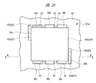
図24は、本発明とは異なり、ローパスフィルタ108A,108Bを配線基板403に内蔵させた場合の、比較例の配線基板403の模式的な断面図である。
FIG. 24 is a schematic cross-sectional view of a
図24に示される比較例の配線基板403は、11層の誘電体層(絶縁層)411と、誘電体層411の間および最上面と最下面の12層の配線層412とが積層された構造を有している。図24の右上側上層部において、配線基板403には、一対の導体413から対面する方向に交互に延在する配線層412a(配線層412の一部)によって容量414が形成されている。比較例の配線基板403では、内蔵された容量414によって、ローパスフィルタ(ローパスフィルタ回路)108A,108Bの容量素子112a,112b,112cが形成されている。
A
比較例の配線基板403では、ローパスフィルタ(ローパスフィルタ回路)108A,108Bの容量素子112a,112bとして十分な容量値を確保しようとすると、誘電体層411の厚みを薄くするか、誘電体層411および配線層412の層数を多くすればよいが、誘電体層411の厚みを薄くするには限界があるので、誘電体層411および配線層412の層数を、図24のように多くする(図24では誘電体層412の数は11層)必要がある。これは、配線基板403の厚みを厚くし、また、配線基板403の製造単価を高めてしまう。このため、このような比較例の配線基板403を用いてRFパワーモジュールを製造した場合、RFパワーモジュールの厚みが厚くなり、また、製造単価が高くなってしまう。
In the
それに対して、本実施の形態では、ローパスフィルタ108A,108BをRFパワーモジュール1内に形成するが、配線基板3上に搭載した集積受動部品6a,6bによりローパスフィルタ108A,108Bを形成している。このため、たとえRFパワーモジュール1内にローパスフィルタ108A,108Bを形成したとしても、RFパワーモジュール1の配線基板3の絶縁体層11や配線層の総数が増加するのを防止できる。例えば、絶縁体層11の数を4層として配線基板3を形成することができる。従って、RFパワーモジュールの薄型化が可能になる。
In contrast, in this embodiment, the low-
また、本実施の形態では、ローパスフィルタ108A,108B用の複数の受動素子(インダクタ素子111a,111b,111cおよび容量素子112a,112b,112c)を半導体基板上に形成した集積受動部品6a,6bを配線基板3上に実装してRFパワーモジュール1を形成している。このため、ローパスフィルタ108A,108B用の個々の受動素子(インダクタ素子111a,111b,111cおよび容量素子112a,112b,112c)を個別のチップ部品として配線基板3上に実装した場合に比較して、RFパワーモジュール1の小型化(小面積化)が可能になる。
In the present embodiment, integrated
図25は、本実施の形態のRFパワーモジュール1の上面透視図であり、封止樹脂7を透視し、配線基板3の上面3aにおける半導体チップ2,4および集積受動部品6a,6bの配置位置(レイアウト)を示したものである。すなわち、図9において、配線基板3の上面3aで、半導体チップ2,4および集積受動部品6a,6b以外の図示を省略したものが、図25に対応する。
FIG. 25 is a top perspective view of the
本実施の形態のRFパワーモジュール1では、図9や図25に示されるように、配線基板3の上面3aにおいて、スイッチ回路109A,109Bを構成する半導体チップ4は、GSM900用のローパスフィルタ108Aを構成する集積受動部品6aと、DCS1800用のローパスフィルタ108Bを構成する集積受動部品6bとの間に配置されている。そして、配線基板3の上面3aにおいて、スイッチ回路109A,109Bを構成する半導体チップ4は、電力増幅回路102A,102Bを構成する半導体チップ2の横(真横)に配置されている。すなわち、図25に示されるように、配線基板3の上面3aにおいて、電力増幅回路102A,102Bを構成する半導体チップ2の一つの辺(側辺、側面、半導体チップ2の主面の側辺)21と直交する直線22(概念上の直線)上に、スイッチ回路109A,109Bを構成する半導体チップ4が位置するように、半導体チップ2,4が配置されている。なお、上記辺21は、半導体チップ2の四辺のうちの、半導体チップ4に対向する側の辺である。また、図25において、点線で上記直線22が模式的に示されている。
In the
更に、本実施の形態のRFパワーモジュール1では、図9に示されるように、配線基板3の上面3aにおいて、集積受動部品6aと半導体チップ4の間、および集積受動部品6bと半導体チップ4の間に、受動部品5が配置されていない。そして、配線基板3の上面3aにおいて、集積受動部品6aと半導体チップ4の間、および集積受動部品6bと半導体チップ4の間は、受動部品5を介さず、配線基板3の導体パターン(12b)または導体パターン(12b)とボンディングワイヤ9を介して、電気的に接続されている。
Further, in the
半導体チップ2内に形成された電力増幅回路102Aで増幅されたGSM900のRF信号(高周波信号)は、受動部品5からなる整合回路107Aを介して、集積受動部品6a内に形成されたローパスフィルタ108Aに入力されて高調波成分がカットされ、ローパスフィルタ108Aを通過して集積受動部品6aから出力されたRF信号は、半導体チップ4内に形成されたスイッチ回路109Aに入力される。一方、半導体チップ2内に形成された電力増幅回路102Bで増幅されたDCS1800のRF信号(高周波信号)は、受動部品5からなる整合回路107Bを介して、集積受動部品6b内に形成されたローパスフィルタ108Bに入力されて高調波成分がカットされ、ローパスフィルタ108Bを通過して集積受動部品6bから出力されたRF信号は、半導体チップ4内に形成されたスイッチ回路109Bに入力される。このため、GSM900用およびDCS1800用のスイッチ回路109A,109Bが形成された半導体チップ4には、GSM900用のローパスフィルタ108Aが形成された集積受動部品6aの出力と、DCS1800用のローパスフィルタ108Bが形成された集積受動部品6bの出力の両方が入力される。
The RF signal (high frequency signal) of GSM900 amplified by the
集積受動部品6a,6b(ローパスフィルタ108A,108B)から出力されて半導体チップ4(スイッチ回路109A,109B)に入力されるRF信号は、電力増幅回路102A,102Bで増幅されたRF信号であるため、集積受動部品6a,6bと半導体チップ4との間が遠いと、集積受動部品6a,6bから出力されて半導体チップ4に入力されるまでの損失が大きくなる。これは、RFパワーモジュールの付加効率(電力付加効率)を低下させる可能性がある。
The RF signal output from the integrated
本実施の形態では、図9や図25に示されるように、GSM900用のローパスフィルタ108Aを構成する集積受動部品6aと、DCS1800用のローパスフィルタ108Bを構成する集積受動部品6bとの間に、スイッチ回路109A,109Bを構成する半導体チップ4を配置しているので、半導体チップ4を集積受動部品6aと集積受動部品6bの両方の近くに配置することができる。すなわち、集積受動部品6aと半導体チップ4を近くし、かつ集積受動部品6bと半導体チップ4を近くすることができる。このため、集積受動部品6a(ローパスフィルタ108A)と半導体チップ4(スイッチ回路109A)の接続経路(配線基板3の導体パターンなど)を短くし、かつ集積受動部品6b(ローパスフィルタ108B)と半導体チップ4(スイッチ回路109B)の接続経路(配線基板3の導体パターンなど)を短くすることができる。従って、集積受動部品6aの出力と、集積受動部品6bの出力の両方を、半導体チップ4のスイッチ回路109A,109Bに最短で入力することが可能になる。これにより、集積受動部品6a,6b(ローパスフィルタ108A,108B)から出力されて半導体チップ4(スイッチ回路109A,109B)に入力されるまでの損失を少なくすることができ、RFパワーモジュールの付加効率(電力付加効率)を向上させることができる。
In this embodiment, as shown in FIGS. 9 and 25, between the integrated
また、本実施の形態では、配線基板3の上面3aにおいて、集積受動部品6a,6bと半導体チップ4の間に受動部品5が配置されないようにしており、これも、集積受動部品6a,6bと半導体チップ4の接続経路(配線基板3の導体パターンなど)を短くするのに有利に作用する。また、本実施の形態では、集積受動部品6a,6bと半導体チップ4の間を、受動部品5を介さずに配線基板3の導体パターン(12b)または導体パターン(12b)とボンディングワイヤ9を介して電気的に接続しており、これも、集積受動部品6a,6bから出力されて半導体チップ4に入力するまでの損失を少なくするように有利に作用する。このため、RFパワーモジュール1の付加効率をより向上することができる。
Further, in the present embodiment, the
なお、図9および図10に示されるように、半導体チップ4を配線基板3の上面3aにフェイスアップでダイボンディングし、半導体チップ4の電極4aと配線基板3の基板側端子12aとをワイヤボンディングした場合には、集積受動部品6a,6bと半導体チップ4の間は、受動部品5を介さずに配線基板3の導体パターン(12b)とボンディングワイヤ9を介して電気的に接続される。他の形態として、半導体チップ4の電極4aをバンプ電極とし、半導体チップ4を配線基板4の上面3a上にフリップチップ接続することもでき、この場合、集積受動部品6a,6bと半導体チップ4の間は、受動部品5を介さずに配線基板3の導体パターン(12b)を介して電気的に接続される。
9 and 10, the
また、本実施の形態では、スイッチ回路109A,109Bの制御を行う制御回路103Cを半導体チップ2内に形成し、スイッチ回路109A,109Bの制御信号(上記切換信号CNT1,CNT2)を半導体チップ2(制御回路103C)から半導体チップ4(スイッチ回路109A,109B)に供給するようにしている。本実施の形態では、配線基板3の上面3aにおいて、半導体チップ4を半導体チップ2の横(真横)に配置している(すなわち半導体チップ2の一辺(21)と直交する直線(22)上に半導体チップ4が位置している)ので、半導体チップ2と半導体チップ4の接続経路(配線基板3の導体パターン)を短くすることができ、配線基板3の配線(導体パターン12b)のレイアウトも容易になる。このため、配線基板3の上面3aにおいて、半導体チップ2と半導体チップ4は、配線基板3の導体パターン(12)または導体パターン(12)とボンディングワイヤ8,9を介して電気的に接続され、配線基板3の導体パターン(12)または導体パターン(12)とボンディングワイヤ8,9を介して、半導体チップ2から半導体チップ4にスイッチ回路109A,109Bの制御信号が供給されるようになっている。従って、半導体チップ2(制御回路103C)から半導体チップ4(スイッチ回路109A,109B)に制御信号(切換信号CNT1,CNT2)を最短で供給することが可能になり、スイッチ回路109A,109Bの制御信号(切換信号CNT1,CNT2)がノイズの影響を受けにくくなるので、スイッチ回路109A,109Bの切り換えの誤動作などを防止できる。
In this embodiment, the
また、RFパワーモジュール1は、GSM900およびDCS1800の2系統のRF信号(高周波信号)を増幅できるように構成されている。このため、電力増幅回路、ローパスフィルタおよびスイッチ回路は、それぞれ2系統必要である。このため、各部品のレイアウトを工夫しないと、配線基板3の配線のレイアウトが複雑化し、配線基板3の大型化によるRFパワーモジュールの大型化を招く可能性がある。
The
本実施の形態では、2系統(GSM900およびDCS1800)の電力増幅回路102A,102Bを1つの半導体チップ2内に形成し、2系統(GSM900およびDCS1800)のスイッチ回路109A,109Bを1つの半導体チップ4内に形成し、2系統(GSM900およびDCS1800)のローパスフィルタ108A,108Bを2つの集積受動部品6a,6bに形成している。そして、図9に示されるように、配線基板3の上面3aにおいて、集積受動部品6aと集積受動部品6bとの間に半導体チップ4を配置し、かつ半導体チップ2の横(真横)に半導体チップ4が配置されるようにしている。このため、半導体チップ2と半導体チップ4とを横に並んで配置し、その上下に、GSM900用の部品(整合回路107Aを構成する受動部品5や集積受動部品6a)とDCS1800用の部品(整合回路107Bを構成する受動部品5や集積受動部品6b)をそれぞれまとめて(グループ化して)配置することができる。例えば、図9では、配線基板3の上面3aにおいて、図9の右上側の領域に、GSM900用の部品(整合回路107Aを構成する受動部品5や集積受動部品6a)がまとめて配置され、図9の右下側の領域に、DCS1800用の部品(整合回路107Bを構成する受動部品5や集積受動部品6b)がまとめて配置されている。このため、半導体チップ2内の電力増幅回路102Aで増幅されたGSM900のRF信号を、まとめて配置されたGSM900用の部品(整合回路107Aを構成する受動部品5や集積受動部品6a)を経由して、半導体チップ4のスイッチ回路109Aに入力することができる。また、半導体チップ2内の電力増幅回路102Bで増幅されたDCS1800のRF信号を、まとめて配置されたDCS1800用の部品(整合回路107Bを構成する受動部品5や集積受動部品6b)を経由して、半導体チップ4のスイッチ回路109Bに入力することができる。従って、半導体チップ2、GSM900用の部品(整合回路107Aを構成する受動部品5や集積受動部品6a)および半導体チップ4の間を接続する配線基板3の配線のレイアウトと、半導体チップ2、DCS1800用の部品(整合回路107Bを構成する受動部品5や集積受動部品6b)および半導体チップ4の間を接続する配線基板3の配線のレイアウトの、両方を容易にすることができる。このため、配線基板3の配線のレイアウトを単純化でき、配線基板3を小型化でき、RFパワーモジュール1を小型化することが可能になる。
In the present embodiment, two systems (GSM900 and DCS1800) of
また、本実施の形態では、配線基板3の導体層により形成されたインダクタ素子70が配線基板3に内蔵されている。インダクタ素子70は、整合回路(出力整合回路)107A,107Bに用いられている。インダクタ素子70は、配線基板3の導体層の螺旋状のパターンにより形成されたヘリカルコイルとすることができる。例えば、配線基板3の上面3aの導体パターン12bと配線基板3の複数の絶縁体層11間の導体層により、一部が断線した周回パターン(例えばコの字またはC字状のパターン)を形成して絶縁体層11を間に挟んで積層した状態とし、それらをビアホール13内の導体または導体膜で接続することにより、螺旋の進行方向が配線基板3の厚み方向となるインダクタ素子70が配線基板3に形成されている。
In the present embodiment, the
本実施の形態では、整合回路(出力整合回路)107A,107Bを形成するためのインダクタ素子の少なくとも一部に、チップインダクタではなく、配線基板3の導体層により形成されたインダクタ素子70を用いることで、RFパワーモジュール1の単価(製造単価)を低減することができる。
In the present embodiment, an
また、本実施の形態では、RFパワーモジュール1にスイッチ回路109A,109Bを内蔵させているので、スイッチ回路109A,109Bを制御する制御信号(切換信号CNT1,CNT2)を、半導体チップ4(スイッチ回路109A,109B)に供給する必要がある。このため、電力増幅回路102A,102Bを構成する半導体チップ2内に、更にスイッチ回路109A,109Bの制御回路103Cを形成し、半導体チップ2(制御回路103C)から半導体チップ4(スイッチ回路109A,109B)に制御信号(切換信号)を供給するようにしている。また、RFパワーモジュール1外部の回路部152からRFパワーモジュール1の外部接続端子12cを経由して半導体チップ2(制御回路103C)に供給された制御信号などに基づき、半導体チップ2(制御回路103C)から半導体チップ4にスイッチ回路109A,109Bの制御信号(切換信号)が供給される。このため、RFパワーモジュール内にスイッチ回路109A,109Bを形成していない場合に比較して、本実施の形態の場合、電力増幅回路102A,102Bおよび制御回路103Cが形成された半導体チップ2に入出力される信号が多く、半導体チップ2における電極2aの数が多くなる。すなわち、制御回路103Cに関係する分だけ、半導体チップ2における電極2aの数が多くなる。
In the present embodiment, since the
図26は、本実施の形態のRFパワーモジュール1における半導体チップ2近傍の要部平面図である。図27は、比較例のRFパワーモジュール501における半導体チップ2近傍の要部平面図である。
FIG. 26 is a plan view of an essential part in the vicinity of the
本実施の形態では、図26に示されるように、半導体チップ2の複数の電極2aに複数のボンディングワイヤ8を介してそれぞれ接続すべき複数の基板側端子72は、配線基板3の上面3aにおいて、千鳥配列ではなく、半導体チップ2の周囲に一列に配列されている。これにより、各基板側端子72に接続された各ボンディングワイヤ8が、そのボンディングワイヤ8が接続された基板側端子72とは異なる電位の基板側端子72上を通らないようにしている。なお、基板側端子72は、上記基板側端子12aのうち、ボンディングワイヤ8に接続される基板側端子(ボンディングパッド、パッド電極、電極、端子)である。
In the present embodiment, as shown in FIG. 26, the plurality of substrate-
一方、図27の比較例のRFパワーモジュール501では、半導体チップ2の複数の電極2aに複数のボンディングワイヤ408(本実施の形態のボンディングワイヤ8に対応するもの)を介してそれぞれ接続すべき複数の基板側端子472(本実施の形態の基板側端子72に対応するもの)を、配線基板3の上面3aにおいて、半導体チップ2の周囲に千鳥配列(複数列配列)させている。このため、比較例のRFパワーモジュール501では、図27に示されるように、ボンディングワイヤ408のうちのいくつかのボンディングワイヤ408aでは、基板側端子472aに接続されたボンディングワイヤ408aが、他の基板側端子408b上を通過した状態となっている。
On the other hand, in the
図27の比較例のRFパワーモジュール501では、ボンディングワイヤ408aが接続された基板側端子472aと、そのボンディングワイヤ408aが上を通過する他の基板側端子408bとが同電位であれば、そのボンディングワイヤ408aにはノイズは入力されない。しかしながら、ボンディングワイヤ408aが接続された基板側端子472aと、そのボンディングワイヤ408aが上を通過する他の基板側端子408bとが異なる電位であれば、そのボンディングワイヤ408aにノイズが入力され、このボンディングワイヤ408aを介してノイズが半導体チップ2に入力されてしまう。すなわち、ボンディングワイヤ408aが、そのボンディングワイヤ408aが接続された基板側端子472aとは異なる電位の基板側端子472b上を通過していると、このボンディングワイヤ408aを介してノイズが半導体チップ2に入力されてしまう。半導体チップ2内には電力増幅回路102A,102Bが形成されているので、ボンディングワイヤ408aを介してノイズが半導体チップ2に入力されると、電力増幅回路102A,102Bは発振してしまう可能性がある。これは、RFパワーモジュールの性能を低下させる可能性がある。
In the
それに対して、本実施の形態のRFパワーモジュール1では、図26に示されるように、配線基板3の上面3aにおいて、半導体チップ2の複数の電極2a(第1電極)と配線基板3の複数の基板側端子72(第2電極)とが、複数のボンディングワイヤ8を介して電気的に接続され、それら複数のボンディングワイヤ8のそれぞれが、接続された基板側端子72(第2電極)とは異なる電位の基板側端子72(第2電極)上を通らないようにしている。これにより、ボンディングワイヤ8を介してノイズが半導体チップ2に入力されてしまうのを防止し、半導体チップ2内に形成された電力増幅回路102A,102Bが発振してしまうのを防止でき、RFパワーモジュール1の性能を向上させることができる。
On the other hand, in the
上記のように、本実施の形態では、半導体チップ2内に制御回路103Cを形成している分、半導体チップ2における電極2aの数が多くなり、半導体チップ2にボンディングワイヤ8を介して接続すべき基板側端子72の数が多くなる。しかしながら、半導体チップ2にボンディングワイヤ8を介して接続すべき基板側端子72の数が増えたからと言って、それらの基板側端子72を図27の比較例のように千鳥配列にすると、半導体チップ2へのノイズの入力や電力増幅回路102A,102Bの発振などの問題が生じる可能性がある。このため、本実施の形態では、たとえボンディングワイヤ8を介して半導体チップ2に接続すべき基板側端子72の寸法や配列のピッチが小さくなったとしても、半導体チップ2の複数の電極2aに複数のボンディングワイヤ8を介してそれぞれ接続すべき複数の基板側端子72を、千鳥配列ではなく、配線基板3の上面3aにおいて、半導体チップ2の周囲に一列に配列させる。例えば、ボンディングワイヤ8を接続する基板側端子72の寸法L1を150μm程度とし、間隔L2を100μm程度とし、ピッチL3を250μm程度として、一列に配列させる。これにより、各ボンディングワイヤ8が、そのボンディングワイヤ8が接続された基板側端子72とは異なる電位の基板側端子72上を通らないようにすることができ、半導体チップ2へのノイズの入力を防止し、電力増幅回路102A,102Bが発振するのを防止することができる。
As described above, in the present embodiment, since the
また、本実施の形態では、配線基板3の上面3aに、受動素子として、受動部品5だけでなく集積受動部品6も実装している。受動部品5は、例えばチップ抵抗、チップコンデンサまたはチップインダクタなどからなり、それぞれ、両端に電極が形成された2端子の電位部品であり、両端面と側面の一部にも、電極が形成されている。このため、配線基板3の上面3aの基板側端子12aに受動部品5の電極を半田17で接続した際には、受動部品5の両端面および側面の電極部分を半田17が吸い上がる。この半田17の吸い上がりを確認することにより、配線基板3の上面3aにおいて、受動部品5の位置が、本来搭載されるべき位置からずれていないかを確認することが可能である(位置が合っていると半田の吸い上がりが生じ、位置がずれていると、半田の吸い上がりが生じない)。
In the present embodiment, not only the
しかしながら、集積受動部品6は、上記図19のように基板31上に複数の受動素子(インダクタ素子111a,111b,111cを構成する容量素子34と容量素子112a,112b,112cを構成するスパイラルインダクタ)が形成されたものであり、集積受動部品6は、半田バンプなどのバンプ電極18を介して配線基板3の上面3aの基板側端子12aに電気的に接続される。このため、集積受動部品6の側面には電極は形成されておらず、バンプ電極18が半田により形成されていたとしても、集積受動部品6の側面を半田は吸い上がらない。従って、配線基板3の上面3aにおいて、集積受動部品6の位置が、本来搭載されるべき位置からずれていないかを、集積受動部品6の側面での半田の吸い上がりによって確認することは困難である。
However, as shown in FIG. 19, the integrated
そこで、本実施の形態では、以下のように、配線基板3の上面3aに、集積受動部品6の位置を認識するためのパターン(後述する位置認識用パターン89a,89bに対応)を形成している。
Therefore, in the present embodiment, a pattern for recognizing the position of the integrated passive component 6 (corresponding to position
図28は、本実施の形態のRFパワーモジュール1の要部平面図(要部上面図)であり、集積受動部品6近傍領域が示されている。なお、図28は封止樹脂7を透視した状態が示されている。図29は、集積受動部品6の平面図であり、配線基板3に搭載した際に配線基板3の上面3aに対向する側の主面である表面19aが示されている。図30および図31は、集積受動部品6を搭載する前の配線基板3の要部上面図(要部平面図)であり、図28に対応する領域が示されている。また、図30は、図31からオーバーコートガラス層84およびめっき層86を省略し、ビアホール13の位置を点線で示したものである。
FIG. 28 is a plan view of relevant parts (a top view of relevant parts) of the
なお、図28は、平面図であるが、図面を見易くするために、位置認識用パターン89a,89bにハッチングを付してある。また、図30は、平面図であるが、図面を見易くするために、導体パターン82にハッチングを付してある。また、図31は、平面図であるが、図面を見易くするために、端子88c,88d,88e,88fおよび位置認識用パターン89a,89bにハッチングを付してある。
FIG. 28 is a plan view, but the
また、図32は、集積受動部品6を搭載する前の配線基板3の要部断面図であり、図31のB−B線の断面にほぼ対応するものである。図33は、配線基板3の上面3aに集積受動部品6を搭載した状態を示す要部断面図(すなわち、封止樹脂部6の図示を省略したRFパワーモジュール1の要部断面図)であり、図28のB−B線の断面にほぼ対応するものである。なお、配線基板3は、複数の絶縁体層11と、絶縁体層11間および最上層と最下層の配線層を積層して一体化した多層基板であり、図32および図33の断面図には、複数の絶縁体層11のうちの最上層の絶縁体層11aよりも上部が示され、絶縁体層11aよりも下の構造は、図示を省略している。
32 is a cross-sectional view of the main part of the
図29に示されるように、集積受動部品6は、6つの端子(電極)81を有している。端子81は、上記バンプ電極18(バンプ電極64)に対応するものである。集積受動部品6の6つの端子81は、入力端子81aと、出力端子81bと、4つのグランド端子81c,81d,81e,81fからなる。入力端子81aは、上記図2の入力端子116に対応し、出力端子81bは、上記図2の出力端子117に対応する。グランド端子81c,81d,81e,81fは、上記図2のグランド端子118,119のいずれかに対応する。ここでは、グランドの強化のため、集積受動部品6に4つのグランド端子81c,81d,81e,81fを設けているが、他の形態として、上記図2のグランド端子118,119に対応する2つのグランド端子を集積受動部品6に設けることもでき、この場合、集積受動部品6は、上記図2の入力端子116、出力端子117およびグランド端子118,119にそれぞれ対応する4つの端子81を有することになる。
As shown in FIG. 29, the integrated
図30および図32に示されるように、配線基板3において、絶縁体層11aの上面には、例えば銅(Cu)などを主成分とする導体パターン82が形成されている。導体パターン82は、上記導体パターン12bに対応するものである。導体パターン82は、必要に応じて、絶縁体層11aに形成されたビアホール13内の導体83を介して、絶縁体層11aよりも下層の配線層などに電気的に接続されている。ビアホール13内の導体83は、導体パターン82と同種の導体などにより形成されている。
As shown in FIGS. 30 and 32, in the
図32に示されるように、配線基板3においては、絶縁体層11aの上面に、導体パターン82を覆うように、オーバーコートガラス層(絶縁層)84が形成されている。なお、上記図9の全体平面図では、オーバーコートガラス層84は図示を省略している。
As shown in FIG. 32, in the
オーバーコートガラス層84は、配線基板3上に搭載する部品(半導体チップ2,4、受動部品5および集積受動部品6)に接続する基板側端子12aとなる部分と、位置認識用パターン89a,89bを形成する部分を露出し、それ以外の導体パターン82を覆うようにパターン化されている。すなわち、オーバーコートガラス層84は開口部85を有しており、オーバーコートガラス層84の開口部85から基板側端子12aとなる部分の導体パターン82と、位置認識用パターン89a,89bとなる部分の導体パターン82が露出されている。導体パターン82をオーバーコートガラス層84で覆うことにより、基板側端子12aおよび位置認識用パターン89a,89bとなる部分以外の導体パターン82を保護して絶縁することができる。
The
導体パターン82のうち、オーバーコートガラス層84の開口部85から露出している部分では、その上面(表面)にめっき層86が形成されている。めっき層86は、例えば、下層側のニッケル(Ni)めっき層と、その上の金(Au)めっき層の積層膜からなる。めっき層86は、オーバーコートガラス層84上には形成されておらず、オーバーコートガラス層84の開口部85から露出する導体パターン82上に形成されている。導体パターン82上にめっき層86が形成されて、半田接続やワイヤボンディングなどが可能な基板側端子12aが形成される。
In the
図30に示されるように、配線基板3の上面3aには、集積受動部品6の入力端子81aに接続すべき入力信号用電極パターン82a、集積受動部品6の出力端子81bに接続すべき出力信号用電極パターン82b、集積受動部品6のグランド端子81c,81dに接続すべきグランド用電極パターン82c、および集積受動部品6のグランド端子81e,81fに接続すべきグランド用電極パターン82dが形成されている。これら入力信号用電極パターン82a、出力信号用電極パターン82b、グランド用電極パターン82c,82dは、配線基板3の上面3aの集積受動部品6搭載予定位置近傍に、導体パターン82によって形成されている。
As shown in FIG. 30, the input
図31および図32に示されるように、入力信号用電極パターン82aは、集積受動部品6搭載時に集積受動部品6の入力端子81aに対向する領域(ここでは出力信号用電極パターン82bに対向する側の先端部近傍領域)がオーバーコートガラス層84の開口部85から露出されて、めっき層86が表面に形成された端子88aとなっている。出力信号用電極パターン82bは、集積受動部品6搭載時に集積受動部品6の出力端子81bに対向する領域(ここでは入力信号用電極パターン82aに対向する側の先端部近傍領域)がオーバーコートガラス層84の開口部85から露出されて、めっき層86が表面に形成された端子88bとなっている。グランド用電極パターン82cは、集積受動部品6搭載時に集積受動部品6のグランド端子81c,81dに対向する領域が、オーバーコートガラス層84の開口部85から露出されて、めっき層86が表面に形成された端子88c,88dとなっている。グランド用電極パターン82dは、集積受動部品6搭載時に集積受動部品6のグランド端子81e,81fに対向する領域が、オーバーコートガラス層84の開口部85から露出されて、めっき層86が表面に形成された端子88e,88fとなっている。これら端子88a〜88fは、上記基板側端子12aのうち、集積受動部品6の端子81(バンプ電極18)に接続すべき端子に対応する。
As shown in FIGS. 31 and 32, the input
更に、本実施の形態では、図31および図32に示されるように、グランド用電極パターン82cの一部をオーバーコートガラス層84の開口部85aから露出させて、めっき層86が表面に形成された位置認識用パターン89aを形成し、同様に、グランド用電極パターン82dの一部をオーバーコートガラス層84の開口部85bから露出させて、めっき層86が表面に形成された位置認識用パターン89bを形成している。
Further, in the present embodiment, as shown in FIGS. 31 and 32, a part of the
配線基板3の上面3a上に集積受動部品6を実装する際には、図28および図33からも分かるように、集積受動部品6の入力端子81aを配線基板3の端子88aに接続(電気的に接続)し、集積受動部品6の出力端子81bを配線基板3の端子88bに接続(電気的に接続)し、集積受動部品6のグランド端子81c,81d,81e,81fを配線基板3の端子88c,88d,88e,88fにそれぞれ接続(電気的に接続)する。
When the integrated
集積受動部品6の端子81を半田バンプなどにより形成した場合や、あるいは、配線基板3の端子88a,88b,88c,88d,88e,88f上に半田を供給してから配線基板3に集積受動部品6を搭載した場合は、集積受動部品6搭載後の半田リフロー処理により、半田を介して、集積受動部品6の入力端子81a、出力端子81b、およびグランド81c,81d,81e,81fを、それぞれ、配線基板3の端子88a,88b,88c,88d,88e,88fに接続(半田接続)することができる。また、集積受動部品6の端子81を金バンプなどにより形成した場合は、圧着または熱圧着などにより、集積受動部品6の入力端子81a、出力端子81b、およびグランド81c,81d,81e,81fを、それぞれ、配線基板3の端子88a,88b,88c,88d,88e,88fに接続することができる。
When the terminal 81 of the integrated
位置認識用パターン89a,89bは、配線基板3の上面3aに集積受動部品6を実装した後(半田リフロー処理後)で(すなわち上記図21の工程の後で)、封止樹脂7を形成する前(すなわち上記図23の工程の前)に、集積受動部品6(集積受動素子)の位置(実装位置)を認識(確認)するためのパターンである。このため、位置認識用パターン89a,89bは、目視または画像装置などにより認識可能なパターンとされている。配線基板3の上面3aにおける位置認識用パターン89a,89bには、集積受動部品6の端子81は接続されない。
The
図28および図33に示されるように、配線基板3の上面3aに集積受動部品6を実装した状態では、配線基板3の上面3aにおいて、集積受動部品6の周囲の少なくとも一部に、その集積受動部品6の位置を認識するための位置認識用パターン89a,89bが形成され、位置認識用パターン89a,89bの少なくとも一部の直上には、集積受動部品6が存在していない。このため、配線基板3の上面3aに集積受動部品6を実装した後(半田リフロー処理の後)で、封止樹脂7を形成する前に、配線基板3の上面3aを上方から見る(観察する)と、図28に示されるように、集積受動部品6の周囲に、位置認識用パターン89a,89bが存在するのが認識(確認、観察)できる。集積受動部品6が本来搭載されるべき位置にあれば、配線基板3の上面3aを上方から見た(観察した)際に、集積受動部品6の周囲(ここでは両側)に位置認識用パターン89a,89bの両方が認識(確認、観察)できるような位置に、位置認識用パターン89a,89bが設けられている。
As shown in FIG. 28 and FIG. 33, in a state where the integrated
図34は、配線基板3上に集積受動部品6を実装した段階(半田リフロー処理を行った後の状態)で、集積受動部品6の位置が、本来搭載されるべき位置からずれている場合を示す要部平面図であり、上記図28に相当するものである。
FIG. 34 shows a case where the position of the integrated
図34に示されるように、もし、集積受動部品6の位置が、本来搭載されるべき位置からずれていると、位置認識用パターン89a,89bの少なくとも一方が、集積受動部品6によって隠れてしまい、配線基板3の上面3aを上方から見た(観察した)際に、集積受動部品6の周囲に、位置認識用パターン89a,89bの一方を認識できても、位置認識用パターン89a,89bの両方を認識することはできない。
As shown in FIG. 34, if the position of the integrated
一方、集積受動部品6が本来搭載されるべき位置にあれば、図28に示されるように、配線基板3の上面3aを上方から見た(観察した)際に、集積受動部品6の周囲(ここでは両側)に位置認識用パターン89a,89bの両方を認識(確認、観察)することができる。
On the other hand, if the integrated
このため、配線基板3上に集積受動部品6を実装した段階(半田リフロー処理を行った後の状態)で、集積受動部品6の位置が、本来搭載されるべき位置からずれていないかどうかを、位置認識用パターン89a,89bによって確認することができる。従って、集積受動部品の実装工程(図21の工程段階)の後で、封止樹脂7形成工程(図23の工程段階)の前に、検査工程を導入し、この検査工程で、配線基板4における集積受動部品6の実装状態を位置認識用パターン89a,89bによって確認して選別し、図28のように本来搭載されるべき位置に集積受動部品6が実装されたものだけ、次の工程(例えばワイヤボンディング工程または封止樹脂7形成工程)に送ることができる。これにより、集積受動部品6の実装信頼性を向上でき、RFパワーモジュール1の信頼性をより向上することができる。
For this reason, whether or not the position of the integrated
図34のように本来搭載されるべき位置に集積受動部品6が実装されなかったものは、不良品として除去するか、あるいは、再度集積受動部品6の実装をやり直す。
If the integrated
これにより、最終的に製造されたRFパワーモジュール1では、図28のように本来搭載されるべき位置に集積受動部品6が実装された状態となり、配線基板3の上面3aにおいて、集積受動部品6の周囲の少なくとも一部に、位置認識用パターン89a,89bが形成され、位置認識用パターン89a,89bの少なくとも一部の直上には、集積受動部品6が存在していない状態となっている。すなわち、集積受動部品6が搭載された配線基板3を上方から見た際に(但し封止樹脂7は透視または除去した状態とする)、集積受動部品6の周囲の少なくとも一部(ここでは集積受動部品6の両側)に位置認識用パターン89a,89bの両方が形成(配置)され、各位置認識用パターン89a,89bの少なくとも一部の直上には、集積受動部品6が存在していない状態となっている。
Thus, in the finally manufactured
また、本実施の形態では、位置認識用パターン89a,89bは、集積受動部品6(集積受動素子)の複数の端子81a,81b,81c,81d,81e,81f(第3電極)と電気的に接続された配線基板3の上面3aの複数の端子88a,88b,88c,88d,88e,88fと同層の導体層(ここでは導体パターン82およびその上のめっき層86)により形成されている。このため、端子88a,88b,88c,88d,88e,88f形成工程と同じ工程で位置認識用パターン89a,89bを形成することができ、配線基板3に位置認識用パターン89a,89bを設けたことに伴う配線基板3の製造工程数や製造コストの増加を防止できる。
In the present embodiment, the
以上、本発明者によってなされた発明をその実施の形態に基づき具体的に説明したが、本発明は前記実施の形態に限定されるものではなく、その要旨を逸脱しない範囲で種々変更可能であることは言うまでもない。 As mentioned above, the invention made by the present inventor has been specifically described based on the embodiment. However, the invention is not limited to the embodiment, and various modifications can be made without departing from the scope of the invention. Needless to say.
本発明は、例えば移動体通信装置搭載される電子装置に適用して好適なものである。 The present invention is suitable for application to, for example, an electronic device mounted on a mobile communication device.
1 RFパワーモジュール
2 半導体チップ
2a 電極
2b 裏面電極
3 配線基板
3a 上面
3b 下面
4 半導体チップ
5 受動部品
6,6a,6b 集積受動部品
7 封止樹脂
8,9,408,408a ボンディングワイヤ
11,11a 絶縁体層
12a,72,472,472a 基板側端子
12b 導体パターン
12c 外部接続端子
12d 基準電位供給用端子
13,13a ビアホール
14a,14b 導体層
15,16,17 半田
18 バンプ電極
19a 表面
31 基板
32 絶縁膜
33 配線
34 容量素子
34a 下部電極
34b 容量絶縁膜
34c 上部電極
35 絶縁膜
36 開口部
37 絶縁膜
38 開口部
41 配線
43 絶縁膜
43a 絶縁膜
44 開口部
45 パッド部
51 シード膜
53 配線
54 ニッケル膜
61 絶縁膜
62 開口部
63 金膜
64 バンプ電極
70 インダクタ素子
81,81a〜81f 端子
82 導体パターン
82a 入力信号用電極パターン
82b 出力信号用電極パターン
82c,82d グランド用電極パターン
83 導体
84 オーバーコートガラス層
85 開口部
86 めっき層
88a〜88f 端子
89a,89b 位置認識用パターン
102A,102B 電力増幅回路
102A1,102A2,102A3,102B1,102B2,102B3 増幅段
102AM1,102AM2,102BM1,102BM2 整合回路
103 周辺回路
103A 制御回路
103A1 電源制御回路
103A2 バイアス電圧生成回路
103B バイアス回路
103C 制御回路
104a,104b,104c 入力端子
105A,105B 整合回路
106,110a,110b 端子
107A,107B 整合回路
108A,108B ローパスフィルタ
109A,109B スイッチ回路
111a,111b,111c インダクタ素子
112a,112b,112c 容量素子
113 並列共振回路
114,115 直列共振回路
116 入力端子
117 出力端子
118,119 グランド端子
152 回路部
201 半導体基板
202 エピタキシャル層
203 溝
204 p型打抜き層
205 素子分離領域
206 p型ウエル
207 ゲート絶縁膜
208 ゲート電極
209 n−型オフセットドレイン領域
210 n−型ソース領域
211 サイドウォールスペーサ
212 n型オフセットドレイン領域
213 n+型ドレイン領域
214 n+型ソース領域
215 p+型半導体領域
221 絶縁膜
222 コンタクトホール
223 プラグ
224 配線
224a ソース電極
224b ドレイン電極
225 絶縁膜
226 スルーホール
227 プラグ
228 配線
229 表面保護膜
230 裏面電極
301 半導体基板
302 バッファ層
303 電子供給層
304 チャネル層
305 電子供給層
306 ショットキー層
307 層間膜
308 キャップ層
309 素子分離部
310 酸化シリコン膜
313 ソース電極
314 ドレイン電極
315 保護膜
317 ゲート電極
317A ゲートパッド
318 層間絶縁膜
321 配線
324 層間絶縁膜
332 配線
334 表面保護膜
403 配線基板
411 誘電体層
412 配線層
412a 配線層
413 導体
414 容量
ANT アンテナ
CNT1,CNT2 切換信号
D1,D2,D3,D4 ダイオード素子
DPS デジタル携帯電話機システム
FLT1,FLT2 フィルタ
Q1,Q2 HEMT
DESCRIPTION OF SYMBOLS 1 RF power module 2 Semiconductor chip 2a Electrode 2b Back surface electrode 3 Wiring board 3a Upper surface 3b Lower surface 4 Semiconductor chip 5 Passive component 6, 6a, 6b Integrated passive component 7 Sealing resin 8, 9, 408, 408a Bonding wire 11, 11a Insulation Body layer 12a, 72, 472, 472a Substrate side terminal 12b Conductor pattern 12c External connection terminal 12d Reference potential supply terminal 13, 13a Via hole 14a, 14b Conductor layer 15, 16, 17 Solder 18 Bump electrode 19a Surface 31 Substrate 32 Insulating film 33 wiring 34 capacitive element 34a lower electrode 34b capacitive insulating film 34c upper electrode 35 insulating film 36 opening 37 insulating film 38 opening 41 wiring 43 insulating film 43a insulating film 44 opening 45 pad part 51 seed film 53 wiring 54 nickel film 61 Insulating film 62 Opening 63 Gold film 64 Bump electrode 70 Inductor element 81, 81a-81f Terminal 82 Conductor pattern 82a Input signal electrode pattern 82b Output signal electrode pattern 82c, 82d Ground electrode pattern 83 Conductor 84 Overcoat glass layer 85 Opening 86 Plating layer 88a-88f Terminal 89a, 89b Position recognition patterns 102A, 102B Power amplifier circuits 102A1, 102A2, 102A3, 102B1, 102B2, 102B3 Amplifier stages 102AM1, 102AM2, 102BM1, 102BM2 Matching circuit 103 Peripheral circuit 103A Control circuit 103A1 Power supply control circuit 103A2 Bias voltage generation circuit 103B Bias circuit 103C Control circuit 104a, 104b, 104c Input terminal 105A, 105B Matching circuit 106, 110a, 110b Terminal 107 A, 107B Matching circuit 108A, 108B Low pass filter 109A, 109B Switch circuit 111a, 111b, 111c Inductor element 112a, 112b, 112c Capacitance element 113 Parallel resonance circuit 114, 115 Series resonance circuit 116 Input terminal 117 Output terminal 118, 119 Ground terminal 152 circuit portion 201 semiconductor substrate 202 epitaxial layer 203 groove 204 p-type punching layer 205 element isolation region 206 p-type well 207 gate insulating film 208 gate electrode 209 n − type offset drain region 210 n − type source region 211 sidewall spacer 212 n -type offset drain region 213 n + -type drain region 214 n + -type source region 215 p + -type semiconductor region 221 insulating film 222 a contact hole 223 plug 224 distribution 224a Source electrode 224b Drain electrode 225 Insulating film 226 Through hole 227 Plug 228 Wiring 229 Surface protective film 230 Back electrode 301 Semiconductor substrate 302 Buffer layer 303 Electron supply layer 304 Channel layer 305 Electron supply layer 306 Schottky layer 307 Interlayer film 308 Cap layer 309 Element isolation portion 310 Silicon oxide film 313 Source electrode 314 Drain electrode 315 Protective film 317 Gate electrode 317A Gate pad 318 Interlayer insulating film 321 Wiring 324 Interlayer insulating film 332 Wiring 334 Surface protective film 403 Wiring substrate 411 Dielectric layer 412 Wiring layer 412a Wiring layer 413 Conductor 414 Capacitance ANT Antenna CNT1, CNT2 Switching signal D1, D2, D3, D4 Diode element DPS Digital cellular phone system FLT1, FLT2 Fill Q1, Q2 HEMT
Claims (12)
配線基板と、
前記配線基板の主面上に搭載され、前記電力増幅回路を構成するMOSFETが形成された第1半導体チップと、
前記配線基板の前記主面上に搭載され、前記電子装置の外部に設けられたアンテナに電気的に接続される前記スイッチ回路を構成するHEMTが形成された第2半導体チップと、を有し、
前記第1半導体チップは、シリコン基板上にゲート電極と、ソース領域と、前記ソース領域の上部に接続される第1プラグと、前記第1プラグに接続されるソース電極と、前記ソース電極と第2プラグを介して接続され前記ソース領域と前記シリコン基板とを電気的に接続する打抜き層と、前記シリコン基板の裏面に前記打抜き層と電気的に接続される裏面電極が形成され、
前記配線基板は、下面に矩形パターンの基準電位供給用端子を有し、前記第1半導体チップの下方に前記配線基板の主面と前記配線基板の下面とを電気的に接続するビアホールを複数有し、
前記第1半導体チップの裏面電極と、前記半導体基板の基準電位供給用端子とは電気的に接続され、
前記第1半導体チップと前記第2半導体チップは、ボンディングワイヤおよび前記配線基板の主面上の導体パターンを介して接続され、
前記第1半導体チップは、さらに前記電力増幅回路の制御を行う第1制御回路と、前記スイッチ回路の制御を行う第2制御回路とを有し、
前記第2半導体チップの前記スイッチ回路は、前記ボンディングワイヤおよび前記導体パターンを介して供給される前記第2制御回路からの制御信号に応じて前記アンテナとの接続切り替えを行う電子装置。 An electronic device including a power amplifier circuit, the switch circuit having an output connected to said power amplifier circuit,
A wiring board;
A first semiconductor chip mounted on a main surface of the wiring substrate and having a MOSFET formed on the power amplifier circuit;
A second semiconductor chip formed on the main surface of the wiring board and formed with a HEMT that constitutes the switch circuit electrically connected to an antenna provided outside the electronic device ;
The first semiconductor chip includes a gate electrode, a source region, a first plug connected to an upper portion of the source region, a source electrode connected to the first plug, a source electrode, and a first electrode on a silicon substrate. A punching layer connected via two plugs to electrically connect the source region and the silicon substrate, and a back electrode electrically connected to the punching layer on the back surface of the silicon substrate;
The wiring board has a rectangular pattern reference potential supply terminal on the lower surface, and a plurality of via holes that electrically connect the main surface of the wiring board and the lower surface of the wiring board below the first semiconductor chip. And
A back electrode of the first semiconductor chip and a reference potential supply terminal of the semiconductor substrate are electrically connected;
The first semiconductor chip and the second semiconductor chip are connected via a bonding wire and a conductor pattern on a main surface of the wiring board,
The first semiconductor chip further includes a first control circuit that controls the power amplifier circuit, and a second control circuit that controls the switch circuit,
The electronic device in which the switch circuit of the second semiconductor chip performs connection switching with the antenna in accordance with a control signal from the second control circuit supplied via the bonding wire and the conductor pattern .
前記電力増幅回路は、複数の増幅段を含み、The power amplifier circuit includes a plurality of amplification stages,
前記第1制御回路は、さらに前記電力増幅回路の複数の増幅段に対し、バイアス電圧を印加するためのバイアス電圧生成回路を含む電子装置。The first control circuit further includes a bias voltage generation circuit for applying a bias voltage to a plurality of amplification stages of the power amplification circuit.
前記電子装置は、前記電力増幅回路と前記スイッチ回路の間に電気的に接続されたローパスフィルタ回路を更に有し、
前記ローパスフィルタ回路は、前記配線基板の前記主面上に搭載された集積受動素子により形成されている電子装置。 The electronic device according to claim 2 .
The electronic device further includes a low-pass filter circuit electrically connected between the power amplifier circuit and the switch circuit,
The low-pass filter circuit, the wiring onboard formed have that electronic device by integrated passive device on said main surface of the substrate.
前記電子装置は、移動体通信装置に搭載される電子装置。 The electronic device according to claim 3 .
The electronic device, mounted on Ru electronic device to the mobile communication device.
前記電力増幅回路は、第1系統用の第1電力増幅回路と、第2系統用の第2電力増幅回路を含み、
前記スイッチ回路は、前記第1電力増幅回路の出力に電気的に接続された第1スイッチ回路と、前記第2電力増幅回路の出力に電気的に接続された第2スイッチ回路とを含み、
前記電子装置は、前記第1電力増幅回路と前記第1スイッチ回路の間に電気的に接続された第1ローパスフィルタ回路と、前記第2電力増幅回路と前記第2スイッチ回路の間に電気的に接続された第2ローパスフィルタ回路とを有し、
前記第1および第2電力増幅回路を構成するMOSFETが、前記第1半導体チップに形成され、
前記第1および第2スイッチ回路が、前記第2半導体チップに形成され、
前記第1および第2ローパスフィルタ回路は、それぞれ前記配線基板の前記主面上に搭載された第1および第2集積受動素子により形成されている電子装置。 The electronic device according to claim 4 .
The power amplifier circuit includes a first power amplifier circuit for a first system and a second power amplifier circuit for a second system,
The switch circuit includes a first switch circuit that is electrical connected to the output of the first power amplifying circuit, and a second switching circuit electrically connected to the output of the second power amplifier circuit Including
The electronic device during the first B-pass filter circuit and said second switching circuit and the second power amplifier circuit electrical connected between the first power amplifier circuit and the first switch circuit A second low-pass filter circuit electrically connected to
MOS FET constituting the first and second power amplifier circuit is formed on the first semiconductor chip,
It said first and second switch circuit is formed on the second semiconductor chip,
Wherein the first and second B-pass filter circuit, each of the first and second integrated passive element formed by being optionally that electronic device mounted on the main surface of the wiring board.
前記第1半導体チップに形成される前記打抜き層は、p型多結晶シリコン膜によって形成される電子装置。The electronic device in which the punching layer formed on the first semiconductor chip is formed of a p-type polycrystalline silicon film.
前記第1制御回路は、前記第1および第2電力増幅回路の複数の増幅段の出力用の増幅素子のドレイン端子に印加される電圧を発生する電源制御回路を有する電子装置。The electronic device has a power supply control circuit for generating a voltage applied to drain terminals of output amplifying elements of a plurality of amplification stages of the first and second power amplifier circuits.
前記第1スイッチ回路および第2スイッチ回路を構成するゲート電極は、素子分離領域で囲まれたチップ領域内において、複数のソース電極およびドレイン電極の間を連続的に1本で延在する電子装置。An electronic device in which the gate electrodes constituting the first switch circuit and the second switch circuit are continuously extended between a plurality of source electrodes and drain electrodes in a chip region surrounded by an element isolation region. .
前記第1系統の前記電力増幅回路の送信周波数帯は、0.9GHz帯であり、
前記第2系統の前記電力増幅回路の送信周波数帯は、1.8GHz帯である電子装置。 The electronic device according to claim 8 .
The transmission frequency band of the power amplifier circuit of the first system is a 0.9 GHz band,
The transmission frequency band of the power amplifier circuit of the second system is, 1.8GHz Obidea Ru electronic device.
前記配線基板の前記主面において、前記第1集積受動素子と前記第2集積受動素子の間に前記第2半導体チップが配置されている電子装置。 The electronic device according to claim 9 .
In the main surface of the wiring board, the first integrated passive element and the second semiconductor chip is disposed have that electronic device between the second integrated passive device.
前記配線基板の前記主面において、前記第1半導体チップの横に前記第2半導体チップが配置されている電子装置。 The electronic device according to claim 10 .
In the main surface of the wiring substrate, the first semiconductor chip and the second semiconductor chip is disposed have that electronic device next.
前記配線基板の導体パターンにより形成されたインダクタ素子を更に有し、
前記インダクタ素子は、前記第1および第2電力増幅回路の出力整合回路に用いられている電子装置。 The electronic device according to claim 11 .
Further comprising an inductor element formed by the conductor pattern of the wiring board,
The inductor element, the first and have that electronic devices used in the output matching circuit of the second power amplifier.
Priority Applications (3)
| Application Number | Priority Date | Filing Date | Title |
|---|---|---|---|
| JP2006052099A JP4892253B2 (en) | 2006-02-28 | 2006-02-28 | Electronic equipment |
| US11/626,485 US7706756B2 (en) | 2006-02-28 | 2007-01-24 | RF power module |
| US12/730,310 US7962105B2 (en) | 2006-02-28 | 2010-03-24 | RF power module |
Applications Claiming Priority (1)
| Application Number | Priority Date | Filing Date | Title |
|---|---|---|---|
| JP2006052099A JP4892253B2 (en) | 2006-02-28 | 2006-02-28 | Electronic equipment |
Publications (2)
| Publication Number | Publication Date |
|---|---|
| JP2007234738A JP2007234738A (en) | 2007-09-13 |
| JP4892253B2 true JP4892253B2 (en) | 2012-03-07 |
Family
ID=38478352
Family Applications (1)
| Application Number | Title | Priority Date | Filing Date |
|---|---|---|---|
| JP2006052099A Active JP4892253B2 (en) | 2006-02-28 | 2006-02-28 | Electronic equipment |
Country Status (2)
| Country | Link |
|---|---|
| US (2) | US7706756B2 (en) |
| JP (1) | JP4892253B2 (en) |
Families Citing this family (69)
| Publication number | Priority date | Publication date | Assignee | Title |
|---|---|---|---|---|
| US7600058B1 (en) | 2003-06-26 | 2009-10-06 | Nvidia Corporation | Bypass method for efficient DMA disk I/O |
| US8683132B1 (en) | 2003-09-29 | 2014-03-25 | Nvidia Corporation | Memory controller for sequentially prefetching data for a processor of a computer system |
| US8356142B1 (en) | 2003-11-12 | 2013-01-15 | Nvidia Corporation | Memory controller for non-sequentially prefetching data for a processor of a computer system |
| US8700808B2 (en) | 2003-12-01 | 2014-04-15 | Nvidia Corporation | Hardware support system for accelerated disk I/O |
| US8356143B1 (en) | 2004-10-22 | 2013-01-15 | NVIDIA Corporatin | Prefetch mechanism for bus master memory access |
| JP4524454B2 (en) * | 2004-11-19 | 2010-08-18 | ルネサスエレクトロニクス株式会社 | Electronic device and manufacturing method thereof |
| US7935607B2 (en) * | 2007-04-09 | 2011-05-03 | Freescale Semiconductor, Inc. | Integrated passive device with a high resistivity substrate and method for forming the same |
| US8067814B2 (en) * | 2007-06-01 | 2011-11-29 | Panasonic Corporation | Semiconductor device and method of manufacturing the same |
| US20090115051A1 (en) * | 2007-11-01 | 2009-05-07 | Lap-Wai Lydia Leung | Electronic Circuit Package |
| JP5239309B2 (en) * | 2007-11-21 | 2013-07-17 | 株式会社村田製作所 | Semiconductor device |
| US8023269B2 (en) * | 2008-08-15 | 2011-09-20 | Siemens Energy, Inc. | Wireless telemetry electronic circuit board for high temperature environments |
| US7880558B2 (en) * | 2008-08-29 | 2011-02-01 | Motorola, Inc. | Method and apparatus for adjusting load impedance of a distributed amplifier |
| US8356128B2 (en) * | 2008-09-16 | 2013-01-15 | Nvidia Corporation | Method and system of reducing latencies associated with resource allocation by using multiple arbiters |
| US8370552B2 (en) | 2008-10-14 | 2013-02-05 | Nvidia Corporation | Priority based bus arbiters avoiding deadlock and starvation on buses that support retrying of transactions |
| JP5407667B2 (en) * | 2008-11-05 | 2014-02-05 | 株式会社村田製作所 | Semiconductor device |
| US7804365B2 (en) * | 2008-11-07 | 2010-09-28 | Epcos Ag | Multilayer amplifier module |
| US9166471B1 (en) | 2009-03-13 | 2015-10-20 | Rf Micro Devices, Inc. | 3D frequency dithering for DC-to-DC converters used in multi-mode cellular transmitters |
| US8798564B2 (en) * | 2009-03-17 | 2014-08-05 | Provigent Ltd. | Transmitter with replaceable power amplifier |
| US8698823B2 (en) | 2009-04-08 | 2014-04-15 | Nvidia Corporation | System and method for deadlock-free pipelining |
| JP5234521B2 (en) * | 2009-08-21 | 2013-07-10 | Tdk株式会社 | Electronic component and manufacturing method thereof |
| CN201563121U (en) * | 2009-09-23 | 2010-08-25 | 国基电子(上海)有限公司 | Radio frequency circuit framework |
| JP2011120105A (en) * | 2009-12-04 | 2011-06-16 | Renesas Electronics Corp | Semiconductor device |
| US8548398B2 (en) | 2010-02-01 | 2013-10-01 | Rf Micro Devices, Inc. | Envelope power supply calibration of a multi-mode radio frequency power amplifier |
| US9184701B2 (en) | 2010-04-20 | 2015-11-10 | Rf Micro Devices, Inc. | Snubber for a direct current (DC)-DC converter |
| US9214900B2 (en) | 2010-04-20 | 2015-12-15 | Rf Micro Devices, Inc. | Interference reduction between RF communications bands |
| US9900204B2 (en) | 2010-04-20 | 2018-02-20 | Qorvo Us, Inc. | Multiple functional equivalence digital communications interface |
| US9214865B2 (en) | 2010-04-20 | 2015-12-15 | Rf Micro Devices, Inc. | Voltage compatible charge pump buck and buck power supplies |
| US9008597B2 (en) | 2010-04-20 | 2015-04-14 | Rf Micro Devices, Inc. | Direct current (DC)-DC converter having a multi-stage output filter |
| US9577590B2 (en) | 2010-04-20 | 2017-02-21 | Qorvo Us, Inc. | Dual inductive element charge pump buck and buck power supplies |
| US9553550B2 (en) * | 2010-04-20 | 2017-01-24 | Qorvo Us, Inc. | Multiband RF switch ground isolation |
| US9362825B2 (en) | 2010-04-20 | 2016-06-07 | Rf Micro Devices, Inc. | Look-up table based configuration of a DC-DC converter |
| US8848385B2 (en) * | 2010-10-05 | 2014-09-30 | R&D Sockets, Inc | Embedded isolation filter |
| FR2969428B1 (en) * | 2010-12-21 | 2013-01-04 | St Microelectronics Sa | ELECTRONIC SWITCH AND COMMUNICATION APPARATUS INCLUDING SUCH A SWITCH |
| WO2012101978A1 (en) * | 2011-01-25 | 2012-08-02 | 株式会社村田製作所 | Electronic component |
| CN103608915B (en) * | 2011-06-21 | 2016-09-07 | 株式会社村田制作所 | Circuit module |
| CN102355223B (en) * | 2011-08-10 | 2014-08-27 | 锐迪科创微电子(北京)有限公司 | Single-chip GSM (Global System for Mobile Communications) radio-frequency antenna switch module and GSM radio-frequency front end |
| US9679869B2 (en) | 2011-09-02 | 2017-06-13 | Skyworks Solutions, Inc. | Transmission line for high performance radio frequency applications |
| JP5734217B2 (en) * | 2012-02-03 | 2015-06-17 | ルネサスエレクトロニクス株式会社 | Semiconductor device |
| JP5880114B2 (en) * | 2012-02-17 | 2016-03-08 | ソニー株式会社 | Integrated circuit and wireless communication device |
| KR101584042B1 (en) | 2012-06-14 | 2016-01-08 | 스카이워크스 솔루션즈, 인코포레이티드 | Power amplifier modules including related systems, devices, and methods |
| US9035194B2 (en) * | 2012-10-30 | 2015-05-19 | Intel Corporation | Circuit board with integrated passive devices |
| WO2014068351A2 (en) * | 2012-10-31 | 2014-05-08 | Freescale Semiconductor, Inc. | Amplification stage and wideband power amplifier |
| US20140167900A1 (en) | 2012-12-14 | 2014-06-19 | Gregorio R. Murtagian | Surface-mount inductor structures for forming one or more inductors with substrate traces |
| DE202012013392U1 (en) * | 2012-12-28 | 2016-10-14 | Bury Sp.Z.O.O | Circuit arrangement for compensation of a damping occurring in an antenna line between a mobile radio terminal and an antenna |
| US20140320252A1 (en) * | 2013-04-29 | 2014-10-30 | Skyworks Solutions, Inc. | Low loss impedance transformers implemented as integrated passive devices and related methods thereof |
| JP2014239201A (en) | 2013-05-08 | 2014-12-18 | ソニー株式会社 | Semiconductor device, antenna switch circuit, and wireless communication device |
| US9569385B2 (en) | 2013-09-09 | 2017-02-14 | Nvidia Corporation | Memory transaction ordering |
| JP6265415B2 (en) * | 2014-01-24 | 2018-01-24 | 住友電工デバイス・イノベーション株式会社 | Amplifier |
| KR102428141B1 (en) * | 2014-02-25 | 2022-08-02 | 스카이워크스 솔루션즈, 인코포레이티드 | Systems, devices and methods related to improved radio-frequency modules |
| CN106256088A (en) * | 2014-04-07 | 2016-12-21 | 卡文迪什动力有限公司 | There is the device of frequency variable filter for suppressing harmonic wave |
| US9531413B2 (en) * | 2014-09-16 | 2016-12-27 | Skyworks Solutions, Inc. | Multi-band device having switch with input shunt arm |
| US9485001B2 (en) * | 2014-10-31 | 2016-11-01 | Skyworks Solutions, Inc. | Diversity receiver front end system with switching network |
| CN104467776A (en) * | 2014-11-18 | 2015-03-25 | 锐迪科创微电子(北京)有限公司 | Single-chip radio frequency antenna switch module and radio frequency front end |
| US9838056B2 (en) | 2015-05-28 | 2017-12-05 | Skyworks Solutions, Inc. | Integrous signal combiner |
| CN105306162B (en) * | 2015-10-29 | 2018-04-06 | 天津光电安辰信息技术股份有限公司 | The recording screening arrangement and its implementation of a kind of mixing |
| KR101823269B1 (en) * | 2016-11-18 | 2018-01-29 | 삼성전기주식회사 | Radio-frequency switch apparatus with dynamic bias |
| KR101952870B1 (en) * | 2017-01-23 | 2019-02-28 | 삼성전기주식회사 | Antenna-integrated radio frequency module |
| JP2018181943A (en) | 2017-04-05 | 2018-11-15 | 株式会社村田製作所 | Power amplifier module |
| JP7098953B2 (en) * | 2018-02-20 | 2022-07-12 | 三菱電機株式会社 | Semiconductor device |
| KR102017159B1 (en) | 2018-03-12 | 2019-09-02 | 삼성전자주식회사 | Antenna module |
| CN108768421A (en) * | 2018-04-18 | 2018-11-06 | 广东小天才科技有限公司 | A kind of signal transmitting method and radio-frequency front-end radiating circuit |
| JP2020048184A (en) * | 2018-09-14 | 2020-03-26 | 株式会社村田製作所 | High frequency power amplifier and power amplifier module |
| KR20200114745A (en) * | 2019-03-29 | 2020-10-07 | 삼성전자주식회사 | Voltage protection circuit to prevent power amplifier burnout and electonic device including it |
| JP2022116379A (en) * | 2019-06-25 | 2022-08-10 | 京セラ株式会社 | RFID tag |
| US11257740B2 (en) | 2020-02-21 | 2022-02-22 | Wolfspeed, Inc. | Device carrier configured for interconnects, a package implementing a device carrier having interconnects, and processes of making the same |
| JP2021164017A (en) * | 2020-03-31 | 2021-10-11 | 株式会社村田製作所 | High-frequency module and communication device |
| CN111555734A (en) * | 2020-05-13 | 2020-08-18 | 北京航天微电科技有限公司 | Surface acoustic wave switch filtering module based on RF-SiP technology and electronic equipment |
| JP2022092959A (en) * | 2020-12-11 | 2022-06-23 | 株式会社村田製作所 | High-frequency module |
| KR20220141422A (en) * | 2021-04-13 | 2022-10-20 | 삼성전자주식회사 | Electronic device including power amplifier and operating method thereof |
Family Cites Families (18)
| Publication number | Priority date | Publication date | Assignee | Title |
|---|---|---|---|---|
| JPH0897663A (en) * | 1994-09-29 | 1996-04-12 | Toshiba Corp | Semiconductor filter circuit |
| JPH09214079A (en) * | 1996-02-02 | 1997-08-15 | Sony Corp | Wiring board |
| JP3798198B2 (en) * | 1999-09-29 | 2006-07-19 | 株式会社ルネサステクノロジ | High frequency power amplification module and wireless communication device |
| JP3851184B2 (en) | 2002-02-25 | 2006-11-29 | Tdk株式会社 | Front-end module |
| JP2004128288A (en) | 2002-10-04 | 2004-04-22 | Renesas Technology Corp | Semiconductor device and electronic apparatus |
| JP2004296627A (en) | 2003-03-26 | 2004-10-21 | Renesas Technology Corp | Semiconductor device |
| JP2004297456A (en) * | 2003-03-27 | 2004-10-21 | Kyocera Corp | High frequency module |
| DE102004016399B4 (en) * | 2003-03-27 | 2013-06-06 | Kyocera Corp. | High frequency module and radio device |
| DE10321247B4 (en) * | 2003-05-12 | 2005-08-04 | Epcos Ag | Low-loss transmission module |
| JP3840464B2 (en) * | 2003-07-02 | 2006-11-01 | ジャパンゴアテックス株式会社 | Fluororesin tube, fixing roll, fixing belt and image fixing device |
| JP2005032839A (en) * | 2003-07-08 | 2005-02-03 | Toshiba Microelectronics Corp | Semiconductor integrated circuit and master chip |
| JP2005039320A (en) | 2003-07-15 | 2005-02-10 | Renesas Technology Corp | Semiconductor element and high frequency power amplifying apparatus |
| JP2005094405A (en) * | 2003-09-18 | 2005-04-07 | Tdk Corp | High-frequency module having surface acoustic wave filter |
| JP2005117497A (en) * | 2003-10-09 | 2005-04-28 | Kyocera Corp | High-frequency module and radio communication device mounting same |
| JP2005327827A (en) * | 2004-05-13 | 2005-11-24 | Renesas Technology Corp | Semiconductor device and its manufacturing method |
| JP2006013070A (en) * | 2004-06-24 | 2006-01-12 | Renesas Technology Corp | Semiconductor device and its manufacturing method |
| JP2006019612A (en) * | 2004-07-05 | 2006-01-19 | Renesas Technology Corp | Semiconductor device and its manufacturing method |
| JP2006049602A (en) * | 2004-08-05 | 2006-02-16 | Renesas Technology Corp | Semiconductor device and its manufacturing method |
-
2006
- 2006-02-28 JP JP2006052099A patent/JP4892253B2/en active Active
-
2007
- 2007-01-24 US US11/626,485 patent/US7706756B2/en active Active
-
2010
- 2010-03-24 US US12/730,310 patent/US7962105B2/en active Active
Also Published As
| Publication number | Publication date |
|---|---|
| US20070210866A1 (en) | 2007-09-13 |
| JP2007234738A (en) | 2007-09-13 |
| US20100178879A1 (en) | 2010-07-15 |
| US7706756B2 (en) | 2010-04-27 |
| US7962105B2 (en) | 2011-06-14 |
Similar Documents
| Publication | Publication Date | Title |
|---|---|---|
| JP4892253B2 (en) | Electronic equipment | |
| JP5407667B2 (en) | Semiconductor device | |
| KR100993277B1 (en) | Semiconductor device and electronic device | |
| US7510941B2 (en) | Semiconductor device and manufacturing method of the same | |
| JP5239309B2 (en) | Semiconductor device | |
| JP2007073611A (en) | Electronic device and manufacturing method thereof | |
| US8890334B2 (en) | Semiconductor device, a mobile communication device, and a method for manufacturing a semiconductor device | |
| JP2001237316A (en) | Radio communication equipment | |
| US8218328B2 (en) | Semiconductor device | |
| JP4828235B2 (en) | Semiconductor device | |
| JP2008042038A (en) | Electronic apparatus and semiconductor device | |
| KR100993579B1 (en) | Semiconductor device and electronic device | |
| US8546939B2 (en) | RF module including control IC without the aid of a relay pad | |
| JP2006094557A (en) | Semiconductor element, high-frequency power amplifier device and radio communication device | |
| JP2008235759A (en) | Electronic device | |
| JP2006165830A (en) | Electronic equipment, low pass filter and method for manufacturing electronic equipment | |
| JP2006180151A (en) | Power amplifier module and its manufacturing method | |
| WO2013051599A1 (en) | Semiconductor device and production method for same | |
| JP2006310425A (en) | Electronic apparatus and its manufacturing method | |
| JP2011176061A (en) | Semiconductor device | |
| JP2008258369A (en) | Semiconductor device and its manufacturing method | |
| JP2007053124A (en) | Semiconductor device | |
| JP2010171037A (en) | Semiconductor device | |
| JP2006086197A (en) | Integrated passive element and power amplifying module | |
| JP4711442B2 (en) | Semiconductor integrated circuit device |
Legal Events
| Date | Code | Title | Description |
|---|---|---|---|
| A621 | Written request for application examination |
Free format text: JAPANESE INTERMEDIATE CODE: A621 Effective date: 20090210 |
|
| A711 | Notification of change in applicant |
Free format text: JAPANESE INTERMEDIATE CODE: A712 Effective date: 20100528 |
|
| A977 | Report on retrieval |
Free format text: JAPANESE INTERMEDIATE CODE: A971007 Effective date: 20110117 |
|
| A131 | Notification of reasons for refusal |
Free format text: JAPANESE INTERMEDIATE CODE: A131 Effective date: 20110125 |
|
| TRDD | Decision of grant or rejection written | ||
| A01 | Written decision to grant a patent or to grant a registration (utility model) |
Free format text: JAPANESE INTERMEDIATE CODE: A01 Effective date: 20111122 |
|
| A01 | Written decision to grant a patent or to grant a registration (utility model) |
Free format text: JAPANESE INTERMEDIATE CODE: A01 |
|
| A61 | First payment of annual fees (during grant procedure) |
Free format text: JAPANESE INTERMEDIATE CODE: A61 Effective date: 20111219 |
|
| R150 | Certificate of patent or registration of utility model |
Ref document number: 4892253 Country of ref document: JP Free format text: JAPANESE INTERMEDIATE CODE: R150 Free format text: JAPANESE INTERMEDIATE CODE: R150 |
|
| FPAY | Renewal fee payment (event date is renewal date of database) |
Free format text: PAYMENT UNTIL: 20141222 Year of fee payment: 3 |
|
| FPAY | Renewal fee payment (event date is renewal date of database) |
Free format text: PAYMENT UNTIL: 20141222 Year of fee payment: 3 |
|
| S111 | Request for change of ownership or part of ownership |
Free format text: JAPANESE INTERMEDIATE CODE: R313113 |
|
| FPAY | Renewal fee payment (event date is renewal date of database) |
Free format text: PAYMENT UNTIL: 20141222 Year of fee payment: 3 |
|
| R350 | Written notification of registration of transfer |
Free format text: JAPANESE INTERMEDIATE CODE: R350 |