JP5417412B2 - 表示装置 - Google Patents
表示装置 Download PDFInfo
- Publication number
- JP5417412B2 JP5417412B2 JP2011246099A JP2011246099A JP5417412B2 JP 5417412 B2 JP5417412 B2 JP 5417412B2 JP 2011246099 A JP2011246099 A JP 2011246099A JP 2011246099 A JP2011246099 A JP 2011246099A JP 5417412 B2 JP5417412 B2 JP 5417412B2
- Authority
- JP
- Japan
- Prior art keywords
- film
- transparent conductive
- conductive film
- metal film
- metal
- Prior art date
- Legal status (The legal status is an assumption and is not a legal conclusion. Google has not performed a legal analysis and makes no representation as to the accuracy of the status listed.)
- Active
Links
Images


Classifications
-
- H—ELECTRICITY
- H10—SEMICONDUCTOR DEVICES; ELECTRIC SOLID-STATE DEVICES NOT OTHERWISE PROVIDED FOR
- H10D—INORGANIC ELECTRIC SEMICONDUCTOR DEVICES
- H10D86/00—Integrated devices formed in or on insulating or conducting substrates, e.g. formed in silicon-on-insulator [SOI] substrates or on stainless steel or glass substrates
- H10D86/40—Integrated devices formed in or on insulating or conducting substrates, e.g. formed in silicon-on-insulator [SOI] substrates or on stainless steel or glass substrates characterised by multiple TFTs
- H10D86/441—Interconnections, e.g. scanning lines
-
- H—ELECTRICITY
- H05—ELECTRIC TECHNIQUES NOT OTHERWISE PROVIDED FOR
- H05B—ELECTRIC HEATING; ELECTRIC LIGHT SOURCES NOT OTHERWISE PROVIDED FOR; CIRCUIT ARRANGEMENTS FOR ELECTRIC LIGHT SOURCES, IN GENERAL
- H05B33/00—Electroluminescent light sources
- H05B33/12—Light sources with substantially two-dimensional [2D] radiating surfaces
- H05B33/26—Light sources with substantially two-dimensional [2D] radiating surfaces characterised by the composition or arrangement of the conductive material used as an electrode
-
- G—PHYSICS
- G02—OPTICS
- G02F—OPTICAL DEVICES OR ARRANGEMENTS FOR THE CONTROL OF LIGHT BY MODIFICATION OF THE OPTICAL PROPERTIES OF THE MEDIA OF THE ELEMENTS INVOLVED THEREIN; NON-LINEAR OPTICS; FREQUENCY-CHANGING OF LIGHT; OPTICAL LOGIC ELEMENTS; OPTICAL ANALOGUE/DIGITAL CONVERTERS
- G02F1/00—Devices or arrangements for the control of the intensity, colour, phase, polarisation or direction of light arriving from an independent light source, e.g. switching, gating or modulating; Non-linear optics
- G02F1/01—Devices or arrangements for the control of the intensity, colour, phase, polarisation or direction of light arriving from an independent light source, e.g. switching, gating or modulating; Non-linear optics for the control of the intensity, phase, polarisation or colour
- G02F1/13—Devices or arrangements for the control of the intensity, colour, phase, polarisation or direction of light arriving from an independent light source, e.g. switching, gating or modulating; Non-linear optics for the control of the intensity, phase, polarisation or colour based on liquid crystals, e.g. single liquid crystal display cells
- G02F1/133—Constructional arrangements; Operation of liquid crystal cells; Circuit arrangements
- G02F1/1333—Constructional arrangements; Manufacturing methods
- G02F1/133345—Insulating layers
-
- G—PHYSICS
- G02—OPTICS
- G02F—OPTICAL DEVICES OR ARRANGEMENTS FOR THE CONTROL OF LIGHT BY MODIFICATION OF THE OPTICAL PROPERTIES OF THE MEDIA OF THE ELEMENTS INVOLVED THEREIN; NON-LINEAR OPTICS; FREQUENCY-CHANGING OF LIGHT; OPTICAL LOGIC ELEMENTS; OPTICAL ANALOGUE/DIGITAL CONVERTERS
- G02F1/00—Devices or arrangements for the control of the intensity, colour, phase, polarisation or direction of light arriving from an independent light source, e.g. switching, gating or modulating; Non-linear optics
- G02F1/01—Devices or arrangements for the control of the intensity, colour, phase, polarisation or direction of light arriving from an independent light source, e.g. switching, gating or modulating; Non-linear optics for the control of the intensity, phase, polarisation or colour
- G02F1/13—Devices or arrangements for the control of the intensity, colour, phase, polarisation or direction of light arriving from an independent light source, e.g. switching, gating or modulating; Non-linear optics for the control of the intensity, phase, polarisation or colour based on liquid crystals, e.g. single liquid crystal display cells
- G02F1/133—Constructional arrangements; Operation of liquid crystal cells; Circuit arrangements
- G02F1/1333—Constructional arrangements; Manufacturing methods
- G02F1/1335—Structural association of cells with optical devices, e.g. polarisers or reflectors
- G02F1/133509—Filters, e.g. light shielding masks
- G02F1/133512—Light shielding layers, e.g. black matrix
-
- G—PHYSICS
- G02—OPTICS
- G02F—OPTICAL DEVICES OR ARRANGEMENTS FOR THE CONTROL OF LIGHT BY MODIFICATION OF THE OPTICAL PROPERTIES OF THE MEDIA OF THE ELEMENTS INVOLVED THEREIN; NON-LINEAR OPTICS; FREQUENCY-CHANGING OF LIGHT; OPTICAL LOGIC ELEMENTS; OPTICAL ANALOGUE/DIGITAL CONVERTERS
- G02F1/00—Devices or arrangements for the control of the intensity, colour, phase, polarisation or direction of light arriving from an independent light source, e.g. switching, gating or modulating; Non-linear optics
- G02F1/01—Devices or arrangements for the control of the intensity, colour, phase, polarisation or direction of light arriving from an independent light source, e.g. switching, gating or modulating; Non-linear optics for the control of the intensity, phase, polarisation or colour
- G02F1/13—Devices or arrangements for the control of the intensity, colour, phase, polarisation or direction of light arriving from an independent light source, e.g. switching, gating or modulating; Non-linear optics for the control of the intensity, phase, polarisation or colour based on liquid crystals, e.g. single liquid crystal display cells
- G02F1/133—Constructional arrangements; Operation of liquid crystal cells; Circuit arrangements
- G02F1/1333—Constructional arrangements; Manufacturing methods
- G02F1/1343—Electrodes
- G02F1/134309—Electrodes characterised by their geometrical arrangement
- G02F1/134336—Matrix
-
- G—PHYSICS
- G02—OPTICS
- G02F—OPTICAL DEVICES OR ARRANGEMENTS FOR THE CONTROL OF LIGHT BY MODIFICATION OF THE OPTICAL PROPERTIES OF THE MEDIA OF THE ELEMENTS INVOLVED THEREIN; NON-LINEAR OPTICS; FREQUENCY-CHANGING OF LIGHT; OPTICAL LOGIC ELEMENTS; OPTICAL ANALOGUE/DIGITAL CONVERTERS
- G02F1/00—Devices or arrangements for the control of the intensity, colour, phase, polarisation or direction of light arriving from an independent light source, e.g. switching, gating or modulating; Non-linear optics
- G02F1/01—Devices or arrangements for the control of the intensity, colour, phase, polarisation or direction of light arriving from an independent light source, e.g. switching, gating or modulating; Non-linear optics for the control of the intensity, phase, polarisation or colour
- G02F1/13—Devices or arrangements for the control of the intensity, colour, phase, polarisation or direction of light arriving from an independent light source, e.g. switching, gating or modulating; Non-linear optics for the control of the intensity, phase, polarisation or colour based on liquid crystals, e.g. single liquid crystal display cells
- G02F1/133—Constructional arrangements; Operation of liquid crystal cells; Circuit arrangements
- G02F1/1333—Constructional arrangements; Manufacturing methods
- G02F1/1343—Electrodes
- G02F1/13439—Electrodes characterised by their electrical, optical, physical properties; materials therefor; method of making
-
- G—PHYSICS
- G02—OPTICS
- G02F—OPTICAL DEVICES OR ARRANGEMENTS FOR THE CONTROL OF LIGHT BY MODIFICATION OF THE OPTICAL PROPERTIES OF THE MEDIA OF THE ELEMENTS INVOLVED THEREIN; NON-LINEAR OPTICS; FREQUENCY-CHANGING OF LIGHT; OPTICAL LOGIC ELEMENTS; OPTICAL ANALOGUE/DIGITAL CONVERTERS
- G02F1/00—Devices or arrangements for the control of the intensity, colour, phase, polarisation or direction of light arriving from an independent light source, e.g. switching, gating or modulating; Non-linear optics
- G02F1/01—Devices or arrangements for the control of the intensity, colour, phase, polarisation or direction of light arriving from an independent light source, e.g. switching, gating or modulating; Non-linear optics for the control of the intensity, phase, polarisation or colour
- G02F1/13—Devices or arrangements for the control of the intensity, colour, phase, polarisation or direction of light arriving from an independent light source, e.g. switching, gating or modulating; Non-linear optics for the control of the intensity, phase, polarisation or colour based on liquid crystals, e.g. single liquid crystal display cells
- G02F1/133—Constructional arrangements; Operation of liquid crystal cells; Circuit arrangements
- G02F1/136—Liquid crystal cells structurally associated with a semi-conducting layer or substrate, e.g. cells forming part of an integrated circuit
- G02F1/1362—Active matrix addressed cells
- G02F1/136218—Shield electrodes
-
- G—PHYSICS
- G02—OPTICS
- G02F—OPTICAL DEVICES OR ARRANGEMENTS FOR THE CONTROL OF LIGHT BY MODIFICATION OF THE OPTICAL PROPERTIES OF THE MEDIA OF THE ELEMENTS INVOLVED THEREIN; NON-LINEAR OPTICS; FREQUENCY-CHANGING OF LIGHT; OPTICAL LOGIC ELEMENTS; OPTICAL ANALOGUE/DIGITAL CONVERTERS
- G02F1/00—Devices or arrangements for the control of the intensity, colour, phase, polarisation or direction of light arriving from an independent light source, e.g. switching, gating or modulating; Non-linear optics
- G02F1/01—Devices or arrangements for the control of the intensity, colour, phase, polarisation or direction of light arriving from an independent light source, e.g. switching, gating or modulating; Non-linear optics for the control of the intensity, phase, polarisation or colour
- G02F1/13—Devices or arrangements for the control of the intensity, colour, phase, polarisation or direction of light arriving from an independent light source, e.g. switching, gating or modulating; Non-linear optics for the control of the intensity, phase, polarisation or colour based on liquid crystals, e.g. single liquid crystal display cells
- G02F1/133—Constructional arrangements; Operation of liquid crystal cells; Circuit arrangements
- G02F1/136—Liquid crystal cells structurally associated with a semi-conducting layer or substrate, e.g. cells forming part of an integrated circuit
- G02F1/1362—Active matrix addressed cells
- G02F1/136227—Through-hole connection of the pixel electrode to the active element through an insulation layer
-
- H—ELECTRICITY
- H05—ELECTRIC TECHNIQUES NOT OTHERWISE PROVIDED FOR
- H05B—ELECTRIC HEATING; ELECTRIC LIGHT SOURCES NOT OTHERWISE PROVIDED FOR; CIRCUIT ARRANGEMENTS FOR ELECTRIC LIGHT SOURCES, IN GENERAL
- H05B33/00—Electroluminescent light sources
- H05B33/10—Apparatus or processes specially adapted to the manufacture of electroluminescent light sources
-
- H—ELECTRICITY
- H10—SEMICONDUCTOR DEVICES; ELECTRIC SOLID-STATE DEVICES NOT OTHERWISE PROVIDED FOR
- H10D—INORGANIC ELECTRIC SEMICONDUCTOR DEVICES
- H10D30/00—Field-effect transistors [FET]
- H10D30/60—Insulated-gate field-effect transistors [IGFET]
- H10D30/67—Thin-film transistors [TFT]
- H10D30/6729—Thin-film transistors [TFT] characterised by the electrodes
- H10D30/6737—Thin-film transistors [TFT] characterised by the electrodes characterised by the electrode materials
-
- H—ELECTRICITY
- H10—SEMICONDUCTOR DEVICES; ELECTRIC SOLID-STATE DEVICES NOT OTHERWISE PROVIDED FOR
- H10D—INORGANIC ELECTRIC SEMICONDUCTOR DEVICES
- H10D30/00—Field-effect transistors [FET]
- H10D30/60—Insulated-gate field-effect transistors [IGFET]
- H10D30/67—Thin-film transistors [TFT]
- H10D30/674—Thin-film transistors [TFT] characterised by the active materials
- H10D30/6741—Group IV materials, e.g. germanium or silicon carbide
- H10D30/6743—Silicon
-
- H—ELECTRICITY
- H10—SEMICONDUCTOR DEVICES; ELECTRIC SOLID-STATE DEVICES NOT OTHERWISE PROVIDED FOR
- H10D—INORGANIC ELECTRIC SEMICONDUCTOR DEVICES
- H10D86/00—Integrated devices formed in or on insulating or conducting substrates, e.g. formed in silicon-on-insulator [SOI] substrates or on stainless steel or glass substrates
- H10D86/01—Manufacture or treatment
- H10D86/021—Manufacture or treatment of multiple TFTs
- H10D86/0231—Manufacture or treatment of multiple TFTs using masks, e.g. half-tone masks
-
- H—ELECTRICITY
- H10—SEMICONDUCTOR DEVICES; ELECTRIC SOLID-STATE DEVICES NOT OTHERWISE PROVIDED FOR
- H10D—INORGANIC ELECTRIC SEMICONDUCTOR DEVICES
- H10D86/00—Integrated devices formed in or on insulating or conducting substrates, e.g. formed in silicon-on-insulator [SOI] substrates or on stainless steel or glass substrates
- H10D86/40—Integrated devices formed in or on insulating or conducting substrates, e.g. formed in silicon-on-insulator [SOI] substrates or on stainless steel or glass substrates characterised by multiple TFTs
- H10D86/60—Integrated devices formed in or on insulating or conducting substrates, e.g. formed in silicon-on-insulator [SOI] substrates or on stainless steel or glass substrates characterised by multiple TFTs wherein the TFTs are in active matrices
-
- H—ELECTRICITY
- H10—SEMICONDUCTOR DEVICES; ELECTRIC SOLID-STATE DEVICES NOT OTHERWISE PROVIDED FOR
- H10K—ORGANIC ELECTRIC SOLID-STATE DEVICES
- H10K50/00—Organic light-emitting devices
- H10K50/80—Constructional details
- H10K50/805—Electrodes
- H10K50/81—Anodes
- H10K50/816—Multilayers, e.g. transparent multilayers
-
- H—ELECTRICITY
- H10—SEMICONDUCTOR DEVICES; ELECTRIC SOLID-STATE DEVICES NOT OTHERWISE PROVIDED FOR
- H10K—ORGANIC ELECTRIC SOLID-STATE DEVICES
- H10K59/00—Integrated devices, or assemblies of multiple devices, comprising at least one organic light-emitting element covered by group H10K50/00
- H10K59/10—OLED displays
- H10K59/12—Active-matrix OLED [AMOLED] displays
- H10K59/123—Connection of the pixel electrodes to the thin film transistors [TFT]
-
- H—ELECTRICITY
- H10—SEMICONDUCTOR DEVICES; ELECTRIC SOLID-STATE DEVICES NOT OTHERWISE PROVIDED FOR
- H10K—ORGANIC ELECTRIC SOLID-STATE DEVICES
- H10K59/00—Integrated devices, or assemblies of multiple devices, comprising at least one organic light-emitting element covered by group H10K50/00
- H10K59/10—OLED displays
- H10K59/12—Active-matrix OLED [AMOLED] displays
- H10K59/131—Interconnections, e.g. wiring lines or terminals
- H10K59/1315—Interconnections, e.g. wiring lines or terminals comprising structures specially adapted for lowering the resistance
-
- G—PHYSICS
- G02—OPTICS
- G02F—OPTICAL DEVICES OR ARRANGEMENTS FOR THE CONTROL OF LIGHT BY MODIFICATION OF THE OPTICAL PROPERTIES OF THE MEDIA OF THE ELEMENTS INVOLVED THEREIN; NON-LINEAR OPTICS; FREQUENCY-CHANGING OF LIGHT; OPTICAL LOGIC ELEMENTS; OPTICAL ANALOGUE/DIGITAL CONVERTERS
- G02F1/00—Devices or arrangements for the control of the intensity, colour, phase, polarisation or direction of light arriving from an independent light source, e.g. switching, gating or modulating; Non-linear optics
- G02F1/01—Devices or arrangements for the control of the intensity, colour, phase, polarisation or direction of light arriving from an independent light source, e.g. switching, gating or modulating; Non-linear optics for the control of the intensity, phase, polarisation or colour
- G02F1/13—Devices or arrangements for the control of the intensity, colour, phase, polarisation or direction of light arriving from an independent light source, e.g. switching, gating or modulating; Non-linear optics for the control of the intensity, phase, polarisation or colour based on liquid crystals, e.g. single liquid crystal display cells
- G02F1/133—Constructional arrangements; Operation of liquid crystal cells; Circuit arrangements
- G02F1/1333—Constructional arrangements; Manufacturing methods
- G02F1/1337—Surface-induced orientation of the liquid crystal molecules, e.g. by alignment layers
- G02F1/133707—Structures for producing distorted electric fields, e.g. bumps, protrusions, recesses, slits in pixel electrodes
-
- G—PHYSICS
- G02—OPTICS
- G02F—OPTICAL DEVICES OR ARRANGEMENTS FOR THE CONTROL OF LIGHT BY MODIFICATION OF THE OPTICAL PROPERTIES OF THE MEDIA OF THE ELEMENTS INVOLVED THEREIN; NON-LINEAR OPTICS; FREQUENCY-CHANGING OF LIGHT; OPTICAL LOGIC ELEMENTS; OPTICAL ANALOGUE/DIGITAL CONVERTERS
- G02F1/00—Devices or arrangements for the control of the intensity, colour, phase, polarisation or direction of light arriving from an independent light source, e.g. switching, gating or modulating; Non-linear optics
- G02F1/01—Devices or arrangements for the control of the intensity, colour, phase, polarisation or direction of light arriving from an independent light source, e.g. switching, gating or modulating; Non-linear optics for the control of the intensity, phase, polarisation or colour
- G02F1/13—Devices or arrangements for the control of the intensity, colour, phase, polarisation or direction of light arriving from an independent light source, e.g. switching, gating or modulating; Non-linear optics for the control of the intensity, phase, polarisation or colour based on liquid crystals, e.g. single liquid crystal display cells
- G02F1/133—Constructional arrangements; Operation of liquid crystal cells; Circuit arrangements
- G02F1/136—Liquid crystal cells structurally associated with a semi-conducting layer or substrate, e.g. cells forming part of an integrated circuit
- G02F1/1362—Active matrix addressed cells
- G02F1/136209—Light shielding layers, e.g. black matrix, incorporated in the active matrix substrate, e.g. structurally associated with the switching element
-
- G—PHYSICS
- G02—OPTICS
- G02F—OPTICAL DEVICES OR ARRANGEMENTS FOR THE CONTROL OF LIGHT BY MODIFICATION OF THE OPTICAL PROPERTIES OF THE MEDIA OF THE ELEMENTS INVOLVED THEREIN; NON-LINEAR OPTICS; FREQUENCY-CHANGING OF LIGHT; OPTICAL LOGIC ELEMENTS; OPTICAL ANALOGUE/DIGITAL CONVERTERS
- G02F1/00—Devices or arrangements for the control of the intensity, colour, phase, polarisation or direction of light arriving from an independent light source, e.g. switching, gating or modulating; Non-linear optics
- G02F1/01—Devices or arrangements for the control of the intensity, colour, phase, polarisation or direction of light arriving from an independent light source, e.g. switching, gating or modulating; Non-linear optics for the control of the intensity, phase, polarisation or colour
- G02F1/13—Devices or arrangements for the control of the intensity, colour, phase, polarisation or direction of light arriving from an independent light source, e.g. switching, gating or modulating; Non-linear optics for the control of the intensity, phase, polarisation or colour based on liquid crystals, e.g. single liquid crystal display cells
- G02F1/133—Constructional arrangements; Operation of liquid crystal cells; Circuit arrangements
- G02F1/136—Liquid crystal cells structurally associated with a semi-conducting layer or substrate, e.g. cells forming part of an integrated circuit
- G02F1/1362—Active matrix addressed cells
- G02F1/136286—Wiring, e.g. gate line, drain line
- G02F1/13629—Multilayer wirings
-
- G—PHYSICS
- G02—OPTICS
- G02F—OPTICAL DEVICES OR ARRANGEMENTS FOR THE CONTROL OF LIGHT BY MODIFICATION OF THE OPTICAL PROPERTIES OF THE MEDIA OF THE ELEMENTS INVOLVED THEREIN; NON-LINEAR OPTICS; FREQUENCY-CHANGING OF LIGHT; OPTICAL LOGIC ELEMENTS; OPTICAL ANALOGUE/DIGITAL CONVERTERS
- G02F1/00—Devices or arrangements for the control of the intensity, colour, phase, polarisation or direction of light arriving from an independent light source, e.g. switching, gating or modulating; Non-linear optics
- G02F1/01—Devices or arrangements for the control of the intensity, colour, phase, polarisation or direction of light arriving from an independent light source, e.g. switching, gating or modulating; Non-linear optics for the control of the intensity, phase, polarisation or colour
- G02F1/13—Devices or arrangements for the control of the intensity, colour, phase, polarisation or direction of light arriving from an independent light source, e.g. switching, gating or modulating; Non-linear optics for the control of the intensity, phase, polarisation or colour based on liquid crystals, e.g. single liquid crystal display cells
- G02F1/133—Constructional arrangements; Operation of liquid crystal cells; Circuit arrangements
- G02F1/136—Liquid crystal cells structurally associated with a semi-conducting layer or substrate, e.g. cells forming part of an integrated circuit
- G02F1/1362—Active matrix addressed cells
- G02F1/1368—Active matrix addressed cells in which the switching element is a three-electrode device
-
- G—PHYSICS
- G02—OPTICS
- G02F—OPTICAL DEVICES OR ARRANGEMENTS FOR THE CONTROL OF LIGHT BY MODIFICATION OF THE OPTICAL PROPERTIES OF THE MEDIA OF THE ELEMENTS INVOLVED THEREIN; NON-LINEAR OPTICS; FREQUENCY-CHANGING OF LIGHT; OPTICAL LOGIC ELEMENTS; OPTICAL ANALOGUE/DIGITAL CONVERTERS
- G02F2201/00—Constructional arrangements not provided for in groups G02F1/00 - G02F7/00
- G02F2201/12—Constructional arrangements not provided for in groups G02F1/00 - G02F7/00 electrode
- G02F2201/122—Constructional arrangements not provided for in groups G02F1/00 - G02F7/00 electrode having a particular pattern
-
- G—PHYSICS
- G02—OPTICS
- G02F—OPTICAL DEVICES OR ARRANGEMENTS FOR THE CONTROL OF LIGHT BY MODIFICATION OF THE OPTICAL PROPERTIES OF THE MEDIA OF THE ELEMENTS INVOLVED THEREIN; NON-LINEAR OPTICS; FREQUENCY-CHANGING OF LIGHT; OPTICAL LOGIC ELEMENTS; OPTICAL ANALOGUE/DIGITAL CONVERTERS
- G02F2201/00—Constructional arrangements not provided for in groups G02F1/00 - G02F7/00
- G02F2201/12—Constructional arrangements not provided for in groups G02F1/00 - G02F7/00 electrode
- G02F2201/123—Constructional arrangements not provided for in groups G02F1/00 - G02F7/00 electrode pixel
-
- H—ELECTRICITY
- H10—SEMICONDUCTOR DEVICES; ELECTRIC SOLID-STATE DEVICES NOT OTHERWISE PROVIDED FOR
- H10K—ORGANIC ELECTRIC SOLID-STATE DEVICES
- H10K2102/00—Constructional details relating to the organic devices covered by this subclass
- H10K2102/10—Transparent electrodes, e.g. using graphene
- H10K2102/101—Transparent electrodes, e.g. using graphene comprising transparent conductive oxides [TCO]
- H10K2102/103—Transparent electrodes, e.g. using graphene comprising transparent conductive oxides [TCO] comprising indium oxides, e.g. ITO
-
- H—ELECTRICITY
- H10—SEMICONDUCTOR DEVICES; ELECTRIC SOLID-STATE DEVICES NOT OTHERWISE PROVIDED FOR
- H10K—ORGANIC ELECTRIC SOLID-STATE DEVICES
- H10K50/00—Organic light-emitting devices
- H10K50/80—Constructional details
- H10K50/805—Electrodes
- H10K50/81—Anodes
- H10K50/814—Anodes combined with auxiliary electrodes, e.g. ITO layer combined with metal lines
-
- H—ELECTRICITY
- H10—SEMICONDUCTOR DEVICES; ELECTRIC SOLID-STATE DEVICES NOT OTHERWISE PROVIDED FOR
- H10K—ORGANIC ELECTRIC SOLID-STATE DEVICES
- H10K59/00—Integrated devices, or assemblies of multiple devices, comprising at least one organic light-emitting element covered by group H10K50/00
- H10K59/10—OLED displays
- H10K59/12—Active-matrix OLED [AMOLED] displays
- H10K59/1201—Manufacture or treatment
-
- H—ELECTRICITY
- H10—SEMICONDUCTOR DEVICES; ELECTRIC SOLID-STATE DEVICES NOT OTHERWISE PROVIDED FOR
- H10K—ORGANIC ELECTRIC SOLID-STATE DEVICES
- H10K59/00—Integrated devices, or assemblies of multiple devices, comprising at least one organic light-emitting element covered by group H10K50/00
- H10K59/80—Constructional details
- H10K59/805—Electrodes
- H10K59/8051—Anodes
- H10K59/80516—Anodes combined with auxiliary electrodes, e.g. ITO layer combined with metal lines
-
- H—ELECTRICITY
- H10—SEMICONDUCTOR DEVICES; ELECTRIC SOLID-STATE DEVICES NOT OTHERWISE PROVIDED FOR
- H10K—ORGANIC ELECTRIC SOLID-STATE DEVICES
- H10K71/00—Manufacture or treatment specially adapted for the organic devices covered by this subclass
Landscapes
- Physics & Mathematics (AREA)
- Nonlinear Science (AREA)
- Engineering & Computer Science (AREA)
- Optics & Photonics (AREA)
- Microelectronics & Electronic Packaging (AREA)
- Chemical & Material Sciences (AREA)
- Mathematical Physics (AREA)
- Crystallography & Structural Chemistry (AREA)
- General Physics & Mathematics (AREA)
- Geometry (AREA)
- Manufacturing & Machinery (AREA)
- Liquid Crystal (AREA)
- Spectroscopy & Molecular Physics (AREA)
- Thin Film Transistor (AREA)
- Devices For Indicating Variable Information By Combining Individual Elements (AREA)
- Electroluminescent Light Sources (AREA)
- Internal Circuitry In Semiconductor Integrated Circuit Devices (AREA)
- Led Device Packages (AREA)
Priority Applications (1)
| Application Number | Priority Date | Filing Date | Title |
|---|---|---|---|
| JP2011246099A JP5417412B2 (ja) | 2005-10-14 | 2011-11-10 | 表示装置 |
Applications Claiming Priority (3)
| Application Number | Priority Date | Filing Date | Title |
|---|---|---|---|
| JP2005301022 | 2005-10-14 | ||
| JP2005301022 | 2005-10-14 | ||
| JP2011246099A JP5417412B2 (ja) | 2005-10-14 | 2011-11-10 | 表示装置 |
Related Parent Applications (1)
| Application Number | Title | Priority Date | Filing Date |
|---|---|---|---|
| JP2006258180A Division JP5105811B2 (ja) | 2005-10-14 | 2006-09-25 | 表示装置 |
Related Child Applications (1)
| Application Number | Title | Priority Date | Filing Date |
|---|---|---|---|
| JP2013125257A Division JP5577431B2 (ja) | 2005-10-14 | 2013-06-14 | 表示装置 |
Publications (3)
| Publication Number | Publication Date |
|---|---|
| JP2012083762A JP2012083762A (ja) | 2012-04-26 |
| JP2012083762A5 JP2012083762A5 (enExample) | 2013-02-14 |
| JP5417412B2 true JP5417412B2 (ja) | 2014-02-12 |
Family
ID=38018956
Family Applications (19)
| Application Number | Title | Priority Date | Filing Date |
|---|---|---|---|
| JP2011246099A Active JP5417412B2 (ja) | 2005-10-14 | 2011-11-10 | 表示装置 |
| JP2013125257A Active JP5577431B2 (ja) | 2005-10-14 | 2013-06-14 | 表示装置 |
| JP2014031714A Withdrawn JP2014139676A (ja) | 2005-10-14 | 2014-02-21 | 表示装置 |
| JP2015009920A Withdrawn JP2015121798A (ja) | 2005-10-14 | 2015-01-22 | 表示装置 |
| JP2016088366A Active JP6077701B2 (ja) | 2005-10-14 | 2016-04-26 | 液晶表示装置 |
| JP2016107123A Active JP6229014B2 (ja) | 2005-10-14 | 2016-05-30 | 液晶表示装置 |
| JP2016250504A Withdrawn JP2017072856A (ja) | 2005-10-14 | 2016-12-26 | 表示装置 |
| JP2017038058A Active JP6126763B1 (ja) | 2005-10-14 | 2017-03-01 | 液晶表示装置 |
| JP2018138507A Active JP6457690B2 (ja) | 2005-10-14 | 2018-07-24 | 液晶表示装置、画像再生装置、家庭用ゲーム機器 |
| JP2018156039A Active JP6499362B2 (ja) | 2005-10-14 | 2018-08-23 | 液晶表示装置、画像再生装置、家庭用ゲーム機器 |
| JP2019017840A Active JP6603425B2 (ja) | 2005-10-14 | 2019-02-04 | アクティブマトリクス型表示装置、携帯電話機 |
| JP2019108112A Active JP6714756B2 (ja) | 2005-10-14 | 2019-06-10 | アクティブマトリクス型表示装置、携帯電話機 |
| JP2020065523A Active JP6928142B2 (ja) | 2005-10-14 | 2020-04-01 | 液晶表示装置、携帯情報端末、携帯電話 |
| JP2020170511A Withdrawn JP2021009406A (ja) | 2005-10-14 | 2020-10-08 | 表示装置 |
| JP2021131747A Active JP7129528B2 (ja) | 2005-10-14 | 2021-08-12 | 液晶表示装置、携帯情報端末、携帯電話 |
| JP2022119215A Withdrawn JP2022166017A (ja) | 2005-10-14 | 2022-07-27 | 表示装置 |
| JP2022138993A Active JP7279247B2 (ja) | 2005-10-14 | 2022-09-01 | 液晶表示装置、携帯情報端末、携帯電話 |
| JP2023173422A Withdrawn JP2023174756A (ja) | 2005-10-14 | 2023-10-05 | 表示装置 |
| JP2024145344A Withdrawn JP2024161594A (ja) | 2005-10-14 | 2024-08-27 | 表示装置 |
Family Applications After (18)
| Application Number | Title | Priority Date | Filing Date |
|---|---|---|---|
| JP2013125257A Active JP5577431B2 (ja) | 2005-10-14 | 2013-06-14 | 表示装置 |
| JP2014031714A Withdrawn JP2014139676A (ja) | 2005-10-14 | 2014-02-21 | 表示装置 |
| JP2015009920A Withdrawn JP2015121798A (ja) | 2005-10-14 | 2015-01-22 | 表示装置 |
| JP2016088366A Active JP6077701B2 (ja) | 2005-10-14 | 2016-04-26 | 液晶表示装置 |
| JP2016107123A Active JP6229014B2 (ja) | 2005-10-14 | 2016-05-30 | 液晶表示装置 |
| JP2016250504A Withdrawn JP2017072856A (ja) | 2005-10-14 | 2016-12-26 | 表示装置 |
| JP2017038058A Active JP6126763B1 (ja) | 2005-10-14 | 2017-03-01 | 液晶表示装置 |
| JP2018138507A Active JP6457690B2 (ja) | 2005-10-14 | 2018-07-24 | 液晶表示装置、画像再生装置、家庭用ゲーム機器 |
| JP2018156039A Active JP6499362B2 (ja) | 2005-10-14 | 2018-08-23 | 液晶表示装置、画像再生装置、家庭用ゲーム機器 |
| JP2019017840A Active JP6603425B2 (ja) | 2005-10-14 | 2019-02-04 | アクティブマトリクス型表示装置、携帯電話機 |
| JP2019108112A Active JP6714756B2 (ja) | 2005-10-14 | 2019-06-10 | アクティブマトリクス型表示装置、携帯電話機 |
| JP2020065523A Active JP6928142B2 (ja) | 2005-10-14 | 2020-04-01 | 液晶表示装置、携帯情報端末、携帯電話 |
| JP2020170511A Withdrawn JP2021009406A (ja) | 2005-10-14 | 2020-10-08 | 表示装置 |
| JP2021131747A Active JP7129528B2 (ja) | 2005-10-14 | 2021-08-12 | 液晶表示装置、携帯情報端末、携帯電話 |
| JP2022119215A Withdrawn JP2022166017A (ja) | 2005-10-14 | 2022-07-27 | 表示装置 |
| JP2022138993A Active JP7279247B2 (ja) | 2005-10-14 | 2022-09-01 | 液晶表示装置、携帯情報端末、携帯電話 |
| JP2023173422A Withdrawn JP2023174756A (ja) | 2005-10-14 | 2023-10-05 | 表示装置 |
| JP2024145344A Withdrawn JP2024161594A (ja) | 2005-10-14 | 2024-08-27 | 表示装置 |
Country Status (5)
| Country | Link |
|---|---|
| US (8) | US8149346B2 (enExample) |
| JP (19) | JP5417412B2 (enExample) |
| KR (2) | KR101296697B1 (enExample) |
| CN (3) | CN104505396B (enExample) |
| TW (10) | TWI710141B (enExample) |
Cited By (1)
| Publication number | Priority date | Publication date | Assignee | Title |
|---|---|---|---|---|
| JP2018197877A (ja) * | 2005-10-14 | 2018-12-13 | 株式会社半導体エネルギー研究所 | 表示装置 |
Families Citing this family (357)
| Publication number | Priority date | Publication date | Assignee | Title |
|---|---|---|---|---|
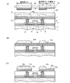
| US7888702B2 (en) * | 2005-04-15 | 2011-02-15 | Semiconductor Energy Laboratory Co., Ltd. | Display device and manufacturing method of the display device |
| US7601566B2 (en) * | 2005-10-18 | 2009-10-13 | Semiconductor Energy Laboratory Co., Ltd. | Semiconductor device and manufacturing method thereof |
| TWI328861B (en) * | 2007-03-13 | 2010-08-11 | Au Optronics Corp | Fabrication methods of thin film transistor substrate |
| KR101415561B1 (ko) * | 2007-06-14 | 2014-08-07 | 삼성디스플레이 주식회사 | 박막 트랜지스터 표시판 및 그의 제조 방법 |
| KR101448903B1 (ko) | 2007-10-23 | 2014-10-13 | 가부시키가이샤 한도오따이 에네루기 켄큐쇼 | 반도체장치 및 그의 제작방법 |
| JP5380037B2 (ja) * | 2007-10-23 | 2014-01-08 | 株式会社半導体エネルギー研究所 | 半導体装置の作製方法 |
| JP5427390B2 (ja) * | 2007-10-23 | 2014-02-26 | 株式会社半導体エネルギー研究所 | 半導体装置の作製方法 |
| US7824939B2 (en) * | 2007-10-23 | 2010-11-02 | Semiconductor Energy Laboratory Co., Ltd. | Method for manufacturing display device comprising separated and electrically connected source wiring layers |
| EP2232561A4 (en) * | 2007-12-03 | 2015-05-06 | Semiconductor Energy Lab | METHOD OF MANUFACTURING A THIN FILM TRANSISTOR AND METHOD OF MANUFACTURING A DISPLAY ARRANGEMENT |
| KR101446249B1 (ko) * | 2007-12-03 | 2014-10-01 | 가부시키가이샤 한도오따이 에네루기 켄큐쇼 | 반도체장치 제조방법 |
| JP5377940B2 (ja) * | 2007-12-03 | 2013-12-25 | 株式会社半導体エネルギー研究所 | 半導体装置 |
| US7977678B2 (en) | 2007-12-21 | 2011-07-12 | Semiconductor Energy Laboratory Co., Ltd. | Semiconductor display device |
| US8035107B2 (en) * | 2008-02-26 | 2011-10-11 | Semiconductor Energy Laboratory Co., Ltd. | Method for manufacturing display device |
| CN101939694B (zh) * | 2008-02-27 | 2014-01-29 | 株式会社半导体能源研究所 | 液晶显示器件及其制造方法以及电子装置 |
| US8101442B2 (en) * | 2008-03-05 | 2012-01-24 | Semiconductor Energy Laboratory Co., Ltd. | Method for manufacturing EL display device |
| US7749820B2 (en) * | 2008-03-07 | 2010-07-06 | Semiconductor Energy Laboratory Co., Ltd. | Thin film transistor, manufacturing method thereof, display device, and manufacturing method thereof |
| US7989275B2 (en) * | 2008-03-10 | 2011-08-02 | Semiconductor Energy Laboratory Co., Ltd. | Thin film transistor, manufacturing method thereof, display device, and manufacturing method thereof |
| US7883943B2 (en) | 2008-03-11 | 2011-02-08 | Semiconductor Energy Laboratory Co., Ltd. | Method for manufacturing thin film transistor and method for manufacturing display device |
| US7985605B2 (en) * | 2008-04-17 | 2011-07-26 | Semiconductor Energy Laboratory Co., Ltd. | Light-emitting device and manufacturing method thereof |
| US9041202B2 (en) | 2008-05-16 | 2015-05-26 | Semiconductor Energy Laboratory Co., Ltd. | Semiconductor device and manufacturing method of the same |
| US7790483B2 (en) * | 2008-06-17 | 2010-09-07 | Semiconductor Energy Laboratory Co., Ltd. | Thin film transistor and manufacturing method thereof, and display device and manufacturing method thereof |
| TWI770659B (zh) | 2008-07-31 | 2022-07-11 | 日商半導體能源研究所股份有限公司 | 半導體裝置及半導體裝置的製造方法 |
| JP2010056541A (ja) | 2008-07-31 | 2010-03-11 | Semiconductor Energy Lab Co Ltd | 半導体装置およびその作製方法 |
| KR102334634B1 (ko) | 2008-11-28 | 2021-12-06 | 가부시키가이샤 한도오따이 에네루기 켄큐쇼 | 반도체 장치, 표시 장치 및 표시 장치를 포함하는 전자 장치 |
| US20100138765A1 (en) * | 2008-11-30 | 2010-06-03 | Nokia Corporation | Indicator Pop-Up |
| JP5491833B2 (ja) * | 2008-12-05 | 2014-05-14 | 株式会社半導体エネルギー研究所 | 半導体装置 |
| US8207026B2 (en) * | 2009-01-28 | 2012-06-26 | Semiconductor Energy Laboratory Co., Ltd. | Manufacturing method of thin film transistor and manufacturing method of display device |
| KR101015850B1 (ko) * | 2009-02-09 | 2011-02-24 | 삼성모바일디스플레이주식회사 | 유기 발광 표시 장치 제조 방법 |
| JP5503995B2 (ja) * | 2009-02-13 | 2014-05-28 | 株式会社半導体エネルギー研究所 | 半導体装置の作製方法 |
| US7989234B2 (en) * | 2009-02-16 | 2011-08-02 | Semiconductor Energy Laboratory Co., Ltd. | Method for manufacturing thin film transistor and method for manufacturing display device |
| US20100224880A1 (en) * | 2009-03-05 | 2010-09-09 | Semiconductor Energy Laboratory Co., Ltd. | Semiconductor device |
| US8202769B2 (en) | 2009-03-11 | 2012-06-19 | Semiconductor Energy Laboratory Co., Ltd. | Semiconductor device and manufacturing method thereof |
| JP5539765B2 (ja) * | 2009-03-26 | 2014-07-02 | 株式会社半導体エネルギー研究所 | トランジスタの作製方法 |
| KR102181301B1 (ko) | 2009-07-18 | 2020-11-20 | 가부시키가이샤 한도오따이 에네루기 켄큐쇼 | 반도체 장치 및 반도체 장치 제조 방법 |
| TWI830077B (zh) | 2009-08-07 | 2024-01-21 | 日商半導體能源研究所股份有限公司 | 半導體裝置 |
| KR101470811B1 (ko) * | 2009-09-16 | 2014-12-09 | 가부시키가이샤 한도오따이 에네루기 켄큐쇼 | 반도체 장치 |
| KR101778513B1 (ko) | 2009-10-09 | 2017-09-15 | 가부시키가이샤 한도오따이 에네루기 켄큐쇼 | 발광 표시 장치 및 이를 포함한 전자 기기 |
| KR20120089505A (ko) * | 2010-12-10 | 2012-08-13 | 삼성전자주식회사 | 표시 장치 및 그 제조 방법 |
| CN102184928A (zh) * | 2010-12-29 | 2011-09-14 | 友达光电股份有限公司 | 显示元件及其制造方法 |
| US20120193656A1 (en) * | 2010-12-29 | 2012-08-02 | Au Optronics Corporation | Display device structure and manufacturing method thereof |
| US20130023129A1 (en) | 2011-07-20 | 2013-01-24 | Asm America, Inc. | Pressure transmitter for a semiconductor processing environment |
| CN102769040B (zh) * | 2012-07-25 | 2015-03-04 | 京东方科技集团股份有限公司 | 薄膜晶体管、阵列基板及其制作方法、显示装置 |
| US10714315B2 (en) | 2012-10-12 | 2020-07-14 | Asm Ip Holdings B.V. | Semiconductor reaction chamber showerhead |
| WO2014091959A1 (ja) * | 2012-12-10 | 2014-06-19 | シャープ株式会社 | 半導体装置およびその製造方法 |
| US20160376700A1 (en) | 2013-02-01 | 2016-12-29 | Asm Ip Holding B.V. | System for treatment of deposition reactor |
| JP6217161B2 (ja) * | 2013-06-19 | 2017-10-25 | セイコーエプソン株式会社 | 発光装置および電子機器 |
| KR102094847B1 (ko) * | 2013-07-03 | 2020-03-31 | 삼성디스플레이 주식회사 | 박막 트랜지스터를 포함하는 표시 기판 및 이의 제조 방법 |
| CN106413792A (zh) * | 2013-12-04 | 2017-02-15 | B.布劳恩梅尔松根股份公司 | 具有密封的缺口的针组件及相关方法 |
| CN103681775B (zh) * | 2013-12-31 | 2016-06-08 | 京东方科技集团股份有限公司 | Amoled显示装置 |
| US11015245B2 (en) | 2014-03-19 | 2021-05-25 | Asm Ip Holding B.V. | Gas-phase reactor and system having exhaust plenum and components thereof |
| CN104037129A (zh) * | 2014-06-20 | 2014-09-10 | 深圳市华星光电技术有限公司 | Tft背板的制造方法及tft背板结构 |
| CN104091810A (zh) * | 2014-06-30 | 2014-10-08 | 京东方科技集团股份有限公司 | 阵列基板及其制作方法、显示装置 |
| US10858737B2 (en) | 2014-07-28 | 2020-12-08 | Asm Ip Holding B.V. | Showerhead assembly and components thereof |
| JP6497876B2 (ja) | 2014-09-01 | 2019-04-10 | 三菱電機株式会社 | 液晶表示パネル、及びその製造方法 |
| KR20250028505A (ko) * | 2014-09-12 | 2025-02-28 | 가부시키가이샤 한도오따이 에네루기 켄큐쇼 | 표시 장치 |
| US10941490B2 (en) | 2014-10-07 | 2021-03-09 | Asm Ip Holding B.V. | Multiple temperature range susceptor, assembly, reactor and system including the susceptor, and methods of using the same |
| US10276355B2 (en) | 2015-03-12 | 2019-04-30 | Asm Ip Holding B.V. | Multi-zone reactor, system including the reactor, and method of using the same |
| KR102329294B1 (ko) * | 2015-04-30 | 2021-11-19 | 삼성디스플레이 주식회사 | 박막 트랜지스터 표시판 및 그 제조 방법 |
| CN104810322A (zh) * | 2015-05-18 | 2015-07-29 | 京东方科技集团股份有限公司 | 阵列基板及其制造方法、显示面板、显示装置、掩模板 |
| CN104932157B (zh) * | 2015-06-18 | 2018-07-17 | 武汉华星光电技术有限公司 | 一种阵列基板及液晶显示器 |
| US10458018B2 (en) | 2015-06-26 | 2019-10-29 | Asm Ip Holding B.V. | Structures including metal carbide material, devices including the structures, and methods of forming same |
| US10211308B2 (en) | 2015-10-21 | 2019-02-19 | Asm Ip Holding B.V. | NbMC layers |
| US11139308B2 (en) | 2015-12-29 | 2021-10-05 | Asm Ip Holding B.V. | Atomic layer deposition of III-V compounds to form V-NAND devices |
| TWI561905B (en) * | 2016-01-04 | 2016-12-11 | Au Optronics Corp | Pixel structure |
| KR102591388B1 (ko) * | 2016-01-18 | 2023-10-19 | 엘지전자 주식회사 | 반도체 발광 소자를 이용한 디스플레이 장치 |
| JP6685142B2 (ja) * | 2016-02-02 | 2020-04-22 | 株式会社ジャパンディスプレイ | 表示装置及びその製造方法 |
| US10529554B2 (en) | 2016-02-19 | 2020-01-07 | Asm Ip Holding B.V. | Method for forming silicon nitride film selectively on sidewalls or flat surfaces of trenches |
| US10343920B2 (en) | 2016-03-18 | 2019-07-09 | Asm Ip Holding B.V. | Aligned carbon nanotubes |
| KR102651136B1 (ko) | 2016-04-12 | 2024-03-25 | 삼성디스플레이 주식회사 | 유기 발광 표시 장치 및 그 제조 방법 |
| US10367080B2 (en) | 2016-05-02 | 2019-07-30 | Asm Ip Holding B.V. | Method of forming a germanium oxynitride film |
| CN105742299B (zh) * | 2016-05-16 | 2019-11-29 | 京东方科技集团股份有限公司 | 一种像素单元及其制作方法、阵列基板及显示装置 |
| US11453943B2 (en) | 2016-05-25 | 2022-09-27 | Asm Ip Holding B.V. | Method for forming carbon-containing silicon/metal oxide or nitride film by ALD using silicon precursor and hydrocarbon precursor |
| KR102663140B1 (ko) * | 2016-06-24 | 2024-05-08 | 삼성디스플레이 주식회사 | 디스플레이 장치 |
| CN109313871A (zh) * | 2016-06-28 | 2019-02-05 | 夏普株式会社 | 有源矩阵基板、光闸基板、显示装置、有源矩阵基板的制造方法 |
| US10612137B2 (en) | 2016-07-08 | 2020-04-07 | Asm Ip Holdings B.V. | Organic reactants for atomic layer deposition |
| US9859151B1 (en) | 2016-07-08 | 2018-01-02 | Asm Ip Holding B.V. | Selective film deposition method to form air gaps |
| US9887082B1 (en) | 2016-07-28 | 2018-02-06 | Asm Ip Holding B.V. | Method and apparatus for filling a gap |
| KR102532607B1 (ko) | 2016-07-28 | 2023-05-15 | 에이에스엠 아이피 홀딩 비.브이. | 기판 가공 장치 및 그 동작 방법 |
| US9812320B1 (en) | 2016-07-28 | 2017-11-07 | Asm Ip Holding B.V. | Method and apparatus for filling a gap |
| JP2018017981A (ja) * | 2016-07-29 | 2018-02-01 | 株式会社ジャパンディスプレイ | 電子機器 |
| JP2018048893A (ja) | 2016-09-21 | 2018-03-29 | Ntn株式会社 | 二次電池の劣化判定装置 |
| US11532757B2 (en) | 2016-10-27 | 2022-12-20 | Asm Ip Holding B.V. | Deposition of charge trapping layers |
| US10714350B2 (en) | 2016-11-01 | 2020-07-14 | ASM IP Holdings, B.V. | Methods for forming a transition metal niobium nitride film on a substrate by atomic layer deposition and related semiconductor device structures |
| KR102546317B1 (ko) | 2016-11-15 | 2023-06-21 | 에이에스엠 아이피 홀딩 비.브이. | 기체 공급 유닛 및 이를 포함하는 기판 처리 장치 |
| KR102762543B1 (ko) | 2016-12-14 | 2025-02-05 | 에이에스엠 아이피 홀딩 비.브이. | 기판 처리 장치 |
| US11581186B2 (en) | 2016-12-15 | 2023-02-14 | Asm Ip Holding B.V. | Sequential infiltration synthesis apparatus |
| US11447861B2 (en) | 2016-12-15 | 2022-09-20 | Asm Ip Holding B.V. | Sequential infiltration synthesis apparatus and a method of forming a patterned structure |
| KR102700194B1 (ko) | 2016-12-19 | 2024-08-28 | 에이에스엠 아이피 홀딩 비.브이. | 기판 처리 장치 |
| US10269558B2 (en) | 2016-12-22 | 2019-04-23 | Asm Ip Holding B.V. | Method of forming a structure on a substrate |
| US11390950B2 (en) | 2017-01-10 | 2022-07-19 | Asm Ip Holding B.V. | Reactor system and method to reduce residue buildup during a film deposition process |
| US10468261B2 (en) | 2017-02-15 | 2019-11-05 | Asm Ip Holding B.V. | Methods for forming a metallic film on a substrate by cyclical deposition and related semiconductor device structures |
| US10529563B2 (en) | 2017-03-29 | 2020-01-07 | Asm Ip Holdings B.V. | Method for forming doped metal oxide films on a substrate by cyclical deposition and related semiconductor device structures |
| US10770286B2 (en) | 2017-05-08 | 2020-09-08 | Asm Ip Holdings B.V. | Methods for selectively forming a silicon nitride film on a substrate and related semiconductor device structures |
| US12040200B2 (en) | 2017-06-20 | 2024-07-16 | Asm Ip Holding B.V. | Semiconductor processing apparatus and methods for calibrating a semiconductor processing apparatus |
| US11306395B2 (en) | 2017-06-28 | 2022-04-19 | Asm Ip Holding B.V. | Methods for depositing a transition metal nitride film on a substrate by atomic layer deposition and related deposition apparatus |
| KR20190009245A (ko) | 2017-07-18 | 2019-01-28 | 에이에스엠 아이피 홀딩 비.브이. | 반도체 소자 구조물 형성 방법 및 관련된 반도체 소자 구조물 |
| US11374112B2 (en) | 2017-07-19 | 2022-06-28 | Asm Ip Holding B.V. | Method for depositing a group IV semiconductor and related semiconductor device structures |
| US11018002B2 (en) | 2017-07-19 | 2021-05-25 | Asm Ip Holding B.V. | Method for selectively depositing a Group IV semiconductor and related semiconductor device structures |
| US10541333B2 (en) | 2017-07-19 | 2020-01-21 | Asm Ip Holding B.V. | Method for depositing a group IV semiconductor and related semiconductor device structures |
| US10590535B2 (en) | 2017-07-26 | 2020-03-17 | Asm Ip Holdings B.V. | Chemical treatment, deposition and/or infiltration apparatus and method for using the same |
| TWI815813B (zh) | 2017-08-04 | 2023-09-21 | 荷蘭商Asm智慧財產控股公司 | 用於分配反應腔內氣體的噴頭總成 |
| US10770336B2 (en) | 2017-08-08 | 2020-09-08 | Asm Ip Holding B.V. | Substrate lift mechanism and reactor including same |
| US10692741B2 (en) | 2017-08-08 | 2020-06-23 | Asm Ip Holdings B.V. | Radiation shield |
| US11139191B2 (en) | 2017-08-09 | 2021-10-05 | Asm Ip Holding B.V. | Storage apparatus for storing cassettes for substrates and processing apparatus equipped therewith |
| US11769682B2 (en) | 2017-08-09 | 2023-09-26 | Asm Ip Holding B.V. | Storage apparatus for storing cassettes for substrates and processing apparatus equipped therewith |
| US11830730B2 (en) | 2017-08-29 | 2023-11-28 | Asm Ip Holding B.V. | Layer forming method and apparatus |
| US11295980B2 (en) | 2017-08-30 | 2022-04-05 | Asm Ip Holding B.V. | Methods for depositing a molybdenum metal film over a dielectric surface of a substrate by a cyclical deposition process and related semiconductor device structures |
| KR102491945B1 (ko) | 2017-08-30 | 2023-01-26 | 에이에스엠 아이피 홀딩 비.브이. | 기판 처리 장치 |
| US11056344B2 (en) | 2017-08-30 | 2021-07-06 | Asm Ip Holding B.V. | Layer forming method |
| US10658205B2 (en) | 2017-09-28 | 2020-05-19 | Asm Ip Holdings B.V. | Chemical dispensing apparatus and methods for dispensing a chemical to a reaction chamber |
| US10403504B2 (en) | 2017-10-05 | 2019-09-03 | Asm Ip Holding B.V. | Method for selectively depositing a metallic film on a substrate |
| KR102556021B1 (ko) * | 2017-10-13 | 2023-07-17 | 삼성디스플레이 주식회사 | 디스플레이 장치 및 그 제조방법 |
| JP2019074684A (ja) | 2017-10-18 | 2019-05-16 | シャープ株式会社 | 表示パネル用基板の製造方法 |
| US10923344B2 (en) | 2017-10-30 | 2021-02-16 | Asm Ip Holding B.V. | Methods for forming a semiconductor structure and related semiconductor structures |
| US11022879B2 (en) | 2017-11-24 | 2021-06-01 | Asm Ip Holding B.V. | Method of forming an enhanced unexposed photoresist layer |
| TWI791689B (zh) | 2017-11-27 | 2023-02-11 | 荷蘭商Asm智慧財產控股私人有限公司 | 包括潔淨迷你環境之裝置 |
| JP7214724B2 (ja) | 2017-11-27 | 2023-01-30 | エーエスエム アイピー ホールディング ビー.ブイ. | バッチ炉で利用されるウェハカセットを収納するための収納装置 |
| KR102092034B1 (ko) | 2017-12-06 | 2020-03-23 | 엘지디스플레이 주식회사 | 표시 장치 및 표시 장치의 제조 방법 |
| CN108091674B (zh) * | 2017-12-12 | 2020-06-26 | 武汉华星光电半导体显示技术有限公司 | Oled背板结构及oled背板制作方法 |
| US10872771B2 (en) | 2018-01-16 | 2020-12-22 | Asm Ip Holding B. V. | Method for depositing a material film on a substrate within a reaction chamber by a cyclical deposition process and related device structures |
| KR102695659B1 (ko) | 2018-01-19 | 2024-08-14 | 에이에스엠 아이피 홀딩 비.브이. | 플라즈마 보조 증착에 의해 갭 충진 층을 증착하는 방법 |
| TWI799494B (zh) | 2018-01-19 | 2023-04-21 | 荷蘭商Asm 智慧財產控股公司 | 沈積方法 |
| US11081345B2 (en) | 2018-02-06 | 2021-08-03 | Asm Ip Holding B.V. | Method of post-deposition treatment for silicon oxide film |
| WO2019159261A1 (ja) * | 2018-02-14 | 2019-08-22 | シャープ株式会社 | 表示デバイスの製造方法および露光マスク |
| US11685991B2 (en) | 2018-02-14 | 2023-06-27 | Asm Ip Holding B.V. | Method for depositing a ruthenium-containing film on a substrate by a cyclical deposition process |
| US10896820B2 (en) | 2018-02-14 | 2021-01-19 | Asm Ip Holding B.V. | Method for depositing a ruthenium-containing film on a substrate by a cyclical deposition process |
| US10731249B2 (en) | 2018-02-15 | 2020-08-04 | Asm Ip Holding B.V. | Method of forming a transition metal containing film on a substrate by a cyclical deposition process, a method for supplying a transition metal halide compound to a reaction chamber, and related vapor deposition apparatus |
| KR102636427B1 (ko) | 2018-02-20 | 2024-02-13 | 에이에스엠 아이피 홀딩 비.브이. | 기판 처리 방법 및 장치 |
| US10975470B2 (en) | 2018-02-23 | 2021-04-13 | Asm Ip Holding B.V. | Apparatus for detecting or monitoring for a chemical precursor in a high temperature environment |
| US11473195B2 (en) | 2018-03-01 | 2022-10-18 | Asm Ip Holding B.V. | Semiconductor processing apparatus and a method for processing a substrate |
| KR102560100B1 (ko) * | 2018-03-08 | 2023-07-26 | 삼성디스플레이 주식회사 | 표시 장치 및 이의 제조 방법 |
| US11629406B2 (en) | 2018-03-09 | 2023-04-18 | Asm Ip Holding B.V. | Semiconductor processing apparatus comprising one or more pyrometers for measuring a temperature of a substrate during transfer of the substrate |
| US11114283B2 (en) | 2018-03-16 | 2021-09-07 | Asm Ip Holding B.V. | Reactor, system including the reactor, and methods of manufacturing and using same |
| KR102646467B1 (ko) | 2018-03-27 | 2024-03-11 | 에이에스엠 아이피 홀딩 비.브이. | 기판 상에 전극을 형성하는 방법 및 전극을 포함하는 반도체 소자 구조 |
| US11088002B2 (en) | 2018-03-29 | 2021-08-10 | Asm Ip Holding B.V. | Substrate rack and a substrate processing system and method |
| US11230766B2 (en) | 2018-03-29 | 2022-01-25 | Asm Ip Holding B.V. | Substrate processing apparatus and method |
| KR102600229B1 (ko) | 2018-04-09 | 2023-11-10 | 에이에스엠 아이피 홀딩 비.브이. | 기판 지지 장치, 이를 포함하는 기판 처리 장치 및 기판 처리 방법 |
| US12025484B2 (en) | 2018-05-08 | 2024-07-02 | Asm Ip Holding B.V. | Thin film forming method |
| TWI843623B (zh) | 2018-05-08 | 2024-05-21 | 荷蘭商Asm Ip私人控股有限公司 | 藉由循環沉積製程於基板上沉積氧化物膜之方法及相關裝置結構 |
| US12272527B2 (en) | 2018-05-09 | 2025-04-08 | Asm Ip Holding B.V. | Apparatus for use with hydrogen radicals and method of using same |
| KR102596988B1 (ko) | 2018-05-28 | 2023-10-31 | 에이에스엠 아이피 홀딩 비.브이. | 기판 처리 방법 및 그에 의해 제조된 장치 |
| TWI840362B (zh) | 2018-06-04 | 2024-05-01 | 荷蘭商Asm Ip私人控股有限公司 | 水氣降低的晶圓處置腔室 |
| US11718913B2 (en) | 2018-06-04 | 2023-08-08 | Asm Ip Holding B.V. | Gas distribution system and reactor system including same |
| US11286562B2 (en) | 2018-06-08 | 2022-03-29 | Asm Ip Holding B.V. | Gas-phase chemical reactor and method of using same |
| US10797133B2 (en) | 2018-06-21 | 2020-10-06 | Asm Ip Holding B.V. | Method for depositing a phosphorus doped silicon arsenide film and related semiconductor device structures |
| KR102568797B1 (ko) | 2018-06-21 | 2023-08-21 | 에이에스엠 아이피 홀딩 비.브이. | 기판 처리 시스템 |
| TWI871083B (zh) | 2018-06-27 | 2025-01-21 | 荷蘭商Asm Ip私人控股有限公司 | 用於形成含金屬材料之循環沉積製程 |
| US11499222B2 (en) | 2018-06-27 | 2022-11-15 | Asm Ip Holding B.V. | Cyclic deposition methods for forming metal-containing material and films and structures including the metal-containing material |
| US10612136B2 (en) | 2018-06-29 | 2020-04-07 | ASM IP Holding, B.V. | Temperature-controlled flange and reactor system including same |
| US10388513B1 (en) | 2018-07-03 | 2019-08-20 | Asm Ip Holding B.V. | Method for depositing silicon-free carbon-containing film as gap-fill layer by pulse plasma-assisted deposition |
| US10755922B2 (en) | 2018-07-03 | 2020-08-25 | Asm Ip Holding B.V. | Method for depositing silicon-free carbon-containing film as gap-fill layer by pulse plasma-assisted deposition |
| US11053591B2 (en) | 2018-08-06 | 2021-07-06 | Asm Ip Holding B.V. | Multi-port gas injection system and reactor system including same |
| CN109037297B (zh) * | 2018-08-09 | 2021-01-29 | 京东方科技集团股份有限公司 | 一种有机发光显示基板及其制作方法 |
| US11430674B2 (en) | 2018-08-22 | 2022-08-30 | Asm Ip Holding B.V. | Sensor array, apparatus for dispensing a vapor phase reactant to a reaction chamber and related methods |
| KR102707956B1 (ko) | 2018-09-11 | 2024-09-19 | 에이에스엠 아이피 홀딩 비.브이. | 박막 증착 방법 |
| US11024523B2 (en) | 2018-09-11 | 2021-06-01 | Asm Ip Holding B.V. | Substrate processing apparatus and method |
| US11049751B2 (en) | 2018-09-14 | 2021-06-29 | Asm Ip Holding B.V. | Cassette supply system to store and handle cassettes and processing apparatus equipped therewith |
| CN110970344B (zh) | 2018-10-01 | 2024-10-25 | Asmip控股有限公司 | 衬底保持设备、包含所述设备的系统及其使用方法 |
| US11232963B2 (en) | 2018-10-03 | 2022-01-25 | Asm Ip Holding B.V. | Substrate processing apparatus and method |
| KR102592699B1 (ko) | 2018-10-08 | 2023-10-23 | 에이에스엠 아이피 홀딩 비.브이. | 기판 지지 유닛 및 이를 포함하는 박막 증착 장치와 기판 처리 장치 |
| KR102546322B1 (ko) | 2018-10-19 | 2023-06-21 | 에이에스엠 아이피 홀딩 비.브이. | 기판 처리 장치 및 기판 처리 방법 |
| KR102605121B1 (ko) | 2018-10-19 | 2023-11-23 | 에이에스엠 아이피 홀딩 비.브이. | 기판 처리 장치 및 기판 처리 방법 |
| USD948463S1 (en) | 2018-10-24 | 2022-04-12 | Asm Ip Holding B.V. | Susceptor for semiconductor substrate supporting apparatus |
| US12378665B2 (en) | 2018-10-26 | 2025-08-05 | Asm Ip Holding B.V. | High temperature coatings for a preclean and etch apparatus and related methods |
| US11087997B2 (en) | 2018-10-31 | 2021-08-10 | Asm Ip Holding B.V. | Substrate processing apparatus for processing substrates |
| KR102748291B1 (ko) | 2018-11-02 | 2024-12-31 | 에이에스엠 아이피 홀딩 비.브이. | 기판 지지 유닛 및 이를 포함하는 기판 처리 장치 |
| US11572620B2 (en) | 2018-11-06 | 2023-02-07 | Asm Ip Holding B.V. | Methods for selectively depositing an amorphous silicon film on a substrate |
| US11031242B2 (en) | 2018-11-07 | 2021-06-08 | Asm Ip Holding B.V. | Methods for depositing a boron doped silicon germanium film |
| US10818758B2 (en) | 2018-11-16 | 2020-10-27 | Asm Ip Holding B.V. | Methods for forming a metal silicate film on a substrate in a reaction chamber and related semiconductor device structures |
| US10847366B2 (en) | 2018-11-16 | 2020-11-24 | Asm Ip Holding B.V. | Methods for depositing a transition metal chalcogenide film on a substrate by a cyclical deposition process |
| US12040199B2 (en) | 2018-11-28 | 2024-07-16 | Asm Ip Holding B.V. | Substrate processing apparatus for processing substrates |
| US11217444B2 (en) | 2018-11-30 | 2022-01-04 | Asm Ip Holding B.V. | Method for forming an ultraviolet radiation responsive metal oxide-containing film |
| KR102636428B1 (ko) | 2018-12-04 | 2024-02-13 | 에이에스엠 아이피 홀딩 비.브이. | 기판 처리 장치를 세정하는 방법 |
| US11158513B2 (en) | 2018-12-13 | 2021-10-26 | Asm Ip Holding B.V. | Methods for forming a rhenium-containing film on a substrate by a cyclical deposition process and related semiconductor device structures |
| JP7504584B2 (ja) | 2018-12-14 | 2024-06-24 | エーエスエム・アイピー・ホールディング・ベー・フェー | 窒化ガリウムの選択的堆積を用いてデバイス構造体を形成する方法及びそのためのシステム |
| CN109658831B (zh) * | 2018-12-20 | 2021-05-04 | 厦门天马微电子有限公司 | 一种显示面板及显示装置 |
| TWI866480B (zh) | 2019-01-17 | 2024-12-11 | 荷蘭商Asm Ip 私人控股有限公司 | 藉由循環沈積製程於基板上形成含過渡金屬膜之方法 |
| KR102727227B1 (ko) | 2019-01-22 | 2024-11-07 | 에이에스엠 아이피 홀딩 비.브이. | 기판 처리 장치 |
| CN111524788B (zh) | 2019-02-01 | 2023-11-24 | Asm Ip私人控股有限公司 | 氧化硅的拓扑选择性膜形成的方法 |
| TWI873122B (zh) | 2019-02-20 | 2025-02-21 | 荷蘭商Asm Ip私人控股有限公司 | 填充一基板之一表面內所形成的一凹槽的方法、根據其所形成之半導體結構、及半導體處理設備 |
| TWI845607B (zh) | 2019-02-20 | 2024-06-21 | 荷蘭商Asm Ip私人控股有限公司 | 用來填充形成於基材表面內之凹部的循環沉積方法及設備 |
| KR20200102357A (ko) | 2019-02-20 | 2020-08-31 | 에이에스엠 아이피 홀딩 비.브이. | 3-d nand 응용의 플러그 충진체 증착용 장치 및 방법 |
| KR102626263B1 (ko) | 2019-02-20 | 2024-01-16 | 에이에스엠 아이피 홀딩 비.브이. | 처리 단계를 포함하는 주기적 증착 방법 및 이를 위한 장치 |
| TWI842826B (zh) | 2019-02-22 | 2024-05-21 | 荷蘭商Asm Ip私人控股有限公司 | 基材處理設備及處理基材之方法 |
| KR102858005B1 (ko) | 2019-03-08 | 2025-09-09 | 에이에스엠 아이피 홀딩 비.브이. | 실리콘 질화물 층을 선택적으로 증착하는 방법, 및 선택적으로 증착된 실리콘 질화물 층을 포함하는 구조체 |
| KR102782593B1 (ko) | 2019-03-08 | 2025-03-14 | 에이에스엠 아이피 홀딩 비.브이. | SiOC 층을 포함한 구조체 및 이의 형성 방법 |
| KR102762833B1 (ko) | 2019-03-08 | 2025-02-04 | 에이에스엠 아이피 홀딩 비.브이. | SiOCN 층을 포함한 구조체 및 이의 형성 방법 |
| JP2020167398A (ja) | 2019-03-28 | 2020-10-08 | エーエスエム・アイピー・ホールディング・ベー・フェー | ドアオープナーおよびドアオープナーが提供される基材処理装置 |
| KR102809999B1 (ko) | 2019-04-01 | 2025-05-19 | 에이에스엠 아이피 홀딩 비.브이. | 반도체 소자를 제조하는 방법 |
| KR102897355B1 (ko) | 2019-04-19 | 2025-12-08 | 에이에스엠 아이피 홀딩 비.브이. | 층 형성 방법 및 장치 |
| KR20200125453A (ko) | 2019-04-24 | 2020-11-04 | 에이에스엠 아이피 홀딩 비.브이. | 기상 반응기 시스템 및 이를 사용하는 방법 |
| KR102869364B1 (ko) | 2019-05-07 | 2025-10-10 | 에이에스엠 아이피 홀딩 비.브이. | 비정질 탄소 중합체 막을 개질하는 방법 |
| KR102929471B1 (ko) | 2019-05-07 | 2026-02-20 | 에이에스엠 아이피 홀딩 비.브이. | 딥 튜브가 있는 화학물질 공급원 용기 |
| KR102929472B1 (ko) | 2019-05-10 | 2026-02-20 | 에이에스엠 아이피 홀딩 비.브이. | 표면 상에 재료를 증착하는 방법 및 본 방법에 따라 형성된 구조 |
| JP7598201B2 (ja) | 2019-05-16 | 2024-12-11 | エーエスエム・アイピー・ホールディング・ベー・フェー | ウェハボートハンドリング装置、縦型バッチ炉および方法 |
| JP7612342B2 (ja) | 2019-05-16 | 2025-01-14 | エーエスエム・アイピー・ホールディング・ベー・フェー | ウェハボートハンドリング装置、縦型バッチ炉および方法 |
| USD947913S1 (en) | 2019-05-17 | 2022-04-05 | Asm Ip Holding B.V. | Susceptor shaft |
| USD975665S1 (en) | 2019-05-17 | 2023-01-17 | Asm Ip Holding B.V. | Susceptor shaft |
| USD935572S1 (en) | 2019-05-24 | 2021-11-09 | Asm Ip Holding B.V. | Gas channel plate |
| USD922229S1 (en) | 2019-06-05 | 2021-06-15 | Asm Ip Holding B.V. | Device for controlling a temperature of a gas supply unit |
| KR20200141002A (ko) | 2019-06-06 | 2020-12-17 | 에이에스엠 아이피 홀딩 비.브이. | 배기 가스 분석을 포함한 기상 반응기 시스템을 사용하는 방법 |
| KR102918757B1 (ko) | 2019-06-10 | 2026-01-28 | 에이에스엠 아이피 홀딩 비.브이. | 석영 에피택셜 챔버를 세정하는 방법 |
| KR20200143254A (ko) | 2019-06-11 | 2020-12-23 | 에이에스엠 아이피 홀딩 비.브이. | 개질 가스를 사용하여 전자 구조를 형성하는 방법, 상기 방법을 수행하기 위한 시스템, 및 상기 방법을 사용하여 형성되는 구조 |
| USD944946S1 (en) | 2019-06-14 | 2022-03-01 | Asm Ip Holding B.V. | Shower plate |
| USD931978S1 (en) | 2019-06-27 | 2021-09-28 | Asm Ip Holding B.V. | Showerhead vacuum transport |
| KR102911421B1 (ko) | 2019-07-03 | 2026-01-12 | 에이에스엠 아이피 홀딩 비.브이. | 기판 처리 장치용 온도 제어 조립체 및 이를 사용하는 방법 |
| JP7499079B2 (ja) | 2019-07-09 | 2024-06-13 | エーエスエム・アイピー・ホールディング・ベー・フェー | 同軸導波管を用いたプラズマ装置、基板処理方法 |
| CN112216646B (zh) | 2019-07-10 | 2026-02-10 | Asmip私人控股有限公司 | 基板支撑组件及包括其的基板处理装置 |
| KR102895115B1 (ko) | 2019-07-16 | 2025-12-03 | 에이에스엠 아이피 홀딩 비.브이. | 기판 처리 장치 |
| TWI826704B (zh) | 2019-07-17 | 2023-12-21 | 荷蘭商Asm Ip私人控股有限公司 | 自由基輔助引燃電漿系統和方法 |
| KR102860110B1 (ko) | 2019-07-17 | 2025-09-16 | 에이에스엠 아이피 홀딩 비.브이. | 실리콘 게르마늄 구조를 형성하는 방법 |
| US11643724B2 (en) | 2019-07-18 | 2023-05-09 | Asm Ip Holding B.V. | Method of forming structures using a neutral beam |
| TWI839544B (zh) | 2019-07-19 | 2024-04-21 | 荷蘭商Asm Ip私人控股有限公司 | 形成形貌受控的非晶碳聚合物膜之方法 |
| KR102903090B1 (ko) | 2019-07-19 | 2025-12-19 | 에이에스엠 아이피 홀딩 비.브이. | 토폴로지-제어된 비정질 탄소 중합체 막을 형성하는 방법 |
| CN112309843B (zh) | 2019-07-29 | 2026-01-23 | Asmip私人控股有限公司 | 实现高掺杂剂掺入的选择性沉积方法 |
| CN112309899B (zh) | 2019-07-30 | 2025-11-14 | Asmip私人控股有限公司 | 基板处理设备 |
| CN112309900B (zh) | 2019-07-30 | 2025-11-04 | Asmip私人控股有限公司 | 基板处理设备 |
| KR20210015655A (ko) | 2019-07-30 | 2021-02-10 | 에이에스엠 아이피 홀딩 비.브이. | 기판 처리 장치 및 방법 |
| US11587815B2 (en) | 2019-07-31 | 2023-02-21 | Asm Ip Holding B.V. | Vertical batch furnace assembly |
| US11587814B2 (en) | 2019-07-31 | 2023-02-21 | Asm Ip Holding B.V. | Vertical batch furnace assembly |
| US11227782B2 (en) | 2019-07-31 | 2022-01-18 | Asm Ip Holding B.V. | Vertical batch furnace assembly |
| KR20210018759A (ko) | 2019-08-05 | 2021-02-18 | 에이에스엠 아이피 홀딩 비.브이. | 화학물질 공급원 용기를 위한 액체 레벨 센서 |
| KR20210018761A (ko) | 2019-08-09 | 2021-02-18 | 에이에스엠 아이피 홀딩 비.브이. | 냉각 장치를 포함한 히터 어셈블리 및 이를 사용하는 방법 |
| USD965044S1 (en) | 2019-08-19 | 2022-09-27 | Asm Ip Holding B.V. | Susceptor shaft |
| USD965524S1 (en) | 2019-08-19 | 2022-10-04 | Asm Ip Holding B.V. | Susceptor support |
| JP7810514B2 (ja) | 2019-08-21 | 2026-02-03 | エーエスエム・アイピー・ホールディング・ベー・フェー | 成膜原料混合ガス生成装置及び成膜装置 |
| USD940837S1 (en) | 2019-08-22 | 2022-01-11 | Asm Ip Holding B.V. | Electrode |
| USD949319S1 (en) | 2019-08-22 | 2022-04-19 | Asm Ip Holding B.V. | Exhaust duct |
| USD930782S1 (en) | 2019-08-22 | 2021-09-14 | Asm Ip Holding B.V. | Gas distributor |
| KR20210024423A (ko) | 2019-08-22 | 2021-03-05 | 에이에스엠 아이피 홀딩 비.브이. | 홀을 구비한 구조체를 형성하기 위한 방법 |
| USD979506S1 (en) | 2019-08-22 | 2023-02-28 | Asm Ip Holding B.V. | Insulator |
| KR102928101B1 (ko) | 2019-08-23 | 2026-02-13 | 에이에스엠 아이피 홀딩 비.브이. | 비스(디에틸아미노)실란을 사용하여 peald에 의해 개선된 품질을 갖는 실리콘 산화물 막을 증착하기 위한 방법 |
| US11286558B2 (en) | 2019-08-23 | 2022-03-29 | Asm Ip Holding B.V. | Methods for depositing a molybdenum nitride film on a surface of a substrate by a cyclical deposition process and related semiconductor device structures including a molybdenum nitride film |
| KR102868968B1 (ko) | 2019-09-03 | 2025-10-10 | 에이에스엠 아이피 홀딩 비.브이. | 칼코지나이드 막 및 상기 막을 포함한 구조체를 증착하기 위한 방법 및 장치 |
| KR102806450B1 (ko) | 2019-09-04 | 2025-05-12 | 에이에스엠 아이피 홀딩 비.브이. | 희생 캡핑 층을 이용한 선택적 증착 방법 |
| KR102733104B1 (ko) | 2019-09-05 | 2024-11-22 | 에이에스엠 아이피 홀딩 비.브이. | 기판 처리 장치 |
| US12469693B2 (en) | 2019-09-17 | 2025-11-11 | Asm Ip Holding B.V. | Method of forming a carbon-containing layer and structure including the layer |
| US11562901B2 (en) | 2019-09-25 | 2023-01-24 | Asm Ip Holding B.V. | Substrate processing method |
| CN112593212B (zh) | 2019-10-02 | 2023-12-22 | Asm Ip私人控股有限公司 | 通过循环等离子体增强沉积工艺形成拓扑选择性氧化硅膜的方法 |
| TWI846953B (zh) | 2019-10-08 | 2024-07-01 | 荷蘭商Asm Ip私人控股有限公司 | 基板處理裝置 |
| TW202128273A (zh) | 2019-10-08 | 2021-08-01 | 荷蘭商Asm Ip私人控股有限公司 | 氣體注入系統、及將材料沉積於反應室內之基板表面上的方法 |
| KR102948143B1 (ko) | 2019-10-08 | 2026-04-07 | 에이에스엠 아이피 홀딩 비.브이. | 활성 종을 이용하기 위한 가스 분배 어셈블리를 포함한 반응기 시스템 및 이를 사용하는 방법 |
| TWI846966B (zh) | 2019-10-10 | 2024-07-01 | 荷蘭商Asm Ip私人控股有限公司 | 形成光阻底層之方法及包括光阻底層之結構 |
| US12009241B2 (en) | 2019-10-14 | 2024-06-11 | Asm Ip Holding B.V. | Vertical batch furnace assembly with detector to detect cassette |
| TWI834919B (zh) | 2019-10-16 | 2024-03-11 | 荷蘭商Asm Ip私人控股有限公司 | 氧化矽之拓撲選擇性膜形成之方法 |
| US11637014B2 (en) | 2019-10-17 | 2023-04-25 | Asm Ip Holding B.V. | Methods for selective deposition of doped semiconductor material |
| KR102845724B1 (ko) | 2019-10-21 | 2025-08-13 | 에이에스엠 아이피 홀딩 비.브이. | 막을 선택적으로 에칭하기 위한 장치 및 방법 |
| US11996292B2 (en) | 2019-10-25 | 2024-05-28 | Asm Ip Holding B.V. | Methods for filling a gap feature on a substrate surface and related semiconductor structures |
| US11646205B2 (en) | 2019-10-29 | 2023-05-09 | Asm Ip Holding B.V. | Methods of selectively forming n-type doped material on a surface, systems for selectively forming n-type doped material, and structures formed using same |
| KR102890638B1 (ko) | 2019-11-05 | 2025-11-25 | 에이에스엠 아이피 홀딩 비.브이. | 도핑된 반도체 층을 갖는 구조체 및 이를 형성하기 위한 방법 및 시스템 |
| US11501968B2 (en) | 2019-11-15 | 2022-11-15 | Asm Ip Holding B.V. | Method for providing a semiconductor device with silicon filled gaps |
| KR102871237B1 (ko) * | 2019-11-15 | 2025-10-14 | 엘지디스플레이 주식회사 | 표시 장치 |
| KR102861314B1 (ko) | 2019-11-20 | 2025-09-17 | 에이에스엠 아이피 홀딩 비.브이. | 기판의 표면 상에 탄소 함유 물질을 증착하는 방법, 상기 방법을 사용하여 형성된 구조물, 및 상기 구조물을 형성하기 위한 시스템 |
| KR20210065848A (ko) | 2019-11-26 | 2021-06-04 | 에이에스엠 아이피 홀딩 비.브이. | 제1 유전체 표면과 제2 금속성 표면을 포함한 기판 상에 타겟 막을 선택적으로 형성하기 위한 방법 |
| CN112951697B (zh) | 2019-11-26 | 2025-07-29 | Asmip私人控股有限公司 | 基板处理设备 |
| CN120432376A (zh) | 2019-11-29 | 2025-08-05 | Asm Ip私人控股有限公司 | 基板处理设备 |
| CN112885692B (zh) | 2019-11-29 | 2025-08-15 | Asmip私人控股有限公司 | 基板处理设备 |
| JP7527928B2 (ja) | 2019-12-02 | 2024-08-05 | エーエスエム・アイピー・ホールディング・ベー・フェー | 基板処理装置、基板処理方法 |
| KR20210070898A (ko) | 2019-12-04 | 2021-06-15 | 에이에스엠 아이피 홀딩 비.브이. | 기판 처리 장치 |
| US11885013B2 (en) | 2019-12-17 | 2024-01-30 | Asm Ip Holding B.V. | Method of forming vanadium nitride layer and structure including the vanadium nitride layer |
| KR102943768B1 (ko) | 2019-12-19 | 2026-03-26 | 에이에스엠 아이피 홀딩 비.브이. | 기판 상의 갭 피처를 충진하는 방법 및 이와 관련된 반도체 소자 구조 |
| TWI887322B (zh) | 2020-01-06 | 2025-06-21 | 荷蘭商Asm Ip私人控股有限公司 | 反應器系統、抬升銷、及處理方法 |
| JP7730637B2 (ja) | 2020-01-06 | 2025-08-28 | エーエスエム・アイピー・ホールディング・ベー・フェー | ガス供給アセンブリ、その構成要素、およびこれを含む反応器システム |
| US11993847B2 (en) | 2020-01-08 | 2024-05-28 | Asm Ip Holding B.V. | Injector |
| KR102882467B1 (ko) | 2020-01-16 | 2025-11-05 | 에이에스엠 아이피 홀딩 비.브이. | 고 종횡비 피처를 형성하는 방법 |
| KR102675856B1 (ko) | 2020-01-20 | 2024-06-17 | 에이에스엠 아이피 홀딩 비.브이. | 박막 형성 방법 및 박막 표면 개질 방법 |
| TWI889744B (zh) | 2020-01-29 | 2025-07-11 | 荷蘭商Asm Ip私人控股有限公司 | 污染物捕集系統、及擋板堆疊 |
| TW202513845A (zh) | 2020-02-03 | 2025-04-01 | 荷蘭商Asm Ip私人控股有限公司 | 半導體裝置結構及其形成方法 |
| KR20210100010A (ko) | 2020-02-04 | 2021-08-13 | 에이에스엠 아이피 홀딩 비.브이. | 대형 물품의 투과율 측정을 위한 방법 및 장치 |
| US11776846B2 (en) | 2020-02-07 | 2023-10-03 | Asm Ip Holding B.V. | Methods for depositing gap filling fluids and related systems and devices |
| KR20210103953A (ko) | 2020-02-13 | 2021-08-24 | 에이에스엠 아이피 홀딩 비.브이. | 가스 분배 어셈블리 및 이를 사용하는 방법 |
| KR102916725B1 (ko) | 2020-02-13 | 2026-01-23 | 에이에스엠 아이피 홀딩 비.브이. | 수광 장치를 포함하는 기판 처리 장치 및 수광 장치의 교정 방법 |
| US11781243B2 (en) | 2020-02-17 | 2023-10-10 | Asm Ip Holding B.V. | Method for depositing low temperature phosphorous-doped silicon |
| CN111293153B (zh) * | 2020-02-20 | 2025-04-25 | 深圳市华星光电半导体显示技术有限公司 | 一种显示面板及显示面板制程方法 |
| TWI895326B (zh) | 2020-02-28 | 2025-09-01 | 荷蘭商Asm Ip私人控股有限公司 | 專用於零件清潔的系統 |
| KR102943116B1 (ko) | 2020-03-04 | 2026-03-23 | 에이에스엠 아이피 홀딩 비.브이. | 반응기 시스템용 정렬 고정구 |
| US11876356B2 (en) | 2020-03-11 | 2024-01-16 | Asm Ip Holding B.V. | Lockout tagout assembly and system and method of using same |
| KR20210116240A (ko) | 2020-03-11 | 2021-09-27 | 에이에스엠 아이피 홀딩 비.브이. | 조절성 접합부를 갖는 기판 핸들링 장치 |
| KR102775390B1 (ko) | 2020-03-12 | 2025-02-28 | 에이에스엠 아이피 홀딩 비.브이. | 타겟 토폴로지 프로파일을 갖는 층 구조를 제조하기 위한 방법 |
| US12173404B2 (en) | 2020-03-17 | 2024-12-24 | Asm Ip Holding B.V. | Method of depositing epitaxial material, structure formed using the method, and system for performing the method |
| KR102904802B1 (ko) | 2020-03-26 | 2025-12-26 | 삼성디스플레이 주식회사 | 표시 장치 |
| KR102755229B1 (ko) | 2020-04-02 | 2025-01-14 | 에이에스엠 아이피 홀딩 비.브이. | 박막 형성 방법 |
| TWI887376B (zh) | 2020-04-03 | 2025-06-21 | 荷蘭商Asm Ip私人控股有限公司 | 半導體裝置的製造方法 |
| TWI888525B (zh) | 2020-04-08 | 2025-07-01 | 荷蘭商Asm Ip私人控股有限公司 | 用於選擇性蝕刻氧化矽膜之設備及方法 |
| US11821078B2 (en) | 2020-04-15 | 2023-11-21 | Asm Ip Holding B.V. | Method for forming precoat film and method for forming silicon-containing film |
| KR20210128343A (ko) | 2020-04-15 | 2021-10-26 | 에이에스엠 아이피 홀딩 비.브이. | 크롬 나이트라이드 층을 형성하는 방법 및 크롬 나이트라이드 층을 포함하는 구조 |
| US11996289B2 (en) | 2020-04-16 | 2024-05-28 | Asm Ip Holding B.V. | Methods of forming structures including silicon germanium and silicon layers, devices formed using the methods, and systems for performing the methods |
| KR102901748B1 (ko) | 2020-04-21 | 2025-12-17 | 에이에스엠 아이피 홀딩 비.브이. | 기판을 처리하기 위한 방법 |
| KR20210132600A (ko) | 2020-04-24 | 2021-11-04 | 에이에스엠 아이피 홀딩 비.브이. | 바나듐, 질소 및 추가 원소를 포함한 층을 증착하기 위한 방법 및 시스템 |
| KR102934380B1 (ko) | 2020-04-24 | 2026-03-05 | 에이에스엠 아이피 홀딩 비.브이. | 바나듐 보라이드 및 바나듐 포스파이드 층을 포함한 구조체를 형성하는 방법 |
| TW202539998A (zh) | 2020-04-24 | 2025-10-16 | 荷蘭商Asm Ip私人控股有限公司 | 包含釩化合物之組成物與容器及用於穩定釩化合物之方法及系統 |
| KR102866804B1 (ko) | 2020-04-24 | 2025-09-30 | 에이에스엠 아이피 홀딩 비.브이. | 냉각 가스 공급부를 포함한 수직형 배치 퍼니스 어셈블리 |
| CN113555279A (zh) | 2020-04-24 | 2021-10-26 | Asm Ip私人控股有限公司 | 形成含氮化钒的层的方法及包含其的结构 |
| KR102783898B1 (ko) | 2020-04-29 | 2025-03-18 | 에이에스엠 아이피 홀딩 비.브이. | 고체 소스 전구체 용기 |
| KR20210134869A (ko) | 2020-05-01 | 2021-11-11 | 에이에스엠 아이피 홀딩 비.브이. | Foup 핸들러를 이용한 foup의 빠른 교환 |
| JP7726664B2 (ja) | 2020-05-04 | 2025-08-20 | エーエスエム・アイピー・ホールディング・ベー・フェー | 基板を処理するための基板処理システム |
| JP7736446B2 (ja) | 2020-05-07 | 2025-09-09 | エーエスエム・アイピー・ホールディング・ベー・フェー | 同調回路を備える反応器システム |
| KR102788543B1 (ko) | 2020-05-13 | 2025-03-27 | 에이에스엠 아이피 홀딩 비.브이. | 반응기 시스템용 레이저 정렬 고정구 |
| KR102936676B1 (ko) | 2020-05-15 | 2026-03-10 | 에이에스엠 아이피 홀딩 비.브이. | 다중 전구체를 사용하여 실리콘 게르마늄 균일도를 제어하기 위한 방법 |
| KR102905441B1 (ko) | 2020-05-19 | 2025-12-30 | 에이에스엠 아이피 홀딩 비.브이. | 기판 처리 장치 |
| CN111341826B (zh) * | 2020-05-21 | 2020-08-25 | 京东方科技集团股份有限公司 | 显示面板和显示装置 |
| KR20210145079A (ko) | 2020-05-21 | 2021-12-01 | 에이에스엠 아이피 홀딩 비.브이. | 기판을 처리하기 위한 플랜지 및 장치 |
| KR102795476B1 (ko) | 2020-05-21 | 2025-04-11 | 에이에스엠 아이피 홀딩 비.브이. | 다수의 탄소 층을 포함한 구조체 및 이를 형성하고 사용하는 방법 |
| TWI873343B (zh) | 2020-05-22 | 2025-02-21 | 荷蘭商Asm Ip私人控股有限公司 | 用於在基材上形成薄膜之反應系統 |
| KR20210146802A (ko) | 2020-05-26 | 2021-12-06 | 에이에스엠 아이피 홀딩 비.브이. | 붕소 및 갈륨을 함유한 실리콘 게르마늄 층을 증착하는 방법 |
| TWI876048B (zh) | 2020-05-29 | 2025-03-11 | 荷蘭商Asm Ip私人控股有限公司 | 基板處理方法 |
| TW202212620A (zh) | 2020-06-02 | 2022-04-01 | 荷蘭商Asm Ip私人控股有限公司 | 處理基板之設備、形成膜之方法、及控制用於處理基板之設備之方法 |
| KR20210156219A (ko) | 2020-06-16 | 2021-12-24 | 에이에스엠 아이피 홀딩 비.브이. | 붕소를 함유한 실리콘 게르마늄 층을 증착하는 방법 |
| TWI908816B (zh) | 2020-06-24 | 2025-12-21 | 荷蘭商Asm Ip私人控股有限公司 | 形成含矽層之方法 |
| TWI873359B (zh) | 2020-06-30 | 2025-02-21 | 荷蘭商Asm Ip私人控股有限公司 | 基板處理方法 |
| KR102884238B1 (ko) * | 2020-07-01 | 2025-11-11 | 삼성디스플레이 주식회사 | 표시 장치 |
| US12431354B2 (en) | 2020-07-01 | 2025-09-30 | Asm Ip Holding B.V. | Silicon nitride and silicon oxide deposition methods using fluorine inhibitor |
| KR102707957B1 (ko) | 2020-07-08 | 2024-09-19 | 에이에스엠 아이피 홀딩 비.브이. | 기판 처리 방법 |
| KR20220010438A (ko) | 2020-07-17 | 2022-01-25 | 에이에스엠 아이피 홀딩 비.브이. | 포토리소그래피에 사용하기 위한 구조체 및 방법 |
| TWI878570B (zh) | 2020-07-20 | 2025-04-01 | 荷蘭商Asm Ip私人控股有限公司 | 用於沉積鉬層之方法及系統 |
| KR20220011092A (ko) | 2020-07-20 | 2022-01-27 | 에이에스엠 아이피 홀딩 비.브이. | 전이 금속층을 포함하는 구조체를 형성하기 위한 방법 및 시스템 |
| TW202219303A (zh) | 2020-07-27 | 2022-05-16 | 荷蘭商Asm Ip私人控股有限公司 | 薄膜沉積製程 |
| KR20220020210A (ko) | 2020-08-11 | 2022-02-18 | 에이에스엠 아이피 홀딩 비.브이. | 기판 상에 티타늄 알루미늄 카바이드 막 구조체 및 관련 반도체 구조체를 증착하는 방법 |
| KR102915124B1 (ko) | 2020-08-14 | 2026-01-19 | 에이에스엠 아이피 홀딩 비.브이. | 기판 처리 방법 |
| US12040177B2 (en) | 2020-08-18 | 2024-07-16 | Asm Ip Holding B.V. | Methods for forming a laminate film by cyclical plasma-enhanced deposition processes |
| TWI911263B (zh) | 2020-08-25 | 2026-01-11 | 荷蘭商Asm Ip私人控股有限公司 | 清潔基板的方法、選擇性沉積的方法、及反應器系統 |
| TW202534193A (zh) | 2020-08-26 | 2025-09-01 | 荷蘭商Asm Ip私人控股有限公司 | 形成金屬氧化矽層及金屬氮氧化矽層的方法 |
| TWI911265B (zh) | 2020-08-27 | 2026-01-11 | 荷蘭商Asm Ip私人控股有限公司 | 形成圖案化結構的方法、操控機械特性的方法、及裝置結構 |
| TWI904232B (zh) | 2020-09-10 | 2025-11-11 | 荷蘭商Asm Ip私人控股有限公司 | 沉積間隙填充流體之方法及相關系統和裝置 |
| USD990534S1 (en) | 2020-09-11 | 2023-06-27 | Asm Ip Holding B.V. | Weighted lift pin |
| KR20220036866A (ko) | 2020-09-16 | 2022-03-23 | 에이에스엠 아이피 홀딩 비.브이. | 실리콘 산화물 증착 방법 |
| USD1012873S1 (en) | 2020-09-24 | 2024-01-30 | Asm Ip Holding B.V. | Electrode for semiconductor processing apparatus |
| TWI889903B (zh) | 2020-09-25 | 2025-07-11 | 荷蘭商Asm Ip私人控股有限公司 | 基板處理方法 |
| US12009224B2 (en) | 2020-09-29 | 2024-06-11 | Asm Ip Holding B.V. | Apparatus and method for etching metal nitrides |
| TW202229612A (zh) | 2020-10-06 | 2022-08-01 | 荷蘭商Asm Ip私人控股有限公司 | 在部件的側壁上形成氮化矽的方法及系統 |
| KR20220045900A (ko) | 2020-10-06 | 2022-04-13 | 에이에스엠 아이피 홀딩 비.브이. | 실리콘 함유 재료를 증착하기 위한 증착 방법 및 장치 |
| CN114293174A (zh) | 2020-10-07 | 2022-04-08 | Asm Ip私人控股有限公司 | 气体供应单元和包括气体供应单元的衬底处理设备 |
| KR102855834B1 (ko) | 2020-10-14 | 2025-09-04 | 에이에스엠 아이피 홀딩 비.브이. | 단차형 구조 상에 재료를 증착하는 방법 |
| KR102873665B1 (ko) | 2020-10-15 | 2025-10-17 | 에이에스엠 아이피 홀딩 비.브이. | 반도체 소자의 제조 방법, 및 ether-cat을 사용하는 기판 처리 장치 |
| TW202217037A (zh) | 2020-10-22 | 2022-05-01 | 荷蘭商Asm Ip私人控股有限公司 | 沉積釩金屬的方法、結構、裝置及沉積總成 |
| TW202223136A (zh) | 2020-10-28 | 2022-06-16 | 荷蘭商Asm Ip私人控股有限公司 | 用於在基板上形成層之方法、及半導體處理系統 |
| TW202229620A (zh) | 2020-11-12 | 2022-08-01 | 特文特大學 | 沉積系統、用於控制反應條件之方法、沉積方法 |
| TW202229795A (zh) | 2020-11-23 | 2022-08-01 | 荷蘭商Asm Ip私人控股有限公司 | 具注入器之基板處理設備 |
| TW202235649A (zh) | 2020-11-24 | 2022-09-16 | 荷蘭商Asm Ip私人控股有限公司 | 填充間隙之方法與相關之系統及裝置 |
| TW202235675A (zh) | 2020-11-30 | 2022-09-16 | 荷蘭商Asm Ip私人控股有限公司 | 注入器、及基板處理設備 |
| KR20220077875A (ko) | 2020-12-02 | 2022-06-09 | 에이에스엠 아이피 홀딩 비.브이. | 샤워헤드 어셈블리용 세정 고정구 |
| US12255053B2 (en) | 2020-12-10 | 2025-03-18 | Asm Ip Holding B.V. | Methods and systems for depositing a layer |
| US12159788B2 (en) | 2020-12-14 | 2024-12-03 | Asm Ip Holding B.V. | Method of forming structures for threshold voltage control |
| CN114639631A (zh) | 2020-12-16 | 2022-06-17 | Asm Ip私人控股有限公司 | 跳动和摆动测量固定装置 |
| TW202232639A (zh) | 2020-12-18 | 2022-08-16 | 荷蘭商Asm Ip私人控股有限公司 | 具有可旋轉台的晶圓處理設備 |
| TW202226899A (zh) | 2020-12-22 | 2022-07-01 | 荷蘭商Asm Ip私人控股有限公司 | 具匹配器的電漿處理裝置 |
| KR20220090435A (ko) | 2020-12-22 | 2022-06-29 | 에이에스엠 아이피 홀딩 비.브이. | 전구체 캡슐, 용기 및 방법 |
| KR20220090438A (ko) | 2020-12-22 | 2022-06-29 | 에이에스엠 아이피 홀딩 비.브이. | 전이금속 증착 방법 |
| USD981973S1 (en) | 2021-05-11 | 2023-03-28 | Asm Ip Holding B.V. | Reactor wall for substrate processing apparatus |
| USD1023959S1 (en) | 2021-05-11 | 2024-04-23 | Asm Ip Holding B.V. | Electrode for substrate processing apparatus |
| USD980813S1 (en) | 2021-05-11 | 2023-03-14 | Asm Ip Holding B.V. | Gas flow control plate for substrate processing apparatus |
| USD980814S1 (en) | 2021-05-11 | 2023-03-14 | Asm Ip Holding B.V. | Gas distributor for substrate processing apparatus |
| USD990441S1 (en) | 2021-09-07 | 2023-06-27 | Asm Ip Holding B.V. | Gas flow control plate |
| USD1099184S1 (en) | 2021-11-29 | 2025-10-21 | Asm Ip Holding B.V. | Weighted lift pin |
| USD1060598S1 (en) | 2021-12-03 | 2025-02-04 | Asm Ip Holding B.V. | Split showerhead cover |
| CN117374056A (zh) * | 2022-06-30 | 2024-01-09 | 深超光电(深圳)有限公司 | 显示面板及显示面板制造方法 |
| KR20250153475A (ko) * | 2024-04-18 | 2025-10-27 | 동우 화인켐 주식회사 | 광학 적층체, 이를 포함하는 투명 디스플레이 및 그 제조 방법 |
Family Cites Families (98)
| Publication number | Priority date | Publication date | Assignee | Title |
|---|---|---|---|---|
| US645265A (en) * | 1899-09-16 | 1900-03-13 | Candide Kingsley | Ratchet-wrench. |
| AT325718B (de) | 1972-09-22 | 1975-11-10 | Siemens Ag | Summenlöscheinrichtung für die wechselrichterventile eines einen elektrischen motor speisenden zwischenkreisumrichters |
| JPS5417412U (enExample) | 1977-06-22 | 1979-02-03 | ||
| WO1993011455A1 (fr) | 1991-11-29 | 1993-06-10 | Seiko Epson Corporation | Affichage a cristaux liquides et procede pour sa fabrication |
| JP3408766B2 (ja) | 1991-11-29 | 2003-05-19 | セイコーエプソン株式会社 | 液晶表示装置 |
| JPH05173183A (ja) * | 1991-12-19 | 1993-07-13 | Sony Corp | 液晶表示装置 |
| JPH06230425A (ja) | 1993-02-03 | 1994-08-19 | Sanyo Electric Co Ltd | 液晶表示装置及びその製造方法 |
| JPH06326312A (ja) * | 1993-05-14 | 1994-11-25 | Toshiba Corp | アクティブマトリクス型表示装置 |
| JPH07120790A (ja) * | 1993-08-31 | 1995-05-12 | Kyocera Corp | アクティブマトリックス基板およびその製造方法 |
| JP3267011B2 (ja) * | 1993-11-04 | 2002-03-18 | セイコーエプソン株式会社 | 液晶表示装置 |
| JP3238020B2 (ja) | 1994-09-16 | 2001-12-10 | 株式会社東芝 | アクティブマトリクス表示装置の製造方法 |
| JPH08122821A (ja) | 1994-10-28 | 1996-05-17 | Hitachi Ltd | 液晶表示装置およびその製造方法 |
| JP3213790B2 (ja) * | 1995-01-13 | 2001-10-02 | 株式会社日立製作所 | 液晶表示装置及びその製造方法 |
| JP3474975B2 (ja) | 1995-09-06 | 2003-12-08 | 株式会社 日立ディスプレイズ | 液晶表示装置およびその製造方法 |
| JP3413000B2 (ja) | 1996-01-25 | 2003-06-03 | 株式会社東芝 | アクティブマトリックス液晶パネル |
| JP3992797B2 (ja) | 1996-09-25 | 2007-10-17 | 東芝松下ディスプレイテクノロジー株式会社 | 液晶表示装置 |
| JP2955277B2 (ja) | 1997-07-28 | 1999-10-04 | シャープ株式会社 | 液晶表示装置 |
| JP3284187B2 (ja) | 1998-01-29 | 2002-05-20 | シャープ株式会社 | 液晶表示装置およびその製造方法 |
| JP3281849B2 (ja) | 1997-10-07 | 2002-05-13 | シャープ株式会社 | アクティブマトリクス型液晶表示装置 |
| US6195140B1 (en) * | 1997-07-28 | 2001-02-27 | Sharp Kabushiki Kaisha | Liquid crystal display in which at least one pixel includes both a transmissive region and a reflective region |
| US6330047B1 (en) | 1997-07-28 | 2001-12-11 | Sharp Kabushiki Kaisha | Liquid crystal display device and method for fabricating the same |
| US6197624B1 (en) | 1997-08-29 | 2001-03-06 | Semiconductor Energy Laboratory Co., Ltd. | Method of adjusting the threshold voltage in an SOI CMOS |
| US6295109B1 (en) | 1997-12-26 | 2001-09-25 | Sharp Kabushiki Kaisha | LCD with plurality of pixels having reflective and transmissive regions |
| TWI226470B (en) | 1998-01-19 | 2005-01-11 | Hitachi Ltd | LCD device |
| JP3765194B2 (ja) * | 1998-01-19 | 2006-04-12 | 株式会社日立製作所 | 液晶表示装置 |
| JP4167335B2 (ja) | 1998-01-30 | 2008-10-15 | シャープ株式会社 | 液晶表示装置 |
| KR100485232B1 (ko) * | 1998-02-09 | 2005-04-25 | 세이코 엡슨 가부시키가이샤 | 액정 패널, 이를 구비한 전자 기기 및 박막 트랜지스터 어레이 기판 |
| JPH11264993A (ja) | 1998-03-18 | 1999-09-28 | Toshiba Corp | 液晶表示装置および液晶表示装置の製造方法 |
| JP3410656B2 (ja) * | 1998-03-31 | 2003-05-26 | シャープ株式会社 | 液晶表示装置及びその製造方法 |
| JP2000101091A (ja) * | 1998-09-28 | 2000-04-07 | Sharp Corp | 薄膜トランジスタ |
| US6809787B1 (en) | 1998-12-11 | 2004-10-26 | Lg.Philips Lcd Co., Ltd. | Multi-domain liquid crystal display device |
| US6850292B1 (en) * | 1998-12-28 | 2005-02-01 | Seiko Epson Corporation | Electric-optic device, method of fabricating the same, and electronic apparatus |
| JP3763381B2 (ja) * | 1999-03-10 | 2006-04-05 | シャープ株式会社 | 液晶表示装置の製造方法 |
| TWI255957B (en) | 1999-03-26 | 2006-06-01 | Hitachi Ltd | Liquid crystal display device and method of manufacturing the same |
| JP4781518B2 (ja) * | 1999-11-11 | 2011-09-28 | 三星電子株式会社 | 反射透過複合形薄膜トランジスタ液晶表示装置 |
| JP3394483B2 (ja) * | 1999-11-16 | 2003-04-07 | 鹿児島日本電気株式会社 | 薄膜トランジスタ基板およびその製造方法 |
| JP2001161091A (ja) * | 1999-11-30 | 2001-06-12 | Ito Denki Kk | モータローラの制御方法 |
| JP3687452B2 (ja) | 1999-12-27 | 2005-08-24 | 株式会社日立製作所 | 液晶表示装置 |
| JP2001257350A (ja) | 2000-03-08 | 2001-09-21 | Semiconductor Energy Lab Co Ltd | 半導体装置およびその作製方法 |
| JP2001255543A (ja) * | 2000-03-10 | 2001-09-21 | Hitachi Ltd | 液晶表示装置 |
| JP4118485B2 (ja) * | 2000-03-13 | 2008-07-16 | 株式会社半導体エネルギー研究所 | 半導体装置の作製方法 |
| US6611108B2 (en) * | 2000-04-26 | 2003-08-26 | Semiconductor Energy Laboratory Co., Ltd. | Electronic device and driving method thereof |
| JP2001311965A (ja) | 2000-04-28 | 2001-11-09 | Nec Corp | アクティブマトリクス基板及びその製造方法 |
| US6774397B2 (en) | 2000-05-12 | 2004-08-10 | Semiconductor Energy Laboratory Co., Ltd. | Semiconductor device |
| JP2001326360A (ja) | 2000-05-18 | 2001-11-22 | Sharp Corp | アクティブマトリクス基板の製造方法およびアクティブマトリクス基板および薄膜電界効果トランジスタの製造方法 |
| JP4630420B2 (ja) | 2000-05-23 | 2011-02-09 | ティーピーオー ホンコン ホールディング リミテッド | パターン形成方法 |
| JP2001350159A (ja) | 2000-06-06 | 2001-12-21 | Hitachi Ltd | 液晶表示装置及びその製造方法 |
| US7223643B2 (en) | 2000-08-11 | 2007-05-29 | Semiconductor Energy Laboratory Co., Ltd. | Method of manufacturing a semiconductor device |
| JP4954365B2 (ja) | 2000-11-28 | 2012-06-13 | 株式会社半導体エネルギー研究所 | 半導体装置の作製方法 |
| JP4693253B2 (ja) * | 2001-01-30 | 2011-06-01 | 株式会社半導体エネルギー研究所 | 発光装置、電子機器 |
| JP4693257B2 (ja) | 2001-02-21 | 2011-06-01 | 株式会社半導体エネルギー研究所 | 半導体装置の作製方法 |
| JP3608613B2 (ja) | 2001-03-28 | 2005-01-12 | 株式会社日立製作所 | 表示装置 |
| JP4019080B2 (ja) * | 2001-03-29 | 2007-12-05 | Nec液晶テクノロジー株式会社 | 液晶表示装置の製造方法 |
| JP3908552B2 (ja) | 2001-03-29 | 2007-04-25 | Nec液晶テクノロジー株式会社 | 液晶表示装置及びその製造方法 |
| JP3722023B2 (ja) * | 2001-07-27 | 2005-11-30 | トヨタ自動車株式会社 | 車両用自動変速機の変速制御装置 |
| JP3895952B2 (ja) | 2001-08-06 | 2007-03-22 | 日本電気株式会社 | 半透過型液晶表示装置及びその製造方法 |
| TW588171B (en) * | 2001-10-12 | 2004-05-21 | Fujitsu Display Tech | Liquid crystal display device |
| US7903209B2 (en) | 2001-11-02 | 2011-03-08 | Samsung Electronics Co., Ltd. | Reflection-transmission type liquid crystal display device and method for manufacturing the same |
| KR100858297B1 (ko) | 2001-11-02 | 2008-09-11 | 삼성전자주식회사 | 반사-투과형 액정표시장치 및 그 제조 방법 |
| JP3714244B2 (ja) * | 2001-12-14 | 2005-11-09 | セイコーエプソン株式会社 | 半透過・反射型電気光学装置の製造方法、半透過・反射型電気光学装置、および電子機器 |
| JP4302347B2 (ja) * | 2001-12-18 | 2009-07-22 | シャープ株式会社 | 薄膜トランジスタ基板及びその製造方法 |
| JP4101533B2 (ja) | 2002-03-01 | 2008-06-18 | 株式会社半導体エネルギー研究所 | 半透過型の液晶表示装置の作製方法 |
| JP4488688B2 (ja) | 2002-03-27 | 2010-06-23 | 東芝モバイルディスプレイ株式会社 | 表示装置用配線基板及びその製造方法 |
| US7115913B2 (en) | 2002-03-27 | 2006-10-03 | Tfpd Corporation | Array substrate used for a display device and a method of making the same |
| JP4156431B2 (ja) | 2002-04-23 | 2008-09-24 | 株式会社半導体エネルギー研究所 | 発光装置およびその作製方法 |
| US7579771B2 (en) | 2002-04-23 | 2009-08-25 | Semiconductor Energy Laboratory Co., Ltd. | Light emitting device and method of manufacturing the same |
| US6953949B2 (en) * | 2002-05-21 | 2005-10-11 | Seiko Epson Corporation | Electro-optical device and electronic apparatus |
| KR100471148B1 (ko) | 2002-06-05 | 2005-02-21 | 삼성전기주식회사 | 카메라 구동장치가 장착된 휴대전화기 |
| KR100853216B1 (ko) * | 2002-06-25 | 2008-08-20 | 삼성전자주식회사 | 배선용 식각액, 이를 이용한 배선의 제조 방법, 그 배선을포함하는 박막 트랜지스터 어레이 기판 및 그의 제조 방법 |
| JP4066731B2 (ja) | 2002-07-09 | 2008-03-26 | セイコーエプソン株式会社 | カラーフィルタ基板及びその製造方法、電気光学装置並びに電子機器 |
| JP3705282B2 (ja) | 2002-10-03 | 2005-10-12 | セイコーエプソン株式会社 | 表示パネル及びその表示パネルを備えた電子機器並びに表示パネルの製造方法 |
| US7355337B2 (en) | 2002-12-27 | 2008-04-08 | Seiko Epson Corporation | Display panel, electronic apparatus with the same, and method of manufacturing the same |
| JP4373086B2 (ja) | 2002-12-27 | 2009-11-25 | 株式会社半導体エネルギー研究所 | 発光装置 |
| US7164228B2 (en) | 2002-12-27 | 2007-01-16 | Seiko Epson Corporation | Display panel and electronic apparatus with the same |
| KR100771825B1 (ko) | 2002-12-31 | 2007-10-30 | 엘지.필립스 엘시디 주식회사 | 액정표시장치 제조방법 |
| JP4522660B2 (ja) * | 2003-03-14 | 2010-08-11 | シャープ株式会社 | 薄膜トランジスタ基板の製造方法 |
| TW588462B (en) | 2003-03-31 | 2004-05-21 | Quanta Display Inc | Method of fabricating a thin film transistor array panel |
| JP4062171B2 (ja) * | 2003-05-28 | 2008-03-19 | ソニー株式会社 | 積層構造の製造方法 |
| CN1567077A (zh) * | 2003-06-16 | 2005-01-19 | 友达光电股份有限公司 | 薄膜晶体管液晶显示器及其制造方法 |
| US20050000196A1 (en) * | 2003-07-03 | 2005-01-06 | Schultz Leonard S. | Smoke evacuation system |
| US7212256B2 (en) | 2003-07-17 | 2007-05-01 | Hannstar Display Corp. | Liquid crystal display device and fabrication method thereof |
| TWI336921B (en) | 2003-07-18 | 2011-02-01 | Semiconductor Energy Lab | Method for manufacturing semiconductor device |
| JP4593094B2 (ja) * | 2003-08-21 | 2010-12-08 | 日本電気株式会社 | 液晶表示装置及びその製造方法 |
| KR100611147B1 (ko) | 2003-11-25 | 2006-08-09 | 삼성에스디아이 주식회사 | 유기전계발광표시장치 |
| JP4085094B2 (ja) | 2004-02-19 | 2008-04-30 | シャープ株式会社 | 導電素子基板の製造方法、液晶表示装置の製造方法 |
| KR101086478B1 (ko) | 2004-05-27 | 2011-11-25 | 엘지디스플레이 주식회사 | 표시 소자용 박막 트랜지스터 기판 및 그 제조 방법 |
| JP4275038B2 (ja) | 2004-09-01 | 2009-06-10 | シャープ株式会社 | アクティブマトリクス基板およびそれを備えた表示装置 |
| KR101139522B1 (ko) | 2004-12-04 | 2012-05-07 | 엘지디스플레이 주식회사 | 반투과형 박막 트랜지스터 기판 및 그 제조 방법 |
| US7608490B2 (en) | 2005-06-02 | 2009-10-27 | Semiconductor Energy Laboratory Co., Ltd. | Semiconductor device and manufacturing method thereof |
| US7588970B2 (en) | 2005-06-10 | 2009-09-15 | Semiconductor Energy Laboratory Co., Ltd. | Semiconductor device and manufacturing method thereof |
| US7737442B2 (en) | 2005-06-28 | 2010-06-15 | Semiconductor Energy Laboratory Co., Ltd. | Semiconductor device |
| US7807516B2 (en) | 2005-06-30 | 2010-10-05 | Semiconductor Energy Laboratory Co., Ltd. | Semiconductor device and manufacturing method of the same |
| US7867791B2 (en) | 2005-07-29 | 2011-01-11 | Semiconductor Energy Laboratory Co., Ltd. | Manufacturing method of semiconductor device using multiple mask layers formed through use of an exposure mask that transmits light at a plurality of intensities |
| US7875483B2 (en) | 2005-08-10 | 2011-01-25 | Semiconductor Energy Laboratory Co., Ltd. | Manufacturing method of microelectromechanical system |
| US7914971B2 (en) | 2005-08-12 | 2011-03-29 | Semiconductor Energy Laboratory Co., Ltd. | Light exposure mask and method for manufacturing semiconductor device using the same |
| US7524593B2 (en) | 2005-08-12 | 2009-04-28 | Semiconductor Energy Laboratory Co., Ltd. | Exposure mask |
| US8149346B2 (en) | 2005-10-14 | 2012-04-03 | Semiconductor Energy Laboratory Co., Ltd. | Display device and manufacturing method thereof |
| US7821613B2 (en) | 2005-12-28 | 2010-10-26 | Semiconductor Energy Laboratory Co., Ltd. | Display device and manufacturing method thereof |
-
2006
- 2006-10-10 US US11/548,097 patent/US8149346B2/en active Active
- 2006-10-12 KR KR1020060099440A patent/KR101296697B1/ko active Active
- 2006-10-13 CN CN201410543778.7A patent/CN104505396B/zh active Active
- 2006-10-13 CN CN2006101359375A patent/CN1949511B/zh not_active Expired - Fee Related
- 2006-10-13 CN CN201210057909.1A patent/CN102610605B/zh active Active
- 2006-10-14 TW TW106137966A patent/TWI710141B/zh active
- 2006-10-14 TW TW110104299A patent/TWI755271B/zh active
- 2006-10-14 TW TW108119149A patent/TWI722446B/zh active
- 2006-10-14 TW TW095137922A patent/TWI467768B/zh not_active IP Right Cessation
- 2006-10-14 TW TW105135736A patent/TWI609497B/zh active
- 2006-10-14 TW TW102111224A patent/TWI525836B/zh active
- 2006-10-14 TW TW111100819A patent/TWI807577B/zh active
- 2006-10-14 TW TW106116697A patent/TWI612678B/zh active
- 2006-10-14 TW TW104114266A patent/TWI619256B/zh active
- 2006-10-14 TW TW108108073A patent/TWI664739B/zh active
-
2011
- 2011-11-10 JP JP2011246099A patent/JP5417412B2/ja active Active
-
2012
- 2012-03-15 US US13/420,793 patent/US8576347B2/en active Active
-
2013
- 2013-02-27 KR KR1020130021264A patent/KR101296709B1/ko active Active
- 2013-06-14 JP JP2013125257A patent/JP5577431B2/ja active Active
- 2013-10-31 US US14/068,085 patent/US8885114B2/en active Active
-
2014
- 2014-02-21 JP JP2014031714A patent/JP2014139676A/ja not_active Withdrawn
- 2014-11-07 US US14/535,601 patent/US9773818B2/en active Active
-
2015
- 2015-01-22 JP JP2015009920A patent/JP2015121798A/ja not_active Withdrawn
-
2016
- 2016-04-26 JP JP2016088366A patent/JP6077701B2/ja active Active
- 2016-05-30 JP JP2016107123A patent/JP6229014B2/ja active Active
- 2016-12-26 JP JP2016250504A patent/JP2017072856A/ja not_active Withdrawn
-
2017
- 2017-03-01 JP JP2017038058A patent/JP6126763B1/ja active Active
- 2017-09-14 US US15/704,067 patent/US10847547B2/en active Active
-
2018
- 2018-07-24 JP JP2018138507A patent/JP6457690B2/ja active Active
- 2018-08-23 JP JP2018156039A patent/JP6499362B2/ja active Active
-
2019
- 2019-02-04 JP JP2019017840A patent/JP6603425B2/ja active Active
- 2019-06-10 JP JP2019108112A patent/JP6714756B2/ja active Active
- 2019-07-22 US US16/517,891 patent/US11296124B2/en active Active
-
2020
- 2020-04-01 JP JP2020065523A patent/JP6928142B2/ja active Active
- 2020-10-08 JP JP2020170511A patent/JP2021009406A/ja not_active Withdrawn
-
2021
- 2021-08-12 JP JP2021131747A patent/JP7129528B2/ja active Active
-
2022
- 2022-03-28 US US17/705,531 patent/US11901370B2/en active Active
- 2022-07-27 JP JP2022119215A patent/JP2022166017A/ja not_active Withdrawn
- 2022-09-01 JP JP2022138993A patent/JP7279247B2/ja active Active
-
2023
- 2023-10-05 JP JP2023173422A patent/JP2023174756A/ja not_active Withdrawn
-
2024
- 2024-02-05 US US18/432,187 patent/US20240274616A1/en not_active Abandoned
- 2024-08-27 JP JP2024145344A patent/JP2024161594A/ja not_active Withdrawn
Cited By (5)
| Publication number | Priority date | Publication date | Assignee | Title |
|---|---|---|---|---|
| JP2018197877A (ja) * | 2005-10-14 | 2018-12-13 | 株式会社半導体エネルギー研究所 | 表示装置 |
| JP2018200477A (ja) * | 2005-10-14 | 2018-12-20 | 株式会社半導体エネルギー研究所 | 液晶表示装置 |
| US10847547B2 (en) | 2005-10-14 | 2020-11-24 | Semiconductor Energy Laboratory Co., Ltd. | Display device having transparent conductive film and metal film |
| US11296124B2 (en) | 2005-10-14 | 2022-04-05 | Semiconductor Energy Laboratory Co., Ltd. | Display device and manufacturing method thereof |
| US11901370B2 (en) | 2005-10-14 | 2024-02-13 | Semiconductor Energy Laboratory Co., Ltd. | Display device |
Also Published As
Similar Documents
| Publication | Publication Date | Title |
|---|---|---|
| JP6603425B2 (ja) | アクティブマトリクス型表示装置、携帯電話機 | |
| JP5105811B2 (ja) | 表示装置 |
Legal Events
| Date | Code | Title | Description |
|---|---|---|---|
| A521 | Request for written amendment filed |
Free format text: JAPANESE INTERMEDIATE CODE: A523 Effective date: 20121227 |
|
| A977 | Report on retrieval |
Free format text: JAPANESE INTERMEDIATE CODE: A971007 Effective date: 20130417 |
|
| A131 | Notification of reasons for refusal |
Free format text: JAPANESE INTERMEDIATE CODE: A131 Effective date: 20130423 |
|
| A521 | Request for written amendment filed |
Free format text: JAPANESE INTERMEDIATE CODE: A523 Effective date: 20130614 |
|
| A131 | Notification of reasons for refusal |
Free format text: JAPANESE INTERMEDIATE CODE: A131 Effective date: 20131001 |
|
| A521 | Request for written amendment filed |
Free format text: JAPANESE INTERMEDIATE CODE: A523 Effective date: 20131023 |
|
| TRDD | Decision of grant or rejection written | ||
| A01 | Written decision to grant a patent or to grant a registration (utility model) |
Free format text: JAPANESE INTERMEDIATE CODE: A01 Effective date: 20131112 |
|
| A61 | First payment of annual fees (during grant procedure) |
Free format text: JAPANESE INTERMEDIATE CODE: A61 Effective date: 20131118 |
|
| R150 | Certificate of patent or registration of utility model |
Ref document number: 5417412 Country of ref document: JP Free format text: JAPANESE INTERMEDIATE CODE: R150 Free format text: JAPANESE INTERMEDIATE CODE: R150 |
|
| R250 | Receipt of annual fees |
Free format text: JAPANESE INTERMEDIATE CODE: R250 |
|
| R250 | Receipt of annual fees |
Free format text: JAPANESE INTERMEDIATE CODE: R250 |
|
| R250 | Receipt of annual fees |
Free format text: JAPANESE INTERMEDIATE CODE: R250 |
|
| R250 | Receipt of annual fees |
Free format text: JAPANESE INTERMEDIATE CODE: R250 |
|
| R250 | Receipt of annual fees |
Free format text: JAPANESE INTERMEDIATE CODE: R250 |
|
| R250 | Receipt of annual fees |
Free format text: JAPANESE INTERMEDIATE CODE: R250 |
|
| R250 | Receipt of annual fees |
Free format text: JAPANESE INTERMEDIATE CODE: R250 |
|
| R250 | Receipt of annual fees |
Free format text: JAPANESE INTERMEDIATE CODE: R250 |
|
| R250 | Receipt of annual fees |
Free format text: JAPANESE INTERMEDIATE CODE: R250 |
|
| R250 | Receipt of annual fees |
Free format text: JAPANESE INTERMEDIATE CODE: R250 |