EP4565029A2 - Mosfet-halbleiterbauelement - Google Patents
Mosfet-halbleiterbauelement Download PDFInfo
- Publication number
- EP4565029A2 EP4565029A2 EP25164461.3A EP25164461A EP4565029A2 EP 4565029 A2 EP4565029 A2 EP 4565029A2 EP 25164461 A EP25164461 A EP 25164461A EP 4565029 A2 EP4565029 A2 EP 4565029A2
- Authority
- EP
- European Patent Office
- Prior art keywords
- main
- fet
- sense
- trenches
- semiconductor device
- Prior art date
- Legal status (The legal status is an assumption and is not a legal conclusion. Google has not performed a legal analysis and makes no representation as to the accuracy of the status listed.)
- Pending
Links
Images


Classifications
-
- G—PHYSICS
- G01—MEASURING; TESTING
- G01R—MEASURING ELECTRIC VARIABLES; MEASURING MAGNETIC VARIABLES
- G01R19/00—Arrangements for measuring currents or voltages or for indicating presence or sign thereof
- G01R19/0092—Measuring current only
-
- G—PHYSICS
- G01—MEASURING; TESTING
- G01R—MEASURING ELECTRIC VARIABLES; MEASURING MAGNETIC VARIABLES
- G01R19/00—Arrangements for measuring currents or voltages or for indicating presence or sign thereof
- G01R19/145—Indicating the presence of current or voltage
- G01R19/15—Indicating the presence of current
-
- H—ELECTRICITY
- H10—SEMICONDUCTOR DEVICES; ELECTRIC SOLID-STATE DEVICES NOT OTHERWISE PROVIDED FOR
- H10D—INORGANIC ELECTRIC SEMICONDUCTOR DEVICES
- H10D30/00—Field-effect transistors [FET]
- H10D30/01—Manufacture or treatment
- H10D30/021—Manufacture or treatment of FETs having insulated gates [IGFET]
- H10D30/025—Manufacture or treatment of FETs having insulated gates [IGFET] of vertical IGFETs
-
- H—ELECTRICITY
- H10—SEMICONDUCTOR DEVICES; ELECTRIC SOLID-STATE DEVICES NOT OTHERWISE PROVIDED FOR
- H10D—INORGANIC ELECTRIC SEMICONDUCTOR DEVICES
- H10D30/00—Field-effect transistors [FET]
- H10D30/01—Manufacture or treatment
- H10D30/021—Manufacture or treatment of FETs having insulated gates [IGFET]
- H10D30/028—Manufacture or treatment of FETs having insulated gates [IGFET] of double-diffused metal oxide semiconductor [DMOS] FETs
- H10D30/0291—Manufacture or treatment of FETs having insulated gates [IGFET] of double-diffused metal oxide semiconductor [DMOS] FETs of vertical DMOS [VDMOS] FETs
- H10D30/0297—Manufacture or treatment of FETs having insulated gates [IGFET] of double-diffused metal oxide semiconductor [DMOS] FETs of vertical DMOS [VDMOS] FETs using recessing of the gate electrodes, e.g. to form trench gate electrodes
-
- H—ELECTRICITY
- H10—SEMICONDUCTOR DEVICES; ELECTRIC SOLID-STATE DEVICES NOT OTHERWISE PROVIDED FOR
- H10D—INORGANIC ELECTRIC SEMICONDUCTOR DEVICES
- H10D30/00—Field-effect transistors [FET]
- H10D30/60—Insulated-gate field-effect transistors [IGFET]
- H10D30/64—Double-diffused metal-oxide semiconductor [DMOS] FETs
- H10D30/66—Vertical DMOS [VDMOS] FETs
- H10D30/668—Vertical DMOS [VDMOS] FETs having trench gate electrodes, e.g. UMOS transistors
-
- H—ELECTRICITY
- H10—SEMICONDUCTOR DEVICES; ELECTRIC SOLID-STATE DEVICES NOT OTHERWISE PROVIDED FOR
- H10D—INORGANIC ELECTRIC SEMICONDUCTOR DEVICES
- H10D30/00—Field-effect transistors [FET]
- H10D30/60—Insulated-gate field-effect transistors [IGFET]
- H10D30/64—Double-diffused metal-oxide semiconductor [DMOS] FETs
- H10D30/66—Vertical DMOS [VDMOS] FETs
- H10D30/669—Vertical DMOS [VDMOS] FETs having voltage-sensing or current-sensing structures, e.g. emulator sections or overcurrent sensing cells
-
- H—ELECTRICITY
- H10—SEMICONDUCTOR DEVICES; ELECTRIC SOLID-STATE DEVICES NOT OTHERWISE PROVIDED FOR
- H10D—INORGANIC ELECTRIC SEMICONDUCTOR DEVICES
- H10D62/00—Semiconductor bodies, or regions thereof, of devices having potential barriers
- H10D62/10—Shapes, relative sizes or dispositions of the regions of the semiconductor bodies; Shapes of the semiconductor bodies
- H10D62/113—Isolations within a component, i.e. internal isolations
- H10D62/115—Dielectric isolations, e.g. air gaps
-
- H—ELECTRICITY
- H10—SEMICONDUCTOR DEVICES; ELECTRIC SOLID-STATE DEVICES NOT OTHERWISE PROVIDED FOR
- H10D—INORGANIC ELECTRIC SEMICONDUCTOR DEVICES
- H10D62/00—Semiconductor bodies, or regions thereof, of devices having potential barriers
- H10D62/10—Shapes, relative sizes or dispositions of the regions of the semiconductor bodies; Shapes of the semiconductor bodies
- H10D62/124—Shapes, relative sizes or dispositions of the regions of semiconductor bodies or of junctions between the regions
- H10D62/126—Top-view geometrical layouts of the regions or the junctions
-
- H—ELECTRICITY
- H10—SEMICONDUCTOR DEVICES; ELECTRIC SOLID-STATE DEVICES NOT OTHERWISE PROVIDED FOR
- H10D—INORGANIC ELECTRIC SEMICONDUCTOR DEVICES
- H10D64/00—Electrodes of devices having potential barriers
- H10D64/01—Manufacture or treatment
- H10D64/013—Manufacture or treatment of electrodes having a conductor capacitively coupled to a semiconductor by an insulator
- H10D64/01302—Manufacture or treatment of electrodes having a conductor capacitively coupled to a semiconductor by an insulator the insulator being formed after the semiconductor body, the semiconductor being silicon
- H10D64/01304—Manufacture or treatment of electrodes having a conductor capacitively coupled to a semiconductor by an insulator the insulator being formed after the semiconductor body, the semiconductor being silicon characterised by the conductor
- H10D64/01306—Manufacture or treatment of electrodes having a conductor capacitively coupled to a semiconductor by an insulator the insulator being formed after the semiconductor body, the semiconductor being silicon characterised by the conductor the conductor comprising a layer of silicon contacting the insulator, e.g. polysilicon
-
- H—ELECTRICITY
- H10—SEMICONDUCTOR DEVICES; ELECTRIC SOLID-STATE DEVICES NOT OTHERWISE PROVIDED FOR
- H10D—INORGANIC ELECTRIC SEMICONDUCTOR DEVICES
- H10D64/00—Electrodes of devices having potential barriers
- H10D64/111—Field plates
- H10D64/117—Recessed field plates, e.g. trench field plates or buried field plates
-
- H—ELECTRICITY
- H10—SEMICONDUCTOR DEVICES; ELECTRIC SOLID-STATE DEVICES NOT OTHERWISE PROVIDED FOR
- H10D—INORGANIC ELECTRIC SEMICONDUCTOR DEVICES
- H10D64/00—Electrodes of devices having potential barriers
- H10D64/20—Electrodes characterised by their shapes, relative sizes or dispositions
- H10D64/23—Electrodes carrying the current to be rectified, amplified, oscillated or switched, e.g. sources, drains, anodes or cathodes
- H10D64/251—Source or drain electrodes for field-effect devices
- H10D64/252—Source or drain electrodes for field-effect devices for vertical or pseudo-vertical devices
-
- H—ELECTRICITY
- H10—SEMICONDUCTOR DEVICES; ELECTRIC SOLID-STATE DEVICES NOT OTHERWISE PROVIDED FOR
- H10D—INORGANIC ELECTRIC SEMICONDUCTOR DEVICES
- H10D64/00—Electrodes of devices having potential barriers
- H10D64/20—Electrodes characterised by their shapes, relative sizes or dispositions
- H10D64/27—Electrodes not carrying the current to be rectified, amplified, oscillated or switched, e.g. gates
- H10D64/311—Gate electrodes for field-effect devices
- H10D64/411—Gate electrodes for field-effect devices for FETs
- H10D64/511—Gate electrodes for field-effect devices for FETs for IGFETs
- H10D64/512—Disposition of the gate electrodes, e.g. buried gates
- H10D64/513—Disposition of the gate electrodes, e.g. buried gates within recesses in the substrate, e.g. trench gates, groove gates or buried gates
-
- H—ELECTRICITY
- H10—SEMICONDUCTOR DEVICES; ELECTRIC SOLID-STATE DEVICES NOT OTHERWISE PROVIDED FOR
- H10D—INORGANIC ELECTRIC SEMICONDUCTOR DEVICES
- H10D64/00—Electrodes of devices having potential barriers
- H10D64/20—Electrodes characterised by their shapes, relative sizes or dispositions
- H10D64/27—Electrodes not carrying the current to be rectified, amplified, oscillated or switched, e.g. gates
- H10D64/311—Gate electrodes for field-effect devices
- H10D64/411—Gate electrodes for field-effect devices for FETs
- H10D64/511—Gate electrodes for field-effect devices for FETs for IGFETs
- H10D64/517—Gate electrodes for field-effect devices for FETs for IGFETs characterised by the conducting layers
-
- H—ELECTRICITY
- H10—SEMICONDUCTOR DEVICES; ELECTRIC SOLID-STATE DEVICES NOT OTHERWISE PROVIDED FOR
- H10D—INORGANIC ELECTRIC SEMICONDUCTOR DEVICES
- H10D84/00—Integrated devices formed in or on semiconductor substrates that comprise only semiconducting layers, e.g. on Si wafers or on GaAs-on-Si wafers
- H10D84/01—Manufacture or treatment
- H10D84/0123—Integrating together multiple components covered by H10D12/00 or H10D30/00, e.g. integrating multiple IGBTs
- H10D84/0126—Integrating together multiple components covered by H10D12/00 or H10D30/00, e.g. integrating multiple IGBTs the components including insulated gates, e.g. IGFETs
- H10D84/016—Integrating together multiple components covered by H10D12/00 or H10D30/00, e.g. integrating multiple IGBTs the components including insulated gates, e.g. IGFETs the components including vertical IGFETs
-
- H—ELECTRICITY
- H10—SEMICONDUCTOR DEVICES; ELECTRIC SOLID-STATE DEVICES NOT OTHERWISE PROVIDED FOR
- H10D—INORGANIC ELECTRIC SEMICONDUCTOR DEVICES
- H10D84/00—Integrated devices formed in or on semiconductor substrates that comprise only semiconducting layers, e.g. on Si wafers or on GaAs-on-Si wafers
- H10D84/01—Manufacture or treatment
- H10D84/02—Manufacture or treatment characterised by using material-based technologies
- H10D84/03—Manufacture or treatment characterised by using material-based technologies using Group IV technology, e.g. silicon technology or silicon-carbide [SiC] technology
- H10D84/038—Manufacture or treatment characterised by using material-based technologies using Group IV technology, e.g. silicon technology or silicon-carbide [SiC] technology using silicon technology, e.g. SiGe
-
- H—ELECTRICITY
- H10—SEMICONDUCTOR DEVICES; ELECTRIC SOLID-STATE DEVICES NOT OTHERWISE PROVIDED FOR
- H10D—INORGANIC ELECTRIC SEMICONDUCTOR DEVICES
- H10D84/00—Integrated devices formed in or on semiconductor substrates that comprise only semiconducting layers, e.g. on Si wafers or on GaAs-on-Si wafers
- H10D84/101—Integrated devices comprising main components and built-in components, e.g. IGBT having built-in freewheel diode
- H10D84/141—VDMOS having built-in components
- H10D84/143—VDMOS having built-in components the built-in components being PN junction diodes
-
- H—ELECTRICITY
- H10—SEMICONDUCTOR DEVICES; ELECTRIC SOLID-STATE DEVICES NOT OTHERWISE PROVIDED FOR
- H10D—INORGANIC ELECTRIC SEMICONDUCTOR DEVICES
- H10D84/00—Integrated devices formed in or on semiconductor substrates that comprise only semiconducting layers, e.g. on Si wafers or on GaAs-on-Si wafers
- H10D84/80—Integrated devices formed in or on semiconductor substrates that comprise only semiconducting layers, e.g. on Si wafers or on GaAs-on-Si wafers characterised by the integration of at least one component covered by groups H10D12/00 or H10D30/00, e.g. integration of IGFETs
- H10D84/811—Combinations of field-effect devices and one or more diodes, capacitors or resistors
-
- H—ELECTRICITY
- H10—SEMICONDUCTOR DEVICES; ELECTRIC SOLID-STATE DEVICES NOT OTHERWISE PROVIDED FOR
- H10D—INORGANIC ELECTRIC SEMICONDUCTOR DEVICES
- H10D84/00—Integrated devices formed in or on semiconductor substrates that comprise only semiconducting layers, e.g. on Si wafers or on GaAs-on-Si wafers
- H10D84/80—Integrated devices formed in or on semiconductor substrates that comprise only semiconducting layers, e.g. on Si wafers or on GaAs-on-Si wafers characterised by the integration of at least one component covered by groups H10D12/00 or H10D30/00, e.g. integration of IGFETs
- H10D84/82—Integrated devices formed in or on semiconductor substrates that comprise only semiconducting layers, e.g. on Si wafers or on GaAs-on-Si wafers characterised by the integration of at least one component covered by groups H10D12/00 or H10D30/00, e.g. integration of IGFETs of only field-effect components
- H10D84/83—Integrated devices formed in or on semiconductor substrates that comprise only semiconducting layers, e.g. on Si wafers or on GaAs-on-Si wafers characterised by the integration of at least one component covered by groups H10D12/00 or H10D30/00, e.g. integration of IGFETs of only field-effect components of only insulated-gate FETs [IGFET]
-
- H—ELECTRICITY
- H10—SEMICONDUCTOR DEVICES; ELECTRIC SOLID-STATE DEVICES NOT OTHERWISE PROVIDED FOR
- H10D—INORGANIC ELECTRIC SEMICONDUCTOR DEVICES
- H10D89/00—Aspects of integrated devices not covered by groups H10D84/00 - H10D88/00
- H10D89/10—Integrated device layouts
-
- H—ELECTRICITY
- H10—SEMICONDUCTOR DEVICES; ELECTRIC SOLID-STATE DEVICES NOT OTHERWISE PROVIDED FOR
- H10P—GENERIC PROCESSES OR APPARATUS FOR THE MANUFACTURE OR TREATMENT OF DEVICES COVERED BY CLASS H10
- H10P14/00—Formation of materials, e.g. in the shape of layers or pillars
- H10P14/60—Formation of materials, e.g. in the shape of layers or pillars of insulating materials
- H10P14/69—Inorganic materials
- H10P14/692—Inorganic materials composed of oxides, glassy oxides or oxide-based glasses
- H10P14/6921—Inorganic materials composed of oxides, glassy oxides or oxide-based glasses containing silicon
- H10P14/6922—Inorganic materials composed of oxides, glassy oxides or oxide-based glasses containing silicon the material containing Si, O and at least one of H, N, C, F or other non-metal elements, e.g. SiOC, SiOC:H or SiONC
- H10P14/6923—Inorganic materials composed of oxides, glassy oxides or oxide-based glasses containing silicon the material containing Si, O and at least one of H, N, C, F or other non-metal elements, e.g. SiOC, SiOC:H or SiONC the material being boron or phosphorus doped silicon oxides, e.g. BPSG, BSG or PSG
-
- H—ELECTRICITY
- H10—SEMICONDUCTOR DEVICES; ELECTRIC SOLID-STATE DEVICES NOT OTHERWISE PROVIDED FOR
- H10P—GENERIC PROCESSES OR APPARATUS FOR THE MANUFACTURE OR TREATMENT OF DEVICES COVERED BY CLASS H10
- H10P14/00—Formation of materials, e.g. in the shape of layers or pillars
- H10P14/60—Formation of materials, e.g. in the shape of layers or pillars of insulating materials
- H10P14/69—Inorganic materials
- H10P14/694—Inorganic materials composed of nitrides
- H10P14/6943—Inorganic materials composed of nitrides containing silicon
- H10P14/69433—Inorganic materials composed of nitrides containing silicon the material being a silicon nitride not containing oxygen, e.g. SixNy or SixByNz
-
- H—ELECTRICITY
- H10—SEMICONDUCTOR DEVICES; ELECTRIC SOLID-STATE DEVICES NOT OTHERWISE PROVIDED FOR
- H10P—GENERIC PROCESSES OR APPARATUS FOR THE MANUFACTURE OR TREATMENT OF DEVICES COVERED BY CLASS H10
- H10P50/00—Etching of wafers, substrates or parts of devices
- H10P50/20—Dry etching; Plasma etching; Reactive-ion etching
- H10P50/26—Dry etching; Plasma etching; Reactive-ion etching of conductive or resistive materials
- H10P50/264—Dry etching; Plasma etching; Reactive-ion etching of conductive or resistive materials by chemical means
-
- H—ELECTRICITY
- H10—SEMICONDUCTOR DEVICES; ELECTRIC SOLID-STATE DEVICES NOT OTHERWISE PROVIDED FOR
- H10P—GENERIC PROCESSES OR APPARATUS FOR THE MANUFACTURE OR TREATMENT OF DEVICES COVERED BY CLASS H10
- H10P50/00—Etching of wafers, substrates or parts of devices
- H10P50/60—Wet etching
- H10P50/64—Wet etching of semiconductor materials
- H10P50/642—Chemical etching
-
- H—ELECTRICITY
- H10—SEMICONDUCTOR DEVICES; ELECTRIC SOLID-STATE DEVICES NOT OTHERWISE PROVIDED FOR
- H10P—GENERIC PROCESSES OR APPARATUS FOR THE MANUFACTURE OR TREATMENT OF DEVICES COVERED BY CLASS H10
- H10P50/00—Etching of wafers, substrates or parts of devices
- H10P50/69—Etching of wafers, substrates or parts of devices using masks for semiconductor materials
- H10P50/691—Etching of wafers, substrates or parts of devices using masks for semiconductor materials for Group V materials or Group III-V materials
Definitions
- Embodiments of the present technology relate to the field of integrated circuit design and manufacture. More specifically, embodiments of the present technology relate to systems and methods for vertical sense devices in vertical trench MOSFETs.
- a current sense function may be used for fault detection and/or protection, for current-mode controlled voltage regulation, and for current control, among other uses.
- a variety of systems have been used to measure current in a power supply, including, for example, discrete resistors, use of a resistance inherent to traces of printed circuit boards, use of resistance inherent to an integrated circuit lead frame, use of inductors, magnetic sensing devices including coils, transformers and Hall effect sensors, and use of a drain-source resistance of a power metal oxide semiconductor field effect transistor (MOSFET).
- MOSFET power metal oxide semiconductor field effect transistor
- a sense-FET is small a FET, separate from the main power FET, referred to herein as the "main-FET.”
- a sense-FET is configured to produce a voltage corresponding to the current in the main-FET.
- the "current sense ratio” is a figure of merit of the implementation of the sense-FET.
- the current sense ratio is a ratio of current in the main-FET to current in the sense-FET, e.g., Imain / Isense.
- Imain / Isense current sense ratio
- a higher current sense ratio is generally desirable, so that the range of current sensing is extended over many decades of current in the main-FET.
- increasing CSR has been a challenge due to, for example, complex interactions between sense-FET structures and main-FET structures.
- a split gate device includes multiple layers of polysilicon in the trenches with different electrical voltages, and it has a special structure and layout to establish the proper charge balance. For example, the trenches are spaced a certain distance apart to establish a charge balance, and furthermore, any active body junction in the device must be properly surrounded by polysilicon shields that establish the charge balance.
- an electronic circuit includes a vertical trench metal oxide semiconductor field effect transistor configured for controlling currents of at least one amp and a current sensing field effect transistor configured to provide an indication of drain to source current of the MOSFET.
- a current sense ratio of the current sensing FET is at least 15 thousand and may be greater than 29 thousand.
- a power semiconductor device in accordance with another embodiment of the present technology, includes a main vertical trench metal oxide semiconductor field effect transistor (main-MOSFET).
- the main-MOSFET includes a plurality of parallel main trenches, wherein the main trenches include a first electrode coupled to a gate of the main-MOSFET and a plurality of main mesas between the main trenches, wherein the main mesas include a main source and a main body of the main-MOSFET.
- the power semiconductor device also includes a current sense field effect transistor (sense-FET).
- the sense-FET includes a plurality of sense-FET trenches, wherein each of the sense-FET trenches includes a portion of one of the main trenches and a plurality of source-FET mesas between the source-FET trenches, wherein the source-FET mesas include a sense-FET source that is electrically isolated from the main source of the main-MOSFET.
- a semiconductor device includes a main-FET including a main-FET source region and a current sensing FET (sense-FET) configured to produce a voltage corresponding to a drain source current of a the main-FET.
- a gate and a drain of the sense-FET are coupled to a gate and a drain of the main-FET.
- the sense-FET includes a plurality of first trenches formed in a first horizontal dimension configured to isolate a sense-FET source region from the main-FET source region.
- Each of the trenches includes multiple alternating layers of conductors and dielectrics in a vertical dimension.
- the semiconductor device further includes at least one second trench in a perpendicular horizontal dimension located between the sense-FET source region and the main-FET source region and configured to isolate the sense-FET source region from the main-FET source region, and a buffer region separating sense-FET source region and the main-FET source region.
- a power semiconductor device in accordance with still another embodiment of the present technology, includes a vertical trench main MOSFET (main-FET) configured to control a drain source current, a vertical trench current sensing FET (sense-FET) configured to produce a voltage corresponding to the drain source current, and an isolation trench configured to isolate the main-FET from the sense-FET.
- the isolation trench is formed at an angle to, and intersects a plurality of trenches of the main-FET.
- a power semiconductor device in a still further embodiment in accordance with the present technology, includes a substrate and a split gate vertical trench main MOSFET (main-FET), formed in the substrate, configured to control a drain source current.
- the main-FET includes a main-FET source metal, disposed on the surface of the substrate, configured to couple a plurality of main-FET source regions to one another and to a plurality of main-FET source terminals.
- the power semiconductor device also includes a vertical trench current sensing FET (sense-FET), formed in the substrate, configured to produce a voltage corresponding to the drain source current.
- the sense-FET is surrounded on at least three sides by the main-FET source metal.
- the substrate may include epitaxially grown material.
- a power semiconductor device in a still further yet embodiment in accordance with the present technology, includes a substrate and a split gate vertical trench main MOSFET (main-FET), formed in the substrate, configured to control a drain source current.
- the power semiconductor device also includes a vertical trench current sensing FET (sense-FET), formed in the substrate, configured to produce a voltage corresponding to the drain source current.
- the sense-FET and the main-FET include common gate and drain terminals.
- the sense-FET may include portions of trenches forming the main-FET.
- the substrate may include epitaxially grown material.
- MOSFET is generally understood to be synonymous with the term insulated-gate field-effect transistor (IGFET), as many modern MOSFETs comprise a non-metal gate and/or a non-oxide gate insulator.
- IGFET insulated-gate field-effect transistor
- MOSFET does not necessarily imply or require FETs that include metal gates and/or oxide gate insulators. Rather, the term “MOSFET” includes devices commonly known as or referred to as MOSFETs.
- n refers to an n-type dopant and the letter “p” refers to a p-type dopant.
- a plus sign "+” or a minus sign "-” is used to represent, respectively, a relatively high or relatively low concentration of such dopant(s).
- channel is used herein in the accepted manner. That is, current moves within a FET in a channel, from the source connection to the drain connection.
- a channel can be made of either n-type or p-type semiconductor material; accordingly, a FET is specified as either an n-channel or p-channel device.
- Some of the figures are discussed in the context of an n-channel device, more specifically an n-channel vertical MOSFET; however, embodiments according to the present technology are not so limited. That is, the features described herein may be utilized in a p-channel device.
- the discussion of an n-channel device can be readily mapped to a p-channel device by substituting p-type dopant and materials for corresponding n-type dopant and materials, and vice versa.
- trench has acquired two different, but related meanings within the semiconductor arts.
- the term trench is used to mean or refer to a void of material, e.g., a hole or ditch. Generally, the length of such a hole is much greater than its width or depth.
- the term trench is used to mean or refer to a solid vertically-aligned structure, disposed beneath a primary surface of a substrate, having a complex composition, different from that of the substrate, and usually adjacent to a channel of a field effect transistor (FET).
- FET field effect transistor
- the structure comprises, for example, a gate of the FET.
- a trench semiconductor device generally comprises a mesa structure, which is not a trench, and portions, e.g., one half, of two adjacent structural "trenches.”
- the semiconductor structure commonly referred to as a "trench” may be formed by etching a trench and then filling the trench, the use of the structural term herein in regards to embodiments of the present technology does not imply, and is not limited to such processes.
- a charge balanced split gate vertical trench metal oxide semiconductor field effect transistor generally comprises trenches that extend into one or more epitaxial layers that are grown on top of a heavily doped substrate.
- the trenches are etched deep enough, typically a few micrometers, to be able to contain several layers of oxide and polysilicon.
- the lower layer of the polysilicon (“poly 1"), which is closest to the trench bottom, is usually tied to the source electrical potential and is an essential part of establishing the charge balance condition that results in a desirable low "on" resistance for a given breakdown voltage.
- the upper layer of the polysilicon (“poly 2”) is usually used as the gate of the device. Both layers are well inside the trench and separated from the epitaxial regions by different thicknesses of dielectric layers, for example, silicon dioxide.
- a relatively small sense-FET is established proximate the top body of a relatively larger split gate MOSFET, known as the "main-FET.”
- a sense-FET should be able to deliver a current in the sense-FET that is a small fraction of the current passing through the main-FET.
- the sense-FET should be characterized as having a large current sense ratio (CSR).
- a current sense ratio may be a property of both device geometry and temperature. For example, temperature differences between a sense-FET and portions of a main-FET may deleteriously change a CSR during operation.
- a sense-FET may be positioned in an area of a main-FET where a sense-FET can sense a high temperature of the die.
- the sense-FET may be surrounded on at least three sides by portions of the main-FET.
- multiple sense-FETs e.g., sharing a common sense-FET source, may be positioned in a plurality of locations throughout a main-FET. Such multiple locations may improve current sensing corresponding to thermal distribution across a large die, for example.
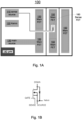
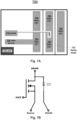
- FIG. 1A illustrates a plan view of an exemplary current sense MOSFET (sense-FET) 160 in a power semiconductor device 100, in accordance with embodiments of the present technology.
- a principal function of power semiconductor device 100 is to function as a power MOSFET, e.g., to control a drain source current through the power MOSFET.
- Power semiconductor device 100 comprises large areas of main-FET 150.
- main-FET 150 comprises numerous trenches comprising gate and shield electrodes, and mesas in-between the trenches comprising source and body regions.
- the main-FET 150 comprises a gate coupled to a gate terminal 140, for example, a bond pad.
- the main-FET 150 comprises a source coupled to a main-FET source terminal 130.
- the drain of the main-FET 150 is outside, e.g., below, the plane of Figure 1A .
- Power semiconductor device 100 comprises a sense-FET 160, formed within a region of the main-FET 150, in accordance with embodiments of the present technology. It is appreciated that die area of main-FET 150 is very much greater than die area of sense-FET 160.
- the gate and drain of the sense-FET 160 are in common, e.g., in parallel, with the gate and drain of the main-FET 150.
- the source of the sense-FET 160 is coupled to a sense source terminal 110, e.g., a bond pad.
- the sense-FET outputs a voltage corresponding to current in the main-FET 150.
- the node Kelvin may be coupled to a terminal 120 for use off the die of power semiconductor device 100, in some embodiments.
- the voltage Kelvin may also, or alternatively, be used by circuitry (not shown) on the die of power semiconductor device 100, for example, to turn main-FET 150 off for over-current protection.
- Figure 1B illustrates an exemplary schematic symbol for power semiconductor device 100, in accordance with embodiments of the present technology.
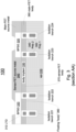
- FIG 2 illustrates an exemplary enlarged plan view of a portion of power semiconductor device 100 around and including sense-FET 160, in accordance with embodiments of the present technology.
- Power semiconductor device 100 comprises a plurality of primary trenches 210, illustrated horizontally in Figure 2 . The majority of primary trenches 210 are utilized by the main-FET 150.
- Power semiconductor device 100 comprises four isolation trenches 221, 222, 223 and 224, in accordance with embodiments of the present technology.
- the isolation trenches 221-224 are part of a group of isolation structures to isolate sense-FET 160 from the main-FET 150.
- the isolation trenches 221-224 are perpendicular to the primary trenches 210, in accordance with embodiments of the present technology.
- Sense-FET 160 comprises a sense-FET source 230.
- Sense-FET source 230 is bounded by two isolation trenches, isolation trenches 222 and 223, and portions of two primary trenches 210, primary trenches 210A and 210B. Overlying and coupling sense-FET source 230 is sense-FET source metal 240.
- Sense-FET source metal 240 overlaps the isolation trenches 222 and 224.
- Sense-FET source metal 240 may extend off the top of the Figure 2 for coupling to sense source terminal 110 ( Figure 1A ), for example, in some embodiments.
- the source of main-FET 150 may be coupled in a different manner, e.g., out of the plane of Figure 2 .
- the surface isolation region 250 would form a square annulus around the sense-FET 160 ( Figure 1 ), in accordance with embodiments of the present technology.
- a surface isolation region 250 is formed outside of sense-FET 160, in accordance with embodiments of the present technology.
- surface isolation region 250 is generally "U" shaped.
- Surface isolation region 250 is formed between isolation trenches 221 and 222, between isolation trenches 223 and 224, and between primary trenches 210B and 210C.
- portions of multiple primary trenches 220 should be used to isolate a sense-FET 160 from a main-FET 150, in order to maintain charge balance.
- P-type materials in the mesas of surface isolation region 250 are left floating.
- the surface of surface isolation region 250 may be covered with an insulator, for example, borophosphosilicate glass (BPSG).
- BPSG borophosphosilicate glass
- regions of main-FET 150 are regions of main-FET 150.
- p-type material in mesas between primary trenches 210 is coupled to the main-FET source terminal 130 ( Figure 1 ), and such regions are overlaid with main-FET source metal (not shown).
- Figure 3 illustrates an exemplary cross-sectional view of a portion of power semiconductor device 100, in accordance with embodiments of the present technology.
- Figure 3 corresponds to cross section AA of Figure 2 .
- the view of Figure 3 is taken along a mesa, e.g., between primary trenches 210 ( Figure 2 ), cutting an active region of sense-FET 160 ( Figure 1A ).
- Power semiconductor device 100 comprises an epitaxial layer 310, e.g., N - , formed on an N + substrate (not shown).
- a metallic drain contact (not shown) is typically formed on the bottom the substrate.
- Isolation trenches 221, 222, 223 and 224 are formed in epitaxial layer 310.
- isolation trenches 221, 222, 223 and 224 are perpendicular to the primary trenches 210.
- a wide variety of angles between isolation trenches 221-224 and primary trenches 210, e.g., from about 40 degrees to 90 degrees, are well suited to embodiments in accordance with the present technology.
- Primary trenches 210 are above and below the plane of Figure 3 .
- the isolation trenches 221-224 should be deeper than the drain-body PN junction, and may be about the same depth as the primary trenches 210. Such a depth establishes a physical barrier between the source of the sense-FET 160 and the source of the main-FET 150.
- the body implant may be performed without a mask, hence making the manufacturing process more cost effective.
- Power semiconductor device 100 additionally comprises a body implant 330, e.g., P + doping, typically at a depth below the surface of epitaxial layer 310.
- the implant region 360 between isolation trenches 221 and 222, and between isolation trenches 223 and 224 is left floating to create a buffer region between the body region 370 of the sense-FET and the electrically separate body region of the main-FET 380, thus improving the electrical isolation of the two FETs with minimal distance separating the two body regions 370 and 380.
- the region between isolation trenches 221 and 222, and between isolation trenches 223 and 224 is a part of surface isolation region 250 ( Figure 2 ).
- Surface isolation region 250 is covered with an insulator, for example, borophosphosilicate glass (BPSG) 320.
- BPSG borophosphosilicate glass
- LTO low temperature oxide
- Sense-FET source metal 240 couples the sources of the sense-FET 160 (not shown) and the sense-FET body 370 to a sense-FET source terminal of power semiconductor device 100, e.g., sense-FET source terminal 110 ( Figure 1A ).
- Figure 4 illustrates an exemplary cross-sectional view of a portion of power semiconductor device 100, in accordance with embodiments of the present technology.
- Figure 4 corresponds to cross section BB of Figure 2 .
- the view of Figure 4 is taken through an active region of sense-FET 160 ( Figure 1A ), perpendicular to primary trenches 210. Portions of several primary trenches 210, e.g., under surface isolation region 250 and BPSG 320, are utilized as isolation trenches 440.
- the top electrode, poly 2 (340) is coupled to the gate electrode, and the bottom electrode, poly 1 (350), is coupled to the source of the main-FET. Portions of different primary trenches 210 are used as trenches 430 to form sense-FET 160.
- Figure 4 illustrates only two trenches as part of a sense-FET 160 for clarity. There would typically be many more trenches 430 within a sense-FET 160.
- Sense-FET 160 comprises a sense-FET source 410, which is typically an N + implant at or near the top of epitaxial layer 310.
- Sense-FET 160 also comprises a sense-FET source-body contact 420.
- a sense-FET source metal extension 450 for example, used to route sense-FET source metal extension to a sense-FET source contact, e.g., sense-FET source terminal 110 of Figure 1A .
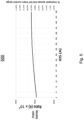
- FIG. 5 illustrates a graph 500 of experimental measurements taken on prototype devices constructed in accordance with embodiments of the present technology.
- Graph 500 illustrates a current sense ratio (CSR), e.g., a ratio of Imain/Isense, on the left abscissa, across a range of drain-source currents, Ids, of the main-FET, also known as Imain, from 2 amps to 50 amps (ordinate).
- the ratio is at least 2.99 x 10 4 , e.g., at 2 amps, and may be as high as 3.1 x 10 4 , e.g., at 50 amps.
- the highest claimed CSR under the conventional art known to applicants at this time is approximately 1.2 x 10 3 .
- Graph 500 of Figure 5 also illustrates a percentage mismatch across the full main current range on the right abscissa.
- the mismatch describes the accuracy of the ratio of Imain/Isense.
- the mismatch is very small, e.g., within a range of +/- 0.33 percent across a range of Ids from 2 amps to 50 amps. Thus, the prototype very accurately indicates Ids of the main-FET.
- a current sense MOSFET in a vertical trench MOSFET may be formed without additional process steps or additional mask layers in comparison to process steps and mask layers required to produce a corresponding vertical trench MOSFET by itself.
- the perpendicular isolation trenches e.g., isolation trenches 221-224 of Figure 2
- the perpendicular isolation trenches may be formed utilizing the same process steps and masks that form the primary trenches 210 of Figure 2 . It is appreciated that several masks, including, for example, a trench mask and metallization masks, will be different between embodiments in accordance with the present technology and the conventional art.
- a single mask for forming FET trenches e.g., primary trenches 210 ( Figure 2 ) and perpendicular isolation trenches, e.g., isolation trenches 221-224 ( Figure 2 )
- FET trenches e.g., primary trenches 210 ( Figure 2 )
- perpendicular isolation trenches e.g., isolation trenches 221-224
- the processes and numbers of masks may be the same.
- FIG 6 illustrates an exemplary process flow 600 for constructing a current sense MOSFET in a vertical trench MOSFET, for example, power semiconductor device 100 of Figure 1A , in accordance with embodiments of the present technology.
- a plurality of trenches are etched with a hard mask to a depth, e.g., of typically a few micrometers.
- the trenches include, for example, primary trenches, e.g., primary trenches 210 ( Figure 2 ) and isolation trenches, e.g., isolation trenches 221-224, formed at an angle to the primary trenches.
- the primary trenches and isolation trenches may be etched to about the same depth, but that is not required.
- the vertical trenches are made slightly wider than primary trenches 210 such that when both trenches are etched (at the same process step) the vertical trenches are somewhat deeper than the primary trenches.
- thermal oxide is grown followed by a deposited oxide inside the trench.
- first polysilicon e.g., poly 1 (350) of Figure 3
- the first polysilicon may be doped with a high concentration of Phosphorus.
- the first polysilicon is recessed back to a desired depth, typically on the order of 1 micrometer.
- a second oxide layer is grown or deposited over and above the first polysilicon.
- a selective oxide etch is performed to etch the active region where the gate oxide is grown.
- second polysilicon e.g., poly 2 (340) of Figure 3
- the second polysilicon is recessed in the active area to allow a layer of deposited oxide the fill the top of the trenches by a fill and etch back process.
- the body and source implants should be introduced consecutively.
- a layer of silicon nitride and doped oxide is used to cover the surface before contacts are etched to silicon, first polysilicon and second polysilicon.
- a layer of metal is deposited and etched forming the gate and source contacts. It is appreciated that the source metal patterns of embodiments in accordance with the present technology differ from a conventional vertical MOSFET, for example, to accommodate the separate sense source of the novel sense-FET. In addition, there is no source metal in an isolation region around the sense-FET.
- a passivation layer of oxide and nitride are deposited over the metallization and etched.
- a metal layer is deposited forming the backside drain contact.
- a sense diode may be established proximate the top body of a relatively larger split gate MOSFET, known as the "main-FET.” Such a sense diode may be used to indicate temperature of the main-FET, in some embodiments. Temperature of a main-FET may be used for numerous purposes, e.g., to shut down a device responsive to an over-temperature condition. A sense diode may also be used to measure gate voltage of the main-FET, in some embodiments. Measuring gate voltage of a main-FET may be desirable when the gate terminal of a main-FET is not exposed, e.g., in packaged, high function devices such as driver MOS ("DrMOS”) devices.
- DrMOS driver MOS
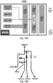
- FIG. 7A illustrates a plan view of an exemplary sense diode 720 in a power semiconductor device 700, in accordance with embodiments of the present technology.
- a principal function of power semiconductor device 700 is to function as a power MOSFET, e.g., to control a drain source current through the power MOSFET.
- Power semiconductor device 700 comprises large areas of main-FET 750.
- main-FET 150 comprises numerous trenches comprising gate and shield electrodes, and mesas in-between the trenches comprising source and body regions.
- the main-FET 750 comprises a gate coupled to a gate terminal 740, for example, a bond pad.
- the main-FET 750 comprises a source coupled to a main-FET source terminal 730.
- the drain of the MOSFET 750 is outside, e.g., below, the plane of Figure 7A .
- the function and structure of main-FET 750, main source 730 and gate 740 are generally equivalent to the comparable structures of device 100, as illustrated in Figure 1A .
- Power semiconductor device 100 comprises a sense-diode 720, formed within a region of the main-FET 750, in accordance with embodiments of the present technology. It is appreciated that die area of main-FET 750 is very much greater than die area of sense-diode 720.
- the cathode terminal of sense-diode 720 is in common with the drain terminal of main-FET 750, outside the plane of Figure 7A .
- the anode terminal of sense-diode 720 is coupled to anode terminal 710., e.g., a bond pad.
- Figure 7B illustrates an exemplary schematic symbol for power semiconductor device 700, in accordance with embodiments of the present technology.
- sense-diode 720 is structurally very similar to sense-FET 160 of Figures 1A , 2 , 3 and 4 .
- the isolation trenches that isolate sense-diode 720 are equivalent to the isolation trenches that isolate sense-FET 160.
- the salient differences between sense-FET 160 and sense-diode 720 are that sense-diode 720 may lack a source implant 410 and a source-body contact 420 ( Figure 4 ), and the two poly layers within the trenches are connected differently.
- Figure 8 illustrates an exemplary cross-sectional view of a portion of power semiconductor device 700, in accordance with embodiments of the present technology.
- Figure 8 is generally equivalent to the cross section illustration of Figure 4 .
- the view of Figure 8 is taken through an active region of sense-diode 720 ( Figure 7A ), perpendicular to primary trenches of main-FET 750. Portions of several primary trenches, e.g., under surface isolation regions and BPSG 825, are utilized as isolation trenches 840.
- the top electrode, poly 2 (842) is coupled to the gate electrode, and the bottom electrode, poly 1 (841), is coupled to the source of the main-FET. Portions of different primary trenches are used as trenches 830 to form sense-diode 820.
- Figure 8 illustrates only two trenches as part of a sense-diode 720 for clarity. There would typically be many more trenches 830 within a sense-diode 720.
- Sense diode 720 comprises a sense-diode anode 870.
- sense diode 720 may comprise a sense-diode anode contact 851, similar to a source-body contact of a MOSFET, e.g., sense-FET source-body contact 420 of Figure 4 .
- a sense-FET source metal extension 850 for example, used to route sense-FET source metal extension to a sense-FET source contact, e.g., sense-FET anode contact 710 of Figure 7A .
- sense-diode 720 may be used to sense temperature of the device, e.g., a temperature of main-FET 750 and/or to indicate the voltage of gate 740.
- the first field plate, poly 1 (841), should be electrically coupled to the anode of the sense-diode 720, which has a separate terminal distinct from the source of the main-FET 750 (or a sense-FET, if present).
- the second field plate, poly 2 (842), uses the gate structure and should be electrically coupled to the anode (not to the gate terminal 740 of the main-FET 750).
- the cathode side of the diode is common to the drain of the main-FET 750 (and a sense-FET, if present).
- the diode is not affected by the main-FET 750 gate voltage and exhibits good diode characteristics that can be calibrated as a function of temperature for temperature sensing. Accordingly, this novel structure of a vertical MOS diode within a vertical trench MOSFET may be used to sense temperature of the device via well known methods.
- the second field plate, poly 2 (842) should be electrically coupled to the gate terminal of the main-FET 750.
- the sense-diode 720 characteristics change as a function of the gate voltage.
- the sense-diode 720 current-voltage relation depends on gate terminal voltage if the second field plate, poly 2 (842), is electrically coupled to the gate terminal.
- the sense-diode 720 current-voltage characteristic may be used to indicate the gate voltage, at a given temperature, by calibrating the sense-diode 720 voltage at a given current to the gate voltage.
- FIG. 9 illustrates exemplary characteristics of the sense-diode 720 as a function of the gate voltage, to facilitate determining gate voltage.
- Figure 9 illustrates exemplary characteristics 900 of an exemplary sense-diode 720 as a function of gate voltage, in accordance with embodiments of the present technology.
- Characteristics 900 may be used to determine gate voltage based on diode current and anode voltage.
- the modulation of the current - voltage characteristics of the sense-diode 720 is seen here depending on the gate voltage, as applied to the second field plate, poly 2 (842) as illustrated in Figure 8 .
- Vgs 0 volts
- the channel is off, and the sense-diode 720 is working in a "pure diode mode.”
- the sense-diode 720 is modulated by the parasitic MOSFET.
- sense-FET e.g., sense-FET 160 of Figure 1A
- sense-diode e.g., sense-diode 720 of Figure 7A
- FIG. 10A illustrates a plan view of an exemplary current sense MOSFET (sense-FET) 160 and an exemplary sense diode 720 in a power semiconductor device 1000, in accordance with embodiments of the present technology.
- a principal function of power semiconductor device 1000 is to function as a power MOSFET, e.g., to control a drain source current through the power MOSFET.
- Power semiconductor device 1000 comprises large areas of main-FET 1050.
- main-FET 1050 comprises numerous trenches comprising gate and shield electrodes, and mesas in-between the trenches comprising source and body regions.
- the main-FET 1050 comprises a gate coupled to a gate terminal 140, for example, a bond pad.
- the main-FET 1050 comprises a source coupled to a main-FET source terminal 130.
- the drain of the MOSFET 1050 is outside, e.g., below, the plane of Figure 1A .
- Power semiconductor device 1000 comprises a sense-FET 160, formed within a region of the main-FET 1050, in accordance with embodiments of the present technology. It is appreciated that die area of main-FET 1050 is very much greater than die area of sense-FET 160.
- the gate and drain of the sense-FET 160 are in common, e.g., in parallel, with the gate and drain of the main-FET 1050.
- the source of the sense-FET 160 is coupled to a sense source terminal 110, e.g., a bond pad.
- the sense-FET outputs a voltage corresponding to current in the main-FET 1050.
- the node Kelvin may be coupled to a terminal 120 for use off the die of power semiconductor device 100, in some embodiments.
- the voltage Kelvin may also, or alternatively, be used by circuitry (not shown) on the die of power semiconductor device 1000, for example, to turn main-FET 1050 off for over-current protection.
- Power semiconductor device 1000 further comprises a sense-diode 720, formed within a region of the main-FET 1050, in accordance with embodiments of the present technology. It is appreciated that die area of main-FET 1050 is very much greater than die area of sense-diode 720.
- the cathode of the sense-diode 720 is in common with the drain of the main-FET 1050.
- the anode of sense-diode 720 is coupled to an anode terminal, e.g., a bond pad 710.
- the sense-diode 720 may be used to measure temperature of the device and/or gate voltage, as previously described.
- a power MOSFET device comprising at least two sense-diodes is envisioned, and is considered within the scope of the present technology.
- multiple sense diodes may be configured to measure temperature in different regions of a MOSFET.
- at least one sense diode may be configured to indicate gate voltage in conjunction with one or more sense diodes configured to measure temperature.
- Figure 10B illustrates an exemplary schematic symbol for power semiconductor device 1000, in accordance with embodiments of the present technology.
- sense-FET 160 and/or sense-diode 720 utilize structures common to a main-FET, e.g., trenches and poly layers, for their function, and further utilize structures common to a main-FET, e.g., trenches and BPSG, for isolation. Accordingly, the benefits of a sense-FET 160 and/or sense-diode 720 may be realized with no additional manufacturing cost in comparison to a trench MOSFET.
- Embodiments in accordance with the present technology are well suited to a variety of trench MOSFETs, including, for example, single gate trench MOSFETs, split gate charge balanced trench MOSFETs, Hybrid Split Gate MOSFETs, for example, as disclosed in co-pending, commonly owned United States Patent Application No. 13/460,567, filed April 20, 2012, to Bobde et al. , entitled “Hybrid Split Gate Semiconductor,” which is hereby incorporated herein by reference in its entirety, and dual trench MOSFETs, for example, as described in the publication: " Poly Flanked VDMOS (PFVDMOS): A Superior Technology for Superjunction Devices" by K. P. Gan, Y. C. Liang, G. Samudra, S. M. Xu, L. Yong, IEEE Power Electronics Specialist Conference, 2001 .
- PFVDMOS Poly Flanked VDMOS
- Embodiments in accordance with the present technology provide systems and methods for current sense metal oxide semiconductor field effect transistors (MOSFETs) in vertical trench MOSFETs.
- embodiments in accordance with the present technology provide systems and methods for current sense MOSFETs in vertical trench MOSFETs that are integral to the main-FET.
- embodiments in accordance with the present technology provide systems and methods for current sense MOSFETs in vertical trench MOSFETs that are integral to the main-FET.
- Yet further embodiments in accordance with the present technology provide systems and methods for a sensing diode to sense temperature and/or gate voltage of the main-FET.
- embodiments in accordance with the present technology provide systems and methods for systems and methods for current sense MOSFETs and/or sense diodes in vertical trench MOSFETs that are compatible and complementary with existing systems and methods of integrated circuit design, manufacturing and test.
Landscapes
- Physics & Mathematics (AREA)
- General Physics & Mathematics (AREA)
- Metal-Oxide And Bipolar Metal-Oxide Semiconductor Integrated Circuits (AREA)
- Chemical & Material Sciences (AREA)
- Chemical Kinetics & Catalysis (AREA)
- General Chemical & Material Sciences (AREA)
- Engineering & Computer Science (AREA)
- General Engineering & Computer Science (AREA)
- Composite Materials (AREA)
- Semiconductor Integrated Circuits (AREA)
Applications Claiming Priority (3)
| Application Number | Priority Date | Filing Date | Title |
|---|---|---|---|
| US201462039335P | 2014-08-19 | 2014-08-19 | |
| EP15833032.4A EP3183753B1 (de) | 2014-08-19 | 2015-08-19 | Mosfet-halbleiteranordnung |
| PCT/US2015/045975 WO2016028943A1 (en) | 2014-08-19 | 2015-08-19 | Electronic circuit |
Related Parent Applications (1)
| Application Number | Title | Priority Date | Filing Date |
|---|---|---|---|
| EP15833032.4A Division EP3183753B1 (de) | 2014-08-19 | 2015-08-19 | Mosfet-halbleiteranordnung |
Publications (2)
| Publication Number | Publication Date |
|---|---|
| EP4565029A2 true EP4565029A2 (de) | 2025-06-04 |
| EP4565029A3 EP4565029A3 (de) | 2025-07-30 |
Family
ID=55348926
Family Applications (2)
| Application Number | Title | Priority Date | Filing Date |
|---|---|---|---|
| EP15833032.4A Active EP3183753B1 (de) | 2014-08-19 | 2015-08-19 | Mosfet-halbleiteranordnung |
| EP25164461.3A Pending EP4565029A3 (de) | 2014-08-19 | 2015-08-19 | Mosfet-halbleiterbauelement |
Family Applications Before (1)
| Application Number | Title | Priority Date | Filing Date |
|---|---|---|---|
| EP15833032.4A Active EP3183753B1 (de) | 2014-08-19 | 2015-08-19 | Mosfet-halbleiteranordnung |
Country Status (5)
| Country | Link |
|---|---|
| US (4) | US10234486B2 (de) |
| EP (2) | EP3183753B1 (de) |
| KR (1) | KR102026543B1 (de) |
| CN (2) | CN115483211A (de) |
| WO (1) | WO2016028943A1 (de) |
Families Citing this family (32)
| Publication number | Priority date | Publication date | Assignee | Title |
|---|---|---|---|---|
| CN115483211A (zh) | 2014-08-19 | 2022-12-16 | 维西埃-硅化物公司 | 电子电路 |
| DE102015204637A1 (de) * | 2015-03-13 | 2016-09-15 | Infineon Technologies Ag | Verfahren zum Dotieren eines aktiven Hall-Effekt-Gebiets einer Hall-Effekt-Vorrichtung und Hall-Effekt-Vorrichtung mit einem dotierten aktiven Hall-Effekt-Gebiet |
| JP6631114B2 (ja) * | 2015-09-17 | 2020-01-15 | 富士電機株式会社 | 半導体装置及び半導体装置の計測方法 |
| US9973183B2 (en) | 2015-09-28 | 2018-05-15 | Power Integrations, Inc. | Field-effect transistor device with partial finger current sensing FETs |
| US9748376B2 (en) * | 2015-12-21 | 2017-08-29 | Texas Instruments Incorporated | Power FET with integrated sensors and method of manufacturing |
| US9983239B2 (en) | 2016-05-13 | 2018-05-29 | Power Integrations, Inc. | Integrated linear current sense circuitry for semiconductor transistor devices |
| WO2018030990A1 (en) | 2016-08-08 | 2018-02-15 | Power Integrations, Inc. | Integrated circuit fast temperature sensing of a semiconductor switching device |
| JP6805620B2 (ja) * | 2016-08-10 | 2020-12-23 | 富士電機株式会社 | 半導体装置 |
| US10753964B2 (en) * | 2017-04-27 | 2020-08-25 | Microchip Technology Incorporated | Current sensing for integrated circuit devices |
| JP6519630B1 (ja) * | 2017-10-30 | 2019-05-29 | ダイキン工業株式会社 | 電流検出装置 |
| JP7113666B2 (ja) | 2018-06-01 | 2022-08-05 | ローム株式会社 | 半導体装置および半導体装置の製造方法 |
| US11063146B2 (en) * | 2019-01-10 | 2021-07-13 | Texas Instruments Incorporated | Back-to-back power field-effect transistors with associated current sensors |
| DE102020107747B4 (de) | 2019-03-22 | 2023-07-20 | Infineon Technologies Ag | Transistoranordnung mit einem lasttransistor und einemerfassungstransistor und elektronische schaltung mit dieser |
| EP3736864B1 (de) | 2019-05-06 | 2023-04-19 | Infineon Technologies Austria AG | Halbleiterbauelement |
| DE102019003481B3 (de) * | 2019-05-16 | 2020-06-18 | Tdk-Micronas Gmbh | Hallsensorstruktur |
| US11031308B2 (en) * | 2019-05-30 | 2021-06-08 | Sandisk Technologies Llc | Connectivity detection for wafer-to-wafer alignment and bonding |
| JP7425943B2 (ja) * | 2019-12-12 | 2024-02-01 | 株式会社デンソー | 炭化珪素半導体装置 |
| CN111129152B (zh) * | 2019-12-17 | 2023-09-26 | 杭州芯迈半导体技术有限公司 | 沟槽mosfet结构及其制造方法 |
| US12068408B2 (en) * | 2020-07-15 | 2024-08-20 | Semiconductor Components Industries, Llc | High electron mobility transistor |
| JP2023547122A (ja) | 2020-10-20 | 2023-11-09 | ミルウォーキー エレクトリック ツール コーポレイション | 電界効果トランジスタを使用する電動工具デバイスにおける電流感知 |
| CN113066852B (zh) * | 2021-03-15 | 2022-09-09 | 无锡新洁能股份有限公司 | 感测功率半导体器件 |
| JP7653305B2 (ja) * | 2021-06-02 | 2025-03-28 | ルネサスエレクトロニクス株式会社 | 半導体装置 |
| CN113539833B (zh) * | 2021-07-23 | 2023-04-25 | 电子科技大学 | 一种分离栅功率mosfet器件的制造方法 |
| JP2023131415A (ja) * | 2022-03-09 | 2023-09-22 | ルネサスエレクトロニクス株式会社 | 半導体装置 |
| KR102404463B1 (ko) * | 2022-04-26 | 2022-06-07 | (주) 트리노테크놀로지 | 폴디드 채널 영역이 형성된 실리콘 카바이드 전력 반도체 장치 및 그 제조 방법 |
| CN115810654B (zh) * | 2022-11-11 | 2025-12-12 | 天狼芯半导体(成都)有限公司 | 金属氧化物半导体场效应晶体管及其制作方法 |
| DE102023205705A1 (de) | 2023-06-19 | 2024-12-19 | Infineon Technologies Austria Ag | Halbleitervorrichtung mit einem aktiven vorrichtungsbereich und einem stromsensorbereich |
| CN116613072B (zh) * | 2023-07-10 | 2023-09-22 | 南京华瑞微集成电路有限公司 | 集成电压采样功能的沟槽型mosfet及其制造方法 |
| US20250113620A1 (en) * | 2023-09-28 | 2025-04-03 | Alpha And Omega Semiconductor International Lp | Distributed Gate Drive for DrMOS |
| DE102023136297A1 (de) * | 2023-12-21 | 2025-06-26 | Valeo Eautomotive Germany Gmbh | Elektrischer Leistungswandler und Verfahren zum Betreiben eines elektrischen Leistungswandlers |
| CN117832285B (zh) * | 2024-03-04 | 2024-04-30 | 南京华瑞微集成电路有限公司 | 一种具有过压保护功能的低压沟槽mosfet及其制作方法 |
| CN119153517B (zh) * | 2024-08-27 | 2025-09-26 | 深圳尚阳通科技股份有限公司 | 功率器件 |
Family Cites Families (327)
| Publication number | Priority date | Publication date | Assignee | Title |
|---|---|---|---|---|
| US3906540A (en) | 1973-04-02 | 1975-09-16 | Nat Semiconductor Corp | Metal-silicide Schottky diode employing an aluminum connector |
| JPH0612828B2 (ja) | 1983-06-30 | 1994-02-16 | 株式会社東芝 | 半導体装置 |
| US4641174A (en) | 1983-08-08 | 1987-02-03 | General Electric Company | Pinch rectifier |
| US4672407A (en) | 1984-05-30 | 1987-06-09 | Kabushiki Kaisha Toshiba | Conductivity modulated MOSFET |
| JPS6292361A (ja) | 1985-10-17 | 1987-04-27 | Toshiba Corp | 相補型半導体装置 |
| JPH0693512B2 (ja) | 1986-06-17 | 1994-11-16 | 日産自動車株式会社 | 縦形mosfet |
| JPH0685441B2 (ja) | 1986-06-18 | 1994-10-26 | 日産自動車株式会社 | 半導体装置 |
| JP2570742B2 (ja) | 1987-05-27 | 1997-01-16 | ソニー株式会社 | 半導体装置 |
| US4799095A (en) | 1987-07-06 | 1989-01-17 | General Electric Company | Metal oxide semiconductor gated turn off thyristor |
| US5021840A (en) | 1987-08-18 | 1991-06-04 | Texas Instruments Incorporated | Schottky or PN diode with composite sidewall |
| US4827321A (en) | 1987-10-29 | 1989-05-02 | General Electric Company | Metal oxide semiconductor gated turn off thyristor including a schottky contact |
| US4893160A (en) | 1987-11-13 | 1990-01-09 | Siliconix Incorporated | Method for increasing the performance of trenched devices and the resulting structure |
| US20020074585A1 (en) | 1988-05-17 | 2002-06-20 | Advanced Power Technology, Inc., Delaware Corporation | Self-aligned power MOSFET with enhanced base region |
| US5283201A (en) | 1988-05-17 | 1994-02-01 | Advanced Power Technology, Inc. | High density power device fabrication process |
| US4969027A (en) | 1988-07-18 | 1990-11-06 | General Electric Company | Power bipolar transistor device with integral antisaturation diode |
| US4967243A (en) | 1988-07-19 | 1990-10-30 | General Electric Company | Power transistor structure with high speed integral antiparallel Schottky diode |
| EP0354449A3 (de) | 1988-08-08 | 1991-01-02 | Seiko Epson Corporation | Einkristall-Halbleitersubstrat |
| US5055896A (en) | 1988-12-15 | 1991-10-08 | Siliconix Incorporated | Self-aligned LDD lateral DMOS transistor with high-voltage interconnect capability |
| US5072266A (en) | 1988-12-27 | 1991-12-10 | Siliconix Incorporated | Trench DMOS power transistor with field-shaping body profile and three-dimensional geometry |
| US4939557A (en) | 1989-02-15 | 1990-07-03 | Varian Associates, Inc. | (110) GaAs microwave FET |
| US5111253A (en) | 1989-05-09 | 1992-05-05 | General Electric Company | Multicellular FET having a Schottky diode merged therewith |
| JPH03173180A (ja) | 1989-12-01 | 1991-07-26 | Hitachi Ltd | 半導体素子 |
| JPH03211885A (ja) | 1990-01-17 | 1991-09-17 | Matsushita Electron Corp | 半導体装置及びその製造方法 |
| EP0438700A1 (de) | 1990-01-25 | 1991-07-31 | Asea Brown Boveri Ag | Abschaltbares, MOS-gesteuertes Leistungshalbleiter-Bauelement sowie Verfahren zu dessen Herstellung |
| JP2692350B2 (ja) | 1990-04-02 | 1997-12-17 | 富士電機株式会社 | Mos型半導体素子 |
| US5063307A (en) | 1990-09-20 | 1991-11-05 | Ixys Corporation | Insulated gate transistor devices with temperature and current sensor |
| FR2668465B1 (fr) | 1990-10-30 | 1993-04-16 | Inst Francais Du Petrole | Procede d'elimination de mercure ou d'arsenic dans un fluide en presence d'une masse de captation de mercure et/ou d'arsenic. |
| US5168331A (en) | 1991-01-31 | 1992-12-01 | Siliconix Incorporated | Power metal-oxide-semiconductor field effect transistor |
| JPH04291767A (ja) | 1991-03-20 | 1992-10-15 | Fuji Electric Co Ltd | 伝導度変調型mosfet |
| JP3131239B2 (ja) | 1991-04-25 | 2001-01-31 | キヤノン株式会社 | 半導体回路装置用配線および半導体回路装置 |
| JP3156300B2 (ja) | 1991-10-07 | 2001-04-16 | 株式会社デンソー | 縦型半導体装置 |
| US5366914A (en) | 1992-01-29 | 1994-11-22 | Nec Corporation | Vertical power MOSFET structure having reduced cell area |
| JP3322936B2 (ja) | 1992-03-19 | 2002-09-09 | 株式会社東芝 | 半導体記憶装置 |
| JPH05315620A (ja) | 1992-05-08 | 1993-11-26 | Rohm Co Ltd | 半導体装置およびその製造法 |
| US5233215A (en) * | 1992-06-08 | 1993-08-03 | North Carolina State University At Raleigh | Silicon carbide power MOSFET with floating field ring and floating field plate |
| JP2837033B2 (ja) | 1992-07-21 | 1998-12-14 | 三菱電機株式会社 | 半導体装置及びその製造方法 |
| GB9215653D0 (en) | 1992-07-23 | 1992-09-09 | Philips Electronics Uk Ltd | A method of manufacturing a semiconductor device comprising an insulated gate field effect device |
| GB9216599D0 (en) | 1992-08-05 | 1992-09-16 | Philips Electronics Uk Ltd | A semiconductor device comprising a vertical insulated gate field effect device and a method of manufacturing such a device |
| US5408141A (en) | 1993-01-04 | 1995-04-18 | Texas Instruments Incorporated | Sensed current driving device |
| GB9306895D0 (en) | 1993-04-01 | 1993-05-26 | Philips Electronics Uk Ltd | A method of manufacturing a semiconductor device comprising an insulated gate field effect device |
| US5430315A (en) | 1993-07-22 | 1995-07-04 | Rumennik; Vladimir | Bi-directional power trench MOS field effect transistor having low on-state resistance and low leakage current |
| JP3082522B2 (ja) | 1993-07-27 | 2000-08-28 | 日産自動車株式会社 | 絶縁電極およびその製造方法 |
| JP3383377B2 (ja) | 1993-10-28 | 2003-03-04 | 株式会社東芝 | トレンチ構造の縦型のノーマリーオン型のパワーmosfetおよびその製造方法 |
| JP3334290B2 (ja) | 1993-11-12 | 2002-10-15 | 株式会社デンソー | 半導体装置 |
| JPH07176745A (ja) | 1993-12-17 | 1995-07-14 | Semiconductor Energy Lab Co Ltd | 半導体素子 |
| JP3481287B2 (ja) | 1994-02-24 | 2003-12-22 | 三菱電機株式会社 | 半導体装置の製造方法 |
| JP3307785B2 (ja) | 1994-12-13 | 2002-07-24 | 三菱電機株式会社 | 絶縁ゲート型半導体装置 |
| US5674766A (en) | 1994-12-30 | 1997-10-07 | Siliconix Incorporated | Method of making a trench MOSFET with multi-resistivity drain to provide low on-resistance by varying dopant concentration in epitaxial layer |
| US6008520A (en) | 1994-12-30 | 1999-12-28 | Siliconix Incorporated | Trench MOSFET with heavily doped delta layer to provide low on- resistance |
| US5567634A (en) | 1995-05-01 | 1996-10-22 | National Semiconductor Corporation | Method of fabricating self-aligned contact trench DMOS transistors |
| US6049108A (en) | 1995-06-02 | 2000-04-11 | Siliconix Incorporated | Trench-gated MOSFET with bidirectional voltage clamping |
| US6204533B1 (en) | 1995-06-02 | 2001-03-20 | Siliconix Incorporated | Vertical trench-gated power MOSFET having stripe geometry and high cell density |
| US5998837A (en) | 1995-06-02 | 1999-12-07 | Siliconix Incorporated | Trench-gated power MOSFET with protective diode having adjustable breakdown voltage |
| DE69631995T2 (de) | 1995-06-02 | 2005-02-10 | Siliconix Inc., Santa Clara | Bidirektional sperrender Graben-Leistungs-MOSFET |
| US6140678A (en) | 1995-06-02 | 2000-10-31 | Siliconix Incorporated | Trench-gated power MOSFET with protective diode |
| DE69617098T2 (de) | 1995-06-02 | 2002-04-18 | Siliconix Inc | Grabengate-Leistungs-MOSFET mit Schutzdioden in periodischer Anordnung |
| US5689129A (en) | 1995-06-07 | 1997-11-18 | Harris Corporation | High efficiency power MOS switch |
| US5689128A (en) | 1995-08-21 | 1997-11-18 | Siliconix Incorporated | High density trenched DMOS transistor |
| EP0864178A4 (de) * | 1995-10-02 | 2001-10-10 | Siliconix Inc | Grabengate-mosfet mit integraler temperatur-erkennungsdiode |
| JPH09129877A (ja) | 1995-10-30 | 1997-05-16 | Toyota Central Res & Dev Lab Inc | 半導体装置の製造方法、絶縁ゲート型半導体装置の製造方法および絶縁ゲート型半導体装置 |
| JPH09191103A (ja) * | 1996-01-09 | 1997-07-22 | Nec Corp | 電流検出手段を有する半導体装置 |
| US5814858A (en) | 1996-03-15 | 1998-09-29 | Siliconix Incorporated | Vertical power MOSFET having reduced sensitivity to variations in thickness of epitaxial layer |
| JP3149773B2 (ja) | 1996-03-18 | 2001-03-26 | 富士電機株式会社 | 電流制限回路を備えた絶縁ゲートバイポーラトランジスタ |
| JPH09260645A (ja) | 1996-03-19 | 1997-10-03 | Sanyo Electric Co Ltd | 半導体装置 |
| US5770878A (en) | 1996-04-10 | 1998-06-23 | Harris Corporation | Trench MOS gate device |
| JP2917922B2 (ja) | 1996-07-15 | 1999-07-12 | 日本電気株式会社 | 半導体装置及びその製造方法 |
| US5808340A (en) | 1996-09-18 | 1998-09-15 | Advanced Micro Devices, Inc. | Short channel self aligned VMOS field effect transistor |
| JPH10173175A (ja) | 1996-12-09 | 1998-06-26 | Toshiba Corp | 半導体装置及び半導体装置の製造方法 |
| US7269034B2 (en) | 1997-01-24 | 2007-09-11 | Synqor, Inc. | High efficiency power converter |
| JP3173405B2 (ja) | 1997-01-31 | 2001-06-04 | 日本電気株式会社 | 半導体装置の製造方法 |
| US5952695A (en) | 1997-03-05 | 1999-09-14 | International Business Machines Corporation | Silicon-on-insulator and CMOS-on-SOI double film structures |
| JP3545590B2 (ja) | 1997-03-14 | 2004-07-21 | 株式会社東芝 | 半導体装置 |
| US6180966B1 (en) | 1997-03-25 | 2001-01-30 | Hitachi, Ltd. | Trench gate type semiconductor device with current sensing cell |
| US6281547B1 (en) | 1997-05-08 | 2001-08-28 | Megamos Corporation | Power transistor cells provided with reliable trenched source contacts connected to narrower source manufactured without a source mask |
| US5969383A (en) * | 1997-06-16 | 1999-10-19 | Motorola, Inc. | Split-gate memory device and method for accessing the same |
| JP3450650B2 (ja) | 1997-06-24 | 2003-09-29 | 株式会社東芝 | 半導体装置 |
| US6172398B1 (en) | 1997-08-11 | 2001-01-09 | Magepower Semiconductor Corp. | Trenched DMOS device provided with body-dopant redistribution-compensation region for preventing punch through and adjusting threshold voltage |
| JPH1168102A (ja) | 1997-08-21 | 1999-03-09 | Toshiba Corp | 半導体装置の製造方法 |
| JP3502531B2 (ja) | 1997-08-28 | 2004-03-02 | 株式会社ルネサステクノロジ | 半導体装置の製造方法 |
| US6031265A (en) | 1997-10-16 | 2000-02-29 | Magepower Semiconductor Corp. | Enhancing DMOS device ruggedness by reducing transistor parasitic resistance and by inducing breakdown near gate runners and termination area |
| US6429481B1 (en) | 1997-11-14 | 2002-08-06 | Fairchild Semiconductor Corporation | Field effect transistor and method of its manufacture |
| US6268242B1 (en) | 1997-12-31 | 2001-07-31 | Richard K. Williams | Method of forming vertical mosfet device having voltage clamped gate and self-aligned contact |
| US6242775B1 (en) | 1998-02-24 | 2001-06-05 | Micron Technology, Inc. | Circuits and methods using vertical complementary transistors |
| JP3705919B2 (ja) | 1998-03-05 | 2005-10-12 | 三菱電機株式会社 | 半導体装置及びその製造方法 |
| KR100295063B1 (ko) | 1998-06-30 | 2001-08-07 | 김덕중 | 트렌치게이트구조의전력반도체장치및그제조방법 |
| JP3413569B2 (ja) | 1998-09-16 | 2003-06-03 | 株式会社日立製作所 | 絶縁ゲート型半導体装置およびその製造方法 |
| US6939776B2 (en) | 1998-09-29 | 2005-09-06 | Sanyo Electric Co., Ltd. | Semiconductor device and a method of fabricating the same |
| FR2785090B1 (fr) | 1998-10-23 | 2001-01-19 | St Microelectronics Sa | Composant de puissance portant des interconnexions |
| US6621121B2 (en) | 1998-10-26 | 2003-09-16 | Silicon Semiconductor Corporation | Vertical MOSFETs having trench-based gate electrodes within deeper trench-based source electrodes |
| US5998833A (en) | 1998-10-26 | 1999-12-07 | North Carolina State University | Power semiconductor devices having improved high frequency switching and breakdown characteristics |
| US6160441A (en) | 1998-10-30 | 2000-12-12 | Volterra Semiconductor Corporation | Sensors for measuring current passing through a load |
| US7578923B2 (en) | 1998-12-01 | 2009-08-25 | Novellus Systems, Inc. | Electropolishing system and process |
| JP2000191344A (ja) | 1998-12-25 | 2000-07-11 | Kanegafuchi Chem Ind Co Ltd | 調光ガラスおよびそれを使用した窓 |
| US6255683B1 (en) | 1998-12-29 | 2001-07-03 | Infineon Technologies Ag | Dynamic random access memory |
| KR100415490B1 (ko) | 1999-01-11 | 2004-01-24 | 프라운호퍼-게젤샤프트 츄어 푀르더룽 데어 안게반텐 포르슝에.파우. | 파워 모스 소자 및 그 제조 방법 |
| JP3743189B2 (ja) | 1999-01-27 | 2006-02-08 | 富士通株式会社 | 不揮発性半導体記憶装置及びその製造方法 |
| JP2000223705A (ja) | 1999-01-29 | 2000-08-11 | Nissan Motor Co Ltd | 半導体装置 |
| US6351009B1 (en) | 1999-03-01 | 2002-02-26 | Fairchild Semiconductor Corporation | MOS-gated device having a buried gate and process for forming same |
| US6404007B1 (en) | 1999-04-05 | 2002-06-11 | Fairchild Semiconductor Corporation | Trench transistor with superior gate dielectric |
| US6277695B1 (en) | 1999-04-16 | 2001-08-21 | Siliconix Incorporated | Method of forming vertical planar DMOSFET with self-aligned contact |
| US6413822B2 (en) | 1999-04-22 | 2002-07-02 | Advanced Analogic Technologies, Inc. | Super-self-aligned fabrication process of trench-gate DMOS with overlying device layer |
| US6238981B1 (en) | 1999-05-10 | 2001-05-29 | Intersil Corporation | Process for forming MOS-gated devices having self-aligned trenches |
| US6291298B1 (en) | 1999-05-25 | 2001-09-18 | Advanced Analogic Technologies, Inc. | Process of manufacturing Trench gate semiconductor device having gate oxide layer with multiple thicknesses |
| JP4117977B2 (ja) | 1999-06-25 | 2008-07-16 | 富士通株式会社 | 半導体装置 |
| WO2001005116A2 (en) | 1999-07-13 | 2001-01-18 | Alteon Web Systems, Inc. | Routing method and apparatus |
| GB9917099D0 (en) | 1999-07-22 | 1999-09-22 | Koninkl Philips Electronics Nv | Cellular trench-gate field-effect transistors |
| US6483171B1 (en) | 1999-08-13 | 2002-11-19 | Micron Technology, Inc. | Vertical sub-micron CMOS transistors on (110), (111), (311), (511), and higher order surfaces of bulk, SOI and thin film structures and method of forming same |
| US6211018B1 (en) | 1999-08-14 | 2001-04-03 | Electronics And Telecommunications Research Institute | Method for fabricating high density trench gate type power device |
| US6245615B1 (en) | 1999-08-31 | 2001-06-12 | Micron Technology, Inc. | Method and apparatus on (110) surfaces of silicon structures with conduction in the <110> direction |
| US6518621B1 (en) | 1999-09-14 | 2003-02-11 | General Semiconductor, Inc. | Trench DMOS transistor having reduced punch-through |
| US6348712B1 (en) | 1999-10-27 | 2002-02-19 | Siliconix Incorporated | High density trench-gated power MOSFET |
| GB9928285D0 (en) | 1999-11-30 | 2000-01-26 | Koninkl Philips Electronics Nv | Manufacture of trench-gate semiconductor devices |
| US6285060B1 (en) | 1999-12-30 | 2001-09-04 | Siliconix Incorporated | Barrier accumulation-mode MOSFET |
| US6548860B1 (en) | 2000-02-29 | 2003-04-15 | General Semiconductor, Inc. | DMOS transistor structure having improved performance |
| JP3949869B2 (ja) | 2000-03-22 | 2007-07-25 | セイコーインスツル株式会社 | 縦形mosトランジスタ及びその製造方法 |
| US6580123B2 (en) | 2000-04-04 | 2003-06-17 | International Rectifier Corporation | Low voltage power MOSFET device and process for its manufacture |
| JP4581179B2 (ja) | 2000-04-26 | 2010-11-17 | 富士電機システムズ株式会社 | 絶縁ゲート型半導体装置 |
| EP1170803A3 (de) | 2000-06-08 | 2002-10-09 | Siliconix Incorporated | MOSFET mit Graben-Gateelektrode und Verfahren zu dessen Herstellung |
| US6472678B1 (en) | 2000-06-16 | 2002-10-29 | General Semiconductor, Inc. | Trench MOSFET with double-diffused body profile |
| US6784486B2 (en) | 2000-06-23 | 2004-08-31 | Silicon Semiconductor Corporation | Vertical power devices having retrograded-doped transition regions therein |
| JP2002016080A (ja) | 2000-06-28 | 2002-01-18 | Toshiba Corp | トレンチゲート型mosfetの製造方法 |
| JP4528460B2 (ja) | 2000-06-30 | 2010-08-18 | 株式会社東芝 | 半導体素子 |
| US6304108B1 (en) | 2000-07-14 | 2001-10-16 | Micrel, Incorporated | Reference-corrected ratiometric MOS current sensing circuit |
| US6700158B1 (en) | 2000-08-18 | 2004-03-02 | Fairchild Semiconductor Corporation | Trench corner protection for trench MOSFET |
| US6309929B1 (en) | 2000-09-22 | 2001-10-30 | Industrial Technology Research Institute And Genetal Semiconductor Of Taiwan, Ltd. | Method of forming trench MOS device and termination structure |
| JP2002110978A (ja) | 2000-10-02 | 2002-04-12 | Toshiba Corp | 電力用半導体素子 |
| US6509233B2 (en) | 2000-10-13 | 2003-01-21 | Siliconix Incorporated | Method of making trench-gated MOSFET having cesium gate oxide layer |
| JP4514006B2 (ja) | 2000-10-25 | 2010-07-28 | ソニー株式会社 | 半導体装置 |
| US6649975B2 (en) | 2000-11-16 | 2003-11-18 | Silicon Semiconductor Corporation | Vertical power devices having trench-based electrodes therein |
| US6608350B2 (en) | 2000-12-07 | 2003-08-19 | International Rectifier Corporation | High voltage vertical conduction superjunction semiconductor device |
| JP3551251B2 (ja) | 2000-12-22 | 2004-08-04 | サンケン電気株式会社 | 絶縁ゲート型電界効果トランジスタ及びその製造方法 |
| JP2002222950A (ja) | 2001-01-25 | 2002-08-09 | Denso Corp | 炭化珪素半導体装置の製造方法 |
| US7345342B2 (en) | 2001-01-30 | 2008-03-18 | Fairchild Semiconductor Corporation | Power semiconductor devices and methods of manufacture |
| US6870220B2 (en) | 2002-08-23 | 2005-03-22 | Fairchild Semiconductor Corporation | Method and apparatus for improved MOS gating to reduce miller capacitance and switching losses |
| US6710403B2 (en) | 2002-07-30 | 2004-03-23 | Fairchild Semiconductor Corporation | Dual trench power MOSFET |
| US7132712B2 (en) | 2002-11-05 | 2006-11-07 | Fairchild Semiconductor Corporation | Trench structure having one or more diodes embedded therein adjacent a PN junction |
| JP3531613B2 (ja) | 2001-02-06 | 2004-05-31 | 株式会社デンソー | トレンチゲート型半導体装置及びその製造方法 |
| JP4932088B2 (ja) | 2001-02-19 | 2012-05-16 | ルネサスエレクトロニクス株式会社 | 絶縁ゲート型半導体装置の製造方法 |
| TW543146B (en) | 2001-03-09 | 2003-07-21 | Fairchild Semiconductor | Ultra dense trench-gated power device with the reduced drain-source feedback capacitance and miller charge |
| JP2002280553A (ja) | 2001-03-19 | 2002-09-27 | Toshiba Corp | 半導体装置及びその製造方法 |
| TW484213B (en) | 2001-04-24 | 2002-04-21 | Ememory Technology Inc | Forming method and operation method of trench type separation gate nonvolatile flash memory cell structure |
| JP4823435B2 (ja) | 2001-05-29 | 2011-11-24 | 三菱電機株式会社 | 半導体装置及びその製造方法 |
| JP4608133B2 (ja) | 2001-06-08 | 2011-01-05 | ルネサスエレクトロニクス株式会社 | 縦型mosfetを備えた半導体装置およびその製造方法 |
| EP1267415A3 (de) | 2001-06-11 | 2009-04-15 | Kabushiki Kaisha Toshiba | Leistungshalbleiterbauelement mit RESURF-Schicht |
| JP2002373989A (ja) | 2001-06-13 | 2002-12-26 | Toshiba Corp | 半導体装置 |
| JP4854868B2 (ja) | 2001-06-14 | 2012-01-18 | ローム株式会社 | 半導体装置 |
| US7009247B2 (en) | 2001-07-03 | 2006-03-07 | Siliconix Incorporated | Trench MIS device with thick oxide layer in bottom of gate contact trench |
| JP2003030396A (ja) | 2001-07-13 | 2003-01-31 | Nec Corp | 委託作業管理システム、方法およびプログラム |
| GB0118000D0 (en) | 2001-07-24 | 2001-09-19 | Koninkl Philips Electronics Nv | Manufacture of semiconductor devices with schottky barriers |
| US6882000B2 (en) | 2001-08-10 | 2005-04-19 | Siliconix Incorporated | Trench MIS device with reduced gate-to-drain capacitance |
| US6489204B1 (en) | 2001-08-20 | 2002-12-03 | Episil Technologies, Inc. | Save MOS device |
| US6621107B2 (en) | 2001-08-23 | 2003-09-16 | General Semiconductor, Inc. | Trench DMOS transistor with embedded trench schottky rectifier |
| US7045859B2 (en) | 2001-09-05 | 2006-05-16 | International Rectifier Corporation | Trench fet with self aligned source and contact |
| CN1331238C (zh) | 2001-09-19 | 2007-08-08 | 株式会社东芝 | 半导体装置及其制造方法 |
| JP2003115587A (ja) | 2001-10-03 | 2003-04-18 | Tadahiro Omi | <110>方位のシリコン表面上に形成された半導体装置およびその製造方法 |
| JP3973395B2 (ja) | 2001-10-16 | 2007-09-12 | 株式会社豊田中央研究所 | 半導体装置とその製造方法 |
| KR100406180B1 (ko) | 2001-12-22 | 2003-11-17 | 주식회사 하이닉스반도체 | 플래쉬 메모리 셀의 제조 방법 |
| US6573142B1 (en) | 2002-02-26 | 2003-06-03 | Taiwan Semiconductor Manufacturing Company | Method to fabricate self-aligned source and drain in split gate flash |
| FR2837523B1 (fr) * | 2002-03-19 | 2004-05-14 | Montabert Sa | Marteau perforateur hydraulique roto-percutant |
| DE10212149B4 (de) | 2002-03-19 | 2007-10-04 | Infineon Technologies Ag | Transistoranordnung mit Schirmelektrode außerhalb eines aktiven Zellenfeldes und reduzierter Gate-Drain-Kapazität |
| JP3960091B2 (ja) | 2002-03-20 | 2007-08-15 | 富士電機ホールディングス株式会社 | 半導体装置およびその製造方法 |
| US6838722B2 (en) | 2002-03-22 | 2005-01-04 | Siliconix Incorporated | Structures of and methods of fabricating trench-gated MIS devices |
| JP4004843B2 (ja) | 2002-04-24 | 2007-11-07 | Necエレクトロニクス株式会社 | 縦型mosfetの製造方法 |
| JP3652322B2 (ja) | 2002-04-30 | 2005-05-25 | Necエレクトロニクス株式会社 | 縦型mosfetとその製造方法 |
| US7012005B2 (en) | 2002-06-25 | 2006-03-14 | Siliconix Incorporated | Self-aligned differential oxidation in trenches by ion implantation |
| US6858494B2 (en) | 2002-08-20 | 2005-02-22 | Taiwan Semiconductor Manufacturing Company | Structure and fabricating method with self-aligned bit line contact to word line in split gate flash |
| JP3640945B2 (ja) | 2002-09-02 | 2005-04-20 | 株式会社東芝 | トレンチゲート型半導体装置及びその製造方法 |
| US8629019B2 (en) | 2002-09-24 | 2014-01-14 | Vishay-Siliconix | Method of forming self aligned contacts for a power MOSFET |
| US8080459B2 (en) | 2002-09-24 | 2011-12-20 | Vishay-Siliconix | Self aligned contact in a semiconductor device and method of fabricating the same |
| US7576388B1 (en) | 2002-10-03 | 2009-08-18 | Fairchild Semiconductor Corporation | Trench-gate LDMOS structures |
| JP3931138B2 (ja) | 2002-12-25 | 2007-06-13 | 三菱電機株式会社 | 電力用半導体装置及び電力用半導体装置の製造方法 |
| JP2004241413A (ja) | 2003-02-03 | 2004-08-26 | Toshiba Corp | 半導体装置 |
| US6861701B2 (en) | 2003-03-05 | 2005-03-01 | Advanced Analogic Technologies, Inc. | Trench power MOSFET with planarized gate bus |
| US7638841B2 (en) | 2003-05-20 | 2009-12-29 | Fairchild Semiconductor Corporation | Power semiconductor devices and methods of manufacture |
| JP2004356114A (ja) | 2003-05-26 | 2004-12-16 | Tadahiro Omi | Pチャネルパワーmis電界効果トランジスタおよびスイッチング回路 |
| JP4626131B2 (ja) | 2003-07-11 | 2011-02-02 | 富士電機システムズ株式会社 | 絶縁ゲート型半導体装置 |
| US6818939B1 (en) | 2003-07-18 | 2004-11-16 | Semiconductor Components Industries, L.L.C. | Vertical compound semiconductor field effect transistor structure |
| US6987305B2 (en) | 2003-08-04 | 2006-01-17 | International Rectifier Corporation | Integrated FET and schottky device |
| JP4945055B2 (ja) | 2003-08-04 | 2012-06-06 | ルネサスエレクトロニクス株式会社 | 半導体装置およびその製造方法 |
| DE10339455B3 (de) | 2003-08-27 | 2005-05-04 | Infineon Technologies Ag | Vertikales Halbleiterbauelement mit einer eine Feldelektrode aufweisenden Driftzone und Verfahren zur Herstellung einer solchen Driftzone |
| US7022578B2 (en) | 2003-10-09 | 2006-04-04 | Chartered Semiconductor Manufacturing Ltd. | Heterojunction bipolar transistor using reverse emitter window |
| JP4470454B2 (ja) | 2003-11-04 | 2010-06-02 | 株式会社豊田中央研究所 | 半導体装置とその製造方法 |
| DE10353387B4 (de) | 2003-11-14 | 2008-07-24 | Infineon Technologies Ag | Verfahren zur Herstellung einer Leistungstransistoranordnung und Leistungstransistoranordnung |
| GB0327793D0 (en) | 2003-11-29 | 2003-12-31 | Koninkl Philips Electronics Nv | Trench mosfet |
| GB0327791D0 (en) | 2003-11-29 | 2003-12-31 | Koninkl Philips Electronics Nv | Trench insulated gate field effect transistor |
| JP4398719B2 (ja) | 2003-12-25 | 2010-01-13 | 株式会社東芝 | 半導体装置 |
| US7368777B2 (en) | 2003-12-30 | 2008-05-06 | Fairchild Semiconductor Corporation | Accumulation device with charge balance structure and method of forming the same |
| JP4903055B2 (ja) | 2003-12-30 | 2012-03-21 | フェアチャイルド・セミコンダクター・コーポレーション | パワー半導体デバイスおよびその製造方法 |
| US7619280B2 (en) * | 2004-01-30 | 2009-11-17 | International Rectifier Corporation | Current sense trench type MOSFET with improved accuracy and ESD withstand capability |
| US7405452B2 (en) | 2004-02-02 | 2008-07-29 | Hamza Yilmaz | Semiconductor device containing dielectrically isolated PN junction for enhanced breakdown characteristics |
| JP4904673B2 (ja) | 2004-02-09 | 2012-03-28 | 富士電機株式会社 | 半導体装置および半導体装置の製造方法 |
| JP2005268679A (ja) | 2004-03-22 | 2005-09-29 | Matsushita Electric Ind Co Ltd | 半導体装置およびその製造方法 |
| JP2005304210A (ja) | 2004-04-14 | 2005-10-27 | Renesas Technology Corp | 電源ドライバ装置及びスイッチング電源装置 |
| US6906380B1 (en) | 2004-05-13 | 2005-06-14 | Vishay-Siliconix | Drain side gate trench metal-oxide-semiconductor field effect transistor |
| US8120135B2 (en) | 2004-05-19 | 2012-02-21 | Infineon Technologies Ag | Transistor |
| DE102004063946B4 (de) * | 2004-05-19 | 2018-03-22 | Infineon Technologies Ag | Transistoranordnungen mit einer in einem Trennungstrench angeordneten Elektrode |
| DE102004029435B4 (de) | 2004-06-18 | 2017-02-16 | Infineon Technologies Ag | Feldplattentrenchtransistor |
| US7141860B2 (en) | 2004-06-23 | 2006-11-28 | Freescale Semiconductor, Inc. | LDMOS transistor |
| US7405562B2 (en) * | 2004-07-23 | 2008-07-29 | Yehya Ghallab | Magnetic field imaging detection apparatus |
| GB0419558D0 (en) | 2004-09-03 | 2004-10-06 | Koninkl Philips Electronics Nv | Vertical semiconductor devices and methods of manufacturing such devices |
| JP4913336B2 (ja) | 2004-09-28 | 2012-04-11 | ルネサスエレクトロニクス株式会社 | 半導体装置 |
| JP4841829B2 (ja) | 2004-11-17 | 2011-12-21 | ルネサスエレクトロニクス株式会社 | 半導体装置及びその製造方法 |
| US20060108635A1 (en) | 2004-11-23 | 2006-05-25 | Alpha Omega Semiconductor Limited | Trenched MOSFETS with part of the device formed on a (110) crystal plane |
| DE102004057237B4 (de) | 2004-11-26 | 2007-02-08 | Infineon Technologies Ag | Verfahren zum Herstellen von Kontaktlöchern in einem Halbleiterkörper sowie Transistor mit vertikalem Aufbau |
| US20060113588A1 (en) | 2004-11-29 | 2006-06-01 | Sillicon-Based Technology Corp. | Self-aligned trench-type DMOS transistor structure and its manufacturing methods |
| US7439583B2 (en) | 2004-12-27 | 2008-10-21 | Third Dimension (3D) Semiconductor, Inc. | Tungsten plug drain extension |
| JP2006202931A (ja) | 2005-01-20 | 2006-08-03 | Renesas Technology Corp | 半導体装置およびその製造方法 |
| US7453119B2 (en) | 2005-02-11 | 2008-11-18 | Alphs & Omega Semiconductor, Ltd. | Shielded gate trench (SGT) MOSFET cells implemented with a schottky source contact |
| DE102005009000B4 (de) | 2005-02-28 | 2009-04-02 | Infineon Technologies Austria Ag | Vertikales Halbleiterbauelement vom Grabenstrukturtyp und Herstellungsverfahren |
| DE102005009020B4 (de) | 2005-02-28 | 2012-04-26 | Infineon Technologies Austria Ag | Verfahren zur Erzeugung eines Leistungstransistors und damit erzeugbare integrierte Schaltungsanordnung |
| DE112006000832B4 (de) | 2005-04-06 | 2018-09-27 | Fairchild Semiconductor Corporation | Trenched-Gate-Feldeffekttransistoren und Verfahren zum Bilden derselben |
| US7494876B1 (en) | 2005-04-21 | 2009-02-24 | Vishay Siliconix | Trench-gated MIS device having thick polysilicon insulation layer at trench bottom and method of fabricating the same |
| WO2006126998A1 (en) | 2005-05-24 | 2006-11-30 | Vishay-Siliconix | Trench metal oxide semiconductor field effect transistor |
| DE112006001318T5 (de) | 2005-05-26 | 2008-04-17 | Fairchild Semiconductor Corp. | Trench-Gate-Feldeffekttransistoren und Verfahren zum Bilden derselben |
| JP2006339558A (ja) | 2005-06-06 | 2006-12-14 | Seiko Epson Corp | 半導体装置の製造方法 |
| US20070004116A1 (en) | 2005-06-06 | 2007-01-04 | M-Mos Semiconductor Sdn. Bhd. | Trenched MOSFET termination with tungsten plug structures |
| US7592650B2 (en) | 2005-06-06 | 2009-09-22 | M-Mos Semiconductor Sdn. Bhd. | High density hybrid MOSFET device |
| DE112006001516T5 (de) | 2005-06-10 | 2008-04-17 | Fairchild Semiconductor Corp. | Feldeffekttransistor mit Ladungsgleichgewicht |
| TWI400757B (zh) | 2005-06-29 | 2013-07-01 | 快捷半導體公司 | 形成遮蔽閘極場效應電晶體之方法 |
| JP2007012977A (ja) | 2005-07-01 | 2007-01-18 | Toshiba Corp | 半導体装置 |
| JP2007027193A (ja) | 2005-07-12 | 2007-02-01 | Renesas Technology Corp | 半導体装置およびその製造方法、ならびに非絶縁型dc/dcコンバータ |
| JP4928754B2 (ja) | 2005-07-20 | 2012-05-09 | 株式会社東芝 | 電力用半導体装置 |
| JP2007035841A (ja) | 2005-07-26 | 2007-02-08 | Toshiba Corp | 半導体装置 |
| US7385248B2 (en) | 2005-08-09 | 2008-06-10 | Fairchild Semiconductor Corporation | Shielded gate field effect transistor with improved inter-poly dielectric |
| DE102005041322B4 (de) | 2005-08-31 | 2017-03-16 | Infineon Technologies Ag | Trenchtransistorstruktur mit Feldelektrodenanordnung und Herstellungsverfahren hierfür |
| DE102005052734B4 (de) | 2005-10-06 | 2012-02-23 | Infineon Technologies Ag | Halbleiterstruktur, Verfahren zum Betreiben einer Halbleiterstruktur und Verfahren zum Herstellen einer Halbleiterstruktur |
| JP4735224B2 (ja) | 2005-12-08 | 2011-07-27 | トヨタ自動車株式会社 | 絶縁ゲート型半導体装置およびその製造方法 |
| JP2007189192A (ja) | 2005-12-15 | 2007-07-26 | Toshiba Corp | 半導体装置 |
| US7544545B2 (en) * | 2005-12-28 | 2009-06-09 | Vishay-Siliconix | Trench polysilicon diode |
| US7449354B2 (en) | 2006-01-05 | 2008-11-11 | Fairchild Semiconductor Corporation | Trench-gated FET for power device with active gate trenches and gate runner trench utilizing one-mask etch |
| US7554152B1 (en) | 2006-01-11 | 2009-06-30 | National Semiconductor Corporation | Versatile system for integrated sense transistor |
| DE102006007096B4 (de) | 2006-02-15 | 2008-07-17 | Infineon Technologies Austria Ag | MOSFET mit Kompensationsstruktur und Randabschluss sowie Verfahren zu dessen Herstellung |
| US7446374B2 (en) | 2006-03-24 | 2008-11-04 | Fairchild Semiconductor Corporation | High density trench FET with integrated Schottky diode and method of manufacture |
| JP4182986B2 (ja) | 2006-04-19 | 2008-11-19 | トヨタ自動車株式会社 | 半導体装置とその製造方法 |
| WO2007129261A2 (en) | 2006-05-05 | 2007-11-15 | Nxp B.V. | Trench field effect transistors |
| US7319256B1 (en) | 2006-06-19 | 2008-01-15 | Fairchild Semiconductor Corporation | Shielded gate trench FET with the shield and gate electrodes being connected together |
| JP5222466B2 (ja) | 2006-08-09 | 2013-06-26 | ルネサスエレクトロニクス株式会社 | 半導体装置およびその製造方法 |
| US7544571B2 (en) | 2006-09-20 | 2009-06-09 | Fairchild Semiconductor Corporation | Trench gate FET with self-aligned features |
| US7750398B2 (en) | 2006-09-26 | 2010-07-06 | Force-Mos Technology Corporation | Trench MOSFET with trench termination and manufacture thereof |
| DE102006045441B4 (de) | 2006-09-26 | 2008-09-25 | Infineon Technologies Austria Ag | Verfahren zur Herstellung einer Halbleiterbauelementanordnung mit einer Trenchtransistorstruktur |
| JP2010505270A (ja) | 2006-09-27 | 2010-02-18 | マックスパワー・セミコンダクター・インコーポレイテッド | 窪んだフィールドプレートを備えたパワーmosfet |
| US7732842B2 (en) | 2006-12-06 | 2010-06-08 | Fairchild Semiconductor Corporation | Structure and method for forming a planar schottky contact |
| US9437729B2 (en) | 2007-01-08 | 2016-09-06 | Vishay-Siliconix | High-density power MOSFET with planarized metalization |
| JP5091487B2 (ja) | 2007-01-09 | 2012-12-05 | 株式会社東芝 | 半導体装置の製造方法 |
| US8659074B2 (en) | 2007-01-09 | 2014-02-25 | Maxpower Semiconductor, Inc. | Semiconductor device |
| US7670908B2 (en) | 2007-01-22 | 2010-03-02 | Alpha & Omega Semiconductor, Ltd. | Configuration of high-voltage semiconductor power device to achieve three dimensional charge coupling |
| US8653583B2 (en) * | 2007-02-16 | 2014-02-18 | Power Integrations, Inc. | Sensing FET integrated with a high-voltage transistor |
| US7615847B2 (en) | 2007-03-23 | 2009-11-10 | Infineon Technologies Austria Ag | Method for producing a semiconductor component |
| US9947770B2 (en) | 2007-04-03 | 2018-04-17 | Vishay-Siliconix | Self-aligned trench MOSFET and method of manufacture |
| US8035159B2 (en) | 2007-04-30 | 2011-10-11 | Alpha & Omega Semiconductor, Ltd. | Device structure and manufacturing method using HDP deposited source-body implant block |
| DE102007020249B4 (de) * | 2007-04-30 | 2015-01-08 | Infineon Technologies Austria Ag | Halbleiterbauelement, Halbleitersensorstruktur sowie Vorrichtung und Verfahren zum Herstellen eines Halbleiterbauelement |
| US8816419B2 (en) | 2007-06-19 | 2014-08-26 | Rohm Co., Ltd. | Semiconductor device |
| JP2009004411A (ja) | 2007-06-19 | 2009-01-08 | Rohm Co Ltd | 半導体装置 |
| US7960997B2 (en) | 2007-08-08 | 2011-06-14 | Advanced Analogic Technologies, Inc. | Cascode current sensor for discrete power semiconductor devices |
| JP2009043966A (ja) | 2007-08-09 | 2009-02-26 | Toshiba Corp | 半導体装置及びその製造方法 |
| US8497549B2 (en) | 2007-08-21 | 2013-07-30 | Fairchild Semiconductor Corporation | Method and structure for shielded gate trench FET |
| US8686493B2 (en) | 2007-10-04 | 2014-04-01 | Fairchild Semiconductor Corporation | High density FET with integrated Schottky |
| JP2009135360A (ja) | 2007-12-03 | 2009-06-18 | Renesas Technology Corp | 半導体装置およびその製造方法 |
| JP5604029B2 (ja) | 2007-12-04 | 2014-10-08 | ローム株式会社 | 半導体装置およびその製造方法 |
| KR101396124B1 (ko) | 2007-12-21 | 2014-05-19 | 삼성전자주식회사 | 트렌치 형성 방법 및 이를 이용한 반도체 소자의 제조 방법 |
| JP4748149B2 (ja) | 2007-12-24 | 2011-08-17 | 株式会社デンソー | 半導体装置 |
| US7825431B2 (en) | 2007-12-31 | 2010-11-02 | Alpha & Omega Semicondictor, Ltd. | Reduced mask configuration for power MOSFETs with electrostatic discharge (ESD) circuit protection |
| CN102522427B (zh) | 2008-01-29 | 2014-07-30 | 富士电机株式会社 | 半导体装置 |
| JP5481030B2 (ja) * | 2008-01-30 | 2014-04-23 | ルネサスエレクトロニクス株式会社 | 半導体装置 |
| US7939882B2 (en) * | 2008-04-07 | 2011-05-10 | Alpha And Omega Semiconductor Incorporated | Integration of sense FET into discrete power MOSFET |
| US7799646B2 (en) * | 2008-04-07 | 2010-09-21 | Alpha & Omega Semiconductor, Ltd | Integration of a sense FET into a discrete power MOSFET |
| US7936009B2 (en) | 2008-07-09 | 2011-05-03 | Fairchild Semiconductor Corporation | Shielded gate trench FET with an inter-electrode dielectric having a low-k dielectric therein |
| US8005015B2 (en) * | 2008-07-28 | 2011-08-23 | Telefonaktiebolaget L M Ericsson (Publ) | Signaling framework for negotiating and executing composition of registries |
| US8642459B2 (en) | 2008-08-28 | 2014-02-04 | Infineon Technologies Ag | Method for forming a semiconductor device with an isolation region on a gate electrode |
| US8039877B2 (en) | 2008-09-09 | 2011-10-18 | Fairchild Semiconductor Corporation | (110)-oriented p-channel trench MOSFET having high-K gate dielectric |
| US8203181B2 (en) | 2008-09-30 | 2012-06-19 | Infineon Technologies Austria Ag | Trench MOSFET semiconductor device and manufacturing method therefor |
| US8796764B2 (en) | 2008-09-30 | 2014-08-05 | Infineon Technologies Austria Ag | Semiconductor device comprising trench gate and buried source electrodes |
| US8022474B2 (en) | 2008-09-30 | 2011-09-20 | Infineon Technologies Austria Ag | Semiconductor device |
| US20100090274A1 (en) | 2008-10-10 | 2010-04-15 | Force Mos Technology Co. Ltd. | Trench mosfet with shallow trench contact |
| KR20100063389A (ko) | 2008-12-03 | 2010-06-11 | 주식회사 동부하이텍 | 전원 공급 ic 및 그 구동 방법 |
| WO2010120704A2 (en) | 2009-04-13 | 2010-10-21 | Maxpower Semiconductor Inc. | Power semiconductor devices, methods, and structures with embedded dielectric layers containing permanent charges |
| TWI402985B (zh) | 2009-06-02 | 2013-07-21 | Anpec Electronics Corp | 絕緣閘雙極電晶體與二極體之整合結構及其製作方法 |
| US7910486B2 (en) | 2009-06-12 | 2011-03-22 | Alpha & Omega Semiconductor, Inc. | Method for forming nanotube semiconductor devices |
| WO2011009652A2 (en) * | 2009-07-21 | 2011-01-27 | International Business Machines Corporation | A method and system for job scheduling in distributed data processing system with identification of optimal network topology |
| US9425306B2 (en) | 2009-08-27 | 2016-08-23 | Vishay-Siliconix | Super junction trench power MOSFET devices |
| US9443974B2 (en) | 2009-08-27 | 2016-09-13 | Vishay-Siliconix | Super junction trench power MOSFET device fabrication |
| US9425305B2 (en) | 2009-10-20 | 2016-08-23 | Vishay-Siliconix | Structures of and methods of fabricating split gate MIS devices |
| US9431530B2 (en) | 2009-10-20 | 2016-08-30 | Vishay-Siliconix | Super-high density trench MOSFET |
| US9419129B2 (en) | 2009-10-21 | 2016-08-16 | Vishay-Siliconix | Split gate semiconductor device with curved gate oxide profile |
| US20120220092A1 (en) | 2009-10-21 | 2012-08-30 | Vishay-Siliconix | Method of forming a hybrid split gate simiconductor |
| US8354711B2 (en) | 2010-01-11 | 2013-01-15 | Maxpower Semiconductor, Inc. | Power MOSFET and its edge termination |
| JP5736394B2 (ja) | 2010-03-02 | 2015-06-17 | ヴィシェイ−シリコニックス | 半導体装置の構造及びその製造方法 |
| JP5921055B2 (ja) | 2010-03-08 | 2016-05-24 | ルネサスエレクトロニクス株式会社 | 半導体装置 |
| JP5553652B2 (ja) | 2010-03-18 | 2014-07-16 | ルネサスエレクトロニクス株式会社 | 半導体基板および半導体装置 |
| US8264035B2 (en) | 2010-03-26 | 2012-09-11 | Force Mos Technology Co., Ltd. | Avalanche capability improvement in power semiconductor devices |
| WO2011145970A1 (en) | 2010-05-21 | 2011-11-24 | Freescale Semiconductor, Inc. | Power switching apparatus and method for improving current sense accuracy |
| US8330530B2 (en) | 2010-06-07 | 2012-12-11 | Skyworks Solutions, Inc. | Apparatus and method for disabling well bias |
| JP5569162B2 (ja) | 2010-06-10 | 2014-08-13 | 富士電機株式会社 | 半導体装置および半導体装置の製造方法 |
| JP5740108B2 (ja) | 2010-07-16 | 2015-06-24 | 株式会社東芝 | 半導体装置 |
| JP5580150B2 (ja) | 2010-09-09 | 2014-08-27 | 株式会社東芝 | 半導体装置 |
| JP2012064849A (ja) * | 2010-09-17 | 2012-03-29 | Toshiba Corp | 半導体装置 |
| US8373449B2 (en) | 2010-12-30 | 2013-02-12 | Infineon Technologies Ag | Circuit arrangement including a common source sense-FET |
| US8362550B2 (en) | 2011-01-20 | 2013-01-29 | Fairchild Semiconductor Corporation | Trench power MOSFET with reduced on-resistance |
| JP5659897B2 (ja) * | 2011-03-22 | 2015-01-28 | トヨタ自動車株式会社 | 半導体装置と制御手段とを備えるシステム、及び、半導体装置を流れる電流の制御方法 |
| JP5637916B2 (ja) | 2011-03-31 | 2014-12-10 | トヨタ自動車株式会社 | 半導体装置及びその製造方法 |
| US8587059B2 (en) | 2011-04-22 | 2013-11-19 | Infineon Technologies Austria Ag | Transistor arrangement with a MOSFET |
| US8466513B2 (en) | 2011-06-13 | 2013-06-18 | Semiconductor Components Industries, Llc | Semiconductor device with enhanced mobility and method |
| US8507978B2 (en) * | 2011-06-16 | 2013-08-13 | Alpha And Omega Semiconductor Incorporated | Split-gate structure in trench-based silicon carbide power device |
| US8633539B2 (en) | 2011-06-27 | 2014-01-21 | Infineon Technologies Austria Ag | Trench transistor and manufacturing method of the trench transistor |
| JP5706251B2 (ja) | 2011-06-30 | 2015-04-22 | ルネサスエレクトロニクス株式会社 | 半導体装置 |
| US9385132B2 (en) | 2011-08-25 | 2016-07-05 | Micron Technology, Inc. | Arrays of recessed access devices, methods of forming recessed access gate constructions, and methods of forming isolation gate constructions in the fabrication of recessed access devices |
| KR20130050160A (ko) * | 2011-11-07 | 2013-05-15 | 삼성전자주식회사 | 반도체 소자의 제조 방법 |
| US8854065B2 (en) | 2012-01-13 | 2014-10-07 | Infineon Technologies Austria Ag | Current measurement in a power transistor |
| JP5844656B2 (ja) | 2012-02-20 | 2016-01-20 | ルネサスエレクトロニクス株式会社 | 半導体装置及び半導体装置の製造方法 |
| US9070585B2 (en) | 2012-02-24 | 2015-06-30 | Semiconductor Components Industries, Llc | Electronic device including a trench and a conductive structure therein and a process of forming the same |
| US8502274B1 (en) | 2012-04-06 | 2013-08-06 | Infineon Technologies Ag | Integrated circuit including power transistor cells and a connecting line |
| CN103489862B (zh) * | 2012-06-12 | 2018-05-22 | 恩智浦美国有限公司 | 功率mosfet电流传感结构和方法 |
| US9076805B2 (en) | 2012-07-14 | 2015-07-07 | Infineon Technologies Ag | Current sense transistor with embedding of sense transistor cells |
| JP6063713B2 (ja) * | 2012-11-08 | 2017-01-18 | ルネサスエレクトロニクス株式会社 | 電池保護システム |
| WO2014091545A1 (ja) * | 2012-12-10 | 2014-06-19 | 三菱電機株式会社 | 半導体装置及びその製造方法 |
| US9082773B2 (en) * | 2013-01-30 | 2015-07-14 | Infineon Technologies Ag | Integrated circuit, semiconductor device and method of manufacturing a semiconductor device |
| US8928066B2 (en) * | 2013-02-04 | 2015-01-06 | Infineon Technologies Austria Ag | Integrated circuit with power and sense transistors |
| US9018700B2 (en) * | 2013-03-14 | 2015-04-28 | Fairchild Semiconductor Corporation | Direct-drain trench FET with source and drain isolation |
| EP2843425B1 (de) | 2013-08-27 | 2018-11-21 | Nxp B.V. | Strommesskreis |
| US20150108568A1 (en) | 2013-10-21 | 2015-04-23 | Vishay-Siliconix | Semiconductor structure with high energy dopant implantation |
| EP2869073B1 (de) | 2013-10-30 | 2019-05-22 | Dialog Semiconductor GmbH | Von Temperatur und Versorgungsspannung unabhängige Gleichstrom-Strommessung |
| US9560765B2 (en) * | 2013-12-06 | 2017-01-31 | Infineon Technologies Dresden Gmbh | Electronic device, a method for manufacturing an electronic device, and a method for operating an electronic device |
| US10388782B2 (en) * | 2014-12-17 | 2019-08-20 | Infineon Technologies Austria Ag | Scalable current sense transistor |
| DE102014106825B4 (de) * | 2014-05-14 | 2019-06-27 | Infineon Technologies Ag | Halbleitervorrichtung |
| US9461639B2 (en) | 2014-05-16 | 2016-10-04 | Freescale Semiconductor, Inc. | Semiconductor device and power circuit including a sense transistor for current sensing |
| CN115483211A (zh) | 2014-08-19 | 2022-12-16 | 维西埃-硅化物公司 | 电子电路 |
| US9425788B1 (en) * | 2015-03-18 | 2016-08-23 | Infineon Technologies Austria Ag | Current sensors and methods of improving accuracy thereof |
-
2015
- 2015-08-19 CN CN202211194090.3A patent/CN115483211A/zh active Pending
- 2015-08-19 CN CN201580052318.7A patent/CN107078161A/zh active Pending
- 2015-08-19 EP EP15833032.4A patent/EP3183753B1/de active Active
- 2015-08-19 KR KR1020177007350A patent/KR102026543B1/ko active Active
- 2015-08-19 US US14/830,324 patent/US10234486B2/en active Active
- 2015-08-19 WO PCT/US2015/045975 patent/WO2016028943A1/en not_active Ceased
- 2015-08-19 EP EP25164461.3A patent/EP4565029A3/de active Pending
-
2017
- 2017-06-27 US US15/634,901 patent/US10444262B2/en active Active
- 2017-06-27 US US15/634,739 patent/US10527654B2/en active Active
-
2019
- 2019-12-17 US US16/717,802 patent/US11131693B2/en active Active
Non-Patent Citations (1)
| Title |
|---|
| K. P. GAN, Y. C. LIANG, G. SAMUDRA, S. M. XU, L. YONG: "Poly Flanked VDMOS (PFVDMOS): A Superior Technology for Superjunction Devices", 2001, IEEE POWER ELECTRONICS SPECIALIST CONFERENCE |
Also Published As
| Publication number | Publication date |
|---|---|
| EP3183753A4 (de) | 2018-01-10 |
| KR102026543B1 (ko) | 2019-09-27 |
| CN107078161A (zh) | 2017-08-18 |
| US20160056138A1 (en) | 2016-02-25 |
| CN115483211A (zh) | 2022-12-16 |
| EP3183753A1 (de) | 2017-06-28 |
| US20170299639A1 (en) | 2017-10-19 |
| US10444262B2 (en) | 2019-10-15 |
| US10234486B2 (en) | 2019-03-19 |
| EP4565029A3 (de) | 2025-07-30 |
| US20200124645A1 (en) | 2020-04-23 |
| EP3183753B1 (de) | 2025-03-19 |
| US10527654B2 (en) | 2020-01-07 |
| KR20170043602A (ko) | 2017-04-21 |
| WO2016028943A1 (en) | 2016-02-25 |
| US11131693B2 (en) | 2021-09-28 |
| US20170322239A1 (en) | 2017-11-09 |
Similar Documents
| Publication | Publication Date | Title |
|---|---|---|
| US11131693B2 (en) | Vertical sense devices in vertical trench MOSFET | |
| US8207580B2 (en) | Power integrated circuit device with incorporated sense FET | |
| US9379181B2 (en) | Semiconductor device | |
| US11004931B2 (en) | Semiconductor device | |
| US10134845B2 (en) | Method and power semiconductor device having an insulating region arranged in an edge termination region | |
| EP3076435B1 (de) | Halbleiterbauelement | |
| CN104347619A (zh) | 高电压半导体开关以及用于切换高电压的方法 | |
| WO2018074425A1 (ja) | 半導体装置 | |
| TW201306264A (zh) | 半導體功率元件及其製備方法 | |
| CN109962111A (zh) | 半导体器件及其制造方法 | |
| US8530964B2 (en) | Semiconductor device including first and second semiconductor elements | |
| KR20060040592A (ko) | 에지 종단 구조체를 갖는 반도체 장치 및 그 형성 방법 | |
| EP2643853B1 (de) | Vertikaler dmos-feldeffekttransistor und verfahren zu dessen herstellung | |
| US20180294259A1 (en) | Semiconductor device | |
| US8368390B2 (en) | Vertical hall sensor and method for manufacturing a vertical hall sensor | |
| US11482615B2 (en) | Super-junction power MOSFET device with improved ruggedness, and method of manufacturing | |
| US20250169166A1 (en) | Enhanced isolation for on-chip current sensors | |
| US20250159914A1 (en) | Semiconductor device with a main device region and a current sensor region | |
| TWI570916B (zh) | 半導體結構 |
Legal Events
| Date | Code | Title | Description |
|---|---|---|---|
| PUAI | Public reference made under article 153(3) epc to a published international application that has entered the european phase |
Free format text: ORIGINAL CODE: 0009012 |
|
| STAA | Information on the status of an ep patent application or granted ep patent |
Free format text: STATUS: THE APPLICATION HAS BEEN PUBLISHED |
|
| AC | Divisional application: reference to earlier application |
Ref document number: 3183753 Country of ref document: EP Kind code of ref document: P |
|
| AK | Designated contracting states |
Kind code of ref document: A2 Designated state(s): AL AT BE BG CH CY CZ DE DK EE ES FI FR GB GR HR HU IE IS IT LI LT LU LV MC MK MT NL NO PL PT RO RS SE SI SK SM TR |
|
| PUAL | Search report despatched |
Free format text: ORIGINAL CODE: 0009013 |
|
| AK | Designated contracting states |
Kind code of ref document: A3 Designated state(s): AL AT BE BG CH CY CZ DE DK EE ES FI FR GB GR HR HU IE IS IT LI LT LU LV MC MK MT NL NO PL PT RO RS SE SI SK SM TR |
|
| RIC1 | Information provided on ipc code assigned before grant |
Ipc: H10D 30/66 20250101AFI20250626BHEP Ipc: H10D 64/27 20250101ALI20250626BHEP Ipc: H10D 84/00 20250101ALI20250626BHEP |
|
| STAA | Information on the status of an ep patent application or granted ep patent |
Free format text: STATUS: REQUEST FOR EXAMINATION WAS MADE |
|
| 17P | Request for examination filed |
Effective date: 20251121 |