US11131693B2 - Vertical sense devices in vertical trench MOSFET - Google Patents
Vertical sense devices in vertical trench MOSFET Download PDFInfo
- Publication number
- US11131693B2 US11131693B2 US16/717,802 US201916717802A US11131693B2 US 11131693 B2 US11131693 B2 US 11131693B2 US 201916717802 A US201916717802 A US 201916717802A US 11131693 B2 US11131693 B2 US 11131693B2
- Authority
- US
- United States
- Prior art keywords
- fet
- main
- sense
- trenches
- semiconductor device
- Prior art date
- Legal status (The legal status is an assumption and is not a legal conclusion. Google has not performed a legal analysis and makes no representation as to the accuracy of the status listed.)
- Active
Links
- 239000004065 semiconductor Substances 0.000 claims abstract description 83
- 230000005669 field effect Effects 0.000 claims abstract description 15
- 238000002955 isolation Methods 0.000 claims description 57
- 239000002184 metal Substances 0.000 claims description 25
- 239000000758 substrate Substances 0.000 claims description 16
- 239000012212 insulator Substances 0.000 claims description 5
- 238000001465 metallisation Methods 0.000 claims description 3
- 229910044991 metal oxide Inorganic materials 0.000 abstract description 7
- 150000004706 metal oxides Chemical class 0.000 abstract description 7
- 238000000034 method Methods 0.000 description 31
- 229910021420 polycrystalline silicon Inorganic materials 0.000 description 14
- 229920005591 polysilicon Polymers 0.000 description 14
- 230000008569 process Effects 0.000 description 11
- 239000005380 borophosphosilicate glass Substances 0.000 description 9
- 238000004519 manufacturing process Methods 0.000 description 8
- 239000000463 material Substances 0.000 description 8
- 239000007943 implant Substances 0.000 description 7
- 210000000746 body region Anatomy 0.000 description 6
- 238000013461 design Methods 0.000 description 5
- 239000002019 doping agent Substances 0.000 description 5
- VYPSYNLAJGMNEJ-UHFFFAOYSA-N Silicium dioxide Chemical compound O=[Si]=O VYPSYNLAJGMNEJ-UHFFFAOYSA-N 0.000 description 4
- 238000007667 floating Methods 0.000 description 3
- 230000008901 benefit Effects 0.000 description 2
- 230000008859 change Effects 0.000 description 2
- 230000000295 complement effect Effects 0.000 description 2
- 230000008878 coupling Effects 0.000 description 2
- 238000010168 coupling process Methods 0.000 description 2
- 238000005859 coupling reaction Methods 0.000 description 2
- 238000005516 engineering process Methods 0.000 description 2
- 238000005530 etching Methods 0.000 description 2
- -1 for example Substances 0.000 description 2
- 238000005259 measurement Methods 0.000 description 2
- 235000012239 silicon dioxide Nutrition 0.000 description 2
- 239000000377 silicon dioxide Substances 0.000 description 2
- 238000012360 testing method Methods 0.000 description 2
- 230000005355 Hall effect Effects 0.000 description 1
- OAICVXFJPJFONN-UHFFFAOYSA-N Phosphorus Chemical compound [P] OAICVXFJPJFONN-UHFFFAOYSA-N 0.000 description 1
- 229910052581 Si3N4 Inorganic materials 0.000 description 1
- 238000013459 approach Methods 0.000 description 1
- 230000004888 barrier function Effects 0.000 description 1
- 230000009286 beneficial effect Effects 0.000 description 1
- 230000015572 biosynthetic process Effects 0.000 description 1
- 230000015556 catabolic process Effects 0.000 description 1
- 239000004020 conductor Substances 0.000 description 1
- 238000005520 cutting process Methods 0.000 description 1
- 238000001514 detection method Methods 0.000 description 1
- 239000003989 dielectric material Substances 0.000 description 1
- 238000009826 distribution Methods 0.000 description 1
- 230000009977 dual effect Effects 0.000 description 1
- 230000003993 interaction Effects 0.000 description 1
- 239000000203 mixture Substances 0.000 description 1
- 238000012986 modification Methods 0.000 description 1
- 230000004048 modification Effects 0.000 description 1
- 150000004767 nitrides Chemical class 0.000 description 1
- 229910052755 nonmetal Inorganic materials 0.000 description 1
- 230000003071 parasitic effect Effects 0.000 description 1
- 238000002161 passivation Methods 0.000 description 1
- 230000002093 peripheral effect Effects 0.000 description 1
- 230000003094 perturbing effect Effects 0.000 description 1
- 229910052698 phosphorus Inorganic materials 0.000 description 1
- 239000011574 phosphorus Substances 0.000 description 1
- 238000011112 process operation Methods 0.000 description 1
- 229910052710 silicon Inorganic materials 0.000 description 1
- 239000010703 silicon Substances 0.000 description 1
- HQVNEWCFYHHQES-UHFFFAOYSA-N silicon nitride Chemical compound N12[Si]34N5[Si]62N3[Si]51N64 HQVNEWCFYHHQES-UHFFFAOYSA-N 0.000 description 1
- 239000007787 solid Substances 0.000 description 1
- 239000013589 supplement Substances 0.000 description 1
- 239000011800 void material Substances 0.000 description 1
Images


Classifications
-
- G—PHYSICS
- G01—MEASURING; TESTING
- G01R—MEASURING ELECTRIC VARIABLES; MEASURING MAGNETIC VARIABLES
- G01R19/00—Arrangements for measuring currents or voltages or for indicating presence or sign thereof
- G01R19/0092—Arrangements for measuring currents or voltages or for indicating presence or sign thereof measuring current only
-
- H—ELECTRICITY
- H01—ELECTRIC ELEMENTS
- H01L—SEMICONDUCTOR DEVICES NOT COVERED BY CLASS H10
- H01L21/00—Processes or apparatus adapted for the manufacture or treatment of semiconductor or solid state devices or of parts thereof
- H01L21/70—Manufacture or treatment of devices consisting of a plurality of solid state components formed in or on a common substrate or of parts thereof; Manufacture of integrated circuit devices or of parts thereof
- H01L21/77—Manufacture or treatment of devices consisting of a plurality of solid state components or integrated circuits formed in, or on, a common substrate
- H01L21/78—Manufacture or treatment of devices consisting of a plurality of solid state components or integrated circuits formed in, or on, a common substrate with subsequent division of the substrate into plural individual devices
- H01L21/82—Manufacture or treatment of devices consisting of a plurality of solid state components or integrated circuits formed in, or on, a common substrate with subsequent division of the substrate into plural individual devices to produce devices, e.g. integrated circuits, each consisting of a plurality of components
- H01L21/822—Manufacture or treatment of devices consisting of a plurality of solid state components or integrated circuits formed in, or on, a common substrate with subsequent division of the substrate into plural individual devices to produce devices, e.g. integrated circuits, each consisting of a plurality of components the substrate being a semiconductor, using silicon technology
- H01L21/8232—Field-effect technology
- H01L21/8234—MIS technology, i.e. integration processes of field effect transistors of the conductor-insulator-semiconductor type
- H01L21/823487—MIS technology, i.e. integration processes of field effect transistors of the conductor-insulator-semiconductor type with a particular manufacturing method of vertical transistor structures, i.e. with channel vertical to the substrate surface
-
- G—PHYSICS
- G01—MEASURING; TESTING
- G01R—MEASURING ELECTRIC VARIABLES; MEASURING MAGNETIC VARIABLES
- G01R19/00—Arrangements for measuring currents or voltages or for indicating presence or sign thereof
- G01R19/145—Indicating the presence of current or voltage
- G01R19/15—Indicating the presence of current
-
- H—ELECTRICITY
- H01—ELECTRIC ELEMENTS
- H01L—SEMICONDUCTOR DEVICES NOT COVERED BY CLASS H10
- H01L21/00—Processes or apparatus adapted for the manufacture or treatment of semiconductor or solid state devices or of parts thereof
- H01L21/02—Manufacture or treatment of semiconductor devices or of parts thereof
- H01L21/02104—Forming layers
- H01L21/02107—Forming insulating materials on a substrate
- H01L21/02109—Forming insulating materials on a substrate characterised by the type of layer, e.g. type of material, porous/non-porous, pre-cursors, mixtures or laminates
- H01L21/02112—Forming insulating materials on a substrate characterised by the type of layer, e.g. type of material, porous/non-porous, pre-cursors, mixtures or laminates characterised by the material of the layer
- H01L21/02123—Forming insulating materials on a substrate characterised by the type of layer, e.g. type of material, porous/non-porous, pre-cursors, mixtures or laminates characterised by the material of the layer the material containing silicon
- H01L21/02126—Forming insulating materials on a substrate characterised by the type of layer, e.g. type of material, porous/non-porous, pre-cursors, mixtures or laminates characterised by the material of the layer the material containing silicon the material containing Si, O, and at least one of H, N, C, F, or other non-metal elements, e.g. SiOC, SiOC:H or SiONC
- H01L21/02129—Forming insulating materials on a substrate characterised by the type of layer, e.g. type of material, porous/non-porous, pre-cursors, mixtures or laminates characterised by the material of the layer the material containing silicon the material containing Si, O, and at least one of H, N, C, F, or other non-metal elements, e.g. SiOC, SiOC:H or SiONC the material being boron or phosphorus doped silicon oxides, e.g. BPSG, BSG or PSG
-
- H—ELECTRICITY
- H01—ELECTRIC ELEMENTS
- H01L—SEMICONDUCTOR DEVICES NOT COVERED BY CLASS H10
- H01L21/00—Processes or apparatus adapted for the manufacture or treatment of semiconductor or solid state devices or of parts thereof
- H01L21/02—Manufacture or treatment of semiconductor devices or of parts thereof
- H01L21/02104—Forming layers
- H01L21/02107—Forming insulating materials on a substrate
- H01L21/02109—Forming insulating materials on a substrate characterised by the type of layer, e.g. type of material, porous/non-porous, pre-cursors, mixtures or laminates
- H01L21/02112—Forming insulating materials on a substrate characterised by the type of layer, e.g. type of material, porous/non-porous, pre-cursors, mixtures or laminates characterised by the material of the layer
- H01L21/02123—Forming insulating materials on a substrate characterised by the type of layer, e.g. type of material, porous/non-porous, pre-cursors, mixtures or laminates characterised by the material of the layer the material containing silicon
- H01L21/0217—Forming insulating materials on a substrate characterised by the type of layer, e.g. type of material, porous/non-porous, pre-cursors, mixtures or laminates characterised by the material of the layer the material containing silicon the material being a silicon nitride not containing oxygen, e.g. SixNy or SixByNz
-
- H—ELECTRICITY
- H01—ELECTRIC ELEMENTS
- H01L—SEMICONDUCTOR DEVICES NOT COVERED BY CLASS H10
- H01L21/00—Processes or apparatus adapted for the manufacture or treatment of semiconductor or solid state devices or of parts thereof
- H01L21/02—Manufacture or treatment of semiconductor devices or of parts thereof
- H01L21/04—Manufacture or treatment of semiconductor devices or of parts thereof the devices having potential barriers, e.g. a PN junction, depletion layer or carrier concentration layer
- H01L21/18—Manufacture or treatment of semiconductor devices or of parts thereof the devices having potential barriers, e.g. a PN junction, depletion layer or carrier concentration layer the devices having semiconductor bodies comprising elements of Group IV of the Periodic Table or AIIIBV compounds with or without impurities, e.g. doping materials
- H01L21/28—Manufacture of electrodes on semiconductor bodies using processes or apparatus not provided for in groups H01L21/20 - H01L21/268
- H01L21/28008—Making conductor-insulator-semiconductor electrodes
- H01L21/28017—Making conductor-insulator-semiconductor electrodes the insulator being formed after the semiconductor body, the semiconductor being silicon
- H01L21/28026—Making conductor-insulator-semiconductor electrodes the insulator being formed after the semiconductor body, the semiconductor being silicon characterised by the conductor
- H01L21/28035—Making conductor-insulator-semiconductor electrodes the insulator being formed after the semiconductor body, the semiconductor being silicon characterised by the conductor the final conductor layer next to the insulator being silicon, e.g. polysilicon, with or without impurities
-
- H—ELECTRICITY
- H01—ELECTRIC ELEMENTS
- H01L—SEMICONDUCTOR DEVICES NOT COVERED BY CLASS H10
- H01L21/00—Processes or apparatus adapted for the manufacture or treatment of semiconductor or solid state devices or of parts thereof
- H01L21/02—Manufacture or treatment of semiconductor devices or of parts thereof
- H01L21/04—Manufacture or treatment of semiconductor devices or of parts thereof the devices having potential barriers, e.g. a PN junction, depletion layer or carrier concentration layer
- H01L21/18—Manufacture or treatment of semiconductor devices or of parts thereof the devices having potential barriers, e.g. a PN junction, depletion layer or carrier concentration layer the devices having semiconductor bodies comprising elements of Group IV of the Periodic Table or AIIIBV compounds with or without impurities, e.g. doping materials
- H01L21/30—Treatment of semiconductor bodies using processes or apparatus not provided for in groups H01L21/20 - H01L21/26
- H01L21/302—Treatment of semiconductor bodies using processes or apparatus not provided for in groups H01L21/20 - H01L21/26 to change their surface-physical characteristics or shape, e.g. etching, polishing, cutting
- H01L21/306—Chemical or electrical treatment, e.g. electrolytic etching
- H01L21/30604—Chemical etching
-
- H—ELECTRICITY
- H01—ELECTRIC ELEMENTS
- H01L—SEMICONDUCTOR DEVICES NOT COVERED BY CLASS H10
- H01L21/00—Processes or apparatus adapted for the manufacture or treatment of semiconductor or solid state devices or of parts thereof
- H01L21/02—Manufacture or treatment of semiconductor devices or of parts thereof
- H01L21/04—Manufacture or treatment of semiconductor devices or of parts thereof the devices having potential barriers, e.g. a PN junction, depletion layer or carrier concentration layer
- H01L21/18—Manufacture or treatment of semiconductor devices or of parts thereof the devices having potential barriers, e.g. a PN junction, depletion layer or carrier concentration layer the devices having semiconductor bodies comprising elements of Group IV of the Periodic Table or AIIIBV compounds with or without impurities, e.g. doping materials
- H01L21/30—Treatment of semiconductor bodies using processes or apparatus not provided for in groups H01L21/20 - H01L21/26
- H01L21/302—Treatment of semiconductor bodies using processes or apparatus not provided for in groups H01L21/20 - H01L21/26 to change their surface-physical characteristics or shape, e.g. etching, polishing, cutting
- H01L21/306—Chemical or electrical treatment, e.g. electrolytic etching
- H01L21/308—Chemical or electrical treatment, e.g. electrolytic etching using masks
-
- H—ELECTRICITY
- H01—ELECTRIC ELEMENTS
- H01L—SEMICONDUCTOR DEVICES NOT COVERED BY CLASS H10
- H01L21/00—Processes or apparatus adapted for the manufacture or treatment of semiconductor or solid state devices or of parts thereof
- H01L21/02—Manufacture or treatment of semiconductor devices or of parts thereof
- H01L21/04—Manufacture or treatment of semiconductor devices or of parts thereof the devices having potential barriers, e.g. a PN junction, depletion layer or carrier concentration layer
- H01L21/18—Manufacture or treatment of semiconductor devices or of parts thereof the devices having potential barriers, e.g. a PN junction, depletion layer or carrier concentration layer the devices having semiconductor bodies comprising elements of Group IV of the Periodic Table or AIIIBV compounds with or without impurities, e.g. doping materials
- H01L21/30—Treatment of semiconductor bodies using processes or apparatus not provided for in groups H01L21/20 - H01L21/26
- H01L21/31—Treatment of semiconductor bodies using processes or apparatus not provided for in groups H01L21/20 - H01L21/26 to form insulating layers thereon, e.g. for masking or by using photolithographic techniques; After treatment of these layers; Selection of materials for these layers
- H01L21/3205—Deposition of non-insulating-, e.g. conductive- or resistive-, layers on insulating layers; After-treatment of these layers
- H01L21/321—After treatment
- H01L21/3213—Physical or chemical etching of the layers, e.g. to produce a patterned layer from a pre-deposited extensive layer
- H01L21/32133—Physical or chemical etching of the layers, e.g. to produce a patterned layer from a pre-deposited extensive layer by chemical means only
-
- H—ELECTRICITY
- H01—ELECTRIC ELEMENTS
- H01L—SEMICONDUCTOR DEVICES NOT COVERED BY CLASS H10
- H01L27/00—Devices consisting of a plurality of semiconductor or other solid-state components formed in or on a common substrate
- H01L27/02—Devices consisting of a plurality of semiconductor or other solid-state components formed in or on a common substrate including semiconductor components specially adapted for rectifying, oscillating, amplifying or switching and having potential barriers; including integrated passive circuit elements having potential barriers
- H01L27/0203—Particular design considerations for integrated circuits
- H01L27/0207—Geometrical layout of the components, e.g. computer aided design; custom LSI, semi-custom LSI, standard cell technique
-
- H—ELECTRICITY
- H01—ELECTRIC ELEMENTS
- H01L—SEMICONDUCTOR DEVICES NOT COVERED BY CLASS H10
- H01L27/00—Devices consisting of a plurality of semiconductor or other solid-state components formed in or on a common substrate
- H01L27/02—Devices consisting of a plurality of semiconductor or other solid-state components formed in or on a common substrate including semiconductor components specially adapted for rectifying, oscillating, amplifying or switching and having potential barriers; including integrated passive circuit elements having potential barriers
- H01L27/04—Devices consisting of a plurality of semiconductor or other solid-state components formed in or on a common substrate including semiconductor components specially adapted for rectifying, oscillating, amplifying or switching and having potential barriers; including integrated passive circuit elements having potential barriers the substrate being a semiconductor body
- H01L27/06—Devices consisting of a plurality of semiconductor or other solid-state components formed in or on a common substrate including semiconductor components specially adapted for rectifying, oscillating, amplifying or switching and having potential barriers; including integrated passive circuit elements having potential barriers the substrate being a semiconductor body including a plurality of individual components in a non-repetitive configuration
- H01L27/0611—Devices consisting of a plurality of semiconductor or other solid-state components formed in or on a common substrate including semiconductor components specially adapted for rectifying, oscillating, amplifying or switching and having potential barriers; including integrated passive circuit elements having potential barriers the substrate being a semiconductor body including a plurality of individual components in a non-repetitive configuration integrated circuits having a two-dimensional layout of components without a common active region
- H01L27/0617—Devices consisting of a plurality of semiconductor or other solid-state components formed in or on a common substrate including semiconductor components specially adapted for rectifying, oscillating, amplifying or switching and having potential barriers; including integrated passive circuit elements having potential barriers the substrate being a semiconductor body including a plurality of individual components in a non-repetitive configuration integrated circuits having a two-dimensional layout of components without a common active region comprising components of the field-effect type
- H01L27/0629—Devices consisting of a plurality of semiconductor or other solid-state components formed in or on a common substrate including semiconductor components specially adapted for rectifying, oscillating, amplifying or switching and having potential barriers; including integrated passive circuit elements having potential barriers the substrate being a semiconductor body including a plurality of individual components in a non-repetitive configuration integrated circuits having a two-dimensional layout of components without a common active region comprising components of the field-effect type in combination with diodes, or resistors, or capacitors
-
- H—ELECTRICITY
- H01—ELECTRIC ELEMENTS
- H01L—SEMICONDUCTOR DEVICES NOT COVERED BY CLASS H10
- H01L27/00—Devices consisting of a plurality of semiconductor or other solid-state components formed in or on a common substrate
- H01L27/02—Devices consisting of a plurality of semiconductor or other solid-state components formed in or on a common substrate including semiconductor components specially adapted for rectifying, oscillating, amplifying or switching and having potential barriers; including integrated passive circuit elements having potential barriers
- H01L27/04—Devices consisting of a plurality of semiconductor or other solid-state components formed in or on a common substrate including semiconductor components specially adapted for rectifying, oscillating, amplifying or switching and having potential barriers; including integrated passive circuit elements having potential barriers the substrate being a semiconductor body
- H01L27/06—Devices consisting of a plurality of semiconductor or other solid-state components formed in or on a common substrate including semiconductor components specially adapted for rectifying, oscillating, amplifying or switching and having potential barriers; including integrated passive circuit elements having potential barriers the substrate being a semiconductor body including a plurality of individual components in a non-repetitive configuration
- H01L27/07—Devices consisting of a plurality of semiconductor or other solid-state components formed in or on a common substrate including semiconductor components specially adapted for rectifying, oscillating, amplifying or switching and having potential barriers; including integrated passive circuit elements having potential barriers the substrate being a semiconductor body including a plurality of individual components in a non-repetitive configuration the components having an active region in common
- H01L27/0705—Devices consisting of a plurality of semiconductor or other solid-state components formed in or on a common substrate including semiconductor components specially adapted for rectifying, oscillating, amplifying or switching and having potential barriers; including integrated passive circuit elements having potential barriers the substrate being a semiconductor body including a plurality of individual components in a non-repetitive configuration the components having an active region in common comprising components of the field effect type
- H01L27/0727—Devices consisting of a plurality of semiconductor or other solid-state components formed in or on a common substrate including semiconductor components specially adapted for rectifying, oscillating, amplifying or switching and having potential barriers; including integrated passive circuit elements having potential barriers the substrate being a semiconductor body including a plurality of individual components in a non-repetitive configuration the components having an active region in common comprising components of the field effect type in combination with diodes, or capacitors or resistors
-
- H—ELECTRICITY
- H01—ELECTRIC ELEMENTS
- H01L—SEMICONDUCTOR DEVICES NOT COVERED BY CLASS H10
- H01L27/00—Devices consisting of a plurality of semiconductor or other solid-state components formed in or on a common substrate
- H01L27/02—Devices consisting of a plurality of semiconductor or other solid-state components formed in or on a common substrate including semiconductor components specially adapted for rectifying, oscillating, amplifying or switching and having potential barriers; including integrated passive circuit elements having potential barriers
- H01L27/04—Devices consisting of a plurality of semiconductor or other solid-state components formed in or on a common substrate including semiconductor components specially adapted for rectifying, oscillating, amplifying or switching and having potential barriers; including integrated passive circuit elements having potential barriers the substrate being a semiconductor body
- H01L27/08—Devices consisting of a plurality of semiconductor or other solid-state components formed in or on a common substrate including semiconductor components specially adapted for rectifying, oscillating, amplifying or switching and having potential barriers; including integrated passive circuit elements having potential barriers the substrate being a semiconductor body including only semiconductor components of a single kind
- H01L27/085—Devices consisting of a plurality of semiconductor or other solid-state components formed in or on a common substrate including semiconductor components specially adapted for rectifying, oscillating, amplifying or switching and having potential barriers; including integrated passive circuit elements having potential barriers the substrate being a semiconductor body including only semiconductor components of a single kind including field-effect components only
- H01L27/088—Devices consisting of a plurality of semiconductor or other solid-state components formed in or on a common substrate including semiconductor components specially adapted for rectifying, oscillating, amplifying or switching and having potential barriers; including integrated passive circuit elements having potential barriers the substrate being a semiconductor body including only semiconductor components of a single kind including field-effect components only the components being field-effect transistors with insulated gate
-
- H—ELECTRICITY
- H01—ELECTRIC ELEMENTS
- H01L—SEMICONDUCTOR DEVICES NOT COVERED BY CLASS H10
- H01L29/00—Semiconductor devices specially adapted for rectifying, amplifying, oscillating or switching and having potential barriers; Capacitors or resistors having potential barriers, e.g. a PN-junction depletion layer or carrier concentration layer; Details of semiconductor bodies or of electrodes thereof ; Multistep manufacturing processes therefor
- H01L29/02—Semiconductor bodies ; Multistep manufacturing processes therefor
- H01L29/06—Semiconductor bodies ; Multistep manufacturing processes therefor characterised by their shape; characterised by the shapes, relative sizes, or dispositions of the semiconductor regions ; characterised by the concentration or distribution of impurities within semiconductor regions
- H01L29/0603—Semiconductor bodies ; Multistep manufacturing processes therefor characterised by their shape; characterised by the shapes, relative sizes, or dispositions of the semiconductor regions ; characterised by the concentration or distribution of impurities within semiconductor regions characterised by particular constructional design considerations, e.g. for preventing surface leakage, for controlling electric field concentration or for internal isolations regions
- H01L29/0642—Isolation within the component, i.e. internal isolation
- H01L29/0649—Dielectric regions, e.g. SiO2 regions, air gaps
-
- H—ELECTRICITY
- H01—ELECTRIC ELEMENTS
- H01L—SEMICONDUCTOR DEVICES NOT COVERED BY CLASS H10
- H01L29/00—Semiconductor devices specially adapted for rectifying, amplifying, oscillating or switching and having potential barriers; Capacitors or resistors having potential barriers, e.g. a PN-junction depletion layer or carrier concentration layer; Details of semiconductor bodies or of electrodes thereof ; Multistep manufacturing processes therefor
- H01L29/02—Semiconductor bodies ; Multistep manufacturing processes therefor
- H01L29/06—Semiconductor bodies ; Multistep manufacturing processes therefor characterised by their shape; characterised by the shapes, relative sizes, or dispositions of the semiconductor regions ; characterised by the concentration or distribution of impurities within semiconductor regions
- H01L29/0684—Semiconductor bodies ; Multistep manufacturing processes therefor characterised by their shape; characterised by the shapes, relative sizes, or dispositions of the semiconductor regions ; characterised by the concentration or distribution of impurities within semiconductor regions characterised by the shape, relative sizes or dispositions of the semiconductor regions or junctions between the regions
- H01L29/0692—Surface layout
-
- H—ELECTRICITY
- H01—ELECTRIC ELEMENTS
- H01L—SEMICONDUCTOR DEVICES NOT COVERED BY CLASS H10
- H01L29/00—Semiconductor devices specially adapted for rectifying, amplifying, oscillating or switching and having potential barriers; Capacitors or resistors having potential barriers, e.g. a PN-junction depletion layer or carrier concentration layer; Details of semiconductor bodies or of electrodes thereof ; Multistep manufacturing processes therefor
- H01L29/40—Electrodes ; Multistep manufacturing processes therefor
- H01L29/402—Field plates
- H01L29/407—Recessed field plates, e.g. trench field plates, buried field plates
-
- H—ELECTRICITY
- H01—ELECTRIC ELEMENTS
- H01L—SEMICONDUCTOR DEVICES NOT COVERED BY CLASS H10
- H01L29/00—Semiconductor devices specially adapted for rectifying, amplifying, oscillating or switching and having potential barriers; Capacitors or resistors having potential barriers, e.g. a PN-junction depletion layer or carrier concentration layer; Details of semiconductor bodies or of electrodes thereof ; Multistep manufacturing processes therefor
- H01L29/40—Electrodes ; Multistep manufacturing processes therefor
- H01L29/41—Electrodes ; Multistep manufacturing processes therefor characterised by their shape, relative sizes or dispositions
- H01L29/417—Electrodes ; Multistep manufacturing processes therefor characterised by their shape, relative sizes or dispositions carrying the current to be rectified, amplified or switched
- H01L29/41725—Source or drain electrodes for field effect devices
- H01L29/41741—Source or drain electrodes for field effect devices for vertical or pseudo-vertical devices
-
- H—ELECTRICITY
- H01—ELECTRIC ELEMENTS
- H01L—SEMICONDUCTOR DEVICES NOT COVERED BY CLASS H10
- H01L29/00—Semiconductor devices specially adapted for rectifying, amplifying, oscillating or switching and having potential barriers; Capacitors or resistors having potential barriers, e.g. a PN-junction depletion layer or carrier concentration layer; Details of semiconductor bodies or of electrodes thereof ; Multistep manufacturing processes therefor
- H01L29/40—Electrodes ; Multistep manufacturing processes therefor
- H01L29/41—Electrodes ; Multistep manufacturing processes therefor characterised by their shape, relative sizes or dispositions
- H01L29/423—Electrodes ; Multistep manufacturing processes therefor characterised by their shape, relative sizes or dispositions not carrying the current to be rectified, amplified or switched
- H01L29/42312—Gate electrodes for field effect devices
- H01L29/42316—Gate electrodes for field effect devices for field-effect transistors
- H01L29/4232—Gate electrodes for field effect devices for field-effect transistors with insulated gate
- H01L29/42356—Disposition, e.g. buried gate electrode
- H01L29/4236—Disposition, e.g. buried gate electrode within a trench, e.g. trench gate electrode, groove gate electrode
-
- H—ELECTRICITY
- H01—ELECTRIC ELEMENTS
- H01L—SEMICONDUCTOR DEVICES NOT COVERED BY CLASS H10
- H01L29/00—Semiconductor devices specially adapted for rectifying, amplifying, oscillating or switching and having potential barriers; Capacitors or resistors having potential barriers, e.g. a PN-junction depletion layer or carrier concentration layer; Details of semiconductor bodies or of electrodes thereof ; Multistep manufacturing processes therefor
- H01L29/40—Electrodes ; Multistep manufacturing processes therefor
- H01L29/41—Electrodes ; Multistep manufacturing processes therefor characterised by their shape, relative sizes or dispositions
- H01L29/423—Electrodes ; Multistep manufacturing processes therefor characterised by their shape, relative sizes or dispositions not carrying the current to be rectified, amplified or switched
- H01L29/42312—Gate electrodes for field effect devices
- H01L29/42316—Gate electrodes for field effect devices for field-effect transistors
- H01L29/4232—Gate electrodes for field effect devices for field-effect transistors with insulated gate
- H01L29/42372—Gate electrodes for field effect devices for field-effect transistors with insulated gate characterised by the conducting layer, e.g. the length, the sectional shape or the lay-out
-
- H—ELECTRICITY
- H01—ELECTRIC ELEMENTS
- H01L—SEMICONDUCTOR DEVICES NOT COVERED BY CLASS H10
- H01L29/00—Semiconductor devices specially adapted for rectifying, amplifying, oscillating or switching and having potential barriers; Capacitors or resistors having potential barriers, e.g. a PN-junction depletion layer or carrier concentration layer; Details of semiconductor bodies or of electrodes thereof ; Multistep manufacturing processes therefor
- H01L29/66—Types of semiconductor device ; Multistep manufacturing processes therefor
- H01L29/66007—Multistep manufacturing processes
- H01L29/66075—Multistep manufacturing processes of devices having semiconductor bodies comprising group 14 or group 13/15 materials
- H01L29/66227—Multistep manufacturing processes of devices having semiconductor bodies comprising group 14 or group 13/15 materials the devices being controllable only by the electric current supplied or the electric potential applied, to an electrode which does not carry the current to be rectified, amplified or switched, e.g. three-terminal devices
- H01L29/66409—Unipolar field-effect transistors
- H01L29/66477—Unipolar field-effect transistors with an insulated gate, i.e. MISFET
- H01L29/66666—Vertical transistors
-
- H—ELECTRICITY
- H01—ELECTRIC ELEMENTS
- H01L—SEMICONDUCTOR DEVICES NOT COVERED BY CLASS H10
- H01L29/00—Semiconductor devices specially adapted for rectifying, amplifying, oscillating or switching and having potential barriers; Capacitors or resistors having potential barriers, e.g. a PN-junction depletion layer or carrier concentration layer; Details of semiconductor bodies or of electrodes thereof ; Multistep manufacturing processes therefor
- H01L29/66—Types of semiconductor device ; Multistep manufacturing processes therefor
- H01L29/66007—Multistep manufacturing processes
- H01L29/66075—Multistep manufacturing processes of devices having semiconductor bodies comprising group 14 or group 13/15 materials
- H01L29/66227—Multistep manufacturing processes of devices having semiconductor bodies comprising group 14 or group 13/15 materials the devices being controllable only by the electric current supplied or the electric potential applied, to an electrode which does not carry the current to be rectified, amplified or switched, e.g. three-terminal devices
- H01L29/66409—Unipolar field-effect transistors
- H01L29/66477—Unipolar field-effect transistors with an insulated gate, i.e. MISFET
- H01L29/66674—DMOS transistors, i.e. MISFETs with a channel accommodating body or base region adjoining a drain drift region
- H01L29/66712—Vertical DMOS transistors, i.e. VDMOS transistors
- H01L29/66734—Vertical DMOS transistors, i.e. VDMOS transistors with a step of recessing the gate electrode, e.g. to form a trench gate electrode
-
- H—ELECTRICITY
- H01—ELECTRIC ELEMENTS
- H01L—SEMICONDUCTOR DEVICES NOT COVERED BY CLASS H10
- H01L29/00—Semiconductor devices specially adapted for rectifying, amplifying, oscillating or switching and having potential barriers; Capacitors or resistors having potential barriers, e.g. a PN-junction depletion layer or carrier concentration layer; Details of semiconductor bodies or of electrodes thereof ; Multistep manufacturing processes therefor
- H01L29/66—Types of semiconductor device ; Multistep manufacturing processes therefor
- H01L29/68—Types of semiconductor device ; Multistep manufacturing processes therefor controllable by only the electric current supplied, or only the electric potential applied, to an electrode which does not carry the current to be rectified, amplified or switched
- H01L29/76—Unipolar devices, e.g. field effect transistors
- H01L29/772—Field effect transistors
- H01L29/78—Field effect transistors with field effect produced by an insulated gate
- H01L29/7801—DMOS transistors, i.e. MISFETs with a channel accommodating body or base region adjoining a drain drift region
- H01L29/7802—Vertical DMOS transistors, i.e. VDMOS transistors
- H01L29/7813—Vertical DMOS transistors, i.e. VDMOS transistors with trench gate electrode, e.g. UMOS transistors
-
- H—ELECTRICITY
- H01—ELECTRIC ELEMENTS
- H01L—SEMICONDUCTOR DEVICES NOT COVERED BY CLASS H10
- H01L29/00—Semiconductor devices specially adapted for rectifying, amplifying, oscillating or switching and having potential barriers; Capacitors or resistors having potential barriers, e.g. a PN-junction depletion layer or carrier concentration layer; Details of semiconductor bodies or of electrodes thereof ; Multistep manufacturing processes therefor
- H01L29/66—Types of semiconductor device ; Multistep manufacturing processes therefor
- H01L29/68—Types of semiconductor device ; Multistep manufacturing processes therefor controllable by only the electric current supplied, or only the electric potential applied, to an electrode which does not carry the current to be rectified, amplified or switched
- H01L29/76—Unipolar devices, e.g. field effect transistors
- H01L29/772—Field effect transistors
- H01L29/78—Field effect transistors with field effect produced by an insulated gate
- H01L29/7801—DMOS transistors, i.e. MISFETs with a channel accommodating body or base region adjoining a drain drift region
- H01L29/7802—Vertical DMOS transistors, i.e. VDMOS transistors
- H01L29/7815—Vertical DMOS transistors, i.e. VDMOS transistors with voltage or current sensing structure, e.g. emulator section, overcurrent sensing cell
Definitions
- Embodiments of the present invention relate to the field of integrated circuit design and manufacture. More specifically, embodiments of the present invention relate to systems and methods for vertical sense devices in vertical trench MOSFETs.
- a current sense function may be used for fault detection and/or protection, for current-mode controlled voltage regulation, and for current control, among other uses.
- a variety of systems have been used to measure current in a power supply, including, for example, discrete resistors, use of a resistance inherent to traces of printed circuit boards, use of resistance inherent to an integrated circuit lead frame, use of inductors, magnetic sensing devices including coils, transformers and Hall effect sensors, and use of a drain-source resistance of a power metal oxide semiconductor field effect transistor (MOSFET).
- MOSFET power metal oxide semiconductor field effect transistor
- a sense-FET is small a FET, separate from the main power FET, referred to herein as the “main-FET.”
- a sense-FET is configured to produce a voltage corresponding to the current in the main-FET.
- the “current sense ratio” (CSR) is a figure of merit of the implementation of the sense-FET.
- the current sense ratio is a ratio of current in the main-FET to current in the sense-FET, e.g., Imain/Isense.
- Imain/Isense current sense ratio
- a higher current sense ratio is generally desirable, so that the range of current sensing is extended over many decades of current in the main-FET.
- increasing CSR has been a challenge due to, for example, complex interactions between sense-FET structures and main-FET structures.
- a split gate device includes multiple layers of polysilicon in the trenches with different electrical voltages, and it has a special structure and layout to establish the proper charge balance. For example, the trenches are spaced a certain distance apart to establish a charge balance, and furthermore, any active body junction in the device must be properly surrounded by polysilicon shields that establish the charge balance.
- an electronic circuit includes a vertical trench metal oxide semiconductor field effect transistor configured for controlling currents of at least one amp and a current sensing field effect transistor configured to provide an indication of drain to source current of the MOSFET.
- a current sense ratio of the current sensing FET is at least 15 thousand and may be greater than 29 thousand.
- a power semiconductor device in accordance with another embodiment of the present invention, includes a main vertical trench metal oxide semiconductor field effect transistor (main-MOSFET).
- the main-MOSFET includes a plurality of parallel main trenches, wherein the main trenches include a first electrode coupled to a gate of the main-MOSFET and a plurality of main mesas between the main trenches, wherein the main mesas include a main source and a main body of the main-MOSFET.
- the power semiconductor device also includes a current sense field effect transistor (sense-FET).
- the sense-FET includes a plurality of sense-FET trenches, wherein each of the sense-FET trenches includes a portion of one of the main trenches and a plurality of source-FET mesas between the source-FET trenches, wherein the source-FET mesas include a sense-FET source that is electrically isolated from the main source of the main-MOSFET.
- a semiconductor device includes a main-FET including a main-FET source region and a current sensing FET (sense-FET) configured to produce a voltage corresponding to a drain source current of a the main-FET.
- a gate and a drain of the sense-FET are coupled to a gate and a drain of the main-FET.
- the sense-FET includes a plurality of first trenches formed in a first horizontal dimension configured to isolate a sense-FET source region from the main-FET source region.
- Each of the trenches includes multiple alternating layers of conductors and dielectrics in a vertical dimension.
- the semiconductor device further includes at least one second trench in a perpendicular horizontal dimension located between the sense-FET source region and the main-FET source region and configured to isolate the sense-FET source region from the main-FET source region, and a buffer region separating sense-FET source region and the main-FET source region.
- a power semiconductor device in accordance with still another embodiment of the present invention, includes a vertical trench main MOSFET (main-FET) configured to control a drain source current, a vertical trench current sensing FET (sense-FET) configured to produce a voltage corresponding to the drain source current, and an isolation trench configured to isolate the main-FET from the sense-FET.
- the isolation trench is formed at an angle to, and intersects a plurality of trenches of the main-FET.
- a power semiconductor device in a still further embodiment in accordance with the present invention, includes a substrate and a split gate vertical trench main MOSFET (main-FET), formed in the substrate, configured to control a drain source current.
- the main-FET includes a main-FET source metal, disposed on the surface of the substrate, configured to couple a plurality of main-FET source regions to one another and to a plurality of main-FET source terminals.
- the power semiconductor device also includes a vertical trench current sensing FET (sense-FET), formed in the substrate, configured to produce a voltage corresponding to the drain source current.
- the sense-FET is surrounded on at least three sides by the main-FET source metal.
- the substrate may include epitaxially grown material.
- a power semiconductor device in a still further yet embodiment in accordance with the present invention, includes a substrate and a split gate vertical trench main MOSFET (main-FET), formed in the substrate, configured to control a drain source current.
- the power semiconductor device also includes a vertical trench current sensing FET (sense-FET), formed in the substrate, configured to produce a voltage corresponding to the drain source current.
- the sense-FET and the main-FET include common gate and drain terminals.
- the sense-FET may include portions of trenches forming the main-FET.
- the substrate may include epitaxially grown material.
- FIG. 1A illustrates a plan view of an exemplary current sense MOSFET in a power semiconductor device, in accordance with embodiments of the present invention.
- FIG. 1B illustrates an exemplary schematic symbol for a power semiconductor device, in accordance with embodiments of the present invention.
- FIG. 2 illustrates an exemplary enlarged plan view of a portion of power semiconductor device, in accordance with embodiments of the present invention.
- FIG. 3 illustrates an exemplary cross-sectional view of a portion of power semiconductor device, in accordance with embodiments of the present invention.
- FIG. 4 illustrates an exemplary cross-sectional view of a portion of power semiconductor device, in accordance with embodiments of the present invention.
- FIG. 5 illustrates a graph of experimental measurements taken on prototype devices constructed in accordance with embodiments of the present invention.
- FIG. 6 illustrates an exemplary process flow for constructing a current sense MOSFET in a vertical trench MOSFET, in accordance with embodiments of the present invention.
- FIG. 7A illustrates a plan view of an exemplary sense diode in a power semiconductor device, in accordance with embodiments of the present invention.
- FIG. 7B illustrates an exemplary schematic symbol for power semiconductor device, in accordance with embodiments of the present invention.
- FIG. 8 illustrates an exemplary cross-sectional view of a portion of power semiconductor device, in accordance with embodiments of the present invention.
- FIG. 9 illustrates exemplary characteristics of an exemplary sense-diode as a function of gate voltage, in accordance with embodiments of the present invention.
- FIG. 10A illustrates a plan view of an exemplary current sense MOSFET (sense-FET) and an exemplary sense diode in a power semiconductor device, in accordance with embodiments of the present invention.
- sense-FET current sense MOSFET
- FIG. 10B illustrates an exemplary schematic symbol for power semiconductor device, in accordance with embodiments of the present invention.
- MOSFET is generally understood to be synonymous with the term insulated-gate field-effect transistor (IGFET), as many modern MOSFETs comprise a non-metal gate and/or a non-oxide gate insulator.
- IGFET insulated-gate field-effect transistor
- MOSFET does not necessarily imply or require FETs that include metal gates and/or oxide gate insulators. Rather, the term “MOSFET” includes devices commonly known as or referred to as MOSFETs.
- n refers to an n-type dopant and the letter “p” refers to a p-type dopant.
- a plus sign “+” or a minus sign “ ⁇ ” is used to represent, respectively, a relatively high or relatively low concentration of such dopant(s).
- channel is used herein in the accepted manner. That is, current moves within a FET in a channel, from the source connection to the drain connection.
- a channel can be made of either n-type or p-type semiconductor material; accordingly, a FET is specified as either an n-channel or p-channel device.
- Some of the figures are discussed in the context of an n-channel device, more specifically an n-channel vertical MOSFET; however, embodiments according to the present invention are not so limited. That is, the features described herein may be utilized in a p-channel device.
- the discussion of an n-channel device can be readily mapped to a p-channel device by substituting p-type dopant and materials for corresponding n-type dopant and materials, and vice versa.
- trench has acquired two different, but related meanings within the semiconductor arts.
- the term trench is used to mean or refer to a void of material, e.g., a hole or ditch. Generally, the length of such a hole is much greater than its width or depth.
- the term trench is used to mean or refer to a solid vertically-aligned structure, disposed beneath a primary surface of a substrate, having a complex composition, different from that of the substrate, and usually adjacent to a channel of a field effect transistor (FET).
- FET field effect transistor
- the structure comprises, for example, a gate of the FET.
- a trench semiconductor device generally comprises a mesa structure, which is not a trench, and portions, e.g., one half, of two adjacent structural “trenches.”
- the semiconductor structure commonly referred to as a “trench” may be formed by etching a trench and then filling the trench, the use of the structural term herein in regards to embodiments of the present invention does not imply, and is not limited to such processes.
- a charge balanced split gate vertical trench metal oxide semiconductor field effect transistor generally comprises trenches that extend into one or more epitaxial layers that are grown on top of a heavily doped substrate.
- the trenches are etched deep enough, typically a few micrometers, to be able to contain several layers of oxide and polysilicon.
- the lower layer of the polysilicon (“poly 1 ”), which is closest to the trench bottom, is usually tied to the source electrical potential and is an essential part of establishing the charge balance condition that results in a desirable low “on” resistance for a given breakdown voltage.
- the upper layer of the polysilicon (“poly 2 ”) is usually used as the gate of the device. Both layers are well inside the trench and separated from the epitaxial regions by different thicknesses of dielectric layers, for example, silicon dioxide.
- a relatively small sense-FET is established proximate the top body of a relatively larger split gate MOSFET, known as the “main-FET.”
- a sense-FET should be able to deliver a current in the sense-FET that is a small fraction of the current passing through the main-FET.
- the sense-FET should be characterized as having a large current sense ratio (CSR).
- a current sense ratio may be a property of both device geometry and temperature. For example, temperature differences between a sense-FET and portions of a main-FET may deleteriously change a CSR during operation.
- a sense-FET may be positioned in an area of a main-FET where a sense-FET can sense a high temperature of the die.
- the sense-FET may be surrounded on at least three sides by portions of the main-FET.
- multiple sense-FETs e.g., sharing a common sense-FET source, may be positioned in a plurality of locations throughout a main-FET. Such multiple locations may improve current sensing corresponding to thermal distribution across a large die, for example.
- FIG. 1A illustrates a plan view of an exemplary current sense MOSFET (sense-FET) 160 in a power semiconductor device 100 , in accordance with embodiments of the present invention.
- a principal function of power semiconductor device 100 is to function as a power MOSFET, e.g., to control a drain source current through the power MOSFET.
- Power semiconductor device 100 comprises large areas of main-FET 150 .
- main-FET 150 comprises numerous trenches comprising gate and shield electrodes, and mesas in-between the trenches comprising source and body regions.
- the main-FET 150 comprises a gate coupled to a gate terminal 140 , for example, a bond pad.
- the main-FET 150 comprises a source coupled to a main-FET source terminal 130 .
- the drain of the main-FET 150 is outside, e.g., below, the plane of FIG. 1A .
- Power semiconductor device 100 comprises a sense-FET 160 , formed within a region of the main-FET 150 , in accordance with embodiments of the present invention. It is appreciated that die area of main-FET 150 is very much greater than die area of sense-FET 160 .
- the gate and drain of the sense-FET 160 are in common, e.g., in parallel, with the gate and drain of the main-FET 150 .
- the source of the sense-FET 160 is coupled to a sense source terminal 110 , e.g., a bond pad.
- the sense-FET outputs a voltage corresponding to current in the main-FET 150 .
- the node Kelvin may be coupled to a terminal 120 for use off the die of power semiconductor device 100 , in some embodiments.
- the voltage Kelvin may also, or alternatively, be used by circuitry (not shown) on the die of power semiconductor device 100 , for example, to turn main-FET 150 off for over-current protection.
- FIG. 1B illustrates an exemplary schematic symbol for power semiconductor device 100 , in accordance with embodiments of the present invention.
- FIG. 2 illustrates an exemplary enlarged plan view of a portion of power semiconductor device 100 around and including sense-FET 160 , in accordance with embodiments of the present invention.
- Power semiconductor device 100 comprises a plurality of primary trenches 210 , illustrated horizontally in FIG. 2 . The majority of primary trenches 210 are utilized by the main-FET 150 .
- Power semiconductor device 100 comprises four isolation trenches 221 , 222 , 223 and 224 , in accordance with embodiments of the present invention.
- the isolation trenches 221 - 224 are part of a group of isolation structures to isolate sense-FET 160 from the main-FET 150 .
- the isolation trenches 221 - 224 are perpendicular to the primary trenches 210 , in accordance with embodiments of the present invention.
- Sense-FET 160 comprises a sense-FET source 230 .
- Sense-FET source 230 is bounded by two isolation trenches, isolation trenches 222 and 223 , and portions of two primary trenches 210 , primary trenches 210 A and 210 B.
- sense-FET source metal 240 Overlying and coupling sense-FET source 230 is sense-FET source metal 240 .
- Sense-FET source metal 240 overlaps the isolation trenches 222 and 224 .
- Sense-FET source metal 240 may extend off the top of the FIG. 2 for coupling to sense source terminal 110 (FIG. 1 A), for example, in some embodiments.
- the source of main-FET 150 may be coupled in a different manner, e.g., out of the plane of FIG. 2 . In such a case, the surface isolation region 250 would form a square annulus around the sense-FET 160 ( FIG. 1 ), in accordance with embodiments of the present invention.
- a surface isolation region 250 is formed outside of sense-FET 160 , in accordance with embodiments of the present invention.
- surface isolation region 250 is generally “U” shaped.
- Surface isolation region 250 is formed between isolation trenches 221 and 222 , between isolation trenches 223 and 224 , and between primary trenches 210 B and 210 C.
- portions of multiple primary trenches 220 should be used to isolate a sense-FET 160 from a main-FET 150 , in order to maintain charge balance.
- P-type materials in the mesas of surface isolation region 250 are left floating.
- the surface of surface isolation region 250 may be covered with an insulator, for example, borophosphosilicate glass (BPSG).
- BPSG borophosphosilicate glass
- regions of main-FET 150 are regions of main-FET 150 .
- p-type material in mesas between primary trenches 210 is coupled to the main-FET source terminal 130 ( FIG. 1 ), and such regions are overlaid with main-FET source metal (not shown).
- FIG. 3 illustrates an exemplary cross-sectional view of a portion of power semiconductor device 100 , in accordance with embodiments of the present invention.
- FIG. 3 corresponds to cross section AA of FIG. 2 .
- the view of FIG. 3 is taken along a mesa, e.g., between primary trenches 210 ( FIG. 2 ), cutting an active region of sense-FET 160 ( FIG. 1A ).
- Power semiconductor device 100 comprises an epitaxial layer 310 , e.g., N ⁇ , formed on an N + substrate (not shown).
- a metallic drain contact (not shown) is typically formed on the bottom the substrate.
- Isolation trenches 221 , 222 , 223 and 224 are formed in epitaxial layer 310 .
- isolation trenches 221 , 222 , 223 and 224 are perpendicular to the primary trenches 210 .
- a wide variety of angles between isolation trenches 221 - 224 and primary trenches 210 e.g., from about 40 degrees to 90 degrees, are well suited to embodiments in accordance with the present invention.
- Primary trenches 210 are above and below the plane of FIG. 3 .
- the isolation trenches 221 - 224 should be deeper than the drain-body PN junction, and may be about the same depth as the primary trenches 210 . Such a depth establishes a physical barrier between the source of the sense-FET 160 and the source of the main-FET 150 .
- the body implant may be performed without a mask, hence making the manufacturing process more cost effective.
- Power semiconductor device 100 additionally comprises a body implant 330 , e.g., P + doping, typically at a depth below the surface of epitaxial layer 310 .
- the implant region 360 between isolation trenches 221 and 222 , and between isolation trenches 223 and 224 is left floating to create a buffer region between the body region 370 of the sense-FET and the electrically separate body region of the main-FET 380 , thus improving the electrical isolation of the two FETs with minimal distance separating the two body regions 370 and 380 .
- the region between isolation trenches 221 and 222 , and between isolation trenches 223 and 224 is a part of surface isolation region 250 ( FIG. 2 ).
- Surface isolation region 250 is covered with an insulator, for example, borophosphosilicate glass (BPSG) 320 .
- BPSG borophosphosilicate glass
- LTO low temperature oxide
- Sense-FET source metal 240 couples the sources of the sense-FET 160 (not shown) and the sense-FET body 370 to a sense-FET source terminal of power semiconductor device 100 , e.g., sense-FET source terminal 110 ( FIG. 1A ).
- FIG. 4 illustrates an exemplary cross-sectional view of a portion of power semiconductor device 100 , in accordance with embodiments of the present invention.
- FIG. 4 corresponds to cross section BB of FIG. 2 .
- the view of FIG. 4 is taken through an active region of sense-FET 160 ( FIG. 1A ), perpendicular to primary trenches 210 .
- Portions of several primary trenches 210 e.g., under surface isolation region 250 and BPSG 320 , are utilized as isolation trenches 440 .
- the top electrode, poly 2 ( 340 ) is coupled to the gate electrode, and the bottom electrode, poly 1 ( 350 ), is coupled to the source of the main-FET.
- FIG. 4 illustrates only two trenches as part of a sense-FET 160 for clarity. There would typically be many more trenches 430 within a sense-FET 160 .
- Sense-FET 160 comprises a sense-FET source 410 , which is typically an N + implant at or near the top of epitaxial layer 310 .
- Sense-FET 160 also comprises a sense-FET source-body contact 420 .
- a sense-FET source metal extension 450 is also illustrated in FIG. 4 , for example, used to route sense-FET source metal extension to a sense-FET source contact, e.g., sense-FET source terminal 110 of FIG. 1A .
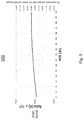
- FIG. 5 illustrates a graph 500 of experimental measurements taken on prototype devices constructed in accordance with embodiments of the present invention.
- Graph 500 illustrates a current sense ratio (CSR), e.g., a ratio of Imain/Isense, on the left abscissa, across a range of drain-source currents, Ids, of the main-FET, also known as Imain, from 2 amps to 50 amps (ordinate).
- the ratio is at least 2.99 ⁇ 10 4 , e.g., at 2 amps, and may be as high as 3.1 ⁇ 10 4 , e.g., at 50 amps.
- the highest claimed CSR under the conventional art known to applicants at this time is approximately 1.2 ⁇ 10 3 .
- Graph 500 of FIG. 5 also illustrates a percentage mismatch across the full main current range on the right abscissa.
- the mismatch describes the accuracy of the ratio of Imain/Isense.
- the mismatch is very small, e.g., within a range of +/ ⁇ 0.33 percent across a range of Ids from 2 amps to 50 amps. Thus, the prototype very accurately indicates Ids of the main-FET.
- a current sense MOSFET in a vertical trench MOSFET may be formed without additional process steps or additional mask layers in comparison to process steps and mask layers required to produce a corresponding vertical trench MOSFET by itself.
- the perpendicular isolation trenches e.g., isolation trenches 221 - 224 of FIG. 2
- the perpendicular isolation trenches 221 - 224 of FIG. 2 may be formed utilizing the same process steps and masks that form the primary trenches 210 of FIG. 2 .
- several masks including, for example, a trench mask and metallization masks, will be different between embodiments in accordance with the present invention and the conventional art.
- a single mask for forming FET trenches e.g., primary trenches 210 ( FIG. 2 ) and perpendicular isolation trenches, e.g., isolation trenches 221 - 224 ( FIG. 2 )
- perpendicular isolation trenches e.g., isolation trenches 221 - 224 ( FIG. 2 )
- the processes and numbers of masks may be the same.
- FIG. 6 illustrates an exemplary process flow 600 for constructing a current sense MOSFET in a vertical trench MOSFET, for example, power semiconductor device 100 of FIG. 1A , in accordance with embodiments of the present invention.
- a plurality of trenches are etched with a hard mask to a depth, e.g., of typically a few micrometers.
- the trenches include, for example, primary trenches, e.g., primary trenches 210 ( FIG. 2 ) and isolation trenches, e.g., isolation trenches 221 - 224 , formed at an angle to the primary trenches.
- the primary trenches and isolation trenches may be etched to about the same depth, but that is not required.
- the vertical trenches are made slightly wider than primary trenches 210 such that when both trenches are etched (at the same process step) the vertical trenches are somewhat deeper than the primary trenches.
- thermal oxide is grown followed by a deposited oxide inside the trench.
- first polysilicon e.g., poly 1 ( 350 ) of FIG. 3
- the first polysilicon may be doped with a high concentration of Phosphorus.
- the first polysilicon is recessed back to a desired depth, typically on the order of 1 micrometer.
- a second oxide layer is grown or deposited over and above the first polysilicon.
- a selective oxide etch is performed to etch the active region where the gate oxide is grown.
- second polysilicon e.g., poly 2 ( 340 ) of FIG. 3
- the second polysilicon is recessed in the active area to allow a layer of deposited oxide the fill the top of the trenches by a fill and etch back process.
- the body and source implants should be introduced consecutively.
- a layer of silicon nitride and doped oxide is used to cover the surface before contacts are etched to silicon, first polysilicon and second polysilicon.
- a layer of metal is deposited and etched forming the gate and source contacts. It is appreciated that the source metal patterns of embodiments in accordance with the present invention differ from a conventional vertical MOSFET, for example, to accommodate the separate sense source of the novel sense-FET. In addition, there is no source metal in an isolation region around the sense-FET.
- a passivation layer of oxide and nitride are deposited over the metallization and etched.
- a metal layer is deposited forming the backside drain contact.
- a sense diode may be established proximate the top body of a relatively larger split gate MOSFET, known as the “main-FET.” Such a sense diode may be used to indicate temperature of the main-FET, in some embodiments. Temperature of a main-FET may be used for numerous purposes, e.g., to shut down a device responsive to an over-temperature condition. A sense diode may also be used to measure gate voltage of the main-FET, in some embodiments. Measuring gate voltage of a main-FET may be desirable when the gate terminal of a main-FET is not exposed, e.g., in packaged, high function devices such as driver MOS (“DrMOS”) devices.
- DrMOS driver MOS
- FIG. 7A illustrates a plan view of an exemplary sense diode 720 in a power semiconductor device 700 , in accordance with embodiments of the present invention.
- a principal function of power semiconductor device 700 is to function as a power MOSFET, e.g., to control a drain source current through the power MOSFET.
- Power semiconductor device 700 comprises large areas of main-FET 750 .
- main-FET 150 comprises numerous trenches comprising gate and shield electrodes, and mesas in-between the trenches comprising source and body regions.
- the main-FET 750 comprises a gate coupled to a gate terminal 740 , for example, a bond pad.
- the main-FET 750 comprises a source coupled to a main-FET source terminal 730 .
- the drain of the MOSFET 750 is outside, e.g., below, the plane of FIG. 7A .
- the function and structure of main-FET 750 , main source 730 and gate 740 are generally equivalent to the comparable structures of device 100 , as illustrated in FIG. 1A .
- Power semiconductor device 100 comprises a sense-diode 720 , formed within a region of the main-FET 750 , in accordance with embodiments of the present invention. It is appreciated that die area of main-FET 750 is very much greater than die area of sense-diode 720 .
- the cathode terminal of sense-diode 720 is in common with the drain terminal of main-FET 750 , outside the plane of FIG. 7A .
- the anode terminal of sense-diode 720 is coupled to anode terminal 710 , e.g., a bond pad.
- FIG. 7B illustrates an exemplary schematic symbol for power semiconductor device 700 , in accordance with embodiments of the present invention.
- sense-diode 720 is structurally very similar to sense-FET 160 of FIGS. 1A, 2, 3 and 4 .
- the isolation trenches that isolate sense-diode 720 are equivalent to the isolation trenches that isolate sense-FET 160 .
- the salient differences between sense-FET 160 and sense-diode 720 are that sense-diode 720 may lack a source implant 410 and a source-body contact 420 ( FIG. 4 ), and the two poly layers within the trenches are connected differently.
- FIG. 8 illustrates an exemplary cross-sectional view of a portion of power semiconductor device 700 , in accordance with embodiments of the present invention.
- FIG. 8 is generally equivalent to the cross section illustration of FIG. 4 .
- the view of FIG. 8 is taken through an active region of sense-diode 720 ( FIG. 7A ), perpendicular to primary trenches of main-FET 750 . Portions of several primary trenches, e.g., under surface isolation regions and BPSG 825 , are utilized as isolation trenches 840 .
- the top electrode, poly 2 ( 842 ) is coupled to the gate electrode, and the bottom electrode, poly 1 ( 841 ), is coupled to the source of the main-FET.
- FIG. 8 illustrates only two trenches as part of a sense-diode 720 for clarity. There would typically be many more trenches 830 within a sense-diode 720 .
- Sense diode 720 comprises a sense-diode anode 870 .
- sense diode 720 may comprise a sense-diode anode contact 851 , similar to a source-body contact of a MOSFET, e.g., sense-FET source-body contact 420 of FIG. 4 .
- a sense-FET source metal extension 850 is also illustrated in FIG. 8 , for example, used to route sense-FET source metal extension to a sense-FET source contact, e.g., sense-FET anode contact 710 of FIG. 7A .
- sense-diode 720 may be used to sense temperature of the device, e.g., a temperature of main-FET 750 and/or to indicate the voltage of gate 740 .
- the first field plate, poly 1 should be electrically coupled to the anode of the sense-diode 720 , which has a separate terminal distinct from the source of the main-FET 750 (or a sense-FET, if present).
- the second field plate, poly 2 uses the gate structure and should be electrically coupled to the anode (not to the gate terminal 740 of the main-FET 750 ).
- the cathode side of the diode is common to the drain of the main-FET 750 (and a sense-FET, if present).
- the diode is not affected by the main-FET 750 gate voltage and exhibits good diode characteristics that can be calibrated as a function of temperature for temperature sensing. Accordingly, this novel structure of a vertical MOS diode within a vertical trench MOSFET may be used to sense temperature of the device via well known methods.
- the second field plate, poly 2 ( 842 ) should be electrically coupled to the gate terminal of the main-FET 750 .
- the sense-diode 720 characteristics change as a function of the gate voltage.
- the sense-diode 720 current-voltage relation depends on gate terminal voltage if the second field plate, poly 2 ( 842 ), is electrically coupled to the gate terminal.
- the sense-diode 720 current-voltage characteristic may be used to indicate the gate voltage, at a given temperature, by calibrating the sense-diode 720 voltage at a given current to the gate voltage.
- FIG. 9 illustrates exemplary characteristics of the sense-diode 720 as a function of the gate voltage, to facilitate determining gate voltage.
- FIG. 9 illustrates exemplary characteristics 900 of an exemplary sense-diode 720 as a function of gate voltage, in accordance with embodiments of the present invention.
- Characteristics 900 may be used to determine gate voltage based on diode current and anode voltage.
- the modulation of the current—voltage characteristics of the sense-diode 720 is seen here depending on the gate voltage, as applied to the second field plate, poly 2 ( 842 ) as illustrated in FIG. 8 .
- the sense-diode 720 in this mode of operation can basically “detect the gate voltage” by calibrating the current flowing through the diode, for example, at 1 ⁇ a of drain-source current, to the following Table 1:
- sense-FET e.g., sense-FET 160 of FIG. 1A
- sense-diode e.g., sense-diode 720 of FIG. 7A
- FIG. 10A illustrates a plan view of an exemplary current sense MOSFET (sense-FET) 160 and an exemplary sense diode 720 in a power semiconductor device 1000 , in accordance with embodiments of the present invention.
- a principal function of power semiconductor device 1000 is to function as a power MOSFET, e.g., to control a drain source current through the power MOSFET.
- Power semiconductor device 1000 comprises large areas of main-FET 1050 .
- main-FET 1050 comprises numerous trenches comprising gate and shield electrodes, and mesas in-between the trenches comprising source and body regions.
- the main-FET 1050 comprises a gate coupled to a gate terminal 140 , for example, a bond pad.
- the main-FET 1050 comprises a source coupled to a main-FET source terminal 130 .
- the drain of the MOSFET 1050 is outside, e.g., below, the plane of FIG. 1A .
- Power semiconductor device 1000 comprises a sense-FET 160 , formed within a region of the main-FET 1050 , in accordance with embodiments of the present invention. It is appreciated that die area of main-FET 1050 is very much greater than die area of sense-FET 160 .
- the gate and drain of the sense-FET 160 are in common, e.g., in parallel, with the gate and drain of the main-FET 1050 .
- the source of the sense-FET 160 is coupled to a sense source terminal 110 , e.g., a bond pad.
- the sense-FET outputs a voltage corresponding to current in the main-FET 1050 .
- the node Kelvin may be coupled to a terminal 120 for use off the die of power semiconductor device 100 , in some embodiments.
- the voltage Kelvin may also, or alternatively, be used by circuitry (not shown) on the die of power semiconductor device 1000 , for example, to turn main-FET 1050 off for over-current protection.
- Power semiconductor device 1000 further comprises a sense-diode 720 , formed within a region of the main-FET 1050 , in accordance with embodiments of the present invention. It is appreciated that die area of main-FET 1050 is very much greater than die area of sense-diode 720 .
- the cathode of the sense-diode 720 is in common with the drain of the main-FET 1050 .
- the anode of sense-diode 720 is coupled to an anode terminal, e.g., a bond pad 710 .
- the sense-diode 720 may be used to measure temperature of the device and/or gate voltage, as previously described.
- a power MOSFET device comprising at least two sense-diodes is envisioned, and is considered within the scope of the present invention.
- multiple sense diodes may be configured to measure temperature in different regions of a MOSFET.
- at least one sense diode may be configured to indicate gate voltage in conjunction with one or more sense diodes configured to measure temperature.
- a power MOSFET device comprising at least two sense-FETs is envisioned, and is considered within the scope of the present invention.
- current within the MOSFET may not be uniformly distributed. Accordingly, it may be advantageous to measure current via multiple sense-FETs at different locations throughout such a device. As a beneficial result of the novel high current sense ratio afforded by embodiments of the present invention, small variations in current may be observed in this manner.
- FIG. 10B illustrates an exemplary schematic symbol for power semiconductor device 1000 , in accordance with embodiments of the present invention.
- sense-FET 160 and/or sense-diode 720 utilize structures common to a main-FET, e.g., trenches and poly layers, for their function, and further utilize structures common to a main-FET, e.g., trenches and BPSG, for isolation. Accordingly, the benefits of a sense-FET 160 and/or sense-diode 720 may be realized with no additional manufacturing cost in comparison to a trench MOSFET.
- Embodiments in accordance with the present invention are well suited to a variety of trench MOSFETs, including, for example, single gate trench MOSFETs, split gate charge balanced trench MOSFETs, Hybrid Split Gate MOSFETs, for example, as disclosed in co-pending, commonly owned U.S. patent application Ser. No. 13/460,567, filed Apr. 20, 2012, to Bobde et al., entitled “Hybrid Split Gate Semiconductor,” which is hereby incorporated herein by reference in its entirety, and dual trench MOSFETs, for example, as described in the publication: “Poly Flanked VDMOS (PFVDMOS): A Superior Technology for Superjunction Devices” by K. P. Gan, Y. C. Liang, G. Samudra, S. M. Xu, L. Yong, IEEE Power Electronics Specialist Conference, 2001.
- PFVDMOS Poly Flanked VDMOS
- Embodiments in accordance with the present invention provide systems and methods for current sense metal oxide semiconductor field effect transistors (MOSFETs) in vertical trench MOSFETs.
- embodiments in accordance with the present invention provide systems and methods for current sense MOSFETs in vertical trench MOSFETs that are integral to the main-FET.
- embodiments in accordance with the present invention provide systems and methods for current sense MOSFETs in vertical trench MOSFETs that are integral to the main-FET.
- Yet further embodiments in accordance with the present invention provide systems and methods for a sensing diode to sense temperature and/or gate voltage of the main-FET.
- embodiments in accordance with the present invention provide systems and methods for systems and methods for current sense MOSFETs and/or sense diodes in vertical trench MOSFETs that are compatible and complementary with existing systems and methods of integrated circuit design, manufacturing and test.
Landscapes
- Engineering & Computer Science (AREA)
- Power Engineering (AREA)
- Microelectronics & Electronic Packaging (AREA)
- Physics & Mathematics (AREA)
- General Physics & Mathematics (AREA)
- Computer Hardware Design (AREA)
- Condensed Matter Physics & Semiconductors (AREA)
- Ceramic Engineering (AREA)
- Manufacturing & Machinery (AREA)
- Chemical & Material Sciences (AREA)
- Chemical Kinetics & Catalysis (AREA)
- General Chemical & Material Sciences (AREA)
- General Engineering & Computer Science (AREA)
- Metal-Oxide And Bipolar Metal-Oxide Semiconductor Integrated Circuits (AREA)
- Composite Materials (AREA)
Abstract
Description
| TABLE 1 | ||
| Vdiode @ 1 μa = 0.62 V => Vgs = 0 V | ||
| Vdiode @ 1 μa = 0.51 V => Vgs = 2.5 V | ||
| Vdiode @ 1 μa = 0.39 V => Vgs = 5 V | ||
| Vdiode @ 1 μa = 0.24 V => Vgs = 10 V | ||
Claims (20)
Priority Applications (1)
| Application Number | Priority Date | Filing Date | Title |
|---|---|---|---|
| US16/717,802 US11131693B2 (en) | 2014-08-19 | 2019-12-17 | Vertical sense devices in vertical trench MOSFET |
Applications Claiming Priority (4)
| Application Number | Priority Date | Filing Date | Title |
|---|---|---|---|
| US201462039335P | 2014-08-19 | 2014-08-19 | |
| US14/830,324 US10234486B2 (en) | 2014-08-19 | 2015-08-19 | Vertical sense devices in vertical trench MOSFET |
| US15/634,739 US10527654B2 (en) | 2014-08-19 | 2017-06-27 | Vertical sense devices in vertical trench MOSFET |
| US16/717,802 US11131693B2 (en) | 2014-08-19 | 2019-12-17 | Vertical sense devices in vertical trench MOSFET |
Related Parent Applications (1)
| Application Number | Title | Priority Date | Filing Date |
|---|---|---|---|
| US15/634,739 Division US10527654B2 (en) | 2014-08-19 | 2017-06-27 | Vertical sense devices in vertical trench MOSFET |
Publications (2)
| Publication Number | Publication Date |
|---|---|
| US20200124645A1 US20200124645A1 (en) | 2020-04-23 |
| US11131693B2 true US11131693B2 (en) | 2021-09-28 |
Family
ID=55348926
Family Applications (4)
| Application Number | Title | Priority Date | Filing Date |
|---|---|---|---|
| US14/830,324 Active US10234486B2 (en) | 2014-08-19 | 2015-08-19 | Vertical sense devices in vertical trench MOSFET |
| US15/634,901 Active US10444262B2 (en) | 2014-08-19 | 2017-06-27 | Vertical sense devices in vertical trench MOSFET |
| US15/634,739 Active US10527654B2 (en) | 2014-08-19 | 2017-06-27 | Vertical sense devices in vertical trench MOSFET |
| US16/717,802 Active US11131693B2 (en) | 2014-08-19 | 2019-12-17 | Vertical sense devices in vertical trench MOSFET |
Family Applications Before (3)
| Application Number | Title | Priority Date | Filing Date |
|---|---|---|---|
| US14/830,324 Active US10234486B2 (en) | 2014-08-19 | 2015-08-19 | Vertical sense devices in vertical trench MOSFET |
| US15/634,901 Active US10444262B2 (en) | 2014-08-19 | 2017-06-27 | Vertical sense devices in vertical trench MOSFET |
| US15/634,739 Active US10527654B2 (en) | 2014-08-19 | 2017-06-27 | Vertical sense devices in vertical trench MOSFET |
Country Status (5)
| Country | Link |
|---|---|
| US (4) | US10234486B2 (en) |
| EP (1) | EP3183753A4 (en) |
| KR (1) | KR102026543B1 (en) |
| CN (2) | CN115483211A (en) |
| WO (1) | WO2016028943A1 (en) |
Families Citing this family (23)
| Publication number | Priority date | Publication date | Assignee | Title |
|---|---|---|---|---|
| CN115483211A (en) | 2014-08-19 | 2022-12-16 | 维西埃-硅化物公司 | Electronic circuit |
| DE102015204637A1 (en) * | 2015-03-13 | 2016-09-15 | Infineon Technologies Ag | A method of doping an active Hall effect region of a Hall effect device and Hall effect device with a doped active Hall effect region |
| JP6631114B2 (en) * | 2015-09-17 | 2020-01-15 | 富士電機株式会社 | Semiconductor device and method of measuring semiconductor device |
| US9973183B2 (en) | 2015-09-28 | 2018-05-15 | Power Integrations, Inc. | Field-effect transistor device with partial finger current sensing FETs |
| US9748376B2 (en) * | 2015-12-21 | 2017-08-29 | Texas Instruments Incorporated | Power FET with integrated sensors and method of manufacturing |
| US9983239B2 (en) | 2016-05-13 | 2018-05-29 | Power Integrations, Inc. | Integrated linear current sense circuitry for semiconductor transistor devices |
| DE112016007127T5 (en) | 2016-08-08 | 2019-08-22 | Power Integrations, Inc. | INTEGRATED CIRCUIT FOR FAST TEMPERATURE PERCEPTION OF SEMICONDUCTOR SWITCHING DEVICE |
| JP6805620B2 (en) * | 2016-08-10 | 2020-12-23 | 富士電機株式会社 | Semiconductor device |
| US10753964B2 (en) | 2017-04-27 | 2020-08-25 | Microchip Technology Incorporated | Current sensing for integrated circuit devices |
| JP6519630B1 (en) * | 2017-10-30 | 2019-05-29 | ダイキン工業株式会社 | Current detection device |
| JP7113666B2 (en) | 2018-06-01 | 2022-08-05 | ローム株式会社 | Semiconductor device and method for manufacturing semiconductor device |
| DE102020107747B4 (en) | 2019-03-22 | 2023-07-20 | Infineon Technologies Ag | TRANSISTOR ARRANGEMENT WITH A LOAD TRANSISTOR AND A SENSING TRANSISTOR AND ELECTRONIC CIRCUIT WITH THESE |
| EP3736864B1 (en) | 2019-05-06 | 2023-04-19 | Infineon Technologies Austria AG | Semiconductor device |
| DE102019003481B3 (en) * | 2019-05-16 | 2020-06-18 | Tdk-Micronas Gmbh | Hall sensor structure |
| US11031308B2 (en) * | 2019-05-30 | 2021-06-08 | Sandisk Technologies Llc | Connectivity detection for wafer-to-wafer alignment and bonding |
| JP7425943B2 (en) * | 2019-12-12 | 2024-02-01 | 株式会社デンソー | silicon carbide semiconductor device |
| CN111129152B (en) * | 2019-12-17 | 2023-09-26 | 杭州芯迈半导体技术有限公司 | Trench MOSFET structure and manufacturing method thereof |
| US12068408B2 (en) * | 2020-07-15 | 2024-08-20 | Semiconductor Components Industries, Llc | High electron mobility transistor |
| CN113066852B (en) * | 2021-03-15 | 2022-09-09 | 无锡新洁能股份有限公司 | Sensing power semiconductor device |
| CN113539833B (en) * | 2021-07-23 | 2023-04-25 | 电子科技大学 | Manufacturing method of split gate power MOSFET device |
| KR102404463B1 (en) * | 2022-04-26 | 2022-06-07 | (주) 트리노테크놀로지 | Silicon carbide power semiconductor device with folded channel region and manufacturing method thereof |
| CN116613072B (en) * | 2023-07-10 | 2023-09-22 | 南京华瑞微集成电路有限公司 | Trench MOSFET integrated with voltage sampling function and manufacturing method thereof |
| CN117832285B (en) * | 2024-03-04 | 2024-04-30 | 南京华瑞微集成电路有限公司 | Low-voltage trench MOSFET with overvoltage protection function and manufacturing method thereof |
Citations (27)
| Publication number | Priority date | Publication date | Assignee | Title |
|---|---|---|---|---|
| US5969383A (en) | 1997-06-16 | 1999-10-19 | Motorola, Inc. | Split-gate memory device and method for accessing the same |
| US20050167695A1 (en) | 2004-02-02 | 2005-08-04 | Hamza Yilmaz | Semiconductor device containing dielectrically isolated pn junction for enhanced breakdown characteristics |
| US20050174823A1 (en) | 2004-01-30 | 2005-08-11 | International Rectifier Corp. | Current sense trench type MOSFET with improved accuracy and ESD withstand capability |
| US20050270869A1 (en) * | 2004-05-19 | 2005-12-08 | Norbert Krischke | Transistor |
| US7129544B2 (en) | 2003-07-18 | 2006-10-31 | Semiconductor Components Industries, L.L.C. | Vertical compound semiconductor field effect transistor structure |
| US7345342B2 (en) | 2001-01-30 | 2008-03-18 | Fairchild Semiconductor Corporation | Power semiconductor devices and methods of manufacture |
| US20080197406A1 (en) | 2007-02-16 | 2008-08-21 | Power Integrations, Inc. | Sensing FET integrated with a high-voltage vertical transistor |
| US20080296668A1 (en) | 2007-04-30 | 2008-12-04 | Infineon Technologies Austria Ag | Semiconductor device and method of manufacturing a semiconductor device |
| US20090039869A1 (en) * | 2007-08-08 | 2009-02-12 | Advanced Analogic Technologies, Inc. | Cascode Current Sensor For Discrete Power Semiconductor Devices |
| US20090189219A1 (en) | 2008-01-30 | 2009-07-30 | Shinbori Atsushi | Semiconductor device and manufacturing method of the same |
| US20100090274A1 (en) | 2008-10-10 | 2010-04-15 | Force Mos Technology Co. Ltd. | Trench mosfet with shallow trench contact |
| US7799646B2 (en) * | 2008-04-07 | 2010-09-21 | Alpha & Omega Semiconductor, Ltd | Integration of a sense FET into a discrete power MOSFET |
| US20100320461A1 (en) | 2008-04-07 | 2010-12-23 | Alpha And Omega Semiconductor Incorporated | Integration of sense fet into discrete power mosfet |
| US20110233606A1 (en) | 2010-03-26 | 2011-09-29 | Force Mos Technology Co. Ltd. | Avalanche capability improvement in power semiconductor devices |
| US8299599B2 (en) | 2010-03-08 | 2012-10-30 | Renesas Electronics Corporation | Semiconductor device |
| US8373449B2 (en) | 2010-12-30 | 2013-02-12 | Infineon Technologies Ag | Circuit arrangement including a common source sense-FET |
| US8502274B1 (en) | 2012-04-06 | 2013-08-06 | Infineon Technologies Ag | Integrated circuit including power transistor cells and a connecting line |
| US8633550B2 (en) | 2011-06-30 | 2014-01-21 | Renesas Electronics Corporation | Semiconductor device |
| US20140125289A1 (en) | 2012-11-08 | 2014-05-08 | Renesas Electronics Corporation | Cell protection system |
| US20140217495A1 (en) * | 2013-02-04 | 2014-08-07 | Infineon Technologies Austria Ag | Integrated Circuit with Power and Sense Transistors |
| US8854065B2 (en) | 2012-01-13 | 2014-10-07 | Infineon Technologies Austria Ag | Current measurement in a power transistor |
| US20150163915A1 (en) * | 2013-12-06 | 2015-06-11 | Infineon Technologies Dresden Gmbh | Electronic device, a method for manufacturing an electronic device, and a method for operating an electronic device |
| US9076805B2 (en) | 2012-07-14 | 2015-07-07 | Infineon Technologies Ag | Current sense transistor with embedding of sense transistor cells |
| US9368587B2 (en) | 2001-01-30 | 2016-06-14 | Fairchild Semiconductor Corporation | Accumulation-mode field effect transistor with improved current capability |
| US20160178670A1 (en) * | 2014-12-17 | 2016-06-23 | Infineon Technologies Austria Ag | Scalable current sense transistor |
| US9425788B1 (en) * | 2015-03-18 | 2016-08-23 | Infineon Technologies Austria Ag | Current sensors and methods of improving accuracy thereof |
| US9466711B2 (en) | 2008-01-29 | 2016-10-11 | Fuji Electric Co., Ltd. | Semiconductor device |
Family Cites Families (298)
| Publication number | Priority date | Publication date | Assignee | Title |
|---|---|---|---|---|
| US3906540A (en) | 1973-04-02 | 1975-09-16 | Nat Semiconductor Corp | Metal-silicide Schottky diode employing an aluminum connector |
| JPH0612828B2 (en) | 1983-06-30 | 1994-02-16 | 株式会社東芝 | Semiconductor device |
| US4641174A (en) | 1983-08-08 | 1987-02-03 | General Electric Company | Pinch rectifier |
| US4672407A (en) | 1984-05-30 | 1987-06-09 | Kabushiki Kaisha Toshiba | Conductivity modulated MOSFET |
| JPS6292361A (en) | 1985-10-17 | 1987-04-27 | Toshiba Corp | Complementary type semiconductor device |
| JPH0693512B2 (en) | 1986-06-17 | 1994-11-16 | 日産自動車株式会社 | Vertical MOSFET |
| JPH0685441B2 (en) | 1986-06-18 | 1994-10-26 | 日産自動車株式会社 | Semiconductor device |
| JP2570742B2 (en) | 1987-05-27 | 1997-01-16 | ソニー株式会社 | Semiconductor device |
| US4799095A (en) | 1987-07-06 | 1989-01-17 | General Electric Company | Metal oxide semiconductor gated turn off thyristor |
| US5021840A (en) | 1987-08-18 | 1991-06-04 | Texas Instruments Incorporated | Schottky or PN diode with composite sidewall |
| US4827321A (en) | 1987-10-29 | 1989-05-02 | General Electric Company | Metal oxide semiconductor gated turn off thyristor including a schottky contact |
| US4893160A (en) | 1987-11-13 | 1990-01-09 | Siliconix Incorporated | Method for increasing the performance of trenched devices and the resulting structure |
| US20020074585A1 (en) | 1988-05-17 | 2002-06-20 | Advanced Power Technology, Inc., Delaware Corporation | Self-aligned power MOSFET with enhanced base region |
| US5283201A (en) | 1988-05-17 | 1994-02-01 | Advanced Power Technology, Inc. | High density power device fabrication process |
| US4969027A (en) | 1988-07-18 | 1990-11-06 | General Electric Company | Power bipolar transistor device with integral antisaturation diode |
| US4967243A (en) | 1988-07-19 | 1990-10-30 | General Electric Company | Power transistor structure with high speed integral antiparallel Schottky diode |
| EP0354449A3 (en) | 1988-08-08 | 1991-01-02 | Seiko Epson Corporation | Semiconductor single crystal substrate |
| US5055896A (en) | 1988-12-15 | 1991-10-08 | Siliconix Incorporated | Self-aligned LDD lateral DMOS transistor with high-voltage interconnect capability |
| US5072266A (en) | 1988-12-27 | 1991-12-10 | Siliconix Incorporated | Trench DMOS power transistor with field-shaping body profile and three-dimensional geometry |
| US4939557A (en) | 1989-02-15 | 1990-07-03 | Varian Associates, Inc. | (110) GaAs microwave FET |
| US5111253A (en) | 1989-05-09 | 1992-05-05 | General Electric Company | Multicellular FET having a Schottky diode merged therewith |
| JPH03173180A (en) | 1989-12-01 | 1991-07-26 | Hitachi Ltd | Semiconductor element |
| JPH03211885A (en) | 1990-01-17 | 1991-09-17 | Matsushita Electron Corp | Semiconductor device and manufacture thereof |
| EP0438700A1 (en) | 1990-01-25 | 1991-07-31 | Asea Brown Boveri Ag | Turn-off MOS-controlled power semiconductor device and method of making the same |
| JP2692350B2 (en) | 1990-04-02 | 1997-12-17 | 富士電機株式会社 | MOS type semiconductor device |
| US5063307A (en) | 1990-09-20 | 1991-11-05 | Ixys Corporation | Insulated gate transistor devices with temperature and current sensor |
| FR2668465B1 (en) | 1990-10-30 | 1993-04-16 | Inst Francais Du Petrole | PROCESS FOR REMOVAL OF MERCURY OR ARSENIC IN A FLUID IN THE PRESENCE OF A MASS OF MERCURY AND / OR ARSENIC CAPTATION. |
| US5168331A (en) | 1991-01-31 | 1992-12-01 | Siliconix Incorporated | Power metal-oxide-semiconductor field effect transistor |
| JPH04291767A (en) | 1991-03-20 | 1992-10-15 | Fuji Electric Co Ltd | Conductivity modulation mosfet |
| JP3131239B2 (en) | 1991-04-25 | 2001-01-31 | キヤノン株式会社 | Wiring for semiconductor circuit device and semiconductor circuit device |
| JP3156300B2 (en) | 1991-10-07 | 2001-04-16 | 株式会社デンソー | Vertical semiconductor device |
| JPH05304297A (en) | 1992-01-29 | 1993-11-16 | Nec Corp | Semiconductor power device and manufacture thereof |
| JP3322936B2 (en) | 1992-03-19 | 2002-09-09 | 株式会社東芝 | Semiconductor storage device |
| JPH05315620A (en) | 1992-05-08 | 1993-11-26 | Rohm Co Ltd | Semiconductor device and manufacture thereof |
| US5233215A (en) * | 1992-06-08 | 1993-08-03 | North Carolina State University At Raleigh | Silicon carbide power MOSFET with floating field ring and floating field plate |
| JP2837033B2 (en) | 1992-07-21 | 1998-12-14 | 三菱電機株式会社 | Semiconductor device and manufacturing method thereof |
| GB9215653D0 (en) | 1992-07-23 | 1992-09-09 | Philips Electronics Uk Ltd | A method of manufacturing a semiconductor device comprising an insulated gate field effect device |
| GB9216599D0 (en) | 1992-08-05 | 1992-09-16 | Philips Electronics Uk Ltd | A semiconductor device comprising a vertical insulated gate field effect device and a method of manufacturing such a device |
| US5408141A (en) | 1993-01-04 | 1995-04-18 | Texas Instruments Incorporated | Sensed current driving device |
| GB9306895D0 (en) | 1993-04-01 | 1993-05-26 | Philips Electronics Uk Ltd | A method of manufacturing a semiconductor device comprising an insulated gate field effect device |
| US5430315A (en) | 1993-07-22 | 1995-07-04 | Rumennik; Vladimir | Bi-directional power trench MOS field effect transistor having low on-state resistance and low leakage current |
| JP3082522B2 (en) | 1993-07-27 | 2000-08-28 | 日産自動車株式会社 | Insulated electrode and method of manufacturing the same |
| JP3383377B2 (en) | 1993-10-28 | 2003-03-04 | 株式会社東芝 | Vertical normally-on type power MOSFET having a trench structure and method of manufacturing the same |
| JP3334290B2 (en) | 1993-11-12 | 2002-10-15 | 株式会社デンソー | Semiconductor device |
| JPH07176745A (en) | 1993-12-17 | 1995-07-14 | Semiconductor Energy Lab Co Ltd | Semiconductor element |
| JP3481287B2 (en) | 1994-02-24 | 2003-12-22 | 三菱電機株式会社 | Manufacturing method of semiconductor device |
| JP3307785B2 (en) | 1994-12-13 | 2002-07-24 | 三菱電機株式会社 | Insulated gate semiconductor device |
| US6008520A (en) | 1994-12-30 | 1999-12-28 | Siliconix Incorporated | Trench MOSFET with heavily doped delta layer to provide low on- resistance |
| US5674766A (en) | 1994-12-30 | 1997-10-07 | Siliconix Incorporated | Method of making a trench MOSFET with multi-resistivity drain to provide low on-resistance by varying dopant concentration in epitaxial layer |
| US5567634A (en) | 1995-05-01 | 1996-10-22 | National Semiconductor Corporation | Method of fabricating self-aligned contact trench DMOS transistors |
| US6140678A (en) | 1995-06-02 | 2000-10-31 | Siliconix Incorporated | Trench-gated power MOSFET with protective diode |
| US6204533B1 (en) | 1995-06-02 | 2001-03-20 | Siliconix Incorporated | Vertical trench-gated power MOSFET having stripe geometry and high cell density |
| EP0746042B1 (en) | 1995-06-02 | 2004-03-31 | SILICONIX Incorporated | Bidirectional blocking trench power MOSFET |
| US5998837A (en) | 1995-06-02 | 1999-12-07 | Siliconix Incorporated | Trench-gated power MOSFET with protective diode having adjustable breakdown voltage |
| US6049108A (en) | 1995-06-02 | 2000-04-11 | Siliconix Incorporated | Trench-gated MOSFET with bidirectional voltage clamping |
| EP0746030B1 (en) | 1995-06-02 | 2001-11-21 | SILICONIX Incorporated | Trench-gated power MOSFET with protective diodes in a periodically repeating pattern |
| US5689129A (en) | 1995-06-07 | 1997-11-18 | Harris Corporation | High efficiency power MOS switch |
| US5689128A (en) | 1995-08-21 | 1997-11-18 | Siliconix Incorporated | High density trenched DMOS transistor |
| JPH09129877A (en) | 1995-10-30 | 1997-05-16 | Toyota Central Res & Dev Lab Inc | Manufacture of semiconductor device, manufacture of insulated gate semiconductor device, and insulated gate semiconductor device |
| JPH09191103A (en) | 1996-01-09 | 1997-07-22 | Nec Corp | Semiconductor device with current detecting means |
| US5814858A (en) | 1996-03-15 | 1998-09-29 | Siliconix Incorporated | Vertical power MOSFET having reduced sensitivity to variations in thickness of epitaxial layer |
| JP3149773B2 (en) | 1996-03-18 | 2001-03-26 | 富士電機株式会社 | Insulated gate bipolar transistor with current limiting circuit |
| JPH09260645A (en) | 1996-03-19 | 1997-10-03 | Sanyo Electric Co Ltd | Semiconductor device |
| US5770878A (en) | 1996-04-10 | 1998-06-23 | Harris Corporation | Trench MOS gate device |
| JP2917922B2 (en) | 1996-07-15 | 1999-07-12 | 日本電気株式会社 | Semiconductor device and manufacturing method thereof |
| US5808340A (en) | 1996-09-18 | 1998-09-15 | Advanced Micro Devices, Inc. | Short channel self aligned VMOS field effect transistor |
| JPH10173175A (en) | 1996-12-09 | 1998-06-26 | Toshiba Corp | Semiconductor device and its manufacture |
| US7269034B2 (en) | 1997-01-24 | 2007-09-11 | Synqor, Inc. | High efficiency power converter |
| JP3173405B2 (en) | 1997-01-31 | 2001-06-04 | 日本電気株式会社 | Method for manufacturing semiconductor device |
| US5952695A (en) | 1997-03-05 | 1999-09-14 | International Business Machines Corporation | Silicon-on-insulator and CMOS-on-SOI double film structures |
| JP3545590B2 (en) | 1997-03-14 | 2004-07-21 | 株式会社東芝 | Semiconductor device |
| US6180966B1 (en) | 1997-03-25 | 2001-01-30 | Hitachi, Ltd. | Trench gate type semiconductor device with current sensing cell |
| US6281547B1 (en) | 1997-05-08 | 2001-08-28 | Megamos Corporation | Power transistor cells provided with reliable trenched source contacts connected to narrower source manufactured without a source mask |
| JP3450650B2 (en) * | 1997-06-24 | 2003-09-29 | 株式会社東芝 | Semiconductor device |
| US6172398B1 (en) | 1997-08-11 | 2001-01-09 | Magepower Semiconductor Corp. | Trenched DMOS device provided with body-dopant redistribution-compensation region for preventing punch through and adjusting threshold voltage |
| JPH1168102A (en) | 1997-08-21 | 1999-03-09 | Toshiba Corp | Production of semiconductor device |
| JP3502531B2 (en) | 1997-08-28 | 2004-03-02 | 株式会社ルネサステクノロジ | Method for manufacturing semiconductor device |
| US6031265A (en) | 1997-10-16 | 2000-02-29 | Magepower Semiconductor Corp. | Enhancing DMOS device ruggedness by reducing transistor parasitic resistance and by inducing breakdown near gate runners and termination area |
| US6429481B1 (en) | 1997-11-14 | 2002-08-06 | Fairchild Semiconductor Corporation | Field effect transistor and method of its manufacture |
| US6268242B1 (en) | 1997-12-31 | 2001-07-31 | Richard K. Williams | Method of forming vertical mosfet device having voltage clamped gate and self-aligned contact |
| US6242775B1 (en) | 1998-02-24 | 2001-06-05 | Micron Technology, Inc. | Circuits and methods using vertical complementary transistors |
| JP3705919B2 (en) | 1998-03-05 | 2005-10-12 | 三菱電機株式会社 | Semiconductor device and manufacturing method thereof |
| KR100295063B1 (en) | 1998-06-30 | 2001-08-07 | 김덕중 | Power semiconductor device having trench gate structure and method for fabricating thereof |
| JP3413569B2 (en) | 1998-09-16 | 2003-06-03 | 株式会社日立製作所 | Insulated gate semiconductor device and method of manufacturing the same |
| US6939776B2 (en) | 1998-09-29 | 2005-09-06 | Sanyo Electric Co., Ltd. | Semiconductor device and a method of fabricating the same |
| FR2785090B1 (en) | 1998-10-23 | 2001-01-19 | St Microelectronics Sa | POWER COMPONENT CARRYING INTERCONNECTIONS |
| US6621121B2 (en) | 1998-10-26 | 2003-09-16 | Silicon Semiconductor Corporation | Vertical MOSFETs having trench-based gate electrodes within deeper trench-based source electrodes |
| US5998833A (en) | 1998-10-26 | 1999-12-07 | North Carolina State University | Power semiconductor devices having improved high frequency switching and breakdown characteristics |
| US6160441A (en) | 1998-10-30 | 2000-12-12 | Volterra Semiconductor Corporation | Sensors for measuring current passing through a load |
| US7578923B2 (en) | 1998-12-01 | 2009-08-25 | Novellus Systems, Inc. | Electropolishing system and process |
| JP2000191344A (en) | 1998-12-25 | 2000-07-11 | Kanegafuchi Chem Ind Co Ltd | Light-controlling glass and window using the same |
| US6255683B1 (en) | 1998-12-29 | 2001-07-03 | Infineon Technologies Ag | Dynamic random access memory |
| WO2000042665A1 (en) | 1999-01-11 | 2000-07-20 | Fraunhofer-Gesellschaft zur Förderung der angewandten Forschung e.V. | Power mos element and method for producing the same |
| JP3743189B2 (en) | 1999-01-27 | 2006-02-08 | 富士通株式会社 | Nonvolatile semiconductor memory device and manufacturing method thereof |
| JP2000223705A (en) | 1999-01-29 | 2000-08-11 | Nissan Motor Co Ltd | Semiconductor device |
| US6351009B1 (en) | 1999-03-01 | 2002-02-26 | Fairchild Semiconductor Corporation | MOS-gated device having a buried gate and process for forming same |
| US6404007B1 (en) | 1999-04-05 | 2002-06-11 | Fairchild Semiconductor Corporation | Trench transistor with superior gate dielectric |
| US6277695B1 (en) | 1999-04-16 | 2001-08-21 | Siliconix Incorporated | Method of forming vertical planar DMOSFET with self-aligned contact |
| US6413822B2 (en) | 1999-04-22 | 2002-07-02 | Advanced Analogic Technologies, Inc. | Super-self-aligned fabrication process of trench-gate DMOS with overlying device layer |
| US6238981B1 (en) | 1999-05-10 | 2001-05-29 | Intersil Corporation | Process for forming MOS-gated devices having self-aligned trenches |
| US6291298B1 (en) | 1999-05-25 | 2001-09-18 | Advanced Analogic Technologies, Inc. | Process of manufacturing Trench gate semiconductor device having gate oxide layer with multiple thicknesses |
| JP4117977B2 (en) | 1999-06-25 | 2008-07-16 | 富士通株式会社 | Semiconductor device |
| WO2001005116A2 (en) | 1999-07-13 | 2001-01-18 | Alteon Web Systems, Inc. | Routing method and apparatus |
| GB9917099D0 (en) | 1999-07-22 | 1999-09-22 | Koninkl Philips Electronics Nv | Cellular trench-gate field-effect transistors |
| US6483171B1 (en) | 1999-08-13 | 2002-11-19 | Micron Technology, Inc. | Vertical sub-micron CMOS transistors on (110), (111), (311), (511), and higher order surfaces of bulk, SOI and thin film structures and method of forming same |
| US6211018B1 (en) | 1999-08-14 | 2001-04-03 | Electronics And Telecommunications Research Institute | Method for fabricating high density trench gate type power device |
| US6245615B1 (en) | 1999-08-31 | 2001-06-12 | Micron Technology, Inc. | Method and apparatus on (110) surfaces of silicon structures with conduction in the <110> direction |
| US6518621B1 (en) | 1999-09-14 | 2003-02-11 | General Semiconductor, Inc. | Trench DMOS transistor having reduced punch-through |
| US6348712B1 (en) | 1999-10-27 | 2002-02-19 | Siliconix Incorporated | High density trench-gated power MOSFET |
| GB9928285D0 (en) | 1999-11-30 | 2000-01-26 | Koninkl Philips Electronics Nv | Manufacture of trench-gate semiconductor devices |
| US6285060B1 (en) | 1999-12-30 | 2001-09-04 | Siliconix Incorporated | Barrier accumulation-mode MOSFET |
| US6548860B1 (en) | 2000-02-29 | 2003-04-15 | General Semiconductor, Inc. | DMOS transistor structure having improved performance |
| JP3949869B2 (en) | 2000-03-22 | 2007-07-25 | セイコーインスツル株式会社 | Vertical MOS transistor and manufacturing method thereof |
| US6580123B2 (en) | 2000-04-04 | 2003-06-17 | International Rectifier Corporation | Low voltage power MOSFET device and process for its manufacture |
| JP4581179B2 (en) | 2000-04-26 | 2010-11-17 | 富士電機システムズ株式会社 | Insulated gate semiconductor device |
| EP1170803A3 (en) | 2000-06-08 | 2002-10-09 | Siliconix Incorporated | Trench gate MOSFET and method of making the same |
| US6472678B1 (en) | 2000-06-16 | 2002-10-29 | General Semiconductor, Inc. | Trench MOSFET with double-diffused body profile |
| US6784486B2 (en) | 2000-06-23 | 2004-08-31 | Silicon Semiconductor Corporation | Vertical power devices having retrograded-doped transition regions therein |
| JP2002016080A (en) | 2000-06-28 | 2002-01-18 | Toshiba Corp | Manufacturing method of trench-gate type mosfet |
| JP4528460B2 (en) | 2000-06-30 | 2010-08-18 | 株式会社東芝 | Semiconductor element |
| US6304108B1 (en) | 2000-07-14 | 2001-10-16 | Micrel, Incorporated | Reference-corrected ratiometric MOS current sensing circuit |
| US6700158B1 (en) | 2000-08-18 | 2004-03-02 | Fairchild Semiconductor Corporation | Trench corner protection for trench MOSFET |
| US6309929B1 (en) | 2000-09-22 | 2001-10-30 | Industrial Technology Research Institute And Genetal Semiconductor Of Taiwan, Ltd. | Method of forming trench MOS device and termination structure |
| JP2002110978A (en) | 2000-10-02 | 2002-04-12 | Toshiba Corp | Power semiconductor element |
| US6509233B2 (en) | 2000-10-13 | 2003-01-21 | Siliconix Incorporated | Method of making trench-gated MOSFET having cesium gate oxide layer |
| JP4514006B2 (en) | 2000-10-25 | 2010-07-28 | ソニー株式会社 | Semiconductor device |
| AU2002230482A1 (en) | 2000-11-16 | 2002-05-27 | Silicon Wireless Corporation | Discrete and packaged power devices for radio frequency (rf) applications and methods of forming same |
| US6608350B2 (en) | 2000-12-07 | 2003-08-19 | International Rectifier Corporation | High voltage vertical conduction superjunction semiconductor device |
| JP3551251B2 (en) | 2000-12-22 | 2004-08-04 | サンケン電気株式会社 | Insulated gate field effect transistor and method of manufacturing the same |
| JP2002222950A (en) | 2001-01-25 | 2002-08-09 | Denso Corp | Method of manufacturing silicon carbide semiconductor device |
| US6710403B2 (en) | 2002-07-30 | 2004-03-23 | Fairchild Semiconductor Corporation | Dual trench power MOSFET |
| US6870220B2 (en) | 2002-08-23 | 2005-03-22 | Fairchild Semiconductor Corporation | Method and apparatus for improved MOS gating to reduce miller capacitance and switching losses |
| US7132712B2 (en) | 2002-11-05 | 2006-11-07 | Fairchild Semiconductor Corporation | Trench structure having one or more diodes embedded therein adjacent a PN junction |
| JP3531613B2 (en) | 2001-02-06 | 2004-05-31 | 株式会社デンソー | Trench gate type semiconductor device and manufacturing method thereof |
| JP4932088B2 (en) | 2001-02-19 | 2012-05-16 | ルネサスエレクトロニクス株式会社 | Insulated gate type semiconductor device manufacturing method |
| US6683346B2 (en) | 2001-03-09 | 2004-01-27 | Fairchild Semiconductor Corporation | Ultra dense trench-gated power-device with the reduced drain-source feedback capacitance and Miller charge |
| JP2002280553A (en) | 2001-03-19 | 2002-09-27 | Toshiba Corp | Semiconductor device and method for manufacturing the same |
| TW484213B (en) | 2001-04-24 | 2002-04-21 | Ememory Technology Inc | Forming method and operation method of trench type separation gate nonvolatile flash memory cell structure |
| JP4823435B2 (en) | 2001-05-29 | 2011-11-24 | 三菱電機株式会社 | Semiconductor device and manufacturing method thereof |
| JP4608133B2 (en) | 2001-06-08 | 2011-01-05 | ルネサスエレクトロニクス株式会社 | Semiconductor device provided with vertical MOSFET and manufacturing method thereof |
| EP1267415A3 (en) | 2001-06-11 | 2009-04-15 | Kabushiki Kaisha Toshiba | Power semiconductor device having resurf layer |
| JP2002373989A (en) | 2001-06-13 | 2002-12-26 | Toshiba Corp | Semiconductor device |
| JP4854868B2 (en) | 2001-06-14 | 2012-01-18 | ローム株式会社 | Semiconductor device |
| US7009247B2 (en) | 2001-07-03 | 2006-03-07 | Siliconix Incorporated | Trench MIS device with thick oxide layer in bottom of gate contact trench |
| JP2003030396A (en) | 2001-07-13 | 2003-01-31 | Nec Corp | System, method, and program for entrusted operation management |
| GB0118000D0 (en) | 2001-07-24 | 2001-09-19 | Koninkl Philips Electronics Nv | Manufacture of semiconductor devices with schottky barriers |
| US6882000B2 (en) | 2001-08-10 | 2005-04-19 | Siliconix Incorporated | Trench MIS device with reduced gate-to-drain capacitance |
| US6489204B1 (en) | 2001-08-20 | 2002-12-03 | Episil Technologies, Inc. | Save MOS device |
| US6621107B2 (en) | 2001-08-23 | 2003-09-16 | General Semiconductor, Inc. | Trench DMOS transistor with embedded trench schottky rectifier |
| US7045859B2 (en) | 2001-09-05 | 2006-05-16 | International Rectifier Corporation | Trench fet with self aligned source and contact |
| WO2003028108A1 (en) | 2001-09-19 | 2003-04-03 | Kabushiki Kaisha Toshiba | Semiconductor device and method for fabricating the same |
| JP2003115587A (en) | 2001-10-03 | 2003-04-18 | Tadahiro Omi | Semiconductor device formed on silicon surface with <100> orientation, and manufacturing method therefor |
| JP3973395B2 (en) | 2001-10-16 | 2007-09-12 | 株式会社豊田中央研究所 | Semiconductor device and manufacturing method thereof |
| KR100406180B1 (en) | 2001-12-22 | 2003-11-17 | 주식회사 하이닉스반도체 | Method of manufacturing a flash memory cell |
| US6573142B1 (en) | 2002-02-26 | 2003-06-03 | Taiwan Semiconductor Manufacturing Company | Method to fabricate self-aligned source and drain in split gate flash |
| FR2837523B1 (en) * | 2002-03-19 | 2004-05-14 | Montabert Sa | ROTO-PERCUTANT HYDRAULIC PERFORATOR HAMMER |
| DE10212149B4 (en) | 2002-03-19 | 2007-10-04 | Infineon Technologies Ag | Transistor arrangement with shield electrode outside of an active cell array and reduced gate-drain capacitance |
| JP3960091B2 (en) | 2002-03-20 | 2007-08-15 | 富士電機ホールディングス株式会社 | Semiconductor device and manufacturing method thereof |
| US6838722B2 (en) | 2002-03-22 | 2005-01-04 | Siliconix Incorporated | Structures of and methods of fabricating trench-gated MIS devices |
| JP4004843B2 (en) | 2002-04-24 | 2007-11-07 | Necエレクトロニクス株式会社 | Method for manufacturing vertical MOSFET |
| JP3652322B2 (en) | 2002-04-30 | 2005-05-25 | Necエレクトロニクス株式会社 | Vertical MOSFET and manufacturing method thereof |
| US7012005B2 (en) | 2002-06-25 | 2006-03-14 | Siliconix Incorporated | Self-aligned differential oxidation in trenches by ion implantation |
| US6858494B2 (en) | 2002-08-20 | 2005-02-22 | Taiwan Semiconductor Manufacturing Company | Structure and fabricating method with self-aligned bit line contact to word line in split gate flash |
| JP3640945B2 (en) | 2002-09-02 | 2005-04-20 | 株式会社東芝 | Trench gate type semiconductor device and manufacturing method thereof |
| US8080459B2 (en) | 2002-09-24 | 2011-12-20 | Vishay-Siliconix | Self aligned contact in a semiconductor device and method of fabricating the same |
| US8629019B2 (en) | 2002-09-24 | 2014-01-14 | Vishay-Siliconix | Method of forming self aligned contacts for a power MOSFET |
| US7576388B1 (en) | 2002-10-03 | 2009-08-18 | Fairchild Semiconductor Corporation | Trench-gate LDMOS structures |
| JP3931138B2 (en) | 2002-12-25 | 2007-06-13 | 三菱電機株式会社 | Power semiconductor device and method for manufacturing power semiconductor device |
| JP2004241413A (en) | 2003-02-03 | 2004-08-26 | Toshiba Corp | Semiconductor device |
| US6861701B2 (en) | 2003-03-05 | 2005-03-01 | Advanced Analogic Technologies, Inc. | Trench power MOSFET with planarized gate bus |
| JP2004356114A (en) | 2003-05-26 | 2004-12-16 | Tadahiro Omi | P-channel power mis field effect transistor and switching circuit |
| JP4626131B2 (en) | 2003-07-11 | 2011-02-02 | 富士電機システムズ株式会社 | Insulated gate semiconductor device |
| JP4945055B2 (en) | 2003-08-04 | 2012-06-06 | ルネサスエレクトロニクス株式会社 | Semiconductor device and manufacturing method thereof |
| US6987305B2 (en) | 2003-08-04 | 2006-01-17 | International Rectifier Corporation | Integrated FET and schottky device |
| DE10339455B3 (en) | 2003-08-27 | 2005-05-04 | Infineon Technologies Ag | Vertical semiconductor device having a field electrode drift zone and method for making such a drift zone |
| US7022578B2 (en) | 2003-10-09 | 2006-04-04 | Chartered Semiconductor Manufacturing Ltd. | Heterojunction bipolar transistor using reverse emitter window |
| JP4470454B2 (en) | 2003-11-04 | 2010-06-02 | 株式会社豊田中央研究所 | Semiconductor device and manufacturing method thereof |
| DE10353387B4 (en) | 2003-11-14 | 2008-07-24 | Infineon Technologies Ag | Method for producing a power transistor arrangement and power transistor arrangement |
| GB0327793D0 (en) | 2003-11-29 | 2003-12-31 | Koninkl Philips Electronics Nv | Trench mosfet |
| GB0327791D0 (en) | 2003-11-29 | 2003-12-31 | Koninkl Philips Electronics Nv | Trench insulated gate field effect transistor |
| JP4398719B2 (en) | 2003-12-25 | 2010-01-13 | 株式会社東芝 | Semiconductor device |
| WO2005065385A2 (en) | 2003-12-30 | 2005-07-21 | Fairchild Semiconductor Corporation | Power semiconductor devices and methods of manufacture |
| US7368777B2 (en) | 2003-12-30 | 2008-05-06 | Fairchild Semiconductor Corporation | Accumulation device with charge balance structure and method of forming the same |
| JP4904673B2 (en) | 2004-02-09 | 2012-03-28 | 富士電機株式会社 | Semiconductor device and manufacturing method of semiconductor device |
| JP2005268679A (en) | 2004-03-22 | 2005-09-29 | Matsushita Electric Ind Co Ltd | Semiconductor device and manufacturing method for the same |
| JP2005304210A (en) | 2004-04-14 | 2005-10-27 | Renesas Technology Corp | Power supply driver apparatus and switching regulator |
| US6906380B1 (en) | 2004-05-13 | 2005-06-14 | Vishay-Siliconix | Drain side gate trench metal-oxide-semiconductor field effect transistor |
| US8120135B2 (en) | 2004-05-19 | 2012-02-21 | Infineon Technologies Ag | Transistor |
| DE102004029435B4 (en) | 2004-06-18 | 2017-02-16 | Infineon Technologies Ag | Field plate trench transistor |
| US7141860B2 (en) | 2004-06-23 | 2006-11-28 | Freescale Semiconductor, Inc. | LDMOS transistor |
| US7405562B2 (en) | 2004-07-23 | 2008-07-29 | Yehya Ghallab | Magnetic field imaging detection apparatus |
| GB0419558D0 (en) | 2004-09-03 | 2004-10-06 | Koninkl Philips Electronics Nv | Vertical semiconductor devices and methods of manufacturing such devices |
| JP4913336B2 (en) | 2004-09-28 | 2012-04-11 | ルネサスエレクトロニクス株式会社 | Semiconductor device |
| JP4841829B2 (en) | 2004-11-17 | 2011-12-21 | ルネサスエレクトロニクス株式会社 | Semiconductor device and manufacturing method thereof |
| US20060108635A1 (en) | 2004-11-23 | 2006-05-25 | Alpha Omega Semiconductor Limited | Trenched MOSFETS with part of the device formed on a (110) crystal plane |
| DE102004057237B4 (en) | 2004-11-26 | 2007-02-08 | Infineon Technologies Ag | Method for producing contact holes in a semiconductor body and transistor with a vertical structure |
| US20060113588A1 (en) | 2004-11-29 | 2006-06-01 | Sillicon-Based Technology Corp. | Self-aligned trench-type DMOS transistor structure and its manufacturing methods |
| US7439583B2 (en) | 2004-12-27 | 2008-10-21 | Third Dimension (3D) Semiconductor, Inc. | Tungsten plug drain extension |
| JP2006202931A (en) | 2005-01-20 | 2006-08-03 | Renesas Technology Corp | Semiconductor device and its manufacturing method |
| US7453119B2 (en) | 2005-02-11 | 2008-11-18 | Alphs & Omega Semiconductor, Ltd. | Shielded gate trench (SGT) MOSFET cells implemented with a schottky source contact |
| DE102005009020B4 (en) | 2005-02-28 | 2012-04-26 | Infineon Technologies Austria Ag | Method for generating a power transistor and thus generated integrated circuit arrangement |
| DE102005009000B4 (en) | 2005-02-28 | 2009-04-02 | Infineon Technologies Austria Ag | Trench structural type vertical semiconductor device and manufacturing method |
| AT504998A2 (en) | 2005-04-06 | 2008-09-15 | Fairchild Semiconductor | TRENCHED-GATE FIELD EFFECT TRANSISTORS AND METHOD FOR MAKING THE SAME |
| US7494876B1 (en) | 2005-04-21 | 2009-02-24 | Vishay Siliconix | Trench-gated MIS device having thick polysilicon insulation layer at trench bottom and method of fabricating the same |
| KR101047945B1 (en) | 2005-05-24 | 2011-07-12 | 비쉐이-실리코닉스 | Trench Metal Oxide Semiconductor Field Effect Transistor |
| US7504303B2 (en) | 2005-05-26 | 2009-03-17 | Fairchild Semiconductor Corporation | Trench-gate field effect transistors and methods of forming the same |
| US7592650B2 (en) | 2005-06-06 | 2009-09-22 | M-Mos Semiconductor Sdn. Bhd. | High density hybrid MOSFET device |
| JP2006339558A (en) | 2005-06-06 | 2006-12-14 | Seiko Epson Corp | Semiconductor device and its manufacturing method |
| US20070004116A1 (en) | 2005-06-06 | 2007-01-04 | M-Mos Semiconductor Sdn. Bhd. | Trenched MOSFET termination with tungsten plug structures |
| CN103094348B (en) | 2005-06-10 | 2016-08-10 | 飞兆半导体公司 | Field-effect transistor |
| TWI400757B (en) | 2005-06-29 | 2013-07-01 | Fairchild Semiconductor | Methods for forming shielded gate field effect transistors |
| JP2007012977A (en) | 2005-07-01 | 2007-01-18 | Toshiba Corp | Semiconductor device |
| JP2007027193A (en) | 2005-07-12 | 2007-02-01 | Renesas Technology Corp | Semiconductor device, its manufacturing method and non-insulated dc/dc converter |
| JP4928754B2 (en) | 2005-07-20 | 2012-05-09 | 株式会社東芝 | Power semiconductor device |
| JP2007035841A (en) | 2005-07-26 | 2007-02-08 | Toshiba Corp | Semiconductor device |
| US7385248B2 (en) | 2005-08-09 | 2008-06-10 | Fairchild Semiconductor Corporation | Shielded gate field effect transistor with improved inter-poly dielectric |
| DE102005041322B4 (en) | 2005-08-31 | 2017-03-16 | Infineon Technologies Ag | Trench transistor structure with field electrode assembly and manufacturing method thereof |
| DE102005052734B4 (en) | 2005-10-06 | 2012-02-23 | Infineon Technologies Ag | Semiconductor structure, method for operating a semiconductor structure and method for producing a semiconductor structure |
| JP4735224B2 (en) | 2005-12-08 | 2011-07-27 | トヨタ自動車株式会社 | Insulated gate semiconductor device and manufacturing method thereof |
| JP2007189192A (en) | 2005-12-15 | 2007-07-26 | Toshiba Corp | Semiconductor device |
| US7544545B2 (en) * | 2005-12-28 | 2009-06-09 | Vishay-Siliconix | Trench polysilicon diode |
| US7449354B2 (en) | 2006-01-05 | 2008-11-11 | Fairchild Semiconductor Corporation | Trench-gated FET for power device with active gate trenches and gate runner trench utilizing one-mask etch |
| US7554152B1 (en) | 2006-01-11 | 2009-06-30 | National Semiconductor Corporation | Versatile system for integrated sense transistor |
| DE102006007096B4 (en) | 2006-02-15 | 2008-07-17 | Infineon Technologies Austria Ag | Compensating structure and edge termination MOSFET and method of making the same |
| US7446374B2 (en) | 2006-03-24 | 2008-11-04 | Fairchild Semiconductor Corporation | High density trench FET with integrated Schottky diode and method of manufacture |
| JP4182986B2 (en) | 2006-04-19 | 2008-11-19 | トヨタ自動車株式会社 | Semiconductor device and manufacturing method thereof |
| WO2007129261A2 (en) | 2006-05-05 | 2007-11-15 | Nxp B.V. | Trench field effect transistors |
| US7319256B1 (en) | 2006-06-19 | 2008-01-15 | Fairchild Semiconductor Corporation | Shielded gate trench FET with the shield and gate electrodes being connected together |
| JP5222466B2 (en) | 2006-08-09 | 2013-06-26 | ルネサスエレクトロニクス株式会社 | Semiconductor device and manufacturing method thereof |
| US7544571B2 (en) | 2006-09-20 | 2009-06-09 | Fairchild Semiconductor Corporation | Trench gate FET with self-aligned features |
| DE102006045441B4 (en) | 2006-09-26 | 2008-09-25 | Infineon Technologies Austria Ag | A method of manufacturing a semiconductor device device having a trench transistor structure |
| US7750398B2 (en) | 2006-09-26 | 2010-07-06 | Force-Mos Technology Corporation | Trench MOSFET with trench termination and manufacture thereof |
| KR101375035B1 (en) | 2006-09-27 | 2014-03-14 | 맥스파워 세미컨덕터 인크. | Power mosfet with recessed field plate |
| US7732842B2 (en) | 2006-12-06 | 2010-06-08 | Fairchild Semiconductor Corporation | Structure and method for forming a planar schottky contact |
| US9437729B2 (en) | 2007-01-08 | 2016-09-06 | Vishay-Siliconix | High-density power MOSFET with planarized metalization |
| JP5091487B2 (en) | 2007-01-09 | 2012-12-05 | 株式会社東芝 | Manufacturing method of semiconductor device |
| KR20090116702A (en) | 2007-01-09 | 2009-11-11 | 맥스파워 세미컨덕터 인크. | Semiconductor device |
| US7670908B2 (en) | 2007-01-22 | 2010-03-02 | Alpha & Omega Semiconductor, Ltd. | Configuration of high-voltage semiconductor power device to achieve three dimensional charge coupling |
| US7615847B2 (en) | 2007-03-23 | 2009-11-10 | Infineon Technologies Austria Ag | Method for producing a semiconductor component |
| US9947770B2 (en) | 2007-04-03 | 2018-04-17 | Vishay-Siliconix | Self-aligned trench MOSFET and method of manufacture |
| US8035159B2 (en) | 2007-04-30 | 2011-10-11 | Alpha & Omega Semiconductor, Ltd. | Device structure and manufacturing method using HDP deposited source-body implant block |
| JP2009004411A (en) | 2007-06-19 | 2009-01-08 | Rohm Co Ltd | Semiconductor device |
| WO2008156071A1 (en) | 2007-06-19 | 2008-12-24 | Rohm Co., Ltd. | Semiconductor device |
| JP2009043966A (en) | 2007-08-09 | 2009-02-26 | Toshiba Corp | Semiconductor apparatus and method of manufacturing the same |
| US8497549B2 (en) | 2007-08-21 | 2013-07-30 | Fairchild Semiconductor Corporation | Method and structure for shielded gate trench FET |
| US8686493B2 (en) | 2007-10-04 | 2014-04-01 | Fairchild Semiconductor Corporation | High density FET with integrated Schottky |
| JP2009135360A (en) | 2007-12-03 | 2009-06-18 | Renesas Technology Corp | Semiconductor device and its manufacturing method |
| JP5604029B2 (en) | 2007-12-04 | 2014-10-08 | ローム株式会社 | Semiconductor device and manufacturing method thereof |
| KR101396124B1 (en) | 2007-12-21 | 2014-05-19 | 삼성전자주식회사 | Method of forming a trench and method of manufacturing a semiconductor device using the same |
| JP4748149B2 (en) | 2007-12-24 | 2011-08-17 | 株式会社デンソー | Semiconductor device |
| US7825431B2 (en) | 2007-12-31 | 2010-11-02 | Alpha & Omega Semicondictor, Ltd. | Reduced mask configuration for power MOSFETs with electrostatic discharge (ESD) circuit protection |
| US7936009B2 (en) | 2008-07-09 | 2011-05-03 | Fairchild Semiconductor Corporation | Shielded gate trench FET with an inter-electrode dielectric having a low-k dielectric therein |
| US8005015B2 (en) * | 2008-07-28 | 2011-08-23 | Telefonaktiebolaget L M Ericsson (Publ) | Signaling framework for negotiating and executing composition of registries |
| US8642459B2 (en) | 2008-08-28 | 2014-02-04 | Infineon Technologies Ag | Method for forming a semiconductor device with an isolation region on a gate electrode |
| US8039877B2 (en) | 2008-09-09 | 2011-10-18 | Fairchild Semiconductor Corporation | (110)-oriented p-channel trench MOSFET having high-K gate dielectric |
| US8203181B2 (en) | 2008-09-30 | 2012-06-19 | Infineon Technologies Austria Ag | Trench MOSFET semiconductor device and manufacturing method therefor |
| US8796764B2 (en) | 2008-09-30 | 2014-08-05 | Infineon Technologies Austria Ag | Semiconductor device comprising trench gate and buried source electrodes |
| US8022474B2 (en) | 2008-09-30 | 2011-09-20 | Infineon Technologies Austria Ag | Semiconductor device |
| KR20100063389A (en) | 2008-12-03 | 2010-06-11 | 주식회사 동부하이텍 | Power ic and driving method thereof |
| WO2010120704A2 (en) | 2009-04-13 | 2010-10-21 | Maxpower Semiconductor Inc. | Power semiconductor devices, methods, and structures with embedded dielectric layers containing permanent charges |
| TWI402985B (en) | 2009-06-02 | 2013-07-21 | Anpec Electronics Corp | Integrated structure of igbt and diode and method of forming the same |
| US7910486B2 (en) | 2009-06-12 | 2011-03-22 | Alpha & Omega Semiconductor, Inc. | Method for forming nanotube semiconductor devices |
| JP5602851B2 (en) * | 2009-07-21 | 2014-10-08 | インターナショナル・ビジネス・マシーンズ・コーポレーション | Method and system for job scheduling in a distributed data processing system using identification of optimal network topology |
| US9443974B2 (en) | 2009-08-27 | 2016-09-13 | Vishay-Siliconix | Super junction trench power MOSFET device fabrication |
| US9425306B2 (en) | 2009-08-27 | 2016-08-23 | Vishay-Siliconix | Super junction trench power MOSFET devices |
| US9431530B2 (en) | 2009-10-20 | 2016-08-30 | Vishay-Siliconix | Super-high density trench MOSFET |
| US9425305B2 (en) | 2009-10-20 | 2016-08-23 | Vishay-Siliconix | Structures of and methods of fabricating split gate MIS devices |
| US9419129B2 (en) | 2009-10-21 | 2016-08-16 | Vishay-Siliconix | Split gate semiconductor device with curved gate oxide profile |
| US20120220092A1 (en) | 2009-10-21 | 2012-08-30 | Vishay-Siliconix | Method of forming a hybrid split gate simiconductor |
| US8354711B2 (en) | 2010-01-11 | 2013-01-15 | Maxpower Semiconductor, Inc. | Power MOSFET and its edge termination |
| US9577089B2 (en) | 2010-03-02 | 2017-02-21 | Vishay-Siliconix | Structures and methods of fabricating dual gate devices |
| JP5553652B2 (en) | 2010-03-18 | 2014-07-16 | ルネサスエレクトロニクス株式会社 | Semiconductor substrate and semiconductor device |
| WO2011145970A1 (en) | 2010-05-21 | 2011-11-24 | Freescale Semiconductor, Inc. | Power switching apparatus and method for improving current sense accuracy |
| US20110298280A1 (en) | 2010-06-07 | 2011-12-08 | Skyworks Solutions, Inc | Apparatus and method for variable voltage distribution |
| JP5569162B2 (en) | 2010-06-10 | 2014-08-13 | 富士電機株式会社 | Semiconductor device and manufacturing method of semiconductor device |
| JP5740108B2 (en) | 2010-07-16 | 2015-06-24 | 株式会社東芝 | Semiconductor device |
| JP5580150B2 (en) | 2010-09-09 | 2014-08-27 | 株式会社東芝 | Semiconductor device |
| US8362550B2 (en) | 2011-01-20 | 2013-01-29 | Fairchild Semiconductor Corporation | Trench power MOSFET with reduced on-resistance |
| JP5659897B2 (en) | 2011-03-22 | 2015-01-28 | トヨタ自動車株式会社 | System comprising semiconductor device and control means, and method for controlling current flowing through semiconductor device |
| JP5637916B2 (en) | 2011-03-31 | 2014-12-10 | トヨタ自動車株式会社 | Semiconductor device and manufacturing method thereof |
| US8587059B2 (en) | 2011-04-22 | 2013-11-19 | Infineon Technologies Austria Ag | Transistor arrangement with a MOSFET |
| US8466513B2 (en) | 2011-06-13 | 2013-06-18 | Semiconductor Components Industries, Llc | Semiconductor device with enhanced mobility and method |
| US8507978B2 (en) * | 2011-06-16 | 2013-08-13 | Alpha And Omega Semiconductor Incorporated | Split-gate structure in trench-based silicon carbide power device |
| US8633539B2 (en) | 2011-06-27 | 2014-01-21 | Infineon Technologies Austria Ag | Trench transistor and manufacturing method of the trench transistor |
| US9385132B2 (en) | 2011-08-25 | 2016-07-05 | Micron Technology, Inc. | Arrays of recessed access devices, methods of forming recessed access gate constructions, and methods of forming isolation gate constructions in the fabrication of recessed access devices |
| KR20130050160A (en) | 2011-11-07 | 2013-05-15 | 삼성전자주식회사 | Method of manufacturing semiconductor device |
| JP5844656B2 (en) | 2012-02-20 | 2016-01-20 | ルネサスエレクトロニクス株式会社 | Semiconductor device and manufacturing method of semiconductor device |
| US9070585B2 (en) | 2012-02-24 | 2015-06-30 | Semiconductor Components Industries, Llc | Electronic device including a trench and a conductive structure therein and a process of forming the same |
| CN103489862B (en) | 2012-06-12 | 2018-05-22 | 恩智浦美国有限公司 | Power MOSFET current sense structures and methods |
| WO2014091545A1 (en) | 2012-12-10 | 2014-06-19 | 三菱電機株式会社 | Semiconductor device and manufacturing method thereof |
| US9082773B2 (en) | 2013-01-30 | 2015-07-14 | Infineon Technologies Ag | Integrated circuit, semiconductor device and method of manufacturing a semiconductor device |
| US9018700B2 (en) * | 2013-03-14 | 2015-04-28 | Fairchild Semiconductor Corporation | Direct-drain trench FET with source and drain isolation |
| EP2843425B1 (en) | 2013-08-27 | 2018-11-21 | Nxp B.V. | Current measuring circuit |
| US20150108568A1 (en) | 2013-10-21 | 2015-04-23 | Vishay-Siliconix | Semiconductor structure with high energy dopant implantation |
| EP2869073B1 (en) | 2013-10-30 | 2019-05-22 | Dialog Semiconductor GmbH | Temperature and supply voltage independent DC-DC current sensing |
| DE102014106825B4 (en) * | 2014-05-14 | 2019-06-27 | Infineon Technologies Ag | Semiconductor device |
| US9461639B2 (en) | 2014-05-16 | 2016-10-04 | Freescale Semiconductor, Inc. | Semiconductor device and power circuit including a sense transistor for current sensing |
| CN115483211A (en) | 2014-08-19 | 2022-12-16 | 维西埃-硅化物公司 | Electronic circuit |
-
2015
- 2015-08-19 CN CN202211194090.3A patent/CN115483211A/en active Pending
- 2015-08-19 WO PCT/US2015/045975 patent/WO2016028943A1/en active Application Filing
- 2015-08-19 KR KR1020177007350A patent/KR102026543B1/en active IP Right Grant
- 2015-08-19 CN CN201580052318.7A patent/CN107078161A/en active Pending
- 2015-08-19 US US14/830,324 patent/US10234486B2/en active Active
- 2015-08-19 EP EP15833032.4A patent/EP3183753A4/en active Pending
-
2017
- 2017-06-27 US US15/634,901 patent/US10444262B2/en active Active
- 2017-06-27 US US15/634,739 patent/US10527654B2/en active Active
-
2019
- 2019-12-17 US US16/717,802 patent/US11131693B2/en active Active
Patent Citations (29)
| Publication number | Priority date | Publication date | Assignee | Title |
|---|---|---|---|---|
| US5969383A (en) | 1997-06-16 | 1999-10-19 | Motorola, Inc. | Split-gate memory device and method for accessing the same |
| US7345342B2 (en) | 2001-01-30 | 2008-03-18 | Fairchild Semiconductor Corporation | Power semiconductor devices and methods of manufacture |
| US9368587B2 (en) | 2001-01-30 | 2016-06-14 | Fairchild Semiconductor Corporation | Accumulation-mode field effect transistor with improved current capability |
| US7129544B2 (en) | 2003-07-18 | 2006-10-31 | Semiconductor Components Industries, L.L.C. | Vertical compound semiconductor field effect transistor structure |
| US20050174823A1 (en) | 2004-01-30 | 2005-08-11 | International Rectifier Corp. | Current sense trench type MOSFET with improved accuracy and ESD withstand capability |
| US20050167695A1 (en) | 2004-02-02 | 2005-08-04 | Hamza Yilmaz | Semiconductor device containing dielectrically isolated pn junction for enhanced breakdown characteristics |
| US20050270869A1 (en) * | 2004-05-19 | 2005-12-08 | Norbert Krischke | Transistor |
| US20080197406A1 (en) | 2007-02-16 | 2008-08-21 | Power Integrations, Inc. | Sensing FET integrated with a high-voltage vertical transistor |
| US20080296668A1 (en) | 2007-04-30 | 2008-12-04 | Infineon Technologies Austria Ag | Semiconductor device and method of manufacturing a semiconductor device |
| US20090039869A1 (en) * | 2007-08-08 | 2009-02-12 | Advanced Analogic Technologies, Inc. | Cascode Current Sensor For Discrete Power Semiconductor Devices |
| US9500678B2 (en) | 2007-08-08 | 2016-11-22 | Advanced Analogic Technologies Incorporated | System and method of sensing current in a power semiconductor device |
| US9466711B2 (en) | 2008-01-29 | 2016-10-11 | Fuji Electric Co., Ltd. | Semiconductor device |
| US20090189219A1 (en) | 2008-01-30 | 2009-07-30 | Shinbori Atsushi | Semiconductor device and manufacturing method of the same |
| US7799646B2 (en) * | 2008-04-07 | 2010-09-21 | Alpha & Omega Semiconductor, Ltd | Integration of a sense FET into a discrete power MOSFET |
| US20100320461A1 (en) | 2008-04-07 | 2010-12-23 | Alpha And Omega Semiconductor Incorporated | Integration of sense fet into discrete power mosfet |
| US7939882B2 (en) | 2008-04-07 | 2011-05-10 | Alpha And Omega Semiconductor Incorporated | Integration of sense FET into discrete power MOSFET |
| US20100090274A1 (en) | 2008-10-10 | 2010-04-15 | Force Mos Technology Co. Ltd. | Trench mosfet with shallow trench contact |
| US8299599B2 (en) | 2010-03-08 | 2012-10-30 | Renesas Electronics Corporation | Semiconductor device |
| US20110233606A1 (en) | 2010-03-26 | 2011-09-29 | Force Mos Technology Co. Ltd. | Avalanche capability improvement in power semiconductor devices |
| US8373449B2 (en) | 2010-12-30 | 2013-02-12 | Infineon Technologies Ag | Circuit arrangement including a common source sense-FET |
| US8633550B2 (en) | 2011-06-30 | 2014-01-21 | Renesas Electronics Corporation | Semiconductor device |
| US8854065B2 (en) | 2012-01-13 | 2014-10-07 | Infineon Technologies Austria Ag | Current measurement in a power transistor |
| US8502274B1 (en) | 2012-04-06 | 2013-08-06 | Infineon Technologies Ag | Integrated circuit including power transistor cells and a connecting line |
| US9076805B2 (en) | 2012-07-14 | 2015-07-07 | Infineon Technologies Ag | Current sense transistor with embedding of sense transistor cells |
| US20140125289A1 (en) | 2012-11-08 | 2014-05-08 | Renesas Electronics Corporation | Cell protection system |
| US20140217495A1 (en) * | 2013-02-04 | 2014-08-07 | Infineon Technologies Austria Ag | Integrated Circuit with Power and Sense Transistors |
| US20150163915A1 (en) * | 2013-12-06 | 2015-06-11 | Infineon Technologies Dresden Gmbh | Electronic device, a method for manufacturing an electronic device, and a method for operating an electronic device |
| US20160178670A1 (en) * | 2014-12-17 | 2016-06-23 | Infineon Technologies Austria Ag | Scalable current sense transistor |
| US9425788B1 (en) * | 2015-03-18 | 2016-08-23 | Infineon Technologies Austria Ag | Current sensors and methods of improving accuracy thereof |
Also Published As
| Publication number | Publication date |
|---|---|
| US20160056138A1 (en) | 2016-02-25 |
| WO2016028943A1 (en) | 2016-02-25 |
| CN107078161A (en) | 2017-08-18 |
| EP3183753A4 (en) | 2018-01-10 |
| US20170322239A1 (en) | 2017-11-09 |
| EP3183753A1 (en) | 2017-06-28 |
| US20200124645A1 (en) | 2020-04-23 |
| CN115483211A (en) | 2022-12-16 |
| US20170299639A1 (en) | 2017-10-19 |
| US10234486B2 (en) | 2019-03-19 |
| KR102026543B1 (en) | 2019-09-27 |
| US10444262B2 (en) | 2019-10-15 |
| KR20170043602A (en) | 2017-04-21 |
| US10527654B2 (en) | 2020-01-07 |
Similar Documents
| Publication | Publication Date | Title |
|---|---|---|
| US11131693B2 (en) | Vertical sense devices in vertical trench MOSFET | |
| US9263564B2 (en) | Power integrated circuit with incorporated sense FET | |
| US7939882B2 (en) | Integration of sense FET into discrete power MOSFET | |
| TWI407548B (en) | Integration of a sense fet into a discrete power mosfet | |
| WO2018074425A1 (en) | Semiconductor device | |
| EP3076435B1 (en) | Semiconductor device | |
| US11004931B2 (en) | Semiconductor device | |
| CN104347619A (en) | High-voltage semiconductor switch and method for switching high voltages | |
| TW201306264A (en) | Semiconductor power device and preparation method thereof | |
| US8530964B2 (en) | Semiconductor device including first and second semiconductor elements | |
| US20130307609A1 (en) | Hall Effect Device | |
| US10396071B2 (en) | Semiconductor device having a sense diode portion | |
| EP2643853B1 (en) | Vertical dmos field-effect transistor and method of making the same | |
| US11482615B2 (en) | Super-junction power MOSFET device with improved ruggedness, and method of manufacturing | |
| US8368390B2 (en) | Vertical hall sensor and method for manufacturing a vertical hall sensor | |
| US10734480B2 (en) | Semiconductor device having a transistor and a conductive plate | |
| US20230085921A1 (en) | Semiconductor device | |
| US20200388703A1 (en) | Semiconductor Device | |
| TW202137555A (en) | Semiconductor device |
Legal Events
| Date | Code | Title | Description |
|---|---|---|---|
| FEPP | Fee payment procedure |
Free format text: ENTITY STATUS SET TO UNDISCOUNTED (ORIGINAL EVENT CODE: BIG.); ENTITY STATUS OF PATENT OWNER: LARGE ENTITY |
|
| STPP | Information on status: patent application and granting procedure in general |
Free format text: DOCKETED NEW CASE - READY FOR EXAMINATION |
|
| STPP | Information on status: patent application and granting procedure in general |
Free format text: NOTICE OF ALLOWANCE MAILED -- APPLICATION RECEIVED IN OFFICE OF PUBLICATIONS |
|
| STPP | Information on status: patent application and granting procedure in general |
Free format text: NOTICE OF ALLOWANCE MAILED -- APPLICATION RECEIVED IN OFFICE OF PUBLICATIONS |
|
| STPP | Information on status: patent application and granting procedure in general |
Free format text: PUBLICATIONS -- ISSUE FEE PAYMENT VERIFIED |
|
| STCF | Information on status: patent grant |
Free format text: PATENTED CASE |