EP1130565A1 - Stromsteuerschaltung und anzeigevorrichtung damit, bildpunktschaltung und ansteuerverfahren - Google Patents
Stromsteuerschaltung und anzeigevorrichtung damit, bildpunktschaltung und ansteuerverfahren Download PDFInfo
- Publication number
- EP1130565A1 EP1130565A1 EP00946353A EP00946353A EP1130565A1 EP 1130565 A1 EP1130565 A1 EP 1130565A1 EP 00946353 A EP00946353 A EP 00946353A EP 00946353 A EP00946353 A EP 00946353A EP 1130565 A1 EP1130565 A1 EP 1130565A1
- Authority
- EP
- European Patent Office
- Prior art keywords
- field effect
- type field
- effect transistor
- current
- gate type
- Prior art date
- Legal status (The legal status is an assumption and is not a legal conclusion. Google has not performed a legal analysis and makes no representation as to the accuracy of the status listed.)
- Withdrawn
Links
Images


Classifications
-
- G—PHYSICS
- G09—EDUCATION; CRYPTOGRAPHY; DISPLAY; ADVERTISING; SEALS
- G09G—ARRANGEMENTS OR CIRCUITS FOR CONTROL OF INDICATING DEVICES USING STATIC MEANS TO PRESENT VARIABLE INFORMATION
- G09G3/00—Control arrangements or circuits, of interest only in connection with visual indicators other than cathode-ray tubes
- G09G3/20—Control arrangements or circuits, of interest only in connection with visual indicators other than cathode-ray tubes for presentation of an assembly of a number of characters, e.g. a page, by composing the assembly by combination of individual elements arranged in a matrix no fixed position being assigned to or needed to be assigned to the individual characters or partial characters
- G09G3/22—Control arrangements or circuits, of interest only in connection with visual indicators other than cathode-ray tubes for presentation of an assembly of a number of characters, e.g. a page, by composing the assembly by combination of individual elements arranged in a matrix no fixed position being assigned to or needed to be assigned to the individual characters or partial characters using controlled light sources
- G09G3/30—Control arrangements or circuits, of interest only in connection with visual indicators other than cathode-ray tubes for presentation of an assembly of a number of characters, e.g. a page, by composing the assembly by combination of individual elements arranged in a matrix no fixed position being assigned to or needed to be assigned to the individual characters or partial characters using controlled light sources using electroluminescent panels
- G09G3/32—Control arrangements or circuits, of interest only in connection with visual indicators other than cathode-ray tubes for presentation of an assembly of a number of characters, e.g. a page, by composing the assembly by combination of individual elements arranged in a matrix no fixed position being assigned to or needed to be assigned to the individual characters or partial characters using controlled light sources using electroluminescent panels semiconductive, e.g. using light-emitting diodes [LED]
- G09G3/3208—Control arrangements or circuits, of interest only in connection with visual indicators other than cathode-ray tubes for presentation of an assembly of a number of characters, e.g. a page, by composing the assembly by combination of individual elements arranged in a matrix no fixed position being assigned to or needed to be assigned to the individual characters or partial characters using controlled light sources using electroluminescent panels semiconductive, e.g. using light-emitting diodes [LED] organic, e.g. using organic light-emitting diodes [OLED]
- G09G3/3216—Control arrangements or circuits, of interest only in connection with visual indicators other than cathode-ray tubes for presentation of an assembly of a number of characters, e.g. a page, by composing the assembly by combination of individual elements arranged in a matrix no fixed position being assigned to or needed to be assigned to the individual characters or partial characters using controlled light sources using electroluminescent panels semiconductive, e.g. using light-emitting diodes [LED] organic, e.g. using organic light-emitting diodes [OLED] using a passive matrix
-
- G—PHYSICS
- G09—EDUCATION; CRYPTOGRAPHY; DISPLAY; ADVERTISING; SEALS
- G09G—ARRANGEMENTS OR CIRCUITS FOR CONTROL OF INDICATING DEVICES USING STATIC MEANS TO PRESENT VARIABLE INFORMATION
- G09G3/00—Control arrangements or circuits, of interest only in connection with visual indicators other than cathode-ray tubes
- G09G3/20—Control arrangements or circuits, of interest only in connection with visual indicators other than cathode-ray tubes for presentation of an assembly of a number of characters, e.g. a page, by composing the assembly by combination of individual elements arranged in a matrix no fixed position being assigned to or needed to be assigned to the individual characters or partial characters
- G09G3/22—Control arrangements or circuits, of interest only in connection with visual indicators other than cathode-ray tubes for presentation of an assembly of a number of characters, e.g. a page, by composing the assembly by combination of individual elements arranged in a matrix no fixed position being assigned to or needed to be assigned to the individual characters or partial characters using controlled light sources
- G09G3/30—Control arrangements or circuits, of interest only in connection with visual indicators other than cathode-ray tubes for presentation of an assembly of a number of characters, e.g. a page, by composing the assembly by combination of individual elements arranged in a matrix no fixed position being assigned to or needed to be assigned to the individual characters or partial characters using controlled light sources using electroluminescent panels
- G09G3/32—Control arrangements or circuits, of interest only in connection with visual indicators other than cathode-ray tubes for presentation of an assembly of a number of characters, e.g. a page, by composing the assembly by combination of individual elements arranged in a matrix no fixed position being assigned to or needed to be assigned to the individual characters or partial characters using controlled light sources using electroluminescent panels semiconductive, e.g. using light-emitting diodes [LED]
- G09G3/3208—Control arrangements or circuits, of interest only in connection with visual indicators other than cathode-ray tubes for presentation of an assembly of a number of characters, e.g. a page, by composing the assembly by combination of individual elements arranged in a matrix no fixed position being assigned to or needed to be assigned to the individual characters or partial characters using controlled light sources using electroluminescent panels semiconductive, e.g. using light-emitting diodes [LED] organic, e.g. using organic light-emitting diodes [OLED]
- G09G3/3225—Control arrangements or circuits, of interest only in connection with visual indicators other than cathode-ray tubes for presentation of an assembly of a number of characters, e.g. a page, by composing the assembly by combination of individual elements arranged in a matrix no fixed position being assigned to or needed to be assigned to the individual characters or partial characters using controlled light sources using electroluminescent panels semiconductive, e.g. using light-emitting diodes [LED] organic, e.g. using organic light-emitting diodes [OLED] using an active matrix
- G09G3/3233—Control arrangements or circuits, of interest only in connection with visual indicators other than cathode-ray tubes for presentation of an assembly of a number of characters, e.g. a page, by composing the assembly by combination of individual elements arranged in a matrix no fixed position being assigned to or needed to be assigned to the individual characters or partial characters using controlled light sources using electroluminescent panels semiconductive, e.g. using light-emitting diodes [LED] organic, e.g. using organic light-emitting diodes [OLED] using an active matrix with pixel circuitry controlling the current through the light-emitting element
- G09G3/3241—Control arrangements or circuits, of interest only in connection with visual indicators other than cathode-ray tubes for presentation of an assembly of a number of characters, e.g. a page, by composing the assembly by combination of individual elements arranged in a matrix no fixed position being assigned to or needed to be assigned to the individual characters or partial characters using controlled light sources using electroluminescent panels semiconductive, e.g. using light-emitting diodes [LED] organic, e.g. using organic light-emitting diodes [OLED] using an active matrix with pixel circuitry controlling the current through the light-emitting element the current through the light-emitting element being set using a data current provided by the data driver, e.g. by using a two-transistor current mirror
- G09G3/325—Control arrangements or circuits, of interest only in connection with visual indicators other than cathode-ray tubes for presentation of an assembly of a number of characters, e.g. a page, by composing the assembly by combination of individual elements arranged in a matrix no fixed position being assigned to or needed to be assigned to the individual characters or partial characters using controlled light sources using electroluminescent panels semiconductive, e.g. using light-emitting diodes [LED] organic, e.g. using organic light-emitting diodes [OLED] using an active matrix with pixel circuitry controlling the current through the light-emitting element the current through the light-emitting element being set using a data current provided by the data driver, e.g. by using a two-transistor current mirror the data current flowing through the driving transistor during a setting phase, e.g. by using a switch for connecting the driving transistor to the data driver
-
- G—PHYSICS
- G09—EDUCATION; CRYPTOGRAPHY; DISPLAY; ADVERTISING; SEALS
- G09G—ARRANGEMENTS OR CIRCUITS FOR CONTROL OF INDICATING DEVICES USING STATIC MEANS TO PRESENT VARIABLE INFORMATION
- G09G2300/00—Aspects of the constitution of display devices
- G09G2300/08—Active matrix structure, i.e. with use of active elements, inclusive of non-linear two terminal elements, in the pixels together with light emitting or modulating elements
- G09G2300/0809—Several active elements per pixel in active matrix panels
- G09G2300/0842—Several active elements per pixel in active matrix panels forming a memory circuit, e.g. a dynamic memory with one capacitor
- G09G2300/0852—Several active elements per pixel in active matrix panels forming a memory circuit, e.g. a dynamic memory with one capacitor being a dynamic memory with more than one capacitor
-
- G—PHYSICS
- G09—EDUCATION; CRYPTOGRAPHY; DISPLAY; ADVERTISING; SEALS
- G09G—ARRANGEMENTS OR CIRCUITS FOR CONTROL OF INDICATING DEVICES USING STATIC MEANS TO PRESENT VARIABLE INFORMATION
- G09G2300/00—Aspects of the constitution of display devices
- G09G2300/08—Active matrix structure, i.e. with use of active elements, inclusive of non-linear two terminal elements, in the pixels together with light emitting or modulating elements
- G09G2300/0809—Several active elements per pixel in active matrix panels
- G09G2300/0842—Several active elements per pixel in active matrix panels forming a memory circuit, e.g. a dynamic memory with one capacitor
- G09G2300/0861—Several active elements per pixel in active matrix panels forming a memory circuit, e.g. a dynamic memory with one capacitor with additional control of the display period without amending the charge stored in a pixel memory, e.g. by means of additional select electrodes
- G09G2300/0866—Several active elements per pixel in active matrix panels forming a memory circuit, e.g. a dynamic memory with one capacitor with additional control of the display period without amending the charge stored in a pixel memory, e.g. by means of additional select electrodes by means of changes in the pixel supply voltage
-
- G—PHYSICS
- G09—EDUCATION; CRYPTOGRAPHY; DISPLAY; ADVERTISING; SEALS
- G09G—ARRANGEMENTS OR CIRCUITS FOR CONTROL OF INDICATING DEVICES USING STATIC MEANS TO PRESENT VARIABLE INFORMATION
- G09G2310/00—Command of the display device
- G09G2310/02—Addressing, scanning or driving the display screen or processing steps related thereto
- G09G2310/0243—Details of the generation of driving signals
- G09G2310/0248—Precharge or discharge of column electrodes before or after applying exact column voltages
-
- G—PHYSICS
- G09—EDUCATION; CRYPTOGRAPHY; DISPLAY; ADVERTISING; SEALS
- G09G—ARRANGEMENTS OR CIRCUITS FOR CONTROL OF INDICATING DEVICES USING STATIC MEANS TO PRESENT VARIABLE INFORMATION
- G09G2310/00—Command of the display device
- G09G2310/02—Addressing, scanning or driving the display screen or processing steps related thereto
- G09G2310/0262—The addressing of the pixel, in a display other than an active matrix LCD, involving the control of two or more scan electrodes or two or more data electrodes, e.g. pixel voltage dependent on signals of two data electrodes
-
- G—PHYSICS
- G09—EDUCATION; CRYPTOGRAPHY; DISPLAY; ADVERTISING; SEALS
- G09G—ARRANGEMENTS OR CIRCUITS FOR CONTROL OF INDICATING DEVICES USING STATIC MEANS TO PRESENT VARIABLE INFORMATION
- G09G2320/00—Control of display operating conditions
- G09G2320/02—Improving the quality of display appearance
- G09G2320/0219—Reducing feedthrough effects in active matrix panels, i.e. voltage changes on the scan electrode influencing the pixel voltage due to capacitive coupling
-
- G—PHYSICS
- G09—EDUCATION; CRYPTOGRAPHY; DISPLAY; ADVERTISING; SEALS
- G09G—ARRANGEMENTS OR CIRCUITS FOR CONTROL OF INDICATING DEVICES USING STATIC MEANS TO PRESENT VARIABLE INFORMATION
- G09G2320/00—Control of display operating conditions
- G09G2320/02—Improving the quality of display appearance
- G09G2320/0238—Improving the black level
-
- G—PHYSICS
- G09—EDUCATION; CRYPTOGRAPHY; DISPLAY; ADVERTISING; SEALS
- G09G—ARRANGEMENTS OR CIRCUITS FOR CONTROL OF INDICATING DEVICES USING STATIC MEANS TO PRESENT VARIABLE INFORMATION
- G09G3/00—Control arrangements or circuits, of interest only in connection with visual indicators other than cathode-ray tubes
- G09G3/20—Control arrangements or circuits, of interest only in connection with visual indicators other than cathode-ray tubes for presentation of an assembly of a number of characters, e.g. a page, by composing the assembly by combination of individual elements arranged in a matrix no fixed position being assigned to or needed to be assigned to the individual characters or partial characters
- G09G3/22—Control arrangements or circuits, of interest only in connection with visual indicators other than cathode-ray tubes for presentation of an assembly of a number of characters, e.g. a page, by composing the assembly by combination of individual elements arranged in a matrix no fixed position being assigned to or needed to be assigned to the individual characters or partial characters using controlled light sources
- G09G3/30—Control arrangements or circuits, of interest only in connection with visual indicators other than cathode-ray tubes for presentation of an assembly of a number of characters, e.g. a page, by composing the assembly by combination of individual elements arranged in a matrix no fixed position being assigned to or needed to be assigned to the individual characters or partial characters using controlled light sources using electroluminescent panels
- G09G3/32—Control arrangements or circuits, of interest only in connection with visual indicators other than cathode-ray tubes for presentation of an assembly of a number of characters, e.g. a page, by composing the assembly by combination of individual elements arranged in a matrix no fixed position being assigned to or needed to be assigned to the individual characters or partial characters using controlled light sources using electroluminescent panels semiconductive, e.g. using light-emitting diodes [LED]
- G09G3/3208—Control arrangements or circuits, of interest only in connection with visual indicators other than cathode-ray tubes for presentation of an assembly of a number of characters, e.g. a page, by composing the assembly by combination of individual elements arranged in a matrix no fixed position being assigned to or needed to be assigned to the individual characters or partial characters using controlled light sources using electroluminescent panels semiconductive, e.g. using light-emitting diodes [LED] organic, e.g. using organic light-emitting diodes [OLED]
- G09G3/3275—Details of drivers for data electrodes
-
- H—ELECTRICITY
- H10—SEMICONDUCTOR DEVICES; ELECTRIC SOLID-STATE DEVICES NOT OTHERWISE PROVIDED FOR
- H10K—ORGANIC ELECTRIC SOLID-STATE DEVICES
- H10K59/00—Integrated devices, or assemblies of multiple devices, comprising at least one organic light-emitting element covered by group H10K50/00
- H10K59/10—OLED displays
- H10K59/12—Active-matrix OLED [AMOLED] displays
Definitions
- the present invention relates to a current drive circuit for driving an organic electroluminescence (EL) element or other light emitting element controlled in brightness by a current, a display device providing a light emitting element driven by this current drive circuit for every pixel, a pixel circuit, and a method for driving a light emitting element.
- the present invention relates to a current drive circuit for controlling an amount of the current supplied to a light emitting element by an insulating gate type field effect transistor or other active element provided in each pixel and a so-called active matrix type image display device using the same.
- an image is displayed by arranging a large number of pixels in a matrix and controlling a light intensity for every pixel in accordance with given brightness information.
- a liquid crystal as an electro-optical substance
- the transmittance of each pixel varies in accordance with a voltage written into the pixel.
- EL organic electroluminescence
- an organic EL display is a so-called self-luminescent type having a light emitting element for every pixel, so has the advantages of a better visual recognition of the image in comparison with a liquid crystal display, no need for back light, and a fast response speed.
- the brightnesses of individual light emitting elements are controlled by the amount of current. Namely, this display is largely different from a liquid crystal display in the point that the light emitting elements are current driven types or current controlled types.
- an organic EL display In the same way as a liquid crystal display, in an organic EL display as well, there are a simple matrix and an active matrix drive methods.
- the former is simple in structure, but makes it difficult to realize a large sized, high definition display, so the active matrix method is being vigorously developed.
- the active matrix method controls the current flowing through the light emitting element provided in each pixel by an active element (generally a thin film transistor, one type of the insulating gate type field effect transistor, hereinafter sometimes referred to as a "TFT") provided inside the pixel.
- an active element generally a thin film transistor, one type of the insulating gate type field effect transistor, hereinafter sometimes referred to as a "TFT"
- An organic EL display of this active matrix method is disclosed in for example Japanese Unexamined Patent Publication (Kokai) No. 8-234683.
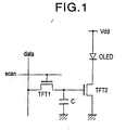
- One pixel's worth of an equivalent circuit is shown in Fig. 1.
- the pixel is comprised of a light emitting element OLED, a first thin film transistor TFT1, a second thin film transistor TFT2, and a holding capacitor C.
- the light emitting element is an organic electroluminescence (EL) element.
- An organic EL element has a rectification property in many cases, so is sometimes referred to as an OLED (organic light emitting diode).
- OLED organic light emitting diode
- the symbol of a diode is used to indicate the light emitting element OLED.
- the light emitting element is not always limited to an OLED and may be any element controlled in brightness by the amount of the current flowing through it. Also, a rectification property is not always required in the light emitting element.
- a source of the TFT2 is set at a reference potential (ground potential), an anode of the light emitting element OLED is connected to Vdd (power supply potential), and a cathode is connected to a drain of the TFT2.
- a gate of the TFT1 is connected to a scanning line SCAN, the source is connected to a data line DATA, and the drain is connected to the holding capacitor C and the gate of the TFT2.
- the TFT1 becomes conductive, the holding capacitor C is charged or discharged, and the gate potential of the TFT2 coincides with the data potential Vw.
- the scanning line SCAN is brought to an unselected state, the TFT1 becomes OFF and the TFT2 is electrically separated from the data line DATA, but the gate potential of the TFT2 is stably held by the holding capacitor C.
- the current flowing through the light emitting element OLED via the TFT2 becomes a value in accordance with a gate/source voltage Vgs, and the light emitting element OLED continuously emits the light with a brightness in accordance with the amount of the current supplied through the TFT2.
- Vth indicates a threshold value of the TFT2
- ⁇ indicates a mobility of a carrier
- W indicates a channel width
- L indicates a channel length
- ⁇ 0 indicates a permittivity of vacuum
- ⁇ r indicates a dielectric constant of the gate insulating film
- d is a thickness of the gate insulating film.
- Ids can be controlled by the potential Vw written into the pixel.
- Vw the potential of the light emitting element OLED
- the reason for the operation of the TFT2 in the saturated region is as follows. Namely, this is because, in the saturated region, Ids is controlled by only the Vgs and does not depend upon the drain/source voltage Vds. Therefore, even if Vds fluctuates due to variations in the characteristics of the OLED, a predetermined amount of the drive current Ids can be passed through the OLED.
- an active matrix type display device can be configured.
- lines DATA giving brightness information (data potential Vw) for driving the pixels 25 are arranged in a matrix.
- the scanning lines SCAN-1 through SCAN-N are connected to a scanning line drive circuit 21, while the data lines DATA are connected to a data line drive circuit 22.
- a simple matrix type display device the light emitting element contained in each pixel emits light only at an instant of selection.
- the active matrix type display device shown in Fig. 2 the light emitting element of each pixel 25 continues to emit light even after finishing being written. Therefore, in particular in a large sized, high definition display, there is the advantage that the level of the drive current of the light emitting elements can be lowered in comparison with the simple matrix type.
- FIG. 3 schematically shows a sectional structure of the pixel 25 shown in Fig. 2. Note, only OLED and TFT2 are represented for facilitating the illustration.
- the OLED is configured by successively superposing a transparent electrode 10, an organic EL layer 11, and a metal electrode 12.
- the transparent electrode 10 is separated for every pixel, acts as the anode of the OLED, and is made of a transparent conductive film for example ITO.
- the metal electrode 12 is commonly connected among pixels and acts as the cathode of the OLED. Namely, the metal electrode 12 is commonly connected to a predetermined power supply potential Vdd.
- the organic EL layer 11 is a composite film obtained by superposing for example a positive hole transport layer and an electron transport layer.
- Diamyne is vapor deposited on the transparent electrode 10 acting as the anode (positive hole injection electrode) as the positive hole transport layer
- Alq3 is vapor deposited thereon as the electron transport layer.
- a metal electrode 12 acting as the cathode (electron injection electrode) is grown thereon.
- Alq3 represents 8-hydroxy quinoline aluminum.
- the OLED having such a laminate structure is only one example. When a voltage in a forward direction (about 10V) is applied between the anode and the cathode of the OLED having such a configuration, injection of carriers such as electrons and positive holes occurs and luminescence is observed.
- the operation of the OLED can be considered to be the emission of light by excisions formed by the positive holes injected from the positive hole transport layer and the electrons injected from the electron transport layer.
- the TFT2 comprises a gate electrode 2 formed on a substrate 1 made of glass or the like, a gate insulating film 3 superimposed on the top surface thereof, and a semiconductor thin film 4 superimposed above the gate electrode 2 via this gate insulating film 3.
- This semiconductor thin film 4 is made of for example a polycrystalline silicon thin film.
- the TFT2 is provided with a source S, a channel Ch, and a drain D acting as a passage of the current supplied to the OLED.
- the channel Ch is located immediately directly above the gate electrode 2.
- the TFT2 of this bottom gate structure is coated by an inter-layer insulating film 5.
- a source electrode 6 and a drain electrode 7 are formed above that. Above them, the OLED mentioned above is grown via another inter-layer insulating film 9. Note that, in the example of Fig. 3, the anode of the OLED is connected to the drain of the TFT2, so a P-channel thin film transistor is used as the TFT2.
- an organic EL display In an active matrix type organic EL display, generally a TFT (thin film transistor) formed on a glass substrate is utilized as the active element.
- TFT thin film transistor
- an organic EL display is a direct viewing type. Due to this, it becomes relatively large in size. Due to restrictions of cost and manufacturing facilities, a usage of a single crystalline silicon substrate for the formation of the active elements is not practical.
- a transparent conductive film of ITO indium tin oxide
- ITO indium tin oxide
- ITO indium tin oxide
- the gate electrode 2, gate insulating film 3, and semiconductor thin film 4 comprised of amorphous silicon are successively stacked and patterned on the glass substrate 1 to form the TFT2.
- the amorphous silicon is sometimes formed into polysilicon (polycrystalline silicon) by heat treatment such as laser annealing.
- a TFT2 having a larger degree of carrier mobility in comparison with amorphous silicon and a larger current driving capability can be formed.
- an ITO transparent electrode 10 acting as the anode of the light emitting element OLED is formed.
- an organic EL layer 11 is stacked to form the light emitting element OLED.
- the metal electrode 12 acting as the cathode of the light emitting element is formed by a metal material (for example aluminum).
- the substrate 1 does not have to be transparent like glass, but as the transistor formed on a large sized substrate, use is generally still made of a TFT.
- the amorphous silicon and polysilicon used for the formation of the TFT have a worse crystallinity in comparison with single crystalline silicon and have a poor controllability of the conduction mechanism, therefore it has been known that there is a large variation in characteristics in formed TFTs.
- the laser annealing method is used as mentioned above in order to avoid the problem of thermal deformation of the glass substrate, but it is difficult to uniformly irradiate laser energy to a large glass substrate. Occurrence of variations in the state of the crystallization of the polysilicon according to the location in the substrate cannot be avoided.
- the Vth (threshold value)
- the Vth will vary according to the pixels.
- the current Ids flowing through the OLEDs will largely vary for every pixel and consequently become completely off from the intended value, so a high quality of image cannot be expected as the display.
- a similar thing can be said for not only the Vth, but also the variation of parameters of equation (1) such as the carrier mobility ⁇ .
- An object of the present invention is to provide a current drive circuit capable of stably and accurately supplying an intended current to a light emitting element etc. of a pixel without being affected by variations in characteristics of an active element inside the pixel, a display device using the same and as a result capable of displaying a high quality image, a pixel circuit, and a method for driving a light emitting element.
- a display device provides a scanning line drive circuit for successively selecting scanning lines, a data line drive circuit including a current source for generating a signal current having a current level in accordance with brightness information and successively supplying the same to data lines, and a plurality of pixels arranged at intersecting portions of the scanning lines and the data lines and including current driven type light emitting elements emitting light by receiving the supply of the drive current.
- each pixel comprises a receiving part for fetching the signal current from the data line when the scanning line is selected, a converting part for converting a current level of the fetched signal current to a voltage level and holding the same, and a drive part for passing a drive current having a current level in accordance with the held voltage level through the light emitting element.
- the converting part includes a conversion use insulating gate type field effect transistor provided with a gate, a source, a drain, and a channel and a capacitor connected to the gate.
- the conversion use insulating gate type field effect transistor generates a converted voltage level at the gate by passing the signal current fetched by the receiving part through the channel.
- the capacitor holds the voltage level created at the gate.
- the converting part includes a switch use insulating gate type field effect transistor inserted between the drain and the gate of the conversion use insulating gate type field effect transistor.
- the switch use insulating gate type field effect transistor becomes conductive when converting the current level of the signal current to the voltage level and electrically connects the drain and the gate of the conversion use insulating gate type field effect transistor to create the voltage level with the source as the reference at the gate, while the switch use insulating gate type field effect transistor is shut off when the capacitor holds the voltage level and separates the gate of the conversion use insulating gate type field effect transistor and the capacitor connected to this from the drain.
- the drive part includes a drive use insulating gate type field effect transistor provided with a gate, a drain, a source, and a channel.
- This drive use insulating gate type field effect transistor receives the voltage level held at the capacitor at its gate and passes a drive current having a current level in accordance with that through the light emitting element via the channel.
- a current mirror circuit is configured by direct connection of the gate of the conversion use insulating gate type field effect transistor and the gate of the drive use insulating gate type field effect transistor, whereby a proportional relationship is exhibited between the current level of the signal current and the current level of the drive current.
- the drive use insulating gate type field effect transistor is formed in the vicinity of the corresponding conversion use insulating gate type field effect transistor inside the pixel and has an equivalent threshold voltage to that of the conversion use insulating gate type field effect transistor.
- the drive use insulating gate type field effect transistor operates in the saturated region and passes a drive current in accordance with a difference between the level of the voltage applied to the gate thereof and the threshold voltage through the light emitting element.
- the drive part shares the conversion use insulating gate type field effect transistor together with the converting part in a time division manner.
- the drive part separates the conversion use insulating gate type field effect transistor from the receiving part and uses the same for driving after the conversion of the signal current is completed and passes the drive current to the light emitting element through the channel in a state where the held voltage level is applied to the gate of the conversion use insulating gate type field effect transistor.
- the drive part has a controlling means for cutting off an unnecessary current flowing to the light emitting element via the conversion use insulating gate type field effect transistor at times other than the time of drive.
- the controlling means cuts off the unnecessary current by controlling a voltage between terminals of a two terminal type light emitting element having a rectification function.
- the controlling means comprises a control use insulating gate type field effect transistor inserted between the conversion use insulating gate type field effect transistor and the light emitting element, and the control use insulating gate type field effect transistor becomes nonconductive in state and separates the conversion use insulating gate type field effect transistor and the light emitting element when the light emitting element is not driven and switches to the conductive state when the light emitting element is driven.
- the controlling means controls a ratio between a time for cutting off the drive current when the light emitting element is not to be driven and placing the light emitting element in the non-light emitting state and a time of passing the drive current when the light emitting element is to be driven and placing the light emitting element in the light emitting and thereby to enable the control of the brightness of the pixel.
- the drive part has a potential fixing means for fixing the potential of the drain with reference to the source of the conversion use insulating gate type field effect transistor in order to stabilize the current level of the drive current flowing to the light emitting element through the conversion use insulating gate type field effect transistor.
- the receiving part, the converting part, and the drive part configure a current circuit combining a plurality of insulating gate type field effect transistors, and one or two or more insulating gate type field effect transistors have a double gate structure for suppressing current leakage in the current circuit.
- the drive part includes the insulating gate type field effect transistor provided with the gate, drain, and the source and passes the drive current passing between the drain and the source to the light emitting element in accordance with the level of the voltage applied to the gate, the light emitting element is a two terminal type having an anode and a cathode, and the cathode is connected to the drain.
- the drive part includes an insulating gate type field effect transistor provided with a gate, a drain, and a source and passes a drive current passing between the drain and the source to the light emitting element in accordance with the level of the voltage applied to the gate, the light emitting element is a two terminal type having an anode and a cathode, and the anode is connected to the source. Further, it includes an adjusting means for downwardly adjusting the voltage level held by the converting part and supplying the same to the drive part to tighten the black level of the brightness of each pixel.
- the drive part includes an insulating gate type field effect transistor having a gate, a drain, and a source, and the adjusting means downwardly adjusts the level of the voltage applied to the gate by raising the bottom of the voltage between the gate and the source of the insulating gate type field effect transistor.
- the drive part includes an insulating gate type field effect transistor having a gate, a drain, and a source
- the converting part is provided with a capacitor connected to the gate of the thin film transistor and holding the voltage level
- the adjusting means comprises an additional capacitor connected to that capacitor and downwardly adjusts the level of the voltage to be applied to the gate of the insulating gate type field effect transistor held at that capacitor.
- the drive part includes an insulating gate type field effect transistor having a gate, a drain, and a source
- the converting part is provided with a capacitor connected to the gate of the insulating gate type field effect transistor on its one end and holding the voltage level
- the adjusting means adjusts the potential of the other end of the capacitor when holding the voltage level converted by the converting part at that capacitor to downwardly adjust the level of the voltage to be applied to the gate of the insulating gate type field effect transistor.
- the light emitting element use is made of for example an organic electroluminescence element.
- the pixel circuit of the present invention has the following characteristic features.
- Second, the voltage between the gate and source created as described above or the gate potential is held by the function of the capacitor formed inside the pixel or existing parasitically and is held at about that level for a predetermined period even after the end of the writing.
- the current flowing through the OLED is controlled by the conversion use insulating gate type field effect transistor per se connected to it in series or the drive use insulating gate type field effect transistor provided inside the pixel separately from that and having a gate commonly connected together with the conversion use insulating gate type field effect transistor.
- the voltage between the gate and source at the OLED drive is generally equal to the voltage between the gate and source of the conversion use insulating gate type field effect transistor created according to the first characterizing feature.
- the data line and the internal portion of the pixel are made conductive by a fetch use insulating gate type field effect transistor controlled by the first scanning line, and the gate and the drain of the conversion use insulating gate type field effect transistor are short-circuited by the switch use insulating gate type field effect transistor controlled by the second scanning line.
- an object of the present invention is to accurately pass the intended current through the OLEDs without being affected by variations in the characteristics of the TFTs.
- the reason why the present object can be achieved by the first through fourth characterizing features will be explained below.
- the conversion use insulating gate type field effect transistor will be described as the TFT1
- the drive use insulating gate type field effect transistor will be described as the TFT2
- the fetch use insulating gate type field effect transistor will be described as the TFT3
- the switch use insulating gate type field effect transistor will be described as the TFT4.
- the present invention is not limited to TFTs (thin film transistors).
- Insulating gate type field effect transistors can be widely employed as the active elements, for example, single crystalline silicon transistors formed on a single crystalline silicon substrate or SOI substrate.
- the signal current passing through the TFT1 at the time of writing of the brightness information is defined as Iw, and the voltage between the gate and source created in the TFT1 as a result of this is defined as Vgs.
- Idrv ⁇ 2 ⁇ Cox 2 ⁇ W2/L2/2(Vgs-Vth2) 2
- the correct current can be passed through the OLED without being affected by variations in the characteristics of the TFT.
- equation (6) there is the large advantage of the simple proportional relationship between Iw and Idrv. Namely, in the conventional example of Fig. 1, as shown in equation (1), Vw and Idrv are nonlinear and are affected by variations in the characteristics of the TFT, so the control of the voltage at the drive side becomes complex. Further, it is seen that the carrier mobility ⁇ among the characteristics of the TFT shown in equation (1) fluctuates according to the temperature.
- Idrw ⁇ 2 ⁇ Cox2 ⁇ W2/L2* ⁇ (Vgs-Vth2)Vds2 - Vds2 2 /2 ⁇
- Vds2 is the voltage between the drain and source of TFT2.
- the relationship between Iw and Idrv does not become a simple proportional relationship as in equation (6), but Vth is not contained in equation (8). Therefore, it is seen that the relationship of Iw and Idrv is not affected by the variation of Vth (variation in a screen or variation for every manufacturing lot). Namely, by writing the predetermined Iw without being affected by variation of the Vth, the intended Idrv can be obtained. Note, where ⁇ and Cox vary in the screen, due to these values, even if a specific Iw is given to the data line, the value of Idrv determined from equation (8) will vary. Therefore desirably the TFT2 operates in the saturated region as mentioned before.
- the TFT3 and the TFT4 are controlled by different scanning lines, and the TFT4 is brought to the off state preceding the TFT3 at the end of the write operation.
- the TFT3 and the TFT4 do not have to be the same conductivity type.
- the pixel circuit may be configured so that the TFT3 and the TFT4 are an identical or different conductivity types, the gates of them controlled by different scanning lines, and the TFT4 brought to the off state preceding to the TFT3 at the end of the write operation.
- the TFT4 may be brought to the on state by the operation of the scanning line, and the pixels extinguished in units of the scanning lines. This is because, the gate and the drain of the TFT1 and the gate of the TFT2 are connected, so the gate voltage of the TFT2 becomes the threshold value of the TFT1 (this is almost equal to the threshold value of the TFT2), and both of the TFT1 and TFT2 become the off state.
- the second scanning line is divided into colors of R, G, and Band separately controlled, adjustment of the color balance is also easy.
- the drive current of a light emitting element OLED can be made larger by reducing the ratio of the light emitting period (duty).
- Figure 1 is a circuit diagram of an example of a conventional pixel circuit.
- Figure 2 is a block diagram of an example of the configuration of a conventional display device.
- Figure 3 is a sectional view of an example of the configuration of a conventional display device.
- Figure 4 is a sectional view of another example of the configuration of a conventional display device.
- Figure 5 is a circuit diagram of an embodiment of a pixel circuit according to the present invention.
- Figure 6 is a waveform diagram of an example of waveforms of signals in the embodiment of Fig. 5.
- Figure 7 is a block diagram of an example of the configuration of a display device using a pixel circuit according to the embodiment of Fig. 5.
- Figure 8 is a circuit diagram of a modification of the embodiment of Fig. 5.
- Figure 9 is a circuit diagram of another embodiment of a pixel circuit according to the present invention.
- Figure 10 is a waveform diagram of an example of the waveforms of signals in the embodiment of Fig. 9.
- Figure 11 is a circuit diagram of a modification of the embodiment of Fig. 9.
- Figure 12 is a circuit diagram of a modification of the embodiment of Fig. 9.
- Figure 13 is a circuit diagram of a modification of the embodiment of Fig. 9.
- Figure 14 is a circuit diagram of a modification of the embodiment of Fig. 9.
- Figure 15 is a circuit diagram of another embodiment of the pixel circuit according to the present invention.
- Figure 16 is a circuit diagram of a modification of the embodiment of Fig. 15.
- Figure 17 is a circuit diagram of a modification of the embodiment of Fig. 15.
- Figure 18 is a circuit diagram of another embodiment of the pixel circuit according to the present invention.
- Figure 19 is a circuit diagram of a modification of the embodiment of Fig. 18.
- Figure 20 is a view for explaining a case where the pixels are extinguished in units of scanning lines in the circuit of Fig. 19.
- Figure 21 is a circuit diagram of a modification of the embodiment of Fig. 19.
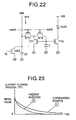
- Figure 22 is a circuit diagram of a modification of the embodiment of Fig. 19.
- Figure 23 is a diagram of characteristics of currents flowing through conversion use transistors of the circuit of Fig. 22 and the conventional circuit.
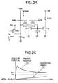
- Figure 24 is a circuit diagram of a modification of the embodiment of Fig. 19.
- Figure 25 is a view of data line potentials of the circuit of Fig. 23 and the conventional circuit.
- Figure 26 is a circuit diagram of another embodiment of the pixel circuit according to the present invention.
- Figure 27 is a circuit diagram of another embodiment of the pixel circuit according to the present invention.
- FIG. 5 shows an example of a pixel circuit according to the present invention.
- This circuit comprises, other than the conversion use transistor TFT1 with the signal current flowing therethrough and the drive use transistor TFT2 for controlling the drive current flowing through a light emitting element made of an organic EL element or the like, a fetch use transistor TFT3 for connecting or disconnecting the pixel circuit and the data line DATA by the control of a first scanning line SCAN-A, a switch use transistor TFT4 for short-circuiting the gate and the drain of the TFT1 during the writing period by the control of a second scanning line SCAN-B, a capacitor C for holding the voltage between the gate and source of the TFT1 even after the end of the writing, and the light emitting element OLED.
- TFT3 is configured by a PMOS, and the other transistors are configured by NMOSs, but this is one example.
- the invention does not always have to be this way.
- the capacitor C is connected to the gate of the TFT1 at its one terminal, and connected to the GND (ground potential) at its other terminal, but this is not limited to GND. Any constant potential is possible.
- the anode of the OLED is connected to the positive power supply potential Vdd.
- the display device is provided with a scanning line drive circuit for successively selecting scanning lines SCAN-A and SCAN-B, a data line drive circuit including a current source CS for generating a signal current Iw having a current level in accordance with the brightness information and successively supplying the same to the data lines DATA, and a plurality of pixels arranged at intersecting portions of the scanning lines SCAN-A and SCAN-B and data lines DATA and including current drive type light emitting elements OLED emitting light by receiving the supply of the drive current.
- a scanning line drive circuit for successively selecting scanning lines SCAN-A and SCAN-B
- a data line drive circuit including a current source CS for generating a signal current Iw having a current level in accordance with the brightness information and successively supplying the same to the data lines DATA
- a plurality of pixels arranged at intersecting portions of the scanning lines SCAN-A and SCAN-B and data lines DATA and including current drive type light emitting elements OLED emitting light by receiving the supply of the
- the converting part includes a conversion use thin film transistor TFT1 provided with a gate, source, drain, and channel and the capacitor C connected to the gate.
- the conversion use thin film transistor TFT1 generates a converted voltage level at the gate by passing the signal current Iw fetched by the receiving part through the channel, while the capacitor C holds the voltage level created at the gate.
- the converting part includes the switch use thin film transistor TFT4 inserted between the drain and gate of the conversion use thin film transistor TFT1.
- the switch use thin film transistor TFT4 becomes conductive when converting the current level of the signal current Iw to the voltage level, electrically connects the drain and gate of the conversion use thin film transistor TFT1, and creates the voltage level with reference to the source at the gate of the TFT1. Further, the switch use thin film transistor TFT4 is cut off when the capacitor C holds the voltage level and separates the gate of the conversion use thin film transistor TFT1 and the capacitor C connected to this from the drain of the TFT1.
- the drive part includes a drive use thin film transistor TFT2 provided with a gate, drain, source, and channel.
- the drive use thin film transistor TFT2 receives the voltage level held at the capacitor C at its gate and passes a drive current having a current level in accordance with that via the channel to the light emitting element OLED.
- a current mirror circuit is configured by direct connection of the gate of the conversion use thin film transistor TFT1 and the gate of the drive use thin film transistor TFT2, whereby a proportional relationship is exhibited between the current level of the signal current Iw and the current level of the drive current.
- the drive use thin film transistor TFT2 is formed in the vicinity of the corresponding conversion use thin film transistor TFT1 inside the pixel and has an equivalent threshold voltage to that of the conversion use thin film transistor TFT1.
- the drive use thin film transistor TFT2 operates in the saturated region and passes a drive current in accordance with the difference between the level of the voltage applied to the gate thereof and the threshold voltage to the light emitting element OLED.
- the driving method of the present pixel circuit is as follows.
- the drive waveforms are shown in Fig. 6.
- the first scanning line SCAN-A and the second scanning line SCAN-B are brought into the selected state.
- the first scanning line SCAN-A is set at a low level
- the second scanning line SCAN-B is set at a high level.
- the current source CS is a variable current source controlled in accordance with the brightness information.
- the pixel circuit and the data line DATA are electrically cut off, and therefore, the writing to the other pixel can be carried out via the data line DATA thereafter.
- the data output by the current source CS as the current level of the signal current must be effective at the point of time when the second scanning line SCAN-B becomes unselected, but after that, may be set at any level (for example the write data of the next pixel).
- the gate and the source of the TFT2 are commonly connected together with the TFT1. Further, the two are formed close inside a small pixel. Therefore, if the TFT2 operates in the saturated region, the current flowing through the TFT2 is given by equation (4).
- the present invention is effective even in the case where the TFT2 operates in the linear region as mentioned before.
- Vds2 is determined by current-voltage characteristics of the light emitting element OLED and the current Idrv flowing through the light emitting element OLED.
- FIG. 7 shows an example of the display device configured by arranging the pixel circuits of Fig. 5 in the matrix state. The operation thereof will be explained below.
- a vertical start pulse VSP
- VSP vertical start pulse
- the scanning line drive circuit A21 and scanning line drive circuit B23 successively select first scanning lines SCAN-A1 to SCAN-AN and second scanning lines SCAN-B1 to SCAN-BN synchronous to the vertical clocks (VCKA, VCKB).
- the current source CS is provided in the data line drive circuit 22 corresponding to each data line DATA and drives the data line at a current level in accordance with the brightness information.
- the current source CS comprises an illustrated voltage/current conversion circuit and outputs the signal current in accordance with the voltage representing the brightness information.
- the signal current flows through the pixel on the selected scanning line, and the current is written in units of the scanning lines. Each pixel starts to emit light with an intensity in accordance with its current level.
- VCKA is slightly delayed relative to VCKB by a delay circuit 24. By this, as shown in Fig. 6, SCAN-B becomes unselected preceding SCAN-A.
- Figure 8 is a modification of the pixel circuit of Fig. 5.
- This circuit gives a double gate configuration wherein two transistors TFT2a and TFT2b are connected in series to the TFT2 in Fig. 5 and imparts a double gate configuration wherein two transistors TFT4a and TFT4b are connected in series to the TFT4 in Fig. 5.
- the gates of the TFT2a and TFT2b and the gates of the TFT4a and TFT4b are commonly connected, therefore basically they perform a similar operation to that of single transistors.
- the pixel circuit of Fig. 8 performs a similar operation to that of the pixel circuit of Fig. 5.
- the receiving part, converting part, and the drive part configure the current circuit combining a plurality of thin film transistors TFT.
- One or more thin film transistors (TFT) have the double gate structure for suppressing the current leakage in the current circuit.
- Figure 9 shows another embodiment of the pixel circuit according to the present invention.
- the characterizing feature of this circuit resides in that the transistor TFT1 with the signal current Iw flowing therethrough per se controls the current Idrv flowing through the light emitting element OLED.
- equation (6) does not correctly stand, and there is a possibility such that Iw and Idrv are not correctly proportional, but in the pixel circuit of Fig. 9, such a problem does not occur in principle.
- a transistor TFT3 for connecting or disconnecting the pixel circuit and the data line DATA by the control of the first scanning line SCAN-A
- a transistor TFT4 for short-circuiting the gate and the drain of the TFT1 during the writing period by the control of the second scanning line SCAN-B
- a capacitor C for holding the voltage between the gate and source of the TFT1 even after the end of the writing
- a light emitting element OLED made of the organic EL element.
- the holding capacitor C is connected to the gate of the TFT1 at its one terminal and connected to the GND (ground potential) at its other terminal, but this is not limited to GND. Any constant potential is possible.
- the anode of the light emitting element OLED is connected to the anode line A arranged in units of the scanning lines.
- the TFT3 is configured by a PMOS, and the other transistors are configured by NMOSs, but this is one example. The invention does not always have to be this way.
- the drive part of the pixel circuit shares the conversion use thin film transistor TFT1 in a time division manner together with the conversion part.
- the drive part separates the conversion use thin film transistor TFT1 from the receiving part after completing the conversion of the signal current Iw and uses the same for drive and passes the drive current to the light emitting element OLED through the channel in the state where the held voltage level is applied to the gate of the conversion use thin film transistor TFT1.
- the drive part has a controlling means for cutting off the unnecessary current flowing through the light emitting element OLED via the conversion use thin film transistor TFT1 at times other than the drive.
- the controlling means controls the voltage between terminals of the two terminal type light emitting elements OLED having the rectification function by the anode line A and cuts off the unnecessary current.
- the driving method of this circuit is as follows.
- the drive waveform is shown in Fig. 10.
- the first scanning line SCAN-A and the second scanning line SCAN-B are brought to the selected state at the time of writing.
- the first scanning line SCAN-A is set at a low level
- the second scanning line SCAN-B is set at a high level.
- the current source CS of the current value Iw is connected to the data line DATA, but in order to prevent the Iw from flowing via the light emitting element OLED, the anode line A of the light emitting element OLED is set at low level (for example GND or negative potential) so that the light emitting element OLED becomes the off state.
- the signal current Iw flows through the TFT1.
- the gate and the drain of the TFT1 are electrically shortcircuited by the TFT4, therefore equation (5) stands, and the TFT1 operates in the saturated region. Accordingly, the voltage Vgs given by equation (3) is created between the gate and the source thereof.
- the first scanning line SCAN-A and the second scanning line SCAN-B are brought to the unselected state. In more detail, first, the second scanning line SCAN-B is brought to the low level and the TFT4 is brought to the off state. By this, the Vgs created in the TFT1 is held at the capacity C.
- the pixel circuit and the data line DATA are electrically cut off, and therefore the writing to another pixel can be carried out via the data line DATA after that.
- the data supplied by the current source CS as the signal current Iw must be valid at a point of time when the second scanning line SCAN-B becomes unselected, but may be set at any value (for example write data of the next pixel) after that.
- the anode line A is brought to the high level.
- the Vgs of the TFT1 is held by the capacitor C, therefore if the TFT1 operates in the saturated region, the current flowing through the TFT1 coincides with Iw in equation (3).
- the drive current Idrv flowing through the light emitting element OLED This becomes the drive current Idrv flowing through the light emitting element OLED. That is, the signal current Iw coincides with the drive current Idrv of the light emitting element OLED.
- a sufficient positive potential may be given to the anode line A so that equation (5) still stands even if the voltage drop at the light emitting element OLED is considered. According to the above drive, the current Idrv flowing through the light emitting element OLED correctly coincides with Iw without being affected by variations in the characteristics of the TFT.
- FIG. 11 is a modification of the pixel circuit shown in Fig. 9.
- Fig. 11 there is no anode line as in Fig. 9.
- the anode of the light emitting element OLED is connected to the constant positive potential Vdd, while a P-channel transistor TFT5 is inserted between the drain of the TFT1 and the cathode of the light emitting element OLED.
- the gate of the TFT5 is controlled by the drive line drv arranged in units of the scanning lines.
- the object of insertion of TFT5 is prevention of the flow of the signal current Iw via the light emitting element OLED by setting the drive line drv at a high level and bringing the TFT5 to the off state at the time of writing data.
- the drv is brought to the low level, the TFT5 is brought to the on state, and the drive current Idrv flows through the light emitting element OLED.
- the rest of the operation is similar to that of the circuit of Fig. 9.
- the present example includes the TFT5 connected to the light emitting element OLED in series and can cut off the current flowing to the light emitting element OLED in accordance with the control signal given to the TFT5.
- the control signal is given to the gate of the TFT5 included in each pixel on the identical scanning line via the drive line drv provided in parallel to the scanning line SCAN.
- the TFT5 is inserted between the light emitting element OLED and the TFT1, and the current flowing through the light emitting element OLED can be turned on or off by the control of the gate potential of the TFT5.
- the emission of light of each pixel is achieved for the amount of time where the TFT5 is on by a light emission control signal.
- the on time ⁇ and the time of one frame as T
- the ratio in time when the pixel is emitting light that is, the duty
- the duty becomes approximately ⁇ /T.
- a time average brightness of the light emitting element changes in proportional to this duty. Accordingly, by changing the on time ⁇ by controlling the TFT5, it is also possible to variably adjust the screen brightness of the EL display conveniently and in a wide range.
- the controlling means comprises the control use thin film transistor TFT5 inserted between the conversion use thin film transistor TFT1 and the light emitting element OLED.
- the control use thin film transistor TFT5 becomes nonconductive and separates the conversion use thin film-transistor TFT1 and the light emitting element OLED when the light emitting element OLED is not driven and switches to the conductive state at the time of drive.
- this controlling means can control the brightness of each pixel by controlling the ratio between the off time for which the drive current is cut off and the light emitting element OLED is placed in the non-light emitting state when the OLED is not to be driven and the on time for which the drive current is passed and the light emitting element OLED is placed in the light emitting state when the OLED is to be driven.
- the display device before the brightness information of the next scanning line cycle (frame) is newly written after writing the brightness information into the pixels in units of the scanning lines, the display device can extinguish the light emitting elements contained in the pixels in units of the scanning lines together. This means that the time from the lighting to the extinguishing of the light emitting elements after the writing of the brightness information can be adjusted.
- the ratio (duty) of the light emitting time in one scanning line cycle can be adjusted.
- the adjustment of the light emitting time (duty) corresponds to the adjustment of the drive current supplied to each light emitting element. Accordingly, it is possible to adjust the display brightness conveniently and freely by adjusting the duty.
- the drive current can be equivalently made large by adequately setting the duty. For example, when the duty is set at 1/10, even if the drive current is increased to 10 times, an equivalent brightness is obtained. If the drive current is made 10 times large, also the signal current corresponding to this can be made 10 times larger, and therefore it is not necessary to handle a weak current level.
- FIG. 12 is another modification of the pixel circuit shown in Fig. 9.
- a TFT6 is inserted between the drain of the TFT1 and the cathode of the light emitting element OLED, a TFT7 is connected between the gate and the drain of the TFT6, and the gate thereof is controlled by the second scanning line SCAN-B.
- An auxiliary capacity C2 is connected between the source of the TFT7 and the GND potential.
- the driving method of this circuit is basically the same as the case of the pixel circuit of Fig. 9, but will be explained below. Note that, the drive waveform is similar to that of the case of Fig. 10.
- the signal current Iw flows through the TFT1 and TFT6. Since the gates and the sources are short-circuited by the TFT4 and TFT7, the two TFTs operate in the saturated region.
- the first scanning line SCAN-A and second scanning line SCAN-B are brought to the unselected state. By this, the Vgs previously created in the TFT1 and the TFT6 are held by the capacitor C and the auxiliary capacitor C2.
- the anode line A is set at a high level. Since the Vgs of the TFT1 is held by the capacitor C, if the TFT1 operates in the saturated region, the current flowing through the TFT1 coincides with Iw of equation (3). This becomes the current Idrv flowing through the light emitting element OLED. That is, the signal current Iw coincides with the drive current Idrv of the light emitting element OLED.
- Ids will depend on Vds.
- ⁇ is a positive constant.
- Iw does not coincide with Idrv unless Vds is not identical between the time of the writing and the time of the drive.
- the drain potential thereof is not generally identical between the time of the writing and the time of the drive. For example, where the drain potential at the time of the drive is higher, the Vds of the TFT6 becomes larger.
- Ids is increased at the time of the drive. In other words, Idrv becomes bigger than Iw, and the two do not coincide.
- the Idrv flows through the TFT1, therefore, in that case, the voltage drop at the TFT1 becomes large and the drain potential thereof (source potential of the TFT6) rises.
- Vgs of the TFT6 becomes small. This acts in a direction reducing the Idrv. As a result, the drain potential of the TFT1 (source potential of the TFT6) cannot largely fluctuate.
- Ids does not largely change between the time of the writing and the time of the drive. Namely, Iw and Idrv will coincide with a remarkably high precision. In order to perform this operation better, it is good if the dependency of Ids with respect to Vds is made small in both of the TFT1 and TFT6, therefore desirably both transistors are operated in the saturated region.
- the gate and the drain are short-circuited in both of the TFT1 and TFT6. Therefore, regardless of the brightness data written, the two operate in the saturated region. In order to operate them also at the drive, a sufficient positive potential may be given to the anode line A so that the TFT6 still operates in the saturated region even if the voltage drop at the light emitting element OLED is considered. By this drive, the current Idrv flowing through the light emitting element OLED more correctly coincides with the Iw than the embodiment of Fig. 9 without being affected by variations in the characteristics of the TFT.
- the drive part of the present example has TFT6, TFT7, and C2 as potential fixing means for fixing the potential of the drain with reference to the source of the conversion use thin film transistor TFT1 for stabilizing the current level of the drive current flowing to the light emitting element OLED through the conversion use thin film transistor TFT1.
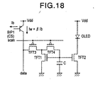
- Figure 13 is another embodiment of the pixel circuit according to the present invention.
- the characterizing feature of this pixel circuit resides in that, in the same way as Fig. 9, Fig. 11, and Fig. 12, the transistor TFT1 per se with the signal current Iw flowing therethrough controls the current Idrv flowing through the light emitting element OLED, but in Fig. 13, the light emitting element OLED is connected to the source side of the TFT1.
- the drive part of the present pixel circuit includes the thin film transistor TFT1 provided with the gate, drain, and the source and passes the drive current passing between the drain and the source to the light emitting element OLED in accordance with the level of the voltage applied to the gate.
- the light emitting element OLED is a two-terminal type having an anode and a cathode, and the anode is connected to the source.
- the drive part of the pixel circuit shown in Fig. 9 includes the thin film transistor provided with the gate, drain, and the source and passes the drive current passing between the drain and the source to the light emitting element in accordance with the level of the voltage applied to the gate.
- the light emitting element is the two-terminal type having an anode and a cathode, and the cathode is connected to the drain.
- the pixel circuit of the present example comprises, other than the TFT1, a transistor TFT3 for connecting or cutting off the pixel circuit and the data line DATA by the control of the first scanning line SCAN-A, a transistor TFT4 for short-circuiting the gate and the drain of the TFT1 during the writing period by the control of the second scanning line SCAN-B, a capacitor C for holding the gate potential of the TFT1 even after the end of the writing, a P-channel transistor TFT5 inserted between the drain of the TFT1 and the power supply potential Vdd, and the light emitting element OLED.
- a transistor TFT3 for connecting or cutting off the pixel circuit and the data line DATA by the control of the first scanning line SCAN-A
- a transistor TFT4 for short-circuiting the gate and the drain of the TFT1 during the writing period by the control of the second scanning line SCAN-B
- a capacitor C for holding the gate potential of the TFT1 even after the end of the writing
- one terminal of the capacitor C is connected to the GND, and the Vgs of the TFT1 is held at schematically the same value between the time of the writing and the time of the drive.
- the gate of the TFT5 is controlled by the drive line drv.
- the object of the insertion of the TFT5 is to bring the TFT5 into the off state by setting the drive line drv at the high level at the time of writing data and pass all of the signal current Iw through the TFT1.
- the drv is brought to the low level, the TFT5 is brought to the on state, and the drive current Idrv is passed through the light emitting element OLED.
- the driving method is similar to that of the circuit of Fig. 11.
- Figure 14 is a modification of the pixel circuit shown in Fig. 13.
- the difference resides in that one terminal of the capacitor C is connected to the GND in Fig. 13, but is connected to the source of the TFT1 in Fig. 14, but in both cases, there is no functional difference in the point that the Vgs of the TFT1 is held at schematically the same value between the time of the writing and the time of the drive.
- FIG. 15 is a more developed example of the pixel circuit shown in Fig. 5.
- the present pixel circuit includes an adjusting means for downwardly adjusting the voltage level held by the converting part and supplying the same to the drive part to tighten the black level of the brightness of each pixel.
- the drive part includes a thin film transistor TFT2 having a gate, drain, and source and an adjusting means provided with a constant voltage source E for raising the bottom of the voltage between the gate and the source of the thin film transistor TFT2 and downwardly adjusting the level of the voltage applied to the gate. Namely, it tightens the black level by connecting the source of the TFT2 to the potential E slightly higher than the source potential of the TFT1.
- Figure 16 is a modification of the pixel circuit shown in Fig. 15.
- the adjusting procedure is comprised by an additional capacitor C2 connected to the gate of the thin film transistor TFT2 and the second scanning line SCAN-B and downwardly adjusts the voltage level to be held at the capacitor C for applying the same to the gate of the thin film transistor TFT2.
- the gate potential of the TFT2 can be slightly lowered by the function of the capacitor C2.
- the scanning line SCAN-A for selecting the pixel and the data line DATA giving the brightness information for driving the pixel are arranged in the matrix state.
- Each pixel includes the light emitting element OLED having the brightness changing according to the amount of the supplied current, the writing means (TFT1, TFT3, C) controlled by the scanning line SCAN-A and writing the brightness information given from the data line DATA to the pixel, and the driving means (TFT2) for controlling the amount of the current supplied to the light emitting element OLED in accordance with the written brightness information.
- the brightness information is written into each pixel by applying the electric signal Iw in accordance with the brightness information to the data line DATA in the state where the scanning line SCAN A is selected.
- the brightness information written in each pixel is held at each pixel even after the scanning line SCAN-A becomes unselected.
- the light emitting element OLED of each pixel includes the adjusting means (C2) capable of maintaining the lighting with the brightness in accordance with the held brightness information, downwardly adjusting the brightness information written by the writing means (TFT1, TFT3, C), and supplying the same to the drive means (TFT2) and can tighten the black level of the brightness of each pixel.
- the adjusting means (C2) capable of maintaining the lighting with the brightness in accordance with the held brightness information, downwardly adjusting the brightness information written by the writing means (TFT1, TFT3, C), and supplying the same to the drive means (TFT2) and can tighten the black level of the brightness of each pixel.
- Figure 17 is a modification of the pixel circuit shown in Fig. 15.
- the adjusting procedure downwardly adjusts the level of the voltage to be applied to the gate of the TFT2 by adjusting the potential of one end of the capacitor C when holding the voltage level converted by the TFT1 at the capacitor C.
- the black level is tightened.
- the potential control line S is provided in units of the scanning lines and controlled. The potential control line S is brought to an "H" level during the writing and brought to an "L” level after the end of the writing.
- the absolute values of the H and L potentials can be freely set.
- Figure 18 is another embodiment of the pixel circuit according to the present invention.
- the fetch use thin film transistor TFT3 and the switch use thin film transistor TFT4 are configured as the identical conductivity type (PMOS in Fig. 18). Then, in the present example, as shown in Fig. 18, it is also possible to connect their gates to the common scanning line SCAN in the write operation and control them by the common signal. In the device display in this case, the scanning line drive circuit B23 in the display device shown in Fig. 7 is unnecessary.
- Figure 19 is a modification of the pixel circuit shown in Fig. 18.
- the gates of the fetch use thin film transistor TFT3 and switch use thin film transistor TFT4 configured by the same conductivity type P-channel TFT are connected to different scanning lines, that is, the first scanning line SCAN-A and the second scanning line SCAN-B, and separately controlled.
- the reason why they are separately controlled in this way is that, if the TFT3 and the TFT4 are controlled by the common signal as in the example of Fig. 18, the following inconvenience sometimes occurs.
- the impedance of the TFT3 is inevitably increase and finally actually becomes infinitely large, that is, the off state. Accordingly, in this step, the potential of the data line DATA gradually rises, but at a point of time when it rises to a certain degree, the current source for driving the data line DATA loses the constant current property, and the current value is decreased.
- the data line DATA is driven by a PNP transistor BIP1 as in Fig. 18 is considered.
- the current flowing through the base is the constant value Ib and a current amplification rate of a transistor IBIP1 is ⁇
- a certain degree of the voltage for example 1V
- the TFT3 and the TFT4 are controlled by the different signal lines, that is, the first scanning line SCAN-A and the second scanning line SCAN-B, and the TFT4 is brought to the off state preceding the TFT3 at the end of the write operation.
- the TFT3 and the TFT4 do not have to be the same conductivity type as in the examples mentioned before.
- the pixel circuit may be configured so that the TFT3 and the TFT4 are the identical or different conductivity types, their gates are controlled by the different scanning lines such as the SCAN-A and the SCAN-B, and the TFT4 is brought to the off state preceding the TFT3 at the end of the write operation. This is true also for the examples explained before by referring to the drawings.
- the TFT4 is brought to the on state by the operation of the second scanning line SCAN-B, and the pixels can be extinguished in units of the scanning lines.
- the gate and the drain of the TFT1 and the gate of the TFT2 are connected, so the gate voltage of the TFT2 becomes the threshold value of the TFT1 (this is almost equal to the threshold value of the TFT2), and both of the TFT1 and TFT2 become the off state.
- the waveform of the second SCAN-B as shown in Fig. 20(B)
- the second scanning line SCAN-B is divided for each of the colors of R, G, and B and they are separately controlled, the color balance can also be easily adjusted.
- the drive current of the light emitting element OLED can be made large. This means that a write current larger by that amount is handled. Therefore, the realization of the write drive circuit to the data line DATA becomes easy, and also a write required time can be shortened. Further, by reducing the light emission duty to about 50% or less, the moving picture image quality is improved.
- the fetch use thin film transistor TFT3 and the conversion use thin film transistor TFT1 are configured as different conductivity types.
- the fetch use thin film transistor TFT3 is configured as the P-channel type. This is for the following reason.
- the fluctuation of the potential of the data line is as small as possible when configuring the constant current drive circuit for driving the data line. This is because, as mentioned before, if the amount of fluctuation of the data line potential is wide, the constant current property is easily lost in the data line drive circuit. In addition, the amplitude of the scanning line SCAN-A for reliably turning on or off the TFT3 becomes large. This is disadvantageous in the point of the consumed power.
- the voltage drop of the route reaching the ground potential from the data line via the TFT3 and the TFT1 is small. Therefore, in contrast to the example of Fig. 19 wherein the TFT1 is an NMOS, the TFT3 is configured by a PMOS, and the voltage drop at the TFT3 is suppressed small. Namely, the voltage drop at the TFT3 becomes the maximum when the value of the write current Iw is the maximum. Therefore, in order to suppress the amplitude of the data line small, the voltage drop at the TFT3 when the write current Iw is the maximum should be made small. In the example of Fig.
- the TFT3 is an NMOS, the larger the write current Iw, the smaller the voltage between the gate and the source, the greater the impedance of the TFT3, and the more easily a rise of the data line potential is induced.
- the TFT1 is configured by a PMOS
- the TFT3 is preferably configured by a NMOS.
- Figure 21 is a modification of the pixel circuit shown in Fig. 19.
- the pixel circuit according to the present example is similar to the pixel circuit shown in Fig. 19 in terms of the equivalent circuit, but it is different from the circuit of Fig. 19 in the point that the ratio W/L between the channel width (W) and the channel length (L) of the conversion use thin film transistor TFT1 is set larger than the W/L of the drive use thin film transistor TFT2.
- the reason for setting the W/L of the TFT1 larger than the W/L of the TFT2 in this way is for reliably ending the write operation. An explanation will be made of this below by giving specific figures.
- the TFT1 operates in the state of high impedance, therefore a long time is taken for stabilization of the state of the circuit due to an influence of a parasitic capacitance of the data line DATA, etc.
- the write operation sometimes cannot be terminated within the predetermined scanning line cycle.
- Figure 22 is a more developed example of the circuit shown in Fig. 19.
- a leak element LEK1 is connected between each data line DATA and the predetermined potential to try to speed up of black writing.
- a case of writing "black” corresponds to a case where the write current is zero.
- a "white” level that is a relatively large current
- the writing of "black” means that initial charges stored in a capacitor Cd etc. of the data line are discharged, but when the data line potential is lowered and becomes in the vicinity of the threshold value of the TFT1, the impedance of the TFT1 becomes high, and as indicated by a characteristic curve ⁇ 1> in Fig.
- the leak element LEK1 concretely the NMOS transistor, is connected between the data line DATA and the ground potential GND, and a constant bias is given as Vg.
- Vg a constant bias
- the leak element LEK1 also a simple resistor may be used, but in that case, when the data line potential rises at the "white” writing, the current flowing through the resistor is increased in proportion to that, and this induces the lowering of the current flowing through the TFT1 and the degradation of the power consumption.
- Figure 24 is a more developed example of the circuit shown in Fig. 19.
- an initial value setting element PRC1 is connected between each data line DATA and the predetermined potential, and the initial value of the data line is set preceding the write operation by the operation of that element to speed up the write operation.
- gray near "black”, that is, a very small current value, is written from 0V as the initial value, therefore a long time is taken for reaching the balance potential VBLA.
- the threshold value of the TFT1 is not reached within the predetermined write time, but in this case, the TFT2 also becomes the off state, the gray cannot be correctly written, and the display image exhibits a so-called black crushed state.
- a PMOS transistor is connected between the data line and the power supply potential Vdd as the initial value setting (precharging) element PRC1, and the first pulse is given at the first writing cycle as the gate potential Vg.
- the data line potential rises to the threshold value Vth1 of the TFT1 or more and converges thereafter at relatively a high speed toward the balance potential VBLA determined by a balance between the write current Iw and the operation of the TFT inside the pixel, so correct writing of the brightness data at a high speed becomes possible.
- Figure 26 is another embodiment of the pixel circuit according to the present invention.
- the conductivity types of the TFT1 and the TFT2 are achieved by the P-channel type (PMOS).
- the TFT3 is configured as the N-channel type (NMOS) as a conductivity type different from that of the TFT1.
- the TFT4 is configured as the N-channel type (NMOS) as the identical conductivity type to that of the TFT3 in consideration with the controllability.
- the two transistors TFT1 and TFT2 operate by equal gate-source voltages at the time of driving the light emitting element OLED, but the drain-source voltages are not always equal.
- the TFT2 is operated in the saturated region as previously mentioned.
- an LDD (lightly doped drain) structure is employed in order to improve the withstand voltage. This is because, in this case, the drain current is easily influenced by the drain-source voltage in the saturated region. In other words, the constant current property tends to be inferior to an PMOS due to a serial resistance component by the LDD.
- the conversion use thin film transistor TFT1 and the drive use thin film transistor TFT2 are configured by PMOSs.
- this circuit is basically similar to that of the circuit of Fig. 5 etc. except for the point that the polarities of the elements become reverse.
- FIG. 27 shows another embodiment of the pixel circuit according to the present invention. Unlike the circuits of the examples mentioned above, this circuit is configured so that, in place of connecting the switch use thin film transistor TFT4 between the drain and the gate of the conversion use thin film transistor TFT1, the drain and the gate of the TFT1 are directly connected, and the TFT4 is connected between a connection point of them and the connection point between the gate of the TFT2 and the capacitor.
- the TFT3 and the TFT4 may be identical or different conductivity types, the gates of them are controlled by different scanning lines such as the first scanning line SCAN-A and the second scanning line SCAN-B, and the TFT4 brought to the off state preceding the TFT3 at the end of the write operation.
- the size (W/L) of the TFT1 is set larger than the size of the TFT2.
- the current drive circuit according to the present invention and the display device using the same, it is possible to pass a drive current Idrv correctly proportional (or corresponding) to the signal current Iw from a data line through a current drive type light emitting element (organic EL element or the like) without being affected by variations in the characteristics of the active element (TFT etc.)
- a current drive type light emitting element organic EL element or the like
- TFT etc. variations in the characteristics of the active element
Applications Claiming Priority (3)
| Application Number | Priority Date | Filing Date | Title |
|---|---|---|---|
| JP20084399 | 1999-07-14 | ||
| JP20084399 | 1999-07-14 | ||
| PCT/JP2000/004763 WO2001006484A1 (fr) | 1999-07-14 | 2000-07-14 | Circuit d'attaque et affichage le comprenant, circuit de pixels et procede d'attaque |
Publications (2)
| Publication Number | Publication Date |
|---|---|
| EP1130565A1 true EP1130565A1 (de) | 2001-09-05 |
| EP1130565A4 EP1130565A4 (de) | 2006-10-04 |
Family
ID=16431145
Family Applications (1)
| Application Number | Title | Priority Date | Filing Date |
|---|---|---|---|
| EP00946353A Withdrawn EP1130565A4 (de) | 1999-07-14 | 2000-07-14 | Stromsteuerschaltung und anzeigevorrichtung damit, bildpunktschaltung und ansteuerverfahren |
Country Status (6)
| Country | Link |
|---|---|
| US (1) | US6859193B1 (de) |
| EP (1) | EP1130565A4 (de) |
| JP (2) | JP4126909B2 (de) |
| KR (2) | KR100861756B1 (de) |
| TW (1) | TW526455B (de) |
| WO (1) | WO2001006484A1 (de) |
Cited By (183)
| Publication number | Priority date | Publication date | Assignee | Title |
|---|---|---|---|---|
| EP1290671A1 (de) * | 2000-05-22 | 2003-03-12 | Koninklijke Philips Electronics N.V. | Elektrolumineszenzanzeige mit aktiver matrix |
| WO2003025894A2 (en) * | 2001-09-18 | 2003-03-27 | Pioneer Corporation | Driving circuit for light emitting elements |
| WO2003077230A1 (en) * | 2002-03-13 | 2003-09-18 | Koninklijke Philips Electronics N.V. | Electroluminescent display device |
| WO2004015667A1 (en) * | 2002-08-06 | 2004-02-19 | Koninklijke Philips Electronics N.V. | Electroluminescent display device having pixels with nmos transistors |
| EP1424680A2 (de) | 2002-11-27 | 2004-06-02 | Seiko Epson Corporation | Elektro-optische Vorrichtung, Methode der Ansteuerung der elektro-optischen Vorrichtung und elektronischer Apparat |
| EP1424674A1 (de) * | 2001-09-07 | 2004-06-02 | Matsushita Electric Industrial Co., Ltd. | El-display-tafel, verfahren zu ihrer ansteuerung und el-display-vorrichtung |
| US6753654B2 (en) | 2001-02-21 | 2004-06-22 | Semiconductor Energy Laboratory Co., Ltd. | Light emitting device and electronic appliance |
| US6753839B2 (en) | 2000-12-14 | 2004-06-22 | Seiko Epson Corporation | Electro-optical panel and electronic device |
| EP1441324A1 (de) * | 2001-10-30 | 2004-07-28 | Semiconductor Energy Laboratory Co., Ltd. | Schaltung zur ansteuerung einer signalleitung, lichtemissionseinrichtung und ansteuerverfahren dafür |
| US6777888B2 (en) | 2001-03-21 | 2004-08-17 | Canon Kabushiki Kaisha | Drive circuit to be used in active matrix type light-emitting element array |
| US6777710B1 (en) | 2001-02-26 | 2004-08-17 | Semiconductor Energy Laboratory Co., Ltd. | Organic light emitting device with constant luminance |
| WO2004070696A1 (ja) * | 2003-01-22 | 2004-08-19 | Toshiba Matsushita Display Technology Co., Ltd. | 有機elディスプレイ及びアクティブマトリクス基板 |
| WO2004077671A1 (ja) * | 2003-02-28 | 2004-09-10 | Semiconductor Energy Laboratory Co., Ltd. | 半導体装置およびその駆動方法 |
| EP1477961A2 (de) * | 2003-05-16 | 2004-11-17 | Toshiba Matsushita Display Technology Co., Ltd. | Anzeigegerät mit aktiver Matrix |
| US6876350B2 (en) | 2001-08-10 | 2005-04-05 | Semiconductor Energy Laboratory Co., Ltd. | Display device and electronic equipment using the same |
| WO2005036515A1 (en) * | 2003-10-09 | 2005-04-21 | Koninklijke Philips Electronics N.V. | Electroluminescent display device with scrolling addressing |
| DE10360816A1 (de) * | 2003-12-23 | 2005-07-28 | Deutsche Thomson-Brandt Gmbh | Schaltung und Ansteuerverfahren für eine Leuchtanzeige |
| EP1566793A1 (de) * | 2002-11-29 | 2005-08-24 | Semiconductor Energy Laboratory Co., Ltd. | Stromsteuerschaltung und anzeige damit |
| EP1575019A1 (de) * | 2002-12-19 | 2005-09-14 | Semiconductor Energy Laboratory Co., Ltd. | Ansteuerverfahren für eine lichtemittierende vorrichtung und elektronisches gerät |
| WO2005091267A1 (en) * | 2004-03-12 | 2005-09-29 | Koninklijke Philips Electronics N.V. | Active matrix display device |
| EP1591993A1 (de) * | 2004-04-29 | 2005-11-02 | Samsung SDI Co., Ltd. | Lichtemittierende Anzeigevorrichtung |
| US6992663B2 (en) | 2001-03-22 | 2006-01-31 | Canon Kabushiki Kaisha | Driving circuit of active matrix type light-emitting element |
| EP1628283A1 (de) * | 2003-05-23 | 2006-02-22 | Sony Corporation | Pixel-schaltung, display-einheit und pixel-schaltungs-ansteuerverfahren |
| KR100562261B1 (ko) * | 2002-07-31 | 2006-03-22 | 세이코 엡슨 가부시키가이샤 | 전자 회로, 전자 회로의 구동 방법, 전기 광학 장치, 전기광학 장치의 구동 방법 및 전자 기기 |
| US7046240B2 (en) | 2001-08-29 | 2006-05-16 | Semiconductor Energy Laboratory Co., Ltd. | Light emitting device, method of driving a light emitting device, element substrate, and electronic equipment |
| US7126593B2 (en) | 2002-01-29 | 2006-10-24 | Sanyo Electric Co., Ltd. | Drive circuit including a plurality of transistors characteristics of which are made to differ from one another, and a display apparatus including the drive circuit |
| US7170094B2 (en) | 2001-09-21 | 2007-01-30 | Semiconductor Energy Laboratory Co., Ltd. | Light emitting device, driving method of light emitting device and electronic device |
| WO2007042957A2 (en) * | 2005-10-12 | 2007-04-19 | Koninklijke Philips Electronics N.V. | Transistor control circuits and control methods, and active matrix display devices using the same |
| US7215304B2 (en) | 2002-02-18 | 2007-05-08 | Sanyo Electric Co., Ltd. | Display apparatus in which characteristics of a plurality of transistors are made to differ from one another |
| EP1796069A1 (de) * | 2004-09-28 | 2007-06-13 | Toshiba Matsushita Display Technology Co., Ltd. | Bildschirmanordnung und verfahren zum ansteuern deselben |
| US7245278B2 (en) | 2003-09-12 | 2007-07-17 | Au Optronics Corporation | Light emitting device and method of driving thereof |
| US7250928B2 (en) | 2001-09-17 | 2007-07-31 | Semiconductor Energy Laboratory Co., Ltd. | Light emitting device, method of driving a light emitting device, and electronic equipment |
| US7310077B2 (en) | 2003-09-29 | 2007-12-18 | Michael Gillis Kane | Pixel circuit for an active matrix organic light-emitting diode display |
| CN100361180C (zh) * | 2003-11-29 | 2008-01-09 | 三星Sdi株式会社 | 发光显示设备及其驱动方法 |
| US7355459B2 (en) | 2002-10-03 | 2008-04-08 | Seiko Epson Corporation | Electronic circuit, method of driving electronic circuit, electronic device, electro-optical device, method of driving electro-optical device, and electronic apparatus |
| US7372440B2 (en) | 2003-05-13 | 2008-05-13 | Toshiba Matsushita Display Technology Co., Ltd. | Active matrix display device |
| EP1923857A2 (de) | 2006-11-14 | 2008-05-21 | Samsung SDI Co., Ltd. | Pixel, organische Licht emittierende Anzeigevorrichtung und Verfahren zu ihrer Ansteuerung |
| US7378882B2 (en) | 2003-04-25 | 2008-05-27 | Semiconductor Energy Laboratory Co., Ltd. | Semiconductor device including a pixel having current-driven light emitting element |
| EP1929463A1 (de) * | 2003-05-16 | 2008-06-11 | Toshiba Matsushita Display Technology Co., Ltd. | Anzeigevorrichtung des aktivmatrixtyps |
| CN100407273C (zh) * | 2004-04-12 | 2008-07-30 | 友达光电股份有限公司 | 显示阵列及显示面板 |
| US7414600B2 (en) | 2001-02-16 | 2008-08-19 | Ignis Innovation Inc. | Pixel current driver for organic light emitting diode displays |
| US7453427B2 (en) | 2003-05-09 | 2008-11-18 | Semiconductor Energy Laboratory Co., Ltd. | Semiconductor device and driving method thereof |
| CN100440288C (zh) * | 2003-01-22 | 2008-12-03 | 东芝松下显示技术有限公司 | 有机el显示器和有源矩阵基板 |
| US7463223B2 (en) | 2003-05-14 | 2008-12-09 | Semiconductor Energy Laboratory Co., Ltd. | Semiconductor device |
| CN100444242C (zh) * | 2004-09-03 | 2008-12-17 | 周庆盈 | 有源矩阵发光装置显示器及其驱动方法 |
| US7474285B2 (en) | 2002-05-17 | 2009-01-06 | Semiconductor Energy Laboratory Co., Ltd. | Display apparatus and driving method thereof |
| EP2016579A1 (de) * | 2006-09-05 | 2009-01-21 | Canon Kabushiki Kaisha | Organische lichtemittierende anzeigevorrichtung |
| US7532209B2 (en) | 2002-05-17 | 2009-05-12 | Semiconductor Energy Laboratory Co., Ltd. | Display apparatus and driving method thereof |
| US7545353B2 (en) | 2001-03-22 | 2009-06-09 | Semiconductor Energy Laboratory Co., Ltd. | Light emitting device, driving method for the same and electronic apparatus |
| US7561147B2 (en) | 2003-05-07 | 2009-07-14 | Toshiba Matsushita Display Technology Co., Ltd. | Current output type of semiconductor circuit, source driver for display drive, display device, and current output method |
| US7566902B2 (en) | 2003-05-16 | 2009-07-28 | Semiconductor Energy Laboratory Co., Ltd. | Light-emitting device and electronic device |
| US7569849B2 (en) | 2001-02-16 | 2009-08-04 | Ignis Innovation Inc. | Pixel driver circuit and pixel circuit having the pixel driver circuit |
| US7576718B2 (en) | 2003-11-28 | 2009-08-18 | Seiko Epson Corporation | Display apparatus and method of driving the same |
| US7583257B2 (en) | 2001-10-31 | 2009-09-01 | Semiconductor Energy Laboratory Co., Ltd. | Signal line driving circuit and light emitting device |
| US7619593B2 (en) | 2003-03-29 | 2009-11-17 | Koninklijke Philips Electronics N.V. | Active matrix display device |
| US7633470B2 (en) | 2003-09-29 | 2009-12-15 | Michael Gillis Kane | Driver circuit, as for an OLED display |
| EP2157562A2 (de) | 2001-09-05 | 2010-02-24 | Nec Corporation | Schaltung und Verfahren zum Treiben einer stromgesteuerten Vorrichtung |
| US7742064B2 (en) | 2001-10-30 | 2010-06-22 | Semiconductor Energy Laboratory Co., Ltd | Signal line driver circuit, light emitting device and driving method thereof |
| US7742019B2 (en) | 2002-04-26 | 2010-06-22 | Toshiba Matsushita Display Technology Co., Ltd. | Drive method of el display apparatus |
| US7777698B2 (en) | 2002-04-26 | 2010-08-17 | Toshiba Matsushita Display Technology, Co., Ltd. | Drive method of EL display panel |
| US7791566B2 (en) | 2001-10-31 | 2010-09-07 | Semiconductor Energy Laboratory Co., Ltd. | Signal line driving circuit and light emitting device |
| CN1871631B (zh) * | 2003-09-23 | 2010-10-13 | 伊格尼斯创新有限公司 | 像素驱动器电路 |
| US7817149B2 (en) | 2002-04-26 | 2010-10-19 | Toshiba Matsushita Display Technology Co., Ltd. | Semiconductor circuits for driving current-driven display and display |
| US7843408B2 (en) | 2003-03-19 | 2010-11-30 | Semiconductor Energy Laboratory Co., Ltd. | Device substrate, light emitting device and driving method of light emitting device |
| US7852297B2 (en) | 2002-05-17 | 2010-12-14 | Semiconductor Energy Laboratory Co., Ltd. | Display device |
| US7852330B2 (en) | 2003-06-06 | 2010-12-14 | Semiconductor Energy Laboratory Co., Ltd. | Semiconductor device |
| US7859520B2 (en) | 2001-09-21 | 2010-12-28 | Semiconductor Energy Laboratory Co., Ltd. | Display device and driving method thereof |
| US7864141B2 (en) | 2004-06-22 | 2011-01-04 | Samsung Electronics Co., Ltd. | Display device and a driving method thereof |
| US7889157B2 (en) | 2003-12-30 | 2011-02-15 | Lg Display Co., Ltd. | Electro-luminescence display device and driving apparatus thereof |
| US7915830B2 (en) | 2001-09-21 | 2011-03-29 | Semiconductor Energy Laboratory Co., Ltd. | Semiconductor device |
| US7928945B2 (en) | 2003-05-16 | 2011-04-19 | Semiconductor Energy Laboratory Co., Ltd. | Display device and driving method thereof |
| US7952541B2 (en) | 2001-03-22 | 2011-05-31 | Semiconductor Energy Laboratory Co., Ltd. | Method of driving a display device |
| US8004513B2 (en) | 2002-03-06 | 2011-08-23 | Semiconductor Energy Laboratory Co., Ltd. | Semiconductor integrated circuit and method of driving the same |
| US8044893B2 (en) | 2005-01-28 | 2011-10-25 | Ignis Innovation Inc. | Voltage programmed pixel circuit, display system and driving method thereof |
| US8059068B2 (en) | 2001-11-13 | 2011-11-15 | Semiconductor Energy Laboratory Co., Ltd. | Display device and method for driving the same |
| US8085226B2 (en) | 2003-08-15 | 2011-12-27 | Semiconductor Energy Laboratory Co., Ltd. | Semiconductor device |
| CN101615381B (zh) * | 2008-06-23 | 2012-02-08 | 索尼株式会社 | 显示装置、显示装置的驱动方法以及电子装置 |
| CN101656048B (zh) * | 2008-08-22 | 2012-03-21 | 索尼株式会社 | 图像显示设备和图像显示设备的驱动方法 |
| US8164548B2 (en) | 2001-10-30 | 2012-04-24 | Semiconductor Energy Laboratory Co., Ltd. | Signal line driver circuit and light emitting device and driving method therefor |
| US8188945B2 (en) | 2002-06-05 | 2012-05-29 | Semiconductor Energy Laboratory Co., Ld. | Semiconductor device |
| US8194012B2 (en) | 2008-03-10 | 2012-06-05 | Samsung Mobile Display Co.,Ltd. | Pixel and organic light emitting display using the same |
| CN1851791B (zh) * | 2005-04-21 | 2012-07-11 | 三星电子株式会社 | 显示设备及其驱动方法 |
| EP2028639A3 (de) * | 2007-08-23 | 2012-09-19 | Samsung Mobile Display Co., Ltd. | Organische lichtemittierende Anzeige und Verfahren zu ihrer Ansteuerung |
| CN102708786A (zh) * | 2011-08-25 | 2012-10-03 | 京东方科技集团股份有限公司 | Amoled像素单元驱动电路和方法、像素单元以及显示装置 |
| WO2012114059A3 (en) * | 2011-02-21 | 2012-12-13 | Cambridge Display Technology Limited | Oled display drive circuits and techniques |
| US8350785B2 (en) | 2003-09-12 | 2013-01-08 | Semiconductor Energy Laboratory Co., Ltd. | Semiconductor device and driving method of the same |
| US8368427B2 (en) | 2004-06-25 | 2013-02-05 | Semiconductor Energy Laboratory Co., Ltd. | Semiconductor device, driving method thereof and electronic device |
| US8378939B2 (en) | 2003-07-11 | 2013-02-19 | Semiconductor Energy Laboratory Co., Ltd. | Semiconductor device |
| US8378938B2 (en) | 2004-12-07 | 2013-02-19 | Ignis Innovation Inc. | Method and system for programming and driving active matrix light emitting device pixel having a controllable supply voltage |
| WO2013026404A1 (zh) * | 2011-08-25 | 2013-02-28 | 京东方科技集团股份有限公司 | Amoled像素单元驱动电路和方法、像素单元以及显示装置 |
| US8400374B2 (en) | 2005-12-02 | 2013-03-19 | Semiconductor Energy Laboratory Co., Ltd. | Semiconductor device |
| US8743096B2 (en) | 2006-04-19 | 2014-06-03 | Ignis Innovation, Inc. | Stable driving scheme for active matrix displays |
| US8816946B2 (en) | 2004-12-15 | 2014-08-26 | Ignis Innovation Inc. | Method and system for programming, calibrating and driving a light emitting device display |
| US8860636B2 (en) | 2005-06-08 | 2014-10-14 | Ignis Innovation Inc. | Method and system for driving a light emitting device display |
| US8901579B2 (en) | 2011-08-03 | 2014-12-02 | Ignis Innovation Inc. | Organic light emitting diode and method of manufacturing |
| US8907991B2 (en) | 2010-12-02 | 2014-12-09 | Ignis Innovation Inc. | System and methods for thermal compensation in AMOLED displays |
| USRE45291E1 (en) | 2004-06-29 | 2014-12-16 | Ignis Innovation Inc. | Voltage-programming scheme for current-driven AMOLED displays |
| US8922544B2 (en) | 2012-05-23 | 2014-12-30 | Ignis Innovation Inc. | Display systems with compensation for line propagation delay |
| US8994617B2 (en) | 2010-03-17 | 2015-03-31 | Ignis Innovation Inc. | Lifetime uniformity parameter extraction methods |
| US9030506B2 (en) | 2009-11-12 | 2015-05-12 | Ignis Innovation Inc. | Stable fast programming scheme for displays |
| US9058775B2 (en) | 2006-01-09 | 2015-06-16 | Ignis Innovation Inc. | Method and system for driving an active matrix display circuit |
| US9059117B2 (en) | 2009-12-01 | 2015-06-16 | Ignis Innovation Inc. | High resolution pixel architecture |
| US9070775B2 (en) | 2011-08-03 | 2015-06-30 | Ignis Innovations Inc. | Thin film transistor |
| US9093029B2 (en) | 2011-05-20 | 2015-07-28 | Ignis Innovation Inc. | System and methods for extraction of threshold and mobility parameters in AMOLED displays |
| US9093028B2 (en) | 2009-12-06 | 2015-07-28 | Ignis Innovation Inc. | System and methods for power conservation for AMOLED pixel drivers |
| US9111485B2 (en) | 2009-06-16 | 2015-08-18 | Ignis Innovation Inc. | Compensation technique for color shift in displays |
| US9125278B2 (en) | 2006-08-15 | 2015-09-01 | Ignis Innovation Inc. | OLED luminance degradation compensation |
| US9134825B2 (en) | 2011-05-17 | 2015-09-15 | Ignis Innovation Inc. | Systems and methods for display systems with dynamic power control |
| US9171500B2 (en) | 2011-05-20 | 2015-10-27 | Ignis Innovation Inc. | System and methods for extraction of parasitic parameters in AMOLED displays |
| US9171504B2 (en) | 2013-01-14 | 2015-10-27 | Ignis Innovation Inc. | Driving scheme for emissive displays providing compensation for driving transistor variations |
| US9269322B2 (en) | 2006-01-09 | 2016-02-23 | Ignis Innovation Inc. | Method and system for driving an active matrix display circuit |
| US9275579B2 (en) | 2004-12-15 | 2016-03-01 | Ignis Innovation Inc. | System and methods for extraction of threshold and mobility parameters in AMOLED displays |
| US9280933B2 (en) | 2004-12-15 | 2016-03-08 | Ignis Innovation Inc. | System and methods for extraction of threshold and mobility parameters in AMOLED displays |
| US9305488B2 (en) | 2013-03-14 | 2016-04-05 | Ignis Innovation Inc. | Re-interpolation with edge detection for extracting an aging pattern for AMOLED displays |
| US9311859B2 (en) | 2009-11-30 | 2016-04-12 | Ignis Innovation Inc. | Resetting cycle for aging compensation in AMOLED displays |
| US9324268B2 (en) | 2013-03-15 | 2016-04-26 | Ignis Innovation Inc. | Amoled displays with multiple readout circuits |
| US9336717B2 (en) | 2012-12-11 | 2016-05-10 | Ignis Innovation Inc. | Pixel circuits for AMOLED displays |
| US9343006B2 (en) | 2012-02-03 | 2016-05-17 | Ignis Innovation Inc. | Driving system for active-matrix displays |
| US9351368B2 (en) | 2013-03-08 | 2016-05-24 | Ignis Innovation Inc. | Pixel circuits for AMOLED displays |
| US9370075B2 (en) | 2008-12-09 | 2016-06-14 | Ignis Innovation Inc. | System and method for fast compensation programming of pixels in a display |
| US9385169B2 (en) | 2011-11-29 | 2016-07-05 | Ignis Innovation Inc. | Multi-functional active matrix organic light-emitting diode display |
| US9384698B2 (en) | 2009-11-30 | 2016-07-05 | Ignis Innovation Inc. | System and methods for aging compensation in AMOLED displays |
| US9430958B2 (en) | 2010-02-04 | 2016-08-30 | Ignis Innovation Inc. | System and methods for extracting correlation curves for an organic light emitting device |
| US9437137B2 (en) | 2013-08-12 | 2016-09-06 | Ignis Innovation Inc. | Compensation accuracy |
| US9466240B2 (en) | 2011-05-26 | 2016-10-11 | Ignis Innovation Inc. | Adaptive feedback system for compensating for aging pixel areas with enhanced estimation speed |
| US9489891B2 (en) | 2006-01-09 | 2016-11-08 | Ignis Innovation Inc. | Method and system for driving an active matrix display circuit |
| US9502653B2 (en) | 2013-12-25 | 2016-11-22 | Ignis Innovation Inc. | Electrode contacts |
| US9530349B2 (en) | 2011-05-20 | 2016-12-27 | Ignis Innovations Inc. | Charged-based compensation and parameter extraction in AMOLED displays |
| US9606607B2 (en) | 2011-05-17 | 2017-03-28 | Ignis Innovation Inc. | Systems and methods for display systems with dynamic power control |
| US9697771B2 (en) | 2013-03-08 | 2017-07-04 | Ignis Innovation Inc. | Pixel circuits for AMOLED displays |
| US9721505B2 (en) | 2013-03-08 | 2017-08-01 | Ignis Innovation Inc. | Pixel circuits for AMOLED displays |
| US9741282B2 (en) | 2013-12-06 | 2017-08-22 | Ignis Innovation Inc. | OLED display system and method |
| US9747834B2 (en) | 2012-05-11 | 2017-08-29 | Ignis Innovation Inc. | Pixel circuits including feedback capacitors and reset capacitors, and display systems therefore |
| US9761170B2 (en) | 2013-12-06 | 2017-09-12 | Ignis Innovation Inc. | Correction for localized phenomena in an image array |
| USRE46561E1 (en) | 2008-07-29 | 2017-09-26 | Ignis Innovation Inc. | Method and system for driving light emitting display |
| US9773439B2 (en) | 2011-05-27 | 2017-09-26 | Ignis Innovation Inc. | Systems and methods for aging compensation in AMOLED displays |
| US9786223B2 (en) | 2012-12-11 | 2017-10-10 | Ignis Innovation Inc. | Pixel circuits for AMOLED displays |
| US9786209B2 (en) | 2009-11-30 | 2017-10-10 | Ignis Innovation Inc. | System and methods for aging compensation in AMOLED displays |
| US9799246B2 (en) | 2011-05-20 | 2017-10-24 | Ignis Innovation Inc. | System and methods for extraction of threshold and mobility parameters in AMOLED displays |
| US9830857B2 (en) | 2013-01-14 | 2017-11-28 | Ignis Innovation Inc. | Cleaning common unwanted signals from pixel measurements in emissive displays |
| US9842889B2 (en) | 2014-11-28 | 2017-12-12 | Ignis Innovation Inc. | High pixel density array architecture |
| US9867257B2 (en) | 2008-04-18 | 2018-01-09 | Ignis Innovation Inc. | System and driving method for light emitting device display |
| US9881532B2 (en) | 2010-02-04 | 2018-01-30 | Ignis Innovation Inc. | System and method for extracting correlation curves for an organic light emitting device |
| US9881587B2 (en) | 2011-05-28 | 2018-01-30 | Ignis Innovation Inc. | Systems and methods for operating pixels in a display to mitigate image flicker |
| US9886899B2 (en) | 2011-05-17 | 2018-02-06 | Ignis Innovation Inc. | Pixel Circuits for AMOLED displays |
| US9947293B2 (en) | 2015-05-27 | 2018-04-17 | Ignis Innovation Inc. | Systems and methods of reduced memory bandwidth compensation |
| US9952698B2 (en) | 2013-03-15 | 2018-04-24 | Ignis Innovation Inc. | Dynamic adjustment of touch resolutions on an AMOLED display |
| US10013907B2 (en) | 2004-12-15 | 2018-07-03 | Ignis Innovation Inc. | Method and system for programming, calibrating and/or compensating, and driving an LED display |
| US10012678B2 (en) | 2004-12-15 | 2018-07-03 | Ignis Innovation Inc. | Method and system for programming, calibrating and/or compensating, and driving an LED display |
| US10019941B2 (en) | 2005-09-13 | 2018-07-10 | Ignis Innovation Inc. | Compensation technique for luminance degradation in electro-luminance devices |
| US10074304B2 (en) | 2015-08-07 | 2018-09-11 | Ignis Innovation Inc. | Systems and methods of pixel calibration based on improved reference values |
| US10078984B2 (en) | 2005-02-10 | 2018-09-18 | Ignis Innovation Inc. | Driving circuit for current programmed organic light-emitting diode displays |
| US10089921B2 (en) | 2010-02-04 | 2018-10-02 | Ignis Innovation Inc. | System and methods for extracting correlation curves for an organic light emitting device |
| US10089924B2 (en) | 2011-11-29 | 2018-10-02 | Ignis Innovation Inc. | Structural and low-frequency non-uniformity compensation |
| US10102808B2 (en) | 2015-10-14 | 2018-10-16 | Ignis Innovation Inc. | Systems and methods of multiple color driving |
| US10134325B2 (en) | 2014-12-08 | 2018-11-20 | Ignis Innovation Inc. | Integrated display system |
| US10152915B2 (en) | 2015-04-01 | 2018-12-11 | Ignis Innovation Inc. | Systems and methods of display brightness adjustment |
| US10163401B2 (en) | 2010-02-04 | 2018-12-25 | Ignis Innovation Inc. | System and methods for extracting correlation curves for an organic light emitting device |
| US10163996B2 (en) | 2003-02-24 | 2018-12-25 | Ignis Innovation Inc. | Pixel having an organic light emitting diode and method of fabricating the pixel |
| US10176752B2 (en) | 2014-03-24 | 2019-01-08 | Ignis Innovation Inc. | Integrated gate driver |
| US10176736B2 (en) | 2010-02-04 | 2019-01-08 | Ignis Innovation Inc. | System and methods for extracting correlation curves for an organic light emitting device |
| US10181282B2 (en) | 2015-01-23 | 2019-01-15 | Ignis Innovation Inc. | Compensation for color variations in emissive devices |
| US10192479B2 (en) | 2014-04-08 | 2019-01-29 | Ignis Innovation Inc. | Display system using system level resources to calculate compensation parameters for a display module in a portable device |
| US10204540B2 (en) | 2015-10-26 | 2019-02-12 | Ignis Innovation Inc. | High density pixel pattern |
| US10235933B2 (en) | 2005-04-12 | 2019-03-19 | Ignis Innovation Inc. | System and method for compensation of non-uniformities in light emitting device displays |
| US10242619B2 (en) | 2013-03-08 | 2019-03-26 | Ignis Innovation Inc. | Pixel circuits for amoled displays |
| US10311780B2 (en) | 2015-05-04 | 2019-06-04 | Ignis Innovation Inc. | Systems and methods of optical feedback |
| US10319307B2 (en) | 2009-06-16 | 2019-06-11 | Ignis Innovation Inc. | Display system with compensation techniques and/or shared level resources |
| US10373554B2 (en) | 2015-07-24 | 2019-08-06 | Ignis Innovation Inc. | Pixels and reference circuits and timing techniques |
| US10410579B2 (en) | 2015-07-24 | 2019-09-10 | Ignis Innovation Inc. | Systems and methods of hybrid calibration of bias current |
| US10573231B2 (en) | 2010-02-04 | 2020-02-25 | Ignis Innovation Inc. | System and methods for extracting correlation curves for an organic light emitting device |
| US10586491B2 (en) | 2016-12-06 | 2020-03-10 | Ignis Innovation Inc. | Pixel circuits for mitigation of hysteresis |
| US10657895B2 (en) | 2015-07-24 | 2020-05-19 | Ignis Innovation Inc. | Pixels and reference circuits and timing techniques |
| US10714018B2 (en) | 2017-05-17 | 2020-07-14 | Ignis Innovation Inc. | System and method for loading image correction data for displays |
| CN111710304A (zh) * | 2020-07-17 | 2020-09-25 | 京东方科技集团股份有限公司 | 像素驱动电路及其驱动方法、显示设备 |
| US10867536B2 (en) | 2013-04-22 | 2020-12-15 | Ignis Innovation Inc. | Inspection system for OLED display panels |
| US10957714B2 (en) | 2009-10-21 | 2021-03-23 | Semiconductor Energy Laboratory Co., Ltd. | Analog circuit and semiconductor device |
| US10971078B2 (en) | 2018-02-12 | 2021-04-06 | Ignis Innovation Inc. | Pixel measurement through data line |
| US10996258B2 (en) | 2009-11-30 | 2021-05-04 | Ignis Innovation Inc. | Defect detection and correction of pixel circuits for AMOLED displays |
| US10997901B2 (en) | 2014-02-28 | 2021-05-04 | Ignis Innovation Inc. | Display system |
| US11025899B2 (en) | 2017-08-11 | 2021-06-01 | Ignis Innovation Inc. | Optical correction systems and methods for correcting non-uniformity of emissive display devices |
| US11302253B2 (en) | 2001-09-07 | 2022-04-12 | Joled Inc. | El display apparatus |
| US11636819B2 (en) | 2013-09-12 | 2023-04-25 | Semiconductor Energy Laboratory Co., Ltd. | Display device |
Families Citing this family (277)
| Publication number | Priority date | Publication date | Assignee | Title |
|---|---|---|---|---|
| TWI312979B (en) * | 2000-07-07 | 2009-08-01 | Seiko Epson Corporatio | Driver circuit, electro-optical device and electronic apparatus |
| SG114502A1 (en) * | 2000-10-24 | 2005-09-28 | Semiconductor Energy Lab | Light emitting device and method of driving the same |
| US7173612B2 (en) * | 2000-12-08 | 2007-02-06 | Matsushita Electric Industrial Co., Ltd. | EL display device providing means for delivery of blanking signals to pixel elements |
| JP2002182612A (ja) * | 2000-12-11 | 2002-06-26 | Sony Corp | 画像表示装置 |
| JP2002189445A (ja) * | 2000-12-19 | 2002-07-05 | Sony Corp | 画像表示装置とその駆動方法 |
| JP2002215095A (ja) * | 2001-01-22 | 2002-07-31 | Pioneer Electronic Corp | 発光ディスプレイの画素駆動回路 |
| JP2002244617A (ja) * | 2001-02-15 | 2002-08-30 | Sanyo Electric Co Ltd | 有機el画素回路 |
| JP4212815B2 (ja) * | 2001-02-21 | 2009-01-21 | 株式会社半導体エネルギー研究所 | 発光装置 |
| JP2005228751A (ja) * | 2001-02-21 | 2005-08-25 | Semiconductor Energy Lab Co Ltd | 発光装置 |
| JPWO2002075710A1 (ja) * | 2001-03-21 | 2004-07-08 | キヤノン株式会社 | アクティブマトリクス型発光素子の駆動回路 |
| JP2002351401A (ja) * | 2001-03-21 | 2002-12-06 | Mitsubishi Electric Corp | 自発光型表示装置 |
| JP2002351404A (ja) * | 2001-03-22 | 2002-12-06 | Semiconductor Energy Lab Co Ltd | 表示装置の駆動方法 |
| US7079131B2 (en) * | 2001-05-09 | 2006-07-18 | Clare Micronix Integrated Systems, Inc. | Apparatus for periodic element voltage sensing to control precharge |
| US7079130B2 (en) * | 2001-05-09 | 2006-07-18 | Clare Micronix Integrated Systems, Inc. | Method for periodic element voltage sensing to control precharge |
| US6594606B2 (en) * | 2001-05-09 | 2003-07-15 | Clare Micronix Integrated Systems, Inc. | Matrix element voltage sensing for precharge |
| KR100743103B1 (ko) * | 2001-06-22 | 2007-07-27 | 엘지.필립스 엘시디 주식회사 | 일렉트로 루미네센스 패널 |
| KR100593276B1 (ko) * | 2001-06-22 | 2006-06-26 | 탑폴리 옵토일렉트로닉스 코포레이션 | 유기 발광 다이오드 픽셀 회로 구동 방법 및 구동기 |
| JP2003005710A (ja) * | 2001-06-25 | 2003-01-08 | Nec Corp | 電流駆動回路及び画像表示装置 |
| JP2003015605A (ja) * | 2001-07-03 | 2003-01-17 | Sony Corp | アクティブマトリクス型表示装置およびアクティブマトリクス型有機エレクトロルミネッセンス表示装置、並びにそれらの駆動方法 |
| JP4556354B2 (ja) * | 2001-07-09 | 2010-10-06 | セイコーエプソン株式会社 | 駆動回路、装置、及び電子機器 |
| JP2003043995A (ja) * | 2001-07-31 | 2003-02-14 | Matsushita Electric Ind Co Ltd | アクティブマトリックス型oled表示装置およびその駆動方法 |
| JP3951687B2 (ja) * | 2001-08-02 | 2007-08-01 | セイコーエプソン株式会社 | 単位回路の制御に使用されるデータ線の駆動 |
| JP3876904B2 (ja) * | 2001-08-02 | 2007-02-07 | セイコーエプソン株式会社 | 単位回路の制御に使用されるデータ線の駆動 |
| JP4926346B2 (ja) * | 2001-08-10 | 2012-05-09 | 株式会社半導体エネルギー研究所 | 発光装置 |
| US7227517B2 (en) | 2001-08-23 | 2007-06-05 | Seiko Epson Corporation | Electronic device driving method, electronic device, semiconductor integrated circuit, and electronic apparatus |
| JP2008112191A (ja) * | 2001-08-23 | 2008-05-15 | Seiko Epson Corp | 電子装置の駆動方法、電子装置、半導体集積回路及び電子機器 |
| JP5070666B2 (ja) * | 2001-08-24 | 2012-11-14 | パナソニック株式会社 | 画素構成およびアクティブマトリクス型表示装置 |
| JP4887585B2 (ja) * | 2001-08-24 | 2012-02-29 | パナソニック株式会社 | 表示パネルおよびそれを用いた情報表示装置 |
| JP5636147B2 (ja) * | 2001-08-28 | 2014-12-03 | パナソニック株式会社 | アクティブマトリックス型表示装置 |
| CN100365688C (zh) * | 2001-08-29 | 2008-01-30 | 日本电气株式会社 | 用于驱动电流负载器件的半导体器件及提供的电流负载器件 |
| DE60239582D1 (de) * | 2001-08-29 | 2011-05-12 | Nec Corp | Treiber für eine TFT-Displaymatrix |
| JP4193452B2 (ja) * | 2001-08-29 | 2008-12-10 | 日本電気株式会社 | 電流負荷デバイス駆動用半導体装置及びそれを備えた電流負荷デバイス |
| JP4603233B2 (ja) * | 2001-08-29 | 2010-12-22 | 日本電気株式会社 | 電流負荷素子の駆動回路 |
| JP4452076B2 (ja) * | 2001-09-07 | 2010-04-21 | パナソニック株式会社 | El表示装置。 |
| JP4075505B2 (ja) * | 2001-09-10 | 2008-04-16 | セイコーエプソン株式会社 | 電子回路、電子装置、及び電子機器 |
| JP4742726B2 (ja) * | 2001-09-10 | 2011-08-10 | セイコーエプソン株式会社 | 電子装置、及び電子機器 |
| JP4581893B2 (ja) * | 2001-09-10 | 2010-11-17 | セイコーエプソン株式会社 | 電子装置、及び電子機器 |
| JP2010122700A (ja) * | 2001-09-10 | 2010-06-03 | Seiko Epson Corp | 電気光学装置及び電子機器 |
| JP3810724B2 (ja) * | 2001-09-17 | 2006-08-16 | 株式会社半導体エネルギー研究所 | 発光装置及び電子機器 |
| JP4163225B2 (ja) * | 2001-09-17 | 2008-10-08 | 株式会社半導体エネルギー研究所 | 半導体装置及び発光装置 |
| EP1428200A2 (de) * | 2001-09-20 | 2004-06-16 | Pioneer Corporation | Treiberschaltung für lichtemittierende elemente |
| JP2006338042A (ja) * | 2001-09-21 | 2006-12-14 | Semiconductor Energy Lab Co Ltd | 発光装置、発光装置の駆動方法 |
| KR100572429B1 (ko) * | 2001-09-25 | 2006-04-18 | 마츠시타 덴끼 산교 가부시키가이샤 | El 표시 패널 및 그것을 이용한 el 표시 장치 |
| JP5589250B2 (ja) * | 2001-09-25 | 2014-09-17 | パナソニック株式会社 | アクティブマトリクス型表示装置 |
| JP3899886B2 (ja) | 2001-10-10 | 2007-03-28 | 株式会社日立製作所 | 画像表示装置 |
| JP2003122303A (ja) * | 2001-10-16 | 2003-04-25 | Matsushita Electric Ind Co Ltd | El表示パネルおよびそれを用いた表示装置とその駆動方法 |
| JP4213376B2 (ja) * | 2001-10-17 | 2009-01-21 | パナソニック株式会社 | アクティブマトリクス型表示装置及びその駆動方法と携帯情報端末 |
| US20030169241A1 (en) * | 2001-10-19 | 2003-09-11 | Lechevalier Robert E. | Method and system for ramp control of precharge voltage |
| AU2002340265A1 (en) * | 2001-10-19 | 2003-04-28 | Clare Micronix Integrated Systems Inc. | Matrix element precharge voltage adjusting apparatus and method |
| US20030151570A1 (en) * | 2001-10-19 | 2003-08-14 | Lechevalier Robert E. | Ramp control boost current method |
| US7365713B2 (en) | 2001-10-24 | 2008-04-29 | Semiconductor Energy Laboratory Co., Ltd. | Semiconductor device and driving method thereof |
| US7456810B2 (en) | 2001-10-26 | 2008-11-25 | Semiconductor Energy Laboratory Co., Ltd. | Light-emitting device and driving method thereof |
| JP4498669B2 (ja) | 2001-10-30 | 2010-07-07 | 株式会社半導体エネルギー研究所 | 半導体装置、表示装置、及びそれらを具備する電子機器 |
| KR100848954B1 (ko) * | 2001-11-03 | 2008-07-29 | 엘지디스플레이 주식회사 | 일렉트로 루미네센스 패널의 구동 장치 및 방법 |
| JP4485119B2 (ja) * | 2001-11-13 | 2010-06-16 | 株式会社半導体エネルギー研究所 | 表示装置 |
| US7167169B2 (en) * | 2001-11-20 | 2007-01-23 | Toppoly Optoelectronics Corporation | Active matrix oled voltage drive pixel circuit |
| US7071932B2 (en) * | 2001-11-20 | 2006-07-04 | Toppoly Optoelectronics Corporation | Data voltage current drive amoled pixel circuit |
| US7483001B2 (en) * | 2001-11-21 | 2009-01-27 | Seiko Epson Corporation | Active matrix substrate, electro-optical device, and electronic device |
| JP3852916B2 (ja) * | 2001-11-27 | 2006-12-06 | パイオニア株式会社 | ディスプレイ装置 |
| JP2003195806A (ja) * | 2001-12-06 | 2003-07-09 | Pioneer Electronic Corp | 有機エレクトロルミネッセンス素子の発光回路及び表示装置 |
| JP3800404B2 (ja) * | 2001-12-19 | 2006-07-26 | 株式会社日立製作所 | 画像表示装置 |
| KR100467943B1 (ko) * | 2001-12-28 | 2005-01-24 | 엘지.필립스 엘시디 주식회사 | 유기 전계발광소자와 그 제조방법 |
| JP2003195810A (ja) | 2001-12-28 | 2003-07-09 | Casio Comput Co Ltd | 駆動回路、駆動装置及び光学要素の駆動方法 |
| JP2003216100A (ja) * | 2002-01-21 | 2003-07-30 | Matsushita Electric Ind Co Ltd | El表示パネルとel表示装置およびその駆動方法および表示装置の検査方法とel表示装置のドライバ回路 |
| JP3953330B2 (ja) | 2002-01-25 | 2007-08-08 | 三洋電機株式会社 | 表示装置 |
| JP3956347B2 (ja) | 2002-02-26 | 2007-08-08 | インターナショナル・ビジネス・マシーンズ・コーポレーション | ディスプレイ装置 |
| JP2003332058A (ja) | 2002-03-05 | 2003-11-21 | Sanyo Electric Co Ltd | エレクトロルミネッセンスパネルおよびその製造方法 |
| CN100517422C (zh) | 2002-03-07 | 2009-07-22 | 三洋电机株式会社 | 配线结构、其制造方法、以及光学设备 |
| JP3837344B2 (ja) | 2002-03-11 | 2006-10-25 | 三洋電機株式会社 | 光学素子およびその製造方法 |
| KR100643563B1 (ko) * | 2002-03-26 | 2006-11-10 | 엘지.필립스 엘시디 주식회사 | 능동행렬 유기전기발광소자 |
| JP4151882B2 (ja) * | 2002-04-23 | 2008-09-17 | ローム株式会社 | 有機el駆動回路および有機el表示装置 |
| JP3637911B2 (ja) | 2002-04-24 | 2005-04-13 | セイコーエプソン株式会社 | 電子装置、電子機器、および電子装置の駆動方法 |
| JP4630884B2 (ja) * | 2002-04-26 | 2011-02-09 | 東芝モバイルディスプレイ株式会社 | El表示装置の駆動方法、およびel表示装置 |
| JP2007226258A (ja) * | 2002-04-26 | 2007-09-06 | Toshiba Matsushita Display Technology Co Ltd | El表示パネルのドライバ回路 |
| KR100865603B1 (ko) * | 2002-04-26 | 2008-10-27 | 도시바 마쯔시따 디스플레이 테크놀로지 컴퍼니, 리미티드 | El 표시 장치 |
| JP2008003620A (ja) * | 2002-04-26 | 2008-01-10 | Toshiba Matsushita Display Technology Co Ltd | El表示装置 |
| JP4653775B2 (ja) * | 2002-04-26 | 2011-03-16 | 東芝モバイルディスプレイ株式会社 | El表示装置の検査方法 |
| JP2003332910A (ja) * | 2002-05-10 | 2003-11-21 | Toshiba Matsushita Display Technology Co Ltd | ドライバー回路とそれを用いたel表示装置 |
| JP2003330413A (ja) * | 2002-05-10 | 2003-11-19 | Toshiba Matsushita Display Technology Co Ltd | El表示パネルおよびドライバic |
| JP4693338B2 (ja) * | 2002-05-17 | 2011-06-01 | 株式会社半導体エネルギー研究所 | 表示装置 |
| TWI360098B (en) * | 2002-05-17 | 2012-03-11 | Semiconductor Energy Lab | Display apparatus and driving method thereof |
| US7170479B2 (en) * | 2002-05-17 | 2007-01-30 | Semiconductor Energy Laboratory Co., Ltd. | Display device and driving method thereof |
| JP4089289B2 (ja) | 2002-05-17 | 2008-05-28 | 株式会社日立製作所 | 画像表示装置 |
| JP4566523B2 (ja) * | 2002-05-17 | 2010-10-20 | 株式会社半導体エネルギー研究所 | 表示装置 |
| JP2004054239A (ja) * | 2002-05-31 | 2004-02-19 | Seiko Epson Corp | 電子回路、電気光学装置、電気光学装置の駆動方法、及び電子機器 |
| JP2004054238A (ja) * | 2002-05-31 | 2004-02-19 | Seiko Epson Corp | 電子回路、電気光学装置、電気光学装置の駆動方法、及び電子機器 |
| JP4588300B2 (ja) * | 2002-06-05 | 2010-11-24 | 株式会社半導体エネルギー研究所 | 半導体装置、電子機器 |
| JP3972359B2 (ja) | 2002-06-07 | 2007-09-05 | カシオ計算機株式会社 | 表示装置 |
| JP2004070294A (ja) * | 2002-06-12 | 2004-03-04 | Seiko Epson Corp | 電子装置、電子装置の駆動方法及び電子機器 |
| JP2004070293A (ja) * | 2002-06-12 | 2004-03-04 | Seiko Epson Corp | 電子装置、電子装置の駆動方法及び電子機器 |
| JP4610843B2 (ja) | 2002-06-20 | 2011-01-12 | カシオ計算機株式会社 | 表示装置及び表示装置の駆動方法 |
| KR100868642B1 (ko) * | 2002-07-19 | 2008-11-12 | 매그나칩 반도체 유한회사 | 능동 방식 유기 el 디스플레이 장치 |
| JP4273718B2 (ja) * | 2002-08-16 | 2009-06-03 | ソニー株式会社 | 電流サンプリング回路及びそれを用いた電流出力型駆動回路 |
| JP4103500B2 (ja) * | 2002-08-26 | 2008-06-18 | カシオ計算機株式会社 | 表示装置及び表示パネルの駆動方法 |
| JP2004109991A (ja) * | 2002-08-30 | 2004-04-08 | Sanyo Electric Co Ltd | 表示駆動回路 |
| JP2004145278A (ja) | 2002-08-30 | 2004-05-20 | Seiko Epson Corp | 電子回路、電子回路の駆動方法、電気光学装置、電気光学装置の駆動方法及び電子機器 |
| TW588468B (en) * | 2002-09-19 | 2004-05-21 | Ind Tech Res Inst | Pixel structure of active matrix organic light-emitting diode |
| JP2004139042A (ja) * | 2002-09-24 | 2004-05-13 | Seiko Epson Corp | 電子回路、電気光学装置、電気光学装置の駆動方法及び電子機器 |
| JP2004139043A (ja) * | 2002-09-24 | 2004-05-13 | Seiko Epson Corp | 電子回路、電気光学装置、電気光学装置の駆動方法及び電子機器 |
| JP2004117820A (ja) | 2002-09-26 | 2004-04-15 | Seiko Epson Corp | 電子回路、電子装置及び電子機器 |
| JP2006072385A (ja) * | 2002-10-03 | 2006-03-16 | Seiko Epson Corp | 電子装置及び電子機器 |
| JP2004138773A (ja) * | 2002-10-17 | 2004-05-13 | Tohoku Pioneer Corp | アクティブ型発光表示装置 |
| AU2003276706A1 (en) | 2002-10-31 | 2004-05-25 | Casio Computer Co., Ltd. | Display device and method for driving display device |
| JP4247660B2 (ja) * | 2002-11-28 | 2009-04-02 | カシオ計算機株式会社 | 電流生成供給回路及びその制御方法並びに電流生成供給回路を備えた表示装置 |
| WO2004047061A2 (en) * | 2002-11-15 | 2004-06-03 | Koninklijke Philips Electronics N.V. | Display device, electric device comprising such a display device and method for driving a display device |
| WO2004047064A1 (ja) * | 2002-11-20 | 2004-06-03 | Toshiba Matsushita Display Technology Co., Ltd. | 有機elディスプレイ及びアクティブマトリクス基板 |
| JP5057637B2 (ja) * | 2002-11-29 | 2012-10-24 | 株式会社半導体エネルギー研究所 | 半導体装置 |
| JP2006509233A (ja) * | 2002-12-04 | 2006-03-16 | コーニンクレッカ フィリップス エレクトロニクス エヌ ヴィ | 多数の駆動トランジスタをもつアクティブマトリクス型画素セル、及びかかる画素を駆動するための方法 |
| AU2003284527A1 (en) | 2002-12-10 | 2004-06-30 | Semiconductor Energy Laboratory Co., Ltd. | Semiconductor device, digital-analog conversion circuit, and display device using them |
| JP2004198493A (ja) * | 2002-12-16 | 2004-07-15 | Seiko Epson Corp | 電子回路の駆動方法、電子装置の駆動方法、電気光学装置の駆動方法及び電子機器 |
| KR100928922B1 (ko) * | 2002-12-23 | 2009-11-30 | 엘지디스플레이 주식회사 | 평판 표시장치의 구동회로 |
| CN100565637C (zh) | 2002-12-27 | 2009-12-02 | 株式会社半导体能源研究所 | 半导体装置以及使用了该装置的显示装置 |
| JP4397811B2 (ja) | 2002-12-27 | 2010-01-13 | 株式会社半導体エネルギー研究所 | 半導体装置、el表示装置、及び電子機器 |
| JP2004341200A (ja) * | 2003-05-15 | 2004-12-02 | Toshiba Matsushita Display Technology Co Ltd | アクティブマトリックス型表示装置 |
| JP4550372B2 (ja) * | 2003-05-16 | 2010-09-22 | 東芝モバイルディスプレイ株式会社 | アクティブマトリクス型表示装置 |
| TW589603B (en) * | 2003-02-11 | 2004-06-01 | Toppoly Optoelectronics Corp | Pixel actuating circuit and method for use in active matrix electron luminescent display |
| JP4734529B2 (ja) * | 2003-02-24 | 2011-07-27 | 奇美電子股▲ふん▼有限公司 | 表示装置 |
| JP3952965B2 (ja) | 2003-02-25 | 2007-08-01 | カシオ計算機株式会社 | 表示装置及び表示装置の駆動方法 |
| US7612749B2 (en) * | 2003-03-04 | 2009-11-03 | Chi Mei Optoelectronics Corporation | Driving circuits for displays |
| JP4703103B2 (ja) * | 2003-03-05 | 2011-06-15 | 東芝モバイルディスプレイ株式会社 | アクティブマトリックス型のel表示装置の駆動方法 |
| JP3925435B2 (ja) | 2003-03-05 | 2007-06-06 | カシオ計算機株式会社 | 発光駆動回路及び表示装置並びにその駆動制御方法 |
| TWI230914B (en) * | 2003-03-12 | 2005-04-11 | Au Optronics Corp | Circuit of current driving active matrix organic light emitting diode pixel and driving method thereof |
| JP4790070B2 (ja) * | 2003-03-19 | 2011-10-12 | 株式会社半導体エネルギー研究所 | 発光装置及び発光装置の駆動方法 |
| TWI228696B (en) * | 2003-03-21 | 2005-03-01 | Ind Tech Res Inst | Pixel circuit for active matrix OLED and driving method |
| JP2004294752A (ja) * | 2003-03-27 | 2004-10-21 | Toshiba Matsushita Display Technology Co Ltd | El表示装置 |
| JP4197287B2 (ja) * | 2003-03-28 | 2008-12-17 | シャープ株式会社 | 表示装置 |
| KR100502912B1 (ko) * | 2003-04-01 | 2005-07-21 | 삼성에스디아이 주식회사 | 발광 표시 장치 및 그 표시 패널과 구동 방법 |
| KR100515299B1 (ko) | 2003-04-30 | 2005-09-15 | 삼성에스디아이 주식회사 | 화상 표시 장치와 그 표시 패널 및 구동 방법 |
| US20070080905A1 (en) * | 2003-05-07 | 2007-04-12 | Toshiba Matsushita Display Technology Co., Ltd. | El display and its driving method |
| JP4618986B2 (ja) * | 2003-05-16 | 2011-01-26 | 株式会社半導体エネルギー研究所 | 表示装置 |
| JP3772889B2 (ja) * | 2003-05-19 | 2006-05-10 | セイコーエプソン株式会社 | 電気光学装置およびその駆動装置 |
| JP2005017977A (ja) * | 2003-06-30 | 2005-01-20 | Casio Comput Co Ltd | 電流生成供給回路及び該電流生成供給回路を備えた表示装置 |
| JP4168836B2 (ja) | 2003-06-03 | 2008-10-22 | ソニー株式会社 | 表示装置 |
| JP2004361753A (ja) * | 2003-06-05 | 2004-12-24 | Chi Mei Electronics Corp | 画像表示装置 |
| JP4547873B2 (ja) * | 2003-06-16 | 2010-09-22 | ソニー株式会社 | 画素回路、表示装置、および画素回路の駆動方法 |
| TWI250496B (en) * | 2003-06-20 | 2006-03-01 | Au Optronics Corp | Driving method for current driven active matrix organic light emitting diode pixel |
| JP4304585B2 (ja) | 2003-06-30 | 2009-07-29 | カシオ計算機株式会社 | 電流生成供給回路及びその制御方法並びに該電流生成供給回路を備えた表示装置 |
| JP4103079B2 (ja) | 2003-07-16 | 2008-06-18 | カシオ計算機株式会社 | 電流生成供給回路及びその制御方法並びに電流生成供給回路を備えた表示装置 |
| JP2005055726A (ja) * | 2003-08-06 | 2005-03-03 | Toshiba Matsushita Display Technology Co Ltd | El表示装置 |
| TWI261213B (en) * | 2003-08-21 | 2006-09-01 | Seiko Epson Corp | Optoelectronic apparatus and electronic machine |
| JP4758085B2 (ja) * | 2003-09-12 | 2011-08-24 | 株式会社半導体エネルギー研究所 | 半導体装置及び電子機器 |
| KR100560468B1 (ko) * | 2003-09-16 | 2006-03-13 | 삼성에스디아이 주식회사 | 화상 표시 장치와 그 표시 패널 |
| KR100515300B1 (ko) * | 2003-10-07 | 2005-09-15 | 삼성에스디아이 주식회사 | 전류 샘플/홀드 회로와 전류 샘플/홀드 방법 및 이를이용한 역다중화 장치와 디스플레이 장치 |
| TWI252602B (en) * | 2003-10-09 | 2006-04-01 | Au Optronics Corp | Pixel structure of active organic light emitting diode |
| JP4566545B2 (ja) * | 2003-10-24 | 2010-10-20 | 大日本印刷株式会社 | 時分割階調表示ディスプレイ用駆動装置、時分割階調表示ディスプレイ |
| JP2005134462A (ja) | 2003-10-28 | 2005-05-26 | Seiko Epson Corp | 電気光学装置の駆動方法、電気光学装置及び電子機器 |
| KR100515306B1 (ko) | 2003-10-29 | 2005-09-15 | 삼성에스디아이 주식회사 | 유기el 표시패널 |
| JP4049085B2 (ja) * | 2003-11-11 | 2008-02-20 | セイコーエプソン株式会社 | 画素回路の駆動方法、画素回路および電子機器 |
| JP2005181975A (ja) | 2003-11-20 | 2005-07-07 | Seiko Epson Corp | 画素回路、電気光学装置および電子機器 |
| JP3966270B2 (ja) * | 2003-11-21 | 2007-08-29 | セイコーエプソン株式会社 | 画素回路の駆動方法、電気光学装置及び電子機器 |
| KR100741961B1 (ko) | 2003-11-25 | 2007-07-23 | 삼성에스디아이 주식회사 | 평판표시장치 및 그의 구동방법 |
| TWI255150B (en) | 2003-12-22 | 2006-05-11 | Lg Philips Lcd Co Ltd | Organic electroluminescent device and method of fabricating the same |
| JP2005189497A (ja) * | 2003-12-25 | 2005-07-14 | Toshiba Matsushita Display Technology Co Ltd | 電流出力型半導体回路の駆動方法 |
| JP4203656B2 (ja) * | 2004-01-16 | 2009-01-07 | カシオ計算機株式会社 | 表示装置及び表示パネルの駆動方法 |
| JP2005242323A (ja) * | 2004-01-26 | 2005-09-08 | Semiconductor Energy Lab Co Ltd | 表示装置及びその駆動方法 |
| US7268332B2 (en) | 2004-01-26 | 2007-09-11 | Semiconductor Energy Laboratory Co., Ltd. | Display device and driving method of the same |
| KR100573132B1 (ko) * | 2004-02-14 | 2006-04-24 | 삼성에스디아이 주식회사 | 유기 전계 발광 표시장치 및 그 제조 방법 |
| JP4665419B2 (ja) * | 2004-03-30 | 2011-04-06 | カシオ計算機株式会社 | 画素回路基板の検査方法及び検査装置 |
| KR20050102385A (ko) * | 2004-04-22 | 2005-10-26 | 엘지.필립스 엘시디 주식회사 | 일렉트로-루미네센스 표시장치 |
| TWI288900B (en) * | 2004-04-30 | 2007-10-21 | Fujifilm Corp | Active matrix type display device |
| KR101054327B1 (ko) * | 2004-04-30 | 2011-08-04 | 엘지디스플레이 주식회사 | 화질 개선을 위한 화소구조를 가지는 전류구동형 능동행렬유기전계발광 디스플레이 장치 |
| KR101066414B1 (ko) * | 2004-05-19 | 2011-09-21 | 재단법인서울대학교산학협력재단 | 유기발광소자의 구동소자 및 구동방법과, 이를 갖는표시패널 및 표시장치 |
| JP4660116B2 (ja) | 2004-05-20 | 2011-03-30 | 三洋電機株式会社 | 電流駆動画素回路 |
| US8355015B2 (en) * | 2004-05-21 | 2013-01-15 | Semiconductor Energy Laboratory Co., Ltd. | Semiconductor device, display device and electronic device including a diode electrically connected to a signal line |
| JP2005352063A (ja) * | 2004-06-09 | 2005-12-22 | Mitsubishi Electric Corp | 画像表示装置 |
| JP4182086B2 (ja) * | 2004-06-24 | 2008-11-19 | キヤノン株式会社 | アクティブマトリクス型表示装置及び負荷の駆動装置 |
| US7608861B2 (en) * | 2004-06-24 | 2009-10-27 | Canon Kabushiki Kaisha | Active matrix type display having two transistors of opposite conductivity acting as a single switch for the driving transistor of a display element |
| JP4834876B2 (ja) * | 2004-06-25 | 2011-12-14 | 京セラ株式会社 | 画像表示装置 |
| KR100578812B1 (ko) * | 2004-06-29 | 2006-05-11 | 삼성에스디아이 주식회사 | 발광 표시 장치 |
| JP4558391B2 (ja) * | 2004-06-30 | 2010-10-06 | グローバル・オーエルイーディー・テクノロジー・リミテッド・ライアビリティ・カンパニー | アクティブマトリクス型表示装置 |
| KR100578806B1 (ko) | 2004-06-30 | 2006-05-11 | 삼성에스디아이 주식회사 | 역다중화 장치와, 이를 이용한 표시 장치 및 그 표시 패널 |
| KR100592641B1 (ko) * | 2004-07-28 | 2006-06-26 | 삼성에스디아이 주식회사 | 화소 회로 및 그것을 채용한 유기 발광 표시 장치 |
| US8199079B2 (en) * | 2004-08-25 | 2012-06-12 | Samsung Mobile Display Co., Ltd. | Demultiplexing circuit, light emitting display using the same, and driving method thereof |
| KR100590042B1 (ko) | 2004-08-30 | 2006-06-14 | 삼성에스디아이 주식회사 | 발광 표시 장치, 그 구동방법 및 신호구동장치 |
| GB0421711D0 (en) * | 2004-09-30 | 2004-11-03 | Cambridge Display Tech Ltd | Multi-line addressing methods and apparatus |
| JP4501785B2 (ja) | 2004-09-30 | 2010-07-14 | セイコーエプソン株式会社 | 画素回路及び電子機器 |
| TWI278800B (en) | 2004-10-28 | 2007-04-11 | Au Optronics Corp | Current-driven OLED panel and related pixel structure |
| KR20060054603A (ko) * | 2004-11-15 | 2006-05-23 | 삼성전자주식회사 | 표시 장치 및 그 구동 방법 |
| JP2008521033A (ja) * | 2004-11-16 | 2008-06-19 | イグニス・イノベイション・インコーポレーテッド | アクティブマトリクス型発光デバイス表示器のためのシステム及び駆動方法 |
| KR100599788B1 (ko) | 2004-11-17 | 2006-07-12 | 삼성에스디아이 주식회사 | 발광 표시 패널 및 발광 표시 장치 |
| KR100739318B1 (ko) * | 2004-11-22 | 2007-07-12 | 삼성에스디아이 주식회사 | 화소회로 및 발광 표시장치 |
| JP4364849B2 (ja) * | 2004-11-22 | 2009-11-18 | 三星モバイルディスプレイ株式會社 | 発光表示装置 |
| KR100600344B1 (ko) * | 2004-11-22 | 2006-07-18 | 삼성에스디아이 주식회사 | 화소회로 및 발광 표시장치 |
| KR100600345B1 (ko) * | 2004-11-22 | 2006-07-18 | 삼성에스디아이 주식회사 | 화소회로 및 그를 이용한 발광 표시장치 |
| US7830340B2 (en) | 2004-12-01 | 2010-11-09 | Semiconductor Energy Laboratory Co., Ltd. | Display device and driving method thereof, display module, and portable information terminal |
| KR100611660B1 (ko) | 2004-12-01 | 2006-08-10 | 삼성에스디아이 주식회사 | 유기 전계 발광 장치 및 동작 방법 |
| KR100604061B1 (ko) * | 2004-12-09 | 2006-07-24 | 삼성에스디아이 주식회사 | 화소회로 및 발광 표시장치 |
| US8599191B2 (en) | 2011-05-20 | 2013-12-03 | Ignis Innovation Inc. | System and methods for extraction of threshold and mobility parameters in AMOLED displays |
| KR100700845B1 (ko) * | 2004-12-24 | 2007-03-27 | 삼성에스디아이 주식회사 | 발광 표시장치 |
| KR100599657B1 (ko) * | 2005-01-05 | 2006-07-12 | 삼성에스디아이 주식회사 | 표시 장치 및 그 구동 방법 |
| US20060158397A1 (en) * | 2005-01-14 | 2006-07-20 | Joon-Chul Goh | Display device and driving method therefor |
| KR100818751B1 (ko) * | 2005-05-06 | 2008-04-04 | 하바텍 코포레이션 | Lcd 구동 회로 및 그 방법 |
| KR100818748B1 (ko) * | 2005-05-24 | 2008-04-04 | 하바텍 코포레이션 | 디스플레이 구동 회로 및 그 구동 방법 |
| US7456580B2 (en) * | 2005-06-30 | 2008-11-25 | Lg Display Co., Ltd. | Light emitting device |
| KR100665943B1 (ko) * | 2005-06-30 | 2007-01-09 | 엘지.필립스 엘시디 주식회사 | 유기전계 발광 디스플레이 장치 및 구동방법 |
| US20070200803A1 (en) * | 2005-07-27 | 2007-08-30 | Semiconductor Energy Laboratory Co., Ltd. | Display device, and driving method and electronic device thereof |
| KR100703463B1 (ko) * | 2005-08-01 | 2007-04-03 | 삼성에스디아이 주식회사 | 데이터 구동회로와 이를 이용한 유기 발광 표시장치 및그의 구동방법 |
| KR100754131B1 (ko) * | 2005-08-01 | 2007-08-30 | 삼성에스디아이 주식회사 | 데이터 구동회로와 이를 이용한 유기 발광 표시장치 및그의 구동방법 |
| KR100698700B1 (ko) * | 2005-08-01 | 2007-03-23 | 삼성에스디아이 주식회사 | 발광 표시장치 |
| KR100698699B1 (ko) * | 2005-08-01 | 2007-03-23 | 삼성에스디아이 주식회사 | 데이터 구동회로와 이를 이용한 발광 표시장치 및 그의구동방법 |
| KR100703492B1 (ko) * | 2005-08-01 | 2007-04-03 | 삼성에스디아이 주식회사 | 데이터 구동회로와 이를 이용한 유기 발광 표시장치 |
| KR100703500B1 (ko) | 2005-08-01 | 2007-04-03 | 삼성에스디아이 주식회사 | 데이터 구동회로와 이를 이용한 발광 표시장치 및 그의구동방법 |
| US8659511B2 (en) | 2005-08-10 | 2014-02-25 | Samsung Display Co., Ltd. | Data driver, organic light emitting display device using the same, and method of driving the organic light emitting display device |
| KR100658265B1 (ko) * | 2005-08-10 | 2006-12-14 | 삼성에스디아이 주식회사 | 데이터 구동회로와 이를 이용한 발광 표시장치 및 그의구동방법 |
| KR100635509B1 (ko) | 2005-08-16 | 2006-10-17 | 삼성에스디아이 주식회사 | 유기 전계발광 표시장치 |
| KR100666640B1 (ko) | 2005-09-15 | 2007-01-09 | 삼성에스디아이 주식회사 | 유기 전계발광 표시장치 |
| JP4556814B2 (ja) * | 2005-09-16 | 2010-10-06 | セイコーエプソン株式会社 | 装置、装置の駆動方法及び電子機器 |
| JP2006072377A (ja) * | 2005-09-16 | 2006-03-16 | Seiko Epson Corp | 回路、装置、及び電子機器 |
| US7916112B2 (en) * | 2005-10-19 | 2011-03-29 | Tpo Displays Corp. | Systems for controlling pixels |
| TWI294254B (en) * | 2006-01-02 | 2008-03-01 | Au Optronics Corp | Pixel structure organic electro-luminescence displaying unit and repairing method thereo |
| CA2535233A1 (en) * | 2006-01-09 | 2007-07-09 | Ignis Innovation Inc. | Low-cost stable driving scheme for amoled displays |
| JP2007187714A (ja) | 2006-01-11 | 2007-07-26 | Matsushita Electric Ind Co Ltd | 電流駆動装置 |
| TWI338874B (en) | 2006-03-10 | 2011-03-11 | Au Optronics Corp | Light emitting diode display and driving pixel method thereof |
| JP5224702B2 (ja) | 2006-03-13 | 2013-07-03 | キヤノン株式会社 | 画素回路、及び当該画素回路を有する画像表示装置 |
| JP2006285268A (ja) * | 2006-05-26 | 2006-10-19 | Matsushita Electric Ind Co Ltd | El表示パネルおよびそれを用いた表示装置とその駆動方法 |
| WO2007138729A1 (ja) * | 2006-05-30 | 2007-12-06 | Sharp Kabushiki Kaisha | 電流駆動型表示装置 |
| JP4208902B2 (ja) * | 2006-06-30 | 2009-01-14 | キヤノン株式会社 | アクティブマトリクス型表示装置およびその駆動方法 |
| JP2007052440A (ja) * | 2006-09-06 | 2007-03-01 | Seiko Epson Corp | 電子装置及び電子機器 |
| JP4658016B2 (ja) * | 2006-10-27 | 2011-03-23 | 株式会社半導体エネルギー研究所 | 半導体装置 |
| US8497494B2 (en) * | 2006-11-24 | 2013-07-30 | Lg Display Co., Ltd. | Thin film transistor and array substrate for liquid crystal display device comprising organic insulating material |
| JP4149494B2 (ja) * | 2007-02-16 | 2008-09-10 | 松下電器産業株式会社 | アクティブマトリクス型表示装置。 |
| JP2008298970A (ja) * | 2007-05-30 | 2008-12-11 | Canon Inc | 有機el画素回路及びその駆動方法 |
| KR101526475B1 (ko) * | 2007-06-29 | 2015-06-05 | 가부시키가이샤 한도오따이 에네루기 켄큐쇼 | 표시 장치 및 그 구동 방법 |
| JP5201712B2 (ja) * | 2007-08-10 | 2013-06-05 | 株式会社ジャパンディスプレイイースト | 表示装置 |
| US20090066615A1 (en) * | 2007-09-11 | 2009-03-12 | Canon Kabushiki Kaisha | Display apparatus and driving method thereof |
| JP2008146051A (ja) * | 2007-11-22 | 2008-06-26 | Toshiba Matsushita Display Technology Co Ltd | El表示装置 |
| JP5308656B2 (ja) * | 2007-12-10 | 2013-10-09 | グローバル・オーエルイーディー・テクノロジー・リミテッド・ライアビリティ・カンパニー | 画素回路 |
| JP2008146093A (ja) * | 2008-01-16 | 2008-06-26 | Matsushita Electric Ind Co Ltd | El表示パネルおよびそれを用いた表示装置とその駆動方法 |
| JP4826598B2 (ja) * | 2008-04-09 | 2011-11-30 | ソニー株式会社 | 画像表示装置及び画像表示装置の駆動方法 |
| JP2009271333A (ja) * | 2008-05-08 | 2009-11-19 | Toshiba Mobile Display Co Ltd | El表示装置 |
| JP2010002795A (ja) * | 2008-06-23 | 2010-01-07 | Sony Corp | 表示装置、表示装置の駆動方法および電子機器 |
| JP4811434B2 (ja) * | 2008-07-24 | 2011-11-09 | カシオ計算機株式会社 | 電流生成供給回路及び電流生成供給回路を備えた表示装置 |
| JP5035179B2 (ja) * | 2008-08-26 | 2012-09-26 | 日本電気株式会社 | 表示装置及び表示装置の駆動方法 |
| JP4930799B2 (ja) * | 2008-09-08 | 2012-05-16 | セイコーエプソン株式会社 | 電気光学装置、及び電子機器 |
| KR101652693B1 (ko) * | 2008-10-03 | 2016-09-01 | 가부시키가이샤 한도오따이 에네루기 켄큐쇼 | 표시 장치 |
| JP5262930B2 (ja) * | 2009-04-01 | 2013-08-14 | ソニー株式会社 | 表示素子の駆動方法、及び、表示装置の駆動方法 |
| KR101423518B1 (ko) * | 2009-09-30 | 2014-08-01 | 엘지디스플레이 주식회사 | 액정표시장치 |
| KR101368738B1 (ko) * | 2010-07-16 | 2014-03-06 | 엘지디스플레이 주식회사 | 액정표시장치 |
| CN102034451A (zh) * | 2009-09-30 | 2011-04-27 | 乐金显示有限公司 | 液晶显示装置 |
| US20110109233A1 (en) | 2009-11-12 | 2011-05-12 | Silicon Touch Technology Inc. | Multi-channel current driver |
| KR101659955B1 (ko) * | 2010-01-26 | 2016-09-26 | 엘지전자 주식회사 | 멀티디스플레이 장치 및 멀티디스플레이 장치의 제어 방법 |
| TWI421836B (zh) * | 2010-05-12 | 2014-01-01 | Au Optronics Corp | 顯示裝置及其顯示方法以及電流驅動元件的驅動電路 |
| JP5244879B2 (ja) * | 2010-09-24 | 2013-07-24 | 株式会社半導体エネルギー研究所 | 表示装置 |
| GB2484288A (en) * | 2010-10-04 | 2012-04-11 | Thorn Security | Isolator Circuit for detector |
| JP5178861B2 (ja) * | 2011-03-01 | 2013-04-10 | 株式会社半導体エネルギー研究所 | 表示装置 |
| CN107195266B (zh) | 2011-05-13 | 2021-02-02 | 株式会社半导体能源研究所 | 显示装置 |
| JP5316590B2 (ja) * | 2011-06-07 | 2013-10-16 | パナソニック株式会社 | El表示装置 |
| US8878589B2 (en) | 2011-06-30 | 2014-11-04 | Semiconductor Energy Laboratory Co., Ltd. | Semiconductor device and driving method thereof |
| JP5958055B2 (ja) * | 2011-07-29 | 2016-07-27 | セイコーエプソン株式会社 | 電気光学装置、電気光学装置の駆動方法および電子機器 |
| KR101960971B1 (ko) * | 2011-08-05 | 2019-03-21 | 가부시키가이샤 한도오따이 에네루기 켄큐쇼 | 표시 장치 |
| WO2013080845A1 (en) | 2011-11-30 | 2013-06-06 | Semiconductor Energy Laboratory Co., Ltd. | Display device |
| JP6124573B2 (ja) | 2011-12-20 | 2017-05-10 | キヤノン株式会社 | 表示装置 |
| US10043794B2 (en) | 2012-03-22 | 2018-08-07 | Semiconductor Energy Laboratory Co., Ltd. | Semiconductor device and electronic device |
| CN102708798B (zh) * | 2012-04-28 | 2015-05-13 | 京东方科技集团股份有限公司 | 一种像素单元驱动电路、驱动方法、像素单元和显示装置 |
| KR20130128148A (ko) | 2012-05-16 | 2013-11-26 | 삼성디스플레이 주식회사 | 박막 트랜지스터 및 그를 구비하는 화소회로 |
| JP2013068964A (ja) * | 2012-11-30 | 2013-04-18 | Panasonic Corp | El表示装置 |
| JP5764185B2 (ja) * | 2013-11-22 | 2015-08-12 | 株式会社Joled | El表示装置 |
| US9954202B2 (en) * | 2014-02-25 | 2018-04-24 | Joled Inc. | Method for manufacturing electroluminescent display device |
| US10483293B2 (en) | 2014-02-27 | 2019-11-19 | Semiconductor Energy Laboratory Co., Ltd. | Active matrix display device, and module and electronic appliance including the same |
| KR102238641B1 (ko) * | 2014-12-26 | 2021-04-09 | 엘지디스플레이 주식회사 | 박막트랜지스터 어레이 기판 |
| JP6131289B2 (ja) * | 2015-05-08 | 2017-05-17 | 株式会社ジャパンディスプレイ | 表示装置 |
| US10032413B2 (en) * | 2015-05-28 | 2018-07-24 | Lg Display Co., Ltd. | Organic light emitting display |
| US9947269B2 (en) * | 2015-05-28 | 2018-04-17 | Lg Display Co., Ltd. | Organic light emitting display and circuit thereof |
| CN105632405B (zh) | 2016-03-18 | 2018-09-21 | 京东方科技集团股份有限公司 | 一种像素驱动电路、显示设备和像素驱动方法 |
| JP2017227820A (ja) * | 2016-06-24 | 2017-12-28 | 株式会社ジャパンディスプレイ | 表示装置 |
| JP2018032018A (ja) | 2016-08-17 | 2018-03-01 | 株式会社半導体エネルギー研究所 | 半導体装置、表示モジュール及び電子機器 |
| KR102462008B1 (ko) * | 2017-09-22 | 2022-11-03 | 삼성디스플레이 주식회사 | 유기 발광 표시 장치 |
| JP6963977B2 (ja) * | 2017-11-28 | 2021-11-10 | 株式会社ジャパンディスプレイ | 表示装置 |
| JP7118130B2 (ja) * | 2018-02-20 | 2022-08-15 | ソニーセミコンダクタソリューションズ株式会社 | 表示装置 |
| CN110767163B (zh) * | 2019-11-08 | 2021-01-26 | 京东方科技集团股份有限公司 | 一种像素电路及显示面板 |
| KR20210106626A (ko) | 2020-02-20 | 2021-08-31 | 삼성디스플레이 주식회사 | 표시 장치 |
| KR20210130311A (ko) | 2020-04-21 | 2021-11-01 | 삼성디스플레이 주식회사 | 표시 장치 |
| CN111445856B (zh) * | 2020-05-13 | 2021-04-09 | 京东方科技集团股份有限公司 | 驱动电路、驱动方法、显示面板及显示装置 |
| CN112331150A (zh) * | 2020-11-05 | 2021-02-05 | Tcl华星光电技术有限公司 | 显示装置及发光面板 |
| KR20220117416A (ko) | 2021-02-16 | 2022-08-24 | 삼성디스플레이 주식회사 | 표시 장치 및 이의 구동 방법 |
| CN113035116B (zh) | 2021-03-02 | 2022-04-01 | Tcl华星光电技术有限公司 | 驱动电路和显示装置 |
| CN114822399A (zh) | 2021-03-16 | 2022-07-29 | 上海天马微电子有限公司 | 显示面板及显示装置 |
Citations (6)
| Publication number | Priority date | Publication date | Assignee | Title |
|---|---|---|---|---|
| EP0397253A1 (de) * | 1989-05-10 | 1990-11-14 | Philips Electronics Uk Limited | Integratorschaltung |
| WO1998048403A1 (en) * | 1997-04-23 | 1998-10-29 | Sarnoff Corporation | Active matrix light emitting diode pixel structure and method |
| JPH10319908A (ja) * | 1997-04-14 | 1998-12-04 | Sarnoff Corp | アクティブマトリックス有機発光ダイオード(amoled)の表示ピクセル構造とそのためのデータロード/発光回路 |
| JPH11282419A (ja) * | 1998-03-31 | 1999-10-15 | Nec Corp | 素子駆動装置および方法、画像表示装置 |
| WO1999065011A2 (en) * | 1998-06-12 | 1999-12-16 | Koninklijke Philips Electronics N.V. | Active matrix electroluminescent display devices |
| WO1999065012A2 (en) * | 1998-06-12 | 1999-12-16 | Koninklijke Philips Electronics N.V. | Active matrix electroluminescent display devices |
Family Cites Families (25)
| Publication number | Priority date | Publication date | Assignee | Title |
|---|---|---|---|---|
| JPH0542488Y2 (de) * | 1986-01-28 | 1993-10-26 | ||
| JPH01279670A (ja) * | 1988-05-06 | 1989-11-09 | Nec Corp | レーザプリンタの同期状態表示機能を有する同期信号発生回路 |
| US4967140A (en) * | 1988-09-12 | 1990-10-30 | U.S. Philips Corporation | Current-source arrangement |
| GB2234835A (en) * | 1989-08-07 | 1991-02-13 | Philips Electronic Associated | Intergrator circuit |
| JPH03118168A (ja) * | 1989-09-20 | 1991-05-20 | Hewlett Packard Co <Hp> | Ledプリントヘッド駆動回路 |
| US5296752A (en) * | 1991-05-08 | 1994-03-22 | U.S. Philips Corporation | Current memory cell |
| GB9301463D0 (en) * | 1993-01-26 | 1993-03-17 | Philips Electronics Uk Ltd | Current memory |
| US5508508A (en) * | 1994-07-08 | 1996-04-16 | At&T Corp. | Apparatus for converting optical bipolar signals to optical unipolar signals |
| JP2689916B2 (ja) * | 1994-08-09 | 1997-12-10 | 日本電気株式会社 | アクティブマトリクス型電流制御型発光素子の駆動回路 |
| JP3276284B2 (ja) * | 1996-01-12 | 2002-04-22 | 旭光学工業株式会社 | マルチビーム光走査装置 |
| JPH09264810A (ja) * | 1996-03-28 | 1997-10-07 | Nec Corp | レーザ素子劣化検出装置 |
| JP3311233B2 (ja) | 1996-03-29 | 2002-08-05 | 川崎製鉄株式会社 | 高炉送風への水吹き込みによる調湿方法 |
| US6229506B1 (en) * | 1997-04-23 | 2001-05-08 | Sarnoff Corporation | Active matrix light emitting diode pixel structure and concomitant method |
| US6229508B1 (en) * | 1997-09-29 | 2001-05-08 | Sarnoff Corporation | Active matrix light emitting diode pixel structure and concomitant method |
| JP3787449B2 (ja) * | 1998-01-14 | 2006-06-21 | キヤノン株式会社 | アナログ信号処理回路 |
| JP2000040924A (ja) * | 1998-07-24 | 2000-02-08 | Nec Corp | 定電流駆動回路 |
| JP3315652B2 (ja) * | 1998-09-07 | 2002-08-19 | キヤノン株式会社 | 電流出力回路 |
| JP3686769B2 (ja) * | 1999-01-29 | 2005-08-24 | 日本電気株式会社 | 有機el素子駆動装置と駆動方法 |
| JP4092857B2 (ja) * | 1999-06-17 | 2008-05-28 | ソニー株式会社 | 画像表示装置 |
| JP2001056667A (ja) * | 1999-08-18 | 2001-02-27 | Tdk Corp | 画像表示装置 |
| JP2001083924A (ja) * | 1999-09-08 | 2001-03-30 | Matsushita Electric Ind Co Ltd | 電流制御型発光素子の駆動回路および駆動方法 |
| JP2001147659A (ja) * | 1999-11-18 | 2001-05-29 | Sony Corp | 表示装置 |
| US6307322B1 (en) * | 1999-12-28 | 2001-10-23 | Sarnoff Corporation | Thin-film transistor circuitry with reduced sensitivity to variance in transistor threshold voltage |
| US7015882B2 (en) * | 2000-11-07 | 2006-03-21 | Sony Corporation | Active matrix display and active matrix organic electroluminescence display |
| JP3610923B2 (ja) * | 2001-05-30 | 2005-01-19 | ソニー株式会社 | アクティブマトリクス型表示装置およびアクティブマトリクス型有機エレクトロルミネッセンス表示装置、並びにそれらの駆動方法 |
-
2000
- 2000-07-14 JP JP2001511659A patent/JP4126909B2/ja not_active Expired - Fee Related
- 2000-07-14 KR KR1020017003207A patent/KR100861756B1/ko not_active IP Right Cessation
- 2000-07-14 WO PCT/JP2000/004763 patent/WO2001006484A1/ja active Application Filing
- 2000-07-14 TW TW089114115A patent/TW526455B/zh not_active IP Right Cessation
- 2000-07-14 KR KR1020087004907A patent/KR100888004B1/ko not_active IP Right Cessation
- 2000-07-14 EP EP00946353A patent/EP1130565A4/de not_active Withdrawn
- 2000-07-14 US US09/787,036 patent/US6859193B1/en not_active Expired - Lifetime
-
2005
- 2005-12-19 JP JP2005365583A patent/JP4169031B2/ja not_active Expired - Fee Related
Patent Citations (6)
| Publication number | Priority date | Publication date | Assignee | Title |
|---|---|---|---|---|
| EP0397253A1 (de) * | 1989-05-10 | 1990-11-14 | Philips Electronics Uk Limited | Integratorschaltung |
| JPH10319908A (ja) * | 1997-04-14 | 1998-12-04 | Sarnoff Corp | アクティブマトリックス有機発光ダイオード(amoled)の表示ピクセル構造とそのためのデータロード/発光回路 |
| WO1998048403A1 (en) * | 1997-04-23 | 1998-10-29 | Sarnoff Corporation | Active matrix light emitting diode pixel structure and method |
| JPH11282419A (ja) * | 1998-03-31 | 1999-10-15 | Nec Corp | 素子駆動装置および方法、画像表示装置 |
| WO1999065011A2 (en) * | 1998-06-12 | 1999-12-16 | Koninklijke Philips Electronics N.V. | Active matrix electroluminescent display devices |
| WO1999065012A2 (en) * | 1998-06-12 | 1999-12-16 | Koninklijke Philips Electronics N.V. | Active matrix electroluminescent display devices |
Non-Patent Citations (2)
| Title |
|---|
| DAWSON R M A ET AL: "THE IMPACT OF THE TRANSIENT RESPONSE OF ORGANIC LIGHT EMITTING DIODES ON THE DESIGN OF ACTIVE MATRIX OLED DISPLAYS" INTERNATIONAL ELECTRON DEVICES MEETING 1998. IEDM TECHNICAL DIGEST. SAN FRANCISCO, CA, DEC. 6 - 9, 1998, NEW YORK, NY : IEEE, US, 6 December 1998 (1998-12-06), pages 875-878, XP000859508 ISBN: 0-7803-4775-7 * |
| See also references of WO0106484A1 * |
Cited By (438)
| Publication number | Priority date | Publication date | Assignee | Title |
|---|---|---|---|---|
| EP1290671A1 (de) * | 2000-05-22 | 2003-03-12 | Koninklijke Philips Electronics N.V. | Elektrolumineszenzanzeige mit aktiver matrix |
| US6753839B2 (en) | 2000-12-14 | 2004-06-22 | Seiko Epson Corporation | Electro-optical panel and electronic device |
| US7569849B2 (en) | 2001-02-16 | 2009-08-04 | Ignis Innovation Inc. | Pixel driver circuit and pixel circuit having the pixel driver circuit |
| US8890220B2 (en) | 2001-02-16 | 2014-11-18 | Ignis Innovation, Inc. | Pixel driver circuit and pixel circuit having control circuit coupled to supply voltage |
| US7414600B2 (en) | 2001-02-16 | 2008-08-19 | Ignis Innovation Inc. | Pixel current driver for organic light emitting diode displays |
| US8120557B2 (en) | 2001-02-21 | 2012-02-21 | Semiconductor Energy Laboratory Co., Ltd. | Light emitting device and electronic appliance |
| US7719498B2 (en) | 2001-02-21 | 2010-05-18 | Semiconductor Energy Laboratory Co., Ltd. | Light emitting device and electronic appliance |
| US6753654B2 (en) | 2001-02-21 | 2004-06-22 | Semiconductor Energy Laboratory Co., Ltd. | Light emitting device and electronic appliance |
| US9431466B2 (en) | 2001-02-21 | 2016-08-30 | Semiconductor Energy Laboratory Co., Ltd. | Light emitting device and electronic appliance |
| US9886895B2 (en) | 2001-02-21 | 2018-02-06 | Semiconductor Energy Laboratory Co., Ltd. | Light emitting device and electronic appliance |
| US8780018B2 (en) | 2001-02-21 | 2014-07-15 | Semiconductor Energy Laboratory Co., Ltd. | Light emitting device and electronic appliance |
| US7336035B2 (en) | 2001-02-21 | 2008-02-26 | Semiconductor Energy Laboratory Co., Ltd. | Light emitting device and electronic appliance |
| US9040996B2 (en) | 2001-02-21 | 2015-05-26 | Semiconductor Energy Laboratory Co., Ltd. | Light emitting device and electronic appliance |
| US6777710B1 (en) | 2001-02-26 | 2004-08-17 | Semiconductor Energy Laboratory Co., Ltd. | Organic light emitting device with constant luminance |
| US7851796B2 (en) | 2001-02-26 | 2010-12-14 | Semiconductor Energy Laboratory Co., Ltd. | Light emitting device and electronic equipment |
| US8610117B2 (en) | 2001-02-26 | 2013-12-17 | Semiconductor Energy Laboratory Co., Ltd. | Light emitting device and electronic equipment |
| US8314427B2 (en) | 2001-02-26 | 2012-11-20 | Semiconductor Energy Laboratory Co., Ltd. | Light emitting device and electronic equipment |
| US8071982B2 (en) | 2001-02-26 | 2011-12-06 | Semiconductor Energy Laboratory Co., Ltd. | Light emitting device and electronic equipment |
| US6777888B2 (en) | 2001-03-21 | 2004-08-17 | Canon Kabushiki Kaisha | Drive circuit to be used in active matrix type light-emitting element array |
| US7545353B2 (en) | 2001-03-22 | 2009-06-09 | Semiconductor Energy Laboratory Co., Ltd. | Light emitting device, driving method for the same and electronic apparatus |
| US7952541B2 (en) | 2001-03-22 | 2011-05-31 | Semiconductor Energy Laboratory Co., Ltd. | Method of driving a display device |
| US7990350B2 (en) | 2001-03-22 | 2011-08-02 | Semiconductor Energy Laboratory Co., Ltd. | Light emitting device, driving method for the same and electronic apparatus |
| US6992663B2 (en) | 2001-03-22 | 2006-01-31 | Canon Kabushiki Kaisha | Driving circuit of active matrix type light-emitting element |
| US8593066B2 (en) | 2001-03-22 | 2013-11-26 | Semiconductor Energy Laboratory Co., Ltd. | Light emitting device, driving method for same and electronic apparatus |
| US6876350B2 (en) | 2001-08-10 | 2005-04-05 | Semiconductor Energy Laboratory Co., Ltd. | Display device and electronic equipment using the same |
| US8749455B2 (en) | 2001-08-10 | 2014-06-10 | Semiconductor Energy Laboratory Co., Ltd. | Display device and electronic equipment using the same |
| US8232937B2 (en) | 2001-08-10 | 2012-07-31 | Semiconductor Energy Laboratory Co., Ltd. | Display device and electronic equipment using the same |
| US7176859B2 (en) | 2001-08-10 | 2007-02-13 | Semiconductor Energy Laboratory Co., Ltd. | Display device and electronic equipment using the same |
| US7804467B2 (en) | 2001-08-10 | 2010-09-28 | Semiconductor Energy Laboratory Co., Ltd. | Display device and electronic equipment using the same |
| US8982021B2 (en) | 2001-08-29 | 2015-03-17 | Semiconductor Energy Laboratory Co., Ltd. | Light emitting device, method of driving a light emitting device, element substrate, and electronic equipment |
| US7046240B2 (en) | 2001-08-29 | 2006-05-16 | Semiconductor Energy Laboratory Co., Ltd. | Light emitting device, method of driving a light emitting device, element substrate, and electronic equipment |
| US8704736B2 (en) | 2001-08-29 | 2014-04-22 | Semiconductor Energy Laboratory Co., Ltd. | Light emitting device, method of driving a light emitting device, element substrate, and electronic equipment |
| US7411586B2 (en) | 2001-08-29 | 2008-08-12 | Semiconductor Energy Laboratory Co., Ltd. | Light emitting device, method of driving a light emitting device, element substrate, and electronic equipment |
| US8482491B2 (en) | 2001-08-29 | 2013-07-09 | Semiconductor Energy Laboratory Co., Ltd. | Light emitting device, method of driving a light emitting device, element substrate, and electronic equipment |
| EP2157562A2 (de) | 2001-09-05 | 2010-02-24 | Nec Corporation | Schaltung und Verfahren zum Treiben einer stromgesteuerten Vorrichtung |
| EP2157562A3 (de) * | 2001-09-05 | 2010-03-03 | Nec Corporation | Schaltung und Verfahren zum Treiben einer stromgesteuerten Vorrichtung |
| US10923030B2 (en) | 2001-09-07 | 2021-02-16 | Joled Inc. | EL display apparatus |
| US10553158B2 (en) | 2001-09-07 | 2020-02-04 | Joled Inc. | EL display apparatus |
| US9728130B2 (en) | 2001-09-07 | 2017-08-08 | Joled Inc. | EL display apparatus |
| EP3232429A1 (de) * | 2001-09-07 | 2017-10-18 | Joled Inc. | El-anzeigetafel, verfahren zur ansteuerung davon und el-anzeigevorrichtung |
| US11302253B2 (en) | 2001-09-07 | 2022-04-12 | Joled Inc. | El display apparatus |
| EP1424674A1 (de) * | 2001-09-07 | 2004-06-02 | Matsushita Electric Industrial Co., Ltd. | El-display-tafel, verfahren zu ihrer ansteuerung und el-display-vorrichtung |
| EP1424674A4 (de) * | 2001-09-07 | 2009-05-06 | Panasonic Corp | El-display-tafel, verfahren zu ihrer ansteuerung und el-display-vorrichtung |
| US10134336B2 (en) | 2001-09-07 | 2018-11-20 | Joled Inc. | EL display apparatus |
| US10818235B2 (en) | 2001-09-07 | 2020-10-27 | Joled Inc. | EL display apparatus |
| US10198992B2 (en) | 2001-09-07 | 2019-02-05 | Joled Inc. | EL display apparatus |
| US9997108B1 (en) | 2001-09-07 | 2018-06-12 | Joled Inc. | EL display apparatus |
| EP3716257A1 (de) * | 2001-09-07 | 2020-09-30 | Joled Inc. | El-anzeigetafel, verfahren zur ansteuerung davon und el-anzeigevorrichtung |
| US10198993B2 (en) | 2001-09-07 | 2019-02-05 | Joled Inc. | EL display apparatus |
| US10699639B2 (en) | 2001-09-07 | 2020-06-30 | Joled Inc. | EL display apparatus |
| US9892683B2 (en) | 2001-09-07 | 2018-02-13 | Joled Inc. | EL display apparatus |
| US10347183B2 (en) | 2001-09-07 | 2019-07-09 | Joled Inc. | EL display apparatus |
| US10453395B2 (en) | 2001-09-07 | 2019-10-22 | Joled Inc. | EL display apparatus |
| US9959809B2 (en) | 2001-09-07 | 2018-05-01 | Joled Inc. | EL display apparatus |
| US8823606B2 (en) | 2001-09-07 | 2014-09-02 | Panasonic Corporation | EL display panel, its driving method, and EL display apparatus |
| US9922597B2 (en) | 2001-09-07 | 2018-03-20 | Joled Inc. | EL display apparatus |
| US7250928B2 (en) | 2001-09-17 | 2007-07-31 | Semiconductor Energy Laboratory Co., Ltd. | Light emitting device, method of driving a light emitting device, and electronic equipment |
| US7196681B2 (en) | 2001-09-18 | 2007-03-27 | Pioneer Corporation | Driving circuit for light emitting elements |
| WO2003025894A2 (en) * | 2001-09-18 | 2003-03-27 | Pioneer Corporation | Driving circuit for light emitting elements |
| WO2003025894A3 (en) * | 2001-09-18 | 2003-10-30 | Pioneer Corp | Driving circuit for light emitting elements |
| US8378578B2 (en) | 2001-09-21 | 2013-02-19 | Semiconductor Energy Laboratory Co., Ltd. | Semiconductor device |
| US9847381B2 (en) | 2001-09-21 | 2017-12-19 | Semiconductor Energy Laboratory Co., Ltd. | Light emitting device, driving method of light emitting device and electronic device |
| US9876063B2 (en) | 2001-09-21 | 2018-01-23 | Semiconductor Energy Laboratory Co., Ltd. | Light emitting device, driving method of light emitting device and electronic device |
| US7915830B2 (en) | 2001-09-21 | 2011-03-29 | Semiconductor Energy Laboratory Co., Ltd. | Semiconductor device |
| US8895983B2 (en) | 2001-09-21 | 2014-11-25 | Semiconductor Energy Laboratory Co., Ltd. | Light emitting device, driving method of light emitting device and electronic device |
| US8604704B2 (en) | 2001-09-21 | 2013-12-10 | Semiconductor Energy Laboratory Co., Ltd. | Semiconductor device |
| US7859520B2 (en) | 2001-09-21 | 2010-12-28 | Semiconductor Energy Laboratory Co., Ltd. | Display device and driving method thereof |
| US9876062B2 (en) | 2001-09-21 | 2018-01-23 | Semiconductor Energy Laboratory Co., Ltd. | Light emitting device, driving method of light emitting device and electronic device |
| US10068953B2 (en) | 2001-09-21 | 2018-09-04 | Semiconductor Energy Laboratory Co., Ltd. | Light emitting device, driving method of light emitting device and electronic device |
| US8519392B2 (en) | 2001-09-21 | 2013-08-27 | Semiconductor Energy Laboratory Co., Ltd. | Light emitting device, driving method of light emitting device and electronic device |
| US8599109B2 (en) | 2001-09-21 | 2013-12-03 | Semiconductor Energy Laboratory Co., Ltd. | Display device and driving method thereof |
| US7795618B2 (en) | 2001-09-21 | 2010-09-14 | Semiconductor Energy Laboratory Co., Ltd. | Light emitting device, driving method of light emitting device and electronic device |
| US7170094B2 (en) | 2001-09-21 | 2007-01-30 | Semiconductor Energy Laboratory Co., Ltd. | Light emitting device, driving method of light emitting device and electronic device |
| US8227807B2 (en) | 2001-09-21 | 2012-07-24 | Semiconductor Energy Laboratory Co., Ltd. | Light emitting device, driving method of light emitting device and electronic device |
| US7961159B2 (en) | 2001-10-30 | 2011-06-14 | Semiconductor Energy Laboratory Co., Ltd. | Signal line driver circuit, light emitting device and driving method thereof |
| US7742064B2 (en) | 2001-10-30 | 2010-06-22 | Semiconductor Energy Laboratory Co., Ltd | Signal line driver circuit, light emitting device and driving method thereof |
| US8164548B2 (en) | 2001-10-30 | 2012-04-24 | Semiconductor Energy Laboratory Co., Ltd. | Signal line driver circuit and light emitting device and driving method therefor |
| EP1441324A1 (de) * | 2001-10-30 | 2004-07-28 | Semiconductor Energy Laboratory Co., Ltd. | Schaltung zur ansteuerung einer signalleitung, lichtemissionseinrichtung und ansteuerverfahren dafür |
| US8314754B2 (en) | 2001-10-30 | 2012-11-20 | Semiconductor Energy Laboratory Co., Ltd. | Signal line driver circuit, light emitting device and driving method thereof |
| US8325165B2 (en) | 2001-10-30 | 2012-12-04 | Semiconductor Energy Laboratory Co., Ltd. | Signal line driving circuit, light emitting device, and method for driving the same |
| EP1441324A4 (de) * | 2001-10-30 | 2008-01-02 | Semiconductor Energy Lab | Schaltung zur ansteuerung einer signalleitung, lichtemissionseinrichtung und ansteuerverfahren dafür |
| US8624802B2 (en) | 2001-10-30 | 2014-01-07 | Semiconductor Energy Laboratory Co., Ltd. | Signal line driver circuit and light emitting device and driving method therefor |
| US7576734B2 (en) | 2001-10-30 | 2009-08-18 | Semiconductor Energy Laboratory Co., Ltd. | Signal line driving circuit, light emitting device, and method for driving the same |
| US7791566B2 (en) | 2001-10-31 | 2010-09-07 | Semiconductor Energy Laboratory Co., Ltd. | Signal line driving circuit and light emitting device |
| US7948453B2 (en) | 2001-10-31 | 2011-05-24 | Semiconductor Energy Laboratory Co., Ltd. | Signal line driving circuit and light emitting device |
| US7583257B2 (en) | 2001-10-31 | 2009-09-01 | Semiconductor Energy Laboratory Co., Ltd. | Signal line driving circuit and light emitting device |
| US8294640B2 (en) | 2001-10-31 | 2012-10-23 | Semiconductor Energy Laboratory Co., Ltd. | Signal line driving circuit and light emitting device |
| US9076385B2 (en) | 2001-10-31 | 2015-07-07 | Semiconductor Energy Laboratory Co., Ltd. | Signal line driving circuit and light emitting device |
| US7940235B2 (en) | 2001-10-31 | 2011-05-10 | Semiconductor Energy Laboratory Co., Ltd. | Signal line driving circuit and light emitting device |
| US8593377B2 (en) | 2001-10-31 | 2013-11-26 | Semiconductor Energy Laboratory Co., Ltd. | Signal line driving circuit and light emitting device |
| US8242986B2 (en) | 2001-11-13 | 2012-08-14 | Semiconductor Energy Laboratory Co., Ltd. | Display device and method for driving the same |
| TWI576808B (zh) * | 2001-11-13 | 2017-04-01 | 半導體能源研究所股份有限公司 | 半導體裝置及發光裝置 |
| US10128280B2 (en) | 2001-11-13 | 2018-11-13 | Semiconductor Energy Laboratory Co., Ltd. | Display device and method for driving the same |
| US9825068B2 (en) | 2001-11-13 | 2017-11-21 | Semiconductor Energy Laboratory Co., Ltd. | Display device and method for driving the same |
| US11037964B2 (en) | 2001-11-13 | 2021-06-15 | Semiconductor Energy Laboratory Co., Ltd. | Display device and method for driving the same |
| TWI576810B (zh) * | 2001-11-13 | 2017-04-01 | 半導體能源研究所股份有限公司 | 半導體裝置及發光裝置 |
| US8508443B2 (en) | 2001-11-13 | 2013-08-13 | Semiconductor Energy Laboratory Co., Ltd. | Display device and method for driving the same |
| US8059068B2 (en) | 2001-11-13 | 2011-11-15 | Semiconductor Energy Laboratory Co., Ltd. | Display device and method for driving the same |
| US7126593B2 (en) | 2002-01-29 | 2006-10-24 | Sanyo Electric Co., Ltd. | Drive circuit including a plurality of transistors characteristics of which are made to differ from one another, and a display apparatus including the drive circuit |
| US7215304B2 (en) | 2002-02-18 | 2007-05-08 | Sanyo Electric Co., Ltd. | Display apparatus in which characteristics of a plurality of transistors are made to differ from one another |
| US8373694B2 (en) | 2002-03-06 | 2013-02-12 | Semiconductor Energy Laboratory Co., Ltd. | Semiconductor integrated circuit and method of driving the same |
| US8004513B2 (en) | 2002-03-06 | 2011-08-23 | Semiconductor Energy Laboratory Co., Ltd. | Semiconductor integrated circuit and method of driving the same |
| WO2003077230A1 (en) * | 2002-03-13 | 2003-09-18 | Koninklijke Philips Electronics N.V. | Electroluminescent display device |
| KR100930954B1 (ko) * | 2002-03-13 | 2009-12-10 | 티피오 디스플레이스 코포레이션 | 전계발광 디스플레이 디바이스 |
| US8063855B2 (en) | 2002-04-26 | 2011-11-22 | Toshiba Matsushita Display Technology Co., Ltd. | Drive method of EL display panel |
| US7932880B2 (en) | 2002-04-26 | 2011-04-26 | Toshiba Matsushita Display Technology Co., Ltd. | EL display panel driving method |
| US7742019B2 (en) | 2002-04-26 | 2010-06-22 | Toshiba Matsushita Display Technology Co., Ltd. | Drive method of el display apparatus |
| US7817149B2 (en) | 2002-04-26 | 2010-10-19 | Toshiba Matsushita Display Technology Co., Ltd. | Semiconductor circuits for driving current-driven display and display |
| US7777698B2 (en) | 2002-04-26 | 2010-08-17 | Toshiba Matsushita Display Technology, Co., Ltd. | Drive method of EL display panel |
| US7924248B2 (en) | 2002-04-26 | 2011-04-12 | Toshiba Matsushita Display Technology Co., Ltd. | Drive method of EL display apparatus |
| US7532209B2 (en) | 2002-05-17 | 2009-05-12 | Semiconductor Energy Laboratory Co., Ltd. | Display apparatus and driving method thereof |
| US7852297B2 (en) | 2002-05-17 | 2010-12-14 | Semiconductor Energy Laboratory Co., Ltd. | Display device |
| US7474285B2 (en) | 2002-05-17 | 2009-01-06 | Semiconductor Energy Laboratory Co., Ltd. | Display apparatus and driving method thereof |
| US9293477B2 (en) | 2002-06-05 | 2016-03-22 | Semiconductor Energy Laboratory Co., Ltd. | Semiconductor device |
| US8188945B2 (en) | 2002-06-05 | 2012-05-29 | Semiconductor Energy Laboratory Co., Ld. | Semiconductor device |
| US10062742B2 (en) | 2002-06-05 | 2018-08-28 | Semiconductor Energy Laboratory Co., Ltd. | Semiconductor device |
| US8975632B2 (en) | 2002-06-05 | 2015-03-10 | Semiconductor Energy Laboratory Co., Ltd. | Semiconductor device |
| US9859353B2 (en) | 2002-06-05 | 2018-01-02 | Semiconductor Energy Laboratory Co., Ltd. | Semiconductor device |
| US8624258B2 (en) | 2002-06-05 | 2014-01-07 | Semiconductor Energy Laboratory Co., Ltd. | Semiconductor device |
| KR100562261B1 (ko) * | 2002-07-31 | 2006-03-22 | 세이코 엡슨 가부시키가이샤 | 전자 회로, 전자 회로의 구동 방법, 전기 광학 장치, 전기광학 장치의 구동 방법 및 전자 기기 |
| WO2004015667A1 (en) * | 2002-08-06 | 2004-02-19 | Koninklijke Philips Electronics N.V. | Electroluminescent display device having pixels with nmos transistors |
| CN100378786C (zh) * | 2002-08-06 | 2008-04-02 | 皇家飞利浦电子股份有限公司 | 具有像素的电致发光显示装置及驱动该装置的像素的方法 |
| US7355459B2 (en) | 2002-10-03 | 2008-04-08 | Seiko Epson Corporation | Electronic circuit, method of driving electronic circuit, electronic device, electro-optical device, method of driving electro-optical device, and electronic apparatus |
| EP1424680A2 (de) | 2002-11-27 | 2004-06-02 | Seiko Epson Corporation | Elektro-optische Vorrichtung, Methode der Ansteuerung der elektro-optischen Vorrichtung und elektronischer Apparat |
| US7283108B2 (en) | 2002-11-27 | 2007-10-16 | Seiko Epson Corporation | Electro-optical device, method of driving electro-optical device, and electronic apparatus |
| CN1503211B (zh) * | 2002-11-27 | 2010-10-06 | 精工爱普生株式会社 | 电光学装置、电光学装置的驱动方法和电子设备 |
| EP1424680A3 (de) * | 2002-11-27 | 2006-03-15 | Seiko Epson Corporation | Elektro-optische Vorrichtung, Methode der Ansteuerung der elektro-optischen Vorrichtung und elektronischer Apparat |
| US8605064B2 (en) | 2002-11-29 | 2013-12-10 | Semiconductor Energy Laboratory Co., Ltd. | Current driving circuit and display device using the current driving circuit |
| US8035626B2 (en) | 2002-11-29 | 2011-10-11 | Semiconductor Energy Laboratory Co., Ltd. | Current driving circuit and display device using the current driving circuit |
| US8395607B2 (en) | 2002-11-29 | 2013-03-12 | Semiconductor Energy Laboratory Co., Ltd. | Current driving circuit and display device using the current driving circuit |
| EP1566793A1 (de) * | 2002-11-29 | 2005-08-24 | Semiconductor Energy Laboratory Co., Ltd. | Stromsteuerschaltung und anzeige damit |
| EP1566793B1 (de) * | 2002-11-29 | 2012-07-18 | Semiconductor Energy Laboratory Co., Ltd. | Anzeigeeinrichtung mit Transistoren mit enstsprechender Grösse und Leitfähigkeit innerhalb einer Stromsteuerschaltung bzw. einer Vorladeschaltung |
| EP1575019A1 (de) * | 2002-12-19 | 2005-09-14 | Semiconductor Energy Laboratory Co., Ltd. | Ansteuerverfahren für eine lichtemittierende vorrichtung und elektronisches gerät |
| EP1575019B1 (de) * | 2002-12-19 | 2013-10-16 | Semiconductor Energy Laboratory Co., Ltd. | Ansteuerverfahren für eine lichtemittierende vorrichtung und elektronisches gerät |
| CN100440288C (zh) * | 2003-01-22 | 2008-12-03 | 东芝松下显示技术有限公司 | 有机el显示器和有源矩阵基板 |
| US7333079B2 (en) | 2003-01-22 | 2008-02-19 | Toshiba Matsushita Display Technology Co., Ltd. | Organic EL display and active matrix substrate |
| WO2004070696A1 (ja) * | 2003-01-22 | 2004-08-19 | Toshiba Matsushita Display Technology Co., Ltd. | 有機elディスプレイ及びアクティブマトリクス基板 |
| US10163996B2 (en) | 2003-02-24 | 2018-12-25 | Ignis Innovation Inc. | Pixel having an organic light emitting diode and method of fabricating the pixel |
| CN102360538B (zh) * | 2003-02-28 | 2015-09-02 | 株式会社半导体能源研究所 | 半导体装置及其驱动方法 |
| US9640106B2 (en) | 2003-02-28 | 2017-05-02 | Semiconductor Energy Laboratory Co., Ltd. | Semiconductor device and driving method thereof |
| CN102360538A (zh) * | 2003-02-28 | 2012-02-22 | 株式会社半导体能源研究所 | 半导体装置及其驱动方法 |
| CN1754316B (zh) * | 2003-02-28 | 2011-07-13 | 株式会社半导体能源研究所 | 半导体装置及其驱动方法 |
| KR101101340B1 (ko) | 2003-02-28 | 2012-01-02 | 가부시키가이샤 한도오따이 에네루기 켄큐쇼 | 반도체 장치 및 그 구동방법 |
| US7928933B2 (en) | 2003-02-28 | 2011-04-19 | Semiconductor Energy Laboratory Co., Ltd. | Semiconductor device and driving method thereof |
| WO2004077671A1 (ja) * | 2003-02-28 | 2004-09-10 | Semiconductor Energy Laboratory Co., Ltd. | 半導体装置およびその駆動方法 |
| JP4663327B2 (ja) * | 2003-02-28 | 2011-04-06 | 株式会社半導体エネルギー研究所 | 半導体装置 |
| US8836616B2 (en) | 2003-02-28 | 2014-09-16 | Semiconductor Energy Laboratory Co., Ltd. | Semiconductor device and driving method thereof |
| JPWO2004077671A1 (ja) * | 2003-02-28 | 2006-06-08 | 株式会社半導体エネルギー研究所 | 半導体装置およびその駆動方法 |
| US7253665B2 (en) | 2003-02-28 | 2007-08-07 | Semiconductor Energy Laboratory Co., Ltd. | Semiconductor device and driving method thereof |
| US8570256B2 (en) | 2003-03-19 | 2013-10-29 | Semiconductor Energy Laboratory Co., Ltd. | Device substrate, light emitting device and driving method of light emitting device |
| US8242988B2 (en) | 2003-03-19 | 2012-08-14 | Semiconductor Energy Laboratory Co., Ltd. | Device substrate, light emitting device and driving method of light emitting device |
| US7843408B2 (en) | 2003-03-19 | 2010-11-30 | Semiconductor Energy Laboratory Co., Ltd. | Device substrate, light emitting device and driving method of light emitting device |
| US7619593B2 (en) | 2003-03-29 | 2009-11-17 | Koninklijke Philips Electronics N.V. | Active matrix display device |
| US7378882B2 (en) | 2003-04-25 | 2008-05-27 | Semiconductor Energy Laboratory Co., Ltd. | Semiconductor device including a pixel having current-driven light emitting element |
| US7561147B2 (en) | 2003-05-07 | 2009-07-14 | Toshiba Matsushita Display Technology Co., Ltd. | Current output type of semiconductor circuit, source driver for display drive, display device, and current output method |
| US8487845B2 (en) | 2003-05-09 | 2013-07-16 | Semiconductor Energy Laboratory Co., Ltd. | Semiconductor device and driving method thereof |
| US7453427B2 (en) | 2003-05-09 | 2008-11-18 | Semiconductor Energy Laboratory Co., Ltd. | Semiconductor device and driving method thereof |
| US7372440B2 (en) | 2003-05-13 | 2008-05-13 | Toshiba Matsushita Display Technology Co., Ltd. | Active matrix display device |
| US7463223B2 (en) | 2003-05-14 | 2008-12-09 | Semiconductor Energy Laboratory Co., Ltd. | Semiconductor device |
| US9576526B2 (en) | 2003-05-14 | 2017-02-21 | Semiconductor Energy Laboratory Co., Ltd. | Semiconductor device |
| US8289238B2 (en) | 2003-05-14 | 2012-10-16 | Semiconductor Energy Laboratory Co., Ltd. | Semiconductor device |
| US7566902B2 (en) | 2003-05-16 | 2009-07-28 | Semiconductor Energy Laboratory Co., Ltd. | Light-emitting device and electronic device |
| US8643591B2 (en) | 2003-05-16 | 2014-02-04 | Semiconductor Energy Laboratory Co., Ltd. | Display device and driving method thereof |
| EP1929463A4 (de) * | 2003-05-16 | 2009-11-11 | Toshiba Matsushita Display Tec | Anzeigevorrichtung des aktivmatrixtyps |
| US7928945B2 (en) | 2003-05-16 | 2011-04-19 | Semiconductor Energy Laboratory Co., Ltd. | Display device and driving method thereof |
| EP1477961A3 (de) * | 2003-05-16 | 2009-10-07 | Toshiba Matsushita Display Technology Co., Ltd. | Anzeigegerät mit aktiver Matrix |
| EP1929463A1 (de) * | 2003-05-16 | 2008-06-11 | Toshiba Matsushita Display Technology Co., Ltd. | Anzeigevorrichtung des aktivmatrixtyps |
| EP1477961A2 (de) * | 2003-05-16 | 2004-11-17 | Toshiba Matsushita Display Technology Co., Ltd. | Anzeigegerät mit aktiver Matrix |
| US8754833B2 (en) | 2003-05-23 | 2014-06-17 | Sony Corporation | Pixel circuit, display device, and method of driving pixel circuit |
| US10475383B2 (en) | 2003-05-23 | 2019-11-12 | Sony Corporation | Pixel circuit, display device, and method of driving pixel circuit |
| EP1628283A4 (de) * | 2003-05-23 | 2007-08-01 | Sony Corp | Pixel-schaltung, display-einheit und pixel-schaltungs-ansteuerverfahren |
| US8760373B2 (en) | 2003-05-23 | 2014-06-24 | Sony Corporation | Pixel circuit, display device, and method of driving pixel circuit |
| US9666130B2 (en) | 2003-05-23 | 2017-05-30 | Sony Corporation | Pixel circuit, display device, and method of driving pixel circuit |
| US8988326B2 (en) | 2003-05-23 | 2015-03-24 | Sony Corporation | Pixel circuit, display device, and method of driving pixel circuit |
| US9984625B2 (en) | 2003-05-23 | 2018-05-29 | Sony Corporation | Pixel circuit, display device, and method of driving pixel circuit |
| US8149185B2 (en) | 2003-05-23 | 2012-04-03 | Sony Corporation | Pixel circuit, display unit, and pixel circuit drive method |
| US8723761B2 (en) | 2003-05-23 | 2014-05-13 | Sony Corporation | Pixel circuit, display device, and method of driving pixel circuit |
| EP1628283A1 (de) * | 2003-05-23 | 2006-02-22 | Sony Corporation | Pixel-schaltung, display-einheit und pixel-schaltungs-ansteuerverfahren |
| US9947270B2 (en) | 2003-05-23 | 2018-04-17 | Sony Corporation | Pixel circuit, display device, and method of driving pixel circuit |
| US8284128B2 (en) | 2003-06-06 | 2012-10-09 | Semiconductor Energy Laboratory Co., Ltd. | Semiconductor device |
| US7852330B2 (en) | 2003-06-06 | 2010-12-14 | Semiconductor Energy Laboratory Co., Ltd. | Semiconductor device |
| US8378939B2 (en) | 2003-07-11 | 2013-02-19 | Semiconductor Energy Laboratory Co., Ltd. | Semiconductor device |
| US8085226B2 (en) | 2003-08-15 | 2011-12-27 | Semiconductor Energy Laboratory Co., Ltd. | Semiconductor device |
| US8432350B2 (en) | 2003-08-15 | 2013-04-30 | Semiconductor Energy Laboratory Co., Ltd. | Semiconductor device |
| US8350785B2 (en) | 2003-09-12 | 2013-01-08 | Semiconductor Energy Laboratory Co., Ltd. | Semiconductor device and driving method of the same |
| US9385704B2 (en) | 2003-09-12 | 2016-07-05 | Semiconductor Energy Laboratory Co., Ltd. | Semiconductor device and driving method of the same |
| US7245278B2 (en) | 2003-09-12 | 2007-07-17 | Au Optronics Corporation | Light emitting device and method of driving thereof |
| US10089929B2 (en) | 2003-09-23 | 2018-10-02 | Ignis Innovation Inc. | Pixel driver circuit with load-balance in current mirror circuit |
| US9852689B2 (en) | 2003-09-23 | 2017-12-26 | Ignis Innovation Inc. | Circuit and method for driving an array of light emitting pixels |
| CN1871631B (zh) * | 2003-09-23 | 2010-10-13 | 伊格尼斯创新有限公司 | 像素驱动器电路 |
| US8941697B2 (en) | 2003-09-23 | 2015-01-27 | Ignis Innovation Inc. | Circuit and method for driving an array of light emitting pixels |
| US8502751B2 (en) | 2003-09-23 | 2013-08-06 | Ignis Innovation Inc. | Pixel driver circuit with load-balance in current mirror circuit |
| US9472138B2 (en) | 2003-09-23 | 2016-10-18 | Ignis Innovation Inc. | Pixel driver circuit with load-balance in current mirror circuit |
| US9472139B2 (en) | 2003-09-23 | 2016-10-18 | Ignis Innovation Inc. | Circuit and method for driving an array of light emitting pixels |
| US7310077B2 (en) | 2003-09-29 | 2007-12-18 | Michael Gillis Kane | Pixel circuit for an active matrix organic light-emitting diode display |
| US7956825B2 (en) | 2003-09-29 | 2011-06-07 | Transpacific Infinity, Llc | Pixel circuit for an active matrix organic light-emitting diode display |
| US7633470B2 (en) | 2003-09-29 | 2009-12-15 | Michael Gillis Kane | Driver circuit, as for an OLED display |
| US7916099B2 (en) | 2003-10-09 | 2011-03-29 | Koninklijke Philips Electronics N.V. | Electroluminescent display device with scrolling addressing |
| WO2005036515A1 (en) * | 2003-10-09 | 2005-04-21 | Koninklijke Philips Electronics N.V. | Electroluminescent display device with scrolling addressing |
| US7576718B2 (en) | 2003-11-28 | 2009-08-18 | Seiko Epson Corporation | Display apparatus and method of driving the same |
| CN100361180C (zh) * | 2003-11-29 | 2008-01-09 | 三星Sdi株式会社 | 发光显示设备及其驱动方法 |
| DE10360816A1 (de) * | 2003-12-23 | 2005-07-28 | Deutsche Thomson-Brandt Gmbh | Schaltung und Ansteuerverfahren für eine Leuchtanzeige |
| US7876295B2 (en) | 2003-12-23 | 2011-01-25 | Thomson Licensing | Circuit and method for driving a light-emitting display |
| DE102004021069B4 (de) | 2003-12-30 | 2018-03-08 | Lg Display Co., Ltd. | Elektrolumineszenz-Anzeigevorrichtung und Verfahren zu deren Ansteuerung |
| US8026909B2 (en) | 2003-12-30 | 2011-09-27 | Lg Display Co., Ltd. | Electro-luminescence display device and driving apparatus thereof |
| DE102004064324B3 (de) | 2003-12-30 | 2023-06-07 | Lg Display Co., Ltd. | Elektrolumineszenz-Anzeigevorrichtung |
| US7889157B2 (en) | 2003-12-30 | 2011-02-15 | Lg Display Co., Ltd. | Electro-luminescence display device and driving apparatus thereof |
| US7701422B2 (en) | 2004-03-12 | 2010-04-20 | Tpo Hong Kong Holding Limited | Active matrix display device |
| WO2005091267A1 (en) * | 2004-03-12 | 2005-09-29 | Koninklijke Philips Electronics N.V. | Active matrix display device |
| CN100407273C (zh) * | 2004-04-12 | 2008-07-30 | 友达光电股份有限公司 | 显示阵列及显示面板 |
| US7202606B2 (en) | 2004-04-29 | 2007-04-10 | Samsung Sdi Co., Ltd. | Light-emitting display |
| EP1591993A1 (de) * | 2004-04-29 | 2005-11-02 | Samsung SDI Co., Ltd. | Lichtemittierende Anzeigevorrichtung |
| US7864141B2 (en) | 2004-06-22 | 2011-01-04 | Samsung Electronics Co., Ltd. | Display device and a driving method thereof |
| US8368427B2 (en) | 2004-06-25 | 2013-02-05 | Semiconductor Energy Laboratory Co., Ltd. | Semiconductor device, driving method thereof and electronic device |
| US8723550B2 (en) | 2004-06-25 | 2014-05-13 | Semiconductor Energy Laboratory Co., Ltd. | Semiconductor device, driving method thereof and electronic device |
| USRE47257E1 (en) | 2004-06-29 | 2019-02-26 | Ignis Innovation Inc. | Voltage-programming scheme for current-driven AMOLED displays |
| USRE45291E1 (en) | 2004-06-29 | 2014-12-16 | Ignis Innovation Inc. | Voltage-programming scheme for current-driven AMOLED displays |
| CN100444242C (zh) * | 2004-09-03 | 2008-12-17 | 周庆盈 | 有源矩阵发光装置显示器及其驱动方法 |
| EP1796069A1 (de) * | 2004-09-28 | 2007-06-13 | Toshiba Matsushita Display Technology Co., Ltd. | Bildschirmanordnung und verfahren zum ansteuern deselben |
| CN100440290C (zh) * | 2004-09-28 | 2008-12-03 | 东芝松下显示技术有限公司 | 显示器及其驱动方法 |
| EP1796069A4 (de) * | 2004-09-28 | 2007-10-31 | Toshiba Matsushita Display Tec | Bildschirmanordnung und verfahren zum ansteuern deselben |
| US9741292B2 (en) | 2004-12-07 | 2017-08-22 | Ignis Innovation Inc. | Method and system for programming and driving active matrix light emitting device pixel having a controllable supply voltage |
| US8405587B2 (en) | 2004-12-07 | 2013-03-26 | Ignis Innovation Inc. | Method and system for programming and driving active matrix light emitting device pixel having a controllable supply voltage |
| US9153172B2 (en) | 2004-12-07 | 2015-10-06 | Ignis Innovation Inc. | Method and system for programming and driving active matrix light emitting device pixel having a controllable supply voltage |
| US8378938B2 (en) | 2004-12-07 | 2013-02-19 | Ignis Innovation Inc. | Method and system for programming and driving active matrix light emitting device pixel having a controllable supply voltage |
| US10013907B2 (en) | 2004-12-15 | 2018-07-03 | Ignis Innovation Inc. | Method and system for programming, calibrating and/or compensating, and driving an LED display |
| US10012678B2 (en) | 2004-12-15 | 2018-07-03 | Ignis Innovation Inc. | Method and system for programming, calibrating and/or compensating, and driving an LED display |
| US9280933B2 (en) | 2004-12-15 | 2016-03-08 | Ignis Innovation Inc. | System and methods for extraction of threshold and mobility parameters in AMOLED displays |
| US9275579B2 (en) | 2004-12-15 | 2016-03-01 | Ignis Innovation Inc. | System and methods for extraction of threshold and mobility parameters in AMOLED displays |
| US10699624B2 (en) | 2004-12-15 | 2020-06-30 | Ignis Innovation Inc. | Method and system for programming, calibrating and/or compensating, and driving an LED display |
| US9970964B2 (en) | 2004-12-15 | 2018-05-15 | Ignis Innovation Inc. | Method and system for programming, calibrating and driving a light emitting device display |
| US8816946B2 (en) | 2004-12-15 | 2014-08-26 | Ignis Innovation Inc. | Method and system for programming, calibrating and driving a light emitting device display |
| US8994625B2 (en) | 2004-12-15 | 2015-03-31 | Ignis Innovation Inc. | Method and system for programming, calibrating and driving a light emitting device display |
| US9728135B2 (en) | 2005-01-28 | 2017-08-08 | Ignis Innovation Inc. | Voltage programmed pixel circuit, display system and driving method thereof |
| US8044893B2 (en) | 2005-01-28 | 2011-10-25 | Ignis Innovation Inc. | Voltage programmed pixel circuit, display system and driving method thereof |
| US8659518B2 (en) | 2005-01-28 | 2014-02-25 | Ignis Innovation Inc. | Voltage programmed pixel circuit, display system and driving method thereof |
| US8497825B2 (en) | 2005-01-28 | 2013-07-30 | Ignis Innovation Inc. | Voltage programmed pixel circuit, display system and driving method thereof |
| US9373645B2 (en) | 2005-01-28 | 2016-06-21 | Ignis Innovation Inc. | Voltage programmed pixel circuit, display system and driving method thereof |
| US10078984B2 (en) | 2005-02-10 | 2018-09-18 | Ignis Innovation Inc. | Driving circuit for current programmed organic light-emitting diode displays |
| US10235933B2 (en) | 2005-04-12 | 2019-03-19 | Ignis Innovation Inc. | System and method for compensation of non-uniformities in light emitting device displays |
| CN1851791B (zh) * | 2005-04-21 | 2012-07-11 | 三星电子株式会社 | 显示设备及其驱动方法 |
| US9330598B2 (en) | 2005-06-08 | 2016-05-03 | Ignis Innovation Inc. | Method and system for driving a light emitting device display |
| US9805653B2 (en) | 2005-06-08 | 2017-10-31 | Ignis Innovation Inc. | Method and system for driving a light emitting device display |
| US8860636B2 (en) | 2005-06-08 | 2014-10-14 | Ignis Innovation Inc. | Method and system for driving a light emitting device display |
| US10388221B2 (en) | 2005-06-08 | 2019-08-20 | Ignis Innovation Inc. | Method and system for driving a light emitting device display |
| US10019941B2 (en) | 2005-09-13 | 2018-07-10 | Ignis Innovation Inc. | Compensation technique for luminance degradation in electro-luminance devices |
| US8344970B2 (en) | 2005-10-12 | 2013-01-01 | Koninklijke Philips Electronics N.V. | Transistor control circuits and control methods, and active matrix display devices using the same |
| WO2007042957A3 (en) * | 2005-10-12 | 2007-09-07 | Koninkl Philips Electronics Nv | Transistor control circuits and control methods, and active matrix display devices using the same |
| WO2007042957A2 (en) * | 2005-10-12 | 2007-04-19 | Koninklijke Philips Electronics N.V. | Transistor control circuits and control methods, and active matrix display devices using the same |
| US8400374B2 (en) | 2005-12-02 | 2013-03-19 | Semiconductor Energy Laboratory Co., Ltd. | Semiconductor device |
| US9058775B2 (en) | 2006-01-09 | 2015-06-16 | Ignis Innovation Inc. | Method and system for driving an active matrix display circuit |
| US10262587B2 (en) | 2006-01-09 | 2019-04-16 | Ignis Innovation Inc. | Method and system for driving an active matrix display circuit |
| US9489891B2 (en) | 2006-01-09 | 2016-11-08 | Ignis Innovation Inc. | Method and system for driving an active matrix display circuit |
| US10229647B2 (en) | 2006-01-09 | 2019-03-12 | Ignis Innovation Inc. | Method and system for driving an active matrix display circuit |
| US9269322B2 (en) | 2006-01-09 | 2016-02-23 | Ignis Innovation Inc. | Method and system for driving an active matrix display circuit |
| US9633597B2 (en) | 2006-04-19 | 2017-04-25 | Ignis Innovation Inc. | Stable driving scheme for active matrix displays |
| US10127860B2 (en) | 2006-04-19 | 2018-11-13 | Ignis Innovation Inc. | Stable driving scheme for active matrix displays |
| US8743096B2 (en) | 2006-04-19 | 2014-06-03 | Ignis Innovation, Inc. | Stable driving scheme for active matrix displays |
| US9842544B2 (en) | 2006-04-19 | 2017-12-12 | Ignis Innovation Inc. | Stable driving scheme for active matrix displays |
| US10453397B2 (en) | 2006-04-19 | 2019-10-22 | Ignis Innovation Inc. | Stable driving scheme for active matrix displays |
| US10325554B2 (en) | 2006-08-15 | 2019-06-18 | Ignis Innovation Inc. | OLED luminance degradation compensation |
| US9125278B2 (en) | 2006-08-15 | 2015-09-01 | Ignis Innovation Inc. | OLED luminance degradation compensation |
| US9530352B2 (en) | 2006-08-15 | 2016-12-27 | Ignis Innovations Inc. | OLED luminance degradation compensation |
| EP2016579A1 (de) * | 2006-09-05 | 2009-01-21 | Canon Kabushiki Kaisha | Organische lichtemittierende anzeigevorrichtung |
| EP1923857A3 (de) * | 2006-11-14 | 2008-06-11 | Samsung SDI Co., Ltd. | Pixel, organische Licht emittierende Anzeigevorrichtung und Verfahren zu ihrer Ansteuerung |
| US8054258B2 (en) | 2006-11-14 | 2011-11-08 | Samsung Mobile Display Co., Ltd. | Pixel, organic light emitting display device and driving method thereof |
| EP1923857A2 (de) | 2006-11-14 | 2008-05-21 | Samsung SDI Co., Ltd. | Pixel, organische Licht emittierende Anzeigevorrichtung und Verfahren zu ihrer Ansteuerung |
| US8558767B2 (en) | 2007-08-23 | 2013-10-15 | Samsung Display Co., Ltd. | Organic light emitting display and driving method thereof |
| EP2028639A3 (de) * | 2007-08-23 | 2012-09-19 | Samsung Mobile Display Co., Ltd. | Organische lichtemittierende Anzeige und Verfahren zu ihrer Ansteuerung |
| US8194012B2 (en) | 2008-03-10 | 2012-06-05 | Samsung Mobile Display Co.,Ltd. | Pixel and organic light emitting display using the same |
| US10555398B2 (en) | 2008-04-18 | 2020-02-04 | Ignis Innovation Inc. | System and driving method for light emitting device display |
| US9877371B2 (en) | 2008-04-18 | 2018-01-23 | Ignis Innovations Inc. | System and driving method for light emitting device display |
| US9867257B2 (en) | 2008-04-18 | 2018-01-09 | Ignis Innovation Inc. | System and driving method for light emitting device display |
| CN101615381B (zh) * | 2008-06-23 | 2012-02-08 | 索尼株式会社 | 显示装置、显示装置的驱动方法以及电子装置 |
| USRE49389E1 (en) | 2008-07-29 | 2023-01-24 | Ignis Innovation Inc. | Method and system for driving light emitting display |
| USRE46561E1 (en) | 2008-07-29 | 2017-09-26 | Ignis Innovation Inc. | Method and system for driving light emitting display |
| CN101656048B (zh) * | 2008-08-22 | 2012-03-21 | 索尼株式会社 | 图像显示设备和图像显示设备的驱动方法 |
| US9370075B2 (en) | 2008-12-09 | 2016-06-14 | Ignis Innovation Inc. | System and method for fast compensation programming of pixels in a display |
| US11030949B2 (en) | 2008-12-09 | 2021-06-08 | Ignis Innovation Inc. | Systems and method for fast compensation programming of pixels in a display |
| US9824632B2 (en) | 2008-12-09 | 2017-11-21 | Ignis Innovation Inc. | Systems and method for fast compensation programming of pixels in a display |
| US10319307B2 (en) | 2009-06-16 | 2019-06-11 | Ignis Innovation Inc. | Display system with compensation techniques and/or shared level resources |
| US10553141B2 (en) | 2009-06-16 | 2020-02-04 | Ignis Innovation Inc. | Compensation technique for color shift in displays |
| US9111485B2 (en) | 2009-06-16 | 2015-08-18 | Ignis Innovation Inc. | Compensation technique for color shift in displays |
| US9418587B2 (en) | 2009-06-16 | 2016-08-16 | Ignis Innovation Inc. | Compensation technique for color shift in displays |
| US9117400B2 (en) | 2009-06-16 | 2015-08-25 | Ignis Innovation Inc. | Compensation technique for color shift in displays |
| US10957714B2 (en) | 2009-10-21 | 2021-03-23 | Semiconductor Energy Laboratory Co., Ltd. | Analog circuit and semiconductor device |
| US9030506B2 (en) | 2009-11-12 | 2015-05-12 | Ignis Innovation Inc. | Stable fast programming scheme for displays |
| US10685627B2 (en) | 2009-11-12 | 2020-06-16 | Ignis Innovation Inc. | Stable fast programming scheme for displays |
| US9818376B2 (en) | 2009-11-12 | 2017-11-14 | Ignis Innovation Inc. | Stable fast programming scheme for displays |
| US10996258B2 (en) | 2009-11-30 | 2021-05-04 | Ignis Innovation Inc. | Defect detection and correction of pixel circuits for AMOLED displays |
| US9384698B2 (en) | 2009-11-30 | 2016-07-05 | Ignis Innovation Inc. | System and methods for aging compensation in AMOLED displays |
| US10679533B2 (en) | 2009-11-30 | 2020-06-09 | Ignis Innovation Inc. | System and methods for aging compensation in AMOLED displays |
| US9311859B2 (en) | 2009-11-30 | 2016-04-12 | Ignis Innovation Inc. | Resetting cycle for aging compensation in AMOLED displays |
| US10699613B2 (en) | 2009-11-30 | 2020-06-30 | Ignis Innovation Inc. | Resetting cycle for aging compensation in AMOLED displays |
| US9786209B2 (en) | 2009-11-30 | 2017-10-10 | Ignis Innovation Inc. | System and methods for aging compensation in AMOLED displays |
| US10304390B2 (en) | 2009-11-30 | 2019-05-28 | Ignis Innovation Inc. | System and methods for aging compensation in AMOLED displays |
| US9059117B2 (en) | 2009-12-01 | 2015-06-16 | Ignis Innovation Inc. | High resolution pixel architecture |
| US9262965B2 (en) | 2009-12-06 | 2016-02-16 | Ignis Innovation Inc. | System and methods for power conservation for AMOLED pixel drivers |
| US9093028B2 (en) | 2009-12-06 | 2015-07-28 | Ignis Innovation Inc. | System and methods for power conservation for AMOLED pixel drivers |
| US9430958B2 (en) | 2010-02-04 | 2016-08-30 | Ignis Innovation Inc. | System and methods for extracting correlation curves for an organic light emitting device |
| US10032399B2 (en) | 2010-02-04 | 2018-07-24 | Ignis Innovation Inc. | System and methods for extracting correlation curves for an organic light emitting device |
| US10163401B2 (en) | 2010-02-04 | 2018-12-25 | Ignis Innovation Inc. | System and methods for extracting correlation curves for an organic light emitting device |
| US10176736B2 (en) | 2010-02-04 | 2019-01-08 | Ignis Innovation Inc. | System and methods for extracting correlation curves for an organic light emitting device |
| US9881532B2 (en) | 2010-02-04 | 2018-01-30 | Ignis Innovation Inc. | System and method for extracting correlation curves for an organic light emitting device |
| US10573231B2 (en) | 2010-02-04 | 2020-02-25 | Ignis Innovation Inc. | System and methods for extracting correlation curves for an organic light emitting device |
| US11200839B2 (en) | 2010-02-04 | 2021-12-14 | Ignis Innovation Inc. | System and methods for extracting correlation curves for an organic light emitting device |
| US10089921B2 (en) | 2010-02-04 | 2018-10-02 | Ignis Innovation Inc. | System and methods for extracting correlation curves for an organic light emitting device |
| US10971043B2 (en) | 2010-02-04 | 2021-04-06 | Ignis Innovation Inc. | System and method for extracting correlation curves for an organic light emitting device |
| US10395574B2 (en) | 2010-02-04 | 2019-08-27 | Ignis Innovation Inc. | System and methods for extracting correlation curves for an organic light emitting device |
| US9773441B2 (en) | 2010-02-04 | 2017-09-26 | Ignis Innovation Inc. | System and methods for extracting correlation curves for an organic light emitting device |
| US8994617B2 (en) | 2010-03-17 | 2015-03-31 | Ignis Innovation Inc. | Lifetime uniformity parameter extraction methods |
| US10460669B2 (en) | 2010-12-02 | 2019-10-29 | Ignis Innovation Inc. | System and methods for thermal compensation in AMOLED displays |
| US9489897B2 (en) | 2010-12-02 | 2016-11-08 | Ignis Innovation Inc. | System and methods for thermal compensation in AMOLED displays |
| US8907991B2 (en) | 2010-12-02 | 2014-12-09 | Ignis Innovation Inc. | System and methods for thermal compensation in AMOLED displays |
| US9997110B2 (en) | 2010-12-02 | 2018-06-12 | Ignis Innovation Inc. | System and methods for thermal compensation in AMOLED displays |
| CN103392199A (zh) * | 2011-02-21 | 2013-11-13 | 剑桥显示技术有限公司 | Oled显示器的驱动电路及技术 |
| WO2012114059A3 (en) * | 2011-02-21 | 2012-12-13 | Cambridge Display Technology Limited | Oled display drive circuits and techniques |
| US10249237B2 (en) | 2011-05-17 | 2019-04-02 | Ignis Innovation Inc. | Systems and methods for display systems with dynamic power control |
| US9886899B2 (en) | 2011-05-17 | 2018-02-06 | Ignis Innovation Inc. | Pixel Circuits for AMOLED displays |
| US10515585B2 (en) | 2011-05-17 | 2019-12-24 | Ignis Innovation Inc. | Pixel circuits for AMOLED displays |
| US9606607B2 (en) | 2011-05-17 | 2017-03-28 | Ignis Innovation Inc. | Systems and methods for display systems with dynamic power control |
| US9134825B2 (en) | 2011-05-17 | 2015-09-15 | Ignis Innovation Inc. | Systems and methods for display systems with dynamic power control |
| US10032400B2 (en) | 2011-05-20 | 2018-07-24 | Ignis Innovation Inc. | System and methods for extraction of threshold and mobility parameters in AMOLED displays |
| US9171500B2 (en) | 2011-05-20 | 2015-10-27 | Ignis Innovation Inc. | System and methods for extraction of parasitic parameters in AMOLED displays |
| US9799248B2 (en) | 2011-05-20 | 2017-10-24 | Ignis Innovation Inc. | System and methods for extraction of threshold and mobility parameters in AMOLED displays |
| US10475379B2 (en) | 2011-05-20 | 2019-11-12 | Ignis Innovation Inc. | Charged-based compensation and parameter extraction in AMOLED displays |
| US9355584B2 (en) | 2011-05-20 | 2016-05-31 | Ignis Innovation Inc. | System and methods for extraction of threshold and mobility parameters in AMOLED displays |
| US9799246B2 (en) | 2011-05-20 | 2017-10-24 | Ignis Innovation Inc. | System and methods for extraction of threshold and mobility parameters in AMOLED displays |
| US9589490B2 (en) | 2011-05-20 | 2017-03-07 | Ignis Innovation Inc. | System and methods for extraction of threshold and mobility parameters in AMOLED displays |
| US10580337B2 (en) | 2011-05-20 | 2020-03-03 | Ignis Innovation Inc. | System and methods for extraction of threshold and mobility parameters in AMOLED displays |
| US9530349B2 (en) | 2011-05-20 | 2016-12-27 | Ignis Innovations Inc. | Charged-based compensation and parameter extraction in AMOLED displays |
| US10127846B2 (en) | 2011-05-20 | 2018-11-13 | Ignis Innovation Inc. | System and methods for extraction of threshold and mobility parameters in AMOLED displays |
| US9093029B2 (en) | 2011-05-20 | 2015-07-28 | Ignis Innovation Inc. | System and methods for extraction of threshold and mobility parameters in AMOLED displays |
| US10325537B2 (en) | 2011-05-20 | 2019-06-18 | Ignis Innovation Inc. | System and methods for extraction of threshold and mobility parameters in AMOLED displays |
| US9640112B2 (en) | 2011-05-26 | 2017-05-02 | Ignis Innovation Inc. | Adaptive feedback system for compensating for aging pixel areas with enhanced estimation speed |
| US10706754B2 (en) | 2011-05-26 | 2020-07-07 | Ignis Innovation Inc. | Adaptive feedback system for compensating for aging pixel areas with enhanced estimation speed |
| US9466240B2 (en) | 2011-05-26 | 2016-10-11 | Ignis Innovation Inc. | Adaptive feedback system for compensating for aging pixel areas with enhanced estimation speed |
| US9978297B2 (en) | 2011-05-26 | 2018-05-22 | Ignis Innovation Inc. | Adaptive feedback system for compensating for aging pixel areas with enhanced estimation speed |
| US9773439B2 (en) | 2011-05-27 | 2017-09-26 | Ignis Innovation Inc. | Systems and methods for aging compensation in AMOLED displays |
| US10417945B2 (en) | 2011-05-27 | 2019-09-17 | Ignis Innovation Inc. | Systems and methods for aging compensation in AMOLED displays |
| US10290284B2 (en) | 2011-05-28 | 2019-05-14 | Ignis Innovation Inc. | Systems and methods for operating pixels in a display to mitigate image flicker |
| US9881587B2 (en) | 2011-05-28 | 2018-01-30 | Ignis Innovation Inc. | Systems and methods for operating pixels in a display to mitigate image flicker |
| US8901579B2 (en) | 2011-08-03 | 2014-12-02 | Ignis Innovation Inc. | Organic light emitting diode and method of manufacturing |
| US9224954B2 (en) | 2011-08-03 | 2015-12-29 | Ignis Innovation Inc. | Organic light emitting diode and method of manufacturing |
| US9070775B2 (en) | 2011-08-03 | 2015-06-30 | Ignis Innovations Inc. | Thin film transistor |
| CN102708786A (zh) * | 2011-08-25 | 2012-10-03 | 京东方科技集团股份有限公司 | Amoled像素单元驱动电路和方法、像素单元以及显示装置 |
| WO2013026405A1 (zh) * | 2011-08-25 | 2013-02-28 | 京东方科技集团股份有限公司 | Amoled像素单元面板的驱动电路和方法、像素单元以及显示装置 |
| CN102708786B (zh) * | 2011-08-25 | 2014-12-10 | 京东方科技集团股份有限公司 | Amoled像素单元驱动电路和方法、像素单元以及显示装置 |
| US9119259B2 (en) | 2011-08-25 | 2015-08-25 | Boe Technology Group Co., Ltd. | AMOLED pixel unit driving circuit and method, AMOLED pixel unit and display apparatus |
| WO2013026404A1 (zh) * | 2011-08-25 | 2013-02-28 | 京东方科技集团股份有限公司 | Amoled像素单元驱动电路和方法、像素单元以及显示装置 |
| US8963441B2 (en) | 2011-08-25 | 2015-02-24 | Boe Technology Group Co., Ltd. | Pixel unit driving circuit and method, pixel unit of AMOLED pixel unit panel and display apparatus |
| US9818806B2 (en) | 2011-11-29 | 2017-11-14 | Ignis Innovation Inc. | Multi-functional active matrix organic light-emitting diode display |
| US10380944B2 (en) | 2011-11-29 | 2019-08-13 | Ignis Innovation Inc. | Structural and low-frequency non-uniformity compensation |
| US10079269B2 (en) | 2011-11-29 | 2018-09-18 | Ignis Innovation Inc. | Multi-functional active matrix organic light-emitting diode display |
| US10453904B2 (en) | 2011-11-29 | 2019-10-22 | Ignis Innovation Inc. | Multi-functional active matrix organic light-emitting diode display |
| US9385169B2 (en) | 2011-11-29 | 2016-07-05 | Ignis Innovation Inc. | Multi-functional active matrix organic light-emitting diode display |
| US10089924B2 (en) | 2011-11-29 | 2018-10-02 | Ignis Innovation Inc. | Structural and low-frequency non-uniformity compensation |
| US9792857B2 (en) | 2012-02-03 | 2017-10-17 | Ignis Innovation Inc. | Driving system for active-matrix displays |
| US10453394B2 (en) | 2012-02-03 | 2019-10-22 | Ignis Innovation Inc. | Driving system for active-matrix displays |
| US9343006B2 (en) | 2012-02-03 | 2016-05-17 | Ignis Innovation Inc. | Driving system for active-matrix displays |
| US10043448B2 (en) | 2012-02-03 | 2018-08-07 | Ignis Innovation Inc. | Driving system for active-matrix displays |
| US10424245B2 (en) | 2012-05-11 | 2019-09-24 | Ignis Innovation Inc. | Pixel circuits including feedback capacitors and reset capacitors, and display systems therefore |
| US9747834B2 (en) | 2012-05-11 | 2017-08-29 | Ignis Innovation Inc. | Pixel circuits including feedback capacitors and reset capacitors, and display systems therefore |
| US8922544B2 (en) | 2012-05-23 | 2014-12-30 | Ignis Innovation Inc. | Display systems with compensation for line propagation delay |
| US9368063B2 (en) | 2012-05-23 | 2016-06-14 | Ignis Innovation Inc. | Display systems with compensation for line propagation delay |
| US9536460B2 (en) | 2012-05-23 | 2017-01-03 | Ignis Innovation Inc. | Display systems with compensation for line propagation delay |
| US9741279B2 (en) | 2012-05-23 | 2017-08-22 | Ignis Innovation Inc. | Display systems with compensation for line propagation delay |
| US10176738B2 (en) | 2012-05-23 | 2019-01-08 | Ignis Innovation Inc. | Display systems with compensation for line propagation delay |
| US9940861B2 (en) | 2012-05-23 | 2018-04-10 | Ignis Innovation Inc. | Display systems with compensation for line propagation delay |
| US9786223B2 (en) | 2012-12-11 | 2017-10-10 | Ignis Innovation Inc. | Pixel circuits for AMOLED displays |
| US11030955B2 (en) | 2012-12-11 | 2021-06-08 | Ignis Innovation Inc. | Pixel circuits for AMOLED displays |
| US10311790B2 (en) | 2012-12-11 | 2019-06-04 | Ignis Innovation Inc. | Pixel circuits for amoled displays |
| US9997106B2 (en) | 2012-12-11 | 2018-06-12 | Ignis Innovation Inc. | Pixel circuits for AMOLED displays |
| US9978310B2 (en) | 2012-12-11 | 2018-05-22 | Ignis Innovation Inc. | Pixel circuits for amoled displays |
| US9336717B2 (en) | 2012-12-11 | 2016-05-10 | Ignis Innovation Inc. | Pixel circuits for AMOLED displays |
| US9685114B2 (en) | 2012-12-11 | 2017-06-20 | Ignis Innovation Inc. | Pixel circuits for AMOLED displays |
| US10140925B2 (en) | 2012-12-11 | 2018-11-27 | Ignis Innovation Inc. | Pixel circuits for AMOLED displays |
| US10847087B2 (en) | 2013-01-14 | 2020-11-24 | Ignis Innovation Inc. | Cleaning common unwanted signals from pixel measurements in emissive displays |
| US9830857B2 (en) | 2013-01-14 | 2017-11-28 | Ignis Innovation Inc. | Cleaning common unwanted signals from pixel measurements in emissive displays |
| US9171504B2 (en) | 2013-01-14 | 2015-10-27 | Ignis Innovation Inc. | Driving scheme for emissive displays providing compensation for driving transistor variations |
| US11875744B2 (en) | 2013-01-14 | 2024-01-16 | Ignis Innovation Inc. | Cleaning common unwanted signals from pixel measurements in emissive displays |
| US9351368B2 (en) | 2013-03-08 | 2016-05-24 | Ignis Innovation Inc. | Pixel circuits for AMOLED displays |
| US9922596B2 (en) | 2013-03-08 | 2018-03-20 | Ignis Innovation Inc. | Pixel circuits for AMOLED displays |
| US9934725B2 (en) | 2013-03-08 | 2018-04-03 | Ignis Innovation Inc. | Pixel circuits for AMOLED displays |
| US10013915B2 (en) | 2013-03-08 | 2018-07-03 | Ignis Innovation Inc. | Pixel circuits for AMOLED displays |
| US9659527B2 (en) | 2013-03-08 | 2017-05-23 | Ignis Innovation Inc. | Pixel circuits for AMOLED displays |
| US10242619B2 (en) | 2013-03-08 | 2019-03-26 | Ignis Innovation Inc. | Pixel circuits for amoled displays |
| US9697771B2 (en) | 2013-03-08 | 2017-07-04 | Ignis Innovation Inc. | Pixel circuits for AMOLED displays |
| US10593263B2 (en) | 2013-03-08 | 2020-03-17 | Ignis Innovation Inc. | Pixel circuits for AMOLED displays |
| US9721505B2 (en) | 2013-03-08 | 2017-08-01 | Ignis Innovation Inc. | Pixel circuits for AMOLED displays |
| US9536465B2 (en) | 2013-03-14 | 2017-01-03 | Ignis Innovation Inc. | Re-interpolation with edge detection for extracting an aging pattern for AMOLED displays |
| US9305488B2 (en) | 2013-03-14 | 2016-04-05 | Ignis Innovation Inc. | Re-interpolation with edge detection for extracting an aging pattern for AMOLED displays |
| US10198979B2 (en) | 2013-03-14 | 2019-02-05 | Ignis Innovation Inc. | Re-interpolation with edge detection for extracting an aging pattern for AMOLED displays |
| US9818323B2 (en) | 2013-03-14 | 2017-11-14 | Ignis Innovation Inc. | Re-interpolation with edge detection for extracting an aging pattern for AMOLED displays |
| US9952698B2 (en) | 2013-03-15 | 2018-04-24 | Ignis Innovation Inc. | Dynamic adjustment of touch resolutions on an AMOLED display |
| US10460660B2 (en) | 2013-03-15 | 2019-10-29 | Ingis Innovation Inc. | AMOLED displays with multiple readout circuits |
| US9324268B2 (en) | 2013-03-15 | 2016-04-26 | Ignis Innovation Inc. | Amoled displays with multiple readout circuits |
| US9721512B2 (en) | 2013-03-15 | 2017-08-01 | Ignis Innovation Inc. | AMOLED displays with multiple readout circuits |
| US9997107B2 (en) | 2013-03-15 | 2018-06-12 | Ignis Innovation Inc. | AMOLED displays with multiple readout circuits |
| US10867536B2 (en) | 2013-04-22 | 2020-12-15 | Ignis Innovation Inc. | Inspection system for OLED display panels |
| US9437137B2 (en) | 2013-08-12 | 2016-09-06 | Ignis Innovation Inc. | Compensation accuracy |
| US9990882B2 (en) | 2013-08-12 | 2018-06-05 | Ignis Innovation Inc. | Compensation accuracy |
| US10600362B2 (en) | 2013-08-12 | 2020-03-24 | Ignis Innovation Inc. | Compensation accuracy |
| US11636819B2 (en) | 2013-09-12 | 2023-04-25 | Semiconductor Energy Laboratory Co., Ltd. | Display device |
| US10395585B2 (en) | 2013-12-06 | 2019-08-27 | Ignis Innovation Inc. | OLED display system and method |
| US9741282B2 (en) | 2013-12-06 | 2017-08-22 | Ignis Innovation Inc. | OLED display system and method |
| US9761170B2 (en) | 2013-12-06 | 2017-09-12 | Ignis Innovation Inc. | Correction for localized phenomena in an image array |
| US10186190B2 (en) | 2013-12-06 | 2019-01-22 | Ignis Innovation Inc. | Correction for localized phenomena in an image array |
| US10439159B2 (en) | 2013-12-25 | 2019-10-08 | Ignis Innovation Inc. | Electrode contacts |
| US9502653B2 (en) | 2013-12-25 | 2016-11-22 | Ignis Innovation Inc. | Electrode contacts |
| US9831462B2 (en) | 2013-12-25 | 2017-11-28 | Ignis Innovation Inc. | Electrode contacts |
| US10997901B2 (en) | 2014-02-28 | 2021-05-04 | Ignis Innovation Inc. | Display system |
| US10176752B2 (en) | 2014-03-24 | 2019-01-08 | Ignis Innovation Inc. | Integrated gate driver |
| US10192479B2 (en) | 2014-04-08 | 2019-01-29 | Ignis Innovation Inc. | Display system using system level resources to calculate compensation parameters for a display module in a portable device |
| US9842889B2 (en) | 2014-11-28 | 2017-12-12 | Ignis Innovation Inc. | High pixel density array architecture |
| US10170522B2 (en) | 2014-11-28 | 2019-01-01 | Ignis Innovations Inc. | High pixel density array architecture |
| US10726761B2 (en) | 2014-12-08 | 2020-07-28 | Ignis Innovation Inc. | Integrated display system |
| US10134325B2 (en) | 2014-12-08 | 2018-11-20 | Ignis Innovation Inc. | Integrated display system |
| US10181282B2 (en) | 2015-01-23 | 2019-01-15 | Ignis Innovation Inc. | Compensation for color variations in emissive devices |
| US10152915B2 (en) | 2015-04-01 | 2018-12-11 | Ignis Innovation Inc. | Systems and methods of display brightness adjustment |
| US10311780B2 (en) | 2015-05-04 | 2019-06-04 | Ignis Innovation Inc. | Systems and methods of optical feedback |
| US9947293B2 (en) | 2015-05-27 | 2018-04-17 | Ignis Innovation Inc. | Systems and methods of reduced memory bandwidth compensation |
| US10403230B2 (en) | 2015-05-27 | 2019-09-03 | Ignis Innovation Inc. | Systems and methods of reduced memory bandwidth compensation |
| US10657895B2 (en) | 2015-07-24 | 2020-05-19 | Ignis Innovation Inc. | Pixels and reference circuits and timing techniques |
| US10373554B2 (en) | 2015-07-24 | 2019-08-06 | Ignis Innovation Inc. | Pixels and reference circuits and timing techniques |
| US10410579B2 (en) | 2015-07-24 | 2019-09-10 | Ignis Innovation Inc. | Systems and methods of hybrid calibration of bias current |
| US10074304B2 (en) | 2015-08-07 | 2018-09-11 | Ignis Innovation Inc. | Systems and methods of pixel calibration based on improved reference values |
| US10339860B2 (en) | 2015-08-07 | 2019-07-02 | Ignis Innovation, Inc. | Systems and methods of pixel calibration based on improved reference values |
| US10446086B2 (en) | 2015-10-14 | 2019-10-15 | Ignis Innovation Inc. | Systems and methods of multiple color driving |
| US10102808B2 (en) | 2015-10-14 | 2018-10-16 | Ignis Innovation Inc. | Systems and methods of multiple color driving |
| US10204540B2 (en) | 2015-10-26 | 2019-02-12 | Ignis Innovation Inc. | High density pixel pattern |
| US10586491B2 (en) | 2016-12-06 | 2020-03-10 | Ignis Innovation Inc. | Pixel circuits for mitigation of hysteresis |
| US10714018B2 (en) | 2017-05-17 | 2020-07-14 | Ignis Innovation Inc. | System and method for loading image correction data for displays |
| US11025899B2 (en) | 2017-08-11 | 2021-06-01 | Ignis Innovation Inc. | Optical correction systems and methods for correcting non-uniformity of emissive display devices |
| US11792387B2 (en) | 2017-08-11 | 2023-10-17 | Ignis Innovation Inc. | Optical correction systems and methods for correcting non-uniformity of emissive display devices |
| US10971078B2 (en) | 2018-02-12 | 2021-04-06 | Ignis Innovation Inc. | Pixel measurement through data line |
| US11847976B2 (en) | 2018-02-12 | 2023-12-19 | Ignis Innovation Inc. | Pixel measurement through data line |
| CN111710304A (zh) * | 2020-07-17 | 2020-09-25 | 京东方科技集团股份有限公司 | 像素驱动电路及其驱动方法、显示设备 |
Also Published As
| Publication number | Publication date |
|---|---|
| JP2006106786A (ja) | 2006-04-20 |
| KR20080031985A (ko) | 2008-04-11 |
| JP4169031B2 (ja) | 2008-10-22 |
| WO2001006484A1 (fr) | 2001-01-25 |
| US6859193B1 (en) | 2005-02-22 |
| EP1130565A4 (de) | 2006-10-04 |
| TW526455B (en) | 2003-04-01 |
| KR100888004B1 (ko) | 2009-03-09 |
| JP4126909B2 (ja) | 2008-07-30 |
| KR20010085788A (ko) | 2001-09-07 |
| KR100861756B1 (ko) | 2008-10-06 |
Similar Documents
| Publication | Publication Date | Title |
|---|---|---|
| US6859193B1 (en) | Current drive circuit and display device using the same, pixel circuit, and drive method | |
| US7193591B2 (en) | Current drive circuit and display device using same, pixel circuit, and drive method | |
| KR100619609B1 (ko) | 화상표시장치 | |
| US7564433B2 (en) | Active matrix display devices | |
| US7071932B2 (en) | Data voltage current drive amoled pixel circuit | |
| KR20010051698A (ko) | 표시 장치 | |
| US7619593B2 (en) | Active matrix display device | |
| US8284124B2 (en) | Organic electroluminescent display device and driving method of the same | |
| CN107424563A (zh) | 有机发光二极管显示装置 | |
| US20060221662A1 (en) | Display device and driving method thereof | |
| US8749460B2 (en) | Image display device having a reset switch for setting a potential of a capacitor to a predetermined reference state | |
| TW200405237A (en) | Display apparatus and driving method of display apparatus | |
| JP4049190B2 (ja) | 画像表示装置及びその駆動方法 | |
| JP4079198B2 (ja) | 画像表示装置及びその駆動方法 | |
| JP2006285267A (ja) | 画像表示装置 | |
| Leroy | Addressing OLED Microdisplays | |
| JP4353300B2 (ja) | 画像表示装置及びその駆動方法 | |
| KR20070000422A (ko) | 전계 발광 디스플레이 디바이스를 위한 임계전압 보상 방법 |
Legal Events
| Date | Code | Title | Description |
|---|---|---|---|
| PUAI | Public reference made under article 153(3) epc to a published international application that has entered the european phase |
Free format text: ORIGINAL CODE: 0009012 |
|
| 17P | Request for examination filed |
Effective date: 20010315 |
|
| AK | Designated contracting states |
Kind code of ref document: A1 Designated state(s): AT BE CH CY DE DK ES FI FR GB GR IE IT LI LU MC NL PT SE |
|
| RBV | Designated contracting states (corrected) |
Designated state(s): DE FR GB |
|
| A4 | Supplementary search report drawn up and despatched |
Effective date: 20060901 |
|
| 17Q | First examination report despatched |
Effective date: 20070119 |
|
| RAP1 | Party data changed (applicant data changed or rights of an application transferred) |
Owner name: SONY CORPORATION |
|
| STAA | Information on the status of an ep patent application or granted ep patent |
Free format text: STATUS: THE APPLICATION IS DEEMED TO BE WITHDRAWN |
|
| 18D | Application deemed to be withdrawn |
Effective date: 20140201 |