EP1094470B1 - Mémoire flash, divisée en blocs, dont les lignes de données sont sans perturbation, et micro-ordinateur comprenant mémoire flash - Google Patents
Mémoire flash, divisée en blocs, dont les lignes de données sont sans perturbation, et micro-ordinateur comprenant mémoire flash Download PDFInfo
- Publication number
- EP1094470B1 EP1094470B1 EP00121759A EP00121759A EP1094470B1 EP 1094470 B1 EP1094470 B1 EP 1094470B1 EP 00121759 A EP00121759 A EP 00121759A EP 00121759 A EP00121759 A EP 00121759A EP 1094470 B1 EP1094470 B1 EP 1094470B1
- Authority
- EP
- European Patent Office
- Prior art keywords
- memory
- data
- flash memory
- write
- block
- Prior art date
- Legal status (The legal status is an assumption and is not a legal conclusion. Google has not performed a legal analysis and makes no representation as to the accuracy of the status listed.)
- Expired - Lifetime
Links
Images


Classifications
-
- G—PHYSICS
- G06—COMPUTING; CALCULATING OR COUNTING
- G06F—ELECTRIC DIGITAL DATA PROCESSING
- G06F15/00—Digital computers in general; Data processing equipment in general
- G06F15/76—Architectures of general purpose stored program computers
- G06F15/78—Architectures of general purpose stored program computers comprising a single central processing unit
- G06F15/7807—System on chip, i.e. computer system on a single chip; System in package, i.e. computer system on one or more chips in a single package
- G06F15/7821—Tightly coupled to memory, e.g. computational memory, smart memory, processor in memory
-
- G—PHYSICS
- G06—COMPUTING; CALCULATING OR COUNTING
- G06F—ELECTRIC DIGITAL DATA PROCESSING
- G06F15/00—Digital computers in general; Data processing equipment in general
- G06F15/76—Architectures of general purpose stored program computers
- G06F15/78—Architectures of general purpose stored program computers comprising a single central processing unit
- G06F15/7807—System on chip, i.e. computer system on a single chip; System in package, i.e. computer system on one or more chips in a single package
- G06F15/7814—Specially adapted for real time processing, e.g. comprising hardware timers
-
- G—PHYSICS
- G06—COMPUTING; CALCULATING OR COUNTING
- G06F—ELECTRIC DIGITAL DATA PROCESSING
- G06F9/00—Arrangements for program control, e.g. control units
- G06F9/06—Arrangements for program control, e.g. control units using stored programs, i.e. using an internal store of processing equipment to receive or retain programs
- G06F9/44—Arrangements for executing specific programs
- G06F9/445—Program loading or initiating
-
- G—PHYSICS
- G11—INFORMATION STORAGE
- G11C—STATIC STORES
- G11C16/00—Erasable programmable read-only memories
- G11C16/02—Erasable programmable read-only memories electrically programmable
- G11C16/04—Erasable programmable read-only memories electrically programmable using variable threshold transistors, e.g. FAMOS
- G11C16/0408—Erasable programmable read-only memories electrically programmable using variable threshold transistors, e.g. FAMOS comprising cells containing floating gate transistors
- G11C16/0416—Erasable programmable read-only memories electrically programmable using variable threshold transistors, e.g. FAMOS comprising cells containing floating gate transistors comprising cells containing a single floating gate transistor and no select transistor, e.g. UV EPROM
-
- G—PHYSICS
- G11—INFORMATION STORAGE
- G11C—STATIC STORES
- G11C16/00—Erasable programmable read-only memories
- G11C16/02—Erasable programmable read-only memories electrically programmable
- G11C16/06—Auxiliary circuits, e.g. for writing into memory
- G11C16/10—Programming or data input circuits
- G11C16/102—External programming circuits, e.g. EPROM programmers; In-circuit programming or reprogramming; EPROM emulators
- G11C16/105—Circuits or methods for updating contents of nonvolatile memory, especially with 'security' features to ensure reliable replacement, i.e. preventing that old data is lost before new data is reliably written
-
- G—PHYSICS
- G11—INFORMATION STORAGE
- G11C—STATIC STORES
- G11C16/00—Erasable programmable read-only memories
- G11C16/02—Erasable programmable read-only memories electrically programmable
- G11C16/06—Auxiliary circuits, e.g. for writing into memory
- G11C16/10—Programming or data input circuits
- G11C16/12—Programming voltage switching circuits
-
- G—PHYSICS
- G11—INFORMATION STORAGE
- G11C—STATIC STORES
- G11C16/00—Erasable programmable read-only memories
- G11C16/02—Erasable programmable read-only memories electrically programmable
- G11C16/06—Auxiliary circuits, e.g. for writing into memory
- G11C16/26—Sensing or reading circuits; Data output circuits
-
- G—PHYSICS
- G11—INFORMATION STORAGE
- G11C—STATIC STORES
- G11C16/00—Erasable programmable read-only memories
- G11C16/02—Erasable programmable read-only memories electrically programmable
- G11C16/06—Auxiliary circuits, e.g. for writing into memory
- G11C16/30—Power supply circuits
-
- G—PHYSICS
- G11—INFORMATION STORAGE
- G11C—STATIC STORES
- G11C16/00—Erasable programmable read-only memories
- G11C16/02—Erasable programmable read-only memories electrically programmable
- G11C16/06—Auxiliary circuits, e.g. for writing into memory
- G11C16/34—Determination of programming status, e.g. threshold voltage, overprogramming or underprogramming, retention
- G11C16/3418—Disturbance prevention or evaluation; Refreshing of disturbed memory data
- G11C16/3427—Circuits or methods to prevent or reduce disturbance of the state of a memory cell when neighbouring cells are read or written
-
- G—PHYSICS
- G11—INFORMATION STORAGE
- G11C—STATIC STORES
- G11C16/00—Erasable programmable read-only memories
- G11C16/02—Erasable programmable read-only memories electrically programmable
- G11C16/06—Auxiliary circuits, e.g. for writing into memory
- G11C16/34—Determination of programming status, e.g. threshold voltage, overprogramming or underprogramming, retention
- G11C16/3436—Arrangements for verifying correct programming or erasure
- G11C16/344—Arrangements for verifying correct erasure or for detecting overerased cells
- G11C16/3445—Circuits or methods to verify correct erasure of nonvolatile memory cells
-
- G—PHYSICS
- G11—INFORMATION STORAGE
- G11C—STATIC STORES
- G11C16/00—Erasable programmable read-only memories
- G11C16/02—Erasable programmable read-only memories electrically programmable
- G11C16/06—Auxiliary circuits, e.g. for writing into memory
- G11C16/34—Determination of programming status, e.g. threshold voltage, overprogramming or underprogramming, retention
- G11C16/3436—Arrangements for verifying correct programming or erasure
- G11C16/3454—Arrangements for verifying correct programming or for detecting overprogrammed cells
- G11C16/3459—Circuits or methods to verify correct programming of nonvolatile memory cells
-
- G—PHYSICS
- G11—INFORMATION STORAGE
- G11C—STATIC STORES
- G11C7/00—Arrangements for writing information into, or reading information out from, a digital store
- G11C7/10—Input/output [I/O] data interface arrangements, e.g. I/O data control circuits, I/O data buffers
- G11C7/1015—Read-write modes for single port memories, i.e. having either a random port or a serial port
- G11C7/1045—Read-write mode select circuits
-
- H—ELECTRICITY
- H10—SEMICONDUCTOR DEVICES; ELECTRIC SOLID-STATE DEVICES NOT OTHERWISE PROVIDED FOR
- H10B—ELECTRONIC MEMORY DEVICES
- H10B41/00—Electrically erasable-and-programmable ROM [EEPROM] devices comprising floating gates
- H10B41/40—Electrically erasable-and-programmable ROM [EEPROM] devices comprising floating gates characterised by the peripheral circuit region
- H10B41/42—Simultaneous manufacture of periphery and memory cells
- H10B41/49—Simultaneous manufacture of periphery and memory cells comprising different types of peripheral transistor
-
- H—ELECTRICITY
- H10—SEMICONDUCTOR DEVICES; ELECTRIC SOLID-STATE DEVICES NOT OTHERWISE PROVIDED FOR
- H10B—ELECTRONIC MEMORY DEVICES
- H10B69/00—Erasable-and-programmable ROM [EPROM] devices not provided for in groups H10B41/00 - H10B63/00, e.g. ultraviolet erasable-and-programmable ROM [UVEPROM] devices
-
- G—PHYSICS
- G11—INFORMATION STORAGE
- G11C—STATIC STORES
- G11C16/00—Erasable programmable read-only memories
- G11C16/02—Erasable programmable read-only memories electrically programmable
- G11C16/06—Auxiliary circuits, e.g. for writing into memory
- G11C16/10—Programming or data input circuits
- G11C16/14—Circuits for erasing electrically, e.g. erase voltage switching circuits
- G11C16/16—Circuits for erasing electrically, e.g. erase voltage switching circuits for erasing blocks, e.g. arrays, words, groups
-
- H—ELECTRICITY
- H01—ELECTRIC ELEMENTS
- H01L—SEMICONDUCTOR DEVICES NOT COVERED BY CLASS H10
- H01L27/00—Devices consisting of a plurality of semiconductor or other solid-state components formed in or on a common substrate
- H01L27/02—Devices consisting of a plurality of semiconductor or other solid-state components formed in or on a common substrate including semiconductor components specially adapted for rectifying, oscillating, amplifying or switching and having at least one potential-jump barrier or surface barrier; including integrated passive circuit elements with at least one potential-jump barrier or surface barrier
- H01L27/04—Devices consisting of a plurality of semiconductor or other solid-state components formed in or on a common substrate including semiconductor components specially adapted for rectifying, oscillating, amplifying or switching and having at least one potential-jump barrier or surface barrier; including integrated passive circuit elements with at least one potential-jump barrier or surface barrier the substrate being a semiconductor body
- H01L27/10—Devices consisting of a plurality of semiconductor or other solid-state components formed in or on a common substrate including semiconductor components specially adapted for rectifying, oscillating, amplifying or switching and having at least one potential-jump barrier or surface barrier; including integrated passive circuit elements with at least one potential-jump barrier or surface barrier the substrate being a semiconductor body including a plurality of individual components in a repetitive configuration
- H01L27/105—Devices consisting of a plurality of semiconductor or other solid-state components formed in or on a common substrate including semiconductor components specially adapted for rectifying, oscillating, amplifying or switching and having at least one potential-jump barrier or surface barrier; including integrated passive circuit elements with at least one potential-jump barrier or surface barrier the substrate being a semiconductor body including a plurality of individual components in a repetitive configuration including field-effect components
-
- Y—GENERAL TAGGING OF NEW TECHNOLOGICAL DEVELOPMENTS; GENERAL TAGGING OF CROSS-SECTIONAL TECHNOLOGIES SPANNING OVER SEVERAL SECTIONS OF THE IPC; TECHNICAL SUBJECTS COVERED BY FORMER USPC CROSS-REFERENCE ART COLLECTIONS [XRACs] AND DIGESTS
- Y02—TECHNOLOGIES OR APPLICATIONS FOR MITIGATION OR ADAPTATION AGAINST CLIMATE CHANGE
- Y02D—CLIMATE CHANGE MITIGATION TECHNOLOGIES IN INFORMATION AND COMMUNICATION TECHNOLOGIES [ICT], I.E. INFORMATION AND COMMUNICATION TECHNOLOGIES AIMING AT THE REDUCTION OF THEIR OWN ENERGY USE
- Y02D10/00—Energy efficient computing, e.g. low power processors, power management or thermal management
Landscapes
- Engineering & Computer Science (AREA)
- Computer Hardware Design (AREA)
- Theoretical Computer Science (AREA)
- General Engineering & Computer Science (AREA)
- Microelectronics & Electronic Packaging (AREA)
- Computing Systems (AREA)
- General Physics & Mathematics (AREA)
- Physics & Mathematics (AREA)
- Software Systems (AREA)
- Manufacturing & Machinery (AREA)
- Computer Security & Cryptography (AREA)
- Read Only Memory (AREA)
- Semiconductor Memories (AREA)
- Microcomputers (AREA)
Claims (5)
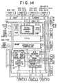
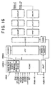
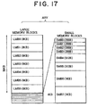
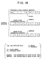
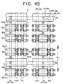
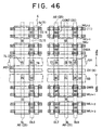
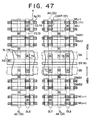
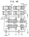
- Dispositif à semi-conducteurs, comportant :caractérisé en ce que le dispositif est formé dans un circuit intégré sur un substrat à semi-conducteurs, et comporte en outreune unité centrale de traitement (CPU),un bus d'adresses (ABUS) couplé à ladite CPU,un bus de données (DBUS) couplé à ladite CPU, etune mémoire (FMRY) couplée audit bus d'adresses et audit bus de données, ladite mémoire incluant une pluralité de blocs de mémoire (LMB0-LMB6, SMB0-SMB7) sur la figure 17 ou 23) fonctionnant chacun comme uns unité de données simultanément effaçable mémorisées dans celle-ci, chaque bloc de mémoire incluant une pluralité de cellules de mémoire électriquement effaçables et programmables (MC),
un registre de commande (MBREG1, MBREG2 sur la figure 18) couplé audit bus d'adresses et audit bus de données et ayant des bits de commanda pour des informations désignant un bloc de mémoire à effacer, dans lequel l'unité de traitement est adaptée pour fournir une adresse destinée à sélectionner le registre de commande et des informations à établir dans les bits de commande au bus d'adresses et au bus de données, respectivement, de sorte que des données mémorisées dans le bloc de mémoire, qui est désigné par les informations dans les bits de commande, sont effacées dans une opération d'effacement. - Dispositif selon la revendication 1, dans lequel
chaque bloc de mémoire inclut une pluralité de cellules de mémoire électriquement effaçables et programmables, et
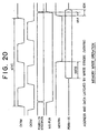
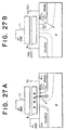
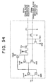
chaque cellule de mémoire (MC) comporte :une première région (source) et une seconds région (drain) qui sont formées dans ledit corps semi-conducteur (1) et sont séparées l'une de l'autre,une première couche d'isolation de grille (7) sur une région dudit corps semi-conducteur entre les première et seconde régions,une grille flottante (8) sur la couche d'isolation de grille, etun grille de commande (11) sur la grille flottante. - Dispositif selon la revendication 1 ou 2, dans lequel la mémoire inclut :une pluralité de lignes de mots (WL0-WLn) couplées à la pluralité de cellules de mémoire de sorts que la grille de commande d'une cellule de mémoire est couplée à une ligne de mots,une pluralité de lignes de données (DL0-DLm) couplées à la pluralité de cellules de mémoire de sorte que la seconde région (drain) d'une cellule de mémoire est couplée à une ligne de données, etune pluralité de lignes de source (SLW1-SLWi), dans lequel les cellules de mémoire qui sont couplées à la même ligne de mots ont chacune la première région (source) couplée en commun à une ligne parmi ladite pluralité de lignes de source pour former un bloc de la pluralité de blocs de mémoire.
- Dispositif selon la revendication 1 ou 2, dans lequel des blocs (LMB0-LMB6, SMB0-SMB7) parmi la pluralité de blocs de mémoire ont des capacités de mémoire différentes.
- Dispositif selon la revendication 4, comportant en outre une mémoire à accès direct (RAM), dans lequel un bloc (SMB0-SMB7) parmi la pluralité de blocs de mémoire a des capacités de mémoire inférieures à celle de la RAM.
Applications Claiming Priority (6)
| Application Number | Priority Date | Filing Date | Title |
|---|---|---|---|
| JP9191992 | 1992-03-17 | ||
| JP9191992A JPH05266219A (ja) | 1992-03-17 | 1992-03-17 | マイクロコンピュータ |
| JP09390892A JP3534781B2 (ja) | 1992-03-19 | 1992-03-19 | マイクロコンピュータ、及びフラッシュメモリ |
| JP9390892 | 1992-03-19 | ||
| EP98118739A EP0902436B1 (fr) | 1992-03-17 | 1993-03-11 | Micro-ordinateur comprenant une mémoire flash programmable au moyen d'une borne externe |
| EP93103907A EP0561271B1 (fr) | 1992-03-17 | 1993-03-11 | Micro-ordinateur comprenant une mémoire à access aléatoire et une mémoire flash non volatile |
Related Parent Applications (2)
| Application Number | Title | Priority Date | Filing Date |
|---|---|---|---|
| EP93103907.7 Division | 1993-03-11 | ||
| EP98118739.6 Division | 1998-10-05 |
Publications (2)
| Publication Number | Publication Date |
|---|---|
| EP1094470A1 EP1094470A1 (fr) | 2001-04-25 |
| EP1094470B1 true EP1094470B1 (fr) | 2003-08-13 |
Family
ID=26433348
Family Applications (4)
| Application Number | Title | Priority Date | Filing Date |
|---|---|---|---|
| EP98118740A Expired - Lifetime EP0893799B1 (fr) | 1992-03-17 | 1993-03-11 | Mémoire flash divisée en blocs avec lignes de données sans perturbations et micro-ordinateur avec mémoire flash |
| EP93103907A Expired - Lifetime EP0561271B1 (fr) | 1992-03-17 | 1993-03-11 | Micro-ordinateur comprenant une mémoire à access aléatoire et une mémoire flash non volatile |
| EP00121759A Expired - Lifetime EP1094470B1 (fr) | 1992-03-17 | 1993-03-11 | Mémoire flash, divisée en blocs, dont les lignes de données sont sans perturbation, et micro-ordinateur comprenant mémoire flash |
| EP98118739A Expired - Lifetime EP0902436B1 (fr) | 1992-03-17 | 1993-03-11 | Micro-ordinateur comprenant une mémoire flash programmable au moyen d'une borne externe |
Family Applications Before (2)
| Application Number | Title | Priority Date | Filing Date |
|---|---|---|---|
| EP98118740A Expired - Lifetime EP0893799B1 (fr) | 1992-03-17 | 1993-03-11 | Mémoire flash divisée en blocs avec lignes de données sans perturbations et micro-ordinateur avec mémoire flash |
| EP93103907A Expired - Lifetime EP0561271B1 (fr) | 1992-03-17 | 1993-03-11 | Micro-ordinateur comprenant une mémoire à access aléatoire et une mémoire flash non volatile |
Family Applications After (1)
| Application Number | Title | Priority Date | Filing Date |
|---|---|---|---|
| EP98118739A Expired - Lifetime EP0902436B1 (fr) | 1992-03-17 | 1993-03-11 | Micro-ordinateur comprenant une mémoire flash programmable au moyen d'une borne externe |
Country Status (5)
| Country | Link |
|---|---|
| US (17) | US5768194A (fr) |
| EP (4) | EP0893799B1 (fr) |
| KR (1) | KR100276474B1 (fr) |
| DE (4) | DE69332422T2 (fr) |
| TW (1) | TW231343B (fr) |
Families Citing this family (261)
| Publication number | Priority date | Publication date | Assignee | Title |
|---|---|---|---|---|
| US6347051B2 (en) * | 1991-11-26 | 2002-02-12 | Hitachi, Ltd. | Storage device employing a flash memory |
| TW231343B (fr) * | 1992-03-17 | 1994-10-01 | Hitachi Seisakusyo Kk | |
| US6414878B2 (en) * | 1992-03-17 | 2002-07-02 | Hitachi, Ltd. | Data line disturbance free memory block divided flash memory and microcomputer having flash memory therein |
| US5687345A (en) * | 1992-03-17 | 1997-11-11 | Hitachi, Ltd. | Microcomputer having CPU and built-in flash memory that is rewritable under control of the CPU analyzing a command supplied from an external device |
| US7057937B1 (en) | 1992-03-17 | 2006-06-06 | Renesas Technology Corp. | Data processing apparatus having a flash memory built-in which is rewritable by use of external device |
| JPH0728772A (ja) | 1993-06-25 | 1995-01-31 | Hitachi Ltd | マイクロコンピュータ |
| US6006304A (en) * | 1993-06-25 | 1999-12-21 | Hitachi, Ltd. | Apparatus and method for calculating an erasure time for data stored in a flash memory |
| US5719065A (en) * | 1993-10-01 | 1998-02-17 | Semiconductor Energy Laboratory Co., Ltd. | Method for manufacturing semiconductor device with removable spacers |
| US5814529A (en) | 1995-01-17 | 1998-09-29 | Semiconductor Energy Laboratory Co., Ltd. | Method for producing a semiconductor integrated circuit including a thin film transistor and a capacitor |
| JPH08212185A (ja) * | 1995-01-31 | 1996-08-20 | Mitsubishi Electric Corp | マイクロコンピュータ |
| US5606532A (en) * | 1995-03-17 | 1997-02-25 | Atmel Corporation | EEPROM array with flash-like core |
| US8171203B2 (en) * | 1995-07-31 | 2012-05-01 | Micron Technology, Inc. | Faster write operations to nonvolatile memory using FSInfo sector manipulation |
| US5845313A (en) | 1995-07-31 | 1998-12-01 | Lexar | Direct logical block addressing flash memory mass storage architecture |
| US6978342B1 (en) | 1995-07-31 | 2005-12-20 | Lexar Media, Inc. | Moving sectors within a block of information in a flash memory mass storage architecture |
| US6728851B1 (en) * | 1995-07-31 | 2004-04-27 | Lexar Media, Inc. | Increasing the memory performance of flash memory devices by writing sectors simultaneously to multiple flash memory devices |
| JP3560266B2 (ja) * | 1995-08-31 | 2004-09-02 | 株式会社ルネサステクノロジ | 半導体装置及び半導体データ装置 |
| DE19545557A1 (de) * | 1995-12-06 | 1997-06-12 | Siemens Ag | Festspeicher und Verfahren zur Ansteuerung desselben |
| JPH09212411A (ja) * | 1996-02-06 | 1997-08-15 | Tokyo Electron Ltd | メモリシステム |
| US5867394A (en) * | 1996-03-01 | 1999-02-02 | The Standard Register Company | Document dispenser operational program downloading |
| JPH1049439A (ja) * | 1996-03-26 | 1998-02-20 | Robert Bosch Gmbh | 制御装置の作動方法 |
| US5774545A (en) * | 1996-03-28 | 1998-06-30 | Lucent Technologies Inc. | Method and apparatus for enhancing security in and discouraging theft of VLSI and ULSI devices |
| EP1008928A4 (fr) * | 1996-04-11 | 2007-08-08 | Hitachi Ltd | Unite de disques et ordinateur |
| US6073204A (en) * | 1997-04-23 | 2000-06-06 | Micron Technology, Inc. | Memory system having flexible architecture and method |
| US5854944A (en) * | 1996-05-09 | 1998-12-29 | Motorola, Inc. | Method and apparatus for determining wait states on a per cycle basis in a data processing system |
| JPH09320282A (ja) * | 1996-05-27 | 1997-12-12 | Sharp Corp | 不揮発性半導体記憶装置の消去制御方法 |
| TW334581B (en) * | 1996-06-04 | 1998-06-21 | Handotai Energy Kenkyusho Kk | Semiconductor integrated circuit and fabrication method thereof |
| EP0825530A3 (fr) * | 1996-06-20 | 2004-06-02 | Sharp Kabushiki Kaisha | Dispositif d'ordinateur avec mémoire non volatile électriquement reprogrammable et avec mémoire non volatile à semi-conducteurs |
| EP0825611B1 (fr) * | 1996-08-22 | 2003-04-09 | STMicroelectronics S.r.l. | Dispositifs de mémoire non volatile multiétats |
| US6493788B1 (en) | 1996-10-28 | 2002-12-10 | Macronix International Co., Ltd. | Processor with embedded in-circuit programming structures |
| US6282675B1 (en) * | 1997-08-06 | 2001-08-28 | Macronix International Co., Ltd. | Fault-tolerant architecture for in-circuit programming |
| US5912837A (en) * | 1996-10-28 | 1999-06-15 | Micron Technology, Inc. | Bitline disturb reduction |
| US6842820B2 (en) | 1997-10-03 | 2005-01-11 | Macronix International Co., Ltd. | Processor with embedded in-circuit programming structures |
| JP3773607B2 (ja) * | 1996-11-28 | 2006-05-10 | Necエレクトロニクス株式会社 | フラッシュeeprom内蔵マイクロコンピュータ |
| JPH10177797A (ja) * | 1996-12-17 | 1998-06-30 | Toshiba Corp | 半導体記憶装置 |
| US5723355A (en) * | 1997-01-17 | 1998-03-03 | Programmable Microelectronics Corp. | Method to incorporate non-volatile memory and logic components into a single sub-0.3 micron fabrication process for embedded non-volatile memory |
| KR100251636B1 (ko) * | 1997-04-10 | 2000-05-01 | 윤종용 | 소형컴퓨터시스템인터페이스방식접속을위한메모리장치 |
| US6252799B1 (en) * | 1997-04-11 | 2001-06-26 | Programmable Silicon Solutions | Device with embedded flash and EEPROM memories |
| KR100476293B1 (ko) * | 1997-04-15 | 2005-06-08 | 유티스타콤코리아 유한회사 | Mc683시리즈계열을사용한보드에서의메모리실장확인및테스트방법 |
| JPH10326493A (ja) * | 1997-05-23 | 1998-12-08 | Ricoh Co Ltd | 複合化フラッシュメモリ装置 |
| JPH10333898A (ja) * | 1997-05-29 | 1998-12-18 | Nec Corp | マイクロコンピュータ |
| JP3189740B2 (ja) * | 1997-06-20 | 2001-07-16 | 日本電気株式会社 | 不揮発性半導体メモリのデータ修復方法 |
| US6226708B1 (en) * | 1997-08-18 | 2001-05-01 | Texas Instruments Incorporated | Method and system for efficiently programming non-volatile memory |
| US6289300B1 (en) | 1998-02-06 | 2001-09-11 | Analog Devices, Inc. | Integrated circuit with embedded emulator and emulation system for use with such an integrated circuit |
| EP0935195A2 (fr) | 1998-02-06 | 1999-08-11 | Analog Devices, Inc. | Circuit intégré avec convertisseur analogique-numérique à haute résolution, un microcontrolleur et une mémoire à haute densité et émulateur correspondant |
| US6701395B1 (en) | 1998-02-06 | 2004-03-02 | Analog Devices, Inc. | Analog-to-digital converter that preseeds memory with channel identifier data and makes conversions at fixed rate with direct memory access |
| US6385689B1 (en) * | 1998-02-06 | 2002-05-07 | Analog Devices, Inc. | Memory and a data processor including a memory |
| TW407364B (en) * | 1998-03-26 | 2000-10-01 | Toshiba Corp | Memory apparatus, card type memory apparatus, and electronic apparatus |
| IT1298819B1 (it) * | 1998-03-27 | 2000-02-02 | Sgs Thomson Microelectronics | Circuito di commutazione |
| JP3559166B2 (ja) * | 1998-06-15 | 2004-08-25 | 三菱電機株式会社 | 自動車用制御装置 |
| ITMI981564A1 (it) * | 1998-07-09 | 2000-01-09 | St Microelectronics Srl | Memoria non volatile in grado di eseguire un programma autonomamente |
| JP2002526921A (ja) * | 1998-09-29 | 2002-08-20 | アドバンスト・マイクロ・ディバイシズ・インコーポレイテッド | ゲートへの酸化膜堆積方法 |
| DE69832609D1 (de) * | 1998-09-30 | 2006-01-05 | St Microelectronics Srl | Emulierte EEPROM Speicheranordnung und entsprechendes Verfahren |
| EP1005079B1 (fr) | 1998-11-26 | 2012-12-26 | STMicroelectronics Srl | Procédé d'intégration d'une mémoire non volatile et d'un circuit logique à haute performance sur la même puce |
| JP2000173279A (ja) * | 1998-12-02 | 2000-06-23 | Nec Corp | 不揮発性半導体記憶装置とその消去検証方法 |
| JP2000251035A (ja) * | 1999-02-26 | 2000-09-14 | Hitachi Ltd | メモリカード |
| AU1960301A (en) * | 1999-09-13 | 2001-04-17 | Advanced Technology Materials, Inc. | A single chip embedded microcontroller having multiple non-volatile erasable proms sharing a single high voltage generator |
| KR100375217B1 (ko) * | 1999-10-21 | 2003-03-07 | 삼성전자주식회사 | 전기적으로 재기입 가능한 불휘발성 메모리를 구비하는마이크로컨트롤러 |
| US6640262B1 (en) * | 1999-12-20 | 2003-10-28 | 3Com Corporation | Method and apparatus for automatically configuring a configurable integrated circuit |
| GB2357602A (en) * | 1999-12-22 | 2001-06-27 | Nokia Mobile Phones Ltd | Memory controller for a memory array comprising different memory types |
| FR2803080A1 (fr) * | 1999-12-22 | 2001-06-29 | St Microelectronics Sa | Memoire flash programmable page par page |
| US6426893B1 (en) | 2000-02-17 | 2002-07-30 | Sandisk Corporation | Flash eeprom system with simultaneous multiple data sector programming and storage of physical block characteristics in other designated blocks |
| JP3872927B2 (ja) * | 2000-03-22 | 2007-01-24 | 株式会社東芝 | 昇圧回路 |
| EP1139419A1 (fr) | 2000-03-29 | 2001-10-04 | STMicroelectronics S.r.l. | Procédé de fabrication d'une mémoire non-volatile programmable électriquement avec circuit logique |
| JP2001357023A (ja) * | 2000-06-14 | 2001-12-26 | Seiko Epson Corp | 半導体集積回路及びそれに内蔵された不揮発性メモリへの書き込み方法 |
| NO20004236L (no) * | 2000-08-24 | 2002-02-25 | Thin Film Electronics Asa | Ikke-flyktig passiv matriseinnretning og fremgangsmåte for utlesing av samme |
| JP2002025282A (ja) | 2000-07-12 | 2002-01-25 | Hitachi Ltd | 不揮発性半導体記憶装置 |
| US7167944B1 (en) | 2000-07-21 | 2007-01-23 | Lexar Media, Inc. | Block management for mass storage |
| US6266273B1 (en) * | 2000-08-21 | 2001-07-24 | Sandisk Corporation | Method and structure for reliable data copy operation for non-volatile memories |
| US6567289B1 (en) * | 2000-08-23 | 2003-05-20 | Advanced Micro Devices, Inc. | Physical memory layout with various sized memory sectors |
| JP2002073425A (ja) * | 2000-08-31 | 2002-03-12 | Hitachi Ltd | 媒体再生装置 |
| US20020044486A1 (en) * | 2000-10-16 | 2002-04-18 | Cheng-Sheng Chan | IC card with different page sizes to increase endurance |
| US6834331B1 (en) | 2000-10-24 | 2004-12-21 | Starfish Software, Inc. | System and method for improving flash memory data integrity |
| DE10101034A1 (de) * | 2001-01-11 | 2002-08-01 | Jumptec Ind Computertechnik Ag | Datenkommunikationssystem und Datenumwandlungsvorrichtung |
| US6449209B1 (en) * | 2001-01-19 | 2002-09-10 | Samsung Electronics Co., Ltd. | Semiconductor memory device comprising more than two internal banks of different sizes |
| US6344994B1 (en) * | 2001-01-31 | 2002-02-05 | Advanced Micro Devices | Data retention characteristics as a result of high temperature bake |
| DE60140039D1 (de) * | 2001-02-05 | 2009-11-12 | St Microelectronics Srl | Löschverfahren für einen Flash-Speicher |
| JP2002269065A (ja) | 2001-03-08 | 2002-09-20 | Mitsubishi Electric Corp | プログラム可能な不揮発性メモリを内蔵したマイクロコンピュータ |
| US6452836B1 (en) | 2001-03-09 | 2002-09-17 | Micron Technology, Inc. | Non-volatile memory device with erase cycle register |
| US6549467B2 (en) * | 2001-03-09 | 2003-04-15 | Micron Technology, Inc. | Non-volatile memory device with erase address register |
| JP4230122B2 (ja) * | 2001-03-30 | 2009-02-25 | 株式会社ルネサステクノロジ | マイクロコンピュータ、書込み方法及び消去方法 |
| US6490202B2 (en) * | 2001-04-06 | 2002-12-03 | Micron Technology, Inc. | Non-volatile memory device with erase register |
| FR2824650A1 (fr) * | 2001-05-10 | 2002-11-15 | Koninkl Philips Electronics Nv | Systeme de traitement de donnees et procede de distribution d'acces a des memoires |
| JP4049297B2 (ja) * | 2001-06-11 | 2008-02-20 | 株式会社ルネサステクノロジ | 半導体記憶装置 |
| DE10131300B4 (de) * | 2001-07-02 | 2012-12-06 | Robert Bosch Gmbh | Verfahren zum Schutz eines Mikrorechner-Systems gegen Manipulation von in einer Speicheranordnung abgelegten Daten und Mikrorechner-System |
| JP2003023114A (ja) * | 2001-07-05 | 2003-01-24 | Fujitsu Ltd | 半導体集積回路装置およびその製造方法 |
| US6594194B2 (en) * | 2001-07-11 | 2003-07-15 | Sun Microsystems, Inc. | Memory array with common word line |
| JP4157285B2 (ja) * | 2001-08-31 | 2008-10-01 | 株式会社東芝 | 不揮発性半導体メモリ |
| JP3979486B2 (ja) * | 2001-09-12 | 2007-09-19 | 株式会社ルネサステクノロジ | 不揮発性記憶装置およびデータ格納方法 |
| JP2003099414A (ja) * | 2001-09-21 | 2003-04-04 | Mitsubishi Electric Corp | 半導体集積回路 |
| GB0123416D0 (en) | 2001-09-28 | 2001-11-21 | Memquest Ltd | Non-volatile memory control |
| GB0123415D0 (en) | 2001-09-28 | 2001-11-21 | Memquest Ltd | Method of writing data to non-volatile memory |
| GB0123417D0 (en) * | 2001-09-28 | 2001-11-21 | Memquest Ltd | Improved data processing |
| GB0123410D0 (en) * | 2001-09-28 | 2001-11-21 | Memquest Ltd | Memory system for data storage and retrieval |
| GB0123421D0 (en) * | 2001-09-28 | 2001-11-21 | Memquest Ltd | Power management system |
| JP3961806B2 (ja) * | 2001-10-18 | 2007-08-22 | 富士通株式会社 | 不揮発性半導体記憶装置 |
| ITRM20010647A1 (it) * | 2001-11-02 | 2003-05-02 | Micron Technology Inc | Verifica di cancellazione a blocchi per memorie flash. |
| US6977850B2 (en) * | 2001-12-27 | 2005-12-20 | Kabushiki Kaisha Toshiba | Semiconductor device having switch circuit to supply voltage |
| KR100404232B1 (ko) * | 2002-01-02 | 2003-11-05 | 주식회사 하이닉스반도체 | 마이크로 컨트롤러 장치 |
| JP2003203997A (ja) * | 2002-01-07 | 2003-07-18 | Mitsubishi Electric Corp | 不揮発性半導体記憶装置及びその製造方法 |
| US7209252B2 (en) * | 2002-01-15 | 2007-04-24 | Lexmark International, Inc. | Memory module, printer assembly, and method for storing printer code |
| JP2003223792A (ja) * | 2002-01-25 | 2003-08-08 | Hitachi Ltd | 不揮発性メモリ及びメモリカード |
| US7231643B1 (en) | 2002-02-22 | 2007-06-12 | Lexar Media, Inc. | Image rescue system including direct communication between an application program and a device driver |
| US7475259B1 (en) * | 2002-02-28 | 2009-01-06 | The Directv Group, Inc. | Multiple nonvolatile memories |
| US7437571B1 (en) | 2002-02-28 | 2008-10-14 | The Directv Group, Inc. | Dedicated nonvolatile memory |
| US7457967B2 (en) * | 2002-02-28 | 2008-11-25 | The Directv Group, Inc. | Hidden identification |
| US7275163B2 (en) * | 2002-02-28 | 2007-09-25 | The Directv Group, Inc. | Asynchronous configuration |
| US7111109B2 (en) * | 2002-03-13 | 2006-09-19 | Canon Kabushiki Kaisha | Control system, recording device and electronic apparatus |
| KR20030073824A (ko) * | 2002-03-13 | 2003-09-19 | 주식회사 레인콤 | 범용 직렬 버스를 이용한 시스템의 펌웨어 업그레이드방법 및 장치 |
| KR100414739B1 (ko) * | 2002-03-25 | 2004-01-13 | 주식회사 하이닉스반도체 | 반도체 메모리 소자의 내부전압 발생 장치 |
| JP3989761B2 (ja) | 2002-04-09 | 2007-10-10 | 株式会社半導体エネルギー研究所 | 半導体表示装置 |
| US7038239B2 (en) | 2002-04-09 | 2006-05-02 | Semiconductor Energy Laboratory Co., Ltd. | Semiconductor element and display device using the same |
| JP3989763B2 (ja) | 2002-04-15 | 2007-10-10 | 株式会社半導体エネルギー研究所 | 半導体表示装置 |
| KR100968496B1 (ko) * | 2002-04-15 | 2010-07-07 | 가부시키가이샤 한도오따이 에네루기 켄큐쇼 | 표시장치 및 그 제조방법 |
| US7256421B2 (en) | 2002-05-17 | 2007-08-14 | Semiconductor Energy Laboratory, Co., Ltd. | Display device having a structure for preventing the deterioration of a light emitting device |
| JP2004005296A (ja) * | 2002-06-03 | 2004-01-08 | Motorola Inc | 電子制御装置 |
| JP2004070407A (ja) * | 2002-08-01 | 2004-03-04 | Alps Electric Co Ltd | 電気機器の制御装置及び該制御装置へのアプリケーションプログラム書き込み方法 |
| US8050085B2 (en) * | 2002-08-29 | 2011-11-01 | Renesas Electronics Corporation | Semiconductor processing device and IC card |
| JP2004126658A (ja) * | 2002-09-30 | 2004-04-22 | Toshiba Corp | プロセッサシステム |
| US7024570B2 (en) * | 2002-10-18 | 2006-04-04 | Infineon Technologies North America Corp. | Low-power indicator |
| ITMI20022668A1 (it) * | 2002-12-18 | 2004-06-19 | Simicroelectronics S R L | Dispositivo di memoria non volatile con migliorata velocita' |
| JP2004237667A (ja) * | 2003-02-07 | 2004-08-26 | Canon Inc | データ転送方法 |
| US20050185465A1 (en) * | 2003-03-11 | 2005-08-25 | Fujitsu Limited | Memory device |
| JP2004319034A (ja) * | 2003-04-18 | 2004-11-11 | Renesas Technology Corp | データプロセッサ |
| DE10319271A1 (de) * | 2003-04-29 | 2004-11-25 | Infineon Technologies Ag | Speicher-Schaltungsanordnung und Verfahren zur Herstellung |
| JP4289026B2 (ja) * | 2003-05-28 | 2009-07-01 | 日本電気株式会社 | 半導体記憶装置 |
| KR100555506B1 (ko) * | 2003-07-11 | 2006-03-03 | 삼성전자주식회사 | 프로그램된 메모리 셀들과 프로그램 및 소거 가능한메모리 셀들을 포함하는 메모리 장치 |
| JP2005092963A (ja) * | 2003-09-16 | 2005-04-07 | Renesas Technology Corp | 不揮発性記憶装置 |
| US6941219B2 (en) | 2003-09-30 | 2005-09-06 | Detroit Diesel Corporation | Method for recreating valid calibration data for an engine control module |
| TWI343531B (en) * | 2003-12-19 | 2011-06-11 | Oce Tech Bv | Erasing a stored information pattern on a storage medium |
| US7607177B2 (en) * | 2004-02-23 | 2009-10-20 | Micron Technology, Inc. | Secure compact flash |
| US7725628B1 (en) | 2004-04-20 | 2010-05-25 | Lexar Media, Inc. | Direct secondary device interface by a host |
| US7370166B1 (en) | 2004-04-30 | 2008-05-06 | Lexar Media, Inc. | Secure portable storage device |
| KR100532510B1 (ko) * | 2004-05-04 | 2005-11-30 | 삼성전자주식회사 | 기입 동작시 메모리 셀 어레이의 일부 영역에 기입되는데이터를 마스킹하는 반도체 메모리 장치 및 그 마스킹 방법 |
| US7490283B2 (en) | 2004-05-13 | 2009-02-10 | Sandisk Corporation | Pipelined data relocation and improved chip architectures |
| US20060044899A1 (en) * | 2004-08-27 | 2006-03-02 | Ellis Robert W | Method and apparatus for destroying flash memory |
| US7464306B1 (en) * | 2004-08-27 | 2008-12-09 | Lexar Media, Inc. | Status of overall health of nonvolatile memory |
| US7594063B1 (en) * | 2004-08-27 | 2009-09-22 | Lexar Media, Inc. | Storage capacity status |
| US20060054977A1 (en) * | 2004-09-16 | 2006-03-16 | Intel Corporation | Charge storage memory cell |
| WO2006033832A2 (fr) * | 2004-09-21 | 2006-03-30 | Atmel Corporation | Nouveau procede compense de mise en place d'une phase de decharge haute tension apres effacement des impulsions dans un dispositif a memoire flash |
| ITMI20041802A1 (it) | 2004-09-21 | 2004-12-21 | Atmel Corp | "nuovo metodo compensato per attuare una fase di scarica ad alta tensione dopo un impulso di cancellazione in un dispositivo di memoria flash" |
| KR100618865B1 (ko) * | 2004-09-30 | 2006-08-31 | 삼성전자주식회사 | 멀티플 프로그래밍 가능한 otp 메모리 장치 및 그프로그래밍 방법 |
| ATE395703T1 (de) * | 2004-10-20 | 2008-05-15 | Actaris Sas | Verfahren zum löschen eines flash-speichers und zähler mit einem flash-speicher |
| DE102004052218B3 (de) * | 2004-10-27 | 2006-04-27 | Infineon Technologies Ag | Speicheranordnung mit geringem Stromverbrauch |
| JP4759983B2 (ja) * | 2004-11-04 | 2011-08-31 | 船井電機株式会社 | ディスク装置のファームウェア書き換え方法、及びファームウェア書き換えプログラム |
| US7849381B2 (en) * | 2004-12-21 | 2010-12-07 | Sandisk Corporation | Method for copying data in reprogrammable non-volatile memory |
| US7409473B2 (en) | 2004-12-21 | 2008-08-05 | Sandisk Corporation | Off-chip data relocation |
| US7212440B2 (en) * | 2004-12-30 | 2007-05-01 | Sandisk Corporation | On-chip data grouping and alignment |
| JP2006331584A (ja) * | 2005-05-27 | 2006-12-07 | Renesas Technology Corp | 半導体集積回路及びマイクロコンピュータ |
| US7668017B2 (en) * | 2005-08-17 | 2010-02-23 | Saifun Semiconductors Ltd. | Method of erasing non-volatile memory cells |
| JP2007140733A (ja) * | 2005-11-16 | 2007-06-07 | Renesas Technology Corp | 半導体処理装置及び半導体集積回路 |
| US7502916B2 (en) * | 2005-12-02 | 2009-03-10 | Infineon Technologies Flash Gmbh & Co. Kg | Processing arrangement, memory card device and method for operating and manufacturing a processing arrangement |
| KR100784862B1 (ko) * | 2006-01-09 | 2007-12-14 | 삼성전자주식회사 | 더미 셀을 포함하는 플래시 메모리 장치 |
| US7793059B2 (en) * | 2006-01-18 | 2010-09-07 | Apple Inc. | Interleaving policies for flash memory |
| US7702935B2 (en) * | 2006-01-25 | 2010-04-20 | Apple Inc. | Reporting flash memory operating voltages |
| US20070174641A1 (en) * | 2006-01-25 | 2007-07-26 | Cornwell Michael J | Adjusting power supplies for data storage devices |
| US7861122B2 (en) * | 2006-01-27 | 2010-12-28 | Apple Inc. | Monitoring health of non-volatile memory |
| US8069328B2 (en) * | 2006-03-28 | 2011-11-29 | Mosaid Technologies Incorporated | Daisy chain cascade configuration recognition technique |
| US7478213B2 (en) * | 2006-03-29 | 2009-01-13 | Atmel Corporation | Off-chip micro control and interface in a multichip integrated memory system |
| US7366028B2 (en) * | 2006-04-24 | 2008-04-29 | Sandisk Corporation | Method of high-performance flash memory data transfer |
| US7499369B2 (en) * | 2006-07-19 | 2009-03-03 | Sandisk Corporation | Method of high-performance flash memory data transfer |
| US7345926B2 (en) * | 2006-04-24 | 2008-03-18 | Sandisk Corporation | High-performance flash memory data transfer |
| US7366029B2 (en) * | 2006-04-24 | 2008-04-29 | Sandisk Corporation | High-performance flash memory data transfer |
| US7499339B2 (en) * | 2006-07-19 | 2009-03-03 | Sandisk Corporation | High-performance flash memory data transfer |
| US7525855B2 (en) * | 2006-04-24 | 2009-04-28 | Sandisk Corporation | Method of high-performance flash memory data transfer |
| US20070248657A1 (en) * | 2006-04-25 | 2007-10-25 | Smith David J | Multi-compartment transdermal pain control device |
| EP1865554B1 (fr) * | 2006-06-09 | 2017-01-11 | ams AG | Dispositif de mémoire à semi-conducteurs et son mode de fonctionnement |
| US7599229B2 (en) * | 2006-06-21 | 2009-10-06 | Macronix International Co., Ltd. | Methods and structures for expanding a memory operation window and reducing a second bit effect |
| US7684252B2 (en) * | 2006-06-21 | 2010-03-23 | Macronix International Co., Ltd. | Method and structure for operating memory devices on fringes of control gate |
| US7489549B2 (en) * | 2006-06-22 | 2009-02-10 | Sandisk Corporation | System for non-real time reprogramming of non-volatile memory to achieve tighter distribution of threshold voltages |
| US7486561B2 (en) * | 2006-06-22 | 2009-02-03 | Sandisk Corporation | Method for non-real time reprogramming of non-volatile memory to achieve tighter distribution of threshold voltages |
| JP2008009702A (ja) * | 2006-06-29 | 2008-01-17 | Matsushita Electric Ind Co Ltd | 演算処理システム |
| KR101410288B1 (ko) * | 2006-09-12 | 2014-06-20 | 샌디스크 테크놀로지스, 인코포레이티드 | 초기 프로그래밍 전압의 선형 추정을 위한 비휘발성 메모리및 방법 |
| US7697344B2 (en) * | 2006-11-03 | 2010-04-13 | Samsung Electronics Co., Ltd. | Memory device and method of operating and fabricating the same |
| KR100852895B1 (ko) * | 2006-12-05 | 2008-08-19 | 삼성전자주식회사 | 복합 메모리 칩과 이를 포함하는 메모리 카드 및 이의 제조방법 |
| US7613049B2 (en) * | 2007-01-08 | 2009-11-03 | Macronix International Co., Ltd | Method and system for a serial peripheral interface |
| JP4434217B2 (ja) * | 2007-02-14 | 2010-03-17 | 株式会社デンソー | 充電制御装置 |
| JP5116337B2 (ja) * | 2007-03-30 | 2013-01-09 | ルネサスエレクトロニクス株式会社 | 半導体記憶装置 |
| US20080288712A1 (en) | 2007-04-25 | 2008-11-20 | Cornwell Michael J | Accessing metadata with an external host |
| US7913032B1 (en) | 2007-04-25 | 2011-03-22 | Apple Inc. | Initiating memory wear leveling |
| KR100898653B1 (ko) * | 2007-07-25 | 2009-05-22 | 주식회사 하이닉스반도체 | 플래시 메모리 소자 및 프로그램 방법 |
| JP2009080884A (ja) * | 2007-09-26 | 2009-04-16 | Panasonic Corp | 不揮発性半導体記憶装置 |
| US7532027B2 (en) * | 2007-09-28 | 2009-05-12 | Adtron, Inc. | Deliberate destruction of integrated circuits |
| JP5221172B2 (ja) * | 2008-02-29 | 2013-06-26 | 株式会社東芝 | Nand混載型半導体時限スイッチ |
| US8132253B2 (en) * | 2008-04-21 | 2012-03-06 | Dell Products L.P. | Memory security override protection for manufacturability of information handling systems |
| US11955476B2 (en) | 2008-12-23 | 2024-04-09 | Schottky Lsi, Inc. | Super CMOS devices on a microelectronics system |
| US11342916B2 (en) | 2008-12-23 | 2022-05-24 | Schottky Lsi, Inc. | Schottky-CMOS asynchronous logic cells |
| US8476689B2 (en) | 2008-12-23 | 2013-07-02 | Augustine Wei-Chun Chang | Super CMOS devices on a microelectronics system |
| US8102724B2 (en) * | 2009-01-29 | 2012-01-24 | International Business Machines Corporation | Setting controller VREF in a memory controller and memory device interface in a communication bus |
| US8111564B2 (en) * | 2009-01-29 | 2012-02-07 | International Business Machines Corporation | Setting controller termination in a memory controller and memory device interface in a communication bus |
| JP5532671B2 (ja) * | 2009-05-08 | 2014-06-25 | ソニー株式会社 | データ記憶システムおよびデータ記憶方法、実行装置および制御方法、並びに制御装置および制御方法 |
| TWI490780B (zh) * | 2010-02-05 | 2015-07-01 | Nat Applied Res Laboratoires | 嵌入式系統及其存取資料方法 |
| JP2011170914A (ja) * | 2010-02-18 | 2011-09-01 | Elpida Memory Inc | 半導体装置 |
| JP4901968B2 (ja) * | 2010-03-01 | 2012-03-21 | 株式会社東芝 | 半導体記憶装置 |
| US8681571B2 (en) | 2010-06-15 | 2014-03-25 | International Business Machines Corporation | Training a memory controller and a memory device using multiple read and write operations |
| US8289784B2 (en) | 2010-06-15 | 2012-10-16 | International Business Machines Corporation | Setting a reference voltage in a memory controller trained to a memory device |
| US9224496B2 (en) | 2010-08-11 | 2015-12-29 | Shine C. Chung | Circuit and system of aggregated area anti-fuse in CMOS processes |
| US9460807B2 (en) | 2010-08-20 | 2016-10-04 | Shine C. Chung | One-time programmable memory devices using FinFET technology |
| US9251893B2 (en) | 2010-08-20 | 2016-02-02 | Shine C. Chung | Multiple-bit programmable resistive memory using diode as program selector |
| US10923204B2 (en) | 2010-08-20 | 2021-02-16 | Attopsemi Technology Co., Ltd | Fully testible OTP memory |
| US10229746B2 (en) | 2010-08-20 | 2019-03-12 | Attopsemi Technology Co., Ltd | OTP memory with high data security |
| US9818478B2 (en) | 2012-12-07 | 2017-11-14 | Attopsemi Technology Co., Ltd | Programmable resistive device and memory using diode as selector |
| US9019742B2 (en) | 2010-08-20 | 2015-04-28 | Shine C. Chung | Multiple-state one-time programmable (OTP) memory to function as multi-time programmable (MTP) memory |
| US8830720B2 (en) | 2010-08-20 | 2014-09-09 | Shine C. Chung | Circuit and system of using junction diode as program selector and MOS as read selector for one-time programmable devices |
| US9431127B2 (en) * | 2010-08-20 | 2016-08-30 | Shine C. Chung | Circuit and system of using junction diode as program selector for metal fuses for one-time programmable devices |
| US9025357B2 (en) | 2010-08-20 | 2015-05-05 | Shine C. Chung | Programmable resistive memory unit with data and reference cells |
| US9496033B2 (en) | 2010-08-20 | 2016-11-15 | Attopsemi Technology Co., Ltd | Method and system of programmable resistive devices with read capability using a low supply voltage |
| US9711237B2 (en) | 2010-08-20 | 2017-07-18 | Attopsemi Technology Co., Ltd. | Method and structure for reliable electrical fuse programming |
| US10249379B2 (en) | 2010-08-20 | 2019-04-02 | Attopsemi Technology Co., Ltd | One-time programmable devices having program selector for electrical fuses with extended area |
| US9824768B2 (en) | 2015-03-22 | 2017-11-21 | Attopsemi Technology Co., Ltd | Integrated OTP memory for providing MTP memory |
| US9042153B2 (en) | 2010-08-20 | 2015-05-26 | Shine C. Chung | Programmable resistive memory unit with multiple cells to improve yield and reliability |
| US9236141B2 (en) | 2010-08-20 | 2016-01-12 | Shine C. Chung | Circuit and system of using junction diode of MOS as program selector for programmable resistive devices |
| US10916317B2 (en) | 2010-08-20 | 2021-02-09 | Attopsemi Technology Co., Ltd | Programmable resistance memory on thin film transistor technology |
| US9070437B2 (en) | 2010-08-20 | 2015-06-30 | Shine C. Chung | Circuit and system of using junction diode as program selector for one-time programmable devices with heat sink |
| US8576602B2 (en) | 2010-08-20 | 2013-11-05 | Shine C. Chung | One-time programmable memories using polysilicon diodes as program selectors |
| US8488359B2 (en) * | 2010-08-20 | 2013-07-16 | Shine C. Chung | Circuit and system of using junction diode as program selector for one-time programmable devices |
| US9019791B2 (en) | 2010-11-03 | 2015-04-28 | Shine C. Chung | Low-pin-count non-volatile memory interface for 3D IC |
| US8988965B2 (en) | 2010-11-03 | 2015-03-24 | Shine C. Chung | Low-pin-count non-volatile memory interface |
| US9076513B2 (en) | 2010-11-03 | 2015-07-07 | Shine C. Chung | Low-pin-count non-volatile memory interface with soft programming capability |
| US8913449B2 (en) | 2012-03-11 | 2014-12-16 | Shine C. Chung | System and method of in-system repairs or configurations for memories |
| AU2016238887B2 (en) * | 2010-11-18 | 2018-08-02 | Google Llc | Contextual history of computing objects |
| CN102544011A (zh) | 2010-12-08 | 2012-07-04 | 庄建祥 | 反熔丝存储器及电子系统 |
| KR20120080360A (ko) | 2011-01-07 | 2012-07-17 | 에스케이하이닉스 주식회사 | 반도체 메모리 장치 및 이를 포함하는 메모리 시스템 |
| US9369172B2 (en) * | 2011-02-10 | 2016-06-14 | Mediatek Inc. | Wireless communication device |
| US9258030B2 (en) * | 2011-02-10 | 2016-02-09 | Mediatek Inc. | Wireless communication device |
| US9713093B2 (en) * | 2011-02-10 | 2017-07-18 | Mediatek Inc. | Wireless communication device |
| US8971378B2 (en) * | 2011-02-10 | 2015-03-03 | Mediatek Inc. | Wireless communication device |
| US10192615B2 (en) | 2011-02-14 | 2019-01-29 | Attopsemi Technology Co., Ltd | One-time programmable devices having a semiconductor fin structure with a divided active region |
| US10586832B2 (en) | 2011-02-14 | 2020-03-10 | Attopsemi Technology Co., Ltd | One-time programmable devices using gate-all-around structures |
| US8848423B2 (en) | 2011-02-14 | 2014-09-30 | Shine C. Chung | Circuit and system of using FinFET for building programmable resistive devices |
| KR101736457B1 (ko) * | 2011-07-12 | 2017-05-17 | 삼성전자주식회사 | 불휘발성 메모리 장치, 불휘발성 메모리 장치의 소거 방법, 불휘발성 메모리 장치의 동작 방법, 불휘발성 메모리 장치를 포함하는 메모리 시스템, 메모리 시스템의 동작 방법, 불휘발성 메모리 장치를 포함하는 메모리 카드 및 솔리드 스테이트 드라이브 |
| US9136261B2 (en) | 2011-11-15 | 2015-09-15 | Shine C. Chung | Structures and techniques for using mesh-structure diodes for electro-static discharge (ESD) protection |
| US9324849B2 (en) | 2011-11-15 | 2016-04-26 | Shine C. Chung | Structures and techniques for using semiconductor body to construct SCR, DIAC, or TRIAC |
| US8912576B2 (en) | 2011-11-15 | 2014-12-16 | Shine C. Chung | Structures and techniques for using semiconductor body to construct bipolar junction transistors |
| US8902625B2 (en) * | 2011-11-22 | 2014-12-02 | Marvell World Trade Ltd. | Layouts for memory and logic circuits in a system-on-chip |
| US9007804B2 (en) | 2012-02-06 | 2015-04-14 | Shine C. Chung | Circuit and system of protective mechanisms for programmable resistive memories |
| US9053066B2 (en) * | 2012-03-30 | 2015-06-09 | Sandisk Technologies Inc. | NAND flash memory interface |
| TWI497515B (zh) * | 2012-07-10 | 2015-08-21 | Silicon Motion Inc | 快閃記憶體控制器、快閃記憶體偵錯方法 |
| US9135978B2 (en) | 2012-07-11 | 2015-09-15 | Micron Technology, Inc. | Memory programming methods and memory systems |
| US20140058532A1 (en) * | 2012-08-23 | 2014-02-27 | GM Global Technology Operations LLC | Method for partial flashing of ecus |
| US9076526B2 (en) | 2012-09-10 | 2015-07-07 | Shine C. Chung | OTP memories functioning as an MTP memory |
| US9183897B2 (en) | 2012-09-30 | 2015-11-10 | Shine C. Chung | Circuits and methods of a self-timed high speed SRAM |
| US9324447B2 (en) | 2012-11-20 | 2016-04-26 | Shine C. Chung | Circuit and system for concurrently programming multiple bits of OTP memory devices |
| US9293196B2 (en) | 2013-03-15 | 2016-03-22 | Micron Technology, Inc. | Memory cells, memory systems, and memory programming methods |
| JP6220244B2 (ja) * | 2013-11-21 | 2017-10-25 | キヤノン株式会社 | 電子機器 |
| US9412473B2 (en) | 2014-06-16 | 2016-08-09 | Shine C. Chung | System and method of a novel redundancy scheme for OTP |
| CN106688039B (zh) * | 2014-09-12 | 2019-03-12 | 东芝存储器株式会社 | 存储装置 |
| KR102329267B1 (ko) * | 2014-09-29 | 2021-11-22 | 삼성디스플레이 주식회사 | 박막트랜지스터 기판, 이를 구비한 디스플레이 장치, 박막트랜지스터 기판 제조방법 및 디스플레이 장치 제조방법 |
| US9809699B2 (en) * | 2015-10-30 | 2017-11-07 | Fina Technology, Inc. | Alternative methods to control crosslinking in high impact polystyrene |
| KR102468992B1 (ko) * | 2015-11-06 | 2022-11-22 | 에스케이하이닉스 주식회사 | 메모리 장치 및 이의 동작 방법 |
| US10057523B1 (en) | 2017-02-13 | 2018-08-21 | Alexander Krymski | Image sensors and methods with multiple phase-locked loops and serializers |
| US10726914B2 (en) | 2017-04-14 | 2020-07-28 | Attopsemi Technology Co. Ltd | Programmable resistive memories with low power read operation and novel sensing scheme |
| US11062786B2 (en) | 2017-04-14 | 2021-07-13 | Attopsemi Technology Co., Ltd | One-time programmable memories with low power read operation and novel sensing scheme |
| US11615859B2 (en) | 2017-04-14 | 2023-03-28 | Attopsemi Technology Co., Ltd | One-time programmable memories with ultra-low power read operation and novel sensing scheme |
| US10535413B2 (en) | 2017-04-14 | 2020-01-14 | Attopsemi Technology Co., Ltd | Low power read operation for programmable resistive memories |
| US10770160B2 (en) | 2017-11-30 | 2020-09-08 | Attopsemi Technology Co., Ltd | Programmable resistive memory formed by bit slices from a standard cell library |
| JP7212239B2 (ja) * | 2018-06-05 | 2023-01-25 | ユナイテッド・セミコンダクター・ジャパン株式会社 | 不揮発性半導体記憶装置及び不揮発性半導体記憶装置の書き換え方法 |
| TWI702611B (zh) * | 2018-12-06 | 2020-08-21 | 旺宏電子股份有限公司 | 記憶體電路 |
| TWI711044B (zh) * | 2019-07-05 | 2020-11-21 | 旺宏電子股份有限公司 | 記憶體裝置及其操作方法 |
| US10950290B2 (en) | 2019-07-05 | 2021-03-16 | Macronix International Co., Ltd. | Memory device and operating method thereof that reduce off current to reduce errors in reading and writing data which have plurality of memory cell blocks and a source voltage generator |
| CN113055808B (zh) * | 2021-06-01 | 2021-08-13 | 中芯集成电路制造(绍兴)有限公司 | 器件加工方法、mems器件及其加工方法以及mems麦克风 |
| CN113918389B (zh) * | 2021-12-15 | 2022-03-11 | 苏州浪潮智能科技有限公司 | 一种双Flash切换装置和服务器 |
Family Cites Families (91)
| Publication number | Priority date | Publication date | Assignee | Title |
|---|---|---|---|---|
| JPS55115729A (en) * | 1979-02-28 | 1980-09-05 | Toshiba Corp | Mos transistor circuit |
| US4794558A (en) * | 1979-06-12 | 1988-12-27 | Motorola, Inc. | Microprocessor having self-programmed eprom |
| DE3102445C2 (de) * | 1980-02-13 | 1987-05-27 | Aisin Seiki K.K., Kariya, Aichi | Steuersystem für mehrere Sticknähmaschinen |
| US4450519A (en) * | 1980-11-24 | 1984-05-22 | Texas Instruments Incorporated | Psuedo-microprogramming in microprocessor in single-chip microprocessor with alternate IR loading from internal or external program memories |
| US4402065A (en) * | 1981-03-11 | 1983-08-30 | Harris Corporation | Integrated RAM/EAROM memory system |
| JPS5929448A (ja) * | 1982-08-11 | 1984-02-16 | Nec Corp | プログラマブル・リ−ド・オンリ−・メモリ− |
| JPS5971179A (ja) | 1982-10-16 | 1984-04-21 | Dainippon Printing Co Ltd | Icカ−ドにおける編集処理方法 |
| US4578777A (en) * | 1983-07-11 | 1986-03-25 | Signetics Corporation | One step write circuit arrangement for EEPROMS |
| JPH0738187B2 (ja) * | 1984-03-23 | 1995-04-26 | 株式会社日立製作所 | Lsiに構成されたマイクロコンピュータ |
| JPS60163592U (ja) * | 1984-04-07 | 1985-10-30 | ソニー株式会社 | 乗物用光学デイスクプレーヤ |
| JPS60254344A (ja) | 1984-05-31 | 1985-12-16 | Toshiba Corp | メモリアドレス割付け方式 |
| JPH0661109B2 (ja) | 1984-06-01 | 1994-08-10 | 富士通株式会社 | 内蔵されるepromへの書込みが可能であるワンチップマイクロコンピュ−タ |
| JPS6151695A (ja) * | 1984-08-22 | 1986-03-14 | Hitachi Ltd | 半導体集積回路装置 |
| KR950000341B1 (ko) * | 1984-11-26 | 1995-01-13 | 가부시기가이샤 히다찌세이사꾸쇼 | 메모리를 내장한 반도체 집적회로 장치 |
| US4698750A (en) * | 1984-12-27 | 1987-10-06 | Motorola, Inc. | Security for integrated circuit microcomputer with EEPROM |
| US4744062A (en) * | 1985-04-23 | 1988-05-10 | Hitachi, Ltd. | Semiconductor integrated circuit with nonvolatile memory |
| DE3532744A1 (de) * | 1985-09-13 | 1987-03-26 | Vdo Schindling | Anordnung zum programmieren eines festwertspeichers |
| US5175840A (en) * | 1985-10-02 | 1992-12-29 | Hitachi, Ltd. | Microcomputer having a PROM including data security and test circuitry |
| JPS6299856A (ja) * | 1985-10-25 | 1987-05-09 | Mitsubishi Electric Corp | マイクロコンピユ−タ |
| JPS62117633A (ja) * | 1985-11-15 | 1987-05-29 | Toyota Motor Corp | モノリス触媒の製造方法 |
| FR2591008B1 (fr) * | 1985-11-30 | 1991-05-17 | Toshiba Kk | Dispositif electronique portatif |
| JPS6353669A (ja) * | 1986-08-22 | 1988-03-07 | Hitachi Micro Comput Eng Ltd | マイクロプロセツサ |
| JPS63206852A (ja) * | 1987-02-24 | 1988-08-26 | Hitachi Maxell Ltd | シングルチツプlsi |
| US4785425A (en) * | 1987-02-27 | 1988-11-15 | Emhart Industries, Inc. | Electronic locking system |
| US4931997A (en) * | 1987-03-16 | 1990-06-05 | Hitachi Ltd. | Semiconductor memory having storage buffer to save control data during bulk erase |
| US4922451A (en) * | 1987-03-23 | 1990-05-01 | International Business Machines Corporation | Memory re-mapping in a microcomputer system |
| JP3032207B2 (ja) | 1987-04-24 | 2000-04-10 | 株式会社日立製作所 | マイクロ・コンピュータ |
| JP2556324B2 (ja) | 1987-05-19 | 1996-11-20 | 日立マクセル株式会社 | Icカ−ド |
| EP0292237B2 (fr) | 1987-05-19 | 2000-03-01 | Hitachi Maxell Ltd. | Système informatique avec carte de CI |
| US4796235A (en) * | 1987-07-22 | 1989-01-03 | Motorola, Inc. | Write protect mechanism for non-volatile memory |
| US5321845A (en) * | 1987-09-09 | 1994-06-14 | Hitachi, Ltd. | Single-chip microcomputer including non-volatile memory elements |
| EP0316549A2 (fr) * | 1987-11-03 | 1989-05-24 | Motorola, Inc. | Microprocesseur avec PROM sûre intégrée sur une puce |
| US5280626A (en) * | 1987-12-02 | 1994-01-18 | Hitachi, Ltd. | Multi-process emulator suitable for testing software under multi-process environments |
| US4975878A (en) * | 1988-01-28 | 1990-12-04 | National Semiconductor | Programmable memory data protection scheme |
| US5222046A (en) * | 1988-02-17 | 1993-06-22 | Intel Corporation | Processor controlled command port architecture for flash memory |
| US4823871A (en) * | 1988-02-24 | 1989-04-25 | Cameron Iron Works Usa, Inc. | Hanger and seal assembly |
| JP2644270B2 (ja) * | 1988-04-25 | 1997-08-25 | 株式会社日立製作所 | 半導体記憶装置 |
| JPH01298600A (ja) * | 1988-05-26 | 1989-12-01 | Toshiba Corp | 半導体記憶装置 |
| JPH028955A (ja) * | 1988-06-28 | 1990-01-12 | Canon Inc | 文書処理装置 |
| JPH07109720B2 (ja) * | 1988-07-29 | 1995-11-22 | 三菱電機株式会社 | 不揮発性半導体記憶装置 |
| US4930107A (en) * | 1988-08-08 | 1990-05-29 | Altera Corporation | Method and apparatus for programming and verifying programmable elements in programmable devices |
| US5200600A (en) * | 1988-08-29 | 1993-04-06 | Hitachi Maxell, Ltd. | IC card and method for writing information therein |
| JPH0289555A (ja) * | 1988-09-23 | 1990-03-29 | Honda Motor Co Ltd | 低圧鋳造装置 |
| JPH0752405B2 (ja) * | 1988-12-14 | 1995-06-05 | 日本電気株式会社 | シングルチップマイクロコンピュータ |
| JPH07105140B2 (ja) * | 1988-12-16 | 1995-11-13 | 日本電気株式会社 | 半導体メモリ |
| US5844842A (en) * | 1989-02-06 | 1998-12-01 | Hitachi, Ltd. | Nonvolatile semiconductor memory device |
| JP2654596B2 (ja) * | 1989-02-06 | 1997-09-17 | 株式会社日立製作所 | 不揮発性記憶装置 |
| JPH0812646B2 (ja) * | 1989-03-03 | 1996-02-07 | 三菱電機株式会社 | 半導体集積回路 |
| JPH0770691B2 (ja) * | 1989-03-15 | 1995-07-31 | シャープ株式会社 | 半導体記憶装置 |
| US5357627A (en) * | 1989-03-28 | 1994-10-18 | Olympus Optical Co., Ltd. | Microcomputer having a program correction function |
| DE69033262T2 (de) * | 1989-04-13 | 2000-02-24 | Sandisk Corp | EEPROM-Karte mit Austauch von fehlerhaften Speicherzellen und Zwischenspeicher |
| JPH02310786A (ja) * | 1989-05-26 | 1990-12-26 | Nec Ic Microcomput Syst Ltd | マイクロコンピュータ |
| GB2232798B (en) * | 1989-06-12 | 1994-02-23 | Intel Corp | Electrically programmable read-only memory |
| JP2504831B2 (ja) * | 1989-06-13 | 1996-06-05 | 三菱電機株式会社 | 不揮発性半導体記憶装置 |
| US5283758A (en) * | 1989-06-13 | 1994-02-01 | Mitsubishi Denki Kabushiki Kaisha | Non-volatile semiconductor memory device |
| KR100204721B1 (ko) | 1989-08-18 | 1999-06-15 | 가나이 쓰도무 | 메모리블럭으로 분활된 메모리셀 어레이를 갖는 전기적 소거 가능한 반도체 불휘발성 기억장치 |
| JPH0378195A (ja) * | 1989-08-21 | 1991-04-03 | Mitsubishi Electric Corp | Epromを内蔵したマイクロコンピュータ装置 |
| US5065364A (en) * | 1989-09-15 | 1991-11-12 | Intel Corporation | Apparatus for providing block erasing in a flash EPROM |
| JPH03223979A (ja) | 1989-12-07 | 1991-10-02 | Hitachi Ltd | マイクロプロセッサ及びその周辺機能設定方法 |
| JP2926808B2 (ja) * | 1989-12-16 | 1999-07-28 | 三菱電機株式会社 | 半導体メモリ装置 |
| JPH03229955A (ja) * | 1990-02-01 | 1991-10-11 | Hitachi Ltd | マイクロコンピュータ制御装置 |
| JP2817988B2 (ja) | 1990-02-20 | 1998-10-30 | 株式会社ニツセン | 染色用キャリヤに装填されたチーズの取出方法及び装置 |
| JP2624864B2 (ja) * | 1990-02-28 | 1997-06-25 | 株式会社東芝 | 不揮発性半導体メモリ |
| JP2709751B2 (ja) * | 1990-06-15 | 1998-02-04 | 三菱電機株式会社 | 不揮発性半導体記憶装置およびそのデータ消去方法 |
| JPH04109496A (ja) | 1990-08-29 | 1992-04-10 | Mitsubishi Electric Corp | 半導体記憶装置 |
| US5199001A (en) * | 1990-10-29 | 1993-03-30 | Intel Corporation | Architecture for erasing very small areas of flash EPROMs |
| EP0489204B1 (fr) * | 1990-12-04 | 1995-08-16 | Hewlett-Packard Limited | Support de données reprogrammable |
| US5222040A (en) * | 1990-12-11 | 1993-06-22 | Nexcom Technology, Inc. | Single transistor eeprom memory cell |
| JP3223979B2 (ja) | 1991-01-17 | 2001-10-29 | ヤマハ株式会社 | 電子楽器のパラメータ入力装置 |
| DE4101686A1 (de) * | 1991-01-22 | 1992-07-23 | Merck Patent Gmbh | Indolderivate |
| JP3408552B2 (ja) * | 1991-02-11 | 2003-05-19 | インテル・コーポレーション | 不揮発性半導体メモリをプログラム及び消去する回路とその方法 |
| US5185718A (en) * | 1991-02-19 | 1993-02-09 | Catalyst Semiconductor Corporation | Memory array architecture for flash memory |
| JP2794974B2 (ja) * | 1991-04-10 | 1998-09-10 | 日本電気株式会社 | 不揮発性半導体記憶装置の起動方法 |
| US5255244A (en) * | 1991-06-21 | 1993-10-19 | National Semiconductor Corporation | Method and apparatus for serially programming an on-chip EPROM in a microcontroller |
| JP3229345B2 (ja) * | 1991-09-11 | 2001-11-19 | ローム株式会社 | 不揮発性icメモリ |
| JPH05144263A (ja) * | 1991-11-20 | 1993-06-11 | Fujitsu Ltd | 半導体記憶装置 |
| JP2696026B2 (ja) * | 1991-11-21 | 1998-01-14 | 株式会社東芝 | 半導体記憶装置 |
| US5369647A (en) * | 1991-12-16 | 1994-11-29 | Intel Corporation | Circuitry and method for testing a write state machine |
| TW231343B (fr) * | 1992-03-17 | 1994-10-01 | Hitachi Seisakusyo Kk | |
| JPH06119230A (ja) * | 1992-10-06 | 1994-04-28 | Fujitsu Ltd | 半導体記憶装置 |
| JPH0729386A (ja) * | 1993-07-13 | 1995-01-31 | Hitachi Ltd | フラッシュメモリ及びマイクロコンピュータ |
| US5337273A (en) * | 1993-07-30 | 1994-08-09 | Sgs-Thomson Microelectronics, Inc. | Charge sharing flash clear for memory arrays |
| JP3229955B2 (ja) | 1993-09-27 | 2001-11-19 | 経済産業省産業技術総合研究所長 | 油膜厚さ測定装置 |
| US5440505A (en) * | 1994-01-21 | 1995-08-08 | Intel Corporation | Method and circuitry for storing discrete amounts of charge in a single memory element |
| JP3014272B2 (ja) | 1994-06-15 | 2000-02-28 | 東北リコー株式会社 | 小サイズ印刷物排紙収納装置及びそのクリーニングシート |
| JP3014272U (ja) | 1994-07-14 | 1995-08-08 | エス ウァン エル | 水道蛇口又はシャワーヘッド |
| JP3187263B2 (ja) | 1994-11-09 | 2001-07-11 | 株式会社ロッテ | 低粘着性のガムベースおよびチューインガム |
| JP3078195B2 (ja) | 1995-01-18 | 2000-08-21 | 矢崎総業株式会社 | 操作レバー構造 |
| US5615159A (en) * | 1995-11-28 | 1997-03-25 | Micron Quantum Devices, Inc. | Memory system with non-volatile data storage unit and method of initializing same |
| JP3250495B2 (ja) | 1997-09-10 | 2002-01-28 | 日本電気株式会社 | 半導体構造体及び半導体結晶成長方法 |
| EP2310786B1 (fr) | 2008-05-16 | 2014-09-24 | Carrier Corporation | Échangeur de chaleur à microcanaux a distribution amélioré du réfrigérant |
-
1993
- 1993-03-09 TW TW082101739A patent/TW231343B/zh not_active IP Right Cessation
- 1993-03-11 EP EP98118740A patent/EP0893799B1/fr not_active Expired - Lifetime
- 1993-03-11 DE DE69332422T patent/DE69332422T2/de not_active Expired - Lifetime
- 1993-03-11 DE DE69325533T patent/DE69325533T2/de not_active Expired - Lifetime
- 1993-03-11 DE DE69332551T patent/DE69332551T2/de not_active Expired - Lifetime
- 1993-03-11 EP EP93103907A patent/EP0561271B1/fr not_active Expired - Lifetime
- 1993-03-11 EP EP00121759A patent/EP1094470B1/fr not_active Expired - Lifetime
- 1993-03-11 DE DE69333151T patent/DE69333151T2/de not_active Expired - Lifetime
- 1993-03-11 EP EP98118739A patent/EP0902436B1/fr not_active Expired - Lifetime
- 1993-03-16 KR KR1019930003964A patent/KR100276474B1/ko not_active IP Right Cessation
-
1995
- 1995-06-07 US US08/473,114 patent/US5768194A/en not_active Expired - Lifetime
- 1995-07-31 US US08/520,721 patent/US5581503A/en not_active Expired - Lifetime
-
1997
- 1997-01-24 US US08/788,198 patent/US6026020A/en not_active Expired - Lifetime
-
1998
- 1998-08-31 US US09/144,194 patent/US6064593A/en not_active Expired - Lifetime
-
1999
- 1999-10-08 US US09/414,944 patent/US6166953A/en not_active Expired - Lifetime
- 1999-10-08 US US09/414,170 patent/US6130836A/en not_active Expired - Lifetime
- 1999-11-05 US US09/435,037 patent/US6181598B1/en not_active Expired - Lifetime
-
2000
- 2000-11-06 US US09/705,835 patent/US6335879B1/en not_active Expired - Fee Related
-
2001
- 2001-11-16 US US09/987,958 patent/US6400609B1/en not_active Expired - Fee Related
- 2001-11-16 US US09/987,957 patent/US6493271B2/en not_active Expired - Fee Related
-
2002
- 2002-06-03 US US10/158,901 patent/US6690603B2/en not_active Expired - Fee Related
- 2002-09-24 US US10/252,438 patent/US6804152B2/en not_active Expired - Fee Related
-
2004
- 2004-07-26 US US10/898,333 patent/US6999350B2/en not_active Expired - Fee Related
-
2005
- 2005-10-07 US US11/245,338 patent/US7184321B2/en not_active Expired - Fee Related
-
2007
- 2007-01-25 US US11/657,473 patent/US7295476B2/en not_active Expired - Fee Related
- 2007-09-25 US US11/860,762 patent/US7505329B2/en not_active Expired - Fee Related
-
2009
- 2009-02-02 US US12/320,679 patent/US7965563B2/en not_active Expired - Fee Related
Also Published As
Similar Documents
| Publication | Publication Date | Title |
|---|---|---|
| EP1094470B1 (fr) | Mémoire flash, divisée en blocs, dont les lignes de données sont sans perturbation, et micro-ordinateur comprenant mémoire flash | |
| US7092296B2 (en) | Nonvolatile semiconductor memory | |
| JP3534781B2 (ja) | マイクロコンピュータ、及びフラッシュメモリ | |
| US6414878B2 (en) | Data line disturbance free memory block divided flash memory and microcomputer having flash memory therein | |
| JP2003151288A (ja) | マイクロコンピュータ、及びフラッシュメモリ | |
| JP2004246923A (ja) | マイクロコンピュータ | |
| JPH086919A (ja) | マイクロコンピュータ |
Legal Events
| Date | Code | Title | Description |
|---|---|---|---|
| PUAI | Public reference made under article 153(3) epc to a published international application that has entered the european phase |
Free format text: ORIGINAL CODE: 0009012 |
|
| 17P | Request for examination filed |
Effective date: 20001103 |
|
| AC | Divisional application: reference to earlier application |
Ref document number: 902436 Country of ref document: EP Ref document number: 561271 Country of ref document: EP |
|
| AK | Designated contracting states |
Kind code of ref document: A1 Designated state(s): DE FR GB IT |
|
| 17Q | First examination report despatched |
Effective date: 20010918 |
|
| AKX | Designation fees paid |
Free format text: DE FR GB IT |
|
| GRAH | Despatch of communication of intention to grant a patent |
Free format text: ORIGINAL CODE: EPIDOS IGRA |
|
| GRAH | Despatch of communication of intention to grant a patent |
Free format text: ORIGINAL CODE: EPIDOS IGRA |
|
| GRAA | (expected) grant |
Free format text: ORIGINAL CODE: 0009210 |
|
| AC | Divisional application: reference to earlier application |
Ref document number: 0561271 Country of ref document: EP Kind code of ref document: P Ref document number: 0902436 Country of ref document: EP Kind code of ref document: P |
|
| AK | Designated contracting states |
Designated state(s): DE FR GB IT |
|
| REG | Reference to a national code |
Ref country code: GB Ref legal event code: FG4D |
|
| RIN1 | Information on inventor provided before grant (corrected) |
Inventor name: SHIBA, KAZUYOSHI Inventor name: KURODA, KENICHI Inventor name: TERASAWA, MASAAKI Inventor name: SATO, MASANAO Inventor name: MUKAI, HIROFUMI Inventor name: ITO, TAKASHI Inventor name: BABA, SHIRO Inventor name: YASHIKI, NAOKI Inventor name: MATSUBARA, KIYOSHI |
|
| REF | Corresponds to: |
Ref document number: 69333151 Country of ref document: DE Date of ref document: 20030918 Kind code of ref document: P |
|
| ET | Fr: translation filed | ||
| PLBE | No opposition filed within time limit |
Free format text: ORIGINAL CODE: 0009261 |
|
| STAA | Information on the status of an ep patent application or granted ep patent |
Free format text: STATUS: NO OPPOSITION FILED WITHIN TIME LIMIT |
|
| 26N | No opposition filed |
Effective date: 20040514 |
|
| REG | Reference to a national code |
Ref country code: FR Ref legal event code: TP |
|
| REG | Reference to a national code |
Ref country code: FR Ref legal event code: TP Owner name: RENESAS ELECTRONICS CORPORATION, JP Effective date: 20110907 |
|
| REG | Reference to a national code |
Ref country code: FR Ref legal event code: RM Effective date: 20120103 |
|
| PGFP | Annual fee paid to national office [announced via postgrant information from national office to epo] |
Ref country code: FR Payment date: 20120319 Year of fee payment: 20 |
|
| PGFP | Annual fee paid to national office [announced via postgrant information from national office to epo] |
Ref country code: IT Payment date: 20120320 Year of fee payment: 20 Ref country code: GB Payment date: 20120307 Year of fee payment: 20 |
|
| PGFP | Annual fee paid to national office [announced via postgrant information from national office to epo] |
Ref country code: DE Payment date: 20120411 Year of fee payment: 20 |
|
| REG | Reference to a national code |
Ref country code: DE Ref legal event code: R071 Ref document number: 69333151 Country of ref document: DE |
|
| REG | Reference to a national code |
Ref country code: DE Ref legal event code: R071 Ref document number: 69333151 Country of ref document: DE |
|
| REG | Reference to a national code |
Ref country code: GB Ref legal event code: PE20 Expiry date: 20130310 |
|
| PG25 | Lapsed in a contracting state [announced via postgrant information from national office to epo] |
Ref country code: DE Free format text: LAPSE BECAUSE OF EXPIRATION OF PROTECTION Effective date: 20130312 Ref country code: GB Free format text: LAPSE BECAUSE OF EXPIRATION OF PROTECTION Effective date: 20130310 |