JP5193045B2 - 出力制御部を備えたメモリ - Google Patents
出力制御部を備えたメモリ Download PDFInfo
- Publication number
- JP5193045B2 JP5193045B2 JP2008532552A JP2008532552A JP5193045B2 JP 5193045 B2 JP5193045 B2 JP 5193045B2 JP 2008532552 A JP2008532552 A JP 2008532552A JP 2008532552 A JP2008532552 A JP 2008532552A JP 5193045 B2 JP5193045 B2 JP 5193045B2
- Authority
- JP
- Japan
- Prior art keywords
- data
- input
- output
- memory device
- serial
- Prior art date
- Legal status (The legal status is an assumption and is not a legal conclusion. Google has not performed a legal analysis and makes no representation as to the accuracy of the status listed.)
- Expired - Fee Related
Links
Images


Classifications
-
- G—PHYSICS
- G11—INFORMATION STORAGE
- G11C—STATIC STORES
- G11C11/00—Digital stores characterised by the use of particular electric or magnetic storage elements; Storage elements therefor
- G11C11/56—Digital stores characterised by the use of particular electric or magnetic storage elements; Storage elements therefor using storage elements with more than two stable states represented by steps, e.g. of voltage, current, phase, frequency
- G11C11/5621—Digital stores characterised by the use of particular electric or magnetic storage elements; Storage elements therefor using storage elements with more than two stable states represented by steps, e.g. of voltage, current, phase, frequency using charge storage in a floating gate
- G11C11/5628—Programming or writing circuits; Data input circuits
-
- G—PHYSICS
- G11—INFORMATION STORAGE
- G11C—STATIC STORES
- G11C7/00—Arrangements for writing information into, or reading information out from, a digital store
- G11C7/10—Input/output [I/O] data interface arrangements, e.g. I/O data control circuits, I/O data buffers
- G11C7/1015—Read-write modes for single port memories, i.e. having either a random port or a serial port
- G11C7/1018—Serial bit line access mode, e.g. using bit line address shift registers, bit line address counters, bit line burst counters
- G11C7/1021—Page serial bit line access mode, i.e. using an enabled row address stroke pulse with its associated word line address and a sequence of enabled column address stroke pulses each with its associated bit line address
-
- G—PHYSICS
- G11—INFORMATION STORAGE
- G11C—STATIC STORES
- G11C16/00—Erasable programmable read-only memories
- G11C16/02—Erasable programmable read-only memories electrically programmable
- G11C16/06—Auxiliary circuits, e.g. for writing into memory
-
- G—PHYSICS
- G06—COMPUTING; CALCULATING OR COUNTING
- G06F—ELECTRIC DIGITAL DATA PROCESSING
- G06F1/00—Details not covered by groups G06F3/00 - G06F13/00 and G06F21/00
- G06F1/04—Generating or distributing clock signals or signals derived directly therefrom
- G06F1/12—Synchronisation of different clock signals provided by a plurality of clock generators
-
- G—PHYSICS
- G11—INFORMATION STORAGE
- G11C—STATIC STORES
- G11C11/00—Digital stores characterised by the use of particular electric or magnetic storage elements; Storage elements therefor
- G11C11/56—Digital stores characterised by the use of particular electric or magnetic storage elements; Storage elements therefor using storage elements with more than two stable states represented by steps, e.g. of voltage, current, phase, frequency
- G11C11/5621—Digital stores characterised by the use of particular electric or magnetic storage elements; Storage elements therefor using storage elements with more than two stable states represented by steps, e.g. of voltage, current, phase, frequency using charge storage in a floating gate
- G11C11/5642—Sensing or reading circuits; Data output circuits
-
- G—PHYSICS
- G11—INFORMATION STORAGE
- G11C—STATIC STORES
- G11C16/00—Erasable programmable read-only memories
- G11C16/02—Erasable programmable read-only memories electrically programmable
- G11C16/06—Auxiliary circuits, e.g. for writing into memory
- G11C16/10—Programming or data input circuits
- G11C16/14—Circuits for erasing electrically, e.g. erase voltage switching circuits
- G11C16/16—Circuits for erasing electrically, e.g. erase voltage switching circuits for erasing blocks, e.g. arrays, words, groups
-
- G—PHYSICS
- G11—INFORMATION STORAGE
- G11C—STATIC STORES
- G11C16/00—Erasable programmable read-only memories
- G11C16/02—Erasable programmable read-only memories electrically programmable
- G11C16/06—Auxiliary circuits, e.g. for writing into memory
- G11C16/26—Sensing or reading circuits; Data output circuits
-
- G—PHYSICS
- G11—INFORMATION STORAGE
- G11C—STATIC STORES
- G11C16/00—Erasable programmable read-only memories
- G11C16/02—Erasable programmable read-only memories electrically programmable
- G11C16/06—Auxiliary circuits, e.g. for writing into memory
- G11C16/30—Power supply circuits
-
- G—PHYSICS
- G11—INFORMATION STORAGE
- G11C—STATIC STORES
- G11C16/00—Erasable programmable read-only memories
- G11C16/02—Erasable programmable read-only memories electrically programmable
- G11C16/06—Auxiliary circuits, e.g. for writing into memory
- G11C16/34—Determination of programming status, e.g. threshold voltage, overprogramming or underprogramming, retention
- G11C16/3436—Arrangements for verifying correct programming or erasure
- G11C16/344—Arrangements for verifying correct erasure or for detecting overerased cells
- G11C16/3445—Circuits or methods to verify correct erasure of nonvolatile memory cells
-
- G—PHYSICS
- G11—INFORMATION STORAGE
- G11C—STATIC STORES
- G11C7/00—Arrangements for writing information into, or reading information out from, a digital store
- G11C7/10—Input/output [I/O] data interface arrangements, e.g. I/O data control circuits, I/O data buffers
- G11C7/1051—Data output circuits, e.g. read-out amplifiers, data output buffers, data output registers, data output level conversion circuits
-
- G—PHYSICS
- G11—INFORMATION STORAGE
- G11C—STATIC STORES
- G11C7/00—Arrangements for writing information into, or reading information out from, a digital store
- G11C7/10—Input/output [I/O] data interface arrangements, e.g. I/O data control circuits, I/O data buffers
- G11C7/1078—Data input circuits, e.g. write amplifiers, data input buffers, data input registers, data input level conversion circuits
-
- G—PHYSICS
- G11—INFORMATION STORAGE
- G11C—STATIC STORES
- G11C2207/00—Indexing scheme relating to arrangements for writing information into, or reading information out from, a digital store
- G11C2207/10—Aspects relating to interfaces of memory device to external buses
- G11C2207/107—Serial-parallel conversion of data or prefetch
Description

タスにアクセスし、これをチェックすることができる。図12で実施される仮想多重リンク機能の諸態様は、たとえ初期のメモリ動作がペンディング中であっても、リンクが使用可能であることを示す。この機能からの少なくとも1つの利点は、仮想多重リンク構成から結果として生じるピンカウントが削減されることである。他の利点は、メモリデバイスの性能が向上することである。
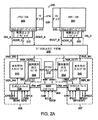
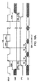
204 メモリバンクB
205 インターフェース回路
206 アドレスおよびデータパス交換回路
207 インターフェース回路
208 制御インターフェース
210 ステータス/IDレジスタ回路
212 SAおよびページバッファ回路ブロック
214 行デコーダ
216 制御およびプリデコーダ
218 SAおよびページバッファ
220 行デコーダ
222 制御およびプリデコーダ
230 シリアルデータリンク
232 直列並列入力レジスタブロック
234 並列直列出力レジスタブロック
236 シリアルデータリンク
238 並列直列出力レジスタブロック
240 直列並列入力レジスタブロック
Claims (32)
- メモリと、
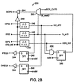
入力データをデータ入力ポートで受信するように、およびデータをデータ出力ポートに転送するように構成されたデータリンクインターフェースと、
前記メモリデバイスが前記データを前記データ出力ポートに転送できるようにするために使用される、第1の出力イネーブル信号を受信するための第1の制御入力ポートと、
前記メモリデバイスが前記入力データを受信できるようにするために使用される、第1の入力イネーブル信号を受信するための第2の制御入力ポートと、
第2の出力イネーブル信号を出力するための第1の制御出力ポートと、
第2の入力イネーブル信号を出力するための第2の制御出力ポートと、
前記データ出力ポート上でのデータ転送を制御する前記第1の出力イネーブル信号に応答する制御回路と
を備える、半導体メモリデバイス。 - 前記第2の出力イネーブル信号が、遅延した前記第1の出力イネーブル信号である、請求項1に記載の半導体メモリデバイス。
- 前記データリンクインターフェースがシリアルデータリンクインターフェースであり、前記入力データがシリアル入力データであり、さらに前記データリンクインターフェースが、シリアル入力データをパラレルデータに変換するように、および前記データを前記メモリに転送するように構成された、請求項1に記載の半導体メモリデバイス。
- 前記メモリ、前記データリンクインターフェース、および前記制御回路が、片面パッドアーキテクチャを有する単一パッケージ内に配置される、請求項1から3のいずれか一項に記載の半導体メモリデバイス。
- さらに前記制御回路が、前記出力ポート上での前記データ転送が完了するまで出力イネーブル信号が引き続きアクティブであることを要求するように構成される、請求項1から3のいずれか一項に記載の半導体メモリデバイス。
- クロック信号を受信するためのクロック入力ポートをさらに備える、
請求項1から3のいずれか一項に記載の半導体メモリデバイス。 - 前記第1の制御入力ポート、前記第2の制御入力ポート、前記制御出力ポート、前記データ入力ポート、および前記データ出力ポートが、前記クロック信号と同期するように構成される、請求項6に記載の半導体メモリデバイス。
- 前記制御回路が、ターゲットデバイスアドレスおよびコマンド命令が受信されるまで、入力イネーブル信号が引き続きアクティブであることを要求するように構成される、請求項1から3のいずれか一項に記載の半導体メモリデバイス。
- さらに前記制御回路が、選択された一つ以上の行アドレスおよび列アドレスが受信されるまで、入力イネーブル信号が引き続きアクティブであることを要求するように構成される、請求項8に記載の半導体メモリデバイス。
- 命令をデータ入力ポートで受信するステップと、
前記メモリデバイスが前記命令を受信できるようにするために使用される、第1の入力イネーブル信号を第1の制御入力ポートで受信するステップと、
制御出力ポートから第2の入力イネーブル信号を出力するステップと、
出力イネーブル信号を第2の制御入力ポートで受信するステップと、
前記出力イネーブル信号に基づいて、出力データの出力を実行可能にするステップと、
データリンクインターフェースから出力データストリームを送信するステップと
を含む、半導体メモリデバイスにおいてデータリンクインターフェースからのデータ転送を制御する方法。 - 前記データリンクインターフェースがシリアルデータリンクインターフェースであり、前記出力データストリームがシリアル出力データストリームであり、前記方法が、
前記メモリデバイスのメモリと前記シリアルデータリンクインターフェースとの間でパラレルデータを転送するステップと、
前記シリアル出力データストリームを前記シリアルデータリンクインターフェースから送信するステップに先立って、前記パラレルデータをシリアル出力データに変換するステップと
をさらに含む、請求項10に記載の方法。 - i) 入力データを受信するためのデータ入力ポートと、ii) 出力データを出力するためのデータ出力ポートと、iii) 外部ソースデバイスから第1の出力イネーブル信号を受信するための第1の制御入力ポートと、iv) 前記メモリデバイスが前記入力データを受信できるようにするために使用される第1の入力イネーブル信号を受信するための第2の制御入力ポートと、v) 第2の出力イネーブル信号を出力するための第1の制御出力ポートと、vi) 第2の入力イネーブル信号を出力するための第2の制御出力ポートと、を有する第1のフラッシュメモリデバイスと、
前記第1のフラッシュメモリデバイスに直列に接続されているとともに、データ入力ポートを有し、前記出力データを前記第1のフラッシュメモリデバイスから受信するように構成されている第2のフラッシュメモリデバイスと
を備え、
前記第1のフラッシュメモリデバイスが、出力データを前記第1の出力イネーブル信号に基づいて出力するように構成されている、フラッシュメモリシステム。 - 前記第2のフラッシュメモリデバイスが、出力データを出力するように構成されたデータ出力ポートと、前記第1のフラッシュメモリデバイスの前記第1の制御出力ポートから前記第2の出力イネーブル信号を受信するように構成された制御入力ポートとをさらに含む、請求項12に記載のフラッシュメモリシステム。
- 前記データリンクインターフェースがシリアルデータリンクインターフェースであり、前記データ入力ポートがシリアルデータ入力ポートであり、前記データ出力ポートがシリアルデータ出力ポートである、請求項1または2に記載の半導体メモリデバイス。
- 前記入力データとの同期をとるためのクロック信号を受信するためのクロック入力ポートと、
その他との同期をとるための出力クロック信号を出力するためのクロック入力ポートと
をさらに備える、請求項1から3のいずれか一項に記載の半導体メモリデバイス。 - 前記入力クロック信号と前記出力クロック信号との間のいかなる位相差にも同期するロックループをさらに備える、請求項15に記載の半導体メモリデバイス。
- 前記入力クロック信号と前記出力クロック信号との間のいかなる位相差にも同期する位相ロックループをさらに備える、請求項15に記載の半導体メモリデバイス。
- 前記メモリはフラッシュメモリである、請求項1から3のいずれか一項に記載の半導体メモリデバイス。
- 前記第2の出力イネーブル信号は、前記第1の出力イネーブル信号から得られる、請求項1または3に記載の半導体メモリデバイス。
- 前記受信された命令との同期をとるための入力クロック信号を受信するステップと、
その他との同期をとるための出力クロック信号を出力するステップと
をさらに含む、請求項10または11に記載の方法。 - 前記半導体メモリデバイスは、ダブルデータレート動作で前記入力クロック信号を使用する、請求項20に記載の方法。
- 前記外部ソースデバイスは、メモリコントローラである、請求項12または13に記載のフラッシュメモリシステム。
- 前記第2の出力イネーブル信号は、前記第1の出力イネーブル信号から得られる、請求項12または13に記載のフラッシュメモリシステム。
- フラッシュメモリと、
クロック信号を受信するように構成されたクロック入力と、
入力データおよびコマンドデータを異なる時間で受信するように構成されたコモン・コマンドおよびデータ入力と、
2つのイネーブル信号における第1信号を受信するように構成された第1の制御入力と、
前記2つのイネーブル信号における第2信号を受信するように構成された第2の制御入力と、
前記コマンドデータに対応してフラッシュメモリ上で動作を実行するように構成されたコア回路と、
ラッチ回路と
を備え、
前記ラッチ回路は、
前記2つのイネーブル信号における前記第1信号が少なくとも所定時間だけアクティブ論理レベルで保持されている間、前記コマンドデータをラッチするとともに、前記コマンドデータが前記コモン・コマンドおよびデータ入力で受信され、前記クロック信号の立ち上がりおよび立ち下がりエッジに同期して前記入力データをラッチするように構成されている、メモリデバイス。 - 前記2つのイネーブル信号における前記第1信号が少なくとも所定時間だけアクティブ論理レベルで保持されているときのみ、前記コマンドデータが前記コモン・コマンドおよびデータ入力で受信される、請求項24に記載のメモリデバイス。
- 前記2つのイネーブル信号における前記第1信号は、入力ポートイネーブル信号である、請求項24に記載のメモリデバイス。
- 前記2つのイネーブル信号における前記第2信号は、出力ポートイネーブル信号である、請求項24に記載のメモリデバイス。
- 前記動作は、消去動作である、請求項24に記載のメモリデバイス。
- 前記動作は、プログラム動作である、請求項24に記載のメモリデバイス。
- 前記コモン・コマンドおよびデータ入力は、シリアル入力である、請求項24に記載のメモリデバイス。
- 非アクティブ状態からアクティブ状態への前記2つのイネーブル信号における前記第1信号の遷移は、前記コマンドデータが前記コモン・コマンドおよびデータ入力で受信されることの開始を示す、請求項24に記載のメモリデバイス。
- コントローラと、
請求項24に記載のメモリデバイスと
を備え、
前記メモリデバイスは、前記コントローラと通信可能に結合されている、システム。
Applications Claiming Priority (7)
| Application Number | Priority Date | Filing Date | Title |
|---|---|---|---|
| US72236805P | 2005-09-30 | 2005-09-30 | |
| US60/722,368 | 2005-09-30 | ||
| US11/324,023 | 2005-12-30 | ||
| US11/324,023 US7652922B2 (en) | 2005-09-30 | 2005-12-30 | Multiple independent serial link memory |
| US84779006P | 2006-09-27 | 2006-09-27 | |
| US60/847,790 | 2006-09-27 | ||
| PCT/CA2006/001609 WO2007036050A1 (en) | 2005-09-30 | 2006-09-29 | Memory with output control |
Publications (3)
| Publication Number | Publication Date |
|---|---|
| JP2009510657A JP2009510657A (ja) | 2009-03-12 |
| JP2009510657A5 JP2009510657A5 (ja) | 2009-06-04 |
| JP5193045B2 true JP5193045B2 (ja) | 2013-05-08 |
Family
ID=37899332
Family Applications (1)
| Application Number | Title | Priority Date | Filing Date |
|---|---|---|---|
| JP2008532552A Expired - Fee Related JP5193045B2 (ja) | 2005-09-30 | 2006-09-29 | 出力制御部を備えたメモリ |
Country Status (6)
| Country | Link |
|---|---|
| US (14) | US7515471B2 (ja) |
| EP (1) | EP1932158A4 (ja) |
| JP (1) | JP5193045B2 (ja) |
| KR (2) | KR101260632B1 (ja) |
| TW (2) | TWI446356B (ja) |
| WO (1) | WO2007036050A1 (ja) |
Families Citing this family (95)
| Publication number | Priority date | Publication date | Assignee | Title |
|---|---|---|---|---|
| US9010645B2 (en) | 2003-06-13 | 2015-04-21 | Michael Arnouse | Portable computing system and portable computer for use with same |
| KR100697270B1 (ko) * | 2004-12-10 | 2007-03-21 | 삼성전자주식회사 | 저전력 멀티칩 반도체 메모리 장치 및 그것의 칩 인에이블방법 |
| US7652922B2 (en) | 2005-09-30 | 2010-01-26 | Mosaid Technologies Incorporated | Multiple independent serial link memory |
| US11948629B2 (en) | 2005-09-30 | 2024-04-02 | Mosaid Technologies Incorporated | Non-volatile memory device with concurrent bank operations |
| TWI446356B (zh) * | 2005-09-30 | 2014-07-21 | Mosaid Technologies Inc | 具有輸出控制之記憶體及其系統 |
| US20070076502A1 (en) * | 2005-09-30 | 2007-04-05 | Pyeon Hong B | Daisy chain cascading devices |
| JP2007172332A (ja) * | 2005-12-22 | 2007-07-05 | Sanyo Electric Co Ltd | メモリ制御回路及びメモリ制御方法 |
| JP2007172333A (ja) * | 2005-12-22 | 2007-07-05 | Sanyo Electric Co Ltd | バスアドレス選択回路およびバスアドレス選択方法 |
| US7904639B2 (en) | 2006-08-22 | 2011-03-08 | Mosaid Technologies Incorporated | Modular command structure for memory and memory system |
| US7817470B2 (en) | 2006-11-27 | 2010-10-19 | Mosaid Technologies Incorporated | Non-volatile memory serial core architecture |
| US7613049B2 (en) * | 2007-01-08 | 2009-11-03 | Macronix International Co., Ltd | Method and system for a serial peripheral interface |
| US8122202B2 (en) | 2007-02-16 | 2012-02-21 | Peter Gillingham | Reduced pin count interface |
| US8086785B2 (en) | 2007-02-22 | 2011-12-27 | Mosaid Technologies Incorporated | System and method of page buffer operation for memory devices |
| WO2008101316A1 (en) | 2007-02-22 | 2008-08-28 | Mosaid Technologies Incorporated | Apparatus and method for using a page buffer of a memory device as a temporary cache |
| US7688652B2 (en) * | 2007-07-18 | 2010-03-30 | Mosaid Technologies Incorporated | Storage of data in memory via packet strobing |
| US7889578B2 (en) | 2007-10-17 | 2011-02-15 | Mosaid Technologies Incorporated | Single-strobe operation of memory devices |
| US8825939B2 (en) * | 2007-12-12 | 2014-09-02 | Conversant Intellectual Property Management Inc. | Semiconductor memory device suitable for interconnection in a ring topology |
| US8145925B2 (en) * | 2007-12-21 | 2012-03-27 | Mosaid Technologies Incorporated | Non-volatile semiconductor memory device with power saving feature |
| US7660177B2 (en) * | 2007-12-21 | 2010-02-09 | Silicon Storage Technology, Inc. | Non-volatile memory device having high speed serial interface |
| US8291248B2 (en) | 2007-12-21 | 2012-10-16 | Mosaid Technologies Incorporated | Non-volatile semiconductor memory device with power saving feature |
| USRE49124E1 (en) | 2008-02-13 | 2022-07-05 | Arnouse Digital Devices Corp. | Mobile data center |
| US11113228B2 (en) | 2008-02-13 | 2021-09-07 | Arnouse Digital Devices Corporation | Portable computing system and portable computer for use with same |
| US10235323B2 (en) | 2008-02-13 | 2019-03-19 | Michael Arnouse | Portable computing system and portable computer for use with same |
| JP5562329B2 (ja) * | 2008-07-01 | 2014-07-30 | エルエスアイ コーポレーション | フラッシュ・メモリ・コントローラとフラッシュ・メモリ・アレイの間でインタフェースをとるための方法および装置 |
| US8139390B2 (en) * | 2008-07-08 | 2012-03-20 | Mosaid Technologies Incorporated | Mixed data rates in memory devices and systems |
| US8161313B2 (en) * | 2008-09-30 | 2012-04-17 | Mosaid Technologies Incorporated | Serial-connected memory system with duty cycle correction |
| US8181056B2 (en) * | 2008-09-30 | 2012-05-15 | Mosaid Technologies Incorporated | Serial-connected memory system with output delay adjustment |
| EP2329496A4 (en) | 2008-09-30 | 2012-06-13 | Mosaid Technologies Inc | SERIAL SWITCHED STORAGE SYSTEM WITH OUTPUT DELAY SETTING |
| US8134852B2 (en) | 2008-10-14 | 2012-03-13 | Mosaid Technologies Incorporated | Bridge device architecture for connecting discrete memory devices to a system |
| US7957173B2 (en) | 2008-10-14 | 2011-06-07 | Mosaid Technologies Incorporated | Composite memory having a bridging device for connecting discrete memory devices to a system |
| US8549209B2 (en) | 2008-11-04 | 2013-10-01 | Mosaid Technologies Incorporated | Bridging device having a configurable virtual page size |
| US20100115172A1 (en) * | 2008-11-04 | 2010-05-06 | Mosaid Technologies Incorporated | Bridge device having a virtual page buffer |
| KR101014149B1 (ko) * | 2008-11-13 | 2011-02-14 | (주)인디링스 | 메모리 뱅크로의 접근을 제어하는 고체 상태 디스크를 위한컨트롤러 |
| US8825940B1 (en) | 2008-12-02 | 2014-09-02 | Siliconsystems, Inc. | Architecture for optimizing execution of storage access commands |
| US8880970B2 (en) * | 2008-12-23 | 2014-11-04 | Conversant Intellectual Property Management Inc. | Error detection method and a system including one or more memory devices |
| US9176859B2 (en) * | 2009-01-07 | 2015-11-03 | Siliconsystems, Inc. | Systems and methods for improving the performance of non-volatile memory operations |
| US10079048B2 (en) * | 2009-03-24 | 2018-09-18 | Western Digital Technologies, Inc. | Adjusting access of non-volatile semiconductor memory based on access time |
| JP5564197B2 (ja) * | 2009-04-23 | 2014-07-30 | 株式会社メガチップス | メモリ制御装置、半導体メモリ装置、メモリシステム及びメモリ制御方法 |
| EP2425238B1 (en) * | 2009-05-01 | 2018-10-17 | Analog Devices, Inc. | An addressable integrated circuit and method thereof |
| JP2010262698A (ja) * | 2009-05-07 | 2010-11-18 | Sanyo Electric Co Ltd | 不揮発性半導体記憶装置 |
| WO2011000082A1 (en) | 2009-06-29 | 2011-01-06 | Mosaid Technologies Incorporated | A bridging device having a frequency configurable clock domain |
| US8521980B2 (en) | 2009-07-16 | 2013-08-27 | Mosaid Technologies Incorporated | Simultaneous read and write data transfer |
| WO2011080784A1 (en) | 2009-12-31 | 2011-07-07 | Ferdinando Bedeschi | Methods for a phase-change memory array |
| US8582382B2 (en) * | 2010-03-23 | 2013-11-12 | Mosaid Technologies Incorporated | Memory system having a plurality of serially connected devices |
| US9009423B2 (en) * | 2010-04-26 | 2015-04-14 | Novachips Canada Inc. | Serially connected memory having subdivided data interface |
| US8843692B2 (en) | 2010-04-27 | 2014-09-23 | Conversant Intellectual Property Management Inc. | System of interconnected nonvolatile memories having automatic status packet |
| KR20130071436A (ko) * | 2010-05-07 | 2013-06-28 | 모사이드 테크놀로지스 인코퍼레이티드 | 단일 버퍼를 사용하여 복수의 메모리 장치를 동시에 판독하는 방법 및 장치 |
| US8463959B2 (en) * | 2010-05-31 | 2013-06-11 | Mosaid Technologies Incorporated | High-speed interface for daisy-chained devices |
| US8441873B2 (en) * | 2010-08-31 | 2013-05-14 | Terry Grunzke | Memory devices and methods of operating memory |
| US8386887B2 (en) * | 2010-09-24 | 2013-02-26 | Texas Memory Systems, Inc. | High-speed memory system |
| JP5323170B2 (ja) * | 2011-12-05 | 2013-10-23 | ウィンボンド エレクトロニクス コーポレーション | 不揮発性半導体メモリおよびそのデータの読出し方法 |
| US8825967B2 (en) | 2011-12-08 | 2014-09-02 | Conversant Intellectual Property Management Inc. | Independent write and read control in serially-connected devices |
| US8797799B2 (en) * | 2012-01-05 | 2014-08-05 | Conversant Intellectual Property Management Inc. | Device selection schemes in multi chip package NAND flash memory system |
| US10101769B2 (en) | 2012-04-10 | 2018-10-16 | Michael Arnouse | Mobile data center |
| US9336112B2 (en) * | 2012-06-19 | 2016-05-10 | Apple Inc. | Parallel status polling of multiple memory devices |
| CN103514067A (zh) * | 2012-06-28 | 2014-01-15 | 鸿富锦精密工业(深圳)有限公司 | 内存条 |
| US9471484B2 (en) | 2012-09-19 | 2016-10-18 | Novachips Canada Inc. | Flash memory controller having dual mode pin-out |
| KR20150106399A (ko) | 2012-11-09 | 2015-09-21 | 노바칩스 캐나다 인크. | 데이지 체인형 메모리 시스템에서 pll 락킹 제어를 위한 방법 및 장치 |
| CN103049408B (zh) * | 2012-12-28 | 2015-06-17 | 苏州国芯科技有限公司 | 一种多接口sram读写控制电路及方法 |
| JP2015197859A (ja) * | 2014-04-02 | 2015-11-09 | 株式会社東芝 | メモリコントローラ、半導体記憶装置、およびメモリコントローラの制御方法 |
| US9691452B2 (en) | 2014-08-15 | 2017-06-27 | Micron Technology, Inc. | Apparatuses and methods for concurrently accessing different memory planes of a memory |
| KR20160117087A (ko) * | 2015-03-31 | 2016-10-10 | 에스케이하이닉스 주식회사 | 반도체장치 |
| US10013389B2 (en) | 2015-06-09 | 2018-07-03 | Avago Technologies General Ip (Singapore) Pte. Ltd. | Automatic cascaded address selection |
| US11120884B2 (en) | 2015-09-30 | 2021-09-14 | Sunrise Memory Corporation | Implementing logic function and generating analog signals using NOR memory strings |
| US9842651B2 (en) | 2015-11-25 | 2017-12-12 | Sunrise Memory Corporation | Three-dimensional vertical NOR flash thin film transistor strings |
| US9892800B2 (en) | 2015-09-30 | 2018-02-13 | Sunrise Memory Corporation | Multi-gate NOR flash thin-film transistor strings arranged in stacked horizontal active strips with vertical control gates |
| US10162558B2 (en) | 2015-10-30 | 2018-12-25 | Micron Technology, Inc. | Data transfer techniques for multiple devices on a shared bus |
| US10719237B2 (en) * | 2016-01-11 | 2020-07-21 | Micron Technology, Inc. | Apparatuses and methods for concurrently accessing multiple partitions of a non-volatile memory |
| US9812180B2 (en) * | 2016-01-18 | 2017-11-07 | Hare Krishna Verma | Programmable logic accelerator in system on chip |
| KR20170089069A (ko) * | 2016-01-25 | 2017-08-03 | 에스케이하이닉스 주식회사 | 메모리 시스템 및 그의 동작방법 |
| US10620879B2 (en) * | 2017-05-17 | 2020-04-14 | Macronix International Co., Ltd. | Write-while-read access method for a memory device |
| EP3642841A4 (en) | 2017-06-20 | 2021-07-28 | Sunrise Memory Corporation | 3-DIMENSIONAL NOR MEMORY ARCHITECTURE AND MANUFACTURING PROCESS FOR IT |
| US10692874B2 (en) | 2017-06-20 | 2020-06-23 | Sunrise Memory Corporation | 3-dimensional NOR string arrays in segmented stacks |
| US10608008B2 (en) | 2017-06-20 | 2020-03-31 | Sunrise Memory Corporation | 3-dimensional nor strings with segmented shared source regions |
| JP2019057336A (ja) * | 2017-09-19 | 2019-04-11 | 株式会社東芝 | 半導体集積回路 |
| KR20190040598A (ko) * | 2017-10-11 | 2019-04-19 | 에스케이하이닉스 주식회사 | 컨트롤러 및 컨트롤러의 동작방법 |
| DE102017125156A1 (de) * | 2017-10-26 | 2019-05-02 | Infineon Technologies Ag | Vorrichtung und Verfahren zum Verarbeiten von Radarsignalen |
| US10438656B2 (en) * | 2017-12-18 | 2019-10-08 | Intel Corporation | System and method for performing a concurrent multiple page read of a memory array |
| JP7223503B2 (ja) * | 2018-02-28 | 2023-02-16 | ラピスセミコンダクタ株式会社 | シリアルインタフェース回路、半導体装置、及びシリアルパラレル変換方法 |
| JP2019215662A (ja) * | 2018-06-12 | 2019-12-19 | 株式会社日立製作所 | 不揮発性メモリデバイス、及びインターフェース設定方法 |
| TWI713195B (zh) | 2018-09-24 | 2020-12-11 | 美商森恩萊斯記憶體公司 | 三維nor記憶電路製程中之晶圓接合及其形成之積體電路 |
| CN113383415A (zh) | 2019-01-30 | 2021-09-10 | 日升存储公司 | 使用晶片键合的具有嵌入式高带宽、高容量存储器的设备 |
| KR20200098009A (ko) | 2019-02-11 | 2020-08-20 | 삼성전자주식회사 | 비휘발성 메모리 장치 및 그 동작 방법 |
| US11515309B2 (en) | 2019-12-19 | 2022-11-29 | Sunrise Memory Corporation | Process for preparing a channel region of a thin-film transistor in a 3-dimensional thin-film transistor array |
| US11675500B2 (en) | 2020-02-07 | 2023-06-13 | Sunrise Memory Corporation | High capacity memory circuit with low effective latency |
| WO2021173209A1 (en) * | 2020-02-24 | 2021-09-02 | Sunrise Memory Corporation | High capacity memory module including wafer-section memory circuit |
| CN115497526A (zh) * | 2020-08-27 | 2022-12-20 | 长江存储科技有限责任公司 | Nand闪存设备中的非破坏性模式高速缓存编程 |
| US11894075B2 (en) | 2020-08-27 | 2024-02-06 | Yangtze Memory Technologies Co. Ltd. | Non-destructive mode cache programming in NAND flash memory devices |
| US11626149B2 (en) * | 2020-09-15 | 2023-04-11 | Integrated Silicon Solution, (Cayman) Inc. | SPI NOR memory with optimized read and program operation |
| WO2022108848A1 (en) | 2020-11-17 | 2022-05-27 | Sunrise Memory Corporation | Methods for reducing disturb errors by refreshing data alongside programming or erase operations |
| TWI749888B (zh) * | 2020-11-20 | 2021-12-11 | 智原科技股份有限公司 | 雙倍資料率記憶體系統及相關的閘信號控制電路 |
| KR20220077400A (ko) | 2020-12-02 | 2022-06-09 | 삼성전자주식회사 | 메모리 장치, 메모리 시스템 및 이의 동작 방법 |
| US11848056B2 (en) | 2020-12-08 | 2023-12-19 | Sunrise Memory Corporation | Quasi-volatile memory with enhanced sense amplifier operation |
| TW202310429A (zh) | 2021-07-16 | 2023-03-01 | 美商日升存儲公司 | 薄膜鐵電電晶體的三維記憶體串陣列 |
| US11757610B1 (en) * | 2022-04-18 | 2023-09-12 | Nxp B.V. | Low phase noise clock recovery over a data connection |
Family Cites Families (308)
| Publication number | Priority date | Publication date | Assignee | Title |
|---|---|---|---|---|
| US3249270A (en) | 1965-05-03 | 1966-05-03 | Mister Hanger Inc | Garment support means |
| US4174536A (en) * | 1977-01-21 | 1979-11-13 | Massachusetts Institute Of Technology | Digital communications controller with firmware control |
| JPS58169383A (ja) * | 1982-03-30 | 1983-10-05 | Fujitsu Ltd | 半導体記憶装置 |
| US4617566A (en) * | 1983-12-15 | 1986-10-14 | Teleplex Corporation | Addressable-port, daisy chain telemetry system with self-test capability |
| JPS60193193A (ja) * | 1984-03-13 | 1985-10-01 | Toshiba Corp | メモリlsi |
| EP0179605B1 (en) | 1984-10-17 | 1992-08-19 | Fujitsu Limited | Semiconductor memory device having a serial data input circuit and a serial data output circuit |
| US4683555A (en) * | 1985-01-22 | 1987-07-28 | Texas Instruments Incorporated | Serial accessed semiconductor memory with reconfigureable shift registers |
| US4714536A (en) | 1985-08-26 | 1987-12-22 | Varian Associates, Inc. | Planar magnetron sputtering device with combined circumferential and radial movement of magnetic fields |
| US4730308A (en) | 1985-10-04 | 1988-03-08 | International Business Machines Corporation | Interface between a computer bus and a serial packet link |
| JPS6289149A (ja) | 1985-10-15 | 1987-04-23 | Agency Of Ind Science & Technol | 多ポ−トメモリシステム |
| JPS62152050A (ja) * | 1985-12-26 | 1987-07-07 | Nec Corp | 半導体メモリ |
| JP2728395B2 (ja) * | 1986-09-26 | 1998-03-18 | 株式会社日立製作所 | 半導体記憶装置 |
| JPS63113624A (ja) * | 1986-10-30 | 1988-05-18 | Tokyo Electric Co Ltd | 電子秤のプリンタインタ−フエ−ス |
| JP2764908B2 (ja) | 1988-02-04 | 1998-06-11 | 日本電気株式会社 | カスケード・バッファ回路 |
| US5136292A (en) | 1989-03-15 | 1992-08-04 | Oki Electric Industry Co., Ltd. | Serial data receiving circuit for serial to parallel conversion |
| DE69033262T2 (de) | 1989-04-13 | 2000-02-24 | Sandisk Corp | EEPROM-Karte mit Austauch von fehlerhaften Speicherzellen und Zwischenspeicher |
| JPH02282989A (ja) | 1989-04-25 | 1990-11-20 | Sony Corp | メモリ制御回路 |
| US5126808A (en) * | 1989-10-23 | 1992-06-30 | Advanced Micro Devices, Inc. | Flash EEPROM array with paged erase architecture |
| US5175819A (en) | 1990-03-28 | 1992-12-29 | Integrated Device Technology, Inc. | Cascadable parallel to serial converter using tap shift registers and data shift registers while receiving input data from FIFO buffer |
| IL96808A (en) | 1990-04-18 | 1996-03-31 | Rambus Inc | Introductory / Origin Circuit Agreed Using High-Performance Brokerage |
| US5243703A (en) | 1990-04-18 | 1993-09-07 | Rambus, Inc. | Apparatus for synchronously generating clock signals in a data processing system |
| US5204669A (en) * | 1990-08-30 | 1993-04-20 | Datacard Corporation | Automatic station identification where function modules automatically initialize |
| US5319598A (en) * | 1990-12-10 | 1994-06-07 | Hughes Aircraft Company | Nonvolatile serially programmable devices |
| US5132635A (en) * | 1991-03-05 | 1992-07-21 | Ast Research, Inc. | Serial testing of removable circuit boards on a backplane bus |
| US5249270A (en) | 1991-03-29 | 1993-09-28 | Echelon Corporation | Development system protocol |
| US5663901A (en) | 1991-04-11 | 1997-09-02 | Sandisk Corporation | Computer memory cards using flash EEPROM integrated circuit chips and memory-controller systems |
| JPH0776942B2 (ja) | 1991-04-22 | 1995-08-16 | インターナショナル・ビジネス・マシーンズ・コーポレイション | マルチプロセッサ・システムおよびそのデータ伝送装置 |
| US5237218A (en) * | 1991-05-03 | 1993-08-17 | Lattice Semiconductor Corporation | Structure and method for multiplexing pins for in-system programming |
| JP3001679B2 (ja) | 1991-07-19 | 2000-01-24 | 出光興産株式会社 | 2サイクルエンジンまたはロータリーエンジン用潤滑油組成物 |
| US5430859A (en) * | 1991-07-26 | 1995-07-04 | Sundisk Corporation | Solid state memory system including plural memory chips and a serialized bus |
| US6230233B1 (en) * | 1991-09-13 | 2001-05-08 | Sandisk Corporation | Wear leveling techniques for flash EEPROM systems |
| US5361227A (en) | 1991-12-19 | 1994-11-01 | Kabushiki Kaisha Toshiba | Non-volatile semiconductor memory device and memory system using the same |
| KR950000761B1 (ko) | 1992-01-15 | 1995-01-28 | 삼성전자 주식회사 | 직렬 입력신호의 동기회로 |
| JPH05210981A (ja) * | 1992-01-30 | 1993-08-20 | Nec Ic Microcomput Syst Ltd | 半導体記憶装置 |
| US5313096A (en) | 1992-03-16 | 1994-05-17 | Dense-Pac Microsystems, Inc. | IC chip package having chip attached to and wire bonded within an overlying substrate |
| JP3088180B2 (ja) | 1992-03-26 | 2000-09-18 | 日本電気アイシーマイコンシステム株式会社 | シリアル入力インタフェース回路 |
| US5592415A (en) | 1992-07-06 | 1997-01-07 | Hitachi, Ltd. | Non-volatile semiconductor memory |
| KR950012019B1 (ko) * | 1992-10-02 | 1995-10-13 | 삼성전자주식회사 | 반도체메모리장치의 데이타출력버퍼 |
| JP3400824B2 (ja) * | 1992-11-06 | 2003-04-28 | 三菱電機株式会社 | 半導体記憶装置 |
| KR960000616B1 (ko) | 1993-01-13 | 1996-01-10 | 삼성전자주식회사 | 불휘발성 반도체 메모리 장치 |
| US5343437A (en) | 1993-02-19 | 1994-08-30 | Motorola Inc. | Memory having nonvolatile and volatile memory banks |
| JPH06275069A (ja) | 1993-03-20 | 1994-09-30 | Hitachi Ltd | シリアルメモリ |
| US5519847A (en) | 1993-06-30 | 1996-05-21 | Intel Corporation | Method of pipelining sequential writes in a flash memory |
| US5509134A (en) | 1993-06-30 | 1996-04-16 | Intel Corporation | Method and apparatus for execution of operations in a flash memory array |
| US5365484A (en) * | 1993-08-23 | 1994-11-15 | Advanced Micro Devices, Inc. | Independent array grounds for flash EEPROM array with paged erase architechture |
| JPH0793219A (ja) | 1993-09-20 | 1995-04-07 | Olympus Optical Co Ltd | 情報処理装置 |
| US5602780A (en) | 1993-10-20 | 1997-02-11 | Texas Instruments Incorporated | Serial to parallel and parallel to serial architecture for a RAM based FIFO memory |
| SG49632A1 (en) | 1993-10-26 | 1998-06-15 | Intel Corp | Programmable code store circuitry for a nonvolatile semiconductor memory device |
| US5452259A (en) | 1993-11-15 | 1995-09-19 | Micron Technology Inc. | Multiport memory with pipelined serial input |
| US5404460A (en) * | 1994-01-28 | 1995-04-04 | Vlsi Technology, Inc. | Method for configuring multiple identical serial I/O devices to unique addresses through a serial bus |
| US5475854A (en) * | 1994-01-28 | 1995-12-12 | Vlsi Technology, Inc. | Serial bus I/O system and method for serializing interrupt requests and DMA requests in a computer system |
| US5596724A (en) | 1994-02-04 | 1997-01-21 | Advanced Micro Devices | Input/output data port with a parallel and serial interface |
| JPH07254292A (ja) | 1994-03-15 | 1995-10-03 | Mitsubishi Electric Corp | 不揮発性メモリおよびこの不揮発性メモリを用いたマイクロコンピュータ |
| JPH07254342A (ja) * | 1994-03-15 | 1995-10-03 | Fuji Electric Co Ltd | 熱動形過負荷継電器 |
| US5666557A (en) | 1994-06-16 | 1997-09-09 | Cassidy; Bruce Michael | Method and apparatus for automatically assigning device identifiers on a parallel data bus |
| DE4429433C1 (de) * | 1994-08-19 | 1995-10-26 | Siemens Ag | Adreßzuordnungsverfahren |
| US5473566A (en) * | 1994-09-12 | 1995-12-05 | Cirrus Logic, Inc. | Memory architecture and devices, systems and methods utilizing the same |
| KR0142367B1 (ko) * | 1995-02-04 | 1998-07-15 | 김광호 | 열 리던던씨를 가지는 불휘발성 반도체 메모리의 소거 검증회로 |
| US5636342A (en) * | 1995-02-17 | 1997-06-03 | Dell Usa, L.P. | Systems and method for assigning unique addresses to agents on a system management bus |
| JP3150864B2 (ja) | 1995-02-27 | 2001-03-26 | 三菱電機株式会社 | Atm通信ネットワークシステム及びatm通信装置 |
| US5878240A (en) | 1995-05-11 | 1999-03-02 | Lucent Technologies, Inc. | System and method for providing high speed memory access in a multiprocessor, multimemory environment |
| US5729683A (en) * | 1995-05-18 | 1998-03-17 | Compaq Computer Corporation | Programming memory devices through the parallel port of a computer system |
| JPH0922393A (ja) * | 1995-07-06 | 1997-01-21 | Mitsubishi Electric Corp | 通信機能を有するワンチップフラッシュメモリ装置 |
| US5598374A (en) | 1995-07-14 | 1997-01-28 | Cirrus Logic, Inc. | Pipeland address memories, and systems and methods using the same |
| US5594694A (en) * | 1995-07-28 | 1997-01-14 | Micron Quantum Devices, Inc. | Memory circuit with switch for selectively connecting an input/output pad directly to a nonvolatile memory cell |
| US6728851B1 (en) * | 1995-07-31 | 2004-04-27 | Lexar Media, Inc. | Increasing the memory performance of flash memory devices by writing sectors simultaneously to multiple flash memory devices |
| US5845313A (en) | 1995-07-31 | 1998-12-01 | Lexar | Direct logical block addressing flash memory mass storage architecture |
| JP2817672B2 (ja) * | 1995-08-11 | 1998-10-30 | 日本電気株式会社 | 半導体メモリ |
| US5742840A (en) * | 1995-08-16 | 1998-04-21 | Microunity Systems Engineering, Inc. | General purpose, multiple precision parallel operation, programmable media processor |
| US5812796A (en) | 1995-08-18 | 1998-09-22 | General Magic, Inc. | Support structures for an intelligent low power serial bus |
| KR0164395B1 (ko) * | 1995-09-11 | 1999-02-18 | 김광호 | 반도체 메모리 장치와 그 리이드 및 라이트 방법 |
| US5835935A (en) * | 1995-09-13 | 1998-11-10 | Lexar Media, Inc. | Method of and architecture for controlling system data with automatic wear leveling in a semiconductor non-volatile mass storage memory |
| JPH0991197A (ja) * | 1995-09-22 | 1997-04-04 | Sharp Corp | データ転送制御装置 |
| JPH09115286A (ja) | 1995-10-17 | 1997-05-02 | Hitachi Ltd | マルチポートメモリ |
| JP3693721B2 (ja) * | 1995-11-10 | 2005-09-07 | Necエレクトロニクス株式会社 | フラッシュメモリ内蔵マイクロコンピュータ及びそのテスト方法 |
| TW307869B (en) | 1995-12-20 | 1997-06-11 | Toshiba Co Ltd | Semiconductor memory |
| KR100197563B1 (ko) | 1995-12-27 | 1999-06-15 | 윤종용 | 동기 지연라인을 이용한 디지탈 지연 동기루프 회로 |
| KR100211760B1 (ko) | 1995-12-28 | 1999-08-02 | 윤종용 | 멀티뱅크 구조를 갖는 반도체 메모리 장치의 데이타 입출력 경로 제어회로 |
| KR0170723B1 (ko) | 1995-12-29 | 1999-03-30 | 김광호 | 단일 ras 신호에 의해 동시 동작이 가능한 이중 뱅크를 갖는 반도체 메모리 장치 |
| US5828899A (en) * | 1996-01-04 | 1998-10-27 | Compaq Computer Corporation | System for peripheral devices recursively generating unique addresses based on the number of devices connected dependent upon the relative position to the port |
| KR100359414B1 (ko) | 1996-01-25 | 2003-01-24 | 동경 엘렉트론 디바이스 주식회사 | 데이타독출/기록방법및그를이용한메모리제어장치및시스템 |
| US6282505B1 (en) | 1996-02-16 | 2001-08-28 | Hitachi, Ltd. | Multi-port memory and a data processor accessing the same |
| US7166495B2 (en) | 1996-02-20 | 2007-01-23 | Micron Technology, Inc. | Method of fabricating a multi-die semiconductor package assembly |
| JPH09231740A (ja) * | 1996-02-21 | 1997-09-05 | Nec Corp | 半導体記憶装置 |
| US5809070A (en) | 1996-02-27 | 1998-09-15 | Flat Connections, Inc. | High speed data communications using multiple low speed modems |
| US5860080A (en) | 1996-03-19 | 1999-01-12 | Apple Computer, Inc. | Multicasting system for selecting a group of memory devices for operation |
| US5737544A (en) | 1996-04-08 | 1998-04-07 | Vlsi Technology, Inc. | Link system controller interface linking a PCI bus to multiple other buses |
| US5838631A (en) | 1996-04-19 | 1998-11-17 | Integrated Device Technology, Inc. | Fully synchronous pipelined ram |
| US5938750A (en) | 1996-06-28 | 1999-08-17 | Intel Corporation | Method and apparatus for a memory card bus design |
| US6128639A (en) * | 1996-06-28 | 2000-10-03 | Cray Research, Inc. | Array address and loop alignment calculations |
| US5906978A (en) * | 1996-08-14 | 1999-05-25 | Hemocleanse, Inc. | Method for iron delivery to a patient by transfer from dialysate |
| US5815458A (en) | 1996-09-06 | 1998-09-29 | Micron Technology, Inc. | System and method for writing data to memory cells so as to enable faster reads of the data using dual wordline drivers |
| JP3451576B2 (ja) | 1996-09-20 | 2003-09-29 | 株式会社日立製作所 | 情報処理システム |
| DE69629598T2 (de) * | 1996-09-26 | 2004-06-24 | Mitsubishi Denki K.K. | Synchron-halbleiterspeichervorrichtung |
| US5941974A (en) | 1996-11-29 | 1999-08-24 | Motorola, Inc. | Serial interface with register selection which uses clock counting, chip select pulsing, and no address bits |
| US6493347B2 (en) | 1996-12-16 | 2002-12-10 | Juniper Networks, Inc. | Memory organization in a switching device |
| US6075743A (en) | 1996-12-26 | 2000-06-13 | Rambus Inc. | Method and apparatus for sharing sense amplifiers between memory banks |
| KR100243335B1 (ko) * | 1996-12-31 | 2000-02-01 | 김영환 | 독립적인 리프레쉬 수단을 가지는 데이지 체인 구조의 반도체 장치 |
| KR100272037B1 (ko) * | 1997-02-27 | 2000-12-01 | 니시무로 타이죠 | 불휘발성 반도체 기억 장치 |
| JPH10262020A (ja) | 1997-03-18 | 1998-09-29 | Fujitsu Ltd | 回線多重化方式 |
| US5900021A (en) * | 1997-04-04 | 1999-05-04 | United Memories, Inc. | Pad input select circuit for use with bond options |
| KR100258859B1 (ko) * | 1997-04-30 | 2000-06-15 | 김영환 | 메모리의 데이터 출력 버퍼 |
| US5966723A (en) * | 1997-05-16 | 1999-10-12 | Intel Corporation | Serial programming mode for non-volatile memory |
| US5964857A (en) * | 1997-05-30 | 1999-10-12 | Quality Semiconductor, Inc. | Priority encoder for a content addressable memory system |
| JPH1166874A (ja) * | 1997-08-08 | 1999-03-09 | Mitsubishi Electric Corp | 不揮発性半導体記憶装置 |
| US6442644B1 (en) | 1997-08-11 | 2002-08-27 | Advanced Memory International, Inc. | Memory system having synchronous-link DRAM (SLDRAM) devices and controller |
| GB2329792A (en) * | 1997-08-20 | 1999-03-31 | Nokia Telecommunications Oy | Identification signals enable a transceiver module to correctly configure itself to an attached functional module |
| US6253292B1 (en) | 1997-08-22 | 2001-06-26 | Seong Tae Jhang | Distributed shared memory multiprocessor system based on a unidirectional ring bus using a snooping scheme |
| JPH1166841A (ja) | 1997-08-22 | 1999-03-09 | Mitsubishi Electric Corp | 半導体記憶装置 |
| KR100240873B1 (ko) | 1997-08-26 | 2000-01-15 | 윤종용 | 송수신 겸용의 레지스터를 갖는 직렬인터페이스장치 |
| US6134240A (en) | 1997-09-10 | 2000-10-17 | Voloshin; Moshe | Chip address allocation through a serial data ring on a stackable repeater |
| JP4039532B2 (ja) * | 1997-10-02 | 2008-01-30 | 株式会社ルネサステクノロジ | 半導体集積回路装置 |
| US6378018B1 (en) | 1997-10-10 | 2002-04-23 | Intel Corporation | Memory device and system including a low power interface |
| US5937425A (en) * | 1997-10-16 | 1999-08-10 | M-Systems Flash Disk Pioneers Ltd. | Flash file system optimized for page-mode flash technologies |
| US6148364A (en) * | 1997-12-30 | 2000-11-14 | Netlogic Microsystems, Inc. | Method and apparatus for cascading content addressable memory devices |
| JPH11224492A (ja) | 1997-11-06 | 1999-08-17 | Toshiba Corp | 半導体記憶装置、不揮発性半導体記憶装置及びフラッシュメモリ |
| JP3532747B2 (ja) | 1997-12-09 | 2004-05-31 | 富士通株式会社 | 強誘電体記憶装置、フラッシュメモリ、および不揮発性ランダムアクセスメモリ |
| US6102963A (en) * | 1997-12-29 | 2000-08-15 | Vantis Corporation | Electrically erasable and reprogrammable, nonvolatile integrated storage device with in-system programming and verification (ISPAV) capabilities for supporting in-system reconfiguring of PLD's |
| US6002638A (en) * | 1998-01-20 | 1999-12-14 | Microchip Technology Incorporated | Memory device having a switchable clock output and method therefor |
| US6453365B1 (en) * | 1998-02-11 | 2002-09-17 | Globespanvirata, Inc. | Direct memory access controller having decode circuit for compact instruction format |
| GB2339044B (en) * | 1998-03-02 | 2003-06-04 | Lexar Media Inc | Flash memory card with enhanced operating mode detection and user-friendly interfacing system |
| US6016270A (en) | 1998-03-06 | 2000-01-18 | Alliance Semiconductor Corporation | Flash memory architecture that utilizes a time-shared address bus scheme and separate memory cell access paths for simultaneous read/write operations |
| US6085290A (en) * | 1998-03-10 | 2000-07-04 | Nexabit Networks, Llc | Method of and apparatus for validating data read out of a multi port internally cached dynamic random access memory (AMPIC DRAM) |
| US6430719B1 (en) * | 1998-06-12 | 2002-08-06 | Stmicroelectronics, Inc. | General port capable of implementing the JTAG protocol |
| WO2001006371A1 (en) | 1998-07-21 | 2001-01-25 | Seagate Technology Llc | Improved memory system apparatus and method |
| US6144576A (en) * | 1998-08-19 | 2000-11-07 | Intel Corporation | Method and apparatus for implementing a serial memory architecture |
| JP2000082982A (ja) * | 1998-09-03 | 2000-03-21 | Nec Corp | アレーアンテナ受信装置 |
| JP2000163969A (ja) * | 1998-09-16 | 2000-06-16 | Fujitsu Ltd | 半導体記憶装置 |
| US5995417A (en) * | 1998-10-20 | 1999-11-30 | Advanced Micro Devices, Inc. | Scheme for page erase and erase verify in a non-volatile memory array |
| US5995405A (en) | 1998-10-27 | 1999-11-30 | Micron Technology, Inc. | Memory module with flexible serial presence detect configuration |
| JP4601737B2 (ja) | 1998-10-28 | 2010-12-22 | 株式会社東芝 | メモリ混載ロジックlsi |
| JP2000149564A (ja) | 1998-10-30 | 2000-05-30 | Mitsubishi Electric Corp | 半導体記憶装置 |
| US6216178B1 (en) | 1998-11-16 | 2001-04-10 | Infineon Technologies Ag | Methods and apparatus for detecting the collision of data on a data bus in case of out-of-order memory accesses of different times of memory access execution |
| US6304921B1 (en) * | 1998-12-07 | 2001-10-16 | Motorola Inc. | System for serial peripheral interface with embedded addressing circuit for providing portion of an address for peripheral devices |
| KR100284742B1 (ko) | 1998-12-28 | 2001-04-02 | 윤종용 | 입출력 센스앰프의 개수가 최소화된 메모리장치 |
| JP2000207889A (ja) * | 1999-01-14 | 2000-07-28 | Nec Eng Ltd | シリアルメモリ |
| US6255828B1 (en) | 1999-02-19 | 2001-07-03 | Eubanks Engineering Co. | Interface for cable testing |
| US6422098B1 (en) | 1999-03-03 | 2002-07-23 | Hanson Research Corp. | Dissolution sampling apparatus |
| AUPQ005099A0 (en) | 1999-04-29 | 1999-05-20 | Canon Kabushiki Kaisha | Sequential bus architecture |
| JP3853537B2 (ja) * | 1999-04-30 | 2006-12-06 | 株式会社日立製作所 | 半導体メモリファイルシステム |
| US6377502B1 (en) | 1999-05-10 | 2002-04-23 | Kabushiki Kaisha Toshiba | Semiconductor device that enables simultaneous read and write/erase operation |
| DE60012081T2 (de) | 1999-05-11 | 2004-11-18 | Fujitsu Ltd., Kawasaki | Nichtflüchtige Halbleiterspeicheranordnung, die eine Datenleseoperation während einer Datenschreib/lösch-Operation erlaubt |
| JP3792435B2 (ja) | 1999-05-11 | 2006-07-05 | 富士通株式会社 | 半導体記憶装置 |
| US7069406B2 (en) | 1999-07-02 | 2006-06-27 | Integrated Device Technology, Inc. | Double data rate synchronous SRAM with 100% bus utilization |
| US7130958B2 (en) * | 2003-12-02 | 2006-10-31 | Super Talent Electronics, Inc. | Serial interface to flash-memory chip using PCI-express-like packets and packed data for partial-page writes |
| US6792003B1 (en) | 1999-08-12 | 2004-09-14 | Nortel Networks Limited | Method and apparatus for transporting and aligning data across multiple serial data streams |
| JP4397076B2 (ja) | 1999-08-20 | 2010-01-13 | 株式会社ルネサステクノロジ | 半導体装置 |
| DE10043397B4 (de) * | 1999-09-06 | 2007-02-08 | Samsung Electronics Co., Ltd., Suwon | Flash-Speicherbauelement mit Programmierungszustandsfeststellungsschaltung und das Verfahren dafür |
| JP3892655B2 (ja) | 1999-09-17 | 2007-03-14 | 株式会社東芝 | 半導体集積回路装置 |
| US6567023B1 (en) | 1999-09-17 | 2003-05-20 | Kabushiki Kaisha Toshiba | Analog to digital to analog converter for multi-valued current data using internal binary voltage |
| JP2001094069A (ja) | 1999-09-21 | 2001-04-06 | Mitsubishi Electric Corp | 半導体記憶装置 |
| KR100675623B1 (ko) | 1999-09-21 | 2007-02-01 | 엘지.필립스 엘시디 주식회사 | 전계발광소자 및 그 구동방법 |
| US6680904B1 (en) | 1999-12-27 | 2004-01-20 | Orckit Communications Ltd. | Bi-directional chaining of network access ports |
| KR100398040B1 (ko) * | 1999-12-28 | 2003-09-19 | 주식회사 하이닉스반도체 | 플래시 메모리 소자 |
| US20050160218A1 (en) * | 2004-01-20 | 2005-07-21 | Sun-Teck See | Highly integrated mass storage device with an intelligent flash controller |
| JP3815936B2 (ja) * | 2000-01-25 | 2006-08-30 | 株式会社ルネサステクノロジ | Icカード |
| US6442098B1 (en) | 2000-02-08 | 2002-08-27 | Alliance Semiconductor | High performance multi-bank compact synchronous DRAM architecture |
| US6426893B1 (en) | 2000-02-17 | 2002-07-30 | Sandisk Corporation | Flash eeprom system with simultaneous multiple data sector programming and storage of physical block characteristics in other designated blocks |
| AU2001243463A1 (en) | 2000-03-10 | 2001-09-24 | Arc International Plc | Memory interface and method of interfacing between functional entities |
| US7181635B2 (en) | 2000-03-13 | 2007-02-20 | Analog Devices, Inc. | Method for placing a device in a selected mode of operation |
| US6400603B1 (en) | 2000-05-03 | 2002-06-04 | Advanced Technology Materials, Inc. | Electronically-eraseable programmable read-only memory having reduced-page-size program and erase |
| US6816933B1 (en) * | 2000-05-17 | 2004-11-09 | Silicon Laboratories, Inc. | Serial device daisy chaining method and apparatus |
| US6535948B1 (en) | 2000-05-31 | 2003-03-18 | Agere Systems Inc. | Serial interface unit |
| US6778404B1 (en) | 2000-06-02 | 2004-08-17 | Micron Technology Inc | Stackable ball grid array |
| US6317350B1 (en) * | 2000-06-16 | 2001-11-13 | Netlogic Microsystems, Inc. | Hierarchical depth cascading of content addressable memory devices |
| JP2002024158A (ja) | 2000-07-05 | 2002-01-25 | Denso Corp | データ転送装置及びマイクロコンピュータ |
| US6832281B2 (en) | 2000-07-06 | 2004-12-14 | Onspec Electronic Inc. | Flashtoaster for reading several types of flash memory cards with or without a PC |
| US6356487B1 (en) | 2000-08-23 | 2002-03-12 | Micron Technology, Inc. | Memory device having data path containing dual mode flip-flop used for normal operation and for internal testing |
| US6754807B1 (en) * | 2000-08-31 | 2004-06-22 | Stmicroelectronics, Inc. | System and method for managing vertical dependencies in a digital signal processor |
| GB2370667B (en) | 2000-09-05 | 2003-02-12 | Samsung Electronics Co Ltd | Semiconductor memory device having altered clock frequency for address and/or command signals, and memory module and system having the same |
| JP2002093159A (ja) | 2000-09-08 | 2002-03-29 | Mitsubishi Electric Corp | 半導体記憶装置 |
| US6317352B1 (en) | 2000-09-18 | 2001-11-13 | Intel Corporation | Apparatus for implementing a buffered daisy chain connection between a memory controller and memory modules |
| US6853557B1 (en) * | 2000-09-20 | 2005-02-08 | Rambus, Inc. | Multi-channel memory architecture |
| JP2002109884A (ja) | 2000-09-27 | 2002-04-12 | Toshiba Corp | メモリ装置 |
| US6658509B1 (en) * | 2000-10-03 | 2003-12-02 | Intel Corporation | Multi-tier point-to-point ring memory interface |
| FR2816751A1 (fr) * | 2000-11-15 | 2002-05-17 | St Microelectronics Sa | Memoire flash effacable par page |
| US6820179B2 (en) | 2000-12-04 | 2004-11-16 | Hitachi Hokkai Semiconductor, Ltd. | Semiconductor device and data processing system |
| JP2002236611A (ja) | 2000-12-04 | 2002-08-23 | Hitachi Ltd | 半導体装置と情報処理システム |
| JP2002230977A (ja) | 2001-01-26 | 2002-08-16 | Seiko Epson Corp | マルチポートメモリのアービタ装置及び半導体装置 |
| JP4722305B2 (ja) * | 2001-02-27 | 2011-07-13 | 富士通セミコンダクター株式会社 | メモリシステム |
| US6718432B1 (en) | 2001-03-22 | 2004-04-06 | Netlogic Microsystems, Inc. | Method and apparatus for transparent cascading of multiple content addressable memory devices |
| US6757761B1 (en) | 2001-05-08 | 2004-06-29 | Tera Force Technology Corp. | Multi-processor architecture for parallel signal and image processing |
| US6732221B2 (en) * | 2001-06-01 | 2004-05-04 | M-Systems Flash Disk Pioneers Ltd | Wear leveling of static areas in flash memory |
| US6996644B2 (en) * | 2001-06-06 | 2006-02-07 | Conexant Systems, Inc. | Apparatus and methods for initializing integrated circuit addresses |
| US6823402B2 (en) | 2001-11-14 | 2004-11-23 | Texas Instruments Incorporated | Apparatus and method for distribution of signals from a high level data link controller to multiple digital signal processor cores |
| KR100413762B1 (ko) | 2001-07-02 | 2003-12-31 | 삼성전자주식회사 | 뱅크 수를 가변할 수 있는 반도체 장치 및 그 방법 |
| JP2003036681A (ja) | 2001-07-23 | 2003-02-07 | Hitachi Ltd | 不揮発性記憶装置 |
| EP1411705B1 (en) * | 2001-07-25 | 2008-10-01 | Sony Corporation | Interface apparatus |
| US6669644B2 (en) | 2001-07-31 | 2003-12-30 | Koninklijke Philips Electronics N.V. | Micro-machined ultrasonic transducer (MUT) substrate that limits the lateral propagation of acoustic energy |
| US6556470B1 (en) * | 2001-07-31 | 2003-04-29 | Hewlett-Packard Company | Field addressable rewritable media |
| JP2003043116A (ja) * | 2001-08-01 | 2003-02-13 | Anritsu Corp | Jtagチェーン接続型プログラムデータ書込方法,jtagチェーン接続型プログラムデータ書込装置及びjtagチェーン接続型プログラムデータ書込プログラム |
| US6835573B2 (en) | 2001-08-29 | 2004-12-28 | Husky Injection Molding Systems Ltd. | Method and device for testing aldehyde in polyester polymer |
| JP2003077276A (ja) | 2001-08-31 | 2003-03-14 | Nec Corp | 半導体メモリ |
| DE10144998A1 (de) | 2001-09-12 | 2003-05-08 | Kluft Werner | Ereignisdatenrekorder für Kollisions- bzw. Überlastsituationen an Werkzeugmaschinen |
| US6928501B2 (en) * | 2001-10-15 | 2005-08-09 | Silicon Laboratories, Inc. | Serial device daisy chaining method and apparatus |
| US7003563B2 (en) | 2001-11-02 | 2006-02-21 | Hewlett-Packard Development Company, L.P. | Remote management system for multiple servers |
| US6914901B1 (en) | 2001-12-05 | 2005-07-05 | Cisco Technology, Inc. | System and method for communicating using multiple memory banks |
| US6778443B2 (en) | 2001-12-25 | 2004-08-17 | Kabushiki Kaisha Toshiba | Non-volatile semiconductor memory device having memory blocks pre-programmed before erased |
| JP2003198356A (ja) | 2001-12-25 | 2003-07-11 | Hitachi Ltd | 半導体チップおよび集積回路 |
| US7111035B2 (en) * | 2001-12-26 | 2006-09-19 | Hewlett-Packard Development Company, L.P. | Fault tolerance associations for IP transport protocols |
| US6763426B1 (en) * | 2001-12-27 | 2004-07-13 | Cypress Semiconductor Corporation | Cascadable content addressable memory (CAM) device and architecture |
| JP3916953B2 (ja) | 2001-12-28 | 2007-05-23 | 日本テキサス・インスツルメンツ株式会社 | 可変時分割多重伝送システム |
| JP4204226B2 (ja) | 2001-12-28 | 2009-01-07 | 日本テキサス・インスツルメンツ株式会社 | デバイス識別方法、データ伝送方法、デバイス識別子付与装置、並びにデバイス |
| US6799235B2 (en) | 2002-01-02 | 2004-09-28 | Intel Corporation | Daisy chain latency reduction |
| JP4061272B2 (ja) * | 2002-01-09 | 2008-03-12 | 株式会社ルネサステクノロジ | メモリシステム及びメモリカード |
| US6761470B2 (en) | 2002-02-08 | 2004-07-13 | Lowel-Light Manufacturing, Inc. | Controller panel and system for light and serially networked lighting system |
| WO2003073431A1 (fr) | 2002-02-28 | 2003-09-04 | Renesas Technology Corp. | Memoire a semi-conducteurs non volatile |
| US7234052B2 (en) | 2002-03-08 | 2007-06-19 | Samsung Electronics Co., Ltd | System boot using NAND flash memory and method thereof |
| JP2003263363A (ja) | 2002-03-08 | 2003-09-19 | Ricoh Co Ltd | メモリ制御回路 |
| US6906978B2 (en) * | 2002-03-19 | 2005-06-14 | Intel Corporation | Flexible integrated memory |
| JP4074110B2 (ja) | 2002-03-20 | 2008-04-09 | Necエレクトロニクス株式会社 | シングルチップ・マイクロコンピュータ |
| JP2003308698A (ja) * | 2002-04-12 | 2003-10-31 | Toshiba Corp | 不揮発性半導体メモリ装置 |
| JP4122824B2 (ja) * | 2002-04-24 | 2008-07-23 | 沖電気工業株式会社 | 不揮発性記憶装置のデ−タ転送制御回路,不揮発性記憶装置の書き換え回路,及び,通信制御装置 |
| KR100456596B1 (ko) | 2002-05-08 | 2004-11-09 | 삼성전자주식회사 | 부유트랩형 비휘발성 기억소자의 소거 방법 |
| JP2003337640A (ja) | 2002-05-21 | 2003-11-28 | Mitsubishi Electric Corp | バス制御装置 |
| US7073022B2 (en) * | 2002-05-23 | 2006-07-04 | International Business Machines Corporation | Serial interface for a data storage array |
| US7062601B2 (en) * | 2002-06-28 | 2006-06-13 | Mosaid Technologies Incorporated | Method and apparatus for interconnecting content addressable memory devices |
| JP4257824B2 (ja) | 2002-07-03 | 2009-04-22 | シャープ株式会社 | 半導体記憶装置 |
| WO2004010315A1 (ja) | 2002-07-22 | 2004-01-29 | Renesas Technology Corp. | 半導体集積回路装置、データ処理システム及びメモリシステム |
| KR100499686B1 (ko) * | 2002-07-23 | 2005-07-07 | 주식회사 디지털웨이 | 메모리 확장 가능한 휴대용 플래쉬 메모리 장치 |
| KR100437454B1 (ko) | 2002-07-30 | 2004-06-23 | 삼성전자주식회사 | 소오스 싱크로너스 전송 방식을 이용한 비동기 메모리 및그것을 포함한 시스템 |
| CA2396632A1 (en) * | 2002-07-31 | 2004-01-31 | Mosaid Technologies Incorporated | Cam diamond cascade architecture |
| US6820181B2 (en) | 2002-08-29 | 2004-11-16 | Micron Technology, Inc. | Method and system for controlling memory accesses to memory modules having a memory hub architecture |
| KR100487539B1 (ko) * | 2002-09-02 | 2005-05-03 | 삼성전자주식회사 | 직렬 에이티에이 케이블과 연결되는 불휘발성 반도체메모리 장치 |
| US6891753B2 (en) * | 2002-09-24 | 2005-05-10 | Sandisk Corporation | Highly compact non-volatile memory and method therefor with internal serial buses |
| JP4122921B2 (ja) | 2002-10-18 | 2008-07-23 | 株式会社日立製作所 | バス装置 |
| US7032039B2 (en) | 2002-10-30 | 2006-04-18 | Atmel Corporation | Method for identification of SPI compatible serial memory devices |
| EP1424635B1 (en) * | 2002-11-28 | 2008-10-29 | STMicroelectronics S.r.l. | Non volatile memory device architecture, for instance a flash kind, having a serial communication interface |
| KR100493884B1 (ko) * | 2003-01-09 | 2005-06-10 | 삼성전자주식회사 | 시리얼 플래시 메모리에서의 현지 실행을 위한 제어 장치및 그 방법, 이를 이용한 플래시 메모리 칩 |
| US7308524B2 (en) * | 2003-01-13 | 2007-12-11 | Silicon Pipe, Inc | Memory chain |
| US7085958B2 (en) * | 2003-01-17 | 2006-08-01 | International Business Machines Corporation | System and method for isolating a faulty switch, storage device or SFP in a daisy-chained configuration |
| US7069370B2 (en) | 2003-01-31 | 2006-06-27 | Toshiba Corporation | USB memory storage apparatus with integrated circuit in a connector |
| US7242684B2 (en) | 2003-02-07 | 2007-07-10 | Fujitsu Limited | Architecture for switching packets in a high-speed switching environment |
| US20040199721A1 (en) * | 2003-03-12 | 2004-10-07 | Power Data Communication Co., Ltd. | Multi-transmission interface memory card |
| US7571287B2 (en) * | 2003-03-13 | 2009-08-04 | Marvell World Trade Ltd. | Multiport memory architecture, devices and systems including the same, and methods of using the same |
| DE112004000821B4 (de) * | 2003-05-13 | 2016-12-01 | Advanced Micro Devices, Inc. | System mit einem Hauptrechner, der mit mehreren Speichermodulen über eine serielle Speicherverbindung verbunden ist |
| US7194581B2 (en) | 2003-06-03 | 2007-03-20 | Intel Corporation | Memory channel with hot add/remove |
| KR100546331B1 (ko) | 2003-06-03 | 2006-01-26 | 삼성전자주식회사 | 스택 뱅크들 마다 독립적으로 동작하는 멀티 포트 메모리장치 |
| JP4256210B2 (ja) | 2003-06-12 | 2009-04-22 | 株式会社半導体理工学研究センター | 同期バンク型メモリ |
| JP4156986B2 (ja) * | 2003-06-30 | 2008-09-24 | 株式会社東芝 | 不揮発性半導体記憶装置 |
| JP4156985B2 (ja) | 2003-06-30 | 2008-09-24 | 株式会社東芝 | 半導体記憶装置 |
| JP2005025473A (ja) | 2003-07-01 | 2005-01-27 | Matsushita Electric Ind Co Ltd | 複合入出力装置 |
| JP3992145B2 (ja) | 2003-07-24 | 2007-10-17 | 株式会社ルネサステクノロジ | 半導体装置 |
| US7065697B2 (en) | 2003-07-29 | 2006-06-20 | Hewlett-Packard Development Company, L.P. | Systems and methods of partitioning data to facilitate error correction |
| KR100542712B1 (ko) | 2003-08-25 | 2006-01-11 | 주식회사 하이닉스반도체 | 동기형 디램의 라이트 패스 구조 |
| DE10339787B4 (de) | 2003-08-28 | 2005-11-03 | Infineon Technologies Ag | Speichermodul |
| JP2005078523A (ja) | 2003-09-02 | 2005-03-24 | Matsushita Electric Ind Co Ltd | シリアル転送装置 |
| US7139863B1 (en) | 2003-09-26 | 2006-11-21 | Storage Technology Corporation | Method and system for improving usable life of memory devices using vector processing |
| IES20030722A2 (en) | 2003-10-01 | 2005-04-06 | Yqa Now Ltd | A data storage device |
| US7433258B2 (en) * | 2003-10-10 | 2008-10-07 | Datasecure Llc. | Posted precharge and multiple open-page RAM architecture |
| JP2005123685A (ja) | 2003-10-14 | 2005-05-12 | Ricoh Co Ltd | 機器拡張方式 |
| US20050086413A1 (en) | 2003-10-15 | 2005-04-21 | Super Talent Electronics Inc. | Capacity Expansion of Flash Memory Device with a Daisy-Chainable Structure and an Integrated Hub |
| US7779212B2 (en) | 2003-10-17 | 2010-08-17 | Micron Technology, Inc. | Method and apparatus for sending data from multiple sources over a communications bus |
| US7243205B2 (en) | 2003-11-13 | 2007-07-10 | Intel Corporation | Buffered memory module with implicit to explicit memory command expansion |
| US8069336B2 (en) | 2003-12-03 | 2011-11-29 | Globalfoundries Inc. | Transitioning from instruction cache to trace cache on label boundaries |
| US7302282B2 (en) * | 2003-12-05 | 2007-11-27 | Agilent Technologies, Inc. | Communications system for implementation of synchronous, multichannel, galvanically isolated instrumentation devices |
| US8970049B2 (en) | 2003-12-17 | 2015-03-03 | Chippac, Inc. | Multiple chip package module having inverted package stacked over die |
| KR100596821B1 (ko) | 2003-12-22 | 2006-07-03 | 주식회사 하이닉스반도체 | 멀티 프로세서 기능을 지원하는 메모리 장치 |
| US20050138267A1 (en) | 2003-12-23 | 2005-06-23 | Bains Kuljit S. | Integral memory buffer and serial presence detect capability for fully-buffered memory modules |
| KR100543310B1 (ko) * | 2003-12-24 | 2006-01-20 | 주식회사 하이닉스반도체 | 플래쉬 메모리 소자 |
| KR100598097B1 (ko) | 2003-12-29 | 2006-07-07 | 삼성전자주식회사 | 듀얼 칩 패키지 |
| US7031221B2 (en) * | 2003-12-30 | 2006-04-18 | Intel Corporation | Fixed phase clock and strobe signals in daisy chained chips |
| JP2007519119A (ja) | 2004-01-20 | 2007-07-12 | トレック・2000・インターナショナル・リミテッド | 複数のメモリデバイスを使用するポータブルデータ記憶デバイス |
| JP4697924B2 (ja) * | 2004-06-07 | 2011-06-08 | キヤノン株式会社 | データ転送方法 |
| US7254663B2 (en) | 2004-07-22 | 2007-08-07 | International Business Machines Corporation | Multi-node architecture with daisy chain communication link configurable to operate in unidirectional and bidirectional modes |
| US8375146B2 (en) | 2004-08-09 | 2013-02-12 | SanDisk Technologies, Inc. | Ring bus structure and its use in flash memory systems |
| US7669027B2 (en) | 2004-08-19 | 2010-02-23 | Micron Technology, Inc. | Memory command delay balancing in a daisy-chained memory topology |
| US7457156B2 (en) | 2004-09-02 | 2008-11-25 | Micron Technology, Inc. | NAND flash depletion cell structure |
| KR100705221B1 (ko) * | 2004-09-03 | 2007-04-06 | 에스티마이크로일렉트로닉스 엔.브이. | 플래쉬 메모리 소자 및 이를 이용한 플래쉬 메모리 셀의소거 방법 |
| JP4444770B2 (ja) | 2004-09-14 | 2010-03-31 | シャープ株式会社 | メモリ装置 |
| US6950325B1 (en) * | 2004-10-07 | 2005-09-27 | Winbond Electronics Corporation | Cascade-connected ROM |
| US20060087013A1 (en) | 2004-10-21 | 2006-04-27 | Etron Technology, Inc. | Stacked multiple integrated circuit die package assembly |
| US7334070B2 (en) * | 2004-10-29 | 2008-02-19 | International Business Machines Corporation | Multi-channel memory architecture for daisy chained arrangements of nodes with bridging between memory channels |
| JP2008530683A (ja) | 2005-02-11 | 2008-08-07 | サンディスク アイエル リミテッド | Nandフラッシュメモリ・システム・アーキテクチャ |
| US8041879B2 (en) * | 2005-02-18 | 2011-10-18 | Sandisk Il Ltd | Flash memory backup system and method |
| JP2006260127A (ja) | 2005-03-17 | 2006-09-28 | Hiroshima Univ | 結合網およびそれを用いたマルチポートメモリ |
| US7184360B2 (en) | 2005-06-15 | 2007-02-27 | Infineon Technologies, Ag | High-speed interface circuit for semiconductor memory chips and memory system including semiconductor memory chips |
| ATE520086T1 (de) | 2005-06-30 | 2011-08-15 | Imec | Speicheranordnung für mehrprozessorsysteme |
| US20070005831A1 (en) | 2005-06-30 | 2007-01-04 | Peter Gregorius | Semiconductor memory system |
| US7414917B2 (en) | 2005-07-29 | 2008-08-19 | Infineon Technologies | Re-driving CAwD and rD signal lines |
| US7464225B2 (en) | 2005-09-26 | 2008-12-09 | Rambus Inc. | Memory module including a plurality of integrated circuit memory devices and a plurality of buffer devices in a matrix topology |
| US20070076502A1 (en) * | 2005-09-30 | 2007-04-05 | Pyeon Hong B | Daisy chain cascading devices |
| US20070165457A1 (en) * | 2005-09-30 | 2007-07-19 | Jin-Ki Kim | Nonvolatile memory system |
| US7747833B2 (en) | 2005-09-30 | 2010-06-29 | Mosaid Technologies Incorporated | Independent link and bank selection |
| US7652922B2 (en) * | 2005-09-30 | 2010-01-26 | Mosaid Technologies Incorporated | Multiple independent serial link memory |
| TWI446356B (zh) * | 2005-09-30 | 2014-07-21 | Mosaid Technologies Inc | 具有輸出控制之記憶體及其系統 |
| US7496777B2 (en) | 2005-10-12 | 2009-02-24 | Sun Microsystems, Inc. | Power throttling in a memory system |
| KR100660553B1 (ko) | 2005-10-18 | 2006-12-22 | 삼성전자주식회사 | 데이터 버스트 주파수를 증가시킬 수 있는 원낸드 플래시메모리 장치 |
| US7523282B1 (en) | 2005-10-27 | 2009-04-21 | Sun Microsystems, Inc. | Clock enable throttling for power savings in a memory subsystem |
| US7606992B1 (en) | 2005-12-01 | 2009-10-20 | Chris Karabatsos | High performance data rate system for flash devices |
| US8069318B2 (en) | 2005-12-01 | 2011-11-29 | Urenschi Assets Limited Liability Company | High performance data rate system for flash devices |
| ATE527791T1 (de) | 2006-01-19 | 2011-10-15 | Panasonic Corp | Funkkommunikationsbasisstation und verfahren zur pilotübertragung |
| US8364861B2 (en) | 2006-03-28 | 2013-01-29 | Mosaid Technologies Incorporated | Asynchronous ID generation |
| US20070260764A1 (en) | 2006-04-10 | 2007-11-08 | Honeywell International Inc. | Semi-automatic token generated addressing |
| US7545664B2 (en) | 2006-07-26 | 2009-06-09 | International Business Machines Corporation | Memory system having self timed daisy chained memory chips |
| US7546410B2 (en) | 2006-07-26 | 2009-06-09 | International Business Machines Corporation | Self timed memory chip having an apportionable data bus |
| US7711889B2 (en) * | 2006-07-31 | 2010-05-04 | Kabushiki Kaisha Toshiba | Nonvolatile memory system, and data read/write method for nonvolatile memory system |
| US8407395B2 (en) | 2006-08-22 | 2013-03-26 | Mosaid Technologies Incorporated | Scalable memory system |
| US7817470B2 (en) * | 2006-11-27 | 2010-10-19 | Mosaid Technologies Incorporated | Non-volatile memory serial core architecture |
| US7721130B2 (en) | 2006-11-27 | 2010-05-18 | Qimonda Ag | Apparatus and method for switching an apparatus to a power saving mode |
| US7650459B2 (en) | 2006-12-21 | 2010-01-19 | Intel Corporation | High speed interface for non-volatile memory |
| US7796462B2 (en) * | 2007-02-22 | 2010-09-14 | Mosaid Technologies Incorporated | Data flow control in multiple independent port |
| US8181056B2 (en) * | 2008-09-30 | 2012-05-15 | Mosaid Technologies Incorporated | Serial-connected memory system with output delay adjustment |
| US9062562B2 (en) * | 2008-11-28 | 2015-06-23 | Herakles | Composite material turbomachine engine blade or vane, compressor stator segment or turbine nozzle segment incorporating such vanes and method for manufacturing same |
| US9432298B1 (en) * | 2011-12-09 | 2016-08-30 | P4tents1, LLC | System, method, and computer program product for improving memory systems |
| WO2014134141A1 (en) | 2013-02-26 | 2014-09-04 | President And Fellows Of Harvard College | Synthesis of acyclic and cyclic amines using iron-catalyzed nitrene group transfer |
| US9666286B2 (en) * | 2014-09-28 | 2017-05-30 | Aplus Flash Technology, Inc. | Self-timed SLC NAND pipeline and concurrent program without verification |
| US9524193B1 (en) * | 2015-09-09 | 2016-12-20 | Ca, Inc. | Transparent virtualized operating system |
-
2006
- 2006-09-29 TW TW095136448A patent/TWI446356B/zh active
- 2006-09-29 WO PCT/CA2006/001609 patent/WO2007036050A1/en active Application Filing
- 2006-09-29 EP EP06790773A patent/EP1932158A4/en not_active Ceased
- 2006-09-29 KR KR1020127027496A patent/KR101260632B1/ko active IP Right Grant
- 2006-09-29 KR KR1020087010560A patent/KR101293365B1/ko active IP Right Grant
- 2006-09-29 JP JP2008532552A patent/JP5193045B2/ja not_active Expired - Fee Related
- 2006-09-29 TW TW103116230A patent/TWI543185B/zh active
- 2006-10-19 US US11/583,354 patent/US7515471B2/en active Active
-
2008
- 2008-11-21 US US12/275,701 patent/US7826294B2/en active Active
-
2010
- 2010-09-15 US US12/882,931 patent/US8199598B2/en active Active
-
2012
- 2012-05-03 US US13/463,339 patent/US8427897B2/en active Active
-
2013
- 2013-04-22 US US13/867,437 patent/US8654601B2/en active Active
-
2014
- 2014-01-15 US US14/156,047 patent/US9257193B2/en active Active
-
2015
- 2015-12-30 US US14/984,303 patent/US9524783B2/en active Active
-
2016
- 2016-11-08 US US15/345,552 patent/US9779804B2/en active Active
-
2017
- 2017-08-31 US US15/692,206 patent/US9966133B2/en active Active
-
2018
- 2018-01-11 US US15/868,219 patent/US9972381B1/en active Active
- 2018-03-28 US US15/937,937 patent/US10224098B2/en active Active
-
2019
- 2019-01-16 US US16/249,482 patent/US10679695B2/en active Active
-
2020
- 2020-05-05 US US16/866,818 patent/US11017849B2/en active Active
-
2021
- 2021-04-30 US US17/246,190 patent/US11600323B2/en active Active
Also Published As
Similar Documents
| Publication | Publication Date | Title |
|---|---|---|
| JP5193045B2 (ja) | 出力制御部を備えたメモリ | |
| KR101154148B1 (ko) | 복수 개의 독립적인 직렬 링크 메모리 | |
| US11948629B2 (en) | Non-volatile memory device with concurrent bank operations |
Legal Events
| Date | Code | Title | Description |
|---|---|---|---|
| A521 | Request for written amendment filed |
Free format text: JAPANESE INTERMEDIATE CODE: A523 Effective date: 20090416 |
|
| A621 | Written request for application examination |
Free format text: JAPANESE INTERMEDIATE CODE: A621 Effective date: 20090416 |
|
| A977 | Report on retrieval |
Free format text: JAPANESE INTERMEDIATE CODE: A971007 Effective date: 20111018 |
|
| A131 | Notification of reasons for refusal |
Free format text: JAPANESE INTERMEDIATE CODE: A131 Effective date: 20111122 |
|
| A601 | Written request for extension of time |
Free format text: JAPANESE INTERMEDIATE CODE: A601 Effective date: 20120130 |
|
| A602 | Written permission of extension of time |
Free format text: JAPANESE INTERMEDIATE CODE: A602 Effective date: 20120206 |
|
| A521 | Request for written amendment filed |
Free format text: JAPANESE INTERMEDIATE CODE: A523 Effective date: 20120522 |
|
| A131 | Notification of reasons for refusal |
Free format text: JAPANESE INTERMEDIATE CODE: A131 Effective date: 20120911 |
|
| A521 | Request for written amendment filed |
Free format text: JAPANESE INTERMEDIATE CODE: A523 Effective date: 20121203 |
|
| TRDD | Decision of grant or rejection written | ||
| A01 | Written decision to grant a patent or to grant a registration (utility model) |
Free format text: JAPANESE INTERMEDIATE CODE: A01 Effective date: 20130108 |
|
| A61 | First payment of annual fees (during grant procedure) |
Free format text: JAPANESE INTERMEDIATE CODE: A61 Effective date: 20130201 |
|
| R150 | Certificate of patent or registration of utility model |
Free format text: JAPANESE INTERMEDIATE CODE: R150 |
|
| FPAY | Renewal fee payment (event date is renewal date of database) |
Free format text: PAYMENT UNTIL: 20160208 Year of fee payment: 3 |
|
| S531 | Written request for registration of change of domicile |
Free format text: JAPANESE INTERMEDIATE CODE: R313531 |
|
| S533 | Written request for registration of change of name |
Free format text: JAPANESE INTERMEDIATE CODE: R313533 |
|
| R350 | Written notification of registration of transfer |
Free format text: JAPANESE INTERMEDIATE CODE: R350 |
|
| R250 | Receipt of annual fees |
Free format text: JAPANESE INTERMEDIATE CODE: R250 |
|
| R250 | Receipt of annual fees |
Free format text: JAPANESE INTERMEDIATE CODE: R250 |
|
| LAPS | Cancellation because of no payment of annual fees |