US9892800B2 - Multi-gate NOR flash thin-film transistor strings arranged in stacked horizontal active strips with vertical control gates - Google Patents
Multi-gate NOR flash thin-film transistor strings arranged in stacked horizontal active strips with vertical control gates Download PDFInfo
- Publication number
- US9892800B2 US9892800B2 US15/220,375 US201615220375A US9892800B2 US 9892800 B2 US9892800 B2 US 9892800B2 US 201615220375 A US201615220375 A US 201615220375A US 9892800 B2 US9892800 B2 US 9892800B2
- Authority
- US
- United States
- Prior art keywords
- active
- charge
- lines
- voltage
- memory structure
- Prior art date
- Legal status (The legal status is an assumption and is not a legal conclusion. Google has not performed a legal analysis and makes no representation as to the accuracy of the status listed.)
- Active
Links
- 239000010409 thin film Substances 0.000 title abstract description 14
- 238000003860 storage Methods 0.000 claims abstract description 55
- 239000000758 substrate Substances 0.000 claims abstract description 30
- 239000004065 semiconductor Substances 0.000 claims description 35
- 239000000463 material Substances 0.000 claims description 17
- 239000004020 conductor Substances 0.000 claims description 12
- 230000003071 parasitic effect Effects 0.000 claims description 9
- 238000003491 array Methods 0.000 abstract description 13
- XUIMIQQOPSSXEZ-UHFFFAOYSA-N Silicon Chemical compound [Si] XUIMIQQOPSSXEZ-UHFFFAOYSA-N 0.000 abstract description 6
- 229910052710 silicon Inorganic materials 0.000 abstract description 6
- 239000010703 silicon Substances 0.000 abstract description 6
- 238000013500 data storage Methods 0.000 abstract description 2
- 229910021420 polycrystalline silicon Inorganic materials 0.000 description 34
- 229920005591 polysilicon Polymers 0.000 description 34
- 238000000034 method Methods 0.000 description 23
- 229910052751 metal Inorganic materials 0.000 description 20
- 239000002184 metal Substances 0.000 description 20
- 238000005530 etching Methods 0.000 description 18
- 238000000151 deposition Methods 0.000 description 14
- 239000003990 capacitor Substances 0.000 description 12
- 229910052581 Si3N4 Inorganic materials 0.000 description 11
- 230000005641 tunneling Effects 0.000 description 11
- 238000002955 isolation Methods 0.000 description 10
- 230000008569 process Effects 0.000 description 10
- HQVNEWCFYHHQES-UHFFFAOYSA-N silicon nitride Chemical compound N12[Si]34N5[Si]62N3[Si]51N64 HQVNEWCFYHHQES-UHFFFAOYSA-N 0.000 description 10
- VYPSYNLAJGMNEJ-UHFFFAOYSA-N Silicium dioxide Chemical compound O=[Si]=O VYPSYNLAJGMNEJ-UHFFFAOYSA-N 0.000 description 9
- 239000010408 film Substances 0.000 description 7
- 238000000059 patterning Methods 0.000 description 7
- 230000014759 maintenance of location Effects 0.000 description 6
- 229910052814 silicon oxide Inorganic materials 0.000 description 6
- 238000009792 diffusion process Methods 0.000 description 5
- 239000002784 hot electron Substances 0.000 description 5
- 238000002347 injection Methods 0.000 description 5
- 239000007924 injection Substances 0.000 description 5
- 239000012774 insulation material Substances 0.000 description 5
- 238000004519 manufacturing process Methods 0.000 description 5
- 239000011295 pitch Substances 0.000 description 5
- 230000005689 Fowler Nordheim tunneling Effects 0.000 description 4
- 238000013459 approach Methods 0.000 description 4
- 230000000903 blocking effect Effects 0.000 description 4
- 230000008021 deposition Effects 0.000 description 4
- WFKWXMTUELFFGS-UHFFFAOYSA-N tungsten Chemical compound [W] WFKWXMTUELFFGS-UHFFFAOYSA-N 0.000 description 4
- 239000010937 tungsten Substances 0.000 description 4
- 229910052721 tungsten Inorganic materials 0.000 description 4
- 238000011049 filling Methods 0.000 description 3
- 238000011065 in-situ storage Methods 0.000 description 3
- 230000007246 mechanism Effects 0.000 description 3
- TWNQGVIAIRXVLR-UHFFFAOYSA-N oxo(oxoalumanyloxy)alumane Chemical compound O=[Al]O[Al]=O TWNQGVIAIRXVLR-UHFFFAOYSA-N 0.000 description 3
- 229920002120 photoresistant polymer Polymers 0.000 description 3
- 235000012431 wafers Nutrition 0.000 description 3
- ZOXJGFHDIHLPTG-UHFFFAOYSA-N Boron Chemical compound [B] ZOXJGFHDIHLPTG-UHFFFAOYSA-N 0.000 description 2
- RYGMFSIKBFXOCR-UHFFFAOYSA-N Copper Chemical compound [Cu] RYGMFSIKBFXOCR-UHFFFAOYSA-N 0.000 description 2
- PXHVJJICTQNCMI-UHFFFAOYSA-N Nickel Chemical compound [Ni] PXHVJJICTQNCMI-UHFFFAOYSA-N 0.000 description 2
- ATJFFYVFTNAWJD-UHFFFAOYSA-N Tin Chemical compound [Sn] ATJFFYVFTNAWJD-UHFFFAOYSA-N 0.000 description 2
- 230000009471 action Effects 0.000 description 2
- 230000004913 activation Effects 0.000 description 2
- 238000001994 activation Methods 0.000 description 2
- 230000008901 benefit Effects 0.000 description 2
- 230000015572 biosynthetic process Effects 0.000 description 2
- 229910052796 boron Inorganic materials 0.000 description 2
- 229910052802 copper Inorganic materials 0.000 description 2
- 239000010949 copper Substances 0.000 description 2
- 238000013461 design Methods 0.000 description 2
- 239000003989 dielectric material Substances 0.000 description 2
- 239000002019 doping agent Substances 0.000 description 2
- 230000000694 effects Effects 0.000 description 2
- 238000005516 engineering process Methods 0.000 description 2
- 230000006870 function Effects 0.000 description 2
- 230000005764 inhibitory process Effects 0.000 description 2
- 230000008520 organization Effects 0.000 description 2
- 230000000737 periodic effect Effects 0.000 description 2
- 238000012545 processing Methods 0.000 description 2
- 238000009877 rendering Methods 0.000 description 2
- 239000000377 silicon dioxide Substances 0.000 description 2
- OKTJSMMVPCPJKN-UHFFFAOYSA-N Carbon Chemical compound [C] OKTJSMMVPCPJKN-UHFFFAOYSA-N 0.000 description 1
- VYZAMTAEIAYCRO-UHFFFAOYSA-N Chromium Chemical compound [Cr] VYZAMTAEIAYCRO-UHFFFAOYSA-N 0.000 description 1
- OAICVXFJPJFONN-UHFFFAOYSA-N Phosphorus Chemical compound [P] OAICVXFJPJFONN-UHFFFAOYSA-N 0.000 description 1
- -1 SiN or Si3N4) Chemical compound 0.000 description 1
- 238000005275 alloying Methods 0.000 description 1
- 229910052787 antimony Inorganic materials 0.000 description 1
- WATWJIUSRGPENY-UHFFFAOYSA-N antimony atom Chemical compound [Sb] WATWJIUSRGPENY-UHFFFAOYSA-N 0.000 description 1
- 229910052785 arsenic Inorganic materials 0.000 description 1
- RQNWIZPPADIBDY-UHFFFAOYSA-N arsenic atom Chemical compound [As] RQNWIZPPADIBDY-UHFFFAOYSA-N 0.000 description 1
- 238000000231 atomic layer deposition Methods 0.000 description 1
- 230000004888 barrier function Effects 0.000 description 1
- 238000009412 basement excavation Methods 0.000 description 1
- 229910052799 carbon Inorganic materials 0.000 description 1
- 230000015556 catabolic process Effects 0.000 description 1
- 238000005229 chemical vapour deposition Methods 0.000 description 1
- 229910052681 coesite Inorganic materials 0.000 description 1
- 229910052906 cristobalite Inorganic materials 0.000 description 1
- 238000005520 cutting process Methods 0.000 description 1
- 230000001351 cycling effect Effects 0.000 description 1
- 230000002950 deficient Effects 0.000 description 1
- 238000006731 degradation reaction Methods 0.000 description 1
- 230000009977 dual effect Effects 0.000 description 1
- 229910000449 hafnium oxide Inorganic materials 0.000 description 1
- WIHZLLGSGQNAGK-UHFFFAOYSA-N hafnium(4+);oxygen(2-) Chemical compound [O-2].[O-2].[Hf+4] WIHZLLGSGQNAGK-UHFFFAOYSA-N 0.000 description 1
- 230000036039 immunity Effects 0.000 description 1
- 238000002513 implantation Methods 0.000 description 1
- 238000005468 ion implantation Methods 0.000 description 1
- 150000002500 ions Chemical class 0.000 description 1
- 239000007769 metal material Substances 0.000 description 1
- 230000004048 modification Effects 0.000 description 1
- 238000012986 modification Methods 0.000 description 1
- 229910021421 monocrystalline silicon Inorganic materials 0.000 description 1
- 239000002159 nanocrystal Substances 0.000 description 1
- 229910052759 nickel Inorganic materials 0.000 description 1
- 150000004767 nitrides Chemical class 0.000 description 1
- RJCRUVXAWQRZKQ-UHFFFAOYSA-N oxosilicon;silicon Chemical compound [Si].[Si]=O RJCRUVXAWQRZKQ-UHFFFAOYSA-N 0.000 description 1
- 238000012856 packing Methods 0.000 description 1
- 229910052698 phosphorus Inorganic materials 0.000 description 1
- 239000011574 phosphorus Substances 0.000 description 1
- 238000005498 polishing Methods 0.000 description 1
- 239000013641 positive control Substances 0.000 description 1
- 239000002096 quantum dot Substances 0.000 description 1
- 238000004151 rapid thermal annealing Methods 0.000 description 1
- 239000003870 refractory metal Substances 0.000 description 1
- 230000002787 reinforcement Effects 0.000 description 1
- 230000002441 reversible effect Effects 0.000 description 1
- 230000035945 sensitivity Effects 0.000 description 1
- 229910021332 silicide Inorganic materials 0.000 description 1
- FVBUAEGBCNSCDD-UHFFFAOYSA-N silicide(4-) Chemical compound [Si-4] FVBUAEGBCNSCDD-UHFFFAOYSA-N 0.000 description 1
- 235000012239 silicon dioxide Nutrition 0.000 description 1
- 229910052682 stishovite Inorganic materials 0.000 description 1
- 239000011232 storage material Substances 0.000 description 1
- 239000000126 substance Substances 0.000 description 1
- 230000001629 suppression Effects 0.000 description 1
- 229910052715 tantalum Inorganic materials 0.000 description 1
- GUVRBAGPIYLISA-UHFFFAOYSA-N tantalum atom Chemical compound [Ta] GUVRBAGPIYLISA-UHFFFAOYSA-N 0.000 description 1
- 238000007725 thermal activation Methods 0.000 description 1
- 238000012546 transfer Methods 0.000 description 1
- 229910052905 tridymite Inorganic materials 0.000 description 1
- WQJQOUPTWCFRMM-UHFFFAOYSA-N tungsten disilicide Chemical compound [Si]#[W]#[Si] WQJQOUPTWCFRMM-UHFFFAOYSA-N 0.000 description 1
- 229910021342 tungsten silicide Inorganic materials 0.000 description 1
Images


Classifications
-
- G—PHYSICS
- G11—INFORMATION STORAGE
- G11C—STATIC STORES
- G11C16/00—Erasable programmable read-only memories
- G11C16/02—Erasable programmable read-only memories electrically programmable
- G11C16/06—Auxiliary circuits, e.g. for writing into memory
- G11C16/34—Determination of programming status, e.g. threshold voltage, overprogramming or underprogramming, retention
- G11C16/3418—Disturbance prevention or evaluation; Refreshing of disturbed memory data
- G11C16/3431—Circuits or methods to detect disturbed nonvolatile memory cells, e.g. which still read as programmed but with threshold less than the program verify threshold or read as erased but with threshold greater than the erase verify threshold, and to reverse the disturbance via a refreshing programming or erasing step
-
- H—ELECTRICITY
- H10—SEMICONDUCTOR DEVICES; ELECTRIC SOLID-STATE DEVICES NOT OTHERWISE PROVIDED FOR
- H10B—ELECTRONIC MEMORY DEVICES
- H10B43/00—EEPROM devices comprising charge-trapping gate insulators
- H10B43/30—EEPROM devices comprising charge-trapping gate insulators characterised by the memory core region
- H10B43/35—EEPROM devices comprising charge-trapping gate insulators characterised by the memory core region with cell select transistors, e.g. NAND
-
- G—PHYSICS
- G11—INFORMATION STORAGE
- G11C—STATIC STORES
- G11C11/00—Digital stores characterised by the use of particular electric or magnetic storage elements; Storage elements therefor
- G11C11/56—Digital stores characterised by the use of particular electric or magnetic storage elements; Storage elements therefor using storage elements with more than two stable states represented by steps, e.g. of voltage, current, phase, frequency
- G11C11/5621—Digital stores characterised by the use of particular electric or magnetic storage elements; Storage elements therefor using storage elements with more than two stable states represented by steps, e.g. of voltage, current, phase, frequency using charge storage in a floating gate
- G11C11/5628—Programming or writing circuits; Data input circuits
- G11C11/5635—Erasing circuits
-
- G—PHYSICS
- G11—INFORMATION STORAGE
- G11C—STATIC STORES
- G11C16/00—Erasable programmable read-only memories
- G11C16/02—Erasable programmable read-only memories electrically programmable
- G11C16/04—Erasable programmable read-only memories electrically programmable using variable threshold transistors, e.g. FAMOS
- G11C16/0408—Erasable programmable read-only memories electrically programmable using variable threshold transistors, e.g. FAMOS comprising cells containing floating gate transistors
- G11C16/0416—Erasable programmable read-only memories electrically programmable using variable threshold transistors, e.g. FAMOS comprising cells containing floating gate transistors comprising cells containing a single floating gate transistor and no select transistor, e.g. UV EPROM
-
- G—PHYSICS
- G11—INFORMATION STORAGE
- G11C—STATIC STORES
- G11C16/00—Erasable programmable read-only memories
- G11C16/02—Erasable programmable read-only memories electrically programmable
- G11C16/04—Erasable programmable read-only memories electrically programmable using variable threshold transistors, e.g. FAMOS
- G11C16/0466—Erasable programmable read-only memories electrically programmable using variable threshold transistors, e.g. FAMOS comprising cells with charge storage in an insulating layer, e.g. metal-nitride-oxide-silicon [MNOS], silicon-oxide-nitride-oxide-silicon [SONOS]
-
- G—PHYSICS
- G11—INFORMATION STORAGE
- G11C—STATIC STORES
- G11C16/00—Erasable programmable read-only memories
- G11C16/02—Erasable programmable read-only memories electrically programmable
- G11C16/04—Erasable programmable read-only memories electrically programmable using variable threshold transistors, e.g. FAMOS
- G11C16/0483—Erasable programmable read-only memories electrically programmable using variable threshold transistors, e.g. FAMOS comprising cells having several storage transistors connected in series
-
- G—PHYSICS
- G11—INFORMATION STORAGE
- G11C—STATIC STORES
- G11C16/00—Erasable programmable read-only memories
- G11C16/02—Erasable programmable read-only memories electrically programmable
- G11C16/04—Erasable programmable read-only memories electrically programmable using variable threshold transistors, e.g. FAMOS
- G11C16/0491—Virtual ground arrays
-
- G—PHYSICS
- G11—INFORMATION STORAGE
- G11C—STATIC STORES
- G11C16/00—Erasable programmable read-only memories
- G11C16/02—Erasable programmable read-only memories electrically programmable
- G11C16/06—Auxiliary circuits, e.g. for writing into memory
- G11C16/10—Programming or data input circuits
-
- G—PHYSICS
- G11—INFORMATION STORAGE
- G11C—STATIC STORES
- G11C16/00—Erasable programmable read-only memories
- G11C16/02—Erasable programmable read-only memories electrically programmable
- G11C16/06—Auxiliary circuits, e.g. for writing into memory
- G11C16/26—Sensing or reading circuits; Data output circuits
- G11C16/28—Sensing or reading circuits; Data output circuits using differential sensing or reference cells, e.g. dummy cells
-
- G—PHYSICS
- G11—INFORMATION STORAGE
- G11C—STATIC STORES
- G11C16/00—Erasable programmable read-only memories
- G11C16/02—Erasable programmable read-only memories electrically programmable
- G11C16/06—Auxiliary circuits, e.g. for writing into memory
- G11C16/34—Determination of programming status, e.g. threshold voltage, overprogramming or underprogramming, retention
- G11C16/3418—Disturbance prevention or evaluation; Refreshing of disturbed memory data
- G11C16/3427—Circuits or methods to prevent or reduce disturbance of the state of a memory cell when neighbouring cells are read or written
-
- G—PHYSICS
- G11—INFORMATION STORAGE
- G11C—STATIC STORES
- G11C8/00—Arrangements for selecting an address in a digital store
- G11C8/14—Word line organisation; Word line lay-out
-
- H01L21/28282—
-
- H—ELECTRICITY
- H01—ELECTRIC ELEMENTS
- H01L—SEMICONDUCTOR DEVICES NOT COVERED BY CLASS H10
- H01L27/00—Devices consisting of a plurality of semiconductor or other solid-state components formed in or on a common substrate
- H01L27/02—Devices consisting of a plurality of semiconductor or other solid-state components formed in or on a common substrate including semiconductor components specially adapted for rectifying, oscillating, amplifying or switching and having at least one potential-jump barrier or surface barrier; including integrated passive circuit elements with at least one potential-jump barrier or surface barrier
- H01L27/04—Devices consisting of a plurality of semiconductor or other solid-state components formed in or on a common substrate including semiconductor components specially adapted for rectifying, oscillating, amplifying or switching and having at least one potential-jump barrier or surface barrier; including integrated passive circuit elements with at least one potential-jump barrier or surface barrier the substrate being a semiconductor body
- H01L27/06—Devices consisting of a plurality of semiconductor or other solid-state components formed in or on a common substrate including semiconductor components specially adapted for rectifying, oscillating, amplifying or switching and having at least one potential-jump barrier or surface barrier; including integrated passive circuit elements with at least one potential-jump barrier or surface barrier the substrate being a semiconductor body including a plurality of individual components in a non-repetitive configuration
- H01L27/0688—Integrated circuits having a three-dimensional layout
-
- H01L27/11573—
-
- H01L27/11582—
-
- H—ELECTRICITY
- H01—ELECTRIC ELEMENTS
- H01L—SEMICONDUCTOR DEVICES NOT COVERED BY CLASS H10
- H01L29/00—Semiconductor devices adapted for rectifying, amplifying, oscillating or switching, or capacitors or resistors with at least one potential-jump barrier or surface barrier, e.g. PN junction depletion layer or carrier concentration layer; Details of semiconductor bodies or of electrodes thereof ; Multistep manufacturing processes therefor
- H01L29/40—Electrodes ; Multistep manufacturing processes therefor
- H01L29/401—Multistep manufacturing processes
- H01L29/4011—Multistep manufacturing processes for data storage electrodes
- H01L29/40117—Multistep manufacturing processes for data storage electrodes the electrodes comprising a charge-trapping insulator
-
- H—ELECTRICITY
- H01—ELECTRIC ELEMENTS
- H01L—SEMICONDUCTOR DEVICES NOT COVERED BY CLASS H10
- H01L29/00—Semiconductor devices adapted for rectifying, amplifying, oscillating or switching, or capacitors or resistors with at least one potential-jump barrier or surface barrier, e.g. PN junction depletion layer or carrier concentration layer; Details of semiconductor bodies or of electrodes thereof ; Multistep manufacturing processes therefor
- H01L29/66—Types of semiconductor device ; Multistep manufacturing processes therefor
- H01L29/66007—Multistep manufacturing processes
- H01L29/66075—Multistep manufacturing processes of devices having semiconductor bodies comprising group 14 or group 13/15 materials
- H01L29/66227—Multistep manufacturing processes of devices having semiconductor bodies comprising group 14 or group 13/15 materials the devices being controllable only by the electric current supplied or the electric potential applied, to an electrode which does not carry the current to be rectified, amplified or switched, e.g. three-terminal devices
- H01L29/66409—Unipolar field-effect transistors
- H01L29/66477—Unipolar field-effect transistors with an insulated gate, i.e. MISFET
- H01L29/66833—Unipolar field-effect transistors with an insulated gate, i.e. MISFET with a charge trapping gate insulator, e.g. MNOS transistors
-
- H—ELECTRICITY
- H01—ELECTRIC ELEMENTS
- H01L—SEMICONDUCTOR DEVICES NOT COVERED BY CLASS H10
- H01L29/00—Semiconductor devices adapted for rectifying, amplifying, oscillating or switching, or capacitors or resistors with at least one potential-jump barrier or surface barrier, e.g. PN junction depletion layer or carrier concentration layer; Details of semiconductor bodies or of electrodes thereof ; Multistep manufacturing processes therefor
- H01L29/66—Types of semiconductor device ; Multistep manufacturing processes therefor
- H01L29/68—Types of semiconductor device ; Multistep manufacturing processes therefor controllable by only the electric current supplied, or only the electric potential applied, to an electrode which does not carry the current to be rectified, amplified or switched
- H01L29/76—Unipolar devices, e.g. field effect transistors
- H01L29/772—Field effect transistors
- H01L29/78—Field effect transistors with field effect produced by an insulated gate
- H01L29/792—Field effect transistors with field effect produced by an insulated gate with charge trapping gate insulator, e.g. MNOS-memory transistors
- H01L29/7926—Vertical transistors, i.e. transistors having source and drain not in the same horizontal plane
-
- H—ELECTRICITY
- H05—ELECTRIC TECHNIQUES NOT OTHERWISE PROVIDED FOR
- H05K—PRINTED CIRCUITS; CASINGS OR CONSTRUCTIONAL DETAILS OF ELECTRIC APPARATUS; MANUFACTURE OF ASSEMBLAGES OF ELECTRICAL COMPONENTS
- H05K999/00—PRINTED CIRCUITS; CASINGS OR CONSTRUCTIONAL DETAILS OF ELECTRIC APPARATUS; MANUFACTURE OF ASSEMBLAGES OF ELECTRICAL COMPONENTS dummy group
- H05K999/99—PRINTED CIRCUITS; CASINGS OR CONSTRUCTIONAL DETAILS OF ELECTRIC APPARATUS; MANUFACTURE OF ASSEMBLAGES OF ELECTRICAL COMPONENTS dummy group dummy group
-
- H—ELECTRICITY
- H10—SEMICONDUCTOR DEVICES; ELECTRIC SOLID-STATE DEVICES NOT OTHERWISE PROVIDED FOR
- H10B—ELECTRONIC MEMORY DEVICES
- H10B43/00—EEPROM devices comprising charge-trapping gate insulators
- H10B43/20—EEPROM devices comprising charge-trapping gate insulators characterised by three-dimensional arrangements, e.g. with cells on different height levels
- H10B43/23—EEPROM devices comprising charge-trapping gate insulators characterised by three-dimensional arrangements, e.g. with cells on different height levels with source and drain on different levels, e.g. with sloping channels
- H10B43/27—EEPROM devices comprising charge-trapping gate insulators characterised by three-dimensional arrangements, e.g. with cells on different height levels with source and drain on different levels, e.g. with sloping channels the channels comprising vertical portions, e.g. U-shaped channels
-
- H—ELECTRICITY
- H10—SEMICONDUCTOR DEVICES; ELECTRIC SOLID-STATE DEVICES NOT OTHERWISE PROVIDED FOR
- H10B—ELECTRONIC MEMORY DEVICES
- H10B43/00—EEPROM devices comprising charge-trapping gate insulators
- H10B43/40—EEPROM devices comprising charge-trapping gate insulators characterised by the peripheral circuit region
-
- H01L27/11565—
-
- H—ELECTRICITY
- H10—SEMICONDUCTOR DEVICES; ELECTRIC SOLID-STATE DEVICES NOT OTHERWISE PROVIDED FOR
- H10B—ELECTRONIC MEMORY DEVICES
- H10B43/00—EEPROM devices comprising charge-trapping gate insulators
- H10B43/10—EEPROM devices comprising charge-trapping gate insulators characterised by the top-view layout
Definitions
- the present invention relates to high-density memory structures.
- the present invention relates to high-density memory structures formed by interconnected thin-film storage elements, such as thin-film storage transistors.
- memory circuit structures are described. These structures may be fabricated on planar semiconductor substrates (e.g., silicon wafers) using conventional fabrication processes.
- planar semiconductor substrates e.g., silicon wafers
- horizontal refers to any direction that is parallel to the surface of that semiconductor substrate.
- a number of high-density non-volatile memory structures are known in the prior art. Many of these high-density memory structures are formed using thin-film storage transistors formed out of deposited thin-films (e.g., polysilicon thin-films), and organized as arrays of “memory strings.”
- One type of memory strings is referred to as NAND memory strings or simply “NAND strings”.
- a NAND string consists of a number of series-connected storage transistors (“TFTs”). Reading or programming any of the series-connected TFTs requires activation of all series-connected TFTs in the NAND string.
- TFTs formed out of polysilicon thin films have much lower channel mobility—and therefore higher resistivity—than conventional transistors formed in a single-crystal silicon substrate.
- the higher series resistance in the NAND string limits the number of TFTs in a string in practice to typically no more than 64 or 128 TFTs.
- the low read current that is required to be conducted through a long NAND string results in a long latency.
- a NOR string includes a number of storage transistors each connected to a shared source region and a shared drain region. Thus, the transistors in a NOR string are connected in parallel, so that a read current in a NOR string is conducted over a much lesser resistance than the read current through a NAND string.
- the present inventor is not aware of any NOR string in the prior art that is formed out of TFTs.
- To read or program a storage transistor in a NOR string only that storage transistor needs to be activated (i.e., “on” or conducting), all other storage transistors in the NOR string remain dormant (i.e., “off” or non-conducting). Consequently, a NOR string allows much faster sensing of the activated storage transistor to be read and avoids program-disturb or read-disturb conditions in the other storage transistors of the NOR string that are not read or programmed.
- Three-dimensional memory structures are disclosed, for example, in U.S. Pat. No. 8,878,278 to Alsmeier et al. (“Alsmeier”), entitled “Compact Three Dimensional Vertical NAND and Method of Making Thereof,” filed on Jan. 30, 2013 and issued on Nov. 4, 2014.
- Alsmeier discloses various types of high-density NAND memory structures, such as “terabit cell array transistor” (TCAT) NAND arrays ( FIG. 1A ), “Pipe-Shaped Bit-Cost scalable” (P-BiCS) flash memory ( FIG. 1B ) and a “vertical NAND” memory string structure.
- TCAT terabit cell array transistor
- P-BiCS Pipe-Shaped Bit-Cost scalable flash memory
- FIG. 1B vertical NAND
- U.S. Pat. No. 6,580,124 to Cleaves et al entitled “Multigate Semiconductor Device with Vertical Channel Current and Method of Fabrication” filed on Aug. 14, 2000 and issued on Jun. 17, 2003, discloses a multibit memory transistor with two or four charge storage mediums formed along vertical surfaces of the transistor.
- a three-dimensional memory structure including horizontal NAND strings that are controlled by vertical polysilicon gates, is disclosed in the article “Multi-layered Vertical gate NAND Flash Overcoming Stacking Limit for Terabit Density Storage” (“Kim”), by W. Kim at al., published in the 2009 Symposium on VLSI Tech. Dig. Of Technical Papers, pp 188-189. Horizontal 3D NAND strings with vertical poly gates.
- Another three-dimensional memory structure, also including horizontal NAND strings with vertical polysilicon gates is disclosed in the article, “A Highly Scalable 8-Layer 3D Vertical-gate (VG) TFT NAND Flash Using Junction-Free Buried Channel BE-SONOS Device,” by H. T. Lue et al., published in the 2010 Symposium on VLSI: Tech. Dig. Of Technical Papers, pp. 131-132.
- stored information is represented by the stored electric charge, which may be introduced using any of a variety of techniques.
- U.S. Pat. No. 5,768,192 to Eitan entitled “Non-Volatile Semiconductor Memory Cell Utilizing Asymmetrical Charge Trapping,” filed on Jul. 23, 1996 and issued on Jun. 16, 1998, discloses NROM type memory transistor operation based on a “hot electron channel injection’ technique.
- Other techniques include Fowler-Nordheim tunneling used in TFT NAND strings, and direct tunneling, both of which are known to those of ordinary skill in the art.
- multi-gate NOR flash thin-film transistor (TFT) string arrays (“multi-gate NOR string arrays”) are organized as stacks of horizontal active strips running parallel to the surface of a silicon substrate, with the TFTs in each stack being controlled by vertical local word-lines provided along one or both sidewalls of the stack of active strips.
- Each active strip includes at least a channel layer formed between two shared source or drain layers. Data storage in the TFTs of an active strip is provided by charge-storage elements provided between the active strip and the control gates provided by the adjacent local word-lines.
- Each active strip may provide TFTs that belong to one or two NOR strings, depending on whether one or both sides of the active strip are used.
- only one of the shared source or drain layers in an active strip is connected to a supply voltage, while the other source or drain layer is held at a voltage determined by a quantity of charge deposited in the source or drain layer.
- the TFTs that are not to be activated act as a strip capacitor, with one plate being the source or drain layer itself and the other plate being the control gate electrodes in the NOR string that are referenced to a ground reference.
- the charge on the strip capacitor is provided by one or more pre-charge TFTs that are activated momentarily to transfer charge to the strip capacitor from a supply voltage connected to the contacted source or drain layer.
- TFTs are formed on both vertical side edges of each active strip, so that vertical local word-lines may be provided along both vertical side edges of the active strips.
- double-density is achieved by having the local word-lines along one of vertical edges of an active strip be contacted by horizontal global word-lines provided above the active strip, while the local word-lines along the other vertical edge of the active strip be contacted by horizontal global word-lines provided beneath the active strip. All global word-lines may run in a direction perpendicular to the direction of the corresponding active strips. Even greater storage density may be achieved by storing more than one bit of data in each TFT.
- DRAM dynamic random access memory
- variations in threshold voltages within a block of NOR strings may be compensated by providing electrically programmable reference strings within the block. Effects on a read operation due to background leakage currents inherent to multi-gate NOR strings can be substantially eliminated by comparing the sensed result of the TFT being read and that of a concurrently read TFT on a reference NOR string.
- the charge-storing element of each TFT may have its structure modified to provide a high write/erase cycle endurance, albeit a lower retention time that requires refreshing.
- the NOR string arrays of the present invention may operate in some DRAM applications. Such use of the NOR strings allows a substantially lower cost-per-bit figure of merit, as compared to the conventional DRAMs, and a substantially lower read-latency, as compared to conventional NAND string arrays.
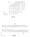
- FIG. 1 a shows a conceptualized memory structure 100 which illustrates an organization of memory cells according to one embodiment of the present invention.
- FIG. 1 b shows a basic circuit representation of two stacks of NOR strings sharing common vertical word-lines, according to one embodiment of the present invention.
- FIG. 1 c shows a basic circuit representation of a stack of four NOR strings in a Y-Z plane cross section of conceptualized memory structure 100 .
- FIG. 2 a shows a cross section in an Y-Z plane of memory structure 200 , after active layers 202 - 0 to 202 - 7 have been formed on semiconductor substrate 201 , but prior to formation of individual active strips, in accordance with one embodiment of the present invention.
- FIG. 2 b - 1 shows structure 220 a , which may be used to implement any of active layers 202 - 0 to 202 - 7 of FIG. 2 a , in accordance with one embodiment of the present invention.
- FIG. 2 b - 2 shows structure 220 b , which includes additional metallic sublayer 224 adjacent one of layers 221 and 223 of structure 220 a , in accordance with one embodiment of the present invention.
- FIG. 2 b - 3 shows structure 220 c , which includes additional metallic sublayer 224 adjacent each of layers 221 and 223 of structure 220 a , in accordance with one embodiment of the present invention.
- FIG. 2 c shows a cross section in an Y-Z plane through buried contacts 205 - 0 and 205 - 1 , which connect N + sublayer 223 in each of active layers 202 - 0 and 202 - 1 to contacts 206 - 0 and 206 - 1 in semiconductor substrate 201 .
- FIG. 2 d illustrates forming trenches 230 in memory structure 200 of FIG. 2 a , in a cross section in an X-Y plane through active layer 202 - 7 in one portion of memory structure 200 of FIG. 2 a.
- FIG. 2 e illustrates depositing charge-trapping layers 231 L and 231 R on opposite side walls of the active strips along trenches 230 , in a cross section in an X-Y plane through active layer 202 - 7 in one portion of memory structure 200 of FIG. 2 a.
- FIG. 2 f illustrates depositing polysilicon or metal 208 to fill trenches 230 .
- FIG. 2 g shows, after photo-lithographical patterning and etching steps on the memory structure of FIG. 2 f , local word-lines 208 w and pre-charge word-lines 208 - chg are achieved by removing exposed portions of the deposited polysilicon 208 , and filling the resulting shafts with insulation material 209 or air gap isolation.
- FIG. 2 h shows a cross section in the X-Z plane through a row of local word-lines 208 w of FIG. 2 g 8 , showing active strips in active layers 202 - 7 and 202 - 6 .
- FIG. 2 i shows that each of local word-lines 208 w of FIG. 2 h is connected to either one of global word-lines 208 g - a , routed in one or more layers provided above active layers 202 - 0 to 202 - 7 , or one of global word-lines 208 g - s , routed in one or more layers provided below the active layers between active layer 202 - 0 and substrate 201 (see FIG. 4 a ).
- FIG. 2 j shows an alternative embodiment to the embodiment of FIG. 2 i , in which only top global word-lines—i.e., without any bottom global word-lines—are provided, in accordance with one embodiment of the present invention; in this embodiment, the local word-lines along one edge of an active strip are staggered with respect to the local word-lines on the other edge of the active strip (see FIG. 4 b )
- FIG. 2 k shows each of local word-lines 208 w controlling TFTs formed out of the active strips on opposite sides of the local word-line, according to one embodiment of the present invention (see FIG. 4 c ).
- FIG. 3 illustrates the methods and circuit elements used for setting a source voltage (V ss ) on source lines in N+ sublayer 221 ; specifically, the source line voltage may be set through hard-wire decoded source line connection 280 or using pre-charge TFTs 303 and bit-line connections 270 .
- FIG. 4 a shows a cross section in the X-Y plane, showing contacts 291 connecting local word-lines 208 w to global word-lines 208 g - a , for the embodiment of the present invention shown in FIG. 2 i.
- FIG. 4 b shows a cross section in the X-Y plane, showing contacts 291 connecting local word-lines 208 w to top global word-lines 208 g - a (or bottom global word-lines 208 g - s ) in a staggered configuration, for the embodiment of the present invention shown in FIG. 2 j.
- FIG. 4 c shows a cross section in the X-Y plane, showing contacts 291 connecting local word-lines 208 w to global word-lines 208 g - a and the isolation 209 between adjacent active strip-pairs, for the embodiment of the present invention shown in FIG. 2 k.
- FIG. 1 a shows a conceptualized memory structure 100 that facilitates illustration in this detailed description of an organization of memory cells according to one embodiment of the present invention.
- memory structure 100 represents a 3-dimensional block of memory cells formed in deposited thin-films over the surface of substrate layer 101 .
- Substrate layer 101 may be, for example, a conventional silicon wafer used for fabricating integrated circuits, familiar to those of ordinary skill in the art.
- a Cartesian coordinate system (such as indicated in FIG. 1 a ) is adopted solely for the purpose of facilitating discussion. Under this coordinate system, the surface of substrate layer 101 is considered a plane which is parallel to the X-Y plane.
- the term “horizontal” refers to any direction parallel to the X-Y plane, while “vertical” refers to the Z-direction.
- each vertical column represents storage elements (i.e., thin-film storage transistors or TFTs) that share a vertical common control gate or word-line in a stack of horizontal NOR strings, with each NOR string running along the Y direction.
- Each NOR string is formed out of TFTs along an “active strip”, described in further detail below.
- active strip described in further detail below.
- memory structure 100 represents an array consisting of 4 stacks of NOR strings, with each stack having four NOR strings, and each NOR string having four TFTs.
- memory structure 100 is merely an abstraction of certain salient characteristics of a memory structure of the present invention.
- a memory structure of the present invention may have any number of TFTs along any of the X, Y and Z directions.
- numbers that are integer powers of 2 i.e., 2 n , where n is an integer
- a memory structure within the scope of the present invention may have M NOR strings along each of the X and Z directions, with M being a number that is not necessarily 2 n , for any integer n.
- memory block 100 has 8192 stacks of 8 NOR strings each, with each NOR string having 8192 storage elements, memory block 100 would have more than half a billion storage elements in the form of NOR-type nonvolatile TFTs.
- MLC multi-level cell
- memory block 100 can store more than one billion bits of information.
- a one-terabit memory chip would have one thousand or more such blocks plus spare blocks available to substitute defective or worn-out blocks.
- memory structure 100 is not drawn to scale in any of the X, Y, Z directions.
- FIG. 1 c shows a basic circuit representation of a stack of 4 NOR strings in a Y-Z plane cross section of conceptualized memory structure 100 .
- each NOR string runs along the Y direction, with storage elements connected between source line 153 - m and bit lines 154 - m , where m is the index between 1 to 4 of the corresponding active strip.
- Corresponding storage elements in the 4 NOR strings are connected corresponding vertical word-lines 151 - n , where n is the index of the word-lines along the active strips.
- FIG. 1 b shows a basic circuit representation of two stacks of NOR strings sharing common vertical word-lines, according to one embodiment of the present invention. The detailed structure of this configuration is discussed and illustrated below in conjunction with FIG. 2 k .
- this basic circuit configuration includes NOR strings (e.g., NOR strings 150 L and 150 R) that are provided in adjacent columns of memory structure 100 sharing a common word-line.
- NOR strings 150 L and 150 R are NOR strings in two active strips located on opposite sides of common word-line 151 a .
- Storage transistors 152 R- 1 to 152 R- 4 and 152 L- 1 to 152 L- 4 are storage elements in the four active strips to the right and in the four active strips to the left of their common vertical word-line 151 a , respectively.
- a greater storage density may be achieved by having a common local word-line to control TFTs of adjacent active strips.
- word-line 151 n controls TFTs in the NOR strings of bit lines 153 R- 1 , 153 R- 2 , 153 R- 3 and 153 R- 4 , and TFTs in the NOR strings of bit lines 153 L- 1 , 153 L- 2 , 153 L- 3 and 153 L- 4 .
- the parasitic capacitance C intrinsic to each NOR string e.g., the parasitic capacitance between the N+ diffusions of a string and its numerous associated local word-lines
- the TFTs in the NOR strings of the present invention may be programmed, program-inhibited, erased, or read using conventional programming, inhibition, erasure and read voltages.
- the TFTs are implemented by thin-film storage transistors that are programmed or erased using Fowler-Nordheim tunneling or direct tunneling mechanisms.
- channel hot electron injection may be used for programming.
- FIG. 2 a shows a cross section in an Y-Z plane of memory structure 200 , after active layers 202 - 0 to 202 - 7 are formed on semiconductor substrate 201 , in accordance with one embodiment of the present invention.
- memory structure 200 includes active layers 202 - 0 to 202 - 7 .
- Semiconductor substrate 201 represents, for example, a P-doped bulk silicon wafer on which support circuits for memory structure 200 may be formed prior to forming the active layers. Such support circuits may include both analog and digital circuits.
- support circuits may include shift registers, latches, sense amplifiers, reference cells, power supply lines, bias and reference voltage generators, inverters, Nand, Nor, Exclusive-Or and other logic gates, input/output drivers, address decoders, including bit-line and word-line decoders, other memory elements, sequencers and state machines.
- These support circuits may be formed out of the building blocks of conventional devices, e.g., N-Wells, P-Wells, triple wells, N + , P + diffusions, isolation regions, low and high voltage transistors, capacitors, resistors, and interconnects, as known to those skilled in the art.
- insulating layer 203 - 0 is provided, which may be a deposited or grown thick silicon oxide, for example.
- one or more layers of interconnect may be formed, including “global word-lines,” which are discussed below.
- Such metallic interconnect lines e.g., global word-line landing pads 264 of FIG. 2 c , discussed below
- the metallic interconnect lines may be formed by applying photo-lithographical patterning and etching steps on one or more deposited metal layers. (Alternatively these metallic interconnect lines can be formed using a conventional damascene process, such as a copper damascene process). Thick oxide 203 - 0 is then deposited, followed by a planarization step using conventional chemical mechanical polishing (CMP).
- CMP chemical mechanical polishing
- Active layers 202 - 0 to 202 - 7 are then successively formed, each active layer being insulated from previous active layer underneath by a corresponding one of insulating layers 203 - 1 to 203 - 7 .
- FIG. 2 a although eight active layers are shown, any number of active layers may be provided. In practice, the number of active layers to provide may depend on the process technology, such as availability of a well-controlled anisotropic etching process that allows cutting through the active layers to reach semiconductor substrate 201 .
- Each active layer is etched at an etching step discussed below to form a large number of parallel active strips each running along the Y direction.
- FIG. 2 b - l shows structure 220 a , which may be used to implement any of active layers 202 - 0 to 202 - 7 of FIG. 2 a , in accordance with one embodiment of the present invention.
- active layer 220 a includes deposited polysilicon sublayers 221 - 223 .
- Sublayers 221 - 223 may be deposited successively in the same process chamber without removal in between.
- Sublayer 223 may be formed by depositing 5-50 nm of in-situ doped N + polysilicon.
- Sublayers 222 and 221 may then be formed by depositing undoped or lightly doped polysilicon, in the thickness range of 40-100 nm.
- Sublayer 221 (i.e., the top portion of the deposited polysilicon) is then N + doped.
- This N + doping may be achieved by either (i) a low-energy shallow ion implantation of arsenic or antimony, forming a 20-50 nm N+ doped top sublayer 221 , or (ii) in-situ doping of the deposited polysilicon, forming a 20-50 nm N + top sublayer 221 . (Thermal diffusion should not be used, as it would expose the lower active layers formed earlier to greater diffusion than the upper active layers).
- a low-dose implantation of boron (P ⁇ ) or phosphorus (N ⁇ ) ions may also be carried out at an energy sufficient to penetrate the implanted or in-situ N + doped sublayer 221 , so as to adjust to an enhancement mode threshold voltage for sublayer 222 lying between top N+ doped sublayer 221 and bottom N+ doped sublayer 223 .
- Thermal activation of the N+ and P ⁇ implanted species in sublayers 221 and 222 should preferably take place after all active layers 202 - 0 to 202 - 7 have been formed, using a conventional rapid thermal annealing technique (e.g., at 700° C. or higher), thereby ensuring that all active layers experience high temperature processing in roughly the same amount. Caution must be exercised to limit the total thermal budget, so as to avoid merging N + sublayer 223 with the N+ sublayer 221 , so as not to eliminate P ⁇ sublayer 222 .
- P ⁇ sublayer 222 is required to remain sufficiently thick to avoid N+P ⁇ N+ transistor punch-through at a low voltage applied across N+ sublayers 221 and 223 .
- the final thickness of sublayer 222 represents the TFT channel length, which may be as little as 10 nm or less over long active strips. In one embodiment, it is possible to control the TFT channel length to less than 10 nm by depositing an ultra-thin (around 1 nm) film of silicon nitride (e.g., SiN or Si 3 N 4 ), or another suitable diffusion-blocking film following the formation of N + sublayer 223 , and then again following deposition of the polysilicon of sublayer 222 in a thickness range between 5-30 nm, before depositing N+ polysilicon sublayer 221 .
- silicon nitride e.g., SiN or Si 3 N 4
- the ultra-thin silicon nitride layers can be deposited by chemical vapor deposition, atomic layer deposition or any other means, e.g., high pressure nitrodization at low temperature.
- Each ultra-thin silicon nitride layer acts as a diffusion-barrier that prevents the N + dopants in N + sublayers 221 and 223 from diffusing into P ⁇ sublayer 222 , yet are sufficiently thin to only marginally impede MOS transistor action in the region between N+ sublayer 221 (acting as a source) and N+ sublayer 223 (acting as a drain). (Electrons in the surface inversion layer of sublayer 222 readily tunnel directly through 1 nm of silicon nitride).
- ultra-thin silicon nitride layers increase the manufacturing cost, but serve to significantly reduce leakage current in the numerous TFTs along the active strips that are in the “off” state, while providing a high read current for the accessed TFT that is in the “on” state.
- additional conductive sublayer 224 may be provided adjacent the corresponding one of N + sublayers 221 and 223 (e.g., w in FIG. 2 b - 2 ), or both (e.g., FIG. 2 b - 3 ).
- Sublayer 224 may be provided by one or more deposited metal layers.
- sublayer 224 may be provided by first depositing 1-2 nm thick layer of TiN, followed by depositing a 10-40 nm thick layer of tungsten or a similar refractory metal, or its silicide or salicide.
- Reduced line resistance is desirable for reducing the “RC delay” of a signal traversing a long conductive strip (i.e., the time delay due to the product of the line resistance R and the line capacitance C), and for minimizing the “IR drop” across a long and narrow active strip (i.e., the voltage drop due to the product of the current I and the line resistance R).
- Inclusion of metal sublayer 224 in each of active layers 202 - 0 to 202 - 7 may, however, increase cost and complexity in the manufacturing process, including the complication that some of the metallic materials are relatively more difficult to anisotropically etch than materials such as polysilicon or silicon oxide in the other sublayers.
- metal sublayer 224 enables use of considerably longer active strips which result in superior array efficiency.
- shorter active strips have superior immunity to leakage between N + sublayer 223 and N + sublayer 221 , and lower intrinsic capacitance than the longer strips.
- the integrated circuit designer may opt for a shorter active strip (with or without one or both metal layers) when low latency is most valued.
- the strip resistance may be reduced by providing buried contacts at both ends, of each active strip, rather than just at one end.
- Block-formation patterning and etching steps define separate blocks in the active layers formed.
- Each block defines an area in which a large number (e.g., thousands) of active strips running in parallel along the Y direction may be formed, as discussed below, with each active strip eventually forming a large number (e.g., thousands) of TFTs.
- each of active layers 202 - 0 to 202 - 7 is successively formed, with each active layer being formed by repeating the steps described above.
- each next higher active layer extends slightly beyond the previous active layer (see, e.g., as illustrated in FIG. 2 c , discussed below, layer 202 - 1 extends beyond layer 202 - 0 ) to allow the higher active layer to access its specific decoders and other circuitry in semiconductor substrate 201 through designated buried contacts.
- FIG. 2 c shows a cross section in an Y-Z plane through buried contacts 205 - 0 and 205 - 1 , which connect N + sublayer 223 in each of active layers 202 - 0 and 202 - 1 to contacts 206 - 0 and 206 - 1 in semiconductor substrate 201 .
- buried contacts 205 - 0 and 205 - 1 connect contacts 206 - 0 and 206 - 1 in semiconductor substrate 201 , for example, to the local bit or source lines formed out of N + sublayer 223 in each of active layers 202 - 0 and 202 - 1 .
- Buried contacts for active layers 202 - 2 to 202 - 7 may be similarly provided to connect active layers 202 - 2 to 202 - 7 to contacts 206 - 2 to 206 - 7 (not shown) in semiconductor substrate 201 .
- each of contacts 206 - 0 to 206 - 7 may apply a pre-charge voltage V bl to the respective bit line or source line or, during a read operation, may be connected to an input terminal of a sense amplifier or a latch.
- the switch circuit may selectively connect each of contacts 206 - 0 to 206 - 7 to any of a number of specific voltage sources, such as a programming voltage (V program ), an inhibit voltage (V inhibit ), an erasure voltage (V erase ), or any other suitable predetermined or pre-charge reference voltage V bl or V ss .
- V program programming voltage
- V inhibit inhibit voltage
- V erase erasure voltage
- V bl or V ss any other suitable predetermined or pre-charge reference voltage
- FIG. 2 c also shows buried contacts 261 - 0 to 261 - n for connecting global word-lines—which are to be formed running along the X direction—to contacts 262 - 0 to 262 - n in semiconductor substrate 201 .
- These global word-lines are provided to connect corresponding local word-lines 208 w to be formed (see, e.g., FIG. 2 g , which is described below).
- Landing pads 264 are provided to allow connection to local word-lines 208 w , which are yet to be formed vertically on top of global word-lines 261 - 0 and 261 - n .
- each of global word-lines 262 - 0 to 262 - n may be selectively connected, either individually, or shared among several global word-lines to any one of a number of reference voltage sources, such as stepped programming voltage (V program ), a read voltage (V read ) and an erasure voltage (V erase ).
- V program stepped programming voltage
- V read read voltage
- V erase erasure voltage
- These buried contacts, the global word-lines and the landing pads may be formed using conventional photo-lithographical patterning and etching steps, following by deposition of one or more conductors or by alloying (e.g., tungsten metal or tungsten silicide).
- trenches are created by etching through the active layers to reach the bottom global word-lines (or semiconductor substrate 201 ) using a strip-formation mask.
- the strip-formation mask consists of a pattern in a photoresist layer of long narrow strips running along the Y direction (i.e., perpendicular to that of global word-line strips that run along the X direction). Sequential anisotropic etches etch through active layers 202 - 7 down to 202 - 0 , and dielectric isolations layers 203 - 7 down to 203 - 0 .
- the number of active layers to be etched which is eight in the example of FIG.
- a photoresist mask by itself may not be sufficiently robust to hold the strip pattern through the numerous etches necessary to etch through the lowest active layer.
- reinforcement by a hard mask material, such as carbon may be required, as is known to those of ordinary skill in the art.
- Etching terminates at the dielectric isolation above the landing pads of the global word-lines. It may be advantageous to provide an etch-stop barrier film such as aluminum oxide to protect the landing pads during the trench etch sequence.
- FIG. 2 d illustrates forming trenches 230 in memory structure 200 of FIG. 2 a , in a cross section in an X-Y plane through active layer 202 - 7 in one portion of memory structure 200 of FIG. 2 a .
- Between adjacent trenches 230 is a stack of high aspect-ratio, long and narrow active strips.
- etch chemistry may have to be changed when etching through the materials of the different sublayers, especially when metal sublayers 224 are present.
- the anisotropy of the multi-step etch is important, as undercutting of any sublayer should be avoided as much as possible, and so that an active strip in the bottom active layer (e.g., an active strip in active layer 202 - 0 ) has approximately the same width and gap spacing to an adjacent active strip as the corresponding width and gap spacing in an active strip of the top active layer (i.e., an active strip of active layer 202 - 7 ).
- an active strip in the bottom active layer e.g., an active strip in active layer 202 - 0
- an active strip of the top active layer i.e., an active strip of active layer 202 - 7
- the greater the number of active layers in the stack to be etched the more challenging is the design of the successive etches.
- etching may be conducted in sections of, say 8 layers each, as discussed in Kim, mentioned above, at pp. 188-189. As shown in FIG. 2 d , trenches 230 run along the Y direction.
- the charge-trapping layer is formed by first depositing or growing a thin tunneling dielectric film of a 2-10 nm thickness, typically a silicon dioxide layer or a silicon oxide-silicon nitride-silicon oxide (“ONO”) triple layer, followed by deposition of a 4-10 nm thick layer of charge-trapping material, typically silicon nitride or silicon-rich nitride or oxide or nanocrystals or nanodots embedded in a thin dielectric film, which is then capped by a blocking dielectric.
- a thin tunneling dielectric film typically a silicon dioxide layer or a silicon oxide-silicon nitride-silicon oxide (“ONO”) triple layer
- ONO silicon oxide-silicon nitride-silicon oxide
- the blocking dielectric may be a 5-15 nm thick layer consisting, for example, of an ONO layer, or a high dielectric constant film, such as aluminum oxide, hafnium oxide or some combination thereof.
- the storage element can be SONOS, TANOS, nanodot storage, isolated floating gates or any suitable charge-trapping sandwich structures known to those of ordinary skill in the art.
- Trenches 230 must be sufficiently wide to accommodate the storage elements on the two opposing sidewalls of the adjoining active strips, plus the vertical local word-lines to be shared by the TFT's on these opposite sidewalls. FIG.
- FIG. 2 e illustrates deposited charge-trapping layers 231 L and 231 R on opposite side walls of the active strips along trenches 230 , in a cross section in an X-Y plane through active layer 202 - 7 in one portion of memory structure 200 of FIG. 2 a.
- Contact openings at the bottom global word-lines are photo-lithographically patterned at the top of layer 202 - 7 and exposed by anisotropically etching through the charge-trapping materials at the bottom of trenches 230 , stopping at the bottom global word-line landing pads (e.g., global word-line landing pads 264 of FIG. 2 c ).
- the bottom global word-line landing pads e.g., global word-line landing pads 264 of FIG. 2 c .
- only alternate rows of trenches 230 e.g., the rows in which the word-lines formed therein are assigned odd-numbered addresses
- etching is preceded by a deposition of an ultra-thin film of polysilicon (e.g. 2-5 nm thick) to protect the vertical surface of the blocking dielectric on the sidewalls of trenches 230 during the anisotropic etch of the charge-trapping material at the bottom of trenches 230 .
- doped polysilicon e.g., P + polysilicon
- P + doped polysilicon is preferable because of its higher work function than N+ doped polysilicon.
- a metal with a high work function relative to SiO 2 e.g., tungsten, tantalum, chrome or nickel
- Trenches 230 may now be filled with the P + doped polysilicon or the metal. In the embodiment of FIG.
- the doped polysilicon or metal in alternate rows of trenches 230 is in ohmic contact with the bottom global word-lines.
- the polysilicon in the other ones of trenches 230 i.e., the rows to host local word-lines that are assigned even-numbered addresses
- These local word-lines are to be contacted by top global word-lines routed above the top active layer).
- the photoresist and hard mask may now be removed.
- a CMP step may then be used to remove the doped polysilicon from the top surface of each block.
- FIG. 2 f illustrates depositing polysilicon 208 to fill trenches 230 .
- FIG. 2 g shows, after photo-lithographical patterning and etching steps on the memory structure of FIG. 2 f , local word-lines 208 w are achieved by removing exposed portions of the deposited polysilicon 208 , and filling the resulting shafts with insulation material 209 .
- a hard mask may be required, using the technique described above.
- the resulting shafts may be filled with insulation material 209 or left as an air gap.
- the mask pattern that exposes the doped polysilicon for excavation are parallel strips that run along the X direction, so that they coincide with the global word-lines that are required to be formed in one embodiment to contact local word-lines 208 w.
- the portions of charge-trapping layers 231 L and 231 R adjacent insulation material 209 remained after the removal of the corresponding portions of deposited polysilicon 208 .
- those portions of charge-trapping layers 231 L and 231 R may be removed by a conventional etching process prior to filling the shafts with insulation material 209 .
- Etching of the charge-trapping materials in the shafts may be carried out concurrently with the removal of the doped polysilicon, or subsequent to it.
- a subsequent etch would also remove any fine polysilicon stringers that the anisotropic etch has left behind; such polysilicon stringers may cause undesirable charge leakage, serving as resistive leakage paths between adjacent vertical local word-lines. Removal of such charge trapping material also eliminates lateral diffusion of trapped charge between one TFT and the TFTs immediately to its left and right along the same string.
- FIG. 2 h shows a cross section in the X-Z plane through a row of local vertical word-lines 208 w (shown also in FIG. 2 g in the X-Y plane), showing active strips in active layers 202 - 7 and 202 - 6 .
- each active layer includes N + sublayer 221 , P ⁇ sublayer 222 , and N + sublayer 223 .
- N+ sublayer 221 e.g., a source line
- V ss ground reference voltage
- N + sublayer 223 e.g., a bit line
- local word-line 208 w the portion of active layer 202 - 7 or 202 - 6 facing word-line 208 w and the charge-trapping layer 231 L between word-line 208 w and that portion of active layer 202 - 7 or 202 - 6 form a storage element or storage TFT, as indicated by reference numeral 281 and 282 in FIG. 2 h .
- Facing TFTs 281 and 282 on the opposite side of 208 W are TFTs 283 and 284 respectively, incorporating therein charge trapping layer 231 R.
- TFTs 285 and 286 are provided on the other side of the active strips 202 - 6 and 202 - 7 providing TFTs 283 and 284 . Accordingly, the configuration shown in FIG.
- N + sublayer 223 can be charged to a suitable voltage required for an operation of the storage transistors at hand (e.g., program voltage V prog , inhibition voltage V inhibit , erase voltage V erase , or the read reference voltage V bl ).
- a suitable voltage required for an operation of the storage transistors at hand e.g., program voltage V prog , inhibition voltage V inhibit , erase voltage V erase , or the read reference voltage V bl .
- additional metallic sublayer 224 increases the conductivity of the bit line, so as to facilitate memory device operations.
- N + sublayer 221 in any of active layers 202 - 0 to 202 - 7 may be left floating.
- one or more of the local vertical word-lines may be used as a non-memory TFT.
- a suitable voltage i.e., rendering the pre-charge TFT to the “on” state
- each pre-charge word-line momentarily inverts sublayer 222 , so that N + sublayer 221 may be pre-charged to the voltage V ss on N + sublayer 223 .
- device operation may proceed with N + sublayer 221 left electrically charged as a virtual reference at the pre-charged voltage V ss because the parasitic capacitance in the strip capacitor of N + sublayer 221 is large enough to hold its charge sufficiently long to support program and read operations (see below).
- Each local word-line 208 w may be used to read, write or erase the charge stored in the designated one of the TFTs formed in each of active layers 202 - 0 to 202 - 7 , located on either charge-trapping portion 231 L or 231 R, when a suitable voltage is imposed.
- each local word-line 208 w may be used to read, write or erase the charge stored in any of the TFTs formed in each of active layers 202 - 0 to 202 - 7 , located on either charge-trapping portions 231 L or 231 R, when a suitable voltage is imposed.
- FIG. 2 k only one of the two sides of active layers 202 - 0 to 202 - 7 is formed as storage TFTs, thereby eliminating the need for both bottom and top global word-lines in the embodiment.
- An isolation dielectric or oxide may be then deposited and its surface planarized. Contacts to semiconductor substrate 201 and to local word-lines 208 w may then be photo-lithographically patterned and etched. In one embodiment, which is described in conjunction with FIG. 2 i and corresponding FIG. 4 a , contacts to local word-lines 208 w are provided only for those assigned an even-numbered address (local word-lines assigned an odd address are contacted from the bottom of the array by bottom global word-lines). For the embodiment shown in FIG. 2 j , contacts are provided for every local word-line but the local word-lines are staggered relative to opposing word-lines, as shown in FIG. 4 b . A deposited metal layer provides a top metal layer and the contacts.
- Such a metal layer may be provided by, first, forming a thin TiN layer, followed by forming a low resistance metal layer (e.g., tungsten). The metal layer is then photo-lithographically patterned to form top global word-lines. (Alternatively, these global word-lines may be provided by a copper damascene process.) In one embodiment, these global word-lines are horizontal, running along the X direction, electrically connecting with the contacts formed in the isolation oxide (i.e., thereby contacting local word-lines 208 w ) and with the contacts to semiconductor substrate 201 (not shown).
- FIG. 2 i shows that each of local word-lines 208 w of FIG. 2 h is connected to either one of global word-lines 208 g - a , routed in one or more layers provided above active layers 202 - 0 to 202 - 7 , or one of global word-lines 208 g - s , routed in one or more layers provided below the active layers between active layer 202 - 0 and substrate 201 .
- Local word-lines 208 w that are coupled to bottom global word-lines may be assigned odd addresses, while local word-lines 208 w coupled to the top global word-lines may be assigned even addresses.
- FIG. 1 shows that each of local word-lines 208 w of FIG. 2 h is connected to either one of global word-lines 208 g - a , routed in one or more layers provided above active layers 202 - 0 to 202 - 7 , or one of global word-lines 208 g - s , routed in one or more layers provided below
- FIG. 4 a shows a corresponding cross section in the X-Y plane, showing contacts 291 connecting local word-lines 208 w to global word-lines 208 g - a .
- local word-lines 208 w control each active strip on only one of the active strip's sides.
- FIG. 2 j shows an alternative embodiment to the embodiment of FIG. 2 i , in which only top global word-lines are provided (or, alternatively, only bottom global word-lines are provided), in accordance with one embodiment of the present invention.
- the local word-lines along one edge of an active strip are staggered with respect to the local word-lines on the other edge of the active strip.
- FIG. 4 b shows a corresponding cross section in the X-Y plane, showing contacts 291 connecting local word-lines 208 w to top global word-lines 208 g - a (or bottom global word-lines 208 g - s ) in a staggered configuration.
- This embodiment simplifies the process flow by obviating the process steps needed to form the bottom global word-lines (or the top global word-lines, as the case may be).
- two TFTs may be provided in each active layer of each active strip within one pitch of a global word-line (i.e., in each active strip, one TFT is formed using one sidewall of the active strip, and controlled from a bottom global word-line, the other TFT is formed using the other sidewall of the active strip, and controlled from a top global word-line).
- a pitch is one minimum line width plus a required minimum spacing between adjacent lines).
- only one TFT may be provided within one global word line pitch in each active layer.
- the two local word-lines 208 w at the two sides of each strip can be staggered relative to each other so that two global word-line pitches are required to contact them both.
- the penalty for the staggered embodiment is the forfeiting of the double-density TFT inherent in having both edges of each active strip providing a TFT within one pitch of each global word-line.
- FIG. 2 k shows each of local word-lines 208 w controlling TFTs formed out of the active strips on opposite sides of the local word-line, according to one embodiment of the present invention.
- FIG. 4 c shows a corresponding cross section in the X-Y plane, showing contacts 291 connecting local word-lines 208 w to global word-lines 208 g - a and the isolation 209 between adjacent active strip-pairs.
- each TFT is formed from either one of a dual-pair of active strips located on opposite side of a common local word-line, with each dual-pair of active strips being isolated by a trench filled with oxide or dielectric material or an air gap 209 from similarly formed adjacent dual-pairs of active strips.
- the isolation trenches between adjacent dual-pairs of active strips accommodate the charge-trapping-material 231 or polysilicon 208 .
- the protected isolation trenches may then be filled with oxide or dielectric material 209 , or left as air gaps.
- FIG. 3 shows schematically an embodiment where sublayer 221 of each active strip (see, e.g., FIG. 2 b - 1 ) is connected by hard wires 280 (dashed line) to a source reference voltage V ss by a metal or N+ doped polysilicon conductor.
- hard wires 280 may be independently connected, so that the source voltages for different layers need not be the same. Since sublayer 221 is formed only after sublayer 223 is formed, the metal or N+ doped polysilicon conductor to connect sublayer 221 to the reference voltage V ss requires one or two additional patterning and etching steps to each of active layers 202 - 0 to 202 - 7 , hence increasing the processing cost.
- each active NOR string uses the large intrinsic parasitic capacitance C of each active NOR string.
- hard wires 280 are not needed and sublayer 221 of each active strip is left floating, after being temporarily pre-charged to voltage V ss transferred to it from bit-line sublayer 223 through the action of local vertical pre-charge TFTs that are controlled by pre-charge word-lines 208 - chg .
- several pre-charge TFTs may be provided on either side of the active strip (e.g., one every 512 TFTs).
- each such TFT provides a capacitor that is typically around 3 ⁇ 10 ⁇ 18 farads.
- the total capacitance C of the string is approaching 0.01 picofarad, which is sufficient to preserve the pre-charge voltage on it well beyond the milliseconds required for write, erase or read operations that follow immediately after a pre-charging operation.
- Capacitance C may be increased by lengthening the NOR string to accommodate thousands more TFTs along each side of the string, correspondingly increasing the retention time of pre-charge voltage V ss on N + sublayer 221 .
- NOR string suffers from an increased leakage current between N + sublayer 221 and N + sublayer 223 , such leakage current may interfere with the sensed current when reading the one TFT being addressed.
- leakage current may interfere with the sensed current when reading the one TFT being addressed.
- the potentially longer time it takes to pre-charge a larger capacitor during a read operation can conflict with the requirement for a low read latency (i.e., a fast read access time).
- To speed up the pre-charging of the capacitance C of a long NOR string would typically require providing more than one pre-charge TFT; such pre-charge TFTs may be distributed throughout the length of the NOR string.
- V bb back-bias voltage
- a negative V bb voltage can be used to modulate the threshold voltage of the TFTs along each active strip, so as to reduce the subthreshold leakage current between N+ source sublayer 221 and N+ drain sublayer 223 .
- a high positive V bb voltage can be applied during an erase operation to tunnel-erase TFTs whose control gates are held at ground potential.
- the read operating condition for the NOR strings of the present invention should preferably ensure that all TFTs along both edges of an active strip operate in enhancement mode (i.e., they each have a positive threshold voltage between their control gate 151 n and their source 221 voltage V ss ), so as to suppress the leakage current between N + sublayers 221 and 223 of the active strip when all control gates on both sides of the strip are held at, or below V ss .
- This enhancement threshold voltage can be achieved by doping sublayer 222 with a P ⁇ dopant concentration (typically by boron, in a concentration typically between 1 ⁇ 10 16 and 1 ⁇ 10 17 per cm 3 ), so as to result in a native TFT threshold voltage of around 1 volt, and by holding all unaddressed local word-lines on both sides of the active strip at 0 volt.
- a P ⁇ dopant concentration typically by boron, in a concentration typically between 1 ⁇ 10 16 and 1 ⁇ 10 17 per cm 3
- leakage current suppression can be achieved by raising the V ss voltage on N sublayer 221 to around 1.5 volts and the voltage V bl on N + sublayer 223 to a voltage that is about half a volt to one volt above 1.5 volts, while holding all local word-lines at 0 volt. This provides the same effect as holding the word-line voltage at ⁇ 1.5 volts with respect to the source, thereby suppressing any leakage due to TFTs that are in a slightly depleted threshold voltage.
- the erase operation should preferably include a soft-programming operation that shifts any TFT that has been over-erased into a depletion mode threshold voltage back into an enhancement mode threshold voltage.
- the charge-trapping material e.g., an ONO stack
- ONO stack has a long data retention time (typically measured in many years), but low endurance. Endurance, which is a measure of a storage transistor's performance degradation after some number of write-erase cycles, is typically considered low if it is less than ten thousand cycles. However, one may alter the charge-trapping material to reduce retention times, but significantly increase endurance (e.g., reducing retention times to hours, while increasing endurance to tens of millions of write/erase cycles).
- the tunnel dielectric typically 6-8 nm of silicon oxide can be reduced to 2 nm or less of silicon oxide, or replaced altogether with another dielectric (e.g., silicon nitride or SiN).
- another dielectric e.g., silicon nitride or SiN.
- electrons will be attracted through direct tunneling (as distinct from Fowler-Nordheim tunneling) into the silicon nitride charge-trapping layer where the electrons will be temporarily trapped for a few minutes to hours or days.
- the charge-trapping silicon nitride layer and the blocking layer of silicon oxide or aluminum oxide will keep these electrons from escaping to the control gate word-line, but they will eventually leak back out to the active sublayers (electrons are negatively charged and repel each other). Even if the 2 nm or less tunnel dielectric breaks down locally after extended cycling, the trapped electrons will be slow to depart from their traps in the silicon nitride layer.
- Other combinations of charge storage materials may also result in a high endurance but low retention (“semi-volatile”) TFT. Such a TFT may require periodic write refresh to replenish the lost charge.
- NOR string arrays of the present invention that have such TFTs may be useful in applications that currently can get by with relatively slow DRAMs.
- the advantages of such NOR string arrays over DRAMs include: a much lower cost-per-bit because DRAMs cannot be built in three dimensional blocks, and a much lower power dissipation, as the refresh cycles need only be run approximately once every few minutes or once every few hour, as compared to every few milliseconds required in current DRAM technology.
- the NOR string arrays of the present invention are achieved by changing the constitution of the charge-trapping material (e.g., charge-trapping layers 231 L and 231 R in FIG. 2 e ), and by appropriately adapting the program/read/erase conditions to incorporate the periodic data refreshes.
- NOR string arrays may also be programmed using a channel hot-electron injection approach, similar to that which is used in NROM/Mirror Bit transistors, known to those of ordinary skill in the art.
- NROM/Mirror Bit transistor charge representing one bit is stored at one end of the channel region next to the junction with the drain region, and by reversing polarity of the source and drain, charge representing a second bit is programmed and stored at the opposite end of the channel region next to the source junction.
- Typical programming voltages are 5 volts on the drain, 0 volt on the source and 8 volts on the control gate. Reading both bits requires reading in reverse the source and drain, as is well known to those skilled in the art.
- channel hot electron programming is much less efficient than tunnel programming, and therefore the method does not lend itself to the massively parallel programming possible by tunneling.
- the channel hot electron injection approach provides double the bit density though, making it attractive for applications such as archival memory.
- the TFTs on both sides of the active strip are initially set in an “off” state, so that all global and local word-lines in a selected block are initially held at 0 volts.
- the addressed NOR string can either share a sensing circuit among several NOR strings through a decoding circuitry, or each NOR string may be directly connected to a dedicated sensing circuit and many other addressed NOR strings sharing the same plane can be sensed in parallel.
- Each addressed NOR string has its source (N + sublayer 221 ) set at V ss ⁇ 0V, either through hard-wire 280 or through bit-line connection 270 in conjunction with pre-charge word-line 208 - chg (in this case V bl is initially held at 0 volt during a pre-charge phase).
- the bit-line i.e., N + sublayer 223
- the V bl voltage is the sense voltage at the sense amplifiers for the addressed NOR strings.
- the one addressed global word-line and all its associated vertical local word-lines are raised from 0 volts to typically around 2 volts while all other global word lines in the block are in their off state. If the addressed TFT is in an erased state (i.e., V th ⁇ 1 volt), bit-line voltage V bl will begin to discharge toward source voltage V ss . This voltage dip is detected by the respective sense amplifier. However, if the addressed TFT is in a programmed state (e.g. V th ⁇ 3 volts) no dip is detected.
- the addressed TFT may be programmed to any of several threshold voltages (e.g., 1 volt (for an erased state), 2.5 volts, 4 volts or 5.5 volts for the four states representing two bits of data).
- the addressed global word-line and its local word-lines can be raised in incremental voltage steps until conduction is detected in the addressed TFT by the respective sense amplifier.
- a single word-line voltage V bl can be applied (e.g. V bl ⁇ 6 volts), and the rate of discharge of voltage V bl can be compared with the rate of discharge of each of several programmable reference voltages representative of the four voltage states representing the bits stored in the TFT.
- the programmable reference voltages are stored on NOR strings dedicated as reference NOR strings in the same block, preferably located in the same plane as the addressed NOR string.
- more than one programmable reference NOR string may be provided to detect each of the programmed states.
- the programmable reference NOR strings closely track the characteristics of the operating NOR strings in the same block through read, program, and background leakage. Only TFTs on one of the two sides of the active strip can participate in a read operation; each TFT on the other side of an active strip must be set to the “off” state. Other ways to read the correct state of a multi-state TFT, as are known to those skilled in the art.
- Reading is fast because, in a NOR string, only the TFT to be read is required to be “on”, as compared to a NAND string, in which the TFTs in series with the one TFT being read must also be “on”.
- metal sublayer 224 is not provided in the active layer (see, e.g., 220 a of FIG. 2 b - 1 )
- a typical resistance R is ⁇ 100,000 Ohm and a typical capacitance C ⁇ 10 ⁇ 14 farad, to provide a RC time delay in the order of one nanosecond.
- the RC time delay would still be less than 20 nanoseconds.
- the time delay may be much reduced, if metal sublayer 224 is provided to reduce the resistance R of the active strip.
- some or all the planes in selected active blocks may be kept always pre-charged to their read voltages V ss and V bl , thereby rendering them ready to immediately sense the addressed TFT (i.e., obviating the pre-charge phase immediately before the read operation).
- Such ready-standby requires very little standby power because the current required to periodically re-charge capacitor C to compensate for charge leakage is very small.
- all strings on all eight or more planes can be pre-charged to be ready for fast read; for example, after reading all strings in plane 207 - 0 ( FIG. 2 a ), plane 207 - 1 can be read in short order because its V ss and V bl are already previously set for a read.
- each TFT per NOR string can be read in a single operation.
- the eight thousand TFTs that share a common global word-line may all be read concurrently, provided that each NOR string is connected to its own sense amplifier. If each sense amplifier is shared among, for example, four NOR strings in the same plane using a string decode circuit, then four read operations are required to take place in four successive steps, with each read operation involving two thousand TFTs.
- Each plane can be provided its own set of dedicated sense amplifiers or, alternatively one set of sense amplifiers can be shared among NOR strings in the eight or more planes through a plane-decoding selector.
- N+ source and drain (sublayers 221 , 223 in FIG. 2 b - 1 ) and the P ⁇ channel (sublayer 222 ) of the TFT is inverted at the surface and electrons tunnel into the charge trapping layer.
- TFT Programming can be inhibited by applying a half-select voltage (e.g., 10 volts, in this example).
- Program-inhibit can be accomplished, for example, either by lowering the word-line voltage to 10 volts while keeping the strip voltage at 0 volt, or by raising to 10 volts the active strip voltage, while keeping the word-line voltage at 20 volts, or some combination of the two.
- TFTs on other strips can be programmed in parallel in the same programming cycle.
- all other TFTs in the NOR strings are programming-inhibited, as are all TFTs on the other side of the active strip (e.g., all TFTs in the odd-addressed NOR string).
- all TFTs in a block are first erased to a threshold voltage of around 1 volt.
- the voltage on the active strip of each addressed TFT is then set to 0 volts (e.g., through connection 270 in conjunction with pre-charge word-line 208 - chg , or through connection 280 , as illustrated in FIG. 3 ), if the addressed TFT is to be programmed; otherwise, the voltage on the active strip of the addressed TFT is set to 10 volts if it is to remain in its erased state (i.e., program-inhibited).
- the global word-line associated with the addressed TFT is then raised to 20 volt, either in one step or in short-duration steps of incrementally increasing voltages, starting at around 14 volts.
- Such incremental voltage steps reduce the electrical stress across the TFT and avoid overshooting the target threshold voltage.
- All other global word-lines in the block are set at half-select 10 volt.
- All active strips on all planes that are not being addressed in the block, as well as all active strips within the addressed plane that are not individually addressed, are also set at 10 volts, or may be floated. These active strips are strongly capacity-coupled to the local word-lines, which are at 10 volts, and thus float at close to 10 volts.
- Each of the incrementally higher voltage programming pulses is followed by a read cycle to determine if the addressed TFT has reached its target threshold voltage.
- the active strip voltage is raised to 10 volts (alternatively the strip is floated, and rises close to 10 volts when all but the one addressed global word lines in the block are raised to 10 volt) to inhibit further programming, while the global word-line keeps programming other addressed strips on the same plane that have not yet attained their target threshold voltages.
- This programming sequence terminates when all addressed TFTs have been read-verified to be correctly programmed.
- programming of the correct one of the multiple threshold voltage states can be accelerated by first pre-charging capacitor C of all addressed active strips (see, e.g., through connection 270 and pre-charge word-line 208 - chg of FIG.
- a typical block may be eight planes high with each plane having 8,000 active strips each with 4,000 TFTs on either of its sides, for a total of half a billion TFTs in a block, so that a one-terabit chip includes approximately 1,000 such blocks, if two bits of information are stored on each TFT.
- block erase is carried out by applying around 20 volts to the P ⁇ sublayer 222 (see, e.g., FIG.
- the duration of an erase pulse should be such that most TFTs are erased to a slight enhancement mode threshold voltage, between zero and one volts. Some TFTs may overshoot and be erased into depletion mode (i.e., having a slightly negative threshold voltage). Such TFTs are required to be programmed into a slight enhancement mode threshold voltage subsequent to the termination of the erase pulses, as part of the erase command.
- sublayers 221 and 223 on all active strips are raised to around 20 volts while holding all global word-lines at zero volt for the duration of the erase pulse.
- This scheme requires that strip-select decoders ( 206 - 0 , 206 - 1 in FIG. 2 c ) employ transistors that can withstand the 20 volts at their junctions.
- all but the addressed global word-line are held at zero volts, while pulsing the addressed global word-line to ⁇ 20 volts and holding all active strips in planes 202 - 0 through 202 - 7 at zero volts.
- This method erases only the X-Z slice of all TFTs touched by the one addressed global bit line.
- Erase for the NROM TFT embodiment can be achieved using the conventional NROM erase mechanism of band-to-band tunneling-induced hot hole injection.
Abstract
Multi-gate NOR flash thin-film transistor (TFT) string arrays (“multi-gate NOR string arrays”) are organized as stacks of horizontal active strips running parallel to the surface of a silicon substrate, with the TFTs in each stack being controlled by vertical local word-lines provided along one or both sidewalls of the stack of active strips. Each active strip includes at least a channel layer formed between two shared source or drain layers. Data storage in the TFTs of an active strip is provided by charge-storage elements provided between the active strip and the control gates provided by the adjacent local word-lines. Each active strip may provide TFTs that belong to one or two NOR strings, depending on whether one or both sides of the active strip are used.
Description
The present application relates to and claims priority of U.S. provisional patent application (Provisional Patent Application), Ser. No. 62/235,322, entitled “Multi-Gate NOR Flash Thin-Film Transistor Strings Arranged in Stacked Horizontal Active Strips with Vertical Control Gates,” filed on Sep. 30, 2015. The Provisional Patent Application is hereby incorporated by reference in its entirety.
1. Field of the Invention
The present invention relates to high-density memory structures. In particular, the present invention relates to high-density memory structures formed by interconnected thin-film storage elements, such as thin-film storage transistors.
2. Discussion of the Related Art
In this disclosure, memory circuit structures are described. These structures may be fabricated on planar semiconductor substrates (e.g., silicon wafers) using conventional fabrication processes. To facilitate clarity in this description, the term “vertical” refers to the direction perpendicular to the surface of a semiconductor substrate, and the term “horizontal” refers to any direction that is parallel to the surface of that semiconductor substrate.
A number of high-density non-volatile memory structures, sometimes referred to as “three-dimensional vertical NAND strings,” are known in the prior art. Many of these high-density memory structures are formed using thin-film storage transistors formed out of deposited thin-films (e.g., polysilicon thin-films), and organized as arrays of “memory strings.” One type of memory strings is referred to as NAND memory strings or simply “NAND strings”. A NAND string consists of a number of series-connected storage transistors (“TFTs”). Reading or programming any of the series-connected TFTs requires activation of all series-connected TFTs in the NAND string. Under this NAND arrangement, the activated TFTs that are not read or programmed may experience undesirable program-disturb or read-disturb conditions. Further, TFTs formed out of polysilicon thin films have much lower channel mobility—and therefore higher resistivity—than conventional transistors formed in a single-crystal silicon substrate. The higher series resistance in the NAND string limits the number of TFTs in a string in practice to typically no more than 64 or 128 TFTs. The low read current that is required to be conducted through a long NAND string results in a long latency.
Another type of high density memory structures is referred to as the NOR memory strings or “NOR strings.” A NOR string includes a number of storage transistors each connected to a shared source region and a shared drain region. Thus, the transistors in a NOR string are connected in parallel, so that a read current in a NOR string is conducted over a much lesser resistance than the read current through a NAND string. At the present time, the present inventor is not aware of any NOR string in the prior art that is formed out of TFTs. To read or program a storage transistor in a NOR string, only that storage transistor needs to be activated (i.e., “on” or conducting), all other storage transistors in the NOR string remain dormant (i.e., “off” or non-conducting). Consequently, a NOR string allows much faster sensing of the activated storage transistor to be read and avoids program-disturb or read-disturb conditions in the other storage transistors of the NOR string that are not read or programmed.
Three-dimensional memory structures are disclosed, for example, in U.S. Pat. No. 8,878,278 to Alsmeier et al. (“Alsmeier”), entitled “Compact Three Dimensional Vertical NAND and Method of Making Thereof,” filed on Jan. 30, 2013 and issued on Nov. 4, 2014. Alsmeier discloses various types of high-density NAND memory structures, such as “terabit cell array transistor” (TCAT) NAND arrays (FIG. 1A ), “Pipe-Shaped Bit-Cost scalable” (P-BiCS) flash memory (FIG. 1B ) and a “vertical NAND” memory string structure. Likewise, U.S. Pat. No. 7,005,350 to Walker et al. (“Walker I”), entitled “Method for Fabricating Programmable Memory Array Structures Incorporating Series—Connected Transistor Strings,” filed on Dec. 31, 2002 and issued on Feb. 28, 2006, also discloses a number of three-dimensional high-density NAND memory structures.
U.S. Pat. No. 7,612,411 to Walker (“Walker II”), entitled “Dual-Gate Device and Method” filed on Aug. 3, 2005 and issued on Nov. 3, 2009, discloses a “dual gate” memory structure, in which a common active region serves independently controlled storage elements in two NAND strings formed on opposite sides of the common active region.
U.S. Pat. No. 6,744,094 to Forbes (“Forbes”), entitled “Floating Gate Transistor with Horizontal Gate Layers Stacked Next to Vertical Body” filed on Aug. 24, 2001 and issued on Jun. 1, 2004, discloses memory structures having vertical body transistors with adjacent parallel horizontal gate layers.
U.S. Pat. No. 6,580,124 to Cleaves et al, entitled “Multigate Semiconductor Device with Vertical Channel Current and Method of Fabrication” filed on Aug. 14, 2000 and issued on Jun. 17, 2003, discloses a multibit memory transistor with two or four charge storage mediums formed along vertical surfaces of the transistor.
A three-dimensional memory structure, including horizontal NAND strings that are controlled by vertical polysilicon gates, is disclosed in the article “Multi-layered Vertical gate NAND Flash Overcoming Stacking Limit for Terabit Density Storage” (“Kim”), by W. Kim at al., published in the 2009 Symposium on VLSI Tech. Dig. Of Technical Papers, pp 188-189. Horizontal 3D NAND strings with vertical poly gates. Another three-dimensional memory structure, also including horizontal NAND strings with vertical polysilicon gates, is disclosed in the article, “A Highly Scalable 8-Layer 3D Vertical-gate (VG) TFT NAND Flash Using Junction-Free Buried Channel BE-SONOS Device,” by H. T. Lue et al., published in the 2010 Symposium on VLSI: Tech. Dig. Of Technical Papers, pp. 131-132.
In the memory structures discussed herein, stored information is represented by the stored electric charge, which may be introduced using any of a variety of techniques. For example, U.S. Pat. No. 5,768,192 to Eitan, entitled “Non-Volatile Semiconductor Memory Cell Utilizing Asymmetrical Charge Trapping,” filed on Jul. 23, 1996 and issued on Jun. 16, 1998, discloses NROM type memory transistor operation based on a “hot electron channel injection’ technique. Other techniques include Fowler-Nordheim tunneling used in TFT NAND strings, and direct tunneling, both of which are known to those of ordinary skill in the art.
According to one embodiment of the present invention, multi-gate NOR flash thin-film transistor (TFT) string arrays (“multi-gate NOR string arrays”) are organized as stacks of horizontal active strips running parallel to the surface of a silicon substrate, with the TFTs in each stack being controlled by vertical local word-lines provided along one or both sidewalls of the stack of active strips. Each active strip includes at least a channel layer formed between two shared source or drain layers. Data storage in the TFTs of an active strip is provided by charge-storage elements provided between the active strip and the control gates provided by the adjacent local word-lines. Each active strip may provide TFTs that belong to one or two NOR strings, depending on whether one or both sides of the active strip are used.
In one embodiment, only one of the shared source or drain layers in an active strip is connected to a supply voltage, while the other source or drain layer is held at a voltage determined by a quantity of charge deposited in the source or drain layer. Prior to a read, write or erase operation, the TFTs that are not to be activated act as a strip capacitor, with one plate being the source or drain layer itself and the other plate being the control gate electrodes in the NOR string that are referenced to a ground reference. The charge on the strip capacitor is provided by one or more pre-charge TFTs that are activated momentarily to transfer charge to the strip capacitor from a supply voltage connected to the contacted source or drain layer.
In one embodiment, TFTs are formed on both vertical side edges of each active strip, so that vertical local word-lines may be provided along both vertical side edges of the active strips. In that embodiment, double-density is achieved by having the local word-lines along one of vertical edges of an active strip be contacted by horizontal global word-lines provided above the active strip, while the local word-lines along the other vertical edge of the active strip be contacted by horizontal global word-lines provided beneath the active strip. All global word-lines may run in a direction perpendicular to the direction of the corresponding active strips. Even greater storage density may be achieved by storing more than one bit of data in each TFT.
Organizing the TFTs into NOR strings—rather than the prior art NAND strings—results in (i) a reduced read-latency that approaches that of a dynamic random access memory (DRAM) array, (ii) reduced sensitivities to read-disturb and program-disturb conditions that are associated with long NAND strings, and (iii) reduced power dissipation and lower costs, relative to planar NAND or 3D NAND arrays.
According to one embodiment of the present invention, variations in threshold voltages within a block of NOR strings may be compensated by providing electrically programmable reference strings within the block. Effects on a read operation due to background leakage currents inherent to multi-gate NOR strings can be substantially eliminated by comparing the sensed result of the TFT being read and that of a concurrently read TFT on a reference NOR string. In other embodiments, the charge-storing element of each TFT may have its structure modified to provide a high write/erase cycle endurance, albeit a lower retention time that requires refreshing. However, as such refreshing is required significantly less frequently than a conventional dynamic random access memory (DRAM) circuit, the NOR string arrays of the present invention may operate in some DRAM applications. Such use of the NOR strings allows a substantially lower cost-per-bit figure of merit, as compared to the conventional DRAMs, and a substantially lower read-latency, as compared to conventional NAND string arrays.
The present invention is better understood upon consideration of the detailed description below, in conjunction with the accompanying drawings.
In FIG. 1a , each vertical column represents storage elements (i.e., thin-film storage transistors or TFTs) that share a vertical common control gate or word-line in a stack of horizontal NOR strings, with each NOR string running along the Y direction. Each NOR string is formed out of TFTs along an “active strip”, described in further detail below. Unlike a NAND string, in a NOR string, writing, reading or erasing one of its TFTs does not involve activation of other TFTs in the NOR string. As shown in FIG. 1a , memory structure 100 represents an array consisting of 4 stacks of NOR strings, with each stack having four NOR strings, and each NOR string having four TFTs. Note that, as a conceptualized structure, memory structure 100 is merely an abstraction of certain salient characteristics of a memory structure of the present invention. Although shown in FIG. 1a as an array of 4×4 NOR strings, each having four TFTs, a memory structure of the present invention may have any number of TFTs along any of the X, Y and Z directions. For example, there may be 2, 4, 8, 16, 32, 64, . . . NOR-type strings along each of the X and Z directions, with each NOR string may have 2, 4, 8, 16, . . . 8192 or more TFTs. The use of numbers that are integer powers of 2 (i.e., 2n, where n is an integer) follows a customary practice in conventional memory design. It is customary to access each addressable unit of memory by decoding a binary address. Thus, for example, a memory structure within the scope of the present invention may have M NOR strings along each of the X and Z directions, with M being a number that is not necessarily 2n, for any integer n. If memory block 100 has 8192 stacks of 8 NOR strings each, with each NOR string having 8192 storage elements, memory block 100 would have more than half a billion storage elements in the form of NOR-type nonvolatile TFTs. As it is not uncommon today to store more than one bit in a storage element using a multi-level cell (MLC) technique, memory block 100 can store more than one billion bits of information. A one-terabit memory chip would have one thousand or more such blocks plus spare blocks available to substitute defective or worn-out blocks.
As a conceptualized structure, memory structure 100 is not drawn to scale in any of the X, Y, Z directions.
As shown in FIG. 1b , NOR strings 150L and 150R are NOR strings in two active strips located on opposite sides of common word-line 151 a. Storage transistors 152R-1 to 152R-4 and 152L-1 to 152L-4 are storage elements in the four active strips to the right and in the four active strips to the left of their common vertical word-line 151 a, respectively. In this embodiment, as illustrated in greater detail below in conjunction with FIG. 2k and FIG. 4c , a greater storage density may be achieved by having a common local word-line to control TFTs of adjacent active strips. For example, word-line 151 n controls TFTs in the NOR strings of bit lines 153R-1, 153R-2, 153R-3 and 153R-4, and TFTs in the NOR strings of bit lines 153L-1, 153L-2, 153L-3 and 153L-4. As discussed in greater detail below, in one embodiment, the parasitic capacitance C intrinsic to each NOR string (e.g., the parasitic capacitance between the N+ diffusions of a string and its numerous associated local word-lines) may be used, under some operating conditions, to provide a virtual voltage source.
The TFTs in the NOR strings of the present invention may be programmed, program-inhibited, erased, or read using conventional programming, inhibition, erasure and read voltages. In one or more embodiments of the present invention, the TFTs are implemented by thin-film storage transistors that are programmed or erased using Fowler-Nordheim tunneling or direct tunneling mechanisms. In another embodiment channel hot electron injection may be used for programming.
After the support circuits have been formed in and on semiconductor substrate 201, insulating layer 203-0 is provided, which may be a deposited or grown thick silicon oxide, for example.
Next, in some embodiments, one or more layers of interconnect may be formed, including “global word-lines,” which are discussed below. Such metallic interconnect lines (e.g., global word-line landing pads 264 of FIG. 2c , discussed below) may be provided as horizontal long narrow strips running along a predetermined direction that is perpendicular to the active NOR strings to be formed at a later step. To facilitate discussion in this detailed description, the global word-lines are presumed to run along the X direction. The metallic interconnect lines may be formed by applying photo-lithographical patterning and etching steps on one or more deposited metal layers. (Alternatively these metallic interconnect lines can be formed using a conventional damascene process, such as a copper damascene process). Thick oxide 203-0 is then deposited, followed by a planarization step using conventional chemical mechanical polishing (CMP).
Active layers 202-0 to 202-7 are then successively formed, each active layer being insulated from previous active layer underneath by a corresponding one of insulating layers 203-1 to 203-7. In FIG. 2a , although eight active layers are shown, any number of active layers may be provided. In practice, the number of active layers to provide may depend on the process technology, such as availability of a well-controlled anisotropic etching process that allows cutting through the active layers to reach semiconductor substrate 201. Each active layer is etched at an etching step discussed below to form a large number of parallel active strips each running along the Y direction.
Thermal activation of the N+ and P− implanted species in sublayers 221 and 222 should preferably take place after all active layers 202-0 to 202-7 have been formed, using a conventional rapid thermal annealing technique (e.g., at 700° C. or higher), thereby ensuring that all active layers experience high temperature processing in roughly the same amount. Caution must be exercised to limit the total thermal budget, so as to avoid merging N+ sublayer 223 with the N+ sublayer 221, so as not to eliminate P− sublayer 222. P− sublayer 222 is required to remain sufficiently thick to avoid N+P−N+ transistor punch-through at a low voltage applied across N+ sublayers 221 and 223.
The final thickness of sublayer 222 represents the TFT channel length, which may be as little as 10 nm or less over long active strips. In one embodiment, it is possible to control the TFT channel length to less than 10 nm by depositing an ultra-thin (around 1 nm) film of silicon nitride (e.g., SiN or Si3N4), or another suitable diffusion-blocking film following the formation of N+ sublayer 223, and then again following deposition of the polysilicon of sublayer 222 in a thickness range between 5-30 nm, before depositing N+ polysilicon sublayer 221. The ultra-thin silicon nitride layers can be deposited by chemical vapor deposition, atomic layer deposition or any other means, e.g., high pressure nitrodization at low temperature. Each ultra-thin silicon nitride layer acts as a diffusion-barrier that prevents the N+ dopants in N+ sublayers 221 and 223 from diffusing into P− sublayer 222, yet are sufficiently thin to only marginally impede MOS transistor action in the region between N+ sublayer 221 (acting as a source) and N+ sublayer 223 (acting as a drain). (Electrons in the surface inversion layer of sublayer 222 readily tunnel directly through 1 nm of silicon nitride). These additional ultra-thin silicon nitride layers increase the manufacturing cost, but serve to significantly reduce leakage current in the numerous TFTs along the active strips that are in the “off” state, while providing a high read current for the accessed TFT that is in the “on” state.
Optionally, to provide lower resistivity along the bit lines and the source lines of N+ sublayers 223 and 221, additional conductive sublayer 224 may be provided adjacent the corresponding one of N+ sublayers 221 and 223 (e.g., w in FIG. 2b -2), or both (e.g., FIG. 2b -3). Sublayer 224 may be provided by one or more deposited metal layers. For example, sublayer 224 may be provided by first depositing 1-2 nm thick layer of TiN, followed by depositing a 10-40 nm thick layer of tungsten or a similar refractory metal, or its silicide or salicide. Reduced line resistance is desirable for reducing the “RC delay” of a signal traversing a long conductive strip (i.e., the time delay due to the product of the line resistance R and the line capacitance C), and for minimizing the “IR drop” across a long and narrow active strip (i.e., the voltage drop due to the product of the current I and the line resistance R). Inclusion of metal sublayer 224 in each of active layers 202-0 to 202-7 may, however, increase cost and complexity in the manufacturing process, including the complication that some of the metallic materials are relatively more difficult to anisotropically etch than materials such as polysilicon or silicon oxide in the other sublayers. However, the use of metal sublayer 224 enables use of considerably longer active strips which result in superior array efficiency. On the other hand, shorter active strips have superior immunity to leakage between N+ sublayer 223 and N+ sublayer 221, and lower intrinsic capacitance than the longer strips. The integrated circuit designer may opt for a shorter active strip (with or without one or both metal layers) when low latency is most valued. Alternatively the strip resistance may be reduced by providing buried contacts at both ends, of each active strip, rather than just at one end.
Block-formation patterning and etching steps define separate blocks in the active layers formed. Each block defines an area in which a large number (e.g., thousands) of active strips running in parallel along the Y direction may be formed, as discussed below, with each active strip eventually forming a large number (e.g., thousands) of TFTs.
Each of active layers 202-0 to 202-7 is successively formed, with each active layer being formed by repeating the steps described above. In addition, in the block-formation patterning that defines the blocks of each active layer, each next higher active layer extends slightly beyond the previous active layer (see, e.g., as illustrated in FIG. 2c , discussed below, layer 202-1 extends beyond layer 202-0) to allow the higher active layer to access its specific decoders and other circuitry in semiconductor substrate 201 through designated buried contacts.
These buried contacts, the global word-lines and the landing pads may be formed using conventional photo-lithographical patterning and etching steps, following by deposition of one or more conductors or by alloying (e.g., tungsten metal or tungsten silicide).
After the top active layer (e.g., active layer 202-7) is formed, trenches are created by etching through the active layers to reach the bottom global word-lines (or semiconductor substrate 201) using a strip-formation mask. The strip-formation mask consists of a pattern in a photoresist layer of long narrow strips running along the Y direction (i.e., perpendicular to that of global word-line strips that run along the X direction). Sequential anisotropic etches etch through active layers 202-7 down to 202-0, and dielectric isolations layers 203-7 down to 203-0. As the number of active layers to be etched, which is eight in the example of FIG. 2c (and, more generally may be 16 or more active layers), a photoresist mask by itself may not be sufficiently robust to hold the strip pattern through the numerous etches necessary to etch through the lowest active layer. Thus, reinforcement by a hard mask material, such as carbon, may be required, as is known to those of ordinary skill in the art. Etching terminates at the dielectric isolation above the landing pads of the global word-lines. It may be advantageous to provide an etch-stop barrier film such as aluminum oxide to protect the landing pads during the trench etch sequence.
Thereafter, one or more layers of charge-trapping material are conformally deposited on the sidewalls of the active strips in trenches 230. The charge-trapping layer is formed by first depositing or growing a thin tunneling dielectric film of a 2-10 nm thickness, typically a silicon dioxide layer or a silicon oxide-silicon nitride-silicon oxide (“ONO”) triple layer, followed by deposition of a 4-10 nm thick layer of charge-trapping material, typically silicon nitride or silicon-rich nitride or oxide or nanocrystals or nanodots embedded in a thin dielectric film, which is then capped by a blocking dielectric. The blocking dielectric may be a 5-15 nm thick layer consisting, for example, of an ONO layer, or a high dielectric constant film, such as aluminum oxide, hafnium oxide or some combination thereof. The storage element can be SONOS, TANOS, nanodot storage, isolated floating gates or any suitable charge-trapping sandwich structures known to those of ordinary skill in the art. Trenches 230 must be sufficiently wide to accommodate the storage elements on the two opposing sidewalls of the adjoining active strips, plus the vertical local word-lines to be shared by the TFT's on these opposite sidewalls. FIG. 2e illustrates deposited charge-trapping layers 231L and 231R on opposite side walls of the active strips along trenches 230, in a cross section in an X-Y plane through active layer 202-7 in one portion of memory structure 200 of FIG. 2 a.
Contact openings at the bottom global word-lines are photo-lithographically patterned at the top of layer 202-7 and exposed by anisotropically etching through the charge-trapping materials at the bottom of trenches 230, stopping at the bottom global word-line landing pads (e.g., global word-line landing pads 264 of FIG. 2c ). In one embodiment, to be described in conjunction with FIG. 2i below, only alternate rows of trenches 230 (e.g., the rows in which the word-lines formed therein are assigned odd-numbered addresses) should be etched down to the bottom global word-lines. In some embodiments, etching is preceded by a deposition of an ultra-thin film of polysilicon (e.g. 2-5 nm thick) to protect the vertical surface of the blocking dielectric on the sidewalls of trenches 230 during the anisotropic etch of the charge-trapping material at the bottom of trenches 230.
Thereafter, doped polysilicon (e.g., P+ polysilicon) may be deposited over the charge-trapping layers to form the control gates or vertical local word-lines. P+ doped polysilicon is preferable because of its higher work function than N+ doped polysilicon. Alternatively, a metal with a high work function relative to SiO2 (e.g., tungsten, tantalum, chrome or nickel) may also be used to form the vertical local word lines. Trenches 230 may now be filled with the P+ doped polysilicon or the metal. In the embodiment of FIG. 2i , discussed below, the doped polysilicon or metal in alternate rows of trenches 230 (i.e., the rows to host local word-lines that are assigned odd-numbered addresses) is in ohmic contact with the bottom global word-lines. The polysilicon in the other ones of trenches 230 (i.e., the rows to host local word-lines that are assigned even-numbered addresses) are isolated from the bottom global word-lines. (These local word-lines are to be contacted by top global word-lines routed above the top active layer). The photoresist and hard mask may now be removed. A CMP step may then be used to remove the doped polysilicon from the top surface of each block. FIG. 2f illustrates depositing polysilicon 208 to fill trenches 230.
In FIG. 2g , the portions of charge-trapping layers 231L and 231R adjacent insulation material 209 remained after the removal of the corresponding portions of deposited polysilicon 208. In some embodiments, those portions of charge-trapping layers 231L and 231R may be removed by a conventional etching process prior to filling the shafts with insulation material 209. Etching of the charge-trapping materials in the shafts may be carried out concurrently with the removal of the doped polysilicon, or subsequent to it. A subsequent etch would also remove any fine polysilicon stringers that the anisotropic etch has left behind; such polysilicon stringers may cause undesirable charge leakage, serving as resistive leakage paths between adjacent vertical local word-lines. Removal of such charge trapping material also eliminates lateral diffusion of trapped charge between one TFT and the TFTs immediately to its left and right along the same string.
Each local word-line 208 w may be used to read, write or erase the charge stored in the designated one of the TFTs formed in each of active layers 202-0 to 202-7, located on either charge-trapping portion 231L or 231R, when a suitable voltage is imposed. Alternatively, in one embodiment, to be described in conjunction with FIG. 2k below, each local word-line 208 w may be used to read, write or erase the charge stored in any of the TFTs formed in each of active layers 202-0 to 202-7, located on either charge-trapping portions 231L or 231R, when a suitable voltage is imposed. However, as shown in FIG. 2k , only one of the two sides of active layers 202-0 to 202-7 is formed as storage TFTs, thereby eliminating the need for both bottom and top global word-lines in the embodiment.
An isolation dielectric or oxide may be then deposited and its surface planarized. Contacts to semiconductor substrate 201 and to local word-lines 208 w may then be photo-lithographically patterned and etched. In one embodiment, which is described in conjunction with FIG. 2i and corresponding FIG. 4a , contacts to local word-lines 208 w are provided only for those assigned an even-numbered address (local word-lines assigned an odd address are contacted from the bottom of the array by bottom global word-lines). For the embodiment shown in FIG. 2j , contacts are provided for every local word-line but the local word-lines are staggered relative to opposing word-lines, as shown in FIG. 4b . A deposited metal layer provides a top metal layer and the contacts. Such a metal layer may be provided by, first, forming a thin TiN layer, followed by forming a low resistance metal layer (e.g., tungsten). The metal layer is then photo-lithographically patterned to form top global word-lines. (Alternatively, these global word-lines may be provided by a copper damascene process.) In one embodiment, these global word-lines are horizontal, running along the X direction, electrically connecting with the contacts formed in the isolation oxide (i.e., thereby contacting local word-lines 208 w) and with the contacts to semiconductor substrate 201 (not shown). Of course other mask and etch process flows known to those skilled in the art are possible to form even and odd addressed local word-lines and connect them appropriately to their global word-lines, either from the top of the array through the top global word-lines or from the bottom of the array through the bottom global word-lines and in some embodiments from both.
Also shown in FIG. 3 is an optional connection 290 to the P− sublayers 222 to access a back-bias voltage Vbb from substrate 201. A negative Vbb voltage can be used to modulate the threshold voltage of the TFTs along each active strip, so as to reduce the subthreshold leakage current between N+ source sublayer 221 and N+ drain sublayer 223. In some embodiments a high positive Vbb voltage can be applied during an erase operation to tunnel-erase TFTs whose control gates are held at ground potential.
Because the TFTs in a NOR string are connected in parallel, the read operating condition for the NOR strings of the present invention should preferably ensure that all TFTs along both edges of an active strip operate in enhancement mode (i.e., they each have a positive threshold voltage between their control gate 151 n and their source 221 voltage Vss), so as to suppress the leakage current between N+ sublayers 221 and 223 of the active strip when all control gates on both sides of the strip are held at, or below Vss. This enhancement threshold voltage can be achieved by doping sublayer 222 with a P− dopant concentration (typically by boron, in a concentration typically between 1×10¹⁶ and 1×10¹⁷ per cm3), so as to result in a native TFT threshold voltage of around 1 volt, and by holding all unaddressed local word-lines on both sides of the active strip at 0 volt. Alternatively, if some of the TFTs along an active string have negative threshold voltage (i.e in depletion mode threshold voltage), leakage current suppression can be achieved by raising the Vss voltage on N sublayer 221 to around 1.5 volts and the voltage Vbl on N+ sublayer 223 to a voltage that is about half a volt to one volt above 1.5 volts, while holding all local word-lines at 0 volt. This provides the same effect as holding the word-line voltage at −1.5 volts with respect to the source, thereby suppressing any leakage due to TFTs that are in a slightly depleted threshold voltage. Also, after erasing a NOR string, the erase operation should preferably include a soft-programming operation that shifts any TFT that has been over-erased into a depletion mode threshold voltage back into an enhancement mode threshold voltage.
The charge-trapping material (e.g., an ONO stack) described above has a long data retention time (typically measured in many years), but low endurance. Endurance, which is a measure of a storage transistor's performance degradation after some number of write-erase cycles, is typically considered low if it is less than ten thousand cycles. However, one may alter the charge-trapping material to reduce retention times, but significantly increase endurance (e.g., reducing retention times to hours, while increasing endurance to tens of millions of write/erase cycles). For example, in an ONO film or a similar combination of charge-trapping layers, the tunnel dielectric, typically 6-8 nm of silicon oxide can be reduced to 2 nm or less of silicon oxide, or replaced altogether with another dielectric (e.g., silicon nitride or SiN). Under a modest positive control gate voltage, electrons will be attracted through direct tunneling (as distinct from Fowler-Nordheim tunneling) into the silicon nitride charge-trapping layer where the electrons will be temporarily trapped for a few minutes to hours or days. The charge-trapping silicon nitride layer and the blocking layer of silicon oxide or aluminum oxide will keep these electrons from escaping to the control gate word-line, but they will eventually leak back out to the active sublayers (electrons are negatively charged and repel each other). Even if the 2 nm or less tunnel dielectric breaks down locally after extended cycling, the trapped electrons will be slow to depart from their traps in the silicon nitride layer. Other combinations of charge storage materials may also result in a high endurance but low retention (“semi-volatile”) TFT. Such a TFT may require periodic write refresh to replenish the lost charge. Because such a TFT provides a relatively fast read access time with a low latency, NOR string arrays of the present invention that have such TFTs may be useful in applications that currently can get by with relatively slow DRAMs. The advantages of such NOR string arrays over DRAMs include: a much lower cost-per-bit because DRAMs cannot be built in three dimensional blocks, and a much lower power dissipation, as the refresh cycles need only be run approximately once every few minutes or once every few hour, as compared to every few milliseconds required in current DRAM technology. The NOR string arrays of the present invention are achieved by changing the constitution of the charge-trapping material (e.g., charge-trapping layers 231L and 231R in FIG. 2e ), and by appropriately adapting the program/read/erase conditions to incorporate the periodic data refreshes.
According to another embodiment of the present invention, NOR string arrays may also be programmed using a channel hot-electron injection approach, similar to that which is used in NROM/Mirror Bit transistors, known to those of ordinary skill in the art. In an NROM/Mirror Bit transistor, charge representing one bit is stored at one end of the channel region next to the junction with the drain region, and by reversing polarity of the source and drain, charge representing a second bit is programmed and stored at the opposite end of the channel region next to the source junction. Typical programming voltages are 5 volts on the drain, 0 volt on the source and 8 volts on the control gate. Reading both bits requires reading in reverse the source and drain, as is well known to those skilled in the art. However, channel hot electron programming is much less efficient than tunnel programming, and therefore the method does not lend itself to the massively parallel programming possible by tunneling. The channel hot electron injection approach provides double the bit density though, making it attractive for applications such as archival memory.
Exemplary operations for the NOR strings of the present invention are next described.
Read Operation
To read a TFT among the many TFTs on an active strip, the TFTs on both sides of the active strip are initially set in an “off” state, so that all global and local word-lines in a selected block are initially held at 0 volts. In FIG. 3 , the addressed NOR string can either share a sensing circuit among several NOR strings through a decoding circuitry, or each NOR string may be directly connected to a dedicated sensing circuit and many other addressed NOR strings sharing the same plane can be sensed in parallel. Each addressed NOR string has its source (N+ sublayer 221) set at Vss˜0V, either through hard-wire 280 or through bit-line connection 270 in conjunction with pre-charge word-line 208-chg (in this case Vbl is initially held at 0 volt during a pre-charge phase). After the pre-charge phase, the bit-line (i.e., N+ sublayer 223) is then set to around Vbl˜2 volts through bit-line connection 270. The Vbl voltage is the sense voltage at the sense amplifiers for the addressed NOR strings. The one addressed global word-line and all its associated vertical local word-lines are raised from 0 volts to typically around 2 volts while all other global word lines in the block are in their off state. If the addressed TFT is in an erased state (i.e., Vth˜1 volt), bit-line voltage Vbl will begin to discharge toward source voltage Vss. This voltage dip is detected by the respective sense amplifier. However, if the addressed TFT is in a programmed state (e.g. Vth˜3 volts) no dip is detected.
When MLC is used (i.e., more than one bit of information is stored in each TFT), the addressed TFT may be programmed to any of several threshold voltages (e.g., 1 volt (for an erased state), 2.5 volts, 4 volts or 5.5 volts for the four states representing two bits of data). The addressed global word-line and its local word-lines can be raised in incremental voltage steps until conduction is detected in the addressed TFT by the respective sense amplifier. Alternatively a single word-line voltage Vbl can be applied (e.g. Vbl˜6 volts), and the rate of discharge of voltage Vbl can be compared with the rate of discharge of each of several programmable reference voltages representative of the four voltage states representing the bits stored in the TFT. This approach can be extended to store eight states (for 3-bit MLC TFT) or a continuum of states, thereby effectively providing analog storage. The programmable reference voltages are stored on NOR strings dedicated as reference NOR strings in the same block, preferably located in the same plane as the addressed NOR string.
When MLC is used, more than one programmable reference NOR string may be provided to detect each of the programmed states. For example, if 3-bit MLC is used, there should be at least seven reference NOR strings; preferably, an entire set of reference NOR strings should be provided for each active layer and each block. The programmable reference NOR strings closely track the characteristics of the operating NOR strings in the same block through read, program, and background leakage. Only TFTs on one of the two sides of the active strip can participate in a read operation; each TFT on the other side of an active strip must be set to the “off” state. Other ways to read the correct state of a multi-state TFT, as are known to those skilled in the art.
Reading is fast because, in a NOR string, only the TFT to be read is required to be “on”, as compared to a NAND string, in which the TFTs in series with the one TFT being read must also be “on”. In the embodiments in which metal sublayer 224 is not provided in the active layer (see, e.g., 220 a of FIG. 2b -1), for a string with 1,024 TFTs on each side, a typical resistance R is ˜100,000 Ohm and a typical capacitance C˜10−14 farad, to provide a RC time delay in the order of one nanosecond. Even with 4,098 TFTs in each NOR string on either side of an active strip, the RC time delay would still be less than 20 nanoseconds. The time delay may be much reduced, if metal sublayer 224 is provided to reduce the resistance R of the active strip. To further reduce read latency, some or all the planes in selected active blocks may be kept always pre-charged to their read voltages Vss and Vbl, thereby rendering them ready to immediately sense the addressed TFT (i.e., obviating the pre-charge phase immediately before the read operation). Such ready-standby requires very little standby power because the current required to periodically re-charge capacitor C to compensate for charge leakage is very small. Within each block, all strings on all eight or more planes can be pre-charged to be ready for fast read; for example, after reading all strings in plane 207-0 (FIG. 2a ), plane 207-1 can be read in short order because its Vss and Vbl are already previously set for a read.
In memory block 100, only one TFT per NOR string can be read in a single operation. In a plane with eight thousand NOR strings, the eight thousand TFTs that share a common global word-line may all be read concurrently, provided that each NOR string is connected to its own sense amplifier. If each sense amplifier is shared among, for example, four NOR strings in the same plane using a string decode circuit, then four read operations are required to take place in four successive steps, with each read operation involving two thousand TFTs. Each plane can be provided its own set of dedicated sense amplifiers or, alternatively one set of sense amplifiers can be shared among NOR strings in the eight or more planes through a plane-decoding selector. Providing separate sense amplifiers for each plane allows concurrent read operations of NOR strings of all planes, which correspondingly improves the read throughput. However, such throughput comes at the expense of the extra chip area needed for the additional sense amplifiers, and may also create ground voltage bounces when too many TFTs are read all at once. In that regard, embodiments relying on pre-charged capacitor C to set the virtual Vss voltage are particularly advantageous, as it eliminates such ground voltage bounces because source voltage Vss of all NOR strings is not connected to the chip's Vss ground line.
Program (Write) and Program-Inhibit Operations
There are several ways to program an addressed TFT to its intended threshold voltage. The most common way is by tunneling, i.e., either direct tunneling or Fowler-Nordheim tunneling. Either one of these tunneling and charge-trapping mechanisms is highly efficient, so that very little current is needed to program a TFT, allowing parallel programming of tens of thousands of TFTs with minimal power dissipation. For illustration purpose, let us assume that programming by tunneling requires a 20 volts pulse of 100 microseconds (us) duration to be applied to the addressed word-line (control gate), with 0 volts applied to the active strip (e.g., 202-0 in FIG. 2a ). Under these conditions N+ source and drain ( sublayers 221, 223 in FIG. 2b -1) and the P− channel (sublayer 222) of the TFT is inverted at the surface and electrons tunnel into the charge trapping layer. TFT Programming can be inhibited by applying a half-select voltage (e.g., 10 volts, in this example). Program-inhibit can be accomplished, for example, either by lowering the word-line voltage to 10 volts while keeping the strip voltage at 0 volt, or by raising to 10 volts the active strip voltage, while keeping the word-line voltage at 20 volts, or some combination of the two. Only one TFT on an addressed active strip can be programmed at one time, but TFTs on other strips can be programmed in parallel in the same programming cycle. When programming one of the many TFTs on one side of an addressed active strip (e.g., one TFT in the even-addressed NOR string), all other TFTs in the NOR strings are programming-inhibited, as are all TFTs on the other side of the active strip (e.g., all TFTs in the odd-addressed NOR string). Once the addressed TFT is programmed to the target threshold voltage of its designated state, programming-inhibition of that TFT is required, as overshooting that target voltage will exert unnecessary stress on the TFT. When MLC is used, overshooting the target voltage may cause overstepping or merging with the threshold voltage of the next higher target threshold voltage state. It should be noted that all TFTs in the adjacent active strips on the same plane sharing the same global word-line and its associated local word-lines—thus, are exposed to the 20 volts programming voltage—and are required to be programming-inhibited once they have been programmed to their target threshold voltages. Similarly, all TFTs on other planes that are within the same block and that share the same global word-line and its associated local word-lines—and thus, are also exposed to the 20 volts programming voltage—are also required to be programming-inhibited. These program and program-inhibit conditions can all be met under the present invention because the even and odd sides of each active strip are controlled by different global word-lines and their associated local word-lines, and because the voltage on each active strip regardless of its plane can be set independently from all other active strips or other planes.
In one example, all TFTs in a block are first erased to a threshold voltage of around 1 volt. The voltage on the active strip of each addressed TFT is then set to 0 volts (e.g., through connection 270 in conjunction with pre-charge word-line 208-chg, or through connection 280, as illustrated in FIG. 3 ), if the addressed TFT is to be programmed; otherwise, the voltage on the active strip of the addressed TFT is set to 10 volts if it is to remain in its erased state (i.e., program-inhibited). The global word-line associated with the addressed TFT is then raised to 20 volt, either in one step or in short-duration steps of incrementally increasing voltages, starting at around 14 volts. Such incremental voltage steps reduce the electrical stress across the TFT and avoid overshooting the target threshold voltage. All other global word-lines in the block are set at half-select 10 volt. All active strips on all planes that are not being addressed in the block, as well as all active strips within the addressed plane that are not individually addressed, are also set at 10 volts, or may be floated. These active strips are strongly capacity-coupled to the local word-lines, which are at 10 volts, and thus float at close to 10 volts. Each of the incrementally higher voltage programming pulses is followed by a read cycle to determine if the addressed TFT has reached its target threshold voltage. When the target threshold voltage is reached, the active strip voltage is raised to 10 volts (alternatively the strip is floated, and rises close to 10 volts when all but the one addressed global word lines in the block are raised to 10 volt) to inhibit further programming, while the global word-line keeps programming other addressed strips on the same plane that have not yet attained their target threshold voltages. This programming sequence terminates when all addressed TFTs have been read-verified to be correctly programmed. When MLC is used, programming of the correct one of the multiple threshold voltage states can be accelerated by first pre-charging capacitor C of all addressed active strips (see, e.g., through connection 270 and pre-charge word-line 208-chg of FIG. 3 ) to one of several voltages (e.g., 0, 1.5, 3.0, or 4.5 volts, when two bits of information are to be stored in each TFT). 20 volt pulses are then applied to the addressed global word-line, which expose the TFT to different effective tunneling voltages (i.e., 20, 18.5, 17, or 15.5 volts, respectively), resulting in the correct one of the four threshold voltages being programmed in a single course programming step. Thereafter, fine programming pulses may then be applied at the individual TFT level.
Because of the intrinsic capacitance C of every active strip in the block, all active strips on all planes in a block can have their pre-charge voltage states set in place in advance of applying the high voltage pulsing on the addressed global word-line. Consequently, concurrent programming of a great many TFTs can be achieved. Thereafter, individual read-verify, and where necessary, resetting properly programmed active strips into program-inhibit mode can be carried out. Pre-charging is advantageous, as programming time is relatively long (e.g., around 100 microsecond) while pre-charging all capacitors C or read-verifying of addressed TFTs can be carried out over a time period that is more than 1,000 times shorter. Thus, it is advantageous to program as many TFTs as possible in a single global word-line programming sequence.
Erase Operation
With some charge-trapping layers, erase is accomplished through reverse-tunneling of the trapped charge, which can be rather slow (e.g., may require tens of milliseconds of erase pulsing). Therefore, the erase operation is frequently implemented at the block level, often in the background. A typical block may be eight planes high with each plane having 8,000 active strips each with 4,000 TFTs on either of its sides, for a total of half a billion TFTs in a block, so that a one-terabit chip includes approximately 1,000 such blocks, if two bits of information are stored on each TFT. Ideally, block erase is carried out by applying around 20 volts to the P− sublayer 222 (see, e.g., FIG. 2b -1) of every active strip through connection 290 (see, e.g., FIG. 3 ) while holding all global word-lines in the block at 0 volts. The duration of an erase pulse should be such that most TFTs are erased to a slight enhancement mode threshold voltage, between zero and one volts. Some TFTs may overshoot and be erased into depletion mode (i.e., having a slightly negative threshold voltage). Such TFTs are required to be programmed into a slight enhancement mode threshold voltage subsequent to the termination of the erase pulses, as part of the erase command.
Alternatively, in lieu of Vbb applied to P− sublayer, sublayers 221 and 223 on all active strips are raised to around 20 volts while holding all global word-lines at zero volt for the duration of the erase pulse. This scheme requires that strip-select decoders (206-0, 206-1 in FIG. 2c ) employ transistors that can withstand the 20 volts at their junctions. Alternatively, all but the addressed global word-line are held at zero volts, while pulsing the addressed global word-line to −20 volts and holding all active strips in planes 202-0 through 202-7 at zero volts. This method erases only the X-Z slice of all TFTs touched by the one addressed global bit line.
Erase for the NROM TFT embodiment can be achieved using the conventional NROM erase mechanism of band-to-band tunneling-induced hot hole injection. To neutralize the charge of the trapped electrons: apply −5 volts on the word-line, zero volts on source sublayer 221 and 5 volts on drain sublayer 223.
The above detailed description is provided to illustrate specific embodiments of the present invention and is not intended to be limiting. Numerous variations and modification within the scope of the present invention are possible. The present invention is set forth in the accompanying claims.
Claims (16)
1. A memory structure, comprising:
a semiconductor substrate having a substantially planar surface;
a first stack of active strips and a second stack of active strips formed over the surface of the semiconductor substrate and separated by a predetermined distance, wherein each stack of active strips comprises two or more active strips provided one on top of another on two or more isolated planes and being substantially aligned lengthwise with each other along a first direction substantially parallel to the planar surface, and wherein each active strip comprises a first semiconductor layer of a first conductivity type provided between a second semiconductor layer and a third semiconductor layer each of a second conductivity type;
a charge-trapping material; and
a plurality of conductors each extending lengthwise along a second direction that is substantially perpendicular to the planar surface, each conductor being within a group of the conductors that are provided between the first stack of active strips and the second stack of active strips and separated from each stack of active strips by the charge-trapping material, thereby forming in each active strip a NOR string, each NOR string including a plurality of storage transistors that are formed out of the first, the second and the third semiconductor layers of the active strip and their adjacent charge-trapping material and the conductors within the group, wherein the NOR string is associated with a pre-charge device on the active strip that pre-charges the second semiconductor layer to a voltage that is substantially held by virtue of a parasitic capacitance along the active strip during a program, program-inhibit, reading or erasing operation on the NOR string.
2. The memory structure of claim 1 , further comprising
circuitry formed in and on the planar surface of the semiconductor substrate; and
first and second sets of global conductive wiring each running along a direction that is parallel to the planar surface for connecting the conductors to the circuitry, wherein the first set of global wiring runs above the first and second stacks of active strips and the second set of global wiring runs underneath the first and second stacks of active strips.
3. The memory structure of claim 2 , wherein the pre-charge device comprises at least one selected storage transistor and wherein the circuitry applies one of a plurality of configurations of voltages to cause the pre-charge device to pre-charge the parasitic capacitance of the second semiconductor layer to a selected one of several predetermined voltages, the selected predetermined voltage being selected for one of: program, program-inhibit, reading and erasing data of the storage transistors.
4. The memory structure of claim 2 , wherein the pre-charge device includes one or more pre-charge transistors having source and drain regions formed out of the second and the third semiconductor layers, respectively, wherein the circuitry applies one of a plurality of configurations of voltages to cause the pre-charge device to pre-charge the parasitic capacitance of the second semiconductor layer to a selected one of several predetermined voltages, the selected predetermined voltage being selected for one of: program, program-inhibit, reading and erasing data of the storage transistors.
5. The memory structure of claim 4 , wherein the second semiconductor layer serves as a shared virtual ground reference and the third semiconductor layer serves as a common bit line for the storage transistors in each NOR string.
6. The memory structure of claim 4 wherein charge stored in the charge-trapping material in each storage transistor represent data stored in the storage transistor, wherein the circuitry comprises voltage sources for providing the configurations of voltages to be imposed on the terminals of each storage transistor, so as to effectuate program, program-inhibit, reading or erasing data stored in the storage transistor.
7. The memory structure of claim 6 , wherein said data represents more than one bit of binary information stored on each storage transistor.
8. The memory structure of claim 6 , wherein said data represents a continuum of stored states in an analog memory.
9. The memory structure of claim 6 , wherein the circuitry further comprises one or more sense amplifiers for sensing the data stored in the storage transistors.
10. The memory structure of claim 6 wherein, during a reading or a program operation, only the conductor associated with an addressed storage transistor of a NOR string is raised for a period of time to the selected predetermined voltage required for the reading or the program operation, with conductors associated with all other storage elements of the NOR string or pre-charge transistors of the NOR string held at a voltage below a threshold voltage of an erased storage transistor.
11. The memory structure of claim 10 , wherein active strips on one or more planes other than on a plane associated with the addressed storage transistor have their second or third semiconductor layer floated or pre-charged to an inhibit voltage.
12. The memory structure of claim 10 , wherein storage transistors associated with active strips on more than one plane are programmed in a single concurrent programming operation.
13. The memory structure of claim 12 wherein, during the concurrent programming operation, the second semiconductor layer of each active strip in each plane is appropriately pre-charged to the selected predetermined voltage associated with a program or program-inhibit operation, programming voltage pulses are then applied to one or more addressed conductors, and wherein the concurrent programming operation is terminated after all storage transistors associated with the addressed conductors are read-verified to have reached their respective intended programmed states.
14. The memory structure of claim 13 , wherein the programming voltage is one of several programming voltages in a programming sequence, the programming voltages representing different data values.
15. The memory structure of claim 4 wherein the second semiconductor layer of each active strip in one or more planes is appropriately concurrently pre-charged to selected predetermined voltage associated with a reading operation, prior to carrying out one or more reading operations of addressed storage transistors in one or more of the planes.
16. The memory structure of claim 15 wherein the selected predetermined voltages of active strips on one or more planes serve as virtual ground voltage sources that are electrically isolated from each other, thereby substantially avoiding ground bounce or current spikes when a multiplicity of the addressed storage transistors are concurrently read.
Priority Applications (42)
| Application Number | Priority Date | Filing Date | Title |
|---|---|---|---|
| US15/220,375 US9892800B2 (en) | 2015-09-30 | 2016-07-26 | Multi-gate NOR flash thin-film transistor strings arranged in stacked horizontal active strips with vertical control gates |
| PCT/US2016/044336 WO2017058347A1 (en) | 2015-09-30 | 2016-07-27 | Multi-gate nor flash thin-film transistor strings arranged in stacked horizontal active strips with vertical control gates |
| CN202111391363.9A CN114242731B (en) | 2015-09-30 | 2016-07-27 | Multiple gate NOR flash thin film transistor string arranged in horizontal active stripes |
| CN201680057342.4A CN108140415B (en) | 2015-09-30 | 2016-07-27 | Multi-gate NOR flash thin film transistor string arranged in stacked horizontal active band with vertical control gates |
| EP16852238.1A EP3357066A4 (en) | 2015-09-30 | 2016-07-27 | Multi-gate nor flash thin-film transistor strings arranged in stacked horizontal active strips with vertical control gates |
| JP2018517296A JP6800964B2 (en) | 2015-09-30 | 2016-07-27 | Multi-gate NOR flash thin film transistor string placed on a laminated horizontal active strip and having a vertical control gate |
| US15/248,420 US10121553B2 (en) | 2015-09-30 | 2016-08-26 | Capacitive-coupled non-volatile thin-film transistor NOR strings in three-dimensional arrays |
| CN202210518136.6A CN115019859B (en) | 2015-11-25 | 2016-11-04 | memory structure |
| US15/343,332 US9842651B2 (en) | 2015-11-25 | 2016-11-04 | Three-dimensional vertical NOR flash thin film transistor strings |
| JP2018527740A JP6867387B2 (en) | 2015-11-25 | 2016-11-04 | 3D vertical NOR flash thin film transistor string |
| PCT/US2016/060457 WO2017091338A1 (en) | 2015-11-25 | 2016-11-04 | Three-dimensional vertical nor flash thin film transistor strings |
| CN201680068774.5A CN108701475B (en) | 2015-11-25 | 2016-11-04 | Three-dimensional vertical NOR flash thin film transistor string |
| EP16869049.3A EP3381036B1 (en) | 2015-11-25 | 2016-11-04 | Three-dimensional vertical nor flash thin film transistor strings |
| EP21185374.2A EP3913631A1 (en) | 2015-11-25 | 2016-11-04 | Three-dimensional vertical nor flash thin film transistor strings |
| US15/783,201 US9911497B1 (en) | 2015-09-30 | 2017-10-13 | Three-dimensional vertical NOR flash thin-film transistor strings |
| US15/820,337 US10741264B2 (en) | 2015-09-30 | 2017-11-21 | Multi-gate nor flash thin-film transistor strings arranged in stacked horizontal active strips with vertical control gates |
| US15/837,734 US10096364B2 (en) | 2015-09-30 | 2017-12-11 | Three-dimensional vertical NOR flash thin-film transistor strings |
| US15/846,766 US10121554B2 (en) | 2015-09-30 | 2017-12-19 | Multi-gate nor flash thin-film transistor strings arranged in stacked horizontal active strips with vertical control gates |
| US16/107,306 US10622078B2 (en) | 2015-09-30 | 2018-08-21 | System controller and method for determining the location of the most current data file stored on a plurality of memory circuits |
| US16/107,732 US10249370B2 (en) | 2015-09-30 | 2018-08-21 | Three-dimensional vertical NOR flash thing-film transistor strings |
| US16/107,118 US10748629B2 (en) | 2015-09-30 | 2018-08-21 | Capacitive-coupled non-volatile thin-film transistor strings in three dimensional arrays |
| US16/280,407 US10395737B2 (en) | 2015-09-30 | 2019-02-20 | Three-dimensional vertical NOR flash thin-film transistor strings |
| US16/503,229 US10790023B2 (en) | 2015-09-30 | 2019-07-03 | Three-dimensional vertical NOR flash thin-film transistor strings |
| US16/582,996 US10971239B2 (en) | 2015-09-30 | 2019-09-25 | Memory circuit, system and method for rapid retrieval of data sets |
| US16/744,067 US11120884B2 (en) | 2015-09-30 | 2020-01-15 | Implementing logic function and generating analog signals using NOR memory strings |
| US16/820,209 US11315645B2 (en) | 2015-09-30 | 2020-03-16 | 3-dimensional arrays of NOR-type memory strings |
| US16/894,596 US11508445B2 (en) | 2015-09-30 | 2020-06-05 | Capacitive-coupled non-volatile thin-film transistor strings in three dimensional arrays |
| US16/901,758 US11270779B2 (en) | 2015-09-30 | 2020-06-15 | Multi-gate NOR flash thin-film transistor strings arranged in stacked horizontal active strips with vertical control gates |
| US17/005,744 US10902917B2 (en) | 2015-09-30 | 2020-08-28 | Three-dimensional vertical NOR flash thin-film transistor strings |
| JP2020190652A JP7072035B2 (en) | 2015-09-30 | 2020-11-17 | Multi-gate NOR flash thin film transistor string placed on a stacked horizontal active strip and having a vertical control gate |
| US17/121,509 US11127461B2 (en) | 2015-09-30 | 2020-12-14 | Three-dimensional vertical NOR flash thin-film transistor strings |
| JP2021012587A JP7117406B2 (en) | 2015-11-25 | 2021-01-29 | 3D Vertical NOR Flash Thin Film Transistor String |
| US17/187,601 US11302406B2 (en) | 2015-09-30 | 2021-02-26 | Array of nor memory strings and system for rapid data retrieval |
| US17/394,249 US11749344B2 (en) | 2015-09-30 | 2021-08-04 | Three-dimensional vertical nor flash thin-film transistor strings |
| US17/394,733 US11488676B2 (en) | 2015-09-30 | 2021-08-05 | Implementing logic function and generating analog signals using NOR memory strings |
| US17/579,364 US11817156B2 (en) | 2015-09-30 | 2022-01-19 | Multi-gate nor flash thin-film transistor strings arranged in stacked horizontal active strips with vertical control gates |
| JP2022076036A JP2022105153A (en) | 2015-09-30 | 2022-05-02 | Multi-gate nor flash thin film transistor string placed on stacked horizontal active strip and having vertical control gate |
| JP2022121900A JP2022163107A (en) | 2015-11-25 | 2022-07-29 | Three-dimensional vertical nor flash thin film transistor string |
| US17/934,965 US20230290418A9 (en) | 2015-09-30 | 2022-09-23 | Memory circuit, system and method for rapid retrieval of data sets |
| US17/978,144 US11915768B2 (en) | 2015-09-30 | 2022-10-31 | Memory circuit, system and method for rapid retrieval of data sets |
| US18/225,879 US20230368843A1 (en) | 2015-09-30 | 2023-07-25 | Three-dimensional vertical nor flash thin film transistor strings |
| US18/375,869 US20240029803A1 (en) | 2015-09-30 | 2023-10-02 | Multi-gate nor flash thin-film transistor strings arranged in stacked horizontal active strips with vertical control gates |
Applications Claiming Priority (2)
| Application Number | Priority Date | Filing Date | Title |
|---|---|---|---|
| US201562235322P | 2015-09-30 | 2015-09-30 | |
| US15/220,375 US9892800B2 (en) | 2015-09-30 | 2016-07-26 | Multi-gate NOR flash thin-film transistor strings arranged in stacked horizontal active strips with vertical control gates |
Related Parent Applications (2)
| Application Number | Title | Priority Date | Filing Date |
|---|---|---|---|
| US15/248,420 Continuation-In-Part US10121553B2 (en) | 2015-09-30 | 2016-08-26 | Capacitive-coupled non-volatile thin-film transistor NOR strings in three-dimensional arrays |
| US16/894,596 Continuation US11508445B2 (en) | 2015-09-30 | 2020-06-05 | Capacitive-coupled non-volatile thin-film transistor strings in three dimensional arrays |
Related Child Applications (6)
| Application Number | Title | Priority Date | Filing Date |
|---|---|---|---|
| US15/248,420 Continuation-In-Part US10121553B2 (en) | 2015-09-30 | 2016-08-26 | Capacitive-coupled non-volatile thin-film transistor NOR strings in three-dimensional arrays |
| US15/248,420 Division US10121553B2 (en) | 2015-09-30 | 2016-08-26 | Capacitive-coupled non-volatile thin-film transistor NOR strings in three-dimensional arrays |
| US15/248,420 Continuation US10121553B2 (en) | 2015-09-30 | 2016-08-26 | Capacitive-coupled non-volatile thin-film transistor NOR strings in three-dimensional arrays |
| US15/343,332 Continuation-In-Part US9842651B2 (en) | 2015-09-30 | 2016-11-04 | Three-dimensional vertical NOR flash thin film transistor strings |
| US15/820,337 Continuation US10741264B2 (en) | 2015-09-30 | 2017-11-21 | Multi-gate nor flash thin-film transistor strings arranged in stacked horizontal active strips with vertical control gates |
| US15/846,766 Division US10121554B2 (en) | 2015-09-30 | 2017-12-19 | Multi-gate nor flash thin-film transistor strings arranged in stacked horizontal active strips with vertical control gates |
Publications (2)
| Publication Number | Publication Date |
|---|---|
| US20170092370A1 US20170092370A1 (en) | 2017-03-30 |
| US9892800B2 true US9892800B2 (en) | 2018-02-13 |
Family
ID=58406670
Family Applications (6)
| Application Number | Title | Priority Date | Filing Date |
|---|---|---|---|
| US15/220,375 Active US9892800B2 (en) | 2015-09-30 | 2016-07-26 | Multi-gate NOR flash thin-film transistor strings arranged in stacked horizontal active strips with vertical control gates |
| US15/820,337 Active US10741264B2 (en) | 2015-09-30 | 2017-11-21 | Multi-gate nor flash thin-film transistor strings arranged in stacked horizontal active strips with vertical control gates |
| US15/846,766 Active US10121554B2 (en) | 2015-09-30 | 2017-12-19 | Multi-gate nor flash thin-film transistor strings arranged in stacked horizontal active strips with vertical control gates |
| US16/901,758 Active US11270779B2 (en) | 2015-09-30 | 2020-06-15 | Multi-gate NOR flash thin-film transistor strings arranged in stacked horizontal active strips with vertical control gates |
| US17/579,364 Active US11817156B2 (en) | 2015-09-30 | 2022-01-19 | Multi-gate nor flash thin-film transistor strings arranged in stacked horizontal active strips with vertical control gates |
| US18/375,869 Pending US20240029803A1 (en) | 2015-09-30 | 2023-10-02 | Multi-gate nor flash thin-film transistor strings arranged in stacked horizontal active strips with vertical control gates |
Family Applications After (5)
| Application Number | Title | Priority Date | Filing Date |
|---|---|---|---|
| US15/820,337 Active US10741264B2 (en) | 2015-09-30 | 2017-11-21 | Multi-gate nor flash thin-film transistor strings arranged in stacked horizontal active strips with vertical control gates |
| US15/846,766 Active US10121554B2 (en) | 2015-09-30 | 2017-12-19 | Multi-gate nor flash thin-film transistor strings arranged in stacked horizontal active strips with vertical control gates |
| US16/901,758 Active US11270779B2 (en) | 2015-09-30 | 2020-06-15 | Multi-gate NOR flash thin-film transistor strings arranged in stacked horizontal active strips with vertical control gates |
| US17/579,364 Active US11817156B2 (en) | 2015-09-30 | 2022-01-19 | Multi-gate nor flash thin-film transistor strings arranged in stacked horizontal active strips with vertical control gates |
| US18/375,869 Pending US20240029803A1 (en) | 2015-09-30 | 2023-10-02 | Multi-gate nor flash thin-film transistor strings arranged in stacked horizontal active strips with vertical control gates |
Country Status (5)
| Country | Link |
|---|---|
| US (6) | US9892800B2 (en) |
| EP (1) | EP3357066A4 (en) |
| JP (3) | JP6800964B2 (en) |
| CN (2) | CN114242731B (en) |
| WO (1) | WO2017058347A1 (en) |
Cited By (35)
| Publication number | Priority date | Publication date | Assignee | Title |
|---|---|---|---|---|
| US20180090219A1 (en) * | 2015-09-30 | 2018-03-29 | Sunrise Memory Corporation | Multi-gate nor flash thin-film transistor strings arranged in stacked horizontal active strips with vertical control gates |
| US10431596B2 (en) * | 2017-08-28 | 2019-10-01 | Sunrise Memory Corporation | Staggered word line architecture for reduced disturb in 3-dimensional NOR memory arrays |
| US10622078B2 (en) | 2015-09-30 | 2020-04-14 | Sunrise Memory Corporation | System controller and method for determining the location of the most current data file stored on a plurality of memory circuits |
| US10720448B2 (en) | 2018-02-02 | 2020-07-21 | Sunrise Memory Corporation | Three-dimensional vertical NOR flash thin-film transistor strings |
| US10790023B2 (en) | 2015-09-30 | 2020-09-29 | Sunrise Memory Corporation | Three-dimensional vertical NOR flash thin-film transistor strings |
| US10818692B2 (en) | 2017-06-20 | 2020-10-27 | Sunrise Memory Corporation | 3-dimensional NOR memory array architecture and methods for fabrication thereof |
| US10818324B2 (en) * | 2018-12-18 | 2020-10-27 | Micron Technology, Inc. | Memory array decoding and interconnects |
| US10825834B1 (en) | 2019-05-10 | 2020-11-03 | Yung-Tin Chen | Three-dimensional ferroelectric random-access memory (FeRAM) |
| US10896916B2 (en) | 2017-11-17 | 2021-01-19 | Sunrise Memory Corporation | Reverse memory cell |
| US10950616B2 (en) | 2017-06-20 | 2021-03-16 | Sunrise Memory Corporation | 3-dimensional NOR strings with segmented shared source regions |
| US11069696B2 (en) | 2018-07-12 | 2021-07-20 | Sunrise Memory Corporation | Device structure for a 3-dimensional NOR memory array and methods for improved erase operations applied thereto |
| US11120884B2 (en) | 2015-09-30 | 2021-09-14 | Sunrise Memory Corporation | Implementing logic function and generating analog signals using NOR memory strings |
| US11180861B2 (en) | 2017-06-20 | 2021-11-23 | Sunrise Memory Corporation | 3-dimensional NOR string arrays in segmented stacks |
| US11217600B2 (en) | 2019-07-09 | 2022-01-04 | Sunrise Memory Corporation | Process for a 3-dimensional array of horizontal NOR-type memory strings |
| US11507301B2 (en) | 2020-02-24 | 2022-11-22 | Sunrise Memory Corporation | Memory module implementing memory centric architecture |
| US11508693B2 (en) | 2020-02-24 | 2022-11-22 | Sunrise Memory Corporation | High capacity memory module including wafer-section memory circuit |
| US11515309B2 (en) | 2019-12-19 | 2022-11-29 | Sunrise Memory Corporation | Process for preparing a channel region of a thin-film transistor in a 3-dimensional thin-film transistor array |
| US11515330B2 (en) | 2019-05-10 | 2022-11-29 | Yung-Tin Chen | Three-dimensional ferroelectric random-access memory (FeRAM) |
| US11561911B2 (en) | 2020-02-24 | 2023-01-24 | Sunrise Memory Corporation | Channel controller for shared memory access |
| US11580038B2 (en) | 2020-02-07 | 2023-02-14 | Sunrise Memory Corporation | Quasi-volatile system-level memory |
| US11675500B2 (en) | 2020-02-07 | 2023-06-13 | Sunrise Memory Corporation | High capacity memory circuit with low effective latency |
| US11705496B2 (en) | 2020-04-08 | 2023-07-18 | Sunrise Memory Corporation | Charge-trapping layer with optimized number of charge-trapping sites for fast program and erase of a memory cell in a 3-dimensional NOR memory string array |
| US11710729B2 (en) | 2018-09-24 | 2023-07-25 | Sunrise Memory Corporation | Wafer bonding in fabrication of 3-dimensional NOR memory circuits |
| US11730000B2 (en) | 2017-06-20 | 2023-08-15 | Sunrise Memory Corporation | 3-dimensional nor string arrays in segmented stacks |
| US11751391B2 (en) | 2018-07-12 | 2023-09-05 | Sunrise Memory Corporation | Methods for fabricating a 3-dimensional memory structure of nor memory strings |
| US11751392B2 (en) | 2018-07-12 | 2023-09-05 | Sunrise Memory Corporation | Fabrication method for a 3-dimensional NOR memory array |
| US11785869B2 (en) | 2021-06-11 | 2023-10-10 | Winbond Electronics Corp. | Memory device and method of manufacturing the same |
| US11839086B2 (en) | 2021-07-16 | 2023-12-05 | Sunrise Memory Corporation | 3-dimensional memory string array of thin-film ferroelectric transistors |
| US11844217B2 (en) | 2018-12-07 | 2023-12-12 | Sunrise Memory Corporation | Methods for forming multi-layer vertical nor-type memory string arrays |
| US11842777B2 (en) | 2020-11-17 | 2023-12-12 | Sunrise Memory Corporation | Methods for reducing disturb errors by refreshing data alongside programming or erase operations |
| US11848056B2 (en) | 2020-12-08 | 2023-12-19 | Sunrise Memory Corporation | Quasi-volatile memory with enhanced sense amplifier operation |
| US11910612B2 (en) | 2019-02-11 | 2024-02-20 | Sunrise Memory Corporation | Process for forming a vertical thin-film transistor that serves as a connector to a bit-line of a 3-dimensional memory array |
| US11917821B2 (en) | 2019-07-09 | 2024-02-27 | Sunrise Memory Corporation | Process for a 3-dimensional array of horizontal nor-type memory strings |
| US11923341B2 (en) | 2019-01-30 | 2024-03-05 | Sunrise Memory Corporation | Memory device including modular memory units and modular circuit units for concurrent memory operations |
| US11937424B2 (en) | 2020-08-31 | 2024-03-19 | Sunrise Memory Corporation | Thin-film storage transistors in a 3-dimensional array of nor memory strings and process for fabricating the same |
Families Citing this family (145)
| Publication number | Priority date | Publication date | Assignee | Title |
|---|---|---|---|---|
| US11018133B2 (en) | 2009-10-12 | 2021-05-25 | Monolithic 3D Inc. | 3D integrated circuit |
| US11374118B2 (en) | 2009-10-12 | 2022-06-28 | Monolithic 3D Inc. | Method to form a 3D integrated circuit |
| US10910364B2 (en) | 2009-10-12 | 2021-02-02 | Monolitaic 3D Inc. | 3D semiconductor device |
| US11482440B2 (en) | 2010-12-16 | 2022-10-25 | Monolithic 3D Inc. | 3D semiconductor device and structure with a built-in test circuit for repairing faulty circuits |
| US11018191B1 (en) | 2010-10-11 | 2021-05-25 | Monolithic 3D Inc. | 3D semiconductor device and structure |
| US11600667B1 (en) | 2010-10-11 | 2023-03-07 | Monolithic 3D Inc. | Method to produce 3D semiconductor devices and structures with memory |
| US10896931B1 (en) | 2010-10-11 | 2021-01-19 | Monolithic 3D Inc. | 3D semiconductor device and structure |
| US11315980B1 (en) | 2010-10-11 | 2022-04-26 | Monolithic 3D Inc. | 3D semiconductor device and structure with transistors |
| US11469271B2 (en) | 2010-10-11 | 2022-10-11 | Monolithic 3D Inc. | Method to produce 3D semiconductor devices and structures with memory |
| US11227897B2 (en) | 2010-10-11 | 2022-01-18 | Monolithic 3D Inc. | Method for producing a 3D semiconductor memory device and structure |
| US11158674B2 (en) | 2010-10-11 | 2021-10-26 | Monolithic 3D Inc. | Method to produce a 3D semiconductor device and structure |
| US11024673B1 (en) | 2010-10-11 | 2021-06-01 | Monolithic 3D Inc. | 3D semiconductor device and structure |
| US11257867B1 (en) | 2010-10-11 | 2022-02-22 | Monolithic 3D Inc. | 3D semiconductor device and structure with oxide bonds |
| US10978501B1 (en) | 2010-10-13 | 2021-04-13 | Monolithic 3D Inc. | Multilevel semiconductor device and structure with waveguides |
| US11164898B2 (en) | 2010-10-13 | 2021-11-02 | Monolithic 3D Inc. | Multilevel semiconductor device and structure |
| US11327227B2 (en) | 2010-10-13 | 2022-05-10 | Monolithic 3D Inc. | Multilevel semiconductor device and structure with electromagnetic modulators |
| US11133344B2 (en) | 2010-10-13 | 2021-09-28 | Monolithic 3D Inc. | Multilevel semiconductor device and structure with image sensors |
| US11869915B2 (en) | 2010-10-13 | 2024-01-09 | Monolithic 3D Inc. | Multilevel semiconductor device and structure with image sensors and wafer bonding |
| US11855100B2 (en) | 2010-10-13 | 2023-12-26 | Monolithic 3D Inc. | Multilevel semiconductor device and structure with oxide bonding |
| US11063071B1 (en) | 2010-10-13 | 2021-07-13 | Monolithic 3D Inc. | Multilevel semiconductor device and structure with waveguides |
| US11855114B2 (en) | 2010-10-13 | 2023-12-26 | Monolithic 3D Inc. | Multilevel semiconductor device and structure with image sensors and wafer bonding |
| US10943934B2 (en) | 2010-10-13 | 2021-03-09 | Monolithic 3D Inc. | Multilevel semiconductor device and structure |
| US11605663B2 (en) | 2010-10-13 | 2023-03-14 | Monolithic 3D Inc. | Multilevel semiconductor device and structure with image sensors and wafer bonding |
| US11929372B2 (en) | 2010-10-13 | 2024-03-12 | Monolithic 3D Inc. | Multilevel semiconductor device and structure with image sensors and wafer bonding |
| US10833108B2 (en) | 2010-10-13 | 2020-11-10 | Monolithic 3D Inc. | 3D microdisplay device and structure |
| US11404466B2 (en) | 2010-10-13 | 2022-08-02 | Monolithic 3D Inc. | Multilevel semiconductor device and structure with image sensors |
| US11437368B2 (en) | 2010-10-13 | 2022-09-06 | Monolithic 3D Inc. | Multilevel semiconductor device and structure with oxide bonding |
| US11043523B1 (en) | 2010-10-13 | 2021-06-22 | Monolithic 3D Inc. | Multilevel semiconductor device and structure with image sensors |
| US10998374B1 (en) | 2010-10-13 | 2021-05-04 | Monolithic 3D Inc. | Multilevel semiconductor device and structure |
| US11163112B2 (en) | 2010-10-13 | 2021-11-02 | Monolithic 3D Inc. | Multilevel semiconductor device and structure with electromagnetic modulators |
| US11694922B2 (en) | 2010-10-13 | 2023-07-04 | Monolithic 3D Inc. | Multilevel semiconductor device and structure with oxide bonding |
| US11482438B2 (en) | 2010-11-18 | 2022-10-25 | Monolithic 3D Inc. | Methods for producing a 3D semiconductor memory device and structure |
| US11804396B2 (en) | 2010-11-18 | 2023-10-31 | Monolithic 3D Inc. | Methods for producing a 3D semiconductor device and structure with memory cells and multiple metal layers |
| US11735462B2 (en) | 2010-11-18 | 2023-08-22 | Monolithic 3D Inc. | 3D semiconductor device and structure with single-crystal layers |
| US11482439B2 (en) | 2010-11-18 | 2022-10-25 | Monolithic 3D Inc. | Methods for producing a 3D semiconductor memory device comprising charge trap junction-less transistors |
| US11031275B2 (en) | 2010-11-18 | 2021-06-08 | Monolithic 3D Inc. | 3D semiconductor device and structure with memory |
| US11610802B2 (en) | 2010-11-18 | 2023-03-21 | Monolithic 3D Inc. | Method for producing a 3D semiconductor device and structure with single crystal transistors and metal gate electrodes |
| US11521888B2 (en) | 2010-11-18 | 2022-12-06 | Monolithic 3D Inc. | 3D semiconductor device and structure with high-k metal gate transistors |
| US11862503B2 (en) | 2010-11-18 | 2024-01-02 | Monolithic 3D Inc. | Method for producing a 3D semiconductor device and structure with memory cells and multiple metal layers |
| US11784082B2 (en) | 2010-11-18 | 2023-10-10 | Monolithic 3D Inc. | 3D semiconductor device and structure with bonding |
| US11901210B2 (en) | 2010-11-18 | 2024-02-13 | Monolithic 3D Inc. | 3D semiconductor device and structure with memory |
| US11164770B1 (en) | 2010-11-18 | 2021-11-02 | Monolithic 3D Inc. | Method for producing a 3D semiconductor memory device and structure |
| US11569117B2 (en) | 2010-11-18 | 2023-01-31 | Monolithic 3D Inc. | 3D semiconductor device and structure with single-crystal layers |
| US11094576B1 (en) | 2010-11-18 | 2021-08-17 | Monolithic 3D Inc. | Methods for producing a 3D semiconductor memory device and structure |
| US11495484B2 (en) | 2010-11-18 | 2022-11-08 | Monolithic 3D Inc. | 3D semiconductor devices and structures with at least two single-crystal layers |
| US11355380B2 (en) | 2010-11-18 | 2022-06-07 | Monolithic 3D Inc. | Methods for producing 3D semiconductor memory device and structure utilizing alignment marks |
| US11018042B1 (en) | 2010-11-18 | 2021-05-25 | Monolithic 3D Inc. | 3D semiconductor memory device and structure |
| US11107721B2 (en) | 2010-11-18 | 2021-08-31 | Monolithic 3D Inc. | 3D semiconductor device and structure with NAND logic |
| US11211279B2 (en) | 2010-11-18 | 2021-12-28 | Monolithic 3D Inc. | Method for processing a 3D integrated circuit and structure |
| US11854857B1 (en) | 2010-11-18 | 2023-12-26 | Monolithic 3D Inc. | Methods for producing a 3D semiconductor device and structure with memory cells and multiple metal layers |
| US11443971B2 (en) | 2010-11-18 | 2022-09-13 | Monolithic 3D Inc. | 3D semiconductor device and structure with memory |
| US11923230B1 (en) | 2010-11-18 | 2024-03-05 | Monolithic 3D Inc. | 3D semiconductor device and structure with bonding |
| US11004719B1 (en) | 2010-11-18 | 2021-05-11 | Monolithic 3D Inc. | Methods for producing a 3D semiconductor memory device and structure |
| US11508605B2 (en) | 2010-11-18 | 2022-11-22 | Monolithic 3D Inc. | 3D semiconductor memory device and structure |
| US11615977B2 (en) | 2010-11-18 | 2023-03-28 | Monolithic 3D Inc. | 3D semiconductor memory device and structure |
| US11355381B2 (en) | 2010-11-18 | 2022-06-07 | Monolithic 3D Inc. | 3D semiconductor memory device and structure |
| US11881443B2 (en) | 2012-04-09 | 2024-01-23 | Monolithic 3D Inc. | 3D semiconductor device and structure with metal layers and a connective path |
| US11735501B1 (en) | 2012-04-09 | 2023-08-22 | Monolithic 3D Inc. | 3D semiconductor device and structure with metal layers and a connective path |
| US11594473B2 (en) | 2012-04-09 | 2023-02-28 | Monolithic 3D Inc. | 3D semiconductor device and structure with metal layers and a connective path |
| US11694944B1 (en) | 2012-04-09 | 2023-07-04 | Monolithic 3D Inc. | 3D semiconductor device and structure with metal layers and a connective path |
| US11616004B1 (en) | 2012-04-09 | 2023-03-28 | Monolithic 3D Inc. | 3D semiconductor device and structure with metal layers and a connective path |
| US11164811B2 (en) | 2012-04-09 | 2021-11-02 | Monolithic 3D Inc. | 3D semiconductor device with isolation layers and oxide-to-oxide bonding |
| US11410912B2 (en) | 2012-04-09 | 2022-08-09 | Monolithic 3D Inc. | 3D semiconductor device with vias and isolation layers |
| US11476181B1 (en) | 2012-04-09 | 2022-10-18 | Monolithic 3D Inc. | 3D semiconductor device and structure with metal layers |
| US11088050B2 (en) | 2012-04-09 | 2021-08-10 | Monolithic 3D Inc. | 3D semiconductor device with isolation layers |
| US11018116B2 (en) | 2012-12-22 | 2021-05-25 | Monolithic 3D Inc. | Method to form a 3D semiconductor device and structure |
| US11916045B2 (en) | 2012-12-22 | 2024-02-27 | Monolithic 3D Inc. | 3D semiconductor device and structure with metal layers |
| US11217565B2 (en) | 2012-12-22 | 2022-01-04 | Monolithic 3D Inc. | Method to form a 3D semiconductor device and structure |
| US11784169B2 (en) | 2012-12-22 | 2023-10-10 | Monolithic 3D Inc. | 3D semiconductor device and structure with metal layers |
| US11063024B1 (en) | 2012-12-22 | 2021-07-13 | Monlithic 3D Inc. | Method to form a 3D semiconductor device and structure |
| US11309292B2 (en) | 2012-12-22 | 2022-04-19 | Monolithic 3D Inc. | 3D semiconductor device and structure with metal layers |
| US11430667B2 (en) | 2012-12-29 | 2022-08-30 | Monolithic 3D Inc. | 3D semiconductor device and structure with bonding |
| US11177140B2 (en) | 2012-12-29 | 2021-11-16 | Monolithic 3D Inc. | 3D semiconductor device and structure |
| US11087995B1 (en) | 2012-12-29 | 2021-08-10 | Monolithic 3D Inc. | 3D semiconductor device and structure |
| US11004694B1 (en) | 2012-12-29 | 2021-05-11 | Monolithic 3D Inc. | 3D semiconductor device and structure |
| US10903089B1 (en) | 2012-12-29 | 2021-01-26 | Monolithic 3D Inc. | 3D semiconductor device and structure |
| US11430668B2 (en) | 2012-12-29 | 2022-08-30 | Monolithic 3D Inc. | 3D semiconductor device and structure with bonding |
| US11869965B2 (en) | 2013-03-11 | 2024-01-09 | Monolithic 3D Inc. | 3D semiconductor device and structure with metal layers and memory cells |
| US8902663B1 (en) | 2013-03-11 | 2014-12-02 | Monolithic 3D Inc. | Method of maintaining a memory state |
| US11935949B1 (en) | 2013-03-11 | 2024-03-19 | Monolithic 3D Inc. | 3D semiconductor device and structure with metal layers and memory cells |
| US10840239B2 (en) | 2014-08-26 | 2020-11-17 | Monolithic 3D Inc. | 3D semiconductor device and structure |
| US11088130B2 (en) | 2014-01-28 | 2021-08-10 | Monolithic 3D Inc. | 3D semiconductor device and structure |
| US11398569B2 (en) | 2013-03-12 | 2022-07-26 | Monolithic 3D Inc. | 3D semiconductor device and structure |
| US11923374B2 (en) | 2013-03-12 | 2024-03-05 | Monolithic 3D Inc. | 3D semiconductor device and structure with metal layers |
| US11574109B1 (en) | 2013-04-15 | 2023-02-07 | Monolithic 3D Inc | Automation methods for 3D integrated circuits and devices |
| US11270055B1 (en) | 2013-04-15 | 2022-03-08 | Monolithic 3D Inc. | Automation for monolithic 3D devices |
| US11341309B1 (en) | 2013-04-15 | 2022-05-24 | Monolithic 3D Inc. | Automation for monolithic 3D devices |
| US11487928B2 (en) | 2013-04-15 | 2022-11-01 | Monolithic 3D Inc. | Automation for monolithic 3D devices |
| US11720736B2 (en) | 2013-04-15 | 2023-08-08 | Monolithic 3D Inc. | Automation methods for 3D integrated circuits and devices |
| US11031394B1 (en) | 2014-01-28 | 2021-06-08 | Monolithic 3D Inc. | 3D semiconductor device and structure |
| US11107808B1 (en) | 2014-01-28 | 2021-08-31 | Monolithic 3D Inc. | 3D semiconductor device and structure |
| US11056468B1 (en) | 2015-04-19 | 2021-07-06 | Monolithic 3D Inc. | 3D semiconductor device and structure |
| US10825779B2 (en) | 2015-04-19 | 2020-11-03 | Monolithic 3D Inc. | 3D semiconductor device and structure |
| US11011507B1 (en) | 2015-04-19 | 2021-05-18 | Monolithic 3D Inc. | 3D semiconductor device and structure |
| US10847540B2 (en) | 2015-10-24 | 2020-11-24 | Monolithic 3D Inc. | 3D semiconductor memory device and structure |
| US11114464B2 (en) | 2015-10-24 | 2021-09-07 | Monolithic 3D Inc. | 3D semiconductor device and structure |
| US11296115B1 (en) | 2015-10-24 | 2022-04-05 | Monolithic 3D Inc. | 3D semiconductor device and structure |
| US11114427B2 (en) | 2015-11-07 | 2021-09-07 | Monolithic 3D Inc. | 3D semiconductor processor and memory device and structure |
| US11937422B2 (en) | 2015-11-07 | 2024-03-19 | Monolithic 3D Inc. | Semiconductor memory device and structure |
| US11812620B2 (en) | 2016-10-10 | 2023-11-07 | Monolithic 3D Inc. | 3D DRAM memory devices and structures with control circuits |
| US11711928B2 (en) | 2016-10-10 | 2023-07-25 | Monolithic 3D Inc. | 3D memory devices and structures with control circuits |
| US11251149B2 (en) | 2016-10-10 | 2022-02-15 | Monolithic 3D Inc. | 3D memory device and structure |
| US11869591B2 (en) | 2016-10-10 | 2024-01-09 | Monolithic 3D Inc. | 3D memory devices and structures with control circuits |
| US11930648B1 (en) | 2016-10-10 | 2024-03-12 | Monolithic 3D Inc. | 3D memory devices and structures with metal layers |
| US11329059B1 (en) | 2016-10-10 | 2022-05-10 | Monolithic 3D Inc. | 3D memory devices and structures with thinned single crystal substrates |
| US10777566B2 (en) | 2017-11-10 | 2020-09-15 | Macronix International Co., Ltd. | 3D array arranged for memory and in-memory sum-of-products operations |
| US10622377B2 (en) * | 2017-12-28 | 2020-04-14 | Sunrise Memory Corporation | 3-dimensional NOR memory array with very fine pitch: device and method |
| US10734399B2 (en) * | 2017-12-29 | 2020-08-04 | Micron Technology, Inc. | Multi-gate string drivers having shared pillar structure |
| US10957392B2 (en) | 2018-01-17 | 2021-03-23 | Macronix International Co., Ltd. | 2D and 3D sum-of-products array for neuromorphic computing system |
| US10719296B2 (en) | 2018-01-17 | 2020-07-21 | Macronix International Co., Ltd. | Sum-of-products accelerator array |
| US10242737B1 (en) | 2018-02-13 | 2019-03-26 | Macronix International Co., Ltd. | Device structure for neuromorphic computing system |
| US10635398B2 (en) | 2018-03-15 | 2020-04-28 | Macronix International Co., Ltd. | Voltage sensing type of matrix multiplication method for neuromorphic computing system |
| US11138497B2 (en) | 2018-07-17 | 2021-10-05 | Macronix International Co., Ltd | In-memory computing devices for neural networks |
| US10664746B2 (en) | 2018-07-17 | 2020-05-26 | Macronix International Co., Ltd. | Neural network system |
| US11636325B2 (en) | 2018-10-24 | 2023-04-25 | Macronix International Co., Ltd. | In-memory data pooling for machine learning |
| TWI664715B (en) * | 2018-11-30 | 2019-07-01 | 國立成功大學 | Flash memory with multiple control gates and flash memory array device made thereof |
| US10672469B1 (en) | 2018-11-30 | 2020-06-02 | Macronix International Co., Ltd. | In-memory convolution for machine learning |
| US11562229B2 (en) | 2018-11-30 | 2023-01-24 | Macronix International Co., Ltd. | Convolution accelerator using in-memory computation |
| US11934480B2 (en) | 2018-12-18 | 2024-03-19 | Macronix International Co., Ltd. | NAND block architecture for in-memory multiply-and-accumulate operations |
| US11610914B2 (en) | 2019-02-11 | 2023-03-21 | Sunrise Memory Corporation | Vertical thin-film transistor and application as bit-line connector for 3-dimensional memory arrays |
| US11119674B2 (en) | 2019-02-19 | 2021-09-14 | Macronix International Co., Ltd. | Memory devices and methods for operating the same |
| US10783963B1 (en) | 2019-03-08 | 2020-09-22 | Macronix International Co., Ltd. | In-memory computation device with inter-page and intra-page data circuits |
| US11132176B2 (en) | 2019-03-20 | 2021-09-28 | Macronix International Co., Ltd. | Non-volatile computing method in flash memory |
| US11018156B2 (en) | 2019-04-08 | 2021-05-25 | Monolithic 3D Inc. | 3D memory semiconductor devices and structures |
| US11158652B1 (en) | 2019-04-08 | 2021-10-26 | Monolithic 3D Inc. | 3D memory semiconductor devices and structures |
| US10892016B1 (en) | 2019-04-08 | 2021-01-12 | Monolithic 3D Inc. | 3D memory semiconductor devices and structures |
| US11296106B2 (en) | 2019-04-08 | 2022-04-05 | Monolithic 3D Inc. | 3D memory semiconductor devices and structures |
| US11763864B2 (en) | 2019-04-08 | 2023-09-19 | Monolithic 3D Inc. | 3D memory semiconductor devices and structures with bit-line pillars |
| US11069704B2 (en) * | 2019-04-09 | 2021-07-20 | Macronix International Co., Ltd. | 3D NOR memory having vertical gate structures |
| US10910393B2 (en) | 2019-04-25 | 2021-02-02 | Macronix International Co., Ltd. | 3D NOR memory having vertical source and drain structures |
| TWI743784B (en) * | 2019-05-17 | 2021-10-21 | 美商森恩萊斯記憶體公司 | Processes for forming 3-dimensional horizontal nor memory arrays |
| CN110945590B (en) * | 2019-10-23 | 2021-04-23 | 长江存储科技有限责任公司 | Method for reading three-dimensional flash memory |
| KR20210104348A (en) * | 2020-02-17 | 2021-08-25 | 삼성전자주식회사 | Semiconductor memory device and method for fabricating thereof |
| JP2021150486A (en) | 2020-03-19 | 2021-09-27 | キオクシア株式会社 | Semiconductor storage device |
| CN112687700A (en) * | 2020-12-24 | 2021-04-20 | 长江存储科技有限责任公司 | Three-dimensional memory and preparation method thereof |
| US11737274B2 (en) | 2021-02-08 | 2023-08-22 | Macronix International Co., Ltd. | Curved channel 3D memory device |
| CN117295339A (en) * | 2021-03-08 | 2023-12-26 | 中国科学院微电子研究所 | NOR type memory device, method of manufacturing the same, and electronic apparatus including the same |
| CN112909012B (en) * | 2021-03-08 | 2023-09-22 | 中国科学院微电子研究所 | NOR type memory device, method of manufacturing the same, and electronic apparatus including the same |
| US11482490B1 (en) * | 2021-04-12 | 2022-10-25 | Nanya Technology Corporation | Semiconductor device with branch type programmable structure and method for fabricating the same |
| US11916011B2 (en) | 2021-04-14 | 2024-02-27 | Macronix International Co., Ltd. | 3D virtual ground memory and manufacturing methods for same |
| CN114284285A (en) * | 2021-06-02 | 2022-04-05 | 青岛昇瑞光电科技有限公司 | NOR type semiconductor memory device and manufacturing method thereof |
| US11710519B2 (en) | 2021-07-06 | 2023-07-25 | Macronix International Co., Ltd. | High density memory with reference memory using grouped cells and corresponding operations |
| TWI817536B (en) * | 2022-06-01 | 2023-10-01 | 華邦電子股份有限公司 | Semiconductor structure |
| CN116209254B (en) * | 2022-10-18 | 2024-03-29 | 北京超弦存储器研究院 | 3D memory array, preparation method thereof and electronic equipment |
| CN117545274A (en) * | 2024-01-08 | 2024-02-09 | 长鑫新桥存储技术有限公司 | Semiconductor structure and manufacturing method thereof |
Citations (21)
| Publication number | Priority date | Publication date | Assignee | Title |
|---|---|---|---|---|
| US5496533A (en) | 1992-07-31 | 1996-03-05 | Australian Nuclear Science & Technology Organisation | Rhenium complexes |
| US5768192A (en) | 1996-07-23 | 1998-06-16 | Saifun Semiconductors, Ltd. | Non-volatile semiconductor memory cell utilizing asymmetrical charge trapping |
| US20020136077A1 (en) | 2001-03-23 | 2002-09-26 | Wolfgang Spirkl | Semiconductor memory with refresh and method for operating the semiconductor memory |
| US20030038318A1 (en) | 2001-08-24 | 2003-02-27 | Leonard Forbes | Vertical transistor with horizontal gate layers |
| US6580124B1 (en) | 2000-08-14 | 2003-06-17 | Matrix Semiconductor Inc. | Multigate semiconductor device with vertical channel current and method of fabrication |
| US20040125629A1 (en) | 2002-12-31 | 2004-07-01 | Scheuerlein Roy E. | Programmable memory array structure incorporating series-connected transistor strings and methods for fabrication and operation of same |
| US7005350B2 (en) | 2002-12-31 | 2006-02-28 | Matrix Semiconductor, Inc. | Method for fabricating programmable memory array structures incorporating series-connected transistor strings |
| US20080259683A1 (en) * | 2007-04-17 | 2008-10-23 | Stmicroelectronics S.R.L. | Method and circuit for programming a memory cell, in particular of the nor flash type |
| US20080304317A1 (en) | 2007-06-05 | 2008-12-11 | Roohparvar Frankie F | Solid state memory utilizing analog communication of data values |
| US7612411B2 (en) | 2005-08-03 | 2009-11-03 | Walker Andrew J | Dual-gate device and method |
| US20100027355A1 (en) | 2007-07-31 | 2010-02-04 | Dao Thuy B | Planar double gate transistor storage cell |
| US7714377B2 (en) | 2007-04-19 | 2010-05-11 | Qimonda Ag | Integrated circuits and methods of manufacturing thereof |
| US20110044113A1 (en) * | 2009-08-18 | 2011-02-24 | Samsung Electronics Co., Ltd. | Nonvolatile memory device, method for programming same, and memory system incorporating same |
| US20120163086A1 (en) | 2010-12-28 | 2012-06-28 | Taiwan Semiconductor Manufacturing Co., Ltd. | Concurrent operation of plural flash memories |
| US20130001568A1 (en) | 1999-02-23 | 2013-01-03 | Semiconductor Energy Laboratory Co., Ltd. | Semiconductor device and fabrication method thereof |
| US20130250687A1 (en) | 2012-03-26 | 2013-09-26 | Siu Lung Chan | Shared-bit-line bit line setup scheme |
| US20130286747A1 (en) | 2012-04-26 | 2013-10-31 | Donghun Kwak | Nonvolatile memory device and related method of operation |
| US8878278B2 (en) | 2012-03-21 | 2014-11-04 | Sandisk Technologies Inc. | Compact three dimensional vertical NAND and method of making thereof |
| US20150054057A1 (en) | 2010-07-06 | 2015-02-26 | Macronix International Co., Ltd. | 3d memory array with improved ssl and bl contact layout |
| US20160086970A1 (en) | 2014-09-23 | 2016-03-24 | Haibing Peng | Three-dimensional non-volatile nor-type flash memory |
| US20170053906A1 (en) * | 2015-08-23 | 2017-02-23 | Monolithic 3D Inc. | Semiconductor memory device and structure |
Family Cites Families (204)
| Publication number | Priority date | Publication date | Assignee | Title |
|---|---|---|---|---|
| US4213139A (en) | 1978-05-18 | 1980-07-15 | Texas Instruments Incorporated | Double level polysilicon series transistor cell |
| US5583808A (en) | 1994-09-16 | 1996-12-10 | National Semiconductor Corporation | EPROM array segmented for high performance and method for controlling same |
| US5493533A (en) * | 1994-09-28 | 1996-02-20 | Atmel Corporation | Dual differential trans-impedance sense amplifier and method |
| US5525529A (en) | 1994-11-16 | 1996-06-11 | Texas Instruments Incorporated | Method for reducing dopant diffusion |
| US5646886A (en) | 1995-05-24 | 1997-07-08 | National Semiconductor Corporation | Flash memory having segmented array for improved operation |
| JPH098290A (en) | 1995-06-20 | 1997-01-10 | Mitsubishi Electric Corp | Semiconductor device and manufacture thereof |
| US5789776A (en) | 1995-09-22 | 1998-08-04 | Nvx Corporation | Single poly memory cell and array |
| EP0833348B1 (en) | 1996-09-30 | 2003-07-09 | STMicroelectronics S.r.l. | Method and circuit for checking multilevel programming of floating-gate nonvolatile memory cells, particlarly flash cells |
| US5915167A (en) | 1997-04-04 | 1999-06-22 | Elm Technology Corporation | Three dimensional structure memory |
| KR100242723B1 (en) | 1997-08-12 | 2000-02-01 | 윤종용 | Cell array structure of non-volatile semiconductor memory device and method for manufacturing thereof |
| US6350704B1 (en) | 1997-10-14 | 2002-02-26 | Micron Technology Inc. | Porous silicon oxycarbide integrated circuit insulator |
| US6040605A (en) | 1998-01-28 | 2000-03-21 | Hitachi, Ltd. | Semiconductor memory device |
| US6107133A (en) | 1998-05-28 | 2000-08-22 | International Business Machines Corporation | Method for making a five square vertical DRAM cell |
| US6363389B1 (en) | 1998-09-24 | 2002-03-26 | International Business Machines Corporation | Technique for creating a unique quasi-random row identifier |
| JP2000200842A (en) | 1998-11-04 | 2000-07-18 | Sony Corp | Non-volatile semiconductor memory device, and manufacturing and wring method thereof |
| US6118171A (en) | 1998-12-21 | 2000-09-12 | Motorola, Inc. | Semiconductor device having a pedestal structure and method of making |
| JP2000285016A (en) | 1999-03-30 | 2000-10-13 | Sanyo Electric Co Ltd | Memory control circuit |
| JP2000339978A (en) | 1999-05-24 | 2000-12-08 | Sony Corp | Nonvolatile semiconductor memory device and its reading method |
| JP4899241B2 (en) | 1999-12-06 | 2012-03-21 | ソニー株式会社 | Nonvolatile semiconductor memory device and operation method thereof |
| TW587252B (en) | 2000-01-18 | 2004-05-11 | Hitachi Ltd | Semiconductor memory device and data processing device |
| US6639835B2 (en) | 2000-02-29 | 2003-10-28 | Micron Technology, Inc. | Static NVRAM with ultra thin tunnel oxides |
| US6362508B1 (en) | 2000-04-03 | 2002-03-26 | Tower Semiconductor Ltd. | Triple layer pre-metal dielectric structure for CMOS memory devices |
| JP2001357682A (en) | 2000-06-12 | 2001-12-26 | Sony Corp | Memory system, and its programming method |
| AU2001286432A1 (en) | 2000-08-14 | 2002-02-25 | Matrix Semiconductor, Inc. | Dense arrays and charge storage devices, and methods for making same |
| US6621725B2 (en) | 2000-08-17 | 2003-09-16 | Kabushiki Kaisha Toshiba | Semiconductor memory device with floating storage bulk region and method of manufacturing the same |
| US6587365B1 (en) | 2000-08-31 | 2003-07-01 | Micron Technology, Inc. | Array architecture for depletion mode ferroelectric memory devices |
| US20020193484A1 (en) | 2001-02-02 | 2002-12-19 | The 54 Group, Ltd. | Polymeric resins impregnated with insect repellants |
| US6531727B2 (en) | 2001-02-09 | 2003-03-11 | Micron Technology, Inc. | Open bit line DRAM with ultra thin body transistors |
| US7012297B2 (en) | 2001-08-30 | 2006-03-14 | Micron Technology, Inc. | Scalable flash/NV structures and devices with extended endurance |
| GB0123416D0 (en) | 2001-09-28 | 2001-11-21 | Memquest Ltd | Non-volatile memory control |
| US6873004B1 (en) | 2002-02-04 | 2005-03-29 | Nexflash Technologies, Inc. | Virtual ground single transistor memory cell, memory array incorporating same, and method of operation thereof |
| US7064018B2 (en) | 2002-07-08 | 2006-06-20 | Viciciv Technology | Methods for fabricating three dimensional integrated circuits |
| US6774458B2 (en) | 2002-07-23 | 2004-08-10 | Hewlett Packard Development Company, L.P. | Vertical interconnection structure and methods |
| KR100881201B1 (en) | 2003-01-09 | 2009-02-05 | 삼성전자주식회사 | Memory device having side gate and method of manufacturing the same |
| US7307308B2 (en) | 2003-04-07 | 2007-12-11 | Silicon Storage Technology, Inc. | Buried bit line non-volatile floating gate memory cell with independent controllable control gate in a trench, and array thereof, and method of formation |
| US6754105B1 (en) | 2003-05-06 | 2004-06-22 | Advanced Micro Devices, Inc. | Trench side wall charge trapping dielectric flash memory device |
| JP4108537B2 (en) | 2003-05-28 | 2008-06-25 | 富士雄 舛岡 | Semiconductor device |
| KR100546331B1 (en) | 2003-06-03 | 2006-01-26 | 삼성전자주식회사 | Multi-Port memory device with stacked banks |
| KR100535651B1 (en) | 2003-06-30 | 2005-12-08 | 주식회사 하이닉스반도체 | Method for reading a flash memory cell and a flash memory equipment of NAND and NOR type |
| US20040262772A1 (en) | 2003-06-30 | 2004-12-30 | Shriram Ramanathan | Methods for bonding wafers using a metal interlayer |
| JP4545423B2 (en) | 2003-12-09 | 2010-09-15 | ルネサスエレクトロニクス株式会社 | Semiconductor device |
| US7312505B2 (en) | 2004-03-31 | 2007-12-25 | Intel Corporation | Semiconductor substrate with interconnections and embedded circuit elements |
| US7223653B2 (en) | 2004-06-15 | 2007-05-29 | International Business Machines Corporation | Process for forming a buried plate |
| US7378702B2 (en) | 2004-06-21 | 2008-05-27 | Sang-Yun Lee | Vertical memory device structures |
| JP4284259B2 (en) | 2004-09-28 | 2009-06-24 | シャープ株式会社 | Semiconductor memory device and electronic device |
| US7366826B2 (en) | 2004-12-16 | 2008-04-29 | Sandisk Corporation | Non-volatile memory and method with multi-stream update tracking |
| US7412560B2 (en) | 2004-12-16 | 2008-08-12 | Sandisk Corporation | Non-volatile memory and method with multi-stream updating |
| US7450433B2 (en) | 2004-12-29 | 2008-11-11 | Sandisk Corporation | Word line compensation in non-volatile memory erase operations |
| US7473589B2 (en) | 2005-12-09 | 2009-01-06 | Macronix International Co., Ltd. | Stacked thin film transistor, non-volatile memory devices and methods for fabricating the same |
| US8314024B2 (en) | 2008-12-19 | 2012-11-20 | Unity Semiconductor Corporation | Device fabrication |
| KR100673105B1 (en) | 2005-03-31 | 2007-01-22 | 주식회사 하이닉스반도체 | Vertical transistor of semiconductor device and method for forming the same |
| WO2007002324A2 (en) | 2005-06-24 | 2007-01-04 | Metaram, Inc. | An integrated memory core and memory interface circuit |
| US7429767B2 (en) | 2005-09-01 | 2008-09-30 | Micron Technology, Inc. | High performance multi-level non-volatile memory device |
| WO2007036050A1 (en) | 2005-09-30 | 2007-04-05 | Mosaid Technologies Incorporated | Memory with output control |
| JP4282699B2 (en) | 2006-09-01 | 2009-06-24 | 株式会社東芝 | Semiconductor device |
| KR100834396B1 (en) | 2006-12-27 | 2008-06-04 | 주식회사 하이닉스반도체 | Method for forming a pattern in semiconductor device |
| JP2008182035A (en) | 2007-01-24 | 2008-08-07 | Toshiba Corp | Semiconductor memory device and its manufacturing method |
| US7857907B2 (en) | 2007-01-25 | 2010-12-28 | Au Optronics Corporation | Methods of forming silicon nanocrystals by laser annealing |
| JP4320679B2 (en) | 2007-02-19 | 2009-08-26 | セイコーエプソン株式会社 | Method for manufacturing ferroelectric memory device |
| JP2008251138A (en) | 2007-03-30 | 2008-10-16 | Toshiba Corp | Nonvolatile semiconductor memory, control method of nonvolatile semiconductor memory, nonvolatile semiconductor memory system, and memory card |
| US7512012B2 (en) | 2007-04-30 | 2009-03-31 | Macronix International Co., Ltd. | Non-volatile memory and manufacturing method and operating method thereof and circuit system including the non-volatile memory |
| US20090179253A1 (en) | 2007-05-25 | 2009-07-16 | Cypress Semiconductor Corporation | Oxide-nitride-oxide stack having multiple oxynitride layers |
| JP5130596B2 (en) | 2007-05-30 | 2013-01-30 | 国立大学法人東北大学 | Semiconductor device |
| DE102007035251B3 (en) | 2007-07-27 | 2008-08-28 | X-Fab Semiconductor Foundries Ag | Isolation ditches with different side panel doping production method for use in dig-insulating smart-power-technology for leading connection of buried endowed layers, comprises drilling narrow and broad ditch by photolithographic process |
| JP2010097676A (en) | 2008-10-20 | 2010-04-30 | Toshiba Corp | Nonvolatile semiconductor memory device, and threshold control method therefor |
| US20090157946A1 (en) | 2007-12-12 | 2009-06-18 | Siamak Arya | Memory having improved read capability |
| US7542348B1 (en) | 2007-12-19 | 2009-06-02 | Juhan Kim | NOR flash memory including bipolar segment read circuit |
| JP2009206451A (en) | 2008-02-29 | 2009-09-10 | Toshiba Corp | Nonvolatile semiconductor storage device and manufacturing method thereof |
| KR101559868B1 (en) | 2008-02-29 | 2015-10-14 | 삼성전자주식회사 | .Vertical type semiconductor device and method for manufacturing the same |
| US7898857B2 (en) * | 2008-03-20 | 2011-03-01 | Micron Technology, Inc. | Memory structure having volatile and non-volatile memory portions |
| US8072811B2 (en) | 2008-05-07 | 2011-12-06 | Aplus Flash Technology, Inc, | NAND based NMOS NOR flash memory cell, a NAND based NMOS NOR flash memory array, and a method of forming a NAND based NMOS NOR flash memory array |
| WO2009154799A1 (en) | 2008-06-20 | 2009-12-23 | Aplus Flash Technology, Inc. | An apparatus and method for inhibiting excess leakage current in unselected nonvolatile memory cells in an array |
| TWI376773B (en) | 2008-07-17 | 2012-11-11 | Au Optronics Corp | Method for manufacturing non-volatile memory and structure threrof |
| US20100121994A1 (en) | 2008-11-10 | 2010-05-13 | International Business Machines Corporation | Stacked memory array |
| JP2010118580A (en) | 2008-11-14 | 2010-05-27 | Toshiba Corp | Non-volatile semiconductor memory device |
| US8148763B2 (en) | 2008-11-25 | 2012-04-03 | Samsung Electronics Co., Ltd. | Three-dimensional semiconductor devices |
| EP2377129A4 (en) | 2008-12-09 | 2013-05-22 | Rambus Inc | Non-volatile memory device for concurrent and pipelined memory operations |
| KR101532366B1 (en) | 2009-02-25 | 2015-07-01 | 삼성전자주식회사 | Semiconductor memory devices |
| JP4956598B2 (en) | 2009-02-27 | 2012-06-20 | シャープ株式会社 | Nonvolatile semiconductor memory device and manufacturing method thereof |
| US8178396B2 (en) | 2009-03-11 | 2012-05-15 | Micron Technology, Inc. | Methods for forming three-dimensional memory devices, and related structures |
| US8284601B2 (en) | 2009-04-01 | 2012-10-09 | Samsung Electronics Co., Ltd. | Semiconductor memory device comprising three-dimensional memory cell array |
| JP2010251572A (en) * | 2009-04-16 | 2010-11-04 | Toshiba Corp | Nonvolatile semiconductor storage device |
| US8139418B2 (en) | 2009-04-27 | 2012-03-20 | Micron Technology, Inc. | Techniques for controlling a direct injection semiconductor memory device |
| KR101635504B1 (en) | 2009-06-19 | 2016-07-04 | 삼성전자주식회사 | Program method of non-volatile memory device with three-dimentional vertical channel structure |
| JP2011028540A (en) | 2009-07-27 | 2011-02-10 | Renesas Electronics Corp | Information processing system, method for controlling cache memory, program and compiler |
| KR101584113B1 (en) | 2009-09-29 | 2016-01-13 | 삼성전자주식회사 | 3 Three Dimensional Semiconductor Memory Device And Method Of Fabricating The Same |
| JP5031809B2 (en) | 2009-11-13 | 2012-09-26 | ユニサンティス エレクトロニクス シンガポール プライベート リミテッド | Semiconductor device |
| EP2333830B1 (en) | 2009-12-07 | 2014-09-03 | STMicroelectronics (Research & Development) Limited | a package comprising a first and a second die coupled by a multiplexed bus |
| US8247895B2 (en) | 2010-01-08 | 2012-08-21 | International Business Machines Corporation | 4D device process and structure |
| JP2010108522A (en) | 2010-02-02 | 2010-05-13 | Toshiba Corp | Method of controlling memory system |
| US8026521B1 (en) | 2010-10-11 | 2011-09-27 | Monolithic 3D Inc. | Semiconductor device and structure |
| US8395942B2 (en) | 2010-05-17 | 2013-03-12 | Sandisk Technologies Inc. | Junctionless TFT NAND flash memory |
| KR101137929B1 (en) | 2010-05-31 | 2012-05-09 | 에스케이하이닉스 주식회사 | Nonvolatile memory device and method for manufacturing the same |
| KR101660432B1 (en) | 2010-06-07 | 2016-09-27 | 삼성전자 주식회사 | Semiconductor memory device having vertical structure |
| US8603890B2 (en) | 2010-06-19 | 2013-12-10 | Sandisk Technologies Inc. | Air gap isolation in non-volatile memory |
| US10217667B2 (en) | 2011-06-28 | 2019-02-26 | Monolithic 3D Inc. | 3D semiconductor device, fabrication method and system |
| US8630114B2 (en) * | 2011-01-19 | 2014-01-14 | Macronix International Co., Ltd. | Memory architecture of 3D NOR array |
| KR20120085591A (en) * | 2011-01-24 | 2012-08-01 | 김진선 | Non-volatile memory device, method of operating the same, and method of fabricating the same |
| KR20120085603A (en) * | 2011-01-24 | 2012-08-01 | 김진선 | Non-volatile memory device, method of operating the same, and method of fabricating the same |
| US8952418B2 (en) | 2011-03-01 | 2015-02-10 | Micron Technology, Inc. | Gated bipolar junction transistors |
| JP2012204684A (en) | 2011-03-25 | 2012-10-22 | Toshiba Corp | Nonvolatile semiconductor memory device |
| US9559216B2 (en) | 2011-06-06 | 2017-01-31 | Micron Technology, Inc. | Semiconductor memory device and method for biasing same |
| US20120327714A1 (en) | 2011-06-23 | 2012-12-27 | Macronix International Co., Ltd. | Memory Architecture of 3D Array With Diode in Memory String |
| US8527695B2 (en) | 2011-07-29 | 2013-09-03 | The Boeing Company | System for updating an associative memory |
| US8933502B2 (en) * | 2011-11-21 | 2015-01-13 | Sandisk Technologies Inc. | 3D non-volatile memory with metal silicide interconnect |
| KR20130088348A (en) | 2012-01-31 | 2013-08-08 | 에스케이하이닉스 주식회사 | 3-dimensional non-volatile memory device |
| JP2013214552A (en) | 2012-03-30 | 2013-10-17 | Toshiba Corp | Semiconductor device and method for manufacturing the same |
| US9645177B2 (en) | 2012-05-04 | 2017-05-09 | Seagate Technology Llc | Retention-drift-history-based non-volatile memory read threshold optimization |
| US9054183B2 (en) | 2012-07-13 | 2015-06-09 | United Silicon Carbide, Inc. | Trenched and implanted accumulation mode metal-oxide-semiconductor field-effect transistor |
| US9697147B2 (en) | 2012-08-06 | 2017-07-04 | Advanced Micro Devices, Inc. | Stacked memory device with metadata management |
| US8922243B2 (en) | 2012-12-23 | 2014-12-30 | Advanced Micro Devices, Inc. | Die-stacked memory device with reconfigurable logic |
| JP2014053568A (en) | 2012-09-10 | 2014-03-20 | Toshiba Corp | Ferroelectric memory and method of manufacturing the same |
| KR101975534B1 (en) | 2012-09-11 | 2019-05-07 | 삼성전자주식회사 | Semiconductor memory device with operation functions |
| JP2014093319A (en) | 2012-10-31 | 2014-05-19 | Toshiba Corp | Semiconductor device and method for manufacturing the same |
| KR101447547B1 (en) | 2012-11-23 | 2014-10-06 | 삼성전자주식회사 | Method for imaging magnetic resonance image and appratus using the same thereof |
| US10403766B2 (en) | 2012-12-04 | 2019-09-03 | Conversant Intellectual Property Management Inc. | NAND flash memory with vertical cell stack structure and method for manufacturing same |
| US8877586B2 (en) | 2013-01-31 | 2014-11-04 | Sandisk 3D Llc | Process for forming resistive switching memory cells using nano-particles |
| US8878271B2 (en) | 2013-03-01 | 2014-11-04 | Micron Technology, Inc. | Vertical access device and apparatuses having a body connection line, and related method of operating the same |
| US9202694B2 (en) | 2013-03-04 | 2015-12-01 | Sandisk 3D Llc | Vertical bit line non-volatile memory systems and methods of fabrication |
| US8902663B1 (en) | 2013-03-11 | 2014-12-02 | Monolithic 3D Inc. | Method of maintaining a memory state |
| US10840239B2 (en) | 2014-08-26 | 2020-11-17 | Monolithic 3D Inc. | 3D semiconductor device and structure |
| US9368625B2 (en) | 2013-05-01 | 2016-06-14 | Zeno Semiconductor, Inc. | NAND string utilizing floating body memory cell |
| US9281044B2 (en) | 2013-05-17 | 2016-03-08 | Micron Technology, Inc. | Apparatuses having a ferroelectric field-effect transistor memory array and related method |
| CN103366798B (en) | 2013-07-10 | 2016-02-17 | 格科微电子(上海)有限公司 | Dynamic RAM and manufacture method, semiconductor package part and method for packing |
| US9337210B2 (en) | 2013-08-12 | 2016-05-10 | Micron Technology, Inc. | Vertical ferroelectric field effect transistor constructions, constructions comprising a pair of vertical ferroelectric field effect transistors, vertical strings of ferroelectric field effect transistors, and vertical strings of laterally opposing pairs of vertical ferroelectric field effect transistors |
| US9368214B2 (en) | 2013-10-03 | 2016-06-14 | Apple Inc. | Programmable peak-current control in non-volatile memory devices |
| CN106462504B (en) | 2013-10-21 | 2023-09-01 | Flc环球有限公司 | Final level cache system and corresponding method |
| KR102128469B1 (en) | 2013-11-08 | 2020-06-30 | 삼성전자주식회사 | Semiconductor devices |
| US9190293B2 (en) | 2013-12-18 | 2015-11-17 | Applied Materials, Inc. | Even tungsten etch for high aspect ratio trenches |
| KR102066743B1 (en) | 2014-01-09 | 2020-01-15 | 삼성전자주식회사 | Nonvolatile memory device and manufactureing the same |
| KR102183713B1 (en) | 2014-02-13 | 2020-11-26 | 삼성전자주식회사 | Staircase Connection Structure Of Three-Dimensional Semiconductor Device And Method Of Forming The Same |
| US9368601B2 (en) | 2014-02-28 | 2016-06-14 | Sandisk Technologies Inc. | Method for forming oxide below control gate in vertical channel thin film transistor |
| US20150372099A1 (en) | 2014-06-19 | 2015-12-24 | Taiwan Semiconductor Manufacturing Company, Ltd. | Contact silicide formation using a spike annealing process |
| US20160013156A1 (en) | 2014-07-14 | 2016-01-14 | Apple Inc. | Package-on-package options with multiple layer 3-d stacking |
| KR102140788B1 (en) | 2014-07-18 | 2020-08-03 | 삼성전자주식회사 | Resistive Memory Device and Operating Method thereof |
| US9685429B2 (en) | 2014-07-29 | 2017-06-20 | Dyi-chung Hu | Stacked package-on-package memory devices |
| US10026771B1 (en) | 2014-09-30 | 2018-07-17 | Apple Inc. | Image sensor with a cross-wafer capacitor |
| US9230985B1 (en) | 2014-10-15 | 2016-01-05 | Sandisk 3D Llc | Vertical TFT with tunnel barrier |
| US9698152B2 (en) | 2014-11-13 | 2017-07-04 | Sandisk Technologies Llc | Three-dimensional memory structure with multi-component contact via structure and method of making thereof |
| US9356105B1 (en) | 2014-12-29 | 2016-05-31 | Macronix International Co., Ltd. | Ring gate transistor design for flash memory |
| US9595566B2 (en) | 2015-02-25 | 2017-03-14 | Sandisk Technologies Llc | Floating staircase word lines and process in a 3D non-volatile memory having vertical bit lines |
| US10007573B2 (en) | 2015-04-27 | 2018-06-26 | Invensas Corporation | Preferred state encoding in non-volatile memories |
| KR20160128127A (en) | 2015-04-28 | 2016-11-07 | 에스케이하이닉스 주식회사 | Semiconductor device and manufaturing method thereof |
| CN106206447A (en) | 2015-05-05 | 2016-12-07 | 中芯国际集成电路制造(上海)有限公司 | The forming method of 3D NAND device |
| US9620605B2 (en) | 2015-05-15 | 2017-04-11 | Taiwan Semiconductor Manufacturing Company, Ltd. | Semiconductor device structure and method |
| US10254968B1 (en) | 2015-06-10 | 2019-04-09 | Firquest Llc | Hybrid memory device for lookup operations |
| US9589982B1 (en) * | 2015-09-15 | 2017-03-07 | Macronix International Co., Ltd. | Structure and method of operation for improved gate capacity for 3D NOR flash memory |
| CN108401468A (en) * | 2015-09-21 | 2018-08-14 | 莫诺利特斯3D有限公司 | 3D semiconductor devices and structure |
| US20190148286A1 (en) | 2015-09-21 | 2019-05-16 | Monolithic 3D Inc. | Multi-level semiconductor device and structure with memory |
| US9412752B1 (en) | 2015-09-22 | 2016-08-09 | Macronix International Co., Ltd. | Reference line and bit line structure for 3D memory |
| US9892800B2 (en) * | 2015-09-30 | 2018-02-13 | Sunrise Memory Corporation | Multi-gate NOR flash thin-film transistor strings arranged in stacked horizontal active strips with vertical control gates |
| US10121553B2 (en) * | 2015-09-30 | 2018-11-06 | Sunrise Memory Corporation | Capacitive-coupled non-volatile thin-film transistor NOR strings in three-dimensional arrays |
| US9842651B2 (en) | 2015-11-25 | 2017-12-12 | Sunrise Memory Corporation | Three-dimensional vertical NOR flash thin film transistor strings |
| US9831266B2 (en) | 2015-11-20 | 2017-11-28 | Sandisk Technologies Llc | Three-dimensional NAND device containing support pedestal structures for a buried source line and method of making the same |
| WO2017111790A1 (en) | 2015-12-23 | 2017-06-29 | Manusharow Mathew J | Improving size and efficiency of dies |
| US9985046B2 (en) | 2016-06-13 | 2018-05-29 | Sandisk Technologies Llc | Method of forming a staircase in a semiconductor device using a linear alignment control feature |
| US10417098B2 (en) | 2016-06-28 | 2019-09-17 | International Business Machines Corporation | File level access to block level incremental backups of a virtual disk |
| US9995785B2 (en) | 2016-09-30 | 2018-06-12 | Intel Corporation | Stacked semiconductor package and method for performing bare die testing on a functional die in a stacked semiconductor package |
| US10157780B2 (en) | 2016-11-29 | 2018-12-18 | Taiwan Semiconductor Manufacturing Company, Ltd. | Method of forming a device having a doping layer and device formed |
| JP2018152419A (en) | 2017-03-10 | 2018-09-27 | 東芝メモリ株式会社 | Semiconductor memory device |
| US10374013B2 (en) | 2017-03-30 | 2019-08-06 | Sandisk Technologies Llc | Methods and apparatus for three-dimensional nonvolatile memory |
| US10475514B2 (en) | 2017-05-11 | 2019-11-12 | The Penn State Research Foundation | Nonvolatile digital computing with ferroelectric FET |
| US10319635B2 (en) | 2017-05-25 | 2019-06-11 | Sandisk Technologies Llc | Interconnect structure containing a metal slilicide hydrogen diffusion barrier and method of making thereof |
| US10608008B2 (en) | 2017-06-20 | 2020-03-31 | Sunrise Memory Corporation | 3-dimensional nor strings with segmented shared source regions |
| CN111033625B (en) | 2017-06-20 | 2024-02-06 | 日升存储公司 | Three-dimensional NOR memory array architecture and method of fabrication |
| US10692874B2 (en) | 2017-06-20 | 2020-06-23 | Sunrise Memory Corporation | 3-dimensional NOR string arrays in segmented stacks |
| US10460817B2 (en) | 2017-07-13 | 2019-10-29 | Qualcomm Incorporated | Multiple (multi-) level cell (MLC) non-volatile (NV) memory (NVM) matrix circuits for performing matrix computations with multi-bit input vectors |
| US10431596B2 (en) | 2017-08-28 | 2019-10-01 | Sunrise Memory Corporation | Staggered word line architecture for reduced disturb in 3-dimensional NOR memory arrays |
| WO2019045905A1 (en) | 2017-08-31 | 2019-03-07 | Micron Technology, Inc. | Apparatuses having memory cells with two transistors and one capacitor, and having body regions of the transistors coupled with reference voltages |
| US10630296B2 (en) | 2017-09-12 | 2020-04-21 | iCometrue Company Ltd. | Logic drive with brain-like elasticity and integrality based on standard commodity FPGA IC chips using non-volatile memory cells |
| US10896916B2 (en) | 2017-11-17 | 2021-01-19 | Sunrise Memory Corporation | Reverse memory cell |
| US10622377B2 (en) | 2017-12-28 | 2020-04-14 | Sunrise Memory Corporation | 3-dimensional NOR memory array with very fine pitch: device and method |
| US10283493B1 (en) | 2018-01-17 | 2019-05-07 | Sandisk Technologies Llc | Three-dimensional memory device containing bonded memory die and peripheral logic die and method of making thereof |
| US10475812B2 (en) | 2018-02-02 | 2019-11-12 | Sunrise Memory Corporation | Three-dimensional vertical NOR flash thin-film transistor strings |
| US10381378B1 (en) | 2018-02-02 | 2019-08-13 | Sunrise Memory Corporation | Three-dimensional vertical NOR flash thin-film transistor strings |
| US10461095B2 (en) | 2018-03-28 | 2019-10-29 | Sandisk Technologies Llc | Ferroelectric non-volatile memory |
| KR102512754B1 (en) | 2018-03-30 | 2023-03-23 | 삼성전자주식회사 | Memory device sampling data using control signal transmitted through tsv |
| US10431576B1 (en) | 2018-04-20 | 2019-10-01 | Taiwan Semiconductor Manufacturing Company, Ltd. | Memory cell array and method of manufacturing same |
| US10748931B2 (en) | 2018-05-08 | 2020-08-18 | Micron Technology, Inc. | Integrated assemblies having ferroelectric transistors with body regions coupled to carrier reservoirs |
| US10319696B1 (en) | 2018-05-10 | 2019-06-11 | Micron Technology, Inc. | Methods for fabricating 3D semiconductor device packages, resulting packages and systems incorporating such packages |
| US10651153B2 (en) | 2018-06-18 | 2020-05-12 | Intel Corporation | Three-dimensional (3D) memory with shared control circuitry using wafer-to-wafer bonding |
| US11751391B2 (en) | 2018-07-12 | 2023-09-05 | Sunrise Memory Corporation | Methods for fabricating a 3-dimensional memory structure of nor memory strings |
| US11069696B2 (en) | 2018-07-12 | 2021-07-20 | Sunrise Memory Corporation | Device structure for a 3-dimensional NOR memory array and methods for improved erase operations applied thereto |
| WO2020014655A1 (en) | 2018-07-12 | 2020-01-16 | Sunrise Memory Corporation | Fabrication method for a 3-dimensional nor memory array |
| US10692837B1 (en) | 2018-07-20 | 2020-06-23 | Xilinx, Inc. | Chip package assembly with modular core dice |
| US11488830B2 (en) | 2018-08-23 | 2022-11-01 | Applied Materials, Inc. | Oxygen free deposition of platinum group metal films |
| TWI757635B (en) | 2018-09-20 | 2022-03-11 | 美商森恩萊斯記憶體公司 | Memory structure and process for staircase structures for electrically connecting multiple horizontal conductive layers of a 3-dimensional memory device |
| TWI713195B (en) | 2018-09-24 | 2020-12-11 | 美商森恩萊斯記憶體公司 | Wafer bonding in fabrication of 3-dimensional nor memory circuits and integrated circuit formed therefrom |
| US10686050B2 (en) | 2018-09-26 | 2020-06-16 | Taiwan Semiconductor Manufacturing Co., Ltd. | Method of manufacturing a semiconductor device and a semiconductor device |
| KR20210091822A (en) | 2018-12-04 | 2021-07-22 | 선라이즈 메모리 코포레이션 | Method for forming multi-layer horizontal NOR-type thin film memory strings |
| JP2022519537A (en) | 2019-02-11 | 2022-03-24 | サンライズ メモリー コーポレイション | Applied memory circuit method as a bit line connector for a vertical thin film transistor and a vertical thin film transistor for a three-dimensional memory array. |
| US11062976B2 (en) | 2019-05-03 | 2021-07-13 | International Business Machines Corporation | Functional stiffener that enables land grid array interconnections and power decoupling |
| US10825834B1 (en) | 2019-05-10 | 2020-11-03 | Yung-Tin Chen | Three-dimensional ferroelectric random-access memory (FeRAM) |
| US11251199B2 (en) | 2019-12-09 | 2022-02-15 | Sandisk Technologies Llc | Three-dimensional NOR array including active region pillars and method of making the same |
| US11729986B2 (en) | 2020-05-28 | 2023-08-15 | Taiwan Semiconductor Manufacturing Company, Ltd. | Ferroelectric memory device and method of forming the same |
| DE102020130975A1 (en) | 2020-05-28 | 2021-12-02 | Taiwan Semiconductor Manufacturing Co., Ltd. | FERROELECTRIC STORAGE DEVICE AND METHOD OF MAKING THE SAME |
| CN111799263A (en) | 2020-06-30 | 2020-10-20 | 湘潭大学 | Three-dimensional NAND ferroelectric memory and preparation method thereof |
| TW202220191A (en) | 2020-07-21 | 2022-05-16 | 美商日升存儲公司 | Methods for fabricating a 3-dimensional memory structure of nor memory strings |
| US11387254B2 (en) | 2020-10-30 | 2022-07-12 | Ferroelectric Memory Gmbh | Memory cell and methods thereof |
| US11910615B2 (en) | 2021-01-15 | 2024-02-20 | Taiwan Semiconductor Manufacturing Company, Ltd. | Memory device and manufacturing method thereof |
| US11810640B2 (en) | 2021-02-10 | 2023-11-07 | Sunrise Memory Corporation | Memory interface with configurable high-speed serial data lanes for high bandwidth memory |
| KR20220149304A (en) | 2021-04-30 | 2022-11-08 | 삼성전자주식회사 | Non-volatile content addressable memory device having simple cell configuration and method of operating the same |
| US11923458B2 (en) | 2021-06-02 | 2024-03-05 | International Business Machines Corporation | FeFET with double gate structure |
| KR20230025178A (en) | 2021-08-13 | 2023-02-21 | 삼성전자주식회사 | Semiconductor device |
-
2016
- 2016-07-26 US US15/220,375 patent/US9892800B2/en active Active
- 2016-07-27 CN CN202111391363.9A patent/CN114242731B/en active Active
- 2016-07-27 EP EP16852238.1A patent/EP3357066A4/en active Pending
- 2016-07-27 CN CN201680057342.4A patent/CN108140415B/en active Active
- 2016-07-27 JP JP2018517296A patent/JP6800964B2/en active Active
- 2016-07-27 WO PCT/US2016/044336 patent/WO2017058347A1/en active Application Filing
-
2017
- 2017-11-21 US US15/820,337 patent/US10741264B2/en active Active
- 2017-12-19 US US15/846,766 patent/US10121554B2/en active Active
-
2020
- 2020-06-15 US US16/901,758 patent/US11270779B2/en active Active
- 2020-11-17 JP JP2020190652A patent/JP7072035B2/en active Active
-
2022
- 2022-01-19 US US17/579,364 patent/US11817156B2/en active Active
- 2022-05-02 JP JP2022076036A patent/JP2022105153A/en active Pending
-
2023
- 2023-10-02 US US18/375,869 patent/US20240029803A1/en active Pending
Patent Citations (22)
| Publication number | Priority date | Publication date | Assignee | Title |
|---|---|---|---|---|
| US5496533A (en) | 1992-07-31 | 1996-03-05 | Australian Nuclear Science & Technology Organisation | Rhenium complexes |
| US5768192A (en) | 1996-07-23 | 1998-06-16 | Saifun Semiconductors, Ltd. | Non-volatile semiconductor memory cell utilizing asymmetrical charge trapping |
| US20130001568A1 (en) | 1999-02-23 | 2013-01-03 | Semiconductor Energy Laboratory Co., Ltd. | Semiconductor device and fabrication method thereof |
| US6580124B1 (en) | 2000-08-14 | 2003-06-17 | Matrix Semiconductor Inc. | Multigate semiconductor device with vertical channel current and method of fabrication |
| US20020136077A1 (en) | 2001-03-23 | 2002-09-26 | Wolfgang Spirkl | Semiconductor memory with refresh and method for operating the semiconductor memory |
| US6744094B2 (en) | 2001-08-24 | 2004-06-01 | Micron Technology Inc. | Floating gate transistor with horizontal gate layers stacked next to vertical body |
| US20030038318A1 (en) | 2001-08-24 | 2003-02-27 | Leonard Forbes | Vertical transistor with horizontal gate layers |
| US7005350B2 (en) | 2002-12-31 | 2006-02-28 | Matrix Semiconductor, Inc. | Method for fabricating programmable memory array structures incorporating series-connected transistor strings |
| US20040125629A1 (en) | 2002-12-31 | 2004-07-01 | Scheuerlein Roy E. | Programmable memory array structure incorporating series-connected transistor strings and methods for fabrication and operation of same |
| US7612411B2 (en) | 2005-08-03 | 2009-11-03 | Walker Andrew J | Dual-gate device and method |
| US20080259683A1 (en) * | 2007-04-17 | 2008-10-23 | Stmicroelectronics S.R.L. | Method and circuit for programming a memory cell, in particular of the nor flash type |
| US7714377B2 (en) | 2007-04-19 | 2010-05-11 | Qimonda Ag | Integrated circuits and methods of manufacturing thereof |
| US20080304317A1 (en) | 2007-06-05 | 2008-12-11 | Roohparvar Frankie F | Solid state memory utilizing analog communication of data values |
| US20100027355A1 (en) | 2007-07-31 | 2010-02-04 | Dao Thuy B | Planar double gate transistor storage cell |
| US20110044113A1 (en) * | 2009-08-18 | 2011-02-24 | Samsung Electronics Co., Ltd. | Nonvolatile memory device, method for programming same, and memory system incorporating same |
| US20150054057A1 (en) | 2010-07-06 | 2015-02-26 | Macronix International Co., Ltd. | 3d memory array with improved ssl and bl contact layout |
| US20120163086A1 (en) | 2010-12-28 | 2012-06-28 | Taiwan Semiconductor Manufacturing Co., Ltd. | Concurrent operation of plural flash memories |
| US8878278B2 (en) | 2012-03-21 | 2014-11-04 | Sandisk Technologies Inc. | Compact three dimensional vertical NAND and method of making thereof |
| US20130250687A1 (en) | 2012-03-26 | 2013-09-26 | Siu Lung Chan | Shared-bit-line bit line setup scheme |
| US20130286747A1 (en) | 2012-04-26 | 2013-10-31 | Donghun Kwak | Nonvolatile memory device and related method of operation |
| US20160086970A1 (en) | 2014-09-23 | 2016-03-24 | Haibing Peng | Three-dimensional non-volatile nor-type flash memory |
| US20170053906A1 (en) * | 2015-08-23 | 2017-02-23 | Monolithic 3D Inc. | Semiconductor memory device and structure |
Non-Patent Citations (3)
| Title |
|---|
| International Search Report and Written Opinion of PCT Application No. PCT/US2016/044336 dated Dec. 12, 2016. |
| Kim, W. et al., "Multi-Layered Vertical Gate NAND Flash Overcoming Stacking Limit for Terabit Density Storage", published in the 2009 Symposium on VLSI Technology Digest of Technical Papers, pp. 188-189. |
| Lue, H.T. et al., "A Highly Scalable 8-Layer 3D Vertical-Gate (VG) TFT NAND Flash Using Junction-Free Buried Channel BE-SONOS Device", published in the 2010 Symposium on VLSI Technology Digest of Technical Papers, pp. 131-132. |
Cited By (66)
| Publication number | Priority date | Publication date | Assignee | Title |
|---|---|---|---|---|
| US11315645B2 (en) | 2015-09-30 | 2022-04-26 | Sunrise Memory Corporation | 3-dimensional arrays of NOR-type memory strings |
| US11302406B2 (en) | 2015-09-30 | 2022-04-12 | Sunrise Memory Corporation | Array of nor memory strings and system for rapid data retrieval |
| US11508445B2 (en) | 2015-09-30 | 2022-11-22 | Sunrise Memory Corporation | Capacitive-coupled non-volatile thin-film transistor strings in three dimensional arrays |
| US11488676B2 (en) | 2015-09-30 | 2022-11-01 | Sunrise Memory Corporation | Implementing logic function and generating analog signals using NOR memory strings |
| US10741264B2 (en) * | 2015-09-30 | 2020-08-11 | Sunrise Memory Corporation | Multi-gate nor flash thin-film transistor strings arranged in stacked horizontal active strips with vertical control gates |
| US11270779B2 (en) | 2015-09-30 | 2022-03-08 | Sunrise Memory Corporation | Multi-gate NOR flash thin-film transistor strings arranged in stacked horizontal active strips with vertical control gates |
| US10748629B2 (en) | 2015-09-30 | 2020-08-18 | Sunrise Memory Corporation | Capacitive-coupled non-volatile thin-film transistor strings in three dimensional arrays |
| US10790023B2 (en) | 2015-09-30 | 2020-09-29 | Sunrise Memory Corporation | Three-dimensional vertical NOR flash thin-film transistor strings |
| US20180090219A1 (en) * | 2015-09-30 | 2018-03-29 | Sunrise Memory Corporation | Multi-gate nor flash thin-film transistor strings arranged in stacked horizontal active strips with vertical control gates |
| US11915768B2 (en) | 2015-09-30 | 2024-02-27 | Sunrise Memory Corporation | Memory circuit, system and method for rapid retrieval of data sets |
| US11817156B2 (en) | 2015-09-30 | 2023-11-14 | Sunrise Memory Corporation | Multi-gate nor flash thin-film transistor strings arranged in stacked horizontal active strips with vertical control gates |
| US11127461B2 (en) | 2015-09-30 | 2021-09-21 | Sunrise Memory Corporation | Three-dimensional vertical NOR flash thin-film transistor strings |
| US11120884B2 (en) | 2015-09-30 | 2021-09-14 | Sunrise Memory Corporation | Implementing logic function and generating analog signals using NOR memory strings |
| US10902917B2 (en) | 2015-09-30 | 2021-01-26 | Sunrise Memory Corporation | Three-dimensional vertical NOR flash thin-film transistor strings |
| US11749344B2 (en) | 2015-09-30 | 2023-09-05 | Sunrise Memory Corporation | Three-dimensional vertical nor flash thin-film transistor strings |
| US10971239B2 (en) | 2015-09-30 | 2021-04-06 | Sunrise Memory Corporation | Memory circuit, system and method for rapid retrieval of data sets |
| US10622078B2 (en) | 2015-09-30 | 2020-04-14 | Sunrise Memory Corporation | System controller and method for determining the location of the most current data file stored on a plurality of memory circuits |
| US20220199643A1 (en) * | 2017-06-20 | 2022-06-23 | Sunrise Memory Corporation | 3-dimensional nor memory array architecture and methods for fabrication thereof |
| US11751388B2 (en) | 2017-06-20 | 2023-09-05 | Sunrise Memory Corporation | 3-dimensional nor strings with segmented shared source regions |
| US11729980B2 (en) * | 2017-06-20 | 2023-08-15 | Sunrise Memory Corporation | 3-dimensional NOR memory array architecture and methods for fabrication thereof |
| US10818692B2 (en) | 2017-06-20 | 2020-10-27 | Sunrise Memory Corporation | 3-dimensional NOR memory array architecture and methods for fabrication thereof |
| US11730000B2 (en) | 2017-06-20 | 2023-08-15 | Sunrise Memory Corporation | 3-dimensional nor string arrays in segmented stacks |
| US11180861B2 (en) | 2017-06-20 | 2021-11-23 | Sunrise Memory Corporation | 3-dimensional NOR string arrays in segmented stacks |
| US11309331B2 (en) | 2017-06-20 | 2022-04-19 | Sunrise Memory Corporation | 3-dimensional NOR memory array architecture and methods for fabrication thereof |
| US11335693B2 (en) | 2017-06-20 | 2022-05-17 | Sunrise Memory Corporation | 3-dimensional NOR strings with segmented shared source regions |
| US10950616B2 (en) | 2017-06-20 | 2021-03-16 | Sunrise Memory Corporation | 3-dimensional NOR strings with segmented shared source regions |
| US10741582B2 (en) * | 2017-08-28 | 2020-08-11 | Sunrise Memory Corporation | Staggered word line architecture for reduced disturb in 3-dimensional NOR memory arrays |
| US20230082546A1 (en) * | 2017-08-28 | 2023-03-16 | Sunrise Memory Corporation | Staggered word line architecture for reduced disturb in 3-dimensional nor memory arrays |
| US11515328B2 (en) * | 2017-08-28 | 2022-11-29 | Sunrise Memory Corporation | Staggered word line architecture for reduced disturb in 3-dimensional NOR memory arrays |
| US10431596B2 (en) * | 2017-08-28 | 2019-10-01 | Sunrise Memory Corporation | Staggered word line architecture for reduced disturb in 3-dimensional NOR memory arrays |
| US11011544B2 (en) * | 2017-08-28 | 2021-05-18 | Sunrise Memory Corporation | Staggered word line architecture for reduced disturb in 3-dimensional NOR memory arrays |
| US10896916B2 (en) | 2017-11-17 | 2021-01-19 | Sunrise Memory Corporation | Reverse memory cell |
| US10720448B2 (en) | 2018-02-02 | 2020-07-21 | Sunrise Memory Corporation | Three-dimensional vertical NOR flash thin-film transistor strings |
| US11049879B2 (en) | 2018-02-02 | 2021-06-29 | Sunrise Memory Corporation | Three-dimensional vertical NOR flash thin-film transistor strings |
| US10854634B2 (en) | 2018-02-02 | 2020-12-01 | Sunrise Memory Corporation | Three-dimensional vertical NOR flash thin-film transistor strings |
| US11758727B2 (en) | 2018-02-02 | 2023-09-12 | Sunrise Memory Corporation | Three-dimensional vertical nor flash thin-film transistor strings |
| US11751391B2 (en) | 2018-07-12 | 2023-09-05 | Sunrise Memory Corporation | Methods for fabricating a 3-dimensional memory structure of nor memory strings |
| US11069696B2 (en) | 2018-07-12 | 2021-07-20 | Sunrise Memory Corporation | Device structure for a 3-dimensional NOR memory array and methods for improved erase operations applied thereto |
| US11751392B2 (en) | 2018-07-12 | 2023-09-05 | Sunrise Memory Corporation | Fabrication method for a 3-dimensional NOR memory array |
| US11710729B2 (en) | 2018-09-24 | 2023-07-25 | Sunrise Memory Corporation | Wafer bonding in fabrication of 3-dimensional NOR memory circuits |
| US11844217B2 (en) | 2018-12-07 | 2023-12-12 | Sunrise Memory Corporation | Methods for forming multi-layer vertical nor-type memory string arrays |
| TWI732364B (en) * | 2018-12-18 | 2021-07-01 | 美商美光科技公司 | Memory array decoding and interconnects |
| US11862280B2 (en) | 2018-12-18 | 2024-01-02 | Micron Technology, Inc. | Memory array decoding and interconnects |
| US10818324B2 (en) * | 2018-12-18 | 2020-10-27 | Micron Technology, Inc. | Memory array decoding and interconnects |
| US11501803B2 (en) | 2018-12-18 | 2022-11-15 | Micron Technology, Inc. | Memory array decoding and interconnects |
| US11923341B2 (en) | 2019-01-30 | 2024-03-05 | Sunrise Memory Corporation | Memory device including modular memory units and modular circuit units for concurrent memory operations |
| US11910612B2 (en) | 2019-02-11 | 2024-02-20 | Sunrise Memory Corporation | Process for forming a vertical thin-film transistor that serves as a connector to a bit-line of a 3-dimensional memory array |
| US10825834B1 (en) | 2019-05-10 | 2020-11-03 | Yung-Tin Chen | Three-dimensional ferroelectric random-access memory (FeRAM) |
| US11462567B2 (en) | 2019-05-10 | 2022-10-04 | Yung-Tin Chen | Three-dimensional ferroelectric random-access memory (FeRAM) |
| US11515330B2 (en) | 2019-05-10 | 2022-11-29 | Yung-Tin Chen | Three-dimensional ferroelectric random-access memory (FeRAM) |
| US11217600B2 (en) | 2019-07-09 | 2022-01-04 | Sunrise Memory Corporation | Process for a 3-dimensional array of horizontal NOR-type memory strings |
| US11917821B2 (en) | 2019-07-09 | 2024-02-27 | Sunrise Memory Corporation | Process for a 3-dimensional array of horizontal nor-type memory strings |
| US11844204B2 (en) | 2019-12-19 | 2023-12-12 | Sunrise Memory Corporation | Process for preparing a channel region of a thin-film transistor in a 3-dimensional thin-film transistor array |
| US11515309B2 (en) | 2019-12-19 | 2022-11-29 | Sunrise Memory Corporation | Process for preparing a channel region of a thin-film transistor in a 3-dimensional thin-film transistor array |
| US11675500B2 (en) | 2020-02-07 | 2023-06-13 | Sunrise Memory Corporation | High capacity memory circuit with low effective latency |
| US11580038B2 (en) | 2020-02-07 | 2023-02-14 | Sunrise Memory Corporation | Quasi-volatile system-level memory |
| US11508693B2 (en) | 2020-02-24 | 2022-11-22 | Sunrise Memory Corporation | High capacity memory module including wafer-section memory circuit |
| US11789644B2 (en) | 2020-02-24 | 2023-10-17 | Sunrise Memory Corporation | Memory centric system incorporating computational memory |
| US11561911B2 (en) | 2020-02-24 | 2023-01-24 | Sunrise Memory Corporation | Channel controller for shared memory access |
| US11507301B2 (en) | 2020-02-24 | 2022-11-22 | Sunrise Memory Corporation | Memory module implementing memory centric architecture |
| US11705496B2 (en) | 2020-04-08 | 2023-07-18 | Sunrise Memory Corporation | Charge-trapping layer with optimized number of charge-trapping sites for fast program and erase of a memory cell in a 3-dimensional NOR memory string array |
| US11937424B2 (en) | 2020-08-31 | 2024-03-19 | Sunrise Memory Corporation | Thin-film storage transistors in a 3-dimensional array of nor memory strings and process for fabricating the same |
| US11842777B2 (en) | 2020-11-17 | 2023-12-12 | Sunrise Memory Corporation | Methods for reducing disturb errors by refreshing data alongside programming or erase operations |
| US11848056B2 (en) | 2020-12-08 | 2023-12-19 | Sunrise Memory Corporation | Quasi-volatile memory with enhanced sense amplifier operation |
| US11785869B2 (en) | 2021-06-11 | 2023-10-10 | Winbond Electronics Corp. | Memory device and method of manufacturing the same |
| US11839086B2 (en) | 2021-07-16 | 2023-12-05 | Sunrise Memory Corporation | 3-dimensional memory string array of thin-film ferroelectric transistors |
Also Published As
| Publication number | Publication date |
|---|---|
| CN108140415A (en) | 2018-06-08 |
| JP2022105153A (en) | 2022-07-12 |
| JP7072035B2 (en) | 2022-05-19 |
| JP2021044566A (en) | 2021-03-18 |
| EP3357066A4 (en) | 2019-05-01 |
| US20240029803A1 (en) | 2024-01-25 |
| US20180108423A1 (en) | 2018-04-19 |
| US20220139472A1 (en) | 2022-05-05 |
| US20180090219A1 (en) | 2018-03-29 |
| US10121554B2 (en) | 2018-11-06 |
| JP2018530163A (en) | 2018-10-11 |
| WO2017058347A1 (en) | 2017-04-06 |
| CN114242731B (en) | 2023-11-03 |
| CN114242731A (en) | 2022-03-25 |
| US11270779B2 (en) | 2022-03-08 |
| US10741264B2 (en) | 2020-08-11 |
| US11817156B2 (en) | 2023-11-14 |
| EP3357066A1 (en) | 2018-08-08 |
| CN108140415B (en) | 2021-12-07 |
| US20200312416A1 (en) | 2020-10-01 |
| US20170092370A1 (en) | 2017-03-30 |
| JP6800964B2 (en) | 2020-12-16 |
Similar Documents
| Publication | Publication Date | Title |
|---|---|---|
| US11817156B2 (en) | Multi-gate nor flash thin-film transistor strings arranged in stacked horizontal active strips with vertical control gates | |
| US11749344B2 (en) | Three-dimensional vertical nor flash thin-film transistor strings | |
| JP7117406B2 (en) | 3D Vertical NOR Flash Thin Film Transistor String | |
| US11508445B2 (en) | Capacitive-coupled non-volatile thin-film transistor strings in three dimensional arrays | |
| US20230368843A1 (en) | Three-dimensional vertical nor flash thin film transistor strings |
Legal Events
| Date | Code | Title | Description |
|---|---|---|---|
| AS | Assignment |
Owner name: SUNRISE MEMORY CORPORATION, CALIFORNIA Free format text: ASSIGNMENT OF ASSIGNORS INTEREST;ASSIGNOR:HARARI, ELI;REEL/FRAME:043282/0549 Effective date: 20170811 |
|
| STCF | Information on status: patent grant |
Free format text: PATENTED CASE |
|
| MAFP | Maintenance fee payment |
Free format text: PAYMENT OF MAINTENANCE FEE, 4TH YR, SMALL ENTITY (ORIGINAL EVENT CODE: M2551); ENTITY STATUS OF PATENT OWNER: SMALL ENTITY Year of fee payment: 4 |