EP2698814B1 - Procédé pour le découpage par plasma d'une plaquette de semi-conducteur - Google Patents
Procédé pour le découpage par plasma d'une plaquette de semi-conducteur Download PDFInfo
- Publication number
- EP2698814B1 EP2698814B1 EP13188082.5A EP13188082A EP2698814B1 EP 2698814 B1 EP2698814 B1 EP 2698814B1 EP 13188082 A EP13188082 A EP 13188082A EP 2698814 B1 EP2698814 B1 EP 2698814B1
- Authority
- EP
- European Patent Office
- Prior art keywords
- substrate
- work piece
- plasma
- frame
- process chamber
- Prior art date
- Legal status (The legal status is an assumption and is not a legal conclusion. Google has not performed a legal analysis and makes no representation as to the accuracy of the status listed.)
- Active
Links
- 238000000034 method Methods 0.000 title claims description 159
- 239000004065 semiconductor Substances 0.000 title description 24
- 239000000758 substrate Substances 0.000 claims description 187
- 230000008569 process Effects 0.000 claims description 117
- 238000012545 processing Methods 0.000 claims description 44
- 238000012546 transfer Methods 0.000 claims description 42
- 230000007246 mechanism Effects 0.000 claims description 21
- 238000005530 etching Methods 0.000 claims description 8
- 238000011068 loading method Methods 0.000 claims description 4
- 210000002381 plasma Anatomy 0.000 description 112
- 235000012431 wafers Nutrition 0.000 description 45
- 239000007789 gas Substances 0.000 description 43
- 239000010410 layer Substances 0.000 description 39
- 239000000463 material Substances 0.000 description 28
- XUIMIQQOPSSXEZ-UHFFFAOYSA-N Silicon Chemical compound [Si] XUIMIQQOPSSXEZ-UHFFFAOYSA-N 0.000 description 16
- 229910052710 silicon Inorganic materials 0.000 description 16
- 239000010703 silicon Substances 0.000 description 16
- 239000012530 fluid Substances 0.000 description 12
- 238000004519 manufacturing process Methods 0.000 description 12
- 239000000945 filler Substances 0.000 description 11
- 238000001020 plasma etching Methods 0.000 description 11
- 238000000926 separation method Methods 0.000 description 10
- 238000004891 communication Methods 0.000 description 9
- 239000003989 dielectric material Substances 0.000 description 9
- 229910052751 metal Inorganic materials 0.000 description 9
- 239000002184 metal Substances 0.000 description 9
- YCKRFDGAMUMZLT-UHFFFAOYSA-N Fluorine atom Chemical compound [F] YCKRFDGAMUMZLT-UHFFFAOYSA-N 0.000 description 8
- 229910052782 aluminium Inorganic materials 0.000 description 8
- XAGFODPZIPBFFR-UHFFFAOYSA-N aluminium Chemical compound [Al] XAGFODPZIPBFFR-UHFFFAOYSA-N 0.000 description 8
- 229910052731 fluorine Inorganic materials 0.000 description 8
- 239000011737 fluorine Substances 0.000 description 8
- 230000001681 protective effect Effects 0.000 description 8
- 230000002829 reductive effect Effects 0.000 description 8
- JBRZTFJDHDCESZ-UHFFFAOYSA-N AsGa Chemical compound [As]#[Ga] JBRZTFJDHDCESZ-UHFFFAOYSA-N 0.000 description 7
- 229910001218 Gallium arsenide Inorganic materials 0.000 description 7
- KLZUFWVZNOTSEM-UHFFFAOYSA-K Aluminium flouride Chemical compound F[Al](F)F KLZUFWVZNOTSEM-UHFFFAOYSA-K 0.000 description 6
- ZAMOUSCENKQFHK-UHFFFAOYSA-N Chlorine atom Chemical compound [Cl] ZAMOUSCENKQFHK-UHFFFAOYSA-N 0.000 description 6
- 229910052801 chlorine Inorganic materials 0.000 description 6
- 239000000460 chlorine Substances 0.000 description 6
- 230000008878 coupling Effects 0.000 description 6
- 238000010168 coupling process Methods 0.000 description 6
- 238000005859 coupling reaction Methods 0.000 description 6
- 229910052736 halogen Inorganic materials 0.000 description 6
- 150000002367 halogens Chemical class 0.000 description 6
- 229920002120 photoresistant polymer Polymers 0.000 description 6
- 229920000642 polymer Polymers 0.000 description 6
- 239000000853 adhesive Substances 0.000 description 5
- 230000001070 adhesive effect Effects 0.000 description 5
- 230000008901 benefit Effects 0.000 description 5
- 239000000919 ceramic Substances 0.000 description 5
- 239000001307 helium Substances 0.000 description 5
- 229910052734 helium Inorganic materials 0.000 description 5
- SWQJXJOGLNCZEY-UHFFFAOYSA-N helium atom Chemical compound [He] SWQJXJOGLNCZEY-UHFFFAOYSA-N 0.000 description 5
- 238000005192 partition Methods 0.000 description 5
- 230000007423 decrease Effects 0.000 description 4
- 238000010438 heat treatment Methods 0.000 description 4
- 230000000873 masking effect Effects 0.000 description 4
- 230000003287 optical effect Effects 0.000 description 4
- 230000002411 adverse Effects 0.000 description 3
- 238000013459 approach Methods 0.000 description 3
- 238000011109 contamination Methods 0.000 description 3
- 238000013461 design Methods 0.000 description 3
- 210000002304 esc Anatomy 0.000 description 3
- 239000012528 membrane Substances 0.000 description 3
- 238000009832 plasma treatment Methods 0.000 description 3
- 239000011241 protective layer Substances 0.000 description 3
- 238000005086 pumping Methods 0.000 description 3
- -1 (e.g. Substances 0.000 description 2
- WKBOTKDWSSQWDR-UHFFFAOYSA-N Bromine atom Chemical compound [Br] WKBOTKDWSSQWDR-UHFFFAOYSA-N 0.000 description 2
- OKTJSMMVPCPJKN-UHFFFAOYSA-N Carbon Chemical compound [C] OKTJSMMVPCPJKN-UHFFFAOYSA-N 0.000 description 2
- UFHFLCQGNIYNRP-UHFFFAOYSA-N Hydrogen Chemical compound [H][H] UFHFLCQGNIYNRP-UHFFFAOYSA-N 0.000 description 2
- VYPSYNLAJGMNEJ-UHFFFAOYSA-N Silicium dioxide Chemical compound O=[Si]=O VYPSYNLAJGMNEJ-UHFFFAOYSA-N 0.000 description 2
- GDTBXPJZTBHREO-UHFFFAOYSA-N bromine Substances BrBr GDTBXPJZTBHREO-UHFFFAOYSA-N 0.000 description 2
- 229910052794 bromium Inorganic materials 0.000 description 2
- 229910052799 carbon Inorganic materials 0.000 description 2
- 230000015556 catabolic process Effects 0.000 description 2
- 239000011248 coating agent Substances 0.000 description 2
- 238000000576 coating method Methods 0.000 description 2
- 238000010276 construction Methods 0.000 description 2
- 238000001816 cooling Methods 0.000 description 2
- PMHQVHHXPFUNSP-UHFFFAOYSA-M copper(1+);methylsulfanylmethane;bromide Chemical compound Br[Cu].CSC PMHQVHHXPFUNSP-UHFFFAOYSA-M 0.000 description 2
- 238000006731 degradation reaction Methods 0.000 description 2
- 230000000694 effects Effects 0.000 description 2
- 238000000227 grinding Methods 0.000 description 2
- 239000001257 hydrogen Substances 0.000 description 2
- 229910052739 hydrogen Inorganic materials 0.000 description 2
- 238000011065 in-situ storage Methods 0.000 description 2
- 230000001965 increasing effect Effects 0.000 description 2
- 238000009616 inductively coupled plasma Methods 0.000 description 2
- 238000010849 ion bombardment Methods 0.000 description 2
- TWNQGVIAIRXVLR-UHFFFAOYSA-N oxo(oxoalumanyloxy)alumane Chemical compound O=[Al]O[Al]=O TWNQGVIAIRXVLR-UHFFFAOYSA-N 0.000 description 2
- 239000002245 particle Substances 0.000 description 2
- 238000002161 passivation Methods 0.000 description 2
- 238000000059 patterning Methods 0.000 description 2
- 230000035515 penetration Effects 0.000 description 2
- 229920001343 polytetrafluoroethylene Polymers 0.000 description 2
- 239000004810 polytetrafluoroethylene Substances 0.000 description 2
- 238000010926 purge Methods 0.000 description 2
- 229910052594 sapphire Inorganic materials 0.000 description 2
- 239000010980 sapphire Substances 0.000 description 2
- 238000012360 testing method Methods 0.000 description 2
- ZCYVEMRRCGMTRW-UHFFFAOYSA-N 7553-56-2 Chemical compound [I] ZCYVEMRRCGMTRW-UHFFFAOYSA-N 0.000 description 1
- 241001050985 Disco Species 0.000 description 1
- 239000004809 Teflon Substances 0.000 description 1
- 229920006362 Teflon® Polymers 0.000 description 1
- 239000002390 adhesive tape Substances 0.000 description 1
- 230000009286 beneficial effect Effects 0.000 description 1
- 230000015572 biosynthetic process Effects 0.000 description 1
- 239000003990 capacitor Substances 0.000 description 1
- 230000008859 change Effects 0.000 description 1
- 150000001875 compounds Chemical class 0.000 description 1
- 239000004020 conductor Substances 0.000 description 1
- 239000000112 cooling gas Substances 0.000 description 1
- 239000013078 crystal Substances 0.000 description 1
- 230000003247 decreasing effect Effects 0.000 description 1
- 238000000151 deposition Methods 0.000 description 1
- 230000008021 deposition Effects 0.000 description 1
- 229910003460 diamond Inorganic materials 0.000 description 1
- 239000010432 diamond Substances 0.000 description 1
- 238000009826 distribution Methods 0.000 description 1
- 239000011521 glass Substances 0.000 description 1
- 230000006872 improvement Effects 0.000 description 1
- 229910052738 indium Inorganic materials 0.000 description 1
- APFVFJFRJDLVQX-UHFFFAOYSA-N indium atom Chemical compound [In] APFVFJFRJDLVQX-UHFFFAOYSA-N 0.000 description 1
- 230000001939 inductive effect Effects 0.000 description 1
- 239000012212 insulator Substances 0.000 description 1
- 229910052740 iodine Inorganic materials 0.000 description 1
- 239000011630 iodine Substances 0.000 description 1
- 239000007788 liquid Substances 0.000 description 1
- 150000002739 metals Chemical class 0.000 description 1
- 230000007935 neutral effect Effects 0.000 description 1
- 238000004806 packaging method and process Methods 0.000 description 1
- 230000036961 partial effect Effects 0.000 description 1
- 230000000704 physical effect Effects 0.000 description 1
- 239000004033 plastic Substances 0.000 description 1
- 239000002861 polymer material Substances 0.000 description 1
- 239000011253 protective coating Substances 0.000 description 1
- 230000005855 radiation Effects 0.000 description 1
- 230000002441 reversible effect Effects 0.000 description 1
- HBMJWWWQQXIZIP-UHFFFAOYSA-N silicon carbide Chemical compound [Si+]#[C-] HBMJWWWQQXIZIP-UHFFFAOYSA-N 0.000 description 1
- 229910010271 silicon carbide Inorganic materials 0.000 description 1
- 235000012239 silicon dioxide Nutrition 0.000 description 1
- 239000000377 silicon dioxide Substances 0.000 description 1
- 241000894007 species Species 0.000 description 1
Images


Classifications
-
- H—ELECTRICITY
- H01—ELECTRIC ELEMENTS
- H01J—ELECTRIC DISCHARGE TUBES OR DISCHARGE LAMPS
- H01J37/00—Discharge tubes with provision for introducing objects or material to be exposed to the discharge, e.g. for the purpose of examination or processing thereof
- H01J37/32—Gas-filled discharge tubes
- H01J37/32431—Constructional details of the reactor
- H01J37/32623—Mechanical discharge control means
-
- H—ELECTRICITY
- H01—ELECTRIC ELEMENTS
- H01J—ELECTRIC DISCHARGE TUBES OR DISCHARGE LAMPS
- H01J37/00—Discharge tubes with provision for introducing objects or material to be exposed to the discharge, e.g. for the purpose of examination or processing thereof
- H01J37/32—Gas-filled discharge tubes
- H01J37/32009—Arrangements for generation of plasma specially adapted for examination or treatment of objects, e.g. plasma sources
- H01J37/32082—Radio frequency generated discharge
- H01J37/321—Radio frequency generated discharge the radio frequency energy being inductively coupled to the plasma
-
- H—ELECTRICITY
- H01—ELECTRIC ELEMENTS
- H01J—ELECTRIC DISCHARGE TUBES OR DISCHARGE LAMPS
- H01J37/00—Discharge tubes with provision for introducing objects or material to be exposed to the discharge, e.g. for the purpose of examination or processing thereof
- H01J37/32—Gas-filled discharge tubes
- H01J37/32009—Arrangements for generation of plasma specially adapted for examination or treatment of objects, e.g. plasma sources
- H01J37/32082—Radio frequency generated discharge
- H01J37/32137—Radio frequency generated discharge controlling of the discharge by modulation of energy
- H01J37/32155—Frequency modulation
-
- H—ELECTRICITY
- H01—ELECTRIC ELEMENTS
- H01J—ELECTRIC DISCHARGE TUBES OR DISCHARGE LAMPS
- H01J37/00—Discharge tubes with provision for introducing objects or material to be exposed to the discharge, e.g. for the purpose of examination or processing thereof
- H01J37/32—Gas-filled discharge tubes
- H01J37/32431—Constructional details of the reactor
- H01J37/32623—Mechanical discharge control means
- H01J37/32642—Focus rings
-
- H—ELECTRICITY
- H01—ELECTRIC ELEMENTS
- H01J—ELECTRIC DISCHARGE TUBES OR DISCHARGE LAMPS
- H01J37/00—Discharge tubes with provision for introducing objects or material to be exposed to the discharge, e.g. for the purpose of examination or processing thereof
- H01J37/32—Gas-filled discharge tubes
- H01J37/32431—Constructional details of the reactor
- H01J37/32623—Mechanical discharge control means
- H01J37/32651—Shields, e.g. dark space shields, Faraday shields
-
- H—ELECTRICITY
- H01—ELECTRIC ELEMENTS
- H01J—ELECTRIC DISCHARGE TUBES OR DISCHARGE LAMPS
- H01J37/00—Discharge tubes with provision for introducing objects or material to be exposed to the discharge, e.g. for the purpose of examination or processing thereof
- H01J37/32—Gas-filled discharge tubes
- H01J37/32431—Constructional details of the reactor
- H01J37/32715—Workpiece holder
- H01J37/32724—Temperature
-
- H—ELECTRICITY
- H01—ELECTRIC ELEMENTS
- H01L—SEMICONDUCTOR DEVICES NOT COVERED BY CLASS H10
- H01L21/00—Processes or apparatus adapted for the manufacture or treatment of semiconductor or solid state devices or of parts thereof
- H01L21/02—Manufacture or treatment of semiconductor devices or of parts thereof
- H01L21/04—Manufacture or treatment of semiconductor devices or of parts thereof the devices having at least one potential-jump barrier or surface barrier, e.g. PN junction, depletion layer or carrier concentration layer
- H01L21/18—Manufacture or treatment of semiconductor devices or of parts thereof the devices having at least one potential-jump barrier or surface barrier, e.g. PN junction, depletion layer or carrier concentration layer the devices having semiconductor bodies comprising elements of Group IV of the Periodic System or AIIIBV compounds with or without impurities, e.g. doping materials
- H01L21/30—Treatment of semiconductor bodies using processes or apparatus not provided for in groups H01L21/20 - H01L21/26
- H01L21/302—Treatment of semiconductor bodies using processes or apparatus not provided for in groups H01L21/20 - H01L21/26 to change their surface-physical characteristics or shape, e.g. etching, polishing, cutting
- H01L21/306—Chemical or electrical treatment, e.g. electrolytic etching
- H01L21/3065—Plasma etching; Reactive-ion etching
- H01L21/30655—Plasma etching; Reactive-ion etching comprising alternated and repeated etching and passivation steps, e.g. Bosch process
-
- H—ELECTRICITY
- H01—ELECTRIC ELEMENTS
- H01L—SEMICONDUCTOR DEVICES NOT COVERED BY CLASS H10
- H01L21/00—Processes or apparatus adapted for the manufacture or treatment of semiconductor or solid state devices or of parts thereof
- H01L21/67—Apparatus specially adapted for handling semiconductor or electric solid state devices during manufacture or treatment thereof; Apparatus specially adapted for handling wafers during manufacture or treatment of semiconductor or electric solid state devices or components ; Apparatus not specifically provided for elsewhere
- H01L21/67005—Apparatus not specifically provided for elsewhere
- H01L21/67011—Apparatus for manufacture or treatment
- H01L21/67017—Apparatus for fluid treatment
- H01L21/67063—Apparatus for fluid treatment for etching
- H01L21/67069—Apparatus for fluid treatment for etching for drying etching
-
- H—ELECTRICITY
- H01—ELECTRIC ELEMENTS
- H01L—SEMICONDUCTOR DEVICES NOT COVERED BY CLASS H10
- H01L21/00—Processes or apparatus adapted for the manufacture or treatment of semiconductor or solid state devices or of parts thereof
- H01L21/67—Apparatus specially adapted for handling semiconductor or electric solid state devices during manufacture or treatment thereof; Apparatus specially adapted for handling wafers during manufacture or treatment of semiconductor or electric solid state devices or components ; Apparatus not specifically provided for elsewhere
- H01L21/68—Apparatus specially adapted for handling semiconductor or electric solid state devices during manufacture or treatment thereof; Apparatus specially adapted for handling wafers during manufacture or treatment of semiconductor or electric solid state devices or components ; Apparatus not specifically provided for elsewhere for positioning, orientation or alignment
-
- H—ELECTRICITY
- H01—ELECTRIC ELEMENTS
- H01L—SEMICONDUCTOR DEVICES NOT COVERED BY CLASS H10
- H01L21/00—Processes or apparatus adapted for the manufacture or treatment of semiconductor or solid state devices or of parts thereof
- H01L21/67—Apparatus specially adapted for handling semiconductor or electric solid state devices during manufacture or treatment thereof; Apparatus specially adapted for handling wafers during manufacture or treatment of semiconductor or electric solid state devices or components ; Apparatus not specifically provided for elsewhere
- H01L21/683—Apparatus specially adapted for handling semiconductor or electric solid state devices during manufacture or treatment thereof; Apparatus specially adapted for handling wafers during manufacture or treatment of semiconductor or electric solid state devices or components ; Apparatus not specifically provided for elsewhere for supporting or gripping
- H01L21/6831—Apparatus specially adapted for handling semiconductor or electric solid state devices during manufacture or treatment thereof; Apparatus specially adapted for handling wafers during manufacture or treatment of semiconductor or electric solid state devices or components ; Apparatus not specifically provided for elsewhere for supporting or gripping using electrostatic chucks
- H01L21/6833—Details of electrostatic chucks
-
- H—ELECTRICITY
- H01—ELECTRIC ELEMENTS
- H01L—SEMICONDUCTOR DEVICES NOT COVERED BY CLASS H10
- H01L21/00—Processes or apparatus adapted for the manufacture or treatment of semiconductor or solid state devices or of parts thereof
- H01L21/67—Apparatus specially adapted for handling semiconductor or electric solid state devices during manufacture or treatment thereof; Apparatus specially adapted for handling wafers during manufacture or treatment of semiconductor or electric solid state devices or components ; Apparatus not specifically provided for elsewhere
- H01L21/683—Apparatus specially adapted for handling semiconductor or electric solid state devices during manufacture or treatment thereof; Apparatus specially adapted for handling wafers during manufacture or treatment of semiconductor or electric solid state devices or components ; Apparatus not specifically provided for elsewhere for supporting or gripping
- H01L21/687—Apparatus specially adapted for handling semiconductor or electric solid state devices during manufacture or treatment thereof; Apparatus specially adapted for handling wafers during manufacture or treatment of semiconductor or electric solid state devices or components ; Apparatus not specifically provided for elsewhere for supporting or gripping using mechanical means, e.g. chucks, clamps or pinches
- H01L21/68714—Apparatus specially adapted for handling semiconductor or electric solid state devices during manufacture or treatment thereof; Apparatus specially adapted for handling wafers during manufacture or treatment of semiconductor or electric solid state devices or components ; Apparatus not specifically provided for elsewhere for supporting or gripping using mechanical means, e.g. chucks, clamps or pinches the wafers being placed on a susceptor, stage or support
- H01L21/68735—Apparatus specially adapted for handling semiconductor or electric solid state devices during manufacture or treatment thereof; Apparatus specially adapted for handling wafers during manufacture or treatment of semiconductor or electric solid state devices or components ; Apparatus not specifically provided for elsewhere for supporting or gripping using mechanical means, e.g. chucks, clamps or pinches the wafers being placed on a susceptor, stage or support characterised by edge profile or support profile
-
- H—ELECTRICITY
- H01—ELECTRIC ELEMENTS
- H01L—SEMICONDUCTOR DEVICES NOT COVERED BY CLASS H10
- H01L21/00—Processes or apparatus adapted for the manufacture or treatment of semiconductor or solid state devices or of parts thereof
- H01L21/67—Apparatus specially adapted for handling semiconductor or electric solid state devices during manufacture or treatment thereof; Apparatus specially adapted for handling wafers during manufacture or treatment of semiconductor or electric solid state devices or components ; Apparatus not specifically provided for elsewhere
- H01L21/683—Apparatus specially adapted for handling semiconductor or electric solid state devices during manufacture or treatment thereof; Apparatus specially adapted for handling wafers during manufacture or treatment of semiconductor or electric solid state devices or components ; Apparatus not specifically provided for elsewhere for supporting or gripping
- H01L21/687—Apparatus specially adapted for handling semiconductor or electric solid state devices during manufacture or treatment thereof; Apparatus specially adapted for handling wafers during manufacture or treatment of semiconductor or electric solid state devices or components ; Apparatus not specifically provided for elsewhere for supporting or gripping using mechanical means, e.g. chucks, clamps or pinches
- H01L21/68714—Apparatus specially adapted for handling semiconductor or electric solid state devices during manufacture or treatment thereof; Apparatus specially adapted for handling wafers during manufacture or treatment of semiconductor or electric solid state devices or components ; Apparatus not specifically provided for elsewhere for supporting or gripping using mechanical means, e.g. chucks, clamps or pinches the wafers being placed on a susceptor, stage or support
- H01L21/68742—Apparatus specially adapted for handling semiconductor or electric solid state devices during manufacture or treatment thereof; Apparatus specially adapted for handling wafers during manufacture or treatment of semiconductor or electric solid state devices or components ; Apparatus not specifically provided for elsewhere for supporting or gripping using mechanical means, e.g. chucks, clamps or pinches the wafers being placed on a susceptor, stage or support characterised by a lifting arrangement, e.g. lift pins
-
- H—ELECTRICITY
- H01—ELECTRIC ELEMENTS
- H01L—SEMICONDUCTOR DEVICES NOT COVERED BY CLASS H10
- H01L21/00—Processes or apparatus adapted for the manufacture or treatment of semiconductor or solid state devices or of parts thereof
- H01L21/70—Manufacture or treatment of devices consisting of a plurality of solid state components formed in or on a common substrate or of parts thereof; Manufacture of integrated circuit devices or of parts thereof
- H01L21/77—Manufacture or treatment of devices consisting of a plurality of solid state components or integrated circuits formed in, or on, a common substrate
- H01L21/78—Manufacture or treatment of devices consisting of a plurality of solid state components or integrated circuits formed in, or on, a common substrate with subsequent division of the substrate into plural individual devices
-
- H—ELECTRICITY
- H01—ELECTRIC ELEMENTS
- H01J—ELECTRIC DISCHARGE TUBES OR DISCHARGE LAMPS
- H01J37/00—Discharge tubes with provision for introducing objects or material to be exposed to the discharge, e.g. for the purpose of examination or processing thereof
- H01J37/32—Gas-filled discharge tubes
- H01J37/32009—Arrangements for generation of plasma specially adapted for examination or treatment of objects, e.g. plasma sources
- H01J37/32422—Arrangement for selecting ions or species in the plasma
-
- H—ELECTRICITY
- H01—ELECTRIC ELEMENTS
- H01L—SEMICONDUCTOR DEVICES NOT COVERED BY CLASS H10
- H01L21/00—Processes or apparatus adapted for the manufacture or treatment of semiconductor or solid state devices or of parts thereof
- H01L21/02—Manufacture or treatment of semiconductor devices or of parts thereof
- H01L21/04—Manufacture or treatment of semiconductor devices or of parts thereof the devices having at least one potential-jump barrier or surface barrier, e.g. PN junction, depletion layer or carrier concentration layer
- H01L21/18—Manufacture or treatment of semiconductor devices or of parts thereof the devices having at least one potential-jump barrier or surface barrier, e.g. PN junction, depletion layer or carrier concentration layer the devices having semiconductor bodies comprising elements of Group IV of the Periodic System or AIIIBV compounds with or without impurities, e.g. doping materials
- H01L21/30—Treatment of semiconductor bodies using processes or apparatus not provided for in groups H01L21/20 - H01L21/26
- H01L21/31—Treatment of semiconductor bodies using processes or apparatus not provided for in groups H01L21/20 - H01L21/26 to form insulating layers thereon, e.g. for masking or by using photolithographic techniques; After treatment of these layers; Selection of materials for these layers
- H01L21/3105—After-treatment
- H01L21/311—Etching the insulating layers by chemical or physical means
- H01L21/31105—Etching inorganic layers
- H01L21/31111—Etching inorganic layers by chemical means
- H01L21/31116—Etching inorganic layers by chemical means by dry-etching
-
- H—ELECTRICITY
- H01—ELECTRIC ELEMENTS
- H01L—SEMICONDUCTOR DEVICES NOT COVERED BY CLASS H10
- H01L21/00—Processes or apparatus adapted for the manufacture or treatment of semiconductor or solid state devices or of parts thereof
- H01L21/67—Apparatus specially adapted for handling semiconductor or electric solid state devices during manufacture or treatment thereof; Apparatus specially adapted for handling wafers during manufacture or treatment of semiconductor or electric solid state devices or components ; Apparatus not specifically provided for elsewhere
- H01L21/677—Apparatus specially adapted for handling semiconductor or electric solid state devices during manufacture or treatment thereof; Apparatus specially adapted for handling wafers during manufacture or treatment of semiconductor or electric solid state devices or components ; Apparatus not specifically provided for elsewhere for conveying, e.g. between different workstations
- H01L21/67739—Apparatus specially adapted for handling semiconductor or electric solid state devices during manufacture or treatment thereof; Apparatus specially adapted for handling wafers during manufacture or treatment of semiconductor or electric solid state devices or components ; Apparatus not specifically provided for elsewhere for conveying, e.g. between different workstations into and out of processing chamber
-
- H—ELECTRICITY
- H01—ELECTRIC ELEMENTS
- H01L—SEMICONDUCTOR DEVICES NOT COVERED BY CLASS H10
- H01L2221/00—Processes or apparatus adapted for the manufacture or treatment of semiconductor or solid state devices or of parts thereof covered by H01L21/00
- H01L2221/67—Apparatus for handling semiconductor or electric solid state devices during manufacture or treatment thereof; Apparatus for handling wafers during manufacture or treatment of semiconductor or electric solid state devices or components; Apparatus not specifically provided for elsewhere
- H01L2221/683—Apparatus for handling semiconductor or electric solid state devices during manufacture or treatment thereof; Apparatus for handling wafers during manufacture or treatment of semiconductor or electric solid state devices or components; Apparatus not specifically provided for elsewhere for supporting or gripping
- H01L2221/68304—Apparatus for handling semiconductor or electric solid state devices during manufacture or treatment thereof; Apparatus for handling wafers during manufacture or treatment of semiconductor or electric solid state devices or components; Apparatus not specifically provided for elsewhere for supporting or gripping using temporarily an auxiliary support
- H01L2221/68327—Apparatus for handling semiconductor or electric solid state devices during manufacture or treatment thereof; Apparatus for handling wafers during manufacture or treatment of semiconductor or electric solid state devices or components; Apparatus not specifically provided for elsewhere for supporting or gripping using temporarily an auxiliary support used during dicing or grinding
-
- Y—GENERAL TAGGING OF NEW TECHNOLOGICAL DEVELOPMENTS; GENERAL TAGGING OF CROSS-SECTIONAL TECHNOLOGIES SPANNING OVER SEVERAL SECTIONS OF THE IPC; TECHNICAL SUBJECTS COVERED BY FORMER USPC CROSS-REFERENCE ART COLLECTIONS [XRACs] AND DIGESTS
- Y10—TECHNICAL SUBJECTS COVERED BY FORMER USPC
- Y10S—TECHNICAL SUBJECTS COVERED BY FORMER USPC CROSS-REFERENCE ART COLLECTIONS [XRACs] AND DIGESTS
- Y10S414/00—Material or article handling
- Y10S414/135—Associated with semiconductor wafer handling
- Y10S414/139—Associated with semiconductor wafer handling including wafer charging or discharging means for vacuum chamber
Landscapes
- Engineering & Computer Science (AREA)
- Physics & Mathematics (AREA)
- Power Engineering (AREA)
- Microelectronics & Electronic Packaging (AREA)
- Manufacturing & Machinery (AREA)
- Computer Hardware Design (AREA)
- General Physics & Mathematics (AREA)
- Condensed Matter Physics & Semiconductors (AREA)
- Plasma & Fusion (AREA)
- Chemical & Material Sciences (AREA)
- Analytical Chemistry (AREA)
- Drying Of Semiconductors (AREA)
- Dicing (AREA)
- Container, Conveyance, Adherence, Positioning, Of Wafer (AREA)
- Plasma Technology (AREA)
Claims (2)
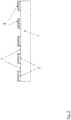
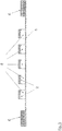
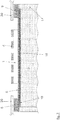
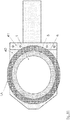
- Procédé pour le découpage par plasma (7) d'un substrat (1), le procédé comprenant :la fourniture d'un bras de transfert (40) ;la fourniture d'une chambre de traitement (10) dotée d'une paroi (10W) ;la fourniture d'une source de plasma adjacente à la paroi de la chambre de traitement (10) ;la fourniture d'un support de pièce à travailler (13) au sein de la chambre de traitement (10) ;la fourniture d'un mécanisme de levage à l'intérieur du support de pièce à travailler (13) ;la fourniture du substrat (1) ayant un diamètre, une surface supérieure et une surface inférieure, la surface supérieure du substrat (1) ayant une pluralité de structures de dispositifs (2) et des zones de rue (3) ;le placement de la surface inférieure du substrat (1) sur un film de support sur un cadre (6) pour former une pièce à travailler (1A) ;le chargement de la pièce à travailler (1A) sur le bras de transfert (40) ;le transfert de la pièce à travailler (1A) dans la chambre de traitement (10) sur le mécanisme de levage à l'aide du bras de transfert (40), le mécanisme de levage touchant le cadre (6) de la pièce à travailler (1A), le mécanisme de levage ne touchant pas le substrat (1) de la pièce à travailler (1A), le transfert de la pièce à travailler (1A) dans la chambre de traitement (10) étant effectué sous vide, le bras de transfert (40) maintenant coplanaire le cadre (6) au substrat (1) pendant l'étape de transfert, le bras de transfert (40) n'entrant pas en contact avec le substrat (1) ;la fourniture d'un anneau de couverture (20) ayant un diamètre intérieur disposé au-dessus de la pièce à travailler (1A), le diamètre intérieur de l'anneau de couverture (20) étant supérieur au diamètre du substrat (1), l'anneau de couverture (20) n'étant pas en contact avec le cadre (6) de la pièce à travailler (1A) ;la génération d'un plasma (7) par la source de plasma ; etla gravure des zones de rues non protégées (3) sur la surface supérieure du substrat (1) de la pièce à travailler (1A) dans la chambre de traitement par plasma (10) par le plasma généré (7).
- Procédé selon la revendication 1 comprenant en outre l'alignement de la pièce à travailler (1A) dans le bras de transfert (40) à l'aide d'un dispositif d'alignement.
Applications Claiming Priority (4)
| Application Number | Priority Date | Filing Date | Title |
|---|---|---|---|
| US201161452450P | 2011-03-14 | 2011-03-14 | |
| US13/412,119 US8802545B2 (en) | 2011-03-14 | 2012-03-05 | Method and apparatus for plasma dicing a semi-conductor wafer |
| PCT/US2012/028771 WO2012125560A2 (fr) | 2011-03-14 | 2012-03-12 | Procédé et appareil pour découper au plasma une tranche semi-conductrice |
| EP12719486.8A EP2686877B1 (fr) | 2011-03-14 | 2012-03-12 | Procédé pour découper au plasma une tranche semi-conductrice |
Related Parent Applications (2)
| Application Number | Title | Priority Date | Filing Date |
|---|---|---|---|
| EP12719486.8A Division EP2686877B1 (fr) | 2011-03-14 | 2012-03-12 | Procédé pour découper au plasma une tranche semi-conductrice |
| EP12719486.8A Division-Into EP2686877B1 (fr) | 2011-03-14 | 2012-03-12 | Procédé pour découper au plasma une tranche semi-conductrice |
Publications (3)
| Publication Number | Publication Date |
|---|---|
| EP2698814A2 EP2698814A2 (fr) | 2014-02-19 |
| EP2698814A3 EP2698814A3 (fr) | 2014-07-02 |
| EP2698814B1 true EP2698814B1 (fr) | 2020-07-15 |
Family
ID=46828800
Family Applications (6)
| Application Number | Title | Priority Date | Filing Date |
|---|---|---|---|
| EP13188082.5A Active EP2698814B1 (fr) | 2011-03-14 | 2012-03-12 | Procédé pour le découpage par plasma d'une plaquette de semi-conducteur |
| EP13188083.3A Withdrawn EP2698815A3 (fr) | 2011-03-14 | 2012-03-12 | Procédé et appareil pour le découpage par plasma d'une plaquette de semi-conducteur |
| EP13188081.7A Active EP2698813B1 (fr) | 2011-03-14 | 2012-03-12 | Procédé pour le découpage par plasma d'une plaquette de semi-conducteur |
| EP12719486.8A Active EP2686877B1 (fr) | 2011-03-14 | 2012-03-12 | Procédé pour découper au plasma une tranche semi-conductrice |
| EP13188079.1A Withdrawn EP2698812A3 (fr) | 2011-03-14 | 2012-03-12 | Procédé et appareil pour le découpage par plasma d'une plaquette de semi-conducteur |
| EP13188085.8A Ceased EP2698816A3 (fr) | 2011-03-14 | 2012-03-12 | Procédé et appareil pour le découpage par plasma d'une plaquette de semi-conducteur |
Family Applications After (5)
| Application Number | Title | Priority Date | Filing Date |
|---|---|---|---|
| EP13188083.3A Withdrawn EP2698815A3 (fr) | 2011-03-14 | 2012-03-12 | Procédé et appareil pour le découpage par plasma d'une plaquette de semi-conducteur |
| EP13188081.7A Active EP2698813B1 (fr) | 2011-03-14 | 2012-03-12 | Procédé pour le découpage par plasma d'une plaquette de semi-conducteur |
| EP12719486.8A Active EP2686877B1 (fr) | 2011-03-14 | 2012-03-12 | Procédé pour découper au plasma une tranche semi-conductrice |
| EP13188079.1A Withdrawn EP2698812A3 (fr) | 2011-03-14 | 2012-03-12 | Procédé et appareil pour le découpage par plasma d'une plaquette de semi-conducteur |
| EP13188085.8A Ceased EP2698816A3 (fr) | 2011-03-14 | 2012-03-12 | Procédé et appareil pour le découpage par plasma d'une plaquette de semi-conducteur |
Country Status (6)
| Country | Link |
|---|---|
| US (10) | US8802545B2 (fr) |
| EP (6) | EP2698814B1 (fr) |
| JP (10) | JP6165635B2 (fr) |
| CN (6) | CN103460350A (fr) |
| TW (7) | TW201530636A (fr) |
| WO (1) | WO2012125560A2 (fr) |
Families Citing this family (173)
| Publication number | Priority date | Publication date | Assignee | Title |
|---|---|---|---|---|
| US8642448B2 (en) | 2010-06-22 | 2014-02-04 | Applied Materials, Inc. | Wafer dicing using femtosecond-based laser and plasma etch |
| US8691702B2 (en) * | 2011-03-14 | 2014-04-08 | Plasma-Therm Llc | Method and apparatus for plasma dicing a semi-conductor wafer |
| US9343365B2 (en) * | 2011-03-14 | 2016-05-17 | Plasma-Therm Llc | Method and apparatus for plasma dicing a semi-conductor wafer |
| US8946058B2 (en) * | 2011-03-14 | 2015-02-03 | Plasma-Therm Llc | Method and apparatus for plasma dicing a semi-conductor wafer |
| US8507363B2 (en) | 2011-06-15 | 2013-08-13 | Applied Materials, Inc. | Laser and plasma etch wafer dicing using water-soluble die attach film |
| US8759197B2 (en) | 2011-06-15 | 2014-06-24 | Applied Materials, Inc. | Multi-step and asymmetrically shaped laser beam scribing |
| US8557683B2 (en) | 2011-06-15 | 2013-10-15 | Applied Materials, Inc. | Multi-step and asymmetrically shaped laser beam scribing |
| US8912077B2 (en) | 2011-06-15 | 2014-12-16 | Applied Materials, Inc. | Hybrid laser and plasma etch wafer dicing using substrate carrier |
| US9029242B2 (en) | 2011-06-15 | 2015-05-12 | Applied Materials, Inc. | Damage isolation by shaped beam delivery in laser scribing process |
| US8703581B2 (en) | 2011-06-15 | 2014-04-22 | Applied Materials, Inc. | Water soluble mask for substrate dicing by laser and plasma etch |
| US9129904B2 (en) | 2011-06-15 | 2015-09-08 | Applied Materials, Inc. | Wafer dicing using pulse train laser with multiple-pulse bursts and plasma etch |
| US8946057B2 (en) | 2012-04-24 | 2015-02-03 | Applied Materials, Inc. | Laser and plasma etch wafer dicing using UV-curable adhesive film |
| US9048309B2 (en) | 2012-07-10 | 2015-06-02 | Applied Materials, Inc. | Uniform masking for wafer dicing using laser and plasma etch |
| US8859397B2 (en) | 2012-07-13 | 2014-10-14 | Applied Materials, Inc. | Method of coating water soluble mask for laser scribing and plasma etch |
| US8940619B2 (en) | 2012-07-13 | 2015-01-27 | Applied Materials, Inc. | Method of diced wafer transportation |
| US20140051253A1 (en) * | 2012-08-14 | 2014-02-20 | Lam Research Corporation | Plasma baffle ring for a plasma processing apparatus and method of use |
| JP5849232B2 (ja) * | 2012-09-20 | 2016-01-27 | パナソニックIpマネジメント株式会社 | プラズマ処理装置及びプラズマ処理方法 |
| US9368404B2 (en) * | 2012-09-28 | 2016-06-14 | Plasma-Therm Llc | Method for dicing a substrate with back metal |
| US9252057B2 (en) | 2012-10-17 | 2016-02-02 | Applied Materials, Inc. | Laser and plasma etch wafer dicing with partial pre-curing of UV release dicing tape for film frame wafer application |
| US9484260B2 (en) | 2012-11-07 | 2016-11-01 | Semiconductor Components Industries, Llc | Heated carrier substrate semiconductor die singulation method |
| US9136173B2 (en) * | 2012-11-07 | 2015-09-15 | Semiconductor Components Industries, Llc | Singulation method for semiconductor die having a layer of material along one major surface |
| US8975162B2 (en) | 2012-12-20 | 2015-03-10 | Applied Materials, Inc. | Wafer dicing from wafer backside |
| JP6110136B2 (ja) * | 2012-12-28 | 2017-04-05 | 株式会社ディスコ | ウエーハのレーザー加工方法およびレーザー加工装置 |
| US9236305B2 (en) | 2013-01-25 | 2016-01-12 | Applied Materials, Inc. | Wafer dicing with etch chamber shield ring for film frame wafer applications |
| US9034734B2 (en) | 2013-02-04 | 2015-05-19 | Avago Technologies General Ip (Singapore) Pte. Ltd. | Systems and methods for plasma etching compound semiconductor (CS) dies and passively aligning the dies |
| JP6388886B2 (ja) * | 2013-03-06 | 2018-09-12 | プラズマ − サーム、エルエルシー | 半導体ウエハをプラズマ・ダイシングするための方法 |
| TWI619165B (zh) | 2013-03-14 | 2018-03-21 | 應用材料股份有限公司 | 以雷射及電漿蝕刻進行的基板切割所用的含非光可界定雷射能量吸收層的多層遮罩 |
| US9214423B2 (en) * | 2013-03-15 | 2015-12-15 | Semiconductor Components Industries, Llc | Method of forming a HEMT semiconductor device and structure therefor |
| JP5934939B2 (ja) * | 2013-05-09 | 2016-06-15 | パナソニックIpマネジメント株式会社 | プラズマ処理装置及びプラズマ処理方法 |
| JP5962921B2 (ja) | 2013-05-09 | 2016-08-03 | パナソニックIpマネジメント株式会社 | プラズマ処理装置及びプラズマ処理方法 |
| GB201309583D0 (en) * | 2013-05-29 | 2013-07-10 | Spts Technologies Ltd | Apparatus for processing a semiconductor workpiece |
| US20150011073A1 (en) * | 2013-07-02 | 2015-01-08 | Wei-Sheng Lei | Laser scribing and plasma etch for high die break strength and smooth sidewall |
| JP6226117B2 (ja) * | 2013-07-25 | 2017-11-08 | パナソニックIpマネジメント株式会社 | プラズマ処理装置及びプラズマ処理方法 |
| JP6226118B2 (ja) * | 2013-07-25 | 2017-11-08 | パナソニックIpマネジメント株式会社 | プラズマ処理装置及びプラズマ処理方法 |
| CN104347391B (zh) * | 2013-08-09 | 2017-05-24 | 无锡华润上华半导体有限公司 | 一种深沟槽刻蚀设备及其方法 |
| US9293303B2 (en) * | 2013-08-30 | 2016-03-22 | Taiwan Semiconductor Manufacturing Company, Ltd. | Low contamination chamber for surface activation |
| US9105710B2 (en) | 2013-08-30 | 2015-08-11 | Applied Materials, Inc. | Wafer dicing method for improving die packaging quality |
| JP6083529B2 (ja) * | 2013-09-02 | 2017-02-22 | パナソニックIpマネジメント株式会社 | プラズマ処理装置及びプラズマ処理方法 |
| JP6094813B2 (ja) * | 2013-09-02 | 2017-03-15 | パナソニックIpマネジメント株式会社 | プラズマ処理装置 |
| US9224650B2 (en) | 2013-09-19 | 2015-12-29 | Applied Materials, Inc. | Wafer dicing from wafer backside and front side |
| US20150087131A1 (en) * | 2013-09-20 | 2015-03-26 | Infineon Technologies Ag | Method for processing a chip |
| US9460966B2 (en) | 2013-10-10 | 2016-10-04 | Applied Materials, Inc. | Method and apparatus for dicing wafers having thick passivation polymer layer |
| US9041198B2 (en) | 2013-10-22 | 2015-05-26 | Applied Materials, Inc. | Maskless hybrid laser scribing and plasma etching wafer dicing process |
| JP6024921B2 (ja) * | 2013-11-01 | 2016-11-16 | パナソニックIpマネジメント株式会社 | プラズマ処理装置及びプラズマ処理方法 |
| JP5938716B2 (ja) * | 2013-11-01 | 2016-06-22 | パナソニックIpマネジメント株式会社 | プラズマ処理装置及びプラズマ処理方法 |
| WO2015068597A1 (fr) * | 2013-11-06 | 2015-05-14 | シャープ株式会社 | Procédé de fabrication d'élément à semi-conducteur, et élément à semi-conducteur |
| TWI671812B (zh) * | 2013-11-13 | 2019-09-11 | 東芝股份有限公司 | 半導體晶片之製造方法、半導體晶片及半導體裝置 |
| JP6441025B2 (ja) * | 2013-11-13 | 2018-12-19 | 株式会社東芝 | 半導体チップの製造方法 |
| US9312177B2 (en) | 2013-12-06 | 2016-04-12 | Applied Materials, Inc. | Screen print mask for laser scribe and plasma etch wafer dicing process |
| US9299614B2 (en) | 2013-12-10 | 2016-03-29 | Applied Materials, Inc. | Method and carrier for dicing a wafer |
| US9293304B2 (en) | 2013-12-17 | 2016-03-22 | Applied Materials, Inc. | Plasma thermal shield for heat dissipation in plasma chamber |
| US9018079B1 (en) | 2014-01-29 | 2015-04-28 | Applied Materials, Inc. | Wafer dicing using hybrid laser scribing and plasma etch approach with intermediate reactive post mask-opening clean |
| US9299611B2 (en) | 2014-01-29 | 2016-03-29 | Applied Materials, Inc. | Method of wafer dicing using hybrid laser scribing and plasma etch approach with mask plasma treatment for improved mask etch resistance |
| US9236284B2 (en) | 2014-01-31 | 2016-01-12 | Applied Materials, Inc. | Cooled tape frame lift and low contact shadow ring for plasma heat isolation |
| US8991329B1 (en) | 2014-01-31 | 2015-03-31 | Applied Materials, Inc. | Wafer coating |
| CN106068548B (zh) * | 2014-03-07 | 2020-02-28 | 等离子瑟姆有限公司 | 用于对半导体晶圆进行等离子体切片的方法和设备 |
| US9275902B2 (en) | 2014-03-26 | 2016-03-01 | Applied Materials, Inc. | Dicing processes for thin wafers with bumps on wafer backside |
| US9076860B1 (en) | 2014-04-04 | 2015-07-07 | Applied Materials, Inc. | Residue removal from singulated die sidewall |
| US8975163B1 (en) | 2014-04-10 | 2015-03-10 | Applied Materials, Inc. | Laser-dominated laser scribing and plasma etch hybrid wafer dicing |
| US8932939B1 (en) | 2014-04-14 | 2015-01-13 | Applied Materials, Inc. | Water soluble mask formation by dry film lamination |
| US8912078B1 (en) | 2014-04-16 | 2014-12-16 | Applied Materials, Inc. | Dicing wafers having solder bumps on wafer backside |
| US8999816B1 (en) | 2014-04-18 | 2015-04-07 | Applied Materials, Inc. | Pre-patterned dry laminate mask for wafer dicing processes |
| US9159621B1 (en) | 2014-04-29 | 2015-10-13 | Applied Materials, Inc. | Dicing tape protection for wafer dicing using laser scribe process |
| US8912075B1 (en) | 2014-04-29 | 2014-12-16 | Applied Materials, Inc. | Wafer edge warp supression for thin wafer supported by tape frame |
| JP6364933B2 (ja) * | 2014-05-01 | 2018-08-01 | 住友電気工業株式会社 | 半導体光デバイスを製造する方法 |
| KR101940981B1 (ko) | 2014-05-05 | 2019-01-23 | 3디 글래스 솔루션즈 인코포레이티드 | 2d 및 3d 인덕터 안테나 및 변압기 제작 광 활성 기판 |
| US8980727B1 (en) | 2014-05-07 | 2015-03-17 | Applied Materials, Inc. | Substrate patterning using hybrid laser scribing and plasma etching processing schemes |
| US9112050B1 (en) * | 2014-05-13 | 2015-08-18 | Applied Materials, Inc. | Dicing tape thermal management by wafer frame support ring cooling during plasma dicing |
| US20150334812A1 (en) * | 2014-05-16 | 2015-11-19 | John Mazzocco | Design to manage charge and discharge of wafers and wafer carrier rings |
| JP2015220366A (ja) * | 2014-05-19 | 2015-12-07 | 株式会社ディスコ | ウェーハの加工方法 |
| US9034771B1 (en) | 2014-05-23 | 2015-05-19 | Applied Materials, Inc. | Cooling pedestal for dicing tape thermal management during plasma dicing |
| JP6319687B2 (ja) * | 2014-05-26 | 2018-05-09 | パナソニックIpマネジメント株式会社 | プラズマ処理装置及び方法 |
| JP6399435B2 (ja) * | 2014-05-26 | 2018-10-03 | パナソニックIpマネジメント株式会社 | プラズマ処理方法及び装置 |
| US20150371889A1 (en) * | 2014-06-20 | 2015-12-24 | Applied Materials, Inc. | Methods for shallow trench isolation formation in a silicon germanium layer |
| US9093518B1 (en) | 2014-06-30 | 2015-07-28 | Applied Materials, Inc. | Singulation of wafers having wafer-level underfill |
| US9130057B1 (en) | 2014-06-30 | 2015-09-08 | Applied Materials, Inc. | Hybrid dicing process using a blade and laser |
| US9165832B1 (en) | 2014-06-30 | 2015-10-20 | Applied Materials, Inc. | Method of die singulation using laser ablation and induction of internal defects with a laser |
| US9142459B1 (en) | 2014-06-30 | 2015-09-22 | Applied Materials, Inc. | Wafer dicing using hybrid laser scribing and plasma etch approach with mask application by vacuum lamination |
| CN105336561B (zh) * | 2014-07-18 | 2017-07-21 | 中微半导体设备(上海)有限公司 | 等离子体刻蚀装置 |
| US9349648B2 (en) | 2014-07-22 | 2016-05-24 | Applied Materials, Inc. | Hybrid wafer dicing approach using a rectangular shaped two-dimensional top hat laser beam profile or a linear shaped one-dimensional top hat laser beam profile laser scribing process and plasma etch process |
| US9117868B1 (en) * | 2014-08-12 | 2015-08-25 | Applied Materials, Inc. | Bipolar electrostatic chuck for dicing tape thermal management during plasma dicing |
| US9196498B1 (en) | 2014-08-12 | 2015-11-24 | Applied Materials, Inc. | Stationary actively-cooled shadow ring for heat dissipation in plasma chamber |
| US10283334B2 (en) * | 2014-08-22 | 2019-05-07 | Applied Materials, Inc. | Methods and apparatus for maintaining low non-uniformity over target life |
| US9385041B2 (en) | 2014-08-26 | 2016-07-05 | Semiconductor Components Industries, Llc | Method for insulating singulated electronic die |
| JP6296297B2 (ja) | 2014-08-27 | 2018-03-20 | パナソニックIpマネジメント株式会社 | プラズマ処理装置およびプラズマ処理方法 |
| US9281244B1 (en) | 2014-09-18 | 2016-03-08 | Applied Materials, Inc. | Hybrid wafer dicing approach using an adaptive optics-controlled laser scribing process and plasma etch process |
| US11195756B2 (en) | 2014-09-19 | 2021-12-07 | Applied Materials, Inc. | Proximity contact cover ring for plasma dicing |
| US9177861B1 (en) | 2014-09-19 | 2015-11-03 | Applied Materials, Inc. | Hybrid wafer dicing approach using laser scribing process based on an elliptical laser beam profile or a spatio-temporal controlled laser beam profile |
| US9196536B1 (en) | 2014-09-25 | 2015-11-24 | Applied Materials, Inc. | Hybrid wafer dicing approach using a phase modulated laser beam profile laser scribing process and plasma etch process |
| US9543157B2 (en) * | 2014-09-30 | 2017-01-10 | Infineon Technologies Ag | Method for processing a carrier, a method for operating a plasma processing chamber, and a method for processing a semiconductor wafer |
| US9130056B1 (en) | 2014-10-03 | 2015-09-08 | Applied Materials, Inc. | Bi-layer wafer-level underfill mask for wafer dicing and approaches for performing wafer dicing |
| US9245803B1 (en) | 2014-10-17 | 2016-01-26 | Applied Materials, Inc. | Hybrid wafer dicing approach using a bessel beam shaper laser scribing process and plasma etch process |
| US10692765B2 (en) | 2014-11-07 | 2020-06-23 | Applied Materials, Inc. | Transfer arm for film frame substrate handling during plasma singulation of wafers |
| JP6254509B2 (ja) * | 2014-11-07 | 2017-12-27 | 信越化学工業株式会社 | 電磁波シールド性支持基材付封止材及び封止後半導体素子搭載基板、封止後半導体素子形成ウエハ並びに半導体装置 |
| CN105789008B (zh) * | 2014-12-22 | 2017-12-19 | 中微半导体设备(上海)有限公司 | 等离子体处理装置及等离子体刻蚀方法 |
| CN105789010B (zh) * | 2014-12-24 | 2017-11-10 | 中微半导体设备(上海)有限公司 | 等离子体处理装置及等离子体分布的调节方法 |
| US9330977B1 (en) | 2015-01-05 | 2016-05-03 | Applied Materials, Inc. | Hybrid wafer dicing approach using a galvo scanner and linear stage hybrid motion laser scribing process and plasma etch process |
| US9355907B1 (en) | 2015-01-05 | 2016-05-31 | Applied Materials, Inc. | Hybrid wafer dicing approach using a line shaped laser beam profile laser scribing process and plasma etch process |
| US9159624B1 (en) | 2015-01-05 | 2015-10-13 | Applied Materials, Inc. | Vacuum lamination of polymeric dry films for wafer dicing using hybrid laser scribing and plasma etch approach |
| DE102015100783A1 (de) | 2015-01-20 | 2016-07-21 | Infineon Technologies Ag | Verfahren zum Zertrennen eines Wafers und Halbleiterchip |
| JP6367727B2 (ja) * | 2015-01-30 | 2018-08-01 | 東京エレクトロン株式会社 | 洗浄装置、剥離システム、洗浄方法、剥離方法、プログラム、および情報記憶媒体 |
| CN106024566B (zh) * | 2015-03-31 | 2019-07-05 | 松下知识产权经营株式会社 | 等离子处理装置以及等离子处理方法 |
| CN106024565B (zh) * | 2015-03-31 | 2019-11-19 | 松下知识产权经营株式会社 | 等离子处理装置以及等离子处理方法 |
| US10903055B2 (en) | 2015-04-17 | 2021-01-26 | Applied Materials, Inc. | Edge ring for bevel polymer reduction |
| KR101682155B1 (ko) * | 2015-04-20 | 2016-12-02 | 주식회사 유진테크 | 기판 처리 장치 |
| US9601375B2 (en) | 2015-04-27 | 2017-03-21 | Applied Materials, Inc. | UV-cure pre-treatment of carrier film for wafer dicing using hybrid laser scribing and plasma etch approach |
| US9478455B1 (en) | 2015-06-12 | 2016-10-25 | Applied Materials, Inc. | Thermal pyrolytic graphite shadow ring assembly for heat dissipation in plasma chamber |
| US9721839B2 (en) | 2015-06-12 | 2017-08-01 | Applied Materials, Inc. | Etch-resistant water soluble mask for hybrid wafer dicing using laser scribing and plasma etch |
| KR102382823B1 (ko) * | 2015-09-04 | 2022-04-06 | 삼성전자주식회사 | 에어 홀을 갖는 링 부재 및 그를 포함하는 기판 처리 장치 |
| US9779986B2 (en) | 2015-09-07 | 2017-10-03 | Panasonic Intellectual Property Management Co., Ltd. | Plasma treatment method and method of manufacturing electronic component |
| JP6492287B2 (ja) * | 2015-10-01 | 2019-04-03 | パナソニックIpマネジメント株式会社 | 素子チップの製造方法および電子部品実装構造体の製造方法 |
| GB201518756D0 (en) * | 2015-10-22 | 2015-12-09 | Spts Technologies Ltd | Apparatus for plasma dicing |
| CN113675131A (zh) * | 2015-11-09 | 2021-11-19 | 古河电气工业株式会社 | 半导体芯片的制造方法和用于该制造方法的掩模一体型表面保护带 |
| EP4002724A1 (fr) | 2015-12-13 | 2022-05-25 | Genxcomm, Inc. | Procédés et appareil d'annulation d'interférence |
| JP6467592B2 (ja) * | 2016-02-04 | 2019-02-13 | パナソニックIpマネジメント株式会社 | 素子チップの製造方法および電子部品実装構造体の製造方法ならびに電子部品実装構造体 |
| US9972575B2 (en) | 2016-03-03 | 2018-05-15 | Applied Materials, Inc. | Hybrid wafer dicing approach using a split beam laser scribing process and plasma etch process |
| JP2017162901A (ja) * | 2016-03-08 | 2017-09-14 | 株式会社ディスコ | ウエーハの分割方法 |
| JP6519802B2 (ja) | 2016-03-18 | 2019-05-29 | パナソニックIpマネジメント株式会社 | プラズマ処理方法およびプラズマ処理装置 |
| US9852997B2 (en) | 2016-03-25 | 2017-12-26 | Applied Materials, Inc. | Hybrid wafer dicing approach using a rotating beam laser scribing process and plasma etch process |
| US9793132B1 (en) | 2016-05-13 | 2017-10-17 | Applied Materials, Inc. | Etch mask for hybrid laser scribing and plasma etch wafer singulation process |
| GB201611652D0 (en) * | 2016-07-04 | 2016-08-17 | Spts Technologies Ltd | Method of detecting a condition |
| US10257746B2 (en) | 2016-07-16 | 2019-04-09 | GenXComm, Inc. | Interference cancellation methods and apparatus |
| JP6822802B2 (ja) * | 2016-09-05 | 2021-01-27 | 株式会社ディスコ | ウエーハの加工方法 |
| JP6807558B2 (ja) * | 2016-11-08 | 2021-01-06 | パナソニックIpマネジメント株式会社 | プラズマ処理方法およびプラズマ処理装置 |
| US20180143332A1 (en) | 2016-11-18 | 2018-05-24 | Plasma-Therm Llc | Ion Filter |
| JP6340655B2 (ja) * | 2017-01-10 | 2018-06-13 | パナソニックIpマネジメント株式会社 | プラズマ処理装置及びプラズマ処理方法 |
| JP6650593B2 (ja) * | 2017-02-17 | 2020-02-19 | パナソニックIpマネジメント株式会社 | プラズマ処理装置およびプラズマ処理方法 |
| JP6524562B2 (ja) | 2017-02-23 | 2019-06-05 | パナソニックIpマネジメント株式会社 | 素子チップおよびその製造方法 |
| JP2018156973A (ja) * | 2017-03-15 | 2018-10-04 | 株式会社ディスコ | ウェーハの加工方法 |
| JP6861570B2 (ja) * | 2017-04-27 | 2021-04-21 | 東京エレクトロン株式会社 | 基板処理装置 |
| JP6899252B2 (ja) * | 2017-05-10 | 2021-07-07 | 株式会社ディスコ | 加工方法 |
| US10373869B2 (en) | 2017-05-24 | 2019-08-06 | Semiconductor Components Industries, Llc | Method of separating a back layer on a substrate using exposure to reduced temperature and related apparatus |
| US11158540B2 (en) | 2017-05-26 | 2021-10-26 | Applied Materials, Inc. | Light-absorbing mask for hybrid laser scribing and plasma etch wafer singulation process |
| US10363629B2 (en) | 2017-06-01 | 2019-07-30 | Applied Materials, Inc. | Mitigation of particle contamination for wafer dicing processes |
| CN107248499B (zh) * | 2017-06-20 | 2019-11-26 | 上海华力微电子有限公司 | 静电释放装置及制造方法、聚焦离子束设备及使用方法 |
| JP6524564B2 (ja) | 2017-06-28 | 2019-06-05 | パナソニックIpマネジメント株式会社 | 素子チップの製造方法および基板加熱装置 |
| JP7069605B2 (ja) * | 2017-08-29 | 2022-05-18 | 富士電機株式会社 | 半導体装置の製造方法 |
| JP7045635B2 (ja) | 2017-08-30 | 2022-04-01 | パナソニックIpマネジメント株式会社 | プラズマ処理装置及び方法 |
| NL2019623B1 (en) * | 2017-09-25 | 2019-04-01 | Suss Microtec Lithography Gmbh | Wafer support system, wafer support device, system comprising a wafer and a wafer support device as well as mask aligner |
| JP6782215B2 (ja) * | 2017-10-18 | 2020-11-11 | 古河電気工業株式会社 | プラズマダイシング用マスク材、マスク一体型表面保護テープおよび半導体チップの製造方法 |
| JP6982837B2 (ja) | 2017-10-20 | 2021-12-17 | パナソニックIpマネジメント株式会社 | プラズマ処理方法 |
| US10854946B2 (en) | 2017-12-15 | 2020-12-01 | 3D Glass Solutions, Inc. | Coupled transmission line resonate RF filter |
| JP6998545B2 (ja) | 2017-12-25 | 2022-01-18 | パナソニックIpマネジメント株式会社 | 素子チップの製造方法 |
| CA3082624C (fr) | 2018-01-04 | 2022-12-06 | 3D Glass Solutions, Inc. | Structure conductrice d'adaptation d'impedance pour circuits rf a haute efficacite |
| US10665494B2 (en) * | 2018-01-31 | 2020-05-26 | Applied Materials, Inc. | Automated apparatus to temporarily attach substrates to carriers without adhesives for processing |
| US10535561B2 (en) | 2018-03-12 | 2020-01-14 | Applied Materials, Inc. | Hybrid wafer dicing approach using a multiple pass laser scribing process and plasma etch process |
| CN110277343B (zh) * | 2018-03-14 | 2023-06-30 | Toto株式会社 | 静电吸盘 |
| JP2018137483A (ja) * | 2018-05-23 | 2018-08-30 | Sppテクノロジーズ株式会社 | プラズマ加工方法及びこの方法を用いて製造された基板 |
| US10916474B2 (en) * | 2018-06-25 | 2021-02-09 | Semiconductor Components Industries, Llc | Method of reducing residual contamination in singulated semiconductor die |
| CN110634796A (zh) * | 2018-06-25 | 2019-12-31 | 半导体元件工业有限责任公司 | 用于处理电子管芯的方法及半导体晶圆和管芯的切单方法 |
| US11355394B2 (en) | 2018-09-13 | 2022-06-07 | Applied Materials, Inc. | Wafer dicing using hybrid laser scribing and plasma etch approach with intermediate breakthrough treatment |
| US10607889B1 (en) * | 2018-09-19 | 2020-03-31 | Semiconductor Components Industries, Llc | Jet ablation die singulation systems and related methods |
| JP7209247B2 (ja) * | 2018-09-25 | 2023-01-20 | パナソニックIpマネジメント株式会社 | 素子チップの製造方法 |
| TWI675413B (zh) * | 2018-10-08 | 2019-10-21 | 華邦電子股份有限公司 | 切割晶圓的方法 |
| US11150409B2 (en) | 2018-12-27 | 2021-10-19 | GenXComm, Inc. | Saw assisted facet etch dicing |
| KR102393450B1 (ko) | 2018-12-28 | 2022-05-04 | 3디 글래스 솔루션즈 인코포레이티드 | 광활성 유리 기판들에서 rf, 마이크로파, 및 mm 파 시스템들을 위한 이종 통합 |
| US10818551B2 (en) | 2019-01-09 | 2020-10-27 | Semiconductor Components Industries, Llc | Plasma die singulation systems and related methods |
| JP7140435B2 (ja) | 2019-04-05 | 2022-09-21 | スリーディー グラス ソリューションズ,インク | ガラスベースの空基板集積導波路デバイス |
| WO2020214788A1 (fr) | 2019-04-18 | 2020-10-22 | 3D Glass Solutions, Inc. | Libération et découpage à l'emporte-pièce à haut rendement |
| US10727945B1 (en) | 2019-07-15 | 2020-07-28 | GenXComm, Inc. | Efficiently combining multiple taps of an optical filter |
| US11011424B2 (en) | 2019-08-06 | 2021-05-18 | Applied Materials, Inc. | Hybrid wafer dicing approach using a spatially multi-focused laser beam laser scribing process and plasma etch process |
| US11342226B2 (en) | 2019-08-13 | 2022-05-24 | Applied Materials, Inc. | Hybrid wafer dicing approach using an actively-focused laser beam laser scribing process and plasma etch process |
| US10903121B1 (en) | 2019-08-14 | 2021-01-26 | Applied Materials, Inc. | Hybrid wafer dicing approach using a uniform rotating beam laser scribing process and plasma etch process |
| JP7281741B2 (ja) | 2019-08-23 | 2023-05-26 | パナソニックIpマネジメント株式会社 | 素子チップのスムージング方法および素子チップの製造方法 |
| KR102366179B1 (ko) * | 2019-08-23 | 2022-02-22 | 세메스 주식회사 | 반송 장치 및 이를 가지는 기판 처리 장치 |
| US11215755B2 (en) | 2019-09-19 | 2022-01-04 | GenXComm, Inc. | Low loss, polarization-independent, large bandwidth mode converter for edge coupling |
| US11539394B2 (en) | 2019-10-29 | 2022-12-27 | GenXComm, Inc. | Self-interference mitigation in in-band full-duplex communication systems |
| US11600492B2 (en) | 2019-12-10 | 2023-03-07 | Applied Materials, Inc. | Electrostatic chuck with reduced current leakage for hybrid laser scribing and plasma etch wafer singulation process |
| TWI712104B (zh) * | 2020-01-10 | 2020-12-01 | 力成科技股份有限公司 | 晶片固定裝置 |
| CA3177603C (fr) | 2020-04-17 | 2024-01-09 | 3D Glass Solutions, Inc. | Induction de large bande |
| US11796737B2 (en) | 2020-08-10 | 2023-10-24 | GenXComm, Inc. | Co-manufacturing of silicon-on-insulator waveguides and silicon nitride waveguides for hybrid photonic integrated circuits |
| US11972970B1 (en) | 2020-09-01 | 2024-04-30 | Hrl Laboratories, Llc | Singulation process for chiplets |
| CA3234722A1 (fr) | 2021-10-25 | 2023-05-04 | Farzad Mokhtari-Koushyar | Circuits integres photoniques hybrides pour generateurs de signaux a bruit de phase ultra faible |
Family Cites Families (229)
| Publication number | Priority date | Publication date | Assignee | Title |
|---|---|---|---|---|
| JPS5676242A (en) * | 1979-11-26 | 1981-06-23 | Tokyo Ohka Kogyo Co Ltd | Treating apparatus using gas plasma reaction |
| US4377436A (en) * | 1980-05-13 | 1983-03-22 | Bell Telephone Laboratories, Incorporated | Plasma-assisted etch process with endpoint detection |
| JPS59147433A (ja) * | 1983-02-14 | 1984-08-23 | Hitachi Ltd | エツチング装置 |
| US4496425A (en) * | 1984-01-30 | 1985-01-29 | At&T Technologies, Inc. | Technique for determining the end point of an etching process |
| DE3615361C2 (de) * | 1986-05-06 | 1994-09-01 | Santos Pereira Ribeiro Car Dos | Vorrichtung zur Oberflächenbehandlung von Werkstücken |
| US4717446A (en) * | 1986-09-18 | 1988-01-05 | Motorola Inc. | Method of detecting the endpoint of the etch of epitaxially grown silicon |
| US4687539A (en) * | 1986-10-29 | 1987-08-18 | International Business Machines Corp. | End point detection and control of laser induced dry chemical etching |
| JPH0291958A (ja) * | 1988-09-29 | 1990-03-30 | Tokyo Electron Ltd | 搬送装置 |
| JPH02114530A (ja) * | 1988-10-25 | 1990-04-26 | Mitsubishi Electric Corp | 薄膜形成装置 |
| JPH07101685B2 (ja) * | 1989-01-26 | 1995-11-01 | 富士通株式会社 | マイクロ波プラズマ処理装置 |
| JPH0750700B2 (ja) | 1989-06-27 | 1995-05-31 | 三菱電機株式会社 | 半導体チップの製造方法 |
| US5013400A (en) * | 1990-01-30 | 1991-05-07 | General Signal Corporation | Dry etch process for forming champagne profiles, and dry etch apparatus |
| US5202008A (en) * | 1990-03-02 | 1993-04-13 | Applied Materials, Inc. | Method for preparing a shield to reduce particles in a physical vapor deposition chamber |
| JPH03257182A (ja) | 1990-03-07 | 1991-11-15 | Hitachi Ltd | 表面加工装置 |
| US4975141A (en) * | 1990-03-30 | 1990-12-04 | International Business Machines Corporation | Laser ablation for plasma etching endpoint detection |
| US5447570A (en) * | 1990-04-23 | 1995-09-05 | Genus, Inc. | Purge gas in wafer coating area selection |
| JP2888258B2 (ja) * | 1990-11-30 | 1999-05-10 | 東京エレクトロン株式会社 | 基板処理装置および基板処理方法 |
| US5279669A (en) * | 1991-12-13 | 1994-01-18 | International Business Machines Corporation | Plasma reactor for processing substrates comprising means for inducing electron cyclotron resonance (ECR) and ion cyclotron resonance (ICR) conditions |
| KR100324792B1 (ko) * | 1993-03-31 | 2002-06-20 | 히가시 데쓰로 | 플라즈마처리장치 |
| US5591269A (en) * | 1993-06-24 | 1997-01-07 | Tokyo Electron Limited | Vacuum processing apparatus |
| US5449410A (en) * | 1993-07-28 | 1995-09-12 | Applied Materials, Inc. | Plasma processing apparatus |
| US5389182A (en) * | 1993-08-02 | 1995-02-14 | Texas Instruments Incorporated | Use of a saw frame with tape as a substrate carrier for wafer level backend processing |
| US5405488A (en) * | 1993-09-13 | 1995-04-11 | Vlsi Technology, Inc. | System and method for plasma etching endpoint detection |
| TW357404B (en) | 1993-12-24 | 1999-05-01 | Tokyo Electron Ltd | Apparatus and method for processing of plasma |
| JP3118497B2 (ja) * | 1993-12-24 | 2000-12-18 | 東京エレクトロン株式会社 | プラズマ処理装置及びプラズマ処理方法 |
| JP3264076B2 (ja) * | 1994-01-31 | 2002-03-11 | 松下電器産業株式会社 | 真空処理装置 |
| US5680013A (en) * | 1994-03-15 | 1997-10-21 | Applied Materials, Inc. | Ceramic protection for heated metal surfaces of plasma processing chamber exposed to chemically aggressive gaseous environment therein and method of protecting such heated metal surfaces |
| US5783100A (en) * | 1994-03-16 | 1998-07-21 | Micron Display Technology, Inc. | Method of high density plasma etching for semiconductor manufacture |
| US5900103A (en) * | 1994-04-20 | 1999-05-04 | Tokyo Electron Limited | Plasma treatment method and apparatus |
| US5685914A (en) * | 1994-04-05 | 1997-11-11 | Applied Materials, Inc. | Focus ring for semiconductor wafer processing in a plasma reactor |
| US6391147B2 (en) * | 1994-04-28 | 2002-05-21 | Tokyo Electron Limited | Plasma treatment method and apparatus |
| JPH07312362A (ja) * | 1994-05-17 | 1995-11-28 | Nissin Electric Co Ltd | ドライエッチング装置 |
| US5744049A (en) * | 1994-07-18 | 1998-04-28 | Applied Materials, Inc. | Plasma reactor with enhanced plasma uniformity by gas addition, and method of using same |
| TW295677B (fr) * | 1994-08-19 | 1997-01-11 | Tokyo Electron Co Ltd | |
| JP2718901B2 (ja) | 1994-10-31 | 1998-02-25 | ローム株式会社 | 半導体装置の製造方法 |
| DE19505906A1 (de) | 1995-02-21 | 1996-08-22 | Siemens Ag | Verfahren zum Damage-Ätzen der Rückseite einer Halbleiterscheibe bei geschützter Scheibenvorderseite |
| JP3350278B2 (ja) * | 1995-03-06 | 2002-11-25 | 大日本スクリーン製造株式会社 | 基板処理装置 |
| EP0735565B1 (fr) * | 1995-03-31 | 1999-06-02 | International Business Machines Corporation | Méthode et appareil pour contrÔler la gravure sèche d'un film diélectrique jusqu'à une épaisseur donnée |
| TW434745B (en) * | 1995-06-07 | 2001-05-16 | Tokyo Electron Ltd | Plasma processing apparatus |
| TW309503B (fr) * | 1995-06-27 | 1997-07-01 | Tokyo Electron Co Ltd | |
| JPH09129607A (ja) * | 1995-11-01 | 1997-05-16 | Canon Inc | マイクロ波プラズマエッチング装置及び方法 |
| JP3005461B2 (ja) * | 1995-11-24 | 2000-01-31 | 日本電気株式会社 | 静電チャック |
| US5669977A (en) | 1995-12-22 | 1997-09-23 | Lam Research Corporation | Shape memory alloy lift pins for semiconductor processing equipment |
| US5891348A (en) * | 1996-01-26 | 1999-04-06 | Applied Materials, Inc. | Process gas focusing apparatus and method |
| DE69725245T2 (de) | 1996-08-01 | 2004-08-12 | Surface Technoloy Systems Plc | Verfahren zur Ätzung von Substraten |
| TW334609B (en) * | 1996-09-19 | 1998-06-21 | Hitachi Ltd | Electrostatic chuck, method and device for processing sanyle use the same |
| JPH10150025A (ja) * | 1996-11-20 | 1998-06-02 | Mitsubishi Electric Corp | プラズマ反応装置 |
| JPH10172954A (ja) * | 1996-12-06 | 1998-06-26 | Hitachi Ltd | プラズマ処理装置 |
| EP0860513A3 (fr) * | 1997-02-19 | 2000-01-12 | Canon Kabushiki Kaisha | Appareillage et procédé pour la production des couches minces |
| US6332359B1 (en) | 1997-04-24 | 2001-12-25 | Fuji Electric Co., Ltd. | Semiconductor sensor chip and method for producing the chip, and semiconductor sensor and package for assembling the sensor |
| US6071372A (en) * | 1997-06-05 | 2000-06-06 | Applied Materials, Inc. | RF plasma etch reactor with internal inductive coil antenna and electrically conductive chamber walls |
| EP1029099A2 (fr) * | 1997-10-15 | 2000-08-23 | Tokyo Electron Limited | Appareil et procede de reglage de la distribution densimetrique d'un plasma |
| JPH11176813A (ja) * | 1997-12-12 | 1999-07-02 | Nec Kyushu Ltd | ドライエッチング装置 |
| JP4035225B2 (ja) * | 1998-03-20 | 2008-01-16 | 株式会社日立製作所 | プラズマ処理方法 |
| US6203657B1 (en) * | 1998-03-31 | 2001-03-20 | Lam Research Corporation | Inductively coupled plasma downstream strip module |
| JPH11307513A (ja) * | 1998-04-20 | 1999-11-05 | Sony Corp | 絶縁体基板対応プラズマ処理装置 |
| US6068783A (en) * | 1998-04-28 | 2000-05-30 | Winbond Electronics Corp | In-situ and non-intrusive method for monitoring plasma etch chamber condition utilizing spectroscopic technique |
| US6126848A (en) * | 1998-05-06 | 2000-10-03 | International Business Machines Corporation | Indirect endpoint detection by chemical reaction and chemiluminescence |
| US6071822A (en) * | 1998-06-08 | 2000-06-06 | Plasma-Therm, Inc. | Etching process for producing substantially undercut free silicon on insulator structures |
| JP2000021861A (ja) * | 1998-07-03 | 2000-01-21 | Sony Corp | ドライエッチング装置 |
| JP4163857B2 (ja) * | 1998-11-04 | 2008-10-08 | サーフィス テクノロジー システムズ ピーエルシー | 基板をエッチングするための方法と装置 |
| US6168668B1 (en) * | 1998-11-25 | 2001-01-02 | Applied Materials, Inc. | Shadow ring and guide for supporting the shadow ring in a chamber |
| KR100768610B1 (ko) * | 1998-12-11 | 2007-10-18 | 서페이스 테크놀로지 시스템스 피엘씨 | 플라즈마 처리장치 |
| US6305677B1 (en) * | 1999-03-30 | 2001-10-23 | Lam Research Corporation | Perimeter wafer lifting |
| JP2000286328A (ja) * | 1999-03-31 | 2000-10-13 | Tokyo Electron Ltd | ガス処理装置 |
| US6339028B2 (en) * | 1999-04-27 | 2002-01-15 | Stmicroelectronics, Inc. | Vacuum loadlock ultra violet bake for plasma etch |
| DE19919469A1 (de) * | 1999-04-29 | 2000-11-02 | Bosch Gmbh Robert | Verfahren zum Plasmaätzen von Silizium |
| JP2001023955A (ja) * | 1999-07-07 | 2001-01-26 | Mitsubishi Electric Corp | プラズマ処理装置 |
| JP4288767B2 (ja) * | 1999-07-07 | 2009-07-01 | 東京エレクトロン株式会社 | 半導体装置の製造方法 |
| US6992876B1 (en) | 1999-07-08 | 2006-01-31 | Lam Research Corporation | Electrostatic chuck and its manufacturing method |
| US6406545B2 (en) * | 1999-07-27 | 2002-06-18 | Kabushiki Kaisha Toshiba | Semiconductor workpiece processing apparatus and method |
| JP4387007B2 (ja) | 1999-10-26 | 2009-12-16 | 株式会社ディスコ | 半導体ウェーハの分割方法 |
| US6176931B1 (en) * | 1999-10-29 | 2001-01-23 | International Business Machines Corporation | Wafer clamp ring for use in an ionized physical vapor deposition apparatus |
| DE10060002B4 (de) * | 1999-12-07 | 2016-01-28 | Komatsu Ltd. | Vorrichtung zur Oberflächenbehandlung |
| JP2001168087A (ja) * | 1999-12-10 | 2001-06-22 | Nec Corp | プラズマ処理装置およびプラズマ処理装置のステージ製造方法 |
| DE10016340C1 (de) | 2000-03-31 | 2001-12-06 | Promos Technologies Inc | Verfahren zur Herstellung von flaschenförmigen Tiefgräben zur Verwendung in Halbleitervorrichtungen |
| KR100367662B1 (ko) * | 2000-05-02 | 2003-01-10 | 주식회사 셈테크놀러지 | 하이퍼서멀 중성입자 발생 장치 및 이를 채용하는 중성입자 처리 장치 |
| JP2001335937A (ja) * | 2000-05-29 | 2001-12-07 | Mitsubishi Heavy Ind Ltd | 金属汚染低減方法及びプラズマ装置の再生方法 |
| US6221166B1 (en) | 2000-06-07 | 2001-04-24 | Simplus Systems Corporation | Multi-thermal zone shielding apparatus |
| DE10031252A1 (de) * | 2000-06-27 | 2002-01-10 | Bosch Gmbh Robert | Verfahren zur Zertrennung eines Substratwafers in eine Anzahl von Substratchips |
| JP3792999B2 (ja) * | 2000-06-28 | 2006-07-05 | 株式会社東芝 | プラズマ処理装置 |
| JP3605009B2 (ja) * | 2000-08-03 | 2004-12-22 | 三洋電機株式会社 | 半導体装置の製造方法 |
| US20020185226A1 (en) * | 2000-08-10 | 2002-12-12 | Lea Leslie Michael | Plasma processing apparatus |
| JP3379518B2 (ja) | 2000-08-14 | 2003-02-24 | 株式会社村田製作所 | 圧電素子の製造方法 |
| JP2002093752A (ja) * | 2000-09-14 | 2002-03-29 | Tokyo Electron Ltd | 半導体素子分離方法及び半導体素子分離装置 |
| US6726804B2 (en) * | 2001-01-22 | 2004-04-27 | Liang-Guo Wang | RF power delivery for plasma processing using modulated power signal |
| JP2002246354A (ja) * | 2001-02-14 | 2002-08-30 | Enya Systems Ltd | ウエ−ハの処理方法及びそれに用いるメカニカルチャック装置 |
| US6935466B2 (en) | 2001-03-01 | 2005-08-30 | Applied Materials, Inc. | Lift pin alignment and operation methods and apparatus |
| JP2002270598A (ja) | 2001-03-13 | 2002-09-20 | Tokyo Electron Ltd | プラズマ処理装置 |
| US6761796B2 (en) * | 2001-04-06 | 2004-07-13 | Axcelis Technologies, Inc. | Method and apparatus for micro-jet enabled, low-energy ion generation transport in plasma processing |
| US6755150B2 (en) * | 2001-04-20 | 2004-06-29 | Applied Materials Inc. | Multi-core transformer plasma source |
| US6483690B1 (en) | 2001-06-28 | 2002-11-19 | Lam Research Corporation | Ceramic electrostatic chuck assembly and method of making |
| US6686225B2 (en) | 2001-07-27 | 2004-02-03 | Texas Instruments Incorporated | Method of separating semiconductor dies from a wafer |
| JP4518712B2 (ja) * | 2001-08-13 | 2010-08-04 | キヤノンアネルバ株式会社 | トレイ式マルチチャンバー基板処理装置 |
| TWI220423B (en) | 2001-08-30 | 2004-08-21 | Hrl Lab Llc | A method of fabrication of a sensor |
| JP2003077699A (ja) * | 2001-09-04 | 2003-03-14 | Canon Inc | プラズマ処理方法及び装置 |
| JP2003100708A (ja) * | 2001-09-27 | 2003-04-04 | Mitsubishi Electric Corp | 終点判別方法、半導体処理装置および半導体装置の製造方法 |
| US20030062064A1 (en) * | 2001-09-28 | 2003-04-03 | Infineon Technologies North America Corp. | Method of removing PECVD residues of fluorinated plasma using in-situ H2 plasma |
| US6642127B2 (en) | 2001-10-19 | 2003-11-04 | Applied Materials, Inc. | Method for dicing a semiconductor wafer |
| US6949395B2 (en) | 2001-10-22 | 2005-09-27 | Oriol, Inc. | Method of making diode having reflective layer |
| JP2003257896A (ja) * | 2002-02-28 | 2003-09-12 | Disco Abrasive Syst Ltd | 半導体ウェーハの分割方法 |
| JP2003273082A (ja) | 2002-03-14 | 2003-09-26 | Tokyo Electron Ltd | プラズマ処理装置及びプラズマ処理方法 |
| US6776849B2 (en) | 2002-03-15 | 2004-08-17 | Asm America, Inc. | Wafer holder with peripheral lift ring |
| US6946410B2 (en) | 2002-04-05 | 2005-09-20 | E. I. Du Pont De Nemours And Company | Method for providing nano-structures of uniform length |
| US6846747B2 (en) | 2002-04-09 | 2005-01-25 | Unaxis Usa Inc. | Method for etching vias |
| US6818532B2 (en) | 2002-04-09 | 2004-11-16 | Oriol, Inc. | Method of etching substrates |
| US20030219986A1 (en) * | 2002-05-22 | 2003-11-27 | Applied Materials, Inc. | Substrate carrier for processing substrates |
| US6784544B1 (en) * | 2002-06-25 | 2004-08-31 | Micron Technology, Inc. | Semiconductor component having conductors with wire bondable metalization layers |
| JP2004047511A (ja) * | 2002-07-08 | 2004-02-12 | Tokyo Electron Ltd | 離脱方法、処理方法、静電吸着装置および処理装置 |
| JP2004047823A (ja) | 2002-07-12 | 2004-02-12 | Tokyo Seimitsu Co Ltd | ダイシングテープ貼付装置およびバックグラインド・ダイシングテープ貼付システム |
| JP2004087744A (ja) * | 2002-08-27 | 2004-03-18 | Hitachi Ltd | 半導体装置の製造方法 |
| JP2004090534A (ja) * | 2002-09-02 | 2004-03-25 | Tokyo Electron Ltd | 基板の加工装置および加工方法 |
| US20030047536A1 (en) * | 2002-10-02 | 2003-03-13 | Johnson Wayne L. | Method and apparatus for distributing gas within high density plasma process chamber to ensure uniform plasma |
| US20040096636A1 (en) * | 2002-11-18 | 2004-05-20 | Applied Materials, Inc. | Lifting glass substrate without center lift pins |
| JP3966168B2 (ja) * | 2002-11-20 | 2007-08-29 | 松下電器産業株式会社 | 半導体装置の製造方法 |
| US6897128B2 (en) * | 2002-11-20 | 2005-05-24 | Matsushita Electric Industrial Co., Ltd. | Method of manufacturing semiconductor device, plasma processing apparatus and plasma processing method |
| JP4013745B2 (ja) * | 2002-11-20 | 2007-11-28 | 松下電器産業株式会社 | プラズマ処理方法 |
| JP4013753B2 (ja) | 2002-12-11 | 2007-11-28 | 松下電器産業株式会社 | 半導体ウェハの切断方法 |
| JP3991872B2 (ja) * | 2003-01-23 | 2007-10-17 | 松下電器産業株式会社 | 半導体装置の製造方法 |
| FR2850790B1 (fr) | 2003-02-05 | 2005-04-08 | Semco Engineering Sa | Semelle de collage electrostatique avec electrode radiofrequence et moyens thermostatiques integres |
| US6982175B2 (en) | 2003-02-14 | 2006-01-03 | Unaxis Usa Inc. | End point detection in time division multiplexed etch processes |
| US6951821B2 (en) | 2003-03-17 | 2005-10-04 | Tokyo Electron Limited | Processing system and method for chemically treating a substrate |
| US20040182315A1 (en) * | 2003-03-17 | 2004-09-23 | Tokyo Electron Limited | Reduced maintenance chemical oxide removal (COR) processing system |
| KR100739890B1 (ko) | 2003-05-02 | 2007-07-13 | 동경 엘렉트론 주식회사 | 처리가스도입기구 및 플라즈마 처리장치 |
| JP2007501532A (ja) | 2003-05-09 | 2007-01-25 | ウナクシス ユーエスエイ、インコーポレイテッド | 時分割多重プロセスにおける包絡線フォロア終点検出 |
| KR100542031B1 (ko) * | 2003-05-30 | 2006-01-11 | 피에스케이 주식회사 | 반도체 제조공정에서의 포토레지스트 제거방법 |
| US20040244949A1 (en) * | 2003-05-30 | 2004-12-09 | Tokyo Electron Limited | Temperature controlled shield ring |
| US20050011447A1 (en) * | 2003-07-14 | 2005-01-20 | Tokyo Electron Limited | Method and apparatus for delivering process gas to a process chamber |
| US20050029221A1 (en) * | 2003-08-09 | 2005-02-10 | Taiwan Semiconductor Manufacturing Co., Ltd. | Deep trench etching using HDP chamber |
| US7581511B2 (en) * | 2003-10-10 | 2009-09-01 | Micron Technology, Inc. | Apparatus and methods for manufacturing microfeatures on workpieces using plasma vapor processes |
| US20050112891A1 (en) * | 2003-10-21 | 2005-05-26 | David Johnson | Notch-free etching of high aspect SOI structures using a time division multiplex process and RF bias modulation |
| US20050103267A1 (en) * | 2003-11-14 | 2005-05-19 | Hur Gwang H. | Flat panel display manufacturing apparatus |
| JP2005166820A (ja) * | 2003-12-01 | 2005-06-23 | Toshiba Ceramics Co Ltd | 静電チャック装置 |
| US20050136622A1 (en) | 2003-12-18 | 2005-06-23 | Mulligan Rose A. | Methods and apparatus for laser dicing |
| US20050221586A1 (en) | 2003-12-18 | 2005-10-06 | Mulligan Rose A | Methods and apparatus for laser dicing |
| JP2005191039A (ja) * | 2003-12-24 | 2005-07-14 | Matsushita Electric Ind Co Ltd | 半導体ウェハの処理方法 |
| JP4515755B2 (ja) * | 2003-12-24 | 2010-08-04 | 東京エレクトロン株式会社 | 処理装置 |
| US7892357B2 (en) * | 2004-01-12 | 2011-02-22 | Axcelis Technologies, Inc. | Gas distribution plate assembly for plasma reactors |
| US6933212B1 (en) | 2004-01-13 | 2005-08-23 | National Semiconductor Corporation | Apparatus and method for dicing semiconductor wafers |
| JP4365227B2 (ja) * | 2004-01-14 | 2009-11-18 | 株式会社日立ハイテクノロジーズ | プラズマ処理装置およびプラズマ処理方法 |
| US7169691B2 (en) * | 2004-01-29 | 2007-01-30 | Micron Technology, Inc. | Method of fabricating wafer-level packaging with sidewall passivation and related apparatus |
| US7507638B2 (en) * | 2004-06-30 | 2009-03-24 | Freescale Semiconductor, Inc. | Ultra-thin die and method of fabricating same |
| US8349128B2 (en) * | 2004-06-30 | 2013-01-08 | Applied Materials, Inc. | Method and apparatus for stable plasma processing |
| US7767561B2 (en) * | 2004-07-20 | 2010-08-03 | Applied Materials, Inc. | Plasma immersion ion implantation reactor having an ion shower grid |
| JP4550507B2 (ja) * | 2004-07-26 | 2010-09-22 | 株式会社日立ハイテクノロジーズ | プラズマ処理装置 |
| JP4018088B2 (ja) | 2004-08-02 | 2007-12-05 | 松下電器産業株式会社 | 半導体ウェハの分割方法及び半導体素子の製造方法 |
| JP4559801B2 (ja) | 2004-09-06 | 2010-10-13 | 東京エレクトロン株式会社 | ウエハチャック |
| US7375434B2 (en) | 2004-09-13 | 2008-05-20 | Infineon Technologies Ag | Semiconductor chip with flexible contacts at a face |
| JP2006120834A (ja) | 2004-10-21 | 2006-05-11 | Disco Abrasive Syst Ltd | ウェーハの分割方法 |
| KR100663351B1 (ko) * | 2004-11-12 | 2007-01-02 | 삼성전자주식회사 | 플라즈마 처리장치 |
| JP2006173462A (ja) | 2004-12-17 | 2006-06-29 | Disco Abrasive Syst Ltd | ウェーハの加工装置 |
| JP4338650B2 (ja) | 2005-01-12 | 2009-10-07 | パナソニック株式会社 | 半導体チップの製造方法 |
| CN100517645C (zh) * | 2005-01-24 | 2009-07-22 | 松下电器产业株式会社 | 半导体芯片的制造方法及半导体芯片 |
| JP2006210401A (ja) | 2005-01-25 | 2006-08-10 | Disco Abrasive Syst Ltd | ウェーハの分割方法 |
| JP4275095B2 (ja) | 2005-04-14 | 2009-06-10 | パナソニック株式会社 | 半導体チップの製造方法 |
| JP4275096B2 (ja) | 2005-04-14 | 2009-06-10 | パナソニック株式会社 | 半導体チップの製造方法 |
| JP4288252B2 (ja) | 2005-04-19 | 2009-07-01 | パナソニック株式会社 | 半導体チップの製造方法 |
| JP2006319043A (ja) * | 2005-05-11 | 2006-11-24 | Hitachi High-Technologies Corp | プラズマ処理装置 |
| JP4285455B2 (ja) | 2005-07-11 | 2009-06-24 | パナソニック株式会社 | 半導体チップの製造方法 |
| JP4721794B2 (ja) * | 2005-07-11 | 2011-07-13 | キヤノンアネルバ株式会社 | 微細構造物の作製方法 |
| JP2007042951A (ja) * | 2005-08-04 | 2007-02-15 | Tokyo Electron Ltd | プラズマ処理装置 |
| WO2007023501A2 (fr) | 2005-08-26 | 2007-03-01 | Camtek Ltd. | Systeme d'inspection de plaquettes et procede de translation de plaquettes |
| JP2007073589A (ja) * | 2005-09-05 | 2007-03-22 | Matsushita Electric Ind Co Ltd | 半導体製造装置および半導体ウエハ処理方法 |
| JP4508054B2 (ja) | 2005-09-12 | 2010-07-21 | パナソニック株式会社 | 電極部材の製造方法 |
| JP4589853B2 (ja) * | 2005-09-22 | 2010-12-01 | 東京エレクトロン株式会社 | 基板搬送システム及び基板搬送方法 |
| US20070190747A1 (en) | 2006-01-23 | 2007-08-16 | Tessera Technologies Hungary Kft. | Wafer level packaging to lidded chips |
| US7906032B2 (en) | 2006-03-31 | 2011-03-15 | Tokyo Electron Limited | Method for conditioning a process chamber |
| JP2007294812A (ja) * | 2006-04-27 | 2007-11-08 | Fujikura Ltd | 冷却装置およびプラズマ処理装置 |
| JP4887913B2 (ja) * | 2006-06-02 | 2012-02-29 | 東京エレクトロン株式会社 | 基板処理装置、基板処理方法及び記憶媒体 |
| JP4698519B2 (ja) | 2006-07-31 | 2011-06-08 | 日東電工株式会社 | 半導体ウエハマウント装置 |
| JP2008041985A (ja) * | 2006-08-08 | 2008-02-21 | Tokyo Ohka Kogyo Co Ltd | サポートプレート |
| JP5023614B2 (ja) | 2006-08-24 | 2012-09-12 | パナソニック株式会社 | 半導体チップの製造方法及び半導体ウエハの処理方法 |
| US8057153B2 (en) * | 2006-09-05 | 2011-11-15 | Tokyo Electron Limited | Substrate transfer device, substrate processing apparatus and substrate transfer method |
| TWI435376B (zh) * | 2006-09-26 | 2014-04-21 | Applied Materials Inc | 用於缺陷鈍化之高k閘極堆疊的氟電漿處理 |
| JP4544231B2 (ja) | 2006-10-06 | 2010-09-15 | パナソニック株式会社 | 半導体チップの製造方法 |
| US20080092806A1 (en) * | 2006-10-19 | 2008-04-24 | Applied Materials, Inc. | Removing residues from substrate processing components |
| US7943005B2 (en) * | 2006-10-30 | 2011-05-17 | Applied Materials, Inc. | Method and apparatus for photomask plasma etching |
| JP5064985B2 (ja) * | 2006-12-05 | 2012-10-31 | 古河電気工業株式会社 | 半導体ウェハの処理方法 |
| JP4840174B2 (ja) * | 2007-02-08 | 2011-12-21 | パナソニック株式会社 | 半導体チップの製造方法 |
| KR101397124B1 (ko) * | 2007-02-28 | 2014-05-19 | 주성엔지니어링(주) | 기판지지프레임 및 이를 포함하는 기판처리장치, 이를이용한 기판의 로딩 및 언로딩 방법 |
| JP4840200B2 (ja) | 2007-03-09 | 2011-12-21 | パナソニック株式会社 | 半導体チップの製造方法 |
| US20080257263A1 (en) | 2007-04-23 | 2008-10-23 | Applied Materials, Inc. | Cooling shield for substrate processing chamber |
| JP2009016453A (ja) * | 2007-07-02 | 2009-01-22 | Tokyo Electron Ltd | プラズマ処理装置 |
| US7838424B2 (en) | 2007-07-03 | 2010-11-23 | Taiwan Semiconductor Manufacturing Company, Ltd. | Enhanced reliability of wafer-level chip-scale packaging (WLCSP) die separation using dry etching |
| US8012857B2 (en) | 2007-08-07 | 2011-09-06 | Semiconductor Components Industries, Llc | Semiconductor die singulation method |
| US7781310B2 (en) | 2007-08-07 | 2010-08-24 | Semiconductor Components Industries, Llc | Semiconductor die singulation method |
| US8859396B2 (en) | 2007-08-07 | 2014-10-14 | Semiconductor Components Industries, Llc | Semiconductor die singulation method |
| US7989319B2 (en) | 2007-08-07 | 2011-08-02 | Semiconductor Components Industries, Llc | Semiconductor die singulation method |
| KR20090024522A (ko) * | 2007-09-04 | 2009-03-09 | 주식회사 유진테크 | 기판처리장치 |
| JP4858395B2 (ja) | 2007-10-12 | 2012-01-18 | パナソニック株式会社 | プラズマ処理装置 |
| US8680653B2 (en) | 2007-11-12 | 2014-03-25 | Infineon Technologies Ag | Wafer and a method of dicing a wafer |
| JP4882971B2 (ja) * | 2007-11-16 | 2012-02-22 | パナソニック株式会社 | プラズマダイシング装置 |
| JP4882970B2 (ja) * | 2007-11-16 | 2012-02-22 | パナソニック株式会社 | 半導体チップの製造方法 |
| TW200935506A (en) * | 2007-11-16 | 2009-08-16 | Panasonic Corp | Plasma dicing apparatus and semiconductor chip manufacturing method |
| JP5283370B2 (ja) * | 2007-11-29 | 2013-09-04 | 株式会社ニューフレアテクノロジー | 気相成長装置および気相成長方法 |
| JP2009141276A (ja) * | 2007-12-10 | 2009-06-25 | Fuji Electric Device Technology Co Ltd | 半導体装置およびその製造方法 |
| JP2009176793A (ja) | 2008-01-22 | 2009-08-06 | Disco Abrasive Syst Ltd | ウエーハの分割方法 |
| JP2009260272A (ja) | 2008-03-25 | 2009-11-05 | Panasonic Corp | 基板の加工方法および半導体チップの製造方法ならびに樹脂接着層付き半導体チップの製造方法 |
| JP5254653B2 (ja) * | 2008-04-04 | 2013-08-07 | 株式会社ディスコ | 保護膜被覆装置 |
| JP5325457B2 (ja) * | 2008-05-22 | 2013-10-23 | 株式会社日立ハイテクノロジーズ | プラズマ処理装置 |
| JP5272648B2 (ja) * | 2008-10-27 | 2013-08-28 | 大日本印刷株式会社 | 半導体素子の製造方法、及び半導体基板の加工方法 |
| JP5253996B2 (ja) * | 2008-12-26 | 2013-07-31 | 株式会社ディスコ | ワーク分割方法およびテープ拡張装置 |
| JP5221403B2 (ja) * | 2009-01-26 | 2013-06-26 | 東京エレクトロン株式会社 | プラズマエッチング方法、プラズマエッチング装置および記憶媒体 |
| KR101680751B1 (ko) * | 2009-02-11 | 2016-12-12 | 어플라이드 머티어리얼스, 인코포레이티드 | 비-접촉 기판 프로세싱 |
| JP5308213B2 (ja) * | 2009-03-31 | 2013-10-09 | セミコンダクター・コンポーネンツ・インダストリーズ・リミテッド・ライアビリティ・カンパニー | 半導体装置の製造方法 |
| JP5246001B2 (ja) | 2009-04-10 | 2013-07-24 | パナソニック株式会社 | 基板の加工方法および半導体チップの製造方法ならびに樹脂接着層付き半導体チップの製造方法 |
| JP5071437B2 (ja) * | 2009-05-18 | 2012-11-14 | パナソニック株式会社 | プラズマ処理装置及びプラズマ処理装置におけるトレイの載置方法 |
| JP5288555B2 (ja) * | 2009-05-27 | 2013-09-11 | サムコ株式会社 | 誘導結合プラズマ処理装置及びプラズマエッチング方法 |
| KR101094450B1 (ko) | 2009-06-05 | 2011-12-15 | 에스티에스반도체통신 주식회사 | 플라즈마를 이용한 다이싱 방법 |
| JP2011023505A (ja) * | 2009-07-15 | 2011-02-03 | Hitachi Kokusai Electric Inc | 基板処理装置 |
| JP2011035199A (ja) * | 2009-08-03 | 2011-02-17 | Tokyo Electron Ltd | 基板載置機構およびそれを用いた基板処理装置 |
| JP2011035281A (ja) * | 2009-08-05 | 2011-02-17 | Disco Abrasive Syst Ltd | ワーク収納機構および研削装置 |
| US20110061812A1 (en) * | 2009-09-11 | 2011-03-17 | Applied Materials, Inc. | Apparatus and Methods for Cyclical Oxidation and Etching |
| US20110177694A1 (en) * | 2010-01-15 | 2011-07-21 | Tokyo Electron Limited | Switchable Neutral Beam Source |
| US8343371B2 (en) * | 2010-01-15 | 2013-01-01 | Tokyo Electron Limited | Apparatus and method for improving photoresist properties using a quasi-neutral beam |
| US9165833B2 (en) | 2010-01-18 | 2015-10-20 | Semiconductor Components Industries, Llc | Method of forming a semiconductor die |
| JP5562065B2 (ja) * | 2010-02-25 | 2014-07-30 | Sppテクノロジーズ株式会社 | プラズマ処理装置 |
| US8361884B2 (en) | 2010-06-22 | 2013-01-29 | Infineon Technologies Ag | Plasma dicing and semiconductor devices formed thereof |
| US8642448B2 (en) | 2010-06-22 | 2014-02-04 | Applied Materials, Inc. | Wafer dicing using femtosecond-based laser and plasma etch |
| JP6046128B2 (ja) * | 2011-05-31 | 2016-12-14 | アプライド マテリアルズ インコーポレイテッドApplied Materials,Incorporated | 誘導結合プラズマ(icp)リアクタ用動的イオンラジカルシーブ及びイオンラジカルアパーチャ |
| US8912077B2 (en) * | 2011-06-15 | 2014-12-16 | Applied Materials, Inc. | Hybrid laser and plasma etch wafer dicing using substrate carrier |
| KR101372805B1 (ko) * | 2012-11-30 | 2014-03-19 | 로체 시스템즈(주) | 웨이퍼 식각 시스템 및 이를 이용한 웨이퍼 식각 공정 |
| US9236305B2 (en) | 2013-01-25 | 2016-01-12 | Applied Materials, Inc. | Wafer dicing with etch chamber shield ring for film frame wafer applications |
| JP5934939B2 (ja) * | 2013-05-09 | 2016-06-15 | パナソニックIpマネジメント株式会社 | プラズマ処理装置及びプラズマ処理方法 |
| JP6094813B2 (ja) * | 2013-09-02 | 2017-03-15 | パナソニックIpマネジメント株式会社 | プラズマ処理装置 |
| JP5938716B2 (ja) * | 2013-11-01 | 2016-06-22 | パナソニックIpマネジメント株式会社 | プラズマ処理装置及びプラズマ処理方法 |
| JP6024921B2 (ja) * | 2013-11-01 | 2016-11-16 | パナソニックIpマネジメント株式会社 | プラズマ処理装置及びプラズマ処理方法 |
| US20150170955A1 (en) * | 2013-12-17 | 2015-06-18 | Applied Materials, Inc. | Actively-cooled shadow ring for heat dissipation in plasma chamber |
| US9293304B2 (en) * | 2013-12-17 | 2016-03-22 | Applied Materials, Inc. | Plasma thermal shield for heat dissipation in plasma chamber |
-
2012
- 2012-03-05 US US13/412,119 patent/US8802545B2/en active Active
- 2012-03-12 JP JP2013558089A patent/JP6165635B2/ja active Active
- 2012-03-12 CN CN2012800136424A patent/CN103460350A/zh active Pending
- 2012-03-12 CN CN201510186312.0A patent/CN104810274B/zh active Active
- 2012-03-12 EP EP13188082.5A patent/EP2698814B1/fr active Active
- 2012-03-12 EP EP13188083.3A patent/EP2698815A3/fr not_active Withdrawn
- 2012-03-12 CN CN201510187553.7A patent/CN104979265B/zh active Active
- 2012-03-12 CN CN201510186311.6A patent/CN104821289A/zh active Pending
- 2012-03-12 EP EP13188081.7A patent/EP2698813B1/fr active Active
- 2012-03-12 EP EP12719486.8A patent/EP2686877B1/fr active Active
- 2012-03-12 CN CN201510187545.2A patent/CN105047599B/zh active Active
- 2012-03-12 EP EP13188079.1A patent/EP2698812A3/fr not_active Withdrawn
- 2012-03-12 CN CN201510187572.XA patent/CN105047558A/zh active Pending
- 2012-03-12 EP EP13188085.8A patent/EP2698816A3/fr not_active Ceased
- 2012-03-12 WO PCT/US2012/028771 patent/WO2012125560A2/fr active Application Filing
- 2012-03-14 TW TW104113516A patent/TW201530636A/zh unknown
- 2012-03-14 TW TW104113513A patent/TWI550700B/zh active
- 2012-03-14 TW TW104113521A patent/TWI569317B/zh active
- 2012-03-14 TW TW104113518A patent/TWI556302B/zh active
- 2012-03-14 TW TW101108561A patent/TWI528433B/zh active
- 2012-03-14 TW TW105136857A patent/TWI601192B/zh active
- 2012-03-14 TW TW104113510A patent/TWI528435B/zh active
- 2012-04-17 US US13/448,769 patent/US8778806B2/en active Active
-
2013
- 2013-02-11 US US13/764,110 patent/US8796154B2/en active Active
- 2013-02-11 US US13/764,160 patent/US8980764B2/en active Active
- 2013-02-11 US US13/764,177 patent/US9202720B2/en active Active
- 2013-02-11 US US13/764,142 patent/US8785332B2/en active Active
-
2014
- 2014-02-10 US US14/176,747 patent/US9202721B2/en active Active
-
2015
- 2015-04-30 JP JP2015093181A patent/JP6072851B2/ja active Active
- 2015-04-30 JP JP2015093179A patent/JP2015173279A/ja active Pending
- 2015-04-30 JP JP2015093177A patent/JP2015146463A/ja active Pending
- 2015-04-30 JP JP2015093180A patent/JP2015179851A/ja active Pending
- 2015-04-30 JP JP2015093178A patent/JP2015146464A/ja active Pending
- 2015-09-01 US US14/842,365 patent/US10297427B2/en active Active
- 2015-12-18 US US14/974,840 patent/US9564366B2/en active Active
-
2017
- 2017-04-03 JP JP2017073391A patent/JP2017152713A/ja active Pending
- 2017-04-03 JP JP2017073392A patent/JP2017143294A/ja active Pending
- 2017-05-26 JP JP2017104134A patent/JP6336658B2/ja active Active
- 2017-07-31 JP JP2017147610A patent/JP6427236B2/ja active Active
-
2018
- 2018-09-14 US US16/132,040 patent/US10707060B2/en active Active
Non-Patent Citations (1)
| Title |
|---|
| None * |
Also Published As
Similar Documents
| Publication | Publication Date | Title |
|---|---|---|
| US10707060B2 (en) | Method and apparatus for plasma dicing a semi-conductor wafer | |
| EP2956959B1 (fr) | Procédé pour le découpage en dés au plasma d'une plaquette semi-conductrice | |
| USRE46339E1 (en) | Method and apparatus for plasma dicing a semi-conductor wafer |
Legal Events
| Date | Code | Title | Description |
|---|---|---|---|
| AC | Divisional application: reference to earlier application |
Ref document number: 2686877 Country of ref document: EP Kind code of ref document: P |
|
| AK | Designated contracting states |
Kind code of ref document: A2 Designated state(s): AL AT BE BG CH CY CZ DE DK EE ES FI FR GB GR HR HU IE IS IT LI LT LU LV MC MK MT NL NO PL PT RO RS SE SI SK SM TR |
|
| AX | Request for extension of the european patent |
Extension state: BA ME |
|
| PUAI | Public reference made under article 153(3) epc to a published international application that has entered the european phase |
Free format text: ORIGINAL CODE: 0009012 |
|
| RIN1 | Information on inventor provided before grant (corrected) |
Inventor name: JOHNSON, CHRIS Inventor name: PAYS-VOLARD, DAVID Inventor name: JOHNSON, DAVID Inventor name: WESTERMAN, RUSSELL Inventor name: MARTINEZ, LINNELL Inventor name: GORDON, GRIVNA |
|
| PUAL | Search report despatched |
Free format text: ORIGINAL CODE: 0009013 |
|
| AK | Designated contracting states |
Kind code of ref document: A3 Designated state(s): AL AT BE BG CH CY CZ DE DK EE ES FI FR GB GR HR HU IE IS IT LI LT LU LV MC MK MT NL NO PL PT RO RS SE SI SK SM TR |
|
| AX | Request for extension of the european patent |
Extension state: BA ME |
|
| RIC1 | Information provided on ipc code assigned before grant |
Ipc: H01L 21/687 20060101ALI20140528BHEP Ipc: H01J 37/32 20060101ALI20140528BHEP Ipc: H01L 21/78 20060101ALI20140528BHEP Ipc: H01L 21/67 20060101ALI20140528BHEP Ipc: H01L 21/683 20060101ALI20140528BHEP Ipc: H01L 21/3065 20060101AFI20140528BHEP |
|
| 17P | Request for examination filed |
Effective date: 20141219 |
|
| RBV | Designated contracting states (corrected) |
Designated state(s): AL AT BE BG CH CY CZ DE DK EE ES FI FR GB GR HR HU IE IS IT LI LT LU LV MC MK MT NL NO PL PT RO RS SE SI SK SM TR |
|
| STAA | Information on the status of an ep patent application or granted ep patent |
Free format text: STATUS: EXAMINATION IS IN PROGRESS |
|
| 17Q | First examination report despatched |
Effective date: 20190808 |
|
| GRAP | Despatch of communication of intention to grant a patent |
Free format text: ORIGINAL CODE: EPIDOSNIGR1 |
|
| STAA | Information on the status of an ep patent application or granted ep patent |
Free format text: STATUS: GRANT OF PATENT IS INTENDED |
|
| INTG | Intention to grant announced |
Effective date: 20200403 |
|
| GRAS | Grant fee paid |
Free format text: ORIGINAL CODE: EPIDOSNIGR3 |
|
| GRAA | (expected) grant |
Free format text: ORIGINAL CODE: 0009210 |
|
| STAA | Information on the status of an ep patent application or granted ep patent |
Free format text: STATUS: THE PATENT HAS BEEN GRANTED |
|
| AC | Divisional application: reference to earlier application |
Ref document number: 2686877 Country of ref document: EP Kind code of ref document: P |
|
| AK | Designated contracting states |
Kind code of ref document: B1 Designated state(s): AL AT BE BG CH CY CZ DE DK EE ES FI FR GB GR HR HU IE IS IT LI LT LU LV MC MK MT NL NO PL PT RO RS SE SI SK SM TR |
|
| REG | Reference to a national code |
Ref country code: GB Ref legal event code: FG4D Ref country code: CH Ref legal event code: EP |
|
| REG | Reference to a national code |
Ref country code: CH Ref legal event code: NV Representative=s name: ACTOSPHERE SARL, CH |
|
| REG | Reference to a national code |
Ref country code: IE Ref legal event code: FG4D |
|
| REG | Reference to a national code |
Ref country code: DE Ref legal event code: R096 Ref document number: 602012071318 Country of ref document: DE |
|
| REG | Reference to a national code |
Ref country code: AT Ref legal event code: REF Ref document number: 1291933 Country of ref document: AT Kind code of ref document: T Effective date: 20200815 |
|
| REG | Reference to a national code |
Ref country code: LT Ref legal event code: MG4D |
|
| REG | Reference to a national code |
Ref country code: AT Ref legal event code: MK05 Ref document number: 1291933 Country of ref document: AT Kind code of ref document: T Effective date: 20200715 |
|
| REG | Reference to a national code |
Ref country code: NL Ref legal event code: MP Effective date: 20200715 |
|
| PG25 | Lapsed in a contracting state [announced via postgrant information from national office to epo] |
Ref country code: ES Free format text: LAPSE BECAUSE OF FAILURE TO SUBMIT A TRANSLATION OF THE DESCRIPTION OR TO PAY THE FEE WITHIN THE PRESCRIBED TIME-LIMIT Effective date: 20200715 Ref country code: NO Free format text: LAPSE BECAUSE OF FAILURE TO SUBMIT A TRANSLATION OF THE DESCRIPTION OR TO PAY THE FEE WITHIN THE PRESCRIBED TIME-LIMIT Effective date: 20201015 Ref country code: AT Free format text: LAPSE BECAUSE OF FAILURE TO SUBMIT A TRANSLATION OF THE DESCRIPTION OR TO PAY THE FEE WITHIN THE PRESCRIBED TIME-LIMIT Effective date: 20200715 Ref country code: GR Free format text: LAPSE BECAUSE OF FAILURE TO SUBMIT A TRANSLATION OF THE DESCRIPTION OR TO PAY THE FEE WITHIN THE PRESCRIBED TIME-LIMIT Effective date: 20201016 Ref country code: FI Free format text: LAPSE BECAUSE OF FAILURE TO SUBMIT A TRANSLATION OF THE DESCRIPTION OR TO PAY THE FEE WITHIN THE PRESCRIBED TIME-LIMIT Effective date: 20200715 Ref country code: BG Free format text: LAPSE BECAUSE OF FAILURE TO SUBMIT A TRANSLATION OF THE DESCRIPTION OR TO PAY THE FEE WITHIN THE PRESCRIBED TIME-LIMIT Effective date: 20201015 Ref country code: SE Free format text: LAPSE BECAUSE OF FAILURE TO SUBMIT A TRANSLATION OF THE DESCRIPTION OR TO PAY THE FEE WITHIN THE PRESCRIBED TIME-LIMIT Effective date: 20200715 Ref country code: LT Free format text: LAPSE BECAUSE OF FAILURE TO SUBMIT A TRANSLATION OF THE DESCRIPTION OR TO PAY THE FEE WITHIN THE PRESCRIBED TIME-LIMIT Effective date: 20200715 Ref country code: HR Free format text: LAPSE BECAUSE OF FAILURE TO SUBMIT A TRANSLATION OF THE DESCRIPTION OR TO PAY THE FEE WITHIN THE PRESCRIBED TIME-LIMIT Effective date: 20200715 Ref country code: PT Free format text: LAPSE BECAUSE OF FAILURE TO SUBMIT A TRANSLATION OF THE DESCRIPTION OR TO PAY THE FEE WITHIN THE PRESCRIBED TIME-LIMIT Effective date: 20201116 |
|
| PG25 | Lapsed in a contracting state [announced via postgrant information from national office to epo] |
Ref country code: IS Free format text: LAPSE BECAUSE OF FAILURE TO SUBMIT A TRANSLATION OF THE DESCRIPTION OR TO PAY THE FEE WITHIN THE PRESCRIBED TIME-LIMIT Effective date: 20201115 Ref country code: PL Free format text: LAPSE BECAUSE OF FAILURE TO SUBMIT A TRANSLATION OF THE DESCRIPTION OR TO PAY THE FEE WITHIN THE PRESCRIBED TIME-LIMIT Effective date: 20200715 Ref country code: RS Free format text: LAPSE BECAUSE OF FAILURE TO SUBMIT A TRANSLATION OF THE DESCRIPTION OR TO PAY THE FEE WITHIN THE PRESCRIBED TIME-LIMIT Effective date: 20200715 Ref country code: LV Free format text: LAPSE BECAUSE OF FAILURE TO SUBMIT A TRANSLATION OF THE DESCRIPTION OR TO PAY THE FEE WITHIN THE PRESCRIBED TIME-LIMIT Effective date: 20200715 |
|
| PG25 | Lapsed in a contracting state [announced via postgrant information from national office to epo] |
Ref country code: NL Free format text: LAPSE BECAUSE OF FAILURE TO SUBMIT A TRANSLATION OF THE DESCRIPTION OR TO PAY THE FEE WITHIN THE PRESCRIBED TIME-LIMIT Effective date: 20200715 |
|
| REG | Reference to a national code |
Ref country code: DE Ref legal event code: R097 Ref document number: 602012071318 Country of ref document: DE |
|
| PG25 | Lapsed in a contracting state [announced via postgrant information from national office to epo] |
Ref country code: SM Free format text: LAPSE BECAUSE OF FAILURE TO SUBMIT A TRANSLATION OF THE DESCRIPTION OR TO PAY THE FEE WITHIN THE PRESCRIBED TIME-LIMIT Effective date: 20200715 Ref country code: RO Free format text: LAPSE BECAUSE OF FAILURE TO SUBMIT A TRANSLATION OF THE DESCRIPTION OR TO PAY THE FEE WITHIN THE PRESCRIBED TIME-LIMIT Effective date: 20200715 Ref country code: IT Free format text: LAPSE BECAUSE OF FAILURE TO SUBMIT A TRANSLATION OF THE DESCRIPTION OR TO PAY THE FEE WITHIN THE PRESCRIBED TIME-LIMIT Effective date: 20200715 Ref country code: EE Free format text: LAPSE BECAUSE OF FAILURE TO SUBMIT A TRANSLATION OF THE DESCRIPTION OR TO PAY THE FEE WITHIN THE PRESCRIBED TIME-LIMIT Effective date: 20200715 Ref country code: CZ Free format text: LAPSE BECAUSE OF FAILURE TO SUBMIT A TRANSLATION OF THE DESCRIPTION OR TO PAY THE FEE WITHIN THE PRESCRIBED TIME-LIMIT Effective date: 20200715 Ref country code: DK Free format text: LAPSE BECAUSE OF FAILURE TO SUBMIT A TRANSLATION OF THE DESCRIPTION OR TO PAY THE FEE WITHIN THE PRESCRIBED TIME-LIMIT Effective date: 20200715 |
|
| PLBE | No opposition filed within time limit |
Free format text: ORIGINAL CODE: 0009261 |
|
| STAA | Information on the status of an ep patent application or granted ep patent |
Free format text: STATUS: NO OPPOSITION FILED WITHIN TIME LIMIT |
|
| PG25 | Lapsed in a contracting state [announced via postgrant information from national office to epo] |
Ref country code: AL Free format text: LAPSE BECAUSE OF FAILURE TO SUBMIT A TRANSLATION OF THE DESCRIPTION OR TO PAY THE FEE WITHIN THE PRESCRIBED TIME-LIMIT Effective date: 20200715 |
|
| 26N | No opposition filed |
Effective date: 20210416 |
|
| PG25 | Lapsed in a contracting state [announced via postgrant information from national office to epo] |
Ref country code: SK Free format text: LAPSE BECAUSE OF FAILURE TO SUBMIT A TRANSLATION OF THE DESCRIPTION OR TO PAY THE FEE WITHIN THE PRESCRIBED TIME-LIMIT Effective date: 20200715 |
|
| PG25 | Lapsed in a contracting state [announced via postgrant information from national office to epo] |
Ref country code: SI Free format text: LAPSE BECAUSE OF FAILURE TO SUBMIT A TRANSLATION OF THE DESCRIPTION OR TO PAY THE FEE WITHIN THE PRESCRIBED TIME-LIMIT Effective date: 20200715 |
|
| PG25 | Lapsed in a contracting state [announced via postgrant information from national office to epo] |
Ref country code: MC Free format text: LAPSE BECAUSE OF FAILURE TO SUBMIT A TRANSLATION OF THE DESCRIPTION OR TO PAY THE FEE WITHIN THE PRESCRIBED TIME-LIMIT Effective date: 20200715 |
|
| REG | Reference to a national code |
Ref country code: BE Ref legal event code: MM Effective date: 20210331 |
|
| PG25 | Lapsed in a contracting state [announced via postgrant information from national office to epo] |
Ref country code: LU Free format text: LAPSE BECAUSE OF NON-PAYMENT OF DUE FEES Effective date: 20210312 Ref country code: IE Free format text: LAPSE BECAUSE OF NON-PAYMENT OF DUE FEES Effective date: 20210312 |
|
| PG25 | Lapsed in a contracting state [announced via postgrant information from national office to epo] |
Ref country code: BE Free format text: LAPSE BECAUSE OF NON-PAYMENT OF DUE FEES Effective date: 20210331 |
|
| PGFP | Annual fee paid to national office [announced via postgrant information from national office to epo] |
Ref country code: FR Payment date: 20230324 Year of fee payment: 12 |
|
| PG25 | Lapsed in a contracting state [announced via postgrant information from national office to epo] |
Ref country code: HU Free format text: LAPSE BECAUSE OF FAILURE TO SUBMIT A TRANSLATION OF THE DESCRIPTION OR TO PAY THE FEE WITHIN THE PRESCRIBED TIME-LIMIT; INVALID AB INITIO Effective date: 20120312 Ref country code: CY Free format text: LAPSE BECAUSE OF FAILURE TO SUBMIT A TRANSLATION OF THE DESCRIPTION OR TO PAY THE FEE WITHIN THE PRESCRIBED TIME-LIMIT Effective date: 20200715 |
|
| P01 | Opt-out of the competence of the unified patent court (upc) registered |
Effective date: 20230524 |
|
| PGFP | Annual fee paid to national office [announced via postgrant information from national office to epo] |
Ref country code: CH Payment date: 20230401 Year of fee payment: 12 |
|
| PG25 | Lapsed in a contracting state [announced via postgrant information from national office to epo] |
Ref country code: MK Free format text: LAPSE BECAUSE OF FAILURE TO SUBMIT A TRANSLATION OF THE DESCRIPTION OR TO PAY THE FEE WITHIN THE PRESCRIBED TIME-LIMIT Effective date: 20200715 |
|
| PGFP | Annual fee paid to national office [announced via postgrant information from national office to epo] |
Ref country code: DE Payment date: 20240320 Year of fee payment: 13 Ref country code: GB Payment date: 20240320 Year of fee payment: 13 |