EP1624435A1 - El display and its driving method - Google Patents
El display and its driving method Download PDFInfo
- Publication number
- EP1624435A1 EP1624435A1 EP04730064A EP04730064A EP1624435A1 EP 1624435 A1 EP1624435 A1 EP 1624435A1 EP 04730064 A EP04730064 A EP 04730064A EP 04730064 A EP04730064 A EP 04730064A EP 1624435 A1 EP1624435 A1 EP 1624435A1
- Authority
- EP
- European Patent Office
- Prior art keywords
- present
- explanatory diagram
- current
- transistor
- driver circuit
- Prior art date
- Legal status (The legal status is an assumption and is not a legal conclusion. Google has not performed a legal analysis and makes no representation as to the accuracy of the status listed.)
- Withdrawn
Links
Images


Classifications
-
- G—PHYSICS
- G09—EDUCATION; CRYPTOGRAPHY; DISPLAY; ADVERTISING; SEALS
- G09G—ARRANGEMENTS OR CIRCUITS FOR CONTROL OF INDICATING DEVICES USING STATIC MEANS TO PRESENT VARIABLE INFORMATION
- G09G3/00—Control arrangements or circuits, of interest only in connection with visual indicators other than cathode-ray tubes
- G09G3/20—Control arrangements or circuits, of interest only in connection with visual indicators other than cathode-ray tubes for presentation of an assembly of a number of characters, e.g. a page, by composing the assembly by combination of individual elements arranged in a matrix no fixed position being assigned to or needed to be assigned to the individual characters or partial characters
- G09G3/22—Control arrangements or circuits, of interest only in connection with visual indicators other than cathode-ray tubes for presentation of an assembly of a number of characters, e.g. a page, by composing the assembly by combination of individual elements arranged in a matrix no fixed position being assigned to or needed to be assigned to the individual characters or partial characters using controlled light sources
- G09G3/30—Control arrangements or circuits, of interest only in connection with visual indicators other than cathode-ray tubes for presentation of an assembly of a number of characters, e.g. a page, by composing the assembly by combination of individual elements arranged in a matrix no fixed position being assigned to or needed to be assigned to the individual characters or partial characters using controlled light sources using electroluminescent panels
- G09G3/32—Control arrangements or circuits, of interest only in connection with visual indicators other than cathode-ray tubes for presentation of an assembly of a number of characters, e.g. a page, by composing the assembly by combination of individual elements arranged in a matrix no fixed position being assigned to or needed to be assigned to the individual characters or partial characters using controlled light sources using electroluminescent panels semiconductive, e.g. using light-emitting diodes [LED]
- G09G3/3208—Control arrangements or circuits, of interest only in connection with visual indicators other than cathode-ray tubes for presentation of an assembly of a number of characters, e.g. a page, by composing the assembly by combination of individual elements arranged in a matrix no fixed position being assigned to or needed to be assigned to the individual characters or partial characters using controlled light sources using electroluminescent panels semiconductive, e.g. using light-emitting diodes [LED] organic, e.g. using organic light-emitting diodes [OLED]
- G09G3/3225—Control arrangements or circuits, of interest only in connection with visual indicators other than cathode-ray tubes for presentation of an assembly of a number of characters, e.g. a page, by composing the assembly by combination of individual elements arranged in a matrix no fixed position being assigned to or needed to be assigned to the individual characters or partial characters using controlled light sources using electroluminescent panels semiconductive, e.g. using light-emitting diodes [LED] organic, e.g. using organic light-emitting diodes [OLED] using an active matrix
- G09G3/3233—Control arrangements or circuits, of interest only in connection with visual indicators other than cathode-ray tubes for presentation of an assembly of a number of characters, e.g. a page, by composing the assembly by combination of individual elements arranged in a matrix no fixed position being assigned to or needed to be assigned to the individual characters or partial characters using controlled light sources using electroluminescent panels semiconductive, e.g. using light-emitting diodes [LED] organic, e.g. using organic light-emitting diodes [OLED] using an active matrix with pixel circuitry controlling the current through the light-emitting element
- G09G3/3241—Control arrangements or circuits, of interest only in connection with visual indicators other than cathode-ray tubes for presentation of an assembly of a number of characters, e.g. a page, by composing the assembly by combination of individual elements arranged in a matrix no fixed position being assigned to or needed to be assigned to the individual characters or partial characters using controlled light sources using electroluminescent panels semiconductive, e.g. using light-emitting diodes [LED] organic, e.g. using organic light-emitting diodes [OLED] using an active matrix with pixel circuitry controlling the current through the light-emitting element the current through the light-emitting element being set using a data current provided by the data driver, e.g. by using a two-transistor current mirror
-
- G—PHYSICS
- G09—EDUCATION; CRYPTOGRAPHY; DISPLAY; ADVERTISING; SEALS
- G09G—ARRANGEMENTS OR CIRCUITS FOR CONTROL OF INDICATING DEVICES USING STATIC MEANS TO PRESENT VARIABLE INFORMATION
- G09G3/00—Control arrangements or circuits, of interest only in connection with visual indicators other than cathode-ray tubes
- G09G3/20—Control arrangements or circuits, of interest only in connection with visual indicators other than cathode-ray tubes for presentation of an assembly of a number of characters, e.g. a page, by composing the assembly by combination of individual elements arranged in a matrix no fixed position being assigned to or needed to be assigned to the individual characters or partial characters
- G09G3/22—Control arrangements or circuits, of interest only in connection with visual indicators other than cathode-ray tubes for presentation of an assembly of a number of characters, e.g. a page, by composing the assembly by combination of individual elements arranged in a matrix no fixed position being assigned to or needed to be assigned to the individual characters or partial characters using controlled light sources
- G09G3/30—Control arrangements or circuits, of interest only in connection with visual indicators other than cathode-ray tubes for presentation of an assembly of a number of characters, e.g. a page, by composing the assembly by combination of individual elements arranged in a matrix no fixed position being assigned to or needed to be assigned to the individual characters or partial characters using controlled light sources using electroluminescent panels
-
- G—PHYSICS
- G09—EDUCATION; CRYPTOGRAPHY; DISPLAY; ADVERTISING; SEALS
- G09G—ARRANGEMENTS OR CIRCUITS FOR CONTROL OF INDICATING DEVICES USING STATIC MEANS TO PRESENT VARIABLE INFORMATION
- G09G3/00—Control arrangements or circuits, of interest only in connection with visual indicators other than cathode-ray tubes
- G09G3/20—Control arrangements or circuits, of interest only in connection with visual indicators other than cathode-ray tubes for presentation of an assembly of a number of characters, e.g. a page, by composing the assembly by combination of individual elements arranged in a matrix no fixed position being assigned to or needed to be assigned to the individual characters or partial characters
- G09G3/22—Control arrangements or circuits, of interest only in connection with visual indicators other than cathode-ray tubes for presentation of an assembly of a number of characters, e.g. a page, by composing the assembly by combination of individual elements arranged in a matrix no fixed position being assigned to or needed to be assigned to the individual characters or partial characters using controlled light sources
- G09G3/30—Control arrangements or circuits, of interest only in connection with visual indicators other than cathode-ray tubes for presentation of an assembly of a number of characters, e.g. a page, by composing the assembly by combination of individual elements arranged in a matrix no fixed position being assigned to or needed to be assigned to the individual characters or partial characters using controlled light sources using electroluminescent panels
- G09G3/32—Control arrangements or circuits, of interest only in connection with visual indicators other than cathode-ray tubes for presentation of an assembly of a number of characters, e.g. a page, by composing the assembly by combination of individual elements arranged in a matrix no fixed position being assigned to or needed to be assigned to the individual characters or partial characters using controlled light sources using electroluminescent panels semiconductive, e.g. using light-emitting diodes [LED]
- G09G3/3208—Control arrangements or circuits, of interest only in connection with visual indicators other than cathode-ray tubes for presentation of an assembly of a number of characters, e.g. a page, by composing the assembly by combination of individual elements arranged in a matrix no fixed position being assigned to or needed to be assigned to the individual characters or partial characters using controlled light sources using electroluminescent panels semiconductive, e.g. using light-emitting diodes [LED] organic, e.g. using organic light-emitting diodes [OLED]
- G09G3/3225—Control arrangements or circuits, of interest only in connection with visual indicators other than cathode-ray tubes for presentation of an assembly of a number of characters, e.g. a page, by composing the assembly by combination of individual elements arranged in a matrix no fixed position being assigned to or needed to be assigned to the individual characters or partial characters using controlled light sources using electroluminescent panels semiconductive, e.g. using light-emitting diodes [LED] organic, e.g. using organic light-emitting diodes [OLED] using an active matrix
- G09G3/3233—Control arrangements or circuits, of interest only in connection with visual indicators other than cathode-ray tubes for presentation of an assembly of a number of characters, e.g. a page, by composing the assembly by combination of individual elements arranged in a matrix no fixed position being assigned to or needed to be assigned to the individual characters or partial characters using controlled light sources using electroluminescent panels semiconductive, e.g. using light-emitting diodes [LED] organic, e.g. using organic light-emitting diodes [OLED] using an active matrix with pixel circuitry controlling the current through the light-emitting element
-
- G—PHYSICS
- G09—EDUCATION; CRYPTOGRAPHY; DISPLAY; ADVERTISING; SEALS
- G09G—ARRANGEMENTS OR CIRCUITS FOR CONTROL OF INDICATING DEVICES USING STATIC MEANS TO PRESENT VARIABLE INFORMATION
- G09G3/00—Control arrangements or circuits, of interest only in connection with visual indicators other than cathode-ray tubes
- G09G3/20—Control arrangements or circuits, of interest only in connection with visual indicators other than cathode-ray tubes for presentation of an assembly of a number of characters, e.g. a page, by composing the assembly by combination of individual elements arranged in a matrix no fixed position being assigned to or needed to be assigned to the individual characters or partial characters
- G09G3/22—Control arrangements or circuits, of interest only in connection with visual indicators other than cathode-ray tubes for presentation of an assembly of a number of characters, e.g. a page, by composing the assembly by combination of individual elements arranged in a matrix no fixed position being assigned to or needed to be assigned to the individual characters or partial characters using controlled light sources
- G09G3/30—Control arrangements or circuits, of interest only in connection with visual indicators other than cathode-ray tubes for presentation of an assembly of a number of characters, e.g. a page, by composing the assembly by combination of individual elements arranged in a matrix no fixed position being assigned to or needed to be assigned to the individual characters or partial characters using controlled light sources using electroluminescent panels
- G09G3/32—Control arrangements or circuits, of interest only in connection with visual indicators other than cathode-ray tubes for presentation of an assembly of a number of characters, e.g. a page, by composing the assembly by combination of individual elements arranged in a matrix no fixed position being assigned to or needed to be assigned to the individual characters or partial characters using controlled light sources using electroluminescent panels semiconductive, e.g. using light-emitting diodes [LED]
- G09G3/3208—Control arrangements or circuits, of interest only in connection with visual indicators other than cathode-ray tubes for presentation of an assembly of a number of characters, e.g. a page, by composing the assembly by combination of individual elements arranged in a matrix no fixed position being assigned to or needed to be assigned to the individual characters or partial characters using controlled light sources using electroluminescent panels semiconductive, e.g. using light-emitting diodes [LED] organic, e.g. using organic light-emitting diodes [OLED]
- G09G3/3225—Control arrangements or circuits, of interest only in connection with visual indicators other than cathode-ray tubes for presentation of an assembly of a number of characters, e.g. a page, by composing the assembly by combination of individual elements arranged in a matrix no fixed position being assigned to or needed to be assigned to the individual characters or partial characters using controlled light sources using electroluminescent panels semiconductive, e.g. using light-emitting diodes [LED] organic, e.g. using organic light-emitting diodes [OLED] using an active matrix
- G09G3/3258—Control arrangements or circuits, of interest only in connection with visual indicators other than cathode-ray tubes for presentation of an assembly of a number of characters, e.g. a page, by composing the assembly by combination of individual elements arranged in a matrix no fixed position being assigned to or needed to be assigned to the individual characters or partial characters using controlled light sources using electroluminescent panels semiconductive, e.g. using light-emitting diodes [LED] organic, e.g. using organic light-emitting diodes [OLED] using an active matrix with pixel circuitry controlling the voltage across the light-emitting element
-
- H—ELECTRICITY
- H05—ELECTRIC TECHNIQUES NOT OTHERWISE PROVIDED FOR
- H05B—ELECTRIC HEATING; ELECTRIC LIGHT SOURCES NOT OTHERWISE PROVIDED FOR; CIRCUIT ARRANGEMENTS FOR ELECTRIC LIGHT SOURCES, IN GENERAL
- H05B33/00—Electroluminescent light sources
- H05B33/12—Light sources with substantially two-dimensional radiating surfaces
-
- G—PHYSICS
- G09—EDUCATION; CRYPTOGRAPHY; DISPLAY; ADVERTISING; SEALS
- G09G—ARRANGEMENTS OR CIRCUITS FOR CONTROL OF INDICATING DEVICES USING STATIC MEANS TO PRESENT VARIABLE INFORMATION
- G09G2300/00—Aspects of the constitution of display devices
- G09G2300/04—Structural and physical details of display devices
- G09G2300/0421—Structural details of the set of electrodes
- G09G2300/043—Compensation electrodes or other additional electrodes in matrix displays related to distortions or compensation signals, e.g. for modifying TFT threshold voltage in column driver
-
- G—PHYSICS
- G09—EDUCATION; CRYPTOGRAPHY; DISPLAY; ADVERTISING; SEALS
- G09G—ARRANGEMENTS OR CIRCUITS FOR CONTROL OF INDICATING DEVICES USING STATIC MEANS TO PRESENT VARIABLE INFORMATION
- G09G2300/00—Aspects of the constitution of display devices
- G09G2300/08—Active matrix structure, i.e. with use of active elements, inclusive of non-linear two terminal elements, in the pixels together with light emitting or modulating elements
- G09G2300/0809—Several active elements per pixel in active matrix panels
- G09G2300/0842—Several active elements per pixel in active matrix panels forming a memory circuit, e.g. a dynamic memory with one capacitor
- G09G2300/0861—Several active elements per pixel in active matrix panels forming a memory circuit, e.g. a dynamic memory with one capacitor with additional control of the display period without amending the charge stored in a pixel memory, e.g. by means of additional select electrodes
Definitions
- the present invention relates to a self-luminous display panel such as an EL display panel (display apparatus) which employs organic or inorganic electroluminescent (EL) elements and the like. Also, it relates to such as a drive circuit (IC etc.) and a drive method for the display panel and the like.
- a self-luminous display panel such as an EL display panel (display apparatus) which employs organic or inorganic electroluminescent (EL) elements and the like.
- IC etc. drive circuit
- organic electroluminescent (EL) material As an electrochemical substance, emission brightness changes according to current written into pixels.
- An organic EL display panel is of a self-luminous type in which each pixel has a light-emitting element.
- Organic EL display panels have the advantages of being more viewable than liquid crystal display panels, requiring no backlighting, having high response speed, etc.
- a construction of organic EL display panels can be either a simple-matrix type or active-matrix type. It is difficult to implement a large high-resolution display panel of the former type although the former type is simple in structure and inexpensive. The latter type allows a large high-resolution display panel to be implemented. However, the latter type involves a problem that it is a technically difficult control method and is relatively expensive.
- active-matrix type display panels are developed intensively. In the active-matrix type display panel, current flowing through the light-emitting elements provided in each pixel is controlled by thin-film transistors (transistors) installed in the pixels.
- An organic EL display panel of an active-matrix type is disclosed in, for example, Japanese Patent Laid-Open No. 8-234683.
- a pixel 16 consists of an EL element 15 which is a light-emitting element, a first transistor (driver transistor) 11a, a second transistor (switching transistor) 11b, and a storage capacitance (condenser) 19.
- the light-emitting element 15 is an organic electroluminescent (EL) element.
- the transistor 11a which supplies (controls) current to the EL element 15 is herein referred to as a driver transistor 11.
- a transistor, such as the transistor 11b shown in Figure 2, which operates as a switch, is referred to as a switching transistor 11.
- the organic EL element 15 in many cases, may be referred to as an OLED (organic light-emitting diode) because of its rectification.
- OLED organic light-emitting diode
- Figure 1, 2 or the like a diode symbol is used for the lgiht-emitting element 15.
- the light-emitting element 15 is not limited to an OLED. It may be of any type as long as its brightness is controlled by the amount of current flowing through the element 15. Examples include an inorganic EL element, a white light-emitting diode consisting of a semiconductor, and a light-emitting transistor. Rectification is not necessarily required of the light-emitting element 15. Bidirectional elements are also available.
- a video signal of voltage which represents brightness information is first applied to the source signal line 18 with the gate signal line 17 selected.
- the transistor 11a conducts and the video signal is charged to the storage capacitance 19.
- the gate signal line 17 is deselected, the transistor 11a is turned off.
- the transistor 11b is cut off electrically from the source signal line 18.
- the gate terminal potential of the transistor 11a is maintained stably by the storage capacitance (capacitor) 19.
- Current delivered to the luminance element 15 via the transistor 11a depends on gate-drain voltage Vgd of the transistor 11a.
- the luminance element 15 continues to emit light at an intensity which corresponds to the amount of current supplied via the transistor 11a.
- Organic EL display panels are made of low-temperature poly-silicon transistor arrays. However, since organic EL elements use current to emit light, variations in the transistor characteristics of the poly-silicon transistor arrays cause display irregularities.
- Figure 2 shows pixel configuration for voltage programming mode.
- the voltage-based video signal is converted into a current signal by the transistor 11a.
- any variation in the characteristics of the transistor 11a causes variations in the resulting current signal.
- the transistor 11a has 50% or more variations in its characteristics. Consequently, the configuration in Figure 2 causes display irregularities.
- the display irregularities which are generated by current programming can be reduced using current programming.
- a current-driven driver circuit is required.
- variations will also occur in transistor elements which compose a current output stage. This in turn causes variations in gradation output currents from output terminals, making it impossible to display images properly.
- the drive current is small in a low gradation region.
- parasitic capacitance of the source signal line 18 can prevent proper driving.
- the current for the 0-th gradation is zero. This sometimes makes it impossible to change image display.
- the 1 st aspect of the present invention is an EL display apparatus comprising:
- the 2 nd aspect of the present invention is a driving method of an EL display apparatus having EL elements and drive elements placed like a matrix formed therein and having a source signal line for stamping a signal to the drive elements, in which:
- the 3 rd aspect of the present invention is an EL display apparatus comprising:
- the 4 th aspect of the present invention is a driving method of an EL display apparatus having pixels formed like a matrix, in which:
- the 5 th aspect of the present invention is an EL display apparatus comprising:
- the driver circuit of the display panel (display apparatus) comprises a plurality of transistors which output unit currents, and produces an output current by varying the number of transistors. Also, the display apparatus and the like according to the present invention perform duty ratio control, reference current control, etc.
- the source driver circuit according to the present invention has a reference current generator circuit and performs current control and brightness control by controlling the gate driver circuit.
- the pixel has one or more driver transistors, which are driven in such a way as to prevent variations in the current flowing through the EL element 15. This makes it possible to reduce display irregularities caused by variations in the thresholds of the transistors. Also, duty ratio control and the like make it possible to achieve an image display with a wide dynamic range.
- the display panel, display apparatus, etc. according to the present invention provide peculiar advantages, including high image quality, proper movie display, low power consumption, low costs, and high brightness, depending on their configuration.
- the present invention can reduce power consumption of information display apparatus and the like, it can save power. Also, since it can reduce the size and weight of information display apparatus and the like, it does not waste resources. Thus, the present invention is familiar to the global environment and space environment.
- a touch panel or the like can be attached to a display panel in Figures 3 and 4 of the present invention to provide an information display apparatus shown in Figures 154 to 157.
- Thin-film transistors are cited herein as driver transistors 11 and switching transistors 11, this is not restrictive. Thin-film diodes (TFDs) or ring diodes may be used instead. Also, the present invention is not limited to thin-film elements, and transistors formed on silicon wafers may also be used. Needless to say, FETs, MOS-FETs, MOS transistors, or bipolar transistors may also be used. They are basically, thin-film transistors. It goes without saying that the present invention may also use varistors, thyristors, ring diodes, photodiodes, phototransistors, or PLZT elements. That is, the transistor 11, gate driver circuit 12, and source driver circuit (IC) 14 according to the present invention can use any of the above elements.
- TDDs Thin-film diodes
- ring diodes may be used instead.
- the present invention is not limited to thin-film elements, and transistors formed on silicon wafers may also be used. Needless to say, FET
- a source driver circuit (IC) 14 may incorporate a power circuit, buffer circuit (including a circuit such as a shift register), data conversion circuit, latch circuit, command decoder, shifting circuit, address conversion circuit, image memory, etc, as well as a mere driver function.
- the substrate 30 is a glass substrate, a silicon wafer may be used alternatively.
- the substrate 30 may be a metal substrate, ceramic substrate, plastic sheet (plate), or the like.
- the transistors 11, gate driver circuits 12, source driver circuits (IC) 14, and the like may be formed on a glass substrate, and then transferred to another substrate (such as a plastic sheet).
- the material or the configuration of the lid 40 Needless to say, sapphire glass may be used for the lid 40 and substrate 30 to improve heat dissipation characteristics.
- an organic EL display panel consists of a glass substrate 30 (array board 30) , transparent electrodes 35 formed as pixel electrodes, at least one organic functional layer (EL layer) 29, and a metal electrode (reflective film) (cathode) 36, which are stacked one on top of another, where the organic functional layer consists of an electron transport layer, light-emitting layer, positive hole transport layer, etc.
- the organic functional layer (EL film) 29 emits light when a positive voltage is applied to the anode or transparent electrodes (pixel electrodes) 35 and a negative voltage is applied to the cathode or metal electrode (reflective electrode) 36, i.e., when a direct current is applied between the transparent electrodes 35 and metal electrode 36.
- a desiccant 37 is placed in a space between the sealing lid 40 and array board 30. This is because the organic EL film 29 is vulnerable to moisture.
- the desiccant 37 absorbs water penetrating a sealant and thereby prevents deterioration of the organic EL film 29.
- the lid 40 and array board 30 have their periphery sealed with sealing resin 2511 as illustrated in Figure 251.
- the lid 40 is a means of preventing or reducing penetration of moisture and is not limited to a particular shape.
- it may be made of a glass plate, plastic plate, or film.
- the lid 40 may be made of fused glass.
- it may be formed of resin or inorganic material or made of a thin film (see Figure 4) formed by vapor deposition technology.
- a speaker 2512 may be placed or formed between the sealing lid 40 and array board 30.
- the speaker 2512 may be a thin film speaker used on mobile devices and the like.
- there is a space 2514 which can be used efficiently if the speaker 2512 is placed in it.
- the speaker 2512 vibrates in the space 2514 and thus the panel can be configured to produce sound from its surface.
- the speaker 2512 may be placed on the back surface (opposite to viewing surface) of the display panel. This provides a good acoustic device in which the speaker 2512 vibrates, resulting in vibration of the space 2514.
- the speaker 2512 can be either fastened together with the desiccant 37 or affixed securely to the sealing lid 40 at a location separate from the desiccant 37. Alternatively, the speaker 2512 may be formed directly on the sealing lid 40.
- a temperature sensor (not shown) may be formed or placed in the space 2514 in the sealing lid 40 or on a surface of the sealing lid 40. Duty ratio control, reference current control, lighting ratio control, etc. (described alter) may be performed based on output from the temperature sensor.
- Terminal wiring of the speaker 2512 is formed of deposited aluminum film on the substrate 30 or the like.
- the terminal wiring is connected to a power source or signal source outside the sealing lid 40.
- a thin microphone may be placed or formed in a manner similar to the speaker 2512. Also, a piezooscillator may be used as a speaker. Needless to say, drive circuits for the speaker, microphone, etc. may be formed or placed directly on the array 30 using polysilicon technology.
- EL display apparatus One of the problems with EL display panels (EL display apparatus) is reduced contrast due to halation in the panel.
- the halation is caused by diffusion of light given off by the EL elements 15 (EL film 29) and trapped in the panel.
- a light-absorbing film (light-absorbing means) is formed in display areas unavailable for image display (ineffective areas).
- the light-absorbing film prevents display contrast from being reduced by the halation which occurs as the light emitted by the pixels 16 is diffused by the substrate 30.
- flanks of the substrate 30 or sealing lid 40 examples include flanks of the substrate 30 or sealing lid 40, non-display areas (e.g., areas in or around which gate driver circuits 12 or source driver circuits (IC) 14 are formed) on the substrate 30, and a entire surface of the sealing lid 40 (in the case of underside extraction).
- non-display areas e.g., areas in or around which gate driver circuits 12 or source driver circuits (IC) 14 are formed
- Possible materials for light-absorbing films include, for example, organic material such as acrylic resin containing carbon, organic resin with a black pigment dispersed in it, and gelatin or casein colored with a black acidic dye as with a color filter. Besides, they also include a fluorine-based pigment which singly develops a black color as well as green and red pigments which develop a black color when mixed. Furthermore, they also include PrMnO3 film formed by sputtering, phthalocyanine film formed by plasma polymerization, etc.
- metal materials may also be used for the light-absorbing films.
- Possible materials include, for example, hexavalent chromium. Hexavalent chromium is black in color and functions as a light-absorbing film.
- light-scattering materials such as opal glass and titanium oxide are also available. This is because it becomes equal to absorb light as a result of scattering light.
- An organic EL display panel shown in Figure 3 according to the present invention has an arrangement of encapsulation with cover 40 of glass.
- the present invention is not limited to this however.
- encapsulation may be achieved using a film 41 (thin film) as shown in Figure 4. That is, it may have an encapsulating structure using 41 which is encapsulating thin film 41.
- an example of the encapsulating film (encapsulating thin film) 41 is a film formed by vapor deposition of DLC (diamond-like-carbon) on a film for use in electrolytic capacitors.
- This film has very poor water permeability (i.e. high moistureproofness) and hence is used as the encapsulating film 41.
- the encapsulating thin film may comprise a multi-layered film formed by stacking a resin thin film and a metal thin film on the other.
- the thickness of the thin film 41 or film used for sealing is not limited to the film thickness in the interference area. Needless to say, the film may be 5 to 10 ⁇ m or above, or 100 ⁇ m or above. If the thin film 41 used for sealing has transparency, side A in Figure 4 corresponds to a light exit side and if the thin film 41 has an untransparent or reflective feature or structure, side B corresponds to a light exit side.
- the EL display panel may be configured to emit light from both side A and side B. In that case, images viewed from side A and side B of the EL display panel are horizontally flipped images of each other.
- an EL display panel which is viewed from both side A and side B is equipped with a function to horizontally flip images either manually or automatically. To implement this function, one or more pixel rows of a video signal can be accumulated in a line memory and the reading direction of the line memory can be reversed.
- thin film encapsulation 41 A technique which uses an encapsulation film 41 for sealing instead of a sealing lid 40 as shown in Figure 4 is called thin film encapsulation.
- thin film encapsulation 41 involves forming an EL film and then forming an aluminum electrode which will serve as a cathode on the EL film. Then, a resin layer is formed as a cushioning layer on the aluminum layer. An organic material such as acrylic or epoxy may be used for a cushioning layer.
- Suitable film thickness is from 1 ⁇ m to 10 ⁇ m (both inclusive). More preferably, the film thickness is from 2 ⁇ m to 6 ⁇ m (both inclusive).
- the encapsulation film 74 is formed on the cushioning film.
- the encapsulation film 41 may be made, for example, of DLC (diamond-like carbon) or an electrolytic capacitor of a laminar structure (structure consisting of thin dielectric films and aluminum films vapor-deposited alternately).
- thin film encapsulation involves forming the organic EL film 29 and then forming an Ag-Mg film 20 angstrom (inclusive) to 300 angstrom thick on the organic EL film 29 to serve as a cathode (or anode).
- a transparent electrode such as ITO is formed on the film to reduce resistance.
- a resin layer is formed as a cushioning layer on the electrode film.
- An encapsulation film 41 is formed on the cushioning film.
- display brightness can be improved if minute triangular or quadrangular prisms are formed on the light exit surface.
- the sides of the bottom face should be between 10 and 100 ⁇ m (both inclusive). Preferably, they should be between 10 and 30 ⁇ m (both inclusive).
- the diameter of the bottom side should be between 10 and 100 ⁇ m (both inclusive). Preferably, it should be between 10 and 30 ⁇ m (both inclusive).
- the pixels 16 are reflective electrodes, the light produced by the organic EL film 29 is emitted upward (light is emitted in the direction A in Figure 4).
- the phase plate 38 and polarizing plate 39 are placed on the side from which light is emitted.
- Reflective pixels 16 can be obtained by making pixel electrodes 35 from aluminum, chromium, silver, or the like. Also, by providing projections (or projections and depressions) on a surface of the pixel electrodes 35, it is possible to increase an interface with the organic EL film 29, and thereby increase the light-emitting area, resulting in improved light-emission efficiency.
- the reflective film which serves as the cathode 36 (anode 35) is made as a transparent electrode. If reflectance can be reduced to 30% or less, no circular polarizing plate is required. This is because glare is reduced greatly. Light interference is reduced as well.
- the use of diffraction grating as the projections (or projections and depressions) is effective in deriving light.
- the diffraction grating should have a two- or three-dimensional structure.
- the pitch of the diffraction grating is preferably between 0.2 ⁇ m and 2 ⁇ m (both inclusive). This range provides good optical efficiency. More preferably, it is between 0.3 ⁇ m and 0.8 ⁇ m (both inclusive).
- the diffraction grating is preferably sinusoidal.
- transistor 11 is preferably structured in LDD (lightly doped drain).
- Masked vapor deposition is used for colorization of EL display apparatus, but the present invention is not limited to this.
- CCM color change media
- color filters are placed on or under the thin film 41.
- an uchiwake method of RGB organic materials (EL materials) using precision shadow-masking may be used.
- the EL display panel according to the present invention may use any of the above methods.
- Each structure of pixel 16 in an EL panel (EL display appratus) comprises four transistors 11 and an EL element 15 as shown in Figure 1 and the like.
- Pixel electrodes 35 are configured to overlap with a source signal line 18.
- a planarized film 32 which consists of an insulating film or an acrylic material, is formed on the source signal line 18 for insulation and the pixel electrode 35 is formed on the planarized film 32.
- a structure in which pixel electrodes 35 overlap with at least part of the source signal line 18 is known as a high aperture (HA) structure. This reduces unnecessary light interference and allows proper light emission.
- HA high aperture
- the planarized film 32 also acts as an interlayer insulating film.
- the planarized film 32 is formed or configured to have a thickness of 0.4 to 2.0 ⁇ m (both inclusive). A film thickness of 0.4 or less tends to cause poor layer insulation (resulting in a reduced yield). A film thickness of 2.0 ⁇ m or more makes it difficult to form a contact connector 34, often causing a poor contact (resulting in a reduced yield).
- the present invention is also applicable, for example, to the pixel configurations in Figure 2, Figures 6 to 13, Figure 28, Figure 31, Figures 33 to 36, Figure 158, Figures 193 to 194, Figure 574, Figure 576, Figures 578 to 581, Figure 595, Figure 598, Figures 602 to 604, and Figures 607(a), 607(b), and 607 (c) .
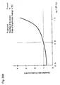
- a driver transistor 11a which drives a B pixel 16 is indicated by a broken line while a driver transistor 11a which drives a G pixel 16 is indicated by a solid line.
- the vertical axis in Figure 235 represents a current (S-D current) ( ⁇ A) passed by the driver transistor 11a, i.e., the programming current Iw while the horizontal axis represents a gate terminal voltage of the driver transistor 11a.
- the WL ratio i.e., the ratio between the channel width (W) and channel length (L) is adjusted during the design of the driver transistor 11a.
- the S-D currents outputted by the R, G, and B driver transistors at the same gate terminal voltage do not differ from each other by more than twice.
- the EL elements 15 will be described herein taking organic EL elements (known by various abbreviations including OEL, PEL, PLED, OLED) as an example, but this is not restrictive and inorganic EL elements may be used as well.
- organic EL elements known by various abbreviations including OEL, PEL, PLED, OLED
- An organic EL display panel of active-matrix type must satisfy two conditions: that it is capable of selecting a specific pixel and give necessary display information and that it is capable of passing current through the EL element throughout one frame period.
- a switching transistor is used to be functioned as a first transistor 11b to select the pixel.
- a driver transistor is used to be functioned as a second transistor 11a to supply current to an EL element 15.
- the turn-on current of a transistor is extremely uniform if the transistor is monocrystalline.
- its threshold varies in a range of ⁇ 0.2 V to 0.5 V.
- the turn-on current flowing through the driver transistor 11a varies accordingly, causing display irregularities.
- the irregularities are caused not only by variations in the threshold voltage, but also by mobility of the transistor and thickness of a gate insulating film. Characteristics also change due to degradation of the transistor 11.
- This phenomenon is not limited to low-temperature polysilicon technologies, and can occur in transistors formed on semiconductor films grown in solid-phase (CGS) by high-temperature polysilicon technology at a process temperature of 450 degrees (centigrade) or higher. Besides, the phenomenon can occur in organic transistors and amorphous silicon transistors.
- Transistor 11 which composes a pixel 16 of the display panel in the present invention is composed by p-channel polysilicon thin-film transistor. And the transistor 11b is a dual-gate or multi-gate transistor.
- the transistor 11b which composes a pixel 16 of the display panel in the present invention acts for the transistor 11a as a source-drain switch. Accordingly, as high an ON/OFF ratio as possible is required of transistor 11b. By using a dual-gate or multi-gate structure for the transistor 11b, it is possible to achieve a high ON/OFF ratio.
- the semiconductor films composing the transistors 11 in the pixel 16 are generally formed by laser annealing in low-temperature polysilicon technology. Variations in laser annealing conditions result in variations in transistor 11 characteristics. However, if the characteristics of the transistors 11 in the pixel 16 are consistent, it is possible to drive the pixel using current programming so that a predetermined current will flow through the EL element 15. This is an advantage lacked by voltage programming.
- the laser used is an excimer laser.
- the semiconductor film formation according to the present invention is not limited to the laser annealing method.
- the present invention may also use a heat annealing method and a method which involves solid-phase (CGS) growth.
- CGS solid-phase
- the present invention is not limited to the low-temperature polysilicon technology and may use high-temperature polysilicon technology.
- the semiconductor films may be formed by amorphous silicon technology.
- the present invention moves a laser spot (lined laser irradiation range) in parallel to the source signal line 18. Also, the laser spot is moved in such a way as to align with one pixel row.
- the number of pixel rows is not limited to one.
- laser may be shot by treating RGB pixel (three pixel columns in this case) as a single pixel.
- laser may be directed at two or more pixels at a time.
- moving laser irradiation ranges may overlap (it is usual for moving laser irradiation ranges to overlap).
- the linear laser spot coincide with the formation direction of the source signal line 18 (by aligning the formation direction of the source signal line 18 in parallel to the longer dimension of the laser spot) during laser annealing, the characteristics (mobility, Vt, S value, etc.) of the transistors 11 connected to the same source signal line 18 can be made uniform.
- Pixels are constructed in such a way that three pixels of RGB will form a square shape.
- each of the R, G, B pixels has oblong shape. Consequently, by performing annealing using an oblong laser spot, it is possible to eliminate variations in the characteristics of the transistors 11 within each pixel.
- the pixel aperture ratio may be varied among R, G, and B pixels. By varying the aperture ratio, it is possible to vary the density of the current flowing through the EL pixels 15 among R, G, and B. Varying the current density makes it possible to equalize degradation rates of the EL pixels 15 for R, G, and B. Equal degradation rates prevent the white balance of the EL display apparatus from being upset.
- Characteristic distribution (variations in the characteristics) of the driver transistors 11a on the array board 30 can occur even in a doping process. As illustrated in Figure 591(a), holes for doping are provided at equal intervals in a doping head 5911. Characteristic distribution due to doping appears in a streak form as illustrated in Figure 591(a).
- characteristic distribution occurs in the scanning direction of the doping head 3461 (in the direction perpendicular to the doping head).
- characteristic distribution occurs in the direction perpendicular to the scanning direction of a laser head 3462 (the characteristic distribution occurs along the longer dimension of the doping head). This is because laser annealing occurs linearly with a linear laser light directed at the substrate 30. That is, laser shots are placed linearly while shifting the laser irradiation site in sequence to laser-anneal the entire substrate 30.
- the longer dimension of the laser head 5912 is parallel to the source signal line 18 (the linear laser light is directed in parallel to the source signal line 18).
- the doping head 5911 is placed and manipulated in vertical to the source signal line 18 (doping is performed such that the direction of the characteristic distribution due to the doping will be parallel to the source signal line 18).
- the driver transistor 11a of the pixel 16 is formed or placed in such a way that the longer dimension (the longer of sides a and b when the channel area is given by a x b) of the transistor 11a will coincide with the direction of the laser head 5912 (that the longer dimension of the channel of the transistor 11a will be perpendicular to the scanning direction of the laser head 5912). This is because the channel of the transistor 11a is annealed by a single laser shot, resulting in reduced variations in the characteristics. Also, the transistor 11a is formed or placed in such a way that the longer dimension of the channel of the transistor 11a will be parallel to the source signal line 18.
- the manufacturing method according to the present invention performs the doping process after the laser annealing process.
- the unit transistors 154 of the source driver circuit (IC) 16 needs to have a certain area.
- a wafer 5891 has a mobility distribution.
- Figure 589 conceptually shows characteristic distribution of the wafer 5891.
- characteristic distribution 5892 of the wafer 5891 has a stripe pattern (streaky pattern). The characteristics of the parts represented by the strips are similar to each other.
- an IC process in a diffusion process is designed ingeniously. It is useful to run the same diffusion process multiple times. In the diffusion process, doping and the like are scanned. The scanning varies the characteristics (especially Vt) of the unit transistors periodically. Thus, by running the diffusion process multiple times and shifting the start position in each iteration of the diffusion process, it is possible to average the characteristic distribution of the transistors. This reduces periodic irregularities. Without these procedures, characteristic distribution of the transistors is usually striped at intervals of 3 to 5 mm. It is appropriate to shift scans by 1 to 2 mmmultiple times.
- the diffusion process which sets or determines the mobility of the transistors in the source driver circuit (IC) 14 is divided into multiple segments or repeated multiple times. These procedures provide an effective or characteristic manufacturing method of the current-output type source driver circuit (IC) 14.
- the source driver circuit (IC) 14 should be laid out along the characteristic distribution 5892 as illustrated in Figure 590 (b) rather than as illustrated in Figure 590(a). That is, a reticle for the IC chip is laid out such that the longer dimension of the IC chip will coincide with the direction of the characteristic distribution 5892 of the wafer 5891.
- Variations in the characteristics of the unit transistors 154 depend on the output current of the transistor group 431c.
- the output current in turn depends on the efficiency of the EL elements 15.
- the programming current outputted from the output terminal 155 for the G color decreases with increases in the luminous efficiency of the EL elements 15 for the G color.
- the programming current outputted from the output terminal 155 for the B color increases with decreases in the luminous efficiency of the EL elements 15 for the B color.
- the decreased programming current means decreases in the current outputted by the unit transistors 154.
- the decreased current results in increased variations in the unit transistors 154.
- the size of the transistors can be increased.
- the gate signal line (first scanning line) 17a is activated (a turn-on voltage is applied).
- a program current Iw to be passed through the EL element 15 is delivered from the source driver circuit (IC) 14 to the driver transistor 11a via the switching transistor 11c.
- the transistor 11b drives to cause a short circuit between gate terminal (G) and drain terminal (D) of the driver transistor 11a.
- gate voltage (or drain voltage) of the transistor 11a is stored in a capacitor (storage capacitance, additional capacitance) 19 connected between the gate terminal (G) and drain terminal (S) of the transistor 11a (see Figure 5(a)).
- the capacitor (storage capacitance) 19 should be from 0.2 pF to 2 pF both inclusive. More preferably, the capacitor (storage capacitance) 19 should be from 0.4 pF to 1.2 pF both inclusive.
- the capacity of the capacitor 19 is determined taking pixel size into consideration.
- the capacity needed for a single pixel is Cs (pF) and an area occupied by the pixel is Sp (square ⁇ m).
- Sp is not an aperture ratio.
- a condition 1500/Sp ⁇ Cs ⁇ 30000/Sp, and more preferably a condition 3000/Sp ⁇ Cs ⁇ 15000/Sp should be satisfied. Since gate capacity of the transistor 11 is small, Q as referred to here is the capacity of the storage capacitance (capacitor) 19 alone. If Cs is smaller than 1500/Sp, penetration voltage of the gate signal lines 17 has a greater impact and voltage retention decreases, causing luminance gradient and the like to appear. Also, compensation performance of TFTs is degraded. If Cs is larger than 30000/Sp, the aperture ratio of the pixel 16 decreases. Consequently, electric field density of the EL element increases, causing adverse effects such as reduction in the life of the EL element. Also, write time for current programming is increased due to the capacitance of the capacitor, resulting in insufficient writing in a low gradation region.
- the capacitance value of the storage capacitance 19 is Cs and the turn-off current value of the second transistor 11b is Ioff, preferably the following equation is satisfied. 3 ⁇ Cs / Ioff ⁇ 24
- the turn-off current of the transistor 11b By setting the turn-off current of the transistor 11b to 5 pA or less, it is possible to reduce changes in the current flowing through the EL to 2% or less. This is because when leakage current increases, electric charges stored between the gate and source (across the capacitor) cannot be held for one field with no voltage applied. Thus, the larger the storage capacity of the capacitor 19 becomes, the larger the permissible amount of the turn-off current. By satisfying the above equation, it is possible to reduce fluctuations in current values between adjacent pixels to 2% or less.
- the gate signal line 17a is deactivated (a turn-off voltage is applied) and a gate signal line 17b is activated.
- a single pixel contains four transistors 11.
- the gate terminal of the driver transistor 11a is connected to the source terminal of the transistor 11b.
- the gate terminals of the transistors 11b and 11c are connected to the gate signal line 17a.
- the drain terminal of the transistor 11b is connected to the source terminal of the transistor 11c and source terminal of the transistor 11d.
- the drain terminal of the transistor 11c is connected to the source signal line 18.
- the gate terminal of the transistor 11d is connected to the gate signal line 17b and the drain terminal of the transistor 11d is connected to the anode electrode of the EL element 15.
- All the transistors in Figure 1 are P-channel transistors. Compared to N-channel transistors, P-channel transistors have more or less lower mobility, but they are preferable because they are more resistant to voltage and degradation.
- the EL element according to the present invention is not limited to P-channel transistors and the present invention may employ N-channel transistors alone. Also, the present invention may employ both N-channel and P-channel transistors.
- P-channel transistors should be used for all the transistors 11 composing pixels as well as for the built-in gate driver circuits 12.
- the EL element according to the present invention is controlled using two timings.
- the first timing is the one when required current values are stored.
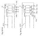
- Turning on the transistor 11b and transistor 11c with this timing provides an equivalent circuit shown in Figure 5(a).
- a predetermined current Iw is applied from signal lines. This makes the gate and drain of the transistor 11a connected, allowing the current Iw to flow through the transistor 11a and transistor 11c.
- the gate-source voltage of the transistor 11a is such that allows I1 to flow.
- the second timing is the one when the transistor 11a and transistor 11c are closed and the transistor 11d is opened.
- the equivalent circuit available at this time is shown in Figure 5(b).
- the source-gate voltage of the transistor 11a is maintained. In this case, since the transistor 11a always operates in a saturation region, the current Iw remains constant.
- Reference numeral 191a in Figure 19(a) denotes a pixel (row) (write pixel row) programmed with current at a certain time point in a display screen 144.
- the pixel row 191a is non-illuminated (non-display pixel (row)) as illustrated in Figure 5(b).
- the programming current Iw flows through the source signal line 18 during current programming as shown in figure 5 (a).
- the current Iw flows through the driver transistor 11a and voltage is set (programmed) in the capacitor 19 in such a way as to maintain the program current Iw.
- the transistor 11d is open (off).
- the transistors 11c and 11b turn off and the transistor 11d turns on as shown in Figure 5(b). Specifically, a turn-off voltage (Vgh) is applied to the gate signal line 17a, turning off the transistors 11b and 11c. On the other hand, a turn-on voltage (Vgl) is applied to the gate signal line 17b, turning on the transistor 11d.
- Vgh turn-off voltage
- Vgl turn-on voltage
- a timing chart is shown in Figure 21.
- the subscripts in brackets in Figure 21 (e.g., (1)) indicate pixel row numbers.
- a gate signal line 17a (1) denotes a gate signal line 17a in a pixel row (1) .
- *H (where "*" is an arbitrary symbol or numeral and indicates a horizontal scanning line number) in the top row in Figure 4 indicates a horizontal scanning period.
- 1H is a first horizontal scanning period.
- the items (1H number, 1-H cycle, order of pixel row numbers, etc.) described above are intended to facilitate explanation and are not intended to be restrictive.
- the gate of the transistor 11a and gate of the transistor 11c are connected to the same gate signal line 11a.
- the gate of the transistor 11a and gate of the transistor 11c may be connected to different gate signal lines 11 (see Figure 6).
- one pixel will have three gate signal lines (two in the configuration in Figure 1).
- gate signal lines 17a1 and 17a2 are selected at the same time, turning on the transistor 11b and 11c.
- Turn-off voltage is applied to the gate signal line 17b of the pixel 16 which is conducting the current programming turning off the transistor 11d.
- a turn-off voltage (Vgh) is applied to the gate signal line 17a1, turning off the transistor 11b.
- Vgl turn-on voltage
- Vgh turn-off voltage
- both transistors 11b and 11c are in on state, to turn off both transistors 11b and 11c (to finish a current programming period of the given pixel row), first the transistor 11b is turned off, breaking the connection between the gate terminal (G) and drain terminal (D) of the driver transistor 11a (a turn-off voltage (Vgh) is applied to the gate signal line 17a1). Next, the transistor 11c is turned off, disconnecting the drain terminal (D) of the driver transistor 11a from the source signal line 18 (a turn-off voltage (Vgh) is applied to the gate signal line 17a2 as well).
- Vgh turn-off voltage
- the interval Tw between the time when a turn-off voltage is applied to the gate signal line 17a1 and the time when a turn-off voltage is applied to the gate signal line 17a2 is between 0.1 and 10 ⁇ sec (both inclusive). Preferably, it is between 0.1 and 10 ⁇ sec (both inclusive).
- Tw is preferably between Th/500 and Th/10 (both inclusive). More preferably, Tw is between Th/200 and Th/50 (both inclusive).
- a turn-off voltage (Vgh) is applied to the gate signal line 17a1, turning off the transistor 11d.
- Vgl turn-on voltage
- Vgh turn-off voltage
- both transistors 11d and 11c are in on state, to turn off both transistors 11d and 11c (to finish a current programming period of the given pixel row), first the transistor 11d is turned off, breaking the connection between the gate terminal (G) and drain terminal (D) of the driver transistor 11a (a turn-off voltage (Vgh) is applied to the gate signal line 17a1). Next, the transistor 11c is turned off, disconnecting the drain terminal (D) of the driver transistor 11a from the source signal line 18 (a turn-off voltage (Vgh) is applied to the gate signal line 17a2 as well).
- Vgh turn-off voltage
- the interval Tw between the time when a turn-off voltage is applied to the gate signal line 17a1 and the time when a turn-off voltage is applied to the gate signal line 17a2 is preferably between 0.1 and 10 ⁇ sec (both inclusive) in Figure 12. Preferably, it is between 0.1 and 10 ⁇ sec (both inclusive).
- Tw is preferably between Th/500 and Th/10 (both inclusive). More preferably, Tw is between Th/200 and Th/50 (both inclusive).
- switching transistor 11e may be omitted as shown in Figure 13 although switching transistor 11e is placed between the driver transistor 11b and the EL element 15 in Figure 12.
- the pixel configuration according to the present invention is not limited to those shown in Figures 1 and 12.
- pixels may be configured as shown in Figure 7.
- Figure 7 lacks the switching transistor 11d unlike the configuration in Figure 1. Instead, a changeover switch 71 is formed or placed.
- the switch 11d in Figure 1 functions to turn on and off (pass and shut off) the current delivered from the driver transistor 11a to the EL element 15.
- the on/off control function of the transistor 11d constitutes an important part of the present invention.
- the configuration in Figure 7 achieves the on/off function without using the transistor 11d.
- a terminal a of the changeover switch 71 is connected to anode voltage Vdd.
- the voltage applied to the terminal a is not limited to the anode voltage Vdd. It may be any voltage that can turn off the current flowing through the EL element 15.
- a terminal b of the changeover switch 71 is connected to cathode voltage (indicated as ground in Figure 7).
- the voltage applied to the terminal b is not limited to the cathode voltage. It may be any voltage that can turn on the current flowing through the EL element 15.
- a terminal c of the changeover switch 71 is connected with a cathode terminal of the EL element 15.
- the changeover switch 71 may be of any type as long as it has a capability to turn on and off the current flowing through the EL element 15.
- its installation location is not limited to the one shown in Figure 7 and the switch may be located anywhere on the path through which current is delivered to the EL element 15.
- the switch is not limited by its functionality as long as the switch can turn on and off the current flowing through the EL element 15.
- the present invention can have any pixel configuration as long as switching means capable of turning on and off the current flowing through the EL element 15 is installed on the current path for the EL element 15.
- the term "off" here does not mean a state in which no current flows, but it means a state in which the current flowing through the EL element 15 is reduced to below normal.
- the transistor 11d may pass a leakage current which illuminates the EL element 15.
- the changeover switch 71 will require no explanation because it can be implemented easily by a combination of P-channel and N-channel transistors. Of course, the switch 71 can be constructed of only P-channel or N-channel transistors because it only turns off the current flowing through the EL element 15.
- the switch 71 When the switch 71 is connected to the terminal a, the anode voltage Vdd is applied to the cathode terminal of the EL element 15. Thus, current does not flow through the EL element 15 regardless of the voltage state of voltage held by the gate terminal G of the driver transistor 11a. Consequently, the EL element 15 is non-illuminated.
- the voltage at the terminal a of the changeover switch (circuit) 71 can be set such that the voltage between the source terminal (S) and drain terminal (D) of the driver transistor 11a can be at or near the cutoff point.
- the cathode voltage GND is applied to the cathode terminal of the EL element 15.
- the switching transistor 11 and the like of the pixels 16 may be phototransistors. For example, by turning on and off the phototransistors 11 depending on the intensity of external light and thereby controlling the current flowing through the EL elements 15, it is possible to change the brightness of the display panel.
- one pixel contains one driver transistor 11a or 11b.
- the present invention is not limited to this and one pixel may contain two or more driver transistors 11a.
- FIG 8 An example is shown in Figure 8, where two or more driver transistors 11a are implemented or constructed in one pixel 16.
- one pixel contains two driver transistors 11a1 and 11a2, whose gate terminals are connected to a common capacitor 19.
- driver transistors 11a By using a plurality of driver transistors 11a, it is possible to reduce variations in programming current.
- the other part of the configuration is the same as those shown in Figure 1 and the like, and thus description thereof will be omitted.
- driver transistors 11a may be constructed (implemented). Further, a plurality of driver transistors 11a can be constructed (implemented) using both P-channel and N-channel.
- the current delivered to the EL element 15 is controlled by the driver transistor 11a.
- the current flowing through the EL element 15 is turned on and off by the switching element 11d placed between the Vdd terminal and EL element 15.
- the switching element 11d may be placed anywhere as long as it can control the current flowing through the EL element 15.
- the other part of the operation is similar to or the same as those shown in Figure 1 and the like, and thus description thereof will be omitted.
- all transistors are constructed of N-channel.
- the present invention does not limit the EL element configuration only of N-channel. It may be constructed of both N-channel and P-channel.
- the pixel configuration in Figure 10 is controlled using two timings.
- the first timing is the one when required current values are stored.
- the transistor 11b and transistor 11c are turned on because the turn-on voltage (Vgh) is applied to the gate signal lines 17a1 and 17a2.
- turn-off voltage (Vgl) is applied to the gate signal line 17b and the transistor 11d is turned off.
- a predetermined current Iw is applied from source signal lines 18. This makes the gate and drain of the transistor 11a short connected.
- the driver transistor 11a allows the program current to flow through transistor 11c.
- a turn-off voltage (Vgh) is applied to the gate signal line 17a1, turning off the transistor 11b.
- Vgl turn-on voltage
- Vgh turn-off voltage
- both transistors 11b and 11c are in on state, to turn off both transistors 11b and 11c (to finish a current programming period of the given pixel row), first the transistor 11b is turned off, breaking the connection between the gate terminal (G) and drain terminal (D) of the transistor 11a (a turn-off voltage (Vgh) is applied to the gate signal line 17a1). Next, the transistor 11c is turned off, disconnecting the drain terminal (D) of the transistor 11a from the source signal line 18 (a turn-off voltage (Vgh) is applied to the gate signal line 17a2 as well).
- Vgh turn-off voltage
- the turn-off voltage is applied to the gate signal lines 17a1 and 17a2 and the turn-on voltage is applied to the gate signal line 17b. Accordingly, the transistor 11b and transistor 11c are turned off and the transistor 11d is turned on. In this case, since the transistor 11a always operates in a saturation region, the current Iw remains constant.
- the channel length L of the driver transistor 11 is from 5 ⁇ m to 100 ⁇ m (both inclusive). More preferably, it is from 10 ⁇ m to 50 ⁇ m (both inclusive). This is probably because a long channel length L increases grain boundaries contained in the channel, reducing electric fields, and thereby suppressing kink effect.
- circuit means which controls the current flowing through the EL element 15 is constructed, formed, or placed on the path along which current flows into the EL element 15 and the path along which current flows out of the EL element 15 (i.e., the current path for the EL element 15).
- the switching transistors 11d and 11c in Figure 11 are connected to a single gate signal line 17a, the switching transistor 11c may be controlled by a gate signal line 17a2 and the switching transistor 11d may be controlled by a gate signal line 17a1 as shown in Figure 12.
- the pixel configuration in Figure 12 makes pixel 16 control more versatile and makes the characteristic compensation performance of the driver transistor 11b improve.
- FIG 14 is an explanatory diagram which mainly illustrates a circuit of the EL display apparatus.
- Pixels 16 are arranged or formed in a matrix.
- Each pixel 16 is connected with a source driver circuit (IC) 14 which outputs program current for use in current programming of the pixel.
- IC source driver circuit
- In an output stage of the source driver circuit (IC) 14 are current mirror circuits (described later) corresponding to the bit count of a video signal. For example, if 64 gradations are used, 63 current mirror circuits are formed on respective source signal lines so as to apply desired current to the source signal lines 18 when an appropriate number of current mirror circuits is selected (see Figures 15, 57, 58, 59 etc.).
- the minimum output current of the unit transistor 154 of the source driver circuit (IC) 14 is from 0.5 nA to 100 nA (both inclusive).
- the minimum output current of the unit transistor 154 should be from 2 nA to 20 nA (both inclusive) to secure accuracy of the the unit transistor 154 composing the unit transistor group 431c in the driver IC 14.
- the source driver circuit (IC) 14 incorporates a precharge circuit to charge or discharge the source signal line 18 forcibly. See Figure 16 etc.
- voltage (current) output values of the precharge or discharge circuit which charges or discharges the source signal line 18 forcibly can be set separately for R, G, and B. This is because the thresholds of the EL element 15 differ among R, G, and B.
- the precharge voltage can be regarded as a means of applying a voltage not higher than a rising voltage to the gate terminal (G) of the driver transistor 11a. That is, the driver transistor 11a is turned off to set the programming current Iw to 0 so that current will not flow through the EL element 15.
- the charging and discharging of the source signal line 18 are subsidiary.
- the source driver circuit (IC) 14 is made of a semiconductor silicon chip and connected with a terminal on the source signal line 18 of the board 30 by glass-on-chip (COG) technology.
- the gate driver circuit 12 is formed by low-temperature polysilicon technology. That is, it is formed in the same process as the transistors in pixels. This is because the gate driver circuit 12 has a simpler internal structure and lower operating frequency than the source driver circuit (IC) 14. Thus, it can be formed easily even by low-temperature polysilicon technology and allows bezel width of the display panel to be reduced. Of course, it is possible to construct the gate driver circuit 12 from a silicon chip and mount it on the board 30 using the COG technology.
- gate driver circuit (IC) 12 and the source driver circuit (IC) 14 using the COF or the TAB technology.
- switching elements such as pixel transistors as well as gate drivers may be formed by high-temperature polysilicon technology or may be formed of an organic material (organic transistors).
- the gate driver circuit 12 incorporates a shift register circuit 141a for a gate signal line 17a and a shift register circuit 141b for a gate signal line 17b.
- a shift register circuit 141a for a gate signal line 17a
- a shift register circuit 141b for a gate signal line 17b.
- the pixel configuration is described according to, for example, Figure 1. If the gate signal line 17a is composed of the gate signal lines 17al and 17a2, a separate shift register circuit 141 is formed for each gate signal line or control signals for the gate signal lines 17a1 and 17a2 are generated by a logic circuit using output signals of the shift register circuits 141.
- the shift register circuits 141 are controlled by positive-phase and negative-phase clock signals (CLKxP and CLKxN) and a start pulse (STx) (see Figure 14). Besides, it is preferable to add an enable (ENABL) signal which controls output and non-output from the gate signal line and an up-down (UPDWN) signal which turns a shift direction upside down. Also, it is preferable to install an output terminal to ensure that the start pulse is shifted by the shift register circuit 141 and is outputted.
- ENABL enable
- UPDWN up-down
- Shift timings of the shift register circuits 141 are controlled by a control signal from a control IC 760 as later described. Also, the gate driver circuit 12 incorporates a level shift circuit 141 which level-shifts external data. By using only positive-phase clock signals, it is possible to reduce the number of signal lines and thereby reduce bezel width.
- the shift register circuits 141 Since the shift register circuits 141 have small buffer capacity, they cannot drive the gate signal lines 17 directly. Therefore, at least two or more inverter circuits 142 are formed between each shift register circuit 141 and an output gate 143 which drives the gate signal line 17.
- the source driver circuit (IC) 14 is formed on the board 30 by polysilicon technology such as low-temperature polysilicon technology.
- a plurality of inverter circuits are formed between an analog switching gate such as a transfer gate which drives the source signal line 18 and the shift register of the source driver circuit (IC) 14.
- shift register output and output stages which drive signal lines (inverter circuits placed between output stages such as output gates or transfer gates) are common to the gate driver circuit and source driver circuit.
- difference between current densities of different colors should be within ⁇ 30%. More preferably, the difference should be within ⁇ 15%. For example, if current densities are around 100 A/square meter, all the three primary colors should have a current density of 70 A/square meter to 130 A/square meter (both inclusive). More preferably, all the three primary colors should have a current density of 85 A/square meter to 115 A/square meter (both inclusive).
- the organic EL element 15 is a self-luminous element. When light from this self-luminous element enters a transistor serving as a switching element, a photoconductive phenomenon occurs.
- the photoconductive phenomenon is a phenomenon in which leakage (off-leakage) increases due to photoexcitation when a switching element such as a transistor is off.
- the present invention forms a shading film under the gate driver circuit 12 (source driver circuit (IC) 14 in some cases) and under the pixel transistor 11.
- it is preferably to shade the transistor 11b placed between a potential position (denoted by c) of the gate terminal and potential position (denoted by a) of the drain terminal of the transistor 11a.
- the light-shielding film 3141 is a thin filmof metal such as chromium and is 50 to 150 nm thick (both inclusive) .
- a thin film will provide a poor shading effect while a thick film will cause irregularities, making it difficult to pattern the transistor 11 in an upper layer.
- the present invention also forms a cathode electrode on the surface of the driver circuit 12 and the like and uses it as a shading film.
- the present invention forms at least one layer of organic EL film, and preferably two or more layers, on the driver circuit 12 simultaneously with the formation of organic EL film on the pixel electrode.
- the gate signal line 17a conducts when the row remains selected (since the transistor 11 in Figure 1 is a P-channel transistor, the gate signal line 17a conducts when it is in low state) and the gate signal line 17b applies to the turn-off voltage when the row remains non-selected.
- Parasitic capacitance (not shown) is present in the source signal line 18.
- the parasitic capacitance is caused by the capacitance at the junction of the source signal line 18 and gate signal line 17, channel capacitance of the transistors 11b and 11c, etc.
- Parasitic capacitance is generated not only in the source signal line 18, but also in the source driver IC 14.
- the protective diodes 171 are the main cause.
- the protective diodes 171 are intended to protect the IC 14 from static electricity, but they also acts as capacitors, causing parasitic capacitance.
- the capacitance of a typical protective diode is 3 to 5pF.
- a surge limiting resistor 172 is formed or placed between the connection terminal 155 and current output circuit 164 as illustrated in Figure 17.
- the resistor 172 is made of polysilicon or is a diffused resistor.
- the resistance of the resistor 172 should be between 1 K ⁇ and 1M ⁇ (both inclusive).
- the resistor 172 controls external static electricity. This allows the size of the protective diodes 171 to be reduced. Reduction in the size of the protective diodes 171 results in reduction in the magnitude of the parasitic capacitance caused by the protective diodes.
- Figure 17 shows that the resistor 172 is formed or placed in the source driver IC 14, this is not restrictive. Needless to say, the resistor 172 may be formed or placed on the array 30. This also applies to the diodes (including transistors configured as diodes) 171.
- the resistors 171a and 171b are configured to allow their resistance to be adjusted by trimming.
- the resistance of the resistors 171a and 171b can be adjusted by trimming to eliminate leakage current flowing through the source signal line 18. It is also possible to adjust resistance and the like by a method other than trimming. If diffused resistors are used as the resistors 171, their resistance can be adjusted by heating. For example, the resistance can be adjusted by irradiating the resistors with a laser light and thereby heating them.
- the programming current is increased Nfold, the current flowing through the EL element 15 is also increased Nfold. Consequently, the brightness of the EL element 15 is increased Nfold as well.
- the conduction period of the transistor 17d in Figure 1 is reduced to 1/N.
- a 10 times larger current value is written into the pixel transistor 11a (more precisely, the terminal voltage of the capacitor 19 is set) and that the conduction period of the EL element 15 is reduced to 1/10
- a 10 times larger current value may be written into the pixel transistor 11a and the conduction period of the EL element 15 may be reduced to 1/5.
- a 10 times larger current value may be written into the pixel transistor 11a and the conduction period of the EL element 15 may be halved.
- a current value may be written into the pixel transistor 11a and the conduction period of the EL element 15 may be reduced to 1/5.
- the present invention is characterized in that the write current into a pixel is set at a value other than a predetermined value and that a current is passed through the EL element 15 intermittently.
- N1 times N1 is not limited to more than 1
- larger current may be written into the driver transistor 11 of the pixel 16 and the conduction period of the EL element 15 may be reduced to 1/N2 (N2 is more than 1.
- N1 and N2 are different from each other).
- the drive method of the present invention for example, in white raster display, it is assumed that average brightness over one field (frame) period of the display screen 144 is B0.
- This drive method performs current programming in such a way that the brightness B1 of each pixel 16 is higher than the average brightness B0.
- a non-display area 192 appears during at least one field (frame) period.
- the average brightness over one field (frame) period is lower than B1.
- This method programs the pixels 16 with current at normal brightness during one field (frame) period so than a non-display area 192 will appear.
- average brightness during one field (frame) period is lower than with a normal drive method (conventional drive method).
- this method has the advantage of improving movie display performance.
- the pixel configuration according to the present invention is not limited to current-programming mode.
- the present invention can use the pixel configuration in voltage-programming mode shown in Figure 26. This is because it is useful in improving movie display performance even in voltage-programming mode to use high brightness display mode in a predetermined part of one field (frame) period and non-illumination mode in the rest of the period. Besides, the effect of parasitic capacitance of the source signal lines 18 cannot be ignored even in voltage-programming mode.
- the drive method according to the present invention is useful especially for large EL display panels, which are prone to large parasitic capacitance.
- the non-display area 192 and display area 193 are not necessarily spaced equally. For example, they may appear at random (provided that the display period or non-display period makes up a predetermined value (constant ratio) as a whole). Also, display periods may vary among R, G, and B. That is, display periods of R, G, and B or non-display period can be adjusted to a predetermined value (constant ratio) in such a way as to obtain an optimum white balance.
- the non-display area 192 is a pixel 16 area in which EL elements 15 are non-illuminated at the given time.
- the display area 193 is a pixel 16 area in which EL elements 15 are illuminated at the given time. Both non-display area 192 and display area 193 are shifted by one pixel row at a time in sync with a horizontal synchronization signal.
- 1/N means reducing 1F (one field or one frame) to 1/N. Needless to say, however, it takes time to select one pixel row and to program current values (normally, one horizontal scanning period (1 H)) and error may result depending on scanning conditions. Of course, there can also be deviations from an ideal state due to penetration voltage of the gate signal lines 17. However, it is assumed here for ease of explanation that there is no deviation.
- the liquid display panel holds the current (voltage) written into a pixel for 1F (one field or one frame) period.
- a problem is that displaying moving pictures will result in blurred edges.
- Organic (inorganic) EL display panels hold the current (voltage) written into a pixel for 1F (one field or one frame) period. Thus, they have the same problem as liquid crystal display panels.
- displays such as CRTs which display an image as a set of lines using an electron gun do not suffer edge blur of moving images because they use persistence of vision for image display.
- the drive method according to the present invention implements intermittent display.
- the transistor 11d simply turns on and off on a 1-H cycle at the maximum. Consequently, a main clock of the circuit does not differ from conventional ones, and thus there is no increase in the power consumption of the circuit.
- Liquid crystal display panels need an image memory in order to achieve intermittent display. According to the present invention, image data is held in each pixel 16. Thus, the drive method in the present invention requires no image memory for intermittent display.
- the drive method of the present invention controls the current passed through the EL element 15 by simply turning on and off the switching transistor 11d, the transistor 11e ( Figure 12, etc.), and the like. That is, even if the current Iw flowing through the EL element 15 is turned off, the image data is held as it is in the capacitor 19 of the pixel 16. Thus, when the switching element 11d is turned on the next time, the current passed through the EL element 15 has the same value as the current flowing through the EL element 15 the previous time.
- the present invention does not need to speed up the main clock of the circuit. Also, it does not need to elongate a time axis, and thus requires no image memory. Besides, the EL element 15 responds quickly, requiring a short time from application of current to light emission. Thus, the present invention is suitable for movie display, and by using intermittent display, it can solve a problem with conventional data-holding display panels (liquid crystal display panels, EL display panels, etc.) in displaying moving pictures.
- conventional data-holding display panels liquid crystal display panels, EL display panels, etc.
- the conduction period of the gate signal line 17b (the transistor 11d) can be set to 1F/N. This makes it possible to apply the present invention to television sets, monitors, and other large display apparatus.
- the pixel capacitor 19 needs to be programmed with a minute current of 20 nA or less.
- the parasitic capacitance cannot be charged and discharged during the time when one pixel row is programmed (basically within 1 H, but not limited to 1 H because two pixel rows may be programmed simultaneously). If the parasitic capacitance cannot be charged and discharged within a period of 1 H, sufficient current cannot be written into the pixel, resulting in inadequate resolution.
- the programming current Iw flows through the source signal line 18 during current programming as shown in figure 6(a).
- the current Iw flows through the transistor 11a and voltage is set (programmed) in the capacitor 19 in such a way as to maintain the current Iw.
- the transistor 11d is open (off).
- the transistors 11c and 11b turn off and the transistor 11d turns on as shown in Figure 6(b). Specifically, a turn-off voltage (Vgh) is applied to the gate signal line 17a, turning off the transistors 11b and 11c. On the other hand, a turn-on voltage (Vgl) is applied to the gate signal line 17b, turning on the transistor 11d.
- Vgh turn-off voltage
- Vgl turn-on voltage
- a program current Iw is N times the current which should normally flow (a predetermined value)
- the current flowing through the EL element 15 in Figure 6 (b) is also Ie.
- the EL element 15 emits light 10 times more brightly that a predetermined value.
- the magnification N the higher the instant display brightness B of the pixel 16.
- the magnification N and the brightness of the pixel 16 are basically proportional to each other.
- the average brightness over the 1F equals predetermined brightness.
- This display condition closely resembles the display condition under which a CRT is scanning a screen with an electronic gun. The difference is that 1/N of the entire screen illuminates (where the entire screen is taken as 1) in the range where the image is displayed (in a CRT, what illuminates is one pixel row--more precisely, one pixel).
- 1F/N of the display (illumination) area 193 moves from top to bottom of the screen 144 as shown in Figure 19(b).
- the scanning direction of the display area 193 may be from bottom of the screen 144 to the top, or may be at random.
- the write pixel row 191a is non-illuminated area 192.
- this is true only to the pixel configurations in Figures 1, 2, etc.
- the write pixel row 191 may be illuminated.
- description will be given herein citing mainly the pixel configuration in Figure 1 for ease of explanation.
- N-fold pulse driving a drive method which involves driving a pixel intermittently by programming it with a current larger than the predetermined drive current Iw shown in Figures 19, 23, etc. is referred to as N-fold pulse driving.
- image data display and black display are repeated every 1F. That is, image data is displayed at intervals (intermittently) in the temporal sense.
- Liquid crystal display panels (EL display panels other than that of the present invention), which hold data in pixels for a period of 1F, cannot keep up with changes in image data during movie display, resulting is blurred moving pictures (edge blur of images). Since the present invention displays images intermittently, it can achieve a good display condition wi thout edge blur of images. In short, movie display close to that of a CRT can be achieved.
- the drive method according to the present invention cannot be implemented using a configuration in which logic (Vgh or Vgl) applied to the gate signal line 17 is applied to the transistor 11b and the logic applied to the gate signal line 17 is converted (Vgh or Vgl) by an inverter and applied to the transistor 11d.
- the present invention requires a gate driver circuit 12a which operates the gate signal line 17a and gate driver circuit 12b which operates the gate signal line 17b.
- FIG 20 A timing chart of the drive method shown in Figure 19 is illustrated in Figure 20.
- the pixel configuration referred to in the present invention and the like is the one shown in Figure 1 unless otherwise stated.
- the selection period is designated as 1 H
- a turn-on voltage (Vg1) is applied to the gate signal line 17a (see Figure 20(a))
- a turn-off voltage is applied to the gate signal line 17b (see Figure 20(b)).
- current does not flow through the EL element 15 (non-illumination mode).
- a turn-on voltage (Vgl) is applied to the gate signal line 17b and a turn-off voltage (Vgh) is applied to the gate signal line 17a.
- Vgl turn-on voltage
- Vgh turn-off voltage
- the EL element 15 illuminates at a brightness (N ⁇ B) N times the predetermined brightness and the illumination period is 1F/N.
- the value of N can be more than one.
- Figure 21 shows an example in which operations shown in Figure 20 are applied to each pixel row.
- the figure shows voltage waveforms applied to the gate signal lines 17. Waveforms of the turn-off voltage are denoted by Vgh (high level) while waveforms of the turn-on voltage are denoted by Vgl (low level).
- Vgh high level
- Vgl low level
- the subscripts such as (1) and (2) indicate selected pixel row numbers.
- a gate signal line 17a(1) is selected (Vgl voltage) and a programming current flows through the source signal line 18 in the direction from the transistor 11a in the selected pixel row to the source driver circuit (IC) 14.
- the programming current is N times larger than a predetermined value. Since the predetermined value is a data current for use to display images, it is not a fixed value unless in the case of white raster display).
- the capacitor 19 is programmed so that a N times larger current will flow through the transistor 11a.
- a gate signal line 17a(2) is selected (Vgl voltage) and a programming current flows through the source signal line 18 in the direction from the transistor 11a in the selected pixel row to the source driver circuit (IC) 14.
- the programming current is N times larger than a predetermined value.
- the capacitor 19 is programmed so that N times larger current will flow through the transistor 11a.
- a gate signal line 17a(3) is selected, a turn-off voltage (Vgh) is applied to the gate signal line 17b(3), and current does not flow through the EL element 15 in the pixel row (3).
- Vgh turn-off voltage
- Vgl turn-on voltage
- the basic idea of the present invention is to use a large current for programming, insert a black screen (non-illuminated display area) 192, and thereby obtain a predetermined brightness.
- the drive method according to the present invention causes a current larger than a predetermined current to flow through the EL element 15, and thereby charges and discharges the parasitic capacitance of the source signal line 18 sufficiently. That is, there is no need to pass an N times larger current through the EL element 15.
- it is conceivable to form a current path in parallel with the EL element 15 form a dummy EL element and use a shield film to prevent the dummy EL element from emitting light
- program current which writes to the pixel 16 for programming is 0.2 ⁇ A.
- Program current which outputs from the source driver circuit (IC) 14 is 2.0 ⁇ A.
- 1.8 ⁇ A 2.0 - 0.2
- the remaining 0.2 ⁇ A is passed through the driver transistors 11a of the pixels 16 to be programmed.
- the dummy pixel row is either kept from emitting light or hidden from view by a shield film or the like even if it emits light.
- Figure 19(a) shows writing into the display screen 144.
- reference numeral 191a denotes a write pixel row.
- a programming current is supplied to the source signal line 18 from the source driver IC 14.
- there is one pixel row into which current is written during a period of 1 H but this is not restrictive. The period may be 0.5 H or 2 Hs.
- a programming current is written into the source signal line 18, the present invention is not limited to current programming.
- the present invention may also use voltage programming ( Figure 28, etc.) which writes voltage into the source signal line 18.
- the screen becomes 10 times brighter.
- 90% of the display screen.144 can be constituted of the non-illuminated area 192.
- S/N of the entire area constitutes a display area 193, which is illuminated N times more brightly (N is more than 1). Then, the display area 193 is scanned in the vertical direction of the screen. Thus, S (N - 1)/N of the entire area is a non-illuminated area 192.
- the non-illuminated area presents a black display (is non-luminous).
- the non-luminous area 192 is produced by turning off the transistor 11d. Incidentally, although it has been stated that the display area 53 is illuminated N times more brightly, naturally the value of N changes by brightness adjustment and gamma adjustment.
- the screen becomes 10 times brighter and 90% of the display screen 144 can be constituted of the non-illuminated area 192.
- this does not necessarily mean that R, G, and B pixels constitute the non-illuminated area 192 in the same proportion.
- 1/8 of the R pixels, 1/6 of the G pixels, and 1/10 of the B pixels may constitute the non-illuminated area 192 with different colors making up different proportions.
- the non-illuminated area 192 (or illuminated area 193) may be adjusted separately among R, G, and B.
- allowing R, G, and B to be adjusted separately makes it possible to adjust white balance, making it easy to adjust color balance for each gradation.
- the example is shown in Figure 22.
- pixel rows including the write pixel row 191a compose a non-illuminated area 192 while an area of S/N (1F/N in the temporal sense) above the write pixel row 191a compose a display area 193 (when write scans are performed from top to bottom of the screen. When the screen is scanned from bottom to top, the areas change places). Regarding the display condition of the screen, a strip of the display area 193 moves from top to bottom of the screen.
- one display area 193 moves from top to bottom of the screen. At a low frame rate, the movement of the display area 193 is recognized visually. It tends to be recognized easily especially when a user closes his/her eyes or moves his/her head up and down. To deal with this problem, the display area 193 can be divided into a plurality of parts as shown in Figure 23. If the total area of the divided display area is S (N - 1)/N, the brightness is equal to the brightness in Figure 19. Incidentally, there is no need to divide the display area 193 equally. Also, there is no need to divide the non-display area 192 equally.
- Dividing the display area 193 reduces flickering of the screen. Thus, a flicker-free good image display can be achieved.
- the display area 53 may be divided more finely. However, the more finely the display area 53 is divided, the poorer the movie display performance becomes.
- Figure 24 shows voltage waveforms of gate signal lines 17 and emission brightness of the EL element.
- a period (1F/N) during which the gate signal line 17b is set to Vgl is divided into a plurality of parts (K parts). That is, a period of 1F/(K ⁇ N) during which the gate signal line 17b is set to Vg1 repeats K times. This reduces flickering and implements image display at a low frame rate.
- the number of divisions is variable.
- the value of K may be changed in response.
- the user may be allowed to adjust brightness.
- the value of K may be changed manually or automatically depending on images or data to be displayed.
- a period (1F/N) during which the gate signal line 17b is set to Vg1 is divided into a plurality of parts (K parts) and that a period of 1F/(K ⁇ N) during which the gate signal line 17b is set to Vg1 repeats K times, this is not restrictive.
- a period of 1F/(K ⁇ N) may be repeated L (L ⁇ K) times.
- the present invention displays the display screen 144 by controlling the period (time) during which current is passed through the EL element 15.
- the idea of repeating the 1F/(K ⁇ N) period L (L ⁇ K) times is included in the technical idea of the present invention.
- the display screen 144 is turned on and off (illuminated and non-illuminated) as the current delivered to the EL element 15 is switched on and off and the path delivered to the EL element 15 is formed by the transistor 11d or the switch (circuit) 71, etc. That is, approximately equal current is passed through the drive transistor 11a multiple times using electric charges held in the capacitor 19.
- the present invention is not limited to this.
- the display screen 144 may be turned on and off (illuminated and non-illuminated) by charging and discharging the capacitor 19.
- Figure 25 shows voltage waveforms applied to gate signal lines 17 to achieve the image display condition shown in Figure 23.
- Figure 25 differs from Figure 21 in the operation of the gate signal line 17b.
- the gate signal line 17b is turned on and off (Vgl and Vgh) as many times as there are screen divisions.
- Figure 25 is the same as Figure 21 in other respects, and thus description thereof will be omitted.
- the ratio between the illuminated area 193 and the entire screen area 144 may be referred to herein as a duty ratio. That is, the duty ratio is "the area of the illuminated area 193" divided by “the area of the entire display screen 144.” To put it another way, the duty ratio is "the number of gate signal lines 17b to which a turn-on voltage is applied” divided by “the total number of gate signal lines 17b,” or "the number of selected pixel rows connected to the gate signal lines 17b to which a turn-on voltage is applied” divided by the total number of pixel rows in the entire screen area 144.
- Flickering occurs if the inverse of the duty ratio (the total number of pixel rows/the number of selected pixel rows) is higher than a certain value.
- This relationship is shown in Figure 266, where the horizontal axis represents "the total number of pixel rows"/"the number of selected pixel rows, " i.e., the inverse of the duty ratio.
- the vertical axis represents the incidence of flickering. Its smallest value is 1. With increases in this value, flickering becomes more conspicuous.
- the total number of pixel rows"/"the number of selected pixel rows should be 8 or less. That is, it is preferable that the duty ratio is 1/8 or higher. If some flickering is permissible (presents no practical harm), it is appropriate that "the total number of pixel rows"/"the number of selected pixel rows” should be 10 or less. That is, it is preferable that the duty ratio is 1/10 or higher.
- Figures 271 and 272 show an example of a drive method which selects two pixel rows simultaneously.
- the pixel row (1) is a write pixel row in Figure 271
- gate signal lines 17a(1) and 17a(2) are selected (see Figure 272). That is, the switching transistors 11b and transistors 11c of the pixel rows (1) and (2) are on. Further, when a turn-on voltage is applied to the gate signal line 17a of each pixel row, a turn-off voltage is applied to the gate signal line 17b.
- the switching transistors 11d in the pixel rows (1) and (2) are off and current does not flow through the EL elements 15 in the corresponding pixel rows. That is, the EL elements 15 are in non-illumination mode 192.
- the display area 193 is divided into five parts to reduce flickering.
- a current five times larger than Iw is programmed into the capacitor 19 of each pixel 16 and held.
- a current conventionally written into the write pixel row 191a is Id
- a current of Iw x 10 is passed through the source signal line 18.
- the pixel row 191b provides the same display as the pixel row 191a during a period of 1 H. Consequently, at least the write pixel row 191a and the pixel rows 191b selected to increase current are in non-display mode 192.
- the gate signal line 17a(1) becomes deselected and a turn-on voltage (Vgl) is applied to the gate signal line 17b.
- the gate signal line 17a(3) is selected (Vgl voltage) and a programming current flows through the source signal line 18 in the direction from the transistor 11a in the selected pixel row (3) to the source driver 14. Through this operation, regular image data is held in the pixel row (1).
- the gate signal line 17a(2) becomes deselected and a turn-on voltage (Vgl) is applied to the gate signal line 17b.
- the gate signal line 17a(4) is selected (Vgl voltage) and a programming current flows through the source signal line 18 in the direction from the transistor 11a in the selected pixel row (4) to the source driver 14.
- regular image data is held in the pixel row (2).
- the entire screen is redrawn as it is scanned by shifting pixel rows one by one through the above operations (of course, two or more pixel rows may be shifted simultaneously. For example, in the case of pseudo-interlaced driving, two pixel rows will be shifted at a time. Also, from the viewpoint of image display, the same image may be written into two or more pixel rows).
- each pixel is programmed with a five times larger current, ideally the emission brightness of the EL element 15 of each pixel is five times higher.
- the brightness of the display area 193 is five times higher than a predetermined value.
- an area which includes the write pixel rows 191 and which is one fifth as large as the display screen 1 can be turned into a non-display area 192 as above-described.
- two write pixel rows 191 (191a and 191b) are selected in sequence from the upper side to the lower side of the screen 144 (see also Figure 273. Pixel rows 16a and 16b are selected in Figure 273).
- FIG 274 (b) at the bottom of the screen, there does not exist 191b although the write pixel row 191a exists. That is, there is only one pixel row to be selected.
- the current applied to the source signal line 18 is all written into the write pixel row 191a. Consequently, twice as large a current as usual is written into the write pixel row 191a.
- the present invention forms (places) a dummy pixel row 2741 at the bottom of the screen 144, as shown in Figure 274 (b).
- the dummy pixel row 2741 is illustrated as being adjacent to the top end or bottom end of the display area 144, this is not restrictive. It may be formed at a location away from the display area 144.
- the dummy pixel row 2741 does not need to contain a switching transistor 11d or EL element 15 such as those shown in Figure 1. This reduces the size of the dummy pixel row 2741 and thereby reduces bevel width of the panel.
- Figure 275 shows a mechanism of how the state shown in Figure 274 (b) takes place.
- the final pixel row 2741 of the screen 144 is selected.
- the dummy pixel row 2741 is placed outside the screen area 144. That is, the dummy pixel row 2741 does not illuminate, is not illuminated, or is hidden even if illuminated. For example, contact holes between the pixel electrode and transistor 11 are eliminated, no EL element 15 is formed on the dummy pixel row, or the like.
- the dummy pixel row 2741 shown in Figure 275 contains the EL elements 15, transistors 11d, gate signal lines 17b, these components are not needed to implement the drive method.
- No EL elements 15, transistor 11d or gate signal line 17b is formed in the dummy pixel row 2741 in the display panel actually developed according to the present invention.
- the dummy pixel (row) 2741 is provided (formed or placed) along the bottom edge of the screen 144, this is not restrictive. For example, as shown in Figure 276 (a), it scans from the bottom edge to the top edge of the screen. If inverse scanning is used, a dummy pixel row 2741 should also be formed along the top edge of the screen 144 as illustrated in Figure 276(b). That is, dummy pixel rows 2741 are formed (placed) both at the top and bottom of the screen 144. This configuration accommodates inverse scanning of the screen as well.
- Two pixel rows are selected simultaneously in the example described above.
- the present invention is not limited to this.
- five pixel rows may be selected simultaneously.
- four dummy pixel rows 2741 should be formed.
- Figures 274 and 276 is an explanatory diagram illustrating placement locations of dummy pixel rows in the case where the dummy pixel rows 2741 are formed. Basically, assuming inversion driving, dummy pixel rows 2741 are placed at the top and bottom of the screen 144.
- pixel rows are selected one by one and programmed with current, or two or more pixel rows are selected at a time and programmed with current.
- the present invention is not limited to this . It is also possible to use a combination of the two methods according to image data: the method of selecting pixel rows one by one and programming them with current and the method of selecting two or more pixel rows at a time and programming them with current.
- Figure 533 shows a configuration of the display panel according to the present invention which performs the interlaced driving.
- the gate signal lines 17a of odd-numbered pixel rows are connected to a gate driver circuit 12a1.
- the gate signal lines 17a of even-numbered pixel rows are connected to a gate driver circuit 12a2.
- the gate signal lines 17b of the odd-numbered pixel rows are connected to a gate driver circuit 12b1.
- the gate signal lines 17b of the even-numbered pixel rows are connected to a gate driver circuit 12b2.
- image data in the odd-numbered pixel rows are rewritten in sequence.
- illumination and non-illumination of the EL elements are controlled through operation (control) of the gate driver circuit 12b1.
- image data in the even-numbered pixel rows are rewritten in sequence.
- illumination and non-illumination of the EL elements are controlled through operation (control) of the gate driver circuit 12b2.
- Figure 532(a) shows operating state in the first field of the display panel.
- Figure 532(b) shows operating state in the second field of the display panel.
- the oblique hatching which marks the gate driver 12 indicates that the gate driver 12 are not taking part in data scanning operation.
- the gate driver circuit 12a1 is operating for write control of programming current and the gate driver circuit 12b2 is operating for illumination control of the EL element 15.
- the gate driver circuit 12a2 is operating for write control of programming current and the gate driver circuit 12b1 is operating for illumination control of the EL element 15.
- the above operations are repeated within the frame.
- Figure 534 shows image display status in the first field.
- Figure 534(a) illustrates write pixel rows (locations of odd-numbered pixel rows programmed with current (voltage)). The location of the write pixel row is shifted in sequence: Figure 534(a1) ⁇ (a2) ⁇ (a3).
- Figure 534(b) illustrates display status of odd-numbered pixel rows.
- Figure 534 (b) illustrates only odd-numbered pixel rows.
- Even-numbered pixel rows are illustrated in Figure 534(c).
- the EL elements 15 of the pixels in the odd-numbered pixel rows are non-illuminated.
- the even-numbered pixel rows are scanned in both display area 193 and non-display area 192 as shown in Figure 534 (c).
- Figure 535 shows image display status in the second field.
- Figure 535(a) illustrates write pixel rows (locations of odd-numbered pixel rows programmed with current (voltage) ) . The location of the write pixel row is shifted in sequence: Figure 535(a1) ⁇ (a2) ⁇ (a3).
- Figure 535(b) illustrates display status of odd-numbered pixel rows.
- Figure 535 (b) illustrates only odd-numbered pixel rows. Even-numbered pixel rows are illustrated in Figure 535(c).
- interlaced driving can be implemented easily on an EL display panel.
- N-fold pulse driving eliminates shortages of write current and blurred moving pictures.
- current (voltage) programming and illumination of EL elements 15 can be controlled easily and circuits can be implemented easily.
- the drive method according to the present invention is not limited to those shown in Figures 534 and 535.
- a drive method shown in Figure 536 is also available.
- the odd-numbered pixel rows or even-numbered pixel rows are programmed belong to a non-display area 192 (non-illumination or black display).
- the example in Figure 536 involves synchronizing the gate driver circuits 12b1 and 12b2 which control illumination of the EL elements 15. Needless to say, however, the write pixel row 191 being programmed with current (voltage) belongs to a non-display area (there is no need for this in the case of the current-mirror pixel configuration in Figures 11 and 12).
- the drive method in Figure 536 uses illumination control for both odd-numbered pixel rows and even-numbered pixel rows.
- Figure 537 shows an example in which illumination control varies between odd-numbered pixel rows and even-numbered pixel rows.
- the illumination mode (display (illumination) area 193 and non-display (non-illumination) area 192) of odd-numbered pixel rows and illumination mode of even-numbered pixel rows have opposite patterns.
- display area 193 and non-display area 192 have the same size.
- this is not restrictive.
- the drive method programs pixel rows with current (voltage) one at a time.
- the drive method according to the present invention is not limited to this.
- two pixel rows (a plurality of pixel rows) may be programmed with current (voltage) simultaneously as shown in Figure 538 (see also Figures 274 to 276 and the descriptions).
- Figure 538 (a) shows an example concerning odd-numbered fields while Figure 538 (b) shows an example concerning an even-numbered fields.
- odd-numbered fields combinations of two pixel rows (1, 2), (3, 4), (5, 6), (7, 8), (9, 10), (11, 12), ..., (n, n+1) are selected in sequence and programmed with current (where n is an integer not smaller than 1).
- one frame may be composed of three or more field.
- current programming can be performed by selecting the second pixel row in the first 1/2 H of the first 1 H and selecting the third pixel row in the second 1/2 H of the first 1 H, selecting the fourth pixel row in the first 1/2 H of the second 1 H and selecting the fifth pixel row in the second 1/2 H of the second 1 H, selecting the sixth pixel row in the first 1/2 H of the third 1 H and selecting the seventh pixel row in the second 1/2 H of the third 1 H, and so on.
- the N-fold pulse driving method according to the present invention uses the same waveform for the gate signal lines 17b of different pixel rows and applies current by shifting the pixel rows at 1 H intervals.
- the use of such scanning makes it possible to shift illuminating pixel rows in sequence with the illumination duration of the EL elements 15 fixed to 1F/N. It is easy to shift pixel rows in this way while using the same waveform for the gate signal lines 17b of the pixel rows. It can be done by simply controlling data ST1 and ST2 applied to the shift register circuits 141a and 141b in Figure 14.
- ST2 applied to the shift register circuit 17b can be set low for a period of 1F/N and set high for the remaining period. Then, inputted ST2 can be shifted using a clock CLK2 synchronized with 1 H.
- the drive method described above is not limited to a current-driven type and can be applied to a voltage-driven type as well. That is, in a configuration in which the current passed through the EL element 15 is stored in each pixel, intermittent driving is implemented by switching on and off the current path between the driver transistor 11 and EL element 15.
- the current passed through the EL element 15 by the transistor 11a must be higher than 65%. More specifically, if the initial current written into the pixel 16 and passed through the EL element 15 is taken as 100%, the current passed through the EL element 15 just before it is written into the pixel 16 in the next frame (field) must not fall below 65%.
- the operation clock of the gate driver circuit 12 is significantly slower than the operation clock of the source driver circuit (IC) 14, there is no need to upgrade the main clock of the circuit. Besides, the value of N can be changed easily.
- the image display direction may be from top to bottom of the screen in the first field (frame), and from bottom to top of the screen in the second field (frame). That is, an upward direction and downward direction may be repeated alternately. Also, it is possible to use a downward direction in the first field (frame), turn the entire screen into black display (non-display) once, and use an upward direction in the second field (frame). It is also possible to turn the entire screen into black display (non-display) once. It is also possible to scan from the center of the screen. It is also possible to make the position where the scanning starts at random.
- top-to-bottom and bottom-to-top writing directions on the screen are used in the drive method described above, this is not restrictive.
- the non-display area 192 need not be totally non-illuminated. Weak light emission or dim image display will not be a problem in practical use. It should be regarded to be an area which has a lower display brightness than the image display (illumination) area 193. Also, the non-display area 192 may be an area which does not display one or two colors out of R, G, and B. Also, it may be an area which displays one or two colors among R, G, and B at low brightness.
- the brightness of the display area 193 is kept at a predetermined value, the larger the display area 193, the brighter the display screen 144.
- the brightness of the image display area 193 is 100 (nt)
- the percentage of the entire display screen 144 accounted for by the display area 193 changes from 10% to 20%
- the brightness of the screen is doubled.
- the display brightness of the display screen 144 is proportional to the ratio of the display area 193 to the display screen 144.
- the size of the display area 193 can be specified freely by controlling data pulses (ST2) sent to the shift register circuit 141 as shown in Figure 14. Also, by varying the input timing and period of the data pulses, it is possible to switch between the display condition shown in Figure 23 and display condition shown in Figure 19. Increasing the number of data pulses in one IF period makes the display screen 144 brighter and decreasing it makes the display screen 144 dimmer. Also, continuous application of the data pulses brings on the display condition shown in Figure 19 while intermittent application of the data pulses brings on the display condition shown in Figure 23.
- the drive method according to the present invention does not depend on the display brightness of the screen and can display up to 64 gradations, which is the highest.
- a predetermined brightness can be achieved if a current Iw 5/4 a predetermined value is used for current programming and the EL element is illuminated for 4/5 of 1F.
- a current Iw 10/4 a predetermined value may be used for current programming to illuminate the EL element for 4/5 of 1F. In this case, the EL element illuminates at twice a predetermined brightness.
- a current Iw 5/4 a predetermined value may be used for current programming to illuminate the EL element for 2/5 of 1F. In this case, the EL element illuminates at 1/2 the predetermined brightness.
- a current Iw 5/4 a predetermined value may be used for current programming to illuminate the EL element for 1/1 of 1F. In this case, the EL element illuminates at 5/4 the predetermined brightness.
- a current Iw 1 a predetermined value may be used for current programming to illuminate the EL element for 1/4 of 1F. In this case, the EL element illuminates at 1/4 the predetermined brightness.
- the present invention controls the brightness of the display screen by controlling the magnitude of programming current and illumination period IF. Also, by illuminating the EL element for a period shorter than the period of 1F, the present invention can insert a black display 192, and thereby improve movie display performance. On the other hand, when N is not smaller than 1, by illuminating the EL element constantly for the period of 1F, the present invention can display a bright screen.
- pixel size is A square mm and predetermined brightness of white raster display is B (nt), preferably programming current I ( ⁇ A) (programming current outputted from the source driver circuit (IC) 14 or the current written into the pixel satisfies: ( A ⁇ B ) / 20 ⁇ I ⁇ ( A ⁇ B )
- the programming current I ( ⁇ A) falls within the range: ( A ⁇ B ) / 10 ⁇ I ⁇ ( A ⁇ B )
- a timing chart of this drive method is shown in Figure 26, in which a turn-on voltage (Vgl) is applied to the gate signal line 17 for 1 H (selection period).
- a turn-off voltage (Vgh) is applied to the gate signal line 17b for 1H period before and 1H period after the 1H period during which the pixel is selected (for a total of 3H periods).
- a turn-off voltage is applied to the gate signal line 17b for 1H period both before and after a selection period.
- the present invention is not limited to this.
- a turn-off voltage may be applied to the gate signal line 17b for 1H period before and 2H periods after the selection period. Needless to say, this also applies to other examples of the present invention.
- the EL elements 15 must be turned on and off at intervals of 0.5 msec or longer. Short intervals will lead to insufficient black display due to persistence of vision, resulting in blurred images and making it look as if the resolution has lowered. This also represents a display state of a data holding display. However, increasing the on/off intervals to 100 msec will cause flickering. Thus, the on/off intervals of the EL elements must be not shorter than 0.5 ⁇ sec and not longer than 100 msec. More preferably, the on/off intervals should be from 2 msec to 30 msec (both inclusive). Even more preferably, the on/off intervals should be from 3 msec to 20 msec (both inclusive).
- an undivided black screen 192 achieves good movie display, but makes flickering of the screen more noticeable.
- the number of divisions should be from 1 to 8 (both inclusive). More preferably, it should be from 1 to 5 (both inclusive).
- the number of divisions of a black screen can be varied between still pictures and moving pictures.
- N 4
- 75% is occupied by a black screen and 25% is occupied by image display.
- the number of divisions is 1, a strip of black display which makes up 75% is scanned vertically.
- the number of divisions is 3, three blocks are scanned, where each block consists of a black screen which makes up 25% and a display screen which makes up 25/3 percent.
- the number of divisions is increased for still pictures and decreased for moving pictures.
- the switching can be done either automatically according to input images (detection of moving pictures) or manually by the user.
- the number of divisions should be 10 or more (in extreme cases, the display may be turned on and off every 1 H).
- the number of divisions should be from 1 to 5 (both inclusive).
- the number of divisions can be switched in three or more steps; for example, 0, 2, 4, 8 divisions, and so on
- the ratio of the black screen to the entire display screen 144 should be from 0.2 to 0.9 (from 1.2 to 9 in terms of N) both inclusive when the area of the entire screen is taken as 1. More preferably, the ratio should be from 0.25 to 0.6 (from 1.25 to 6 in terms of N) both inclusive. If the ratio is 0.20 or less, movie display is not improved much. When the ratio is 0.9 or more, the display part becomes bright and its vertical movements become liable to be recognized visually.
- the number of frames per second is from 10 to 100 (10 Hz to 100 Hz) both inclusive. More preferably, it is from 12 to 65 (12 Hz to 65 Hz) both inclusive.
- the number of frames is small, flickering of the screen becomes conspicuous while too large a number of frames makes writing from the source driver circuit (IC)14 and the like difficult, resulting in deterioration of resolution.
- the non-display area 192a (refer to Figure 468 (b)) is generated from the center of the display area 193a of Figure 468 (a), and the area of A of the non-display area 192a is gradually expanded (in the case where the image contents do not change, it is necessary to maintain a total of the area of the display areas 193).
- the non-display areas 192 are divided, the portion B is gradually expanded and the display area 193 is divided into a plurality as in Figure 468 (c).
- an inverse driving method (display method or control method) is implemented. The above manipulation or operation prevents the flicker from occurring on shifting from the still image to the moving image or on shifting inversely.
- the non-display areas 192 are dispersed into a large number as shown in Figures 23, 54 (c) and 468 (c).
- the non-display areas are integrated as shown in Figures 23, 54 (a) and 468 (a). As will be described later, however, it cannot be primarily decided due to combination with the duty ratio control or the reference current ratio control.
- the non-display area 192 there may be no non-display area 192 when the duty ratio is 1/1 in the case of the dynamic image.
- the entire screen 144 may be the non-display area 192 so that the non-display area 192 cannot be divided.
- the duty ratio is small (close to 0/1) in the case of the dynamic image, the non-display area 192 may be divided into a plurality.
- the duty ratio is large (close to 1/1) in the case of the still image, there may be no non-display area 192 on the entire screen 144 so that the non-display area 192 cannot be divided.
- non-display areas 192 are dispersed into a large number as shown in Figures 23, 54 (c) and 468 (c) in the case of the still image, and the non-display areas are integrated as shown in Figures 23, 54 (a) and 468 (a) in the case of the dynamic image.
- the non-display areas 192 are dispersed into a large number as shown in Figures 23, 54 (c) and 468 (c) in the case of the still image, and the non-display areas are integrated as shown in Figures 23, 54 (a) and 468 (a) in the case of the dynamic image.
- the display apparatus of the present invention is driven, when displaying a number of displays (a drama, a movie and so on) thereon, so that there is a scene at least once in which the non-display areas 192 are dispersed into a large number as shown in Figures 23, 54 (c) and 468 (c) in the case of the still image, and there is a scene at least once in which the non-display areas are integrated as shown in Figures 23, 54 (a) and 468 (a) in the case of the dynamic image.
- a number of displays a drama, a movie and so on
- the gate signal line 17b may be set to Vg1 for a period of 1F/N anytime during the period of 1F (not limited to 1F. Any unit time will do). This is because a predetermined brightness is obtained by turning off the EL element 15 for a predetermined period out of a unit time. However, it is preferable to set the gate signal line 17b to Vg1 and illuminate the EL element 15 immediately after the current programming period (1 H). This will reduce the effect of retention characteristics of the capacitor 19 in Figure 1.
- the drive voltage should be varied between the gate signal line 17a which drives the transistors 11b and 11c and the gate signal line 17b which drives the transistor 11d.
- the amplitude value (difference between turn-on voltage and turn-off voltage) of the gate signal line 17a should be smaller than the amplitude value of the gate signal line 17b.
- Too large an amplitude value of the gate signal line 17a will increase penetration voltage between the gate signal line 17a and pixel 16, resulting in an insufficient black level.
- the amplitude of the gate signal line 17a can be controlled by controlling the time when the potential of the source signal line 18 is applied to the pixel 16. Since changes in the potential of the source signal line 18 are small, the amplitude value of the gate signal line 17a can be made small.
- the gate signal line 17b is used for on/off control of EL element 15.
- its amplitude value becomes large.
- output voltage is varied between the shift register circuit circuits 141a and 141b in Figure 6. If the pixel is constructed of P-channel transistors, approximately equal Vgh (turn-off voltage) is used for the shift register circuits 141a and 141b while Vgl (turn-on voltage) of the shift register circuit 141a is made lower than Vgl (turn-on voltage) of the shift register circuit 141b.
- one selection pixel row is placed (formed) per pixel row.
- the present invention is not limited to this and a gate signal line 17a may be placed (formed) for two or more pixel rows.
- Figure 22 shows such an example.
- the pixel configuration in Figure 1 is employed mainly.
- the gate signal line 17a for pixel row selection selects three pixels (16R, 16G, and 16B) simultaneously.
- Reference character R is intended to indicate something related to a red pixel
- reference character G indicates something related to a green pixel
- reference character B indicates something related to a blue pixel.
- the pixels 16R, 16G, and 16B are selected and get ready to write data.
- the pixel 16R writes video data into a capacitor 19R via a source signal line 18R
- the pixel 16G writes video data into a capacitor 19G via a source signal line 18G
- the pixel 16B writes video data into a capacitor 19B via a source signal line 18B.
- the transistor 11d of the pixel 16R is connected to a gate signal line 17bR
- the transistor 11d of the pixel 16G is connected to a gate signal line 17bG
- the transistor 11d of the pixel 16B is connected to a gate signal line 17bB.
- An EL element 15R of the pixel 16R, EL element 15G of the pixel 16G, and EL element 15B of the pixel 16B can be turned on and off separately. Illumination times and illumination periods of the EL element 15R, EL element 15G, and EL element 15B can be controlled separately by controlling the gate signal line 17bR, gate signal line 17bG, and gate signal line 17bB.
- shift register circuit 141 which scans the gate signal line 17a
- shift register circuit 141R (not shown in the drawing) which scans the gate signal line 17bR
- shift register circuit 141G (not shown in the drawing) which scans the gate signal line 17bG
- shift register circuit 141B (not shown in the drawing) which scans the gate signal line 17bB.
- this method sets an N times larger current value to pass a current proportional or corresponding to the N-fold value through the EL element 15.
- the present invention performs current (voltage) programming so as to obtain desired emission brightness of the EL element by passing a current larger than a desired value intermittently through the driver transistor 11a (in the case of Figure 1) (i.e., a current which will give brightness higher than the desired brightness if passed through the EL element 15 continuously).
- P-channel transistors As the switching transistors 11b and 11c in Figure 1 to cause penetration, and thereby obtain a proper black display.
- the P-channel transistor 11b turns off, the voltage goes high (Vgh), shifting the terminal voltage of the capacitor 19 slightly to the Vdd side. Consequently, the voltage at the gate (G) terminal of the transistor 11a rises, resulting in more intense black display.
- the current used for first gradation display can be increased (a certain base current can be delivered up until gradation 1) , and thus shortages of write current can be eased during current programming.
- the transistor 11b in Figure 1 operates such that the current flowing through the driver transistor 11a is held in the capacitor 19. That is, it has a function to short-circuit the gate terminal (G) of the driver transistor 11a with the drain terminal (D) or source terminal (S) during programming.
- the source terminal (S) or drain terminal (D) of the transistor 11b is connected with the holding capacitor 19.
- the transistor 11b is subjected to on/off control by means of the voltage applied to the gate signal line 17a.
- the problem is that the voltage of the gate signal line 17a penetrates into the capacitor 19 when a turn-off voltage is applied.
- the potential of the capacitor 19 (potential at the gate terminal (G) of the driver transistor 11a) is changed by the penetration voltage. This makes it impossible to compensate for characteristics of the transistor 11a using programming current. Thus, the penetration voltage must be reduced.
- the size of the transistor 11b can be reduced.
- the horizontal axis represents Scc/n, i.e., Scc divided by n.
- Scc/n is the sum of transistor sizes where n represents the number of connected transistors.
- the horizontal axis represents Scc divided by n, that is, the size of one transistor.
- the transistor size Scc is given as the product of channel width W ( ⁇ m) and channel length L ( ⁇ m)
- the vertical axis represents penetration voltage (V).
- the penetration voltage must be 0.3 V or lower. A higher penetration voltage will cause laser shot irregularities, resulting in visually unallowable images.
- the size of one transistor should be 25 square ⁇ m or less. On the other hand, a transistor smaller than 5 square ⁇ m will degrade processing accuracy of the transistor, resulting in large variations. Also, transistor size outside the above range will adversely affect driving capacity. Thus, the transistor size should be within 5 and 25 square ⁇ m (both inclusive). More preferably, it should be within 5 and 20 square ⁇ m (both inclusive).
- the penetration voltage caused by a transistor is also correlated with the amplitude value (Vgh - Vgl) of the voltages (Vgh and Vgl) which drive the transistor.
- This relationship is shown in Figure 30, in which the horizontal axis represents the amplitude value (Vgh - Vgl).
- the vertical axis represents the penetration voltage.
- the penetration voltage must be 0.3 V or lower.
- the permissible value (0.3 V) of penetration voltage is equal to or smaller than 1/5 (20%) the amplitude value of the source signal line 18.
- the voltage of the source signal line 18 is 1.5 V when the programming current is intended for white display, and 3.0 V when the programming current is intended for black display.
- 3.0 - 1.5/5 0.3 (V).
- the amplitude value (Vgh - Vgl) of the gate signal line is 4 (V) or more, sufficient current cannot be written into the pixel 16.
- the amplitude value (Vgh - Vgl) of the gate signal line should be between 4 V and 15 V (both inclusive) . More preferably, the amplitude value (Vgh - Vgl) of the gate signal line is between 5 V and 12 V (both inclusive).
- the transistor 11bx is turned off earlier than the other transistors 11b. This reduces the effect of penetration voltage. For example, if the channel width W of the plurality of transistors 11b and the transistor 11bx is 3 ⁇ m, the channel length L of the plurality of transistors 11b (the transistors other than the transistor 11bx) is 5 ⁇ m and the channel length Lx of the transistor 11bx is 10 ⁇ m.
- the transistors 11b are placed beginning with the one nearest to the transistor 11c and the transistor 11bx is placed on the side of the gate terminal (G) of the driver transistor 11a.
- the channel length Lx of the transistor 11bx is not smaller than 1.4 times and not larger than 4 times the channel length L of the transistors 11b. More preferably, the channel length Lx of the transistor 11bx is not smaller than 1.5 times and not larger than 3 times the channel length L of the transistors 11b.
- the penetration voltage depends on voltage amplitude of the gate driver circuit 12a which selects pixels 16. That is, it depends on the potential difference between the turn-on voltage (Vg11) and turn-off voltage (Vgh1) in the pixel configuration in Figure 1. The smaller the potential difference, the smaller the penetration voltage to the capacitor 19, and thus the smaller the potential shift at the gate terminal of the transistor 11a.
- Vg11 and Vgh1 A small potential difference between Vg11 and Vgh1 is effective in reducing "penetration voltage,” but disables the transistor 11c from turning on completely.
- the voltages applied to the source signal line 18 range between 5 V and 0 V
- penetration voltage is described herein by citing the pixel configuration in Figure 1, this is not restrictive. Needless to say, for example, the method described above can also be used for other configurations such as the current-mirror configurations in Figures 11, 12, and 13, 375(b). It goes without saying that the above items also apply to other examples of the present invention.
- the gate driver circuit (IC) 12a1 controls the gate signal line 17a1 while the gate driver circuit (IC) 12a2 controls the gate signal line 17a2.
- the gate signal line 17a1 controls the on/off state of the transistor 11b using a turn-on voltage Vghla and a turn-off voltage Vgl1a.
- the gate signal line 17a2 controls the on/off state of the transistor 11c using a turn-on voltage Vgh1b and turn-off voltage Vgl1b.
- the turn-off voltage Vgh1 is identical to turn-off voltage Vgh2. This will decrease the number of power supplies, thereby reducing circuit costs. Also, by basing the turn-off voltage Vgh1 on the anode voltage Vdd, it is possible to stabilize the operation of the transistors 11.
- the turn-on voltage Vgl1 of the gate driver circuit (IC) 12a1 is kept within +1 V to -6 V (both inclusive) of the ground voltage (GND) of the source driver circuit (IC) 14. This will reduce penetration voltage, achieving good uniform display.
- the turn-on voltage Vg12 of the gate driver circuit (IC) 12a2 is kept within 0 V to -10 V (both inclusive) of the ground voltage (GND) of the source driver circuit (IC) 14. This will allow the transistor 11c to turn on completely, making it possible to achieve proper current (voltage) programming. Also, it is preferable that Vgl2 is lower than Vgl1 by 1 V or more.
- a turn-off voltage is applied to a gate signal line 17a with the following timing after a turn-on voltage is applied to a gate signal line 17a to select a pixel row.
- a turn-off voltage Vghlb
- Vghla turn-off voltage
- the two gate driver circuits 12a1 and 12a2 are illustrated in Figure 281, this is not restrictive and they may be provided as a unit. This also applies to relationship between the gate driver circuits 12a and 12b.
- the gate driver circuit 12 may be provided as a unit, for example, as illustrated in Figure 14. Needless to say, this also applies to other examples of the present invention.
- transistors in pixels 16 has been described in the above example, needless to say, the present invention is not limited to pixels and is also applicable to a holding circuit 2280 (described with reference to Figure 231) and the like because these components have similar configurations and are based on the same technical idea.
- the driver transistor 11a is a P-channel transistor.
- the driver transistor 11a is an N-channel transistor, the present invention can be applied by adjusting the potentials of the turn-on voltage and turn-off voltage accordingly, and thus description will be omitted.
- driver transistor 11a there is one driver transistor 11a for each pixel.
- the number of driver transistors 11a according to the present invention is not limited to one. Examples include a pixel configuration in Figure 31.
- Figure 31 shows an example in which a pixel 16 has six transistors: a programming transistor 11an is connected to a source signal line 18 via two transistors 11b2 and 11c and a driver transistor 11a1 is connected to the source signal line 18 via two transistors 11b1 and 11c.
- the driver transistor 11a1 and programming transistor 11an share a common gate terminal.
- the transistor 11b1 acts to short-circuit the drain and gate terminals of the driver transistor 11a1 during current programming.
- the transistor 11b2 acts to short-circuit the drain and gate terminals of the programming transistor 11an during current programming.
- the transistor 11c is connected to the gate terminal of the driver transistor 11a1.
- the transistor 11d is formed or placed between the driver transistor 11a1 and EL element 15 to control the current flowing through the EL element 15.
- An additional capacitor 19 is formed or placed between the gate terminal and anode (Vdd) terminal of the driver transistor 11a1.
- the source terminals of the driver transistor 11a1 and programming transistor 11an are connected to the anode (Vdd) terminal.
- the current flowing through the driver transistor 11a1 and current flowing through the programming transistor 11an are passed through the same number of transistors as described above, it is possible to improve accuracy. That is, the current flowing through the driver transistor 11a1 flows to the source signal line 18 via the transistor 11b1 and transistor 11c.
- the current flowing through the programming transistor 11an flows to the source signal line 18 via the transistor 11b2 and transistor 11c.
- the current from the driver transistor 11a1 and current from the programming transistor 11an flow to the source signal line 18 via the same number of transistors, namely two transistors.
- driver transistor 11an Although only one driver transistor 11an is shown in Figure 31, this is not restrictive. There may be two or more driver transistors 11an of the same channel width W and same channel length L, or two or more driver transistors 11an with the same WL ratio. Preferably, it has either the same channel width W and same channel length L or the same WL ratio as the driver transistor 11an of the driver transistor 11a1.
- the use of transistors of the same WL or with the same WL ratio is preferable because it reduces output variations among the transistors 11a, thereby reducing variations among the pixels 16.
- a selection voltage (turn-on voltage) is applied to the gate signal line 17a
- the current from the transistor 11an and current from the transistor 11a1 are combined into a programming current Iw.
- the programming current Iw bears a predetermined ratio to the current Ie flowing from the driver transistor 11a1 to the EL element 15.
- Iw n * Ie ( n is a natural number equal to or more than one )
- Iw is the programming current outputted by the source driver circuit (IC) 14. The voltage corresponding to this programming current is held by the capacitor 19 of the pixel 16.
- Ie is the current passed through the EL element 15 by the driver transistor 11a1.
- Variations in the output of the transistor 11a1 and transistor 11an can be reduced by forming or placing the transistor 11an and driver transistor 11a1 close to each other. Also, the characteristics of the transistor 11an and transistor 11a1 may vary with their formation direction. Thus, preferably the transistors are formed in the same orientation.
- both driver transistor 11a1 and programming transistor 11an turn on.
- the current Iw1 passed by the driver transistor 11a1 and current Iw2 passed by the programming transistor 11a1 are approximately equal.
- Iw2/Iw1 is between 1 and 10 (both inclusive).
- Iw2/Iw1 is between 1 and 10 (both inclusive) . More preferably, it is between 1.5 and 5 (both inclusive).
- Iw2/Iwl is 1 or less, little reduction can be expected in the effect of the parasitic capacitance of the source signal line 18.
- Iw2/Iw1 is 10 or larger, there will be variations in the relationship of Ie to Iw among pixels, making it impossible to achieve uniform image display. Beside, the turn-on resistance of the transistor 11b will have an increased effect, making pixel design difficult.
- the turn-on resistance of the switching transistor 11b2 should be lower than the turn-on resistance of the switching transistor 11b1. This is because the switching transistor 11b2 should be configured to pass a larger current than the switching transistor 11b1 at the same voltage of the gate signal line 17a.
- the size of the transistor 11b1 with respect to the magnitude of the output current of the driver transistor 11a1 should match the size of the transistor 11b2 with respect to the magnitude of the output current of the programming transistor 11an.
- the turn-on resistance of the transistor 11b should be varied between the programming current Iw2 and the programming current Iw1. Also, the size of the transistors 11b1 and 11b2 should be varied between the programming current Iw2 and programming current Iw1.
- the turn-on resistance of the transistor 11b2 should be lower than the turn-on resistance of the transistor 11b1 (if the transistor 11b1 and transistor 11b2 are equal in gate terminal voltage) . If the programming current Iw2 is larger than the programming current Iw1, the turn-on current (Iw2) of the transistor 11b2 should be larger than the turn-on current (Iw1) of the transistor 11b1 (if the transistor 11b1 and transistor 11b2 are equal in gate terminal voltage).
- the turn-on resistance of the transistor 11b2 is R2 and the turn-on resistance of the transistor 11b1 is R1 when the transistor 11b1 and transistor 11b2 are turned on by the application of a turn-on voltage to the gate signal line 17a.
- R2 should be between R1/(n + 5) and R1/n (both inclusive), where n is a value larger than 1. This can be achieved by forming, placing, or operating the transistor 11b in such a way as to have a predetermined size.
- any pixel configuration may be used as long as it satisfies the above conditions.
- the turn-on resistance and the like can be varied by applying different voltages to the different gate signal lines, and thus the conditions of the present invention can be satisfied.
- Figure 32 is an explanatory diagram illustrating operation of the pixel shown in Figure 31.
- Figure 32 (a) shows current programming mode and
- Figure 31(b) shows a state in which current is being supplied to the EL element 15. Needless to say, in the state shown in Figure 32 (b) , the transistor may be turned on and off to achieve intermittent display.
- a turn-on voltage is applied to the gate signal line 17a to turn on the transistors 11b1, 11b2, and 11c.
- the current Ie is supplied by the transistor 11a1
- current Iw - Ie is supplied by the transistor 11an
- resultant current Iw provides a programming current for the source driver IC.
- the above operations cause a current corresponding to the programming current Iw to be held in the capacitor 19.
- the transistor 11d is kept off (a turn-off voltage is being applied to the gate signal line 17b).
- Figure 32(b) shows an operating state in which current is passed through the EL element 15.
- a turn-off voltage is applied to the gate signal line 17a and a turn-on voltage is applied to the gate signal line 17b.
- the transistors 11b1, 11b2, and 11c are off while the transistor 11d is on.
- the current Ie is supplied to the EL element 15.
- Figure 33 is a variation of Figure 31.
- the transistor 11c is placed between the source signal line 18 and drain terminal of the transistor 11a1. In this way, the configuration in Figure 31 has many variations.
- the transistors 11b1, 11b2 and 11c are controlled by applying the on-off voltage to the gate signal line 17a.
- the voltage held in the capacitor 19 may differ from a specified value when the transistors 11b1, 11b2, and 11c turn off simultaneously unlike when the transistor 11c turns off before the transistors 11b1 and 11b2. This will cause errors in the current Ie supplied from the driver transistor 11a to the EL element 15.
- the configuration shown in Figure 34 is preferable.
- the gate terminals of the transistor 11b1 and transistor 11b2 on the gate signal line 17a1 are connected.
- the gate signal line 17a2 is connected with the gate terminal of the transistor 11c. Therefore, the transistors 11b1 and 11b2 are on-off controlled by applying the on-off voltage to the gate signal line 17a1.
- the transistor 11c is on-off controlled by applying the on-off voltage to the gate signal line 17a2.
- the time lag between the timing to apply a turn-off voltage to the gate signal line 17a1 and the timing to apply a turn-off voltage to the gate signal line 17a2 is between 0.1 and 5 ⁇ sec (both inclusive).
- driver transistor 11a Although only one driver transistor 11a is shown in Figure 34, the present invention is not limited to this. There may be two or more driver transistors 11a as illustrated in Figure 193, in which there are two transistors 11a (driver transistors 11a1 and 11a2) that drive the EL element 15 and two programming transistors 11an (11an1 and 11an2).
- the configuration in Figure 193 makes it possible to reduce variations in pixel characteristics.
- the driver transistors 11a and programming transistors 11an may be arranged alternately.
- the pixel configuration in Figure 194 is also useful. It contains two driver transistors 11a (11a1 and 11a2), both of which supply the current Ie to the EL element 15 to make the EL element 15 emit light at brightness B.
- Figure 195 is a timing chart illustrating operation of the pixel shown in Figure 194.
- the operation of the pixel shown in Figure 194 will be described below. Pixels such as the one shown in Figure 194 are arranged in a matrix and are selected in sequence as respective gate signal lines are selected. For ease of explanation, only a single pixel will be described here as in the case of Figure 1.
- the transistors 11b2, 11b1, and 11c are turned on and triggered into conduction.
- the programming current applied to the source signal line 18 flows to the transistors 11a2 and 11a1 and voltage is held in the capacitor 19 so as to allow the programming current Iw to flow (see the line chart of the gate signal line 17a in Figure 195).
- a turn-on voltage (Vgl) is applied to the gate signal line 17a for a period of 1 H, and then a turn-off voltage (Vgh) is applied after a selection period.
- Vgl turn-on voltage
- Vgh turn-off voltage
- the gate signal line 17b1 is selected (Vgl voltage is applied) during the period in which the current Ie1 from the driver transistor 11a1 is passed through the EL element 15.
- a turn-off voltage (Vgh voltage) is applied to the gate signal line 17b1 during the period in which current is not passed through the EL element 15.
- Vgh voltage a turn-off voltage
- the EL element 15 emits light.
- the EL element 15 emits light at brightness B.
- a timing chart of the gate signal line 17b1 is shown in Figure 195.
- the gate signal line 17b2 is selected (Vgl voltage is applied) during the period in which the current Ie2 from the driver transistor 11a2 is passed through the EL element 15.
- a turn-off voltage (Vgh voltage) is applied to the gate signal line 17b2 during the period in which current is not passed through the EL element 15.
- Vgh voltage a turn-off voltage
- the EL element 15 emits light (in Figure 195, the EL element 15 emits light at brightness B.
- a timing chart of the gate signal line 17b2 is shown in Figure 195.
- driver transistors 11a are used by switching between them, this is not restrictive. It is alternatively possible to form or place three or more driver transistors 11a and supply the current Ie to the EL element 15 by switching among them. Also, two or more driver transistors 11a may supply the current Ie to the EL element 15 simultaneously. The current Ie1 supplied to the EL element 15 by the driver transistor 11a1 may differ in magnitude from the current Ie2 supplied to the EL element 15 by the driver transistor 11a2.
- the plurality of driver transistors 11a may be different in size. Also, the time periods during which the plurality of driver transistors 11a pass current through the EL element 15 do not have to be equal and may vary. For example, the driver transistor 11a1 may supply current to the EL element 15 for 10 ⁇ sec and the driver transistor 11a2 may supply current to the EL element 15 for 20 ⁇ sec.
- the example described above is mainly a variation of the pixel configuration in Figure 1.
- the present invention is not limited to this and is applicable to the current-mirror pixel configuration in Figure 13 and the like.
- Figure 35 is an example of the present invention. It contains one driver transistor 11b and four programming transistors 11an. The rest of the configuration is the same as the example in Figure 12 or 13.
- the transistors 11c and 11d turn on, forming a current path between the programming transistors 11an and the source signal line 18.
- the four programming transistors 11an have the same size (the same channel width W and same channel length L).
- the present invention may configure a pixel with a single programming transistor 11an. In that case, it is preferable to achieve a predetermined programming current Iw by taking into consideration the shape or WL ratio of the single programming transistor 11an.
- the programming current Iw is a combination of currents from the four programming transistors 11an.
- the transistor 11a which supplies current Ie to the EL element is referred to as a driver transistor 11b and the transistors 11an which operate during current programming are referred to as programming transistors 11an.
- the driver transistor 11b and one programming transistor 11an pass equal currents (provided that equal voltages are applied to the gate terminals of the driver transistor and the programming transistor).
- the transistors 11an and 11b can have the same WL (channel width W and channel length L).
- the use of a plurality of the transistors 11a of the same WL or with the same WL ratio is preferable because it reduces output variations among the transistors 11a, thereby reducing variations among the pixels 16.
- Iw is the programming current outputted by the source driver circuit (IC) 14. The voltage corresponding to this programming current is held by the capacitor 19 of the pixel 16.
- Ie is the current passed through the EL element 15 by the driver transistor 11a.
- the WL or size (transistor shape) of the driver transistor 11b and programming transistors 11an are formed or configured in such a way as to satisfy the above equations.
- the size or supply current of the driver transistor 11b is equal to the size (shape) or supply current of each programming transistor 11a.
- the above equation can be satisfied using n - 1 programming transistors 11a.
- the pixel configuration in Figure 35 in particular, can also use the current of the driver transistor 11a as a programming current, and thereby make the aperture ratio of the pixel 16 larger than possible with current-mirror pixel configurations.
- the programming current Iw becomes n times larger than Ie. Thus, even if there is parasitic capacitance in the source signal line 18, insufficient writing can be avoided.
- Variations in the output of the transistor 11b and transistors 11an can be reduced by forming or placing the programming transistors 11an and driver transistor 11b close to each other. Also, the characteristics of the transistors 11an and transistor 11b may vary with their formation direction. Thus, preferably the channels of the transistors are formed in the same direction, either laterally or longitudinally.
- R, G, and B EL elements are made of different material. Thus, luminous efficiency often varies from color to color. Consequently, the programming current Iw also varies among R, G, and B. However, parasitic capacitance of the source signal line 18 generally does not vary among R, G, and B and is often identical among them. Since the programming current Iw varies among R, G, and B and parasitic capacitance of the source signal line is identical among R, G, and B, the write time constant of the programming current varies.
- the number of programming transistors 11an can be varied among R, G, and B. Needless to say, the size (WL, etc.) or supply current of the programming transistors 11an can be varied among R, G, and B as well. Also, the number or size of driver transistors 11b may be varied.
- the above is applied to the pixel configuration shown in Figures 31, 33, 34 or the like.
- the number of programming transistors 11an can be varied among R, G, and B. Needless to say, the size (WL, etc.) or supply current of the programming transistors 11an can be varied among R, G, and B as well. Also, the number or size of driver transistors 11b may be varied.
- Figure 574 shows an example in which five driver transistors 11a are formed. The rest of the configuration is the same as in the example in Figure 1.
- the programming current Iw equals the current flowing through the EL element 15.
- the programming current Iw is decreased, rendering the source signal line 18 susceptible to parasitic capacitance (it takes time to charge and discharge parasitic capacitance during a 1H period, making it difficult to set the gate terminal of the driver transistor 11a to a predetermined potential).
- the transistors 11e, 11b, and 11c turn on, forming a current path between the driver transistor 11a and the source signal line 18.
- the programming current Iw is a combination of currents from the driver transistors 11a, 11a2, 11a3, 11a4, and 11a5.
- the transistor 11a which supplies current Ie to the EL element is referred to as a driver transistor and the transistor 11a2 and the like which operate during current programming are referred to as programming transistors 11a.
- the driver transistor 11a and each programming transistor 11a pass equal currents (provided that equal voltages are applied to the gate terminals).
- the transistors 11a can have the same WL (channel width W and channel length L).
- the use of multiple transistors 11a of the same WL is preferable because it reduces output variations among the transistors 11a, thereby reducing variations among the pixels 16.
- the source driver IC 14 described later with reference to Figure 5 is composed of a plurality of unit transistors 153.
- a single programming transistor 11a may be used instead of the plurality of programming transistors 11a. In that case, the single programming transistor 11a can be configured easily by increasing its W.
- Iw is the programming current outputted by the source driver circuit (IC) 14. The voltage corresponding to this programming current is held by the capacitor 19 of the pixel 16.
- Ie is the current passed through the EL element 15 by the driver transistor 11a1. Errors by the penetration voltage or the like are not considered here.
- the WL, size and the output current of the programming transistor 11a is formed or configured in such a way as to satisfy the above equations. It is assumed in the configuration in Figure 574 that the size or supply current of the driver transistor 11a is equal to the size (shape) or supply current of each programming transistor 11a. Then, the above equation can be satisfied using n - 1 programming transistors 11a.
- the pixel configuration in Figure 574 in particular, can also use the current of the driver transistor 11a as a programming current, and thereby make the aperture ratio of the pixel 16 larger than possible with current-mirror pixel configurations.
- the programming current Iw becomes n times larger than Ie. Thus, even if there is parasitic capacitance in the source signal line 18, insufficient writing can be avoided.
- the programming current Iw is equal to the current Ie flowing through the EL element 15. This eliminates variations. However, in the configuration in Figure 574, part of the programming current Iw becomes a current Ie flowing through the EL element 15. This contains possibilities for variations.
- the programming transistors 11a and driver transistor 11a are formed or placed in close proximity to each other (see Figure 575).
- the programming transistors 11a and driver transistor 11a have the same WL.
- driver transistor 11a Although there is one driver transistor 11a in the example in Figure 574, the present invention is not limited to this. There may be two or more driver transistors 11a (11aa and 11ab) as illustrated in Figure 576. Also, the transistors 11 may be formed in different directions as illustrated in Figure 577.
- the characteristics of the transistors 11a may vary with their formation direction. Thus, as shown in Figure 575, the output variations can be reduced by forming one driver transistor 11aa laterally and the other driver transistors 11ab longitudinally. As shown in Figure 575, the programming transistors 11a are also preferably placed in the same direction, either laterally or longitudinally.
- R, G, and B EL elements are made of different material. Thus, luminous efficiency often varies from color to color. Consequently, the programming current Iw also varies among R, G, and B. However, parasitic capacitance of the source signal line 18 generally does not vary among R, G, and B and is often identical among them. Since the programming current Iw varies among R, G, and B and parasitic capacitance of the source signal line is identical among R, G, and B, the write time constant of the programming current varies.
- the present invention varies the number of programming transistors 11a among R, G, and B.
- One example is that there may be two programming transistors 11a of R pixel 16 and four programming transistors 11a of G pixel 16, and one programming transistor 11a of B pixel 16.
- the present invention is not limited to this. Needless to say, for example, the size (W, L, etc.) or supply current of the programming transistors 11an may be varied among R, G, and B. Also, it goes without saying that the same number of programming transistors 11an may be used for R, G, and B if the programming currents for R, G, and B are equal or approximately equal to each other.
- programming transistors 11an is varied among R, G, and B in the example in Figure 578, the present invention is not limited to this.
- the number or size of driver transistors 11a may be varied as illustrated in Figure 579.
- the transistors are formed or configured such that the size of the driver transistor 11a for the B pixel > the size of the driver transistor 11a for the G pixel > the size of the driver transistor 11a for the R pixel.
- the current Ie from the driver transistor 11a is outputted to the source signal line 18 via the transistors 11e and 11c during current programming.
- the output current Iw - Ie is outputted to the source signal line 18 via only a single transistor 11c.
- a potential difference appears between the source and drain even when they are on. This may make the output current of the driver transistor 11a smaller than the output current of each programming transistor 11a.
- the current Ie from the driver transistor 11al is outputted to the source signal line 18 via the transistor 11c1.
- the output current Iw - Ie from the programming transistor 11an is outputted to the source signal line 18 via the transistor 11c2.
- the current from the driver transistor 11a1 and current from the programming transistor 11an pass the same number of transistors before they reach the source signal line 18. This eliminates the effect of the potential difference between the source and drain of the transistors, making the output current of the driver transistor 11a1 equal to the output current of each programming transistor 11an.
- a transistor 11b1 is formed or placed to short-circuit the gate and drain of the driver transistor 11a.
- a transistor 11b2 is formed or placed to short-circuit the gate and drain of the programming transistor 11an.
- Figure 581 is a diagram of pixel configuration in which a transistor 11b1 is formed to connect the drain terminals of the programming transistor 11a1 and programming transistor 11an.
- the pixel 16 contains as many as seven transistors, reducing the pixel aperture ratio.
- Figure 323 shows an example in which the pixel 16 contains six transistors, the programming transistor 11an is connected to the source signal line 18 via two transistors 11an and 11b2, and the driver transistor 11a1 is connected to the source signal line 18 via two transistors 11b1 and 11c.
- the transistor 11c is controlled by the gate signal line 17a2 and the transistor 11d is controlled by the gate signal line 17a1. This prevents the transistors 11c and 11d from turning off simultaneously when switching from current programming mode to another mode.
- the time lag between the timing to apply a turn-off voltage to the gate signal line 17a1 and the timing to apply a turn-off voltage to the gate signal line 17a2 is between 0.1 and 5 ⁇ sec (both inclusive).
- Figure 375 shows a configuration in which the potential is shifted via the capacitor 19 connected to the gate terminal of the driver transistor 11a.
- the driver transistor 11a is a P-channel transistor.
- the present invention is not limited to this. Needless to say, the direction of the potential shift must be reversed if the driver transistor 11a (transistor which drives the EL element 15) is an N-channel transistor or if the driver transistor 11a is programmed with a discharge current. That is, the wording of phrases herein should be changed as appropriate. The change of wording is easy for those skilled in the art, and thus description thereof will be omitted. Incidentally, this also applies to other examples of the present invention.
- an end of the capacitor 19 is connected to a capacitor signal line 3751.
- the capacitor signal line 3751 is driven by a capacitor driver 3752.
- the capacitor driver 3752 is formed by polysilicon technology. It operates in the same manner as, or in a manner similar to, the gate driver circuit 12. However, the capacitor driver 3752 differs from the gate driver circuit 12 in amplitude because it shifts the potential at the gate terminal of the driver transistor 11a within a range of 0.1 to 1 V.
- the potential of the capacitor signal line 3751 is kept constant.
- the potential of the capacitor signal line 3751 is shifted toward the anode voltage Vdd by the capacitor driver 3752.
- This potential shift causes the potential at the gate terminal of the driver transistor 11a to be shifted toward the anode voltage Vdd as well. That is, the potential at the gate terminal of the driver transistor 11a is shifted toward the side where no current flows.
- Figure 375(a) is an example in which the drive method according to the present invention is applied to the pixel configuration in Figure 1.
- Figure 375 (b) shows an example in which the drive method is applied mainly to the current-mirror pixel configuration in Figure 12 and the like.
- Figure 207 shows an example in which the drive method is applied to a double-transistor pixel configuration.
- the pixel configuration in Figure 206 also achieves a proper image display by manipulating the potential at one electrode of the capacitor 19.
- the potential of the capacitor signal line 3751 is shifted by the capacitor driver 3752.
- the potential of the capacitor signal line 3751 may be set equal to or higher than the anode potential Vdd to achieve a proper black display. This is because the larger the potential of the capacitor signal line 3751, the larger the difference from the turn-on voltage Vgl1 of the gate signal line 17a, causing parasitic capacitance of the transistor 11b and penetration voltage of the capacitor 19 to increase the potential shift at the gate terminal of the transistor 11a.
- the capacitor signal line 3751 produces a larger penetration voltage at a potential of 10 V than at a potential of 6 V, increasing the potential shift at the gate terminal of the transistor 11a and making it hard for the driver transistor 11a to pass current in a low gradation region. This makes it possible to achieve a proper black display.
- the present invention allows voltages to be applied separately (different voltages to be applied) to the source terminal (an anode terminal Vdd) of the driver transistor 11a and the terminal of the capacitor 19, which holds the gate terminal potential of the driver transistor 11a.
- Vdd an anode terminal
- the driver transistor 11a is a P-channel transistor and that current programming is performed with sink current. Needless to say, the relationship is reversed if the driver transistor 11a is an N-channel transistor.
- This configuration makes it possible to adjust or control black display by varying the potential at one terminal of the capacitor 19.
- the adjustment or control are performed based on relative relationships between the terminal voltage of the capacitor 19 and voltage at the source or drain terminal of the driver transistor 11a.
- the above example improves black display by manipulating the capacitor signal line 3751.
- the present invention is not limited to this.
- the driver transistor 11a is an N-channel transistor
- the present invention can increase current in a high gradation region by manipulating the capacitor signal line 3751 and the like. Thus, it can achieve proper white display.
- Figure 36 shows a configuration which allows the transistor 11c and transistor 11d to be controlled by voltages applied to the gate signal line 17a. This configuration reduces the number of signal lines because the pixel 16 can be driven by a single gate signal line 17. It cannot produce a non-display area 192, but it can control pixels easily and improve the pixel aperture ratio.
- the above example concerns a current-driven pixel configuration.
- the present invention is not limited to this and can use a combination of voltage-driven and current-driven pixel configurations.
- the pixel configuration in Figure 211 can perform both voltage driving and current driving.
- FIG. 213 is an explanatory diagram illustrating a drive method according to the present invention. As illustrated in Figure 213, voltage driving is used in a low gradation region. Current driving is used in a high gradation region. In an intermediate gradation region, voltage driving and current driving are used in sequence. That is, the drive method according to the present invention uses both or one of current driving and voltage driving depending on gradations, and thereby solves the problems with current driving and voltage driving.
- Figure 211 shows a pixel configuration which can perform both voltage driving and current driving. For ease of explanation, it shows only a single pixel as in the case of Figure 1. It also shows a driver circuit 12 and the like conceptually.
- Figure 211 provides a pixel configuration for voltage offset canceling mode.
- shown in Figure 211 is a pixel configuration for voltage offset canceling mode with the transistor 11e formed to short-circuit a capacitor 19b.
- Figure 212 is an explanatory diagram illustrating the pixel configuration in Figure 211.
- Figure 212(a) shows a state of a pixel during programming in current driving mode while Figure 212 (b) shows a state of a pixel during programming in voltage driving mode.
- the gate driver circuits 12a+12d applies a turn-on voltage to the gate signal lines 17b and 17a. Consequently, the transistors 11e, 11c, and 11b turn on simultaneously. That is, the pixel configuration in Figure 212(a) is the same as that in Figure 1. Thus, the programming current Iw outputted from the source driver circuit (IC) 14 is written into the driver transistor 11a.
- the present invention uses the pixel circuit configuration shown in Figure 212 (b) in a low gradation region, and the pixel circuit configuration circuit shown in Figure 212(a) in a high gradation region.
- the voltage driving shown in Figure 212 (b) and then current programming shown in Figure 212 (a) are performed except in the gradation ranges in which only current driving or voltage driving are performed.
- the voltage driving shown in Figure 212(b) and then current programming shown in Figure 212(a) may be performed in the high gradation region as well.
- the voltage driving shown in Figure 212 (b) and then current programming shown in Figure 212(a) may be performed in the low gradation region as well. This is because voltage programming mode is predominant in the low gradation region and current programming does not affect programming of the pixels 16 even if the current programming is performed after the voltage programming.
- At least voltage programming is performed in the low gradation region at the beginning of 1 H by setting up a configuration for voltage programming and at least current programming is performed in the high gradation region at the end of 1 H by setting up a configuration for current programming.
- Figure 1 shows the pixel configuration of current programming. This is not limited to Figure 1 however. The following method is applied to also in Figures 6, 7, 8, 9, 10, 11, 12, 13, 31, 607 (a) (b) (c), or the like. Needless to say, the above is also applied to the other examples of the present invention in the same way.
- Figure 214 shows an example in which voltage programming is performed using a current-driven pixel configuration.
- Figure 214(a) shows a state in which voltage programming is performed.
- Figure 214(b) shows a state in which a programming current Iw is passed through an EL element 15 to make it emit light.
- a turn-on voltage is applied to the gate signal line 17a to turn on the transistors 11b and 11c.
- a programming voltage V is applied to the source signal line 18 and the voltage V is held by the capacitor 19 of the pixel 16.
- a turn-off voltage is applied to the gate signal line 17b to turn off (open) the transistor 17d.
- Figure 214 (b) shows a state of transistors when the EL element 15 is made to emit light.
- a turn-off voltage is applied to the gate signal line 17a to open the transistors 11b and 11c.
- a turn-on voltage is applied to the gate signal line 17b to short-circuit (turn on) the transistor 11d.
- Voltage programming is performed by driving the pixel in this way. That is, the programming voltage V is applied to the source signal line in the low gradation region at least at the beginning of 1 H and the programming current Iw is applied in the high gradation region at least at the end of 1 H.
- Figure 215 is a variation of Figure 211.
- the pixel configuration in Figure 215 can be regarded as a combination of configurations in Figures 1 and 2 because it additionally contains a transistor 11e compared to the pixel configuration in Figure 1. It also has a gate signal line 17c which controls the transistor 11e and a gate driver circuit 12c which applies a turn-off voltage sequentially to the gate signal line 17c in a scanning manner.
- Figures 216(a) and 216(b) are explanatory diagrams illustrating the operation of the pixel in Figure 215.
- Figure 216(a) shows a pixel in drive mode for current programming while
- Figure 216(b) shows a pixel in drive mode for voltage programming.
- a turn-off voltage is applied to the gate signal line 17c to open (turn off) the transistor 11e.
- This state is the same as the pixel configuration in Figure 1.
- a turn-off voltage is constantly applied to the gate signal line 17.
- the transistors 11b and 11c connected to the gate signal line 17a is kept off (open).
- the gate driver circuit 12c applies a turn-off voltage sequentially to the gate signal line 17c in a scanning manner.
- the transistor 11e in the selected pixel row turns on, causing the programming voltage V applied to the source signal line to be applied to the capacitor 19.
- the transistor 11d does not necessarily have to be turned off (opened) during voltage programming and it may be either on or off as illustrated in Figure 216(b). Needless to say, however, the transistor 11d must be turned on when current is passed through the EL element 15. The rest of the operation is the same as in the preceding example, and thus description thereof will be omitted.
- Figure 217 is a variation of Figure 212 or 215.
- the transistor 11e is formed or placed between the driver transistor 11a and the transistor 11d.
- the transistor 11e is turned on and off by the gate signal line 17c connected to the gate driver circuit 12c.
- Figure 218 is an explanatory diagram illustrating the operation of the pixel in Figure 217.
- Figure 218 (a) shows a pixel in drive mode for current programming while Figure 218(b) shows a pixel in drive mode for voltage programming .
- a turn-on voltage is constantly applied to the gate signal line 17c and a turn-on voltage is applied to the gate signal line 17a of a selected pixel row.
- the transistor 11e may be turned on when a pixel row is selected as in the case of Figure 212. This similarly applies to Figure 215.
- a programming current Iw is applied to the source signal line 18 and written into the capacitor 19 of the selected pixel 16.
- Figure 218(b) shows a state in which voltage is written into a pixel during voltage programming. Basically, this state is the same as in the voltage programming mode in Figure 2. A turn-off voltage is applied to the gate signal line 17c to turn off (open) the transistor 11e. Also, as in the case of Figure 218 (a), a turn-off voltage is applied to the gate signal line 17b to turn off the transistor 11d. In this state, the programming voltage V applied to the source signal line 18 is written into the capacitor 19 of the selected pixel 16. The rest of the operation is the same as in the preceding example, and thus description thereof will be omitted.
- a particular problem encountered by the pixel configuration in Figure 2 is that transient current flows through the EL element 15 when turning on and off power (cathode voltage and anode voltage supplied to the panel). This is because the power supply is turned off when the on/off state of the transistor 11 is unestablished and the potential state of the capacitor 19 is undetermined. This is also true when the power supply is off.
- a switching transistor 219a can be placed or formed between the anode and driver transistor 11a and a transistor 219b can be formed or placed between the driver transistor 11a and anode or EL element 15, as illustrated in Figure 219.
- transistors 2191 are turned off by a controller. As illustrated in Figure 220(a), one of transistors 2191a and 2191b may be turned off. Alternatively, both transistors 2191a and 2191b may be turned off before turning off the power circuit as illustrated in Figure 220(b)
- the transistors 2191 are turned off by the controller. Preferably the transistors 2191 are turned on after turning on the power circuit.
- switching transistors 2191 are formed or placed in each pixel 16, this is not restrictive. It is alternatively possible to place one switching transistor 2191a on the anode terminal and one switching transistor 2191b on the cathode terminal.
- transistors 2191 are used in Figure 219, this is not restrictive. Needless to say, thyristors, photodiodes, relay elements, or other elements may be used alternatively.
- the pixels formed or placed in the display area have a current-driven pixel configuration, a voltage-driven pixel configuration, or a pixel configuration switchable between current driving mode and voltage driving mode.
- the present invention is not limited to this.
- the configuration shown in Figure 221 may be used alternatively.
- Figure 221 shows a configuration in which current-driven pixels (Figure 1, etc.) 16b and voltage-driven pixels ( Figure 2, etc.) 16a are connected to a single source signal line 18.
- the current-driven pixels 16b are formed or placed on one end of the source signal line 18 and are located away from the source driver circuit (IC) 14.
- the driver transistors 11a for the current-driven pixels 16b and the driver transistors 11a for the voltage-driven pixels 16a are made to coincide in WL.
- the current-driven pixels 16b are turned on depending on such conditions as the magnitude of programming current (voltage), current is supplied through the source signal line 18, and the source signal line 18 is charged and discharged to program the pixels 16.
- Figure 222 shows a configuration in which the voltage-driven pixels 16a and current-driven pixels 16b of Figure 221 are replaced with each other. As described above, the present invention forms or places both voltage-driven pixels 16a and current-driven pixels 16b in the display area.
- the pixel configuration of the present invention can display RGB images in sequence by controlling switching means such as the transistors 11d (in the case of Figure 1). Also see the configuration shown in Figure 22.
- an R display area 193R, G display area 193G, and B display area 193B are scanned from top to bottom (or from bottom to top) of the screen during one frame (one field) period.
- the remaining area becomes a non-display area 52. That is, intermittent driving is performed. Intermittent display is performed separately in RGB display areas 193.
- Figure 37(b) shows an example in which a plurality of R, G, B display areas 193 are generated during one field (one frame) period. This drive method is analogous to the one shown in Figure 23. Thus, it will require no explanation. In Figure 37(b), by dividing the display area 193, it is possible to eliminate flickering even at a lower frame rate.
- Figure 38 (a) shows a case in which R, G, and B display areas 193 have different sizes (needless to say, the size of a display area 193 is proportional to its illumination period).
- the R display area 193R and G display area 193G have the same size.
- the B display area 193B has a larger size than the G display area 193G.
- B In an organic EL display panel, B often has a low light emission efficiency.
- B display area 193B By making the B display area 193B larger than the display areas 193 of other colors as shown in Figure 38(a), it is possible to achieve a white balance efficiently. Also variation of R, G, B display area 193 makes it realize the white balance adjustment and color temperature adjustment easily.
- Figure 38(b) shows an example in which there are a plurality of B display periods 193B (193B1 and 193B2) during one field (one frame) period.
- Figure 38 (a) shows a method of varying the size of one B display area 193B to allow the white balance to be adjusted properly.
- Figure 38(b) shows a method of displaying multiple B display areas 193B having the same surface area to achieve a proper white balance adjustment (correction). This also achieves proper color temperature correction (adjustment). For example, it is useful to vary color temperature between indoor and outdoor environments, for example, decreasing the color temperature in indoor environments and increasing it in outdoor environments.
- R, G, and B display areas 193 may be generated separately and brought up intermittently. This avoids blurred moving pictures and improves the insufficient writing to the pixel 16.
- Figure 38 (a) and Figure 38(b) may be combined.
- the above driving can be implemented by forming or placing a gate driver circuit 12bR which controls the gate signal line 17bR, a gate driver circuit 12bG which controls the gate signal line 17bG, and a gate driver circuit 12bB which controls the gate signal line 17bB, as illustrated in Figure 39.
- the gate signal line 17b (EL-side selection signal line) applies a turn-on voltage (Vgl) and turn-off voltage (Vgh) every horizontal scanning period (1 H) .
- Vgl turn-on voltage
- Vgh turn-off voltage
- light emission quantity of the EL elements 15 is proportional to the duration of the current.
- the duration is not limited to 1 H.
- the followings can be applied to gate signal lines 17a (17a1, 17a2).
- the pixel rows to be programmed with current are selected by the gate signal line 17a (in the case of Figure 1).
- the output from the gate driver circuit 12a which controls the gate signal line 17a is referred to as a WR-side selection signal line.
- EL elements 15 are selected by the gate signal line 17b (in the case of Figure 1).
- the output from the gate driver circuit 12b which controls the gate signal line 17b is referred to as an EL-side selection signal line.
- the gate driver circuits 12 are fed a start pulse, which is shifted as holding data in sequence within a shift register. Based on the holding data in the shift register of the gate driver circuit 12a, it is determined whether to output a turn-on voltage (Vgl) or turn-off voltage (Vgh) to the WR-side selection signal line.
- An OEV1 circuit (not shown) which turns off output forcibly is formed or placed in an output stage of the gate driver circuit 12a. When the OEV1 circuit is low, a WR-side selection signal which is an output of the gate driver circuit 12a is output as it is to the gate signal line 17a.
- the turn-on voltage is set at logic level L (0) and the turn-off voltage is set at logic voltage H (1).
- the gate driver circuit 12a When the gate driver circuit 12a outputs a turn-off voltage, the turn-off voltage is applied to the gate signal line 17a.
- the gate driver circuit 12a When the gate driver circuit 12a outputs a turn-on voltage (logic low), it is ORed with the output of the OEV1 circuit by the OR circuit and the result is output to the gate signal line 17a.
- the turn-off voltage (Vgh) is output to the gate driver signal line 17a (see an exemplary timing chart in Figure 40(a)).
- the gate driver circuit 12b When the gate driver circuit 12b outputs a turn-off voltage (an EL-side selection signal is a turn-off voltage), the turn-off voltage is applied to the gate signal line 17b.
- the gate driver circuit 12b When the gate driver circuit 12b outputs a turn-on voltage (logic low), it is ORed with the output of the OEV2 circuit by the OR circuit and the result is output to the gate signal line 17b. That is, when an input signal is high, the OEV2 circuit outputs the turn-off voltage (Vgh) to the gate driver signal line 17b.
- the turn-off voltage (Vgh) is output forcibly to the gate signal line 17b.
- the EL-side selection signal if an input to the OEV2 circuit is low, the EL-side selection signal is output directly to the gate signal line 17b (see the exemplary timing chart in Figure 40(a)).
- FIG 42 multiple sets of turn-on voltage and turn-off voltage may be applied in a period of 1 H.
- Figure 42 (a) shows an example in which six sets are applied.
- Figure 42 (b) shows an example in which three sets are applied.
- Figure 42 (c) shows an example in which one set is applied.
- display brightness is lower in Figure 42 (b) than in Figure 42 (a). It is lower in Figure 42 (c) than in Figure 42 (b).
- display brightness can be adjusted (controlled) easily.
- the current-driven source driver circuit (IC) 14 according to the present invention will be described below.
- the source driver IC according to the present invention is used to implement the drive methods and drive circuits according to the present invention described earlier. It is used in combination with drive methods, drive circuits, and display apparatus according to the present invention.
- the source driver circuit is described in the examples in the present invention as an IC chip, this is not restrictive and the source driver circuit may be built directly on the board 30 of the display panel using high-temperature polysilicon technology, low-temperature polysilicon technology, CGS technology, amorphous silicon technology, or the like. Also, a source driver circuit (IC) 14 formed on a silicon wafer may be transferred to a substrate 30.
- IC source driver circuit
- Figure 43 is a structural drawing of one output stage of the source driver circuit (IC) 14. This is an output part connected to one source signal line 18. It is composed of multiple unit transistors 154 (1 unit) of the same size. Their number is bit-weighted according to the data size of image data. Figure 43 shows an example of 64-gradation display.
- the transistor group 431c in one output stage consists of 63 unit transistors 154.
- the transistors or transistor groups composing the source driver circuit (IC) 14 according to the present invention are not limited to a MOS type and may be a bipolar type. Also, they are not limited to silicon semiconductors and may be gallium arsenide semiconductors. They may be germanium semiconductors. Alternatively, they may be formed or configured using low-temperature polysilicon technology, high-temperature polysilicon technology, and CGS technology.
- Figure 43 illustrates an example of the present invention which handles 6-bit digital input.
- Six bits are the sixth power of two, and thus provide a 64-gradation display.
- Sixty-four (64) gradations require 1 D0-bit unit transistor 154, two D1-bit unit transistors 154, four D2-bit unit transistors 154, eight D3-bit unit transistors 154, sixteen D4-bit unit transistors 154, and thirty-two D5-bit unit transistors 154 for a total of 63 unit transistors 154.
- the present invention produces one output using as many unit transistors 154 as the number of gradations (64 gradations in this example) minus 1.
- a unit transistor 154 is configured by four sub-unit transistors. It makes no difference in the fact that the present invention uses as many unit transistors as the number of gradations minus 1.
- the 32 D5-bit unit transistors 154 in Figure 43 are placed (formed) densely, the present invention is not limited to this. For example, they may be divided into groups of eight unit transistors 154 (i.e., four 8-transistor groups) and the resulting transistor groups may be placed (formed) in a distributed manner. This will reduce variations in output current.
- D0 represents LSB input and D5 represents MSB input.
- a switch 151a is closed (the switch 481a is an on/off means and may be constructed of a single transistor or may be an analog switch consisting of a P-channel transistor and N-channel transistor.
- current flows to a unit transistor 154 composing a current mirror.
- the current flows through internal wiring 153 in the IC 14. Since the internal wiring 153 is connected to the source signal line 18 via a terminal electrode of the IC 14, the current flowing through internal wiring 153 provides a programming current for the pixels 16.
- a switch 151 is closed. Then, current flows to two unit transistors 154 composing a current mirror. The current flows through the internal wiring 153 in the IC 14. Since the internal wiring 153 is connected to the source signal line 18 via a terminal electrode of the IC 14, the current flowing through internal wiring 153 provides a programming current for the pixels 16.
- switches 151 When a D2 input terminal is high (positive logic), a switch 151c is closed. Then, current flows to four unit transistors 154 composing a current mirror. When a D5 input terminal is high (positive logic), a switch 151f is closed. Then, current flows to 32 (thirty-two) unit transistors 154 composing a current mirror.
- unit transistors 154 need to pass equal current.
- individual unit transistors 154 may be weighted.
- a current output circuit may be constructed using a mixture of single-unit unit transistors 154, double-sized unit transistors 154, quadruple-sized unit transistors 154, etc.
- each current source may not provide the right proportions, resulting in variations.
- Programming current Iw is output (drawn) to the source signal line via switches controlled by 6-bit image data consisting of D0, D1, D2, ..., and D5.
- 6-bit image data consisting of D0, D1, D2, ..., and D5
- 1 time, 2 times, 4 times, ... and/or 32 times larger currents are added and outputted to the output line. That is, according to activation and deactivation of the 6-bit image data consisting of D0, D1, D2, ..., and D5, a programming current is output from the output line 153 (the current is drawn from the source signal line 18.) .
- the white balance can be adjusted by controlling the ratios of the RGB reference currents.
- the value of current passed by the unit transistor 154 is determined based on a reference current.
- the current passed by the unit transistor 154 can be determined by determining the magnitude of the reference current. Consequently, the white balance in every gradation can be achieved by setting a reference current for each of R, G, and B.
- the above matters work because the source driver circuit (IC) 14 produces current outputs varied in steps (is current-driven).
- the gate terminals (G) of the unit transistors 154 in the transistor group 431c are connected to common gate wiring 153. Further, the source terminals (S) of the unit transistors 154 are connected to common internal wiring 150 at one end of which a terminal 155 is formed. The drain terminals (D) of the unit transistors 154 are connected to the ground potential (GND).
- One transistor group 431c corresponds to one source signal line 18. Also, as illustrated in Figure 47, the unit transistors 154 compose current mirror circuits together with the transistor 158b1 or transistor 158b2. A reference current Ic flows through the transistor 158b to determine the output current of the unit transistors 154.
- the gate terminal (G) of the driver transistor 158b and gate terminals (G) of the unit transistors 154 are connected to common gate wiring 153. Accordingly, the transistor 158b and transistor groups 431c compose current mirror circuits.
- transistor 158b1 and transistor 158b2 By placing the transistor 158b1 and transistor 158b2 on both sides of the transistor groups 431c as illustrated in Figure 47, it is possible to reduce the potential gradient of the gate wiring 153. This equalizes the output currents of the transistor groups (431c1 and 431cn) on the left and right ends (provided that the output currents represent the same gradation). Also, by adjusting the magnitudes of the reference currents Ic1 and Ic2, it is possible to vary the potential gradient of the gate wiring 153 and adjust the magnitudes of the output currents of the transistor groups (431c1 and 431cn) on the left and right ends.
- the transistor group 431c and the transistor 158b compose current mirror circuits.
- the transistor 158b consists of a plurality of transistors.
- the transistor group 431b which consists of a plurality of transistors 158b and the transistor group 431c compose the current mirror circuit.
- the gate terminals of the transistors 158b and gate terminals of the unit transistors 154 are connected with each other via common gate wiring 153.
- Figure 48 shows a layout configuration of transistors 483b in a transistor group 431b.
- One transistor group 431b includes 63 transistors 158b, i.e., as many transistors as there are unit transistors 154 in the transistor group 431c
- the number of transistors 158b in one transistor group 431b is not limited to 63. If the unit transistor group 431c contains as many unit transistors 154 as the number of gradations minus 1, the transistor group 431b also contains as many transistors 158b or approximately as many transistors 158b as the number of gradations minus 1. Incidentally, the configuration in Figure 48 is not restrictive. Transistors may be formed or placed in a matrix as shown in Figure 49.
- the configuration is schematically shown in Figure 44. As many unit transistor groups 431c as there are output terminals are placed in parallel. Multiple transistor groups 431b are formed on both sides of the unit transistor groups 431c. The gate terminals of the transistors 158b in the transistor groups 431b and unit transistors 154 in the unit transistor groups 431c are connected with each other via gate wiring 153.
- the source driver IC 14 has been treated above as if it were monochromatic.
- the source driver IC 14 is configured as shown in Figure 45. That is, transistor groups 431b for red (R), green (G), and blue (B) are arranged in turns, and so do unit transistor groups 431c for red (R), green (G), and blue (B).
- reference numerals with a subscript R denote transistor groups for red (R)
- reference numerals with a subscript G denote transistor groups for green (G)
- reference numerals with a subscript B denote transistor groups for Blue (B).
- the transistors 158b (158b1 and 158b2) are formed or placed on both sides of the transistor groups 431c to 431cn.
- the present invention is not limited to this.
- the transistor 158 may be formed only on one side as illustrated in Figure 46.
- the transistor group 431b (transistor 158b) which passes reference current is placed near the outer periphery of the IC chip.
- the transistor group is composed of multiple transistors 158b rather than a single transistor.
- the transistor group 431b consists of the transistor 158b. This item also applies to other examples of the present invention.
- the transistor 158b is formed outside the IC chip (at an end of the chip).
- the present invention is not limited to this.
- the transistors 158b3 may be formed or placed in the center area of the gate wiring 153 or the like as illustrated in Figure 554. This increases stability of the gate wiring 153, eliminating horizontal cross-talk.
- the capacitor 19 may be connected externally to a terminal of the source driver IC chip 14. Needless to say, even if the source driver circuit (IC) 14 is formed directly on a substrate 30 by low-temperature polysilicon technology or the like, formation of the capacitor 19 improves the stability of the gate wiring 153.
- a source driver IC 14a has, on its right end, a transistor 158b2 which passes a reference current while its left end is open.
- the reference current Ic2 flows through the transistor 158b2 (gate wiring 153a passes only current that flows to the gate terminals of the unit transistors 154).
- the reference currents Ic1 and Ic2 are equal.
- An output terminal 155a1 outputs a current by accurately mirroring the transistor 158b2 which forms a current mirror circuit.
- a source driver IC 14b has, on its left end, a transistor 158b1 which passes a reference current while its right end is open.
- the reference current Ic1 flows through the transistor 158b1 (gate wiring 153b passes only current that flows to the gate terminals of the unit transistors 154).
- An output terminal 155a2 outputs a current by accurately mirroring the transistor 158b1 which forms a current mirror circuit.
- gradation current outputted from the output terminal 155a1 of the source driver IC 14a and gradation current outputted from an output terminal 155a2 of the source driver IC 14b are equal. For these reasons, the two source drivers ICs 14a and 14b are cascaded properly.
- the gradation current (programming current) outputted from a terminal 155a3 at the right end of the source driver IC 14a and gradation current (programming current) outputted from the terminal 155a1 of the source driver IC 14a are not necessarily equal. This is because the gradation currents vary with the characteristics of the unit transistors 154 in the IC chip 14a.
- the gradation current outputted from a terminal 155a2 at the right end of the source driver IC 14b and gradation current outputted from the terminal 155a3 of the source driver IC 14b are not necessarily equal. This is because the gradation currents vary with the characteristics of the unit transistors 154 in the IC chip 14b. However, since the cascaded source driver IC 14 includes two chips, there is no problem if the gradation current from the output terminal 155a1 of the source driver IC 14a and the gradation current from the output terminal 155a2 of the source driver IC 14b are equal. Thus, the gate wiring 153 may be made of low resistance wires.
- Figure 557 shows another example of the present invention.
- the current flowing through the transistors 158b deviates from its normal value, resulting in errors in the gradation output current.
- the reason why the current flows through the gate wiring 153 is that there are differences in characteristics (especially Vt) between the left and right sides of the IC chip, causing differences in gate terminal voltage between the transistor 158b1 and transistor 158b2.
- the present invention alternates a state in which the reference current Ic1 is passed through the transistor 158b1 (see Figure 557(a), where no current flows through the transistor 158b2) and a state in which the reference current Ic2 is passed through the transistor 158b2 as illustrated in Figure 557 (see Figure 557 (b) , where no current flows through the transistor 158b1).
- the drain terminal of the transistor 158b2 is also opened in Figure 557 (a) as illustrated in Figure 556, and preferably, the drain terminal of the transistor 158b1 is also opened in Figure 557(b).
- the present invention alternates a period in which the transistor group 431c forms a current mirror circuit in conjunction with the transistor 158b1 and a period in which the transistor group 431c forms a current mirror circuit in conjunction with the transistor 158b2. This reduces irregularities in characteristics between the left and right sides of the IC chip 14.
- the reference current Ic is generated by an electronic regulator 501, operational amplifier 502, and the like as illustrated in Figure 50.
- the electronic regulator 501, operational amplifier 502, and the like are incorporated in the source driver IC 14.
- the electronic regulator 501 contains a ladder resistor R, which divides a reference voltage Vs (or IC power supply voltage).
- An output voltage from the ladder resistor R is selected by a switch S and applied to the positive terminal of the operational amplifier 502.
- a reference current Ic is generated from the applied voltage and an external resistor R1 of the source driver IC 14.
- the use of the external resistor R1 makes it possible to adjust the value of the reference current using the value of R1. Also, white balance can be achieved easily by adjusting the external resistors of the R, G, and B circuits.
- the operational amplifier 502 is sometimes used as a buffer as well as an analog processing circuit such as an amplifier circuit. Also, it may be treated as a comparator.
- the electronic regulators 501a and 501b can be operated independently.
- the values of the currents flowing through the transistors 158a1 and 158a2 can be changed. This makes it possible to adjust the currents passed through the transistors 158b (158b1 and 158b2) on the left and right sides of the chip and adjust the potential gradient of the gate wiring 153.
- the unit transistor 154 should be equal to or larger than a certain size. The smaller the transistor size, the larger the variations in output current.
- Sb denote the total area of the transistors 158b in each transistor group 431b (where the total area is the number of transistor groups 431b multiplied by the W and L sizes of the transistors 158b in each transistor group 431b multiplied by the number of the transistors 158b). If the transistor group 431b consists of a single transistor 158b, needless to say, Sb equals the size of the W and L sizes of the transistor 158b multiplied by the number of the transistor group 431b. In view of the above, let Sb denote the total area of the transistor 158b.
- Sc (square ⁇ m) denote the total area of the unit transistors 154 in each transistor group 431c (where the total area is the W and L sizes of the unit transistors 154 in each transistor group 431c multiplied by the number of the unit transistors 154) . It is assumed that the number of the transistor groups 431c is n (n is an integer). In the case of a QCIF+ panel, n is 176 (a reference current circuit is formed for each of R, G, and B). Thus, n x Sc (square ⁇ m) provides the total area of the unit transistors 154 which compose current mirror circuits in conjunction with the transistors 158b in the transistor group 431b (i.e., which share the gate wiring 153 with the transistors 158b).
- the swing of the gate wiring 153 is increased with increases in Sc x n/Sb.
- a large value of Sc x n/Sb means that the total area of the unit transistors 154 in the transistor groups 431c is larger than the total area of the transistors 158b in the transistor groups 431b when the number n of output terminals is constant.
- the swing of the gate wiring 153 is increased.
- the swing of the gate wiring 153 is increased accordingly.
- a small value of Sc x n/Sb means that the total area of the unit transistors 154 in the transistor groups 431c is smaller than the total area of the transistors 158b in the transistor groups 431b when the number n of output terminals is constant. In that case, the swing of the gate wiring 153 is small.
- An allowable range of the swing of the gate wiring 153 corresponds to a value of Sc x n/Sb of 50 or less.
- Sc x n/Sb is 50 or less, the fluctuation ratio falls within the allowable range and potential fluctuations of the gate wiring 153 is extremely small. This makes it possible to eliminate horizontal cross-talk, keep output variations within an allowable range, and thus achieve proper image display.
- Figure 67 illustrates relationship between IC voltage resistance and output variations of unit transistors 154.
- the variation rate on the vertical axis is based on the variation of unit transistors 154 produced in a 1.8-V voltage resistance process, which variation is taken to be 1.
- a plurality of unit transistors 154 were produced in each IC voltage resistance process and variations in their output current were determined.
- the voltage resistance processes were composed discretely of 1.8-V voltage resistance, 2.5-V voltage resistance, 3.3-V voltage resistance, 5-V voltage resistance, 8-V voltage resistance, and 10-V voltage resistance, 15-V voltage resistance processes.
- variations in the transistors formed in the different voltage resistance processes are plotted on the graph and connected with straight lines.
- the variation rate (variations in the output current of the unit transistors 154) increases gradually up until an IC voltage resistance of 13 V.
- the slope of the variation rate with respect to the IC voltage resistance becomes large.
- the permissible limit to the variation rate is 3 for 64- to 256-gradation display.
- the variation rate varies with the area, L/W, etc. of the unit transistor 154.
- the variation rate with respect to the IC voltage resistance is hardly affected by the shape of the unit transistor 154.
- the variation rate tends to increase above an IC voltage resistance of 13 to 15 V.
- the potential at the output terminal 155 of the source driver circuit (IC) 14 varies with the programming current for the driver transistor 11a of the pixel 16.
- Vw white raster
- Vb black raster
- the absolute value of Vw - Vb must be 2 V or larger.
- the IC voltage resistance is equivalent to the maximum value of available power supply voltage. Incidentally, the available power supply voltage is the voltage constantly available rather than instantaneous voltage resistance.
- a voltage resistance process in the range of 2.5-V to 13-V (both inclusive) is used for the source driver IC 12.
- This voltage resistance is also applied to examples (e.g., a low-temperature polysilicon process) in which the source driver circuit (IC) 14 is formed directly on an array board 30.
- Working voltage resistance of a source driver circuit (IC) 14 formed directly on an array board 30 can be high and exceeds 15 V in some cases.
- the power supply voltage used for the source driver circuit (IC) 14 may be substituted with the IC voltage resistance illustrated in Figure 67.
- the source driver IC 14 may have the IC voltage resistance substituted with the power supply voltage used.
- the reason why the unit transistors 154 must have a certain transistor size is that a wafer has a distribution of mobility characteristics.
- the channel width W of a unit transistor 154 is correlated with the variations in its output current.
- Figure 51 is a graph obtained by varying the transistor width W of a unit transistor 154 with the area of the unit transistor 154 kept constant. In Figure 51, the variation of the unit transistor 154 with a channel width W of 2 ⁇ m is taken as 1.
- the variation rate increases gradually when W of the unit transistor 484 is from 2 ⁇ m to 9 or 10 ⁇ m.
- the increase in the variation rate tends to become large when W is 10 ⁇ m or more.
- the permissible limit to the variation rate is 3 for 64- to 256-gradation display.
- the variation rate varies with the area of the unit transistor 154.
- the variation rate with respect to the IC voltage resistance is hardly affected by the area of the unit transistor 154.
- the channel width W of the unit transistor 484 is from 2 ⁇ m to 10 ⁇ m (both inclusive). More preferably, the channel width W of the unit transistor 154 is from 2 ⁇ m to 9 ⁇ m (both inclusive). Further, it is preferable that the channel width W of the unit transistors 154 falls within the above range in order to reduce linking of the gate wiring 153 in Figure 52.
- Figure 53 is a graph showing deviation (variation) in L/W of unit transistors from a target value.
- L/W ratio of unit transistors 154 is equal to or smaller than 2
- the deviation from the target value is large (the slope of the straight line is large).
- L/W of unit transistors 154 is equal to or larger than 2
- the deviation from the target value is small.
- this value can be used for source driver circuits (IC) 14 to indicate accuracy of transistors.
- L/W of a unit transistor 154 is two or more.
- larger L/W means larger L, and thus a larger transistor size.
- L/W is 40 or less. More preferably, L/W is between 3 and 12 (both inclusive).
- the reason why a relatively large L/W value results in small output variations may be that when the gate voltage of the given unit transistor 154 is increased, variations in the output current are relatively small compared to variations in the gate voltage.
- L/W also depends on the number of gradations. If the number of gradations is small, there is no problem even if there are variations in the output current of the unit transistor 154 due to kink effect because there are large differences between gradations. However, in the case of a display panel with a large number of gradations, since there are small differences between gradations, even small variations in the output current of the unit transistor 154 due to kink effect will decrease the number of gradations.
- the driver circuit 14 is configured (constituted) to satisfy the following relationship: ( ⁇ ( K / 16 ) ) ⁇ L / W ⁇ and ( ⁇ ( K / 16 ) ) ⁇ 20 where K is the number of gradations, L is the channel length of the unit transistor 154, and W is the channel width of the unit transistor.
- each transistor group 431c may be further composed of a plurality of sub-transistors.
- Figure 547 (a) shows the unit transistor 154.
- Figure 547(b) shows a unit transistor 154 composed of four sub-transistors 5471.
- the output current by adding all the currents of a plurality of the sub-transistors 5471 is designed to be equal to that of the unit transistor 154. That is, the unit transistor 154 is composed of four sub-transistors 5471.
- the present invention is not limited to a configuration in which the unit transistor 154 is composed of four sub-transistors 5471 and is applicable to any configuration in which the unit transistor 154 is composed of multiple sub-transistors 5471.
- the sub-transistors 5471 are designed to be of the same size or to produce the same output current.
- reference character S denotes the source terminal of a transistor
- G denotes the gate terminal of the transistor
- D denotes the drain terminal of the transistor.
- the sub-transistors 5471 are oriented in the same direction.
- the sub-transistors 5471 are oriented differently between different rows.
- the sub-transistors 5471 are oriented differently between different columns and arranged symmetrically about a point. All the arrangements in Figures 547 (b) , 547(c), and 547(d) have regularities.
- Figures 547(a), 547(b), 547(c), and 547(d) show layouts.
- the sub-transistors may be connected in series as illustrated in Figure 547(e) or in parallel as illustrated in Figure 547(f).
- Changes in the formation direction of the unit transistors 154 or sub-transistors 5471 often change their characteristics.
- the unit transistor 154a and sub-transistor 5471b produce different output currents even if an equal voltage is applied to their gate terminals.
- sub-transistors 5471 with different characteristics are formed in equal numbers. This reduces variations in the transistor (unit) as a whole. If the orientations of unit transistors 154 or sub-transistors 5471 with different formation directions are changed, differences in characteristics will complement each other, resulting in reduced variations in the transistor (single unit). Needless to say, the above items also apply to the arrangement in Figure 547(d).
- Figure 548 shows an example in which the unit transistors 154 are oriented differently between different columns within each transistor groups 431c.
- Figure 549 shows an example in which the unit transistors 154 are oriented differently between different rows within each transistor groups 431c.
- Figure 550 shows an example in which the unit transistors 154 are oriented differently between different rows as well as between different columns within each transistor group 431c.
- Variations in the characteristics of the unit transistors 154 also depend on the output current of the transistor group 431c.
- the output current in turn depends on the efficiency of the EL elements 15. For example, the programming current outputted from the output terminal 155 for the G color decreases with increases in the luminous efficiency of the EL elements 15 for the G color. Conversely, the programming current outputted from the output terminal 155 for the B color increases with decreases in the luminous efficiency of the EL elements 15 for the B color.
- the decreased programming current means decreases in the current outputted by the unit transistors 154.
- the decreased current results in increased variations in the unit transistors 154.
- the transistor size can be increased.
- Figure 552 shows an example.
- the output current of the R pixels is the smallest, and thus the size of the unit transistors 154 for the R pixels is the largest.
- the output current of the G pixels is the largest, and thus the size of the unit transistors 154 for the G pixels is the smallest.
- the output current of the B pixels is intermediate in magnitude.
- the size of the unit transistors 154 for the B pixels is intermediate between the R pixels and B pixels. Thus, it is very useful to determine the size of the unit transistors 154 according to the efficiency of the EL elements for R, G, and B colors (according to the magnitude of programming current).
- a plurality of unit transistors 154 are formed or placed for each bit (excluding the least significant bit) as illustrated in Figure 553(b).
- the present invention is not limited to this. Needless to say, for example, one transistor 154 may be formed or placed for each bit to output a current appropriate to the given bit as illustrated in Figure 553.
- Figure 55 (b) shows a configuration of a transistor group 431c in which unit transistors 154 of the same size are placed for all bits. For ease of explanation, it is assumed that in Figure 55 (a) 63 unit transistors 154 are formed to compose the 6-bit transistor group 431c. Also, it is assumed that shown in Figure 55(b) is an 8-bit transistor group.
- low-order two bits consist of transistors smaller in size than the unit transistors 154.
- the least significant bit i.e., the 0-th bit consists of a transistor (shown as unit transistor 154b) with a channel width 1/4 the channel width W of the unit transistors 154.
- the 1-st bit consists of a transistor (shown as unit transistor 154a) with a channel width 1/2 the channel width W of the unit transistors 154.
- the low-order two bits consist of transistors (154a and 154b) smaller in size than the higher-order unit transistors 154.
- the number of regular unit transistors 154 is 63, which remains unchanged.
- the size of the transistor group 431c in the output stage does not increase even if 6-bit specification is changed to 8-bit specification as illustrated in Figure 55 (b) because this example takes advantage of the facts that currents can be added and that the current passed through the unit transistors 154 can be reduced to 1/n by reducing the channel width W of the unit transistors 154 to 1/n with its channel length L kept constant.
- unit transistors e.g., 154a and 154b
- unit transistors e.g., 154a and 154b
- the 8-bit specification in Figure 55 (b) can produce a higher gradation output than the 6-bit specification in Figure 55(a).
- the present invention sets the transistor sizes as follows.
- a small number of sizes such as two sizes are used for the unit transistors 154 in the source driver circuit (IC) 14.
- a correction factor can be determined easily by forming and measuring test transistors.
- the present invention places or forms unit transistors smaller than the unit transistors 154 for high-order bits.
- the term "smaller” here means being smaller in terms of the output current of the unit transistors.
- the smaller unit transistors include not only unit transistors smaller in channel width W than the unit transistor 154, but also unit transistors smaller in both channel width W and channel length L. They also include unit transistors of other shapes.
- the unit transistors 154 composing the transistor group 431c come in multiple sizes: namely two sizes. This is because if the unit transistors 154 vary in size, the magnitude of their output current is no longer proportional to the transistor shape as described above, resulting in design difficulty. Thus, it is preferable to use two sizes--for low gradations and high gradations--for the unit transistors 154 composing the transistor group 431c. However, the present invention is not limited to this. Needless to say, three or more sizes may be used.
- the gate terminals of the unit transistors 154 composing the transistor group 431c are connected to a single gate wire 153.
- the output currents of the unit transistors 154 depend on the voltage applied to the gate wire 153.
- the unit transistors 154 in the transistor group 431c have the same shape, the unit transistors 154 output equal unit currents.
- the present invention is not limited to sharing the gate wiring 153 among the unit transistors 154 composing the transistor group 431c.
- the configuration in Figure 56(a) may be used.
- Figure 56 (a) shows the unit transistors 154 which compose current mirror circuits in conjunction with the transistor 158b1 as well as unit transistors 154 which compose current mirror circuits in conjunction with the transistor 158b2.
- the transistor 158b1 is connected to the gate wiring 153a while the transistor 158b2 is connected to the gate wiring 153b.
- the uppermost one unit transistor 154 corresponds to the LSB (0-th bit)
- the two unit transistors 154 in the second row correspond to the 1-st bit
- the four unit transistors 154 in the third row correspond to the 2-nd bit
- the eight unit transistors 154 in the third row correspond to the 3-rd bit.
- Unit transistors 154 of different shapes may be made to produce equal output currents by adjusting the voltages applied to the gate wiring 153a and gate wiring 153b.
- the size of the unit transistors 154 constituting low-gradation bits are smaller than the unit transistors 154 constituting high-gradation bits. Decreases in the size of the unit transistors 154 increase output variations. To reduce the output variations by avoiding decreases in the area of the low-gradation unit transistors 154, the unit transistors 154 for low gradations actually have a longer channel length L than the unit transistors 154 for high gradations.
- the configuration in Figure 56 makes it possible to equalize the output currents of the unit transistors 154 by adjusting the voltages applied to the gate wiring 153 regardless of the sizes of the low-gradation and high-gradation unit transistors 154.
- gate wires 153--namely 153a and 153b-- have been described herein, there may be three or more gate wires. Also, there may be three or more shapes of unit transistors 154.
- Figure 56 (b) shows an example in which two gate wires 153 are used and the unit transistors 154 have the same size.
- the uppermost two unit transistors 154 correspond to the LSB (0-th bit)
- the four unit transistors 154 in the second row correspond to the 1-st bit
- the eight unit transistors 154 in the third row correspond to the 2-nd bit.
- the eight unit transistors 154 located in the fourth row and connected to the gate wiring 153b correspond to the 3-rd bit.
- the output current of each unit transistor 154a connected to the gate wiring 153a for high gradations is configured to be 1/2 the output current of each unit transistor 154b connected to the gate wiring 153b for low gradations.
- the unit transistors 154a and unit transistors 154b have the same shape.
- a lower voltage is applied to the gate wiring 153a than to the gate wiring 153b. Adjustment of the voltages applied to the gate wiring 153 makes it possible to vary or adjust the output currents even if the unit transistors 154a and unit transistors 154 have approximately the same shape.
- the voltages applied to the gate wiring 153 are varied. Needless to say, the voltages may be applied to the gate wiring 153 from outside the source driver circuit (IC) 14. Generally, however, the voltages applied to the gate wiring 153 can be adjusted or changed by changing or designing the configuration or size of the transistors 158b (transistor group 431b) which compose current mirrors in conjunction with the unit transistors 154. Needless to say, it is possible to change or adjust the current Ic passed through the transistors 158b (transistor group 431b) which compose current mirrors in conjunction with the unit transistors 154.
- the numbers of unit transistors 154a (D2, D3, D4, ...) for high gradations are powers of two.
- the numbers of unit transistors 154b (D1, D2) for low gradations are also powers of two when the numbers of the unit transistors themselves are counted. If each unit transistor is composed of sub-transistors, the number of sub-transistors is an integral multiple of the number of unit transistors.
- Unit output currents are varied between the unit transistors 154a and unit transistors 154b (The unit transistors 154b produce a smaller unit current than the unit transistors 154a.
- the low-gradation unit transistors have a smaller channel width W).
- Both low-gradation unit transistors 154 and high-gradation unit transistors 154 are connected to common gate wiring 153 and are controlled by a reference current Ic flowing through the transistors 158b of a current mirror circuit.
- the numbers of unit transistors 154a (D2, D3, D4, ...) for high gradations are powers of two.
- the numbers of unit transistors 154b (D1, D2) for low gradations are also powers of two when the numbers of the unit transistors themselves are counted.
- the high-gradation unit transistors 154a compose a current mirror circuit in conjunction with the transistor 158bh.
- a reference current Ich flows through the transistor 158bh.
- the law-gradation unit transistors 154b compose a current mirror circuit in conjunction with the transistor 158bl.
- a reference current Ic1 flows through the transistor 158b1.
- the above configuration makes the unit transistors 154a and unit transistors 154b produce different unit output currents (The unit transistors 154b produce a smaller unit current than the unit transistors 154a).
- the low-gradation unit transistors 154 and high-gradation unit transistors 154 are connected to different gate wires 153.
- the present invention has many variations. For example, a combination of configurations in Figures 58 and 59 is conceivable. Needless to say, the above items also apply to other examples of the present invention. Also, part of the unit transistors 154 may be larger or smaller.
- the unit transistors 154 composing the transistor group 431c and transistors 158b composing the transistor group 431b are N-channel transistors. This is because N-channel transistors produce smaller output variations per unit transistor area than P-channel transistors. Thus, by using N-channel transistors for the unit transistors 154 and the like, it is possible to reduce the size of the source driver IC.
- the use of N-channel transistors for the unit transistors 154 means a sink type (sink current type) source driver IC 14.
- the driver transistors 11a of the pixels 16 are P-channel transistors.
- Figure 159 is a graph showing output variations assuming that P-channel transistors and N-channel transistors are equal in size (WL) and output current.
- the horizontal axis represents the total area Sc (in terms of area ratio) of the transistor group 431c which provides one output. The larger the area Sc, the smaller the output variations.
- the vertical axis in Figure 159 represents an output variation ratio, which is taken as 1 when the total area Sc of the N-channel transistors is 1.
- the output variation of the P-channel transistors is 1.4 times the output variation of the N-channel transistors.
- the unit transistors 154 composing the transistor group 431c and transistors 158b composing the transistor group 431b are composed (formed) of N-channel transistors.
- An output stage is composed of unit transistors 154 and the like.
- the transistor group 431c composes current mirror circuits in conjunction with transistors 158b or with a transistor group consisting of transistors 158b. If the unit transistors 154c and transistors 158b are placed in close vicinity, an almost constant current mirror ratio is obtained. However, the current mirror ratio sometimes fluctuates in a certain range. In that case, it is useful to cut off the transistor 158b or the like by trimming (laser trimming, sand blasting, etc.) as illustrated in Figure 160 so that the current mirror ratio will fall within a predetermined range.
- the trimming is performed at point A in Figure 160 to cut off the transistor 158b2.
- the trimming is performed at point A in Figure 160 to cut off the transistor 158b2.
- transistors 158b are formed or placed at both ends of wiring 153. By cutting at trimming point A1 or A2, it is possible to average the output currents from output terminals 155a and 155n of the IC chip.
- the configuration in Figure 162 is effective in adjusting output variations of transistors 431c in output stages.
- high-value resistor 1623 is formed or placed between each transistor group 431c and the gate wiring 153. (It is not limited to transistor groups. Current output circuits of any configuration may be used.) Because of its high value, the resistor 1623 causes voltage drops even if the output current from the output stage is very weak. The voltage drops allow the output current to be adjusted.
- the resistor 1623 is trimmed using a laser light 1622 from a trimmer 1621.
- the resistor 1623 is trimmed to raise its resistance.
- the transistor group 4 31c is composed of unit transistors 154 according to examples of the present invention, this is not restrictive.
- a single transistor or a current-holding circuit (described later) may be used alternatively.
- a voltage-current conversion (V-I conversion) circuit may be used. That is, although it is stated herein that output stages are constituted of transistor groups 431c, this is not restrictive. Current output circuits of any configuration may be used.
- a transistor 157b composes a current mirror circuit in conjunction with a plurality of transistors 158a, which in turn compose current mirror circuits in conjunction with transistors 158b. Furthermore, the transistors 158b compose current mirror circuits in conjunction with transistors 431c.
- Adjustment by trimming can be performed on the transistor 158b or transistor group 431c in each output stage.
- Figure 164 conceptually shows output stages of the source driver IC according to the present invention.
- the potential of the gate wiring 153a is determined (adjusted) based on the reference voltage (or power supply voltage of the IC (circuit) 14) Vs and external resistors Ra and Rb.
- the current circuit in each output stage consists of a resistor Rn and transistors 158a and 158b.
- the current flowing through the current circuit depends on the resistor Rn.
- the transistor 158b and transistor group 431c compose a current mirror circuit.
- the current outputted from an output terminal 155 of the transistor group 431c is obtained by trimming the resistor Rn. By laser-trimming the resistor Rn, it is possible to control the current flowing through the current mirror circuit (transistor 158b and transistor group 431c).
- the transistors 158a and 158b may compose a transistor group.
- the configuration in Figure 165 is also effective in adjusting the slopes of output currents on the left and right sides of the IC chip (equalizing the output terminals 155a to 155n, i.e., eliminating output variations).
- a resistor Ra is placed on a current Ic1 path of a transistor 158b and a resistor Rb is placed on a current Ic2 path of a transistor 158b.
- the resistor Ra and resistor Rb may be installed either internally or externally. By trimming one or both of Ra and Rb, it is possible to vary the current Id flowing through the gate wiring 153. Thus, voltage drops in the gate wiring 153 cause the potential of the gate signal line for the unit transistors 154 in the output stage 431 to vary. This makes it possible to correct the slope distribution of output currents in the output stages 431a to 431n.
- the resistors Ra and Rb may be formed (placed) as regulators.
- the magnitude of a current Id can be adjusted by adjusting the regulators.
- resistors are diffused resistors, their resistance can be adjusted or varied by heating.
- the resistance can be adjusted by irradiating the resistors with a laser light and thereby heating them. Also, by heating the IC chip entirely or partially, it is possible to adjust or vary the overall resistance in the IC chip or the resistance of some resistors.
- trimming includes element trimming which varies resistance; functional trimming which varies functions; cutting which cuts off elements such as transistors from wiring; splitting which divides one resistive element into multiple parts; trimming which involves irradiating unconnected parts with a laser light, short-circuiting them, and thereby connecting them; adjustment which adjusts resistance of regulators and the like.
- trimming also includes varying the S value, varying ⁇ , varying the WL ratio and thereby varying the magnitude of output current, and changing the position of rising voltage. Besides, it includes varying oscillation frequency and varying cutoff positions.
- the concept of trimming includes concepts of processing, adjustment, and changing. The above items are also true to other examples of the present invention.
- Figure 166 conceptually shows output stages of the source driver IC according to the present invention.
- the potential of the gate wiring 152a is determined (adjusted) by the electronic regulator circuit 501 and operational amplifier 502.
- a constant current circuit is composed of the operational amplifier 502, resistor R1, and transistor 158a.
- a reference current Ic flows through R1. The value of the current flowing through R1 depends on the voltage applied to the positive terminal of the operational amplifier 502 and the resistance of the resistor R1.
- the magnitude of the reference current Ic can be varied by trimming the resistor R1. This makes it possible to change or adjust the magnitude of the output current from the output terminal 155.
- the resistor R1 may be a regulator installed externally. Alternatively, it may be an electronic regulator circuit. Also, it may be provided as an analog input.
- the output current from the operational amplifier 502 is applied to the gate terminals of a plurality of transistors 158a. Consequently, a current Ic flows through the resistor R1.
- the current Ic is divided and passed through the transistors 158b.
- This current sets the gate wiring 153b to a predetermined potential.
- the potential of the gate wiring 153b is fixed by the transistors 158b placed at a plurality of locations. This makes the gate wiring 153b less liable to potential gradient and reduces output variations of the output terminals 155.
- unit transistors 154 are formed corresponding to gradation bits as illustrated in Figure 43 and the output current is varied by varying the number of unit transistors 154 which are turned on (to output current to the terminal 155). For example, in Figure 43, thirty-two (32) unit transistors 154 are placed for the D5 bit, one unit transistor 154 is placed (formed) for the D0 bit, and two unit transistors 154 are placed (formed) for the D1 bit.
- the present invention is not limited to this.
- different bits may be represented by transistors of different sizes.
- the transistor 154b outputs a current approximately two times larger than the transistor 154a and the transistor 154f outputs a current approximately two times larger than the transistor 154e.
- the present invention is not limited to configurations in which the output stage 431c is composed of unit transistors 154.
- Figure 165 shows a configuration in which both ends of the gate wiring 153 is held by transistors 158b while Figure 166 shows a configuration in which the potential of the gate wiring 153 is held by a plurality of transistors 158b.
- the potential gradient of the gate wiring 153 may be adjusted by the current Id flowing through a transistor 1681 with one end of the gate wiring 153 held by the transistor 1681.
- the current flowing through the transistor 1681 is adjusted by divided voltages of the resistors Ra and Rb connected to the gate terminal.
- the resistor Rb is configured as a regulator or its resistance is adjusted by trimming. Basically, the current flowing through the transistor 1681 is very weak.
- special operating methods include, for example, a method which lowers the potential of the gate wiring 153 close to ground potential by making the transistor 1681 perfect.
- the unit transistors 154 in the transistor group 431c can be turned off. That is, the output current of the output terminal 155 can be turned on and off through operation of the transistor 1681.
- the output current and the like can be varied, changed, or adjusted by trimming or adjusting transistors (158, 154, etc.).
- the transistors to be adjusted, etc. are preferably configured as illustrated in Figure 169.
- Figure 169 conceptually shows a transistor 1694 to be adjusted, etc.
- the transistor 1694 has a gate terminal 1692, source terminal 1691, and drain terminal 1693.
- the drain terminal 1693 is divided into multiple parts (drain terminals 1693a, 1693b, 1693c, ...) to ease trimming.
- a cut along line A in Figure 169(a) cuts off the drain terminal 1693e, decreasing the output current of the transistor 1693.
- Figure 169(a) shows the transistor 1694 with trimming intervals of the drain terminal 1693 varied. Depending on the amount of current to be trimmed, one or more drain terminals 1693 are trimmed to adjust the output current. In Figure 169(a), drain terminals are trimmed along line B.
- Figure 170 shows a variation of Figure 169.
- Figure 170(a) shows an example in which the gate terminal 1692 is divided into 1692a and 1692b.
- Figure 170 (b) shows an example in which the drain terminal 1693 and source terminal 1691 are provided with trimming lines (line C, line D).
- the drain terminal 1693 or source terminal 1691 is trimmed at one or more locations
- the present invention is not limited to this.
- the gate terminal 1692 may be trimmed.
- the present invention is not limited to trimming. Needless to say, it is alternatively possible to direct a laser light or thermal energy at a semiconductor film of the transistor 1694, thereby degrade the transistor 1694, and thereby adjust output current.
- the examples in Figures 169, 170, etc. are not limited to transistors. Needless to say, they are also applicable to diodes, quartz, thyristors, capacitors, resistors, or the like.
- transistor size varies among different bits (e.g., if the transistor size is proportional to bit size), preferably the length (e.g., the length of the drain terminal) to be trimmed is proportional to bit size.
- An example is shown in Figures 175(a), 175(b), and 175(c).
- Figure 175 (a) , 175 (b) , and 175 (c) Figure 175(a) corresponds to low-order bits and 175 (c) corresponds to high-order bits.
- Figure 175(b) corresponds to intermediate bits between Figures 175(a) and 175(c).
- Trimming length A for the low-order bits are configured to be shorter than trimming length C for the high-order bits. Trimming length is proportional to the amount of change in transistor current. Thus, the amount of trimming is larger in the case of transistors for high-order bits.
- the trimming length may be varied according to transistor size, bit positions, etc. That is, there is no need to make transistor size uniforms among different bits.
- Figure 43 shows an example in which the required number of unit transistors 154 are formed or placed for each bit.
- unit transistors 154 are subject to manufacturing variations, causing variations in the output from the output terminal 155. To reduce the variations, it is necessary to adjust the output current of each bit.
- extra unit transistors 154 can be formed in advance and cut off from the output terminal 155. Incidentally, the extra unit transistors 154 do not need to have the same size as the other unit transistors 154. Preferably, the extra unit transistors 154 are smaller in size (so that they will share smaller part of the output current).
- Figure 171 shows an example which corresponds to the above description.
- Three unit transistors 154 are formed for the D0 bit. One of them is a regular unit transistor 154 and the other two are unit transistors 154 (more correctly called adjustment transistors) to be adjusted, or cut off if necessary, by trimming.
- unit transistors 154 are formed for the D1 bit. Two of them are regular unit transistors 154 and the other two are unit transistors 154 (more correctly called adjustment transistors) to be adjusted, or cut off if necessary, by trimming. Similarly, eight unit transistors 154 are formed for the D2 bit. Four of them are regular unit transistors 154 and the other four are unit transistors 154 (more correctly called adjustment transistors) to be adjusted, or cut off if necessary, by trimming.
- the adjustment transistors 154 are trimmed or the like to adjust output current.
- Transistors indicated B are placed along the line indicated by arrow A. Consequently, during scanning by a laser light or the like, the adjustment transistors can be trimmed by scanning in a single direction. This allows rapid scanning.
- the output stages are composed of unit transistors 154 and the like.
- the present invention is not limited to this.
- the methods can be applied to configurations in which the output stage connected to each output terminal is composed of an operational amplifier 502, transistor 158b, and resistor R1, as illustrated in Figure 172.
- Each of the output stages illustrated in Figure 172 is composed of the operational amplifier 502, transistor 158b, and resistor R1.
- the magnitude of current is adjusted by the resistor R1 and gradations are represented by gradation voltages outputted from a circuit 862.
- Each output stage in Figure 172 is trimmed by being irradiated with a laser light 1622 or the like from a laser device 1621. By trimming the resistors R1 in the respective output stages in sequence, it is possible to eliminate variations in the output current.
- the output current depends on an analog voltage outputted from the circuit 862.
- the present invention is not limited to this.
- 8-bit digital data may be converted into an analog voltage by a D/A circuit 661 and applied to an operational amplifier 502a as illustrated in Figure 174.
- the output stage may be provided as a current mirror circuit composed of a transistor 154 and a transistor 158b which passes a current corresponding to video data.
- Each output stage constitutes a current circuit composed of a D/A circuit 501, operational amplifier 502, built-in resistor R1, transistor 158a, etc. By subjecting the resistor R1 to trimming or the like, it is possible to minimize output variations.
- Figure 210 shows a configuration similar to the one shown in Figure 209.
- the current Ic corresponding to video data is supplied from a sampling circuit 862 to the transistor 158b.
- the transistor 158b and transistor 154 compose an N-fold current mirror circuit.
- the present invention is not limited to this. Needless to say, for example, the output stages 431c may be trimmed as required.
- the need for trimming is determined by bringing the terminal 155 into contact with test terminals 1734 or the like and connecting it to an ammeter (current measuring means) 1733 via selector switches 1731 and a common line 1732.
- the selector switches 1731 are turned on in sequence to apply the current from the output stages 431c to the ammeter 1733.
- Trimming means 1632 trims unit transistors, resistors, etc. and thereby adjusts them to predetermined values based on the current value measured on the ammeter 1733.
- the output current may be varied or adjusted by trimming resistors Ra, Rb, etc. used to produce reference current of a predetermined value and thereby adjusting the reference current Ic as illustrated in Figure 176.
- the circuit configuration in Figure 60, etc. allows easy white balance adjustment. First, R, G, and B electronic regulators 501 are set to the same set value. Then, the white balance is adjusted by operating external resistors R1r, R1g, and R1b.
- Reference numeral 601 denotes reference current circuit.
- the source driver circuit (IC) 14 once white balance is achieved by any of the electronic regulators, brightness of the display screen 144 can be adjusted, with the white balance maintained, by setting the electronic regulators 501 to the same value.
- the present invention allows reference current to be varied or changed by digital data control from outside the source driver circuit (IC) 14. This is important for current drivers.
- current driving video data is proportional to the current flowing through the EL elements 15.
- the reference current is also proportional to the current flowing through the EL elements 15, by digitally controlling the reference current, it is possible to control the current flowing through all the EL elements 15.
- the dynamic range of display brightness can be extended easily.
- the output current of the unit transistors 154 can be varied by changing or varying the reference current. For example, assume that when the reference current Ic is 100 ⁇ A, the output current of one unit transistor 154 is 1 ⁇ A in the ON state. In this state, if the reference current Ic is set to 50 ⁇ A, the output current of the unit transistor 154 becomes 0.5 ⁇ A. Similarly, if the reference current Ic is set to 200 ⁇ A, the output current of the unit transistor 154 becomes 2.0 ⁇ A. In short, it is preferable that the output current Id of the unit transistor 154 is proportional to the reference current Ic (see solid line a in Figure 62).
- the reference current Ic is proportional to setting data which specifies the reference current Ic. For example, if the reference current Ic is 100 ⁇ A when the setting data indicates 1, the reference current Ic should be 200 ⁇ A when the setting data indicates 100. In short, it is preferable that as the setting data increases by 1, the reference current Ic increases by 1 ⁇ A.
- this configuration allows R, G, and B reference currents (Icr, Icg, and Icb) to vary while maintaining a linear relationship. Since the linear relationship is maintained, once white balance is adjusted using the setting data for any of the reference currents, the white balance is maintained for any setting data.
- the adjustment of white balance by means of the external resistors R1r, R1g, and R1b is an important feature of this configuration.
- the resistors R1 may be incorporated in the IC chip.
- switches S may be added to adjust or control resistance.
- the external resistor is R1
- switch S2 is selected
- the external resistor is R2.
- the external resistors R1 and R2 are connected in parallel, producing corresponding resistance.
- Figure 63(b) shows a configuration in which the resistors R1 and R2 are connected in series so that they can be added (R1 + R2) or only the external resistor R1 can be enabled under the control of the switch S.
- the configuration in Figure 63 allows the variable range of the reference current Ic to be extended because the configuration makes it possible not only to adjust the setting data of the electronic regulator 501, but also to adjust the reference current under the control of the switches S. This makes it possible to extend the brightness adjustment range (dynamic range) of the EL display panel.
- the brightness of the display screen 144 will change greatly when the electronic regulator is operated. This will result in perception of flickering. Conversely, if the change in the reference current per step is small, the change in the brightness of the display screen 144 is also small, resulting in a narrow dynamic range of brightness adjustment. On the other hand, increasing the number of steps will lead directly to an increase in the size of the electronic regulator 501, thereby increasing the size of the source driver IC 14 and resulting in increased costs.
- the output current Id of the unit transistor 154 is preferably proportional to the reference current Ic as indicated by solid line a in Figure 62, this is not restrictive.
- a non-linear relationship preferably in a range of between the 1. 8-th power to the 2. 8-th power
- the use of a non-linear relationship brings changes in the reference current with respect to design data of the electronic regulator 501 close to a square curve of human vision. This results in good gradation characteristics.
- the reference current is varied using setting data of the electronic regulator 501, this is not restrictive. Needless to say, the reference current may be varied, adjusted or controlled using voltage input/output terminals 643 as illustrated in Figures 64 and 65.
- the electronic regulator 501 in Figures, 50, 60 and 61 may be configured as shown in Figure 64, in which the ladder resistor 641 (resistor array or transistor array) and switches 642 correspond to the electronic regulator 501.
- the ladder resistor 641 may be of any type as long as it regulates a voltage at regular intervals or in predetermined increments/decrements. For example, it may be composed of diode-connected transistors or provided by on-resistance of transistors.
- the electronic regulator 501 used to produce the reference current Ic or means of producing the reference current Ic is configured as shown in Figure 500.
- Figure 500 illustrates the configuration shown in Figure 65. It is not limited to the configuration in Figure 65 and is also applicable to other configurations according to the present invention. Needless to say, the items described below also apply to precharge voltage Vpc generation circuits, too.
- resistors R incorporated in the source driver circuit (IC) 14 are formed or placed in series. Also, a built-in resistor Ra is connected between a switch S1 and reference voltage Vstd. A built-in resistor Rb is connected between a switch Sn and ground voltage GND.
- the reference voltage Vstd is a precise fixed voltage. Thus, even if the Vdd voltage of the EL display panel fluctuates, the Vstd voltage does not fluctuate. This is intended to keep the brightness of the display panel constant by preventing fluctuations in the reference current Ic, which would be caused by any change in Vstd.
- the resistors Ra, R, and Rb are polysilicon resistors incorporated in the source driver circuit (IC) 14 as described above, relative values of the resistors Ra, R, and Rb do not fluctuate even if the sheet resistance of individual polysilicon resistors in the source driver circuit (IC) 14 fluctuates. Thus, the source driver circuit (IC) 14 is free of variations in the reference current Ic.
- the R reference current Icr depends on the output current of the electronic regulator 501 and the resistor R1r.
- the G reference current Icg depends on the output current of the electronic regulator 501 and the resistor R1g.
- the B reference current Icb depends on the output current of the electronic regulator 501 and the resistor R1b.
- the reference voltage Vstd is shared among R, G, and B and white balance is adjusted by the resistors R1r, R1g, and R1b.
- the built-in resistors Ra, R, and Rb are brought to the same relative value and the voltage is set to Vstd. This makes it possible to keep the reference currents Icr, Icg, and Icb constant among the source driver circuits (IC) 14 with high accuracy.
- IDATA used to vary the reference current Ic is controlled by a control circuit (IC) 760.
- the resistors R1r, R1g, and R1b are external resistors or external variable resistors. If the reference voltage Vstd is not used or if a voltage corresponding to the reference voltage Vstd is desired to be varied or adjusted, preferably a switch SW1 is designed to allow an external voltage Vs to be applied. Furthermore, it is preferable that a switch SW2 is designed to allow an external voltage Va to be applied to vary or change the potential of the switch S1. Also, although not shown in Figure 500, a voltage application terminal is provided outside the source driver circuits (IC) 14 to allow the output voltage of the switch Sn to be changed.
- IC source driver circuits
- an EL display apparatus which uses a source driver circuit (IC) 14 as well as of the source driver circuit (IC) 14 comprising a transistor 158ar which prescribes a reference current Icr to be applied to red pixels, a transistor 158ag which prescribes a reference current Icg to be applied to green pixels, a transistor 158ab which prescribes a reference current Icb to be applied to blue pixels, and control means 501 (501a and 501b) for controlling the transistor 158ar, the transistor 158ag, and the transistor 158ab, wherein the control means 501 (501a and 501b) varies the magnitudes of the reference current Icr, reference current Icg, and reference current Icb proportionally.
- the reference voltage Vstd can also be changed or varied by data applied to a DA conversion circuit 501b as illustrated in Figure 501.
- a current Ir generated by a constant-current circuit consisting of a transistor 158 and operational amplifier may be passed through a built-in resistor R of the electronic regulator 501 to allow a voltage outputted from terminal b to be varied.
- the configuration or system consisting of the ladder resistor 641 and switch circuits 642 as well as the configuration or system of the voltage input/output terminals 643 are also applicable to the precharging configuration in Figure 75, the color management and processing configuration in Figures 146 and 147, the voltage programming configuration in Figures 140, 141, 143, 607, etc.
- configurations shown in Figures 64 and 65 are applicable to those in Figures 56 and 57. They are also applicable to configurations, such as the one shown in Figure 50, in which reference current is applied to the source driver circuit (IC) 14 from both sides. Moreover, it goes without saying that they are applicable to configurations shown in Figures 46 and 61.
- the transistor 158ar generates the reference current Icr for the R circuit
- the transistor 158ag generates the reference current Icg for the G circuit
- the transistor 158ab generates the reference current Icb for the B circuit.
- the ladder resistor 641 is shared among three switch circuits (642r, 642g, and 642b) for R, G, and B. This reduces the formation area of the ladder resistor 641 in the source driver circuit (IC) 14.
- the setting data of the switch circuits 642 allows the R, G, and B reference currents (Icr, Icg, and Icb) to be varied with a linear relationship maintained. Since the linear relationship is maintained, once white balance is adjusted using the setting data for any of the reference currents, the white balance is maintained for any setting data. This configuration makes it possible to achieve white balance by adjusting the external resistors R1r, R1g, and R1b.
- the voltage input/output terminals 643 are used to enter analog voltage from out of the source driver circuit (IC) 14.
- the analog voltage allows the reference currents Ic to be varied or adjusted. This makes it possible to adjust white balance as well as the brightness of the display screen 144 without using the switch circuits 642.
- Figure 346 shows a variation of Figure 65.
- the electronic regulator 501 is shared among reference current generator circuits for red, green, and blue colors.
- the magnitudes of the R, G, and B reference currents are adjusted by internal or external resistors R (R1 for red, R2 for green, and R3 for blue) or built-in resistors of the source driver circuit (IC) 14 to maintain white balance. If the resistors R are of a built-in type, they are adjusted by trimming or the like so that white balance can be achieved.
- the external resistors R may be regulators.
- the resistors R may be of any type as long as they provide means of adjusting or setting reference currents. They may be non-linear elements such as Zener diodes, transistors, or thyristors. Also, they may be such circuits or elements as constant-voltage regulators or switching power supplies. Posistors, thermistors, or other elements may be used instead of the resistors R. These elements will allow temperature compensation in addition to adjustment or setting of reference currents. Besides, constant-current circuits which generate reference currents may be used.
- a switch in the electronic regulator 501 is specified by IDATA (reference current setting data) and a Vx voltage (reference current setting voltage) is outputted from the electronic regulator 501.
- the Vx voltage is applied to the positive terminals of the operational amplifiers 502 (502R for red, 502R for green, and 502R for blue).
- these reference currents determine the magnitudes of the R, G, and B programming currents (see Figures 60, 61, etc.)
- the reference currents can be set at relatively long intervals such as every frame (every field) because it is sufficient to set them in accordance with a changing screen (images).
- the magnitudes of the R, G, and B reference currents vary with IDATA, and the size of IDATA and the R, G, and B reference currents vary, maintaining a linear relationship.
- white balance is maintained even if IDATA varies.
- the brightness of the display screen 144 varies in proportion to the size of IDATA (provided the duty ratio is kept constant). That is, IDATA allows the brightness of the display screen 144 to be controlled linearly with white balance maintained.
- the linear variation makes it very easy to use this control method in combination with duty ratio control (see Figures 93 to 116, etc.). This is a useful feature of the present invention.
- Other points are the same as in Figures 64, 65, etc. and thus description thereof will be omitted.
- the R reference current IcR can be varied by varying the number of closed switches out of the switches Sr1 to S3R.
- a 2-bit external terminal Sa (not shown) of the source driver circuit (IC) 14 is used to select which of the switches Sr1 to Sr3 should be closed/opened. If data inputted in the terminal Sa for R indicates 0, all the switches Sr1 to Sr3 are open. Thus, the reference current IcR is 0 and no programming current Iw is outputted from the terminal 431cR. No overcurrent Id is outputted either. If the data inputted in the terminal Sa for R indicates 1, one switch Sr1 is closed and the switches Sr1 and Sr2 are open. Consequently, a one-fold reference current IcR flows and a one-fold programming current Iw is outputted from the terminal 431cR. Besides, one-fold overcurrent Id is outputted depending on control status of the source driver circuit (IC) 14.
- the G reference current IcG can be varied by varying the number of closed switches out of the switches Sg1 to Sg3.
- a 2-bit external terminal Sa (not shown) corresponding to G of the source driver circuit (IC) 14 is used to select which of the switches Sr1 to Sr3 should be closed/opened. If data inputted in the terminal Sa for G indicates 0, all the switches Sg1 to Sg3 are open. Thus, the reference current IcG is 0 and no programming current Iw is outputted from the terminal 431cG. No overcurrent Id is outputted either. If the data inputted in the terminal Sa corresponding to G indicates 1, one switch Sg1 is closed and the switches Sg1 and Sg2 are open. Thus, a one-fold reference current IcG flows and one-fold programming current Iw is outputted from the terminal 431cG. Besides, one-fold overcurrent Id is outputted depending on control status of the source driver circuit (IC) 14.
- B is also similar, and the B reference current IcB can be varied by varying the number of closed switches out of the switches Sb1 to Sb3.
- a 2-bit external terminal Sa (not shown) corresponding to B of the source driver circuit (IC) 14 is used to select which of the switches Sg1 to Sg3 should be closed/opened. If data inputted in the terminal Sa corresponding to B indicates 0, all the switches Sb1 to Sb3 are open.
- the reference current IcB is 0 and no programming current Iw is outputted from the terminal 431cB. No overcurrent Id is outputted either.
- the switch circuit 642 is configured such that all the switches are opened when the setting data indicates 0.
- the setting data of the switch circuit 642 indicates 0, the input voltage of the voltage input/output terminal 642 is enabled.
- the setting data of the switch circuit 642 indicates other than 0, the voltage from the ladder resistor 641 is inputted in the positive terminal of the operational amplifier 502.
- the voltage input/output terminal 643 also functions as a monitor terminal for the output voltage of the switch circuit 642. That is, when selection voltages from the ladder resistor 641 are selected by the switch circuit 642, the voltage input/output terminal 643 can monitor which of the selected voltages is inputted in the operational amplifier 502.
- Figure 64 a large chip area is required because there are a large number of wires between the ladder resistor 641 (incremental voltage output means) and the switch circuits 642.
- Figure 65 shows an example in which a single switch circuit 642 is used for R, G, and B. This configuration also makes it possible to carry out white balance adjustment, etc. without practical problems.
- the reference currents Ic may be controlled by varying (changing) the input voltage (indicated by point c) of the operational amplifier 502 using a digital-to-analog conversion circuit (D/A circuit) 661 as illustrated in Figures 66(a) and 66(b).
- D/A circuit digital-to-analog conversion circuit
- Figure 371 shows another example of a configuration or system for use to adjust or control reference current.
- the R, G, and B reference currents are determined by resistors R1 (R1r, R1g, and R1b), which are also used to adjust white balance.
- Reference character R1 (R1r, R1g, R1b) denotes an external resistor.
- a resistor Rs is also an external resistor. By varying the resistor Rs, the brightness in the source driver IC 14 can be adjusted with white balance maintained. Thus, a plurality of source driver ICs 14 can be cascaded easily by adjusting the resistor Rs.
- the resistor Rs may be a regulator. The resistance may be adjusted by trimming. Alternatively, it may be adjusted or varied using an electronic regulator.
- Figure 378 shows a configuration in which the terminal voltages of the resistors R1 are changed by electronic regulators 501b.
- the electronic regulators 501b are adjusted by DATA.
- the output voltage of the electronic regulator 501bR is applied to one terminal of the resistor R1r.
- the output voltage of the electronic regulator 501bR can be varied by 8-bit RData.
- reference current Ir is varied by RData.
- the output voltage of the electronic regulator 501bG is applied to one terminal of the resistor R1g.
- the output voltage of the electronic regulator 501bG can be varied by 8-bit GData.
- reference current Ir is varied by GData.
- the output voltage of the electronic regulator 501bB is applied to one terminal of the resistor R1b.
- the output voltage of the electronic regulator 501bB can be varied by 8-bit BData.
- reference current Ir is varied by BData.
- the above configuration makes it possible to adjust white balance and reference currents by controlling the electronic regulators 501b.
- Figure 379 shows a variation of Figure 377.
- An electronic regulator is used as the resistor Rs.
- the electronic regulator 501 is incorporated in the source driver circuit (IC) 14.
- the output current of the electronic regulator 501 can be varied or controlled by SATA.
- the terminal voltages of the resistors R1 (R1r, R1g, and R1b) can be controlled by SATA.
- the R, G, and B reference currents are determined by the resistors R1 (R1r, R1g, and R1b).
- the resistors R1 (R1r, R1g, and R1b) are used to adjust white balance.
- the resistors R1 (R1r, R1g, and R1b) are installed externally. Other items are the same or similar as/to in Figure 377 and thus description thereof will be omitted.
- a source driver circuit (IC) 14 as shown in Figure 44, in particular, when images are displayed on a display panel, current applied to source signal lines 18 causes fluctuations in potential of source signal line 18, which in turn cause the gate wiring 153 of the source driver IC 14 to swing (See Figure 52). As illustrated in Figure 52, linking occurs on the gate wiring 153 at points where the video signal applied to the source signal line 18 varies. Since the potential of the gate wiring 153 is varied by the linking, the gate potential of the unit transistor 154 varies, resulting in fluctuations of the output current. Potential fluctuations in the gate wiring 153, in particular, cause cross-talk (horizontal cross-talk) along gate signal lines 14.
- the fluctuations (the linking of the gate wiring 153 (see Figure 52)) is related to the power supply voltage of the source driver IC 14. That is, the higher that power supply voltage, larger the wave height of linking. In the worst case, the power supply voltage also oscillates.
- the steady-state value of the voltage of the gate wiring 153 is 0.55 to 0.65 V. Thus, even slight linking causes the output current to fluctuate greatly.
- Figure 67 shows a ratio of potential fluctuations of the gate wiring based on the value obtained when the power supply voltage of the source driver IC 14 is 1.8 V.
- the fluctuation ratio increases with increases in the power supply voltage of the source driver IC 14.
- An allowable range of fluctuation ratio is approximately 3.
- a higher fluctuation ratio will cause horizontal cross-talk.
- the fluctuation ratio with respect to the power supply voltage tends to increase when the power supply voltage of the IC is 13 to 15 V or higher.
- the power supply voltage of the source driver IC 14 should be 13 V or less.
- the power supply voltage of the source driver IC 14 should be from 2.5 V to 13 V (both inclusive). More preferably, the power supply voltage (working voltage) of the source driver IC 14 is between 6 and 10 V (both inclusive). The use of this range makes it possible to keep fluctuations in the gate wiring 153 within a stipulated range, eliminate horizontal cross-talk, and thus achieve proper image display.
- Wiring resistance of the gate wiring 153 also presents a problem.
- the wiring resistance ( ⁇ ) of the gate wiring 153 is the value of the resistance of the wiring throughout its length from transistor 158b1 to transistor 158b2 or the resistance of the gate wiring throughout its length. Also, in Figure 46, it is the value of the resistance of the wiring throughout its length from transistor 158b (transistor group 431b) to transistor group 431cn.
- the magnitude of a transient phenomenon of the gate wiring 153 depends on one horizontal scanning period (1 H) as well because the shorter the period of 1 H, the larger the impact of the transient phenomenon.
- a larger wiring resistance ( ⁇ ) makes a transient phenomenon easier to occur. This phenomenon poses a problem especially for the source driver circuit (IC) 14 having the configurations of single-stage current-mirror connections shown in Figures 44 to 47, in which the gate wiring 153 is long and connected with a large number of unit transistors 154.
- Figure 68 is a graph in which the horizontal axis represents the product (R ⁇ T) of wiring resistance ( ⁇ ) of the gate wiring 153 and one horizontal scanning period (1-H period) T (sec) while the vertical axis represents a fluctuation ratio.
- fluctuation ratio tends to grow larger when R ⁇ T is 5 or less.
- Fluctuation ratio also tends to grow larger when R ⁇ T is 1000 or more.
- R ⁇ T is from 5 to 1000 (both inclusive).
- R-T meets the condition that it is from 10 to 500 (both inclusive).
- the duty ratio also presents a problem because it is related to increases in fluctuations of the source signal line 18.
- the duty ratio will be described later.
- the duty ratio is defined here as a ratio of intermittent driving. Let Sc (square ⁇ m) denote the total area of the unit transistors 154 in each transistor group 431c (where the total area is the W and L sizes of the unit transistors 154 in each transistor group 431c multiplied by the number of the unit transistors 154).
- the horizontal axis represents Sc x duty ratio while the vertical axis represents a fluctuation ratio.
- the fluctuation ratio tends to increase when Sc x duty ratio is 500 or more.
- An allowable range of fluctuation ratio is 3 or less.
- Sc ⁇ duty ratio is 500 or less.
- An allowable range of fluctuations corresponds to a value of Sc x duty ratio of 500 or less.
- Sc x duty ratio is 500 or less
- the fluctuation ratio falls within the allowable range and potential fluctuations of the gate wiring 153 is extremely small. This makes it possible to eliminate horizontal cross-talk, keep output variations within an allowable range, and thus achieve proper image display. It is true that the fluctuation ratio falls within the allowable range when Sc x duty ratio is 500 or less.
- decreasing Sc x duty ratio to 50 or less has almost no effect.
- the chip area of the IC 14 increases.
- preferably Sc ⁇ duty ratio should be from 50 to 500 (both inclusive).
- the transistors 158b composing current mirror circuits in conjunction with the unit transistor group 431c or the transistor group 431b composed of the transistors 158b preferably satisfy the relationship show in Figure 70.
- Ic denote the current supplied to the transistors 158b or the transistor group 431b composed of the transistors 158b (see Figures 48 and 49) and let Id denote the current outputted from each transistor group 431c.
- the current Id which is a programming current (sink current or discharge current) outputted to the source signal line 18, flows when all the unit transistors 154 in the transistor group 431c are selected. Thus, the current Id is applied to the pixels 16 for the highest gradation.
- the ratio between the currents Id and Ic should be 5 or larger.
- the vertical axis represents a cross-talk ratio.
- Cross-talk is a phenomenon in which changes in the potential of the source signal lines 18 propagate through the gate wiring 153 of the source driver circuit (IC) 14, resulting in horizontal noise on the display screen 144.
- Cross-talk tends to occur where images change from white display to black display or from black display to white display (e.g., upper and lower edges of white window display).
- Ic/Id When Ic/Id is below 5, cross-talk intensifies (the cross-talk ratio increases) sharply, but when Ic/Id is above 5, the slope of the curve decreases.
- Ic/Id should be 5 or larger as can be seen from 70. However Ic/Id of 100 or larger is not practical because it increases the size of the transistor group 431b composed of the transistors 158b. Thus, Ic/Id should be between 5 and 100 (both inclusive). More preferably, it is between 8 and 50 (both inclusive).
- one horizontal scanning period can be considered to be a period required to write programming current (programming voltage) into a pixel row. That is, one horizontal scanning period is a period during which pixels are selected and current (voltage) is written into the pixels 16. This period corresponds to two horizontal scanning periods in the case of a drive method in which two pixel rows are selected simultaneously.
- one horizontal scanning period H time required to select one pixel row
- H time required to select one pixel row
- the unit of Ic and Id is ⁇ A. 0.3 ⁇ ( Ic * H ) / Id ⁇ 6.0
- H is a fixed value which represents the number of pixel rows on the panel.
- the output stage is provided by the transistor group 431c composed of unit transistors 154
- the present invention is not limited to this. Needless to say, this also applies to configurations in Figures 160 to 170 described later. The above items also apply to the following part of the present invention.
- the magnitude of the output current is correlated with output variations.
- the variations in the output current is correlated with the area Sc (WL or the total area Sc of transistors which provide one output current) of the transistor (or transistor group 431c composed of unit transistors 154) in one output stage.
- Figure 183 shows the above relationship, i.e., the relationship between the transistor area Sc needed to produce predetermined output variations and output current.
- the larger the output current the smaller the transistor area Sc needed to produce predetermined output variations.
- a maximum output current for an output current of one terminal is set between 0.2 ⁇ A and 20 ⁇ A (both inclusive).
- An output current of 0.2 ⁇ A or smaller is not practical because of large output variations.
- An output current of 20 ⁇ A or larger is not desirable because of large output variations: it leads to increased gate terminal voltage and decreased source terminal voltage, making it necessary to increase IC voltage resistance.
- the maximum output current is the output current for the highest gradation, which is, for example, the 255-th gradation if there are 256 gradations or the 63-rd gradation if there are 64 gradations.
- the output stage is provided by the transistor group 431c composed of unit transistors 154
- the present invention is not limited to this. Needless to say, this also applies to configurations in Figures 160 to 170 described later. The above items also apply to the following part of the present invention.
- the source driver ICs 14a and 14b can be cascaded properly as illustrated in Figure 212 by adjusting the reference current Ic1 passed through the transistor 158b1 and the reference current Ic2 passed through the transistor 158b2.
- the source driver ICs 14 are connected via cascade wires 2081 as illustrated in Figure 208.
- the cascade wires 2081 are laid on the array 30.
- the cascade wires 2081 may be configured to input or output reference currents to/from different source driver circuits (IC) 14 separately as illustrated in Figure 249(a) or configured to deliver the reference currents between the source driver circuit (IC) 14a and source driver circuit (IC) 14b as illustrated in Figure 249(b).
- IC source driver circuit
- IC source driver circuit
- IC source driver circuit
- IC source driver circuit
- I5 terminals (I0 to I5) are arranged in such a way as to prevent the cascade wires 2081 from crossing each other.
- currents in the cascade are delivered from the source driver circuit (IC) 14a to the source driver circuit (IC) 14b.
- currents may be delivered either between adjacent source driver circuits (IC) 14 (see Figure 400) in sequence or from a master source driver circuit (IC) 14 to slave source driver circuits (IC). In that case, one frame or multiple frame periods can be divided and the currents in the cascade can be delivered on a time-shared basis.
- source driver ICs can be configured as shown in Figure 582, where a reference current source is placed or formed on one end of each source driver IC and a current source for cascading is placed on the other end.
- the cascade wires 2081 are not limited to being formed on an array board 71.
- cascade connections may be made via a cascade wiring pattern 2081 formed on a flexible board 1802 or printed board as illustrated in Figure 583.
- the source driver ICs may be cascaded by forming cascade wires 2081 on a COF film as illustrated in Figure 584.
- a trimmer-adjuster 2501 consisting of transistors and the like may be formed between cascade wires 2081a and 2081b as illustrated in Figure 250.
- the trimmer-adjuster 2501 adjusts the magnitude of reference current by emitting a laser light 1622 or the like from a laser device 1621.
- the trimmer-adjuster 2501 may be formed in the source driver circuit (IC) 14 or formed on a substrate 30 by polysilicon technology or the like.
- a power source which outputs reference currents in a cascaded section makes adjustments by trimming to output predetermined reference currents. Laser trimming is used.
- source driver circuit (IC) 14 it is sometimes necessary to measure characteristics of source driver ICs 14 after manufacturing. If characteristics can be measured, adjustment or processing can be carried out by trimming or the like. A method of measuring characteristics of the source driver circuit (IC) 14 according to the present invention will be described below. Also, it can measure (determine) variations in output current between adjacent source signal lines 18.
- the source driver circuit (IC) 14 has terminals 155 for cascade connection.
- a reference current IcR (for red color) for cascade connection is outputted to the terminal 155a.
- a reference current IcG (for green color) for cascade connection is outputted to the terminal 155b.
- a reference current IcB (for red color) for cascade connection is outputted to the terminal 155c.
- the reference currents Ic represent the characteristics of the source driver IC 14. The Smaller the reference currents Ic, the smaller the programming currents Iw. On the other hand, the larger the reference currents Ic, the larger the programming currents Iw.
- the reference currents Ic may be measured by connecting an ammeter directly to the terminals 155.
- Terminals 155 dedicated to measuring characteristics may be formed, constructed, or placed as illustrated in Figure 300.
- transistor groups 431c (431cR (red), 431cG (green), and 431cB (blue)) for measuring characteristics are mounted next to a transistor group 431c which outputs programming currents Iw to the source signal lines 18. Since the transistor groups 431cR, 431cG, and 431cB are formed next to the transistor group 431c, they have almost the same characteristics as the latter. Thus, by connecting resistors R of known resistance to the terminals 155 and measuring the voltages of the terminals 155 (a, b, and c) as illustrated in Figure 301(b), it is possible to determine the characteristics of the source driver IC 14. Alternatively, the reference currents Ic may be measured by connecting an ammeter directly to the terminals 155.
- the resistors R may be incorporated in the IC chip 14. However, when the resistors R are incorporated, preferably they are trimmed to known resistance.
- the configuration in Figure 301(b) allows the voltages of the terminals 155a, 155b, and 155c to be measured by setting the terminal 155d to a predetermined potential (ground potential in Figure 301). This makes it possible to measure or predict the characteristics of the transistor groups 431c connected to the terminals 155 of the source driver IC 14. Also, the characteristics resulting from a cascade connection can be estimated, predicted, or measured.
- FIG. 301 the transistor groups 431c and the like connected to the terminals 155 are measured.
- FIG 302 shows an example of such a configuration.
- the resistors R are incorporated in the chip 14.
- the resistors R have been trimmed to predetermined resistance.
- the switches S (Sa, Sb, and Sc) are closed, reference currents Ic flow into the resistors R. This makes it possible to measure the values of the reference currents Ic based on the output voltages of the terminals 155. After the measurement, the reference currents Ic (IcR, IcG, and IcB) are adjusted to predetermined values.
- the source driver circuit (IC) 14 can prescribe RGB white balance and adjust it to a predetermined value by adjusting the reference currents Ic to predetermined values. Also, since the programming currents Iw can be adjusted to predetermined values, the display brightness of images can be adjusted to predetermined values as well. Thus, it is very important to set the reference currents Ic to predetermined values.
- the present invention has electronic regulators 501 to adjust the R, G, and B reference currents separately as illustrated in Figure 303. Also, it has a flash memory 3031 to set the reference currents Ic to predetermined values by adjusting and fixing the values of the electronic regulators 501. By rewriting FDATA (FDATAR, FDATAG, and FDATAB) into the flash memory 3031, it is possible to fix or temporarily hold the values of the electronic regulators 501 (501R, 501G, and 501B). Thus, the reference currents Ic (IcR, IcG, and IcB) can be adjusted easily to predetermined values. Target values for adjustment may be determined by measuring the reference currents Ic directly or by measuring the display brightness of the display screen 144 as illustrated in Figure 306.
- target values of the reference currents Ic are obtained by adjusting the electronic regulators 501 to predetermined values using the flash memory 3031
- the present invention is not limited to this.
- the reference currents Ic may be adjusted using external regulators VR (VR1 for red, VR2 for green, and VR3 for blue) as illustrated in Figure 304.
- the reference currents Ic (IcR, IcG, and IcB) flowing through the transistors 158 may be adjusted on current sources I (Ia, Ib, and Ic) as illustrated in Figure 305.
- the resistance of the gate wiring 153 is set to 100 (K ⁇ )
- the slopes of output currents are adjusted and the difference between the output currents of adjacent ICs 14 are kept within 1%.
- the present invention is characterized in that all or at least part of the gate wiring 153 is made of polysilicon.
- the gate wiring 153 is made of polysilicon except at or near the points of contact with the gate terminals of unit transistors 154.
- the gate wiring 153 is configured to have desired resistance by adjusting its width or by meandering it.
- Linking of the gate wiring 153 can be reduced by reducing the resistance of the gate wiring 153 to or below a predetermined value, by increasing the total area Sb of the transistors 158b (or total area Sb of the transistor group 431b), or by increasing the reference current Ic.
- S0 denote the area of unit transistors 154 per output (the total area of unit transistors 154 in one transistor group 431c) and let Sb denote the total area of the transistors 158b in the transistor group 431b (or the total area of the transistors 158b in the transistor groups 431b if there are a plurality of transistor groups 431b as in the case of Figure 44).
- Figure 71 shows a relationship between Sb/S0 represented by the horizontal axis and allowable gate wiring resistance (K ⁇ ) represented by the vertical axis.
- An allowable range (range in which the gate wiring 153 is not subject to linking) corresponds to the area below the solid line in Figure 71. In other words, this is a range in which horizontal cross-talk is allowable in practical terms.
- the horizontal axis in Figure 71 represents the total size Sb of the transistor groups 431b in relation to the size S0 of unit transistors 154 per output (63 unit transistors 154 if there are 64 gradations). If S0 is a fixed value, the allowable resistance of the gate wiring 153 increases with increases in Sb. This is because the impedance of the gate wiring 153 decreases with increases in Sb, resulting in increased stability.
- SO Due to the need to reduce output variations to or below a certain level while generating required output current (programming current), SO has a narrow design range. On the other hand, there are design constraints to set the resistance of the gate wiring 153 to a predetermined value.
- Increasing the resistance of the gate wiring 153 involves a problem of reduced wire width, resulting in a broken wire as well as a problem of stability. Also, increases in Sb increase the chip area, resulting in high costs. Thus, from the viewpoint of IC 14 size, it is preferable that Sb/S0 is 50 or less. Also, due to the problem of linking and other constraints, it is preferable that Sb/S0 is 5 or more for stable design of gate wiring 153. Thus, the relationship 5 ⁇ Sb/S0 ⁇ 50 should be satisfied.
- the reference current Ic improves the stability of the gate wiring 153. However, this increases the amount of reactive current consumed by the source driver IC 14 and raises the potential of the gate wiring 153. In view of this, the reference current Ic should be equal to 50 ( ⁇ A) or less.
- the reference current Ic lowers the stability of the gate wiring 153.
- the resistance of the gate wiring 153 must be lowered.
- a reference current lower than a certain level increases variations in the output currents of the unit transistors 431c, decreasing the stability of the output currents.
- the reference current Ic should be equal to 2 ( ⁇ A) or more.
- the reference current Ic passed through the transistors 158b should be between 2 and 50 ⁇ A (both inclusive).
- the graph (solid line) in Figure 72 can be approximated by two straight lines.
- Ic is between 2 and 15 ⁇ A (both inclusive)
- the resistance (M ⁇ ) of the gate wiring 153 should be 0.04 x Ic (M ⁇ ) or below.
- Ic 15 ( ⁇ A)
- the resistance (M ⁇ ) of the gate wiring 153 should be 0.25 x Ic (M ⁇ ) or below.
- the horizontal axis represents one horizontal scanning period ( ⁇ sec) while the vertical axis represents the product of gate wiring resistance (K ⁇ ) and chip length D (m).
- the area below the solid line in Figure 73 is an allowable range.
- An R * D value of 9 (K ⁇ *m) corresponds to a limit of manufacturing for the source driver IC. Above this limit, the source driver IC becomes too expensive to be practical.
- R * D is 0.05 or below, the current Id becomes too large, and so do differences between adjacent output currents. Thus, R * D should be between 0.05 and 9 (both inclusive).
- N-channel transistors should be used as the unit transistors 154 of the source driver circuits (see Figures 15, 57, 58 and 59). That is, the source driver circuits (IC) 14 should be configured in such a way as to draw the programming current Iw.
- the driver transistors 11a of the pixels 16 are P-channel transistors
- the unit transistors 154 must be N-channel transistors to ensure that the source driver circuits (IC) 14 will draw the programming current Iw.
- a source driver circuit (IC) 14 on an array board 30 it is necessary to use both mask (process) for N-channel transistors and mask (process) for P-channel transistors.
- mask (process) for N-channel transistors
- P-channel transistors are used for the pixels 16 and gate driver circuits 12 while N-channel transistors are used as the transistors of drawing current sources of the source drivers
- P-channel transistors are used as the transistors 11 of pixels 16 and for the gate driver circuits 12. This makes it possible to reduce the costs of substrates 30.
- the source driver circuits (IC) 14 unit transistors 154 must be N-channel transistors.
- the source driver circuits (IC) 14 cannot be formed directly on a substrate 30 if only the process for P-channel transistors is used.
- the source driver circuits (IC) 14 are made of silicon chips and the like separately and mounted on the substrate 30.
- the present invention is configured to mount source driver ICs 14 (means of outputting programming current as video signals) externally.
- N-channel unit transistors 154 have 70% as large variations as P-channel unit transistors 154 when they have the same area. That is, N-channel unit transistors 154 cause smaller variations than P-channel unit transistors if their formation areas are equal. Results of study indicate that a formation area twice larger than that of N-channel unit transistors is required of P-channel unit transistors to reduce their variations to the same level as N-channel unit transistors (see Figure 159).
- the source driver circuits (IC) 14 are made of silicon chips, this is not restrictive.
- a large number of source driver circuits may be formed on a glass substrate simultaneously using low-temperature polysilicon technology or the like, cut off into chips, and mounted on a board 30.
- source driver circuits are mounted on a board 30, this is not restrictive. Any form may be adopted as long as the output terminals 431 of the source driver circuits (IC) 14 are connected to the source signal lines 18 of the board 30.
- the source driver circuits (IC) 14 may be connected to the source signal lines 18 using TAB technology.
- P-channel transistors are used as selection transistors of pixels 16 and for gate driver circuits is not limited to organic EL or other self-luminous devices (display panels or display apparatus). For example, it is also applicable to liquid crystal display panels and FEDs (field emission displays).
- the switching transistors 11b and 11c of a pixel 16 are P-channel transistors, the pixel 16 becomes selected at Vgh, and becomes deselected at Vgl. As described earlier, when the gate signal line 17a changes from Vgl (on) to Vgh (off), voltage penetrates (penetration voltage). If the driver transistor 11a of the pixel 16 is a P-channel transistor, the penetration voltage restricts the flow of current through the transistor 11a in black display mode. This makes it possible to achieve a proper black display. The problem with the current-driven system is that it is difficult to achieve a black display.
- the turn-on voltage corresponds to Vgh.
- the gate driver circuits 12 match well with the pixels 16 constructed from P-channel transistors.
- the programming current Iw flows from the anode voltage Vdd to the unit transistors 154 of the source driver circuits (IC) 14 via the driver transistors 11a and source signal lines 18, as is the case with the pixel 16 configuration shown in Figures 1, 2, 6, 7, and 8.
- unit transistors 154 constituted of N-channel transistors have smaller variations in output current than unit transistors 154 constituted of P-channel transistors.
- N-channel unit transistors 154 have 1/1.5 to 1/2 as large variations in output current as P-channel unit transistors 154 when they have the same area (W.L). For this reason, it is preferable that N-channel transistors are used as the unit transistors 154 of the source driver IC 14.
- Figure 42(b) shows a configuration in which a programming current Iw flows from an anode voltage Vdd to the unit transistors 154 of a source driver circuit (IC) 14 via a programming transistor 11a and source signal line 18 rather than a configuration in which current flows into the unit transistors 154 of a source driver circuit (IC) 14 via a driver transistor 11b.
- the driver transistors 11a of the pixels 16 are P-channel transistors and the switching transistors 11b and 11c are P-channel transistors.
- the unit transistors 154 in the output stages of the source driver circuits 14 are N-channel transistors. Besides, preferably P-channel transistors are used for the gate driver circuits 12.
- the driver transistors 11a of the pixels 16 are N-channel transistors and the switching transistors 11b and 11c are N-channel transistors.
- the unit transistors 154 in the output stages of the source driver circuits 14 are P-channel transistors.
- preferably N-channel transistors are used for the gate driver circuits 12. This configuration also belongs to the present invention.
- black-level current is as weak as a few nA, and thus it is difficult to drive parasitic capacitance (load capacitance of wiring) which is assumed to measure tens of pF using the signal value of the black-level current.
- Precharging is a method of applying a voltage forcibly to source signal lines 18 at the beginning of 1 H or the like.
- the voltage turns off the driver transistors 11a (although the configuration in Figure 1 is cited, this is not restrictive and the method is also applicable to voltage-driven pixel configurations).
- the driver transistors 11a are P-channel transistors, a voltage close to the anode voltage is applied. That is, the applied voltage acts as a turn-off voltage.
- the driver transistors 11a are N-channel transistors, a voltage close to the cathode voltage is applied.
- Precharging consists in applying a voltage (not higher than a start-up current) which turns off the driver transistors 11a or brings them close to an OFF state. If a plurality of precharge voltages (synonymous or roughly synonymous with programming voltages) are used as in the case of Figures 135 to 139 (low-gradation precharge driving) , the voltages are applied to the gate terminals (G) of the driver transistors 11a and the output currents of the driver transistors 11a are varied (controlled) according to the applied voltages.
- Precharge driving consists in writing a black level voltage into the pixel transistors 11a. Also, it is a drive method which cuts off the pixel transistors 11a. Besides, it writes a current for use by the transistors 11a to turn off the terminal voltage of capacitors 11a.
- precharge voltage (synonymous or roughly synonymous with programming voltages) is the method of applying the voltage which turns off the driver transistors 11a forcibly. Also, the precharge voltage is applied to the source signal lines 18 for forcible charging and discharging.
- the potential of the source signal lines 18 can be varied not only by the application of a voltage, but also by the application of a current (charging and discharging).
- a precharge voltage also includes application of a precharge current.
- the precharge voltage (synonymous or roughly synonymous with programming voltages) (current) may be applied not only once in a horizontal scanning period, but also multiple times in a horizontal scanning period. Needless to say, the precharge voltage may be applied once in multiple horizontal scanning periods, once in a frame or field period, or once or multiple times in multiple fields or one frame.
- the magnitude of the precharge voltage may be varied among the multiple times or the application duration of the precharge voltage may be varied among the multiple times.
- the point of application e.g., both ends or the center of the source signal line 18
- It may be varied every frame or every horizontal scanning period.
- the present invention is characterized in that the driver transistors are P-channel transistors and that the precharge voltage (synonymous or roughly synonymous with programming voltages) is lower than the anode voltage Vdd (i.e., the anode voltage Vdd minus 1.5 V). Also, a precharge voltage (synonymous or roughly synonymous with programming voltages) different from other precharge voltages is used for at least one of R, G, and B. For example, the configuration shown in Figure 75 is provided in the source driver IC 14 for each of R, G, and B.
- R, G, and B output circuits are provided in a single source driver circuit (IC) 14, this is not restrictive.
- IC three source driver circuits (IC) 14 may be installed on a single array board 30 or the like to produce separate R, G, and B outputs.
- the precharge circuit configuration illustrated in Figure 75, etc. is placed in each of the R, G, and B IC chips (circuits) 14.
- the present invention is not limited to placing three precharge circuits and the like for R, G, and B in a single source driver circuit (IC) 14. It is sufficient to provide one or more of R, G, and B precharge circuits. This is because there are EL elements 15 which can achieve proper black display even if all of the R, G, and B pixels are not precharged.
- a fixed voltage may be divided into multiple precharge voltages as illustrated in Figure 558.
- a voltage Vp is divided by resistors R and the resulting voltages have their impedance lowered through the operational amplifier 502 to generate precharge voltages Vp1 and Vp2.
- One of the precharge voltages (Vp1 and Vp2) is selected according to image data and outputted through the terminal 155. The selection of the output voltage is made by switches 151a and 151b.
- Figure 186 is an explanatory diagram illustrating precharge driving.
- Figure 186(a) shows a case in which the driver transistor 11a is a P-channel transistor.
- the pixel configuration in Figure 1 is cited, this is not restrictive. Needless to say, this method is also applicable to EL display panels or EL display apparatus with other pixel configurations such as those shown in Figures 2, 7, 11, 12, 13, 28, and 31.
- the precharge voltage (synonymous or roughly synonymous with programming voltages) is generated by the source driver circuit (IC) 14. This is also a feature of the present invention.
- the source driver circuit (IC) 14 consists of a silicon chip.
- the precharge voltage (synonymous or roughly synonymous with programming voltages) is not higher than Vdd and not lower than Vdd - 5.0 (V).
- the precharge voltage (synonymous or roughly synonymous with programming voltages) Vp is applied to either both the gate terminal and drain terminal or the gate terminal of the driver transistor 11a when the pixel selection transistor 11c turns on.
- the precharge voltage turns off the driver transistor 11a (so that current does not flow).
- the transistor 11d of the pixel to which the precharge voltage (synonymous or roughly synonymous with programming voltages) is applied is turned off so that the precharge voltage (synonymous or roughly synonymous with programming voltages) will not be applied to the EL element 15. Consequently, the precharge voltage (synonymous or roughly synonymous with programming voltages) does not cause the EL element 15 to emit light unnecessarily.
- Figure 186(b) shows a case in which the driver transistor 11a is an N-channel transistor.
- the precharge voltage (synonymous or roughly synonymous with programming voltages) is generated by the source driver circuit (IC) 14.
- the precharge voltage is not lower than Vss and not higher than Vss + 5.0 (V).
- the precharge voltage (synonymous or roughly synonymous with programming voltages) Vp is applied to either both the gate terminal and drain terminal or the gate terminal of the driver transistor 11a when the pixel selection transistor 11c turns on.
- the precharge voltage (synonymous or roughly synonymous with programming voltages) turns off the driver transistor 11a (so that current does not flow).
- the transistor 11d of the pixel to which the precharge voltage (synonymous or roughly synonymous with programming voltages) is applied is turned off so that the precharge voltage (synonymous or roughly synonymous with programming voltages) will not be applied to the EL element 15. Consequently, the precharge voltage (synonymous or roughly synonymous with programming voltages) does not cause the EL element 15 to emit light unnecessarily.
- Figure 187 (a) shows a case in which a current-mirror pixel configuration is used as in the case of Figure 13.
- the driver transistor 11b is a P-channel transistor.
- the precharge voltage (synonymous or roughly synonymous with programming voltages) is generated by the source driver circuit (IC) 14.
- the driver transistor 11a is a P-channel transistor, the precharge voltage (synonymous or roughly synonymous with programming voltages) is not higher than Vdd and not lower than Vdd - 5.0 (V).
- the precharge voltage (synonymous or roughly synonymous with programming voltages) Vp is applied to either both the gate terminal and drain terminal or the gate terminal of the driver transistor 11a when the pixel selection transistor 11c turns on.
- the precharge voltage (synonymous or roughly synonymous with programming voltages) turns off the driver transistor 11a (so that current does not flow).
- the transistor 11d of the pixel to which the precharge voltage is applied is turned off so that the precharge voltage will not be applied to the EL element 15. Consequently, the precharge voltage does not cause the EL element 15 to emit light unnecessarily.
- the transistor 11b is not strictly necessary.
- the transistor 11b is unnecessary especially in the case of a current-mirror pixel configuration such as the one shown in Figure 13.
- the driver transistor 11b in Figure 187 may be an N-channel transistor as in the case of Figure 186(b).
- precharge driving is illustrated in Figures 565 to 568.
- the precharge voltage is freely configurable with an electronic regulator or the like.
- the top graph shows the potential of a source signal line 18 to which no precharge voltage is applied.
- the driver transistor of the pixel 16 is a P-channel transistor.
- the precharge voltage (PRV) is close to the anode voltage (Vdd).
- the precharge voltage (PRV) is applied so that no current or little current will flow through the driver transistor. This puts the pixel 16 in black display mode.
- the driver transistor is an N-channel transistor, a voltage close to the ground (GND) potential or cathode voltage (Vss) is applied as the precharge voltage so that no current will flow through the driver transistor.
- the foregoing is a method of putting a pixel in black display mode or in a state close to black display mode by the application of a precharge voltage.
- the precharge voltage is applied not only to make pixels display black, but also to set the source signal line 18 to a predetermined potential.
- the driver transistor 11a of the pixel 16 is a P-channel transistor as in the case of Figure 1, etc.
- the switching transistor 11b is also a P-channel transistor. This is because the penetration voltage produced when the switching element 11b turns off makes black display easier.
- the driver transistor 11a of the pixel 16 is an N-channel transistor
- the switching transistor 11b is also an N-channel transistor. This is because the penetration voltage produced when the switching element 11b turns off makes black display easier.
- the bottom graph illustrates the potential of the source signal line 18 to which the precharge voltage (PRV) is applied.
- the arrows indicate points at which the precharge voltage (PRV) is applied.
- the points of application of precharge voltage are not limited to the beginning of 1 H.
- the precharge voltage can be applied within the first 1/2 H.
- all gate signal lines 17a are kept deselected by the operation of an OEV terminal of the selection-side gate driver 12a.
- Figure 565 shows ALL precharge mode.
- the precharge voltage (PRV) is applied to the source signal line at the beginning of 1 H.
- PRV precharge voltage
- a black display voltage is applied to the source signal line 18 for a moment.
- Figure 566 shows the potential of the source signal line in selective precharge mode, in which the precharge voltage is applied only for the 0th gradation (completely black display).
- Figure 567 shows the potential of the source signal line in selective precharge mode, in which the precharge voltage is applied in the case of the 8th or lower gradation.
- Figure 568 shows adaptive precharge mode.
- adaptive precharge mode when performing precharging only for the 0th gradations, if the 0th gradation occurs consecutively, once precharging is performed, no precharging is performed for the consecutive 0th gradations.
- adaptive precharge mode in Figure 568 when performing selective precharging for the eighth and higher gradations, if the eighth or higher gradations occur consecutively, once precharging is performed, no precharging is performed for the consecutive eighth or higher gradations.
- Figure 569 shows an example in which the potentials of the source signal lines 18 are stabilized by the application of a precharge voltage.
- the precharge voltage is applied to the source signal lines 18 all at once at the end or beginning of one field or frame.
- Figure 570 shows a variation. In the first field, the precharge voltage is applied to the odd-numbered source signal lines 18 and in the second field, the precharge voltage is applied to the even-numbered source signal lines 18.
- the precharge voltage is applied earlier than a display period by 1 H or more as illustrated in Figure 571.
- precharging is performed before B reaches 2 Hs (two horizontal scanning periods) . This is because precharging, if performed immediately before a display period, can change the potentials of the source signal lines 18 greatly, which may cause adverse effect, namely, a reduction in the brightness of the first pixel row in image display.
- Figure 75 shows an example of a current-output type source driver IC (circuit) 14 equipped with a precharge function according to the present invention.
- Figure 75 shows a case in which the precharge function is provided in the output stage of a 6-bit constant-current output circuit 164.
- any precharge voltage supplied is applied to point B on internal wiring 150.
- it is applied to the current output stage 164 as well.
- the current output stage 164 constitutes a constant-current circuit, it has high impedance.
- the precharge voltage is applied to the current output stage 164, there is no problem with circuit operation.
- precharging may be performed over the entire range of gradations, preferably precharging should be limited to a black display region. Specifically, precharging is performed by selecting gradations in a black region (low brightness region, in which only a small (weak) current flows in the case of current driving) from write image data (hereinafter, this type of precharging will be referred to as selective precharging). If precharging is performed over the entire range of gradations, brightness lowers (a target brightness is not reached) in a white display region. Also, vertical streaks may be displayed in some cases.
- selective precharging is performed for 1/8 of all the gradations beginning with the 0th gradation (e.g., in the case of 64 gradations, image data is written after precharging for the 0th to 7th gradations). More preferably, selective precharging is performed for 1/16 of all the gradations beginning with the 0th gradation (e.g., in the case of 64 gradations, image data is written after precharging for the 0th to 3rd gradations).
- a method which performs precharging by detecting only the 0th gradation is also effective in enhancing contrast, especially in black display. It achieves an extremely good black display.
- the method of performing precharging by extracting only the 0th gradation causes little harm to image display. Thus, it is most preferable to adopt this method as a precharging technique.
- precharging is performed for 1/8 of all the gradations beginning with the Oth gradation (e.g., in the case of 64 gradations, image data is written after precharging for the 0th to 7th gradations) in the case of R.
- selective precharging is performed for 1/16 of all the gradations beginning with the 0th gradation (e.g., in the case of 64 gradations, image data is written after precharging for the 0th to 3rd gradations).
- the precharge voltage if 7 V is written into the source signal lines 18 for R, 7.5 V is written into the source signal lines 18 for the other colors (G and B).
- precharge voltage often varies with the production lot of the EL display panel.
- precharge voltage can be adjustable with an external regulator.
- Such a regulator circuit can be implemented easily using an electronic regulator.
- the precharge voltage is not higher than the anode voltage Vdd minus 0.5 V and not lower than the anode voltage Vdd minus 2.5 V in Figure 1.
- These modes can be implemented easily by constructing (designing) a logic circuit in the source driver circuit (IC) 14.
- the switch 151a is turned on and off according to applied signals.
- the precharge voltage PV is applied to the source signal line 18.
- the duration of application of the precharge voltage PV is set by a counter (not shown) formed separately.
- the counter is configurable by commands.
- the application duration of the precharge voltage is from 1/100 to 1/5 of one horizontal scanning period (1 H) both inclusive. For example, if 1 H is 100 ⁇ sec, the application duration should be from 1 ⁇ sec to 20 ⁇ sec (from 1/100 to 1/5 of 1 H) both inclusive. More preferably, it should be from 2 ⁇ sec to 10 ⁇ sec (from 2/100 to 1/10 of 1 H) both inclusive.
- the output from the coincidence circuit 161 and output from the counter circuit 162 are ANDed by the AND circuit 163, and consequently a black level voltage Vp is output for a predetermined period.
- Figure 75 shows an example which allows the precharge voltage to be varied according to gradations.
- the precharge voltage can be varied by the electronic regulator 501 based on image data (D3 to D0).
- the D3 to D0 bits are connected to the electronic regulator to allow the precharge voltage for low gradations to be varied. This is because a weak current is used for black display and a large current is used for white display.
- the lower the gradation region higher the precharge voltage should be. Since the driver transistors 11a of pixels 16 are P-channel transistors, the anode voltage (Vdd) is closer to a complete black display voltage. The higher the gradation region, the lower the precharge voltage should be (if the pixel transistors 11a are P-channel transistors). That is, voltage programming is performed in low gradation regions and current programming is performed in high gradation regions (white display).
- the precharge voltage may be varied or controlled according to temperature, lighting ratio, reference current ratio, or duty ratio in addition to being varied according to gradations.
- the application duration of the precharge voltage may be varied or controlled according to the temperature, lighting ratio, reference current ratio, or duty ratio.
- precharge circuit in Figure 75 it is possible to select whether to perform precharging for only gradation 0 or gradations 0 to 7. Also, precharge voltages for individual gradations can be varied by the electronic regulator 501.
- the duration of application of the precharge voltage PV is varied using the image data applied to the source signal lines 18.
- the application duration may be increased for the 0th gradation of completely black display, and made shorter for the 4th gradation.
- good results can be obtained if the application duration is specified taking into consideration the difference between image data and image data to be applied 1 H later.
- the precharge time should be increased. This is because a weak current is used for black display. Conversely, when writing a current into the source signal lines to put the pixels in white display mode 1 H after writing a current into source signal lines to put the pixels in black display mode, the precharge time should be decreased or precharging should be stopped. This is because a large current is used for white display. Of course, the precharge time may be controlled (varied) according to the lighting ratio.
- a (proper precharging) capability to stop precharging when a white display area (area with a certain brightness) (white area) and a black display area (area with brightness below a predetermined level) (black area) coexist in the screen and the ratio of the white area to the black area falls within a certain range. It is because vertical streaks appear in this range. Conversely, precharging may be done in this range because images may act as noise when they move. Proper precharging can be implemented easily by counting (calculating) pixel data which correspond to the white area and black area using an arithmetic circuit.
- precharge control among R, G, and B because emission start voltage and emission brightness of EL display elements 15 vary among R, G, and B.
- a possible method involves stopping or starting precharging for R when the ratio of a white area with a predetermined brightness to a black area with a predetermined brightness is 1 to 20 or above and stopping or starting precharging for G and B when the ratio of a white area with a predetermined brightness to a black area with a predetermined brightness is 1 to 16 or above.
- precharging should be stopped or started when the ratio of a white area with a predetermined brightness to a black area with a predetermined brightness is 1 to 100 or above (i.e., the black area is at least 100 times larger than the white area). More preferably, precharging should be stopped or started when the ratio of a white area with a predetermined brightness to a black area with a predetermined brightness is 1 to 200 or above (i.e., the black area is at least 200 times larger than the white area).
- each of the R, G, and B image data (RDATA, GDATA, and BDATA) is 8-bit data.
- Each of the 8-bit R, G, and B image data is subjected to gamma conversion by a gamma circuit 764, and thereby converted into a 10-bit signal.
- the signals resulting from the gamma conversion are subjected to an FRC process by a frame rate control (FRC) circuit 765, and thereby converted into 6-bit image data.
- a precharge control (PC) circuit 761 generates a precharge control signal (which is set high (H) for precharging, or set low (L) for no precharging) from the 6-bit image data. A method of generating the precharge will be described later.
- the FRC uses 8-bit or 6-bit processing for the 10-bit signals to avoid image corruption.
- Figure 77 is a block diagram showing mainly a precharge circuit 773 of the source driver circuit (IC) 14.
- the precharge circuit 773 outputs the precharge control (PC) signal (red (RPC), green (GPC), and blue (BPC)) generated by the precharge control circuit 761.
- the PC signal is generated by the precharge control circuit 761 of a control IC 81 illustrated in Figure 76 and inputted in a selector circuit 772 of the source driver IC 14 illustrated in Figure 77.
- the selector circuit 772 latches data onto a latch circuit 771 in sequence in sync with a main clock, where the latch circuit 771 corresponds to output circuits.
- the latch circuit 771 consists of two stages: latch circuit 771a and latch circuit 771b.
- the latch circuit 771b sends out data to the precharge circuit 773 in sync with a horizontal scanning clock (1 H). That is, the selector latches one pixel row of image data and PC data in sequence and stores the data in the latch circuit 771b in sync with the horizontal scanning clock (1 H).
- R, G, and B indicate 6-bit image data while P indicates the 3-bit precharge signal (RPC, GPC, and BPC).
- the precharge circuit 773 When the output of the latch circuit 771b is high, the precharge circuit 773 turns on the switch 151a to output a precharge voltage to the source signal line 18.
- the current output circuit 164 outputs a programming current to the source signal line 18 according to image data.
- Figures 76 and 77 The configuration in Figures 76 and 77 is schematically illustrated in Figure 78.
- Figures 78 and 79 show configurations in which a plurality of source driver circuits (IC) 14 (a cathode connection of source driver ICs) are mounted on a single display panel.
- IC source driver circuits
- CSEL1 and CSEL2 in Figures 78 and 79 denote select signals of an IC chip.
- the select signals CSEL determine which IC chip to select to input the image data and PC signal.
- the precharge control (PC) signal is generated for each item of R, G, and B image data.
- precharge voltages separately for R, G, and B.
- FIG 79 Such a configuration is shown in Figure 79.
- the PC signal needs to be a 3-bit signal (RPC, GPC, and BPC) while in the configuration in Figure 79, the PC signal only needs to be a 1-bit signal.
- the latch circuit 771 in Figure 77 P only needs to be a 1-bit latch.
- R, G, and B are not treated separately in the following description.
- the above configurations according to the present invention are characterized in that the controller circuit (IC) 760 generates image data based on the PC signal (precharge control signal) and that the source driver IC 14 latches the PC signal and applies it to the source signal lines 18 in sync with a horizontal synchronization signal. Besides, the controller 81 can easily change the way the precharge signal is generated, according to a precharge mode (PMODE) signal as illustrated in Figure 76.
- PMODE precharge mode
- Precharge modes include, for example, a mode in which only pixels for gradation 0 are precharged, a mode in which pixels in a certain range of gradations such as gradations 0 to 7 are precharged, a mode in which pixels are precharged when image data changes frombright image data to dark image data, and mode in which pixels are precharged when low-gradation display continues for a certain number of frames.
- Determinations as to whether to perform precharging may be made not only for image data of a single pixel, but also for image data of multiple pixel rows. Also, determinations about precharging may be made taking into consideration (e.g., weighing) the image data of those pixels which are around the pixels to be precharged. There is a method which varies the way how determinations about precharging are made between moving pictures and still pictures. An important feature here is that the controller generates the precharge signal based on image data, thereby achieving great versatility. The following description will focus on determinations about precharging as well as on precharge modes.
- the determinations as to whether to precharge pixels may be based on the image data of the previous pixel row (or the image data applied to the source signal line 18 just before).
- the image data applied to a source signal line 18 changes in the order: white, black, and black.
- a precharge voltage is applied when the image data changes from white to black. This is because black gradation data is difficult to write.
- no precharge voltage is applied because the source signal line 18 has already been set at the potential for black display in the previous black display.
- the above operations can be accomplished easily by forming (placing) one pixel row of line memory (two lines of memory are required because of FIFO).
- precharge voltage is outputted in the case of precharge driving, this is not restrictive.
- a current larger than a programming current may be written into the source signal line 18 for a period shorter than one horizontal scanning period. That is, a precharge current may be written into the source signal line 18 before writing a programming current into the source signal line 18.
- the precharge current causes voltage changes all the same in a physical sense.
- the use of precharge current is also included within the technical scope of the present invention.
- the electronic regulator 501 used to vary the precharge voltage in Figure 75 can be changed to a current-output type. This change can be achieved easily by combining a plurality of current mirror circuits. It is assumed herein for ease of explanation that precharge voltage is used for precharge driving.
- the present invention is not limited to application of a fixed precharge voltage (current).
- a plurality of precharge voltages may be applied to source signal lines. For example, it is possible to apply a 5-volt precharge voltage for 5 ⁇ sec, a 4.5-volt precharge voltage for 5 ⁇ sec, and then a programming current Iw to the source signal line 18.
- the voltage applied may have a sawtooth waveform or a rectangular waveform.
- a precharge voltage current
- a regular programming current voltage
- the magnitude and application duration of the precharge voltage may be varied according to image data.
- the type of applied waveform, values of precharge voltage, etc. may be varied according to values of image data.
- precharge driving also works well for voltage driving.
- Voltage driving involves high gate capacity because large driver transistors are used to drive the EL elements 15. This makes it difficult to write regular programming voltage. To deal with this problem, precharging is performed before application of programming voltage, thereby resetting the driver transistors. This allows proper writing.
- the precharge driving according to the present invention is not limited to driving based on current programming.
- current-driven pixel configurations are cited for ease of explanation (see Figure 1, etc.).
- precharge driving works only for driver transistors 11a.
- precharge driving also works well for the transistors 11a which compose current mirror circuits in the pixel configurations in Figures 11, 12, and 13.
- the precharge driving according to the present invention is intended to charge and discharge parasitic capacitance of source signal lines 18 as viewed from the source driver circuit (IC) 14, and naturally it is also intended to charge and discharge parasitic capacitance of the source driver circuit (IC) 14.
- the precharge voltage (current) is intended to achieve proper black display, but this is not restrictive. Proper white display can be achieved if precharge voltage (current) for white display is applied.
- the precharge driving according to the present invention consists in applying a predetermined voltage (current) for precharging before writing programming current (voltage) to make it easier to write the programming current (voltage).
- precharging is used for black display, and basically the precharging is performed with respect to the source driver circuit (IC) 14 from the driver transistors 11a using sink current. If the driver transistors are N-channel transistors, current programming is performed from the source driver circuit (IC) 14 using discharge current. With some pixel configurations, it is difficult to carry out writing during white display.
- the precharge driving according to the present invention is intended to change the potentials of source signal lines 18 and the like to predetermined values, and the question as to whether to perform precharging in white display or black display only depends on embodiments. Thus, the present invention is not limited to this.
- precharge voltage (current) it is preferable to write the precharge voltage (current) after the pixel row into which programming voltage (current) is written is selected.
- this is not restrictive and it is alternatively possible to precharge source signal lines 18 by applying a precharge voltage (current) with no pixel row selected and then select the pixel row into which programming voltage (current) is written.
- the precharge voltage is applied to source signal lines 18, another method is also available.
- the voltage (Vdd) applied to the anode terminal or voltage (Vss) applied to the cathode terminal may be varied (by the application of a precharge voltage).
- Vdd voltage
- Vss voltage
- By varying the anode voltage or cathode voltage it is possible to increase writing capacity of the driver transistors 11a, thereby producing effect of precharging.
- a method which varies the anode voltage (Vdd) in a pulsed manner is very effective.
- the anode voltage or precharge voltage may be varied with the lighting ratio as illustrated in Figure 236.
- the magnitude of precharge reference voltage (Vbv) may be varied with the reference current ratio as illustrated in Figure 238.
- the precharge reference voltage (Vbv) can be generated by an I-V conversion circuit 2391 which uses a reference current Ic (see Figures 127 to 143 and their explanations).
- the turn-on voltage (Vgl) and turn-off voltage (Vgh) of the gate driver circuit 12 may be varied with the lighting ratio, reference current, or anode (cathode) current of the anode (cathode) terminal. In particular, it is preferable to raise Vgh along with any increase in the anode voltage Vdd.
- the duty ratio, reference current ratio, etc. are varied or controlled using the lighting ratio or the anode (cathode) current of the anode (cathode) terminal, and the lighting ratio and the current of the anode terminal are proportional to the programming current Iw in current driving.
- the technical scope of the present invention also includes controlling the reference current ratio and the like by the programming current Iw, sum total of programming currents, or total of programming currents over a predetermined period (including the precharge control and the like described earlier or later as well as, for example, the timing to switch between voltage programming and current programming in Figure 127 and the like).
- precharge voltage or precharge current
- the precharge voltage may be varied over a plurality of horizontal scanning periods.
- precharge voltage may be applied at random in such a way that the average effective voltage will equal a target precharge voltage. It is alternatively possible to operates on (e.g., adds) the image data of the pixel row to which the precharge voltage is applied and apply a precharge voltage (current) especially if low-gradation image (video) data makes up a large proportion.
- the precharge voltage (current) is varied according to the results of the arithmetic operations. This is because with relatively high gradations, halation occurs in the EL panel, causing certain low-gradation pixels to appear brighter. Thus, by applying a precharge voltage to pixels 16 lower in gradation than the certain low-gradation pixels, it is possible to achieve more complete black display, increasing the perceived contrast of the image.
- a fixed voltage may be applied to the certain low-gradation pixels (poor black reproduction occurs with the certain low-gradation pixels) or the precharge voltage may be varied according to the image data applied to pixels by controlling the value of precharge voltage modification data D in Figure 75.
- the present invention is not limited to this. It is also possible to operate on image (video) data for multiple pixel rows (e.g., ten pixel rows), specify modification data D, and apply a precharge voltage (current) (see Figure 257 (b)). Also, it is alternatively possible to operate on image (video) data in a single frame (field) or multiple frames (fields) and apply a precharge voltage (current).
- the precharge voltage (current) is varied or set to a predetermined voltage by operating on image (video) data and applied to pixels 16 or pixel rows
- a precharge voltage (current) to be applied may be fixed in advance, or a plurality of precharge voltages or the like may be selected in advance so that they can be applied in sequence or at random to pixels, pixel rows, or the entire screen.
- no precharge voltage or the like may be applied depending on results of arithmetic operations.
- precharge voltages may be applied using frame rate control (FRC) technology. That is, by applying or not applying precharge voltages or the like to pixels or pixel rows for multiple frames (fields), it is possible to achieve gradation display for multiple frames (in this case, the application of precharge voltages enables gradation display).
- FRC frame rate control
- the precharge voltage Vpc is generated via the operational amplifier 502 by applying the output of the electronic regulator 501 to the operational amplifier 502.
- the power supply voltage (reference voltage) Vs of the electronic regulator 501 and source terminal voltage (anode voltage) Vdd of the driver transistor 11a are shared. That is, the precharge voltage Vpc is based on the anode voltage of the driver transistor 11a.
- the precharge voltage or the like is operated on and applied to pixels 16 or the like.
- the precharge voltages may be applied after some delay rather than immediately after the arithmetic operations.
- varying the precharge voltage or the like in sequence or at random preferably it is varied gradually, slowly, or with some hysteresis. Abrupt changes in the precharge voltage may cause streaks in images or flicker in image display.
- the technical idea of delays and the like has been described with reference to Figure 98 and in other examples and can be applied here directly or similarly, and thus description thereof will be omitted.
- FRC may be modified according to the lighting ratio, including whether to use FRC, for what gradations FRC should be used, and whether to control the number of converted bits in FRC.
- the display becomes close to white raster.
- the entire screen is whitish and FRC is often unnecessary.
- black display prevails on the screen.
- a low lighting ratio means not only that the current flowing through the screen 144 is small, but also that images are constituted largely of low-gradation pixels, i.e., the pictures on the screen 144 consists largely of dark pixels (low-gradation pixels).
- a low lighting ratio translates into a state in which video data composing the screen consists mainly of low-gradation video data when subjected to histogram processing.
- a high lighting ratio means not only that the current flowing through the screen 144 is large, but also that images are constituted largely of high-gradation pixels. That is, the pictures on the screen 144 consist largely of blight pixels (high-gradation pixels).
- a high lighting ratio translates into a state in which video data composing the screen consists mainly of high-gradation video data when subjected to histogram processing. That is, the control according to the lighting ratio may be synonymous or roughly synonymous with control according to gradation distribution or histogram distribution of pixels.
- increasing the reference current ratio with decreases in the lighting ratio while decreasing the duty ratio with increases in the lighting ratio can be said as increasing the reference current ratio with increases in the number of low-gradation pixels while decreasing the duty ratio with increases in the number of high-gradation pixels.
- Increasing the reference current ratio with decreases in the lighting ratio while decreasing the duty ratio with increases in the lighting ratio is equal or similar, in meaning, operation, or control, to increasing the reference current ratio with increases in the number of low-gradation pixels while decreasing the duty ratio with increases in the number of high-gradation pixels.
- increasing the reference current ratio N-fold and setting the number of select signal lines to N when the lighting ratio is not higher than a predetermined value is equal or similar, in meaning, operation, or control, to increasing the reference current ratio N-fold and setting the number of select signal lines to N when the number of low-gradation pixels is not smaller than a certain number.
- driving usually at a duty ratio of 1/1 and lowering the duty ratio stepwise or smoothly when the lighting ratio is not lower than a predetermined value is equal or similar, in meaning, operation, or control, to driving at a duty ratio of 1/1 when the number of low-gradation or high-gradation pixels is within a certain range and lowering the duty ratio stepwise or smoothly when the number of high-gradation pixels is not smaller than a certain number.
- phase "based on the lighting ratio” can be paraphrased as "based on the proportion of the pixels below or above a predetermined gradation.” Needless to say, the above items similarly apply to other examples of the present invention.
- the precharge voltage, details of FRC, etc. are varied/modified or controlled according to image (video) data
- the present invention is not limited to this.
- the magnitude of precharge voltage (current) may be varied according to lighting ratio, current flowing through the anode (cathode) terminal, reference current, duty ratio, panel temperature, or combination thereof.
- the application time of precharge voltage may be varied.
- the magnitude of programming current varies with the magnitude of reference current while varying the current flowing through the driver transistor 11a
- the screen presents a state close to white display with halation in the entire screen, resulting in insufficient black levels.
- the application of precharge voltage or the like to pixels 16 produces no effect.
- the application of precharge voltage or the like should be stopped to reduce power consumption.
- black display prevails on the screen and there is not much halation, and thus it is necessary to precharge the pixels 16 sufficiently to improve perceived contrast.
- anode (cathode) voltage when the anode (cathode) voltage is large, white display prevails on the screen, and thus the screen is prone to halation. In this case, it is often unnecessary to apply a precharge voltage or the like. Conversely, when the anode (cathode) voltage is small, it is often necessary to apply a precharge voltage or the like.
- FRC or the magnitude of precharge voltage (current) is modified/varied according to image (video) data, lighting ratio, current flowing through the anode (cathode) terminal, reference current, duty ratio, panel temperature, or combination thereof, this is not restrictive.
- details of FRC or the magnitude of precharge voltage (current) may be modified/varied by predicting changes or the rate of change of the image (video) data, lighting ratio, current flowing through the anode (cathode) terminal, anode (cathode) terminal voltage ( Figure 122, etc.), potential difference between anode and cathode terminal voltages ( Figure 280, etc.), duty ratio, panel temperature, etc.
- the present invention provides a drive method of controlling the magnitude of precharge voltage (current), whether to apply precharge voltage, the use of FRC for the application of the precharge voltage, changes in the precharge voltage, the application duration of the precharge voltage, etc. according to pixel (video) data, etc. or according to details of FRC, lighting ratio, current flowing through the anode (cathode) terminal, reference current, duty ratio, panel temperature, or combination thereof.
- the variations or changes are made slowly or with some delay as described with reference to Figure 98.
- the present invention varies details of the first FRC, lighting ratio, the current flowing through the anode (cathode) terminal, reference current, duty ratio, panel temperature, or a combination thereof for the first lighting ratio (or the anode current of the anode terminal) or a range of lighting ratios (or a range of anode currents of the anode terminal).
- the present invention varies details of the second FRC, lighting ratio, the current flowing through the anode (cathode) terminal, reference current, duty ratio, panel temperature, or a combination thereof for the second lighting ratio (or the anode current of the anode terminal) or a range of lighting ratios (or a range of anode currents of the anode terminal).
- the present invention varies details of FRC, lighting ratio, the current flowing through the anode (cathode) terminal, reference current, duty ratio, panel temperature, or a combination thereof according to (to adapt to) the lighting ratio (or the anode current of the anode terminal) or a range of lighting ratios (or a range of anode currents of the anode terminal). Needless to say, the above items also apply to other examples of the present invention.
- the present invention varies details of the first FRC, lighting ratio, the current flowing through the anode (cathode) terminal, reference current, duty ratio, panel temperature, or a combination thereof for the first lighting ratio (or the anode current of the anode terminal) or a range of lighting ratios (or a range of anode currents of the anode terminal).
- the present invention varies details of the second FRC, lighting ratio, the current flowing through the anode (cathode) terminal, reference current, duty ratio, panel temperature, or a combination thereof for the second lighting ratio (or the anode current of the anode terminal) or a range of lighting ratios (or a range of anode currents of the anode terminal), the present invention is not limited to this.
- either or both of the turn-on voltage and turn-off voltage of the gate driver circuits 12 may be varied according to the lighting ratio.
- the lighting ratio in the above description represents a display mode of an image.
- a low lighting ratio represents an image in which black display prevails (an image containing a large number of low-gradation pixels) while a high lighting ratio represents an image in which white display prevails (an image containing a large number of high-gradation pixels).
- the lighting ratio also represents the magnitude of current flowing into the anode terminal (current flowing out of the cathode terminal).
- the lighting ratio is low, since black display prevails in the image, the current flowing into the anode terminal (current flowing out of the cathode terminal) is small.
- the lighting ratio is high, since white display prevails in the image, the current flowing into the anode terminal (current flowing out of the cathode terminal) is large.
- the present invention varies the duty ratio, the panel temperature, details of FRC, the reference current, etc. using the above items.
- a low lighting ratio represents an image in which black display prevails (an image containing a large number of low-gradation pixels).
- black display prevails
- leakage of transistors 11 can cause bright spots and insufficient black levels.
- the EL element 15 is a self-luminous element. When light from this self-luminous element enters a transistor serving as a switching element, a photoconductive phenomenon occurs.
- the photoconductive phenomenon is a phenomenon in which leakage (off-leakage) increases due to photoexcitation when a switching element such as a transistor is off.
- the present invention forms a shading film under the gate driver circuit 12 (source driver circuit (IC) 14 in some cases) and under the pixel transistor 11.
- This configuration is shown in Figures 314(a) and 314(b).
- the potential at the potential position b of the anode terminal of the EL element 15 in Figures 314(a) and 314(b) is close to cathode potential.
- the potential a is low.
- the potential between the source terminal and drain terminal increases, making the transistor 11b prone to leakage.
- the shading film 3141 is formed of thin film of metal such as chromium and is from 50 nm to 150 nm thick (both inclusive). When film thickness 3141 is thin, a poor shading effect will be provided, while a thick film will cause irregularities, making it difficult to pattern the transistor 11 in an upper layer.
- Vg12 is a turn-on voltage of the gate driver circuit 12b.
- the turn-on voltage Vgl2 can be raised at a low lighting ratio. If the turn-on voltage Vgl2 is increased, the transistor 11d will not turn on completely because of increased on-resistance of the transistor 11d. Consequently, the voltage at point a does not fall. This eliminates leakage of the transistor 11b. On the other hand, when the lighting ratio is high, the terminal voltage of the EL element 15 rises. Thus, it is necessary to lower the on-resistance of the transistor 11d.
- FIG. 315 An example is shown in Figure 315.
- the turn-on voltage Vg12 is lowered (in the negative direction) and as the lighting ratio lowers, the turn-on voltage Vg12 is raised to increase the on-resistance of the transistor 11d.
- the lighting ratio can translate into the magnitude of the current at the anode (cathode) terminal.
- the lighting ratio may be controlled not only as indicated by the dotted line in Figure 315, but also as indicated by a solid line.
- the voltage Vgl2 is varied according to the lighting ratio.
- the cathode voltage Vss may be varied as illustrated in Figure 307. If there is marked leakage in black display, the cathode voltage Vss can be raised at a low lighting ratio. If the cathode voltage Vss is increased, the transistor 11d will not turn on completely because of increased on-resistance of the transistor 11d. This eliminates leakage of the transistor 11b. On the other hand, when the lighting ratio is high, the terminal voltage of the EL element 15 rises. Thus, it is necessary to lower the on-resistance of the transistor 11d in order to lower the on-resistance.
- the cathode Vss voltage is lowered.
- the lighting ratio can translate into the magnitude of the current at the anode (cathode) terminal.
- the lighting ratio may be controlled not only as indicated by the dotted line in Figure 315, but also as indicated by a solid line.
- Vgl2 is also varied in duty ratio control.
- the duty ratio is often changed together with reference current.
- the duty ratio is reduced (the proportion of non-illuminated area 192 in the screen 144 is increased) while increasing the reference current ratio (increasing the programming current Iw per gradation).
- Vg12 in response to changes in the duty ratio as illustrated in Figure 318.
- Vg12 0 V. Consequently, the on-resistance of the transistor 11d is relatively high and the transistor 11b is less prone to leakage. This eases the problem of insufficient black levels.
- Vg12 -8 V. This makes it possible to reduce the on-resistance of the transistor 11d, pass a sufficient programming current through the transistor 11a, and illuminate the EL element 15 properly in a saturation region.
- Vgl2 is varied within a range of -8 to 0 V according to the duty ratio or reference current ratio.
- 10-bit data consisting of 6-bit image data (DAT) and 4-bit control data (DCTL) (including precharge data) are applied to the source driver circuit (IC) 14 from the controller 81 as illustrated in Figure 80.
- DAT 6-bit image data
- DCTL 4-bit control data
- images are transferred serially using a clock four times longer than a clock used conventionally (in a parallel transfer of R, G, and B data). That is, as illustrated in Figure 80 (see DAT), 6-bit R data, 6-bit G data, 6-bit B data, and 6-bit control data are transferred in a conventional one clock period.
- the image data and control data are treated as setting data.
- R, G, B data identification data (D) is identified by 4-bit DCTL.
- Figure 80 shows a method of applying 10-bit data consisting of 6-bit image data (DAT) and 4-bit control data (DCTL) (including precharge data) to the source driver IC 14 from the controller 81. Also, serial image transfer is performed using a four-fold clock.
- the present invention is not limited to this.
- the R, G, and B image data and control data D may be transmitted serially and the image data and control data may be identified by an ID signal.
- the ID data indicates the image data when it is high and indicates the control data when it is low.
- image data and control data may be transmitted separately in a serial fashion as illustrated in the figure.
- image data may be transmitted serially and control data may be transmitted in parallel.
- the input data in the source driver circuit (IC) 14 is transmitted serially.
- the data may be transmitted as differential signals.
- Means of generating differential signals includes, for example, LVDS, CMADS, RSDS, mini-LVDS, and self-transfer methods.
- Figure 82 shows an example in which serial video data and the like are converted into differential signals of higher frequency for transmission, and after transmission, the differential signals are reconverted into serial video data and the like, which are then inputted in the source driver circuit (IC) 14 or further converted into parallel data before being inputted in the source driver circuit (IC) 14. That is, the video data is transmitted after being converted into serial data and differential signals. Needless to say, the data may be transmitted in parallel on all or part of the route, or part of the data may be transmitted in parallel.
- serial data from a video processing circuit of the main body is converted into differential signals by a transceiver (transmitter) (T) 811a serving as a differential circuit.
- T transceiver
- the conversion into differential signals reduces the amplitudes of the signals, makes the signals less subject to noise, and decreases spurious radiation. This makes it possible to increase the distance between transmitter (T) 811a and receiver (R) 811b and reduce the number of signal lines.
- the differential signals are converted into serial data by the receiver (R) 811b serving as a differential circuit.
- the differential signals may be converted into parallel data at once by incorporating functions of the controller IC 821 shown in Figure 82 into the receiver (R) 811b.
- the receiver (R) 811b restores the serial data which existed before conversion by the transmitter (T) 811a.
- Figure 82 shows a configuration example in which a serial-parallel conversion circuit 821 is installed in a stage next to the receiver (R) 811b.
- the serial-parallel conversion circuit 821 is a controller IC (circuit) (control means) consisting, specifically, of an ASIC.
- the serial data is converted into parallel data by the serial-parallel conversion circuit 821 and the resulting parallel data is inputted in the source driver circuit (IC) 14.
- a differential circuit and decoder circuit may be formed (placed) in the source driver IC 16 so that a differential signal 1901 can be inputted directly into the source driver IC 16 from out of a panel module 1264 via a connector 1801.
- control data a variety of control data are available including, for example, the precharge data in Figures 16, 75, etc. and electronic regulator data in Figures 60, 64, 65, etc.
- an OSD (on-screen display) signal and S/D signal may be applied to the source driver circuit (IC) 14 as differential signals by the controller circuit (IC) 760.
- the OSD signal is used to display a menu screen on video cameras and the like.
- An audio signal (AD) for the speaker 2512 may also be applied to the source driver circuit (IC) 14 as differential signals by the controller circuit (IC) 760 as illustrated in Figure 320.
- Figure 83 shows a connection configuration of the control IC 81, source driver circuits (IC) 14, and gate driver circuits 12.
- serial-parallel conversion is carried out in the input stage of the source driver circuit (IC) 14, the same latch or holding circuits are used for precharge data and image data as those in Figure 77.
- the four bits of GCTL constitute a clock, start pulse, up/down switch, and enable signal.
- Figure 180 is an external view of the display panel according to the present invention.
- the panel 1264 has the source driver ICs 14 mounted by COG technology.
- the gate driver circuits 12 are made of polysilicon.
- the flexible board 1802 is connected to terminals of the panel 1264.
- the controller circuit (IC) 760 is mounted on the flexible board 1802. Signals for the controller circuit (IC) 760 are inputted via a terminal 1801 and signals for the gate driver circuits 12 are also inputted via the terminal 1801.
- Figure 181 shows the display panel according to the present invention in more detail.
- a cathode voltage is applied to cathode wiring 1811, which is connected with a cathode electrode at a cathode connecting location 1812.
- a gate driver signal 1813 is applied to the gate driver circuits 12 from the controller circuit (IC) 760.
- a source driver signal 1814 is applied to the source driver ICs 14 from the controller circuit (IC) 760.
- Anode wiring 1815 is formed on the back surface of the source driver ICs (on a surface of the array) and near the display area of the display panel.
- Figure 181 shows a configuration in which anode or cathode wiring is formed or placed under the source driver ICs 14.
- Figure 587 shows a possible configuration in which cathode wiring 1811 and anode wiring 1815 are formed or placed under the source driver ICs 14.
- a plurality of anode wires 1815 and cathode wires 1811 are placed between IC 14a and IC 14b.
- At least one cathode wire 1811 is connected to a cathode film at the center and an end of the screen 144 and one of the cathode wire (s) 1811 is placed under the IC 14a.
- At least one of the plurality of anode wires 1815 is connected to the center and an end of the screen 144 and one of the anode wire (s) 1815 is placed under the IC 14b.
- the plurality of anode wires 1815 are short-circuited near the screen 144.
- the configuration in Figure 587 is characterized in that a plurality of power wires (cathode wires and anode wires) placed or formed on the array board 71 located under the IC chips 14 and that the cathode wires 1811 are placed in contact (connected) with a cathode electrode 36 (see Figures 3 and 4) at multiple locations using also wires placed under the IC chips 1. Also, the configuration is characterized in that an anode wire 1815 (placed or formed on the upper side of the screen 144) branching off from anode wiring 5871 (see Vdd in Figure 1, etc.) of the pixel 16 has feeding points at both ends. By providing feeding points at both ends, it is possible to reduce voltage drops even if the current flowing into Vdd of the pixel 16 is increased.
- FIG. 588 A method which can solve this problem is provided by an example shown in Figure 588, in which a thin metal film 5881 of the same material as the cathode electrode 36 is superimposed on thin-film wiring of the cathode wiring 1811 and anode wiring 1815. By laminating the metal material, it is possible to reduce the resistance of the wiring.
- the thin metal film 5881 of the cathode electrode 36 is produced in the process of superimposing the cathode electrode 36 on the EL elements 15.
- the above process can be implemented easily by processing masks for masked vapor deposition in which the EL elements 15 are patterned. Specifically, holes are produced in those parts of the masks through which the thin metal film 5881 will be formed.
- the same material as the cathode electrode 36 is superimposed on the thin-film wiring of the cathode wiring 1811 and anode wiring 1815, this is not restrictive and it goes without saying that the same material as the anode electrode may be superimposed.
- metal material is superimposed on the thin-film wiring of both cathode wiring 1811 and anode wiring 1815, this is not restrictive and the metal material may be superimposed on one of them.
- the anode wiring 1815 is susceptible to voltage drops, and thus it is preferable to reduce its resistance by lamination.
- the material to be superimposed is not limited to metal material and may be any material as long as it can reduce resistance. Possible materials include, for example, ITO and carbon. Not only a single layer, but also a plurality of films may be superimposed. Also, an alloy may be superimposed. For example, ITO composing the pixel electrode may be laminated with Li, Al, etc.
- EL display apparatus which have cathode wiring and anode wiring unlike liquid crystal display apparatus, need two gate driver circuits 12a and 12b as illustrated in Figure 831. This increases the number of wires and complicates their connections. The laying of the wires results in increased bezel width. The need to lead signal lines into the panel 1264 increases the size of the flexible board 1802, resulting directly in increased costs.
- Figure 282 is an explanatory diagram illustrating a configuration used to solve this problem.
- ST signal lines used to apply or transmit start pulses
- CLK signal lines used to apply or transmit clock (shift) pulses
- ENBL signal lines used to apply or transmit enable pulses
- ST signal lines used to apply or transmit start pulses
- CLK signal lines used to apply or transmit clock (shift) pulses
- ENBL signal lines used to apply or transmit enable pulses
- UD signal lines used to apply or transmit up/down signals
- control signal lines While the signal lines used to transmit or supply the Vgh or Vgl voltage and similar signal lines are referred to as voltage signal lines.
- the source driver IC 14 consists of a silicon chip and mounted on the array board 30 using COG (chip-on-glass) technology.
- the gate driver circuits 12 are formed directly on the array board 30 by polysilicon technology such as low-temperature polysilicon technology, high-temperature polysilicon technology, or CGS.
- control signal lines are connected to the gate driver circuits 12 and the like via the back surface of the source driver IC 14 or via a wiring pattern of the source driver IC 14.
- the control signal lines or power signal lines are connected to the gate driver circuits 12 and the like via the back surface of the source driver IC 14 or via a wiring pattern of the source driver IC 14.
- the source driver IC 14 according to the present invention is configured as shown in Figure 288.
- Figure 288 is a back view of the source driver IC 14 according to the present invention.
- Wires 2885 and the like are formed on opposite ends of the chip 14.
- the wires are typical aluminum wires and are formed in the manufacturing process of the ICs.
- the method of forming the wires 2885 and the like is not limited to this. They may be formed by screen printing technology or the like after the completion of the ICs. Needless to say, the wires 2885 and the like may be formed on only one of the chips 14.
- the IC 14 has input terminals 2883 for control signal lines as well as terminals 2884 for connection with source signal lines 18.
- Terminals 2881a for connection with control signal lines are formed or placed on an end of the chip 14.
- the terminals 2881a are connected with wires 2885, whose other ends are connected with terminals 2881b.
- the control signal lines connected to an area G1a are connected to terminals 2881b at a longitudinal end of the chip.
- the power signal lines connected to terminals 2882a are connected to terminals 2882b via wires 2885. It is assumed that the terminals 2882 are connected with anode or cathode wires.
- the power signal lines bridge the 1C chip and come out of the output side (the side connected with the source signal lines 18) of the IC 14.
- the reason why the IC 14 is bridged by the wires 2885 is that the anode wiring 1815 and the like are often formed on the back surface of the IC 14 to serve as a light-shielding film for the IC 14, as illustrated in Figure 208, etc. (see also Figure 290).
- the anode wiring 1815 formed on the back surface of the IC 14 as a light-shielding film prevents more than in the IC caused by a photoconductive phenomenon.
- the wires 2885 and the like are formed on the back surface of the IC 14 (facing the array board 30), this is not restrictive.
- the wires 2885 and the like may be formed or placed on the front surface of the IC chip 14.
- a flexible board 2911 (1802) on which wires 2885 are formed may be placed in a gap between the IC chip 14 and array board 30.
- the wires 2885 and the like are formed on the source driver IC 14 to bridge signal lines.
- the present invention is not limited to this.
- the gate driver circuits 12 may be made of silicon chips (gate driver ICs 12) and the wires 2885 and the like may be formed on the back surface and the like of the gate driver circuits 12.
- a thin film (thick film) of inorganic material or organic material may be formed on the wires 2885.
- the thin film (thick film) should be at least 0.1 ⁇ m thick. Preferably, however, it is 3 ⁇ m or less in thickness.
- the thin film (thick film) protects the wires 2885 and prevents the problem of corrosion and the like.
- the specific inductive capacity of the thin film (thick film) is between 3.5 and 6.0 (both inclusive).
- Figure 289 shows the source driver IC 14 according to the present invention mounted on an array board 30.
- the power signal line (anode wiring in this example) comes out of the terminals 2882b via wiring 2885 and branches to the pixels 16 in the display area 144. It is brought out from the terminal 2882b on the right end of the IC chip of the cathode wiring and connected to the cathode electrode 36 at a cathode connection point.
- the control signal line comes out of the terminals 2881b via wiring 2885 on the IC 14 and enters the gate driver circuits 12.
- Figure 290 is a sectional view of the IC 14 mounted on the array board 30.
- Wires 2885 are formed on the back surface of the IC chip 14 to connect the terminal 2882a and terminal 2882b.
- a gold bump 2904 is formed on the terminals 2882.
- the gold bumps 2904 connect terminals 2902 of the array board 30 with the terminals 2882 of the IC 14.
- a signal applied to a signal line 2901 is connected electrically with a signal line 2852 via the wire 2885 of the IC 14 and does not cross any conductor wire, such as an anode wire 2903, formed on the array board 30.
- power wiring e.g., wiring used to supply the Vgh voltage, Vgl voltage, etc.
- the anode wiring is also formed or placed on the front surface of the array board 30 facing the back surface of the IC chip 14.
- the control signal lines of the gate driver circuits 12 are connected via the wires 2885 formed or placed on the source driver IC 14.
- the above configuration makes it possible to use the back surface of the IC chip 14 effectively and reduce the bezel width of the panel.
- signals and the like are inputted directly to the input signal lines 2901 and 2852 for the IC 14 from the flexible board 2911. Without the wiring 2885 on the IC 14, the control signal lines would have to be bent on an input surface of the array board 30 to avoid the IC 14. Bending the signal lines increases the bezel width of the panel. By connecting the signal lines via the wiring 2885 on the IC 14 as is the case with the present invention, it is possible to reduce the bezel width.
- the terminals 2881a and terminals 2881b are connected via the wiring 2885 or the like. That is, the signals inputted in the terminals 2881a are outputted as they are from the terminals 2881b.
- the present invention is not limited to this. Needless to say, for example, a circuit or wiring may be formed or placed between the terminals 2881 to branch, delay, or vary the inputted signals.
- Figure 283 shows, by way of example, a configuration in which conversion circuits 2831 are formed between the terminals 2881a and terminals 2881b.
- the conversion circuits 2831 in the example in Figure 283 are inverted-output generator circuits.
- the inverted-output generator circuits 2831 generate inverted signals of inputted signals. For example, in the case of an ST signal, they generate a negative ST signal.
- the negative ST signal will be referred to as NST. More specifically, if the ST is 3 V during a period of 1 H in one frame period and is 0 V during the rest of the frame period, the NST signal is 0 V during the 1H period in the frame period and is 3 V during the rest of the frame period.
- the CLK and ENBL signals are inverted-output generator circuits.
- the signals inputted in the terminals 2881a are converted into positive signals and negative signals by the conversion circuits 2831 and outputted through the terminals 2831b. This reduces the number of signals inputted in the source driver IC 14.
- Figure 283 shows a configuration in which delay circuits 2841 constituted of flip-flop circuits (FF circuits) are formed in the source driver IC 14.
- FF circuits flip-flop circuits
- the FF circuits 2841 are placed between the terminals 2881a and terminals 2881b by way of example. ST signals and the like are delayed by the FF circuits 2841. It is necessary to adjust the timing to apply a programming current to the source signal line 18 and the timing to apply a turn-on voltage to the gate signal lines 17a by synchronizing the control signals (ST, CLK, etc.) of the gate driver circuits 12 with the latch circuit 862 and the like of the source driver circuit (IC) 14. The timing adjustment is performed using the FF circuits 2841 and the like. This configuration makes it easy to adjust the timing to output the control signals from the controller circuit (IC) 760.
- control signals may be generated from HD (horizontal scanning signal) and VD (vertical scanning signal) as illustrated in Figure 285. That is, a signal generator circuit 2851 is formed or placed in the source driver circuit (IC) 14. Control signals (ST, CLK, ENBL, etc.) are generated by the signal generator circuit 2851 using HD (horizontal scanning signal), VD (vertical scanning signal), etc. This configuration makes it possible to further reduce the number of signal lines entering the source driver IC 14.
- a gate driver circuit 12 is placed on one side of the screen.
- gate driver circuits (IC) 12a and 12b are placed on the left and right of the screen 144, respectively.
- the display panel (display apparatus) according to the present invention is not limited to this. Both gate driver circuits (IC) 12a and 12b may be placed on both the left and right of the screen 144 as illustrated in Figure 373.
- Figure 373 shows that a gate driver circuit 12a1 which drives gate signal lines 17a is placed or formed at the left end of the screen 144, a gate driver circuit 12a2 which drives the gate signal lines 17a is placed or formed at the right end of the screen 144.
- a gate driver circuit 12bl which drives gate signal lines 17b is placed or formed at the left end of the screen 144, and a gate driver circuit 12b2 which drives the gate signal lines 17b is placed or formed at the right end of the screen 144.
- a gradation gradient may occur between the left and right of the screen 144.
- a gate driver circuit 12b is formed only at the right end of the screen 144, signal waveforms applied to the gate signal lines 17b become blunt at the left end of the screen 144, causing images to dim at the left end of the screen 144.
- a gate driver circuit 12a1 which drives gate signal lines 17a is placed or formed at the left end of the screen 144
- a gate driver circuit 12a2 which drives the gate signal lines 17a is placed or formed at the right end of the screen 144
- a gate driver circuit 12b1 which drives gate signal lines 17b is placed or formed at the left end of the screen 144
- a gate driver circuit 12b2 which drives the gate signal lines 17b is placed or formed at the right end of the screen 144 as illustrated in Figure 373.
- Figure 373 shows that a gate driver circuit 12a1 which drives gate signal lines 17a is placed or formed at the left end of the screen 144.
- a gate driver circuit 12a2 which drives the gate signal lines 17a is placed or formed at the right end of the screen 144.
- a gate driver circuit 12b1 which drives gate signal lines 17b is placed or formed at the left end of the screen 144, and a gate driver circuit 12b2 which drives the gate signal lines 17b is placed or formed at the right end of the screen 144.
- the present invention is not limited to this.
- either the gate driver circuits 12a or gate driver circuits 12b may be placed on the left and right of the screen 144.
- the gate driver circuits 12b may be placed on the left and right of the screen 144 with the gate driver circuit 12a placed on either the left or right of the screen 144.
- a hybrid configuration may be implemented in which the gate driver circuit 12al is mounted directly on the array board 30 using polysilicon technology and the gate driver circuit 12a2 consisting of a silicon chip is mounted on the array board 30 using COG technology.
- a hybrid configuration may be implemented in which the gate driver circuit 12b1 is mounted directly on the array board 30 using polysilicon technology and the gate driver circuit 12b2 consisting of a silicon chip is mounted on the array board 30 using COG technology. Also, combinations of the above configurations are available.
- Figure 374 shows a configuration implemented by the application of the example described with reference to Figures 288 to 291.
- control signals for the gate driver circuits 12 inputted through the terminals 2883 are bifurcated by internal wiring 2885 of the source driver circuit 14 and transmitted to the gate driver circuits 12 placed on the left and right of the screen 144.
- the internal wiring 2885 is connected between two terminals 2881b1 as well as between two terminals 2881b2.
- Signals for controlling the gate driver circuits 12b are outputted through terminals 2882b1 and signals for controlling the gate driver circuits 12a are outputted through terminals 2882b2.
- the signals for controlling the gate driver circuits 12 are bifurcated by the internal wiring 2885 of the source driver circuit 14, this is not restrictive. Needless to say, the signals may be bifurcated by wiring formed on an array 30 surface under the IC 14 as described with reference to Figure 291 and the like.
- the anode voltage and cathode voltage which are power signals are inputted in the terminals 2882a and the gate signal (differential) which controls the gate driver circuits 12 is inputted in the terminal 2881a.
- the video signal (differential) and control signal (differential) are inputted in the terminal 2883.
- the gate signal, video signal, and control signal may be provided as twisted-pair differential signals.
- the gate signal and the like may be transmitted through a fine-line coaxial cable.
- the application of the signals as differential signals in the configuration in Figure 292 makes it possible to reduce the number of signal lines.
- the above configuration produces effect by mounting the gate driver circuits 12 and the like on the array board 30 using polysilicon technology and mounting the source driver IC 14 consisting of a silicon chip and the like on the array board 30 using COG technology.
- the panel 1264 may have two (or more) IC chips 14 mounted on the array board 30 of the display panel 1264. Power signal lines and/or control signal lines are brought out from both ends of each IC 14 and differential-parallel converter circuits 2921 are formed or placed on both ends of each IC 14.
- a logic signal (voltage level) is applied as a selector signal GSEL to select which of the differential-parallel converter circuits 2921 to operate.
- GSEL selector signal
- the differential-parallel converter circuit 2921a1 operates on the IC chip 14a to output control signals for the gate driver circuit 12a, etc.
- the differential-parallel converter circuit 2921b2 operates on the IC chip 14b to output control signals for the gate driver circuit 12b, etc.
- differential signals are outputted from the controller circuit (IC) 760 and received by the source driver circuit (IC) 14 as illustrated in Figure 528.
- a constant-current circuit Icon is constructed on the controller circuit (IC) 760 to control transistors M1 and M2, and thereby output signals TxV+ and TxV- from terminals 2883c.
- the signals outputted from the terminals 2883c are transmitted through wiring on the flexible board, wiring on the printed board, cables, coaxial wiring, etc. and applied to input terminals 2883a of the source driver circuit (IC) 14.
- the signals applied to the terminals 2883a are applied as a differential signal (RxV+, RxV-) to a comparator 5281 and restored to a logic signal TDATA.
- Resistors RT1 and RT2 are installed externally to the source driver circuit (IC) 14. A path for the Icon current is terminated.
- the resistors RT1 and RT2 may be built into the source driver circuit (IC) 14. Needless to say, the source driver circuit (IC) 14 may be formed directly on the array board 30 by polysilicon technology (such as low-temperature polysilicon technology, high-temperature polysilicon technology, or CGS).
- polysilicon technology such as low-temperature polysilicon technology, high-temperature polysilicon technology, or CGS.
- the resistance of the resistor RT1 and the like is adapted to the impedance and the like of a transmission path.
- the resistance of the resistors RT is between 100 and 300 ⁇ (both inclusive).
- Switches (ST1 and ST2) built into the source driver circuit (IC) 14 may be, for example, analog switches.
- the switches ST are turned on and off according to the logic level applied to an input terminal (not shown) of the source driver circuit (IC) 14.
- the switches ST are not limited to typical switches. They may be obtained by causing a short circuit selectively by means of aluminum wiring according to specification of signals inputted in the display panel in an IC process. This is because a selection between a differential input configuration described with reference to Figure 529 and CMOS level input configuration described with reference to Figure 530 has been made in advance according to the specification of signals applied to the display panel. That is, it is rarely necessary to switch between a CMOS level signal and differential signal using the switches ST.
- termination resistors RT may be connected to input terminals of the comparator 5281 or paths leading to output terminals of the controller circuit (IC) 760 as illustrated in Figure 529 without installing switches ST.
- One termination resistor RT maybe placed, installed, or constructed in each wire even if there are two or more source driver circuits (ICs) 14.
- the termination resistors RT may be constituted of regulators whose resistance can be varied or changed. Needless to say, the configurations shown in Figures 368, 369, and 372 may also be used. Besides, the resistors RT may be trimmed to target values.
- Figure 528 illustrates that signals from the controller circuit (IC) 760 are applied to a single source driver circuit (IC) 14. Actually, however, signals from the controller circuit (IC) 760 are applied to a plurality of source driver circuits (IC) 14 as illustrated in Figures 529, 530, etc.
- input signals are differential signals.
- Termination resistors RT are placed in output wires from the controller circuit (IC) 760 (e.g., differential signals D0+/D0-, D1+/D1-, ..., D7+/D7- for a total of eight bits).
- the controller circuit (IC) 760 drives a plurality of source driver circuits (IC) 14.
- the comparators 5281 in the source driver circuits (IC) 14 convert differential signals for respective bits into logic signals (TDATA) for the respective bits.
- TDATA are inputted in driver circuits 5291.
- Possible configurations of the driver circuits 5921 include those described with reference to Figures 77, 43, 45, 48, 46, 50, 56, 60, 393, 394, 495, 508, etc.
- the signals processed or controlled by the driver circuits 5291 are outputted from terminals 155 and applied to the source signal lines 18 of the display panel.
- Figures 528, 529, and 530 illustrate input of video data (D0 to D7), this is not restrictive. Needless to say, the above items also apply to the precharge signal illustrated in Figure 361, the control signals illustrated in Figure 425, the gate driver control signals illustrated in Figure 505, and so on.
- Figure 530 shows a configuration for CMOS level signals (logic signals).
- a direct current voltage (DC voltage) V0 is applied to the negative terminals (or positive terminals) of the comparators 5281.
- the logic signals D0 to D7 are determined to be high when their signal level is higher than the V0 voltage.
- the logic signals D0 to D7 are determined to be low when their signal level is lower than the V0 voltage.
- the comparators 5281 function as buffers.
- the source driver circuit (IC) 14 for the configuration in Figures 528 and 529 has both differential interface (differential IF) 2921a and CMOS (TTL) interface (CMOS IF) 2921b as illustrated in Figure 531.
- interface specification can be selected according to service condition.
- the controller circuit (IC) 760 outputs CMOS level signals.
- the source driver circuit (IC) 14 uses the CMOS IF for use with the configuration in Figure 530.
- the controller circuit (IC) 760 outputs CMOS level signals.
- the configuration in Figure 531 (b) includes a mode converter circuit (IC) 5311.
- the mode converter circuit (IC) 5311 has a function to convert CMOS signals into differential signals.
- the controller circuit (IC) 760 outputs CMOS signals through the CMOS IF 2921b.
- the mode converter circuit (IC) 5311 converts the signals received through the CMOS IF 2921b into differential signals and outputs them through the differential IF 2921a.
- the differential signals outputted from the differential IF 2921a are inputted in the differential IF 2921a of the source driver circuit (IC) 14.
- the source driver circuit (IC) 14 can receive both differential signals and CMOS (TTL) level signals.
- Figure 316 illustrates that the differential-parallel converter circuits 2921 are placed on both ends of the IC chip 14, this is not restrictive. It is alternatively possible to use a single differential-parallel converter circuit 2921 in a configuration in which control signal lines and the like can be branched to both ends of the chip 14 via wiring 2851. What is important is that power signal lines or control signal lines can be brought out from both ends of the IC chip 14.
- Output signals 2852 to the gate driver circuits 12 from different source driver circuits (ICs) 14 may be controlled separately using Gcntl signals as illustrated in Figure 601.
- Gcntl signals as illustrated in Figure 601.
- Figure 601 when the Gcntl1a signal for the source driver circuit (IC) 14a goes high (H), a control signal is outputted from the output terminal 2881b1 of the source driver circuit (IC) 14a to the gate driver circuit 12a.
- the output terminal 2881b1 of the source driver circuit (IC) 14a goes into a high impedance state.
- the Gcnt11b signal for the source driver circuit (IC) 14a goes low (L)
- the output terminal 2881b2 of the source driver circuit (IC) 14a goes into a high impedance state.
- the output terminal 2881b2 of the source driver circuit (IC) 14a has no signal to output, and thus the Gcnt11b signal remains low (L).
- two source driver circuits (IC) 14 are used in one display panel.
- the present invention is not limited to this.
- Three or more source driver circuits (IC) 14 may be used. If three or more source driver circuits (IC) 14 are used, two output terminals 2881b of at least one source driver circuit (IC) 14 go into a high impedance state. Needless to say, the high impedance state is brought about by manipulating the GSEL and Gcntl signals.
- the same source driver IC 14 can be used regardless of whether a single source driver IC 14 or multiple source driver ICs 14 are mounted on the array 30. This also applies even when a single source driver IC is used and gate driver circuits 12 are formed or placed on one end of the screen 144.
- start pulses (ST) outputted from a gate driver circuit 12 may be inputted in a terminal 2821b and then outputted from a terminal 2821a.
- the output pulses are inputted in the control IC 760. They allow the control IC 760 to monitor the operation of the gate driver circuits 12 and determine whether it is normal.
- the source driver IC 14 is made of silicon and the like and mounted on the array board 30 using COG technology or the like, this is not restrictive.
- the source driver IC 14 may be mounted using TAB or COF technology.
- the source driver circuit (IC) 14 may be formed directly on the array board 30 by polysilicon technology. The last method is especially effective for the configuration in Figure 316, etc.
- the IC chip 14 is mounted on the array board 30 (substrate on which the pixel electrode and the like are formed), this is not restrictive. It may be formed on an opposing substrate and connected with source signal lines 18 and the like formed on the array board 30. Needless to say, the above is also applicable to other examples of the present invention.
- Figure 191 is a sectional view of a flexible board 1802.
- a power supply module 1912 is connected to the flexible board 1802 via terminals 1914.
- a coil (transformer) 1913 is mounted on the power supply module 1912, being inserted in a hole produced in the flexible board 1802. This configuration makes it possible to obtain a generally thin panel module.
- the substrate 1802 may be placed such that the control circuit (IC) 760, power supply circuit (IC) , and other components mounted on it will fit into a recess formed in an encapsulation substrate (sealing lid) 40 as illustrated in Figure 585.
- the configuration in Figure 585 makes the panel module compact.
- the driver transistor 11a and selection transistors (11b and 11c) of the pixel 16 are P-channel transistors as shown in Figure 1, a penetration voltage is generated. This is because potential fluctuations of the gate signal line 17a penetrates to a terminal of the capacitor 19 via G-S capacitance (parasitic capacitance) of the selection transistors (11b and 11c).
- G-S capacitance parasitic capacitance
- the P-channel transistor 11b turns off, the voltage goes high (Vgh), shifting the terminal voltage of the capacitor 19 slightly to the Vdd side. Consequently, the voltage at the gate (G) terminal of the transistor 11a rises, resulting in more intense black display. This makes it possible to achieve a proper black display.
- a capacitor 19b which generates a penetration voltage may be formed as illustrated in Figure 595, where Figure 595(a) shows a configuration in which the capacitor 19b is added to the pixel configuration in Figure 1.
- the two electrodes of the capacitor 19b are formed as an electrode layer which constitutes a gate signal line 17 for the transistors 11 and an electrode layer which constitutes (forms) a source signal line 18.
- the capacitance of the capacitor 19b is between 1/4 and 1/1 (both inclusive) of the capacitance of a capacitor 19a.
- Figure 595(b) shows a current-mirror pixel configuration in which the capacitor 19b generates a penetration voltage.
- the transistors 11 are P-channel transistors.
- Figure 596 shows a drive waveform of the gate driver 17a in the pixel configuration in Figure 595.
- the transistors 11b and 11c which are P-channel transistors, turn on at the Vgl voltage (L voltage) and turn off at the Vgh voltage (H voltage). As illustrated in Figure 596, each pixel row is selected for one horizontal scanning period (1 H).
- the voltage applied to the gate signal line 17a changes from Vgl to Vgh at point B, at which the capacitor 19b causes voltage to penetrate into the capacitor 19a. Consequently, the gate terminal potential of the driver transistor 11a shifts toward a higher voltage. This makes the current flowing through the driver transistor 11a smaller than the programming current.
- FIG. 597 A voltage shift caused by a penetration voltage is conceptually shown in Figure 597.
- the capacitor 19b causes a V-I curve of the driver transistor 11a to shift from solid line to dotted line. Along with the shift to the dotted V-I curve, the current applied to the EL element 15 by the driver transistor 11a is reduced. As the amount of voltage shift is constant, proper black display can be achieved especially in a low gradation range.
- the present invention can relatively increase the programming current applied to the source signal line 18, making the current passed through the EL element 15 by the driver transistor 11a smaller than the programming current. That is, a minute programming current can be written into the pixel 16.
- the penetration voltage can be varied by varying the Vgh voltage, Vgl voltage, or potential difference between the Vgh voltage and Vgl voltage.
- a drive method is available which varies or manipulates the Vgh voltage and Vgl voltage according to a lighting ratio (described later).
- the capacitance of the capacitor 19b or anode voltage Vdd can be varied.
- a drive method is available which varies or manipulates the anode voltage (Vdd) according to the lighting ratio (described later).
- the driver transistor 11a, transistor 11b, and the like are P-channel transistors. It is also important that the transistors 11 turn off when the signal applied to the gate signal line 17a is at a voltage (Vgh) close to the anode voltage Vdd, and turn on when the signal applied to the gate signal line 17a is at a voltage (Vgl) close to the cathode voltage. Also, it is important that when a pixel row is selected and then deselected, the value of the current written into each pixel should be held until the pixel row is selected in the next frame (field).
- the transistor 11a is a P-channel transistor.
- the present invention is not limited to this.
- the technical idea of the present invention is also applicable even when the transistor 11a is an N-channel transistor as illustrated in Figure 598.
- Figure 598 shows a configuration in which the penetration voltage is generated by the capacitor 19b. Basically, this is an N-channel version of the configuration shown in Figure 595(a).
Landscapes
- Engineering & Computer Science (AREA)
- Physics & Mathematics (AREA)
- Computer Hardware Design (AREA)
- General Physics & Mathematics (AREA)
- Theoretical Computer Science (AREA)
- Control Of Indicators Other Than Cathode Ray Tubes (AREA)
- Electroluminescent Light Sources (AREA)
- Control Of El Displays (AREA)
Applications Claiming Priority (4)
| Application Number | Priority Date | Filing Date | Title |
|---|---|---|---|
| JP2003129528 | 2003-05-07 | ||
| JP2003277166 | 2003-07-18 | ||
| JP2004045517 | 2004-02-20 | ||
| PCT/JP2004/006153 WO2004100118A1 (ja) | 2003-05-07 | 2004-04-28 | El表示装置およびその駆動方法 |
Publications (1)
| Publication Number | Publication Date |
|---|---|
| EP1624435A1 true EP1624435A1 (en) | 2006-02-08 |
Family
ID=33436993
Family Applications (1)
| Application Number | Title | Priority Date | Filing Date |
|---|---|---|---|
| EP04730064A Withdrawn EP1624435A1 (en) | 2003-05-07 | 2004-04-28 | El display and its driving method |
Country Status (7)
| Country | Link |
|---|---|
| US (1) | US20070080905A1 (ja) |
| EP (1) | EP1624435A1 (ja) |
| JP (5) | JPWO2004100118A1 (ja) |
| KR (4) | KR100832613B1 (ja) |
| CN (1) | CN1820295A (ja) |
| TW (1) | TWI258113B (ja) |
| WO (1) | WO2004100118A1 (ja) |
Cited By (8)
| Publication number | Priority date | Publication date | Assignee | Title |
|---|---|---|---|---|
| US8643400B2 (en) | 2005-12-28 | 2014-02-04 | Semiconductor Energy Laboratory Co., Ltd. | Semiconductor device, display device, and electronic device |
| US8994669B2 (en) | 2010-04-02 | 2015-03-31 | Arolltech Co., Ltd. | Display with in-cell touch sensor |
| TWI513170B (zh) * | 2010-10-14 | 2015-12-11 | Microjet Technology Co Ltd | 壓電致動噴頭的電源供應控制整合電路 |
| CN105957667A (zh) * | 2016-07-06 | 2016-09-21 | 中国电子科技集团公司第二十四研究所 | 可程控隔离电阻可调装置 |
| US9705005B2 (en) | 2009-11-20 | 2017-07-11 | Semiconductor Energy Laboratory Co., Ltd. | Semiconductor device |
| CN107578754A (zh) * | 2017-09-28 | 2018-01-12 | 深圳市华星光电技术有限公司 | 液晶显示面板的过电流保护系统及过电流保护方法 |
| CN113960952A (zh) * | 2021-12-22 | 2022-01-21 | 四川承天翼航空科技有限公司 | 无接触电磁控制和执行系统 |
| EP4365881A1 (en) * | 2022-11-03 | 2024-05-08 | Samsung Display Co., Ltd. | Display device |
Families Citing this family (407)
| Publication number | Priority date | Publication date | Assignee | Title |
|---|---|---|---|---|
| US7569849B2 (en) * | 2001-02-16 | 2009-08-04 | Ignis Innovation Inc. | Pixel driver circuit and pixel circuit having the pixel driver circuit |
| JP4485087B2 (ja) * | 2001-03-01 | 2010-06-16 | 株式会社半導体エネルギー研究所 | 半導体装置の動作方法 |
| KR100956463B1 (ko) | 2002-04-26 | 2010-05-10 | 도시바 모바일 디스플레이 가부시키가이샤 | El 표시 장치 |
| WO2003092165A1 (fr) * | 2002-04-26 | 2003-11-06 | Toshiba Matsushita Display Technology Co., Ltd. | Circuits a semi-conducteur destines a commander par courant un affichage et affichage correspondant |
| KR100638304B1 (ko) * | 2002-04-26 | 2006-10-26 | 도시바 마쯔시따 디스플레이 테크놀로지 컴퍼니, 리미티드 | El 표시 패널의 드라이버 회로 |
| CA2419704A1 (en) | 2003-02-24 | 2004-08-24 | Ignis Innovation Inc. | Method of manufacturing a pixel with organic light-emitting diode |
| KR100934293B1 (ko) * | 2003-05-07 | 2009-12-29 | 도시바 모바일 디스플레이 가부시키가이샤 | 매트릭스형 표시 장치 |
| KR100549666B1 (ko) * | 2003-05-23 | 2006-02-08 | 엘지전자 주식회사 | 플라즈마 디스플레이 패널의 구동장치 |
| JP3987004B2 (ja) * | 2003-06-09 | 2007-10-03 | 日本テキサス・インスツルメンツ株式会社 | 駆動回路およびこれを有する表示システム |
| CA2443206A1 (en) * | 2003-09-23 | 2005-03-23 | Ignis Innovation Inc. | Amoled display backplanes - pixel driver circuits, array architecture, and external compensation |
| DE602004022984D1 (de) * | 2003-12-23 | 2009-10-15 | Thomson Licensing | Bildanzeigeschirm |
| US20050140634A1 (en) * | 2003-12-26 | 2005-06-30 | Nec Corporation | Liquid crystal display device, and method and circuit for driving liquid crystal display device |
| KR100580554B1 (ko) | 2003-12-30 | 2006-05-16 | 엘지.필립스 엘시디 주식회사 | 일렉트로-루미네센스 표시장치 및 그 구동방법 |
| FR2866973B1 (fr) * | 2004-02-27 | 2006-08-04 | Commissariat Energie Atomique | Dispositif ameliore d'adressage de pixels |
| US8355015B2 (en) * | 2004-05-21 | 2013-01-15 | Semiconductor Energy Laboratory Co., Ltd. | Semiconductor device, display device and electronic device including a diode electrically connected to a signal line |
| JP2006003475A (ja) * | 2004-06-15 | 2006-01-05 | Eastman Kodak Co | Oled表示装置 |
| CA2472671A1 (en) * | 2004-06-29 | 2005-12-29 | Ignis Innovation Inc. | Voltage-programming scheme for current-driven amoled displays |
| KR100658620B1 (ko) * | 2004-10-08 | 2006-12-15 | 삼성에스디아이 주식회사 | 전류 샘플/홀드 회로, 및 이를 이용한 표시 장치 및 그표시 패널과 구동 방법 |
| US8294648B2 (en) * | 2004-10-08 | 2012-10-23 | Samsung Display Co., Ltd. | Gray-scale current generating circuit, display device using the same, and display panel and driving method thereof |
| JP4206087B2 (ja) * | 2004-10-13 | 2009-01-07 | 三星エスディアイ株式会社 | 発光表示装置 |
| JP2006133414A (ja) * | 2004-11-04 | 2006-05-25 | Toshiba Matsushita Display Technology Co Ltd | 有機発光素子を用いた表示装置の駆動方法 |
| CA2490858A1 (en) | 2004-12-07 | 2006-06-07 | Ignis Innovation Inc. | Driving method for compensated voltage-programming of amoled displays |
| US8836621B2 (en) | 2004-12-15 | 2014-09-16 | Nlt Technologies, Ltd. | Liquid crystal display apparatus, driving method for same, and driving circuit for same |
| US10012678B2 (en) | 2004-12-15 | 2018-07-03 | Ignis Innovation Inc. | Method and system for programming, calibrating and/or compensating, and driving an LED display |
| US9799246B2 (en) | 2011-05-20 | 2017-10-24 | Ignis Innovation Inc. | System and methods for extraction of threshold and mobility parameters in AMOLED displays |
| US8576217B2 (en) | 2011-05-20 | 2013-11-05 | Ignis Innovation Inc. | System and methods for extraction of threshold and mobility parameters in AMOLED displays |
| US9171500B2 (en) | 2011-05-20 | 2015-10-27 | Ignis Innovation Inc. | System and methods for extraction of parasitic parameters in AMOLED displays |
| US8599191B2 (en) | 2011-05-20 | 2013-12-03 | Ignis Innovation Inc. | System and methods for extraction of threshold and mobility parameters in AMOLED displays |
| US10013907B2 (en) | 2004-12-15 | 2018-07-03 | Ignis Innovation Inc. | Method and system for programming, calibrating and/or compensating, and driving an LED display |
| US9280933B2 (en) | 2004-12-15 | 2016-03-08 | Ignis Innovation Inc. | System and methods for extraction of threshold and mobility parameters in AMOLED displays |
| US20140111567A1 (en) | 2005-04-12 | 2014-04-24 | Ignis Innovation Inc. | System and method for compensation of non-uniformities in light emitting device displays |
| EP2688058A3 (en) | 2004-12-15 | 2014-12-10 | Ignis Innovation Inc. | Method and system for programming, calibrating and driving a light emitting device display |
| US9275579B2 (en) | 2004-12-15 | 2016-03-01 | Ignis Innovation Inc. | System and methods for extraction of threshold and mobility parameters in AMOLED displays |
| KR100805542B1 (ko) * | 2004-12-24 | 2008-02-20 | 삼성에스디아이 주식회사 | 발광 표시장치 및 그의 구동방법 |
| JP2006208653A (ja) * | 2005-01-27 | 2006-08-10 | Mitsubishi Electric Corp | 表示装置 |
| KR100748739B1 (ko) * | 2005-01-28 | 2007-08-13 | 도시바 마쯔시따 디스플레이 테크놀로지 컴퍼니, 리미티드 | El 표시 장치 및 해당 el 표시 장치의 구동 방법 |
| CA2495726A1 (en) | 2005-01-28 | 2006-07-28 | Ignis Innovation Inc. | Locally referenced voltage programmed pixel for amoled displays |
| CA2496642A1 (en) | 2005-02-10 | 2006-08-10 | Ignis Innovation Inc. | Fast settling time driving method for organic light-emitting diode (oled) displays based on current programming |
| JP2006227337A (ja) * | 2005-02-18 | 2006-08-31 | Fuji Electric Holdings Co Ltd | 有機el表示装置およびその駆動方法 |
| JP4962682B2 (ja) * | 2005-03-16 | 2012-06-27 | カシオ計算機株式会社 | 発光駆動回路及び表示装置 |
| JP2006276713A (ja) * | 2005-03-30 | 2006-10-12 | Toshiba Matsushita Display Technology Co Ltd | El表示装置の電源回路 |
| JP2006276718A (ja) * | 2005-03-30 | 2006-10-12 | Toshiba Matsushita Display Technology Co Ltd | El表示装置 |
| JP2006284974A (ja) * | 2005-04-01 | 2006-10-19 | Sony Corp | 面内温度調整方法、表示装置、面内温度調整装置及びプログラム |
| US7483727B2 (en) * | 2005-04-04 | 2009-01-27 | Research In Motion Limited | Mobile wireless communications device having improved antenna impedance match and antenna gain from RF energy |
| KR100639007B1 (ko) * | 2005-05-26 | 2006-10-25 | 삼성에스디아이 주식회사 | 발광표시장치 및 발광 표시장치 구동방법 |
| JP4428329B2 (ja) | 2005-05-30 | 2010-03-10 | エプソンイメージングデバイス株式会社 | 電気光学装置及びその製造方法並びに電子機器 |
| KR20080032072A (ko) | 2005-06-08 | 2008-04-14 | 이그니스 이노베이션 인크. | 발광 디바이스 디스플레이 구동 방법 및 시스템 |
| KR100665970B1 (ko) * | 2005-06-28 | 2007-01-10 | 한국과학기술원 | 액티브 매트릭스 유기발광소자의 자동 전압 출력 구동 방법및 회로와 이를 이용한 데이터 구동 회로 |
| KR100673749B1 (ko) * | 2005-06-29 | 2007-01-24 | 삼성에스디아이 주식회사 | 원장단위 검사가 가능한 유기 발광표시장치의 어레이 기판및 그 검사 방법 |
| KR100624115B1 (ko) * | 2005-08-16 | 2006-09-15 | 삼성에스디아이 주식회사 | 유기전계발광장치의 발광제어 구동장치 |
| CA2518276A1 (en) | 2005-09-13 | 2007-03-13 | Ignis Innovation Inc. | Compensation technique for luminance degradation in electro-luminance devices |
| KR100916866B1 (ko) | 2005-12-01 | 2009-09-09 | 도시바 모바일 디스플레이 가부시키가이샤 | El 표시 장치와 el 표시 장치의 구동 방법 |
| JP2007156045A (ja) * | 2005-12-05 | 2007-06-21 | Sony Corp | 自発光表示装置、消費電力検出装置及びプログラム |
| KR100777730B1 (ko) * | 2005-12-31 | 2007-11-19 | 삼성에스디아이 주식회사 | 플라즈마 디스플레이 패널 |
| US7705841B2 (en) * | 2006-01-20 | 2010-04-27 | Novatek Microelectronics Corp. | Display system and method for embeddedly transmitting data signals, control signals, clock signals and setting signals |
| ES2310898T3 (es) * | 2006-01-24 | 2009-01-16 | Patent-Treuhand-Gesellschaft Fur Elektrische Gluhlampen Mbh | Dispositivo de proteccion para convertidores electronicos, convertidor relacionado y metodo. |
| KR20070077719A (ko) * | 2006-01-24 | 2007-07-27 | 삼성전기주식회사 | 칼라 led의 구동 장치 |
| JP2007206651A (ja) * | 2006-02-06 | 2007-08-16 | Toshiba Corp | 画像表示装置及びその方法 |
| US20070187714A1 (en) * | 2006-02-15 | 2007-08-16 | Eastman Kodak Company | OLED lighting apparatus and method |
| KR100965022B1 (ko) * | 2006-02-20 | 2010-06-21 | 도시바 모바일 디스플레이 가부시키가이샤 | El 표시 장치 및 el 표시 장치의 구동 방법 |
| JP2007241358A (ja) * | 2006-03-06 | 2007-09-20 | Hitachi Displays Ltd | 画像表示装置 |
| JP2007241012A (ja) * | 2006-03-10 | 2007-09-20 | Casio Comput Co Ltd | 表示装置及びその駆動制御方法 |
| JP4577244B2 (ja) * | 2006-03-15 | 2010-11-10 | セイコーエプソン株式会社 | 発光装置及びその駆動方法並びに電子機器 |
| TWI328789B (en) * | 2006-03-23 | 2010-08-11 | Au Optronics Corp | Method of driving lyquid crystal display |
| US20070236437A1 (en) * | 2006-03-30 | 2007-10-11 | Hannstar Display Corp. | Dynamic gamma control method for LCD |
| KR101218311B1 (ko) * | 2006-03-31 | 2013-01-04 | 삼성디스플레이 주식회사 | 표시 기판과 이의 제조 방법, 이를 구비한 표시 장치 및구동 방법 |
| TWI352325B (en) * | 2006-04-17 | 2011-11-11 | Chimei Innolux Corp | A method and a circuit of the scan signal distorti |
| EP2008264B1 (en) | 2006-04-19 | 2016-11-16 | Ignis Innovation Inc. | Stable driving scheme for active matrix displays |
| JP2007298778A (ja) * | 2006-04-28 | 2007-11-15 | Sony Corp | 表示輝度最適化装置、自発光表示装置及びコンピュータプログラム |
| FR2900492B1 (fr) | 2006-04-28 | 2008-10-31 | Thales Sa | Ecran electroluminescent organique |
| JP2007316596A (ja) * | 2006-04-28 | 2007-12-06 | Matsushita Electric Ind Co Ltd | チャージポンプ型表示駆動装置 |
| US20070279333A1 (en) * | 2006-05-31 | 2007-12-06 | Chang Oon Kim | Pulse amplitude modulation driver with fewer transistors for driving organic light-emitting diode display |
| KR101224458B1 (ko) | 2006-06-30 | 2013-01-22 | 엘지디스플레이 주식회사 | 유기발광다이오드 표시장치 및 그의 구동방법 |
| KR100769432B1 (ko) * | 2006-07-04 | 2007-10-22 | 삼성에스디아이 주식회사 | 유기전계발광 소자 및 그의 제조 방법 |
| US20080007550A1 (en) * | 2006-07-07 | 2008-01-10 | Honeywell International, Inc. | Current driven display for displaying compressed video |
| JP2008026395A (ja) * | 2006-07-18 | 2008-02-07 | Sony Corp | 消費電力検出装置、消費電力制御装置、画像処理装置、自発光表示装置、電子機器、消費電力検出方法、消費電力制御方法及びコンピュータプログラム |
| JP4528748B2 (ja) * | 2006-07-20 | 2010-08-18 | Okiセミコンダクタ株式会社 | 駆動回路 |
| JP5125010B2 (ja) * | 2006-07-20 | 2013-01-23 | ソニー株式会社 | 固体撮像装置、及び制御システム |
| JP2008026761A (ja) | 2006-07-25 | 2008-02-07 | Sony Corp | 消費電力制御装置、画像処理装置、自発光表示装置、電子機器、消費電力制御方法及びコンピュータプログラム |
| KR101261607B1 (ko) * | 2006-07-25 | 2013-05-08 | 삼성디스플레이 주식회사 | 액정 표시 장치 |
| TWI385621B (zh) * | 2006-08-01 | 2013-02-11 | Casio Computer Co Ltd | 顯示驅動裝置及其驅動方法、以及顯示裝置及其驅動方法 |
| CA2556961A1 (en) | 2006-08-15 | 2008-02-15 | Ignis Innovation Inc. | Oled compensation technique based on oled capacitance |
| JP5116269B2 (ja) * | 2006-08-25 | 2013-01-09 | 株式会社ジャパンディスプレイイースト | 画像表示装置 |
| JP5061538B2 (ja) * | 2006-09-01 | 2012-10-31 | 株式会社デンソー | 半導体装置 |
| US7605579B2 (en) * | 2006-09-18 | 2009-10-20 | Saifun Semiconductors Ltd. | Measuring and controlling current consumption and output current of charge pumps |
| KR101318367B1 (ko) * | 2006-09-26 | 2013-10-16 | 삼성디스플레이 주식회사 | 표시장치 및 이의 구동방법 |
| US7692644B2 (en) * | 2006-10-13 | 2010-04-06 | Hitachi Displays, Ltd. | Display apparatus |
| KR101285537B1 (ko) * | 2006-10-31 | 2013-07-11 | 엘지디스플레이 주식회사 | 유기발광다이오드 표시장치 및 그 구동방법 |
| KR100810505B1 (ko) * | 2006-11-08 | 2008-03-07 | 삼성전자주식회사 | 디스플레이장치 및 그 구동방법 |
| JP5240538B2 (ja) * | 2006-11-15 | 2013-07-17 | カシオ計算機株式会社 | 表示駆動装置及びその駆動方法、並びに、表示装置及びその駆動方法 |
| JP4528759B2 (ja) * | 2006-11-22 | 2010-08-18 | Okiセミコンダクタ株式会社 | 駆動回路 |
| KR101403397B1 (ko) * | 2006-11-29 | 2014-06-03 | 엘지디스플레이 주식회사 | 유기전계발광 표시장치 |
| JP4591470B2 (ja) * | 2007-04-06 | 2010-12-01 | セイコーエプソン株式会社 | Da変換器、データ線駆動回路、電気光学装置及び電子機器 |
| US7960916B2 (en) * | 2007-05-16 | 2011-06-14 | Advanced Lcd Technologies Development Center Co., Ltd. | Display device and electronic device using thin-film transistors formed on semiconductor thin films which are crystallized on insulating substrates |
| US8456492B2 (en) * | 2007-05-18 | 2013-06-04 | Sony Corporation | Display device, driving method and computer program for display device |
| US8058700B1 (en) * | 2007-06-07 | 2011-11-15 | Inpower Llc | Surge overcurrent protection for solid state, smart, highside, high current, power switch |
| JP4479755B2 (ja) * | 2007-07-03 | 2010-06-09 | ソニー株式会社 | 有機エレクトロルミネッセンス素子、及び、有機エレクトロルミネッセンス表示装置 |
| FR2918504B1 (fr) * | 2007-07-06 | 2009-11-27 | St Microelectronics Sa | Resistance integree diffusee |
| JP5091575B2 (ja) * | 2007-07-20 | 2012-12-05 | 三洋電機株式会社 | 映像表示装置 |
| US7956824B2 (en) * | 2007-07-26 | 2011-06-07 | Stmicroelectronics S.R.L. | Light emitting element driver device |
| WO2009017156A1 (ja) * | 2007-07-30 | 2009-02-05 | Kyocera Corporation | 画像表示装置、画像表示装置の制御方法、画像表示装置の調整システム |
| WO2009035588A1 (en) * | 2007-09-12 | 2009-03-19 | Corning Incorporated | Derivative sampled, fast settling time current driver |
| JP5034805B2 (ja) * | 2007-09-13 | 2012-09-26 | ソニー株式会社 | 表示装置、表示駆動方法 |
| US7940252B2 (en) * | 2007-10-18 | 2011-05-10 | Himax Technologies Limited | Optical sensor with photo TFT |
| KR101416904B1 (ko) * | 2007-11-07 | 2014-07-09 | 엘지디스플레이 주식회사 | 유기전계발광 표시장치의 화소 구동 장치 |
| JP2009118898A (ja) * | 2007-11-12 | 2009-06-04 | Hoya Corp | 内視鏡プロセッサおよび内視鏡システム |
| JP2009124027A (ja) * | 2007-11-16 | 2009-06-04 | Sanyo Electric Co Ltd | 発光素子駆動回路及び携帯電話 |
| JP5166001B2 (ja) * | 2007-11-16 | 2013-03-21 | オンセミコンダクター・トレーディング・リミテッド | 発光素子駆動回路及び携帯電話 |
| JP5119889B2 (ja) * | 2007-11-26 | 2013-01-16 | ソニー株式会社 | 表示装置及びその駆動方法と電子機器 |
| KR20090055351A (ko) * | 2007-11-28 | 2009-06-02 | 삼성전자주식회사 | 영상처리장치 및 영상처리방법 |
| JP5298284B2 (ja) * | 2007-11-30 | 2013-09-25 | 株式会社ジャパンディスプレイ | 画像表示装置とその駆動方法 |
| KR20090058712A (ko) * | 2007-12-05 | 2009-06-10 | 주식회사 동부하이텍 | 액정표시장치의 구동장치 및 그 구동방법 |
| JP4655085B2 (ja) * | 2007-12-21 | 2011-03-23 | ソニー株式会社 | 表示装置及び電子機器 |
| US8358258B1 (en) * | 2008-03-16 | 2013-01-22 | Nongqiang Fan | Active matrix display having pixel element with light-emitting element |
| EP2276420B1 (en) | 2008-04-04 | 2021-10-06 | Journey1, Inc. | Device to treat an eye having an epithelium with a defect |
| JP4780134B2 (ja) | 2008-04-09 | 2011-09-28 | ソニー株式会社 | 画像表示装置及び画像表示装置の駆動方法 |
| KR100941834B1 (ko) * | 2008-05-07 | 2010-02-11 | 삼성모바일디스플레이주식회사 | 유기전계발광 표시장치의 모기판 및 그 에이징 방법 |
| JP2009284388A (ja) * | 2008-05-26 | 2009-12-03 | Olympus Corp | A/d変換回路および固体撮像装置 |
| JP2010002795A (ja) * | 2008-06-23 | 2010-01-07 | Sony Corp | 表示装置、表示装置の駆動方法および電子機器 |
| JP5193704B2 (ja) * | 2008-06-30 | 2013-05-08 | 株式会社東芝 | 表示装置 |
| KR101501934B1 (ko) * | 2008-09-03 | 2015-03-12 | 삼성디스플레이 주식회사 | 표시 장치 및 그 구동 방법 |
| KR101518324B1 (ko) * | 2008-09-24 | 2015-05-11 | 삼성디스플레이 주식회사 | 표시 장치 및 그 구동 방법 |
| KR20100034560A (ko) * | 2008-09-24 | 2010-04-01 | 삼성전자주식회사 | 표시 장치 및 그 구동 방법 |
| US8482551B2 (en) | 2008-10-29 | 2013-07-09 | Himax Technologies Limited | Display system |
| US8525818B2 (en) | 2008-10-29 | 2013-09-03 | Himax Technologies Limited | Display system |
| US8233010B2 (en) * | 2008-11-21 | 2012-07-31 | Mitac Technology Corp. | Display interface and display method for on screen display |
| JP2010127994A (ja) * | 2008-11-25 | 2010-06-10 | Sony Corp | 補正値算出方法、表示装置 |
| JP5012775B2 (ja) * | 2008-11-28 | 2012-08-29 | カシオ計算機株式会社 | 画素駆動装置、発光装置及び画素駆動装置におけるパラメータ取得方法 |
| JP5012774B2 (ja) * | 2008-11-28 | 2012-08-29 | カシオ計算機株式会社 | 画素駆動装置、発光装置及び画素駆動装置におけるパラメータ取得方法 |
| JP5012776B2 (ja) * | 2008-11-28 | 2012-08-29 | カシオ計算機株式会社 | 発光装置、及び発光装置の駆動制御方法 |
| JP4957710B2 (ja) * | 2008-11-28 | 2012-06-20 | カシオ計算機株式会社 | 画素駆動装置及び発光装置 |
| TWI394126B (zh) * | 2008-12-08 | 2013-04-21 | Chunghwa Picture Tubes Ltd | 用於發光二極體背光系統之驅動電路 |
| US20100156761A1 (en) * | 2008-12-19 | 2010-06-24 | Janos Veres | Edge emissive display device |
| KR101023130B1 (ko) * | 2009-01-08 | 2011-03-24 | 삼성모바일디스플레이주식회사 | 표시 장치 및 그의 구동 방법 |
| JP5367383B2 (ja) * | 2009-01-14 | 2013-12-11 | 株式会社東芝 | 表示装置及びその駆動方法 |
| TWI399908B (zh) * | 2009-02-12 | 2013-06-21 | Himax Tech Ltd | 顯示系統 |
| US8194063B2 (en) * | 2009-03-04 | 2012-06-05 | Global Oled Technology Llc | Electroluminescent display compensated drive signal |
| JP4918931B2 (ja) * | 2009-05-12 | 2012-04-18 | セイコーエプソン株式会社 | 液晶装置及びその駆動方法並びに電子機器 |
| US20100315021A1 (en) * | 2009-06-11 | 2010-12-16 | Aerielle Technologies, Inc. | Circuit and method for controlling rgb led color balance using a variable boosted supply voltage |
| CA2669367A1 (en) | 2009-06-16 | 2010-12-16 | Ignis Innovation Inc | Compensation technique for color shift in displays |
| US9384698B2 (en) | 2009-11-30 | 2016-07-05 | Ignis Innovation Inc. | System and methods for aging compensation in AMOLED displays |
| US9311859B2 (en) | 2009-11-30 | 2016-04-12 | Ignis Innovation Inc. | Resetting cycle for aging compensation in AMOLED displays |
| CA2688870A1 (en) | 2009-11-30 | 2011-05-30 | Ignis Innovation Inc. | Methode and techniques for improving display uniformity |
| US10319307B2 (en) | 2009-06-16 | 2019-06-11 | Ignis Innovation Inc. | Display system with compensation techniques and/or shared level resources |
| US20110012839A1 (en) * | 2009-07-16 | 2011-01-20 | Teh-Zheng Lin | Stacking assembly of a touch panel |
| US20110012841A1 (en) * | 2009-07-20 | 2011-01-20 | Teh-Zheng Lin | Transparent touch panel capable of being arranged before display of electronic device |
| JP5399163B2 (ja) | 2009-08-07 | 2014-01-29 | グローバル・オーエルイーディー・テクノロジー・リミテッド・ライアビリティ・カンパニー | 表示装置 |
| JP5531496B2 (ja) * | 2009-08-18 | 2014-06-25 | セイコーエプソン株式会社 | 画像処理装置、表示システム、電子機器及び画像処理方法 |
| JP5471165B2 (ja) * | 2009-08-26 | 2014-04-16 | セイコーエプソン株式会社 | 画像処理装置、表示システム、電子機器及び画像処理方法 |
| WO2011026217A1 (en) | 2009-09-02 | 2011-03-10 | Scobil Industries Corp. | Method and apparatus for driving an electroluminescent display |
| TW201112222A (en) * | 2009-09-25 | 2011-04-01 | Holtek Semiconductor Inc | A method for extending duration of a display apparatus having brightness compensation and an apparatus realizing the same |
| WO2011049230A1 (en) | 2009-10-21 | 2011-04-28 | Semiconductor Energy Laboratory Co., Ltd. | Voltage regulator circuit |
| EP2490635B1 (en) | 2009-10-23 | 2017-09-06 | Nexisvision, Inc. | Corneal denervation for treatment of ocular pain |
| WO2011050365A1 (en) | 2009-10-23 | 2011-04-28 | Forsight Labs, Llc | Conformable therapeutic shield for vision and pain |
| US20110109562A1 (en) * | 2009-11-10 | 2011-05-12 | Teh-Zheng Lin | Decorating frame of touch panel |
| US8283967B2 (en) | 2009-11-12 | 2012-10-09 | Ignis Innovation Inc. | Stable current source for system integration to display substrate |
| US8548070B2 (en) * | 2009-11-13 | 2013-10-01 | Panasonic Corporation | Driver circuit, receiver circuit, and method of controlling a communications system including the circuits |
| JP5702570B2 (ja) * | 2009-11-27 | 2015-04-15 | ローム株式会社 | オペアンプ及びこれを用いた液晶駆動装置、並びに、パラメータ設定回路、半導体装置、電源装置 |
| US10996258B2 (en) | 2009-11-30 | 2021-05-04 | Ignis Innovation Inc. | Defect detection and correction of pixel circuits for AMOLED displays |
| US8803417B2 (en) | 2009-12-01 | 2014-08-12 | Ignis Innovation Inc. | High resolution pixel architecture |
| CA2687631A1 (en) | 2009-12-06 | 2011-06-06 | Ignis Innovation Inc | Low power driving scheme for display applications |
| JPWO2011070722A1 (ja) * | 2009-12-10 | 2013-04-22 | パナソニック株式会社 | 表示装置用駆動回路及び表示装置の駆動方法 |
| KR101615393B1 (ko) | 2010-01-13 | 2016-04-25 | 가부시키가이샤 제이올레드 | 표시 장치 및 그 구동 방법 |
| KR102135326B1 (ko) * | 2010-01-24 | 2020-07-20 | 가부시키가이샤 한도오따이 에네루기 켄큐쇼 | 표시 장치 |
| US10163401B2 (en) | 2010-02-04 | 2018-12-25 | Ignis Innovation Inc. | System and methods for extracting correlation curves for an organic light emitting device |
| US20140313111A1 (en) | 2010-02-04 | 2014-10-23 | Ignis Innovation Inc. | System and methods for extracting correlation curves for an organic light emitting device |
| US9881532B2 (en) | 2010-02-04 | 2018-01-30 | Ignis Innovation Inc. | System and method for extracting correlation curves for an organic light emitting device |
| US10089921B2 (en) | 2010-02-04 | 2018-10-02 | Ignis Innovation Inc. | System and methods for extracting correlation curves for an organic light emitting device |
| CA2692097A1 (en) | 2010-02-04 | 2011-08-04 | Ignis Innovation Inc. | Extracting correlation curves for light emitting device |
| US10176736B2 (en) | 2010-02-04 | 2019-01-08 | Ignis Innovation Inc. | System and methods for extracting correlation curves for an organic light emitting device |
| CA2696778A1 (en) | 2010-03-17 | 2011-09-17 | Ignis Innovation Inc. | Lifetime, uniformity, parameter extraction methods |
| KR20110105574A (ko) * | 2010-03-19 | 2011-09-27 | 삼성전자주식회사 | 휴대용 단말기의 표시 장치 및 방법 |
| JP4908608B2 (ja) * | 2010-03-25 | 2012-04-04 | 三菱電機株式会社 | 電気負荷の電流制御装置 |
| JP5577812B2 (ja) * | 2010-04-15 | 2014-08-27 | セイコーエプソン株式会社 | 画像処理装置、表示システム、電子機器及び画像処理方法 |
| KR101324412B1 (ko) * | 2010-05-06 | 2013-11-01 | 엘지디스플레이 주식회사 | 입체 영상 표시장치와 그 구동 방법 |
| TWI529687B (zh) * | 2010-06-14 | 2016-04-11 | 聯詠科技股份有限公司 | 驅動晶片、面板驅動系統及面板驅動方法 |
| KR20120022411A (ko) * | 2010-09-02 | 2012-03-12 | 삼성모바일디스플레이주식회사 | 표시 장치 및 그 구동 방법 |
| TWI471840B (zh) * | 2010-11-05 | 2015-02-01 | Wintek Corp | 發光元件驅動電路 |
| US8907991B2 (en) | 2010-12-02 | 2014-12-09 | Ignis Innovation Inc. | System and methods for thermal compensation in AMOLED displays |
| JP5625864B2 (ja) * | 2010-12-15 | 2014-11-19 | ソニー株式会社 | 表示装置及び表示装置の駆動方法 |
| KR101765656B1 (ko) * | 2010-12-23 | 2017-08-08 | 삼성디스플레이 주식회사 | 구동 집적회로 및 이를 포함하는 표시장치 |
| KR101807246B1 (ko) * | 2011-01-11 | 2017-12-11 | 삼성디스플레이 주식회사 | 표시 장치 |
| CN202049710U (zh) * | 2011-02-28 | 2011-11-23 | 国琏电子(上海)有限公司 | 电源供应系统及使用其的显示器 |
| US8410913B2 (en) | 2011-03-07 | 2013-04-02 | Kenneth Cottrell | Enhancing depth perception |
| US9261361B2 (en) | 2011-03-07 | 2016-02-16 | Kenneth Cottrell | Enhancing depth perception |
| KR20120111675A (ko) * | 2011-04-01 | 2012-10-10 | 삼성디스플레이 주식회사 | 유기발광 표시 장치, 유기발광 표시 장치를 위한 데이터 구동 장치 및 그 구동 방법 |
| KR101883925B1 (ko) * | 2011-04-08 | 2018-08-02 | 삼성디스플레이 주식회사 | 유기전계발광 표시장치 및 그의 구동방법 |
| US12044905B2 (en) | 2011-04-28 | 2024-07-23 | Journey1 Inc | Contact lenses for refractive correction |
| WO2014210186A2 (en) | 2013-06-26 | 2014-12-31 | Nexisvision, Inc. | Contact lenses for refractive correction |
| US9606607B2 (en) | 2011-05-17 | 2017-03-28 | Ignis Innovation Inc. | Systems and methods for display systems with dynamic power control |
| US9134825B2 (en) | 2011-05-17 | 2015-09-15 | Ignis Innovation Inc. | Systems and methods for display systems with dynamic power control |
| US9530349B2 (en) | 2011-05-20 | 2016-12-27 | Ignis Innovations Inc. | Charged-based compensation and parameter extraction in AMOLED displays |
| US9466240B2 (en) | 2011-05-26 | 2016-10-11 | Ignis Innovation Inc. | Adaptive feedback system for compensating for aging pixel areas with enhanced estimation speed |
| EP3293726B1 (en) | 2011-05-27 | 2019-08-14 | Ignis Innovation Inc. | Systems and methods for aging compensation in amoled displays |
| KR101813192B1 (ko) * | 2011-05-31 | 2017-12-29 | 삼성디스플레이 주식회사 | 화소 및 이를 포함하는 표시장치, 및 그 구동방법 |
| CN102959611B (zh) | 2011-06-16 | 2015-10-21 | 株式会社日本有机雷特显示器 | 显示装置 |
| JP5753183B2 (ja) | 2011-06-16 | 2015-07-22 | 株式会社Joled | 表示装置 |
| KR101823701B1 (ko) * | 2011-06-23 | 2018-01-30 | 가부시키가이샤 제이올레드 | 표시 장치 및 그 구동 방법 |
| US8963811B2 (en) * | 2011-06-27 | 2015-02-24 | Sct Technology, Ltd. | LED display systems |
| WO2013008272A1 (ja) | 2011-07-12 | 2013-01-17 | パナソニック株式会社 | 表示装置および表示装置の駆動方法 |
| JP5738888B2 (ja) | 2011-07-12 | 2015-06-24 | 株式会社Joled | 表示装置 |
| JP5958055B2 (ja) | 2011-07-29 | 2016-07-27 | セイコーエプソン株式会社 | 電気光学装置、電気光学装置の駆動方法および電子機器 |
| US9070775B2 (en) | 2011-08-03 | 2015-06-30 | Ignis Innovations Inc. | Thin film transistor |
| US8901579B2 (en) | 2011-08-03 | 2014-12-02 | Ignis Innovation Inc. | Organic light emitting diode and method of manufacturing |
| US8687026B2 (en) * | 2011-09-28 | 2014-04-01 | Apple Inc. | Systems and method for display temperature detection |
| JP5909067B2 (ja) * | 2011-09-30 | 2016-04-26 | 株式会社ジャパンディスプレイ | 表示装置 |
| US9385169B2 (en) | 2011-11-29 | 2016-07-05 | Ignis Innovation Inc. | Multi-functional active matrix organic light-emitting diode display |
| US9324268B2 (en) | 2013-03-15 | 2016-04-26 | Ignis Innovation Inc. | Amoled displays with multiple readout circuits |
| US10089924B2 (en) | 2011-11-29 | 2018-10-02 | Ignis Innovation Inc. | Structural and low-frequency non-uniformity compensation |
| US8937632B2 (en) | 2012-02-03 | 2015-01-20 | Ignis Innovation Inc. | Driving system for active-matrix displays |
| WO2013118219A1 (ja) * | 2012-02-08 | 2013-08-15 | パナソニック株式会社 | El表示装置およびその製造方法 |
| US9153732B2 (en) * | 2012-02-23 | 2015-10-06 | Nthdegree Technologies Worldwide Inc. | Active LED module |
| JP5870763B2 (ja) * | 2012-03-02 | 2016-03-01 | ミツミ電機株式会社 | 二次電池監視装置および電池パック |
| JP5818722B2 (ja) * | 2012-03-06 | 2015-11-18 | 株式会社ジャパンディスプレイ | 液晶表示装置、表示駆動方法、電子機器 |
| US20130271443A1 (en) * | 2012-04-16 | 2013-10-17 | Shenzhen China Star Optoeletronics Technology Co., Ltd. | Driving circuit of backlight module and display apparatus using the same |
| KR101932993B1 (ko) * | 2012-04-16 | 2018-12-27 | 엘지디스플레이 주식회사 | 표시 장치 |
| JP6227890B2 (ja) | 2012-05-02 | 2017-11-08 | 株式会社半導体エネルギー研究所 | 信号処理回路および制御回路 |
| US9747834B2 (en) | 2012-05-11 | 2017-08-29 | Ignis Innovation Inc. | Pixel circuits including feedback capacitors and reset capacitors, and display systems therefore |
| US8922544B2 (en) | 2012-05-23 | 2014-12-30 | Ignis Innovation Inc. | Display systems with compensation for line propagation delay |
| KR20130133499A (ko) * | 2012-05-29 | 2013-12-09 | 삼성디스플레이 주식회사 | 유기전계발광 표시장치 및 그의 구동방법 |
| CN102752912B (zh) * | 2012-06-01 | 2015-11-25 | 台达电子企业管理(上海)有限公司 | 一种led驱动电路 |
| US9312390B2 (en) * | 2012-07-05 | 2016-04-12 | Semiconductor Energy Laboratory Co., Ltd. | Remote control system |
| KR101351247B1 (ko) * | 2012-07-17 | 2014-01-14 | 삼성디스플레이 주식회사 | 유기전계발광 표시장치 및 그의 구동방법 |
| KR102010486B1 (ko) * | 2012-08-20 | 2019-08-13 | 엘지전자 주식회사 | 영상표시장치 및 그 동작 방법 |
| US8970464B2 (en) * | 2012-08-31 | 2015-03-03 | Appl Inc. | Systems and methods for measuring sheet resistance |
| TWI550580B (zh) * | 2012-09-26 | 2016-09-21 | 達意科技股份有限公司 | 電泳式顯示器及其驅動方法 |
| KR101997776B1 (ko) * | 2012-10-16 | 2019-07-08 | 삼성전자주식회사 | 디스플레이 장치의 소모 전력을 감소시키기 위한 방법 및 그 전자 장치 |
| KR101992273B1 (ko) * | 2012-10-22 | 2019-10-01 | 삼성디스플레이 주식회사 | 유기전계발광 표시장치 및 그 검사방법 |
| US9220140B2 (en) * | 2012-10-25 | 2015-12-22 | Greenmark Technology Inc. | LED lighting driver |
| KR20140058283A (ko) * | 2012-11-06 | 2014-05-14 | 삼성디스플레이 주식회사 | 표시 장치 및 표시 장치의 구동 방법 |
| CN103854596A (zh) * | 2012-11-29 | 2014-06-11 | 利亚德光电股份有限公司 | Led显示器 |
| US9786223B2 (en) | 2012-12-11 | 2017-10-10 | Ignis Innovation Inc. | Pixel circuits for AMOLED displays |
| US9336717B2 (en) | 2012-12-11 | 2016-05-10 | Ignis Innovation Inc. | Pixel circuits for AMOLED displays |
| KR101960387B1 (ko) * | 2012-12-21 | 2019-03-20 | 엘지디스플레이 주식회사 | 플렉서블 표시장치 및 그의 제조방법 |
| US9449552B2 (en) * | 2012-12-26 | 2016-09-20 | Lg Display Co., Ltd. | Organic light emitting display device and driving method thereof including response to panel abnormality |
| TW201430809A (zh) * | 2013-01-11 | 2014-08-01 | Sony Corp | 顯示面板、像素晶片及電子機器 |
| US9830857B2 (en) | 2013-01-14 | 2017-11-28 | Ignis Innovation Inc. | Cleaning common unwanted signals from pixel measurements in emissive displays |
| DE112014000422T5 (de) | 2013-01-14 | 2015-10-29 | Ignis Innovation Inc. | Ansteuerschema für Emissionsanzeigen, das eine Kompensation für Ansteuertransistorschwankungen bereitstellt |
| JP5880467B2 (ja) | 2013-02-04 | 2016-03-09 | ソニー株式会社 | コンパレータ装置、並びに、表示装置及びその駆動方法 |
| CN103117050B (zh) * | 2013-02-05 | 2016-06-08 | 深圳市华星光电技术有限公司 | 用于液晶显示器的补偿电路及液晶显示器 |
| JP6171383B2 (ja) * | 2013-02-15 | 2017-08-02 | セイコーエプソン株式会社 | 電気光学装置及び電子機器 |
| KR102061255B1 (ko) * | 2013-02-28 | 2020-01-03 | 삼성디스플레이 주식회사 | 유기전계발광 표시장치 및 그의 구동방법 |
| US9721505B2 (en) | 2013-03-08 | 2017-08-01 | Ignis Innovation Inc. | Pixel circuits for AMOLED displays |
| KR101977646B1 (ko) * | 2013-03-12 | 2019-05-14 | 엘지디스플레이 주식회사 | 표시장치 및 그 구동방법 |
| CN103137072B (zh) | 2013-03-14 | 2015-05-20 | 京东方科技集团股份有限公司 | 外部补偿感应电路及其感应方法、显示装置 |
| EP3043338A1 (en) | 2013-03-14 | 2016-07-13 | Ignis Innovation Inc. | Re-interpolation with edge detection for extracting an aging pattern for amoled displays |
| WO2014140992A1 (en) | 2013-03-15 | 2014-09-18 | Ignis Innovation Inc. | Dynamic adjustment of touch resolutions on an amoled display |
| KR102002493B1 (ko) | 2013-04-01 | 2019-10-02 | 삼성디스플레이 주식회사 | 유기 발광 표시 장치 및 이의 구동 방법 |
| KR101975393B1 (ko) * | 2013-04-18 | 2019-05-07 | 삼성에스디아이 주식회사 | 외장 배터리 |
| CN105144361B (zh) | 2013-04-22 | 2019-09-27 | 伊格尼斯创新公司 | 用于oled显示面板的检测系统 |
| US10056868B2 (en) | 2013-04-25 | 2018-08-21 | Analog Devices, Inc. | Four-stage circuit architecture for detecting pulsed signals |
| CN103247279B (zh) * | 2013-05-13 | 2015-07-01 | 深圳市华星光电技术有限公司 | 一种发光半导体光源驱动电路及背光模组 |
| TWI503808B (zh) * | 2013-05-17 | 2015-10-11 | 希畢克斯幻像有限公司 | 用於彩色顯示裝置之驅動方法 |
| TWI535003B (zh) * | 2013-05-24 | 2016-05-21 | 群創光電股份有限公司 | 有機發光顯示裝置 |
| KR102249202B1 (ko) * | 2013-06-24 | 2021-05-10 | 소니 주식회사 | 재생 장치, 재생 방법 및 기록 매체 |
| US10460657B2 (en) * | 2013-07-05 | 2019-10-29 | Joled Inc. | EL display device and method for driving EL display device |
| KR20150006637A (ko) * | 2013-07-09 | 2015-01-19 | 삼성디스플레이 주식회사 | 유기전계발광 표시장치 |
| US20150022211A1 (en) * | 2013-07-19 | 2015-01-22 | Shenzhen China Star Optoelectronics Technology Co., Ltd. | Detection circuit for display panel |
| WO2015022626A1 (en) | 2013-08-12 | 2015-02-19 | Ignis Innovation Inc. | Compensation accuracy |
| JP6192431B2 (ja) * | 2013-08-21 | 2017-09-06 | 株式会社ジャパンディスプレイ | 有機el表示装置の駆動方法、及び有機el表示装置 |
| JP6314432B2 (ja) | 2013-11-08 | 2018-04-25 | セイコーエプソン株式会社 | 電気光学装置、電気光学装置の駆動方法、及び電子機器 |
| DE102013113053B4 (de) * | 2013-11-26 | 2019-03-28 | Schott Ag | Treiberschaltung mit einer Halbleiterlichtquelle sowie Verfahren zum Betrieb einer Treiberschaltung |
| US9424442B2 (en) * | 2013-11-27 | 2016-08-23 | Huawei Technologies Co., Ltd. | Nonvolatile memory and electronic device |
| CN103745685B (zh) * | 2013-11-29 | 2015-11-04 | 深圳市华星光电技术有限公司 | 有源矩阵式有机发光二极管面板驱动电路及驱动方法 |
| KR102223552B1 (ko) * | 2013-12-04 | 2021-03-04 | 엘지디스플레이 주식회사 | 유기 발광 표시 장치 및 그의 구동 방법 |
| US9741282B2 (en) | 2013-12-06 | 2017-08-22 | Ignis Innovation Inc. | OLED display system and method |
| US9761170B2 (en) | 2013-12-06 | 2017-09-12 | Ignis Innovation Inc. | Correction for localized phenomena in an image array |
| CN103680444B (zh) * | 2013-12-06 | 2016-03-30 | 深圳市华星光电技术有限公司 | Led升压转换器及应用其的背光源led驱动装置 |
| US9502653B2 (en) | 2013-12-25 | 2016-11-22 | Ignis Innovation Inc. | Electrode contacts |
| KR102068589B1 (ko) * | 2013-12-30 | 2020-01-21 | 엘지디스플레이 주식회사 | 유기 발광 표시 장치 및 그의 구동 방법 |
| US9000435B1 (en) * | 2013-12-30 | 2015-04-07 | Shenzhen China Star Optoelectronics Technology Co Ltd | Display device and testing line repairing method thereof |
| US9322869B2 (en) * | 2014-01-03 | 2016-04-26 | Pixtronix, Inc. | Display apparatus including dummy display element for TFT testing |
| TWI524324B (zh) * | 2014-01-28 | 2016-03-01 | 友達光電股份有限公司 | 液晶顯示器 |
| US10997901B2 (en) | 2014-02-28 | 2021-05-04 | Ignis Innovation Inc. | Display system |
| WO2015134813A1 (en) * | 2014-03-05 | 2015-09-11 | Cirrus Logic, Inc. | Digitally-controlled switch-mode start-up circuit for led based lights |
| KR20150107031A (ko) * | 2014-03-13 | 2015-09-23 | 삼성에스디아이 주식회사 | 외장 배터리 |
| JP2015184313A (ja) * | 2014-03-20 | 2015-10-22 | シナプティクス・ディスプレイ・デバイス合同会社 | 表示駆動回路 |
| US10176752B2 (en) | 2014-03-24 | 2019-01-08 | Ignis Innovation Inc. | Integrated gate driver |
| JP6315321B2 (ja) * | 2014-04-07 | 2018-04-25 | 株式会社ケーヒン | 燃料噴射制御装置 |
| US10192479B2 (en) | 2014-04-08 | 2019-01-29 | Ignis Innovation Inc. | Display system using system level resources to calculate compensation parameters for a display module in a portable device |
| JP6478688B2 (ja) * | 2014-04-17 | 2019-03-06 | キヤノン株式会社 | 画像処理装置及び画像処理方法 |
| CN104052473B (zh) * | 2014-05-28 | 2018-03-02 | 张倩 | 一种抗单粒子辐射的频率产生单元 |
| US10225898B2 (en) * | 2014-06-17 | 2019-03-05 | Philips Lighting Holding B.V. | Dynamic control circuit |
| US9179184B1 (en) | 2014-06-20 | 2015-11-03 | Google Inc. | Methods, systems, and media for detecting a presentation of media content on a display device |
| KR20160006861A (ko) * | 2014-07-09 | 2016-01-20 | 삼성디스플레이 주식회사 | 디스플레이 장치 |
| US9733275B2 (en) * | 2014-07-25 | 2017-08-15 | Analog Devices, Inc. | Circuit architecture for mode switch |
| KR102162257B1 (ko) * | 2014-07-31 | 2020-10-07 | 엘지디스플레이 주식회사 | 디스플레이 장치 |
| KR20160038150A (ko) * | 2014-09-29 | 2016-04-07 | 삼성디스플레이 주식회사 | 표시장치 |
| KR20160053050A (ko) * | 2014-10-30 | 2016-05-13 | 삼성디스플레이 주식회사 | 화소 및 이를 포함하는 유기발광표시장치 |
| CN104347047B (zh) * | 2014-11-11 | 2016-09-07 | 深圳市华星光电技术有限公司 | 阵列基板、显示设备及其驱动方法 |
| CN104318903B (zh) * | 2014-11-19 | 2018-05-18 | 京东方科技集团股份有限公司 | 驱动电源、像素单元驱动电路和有机发光显示器 |
| KR102218642B1 (ko) * | 2014-11-27 | 2021-02-23 | 삼성디스플레이 주식회사 | 표시 장치 및 표시 장치의 구동 방법 |
| CA2872563A1 (en) | 2014-11-28 | 2016-05-28 | Ignis Innovation Inc. | High pixel density array architecture |
| JP2016109866A (ja) * | 2014-12-05 | 2016-06-20 | 株式会社Joled | 表示パネル製造方法、表示パネル |
| KR20160074762A (ko) * | 2014-12-18 | 2016-06-29 | 삼성디스플레이 주식회사 | 적응적 전압 제어를 위한 전계발광 디스플레이 장치 및 그 구동 방법 |
| KR102305502B1 (ko) * | 2014-12-22 | 2021-09-28 | 삼성디스플레이 주식회사 | 스캔라인 드라이버 칩 및 이를 포함하는 디스플레이 장치 |
| CN107408920B (zh) * | 2015-01-09 | 2018-05-29 | 菅原光俊 | 模拟信号电力输出电路 |
| CA2879462A1 (en) | 2015-01-23 | 2016-07-23 | Ignis Innovation Inc. | Compensation for color variation in emissive devices |
| US9818338B2 (en) * | 2015-03-04 | 2017-11-14 | Texas Instruments Incorporated | Pre-charge driver for light emitting devices (LEDs) |
| TW201636690A (zh) * | 2015-04-01 | 2016-10-16 | 中華映管股份有限公司 | 主動元件陣列基板 |
| US9754534B2 (en) | 2015-04-21 | 2017-09-05 | Himax Technologies Limited | Calibrating circuit and calibrating method for display panel |
| JP6262686B2 (ja) * | 2015-04-27 | 2018-01-17 | ファナック株式会社 | 平滑コンデンサの寿命予測手段を有するモータ制御装置 |
| CA2889870A1 (en) | 2015-05-04 | 2016-11-04 | Ignis Innovation Inc. | Optical feedback system |
| CA2892714A1 (en) | 2015-05-27 | 2016-11-27 | Ignis Innovation Inc | Memory bandwidth reduction in compensation system |
| US10657895B2 (en) | 2015-07-24 | 2020-05-19 | Ignis Innovation Inc. | Pixels and reference circuits and timing techniques |
| US10373554B2 (en) | 2015-07-24 | 2019-08-06 | Ignis Innovation Inc. | Pixels and reference circuits and timing techniques |
| CA2898282A1 (en) | 2015-07-24 | 2017-01-24 | Ignis Innovation Inc. | Hybrid calibration of current sources for current biased voltage progra mmed (cbvp) displays |
| JP6365457B2 (ja) * | 2015-08-05 | 2018-08-01 | 株式会社デンソー | 半導体記憶装置、及びその書込み方法 |
| CA2900170A1 (en) | 2015-08-07 | 2017-02-07 | Gholamreza Chaji | Calibration of pixel based on improved reference values |
| CN105093547B (zh) * | 2015-08-20 | 2019-06-07 | 京东方科技集团股份有限公司 | 3d显示装置及其驱动方法 |
| US10354574B2 (en) * | 2015-09-25 | 2019-07-16 | Semiconductor Energy Laboratory Co., Ltd. | Driver IC and electronic device |
| WO2017053505A2 (en) * | 2015-09-25 | 2017-03-30 | General Electric Company | Method and device for measuring features on or near an object |
| US9575592B1 (en) | 2015-10-07 | 2017-02-21 | Lg Display Co., Ltd. | Display device with data line precharging at boundary between touch driving period and display driving period |
| CA2909813A1 (en) | 2015-10-26 | 2017-04-26 | Ignis Innovation Inc | High ppi pattern orientation |
| TWI580984B (zh) * | 2015-10-27 | 2017-05-01 | 力晶科技股份有限公司 | 電壓校正電路及電壓校正系統 |
| JP2017083768A (ja) | 2015-10-30 | 2017-05-18 | 株式会社ジャパンディスプレイ | 表示装置の駆動回路及び表示装置 |
| CN106935200A (zh) * | 2015-12-29 | 2017-07-07 | 上海和辉光电有限公司 | 有机发光显示装置及其驱动方法 |
| US10297191B2 (en) | 2016-01-29 | 2019-05-21 | Samsung Display Co., Ltd. | Dynamic net power control for OLED and local dimming LCD displays |
| JP6727830B2 (ja) * | 2016-02-09 | 2020-07-22 | キヤノン株式会社 | 撮像装置 |
| JP2017151197A (ja) * | 2016-02-23 | 2017-08-31 | ソニー株式会社 | ソースドライバ、表示装置、及び、電子機器 |
| US10754209B2 (en) * | 2016-03-01 | 2020-08-25 | Sharp Kabushiki Kaisha | Display device and inspection method of display device |
| WO2017155957A2 (en) * | 2016-03-08 | 2017-09-14 | Synaptics Incorporated | Capacitive sensing in an led display |
| KR102423861B1 (ko) * | 2016-04-08 | 2022-07-22 | 엘지디스플레이 주식회사 | 전류 센싱형 센싱 유닛과 그를 포함한 유기발광 표시장치 |
| JP2017219586A (ja) * | 2016-06-03 | 2017-12-14 | 株式会社ジャパンディスプレイ | 信号供給回路及び表示装置 |
| KR102604368B1 (ko) * | 2016-07-28 | 2023-11-22 | 엘지디스플레이 주식회사 | 유기발광표시패널, 유기발광표시장치, 구동 회로, 컨트롤러 및 구동방법 |
| US9780527B1 (en) * | 2016-08-17 | 2017-10-03 | Stmicroelectronics (Research & Development) Limited | Direct current sensing of lasing current provided through a safety switch |
| US10755242B2 (en) * | 2016-09-23 | 2020-08-25 | Intel Corporation | Bitcoin mining hardware accelerator with optimized message digest and message scheduler datapath |
| JP6640696B2 (ja) * | 2016-10-20 | 2020-02-05 | キオクシア株式会社 | インターフェースシステム |
| CN106448561B (zh) * | 2016-10-21 | 2017-11-10 | 京东方科技集团股份有限公司 | 用于控制显示面板的el驱动电压的装置及方法 |
| KR102627275B1 (ko) * | 2016-10-25 | 2024-01-23 | 엘지디스플레이 주식회사 | 유기 발광 표시 장치 |
| KR102594294B1 (ko) * | 2016-11-25 | 2023-10-25 | 엘지디스플레이 주식회사 | 전계 발광 표시 장치 및 이의 구동 방법 |
| US10586491B2 (en) | 2016-12-06 | 2020-03-10 | Ignis Innovation Inc. | Pixel circuits for mitigation of hysteresis |
| KR20180071467A (ko) * | 2016-12-19 | 2018-06-28 | 엘지디스플레이 주식회사 | 전계발광 표시장치와 그의 전기적 특성 보상방법 |
| KR102578840B1 (ko) * | 2016-12-21 | 2023-09-14 | 엘지디스플레이 주식회사 | 유기발광 표시장치 |
| CN106504706B (zh) * | 2017-01-05 | 2019-01-22 | 上海天马有机发光显示技术有限公司 | 有机发光显示面板和像素补偿方法 |
| WO2018131357A1 (ja) * | 2017-01-16 | 2018-07-19 | キヤノン株式会社 | 表示装置および表示方法 |
| US20180204524A1 (en) * | 2017-01-19 | 2018-07-19 | Microsoft Technology Licensing, Llc | Controlling brightness of an emissive display |
| JP6797042B2 (ja) * | 2017-02-02 | 2020-12-09 | 株式会社ジャパンディスプレイ | 表示装置 |
| US10629114B2 (en) | 2017-02-21 | 2020-04-21 | Novatek Microelectronics Corp. | Driving apparatus of light emitting diode display device for compensating emission luminance gap |
| CN106647082A (zh) * | 2017-02-24 | 2017-05-10 | 武汉华星光电技术有限公司 | 一种测试阵列基板的栅极线的线路及方法 |
| CN107146806B (zh) * | 2017-05-12 | 2021-09-28 | 京东方科技集团股份有限公司 | 一种oled显示基板及oled显示装置 |
| US10714018B2 (en) | 2017-05-17 | 2020-07-14 | Ignis Innovation Inc. | System and method for loading image correction data for displays |
| CN107170756B (zh) * | 2017-05-24 | 2020-11-06 | 京东方科技集团股份有限公司 | 阵列基板、显示装置以及制备阵列基板的方法 |
| US10395614B2 (en) * | 2017-06-22 | 2019-08-27 | Shenzhen China Star Optoelectronics Technology Co., Ltd | Common voltage generating circuit and LCD |
| CN107146573B (zh) * | 2017-06-26 | 2020-05-01 | 上海天马有机发光显示技术有限公司 | 显示面板、其显示方法及显示装置 |
| US10211739B2 (en) | 2017-06-28 | 2019-02-19 | Semiconductor Components Industries, Llc | Methods and apparatus for an integrated circuit |
| US11025899B2 (en) | 2017-08-11 | 2021-06-01 | Ignis Innovation Inc. | Optical correction systems and methods for correcting non-uniformity of emissive display devices |
| EP3694224B1 (en) * | 2017-10-04 | 2023-08-09 | AGC Inc. | Glass plate construct, and diaphragm |
| CN107591126A (zh) * | 2017-10-26 | 2018-01-16 | 京东方科技集团股份有限公司 | 一种像素电路的控制方法及其控制电路、显示装置 |
| TWI668553B (zh) * | 2017-10-27 | 2019-08-11 | 朋程科技股份有限公司 | 具溫度補償機制的開關電路及使用此開關電路的調節器 |
| CN107749657A (zh) * | 2017-11-16 | 2018-03-02 | 绵阳市建诚电子有限公司 | 一种防过充电池充电器 |
| US10937348B2 (en) * | 2017-11-23 | 2021-03-02 | Facebook Technologies, Llc | Analog data shifter for a current mode display |
| CN108120915B (zh) * | 2017-12-15 | 2020-05-05 | 京东方科技集团股份有限公司 | 应用于显示面板的老化处理方法及老化处理系统 |
| JP6587002B2 (ja) * | 2018-01-26 | 2019-10-09 | セイコーエプソン株式会社 | 表示ドライバー、電気光学装置及び電子機器 |
| US10971078B2 (en) | 2018-02-12 | 2021-04-06 | Ignis Innovation Inc. | Pixel measurement through data line |
| CN108492777B (zh) * | 2018-02-27 | 2020-04-03 | 上海天马有机发光显示技术有限公司 | 像素驱动电路的驱动方法、显示面板和显示装置 |
| KR102540096B1 (ko) * | 2018-03-06 | 2023-06-07 | 삼성디스플레이 주식회사 | 단락 검출 회로 및 이를 포함하는 표시 장치 |
| US10839740B2 (en) * | 2018-04-18 | 2020-11-17 | Innolux Corporation | Panel and tiled device thereof |
| KR102490631B1 (ko) * | 2018-06-12 | 2023-01-20 | 엘지디스플레이 주식회사 | 유기발광 표시장치와 그 구동방법 |
| CN108738201B (zh) * | 2018-06-21 | 2024-04-30 | 上海晶丰明源半导体股份有限公司 | 控制电路、led驱动芯片、led驱动系统及led驱动方法 |
| JP7197292B2 (ja) * | 2018-07-04 | 2022-12-27 | Juki株式会社 | 電子部品実装装置、及び電子部品実装方法 |
| KR102657045B1 (ko) * | 2018-07-17 | 2024-04-15 | 삼성디스플레이 주식회사 | 표시 장치 및 이의 구동 방법 |
| US11114057B2 (en) * | 2018-08-28 | 2021-09-07 | Samsung Display Co., Ltd. | Smart gate display logic |
| KR102131265B1 (ko) * | 2018-10-18 | 2020-07-07 | 주식회사 사피엔반도체 | 마이크로 표시장치 및 그의 검사 방법 |
| CN109064966B (zh) * | 2018-10-31 | 2021-08-27 | 武汉天马微电子有限公司 | 一种显示面板的驱动方法及驱动芯片、显示装置 |
| WO2020110310A1 (ja) * | 2018-11-30 | 2020-06-04 | オリンパス株式会社 | 表示装置及び内視鏡システム |
| CN109507462B (zh) * | 2018-12-03 | 2024-01-23 | 广东电网有限责任公司 | 一种连锁保护的更换终端辅助装置 |
| US10971061B2 (en) | 2019-01-11 | 2021-04-06 | Facebook Technologies, Llc | Control scheme for a scanning display |
| CN109712567B (zh) * | 2019-01-18 | 2020-04-17 | 昆山国显光电有限公司 | 显示数据的修正方法、显示驱动方法和显示装置 |
| TWI697192B (zh) * | 2019-01-24 | 2020-06-21 | 研能科技股份有限公司 | 微機電泵模組 |
| TWI693785B (zh) * | 2019-01-24 | 2020-05-11 | 研能科技股份有限公司 | 微機電泵模組 |
| TWI699086B (zh) * | 2019-01-24 | 2020-07-11 | 研能科技股份有限公司 | 微機電泵模組 |
| KR102661705B1 (ko) * | 2019-02-15 | 2024-05-02 | 삼성디스플레이 주식회사 | 표시 장치 및 표시 장치의 구동 방법 |
| KR20200111873A (ko) * | 2019-03-19 | 2020-10-05 | 삼성디스플레이 주식회사 | 표시 장치 |
| JP7238553B2 (ja) * | 2019-04-02 | 2023-03-14 | セイコーエプソン株式会社 | Lvdsドライバー回路、集積回路装置、発振器、電子機器及び移動体 |
| CN110164361B (zh) * | 2019-06-05 | 2020-12-25 | 京东方科技集团股份有限公司 | 一种像素驱动电路及其驱动方法,以及显示面板 |
| CN110244823B (zh) * | 2019-06-19 | 2021-09-21 | 京东方科技集团股份有限公司 | 显示基板和显示装置 |
| CN110299114A (zh) * | 2019-06-25 | 2019-10-01 | 深圳Tcl新技术有限公司 | 显示均匀性的判断方法、装置及存储介质 |
| CN110299107B (zh) * | 2019-06-28 | 2021-01-29 | 上海天马有机发光显示技术有限公司 | 一种有机发光显示面板及有机发光显示装置 |
| JP2021012268A (ja) * | 2019-07-05 | 2021-02-04 | セイコーエプソン株式会社 | 表示ドライバー、電気光学装置、電子機器及び移動体 |
| CN110380605B (zh) * | 2019-07-11 | 2020-08-14 | 南方电网科学研究院有限责任公司 | 一种柔性直流输电子模块 |
| US10950186B2 (en) * | 2019-07-26 | 2021-03-16 | Novatek Microelectronics Corp. | Display apparatus and method thereof |
| CN110473500B (zh) * | 2019-08-28 | 2021-07-30 | 武汉天马微电子有限公司 | 亮度补偿方法、亮度补偿电路及显示装置 |
| CN110767153B (zh) * | 2019-11-08 | 2020-11-27 | 四川遂宁市利普芯微电子有限公司 | 一种led显示屏的预充电方法 |
| CN111128072A (zh) * | 2020-02-22 | 2020-05-08 | 禹创半导体(广州)有限公司 | 一种利用低电压晶体管的微型micro LED显示装置 |
| KR102156270B1 (ko) * | 2020-04-02 | 2020-09-15 | 주식회사 사피엔반도체 | 동일한 픽셀 메모리를 이용하여 저화질 모드와 고화질 모드로 동작이 가능한 서브 픽셀 구동 회로 및 이를 포함하는 디스플레이 장치 |
| US11798501B2 (en) * | 2020-08-25 | 2023-10-24 | Google Llc | Power monitoring for correcting ambient temperature measurement by electronic devices |
| US11922887B1 (en) | 2020-08-28 | 2024-03-05 | Apple Inc. | Displays with reduced data line crosstalk |
| CN112530369B (zh) * | 2020-12-25 | 2022-03-25 | 京东方科技集团股份有限公司 | 一种显示面板、显示装置以及驱动方法 |
| JP2022106602A (ja) * | 2021-01-07 | 2022-07-20 | 株式会社ジャパンディスプレイ | 温度検出装置、温度検出システム、表示装置及びヘッドアップディスプレイ |
| CN112711558B (zh) * | 2021-01-15 | 2023-07-21 | 飞腾信息技术有限公司 | Lpc总线的串行中断系统、方法、介质 |
| KR20220120806A (ko) * | 2021-02-23 | 2022-08-31 | 삼성디스플레이 주식회사 | 픽셀 회로, 이를 포함하는 표시 장치 및 이의 구동 방법 |
| US11508309B2 (en) | 2021-03-04 | 2022-11-22 | Apple Inc. | Displays with reduced temperature luminance sensitivity |
| JP2024508016A (ja) | 2021-03-04 | 2024-02-21 | アップル インコーポレイテッド | 低減された温度輝度感度を有するディスプレイ |
| CN113066438B (zh) * | 2021-03-29 | 2022-07-22 | 京东方科技集团股份有限公司 | 一种亮度补偿装置、方法、及显示装置 |
| CN113096589B (zh) * | 2021-04-08 | 2022-05-06 | 中国科学院微电子研究所 | 一种像素电路、像素电路的驱动方法及显示装置 |
| US11521694B2 (en) * | 2021-05-04 | 2022-12-06 | Micron Technology, Inc. | Adjustment to trim settings based on a use of a memory device |
| US20230011754A1 (en) * | 2021-07-01 | 2023-01-12 | Universal Display Corporation | Means to Reduce OLED Transient Response |
| CN113539174A (zh) * | 2021-07-12 | 2021-10-22 | 京东方科技集团股份有限公司 | 像素电路及其驱动方法、显示装置 |
| CN113920957B (zh) * | 2021-10-29 | 2022-07-26 | 重庆惠科金渝光电科技有限公司 | 液晶显示设备及其驱动方法 |
| CN114126133B (zh) * | 2021-11-10 | 2024-04-16 | 广电计量检测集团股份有限公司 | 一种脉宽调制灯具亮度变化的自动监控装置 |
| CN114038415B (zh) * | 2021-12-13 | 2022-08-23 | Tcl华星光电技术有限公司 | 像素电路及显示面板 |
| CN116704929A (zh) * | 2022-03-04 | 2023-09-05 | 群创光电股份有限公司 | 电子装置 |
| CN114611454A (zh) * | 2022-03-22 | 2022-06-10 | 上海安路信息科技股份有限公司 | 数字后端绕线方法及系统 |
| WO2023181639A1 (ja) * | 2022-03-25 | 2023-09-28 | ソニーセミコンダクタソリューションズ株式会社 | 発光装置および測距装置 |
| CN117253451A (zh) * | 2022-06-09 | 2023-12-19 | 京东方科技集团股份有限公司 | 像素驱动电路、显示面板及其制备方法、显示装置 |
| CN114999399B (zh) * | 2022-06-30 | 2023-05-26 | 惠科股份有限公司 | 像素驱动电路、显示面板及显示装置 |
Family Cites Families (91)
| Publication number | Priority date | Publication date | Assignee | Title |
|---|---|---|---|---|
| US651255A (en) * | 1899-09-14 | 1900-06-05 | Henry I Lurye | Hat-fastener. |
| US4910480A (en) * | 1989-07-25 | 1990-03-20 | Tektronix, Inc. | Hierarchical current amplifier |
| JPH0519725A (ja) * | 1991-07-15 | 1993-01-29 | Hitachi Ltd | カラー液晶表示装置 |
| US5684365A (en) * | 1994-12-14 | 1997-11-04 | Eastman Kodak Company | TFT-el display panel using organic electroluminescent media |
| JP3424387B2 (ja) * | 1995-04-11 | 2003-07-07 | ソニー株式会社 | アクティブマトリクス表示装置 |
| EP0821490B1 (en) * | 1996-02-09 | 2005-11-02 | Seiko Epson Corporation | Potential generating device |
| US6219113B1 (en) * | 1996-12-17 | 2001-04-17 | Matsushita Electric Industrial Co., Ltd. | Method and apparatus for driving an active matrix display panel |
| US5990629A (en) * | 1997-01-28 | 1999-11-23 | Casio Computer Co., Ltd. | Electroluminescent display device and a driving method thereof |
| KR100550020B1 (ko) * | 1997-03-12 | 2006-10-31 | 세이코 엡슨 가부시키가이샤 | 전류구동형발광소자를구비한화소회로,표시장치및전자기기 |
| JP3667928B2 (ja) * | 1997-03-18 | 2005-07-06 | パイオニア株式会社 | El素子駆動装置及び駆動方法 |
| JPH10260661A (ja) * | 1997-03-19 | 1998-09-29 | Sharp Corp | 表示装置の駆動回路 |
| US5952789A (en) * | 1997-04-14 | 1999-09-14 | Sarnoff Corporation | Active matrix organic light emitting diode (amoled) display pixel structure and data load/illuminate circuit therefor |
| US6229506B1 (en) * | 1997-04-23 | 2001-05-08 | Sarnoff Corporation | Active matrix light emitting diode pixel structure and concomitant method |
| JP3765918B2 (ja) * | 1997-11-10 | 2006-04-12 | パイオニア株式会社 | 発光ディスプレイ及びその駆動方法 |
| JP4066484B2 (ja) * | 1997-12-08 | 2008-03-26 | ソニー株式会社 | 画像処理装置および画像処理方法、並びにカメラ |
| US6531996B1 (en) * | 1998-01-09 | 2003-03-11 | Seiko Epson Corporation | Electro-optical apparatus and electronic apparatus |
| JP3252897B2 (ja) * | 1998-03-31 | 2002-02-04 | 日本電気株式会社 | 素子駆動装置および方法、画像表示装置 |
| JPH11282420A (ja) * | 1998-03-31 | 1999-10-15 | Sanyo Electric Co Ltd | エレクトロルミネッセンス表示装置 |
| JP4081852B2 (ja) * | 1998-04-30 | 2008-04-30 | ソニー株式会社 | 有機el素子のマトリクス駆動方法及び有機el素子のマトリクス駆動装置 |
| GB9812739D0 (en) * | 1998-06-12 | 1998-08-12 | Koninkl Philips Electronics Nv | Active matrix electroluminescent display devices |
| GB9812742D0 (en) * | 1998-06-12 | 1998-08-12 | Philips Electronics Nv | Active matrix electroluminescent display devices |
| US6072415A (en) * | 1998-10-29 | 2000-06-06 | Neomagic Corp. | Multi-mode 8/9-bit DAC with variable input-precision and output range for VGA and NTSC outputs |
| JP2000200067A (ja) * | 1998-11-06 | 2000-07-18 | Matsushita Electric Ind Co Ltd | 表示装置の駆動方法及び表示装置 |
| JP3686769B2 (ja) * | 1999-01-29 | 2005-08-24 | 日本電気株式会社 | 有機el素子駆動装置と駆動方法 |
| JP2000259110A (ja) * | 1999-03-09 | 2000-09-22 | Mitsubishi Electric Corp | 画像データ積算方法及び画像データ積算回路並びに表示装置 |
| JP3500322B2 (ja) * | 1999-04-09 | 2004-02-23 | シャープ株式会社 | 定電流駆動装置および定電流駆動半導体集積回路 |
| JP3259774B2 (ja) * | 1999-06-09 | 2002-02-25 | 日本電気株式会社 | 画像表示方法および装置 |
| JP4092857B2 (ja) * | 1999-06-17 | 2008-05-28 | ソニー株式会社 | 画像表示装置 |
| KR100888004B1 (ko) * | 1999-07-14 | 2009-03-09 | 소니 가부시끼 가이샤 | 전류 구동 회로 및 그것을 사용한 표시 장치, 화소 회로,및 구동 방법 |
| JP2001042827A (ja) * | 1999-08-03 | 2001-02-16 | Pioneer Electronic Corp | ディスプレイ装置及びディスプレイパネルの駆動回路 |
| JP3863325B2 (ja) * | 1999-09-10 | 2006-12-27 | 株式会社日立製作所 | 画像表示装置 |
| WO2001020591A1 (en) * | 1999-09-11 | 2001-03-22 | Koninklijke Philips Electronics N.V. | Active matrix electroluminescent display device |
| TW482992B (en) * | 1999-09-24 | 2002-04-11 | Semiconductor Energy Lab | El display device and driving method thereof |
| US6351076B1 (en) * | 1999-10-06 | 2002-02-26 | Tohoku Pioneer Corporation | Luminescent display panel drive unit and drive method thereof |
| TW591584B (en) * | 1999-10-21 | 2004-06-11 | Semiconductor Energy Lab | Active matrix type display device |
| JP2001147659A (ja) * | 1999-11-18 | 2001-05-29 | Sony Corp | 表示装置 |
| JP2001166737A (ja) * | 1999-12-10 | 2001-06-22 | Tdk Corp | カラー画像表示装置 |
| US6384817B1 (en) * | 1999-12-21 | 2002-05-07 | Philips Electronics North America Corporation | Apparatus for applying voltages to individual columns of pixels in a color electro-optic display device |
| JP2001210122A (ja) * | 2000-01-28 | 2001-08-03 | Matsushita Electric Ind Co Ltd | 照明装置、映像表示装置、映像表示装置の駆動方法、液晶表示パネル、液晶表示パネルの製造方法、液晶表示パネルの駆動方法、アレイ基板、表示装置、ビューファインダおよびビデオカメラ |
| JP4831872B2 (ja) * | 2000-02-22 | 2011-12-07 | 株式会社半導体エネルギー研究所 | 画像表示装置の駆動回路、画像表示装置及び電子機器 |
| US7301520B2 (en) * | 2000-02-22 | 2007-11-27 | Semiconductor Energy Laboratory Co., Ltd. | Image display device and driver circuit therefor |
| GB0008019D0 (en) * | 2000-03-31 | 2000-05-17 | Koninkl Philips Electronics Nv | Display device having current-addressed pixels |
| US7170477B2 (en) * | 2000-04-13 | 2007-01-30 | Sharp Kabushiki Kaisha | Image reproducing method, image display apparatus and picture signal compensation device |
| TW521237B (en) * | 2000-04-18 | 2003-02-21 | Semiconductor Energy Lab | Light emitting device |
| US6867755B2 (en) * | 2000-04-28 | 2005-03-15 | Yazaki Corporation | Device and method for driving EL device |
| TW521256B (en) * | 2000-05-18 | 2003-02-21 | Semiconductor Energy Lab | Electronic device and method of driving the same |
| US6528951B2 (en) * | 2000-06-13 | 2003-03-04 | Semiconductor Energy Laboratory Co., Ltd. | Display device |
| KR100568016B1 (ko) * | 2000-07-07 | 2006-04-07 | 세이코 엡슨 가부시키가이샤 | 유기 전계 발광 표시장치용 전류 샘플링 회로 |
| JP3813463B2 (ja) * | 2000-07-24 | 2006-08-23 | シャープ株式会社 | 液晶表示装置の駆動回路及びそれを用いた液晶表示装置並びにその液晶表示装置を用いた電子機器 |
| JP3700558B2 (ja) * | 2000-08-10 | 2005-09-28 | 日本電気株式会社 | 駆動回路 |
| JP3485175B2 (ja) * | 2000-08-10 | 2004-01-13 | 日本電気株式会社 | エレクトロルミネセンスディスプレイ |
| JP3875470B2 (ja) * | 2000-08-29 | 2007-01-31 | 三星エスディアイ株式会社 | ディスプレイの駆動回路及び表示装置 |
| JP3514719B2 (ja) * | 2000-09-14 | 2004-03-31 | シャープ株式会社 | D/a変換回路およびそれを用いた画像表示装置 |
| US6864863B2 (en) * | 2000-10-12 | 2005-03-08 | Seiko Epson Corporation | Driving circuit including organic electroluminescent element, electronic equipment, and electro-optical device |
| JP2002140037A (ja) * | 2000-11-01 | 2002-05-17 | Pioneer Electronic Corp | 発光パネルの駆動装置及び方法 |
| JP4929431B2 (ja) * | 2000-11-10 | 2012-05-09 | Nltテクノロジー株式会社 | パネル表示装置のデータ線駆動回路 |
| TW548621B (en) * | 2000-12-08 | 2003-08-21 | Matsushita Electric Ind Co Ltd | EL display device |
| JP2002215095A (ja) * | 2001-01-22 | 2002-07-31 | Pioneer Electronic Corp | 発光ディスプレイの画素駆動回路 |
| JP3579368B2 (ja) * | 2001-05-09 | 2004-10-20 | 三洋電機株式会社 | 駆動回路および表示装置 |
| JP2002366112A (ja) * | 2001-06-07 | 2002-12-20 | Hitachi Ltd | 液晶駆動装置及び液晶表示装置 |
| KR100593276B1 (ko) * | 2001-06-22 | 2006-06-26 | 탑폴리 옵토일렉트로닉스 코포레이션 | 유기 발광 다이오드 픽셀 회로 구동 방법 및 구동기 |
| KR100401377B1 (ko) * | 2001-07-09 | 2003-10-17 | 엘지.필립스 엘시디 주식회사 | 액정표시장치 및 그의 구동방법 |
| EP1291835A1 (en) * | 2001-08-23 | 2003-03-12 | Deutsche Thomson-Brandt Gmbh | Method and device for processing video pictures |
| JP5636147B2 (ja) * | 2001-08-28 | 2014-12-03 | パナソニック株式会社 | アクティブマトリックス型表示装置 |
| JP4593034B2 (ja) * | 2001-08-31 | 2010-12-08 | 株式会社デンソー | 車両用前照灯光軸方向自動調整装置 |
| JP2003077663A (ja) * | 2001-09-03 | 2003-03-14 | Pioneer Electronic Corp | 容量性発光素子パネル |
| JP2003076334A (ja) * | 2001-09-04 | 2003-03-14 | Toshiba Corp | 表示装置 |
| EP3716257B1 (en) * | 2001-09-07 | 2021-01-20 | Joled Inc. | El display panel, method of driving the same, and el display device |
| TWI221268B (en) * | 2001-09-07 | 2004-09-21 | Semiconductor Energy Lab | Light emitting device and method of driving the same |
| EP1434193A4 (en) * | 2001-09-07 | 2009-03-25 | Panasonic Corp | EL DISPLAY, EL DISPLAY CONTROL UNIT AND PICTURE DISPLAY |
| JP5589250B2 (ja) * | 2001-09-25 | 2014-09-17 | パナソニック株式会社 | アクティブマトリクス型表示装置 |
| US20050057580A1 (en) * | 2001-09-25 | 2005-03-17 | Atsuhiro Yamano | El display panel and el display apparatus comprising it |
| JP2003108065A (ja) * | 2001-09-28 | 2003-04-11 | Matsushita Electric Ind Co Ltd | アクティブマトリクス型表示装置及びその駆動方法 |
| JP5470668B2 (ja) * | 2001-09-28 | 2014-04-16 | パナソニック株式会社 | アクティブマトリクス型表示装置 |
| JP4540903B2 (ja) * | 2001-10-03 | 2010-09-08 | パナソニック株式会社 | アクティブマトリクス型表示装置 |
| JP2003122303A (ja) * | 2001-10-16 | 2003-04-25 | Matsushita Electric Ind Co Ltd | El表示パネルおよびそれを用いた表示装置とその駆動方法 |
| JP3724430B2 (ja) * | 2002-02-04 | 2005-12-07 | ソニー株式会社 | 有機el表示装置およびその制御方法 |
| JP2003228332A (ja) * | 2002-02-06 | 2003-08-15 | Toshiba Corp | 表示装置 |
| TW583622B (en) * | 2002-02-14 | 2004-04-11 | Rohm Co Ltd | Organic EL drive circuit and organic EL display device using the same |
| JP2003255900A (ja) * | 2002-02-27 | 2003-09-10 | Sanyo Electric Co Ltd | カラー有機el表示装置 |
| JP3742357B2 (ja) * | 2002-03-27 | 2006-02-01 | ローム株式会社 | 有機el駆動回路およびこれを用いる有機el表示装置 |
| JP4102088B2 (ja) * | 2002-03-27 | 2008-06-18 | 松下電器産業株式会社 | 階調制御用出力回路 |
| WO2003092165A1 (fr) * | 2002-04-26 | 2003-11-06 | Toshiba Matsushita Display Technology Co., Ltd. | Circuits a semi-conducteur destines a commander par courant un affichage et affichage correspondant |
| KR100956463B1 (ko) * | 2002-04-26 | 2010-05-10 | 도시바 모바일 디스플레이 가부시키가이샤 | El 표시 장치 |
| KR100638304B1 (ko) * | 2002-04-26 | 2006-10-26 | 도시바 마쯔시따 디스플레이 테크놀로지 컴퍼니, 리미티드 | El 표시 패널의 드라이버 회로 |
| KR100555303B1 (ko) * | 2002-12-11 | 2006-03-03 | 엘지.필립스 엘시디 주식회사 | 감마 전압 생성 장치 및 방법 |
| JP3810364B2 (ja) * | 2002-12-19 | 2006-08-16 | 松下電器産業株式会社 | 表示装置用ドライバ |
| KR100934293B1 (ko) * | 2003-05-07 | 2009-12-29 | 도시바 모바일 디스플레이 가부시키가이샤 | 매트릭스형 표시 장치 |
| JP2004354625A (ja) * | 2003-05-28 | 2004-12-16 | Renesas Technology Corp | 自発光表示装置及び自発光表示用駆動回路 |
| KR100703492B1 (ko) * | 2005-08-01 | 2007-04-03 | 삼성에스디아이 주식회사 | 데이터 구동회로와 이를 이용한 유기 발광 표시장치 |
| KR100965022B1 (ko) * | 2006-02-20 | 2010-06-21 | 도시바 모바일 디스플레이 가부시키가이샤 | El 표시 장치 및 el 표시 장치의 구동 방법 |
-
2004
- 2004-04-28 KR KR1020077008322A patent/KR100832613B1/ko not_active IP Right Cessation
- 2004-04-28 US US10/555,460 patent/US20070080905A1/en not_active Abandoned
- 2004-04-28 KR KR1020057021004A patent/KR100813732B1/ko not_active IP Right Cessation
- 2004-04-28 JP JP2005505999A patent/JPWO2004100118A1/ja active Pending
- 2004-04-28 KR KR1020077008324A patent/KR100832612B1/ko not_active IP Right Cessation
- 2004-04-28 KR KR1020077001166A patent/KR20070024733A/ko not_active Application Discontinuation
- 2004-04-28 EP EP04730064A patent/EP1624435A1/en not_active Withdrawn
- 2004-04-28 WO PCT/JP2004/006153 patent/WO2004100118A1/ja not_active Application Discontinuation
- 2004-04-28 CN CNA2004800191910A patent/CN1820295A/zh active Pending
- 2004-04-30 JP JP2004136379A patent/JP2005266735A/ja active Pending
- 2004-05-07 TW TW093112987A patent/TWI258113B/zh not_active IP Right Cessation
- 2004-05-21 JP JP2004151293A patent/JP2005266736A/ja active Pending
-
2008
- 2008-06-05 JP JP2008148640A patent/JP4498434B2/ja not_active Expired - Lifetime
- 2008-11-28 JP JP2008303313A patent/JP2009110008A/ja active Pending
Non-Patent Citations (1)
| Title |
|---|
| See references of WO2004100118A1 * |
Cited By (12)
| Publication number | Priority date | Publication date | Assignee | Title |
|---|---|---|---|---|
| US8643400B2 (en) | 2005-12-28 | 2014-02-04 | Semiconductor Energy Laboratory Co., Ltd. | Semiconductor device, display device, and electronic device |
| US9177667B2 (en) | 2005-12-28 | 2015-11-03 | Semiconductor Energy Laboratory Co., Ltd. | Semiconductor device, display device, and electronic device |
| US9396676B2 (en) | 2005-12-28 | 2016-07-19 | Semiconductor Energy Laboratory Co., Ltd. | Semiconductor device, display device and electronic device |
| US9984640B2 (en) | 2005-12-28 | 2018-05-29 | Semiconductor Energy Laboratory Co., Ltd. | Semiconductor device, display device and electronic device |
| US9705005B2 (en) | 2009-11-20 | 2017-07-11 | Semiconductor Energy Laboratory Co., Ltd. | Semiconductor device |
| US8994669B2 (en) | 2010-04-02 | 2015-03-31 | Arolltech Co., Ltd. | Display with in-cell touch sensor |
| TWI513170B (zh) * | 2010-10-14 | 2015-12-11 | Microjet Technology Co Ltd | 壓電致動噴頭的電源供應控制整合電路 |
| CN105957667A (zh) * | 2016-07-06 | 2016-09-21 | 中国电子科技集团公司第二十四研究所 | 可程控隔离电阻可调装置 |
| CN105957667B (zh) * | 2016-07-06 | 2018-01-09 | 中国电子科技集团公司第二十四研究所 | 可程控隔离电阻可调装置 |
| CN107578754A (zh) * | 2017-09-28 | 2018-01-12 | 深圳市华星光电技术有限公司 | 液晶显示面板的过电流保护系统及过电流保护方法 |
| CN113960952A (zh) * | 2021-12-22 | 2022-01-21 | 四川承天翼航空科技有限公司 | 无接触电磁控制和执行系统 |
| EP4365881A1 (en) * | 2022-11-03 | 2024-05-08 | Samsung Display Co., Ltd. | Display device |
Also Published As
| Publication number | Publication date |
|---|---|
| TWI258113B (en) | 2006-07-11 |
| JP4498434B2 (ja) | 2010-07-07 |
| JP2008233931A (ja) | 2008-10-02 |
| TW200424995A (en) | 2004-11-16 |
| JP2005266735A (ja) | 2005-09-29 |
| KR20070055588A (ko) | 2007-05-30 |
| KR100813732B1 (ko) | 2008-03-13 |
| KR20060018831A (ko) | 2006-03-02 |
| JP2005266736A (ja) | 2005-09-29 |
| US20070080905A1 (en) | 2007-04-12 |
| JP2009110008A (ja) | 2009-05-21 |
| KR20070024733A (ko) | 2007-03-02 |
| JPWO2004100118A1 (ja) | 2006-07-13 |
| KR20070053327A (ko) | 2007-05-23 |
| KR100832612B1 (ko) | 2008-05-27 |
| CN1820295A (zh) | 2006-08-16 |
| WO2004100118A1 (ja) | 2004-11-18 |
| KR100832613B1 (ko) | 2008-05-27 |
Similar Documents
| Publication | Publication Date | Title |
|---|---|---|
| EP1624435A1 (en) | El display and its driving method | |
| US8063855B2 (en) | Drive method of EL display panel | |
| US7742019B2 (en) | Drive method of el display apparatus | |
| JP2004093682A (ja) | El表示パネル、el表示パネルの駆動方法、el表示装置の駆動回路およびel表示装置 | |
| JP2005055726A (ja) | El表示装置 | |
| JP2004294752A (ja) | El表示装置 | |
| JP4874679B2 (ja) | El表示装置 | |
| JP2005122076A (ja) | El表示装置 | |
| JP2006091850A (ja) | El表示装置およびel表示パネルの検査装置 | |
| JP2004361816A (ja) | El表示装置 | |
| JP2005234242A (ja) | El表示装置の駆動方法 | |
| JP2005208589A (ja) | El表示装置 | |
| JP2004279990A (ja) | El表示装置 | |
| JP2006030289A (ja) | El表示装置 | |
| JP4703146B2 (ja) | El表示装置およびel表示装置の駆動方法 | |
| JP2005148415A (ja) | El表示装置 | |
| JP2005157009A (ja) | El表示装置。 | |
| JP2005164862A (ja) | El表示装置 | |
| JP2005148571A (ja) | El表示装置。 | |
| JP2005134494A (ja) | El表示装置 | |
| JP2005140934A (ja) | El表示装置 | |
| JP2006023398A (ja) | El表示装置 |
Legal Events
| Date | Code | Title | Description |
|---|---|---|---|
| PUAI | Public reference made under article 153(3) epc to a published international application that has entered the european phase |
Free format text: ORIGINAL CODE: 0009012 |
|
| 17P | Request for examination filed |
Effective date: 20051104 |
|
| AK | Designated contracting states |
Kind code of ref document: A1 Designated state(s): DE FR GB |
|
| DAX | Request for extension of the european patent (deleted) | ||
| STAA | Information on the status of an ep patent application or granted ep patent |
Free format text: STATUS: THE APPLICATION HAS BEEN WITHDRAWN |
|
| 18W | Application withdrawn |
Effective date: 20060929 |