JP6727830B2 - 撮像装置 - Google Patents
撮像装置 Download PDFInfo
- Publication number
- JP6727830B2 JP6727830B2 JP2016023059A JP2016023059A JP6727830B2 JP 6727830 B2 JP6727830 B2 JP 6727830B2 JP 2016023059 A JP2016023059 A JP 2016023059A JP 2016023059 A JP2016023059 A JP 2016023059A JP 6727830 B2 JP6727830 B2 JP 6727830B2
- Authority
- JP
- Japan
- Prior art keywords
- pixel
- switch
- semiconductor region
- conductive pattern
- input node
- Prior art date
- Legal status (The legal status is an assumption and is not a legal conclusion. Google has not performed a legal analysis and makes no representation as to the accuracy of the status listed.)
- Active
Links
- 238000003384 imaging method Methods 0.000 title claims description 27
- 239000004065 semiconductor Substances 0.000 claims description 95
- 239000000872 buffer Substances 0.000 claims description 64
- 238000006243 chemical reaction Methods 0.000 claims description 56
- 230000003321 amplification Effects 0.000 claims description 55
- 238000003199 nucleic acid amplification method Methods 0.000 claims description 55
- 239000003990 capacitor Substances 0.000 claims description 32
- 238000012546 transfer Methods 0.000 claims description 27
- 239000012212 insulator Substances 0.000 claims description 18
- 238000002955 isolation Methods 0.000 claims description 5
- 239000011159 matrix material Substances 0.000 claims description 5
- 238000000926 separation method Methods 0.000 claims description 5
- 238000009413 insulation Methods 0.000 claims 1
- 238000010586 diagram Methods 0.000 description 17
- 238000012986 modification Methods 0.000 description 13
- 230000004048 modification Effects 0.000 description 13
- 230000002093 peripheral effect Effects 0.000 description 11
- 230000000694 effects Effects 0.000 description 5
- 238000012545 processing Methods 0.000 description 5
- 230000035945 sensitivity Effects 0.000 description 5
- 238000001514 detection method Methods 0.000 description 4
- 238000000034 method Methods 0.000 description 3
- 230000003071 parasitic effect Effects 0.000 description 3
- 238000009792 diffusion process Methods 0.000 description 2
- 229920006395 saturated elastomer Polymers 0.000 description 2
- 230000005684 electric field Effects 0.000 description 1
- 238000005259 measurement Methods 0.000 description 1
- 229910021420 polycrystalline silicon Inorganic materials 0.000 description 1
- 229920005591 polysilicon Polymers 0.000 description 1
- 238000007493 shaping process Methods 0.000 description 1
- 238000000638 solvent extraction Methods 0.000 description 1
- 230000002194 synthesizing effect Effects 0.000 description 1
Images


Classifications
-
- H—ELECTRICITY
- H01—ELECTRIC ELEMENTS
- H01L—SEMICONDUCTOR DEVICES NOT COVERED BY CLASS H10
- H01L27/00—Devices consisting of a plurality of semiconductor or other solid-state components formed in or on a common substrate
- H01L27/14—Devices consisting of a plurality of semiconductor or other solid-state components formed in or on a common substrate including semiconductor components sensitive to infrared radiation, light, electromagnetic radiation of shorter wavelength or corpuscular radiation and specially adapted either for the conversion of the energy of such radiation into electrical energy or for the control of electrical energy by such radiation
- H01L27/144—Devices controlled by radiation
- H01L27/146—Imager structures
- H01L27/14601—Structural or functional details thereof
- H01L27/14603—Special geometry or disposition of pixel-elements, address-lines or gate-electrodes
- H01L27/14605—Structural or functional details relating to the position of the pixel elements, e.g. smaller pixel elements in the center of the imager compared to pixel elements at the periphery
-
- H—ELECTRICITY
- H04—ELECTRIC COMMUNICATION TECHNIQUE
- H04N—PICTORIAL COMMUNICATION, e.g. TELEVISION
- H04N25/00—Circuitry of solid-state image sensors [SSIS]; Control thereof
- H04N25/70—SSIS architectures; Circuits associated therewith
- H04N25/76—Addressed sensors, e.g. MOS or CMOS sensors
- H04N25/77—Pixel circuitry, e.g. memories, A/D converters, pixel amplifiers, shared circuits or shared components
-
- H—ELECTRICITY
- H04—ELECTRIC COMMUNICATION TECHNIQUE
- H04N—PICTORIAL COMMUNICATION, e.g. TELEVISION
- H04N25/00—Circuitry of solid-state image sensors [SSIS]; Control thereof
- H04N25/50—Control of the SSIS exposure
- H04N25/57—Control of the dynamic range
- H04N25/59—Control of the dynamic range by controlling the amount of charge storable in the pixel, e.g. modification of the charge conversion ratio of the floating node capacitance
-
- H—ELECTRICITY
- H01—ELECTRIC ELEMENTS
- H01L—SEMICONDUCTOR DEVICES NOT COVERED BY CLASS H10
- H01L27/00—Devices consisting of a plurality of semiconductor or other solid-state components formed in or on a common substrate
- H01L27/14—Devices consisting of a plurality of semiconductor or other solid-state components formed in or on a common substrate including semiconductor components sensitive to infrared radiation, light, electromagnetic radiation of shorter wavelength or corpuscular radiation and specially adapted either for the conversion of the energy of such radiation into electrical energy or for the control of electrical energy by such radiation
- H01L27/144—Devices controlled by radiation
- H01L27/146—Imager structures
- H01L27/14601—Structural or functional details thereof
- H01L27/14609—Pixel-elements with integrated switching, control, storage or amplification elements
- H01L27/14612—Pixel-elements with integrated switching, control, storage or amplification elements involving a transistor
-
- H—ELECTRICITY
- H01—ELECTRIC ELEMENTS
- H01L—SEMICONDUCTOR DEVICES NOT COVERED BY CLASS H10
- H01L27/00—Devices consisting of a plurality of semiconductor or other solid-state components formed in or on a common substrate
- H01L27/14—Devices consisting of a plurality of semiconductor or other solid-state components formed in or on a common substrate including semiconductor components sensitive to infrared radiation, light, electromagnetic radiation of shorter wavelength or corpuscular radiation and specially adapted either for the conversion of the energy of such radiation into electrical energy or for the control of electrical energy by such radiation
- H01L27/144—Devices controlled by radiation
- H01L27/146—Imager structures
- H01L27/14601—Structural or functional details thereof
- H01L27/14625—Optical elements or arrangements associated with the device
- H01L27/14627—Microlenses
-
- H—ELECTRICITY
- H01—ELECTRIC ELEMENTS
- H01L—SEMICONDUCTOR DEVICES NOT COVERED BY CLASS H10
- H01L27/00—Devices consisting of a plurality of semiconductor or other solid-state components formed in or on a common substrate
- H01L27/14—Devices consisting of a plurality of semiconductor or other solid-state components formed in or on a common substrate including semiconductor components sensitive to infrared radiation, light, electromagnetic radiation of shorter wavelength or corpuscular radiation and specially adapted either for the conversion of the energy of such radiation into electrical energy or for the control of electrical energy by such radiation
- H01L27/144—Devices controlled by radiation
- H01L27/146—Imager structures
- H01L27/14643—Photodiode arrays; MOS imagers
-
- H—ELECTRICITY
- H04—ELECTRIC COMMUNICATION TECHNIQUE
- H04N—PICTORIAL COMMUNICATION, e.g. TELEVISION
- H04N25/00—Circuitry of solid-state image sensors [SSIS]; Control thereof
- H04N25/50—Control of the SSIS exposure
- H04N25/57—Control of the dynamic range
- H04N25/58—Control of the dynamic range involving two or more exposures
- H04N25/581—Control of the dynamic range involving two or more exposures acquired simultaneously
- H04N25/585—Control of the dynamic range involving two or more exposures acquired simultaneously with pixels having different sensitivities within the sensor, e.g. fast or slow pixels or pixels having different sizes
-
- H—ELECTRICITY
- H04—ELECTRIC COMMUNICATION TECHNIQUE
- H04N—PICTORIAL COMMUNICATION, e.g. TELEVISION
- H04N25/00—Circuitry of solid-state image sensors [SSIS]; Control thereof
- H04N25/70—SSIS architectures; Circuits associated therewith
-
- H—ELECTRICITY
- H04—ELECTRIC COMMUNICATION TECHNIQUE
- H04N—PICTORIAL COMMUNICATION, e.g. TELEVISION
- H04N25/00—Circuitry of solid-state image sensors [SSIS]; Control thereof
- H04N25/70—SSIS architectures; Circuits associated therewith
- H04N25/76—Addressed sensors, e.g. MOS or CMOS sensors
- H04N25/766—Addressed sensors, e.g. MOS or CMOS sensors comprising control or output lines used for a plurality of functions, e.g. for pixel output, driving, reset or power
-
- H—ELECTRICITY
- H04—ELECTRIC COMMUNICATION TECHNIQUE
- H04N—PICTORIAL COMMUNICATION, e.g. TELEVISION
- H04N25/00—Circuitry of solid-state image sensors [SSIS]; Control thereof
- H04N25/70—SSIS architectures; Circuits associated therewith
- H04N25/76—Addressed sensors, e.g. MOS or CMOS sensors
- H04N25/77—Pixel circuitry, e.g. memories, A/D converters, pixel amplifiers, shared circuits or shared components
- H04N25/778—Pixel circuitry, e.g. memories, A/D converters, pixel amplifiers, shared circuits or shared components comprising amplifiers shared between a plurality of pixels, i.e. at least one part of the amplifier must be on the sensor array itself
-
- H—ELECTRICITY
- H04—ELECTRIC COMMUNICATION TECHNIQUE
- H04N—PICTORIAL COMMUNICATION, e.g. TELEVISION
- H04N25/00—Circuitry of solid-state image sensors [SSIS]; Control thereof
- H04N25/70—SSIS architectures; Circuits associated therewith
- H04N25/76—Addressed sensors, e.g. MOS or CMOS sensors
- H04N25/78—Readout circuits for addressed sensors, e.g. output amplifiers or A/D converters
-
- H—ELECTRICITY
- H04—ELECTRIC COMMUNICATION TECHNIQUE
- H04N—PICTORIAL COMMUNICATION, e.g. TELEVISION
- H04N25/00—Circuitry of solid-state image sensors [SSIS]; Control thereof
- H04N25/70—SSIS architectures; Circuits associated therewith
- H04N25/71—Charge-coupled device [CCD] sensors; Charge-transfer registers specially adapted for CCD sensors
- H04N25/75—Circuitry for providing, modifying or processing image signals from the pixel array
Description
本発明の別の撮像装置は、光電変換部と、前記光電変換部で蓄積された電荷を転送する転送トランジスタと、前記転送トランジスタにより転送された電荷を入力ノードで受ける増幅トランジスタと、を有する画素が行列状に複数配された画素部を有し、前記画素部には、行方向に沿って配された複数の画素を有する画素行が、前記行方向とは異なる列方向に沿って第1画素行および第2画素行を含む少なくとも二つ配され、前記第1画素行の第1画素は、前記第1画素に含まれる増幅トランジスタの入力ノードの容量値の大きさを切り替える第1スイッチを有し、前記第2画素行の第2画素は、前記第2画素に含まれる増幅トランジスタの入力ノードの容量値の大きさを切り替える第2スイッチを有する撮像装置であって、前記第1スイッチと前記第2スイッチとを駆動するバッファを有し、前記バッファの出力ノードは、前記第1スイッチの入力ノードと前記第2スイッチの入力ノードに共通して電気的に接続されており、前記スイッチは、絶縁体分離部の上に配された電極を有しており、前記電極は前記絶縁体分離部を挟んで隣り合って配された二つの活性領域の上まで延在しており、前記二つの活性領域の一方には、前記第1画素行の画素に含まれる増幅トランジスタの入力ノードを構成する第1半導体領域が配され、前記二つの活性領域の他方には、前記第2画素行の画素に含まれる増幅トランジスタの入力ノードを構成する第2半導体領域が配され、前記第1半導体領域と前記第2半導体領域は前記電極を挟んで隣り合って配されている。
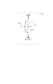
図1〜図5を用いて、本発明に適用可能な撮像装置の一実施例を説明する。各図面において同じ符号が付されている部分は、同じ素子もしくは同じ領域を指す。
はPMOSトランジスタを構成し、これらのトランジスタがバッファ210を構成するインバータとなる。なお、N型半導体領域324にはGND電位が供給され、P型半導体領域325には電源電圧が供給される。そして、N型半導体領域333とP型半導体領域327には、駆動配線206を構成する導電パターン306が電気的に接続される。
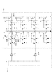
図6〜8に本実施例の撮像装置の特徴を説明するための等価回路図、平面模式図を示す。図1〜5と同様の機能を有する部分には同様の符号を付し詳細な説明を省略する。
図8に実施例2の変形例を示す。図8は第1画素行と第2画素行が隣り合って配され、且つ第1画素行の各画素と第2画素行の各画素がミラー対称の配置になっている点で図7異なる。
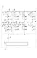
図9、図10に本実施例の撮像装置の特徴を説明するための等価回路図、平面模式図を示す。図1〜5と同様の機能を有する部分には同様の符号を付し詳細な説明を省略する。
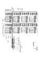
図11〜16に本実施例の撮像装置の特徴を説明するための等価回路図、平面模式図を示す。図1〜5と同様の機能を有する部分には同様の符号を付し詳細な説明を省略する。
図13と図14に実施例4の変形例を示す。図13は図12と、隣り合う画素行の第2方向に隣り合う二つの画素の各々のスイッチ207を構成する電極307が共通である点で異なる。この時、図8のように隣り合う画素行の画素がミラー対称であってもよい。
域313Bによって形成される表面型MOS容量は、第2画素行の画素100の入力ノードに接続される容量208Bである。なお、容量208Aと容量208Bの間には絶縁体分離部300が配されており、容量208Aと容量208Bは電気的に非接続である。
図15に実施例4の変形例を示す。図15は図12と、隣り合う画素行の各画素のFD203を構成するN型半導体領域303が共通であり、さらに入力ノードが共通である点で異なる。
図16に実施例4の変形例を示す。本変形例では各画素行の画素のうち緑色のカラーフィルタを有する画素のみが容量208およびスイッチ207を有する点で異なる。
102 画素部
201 光電変換部
202 転送トランジスタ
205 増幅トランジスタ
207A 第1スイッチ
207B 第2スイッチ
210 バッファ
Claims (15)
- 光電変換部と、前記光電変換部で蓄積された電荷を転送する転送トランジスタと、前記転送トランジスタにより転送された電荷を入力ノードで受ける増幅トランジスタと、を有する画素が行列状に複数配された画素部を有し、
前記画素部には、行方向に沿って配された複数の画素を有する画素行が、前記行方向とは異なる列方向に沿って第1画素行および第2画素行を含む少なくとも二つ配され、
前記第1画素行の第1画素は、前記第1画素に含まれる増幅トランジスタの入力ノードの容量値の大きさを切り替える第1スイッチを有し、
前記第2画素行の第2画素は、前記第2画素に含まれる増幅トランジスタの入力ノードの容量値の大きさを切り替える第2スイッチを有する撮像装置であって、
前記第1スイッチと前記第2スイッチとを駆動するバッファを有し、
前記バッファの出力ノードは、前記第1スイッチの入力ノードと前記第2スイッチの入力ノードに共通して電気的に接続されており、
前記画素部には、前記列方向に沿って、前記第1画素行および前記第2画素行とは別の複数の画素行が配されており、
前記第1画素行および前記第2画素行とは別の前記複数の画素行の画素に含まれる増幅トランジスタの入力ノードの容量値を複数の値に切り替える複数のスイッチを駆動する、前記バッファと異なるバッファを有し、
前記異なるバッファの出力ノードは、前記複数のスイッチの少なくとも一部のスイッチの入力ノードに共通して電気的に接続されていることを特徴とする撮像装置。 - 前記バッファの出力ノードと前記第1スイッチの入力ノードとを電気的に接続し、前記行方向に沿って配された第1導電パターンと、
前記第1導電パターンから分岐し、前記列方向に沿って配された第2導電パターンと、を有し、
さらに前記行方向に沿って配された、第3導電パターンを有し、
前記第2導電パターンは、前記第1導電パターンと前記第3導電パターンとを電気的に接続し、
前記第3導電パターンは、前記第2スイッチと接続されていることを特徴とする請求項1に記載の撮像装置。 - 前記光電変換部の一部を構成し、前記光電変換部で生じた電荷を蓄積する半導体領域が配された第1活性領域と、
前記第1スイッチの入力ノードを構成する電極が上に配された第2活性領域を有することを特徴とする請求項2に記載の撮像装置。 - 前記第2導電パターンは、同一の画素行に含まれ隣り合って配される二つの画素の前記第1活性領域の間で、前記第1導電パターンから分岐することを特徴とする請求項3に記載の撮像装置。
- 前記同一の画素行に含まれ隣り合って配される二つの画素のうち、一方の画素の前記第1活性領域と前記第2活性領域、他方の画素の前記第1活性領域とが前記行方向に沿ってこの順に配され、
前記第2導電パターンは、
前記一方の画素の前記第2活性領域と前記他方の画素の前記第1活性領域との間で、前記第1導電パターンから分岐することを特徴とする請求項4に記載の撮像装置。 - 前記第2導電パターンは、
前記バッファを構成するトランジスタが配される第3活性領域と、前記画素部に配された画素のうち、前記バッファに最も近い位置に配された画素との間で、第1導電パターンから分岐することを特徴とする請求項4に記載の撮像装置。 - 前記電極へ供給される信号により、前記増幅トランジスタの入力ノードへの電気的な接続状態が切り替え可能に配された容量とを有し、
前記第2活性領域に前記増幅トランジスタの入力ノードの一部となる半導体領域が配され、
前記第2活性領域の一部であって、前記電極の下部に位置する部分が前記容量の少なくとも一部を構成していることを特徴とする請求項3乃至6のいずれか1項に記載の撮像装置。 - 前記容量は表面型MOS容量、または埋め込み型MOS容量を有することを特徴とする請求項7に記載の撮像装置。
- 前記第2活性領域は、絶縁体分離部によって区画され、
平面視で前記増幅トランジスタの入力ノードの一部となる半導体領域と前記絶縁体分離部とが、前記電極を挟んで隣り合って配されていることを特徴とする請求項7または8に記載の撮像装置。 - 光電変換部と、前記光電変換部で蓄積された電荷を転送する転送トランジスタと、前記転送トランジスタにより転送された電荷を入力ノードで受ける増幅トランジスタと、を有する画素が行列状に複数配された画素部を有し、
前記画素部には、行方向に沿って配された複数の画素を有する画素行が、前記行方向とは異なる列方向に沿って第1画素行および第2画素行を含む少なくとも二つ配され、
前記第1画素行の第1画素は、前記第1画素に含まれる増幅トランジスタの入力ノードの容量値の大きさを切り替える第1スイッチを有し、
前記第2画素行の第2画素は、前記第2画素に含まれる増幅トランジスタの入力ノードの容量値の大きさを切り替える第2スイッチを有する撮像装置であって、
前記第1スイッチと前記第2スイッチとを駆動するバッファを有し、
前記バッファの出力ノードは、前記第1スイッチの入力ノードと前記第2スイッチの入力ノードに共通して電気的に接続されており、
前記第1スイッチおよび前記第2スイッチは、絶縁体分離部の上に配された電極を有しており、
前記電極は前記絶縁体分離部を挟んで隣り合って配された二つの活性領域の上まで延在しており、
前記二つの活性領域の一方には、前記第1画素行の画素に含まれる増幅トランジスタの入力ノードを構成する第1半導体領域が配され、
前記二つの活性領域の他方には、前記第2画素行の画素に含まれる増幅トランジスタの入力ノードを構成する第2半導体領域が配され、
前記第1半導体領域と前記第2半導体領域は前記電極を挟んで隣り合って配されていることを特徴とする撮像装置。 - 前記電極は、平面視で前記第1半導体領域および前記第2半導体領域の一部と重なることを特徴とする請求項10に記載の撮像装置。
- 前記絶縁体分離部と、前記第1半導体領域および前記第2半導体領域との間に、前記第1半導体領域および前記第2半導体領域と反対導電型の半導体領域が配されることを特徴とする請求項11に記載の撮像装置。
- 前記第1画素行と前記第2画素行とは隣り合って配され、
前記第1画素行の画素と前記第2画素行の画素はミラー対称の配置となることを特徴とする請求項3乃至12のいずれか1項に記載の撮像装置。 - 前記複数の画素の各々が、
一つのマイクロレンズと、
前記一つのマイクロレンズを透過する光に基づく電荷を生成する複数の光電変換部とを有することを特徴とする請求項1乃至13のいずれか1項に記載の撮像装置。 - 前記複数の画素の各々が有する複数のスイッチのすべてを同時にオン状態もしくは同時にオフ状態となるように制御する制御部を有することを特徴とする請求項1乃至14のいずれか1項に撮像装置。
Priority Applications (3)
| Application Number | Priority Date | Filing Date | Title |
|---|---|---|---|
| JP2016023059A JP6727830B2 (ja) | 2016-02-09 | 2016-02-09 | 撮像装置 |
| US15/426,896 US10063801B2 (en) | 2016-02-09 | 2017-02-07 | Image capturing device |
| CN201710068534.1A CN107046626B (zh) | 2016-02-09 | 2017-02-08 | 摄像装置 |
Applications Claiming Priority (1)
| Application Number | Priority Date | Filing Date | Title |
|---|---|---|---|
| JP2016023059A JP6727830B2 (ja) | 2016-02-09 | 2016-02-09 | 撮像装置 |
Publications (3)
| Publication Number | Publication Date |
|---|---|
| JP2017143157A JP2017143157A (ja) | 2017-08-17 |
| JP2017143157A5 JP2017143157A5 (ja) | 2019-03-28 |
| JP6727830B2 true JP6727830B2 (ja) | 2020-07-22 |
Family
ID=59498076
Family Applications (1)
| Application Number | Title | Priority Date | Filing Date |
|---|---|---|---|
| JP2016023059A Active JP6727830B2 (ja) | 2016-02-09 | 2016-02-09 | 撮像装置 |
Country Status (3)
| Country | Link |
|---|---|
| US (1) | US10063801B2 (ja) |
| JP (1) | JP6727830B2 (ja) |
| CN (1) | CN107046626B (ja) |
Families Citing this family (2)
| Publication number | Priority date | Publication date | Assignee | Title |
|---|---|---|---|---|
| JP7356214B2 (ja) * | 2018-09-04 | 2023-10-04 | キヤノン株式会社 | 撮像装置、その製造方法及びカメラ |
| US11871135B2 (en) * | 2022-02-03 | 2024-01-09 | Omnivision Technologies, Inc. | Circuit and method for image artifact reduction in high-density, high-pixel-count, image sensor with phase detection autofocus |
Family Cites Families (35)
| Publication number | Priority date | Publication date | Assignee | Title |
|---|---|---|---|---|
| JPH02262344A (ja) * | 1989-03-31 | 1990-10-25 | Sony Corp | 出力回路 |
| EP0739039A3 (en) * | 1995-04-18 | 1998-03-04 | Interuniversitair Micro-Elektronica Centrum Vzw | Pixel structure, image sensor using such pixel, structure and corresponding peripheric circuitry |
| JP3592106B2 (ja) * | 1998-11-27 | 2004-11-24 | キヤノン株式会社 | 固体撮像装置およびカメラ |
| JP3594891B2 (ja) * | 2000-09-12 | 2004-12-02 | 沖電気工業株式会社 | 半導体記憶装置およびその検査方法 |
| US20070080905A1 (en) * | 2003-05-07 | 2007-04-12 | Toshiba Matsushita Display Technology Co., Ltd. | El display and its driving method |
| JP4317115B2 (ja) * | 2004-04-12 | 2009-08-19 | 国立大学法人東北大学 | 固体撮像装置、光センサおよび固体撮像装置の動作方法 |
| JP4343144B2 (ja) * | 2004-09-24 | 2009-10-14 | 株式会社東芝 | 赤外線センサ |
| JP2006314025A (ja) * | 2005-05-09 | 2006-11-16 | Sony Corp | 撮像装置と撮像装置用の電源供給方法 |
| JP4844032B2 (ja) * | 2005-07-21 | 2011-12-21 | 株式会社ニコン | 撮像装置 |
| EP2942813B1 (en) * | 2006-08-09 | 2020-09-30 | Tohoku University | Optical sensor and solid-state imaging device |
| JP2008046377A (ja) * | 2006-08-17 | 2008-02-28 | Sony Corp | 表示装置 |
| JP5016941B2 (ja) * | 2007-02-08 | 2012-09-05 | 株式会社東芝 | 固体撮像装置 |
| JP4858294B2 (ja) * | 2007-05-09 | 2012-01-18 | ソニー株式会社 | 撮像装置、撮像回路および画像処理回路 |
| JP2008305983A (ja) * | 2007-06-07 | 2008-12-18 | Nikon Corp | 固体撮像素子 |
| JP5228961B2 (ja) * | 2009-02-06 | 2013-07-03 | 日本テキサス・インスツルメンツ株式会社 | 増幅回路及び撮像装置 |
| JP5257176B2 (ja) * | 2009-03-18 | 2013-08-07 | ソニー株式会社 | 固体撮像装置、固体撮像装置の駆動方法および電子機器 |
| JP2010278904A (ja) * | 2009-05-29 | 2010-12-09 | Panasonic Corp | 固体撮像装置、カメラおよび固体撮像装置の駆動方法 |
| JPWO2011058684A1 (ja) * | 2009-11-12 | 2013-03-28 | パナソニック株式会社 | 固体撮像装置 |
| JP5467846B2 (ja) * | 2009-11-20 | 2014-04-09 | 富士フイルム株式会社 | 放射線検出素子 |
| KR101077408B1 (ko) * | 2010-02-05 | 2011-10-26 | 서강대학교산학협력단 | Cmos 이미지 센서 |
| JP2011199196A (ja) * | 2010-03-23 | 2011-10-06 | Toshiba Corp | 固体撮像装置 |
| JP5686765B2 (ja) * | 2011-07-21 | 2015-03-18 | キヤノン株式会社 | 撮像装置およびその制御方法 |
| JP6039165B2 (ja) * | 2011-08-11 | 2016-12-07 | キヤノン株式会社 | 撮像素子及び撮像装置 |
| JP2013089869A (ja) * | 2011-10-20 | 2013-05-13 | Canon Inc | 検出装置及び検出システム |
| JP5967944B2 (ja) * | 2012-01-18 | 2016-08-10 | キヤノン株式会社 | 固体撮像装置およびカメラ |
| JP2014112580A (ja) * | 2012-12-05 | 2014-06-19 | Sony Corp | 固体撮像素子および駆動方法 |
| JP6236635B2 (ja) * | 2012-11-27 | 2017-11-29 | パナソニックIpマネジメント株式会社 | 固体撮像装置およびその駆動方法 |
| JP6108884B2 (ja) * | 2013-03-08 | 2017-04-05 | キヤノン株式会社 | 光電変換装置及び撮像システム |
| JP6230329B2 (ja) * | 2013-08-19 | 2017-11-15 | キヤノン株式会社 | 撮像装置 |
| JP6466645B2 (ja) * | 2014-03-17 | 2019-02-06 | オリンパス株式会社 | 撮像装置 |
| JP6391302B2 (ja) * | 2014-05-23 | 2018-09-19 | キヤノン株式会社 | 撮像装置、および、撮像システム |
| JP6459025B2 (ja) * | 2014-07-07 | 2019-01-30 | パナソニックIpマネジメント株式会社 | 固体撮像装置 |
| JP6406912B2 (ja) * | 2014-07-24 | 2018-10-17 | キヤノン株式会社 | 撮像装置並びにその駆動方法 |
| JP6406911B2 (ja) * | 2014-07-24 | 2018-10-17 | キヤノン株式会社 | 撮像装置及び撮像装置の製造方法 |
| JP6606504B2 (ja) * | 2014-09-17 | 2019-11-13 | ソニーセミコンダクタソリューションズ株式会社 | 撮像装置、撮像素子および撮像装置の制御方法 |
-
2016
- 2016-02-09 JP JP2016023059A patent/JP6727830B2/ja active Active
-
2017
- 2017-02-07 US US15/426,896 patent/US10063801B2/en active Active
- 2017-02-08 CN CN201710068534.1A patent/CN107046626B/zh active Active
Also Published As
| Publication number | Publication date |
|---|---|
| CN107046626A (zh) | 2017-08-15 |
| US20170230600A1 (en) | 2017-08-10 |
| JP2017143157A (ja) | 2017-08-17 |
| US10063801B2 (en) | 2018-08-28 |
| CN107046626B (zh) | 2020-11-17 |
Similar Documents
| Publication | Publication Date | Title |
|---|---|---|
| JP5486639B2 (ja) | イメージセンサに関する方法 | |
| TWI469336B (zh) | 固態成像元件及照相機系統 | |
| KR100851494B1 (ko) | 수직적으로 집적된 세트 및 리셋 다이오드를 갖는 cmos이미지 센서를 위한 소형 픽셀 | |
| US9236406B2 (en) | Photoelectric conversion apparatus with gate control lines and wiring at same height | |
| JP5963450B2 (ja) | 撮像装置および撮像システム | |
| JP5709418B2 (ja) | 固体撮像装置 | |
| JP6406912B2 (ja) | 撮像装置並びにその駆動方法 | |
| JP2014049727A (ja) | 固体撮像装置 | |
| KR20090121322A (ko) | 이미지 센서 및 카메라 | |
| US9197832B2 (en) | Solid-state image pickup apparatus and drive method therefor | |
| JP2010212288A (ja) | 撮像装置 | |
| JP2007243093A (ja) | 固体撮像装置、撮像装置および信号処理方法 | |
| JP6025750B2 (ja) | 撮像装置 | |
| JP6727830B2 (ja) | 撮像装置 | |
| US20210288115A1 (en) | Imaging device | |
| JP6719958B2 (ja) | 撮像装置及び撮像装置の駆動方法 | |
| WO2019069532A1 (ja) | 固体撮像素子および固体撮像装置 | |
| JP6355401B2 (ja) | 固体撮像装置及びカメラ | |
| JP2017117957A (ja) | 光電変換装置 | |
| JP2017084930A (ja) | 撮像装置 | |
| JP2016197644A (ja) | 撮像装置 | |
| JP6682587B2 (ja) | 撮像装置並びにその駆動方法 | |
| WO2023074461A1 (ja) | 撮像装置 | |
| US20140333817A1 (en) | Image pickup apparatus | |
| JPH11346332A (ja) | 固体撮像装置 |
Legal Events
| Date | Code | Title | Description |
|---|---|---|---|
| A521 | Request for written amendment filed |
Free format text: JAPANESE INTERMEDIATE CODE: A523 Effective date: 20190208 |
|
| A621 | Written request for application examination |
Free format text: JAPANESE INTERMEDIATE CODE: A621 Effective date: 20190208 |
|
| A977 | Report on retrieval |
Free format text: JAPANESE INTERMEDIATE CODE: A971007 Effective date: 20191122 |
|
| A131 | Notification of reasons for refusal |
Free format text: JAPANESE INTERMEDIATE CODE: A131 Effective date: 20200107 |
|
| A521 | Request for written amendment filed |
Free format text: JAPANESE INTERMEDIATE CODE: A523 Effective date: 20200306 |
|
| A131 | Notification of reasons for refusal |
Free format text: JAPANESE INTERMEDIATE CODE: A131 Effective date: 20200317 |
|
| A521 | Request for written amendment filed |
Free format text: JAPANESE INTERMEDIATE CODE: A523 Effective date: 20200512 |
|
| TRDD | Decision of grant or rejection written | ||
| A01 | Written decision to grant a patent or to grant a registration (utility model) |
Free format text: JAPANESE INTERMEDIATE CODE: A01 Effective date: 20200602 |
|
| A61 | First payment of annual fees (during grant procedure) |
Free format text: JAPANESE INTERMEDIATE CODE: A61 Effective date: 20200701 |
|
| R151 | Written notification of patent or utility model registration |
Ref document number: 6727830 Country of ref document: JP Free format text: JAPANESE INTERMEDIATE CODE: R151 |