JP6727830B2 - Imaging device - Google Patents
Imaging device Download PDFInfo
- Publication number
- JP6727830B2 JP6727830B2 JP2016023059A JP2016023059A JP6727830B2 JP 6727830 B2 JP6727830 B2 JP 6727830B2 JP 2016023059 A JP2016023059 A JP 2016023059A JP 2016023059 A JP2016023059 A JP 2016023059A JP 6727830 B2 JP6727830 B2 JP 6727830B2
- Authority
- JP
- Japan
- Prior art keywords
- pixel
- switch
- semiconductor region
- conductive pattern
- input node
- Prior art date
- Legal status (The legal status is an assumption and is not a legal conclusion. Google has not performed a legal analysis and makes no representation as to the accuracy of the status listed.)
- Active
Links
- 238000003384 imaging method Methods 0.000 title claims description 27
- 239000004065 semiconductor Substances 0.000 claims description 95
- 239000000872 buffer Substances 0.000 claims description 64
- 238000006243 chemical reaction Methods 0.000 claims description 56
- 230000003321 amplification Effects 0.000 claims description 55
- 238000003199 nucleic acid amplification method Methods 0.000 claims description 55
- 239000003990 capacitor Substances 0.000 claims description 32
- 238000012546 transfer Methods 0.000 claims description 27
- 239000012212 insulator Substances 0.000 claims description 18
- 238000002955 isolation Methods 0.000 claims description 5
- 239000011159 matrix material Substances 0.000 claims description 5
- 238000000926 separation method Methods 0.000 claims description 5
- 238000009413 insulation Methods 0.000 claims 1
- 238000010586 diagram Methods 0.000 description 17
- 238000012986 modification Methods 0.000 description 13
- 230000004048 modification Effects 0.000 description 13
- 230000002093 peripheral effect Effects 0.000 description 11
- 230000000694 effects Effects 0.000 description 5
- 238000012545 processing Methods 0.000 description 5
- 230000035945 sensitivity Effects 0.000 description 5
- 238000001514 detection method Methods 0.000 description 4
- 238000000034 method Methods 0.000 description 3
- 230000003071 parasitic effect Effects 0.000 description 3
- 238000009792 diffusion process Methods 0.000 description 2
- 229920006395 saturated elastomer Polymers 0.000 description 2
- 230000005684 electric field Effects 0.000 description 1
- 238000005259 measurement Methods 0.000 description 1
- 229910021420 polycrystalline silicon Inorganic materials 0.000 description 1
- 229920005591 polysilicon Polymers 0.000 description 1
- 238000007493 shaping process Methods 0.000 description 1
- 238000000638 solvent extraction Methods 0.000 description 1
- 230000002194 synthesizing effect Effects 0.000 description 1
Images


Classifications
-
- H—ELECTRICITY
- H01—ELECTRIC ELEMENTS
- H01L—SEMICONDUCTOR DEVICES NOT COVERED BY CLASS H10
- H01L27/00—Devices consisting of a plurality of semiconductor or other solid-state components formed in or on a common substrate
- H01L27/14—Devices consisting of a plurality of semiconductor or other solid-state components formed in or on a common substrate including semiconductor components sensitive to infrared radiation, light, electromagnetic radiation of shorter wavelength or corpuscular radiation and specially adapted either for the conversion of the energy of such radiation into electrical energy or for the control of electrical energy by such radiation
- H01L27/144—Devices controlled by radiation
- H01L27/146—Imager structures
- H01L27/14601—Structural or functional details thereof
- H01L27/14603—Special geometry or disposition of pixel-elements, address-lines or gate-electrodes
- H01L27/14605—Structural or functional details relating to the position of the pixel elements, e.g. smaller pixel elements in the center of the imager compared to pixel elements at the periphery
-
- H—ELECTRICITY
- H04—ELECTRIC COMMUNICATION TECHNIQUE
- H04N—PICTORIAL COMMUNICATION, e.g. TELEVISION
- H04N25/00—Circuitry of solid-state image sensors [SSIS]; Control thereof
- H04N25/70—SSIS architectures; Circuits associated therewith
- H04N25/76—Addressed sensors, e.g. MOS or CMOS sensors
- H04N25/77—Pixel circuitry, e.g. memories, A/D converters, pixel amplifiers, shared circuits or shared components
-
- H—ELECTRICITY
- H04—ELECTRIC COMMUNICATION TECHNIQUE
- H04N—PICTORIAL COMMUNICATION, e.g. TELEVISION
- H04N25/00—Circuitry of solid-state image sensors [SSIS]; Control thereof
- H04N25/50—Control of the SSIS exposure
- H04N25/57—Control of the dynamic range
- H04N25/59—Control of the dynamic range by controlling the amount of charge storable in the pixel, e.g. modification of the charge conversion ratio of the floating node capacitance
-
- H—ELECTRICITY
- H01—ELECTRIC ELEMENTS
- H01L—SEMICONDUCTOR DEVICES NOT COVERED BY CLASS H10
- H01L27/00—Devices consisting of a plurality of semiconductor or other solid-state components formed in or on a common substrate
- H01L27/14—Devices consisting of a plurality of semiconductor or other solid-state components formed in or on a common substrate including semiconductor components sensitive to infrared radiation, light, electromagnetic radiation of shorter wavelength or corpuscular radiation and specially adapted either for the conversion of the energy of such radiation into electrical energy or for the control of electrical energy by such radiation
- H01L27/144—Devices controlled by radiation
- H01L27/146—Imager structures
- H01L27/14601—Structural or functional details thereof
- H01L27/14609—Pixel-elements with integrated switching, control, storage or amplification elements
- H01L27/14612—Pixel-elements with integrated switching, control, storage or amplification elements involving a transistor
-
- H—ELECTRICITY
- H01—ELECTRIC ELEMENTS
- H01L—SEMICONDUCTOR DEVICES NOT COVERED BY CLASS H10
- H01L27/00—Devices consisting of a plurality of semiconductor or other solid-state components formed in or on a common substrate
- H01L27/14—Devices consisting of a plurality of semiconductor or other solid-state components formed in or on a common substrate including semiconductor components sensitive to infrared radiation, light, electromagnetic radiation of shorter wavelength or corpuscular radiation and specially adapted either for the conversion of the energy of such radiation into electrical energy or for the control of electrical energy by such radiation
- H01L27/144—Devices controlled by radiation
- H01L27/146—Imager structures
- H01L27/14601—Structural or functional details thereof
- H01L27/14625—Optical elements or arrangements associated with the device
- H01L27/14627—Microlenses
-
- H—ELECTRICITY
- H01—ELECTRIC ELEMENTS
- H01L—SEMICONDUCTOR DEVICES NOT COVERED BY CLASS H10
- H01L27/00—Devices consisting of a plurality of semiconductor or other solid-state components formed in or on a common substrate
- H01L27/14—Devices consisting of a plurality of semiconductor or other solid-state components formed in or on a common substrate including semiconductor components sensitive to infrared radiation, light, electromagnetic radiation of shorter wavelength or corpuscular radiation and specially adapted either for the conversion of the energy of such radiation into electrical energy or for the control of electrical energy by such radiation
- H01L27/144—Devices controlled by radiation
- H01L27/146—Imager structures
- H01L27/14643—Photodiode arrays; MOS imagers
-
- H—ELECTRICITY
- H04—ELECTRIC COMMUNICATION TECHNIQUE
- H04N—PICTORIAL COMMUNICATION, e.g. TELEVISION
- H04N25/00—Circuitry of solid-state image sensors [SSIS]; Control thereof
- H04N25/50—Control of the SSIS exposure
- H04N25/57—Control of the dynamic range
- H04N25/58—Control of the dynamic range involving two or more exposures
- H04N25/581—Control of the dynamic range involving two or more exposures acquired simultaneously
- H04N25/585—Control of the dynamic range involving two or more exposures acquired simultaneously with pixels having different sensitivities within the sensor, e.g. fast or slow pixels or pixels having different sizes
-
- H—ELECTRICITY
- H04—ELECTRIC COMMUNICATION TECHNIQUE
- H04N—PICTORIAL COMMUNICATION, e.g. TELEVISION
- H04N25/00—Circuitry of solid-state image sensors [SSIS]; Control thereof
- H04N25/70—SSIS architectures; Circuits associated therewith
-
- H—ELECTRICITY
- H04—ELECTRIC COMMUNICATION TECHNIQUE
- H04N—PICTORIAL COMMUNICATION, e.g. TELEVISION
- H04N25/00—Circuitry of solid-state image sensors [SSIS]; Control thereof
- H04N25/70—SSIS architectures; Circuits associated therewith
- H04N25/76—Addressed sensors, e.g. MOS or CMOS sensors
- H04N25/766—Addressed sensors, e.g. MOS or CMOS sensors comprising control or output lines used for a plurality of functions, e.g. for pixel output, driving, reset or power
-
- H—ELECTRICITY
- H04—ELECTRIC COMMUNICATION TECHNIQUE
- H04N—PICTORIAL COMMUNICATION, e.g. TELEVISION
- H04N25/00—Circuitry of solid-state image sensors [SSIS]; Control thereof
- H04N25/70—SSIS architectures; Circuits associated therewith
- H04N25/76—Addressed sensors, e.g. MOS or CMOS sensors
- H04N25/77—Pixel circuitry, e.g. memories, A/D converters, pixel amplifiers, shared circuits or shared components
- H04N25/778—Pixel circuitry, e.g. memories, A/D converters, pixel amplifiers, shared circuits or shared components comprising amplifiers shared between a plurality of pixels, i.e. at least one part of the amplifier must be on the sensor array itself
-
- H—ELECTRICITY
- H04—ELECTRIC COMMUNICATION TECHNIQUE
- H04N—PICTORIAL COMMUNICATION, e.g. TELEVISION
- H04N25/00—Circuitry of solid-state image sensors [SSIS]; Control thereof
- H04N25/70—SSIS architectures; Circuits associated therewith
- H04N25/76—Addressed sensors, e.g. MOS or CMOS sensors
- H04N25/78—Readout circuits for addressed sensors, e.g. output amplifiers or A/D converters
-
- H—ELECTRICITY
- H04—ELECTRIC COMMUNICATION TECHNIQUE
- H04N—PICTORIAL COMMUNICATION, e.g. TELEVISION
- H04N25/00—Circuitry of solid-state image sensors [SSIS]; Control thereof
- H04N25/70—SSIS architectures; Circuits associated therewith
- H04N25/71—Charge-coupled device [CCD] sensors; Charge-transfer registers specially adapted for CCD sensors
- H04N25/75—Circuitry for providing, modifying or processing image signals from the pixel array
Description
本発明は撮像装置に関する。 The present invention relates to an image pickup device.
従来、画素から出力される信号のダイナミックレンジを拡大するために増幅トランジスタの入力ノードに容量を接続する構成が知られている。 Conventionally, there has been known a configuration in which a capacitor is connected to an input node of an amplification transistor in order to expand a dynamic range of a signal output from a pixel.
特許文献1において、画素に配されたフローティングディフュージョンの容量を可変にするためのスイッチに駆動パルスを供給する駆動配線が、各画素行に配されている構成が開示されている。 Patent Document 1 discloses a configuration in which a drive wiring for supplying a drive pulse to a switch for varying the capacitance of a floating diffusion arranged in a pixel is arranged in each pixel row.
特許文献1のような構成によれば、各画素行の駆動配線に駆動パルスを供給するための周辺回路素子であるバッファが駆動配線ごとに配される。そのため周辺回路部が広くなる恐れがある。 According to the configuration of Patent Document 1, a buffer, which is a peripheral circuit element for supplying a drive pulse to the drive wiring of each pixel row, is arranged for each drive wiring. Therefore, the peripheral circuit section may be widened.
本発明の撮像装置は、光電変換部と、前記光電変換部で蓄積された電荷を転送する転送トランジスタと、前記転送トランジスタにより転送された電荷を入力ノードで受ける増幅トランジスタと、を有する画素が行列状に複数配された画素部を有し、前記画素部には、行方向に沿って配された複数の画素を有する画素行が、前記行方向とは異なる列方向に沿って第1画素行および第2画素行を含む少なくとも二つ配され、前記第1画素行の第1画素は、前記第1画素に含まれる増幅トランジスタの入力ノードの容量値の大きさを切り替える第1スイッチを有し、前記第2画素行の第2画素は、前記第2画素に含まれる増幅トランジスタの入力ノードの容量値の大きさを切り替える第2スイッチを有する撮像装置であって、前記第1スイッチと前記第2スイッチとを駆動するバッファを有し、前記バッファの出力ノードは、前記第1スイッチの入力ノードと前記第2スイッチの入力ノードに共通して電気的に接続されており、前記画素部には、前記列方向に沿って、前記第1画素行および前記第2画素行とは別の複数の画素行が配されており、前記第1画素行および前記第2画素行とは別の前記複数の画素行の画素に含まれる増幅トランジスタの入力ノードの容量値を複数の値に切り替える複数のスイッチを駆動する、前記バッファと異なるバッファを有し、前記異なるバッファの出力ノードは、前記複数のスイッチの少なくとも一部のスイッチの入力ノードに共通して電気的に接続されている。
本発明の別の撮像装置は、光電変換部と、前記光電変換部で蓄積された電荷を転送する転送トランジスタと、前記転送トランジスタにより転送された電荷を入力ノードで受ける増幅トランジスタと、を有する画素が行列状に複数配された画素部を有し、前記画素部には、行方向に沿って配された複数の画素を有する画素行が、前記行方向とは異なる列方向に沿って第1画素行および第2画素行を含む少なくとも二つ配され、前記第1画素行の第1画素は、前記第1画素に含まれる増幅トランジスタの入力ノードの容量値の大きさを切り替える第1スイッチを有し、前記第2画素行の第2画素は、前記第2画素に含まれる増幅トランジスタの入力ノードの容量値の大きさを切り替える第2スイッチを有する撮像装置であって、前記第1スイッチと前記第2スイッチとを駆動するバッファを有し、前記バッファの出力ノードは、前記第1スイッチの入力ノードと前記第2スイッチの入力ノードに共通して電気的に接続されており、前記スイッチは、絶縁体分離部の上に配された電極を有しており、前記電極は前記絶縁体分離部を挟んで隣り合って配された二つの活性領域の上まで延在しており、前記二つの活性領域の一方には、前記第1画素行の画素に含まれる増幅トランジスタの入力ノードを構成する第1半導体領域が配され、前記二つの活性領域の他方には、前記第2画素行の画素に含まれる増幅トランジスタの入力ノードを構成する第2半導体領域が配され、前記第1半導体領域と前記第2半導体領域は前記電極を挟んで隣り合って配されている。
In the imaging device of the present invention, a pixel having a photoelectric conversion unit, a transfer transistor that transfers the charge accumulated in the photoelectric conversion unit, and an amplification transistor that receives the charge transferred by the transfer transistor at an input node is a matrix. A plurality of pixel portions arranged in a row, and a pixel row having a plurality of pixels arranged in a row direction is provided in the pixel portion in a first pixel row along a column direction different from the row direction. And at least two, including a second pixel row, the first pixel of the first pixel row has a first switch for switching the magnitude of the capacitance value of the input node of the amplification transistor included in the first pixel. The second pixel of the second pixel row is an imaging device that includes a second switch that switches a magnitude of a capacitance value of an input node of an amplification transistor included in the second pixel, the first switch and the second switch. A buffer for driving two switches, an output node of the buffer is electrically connected to an input node of the first switch and an input node of the second switch in common, and the output node of the buffer is connected to the pixel unit. , A plurality of pixel rows different from the first pixel row and the second pixel row are arranged along the column direction, and the plurality of pixel rows different from the first pixel row and the second pixel row are arranged. A plurality of switches for switching the capacitance value of the input node of the amplification transistor included in the pixels of the pixel row to a plurality of values, the buffer having a buffer different from the buffer, and the output node of the different buffer has the plurality of switches Are electrically connected in common to the input nodes of at least some of the switches .
Another imaging device of the present invention is a pixel including a photoelectric conversion unit, a transfer transistor that transfers the charges accumulated in the photoelectric conversion unit, and an amplification transistor that receives the charges transferred by the transfer transistor at an input node. Has a plurality of pixel portions arranged in a matrix, and in the pixel portion, a pixel row having a plurality of pixels arranged in the row direction is arranged along a column direction different from the row direction. At least two pixels including a pixel row and a second pixel row are arranged, and the first pixel of the first pixel row includes a first switch that switches a magnitude of a capacitance value of an input node of an amplification transistor included in the first pixel. The second pixel of the second pixel row is an imaging device that includes a second switch that switches a magnitude of a capacitance value of an input node of an amplification transistor included in the second pixel, and the second switch includes: A buffer for driving the second switch, an output node of the buffer is electrically connected to an input node of the first switch and an input node of the second switch in common, and the switch is , An electrode disposed on the insulator separation portion, the electrode extending to above two active regions disposed adjacent to each other with the insulator separation portion interposed therebetween, A first semiconductor region forming an input node of an amplification transistor included in a pixel of the first pixel row is disposed in one of the two active regions, and the other of the two active regions includes a second semiconductor region of the second pixel row. A second semiconductor region forming an input node of an amplification transistor included in a pixel is arranged, and the first semiconductor region and the second semiconductor region are arranged adjacent to each other with the electrode interposed therebetween.
増幅トランジスタの入力ノードの容量値の大きさを切り替えるスイッチを駆動するバッファの数を削減することが可能となる。 It is possible to reduce the number of buffers that drive switches that switch the magnitude of the capacitance value of the input node of the amplification transistor.
(実施例1)
図1〜図5を用いて、本発明に適用可能な撮像装置の一実施例を説明する。各図面において同じ符号が付されている部分は、同じ素子もしくは同じ領域を指す。
(Example 1)
An embodiment of an imaging device applicable to the present invention will be described with reference to FIGS. 1 to 5. Portions with the same reference numerals in the respective drawings indicate the same elements or the same regions.
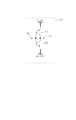
図1に本発明の一実施例である撮像装置101のブロック図を示す。撮像装置101は、画素部102と、周辺回路部107を有する。周辺回路部107は駆動パルス生成部103、垂直走査回路104、信号処理部105、出力部106を有している。
FIG. 1 shows a block diagram of an
画素部102には、各々が光を電気信号へ変換し、変換した電気信号を出力する複数の画素100が行列状に配されている。第1方向(画素部102の行における画素100の並び方向)に沿って配された複数の画素を有する画素行が、第1方向とは異なる第2方向(画素部102の列における画素100の並び方向)に沿って、少なくとも二つ配されている。
In the
駆動パルス生成部103は駆動パルスを生成し、垂直走査回路104は駆動パルス生成部103からの制御パルスを受け、各画素に駆動パルスを供給する。駆動パルス生成部103および垂直走査回路104は駆動パルスの供給を制御する制御部を構成する。
The drive
信号処理部105には、画素部102から並列に出力された信号が入力される。そして信号処理部105は、複数の画素列から並列に出力された信号をシリアライズして出力部106に伝達する。更に信号処理部105は、信号の増幅、AD変換等を行なう列回路を有していてもよい。
The signals output in parallel from the
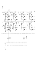
図2に撮像装置の等価回路図の一例を示す。本実施例では、信号電荷の極性を第1導電型と呼ぶ。本実施例では、例として、第1導電型をN型とし、第1導電型と反対導電型の第2導電型をP型として説明するが、これに限らずPとNとが入れ替わってもよい。また、各部材を識別するために添え字A、Bを用いるが、同様の機能を有する部分においては添え字を付さずに説明する。両者を区別しての説明が必要な場合には添え字を付して説明する。 FIG. 2 shows an example of an equivalent circuit diagram of the image pickup apparatus. In this embodiment, the polarity of the signal charge is called the first conductivity type. In the present embodiment, as an example, the first conductivity type is the N type and the second conductivity type opposite to the first conductivity type is the P type. However, the present invention is not limited to this. Good. Further, although subscripts A and B are used to identify each member, description will be made without subscripts for portions having similar functions. When it is necessary to distinguish between the two, a description will be given with a subscript.
まず各画素の構成について説明する。画素100は複数の光電変換部(光電変換部201A、光電変換部201B)を有する。光電変換部201A、201Bでは光電変換により電荷対を生成する。光電変換部201A,201Bには、例えばフォトダイオードが用いられる。
First, the configuration of each pixel will be described. The
転送トランジスタ202Aは光電変換部201Aで生じた電子をフローティングディフュージョン(以下、FD)203へ転送する。転送トランジスタ202Bは光電変換部201Bで生じた電子をFD203へ転送する。
The
FD203は、光電変換部201A、光電変換部201Bにより共有される。そしてFD203は、転送トランジスタ202A、転送トランジスタ202Bを介して光電変換部201Aおよび光電変換部201Bから転送された電子を保持する。
The FD 203 is shared by the
増幅トランジスタ205は、そのゲート電極がFD203に電気的に接続されており、転送トランジスタ202A、転送トランジスタ202BによってFD203に転送された電子に基づく信号を増幅して出力する。より具体的には、FD203に転送された電子は、その量に応じた電圧に変換され、その電圧に応じた電気信号は増幅トランジスタ205を介して画素外へ出力される。増幅トランジスタ205は、不図示の電流源とともにソースフォロア回路を構成している。
The
リセットトランジスタ204は、増幅トランジスタ205の入力ノードの電圧を所定の電位にリセットする。選択トランジスタ220は、増幅トランジスタ205から信号線209への出力を制御する。選択トランジスタ220のドレインは、増幅トランジスタ205のソースに接続され、選択トランジスタ220のソースは信号線209に接続されている。
The
本実施例の構成に代えて、選択トランジスタ220を増幅トランジスタ205のドレインと、電源電圧が供給されている電源配線との間に設けてもよい。いずれの場合も、選択トランジスタ220は、増幅トランジスタ205と信号線209との電気的導通を制御する。
Instead of the configuration of this embodiment, the
容量208は、接続状態において増幅トランジスタ205の入力ノードの一部を構成し、非接続状態において入力ノードから分離される。これにより、増幅トランジスタ205の入力ノードの容量値を変更可能にしている。本例において、容量208の接続・非接続状態の切り替えはスイッチ207によって制御される。
The capacitor 208 constitutes a part of the input node of the
容量208とスイッチ207は一部の構成を兼用してもよい。たとえば、容量208は、スイッチ207のゲート絶縁膜容量で構成することができる。またスイッチ207がMOSトランジスタである場合には、ソースを構成するN型半導体領域により構成されるPN接合容量および寄生容量で構成することができる。ただし、容量208とスイッチ207が兼用されずに独立の部材で構成されていてもよい。 The capacitor 208 and the switch 207 may share a part of the configuration. For example, the capacitor 208 can be formed by the gate insulating film capacitor of the switch 207. When the switch 207 is a MOS transistor, it can be formed of a PN junction capacitance and a parasitic capacitance formed of an N-type semiconductor region forming the source. However, the capacitor 208 and the switch 207 may not be combined and may be configured by independent members.
スイッチ207の入力ノードに駆動パルスが供給され、オン状態(接続状態)、オフ状態(非接続状態)が切り替えられることで、増幅トランジスタ205の入力ノードの容量値を複数の値に切り替える。例えば、容量208を非接続状態とした時に増幅トランジスタ205の入力ノードの容量値は第1の値となる。そして、容量208を接続状態とした時に増幅トランジスタ205の入力ノードの容量値は第1の値よりも大きい第2の値となる。なお、すべてのスイッチ207は同時にオン状態、オフ状態が切り換えられてもよい。
A drive pulse is supplied to the input node of the switch 207 to switch between an on state (connected state) and an off state (not connected state), thereby switching the capacitance value of the input node of the
容量208を接続状態とした場合には、非接続状態に比して増幅トランジスタ205の入力ノードにおける電荷電圧変換効率を低くすることが出来る。
When the capacitor 208 is in the connected state, the charge-voltage conversion efficiency at the input node of the
したがって、増幅トランジスタ205の入力ノードに転送された信号電荷が一定の場合、増幅トランジスタ205の入力ノードで電圧に変換された後の電圧振幅の大きさが、容量値を増大させない場合よりも小さくなる。そのため高照度の信号が入力された場合でもFD203が飽和しにくくなる。
Therefore, when the signal charge transferred to the input node of the
対して、容量208を非接続状態として増幅トランジスタ205の入力ノードの容量値を接続状態と比べて小さくした場合には、接続状態に比して増幅トランジスタ205の入力ノードにおける電荷電圧変換効率が向上する。
On the other hand, when the capacitance 208 is not connected and the capacitance value of the input node of the
したがって、転送された信号電荷が一定の場合、増幅トランジスタ205の入力ノードで電圧に変換された後の電圧振幅が大きくなるため、同じだけのノイズが生じた場合のシグナルノイズ比が向上する。これらを切り替えて用いることで、ダイナミックレンジの変更が可能となる。
Therefore, when the transferred signal charges are constant, the voltage amplitude after being converted into a voltage at the input node of the
なお、スイッチ207と容量208は必ずしもすべての画素に配されていなくてもよい。二つの画素行の各々の画素行において、少なくとも一つの画素100がスイッチ207と容量208を有していればよい。
Note that the switch 207 and the capacitor 208 do not necessarily have to be provided in all pixels. In each pixel row of the two pixel rows, at least one
図2において増幅トランジスタ205とリセットトランジスタ204とは、一つの画素行の一つの画素100の光電変換部201A、光電変換部201Bにより共有される。このような構成の画素100は撮像用の信号と撮像以外の用途に用いる信号を出力することができる。撮像以外とは、例えば位相差検出方式による焦点検出用の信号、距離測定のための信号、異なる波長域の光を光電変換した信号などである。
In FIG. 2, the
画素100から撮像用の信号を得る際には光電変換部201Aおよび光電変換部201Bで生じた信号電荷をFD203に転送する。そして二つの光電変換部201A、201Bで生じた電荷に基づく信号を画素100の信号として信号線209を介して信号処理部105に出力する。
When obtaining a signal for imaging from the
また、焦点検出用の信号を得る際は光電変換部201Aもしくは光電変換部201Bで生じた信号電荷に基づく信号を画素の信号として用いればよい。二つの光電変換部201A、201Bのうち一方の電荷をFD203へ転送した後、FD203をリセットし、他方の光電変換部の電荷をFDへ転送することで二つの光電変換部の各々の信号を得ることができる。
Further, when obtaining a signal for focus detection, a signal based on the signal charge generated in the
もしくは、一方の光電変換部の電荷を転送し、この電荷に基づく信号を読みだした後に、FD203で一方の光電変換部の電荷を保持した状態で他方の光電変換部の電荷を転送することで、二つの光電変換部の信号を得ることができる。二つの光電変換部の信号を得たのちに、あらかじめ出力した一方の光電変換部の信号を減算することで他方の光電変換部の信号を得ることが可能である。
Alternatively, by transferring the charge of one photoelectric conversion unit, reading a signal based on this charge, and then transferring the charge of the other photoelectric conversion unit while holding the charge of one photoelectric conversion unit in the
なお、焦点検出用信号と撮像用信号の出力方法は上記の方法に限定されるものではなく、光電変換部201Aおよび光電変換部201Bの信号をそれぞれ外部に出力してから合成するなどの手段も可能である。
The method of outputting the focus detection signal and the image pickup signal is not limited to the above method, and means for outputting the signals of the
なお、ここでは二つの光電変換部201および転送トランジスタ202が配される構成を示したが各々が一つ以上あればよい。 Although the configuration in which the two photoelectric conversion units 201 and the transfer transistors 202 are arranged is shown here, it is sufficient that each of them is one or more.
次に本実施例の一例として、第2方向に沿って少なくとも二つ配されている画素行について説明する。 Next, as an example of the present embodiment, at least two pixel rows arranged along the second direction will be described.
二つの画素行のうち一方の画素行(以下、第1画素行)の画素100はスイッチ207A(第1スイッチ)と容量208A(第1容量)を有する。他方の画素行(以下、第2画素行)の画素100はスイッチ207B(第2スイッチ)と容量208B(第2容量)を有する。
The
スイッチ207Aは、第1画素行の画素100に配された増幅トランジスタの入力ノードの容量値のみを切り替える。スイッチ207Bは第2画素行の画素100に配された増幅トランジスタの入力ノードの容量値のみを切り替える。
The
また図2では第1画素行と第2画素行が隣り合って配されている構成を示したが、必ずしも隣り合っていなくてもよい。 Although the first pixel row and the second pixel row are arranged adjacent to each other in FIG. 2, they may not necessarily be adjacent to each other.
次に撮像装置の構成を説明する。撮像装置101は、画素部102および周辺回路部107を有する。画素部102には、前述したように第1方向に沿って配された複数の画素を有する画素行が、第2方向に沿って複数配されている。図2では例として4つの画素行を示している。
Next, the configuration of the imaging device will be described. The
周辺回路部107には垂直走査回路104、複数のバッファ210(バッファ210A、バッファ210B)が配されている。垂直走査回路104は、複数のバッファ210に接続されている。そして、各バッファ210は駆動配線206を介してスイッチ207に電気的に接続され、各スイッチを駆動する。各バッファ210は電気信号の波形整形、増幅、もしくはインピーダンス変換を行う回路である。垂直走査回路104から出力した信号に対し上記処理のいずれかを行い、処理後の信号を各スイッチに供給する。
The
バッファ210Aは、駆動配線206Aを介して第1画素行の画素100のスイッチ207Aと、駆動配線206Bを介して第2画素行の画素100のスイッチ207Bとに駆動パルスを供給する。つまり、一つのバッファ210Aの出力ノードはスイッチ207Aの入力ノードとスイッチ207Bの入力ノードに対して共通して電気的に接続されている。
The
またバッファ210Bは、第1画素行および第2画素行とは異なる複数の画素行(第3画素行、第4画素行)の画素に含まれるスイッチ207Aおよびスイッチ207Bに相当する複数のスイッチに駆動パルスを供給する。
Further, the buffer 210B is driven by a plurality of switches corresponding to the
なお、本実施例では一つのバッファが二つの画素行のスイッチ207(スイッチ207A、スイッチ207B)に共通して電気的に接続されているが、二つよりも多くの画素行のスイッチ207に共通して電気的に接続されてもよい。
In this embodiment, one buffer is electrically connected to the switches 207 (
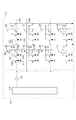
次に図3を用いてバッファ210の等価回路図の一例を示す。バッファ210はPMOSトランジスタ211およびNMOSトランジスタ212を含む。
Next, an example of an equivalent circuit diagram of the
PMOSトランジスタ211、NMOSトランジスタ212のゲートと等価なノードである入力ノード213は、図2の垂直走査回路104に接続され、垂直走査回路104からの駆動パルスを受ける。PMOSトランジスタ211のソースには電源電圧V1が供給され、ドレインは、バッファ210の出力ノード214と等価なノードとなる。出力ノード214は、図2の駆動配線216に接続される。電源電圧V1は例えば5Vである。そして駆動配線216は第1スイッチ及び第2スイッチの制御ノードに共通に接続される。
The
NMOSトランジスタ212のソースには基準電圧V2が供給され、ドレインはバッファ210の出力ノード214と等価なノードとなる。基準電圧V2は、電源電圧V1よりも低い電位となる。たとえば接地電位もしくは、電源電圧V1と符号が反対の電圧である。基準電圧V2は、例えば、−1.2Vである。
The reference voltage V2 is supplied to the source of the
図2のスイッチ207をオン状態にする駆動パルスを供給する際(接続状態)には、垂直走査回路104は、バッファ210の入力ノード213に基準電圧V2もしくはこれよりも低い電位のパルスを供給する。これにより、PMOSトランジスタ211がオン状態、NMOSトランジスタ212がオフ状態となり出力ノード214へ電源電圧V1が供給される。そして、出力ノード214から駆動配線216を介してスイッチ207へ電源電圧V1が供給されスイッチ207がオン状態となる。
When supplying a drive pulse for turning on the switch 207 of FIG. 2 (connection state), the
スイッチ207をオフ状態にする駆動パルスを供給する際(非接続状態)には、垂直走査回路104は、バッファ210の入力ノード213に電源電圧V1もしくはこれよりも高い電位のパルスを供給する。これにより、PMOSトランジスタ211がオフ状態、NMOSトランジスタ212がオン状態となり、出力ノード214へ基準電圧V2が供給される。そして、出力ノード214から駆動配線216を介して、スイッチ207へ基準電圧V2が供給されスイッチ207がオフ状態となる。
When supplying a drive pulse for turning off the switch 207 (non-connection state), the
ここでバッファ210とは、垂直走査回路104から出力された駆動パルスの波形を整形するもので、配線が有する寄生容量、寄生抵抗によるパルスの鈍りを元に戻すように作用するものである。例としてインバータを挙げたが他に、ソースフォロワ回路、ボルテージフォロワ回路などを用いることができる。
Here, the
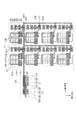
次に図4および図5に本実施例の撮像装置の平面模式図、断面模式図を示す。ここで画素部は例として4行2列の画素を有している。 Next, FIGS. 4 and 5 show a schematic plan view and a schematic cross-sectional view of the image pickup apparatus of this embodiment. Here, the pixel portion has pixels of 4 rows and 2 columns as an example.
まず第1画素行の画素100について説明する。各画素の光電変換部201A、光電変換部201B、FD203、および転送トランジスタ202を構成する半導体領域は第1活性領域320に配される。リセットトランジスタ204、増幅トランジスタ205、選択トランジスタ220、スイッチ207、容量208を構成する半導体領域は第2活性領域321に配される。
First, the
そして光電変換部201Aと光電変換部201Bには、一つのマイクロレンズ223を透過した光がそれぞれ入射する。なお、複数の光電変換部(光電変換部201A、201B)のみが平面視でマイクロレンズ223の下部に配された例を示したが、複数の光電変換部に加えて、一つの画素の外縁の少なくとも一部がマイクロレンズ223の下部に配されていてもよい。また不図示であるが、マイクロレンズ223の下部にはそれぞれカラーフィルタが配されている。
Then, the light transmitted through one
各活性領域を区画する部材として絶縁体分離部300を配した例を用いて説明するが、絶縁体分離部300に代えてもしくは絶縁体分離部300に加えてPN接合分離部を配してもよい。
An example in which the
第1活性領域320Aには、N型半導体領域301A、N型半導体領域301B、N型半導体領域303が配されている。N型半導体領域301Aは光電変換部201Aの一部を構成する。N型半導体領域301Bは光電変換部201Bの一部を構成する。N型半導体領域303はFD203を構成する。
The N-
また、平面視で第1活性領域320Aの上には、転送トランジスタ202Aのゲート電極302Aと転送トランジスタ202Bのゲート電極302Bが配されている。そして、N型半導体領域301Aとゲート電極302AとN型半導体領域303が転送トランジスタ202Aを構成する。N型半導体領域301Bとゲート電極302BとN型半導体領域303とが転送トランジスタ202Bを構成する。
Further, the
第2活性領域321Aには、N型半導体領域311、N型半導体領域310、N型半導体領域309、N型半導体領域312が配されている。そして、平面視で第2活性領域321Aの上にはゲート電極326、ゲート電極305、ゲート電極304、電極307Aが配されている。電極307Aの一部は、絶縁体分離部300の上に配されている。なお、電極307は例えばポリシリコンによって形成される。
The N-
N型半導体領域311、ゲート電極326、N型半導体領域310は選択トランジスタ220を構成する。N型半導体領域310、ゲート電極305、N型半導体領域309は増幅トランジスタ205を構成する。N型半導体領域309、ゲート電極304、N型半導体領域312はリセットトランジスタ204を構成する。そして、電極307Aはスイッチ207Aに含まれ、スイッチ207Aの入力ノードを構成する。
The N-
N型半導体領域303とN型半導体領域312とゲート電極305は電気的に接続されており、増幅トランジスタ205の入力ノードを構成する。
The N-
次に第2画素行の画素100の第1画素行の画素100と異なる点について説明する。第2画素行の画素100の第4活性領域321Bの上には、電極307Bが配されており、電極307Bはスイッチ207Bに含まれ、スイッチ207Bの入力ノードを構成する。
Next, the difference between the
次にバッファ210について説明する。活性領域322AにはN型半導体領域324、N型半導体領域333が配される。そして、第3活性領域323AにはP型半導体領域325、P型半導体領域327が配される。そして、活性領域322Aおよび第3活性領域323Aの上にはゲート電極328が配される。
Next, the
N型半導体領域324、N型半導体領域333、ゲート電極328はNMOSトランジスタ212を構成し、P型半導体領域325、P型半導体領域327、ゲート電極328
はPMOSトランジスタを構成し、これらのトランジスタがバッファ210を構成するインバータとなる。なお、N型半導体領域324にはGND電位が供給され、P型半導体領域325には電源電圧が供給される。そして、N型半導体領域333とP型半導体領域327には、駆動配線206を構成する導電パターン306が電気的に接続される。
The N-
Form a PMOS transistor, and these transistors form an inverter forming a
図2の駆動配線206は、第1方向に沿って配された第1導電パターン306Aと、第1導電パターン306Aから分岐し、第2方向に沿って配された第2導電パターン306Bを有する。さらに駆動配線206は、第2導電パターン306Bから分岐し、第1方向に沿って配された第3導電パターン306Cを有する。
The
本実施例において、第1導電パターン306Aはバッファ210Aの出力ノードとスイッチ207Aを構成する電極307Aに接続する。
In this embodiment, the first
第2導電パターン306Bは、バッファ210を構成するトランジスタが配される第3活性領域323Aと、バッファ210Aに最も近い位置に配された画素100との間で、第1導電パターン306Aから分岐し、第2方向に沿って配される。
The second
第3導電パターン306Cは、バッファ210Aに最も近い位置に配された画素100との間で、第2導電パターン306Bから分岐しスイッチ207Bを構成する電極307Bに接続する。
The third
そして、第2導電パターン306Bは、第1導電パターン306Aと第3導電パターン306Cとを電気的に接続する。
Then, the second
第1導電パターン306Aおよび第3導電パターン306Cは、隣り合う画素行のうち第1画素行の画素100のN型半導体領域301と、第2画素行の画素100のN型半導体領域301との間に配される。
The first
次に図5を用いて図4のA−B線に沿った断面模式図について説明し、スイッチ207をオン状態にすることによって入力ノードに電気的に接続される容量208の構成の1例について説明する。 Next, a schematic cross-sectional view taken along the line AB of FIG. 4 will be described with reference to FIG. 5, and an example of the configuration of the capacitor 208 electrically connected to the input node by turning on the switch 207 will be described. explain.
図5において、N型半導体領域312と絶縁体分離部300は電極307を挟んで隣り合って配されている。N型半導体領域312は、コンタクトプラグ331および配線334を介してFD203に電気的に接続される。また、電極307はコンタクトプラグ329を介して第1導電パターン306Aに電気的に接続される。
In FIG. 5, the N-
図5の例では、電極307の下部の半導体領域には、絶縁膜330を介して印加される電界によって、電極307の下部の活性領域の表面に配されたP型半導体領域313が反転して電荷蓄積領域となる表面型MOS容量を構成する。電極307に導電パターン306Aを介して印加される駆動パルスによって、P型半導体領域313が反転する状態と反転していない状態を切り替える。これによって、容量208のFD203に対する電気的な接続状態と非接続状態とを切り替えることができる。なお、電極307の下部の活性領域の表面にN型半導体領域を配して、埋め込み型のMOS容量とすることもできる。
In the example of FIG. 5, in the semiconductor region below the
なお、本実施例では電極307の一部が平面視で絶縁体分離部300と重なるように配されているが、重ならなくてもよい。
In the present embodiment, a part of the
また、平面視で電極307と絶縁体分離部300とのあいだに、N型半導体領域が配されてもよいし、P型半導体領域が配されてもよい。
In addition, an N-type semiconductor region or a P-type semiconductor region may be provided between the
P型半導体領域が配された場合には、N型半導体領域312と当該P型半導体領域が電極307を挟んで隣り合って配される。
When the P-type semiconductor region is arranged, the N-
N型半導体領域が配された場合には、N型半導体領域312と当該N型半導体領域が電極307を挟んで隣り合って配される。なお当該N型半導体領域、電極307、N型半導体領域312はトランジスタを構成する。
When the N-type semiconductor region is arranged, the N-
本実施例では、図2に示したように一つのバッファ210Aによって、各々が異なる画素行の増幅トランジスタの入力ノードに接続されたスイッチ207A、スイッチ207Bを駆動する。このような構成によれば、スイッチ207を有する画素が配された複数の画素行の各々の画素行に対してバッファを配する場合に比べてバッファの数を減らすことが可能となり、周辺回路部107の面積を狭くすることが可能となる。
In this embodiment, as shown in FIG. 2, one
なお、本実施例において複数の画素100において一つの画素が一つの増幅トランジスタ205を有する構成を示したが、複数の画素が一つの増幅トランジスタ205を共有するなど任意の構成が適用可能である。
In addition, in the present embodiment, one pixel in the plurality of
(実施例2)
図6〜8に本実施例の撮像装置の特徴を説明するための等価回路図、平面模式図を示す。図1〜5と同様の機能を有する部分には同様の符号を付し詳細な説明を省略する。
(Example 2)
6 to 8 show an equivalent circuit diagram and a schematic plan view for explaining the features of the image pickup apparatus of this embodiment. Portions having the same functions as those in FIGS. 1 to 5 are denoted by the same reference numerals and detailed description thereof will be omitted.
図6に実施例2の撮像装置の撮像装置の等価回路図を示す。本実施例と実施例1とは、駆動配線206が分岐する位置が異なる。
FIG. 6 shows an equivalent circuit diagram of the image pickup apparatus of the image pickup apparatus according to the second embodiment. The present embodiment and the first embodiment are different in the position where the
図7に本実施例の撮像装置101の平面模式図を示す。各画素の構成については図4と同様である。本実施例において第2導電パターン306Bは、同一の画素行に含まれ隣り合って配される二つの画素の第1活性領域の間で、第1導電パターン306Aから分岐することを特徴とする。
FIG. 7 shows a schematic plan view of the
図7では、同一画素行の隣り合う二つの画素は、一方の画素の第1活性領域320A、第2活性領域321A、他方の画素の第1活性領域320Bが第1方向に沿ってこの順に配されている。
In FIG. 7, two adjacent pixels in the same pixel row have a first
そして、本実施例において第2導電パターン306Aは、一方の画素の第2活性領域321Aと他方の画素の第1活性領域320Bの間で、第1導電パターン306Aから分岐し、第2方向に沿って配されている。そして第3導電パターン306Cは、一方の画素の第2活性領域321Aと他方の画素の第1活性領域320Bの間で、第2導電パターン306Bから分岐し、第1方向に沿って配される。
In the present embodiment, the second
本実施例においても、第1導電パターン306Aはバッファ210Aの出力ノードとスイッチ207Aを構成する電極307Aに接続する。第3導電パターン306Cは、第2導電パターン306Bとスイッチ207Bを構成する電極307Bとを電気的に接続する。
Also in this embodiment, the first
本実施例のような構成によれば、実施例1の効果に加えて、周辺回路部107から画素部102へ延びるスイッチ207への駆動配線の本数を削減することが可能となり、周辺回路部107の規模を低減することが可能となる。
According to the configuration of this embodiment, in addition to the effect of the first embodiment, it is possible to reduce the number of drive wirings from the
(変形例1)
図8に実施例2の変形例を示す。図8は第1画素行と第2画素行が隣り合って配され、且つ第1画素行の各画素と第2画素行の各画素がミラー対称の配置になっている点で図7異なる。
(Modification 1)
FIG. 8 shows a modification of the second embodiment. FIG. 8 differs from FIG. 7 in that the first pixel row and the second pixel row are arranged adjacent to each other, and each pixel of the first pixel row and each pixel of the second pixel row are arranged in mirror symmetry.
このような構成によれば、隣り合う画素行の各画素のスイッチ207を構成する電極307の配置を図7に比べて近づけることが可能となる。つまり、第2導電パターン306Bの長さを短くすることが可能となる。そのため画素部102の配線密度が低減し、画素の開口面積を拡大することが可能とり、実施例2の効果に加え、光電変換部201の感度を向上させることが可能となる。
With such a configuration, it is possible to make the arrangement of the
なお本変形例では、第2導電パターン306Bが電極307Bに接続される構成を示したが、図7のように第3導電パターン306Cを配して、第2導電パターン306Bから分岐した第3導電パターン306Cが電極307Bに接続されてもよい。
In this modification, the second
なお、本変形例はその他の実施例にも適用可能である。 It should be noted that this modification can be applied to other embodiments.
(実施例3)
図9、図10に本実施例の撮像装置の特徴を説明するための等価回路図、平面模式図を示す。図1〜5と同様の機能を有する部分には同様の符号を付し詳細な説明を省略する。
(Example 3)
9 and 10 show an equivalent circuit diagram and a schematic plan view for explaining the features of the image pickup apparatus of this embodiment. Portions having the same functions as those in FIGS. 1 to 5 are denoted by the same reference numerals and detailed description thereof will be omitted.
図9に実施例3の撮像装置の等価回路図を示す。本実施例は実施例1に対して、バッファ210の数が異なる。本実施例では一つのバッファ210がすべての画素行の画素のスイッチ207に対して共通に設けられる。
FIG. 9 shows an equivalent circuit diagram of the image pickup apparatus according to the third embodiment. This embodiment differs from the first embodiment in the number of
図10に本実施例の撮像装置の平面模式図を示す。本実施例において第1方向に沿って配された第1導電パターン306Aと、第1導電パターン306Aから分岐し、第2方向に沿って配された第2導電パターン306Bを有する。さらに第2導電パターン306Bから分岐し、第1方向に沿って配された第3導電パターン306Cを含む複数の導電パターンを有する。
FIG. 10 shows a schematic plan view of the image pickup apparatus of this embodiment. In this embodiment, the first
一つのバッファ210は、すべての画素行の画素100のスイッチ207(電極307)に共通に設けられている。
One
つまり、第1導電パターン306Aと、第2導電パターン306Bと、第3導電パターン306Cを含む複数の導電パターンのすべてが、一つのバッファ210と電気的に接続されている。
That is, all of the plurality of conductive patterns including the first
なお第2導電パターン306Bは、一つのバッファ210を構成するトランジスタが配される第3活性領域323Aと、画素部102に配された画素100のうち、一つのバッファ210に最も近い位置に配された画素100との間で、第1導電パターン306Aから分岐し、第2方向に沿って配される。
The second
同様に第3導電パターン306Cを含む複数の導電パターンの各々は、一つのバッファ210を構成するトランジスタが配される第3活性領域323Aと、画素部102に配された画素100のうち、一つのバッファ210に最も近い位置に配された画素100との間で、第2導電パターン306Bから分岐し、第1方向に沿って配される。
Similarly, each of the plurality of conductive patterns including the third
そして、第1導電パターン306Aと第3導電パターン306Cを含む複数の導電パターンの各々は、隣り合う画素行の第1画素行の画素100のN型半導体領域301と、第2画素行の画素のN型半導体領域301との間に配される。
Each of the plurality of conductive patterns including the first
本実施例では、図9に示したように一つのバッファ210がスイッチ207を有する画素が配されたすべての画素行に対して共通に設けられている。
In the present embodiment, as shown in FIG. 9, one
このような構成によれば、スイッチ207を有する画素が配された複数の画素行の各々の画素行に対してバッファ210を配する場合に比べてバッファ210の数を減らすことが可能となり、周辺回路部107の面積を狭くすることが可能となる。
With such a configuration, it is possible to reduce the number of
(実施例4)
図11〜16に本実施例の撮像装置の特徴を説明するための等価回路図、平面模式図を示す。図1〜5と同様の機能を有する部分には同様の符号を付し詳細な説明を省略する。
(Example 4)
11 to 16 show an equivalent circuit diagram and a schematic plan view for explaining the features of the image pickup apparatus of the present embodiment. Portions having the same functions as those in FIGS. 1 to 5 are denoted by the same reference numerals and detailed description thereof will be omitted.
図11に実施例4の撮像装置の撮像装置の等価回路図を示す。本実施例でも実施例3と同様に一つのバッファ210がすべての画素行の画素100のスイッチ207に対して共通に設けられ、すべての画素行の画素100のスイッチ207を駆動する駆動パルスを供給する。本実施例と実施例3とは、駆動配線206が分岐する位置が異なる。
FIG. 11 shows an equivalent circuit diagram of the image pickup apparatus of the image pickup apparatus according to the fourth embodiment. Also in the present embodiment, as in the third embodiment, one
図12に本実施例の撮像装置101の平面模式図を示す。各画素の構成については図4と同様である。本実施例において、第2導電パターン306Bは、同一の画素行に含まれ隣り合って配される二つの画素の第1活性領域320の間で、第1導電パターン306Aから分岐することを特徴とする。
FIG. 12 shows a schematic plan view of the
また、本実施例では実施例3と同様に、一つのバッファ210は、すべての画素行の画素100のスイッチ207(電極307)に共通に設けられている。つまり、第1導電パターン306と、第2導電パターン306Bと、第3導電パターン306Cを含む複数の導電パターンのすべてが、一つのバッファ210と電気的に接続されている。
In addition, in this embodiment, as in the case of the third embodiment, one
図12においても、同一画素行の隣り合う二つの画素は、一方の画素の第1活性領域320A、第2活性領域321A、他方の画素の第1活性領域320Bが第1方向に沿ってこの順に配されている。
Also in FIG. 12, two adjacent pixels in the same pixel row have the first
そして図12においては、第2導電パターン306Aは、一方の画素の第2活性領域321Bと他方の画素の第1活性領域320Bの間で、第1導電パターン306Aから分岐している。同様に本実施例において第3導電パターン306Cを含む複数の導電パターンは、一方の画素の第2活性領域321Bと他方の画素の第1活性領域320Bの間で、第2導電パターン306Bから分岐している。
Further, in FIG. 12, the second
このように本実施例と実施例3とは、第1導電パターン306Aと第2導電パターン306Bとが分岐する位置が異なる。さらに第2導電パターン306Bと第3導電パターン306Cを含む複数の導電パターンとが分岐する位置が異なる。
As described above, the present embodiment and the third embodiment are different in the position where the first
本実施例のような構成によれば、実施例3の効果に加えて、平面視で周辺回路部107と重なる位置に配される駆動配線の本数を削減することが可能となり、周辺回路部107の規模を低減することが可能となる。
With the configuration according to the present embodiment, in addition to the effects of the third embodiment, it is possible to reduce the number of drive wirings arranged at positions overlapping the
(変形例1)
図13と図14に実施例4の変形例を示す。図13は図12と、隣り合う画素行の第2方向に隣り合う二つの画素の各々のスイッチ207を構成する電極307が共通である点で異なる。この時、図8のように隣り合う画素行の画素がミラー対称であってもよい。
(Modification 1)
13 and 14 show a modified example of the fourth embodiment. FIG. 13 is different from FIG. 12 in that an
図13において電極307は領域340に配された絶縁体分離部300の上に配されている。そして、電極307は当該絶縁体分離部300を挟んで隣り合って配された第2活性領域321Aと、活性領域321Bの上まで延在している。そして、バッファ210の出力ノードは一つの電極307に電気的に接続されている。
In FIG. 13, the
次に図14を用いて図13のC−D線に沿った断面模式図について説明する。本実施例では平面視で第2活性領域321Aに配されたN型半導体領域312A(第1半導体領域)と、活性領域321Bに配されたN型半導体領域321B(第2半導体領域)とが、電極307を挟んで隣り合って配されている。この時、電極307が、平面視でN型半導体領域321AおよびN型半導体領域321Bの一部と重なってもよい。
Next, a schematic sectional view taken along the line CD of FIG. 13 will be described with reference to FIG. In the present embodiment, an N-
また、絶縁体分離部300とN型半導体領域321Aとの間には、P型半導体領域313Aが配され、絶縁体分離部300とN型半導体領域321Bとの間には、P型半導体領域313Bが配されている。
Further, a P-
そのため電極307に導電パターン306Aを介して印加される駆動パルスによって、P型半導体領域313AおよびP型半導体領域313Bが反転する状態と反転しない状態が切り換えられる。反転した時には電極307の下部の活性領域の表面に配されたP型半導体領域313が反転して電荷蓄積領域となる表面型MOS容量を構成する。
Therefore, the drive pulse applied to the
P型半導体領域313Aによって形成される表面型MOS容量は、隣り合う画素行のうち第1画素行の画素100の入力ノードに接続される容量208Aである。P型半導体領
域313Bによって形成される表面型MOS容量は、第2画素行の画素100の入力ノードに接続される容量208Bである。なお、容量208Aと容量208Bの間には絶縁体分離部300が配されており、容量208Aと容量208Bは電気的に非接続である。
The surface type MOS capacitor formed by the P-
なお、P型半導体領域313AおよびP型半導体領域313Bの表面部分にN型半導体領域を配して、埋め込み型MOS容量としてもよい。
Note that an N-type semiconductor region may be provided on the surface portions of the P-
このような構成によれば、隣り合う画素行の画素で電極307が共通化されているため、第1導電パターン306Aを共通化することが可能となる。つまり、第2導電パターン306Bおよび第3導電パターン306Cを無くすことが可能となる。そのため画素部102の配線密度が低減し、画素の開口面積を拡大することが可能となる。そして実施例2の効果に加え、感度を向上させることが可能となる。
According to such a configuration, since the
なお、本変形例はその他の実施例にも適用可能である。 It should be noted that this modification can be applied to other embodiments.
(変形例2)
図15に実施例4の変形例を示す。図15は図12と、隣り合う画素行の各画素のFD203を構成するN型半導体領域303が共通であり、さらに入力ノードが共通である点で異なる。
(Modification 2)
FIG. 15 shows a modification of the fourth embodiment. 15 is different from FIG. 12 in that the N-
このような構成によれば、複数の画素に対して一つの増幅トランジスタ205、リセットトランジスタ204、スイッチ207が配されていればよい。つまり第2活性領域321の数を減らすことが可能となる。そのため、画素の開口面積を拡大することが可能となり、感度を向上させることが可能となる。
With such a configuration, one
なお、本変形例はその他の実施例にも適用可能である。 It should be noted that this modification can be applied to other embodiments.
(変形例3)
図16に実施例4の変形例を示す。本変形例では各画素行の画素のうち緑色のカラーフィルタを有する画素のみが容量208およびスイッチ207を有する点で異なる。
(Modification 3)
FIG. 16 shows a modification of the fourth embodiment. This modification is different in that only the pixel having the green color filter among the pixels in each pixel row has the capacitor 208 and the switch 207.
図16は、緑色のカラーフィルタを有する画素100Gが第1行第1列、第2行第2列、第3行第1列、第4行第2列に配されている。そのほかの画素は赤色のカラーフィルタもしくは青色のカラーフィルタを有しており、容量208とスイッチ207を有さない。
In FIG. 16,
これは、赤色カラーフィルタを有する画素と青色のカラーフィルタを有する画素に比べて、緑色のカラーフィルタを有する画素は感度が高いため電荷が生じやすく、信号線209以降の電圧が飽和しやすいからである。そのため、緑色のカラーフィルタを有する画素100Gにのみスイッチ207を配置した構成となっている。
This is because a pixel having a green color filter has higher sensitivity than a pixel having a red color filter and a pixel having a blue color filter, and thus a charge is easily generated and a voltage after the
そして、導電パターン306が緑色のカラーフィルタを有する複数の画素100Gで共有されている。
The
本実施例のような構成によれば、実施例4の効果に加えて、赤色のカラーフィルタを有する画素と青色のカラーフィルタを有する画素内の配線密度が低減する。それにより赤色のカラーフィルタを有する画素と青色のカラーフィルタを有する画素の開口面積をより拡大することができるためこれらの感度が向上する。 According to the configuration of the present embodiment, in addition to the effect of the fourth embodiment, the wiring densities in the pixel having the red color filter and the pixel having the blue color filter are reduced. As a result, the aperture areas of the pixels having the red color filter and the pixels having the blue color filter can be further expanded, and thus the sensitivities thereof are improved.
なお、本変形例はその他の実施例にも適用可能である。 It should be noted that this modification can be applied to other embodiments.
100 画素
102 画素部
201 光電変換部
202 転送トランジスタ
205 増幅トランジスタ
207A 第1スイッチ
207B 第2スイッチ
210 バッファ
100
Claims (15)
前記画素部には、行方向に沿って配された複数の画素を有する画素行が、前記行方向とは異なる列方向に沿って第1画素行および第2画素行を含む少なくとも二つ配され、
前記第1画素行の第1画素は、前記第1画素に含まれる増幅トランジスタの入力ノードの容量値の大きさを切り替える第1スイッチを有し、
前記第2画素行の第2画素は、前記第2画素に含まれる増幅トランジスタの入力ノードの容量値の大きさを切り替える第2スイッチを有する撮像装置であって、
前記第1スイッチと前記第2スイッチとを駆動するバッファを有し、
前記バッファの出力ノードは、前記第1スイッチの入力ノードと前記第2スイッチの入力ノードに共通して電気的に接続されており、
前記画素部には、前記列方向に沿って、前記第1画素行および前記第2画素行とは別の複数の画素行が配されており、
前記第1画素行および前記第2画素行とは別の前記複数の画素行の画素に含まれる増幅トランジスタの入力ノードの容量値を複数の値に切り替える複数のスイッチを駆動する、前記バッファと異なるバッファを有し、
前記異なるバッファの出力ノードは、前記複数のスイッチの少なくとも一部のスイッチの入力ノードに共通して電気的に接続されていることを特徴とする撮像装置。 A pixel in which a plurality of pixels each having a photoelectric conversion unit, a transfer transistor that transfers the charge accumulated in the photoelectric conversion unit, and an amplification transistor that receives the charge transferred by the transfer transistor at an input node are arranged in a matrix. Have a section,
In the pixel unit, a pixel row having a plurality of pixels arranged in a row direction is arranged in at least two including a first pixel row and a second pixel row in a column direction different from the row direction. ,
The first pixel of the first pixel row has a first switch for switching the magnitude of the capacitance value of the input node of the amplification transistor included in the first pixel,
The second pixel of the second pixel row is an imaging device having a second switch that switches a magnitude of a capacitance value of an input node of an amplification transistor included in the second pixel,
A buffer for driving the first switch and the second switch,
An output node of the buffer is electrically connected to an input node of the first switch and an input node of the second switch in common,
In the pixel section, a plurality of pixel rows different from the first pixel row and the second pixel row are arranged along the column direction,
Different from the buffer that drives a plurality of switches that switch the capacitance value of the input node of the amplification transistor included in the pixels of the plurality of pixel rows different from the first pixel row and the second pixel row to a plurality of values Have a buffer,
An output device of the different buffer is electrically connected in common to input nodes of at least some of the plurality of switches.
前記第1導電パターンから分岐し、前記列方向に沿って配された第2導電パターンと、を有し、
さらに前記行方向に沿って配された、第3導電パターンを有し、
前記第2導電パターンは、前記第1導電パターンと前記第3導電パターンとを電気的に接続し、
前記第3導電パターンは、前記第2スイッチと接続されていることを特徴とする請求項1に記載の撮像装置。 A first conductive pattern electrically connected between an output node of the buffer and an input node of the first switch and arranged along the row direction;
A second conductive pattern branched from the first conductive pattern and arranged along the column direction,
Furthermore, it has the 3rd conductive pattern arranged along the said row direction,
The second conductive pattern electrically connects the first conductive pattern and the third conductive pattern,
The imaging device according to claim 1, wherein the third conductive pattern is connected to the second switch.
前記第1スイッチの入力ノードを構成する電極が上に配された第2活性領域を有することを特徴とする請求項2に記載の撮像装置。 A first active region that constitutes a part of the photoelectric conversion unit and has a semiconductor region for accumulating charges generated in the photoelectric conversion unit;
3. The image pickup device according to claim 2, wherein the electrode forming the input node of the first switch has a second active region disposed on the electrode.
前記第2導電パターンは、
前記一方の画素の前記第2活性領域と前記他方の画素の前記第1活性領域との間で、前記第1導電パターンから分岐することを特徴とする請求項4に記載の撮像装置。 Of the two pixels included in the same pixel row and arranged adjacent to each other, the first active region and the second active region of one pixel, and the first active region of the other pixel are in the row direction. Are arranged in this order along
The second conductive pattern is
The imaging device according to claim 4, wherein the first conductive pattern is branched between the second active region of the one pixel and the first active region of the other pixel.
前記バッファを構成するトランジスタが配される第3活性領域と、前記画素部に配された画素のうち、前記バッファに最も近い位置に配された画素との間で、第1導電パターンから分岐することを特徴とする請求項4に記載の撮像装置。 The second conductive pattern is
The first conductive pattern is branched between the third active region in which the transistor forming the buffer is arranged and the pixel arranged in a position closest to the buffer among the pixels arranged in the pixel portion. The image pickup apparatus according to claim 4, wherein
前記第2活性領域に前記増幅トランジスタの入力ノードの一部となる半導体領域が配され、
前記第2活性領域の一部であって、前記電極の下部に位置する部分が前記容量の少なくとも一部を構成していることを特徴とする請求項3乃至6のいずれか1項に記載の撮像装置。 A signal supplied to the electrode, and a capacitor arranged so that the electrical connection state to the input node of the amplification transistor is switchable,
A semiconductor region serving as a part of an input node of the amplification transistor is disposed in the second active region,
The part of the second active region, which is located under the electrode, constitutes at least a part of the capacitor. Imaging device.
平面視で前記増幅トランジスタの入力ノードの一部となる半導体領域と前記絶縁体分離部とが、前記電極を挟んで隣り合って配されていることを特徴とする請求項7または8に記載の撮像装置。 The second active region is partitioned by an insulator isolation portion,
9. The semiconductor region, which is a part of an input node of the amplification transistor in a plan view, and the insulator isolation portion are arranged adjacent to each other with the electrode interposed therebetween. Imaging device.
前記画素部には、行方向に沿って配された複数の画素を有する画素行が、前記行方向とは異なる列方向に沿って第1画素行および第2画素行を含む少なくとも二つ配され、
前記第1画素行の第1画素は、前記第1画素に含まれる増幅トランジスタの入力ノードの容量値の大きさを切り替える第1スイッチを有し、
前記第2画素行の第2画素は、前記第2画素に含まれる増幅トランジスタの入力ノードの容量値の大きさを切り替える第2スイッチを有する撮像装置であって、
前記第1スイッチと前記第2スイッチとを駆動するバッファを有し、
前記バッファの出力ノードは、前記第1スイッチの入力ノードと前記第2スイッチの入力ノードに共通して電気的に接続されており、
前記第1スイッチおよび前記第2スイッチは、絶縁体分離部の上に配された電極を有しており、
前記電極は前記絶縁体分離部を挟んで隣り合って配された二つの活性領域の上まで延在しており、
前記二つの活性領域の一方には、前記第1画素行の画素に含まれる増幅トランジスタの入力ノードを構成する第1半導体領域が配され、
前記二つの活性領域の他方には、前記第2画素行の画素に含まれる増幅トランジスタの入力ノードを構成する第2半導体領域が配され、
前記第1半導体領域と前記第2半導体領域は前記電極を挟んで隣り合って配されていることを特徴とする撮像装置。 A pixel in which a plurality of pixels each having a photoelectric conversion unit, a transfer transistor that transfers the charge accumulated in the photoelectric conversion unit, and an amplification transistor that receives the charge transferred by the transfer transistor at an input node are arranged in a matrix. Have a section,
In the pixel unit, a pixel row having a plurality of pixels arranged in a row direction is arranged in at least two including a first pixel row and a second pixel row in a column direction different from the row direction. ,
The first pixel of the first pixel row has a first switch for switching the magnitude of the capacitance value of the input node of the amplification transistor included in the first pixel,
The second pixel of the second pixel row is an imaging device having a second switch that switches a magnitude of a capacitance value of an input node of an amplification transistor included in the second pixel,
A buffer for driving the first switch and the second switch,
An output node of the buffer is electrically connected to an input node of the first switch and an input node of the second switch in common,
The first switch and the second switch has an electrode disposed on the insulation member separation unit,
The electrode extends to above two active regions that are arranged adjacent to each other with the insulator separating portion interposed therebetween,
A first semiconductor region forming an input node of an amplification transistor included in a pixel of the first pixel row is disposed in one of the two active regions,
A second semiconductor region forming an input node of an amplification transistor included in the pixel of the second pixel row is disposed on the other of the two active regions,
The image pickup device, wherein the first semiconductor region and the second semiconductor region are arranged adjacent to each other with the electrode interposed therebetween.
前記第1画素行の画素と前記第2画素行の画素はミラー対称の配置となることを特徴とする請求項3乃至12のいずれか1項に記載の撮像装置。 The first pixel row and the second pixel row are arranged adjacent to each other,
The image pickup apparatus according to claim 3, wherein the pixels of the first pixel row and the pixels of the second pixel row are arranged in mirror symmetry.
一つのマイクロレンズと、
前記一つのマイクロレンズを透過する光に基づく電荷を生成する複数の光電変換部とを有することを特徴とする請求項1乃至13のいずれか1項に記載の撮像装置。 Each of the plurality of pixels is
One microlens,
The imaging device according to any one of claims 1 to 13, further comprising a plurality of photoelectric conversion units that generate electric charges based on light transmitted through the one microlens.
Priority Applications (3)
| Application Number | Priority Date | Filing Date | Title |
|---|---|---|---|
| JP2016023059A JP6727830B2 (en) | 2016-02-09 | 2016-02-09 | Imaging device |
| US15/426,896 US10063801B2 (en) | 2016-02-09 | 2017-02-07 | Image capturing device |
| CN201710068534.1A CN107046626B (en) | 2016-02-09 | 2017-02-08 | Image pickup apparatus |
Applications Claiming Priority (1)
| Application Number | Priority Date | Filing Date | Title |
|---|---|---|---|
| JP2016023059A JP6727830B2 (en) | 2016-02-09 | 2016-02-09 | Imaging device |
Publications (3)
| Publication Number | Publication Date |
|---|---|
| JP2017143157A JP2017143157A (en) | 2017-08-17 |
| JP2017143157A5 JP2017143157A5 (en) | 2019-03-28 |
| JP6727830B2 true JP6727830B2 (en) | 2020-07-22 |
Family
ID=59498076
Family Applications (1)
| Application Number | Title | Priority Date | Filing Date |
|---|---|---|---|
| JP2016023059A Active JP6727830B2 (en) | 2016-02-09 | 2016-02-09 | Imaging device |
Country Status (3)
| Country | Link |
|---|---|
| US (1) | US10063801B2 (en) |
| JP (1) | JP6727830B2 (en) |
| CN (1) | CN107046626B (en) |
Families Citing this family (2)
| Publication number | Priority date | Publication date | Assignee | Title |
|---|---|---|---|---|
| JP7356214B2 (en) * | 2018-09-04 | 2023-10-04 | キヤノン株式会社 | Imaging device, its manufacturing method, and camera |
| US11871135B2 (en) * | 2022-02-03 | 2024-01-09 | Omnivision Technologies, Inc. | Circuit and method for image artifact reduction in high-density, high-pixel-count, image sensor with phase detection autofocus |
Family Cites Families (35)
| Publication number | Priority date | Publication date | Assignee | Title |
|---|---|---|---|---|
| JPH02262344A (en) * | 1989-03-31 | 1990-10-25 | Sony Corp | Output circuit |
| EP0739039A3 (en) * | 1995-04-18 | 1998-03-04 | Interuniversitair Micro-Elektronica Centrum Vzw | Pixel structure, image sensor using such pixel, structure and corresponding peripheric circuitry |
| JP3592106B2 (en) * | 1998-11-27 | 2004-11-24 | キヤノン株式会社 | Solid-state imaging device and camera |
| JP3594891B2 (en) * | 2000-09-12 | 2004-12-02 | 沖電気工業株式会社 | Semiconductor memory device and inspection method thereof |
| CN1820295A (en) * | 2003-05-07 | 2006-08-16 | 东芝松下显示技术有限公司 | El display and its driving method |
| JP4317115B2 (en) * | 2004-04-12 | 2009-08-19 | 国立大学法人東北大学 | Solid-state imaging device, optical sensor, and operation method of solid-state imaging device |
| JP4343144B2 (en) * | 2004-09-24 | 2009-10-14 | 株式会社東芝 | Infrared sensor |
| JP2006314025A (en) * | 2005-05-09 | 2006-11-16 | Sony Corp | Imaging apparatus and power supply method for the same |
| JP4844032B2 (en) * | 2005-07-21 | 2011-12-21 | 株式会社ニコン | Imaging device |
| EP1887626A1 (en) * | 2006-08-09 | 2008-02-13 | Tohoku University | Optical sensor comprising overflow gate and storage capacitor |
| JP2008046377A (en) * | 2006-08-17 | 2008-02-28 | Sony Corp | Display device |
| JP5016941B2 (en) * | 2007-02-08 | 2012-09-05 | 株式会社東芝 | Solid-state imaging device |
| JP4858294B2 (en) * | 2007-05-09 | 2012-01-18 | ソニー株式会社 | Imaging device, imaging circuit, and image processing circuit |
| JP2008305983A (en) * | 2007-06-07 | 2008-12-18 | Nikon Corp | Solid-state imaging element |
| JP5228961B2 (en) * | 2009-02-06 | 2013-07-03 | 日本テキサス・インスツルメンツ株式会社 | Amplification circuit and imaging device |
| JP5257176B2 (en) * | 2009-03-18 | 2013-08-07 | ソニー株式会社 | Solid-state imaging device, driving method of solid-state imaging device, and electronic apparatus |
| JP2010278904A (en) * | 2009-05-29 | 2010-12-09 | Panasonic Corp | Solid-state imaging apparatus, camera and method of driving solid-state imaging apparatus |
| JPWO2011058684A1 (en) * | 2009-11-12 | 2013-03-28 | パナソニック株式会社 | Solid-state imaging device |
| JP5467846B2 (en) * | 2009-11-20 | 2014-04-09 | 富士フイルム株式会社 | Radiation detection element |
| KR101077408B1 (en) * | 2010-02-05 | 2011-10-26 | 서강대학교산학협력단 | CMOS Image Sensor |
| JP2011199196A (en) * | 2010-03-23 | 2011-10-06 | Toshiba Corp | Solid-state imaging device |
| JP5686765B2 (en) * | 2011-07-21 | 2015-03-18 | キヤノン株式会社 | Imaging apparatus and control method thereof |
| JP6039165B2 (en) * | 2011-08-11 | 2016-12-07 | キヤノン株式会社 | Imaging device and imaging apparatus |
| JP2013089869A (en) * | 2011-10-20 | 2013-05-13 | Canon Inc | Detection device and detection system |
| JP5967944B2 (en) * | 2012-01-18 | 2016-08-10 | キヤノン株式会社 | Solid-state imaging device and camera |
| JP2014112580A (en) * | 2012-12-05 | 2014-06-19 | Sony Corp | Solid-state image sensor and driving method |
| CN104813653B (en) * | 2012-11-27 | 2018-09-14 | 松下知识产权经营株式会社 | Solid-state imaging apparatus and its driving method |
| JP6108884B2 (en) * | 2013-03-08 | 2017-04-05 | キヤノン株式会社 | Photoelectric conversion device and imaging system |
| JP6230329B2 (en) * | 2013-08-19 | 2017-11-15 | キヤノン株式会社 | Imaging device |
| JP6466645B2 (en) * | 2014-03-17 | 2019-02-06 | オリンパス株式会社 | Imaging device |
| JP6391302B2 (en) * | 2014-05-23 | 2018-09-19 | キヤノン株式会社 | Imaging apparatus and imaging system |
| JP6459025B2 (en) * | 2014-07-07 | 2019-01-30 | パナソニックIpマネジメント株式会社 | Solid-state imaging device |
| JP6406911B2 (en) * | 2014-07-24 | 2018-10-17 | キヤノン株式会社 | Imaging apparatus and manufacturing method of imaging apparatus |
| JP6406912B2 (en) * | 2014-07-24 | 2018-10-17 | キヤノン株式会社 | Imaging device and driving method thereof |
| WO2016042893A1 (en) * | 2014-09-17 | 2016-03-24 | ソニー株式会社 | Image pickup device, image pickup element, and image pickup device control method |
-
2016
- 2016-02-09 JP JP2016023059A patent/JP6727830B2/en active Active
-
2017
- 2017-02-07 US US15/426,896 patent/US10063801B2/en active Active
- 2017-02-08 CN CN201710068534.1A patent/CN107046626B/en active Active
Also Published As
| Publication number | Publication date |
|---|---|
| JP2017143157A (en) | 2017-08-17 |
| US10063801B2 (en) | 2018-08-28 |
| US20170230600A1 (en) | 2017-08-10 |
| CN107046626A (en) | 2017-08-15 |
| CN107046626B (en) | 2020-11-17 |
Similar Documents
| Publication | Publication Date | Title |
|---|---|---|
| JP5486639B2 (en) | Methods related to image sensors | |
| TWI469336B (en) | Solid-state imaging element and camera system | |
| KR100851494B1 (en) | Small pixel for cmos image sensors with vertically integrated set and reset diodes | |
| US9236406B2 (en) | Photoelectric conversion apparatus with gate control lines and wiring at same height | |
| JP5963450B2 (en) | Imaging apparatus and imaging system | |
| JP5709418B2 (en) | Solid-state imaging device | |
| JP6406912B2 (en) | Imaging device and driving method thereof | |
| JP2014049727A (en) | Solid-state image pickup device | |
| KR20090121322A (en) | Reduced pixel area image sensor | |
| US9197832B2 (en) | Solid-state image pickup apparatus and drive method therefor | |
| JP2010212288A (en) | Image pickup device | |
| JP2007243093A (en) | Solid-state imaging device, imaging device and signal processing method | |
| JP6025750B2 (en) | Imaging device | |
| JP6727830B2 (en) | Imaging device | |
| US20210288115A1 (en) | Imaging device | |
| JP6719958B2 (en) | Imaging device and method of driving imaging device | |
| WO2019069532A1 (en) | Solid-state imaging element and solid-state imaging device | |
| JP6355401B2 (en) | Solid-state imaging device and camera | |
| JP2017117957A (en) | Photoelectric conversion device | |
| JP2017084930A (en) | Imaging apparatus | |
| JP2016197644A (en) | Imaging device | |
| JP6682587B2 (en) | Imaging device and driving method thereof | |
| WO2023074461A1 (en) | Imaging device | |
| US20140333817A1 (en) | Image pickup apparatus | |
| JPH11346332A (en) | Solid-state image pickup device |
Legal Events
| Date | Code | Title | Description |
|---|---|---|---|
| A521 | Request for written amendment filed |
Free format text: JAPANESE INTERMEDIATE CODE: A523 Effective date: 20190208 |
|
| A621 | Written request for application examination |
Free format text: JAPANESE INTERMEDIATE CODE: A621 Effective date: 20190208 |
|
| A977 | Report on retrieval |
Free format text: JAPANESE INTERMEDIATE CODE: A971007 Effective date: 20191122 |
|
| A131 | Notification of reasons for refusal |
Free format text: JAPANESE INTERMEDIATE CODE: A131 Effective date: 20200107 |
|
| A521 | Request for written amendment filed |
Free format text: JAPANESE INTERMEDIATE CODE: A523 Effective date: 20200306 |
|
| A131 | Notification of reasons for refusal |
Free format text: JAPANESE INTERMEDIATE CODE: A131 Effective date: 20200317 |
|
| A521 | Request for written amendment filed |
Free format text: JAPANESE INTERMEDIATE CODE: A523 Effective date: 20200512 |
|
| TRDD | Decision of grant or rejection written | ||
| A01 | Written decision to grant a patent or to grant a registration (utility model) |
Free format text: JAPANESE INTERMEDIATE CODE: A01 Effective date: 20200602 |
|
| A61 | First payment of annual fees (during grant procedure) |
Free format text: JAPANESE INTERMEDIATE CODE: A61 Effective date: 20200701 |
|
| R151 | Written notification of patent or utility model registration |
Ref document number: 6727830 Country of ref document: JP Free format text: JAPANESE INTERMEDIATE CODE: R151 |