JP6719958B2 - Imaging device and method of driving imaging device - Google Patents
Imaging device and method of driving imaging device Download PDFInfo
- Publication number
- JP6719958B2 JP6719958B2 JP2016086547A JP2016086547A JP6719958B2 JP 6719958 B2 JP6719958 B2 JP 6719958B2 JP 2016086547 A JP2016086547 A JP 2016086547A JP 2016086547 A JP2016086547 A JP 2016086547A JP 6719958 B2 JP6719958 B2 JP 6719958B2
- Authority
- JP
- Japan
- Prior art keywords
- potential
- input node
- switch
- capacitance value
- period
- Prior art date
- Legal status (The legal status is an assumption and is not a legal conclusion. Google has not performed a legal analysis and makes no representation as to the accuracy of the status listed.)
- Active
Links
- 238000003384 imaging method Methods 0.000 title claims description 25
- 238000000034 method Methods 0.000 title claims description 14
- 238000006243 chemical reaction Methods 0.000 claims description 74
- 239000004065 semiconductor Substances 0.000 claims description 74
- 230000003321 amplification Effects 0.000 claims description 56
- 238000003199 nucleic acid amplification method Methods 0.000 claims description 56
- 238000009825 accumulation Methods 0.000 claims description 22
- 239000003990 capacitor Substances 0.000 claims description 20
- 238000002955 isolation Methods 0.000 claims description 17
- 238000010586 diagram Methods 0.000 description 7
- 230000000694 effects Effects 0.000 description 6
- 238000000926 separation method Methods 0.000 description 4
- 230000008878 coupling Effects 0.000 description 3
- 238000010168 coupling process Methods 0.000 description 3
- 238000005859 coupling reaction Methods 0.000 description 3
- 230000005684 electric field Effects 0.000 description 3
- 239000000969 carrier Substances 0.000 description 2
- 238000009792 diffusion process Methods 0.000 description 2
- 239000012535 impurity Substances 0.000 description 2
- 239000011159 matrix material Substances 0.000 description 2
- 239000004020 conductor Substances 0.000 description 1
- 230000003247 decreasing effect Effects 0.000 description 1
- 238000001514 detection method Methods 0.000 description 1
- 230000003071 parasitic effect Effects 0.000 description 1
- 229910021420 polycrystalline silicon Inorganic materials 0.000 description 1
- 229920005591 polysilicon Polymers 0.000 description 1
- 229920006395 saturated elastomer Polymers 0.000 description 1
- 238000000638 solvent extraction Methods 0.000 description 1
Images


Classifications
-
- H—ELECTRICITY
- H01—ELECTRIC ELEMENTS
- H01L—SEMICONDUCTOR DEVICES NOT COVERED BY CLASS H10
- H01L27/00—Devices consisting of a plurality of semiconductor or other solid-state components formed in or on a common substrate
- H01L27/14—Devices consisting of a plurality of semiconductor or other solid-state components formed in or on a common substrate including semiconductor components sensitive to infrared radiation, light, electromagnetic radiation of shorter wavelength or corpuscular radiation and specially adapted either for the conversion of the energy of such radiation into electrical energy or for the control of electrical energy by such radiation
- H01L27/144—Devices controlled by radiation
- H01L27/146—Imager structures
- H01L27/14601—Structural or functional details thereof
- H01L27/1462—Coatings
- H01L27/14621—Colour filter arrangements
-
- H—ELECTRICITY
- H04—ELECTRIC COMMUNICATION TECHNIQUE
- H04N—PICTORIAL COMMUNICATION, e.g. TELEVISION
- H04N25/00—Circuitry of solid-state image sensors [SSIS]; Control thereof
- H04N25/70—SSIS architectures; Circuits associated therewith
- H04N25/76—Addressed sensors, e.g. MOS or CMOS sensors
-
- H—ELECTRICITY
- H01—ELECTRIC ELEMENTS
- H01L—SEMICONDUCTOR DEVICES NOT COVERED BY CLASS H10
- H01L27/00—Devices consisting of a plurality of semiconductor or other solid-state components formed in or on a common substrate
- H01L27/14—Devices consisting of a plurality of semiconductor or other solid-state components formed in or on a common substrate including semiconductor components sensitive to infrared radiation, light, electromagnetic radiation of shorter wavelength or corpuscular radiation and specially adapted either for the conversion of the energy of such radiation into electrical energy or for the control of electrical energy by such radiation
- H01L27/144—Devices controlled by radiation
- H01L27/146—Imager structures
- H01L27/14601—Structural or functional details thereof
- H01L27/14634—Assemblies, i.e. Hybrid structures
-
- H—ELECTRICITY
- H04—ELECTRIC COMMUNICATION TECHNIQUE
- H04N—PICTORIAL COMMUNICATION, e.g. TELEVISION
- H04N25/00—Circuitry of solid-state image sensors [SSIS]; Control thereof
- H04N25/50—Control of the SSIS exposure
- H04N25/57—Control of the dynamic range
- H04N25/59—Control of the dynamic range by controlling the amount of charge storable in the pixel, e.g. modification of the charge conversion ratio of the floating node capacitance
-
- H—ELECTRICITY
- H04—ELECTRIC COMMUNICATION TECHNIQUE
- H04N—PICTORIAL COMMUNICATION, e.g. TELEVISION
- H04N25/00—Circuitry of solid-state image sensors [SSIS]; Control thereof
- H04N25/70—SSIS architectures; Circuits associated therewith
- H04N25/702—SSIS architectures characterised by non-identical, non-equidistant or non-planar pixel layout
-
- H—ELECTRICITY
- H04—ELECTRIC COMMUNICATION TECHNIQUE
- H04N—PICTORIAL COMMUNICATION, e.g. TELEVISION
- H04N25/00—Circuitry of solid-state image sensors [SSIS]; Control thereof
- H04N25/70—SSIS architectures; Circuits associated therewith
- H04N25/71—Charge-coupled device [CCD] sensors; Charge-transfer registers specially adapted for CCD sensors
- H04N25/75—Circuitry for providing, modifying or processing image signals from the pixel array
-
- H—ELECTRICITY
- H04—ELECTRIC COMMUNICATION TECHNIQUE
- H04N—PICTORIAL COMMUNICATION, e.g. TELEVISION
- H04N25/00—Circuitry of solid-state image sensors [SSIS]; Control thereof
- H04N25/70—SSIS architectures; Circuits associated therewith
- H04N25/76—Addressed sensors, e.g. MOS or CMOS sensors
- H04N25/77—Pixel circuitry, e.g. memories, A/D converters, pixel amplifiers, shared circuits or shared components
- H04N25/771—Pixel circuitry, e.g. memories, A/D converters, pixel amplifiers, shared circuits or shared components comprising storage means other than floating diffusion
-
- H—ELECTRICITY
- H04—ELECTRIC COMMUNICATION TECHNIQUE
- H04N—PICTORIAL COMMUNICATION, e.g. TELEVISION
- H04N25/00—Circuitry of solid-state image sensors [SSIS]; Control thereof
- H04N25/70—SSIS architectures; Circuits associated therewith
- H04N25/76—Addressed sensors, e.g. MOS or CMOS sensors
- H04N25/77—Pixel circuitry, e.g. memories, A/D converters, pixel amplifiers, shared circuits or shared components
- H04N25/778—Pixel circuitry, e.g. memories, A/D converters, pixel amplifiers, shared circuits or shared components comprising amplifiers shared between a plurality of pixels, i.e. at least one part of the amplifier must be on the sensor array itself
-
- H—ELECTRICITY
- H04—ELECTRIC COMMUNICATION TECHNIQUE
- H04N—PICTORIAL COMMUNICATION, e.g. TELEVISION
- H04N25/00—Circuitry of solid-state image sensors [SSIS]; Control thereof
- H04N25/70—SSIS architectures; Circuits associated therewith
- H04N25/76—Addressed sensors, e.g. MOS or CMOS sensors
- H04N25/78—Readout circuits for addressed sensors, e.g. output amplifiers or A/D converters
Description
本発明は、撮像装置及び撮像装置の駆動方法に関する。 The present invention relates to an imaging device and a driving method of the imaging device.
従来、画素から出力される信号のダイナミックレンジを拡大するために増幅トランジスタの入力ノード(以下、入力ノード)の容量値を切り替え可能となるように容量を設ける構成が知られている。たとえばスイッチにより容量を入力ノードに接続することで入力ノードの容量値は大きくなり、非接続とすることで容量値を小さくすることができる。容量値を大きくすることで入力ノードで取り扱うことが可能な電荷量を増やすことができる。また容量値を小さくすることで増幅トランジスタのゲインをあげることができる。 Conventionally, there is known a configuration in which a capacitance is provided so that a capacitance value of an input node (hereinafter, input node) of an amplification transistor can be switched in order to expand a dynamic range of a signal output from a pixel. For example, the capacitance value of the input node can be increased by connecting the capacitance to the input node by a switch, and the capacitance value can be decreased by disconnecting the capacitance. Increasing the capacitance value can increase the amount of charge that can be handled by the input node. Also, the gain of the amplification transistor can be increased by reducing the capacitance value.
特許文献1には、容量の一部を構成する電極が容量値を切り替えるスイッチの役割を有しており、この電極に供給する電位を第1電位から第2電位へ切り替えることで入力ノードへの容量の電気的な接続状態、非接続状態を切り替えている。
In
増幅トランジスタの入力ノードの容量値を切り替えるスイッチに供給される電位が切り替えられると、入力ノードの一部を構成する半導体領域とスイッチとの間に生じるカップリング容量によって、入力ノードの電位が変化する恐れがある。 When the potential supplied to the switch that switches the capacitance value of the input node of the amplification transistor is switched, the potential of the input node changes due to the coupling capacitance generated between the switch and the semiconductor region forming a part of the input node. There is a fear.
入力ノードの電位が変化した後、所望の値に静定するまでの時間は、このカップリング容量の大きさによって決まる。カップリング容量の大きさは、各画素によってばらつきがあるため、複数の画素間で入力ノードの電位が静定するまでの時間にばらつきが生じる恐れがある。そうすると、仮に撮像面に対し一様な光が入射した場合でも、各画素からの信号が異なり正しい画像を得ることができない。 The time required to settle to a desired value after the potential of the input node changes is determined by the size of this coupling capacitance. Since the magnitude of the coupling capacitance varies from pixel to pixel, there may be variations in the time until the potential of the input node settles among the plurality of pixels. Then, even if uniform light is incident on the image pickup surface, the signals from the respective pixels are different and a correct image cannot be obtained.
本発明は上記課題に鑑み、増幅トランジスタの入力ノードの容量値を切り替えるためにスイッチに供給される電位が変化しても、正しい画像を得ることを目的とする。 In view of the above problems, it is an object of the present invention to obtain a correct image even if the potential supplied to the switch for changing the capacitance value of the input node of the amplification transistor changes.
本発明の一例の撮像装置は、光電変換部と、前記光電変換部で生じた電荷が入力される入力ノードを有する増幅トランジスタと、前記入力ノードの容量値を切り替えるスイッチと、を有する画素を複数有する撮像装置であって、前記スイッチに第1電位が供給されることで、前記入力ノードの容量値が第1容量値となり、前記スイッチに第2電位が供給されることで、前記入力ノードの容量値が前記第1容量値よりも小さな第2容量値となり、前記第2電位から前記第1電位になるまでの期間、もしくは前記第1電位から前記第2電位になるまでの期間のうち少なくとも一方の期間の一部で、前記スイッチに供給される電位が前記第1電位と前記第2電位との間の第3電位に保持されることを特徴とする。
本発明の別の一例の撮像装置は、光電変換部と、前記光電変換部で生じた電荷が入力される入力ノードを有する増幅トランジスタと、前記入力ノードの容量値を切り替えるスイッチと、前記入力ノードの電位をリセットするリセットトランジスタと、を有する画素を複数有する撮像装置であって、前記スイッチに第1電位が供給されることで、前記入力ノードの容量値が第1容量値となり、前記スイッチに第2電位が供給されることで、前記入力ノードの容量値が前記第1容量値よりも小さな第2容量値となり、前記第2電位から前記第1電位になるまでの単位時間当たりの電位変化量、もしくは前記第1電位から前記第2電位になるまでの単位時間当たりの電位変化量のうち少なくとも一方の単位時間当たりの電位変化量が、前記リセットトランジスタのゲートに供給されるオン電位からオフ電位への単位時間当たりの電位変化量に比べて小さいことを特徴とする。
本発明の別の一例の撮像装置の駆動方法は、光電変換部と、前記光電変換部で生じた電荷が入力される入力ノードを有する増幅トランジスタと、前記入力ノードの容量値を切り替えるスイッチと、を有する画素を複数有する撮像装置の駆動方法であって、前記スイッチに第1電位を供給することで、前記入力ノードの容量値が第1容量値となり、前記スイッチに第2電位を供給することで、前記入力ノードの容量値が前記第1容量値よりも小さな第2容量値となり、前記第2電位から前記第1電位になるまでの期間、もしくは前記第1電位から前記第2電位になるまでの期間のうち少なくとも一方の期間の一部で、前記スイッチに供給される電位を前記第1電位と前記第2電位との間の第3電位に保持することを特徴とする。
本発明の別の一例の撮像装置の駆動方法は、光電変換部と、前記光電変換部で生じた電荷が入力される入力ノードを有する増幅トランジスタと、前記入力ノードの容量値を切り替えるスイッチと、前記入力ノードの電位をリセットするリセットトランジスタと、を有する画素を複数有する撮像装置の駆動方法であって、前記スイッチに第1電位が供給されることで、前記入力ノードの容量値が第1容量値となり、前記スイッチに第2電位が供給されることで、前記入力ノードの容量値が前記第1容量値よりも小さな第2容量値となり、前記第2電位から前記第1電位になるまでの単位時間当たりの電位変化量、もしくは前記第1電位から前記第2電位になるまでの単位時間当たりの電位変化量のうち少なくとも一方の単位時間当たりの電位変化量が、前記リセットトランジスタのゲートに供給されるオン電位からオフ電位への単位時間当たりの電位変化量に比べて小さいことを特徴とする。
An image pickup device according to an example of the present invention includes a plurality of pixels each including a photoelectric conversion unit, an amplification transistor having an input node to which an electric charge generated in the photoelectric conversion unit is input, and a switch for switching a capacitance value of the input node. In the imaging device having the above, when the first potential is supplied to the switch, the capacitance value of the input node becomes a first capacitance value, and when the second potential is supplied to the switch, the input node At least the period from the second potential to the first potential, or the period from the first potential to the second potential, where the capacitance value becomes the second capacitance value smaller than the first capacitance value. The potential supplied to the switch is held at a third potential between the first potential and the second potential for a part of one period.
An image pickup device according to another example of the present invention includes a photoelectric conversion unit, an amplification transistor having an input node to which an electric charge generated in the photoelectric conversion unit is input, a switch that switches a capacitance value of the input node, and the input node. And a reset transistor that resets the potential of the input node, wherein a capacitance value of the input node becomes a first capacitance value by supplying a first potential to the switch, By the supply of the second potential, the capacitance value of the input node becomes the second capacitance value smaller than the first capacitance value, and the potential change per unit time from the second potential to the first potential. Amount, or at least one of the potential change amounts per unit time from the first potential to the second potential changes from the on-potential supplied to the gate of the reset transistor to off. It is characterized in that it is smaller than the amount of change in potential per unit time.
A driving method of an image pickup device of another example of the present invention is a photoelectric conversion unit, an amplification transistor having an input node to which an electric charge generated in the photoelectric conversion unit is input, and a switch for switching a capacitance value of the input node, A method for driving an image pickup device having a plurality of pixels having a plurality of pixels, wherein a capacitance value of the input node becomes a first capacitance value by supplying a first potential to the switch, and a second potential is supplied to the switch. , The capacitance value of the input node becomes a second capacitance value smaller than the first capacitance value, and the period from the second potential to the first potential, or from the first potential to the second potential The potential supplied to the switch is held at a third potential between the first potential and the second potential for a part of at least one of the above periods.
A driving method of an image pickup device of another example of the present invention is a photoelectric conversion unit, an amplification transistor having an input node to which an electric charge generated in the photoelectric conversion unit is input, and a switch for switching a capacitance value of the input node, A driving method of an image pickup device having a plurality of pixels each having a reset transistor for resetting a potential of the input node, wherein a capacitance of the input node is changed to a first capacitance by supplying a first potential to the switch. And a second potential is supplied to the switch, whereby the capacitance value of the input node becomes a second capacitance value smaller than the first capacitance value, and the second potential changes from the second potential to the first potential. The potential change amount per unit time or at least one of the potential change amount per unit time from the first potential to the second potential is supplied to the gate of the reset transistor. It is characterized by being smaller than the amount of potential change per unit time from the ON potential to the OFF potential.
本発明によれば、画素の増幅トランジスタの入力ノードの容量値を切り替えるスイッチに供給される電位が切り替わった際に生じる入力ノードの電位変化を抑制することが可能となる。 According to the present invention, it is possible to suppress the potential change of the input node that occurs when the potential supplied to the switch that switches the capacitance value of the input node of the amplification transistor of the pixel is switched.
本実施形態では信号電荷と同導電型を第1導電型、信号電荷と逆導電型を第2導電型とする。以下の説明では、例として第1導電型の電荷を電子、第2導電型の電荷を正孔とし、各トランジスタをNMOSトランジスタとするが、これに限らず第1導電型の電荷を正孔、第2導電型の電荷を電子とし、各トランジスタをPMOSトランジスタとしてもよい。 In this embodiment, the same conductivity type as the signal charge is the first conductivity type, and the opposite conductivity type to the signal charge is the second conductivity type. In the following description, as an example, the first conductivity type charge is an electron, the second conductivity type charge is a hole, and each transistor is an NMOS transistor. However, the present invention is not limited to this, and the first conductivity type charge is a hole. The second conductivity type charges may be electrons, and each transistor may be a PMOS transistor.
(実施例1)
本実施例を図1〜3を用いて説明する。各図面において同じ符号が付されている部分は、同じ素子もしくは同じ領域を指す。
(Example 1)
This embodiment will be described with reference to FIGS. Portions with the same reference numerals in the respective drawings indicate the same elements or the same regions.
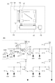
図1(a)に本実施例の撮像装置のブロック図を示す。撮像装置101は、画素部102、駆動パルス生成部103、垂直走査回路104、信号処理部105、出力部106を有している。
FIG. 1A shows a block diagram of the image pickup apparatus of this embodiment. The
画素部102には、複数の画素100が配されている。複数の画素100は行列状に配されており、画素100において変換された電気信号を行ごとに順次出力する。
A plurality of
駆動パルス生成部103は駆動パルスを生成し、垂直走査回路104は駆動パルス生成部103からの制御パルスを受け、各画素に駆動パルスを供給する。信号処理部105は、少なくとも、複数の画素列から並列に出力された信号をシリアライズして出力部106に伝達する。更に信号処理部105は、各画素列に対応し、信号の増幅、AD変換等を行なう列回路を有していてもよい。
The drive
図1(b)に撮像装置101の画素部102の等価回路図を示す。ここでは例として4つの画素100が配されている構成を示した。各部材を識別するために添え字A、Bを用いて説明する。両者を区別しての説明が必要な場合には添え字を付して説明する。
FIG. 1B shows an equivalent circuit diagram of the
画素100は複数の光電変換部(光電変換部201A、光電変換部201B)を有する。光電変換部201A、201Bでは入射光量に応じた電荷対を生成し、信号電荷(以下、電子)を蓄積する。光電変換部201A,201Bには、例えばフォトダイオードが用いられる。
The
転送トランジスタ202Aは光電変換部201Aで生じた電子をフローティングディフュージョン(以下、FD)203へ転送する。転送トランジスタ202Bは光電変換部201Bで生じた電子をFD203へ転送する。転送トランジスタ202A、転送トランジスタ202Bのゲートにはそれぞれ駆動パルスpTX1、pTX2が供給され、接続状態、非接続状態が切り換えられる。
The
FD203は、光電変換部201A、光電変換部201Bにより共有される。そしてFD203は、各々の転送トランジスタ202を介して光電変換部201Aおよび光電変換部201Bから転送された電子を保持する。
The FD 203 is shared by the
増幅トランジスタ205は、そのゲートがFD203に電気的に接続されており、FD203に転送された電子に基づく信号を増幅して出力する。より具体的にFD203に転送された電子は、その量に応じた電圧に変換され、その電圧に応じた電気信号は増幅トランジスタ205を介して画素外へ出力される。増幅トランジスタ205のドレインは電源電圧VDDが供給されている電源配線に接続され、ソースは出力ノードを構成する。増幅トランジスタ205は、不図示の電流源とともにソースフォロア回路を構成している。
The gate of the
リセットトランジスタ204は、増幅トランジスタ205の入力ノードの電圧を所定の電位にリセットする。リセットトランジスタ204のゲートには駆動パルスpRESが供給され、接続状態、非接続状態が切り換えられる。
The
選択トランジスタ206は、増幅トランジスタ205の出力ノードと信号線107との電気的な接続を制御する。選択トランジスタ206のドレインは、増幅トランジスタ205のソースに接続され、選択トランジスタ206のソースは信号線107に接続されている。選択トランジスタ206のゲートには駆動パルスpSELが供給され、接続状態、非接続状態が切り換えられる。
The
信号線107は、行列状に配された複数の画素の各画素列の画素100の増幅トランジスタ205の出力ノードと電気的な接続状態、非接続状態が切り換え可能に配されている。
The
本実施例の構成に代えて、選択トランジスタ206を増幅トランジスタ205のドレインと、電源電圧VDDが供給されている電源配線との間に設けてもよい。また、選択トランジスタ206を設けなくてもよい。その場合には増幅トランジスタ205の出力ノードと信号線107を接続し、増幅トランジスタ205のドレインもしくは入力ノードの電位を切り替える。これにより、増幅トランジスタ205の出力ノードと信号線107の電気的な接続状態とを切り替えてもよい。いずれの場合も、選択トランジスタ206は、増幅トランジスタ205の出力ノードと信号線107との電気的な接続状態、非接続状態を制御する。
Instead of the configuration of this embodiment, the
容量208は、接続状態において増幅トランジスタ205の入力ノードの一部を構成し、非接続状態において入力ノードから分離される。これにより、増幅トランジスタ205の入力ノードの容量値を変更可能にしている。本例においては、容量208の接続状態、非接続状態の切り替えはスイッチ207によって制御される。したがって、スイッチ207に供給される電位によって、増幅トランジスタ205の入力ノードの容量値が切り替えられる。
The
スイッチ207には駆動パルスpFDINCが供給され、接続状態(オン状態)、非接続状態(オフ状態)が切り換えられる。すべてのスイッチ207は同時に接続状態、非接続状態が切り換えられてもよい。
The drive pulse pFDINC is supplied to the
容量208とスイッチ207は一部の構成を兼用してもよい。たとえば、容量208は、スイッチ207のゲート絶縁膜容量で構成することができる。またスイッチ207がMOSトランジスタである場合には、ソースを構成するN型半導体領域により構成されるPN接合容量および寄生容量で構成することができる。ただし、容量208とスイッチ207が兼用されずに独立の部材で構成されていてもよい。
The
増幅トランジスタ205の入力ノードは、少なくとも、FD203、増幅トランジスタ205のゲート電極及びこれらを電気的に接続する導電体を含んで構成される。
The input node of the
容量208を接続状態とした場合には、FD203の容量値が大きくなるため非接続状態に比して増幅トランジスタ205の入力ノードにおける電荷電圧変換効率を下げることが出来る。
When the
したがって、増幅トランジスタ205の入力ノードに転送された電子が一定の場合、増幅トランジスタ205の入力ノードで電圧に変換された後の電圧振幅の大きさが、容量値を増大させない場合よりも小さくなる。そのため第1入射光量(高照度)の場合に信号線107の電圧が飽和することを抑制することができる。
Therefore, when the number of electrons transferred to the input node of the
対して、容量208を非接続状態とした場合には、FD203の容量値は増大しないため、接続状態に比して増幅トランジスタ205の入力ノードにおける電荷電圧変換効率を上げることができる。
On the other hand, when the
したがって、増幅トランジスタ205の入力ノードに転送された信号電荷が一定の場合、増幅トランジスタ205の入力ノードで電圧に変換された後の電圧振幅の大きさが、容量値を増大した場合よりも大きくなる。そのため、第1入射光量より光量が少ない第2入射光量(低照度時)におけるシグナルノイズ比(S/N比)が向上する。
Therefore, when the signal charge transferred to the input node of the
なお、一つの画素100に複数の光電変換部201および複数の転送トランジスタ202を配する構成を示したが単数でもよい。
Although the configuration in which the plurality of photoelectric conversion units 201 and the plurality of transfer transistors 202 are arranged in one
次に図2に本実施例の撮像装置101の平面模式図、断面模式図を示す。ここで画素部102は例として4行2列の画素100を有している。
Next, FIG. 2 shows a schematic plan view and a schematic sectional view of the
図2(a)において、図1(b)の光電変換部201A、光電変換部201B、FD203、および転送トランジスタ202を構成する半導体領域は第1活性領域320に配される。図1(b)のリセットトランジスタ204、増幅トランジスタ205、選択トランジスタ206、容量208を構成する半導体領域は第2活性領域321に配される。また、スイッチ207に含まれる電極は第2活性領域321の上に配される。
In FIG. 2A, the semiconductor regions forming the
そして光電変換部201Aと光電変換部201Bには、一つのマイクロレンズ323を透過した光がそれぞれ入射する。なお、複数の光電変換部(光電変換部201A、201B)のみが平面視でマイクロレンズ323の下部に配された例を示したが、複数の光電変換部に加えて、一つの画素100の外縁の少なくとも一部がマイクロレンズ323の下部に配されていてもよい。
Then, the light transmitted through one
不図示であるが、マイクロレンズ323の下部にはそれぞれカラーフィルタが配されている。図2(a)において各活性領域を区画する部材として素子分離部300として絶縁分離部を配した例を用いて説明するが、素子分離部300としてPN接合分離部を配してもよい。
Although not shown, color filters are arranged below the
第1活性領域320には、N型半導体領域301A、N型半導体領域301B、N型半導体領域303が配されている。N型半導体領域301Aは光電変換部201Aの一部を構成する。N型半導体領域301Bは光電変換部201Bの一部を構成する。N型半導体領域303はFD203を構成する。
An N-
また、平面視で第1活性領域320Aの上には、転送トランジスタ202Aのゲート電極302Aと転送トランジスタ202Bのゲート電極302Bが配されている。そして、N型半導体領域301Aとゲート電極302AとN型半導体領域303が転送トランジスタ202Aを構成する。N型半導体領域301Bとゲート電極302BとN型半導体領域303とが転送トランジスタ202Bを構成する。
Further, the
第2活性領域321には、N型半導体領域311、N型半導体領域310、N型半導体領域309、N型半導体領域312が配されている。そして、平面視で第2活性領域321の上にはゲート電極326、ゲート電極305、ゲート電極304、電極307が配されている。電極307の一部は、素子分離部300の上に配されている。なお、電極307は例えばポリシリコンによって形成される。
The N-
N型半導体領域311、ゲート電極326、N型半導体領域310は選択トランジスタ206を構成する。N型半導体領域310、ゲート電極305、N型半導体領域309は増幅トランジスタ205を構成する。N型半導体領域309、ゲート電極304、N型半導体領域312はリセットトランジスタ204を構成する。そして、電極307はスイッチ207に含まれる。
The N-
N型半導体領域303とN型半導体領域312とゲート電極305は電気的に接続されており、増幅トランジスタ205の入力ノードを構成する。
The N-
導電パターン306は、スイッチ207を構成する電極307に電気的に接続され、駆動パルスpFDINCを供給する駆動配線である。ウエルコンタクト領域324は、素子分離部300に囲まれている。
The
次に図2(b)を用いて図2(a)のA−B線に沿った断面模式図について説明する。図2(b)において、光電変換部201BはP型半導体領域313とN型半導体領域301Bとにより構成されるPN接合を有している。
Next, a schematic sectional view taken along the line AB of FIG. 2A will be described with reference to FIG. In FIG. 2B, the photoelectric conversion unit 201B has a PN junction composed of a P-
FD203はN型半導体領域303により構成される。N型半導体領域303はその周辺に配されたP型半導体領域313と共にPN接合を構成し、このPN接合により構成される容量で、光電変換部201から転送された電子を保持する。
The
P型半導体領域313には、ウエルコンタクト領域324に配されたコンタクトプラグ325を介しての電圧供給配線327が接続され、この電圧供給配線327から基準電圧(例えば0V)が供給される。
A
N型半導体領域312と素子分離部300は、電極307を挟んで隣接して配されている。N型半導体領域312は、コンタクトプラグ331および配線334を介してFD203に電気的に接続される。また、電極307はコンタクトプラグ329を介して導電パターン306に電気的に接続される。なお素子分離部300の周囲にはP型半導体領域313よりも不純物濃度の高いP型半導体領域が配されてもよい。
The N-
図2(b)の例では、電極307の下部の半導体領域には、P型半導体領域313が配される。絶縁膜330を介して印加される電界によって、電極307の下部の活性領域の表面に配されたP型半導体領域313が反転して電荷蓄積領域となる表面型MOS容量を構成する。なお、電極307の下部の活性領域の表面にN型半導体領域を配して、埋め込み型のMOS容量としてもよい。また、電極307の下部の活性領域の表面にP型半導体領域313よりも不純物濃度の低いP型半導体領域を配してもよい。
In the example of FIG. 2B, the P-
電極307に導電パターン306を介して印加される駆動パルスpFDINCによって、P型半導体領域313が反転する状態と反転していない状態を切り替える。これによって、容量208の容量値の大きさを切り替えることができる。
A drive pulse pFDINC applied to the
なお、本実施例では電極307の一部が平面視で素子分離部300と重なるように配されているが、重ならなくてもよい。また、平面視で電極307と素子分離部300とのあいだにN型半導体領域が配されてもよい。N型半導体領域が配された場合には、N型半導体領域312と当該N型半導体領域が電極307を挟んで隣接して配される。当該N型半導体領域、電極307、N型半導体領域312はトランジスタを構成する。さらに当該N型半導体領域に電気的に接続するように容量を配してもよい。
In addition, in this embodiment, a part of the
ただし本実施例のようにN型半導体領域312(第1半導体領域)と素子分離部300は電極307を挟んで隣接して配したほうがよい。平面視で電極307と素子分離部300とのあいだにN型半導体領域が配された場合に比べて、FD203に容量208を接続した状態の信号の出力時に、当該半導体領域とN型半導体領域との間にサブスレッショルド電流が流れ、入力ノードの電位が変化することによって生じるノイズを抑制することが可能となる。
However, as in this embodiment, it is preferable that the N-type semiconductor region 312 (first semiconductor region) and the
なお、平面視で電極307と素子分離部300とのあいだにP型半導体領域(第2半導体領域)を配してもよい。この場合には、平面視でN型半導体領域312、電極307、当該P型半導体領域、素子分離部300とがこの順に隣接して配される。そして当該P型半導体領域は絶縁膜330と界面を構成する。
Note that a P-type semiconductor region (second semiconductor region) may be arranged between the
次に図3において、複数の画素100に供給される駆動パルスの一例として画素部102に配されたN行目の画素行の画素100およびN+1行目の画素行の画素100に供給される駆動パルスを示す。図3はMフレーム目、M+1フレーム目における動作を示している。Mフレーム目はスイッチ207が非接続状態であり、増幅トランジスタの入力ノードの容量値が小さい状態である。M+1フレーム目はスイッチ207が非接続状態から接続状態へ切り替わり、増幅トランジスタの入力ノードの容量値が大きい状態である。ここでは、本実施例の特徴に直接関係する駆動パルスのみを説明する。
Next, in FIG. 3, as an example of drive pulses supplied to the plurality of
各トランジスタおよびスイッチ207はハイレベル(Hレベル)の電位の駆動パルスが供給されると接続状態になる。ローレベル(Lレベル)の駆動パルスが供給されると非接続状態となる。そしてミドルレベル(Mレベル)の電位は、Hレベルの電位とLレベルの電位との間の電位であり、Mレベルの電位の期間において駆動パルスが供給されたトランジスタは接続状態となっても非接続状態となってもよい。
Each transistor and the
第1電位V1はHレベルに相当する電位であり、第2電位V2はLレベルに相当する電位である。第3電位V3はMレベルに相当する電位であり、第1電位V1と第2電位V2の間の電位である。 The first potential V1 is a potential corresponding to the H level, and the second potential V2 is a potential corresponding to the L level. The third potential V3 is a potential corresponding to the M level and is a potential between the first potential V1 and the second potential V2.
また、電極307に供給される電位が各電位に保持された際の容量208の容量値の大きさは、第1電位V1に保持された際の第1容量値、第3電位V3に保持された際の第3容量値、第2電位V2に保持された際の第2容量値の順に大きい。
The magnitude of the capacitance value of the
図3に本実施例の駆動パルスの一例を示す。駆動パルスpFDINCはスイッチ207に供給される駆動パルスを示す。
FIG. 3 shows an example of the drive pulse of this embodiment. The drive pulse pFDINC represents a drive pulse supplied to the
画素の電荷蓄積期間Tsは、光電変換部201(光電変換部201Aおよび光電変換部201B)に蓄積された電荷をリセットすることで開始する。そして光電変換部201(光電変換部201Aおよび光電変換部201B)に蓄積された電荷をFD203に転送することで終了する。
The charge accumulation period Ts of the pixel starts by resetting the charges accumulated in the photoelectric conversion unit 201 (the
画素の信号の出力期間Topは、電荷蓄積期間であって且つリセットトランジスタ204が接続状態から非接続状態となった時に開始する。そして光電変換部201(光電変換部201Aおよび光電変換部201B)に蓄積された電荷に基づく信号を信号線107に出力することで終了する。
The output period Top of the pixel signal starts during the charge accumulation period and when the
まずM+1フレーム目の動作から説明する。 First, the operation of the (M+1)th frame will be described.
時刻t0に、駆動パルスpRES(N)、pTX1(N)、pTX2(N)がLレベルからHレベルになり、N行目の画素100のFD203、光電変換部201A、光電変換部201Bがリセットされる。
At time t0, the driving pulses pRES(N), pTX1(N), and pTX2(N) change from L level to H level, and the
時刻t1に、駆動パルスpRES(N)、pTX1(N)、pTX2(N)がHレベルからLレベルになる。これによりN行目の画素100の光電変換部201A、光電変換部201Bのリセットが終了し、N行目の画素100の光電変換部201A、光電変換部201Bの電荷蓄積期間が開始する。
At time t1, the drive pulses pRES(N), pTX1(N), and pTX2(N) change from H level to L level. As a result, the reset of the
時刻t2に、駆動パルスpFDINC(N)が第2電位V2から第3電位V3となる。これにより、容量208の容量値は、第2容量値から第3容量値となる。時刻t3に、駆動パルスpRES(N+1)、pTX1(N+1)、pTX2(N+1)がLレベルからHレベルになり、N+1行目の画素100のFD203、光電変換部201A、光電変換部201Bがリセットされる。
At time t2, the drive pulse pFDINC(N) changes from the second potential V2 to the third potential V3. As a result, the capacitance value of the
時刻t4に、駆動パルスpRES(N+1)、pTX1(N+1)、pTX2(N+1)がHレベルからLレベルになる。これによりN+1行目の画素100の光電変換部201A、光電変換部201Bのリセットが終了し、N+1行目の画素100の光電変換部201A、光電変換部201Bの電荷の蓄積が開始する。
At time t4, the drive pulses pRES(N+1), pTX1(N+1), pTX2(N+1) change from H level to L level. As a result, resetting of the
時刻t5において、駆動パルスpSEL(N)がLレベルからHレベルになり、行が選択される。これにより増幅トランジスタ205の出力ノードと信号線107は電気的に接続した状態となる。また、駆動パルスpRES(N)がLレベルからHレベルとなる。さらに、駆動パルスpFDINC(N)が第3電位V3から第1電位V1となる。これにより容量208の容量値は第3容量値から第1容量値となる。
At time t5, the drive pulse pSEL(N) changes from the L level to the H level, and the row is selected. As a result, the output node of the
時刻t6において、駆動パルスpRES(N)がHレベルからLレベルとなり、FD203のリセットが完了する。時刻t6において画素の出力期間が開始する。
At time t6, the drive pulse pRES(N) changes from H level to L level, and the reset of the
時刻t7において、駆動パルスpTX1がLレベルからHレベルになり、時刻t8においてHレベルからLレベルとなる。この動作により、期間t1−t8において光電変換部201Aで生じた電荷がFD203に転送される。
At time t7, the drive pulse pTX1 changes from L level to H level, and at time t8, changes from H level to L level. By this operation, the charge generated in the
時刻t9において、駆動パルスpTX1,pTX2が、LレベルからHレベルになり、時刻t10においてHレベルからLレベルとなることで光電変換部201Aおよび光電変換部201Bの電荷蓄積期間が終了する。
At time t9, the drive pulses pTX1 and pTX2 change from the L level to the H level, and from the H level to the L level at the time t10, and the charge accumulation period of the
この動作により期間t1−t10において光電変換部201Aと光電変換部201Bで生じた電荷がFD203に保持される。
By this operation, the charge generated in the
そして時刻t11において、駆動パルスpRES(N)がLレベルからHレベルとなり、画素の出力期間Topが終了する。時刻t12において、駆動パルスpRES(N)がHレベルからLレベルとなり、FD203および容量208のリセットが完了する。駆動パルスpSEL(N)がHレベルからLレベルになり、N行の選択が終了する。駆動パルスpFDINC(N)が第1電位V1レベルから第3電位V3となる。これにより容量208の容量値は、第1容量値から第3容量値となる。
Then, at time t11, the drive pulse pRES(N) changes from the L level to the H level, and the pixel output period Top ends. At time t12, the drive pulse pRES(N) changes from H level to L level, and the reset of the
さらに駆動パルスpSEL(N+1)および駆動パルスpRES(N+1)がLレベルからHレベルになり、N+1行の選択が開始する。N+1行の画素の第1出力期間が開始する。N+1行目の駆動方法はN行の行選択期間における駆動と同一である。 Further, the drive pulse pSEL(N+1) and the drive pulse pRES(N+1) change from the L level to the H level, and the selection of the N+1 row is started. The first output period of the pixels in the N+1th row starts. The driving method for the (N+1)th row is the same as that for driving the Nth row in the row selection period.
Mフレーム目の動作は、M+1フレーム目の動作に比して、スイッチ207が非接続状態を維持している点が異なるのみである。
The operation of the Mth frame is different from the operation of the M+1th frame only in that the
図3の期間t10−t11において、信号線107の電位を、容量208が増幅トランジスタ205の入力ノードに電気的に接続された状態における画素100の信号として出力する。この時に出力される信号は撮像用信号となる。なお、期間T11−T12において駆動パルスpRES(N)をHレベルとしたがLレベルのままでもよい。その場合には、当該信号の出力が終了した時に出力期間Topが終了する。
In a period t10 to t11 in FIG. 3, the potential of the
更に必要に応じて、期間t6−t7における信号線107の電位を信号として用いることで、画素100のノイズ信号を得ることが可能となる。このノイズ信号と前述の撮像用信号との差分を取ることでノイズを低減することが可能となる。
Further, if necessary, by using the potential of the
また、期間t8−t9において、信号線107の電位を容量208が増幅トランジスタ205の入力ノードに電気的に接続された状態における光電変換部201Aで生じた電荷に基づく信号と、期間t10−t11に出力した信号との差分処理を行う。これにより、光電変換部201Bの電荷に基づく信号を得ることができる。この時に得た、光電変換部201Aで生じた電荷に基づく信号と、光電変換部201Bの電荷に基づく信号とを撮像用以外の信号(例えば焦点検出用)として用いることができる。
In the period t8-t9, a signal based on the charge generated in the
なお、撮像用以外の信号を得る必要がない場合には、時刻t7において駆動パルスpTX1をLレベルからHレベルとしなくてよい。 When it is not necessary to obtain a signal other than for imaging, the drive pulse pTX1 does not have to be changed from the L level to the H level at time t7.
期間t0−t5においてpRES(N)およびpSEL(N)は、必ずしもLレベルを保持しなくてもよい。また、期間t5−t12では、駆動パルスpSELをHレベルに保持したが、増幅トランジスタ205の入力ノードおよび容量208に保持した信号を図1(a)で示した信号処理部105に出力する期間だけHレベルとしてもよい。これらは他の画素行および他の実施例においても同様である。
In the period t0 to t5, pRES(N) and pSEL(N) do not necessarily need to hold the L level. Further, in the periods t5 to t12, the drive pulse pSEL is held at the H level, but only during the period in which the signal held in the input node of the
時刻t2において駆動パルスpFDINC(N)が第2電位V2から第3電位V3となるが、時刻t1より前の時刻に第3電位V3となってもよい。電極307に供給される電位が第2電位V2から第1電位V1になる過程で第3電位V3に保持されればよい。
The drive pulse pFDINC(N) changes from the second potential V2 to the third potential V3 at the time t2, but may change to the third potential V3 at a time before the time t1. It suffices if the potential supplied to the
また、駆動パルスpFDINC(N)が第3電位V3から第1電位V1となる時刻を時刻t5としたが、電荷蓄積期間の開始から出力期間の開始まで(期間t1−t6)に第3電位V3から第1電位V1となればよい。 Although the time at which the drive pulse pFDINC(N) changes from the third potential V3 to the first potential V1 is time t5, the third potential V3 is set from the start of the charge accumulation period to the start of the output period (period t1 to t6). From the first potential V1.
本実施例の構成によれば、一度に変化する電位の量が小さくなるため、入力ノードの電位の一時的な変化量が小さくなる。そのため複数の画素間で、入力ノードの電位が静定するまでの時間のばらつきが小さくなる。 According to the configuration of this embodiment, the amount of potential that changes at one time becomes small, so the amount of temporary change in the potential of the input node becomes small. Therefore, the variation in the time until the potential of the input node settles is reduced among a plurality of pixels.
さらに、本実施例のように画素の出力期間の開始の直前にリセットトランジスタを接続状態にすることで、各画素の入力電位が静定した時の電位をリセット電位に揃えることができる。これによりさらに画素ごとの入力ノードの電位のばらつきを抑制し、ノイズを低減することが可能となる。 Further, by setting the reset transistor to the connection state immediately before the start of the output period of the pixel as in the present embodiment, the potential when the input potential of each pixel is settled can be aligned with the reset potential. As a result, it is possible to further suppress variations in the potential of the input node for each pixel and reduce noise.
なお、電荷蓄積期間において駆動パルスpFDINC(N)に供給される電位はなるべく低い電位となる方がよい。具体的には例えば第3電位V3から第1電位V1になるタイミングを選択トランジスタが接続状態となる時刻t5より前に行うよりも時刻t5に行う方がよい。これにより、次の各画素行の画素100の電荷蓄積期間中に電極307とP型半導体領域313もしくは素子分離部300の周辺に配されたP型半導体領域との間に生じる電界を抑制することができる。そしてホットキャリアを起因とするノイズを抑制することが可能となる。これらは以下の実施例においても同様である。
Note that the potential supplied to the drive pulse pFDINC(N) during the charge accumulation period should be as low as possible. Specifically, for example, it is better to perform the timing of changing from the third potential V3 to the first potential V1 at time t5 rather than before the time t5 at which the selection transistor is connected. This suppresses an electric field generated between the
また本実施例においては第3電位V3に保持する構成としたが、第2電位V2から第1電位V1へ変化する際の単位時間当たりの電位変化量を小さくしても同様の効果を得ることができる。たとえば、リセットトランジスタのオン電位(接続状態とする電位)からオフ電位(非接続状態とする電位)、もしくはオフ電位からオン電位への単位時間当たりの変化量よりも、スイッチ207の第2電位V2から第1電位V1への単位時間あたりの変化量を小さくしてもよい。このような駆動パルスは、走査回路のバッファ回路に電流源を用いることで実現することができる。
Further, although the third potential V3 is held in this embodiment, the same effect can be obtained even if the potential change amount per unit time when changing from the second potential V2 to the first potential V1 is reduced. You can For example, the second potential V2 of the
Mフレーム目の時刻t13からM+1フレーム目のt0までの期間は、pFDINC(N)は第2電位V2に保持するのがよい。不要な入力ノードの電位変化を抑制することができるためである。 During the period from time t13 of the Mth frame to t0 of the M+1th frame, pFDINC(N) is preferably held at the second potential V2. This is because it is possible to suppress unnecessary changes in the potential of the input node.
(実施例2)
図4を用いて、本実施例の撮像装置101の駆動パルスを説明する。本実施例において図1と図2の構成については実施例1と同様である。さらに駆動パルスpSEL,pRES、pTX1、pTX2については図3と同様の駆動であるため説明を省略する。
(Example 2)
The drive pulse of the
本実施例と実施例1との違いを説明する。実施例1ではFD203に容量208を非接続状態から接続状態とする際に、駆動パルスpFDINCの電位を第3電位V3に保持していた。実施例2ではFD203に容量208を接続状態から非接続状態とする際に、駆動パルスpFDINCの電位を第3電位V3に保持している。
The difference between this embodiment and the first embodiment will be described. In the first embodiment, when the
まずM+1フレーム目の動作から説明する。 First, the operation of the (M+1)th frame will be described.
時刻t2に駆動パルスpFDINCは第1電位V1から第3電位V3となる。時刻T5において、第3電位V3が第2電位V2になる。時刻T12において、第2電位V2が第3電位V3となる。 At time t2, the drive pulse pFDINC changes from the first potential V1 to the third potential V3. At time T5, the third potential V3 becomes the second potential V2. At time T12, the second potential V2 becomes the third potential V3.
本実施例の構成によれば、増幅トランジスタ205の入力ノードに容量を接続状態から非接続状態とする場合において、電極307に供給する電位を第1電位V1から第2電位V2に切り替える時に第3電位V3に保持している。
According to the configuration of this embodiment, when the capacitance is changed from the connection state to the non-connection state at the input node of the
時刻t2において駆動パルスpFDINC(N)が第1電位V1から第3電位V3となるが、時刻t1より前の時刻に第3電位V3となってもよい。第1電位V1から第2電位V2になるまでに第3電位V3に保持していればよい。また、駆動パルスpFDINC(N)が第3電位V3から第2電位V2となる時刻を時刻t5としたが、電荷蓄積期間の開始から出力期間の開始まで(期間t1−t6)に第3電位V3から第2電位V2となればよい。また時刻t12以降に駆動パルスpFDINCを第2電位V2のままにしてもよいし、第2電位V2から第3電位V3にしてもよい。 The drive pulse pFDINC(N) changes from the first potential V1 to the third potential V3 at time t2, but may change to the third potential V3 at a time before time t1. It suffices to maintain the third potential V3 until the first potential V1 changes to the second potential V2. Although the time at which the drive pulse pFDINC(N) changes from the third potential V3 to the second potential V2 is time t5, the third potential V3 is changed from the start of the charge accumulation period to the start of the output period (period t1 to t6). From the second potential V2. After time t12, the drive pulse pFDINC may be kept at the second potential V2 or may be changed from the second potential V2 to the third potential V3.
Mフレーム目の動作は、M+1フレーム目の動作に比して、スイッチ207が接続状態を維持している点が異なる。ただし、Mフレーム目の期間t0−t12において、駆動パルスpFDINCは第1電位V1としたが、少なくとも時刻t5以降において第1電位V1であればよい。期間t1−t5においては第1電位V1よりも第2電位V2としたほうがよい。電荷蓄積期間中に電極307とP型半導体領域313もしくは素子分離部300の周辺に配されたP型半導体領域との間に生じる電界を抑制することができる。そしてホットキャリアを起因とするノイズを抑制することが可能となる。
The operation of the Mth frame is different from the operation of the M+1th frame in that the
本実施例によれば、電極307に供給する電位を第1電位V1から第2電位V2に切り替える場合に比べて、電極307とN型半導体領域312との間の電位差が小さくなり、入力ノードの電位の一時的な変化量が小さくなる。このような構成においても実施例1と同様の効果を得ることが可能である。
According to this embodiment, the potential difference between the
なお本実施例においても、第1電位V1から第2電位V2へ変化する際の単位時間当たりの電位変化量を小さくしても同様の効果を得ることができる。 Note that, also in this embodiment, the same effect can be obtained even if the potential change amount per unit time when changing from the first potential V1 to the second potential V2 is reduced.
(実施例3)
図5を用いて、本実施例の撮像装置101の駆動パルスを説明する。本実施例において図1と図2の構成については実施例1と同様である。さらに駆動パルスpSEL、pRES、pTX1、pTX2については図3と同様の駆動であるため説明を省略する。
(Example 3)
Drive pulses of the
本実施例は、駆動パルスpFDINCを接続状態から非接続状態とする際及び非接続状態から接続状態へする際に第3電位V3に保持する点で実施例1および実施例2と異なる。 The present embodiment is different from the first and second embodiments in that the drive pulse pFDINC is held at the third potential V3 when the connection state is changed to the non-connection state and when the non-connection state is changed to the connection state.
まずMフレーム目について説明する。時刻t2に駆動パルスpFDINC(N)は、第1電位V1から第3電位V3となる。時刻t5に駆動パルスpFDINC(N)は、第3電位V3から第2電位V2となる。 First, the Mth frame will be described. At time t2, the drive pulse pFDINC(N) changes from the first potential V1 to the third potential V3. At time t5, the drive pulse pFDINC(N) changes from the third potential V3 to the second potential V2.
ここでは、増幅トランジスタ205の入力ノードに容量208を接続状態から非接続状態とする場合において、電極307に供給する電位を第1電位V1から第2電位V2に切り替える時に第3電位V3に保持している。
Here, when the
時刻t2において駆動パルスpFDINC(N)が第1電位V1から第3電位V3となるが、時刻t1より前の時刻に第3電位V3となってもよい。第1電位V1から第2電位V2になるまでに第3電位V3に保持していればよい。また、駆動パルスpFDINC(N)が第3電位V3から第2電位V2となる時刻を時刻t5としたが、電荷蓄積期間の開始から出力期間の開始まで(期間t1−t6)に第3電位V3から第2電位V2となればよい。また時刻t12以降も駆動パルスpFDINCは第2電位V2のままとなる。 The drive pulse pFDINC(N) changes from the first potential V1 to the third potential V3 at time t2, but may change to the third potential V3 at a time before time t1. It suffices to maintain the third potential V3 until the first potential V1 changes to the second potential V2. Although the time at which the drive pulse pFDINC(N) changes from the third potential V3 to the second potential V2 is time t5, the third potential V3 is changed from the start of the charge accumulation period to the start of the output period (period t1 to t6). From the second potential V2. Further, after time t12, the drive pulse pFDINC remains the second potential V2.
次にM+1フレーム目について説明する。時刻t2に、駆動パルスpFDINC(N)は、第2電位V2から第3電位V3となる。時刻t5において、駆動パルスpFDINC(N)は、第3電位V3から第1電位V1となる。 Next, the M+1th frame will be described. At time t2, the drive pulse pFDINC(N) changes from the second potential V2 to the third potential V3. At time t5, the drive pulse pFDINC(N) changes from the third potential V3 to the first potential V1.
ここでは、増幅トランジスタ205の入力ノードに容量を非接続状態から接続状態とする場合において、電極307に供給する電位を第2電位V2から第1電位V1に切り替える時に第3電位に保持している。
Here, when the capacitance is changed from the non-connection state to the connection state to the input node of the
時刻t2において駆動パルスpFDINC(N)が第2電位V2から第3電位V3となるが、時刻t1より前の時刻に第3電位V3となってもよい。第2電位V2から第1電位V1になるまでに第3電位V3に保持していればよい。また、駆動パルスpFDINC(N)が第3電位V3から第1電位V1となる時刻を時刻t5としたが、電荷蓄積期間の開始から出力期間の開始まで(期間t1−t6)に第3電位V3から第1電位V1となればよい。 The drive pulse pFDINC(N) changes from the second potential V2 to the third potential V3 at the time t2, but may change to the third potential V3 at a time before the time t1. It suffices to maintain the third potential V3 until the second potential V2 changes to the first potential V1. Although the time at which the drive pulse pFDINC(N) changes from the third potential V3 to the first potential V1 is time t5, the third potential V3 is changed from the start of the charge accumulation period to the start of the output period (period t1 to t6). From the first potential V1.
なお時刻t12以降において、駆動パルスpFDINC(N)は、第1電位V1から第3電位V3もしくは第2電位V2となってもよい。 Note that after time t12, the drive pulse pFDINC(N) may change from the first potential V1 to the third potential V3 or the second potential V2.
本実施例によれば、あるフレームで電極307に供給する電位を第1電位V1から第2電位V2に切り替えた後に、連続するフレームにおいて第2電位V2から第1電位V1に切り替える場合に、どちらのフレームにおいても入力ノードの電位の一時的な変化量が小さくなる。このような構成においても実施例1と同様の効果を得ることが可能である。
According to the present embodiment, when the potential supplied to the
なお本実施例においても、第2電位V2から第1電位V1へ変化する際の単位時間当たりの電位変化量を小さくしても同様の効果を得ることができる。また、第1電位V1から第2電位V2へ変化する際の単位時間当たりの電位変化量を小さくしても同様の効果を得ることができる。 Also in this embodiment, the same effect can be obtained even if the amount of potential change per unit time when changing from the second potential V2 to the first potential V1 is reduced. Further, the same effect can be obtained by reducing the potential change amount per unit time when changing from the first potential V1 to the second potential V2.
100 画素
107 信号線
201 光電変換部
203 フローティングディフュージョン
205 増幅トランジスタ
208 容量
210 バッファ
307 電極
100
Claims (19)
前記光電変換部で生じた電荷が入力される入力ノードを有する増幅トランジスタと、
前記入力ノードの容量値を切り替えるスイッチと、を有する画素を複数有する撮像装置であって、
前記スイッチに第1電位が供給されることで、前記入力ノードの容量値が第1容量値となり、
前記スイッチに第2電位が供給されることで、前記入力ノードの容量値が前記第1容量値よりも小さな第2容量値となり、
前記第2電位から前記第1電位になるまでの期間、もしくは前記第1電位から前記第2電位になるまでの期間のうち少なくとも一方の期間の一部で、前記スイッチに供給される電位が前記第1電位と前記第2電位との間の第3電位に保持されることを特徴とする撮像装置。 A photoelectric conversion unit,
An amplification transistor having an input node to which the charge generated in the photoelectric conversion unit is input;
An image pickup apparatus having a plurality of pixels each having a switch for switching a capacitance value of the input node,
By supplying the first potential to the switch, the capacitance value of the input node becomes the first capacitance value,
By supplying the second potential to the switch, the capacitance value of the input node becomes a second capacitance value smaller than the first capacitance value,
During a part of at least one of a period from the second potential to the first potential or a period from the first potential to the second potential, the potential supplied to the switch is An image pickup apparatus, which is held at a third potential between the first potential and the second potential.
前記画素の出力期間は、前記電荷蓄積期間において前記入力ノードをリセットすることで開始し、
前記電荷蓄積期間の開始から前記出力期間の開始までの期間に、前記スイッチに供給される電位が前記第3電位から前記第1電位に変化することを特徴とする請求項1に記載の撮像装置。 The charge accumulation period of the pixel is started by resetting the charges accumulated in the photoelectric conversion unit,
The output period of the pixel is started by resetting the input node in the charge accumulation period,
The imaging device according to claim 1 , wherein a potential supplied to the switch changes from the third potential to the first potential during a period from the start of the charge accumulation period to the start of the output period. ..
前記画素の電荷蓄積期間は、前記光電変換部に蓄積された電荷をリセットすることで開始し、
前記電荷蓄積期間の開始から、前記選択トランジスタが、前記増幅トランジスタと前記信号線とを接続状態とするまでの期間に、前記スイッチに供給される電位が前記第3電位から、前記第1電位あるいは前記第2電位に変化することを特徴とする請求項1または2に記載の撮像装置。 The pixel further includes a selection transistor that switches between an electrically connected state and an unconnected state between the amplification transistor and the signal line,
The charge accumulation period of the pixel is started by resetting the charges accumulated in the photoelectric conversion unit,
During the period from the start of the charge accumulation period until the selection transistor connects the amplification transistor and the signal line, the potential supplied to the switch is changed from the third potential to the first potential or the imaging apparatus according to claim 1 or 2, characterized in that changes to the second potential.
前記出力期間の開始より前に前記選択トランジスタが接続状態になり、
前記選択トランジスタが接続状態となった時から、前記出力期間が開始するまでに、前記スイッチに供給される電位が前記第3電位から前記第1電位に変化することを特徴とする請求項2に記載の撮像装置。 The amplifying transistor and a signal line have an electrically connected state and a select transistor for switching the unconnected state,
The selection transistor is connected before the start of the output period,
From when the selection transistor is connected state, until the output period starts, in claim 2 in which the potential supplied to the switch, characterized in that the change in the first potential from said third potential The imaging device described.
前記増幅トランジスタが、前記電荷蓄積期間に前記光電変換部に生じた電荷に基づく信号を前記信号線に出力した後、前記スイッチに供給される電位が前記第1電位から、前記第2電位あるいは前記第1電位から前記第3電位に変化することを特徴とする請求項2〜4のいずれか1項に記載の撮像装置。 The imaging device further has a signal line,
After the amplification transistor outputs a signal based on the charge generated in the photoelectric conversion unit during the charge accumulation period to the signal line, the potential supplied to the switch is changed from the first potential to the second potential or the potential. the imaging apparatus according to any one of claims 2 to 4, characterized in that changes to the third potential from the first potential.
前記画素の出力期間は、前記電荷蓄積期間において前記入力ノードをリセットすることで開始し、
前記電荷蓄積期間の開始から前記出力期間の開始までの期間に、前記スイッチに供給される電位が前記第3電位から前記第2電位に変化することを特徴とする請求項1に記載の撮像装置。 The charge accumulation period of the pixel is started by resetting the charges accumulated in the photoelectric conversion unit,
The output period of the pixel is started by resetting the input node in the charge accumulation period,
The imaging device according to claim 1 , wherein a potential supplied to the switch changes from the third potential to the second potential during a period from the start of the charge accumulation period to the start of the output period. ..
前記出力期間の開始より前に前記選択トランジスタが接続状態になり、
前記電荷蓄積期間の開始から前記選択トランジスタが接続状態になるまでの期間に、前記スイッチに供給される電位が前記第3電位から前記第2電位に変化することを特徴とする請求項6に記載の撮像装置。 The amplifying transistor and a signal line have an electrically connected state and a select transistor for switching the unconnected state,
The selection transistor is connected before the start of the output period,
The period from the start of the charge accumulation period to the selection transistor is connected, according to claim 6, characterized in that the potential supplied to the switch is changed to the second potential from said third potential Imaging device.
前記出力期間の開始より前に前記選択トランジスタが接続状態になり、
前記選択トランジスタが接続状態となった時から、前記出力期間が開始するまでの期間に、前記スイッチに供給される電位が前記第3電位から前記第2電位に変化することを特徴とする請求項6に記載の撮像装置。 The amplifying transistor and a signal line have an electrically connected state and a select transistor for switching the unconnected state,
The selection transistor is connected before the start of the output period,
The potential supplied to the switch changes from the third potential to the second potential during a period from when the selection transistor is connected to when the output period starts. The imaging device according to 6 .
前記容量は表面型MOS容量または、埋め込み型MOS容量であることを特徴とする請求項1〜9のいずれか1項に記載の撮像装置。 The pixel includes a capacitor, and the switch switches between an electrically connected state and an unconnected state between the input node and the capacitor,
The capacitance surface type MOS capacitor or implantable imaging apparatus according to any one of claim 1 to 9, characterized in that MOS is capacitive.
前記活性領域には、信号電荷を保持し、前記増幅トランジスタの入力ノードの一部を構成する第1半導体領域が配され、
前記活性領域の上には前記スイッチを構成する電極が配され、
平面視で前記第1半導体領域と前記素子分離部とが前記電極を挟んで隣接していることを特徴とする請求項1〜10のいずれか1項に記載の撮像装置。 Having an active region partitioned by an element isolation portion,
A first semiconductor region that holds a signal charge and constitutes a part of an input node of the amplification transistor is arranged in the active region,
Electrodes forming the switch are arranged on the active region,
The imaging apparatus according to any one of claims 1 to 10, wherein said first semiconductor region in plan view and said isolation unit is characterized in that adjacent across the electrodes.
前記活性領域には、信号電荷を保持し、前記増幅トランジスタの入力ノードの一部を構成する第1半導体領域と、前記第1半導体領域とは反対導電型の第2半導体領域とが配され、
前記活性領域は、表面が絶縁膜と界面を構成し、
前記活性領域の上には、前記スイッチを構成する電極が配され、
前記第1半導体領域、前記電極、前記第2半導体領域、前記素子分離部が平面視においてこの順に隣接して配されており、
前記第2半導体領域と、前記絶縁膜とが界面を構成していることを特徴とする請求項1〜10のいずれか1項に記載の撮像装置。 Having an active region partitioned by an element isolation portion,
In the active region, a first semiconductor region that holds a signal charge and constitutes a part of an input node of the amplification transistor, and a second semiconductor region having a conductivity type opposite to that of the first semiconductor region are arranged.
In the active region, the surface constitutes an interface with the insulating film,
On the active region, the electrodes forming the switch are arranged,
The first semiconductor region, the electrode, the second semiconductor region, and the element isolation portion are arranged adjacent to each other in this order in plan view,
Said second semiconductor region, the imaging apparatus according to any one of claims 1 to 10, wherein an insulating film is characterized in that it constitutes an interface.
一つのマイクロレンズと、
前記一つのマイクロレンズを透過する光に基づく電荷を生成する複数の光電変換部と有することを特徴とする請求項1〜13のいずれか1項に記載の撮像装置。 Each of the plurality of pixels is
One microlens,
The imaging apparatus according to any one of claims 1 to 13, characterized in that it has a plurality of photoelectric conversion unit that generates an electric charge based on the light transmitted through said one microlens.
前記転送トランジスタによって前記光電変換部と前記入力ノードが接続された状態にある期間よりも、前記スイッチに供給される電位が前記第3電位に保持される期間の方が長いことを特徴とする請求項1〜14のいずれか1項に記載の撮像装置。The period during which the potential supplied to the switch is held at the third potential is longer than the period during which the photoelectric conversion unit and the input node are connected by the transfer transistor. Item 15. The imaging device according to any one of items 1 to 14.
前記光電変換部で生じた電荷が入力される入力ノードを有する増幅トランジスタと、
前記入力ノードの容量値を切り替えるスイッチと、
前記入力ノードの電位をリセットするリセットトランジスタと、を有する画素を複数有する撮像装置であって、
前記スイッチに第1電位が供給されることで、前記入力ノードの容量値が第1容量値となり、
前記スイッチに第2電位が供給されることで、前記入力ノードの容量値が前記第1容量値よりも小さな第2容量値となり、
前記第2電位から前記第1電位になるまでの単位時間当たりの電位変化量、もしくは前記第1電位から前記第2電位になるまでの単位時間当たりの電位変化量のうち少なくとも一方の単位時間当たりの電位変化量が、前記リセットトランジスタのゲートに供給されるオン電位からオフ電位への単位時間当たりの電位変化量に比べて小さいことを特徴とする撮像装置。 A photoelectric conversion unit,
An amplification transistor having an input node to which the charge generated in the photoelectric conversion unit is input;
A switch for switching the capacitance value of the input node,
An image pickup device having a plurality of pixels having a reset transistor for resetting the potential of the input node,
By supplying the first potential to the switch, the capacitance value of the input node becomes the first capacitance value,
By supplying the second potential to the switch, the capacitance value of the input node becomes a second capacitance value smaller than the first capacitance value,
At least one of the amount of change in potential per unit time from the second potential to the first potential or the amount of change in potential per unit time from the first potential to the second potential The image pickup device is characterized in that the amount of change in potential is smaller than the amount of change in potential per unit time from the ON potential to the OFF potential supplied to the gate of the reset transistor.
前記光電変換部で生じた電荷が入力される入力ノードを有する増幅トランジスタと、
前記入力ノードの容量値を切り替えるスイッチと、を有する画素を複数有する撮像装置の駆動方法であって、
前記スイッチに第1電位を供給することで、前記入力ノードの容量値が第1容量値となり、
前記スイッチに第2電位を供給することで、前記入力ノードの容量値が前記第1容量値よりも小さな第2容量値となり、
前記第2電位から前記第1電位になるまでの期間、もしくは前記第1電位から前記第2電位になるまでの期間のうち少なくとも一方の期間の一部で、前記スイッチに供給される電位を前記第1電位と前記第2電位との間の第3電位に保持することを特徴とする撮像装置の駆動方法。 A photoelectric conversion unit,
An amplification transistor having an input node to which the charge generated in the photoelectric conversion unit is input;
A method for driving an image pickup device having a plurality of pixels having a switch for switching the capacitance value of the input node,
By supplying the first potential to the switch, the capacitance value of the input node becomes the first capacitance value,
By supplying the second potential to the switch, the capacitance value of the input node becomes a second capacitance value smaller than the first capacitance value,
The potential supplied to the switch is set to the potential supplied to the switch for a part of at least one of the period from the second potential to the first potential or the period from the first potential to the second potential. A method of driving an image pickup device, which is characterized in that a third potential between the first potential and the second potential is held.
前記転送トランジスタによって前記光電変換部と前記入力ノードが接続された状態にある期間よりも、前記スイッチに供給される電位が前記第3電位に保持される期間の方が長いことを特徴とする請求項17に記載の撮像装置の駆動方法。The period in which the potential supplied to the switch is held at the third potential is longer than the period in which the photoelectric conversion unit and the input node are connected by the transfer transistor. Item 18. A method for driving the image pickup apparatus according to Item 17.
前記光電変換部で生じた電荷が入力される入力ノードを有する増幅トランジスタと、
前記入力ノードの容量値を切り替えるスイッチと、
前記入力ノードの電位をリセットするリセットトランジスタと、を有する画素を複数有する撮像装置の駆動方法であって、
前記スイッチに第1電位が供給されることで、前記入力ノードの容量値が第1容量値となり、
前記スイッチに第2電位が供給されることで、前記入力ノードの容量値が前記第1容量値よりも小さな第2容量値となり、
前記第2電位から前記第1電位になるまでの単位時間当たりの電位変化量、もしくは前記第1電位から前記第2電位になるまでの単位時間当たりの電位変化量のうち少なくとも一方の単位時間当たりの電位変化量が、前記リセットトランジスタのゲートに供給されるオン電位からオフ電位への単位時間当たりの電位変化量に比べて小さいことを特徴とする撮像装置の駆動方法。 A photoelectric conversion unit,
An amplification transistor having an input node to which the charge generated in the photoelectric conversion unit is input;
A switch for switching the capacitance value of the input node,
A driving method of an image pickup device having a plurality of pixels having a reset transistor for resetting the potential of the input node,
By supplying the first potential to the switch, the capacitance value of the input node becomes the first capacitance value,
By supplying the second potential to the switch, the capacitance value of the input node becomes a second capacitance value smaller than the first capacitance value,
At least one of the amount of change in potential per unit time from the second potential to the first potential or the amount of change in potential per unit time from the first potential to the second potential Is smaller than the amount of potential change per unit time from the ON potential to the OFF potential supplied to the gate of the reset transistor.
Priority Applications (2)
| Application Number | Priority Date | Filing Date | Title |
|---|---|---|---|
| JP2016086547A JP6719958B2 (en) | 2016-04-22 | 2016-04-22 | Imaging device and method of driving imaging device |
| US15/490,228 US10044961B2 (en) | 2016-04-22 | 2017-04-18 | Image pickup device, image pickup system, and moving body |
Applications Claiming Priority (1)
| Application Number | Priority Date | Filing Date | Title |
|---|---|---|---|
| JP2016086547A JP6719958B2 (en) | 2016-04-22 | 2016-04-22 | Imaging device and method of driving imaging device |
Publications (3)
| Publication Number | Publication Date |
|---|---|
| JP2017195583A JP2017195583A (en) | 2017-10-26 |
| JP2017195583A5 JP2017195583A5 (en) | 2020-02-13 |
| JP6719958B2 true JP6719958B2 (en) | 2020-07-08 |
Family
ID=60090469
Family Applications (1)
| Application Number | Title | Priority Date | Filing Date |
|---|---|---|---|
| JP2016086547A Active JP6719958B2 (en) | 2016-04-22 | 2016-04-22 | Imaging device and method of driving imaging device |
Country Status (2)
| Country | Link |
|---|---|
| US (1) | US10044961B2 (en) |
| JP (1) | JP6719958B2 (en) |
Families Citing this family (3)
| Publication number | Priority date | Publication date | Assignee | Title |
|---|---|---|---|---|
| US11025848B2 (en) * | 2018-08-31 | 2021-06-01 | Canon Kabushiki Kaisha | Photoelectric conversion device, imaging system, moving body, and stackable semiconductor device |
| US11336854B2 (en) * | 2019-03-01 | 2022-05-17 | Brookman Technology, Inc. | Distance image capturing apparatus and distance image capturing method using distance image capturing apparatus |
| JP2021136634A (en) | 2020-02-28 | 2021-09-13 | キヤノン株式会社 | Imaging device and imaging system |
Family Cites Families (5)
| Publication number | Priority date | Publication date | Assignee | Title |
|---|---|---|---|---|
| US7078746B2 (en) | 2003-07-15 | 2006-07-18 | Micron Technology, Inc. | Image sensor with floating diffusion gate capacitor |
| JP4161855B2 (en) * | 2003-09-10 | 2008-10-08 | ソニー株式会社 | Solid-state imaging device, drive control method, and drive control device |
| CN102044548B (en) * | 2009-10-20 | 2013-01-23 | 中芯国际集成电路制造(上海)有限公司 | CMOS (Complementary Metal-Oxide-Semiconductor Transistor) image sensor |
| US9787923B2 (en) * | 2014-01-13 | 2017-10-10 | Intrinsix Corporation | Correlated double sampled (CDS) pixel sense amplifier |
| JP6459025B2 (en) * | 2014-07-07 | 2019-01-30 | パナソニックIpマネジメント株式会社 | Solid-state imaging device |
-
2016
- 2016-04-22 JP JP2016086547A patent/JP6719958B2/en active Active
-
2017
- 2017-04-18 US US15/490,228 patent/US10044961B2/en active Active
Also Published As
| Publication number | Publication date |
|---|---|
| US10044961B2 (en) | 2018-08-07 |
| US20170310914A1 (en) | 2017-10-26 |
| JP2017195583A (en) | 2017-10-26 |
Similar Documents
| Publication | Publication Date | Title |
|---|---|---|
| US10404933B2 (en) | Solid-state imaging apparatus and imaging system | |
| US9241117B2 (en) | Image pickup apparatus | |
| US8817151B2 (en) | Solid-state imaging device and method for solid-state imaging device for transferring charge from a photoelectric conversion portion to a floating diffusion | |
| JP6406912B2 (en) | Imaging device and driving method thereof | |
| JP5813047B2 (en) | Imaging device and imaging system. | |
| JP6238558B2 (en) | Imaging device and imaging system. | |
| JP6351423B2 (en) | Imaging apparatus and imaging system | |
| CN109155831B (en) | Solid-state imaging device and imaging apparatus | |
| JP6719958B2 (en) | Imaging device and method of driving imaging device | |
| JP2005217607A (en) | Amplification type solid-state imaging apparatus and drive method thereof | |
| JP4135594B2 (en) | Solid-state imaging device | |
| JP6497541B2 (en) | Imaging device | |
| US10063801B2 (en) | Image capturing device | |
| CN108886596B (en) | Solid-state imaging element and imaging device | |
| US9659988B2 (en) | Image pickup apparatus | |
| JP2015204381A (en) | Solid state image sensor and camera | |
| JP2021028989A (en) | Imaging apparatus, imaging system and driving method of imaging apparatus | |
| JP6682587B2 (en) | Imaging device and driving method thereof | |
| JP4618170B2 (en) | Solid-state imaging device | |
| JP2020170953A (en) | Imaging device and image frame readout control circuit | |
| JP2019134418A (en) | Solid-state imaging device, driving circuit of the same, and imaging apparatus | |
| JP2007019681A (en) | Method of driving solid-state imaging element |
Legal Events
| Date | Code | Title | Description |
|---|---|---|---|
| A621 | Written request for application examination |
Free format text: JAPANESE INTERMEDIATE CODE: A621 Effective date: 20190422 |
|
| A521 | Request for written amendment filed |
Free format text: JAPANESE INTERMEDIATE CODE: A523 Effective date: 20191223 |
|
| A977 | Report on retrieval |
Free format text: JAPANESE INTERMEDIATE CODE: A971007 Effective date: 20200110 |
|
| A131 | Notification of reasons for refusal |
Free format text: JAPANESE INTERMEDIATE CODE: A131 Effective date: 20200121 |
|
| A521 | Request for written amendment filed |
Free format text: JAPANESE INTERMEDIATE CODE: A523 Effective date: 20200319 |
|
| TRDD | Decision of grant or rejection written | ||
| A01 | Written decision to grant a patent or to grant a registration (utility model) |
Free format text: JAPANESE INTERMEDIATE CODE: A01 Effective date: 20200519 |
|
| A61 | First payment of annual fees (during grant procedure) |
Free format text: JAPANESE INTERMEDIATE CODE: A61 Effective date: 20200617 |
|
| R151 | Written notification of patent or utility model registration |
Ref document number: 6719958 Country of ref document: JP Free format text: JAPANESE INTERMEDIATE CODE: R151 |