JP6406912B2 - Imaging device and driving method thereof - Google Patents
Imaging device and driving method thereof Download PDFInfo
- Publication number
- JP6406912B2 JP6406912B2 JP2014151123A JP2014151123A JP6406912B2 JP 6406912 B2 JP6406912 B2 JP 6406912B2 JP 2014151123 A JP2014151123 A JP 2014151123A JP 2014151123 A JP2014151123 A JP 2014151123A JP 6406912 B2 JP6406912 B2 JP 6406912B2
- Authority
- JP
- Japan
- Prior art keywords
- region
- semiconductor region
- disposed
- type semiconductor
- electrode
- Prior art date
- Legal status (The legal status is an assumption and is not a legal conclusion. Google has not performed a legal analysis and makes no representation as to the accuracy of the status listed.)
- Active
Links
- 238000003384 imaging method Methods 0.000 title claims description 29
- 238000000034 method Methods 0.000 title claims description 13
- 239000004065 semiconductor Substances 0.000 claims description 207
- 239000003990 capacitor Substances 0.000 claims description 58
- 238000006243 chemical reaction Methods 0.000 claims description 36
- 230000003321 amplification Effects 0.000 claims description 35
- 238000003199 nucleic acid amplification method Methods 0.000 claims description 35
- 239000012212 insulator Substances 0.000 claims description 25
- 238000002955 isolation Methods 0.000 claims description 15
- 238000009792 diffusion process Methods 0.000 claims description 10
- 238000000926 separation method Methods 0.000 claims 2
- 238000010586 diagram Methods 0.000 description 24
- 239000012535 impurity Substances 0.000 description 14
- 230000007704 transition Effects 0.000 description 9
- 230000005684 electric field Effects 0.000 description 8
- 230000002093 peripheral effect Effects 0.000 description 6
- 108091006146 Channels Proteins 0.000 description 5
- 230000004048 modification Effects 0.000 description 5
- 238000012986 modification Methods 0.000 description 5
- 230000007547 defect Effects 0.000 description 4
- 239000013078 crystal Substances 0.000 description 3
- 238000004519 manufacturing process Methods 0.000 description 3
- 239000000758 substrate Substances 0.000 description 3
- VYPSYNLAJGMNEJ-UHFFFAOYSA-N Silicium dioxide Chemical compound O=[Si]=O VYPSYNLAJGMNEJ-UHFFFAOYSA-N 0.000 description 2
- 230000015572 biosynthetic process Effects 0.000 description 2
- 239000004020 conductor Substances 0.000 description 2
- 238000005286 illumination Methods 0.000 description 2
- 238000005468 ion implantation Methods 0.000 description 2
- 230000008569 process Effects 0.000 description 2
- 229910052814 silicon oxide Inorganic materials 0.000 description 2
- 125000006850 spacer group Chemical group 0.000 description 2
- 101000622137 Homo sapiens P-selectin Proteins 0.000 description 1
- 108010075750 P-Type Calcium Channels Proteins 0.000 description 1
- 102100023472 P-selectin Human genes 0.000 description 1
- 238000009825 accumulation Methods 0.000 description 1
- 230000008901 benefit Effects 0.000 description 1
- 239000000969 carrier Substances 0.000 description 1
- 230000015556 catabolic process Effects 0.000 description 1
- 230000008859 change Effects 0.000 description 1
- 238000005229 chemical vapour deposition Methods 0.000 description 1
- 239000011229 interlayer Substances 0.000 description 1
- 150000002500 ions Chemical class 0.000 description 1
- 239000010410 layer Substances 0.000 description 1
- 239000011159 matrix material Substances 0.000 description 1
- 230000003647 oxidation Effects 0.000 description 1
- 238000007254 oxidation reaction Methods 0.000 description 1
- 238000005192 partition Methods 0.000 description 1
- 229910052710 silicon Inorganic materials 0.000 description 1
- 239000010703 silicon Substances 0.000 description 1
- 238000003860 storage Methods 0.000 description 1
Images


Classifications
-
- H—ELECTRICITY
- H01—ELECTRIC ELEMENTS
- H01L—SEMICONDUCTOR DEVICES NOT COVERED BY CLASS H10
- H01L27/00—Devices consisting of a plurality of semiconductor or other solid-state components formed in or on a common substrate
- H01L27/14—Devices consisting of a plurality of semiconductor or other solid-state components formed in or on a common substrate including semiconductor components sensitive to infrared radiation, light, electromagnetic radiation of shorter wavelength or corpuscular radiation and specially adapted either for the conversion of the energy of such radiation into electrical energy or for the control of electrical energy by such radiation
- H01L27/144—Devices controlled by radiation
- H01L27/146—Imager structures
- H01L27/14601—Structural or functional details thereof
- H01L27/14603—Special geometry or disposition of pixel-elements, address-lines or gate-electrodes
- H01L27/14605—Structural or functional details relating to the position of the pixel elements, e.g. smaller pixel elements in the center of the imager compared to pixel elements at the periphery
-
- H—ELECTRICITY
- H04—ELECTRIC COMMUNICATION TECHNIQUE
- H04N—PICTORIAL COMMUNICATION, e.g. TELEVISION
- H04N25/00—Circuitry of solid-state image sensors [SSIS]; Control thereof
- H04N25/70—SSIS architectures; Circuits associated therewith
- H04N25/76—Addressed sensors, e.g. MOS or CMOS sensors
- H04N25/77—Pixel circuitry, e.g. memories, A/D converters, pixel amplifiers, shared circuits or shared components
-
- H—ELECTRICITY
- H01—ELECTRIC ELEMENTS
- H01L—SEMICONDUCTOR DEVICES NOT COVERED BY CLASS H10
- H01L27/00—Devices consisting of a plurality of semiconductor or other solid-state components formed in or on a common substrate
- H01L27/14—Devices consisting of a plurality of semiconductor or other solid-state components formed in or on a common substrate including semiconductor components sensitive to infrared radiation, light, electromagnetic radiation of shorter wavelength or corpuscular radiation and specially adapted either for the conversion of the energy of such radiation into electrical energy or for the control of electrical energy by such radiation
- H01L27/144—Devices controlled by radiation
- H01L27/146—Imager structures
- H01L27/14601—Structural or functional details thereof
- H01L27/14609—Pixel-elements with integrated switching, control, storage or amplification elements
- H01L27/14612—Pixel-elements with integrated switching, control, storage or amplification elements involving a transistor
- H01L27/14616—Pixel-elements with integrated switching, control, storage or amplification elements involving a transistor characterised by the channel of the transistor, e.g. channel having a doping gradient
-
- H—ELECTRICITY
- H01—ELECTRIC ELEMENTS
- H01L—SEMICONDUCTOR DEVICES NOT COVERED BY CLASS H10
- H01L27/00—Devices consisting of a plurality of semiconductor or other solid-state components formed in or on a common substrate
- H01L27/14—Devices consisting of a plurality of semiconductor or other solid-state components formed in or on a common substrate including semiconductor components sensitive to infrared radiation, light, electromagnetic radiation of shorter wavelength or corpuscular radiation and specially adapted either for the conversion of the energy of such radiation into electrical energy or for the control of electrical energy by such radiation
- H01L27/144—Devices controlled by radiation
- H01L27/146—Imager structures
- H01L27/14601—Structural or functional details thereof
- H01L27/14636—Interconnect structures
-
- H—ELECTRICITY
- H01—ELECTRIC ELEMENTS
- H01L—SEMICONDUCTOR DEVICES NOT COVERED BY CLASS H10
- H01L27/00—Devices consisting of a plurality of semiconductor or other solid-state components formed in or on a common substrate
- H01L27/14—Devices consisting of a plurality of semiconductor or other solid-state components formed in or on a common substrate including semiconductor components sensitive to infrared radiation, light, electromagnetic radiation of shorter wavelength or corpuscular radiation and specially adapted either for the conversion of the energy of such radiation into electrical energy or for the control of electrical energy by such radiation
- H01L27/144—Devices controlled by radiation
- H01L27/146—Imager structures
- H01L27/14643—Photodiode arrays; MOS imagers
-
- H—ELECTRICITY
- H04—ELECTRIC COMMUNICATION TECHNIQUE
- H04N—PICTORIAL COMMUNICATION, e.g. TELEVISION
- H04N25/00—Circuitry of solid-state image sensors [SSIS]; Control thereof
- H04N25/50—Control of the SSIS exposure
- H04N25/57—Control of the dynamic range
- H04N25/59—Control of the dynamic range by controlling the amount of charge storable in the pixel, e.g. modification of the charge conversion ratio of the floating node capacitance
Description
本発明は撮像装置並びにその駆動方法に関し、特に画素の増幅トランジスタの入力ノードの容量値を変更可能とするための容量の構造に関するものである。 The present invention relates to an imaging device and a driving method thereof, and more particularly, to a capacitance structure that enables a capacitance value of an input node of an amplification transistor of a pixel to be changed.
従来、画素から出力される信号のダイナミックレンジを拡大するためにフローティングディフュージョン(以下、FD)への電気的な接続状態が切り替え可能となるように容量を設ける構成が知られている。 2. Description of the Related Art Conventionally, a configuration in which a capacitor is provided so that an electrical connection state to a floating diffusion (hereinafter referred to as FD) can be switched in order to expand a dynamic range of a signal output from a pixel.
特許文献1には、FDへの容量の電気的な接続状態を切り替えるゲート電極を挟んで、一方の領域にはFDが配され、他方の領域には信号電荷と同導電型の半導体領域が配されている構成が記載されている。
In
特許文献1は、ゲート電極を挟んでFDとは反対側の活性領域には信号電荷と同導電型の半導体領域を配する構成となっている。活性領域の表面は絶縁膜で覆われており、この活性領域に配された半導体領域は、絶縁膜と界面を構成している。そして、界面を構成する半導体領域の表面の結晶欠陥によって不要電荷を生じ、この不要電荷がFDに注入され、ノイズとなる恐れがある。
In
そこで本発明は、このようなノイズの発生を抑制可能な撮像装置を提供することを目的とする。 Accordingly, an object of the present invention is to provide an imaging apparatus capable of suppressing the occurrence of such noise.
本発明の撮像装置は、光電変換部と、光電変換部で生じた電荷が保持されるフローティングディフュージョンと、フローティングディフュージョンに電気的に接続された増幅トランジスタと、第1ゲート電極を有し、第1ゲート電極へ供給される信号により、フローティングディフュージョンへの電気的な接続状態が切り替え可能に配された容量と、を含み、接続状態を切り替えることで、増幅トランジスタの入力ノードの容量値が変更可能である画素を複数有する撮像装置であって、平面視において、第1ゲート電極を挟むように配された、第1領域と、第2領域とを含む活性領域を有し、活性領域の一部であって第1ゲート電極の下部に位置する部分が容量の少なくとも一部を構成しており、第1領域には、フローティングディフュージョンの少なくとも一部を構成する第1導電型の第1半導体領域が配され、第2領域には、第1導電型とは反対導電型である第2導電型の第2半導体領域が配されており、第2半導体領域の上には、絶縁膜が配されていることを特徴とする。 The imaging device of the present invention includes a photoelectric conversion unit, a floating diffusion in which charges generated in the photoelectric conversion unit are held, an amplification transistor electrically connected to the floating diffusion, and a first gate electrode. The capacitance value of the input node of the amplification transistor can be changed by switching the connection state, including the capacitance arranged so that the electrical connection state to the floating diffusion can be switched by the signal supplied to the gate electrode An imaging device having a plurality of pixels, and having an active region including a first region and a second region arranged so as to sandwich the first gate electrode in plan view, and a part of the active region The portion located below the first gate electrode constitutes at least a part of the capacitance, and the first region has a floating diffusion. A first conductivity type first semiconductor region constituting at least a part of the first conductivity type is disposed, and a second conductivity type second semiconductor region opposite to the first conductivity type is disposed in the second region. An insulating film is disposed on the second semiconductor region.
本発明によれば、ノイズの発生を抑制可能な撮像装置を提供することができる。 ADVANTAGE OF THE INVENTION According to this invention, the imaging device which can suppress generation | occurrence | production of noise can be provided.
図1〜図5を用いて、本発明に適用可能な撮像装置の実施形態を説明する。各図面において同じ符号が付されている部分は、同じ素子もしくは同じ領域を指す。 An embodiment of an imaging apparatus applicable to the present invention will be described with reference to FIGS. Parts denoted by the same reference numerals in the drawings indicate the same element or the same region.
図1は、本発明の実施形態の撮像装置のブロック図を示す。撮像装置101は、画素部102、駆動パルス生成部103、垂直走査回路104、信号処理部105、出力部106を有している。
FIG. 1 is a block diagram of an imaging apparatus according to an embodiment of the present invention. The
画素部102は、光を電気信号へ変換し、変換した電気信号を出力する画素を、行列状に複数有している。駆動パルス生成部103は、駆動パルスを生成する。そして、垂直走査回路104は、駆動パルス生成部103からの駆動パルスを受け、各画素に制御信号を供給する。信号処理部105は、少なくとも、複数の画素列から並列に出力された信号をシリアライズして出力部106に伝達する。更に信号処理部105は、各画素列に対応し、信号の増幅、AD変換等を行なう列回路を有していてもよい。
The
図2には、本実施形態の画素部102に配された1画素の等価回路の一例を示す。本実施形態では、信号電荷を電子とし、各トランジスタはN型のMOSトランジスタとして説明する。ここでは、第1導電型をN型とし、第2導電型を第1導電型と反対導電型のP型とする。ただし、信号電荷には、ホールを用い、各トランジスタとしてP型のMOSトランジスタを用いてもよい。
FIG. 2 shows an example of an equivalent circuit of one pixel arranged in the
また、等価回路は図2に限られるものではなく、一部の構成を複数の画素で共有してもよい。そして、本発明は、表面側から光が入射する表面照射型撮像装置、裏面側から光が入射する裏面照射型撮像装置のいずれにも適用することができる。 Further, the equivalent circuit is not limited to FIG. 2, and a part of the configuration may be shared by a plurality of pixels. The present invention can be applied to both a front side illumination type imaging device in which light enters from the front side and a back side illumination type imaging device in which light enters from the back side.
本実施形態の画素は、増幅トランジスタ205の入力ノードの容量値を変更可能に設けられた容量208を有する。増幅トランジスタ205の入力ノードは、少なくとも、FD203、増幅トランジスタ205のゲート電極及びこれらを電気的に接続する導電体を含んでいる。
The pixel of this embodiment has a
また、切り替えスイッチ207により、容量208とFD203との電気的な接続状態と非接続状態とを切り替え可能である。容量208は、切り替えスイッチ207を介してFD203に電気的に接続されている場合には増幅トランジスタ205の入力ノードの一部を構成する。
In addition, an electrical connection state and a non-connection state between the
容量208とFD203とを電気的な接続状態として増幅トランジスタ205の入力ノードの容量値を増大させた場合には、容量208とFD203とを非接続状態とした場合に比べて増幅トランジスタ205の入力ノードにおける電荷電圧変換効率を低くすることが可能となる。これに対して、容量208とFD203とを非接続状態として増幅トランジスタ205の入力ノードの容量値を小さくした場合には、増幅トランジスタ205の入力ノードにおける電荷電圧変換効率が高くすることが可能となる。
When the capacitance value of the input node of the
電荷電圧変換効率が相対的に低いと、増幅トランジスタ205の入力ノードで電圧に変換された後の電圧振幅が小さくなる。そのため、FD203に転送された電荷量が多い場合でも増幅トランジスタ205の出力信号の線形性を向上させることが可能となる。
これに対して、電荷電圧変換効率が相対的に高いと、増幅トランジスタ205の入力ノードで電圧に変換された後の電圧振幅が大きくなる。そのため、FD203に転送された電荷量が少ない場合でも増幅トランジスタ205の出力信号の線形性を向上させることが可能となる。
When the charge-voltage conversion efficiency is relatively low, the voltage amplitude after being converted to a voltage at the input node of the
On the other hand, when the charge-voltage conversion efficiency is relatively high, the voltage amplitude after being converted to a voltage at the input node of the
したがって、FD203と容量208との電気的な接続状態と非接続状態を切り替えることで、ダイナミックレンジの変更が可能となる。
Therefore, the dynamic range can be changed by switching the electrical connection state and the non-connection state between the FD 203 and the
次に図2を用いて本実施形態の画素を詳細に説明する。 Next, the pixel of this embodiment will be described in detail with reference to FIG.
光電変換部201は、入射光量に応じた量の電荷対を光電変換により生じさせ、電子を蓄積する。転送トランジスタ202は光電変換部201で蓄積された電子をFD203へ転送する。転送トランジスタ202のゲート電極には制御信号pTXが供給される。FD203は、転送トランジスタ202により転送された信号電荷を保持する。
The
増幅トランジスタ205は、そのゲート電極がFD203に電気的に接続されており、転送トランジスタ202によってFD203に転送された電子に基づく信号を増幅して出力する。より具体的には、FD203に転送された電子は、その量に応じた電圧に変換され、その電圧に応じた電気信号が増幅トランジスタ205を介して画素外へ出力される。増幅トランジスタ205は、電流源209とともにソースフォロア回路を構成している。
The
リセットトランジスタ204は、増幅トランジスタ205の入力ノードの電位をリセットする。また、リセットトランジスタ204は、リセットトランジスタ204のオン期間と転送トランジスタ202のオン期間とを重ねることにより、光電変換部201の電位をリセットすることができる。リセットトランジスタ204のゲート電極には制御信号pRESが供給される。
The
選択トランジスタ206は、1つの信号線211に対して複数設けられている画素の信号を、1画素ずつもしくは複数画素ずつ出力させる。選択トランジスタ206のドレインは、増幅トランジスタ205のソースに電気的に接続され、選択トランジスタ206のソースは信号線211に電気的に接続されている。本実施形態に代えて、選択トランジスタ206を増幅トランジスタ205のドレインと、電源電圧が供給されている電源配線との間の電気経路に設けてもよい。
The
つまり、選択トランジスタ206は、増幅トランジスタ205と信号線211との電気的導通を制御可能な構成であればよい。選択トランジスタ206のゲート電極には、制御信号pSELが供給される。
That is, the
なお、選択トランジスタ206を設けずに、増幅トランジスタ205のソースと信号線211を接続し、増幅トランジスタ205のドレインもしくはゲート電極の電位を切り替えることにより、画素の選択状態と、非選択状態とを切り替えてもよい。
Note that the selection state and the non-selection state of the pixel are switched by connecting the source of the
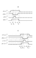
次に図3に、図2に示した撮像装置の駆動パルスの一例を示す。ここでは、本実施形態の特徴に直接関係する駆動タイミングのみについて説明する。図3(a)はn行目の駆動タイミングを示し、図3(b)はn+1行目の駆動タイミングを示す。 Next, FIG. 3 shows an example of drive pulses of the image pickup apparatus shown in FIG. Here, only the drive timing directly related to the features of the present embodiment will be described. FIG. 3A shows the driving timing of the nth row, and FIG. 3B shows the driving timing of the (n + 1) th row.
ここで、図3の実線は容量208とFD203とが接続状態となる画素、もしくは容量208がFD203に接続状態となるモードにおける制御信号を示している。
Here, a solid line in FIG. 3 indicates a control signal in a pixel in which the
点線は、容量208とFD203とが非接続状態となる画素、もしくは非選択状態の画素、もしくは容量208とFD203に非接続状態のモードにおける制御信号を示している。各制御信号がハイレベル(H)の期間において各トランジスタがオンになり、ローレベル(L)の期間に各トランジスタがオフとなる。
A dotted line indicates a control signal in a pixel in which the
図3のpSELは、選択トランジスタ206のゲートに入力される制御信号である。選択される行においては、期間t1−t8において、pSELはHレベルになる。選択されない行においては、点線のように、期間t1−t8において、pSELはLレベルになる。
PSEL in FIG. 3 is a control signal input to the gate of the
pRESは、リセットトランジスタ204のゲートに入力される制御信号である。pRESがHレベルの時、FDの電位をリセットする。
pRES is a control signal input to the gate of the
pTXは、転送トランジスタ202のゲートに入力される制御信号である。pTXがHレベルの時、光電変換部201とFDとを接続状態とし、Lレベルの時には非接続状態とする。
pTX is a control signal input to the gate of the
pAPPは、切り替えスイッチ207に入力される制御信号である。pAPPにより、容量208とFD203との接続状態を切り替える。pAPPがHレベルの時には、容量208とFD203とが接続状態となり、pAPPがLレベルの時には、容量208とFD203とが非接続状態となる。
pAPP is a control signal input to the
まず時刻T=t1nにおいて、制御信号pSELがLレベルから遷移し始め、所定期間経過後、Hレベルになる。またこの時、制御信号pRESがHレベルであり、FD203の電位がVDDになる。
First, at time T = t1 n , the control signal pSEL starts to transition from the L level, and goes to the H level after a predetermined period. At this time, the control signal pRES is at the H level, and the potential of the
次に時刻T=t2nにおいて、制御信号pAPPがLレベルから遷移し始め、所定期間経過後、Hレベルとなる。またこの時、制御信号pSEL及び制御信号pRESはHレベルである。これにより容量208とFD203とが電気的な接続状態になり、FD203及び容量208の電位がVDDになる。なお、容量208とFD203とを非接続状態とする場合には、pAPP(n)をLレベルのまま保持する。
Then, at time T = t2 n, control signal pAPP begins to transition from the L level, after a predetermined period of time, the H level. At this time, the control signal pSEL and the control signal pRES are at the H level. Accordingly, the
次に時刻T=t3nにおいて、制御信号pRESがHレベルから遷移し始め、所定期間経過後、Lレベルとなり、FD203及び容量208の電位のリセット動作が完了する。
Next, at time T = t3 n , the control signal pRES starts to transition from the H level, and after a predetermined period, goes to the L level, and the reset operation of the potentials of the
時刻T=t4nにおいて、制御信号pTXがLレベルから遷移し始め、所定期間経過後、Hレベルになる。この時、光電変換部201とFD203が電気的な接続状態になり、光電変換部201の電子がFD203に転送される。制御信号pAPPがHレベルであり、容量208とFD203とが接続状態であるため、転送された電子はFD203及び容量208で保持される。
At time T = t4 n, control signal pTX begins to transition from the L level, after a predetermined period of time, it becomes H level. At this time, the
時刻T=t5n、制御信号pTXがHレベルから遷移しはじめ、所定期間経過後、Lレベルになる。これにより、光電変換部201とFD203が非接続状態になる。
At time T = t5 n , the control signal pTX starts to transition from the H level, and becomes the L level after a predetermined period. As a result, the
時刻T=t6nにおいて、制御信号pRESがLレベルから遷移し始め、所定期間経過後、Hレベルとなることで、FD203及び容量208の電位がVDDとなる。
At time T = t6 n , the control signal pRES starts to transition from the L level, and after a predetermined period of time, goes to the H level, so that the potentials of the
時刻T=t7nにおいて、制御信号pAPPがHレベルから遷移し始め、所定期間経過後、Lレベルになる。これにより、容量208とFD203とが非接続状態となる。
At time T = t7 n , the control signal pAPP starts to transition from the H level, and becomes the L level after a predetermined period. As a result, the
時刻T=t8nにおいて、制御信号pSELがHレベルから遷移し始め、所定期間経過後、Lレベルになる。これにより、n行目の読み出しが完了する。n+1行目(図3(b))以降も同様の動作が繰り返され、画素部102の信号読み出しが行われる。
At time T = t8 n , the control signal pSEL starts to transition from the H level, and goes to the L level after a predetermined period. Thereby, reading of the nth row is completed. The same operation is repeated after the n + 1th row (FIG. 3B), and signal reading of the
期間t5n−t8nにおける信号線211の電圧を信号として用いることで、容量208が接続された状態の画素の信号を画像信号として用いることが可能となる。
By using the voltage of the
更に、必要に応じて、期間t3n−t4nにおける信号線211の電圧を信号として用いることで、画素のノイズ信号を得ることが可能となる。このノイズ信号と前述の信号電荷との差分を取ることでノイズを低減することが可能となる。
Furthermore, a pixel noise signal can be obtained by using the voltage of the
また、期間t1n−t8nにおいて、制御信号pSELをHレベルに維持している。しかし、容量208とFD203とが接続された状態で増幅トランジスタ205の入力ノードに保持した信号を信号処理部105に読み出す期間だけHレベルとしてもよい。
Further, the control signal pSEL is maintained at the H level in the period t1 n -t8 n . However, it may be set to the H level only during a period in which the signal held at the input node of the
FD203と容量208との電気的な接続状態と非接続状態とを切り替えることを、全画素一括で行ってもよいし、各画素毎あるいは所定の画素毎に行なってもよい。例えば、カラーフィルタの色毎に容量208の電気的な接続状態または非接続状態をいずれかに切り替えてもよい。
Switching between the electrical connection state and the non-connection state of the
パルスがH(L)レベルからL(H)レベルへ遷移する際には一定の時間を要する。もしくは意図的に目的レベルに達するまでの時間を設ける場合もある。図3においてはあるレベルから目的レベルに到達するまでの時間を所定期間として明示しているが、これは意図的に目的レベルに達するまで所定期間を設ける場合もそうでなく本質的に生じてしまう時間のいずれであってもよい。 It takes a certain time for the pulse to transition from the H (L) level to the L (H) level. Or there is a case where a time until the target level is intentionally reached is provided. In FIG. 3, the time required to reach the target level from a certain level is clearly shown as a predetermined period. However, this may occur essentially when a predetermined period is intentionally set until the target level is reached. Any of time may be sufficient.
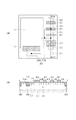
次に本実施形態の画素の特徴を説明する。図4及び図5に本実施形態の撮像装置の1画素の特徴を説明するための平面模式図及び断面模式図を示す。 Next, the characteristics of the pixel of this embodiment will be described. 4 and 5 are a schematic plan view and a schematic cross-sectional view for explaining the characteristics of one pixel of the imaging apparatus of the present embodiment.
図4(a)は、活性領域の説明を容易にするために、絶縁体分離部300と、絶縁体分離部300で区画された活性領域(313A〜313C)を示しているが、1画素内には図4(b)に示すように、図4(a)の活性領域に半導体領域が配され、且つ活性領域の上にゲート電極が配される。尚、図4(b)では、図4(a)で付した活性領域の符号(313A〜313C)を省略している。
FIG. 4A shows the
また、図5(a)及び図5(b)は、図4(b)のA−B線における断面模式図であり、容量208の構成例を説明する図である。
5A and 5B are schematic cross-sectional views taken along the line AB in FIG. 4B, and are diagrams for explaining a configuration example of the
図4(a)及び図4(b)は1画素を平面視で示した図である。後述する図5(a)などの断面模式図からも明らかなように、半導体基板320の表面側に、絶縁体分離部300が設けられており、絶縁体分離部300によって、活性領域は区画される。換言すると、活性領域が絶縁体分離部300によって囲まれている。
4A and 4B are diagrams showing one pixel in plan view. As is clear from a schematic cross-sectional view such as FIG. 5A described later, an
尚、本実施形態においては、活性領域を区画する絶縁体分離部300を配した例を用いて説明するが、絶縁体分離部300に代えてPN接合分離部を配してもよい。
In the present embodiment, an example in which the
ここで説明する実施形態において、活性領域は、絶縁体分離部300に区画された活性領域313A(第1活性領域)、313B(第2活性領域)、313C(第3活性領域)を備えている。そして、第1活性領域313Aと第2活性領域313Bは第1方向に沿って並んで配されている。
In the embodiment described here, the active region includes
また、第2活性領域313Bは、平面視において、第1方向よりも、第1方向に直交する第2方向(典型的には第1方向と直交する方向)に長い形状を有している。そして、第2活性領域313Bと第3活性領域313Cとが第2方向に沿って、並んで配されている。なお、本実施例では、基準電位が供給される領域として第3活性領域313Cを配したが、配さなくてもよい。
In addition, the second
各活性領域(313A、313B、313C)の表面は、絶縁膜316で覆われている。そのため、電極、ゲート電極(以下電極等)は各活性領域の上部に、絶縁膜316の一部を介して配されている。この絶縁膜316は、例えば酸化シリコンにより構成される。この絶縁膜316をCVD法によって成膜した場合、絶縁体分離部300の表面にも絶縁膜316が配される。一方で熱酸化法によって絶縁膜316を配する場合には、絶縁体分離部300の表面に絶縁膜316は実質的に配されない。これに対し、PN接合分離部によって、活性領域を区画した際には、どちらの方法で絶縁膜316を構成してもPN接合分離部の上に絶縁膜316が配される。
The surface of each active region (313A, 313B, 313C) is covered with an insulating
また、電極等の下部に位置しない活性領域は、その表面の少なくとも一部が、電極等の下部に位置する絶縁膜と異なる絶縁膜が配されていてもよい。異なる絶縁膜とは例えば電極等の下部に位置する絶縁膜を形成した後に、電極等の下部以外の絶縁膜を除去した後、別の絶縁膜を形成するような場合である。 In addition, the active region that is not located under the electrode or the like may be provided with an insulating film at least part of the surface of which is different from the insulating film located under the electrode or the like. The different insulating film is, for example, a case where after forming an insulating film located under the electrode or the like, after removing the insulating film other than the lower part such as the electrode, another insulating film is formed.
以下では、電極等の下部に位置する絶縁膜と、電極等の下部以外に位置する、活性領域の表面に配される絶縁膜とが、同一の絶縁膜の場合について説明する。 Below, the case where the insulating film located in the lower part of an electrode etc. and the insulating film arranged on the surface of an active region other than the lower part of an electrode etc. are the same insulating film is demonstrated.
図4(b)に示すように、第1活性領域313Aには、第2方向に沿って光電変換部201、ゲート電極402、N型半導体領域(第3半導体領域)303Aが配される。また、第1活性領域313Aの上には、絶縁膜316を介してゲート電極402が配されており、第2活性領域313Bの上には、絶縁膜316を介して電極404が配されている。
As shown in FIG. 4B, the
そして、図4(b)のように第2活性領域313Bは、平面視において電極404を挟むように、第1領域323と、第2領域324を有している。
As shown in FIG. 4B, the second
第1領域323には、FD203の少なくとも一部を構成するN型半導体領域(第1半導体領域)303Bが配されている。
In the
そして、第2領域324には、絶縁膜316と界面を構成するP型半導体領域312(第2半導体領域)が配されている。
The
FD203は、第1半導体領域303Bと第1活性領域313Aに配された第3半導体領域303Aとを有する。
The
図5(a)は図4(b)のA−B線における断面模式図であり、電極404を挟んで、第1領域323と第2領域324が配されている。この第1領域323には、N型半導体領域303Bが配されている。そして、第2領域324には、絶縁膜316と界面を構成するP型半導体領域312が配されている。また、第1半導体領域(303B)も絶縁膜316と界面を構成している。
FIG. 5A is a schematic cross-sectional view taken along the line AB of FIG. 4B, and the
図5(a)の例では、電極404の下部の半導体領域には、絶縁膜316を介して印加される電界によって、電極404の下部の活性領域の表面に配されたP型半導体領域312が反転して電荷蓄積領域となる表面型MOS容量を構成する。これによって図2の容量208が構成される。その他の実施形態を実施例で後述する。
In the example of FIG. 5A, a P-
さらに、電極404は、図2の切り替えスイッチ207に含まれる。電極404に印加される制御信号pAPPによって後述する容量208のFD203に対する電気的な接続状態と非接続状態とを切り替えることができる。
Furthermore, the
容量208では、電極404の下部の活性領域の表面に電位の井戸が生じ、その部分に電子が蓄積される。ただし、この電位の井戸に上述の第2領域324の表面からの電子が混入することで、容量208をFD203に対して接続状態とした際に、FD203にノイズを混入してしまう恐れがある。
In the
そこで、第2領域324に、その上部に絶縁膜316が配されたP型半導体領域312を配することで、上述のノイズとなりうる電子がP型半導体領域312の多数キャリアである正孔と再結合する。これにより、N型半導体領域303Bに混入する電子を減らすことができ、ノイズを低減することが可能となる。より好ましくは、P型半導体領域312は絶縁膜316と界面を構成するのがよい。
Therefore, by providing the
また、活性領域と絶縁体分離部300の界面では、主に酸化シリコンで構成される絶縁体分離部300と、半導体基板320の主の構成要素であるシリコンとの膨張係数の違いなどにより、欠陥が生じ、不要電荷を生じる恐れがある。
In addition, at the interface between the active region and the
そのため、第2領域324には、活性領域と絶縁膜316との界面から少なくとも絶縁体分離部300の底の深さまでP型半導体領域412を配するのがよい。これによって、容量208と絶縁体分離部300をオフセットし、絶縁体分離部300から生じるノイズを低減することが可能となる。
Therefore, the P-
本実施形態では、表面型MOS容量を用いて説明したが、図5(b)のように、電極404の下部の活性領域の表面にN型半導体領域を配して、埋め込み型のMOS容量とすることもできる。
In the present embodiment, the surface type MOS capacitor has been described. However, as shown in FIG. 5B, an N type semiconductor region is arranged on the surface of the active region below the
また、本実施形態では、第2領域324に、P型半導体領域としてPウェルを構成するP型半導体領域312を配した例を示した。ただし、第2領域324に配されるP型半導体領域の深さは特に限定されるものではない。したがって、第2領域324の絶縁膜316との界面を構成する領域以外の領域がN型半導体領域となっていてもよい。即ち、第2領域324に設けられたP型半導体領域の下にN型半導体領域が設けられていてもよい。
Further, in the present embodiment, an example in which the P-
また、ここでは、P型半導体領域312の上に配される絶縁膜316を電極404の下部に位置する絶縁膜316と同じ絶縁膜として説明した。しかし、例えば層間絶縁膜のように、電極の下部に位置する絶縁膜316とは異なった絶縁膜がP型半導体領域312の上に配されてもよい。
Here, the insulating
さらに、本実施形態では、光電変換部201が配される活性領域313Aと、容量208が配される活性領域313Bとを別の活性領域としたが、必ずしもそれぞれが別の活性領域である必要はなく、同一活性領域としてもよい。
Furthermore, in the present embodiment, the
以下、本実施形態で説明した撮像装置の具体的な実施例を説明する。 Hereinafter, specific examples of the imaging apparatus described in this embodiment will be described.
(実施例1)
図6に本実施例の撮像装置の1画素の特徴を説明するための平面模式図及び断面模式図を示す。図1〜5と同様の機能を有する部分には同様の符号を付し詳細な説明を省略する。本実施例において、第2半導体領域に該当するのはP型半導体領域405である。P型半導体領域405は、P型のウェルを構成するP型半導体領域412に配される。
Example 1
FIG. 6 shows a schematic plan view and a schematic cross-sectional view for explaining the characteristics of one pixel of the image pickup apparatus of this embodiment. Parts having the same functions as those in FIGS. In this embodiment, the P-
図6(a)は本実施例の撮像装置の1画素の平面模式図を示す。本実施例の活性領域の構成は、実施形態の図4(a)で示した活性領域(313A、313B、313C)と同様に、絶縁体分離部300によって区画されている。
FIG. 6A is a schematic plan view of one pixel of the image pickup apparatus of the present embodiment. The configuration of the active region of the present example is partitioned by the
また、本実施例では、実施形態で説明した図4(b)の構成と同様に、平面視において、第2活性領域313Bは、電極404を挟んで配された、第1領域323と第2領域324を含んでいる。そして、N型半導体領域303Bが第1領域323に配され、P型半導体領域405が第2領域324に配されている。P型半導体領域405は、P型半導体領域405の下部に配されたP型半導体領域412よりも不純物濃度が高い。
Further, in this example, similarly to the configuration of FIG. 4B described in the embodiment, the second
活性領域313Aには、第1方向に直交する第2方向に沿って、光電変換部201、ゲート電極402、N型半導体領域303Aが配されている。そして、活性領域313Bには、第2の方向に沿って、N型半導体領域406、ゲート電極407、N型半導体領域408、ゲート電極409、N型半導体領域410、ゲート電極411、N型半導体領域303B、電極404、P型半導体領域405が配されている。
In the
ここで、活性領域313Aに配されているN型半導体領域303Aと活性領域313Bに配されているN型半導体領域303B及びN型半導体領域303Bに電気的に接続される容量208、ゲート電極409は導電体によって接続されている。FD203はN型半導体領域303A、303Bを有している。
Here, the N-
次に図6(b)は図6(a)のC−D線に沿った断面模式図、図6(c)は図6(a)のA−B線に沿った断面模式図である。まず図6(b)について説明する。 Next, FIG. 6B is a schematic cross-sectional view taken along line CD in FIG. 6A, and FIG. 6C is a schematic cross-sectional view taken along line AB in FIG. First, FIG. 6B will be described.
光電変換部201は、N型半導体領域401とP型半導体領域412により構成されるPN接合を有している。本実施例では光電変換部201はフォトダイオードである。またN型半導体領域401の表面にP型半導体領域415が配されることで埋め込み型のフォトダイオードを構成している。ここでN型半導体領域401は各トランジスタのソース、ドレインを構成する半導体領域に比べ、絶縁膜316に対して深い位置まで配されている。
The
図2の転送トランジスタ202は、ドレインとなるN型半導体領域401、ゲート電極402、ソース領域となるN型半導体領域303Aにより構成される。
The
次に、図6(c)に示した、活性領域313Bについて説明する。
Next, the
図2のリセットトランジスタ204は、ソース領域となるN型半導体領域303B、ゲート電極411、ドレイン領域となるN型半導体領域410により構成される。図2のリセットトランジスタ204は、ソース領域となるN型半導体領域303B、ゲート電極411、ドレイン領域となるN型半導体領域410により構成される。図2の増幅トランジスタ205は、ドレイン領域となるN型半導体領域410、ゲート電極409、ソース領域となるN型半導体領域408により構成される。図2の選択トランジスタ206は、ドレイン領域となるN型半導体領域408、ゲート電極407、ソース領域となるN型半導体領域406により構成される。
The
そして、第3活性領域313CにはP型半導体領域414が配されている。このP型半導体領域414には、ウェルを構成するP型半導体領域412に所定の電位を供給するコンタクトプラグが接続されている。このような構成により、P型半導体領域412の電位変化を抑制することができる。所定の電圧とは例えば接地電位である。
A P-
そして、図2の切り替えスイッチ207は、電極404を含み、電極404に供給される電圧により、容量208のFDに対する電気的な接続状態と非接続状態とを切り替える。
2 includes an
本実施例で第2領域324には、絶縁膜316と界面を構成するP型半導体領域405が配されている。
In this embodiment, a P-
さらに、第2領域324には、P型半導体領域405の下には、少なくとも絶縁体分離部300の底の深さまで、P型半導体領域412が配されている。この時、P型半導体領域412は、Pウェルで構成されてもよい。また、Nウェルの上にP型半導体領域412が配されていてもよい。
Furthermore, in the
ここで、絶縁体分離部300の底とは、絶縁体分離部300がP型半導体領域412と界面を構成する深さであって最も深い位置のことである。
Here, the bottom of the
上述したようにP型半導体領域405の不純物濃度は、P型半導体領域412の不純物濃度よりも高い。このような構成とすることにより、容量208に近接する部分(第2領域324の表面近傍)のP型の不純物濃度が図5(a)や図5(b)の構成に比べて高くすることができる。そのため、P型半導体領域405を設けずに、P型半導体領域412が絶縁膜316と界面を構成した形態よりも、半導体領域の表面の結晶欠陥によるノイズを低減することが可能となる。
As described above, the impurity concentration of the P-
P型半導体領域405を形成する方法としては、例えば、電極404をマスクとして用いて、予め設けられたP型半導体領域412の一部の領域にイオン注入をすることで形成することができる。
As a method for forming the P-
以上のことから、本実施例によれば、絶縁膜316との界面の結晶欠陥によるノイズを低減するとともに、絶縁体分離部300から生じるノイズを低減することが可能となる。
From the above, according to this embodiment, it is possible to reduce noise caused by crystal defects at the interface with the insulating
(実施例2)
図7に本実施例の撮像装置の1画素の特徴を説明するための平面模式図及び断面模式図を示す。図1〜6と同様の機能を有する部分には同様の符号を付し詳細な説明を省略する。
(Example 2)
FIG. 7 shows a schematic plan view and a schematic cross-sectional view for explaining the characteristics of one pixel of the image pickup apparatus of this embodiment. The parts having the same functions as those in FIGS.
図7(a)は本実施例の撮像装置の1画素の平面模式図である。本実施例では、平面視で、第2領域324に、P型半導体領域412を形成し、P型半導体領域505が電極404に対してオフセットするようにP型半導体領域412の表面に配される。この、P型半導体領域505が電極404に対してオフセットした領域をオフセット領域518とした時、オフセット領域518を間に挟んで、P型半導体領域505が設けられている点が実施例1と異なる。
FIG. 7A is a schematic plan view of one pixel of the image pickup apparatus of the present embodiment. In this embodiment, the P-
このため、本実施例では,オフセット領域518とP型半導体領域505とが、第2領域324に配されている。
For this reason, in this embodiment, the offset
図7(b)は図7(a)のA−B線に沿った断面模式図である。前述したオフセット領域518は、P型半導体領域505よりも不純物濃度の低いP型半導体領域412で構成されている。
FIG.7 (b) is a cross-sectional schematic diagram along the AB line | wire of Fig.7 (a). The offset
図3を用いて、オフセット領域518を設ける理由を説明する。
The reason why the offset
図3の時刻t2nから時刻t7nの期間では、制御信号pAPPがハイレベルである。そのため、切り替えスイッチ207の電極404の電位はハイレベルになっている。
In the period from time t2 n to time t7 n in FIG. 3, the control signal pAPP is at a high level. Therefore, the potential of the
それに対してP型半導体領域412の電位は、接地レベルになるように構成されているため、P型半導体領域505の電位も接地レベルに近い電位となっている。したがって、切り替えスイッチ207の電極404とP型半導体領域505との間に高電界が生じる。ただし、実際には、例えば、電極404の下部のP型半導体領域412が反転して、表面型MOS容量を構成したりと、必ずしもP型半導体領域412のすべての領域が同一の接地電位になるとは限らない。
On the other hand, since the potential of the P-
この時に、高電界が印加される領域にノイズとなる電荷が存在するとホットキャリア増幅と呼ばれる現象が生じる可能性がある。ホットキャリア増幅が生じると、N型半導体領域303Bへ電荷が混入し、これがノイズとなる。このホットキャリア増幅を抑制するためには切り替えスイッチ207の電極404とP型半導体領域505との間の電界を緩和すればよい。
At this time, if a charge that becomes noise exists in a region to which a high electric field is applied, a phenomenon called hot carrier amplification may occur. When hot carrier amplification occurs, charge is mixed into the N-
そこで、本実施例においては、電極404とP型半導体領域505との間に、P型半導体領域505よりも不純物濃度の低いP型半導体領域412(オフセット領域518)を設けている。このような構成によって、電極404とP型半導体領域505の間にP型半導体領域412(オフセット領域518)を設けない場合に比べて広い空乏層が広がる。そのため、電極404とP型半導体領域505の間の電界を緩和することが出来る。
Therefore, in this embodiment, a P-type semiconductor region 412 (offset region 518) having an impurity concentration lower than that of the P-
電極404との間にオフセット領域518を設けてP型半導体領域505を配する方法としては、例えば、電極404の側壁に絶縁体で形成したサイドスペーサを用いる方法がある。具体的には、サイドスペーサをマスクとして用いて、予め設けられたP型半導体領域412にイオン注入することで、電極404との間にP型半導体領域412を挟んで、P型半導体領域505を配することができる。
As a method of providing the offset
したがって、本実施例によれば、ホットキャリア増幅の発生を抑制し、更にノイズを減らすことが出来る。 Therefore, according to the present embodiment, occurrence of hot carrier amplification can be suppressed and noise can be further reduced.
(実施例3)
図8に本実施例の撮像装置の1画素の特徴を説明するための平面模式図及び断面模式図を示す。図1〜7と同様の機能を有する部分には同様の符号を付し詳細な説明を省略する。
(Example 3)
FIG. 8 shows a schematic plan view and a schematic cross-sectional view for explaining the characteristics of one pixel of the image pickup apparatus of this embodiment. Parts having the same functions as those in FIGS. 1 to 7 are denoted by the same reference numerals, and detailed description thereof is omitted.
図8(a)は、本実施例の撮像装置の1画素の平面模式図である本実施例では実施例2のオフセット領域518にP型半導体領域619を配している点が実施例2と相違する。つまり、本実施例では、平面視において、第2領域324において、P型半導体領域605が、電極404との間に、不純物濃度がP型半導体領域412の不純物濃度よりも高いP型半導体領域619を間に挟んで、設けられている点が実施例2と相違する。
FIG. 8A is a schematic plan view of one pixel of the imaging apparatus of the present embodiment. In this embodiment, the P-
図8(b)は図8(a)のA−B線に沿った断面模式図である。 FIG. 8B is a schematic cross-sectional view taken along the line AB of FIG.
前述したP型半導体領域619は、P型半導体領域412よりも不純物濃度が高く、P型半導体領域605よりも不純物濃度が低い領域である。
The P-
このように第2領域324に、P型半導体領域605と電極404の間にP型半導体領域619を配することで、P型半導体領域619を低濃度の電界緩和領域とし、P型半導体領域605とゲート電極間の電界を緩和することができる。このような構造をLDD構造という。これにより、ホットキャリア増幅を抑制することができ、信頼性および耐圧を向上させることができる。
As described above, by arranging the P-
更に周辺回路にLDD構造を有するPMOSトランジスタを設けた場合には、本実施例のP型半導体領域605及びP型半導体領域619と周辺回路のPMOSトランジスタのソース及びドレインを形成する不純物イオン注入工程を同一工程にしてもよい。
Further, when a PMOS transistor having an LDD structure is provided in the peripheral circuit, an impurity ion implantation process for forming the P-
本実施例の画素がこのような構造を形成することで、本実施例の構成を適応した画素の製造工程において、特段の製造プロセス工程を増やすことなく、周辺回路と一緒に画素を形成することが可能となる。 By forming such a structure in the pixel of this embodiment, in the pixel manufacturing process to which the configuration of this embodiment is applied, the pixel is formed together with the peripheral circuit without increasing the number of special manufacturing process steps. Is possible.
ここで周辺回路領域とは、半導体基板320上の、複数の画素が配列された領域の周辺部に配された領域を言う。この周辺回路領域には、先に説明した制御信号pSEL、pRES、pTX、pAPPなどを出力する制御回路が設けられている。また周辺回路領域には、複数の画素から図2に示す信号線211を通して出力された信号を、サンプリングしたり、出力したりする回路が設けられている。これは以下の実施例においても同様である。
Here, the peripheral circuit region refers to a region on the
本実施例では、P型半導体領域605と電極404の間にP型半導体領域605よりも不純物濃度の低く、P型半導体領域412よりも不純物濃度の高いP型半導体領域619を設けた。前述した実施例2と同様に容量208の電極404とP型半導体領域605との間の電界を緩和することが可能であり、ホットキャリア増幅を抑制し、ノイズを抑制することが出来る。
In this embodiment, a P-
(実施例4)
図9に本実施例の撮像装置の1画素の特徴を説明するための平面模式図及び断面模式図を示す。図1〜8と同様の機能を有する部分には同様の符号を付し詳細な説明を省略する。
Example 4
FIG. 9 shows a schematic plan view and a schematic cross-sectional view for explaining the characteristics of one pixel of the image pickup apparatus of the present embodiment. Portions having functions similar to those in FIGS. 1 to 8 are denoted by the same reference numerals, and detailed description thereof is omitted.
図9(a)は本実施例の撮像装置の1画素の平面模式図である。本実施例では、平面視において、第2領域324において、N型半導体領域303Bが第1領域323に配され、不純物濃度がP型半導体領域412の不純物濃度よりも高いP型半導体領域705が第2領域324に配されている点は実施例1と同様であるが、P型半導体領域705の下にN型半導体領域717を配している点が実施例1と相違する。図9(b)は図9(a)のA−B線に沿った断面模式図である。
FIG. 9A is a schematic plan view of one pixel of the image pickup apparatus of the present embodiment. In the present embodiment, the N-
図9(b)に示すように、本実施例では、P型半導体領域705の下に、P型半導体領域705と界面を構成するN型半導体領域717が設けられている。このN型半導体領域717が、前述した表面型MOS容量又は、埋め込み型のMOS容量に電気的に接続される。そして、N型半導体領域717が構成するPN接合容量は、容量208の一部を構成する。
As shown in FIG. 9B, in this embodiment, an N-
なお、P型半導体領域705とN型半導体領域717は、第2領域324にイオン注入することによりP型半導体領域705とN型半導体領域717とを深さ方向にこの順に配する。
Note that the P-
本実施例では、第2領域324に配されたP型半導体領域705は、必ずしもP型半導体領域412よりも不純物濃度が高くなくてもよい。その場合には、P型半導体領域705をPウェルであるP型半導体領域412で置き換えることができる。
In this embodiment, the P-
(実施例5)
図10に本実施例の撮像装置の1画素の特徴を説明するための平面模式図及び断面模式図を示す。図1〜9と同様の機能を有する部分には同様の符号を付し詳細な説明を省略する。
(Example 5)
FIG. 10 shows a schematic plan view and a schematic cross-sectional view for explaining the characteristics of one pixel of the imaging apparatus of the present embodiment. Parts having the same functions as those in FIGS.
図10(a)は本実施例の撮像装置の1画素の平面模式図である。図10(b)は図10(a)のA−B線に沿った断面模式図である。本実施例の活性領域313A〜313Cは、図10(c)に示すように、第1活性領域313Aの形状が実施例1〜4の第1活性領域313Aと異なっている。そして、第1活性領域313Aに、電極404と第2領域324が配されている点が実施例1〜実施例4と相違する。本実施例では、第1活性領域313Aに、電極404を挟んで、N型半導体領域303AとP型半導体領域805が配されている。N型半導体領域303Aが配される領域が第1領域323に対応し、P型半導体領域805が配される領域が第2領域324に対応する。
FIG. 10A is a schematic plan view of one pixel of the image pickup apparatus of the present embodiment. FIG.10 (b) is a cross-sectional schematic diagram along the AB line | wire of Fig.10 (a). As shown in FIG. 10C, the
本実施例では、第1活性領域313Aに、光電変換部201、N型半導体領域303A、電極404、P型半導体領域805が配される。また、第2活性領域313Bには、N型半導体領域406、ゲート電極407、N型半導体領域408、ゲート電極409、N型半導体領域410、ゲート電極411、N型半導体領域303Bが配される。第3活性領域313Cには、P型半導体領域414が配され、このP型半導体領域414には、P型半導体領域412に電位を供給するコンタクトプラグが接続されている。
In this embodiment, the
本実施例では、FD203はN型半導体領域303A、303Bとを有する。
In this embodiment, the
以上、具体的な実施例を挙げて本発明の説明を行ったが、本発明は上記実施の形態に制限されるものではなく、本発明の目的および範囲から離脱することなく、様々な変更及び変形が可能である。 The present invention has been described with reference to specific examples. However, the present invention is not limited to the above embodiments, and various modifications and changes can be made without departing from the object and scope of the present invention. Deformation is possible.
たとえば、絶縁体分離部300と活性領域の界面にチャネルストップ領域とよばれる高濃度の半導体領域が設けられる場合がある。これによってN型のデバイス間のチャネル形成を抑制する場合には、P型の高濃度の半導体領域が用いられ、P型のデバイス間のチャネル形成を抑制する場合には、N型の高濃度の半導体領域が用いられる。上述の各実施例においては、光電変換部201、容量208、画素のトランジスタはN型のデバイスであるため、チャネルストップ領域はP型の半導体領域が用いられる。
For example, a high-concentration semiconductor region called a channel stop region may be provided at the interface between the
上述の各実施例においてもこのようなチャネルストップ領域を設けてもよい。その場合には、P型半導体領域312、405、412,505,605,705,805と絶縁体分離部300との界面にP型のチャネルストップ領域を設けてもよい。このような構成にすることで、絶縁体分離部300から生じるノイズを低減することも可能となる。これは他の実施例においても同様である。
Such a channel stop region may be provided also in each of the embodiments described above. In that case, a P-type channel stop region may be provided at the interface between the P-
(実施例6)
図11に本実施例の撮像装置の1画素の特徴を説明するための平面模式図及び断面模式図を示す。また、図12に駆動タイミング図を示す。図1〜10と同様の機能を有する部分には同様の符号を付し詳細な説明を省略する。
(Example 6)
FIG. 11 shows a schematic plan view and a schematic cross-sectional view for explaining the characteristics of one pixel of the image pickup apparatus of the present embodiment. FIG. 12 shows a drive timing chart. Portions having functions similar to those in FIGS. 1 to 10 are denoted by the same reference numerals, and detailed description thereof is omitted.
図11(a)は1画素の平面模式図である。本実施例では、第3活性領域313Cが配されていない点が実施例1から5と異なる点である。
FIG. 11A is a schematic plan view of one pixel. The present embodiment is different from the first to fifth embodiments in that the third
図11(b)は図11(a)のA−B線に沿った断面模式図である。 FIG.11 (b) is a cross-sectional schematic diagram along the AB line | wire of Fig.11 (a).
本実施例では、P型半導体領域905には、基準電位が供給されたコンタクトプラグが絶縁膜316を貫通してP型半導体領域905に接続される。この構成により、実施例1〜5で用いていたP型のウェル領域412に基準電位を供給するためのP型半導体領域414と、第2領域324に配されたP型半導体領域(405〜805)とを共通にし、P型半導体領域905とする構成である。
In this embodiment, a contact plug supplied with a reference potential is connected to the P-
なお、この構成はすべての実施例に適応可能である。これによって第3活性領域313Cを設けないことで、平面レイアウトを縮小できるため、容量208、もしくは光電変換部201の平面視における面積を増大させることが可能となる。
This configuration can be applied to all embodiments. Accordingly, since the planar layout can be reduced by not providing the third
例えば、本実施例では電極404の面積を拡大することで、容量208の容量値を増加させることが出来る。そのため、容量208をFD203に電気的に接続した時に、増幅トランジスタ205の入力ノードの容量値を増加させることが可能となり、ダイナミックレンジをより拡大することが可能である。
For example, in this embodiment, the capacitance value of the
また、光電変換部201を拡大した場合は飽和信号量の増大が可能となる。また、増幅トランジスタ205を拡大した場合は、1/fノイズを低減し、画質を向上させることが可能となる。
Further, when the
(駆動方法の変形例)
図12に記載の駆動方法の変形例について説明する。図12(a)、(b)は、容量208を非接続状態とした際のK行目の画素の駆動タイミングと、K+1行目の画素の駆動タイミングの一例を示す。図3の駆動タイミング図とは、所望の蓄積時間の信号を得るために光電変換部201の電荷をリセットする動作である時刻t1kから時刻t2kが追加されている点で異なる。
(Modification of driving method)
A modification of the driving method shown in FIG. 12 will be described. FIGS. 12A and 12B show an example of the drive timing of the pixel in the Kth row and the drive timing of the pixel in the K + 1th row when the
図12(a)において、光電変換部201に信号を蓄積している期間であるt2kからt6kの期間に、光電変換部201にノイズとなる電荷が混入してしまう場合がある。
これを抑制するために、本実施例では時刻t2kから時刻t4kの期間でpAPP(k)をHighレベルとし、容量208をリセットする。
In FIG. 12A, in the period from t2 k to t6 k , which is a period in which signals are accumulated in the
In order to suppress this, in this embodiment, pAPP (k) is set to the high level during the period from time t2 k to time t4 k , and the
この駆動制御により、P型半導体領域905でノイズとなる電子が生じた場合に、光電変換部201よりも近傍にあり、且つ高いポテンシャルにリセットされているN型半導体領域303Bへと電子を誘導する。それによって、光電変換部201へ暗電流が混入することを抑制できる。
With this drive control, when electrons that become noise are generated in the P-
なお、容量208を動作状態とし、N型半導体領域303Bの容量値を増大させることでダイナミックレンジを拡大した状態で、信号を読み出す際には時刻t4kでpAPP(k)をローレベルにしなくてもいい。
Note that pAPP (k) must be set to the low level at time t4 k when reading the signal in a state where the dynamic range is expanded by increasing the capacitance value of the N-
本変形例は上述の全ての実施例に共通して適用可能な駆動方法である。特に、実施例6には、適用するほうがよい。なぜならば、実施例6では、P型半導体領域405にコンタクトプラグが接続され、その部分において、ノイズと成る電子が発生する場合があるからである。このようなノイズに対し本変形例を適用することで、更にノイズを低減させることが可能となる。
This modification is a driving method that can be applied in common to all the embodiments described above. In particular, it is better to apply to the sixth embodiment. This is because, in the sixth embodiment, a contact plug is connected to the P-
303B 第1半導体領域
312 第2半導体領域
316 絶縁膜
323 第1領域
324 第2領域
404 ゲート電極
303B
Claims (12)
前記光電変換部で生じた電荷を保持するフローティングディフュージョンと、
前記フローティングディフュージョンに電気的に接続された増幅トランジスタと、
電極を有し、前記電極へ供給される信号により、前記フローティングディフュージョンへの電気的な接続状態が切り替え可能に配された容量と、を各々が含み、
各々が、前記接続状態を切り替えることで、前記増幅トランジスタの入力ノードの容量値が変更可能である、複数の画素を有する撮像装置であって、
前記複数の画素の各々は、平面視において、前記電極を挟むように配された、第1領域と、第2領域とを含む活性領域を有し、
前記活性領域は、絶縁体分離部又はPN接合分離部である分離部によって囲まれており、
前記第1領域及び前記第2領域は、前記電極が配されていない領域であり、
前記活性領域の一部であって前記電極の下に位置する部分が前記容量の少なくとも一部を構成しており、
前記第1領域には、前記フローティングディフュージョンの少なくとも一部を構成する第1導電型の第1半導体領域が配され、
前記第2領域には、前記第1導電型とは反対導電型である第2導電型の第2半導体領域が配されており、
前記第2半導体領域の上に、絶縁膜が配されていることを特徴とする撮像装置。 A photoelectric conversion unit;
A floating diffusion for holding charges generated in the photoelectric conversion unit;
An amplification transistor electrically connected to the floating diffusion;
Each of which includes an electrode, and a capacitor disposed so that an electrical connection state to the floating diffusion can be switched by a signal supplied to the electrode,
Each of the imaging devices having a plurality of pixels, wherein the capacitance value of the input node of the amplification transistor can be changed by switching the connection state,
Each of the plurality of pixels has an active region including a first region and a second region arranged so as to sandwich the electrode in plan view,
The active region is surrounded by an isolation part which is an insulator isolation part or a PN junction isolation part,
The first region and the second region are regions where the electrode is not disposed,
A portion of the active region located below the electrode constitutes at least a portion of the capacitance;
In the first region, a first semiconductor region of a first conductivity type constituting at least a part of the floating diffusion is disposed,
A second semiconductor region of a second conductivity type that is opposite to the first conductivity type is disposed in the second region,
An imaging device, wherein an insulating film is disposed on the second semiconductor region.
平面視において、
前記第1活性領域と前記第2活性領域とが第1方向に沿って並んで配されており、
前記第2活性領域には前記第1方向に直交する第2方向に沿って前記第1半導体領域と前記第2半導体領域が配され、前記第2活性領域の上には、前記第1半導体領域と前記第2半導体領域に挟まれるように前記電極が配され、
前記第1活性領域には、前記第2方向に沿って前記光電変換部と前記第3半導体領域とが配され、前記第1活性領域の上には、前記光電変換部と前記第3半導体領域に挟まれるように前記転送トランジスタのゲート電極が配されることを特徴とする請求項8に記載の撮像装置。 Each of the plurality of pixels further includes a transfer transistor that transfers a signal of the photoelectric conversion unit to the third semiconductor region,
In plan view,
The first active region and the second active region are arranged side by side along a first direction;
In the second active region, the first semiconductor region and the second semiconductor region are disposed along a second direction orthogonal to the first direction, and the first semiconductor region is disposed on the second active region. And the electrode is disposed so as to be sandwiched between the second semiconductor regions,
The photoelectric conversion unit and the third semiconductor region are disposed in the first active region along the second direction, and the photoelectric conversion unit and the third semiconductor region are disposed on the first active region. The imaging apparatus according to claim 8, wherein a gate electrode of the transfer transistor is disposed so as to be sandwiched between the two.
Priority Applications (4)
| Application Number | Priority Date | Filing Date | Title |
|---|---|---|---|
| JP2014151123A JP6406912B2 (en) | 2014-07-24 | 2014-07-24 | Imaging device and driving method thereof |
| EP15176034.5A EP2978021B1 (en) | 2014-07-24 | 2015-07-09 | Imaging device and method for driving the same |
| US14/805,302 US9641778B2 (en) | 2014-07-24 | 2015-07-21 | Imaging device and method for driving the same |
| CN201510441094.0A CN105304660B (en) | 2014-07-24 | 2015-07-24 | Imaging device and its driving method |
Applications Claiming Priority (1)
| Application Number | Priority Date | Filing Date | Title |
|---|---|---|---|
| JP2014151123A JP6406912B2 (en) | 2014-07-24 | 2014-07-24 | Imaging device and driving method thereof |
Related Child Applications (1)
| Application Number | Title | Priority Date | Filing Date |
|---|---|---|---|
| JP2018174103A Division JP6682587B2 (en) | 2018-09-18 | 2018-09-18 | Imaging device and driving method thereof |
Publications (3)
| Publication Number | Publication Date |
|---|---|
| JP2016025332A JP2016025332A (en) | 2016-02-08 |
| JP2016025332A5 JP2016025332A5 (en) | 2017-08-31 |
| JP6406912B2 true JP6406912B2 (en) | 2018-10-17 |
Family
ID=53793969
Family Applications (1)
| Application Number | Title | Priority Date | Filing Date |
|---|---|---|---|
| JP2014151123A Active JP6406912B2 (en) | 2014-07-24 | 2014-07-24 | Imaging device and driving method thereof |
Country Status (4)
| Country | Link |
|---|---|
| US (1) | US9641778B2 (en) |
| EP (1) | EP2978021B1 (en) |
| JP (1) | JP6406912B2 (en) |
| CN (1) | CN105304660B (en) |
Families Citing this family (10)
| Publication number | Priority date | Publication date | Assignee | Title |
|---|---|---|---|---|
| JP6700656B2 (en) * | 2014-10-31 | 2020-05-27 | キヤノン株式会社 | Imaging device |
| JP6727830B2 (en) * | 2016-02-09 | 2020-07-22 | キヤノン株式会社 | Imaging device |
| JP6664259B2 (en) * | 2016-03-31 | 2020-03-13 | キヤノン株式会社 | Imaging device, imaging system, and moving object |
| WO2018066143A1 (en) * | 2016-10-07 | 2018-04-12 | 国立大学法人東北大学 | Optical sensor and signal reading method therefor, and solid-state imaging device and signal reading method therefor |
| US10110840B2 (en) * | 2016-10-25 | 2018-10-23 | Semiconductor Components Industries, Llc | Image sensor pixels with overflow capabilities |
| DE102017221719B4 (en) | 2017-12-01 | 2023-03-30 | Bruker Axs Gmbh | OPTICAL EMISSION SPECTROMETER WITH CASCADED CHARGE STORAGE |
| US10559614B2 (en) * | 2018-03-09 | 2020-02-11 | Semiconductor Components Industries, Llc | Dual conversion gain circuitry with buried channels |
| JP2020068267A (en) * | 2018-10-23 | 2020-04-30 | ソニーセミコンダクタソリューションズ株式会社 | Solid-state imaging device |
| DE102020111562A1 (en) * | 2020-04-28 | 2021-10-28 | Arnold & Richter Cine Technik Gmbh & Co. Betriebs Kg | Image sensor |
| JP2023064358A (en) * | 2021-10-26 | 2023-05-11 | ソニーセミコンダクタソリューションズ株式会社 | Imaging element and electronic apparatus |
Family Cites Families (17)
| Publication number | Priority date | Publication date | Assignee | Title |
|---|---|---|---|---|
| JP3455655B2 (en) * | 1997-03-03 | 2003-10-14 | 株式会社東芝 | Solid-state imaging device and solid-state imaging device application system |
| JP4459098B2 (en) * | 2005-03-18 | 2010-04-28 | キヤノン株式会社 | Solid-state imaging device and camera |
| JP4677258B2 (en) * | 2005-03-18 | 2011-04-27 | キヤノン株式会社 | Solid-state imaging device and camera |
| KR100720503B1 (en) * | 2005-06-07 | 2007-05-22 | 동부일렉트로닉스 주식회사 | CMOS image sensor and method for manufacturing the same |
| EP1887626A1 (en) * | 2006-08-09 | 2008-02-13 | Tohoku University | Optical sensor comprising overflow gate and storage capacitor |
| JP2008205639A (en) * | 2007-02-16 | 2008-09-04 | Texas Instr Japan Ltd | Solid-state imaging device and its operation method |
| US8072015B2 (en) * | 2007-06-04 | 2011-12-06 | Sony Corporation | Solid-state imaging device and manufacturing method thereof |
| JP2008305983A (en) * | 2007-06-07 | 2008-12-18 | Nikon Corp | Solid-state imaging element |
| JP5213501B2 (en) * | 2008-04-09 | 2013-06-19 | キヤノン株式会社 | Solid-state imaging device |
| JP5521682B2 (en) * | 2010-02-26 | 2014-06-18 | ソニー株式会社 | Solid-state imaging device, driving method of solid-state imaging device, and electronic apparatus |
| US9200956B2 (en) * | 2010-06-27 | 2015-12-01 | Sri International | Readout transistor circuits for CMOS imagers |
| JP5570377B2 (en) * | 2010-09-30 | 2014-08-13 | キヤノン株式会社 | Solid-state imaging device |
| TWI456990B (en) * | 2011-04-08 | 2014-10-11 | Pixart Imaging Inc | High dynamic range imager circuit and method for reading high dynamic range image |
| FR2979485B1 (en) * | 2011-08-26 | 2016-09-09 | E2V Semiconductors | PIXEL REGROUPING IMAGE SENSOR |
| JPWO2013176007A1 (en) * | 2012-05-25 | 2016-01-12 | ソニー株式会社 | Imaging device, driving method, and electronic apparatus |
| US8957359B2 (en) * | 2012-10-12 | 2015-02-17 | Omnivision Technologies, Inc. | Compact in-pixel high dynamic range imaging |
| US10497737B2 (en) * | 2013-05-30 | 2019-12-03 | Caeleste Cvba | Enhanced dynamic range imaging |
-
2014
- 2014-07-24 JP JP2014151123A patent/JP6406912B2/en active Active
-
2015
- 2015-07-09 EP EP15176034.5A patent/EP2978021B1/en active Active
- 2015-07-21 US US14/805,302 patent/US9641778B2/en active Active
- 2015-07-24 CN CN201510441094.0A patent/CN105304660B/en active Active
Also Published As
| Publication number | Publication date |
|---|---|
| CN105304660B (en) | 2018-06-15 |
| CN105304660A (en) | 2016-02-03 |
| EP2978021B1 (en) | 2019-11-06 |
| US9641778B2 (en) | 2017-05-02 |
| US20160028986A1 (en) | 2016-01-28 |
| JP2016025332A (en) | 2016-02-08 |
| EP2978021A2 (en) | 2016-01-27 |
| EP2978021A3 (en) | 2016-04-13 |
Similar Documents
| Publication | Publication Date | Title |
|---|---|---|
| JP6406912B2 (en) | Imaging device and driving method thereof | |
| JP6595750B2 (en) | Solid-state imaging device and imaging system | |
| JP5235774B2 (en) | Solid-state imaging device | |
| JP5213501B2 (en) | Solid-state imaging device | |
| US10332928B2 (en) | Solid-state imaging device, method for manufacturing solid-state imaging device, and electronic apparatus | |
| US9197832B2 (en) | Solid-state image pickup apparatus and drive method therefor | |
| JP5539373B2 (en) | Solid-state imaging device and manufacturing method thereof | |
| JP6406911B2 (en) | Imaging apparatus and manufacturing method of imaging apparatus | |
| CN109155831B (en) | Solid-state imaging device and imaging apparatus | |
| TWI617016B (en) | Imaging device | |
| KR20070116728A (en) | Mos solid-state image pickup device and manufacturing method thereof | |
| JP2024015381A (en) | Imaging device | |
| JP6719958B2 (en) | Imaging device and method of driving imaging device | |
| US9711547B2 (en) | Image pickup apparatus | |
| JP2015088621A (en) | Solid-state imaging device and method of manufacturing solid-state imaging device | |
| JP6497541B2 (en) | Imaging device | |
| US10063801B2 (en) | Image capturing device | |
| JP6682587B2 (en) | Imaging device and driving method thereof | |
| US10217784B2 (en) | Isolation structure and image sensor having the same | |
| JP2016197644A (en) | Imaging device | |
| JP4779575B2 (en) | Solid-state image sensor | |
| JP5512002B2 (en) | Solid-state imaging device |
Legal Events
| Date | Code | Title | Description |
|---|---|---|---|
| A521 | Request for written amendment filed |
Free format text: JAPANESE INTERMEDIATE CODE: A523 Effective date: 20170718 |
|
| A621 | Written request for application examination |
Free format text: JAPANESE INTERMEDIATE CODE: A621 Effective date: 20170718 |
|
| A977 | Report on retrieval |
Free format text: JAPANESE INTERMEDIATE CODE: A971007 Effective date: 20180308 |
|
| A131 | Notification of reasons for refusal |
Free format text: JAPANESE INTERMEDIATE CODE: A131 Effective date: 20180313 |
|
| A521 | Request for written amendment filed |
Free format text: JAPANESE INTERMEDIATE CODE: A523 Effective date: 20180514 |
|
| TRDD | Decision of grant or rejection written | ||
| A01 | Written decision to grant a patent or to grant a registration (utility model) |
Free format text: JAPANESE INTERMEDIATE CODE: A01 Effective date: 20180821 |
|
| A61 | First payment of annual fees (during grant procedure) |
Free format text: JAPANESE INTERMEDIATE CODE: A61 Effective date: 20180918 |
|
| R151 | Written notification of patent or utility model registration |
Ref document number: 6406912 Country of ref document: JP Free format text: JAPANESE INTERMEDIATE CODE: R151 |