EP0775931A2 - Verfahren zur Herstellung einer Flüssigkristall-Anzeige - Google Patents
Verfahren zur Herstellung einer Flüssigkristall-Anzeige Download PDFInfo
- Publication number
- EP0775931A2 EP0775931A2 EP96308344A EP96308344A EP0775931A2 EP 0775931 A2 EP0775931 A2 EP 0775931A2 EP 96308344 A EP96308344 A EP 96308344A EP 96308344 A EP96308344 A EP 96308344A EP 0775931 A2 EP0775931 A2 EP 0775931A2
- Authority
- EP
- European Patent Office
- Prior art keywords
- metal film
- forming
- film
- etching
- liquid crystal
- Prior art date
- Legal status (The legal status is an assumption and is not a legal conclusion. Google has not performed a legal analysis and makes no representation as to the accuracy of the status listed.)
- Granted
Links
Images
Classifications
-
- G—PHYSICS
- G02—OPTICS
- G02F—OPTICAL DEVICES OR ARRANGEMENTS FOR THE CONTROL OF LIGHT BY MODIFICATION OF THE OPTICAL PROPERTIES OF THE MEDIA OF THE ELEMENTS INVOLVED THEREIN; NON-LINEAR OPTICS; FREQUENCY-CHANGING OF LIGHT; OPTICAL LOGIC ELEMENTS; OPTICAL ANALOGUE/DIGITAL CONVERTERS
- G02F1/00—Devices or arrangements for the control of the intensity, colour, phase, polarisation or direction of light arriving from an independent light source, e.g. switching, gating or modulating; Non-linear optics
- G02F1/01—Devices or arrangements for the control of the intensity, colour, phase, polarisation or direction of light arriving from an independent light source, e.g. switching, gating or modulating; Non-linear optics for the control of the intensity, phase, polarisation or colour
- G02F1/13—Devices or arrangements for the control of the intensity, colour, phase, polarisation or direction of light arriving from an independent light source, e.g. switching, gating or modulating; Non-linear optics for the control of the intensity, phase, polarisation or colour based on liquid crystals, e.g. single liquid crystal display cells
- G02F1/133—Constructional arrangements; Operation of liquid crystal cells; Circuit arrangements
- G02F1/136—Liquid crystal cells structurally associated with a semi-conducting layer or substrate, e.g. cells forming part of an integrated circuit
- G02F1/1362—Active matrix addressed cells
- G02F1/136286—Wiring, e.g. gate line, drain line
-
- G—PHYSICS
- G02—OPTICS
- G02F—OPTICAL DEVICES OR ARRANGEMENTS FOR THE CONTROL OF LIGHT BY MODIFICATION OF THE OPTICAL PROPERTIES OF THE MEDIA OF THE ELEMENTS INVOLVED THEREIN; NON-LINEAR OPTICS; FREQUENCY-CHANGING OF LIGHT; OPTICAL LOGIC ELEMENTS; OPTICAL ANALOGUE/DIGITAL CONVERTERS
- G02F1/00—Devices or arrangements for the control of the intensity, colour, phase, polarisation or direction of light arriving from an independent light source, e.g. switching, gating or modulating; Non-linear optics
- G02F1/01—Devices or arrangements for the control of the intensity, colour, phase, polarisation or direction of light arriving from an independent light source, e.g. switching, gating or modulating; Non-linear optics for the control of the intensity, phase, polarisation or colour
- G02F1/13—Devices or arrangements for the control of the intensity, colour, phase, polarisation or direction of light arriving from an independent light source, e.g. switching, gating or modulating; Non-linear optics for the control of the intensity, phase, polarisation or colour based on liquid crystals, e.g. single liquid crystal display cells
- G02F1/133—Constructional arrangements; Operation of liquid crystal cells; Circuit arrangements
- G02F1/1333—Constructional arrangements; Manufacturing methods
- G02F1/1345—Conductors connecting electrodes to cell terminals
- G02F1/13458—Terminal pads
-
- G—PHYSICS
- G02—OPTICS
- G02F—OPTICAL DEVICES OR ARRANGEMENTS FOR THE CONTROL OF LIGHT BY MODIFICATION OF THE OPTICAL PROPERTIES OF THE MEDIA OF THE ELEMENTS INVOLVED THEREIN; NON-LINEAR OPTICS; FREQUENCY-CHANGING OF LIGHT; OPTICAL LOGIC ELEMENTS; OPTICAL ANALOGUE/DIGITAL CONVERTERS
- G02F1/00—Devices or arrangements for the control of the intensity, colour, phase, polarisation or direction of light arriving from an independent light source, e.g. switching, gating or modulating; Non-linear optics
- G02F1/01—Devices or arrangements for the control of the intensity, colour, phase, polarisation or direction of light arriving from an independent light source, e.g. switching, gating or modulating; Non-linear optics for the control of the intensity, phase, polarisation or colour
- G02F1/13—Devices or arrangements for the control of the intensity, colour, phase, polarisation or direction of light arriving from an independent light source, e.g. switching, gating or modulating; Non-linear optics for the control of the intensity, phase, polarisation or colour based on liquid crystals, e.g. single liquid crystal display cells
- G02F1/133—Constructional arrangements; Operation of liquid crystal cells; Circuit arrangements
- G02F1/136—Liquid crystal cells structurally associated with a semi-conducting layer or substrate, e.g. cells forming part of an integrated circuit
- G02F1/1362—Active matrix addressed cells
- G02F1/1368—Active matrix addressed cells in which the switching element is a three-electrode device
-
- H—ELECTRICITY
- H10—SEMICONDUCTOR DEVICES; ELECTRIC SOLID-STATE DEVICES NOT OTHERWISE PROVIDED FOR
- H10D—INORGANIC ELECTRIC SEMICONDUCTOR DEVICES
- H10D30/00—Field-effect transistors [FET]
- H10D30/60—Insulated-gate field-effect transistors [IGFET]
- H10D30/67—Thin-film transistors [TFT]
- H10D30/6729—Thin-film transistors [TFT] characterised by the electrodes
- H10D30/673—Thin-film transistors [TFT] characterised by the electrodes characterised by the shapes, relative sizes or dispositions of the gate electrodes
-
- H—ELECTRICITY
- H10—SEMICONDUCTOR DEVICES; ELECTRIC SOLID-STATE DEVICES NOT OTHERWISE PROVIDED FOR
- H10D—INORGANIC ELECTRIC SEMICONDUCTOR DEVICES
- H10D30/00—Field-effect transistors [FET]
- H10D30/60—Insulated-gate field-effect transistors [IGFET]
- H10D30/67—Thin-film transistors [TFT]
- H10D30/6729—Thin-film transistors [TFT] characterised by the electrodes
- H10D30/6737—Thin-film transistors [TFT] characterised by the electrodes characterised by the electrode materials
- H10D30/6739—Conductor-insulator-semiconductor electrodes
-
- H—ELECTRICITY
- H10—SEMICONDUCTOR DEVICES; ELECTRIC SOLID-STATE DEVICES NOT OTHERWISE PROVIDED FOR
- H10D—INORGANIC ELECTRIC SEMICONDUCTOR DEVICES
- H10D64/00—Electrodes of devices having potential barriers
- H10D64/01—Manufacture or treatment
- H10D64/013—Manufacture or treatment of electrodes having a conductor capacitively coupled to a semiconductor by an insulator
-
- H—ELECTRICITY
- H10—SEMICONDUCTOR DEVICES; ELECTRIC SOLID-STATE DEVICES NOT OTHERWISE PROVIDED FOR
- H10D—INORGANIC ELECTRIC SEMICONDUCTOR DEVICES
- H10D86/00—Integrated devices formed in or on insulating or conducting substrates, e.g. formed in silicon-on-insulator [SOI] substrates or on stainless steel or glass substrates
- H10D86/01—Manufacture or treatment
- H10D86/021—Manufacture or treatment of multiple TFTs
- H10D86/0231—Manufacture or treatment of multiple TFTs using masks, e.g. half-tone masks
-
- H—ELECTRICITY
- H10—SEMICONDUCTOR DEVICES; ELECTRIC SOLID-STATE DEVICES NOT OTHERWISE PROVIDED FOR
- H10D—INORGANIC ELECTRIC SEMICONDUCTOR DEVICES
- H10D86/00—Integrated devices formed in or on insulating or conducting substrates, e.g. formed in silicon-on-insulator [SOI] substrates or on stainless steel or glass substrates
- H10D86/40—Integrated devices formed in or on insulating or conducting substrates, e.g. formed in silicon-on-insulator [SOI] substrates or on stainless steel or glass substrates characterised by multiple TFTs
- H10D86/441—Interconnections, e.g. scanning lines
-
- H—ELECTRICITY
- H10—SEMICONDUCTOR DEVICES; ELECTRIC SOLID-STATE DEVICES NOT OTHERWISE PROVIDED FOR
- H10D—INORGANIC ELECTRIC SEMICONDUCTOR DEVICES
- H10D86/00—Integrated devices formed in or on insulating or conducting substrates, e.g. formed in silicon-on-insulator [SOI] substrates or on stainless steel or glass substrates
- H10D86/40—Integrated devices formed in or on insulating or conducting substrates, e.g. formed in silicon-on-insulator [SOI] substrates or on stainless steel or glass substrates characterised by multiple TFTs
- H10D86/60—Integrated devices formed in or on insulating or conducting substrates, e.g. formed in silicon-on-insulator [SOI] substrates or on stainless steel or glass substrates characterised by multiple TFTs wherein the TFTs are in active matrices
-
- H—ELECTRICITY
- H10—SEMICONDUCTOR DEVICES; ELECTRIC SOLID-STATE DEVICES NOT OTHERWISE PROVIDED FOR
- H10W—GENERIC PACKAGES, INTERCONNECTIONS, CONNECTORS OR OTHER CONSTRUCTIONAL DETAILS OF DEVICES COVERED BY CLASS H10
- H10W20/00—Interconnections in chips, wafers or substrates
- H10W20/40—Interconnections external to wafers or substrates, e.g. back-end-of-line [BEOL] metallisations or vias connecting to gate electrodes
-
- G—PHYSICS
- G02—OPTICS
- G02F—OPTICAL DEVICES OR ARRANGEMENTS FOR THE CONTROL OF LIGHT BY MODIFICATION OF THE OPTICAL PROPERTIES OF THE MEDIA OF THE ELEMENTS INVOLVED THEREIN; NON-LINEAR OPTICS; FREQUENCY-CHANGING OF LIGHT; OPTICAL LOGIC ELEMENTS; OPTICAL ANALOGUE/DIGITAL CONVERTERS
- G02F1/00—Devices or arrangements for the control of the intensity, colour, phase, polarisation or direction of light arriving from an independent light source, e.g. switching, gating or modulating; Non-linear optics
- G02F1/01—Devices or arrangements for the control of the intensity, colour, phase, polarisation or direction of light arriving from an independent light source, e.g. switching, gating or modulating; Non-linear optics for the control of the intensity, phase, polarisation or colour
- G02F1/13—Devices or arrangements for the control of the intensity, colour, phase, polarisation or direction of light arriving from an independent light source, e.g. switching, gating or modulating; Non-linear optics for the control of the intensity, phase, polarisation or colour based on liquid crystals, e.g. single liquid crystal display cells
- G02F1/133—Constructional arrangements; Operation of liquid crystal cells; Circuit arrangements
- G02F1/136—Liquid crystal cells structurally associated with a semi-conducting layer or substrate, e.g. cells forming part of an integrated circuit
- G02F1/1362—Active matrix addressed cells
- G02F1/136227—Through-hole connection of the pixel electrode to the active element through an insulation layer
-
- G—PHYSICS
- G02—OPTICS
- G02F—OPTICAL DEVICES OR ARRANGEMENTS FOR THE CONTROL OF LIGHT BY MODIFICATION OF THE OPTICAL PROPERTIES OF THE MEDIA OF THE ELEMENTS INVOLVED THEREIN; NON-LINEAR OPTICS; FREQUENCY-CHANGING OF LIGHT; OPTICAL LOGIC ELEMENTS; OPTICAL ANALOGUE/DIGITAL CONVERTERS
- G02F1/00—Devices or arrangements for the control of the intensity, colour, phase, polarisation or direction of light arriving from an independent light source, e.g. switching, gating or modulating; Non-linear optics
- G02F1/01—Devices or arrangements for the control of the intensity, colour, phase, polarisation or direction of light arriving from an independent light source, e.g. switching, gating or modulating; Non-linear optics for the control of the intensity, phase, polarisation or colour
- G02F1/13—Devices or arrangements for the control of the intensity, colour, phase, polarisation or direction of light arriving from an independent light source, e.g. switching, gating or modulating; Non-linear optics for the control of the intensity, phase, polarisation or colour based on liquid crystals, e.g. single liquid crystal display cells
- G02F1/133—Constructional arrangements; Operation of liquid crystal cells; Circuit arrangements
- G02F1/136—Liquid crystal cells structurally associated with a semi-conducting layer or substrate, e.g. cells forming part of an integrated circuit
- G02F1/1362—Active matrix addressed cells
- G02F1/136286—Wiring, e.g. gate line, drain line
- G02F1/13629—Multilayer wirings
Definitions
- the present invention relates to a method for manufacturing a liquid crystal display.
- it relates to an improved method for manufacturing a thin film transistor-liquid crystal display in which the number of photolithography processes to be performed is reduced.
- a thin film transistor LCD (referred to hereinafter as TFT-LCD) which uses a thin film transistor as the active device has various advantages such as low power consumption, low voltage drive, thinness, and light weight, for example.
- TFT thin film transistor
- productivity is low and manufacturing costs are high.
- a mask is used in every manufacturing step, at least seven masks are required.
- Various methods for increasing productivity in manufacturing the TFT and in lowering the manufacturing costs have been studied.
- a method for reducing the number of the masks used during the manufacturing process has been widely researched.
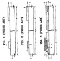
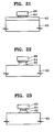
- FIGS. 1 to 4 are sectional views for explaining the method for manufacturing an LCD according to a conventional technology as disclosed in U.S. Patent No. 5,054,887.
- reference characters A and B denote a TFT area and a pad area, respectively.
- gate patterns 4 and 4a are formed by performing a first photolithography step on the first metal film.
- the gate patterns are used as a gate electrode 4 in the TFT area and as a gate pad 4a in the pad area.
- an anodized film 6 is formed by oxidizing the first metal film using the photoresist pattern as an anti-oxidation film. At this time, the anodized film 6 is formed on the entire surface of the gate electrode 4 formed in the TFT area and on a portion of the gate pad 4a in the pad area.
- an insulating film 8 is formed by depositing, for example, a nitride film on the entire surface of the substrate 2 having the anodized film thereon. Then, after forming a semiconductor film by subsequently depositing an amorphous silicon film 10 and an amorphous silicon film 12 doped with impurities on the entire surface of the substrate 2 on which the insulating film 8 is formed, a semiconductor film pattern 10 and 12 to be used as an active portion is formed in the TFT area by performing a third photolithography step on the semiconductor film.
- a photoresist pattern (not shown) is formed which exposes a portion of the gate pad 4a formed in the pad area by performing a fourth photolithography step on the entire surface of the substrate 2 on which the semiconductor film pattern is formed.
- a contact hole which exposes a portion of the gate pad 4a is then formed by etching the insulating film 8 using the photoresist pattern as a mask.
- a source electrode 14a and a drain electrode 14b are formed in the TFT area by depositing a Cr film on the entire surface of the substrate having the contact hole thereon and performing a fifth photolithography step on the Cr film.
- a pad electrode 14c connected to the gate pad 4a through the contact hole is formed.
- the impurity doped-amorphous silicon film 12 on the upper portion of the gate electrode 4 formed in the TFT area during the photolithography process is partially etched, thus exposing a portion of the amorphous silicon film 10.
- a protection film 16 is formed by depositing an oxide film on the entire surface of the substrate 2 on which the source electrode 14a, the drain electrode 14b and the pad electrode 14c are formed. Then, contact hole which exposes a portion of the drain electrode 14b of the TFT area and which expose a portion of the pad electrode 14c of the pad area are formed by performing a sixth photolithography step on the protection film.
- pixel electrodes 18 and 18a are formed by depositing indium tin oxide ITO, which is a transparent conductive material, on the entire surface of the substrate having the contact holes and performing a seventh photolithography step on the ITO film.
- ITO indium tin oxide
- the drain electrode 14b and the pixel electrode 18 are connected in the TFT area and the pad electrode 14c and the pixel electrode 18a are connected in the pad area.
- pure Al is used as the gate electrode material for lowering the resistance of a gate line. Therefore, an anodizing process is required to prevent a hillock caused by the Al, thus complicating the manufacturing process, reducing productivity, and increasing manufacturing costs.
- an improved method for manufacturing a liquid crystal display comprising the steps of forming a gate electrode and a gate pad by sequentially depositing a first metal film and a second metal film on a substrate of a TFT area and a pad area, respectively, by a first photolithography process, forming an insulating film on the entire surface of the substrate on which the gate electrode and the gate pad are formed, forming a semiconductor film pattern on the insulating film of the TFT are using a second photolithography process, forming a source electrode and a drain electrode composed of a third metal film in the TFT area using a third photolithography process, forming a protection film pattern which exposes a portion of the drain electrode and a portion of the gate pad on the substrate on which the source electrode and the drain electrode are formed using a fourth photolithography process, and forming a pixel electrode connected to the drain electrode and the gate pad on the substrate on which the protection film pattern is formed using a fifth photolithography process.
- the first metal film is preferably formed of Al or Al alloy and the second metal film is preferably formed of one metal selected from the group consisting of Cr, Ta, Mo, and Ti.
- the step of forming the gate electrode includes the steps of forming the first metal film and the second metal film on a substrate in the described order, forming a photoresist pattern on a portion of the second metal film, etching the second metal film using the photoresist pattern as a mask, reflowing the photoresist pattern, etching the first metal film using the reflowed photoresist pattern as a mask, and removing the reflowed photoresist pattern.
- the second metal film is overetched in the step of etching the second metal film to generate an undercut.
- the step of reflowing the photoresist pattern are performed in multiple steps.
- the step of forming the gate electrode preferably includes the steps of forming the first metal film and the second metal film on the substrate in the described order, forming a photoresist pattern on a portion of the second metal film, etching the second metal film by dry etching using the photoresist pattern as a mask, and etching the first metal film.
- the second metal film is preferably wet or dry etched and the step of baking the photoresist pattern is preferably further comprised after the step of etching the second metal film.
- the step of forming the gate electrode preferably includes the steps of forming the first metal film and the second metal film on a substrate, forming a photoresist pattern on a portion of the second metal film, etching the second metal film using the photoresist pattern as a mask, etching the first metal film using the patterned second metal film, and re-etching the patterned second metal film.
- the step of baking the photoresist pattern is preferably further comprised prior to the step of etching the first metal film after etching the second metal film.
- the gate electrode in a double structure of Al or an Al alloy and a refractory metal film. Also, it is possible to omit the anodizing process and to simultaneously etch the insulating layer and the protection film due to a capping film, thus reducing the number of the photolithography processes. Also, since it is possible to form the first metal film larger than or identical to the second metal film, an undercut is not generated in the gate electrode. Therefore, it is possible to prevent the deterioration of insulation characteristics due to poor step coverage during deposition of the insulating film after forming the gate electrode.
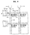
- FIG. 6 is a schematic plan view of the mask patterns used for manufacturing a liquid crystal display according to embodiments of the present invention, in which reference numeral 100 denotes a mask pattern for forming a gateline, reference numeral 105 denotes a mask pattern for forming a gate pad, reference numeral 110 denotes a mask pattern for forming a data line, reference numeral 120 denotes a mask pattern for forming a semiconductor film, reference numeral 130 denotes a mask pattern for forming a source electrode/drain electrode, reference numeral 140 denotes a mask pattern for forming a contact hole for connecting a pixel electrode to the drain electrode in the TFT area, reference numeral 145 denotes a mask pattern for forming a contact hole for connecting a gate pad in the pad area to the pixel electrode, reference numeral 150 denotes a mask pattern for forming a pixel electrode in the TFT area, and reference numeral 155 denotes a mask pattern for forming a pixel electrode in the pad portion.
- the gate line 100 is horizontally arranged, the data line 110 is arranged in a matrix pattern perpendicular to the gate line, the gate pad 105 is provided at the end portion of the gate line 100, and the data pad 115 is provided at the end portion of the data line.
- Pixel portions are respectively arranged in the matrix pattern in the portion bounded by the two adjacent gate lines and the data line.
- the gate electrodes of the respective TFTs are formed so as to protrude to the pixel portions from the respective gate lines.
- the semiconductor film 120 is formed between the drain electrodes of the respective TFTs and the gate electrodes of the respective TFTs.
- the source electrodes of the TFTs are formed in protruding portions from the data line 110.
- the pixel electrodes 150 composed of the transparent ITO are formed in the respective pixel portions.
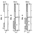
- FIGS. 7 through 11 are sectional views for explaining a method for manufacturing a liquid crystal display according to a first embodiment of the present invention.
- Reference character C represents the TFT area, which is a sectional view taken along I-I' of FIG. 6 and reference character D represents the pad area, which is a sectional view taken along II-II' of FIG. 6.
- FIG. 7 shows the steps for forming the gate electrode, in which a first metal film 22 is formed by depositing an Al or an Al alloy film to a thickness of 2,000-4,000 ⁇ on a transparent substrate 20. Then, a second metal film 24 is formed by depositing a refractory metal film to a thickness 500-2,000 ⁇ on the first metal film. Then, gate patterns are formed in the TFT area and the pad area by performing a first photolithography step on the first and the second metal films 22 and 24. The gate patterns are used as a gate electrode in the TFT area and used as a gate pad in the pad area. At this time, the first and the second metal films are wet or dry etched using a mask.
- the first metal film 22 is formed of Al or an Al alloy such as Al-Nd or Al-Ta. It is possible to lower the resistance of the gate line and to prevent generation of a hillock when the gate electrode is formed of such an Al alloy.
- the second metal film 24, which is a capping film to prevent the Al alloy from contacting the ITO film to be formed in a subsequent process, is formed of one refractory metal selected from the group consisting of Cr, Ta, Mo, and Ti. Due to the capping film on the Al or Al alloy, a high temperature oxidation process and a photolithography process for forming an oxidized film are not required. Also, since the second metal film 24 does not include Al, a battery effect generated in the conventional technology does not arise even though the second metal film 24 directly contacts the ITO film to be formed in a subsequent process.
- FIG. 8 shows the steps for forming a semiconductor film pattern, in which an insulating film 26 is formed by depositing a nitride film to a thickness of about 4,000 ⁇ on the entire surface of the substrate on which a gate pattern is formed. Subsequently, a semiconductor film composed of an amorphous silicon film 28 and an impurity doped-amorphous silicon film 30 is formed to a thickness of 1,000-2,000 ⁇ and a thickness of 500 ⁇ on the insulating layer 26. Then, the semiconductor film pattern to be used as an active area is formed in the TFT area by performing a second photolithography step on the semiconductor film.
- FIG. 9 shows the steps for forming a source electrode and a drain electrode.
- a third metal film is formed by depositing a Cr film to a thickness of 1,000-2,000 ⁇ on the entire surface of the substrate 20 on which the semiconductor film pattern is formed by a sputtering method.
- a source electrode 32a and a drain electrode 32b are then formed in the TFT area by performing a third photolithography step on the third metal film.
- FIG. 10 shows the steps for forming a protection film pattern.
- the protection film is formed by depositing an insulating material, e.g., an oxide film, to a thickness of 1,000-3,000 ⁇ on the entire surface of the substrate on which the source electrode 32a and the drain electrode 32b are formed.
- a protection film pattern 34 which exposes a portion of the drain electrode 32b and a portion of the gate electrode 22 and 24 formed in the pad area, i.e., a gate pad, is formed by performing a fourth photolithography step on the protection film.
- the protection film 34 and the insulating film 26 which are formed on the gate pad are etched simultaneously.
- FIG. 11 shows the steps for forming a pixel electrode.
- the ITO film which is a transparent conductive film
- pixel electrodes 36 and 36a are formed in the TFT area and the pad area by performing a fifth photolithography step on the ITO film.
- the pixel electrode 36 and the drain electrode 32b are connected in the TFT area and the pixel electrode 36a and the gate pad 22 and 24 are connected in the pad area.
- a battery effect and an Al hillock caused by contact of the Al to the ITO is prevented by forming a gate electrode using an Al or Al alloy and by forming a capping film on the gate electrode using a refractory metal. Also, it is possible to reduce the number of photolithography processes by omitting the anodizing process and simultaneously forming the contact on the insulating film and the protection film.
- the first metal film 22 and the second metal film 24 which constitute the gate electrode in the first embodiment of the present invention are etched using only one mask. Therefore, an undercut may be generated in the gate electrode as shown in FIG. 12. As a result, step coverage becomes poor in a subsequent insulating film depositing process, thus creating a risk of deteriorating insulation characteristics.
- a method for preventing the generation of the undercut in the gate electrode is provided.
- FIGS. 13 through 16 are sectional views for explaining a method for manufacturing a liquid crystal display according to a second embodiment of the present invention. Here, the initial steps through the step of forming the gate electrode are shown.
- FIG. 13 shows the step of forming the conductive films for the gate electrode.
- a first metal film 42 is formed by depositing an Al or Al alloy film to a thickness of 2,000 ⁇ 4,000 ⁇ on a transparent substrate 40.
- a second metal film 44 to be used as a capping film is formed by depositing a refractory metal, such as Cr, Ta, Mo, or Ti, preferably Cr, on the first metal film 42.
- a refractory metal such as Cr, Ta, Mo, or Ti, preferably Cr
- Al-Nd or Al-Ta can be used as the Al alloy.
- FIG. 14 shows the step of forming a photoresist pattern 46.
- a photoresist pattern 46 is formed by coating photoresist on the second metal film 44 and exposing and developing the photoresist. Then, a second metal film 44 is etched using the photoresist pattern 46 as a mask. At this time, an undercut is generated in the second metal film 44 by sufficiently overetching the second metal film.
- FIG. 15 shows the step of reflowing the photoresist.
- the substrate is heated to a temperature above 100°C to reflow the photoresist.
- a heat treatment may be performed on the substrate over multiple steps in order to improve the reflow characteristic of the photoresist.
- the patterned second metal film 44 is completely covered by the reflowed photoresist 46a.
- FIG. 16 shows the steps of forming the gate electrode.
- a photoresist pattern is removed after etching the first metal film 42 using the reflowed photoresist pattern 46a of FIG. 15 as a mask.
- the step coverage of the insulating film is favorably formed in a subsequent insulating film depositing process.
- FIGS. 17 through 19 are sectional views for explaining a method for manufacturing a liquid crystal display according to a third embodiment of the present invention. Here, the initial steps through the step of forming the gate electrode are shown.
- FIG. 17 shows the step of forming conductive films 52 and 54 for the gate electrode and a photoresist pattern 56, which is identical to the second embodiment in FIG. 13 of the present invention.
- FIG. 18 shows the step of patterning the second metal film 54, in which the second metal film 54 is wet or dry etched using the photoresist pattern 56 of FIG. 17 as a mask. Then, the photoresist pattern is removed.
- the photoresist pattern is not necessarily removed in this step and may instead be removed after etching the first metal film 52.
- an undercut may be generated to narrow the width of the first metal film to be etched later.
- baking may be performed on the photoresist pattern to prevent lifting of the photoresist pattern.
- FIG. 19 shows the step of forming the gate electrode by etching the first metal film 52, in which the first metal film 52 is etched using the patterned second metal film 54 as a mask.
- the photoresist pattern can be used as a mask and the photoresist pattern is removed after etching the first metal film.
- FIGS. 20 through 23 are sectional views for explaining a method for manufacturing a liquid crystal display according to a fourth embodiment of the present invention. Here, the initial steps through the step of forming the gate electrode are shown.
- FIG. 20 shows the steps of forming conductive films 62 and 64 for the gate electrode and a photoresist pattern 66, which are identical to those of the second and the third embodiments.
- FIG. 21 shows the step of etching the second metal film, in which the second metal film 64 is wet etched using the photoresist pattern 66 as a mask. At this time, the second metal film is sufficiently etched so as to generate an undercut.
- FIG. 22 shows the step of etching the first metal film, in which the undercut is formed in the gate electrode as shown in FIG. 12 when the first metal film 62 is wet etched using the patterned second metal film 64 as a mask.
- FIG. 23 shows the step of re-etching the second metal film, in which the width of the lower portion of the first metal film 62 becomes wider than that of the second metal film 64 when the patterned second metal metal film 64 is re-etched, thus the undercut of the gate electrode is removed.
- baking may be performed on the second metal film 64 after performing the first etching on the second metal film 64, considering the case in which the lifting of the photoresist is generated.
- the gate electrode is formed in a two-layered-structure of Al or Al alloy and a refractory metal. Therefore, it is possible to prevent a battery effect caused by directly contacting the Al to the ITO layer and to prevent the generation of a hillock of the Al due to stress relaxation of the refractory metal. Also, it is possible to reduce the number of photolithography processes since it is possible to omit the anodizing process because of the refractory metal and to etch simultaneously the insulating film and the protection film.
Landscapes
- Physics & Mathematics (AREA)
- Nonlinear Science (AREA)
- Mathematical Physics (AREA)
- Chemical & Material Sciences (AREA)
- Crystallography & Structural Chemistry (AREA)
- General Physics & Mathematics (AREA)
- Optics & Photonics (AREA)
- Engineering & Computer Science (AREA)
- Microelectronics & Electronic Packaging (AREA)
- Liquid Crystal (AREA)
- Thin Film Transistor (AREA)
- Electrodes Of Semiconductors (AREA)
- Internal Circuitry In Semiconductor Integrated Circuit Devices (AREA)
- Devices For Indicating Variable Information By Combining Individual Elements (AREA)
Priority Applications (1)
| Application Number | Priority Date | Filing Date | Title |
|---|---|---|---|
| EP03076155A EP1338914A3 (de) | 1995-11-21 | 1996-11-19 | Verfahren zur Herstellung von Flüssigkristallanzeigevorrichtungen |
Applications Claiming Priority (4)
| Application Number | Priority Date | Filing Date | Title |
|---|---|---|---|
| KR1019950042618A KR0183757B1 (ko) | 1995-11-21 | 1995-11-21 | 박막 트랜지스터-액정 표시장치의 제조방법 |
| KR9542618 | 1995-11-21 | ||
| KR9613912 | 1996-04-30 | ||
| KR1019960013912A KR100219480B1 (ko) | 1995-11-29 | 1996-04-30 | 박막트랜지스터 액정표시장치 및 그 제조방법 |
Related Child Applications (1)
| Application Number | Title | Priority Date | Filing Date |
|---|---|---|---|
| EP03076155A Division EP1338914A3 (de) | 1995-11-21 | 1996-11-19 | Verfahren zur Herstellung von Flüssigkristallanzeigevorrichtungen |
Publications (3)
| Publication Number | Publication Date |
|---|---|
| EP0775931A2 true EP0775931A2 (de) | 1997-05-28 |
| EP0775931A3 EP0775931A3 (de) | 1998-03-25 |
| EP0775931B1 EP0775931B1 (de) | 2005-10-05 |
Family
ID=36627376
Family Applications (2)
| Application Number | Title | Priority Date | Filing Date |
|---|---|---|---|
| EP03076155A Withdrawn EP1338914A3 (de) | 1995-11-21 | 1996-11-19 | Verfahren zur Herstellung von Flüssigkristallanzeigevorrichtungen |
| EP96308344A Expired - Lifetime EP0775931B1 (de) | 1995-11-21 | 1996-11-19 | Verfahren zur Herstellung einer Flüssigkristall-Anzeige |
Family Applications Before (1)
| Application Number | Title | Priority Date | Filing Date |
|---|---|---|---|
| EP03076155A Withdrawn EP1338914A3 (de) | 1995-11-21 | 1996-11-19 | Verfahren zur Herstellung von Flüssigkristallanzeigevorrichtungen |
Country Status (5)
| Country | Link |
|---|---|
| US (5) | US6008065A (de) |
| EP (2) | EP1338914A3 (de) |
| JP (5) | JP3891617B2 (de) |
| DE (1) | DE69635239T2 (de) |
| TW (1) | TW426809B (de) |
Cited By (7)
| Publication number | Priority date | Publication date | Assignee | Title |
|---|---|---|---|---|
| GB2320766A (en) * | 1996-12-30 | 1998-07-01 | Lg Electronics Inc | Liquid crystal displays |
| FR2775386A1 (fr) * | 1998-02-20 | 1999-08-27 | Lg Electronics Inc | Afficheur a cristal liquide et son procede de fabrication |
| USRE39211E1 (en) * | 1995-12-28 | 2006-08-01 | Samsung Electronics Co., Ltd. | Method for manufacturing a liquid crystal display |
| US7189998B2 (en) * | 1998-10-29 | 2007-03-13 | Samsung Electronics Co., Ltd. | Thin film transistor array panel for a liquid crystal display |
| US8368076B2 (en) | 1999-07-22 | 2013-02-05 | Semiconductor Energy Laboratory Co., Ltd. | Contact structure and semiconductor device |
| EP2755083A1 (de) * | 2013-01-11 | 2014-07-16 | Beijing Boe Optoelectronics Technology Co. Ltd. | Arraysubstrat und Herstellungsverfahren dafür |
| CN111584520A (zh) * | 2020-05-25 | 2020-08-25 | 成都中电熊猫显示科技有限公司 | 阵列基板、显示面板以及阵列基板的制作方法 |
Families Citing this family (112)
| Publication number | Priority date | Publication date | Assignee | Title |
|---|---|---|---|---|
| JP3866783B2 (ja) * | 1995-07-25 | 2007-01-10 | 株式会社 日立ディスプレイズ | 液晶表示装置 |
| KR100190023B1 (ko) * | 1996-02-29 | 1999-06-01 | 윤종용 | 박막트랜지스터-액정표시장치 및 그 제조방법 |
| CN1148600C (zh) * | 1996-11-26 | 2004-05-05 | 三星电子株式会社 | 薄膜晶体管基片及其制造方法 |
| US6940566B1 (en) | 1996-11-26 | 2005-09-06 | Samsung Electronics Co., Ltd. | Liquid crystal displays including organic passivation layer contacting a portion of the semiconductor layer between source and drain regions |
| JP3760008B2 (ja) * | 1996-11-29 | 2006-03-29 | セイコーエプソン株式会社 | 液晶パネル用基板およびそれを用いた液晶パネル並びに投写型表示装置 |
| JPH10198292A (ja) | 1996-12-30 | 1998-07-31 | Semiconductor Energy Lab Co Ltd | 半導体装置およびその作製方法 |
| KR100392909B1 (ko) * | 1997-08-26 | 2004-03-22 | 엘지.필립스 엘시디 주식회사 | 박막트랜지스터및그의제조방법 |
| KR100248123B1 (ko) | 1997-03-04 | 2000-03-15 | 구본준 | 박막트랜지스터및그의제조방법 |
| KR100252306B1 (ko) * | 1997-07-04 | 2000-04-15 | 구본준, 론 위라하디락사 | 액티브 매트릭스 기판 및 그 제조방법 |
| KR100338008B1 (ko) * | 1997-11-20 | 2002-10-25 | 삼성전자 주식회사 | 질화 몰리브덴-금속 합금막과 그의 제조 방법, 액정표시장치용 배선과 그의 제조 방법 및 액정 표시 장치와 그의 제조방법 |
| JPH11258633A (ja) * | 1998-03-13 | 1999-09-24 | Toshiba Corp | 表示装置用アレイ基板の製造方法 |
| JPH11258632A (ja) * | 1998-03-13 | 1999-09-24 | Toshiba Corp | 表示装置用アレイ基板 |
| JP4458563B2 (ja) * | 1998-03-31 | 2010-04-28 | 三菱電機株式会社 | 薄膜トランジスタの製造方法およびこれを用いた液晶表示装置の製造方法 |
| KR100482167B1 (ko) * | 1998-07-30 | 2005-07-18 | 엘지.필립스 엘시디 주식회사 | 액정표시장치및그제조방법 |
| USRE39452E1 (en) * | 1998-08-28 | 2007-01-02 | Fujitsu Limited | TFT substrate with low contact resistance and damage resistant terminals |
| US6297519B1 (en) * | 1998-08-28 | 2001-10-02 | Fujitsu Limited | TFT substrate with low contact resistance and damage resistant terminals |
| US6368978B1 (en) * | 1999-03-04 | 2002-04-09 | Applied Materials, Inc. | Hydrogen-free method of plasma etching indium tin oxide |
| KR100333983B1 (ko) * | 1999-05-13 | 2002-04-26 | 윤종용 | 광시야각 액정 표시 장치용 박막 트랜지스터 어레이 기판 및그의 제조 방법 |
| TW428328B (en) * | 1999-07-30 | 2001-04-01 | Hannstar Display Corp | Fabricating method of thin film transistor |
| JP2001053283A (ja) | 1999-08-12 | 2001-02-23 | Semiconductor Energy Lab Co Ltd | 半導体装置及びその作製方法 |
| GB9919913D0 (en) * | 1999-08-24 | 1999-10-27 | Koninkl Philips Electronics Nv | Thin-film transistors and method for producing the same |
| KR100632216B1 (ko) * | 1999-12-16 | 2006-10-09 | 엘지.필립스 엘시디 주식회사 | 액정표시장치용 어레이 기판 및 그 제조방법 |
| KR100325079B1 (ko) * | 1999-12-22 | 2002-03-02 | 주식회사 현대 디스플레이 테크놀로지 | 고개구율 및 고투과율 액정표시장치의 제조방법 |
| KR100601177B1 (ko) * | 2000-02-10 | 2006-07-13 | 삼성전자주식회사 | 액정 표시 장치용 박막 트랜지스터 기판 및 그의 제조 방법 |
| US7023021B2 (en) | 2000-02-22 | 2006-04-04 | Semiconductor Energy Laboratory Co., Ltd. | Semiconductor device and method of manufacturing the same |
| JP4118484B2 (ja) | 2000-03-06 | 2008-07-16 | 株式会社半導体エネルギー研究所 | 半導体装置の作製方法 |
| JP2001257350A (ja) | 2000-03-08 | 2001-09-21 | Semiconductor Energy Lab Co Ltd | 半導体装置およびその作製方法 |
| JP4700160B2 (ja) | 2000-03-13 | 2011-06-15 | 株式会社半導体エネルギー研究所 | 半導体装置 |
| JP4118485B2 (ja) * | 2000-03-13 | 2008-07-16 | 株式会社半導体エネルギー研究所 | 半導体装置の作製方法 |
| JP4683688B2 (ja) | 2000-03-16 | 2011-05-18 | 株式会社半導体エネルギー研究所 | 液晶表示装置の作製方法 |
| JP4393662B2 (ja) | 2000-03-17 | 2010-01-06 | 株式会社半導体エネルギー研究所 | 液晶表示装置の作製方法 |
| JP2001281698A (ja) * | 2000-03-30 | 2001-10-10 | Advanced Display Inc | 電気光学素子の製法 |
| US6789910B2 (en) | 2000-04-12 | 2004-09-14 | Semiconductor Energy Laboratory, Co., Ltd. | Illumination apparatus |
| TW447138B (en) * | 2000-04-28 | 2001-07-21 | Unipac Optoelectronics Corp | Manufacturing method of thin-film transistor |
| JP2001343659A (ja) * | 2000-06-02 | 2001-12-14 | Casio Comput Co Ltd | アクティブマトリクス型液晶表示パネルおよびその製造方法 |
| US6900084B1 (en) | 2000-05-09 | 2005-05-31 | Semiconductor Energy Laboratory Co., Ltd. | Semiconductor device having a display device |
| US6798064B1 (en) * | 2000-07-12 | 2004-09-28 | Motorola, Inc. | Electronic component and method of manufacture |
| TWI253538B (en) * | 2000-09-30 | 2006-04-21 | Au Optronics Corp | Thin film transistor flat display and its manufacturing method |
| KR100400765B1 (ko) * | 2000-11-13 | 2003-10-08 | 엘지.필립스 엘시디 주식회사 | 박막 형성방법 및 이를 적용한 액정표시소자의 제조방법 |
| TW525216B (en) | 2000-12-11 | 2003-03-21 | Semiconductor Energy Lab | Semiconductor device, and manufacturing method thereof |
| KR100715943B1 (ko) * | 2001-01-29 | 2007-05-08 | 삼성전자주식회사 | 액정표시장치 및 그 제조방법 |
| JP4410951B2 (ja) * | 2001-02-27 | 2010-02-10 | Nec液晶テクノロジー株式会社 | パターン形成方法および液晶表示装置の製造方法 |
| SG160191A1 (en) | 2001-02-28 | 2010-04-29 | Semiconductor Energy Lab | Semiconductor device and manufacturing method thereof |
| US7071037B2 (en) | 2001-03-06 | 2006-07-04 | Semiconductor Energy Laboratory Co., Ltd. | Semiconductor device and manufacturing method thereof |
| KR100796749B1 (ko) | 2001-05-16 | 2008-01-22 | 삼성전자주식회사 | 액정 표시 장치용 박막 트랜지스터 어레이 기판 |
| JP4920140B2 (ja) | 2001-05-18 | 2012-04-18 | ゲットナー・ファンデーション・エルエルシー | 液晶表示装置及びその製造方法 |
| JP2003172946A (ja) * | 2001-09-28 | 2003-06-20 | Fujitsu Display Technologies Corp | 液晶表示装置用基板及びそれを用いた液晶表示装置 |
| JP4723787B2 (ja) * | 2002-07-09 | 2011-07-13 | シャープ株式会社 | 電界効果型トランジスタ、その製造方法及び画像表示装置 |
| KR100484092B1 (ko) * | 2002-12-26 | 2005-04-18 | 엘지.필립스 엘시디 주식회사 | 듀얼패널타입 유기전계발광 소자 및 그 제조방법 |
| KR100497095B1 (ko) * | 2002-12-26 | 2005-06-28 | 엘지.필립스 엘시디 주식회사 | 듀얼패널타입 유기전계발광 소자용 어레이 기판 및 그 제조방법 |
| KR100503129B1 (ko) * | 2002-12-28 | 2005-07-22 | 엘지.필립스 엘시디 주식회사 | 듀얼패널타입 유기전계발광 소자 및 그 제조방법 |
| KR100500147B1 (ko) | 2002-12-31 | 2005-07-07 | 엘지.필립스 엘시디 주식회사 | 유기전계 발광소자와 그 제조방법 |
| US7250720B2 (en) | 2003-04-25 | 2007-07-31 | Semiconductor Energy Laboratory Co., Ltd. | Display device |
| TW589663B (en) * | 2003-05-12 | 2004-06-01 | Au Optronics Corp | Flat panel display and manufacturing method thereof |
| JP4517063B2 (ja) * | 2003-05-27 | 2010-08-04 | 日本電気株式会社 | 液晶表示装置 |
| KR100566612B1 (ko) * | 2003-09-23 | 2006-03-31 | 엘지.필립스 엘시디 주식회사 | 다결정 실리콘 박막 트랜지스터 및 그 제조 방법 |
| JP3769564B2 (ja) * | 2003-10-06 | 2006-04-26 | セイコーエプソン株式会社 | 液晶パネル用基板およびそれを用いた液晶パネル並びに投写型表示装置 |
| KR101023978B1 (ko) * | 2004-03-18 | 2011-03-28 | 삼성전자주식회사 | 반투과 액정표시장치의 제조방법과 이에 의한 액정표시장치 |
| KR101087398B1 (ko) * | 2004-06-30 | 2011-11-25 | 엘지디스플레이 주식회사 | 액정표시장치의 패드 구조 및 그 제조방법 |
| KR101061850B1 (ko) * | 2004-09-08 | 2011-09-02 | 삼성전자주식회사 | 박막 트랜지스터 표시판 및 그 제조방법 |
| JP2006178426A (ja) * | 2004-11-24 | 2006-07-06 | Sanyo Electric Co Ltd | 表示装置および表示装置の製造方法 |
| US7049163B1 (en) * | 2005-03-16 | 2006-05-23 | Chunghwa Picture Tubes, Ltd. | Manufacture method of pixel structure |
| KR20060125066A (ko) * | 2005-06-01 | 2006-12-06 | 삼성전자주식회사 | 개구율이 향상된 어레이 기판 및 이의 제조방법 |
| KR20070009013A (ko) * | 2005-07-14 | 2007-01-18 | 삼성전자주식회사 | 평판표시장치 및 평판표시장치의 제조방법 |
| US7601566B2 (en) * | 2005-10-18 | 2009-10-13 | Semiconductor Energy Laboratory Co., Ltd. | Semiconductor device and manufacturing method thereof |
| JP2007114360A (ja) | 2005-10-19 | 2007-05-10 | Nec Lcd Technologies Ltd | 薄膜トランジスタを備えた液晶表示装置及びその製造方法 |
| JP4544532B2 (ja) * | 2006-03-03 | 2010-09-15 | 東京エレクトロン株式会社 | 基板処理方法 |
| JP4842709B2 (ja) * | 2006-05-31 | 2011-12-21 | 株式会社 日立ディスプレイズ | 表示装置の製造方法 |
| US7749907B2 (en) * | 2006-08-25 | 2010-07-06 | Semiconductor Energy Laboratory Co., Ltd. | Method for manufacturing semiconductor device |
| US7932183B2 (en) * | 2006-11-14 | 2011-04-26 | Mitsubishi Electric Corporation | Method of manufacturing multilayer thin film pattern and display device |
| KR20080078164A (ko) * | 2007-02-22 | 2008-08-27 | 삼성전자주식회사 | 액정 표시 장치의 제조 방법 |
| US8110829B2 (en) * | 2007-05-31 | 2012-02-07 | Lg Display Co., Ltd. | Array substrate of liquid crystal display and method for fabricating the same |
| US20090001373A1 (en) * | 2007-06-26 | 2009-01-01 | Kabushiki Kaisha Kobe Seiko Sho (Kobe Steel Ltd.) | Electrode of aluminum-alloy film with low contact resistance, method for production thereof, and display unit |
| JP5250832B2 (ja) * | 2007-07-09 | 2013-07-31 | ゴールドチャームリミテッド | アクティブマトリクス駆動表示装置 |
| KR101308534B1 (ko) * | 2007-07-18 | 2013-09-23 | 삼성디스플레이 주식회사 | 표시 기판 및 이의 제조 방법 |
| TWI348765B (en) * | 2007-08-29 | 2011-09-11 | Au Optronics Corp | Pixel structure and fabricating method for thereof |
| JP5380037B2 (ja) * | 2007-10-23 | 2014-01-08 | 株式会社半導体エネルギー研究所 | 半導体装置の作製方法 |
| KR101448903B1 (ko) | 2007-10-23 | 2014-10-13 | 가부시키가이샤 한도오따이 에네루기 켄큐쇼 | 반도체장치 및 그의 제작방법 |
| JP5357493B2 (ja) * | 2007-10-23 | 2013-12-04 | 株式会社半導体エネルギー研究所 | 半導体装置の作製方法 |
| JP5427390B2 (ja) | 2007-10-23 | 2014-02-26 | 株式会社半導体エネルギー研究所 | 半導体装置の作製方法 |
| EP2232561A4 (de) * | 2007-12-03 | 2015-05-06 | Semiconductor Energy Lab | Herstellungsverfahren für einen dünnfilmtransistor und herstellungsverfahren für eine display-anordnung |
| KR101446249B1 (ko) | 2007-12-03 | 2014-10-01 | 가부시키가이샤 한도오따이 에네루기 켄큐쇼 | 반도체장치 제조방법 |
| CN101217153B (zh) * | 2008-01-18 | 2012-02-29 | 友达光电股份有限公司 | 主动元件阵列结构及其制造方法 |
| US8035107B2 (en) * | 2008-02-26 | 2011-10-11 | Semiconductor Energy Laboratory Co., Ltd. | Method for manufacturing display device |
| WO2009107686A1 (en) | 2008-02-27 | 2009-09-03 | Semiconductor Energy Laboratory Co., Ltd. | Liquid crystal display device and manufacturing method thereof, and electronic device |
| US8101442B2 (en) * | 2008-03-05 | 2012-01-24 | Semiconductor Energy Laboratory Co., Ltd. | Method for manufacturing EL display device |
| US7749820B2 (en) * | 2008-03-07 | 2010-07-06 | Semiconductor Energy Laboratory Co., Ltd. | Thin film transistor, manufacturing method thereof, display device, and manufacturing method thereof |
| US7989275B2 (en) * | 2008-03-10 | 2011-08-02 | Semiconductor Energy Laboratory Co., Ltd. | Thin film transistor, manufacturing method thereof, display device, and manufacturing method thereof |
| US7883943B2 (en) | 2008-03-11 | 2011-02-08 | Semiconductor Energy Laboratory Co., Ltd. | Method for manufacturing thin film transistor and method for manufacturing display device |
| JP5364422B2 (ja) | 2008-04-17 | 2013-12-11 | 株式会社半導体エネルギー研究所 | 発光装置及びその作製方法 |
| US9041202B2 (en) | 2008-05-16 | 2015-05-26 | Semiconductor Energy Laboratory Co., Ltd. | Semiconductor device and manufacturing method of the same |
| US7790483B2 (en) * | 2008-06-17 | 2010-09-07 | Semiconductor Energy Laboratory Co., Ltd. | Thin film transistor and manufacturing method thereof, and display device and manufacturing method thereof |
| US20100138765A1 (en) * | 2008-11-30 | 2010-06-03 | Nokia Corporation | Indicator Pop-Up |
| US8207026B2 (en) * | 2009-01-28 | 2012-06-26 | Semiconductor Energy Laboratory Co., Ltd. | Manufacturing method of thin film transistor and manufacturing method of display device |
| JP5503995B2 (ja) * | 2009-02-13 | 2014-05-28 | 株式会社半導体エネルギー研究所 | 半導体装置の作製方法 |
| US7989234B2 (en) * | 2009-02-16 | 2011-08-02 | Semiconductor Energy Laboratory Co., Ltd. | Method for manufacturing thin film transistor and method for manufacturing display device |
| US8202769B2 (en) * | 2009-03-11 | 2012-06-19 | Semiconductor Energy Laboratory Co., Ltd. | Semiconductor device and manufacturing method thereof |
| JP5539765B2 (ja) * | 2009-03-26 | 2014-07-02 | 株式会社半導体エネルギー研究所 | トランジスタの作製方法 |
| US20120242624A1 (en) * | 2009-11-27 | 2012-09-27 | Sharp Kabushiki Kaisha | Thin film transistor and method for fabricating the same, semiconductor device and method for fabricating the same, as well as display |
| WO2011161714A1 (ja) | 2010-06-21 | 2011-12-29 | パナソニック株式会社 | シリコン薄膜の結晶化方法およびシリコンtft装置の製造方法 |
| TWM423257U (en) * | 2011-06-01 | 2012-02-21 | Chunghwa Picture Tubes Ltd | Pixel array substrate and display panel |
| CN102637632B (zh) * | 2011-06-10 | 2014-12-10 | 京东方科技集团股份有限公司 | 一种薄膜晶体管阵列的制作方法和薄膜晶体管阵列 |
| JP5411236B2 (ja) * | 2011-11-15 | 2014-02-12 | ゲットナー・ファンデーション・エルエルシー | 液晶表示装置及びその製造方法 |
| KR101932495B1 (ko) * | 2012-05-11 | 2018-12-27 | 삼성전자주식회사 | 반도체 패키지 및 반도체 패키지의 제조 방법 |
| CN102956551B (zh) * | 2012-11-02 | 2015-01-07 | 京东方科技集团股份有限公司 | 阵列基板的制作方法、阵列基板及显示装置 |
| TWI582967B (zh) * | 2014-04-01 | 2017-05-11 | 鴻海精密工業股份有限公司 | 顯示陣列基板及顯示陣列基板的製造方法 |
| CN103972243B (zh) * | 2014-04-24 | 2017-03-29 | 京东方科技集团股份有限公司 | 一种阵列基板及其制作方法、显示装置 |
| CN104375344B (zh) * | 2014-11-21 | 2017-09-15 | 深圳市华星光电技术有限公司 | 液晶显示面板及其彩膜阵列基板 |
| CN106057667B (zh) * | 2016-07-06 | 2019-02-05 | 京东方科技集团股份有限公司 | 膜层图案的制作方法、基板的制作方法及基板、显示装置 |
| CN107706196B (zh) * | 2017-09-28 | 2021-05-25 | 京东方科技集团股份有限公司 | 一种阵列基板及其制备方法、显示装置 |
| KR102708891B1 (ko) * | 2019-11-01 | 2024-09-25 | 삼성디스플레이 주식회사 | 광 센서의 제조 방법 |
| KR102920134B1 (ko) | 2020-02-07 | 2026-01-30 | 삼성디스플레이 주식회사 | 도전 패턴의 제조 방법, 표시 장치 및 이의 제조 방법 |
Citations (1)
| Publication number | Priority date | Publication date | Assignee | Title |
|---|---|---|---|---|
| US5054887A (en) | 1988-08-10 | 1991-10-08 | Sharp Kabushiki Kaisha | Active matrix type liquid crystal display |
Family Cites Families (54)
| Publication number | Priority date | Publication date | Assignee | Title |
|---|---|---|---|---|
| JPS5863150A (ja) | 1981-10-12 | 1983-04-14 | Oki Electric Ind Co Ltd | 半導体装置の製造方法 |
| JPS6144468A (ja) | 1984-08-09 | 1986-03-04 | Matsushita Electric Ind Co Ltd | 半導体装置およびその製造方法 |
| JPS61193128A (ja) * | 1985-02-21 | 1986-08-27 | Mitsubishi Electric Corp | マトリクス型表示装置 |
| JPS62285464A (ja) * | 1986-06-03 | 1987-12-11 | Matsushita Electric Ind Co Ltd | 薄膜トランジスタアレイ基板及びその製造方法 |
| US6149988A (en) * | 1986-09-26 | 2000-11-21 | Semiconductor Energy Laboratory Co., Ltd. | Method and system of laser processing |
| JPH061314B2 (ja) * | 1987-07-30 | 1994-01-05 | シャープ株式会社 | 薄膜トランジスタアレイ |
| JPS6484668A (en) | 1987-09-26 | 1989-03-29 | Casio Computer Co Ltd | Thin film transistor |
| GB2211362A (en) * | 1987-10-15 | 1989-06-28 | Johnson Electric Ind Mfg | Fuel pump motor |
| JP2786628B2 (ja) * | 1987-10-15 | 1998-08-13 | シャープ株式会社 | 液晶パネルの電極構造 |
| JPH01151236A (ja) * | 1987-12-08 | 1989-06-14 | Mitsubishi Electric Corp | アルミニウム膜のテーパーエツチング方法 |
| JP2771820B2 (ja) * | 1988-07-08 | 1998-07-02 | 株式会社日立製作所 | アクティブマトリクスパネル及びその製造方法 |
| US5153754A (en) | 1989-06-30 | 1992-10-06 | General Electric Company | Multi-layer address lines for amorphous silicon liquid crystal display devices |
| JPH0734467B2 (ja) * | 1989-11-16 | 1995-04-12 | 富士ゼロックス株式会社 | イメージセンサ製造方法 |
| JP2940689B2 (ja) | 1990-03-23 | 1999-08-25 | 三洋電機株式会社 | アクティブマトリクス型表示装置の薄膜トランジスタアレイ及びその製造方法 |
| JP2813234B2 (ja) | 1990-05-16 | 1998-10-22 | 日本電信電話株式会社 | 配線構造 |
| US5162933A (en) | 1990-05-16 | 1992-11-10 | Nippon Telegraph And Telephone Corporation | Active matrix structure for liquid crystal display elements wherein each of the gate/data lines includes at least a molybdenum-base alloy layer containing 0.5 to 10 wt. % of chromium |
| US5156986A (en) | 1990-10-05 | 1992-10-20 | General Electric Company | Positive control of the source/drain-gate overlap in self-aligned TFTS via a top hat gate electrode configuration |
| JPH04155315A (ja) | 1990-10-19 | 1992-05-28 | Hitachi Ltd | 多層膜配線体の製造方法 |
| JPH04213427A (ja) | 1990-12-11 | 1992-08-04 | Fujitsu Ltd | 多層金属膜電極配線の製造方法 |
| JPH04234930A (ja) * | 1991-01-10 | 1992-08-24 | Shimano Inc | 釣り用リール |
| US5468987A (en) * | 1991-03-06 | 1995-11-21 | Semiconductor Energy Laboratory Co., Ltd. | Semiconductor device and method for forming the same |
| JPH04326330A (ja) | 1991-04-26 | 1992-11-16 | Sharp Corp | 液晶表示装置およびその製造方法 |
| JP2667304B2 (ja) | 1991-05-13 | 1997-10-27 | シャープ株式会社 | アクティブマトリクス基板 |
| US5334859A (en) * | 1991-09-05 | 1994-08-02 | Casio Computer Co., Ltd. | Thin-film transistor having source and drain electrodes insulated by an anodically oxidized film |
| JP3094610B2 (ja) | 1991-12-13 | 2000-10-03 | カシオ計算機株式会社 | 薄膜トランジスタの製造方法 |
| JPH05142570A (ja) | 1991-11-20 | 1993-06-11 | Sharp Corp | アクテイブマトリクス基板 |
| JPH05142554A (ja) * | 1991-11-25 | 1993-06-11 | Matsushita Electric Ind Co Ltd | アクテイブマトリクス基板 |
| JPH05165056A (ja) | 1991-12-17 | 1993-06-29 | Oki Electric Ind Co Ltd | アクティブマトリックス液晶ディスプレイの下基板の製造方法 |
| JP2674406B2 (ja) * | 1992-02-05 | 1997-11-12 | 富士通株式会社 | 半導体装置の製造方法 |
| TW223178B (en) * | 1992-03-27 | 1994-05-01 | Semiconductor Energy Res Co Ltd | Semiconductor device and its production method |
| JPH05299655A (ja) * | 1992-04-08 | 1993-11-12 | Nec Corp | 薄膜トランジスタ |
| JPH05323373A (ja) | 1992-05-22 | 1993-12-07 | Fujitsu Ltd | 薄膜トランジスタパネルの製造方法 |
| JPH063698A (ja) * | 1992-06-19 | 1994-01-14 | Nec Corp | 薄膜トランジスタ装置 |
| KR950008931B1 (ko) * | 1992-07-22 | 1995-08-09 | 삼성전자주식회사 | 표시패널의 제조방법 |
| JPH06232398A (ja) * | 1992-12-15 | 1994-08-19 | Matsushita Electric Ind Co Ltd | 薄膜トランジスタの製造方法と半導体装置の製造方法 |
| JPH06140296A (ja) | 1992-10-26 | 1994-05-20 | Fujitsu Ltd | パターン形成方法 |
| JPH06138487A (ja) | 1992-10-29 | 1994-05-20 | Hitachi Ltd | 半導体装置と液晶表示装置 |
| JPH06160905A (ja) * | 1992-11-26 | 1994-06-07 | Sanyo Electric Co Ltd | 液晶表示装置およびその製造方法 |
| JPH06168970A (ja) * | 1992-11-27 | 1994-06-14 | Fuji Xerox Co Ltd | 半導体素子の製造方法 |
| JPH06188419A (ja) * | 1992-12-16 | 1994-07-08 | Matsushita Electric Ind Co Ltd | 薄膜トランジスタの製造方法 |
| JP3098345B2 (ja) * | 1992-12-28 | 2000-10-16 | 富士通株式会社 | 薄膜トランジスタマトリクス装置及びその製造方法 |
| JP3116149B2 (ja) * | 1993-01-18 | 2000-12-11 | 株式会社日立製作所 | 配線材料および液晶表示装置 |
| JP3573778B2 (ja) * | 1993-03-12 | 2004-10-06 | 株式会社東芝 | 液晶表示装置 |
| JP2948436B2 (ja) * | 1993-03-12 | 1999-09-13 | ローム株式会社 | 薄膜トランジスタおよびそれを用いる液晶表示装置 |
| US5663077A (en) * | 1993-07-27 | 1997-09-02 | Semiconductor Energy Laboratory Co., Ltd. | Method of manufacturing a thin film transistor in which the gate insulator comprises two oxide films |
| JP2501411B2 (ja) | 1993-08-12 | 1996-05-29 | 株式会社東芝 | アクティブマトリクス型表示装置 |
| JP3281167B2 (ja) | 1994-03-17 | 2002-05-13 | 富士通株式会社 | 薄膜トランジスタの製造方法 |
| US5621556A (en) * | 1994-04-28 | 1997-04-15 | Xerox Corporation | Method of manufacturing active matrix LCD using five masks |
| JP2755376B2 (ja) * | 1994-06-03 | 1998-05-20 | 株式会社フロンテック | 電気光学素子の製造方法 |
| US5738948A (en) | 1994-09-29 | 1998-04-14 | Kabushiki Kaisha Toshiba | Electrode-wiring material and electrode-wiring substrate using the same |
| JPH0964366A (ja) * | 1995-08-23 | 1997-03-07 | Toshiba Corp | 薄膜トランジスタ |
| KR100190041B1 (ko) * | 1995-12-28 | 1999-06-01 | 윤종용 | 액정표시장치의 제조방법 |
| JP4366732B2 (ja) * | 1998-09-30 | 2009-11-18 | ソニー株式会社 | 電気光学装置の製造方法及び電気光学装置用の駆動基板の製造方法 |
| US6368227B1 (en) * | 2000-11-17 | 2002-04-09 | Steven Olson | Method of swinging on a swing |
-
1996
- 1996-11-19 EP EP03076155A patent/EP1338914A3/de not_active Withdrawn
- 1996-11-19 EP EP96308344A patent/EP0775931B1/de not_active Expired - Lifetime
- 1996-11-19 DE DE69635239T patent/DE69635239T2/de not_active Expired - Lifetime
- 1996-11-20 JP JP30947296A patent/JP3891617B2/ja not_active Expired - Lifetime
- 1996-11-21 US US08/754,644 patent/US6008065A/en not_active Expired - Lifetime
- 1996-11-21 TW TW085114339A patent/TW426809B/zh not_active IP Right Cessation
-
1999
- 1999-09-08 US US09/391,454 patent/US6339230B1/en not_active Expired - Lifetime
- 1999-11-19 US US09/443,386 patent/US6331443B1/en not_active Expired - Lifetime
-
2002
- 2002-01-02 US US10/032,443 patent/US6661026B2/en not_active Ceased
-
2003
- 2003-07-22 JP JP2003199728A patent/JP2004006936A/ja active Pending
-
2004
- 2004-01-05 JP JP2004000525A patent/JP2004157554A/ja active Pending
-
2005
- 2005-12-08 US US11/296,847 patent/USRE41363E1/en not_active Expired - Lifetime
- 2005-12-21 JP JP2005368671A patent/JP2006106788A/ja active Pending
- 2005-12-21 JP JP2005368670A patent/JP2006148150A/ja active Pending
Patent Citations (1)
| Publication number | Priority date | Publication date | Assignee | Title |
|---|---|---|---|---|
| US5054887A (en) | 1988-08-10 | 1991-10-08 | Sharp Kabushiki Kaisha | Active matrix type liquid crystal display |
Cited By (13)
| Publication number | Priority date | Publication date | Assignee | Title |
|---|---|---|---|---|
| USRE39211E1 (en) * | 1995-12-28 | 2006-08-01 | Samsung Electronics Co., Ltd. | Method for manufacturing a liquid crystal display |
| GB2320766A (en) * | 1996-12-30 | 1998-07-01 | Lg Electronics Inc | Liquid crystal displays |
| FR2758006A1 (fr) * | 1996-12-30 | 1998-07-03 | Lg Electronics Inc | Dispositif d'affichage a cristaux liquides et son procede de fabrication |
| GB2320766B (en) * | 1996-12-30 | 1999-08-11 | Lg Electronics Inc | Liquid crystal displays |
| FR2775386A1 (fr) * | 1998-02-20 | 1999-08-27 | Lg Electronics Inc | Afficheur a cristal liquide et son procede de fabrication |
| US7189998B2 (en) * | 1998-10-29 | 2007-03-13 | Samsung Electronics Co., Ltd. | Thin film transistor array panel for a liquid crystal display |
| US8368076B2 (en) | 1999-07-22 | 2013-02-05 | Semiconductor Energy Laboratory Co., Ltd. | Contact structure and semiconductor device |
| US8624253B2 (en) | 1999-07-22 | 2014-01-07 | Semiconductor Energy Laboratory Co., Ltd. | Contact structure and semiconductor device |
| EP2755083A1 (de) * | 2013-01-11 | 2014-07-16 | Beijing Boe Optoelectronics Technology Co. Ltd. | Arraysubstrat und Herstellungsverfahren dafür |
| US9099312B2 (en) | 2013-01-11 | 2015-08-04 | Beijing Boe Optoelectronics Technology Co., Ltd. | Array substrate and manufacturing method thereof |
| KR101543929B1 (ko) | 2013-01-11 | 2015-08-11 | 베이징 비오이 옵토일렉트로닉스 테크놀로지 컴퍼니 리미티드 | 어레이 기판 및 그 제조 방법 |
| CN111584520A (zh) * | 2020-05-25 | 2020-08-25 | 成都中电熊猫显示科技有限公司 | 阵列基板、显示面板以及阵列基板的制作方法 |
| CN111584520B (zh) * | 2020-05-25 | 2023-09-12 | 成都京东方显示科技有限公司 | 阵列基板、显示面板以及阵列基板的制作方法 |
Also Published As
| Publication number | Publication date |
|---|---|
| EP0775931A3 (de) | 1998-03-25 |
| EP1338914A2 (de) | 2003-08-27 |
| USRE41363E1 (en) | 2010-06-01 |
| TW426809B (en) | 2001-03-21 |
| JP2006106788A (ja) | 2006-04-20 |
| EP0775931B1 (de) | 2005-10-05 |
| US20020106825A1 (en) | 2002-08-08 |
| JP2004006936A (ja) | 2004-01-08 |
| US6661026B2 (en) | 2003-12-09 |
| JPH09171197A (ja) | 1997-06-30 |
| DE69635239D1 (de) | 2005-11-10 |
| DE69635239T2 (de) | 2006-07-06 |
| US6331443B1 (en) | 2001-12-18 |
| US6339230B1 (en) | 2002-01-15 |
| JP2006148150A (ja) | 2006-06-08 |
| EP1338914A3 (de) | 2003-11-19 |
| US6008065A (en) | 1999-12-28 |
| JP3891617B2 (ja) | 2007-03-14 |
| JP2004157554A (ja) | 2004-06-03 |
Similar Documents
| Publication | Publication Date | Title |
|---|---|---|
| EP0775931B1 (de) | Verfahren zur Herstellung einer Flüssigkristall-Anzeige | |
| USRE39211E1 (en) | Method for manufacturing a liquid crystal display | |
| US6081308A (en) | Method for manufacturing liquid crystal display | |
| EP0338766B1 (de) | Verfahren zur Herstellung eines aktiven Matrixsubstrats | |
| JP4169896B2 (ja) | 薄膜トランジスタとその製造方法 | |
| US5976902A (en) | Method of fabricating a fully self-aligned TFT-LCD | |
| CN108803168B (zh) | 一种阵列基板及其制作方法、液晶显示装置 | |
| KR0171980B1 (ko) | 액정 표시 소자의 제조방법 | |
| KR19980025840A (ko) | 액정 표시장치의 제조방법 | |
| KR100430950B1 (ko) | 박막트랜지스터 및 그 제조방법 | |
| KR100219480B1 (ko) | 박막트랜지스터 액정표시장치 및 그 제조방법 | |
| JPH10301127A (ja) | 透明導電膜のパターニング方法 | |
| US7561223B2 (en) | Device and method for protecting gate terminal and lead | |
| KR0183757B1 (ko) | 박막 트랜지스터-액정 표시장치의 제조방법 | |
| KR960012270B1 (ko) | 투명 도전성기관 제조방법 | |
| JPH06130405A (ja) | 液晶表示装置の製造方法 | |
| KR950003942B1 (ko) | 액정표시장치의 박막트랜지스터의 제조방법 | |
| JPH04357832A (ja) | エッチング方法および薄膜トランジスタの製造方法 | |
| KR100265053B1 (ko) | 표시패널 및 그 제조방법 | |
| KR20020080866A (ko) | 박막 트랜지스터 액정표시장치의 제조방법 | |
| JPH05226658A (ja) | 薄膜トランジスタ | |
| KR19990009763A (ko) | 단일막 게이트 라인을 갖는 박막 트랜지스터 기판 및 그 제조 방법 | |
| JPH0756894B2 (ja) | 薄膜トランジスタの製造方法 | |
| KR20010108833A (ko) | 박막 트랜지스터의 제조 방법 | |
| KR20020095506A (ko) | 액정표시장치의 제조방법 |
Legal Events
| Date | Code | Title | Description |
|---|---|---|---|
| PUAI | Public reference made under article 153(3) epc to a published international application that has entered the european phase |
Free format text: ORIGINAL CODE: 0009012 |
|
| AK | Designated contracting states |
Kind code of ref document: A2 Designated state(s): DE FR GB |
|
| 17P | Request for examination filed |
Effective date: 19971001 |
|
| PUAL | Search report despatched |
Free format text: ORIGINAL CODE: 0009013 |
|
| AK | Designated contracting states |
Kind code of ref document: A3 Designated state(s): DE FR GB |
|
| 17Q | First examination report despatched |
Effective date: 20020514 |
|
| GRAP | Despatch of communication of intention to grant a patent |
Free format text: ORIGINAL CODE: EPIDOSNIGR1 |
|
| RTI1 | Title (correction) |
Free format text: METHOD OF MANUFACTURING A LIQUID CRYSTAL DISPLAY |
|
| GRAS | Grant fee paid |
Free format text: ORIGINAL CODE: EPIDOSNIGR3 |
|
| GRAA | (expected) grant |
Free format text: ORIGINAL CODE: 0009210 |
|
| AK | Designated contracting states |
Kind code of ref document: B1 Designated state(s): DE FR GB |
|
| REG | Reference to a national code |
Ref country code: GB Ref legal event code: FG4D |
|
| REF | Corresponds to: |
Ref document number: 69635239 Country of ref document: DE Date of ref document: 20051110 Kind code of ref document: P |
|
| ET | Fr: translation filed | ||
| PLBE | No opposition filed within time limit |
Free format text: ORIGINAL CODE: 0009261 |
|
| STAA | Information on the status of an ep patent application or granted ep patent |
Free format text: STATUS: NO OPPOSITION FILED WITHIN TIME LIMIT |
|
| 26N | No opposition filed |
Effective date: 20060706 |
|
| REG | Reference to a national code |
Ref country code: FR Ref legal event code: TP Owner name: SAMSUNG DISPLAY CO. LTD, KR Effective date: 20130226 |
|
| REG | Reference to a national code |
Ref country code: GB Ref legal event code: 732E Free format text: REGISTERED BETWEEN 20130307 AND 20130313 |
|
| REG | Reference to a national code |
Ref country code: DE Ref legal event code: R082 Ref document number: 69635239 Country of ref document: DE Representative=s name: DR. WEITZEL & PARTNER, DE |
|
| REG | Reference to a national code |
Ref country code: DE Ref legal event code: R082 Ref document number: 69635239 Country of ref document: DE Representative=s name: PATENTANWAELTE RUFF, WILHELM, BEIER, DAUSTER &, DE Effective date: 20130422 Ref country code: DE Ref legal event code: R082 Ref document number: 69635239 Country of ref document: DE Representative=s name: DR. WEITZEL & PARTNER, DE Effective date: 20130422 Ref country code: DE Ref legal event code: R081 Ref document number: 69635239 Country of ref document: DE Owner name: SAMSUNG DISPLAY CO., LTD., YONGIN-CITY, KR Free format text: FORMER OWNER: SAMSUNG ELECTRONICS CO., LTD., SUWON-SI, GYEONGGI-DO, KR Effective date: 20130422 Ref country code: DE Ref legal event code: R081 Ref document number: 69635239 Country of ref document: DE Owner name: SAMSUNG DISPLAY CO., LTD., KR Free format text: FORMER OWNER: SAMSUNG ELECTRONICS CO., LTD., SUWON-SI, KR Effective date: 20130422 |
|
| REG | Reference to a national code |
Ref country code: DE Ref legal event code: R082 Ref document number: 69635239 Country of ref document: DE Representative=s name: PATENTANWAELTE RUFF, WILHELM, BEIER, DAUSTER &, DE |
|
| REG | Reference to a national code |
Ref country code: FR Ref legal event code: PLFP Year of fee payment: 20 |
|
| PGFP | Annual fee paid to national office [announced via postgrant information from national office to epo] |
Ref country code: GB Payment date: 20151026 Year of fee payment: 20 Ref country code: DE Payment date: 20151028 Year of fee payment: 20 |
|
| PGFP | Annual fee paid to national office [announced via postgrant information from national office to epo] |
Ref country code: FR Payment date: 20151026 Year of fee payment: 20 |
|
| REG | Reference to a national code |
Ref country code: DE Ref legal event code: R071 Ref document number: 69635239 Country of ref document: DE |
|
| REG | Reference to a national code |
Ref country code: GB Ref legal event code: PE20 Expiry date: 20161118 |
|
| PG25 | Lapsed in a contracting state [announced via postgrant information from national office to epo] |
Ref country code: GB Free format text: LAPSE BECAUSE OF EXPIRATION OF PROTECTION Effective date: 20161118 |
|
| REG | Reference to a national code |
Ref country code: GB Ref legal event code: 732E Free format text: REGISTERED BETWEEN 20220915 AND 20220921 |
|
| REG | Reference to a national code |
Ref country code: DE Ref legal event code: R081 Ref document number: 69635239 Country of ref document: DE Owner name: TCL CHINA STAR OPTOELECTRONICS TECHNOLOGY CO.,, CN Free format text: FORMER OWNER: SAMSUNG DISPLAY CO., LTD., YONGIN-CITY, GYEONGGI-DO, KR Ref country code: DE Ref legal event code: R082 Ref document number: 69635239 Country of ref document: DE Representative=s name: MURGITROYD GERMANY PATENTANWALTSGESELLSCHAFT M, DE |