EP0338766B1 - Verfahren zur Herstellung eines aktiven Matrixsubstrats - Google Patents
Verfahren zur Herstellung eines aktiven Matrixsubstrats Download PDFInfo
- Publication number
- EP0338766B1 EP0338766B1 EP89303812A EP89303812A EP0338766B1 EP 0338766 B1 EP0338766 B1 EP 0338766B1 EP 89303812 A EP89303812 A EP 89303812A EP 89303812 A EP89303812 A EP 89303812A EP 0338766 B1 EP0338766 B1 EP 0338766B1
- Authority
- EP
- European Patent Office
- Prior art keywords
- layer
- forming
- electrode
- semiconductor layer
- active matrix
- Prior art date
- Legal status (The legal status is an assumption and is not a legal conclusion. Google has not performed a legal analysis and makes no representation as to the accuracy of the status listed.)
- Expired - Lifetime
Links
Images


Classifications
-
- G—PHYSICS
- G02—OPTICS
- G02F—OPTICAL DEVICES OR ARRANGEMENTS FOR THE CONTROL OF LIGHT BY MODIFICATION OF THE OPTICAL PROPERTIES OF THE MEDIA OF THE ELEMENTS INVOLVED THEREIN; NON-LINEAR OPTICS; FREQUENCY-CHANGING OF LIGHT; OPTICAL LOGIC ELEMENTS; OPTICAL ANALOGUE/DIGITAL CONVERTERS
- G02F1/00—Devices or arrangements for the control of the intensity, colour, phase, polarisation or direction of light arriving from an independent light source, e.g. switching, gating or modulating; Non-linear optics
- G02F1/01—Devices or arrangements for the control of the intensity, colour, phase, polarisation or direction of light arriving from an independent light source, e.g. switching, gating or modulating; Non-linear optics for the control of the intensity, phase, polarisation or colour
- G02F1/13—Devices or arrangements for the control of the intensity, colour, phase, polarisation or direction of light arriving from an independent light source, e.g. switching, gating or modulating; Non-linear optics for the control of the intensity, phase, polarisation or colour based on liquid crystals, e.g. single liquid crystal display cells
- G02F1/133—Constructional arrangements; Operation of liquid crystal cells; Circuit arrangements
- G02F1/136—Liquid crystal cells structurally associated with a semi-conducting layer or substrate, e.g. cells forming part of an integrated circuit
- G02F1/1362—Active matrix addressed cells
- G02F1/1368—Active matrix addressed cells in which the switching element is a three-electrode device
-
- H—ELECTRICITY
- H10—SEMICONDUCTOR DEVICES; ELECTRIC SOLID-STATE DEVICES NOT OTHERWISE PROVIDED FOR
- H10D—INORGANIC ELECTRIC SEMICONDUCTOR DEVICES
- H10D30/00—Field-effect transistors [FET]
- H10D30/01—Manufacture or treatment
- H10D30/021—Manufacture or treatment of FETs having insulated gates [IGFET]
- H10D30/031—Manufacture or treatment of FETs having insulated gates [IGFET] of thin-film transistors [TFT]
- H10D30/0312—Manufacture or treatment of FETs having insulated gates [IGFET] of thin-film transistors [TFT] characterised by the gate electrodes
- H10D30/0316—Manufacture or treatment of FETs having insulated gates [IGFET] of thin-film transistors [TFT] characterised by the gate electrodes of lateral bottom-gate TFTs comprising only a single gate
-
- H—ELECTRICITY
- H10—SEMICONDUCTOR DEVICES; ELECTRIC SOLID-STATE DEVICES NOT OTHERWISE PROVIDED FOR
- H10D—INORGANIC ELECTRIC SEMICONDUCTOR DEVICES
- H10D30/00—Field-effect transistors [FET]
- H10D30/01—Manufacture or treatment
- H10D30/021—Manufacture or treatment of FETs having insulated gates [IGFET]
- H10D30/031—Manufacture or treatment of FETs having insulated gates [IGFET] of thin-film transistors [TFT]
- H10D30/0321—Manufacture or treatment of FETs having insulated gates [IGFET] of thin-film transistors [TFT] comprising silicon, e.g. amorphous silicon or polysilicon
-
- H—ELECTRICITY
- H10—SEMICONDUCTOR DEVICES; ELECTRIC SOLID-STATE DEVICES NOT OTHERWISE PROVIDED FOR
- H10D—INORGANIC ELECTRIC SEMICONDUCTOR DEVICES
- H10D86/00—Integrated devices formed in or on insulating or conducting substrates, e.g. formed in silicon-on-insulator [SOI] substrates or on stainless steel or glass substrates
- H10D86/01—Manufacture or treatment
- H10D86/021—Manufacture or treatment of multiple TFTs
- H10D86/0231—Manufacture or treatment of multiple TFTs using masks, e.g. half-tone masks
-
- H—ELECTRICITY
- H10—SEMICONDUCTOR DEVICES; ELECTRIC SOLID-STATE DEVICES NOT OTHERWISE PROVIDED FOR
- H10D—INORGANIC ELECTRIC SEMICONDUCTOR DEVICES
- H10D86/00—Integrated devices formed in or on insulating or conducting substrates, e.g. formed in silicon-on-insulator [SOI] substrates or on stainless steel or glass substrates
- H10D86/40—Integrated devices formed in or on insulating or conducting substrates, e.g. formed in silicon-on-insulator [SOI] substrates or on stainless steel or glass substrates characterised by multiple TFTs
- H10D86/60—Integrated devices formed in or on insulating or conducting substrates, e.g. formed in silicon-on-insulator [SOI] substrates or on stainless steel or glass substrates characterised by multiple TFTs wherein the TFTs are in active matrices
Definitions
- This invention relates to active matrix substrates for display devices used in liquid crystal television for video display, display for computer terminal or the like, and to methods for fabricating active matrix substrates for such use.
- Numeral 1 is a TFT comprising a polycrystal silicon or amorphous silicon as a constituent element formed on a first transparent substrate (not shown)
- 2 is a liquid crystal between a transparent pixel electrode (electrically connected to the drain electrode of the TFT 1) and a transparent counter electrode on a second transparent substrate.
- 1 and 2 are disposed at a position corresponding to each pixel of a video display region 3, and it may be provided with, aside from the electrostatic capacity due to liquid crystal, a capacity formed in the active matrix substrate as storage capacity.
- Numeral 4 is gate bus line connected to the gate electrode of the TFT 1
- 5 is source bus line connected to the source electrode of the TFT 1.
- pixel electrodes, the TFTs, gate bus lines and source bus lines are formed on the first transparent substrate as an active matrix substrate.
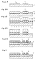
- FIG. 12A is a plan view of the TFT possessing a inverted staggered structure
- FIG. 12B is an A-B sectional view of FIG. 12A
- Numeral 6 is a transparent substrate made of glass
- 7 is a gate electrode
- Numerals 9, 10, 11 are gate insulator layer (first insulator layer), first semiconductor layer and passivation layer, respectively.
- Numeral 8 is a silicon oxide layer for preventing contact between the gate electrode 7 and pixel electrode 15, and enhancing the adhesion between the gate insulator layer 9 and pixel electrode 15.
- Numerals 13 and 14 are drain electrode and source electrode, respectively.
- Numeral 12 is a second semiconductor layer for achieving an ohmic contact between the first semiconductor layer 10 and electrodes which are drain electrode 13 and source electrode 14.
- Numeral 15 is a transparent electrode connected to the drain electrode 13, and it is a pixel electrode for applying a voltage to the liquid crystal layer.
- the pixel electrode 15 is formed beneath the gate insulator layer 9, but this pixel electrode 15 may be also formed on the gate insulator layer, simultaneously and integrally with the drain electrode 13 and source electrode 14.
- the gate electrode serves to shut off light against the incident light from the back side of the substrate, the leakage current in OFF state of TFT is small, and this structure is employed widely in commercial pocket-size TV sets.
- a display device using such active matrix substrate is explained below while referring to FIG. 13.
- a counter substrate 17 to which a counter electrode 16 is adhered, and the active matrix substrate a twisted nematic (TN) liquid crystal 18 processed by twist orientation is sealed in, and polarizer plates (not shown) are glued to one side each of the two transparent substrates, thereby forming a display device.
- TN twisted nematic
- Such forming method involves several problems as mentioned below in the aspects of cost, yield and performance.
- the greater the number of times of photolithography the more the high performance and expensive exposure machines and others are used, which results in a higher cost for forming the active matrix substrate.
- the more the number of times of photolithography the more troubles may occur in the photolithographic processes (such as misalignment between patterns), and the yield is lowered accordingly.
- the substrate material meanwhile, pyrex and other glass materials are often used, and the strain of the substrate caused by the thermal expansion and contraction during process or stress of the thin film may become too large to be ignored (in particular, this problem is serious in a large substrate, and mismatching between patterns on the substrate formed by photo mask may often exceed 10 microns).
- the alignment precision is not uniform within a substrate, and uniformity of the device characteristics decreases, or it may be necessary to use a special apparatus for correcting this strain or to design the device with a special consideration in a margin taking such strain into account.
- the greater the number of times of photo mask matching necessary for realizing the device the larger becomes the device size for keeping the margin.
- the aperture ratio the rate of effective display region
- EP-A-0166647 there is described a method for forming an active matrix substrate, wherein a self-alignment method is used for the positioning of a passivation layer, and by virtue of this for the positioning of the source and drain electrodes.
- European patent application EP-A-0222668 discloses a method for forming a thin film transistor in which one semi-conductor layer is formed by a self-alignment process with respect to the gate electrode, in order to simplify the process of producing a stepped semi-conductor layer to which good ohmic contacts can then be made.
- this invention presents a method of fabricating an active matrix substrate, including the steps of: forming a plurality of gate electrodes of an opaque electro-conducting material by patterning at specified places on a transparent substrate; forming a gate insulator layer over said gate electrodes; forming a first semiconductor layer on said gate insulator layer; forming a second semiconductor layer on said first semiconductor layer; coating a photoresist layer on the second semiconductor layer; irradiating light from the back side of the substrate using said gate electrodes as a mask; forming a resist pattern by developing said photoresist layer; removing portions of the first and second semiconductor layers which have been irradiated by said light from the backside of the substrate, whereby said first and second semiconductor layers are patterned by a self-alignment process using said gate electrodes as a mask; and forming a source region and a drain region on said second semiconductor layer by removing portions thereof to expose the first semiconductor layer.
- the method of this invention for example, when forming the pattern of semiconductor layer, since photolithography is possible by using the gate electrode (or gate electrode and insular conductor layer) as the mask, an inexpensive exposure machine not requiring the alignment mechanism may be used. Or, depending on the cases, the number of times of photolithography may be curtailed, which contributes to reduction of cost and increase of yield in the production of active matrix substrate. Or when irradiating light from the back side, there is no effect of expansion or contraction of the substrate, and a correctly aligned resist pattern will be obtained. Therefore, by using it, it may be possible to reduce the size of the TFT, and an active matrix substrate of high aperture ratio of high density may be realized. Besides, the device performance may be enhanced, and a high performance inverted staggered type TFT can be realized.
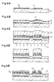
- FIG. 1 illustrates a first embodiment of the invention step by step.
- a gate electrode 7 is formed by a desired patterning (FIG. 1A).
- a gate insulator layer for example, silicon nitride; film thickness approx. 380 nm
- a first semiconductor layer for example, amorphous silicon; film thickness approx. 50 nm
- a passivation layer for example, silicon nitride; film thickness approx.
- a second semiconductor layer for example, phosphorus-doped low resistance amorphous silicon; film thickness approx. 50 nm
- a positive type photo resist 20 is then coated.
- ultraviolet ray 21 is irradiated from the back side of the transparent substrate 6, using the gate electrode 7 as the mask (FIG. 1C).
- the exposed areas of the first semiconductor layer 10 and second semiconductor layer 12 are removed by etching (FIG. 1D).
- a thin film composed of transparent conductive material for example, indium tin oxide (ITO); film thickness approx. 400 nm
- ITO indium tin oxide
- the gate electrode 7 As shown in this embodiment, by performing photolithography using the gate electrode 7 as the mask when forming the pattern of semiconductor layer, an inexpensive exposure machine not requiring alignment mechanism can be used, and the number of times of photolithography may be curtailed, too. Besides, since the semiconductor layer is not spreading wider than the gate electrode, the size of the device may be reduced. In this embodiment, meanwhile, the pixel electrode, source electrode and drain electrode are formed simultaneously, but they may be also formed separately.
- FIG. 2 shows a second embodiment of the invention step by step.
- a gate electrode 7 and an insular conductor layer 7a are formed (FIG. 2A).
- a gate insulator layer (first insulator layer) 9 a first semiconductor layer 10, and a passivation layer 11 are sequentially deposited, and the passivation layer 11 is etched, leaving only a part above the gate electrode 7 (FIG. 2B).
- a second semiconductor layer 12 also by plasma enhanced CVD process, a positive type photo resist 20 is coated.
- ultraviolet ray 21 is irradiated from the back side of the transparent substrate 6, using the gate electrode 7 and insular conductor layer 7a as the mask (FIG. 2C).
- the resist on the substrate is developed, the resist is removed except for the portion corresponding to the gate electrode 7 and insular conductor layer 7a.
- the exposed areas of the first semiconductor layer 10 and second semiconductor layer 12 are etched (FIG. 2D).
- a transparent electrode as pixel electrode 15, drain electrode 13, and source electrode 14 are formed (FIG. 2E)
- the redundancy of the source bus line is increased, and disconnection of the source bus line may be prevented.
- FIG. 3 shows a third embodiment of the invention.
- Example 2 After etching the semiconductor layer in the same manner as in Example 2 (FIG. 2A to D), the resist is removed. Then, a transparent electrode layer is deposited and patterned to form drain electrode 13, source electrode 14 and pixel electrode 15 (FIG. 3), and an active matrix substrate is completed.
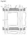
- FIG. 4 shows a fourth embodiment of the invention.
- FIG. 4A is a plan view of essential part of the active matrix array substrate in the fourth embodiment of the invention, showing one pixel and its surrounding parts.
- Numeral 7 is a gate electrode
- 14 is a source electrode
- 13 is a drain electrode
- 15 is a pixel electrode.
- Slits 22 are provided in the gate electrode.
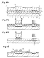
- FIG. 4B to E are sectional views following step by step along the broken line CD in FIG. 4A.
- a gate electrode 7 of metal thin film is patterned and formed by using a first photo mask, and a gate insulator layer 9, a first semiconductor layer 10 and a second semiconductor layer 12 are continuously formed thereon.
- a positive type photo resist 20 is coated, and ultraviolet ray 21 is irradiated from the back side of the substrate (FIG. 4B), and the resist on the substrate is developed.
- the resist pattern is thinned out by the portion of d1 from the gate electrode 7 (FIG. 4C).
- the first semiconductor layer 10 and second semiconductor layer 12 are etched.
- the etching pattern is thinned out by the portion of d2 from the resist pattern.
- a transparent conductive layer is deposited, and patterning is effected by using a second photo mask, and the source electrode 14, drain electrode 13, and picture element electrode 15 are formed simultaneously.
- the second semiconductor layer is etched except for the portion of the second photo mask pattern (FIG. 4E).
- a TFT of which first semiconductor layer 10 is completely separated between adjacent TFTs is completed by using two photo masks.
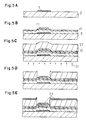
- FIG. 5 shows a fifth embodiment of the invention.
- Example 2 Same as in Example 1, on a transparent substrate 6, gate electrode 7, gate insulator layer (first insulator layer) 9, first semiconductor layer 10, passivation layer 11, and second semiconductor layer 12 are formed, and a negative type photo resist 23 is coated over the entire surface.
- an ultraviolet ray 21 is irradiated from the back side of the transparent substrate 6 using the gate electrode 7 as the mask (FIG. 5A to C).
- this resist on the substrate is developed, only the resist in the portion corresponding to the gate electrode 7 is removed (FIG. 5D).
- a conductor layer 24 is deposited (FIG. 5E), and the resist is removed, then the conductor layer 24 except for the portion above the gate electrode 7 is removed together with the resist.
- the first semiconductor layer 10 and second semiconductor layer 12 are etched (FIG. 5F).
- a transparent conductive layer is deposited and patterned to form drain electrode 13, source electrode 14 and pixel electrode 15, and then an active matrix substrate is completed (FIG. 5F).
- FIG. 6 shows a sixth embodiment of the invention.
- Example 2 on a transparent substrate 6, gate electrode 7, insular conductor layer 7a, gate insulator layer (first insulator layer) 9, first semiconductor layer 10, passivation layer 11, and second semiconductor layer 12 are formed, and a negative type photo resist 23 is coated over the entire surface.
- ultraviolet ray 21 is irradiated from the back side of the transparent substrate 6 using the gate electrode 7 and insular conductor layer 7a as the mask (FIG. 6A to C).
- the resist is removed only in the portions corresponding to the gate electrode 7 and insular conductor layer 7a (FIG. 6D).
- a conductor layer 24 is deposited (FIG.
- the gate electrode 7 as the mask when forming patterns of the semiconductor layer
- an inexpensive exposure machine not requiring alignment mechanism may be used, and the number of times of photolithography may be curtailed.
- the conductor layer 24 and semiconductor layer in the great part of the region beneath the source bus line, the redundancy of the source bus line increases along with lowering of resistance, so that disconnection of the source bus line may be prevented.
- the material of the conductor layer 24 in Examples 5 and 6 Cr, Ta, Ti, Mo, Ni and their alloys, or silicides of these metals may be used.
- FIG. 7 shows a seventh embodiment of the invention.
- the performance of the element may be enhanced without increasing the number of steps of photolithography using photo mask. That is, by inserting a metal oxide between the source electrode and drain electrode and the semiconductor layer, and reducing it to a metal, the resistances of the both electrodes may be lowered, and the contact resistance between the source electrode and the semiconductor layer and contact resistance between the drain electrode and the semiconductor layer may be lowered (conventionally, the contact resistance between the second semiconductor layer and the transparent electrode material of the metal oxide was often a problem, and it is improved herein).
- FIG. 8 shows an eighth embodiment of the invention.
- a gate electrode 7 and an insular conductor layer 7a are formed, and the rest of the procedure is same as in Example 7, and an active matrix substrate is completed (FIG. 7A to E).
- the redundancy of the source bus line is increased, and the disconnection of the source bus line may be prevented.
- the metal layer 14a reduced from the metal oxide the resistance of the source and drain electrodes is lowered, and the contact resistance between the source electrode and the semiconductor layer and the contact resistance between the drain electrode and the semiconductor layer may be lowered.
- TaOx and ITO may be adequately used.
- the reducing method instead of the hydrogen plasma processing, other methods such as exposure in hydrogen atmosphere may be equally employed. Again, better results are obtained when processed in hydrogen atmosphere or hydrogen plasma atmosphere.
- FIG. 9 shown a ninth embodiment of the invention.
- first semiconductor layer 10, passivation layer 11, and second semiconductor layer 12 are formed, and a positive type photo resist 20 is coated, and ultraviolet ray 21 is irradiated from the back side of the transparent substrate 6 using the gate electrode 7 as mask (FIG. 9A to C).
- a metal oxide film composed of at least one layer of metal oxide film, for example, 90% In2O3 - 10% SnO2 is deposited, and patterned to form drain electrode 13, source electrode 14, and pixel electrode 15 (FIG. 9D).
- a negative type photo resist 23 is coated, and ultraviolet ray is irradiated from the back side of the transparent substrate 6 using the gate electrode 7 as mask.
- the substrate After developing the resist (FIG. 9E), the substrate is exposed in hydrogen plasma atmosphere, and part of the drain electrode 13 and source electrode 14 is reduced to become In-Sn.
- an active matrix substrate is completed (FIG. 9F).
- the both electrodes may be lowered in resistance, and the contact resistance between the source electrode and semiconductor layer and the contact resistance between the drain electrode and semiconductor layer may be lowered.
- FIG. 10 shows a tenth embodiment of the invention.
- first semiconductor layer 10 and second semiconductor layer 12 are formed, and a positive type photo resist 20 is coated, and ultraviolet ray 21 is irradiated from the back side of the transparent substrate 6 using the gate electrode 7 as mask (FIG. 10A). After developing this resist, exposed areas of the first semiconductor layer 10 and second semiconductor layer 12 are etched.
- a two-layer metal oxide film composed of at least one metal oxide film such as 90% In2O3-10% SnO2, and Ta2O5 is deposited (the side contacting with the semiconductor is 90% In2O3-10% SnO2), and patterned, and drain electrode 13, source electrode 14 and pixel electrode 15 are formed, and a second insulator layer 19 is deposited thereon (FIG. 10B).
- a negative type photo resist 23 is coated, and ultraviolet ray is irradiated from the back side of the transparent substrate 6 using the gate electrode 7 as mask.
- the portion not covered by the resist of the second insulator layer 19 is etched (FIG.
- the both electrodes are lowered in resistance, while the contact resistance between the source electrode and semiconductor layer and the contact resistance between the drain electrode and semiconductor layer are lowered at the same time.
- the insulation layers of the both electrode surfaces and the second insulator layer 19 become passivation of active matrix substrate.
- Examples 9, 10 as the materials for drain electrode, source electrode and pixel electrode, 90% In2O3-10% SnO2 or 90% In2O3-10% SnO2, and TaO5 are used, but other materials which show conductivity when reduced may be similarly applied.
- 90% In2O3-10% SnO2 or 90% In2O3-10% SnO2, and TaO5 are used, but other materials which show conductivity when reduced may be similarly applied.
- one or more metal oxides selected from a group consisting of In, Sn, Cd, Zn, Nb, Ti and Ta are employed.
- Examples 9, 10 are the drain electrode and source electrode are reduced by processing in hydrogen plasma, but it may be also possible to reduced by exposing to hydrogen atmosphere or the like. However, the best results will be obtained by hydrogen plasma processing.
- the gate electrode material Cr, Ta, Ti, Mo, Ni, Ni-Cr or their metal silicides may be used as the gate electrode material. Any opaque conductive material may be employed as far as it may be used as the material for the gate electrode of the TFT.
- the materials for the gate insulator layer and passivation layer aside from silicon nitride, silicon oxide, metal oxide and other transparent insulators may be used.
- the first and second semiconductor layers amorphous silicon or phosphorus-doped amorphous silicon was used, but any semiconductor material may be equally used as far as it can obtain required TFT characteristics and pass ultraviolet rays to a certain extent, and, for example, polycrystal silicon or recrystallized silicon may be used.
- the material for the pixel electrode InOx, SnOx or transparent conductive material (ITO) of their mixed composition may be used.
- various conductive materials Al, Mo, Ni, other metals or their silicides
- the source and drain electrodes may be formed either in a single layer or in plural layers.
- the adhesion of the resist will be enhanced.
- an inexpensive exposure machine not requiring alignment mechanism may be used, and the photolithographic process requiring the photo mask may be curtailed, so that the reduction of cost which is the greatest subject in the active matrix type liquid crystal display device may be realized.
- the performance of the element may be improved by employing the photolithographic process which does not require precise alignment of mask. Therefore, its industrial significance is extremely great.
Landscapes
- Physics & Mathematics (AREA)
- Nonlinear Science (AREA)
- Engineering & Computer Science (AREA)
- Microelectronics & Electronic Packaging (AREA)
- Mathematical Physics (AREA)
- Chemical & Material Sciences (AREA)
- Crystallography & Structural Chemistry (AREA)
- General Physics & Mathematics (AREA)
- Optics & Photonics (AREA)
- Liquid Crystal (AREA)
- Thin Film Transistor (AREA)
- Devices For Indicating Variable Information By Combining Individual Elements (AREA)
Claims (11)
- Ein Verfahren zum Herstellen eines aktiven Matrixsubstrats mit den folgenden Schritten:
Bilden einer Vielzahl von Gate-Elektroden (7) aus einem lichtundurchlässigen elektroleitfähigen Material durch Strukturierung an bestimmten Stellen auf einem transparenten Substrat (6);
Bilden einer Gate-Isolationsschicht (9) über den Gate-Elektroden (7);
Bilden einer ersten Halbleiterschicht (10) auf der Gate-Isolationsschicht (9);
Bilden einer zweiten Halbleiterschicht (12) auf der ersten Halbleiterschicht (10);
Aufbringen einer Fotoresistschicht (20, 23) auf die zweite Halbleiterschicht;
Einstrahlen von Licht von der Rückseite des Substrats (6) unter Verwendung der Gate-Elektroden (7) als Maske;
Bilden eines Resistmusters durch Entwickeln der Fotoresistschicht (20, 23);
Entfernen von Abschnitten der ersten und zweiten Halbleiterschichten (10, 12), die durch das Licht von der Rückseite des Substrats (6) bestrahlt worden sind, wobei die erste und zweite Halbleiterschicht (10, 12) durch ein Selbstausrichtverfahren unter Verwendung der Gate-Elektroden (7) als Maske strukturiert werden; und
Bilden eines Source-Bereichs und eines Drain-Bereichs auf der zweiten Halbleiterschicht (12) durch Entfernen von Teilen davon, um die erste Halbleiterschicht (10) freizulegen. - Ein Verfahren zum Herstellen eines aktiven Matrixsubstrats gemäß Anspruch 1, das weiter die Schritte umfaßt:
Bilden einer Passivierungsschicht (11) durch Strukturierung auf der ersten Halbleiterschicht (10) über einem Teil jeder Gate-Elektrode (7); und
Bilden einer Drain-Elektrode (13), einer Source-Elektrode (14) und einer Bildpunktelektrode (15) durch Ablagern und Strukturieren einer Schicht aus transparentem, leitfähigem Material auf jedem der Drain- und Source-Bereiche. - Ein Verfahren zum Herstellen eines aktiven Matrixsubstrats gemäß Anspruch 1, das weiter einen Schritt umfaßt
des Bilden eines inselartigen Bereichs (7a) aus dem gleichen lichtundurchlässigen elektroleitfähigen Material wie die Gate-Elektroden (7) durch Strukturierung an einer bestimmten Stelle auf dem transparenten Substrat (6), wobei die ersten und zweiten Halbleiterschichten (10, 12) über dem inselartigen Bereich (7a) durch das Selbstausrichtverfahren unter Verwendung des inselartigen Bereichs (7a) als Maske gebildet werden. - Ein Verfahren zum Herstellen eines aktiven Matrixsubstrats gemäß Anspruch 3, das weiter einen Schritt umfaßt
des Bildens einer Drain-Elektrode (13), einer Source-Elektrode (14) und einer Bildpunktelektrode (15) durch Ablagern und Strukturieren einer Schicht aus transparentem, leitfähigem Material auf jedem der Drain- und Source-Bereiche. - Ein Verfahren zum Herstellen eines aktiven Matrixsubstrats gemäß Anspruch 1, das weiter die folgenden Schritte umfaßt:
Bilden von Schlitzen (22) in ausgewählten Gate-Elektroden (7), wobei bei den Schritten des Bestrahlens und Bildens eines Resistmusters die Fotoresistschicht (20) überbelichtet und überätzt wird, um somit eine Abtragung der Halbleiterschichten (10, 12) um die Schlitze (22) herum in den ausgewählten Gate-Elektroden (7) zu ermöglichen; und
Bilden einer Drain-Elektrode (13), einer Source-Elektrode (14) und einer Bildpunktelektrode (15) durch Ablagern und Strukturieren einer Schicht aus transparentem, leitfähigem Material auf jedem der Source- und Drain-Bereiche. - Ein Verfahren zum Herstellen eines aktiven Matrixsubstrats gemäß Anspruch 1, das weiter die Schritte umfaßt:
Bilden einer Passivierungsschicht (11) durch Strukturierung auf der ersten Halbleiterschicht (10) über einem Teil der Gate-Elektroden (7);
Bilden einer Leiterschicht (24) auf dem Abschnitt der Halbleiterschicht (12) über den Gate-Elektroden (7) vor dem Schritt des Bildens der Source- und Drain-Bereiche; wobei der Schritt weiter ein Entfernen von Teilen der Leiterschicht (24) wie auch von Teilen der Halbleiterschicht (12) über der Gate-Elektrodenschicht (7) umfaßt, um die erste Halbleiterschicht (10) freizulegen; und
Bilden einer Drain-Elektrode (13), einer Source-Elektrode (14) und einer Bildpunktelektrode (15) durch Ablagern und Strukturieren einer Schicht aus transparentem, leitfähigem Material auf den verbleibenden Abschnitten der Leiterschicht (24). - Ein Verfahren zum Herstellen eines aktiven Matrixsubstrats gemäß Anspruch 6, das weiter den Schritt umfaßt
des Bildens eines inselartigen Bereichs (7a) aus dem gleichen lichtundurchlässigen, elektroleitfähigen Material wie die Gate-Elektroden (7) durch Strukturieren an einer bestimmten Stelle auf dem transparenten Substrat (6), wobei die erste und zweite Halbleiterschicht (10, 12) und die Leiterschicht (24) über dem inselartigen Bereich (7a) durch das Selbstausrichtverfahren unter Verwendung der inselartigen Schicht (7a) als Maske geformt werden. - Ein Verfahren zum Herstellen eines aktiven Matrixsubstrats gemäß Anspruch 1, das weiter die Schritte umfaßt
des Bildens einer Passivierungsschicht (11) durch Strukturierung auf der ersten Halbleiterschicht (10) über einem Teil der Gate-Elektroden (7);
des Ablagerns einer Metalloxidschicht (25) auf der zweiten Halbleiterschicht (12) vor dem Schritt des Aufbringens einer Fotoresistschicht (25) auf diese, so daß die Metalloxidschicht (25) ebenfalls durch das Selbstausrichtverfahren unter Verwendung der Gate-Elektroden (7) als Maske strukturiert wird, wobei der Schritt des Bildens der Source- und DrainBereiche weiter eine Entfernung von Teilen der Metalloxidschicht (25) wie auch von Teilen der zweiten Halbleiterschicht (12) über der Gate-Elektrode (7) umfaßt, um die erste Halbleiterschicht (10) freizulegen;
des Reduzierens der Metalloxidschicht (25) zur Erzeugung einer Metallschicht (14a); und
des Bildens einer Drain-Elektrode (13), einer Source-Elektrode (14) und einer Bildpunktelektrode (15) durch Ablagerung und Strukturierung einer Schicht aus transparentem, leitfähigem Material auf den verbleibenden Abschnitten der Metallschicht (14a). - Ein Verfahren zum Herstellen eines aktiven Matrixsubstrats gemäß Anspruch 8, das den weiteren Schritt umfaßt
des Bildens eines inselartigen Bereichs (7a) aus dem gleichen lichtundurchlässigen, elektroleitfähigen Material wie die Gate-Elektroden (7) durch Strukturierung an einer bestimmten Stelle auf dem transparenten Substrat (6), wobei die erste und zweite Halbleiterschicht (10, 12) und die Metallschicht (14a) über dem inselartigen Bereich (7a) unter Verwendung des inselartigen Bereichs (7a) als Maske gebildet werden. - Ein Verfahren zum Herstellen eines aktiven Matrixsubstrats gemäß Anspruch 1, das weiter die Schritte umfaßt
des Ablagerns einer Metalloxidschicht auf der zweiten Halbleiterschicht (12) nach dem Schritt des Bildens der Source- und Drain-Bereiche;
des Strukturierens der Metalloxidschicht zur Bildung einer Drain-Elektrode (13), einer Source-Elektrode (14) und einer Bildpunktelektrode (15);
des Aufbringens eines Fotoresists (23) eines negativen Typs auf die Metalloxidschicht;
des Einstrahlens von Licht von der Rückseite des Substrats (6);
des Entwickelns des Resits (23); und
des Reduzierens des freiliegenden Teils der Source-Elektrode (14) und der Drain-Elektrode (13). - Ein Verfahren zum Herstellen eines aktiven Matrixsubstrats gemäß Anspruch 1, das weiter die Schritte umfaßt
des Ablagerns eines zweischichtigen Metalloxidfilms mit wenigstens einer Metalloxidschicht auf der zweiten Halbleiterschicht (12) nach dem Schritt des Bildens der Source- und Drain-Bereiche;
des Strukturierens des Metalloxidfilms zur Bildung einer Drain-Elektrode (13), einer Source-Elektrode (14) und einer Bildpunktelektrode (15);
des Ablagerns einer zweiten Isolationsschicht (19) darauf;
des Aufbringens eines Fotoresists (23) eines negativen Typs auf die zweite Isolationsschicht (19);
des Einstrahlens von Licht von der Rückseite des Substrats (6) unter Verwendung der Gate-Elektroden (7) als Maske;
des Entwickelns des Resists (23);
des Entfernens des freiliegenden Teils der zweiten Isolationsschicht (19), die nicht durch den Fotoresist (23) abgedeckt ist;
des Reduzierens des Metalloxidfilms der Drain-Elektrode (13) und der Source-Elektrode (14) zur Bildung eines zweischichtigen Metallfilms;
des Oxidierens der Oberflächenschicht der Drain-Elektrode (13) und der Source-Elektrode (14); und
des Entfernens des verbleibenden Abschnitts des Resists (23).
Applications Claiming Priority (4)
| Application Number | Priority Date | Filing Date | Title |
|---|---|---|---|
| JP97008/88 | 1988-04-20 | ||
| JP9700888 | 1988-04-20 | ||
| JP63248197A JPH0242761A (ja) | 1988-04-20 | 1988-09-30 | アクティブマトリクス基板の製造方法 |
| JP248197/88 | 1988-09-30 |
Publications (2)
| Publication Number | Publication Date |
|---|---|
| EP0338766A1 EP0338766A1 (de) | 1989-10-25 |
| EP0338766B1 true EP0338766B1 (de) | 1995-08-09 |
Family
ID=26438156
Family Applications (1)
| Application Number | Title | Priority Date | Filing Date |
|---|---|---|---|
| EP89303812A Expired - Lifetime EP0338766B1 (de) | 1988-04-20 | 1989-04-18 | Verfahren zur Herstellung eines aktiven Matrixsubstrats |
Country Status (5)
| Country | Link |
|---|---|
| US (1) | US5622814A (de) |
| EP (1) | EP0338766B1 (de) |
| JP (1) | JPH0242761A (de) |
| KR (1) | KR930007529B1 (de) |
| DE (1) | DE68923727T2 (de) |
Cited By (6)
| Publication number | Priority date | Publication date | Assignee | Title |
|---|---|---|---|---|
| US7190387B2 (en) | 2003-09-11 | 2007-03-13 | Bright View Technologies, Inc. | Systems for fabricating optical microstructures using a cylindrical platform and a rastered radiation beam |
| US7192692B2 (en) | 2003-09-11 | 2007-03-20 | Bright View Technologies, Inc. | Methods for fabricating microstructures by imaging a radiation sensitive layer sandwiched between outer layers |
| US7360455B2 (en) | 1990-10-12 | 2008-04-22 | Kazuhiro Okada | Force detector and acceleration detector and method of manufacturing the same |
| US7363814B2 (en) | 1993-03-30 | 2008-04-29 | Kazuhiro Okada | Multi-axial angular velocity sensor |
| US7533582B2 (en) | 1990-10-12 | 2009-05-19 | Kazuhiro Okada | Force detector and acceleration detector and method of manufacturing the same |
| US7867695B2 (en) | 2003-09-11 | 2011-01-11 | Bright View Technologies Corporation | Methods for mastering microstructures through a substrate using negative photoresist |
Families Citing this family (93)
| Publication number | Priority date | Publication date | Assignee | Title |
|---|---|---|---|---|
| JP2604867B2 (ja) * | 1990-01-11 | 1997-04-30 | 松下電器産業株式会社 | 反射型液晶表示デバイス |
| JP2767958B2 (ja) * | 1990-02-20 | 1998-06-25 | 松下電器産業株式会社 | 半導体装置の製造方法 |
| JP2938121B2 (ja) * | 1990-03-30 | 1999-08-23 | 株式会社東芝 | 薄膜半導体装置の製造方法 |
| US5474941A (en) * | 1990-12-28 | 1995-12-12 | Sharp Kabushiki Kaisha | Method for producing an active matrix substrate |
| DE69125260T2 (de) * | 1990-12-28 | 1997-10-02 | Sharp Kk | Ein Verfahren zum Herstellen eines Dünnfilm-Transistors und eines Aktive-Matrix-Substrates für Flüssig-Kristall-Anzeige-Anordnungen |
| US5420048A (en) * | 1991-01-09 | 1995-05-30 | Canon Kabushiki Kaisha | Manufacturing method for SOI-type thin film transistor |
| GB9114018D0 (en) * | 1991-06-28 | 1991-08-14 | Philips Electronic Associated | Thin-film transistor manufacture |
| JP3172840B2 (ja) * | 1992-01-28 | 2001-06-04 | 株式会社日立製作所 | アクティブマトリクス基板の製造方法および液晶表示装置 |
| JP3172841B2 (ja) * | 1992-02-19 | 2001-06-04 | 株式会社日立製作所 | 薄膜トランジスタとその製造方法及び液晶表示装置 |
| US5254480A (en) * | 1992-02-20 | 1993-10-19 | Minnesota Mining And Manufacturing Company | Process for producing a large area solid state radiation detector |
| GB9217743D0 (en) * | 1992-08-19 | 1992-09-30 | Philips Electronics Uk Ltd | A semiconductor memory device |
| JP2530990B2 (ja) * | 1992-10-15 | 1996-09-04 | 富士通株式会社 | 薄膜トランジスタ・マトリクスの製造方法 |
| US5643801A (en) * | 1992-11-06 | 1997-07-01 | Semiconductor Energy Laboratory Co., Ltd. | Laser processing method and alignment |
| US6410374B1 (en) | 1992-12-26 | 2002-06-25 | Semiconductor Energy Laborartory Co., Ltd. | Method of crystallizing a semiconductor layer in a MIS transistor |
| US6544825B1 (en) * | 1992-12-26 | 2003-04-08 | Semiconductor Energy Laboratory Co., Ltd. | Method of fabricating a MIS transistor |
| US7297471B1 (en) | 2003-04-15 | 2007-11-20 | Idc, Llc | Method for manufacturing an array of interferometric modulators |
| US7550794B2 (en) | 2002-09-20 | 2009-06-23 | Idc, Llc | Micromechanical systems device comprising a displaceable electrode and a charge-trapping layer |
| JP2755376B2 (ja) * | 1994-06-03 | 1998-05-20 | 株式会社フロンテック | 電気光学素子の製造方法 |
| JP3469337B2 (ja) | 1994-12-16 | 2003-11-25 | 株式会社半導体エネルギー研究所 | 半導体装置の作製方法 |
| JP3778456B2 (ja) | 1995-02-21 | 2006-05-24 | 株式会社半導体エネルギー研究所 | 絶縁ゲイト型薄膜半導体装置の作製方法 |
| JP3478012B2 (ja) * | 1995-09-29 | 2003-12-10 | ソニー株式会社 | 薄膜半導体装置の製造方法 |
| KR100193348B1 (ko) * | 1996-02-12 | 1999-07-01 | 구자홍 | 액정표시장치의 박막트랜지스터 제조방법 |
| KR100448934B1 (ko) * | 1996-12-27 | 2004-12-04 | 삼성전자주식회사 | 액정표시장치의제조방법 |
| JP3883641B2 (ja) * | 1997-03-27 | 2007-02-21 | 株式会社半導体エネルギー研究所 | コンタクト構造およびアクティブマトリクス型表示装置 |
| KR100271043B1 (ko) * | 1997-11-28 | 2000-11-01 | 구본준, 론 위라하디락사 | 액정표시장치의 기판 및 그 제조방법(liquid crystal display and method of manufacturing the same) |
| US6372535B1 (en) * | 1998-02-02 | 2002-04-16 | Samsung Electronics Co., Ltd. | Manufacturing method of a thin film transistor |
| JP4118484B2 (ja) | 2000-03-06 | 2008-07-16 | 株式会社半導体エネルギー研究所 | 半導体装置の作製方法 |
| JP2001257350A (ja) * | 2000-03-08 | 2001-09-21 | Semiconductor Energy Lab Co Ltd | 半導体装置およびその作製方法 |
| JP4118485B2 (ja) * | 2000-03-13 | 2008-07-16 | 株式会社半導体エネルギー研究所 | 半導体装置の作製方法 |
| JP4700160B2 (ja) | 2000-03-13 | 2011-06-15 | 株式会社半導体エネルギー研究所 | 半導体装置 |
| JP4683688B2 (ja) * | 2000-03-16 | 2011-05-18 | 株式会社半導体エネルギー研究所 | 液晶表示装置の作製方法 |
| JP4393662B2 (ja) * | 2000-03-17 | 2010-01-06 | 株式会社半導体エネルギー研究所 | 液晶表示装置の作製方法 |
| US6900084B1 (en) * | 2000-05-09 | 2005-05-31 | Semiconductor Energy Laboratory Co., Ltd. | Semiconductor device having a display device |
| TW521316B (en) * | 2000-11-09 | 2003-02-21 | Macronix Int Co Ltd | Manufacturing method for reducing critical dimensions |
| CA2435298C (en) * | 2001-01-19 | 2011-03-29 | Atraverda Limited | A pore-free electrode comprising titanium suboxides |
| US7071037B2 (en) | 2001-03-06 | 2006-07-04 | Semiconductor Energy Laboratory Co., Ltd. | Semiconductor device and manufacturing method thereof |
| KR100495701B1 (ko) * | 2001-03-07 | 2005-06-14 | 삼성에스디아이 주식회사 | 유기 전계 발광 표시장치의 제조방법 |
| US6794119B2 (en) * | 2002-02-12 | 2004-09-21 | Iridigm Display Corporation | Method for fabricating a structure for a microelectromechanical systems (MEMS) device |
| US6887627B2 (en) * | 2002-04-26 | 2005-05-03 | Macronix International Co., Ltd. | Method of fabricating phase shift mask |
| US7781850B2 (en) | 2002-09-20 | 2010-08-24 | Qualcomm Mems Technologies, Inc. | Controlling electromechanical behavior of structures within a microelectromechanical systems device |
| TW564564B (en) * | 2002-10-03 | 2003-12-01 | Au Optronics Corp | Pixel structure and fabricating method thereof |
| US6995045B2 (en) * | 2003-03-05 | 2006-02-07 | Chunghwa Picture Tubes, Ltd. | Thin film transistor and method of forming thin film transistor |
| TW594360B (en) | 2003-04-21 | 2004-06-21 | Prime View Int Corp Ltd | A method for fabricating an interference display cell |
| TW570896B (en) | 2003-05-26 | 2004-01-11 | Prime View Int Co Ltd | A method for fabricating an interference display cell |
| US7221495B2 (en) * | 2003-06-24 | 2007-05-22 | Idc Llc | Thin film precursor stack for MEMS manufacturing |
| TWI231865B (en) | 2003-08-26 | 2005-05-01 | Prime View Int Co Ltd | An interference display cell and fabrication method thereof |
| TW593126B (en) | 2003-09-30 | 2004-06-21 | Prime View Int Co Ltd | A structure of a micro electro mechanical system and manufacturing the same |
| US7720148B2 (en) * | 2004-03-26 | 2010-05-18 | The Hong Kong University Of Science And Technology | Efficient multi-frame motion estimation for video compression |
| US7349136B2 (en) | 2004-09-27 | 2008-03-25 | Idc, Llc | Method and device for a display having transparent components integrated therein |
| US7405861B2 (en) | 2004-09-27 | 2008-07-29 | Idc, Llc | Method and device for protecting interferometric modulators from electrostatic discharge |
| US20060065622A1 (en) * | 2004-09-27 | 2006-03-30 | Floyd Philip D | Method and system for xenon fluoride etching with enhanced efficiency |
| US7420728B2 (en) | 2004-09-27 | 2008-09-02 | Idc, Llc | Methods of fabricating interferometric modulators by selectively removing a material |
| US7161730B2 (en) | 2004-09-27 | 2007-01-09 | Idc, Llc | System and method for providing thermal compensation for an interferometric modulator display |
| US7369296B2 (en) | 2004-09-27 | 2008-05-06 | Idc, Llc | Device and method for modifying actuation voltage thresholds of a deformable membrane in an interferometric modulator |
| US7492502B2 (en) | 2004-09-27 | 2009-02-17 | Idc, Llc | Method of fabricating a free-standing microstructure |
| US7373026B2 (en) | 2004-09-27 | 2008-05-13 | Idc, Llc | MEMS device fabricated on a pre-patterned substrate |
| US7684104B2 (en) * | 2004-09-27 | 2010-03-23 | Idc, Llc | MEMS using filler material and method |
| US7553684B2 (en) * | 2004-09-27 | 2009-06-30 | Idc, Llc | Method of fabricating interferometric devices using lift-off processing techniques |
| US7417783B2 (en) | 2004-09-27 | 2008-08-26 | Idc, Llc | Mirror and mirror layer for optical modulator and method |
| KR100685955B1 (ko) * | 2004-12-30 | 2007-02-23 | 엘지.필립스 엘시디 주식회사 | 액정 표시 장치 |
| CN100343749C (zh) * | 2005-01-27 | 2007-10-17 | 广辉电子股份有限公司 | 薄膜晶体管液晶显示器的阵列基底及其制造方法 |
| TW200628877A (en) | 2005-02-04 | 2006-08-16 | Prime View Int Co Ltd | Method of manufacturing optical interference type color display |
| CN100565888C (zh) * | 2005-03-16 | 2009-12-02 | 新南创新私人有限公司 | 用于接通薄膜半导体结构的光刻方法 |
| EP2495212A3 (de) * | 2005-07-22 | 2012-10-31 | QUALCOMM MEMS Technologies, Inc. | MEMS-Vorrichtungen mit Stützstrukturen und Herstellungsverfahren dafür |
| JP2009503564A (ja) | 2005-07-22 | 2009-01-29 | クアルコム,インコーポレイテッド | Memsデバイスのための支持構造、およびその方法 |
| US7630114B2 (en) | 2005-10-28 | 2009-12-08 | Idc, Llc | Diffusion barrier layer for MEMS devices |
| US7795061B2 (en) | 2005-12-29 | 2010-09-14 | Qualcomm Mems Technologies, Inc. | Method of creating MEMS device cavities by a non-etching process |
| US7382515B2 (en) | 2006-01-18 | 2008-06-03 | Qualcomm Mems Technologies, Inc. | Silicon-rich silicon nitrides as etch stops in MEMS manufacture |
| US7547568B2 (en) * | 2006-02-22 | 2009-06-16 | Qualcomm Mems Technologies, Inc. | Electrical conditioning of MEMS device and insulating layer thereof |
| US7450295B2 (en) | 2006-03-02 | 2008-11-11 | Qualcomm Mems Technologies, Inc. | Methods for producing MEMS with protective coatings using multi-component sacrificial layers |
| US7643203B2 (en) | 2006-04-10 | 2010-01-05 | Qualcomm Mems Technologies, Inc. | Interferometric optical display system with broadband characteristics |
| US7527996B2 (en) | 2006-04-19 | 2009-05-05 | Qualcomm Mems Technologies, Inc. | Non-planar surface structures and process for microelectromechanical systems |
| US7623287B2 (en) | 2006-04-19 | 2009-11-24 | Qualcomm Mems Technologies, Inc. | Non-planar surface structures and process for microelectromechanical systems |
| US7417784B2 (en) | 2006-04-19 | 2008-08-26 | Qualcomm Mems Technologies, Inc. | Microelectromechanical device and method utilizing a porous surface |
| US7711239B2 (en) | 2006-04-19 | 2010-05-04 | Qualcomm Mems Technologies, Inc. | Microelectromechanical device and method utilizing nanoparticles |
| US7369292B2 (en) | 2006-05-03 | 2008-05-06 | Qualcomm Mems Technologies, Inc. | Electrode and interconnect materials for MEMS devices |
| US7321457B2 (en) | 2006-06-01 | 2008-01-22 | Qualcomm Incorporated | Process and structure for fabrication of MEMS device having isolated edge posts |
| US7405863B2 (en) | 2006-06-01 | 2008-07-29 | Qualcomm Mems Technologies, Inc. | Patterning of mechanical layer in MEMS to reduce stresses at supports |
| US7566664B2 (en) | 2006-08-02 | 2009-07-28 | Qualcomm Mems Technologies, Inc. | Selective etching of MEMS using gaseous halides and reactive co-etchants |
| US7763546B2 (en) | 2006-08-02 | 2010-07-27 | Qualcomm Mems Technologies, Inc. | Methods for reducing surface charges during the manufacture of microelectromechanical systems devices |
| US7706042B2 (en) * | 2006-12-20 | 2010-04-27 | Qualcomm Mems Technologies, Inc. | MEMS device and interconnects for same |
| US7719752B2 (en) | 2007-05-11 | 2010-05-18 | Qualcomm Mems Technologies, Inc. | MEMS structures, methods of fabricating MEMS components on separate substrates and assembly of same |
| BRPI0814680A2 (pt) * | 2007-07-25 | 2016-10-04 | Qualcomm Mems Technologies Inc | dispositivo óptico mems e respectivo método de fabrico |
| US7719754B2 (en) * | 2008-09-30 | 2010-05-18 | Qualcomm Mems Technologies, Inc. | Multi-thickness layers for MEMS and mask-saving sequence for same |
| CN102668098B (zh) | 2009-12-28 | 2015-07-22 | 株式会社半导体能源研究所 | 制造半导体装置的方法 |
| GB2499606B (en) | 2012-02-21 | 2016-06-22 | Pragmatic Printing Ltd | Substantially planar electronic devices and circuits |
| KR101960796B1 (ko) * | 2012-03-08 | 2019-07-16 | 삼성디스플레이 주식회사 | 박막 트랜지스터의 제조 방법, 표시 기판의 제조 방법 및 표시 기판 |
| CN103456742B (zh) * | 2013-08-27 | 2017-02-15 | 京东方科技集团股份有限公司 | 一种阵列基板及其制作方法、显示装置 |
| CN104112711B (zh) * | 2014-07-22 | 2017-05-03 | 深圳市华星光电技术有限公司 | 共平面型氧化物半导体tft基板的制作方法 |
| CN104377246A (zh) * | 2014-10-08 | 2015-02-25 | 京东方科技集团股份有限公司 | 一种薄膜晶体管及其制作方法、阵列基板和显示装置 |
| KR102423679B1 (ko) * | 2015-09-21 | 2022-07-21 | 삼성디스플레이 주식회사 | 표시 장치 제조 방법 |
| CN116941028A (zh) * | 2023-05-11 | 2023-10-24 | 昆山龙腾光电股份有限公司 | 阵列基板的制作方法及阵列基板 |
| CN120112076A (zh) * | 2023-12-01 | 2025-06-06 | 京东方科技集团股份有限公司 | 显示面板及显示装置 |
Family Cites Families (13)
| Publication number | Priority date | Publication date | Assignee | Title |
|---|---|---|---|---|
| DE2658400A1 (de) * | 1976-12-23 | 1978-06-29 | Ibm Deutschland | Verfahren zur herstellung einer negativen maske auf einem substrat |
| US4277884A (en) * | 1980-08-04 | 1981-07-14 | Rca Corporation | Method for forming an improved gate member utilizing special masking and oxidation to eliminate projecting points on silicon islands |
| JPS5952881A (ja) * | 1982-09-21 | 1984-03-27 | Fujitsu Ltd | 電界効果型半導体装置の製造方法 |
| JPS59224822A (ja) * | 1983-06-06 | 1984-12-17 | Fujitsu Ltd | 液晶表示パネルの構成法 |
| FR2566186B1 (fr) * | 1984-06-14 | 1986-08-29 | Thomson Csf | Procede de fabrication d'au moins un transistor a effet de champ en couche mince et transistor obtenu par ce procede |
| DE3680806D1 (de) * | 1985-03-29 | 1991-09-19 | Matsushita Electric Industrial Co Ltd | Duennschicht-transistorenanordnung und methode zu deren herstellung. |
| JP2913300B2 (ja) * | 1985-09-26 | 1999-06-28 | セイコーインスツルメンツ株式会社 | 薄膜トランジスタ装置の製造方法 |
| FR2590409B1 (fr) * | 1985-11-15 | 1987-12-11 | Commissariat Energie Atomique | Procede de fabrication d'un transistor en couches minces a grille auto-alignee par rapport au drain et a la source de celui-ci et transistor obtenu par le procede |
| JPS62140467A (ja) * | 1985-12-13 | 1987-06-24 | Sharp Corp | 薄膜トランジスタの製造方法 |
| JPH0612387B2 (ja) * | 1985-12-17 | 1994-02-16 | 三洋電機株式会社 | 液晶表示装置 |
| JPH07119909B2 (ja) * | 1986-08-29 | 1995-12-20 | 株式会社日立製作所 | 液晶表示素子製造方法 |
| US4931351A (en) * | 1987-01-12 | 1990-06-05 | Eastman Kodak Company | Bilayer lithographic process |
| GB8721193D0 (en) * | 1987-09-09 | 1987-10-14 | Wright S W | Semiconductor devices |
-
1988
- 1988-09-30 JP JP63248197A patent/JPH0242761A/ja active Pending
-
1989
- 1989-04-18 DE DE68923727T patent/DE68923727T2/de not_active Expired - Fee Related
- 1989-04-18 EP EP89303812A patent/EP0338766B1/de not_active Expired - Lifetime
- 1989-04-20 KR KR1019890005223A patent/KR930007529B1/ko not_active Expired - Fee Related
-
1994
- 1994-07-11 US US08/272,634 patent/US5622814A/en not_active Expired - Fee Related
Cited By (10)
| Publication number | Priority date | Publication date | Assignee | Title |
|---|---|---|---|---|
| US7360455B2 (en) | 1990-10-12 | 2008-04-22 | Kazuhiro Okada | Force detector and acceleration detector and method of manufacturing the same |
| US7533582B2 (en) | 1990-10-12 | 2009-05-19 | Kazuhiro Okada | Force detector and acceleration detector and method of manufacturing the same |
| US7363814B2 (en) | 1993-03-30 | 2008-04-29 | Kazuhiro Okada | Multi-axial angular velocity sensor |
| US7900513B2 (en) | 1993-03-30 | 2011-03-08 | Kazuhiro Okada | Multi-axial angular velocity sensor |
| US7190387B2 (en) | 2003-09-11 | 2007-03-13 | Bright View Technologies, Inc. | Systems for fabricating optical microstructures using a cylindrical platform and a rastered radiation beam |
| US7192692B2 (en) | 2003-09-11 | 2007-03-20 | Bright View Technologies, Inc. | Methods for fabricating microstructures by imaging a radiation sensitive layer sandwiched between outer layers |
| US7425407B1 (en) | 2003-09-11 | 2008-09-16 | Bright View Technologies, Inc. | Methods for fabricating optical microstructures by imaging a radiation sensitive layer sandwiched between outer layers |
| US7763417B2 (en) | 2003-09-11 | 2010-07-27 | Tredegar Newco, Inc. | Methods for fabricating optical microstructures using a cylindrical platform and a rastered radiation beam |
| US7867695B2 (en) | 2003-09-11 | 2011-01-11 | Bright View Technologies Corporation | Methods for mastering microstructures through a substrate using negative photoresist |
| US8263318B2 (en) | 2003-09-11 | 2012-09-11 | Bright View Technologies Corporation | Methods for mastering microstructures through a substrate using negative photoresist |
Also Published As
| Publication number | Publication date |
|---|---|
| JPH0242761A (ja) | 1990-02-13 |
| US5622814A (en) | 1997-04-22 |
| KR900017166A (ko) | 1990-11-15 |
| KR930007529B1 (ko) | 1993-08-12 |
| EP0338766A1 (de) | 1989-10-25 |
| DE68923727T2 (de) | 1996-03-21 |
| DE68923727D1 (de) | 1995-09-14 |
Similar Documents
| Publication | Publication Date | Title |
|---|---|---|
| EP0338766B1 (de) | Verfahren zur Herstellung eines aktiven Matrixsubstrats | |
| US7157319B2 (en) | Method of patterning a thin film transistor that includes simultaneously forming a gate electrode and a pixel electrode | |
| US4958205A (en) | Thin film transistor array and method of manufacturing the same | |
| EP0775931B1 (de) | Verfahren zur Herstellung einer Flüssigkristall-Anzeige | |
| EP0304657B1 (de) | Aktive Matrixzelle und deren Herstellungsverfahren | |
| JP2004163968A (ja) | 液晶表示装置の製造方法 | |
| US7649581B2 (en) | Array substrate of an LCD comprising first and second gate insulating layers and method of fabricating the same | |
| US5998230A (en) | Method for making liquid crystal display device with reduced mask steps | |
| JP2004341550A (ja) | 液晶表示装置および液晶表示装置の製造方法 | |
| US6927087B2 (en) | Active matrix substrate for a liquid crystal display and method of forming the same | |
| US7705925B2 (en) | Method of manufacturing an array substrate for use in a LCD device | |
| US6043000A (en) | Method for manufacturing a semiconductor device | |
| EP1646076B1 (de) | Herstellungsverfahren für eine Dünnfilmtransistormatrix | |
| US7023501B2 (en) | Liquid crystal display device having particular connections among drain and pixel electrodes and contact hole | |
| JP2678044B2 (ja) | アクティブマトリクス基板の製造方法 | |
| JP2002250934A (ja) | 液晶用マトリクス基板の製造方法 | |
| KR100669093B1 (ko) | 액정표시소자의 제조방법 | |
| US6317174B1 (en) | TFT array substrate, liquid crystal display using TFT array substrate, and manufacturing method thereof | |
| JP2002098994A (ja) | 液晶用マトリクス基板およびその製造方法ならびにコンタクトホール形成方法 | |
| WO2004036303A1 (en) | A thin film translator array panel and a method for manufacturing the panel | |
| KR100897720B1 (ko) | 액정표시장치의 제조방법 | |
| JPH07142737A (ja) | 薄膜トランジスタの製造方法 | |
| KR100330097B1 (ko) | 액정표시장치용박막트랜지스터기판및그제조방법 | |
| KR20010019666A (ko) | 박막트랜지스터 액정표시장치 | |
| KR100471765B1 (ko) | 단일막게이트라인을갖는박막트랜지스터기판및그제조방법 |
Legal Events
| Date | Code | Title | Description |
|---|---|---|---|
| PUAI | Public reference made under article 153(3) epc to a published international application that has entered the european phase |
Free format text: ORIGINAL CODE: 0009012 |
|
| AK | Designated contracting states |
Kind code of ref document: A1 Designated state(s): DE FR GB |
|
| 17P | Request for examination filed |
Effective date: 19900424 |
|
| 17Q | First examination report despatched |
Effective date: 19920818 |
|
| GRAA | (expected) grant |
Free format text: ORIGINAL CODE: 0009210 |
|
| AK | Designated contracting states |
Kind code of ref document: B1 Designated state(s): DE FR GB |
|
| REF | Corresponds to: |
Ref document number: 68923727 Country of ref document: DE Date of ref document: 19950914 |
|
| ET | Fr: translation filed | ||
| PLBE | No opposition filed within time limit |
Free format text: ORIGINAL CODE: 0009261 |
|
| STAA | Information on the status of an ep patent application or granted ep patent |
Free format text: STATUS: NO OPPOSITION FILED WITHIN TIME LIMIT |
|
| 26N | No opposition filed | ||
| REG | Reference to a national code |
Ref country code: GB Ref legal event code: IF02 |
|
| REG | Reference to a national code |
Ref country code: GB Ref legal event code: 746 Effective date: 20031002 |
|
| REG | Reference to a national code |
Ref country code: FR Ref legal event code: D6 |
|
| PGFP | Annual fee paid to national office [announced via postgrant information from national office to epo] |
Ref country code: FR Payment date: 20060410 Year of fee payment: 18 |
|
| PGFP | Annual fee paid to national office [announced via postgrant information from national office to epo] |
Ref country code: GB Payment date: 20060412 Year of fee payment: 18 |
|
| PGFP | Annual fee paid to national office [announced via postgrant information from national office to epo] |
Ref country code: DE Payment date: 20060413 Year of fee payment: 18 |
|
| GBPC | Gb: european patent ceased through non-payment of renewal fee |
Effective date: 20070418 |
|
| PG25 | Lapsed in a contracting state [announced via postgrant information from national office to epo] |
Ref country code: DE Free format text: LAPSE BECAUSE OF NON-PAYMENT OF DUE FEES Effective date: 20071101 |
|
| PG25 | Lapsed in a contracting state [announced via postgrant information from national office to epo] |
Ref country code: GB Free format text: LAPSE BECAUSE OF NON-PAYMENT OF DUE FEES Effective date: 20070418 |
|
| PG25 | Lapsed in a contracting state [announced via postgrant information from national office to epo] |
Ref country code: FR Free format text: LAPSE BECAUSE OF NON-PAYMENT OF DUE FEES Effective date: 20070430 |