EP0338766B1 - Method of fabricating an active matrix substrate - Google Patents
Method of fabricating an active matrix substrate Download PDFInfo
- Publication number
- EP0338766B1 EP0338766B1 EP89303812A EP89303812A EP0338766B1 EP 0338766 B1 EP0338766 B1 EP 0338766B1 EP 89303812 A EP89303812 A EP 89303812A EP 89303812 A EP89303812 A EP 89303812A EP 0338766 B1 EP0338766 B1 EP 0338766B1
- Authority
- EP
- European Patent Office
- Prior art keywords
- layer
- forming
- electrode
- semiconductor layer
- active matrix
- Prior art date
- Legal status (The legal status is an assumption and is not a legal conclusion. Google has not performed a legal analysis and makes no representation as to the accuracy of the status listed.)
- Expired - Lifetime
Links
- 239000000758 substrate Substances 0.000 title claims description 106
- 239000011159 matrix material Substances 0.000 title claims description 51
- 238000004519 manufacturing process Methods 0.000 title claims description 16
- 239000010410 layer Substances 0.000 claims description 208
- 239000004065 semiconductor Substances 0.000 claims description 100
- 239000004020 conductor Substances 0.000 claims description 37
- 238000000034 method Methods 0.000 claims description 36
- 239000012212 insulator Substances 0.000 claims description 31
- 229910044991 metal oxide Inorganic materials 0.000 claims description 25
- 150000004706 metal oxides Chemical class 0.000 claims description 25
- 230000008569 process Effects 0.000 claims description 21
- 238000000059 patterning Methods 0.000 claims description 19
- 229920002120 photoresistant polymer Polymers 0.000 claims description 19
- 238000002161 passivation Methods 0.000 claims description 16
- 229910052751 metal Inorganic materials 0.000 claims description 15
- 239000002184 metal Substances 0.000 claims description 15
- 238000000151 deposition Methods 0.000 claims description 10
- 239000011248 coating agent Substances 0.000 claims description 6
- 238000000576 coating method Methods 0.000 claims description 6
- 230000001678 irradiating effect Effects 0.000 claims description 6
- 230000001590 oxidative effect Effects 0.000 claims description 2
- 239000002344 surface layer Substances 0.000 claims description 2
- 239000010408 film Substances 0.000 description 13
- 238000000206 photolithography Methods 0.000 description 13
- UFHFLCQGNIYNRP-UHFFFAOYSA-N Hydrogen Chemical compound [H][H] UFHFLCQGNIYNRP-UHFFFAOYSA-N 0.000 description 10
- 239000001257 hydrogen Substances 0.000 description 10
- 229910052739 hydrogen Inorganic materials 0.000 description 10
- 239000000463 material Substances 0.000 description 10
- XOLBLPGZBRYERU-UHFFFAOYSA-N tin dioxide Chemical compound O=[Sn]=O XOLBLPGZBRYERU-UHFFFAOYSA-N 0.000 description 10
- 238000005530 etching Methods 0.000 description 8
- 239000010409 thin film Substances 0.000 description 8
- 239000004973 liquid crystal related substance Substances 0.000 description 7
- 230000007246 mechanism Effects 0.000 description 6
- 229910021417 amorphous silicon Inorganic materials 0.000 description 5
- 150000002739 metals Chemical class 0.000 description 4
- 238000000623 plasma-assisted chemical vapour deposition Methods 0.000 description 4
- 229910052715 tantalum Inorganic materials 0.000 description 4
- 229910052581 Si3N4 Inorganic materials 0.000 description 3
- 230000001965 increasing effect Effects 0.000 description 3
- 229910052750 molybdenum Inorganic materials 0.000 description 3
- 229910052759 nickel Inorganic materials 0.000 description 3
- 238000000926 separation method Methods 0.000 description 3
- 229910021332 silicide Inorganic materials 0.000 description 3
- 229910052710 silicon Inorganic materials 0.000 description 3
- 239000010703 silicon Substances 0.000 description 3
- HQVNEWCFYHHQES-UHFFFAOYSA-N silicon nitride Chemical compound N12[Si]34N5[Si]62N3[Si]51N64 HQVNEWCFYHHQES-UHFFFAOYSA-N 0.000 description 3
- 229910052719 titanium Inorganic materials 0.000 description 3
- VYPSYNLAJGMNEJ-UHFFFAOYSA-N Silicium dioxide Chemical compound O=[Si]=O VYPSYNLAJGMNEJ-UHFFFAOYSA-N 0.000 description 2
- 229910052804 chromium Inorganic materials 0.000 description 2
- 239000000470 constituent Substances 0.000 description 2
- 230000008602 contraction Effects 0.000 description 2
- 230000000694 effects Effects 0.000 description 2
- 239000007772 electrode material Substances 0.000 description 2
- 239000011521 glass Substances 0.000 description 2
- 238000009413 insulation Methods 0.000 description 2
- 230000001681 protective effect Effects 0.000 description 2
- 230000009467 reduction Effects 0.000 description 2
- 229910052814 silicon oxide Inorganic materials 0.000 description 2
- 238000004544 sputter deposition Methods 0.000 description 2
- 229910052718 tin Inorganic materials 0.000 description 2
- RZVAJINKPMORJF-UHFFFAOYSA-N Acetaminophen Chemical compound CC(=O)NC1=CC=C(O)C=C1 RZVAJINKPMORJF-UHFFFAOYSA-N 0.000 description 1
- 229910018487 Ni—Cr Inorganic materials 0.000 description 1
- 229910006854 SnOx Inorganic materials 0.000 description 1
- 229910003070 TaOx Inorganic materials 0.000 description 1
- 229910045601 alloy Inorganic materials 0.000 description 1
- 239000000956 alloy Substances 0.000 description 1
- 229910052782 aluminium Inorganic materials 0.000 description 1
- QVGXLLKOCUKJST-UHFFFAOYSA-N atomic oxygen Chemical compound [O] QVGXLLKOCUKJST-UHFFFAOYSA-N 0.000 description 1
- 229910052793 cadmium Inorganic materials 0.000 description 1
- 238000010276 construction Methods 0.000 description 1
- 230000007423 decrease Effects 0.000 description 1
- 238000010586 diagram Methods 0.000 description 1
- 230000002708 enhancing effect Effects 0.000 description 1
- 229910052738 indium Inorganic materials 0.000 description 1
- PJXISJQVUVHSOJ-UHFFFAOYSA-N indium(III) oxide Inorganic materials [O-2].[O-2].[O-2].[In+3].[In+3] PJXISJQVUVHSOJ-UHFFFAOYSA-N 0.000 description 1
- AMGQUBHHOARCQH-UHFFFAOYSA-N indium;oxotin Chemical compound [In].[Sn]=O AMGQUBHHOARCQH-UHFFFAOYSA-N 0.000 description 1
- -1 meanwhile Substances 0.000 description 1
- 239000000203 mixture Substances 0.000 description 1
- 229910052758 niobium Inorganic materials 0.000 description 1
- 230000008520 organization Effects 0.000 description 1
- 239000001301 oxygen Substances 0.000 description 1
- 229910052760 oxygen Inorganic materials 0.000 description 1
- 230000002265 prevention Effects 0.000 description 1
- 239000005297 pyrex Substances 0.000 description 1
- 239000002356 single layer Substances 0.000 description 1
- 238000009751 slip forming Methods 0.000 description 1
- 238000003892 spreading Methods 0.000 description 1
- 230000007480 spreading Effects 0.000 description 1
- 238000003860 storage Methods 0.000 description 1
- PBCFLUZVCVVTBY-UHFFFAOYSA-N tantalum pentoxide Inorganic materials O=[Ta](=O)O[Ta](=O)=O PBCFLUZVCVVTBY-UHFFFAOYSA-N 0.000 description 1
- 229910052725 zinc Inorganic materials 0.000 description 1
Images


Classifications
-
- H—ELECTRICITY
- H01—ELECTRIC ELEMENTS
- H01L—SEMICONDUCTOR DEVICES NOT COVERED BY CLASS H10
- H01L25/00—Assemblies consisting of a plurality of individual semiconductor or other solid state devices ; Multistep manufacturing processes thereof
-
- H—ELECTRICITY
- H01—ELECTRIC ELEMENTS
- H01L—SEMICONDUCTOR DEVICES NOT COVERED BY CLASS H10
- H01L27/00—Devices consisting of a plurality of semiconductor or other solid-state components formed in or on a common substrate
- H01L27/02—Devices consisting of a plurality of semiconductor or other solid-state components formed in or on a common substrate including semiconductor components specially adapted for rectifying, oscillating, amplifying or switching and having at least one potential-jump barrier or surface barrier; including integrated passive circuit elements with at least one potential-jump barrier or surface barrier
- H01L27/12—Devices consisting of a plurality of semiconductor or other solid-state components formed in or on a common substrate including semiconductor components specially adapted for rectifying, oscillating, amplifying or switching and having at least one potential-jump barrier or surface barrier; including integrated passive circuit elements with at least one potential-jump barrier or surface barrier the substrate being other than a semiconductor body, e.g. an insulating body
- H01L27/1214—Devices consisting of a plurality of semiconductor or other solid-state components formed in or on a common substrate including semiconductor components specially adapted for rectifying, oscillating, amplifying or switching and having at least one potential-jump barrier or surface barrier; including integrated passive circuit elements with at least one potential-jump barrier or surface barrier the substrate being other than a semiconductor body, e.g. an insulating body comprising a plurality of TFTs formed on a non-semiconducting substrate, e.g. driving circuits for AMLCDs
- H01L27/1259—Multistep manufacturing methods
- H01L27/1288—Multistep manufacturing methods employing particular masking sequences or specially adapted masks, e.g. half-tone mask
-
- G—PHYSICS
- G02—OPTICS
- G02F—OPTICAL DEVICES OR ARRANGEMENTS FOR THE CONTROL OF LIGHT BY MODIFICATION OF THE OPTICAL PROPERTIES OF THE MEDIA OF THE ELEMENTS INVOLVED THEREIN; NON-LINEAR OPTICS; FREQUENCY-CHANGING OF LIGHT; OPTICAL LOGIC ELEMENTS; OPTICAL ANALOGUE/DIGITAL CONVERTERS
- G02F1/00—Devices or arrangements for the control of the intensity, colour, phase, polarisation or direction of light arriving from an independent light source, e.g. switching, gating or modulating; Non-linear optics
- G02F1/01—Devices or arrangements for the control of the intensity, colour, phase, polarisation or direction of light arriving from an independent light source, e.g. switching, gating or modulating; Non-linear optics for the control of the intensity, phase, polarisation or colour
- G02F1/13—Devices or arrangements for the control of the intensity, colour, phase, polarisation or direction of light arriving from an independent light source, e.g. switching, gating or modulating; Non-linear optics for the control of the intensity, phase, polarisation or colour based on liquid crystals, e.g. single liquid crystal display cells
- G02F1/133—Constructional arrangements; Operation of liquid crystal cells; Circuit arrangements
- G02F1/136—Liquid crystal cells structurally associated with a semi-conducting layer or substrate, e.g. cells forming part of an integrated circuit
- G02F1/1362—Active matrix addressed cells
- G02F1/1368—Active matrix addressed cells in which the switching element is a three-electrode device
-
- H—ELECTRICITY
- H01—ELECTRIC ELEMENTS
- H01L—SEMICONDUCTOR DEVICES NOT COVERED BY CLASS H10
- H01L27/00—Devices consisting of a plurality of semiconductor or other solid-state components formed in or on a common substrate
- H01L27/02—Devices consisting of a plurality of semiconductor or other solid-state components formed in or on a common substrate including semiconductor components specially adapted for rectifying, oscillating, amplifying or switching and having at least one potential-jump barrier or surface barrier; including integrated passive circuit elements with at least one potential-jump barrier or surface barrier
- H01L27/12—Devices consisting of a plurality of semiconductor or other solid-state components formed in or on a common substrate including semiconductor components specially adapted for rectifying, oscillating, amplifying or switching and having at least one potential-jump barrier or surface barrier; including integrated passive circuit elements with at least one potential-jump barrier or surface barrier the substrate being other than a semiconductor body, e.g. an insulating body
- H01L27/1214—Devices consisting of a plurality of semiconductor or other solid-state components formed in or on a common substrate including semiconductor components specially adapted for rectifying, oscillating, amplifying or switching and having at least one potential-jump barrier or surface barrier; including integrated passive circuit elements with at least one potential-jump barrier or surface barrier the substrate being other than a semiconductor body, e.g. an insulating body comprising a plurality of TFTs formed on a non-semiconducting substrate, e.g. driving circuits for AMLCDs
-
- H—ELECTRICITY
- H01—ELECTRIC ELEMENTS
- H01L—SEMICONDUCTOR DEVICES NOT COVERED BY CLASS H10
- H01L29/00—Semiconductor devices adapted for rectifying, amplifying, oscillating or switching, or capacitors or resistors with at least one potential-jump barrier or surface barrier, e.g. PN junction depletion layer or carrier concentration layer; Details of semiconductor bodies or of electrodes thereof ; Multistep manufacturing processes therefor
- H01L29/66—Types of semiconductor device ; Multistep manufacturing processes therefor
- H01L29/66007—Multistep manufacturing processes
- H01L29/66075—Multistep manufacturing processes of devices having semiconductor bodies comprising group 14 or group 13/15 materials
- H01L29/66227—Multistep manufacturing processes of devices having semiconductor bodies comprising group 14 or group 13/15 materials the devices being controllable only by the electric current supplied or the electric potential applied, to an electrode which does not carry the current to be rectified, amplified or switched, e.g. three-terminal devices
- H01L29/66409—Unipolar field-effect transistors
- H01L29/66477—Unipolar field-effect transistors with an insulated gate, i.e. MISFET
- H01L29/66742—Thin film unipolar transistors
- H01L29/6675—Amorphous silicon or polysilicon transistors
- H01L29/66765—Lateral single gate single channel transistors with inverted structure, i.e. the channel layer is formed after the gate
Definitions
- This invention relates to active matrix substrates for display devices used in liquid crystal television for video display, display for computer terminal or the like, and to methods for fabricating active matrix substrates for such use.
- Numeral 1 is a TFT comprising a polycrystal silicon or amorphous silicon as a constituent element formed on a first transparent substrate (not shown)
- 2 is a liquid crystal between a transparent pixel electrode (electrically connected to the drain electrode of the TFT 1) and a transparent counter electrode on a second transparent substrate.
- 1 and 2 are disposed at a position corresponding to each pixel of a video display region 3, and it may be provided with, aside from the electrostatic capacity due to liquid crystal, a capacity formed in the active matrix substrate as storage capacity.
- Numeral 4 is gate bus line connected to the gate electrode of the TFT 1
- 5 is source bus line connected to the source electrode of the TFT 1.
- pixel electrodes, the TFTs, gate bus lines and source bus lines are formed on the first transparent substrate as an active matrix substrate.
- FIG. 12A is a plan view of the TFT possessing a inverted staggered structure
- FIG. 12B is an A-B sectional view of FIG. 12A
- Numeral 6 is a transparent substrate made of glass
- 7 is a gate electrode
- Numerals 9, 10, 11 are gate insulator layer (first insulator layer), first semiconductor layer and passivation layer, respectively.
- Numeral 8 is a silicon oxide layer for preventing contact between the gate electrode 7 and pixel electrode 15, and enhancing the adhesion between the gate insulator layer 9 and pixel electrode 15.
- Numerals 13 and 14 are drain electrode and source electrode, respectively.
- Numeral 12 is a second semiconductor layer for achieving an ohmic contact between the first semiconductor layer 10 and electrodes which are drain electrode 13 and source electrode 14.
- Numeral 15 is a transparent electrode connected to the drain electrode 13, and it is a pixel electrode for applying a voltage to the liquid crystal layer.
- the pixel electrode 15 is formed beneath the gate insulator layer 9, but this pixel electrode 15 may be also formed on the gate insulator layer, simultaneously and integrally with the drain electrode 13 and source electrode 14.
- the gate electrode serves to shut off light against the incident light from the back side of the substrate, the leakage current in OFF state of TFT is small, and this structure is employed widely in commercial pocket-size TV sets.
- a display device using such active matrix substrate is explained below while referring to FIG. 13.
- a counter substrate 17 to which a counter electrode 16 is adhered, and the active matrix substrate a twisted nematic (TN) liquid crystal 18 processed by twist orientation is sealed in, and polarizer plates (not shown) are glued to one side each of the two transparent substrates, thereby forming a display device.
- TN twisted nematic
- Such forming method involves several problems as mentioned below in the aspects of cost, yield and performance.
- the greater the number of times of photolithography the more the high performance and expensive exposure machines and others are used, which results in a higher cost for forming the active matrix substrate.
- the more the number of times of photolithography the more troubles may occur in the photolithographic processes (such as misalignment between patterns), and the yield is lowered accordingly.
- the substrate material meanwhile, pyrex and other glass materials are often used, and the strain of the substrate caused by the thermal expansion and contraction during process or stress of the thin film may become too large to be ignored (in particular, this problem is serious in a large substrate, and mismatching between patterns on the substrate formed by photo mask may often exceed 10 microns).
- the alignment precision is not uniform within a substrate, and uniformity of the device characteristics decreases, or it may be necessary to use a special apparatus for correcting this strain or to design the device with a special consideration in a margin taking such strain into account.
- the greater the number of times of photo mask matching necessary for realizing the device the larger becomes the device size for keeping the margin.
- the aperture ratio the rate of effective display region
- EP-A-0166647 there is described a method for forming an active matrix substrate, wherein a self-alignment method is used for the positioning of a passivation layer, and by virtue of this for the positioning of the source and drain electrodes.
- European patent application EP-A-0222668 discloses a method for forming a thin film transistor in which one semi-conductor layer is formed by a self-alignment process with respect to the gate electrode, in order to simplify the process of producing a stepped semi-conductor layer to which good ohmic contacts can then be made.
- this invention presents a method of fabricating an active matrix substrate, including the steps of: forming a plurality of gate electrodes of an opaque electro-conducting material by patterning at specified places on a transparent substrate; forming a gate insulator layer over said gate electrodes; forming a first semiconductor layer on said gate insulator layer; forming a second semiconductor layer on said first semiconductor layer; coating a photoresist layer on the second semiconductor layer; irradiating light from the back side of the substrate using said gate electrodes as a mask; forming a resist pattern by developing said photoresist layer; removing portions of the first and second semiconductor layers which have been irradiated by said light from the backside of the substrate, whereby said first and second semiconductor layers are patterned by a self-alignment process using said gate electrodes as a mask; and forming a source region and a drain region on said second semiconductor layer by removing portions thereof to expose the first semiconductor layer.
- the method of this invention for example, when forming the pattern of semiconductor layer, since photolithography is possible by using the gate electrode (or gate electrode and insular conductor layer) as the mask, an inexpensive exposure machine not requiring the alignment mechanism may be used. Or, depending on the cases, the number of times of photolithography may be curtailed, which contributes to reduction of cost and increase of yield in the production of active matrix substrate. Or when irradiating light from the back side, there is no effect of expansion or contraction of the substrate, and a correctly aligned resist pattern will be obtained. Therefore, by using it, it may be possible to reduce the size of the TFT, and an active matrix substrate of high aperture ratio of high density may be realized. Besides, the device performance may be enhanced, and a high performance inverted staggered type TFT can be realized.
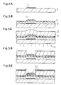
- FIG. 1 illustrates a first embodiment of the invention step by step.
- a gate electrode 7 is formed by a desired patterning (FIG. 1A).
- a gate insulator layer for example, silicon nitride; film thickness approx. 380 nm
- a first semiconductor layer for example, amorphous silicon; film thickness approx. 50 nm
- a passivation layer for example, silicon nitride; film thickness approx.
- a second semiconductor layer for example, phosphorus-doped low resistance amorphous silicon; film thickness approx. 50 nm
- a positive type photo resist 20 is then coated.
- ultraviolet ray 21 is irradiated from the back side of the transparent substrate 6, using the gate electrode 7 as the mask (FIG. 1C).
- the exposed areas of the first semiconductor layer 10 and second semiconductor layer 12 are removed by etching (FIG. 1D).
- a thin film composed of transparent conductive material for example, indium tin oxide (ITO); film thickness approx. 400 nm
- ITO indium tin oxide
- the gate electrode 7 As shown in this embodiment, by performing photolithography using the gate electrode 7 as the mask when forming the pattern of semiconductor layer, an inexpensive exposure machine not requiring alignment mechanism can be used, and the number of times of photolithography may be curtailed, too. Besides, since the semiconductor layer is not spreading wider than the gate electrode, the size of the device may be reduced. In this embodiment, meanwhile, the pixel electrode, source electrode and drain electrode are formed simultaneously, but they may be also formed separately.
- FIG. 2 shows a second embodiment of the invention step by step.
- a gate electrode 7 and an insular conductor layer 7a are formed (FIG. 2A).
- a gate insulator layer (first insulator layer) 9 a first semiconductor layer 10, and a passivation layer 11 are sequentially deposited, and the passivation layer 11 is etched, leaving only a part above the gate electrode 7 (FIG. 2B).
- a second semiconductor layer 12 also by plasma enhanced CVD process, a positive type photo resist 20 is coated.
- ultraviolet ray 21 is irradiated from the back side of the transparent substrate 6, using the gate electrode 7 and insular conductor layer 7a as the mask (FIG. 2C).
- the resist on the substrate is developed, the resist is removed except for the portion corresponding to the gate electrode 7 and insular conductor layer 7a.
- the exposed areas of the first semiconductor layer 10 and second semiconductor layer 12 are etched (FIG. 2D).
- a transparent electrode as pixel electrode 15, drain electrode 13, and source electrode 14 are formed (FIG. 2E)
- the redundancy of the source bus line is increased, and disconnection of the source bus line may be prevented.
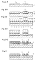
- FIG. 3 shows a third embodiment of the invention.
- Example 2 After etching the semiconductor layer in the same manner as in Example 2 (FIG. 2A to D), the resist is removed. Then, a transparent electrode layer is deposited and patterned to form drain electrode 13, source electrode 14 and pixel electrode 15 (FIG. 3), and an active matrix substrate is completed.
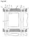
- FIG. 4 shows a fourth embodiment of the invention.
- FIG. 4A is a plan view of essential part of the active matrix array substrate in the fourth embodiment of the invention, showing one pixel and its surrounding parts.
- Numeral 7 is a gate electrode
- 14 is a source electrode
- 13 is a drain electrode
- 15 is a pixel electrode.
- Slits 22 are provided in the gate electrode.
- FIG. 4B to E are sectional views following step by step along the broken line CD in FIG. 4A.
- a gate electrode 7 of metal thin film is patterned and formed by using a first photo mask, and a gate insulator layer 9, a first semiconductor layer 10 and a second semiconductor layer 12 are continuously formed thereon.
- a positive type photo resist 20 is coated, and ultraviolet ray 21 is irradiated from the back side of the substrate (FIG. 4B), and the resist on the substrate is developed.
- the resist pattern is thinned out by the portion of d1 from the gate electrode 7 (FIG. 4C).
- the first semiconductor layer 10 and second semiconductor layer 12 are etched.
- the etching pattern is thinned out by the portion of d2 from the resist pattern.
- a transparent conductive layer is deposited, and patterning is effected by using a second photo mask, and the source electrode 14, drain electrode 13, and picture element electrode 15 are formed simultaneously.
- the second semiconductor layer is etched except for the portion of the second photo mask pattern (FIG. 4E).
- a TFT of which first semiconductor layer 10 is completely separated between adjacent TFTs is completed by using two photo masks.
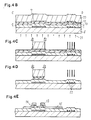
- FIG. 5 shows a fifth embodiment of the invention.
- Example 2 Same as in Example 1, on a transparent substrate 6, gate electrode 7, gate insulator layer (first insulator layer) 9, first semiconductor layer 10, passivation layer 11, and second semiconductor layer 12 are formed, and a negative type photo resist 23 is coated over the entire surface.
- an ultraviolet ray 21 is irradiated from the back side of the transparent substrate 6 using the gate electrode 7 as the mask (FIG. 5A to C).
- this resist on the substrate is developed, only the resist in the portion corresponding to the gate electrode 7 is removed (FIG. 5D).
- a conductor layer 24 is deposited (FIG. 5E), and the resist is removed, then the conductor layer 24 except for the portion above the gate electrode 7 is removed together with the resist.
- the first semiconductor layer 10 and second semiconductor layer 12 are etched (FIG. 5F).
- a transparent conductive layer is deposited and patterned to form drain electrode 13, source electrode 14 and pixel electrode 15, and then an active matrix substrate is completed (FIG. 5F).
- FIG. 6 shows a sixth embodiment of the invention.
- Example 2 on a transparent substrate 6, gate electrode 7, insular conductor layer 7a, gate insulator layer (first insulator layer) 9, first semiconductor layer 10, passivation layer 11, and second semiconductor layer 12 are formed, and a negative type photo resist 23 is coated over the entire surface.
- ultraviolet ray 21 is irradiated from the back side of the transparent substrate 6 using the gate electrode 7 and insular conductor layer 7a as the mask (FIG. 6A to C).
- the resist is removed only in the portions corresponding to the gate electrode 7 and insular conductor layer 7a (FIG. 6D).
- a conductor layer 24 is deposited (FIG.
- the gate electrode 7 as the mask when forming patterns of the semiconductor layer
- an inexpensive exposure machine not requiring alignment mechanism may be used, and the number of times of photolithography may be curtailed.
- the conductor layer 24 and semiconductor layer in the great part of the region beneath the source bus line, the redundancy of the source bus line increases along with lowering of resistance, so that disconnection of the source bus line may be prevented.
- the material of the conductor layer 24 in Examples 5 and 6 Cr, Ta, Ti, Mo, Ni and their alloys, or silicides of these metals may be used.
- FIG. 7 shows a seventh embodiment of the invention.
- the performance of the element may be enhanced without increasing the number of steps of photolithography using photo mask. That is, by inserting a metal oxide between the source electrode and drain electrode and the semiconductor layer, and reducing it to a metal, the resistances of the both electrodes may be lowered, and the contact resistance between the source electrode and the semiconductor layer and contact resistance between the drain electrode and the semiconductor layer may be lowered (conventionally, the contact resistance between the second semiconductor layer and the transparent electrode material of the metal oxide was often a problem, and it is improved herein).
- FIG. 8 shows an eighth embodiment of the invention.
- a gate electrode 7 and an insular conductor layer 7a are formed, and the rest of the procedure is same as in Example 7, and an active matrix substrate is completed (FIG. 7A to E).
- the redundancy of the source bus line is increased, and the disconnection of the source bus line may be prevented.
- the metal layer 14a reduced from the metal oxide the resistance of the source and drain electrodes is lowered, and the contact resistance between the source electrode and the semiconductor layer and the contact resistance between the drain electrode and the semiconductor layer may be lowered.
- TaOx and ITO may be adequately used.
- the reducing method instead of the hydrogen plasma processing, other methods such as exposure in hydrogen atmosphere may be equally employed. Again, better results are obtained when processed in hydrogen atmosphere or hydrogen plasma atmosphere.
- FIG. 9 shown a ninth embodiment of the invention.
- first semiconductor layer 10, passivation layer 11, and second semiconductor layer 12 are formed, and a positive type photo resist 20 is coated, and ultraviolet ray 21 is irradiated from the back side of the transparent substrate 6 using the gate electrode 7 as mask (FIG. 9A to C).
- a metal oxide film composed of at least one layer of metal oxide film, for example, 90% In2O3 - 10% SnO2 is deposited, and patterned to form drain electrode 13, source electrode 14, and pixel electrode 15 (FIG. 9D).
- a negative type photo resist 23 is coated, and ultraviolet ray is irradiated from the back side of the transparent substrate 6 using the gate electrode 7 as mask.
- the substrate After developing the resist (FIG. 9E), the substrate is exposed in hydrogen plasma atmosphere, and part of the drain electrode 13 and source electrode 14 is reduced to become In-Sn.
- an active matrix substrate is completed (FIG. 9F).
- the both electrodes may be lowered in resistance, and the contact resistance between the source electrode and semiconductor layer and the contact resistance between the drain electrode and semiconductor layer may be lowered.
- FIG. 10 shows a tenth embodiment of the invention.
- first semiconductor layer 10 and second semiconductor layer 12 are formed, and a positive type photo resist 20 is coated, and ultraviolet ray 21 is irradiated from the back side of the transparent substrate 6 using the gate electrode 7 as mask (FIG. 10A). After developing this resist, exposed areas of the first semiconductor layer 10 and second semiconductor layer 12 are etched.
- a two-layer metal oxide film composed of at least one metal oxide film such as 90% In2O3-10% SnO2, and Ta2O5 is deposited (the side contacting with the semiconductor is 90% In2O3-10% SnO2), and patterned, and drain electrode 13, source electrode 14 and pixel electrode 15 are formed, and a second insulator layer 19 is deposited thereon (FIG. 10B).
- a negative type photo resist 23 is coated, and ultraviolet ray is irradiated from the back side of the transparent substrate 6 using the gate electrode 7 as mask.
- the portion not covered by the resist of the second insulator layer 19 is etched (FIG.
- the both electrodes are lowered in resistance, while the contact resistance between the source electrode and semiconductor layer and the contact resistance between the drain electrode and semiconductor layer are lowered at the same time.
- the insulation layers of the both electrode surfaces and the second insulator layer 19 become passivation of active matrix substrate.
- Examples 9, 10 as the materials for drain electrode, source electrode and pixel electrode, 90% In2O3-10% SnO2 or 90% In2O3-10% SnO2, and TaO5 are used, but other materials which show conductivity when reduced may be similarly applied.
- 90% In2O3-10% SnO2 or 90% In2O3-10% SnO2, and TaO5 are used, but other materials which show conductivity when reduced may be similarly applied.
- one or more metal oxides selected from a group consisting of In, Sn, Cd, Zn, Nb, Ti and Ta are employed.
- Examples 9, 10 are the drain electrode and source electrode are reduced by processing in hydrogen plasma, but it may be also possible to reduced by exposing to hydrogen atmosphere or the like. However, the best results will be obtained by hydrogen plasma processing.
- the gate electrode material Cr, Ta, Ti, Mo, Ni, Ni-Cr or their metal silicides may be used as the gate electrode material. Any opaque conductive material may be employed as far as it may be used as the material for the gate electrode of the TFT.
- the materials for the gate insulator layer and passivation layer aside from silicon nitride, silicon oxide, metal oxide and other transparent insulators may be used.
- the first and second semiconductor layers amorphous silicon or phosphorus-doped amorphous silicon was used, but any semiconductor material may be equally used as far as it can obtain required TFT characteristics and pass ultraviolet rays to a certain extent, and, for example, polycrystal silicon or recrystallized silicon may be used.
- the material for the pixel electrode InOx, SnOx or transparent conductive material (ITO) of their mixed composition may be used.
- various conductive materials Al, Mo, Ni, other metals or their silicides
- the source and drain electrodes may be formed either in a single layer or in plural layers.
- the adhesion of the resist will be enhanced.
- an inexpensive exposure machine not requiring alignment mechanism may be used, and the photolithographic process requiring the photo mask may be curtailed, so that the reduction of cost which is the greatest subject in the active matrix type liquid crystal display device may be realized.
- the performance of the element may be improved by employing the photolithographic process which does not require precise alignment of mask. Therefore, its industrial significance is extremely great.
Description
- This invention relates to active matrix substrates for display devices used in liquid crystal television for video display, display for computer terminal or the like, and to methods for fabricating active matrix substrates for such use.
- Recently, for the purpose of application into display devices, active matrix substrates for forming thin film transistors (TFTs) on a transparent substrate are being intensively developed. The structure of such active matrix substrates is explained by referring to FIG. 11.
Numeral 1 is a TFT comprising a polycrystal silicon or amorphous silicon as a constituent element formed on a first transparent substrate (not shown), 2 is a liquid crystal between a transparent pixel electrode (electrically connected to the drain electrode of the TFT 1) and a transparent counter electrode on a second transparent substrate. 1 and 2 are disposed at a position corresponding to each pixel of avideo display region 3, and it may be provided with, aside from the electrostatic capacity due to liquid crystal, a capacity formed in the active matrix substrate as storage capacity.Numeral 4 is gate bus line connected to the gate electrode of theTFT TFT 1. In FIG. 11, pixel electrodes, the TFTs, gate bus lines and source bus lines are formed on the first transparent substrate as an active matrix substrate. - An example of the construction of the TFT which is a constituent element of such active matrix substrate is described below with reference to FIG. 12. FIG. 12A is a plan view of the TFT possessing a inverted staggered structure, and FIG. 12B is an A-B sectional view of FIG. 12A. Numeral 6 is a transparent substrate made of glass, and 7 is a gate electrode.
Numerals Numeral 8 is a silicon oxide layer for preventing contact between thegate electrode 7 andpixel electrode 15, and enhancing the adhesion between thegate insulator layer 9 andpixel electrode 15.Numerals Numeral 12 is a second semiconductor layer for achieving an ohmic contact between thefirst semiconductor layer 10 and electrodes which aredrain electrode 13 andsource electrode 14. Numeral 15 is a transparent electrode connected to thedrain electrode 13, and it is a pixel electrode for applying a voltage to the liquid crystal layer. In this example, meanwhile, thepixel electrode 15 is formed beneath thegate insulator layer 9, but thispixel electrode 15 may be also formed on the gate insulator layer, simultaneously and integrally with thedrain electrode 13 andsource electrode 14. Incidentally, in the TFT in the inverted staggered structure, since the gate electrode serves to shut off light against the incident light from the back side of the substrate, the leakage current in OFF state of TFT is small, and this structure is employed widely in commercial pocket-size TV sets. - A display device using such active matrix substrate is explained below while referring to FIG. 13. Between a
counter substrate 17 to which acounter electrode 16 is adhered, and the active matrix substrate, a twisted nematic (TN)liquid crystal 18 processed by twist orientation is sealed in, and polarizer plates (not shown) are glued to one side each of the two transparent substrates, thereby forming a display device. - As the development of such active matrix substrate becomes intensive, it gives rise to the necessity of forming such active matrix substrate on a large substrate in a range of scores of centimeters at a high yield. At the same time, it is also demanded to fabricate the elements at high density. In fabrication of active matrix substrate, therefore, it is required to process finely and precisely by using exposure machines having the same performance level as that for semiconductor process, and attachments such as the alignment mechanism of high precision. That is, conventionally, to form such an active matrix substrate as shown in FIG. 12, five or six photolithographic processes using photo masks are required.
- Such forming method involves several problems as mentioned below in the aspects of cost, yield and performance. First of all, the greater the number of times of photolithography, the more the high performance and expensive exposure machines and others are used, which results in a higher cost for forming the active matrix substrate. Besides, the more the number of times of photolithography, the more troubles may occur in the photolithographic processes (such as misalignment between patterns), and the yield is lowered accordingly. As the substrate material, meanwhile, pyrex and other glass materials are often used, and the strain of the substrate caused by the thermal expansion and contraction during process or stress of the thin film may become too large to be ignored (in particular, this problem is serious in a large substrate, and mismatching between patterns on the substrate formed by photo mask may often exceed 10 microns). As a result, the alignment precision is not uniform within a substrate, and uniformity of the device characteristics decreases, or it may be necessary to use a special apparatus for correcting this strain or to design the device with a special consideration in a margin taking such strain into account. In addition to the substrate strain, the greater the number of times of photo mask matching necessary for realizing the device, the larger becomes the device size for keeping the margin. As a result, the aperture ratio (the rate of effective display region) is lowered. Such phenomena are greater problems when the device density is higher and when the substrate is large. There are also other subjects to be solved, such as enhancement of the element capacity.
- In European patent application 0196915, there is disclosed a self-aligned TFT array for liquid crystal display devices and a method of manufacturing the array. A protective insulating layer on a semiconductor layer is exactly aligned with a gate electrode. A self-alignment method is used for patterning the protective insulating layer and an impurity-doped semiconductor layer on the semiconductor layer. The undoped semiconductor layer itself is patterned by etching, using a separate photomask to pattern a resist film which is then used as a mask for the etching of the semiconductor layer.
- In European patent application EP-A-0166647 there is described a method for forming an active matrix substrate, wherein a self-alignment method is used for the positioning of a passivation layer, and by virtue of this for the positioning of the source and drain electrodes.
- European patent application EP-A-0222668 discloses a method for forming a thin film transistor in which one semi-conductor layer is formed by a self-alignment process with respect to the gate electrode, in order to simplify the process of producing a stepped semi-conductor layer to which good ohmic contacts can then be made.
- It is hence a primary object of this invention, in the light of the above problems, to present a method for fabricating active matrix substrates at a lower cost, by curtailing the photolithographic processes which require precise alignment of photo masks. It is another object of this invention to enhance the performance of the element by employing photolithographic processes which do not require precise alignment of photo masks.
- To achieve the above objects, for example, this invention presents a method of fabricating an active matrix substrate, including the steps of:
forming a plurality of gate electrodes of an opaque electro-conducting material by patterning at specified places on a transparent substrate;
forming a gate insulator layer over said gate electrodes;
forming a first semiconductor layer on said gate insulator layer;
forming a second semiconductor layer on said first semiconductor layer;
coating a photoresist layer on the second semiconductor layer;
irradiating light from the back side of the substrate using said gate electrodes as a mask;
forming a resist pattern by developing said photoresist layer;
removing portions of the first and second semiconductor layers which have been irradiated by said light from the backside of the substrate, whereby said first and second semiconductor layers are patterned by a self-alignment process using said gate electrodes as a mask; and
forming a source region and a drain region on said second semiconductor layer by removing portions thereof to expose the first semiconductor layer. - According to the method of this invention, for example, when forming the pattern of semiconductor layer, since photolithography is possible by using the gate electrode (or gate electrode and insular conductor layer) as the mask, an inexpensive exposure machine not requiring the alignment mechanism may be used. Or, depending on the cases, the number of times of photolithography may be curtailed, which contributes to reduction of cost and increase of yield in the production of active matrix substrate. Or when irradiating light from the back side, there is no effect of expansion or contraction of the substrate, and a correctly aligned resist pattern will be obtained. Therefore, by using it, it may be possible to reduce the size of the TFT, and an active matrix substrate of high aperture ratio of high density may be realized. Besides, the device performance may be enhanced, and a high performance inverted staggered type TFT can be realized.
- While the novel features of the invention are set forth in the appended claims, the invention, both as to organization and content, will be better understood and appreciated, along with other objects and features thereof, from the following detailed description taken in conjunction with the drawings.
-
- FIG. 1, FIG. 2, FIG. 4B to E, and FIG. 5 to FIG. 13 are process sectional views showing the method for fabricating active matrix substrates in first, second, and fourth to tenth embodiments of the invention, respectively;
- FIG. 3 is a sectional view of an active matrix substrate obtained in a third embodiment of the invention;
- FIG. 4A is a plan view of an active matrix substrate obtained in a fourth embodiment of the invention;
- FIG. 11 is a circuit diagram of an active matrix substrate;
- FIG. 12A is a plan view of a thin film transistor for composing a conventional active matrix substrate;
- FIG. 12B is a sectional view of line A-B of FIG. 15A; and
- FIG. 13 is a sectional view of a conventional display device.
- Referring now to the drawings, preferred embodiments of the invention are described in details below.
- FIG. 1 illustrates a first embodiment of the invention step by step.
- On a transparent substrate (for example, Corning Glass 7059) 6, an opaque conductor thin film (for example, Cr; film thickness approx. 100 nm) is deposited by sputtering, and a
gate electrode 7 is formed by a desired patterning (FIG. 1A). By plasma enhanced CVD process, a gate insulator layer (first insulator layer, for example, silicon nitride; film thickness approx. 380 nm) 9, a first semiconductor layer (for example, amorphous silicon; film thickness approx. 50 nm) 10, and a passivation layer (for example, silicon nitride; film thickness approx. 80 nm) 11 are sequentially and uniformly deposited, and then thepassivation layer 11 is etched, leaving only a part above the gate electrode 7 (FIG. 1B). Next, by plasma enhanced CVD process, again, a second semiconductor layer (for example, phosphorus-doped low resistance amorphous silicon; film thickness approx. 50 nm) 12 is applied, and a positive type photo resist 20 is then coated. After prebaking the resist,ultraviolet ray 21 is irradiated from the back side of thetransparent substrate 6, using thegate electrode 7 as the mask (FIG. 1C). When the resist on the substrate is developed, the resist is removed, except for the portion corresponding to thegate electrode 7. After postbaking the resist, using this patterned resist as the etching mask, the exposed areas of thefirst semiconductor layer 10 andsecond semiconductor layer 12 are removed by etching (FIG. 1D). After removing the resist, a thin film composed of transparent conductive material (for example, indium tin oxide (ITO); film thickness approx. 400 nm) is deposited, and is patterned, and adrain electrode 13, asource electrode 14, and apixel electrode 15 are formed (FIG. 1E), so that an active matrix substrate is completed. - As shown in this embodiment, by performing photolithography using the
gate electrode 7 as the mask when forming the pattern of semiconductor layer, an inexpensive exposure machine not requiring alignment mechanism can be used, and the number of times of photolithography may be curtailed, too. Besides, since the semiconductor layer is not spreading wider than the gate electrode, the size of the device may be reduced. In this embodiment, meanwhile, the pixel electrode, source electrode and drain electrode are formed simultaneously, but they may be also formed separately. - FIG. 2 shows a second embodiment of the invention step by step.
- On a light
transmissible substrate 6, an opaque conductor thin film is deposited by sputtering, and by patterning as desired agate electrode 7 and an insular conductor layer 7a are formed (FIG. 2A). By plasma enhanced CVD process, a gate insulator layer (first insulator layer) 9, afirst semiconductor layer 10, and apassivation layer 11 are sequentially deposited, and thepassivation layer 11 is etched, leaving only a part above the gate electrode 7 (FIG. 2B). Then, after depositing asecond semiconductor layer 12 also by plasma enhanced CVD process, a positive type photo resist 20 is coated. After prebaking the resist,ultraviolet ray 21 is irradiated from the back side of thetransparent substrate 6, using thegate electrode 7 and insular conductor layer 7a as the mask (FIG. 2C). When the resist on the substrate is developed, the resist is removed except for the portion corresponding to thegate electrode 7 and insular conductor layer 7a. After postbaking the resist, using this resist as the mask the exposed areas of thefirst semiconductor layer 10 andsecond semiconductor layer 12 are etched (FIG. 2D). After removing the resist, when a transparent electrode aspixel electrode 15,drain electrode 13, andsource electrode 14 are formed (FIG. 2E), an active matrix substrate is completed. - As shown in this embodiment, by forming the semiconductor layer in the great part of the region beneath the source bus line, the redundancy of the source bus line is increased, and disconnection of the source bus line may be prevented.
- FIG. 3 shows a third embodiment of the invention.
- After etching the semiconductor layer in the same manner as in Example 2 (FIG. 2A to D), the resist is removed. Then, a transparent electrode layer is deposited and patterned to form
drain electrode 13,source electrode 14 and pixel electrode 15 (FIG. 3), and an active matrix substrate is completed. - Thus, in this embodiment, by forming the pixel electrode, source electrode and drain electrode simultaneously, one step of photolithography can be omitted.
- FIG. 4 shows a fourth embodiment of the invention.
- FIG. 4A is a plan view of essential part of the active matrix array substrate in the fourth embodiment of the invention, showing one pixel and its surrounding parts.
Numeral 7 is a gate electrode, 14 is a source electrode, 13 is a drain electrode, and 15 is a pixel electrode.Slits 22 are provided in the gate electrode. FIG. 4B to E are sectional views following step by step along the broken line CD in FIG. 4A. On a transparent substrate, agate electrode 7 of metal thin film is patterned and formed by using a first photo mask, and agate insulator layer 9, afirst semiconductor layer 10 and asecond semiconductor layer 12 are continuously formed thereon. In this state, a positive type photo resist 20 is coated, andultraviolet ray 21 is irradiated from the back side of the substrate (FIG. 4B), and the resist on the substrate is developed. At this time, by overexposure, the resist pattern is thinned out by the portion of d1 from the gate electrode 7 (FIG. 4C). Using this resist, furthermore, thefirst semiconductor layer 10 andsecond semiconductor layer 12 are etched. At this time, by overetching the etching pattern is thinned out by the portion of d2 from the resist pattern. By the effect of overexposure and overetching (d1+d2), the semiconductor layer is not left over on thegate wiring 7 around the slits 22 (FIG. 4D). By removing the resist, a transparent conductive layer is deposited, and patterning is effected by using a second photo mask, and thesource electrode 14,drain electrode 13, andpicture element electrode 15 are formed simultaneously. At this time, the second semiconductor layer is etched except for the portion of the second photo mask pattern (FIG. 4E). - In this embodiment, as shown in FIG. 4A, a TFT of which
first semiconductor layer 10 is completely separated between adjacent TFTs is completed by using two photo masks. - In the conventional structure, separation of devices (separation of semiconductor layers) was required by some method or other, but when the active matrix array substrate is formed in the method shown herein, a step of photolithography for separation of devices may be saved.
- FIG. 5 shows a fifth embodiment of the invention.
- Same as in Example 1, on a
transparent substrate 6,gate electrode 7, gate insulator layer (first insulator layer) 9,first semiconductor layer 10,passivation layer 11, andsecond semiconductor layer 12 are formed, and a negative type photo resist 23 is coated over the entire surface. After prebaking the resist, anultraviolet ray 21 is irradiated from the back side of thetransparent substrate 6 using thegate electrode 7 as the mask (FIG. 5A to C). When this resist on the substrate is developed, only the resist in the portion corresponding to thegate electrode 7 is removed (FIG. 5D). Next, aconductor layer 24 is deposited (FIG. 5E), and the resist is removed, then theconductor layer 24 except for the portion above thegate electrode 7 is removed together with the resist. Using thisconductor layer 24 as the etching mask, thefirst semiconductor layer 10 andsecond semiconductor layer 12 are etched (FIG. 5F). Next, a transparent conductive layer is deposited and patterned to formdrain electrode 13,source electrode 14 andpixel electrode 15, and then an active matrix substrate is completed (FIG. 5F). - As shown in this embodiment, by performing photolithography using the
gate electrode 7 as the mask when forming the pattern of semiconductor layer, an inexpensive exposure machine not requiring alignment mechanism can be used. At the same time, the number of times of photolithography may be curtailed. In this constitution, moreover, part of the source and drain electrodes becomes two-layer, and lowering of resistance of electrode and prevention of disconnection of electrode may be realized. - FIG. 6 shows a sixth embodiment of the invention.
- Same as in Example 2, on a
transparent substrate 6,gate electrode 7, insular conductor layer 7a, gate insulator layer (first insulator layer) 9,first semiconductor layer 10,passivation layer 11, andsecond semiconductor layer 12 are formed, and a negative type photo resist 23 is coated over the entire surface. After prebaking the resist,ultraviolet ray 21 is irradiated from the back side of thetransparent substrate 6 using thegate electrode 7 and insular conductor layer 7a as the mask (FIG. 6A to C). By developing the resist on the substrate, the resist is removed only in the portions corresponding to thegate electrode 7 and insular conductor layer 7a (FIG. 6D). Next, aconductor layer 24 is deposited (FIG. 6E), and the resist is removed, so that theconductor layer 24 is removed together with the resist except for the portion corresponding to thegate electrode 7 and insular conductor layer 7a (FIG. 6F). Using thisconductor layer 24 as the etching mask, thefirst semiconductor layer 10 andsecond semiconductor layer 12 are patterned, and a transparent conductive layer is deposited and patterned to formdrain electrode 13,source electrode 14 andpixel electrode 15, thereby completing an active matrix substrate (FIG. 6G). - Thus, according to this embodiment, by performing photolithography using the
gate electrode 7 as the mask when forming patterns of the semiconductor layer, an inexpensive exposure machine not requiring alignment mechanism may be used, and the number of times of photolithography may be curtailed. In addition, by forming theconductor layer 24 and semiconductor layer in the great part of the region beneath the source bus line, the redundancy of the source bus line increases along with lowering of resistance, so that disconnection of the source bus line may be prevented. - Incidentally, as the material of the
conductor layer 24 in Examples 5 and 6, Cr, Ta, Ti, Mo, Ni and their alloys, or silicides of these metals may be used. - FIG. 7 shows a seventh embodiment of the invention.
- Same as in Example 1, on a
transparent substrate 6,gate electrode 7, gate insulator layer (first insulator layer) 9,first semiconductor layer 10,passivation layer 11, andsecond semiconductor layer 12 are formed, and ametal oxide 25 is deposited, and a positive type photo resist 20 is coated over the entire surface. After prebaking the resist,ultraviolet ray 21 is irradiated from the back side of thetransparent substrate 6 using thegate electrode 7 as the mask (FIG. 7A to C). When this resist on the substrate is developed, the resist is removed except for the portion corresponding to thegate electrode 7. After postbaking the resist, using this resist as the mask the exposed areas of themetal oxide 25,first semiconductor layer 10 andsecond semiconductor layer 12 are etched away (FIG. 7D). After removing the resist, when the substrate is exposed to hydrogen plasma atmosphere, themetal oxide 25 is reduced to become ametal layer 14a. Finally, when a transparent electrode aspixel electrode 15, and drainelectrode 13 andsource electrode 14 are formed (FIG. 7E), an active matrix substrate is completed. - In this embodiment, as shown herein, the performance of the element may be enhanced without increasing the number of steps of photolithography using photo mask. That is, by inserting a metal oxide between the source electrode and drain electrode and the semiconductor layer, and reducing it to a metal, the resistances of the both electrodes may be lowered, and the contact resistance between the source electrode and the semiconductor layer and contact resistance between the drain electrode and the semiconductor layer may be lowered (conventionally, the contact resistance between the second semiconductor layer and the transparent electrode material of the metal oxide was often a problem, and it is improved herein).
- FIG. 8 shows an eighth embodiment of the invention.
- On a
transparent substrate 6, agate electrode 7 and an insular conductor layer 7a are formed, and the rest of the procedure is same as in Example 7, and an active matrix substrate is completed (FIG. 7A to E). - In this embodiment, by forming the semiconductor layer and metal layer in the great part of the region beneath the source bus line, the redundancy of the source bus line is increased, and the disconnection of the source bus line may be prevented. Besides, by the
metal layer 14a reduced from the metal oxide, the resistance of the source and drain electrodes is lowered, and the contact resistance between the source electrode and the semiconductor layer and the contact resistance between the drain electrode and the semiconductor layer may be lowered. - In Examples 7, 8, as the
metal oxide 25, TaOx and ITO may be adequately used. As the reducing method, instead of the hydrogen plasma processing, other methods such as exposure in hydrogen atmosphere may be equally employed. Anyway, better results are obtained when processed in hydrogen atmosphere or hydrogen plasma atmosphere. - FIG. 9 shown a ninth embodiment of the invention.
- Same as in Example 1, on a
transparent substrate 6,gate electrode 7, gate insulator layer (first insulator layer) 9,first semiconductor layer 10,passivation layer 11, andsecond semiconductor layer 12 are formed, and a positive type photo resist 20 is coated, andultraviolet ray 21 is irradiated from the back side of thetransparent substrate 6 using thegate electrode 7 as mask (FIG. 9A to C). After developing this resist, the exposed areas of thefirst semiconductor layer 10, andsecond semiconductor layer 12 are etched. Next, a metal oxide film composed of at least one layer of metal oxide film, for example, 90% In₂O₃ - 10% SnO₂ is deposited, and patterned to formdrain electrode 13,source electrode 14, and pixel electrode 15 (FIG. 9D). On this, a negative type photo resist 23 is coated, and ultraviolet ray is irradiated from the back side of thetransparent substrate 6 using thegate electrode 7 as mask. After developing the resist (FIG. 9E), the substrate is exposed in hydrogen plasma atmosphere, and part of thedrain electrode 13 andsource electrode 14 is reduced to become In-Sn. When the resist is removed, an active matrix substrate is completed (FIG. 9F). - Thus, in this embodiment, by reducing the source electrode and drain electrode to transform into metals, the both electrodes may be lowered in resistance, and the contact resistance between the source electrode and semiconductor layer and the contact resistance between the drain electrode and semiconductor layer may be lowered.
- FIG. 10 shows a tenth embodiment of the invention.
- Same as in Example 1, on a
tranparent substrate 6,gate electrode 7, gate insulator layer (first insulator layer) 9,first semiconductor layer 10,passivation layer 11 andsecond semiconductor layer 12 are formed, and a positive type photo resist 20 is coated, andultraviolet ray 21 is irradiated from the back side of thetransparent substrate 6 using thegate electrode 7 as mask (FIG. 10A). After developing this resist, exposed areas of thefirst semiconductor layer 10 andsecond semiconductor layer 12 are etched. A two-layer metal oxide film composed of at least one metal oxide film such as 90% In₂O₃-10% SnO₂, and Ta₂O₅ is deposited (the side contacting with the semiconductor is 90% In₂O₃-10% SnO₂), and patterned, and drainelectrode 13,source electrode 14 andpixel electrode 15 are formed, and asecond insulator layer 19 is deposited thereon (FIG. 10B). On this, furthermore, a negative type photo resist 23 is coated, and ultraviolet ray is irradiated from the back side of thetransparent substrate 6 using thegate electrode 7 as mask. By developing the resist, the portion not covered by the resist of thesecond insulator layer 19 is etched (FIG. 10C), and the substrate is exposed to hydrogen plasma atmosphere, then the metal oxide films of thedrain electrode 13 andsource electrode 14 are reduced to form a two-layer metal film composed of In-Sn and Ta. At this time, when the active matrix substrate is exposed in an oxygen plasma atmosphere or oxidized anodically, the surface layer of the reduceddrain electrode 13 andsource electrode 14 are oxidized again to be insulation layer, and when the resist is removed, an active matrix substrate is completed (FIG. 10D). - In this embodiment, thus, by reducing the source electrode and drain electrode to transform into metals, the both electrodes are lowered in resistance, while the contact resistance between the source electrode and semiconductor layer and the contact resistance between the drain electrode and semiconductor layer are lowered at the same time. Besides, by oxidizing the surface, the insulation layers of the both electrode surfaces and the
second insulator layer 19 become passivation of active matrix substrate. - In Examples 9, 10, meanwhile, as the materials for drain electrode, source electrode and pixel electrode, 90% In₂O₃-10% SnO₂ or 90% In₂O₃-10% SnO₂, and TaO₅ are used, but other materials which show conductivity when reduced may be similarly applied. Anyway, better results will be obtained when one or more metal oxides selected from a group consisting of In, Sn, Cd, Zn, Nb, Ti and Ta are employed.
- Besides, in Examples 9, 10, are the drain electrode and source electrode are reduced by processing in hydrogen plasma, but it may be also possible to reduced by exposing to hydrogen atmosphere or the like. However, the best results will be obtained by hydrogen plasma processing.
- In the above embodiments from Example 1 to Example 10, as the gate electrode material, Cr, Ta, Ti, Mo, Ni, Ni-Cr or their metal silicides may be used. Any opaque conductive material may be employed as far as it may be used as the material for the gate electrode of the TFT. As the materials for the gate insulator layer and passivation layer, aside from silicon nitride, silicon oxide, metal oxide and other transparent insulators may be used. As the first and second semiconductor layers, amorphous silicon or phosphorus-doped amorphous silicon was used, but any semiconductor material may be equally used as far as it can obtain required TFT characteristics and pass ultraviolet rays to a certain extent, and, for example, polycrystal silicon or recrystallized silicon may be used. Furthermore, as the material for the pixel electrode, InOx, SnOx or transparent conductive material (ITO) of their mixed composition may be used. When forming, meanwhile, the source electrode, drain electrode and picture element electrode separately, various conductive materials (Al, Mo, Ni, other metals or their silicides) may be used as the materials for source electrode and drain electrode. In this case, the source and drain electrodes may be formed either in a single layer or in plural layers.
- Besides, before coating the positive or negative type photo resist, by using a primer for the resist, the adhesion of the resist will be enhanced.
- As clear from the embodiments illustrated and described herein, according to the method for fabricating the active matrix substrate of the invention, an inexpensive exposure machine not requiring alignment mechanism may be used, and the photolithographic process requiring the photo mask may be curtailed, so that the reduction of cost which is the greatest subject in the active matrix type liquid crystal display device may be realized. Besides, the performance of the element may be improved by employing the photolithographic process which does not require precise alignment of mask. Therefore, its industrial significance is extremely great.
Claims (11)
- A method of fabricating an active matrix substrate, including the steps of:
forming a plurality of gate electrodes (7) of an opaque electro-conducting material by patterning at specified places on a transparent substrate (6);
forming a gate insulator layer (9) over said gate electrodes (7);
forming a first semiconductor layer (10) on said gate insulator layer (9);
forming a second semiconductor layer (12) on said first semiconductor layer (10);
coating a photoresist layer (20, 23) on the second semiconductor layer;
irradiating light from the back side of the substrate (6) using said gate electrodes (7) as a mask;
forming a resist pattern by developing said photoresist layer (20, 23);
removing portions of the first and second semiconductor layers (10, 12) which have been irradiated by said light from the backside of the substrate (6), whereby said first and second semiconductor layers (10, 12) are patterned by a self-alignment process using said gate electrodes (7) as a mask; and
forming a source region and a drain region on said second semiconductor layer (12) by removing portions thereof to expose the first semiconductor layer (10). - A method of fabricating an active matrix substrate according to claim 1, further comprising steps of
forming a passivation layer (11) by patterning on said first semiconductor layer (10) above a part of each gate electrode (7); and
forming a drain electrode (13), a source electrode (14) and a pixel electrode (15) by depositing a layer of transparent conductive material on each said drain and said source region and patterning it. - A method of fabricating an active matrix substrate according to claim 1, further comprising a step of
forming an insular region (7a) of the same opaque electro-conducting material as said gate electrodes (7) by patterning at a specified place of the transparent substrate (6), wherein said first and second semiconductor layers (10, 12) are formed above said insular region (7a) by the self alignment process using said insular region (7a) as the mask. - A method of fabricating an active matrix substrate according to claim 3, further comprising a step of
forming a drain electrode (13), a source electrode (14) and a pixel electrode (15) by depositing a layer of transparent conductive material on each said drain and said source region and patterning it. - A method of fabricating an active matrix substrate according to claim 1, further comprising the steps of
forming slits (22) in selected gate electrodes (7), wherein in said steps of irradiating and forming a resist pattern, said photoresist layer (20) is overexposed and over-etched such as to allow removal of the semiconductor layers (10, 12) from around the slits (22) in said selected gate electrodes (7); and
forming a drain electrode (13), a source electrode (14) and a pixel electrode (15) by depositing a layer of transparent conductive material on each said drain and said source region and patterning it. - A method of fabricating an active matrix substrate according to claim 1, further comprising the steps of
forming a passivation layer (11) by patterning on said first semiconductor layer (10) above a part of said gate electrodes (7);
forming a conductor layer (24) on the portion of the semiconductor layer (12) above said gate electrodes (7) prior to the step of forming said source and drain regions; wherein said step further comprises removing portions of said conductor layer (24) as well as portions of said semiconductor layer (12) from above said gate electrode layer (7) to expose the first semiconductor layer (10); and
forming a drain electrode (13), a source electrode (14) and a pixel electrode (15) by depositing and patterning a layer of transparent conductive material on the remaining portions of the conductor layer (24). - A method of fabricating an active matrix substrate according to claim 6, further comprising the steps of
forming an insular region (7a) of the same opaque electro-conducting material as said gate electrodes (7) by patterning at a specified place of the transparent substrate (6), wherein said first and second semiconductor layers (10, 12) and said conductor layer (24) are formed above said insular region (7a) by the self-alignment process using said insular layer (7a) as the mask. - A method of fabricating an active matrix substrate according to claim 1, further comprising a step of
forming a passivation layer (11) by patterning on said first semiconductor layer (10) above a part of said gate electrodes (7);
depositing a metal oxide layer (25) on said second semiconductor layer (12) prior to said step of coating a photoresist layer (25) thereon, such that said metal oxide layer (25) is also patterned by the self-alignment process using the gate electrodes (7) as the mask, wherein the step of forming the source and drain regions further comprises removing portions of the metal oxide layer (25) as well as portions of said second semiconductor layer (12) from above said gate electrode (7) to expose the first semiconductor layer (10);
reducing the metal oxide layer (25) to produce a metal layer (14a); and
forming a drain electrode (13), a source electrode (14) and a pixel electrode (15) by depositing and patterning a layer of transparent conductive material on the remaining portions of the metal layer (14a). - A method of fabricating an active matrix substrate according to claim 8, further comprising steps of
forming an insular region (7a) of the same opaque electro-conducting material as said gate electrodes (7) by patterning at a specified place of the transparent substrate (6), wherein said first and second semiconductor layers (10, 12) and said metal layer (14a) are formed above said insular region (7a) using said insular region (7a) as the mask. - A method of fabricating an active matrix substrate according to claim 1, further comprising the steps of
depositing a metal oxide layer on said second semiconductor layer (12) after the step of forming the source and drain regions;
patterning said metal oxide layer to form a drain electrode (13), a source electrode (14) and a pixel electrode (15);
coating a negative type photoresist (23) on said metal oxide layer;
irradiating light from the back side of the substrate (6);
developing the resist (23); and
reducing the exposed part of the source electrode (14) and the drain electrode (13). - A method of fabricating an active matrix substrate according to claim 1, further comprising the steps of
depositing a two-layer metal oxide film comprising at least one metal oxide layer on said second semiconductor layer (12) after the step of forming the source and drain regions;
patterning said metal oxide film to form a drain electrode (13), a source electrode (14) and a pixel electrode (15);
depositing a second insulator layer (19) thereon;
coating a negative type photoresist (23) on said second insulator layer (19);
irradiating light from the back side of the substrate (6) using the gate electrodes (7) as the mask;
developing the resist (23);
removing the exposed part of the second insulating layer (19) not covered by the resist (23);
reducing the metal oxide films of the drain electrode (13) and source electrode (14) to form a two-layer metal film;
oxidizing the surface layer of the drain electrode (13) and the source electrode (14); and
removing the remaining portions of the resist (23).
Applications Claiming Priority (4)
| Application Number | Priority Date | Filing Date | Title |
|---|---|---|---|
| JP97008/88 | 1988-04-20 | ||
| JP9700888 | 1988-04-20 | ||
| JP63248197A JPH0242761A (en) | 1988-04-20 | 1988-09-30 | Manufacture of active matrix substrate |
| JP248197/88 | 1988-09-30 |
Publications (2)
| Publication Number | Publication Date |
|---|---|
| EP0338766A1 EP0338766A1 (en) | 1989-10-25 |
| EP0338766B1 true EP0338766B1 (en) | 1995-08-09 |
Family
ID=26438156
Family Applications (1)
| Application Number | Title | Priority Date | Filing Date |
|---|---|---|---|
| EP89303812A Expired - Lifetime EP0338766B1 (en) | 1988-04-20 | 1989-04-18 | Method of fabricating an active matrix substrate |
Country Status (5)
| Country | Link |
|---|---|
| US (1) | US5622814A (en) |
| EP (1) | EP0338766B1 (en) |
| JP (1) | JPH0242761A (en) |
| KR (1) | KR930007529B1 (en) |
| DE (1) | DE68923727T2 (en) |
Cited By (4)
| Publication number | Priority date | Publication date | Assignee | Title |
|---|---|---|---|---|
| US7190387B2 (en) | 2003-09-11 | 2007-03-13 | Bright View Technologies, Inc. | Systems for fabricating optical microstructures using a cylindrical platform and a rastered radiation beam |
| US7192692B2 (en) | 2003-09-11 | 2007-03-20 | Bright View Technologies, Inc. | Methods for fabricating microstructures by imaging a radiation sensitive layer sandwiched between outer layers |
| US7867695B2 (en) | 2003-09-11 | 2011-01-11 | Bright View Technologies Corporation | Methods for mastering microstructures through a substrate using negative photoresist |
| US7900513B2 (en) | 1993-03-30 | 2011-03-08 | Kazuhiro Okada | Multi-axial angular velocity sensor |
Families Citing this family (67)
| Publication number | Priority date | Publication date | Assignee | Title |
|---|---|---|---|---|
| JP2604867B2 (en) * | 1990-01-11 | 1997-04-30 | 松下電器産業株式会社 | Reflective liquid crystal display device |
| JP2767958B2 (en) * | 1990-02-20 | 1998-06-25 | 松下電器産業株式会社 | Method for manufacturing semiconductor device |
| JP2938121B2 (en) * | 1990-03-30 | 1999-08-23 | 株式会社東芝 | Method for manufacturing thin film semiconductor device |
| US6314823B1 (en) | 1991-09-20 | 2001-11-13 | Kazuhiro Okada | Force detector and acceleration detector and method of manufacturing the same |
| US5421213A (en) * | 1990-10-12 | 1995-06-06 | Okada; Kazuhiro | Multi-dimensional force detector |
| DE69125260T2 (en) * | 1990-12-28 | 1997-10-02 | Sharp Kk | A method of manufacturing a thin film transistor and an active matrix substrate for liquid crystal display devices |
| US5474941A (en) * | 1990-12-28 | 1995-12-12 | Sharp Kabushiki Kaisha | Method for producing an active matrix substrate |
| US5420048A (en) * | 1991-01-09 | 1995-05-30 | Canon Kabushiki Kaisha | Manufacturing method for SOI-type thin film transistor |
| GB9114018D0 (en) * | 1991-06-28 | 1991-08-14 | Philips Electronic Associated | Thin-film transistor manufacture |
| JP3172840B2 (en) * | 1992-01-28 | 2001-06-04 | 株式会社日立製作所 | Active matrix substrate manufacturing method and liquid crystal display device |
| JP3172841B2 (en) * | 1992-02-19 | 2001-06-04 | 株式会社日立製作所 | Thin film transistor, method of manufacturing the same, and liquid crystal display device |
| US5254480A (en) | 1992-02-20 | 1993-10-19 | Minnesota Mining And Manufacturing Company | Process for producing a large area solid state radiation detector |
| GB9217743D0 (en) * | 1992-08-19 | 1992-09-30 | Philips Electronics Uk Ltd | A semiconductor memory device |
| JP2530990B2 (en) * | 1992-10-15 | 1996-09-04 | 富士通株式会社 | Method of manufacturing thin film transistor matrix |
| US5643801A (en) * | 1992-11-06 | 1997-07-01 | Semiconductor Energy Laboratory Co., Ltd. | Laser processing method and alignment |
| US6544825B1 (en) * | 1992-12-26 | 2003-04-08 | Semiconductor Energy Laboratory Co., Ltd. | Method of fabricating a MIS transistor |
| US6410374B1 (en) | 1992-12-26 | 2002-06-25 | Semiconductor Energy Laborartory Co., Ltd. | Method of crystallizing a semiconductor layer in a MIS transistor |
| JP2755376B2 (en) * | 1994-06-03 | 1998-05-20 | 株式会社フロンテック | Manufacturing method of electro-optical element |
| JP3469337B2 (en) * | 1994-12-16 | 2003-11-25 | 株式会社半導体エネルギー研究所 | Method for manufacturing semiconductor device |
| JP3778456B2 (en) | 1995-02-21 | 2006-05-24 | 株式会社半導体エネルギー研究所 | Method for manufacturing insulated gate thin film semiconductor device |
| JP3478012B2 (en) * | 1995-09-29 | 2003-12-10 | ソニー株式会社 | Method for manufacturing thin film semiconductor device |
| KR100193348B1 (en) * | 1996-02-12 | 1999-07-01 | 구자홍 | Fabrication method of thin film transistor for lcd |
| KR100448934B1 (en) * | 1996-12-27 | 2004-12-04 | 삼성전자주식회사 | Fabrication method of a liquid crystal display device, especially in relation to enabling a pixel electrode to magnetically and fully interface with a signal line |
| JP3883641B2 (en) * | 1997-03-27 | 2007-02-21 | 株式会社半導体エネルギー研究所 | Contact structure and active matrix display device |
| KR100271043B1 (en) * | 1997-11-28 | 2000-11-01 | 구본준, 론 위라하디락사 | Lcd substrate and its fabrication method |
| US6372535B1 (en) | 1998-02-02 | 2002-04-16 | Samsung Electronics Co., Ltd. | Manufacturing method of a thin film transistor |
| JP4118484B2 (en) | 2000-03-06 | 2008-07-16 | 株式会社半導体エネルギー研究所 | Method for manufacturing semiconductor device |
| JP2001257350A (en) | 2000-03-08 | 2001-09-21 | Semiconductor Energy Lab Co Ltd | Semiconductor device and its preparation method |
| JP4700160B2 (en) | 2000-03-13 | 2011-06-15 | 株式会社半導体エネルギー研究所 | Semiconductor device |
| JP4118485B2 (en) * | 2000-03-13 | 2008-07-16 | 株式会社半導体エネルギー研究所 | Method for manufacturing semiconductor device |
| JP4683688B2 (en) | 2000-03-16 | 2011-05-18 | 株式会社半導体エネルギー研究所 | Method for manufacturing liquid crystal display device |
| JP4393662B2 (en) | 2000-03-17 | 2010-01-06 | 株式会社半導体エネルギー研究所 | Method for manufacturing liquid crystal display device |
| JP4785229B2 (en) | 2000-05-09 | 2011-10-05 | 株式会社半導体エネルギー研究所 | Method for manufacturing semiconductor device |
| TW521316B (en) * | 2000-11-09 | 2003-02-21 | Macronix Int Co Ltd | Manufacturing method for reducing critical dimensions |
| RU2295803C2 (en) * | 2001-01-19 | 2007-03-20 | Атраверда Лимитед | Storage battery electrode |
| US7071037B2 (en) * | 2001-03-06 | 2006-07-04 | Semiconductor Energy Laboratory Co., Ltd. | Semiconductor device and manufacturing method thereof |
| KR100495701B1 (en) * | 2001-03-07 | 2005-06-14 | 삼성에스디아이 주식회사 | A processing for a organic electroluminescent display |
| US6794119B2 (en) * | 2002-02-12 | 2004-09-21 | Iridigm Display Corporation | Method for fabricating a structure for a microelectromechanical systems (MEMS) device |
| US6887627B2 (en) * | 2002-04-26 | 2005-05-03 | Macronix International Co., Ltd. | Method of fabricating phase shift mask |
| US7781850B2 (en) | 2002-09-20 | 2010-08-24 | Qualcomm Mems Technologies, Inc. | Controlling electromechanical behavior of structures within a microelectromechanical systems device |
| TW564564B (en) * | 2002-10-03 | 2003-12-01 | Au Optronics Corp | Pixel structure and fabricating method thereof |
| US6995045B2 (en) * | 2003-03-05 | 2006-02-07 | Chunghwa Picture Tubes, Ltd. | Thin film transistor and method of forming thin film transistor |
| TW570896B (en) | 2003-05-26 | 2004-01-11 | Prime View Int Co Ltd | A method for fabricating an interference display cell |
| US7221495B2 (en) * | 2003-06-24 | 2007-05-22 | Idc Llc | Thin film precursor stack for MEMS manufacturing |
| US7720148B2 (en) * | 2004-03-26 | 2010-05-18 | The Hong Kong University Of Science And Technology | Efficient multi-frame motion estimation for video compression |
| US20060065622A1 (en) * | 2004-09-27 | 2006-03-30 | Floyd Philip D | Method and system for xenon fluoride etching with enhanced efficiency |
| US7684104B2 (en) * | 2004-09-27 | 2010-03-23 | Idc, Llc | MEMS using filler material and method |
| US7553684B2 (en) * | 2004-09-27 | 2009-06-30 | Idc, Llc | Method of fabricating interferometric devices using lift-off processing techniques |
| KR100685955B1 (en) * | 2004-12-30 | 2007-02-23 | 엘지.필립스 엘시디 주식회사 | Liquid Crystal Display Device |
| CN100343749C (en) * | 2005-01-27 | 2007-10-17 | 广辉电子股份有限公司 | Array substrate of thin film transistor liquid crystal display and manufacturing method thereof |
| EP1882270A1 (en) * | 2005-03-16 | 2008-01-30 | Newsouth Innovations Pty Limited | Photolithography method for contacting thin-film semiconductor structures |
| EP2495212A3 (en) * | 2005-07-22 | 2012-10-31 | QUALCOMM MEMS Technologies, Inc. | Mems devices having support structures and methods of fabricating the same |
| US7795061B2 (en) | 2005-12-29 | 2010-09-14 | Qualcomm Mems Technologies, Inc. | Method of creating MEMS device cavities by a non-etching process |
| US7547568B2 (en) * | 2006-02-22 | 2009-06-16 | Qualcomm Mems Technologies, Inc. | Electrical conditioning of MEMS device and insulating layer thereof |
| US7711239B2 (en) | 2006-04-19 | 2010-05-04 | Qualcomm Mems Technologies, Inc. | Microelectromechanical device and method utilizing nanoparticles |
| US7763546B2 (en) | 2006-08-02 | 2010-07-27 | Qualcomm Mems Technologies, Inc. | Methods for reducing surface charges during the manufacture of microelectromechanical systems devices |
| US7706042B2 (en) * | 2006-12-20 | 2010-04-27 | Qualcomm Mems Technologies, Inc. | MEMS device and interconnects for same |
| US7719752B2 (en) | 2007-05-11 | 2010-05-18 | Qualcomm Mems Technologies, Inc. | MEMS structures, methods of fabricating MEMS components on separate substrates and assembly of same |
| EP2181355A1 (en) * | 2007-07-25 | 2010-05-05 | Qualcomm Mems Technologies, Inc. | Mems display devices and methods of fabricating the same |
| US7719754B2 (en) * | 2008-09-30 | 2010-05-18 | Qualcomm Mems Technologies, Inc. | Multi-thickness layers for MEMS and mask-saving sequence for same |
| KR101436120B1 (en) | 2009-12-28 | 2014-09-01 | 가부시키가이샤 한도오따이 에네루기 켄큐쇼 | Method for manufacturing semiconductor device |
| GB2532895B (en) * | 2012-02-21 | 2016-07-13 | Pragmatic Printing Ltd | Substantially planar electronic devices and circuits |
| KR101960796B1 (en) * | 2012-03-08 | 2019-07-16 | 삼성디스플레이 주식회사 | Method of manufacturing a thin-film transistor, method of manufacturing a display substrate, and display substrate |
| CN103456742B (en) * | 2013-08-27 | 2017-02-15 | 京东方科技集团股份有限公司 | Array substrate, manufacturing method of array substrate and display device |
| CN104112711B (en) * | 2014-07-22 | 2017-05-03 | 深圳市华星光电技术有限公司 | Manufacturing method of coplanar oxide semiconductor TFT (Thin Film Transistor) substrate |
| CN104377246A (en) * | 2014-10-08 | 2015-02-25 | 京东方科技集团股份有限公司 | Thin film transistor, manufacturing method thereof, array substrate and display device |
| KR102423679B1 (en) * | 2015-09-21 | 2022-07-21 | 삼성디스플레이 주식회사 | Method of manufacturing display device |
Family Cites Families (13)
| Publication number | Priority date | Publication date | Assignee | Title |
|---|---|---|---|---|
| DE2658400A1 (en) * | 1976-12-23 | 1978-06-29 | Ibm Deutschland | METHOD OF MANUFACTURING A NEGATIVE MASK ON A SUBSTRATE |
| US4277884A (en) * | 1980-08-04 | 1981-07-14 | Rca Corporation | Method for forming an improved gate member utilizing special masking and oxidation to eliminate projecting points on silicon islands |
| JPS5952881A (en) * | 1982-09-21 | 1984-03-27 | Fujitsu Ltd | Manufacture of field-effect type semiconductor device |
| JPS59224822A (en) * | 1983-06-06 | 1984-12-17 | Fujitsu Ltd | Manufacture of liquid-crystal display panel |
| FR2566186B1 (en) * | 1984-06-14 | 1986-08-29 | Thomson Csf | METHOD FOR MANUFACTURING AT LEAST ONE THIN FILM FIELD EFFECT TRANSISTOR AND TRANSISTOR OBTAINED THEREBY |
| EP0196915B1 (en) * | 1985-03-29 | 1991-08-14 | Matsushita Electric Industrial Co., Ltd. | Thin film transistor array and method of manufacturing same |
| JP2913300B2 (en) * | 1985-09-26 | 1999-06-28 | セイコーインスツルメンツ株式会社 | Method for manufacturing thin film transistor device |
| FR2590409B1 (en) * | 1985-11-15 | 1987-12-11 | Commissariat Energie Atomique | METHOD FOR MANUFACTURING A THIN FILM TRANSISTOR WITH A SELF-ALIGNED GRID WITH RESPECT TO THE DRAIN AND THE SOURCE THEREOF AND TRANSISTOR OBTAINED BY THE PROCESS |
| JPS62140467A (en) * | 1985-12-13 | 1987-06-24 | Sharp Corp | Manufacture of thin-film transistor |
| JPH0612387B2 (en) * | 1985-12-17 | 1994-02-16 | 三洋電機株式会社 | Liquid crystal display |
| JPH07119909B2 (en) * | 1986-08-29 | 1995-12-20 | 株式会社日立製作所 | Liquid crystal display element manufacturing method |
| US4931351A (en) * | 1987-01-12 | 1990-06-05 | Eastman Kodak Company | Bilayer lithographic process |
| GB8721193D0 (en) * | 1987-09-09 | 1987-10-14 | Wright S W | Semiconductor devices |
-
1988
- 1988-09-30 JP JP63248197A patent/JPH0242761A/en active Pending
-
1989
- 1989-04-18 DE DE68923727T patent/DE68923727T2/en not_active Expired - Fee Related
- 1989-04-18 EP EP89303812A patent/EP0338766B1/en not_active Expired - Lifetime
- 1989-04-20 KR KR1019890005223A patent/KR930007529B1/en not_active IP Right Cessation
-
1994
- 1994-07-11 US US08/272,634 patent/US5622814A/en not_active Expired - Fee Related
Cited By (7)
| Publication number | Priority date | Publication date | Assignee | Title |
|---|---|---|---|---|
| US7900513B2 (en) | 1993-03-30 | 2011-03-08 | Kazuhiro Okada | Multi-axial angular velocity sensor |
| US7190387B2 (en) | 2003-09-11 | 2007-03-13 | Bright View Technologies, Inc. | Systems for fabricating optical microstructures using a cylindrical platform and a rastered radiation beam |
| US7192692B2 (en) | 2003-09-11 | 2007-03-20 | Bright View Technologies, Inc. | Methods for fabricating microstructures by imaging a radiation sensitive layer sandwiched between outer layers |
| US7425407B1 (en) | 2003-09-11 | 2008-09-16 | Bright View Technologies, Inc. | Methods for fabricating optical microstructures by imaging a radiation sensitive layer sandwiched between outer layers |
| US7763417B2 (en) | 2003-09-11 | 2010-07-27 | Tredegar Newco, Inc. | Methods for fabricating optical microstructures using a cylindrical platform and a rastered radiation beam |
| US7867695B2 (en) | 2003-09-11 | 2011-01-11 | Bright View Technologies Corporation | Methods for mastering microstructures through a substrate using negative photoresist |
| US8263318B2 (en) | 2003-09-11 | 2012-09-11 | Bright View Technologies Corporation | Methods for mastering microstructures through a substrate using negative photoresist |
Also Published As
| Publication number | Publication date |
|---|---|
| US5622814A (en) | 1997-04-22 |
| DE68923727D1 (en) | 1995-09-14 |
| KR900017166A (en) | 1990-11-15 |
| JPH0242761A (en) | 1990-02-13 |
| EP0338766A1 (en) | 1989-10-25 |
| KR930007529B1 (en) | 1993-08-12 |
| DE68923727T2 (en) | 1996-03-21 |
Similar Documents
| Publication | Publication Date | Title |
|---|---|---|
| EP0338766B1 (en) | Method of fabricating an active matrix substrate | |
| US7157319B2 (en) | Method of patterning a thin film transistor that includes simultaneously forming a gate electrode and a pixel electrode | |
| US4958205A (en) | Thin film transistor array and method of manufacturing the same | |
| EP0775931B1 (en) | Method of manufacturing a liquid crystal display | |
| US7649581B2 (en) | Array substrate of an LCD comprising first and second gate insulating layers and method of fabricating the same | |
| EP0304657B1 (en) | Active matrix cell and method of manufacturing the same | |
| JP2004341550A (en) | Liquid crystal display device and method of manufacturing liquid crystal display device | |
| EP1646076B1 (en) | Manufacturing method of a thin film transistor array panel | |
| JP2004163968A (en) | Method for manufacturing liquid crystal display device | |
| US5998230A (en) | Method for making liquid crystal display device with reduced mask steps | |
| US6927087B2 (en) | Active matrix substrate for a liquid crystal display and method of forming the same | |
| JPH11133455A (en) | Production of liquid crystal display device | |
| US6043000A (en) | Method for manufacturing a semiconductor device | |
| US7023501B2 (en) | Liquid crystal display device having particular connections among drain and pixel electrodes and contact hole | |
| JP2678044B2 (en) | Active matrix substrate manufacturing method | |
| KR100669093B1 (en) | Method of Fabricating Liquid Crystal Display Device | |
| US6317174B1 (en) | TFT array substrate, liquid crystal display using TFT array substrate, and manufacturing method thereof | |
| JP2002350897A (en) | Method for manufacturing matrix substrate for liquid crystal | |
| JP2002098994A (en) | Matrix substrate for liquid crystal, and method for manufacturing the same and method of forming the contact hole | |
| WO2004036303A1 (en) | A thin film translator array panel and a method for manufacturing the panel | |
| KR20000047011A (en) | Photographic etching method of thin film and a fabrication method of thin film transistor substrate for liquid crystal display using it | |
| KR100897720B1 (en) | Fabrication method of Liquid Crystal Display | |
| JPH07142737A (en) | Manufacture of thin-film transistor | |
| KR100330097B1 (en) | Thin film transistor substrate for liquid crystal display and manufacturing method thereof | |
| KR20010019666A (en) | Tft lcd |
Legal Events
| Date | Code | Title | Description |
|---|---|---|---|
| PUAI | Public reference made under article 153(3) epc to a published international application that has entered the european phase |
Free format text: ORIGINAL CODE: 0009012 |
|
| AK | Designated contracting states |
Kind code of ref document: A1 Designated state(s): DE FR GB |
|
| 17P | Request for examination filed |
Effective date: 19900424 |
|
| 17Q | First examination report despatched |
Effective date: 19920818 |
|
| GRAA | (expected) grant |
Free format text: ORIGINAL CODE: 0009210 |
|
| AK | Designated contracting states |
Kind code of ref document: B1 Designated state(s): DE FR GB |
|
| REF | Corresponds to: |
Ref document number: 68923727 Country of ref document: DE Date of ref document: 19950914 |
|
| ET | Fr: translation filed | ||
| PLBE | No opposition filed within time limit |
Free format text: ORIGINAL CODE: 0009261 |
|
| STAA | Information on the status of an ep patent application or granted ep patent |
Free format text: STATUS: NO OPPOSITION FILED WITHIN TIME LIMIT |
|
| 26N | No opposition filed | ||
| REG | Reference to a national code |
Ref country code: GB Ref legal event code: IF02 |
|
| REG | Reference to a national code |
Ref country code: GB Ref legal event code: 746 Effective date: 20031002 |
|
| REG | Reference to a national code |
Ref country code: FR Ref legal event code: D6 |
|
| PGFP | Annual fee paid to national office [announced via postgrant information from national office to epo] |
Ref country code: FR Payment date: 20060410 Year of fee payment: 18 |
|
| PGFP | Annual fee paid to national office [announced via postgrant information from national office to epo] |
Ref country code: GB Payment date: 20060412 Year of fee payment: 18 |
|
| PGFP | Annual fee paid to national office [announced via postgrant information from national office to epo] |
Ref country code: DE Payment date: 20060413 Year of fee payment: 18 |
|
| GBPC | Gb: european patent ceased through non-payment of renewal fee |
Effective date: 20070418 |
|
| PG25 | Lapsed in a contracting state [announced via postgrant information from national office to epo] |
Ref country code: DE Free format text: LAPSE BECAUSE OF NON-PAYMENT OF DUE FEES Effective date: 20071101 |
|
| PG25 | Lapsed in a contracting state [announced via postgrant information from national office to epo] |
Ref country code: GB Free format text: LAPSE BECAUSE OF NON-PAYMENT OF DUE FEES Effective date: 20070418 |
|
| PG25 | Lapsed in a contracting state [announced via postgrant information from national office to epo] |
Ref country code: FR Free format text: LAPSE BECAUSE OF NON-PAYMENT OF DUE FEES Effective date: 20070430 |