JP4700160B2 - Semiconductor device - Google Patents
Semiconductor device Download PDFInfo
- Publication number
- JP4700160B2 JP4700160B2 JP2000069563A JP2000069563A JP4700160B2 JP 4700160 B2 JP4700160 B2 JP 4700160B2 JP 2000069563 A JP2000069563 A JP 2000069563A JP 2000069563 A JP2000069563 A JP 2000069563A JP 4700160 B2 JP4700160 B2 JP 4700160B2
- Authority
- JP
- Japan
- Prior art keywords
- film
- conductive
- substrate
- insulating film
- line side
- Prior art date
- Legal status (The legal status is an assumption and is not a legal conclusion. Google has not performed a legal analysis and makes no representation as to the accuracy of the status listed.)
- Expired - Fee Related
Links
- 239000004065 semiconductor Substances 0.000 title claims description 221
- 239000010408 film Substances 0.000 claims description 529
- 239000000758 substrate Substances 0.000 claims description 176
- 239000010410 layer Substances 0.000 claims description 161
- 239000004973 liquid crystal related substance Substances 0.000 claims description 58
- 239000000463 material Substances 0.000 claims description 34
- 239000011159 matrix material Substances 0.000 claims description 20
- 239000002245 particle Substances 0.000 claims description 14
- 239000010409 thin film Substances 0.000 claims description 14
- 239000013078 crystal Substances 0.000 claims description 12
- 238000013461 design Methods 0.000 claims description 9
- 239000012528 membrane Substances 0.000 claims 4
- 238000000034 method Methods 0.000 description 165
- 239000012535 impurity Substances 0.000 description 73
- 230000008569 process Effects 0.000 description 61
- 238000004519 manufacturing process Methods 0.000 description 56
- 238000005530 etching Methods 0.000 description 52
- 230000015572 biosynthetic process Effects 0.000 description 36
- 238000005268 plasma chemical vapour deposition Methods 0.000 description 31
- 229910052710 silicon Inorganic materials 0.000 description 31
- 238000004544 sputter deposition Methods 0.000 description 31
- XUIMIQQOPSSXEZ-UHFFFAOYSA-N Silicon Chemical compound [Si] XUIMIQQOPSSXEZ-UHFFFAOYSA-N 0.000 description 30
- 239000010703 silicon Substances 0.000 description 30
- 238000010438 heat treatment Methods 0.000 description 28
- 239000010936 titanium Substances 0.000 description 28
- VYPSYNLAJGMNEJ-UHFFFAOYSA-N silicon dioxide Inorganic materials O=[Si]=O VYPSYNLAJGMNEJ-UHFFFAOYSA-N 0.000 description 27
- 239000011521 glass Substances 0.000 description 26
- 239000003990 capacitor Substances 0.000 description 25
- 229910021417 amorphous silicon Inorganic materials 0.000 description 24
- 239000004020 conductor Substances 0.000 description 24
- 229910052698 phosphorus Inorganic materials 0.000 description 24
- OAICVXFJPJFONN-UHFFFAOYSA-N Phosphorus Chemical compound [P] OAICVXFJPJFONN-UHFFFAOYSA-N 0.000 description 23
- 239000011574 phosphorus Substances 0.000 description 23
- 238000002425 crystallisation Methods 0.000 description 21
- 238000006243 chemical reaction Methods 0.000 description 20
- 238000012545 processing Methods 0.000 description 19
- 229910052814 silicon oxide Inorganic materials 0.000 description 18
- 239000012298 atmosphere Substances 0.000 description 16
- 230000003197 catalytic effect Effects 0.000 description 16
- 239000007789 gas Substances 0.000 description 16
- 230000008025 crystallization Effects 0.000 description 15
- 238000010586 diagram Methods 0.000 description 15
- 239000003054 catalyst Substances 0.000 description 13
- 229910052751 metal Inorganic materials 0.000 description 13
- 239000002184 metal Substances 0.000 description 13
- 238000000206 photolithography Methods 0.000 description 13
- 238000003860 storage Methods 0.000 description 13
- 229910052719 titanium Inorganic materials 0.000 description 13
- 229910052581 Si3N4 Inorganic materials 0.000 description 11
- 239000000956 alloy Substances 0.000 description 11
- 229910052739 hydrogen Inorganic materials 0.000 description 11
- 239000011347 resin Substances 0.000 description 11
- 229920005989 resin Polymers 0.000 description 11
- HQVNEWCFYHHQES-UHFFFAOYSA-N silicon nitride Chemical compound N12[Si]34N5[Si]62N3[Si]51N64 HQVNEWCFYHHQES-UHFFFAOYSA-N 0.000 description 11
- XYFCBTPGUUZFHI-UHFFFAOYSA-N Phosphine Chemical compound P XYFCBTPGUUZFHI-UHFFFAOYSA-N 0.000 description 10
- 229910045601 alloy Inorganic materials 0.000 description 10
- 239000001257 hydrogen Substances 0.000 description 10
- UFHFLCQGNIYNRP-UHFFFAOYSA-N Hydrogen Chemical compound [H][H] UFHFLCQGNIYNRP-UHFFFAOYSA-N 0.000 description 9
- 125000004429 atom Chemical group 0.000 description 9
- 230000007547 defect Effects 0.000 description 9
- 239000010453 quartz Substances 0.000 description 9
- 229910052782 aluminium Inorganic materials 0.000 description 8
- 230000004888 barrier function Effects 0.000 description 8
- 239000011651 chromium Substances 0.000 description 8
- 239000010949 copper Substances 0.000 description 8
- 230000005611 electricity Effects 0.000 description 8
- 230000003068 static effect Effects 0.000 description 8
- 229910052715 tantalum Inorganic materials 0.000 description 8
- PXHVJJICTQNCMI-UHFFFAOYSA-N Nickel Chemical compound [Ni] PXHVJJICTQNCMI-UHFFFAOYSA-N 0.000 description 7
- 239000000460 chlorine Substances 0.000 description 7
- 239000011810 insulating material Substances 0.000 description 7
- 239000011229 interlayer Substances 0.000 description 7
- IJGRMHOSHXDMSA-UHFFFAOYSA-N Atomic nitrogen Chemical compound N#N IJGRMHOSHXDMSA-UHFFFAOYSA-N 0.000 description 6
- 230000001133 acceleration Effects 0.000 description 6
- 238000000137 annealing Methods 0.000 description 6
- 229910052804 chromium Inorganic materials 0.000 description 6
- 238000001312 dry etching Methods 0.000 description 6
- 239000010931 gold Substances 0.000 description 6
- 229910021424 microcrystalline silicon Inorganic materials 0.000 description 6
- 239000012495 reaction gas Substances 0.000 description 6
- 239000002356 single layer Substances 0.000 description 6
- MZLGASXMSKOWSE-UHFFFAOYSA-N tantalum nitride Chemical compound [Ta]#N MZLGASXMSKOWSE-UHFFFAOYSA-N 0.000 description 6
- XLOMVQKBTHCTTD-UHFFFAOYSA-N zinc oxide Inorganic materials [Zn]=O XLOMVQKBTHCTTD-UHFFFAOYSA-N 0.000 description 6
- 230000015556 catabolic process Effects 0.000 description 5
- 229910052802 copper Inorganic materials 0.000 description 5
- 229910021419 crystalline silicon Inorganic materials 0.000 description 5
- 229910052736 halogen Inorganic materials 0.000 description 5
- 150000002367 halogens Chemical class 0.000 description 5
- 150000002500 ions Chemical class 0.000 description 5
- 239000012299 nitrogen atmosphere Substances 0.000 description 5
- 229910000073 phosphorus hydride Inorganic materials 0.000 description 5
- 230000035882 stress Effects 0.000 description 5
- 238000002230 thermal chemical vapour deposition Methods 0.000 description 5
- 238000001039 wet etching Methods 0.000 description 5
- XKRFYHLGVUSROY-UHFFFAOYSA-N Argon Chemical compound [Ar] XKRFYHLGVUSROY-UHFFFAOYSA-N 0.000 description 4
- KRHYYFGTRYWZRS-UHFFFAOYSA-N Fluorane Chemical compound F KRHYYFGTRYWZRS-UHFFFAOYSA-N 0.000 description 4
- VEXZGXHMUGYJMC-UHFFFAOYSA-N Hydrochloric acid Chemical compound Cl VEXZGXHMUGYJMC-UHFFFAOYSA-N 0.000 description 4
- KDLHZDBZIXYQEI-UHFFFAOYSA-N Palladium Chemical compound [Pd] KDLHZDBZIXYQEI-UHFFFAOYSA-N 0.000 description 4
- BOTDANWDWHJENH-UHFFFAOYSA-N Tetraethyl orthosilicate Chemical compound CCO[Si](OCC)(OCC)OCC BOTDANWDWHJENH-UHFFFAOYSA-N 0.000 description 4
- LEVVHYCKPQWKOP-UHFFFAOYSA-N [Si].[Ge] Chemical compound [Si].[Ge] LEVVHYCKPQWKOP-UHFFFAOYSA-N 0.000 description 4
- 239000005407 aluminoborosilicate glass Substances 0.000 description 4
- 229910052788 barium Inorganic materials 0.000 description 4
- DSAJWYNOEDNPEQ-UHFFFAOYSA-N barium atom Chemical compound [Ba] DSAJWYNOEDNPEQ-UHFFFAOYSA-N 0.000 description 4
- 230000000903 blocking effect Effects 0.000 description 4
- 239000005388 borosilicate glass Substances 0.000 description 4
- 238000005520 cutting process Methods 0.000 description 4
- 230000007423 decrease Effects 0.000 description 4
- 230000000694 effects Effects 0.000 description 4
- 238000005247 gettering Methods 0.000 description 4
- 238000005499 laser crystallization Methods 0.000 description 4
- 238000004518 low pressure chemical vapour deposition Methods 0.000 description 4
- 238000002156 mixing Methods 0.000 description 4
- 229910052750 molybdenum Inorganic materials 0.000 description 4
- 229910052760 oxygen Inorganic materials 0.000 description 4
- 229920001721 polyimide Polymers 0.000 description 4
- 230000001681 protective effect Effects 0.000 description 4
- 239000000565 sealant Substances 0.000 description 4
- 239000000243 solution Substances 0.000 description 4
- 229910052721 tungsten Inorganic materials 0.000 description 4
- ZAMOUSCENKQFHK-UHFFFAOYSA-N Chlorine atom Chemical compound [Cl] ZAMOUSCENKQFHK-UHFFFAOYSA-N 0.000 description 3
- RYGMFSIKBFXOCR-UHFFFAOYSA-N Copper Chemical compound [Cu] RYGMFSIKBFXOCR-UHFFFAOYSA-N 0.000 description 3
- 229910052779 Neodymium Inorganic materials 0.000 description 3
- 239000004642 Polyimide Substances 0.000 description 3
- XAGFODPZIPBFFR-UHFFFAOYSA-N aluminium Chemical compound [Al] XAGFODPZIPBFFR-UHFFFAOYSA-N 0.000 description 3
- 230000008901 benefit Effects 0.000 description 3
- 229910052801 chlorine Inorganic materials 0.000 description 3
- 238000011109 contamination Methods 0.000 description 3
- 230000006866 deterioration Effects 0.000 description 3
- 229910052732 germanium Inorganic materials 0.000 description 3
- GNPVGFCGXDBREM-UHFFFAOYSA-N germanium atom Chemical compound [Ge] GNPVGFCGXDBREM-UHFFFAOYSA-N 0.000 description 3
- 238000009616 inductively coupled plasma Methods 0.000 description 3
- 238000010030 laminating Methods 0.000 description 3
- 239000007769 metal material Substances 0.000 description 3
- 229910052759 nickel Inorganic materials 0.000 description 3
- 150000004767 nitrides Chemical class 0.000 description 3
- 229910052757 nitrogen Inorganic materials 0.000 description 3
- 230000010355 oscillation Effects 0.000 description 3
- BPUBBGLMJRNUCC-UHFFFAOYSA-N oxygen(2-);tantalum(5+) Chemical compound [O-2].[O-2].[O-2].[O-2].[O-2].[Ta+5].[Ta+5] BPUBBGLMJRNUCC-UHFFFAOYSA-N 0.000 description 3
- BASFCYQUMIYNBI-UHFFFAOYSA-N platinum Chemical compound [Pt] BASFCYQUMIYNBI-UHFFFAOYSA-N 0.000 description 3
- 238000007650 screen-printing Methods 0.000 description 3
- 229910021332 silicide Inorganic materials 0.000 description 3
- FVBUAEGBCNSCDD-UHFFFAOYSA-N silicide(4-) Chemical compound [Si-4] FVBUAEGBCNSCDD-UHFFFAOYSA-N 0.000 description 3
- HBMJWWWQQXIZIP-UHFFFAOYSA-N silicon carbide Chemical compound [Si+]#[C-] HBMJWWWQQXIZIP-UHFFFAOYSA-N 0.000 description 3
- 238000009751 slip forming Methods 0.000 description 3
- 125000006850 spacer group Chemical group 0.000 description 3
- 229910001936 tantalum oxide Inorganic materials 0.000 description 3
- 238000001771 vacuum deposition Methods 0.000 description 3
- 239000011787 zinc oxide Substances 0.000 description 3
- ZOKXTWBITQBERF-UHFFFAOYSA-N Molybdenum Chemical compound [Mo] ZOKXTWBITQBERF-UHFFFAOYSA-N 0.000 description 2
- 239000004988 Nematic liquid crystal Substances 0.000 description 2
- BLRPTPMANUNPDV-UHFFFAOYSA-N Silane Chemical compound [SiH4] BLRPTPMANUNPDV-UHFFFAOYSA-N 0.000 description 2
- 229910000577 Silicon-germanium Inorganic materials 0.000 description 2
- 239000004990 Smectic liquid crystal Substances 0.000 description 2
- ATJFFYVFTNAWJD-UHFFFAOYSA-N Tin Chemical compound [Sn] ATJFFYVFTNAWJD-UHFFFAOYSA-N 0.000 description 2
- RTAQQCXQSZGOHL-UHFFFAOYSA-N Titanium Chemical compound [Ti] RTAQQCXQSZGOHL-UHFFFAOYSA-N 0.000 description 2
- NRTOMJZYCJJWKI-UHFFFAOYSA-N Titanium nitride Chemical compound [Ti]#N NRTOMJZYCJJWKI-UHFFFAOYSA-N 0.000 description 2
- NIXOWILDQLNWCW-UHFFFAOYSA-N acrylic acid group Chemical group C(C=C)(=O)O NIXOWILDQLNWCW-UHFFFAOYSA-N 0.000 description 2
- 230000004913 activation Effects 0.000 description 2
- 239000000853 adhesive Substances 0.000 description 2
- 230000001070 adhesive effect Effects 0.000 description 2
- 239000003513 alkali Substances 0.000 description 2
- 229910052786 argon Inorganic materials 0.000 description 2
- 229910052785 arsenic Inorganic materials 0.000 description 2
- QVGXLLKOCUKJST-UHFFFAOYSA-N atomic oxygen Chemical compound [O] QVGXLLKOCUKJST-UHFFFAOYSA-N 0.000 description 2
- IVHJCRXBQPGLOV-UHFFFAOYSA-N azanylidynetungsten Chemical compound [W]#N IVHJCRXBQPGLOV-UHFFFAOYSA-N 0.000 description 2
- 239000002585 base Substances 0.000 description 2
- UMIVXZPTRXBADB-UHFFFAOYSA-N benzocyclobutene Chemical compound C1=CC=C2CCC2=C1 UMIVXZPTRXBADB-UHFFFAOYSA-N 0.000 description 2
- 238000009125 cardiac resynchronization therapy Methods 0.000 description 2
- 239000003795 chemical substances by application Substances 0.000 description 2
- 150000001875 compounds Chemical class 0.000 description 2
- 238000006356 dehydrogenation reaction Methods 0.000 description 2
- 238000007599 discharging Methods 0.000 description 2
- 238000007687 exposure technique Methods 0.000 description 2
- 230000002349 favourable effect Effects 0.000 description 2
- 230000005669 field effect Effects 0.000 description 2
- PCHJSUWPFVWCPO-UHFFFAOYSA-N gold Chemical compound [Au] PCHJSUWPFVWCPO-UHFFFAOYSA-N 0.000 description 2
- 238000005984 hydrogenation reaction Methods 0.000 description 2
- 230000001771 impaired effect Effects 0.000 description 2
- 238000005468 ion implantation Methods 0.000 description 2
- LQJIDIOGYJAQMF-UHFFFAOYSA-N lambda2-silanylidenetin Chemical compound [Si].[Sn] LQJIDIOGYJAQMF-UHFFFAOYSA-N 0.000 description 2
- 238000003475 lamination Methods 0.000 description 2
- 238000005224 laser annealing Methods 0.000 description 2
- WABPQHHGFIMREM-UHFFFAOYSA-N lead(0) Chemical compound [Pb] WABPQHHGFIMREM-UHFFFAOYSA-N 0.000 description 2
- 239000011733 molybdenum Substances 0.000 description 2
- 239000001301 oxygen Substances 0.000 description 2
- 229910052763 palladium Inorganic materials 0.000 description 2
- 238000002161 passivation Methods 0.000 description 2
- 238000000059 patterning Methods 0.000 description 2
- 230000002093 peripheral effect Effects 0.000 description 2
- 239000004033 plastic Substances 0.000 description 2
- 230000006798 recombination Effects 0.000 description 2
- 230000009467 reduction Effects 0.000 description 2
- 229910000077 silane Inorganic materials 0.000 description 2
- 238000004528 spin coating Methods 0.000 description 2
- GUVRBAGPIYLISA-UHFFFAOYSA-N tantalum atom Chemical compound [Ta] GUVRBAGPIYLISA-UHFFFAOYSA-N 0.000 description 2
- WFKWXMTUELFFGS-UHFFFAOYSA-N tungsten Chemical compound [W] WFKWXMTUELFFGS-UHFFFAOYSA-N 0.000 description 2
- 239000010937 tungsten Substances 0.000 description 2
- 238000007740 vapor deposition Methods 0.000 description 2
- OYQCBJZGELKKPM-UHFFFAOYSA-N zinc indium(3+) oxygen(2-) Chemical compound [O-2].[Zn+2].[O-2].[In+3] OYQCBJZGELKKPM-UHFFFAOYSA-N 0.000 description 2
- ZOXJGFHDIHLPTG-UHFFFAOYSA-N Boron Chemical compound [B] ZOXJGFHDIHLPTG-UHFFFAOYSA-N 0.000 description 1
- OKTJSMMVPCPJKN-UHFFFAOYSA-N Carbon Chemical compound [C] OKTJSMMVPCPJKN-UHFFFAOYSA-N 0.000 description 1
- VYZAMTAEIAYCRO-UHFFFAOYSA-N Chromium Chemical compound [Cr] VYZAMTAEIAYCRO-UHFFFAOYSA-N 0.000 description 1
- GYHNNYVSQQEPJS-UHFFFAOYSA-N Gallium Chemical compound [Ga] GYHNNYVSQQEPJS-UHFFFAOYSA-N 0.000 description 1
- XEEYBQQBJWHFJM-UHFFFAOYSA-N Iron Chemical compound [Fe] XEEYBQQBJWHFJM-UHFFFAOYSA-N 0.000 description 1
- 229910021578 Iron(III) chloride Inorganic materials 0.000 description 1
- GRYLNZFGIOXLOG-UHFFFAOYSA-N Nitric acid Chemical compound O[N+]([O-])=O GRYLNZFGIOXLOG-UHFFFAOYSA-N 0.000 description 1
- 239000004952 Polyamide Substances 0.000 description 1
- 238000001069 Raman spectroscopy Methods 0.000 description 1
- 229910006404 SnO 2 Inorganic materials 0.000 description 1
- 230000003213 activating effect Effects 0.000 description 1
- 229910052783 alkali metal Inorganic materials 0.000 description 1
- 150000001340 alkali metals Chemical class 0.000 description 1
- 150000001408 amides Chemical class 0.000 description 1
- 239000007864 aqueous solution Substances 0.000 description 1
- 238000000149 argon plasma sintering Methods 0.000 description 1
- RQNWIZPPADIBDY-UHFFFAOYSA-N arsenic atom Chemical compound [As] RQNWIZPPADIBDY-UHFFFAOYSA-N 0.000 description 1
- 229910052796 boron Inorganic materials 0.000 description 1
- 239000000919 ceramic Substances 0.000 description 1
- 230000008859 change Effects 0.000 description 1
- 238000004140 cleaning Methods 0.000 description 1
- 239000011248 coating agent Substances 0.000 description 1
- 238000000576 coating method Methods 0.000 description 1
- 229910017052 cobalt Inorganic materials 0.000 description 1
- 239000010941 cobalt Substances 0.000 description 1
- GUTLYIVDDKVIGB-UHFFFAOYSA-N cobalt atom Chemical compound [Co] GUTLYIVDDKVIGB-UHFFFAOYSA-N 0.000 description 1
- 239000011889 copper foil Substances 0.000 description 1
- 230000007797 corrosion Effects 0.000 description 1
- 238000005260 corrosion Methods 0.000 description 1
- 238000001723 curing Methods 0.000 description 1
- 230000002950 deficient Effects 0.000 description 1
- 238000007872 degassing Methods 0.000 description 1
- 238000000151 deposition Methods 0.000 description 1
- 230000008021 deposition Effects 0.000 description 1
- 238000011161 development Methods 0.000 description 1
- 239000010432 diamond Substances 0.000 description 1
- 229910003460 diamond Inorganic materials 0.000 description 1
- 238000009792 diffusion process Methods 0.000 description 1
- 238000010790 dilution Methods 0.000 description 1
- 239000012895 dilution Substances 0.000 description 1
- 238000001035 drying Methods 0.000 description 1
- 239000007772 electrode material Substances 0.000 description 1
- 238000007772 electroless plating Methods 0.000 description 1
- 238000009713 electroplating Methods 0.000 description 1
- 238000005516 engineering process Methods 0.000 description 1
- 229910052733 gallium Inorganic materials 0.000 description 1
- 238000010574 gas phase reaction Methods 0.000 description 1
- 229910052737 gold Inorganic materials 0.000 description 1
- 150000002431 hydrogen Chemical class 0.000 description 1
- 230000006872 improvement Effects 0.000 description 1
- 229910003437 indium oxide Inorganic materials 0.000 description 1
- PJXISJQVUVHSOJ-UHFFFAOYSA-N indium(iii) oxide Chemical compound [O-2].[O-2].[O-2].[In+3].[In+3] PJXISJQVUVHSOJ-UHFFFAOYSA-N 0.000 description 1
- AMGQUBHHOARCQH-UHFFFAOYSA-N indium;oxotin Chemical compound [In].[Sn]=O AMGQUBHHOARCQH-UHFFFAOYSA-N 0.000 description 1
- 238000002347 injection Methods 0.000 description 1
- 239000007924 injection Substances 0.000 description 1
- 238000007689 inspection Methods 0.000 description 1
- 239000012212 insulator Substances 0.000 description 1
- RBTARNINKXHZNM-UHFFFAOYSA-K iron trichloride Chemical compound Cl[Fe](Cl)Cl RBTARNINKXHZNM-UHFFFAOYSA-K 0.000 description 1
- 239000003550 marker Substances 0.000 description 1
- 239000011259 mixed solution Substances 0.000 description 1
- 239000000203 mixture Substances 0.000 description 1
- 229910021421 monocrystalline silicon Inorganic materials 0.000 description 1
- QEFYFXOXNSNQGX-UHFFFAOYSA-N neodymium atom Chemical compound [Nd] QEFYFXOXNSNQGX-UHFFFAOYSA-N 0.000 description 1
- 229910017604 nitric acid Inorganic materials 0.000 description 1
- 230000003287 optical effect Effects 0.000 description 1
- 230000003647 oxidation Effects 0.000 description 1
- 238000007254 oxidation reaction Methods 0.000 description 1
- 230000001590 oxidative effect Effects 0.000 description 1
- 230000003071 parasitic effect Effects 0.000 description 1
- 230000035515 penetration Effects 0.000 description 1
- 238000000016 photochemical curing Methods 0.000 description 1
- 229920002120 photoresistant polymer Polymers 0.000 description 1
- 238000007747 plating Methods 0.000 description 1
- 229910052697 platinum Inorganic materials 0.000 description 1
- 229920002647 polyamide Polymers 0.000 description 1
- 229910021420 polycrystalline silicon Inorganic materials 0.000 description 1
- 239000009719 polyimide resin Substances 0.000 description 1
- 238000007639 printing Methods 0.000 description 1
- 238000003672 processing method Methods 0.000 description 1
- 238000004151 rapid thermal annealing Methods 0.000 description 1
- 230000003014 reinforcing effect Effects 0.000 description 1
- 229910052706 scandium Inorganic materials 0.000 description 1
- SIXSYDAISGFNSX-UHFFFAOYSA-N scandium atom Chemical compound [Sc] SIXSYDAISGFNSX-UHFFFAOYSA-N 0.000 description 1
- 238000007789 sealing Methods 0.000 description 1
- 229910052709 silver Inorganic materials 0.000 description 1
- 239000007787 solid Substances 0.000 description 1
- 238000005507 spraying Methods 0.000 description 1
- 239000010935 stainless steel Substances 0.000 description 1
- 229910001220 stainless steel Inorganic materials 0.000 description 1
- 230000008646 thermal stress Effects 0.000 description 1
- 229910021341 titanium silicide Inorganic materials 0.000 description 1
- 238000002834 transmittance Methods 0.000 description 1
- WQJQOUPTWCFRMM-UHFFFAOYSA-N tungsten disilicide Chemical compound [Si]#[W]#[Si] WQJQOUPTWCFRMM-UHFFFAOYSA-N 0.000 description 1
- NXHILIPIEUBEPD-UHFFFAOYSA-H tungsten hexafluoride Chemical compound F[W](F)(F)(F)(F)F NXHILIPIEUBEPD-UHFFFAOYSA-H 0.000 description 1
- 229910021342 tungsten silicide Inorganic materials 0.000 description 1
Images


Classifications
-
- G—PHYSICS
- G02—OPTICS
- G02F—OPTICAL DEVICES OR ARRANGEMENTS FOR THE CONTROL OF LIGHT BY MODIFICATION OF THE OPTICAL PROPERTIES OF THE MEDIA OF THE ELEMENTS INVOLVED THEREIN; NON-LINEAR OPTICS; FREQUENCY-CHANGING OF LIGHT; OPTICAL LOGIC ELEMENTS; OPTICAL ANALOGUE/DIGITAL CONVERTERS
- G02F1/00—Devices or arrangements for the control of the intensity, colour, phase, polarisation or direction of light arriving from an independent light source, e.g. switching, gating or modulating; Non-linear optics
- G02F1/01—Devices or arrangements for the control of the intensity, colour, phase, polarisation or direction of light arriving from an independent light source, e.g. switching, gating or modulating; Non-linear optics for the control of the intensity, phase, polarisation or colour
- G02F1/13—Devices or arrangements for the control of the intensity, colour, phase, polarisation or direction of light arriving from an independent light source, e.g. switching, gating or modulating; Non-linear optics for the control of the intensity, phase, polarisation or colour based on liquid crystals, e.g. single liquid crystal display cells
- G02F1/133—Constructional arrangements; Operation of liquid crystal cells; Circuit arrangements
- G02F1/136—Liquid crystal cells structurally associated with a semi-conducting layer or substrate, e.g. cells forming part of an integrated circuit
-
- H—ELECTRICITY
- H01—ELECTRIC ELEMENTS
- H01L—SEMICONDUCTOR DEVICES NOT COVERED BY CLASS H10
- H01L29/00—Semiconductor devices adapted for rectifying, amplifying, oscillating or switching, or capacitors or resistors with at least one potential-jump barrier or surface barrier, e.g. PN junction depletion layer or carrier concentration layer; Details of semiconductor bodies or of electrodes thereof ; Multistep manufacturing processes therefor
- H01L29/66—Types of semiconductor device ; Multistep manufacturing processes therefor
- H01L29/68—Types of semiconductor device ; Multistep manufacturing processes therefor controllable by only the electric current supplied, or only the electric potential applied, to an electrode which does not carry the current to be rectified, amplified or switched
- H01L29/76—Unipolar devices, e.g. field effect transistors
- H01L29/772—Field effect transistors
- H01L29/78—Field effect transistors with field effect produced by an insulated gate
- H01L29/786—Thin film transistors, i.e. transistors with a channel being at least partly a thin film
-
- G—PHYSICS
- G02—OPTICS
- G02F—OPTICAL DEVICES OR ARRANGEMENTS FOR THE CONTROL OF LIGHT BY MODIFICATION OF THE OPTICAL PROPERTIES OF THE MEDIA OF THE ELEMENTS INVOLVED THEREIN; NON-LINEAR OPTICS; FREQUENCY-CHANGING OF LIGHT; OPTICAL LOGIC ELEMENTS; OPTICAL ANALOGUE/DIGITAL CONVERTERS
- G02F1/00—Devices or arrangements for the control of the intensity, colour, phase, polarisation or direction of light arriving from an independent light source, e.g. switching, gating or modulating; Non-linear optics
- G02F1/01—Devices or arrangements for the control of the intensity, colour, phase, polarisation or direction of light arriving from an independent light source, e.g. switching, gating or modulating; Non-linear optics for the control of the intensity, phase, polarisation or colour
- G02F1/13—Devices or arrangements for the control of the intensity, colour, phase, polarisation or direction of light arriving from an independent light source, e.g. switching, gating or modulating; Non-linear optics for the control of the intensity, phase, polarisation or colour based on liquid crystals, e.g. single liquid crystal display cells
- G02F1/133—Constructional arrangements; Operation of liquid crystal cells; Circuit arrangements
- G02F1/1333—Constructional arrangements; Manufacturing methods
- G02F1/1345—Conductors connecting electrodes to cell terminals
- G02F1/13452—Conductors connecting driver circuitry and terminals of panels
-
- H—ELECTRICITY
- H01—ELECTRIC ELEMENTS
- H01L—SEMICONDUCTOR DEVICES NOT COVERED BY CLASS H10
- H01L27/00—Devices consisting of a plurality of semiconductor or other solid-state components formed in or on a common substrate
- H01L27/02—Devices consisting of a plurality of semiconductor or other solid-state components formed in or on a common substrate including semiconductor components specially adapted for rectifying, oscillating, amplifying or switching and having at least one potential-jump barrier or surface barrier; including integrated passive circuit elements with at least one potential-jump barrier or surface barrier
- H01L27/12—Devices consisting of a plurality of semiconductor or other solid-state components formed in or on a common substrate including semiconductor components specially adapted for rectifying, oscillating, amplifying or switching and having at least one potential-jump barrier or surface barrier; including integrated passive circuit elements with at least one potential-jump barrier or surface barrier the substrate being other than a semiconductor body, e.g. an insulating body
- H01L27/1214—Devices consisting of a plurality of semiconductor or other solid-state components formed in or on a common substrate including semiconductor components specially adapted for rectifying, oscillating, amplifying or switching and having at least one potential-jump barrier or surface barrier; including integrated passive circuit elements with at least one potential-jump barrier or surface barrier the substrate being other than a semiconductor body, e.g. an insulating body comprising a plurality of TFTs formed on a non-semiconducting substrate, e.g. driving circuits for AMLCDs
- H01L27/1237—Devices consisting of a plurality of semiconductor or other solid-state components formed in or on a common substrate including semiconductor components specially adapted for rectifying, oscillating, amplifying or switching and having at least one potential-jump barrier or surface barrier; including integrated passive circuit elements with at least one potential-jump barrier or surface barrier the substrate being other than a semiconductor body, e.g. an insulating body comprising a plurality of TFTs formed on a non-semiconducting substrate, e.g. driving circuits for AMLCDs with a different composition, shape, layout or thickness of the gate insulator in different devices
-
- H—ELECTRICITY
- H01—ELECTRIC ELEMENTS
- H01L—SEMICONDUCTOR DEVICES NOT COVERED BY CLASS H10
- H01L27/00—Devices consisting of a plurality of semiconductor or other solid-state components formed in or on a common substrate
- H01L27/02—Devices consisting of a plurality of semiconductor or other solid-state components formed in or on a common substrate including semiconductor components specially adapted for rectifying, oscillating, amplifying or switching and having at least one potential-jump barrier or surface barrier; including integrated passive circuit elements with at least one potential-jump barrier or surface barrier
- H01L27/12—Devices consisting of a plurality of semiconductor or other solid-state components formed in or on a common substrate including semiconductor components specially adapted for rectifying, oscillating, amplifying or switching and having at least one potential-jump barrier or surface barrier; including integrated passive circuit elements with at least one potential-jump barrier or surface barrier the substrate being other than a semiconductor body, e.g. an insulating body
- H01L27/1214—Devices consisting of a plurality of semiconductor or other solid-state components formed in or on a common substrate including semiconductor components specially adapted for rectifying, oscillating, amplifying or switching and having at least one potential-jump barrier or surface barrier; including integrated passive circuit elements with at least one potential-jump barrier or surface barrier the substrate being other than a semiconductor body, e.g. an insulating body comprising a plurality of TFTs formed on a non-semiconducting substrate, e.g. driving circuits for AMLCDs
- H01L27/124—Devices consisting of a plurality of semiconductor or other solid-state components formed in or on a common substrate including semiconductor components specially adapted for rectifying, oscillating, amplifying or switching and having at least one potential-jump barrier or surface barrier; including integrated passive circuit elements with at least one potential-jump barrier or surface barrier the substrate being other than a semiconductor body, e.g. an insulating body comprising a plurality of TFTs formed on a non-semiconducting substrate, e.g. driving circuits for AMLCDs with a particular composition, shape or layout of the wiring layers specially adapted to the circuit arrangement, e.g. scanning lines in LCD pixel circuits
-
- H—ELECTRICITY
- H01—ELECTRIC ELEMENTS
- H01L—SEMICONDUCTOR DEVICES NOT COVERED BY CLASS H10
- H01L27/00—Devices consisting of a plurality of semiconductor or other solid-state components formed in or on a common substrate
- H01L27/02—Devices consisting of a plurality of semiconductor or other solid-state components formed in or on a common substrate including semiconductor components specially adapted for rectifying, oscillating, amplifying or switching and having at least one potential-jump barrier or surface barrier; including integrated passive circuit elements with at least one potential-jump barrier or surface barrier
- H01L27/12—Devices consisting of a plurality of semiconductor or other solid-state components formed in or on a common substrate including semiconductor components specially adapted for rectifying, oscillating, amplifying or switching and having at least one potential-jump barrier or surface barrier; including integrated passive circuit elements with at least one potential-jump barrier or surface barrier the substrate being other than a semiconductor body, e.g. an insulating body
- H01L27/1214—Devices consisting of a plurality of semiconductor or other solid-state components formed in or on a common substrate including semiconductor components specially adapted for rectifying, oscillating, amplifying or switching and having at least one potential-jump barrier or surface barrier; including integrated passive circuit elements with at least one potential-jump barrier or surface barrier the substrate being other than a semiconductor body, e.g. an insulating body comprising a plurality of TFTs formed on a non-semiconducting substrate, e.g. driving circuits for AMLCDs
- H01L27/1255—Devices consisting of a plurality of semiconductor or other solid-state components formed in or on a common substrate including semiconductor components specially adapted for rectifying, oscillating, amplifying or switching and having at least one potential-jump barrier or surface barrier; including integrated passive circuit elements with at least one potential-jump barrier or surface barrier the substrate being other than a semiconductor body, e.g. an insulating body comprising a plurality of TFTs formed on a non-semiconducting substrate, e.g. driving circuits for AMLCDs integrated with passive devices, e.g. auxiliary capacitors
-
- H—ELECTRICITY
- H01—ELECTRIC ELEMENTS
- H01L—SEMICONDUCTOR DEVICES NOT COVERED BY CLASS H10
- H01L27/00—Devices consisting of a plurality of semiconductor or other solid-state components formed in or on a common substrate
- H01L27/02—Devices consisting of a plurality of semiconductor or other solid-state components formed in or on a common substrate including semiconductor components specially adapted for rectifying, oscillating, amplifying or switching and having at least one potential-jump barrier or surface barrier; including integrated passive circuit elements with at least one potential-jump barrier or surface barrier
- H01L27/12—Devices consisting of a plurality of semiconductor or other solid-state components formed in or on a common substrate including semiconductor components specially adapted for rectifying, oscillating, amplifying or switching and having at least one potential-jump barrier or surface barrier; including integrated passive circuit elements with at least one potential-jump barrier or surface barrier the substrate being other than a semiconductor body, e.g. an insulating body
- H01L27/1214—Devices consisting of a plurality of semiconductor or other solid-state components formed in or on a common substrate including semiconductor components specially adapted for rectifying, oscillating, amplifying or switching and having at least one potential-jump barrier or surface barrier; including integrated passive circuit elements with at least one potential-jump barrier or surface barrier the substrate being other than a semiconductor body, e.g. an insulating body comprising a plurality of TFTs formed on a non-semiconducting substrate, e.g. driving circuits for AMLCDs
- H01L27/1259—Multistep manufacturing methods
- H01L27/1288—Multistep manufacturing methods employing particular masking sequences or specially adapted masks, e.g. half-tone mask
-
- H—ELECTRICITY
- H01—ELECTRIC ELEMENTS
- H01L—SEMICONDUCTOR DEVICES NOT COVERED BY CLASS H10
- H01L29/00—Semiconductor devices adapted for rectifying, amplifying, oscillating or switching, or capacitors or resistors with at least one potential-jump barrier or surface barrier, e.g. PN junction depletion layer or carrier concentration layer; Details of semiconductor bodies or of electrodes thereof ; Multistep manufacturing processes therefor
- H01L29/66—Types of semiconductor device ; Multistep manufacturing processes therefor
- H01L29/66007—Multistep manufacturing processes
- H01L29/66075—Multistep manufacturing processes of devices having semiconductor bodies comprising group 14 or group 13/15 materials
- H01L29/66227—Multistep manufacturing processes of devices having semiconductor bodies comprising group 14 or group 13/15 materials the devices being controllable only by the electric current supplied or the electric potential applied, to an electrode which does not carry the current to be rectified, amplified or switched, e.g. three-terminal devices
- H01L29/66409—Unipolar field-effect transistors
- H01L29/66477—Unipolar field-effect transistors with an insulated gate, i.e. MISFET
- H01L29/66742—Thin film unipolar transistors
- H01L29/6675—Amorphous silicon or polysilicon transistors
- H01L29/66757—Lateral single gate single channel transistors with non-inverted structure, i.e. the channel layer is formed before the gate
-
- H—ELECTRICITY
- H01—ELECTRIC ELEMENTS
- H01L—SEMICONDUCTOR DEVICES NOT COVERED BY CLASS H10
- H01L29/00—Semiconductor devices adapted for rectifying, amplifying, oscillating or switching, or capacitors or resistors with at least one potential-jump barrier or surface barrier, e.g. PN junction depletion layer or carrier concentration layer; Details of semiconductor bodies or of electrodes thereof ; Multistep manufacturing processes therefor
- H01L29/66—Types of semiconductor device ; Multistep manufacturing processes therefor
- H01L29/66007—Multistep manufacturing processes
- H01L29/66075—Multistep manufacturing processes of devices having semiconductor bodies comprising group 14 or group 13/15 materials
- H01L29/66227—Multistep manufacturing processes of devices having semiconductor bodies comprising group 14 or group 13/15 materials the devices being controllable only by the electric current supplied or the electric potential applied, to an electrode which does not carry the current to be rectified, amplified or switched, e.g. three-terminal devices
- H01L29/66409—Unipolar field-effect transistors
- H01L29/66477—Unipolar field-effect transistors with an insulated gate, i.e. MISFET
- H01L29/66742—Thin film unipolar transistors
- H01L29/6675—Amorphous silicon or polysilicon transistors
- H01L29/66765—Lateral single gate single channel transistors with inverted structure, i.e. the channel layer is formed after the gate
-
- H—ELECTRICITY
- H01—ELECTRIC ELEMENTS
- H01L—SEMICONDUCTOR DEVICES NOT COVERED BY CLASS H10
- H01L29/00—Semiconductor devices adapted for rectifying, amplifying, oscillating or switching, or capacitors or resistors with at least one potential-jump barrier or surface barrier, e.g. PN junction depletion layer or carrier concentration layer; Details of semiconductor bodies or of electrodes thereof ; Multistep manufacturing processes therefor
- H01L29/66—Types of semiconductor device ; Multistep manufacturing processes therefor
- H01L29/68—Types of semiconductor device ; Multistep manufacturing processes therefor controllable by only the electric current supplied, or only the electric potential applied, to an electrode which does not carry the current to be rectified, amplified or switched
- H01L29/76—Unipolar devices, e.g. field effect transistors
- H01L29/772—Field effect transistors
- H01L29/78—Field effect transistors with field effect produced by an insulated gate
- H01L29/786—Thin film transistors, i.e. transistors with a channel being at least partly a thin film
- H01L29/78606—Thin film transistors, i.e. transistors with a channel being at least partly a thin film with supplementary region or layer in the thin film or in the insulated bulk substrate supporting it for controlling or increasing the safety of the device
- H01L29/78618—Thin film transistors, i.e. transistors with a channel being at least partly a thin film with supplementary region or layer in the thin film or in the insulated bulk substrate supporting it for controlling or increasing the safety of the device characterised by the drain or the source properties, e.g. the doping structure, the composition, the sectional shape or the contact structure
- H01L29/78621—Thin film transistors, i.e. transistors with a channel being at least partly a thin film with supplementary region or layer in the thin film or in the insulated bulk substrate supporting it for controlling or increasing the safety of the device characterised by the drain or the source properties, e.g. the doping structure, the composition, the sectional shape or the contact structure with LDD structure or an extension or an offset region or characterised by the doping profile
-
- H—ELECTRICITY
- H01—ELECTRIC ELEMENTS
- H01L—SEMICONDUCTOR DEVICES NOT COVERED BY CLASS H10
- H01L29/00—Semiconductor devices adapted for rectifying, amplifying, oscillating or switching, or capacitors or resistors with at least one potential-jump barrier or surface barrier, e.g. PN junction depletion layer or carrier concentration layer; Details of semiconductor bodies or of electrodes thereof ; Multistep manufacturing processes therefor
- H01L29/66—Types of semiconductor device ; Multistep manufacturing processes therefor
- H01L29/68—Types of semiconductor device ; Multistep manufacturing processes therefor controllable by only the electric current supplied, or only the electric potential applied, to an electrode which does not carry the current to be rectified, amplified or switched
- H01L29/76—Unipolar devices, e.g. field effect transistors
- H01L29/772—Field effect transistors
- H01L29/78—Field effect transistors with field effect produced by an insulated gate
- H01L29/786—Thin film transistors, i.e. transistors with a channel being at least partly a thin film
- H01L29/78651—Silicon transistors
- H01L29/7866—Non-monocrystalline silicon transistors
- H01L29/78672—Polycrystalline or microcrystalline silicon transistor
- H01L29/78675—Polycrystalline or microcrystalline silicon transistor with normal-type structure, e.g. with top gate
-
- H—ELECTRICITY
- H01—ELECTRIC ELEMENTS
- H01L—SEMICONDUCTOR DEVICES NOT COVERED BY CLASS H10
- H01L29/00—Semiconductor devices adapted for rectifying, amplifying, oscillating or switching, or capacitors or resistors with at least one potential-jump barrier or surface barrier, e.g. PN junction depletion layer or carrier concentration layer; Details of semiconductor bodies or of electrodes thereof ; Multistep manufacturing processes therefor
- H01L29/66—Types of semiconductor device ; Multistep manufacturing processes therefor
- H01L29/68—Types of semiconductor device ; Multistep manufacturing processes therefor controllable by only the electric current supplied, or only the electric potential applied, to an electrode which does not carry the current to be rectified, amplified or switched
- H01L29/76—Unipolar devices, e.g. field effect transistors
- H01L29/772—Field effect transistors
- H01L29/78—Field effect transistors with field effect produced by an insulated gate
- H01L29/786—Thin film transistors, i.e. transistors with a channel being at least partly a thin film
- H01L29/78651—Silicon transistors
- H01L29/7866—Non-monocrystalline silicon transistors
- H01L29/78672—Polycrystalline or microcrystalline silicon transistor
- H01L29/78678—Polycrystalline or microcrystalline silicon transistor with inverted-type structure, e.g. with bottom gate
-
- H—ELECTRICITY
- H01—ELECTRIC ELEMENTS
- H01L—SEMICONDUCTOR DEVICES NOT COVERED BY CLASS H10
- H01L29/00—Semiconductor devices adapted for rectifying, amplifying, oscillating or switching, or capacitors or resistors with at least one potential-jump barrier or surface barrier, e.g. PN junction depletion layer or carrier concentration layer; Details of semiconductor bodies or of electrodes thereof ; Multistep manufacturing processes therefor
- H01L29/66—Types of semiconductor device ; Multistep manufacturing processes therefor
- H01L29/68—Types of semiconductor device ; Multistep manufacturing processes therefor controllable by only the electric current supplied, or only the electric potential applied, to an electrode which does not carry the current to be rectified, amplified or switched
- H01L29/76—Unipolar devices, e.g. field effect transistors
- H01L29/772—Field effect transistors
- H01L29/78—Field effect transistors with field effect produced by an insulated gate
- H01L29/786—Thin film transistors, i.e. transistors with a channel being at least partly a thin film
- H01L29/78606—Thin film transistors, i.e. transistors with a channel being at least partly a thin film with supplementary region or layer in the thin film or in the insulated bulk substrate supporting it for controlling or increasing the safety of the device
- H01L29/78618—Thin film transistors, i.e. transistors with a channel being at least partly a thin film with supplementary region or layer in the thin film or in the insulated bulk substrate supporting it for controlling or increasing the safety of the device characterised by the drain or the source properties, e.g. the doping structure, the composition, the sectional shape or the contact structure
- H01L29/78621—Thin film transistors, i.e. transistors with a channel being at least partly a thin film with supplementary region or layer in the thin film or in the insulated bulk substrate supporting it for controlling or increasing the safety of the device characterised by the drain or the source properties, e.g. the doping structure, the composition, the sectional shape or the contact structure with LDD structure or an extension or an offset region or characterised by the doping profile
- H01L2029/7863—Thin film transistors, i.e. transistors with a channel being at least partly a thin film with supplementary region or layer in the thin film or in the insulated bulk substrate supporting it for controlling or increasing the safety of the device characterised by the drain or the source properties, e.g. the doping structure, the composition, the sectional shape or the contact structure with LDD structure or an extension or an offset region or characterised by the doping profile with an LDD consisting of more than one lightly doped zone or having a non-homogeneous dopant distribution, e.g. graded LDD
Description
【0001】
【発明の属する技術分野】
本願発明は薄膜トランジスタ(以下、TFTという)で構成された回路を有する半導体装置およびその作製方法に関する。特に、表示部を形成する画素領域における各画素の構成と、該画素に信号伝達する駆動回路の構成に関する。例えば、液晶表示パネルに代表される電気光学装置およびその様な電気光学装置を部品として搭載した電子機器に関する。
【0002】
なお、本明細書中において半導体装置とは、半導体特性を利用することで機能しうる装置全般を指し、電気光学装置、半導体回路および電子機器をその範疇に含むものとする。
【0003】
【従来の技術】
画像表示装置として液晶表示装置が知られている。パッシブ型の液晶表示装置に比べ高精細な画像が得られることからアクティブマトリクス型の液晶表示装置が多く用いられるようになっている。アクティブマトリクス型の液晶表示装置においては、マトリクス状に配置された画素に電圧を印加することにより液晶の配向を制御して、画面上に画像情報を表示する仕組みになっている。
【0004】
このようなアクティブマトリクス型液晶表示装置は、ノート型パーソナルコンピュータ(ノートパソコン)やモバイルコンピュータ、携帯電話などの携帯型情報端末をはじめ、液晶テレビなどの様々な電子機器に利用され広く普及している。このような表示装置はCRTと比較して軽量薄型化が可能であり、用途によっては画面の大面積化や画素数の高密度化が要求されている。
【0005】
非晶質シリコンに代表される非晶質半導体膜でTFTのチャネル形成領域などを形成する技術は生産性に優れている。非晶質半導体膜は、バリウムホウケイ酸ガラスやアルミノホウケイ酸ガラスなどの比較的安価で大面積の基板に形成できる特徴を有している。しかしながら、非晶質シリコン膜でチャネル形成領域を形成したTFTの電界効果移動度は、大きくとも1cm2/Vsec程度しか得ることができない。そのため、画素領域に設けるスイッチング用のTFT(画素TFT)としては利用できるが、駆動回路を形成して所望の動作をさせることはできなかった。従って、画素に印加する電圧を信号に応じて制御する駆動回路は、単結晶シリコン基板で作製したICチップ(ドライバIC)を用い、画素領域の周辺にTAB(Tape Automated bonding)方式やCOG(Chip on Glass)方式で実装されている。
【0006】
TAB方式は可撓性の絶縁基板上に銅箔などで配線を形成し、その上にICチップを直接装着したものであり、可撓性基板の一方の端が表示装置の入力端子に接続して実装する方法である。一方、COG方式はICチップを表示装置の基板上に形成した配線のパターンに合わせて直接貼り合わせて接続する方式である。
【0007】
また、駆動回路を実装するその他の方法として、特開平7−014880号公報や特開平11−160734号公報にはガラスや石英などの基板上に非単結晶半導体材料で作製したTFTで駆動回路を形成し、短冊状に分割して(以下、このように短冊状に切り出された駆動回路を有する基板をスティックドライバという)、表示装置の基板上に実装する技術が開示されている。
【0008】
いずれにしても、画素領域が形成された基板に駆動回路を実装する領域は可能な限り小さい方が好ましく、駆動回路の実装方法には配線のレイアウトなどを含め様々な工夫が凝らされている。
【0009】
【発明が解決しようとする課題】
テレビやパーソナルコンピュータのモニタとして、これまではCRTが最も使用されてきた。しかし、省スペースや低消費電力化の観点から、それが液晶表示装置に置き換えられていくにつれ、液晶表示装置に対しては画面の大面積化や高精細化が推進される一方で製造コストの削減が求められてきた。
【0010】
アクティブマトリクス型の表示装置は、画素TFTの作製に写真蝕刻(フォトリソグラフィー)技術を用い、少なくとも5枚のフォトマスクを使用している。フォトマスクはフォトリソグラフィーの技術において、エッチング工程のマスクとするフォトレジストパターンを基板上に形成するために用いている。このフォトマスクを1枚使用することによって、レジスト塗布、プレベーク、露光、現像、ポストベークなどの工程と、その前後の工程において、被膜の成膜およびエッチングなどの工程、さらにレジスト剥離、洗浄や乾燥工程などが付加され、製造に係わる作業は煩雑なものとなり問題となっていた。
【0011】
生産性を向上させ歩留まりを向上させるためには、工程数を削減することが有効な手段として考えられる。しかし、フォトマスクの数を減らさない限りは、製造コストの削減にも限界があった。
【0012】
また、基板が絶縁体であるために製造工程中における摩擦などによって静電気が発生していた。この静電気が発生すると基板上に設けられた配線の交差部でショートしたり、静電気によってTFTが劣化または破壊されて電気光学装置に表示欠陥や画質の劣化が生じていた。特に、製造工程で行われる液晶配向処理のラビング時に静電気が発生し問題となっていた。
【0013】
その他に、画素数が増加すると実装するICチップの数も必然的に多くなる。RGBフルカラー表示のXGAパネルでは、画素領域のソース線側の端子数だけで約3000個となり、それがUXGAでは4800個必要となる。ICチップのサイズは製造プロセスにおけるウエハーサイズで限定され、実用的なサイズとして長辺が20mm程度のものが限度となる。このICチップは出力端子のピッチを50μmとしても、1個のICチップで400個の接続端子しか賄うことができない。上述のXGAパネルではソース線側だけでICチップが8個程度、UXGAパネルでは12個が必要となる。
【0014】
長尺のICチップを作製する方法も考えられるが、短冊状のICチップは円形のシリコンウエハーから取り出すことのできる数が必然的に減ってしまい実用に即さない。さらに、シリコンウエハー自体が脆い性質なので、あまり長尺のものを作製すると破損してしまう確率が増大する。また、ICチップの実装には位置合わせの精度や、端子部のコンタクト抵抗を低くする必要がある。1枚のパネルに貼り付けるICチップの数が増えると、不良の発生率が増え、その工程における歩留まりを低下させる懸念がある。その他にも、ICチップの基体となっているシリコンと画素領域が形成されているガラス基板との温度係数か異なるため、貼り合わせた後にたわみなどが発生し、コンタクト抵抗の増大といった直接的な不良の他に、発生する応力によって素子の信頼性が低下する要因になる。
【0015】
一方、スティックドライバは画素領域と同等の長さの駆動回路を形成することも可能であり、一つのスティックドライバで駆動回路を形成して実装することもできる。しかしながら、回路部の面積が増えると、一つの点欠陥で不良となってしまうスティックドライバの数が増加するので、1枚の基板から取り出すことのできる数が減少し、工程歩留まりが低下を招いてしまう。
【0016】
生産性の観点からは、大面積のガラス基板や石英基板上に結晶質半導体膜から作製するTFTで多数のスティックドライバを形成する方法は優れていると考えられる。しかし、走査線側とソース線側では回路の駆動周波数が異なり、また、印加する駆動電圧の値も異なっている。具体的には、走査線側のスティックドライバのTFTには30V程度の耐圧が要求されるものの、駆動周波数は100kHz以下であり高速性は要求されない。ソース線側のスティックドライバのTFTの耐圧は12V程度あれば十分であるが、駆動周波数は3Vにて65MHz程度であり高速動作が要求される。このように、要求される仕様の違いによりスティックドライバおよび該ドライバ内のTFTの構造を適切に作り分ける必要がある。
【0017】
このような背景を基にして、本発明は液晶表示装置の画素TFTを作製する工程数を削減して製造コストの低減および歩留まりの向上を実現することを第1の課題とする。また、各回路が要求する特性を満たすTFTで形成した駆動回路をガラス基板などの大面積基板に一括に形成する方法と、そのような駆動回路を実装した表示装置を提供し、信頼性と生産性を向上させる技術を提供することを第2の課題とする。
【0018】
【課題を解決するための手段】
上記課題を解決するための第1の手段は、画素領域に形成する画素TFTをチャネルエッチ型の逆スタガ型TFTで形成し、ソース領域及びドレイン領域のパターニングと画素電極のパターニングを同じフォトマスクで行うことを特徴とする。
【0019】
本発明の画素TFTの作製方法を図1を参照して簡略に説明する。まず、第1のマスク(フォトマスク1枚目)でゲート配線102と容量配線103のパターンを形成する。次いで、絶縁膜(ゲート絶縁膜)、第1の半導体膜、一導電型の第2の半導体膜、第1の導電膜を順次積層形成する。
【0020】
第2のマスク(フォトマスク2枚目)で第1の導電膜、一導電型の第2の半導体膜、第1の半導体膜を所定の形状にエッチングして、画素TFTのチャネル形成領域やソースまたはドレイン領域を確定すると共に、ソース配線やドレイン電極のパターンを形成する。その後、画素電極を形成するための第2の導電膜を形成する。
【0021】
第3のマスク(フォトマスク3枚目)で第2の導電膜をエッチングして画素電極119を形成する。さらに、画素TFTのチャネル形成領域上に残存する第1の導電膜と一導電型の第2の半導体膜をエッチングして除去する。このエッチング処理では、エッチングの選択比が大きくとれないので第1の半導体膜も一部がエッチングされる。
【0022】
このような工程により、画素TFTの作製に必要なフォトマスクの数を3枚とすることができる。画素TFT上に保護絶縁膜を形成する場合には、画素電極に開口を設ける必要から、もう1枚フォトマスクが必要となる。ソース配線は画素電極と同じ材料である第2の導電膜で覆い、基板全体を外部の静電気等から保護する構造とすることもできる。また、この第2の導電膜を用いて画素TFT部以外の領域に保護回路を形成する構造としてもよい。このような構成とすることで、製造工程において製造装置と絶縁体基板との摩擦による静電気の発生を防止することができる。特に、製造工程で行われる液晶配向処理のラビング時に発生する静電気からTFT等を保護することができる。
【0023】
反射型の液晶表示装置では、明るい表示を得るために画素電極の表面を凹凸化して、最適な反射特性を有する画素電極を形成する方法がある。本発明はこのような反射型の液晶表示装置にも適用し得るものであり、そのためにフォトマスクを増やすことを必要としない。画素電極の表面を凹凸化する方法として、ゲート配線を形成するときに、画素電極の下方の領域に島状に分離されたパターンを形成しておく手法を用いる。そのパターン上にはゲート絶縁膜と画素電極の層が形成されるのみであるので、パターンに対応した凹凸形状を画素電極の表面に形成することができる。
【0024】
上記課題を解決するための第2の手段は、画素領域が形成された第1の基板と、対向電極が形成された第2の基板とを有する表示装置において、結晶質半導体層を有するTFTを用いて形成される駆動回路と該駆動回路に従属する入出力端子を一つのユニットとしたものを、第3の基板上に複数個形成し、その後第3の基板を個々のユニット毎に分割して得られるスティックドライバを、第1の基板に実装することを特徴とする。
【0025】
スティックドライバの各回路の構成は、走査線側とソース線側で異なるものとし、要求される回路特性に応じてTFTのゲート絶縁膜の厚さやチャネル長などを異ならせたものとする。例えば、シフトレジスタ回路、レベルシフタ回路、バッファ回路から構成する走査線のスティックドライバでは、30Vの耐圧が要求されるバッファ回路のTFTはシフトレジスタ回路のTFTよりもゲート絶縁膜を厚く形成する。また、シフトレジスタ回路、ラッチ回路、レベルシフタ回路、D/A変換回路から構成されるソース線側のスティックドライバは、高周波数で駆動するためにシフトレジスタ回路やラッチ回路のゲート絶縁膜の厚さを薄くし、チャネル長も他のTFTよりも短く形成する。
【0026】
また、高い周波数の入力デジタル信号を必要とするソース線側には信号分割回路を設け、スティックドライバに入力するデータ信号の周波数を落とす手段を設ける。これにより、スティックドライバのTFTの負担を軽減し、駆動回路の信頼性を向上させる。信号分割回路は、n個の入力部とm×n個の出力部とを備え、n個の入力部のそれぞれより入力信号の供給を受け、入力デジタル信号のパルスの長さを時間伸長した修正デジタル信号を、m×n個ある出力部より送り出すことにより、入力デジタル信号の周波数を落としている。修正デジタル信号は、入力デジタル信号のパルスの長さを何倍に時間伸長したものであっても良い。
【0027】
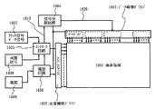
本発明の基本的な概念を図32に示す。表示領域3202が形成された第1の基板3201と、第3の基板3206上に複数の駆動回路を形成し、第3の基板3206を各駆動回路毎に、短冊状または矩形状に分断することによって取り出されるスティックドライバを第1の基板に貼り合わせる。駆動回路の構成は走査線側とソース線側で異なるが、いずれにしてもそれぞれの側で複数個のスティックドライバを実装する。図32では、走査線駆動回路が形成されたスティックドライバ3203、3204及びソース線駆動回路が形成されたスティックドライバ3207、3208が実装される形態を示している。
【0028】
スティックドライバは大面積の第3の基板上に複数個作り込むことが生産性を向上させる観点から適している。例えば、300×400mmや550×650mmの大面積の基板上に駆動回路部と入出力端子を一つのユニットとする回路パターンを複数個形成し、最後に分割して取り出すと良い。スティックドライバの短辺の長さは1〜6mm、長辺の長さは15〜80mmとする。このようなサイズで分割するには、ダイヤモンド片などを利用してガラス基板の表面に罫書き線を形成し、外力を作用させて罫書き線に沿って分断する方法で行うことができる。この加工を行う機械はガラススクライバーとも呼ばれるが、分断加工するのに必要な刃の加工幅は100μmを下らず、100〜500μmは余裕を見込む必要があった。また、基板上に形成したマーカーとの位置合わせ精度も±100μmの誤差がある。従って、ガラススクライバーで短辺が2mmのスティックドライバを切り出すには切りしろを1〜5mm見込む必要があり、そのために1枚の基板からの取り数が制限されてしまう。一方、シリコンウェハーを個々のダイに切断するブレートダイシング法を用いたダイシング装置は、ブレード(刃)の幅が0.02〜0.05mmであり、位置合わせ精度を考慮しても100μm以下の精度で基板を分割することができる。
【0029】
従って、1枚の基板からスティックドライバを効率的に取出す方法は、加工精度の低いガラススクライバーで分断する加工領域と、加工精度の高いダイシング装置で分断する加工領域とを分けて配置する。具体的には、一辺が100〜200mmの領域から成る群を作り、その群の中に短辺の長さ1〜6mmのスティックドライバを複数個配置する。そして、群と群との分割はガラススクライバーで行い、分割された群からスティックドライバを取り出すにはダイシング装置で行う。
【0030】
また、ソース線側のスティックドライバは、チャネル長を0.3〜1μmとし、さらに上記のような限られた面積内に必要な回路を形成するために、走査線側のスティックドライバよりもデザインルールを縮小して形成する。その好ましい方法として、ステッパ方式を用いた露光技術を採用する。
【0031】
【発明の実施の形態】
[実施形態1]
本願発明の液晶表示装置における画素領域の画素の構成について説明する。図1はその平面図の一例であり、ここでは簡略化のため、マトリクス状に配置された複数の画素の1つの画素構成を示している。また、図2及び図3は作製工程を示す図である。
【0032】
図1に示すように、画素領域は互いに平行に配置された複数のゲート配線と、各ゲート配線と交差するソース配線を複数有している。ゲート配線とソース配線とで囲まれた領域には画素電極119が設けられている。また、この画素電極119と重ならないように、画素電極と同じ材料からなる配線120がソース配線117と重なっている。ゲート配線102とソース配線117の交差部近傍にはスイッチング素子としてのTFTが設けられている。このTFTは非晶質構造を有する半導体膜(以下、第1の半導体膜と呼ぶ)で形成されたチャネル形成領域を有する逆スタガ型(若しくはボトムゲート型ともいう)のTFTである。
【0033】
さらに、画素電極119の下方で隣り合う2本のゲート配線の間には、ゲート配線102と平行に容量配線103が配置されている。この容量配線103は全画素に設けられており、画素電極119との間に存在する絶縁膜104bを誘電体として保持容量を形成している。
【0034】
本発明の逆スタガ型TFTは、絶縁性基板上に順次、ゲート電極(ゲート配線102と同じ層で一体形成され、ゲート配線に接続する電極)と、ゲート絶縁膜と、第1の半導体膜膜と、一導電型(通常はn型を用いる)の不純物元素を含む第2の半導体膜からなるソース領域及びドレイン領域と、ソース電極(ソース配線117と一体形成された)及び電極118(以下、ドレイン電極とも呼ぶ)とが積層形成されている。
【0035】
ソース配線(ソース電極含む)及びドレイン電極118の下方には、絶縁性基板上に順次、ゲート絶縁膜と、第1の半導体膜と、n型を付与する不純物元素を含む第2の半導体膜とが積層形成されている。
【0036】
第1の半導体膜のうち、ソース領域と接する領域とドレイン領域との間の領域は、他の領域と比べ膜厚が薄くなっている。膜厚が薄くなったのは、n型を付与する不純物元素を含む第2の半導体膜をエッチングにより分離してソース領域とドレイン領域とを形成する際、第1の半導体膜の一部が除去されたためである。また、このエッチングによって画素電極の端面、ドレイン電極の端面、及びドレイン領域の端面が一致している。このような逆スタガ型のTFTはチャネルエッチ型と呼ばれている。また、本発明における逆スタガ型TFTの特徴は、ソース電極を覆う配線120の端面、ソース領域の端面、及びソース配線の端面が一致している。
【0037】
[実施形態2]
図6は本発明の表示装置の構成を示す図である。基板651上には画素領域652が形成されている。その画素領域652が形成された領域上には対向電極が形成された第2の基板660が液晶層(図示せず)を介して貼り合わされている。第1の基板と第2の基板との間隔、即ち液晶層の厚さはスペーサによって決定付けられるが、ネマチック液晶の場合には3〜8μm、スメチック液晶の場合には1〜4μmとする。第1及び第2の基板にはアルミノホウケイ酸ガラスやバリウムホウケイ酸ガラスなどの無アルカリガラスを用いることが好ましく、その厚さは0.3〜1.1mm(代表的には0.7mm)が用いられるので、相対的に液晶層の厚さは外観上無視できるものである。
【0038】
画素領域652は走査線(ゲート配線に対応する)群658とソース線群659が交差してマトリクスを形成し、各交差部に対応してTFTが配置されている。ここで配置されるTFTは実施形態1で説明した逆スタガ型のTFTを用いる。非晶質シリコン層はプラズマCVD法で300℃以下の温度で形成することが可能であり、例えば、外寸550×650mmの無アルカリガラス基板であっても、TFTを形成するのに必要な膜厚を数十秒で形成することができる。このような製造技術の特徴は、大画面の表示装置を作製する上で非常に有用に活用することができる。
【0039】
画素領域652の外側の領域には、駆動回路が形成されたスティックドライバ653、654が実装されている。653はソース線側の駆動回路であり、654は走査線側の駆動回路であるが、いずれも複数個に分割して実装する。RGBフルカラーに対応した画素領域を形成するためには、XGAクラスでソース線の本数が3072本であり走査線側が768本必要となる。また、UXGAではそれぞれ4800本と1200本が必要となる。このような数で形成されたソース線及び走査線は画素領域652の端部で数ブロック毎に区分して引出線657を形成し、スティックドライバ653、654の出力端子のピッチに合わせて集められている。
【0040】
一方、基板651の端部には外部入力端子655が形成され、この部分で外部回路と接続するFPC(フレキシブルプリント配線板:Flexible Printed Circuit)を貼り合わせる。そして、外部入力端子655とスティックドライバとの間は基板651上に形成した接続配線656によって結ばれ、最終的にはスティックドライバの入力端子のピッチに合わせて集められる。
【0041】
スティックドライバの回路構成は、走査線側とソース線側とで異なっている。図7はその一例を示し、図6と同様に画素領域670の外側に走査線側のスティックドライバ671と、ソース線側のスティックドライバ672が設けられる様子を示している。スティックドライバは画素密度にもよるが、走査線側で1〜2個、データ線側で2〜10個程度が実装される。走査線側のスティックドライバ671の構成は、シフトレジスタ回路673、レベルシフタ回路674、バッファ回路675から成っている。この内、バッファ回路675は30V程度の耐圧が要求されるものの、動作周波数は100kHz程度であるので、特にこの回路を形成するTFTはゲート絶縁膜の厚さは150〜250nm、チャネル長は1〜2μmで形成する。一方、ソース線側のスティックドライバは、シフトレジスタ回路676、ラッチ回路677、レベルシフタ回路678、D/A変換回路679から構成される。シフトレジスタ回路676やラッチ回路677は駆動電圧3Vで周波数50MHz以上(例えば65MHz)で駆動するために、特にこの回路を形成するTFTはゲート絶縁膜の厚さは20〜70nm、チャネル長は0.3〜1μmで形成する。
【0042】
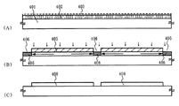
このような駆動回路が形成されたスティックドライバは図8(A)に示すように、第3の基板811上に形成され、TFTで形成された回路部812、入力端子813、出力端子814が設けられている。駆動回路部812のTFTのチャネル形成領域やソース及びドレイン領域は結晶質半導体膜で形成する。結晶質半導体膜には非晶質半導体膜をレーザー結晶化法や熱結晶化法で結晶化させた膜を適用することが可能であり、その他のもSOI技術を用いて形成された単結晶半導体層で形成することも可能である。
【0043】
図8(B)はスティックドライバの上面図であり、図8(A)の断面図はA−A'線に対応している。画素領域のソース線または走査線に接続する出力端子のピッチは40〜100μmで複数個形成する。また、同様に入力端子813も必要な数に応じて形成する。これらの入力端子813及び出力端子814は一辺の長さを30〜100μmとした正方形または長方形状に形成する。図6で示したように、スティックドライバは画素領域の一辺の長さに合わせて形成するものではなく、長辺が15〜80mm、短辺が1〜6mmの矩形状または短冊状に形成する。画素領域のサイズ、即ち画面サイズが大型化すると、その一例として、20型では画面の一方の辺の長さは443mmとなる。勿論、この長さに対応してスティックドライバを形成することは可能であるが、基板の強度を確保するには実用的な形状とはなり得ない。むしろ、15〜80mmの長さとして複数個にスティックドライバを分割する方が取り扱いが容易となり、製造上の歩留まりも向上する。
【0044】
スティックドライバのICチップに対する外形寸法の優位性はこの長辺の長にあり、ICチップを15〜80mmという長さで形成することは生産性の観点から適していない。不可能ではないにしろ、円形のシリコンウエハーから取出すICチップの取り数を減少させるので現実的な選択とはなり得ない。一方、スティックドライバの駆動回路はガラス基板上に形成するものであり、母体として用いる基板の形状に限定されないので生産性を損なうことがない。このように、長辺が15〜80mmで形成されたスティックドライバを用いることにより、画素領域に対応して実装するのに必要な数がICチップを用いる場合よりも少なくて済むので、製造上の歩留まりを向上させることができる。
【0045】
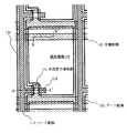
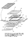
第3の基板を用いて作製されたスティックドライバを第1の基板上に実装する方法はCOG方式と同様なものであり、異方性導電材を用いた接続方法やワイヤボンディング方式などを採用することができる。図9にその一例を示す。図9(A)は第1の基板201にスティックドライバ208が異方性導電材を用いて実装する例を示している。第1の基板210上には画素領域202、引出線206、接続配線及び入出力端子207が設けられている。第2の基板はシール材204で第1の基板201と接着されており、その間に液晶層205が設けられている。また、接続配線及び入出力端子207の一方の端にはFPC212が異方性導電材で接着されている。異方性導電材は樹脂215と表面にAuなどがメッキされた数十〜数百μm径の導電性粒子214から成り、導電性粒子214により接続配線及び入出力端子207とFPC212に形成された配線213とが電気的に接続されている。スティックドライバ208も同様に異方性導電材で第1の基板に接着され、樹脂211中に混入された導電性粒子210により、スティックドライバ208に設けられた入出力端子209と引出線206または接続配線及び入出力端子207と電気的に接続されている。
【0046】
図10(A)はこの方式によるスティックドライバ224の実装方法を詳細に説明する部分断面図である。スティックドライバ224には入出力端子225が設けられ、その周辺部には保護絶縁膜226が形成されていることが望ましい。第1の基板220には第1の導電層221と第2の導電層223、及び絶縁層222が図で示すように形成され、ここでは第1の導電層221と第2の導電層223とで引出線または接続配線を形成している。第1の基板に形成されるこれらの導電層及び絶縁層は画素領域の画素TFTと同じ工程で形成されるものである。例えば、画素TFTが逆スタガ型で形成される場合、第1の導電層221はゲート電極と同じ層に形成され、Ta、Cr、Ti、Alなどの材料で形成される。通常ゲート電極上にはゲート絶縁膜が形成され、絶縁層222はこれと同じ層で形成されるものである。第1の導電層221上に重ねて設ける第2の導電層223は画素電極と同じ透明導電膜で形成されるものであり、導電性粒子227との接触を良好なものとするために設られている。樹脂228中に混入させる導電性粒子227の大きさと密度を適したものとすることにより、このような形態でスティックドライバと第1の基板とは電気的接続構造を形成することができる。
【0047】
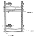
図10(B)は樹脂の収縮力を用いたCOG方式の例であり、スティックドライバ側にTaやTiなどでバリア層229を形成し、その上に無電解メッキ法などによりAuを約20μm形成しバンプ230とする。そして、スティックドライバと第1の基板との間に光硬化性絶縁樹脂231を介在させ、光硬化して固まる樹脂の収縮力を利用して電極間を圧接して電気的な接続を形成する。
【0048】
また、図9(B)で示すように第1の基板にスティックドライバを接着材216で固定して、Auワイヤ217によりスティックドライバの入出力端子と引出線または接続配線とを接続しても良い。そして樹脂218で封止する。
【0049】
スティックドライバの実装方法は図9及び図10を基にした方法に限定されるものではなく、ここで説明した以外にも公知のCOG方法やワイヤボンディング方法、或いはTAB方法を用いることが可能である。
【0050】
スティックドライバの厚さは、対向電極が形成された第2の基板と同じ厚さとすることにより、この両者の間の高さはほぼ同じものとなり、表示装置全体としての薄型化に寄与することができる。また、それぞれの基板を同じ材質のもので作製することにより、この液晶表示装置に温度変化が生じても熱応力が発生することなく、TFTで作製された回路の特性を損なうことはない。その他にも、本実施形態で示すようにICチップよりも長尺のスティックドライバで駆動回路を実装することにより、一つの画素領域に対して必要な数を減らすことができる。
【0051】
【実施例】
[実施例1]
本実施例は液晶表示装置の作製方法を示し、基板上に画素部のTFTを逆スタガ型で形成し、該TFTに接続する保持容量を作製する方法について図1〜図5を用い工程に従って詳細に説明する。また、同図には該基板の端部に設けられ、他の基板に設けた回路の配線と電気的に接続するための端子部の作製工程を同時に示す。
【0052】
図2(A)において、基板100にはコーニング社の#7059ガラスや#1737ガラスなどに代表されるバリウムホウケイ酸ガラスやアルミノホウケイ酸ガラスなどのガラス基板を用いる。その他に、石英基板、プラスチック基板などの基板を使用することができる。
【0053】
この基板100上に導電層を全面に形成した後、第1のフォトマスクを用いるフォトリソ工程を行い、エッチング処理をしてゲート電極102'及びゲート配線(図示せず)、容量配線103、端子101を形成する。このとき少なくともゲート電極102'の端部にテーパー部が形成されるようにエッチングする。また、この段階での上面図を図4に示す。
【0054】
ゲート電極102及びゲート配線と容量配線103、端子部の端子101は、アルミニウム(Al)や銅(Cu)などの低抵抗導電性材料で形成することが望ましいが、Al単体では耐熱性が劣り、また腐蝕しやすい等の問題点があるので耐熱性導電性材料と組み合わせて形成する。また、低抵抗導電性材料としてAgPdCu合金を用いてもよい。耐熱性導電性材料としては、チタン(Ti)、タンタル(Ta)、タングステン(W)、モリブデン(Mo)、クロム(Cr)、Nd(ネオジム)から選ばれた元素、または前記元素を成分とする合金か、前記元素を組み合わせた合金膜、または前記元素を成分とする窒化物で形成する。例えば、TiとCuの積層、TaNとCuとの積層が挙げられる。また、Ti、Si、Cr、Nd等の耐熱性導電性材料と組み合わせて形成した場合、平坦性が向上するため好ましい。その他に、耐熱性導電性材料の単層やMoとW、或いはMoとTaの合金を用いても良い。
【0055】
液晶表示装置を作製するには、ゲート電極およびゲート配線は耐熱性導電性材料と低抵抗導電性材料とを組み合わせて形成することが望ましい。画面サイズが4型程度までなら耐熱性導電性材料の窒化物から成る導電層(A)と耐熱性導電性材料から成る導電層(B)とを積層したニ層構造とする。導電層(B)はAl、Cu、Ta、Ti、W、Nd、Crから選ばれた元素、または前記元素を成分とする合金か、前記元素を組み合わせた合金膜で形成すれば良く、導電層(A)は窒化タンタル(TaN)膜、窒化タングステン(WN)膜、窒化チタン(TiN)膜などで形成する。例えば、導電層(A)としてCr、導電層(B)としてNdを含有するAlとを積層したニ層構造とすることが好ましい。導電層(A)は10〜100nm(好ましくは20〜50nm)とし、導電層(B)は200〜400nm(好ましくは250〜350nm)とする。
【0056】
一方、4型クラス以上の大画面に適用するには耐熱性導電性材料から成る導電層(A)と低抵抗導電性材料から成る導電層(B)と耐熱性導電性材料から成る導電層(C)とを積層した三層構造とすることが好ましい。低抵抗導電性材料から成る導電層(B)は、アルミニウム(Al)を成分とする材料で形成し、純Alの他に、0.01〜5atomic%のスカンジウム(Sc)、Ti、Nd、シリコン(Si)等を含有するAlを使用する。導電層(C)は導電層(B)のAlにヒロックが発生するのを防ぐ効果がある。導電層(A)は10〜100nm(好ましくは20〜50nm)とし、導電層(B)は200〜400nm(好ましくは250〜350nm)とし、導電層(C)は10〜100nm(好ましくは20〜50nm)とする。本実施例では、Tiをターゲットとしたスパッタ法により導電層(A)をTi膜で50nmの厚さに形成し、Alをターゲットとしたスパッタ法により導電層(B)をAl膜で200nmの厚さに形成し、Tiをターゲットとしたスパッタ法により導電層(C)をTi膜で50nmの厚さに形成する。
【0057】
次いで、絶縁膜104aを全面に成膜する。絶縁膜104aはスパッタ法を用い、膜厚を50〜200nmとする。例えば、絶縁膜104aとして窒化シリコン膜を用い、150nmの厚さで形成する。勿論、ゲート絶縁膜はこのような窒化シリコン膜に限定されるものでなく、酸化シリコン膜、酸化窒化シリコン膜、酸化タンタル膜などの他の絶縁膜を用い、これらの材料から成る単層または積層構造として形成しても良い。例えば、下層を窒化シリコン膜とし、上層を酸化シリコン膜とする積層構造としても良い。
【0058】
絶縁膜104a上に50〜200nm(好ましくは100〜150nm)の厚さで第1の半導体膜105を、プラズマCVD法やスパッタ法などの公知の方法で全面に形成する。例えば、シリコンのターゲットを用いたスパッタ法で非晶質シリコン(a−Si)膜を150nmの厚さに形成する。その他、この第1の半導体膜には、微結晶半導体膜、非晶質シリコンゲルマニウム膜(SiXGe(1-X)、(0<X<1))、非晶質シリコンカーバイト(SiXCY)などの非晶質構造を有する化合物半導体膜を適用することも可能である。
【0059】
次に、一導電型(n型またはp型の不純物元素を含有する)の第2の半導体膜を20〜80nmの厚さで形成する。一導電型の第2の半導体膜は、プラズマCVD法やスパッタ法などの公知の方法で全面に形成する。本実施例では、リン(P)が添加されたシリコンターゲットを用いて一導電型の第2の半導体膜106を形成する。或いは、シリコンターゲットを用い、リンを含む雰囲気中でスパッタリングを行い成膜してもよい。その他にも、第2の半導体膜を水素化微結晶シリコン膜(μc−Si:H)で形成しても良い。
【0060】
金属材料からなる第1の導電膜107はスパッタ法や真空蒸着法で形成する。第1の導電膜107の材料としては、第2の半導体膜106とオーミックコンタクトのとれる金属材料であれば特に限定されず、Al、Cr、Ta、Tiから選ばれた元素、または前記元素を成分とする合金か、前記元素を組み合わせた合金膜等が挙げられる。本実施例ではスパッタ法を用い、第1の導電膜107として、50〜150nmの厚さのTi膜と、そのTi膜上に重ねてアルミニウム(Al)を300〜400nmの厚さで形成し、さらにその上にTi膜を100〜150nmの厚さで形成する3層構造で形成する(図2(A))。
【0061】
絶縁膜104a、第1の半導体膜105、一導電型の第2の半導体膜106、及び第1の導電膜107はいずれも公知の方法で作製するものであり、プラズマCVD法やスパッタ法で作製することができる。本実施例では、これらの膜(104a、105、106、107)をスパッタ法で、ターゲット及びスパッタガスを適宣切り替えることにより連続的に形成した。この時、スパッタ装置において、同一の反応室または複数の反応室を用い、これらの膜を大気に晒すことなく連続して積層させることが好ましい。このように、大気に曝さないことで不純物の混入を防止することができる。
【0062】
そして、第2のフォトマスクを用い、フォトリソグラフィー工程を行い、レジストマスク108を形成し、エッチングにより不要な部分を除去して配線(後の工程によりソース配線及びドレイン電極)111を形成する。この際のエッチング方法としてウエットエッチングまたはドライエッチングを用いる。この時、第1の導電膜107、一導電型の第2の半導体膜106、及び第1の半導体膜105が順次、レジストマスク108のパターンに従ってエッチングとなする。この工程では配線の形成のみならず、TFTを形成する半導体層のパターンまでも同時に形成する。TFTの形成部においては、第1の導電膜からなる配線111、n型を付与する不純物元素を含む第2の半導体膜110、及び第1の半導体膜109がそれぞれ形成される。本実施例では、SiCl4とCl2とBCl3の混合ガスを反応ガスとしたドライエッチングにより、Ti膜とAl膜とTi膜を順次積層した第1の導電膜107をエッチングし、反応ガスをCF4とO2の混合ガスに代えて第1の半導体膜105及びn型を付与する不純物元素を含む第2の半導体膜106を選択的に除去する(図2(B))。また、容量部においては容量配線103と絶縁膜104aを残し、同様に端子部においても、端子101と絶縁膜104aが残る。この状態の上面図を図5に示す。但し、簡略化のため図5では全面に成膜された第2の導電膜112は図示していない。
【0063】
次に、レジストマスク108を除去した後、スクリーン印刷で画素領域の全面を覆うマスクを形成し、端子部のパッド部分を覆っている絶縁膜104aを選択的に除去する。この処理は高い位置合わせ精度を要求しないので、スクリーン印刷やシャドーマスクを用いて行うことができる。こうして絶縁膜104bを形成する(図2(C))。
【0064】
そして、全面に透明導電膜からなる第2の導電膜112を成膜する(図2(D))。この第2の導電膜112の材料は、酸化インジウム(In2O3)や酸化インジウム酸化スズ合金(In2O3―SnO2、ITOと略記する)などをスパッタ法や真空蒸着法などを用いて形成する。このような材料のエッチング処理は塩酸系の溶液により行う。しかし、特にITOのエッチングは残渣が発生しやすいので、エッチング加工性を改善するために酸化インジウム酸化亜鉛合金(In2O3―ZnO)を用いても良い。酸化インジウム酸化亜鉛合金は表面平滑性に優れ、ITOと比較して熱安定性にも優れているので、第2の導電膜112と接触する配線111をAl膜で形成しても腐蝕反応をすることを防止できる。同様に、酸化亜鉛(ZnO)も適した材料であり、さらに可視光の透過率や導電率を高めるためにガリウム(Ga)を添加した酸化亜鉛(ZnO:Ga)などを用いることができる。
【0065】
次に、第3のフォトマスクを用い、フォトリソグラフィー工程によりレジストマスク113a〜113cを形成する。そして、エッチングにより不要な部分を除去して第1の半導体膜114、ソース領域115及びドレイン領域116、ソース電極117及びドレイン電極118、画素電極119を形成する(図3(A))。このフォトリソグラフィー工程は、第2の導電膜112をパターニングすると同時に配線111と、一導電型の第2の半導体膜110と第1の半導体膜109の一部をエッチングにより除去して開孔を形成する。本実施例では、まず、ITOからなる第2の導電膜112を硝酸と塩酸の混合溶液または塩化系第2鉄系の溶液を用いたウエットエッチングにより選択的に除去し、ウエットエッチングにより配線111を選択的に除去した後、ドライエッチングによりn型を付与する不純物元素を含む第2の半導体膜110と第1の半導体膜109の一部をエッチングした。なお、本実施例では、ウエットエッチングとドライエッチングとを用いたが、実施者が反応ガスを適宜選択してドライエッチングのみで行ってもよいし、実施者が反応溶液を適宜選択してウエットエッチングのみで行ってもよい。
【0066】
また、開孔の底部は第1の半導体膜に達しており、凹部を有する第1の半導体膜114が形成される。この開孔によって配線111はソース配線117とドレイン電極118に分離され、一導電型の第2の半導体膜110はソース領域115とドレイン領域116に分離される。また、ソース配線と接する第2の導電膜120は、ソース配線を覆い、後の製造工程、特にラビング処理で生じる静電気を防止する役目を果たす。本実施例では、ソース配線上に第2の導電膜120を形成した例を示したが、第2の導電膜120を除去してもよい。また、このフォトリソグラフィー工程において、容量部における絶縁膜104bを誘電体として、容量配線103と画素電極119とで保持容量が形成される。その他に、このフォトリソグラフィー工程において、レジストマスク113cで覆い端子部に形成された透明導電膜からなる第2の導電膜を残す。
【0067】
次に、レジストマスク113a〜113cを除去した。この状態の断面図を図3(B)に示す。尚、図1は1つの画素の上面図であり、A−A'線 及びB−B'線に沿った断面図がそれぞれ図3(B)に相当する。
【0068】
また、図11(A)は、この状態のゲート配線端子部501、及びソース配線端子部502の上面図をそれぞれ図示している。なお、図1〜図3と対応する箇所には同じ符号を用いている。また、図11(B)は図11(A)中のE−E'線 及びF−F'線に沿った断面図に相当する。図11(A)において、透明導電膜からなる503は入力端子として機能する接続用の電極である。また、図11(B)において、504は絶縁膜(104bから延在する)、505は第1の非晶質半導体膜(114から延在する)、506はn型を付与する不純物元素を含む第2の非晶質半導体膜(115から延在する)である。
【0069】
こうして3枚のフォトマスクを使用して、3回のフォトリソグラフィー工程により、逆スタガ型のnチャネル型TFT201を有する画素TFT、保持容量202を完成させることができる。これらを個々の画素に対応してマトリクス状に配置して画素部を構成することによりアクティブマトリクス型の電気光学装置を作製するための一方の基板とすることができる。本明細書では便宜上このような基板をアクティブマトリクス基板と呼ぶ。
【0070】
次に、アクティブマトリクス基板の画素部のみに配向膜121を選択的に形成する。配向膜121を選択的に形成する方法としては、スクリーン印刷法を用いてもよいし、配向膜を塗布後、シャドーマスクを用いてレジストマスクを形成して除去する方法を用いてもよい。通常、液晶表示素子の配向膜にはポリイミド樹脂が多く用いられている。そして、配向膜121にラビング処理を施して液晶分子がある一定のプレチルト角を持って配向するようにする。
【0071】
次いで、アクティブマトリクス基板と、対向電極122と配向膜123とが設けられた対向基板124とをスペーサで基板間隔を保持しながらシール剤により貼り合わせた後、アクティブマトリクス基板と対向基板の間に液晶材料125を注入する。液晶材料125は公知のものを適用すれば良く代表的にはTN液晶を用いる。液晶材料を注入した後、注入口は樹脂材料で封止する(図3(C))。
【0072】
端子部には、実施形態2で示すように駆動回路が形成されたスティックドライバを取り付ける。スティックドライバは走査線側とソース線側で異なる駆動回路が用いられる。こうして、画素領域を3枚のフォトマスクで作製したアクティブマトリクス型液晶表示装置を完成させることができる。
【0073】
[実施例2]
本実施例では、実施例1で作製した画素TFT上に保護膜を形成した例を図12に示す。なお、本実施例は、実施例1の図3(B)の状態まで同一であるので異なる点について以下に説明する。また、図3(B)に対応する箇所は同一の符号を用いている。
【0074】
まず、実施例1に従って図3(B)の状態を得た後、薄い無機絶縁膜を全面に形成する。この薄い無機絶縁膜としては、酸化シリコン膜、窒化シリコン膜、酸化窒化シリコン膜、酸化タンタル膜などの無機絶縁膜を用い、これらの材料から成る単層または積層構造として形成しても良い。
【0075】
次いで、第4のフォトマスクを用い、フォトリソグラフィー工程を行い、レジストマスクを形成し、エッチングにより不要な部分を除去して、画素TFT部においては絶縁膜402、端子部においては無機絶縁膜401をそれぞれ形成する。この無機絶縁膜401、402は、パッシベーション膜として機能する。また、端子部においては、第4のフォトリソグラフィー工程により薄い無機絶縁膜401を除去して、端子部の端子101上に形成された透明導電膜からなる第2の導電膜を露呈させる。
【0076】
こうして本実施例では、4枚のフォトマスクを使用して、4回のフォトリソグラフィー工程により、無機絶縁膜で保護された逆スタガ型のnチャネル型TFT、保持容量を完成させることができる。そして、これらを個々の画素に対応してマトリクス状に配置し、画素部を構成することによりアクティブマトリクス型の電気光学装置を作製するための一方の基板とすることができる。なお、本実施例は、実施例1の構成と組み合わせることが可能である。
【0077】
[実施例3]
実施例1では、絶縁膜、第1の非晶質半導体膜、一導電型の第2の非晶質半導体膜及び第1の導電膜をスパッタ法で形成する例を中心として示しが、本実施例ではプラズマCVD法を用いる例を示す。具体的には、絶縁膜、第1の非晶質半導体膜、及び一導電型の第2の半導体膜をプラズマCVD法で形成する。
【0078】
本実施例においては絶縁膜として酸化窒化シリコン膜を用い、プラズマCVD法により150nmの厚さで形成する。この時、プラズマCVD装置において、電源周波数を13〜70MHz、好ましくは27〜60MHzで行う。特に、電源周波数27〜60MHzを使うことにより緻密な絶縁膜を形成することができ、ゲート絶縁膜としての耐圧を高めることができる。また、SiH4とNH3にN2Oを添加させて作製された酸化窒化シリコン膜は、膜の内部応力が緩和されるので、この用途に対して好ましい材料となる。勿論、ゲート絶縁膜はこのような酸化窒化シリコン膜に限定されるものでなく、酸化シリコン膜、窒化シリコン膜、酸化タンタル膜などの他の絶縁膜を用い、これらの材料から成る単層または積層構造として形成しても良い。も良い。その一例を示せば、下層を窒化シリコン膜とし、上層を酸化シリコン膜とする積層構造はゲート絶縁膜として好ましい形態である。
【0079】
酸化シリコン膜を用いる場合には、プラズマCVD法で、オルトケイ酸テトラエチル(Tetraethyl Orthosilicate:TEOS)とO2とを混合し、反応圧力40Pa、基板温度250〜350℃とし、高周波(13.56MHz)電力密度0.5〜0.8W/cm2で放電させて形成することができる。このようにして作製された酸化シリコン膜は、その後300〜400℃の熱アニールによりゲート絶縁膜として良好な特性を得ることができる。
【0080】
第1の半導体膜として、代表的には、プラズマCVD法で水素化非晶質シリコン(a−Si:H)膜を100nmの厚さに形成する。この時、プラズマCVD装置において、電源周波数13〜70MHz、好ましくは27〜60MHzで行えばよい。電源周波数27〜60MHzを使うことにより成膜速度を向上することが可能となり、成膜された膜は、欠陥密度の少ないa−Si膜となるため好ましい。その他、この第1の非晶質半導体膜には、非晶質シリコンゲルマニウム膜などの非晶質構造を有する化合物半導体膜を適用することも可能である。非晶質半導体膜のプラズマCVD法による成膜において、100〜100kHzのパルス変調放電を行えば、プラズマCVD法の気相反応によるパーティクルの発生を防ぐことができ、成膜においてピンホールの発生を防ぐことができるため好ましい。
【0081】
また、本実施例では、一導電型の不純物元素を含有する半導体膜として、一導電型の第2の非晶質半導体膜を20〜80nmの厚さで形成する。例えば、n型の不純物元素を含有するa−Si:H膜を形成すれば良く、そのためにシラン(SiH4)に対して0.1〜5%の濃度でフォスフィン(PH3)を添加する。或いは、n型を付与する不純物元素を含む第2の非晶質半導体膜106に代えて水素化微結晶シリコン膜(μc−Si:H)を用いても良い。
【0082】
これらの膜は、反応ガスを適宣切り替えることにより、連続的に形成することができる。また、プラズマCVD装置において、同一の反応室または複数の反応室を用い、これらの膜を大気に晒すことなく連続して積層させることもできる。このように、大気に曝さないで連続成膜することで特に、第1の半導体膜への不純物の混入を防止することができる。
【0083】
[実施例4]
図2において示すように、絶縁膜、第1の非晶質半導体膜、一導電型の第2の非晶質半導体膜、第1の導電膜を順次、連続的に積層する工程では、スパッタ装置やプラズマCVD装置の一つの形態として、複数の反応室を備えたマルチチャンバー型の装置が適用できる。
【0084】
図13はマルチチャンバー型の装置(連続成膜システム)の上面からみた概要を示す。装置の構成は、ロード・アンロード室10、15、皮膜を形成するチャンバー11〜14が備えられ、各チャンバーは共通室20に連結されている。ロード・アンロード室、共通室及び各チャンバーには、真空排気ポンプ、ガス導入系が配置されている。
【0085】
ロード・アンロード室10、15は、処理基板30をチャンバーに搬入するためのロードロック室である。第1のチャンバー11は絶縁膜104を成膜するための反応室である。第2のチャンバー12は第1の非晶質半導体膜105を成膜するための反応室である。第3のチャンバー13は一導電型の非晶質半導体膜106を成膜するための反応室である。第4のチャンバー14は第1の導電膜107を成膜するための反応室である。
【0086】
このようなマルチチャンバー型の装置の動作の一例を示す。最初、全てのチャンバーは、一度高真空状態に真空引きされた後、窒素またはアルゴンなどのガスを流し、チャンバー内を0.01〜5Pa程度の圧力に保持することにより、排気口からの逆拡散やチャンバー内壁からの脱ガスによる汚染を防いでいる。
【0087】
処理基板は多数枚が収納されたカセット28ごとロード・アンロード室10にセットされる。処理基板はゲート弁22を開けてカセットから取り出し、ロボットアーム21によって共通室20に移される。この際、共通室において位置合わせが行われる。なお、この基板30は実施例1に従って得られた配線101、102、103が形成されたものを用いた。
【0088】
ここでゲート弁22を閉鎖し、次いでゲート弁23を開ける。そして第1のチャンバー11へ処理基板30を移送する。第1のチャンバー内では150℃から300℃の温度で成膜処理を行い、絶縁膜104を得る。なお、絶縁膜としては、窒化珪素膜、酸化珪素膜、窒化酸化珪素膜、またはこれらの積層膜等を使用することができる。本実施例では単層の窒化珪素膜を採用しているが、二層または三層以上の積層構造としてもよい。なお、ここではプラズマCVD法が可能なチャンバーを用いたが、ターゲットを用いたスパッタ法が可能なチャンバーを用いても良い。
【0089】
絶縁膜の成膜終了後、処理基板はロボットアームによって共通室に引き出され、第2のチャンバー12に移送される。第2のチャンバー内では第1のチャンバーと同様に150℃〜300℃の温度で成膜処理を行い、プラズマCVD法で第1の半導体膜105を得る。なお、第1の非晶質半導体膜としては、微結晶半導体膜、非晶質ゲルマニウム膜、非晶質シリコン・ゲルマニウム膜、またはこれらの積層膜等を使用することができる。また、第1の半導体膜の形成温度を350℃〜500℃として水素濃度を低減するための熱処理を省略してもよい。なお、ここではプラズマCVD法が可能なチャンバーを用いたが、ターゲットを用いたスパッタ法が可能なチャンバーを用いても良い。
【0090】
第1の半導体膜の成膜終了後、処理基板は共通室に引き出され、第3のチャンバー13に移送される。第3のチャンバー内では第2のチャンバーと同様に150℃〜300℃の温度で成膜処理を行い、プラズマCVD法でn型を付与する不純物元素(PまたはAs)を含む一導電型の第2の半導体膜106を得る。なお、ここではプラズマCVD法が可能なチャンバーを用いたが、ターゲットを用いたスパッタ法が可能なチャンバーを用いても良い。
【0091】
一導電型の第2の半導体膜の成膜終了後、処理基板は共通室に引き出され、第4のチャンバー14に移送される。第4のチャンバー内では金属ターゲットを用いたスパッタ法で第1の導電膜107を得る。
【0092】
このようにして四層が連続的に成膜された被処理基板はロボットアームによってロードロック室15に移送されカセット29に収納される。
【0093】
[実施例5]
実施例4では、複数のチャンバーを用いて連続的に積層する例を示したが、本実施例では図14に示す装置を用いて一つのチャンバー内で高真空を保ったまま連続的に積層する方法を採用することもできる。
【0094】
本実施例では図14に示した装置システムを用いた。図14において、40は処理基板、50は共通室、44、46はロードロック室、45はチャンバー、42、43はカセットである。本実施例では基板搬送時に生じる汚染を防ぐために同一チャンバーで積層形成した。
【0095】
図14で示す装置を実施例1に適用する場合には、チャンバー45に複数のターゲットを用意し、順次、反応ガスを入れ替えて絶縁膜104、第1の半導体膜105、一導電型の第2の半導体膜106、第1の導電膜107を積層形成すればよい。
【0096】
また、実施例4に適用する場合には、順次、反応ガスを入れ替えて絶縁膜104、第1の非晶質半導体膜105、一導電型の第2の半導体膜106を積層形成すればよい。
【0097】
[実施例6]
実施例4で示すように、プラズマCVD法を用いるTFTの作製工程では、一導電型の第2の半導体膜を微結晶半導体膜で形成することができる。成膜時の基板加熱温度を80〜300℃、好ましくは140〜200℃とし、水素で希釈したシランガス(SiH4:H2=1:10〜100)とフォスフィン(PH3)との混合ガスを反応ガスとし、ガス圧を0.1〜10Torr、放電電力を10〜300mW/cm2とすることで微結晶シリコン膜を得ることができる。また、この微結晶珪素膜成膜後にリン(P)をプラズマドーピングして形成してもよい。一導電型の第2の半導体膜を微結晶半導体膜で形成することで、ソース及びドレイン領域の低抵抗化が図られ、TFTの特性を向上させることができる。
【0098】
[実施例7]
実施例1〜3では透過型の液晶表示装置に対応するアクティブマトリクス基板の作製方法を示したが、本実施例では図15、16を用いて、反射型の液晶表示装置に適用する例について示す。図15は断面図、図16は上面図を示し、図16中の鎖線G―G’で切断した面での断面構造とH−H’で切断した面に対応する断面構造を図15に示している。
【0099】
まず、絶縁表面を有する基板を用意する。本実施例は、基板としてガラス基板、石英基板、プラスチック基板のような透光性を有する基板の他に、反射型であるため、半導体基板、ステンレス基板、セラミック基板などに絶縁膜を形成したものでもよい。
【0100】
次いで、基板上に金属材料からなる導電膜を形成した後、第1のフォトマスクを用いレジストパターンを形成した後、エッチング処理でゲート配線750及びを凸部751形成する。この凸部は、ゲート配線とソース配線とで囲まれた領域、即ち画素電極が形成されて表示領域となる領域に配置する。なお、凸部751の形状は特に限定されず、径方向の断面が多角形であってもよいし、左右対称でない形状であってもよい。例えば、凸部751の形状は円柱状や角柱状であってもよいし、円錐状や角錐状であってもよい。また、凸部751を規則的に配置しても不規則に配置してもよい。本実施例ではゲート配線がテーパー形状であることが望ましいため、凸部751もテーパー形状を有する角錐形状となる。テーパー部の角度は5〜45度、好ましくは5〜25度とする。
【0101】
次いで、絶縁膜(ゲート絶縁膜)752、第1の半導体膜、一導電型の第2の半導体膜及び第1の導電膜を順次積層形成する。尚、第1の半導体膜は非晶質半導体、微結晶半導体のいずれを適用しても良い。一導電型の第2の半導体膜も実施例6で示すように微結晶半導体を用いてもよい。さらに、これらの膜はスパッタ法やプラズマCVD法を用いて複数のチャンバー内または同一チャンバー内で連続的に大気に曝すことなく形成することができる。大気に曝さないようにすることで不純物の混入を防止できる。上記絶縁膜752は、凸部751が形成された基板上に形成され、表面に凸凹を有している。
【0102】
次いで、第2のフォトマスクを用いレジストパターンを形成した後、エッチング処理で上記第1の導電膜、第2の半導体膜、第1の半導体膜をエッチングする。こうしてソース配線608及び電極(ドレイン電極)609を形成し、第1の半導体膜605を形成する。このエッチング処理により、ソース配線、ドレイン電極、TFTを形成する半導体層が所定のパターンに形成される。
【0103】
その後、全面に第2の導電膜を成膜する。なお、第2の導電膜としては、反射性を有する導電膜を用いる。このような導電膜としてAlやAgなどを適用することが望ましいが、耐熱性が劣るため下層に対するバリアメタル層としてTi、Taなどの層を形成しておいても良い。
【0104】
次いで、第3のフォトマスクを用い、レジストパターンを形成した後、エッチング処理をして、第2の導電膜からなる画素電極604を形成する。こうして、凸部601上に形成された絶縁膜の表面は凸凹を有し、この凸凹を表面に有する絶縁膜602上に画素電極604が形成されるので、画素電極604の表面に凹凸を持たせて光散乱性を図ることができる。
【0105】
また、本実施例の構成とすることで、画素TFT部の作製する際、フォトリソグラフィー技術で使用するフォトマスクの数を3枚とすることができる。従来では、凸凹部を形成する工程を増やす必要があったが、本実施例はゲート配線と同時に凸部を作製するため、全く工程を増やすことなく画素電極に凸凹部を形成することができる。
【0106】
[実施例8]
本実施形態では主に走査線側のスティックドライバに適したTFTの作製方法について説明する。走査線側のスティックドライバには、シフトレジスタ回路やバッファ回路などを形成する。ここでは、シフトレジスタ回路は3〜5V駆動とし、バッファ回路は33V駆動を前提とする。バッファ回路を構成するTFTは高耐圧が要求されるため、他の回路のTFTよりもゲート絶縁膜の膜厚を厚くする必要がある。その作製方法を図17と図18を用いて説明する。
【0107】
図17(A)において、基板301にはコーニング社の#7059ガラスや#1737ガラスなどに代表されるバリウムホウケイ酸ガラスやアルミノホウケイ酸ガラスなどのガラス基板などを用いる。このようなガラス基板は加熱温度により僅かながら収縮するので、ガラス歪み点よりも500〜650℃のい温度で熱処理を施したものを用いると基板の収縮率を低減させることができる。
【0108】
ブロッキング層302は基板301に微量に含まれるアルカリ金属などが半導体層に拡散するのを防ぐために設け、酸化シリコン膜や窒化シリコン膜、または酸化窒化シリコン膜などの絶縁膜で形成する。また、TFTのしきい値電圧(Vth)を安定化させるために、ブロッキング層の応力を引張り応力とすることが望ましい。応力の制御は上記絶縁膜の作製条件により制御する。その目的のために、ブロッキング層は単層に限らず、組成の異なる複数の絶縁膜を積層して形成しても良い。例えば、プラズマCVD法でSiH4、NH3、N2Oから作製される酸化窒化シリコン膜を10〜200nm(好ましくは50〜100nm)形成し、同様にSiH4、N2Oから作製される酸化窒化シリコン膜を50〜200nm(好ましくは100〜150nm)の厚さに積層形成してブロッキング層とすることができる。
【0109】
非晶質構造を有する半導体膜303は、25〜100nmの膜厚で形成する。非晶質構造を有する半導体膜の代表例としては非晶質シリコン(a−Si)膜、非晶質シリコン・ゲルマニウム(a−SiGe)膜、非晶質炭化シリコン(a−SiC)膜、非晶質シリコン・スズ(a−SiSn)膜などがあり、そのいずれでも適用できる。これらの非晶質構造を有する半導体膜はプラズマCVD法やスパッタ法、或いは減圧CVD法などにより形成されるもので、膜中に水素を0.1〜40atomic%程度含有するようにして形成する。好適な一例は、プラズマCVD法でSiH4またはSiH4とH2から作製される非晶質シリコン膜であり、膜厚は55nmとする。尚、SiH4の代わりにSi2H6を使用しても良い。
【0110】
そして、非晶質半導体膜の結晶化温度を低温化することのできる触媒元素を添加する。触媒元素は非晶質半導体膜中に直接注入する方法も可能であるが、スピンコート法、印刷法、スプレー法、バーコーター法、スパッタ法または真空蒸着法によって触媒元素が含有する層304を1〜5nmの厚さに形成しても良い。このような触媒元素の一例は、非晶質シリコンに対してニッケル(Ni)、ゲルマニウム(Ge)、鉄(Fe)、パラジウム(Pd)、スズ(Sn)、鉛(Pb)、コバルト(Co)、白金(Pt)、銅(Cu)、金(Au)が有効であることが知られている。スピンコート法で触媒元素を含有する層304を形成するには、重量換算で1〜100ppm(好ましくは10ppm)の触媒元素を含む水溶液をスピナーで基板を回転させて塗布する。
【0111】
図17(B)で示す結晶化の工程では、まず400〜500℃で1時間程度の熱処理を行い、非晶質シリコン膜の含有水素量を5atom%以下にする。そして、ファーネスアニール炉を用い、窒素雰囲気中において550〜600℃で1〜8時間の熱処理を行う。好適には、550℃で4時間の熱処理を行う。こうして結晶質半導体膜305を得ることができる。このような熱結晶化法により、非晶質シリコン膜からは結晶構造を有する結晶質シリコン膜が形成される。
【0112】
しかし、この熱結晶化法によって作製された結晶質半導体膜305は、局所的に非晶質領域が残存していることがある。このような場合、ラマン分光法では480cm-1にブロードなピークを持つ非晶質成分の存在を確認することができる。レーザー結晶化法はこのように残存する非晶質領域を結晶化させる目的において適した方法である。
【0113】
レーザー結晶化法において用いるレーザー光源にはエキシマレーザー、YAGレーザー、YVO4レーザー、YAlO3レーザー、YLFレーザーなどを用いることができる。エキシマレーザーでは400nm以下の波長の光を高出力で放射させることができるので半導体膜の結晶化に好適に用いることができる。一方、YAGレーザー、YVO4レーザー、YAlO3レーザー、YLFレーザーなどの固体レーザーではその第2高調波(532nm)、第3高調波(355nm)、第4高調波(266nm)を用いる。光の侵入長により、第2高調波(532nm)を用いる場合には半導体膜の表面及び内部から、第3高調波(355nm)や第4高調波(266nm)の場合にはエキシマレーザーと同様に半導体膜の表面から加熱して結晶化を行うことができる。
【0114】
図17(C)はその様子を示すものであり、例えば、Nd:YAGレーザーを用い、そのパルス発振周波数を1〜10kHzとし、レーザーエネルギー密度を100〜500mJ/cm2(代表的には100〜400mJ/cm2)として、シリンドリカルレンズなどを含む光学系にて形成した線状レーザー光306をその長手方向に対し垂直な方向に走査して(或いは、相対的に基板を移動させて)する。線状レーザー光306の線幅は100〜1000μm、例えば400μmとする。このようにして熱結晶化法とレーザー結晶化法を併用することにより、結晶性の高い結晶質半導体膜307を形成することができる。
【0115】
以上のようにして形成される結晶質半導体膜307は、TFTの能動層としてチャネル形成領域をはじめ、ソース領域、ドレイン領域、LDD領域などを形成するのに適している。ニッケルなどの触媒元素を用いた熱結晶化法で作製される結晶質シリコン膜は、微視的に見れば複数の針状または棒状の結晶が集合した構造を有している。しかし、隣接する結晶粒の連続性が高く不対結合手(ダングリングボンド)が殆ど形成されないことが見込まれている。また、その結晶粒の大部分は<110>に配向している。その理由の一つとして、ニッケルなどの触媒元素を用いた場合の結晶成長過程は、触媒元素のシリサイド化物が関与しているものと考えられ、半導体膜の膜厚が25〜100nmと薄いのでその初期核のうち(111)面が基板表面とほぼ垂直なものが優先的に成長するため実質的に<110>の配向性が高くなると考えられる。
【0116】
その後、結晶質半導体膜307はエッチング処理により島状の半導体層308〜311を形成する。図17(D)では便宜上4つの半導体層を示している。以降の説明は、半導体層308、309にはシフトレジスタ回路など低電圧で駆動する回路のTFTを、半導体層310、311にはバッファ回路など高電圧で駆動する回路のTFTをそれぞれ作製することを前提として説明する。
【0117】
半導体層上に形成するゲート絶縁膜は、回路の駆動電圧を考慮して、同一基板上に形成するTFTであってもその膜厚を異ならせて形成する。そのために2段階の成膜プロセスを必要とする。最初に、ゲート絶縁膜第1層目312を40〜200nm(好ましくは70〜90nm)の厚さで形成する。そして、半導体層308、309上のゲート絶縁膜第1層目を選択的にエッチングして除去することにより図17(E)の様な状態を形成する。
【0118】
続いて、図17(F)に示すようにゲート絶縁膜第2層目313を同様に形成する。その結果、ゲート絶縁膜第1層目312とゲート絶縁膜第2層目313とをそれぞれ80nmの厚さで成膜した場合には、半導体層308、309上のゲート絶縁膜の厚さは80nmとなり、半導体層310、311のゲート絶縁膜の厚さは160nmとすることができる。
【0119】
ゲート絶縁膜はプラズマCVD法またはスパッタ法を用いシリコンを含む絶縁膜で形成する。プラズマCVD法でSiH4とN2Oの混合ガスから作製される酸化窒化シリコン膜はゲート絶縁膜として適した材料である。勿論、ゲート絶縁膜はこのような酸化窒化シリコン膜に限定されるものでなく、他のシリコンを含む絶縁膜をで形成しても良い。酸化シリコン膜を適用する場合には、プラズマCVD法でTEOS(Tetraethyl Orthosilicate)とO2とを混合し、反応圧力40Pa、基板温度300〜400℃とし、高周波(13.56MHz)電力密度0.5〜0.8W/cm2で放電させて形成することができる。このようにして作製される酸化シリコン膜は、その後400〜500℃の熱アニールによりゲート絶縁膜として良好な特性を得ることができる。
【0120】
こうして作製されたゲート絶縁膜上にゲート電極を形成するための導電膜を形成する。本実施形態で示すTFTのゲート電極はドライエッチング法で選択比が5〜20(好ましくは、10〜13)以上の2種類の導電性材料を積層して形成する。例えば、窒化物導電性材料から成る第1の導電膜と、400〜650℃の熱処理に耐え得る耐熱性導電性材料から成る第2の導電膜とから形成する。その具体的な一例として、第1の導電膜を窒化タンタル(TaN)、窒化チタン(TiN)、窒化タングステン(WN)から選ばれた材料で形成し、第2の導電膜をタンタル(Ta)、チタン(Ti)、タングステン(W)、モリブデン(Mo)から選ばれた一種または複数種からなる合金材料で形成する。勿論、適用可能なゲート電極材料はここで記載した材料に限定されるものではなく、上記仕様を満たす導電性材料の組み合わせであれば、他の導電性材料を選択することも可能である。尚、ここでいう選択比とは、第1の導電膜に対する第2の導電膜のエッチング速度の割合をいう。
【0121】
本実施形態では、図示はしないが、第1の導電膜をTaN膜で50〜100nmの厚さに形成し、第2の導電膜をW膜で100〜400nmの厚さに形成する。TaN膜はスパッタ法でTaのターゲットを用い、Arと窒素の混合ガスでスパッタして形成する。W膜はWをターゲットとしたスパッタ法で形成する。その他に6フッ化タングステン(WF6)を用いる熱CVD法で形成することもできる。いずれにしてもゲート電極として使用するためには低抵抗化を図る必要がある。W膜は結晶粒を大きくすることで低抵抗率化を図ることができるが、W中に酸素などの不純物元素が多い場合には結晶化が阻害され高抵抗化する。Wのターゲットには純度99.9999%のものを用い、さらに成膜時に気相中からの不純物の混入がないように十分配慮してW膜を形成することにより、抵抗率9〜20μΩcmを実現することができる。
【0122】
ゲート電極は2段階のエッチング処理により形成する。図18(A)に示すようにレジストによるマスク314を形成し、第1のエッチング処理を行う。エッチング方法に限定はないが、好適にはICP(Inductively Coupled Plasma:誘導結合型プラズマ)エッチング装置を用い、エッチング用ガスにCF4とCl2を用い、0.5〜2Pa、好ましくは1Paの圧力でコイル型の電極に500WのRF(13.56MHz)電力を投入してプラズマを生成して行う。基板側(試料ステージ)にも100WのRF(13.56MHz)電力を投入し、実質的に負の自己バイアス電圧を印加する。CF4とCl2を混合した場合にはW膜及びTa膜とも同程度の速度でエッチングすることがでできる。
【0123】
第1のエッチング処理では、第1の導電膜及び第2の導電膜の端部がテーパー形状となるように加工する。テーパー部の角度は15〜45°とする。しかし、ゲート絶縁膜上に残渣を残すことなくエッチングするためには、10〜20%程度の割合でエッチング時間を増加させるオーバーエッチング処理をすると良い。W膜に対する酸化窒化シリコン膜の選択比は2〜4(代表的には3)であるので、オーバーエッチング処理により、酸化窒化シリコン膜が露出した面は20〜50nm程度エッチングされる。こうして、第1のエッチング処理により第1の導電膜と第2の導電膜から成る第1の形状の導電層315〜318(第1の導電層315a〜318aと第2の導電層315b〜318b)を形成する。
【0124】
次に図18(B)に示すように第2のエッチング処理を行う。ICPエッチング装置を用い、エッチングガスにCF4とCl2とO2を混合して、1Paの圧力でコイル型の電極に500WのRF電力(13.56MHz)を供給してプラズマを生成する。基板側(試料ステージ)には50WのRF(13.56MHz)電力を投入し、第1のエッチング処理に比べ低い自己バイアス電圧となるようにする。このような条件によりW膜を異方性エッチングし、かつ、それより遅いエッチング速度でTa膜を異方性エッチングして第2の形状の導電膜319〜322(第1の導電層319a〜322aと第2の導電層319b〜322b)を形成する。ゲート絶縁膜は図では詳細に示さないが、第2の形状の導電層315〜318で覆われない領域は20〜50nm程度エッチングされ薄くなる。
【0125】
そして、図18(C)で示すように、濃度の異なる2種類の不純物領域を形成する。この不純物領域はいずれもn型であり、リン(P)、砒素(As)などのn型を付与する不純物元素をイオンドープ法やイオン注入法で添加する。第1のドーピング処理は、第2の導電層319b〜322bをマスクとして自己整合的に第1の不純物領域323〜326を形成する。概念的には高加速電圧低ドーズ量の条件を選択し、第1の不純物領域323〜326には、添加されるn型を付与する不純物元素の濃度は、1×10¹⁶〜1×10¹⁹atoms/cm3の濃度となるようにする。例えば、イオンドープ法でフォスフィン(PH3)を用い、加速電圧を70〜120keVとし、1×1013/cm2のドーズ量で行う。
【0126】
次いで行う第2のドーピング処理は、低加速高ドーズ量の条件を選択し、不純物領域327〜330の形成を行う。第2の不純物領域327〜330の不純物濃度は1×10²⁰〜1×10²¹atoms/cm3の範囲となるようにする。その為に、イオンドープ法における条件の一例は、ドーズ量を1×1013〜5×1014atoms/cm2とし、加速電圧を30〜70keVとして行う。こうして半導体層に形成される第1の不純物領域323〜326は第1の導電層319a〜322aと重なるように形成され、第2の不純物領域327〜330は、第2の形状の導電層315〜318の外側に形成される。
【0127】
そして図18(D)に示すように、pチャネル型TFTを形成する半導体層308、310にp型を付与する不純物元素が添加された第3の不純物領域332〜335を形成する。このとき、nチャネル型TFTを形成する島状半導体層309、311はレジストのマスク331で全面を被覆しておく。不純物領域332〜335にはそれぞれ異なる濃度でリン(P)が添加されているが、ジボラン(B2H6)を用いたイオンドープ法でp型を付与する不純物元素を添加して、ずれの領域においてもp型を付与する不純物濃度が2×10²⁰〜2×10²¹atoms/cm3となるように形成する。
【0128】
以上までの工程でそれぞれの半導体層に不純物領域が形成される。第2の導電層319〜322がゲート電極として機能する。そして、図18(E)で示す第1の層間絶縁膜336を形成する。第1の層間絶縁膜336は酸化窒化シリコン膜で100〜200nmの厚さで形成する。その後、導電型の制御を目的としてそれぞれの半導体層に添加された不純物元素を活性化する処理を行う。この工程はファーネスアニール炉を用いる熱アニール法、レーザーアニール法、またはラピッドサーマルアニール法(RTA法)を適用することができる。熱アニール法では酸素濃度が1ppm以下、好ましくは0.1ppm以下の窒素雰囲気中で400〜700℃、代表的には500〜600℃で行う。
【0129】
レーザーアニール法では波長400nm以下のエキシマレーザー光やYAGレーザー、YVO4レーザーの第2高調波(532nm)を用いる。活性化の条件は実施者が適宣選択するものであるが、エキシマレーザーを用いる場合はパルス発振周波数30Hzとし、レーザーエネルギー密度を100〜300mJ/cm2とする。また、YAGレーザーを用いる場合にはその第2高調波を用いパルス発振周波数1〜10kHzとし、レーザーエネルギー密度を200〜400mJ/cm2とすると良い。そして幅100〜1000μm、例えば400μmで線状に集光したレーザー光を基板全面に渡って照射し、この時の線状レーザー光の重ね合わせ率(オーバーラップ率)を80〜98%として行う。
【0130】
さらに、3〜100%の水素を含む雰囲気中で、300〜450℃で1〜12時間の熱処理を行い、半導体層を水素化する工程を行う。この工程は熱的に励起された水素により半導体層のダングリングボンドを終端する工程である。水素化の他の手段として、プラズマ水素化(プラズマにより励起された水素を用いる)を行っても良い。
【0131】
第2の層間絶縁膜337は、酸化シリコンや酸化窒化シリコンなどの無機絶縁物材料、または有機絶縁物材料を用い1.0〜2.0μmの平均膜厚で形成する。有機絶縁物材料としては、ポリイミド、アクリル、ポリアミド、ポリイミドアミド、BCB(ベンゾシクロブテン)等を使用することができる。例えば、基板に塗布後、熱重合するタイプのポリイミドを用いる場合には、クリーンオーブンで300℃で焼成して形成する。また、アクリルを用いる場合には、2液性のものを用い、主材と硬化剤を混合した後、スピナーを用いて基板全面に塗布した後、ホットプレートで80℃で60秒の予備加熱を行い、さらにクリーンオーブンを用い、250℃で60分焼成して形成する。
【0132】
そして、半導体層に形成した第2の不純物領域または第3の不純物領域とコンタクトをする配線338〜345を形成する。この配線は50〜200nmのTi膜768a、100〜300nmのAl膜768b、50〜200nmのスズ(Sn)膜またはTi膜で形成する。このような構成で形成された配線338〜345は、最初に形成するTi膜が半導体層と接触をし、コンタクト部分の耐熱性を高めている。
【0133】
以上の様にして、pチャネル型TFT346、348、nチャネル型TFT347、349を有する駆動回路が形成することができる。pチャネル型TFT348とnチャネル型TFT349のゲート絶縁膜は、pチャネル型TFT346とnチャネル型TFT347のゲート絶縁膜よりも厚く形成され、耐圧を高める構造となっている。
【0134】
pチャネル型TFT346にはチャネル形成領域350、ゲート電極である第2の導電層319と重なる第3の不純物領域351、ゲート電極の外側に形成される第3の不純物領域352を有している。また、pチャネル型TFT348にはチャネル形成領域356、ゲート電極である第2の導電層321と重なる第3の不純物領域357、ゲート電極の外側に形成される第3の不純物領域358を有している。pチャネル型TFTはシングルドレインの構造であり、第3の不純物領域は、ソースまたはドレインとして機能するものである。
【0135】
nチャネル型TFT347はチャネル形成領域353、ゲート電極である第2の導電層320と重なる第1の不純物領域354、ゲート電極の外側に形成される第2の不純物領域355が形成されている。また、nチャネル型TFT349はチャネル形成領域359、ゲート電極である第2の導電層322と重なる第1の不純物領域360、ゲート電極の外側に形成される第2の不純物領域361が形成されている。第1の不純物領域354、360はLDD(Lightly Doped Drain)領域であり、第2の不純物領域355、361はソース領域またはドレイン領域として機能する領域である。特に、第1の不純物領域はゲート電極とオーバーラップして形成されるGOLD(Gate Overlapped Drain)構造であるため、ホットキャリア効果によるTFTの劣化を防止することができ、10V以上の高い電圧を印加しても、きわめて安定した動作を得ることができる。
【0136】
いずれにしても、これらのTFTはチャネル長1〜5μm、好ましくは1.5〜2.5μmで形成すれば良い。従って、適用すべきデザインルールもライン・アンド・スペース(線幅と隣接する線との間隔)で1〜1.5μm、コンタクトホールで2μm程度を採用すれば良い。
【0137】
本実施形態で作製されるTFTは走査線側のスティックドライバを形成するのに適している。特に、30V系の高電圧が印加されるバッファ回路などには、図18(E)で示すpチャネル型TFT348、nチャネル型TFT349を適用して形成する。また、シフトレジスタ回路などにはpチャネル型TFT346、nチャネル型TFT347を適用して形成すると良い。ここでは、nチャネル型TFTとpチャネル型TFTを形成する工程を示したが、同工程により容量素子や抵抗素子を形成することは容易に想定できるものであり省略されている。また、回路形成に必要なTFTのサイズ(チャネル長/チャネル幅)やそのレイアウトは実施者が適宣考慮すれば良いものである。
【0138】
[実施例9]
ソース線側に設けるスティックドライバのTFTに要求される耐圧は12V程度であるが、動作周波数は3Vにて50MHz以上(例えば65MHz)が要求される。本実施形態ではそのために適したTFTの作製方法を説明する。
【0139】
TFTのチャネル形成領域を形成する結晶質半導体膜には、高い電界効果移動度と低いサブスレッショルド係数(S値)実現可能な品質が要求される。即ち、捕獲中心や再結合中心となる欠陥準位や、粒界ポテンシャルが低いとった性質を有する結晶質半導体膜が求められる。図19はそのような結晶質半導体膜を作製する方法の一例を示す。
【0140】
図19(A)において基板401として適用し得るものは、600℃(好適には950℃)の熱処理に耐え、絶縁表面を有する基板であれば良い。品質、表面仕上げの精度から言えば石英基板が適している。そのような基板401に密接して形成する非晶質構造を有する半導体膜402は、プラズマCVD法や減圧CVD法で25〜100nmの厚さで形成する。非晶質構造を有する半導体膜の代表例としては非晶質シリコン(a−Si)膜、非晶質シリコン・ゲルマニウム(a−SiGe)膜、非晶質炭化シリコン(a−SiC)膜、非晶質シリコン・スズ(a−SiSn)膜などがあり、そのいずれでも適用できる。そして、非晶質半導体膜の結晶化温度を低温化することのできる触媒元素を含有する層を形成する。図19(A)では非晶質構造を有する半導体膜402上に形成しているが、基板側に形成されていても構わない。ここで適用可能な触媒元素は実施形態2と同じであり、同様な方法で形成する。
【0141】
そして、窒素またはアルゴンなどの雰囲気中で500〜600℃で1〜12時間の熱処理を行い非晶質構造を有する半導体膜の結晶化を行う。この温度の結晶化に先立っては、400〜500℃で1時間程度の熱処理を行い、膜中の含有水素を放出させておくことも必要である。代表的な条件として、450℃で1時間の脱水素処理をした後、続いて570℃で8時間の熱処理を行う。このような熱結晶化法により、非晶質シリコン膜からは結晶構造を有する結晶質半導体膜404が形成される(図19(B))。
【0142】
しかし、結晶質半導体膜404に残存する触媒元素の濃度はおよそ5×10¹⁶〜2×10¹⁸atoms/cm2である。触媒元素は半導体膜の結晶化には有効であるが、その後TFTを形成するための機能材料として使用する目的においては不要な存在となる。結晶質半導体膜中に残存する触媒元素は不純物として欠陥準位などを形成し、捕獲中心や再結合中心を形成したり、半導体接合の不良をもたらす。図19(B)は触媒元素を除去するためのゲッタリング処理を説明するものであり、結晶質半導体膜中の触媒元素の濃度を1×1017atms/cm3以下、好ましくは1×1016atms/cm3にまで低減することを目的としている。
【0143】
まず、結晶質半導体膜404の表面に酸化シリコン膜などでマスク用絶縁膜405を150nmの厚さに形成する。そして、能動層を形成する領域の外側に開口部406を設け、結晶質半導体膜の表面が露出した領域を形成する。そして、イオンドープ法やイオン注入法でリン(P)を添加して、結晶質半導体膜に選択的にリン(P)添加領域407を形成する。この状態で、窒素雰囲気中で550〜800℃、5〜24時間、例えば600℃、12時間の熱処理を行うと、リン(P)添加領域407がゲッタリングサイトとして働き、結晶質半導体膜404に残存していた触媒元素をリン(P)添加領域407に偏析させることができる。
【0144】
その後、マスク用絶縁膜405と、リン(P)添加領域407とをエッチングして除去することにより、触媒元素の濃度が1×10¹⁷atms/cm3以下にまで低減された結晶質半導体膜408を得ることができる(図19(C))。
【0145】
また、図20は結晶質半導体膜を形成する方法の他の一例を示す。図20(A)において基板410、非晶質構造を有する半導体膜411は図19(A)の説明と同様なものを用いる。非晶質構造を有する半導体膜411上にはマスク用絶縁膜412を形成し、選択的に開口部414を形成する。その後、重量換算で1〜100ppmの触媒元素を含む溶液を塗布して、触媒元素含有層413を形成する。触媒元素含有層413は開口部414のみで非晶質構造を有する半導体膜411と接触する構造が形成される。
【0146】
次に、500〜650℃で1〜24時間、例えば600℃、12時間の熱処理を行い、結晶質半導体膜を形成する。この結晶化の過程では、触媒元素が接した半導体膜415から結晶化が進行し、基板410の表面と平行な方向(横方向)へ結晶化が進行する。こうして形成された結晶質半導体膜は棒状または針状の結晶が集合して成り、その各々の結晶は巨視的に見ればある特定の方向性をもって成長しているため、結晶性が揃っているという利点がある。
【0147】
結晶質半導体膜が形成された後、図19(B)と同様に触媒元素を結晶質半導体膜から除去するゲッタリング処理を行う。先に形成された開口部414からリン(P)を添加して、結晶質半導体膜にリン(P)添加領域416を形成する。この状態で、窒素雰囲気中で550〜800℃、5〜24時間、例えば600℃、12時間の熱処理を行い、結晶質半導体膜に残存する触媒元素をリン(P)添加領域416に偏析させる(図20(C))。
【0148】
その後、マスク用絶縁膜412と、リン(P)添加領域416とをエッチングして除去することにより、触媒元素の濃度が1×10¹⁷atms/cm3以下にまで低減された結晶質半導体膜417を得ることができる(図20(D))。
【0149】
図19(C)で示す結晶質半導体膜408及び図20(D)で示す結晶質半導体膜417は、いずれもTFTの能動層を形成する用途において適したものである。図21(A)ではこのような結晶質半導体膜から島状に分離形成した半導体膜420〜423を形成する。図21(A)では便宜上4つの半導体層を示している。以降の説明は、半導体層420、421にはシフトレジスタ回路など低電圧で駆動する回路のTFTを、半導体層422、423にはラッチ回路など高周波数で駆動するTFTをそれぞれ作製することを前提として説明する。後者は高速駆動を可能とするために、ゲート絶縁膜の厚さが薄く形成する。そのために2段階の成膜プロセスを行う。
【0150】
半導体層上に形成するゲート絶縁膜は、回路の駆動電圧を考慮して、同一基板上に形成するTFTであってもその膜厚を異ならせて形成する。そのために2段階の成膜プロセスを必要とする。最初に20〜50nm、例えば40nmの厚さで酸化シリコン膜または酸化窒化シリコン膜などの絶縁膜を形成する。このような絶縁膜はプラズマCVD法や熱CVD法で形成する。熱CVD法における作製条件の一例は、SiH4とN2Oを用い、800℃、40Paであり、ガスの混合比を適当なものとすることにより緻密な膜を形成することができる。その後、半導体層422、423上に形成された絶縁膜をフッ酸などでエッチングして除去して第1の絶縁膜424を形成する。さらに、表面を清浄に洗浄し、800〜1000℃(好ましくは950℃)でハロゲン(代表的には塩素)を含む雰囲気中で酸化膜の形成を行う。
酸化膜は半導体層422、423において30〜50nm(例えば40nm)の厚さとなるように形成する。その結果、半導体層420、421では80nmの厚さの絶縁膜が形成される。ハロゲン雰囲気での酸化膜形成により、微量の金属不純物などが除去され、半導体膜との界面準位密度が低減された良好な絶縁膜を形成することができる。こうして、半導体層420、421と半導体層422、423との間で厚さの異なる第2の絶縁膜425が形成され、この絶縁膜をゲート絶縁膜として利用する(図21(B))。
【0151】
さらに、図21(B)では第2の絶縁膜425上にゲート電極を形成するための第1の導電膜426と第2の導電膜427とを形成する。これらの導電膜は実施形態1と同様にして作製するものであり、第1の導電膜426をTaN膜で50〜100nmの厚さに形成し、第2の導電膜427をW膜で100〜300nmの厚さに形成する。
【0152】
以降の行程は実施形態2ど同様にして行い、nチャネル型TFTとpチャネル型TFTを形成する。ゲート電極の形成は2段階のエッチング処理により行う。図21(C)はレジストマスク428を形成し、テーパーエッチング処理を行う第1のエッチング処理により第1の形状の導電層429〜432(第1の導電層429a〜432aと第2の導電層429b〜432b)が形成された状態を示している。また、図21(D)は異方性エッチングによる第2のエッチング処理により第2の形状の導電層433〜436(第1の導電層433a〜436aと第2の導電層433b〜436b)が形成された状態を示している。
【0153】
nチャネル型TFTおよびpチャネル型TFTの不純物領域の形成は、第2の形状の導電層を利用して自己整合的に形成する。nチャネル型TFTには濃度の異なる2種類の不純物領域を形成する。図21(E)は第1のドーピング処理(高加速電圧低ドーズ量の条件)で形成される第1の不純物領域437〜440と、第2のドーピング処理(低加速電圧高ドーズ量)の条件で形成される第2の不純物領域441〜44とを示している。pチャネル型TFTの不純物領域は、図21(F)で示す様に、レジストのマスク445をnチャネル型TFTが形成される領域を保護するように形成し、第3のドーピング処理によりp型を付与する不純物元素が添加された領域446〜449を形成する。
【0154】
これらの不純物領域を形成した後、第1の層間絶縁膜450を形成し、400〜700℃の熱処理を施して不純物元素の活性化を行う。さらに、3〜100%の水素を含む雰囲気中で300〜450℃で1〜12時間の熱処理を行い、半導体層を水素化して欠陥準位密度を低減する処理を行う。第2の層間絶縁膜451は、酸化シリコンや酸化窒化シリコンなどの無機絶縁物材料、または有機絶縁物材料を用い1.0〜2.0μmの平均膜厚で形成する。配線452〜459はAl、Tiなどで形成する。
【0155】
以上の様にして、pチャネル型TFT460、462、nチャネル型TFT461、463を有する駆動回路が形成することができる。pチャネル型TFT462とnチャネル型TFT463のゲート絶縁膜は、pチャネル型TFT460とnチャネル型TFT461のゲート絶縁膜よりも薄く形成され、低電圧で高速に駆動する構造となっている。前者のTFTは3〜5Vの低電圧で駆動するラッチ回路などを形成し、後者のTFTは5〜12Vで駆動するシフトレジスタ回路などを形成するのに適している。
【0156】
これらのTFTのチャネル長は低電圧部で0.3〜1μm(好ましくは0.6μm)、中電圧部で0.6〜1.5μm(好ましくは0.9μm)で形成する。従って、適用すべきデザインルールもライン・アンド・スペース(線幅と隣接する線との間隔)で0.3〜1.5μm、コンタクトホールで0.9μm程度の精度が要求される。
【0157】
本実施形態で作製されるTFTはソース線側のスティックドライバを形成するのに適している。特に、3Vで数十MHzの周波数で駆動するラッチ回路などは、図21(E)で示すpチャネル型TFT462とnチャネル型TFT463を用いて形成する。また、シフトレジスタ回路などにはpチャネル型TFT460、nチャネル型TFT461を適用して形成すると良い。ここでは、nチャネル型TFTとpチャネル型TFTを形成する工程を示したが、同工程により容量素子や抵抗素子を形成することは容易に想定できるものであり省略されている。また、回路形成に必要なTFTのサイズ(チャネル長/チャネル幅)やそのレイアウトは実施者が適宣考慮すれば良いものである。
【0158】
[実施例10]
ソース線側に設けるスティックドライバに適したTFTの作製方法について他の一例を示す。TFTの能動層を形成するための結晶質半導体膜を形成する工程は実施形態3と同じである。図22(A)において、基板901として適用し得るものは、600℃(好適には950℃)の熱処理に耐え、絶縁表面を有する石英基板が望ましい。そのような基板401に密接して形成する非晶質構造を有する半導体膜902は、プラズマCVD法や減圧CVD法で40〜100nm、一例として70nmの厚さで形成する。石英基板上に良質な結晶質半導体膜を形成するには、スタート膜として形成する非晶質半導体膜の膜厚をある程度厚くしておく必要がある。膜厚が30nm以下であると、下地の基板との間で格子不整合などの影響で結晶化が十分成し遂げることができない懸念がある。非晶質構造を有する半導体膜は実施形態2または3で示す材料と同じであり、代表的には非晶質シリコンを用いる。そして、非晶質半導体膜の結晶化温度を低温化することのできる触媒元素を含有する層903を形成する。
【0159】
結晶化は450℃で1時間の熱処理で脱水素処理を行い、続いて600℃で12時間の熱処理を行う。図22(B)で示すように、こうして得られる結晶質半導体膜904上にはマスク用絶縁膜905を形成し、その開口部906からリン(P)を添加して、リン(P)添加領域907を形成する。触媒元素を除去するためのゲッタリング処理は、窒素雰囲気中で550〜800℃、5〜24時間、例えば600℃で12時間の熱処理を行い、結晶質半導体膜904に残存していた触媒元素をリン(P)添加領域907に偏析させる。その後、マスク用絶縁膜905と、リン(P)添加領域907とをエッチングして除去することにより、触媒元素の濃度が1×10¹⁷atms/cm3以下にまで低減された結晶質半導体膜908を得る。結晶化により、非晶質半導体膜は緻密化するのでその体積は1〜10%程度収縮し、膜厚は僅かであるが減少する。
【0160】
図22(C)は、こうして形成された結晶質半導体膜を熱処理により酸化する工程を示している。熱酸化は800〜1000℃(好ましくは950℃)でハロゲン(代表的には塩素)を含む雰囲気中で酸化膜の形成を行う。この処理により結晶質半導体膜908は酸化膜909の形成で薄くなり、当初の厚さよりも減少する。例えば、酸化膜を60nmの厚さに形成することにより半導体膜はおよそ30nm減少し、40nmの結晶質半導体膜を残すことができる(図22(C))。
【0161】
こうして形成された結晶質半導体膜908をエッチング処理してから島状に分離形成した半導体膜911〜914を形成する。半導体膜上に形成するゲート絶縁膜は、回路の駆動電圧を考慮して、同一基板上に形成するTFTであってもその膜厚を異ならせて形成する。図22(D)と(E)はその工程を示し、最初に20〜50nm、例えば40nmの厚さで酸化シリコン膜または酸化窒化シリコン膜などの絶縁膜を形成する。これらの絶縁膜はプラズマCVD法や熱CVD法で形成する。熱CVD法における作製条件の一例は、SiH4とN2Oを用い、800℃、40Paであり、ガスの混合比を適当なものとすることにより緻密な膜を形成することができる。その後、半導体層913、914上に形成された絶縁膜はフッ酸などでエッチングして除去して第1の絶縁膜915を形成する。さらに、表面を清浄に洗浄し、800〜1000℃(好ましくは950℃)でハロゲン(代表的には塩素)を含む雰囲気中で酸化膜の形成を行う。酸化膜は半導体層913、914において30〜50nm(例えば40nm)の厚さとなるように形成する。一方、半導体層911、912では80nmの厚さの絶縁膜が形成される。ハロゲン雰囲気での酸化膜形成により、微量の金属不純物などが除去され、半導体膜との界面準位密度が低減された良好な絶縁膜を形成することができる。こうして、半導体層911、912と半導体層913、914との間で厚さの異なる第2の絶縁膜916が形成され、この絶縁膜をゲート絶縁膜として利用する。
【0162】
ゲート絶縁膜上に形成するゲート電極は、ゲート絶縁膜が薄く形成されているので注意を要する。勿論、スパッタ法や蒸着法で形成する金属導電膜材料を用いることも可能であるが、より好ましくはゲート絶縁膜に接する第1層目は減圧CVD法で作製するリン(P)ドープされた多結晶シリコン膜であることが望ましい。リン(P)ドープ多結晶シリコン膜は、SiH4とPH3と希釈ガスとしてHe、H2を用い450〜500℃に加熱して100〜200nm、好ましくは150nmの厚さで形成する。さらにその上層にはゲート電極の抵抗値を下げるために、シリサイド金属などを形成する。タングステンシリサイド(WSix)、チタンシリサイド(Ti)など適用し得るシリサイド金属に限定はなく、スパッタ法などで100〜200nm、好ましくは150nmの厚さに形成する。
【0163】
このように第1の導電層、第2の導電層として2層に分けて形成された状態から、図22(F)に示すようにゲート電極917〜920(第1の導電層917a〜920aと第2の導電層917b〜920b)を形成する。
【0164】
次に、nチャネル型TFTのLDD領域を形成するための第1のドーピング処理を行う。ドーピングは、代表的な方法としてフォスフィン(PH3)を用いたイオンドープ法で行い、ゲート電極をマスクとして利用して自己整合的に第1の不純物領域921〜924を形成する。この領域のリン(P)濃度は2×10¹⁶〜5×10¹⁹atoms/cm3の範囲とする(図23(A))。
【0165】
さらに、第2のドーピング処理を行い、n型不純物が添加される第2の不純物領域927、928の形成を行う。この不純物領域はnチャネル型TFTのソース領域およびドレイン領域を形成するものであり、ゲート電極の外側の領域に形成するためにレジストマスク926を形成する。また、pチャネル型TFTを形成する半導体層にリン(P)が添加されないようにレジストマスク925を形成しておく。n型を付与する不純物元素にはリン(P)を用い、その濃度が1×10²⁰〜1×10²¹atoms/cm3の濃度範囲となるようにフォスフィン(PH3)を用いたイオンドープ法で行う(図23(B))。
【0166】
そして図23(C)に示すように、pチャネル型TFTを形成する半導体層にソース領域およびドレイン領域を形成する第3の不純物領域930、931を形成する。ゲート電極612をマスクとしてジボラン(B2H6)を用いたイオンドープ法で行い、自己整合的に第3の不純物領域を形成する。このときnチャネル型TFTを形成する半導体層はレジストマスク929で全面を被覆しておく。この領域のボロン(B)濃度は3×10²⁰〜3×10²¹atoms/cm3となるようにする。
【0167】
これらの不純物領域を形成した後、窒化シリコン膜、酸化シリコン膜、酸化窒化シリコン膜などから成る第1の層間絶縁膜932を形成し、400〜950℃、好ましくは800〜900℃で10〜60分の熱処理を施して不純物元素の活性化を行う。この熱処理でゲート電極側に不純物元素が拡散し、オーバーラップ領域533〜536が形成される(図23(D))。第2の層間絶縁膜937は、酸化シリコンや酸化窒化シリコンなどの無機絶縁物材料、または有機絶縁物材料を用い1.0〜2.0μmの平均膜厚で形成する。配線938〜945はAl、Tiなどで形成する。さらに、3〜100%の水素を含む雰囲気中で300〜450℃で1〜12時間の熱処理を行い、半導体層を水素化して欠陥準位密度を低減する処理を行う(図23(E))。
【0168】
以上の様にして、pチャネル型TFT946、948、nチャネル型TFT947、949を有する駆動回路が形成することができる。pチャネル型TFT948とnチャネル型TFT949のゲート絶縁膜は、pチャネル型TFT946とnチャネル型TFT947のゲート絶縁膜よりも薄く形成され、低電圧で高速に駆動する構造となっている。前者のTFTは3〜5Vの低電圧で駆動するラッチ回路などを形成し、後者のTFTは5〜12Vで駆動するシフトレジスタ回路などを形成するのに適している。
【0169】
pチャネル型TFT946、948には、チャネル形成領域950、955、第3の不純物領域から成るソースまたはドレイン領域946、956が形成されたシングルドレインの構造である。nチャネル型TFT947、949には、チャネル形成領域952、957、第1の不純物領域で形成されるLDD領域953、958、第2の不純物領域から形成されるソースまたはドレイン領域954、959が形成されている。nチャネル型TFTに形成されるLDD領域は0.2〜1μmの長さで形成され、0.1程度は活性化の熱処理によりゲート電極の内側に拡散して、ゲート電極とオーバーラップする構造となっている。この構造により、ホットキャリア効果による特性の劣化を防ぎ、また寄生容量を最低限度に抑えて高速動作を可能とする。
【0170】
これらのTFTのチャネル長は低電圧部で0.3〜1μm(好ましくは0.6μm)、中電圧部で0.6〜1.5μm(好ましくは0.9μm)で形成する。従って、適用すべきデザインルールもライン・アンド・スペース(線幅と隣接する線との間隔)で0.3〜1.5μm、コンタクトホールで0.9μm程度の精度が要求される。
【0171】
本実施形態で作製されるTFTはソース線側のスティックドライバを形成するのに適している。特に、3Vで数十MHzの周波数で駆動するラッチ回路などは、図23(E)で示すpチャネル型TFT948とnチャネル型TFT949を用いて形成する。また、シフトレジスタ回路などにはpチャネル型TFT946、nチャネル型TFT947を適用して形成すると良い。ここでは、nチャネル型TFTとpチャネル型TFTを形成する工程を示したが、同工程により容量素子や抵抗素子を形成することは容易に想定できるものであり省略されている。また、回路形成に必要なTFTのサイズ(チャネル長/チャネル幅)やそのレイアウトは実施者が適宣考慮すれば良いものである。
【0172】
[実施例11]
実施例8〜10のいずれかの方法により作製されるTFTで走査線側またはソース線側のスティックドライバの駆動回路を形成することができる。このようなスティックドライバに設けられる入出力端子は図24で示すようにソースまたはドレイン配線と同じ層上に形成される。図24では入出力端子2400、2401がスティック基板の端部に形成される様子を示している。画素領域が形成される第1の基板にフェースダウンのCOG法で実装するには表面パッシベーションが必要であるので、絶縁層2402により表面をパッシベーションする。このような入出力端子部の形態は実施形態2〜4で作製したスティック基板にも適用できる。
【0173】
また、COGでスティックドライバを実装するには入出力端子にバンプを形成する必要がある。バンプは公知の方法で形成すれば良いが、その一例を図25で説明する。図25(A)において、2403はソースまたはドレイン配線と同じ層上に形成される入出力端子であり、その上にTiとPdまたは、CrとCuを積層したバリアメタル層2405を形成する。バリアメタル層の形成はスパッタ法や蒸着法などを適用する。そして、メッキ用のレジストマスク2406を形成する。
【0174】
そして、図25(B)で示すように、Auで形成されるバンプ2407を電解メッキで5〜20μmの厚さに形成する。そして、不要となったレジストマスク2406を除去して、新たにバンプの上からレジストを塗布してバリアメタル層2405をエッチングするためのレジストマスク2408を形成する。このレジストマスクを形成するためのフォトリソ工程は、バンプを介して行うため高い解像度を得ることができない。レジストマスク2408はバンプとその周辺を覆うように形成する。このレジストマスク2408を利用してバリアメタル層をエッチングすることにより、図25(D)で示すようなバリアメタル層2409が形成される。その後、バンプとバリアメタル層との密着性を高めるために200〜300℃で熱処理を行う。このようにして、他の基板に実装することができるスティックドライバを完成させることができる。
【0175】
[実施例12]
以上説明したようにスティックドライバは液晶表示装置の駆動回路を実装する方法として利用することができる。図26はそのような表示装置のブロック構成図を示す。画素領域1601は複数の走査線とソース線が交差して形成され、実施例1〜7で示されるような逆スタガ型のTFTが設けられたアクティブマトリクス型の構成である。その周辺の領域には走査線スティックドライバ1602及びソース線スティックドライバ1603が設けられている。外部から入力されるクロック信号及びデータ信号1607と画質信号1608は、スティックドライバの入力仕様に変換するためのコントロール回路1605に入力され、それぞれのタイミング仕様に変換される。また、電源1609、オペアンプから成る電源回路1606は外付けの回路で賄われる。このようなコントロール回路1605や電源回路1606はTAB方式で実装すると表示装置を小型化できる。
【0176】
コントロール回路1605からは走査線側とソース線側にそれぞれ信号が出力されるが、ソース線側には信号分割回路1604が設けられ、入力デジタル信号をm個に分割して供給する。分割数mは2以上の自然数で、実際的には2〜16分割にするのが適当である。この場合、入力デジタル信号線1610の本数がn本であれば、修正デジタル信号線1620の本数はn×m本となる。画素密度にもよるが、少なくともソース線側のスティックドライバは複数個設けられて、信号分割回路により入力デジタル信号の周波数が1/mに落とされることによりスティックドライバの負荷を軽減している。信号分割回路は半導体集積回路で形成されるICチップを実装しても良いし、実施形態3または4で示すようなTFTで集積回路を形成したスティックドライバと同様のチップで形成することも可能である。
【0177】
[実施例13]
図27は信号分割回路の一例を示す。本実施例では便宜上入力デジタル信号線の本数nは1、信号分割数mは4として説明する。ラッチ回路前段1301〜1304及びラッチ後段1305〜1308は、各々図27(B)のように2個のインバータ1372、1374と4個のクロックドインバータ1371、1373、1375、1376により構成されている。信号入力部1381は1361に、信号出力部1382は1362に、クロック信号入力部1383、1384はそれぞれ1363、1364に対応している。
【0178】
クロック信号線1322及び反転クロック信号線1323のクロック信号はカウンタ回路1309に入力し、リセット信号1326からの入力を受けて出力を修正クロック信号線1324及び反転修正クロック信号線1325に送る。入力デジタル信号は1321から入力し、クロック信号の周期毎にラッチ回路前段1301から1302へと順次移送されていく。そして、修正クロック信号が反転するときにラッチ回路前段に保持されている入力デジタル信号の電位情報はラッチ回路後段に移される。例えば、ラッチ回路前段1301の電位情報はラッチ回路後段1305に移される。このような動作により、ラッチ回路後段1305〜1308の出力部に接続する各修正デジタル信号線1331〜1334から修正デジタル信号が送出される。ここでは、分割数m=4で説明したため、この場合には修正デジタル信号の周波数は入力デジタル信号の周波数の1/4になる。勿論、分割数は4に限定される訳ではなく、2〜32(実用的には4〜16)の範囲で自由に選択することができる。
【0179】
[実施例14]
図26で示すソース線側に設けるスティックドライバの回路構成の一例を図28に示す。回路構成は、入力側からシフトレジスタ回路1801、ラッチ回路1804、1805、レベルシフタ回路1806、D/A変換回路1807が設けられている。入力デジタル信号がnビットで一画素の情報を表現しRGB表示をする場合、この入力デジタル信号をm分割されていると、ラッチ回路1804、1805はそれぞれ、m×3×n個必要であり、レベルシフタ回路1806、D/A変換回路1807はそれぞれm×3個が必要となる。
【0180】
図21はラッチ回路の代表例であり、図29(A)はクロックドインバータを用いた例であり、図29(B)はSRAM型のものであり、図29(C)はDRAM型のものである。これらは代表例であり、その他の構成をとることも可能である。
【0181】
シフトレジスタ回路、ラッチ回路は駆動電圧3Vであり、レベルシフタ回路により10Vに昇圧してD/A変換回路に信号を送る。D/A変換回路は抵抗分割型やスイッチドキャパシタ型のものを採用することができる。
【0182】
シフトレジスタ回路、ラッチ回路を形成するTFTは実施形態3において図21(G)で示したpチャネル型TFT462、nチャネル型TFT463、または実施形態4において図23(E)で示したpチャネル型TFT548、nチャネル型TFT549を用いて作製すると良い。
【0183】
[実施例15]
図30は本発明のスティックドライバを用いて液晶表示装置の組み立てる様子を模式的に示す図である。第1の基板には画素領域803、外部入出力端子804、接続配線805が形成されている。画素領域803は実施形態1で示す逆スタガ型のTFTで作製されたものである。点線で囲まれた領域は、走査線側のスティックドライバ貼り合わせ領域801とソース線側のスティックドライバ貼り合わせ領域802である。第2の基板808には対向電極809が形成され、シール材810で第1の基板800と貼り合わせる。シール材810の内側には液晶が封入され液晶層811を形成する。第1の基板と第2の基板とは所定の間隔を持って貼り合わせるが、ネマチック液晶の場合には3〜8μm、スメチック液晶の場合には1〜4μmとする。
【0184】
スティックドライバ806、807は実施形態2で説明したように、ソース線側と走査線側とで回路構成が異なる。第3の基板814は特にその区別をしていないが、いずれにしても走査線側、またはソース線側の駆動回路に適応したスティックドライバであるものとする。スティックドライバは第1の基板に実装するが、その方法は実施形態1において図2及び3で説明されている。走査線側に実装するスティックドライバは実施例8で示すものが適しており、ガラス基板上に駆動回路が形成されている。データ線側に実装するスティックドライバは、分割駆動を前提にするにしても高い信号周波数に対応できるTFT特性が要求されるので、実施例9または10で示す石英基板上に形成したスティックドライバが適している。外部入出力端子804には、外部から電源及び制御信号を入力するためのFPC(フレキシブルプリント配線板:Flexible Printed Circuit)812を貼り付ける。FPC812の接着強度を高めるために補強板813を設けても良い。こうして液晶表示装置を完成させることができる。スティックドライバは第1の基板に実装する前に電気検査を行えば液晶表示装置の最終工程での歩留まりを向上させることができ、また、信頼性を高めることができる。
【0185】
[実施例16]
実施例15で示すようにスティックドライバが実装された表示装置を電気光学装置に搭載する方法の一例を図31に示す。表示装置は画素領域702が実装された基板701の端部にスティックドライバ710が実装されている。そして、スペーサ706を内包するシール剤707により対向基板703と貼り合わせられ、さらに偏光版708、709が設けられている。そして、接続部材723によって筐体724に固定される。
【0186】
スティックドライバ710は、その入出力端子711において導電性粒子712を含む樹脂713で基板701上に形成された入力配線714と接続している。入出力配線714の一方の端はフレキシブルプリント配線板(Flexible Printed Circuit:FPC)が導電性粒子715を含む樹脂716で接着されている。FPCは、信号処理回路、増幅回路、電源回路などが設けられたプリント基板719にやはり同様な手法(導電性粒子721を含む樹脂722)で接続し、画像表示に必要な信号をスティックドライバが実装された表示装置に伝達するようになっている。そして、表示装置が透過型の液晶表示装置であれば、対向基板703側に光源と光導光体が設けられてバックライト718が設けられている。
【0187】
ここで示す表示装置の実装方法は一例であり、電気光学装置の形態に合わせて適宣組み立てられるものである。
【0188】
[実施例17]
スティックドライバの生産性を観点からは、大面積の基板を使用して1回のプロセスで1枚の基板からできるだけ多数個取り出す方法が適している。基板はガラス基板または石英基板を使用するが、いずれにしても大面積基板を分割するときに、いかに加工ロスを無くすかが第1の課題となる。加工精度から言えばダイシング装置が適しているが、300×400mmや550×650mm、さらには960×1000mmといった液晶ラインで使用される基板を直接加工するには、装置の規模が大型化してしまう。むしろ、加工精度は劣るものの大面積基板を容易に切断できるガラススクライバーを用い、これにより大面積基板を複数個に分割する第1の段階と、複数個に分割された基板からダイシング装置を用いて個々のスティックドライバに分割する第2の段階とに分けて行う方が適している。
【0189】
例えば、液晶第1期ラインで採用された300×400mmの大面積の基板上に一辺が100〜200mmの領域から成る群902を複数個作り、その中に短辺の長さ1〜6mmのスティックドライバを複数個配置する。各群の間隔は3〜10mmとして配置して、ガラススクライバーで加工線904に沿って大面積基板から分割する。群の中のスティックドライバは切りしろ0.5〜1mmで配置しダイシング装置で分割するという方法を採用することができる。このような加工方法を用いると、2×20mmのスティックドライバを127×127mmの群の中に360個作り込むことができ、1枚の基板からは2160個のスティックドライバを取出すことができる。
【0190】
また、大面積基板上に多数のスティックドライバを形成するための第2の課題は露光技術である。スティックドライバのデザインルールは0.3〜2μm、好ましくは0.35〜1μmである。このようなデザインルールで、やはりスループット良く露光を行う必要がある。露光方式において、プロキシミティ方式やプロジェクション方式はスループット向上には有利であるが、大型の高精細マスクが必要であり、高い解像度や重ね合わせ精度が得られにくいなどの欠点がある。一方、ステッパ方式では、その一例としてi線(365nm)を使って0.7μmの解像度で44mm角の領域、または54×30mmの領域を一度に露光することができる。これに対応して、スティックドライバの長辺の長さをこの露光範囲内としておけばサブミクロンパターンであっても効率よく露光することが可能となる。
【0191】
液晶表示装置などの画素領域は必ずしもサブミクロンのデザインルールを必要としないので、大面積を一度に露光できるプロキシミティ方式やプロジェクション方式が適した方式であると考えられている。従って、駆動回路部と画素領域とを別の露光方式で行うことは生産性を向上させるばかりでなく、本発明のようにスティックドライバを実装することで大画面の表示装置の周辺部(額縁領域)の面積を小さくすることを可能にする。
【0192】
[実施例18]
本実施例では、実施例8のような構成の表示装置を組み込んだ半導体装置について示す。このような半導体装置には、携帯情報端末(電子手帳、モバイルコンピュータ、携帯電話等)、ビデオカメラ、スチルカメラ、パーソナルコンピュータ、テレビ等が挙げられる。それらの一例を図33と図34に示す。
【0193】
図33(A)は携帯電話であり、本体9001、音声出力部9002、音声入力部9003、表示装置9004、操作スイッチ9005、アンテナ9006から構成されている。表示装置9004は本発明の逆スタガ型TFTによる画素領域の周辺にスティックドライバを実装した液晶表示装置を用いることができる。
【0194】
図33(B)はビデオカメラであり、本体9101、表示装置9102、音声入力部9103、操作スイッチ9104、バッテリー9105、受像部9106から成っている。表示装置9102は本発明の逆スタガ型TFTによる画素領域の周辺にスティックドライバを実装した液晶表示装置を用いることができる。
【0195】
図33(C)はモバイルコンピュータ或いは携帯型情報端末であり、本体9201、カメラ部9202、受像部9203、操作スイッチ9204、表示装置9205で構成されている。表示装置9205は本発明の逆スタガ型TFTによる画素領域の周辺にスティックドライバを実装した液晶表示装置を用いることができる。
【0196】
図33(D)はテレビであり、本体9401、スピーカー9402、表示装置9403、受信装置9404、増幅装置9405等で構成される。表示装置9403は本発明の逆スタガ型TFTによる画素領域の周辺にスティックドライバを実装した液晶表示装置を用いることができる。
【0197】
図33(E)は携帯書籍であり、本体9501、表示装置9502、9503、記憶媒体9504、操作スイッチ9505、アンテナ9506から構成されており、ミニディスク(MD)やDVDに記憶されたデータや、アンテナで受信したデータを表示するものである。直視型の表示装置9502、9503は本発明の逆スタガ型TFTによる画素領域の周辺にスティックドライバを実装した液晶表示装置を用いることができる。
【0198】
図34(A)はパーソナルコンピュータであり、本体9601、画像入力部9602、表示装置9603、キーボード9604で構成される。表示装置9603は本発明の逆スタガ型TFTによる画素領域の周辺にスティックドライバを実装した液晶表示装置を用いることができる。
【0199】
図34(B)はプログラムを記録した記録媒体(以下、記録媒体と呼ぶ)を用いるプレーヤーであり、本体9701、表示装置9702、スピーカ部9703、記録媒体9704、操作スイッチ9705で構成される。なお、この装置は記録媒体としてDVD(Digtial Versatile Disc)、CD等を用い、音楽鑑賞や映画鑑賞やゲームやインターネットを行うことができる。表示装置9702は本発明の逆スタガ型TFTによる画素領域の周辺にスティックドライバを実装した液晶表示装置を用いることができる。
【0200】
図34(C)はデジタルカメラであり、本体9801、表示装置9802、接眼部9803、操作スイッチ9804、受像部(図示しない)で構成される。表示装置9802は本発明の逆スタガ型TFTによる画素領域の周辺にスティックドライバを実装した液晶表示装置を用いることができる。
【0201】
【発明の効果】
以上説明したとおり、本発明により、3枚のフォトマスクにより逆スタガ型のnチャネル型TFTを有する画素TFT及び、保持容量を備えた液晶表示装置の画素領域を形成することができる。そのことにより製造工程を簡略化することができる。同様に、3枚のフォトマスクで画素電極の表面を凹凸化した反射型の液晶表示装置を作製することができる。
【0202】
また、スティックドライバを、3枚のフォトマスクにより作製された逆スタガ型の画素TFT及び保持容量を備えた液晶表示装置に実装するに際し、従来のICチップよりも長尺のスティックドライバで駆動回路を実装することにより、一つの画素領域に対して必要な数を減らすことができる。その結果、液晶表示装置の製造歩留まりを向上させ、製造コストを低減させることを可能とする。
【0203】
一方、製造工程からみたスティックドライバの利点は、必ずしもサブミクロンのデザインルールを必要としない画素領域は、大面積を一度に露光できるプロキシミティ方式やプロジェクション方式が適した方式で行い、サブミクロンのデザインルールが要求されるスティックドライバはステッパ方式で露光するといった生産手段の住分けを可能とする。このような手段を用いることにより生産性を高めることができる。
【0204】
【図面の簡単な説明】
【図1】 本発明の画素構造を示す上面図。
【図2】 画素TFT、保持容量、端子部の作製工程を説明する断面図。
【図3】 画素TFT、保持容量、端子部の作製工程を説明する断面図。
【図4】 画素TFT、保持容量の作製工程を説明する上面図。
【図5】 画素TFT、保持容量の作製工程を説明する上面図。
【図6】 画素領域とスティックドライバの配置を説明する図。
【図7】 画素領域とスティックドライバの回路構成を説明するブロック図。
【図8】 スティックドライバの構成を説明する断面図。
【図9】 スティックドライバの実装方法の一例を説明する図。
【図10】 スティックドライバの実装方法の一例を説明する図。
【図11】 入力端子部の上面図及び断面図。
【図12】 画素TFT、保持容量、端子部の構造を説明する断面図。
【図13】 マルチチャンバ方式の製造装置の構成を説明する図。
【図14】 単室連続成膜方式の製造装置の構成を説明する図。
【図15】 反射型の液晶表示装置の断面構造図。
【図16】 反射型の液晶表示装置の画素の上面図。
【図17】 スティックドライバの駆動回路を形成するTFTの作製工程を説明する図。
【図18】 スティックドライバの駆動回路を形成するTFTの作製工程を説明する図。
【図19】 スティックドライバの駆動回路を形成するTFTの作製工程を説明する図。
【図20】 スティックドライバの駆動回路を形成するTFTの作製工程を説明する図。
【図21】 スティックドライバの駆動回路を形成するTFTの作製工程を説明する図。
【図22】 スティックドライバの駆動回路を形成するTFTの作製工程を説明する図。
【図23】 スティックドライバの駆動回路を形成するTFTの作製工程を説明する図。
【図24】 スティックドライバの端子部の構成を説明する断面図。
【図25】 スティックドライバの入出力端子部に形成するバンプの作製工程図。
【図26】 表示装置の回路構成を説明するブロック構成図。
【図27】 信号分割回路の構成を説明する図。
【図28】 ソース線に接続するスティックドライバの駆動回路の構成を説明する図。
【図29】 ラッチ回路の具体例を説明する図。
【図30】 スティックドライバを実装する液晶表示装置の組み立て図。
【図31】 表示装置を電気光学装置の筐体に装着する一例を説明する図。
【図32】 スティックドライバを実装するアクティブマトリクス型表示装置の概念図。
【図33】 半導体装置の一例を説明する図。
【図34】 半導体装置の一例を説明する図。[0001]
BACKGROUND OF THE INVENTION
The present invention relates to a semiconductor device having a circuit formed of a thin film transistor (hereinafter referred to as TFT) and a method for manufacturing the semiconductor device. In particular, the present invention relates to a configuration of each pixel in a pixel region that forms a display portion and a configuration of a driver circuit that transmits a signal to the pixel. For example, the present invention relates to an electro-optical device typified by a liquid crystal display panel and an electronic apparatus in which such an electro-optical device is mounted as a component.
[0002]
Note that in this specification, a semiconductor device refers to all devices that can function by utilizing semiconductor characteristics, and includes electro-optical devices, semiconductor circuits, and electronic devices in its category.
[0003]
[Prior art]
A liquid crystal display device is known as an image display device. Active matrix liquid crystal display devices are often used because high-definition images can be obtained compared to passive liquid crystal display devices. In an active matrix liquid crystal display device, a voltage is applied to pixels arranged in a matrix to control the orientation of the liquid crystal and display image information on a screen.
[0004]
Such an active matrix liquid crystal display device is widely used in various electronic devices such as liquid crystal televisions, as well as portable information terminals such as notebook personal computers (notebook personal computers), mobile computers, and mobile phones. . Such a display device can be made lighter and thinner than a CRT, and depending on the application, a large screen area and a high density of pixels are required.
[0005]
A technique for forming a TFT channel formation region or the like with an amorphous semiconductor film typified by amorphous silicon is excellent in productivity. The amorphous semiconductor film has a feature that it can be formed on a relatively inexpensive and large-area substrate such as barium borosilicate glass or alumino borosilicate glass. However, the field effect mobility of a TFT in which a channel formation region is formed of an amorphous silicon film is at most 1 cm. 2 Can only get about / Vsec. Therefore, although it can be used as a switching TFT (pixel TFT) provided in the pixel region, a driving circuit cannot be formed to perform a desired operation. Therefore, an IC chip (driver IC) manufactured using a single crystal silicon substrate is used as a drive circuit that controls a voltage applied to a pixel in accordance with a signal, and a TAB (Tape Automated Bonding) method or a COG (Chip (Chip)) is formed around the pixel region. on Glass) method.
[0006]
In the TAB method, wiring is formed with a copper foil on a flexible insulating substrate, and an IC chip is directly mounted on the wiring. One end of the flexible substrate is connected to the input terminal of the display device. It is a method to implement. On the other hand, the COG method is a method in which an IC chip is directly bonded and connected in accordance with a wiring pattern formed on a substrate of a display device.
[0007]
As another method for mounting a driver circuit, Japanese Patent Application Laid-Open No. 7-014880 and Japanese Patent Application Laid-Open No. 11-160734 disclose a driver circuit using TFTs made of a non-single crystal semiconductor material on a substrate such as glass or quartz. A technique is disclosed that is formed, divided into strips (hereinafter, a substrate having a drive circuit cut out in a strip shape in this manner is referred to as a stick driver), and mounted on a substrate of a display device.
[0008]
In any case, it is preferable that the area for mounting the drive circuit on the substrate on which the pixel area is formed is as small as possible, and various ingenuity including the layout of wiring and the like has been elaborated in the method for mounting the drive circuit.
[0009]
[Problems to be solved by the invention]
So far, CRTs have been most used as monitors for televisions and personal computers. However, from the viewpoint of space saving and low power consumption, as it is being replaced by liquid crystal display devices, the screen area and the high definition are being promoted for liquid crystal display devices. Reduction has been demanded.
[0010]
An active matrix display device uses a photolithographic technique to manufacture pixel TFTs and uses at least five photomasks. A photomask is used in the photolithography technique to form a photoresist pattern as a mask for an etching process on a substrate. By using one photomask, the steps such as resist coating, pre-baking, exposure, development, and post-baking, and the steps before and after that, such as film formation and etching, resist stripping, cleaning, and drying are performed. Due to the addition of processes and the like, the work related to manufacturing has become complicated and problematic.
[0011]
In order to improve productivity and improve yield, reducing the number of steps is considered as an effective means. However, as long as the number of photomasks is not reduced, there is a limit to reducing the manufacturing cost.
[0012]
In addition, since the substrate is an insulator, static electricity is generated due to friction during the manufacturing process. When this static electricity is generated, a short circuit occurs at the intersection of the wirings provided on the substrate, or the TFT is deteriorated or destroyed by the static electricity, resulting in display defects or image quality deterioration in the electro-optical device. In particular, static electricity is generated during the rubbing of the liquid crystal alignment process performed in the manufacturing process, which is a problem.
[0013]
In addition, as the number of pixels increases, the number of IC chips to be mounted inevitably increases. In an RGB full color display XGA panel, the number of terminals on the source line side of the pixel area is about 3000, and UXGA requires 4800. The size of the IC chip is limited by the wafer size in the manufacturing process, and the practical size is limited to a long side of about 20 mm. This IC chip can cover only 400 connection terminals with one IC chip even if the pitch of the output terminals is 50 μm. The above XGA panel requires about 8 IC chips only on the source line side, and the UXGA panel requires 12 IC chips.
[0014]
Although a method of manufacturing a long IC chip is also conceivable, the number of strip-shaped IC chips that can be taken out from a circular silicon wafer is inevitably reduced, which is not practical. Furthermore, since the silicon wafer itself is fragile, the probability of breakage increases if a very long wafer is manufactured. Further, for mounting an IC chip, it is necessary to reduce the alignment accuracy and the contact resistance of the terminal portion. When the number of IC chips attached to one panel increases, there is a concern that the incidence of defects increases and the yield in that process decreases. In addition, since the temperature coefficient of silicon that is the base of the IC chip is different from that of the glass substrate on which the pixel region is formed, deflection occurs after bonding and direct defects such as an increase in contact resistance occur. In addition, the reliability of the element is reduced due to the generated stress.
[0015]
On the other hand, the stick driver can form a drive circuit having the same length as that of the pixel region, and the drive circuit can be formed and mounted by using one stick driver. However, as the area of the circuit portion increases, the number of stick drivers that become defective due to a single point defect increases, so the number of stick drivers that can be taken out from one substrate decreases, leading to a decrease in process yield. End up.
[0016]
From the viewpoint of productivity, it is considered that a method of forming a large number of stick drivers with TFTs manufactured from a crystalline semiconductor film on a large-area glass substrate or quartz substrate is considered excellent. However, the driving frequency of the circuit is different between the scanning line side and the source line side, and the value of the driving voltage to be applied is also different. Specifically, although a breakdown voltage of about 30 V is required for the TFT of the stick driver on the scanning line side, the driving frequency is 100 kHz or less and high speed is not required. Although it is sufficient that the breakdown voltage of the TFT of the stick driver on the source line side is about 12 V, the driving frequency is about 65 MHz at 3 V, and high speed operation is required. As described above, it is necessary to appropriately create the structure of the stick driver and the TFT in the driver depending on the difference in required specifications.
[0017]
Based on such a background, a first object of the present invention is to reduce the number of steps for manufacturing a pixel TFT of a liquid crystal display device to realize a reduction in manufacturing cost and an improvement in yield. We also provide a method for forming a drive circuit formed of TFTs that satisfy the characteristics required by each circuit on a large area substrate such as a glass substrate, and a display device on which such a drive circuit is mounted. It is a second problem to provide a technique for improving the performance.
[0018]
[Means for Solving the Problems]
A first means for solving the above problem is that a pixel TFT to be formed in a pixel region is formed by a channel etch type inverted staggered TFT, and patterning of a source region and a drain region and patterning of a pixel electrode are performed with the same photomask. It is characterized by performing.
[0019]
A method for manufacturing a pixel TFT of the present invention will be briefly described with reference to FIGS. First, a pattern of the
[0020]
The first conductive film, the one-conductivity-type second semiconductor film, and the first semiconductor film are etched into a predetermined shape with the second mask (second photomask) to form a channel formation region or source of the pixel TFT. Alternatively, the drain region is determined, and the source wiring and drain electrode patterns are formed. Thereafter, a second conductive film for forming a pixel electrode is formed.
[0021]
The
[0022]
Through such a process, the number of photomasks necessary for manufacturing the pixel TFT can be three. In the case where a protective insulating film is formed over the pixel TFT, another photomask is required because it is necessary to provide an opening in the pixel electrode. The source wiring can be covered with a second conductive film which is the same material as the pixel electrode, and the entire substrate can be protected from external static electricity or the like. In addition, a protective circuit may be formed in a region other than the pixel TFT portion using the second conductive film. With such a configuration, generation of static electricity due to friction between the manufacturing apparatus and the insulating substrate in the manufacturing process can be prevented. In particular, the TFT and the like can be protected from static electricity generated during rubbing of the liquid crystal alignment treatment performed in the manufacturing process.
[0023]
In a reflective liquid crystal display device, there is a method of forming a pixel electrode having an optimum reflection characteristic by making the surface of the pixel electrode uneven to obtain a bright display. The present invention can also be applied to such a reflective liquid crystal display device, and therefore, it is not necessary to increase the number of photomasks. As a method for making the surface of the pixel electrode uneven, a method is used in which when the gate wiring is formed, an island-like pattern is formed in a region below the pixel electrode. Since only the layer of the gate insulating film and the pixel electrode is formed on the pattern, an uneven shape corresponding to the pattern can be formed on the surface of the pixel electrode.
[0024]
According to a second means for solving the above problem, a TFT having a crystalline semiconductor layer is provided in a display device having a first substrate on which a pixel region is formed and a second substrate on which a counter electrode is formed. A plurality of drive circuits formed using them and input / output terminals subordinate to the drive circuits as one unit are formed on a third substrate, and then the third substrate is divided into individual units. The stick driver obtained in this way is mounted on a first substrate.
[0025]
The configuration of each circuit of the stick driver is different between the scanning line side and the source line side, and the thickness of the gate insulating film of the TFT, the channel length, and the like are different according to required circuit characteristics. For example, in a scanning line stick driver composed of a shift register circuit, a level shifter circuit, and a buffer circuit, the TFT of the buffer circuit that requires a withstand voltage of 30 V is formed thicker than the TFT of the shift register circuit. In addition, the stick driver on the source line side composed of a shift register circuit, a latch circuit, a level shifter circuit, and a D / A converter circuit has a thickness of the gate insulating film of the shift register circuit and the latch circuit in order to drive at a high frequency. It is made thinner and the channel length is shorter than other TFTs.
[0026]
Further, a signal dividing circuit is provided on the source line side that requires a high frequency input digital signal, and means for reducing the frequency of the data signal input to the stick driver is provided. This reduces the burden on the TFT of the stick driver and improves the reliability of the drive circuit. The signal dividing circuit includes n input units and m × n output units, receives the input signal from each of the n input units, and corrects the pulse length of the input digital signal by extending the time. The frequency of the input digital signal is lowered by sending out digital signals from m × n output units. The modified digital signal may be a signal obtained by extending the pulse length of the input digital signal by several times.
[0027]
The basic concept of the present invention is shown in FIG. A plurality of driver circuits are formed over the first substrate 3201 in which the display region 3202 is formed and the third substrate 3206, and the third substrate 3206 is divided into strips or rectangles for each of the driver circuits. The stick driver taken out is attached to the first substrate. The configuration of the drive circuit differs between the scanning line side and the source line side, but in any case, a plurality of stick drivers are mounted on each side. FIG. 32 shows a form in which stick
[0028]
From the viewpoint of improving productivity, it is suitable to make a plurality of stick drivers on a third substrate having a large area. For example, a plurality of circuit patterns having a drive circuit portion and an input / output terminal as one unit may be formed on a large substrate having a size of 300 × 400 mm or 550 × 650 mm, and finally divided and taken out. The length of the short side of the stick driver is 1 to 6 mm, and the length of the long side is 15 to 80 mm. In order to divide in such a size, it is possible to form a ruled line on the surface of the glass substrate using a diamond piece or the like, and to cut along the ruled line by applying an external force. The machine that performs this processing is also called a glass scriber. However, the processing width of the blade necessary for cutting is not less than 100 μm, and it is necessary to allow for 100 to 500 μm. Further, the alignment accuracy with the marker formed on the substrate also has an error of ± 100 μm. Therefore, in order to cut out a stick driver having a short side of 2 mm with a glass scriber, it is necessary to allow 1 to 5 mm of cutting margin, which limits the number of pieces taken from one substrate. On the other hand, a dicing apparatus using a blade dicing method for cutting a silicon wafer into individual dies has a blade (blade) width of 0.02 to 0.05 mm, and an accuracy of 100 μm or less considering the alignment accuracy. The substrate can be divided.
[0029]
Therefore, in a method for efficiently removing the stick driver from one substrate, a processing region to be divided by a glass scriber having a low processing accuracy and a processing region to be cut by a dicing apparatus having a high processing accuracy are arranged separately. Specifically, a group consisting of regions each having a side of 100 to 200 mm is formed, and a plurality of stick drivers having a short side length of 1 to 6 mm are arranged in the group. The group is divided by a glass scriber, and a dicing device is used to take out the stick driver from the divided group.
[0030]
Further, the stick driver on the source line side has a channel length of 0.3 to 1 μm, and more design rules than the stick driver on the scanning line side in order to form a necessary circuit within the limited area as described above. Is reduced and formed. As a preferable method, an exposure technique using a stepper method is adopted.
[0031]
DETAILED DESCRIPTION OF THE INVENTION
[Embodiment 1]
The configuration of the pixels in the pixel region in the liquid crystal display device of the present invention will be described. FIG. 1 is an example of a plan view, and here, for simplification, one pixel configuration of a plurality of pixels arranged in a matrix is shown. 2 and 3 are diagrams showing a manufacturing process.
[0032]
As shown in FIG. 1, the pixel region has a plurality of gate wirings arranged in parallel to each other and a plurality of source wirings crossing each gate wiring. A
[0033]
Further, a
[0034]
The inverted staggered TFT of the present invention includes a gate electrode (an electrode integrally formed with the same layer as the
[0035]
Below the source wiring (including the source electrode) and the
[0036]
Of the first semiconductor film, the region between the region in contact with the source region and the drain region is thinner than the other regions. The film thickness is reduced because part of the first semiconductor film is removed when the second semiconductor film containing an impurity element imparting n-type conductivity is separated by etching to form a source region and a drain region. It was because it was done. In addition, the end face of the pixel electrode, the end face of the drain electrode, and the end face of the drain region coincide with each other by this etching. Such an inverted stagger type TFT is called a channel etch type. In addition, the feature of the inverted staggered TFT in the present invention is that the end face of the
[0037]
[Embodiment 2]
FIG. 6 is a diagram showing the configuration of the display device of the present invention. A pixel region 652 is formed over the substrate 651. On the region where the pixel region 652 is formed, a second substrate 660 on which a counter electrode is formed is bonded via a liquid crystal layer (not shown). The distance between the first substrate and the second substrate, that is, the thickness of the liquid crystal layer is determined by the spacer, but is 3 to 8 μm for nematic liquid crystal and 1 to 4 μm for smectic liquid crystal. The first and second substrates are preferably made of non-alkali glass such as aluminoborosilicate glass or barium borosilicate glass, and the thickness is 0.3 to 1.1 mm (typically 0.7 mm). Since it is used, the thickness of the liquid crystal layer is relatively negligible in appearance.
[0038]
In the pixel region 652, a scanning line group (corresponding to a gate wiring) group 658 and a source line group 659 intersect to form a matrix, and a TFT is disposed corresponding to each intersecting portion. As the TFT arranged here, the inverted staggered TFT described in
[0039]
In the area outside the pixel area 652, stick drivers 653 and 654 in which a drive circuit is formed are mounted. Reference numeral 653 denotes a driving circuit on the source line side, and reference numeral 654 denotes a driving circuit on the scanning line side. In order to form a pixel region corresponding to RGB full color, the number of source lines is 3072 in the XGA class, and 768 scanning lines are required. In addition, UXGA requires 4800 and 1200, respectively. The source lines and scanning lines formed in such a number are divided into several blocks at the end of the pixel region 652 to form lead lines 657 and collected according to the pitch of the output terminals of the stick drivers 653 and 654. ing.
[0040]
On the other hand, an external input terminal 655 is formed at an end portion of the substrate 651, and an FPC (Flexible Printed Circuit) connected to an external circuit is bonded to this portion. The external input terminal 655 and the stick driver are connected by a connection wiring 656 formed on the substrate 651, and finally collected according to the pitch of the input terminals of the stick driver.
[0041]
The circuit configuration of the stick driver is different between the scanning line side and the source line side. FIG. 7 shows an example of this, and similarly to FIG. 6, the scanning line
[0042]
A stick driver in which such a driver circuit is formed is formed over a
[0043]
FIG. 8B is a top view of the stick driver, and the cross-sectional view of FIG. 8A corresponds to the line AA ′. A plurality of output terminals connected to source lines or scanning lines in the pixel region are formed at a pitch of 40 to 100 μm. Similarly, the
[0044]
The advantage of the external dimensions of the stick driver over the IC chip is the length of the long side, and it is not suitable from the viewpoint of productivity to form the IC chip with a length of 15 to 80 mm. Although it is not impossible, it reduces the number of IC chips taken from a circular silicon wafer, so it cannot be a realistic choice. On the other hand, the drive circuit of the stick driver is formed on a glass substrate and is not limited to the shape of the substrate used as a base, so that productivity is not impaired. In this way, by using a stick driver formed with a long side of 15 to 80 mm, the number required for mounting corresponding to the pixel region can be smaller than when using an IC chip. Yield can be improved.
[0045]
A method of mounting the stick driver manufactured using the third substrate on the first substrate is the same as the COG method, and a connection method using an anisotropic conductive material, a wire bonding method, or the like is adopted. be able to. An example is shown in FIG. FIG. 9A shows an example in which the stick driver 208 is mounted on the first substrate 201 using an anisotropic conductive material. A pixel region 202, a lead line 206, a connection wiring, and an input / output terminal 207 are provided over the first substrate 210. The second substrate is bonded to the first substrate 201 with a sealant 204, and a liquid crystal layer 205 is provided therebetween. An
[0046]
FIG. 10A is a partial cross-sectional view for explaining in detail a method of mounting the
[0047]
FIG. 10B shows an example of the COG method using the shrinkage force of the resin. A
[0048]
Further, as shown in FIG. 9B, a stick driver may be fixed to the first substrate with an adhesive 216, and the input / output terminal of the stick driver and the lead line or connection wiring may be connected by the
[0049]
The method of mounting the stick driver is not limited to the method based on FIGS. 9 and 10, and other than the method described here, a known COG method, wire bonding method, or TAB method can be used. .
[0050]
By making the thickness of the stick driver the same as that of the second substrate on which the counter electrode is formed, the height between the two becomes almost the same, which contributes to the thinning of the entire display device. it can. Further, by manufacturing each substrate with the same material, thermal stress does not occur even if a temperature change occurs in the liquid crystal display device, and the characteristics of the circuit manufactured by the TFT are not impaired. In addition, the number required for one pixel region can be reduced by mounting the drive circuit with a stick driver longer than the IC chip as shown in this embodiment.
[0051]
【Example】
[Example 1]
This embodiment shows a manufacturing method of a liquid crystal display device, and details of a method of forming a TFT of a pixel portion on a substrate with an inverted stagger type and manufacturing a storage capacitor connected to the TFT according to the steps shown in FIGS. Explained. In addition, the same drawing shows a manufacturing process of a terminal portion provided at an end portion of the substrate and electrically connected to wiring of a circuit provided on another substrate.
[0052]
In FIG. 2A, a glass substrate such as barium borosilicate glass or alumino borosilicate glass typified by Corning # 7059 glass or # 1737 glass is used for the
[0053]
After a conductive layer is formed over the entire surface of the
[0054]
The
[0055]
In order to manufacture a liquid crystal display device, the gate electrode and the gate wiring are preferably formed by combining a heat-resistant conductive material and a low-resistance conductive material. If the screen size is up to about 4 types, a two-layer structure in which a conductive layer (A) made of a nitride of a heat-resistant conductive material and a conductive layer (B) made of a heat-resistant conductive material are laminated. The conductive layer (B) may be formed of an element selected from Al, Cu, Ta, Ti, W, Nd, Cr, an alloy containing the element as a component, or an alloy film combining the elements. (A) is formed of a tantalum nitride (TaN) film, a tungsten nitride (WN) film, a titanium nitride (TiN) film, or the like. For example, a two-layer structure in which Cr as the conductive layer (A) and Al containing Nd as the conductive layer (B) are stacked is preferable. The conductive layer (A) is 10 to 100 nm (preferably 20 to 50 nm), and the conductive layer (B) is 200 to 400 nm (preferably 250 to 350 nm).
[0056]
On the other hand, for application to large screens of class 4 or higher, a conductive layer (A) made of a heat-resistant conductive material, a conductive layer (B) made of a low-resistance conductive material, and a conductive layer made of a heat-resistant conductive material ( A three-layer structure in which C) is laminated is preferable. The conductive layer (B) made of a low-resistance conductive material is formed of a material containing aluminum (Al) as a component. In addition to pure Al, 0.01 to 5 atomic% of scandium (Sc), Ti, Nd, silicon Al containing (Si) or the like is used. The conductive layer (C) has an effect of preventing hillocks from being generated in Al of the conductive layer (B). The conductive layer (A) is 10 to 100 nm (preferably 20 to 50 nm), the conductive layer (B) is 200 to 400 nm (preferably 250 to 350 nm), and the conductive layer (C) is 10 to 100 nm (preferably 20 to 50 nm). In this embodiment, the conductive layer (A) is formed to a thickness of 50 nm with a Ti film by sputtering using Ti as a target, and the conductive layer (B) is formed to a thickness of 200 nm with an Al film by sputtering using Al as a target. Then, a conductive layer (C) is formed to a thickness of 50 nm with a Ti film by sputtering using Ti as a target.
[0057]
Next, an insulating
[0058]
A
[0059]
Next, a second semiconductor film of one conductivity type (containing an n-type or p-type impurity element) is formed to a thickness of 20 to 80 nm. The one-conductivity-type second semiconductor film is formed over the entire surface by a known method such as a plasma CVD method or a sputtering method. In this embodiment, the
[0060]
The first
[0061]
The insulating
[0062]
Then, using the second photomask, a photolithography process is performed to form a resist
[0063]
Next, after removing the resist
[0064]
Then, a second
[0065]
Next, resist
[0066]
In addition, the bottom of the opening reaches the first semiconductor film, and the
[0067]
Next, the resist
[0068]
FIG. 11A is a top view of the gate wiring terminal portion 501 and the source wiring terminal portion 502 in this state. In addition, the same code | symbol is used for the location corresponding to FIGS. 1-3. FIG. 11B corresponds to a cross-sectional view taken along the line EE ′ and the line FF ′ in FIG. In FIG. 11A,
[0069]
In this manner, the pixel TFT having the inverted staggered n-channel TFT 201 and the storage capacitor 202 can be completed by three photolithography processes using the three photomasks. By arranging these in a matrix corresponding to each pixel to form a pixel portion, one substrate for manufacturing an active matrix electro-optical device can be obtained. In this specification, such a substrate is referred to as an active matrix substrate for convenience.
[0070]
Next, the
[0071]
Next, the active matrix substrate and the
[0072]
As shown in the second embodiment, a stick driver in which a drive circuit is formed is attached to the terminal portion. Different drive circuits are used for the stick driver on the scanning line side and the source line side. In this manner, an active matrix liquid crystal display device in which a pixel region is manufactured using three photomasks can be completed.
[0073]
[Example 2]
In this embodiment, an example in which a protective film is formed on the pixel TFT manufactured in
[0074]
First, after obtaining the state of FIG. 3B according to Example 1, a thin inorganic insulating film is formed on the entire surface. As the thin inorganic insulating film, an inorganic insulating film such as a silicon oxide film, a silicon nitride film, a silicon oxynitride film, or a tantalum oxide film may be used and formed as a single layer or a laminated structure made of these materials.
[0075]
Next, a photolithography process is performed using a fourth photomask, a resist mask is formed, unnecessary portions are removed by etching, and an insulating
[0076]
Thus, in this embodiment, an inverted staggered n-channel TFT protected by an inorganic insulating film and a storage capacitor can be completed by four photolithography processes using four photomasks. These can be arranged in a matrix corresponding to each pixel, and a pixel portion can be formed to form one substrate for manufacturing an active matrix electro-optical device. The present embodiment can be combined with the configuration of the first embodiment.
[0077]
[Example 3]
[0078]
In this embodiment, a silicon oxynitride film is used as the insulating film and is formed with a thickness of 150 nm by plasma CVD. At this time, in the plasma CVD apparatus, the power supply frequency is 13 to 70 MHz, preferably 27 to 60 MHz. In particular, by using a power supply frequency of 27 to 60 MHz, a dense insulating film can be formed, and the breakdown voltage as a gate insulating film can be increased. SiH Four And NH Three N 2 A silicon oxynitride film manufactured by adding O is a preferable material for this application because the internal stress of the film is relieved. Of course, the gate insulating film is not limited to such a silicon oxynitride film, and other insulating films such as a silicon oxide film, a silicon nitride film, and a tantalum oxide film are used, and a single layer or a stacked layer made of these materials is used. It may be formed as a structure. Also good. For example, a stacked structure in which a lower layer is a silicon nitride film and an upper layer is a silicon oxide film is a preferable form as a gate insulating film.
[0079]
In the case where a silicon oxide film is used, tetraethyl orthosilicate (TEOS) and O2 are formed by plasma CVD. 2 The reaction pressure is 40 Pa, the substrate temperature is 250 to 350 ° C., and the high frequency (13.56 MHz) power density is 0.5 to 0.8 W / cm. 2 And can be formed by discharging. The silicon oxide film thus manufactured can obtain good characteristics as a gate insulating film by thermal annealing at 300 to 400 ° C. thereafter.
[0080]
As the first semiconductor film, a hydrogenated amorphous silicon (a-Si: H) film is typically formed to a thickness of 100 nm by a plasma CVD method. At this time, in the plasma CVD apparatus, the power supply frequency may be 13 to 70 MHz, preferably 27 to 60 MHz. By using a power supply frequency of 27 to 60 MHz, it becomes possible to improve the deposition rate, and the deposited film is preferable because it becomes an a-Si film with a low defect density. In addition, a compound semiconductor film having an amorphous structure such as an amorphous silicon germanium film can be applied to the first amorphous semiconductor film. In the film formation of the amorphous semiconductor film by the plasma CVD method, if pulse modulated discharge of 100 to 100 kHz is performed, the generation of particles due to the gas phase reaction of the plasma CVD method can be prevented, and the generation of pinholes in the film formation is prevented. Since it can prevent, it is preferable.
[0081]
In this embodiment, as the semiconductor film containing the impurity element of one conductivity type, a second amorphous semiconductor film of one conductivity type is formed with a thickness of 20 to 80 nm. For example, an a-Si: H film containing an n-type impurity element may be formed. For this purpose, silane (SiH Four ) Phosphine (PH Three ) Is added. Alternatively, a hydrogenated microcrystalline silicon film (μc-Si: H) may be used instead of the second
[0082]
These films can be continuously formed by appropriately switching the reaction gas. In the plasma CVD apparatus, the same reaction chamber or a plurality of reaction chambers can be used, and these films can be continuously stacked without being exposed to the atmosphere. In this way, continuous film formation without exposure to the atmosphere can prevent impurities from being mixed into the first semiconductor film.
[0083]
[Example 4]
As shown in FIG. 2, in the step of sequentially and successively laminating an insulating film, a first amorphous semiconductor film, a second amorphous semiconductor film of one conductivity type, and a first conductive film, a sputtering apparatus Alternatively, as one form of plasma CVD apparatus, a multi-chamber type apparatus including a plurality of reaction chambers can be applied.
[0084]
FIG. 13 shows an outline of the multi-chamber type apparatus (continuous film forming system) as viewed from above. The configuration of the apparatus includes load / unload chambers 10 and 15 and chambers 11 to 14 for forming a film, and each chamber is connected to a common chamber 20. A vacuum exhaust pump and a gas introduction system are disposed in the load / unload chamber, the common chamber, and each chamber.
[0085]
The load / unload chambers 10 and 15 are load lock chambers for carrying the processing substrate 30 into the chamber. The first chamber 11 is a reaction chamber for forming the insulating film 104. The second chamber 12 is a reaction chamber for forming the first
[0086]
An example of the operation of such a multi-chamber apparatus will be described. Initially, all the chambers are once evacuated to a high vacuum state, and then a gas such as nitrogen or argon is flowed to maintain the pressure in the chamber at a pressure of about 0.01 to 5 Pa, thereby back diffusion from the exhaust port. And contamination due to degassing from the inner wall of the chamber.
[0087]
The processing substrate is set in the load / unload chamber 10 together with the cassette 28 in which a large number of substrates are stored. The processing substrate is taken out of the cassette by opening the
[0088]
Here, the
[0089]
After completion of the formation of the insulating film, the processing substrate is drawn out to the common chamber by the robot arm and transferred to the second chamber 12. In the second chamber, as in the first chamber, film formation is performed at a temperature of 150 ° C. to 300 ° C., and the
[0090]
After completion of the formation of the first semiconductor film, the processing substrate is drawn out to the common chamber and transferred to the third chamber 13. In the third chamber, as in the second chamber, film formation is performed at a temperature of 150 ° C. to 300 ° C., and a first conductivity type first film containing an impurity element (P or As) imparting n-type by plasma CVD is used. 2
[0091]
After the formation of the second semiconductor film of one conductivity type, the processing substrate is drawn out to the common chamber and transferred to the fourth chamber 14. In the fourth chamber, the first
[0092]
The substrate to be processed on which the four layers are continuously formed in this way is transferred to the load lock chamber 15 by the robot arm and stored in the cassette 29.
[0093]
[Example 5]
In the fourth embodiment, an example in which a plurality of chambers are used for continuous lamination is shown. In this embodiment, the apparatus shown in FIG. 14 is used for continuous lamination while maintaining a high vacuum in one chamber. The method can also be adopted.
[0094]
In this example, the apparatus system shown in FIG. 14 was used. In FIG. 14, 40 is a processing substrate, 50 is a common chamber, 44 and 46 are load lock chambers, 45 is a chamber, and 42 and 43 are cassettes. In this embodiment, in order to prevent contamination that occurs when the substrate is conveyed, the layers are formed in the same chamber.
[0095]
When the apparatus shown in FIG. 14 is applied to the first embodiment, a plurality of targets are prepared in the chamber 45, and the reaction gases are sequentially replaced to form the insulating film 104, the
[0096]
In the case of application to Embodiment 4, the reaction gas may be sequentially changed to sequentially stack the insulating film 104, the first
[0097]
[Example 6]
As shown in Embodiment 4, in the manufacturing process of a TFT using a plasma CVD method, the second semiconductor film of one conductivity type can be formed using a microcrystalline semiconductor film. Silane gas (SiH) diluted with hydrogen at a substrate heating temperature during film formation of 80 to 300 ° C., preferably 140 to 200 ° C. Four : H 2 = 1: 10-100) and phosphine (PH Three ) As a reaction gas, gas pressure 0.1 to 10 Torr, discharge power 10 to 300 mW / cm 2 Thus, a microcrystalline silicon film can be obtained. Alternatively, phosphorus (P) may be formed by plasma doping after the microcrystalline silicon film is formed. By forming the second semiconductor film of one conductivity type with a microcrystalline semiconductor film, the resistance of the source and drain regions can be reduced, and the characteristics of the TFT can be improved.
[0098]
[Example 7]
In
[0099]
First, a substrate having an insulating surface is prepared. In this embodiment, in addition to a light-transmitting substrate such as a glass substrate, a quartz substrate, and a plastic substrate, the substrate is a reflective type, and therefore an insulating film is formed on a semiconductor substrate, a stainless steel substrate, a ceramic substrate, or the like. But you can.
[0100]
Next, after a conductive film made of a metal material is formed over the substrate, a resist pattern is formed using a first photomask, and then a gate wiring 750 and a convex portion 751 are formed by an etching process. The convex portion is arranged in a region surrounded by the gate wiring and the source wiring, that is, a region serving as a display region where a pixel electrode is formed. In addition, the shape of the convex part 751 is not specifically limited, The cross section of radial direction may be a polygon, and the shape which is not left-right symmetric may be sufficient. For example, the shape of the convex portion 751 may be a columnar shape or a prism shape, or may be a cone shape or a pyramid shape. Further, the convex portions 751 may be arranged regularly or irregularly. In this embodiment, since the gate wiring desirably has a tapered shape, the convex portion 751 also has a tapered pyramid shape. The angle of the tapered portion is 5 to 45 degrees, preferably 5 to 25 degrees.
[0101]
Next, an insulating film (gate insulating film) 752, a first semiconductor film, a one-conductivity-type second semiconductor film, and a first conductive film are sequentially stacked. Note that either an amorphous semiconductor or a microcrystalline semiconductor may be used for the first semiconductor film. A microcrystalline semiconductor may be used as the second semiconductor film of one conductivity type as shown in Embodiment 6. Further, these films can be formed using a sputtering method or a plasma CVD method in a plurality of chambers or in the same chamber without being continuously exposed to the atmosphere. By not exposing to the atmosphere, contamination of impurities can be prevented. The insulating film 752 is formed on the substrate on which the projecting portion 751 is formed, and has an uneven surface.
[0102]
Next, after a resist pattern is formed using a second photomask, the first conductive film, the second semiconductor film, and the first semiconductor film are etched by an etching process. Thus, a
[0103]
Thereafter, a second conductive film is formed on the entire surface. Note that a reflective conductive film is used as the second conductive film. Although it is desirable to apply Al, Ag, or the like as such a conductive film, a layer of Ti, Ta, or the like may be formed as a barrier metal layer for the lower layer because of poor heat resistance.
[0104]
Next, after forming a resist pattern using a third photomask, etching is performed to form a
[0105]
Further, with the configuration of this embodiment, the number of photomasks used in the photolithography technique can be three when the pixel TFT portion is manufactured. Conventionally, it has been necessary to increase the number of steps for forming the convex and concave portions. However, in this embodiment, since the convex portions are formed simultaneously with the gate wiring, the convex and concave portions can be formed in the pixel electrode without increasing the number of steps.
[0106]
[Example 8]
In this embodiment, a method for manufacturing a TFT suitable for a stick driver on the scanning line side will be mainly described. A shift register circuit, a buffer circuit, and the like are formed in the stick driver on the scanning line side. Here, it is assumed that the shift register circuit is driven at 3 to 5V and the buffer circuit is driven at 33V. Since the TFTs constituting the buffer circuit are required to have a high breakdown voltage, it is necessary to make the gate insulating film thicker than the TFTs of other circuits. The manufacturing method will be described with reference to FIGS.
[0107]
In FIG. 17A, a glass substrate such as barium borosilicate glass or alumino borosilicate glass typified by Corning # 7059 glass or # 1737 glass or the like is used for the
[0108]
The blocking layer 302 is provided to prevent a slight amount of alkali metal contained in the
[0109]
The semiconductor film 303 having an amorphous structure is formed with a thickness of 25 to 100 nm. As a typical example of a semiconductor film having an amorphous structure, an amorphous silicon (a-Si) film, an amorphous silicon-germanium (a-SiGe) film, an amorphous silicon carbide (a-SiC) film, There are crystalline silicon tin (a-SiSn) films, and any of them can be applied. These semiconductor films having an amorphous structure are formed by a plasma CVD method, a sputtering method, a low pressure CVD method, or the like, and are formed so as to contain about 0.1 to 40 atomic% of hydrogen in the film. A suitable example is SiH by plasma CVD. Four Or SiH Four And H 2 The film thickness is 55 nm. SiH Four Instead of Si 2 H 6 May be used.
[0110]
Then, a catalytic element that can lower the crystallization temperature of the amorphous semiconductor film is added. The catalyst element can be directly injected into the amorphous semiconductor film. However, the
[0111]
In the crystallization step shown in FIG. 17B, first, heat treatment is performed at 400 to 500 ° C. for about 1 hour, so that the amount of hydrogen contained in the amorphous silicon film is 5 atom% or less. Then, using a furnace annealing furnace, heat treatment is performed at 550 to 600 ° C. for 1 to 8 hours in a nitrogen atmosphere. Preferably, heat treatment is performed at 550 ° C. for 4 hours. Thus, the
[0112]
However, an amorphous region may remain locally in the
[0113]
Laser light sources used in the laser crystallization method include excimer laser, YAG laser, YVO Four Laser, YAlO Three A laser, a YLF laser, or the like can be used. An excimer laser can radiate light having a wavelength of 400 nm or less with high output, and thus can be suitably used for crystallization of a semiconductor film. On the other hand, YAG laser, YVO Four Laser, YAlO Three A solid laser such as a laser or a YLF laser uses the second harmonic (532 nm), the third harmonic (355 nm), and the fourth harmonic (266 nm). Due to the penetration depth of light, the second harmonic (532 nm) is used from the surface and inside of the semiconductor film, and the third harmonic (355 nm) and the fourth harmonic (266 nm) are used in the same manner as the excimer laser. Crystallization can be performed by heating from the surface of the semiconductor film.
[0114]
FIG. 17C shows such a state. For example, an Nd: YAG laser is used, its pulse oscillation frequency is 1 to 10 kHz, and the laser energy density is 100 to 500 mJ / cm. 2 (Typically 100-400mJ / cm 2 ) And scanning the
[0115]
The
[0116]
After that, the
[0117]
The gate insulating film formed over the semiconductor layer is formed with a different thickness even if the TFT is formed over the same substrate in consideration of circuit drive voltage. Therefore, a two-stage film formation process is required. First, the gate insulating film
[0118]
Subsequently, as shown in FIG. 17F, a gate insulating film
[0119]
The gate insulating film is formed of an insulating film containing silicon using a plasma CVD method or a sputtering method. SiH by plasma CVD Four And N 2 A silicon oxynitride film formed from a mixed gas of O is a material suitable for a gate insulating film. Needless to say, the gate insulating film is not limited to such a silicon oxynitride film, and an insulating film containing other silicon may be used. When a silicon oxide film is applied, TEOS (Tetraethyl Orthosilicate) and O 2 The reaction pressure is 40 Pa, the substrate temperature is 300 to 400 ° C., and the high frequency (13.56 MHz) power density is 0.5 to 0.8 W / cm. 2 And can be formed by discharging. The silicon oxide film thus manufactured can obtain good characteristics as a gate insulating film by subsequent thermal annealing at 400 to 500 ° C.
[0120]
A conductive film for forming a gate electrode is formed on the gate insulating film thus manufactured. The gate electrode of the TFT shown in this embodiment is formed by laminating two kinds of conductive materials having a selection ratio of 5 to 20 (preferably 10 to 13) or more by a dry etching method. For example, a first conductive film made of a nitride conductive material and a second conductive film made of a heat-resistant conductive material that can withstand heat treatment at 400 to 650 ° C. are used. As a specific example thereof, the first conductive film is formed using a material selected from tantalum nitride (TaN), titanium nitride (TiN), and tungsten nitride (WN), and the second conductive film is formed using tantalum (Ta), It is formed of one or more alloy materials selected from titanium (Ti), tungsten (W), and molybdenum (Mo). Of course, applicable gate electrode materials are not limited to the materials described here, and other conductive materials can be selected as long as they are combinations of conductive materials satisfying the above specifications. Note that the selectivity here refers to the ratio of the etching rate of the second conductive film to the first conductive film.
[0121]
In the present embodiment, although not shown, the first conductive film is formed with a TaN film to a thickness of 50 to 100 nm, and the second conductive film is formed with a W film to a thickness of 100 to 400 nm. The TaN film is formed by sputtering using a Ta target and sputtering with a mixed gas of Ar and nitrogen. The W film is formed by sputtering using W as a target. In addition, tungsten hexafluoride (WF 6 It can also be formed by a thermal CVD method using In any case, in order to use it as a gate electrode, it is necessary to reduce the resistance. The resistivity of the W film can be reduced by increasing the crystal grains. However, when there are many impurity elements such as oxygen in W, crystallization is hindered and the resistance is increased. Using a W target with a purity of 99.9999%, and forming a W film with sufficient consideration to prevent impurities from entering the gas phase during film formation, a resistivity of 9 to 20 μΩcm is achieved. can do.
[0122]
The gate electrode is formed by a two-stage etching process. As shown in FIG. 18A, a resist
[0123]
In the first etching treatment, the end portions of the first conductive film and the second conductive film are processed so as to have a tapered shape. The angle of the tapered portion is 15 to 45 °. However, in order to perform etching without leaving a residue on the gate insulating film, it is preferable to perform an overetching process that increases the etching time at a rate of about 10 to 20%. Since the selection ratio of the silicon oxynitride film to the W film is 2 to 4 (typically 3), the surface where the silicon oxynitride film is exposed is etched by about 20 to 50 nm by the over-etching process. Thus, the first shape conductive layers 315 to 318 (the first
[0124]
Next, a second etching process is performed as shown in FIG. Using ICP etching equipment, CF as etching gas Four And Cl 2 And O 2 And 500 W of RF power (13.56 MHz) is supplied to the coil-type electrode at a pressure of 1 Pa to generate plasma. 50 W RF (13.56 MHz) power is applied to the substrate side (sample stage) so that the self-bias voltage is lower than that in the first etching process. Under such conditions, the W film is anisotropically etched, and the Ta film is anisotropically etched at a slower etching rate to form second-shaped
[0125]
Then, as shown in FIG. 18C, two types of impurity regions having different concentrations are formed. All of the impurity regions are n-type, and an impurity element imparting n-type such as phosphorus (P) or arsenic (As) is added by an ion doping method or an ion implantation method. In the first doping treatment,
[0126]
Next, in the second doping process to be performed, the condition of low acceleration and high dose is selected, and the
[0127]
Then, as shown in FIG. 18D,
[0128]
Through the above steps, impurity regions are formed in the respective semiconductor layers. The second
[0129]
In laser annealing, excimer laser light with a wavelength of 400 nm or less, YAG laser, YVO Four The second harmonic of the laser (532 nm) is used. The activation conditions are appropriately selected by the practitioner. When an excimer laser is used, the pulse oscillation frequency is 30 Hz and the laser energy density is 100 to 300 mJ / cm. 2 And When a YAG laser is used, the second harmonic is used and the pulse oscillation frequency is 1 to 10 kHz, and the laser energy density is 200 to 400 mJ / cm. 2 And good. Then, laser light condensed linearly with a width of 100 to 1000 μm, for example, 400 μm, is irradiated over the entire surface of the substrate, and the superposition ratio (overlap ratio) of the linear laser light at this time is 80 to 98%.
[0130]
Further, a heat treatment is performed at 300 to 450 ° C. for 1 to 12 hours in an atmosphere containing 3 to 100% hydrogen to perform a step of hydrogenating the semiconductor layer. This step is a step of terminating dangling bonds in the semiconductor layer with thermally excited hydrogen. As another means of hydrogenation, plasma hydrogenation (using hydrogen excited by plasma) may be performed.
[0131]
The second
[0132]
Then, wirings 338 to 345 which are in contact with the second impurity region or the third impurity region formed in the semiconductor layer are formed. This wiring is formed of a 50 to 200 nm Ti film 768a, a 100 to 300 nm Al film 768b, a 50 to 200 nm tin (Sn) film, or a Ti film. In the
[0133]
As described above, a driver circuit having p-channel TFTs 346 and 348 and n-channel TFTs 347 and 349 can be formed. The gate insulating films of the p-channel TFT 348 and the n-channel TFT 349 are formed thicker than the gate insulating films of the p-channel TFT 346 and the n-channel TFT 347, and have a structure that increases the withstand voltage.
[0134]
The p-channel TFT 346 includes a
[0135]
In the n-channel TFT 347, a
[0136]
In any case, these TFTs may be formed with a channel length of 1 to 5 μm, preferably 1.5 to 2.5 μm. Therefore, the design rule to be applied may be 1 to 1.5 μm for the line and space (interval between the line width and the adjacent line) and about 2 μm for the contact hole.
[0137]
The TFT manufactured in this embodiment is suitable for forming a scanning line side stick driver. In particular, a p-channel TFT 348 and an n-channel TFT 349 shown in FIG. 18E are applied to a buffer circuit to which a high voltage of 30 V is applied. In addition, a p-channel TFT 346 and an n-channel TFT 347 may be applied to a shift register circuit or the like. Here, a process of forming an n-channel TFT and a p-channel TFT is shown, but it is easy to assume that a capacitor element and a resistor element are formed by this process, and are omitted. Further, the size of the TFT (channel length / channel width) necessary for circuit formation and the layout thereof should be considered by the practitioner.
[0138]
[Example 9]
The breakdown voltage required for the TFT of the stick driver provided on the source line side is about 12V, but the operating frequency is required to be 50 MHz or more (for example, 65 MHz) at 3V. In this embodiment, a method for manufacturing a TFT suitable for this purpose will be described.
[0139]
A crystalline semiconductor film that forms a channel formation region of a TFT is required to have high field effect mobility and low subthreshold coefficient (S value) realizable quality. That is, there is a demand for a crystalline semiconductor film having properties such as a defect level serving as a trap center or a recombination center and a low grain boundary potential. FIG. 19 shows an example of a method for manufacturing such a crystalline semiconductor film.
[0140]
In FIG. 19A, any substrate that can withstand heat treatment at 600 ° C. (preferably 950 ° C.) and has an insulating surface may be used as the
[0141]
Then, heat treatment is performed at 500 to 600 ° C. for 1 to 12 hours in an atmosphere such as nitrogen or argon to crystallize the semiconductor film having an amorphous structure. Prior to crystallization at this temperature, it is also necessary to release the hydrogen contained in the film by performing a heat treatment at 400 to 500 ° C. for about 1 hour. As a typical condition, a dehydrogenation treatment is performed at 450 ° C. for 1 hour, followed by a heat treatment at 570 ° C. for 8 hours. By such a thermal crystallization method, a crystalline semiconductor film 404 having a crystal structure is formed from the amorphous silicon film (FIG. 19B).
[0142]
However, the concentration of the catalytic element remaining in the crystalline semiconductor film 404 is approximately 5 × 10 16 ~ 2x10 18 atoms / cm 2 It is. The catalytic element is effective for crystallization of the semiconductor film, but becomes unnecessary for the purpose of using it as a functional material for forming a TFT thereafter. The catalytic element remaining in the crystalline semiconductor film forms a defect level as an impurity, forms a trap center or a recombination center, or causes a semiconductor junction failure. FIG. 19B illustrates a gettering process for removing the catalyst element. The concentration of the catalyst element in the crystalline semiconductor film is set to 1 × 10. 17 atms / cm Three Or less, preferably 1 × 10 16 atms / cm Three The purpose is to reduce it to a minimum.
[0143]
First, a
[0144]
Thereafter, the
[0145]
FIG. 20 shows another example of a method for forming a crystalline semiconductor film. In FIG. 20A, a
[0146]
Next, heat treatment is performed at 500 to 650 ° C. for 1 to 24 hours, for example, 600 ° C. for 12 hours to form a crystalline semiconductor film. In this crystallization process, crystallization proceeds from the
[0147]
After the crystalline semiconductor film is formed, a gettering process for removing the catalytic element from the crystalline semiconductor film is performed as in FIG. Phosphorus (P) is added from the previously formed
[0148]
Thereafter, the
[0149]
Both the
[0150]
The gate insulating film formed over the semiconductor layer is formed with a different thickness even if the TFT is formed over the same substrate in consideration of circuit drive voltage. Therefore, a two-stage film formation process is required. First, an insulating film such as a silicon oxide film or a silicon oxynitride film is formed with a thickness of 20 to 50 nm, for example, 40 nm. Such an insulating film is formed by a plasma CVD method or a thermal CVD method. An example of manufacturing conditions in the thermal CVD method is SiH Four And N 2 A dense film can be formed by using O, at 800 ° C. and 40 Pa, and with an appropriate gas mixing ratio. After that, the insulating film formed over the semiconductor layers 422 and 423 is removed by etching with hydrofluoric acid or the like, so that the first insulating
The oxide film is formed to have a thickness of 30 to 50 nm (for example, 40 nm) in the semiconductor layers 422 and 423. As a result, an insulating film having a thickness of 80 nm is formed in the semiconductor layers 420 and 421. By forming an oxide film in a halogen atmosphere, a small amount of metal impurities and the like are removed, and a favorable insulating film in which the interface state density with the semiconductor film is reduced can be formed. Thus, the second
[0151]
Further, in FIG. 21B, a first
[0152]
Subsequent steps are performed in the same manner as in the second embodiment, and an n-channel TFT and a p-channel TFT are formed. The gate electrode is formed by a two-stage etching process. FIG. 21C illustrates a first shape
[0153]
The impurity regions of the n-channel TFT and the p-channel TFT are formed in a self-aligned manner using the second shape conductive layer. Two types of impurity regions having different concentrations are formed in the n-channel TFT. FIG. 21E shows the
[0154]
After these impurity regions are formed, a first
[0155]
As described above, a driver circuit having p-
[0156]
The channel length of these TFTs is 0.3 to 1 μm (preferably 0.6 μm) at the low voltage portion and 0.6 to 1.5 μm (preferably 0.9 μm) at the medium voltage portion. Accordingly, the design rules to be applied are required to have an accuracy of about 0.3 to 1.5 μm for line and space (interval between line width and adjacent line) and about 0.9 μm for contact holes.
[0157]
The TFT manufactured in this embodiment is suitable for forming a stick driver on the source line side. In particular, a latch circuit or the like that is driven at a frequency of several tens of MHz at 3 V is formed using a p-
[0158]
[Example 10]
Another example of a method for manufacturing a TFT suitable for a stick driver provided on the source line side will be described. The step of forming the crystalline semiconductor film for forming the active layer of the TFT is the same as that of the third embodiment. In FIG. 22A, a quartz substrate that can withstand heat treatment at 600 ° C. (preferably 950 ° C.) and has an insulating surface is preferable as the
[0159]
For crystallization, dehydrogenation is performed by heat treatment at 450 ° C. for 1 hour, followed by heat treatment at 600 ° C. for 12 hours. As shown in FIG. 22B, a
[0160]
FIG. 22C shows a step of oxidizing the crystalline semiconductor film thus formed by heat treatment. In thermal oxidation, an oxide film is formed in an atmosphere containing halogen (typically chlorine) at 800 to 1000 ° C. (preferably 950 ° C.). By this treatment, the
[0161]
The
[0162]
Note that the gate electrode formed on the gate insulating film has a thin gate insulating film. Of course, it is also possible to use a metal conductive film material formed by sputtering or vapor deposition, but more preferably, the first layer in contact with the gate insulating film is a phosphorus (P) -doped multi-layer formed by low pressure CVD. A crystalline silicon film is desirable. The phosphorus (P) doped polycrystalline silicon film is made of SiH. Four And PH Three And He, H as dilution gas 2 And heated to 450 to 500 ° C. to form a thickness of 100 to 200 nm, preferably 150 nm. Further, a silicide metal or the like is formed on the upper layer in order to reduce the resistance value of the gate electrode. The applicable silicide metal such as tungsten silicide (WSix) or titanium silicide (Ti) is not limited, and is formed to a thickness of 100 to 200 nm, preferably 150 nm, by sputtering or the like.
[0163]
As shown in FIG. 22F, gate electrodes 917 to 920 (first
[0164]
Next, a first doping process for forming an LDD region of the n-channel TFT is performed. As a typical method of doping, phosphine (PH Three The
[0165]
Further, a second doping process is performed to form
[0166]
Then, as shown in FIG. 23C,
[0167]
After these impurity regions are formed, a first
[0168]
As described above, a driver circuit including p-
[0169]
The p-
[0170]
The channel length of these TFTs is 0.3 to 1 μm (preferably 0.6 μm) at the low voltage portion and 0.6 to 1.5 μm (preferably 0.9 μm) at the medium voltage portion. Accordingly, the design rules to be applied are required to have an accuracy of about 0.3 to 1.5 μm for line and space (interval between line width and adjacent line) and about 0.9 μm for contact holes.
[0171]
The TFT manufactured in this embodiment is suitable for forming a stick driver on the source line side. In particular, a latch circuit or the like that is driven at a frequency of several tens of MHz at 3 V is formed using a p-channel TFT 948 and an n-channel TFT 949 shown in FIG. Further, a p-
[0172]
[Example 11]
A driving circuit for the stick driver on the scanning line side or the source line side can be formed by using the TFT manufactured by any one of the methods in Embodiments 8 to 10. Input / output terminals provided in such a stick driver are formed on the same layer as the source or drain wiring as shown in FIG. FIG. 24 shows a state where the input /
[0173]
Further, in order to mount a stick driver by COG, it is necessary to form bumps on the input / output terminals. The bump may be formed by a known method, and an example thereof will be described with reference to FIG. In FIG. 25A,
[0174]
Then, as shown in FIG. 25B, a
[0175]
[Example 12]
As described above, the stick driver can be used as a method for mounting a driving circuit of a liquid crystal display device. FIG. 26 shows a block diagram of such a display device. The pixel region 1601 has an active matrix structure in which a plurality of scanning lines and source lines are formed to intersect with each other and an inverted staggered TFT as shown in
[0176]
Signals are output from the
[0177]
[Example 13]
FIG. 27 shows an example of a signal dividing circuit. In this embodiment, for convenience, the number n of input digital signal lines is 1 and the number m of signal divisions is 4. The latch circuit front stages 1301 to 1304 and the latch
[0178]
Clock signals of the
[0179]
[Example 14]
FIG. 28 shows an example of the circuit configuration of the stick driver provided on the source line side shown in FIG. As for the circuit configuration, a shift register circuit 1801,
[0180]
FIG. 21 shows a typical example of a latch circuit, FIG. 29A shows an example using a clocked inverter, FIG. 29B shows an SRAM type, and FIG. 29C shows a DRAM type. It is. These are representative examples, and other configurations are possible.
[0181]
The shift register circuit and the latch circuit have a driving voltage of 3 V, and are boosted to 10 V by the level shifter circuit and send a signal to the D / A conversion circuit. As the D / A conversion circuit, a resistance division type or a switched capacitor type can be adopted.
[0182]
The TFTs forming the shift register circuit and the latch circuit are the p-
[0183]
[Example 15]
FIG. 30 is a diagram schematically showing how the liquid crystal display device is assembled using the stick driver of the present invention. A
[0184]
As described in the second embodiment, the
[0185]
[Example 16]
FIG. 31 shows an example of a method for mounting a display device mounted with a stick driver on an electro-optical device as shown in the fifteenth embodiment. In the display device, a
[0186]
The
[0187]
The mounting method of the display device shown here is an example, and the display device is appropriately assembled according to the form of the electro-optical device.
[0188]
[Example 17]
From the viewpoint of the productivity of the stick driver, a method of taking out as many as possible from one substrate in one process using a large area substrate is suitable. A glass substrate or a quartz substrate is used as a substrate, but in any case, when a large-area substrate is divided, how to eliminate processing loss becomes a first problem. In terms of processing accuracy, a dicing apparatus is suitable. However, in order to directly process a substrate used in a liquid crystal line such as 300 × 400 mm, 550 × 650 mm, or 960 × 1000 mm, the scale of the apparatus increases. Rather, it uses a glass scriber that can easily cut a large-area substrate although it is inferior in processing accuracy, thereby dividing the large-area substrate into a plurality of steps, and using a dicing apparatus from the divided substrate. It is more suitable to carry out by dividing into the second stage of dividing into individual stick drivers.
[0189]
For example, a plurality of
[0190]
A second problem for forming a large number of stick drivers on a large-area substrate is an exposure technique. The design rule of the stick driver is 0.3 to 2 μm, preferably 0.35 to 1 μm. With such a design rule, it is necessary to perform exposure with high throughput. In the exposure method, the proximity method and the projection method are advantageous for improving the throughput, but a large-sized high-definition mask is required, and there is a drawback that it is difficult to obtain high resolution and overlay accuracy. On the other hand, in the stepper method, for example, a 44 mm square region or a 54 × 30 mm region can be exposed at a time with a resolution of 0.7 μm using i-line (365 nm). Correspondingly, if the length of the long side of the stick driver is set within this exposure range, even a submicron pattern can be exposed efficiently.
[0191]
A pixel region of a liquid crystal display device or the like does not necessarily require a sub-micron design rule, so a proximity method or a projection method that can expose a large area at a time is considered a suitable method. Therefore, performing the driving circuit portion and the pixel region by different exposure methods not only improves productivity, but also by mounting a stick driver as in the present invention, the peripheral portion (frame region) of a large-screen display device. ) Can be reduced.
[0192]
[Example 18]
In this embodiment, a semiconductor device incorporating a display device having the structure as in Embodiment 8 will be described. Examples of such a semiconductor device include a portable information terminal (electronic notebook, mobile computer, mobile phone, etc.), a video camera, a still camera, a personal computer, a television, and the like. Examples of these are shown in FIGS.
[0193]
FIG. 33A illustrates a mobile phone, which includes a main body 9001, an
[0194]
FIG. 33B shows a video camera, which includes a main body 9101, a display device 9102, an
[0195]
FIG. 33C illustrates a mobile computer or a portable information terminal, which includes a main body 9201, a camera portion 9202, an image receiving portion 9203, operation switches 9204, and a display device 9205. As the display device 9205, a liquid crystal display device in which a stick driver is mounted around a pixel region using an inverted staggered TFT of the present invention can be used.
[0196]
FIG. 33D illustrates a television set including a main body 9401, a
[0197]
FIG. 33E illustrates a portable book, which includes a main body 9501,
[0198]
FIG. 34A illustrates a personal computer which includes a main body 9601, an
[0199]
FIG. 34B shows a player using a recording medium (hereinafter referred to as a recording medium) on which a program is recorded, and includes a main body 9701, a
[0200]
FIG. 34C illustrates a digital camera, which includes a main body 9801, a
[0201]
【The invention's effect】
As described above, according to the present invention, a pixel TFT having an inverted staggered n-channel TFT and a pixel region of a liquid crystal display device including a storage capacitor can be formed using three photomasks. As a result, the manufacturing process can be simplified. Similarly, a reflective liquid crystal display device in which the surface of the pixel electrode is uneven by using three photomasks can be manufactured.
[0202]
In addition, when mounting a stick driver on a liquid crystal display device having an inverted staggered pixel TFT and a storage capacitor manufactured by three photomasks, the drive circuit is configured with a stick driver longer than a conventional IC chip. By mounting, the number required for one pixel region can be reduced. As a result, it is possible to improve the manufacturing yield of the liquid crystal display device and reduce the manufacturing cost.
[0203]
On the other hand, the advantage of the stick driver from the viewpoint of the manufacturing process is that the pixel area that does not necessarily require submicron design rules is designed using a proximity method or projection method that can expose a large area at a time. A stick driver requiring a rule can be divided into production means such as exposing by a stepper method. Productivity can be increased by using such means.
[0204]
[Brief description of the drawings]
FIG. 1 is a top view illustrating a pixel structure of the present invention.
FIG. 2 is a cross-sectional view illustrating a manufacturing process of a pixel TFT, a storage capacitor, and a terminal portion.
FIG. 3 is a cross-sectional view illustrating a manufacturing process of a pixel TFT, a storage capacitor, and a terminal portion.
FIG. 4 is a top view illustrating a manufacturing process of a pixel TFT and a storage capacitor.
FIG. 5 is a top view illustrating a manufacturing process of a pixel TFT and a storage capacitor.
FIG. 6 is a diagram illustrating the arrangement of a pixel area and a stick driver.
FIG. 7 is a block diagram illustrating a circuit configuration of a pixel area and a stick driver.
FIG. 8 is a cross-sectional view illustrating a configuration of a stick driver.
FIG. 9 is a diagram for explaining an example of a stick driver mounting method;
FIG. 10 illustrates an example of a stick driver mounting method.
FIG. 11 is a top view and a cross-sectional view of an input terminal portion.
FIG. 12 is a cross-sectional view illustrating the structure of a pixel TFT, a storage capacitor, and a terminal portion.
FIG. 13 illustrates a configuration of a multi-chamber manufacturing apparatus.
FIG. 14 is a diagram illustrating a configuration of a single chamber continuous film formation manufacturing apparatus.
FIG. 15 is a cross-sectional structure diagram of a reflective liquid crystal display device.
FIG. 16 is a top view of a pixel of a reflective liquid crystal display device.
FIG. 17 illustrates a manufacturing process of a TFT that forms a driver circuit of a stick driver.
18A and 18B illustrate a manufacturing process of a TFT that forms a driver circuit of a stick driver.
19A and 19B illustrate a manufacturing process of a TFT that forms a driver circuit of a stick driver.
20A and 20B illustrate a manufacturing process of a TFT that forms a driver circuit of a stick driver.
FIG. 21 illustrates a manufacturing process of a TFT that forms a driver circuit of a stick driver.
22A and 22B illustrate a manufacturing process of a TFT that forms a driver circuit of a stick driver.
FIG. 23 illustrates a manufacturing process of a TFT that forms a driver circuit of a stick driver.
FIG. 24 is a cross-sectional view illustrating a configuration of a terminal portion of the stick driver.
FIG. 25 is a manufacturing process diagram of bumps formed on the input / output terminal portion of the stick driver.
FIG 26 is a block diagram illustrating a circuit structure of a display device.
FIG 27 illustrates a structure of a signal dividing circuit.
FIG. 28 is a diagram illustrating a configuration of a drive circuit of a stick driver connected to a source line.
FIG 29 illustrates a specific example of a latch circuit.
FIG. 30 is an assembly diagram of a liquid crystal display device on which a stick driver is mounted.
FIG. 31 is a diagram illustrating an example in which a display device is mounted on a housing of an electro-optical device.
FIG. 32 is a conceptual diagram of an active matrix display device on which a stick driver is mounted.
FIG. 33 illustrates an example of a semiconductor device.
FIG. 34 illustrates an example of a semiconductor device.
Claims (9)
前記画素領域に対向して対向電極が設けられた第2の基板と、
前記画素領域の外側に設けられた走査線側スティックドライバ及びソース線側スティックドライバと、を有し、
前記第1の基板と前記第2の基板との間に液晶層を狭持した半導体装置において、
前記複数の走査線のそれぞれが複数の第1の配線のいずれか一に電気的に接続され、前記複数の第1の配線は前記走査線側スティックドライバの出力端子のピッチに合わせて集められた状態で設けられ、
前記複数のソース線のそれぞれが複数の第2の配線のいずれか一に電気的に接続され、前記複数の第2の配線は前記ソース線側スティックドライバの出力端子のピッチに合わせて集められた状態で設けられ、
前記ソース線側スティックドライバは前記走査線側スティックドライバより多く設けられ、かつ前記走査線側スティックドライバよりデザインルールが縮小され、
前記走査線側スティックドライバは、第1の薄膜トランジスタを含むバッファ回路及び第2の薄膜トランジスタを含む第1のシフトレジスタ回路を有し、
前記第1の薄膜トランジスタのゲート絶縁膜は前記第2の薄膜トランジスタのゲート絶縁膜よりも厚く、
前記ソース線側スティックドライバは、第3の薄膜トランジスタを含む第2のシフトレジスタ回路及び第4の薄膜トランジスタを含むラッチ回路を有し、
前記第3の薄膜トランジスタのゲート絶縁膜は前記第4の薄膜トランジスタのゲート絶縁膜よりも厚いことを特徴とする半導体装置。A plurality of scanning lines and a plurality of source lines are provided so as to intersect with each other through an insulating layer, and a first region having a pixel region in which inverted staggered thin film transistors having an amorphous semiconductor are provided in a matrix at the intersections. A substrate of
A second substrate provided with a counter electrode facing the pixel region;
A scanning line side stick driver and a source line side stick driver provided outside the pixel region;
In the semiconductor device in which a liquid crystal layer is sandwiched between the first substrate and the second substrate,
Wherein each of the plurality of scanning lines is electrically connected to any one of the plurality of first wirings, the plurality of first wirings were collected in accordance with the pitch of output terminals of the scanning line side stick drivers Provided in the state,
Wherein each of the plurality of source lines are electrically connected to any one of the plurality of second wirings, the plurality of second wirings were collected in accordance with the pitch of output terminals of the source line side stick drivers Provided in the state,
The source line side stick driver is provided more than the scanning line side stick driver, and the design rule is reduced compared to the scanning line side stick driver,
The scanning line side stick driver has a buffer circuit including a first thin film transistor and a first shift register circuit including a second thin film transistor,
The gate insulating film of the first thin film transistor is thicker than the gate insulating film of the second thin film transistor,
The source line side stick driver has a second shift register circuit including a third thin film transistor and a latch circuit including a fourth thin film transistor,
The semiconductor device according to claim 3, wherein a gate insulating film of the third thin film transistor is thicker than a gate insulating film of the fourth thin film transistor.
前記第1の薄膜トランジスタのゲート絶縁膜は、第1の絶縁膜及び第2の絶縁膜の積層からなり、
前記第2の薄膜トランジスタのゲート絶縁膜は、前記第2の絶縁膜からなり、
前記第3の薄膜トランジスタのゲート絶縁膜は、第3の絶縁膜及び第4の絶縁膜の積層からなり、
前記第4の薄膜トランジスタのゲート絶縁膜は、前記第4の絶縁膜からなることを特徴とする半導体装置。In claim 1 ,
The gate insulating film of the first thin film transistor comprises a stack of a first insulating film and a second insulating film,
The gate insulating film of the second thin film transistor is composed of the second insulating film,
The gate insulating film of the third thin film transistor comprises a stack of a third insulating film and a fourth insulating film,
The gate insulating film of the fourth thin film transistor is composed of the fourth insulating film.
前記ソース線側スティックドライバに入力するデータ信号の周波数を落とす手段を有することを特徴とする半導体装置。In claim 1 or claim 2 ,
A semiconductor device comprising means for reducing the frequency of a data signal input to the source line side stick driver.
前記走査線側スティックドライバは、導電性粒子を介して、前記第1の配線に電気的に接続され、
前記第1の配線は前記画素領域のゲート電極と同一材料からなる第1の導電膜、及び前記第1の導電膜上に設けられた前記画素領域の画素電極と同一材料からなる第2の導電膜を有し、
前記導電性粒子には前記第2の導電膜が接することを特徴とする半導体装置。In any one of Claim 1 thru | or 3 ,
The scanning line side stick driver is electrically connected to the first wiring via conductive particles,
The first wiring includes a first conductive film made of the same material as the gate electrode of the pixel region, and a second conductive made of the same material as the pixel electrode of the pixel region provided on the first conductive film. Having a membrane,
The semiconductor device, wherein the conductive film is in contact with the second conductive film.
前記ソース線側スティックドライバは、導電性粒子を介して、前記第2の配線に電気的に接続され、
前記第2の配線は前記画素領域のゲート電極と同一材料からなる第1の導電膜、及び前記第1の導電膜上に設けられた前記画素領域の画素電極と同一材料からなる第2の導電膜を有し、
前記導電性粒子には前記第2の導電膜が接することを特徴とする半導体装置。In any one of Claim 1 thru | or 3 ,
The source line side stick driver is electrically connected to the second wiring via conductive particles,
The second wiring includes a first conductive film made of the same material as the gate electrode of the pixel region, and a second conductive made of the same material as the pixel electrode of the pixel region provided on the first conductive film. Having a membrane,
The semiconductor device, wherein the conductive film is in contact with the second conductive film.
前記走査線側スティックドライバは、第1の導電性粒子を介して、前記第1の配線に電気的に接続され、
前記ソース線側スティックドライバは、第2の導電性粒子を介して、前記第2の配線に電気的に接続され、
前記第1の配線は前記画素領域のゲート電極と同一材料からなる第1の導電膜、及び前記第1の導電膜上に設けられた前記画素領域の画素電極と同一材料からなる第2の導電膜を有し、
前記第2の配線は前記画素領域のゲート電極と同一材料からなる第3の導電膜、及び前記第3の導電膜上に設けられた前記画素領域の画素電極と同一材料からなる第4の導電膜を有し、
前記第1の導電性粒子には前記第2の導電膜が接し、
前記第2の導電性粒子には前記第4の導電膜が接することを特徴とする半導体装置。In any one of Claim 1 thru | or 3 ,
The scanning line side stick driver is electrically connected to the first wiring via first conductive particles,
The source line side stick driver is electrically connected to the second wiring via second conductive particles,
The first wiring includes a first conductive film made of the same material as the gate electrode of the pixel region, and a second conductive made of the same material as the pixel electrode of the pixel region provided on the first conductive film. Having a membrane,
The second wiring includes a third conductive film made of the same material as the gate electrode of the pixel region, and a fourth conductive made of the same material as the pixel electrode of the pixel region provided on the third conductive film. Having a membrane,
The second conductive film is in contact with the first conductive particles,
The semiconductor device, wherein the second conductive particles are in contact with the fourth conductive film.
前記走査線側スティックドライバ及び前記ソース線側スティックドライバは、結晶質半導体層を有することを特徴とする半導体装置。In any one of Claims 1 thru | or 6 ,
The scanning line side stick driver and the source line side stick driver each have a crystalline semiconductor layer.
前記走査線側スティックドライバ及び前記ソース線側スティックドライバは、単結晶半導体層を有することを特徴とする半導体装置。In any one of Claims 1 thru | or 6 ,
The scanning line side stick driver and the source line side stick driver each include a single crystal semiconductor layer.
前記半導体装置は、携帯電話、ビデオカメラ、モバイルコンピュータ、携帯書籍、デジタルカメラ、パーソナルコンピュータ、DVDプレーヤー、テレビから選ばれた一つであることを特徴とする半導体装置。In any one of Claims 1 thru | or 8 ,
The semiconductor device is one selected from a mobile phone, a video camera, a mobile computer, a portable book, a digital camera, a personal computer, a DVD player, and a television.
Priority Applications (8)
| Application Number | Priority Date | Filing Date | Title |
|---|---|---|---|
| JP2000069563A JP4700160B2 (en) | 2000-03-13 | 2000-03-13 | Semiconductor device |
| US09/566,723 US6709901B1 (en) | 2000-03-13 | 2000-05-09 | Semiconductor device having stick drivers and a method of manufacturing the same |
| TW090105033A TW480731B (en) | 2000-03-13 | 2001-03-05 | Semiconductor device and a method of manufacturing the same |
| KR1020010012853A KR100828441B1 (en) | 2000-03-13 | 2001-03-13 | Semiconductor device and a method of manufacturing the same |
| US10/388,656 US6806499B2 (en) | 2000-03-13 | 2003-03-17 | Semiconductor device and a method of manufacturing the same |
| US10/932,113 US7995183B2 (en) | 2000-03-13 | 2004-09-02 | Semiconductor device and a method of manufacturing the same |
| US13/205,029 US8300201B2 (en) | 2000-03-13 | 2011-08-08 | Semiconductor device and a method of manufacturing the same |
| US13/661,497 US8934066B2 (en) | 2000-03-13 | 2012-10-26 | Semiconductor device having stick drivers and a method of manufacturing the same |
Applications Claiming Priority (1)
| Application Number | Priority Date | Filing Date | Title |
|---|---|---|---|
| JP2000069563A JP4700160B2 (en) | 2000-03-13 | 2000-03-13 | Semiconductor device |
Related Child Applications (1)
| Application Number | Title | Priority Date | Filing Date |
|---|---|---|---|
| JP2010185109A Division JP5315305B2 (en) | 2010-08-20 | 2010-08-20 | Semiconductor device |
Publications (3)
| Publication Number | Publication Date |
|---|---|
| JP2001255560A JP2001255560A (en) | 2001-09-21 |
| JP2001255560A5 JP2001255560A5 (en) | 2007-03-15 |
| JP4700160B2 true JP4700160B2 (en) | 2011-06-15 |
Family
ID=18588413
Family Applications (1)
| Application Number | Title | Priority Date | Filing Date |
|---|---|---|---|
| JP2000069563A Expired - Fee Related JP4700160B2 (en) | 2000-03-13 | 2000-03-13 | Semiconductor device |
Country Status (4)
| Country | Link |
|---|---|
| US (5) | US6709901B1 (en) |
| JP (1) | JP4700160B2 (en) |
| KR (1) | KR100828441B1 (en) |
| TW (1) | TW480731B (en) |
Families Citing this family (106)
| Publication number | Priority date | Publication date | Assignee | Title |
|---|---|---|---|---|
| US6331457B1 (en) * | 1997-01-24 | 2001-12-18 | Semiconductor Energy Laboratory., Ltd. Co. | Method for manufacturing a semiconductor thin film |
| CN1139837C (en) * | 1998-10-01 | 2004-02-25 | 三星电子株式会社 | Film transistor array substrate for liquid crystal display and manufacture thereof |
| JP2001035808A (en) * | 1999-07-22 | 2001-02-09 | Semiconductor Energy Lab Co Ltd | Wiring and its creating method, semiconductor device having this wiring, and dry-etching method therefor |
| JP2001053283A (en) | 1999-08-12 | 2001-02-23 | Semiconductor Energy Lab Co Ltd | Semiconductor device and its manufacture |
| US6678018B2 (en) * | 2000-02-10 | 2004-01-13 | Samsung Electronics Co., Ltd. | Thin film transistor array substrate for a liquid crystal display and the method for fabricating the same |
| US6882012B2 (en) * | 2000-02-28 | 2005-04-19 | Semiconductor Energy Laboratory Co., Ltd. | Semiconductor device and a method of manufacturing the same |
| JP4118484B2 (en) | 2000-03-06 | 2008-07-16 | 株式会社半導体エネルギー研究所 | Method for manufacturing semiconductor device |
| JP2001257350A (en) * | 2000-03-08 | 2001-09-21 | Semiconductor Energy Lab Co Ltd | Semiconductor device and its preparation method |
| JP4118485B2 (en) * | 2000-03-13 | 2008-07-16 | 株式会社半導体エネルギー研究所 | Method for manufacturing semiconductor device |
| JP4700160B2 (en) * | 2000-03-13 | 2011-06-15 | 株式会社半導体エネルギー研究所 | Semiconductor device |
| JP4683688B2 (en) * | 2000-03-16 | 2011-05-18 | 株式会社半導体エネルギー研究所 | Method for manufacturing liquid crystal display device |
| JP4393662B2 (en) | 2000-03-17 | 2010-01-06 | 株式会社半導体エネルギー研究所 | Method for manufacturing liquid crystal display device |
| JP4785229B2 (en) | 2000-05-09 | 2011-10-05 | 株式会社半導体エネルギー研究所 | Method for manufacturing semiconductor device |
| US7088322B2 (en) | 2000-05-12 | 2006-08-08 | Semiconductor Energy Laboratory Co., Ltd. | Semiconductor device |
| KR100825907B1 (en) * | 2000-05-13 | 2008-04-28 | 가부시키가이샤 한도오따이 에네루기 켄큐쇼 | A method of manufacturing a semiconductor device |
| TWI221645B (en) * | 2001-01-19 | 2004-10-01 | Semiconductor Energy Lab | Method of manufacturing a semiconductor device |
| US7071037B2 (en) | 2001-03-06 | 2006-07-04 | Semiconductor Energy Laboratory Co., Ltd. | Semiconductor device and manufacturing method thereof |
| KR100799463B1 (en) * | 2001-03-21 | 2008-02-01 | 엘지.필립스 엘시디 주식회사 | Liquid Crystal Display Device and Fabricating Method Thereof |
| KR100379684B1 (en) * | 2001-04-20 | 2003-04-10 | 엘지.필립스 엘시디 주식회사 | Manufacturing method for tft lcd |
| WO2003021659A1 (en) * | 2001-09-04 | 2003-03-13 | Applied Materials, Inc. | Methods and apparatus for etching metal layers on substrates |
| JP2003075869A (en) * | 2001-09-05 | 2003-03-12 | Toshiba Corp | Plane display element |
| JP2003201574A (en) * | 2001-10-25 | 2003-07-18 | Seiko Epson Corp | Electroless plating apparatus, semi-conductor wafer with bump, semiconductor chip with bump, manufacturing method thereof, semiconductor device, circuit substrate, and electronic appliance |
| US7232714B2 (en) | 2001-11-30 | 2007-06-19 | Semiconductor Energy Laboratory Co., Ltd. | Semiconductor device |
| KR100897505B1 (en) * | 2002-11-19 | 2009-05-15 | 삼성전자주식회사 | Thin Film Transistor Of Liquid Crystal Display Device And Method Of Manufacturing The Same |
| WO2004081986A2 (en) * | 2003-03-12 | 2004-09-23 | Asm America Inc. | Method to planarize and reduce defect density of silicon germanium |
| US7022593B2 (en) * | 2003-03-12 | 2006-04-04 | Asm America, Inc. | SiGe rectification process |
| WO2004086143A2 (en) * | 2003-03-21 | 2004-10-07 | Applied Materials, Inc. | Multi-step process for etching photomasks |
| US7077973B2 (en) * | 2003-04-18 | 2006-07-18 | Applied Materials, Inc. | Methods for substrate orientation |
| US7123332B2 (en) | 2003-05-12 | 2006-10-17 | Semiconductor Energy Laboratory Co., Ltd. | Liquid crystal display device, electronic device having the same, and semiconductor device |
| JP2004361937A (en) * | 2003-05-12 | 2004-12-24 | Semiconductor Energy Lab Co Ltd | Liquid crystal display device and method for manufacturing the same |
| US8665247B2 (en) * | 2003-05-30 | 2014-03-04 | Global Oled Technology Llc | Flexible display |
| JP4330393B2 (en) * | 2003-07-14 | 2009-09-16 | 日東電工株式会社 | Substrate bonding method and apparatus |
| US7521000B2 (en) * | 2003-08-28 | 2009-04-21 | Applied Materials, Inc. | Process for etching photomasks |
| KR100585873B1 (en) * | 2003-11-03 | 2006-06-07 | 엘지.필립스 엘시디 주식회사 | Polycrystalline liquid crystal display device and fabfication method thereof |
| JP4412143B2 (en) * | 2004-01-14 | 2010-02-10 | セイコーエプソン株式会社 | Manufacturing method of inspection jig |
| US7910471B2 (en) * | 2004-02-02 | 2011-03-22 | Texas Instruments Incorporated | Bumpless wafer scale device and board assembly |
| JP4480442B2 (en) * | 2004-03-31 | 2010-06-16 | Nec液晶テクノロジー株式会社 | Manufacturing method of liquid crystal display device |
| US7448012B1 (en) | 2004-04-21 | 2008-11-04 | Qi-De Qian | Methods and system for improving integrated circuit layout |
| KR101126396B1 (en) * | 2004-06-25 | 2012-03-28 | 엘지디스플레이 주식회사 | Thin film transistor array substrate and fabricating method thereof |
| KR101050300B1 (en) * | 2004-07-30 | 2011-07-19 | 엘지디스플레이 주식회사 | Array substrate for liquid crystal display apparatus and manufacturing method thereof |
| CN100533746C (en) * | 2004-08-03 | 2009-08-26 | 株式会社半导体能源研究所 | Display device, manufacturing method thereof, and television set |
| EP1624333B1 (en) * | 2004-08-03 | 2017-05-03 | Semiconductor Energy Laboratory Co., Ltd. | Display device, manufacturing method thereof, and television set |
| KR101061846B1 (en) * | 2004-08-19 | 2011-09-02 | 삼성전자주식회사 | Drive device for display device |
| US8003449B2 (en) * | 2004-11-26 | 2011-08-23 | Semiconductor Energy Laboratory Co., Ltd. | Method of manufacturing a semiconductor device having a reverse staggered thin film transistor |
| US7829243B2 (en) | 2005-01-27 | 2010-11-09 | Applied Materials, Inc. | Method for plasma etching a chromium layer suitable for photomask fabrication |
| JP2006245057A (en) * | 2005-02-28 | 2006-09-14 | Sony Corp | Hybrid module, its manufacturing method, and hybrid circuit apparatus |
| JP4579012B2 (en) * | 2005-03-03 | 2010-11-10 | シャープ株式会社 | Manufacturing method of liquid crystal display device |
| KR101119186B1 (en) * | 2005-04-06 | 2012-03-20 | 삼성전자주식회사 | Display panel, display apparatus having the same and method of fabricating the same |
| US7829394B2 (en) * | 2005-05-26 | 2010-11-09 | Semiconductor Energy Laboratory Co., Ltd. | Semiconductor device and manufacturing method of the same |
| CN101233531B (en) | 2005-07-29 | 2012-05-30 | 株式会社半导体能源研究所 | Manufacturing method of semiconductor device |
| JP5100997B2 (en) * | 2005-10-18 | 2012-12-19 | 三菱電機株式会社 | Method for manufacturing thin film transistor substrate |
| US8231251B2 (en) * | 2005-10-28 | 2012-07-31 | Philips Lumileds Lighting Company Llc | Multiple piece reflective angle transformer |
| US20070187836A1 (en) * | 2006-02-15 | 2007-08-16 | Texas Instruments Incorporated | Package on package design a combination of laminate and tape substrate, with back-to-back die combination |
| TWI442368B (en) * | 2006-10-26 | 2014-06-21 | Semiconductor Energy Lab | Electronic device, display device, and semiconductor device and method for driving the same |
| KR100944846B1 (en) * | 2006-10-30 | 2010-03-04 | 어플라이드 머티어리얼스, 인코포레이티드 | Mask etch process |
| KR100832241B1 (en) * | 2006-11-03 | 2008-05-28 | 주식회사동양강철 | Al-alloy frame for reinforcing LCD panel and PDP of TV and monitor made of Al alloy extrusion bars, and the fabricating method of the same |
| TWI330406B (en) * | 2006-12-29 | 2010-09-11 | Au Optronics Corp | A method for manufacturing a thin film transistor |
| US20100086212A1 (en) * | 2007-01-29 | 2010-04-08 | Peter Daniel Buck | Method and System for Dispositioning Defects in a Photomask |
| US7777224B2 (en) * | 2007-01-30 | 2010-08-17 | Semiconductor Energy Laboratory Co., Ltd. | Semiconductor device and method of manufacturing the same |
| US7947981B2 (en) * | 2007-01-30 | 2011-05-24 | Semiconductor Energy Laboratory Co., Ltd. | Display device |
| US8581260B2 (en) * | 2007-02-22 | 2013-11-12 | Semiconductor Energy Laboratory Co., Ltd. | Semiconductor device including a memory |
| TWI328861B (en) * | 2007-03-13 | 2010-08-11 | Au Optronics Corp | Fabrication methods of thin film transistor substrate |
| KR101453829B1 (en) * | 2007-03-23 | 2014-10-22 | 가부시키가이샤 한도오따이 에네루기 켄큐쇼 | Semiconductor device and manufacturing method thereof |
| US8304873B2 (en) * | 2007-05-15 | 2012-11-06 | Sharp Kabushiki Kaisha | Manufacturing method for display device and display device |
| US7750345B2 (en) * | 2007-05-18 | 2010-07-06 | Semiconductor Energy Laboratory Co., Ltd. | Semiconductor device |
| JP5331389B2 (en) * | 2007-06-15 | 2013-10-30 | 株式会社半導体エネルギー研究所 | Method for manufacturing display device |
| US8334537B2 (en) * | 2007-07-06 | 2012-12-18 | Semiconductor Energy Laboratory Co., Ltd. | Light-emitting device |
| JP5205012B2 (en) * | 2007-08-29 | 2013-06-05 | 株式会社半導体エネルギー研究所 | Display device and electronic apparatus including the display device |
| JP5284978B2 (en) * | 2007-11-14 | 2013-09-11 | パナソニック株式会社 | Thin film transistor manufacturing method |
| KR100908472B1 (en) * | 2007-11-20 | 2009-07-21 | 주식회사 엔씰텍 | Thin film transistor, method of manufacturing the same, flat panel display including the same, and manufacturing method thereof |
| JP5164547B2 (en) * | 2007-12-12 | 2013-03-21 | 三菱電機株式会社 | Liquid crystal display |
| JP5361651B2 (en) | 2008-10-22 | 2013-12-04 | 株式会社半導体エネルギー研究所 | Method for manufacturing semiconductor device |
| US20100224878A1 (en) * | 2009-03-05 | 2010-09-09 | Semiconductor Energy Laboratory Co., Ltd. | Semiconductor device |
| US8450144B2 (en) * | 2009-03-26 | 2013-05-28 | Semiconductor Energy Laboratory Co., Ltd. | Semiconductor device and method for manufacturing the same |
| US8456586B2 (en) * | 2009-06-11 | 2013-06-04 | Apple Inc. | Portable computer display structures |
| KR20210131462A (en) * | 2009-07-10 | 2021-11-02 | 가부시키가이샤 한도오따이 에네루기 켄큐쇼 | Method for manufacturing liquid crystal display device |
| US8408780B2 (en) * | 2009-11-03 | 2013-04-02 | Apple Inc. | Portable computer housing with integral display |
| US8743309B2 (en) | 2009-11-10 | 2014-06-03 | Apple Inc. | Methods for fabricating display structures |
| TWI606490B (en) | 2010-07-02 | 2017-11-21 | 半導體能源研究所股份有限公司 | Manufacturing method of semiconductor film, manufacturing method of semiconductor device, and manufacturing method of photoelectric conversion device |
| US8583187B2 (en) * | 2010-10-06 | 2013-11-12 | Apple Inc. | Shielding structures for wireless electronic devices with displays |
| US8467177B2 (en) | 2010-10-29 | 2013-06-18 | Apple Inc. | Displays with polarizer windows and opaque masking layers for electronic devices |
| US9143668B2 (en) | 2010-10-29 | 2015-09-22 | Apple Inc. | Camera lens structures and display structures for electronic devices |
| US8854865B2 (en) * | 2010-11-24 | 2014-10-07 | Semiconductor Energy Laboratory Co., Ltd. | Semiconductor memory device |
| US8741677B2 (en) | 2010-11-30 | 2014-06-03 | Semiconductor Energy Laboratory Co., Ltd. | Display device and manufacturing method of the same |
| US9048327B2 (en) * | 2011-01-25 | 2015-06-02 | Semiconductor Energy Laboratory Co., Ltd. | Microcrystalline semiconductor film, method for manufacturing the same, and method for manufacturing semiconductor device |
| JP5982147B2 (en) | 2011-04-01 | 2016-08-31 | 株式会社半導体エネルギー研究所 | Light emitting device |
| US8922464B2 (en) | 2011-05-11 | 2014-12-30 | Semiconductor Energy Laboratory Co., Ltd. | Active matrix display device and driving method thereof |
| CN102651337A (en) * | 2011-05-13 | 2012-08-29 | 京东方科技集团股份有限公司 | Manufacturing method of polycrystalline silicon TFT (Thin Film Transistor) array substrate |
| US8710505B2 (en) | 2011-08-05 | 2014-04-29 | Semiconductor Energy Laboratory Co., Ltd. | Semiconductor device |
| JP6050054B2 (en) | 2011-09-09 | 2016-12-21 | 株式会社半導体エネルギー研究所 | Semiconductor device |
| US10014068B2 (en) * | 2011-10-07 | 2018-07-03 | Semiconductor Energy Laboratory Co., Ltd. | Semiconductor device |
| US10043794B2 (en) | 2012-03-22 | 2018-08-07 | Semiconductor Energy Laboratory Co., Ltd. | Semiconductor device and electronic device |
| JP2013222023A (en) * | 2012-04-16 | 2013-10-28 | Seiko Epson Corp | Electrophoretic display device and electronic apparatus |
| WO2014054569A1 (en) | 2012-10-03 | 2014-04-10 | シャープ株式会社 | Semiconductor device and display device |
| WO2014054558A1 (en) * | 2012-10-03 | 2014-04-10 | シャープ株式会社 | Semiconductor device and display device |
| US8890408B2 (en) * | 2013-01-18 | 2014-11-18 | Nokia Corporation | Method and apparatus for coupling an active display portion and substrate |
| TWI612689B (en) | 2013-04-15 | 2018-01-21 | 半導體能源研究所股份有限公司 | Light-emitting device |
| GB2515750B (en) * | 2013-07-01 | 2017-11-15 | Flexenable Ltd | Supressing Leakage Currents in a Multi - TFT Device |
| US9287287B2 (en) * | 2013-12-18 | 2016-03-15 | Macronix International Co., Ltd. | Semiconductor device including multi-layer structure |
| CN110310962A (en) | 2014-06-13 | 2019-10-08 | 株式会社半导体能源研究所 | Display device |
| WO2016171369A1 (en) * | 2015-04-24 | 2016-10-27 | 경희대학교산학협력단 | Photoreactive sensor including optical amplifying phototransistor, display panel including photoreactive sensor, and vehicle control system |
| US10043917B2 (en) | 2016-03-03 | 2018-08-07 | United Microelectronics Corp. | Oxide semiconductor device and method of manufacturing the same |
| KR102522663B1 (en) * | 2018-10-02 | 2023-04-18 | 삼성전자주식회사 | Electronic device comprising structure connecting display and conductive supporting member with conductive adhesive member |
| US11637919B2 (en) | 2019-12-03 | 2023-04-25 | Apple Inc. | Handheld electronic device |
| US11503143B2 (en) | 2019-12-03 | 2022-11-15 | Apple Inc. | Handheld electronic device |
| CN112259453A (en) * | 2020-10-22 | 2021-01-22 | 绍兴同芯成集成电路有限公司 | Method for slotting surface of chip and chip |
Citations (6)
| Publication number | Priority date | Publication date | Assignee | Title |
|---|---|---|---|---|
| JPH08139333A (en) * | 1994-11-05 | 1996-05-31 | Semiconductor Energy Lab Co Ltd | Method of manufacturing semiconductor device |
| JPH08250742A (en) * | 1995-03-14 | 1996-09-27 | Toshiba Corp | Semiconductor device |
| JPH10125928A (en) * | 1996-10-23 | 1998-05-15 | Semiconductor Energy Lab Co Ltd | Semiconductor integrated circuit and its manufacture |
| JPH10133232A (en) * | 1996-10-30 | 1998-05-22 | Matsushita Electric Ind Co Ltd | Liquid crystal display device |
| JPH10197897A (en) * | 1996-12-27 | 1998-07-31 | Semiconductor Energy Lab Co Ltd | Active matrix display |
| JPH11168214A (en) * | 1997-12-04 | 1999-06-22 | Semiconductor Energy Lab Co Ltd | Liquid crystal electrooptical device and manufacture thereof |
Family Cites Families (229)
| Publication number | Priority date | Publication date | Assignee | Title |
|---|---|---|---|---|
| US3967981A (en) | 1971-01-14 | 1976-07-06 | Shumpei Yamazaki | Method for manufacturing a semiconductor field effort transistor |
| JPS5724917A (en) | 1980-07-23 | 1982-02-09 | Hitachi Ltd | Multilayer liquid crystal panel |
| JPH0682839B2 (en) | 1984-08-21 | 1994-10-19 | セイコー電子工業株式会社 | Manufacturing method of display panel |
| US4730903A (en) | 1985-01-23 | 1988-03-15 | Semiconductor Energy Laboratory Co., Ltd. | Ferroelectric crystal display panel and manufacturing method thereof |
| EP0236629B1 (en) | 1986-03-06 | 1994-05-18 | Kabushiki Kaisha Toshiba | Driving circuit of a liquid crystal display device |
| JPS62265756A (en) | 1986-05-14 | 1987-11-18 | Oki Electric Ind Co Ltd | Thin film transistor matrix |
| JPS6344742A (en) | 1986-08-12 | 1988-02-25 | Fujitsu Ltd | Semiconductor device |
| US4960719A (en) | 1988-02-04 | 1990-10-02 | Seikosha Co., Ltd. | Method for producing amorphous silicon thin film transistor array substrate |
| US5231039A (en) | 1988-02-25 | 1993-07-27 | Sharp Kabushiki Kaisha | Method of fabricating a liquid crystal display device |
| JPH01217423A (en) | 1988-02-26 | 1989-08-31 | Seikosha Co Ltd | Amorphous silicon thin film transistor array substrate |
| JPH0242761A (en) | 1988-04-20 | 1990-02-13 | Matsushita Electric Ind Co Ltd | Manufacture of active matrix substrate |
| JP2653099B2 (en) | 1988-05-17 | 1997-09-10 | セイコーエプソン株式会社 | Active matrix panel, projection display and viewfinder |
| US5076666A (en) * | 1988-12-06 | 1991-12-31 | Sharp Kabushiki Kaisha | Active matrix display apparatus with drain electrode extensions |
| JPH0714880Y2 (en) | 1988-12-06 | 1995-04-10 | 横河電機株式会社 | Residual chlorine meter with electrode dirt check function |
| US5130833A (en) * | 1989-09-01 | 1992-07-14 | Semiconductor Energy Laboratory Co., Ltd. | Liquid crystal device and manufacturing method therefor |
| EP0430702B1 (en) | 1989-11-30 | 1999-01-13 | Kabushiki Kaisha Toshiba | Line material, electronic device using the line material and liquid crystal display |
| JP2657429B2 (en) * | 1990-04-09 | 1997-09-24 | 株式会社ミクロ技術研究所 | Circuit mounting method for circuit board and circuit board used for the method |
| US5151806A (en) | 1990-04-27 | 1992-09-29 | Mitsubishi Denki Kabushiki Kaisha | Liquid crystal display apparatus having a series combination of the storage capacitors |
| JP2875363B2 (en) | 1990-08-08 | 1999-03-31 | 株式会社日立製作所 | Liquid crystal display |
| US5198694A (en) | 1990-10-05 | 1993-03-30 | General Electric Company | Thin film transistor structure with improved source/drain contacts |
| US5849601A (en) | 1990-12-25 | 1998-12-15 | Semiconductor Energy Laboratory Co., Ltd. | Electro-optical device and method for manufacturing the same |
| KR950001360B1 (en) | 1990-11-26 | 1995-02-17 | 가부시키가이샤 한도오따이 에네루기 겐큐쇼 | Electric optical device and driving method thereof |
| US5261156A (en) | 1991-02-28 | 1993-11-16 | Semiconductor Energy Laboratory Co., Ltd. | Method of electrically connecting an integrated circuit to an electric device |
| JP2564728B2 (en) | 1991-02-28 | 1996-12-18 | 株式会社半導体エネルギー研究所 | Semiconductor integrated circuit chip mounting method |
| JP3255942B2 (en) | 1991-06-19 | 2002-02-12 | 株式会社半導体エネルギー研究所 | Method for manufacturing inverted staggered thin film transistor |
| US5391920A (en) | 1991-07-09 | 1995-02-21 | Yamaha Corporation | Semiconductor device having peripheral metal wiring |
| US5334859A (en) | 1991-09-05 | 1994-08-02 | Casio Computer Co., Ltd. | Thin-film transistor having source and drain electrodes insulated by an anodically oxidized film |
| DE69215608T2 (en) | 1991-09-05 | 1997-03-27 | Casio Computer Co Ltd | Thin film transistor and its manufacturing method |
| JP3114303B2 (en) | 1991-11-26 | 2000-12-04 | カシオ計算機株式会社 | Thin film transistor panel and method of manufacturing the same |
| US5739882A (en) | 1991-11-18 | 1998-04-14 | Semiconductor Energy Laboratory Co., Ltd. | LCD polymerized column spacer formed on a modified substrate, from an acrylic resin, on a surface having hydrophilic and hydrophobic portions, or at regular spacings |
| EP0544069B1 (en) | 1991-11-26 | 1997-11-12 | Casio Computer Company Limited | Thin-film transistor panel and method of manufacturing the same |
| JPH05175500A (en) | 1991-12-26 | 1993-07-13 | Kyocera Corp | Manufacture of active matrix substrate |
| GB9200839D0 (en) | 1992-01-15 | 1992-03-11 | Emi Plc Thorn | Optical modulation device |
| TW540747U (en) | 1992-02-19 | 2003-07-01 | Sharp Kk | A reflective substrate and a liquid crystal display device using the same |
| GB9206086D0 (en) | 1992-03-20 | 1992-05-06 | Philips Electronics Uk Ltd | Manufacturing electronic devices comprising,e.g.tfts and mims |
| JP2793076B2 (en) | 1992-05-20 | 1998-09-03 | シャープ株式会社 | Reflective liquid crystal display device and method of manufacturing the same |
| JP3120200B2 (en) * | 1992-10-12 | 2000-12-25 | セイコーインスツルメンツ株式会社 | Light valve device, stereoscopic image display device, and image projector |
| KR960000262B1 (en) * | 1992-11-26 | 1996-01-04 | 삼성전관주식회사 | Liquid crystal display device |
| US5821622A (en) | 1993-03-12 | 1998-10-13 | Kabushiki Kaisha Toshiba | Liquid crystal display device |
| FR2702882B1 (en) | 1993-03-16 | 1995-07-28 | Thomson Lcd | Method for manufacturing direct step thin film transistors. |
| JP3512849B2 (en) | 1993-04-23 | 2004-03-31 | 株式会社東芝 | Thin film transistor and display device using the same |
| US5346833A (en) | 1993-04-05 | 1994-09-13 | Industrial Technology Research Institute | Simplified method of making active matrix liquid crystal display |
| JPH07152024A (en) | 1993-05-17 | 1995-06-16 | Sharp Corp | Liquid crystal display element |
| GB9311129D0 (en) | 1993-05-28 | 1993-07-14 | Philips Electronics Uk Ltd | Electronic devices with-film circuit elements forming a sampling circuit |
| US6190933B1 (en) | 1993-06-30 | 2001-02-20 | The United States Of America As Represented By The Secretary Of The Navy | Ultra-high resolution liquid crystal display on silicon-on-sapphire |
| DE69434302T2 (en) | 1993-07-27 | 2005-12-29 | Sharp K.K. | A liquid crystal display device |
| JPH07335904A (en) | 1994-06-14 | 1995-12-22 | Semiconductor Energy Lab Co Ltd | Thin film semiconductor integrated circuit |
| JPH07131030A (en) | 1993-11-05 | 1995-05-19 | Sony Corp | Thin film semiconductor device for display and fabrication thereof |
| US7081938B1 (en) | 1993-12-03 | 2006-07-25 | Semiconductor Energy Laboratory Co., Ltd. | Electro-optical device and method for manufacturing the same |
| JP3725193B2 (en) | 1993-12-22 | 2005-12-07 | セイコーエプソン株式会社 | Liquid crystal drive device and liquid crystal display device |
| US5576737A (en) | 1993-12-22 | 1996-11-19 | Seiko Epson Corporation | Liquid crystal drive device, liquid crystal display device, and liquid crystal drive method |
| JP2738289B2 (en) | 1993-12-30 | 1998-04-08 | 日本電気株式会社 | Manufacturing method of liquid crystal display device |
| US5822026A (en) | 1994-02-17 | 1998-10-13 | Seiko Epson Corporation | Active matrix substrate and color liquid crystal display |
| KR0139346B1 (en) | 1994-03-03 | 1998-06-15 | 김광호 | Manufacturing method of tft lcd |
| US5729312A (en) | 1994-03-18 | 1998-03-17 | Sharp Kabushiki Kaisha | LCD and method for producing the same in which a larger number of substrate gap control materials is larger in the polymer walls than in the liquid crystal regions |
| US5668651A (en) | 1994-03-18 | 1997-09-16 | Sharp Kabushiki Kaisha | Polymer-wall LCD having liquid crystal molecules having a plane-symmetrical bend orientation |
| JP3402400B2 (en) | 1994-04-22 | 2003-05-06 | 株式会社半導体エネルギー研究所 | Manufacturing method of semiconductor integrated circuit |
| EP0678907B1 (en) | 1994-04-22 | 2002-02-27 | Nec Corporation | Method for fabricating reverse-staggered thin-film transistor |
| TW269743B (en) | 1994-04-26 | 1996-02-01 | Toshiba Eng Co | |
| JP3253808B2 (en) | 1994-07-07 | 2002-02-04 | 株式会社半導体エネルギー研究所 | Semiconductor device and manufacturing method thereof |
| TW321731B (en) | 1994-07-27 | 1997-12-01 | Hitachi Ltd | |
| JP3263250B2 (en) * | 1994-08-24 | 2002-03-04 | 株式会社東芝 | Liquid crystal display |
| JP3122003B2 (en) | 1994-08-24 | 2001-01-09 | シャープ株式会社 | Active matrix substrate |
| JP3238020B2 (en) | 1994-09-16 | 2001-12-10 | 株式会社東芝 | Method for manufacturing active matrix display device |
| JP3097945B2 (en) | 1994-10-03 | 2000-10-10 | シャープ株式会社 | Method for manufacturing reflective liquid crystal display device |
| TW344043B (en) | 1994-10-21 | 1998-11-01 | Hitachi Ltd | Liquid crystal display device with reduced frame portion surrounding display area |
| KR100336554B1 (en) | 1994-11-23 | 2002-11-23 | 주식회사 하이닉스반도체 | Method for forming wiring in semiconductor device |
| JPH08201853A (en) * | 1994-11-24 | 1996-08-09 | Toshiba Electron Eng Corp | Electrode substrate and plane display apparatus |
| JP2715943B2 (en) | 1994-12-02 | 1998-02-18 | 日本電気株式会社 | Drive circuit for liquid crystal display |
| JPH08228011A (en) | 1994-12-14 | 1996-09-03 | Toshiba Corp | Semiconductor device and manufacture thereof |
| JPH08220562A (en) * | 1994-12-14 | 1996-08-30 | Toshiba Corp | Array substrate for display device and its manufacture |
| JP3364081B2 (en) | 1995-02-16 | 2003-01-08 | 株式会社半導体エネルギー研究所 | Method for manufacturing semiconductor device |
| JPH08227283A (en) * | 1995-02-21 | 1996-09-03 | Seiko Epson Corp | Liquid crystal display device, its driving method and display system |
| US5757456A (en) | 1995-03-10 | 1998-05-26 | Semiconductor Energy Laboratory Co., Ltd. | Display device and method of fabricating involving peeling circuits from one substrate and mounting on other |
| US5834327A (en) | 1995-03-18 | 1998-11-10 | Semiconductor Energy Laboratory Co., Ltd. | Method for producing display device |
| JP3499327B2 (en) | 1995-03-27 | 2004-02-23 | 株式会社半導体エネルギー研究所 | Method for manufacturing display device |
| US5706064A (en) | 1995-03-31 | 1998-01-06 | Kabushiki Kaisha Toshiba | LCD having an organic-inorganic hybrid glass functional layer |
| KR100303134B1 (en) | 1995-05-09 | 2002-11-23 | 엘지.필립스 엘시디 주식회사 | Lcd and fabricating method for fabricating the same |
| US5539219A (en) | 1995-05-19 | 1996-07-23 | Ois Optical Imaging Systems, Inc. | Thin film transistor with reduced channel length for liquid crystal displays |
| US5532180A (en) | 1995-06-02 | 1996-07-02 | Ois Optical Imaging Systems, Inc. | Method of fabricating a TFT with reduced channel length |
| US6124606A (en) | 1995-06-06 | 2000-09-26 | Ois Optical Imaging Systems, Inc. | Method of making a large area imager with improved signal-to-noise ratio |
| US5994721A (en) | 1995-06-06 | 1999-11-30 | Ois Optical Imaging Systems, Inc. | High aperture LCD with insulating color filters overlapping bus lines on active substrate |
| JPH0915621A (en) * | 1995-06-29 | 1997-01-17 | Kyocera Corp | Liquid crystal display device |
| JP3744980B2 (en) | 1995-07-27 | 2006-02-15 | 株式会社半導体エネルギー研究所 | Semiconductor device |
| JP2990046B2 (en) | 1995-08-16 | 1999-12-13 | 日本電気株式会社 | Reflective liquid crystal display device and method of manufacturing the same |
| KR100338480B1 (en) | 1995-08-19 | 2003-01-24 | 엘지.필립스 엘시디 주식회사 | Liquid crystal display and method for fabricating the same |
| JPH0964366A (en) | 1995-08-23 | 1997-03-07 | Toshiba Corp | Thin-film transistor |
| KR100225098B1 (en) * | 1996-07-02 | 1999-10-15 | 구자홍 | Method of fabrication of thin transistor |
| KR100204071B1 (en) | 1995-08-29 | 1999-06-15 | 구자홍 | Tft-lcd device and fabrication method thereof |
| KR100412933B1 (en) | 1995-09-14 | 2004-03-22 | 가부시끼가이샤 히다치 세이사꾸쇼 | Active matrix type liquid crystal display |
| JP3199215B2 (en) | 1995-09-14 | 2001-08-13 | シャープ株式会社 | Liquid crystal display device and method of manufacturing the same |
| JPH0990397A (en) | 1995-09-28 | 1997-04-04 | Sharp Corp | Active matrix substrate and display device formed by using the same |
| JP3229789B2 (en) | 1995-10-04 | 2001-11-19 | シャープ株式会社 | Method for manufacturing reflective liquid crystal display device |
| JPH09101541A (en) | 1995-10-05 | 1997-04-15 | Toshiba Corp | Array substrate for display device and its production |
| JPH09127551A (en) | 1995-10-31 | 1997-05-16 | Sharp Corp | Semiconductor device and active matrix substrate |
| US5959599A (en) | 1995-11-07 | 1999-09-28 | Semiconductor Energy Laboratory Co., Ltd. | Active matrix type liquid-crystal display unit and method of driving the same |
| TW329500B (en) | 1995-11-14 | 1998-04-11 | Handotai Energy Kenkyusho Kk | Electro-optical device |
| JPH09146108A (en) | 1995-11-17 | 1997-06-06 | Semiconductor Energy Lab Co Ltd | Liquid crystal display device and its driving method |
| KR0175409B1 (en) | 1995-11-20 | 1999-02-18 | 김광호 | Method of making a tft panel for lcd |
| EP0775931B1 (en) | 1995-11-21 | 2005-10-05 | Samsung Electronics Co., Ltd. | Method of manufacturing a liquid crystal display |
| KR0175410B1 (en) | 1995-11-21 | 1999-02-01 | 김광호 | Tft panel for lcd and the manufacturing method thereof |
| KR100219118B1 (en) | 1996-08-30 | 1999-09-01 | 구자홍 | Thin-film transistor liquid crystal display device and its manufacturing method |
| JPH09152626A (en) | 1995-11-29 | 1997-06-10 | Kyocera Corp | Liquid crystal display device and its production |
| US5739880A (en) * | 1995-12-01 | 1998-04-14 | Hitachi, Ltd. | Liquid crystal display device having a shielding film for shielding light from a light source |
| KR100268069B1 (en) | 1995-12-11 | 2000-10-16 | 마찌다 가쯔히꼬 | Reflector, reflective liquid crystal display device incorpating the same and method for fabricating the same |
| JP3963974B2 (en) | 1995-12-20 | 2007-08-22 | 株式会社半導体エネルギー研究所 | Liquid crystal electro-optical device |
| KR100190041B1 (en) | 1995-12-28 | 1999-06-01 | 윤종용 | Method of fabricating liquid crystal display device |
| KR0181781B1 (en) * | 1995-12-30 | 1999-05-01 | 구자홍 | An array substrate for lcd and method for abrication method |
| JPH09203890A (en) | 1996-01-25 | 1997-08-05 | Sharp Corp | Liquid crystal display element with input function and liquid crystal display element with reflection type input function, and their manufacture |
| US6055028A (en) | 1996-02-14 | 2000-04-25 | Semiconductor Energy Laboratory Co., Ltd. | Liquid crystal electro-optical device |
| US6697129B1 (en) | 1996-02-14 | 2004-02-24 | Semiconductor Energy Laboratory Co., Ltd. | Guest-host mode liquid crystal display device of lateral electric field driving type |
| JPH09230373A (en) | 1996-02-20 | 1997-09-05 | Hitachi Ltd | Liquid crystal display panel and its production |
| US5793072A (en) | 1996-02-28 | 1998-08-11 | International Business Machines Corporation | Non-photosensitive, vertically redundant 2-channel α-Si:H thin film transistor |
| JP3708620B2 (en) | 1996-03-01 | 2005-10-19 | 株式会社半導体エネルギー研究所 | Active matrix liquid crystal electro-optical device |
| US5986724A (en) * | 1996-03-01 | 1999-11-16 | Kabushiki Kaisha Toshiba | Liquid crystal display with liquid crystal layer and ferroelectric layer connected to drain of TFT |
| JP3597305B2 (en) | 1996-03-05 | 2004-12-08 | 株式会社半導体エネルギー研究所 | Liquid crystal display device and manufacturing method thereof |
| JPH09304757A (en) | 1996-03-11 | 1997-11-28 | Sharp Corp | Liquid crystal display element and its production |
| KR100213969B1 (en) | 1996-03-15 | 1999-08-02 | 구자홍 | Active matrix manufactuaring methodes and its structure |
| US6911962B1 (en) | 1996-03-26 | 2005-06-28 | Semiconductor Energy Laboratory Co., Ltd. | Driving method of active matrix display device |
| US5847687A (en) | 1996-03-26 | 1998-12-08 | Semiconductor Energy Laboratory Co., Ltd. | Driving method of active matrix display device |
| JPH09265113A (en) | 1996-03-28 | 1997-10-07 | Nec Corp | Active matrix type liquid crystal display device and its production |
| JPH1010583A (en) | 1996-04-22 | 1998-01-16 | Sharp Corp | Production of active matrix substrate and its active matrix substrate |
| JPH1056184A (en) | 1996-06-04 | 1998-02-24 | Semiconductor Energy Lab Co Ltd | Semiconductor integrated circuit and its manufacture |
| TW334581B (en) | 1996-06-04 | 1998-06-21 | Handotai Energy Kenkyusho Kk | Semiconductor integrated circuit and fabrication method thereof |
| KR100223158B1 (en) | 1996-06-07 | 1999-10-15 | 구자홍 | Active matrix substrate and its manufacturing method |
| US6188452B1 (en) | 1996-07-09 | 2001-02-13 | Lg Electronics, Inc | Active matrix liquid crystal display and method of manufacturing same |
| KR100196336B1 (en) | 1996-07-27 | 1999-06-15 | Lg Electronics Inc | Method of manufacturing thin film transistor |
| US6054975A (en) | 1996-08-01 | 2000-04-25 | Hitachi, Ltd. | Liquid crystal display device having tape carrier packages |
| JPH1048655A (en) * | 1996-08-01 | 1998-02-20 | Hitachi Ltd | Liquid crystal driving device and its display device |
| JPH1068931A (en) * | 1996-08-28 | 1998-03-10 | Sharp Corp | Active matrix type liquid crystal display device |
| US6437844B1 (en) | 1996-09-04 | 2002-08-20 | Matsushita Electric Industrial Co., Ltd. | Liquid crystal display device and associated fabrication method |
| JPH10104663A (en) | 1996-09-27 | 1998-04-24 | Semiconductor Energy Lab Co Ltd | Electrooptic device and its formation |
| KR100268103B1 (en) | 1996-10-11 | 2000-10-16 | 윤종용 | Lines using crnx and the method for manufacturing the same |
| TW451284B (en) | 1996-10-15 | 2001-08-21 | Semiconductor Energy Lab | Semiconductor device and method of manufacturing the same |
| CN1150424C (en) * | 1996-10-22 | 2004-05-19 | 精工爱普生株式会社 | Liquid crystal panel sybstrate liquid crystal panel, and electronic device and projection display device using the same |
| JP3043638B2 (en) | 1996-11-05 | 2000-05-22 | 日本電気株式会社 | Reflective liquid crystal display device and method of manufacturing the same |
| JPH10144928A (en) | 1996-11-08 | 1998-05-29 | Semiconductor Energy Lab Co Ltd | Semiconductor device and its manufacture |
| KR100212284B1 (en) | 1996-11-13 | 1999-08-02 | 윤종용 | Channel protection type thin film transistor substrate |
| JP3788649B2 (en) | 1996-11-22 | 2006-06-21 | 株式会社半導体エネルギー研究所 | Liquid crystal display |
| DE69627393T2 (en) | 1996-11-27 | 2004-02-05 | Hitachi, Ltd. | LIQUID CRYSTAL DISPLAY WITH ACTIVE MATRIX |
| US6266121B1 (en) | 1996-11-28 | 2001-07-24 | Sharp Kabushiki Kaisha | Liquid crystal display element and method of manufacturing same |
| KR100244182B1 (en) | 1996-11-29 | 2000-02-01 | 구본준 | Liquid crystal display device |
| US6075257A (en) | 1996-12-23 | 2000-06-13 | Samsung Electronics Co., Ltd. | Thin film transistor substrate for a liquid crystal display having a silicide prevention insulating layer in the electrode structure |
| JPH10198292A (en) | 1996-12-30 | 1998-07-31 | Semiconductor Energy Lab Co Ltd | Semiconductor device and its manufacture |
| JP3883244B2 (en) | 1997-01-23 | 2007-02-21 | エルジー フィリップス エルシーディー カンパニー リミテッド | Liquid crystal display |
| US5831710A (en) | 1997-02-06 | 1998-11-03 | International Business Machines Corporation | Liquid crystal display |
| JPH10221704A (en) | 1997-02-07 | 1998-08-21 | Sharp Corp | Reflection type liquid crystal display device and its manufacture |
| KR100238795B1 (en) * | 1997-03-03 | 2000-01-15 | 구본준 | Structure of lcd and its fabrication method |
| JP3270821B2 (en) | 1997-03-12 | 2002-04-02 | シャープ株式会社 | Reflective liquid crystal display device and method of manufacturing the same |
| KR100295240B1 (en) * | 1997-04-24 | 2001-11-30 | 마찌다 가쯔히꼬 | Semiconductor device |
| JPH10307288A (en) | 1997-05-09 | 1998-11-17 | Minolta Co Ltd | Liquid crystal element and its manufacturing method |
| KR100257370B1 (en) | 1997-05-19 | 2000-05-15 | 구본준 | In plane switching mode liquid crystal display device |
| US6465268B2 (en) | 1997-05-22 | 2002-10-15 | Semiconductor Energy Laboratory Co., Ltd. | Method of manufacturing an electro-optical device |
| KR100268006B1 (en) | 1997-05-22 | 2000-10-16 | 구본준 | Reflective-type liquid crystal display device and method for producing a reflective film of that |
| KR100262953B1 (en) | 1997-06-11 | 2000-08-01 | 구본준 | Lcd and manufacturing method of the same |
| EP2085815B1 (en) | 1997-06-12 | 2013-03-13 | Sharp Kabushiki Kaisha | Vertically aligned (VA) liquid-crystal display device |
| JP3297372B2 (en) | 1997-06-17 | 2002-07-02 | シャープ株式会社 | Method for manufacturing reflective liquid crystal display device |
| US5943559A (en) | 1997-06-23 | 1999-08-24 | Nec Corporation | Method for manufacturing liquid crystal display apparatus with drain/source silicide electrodes made by sputtering process |
| JP3943200B2 (en) | 1997-08-01 | 2007-07-11 | 株式会社半導体エネルギー研究所 | Method for manufacturing semiconductor device |
| KR100510439B1 (en) * | 1997-08-20 | 2005-10-21 | 삼성전자주식회사 | Chip on glass package structure of lcd driving chip using dummy projecting pad and packaging method therefor |
| US6177968B1 (en) | 1997-09-01 | 2001-01-23 | Canon Kabushiki Kaisha | Optical modulation device with pixels each having series connected electrode structure |
| JP3062136B2 (en) * | 1997-09-25 | 2000-07-10 | 日本電気移動通信株式会社 | Redial method for mobile phones |
| US6218219B1 (en) | 1997-09-29 | 2001-04-17 | Semiconductor Energy Laboratory Co., Ltd. | Semiconductor device and fabrication method thereof |
| US6265889B1 (en) * | 1997-09-30 | 2001-07-24 | Kabushiki Kaisha Toshiba | Semiconductor test circuit and a method for testing a semiconductor liquid crystal display circuit |
| JP3907804B2 (en) | 1997-10-06 | 2007-04-18 | 株式会社半導体エネルギー研究所 | Liquid crystal display |
| KR100476622B1 (en) | 1997-10-13 | 2005-08-23 | 삼성전자주식회사 | Liquid crystal display device using wiring with molybdenum-tungsten alloy and its manufacturing method |
| US6359672B2 (en) | 1997-10-20 | 2002-03-19 | Guardian Industries Corp. | Method of making an LCD or X-ray imaging device with first and second insulating layers |
| US6133977A (en) | 1997-10-21 | 2000-10-17 | Samsung Electronics Co., Ltd. | Liquid crystal displays having common electrode overlap with one or more data lines |
| JPH11133399A (en) | 1997-10-27 | 1999-05-21 | Hitachi Ltd | Reflection type liquid crystal display device and its production |
| US5907380A (en) | 1997-10-30 | 1999-05-25 | International Business Machines Corporation | Liquid crystal cell employing thin wall for pre-tilt control |
| AU9652098A (en) | 1997-11-18 | 1999-06-07 | Mitsubishi Chemical Corporation | Chemical conversion fluid for forming metal oxide film |
| US6215541B1 (en) | 1997-11-20 | 2001-04-10 | Samsung Electronics Co., Ltd. | Liquid crystal displays and manufacturing methods thereof |
| JP3934236B2 (en) | 1998-01-14 | 2007-06-20 | 株式会社半導体エネルギー研究所 | Semiconductor device and manufacturing method thereof |
| US7202497B2 (en) | 1997-11-27 | 2007-04-10 | Semiconductor Energy Laboratory Co., Ltd. | Semiconductor device |
| US6441758B1 (en) | 1997-11-27 | 2002-08-27 | Semiconductor Energy Laboratory Co., Ltd. | D/A conversion circuit and semiconductor device |
| JPH11160734A (en) | 1997-11-28 | 1999-06-18 | Semiconductor Energy Lab Co Ltd | Liquid crystal electrooptical device |
| JP4014710B2 (en) | 1997-11-28 | 2007-11-28 | 株式会社半導体エネルギー研究所 | Liquid crystal display |
| JP4104754B2 (en) | 1997-12-19 | 2008-06-18 | 株式会社半導体エネルギー研究所 | D / A conversion circuit, semiconductor device and electronic apparatus |
| JP3481843B2 (en) | 1997-12-26 | 2003-12-22 | シャープ株式会社 | Liquid crystal display |
| KR100269518B1 (en) | 1997-12-29 | 2000-10-16 | 구본준 | Method for fabricating thin film transistor |
| JPH11264991A (en) | 1998-01-13 | 1999-09-28 | Matsushita Electric Ind Co Ltd | Manufacture of liquid crystal display element |
| TWI226470B (en) | 1998-01-19 | 2005-01-11 | Hitachi Ltd | LCD device |
| US5998229A (en) | 1998-01-30 | 1999-12-07 | Samsung Electronics Co., Ltd. | Methods of manufacturing thin film transistors and liquid crystal displays by plasma treatment of undoped amorphous silicon |
| US6617648B1 (en) | 1998-02-25 | 2003-09-09 | Semiconductor Energy Laboratory Co., Ltd. | Projection TV |
| JP3019831B2 (en) | 1998-03-11 | 2000-03-13 | 日本電気株式会社 | Reflective liquid crystal display device and method of manufacturing the same |
| KR100320007B1 (en) | 1998-03-13 | 2002-01-10 | 니시무로 타이죠 | Method of manufacturing an array substrate for display apparatus |
| JPH11258632A (en) | 1998-03-13 | 1999-09-24 | Toshiba Corp | Array substrate for display device |
| JPH11271718A (en) | 1998-03-25 | 1999-10-08 | Sharp Corp | Liquid crystal display device, plasma address type liquid crystal display device, and its manufacture |
| KR100320661B1 (en) | 1998-04-17 | 2002-01-17 | 니시무로 타이죠 | Liquid crystal display, matrix array substrate and manufacturing method thereof |
| KR19990083510A (en) | 1998-04-27 | 1999-11-25 | 가나이 쓰도무 | Active matrix liquid crystal display |
| US6278130B1 (en) * | 1998-05-08 | 2001-08-21 | Seung-Ki Joo | Liquid crystal display and fabricating method thereof |
| US6317185B1 (en) | 1998-05-29 | 2001-11-13 | Hitachi, Ltd. | Liquid crystal display apparatus |
| KR100301803B1 (en) | 1998-06-05 | 2001-09-22 | 김영환 | Thin film transistor and its manufacturing method |
| JP3335578B2 (en) | 1998-06-30 | 2002-10-21 | シャープ株式会社 | Liquid crystal display device and manufacturing method thereof |
| KR100333180B1 (en) | 1998-06-30 | 2003-06-19 | 주식회사 현대 디스플레이 테크놀로지 | TFT-LCD Manufacturing Method |
| JP4190089B2 (en) | 1998-06-30 | 2008-12-03 | シャープ株式会社 | Liquid crystal display device and manufacturing method thereof |
| JP2000039624A (en) | 1998-07-22 | 2000-02-08 | Hitachi Ltd | Image display device and its production |
| JP3565547B2 (en) | 1998-07-31 | 2004-09-15 | シャープ株式会社 | Color liquid crystal display device and method of manufacturing the same |
| US6297519B1 (en) | 1998-08-28 | 2001-10-02 | Fujitsu Limited | TFT substrate with low contact resistance and damage resistant terminals |
| JP3104687B2 (en) | 1998-08-28 | 2000-10-30 | 日本電気株式会社 | Liquid crystal display |
| CN1139837C (en) | 1998-10-01 | 2004-02-25 | 三星电子株式会社 | Film transistor array substrate for liquid crystal display and manufacture thereof |
| JP3406242B2 (en) | 1998-10-15 | 2003-05-12 | シャープ株式会社 | Liquid crystal display |
| US5998230A (en) | 1998-10-22 | 1999-12-07 | Frontec Incorporated | Method for making liquid crystal display device with reduced mask steps |
| EP2309482A3 (en) * | 1998-10-30 | 2013-04-24 | Semiconductor Energy Laboratory Co, Ltd. | Field sequantial liquid crystal display device and driving method thereof, and head mounted display |
| US6519018B1 (en) | 1998-11-03 | 2003-02-11 | International Business Machines Corporation | Vertically aligned liquid crystal displays and methods for their production |
| US6617644B1 (en) | 1998-11-09 | 2003-09-09 | Semiconductor Energy Laboratory Co., Ltd. | Semiconductor device and method of manufacturing the same |
| US7235810B1 (en) | 1998-12-03 | 2007-06-26 | Semiconductor Energy Laboratory Co., Ltd. | Semiconductor device and method of fabricating the same |
| JP2000180891A (en) | 1998-12-11 | 2000-06-30 | Hitachi Ltd | Liquid crystal display device |
| TW413949B (en) | 1998-12-12 | 2000-12-01 | Samsung Electronics Co Ltd | Thin film transistor array panels for liquid crystal displays and methods of manufacturing the same |
| JP2000193984A (en) | 1998-12-25 | 2000-07-14 | Sony Corp | Liquid crystal light valve device |
| US6287899B1 (en) | 1998-12-31 | 2001-09-11 | Samsung Electronics Co., Ltd. | Thin film transistor array panels for a liquid crystal display and a method for manufacturing the same |
| JP3462135B2 (en) * | 1999-01-14 | 2003-11-05 | シャープ株式会社 | Two-dimensional image detector, active matrix substrate, and display device |
| JP4215905B2 (en) | 1999-02-15 | 2009-01-28 | シャープ株式会社 | Liquid crystal display |
| JP3763381B2 (en) | 1999-03-10 | 2006-04-05 | シャープ株式会社 | Manufacturing method of liquid crystal display device |
| TWI255957B (en) | 1999-03-26 | 2006-06-01 | Hitachi Ltd | Liquid crystal display device and method of manufacturing the same |
| US6861670B1 (en) | 1999-04-01 | 2005-03-01 | Semiconductor Energy Laboratory Co., Ltd. | Semiconductor device having multi-layer wiring |
| US6630977B1 (en) | 1999-05-20 | 2003-10-07 | Semiconductor Energy Laboratory Co., Ltd. | Semiconductor device with capacitor formed around contact hole |
| US6218221B1 (en) | 1999-05-27 | 2001-04-17 | Chi Mei Optoelectronics Corp. | Thin film transistor with a multi-metal structure and a method of manufacturing the same |
| US6583065B1 (en) | 1999-08-03 | 2003-06-24 | Applied Materials Inc. | Sidewall polymer forming gas additives for etching processes |
| US6493050B1 (en) | 1999-10-26 | 2002-12-10 | International Business Machines Corporation | Wide viewing angle liquid crystal with ridge/slit pretilt, post spacer and dam structures and method for fabricating same |
| US6882012B2 (en) | 2000-02-28 | 2005-04-19 | Semiconductor Energy Laboratory Co., Ltd. | Semiconductor device and a method of manufacturing the same |
| JP4118484B2 (en) | 2000-03-06 | 2008-07-16 | 株式会社半導体エネルギー研究所 | Method for manufacturing semiconductor device |
| JP2001257350A (en) | 2000-03-08 | 2001-09-21 | Semiconductor Energy Lab Co Ltd | Semiconductor device and its preparation method |
| JP4700160B2 (en) * | 2000-03-13 | 2011-06-15 | 株式会社半導体エネルギー研究所 | Semiconductor device |
| JP4118485B2 (en) | 2000-03-13 | 2008-07-16 | 株式会社半導体エネルギー研究所 | Method for manufacturing semiconductor device |
| JP4683688B2 (en) | 2000-03-16 | 2011-05-18 | 株式会社半導体エネルギー研究所 | Method for manufacturing liquid crystal display device |
| JP4393662B2 (en) | 2000-03-17 | 2010-01-06 | 株式会社半導体エネルギー研究所 | Method for manufacturing liquid crystal display device |
| JP4785229B2 (en) | 2000-05-09 | 2011-10-05 | 株式会社半導体エネルギー研究所 | Method for manufacturing semiconductor device |
| US7071037B2 (en) | 2001-03-06 | 2006-07-04 | Semiconductor Energy Laboratory Co., Ltd. | Semiconductor device and manufacturing method thereof |
-
2000
- 2000-03-13 JP JP2000069563A patent/JP4700160B2/en not_active Expired - Fee Related
- 2000-05-09 US US09/566,723 patent/US6709901B1/en not_active Expired - Lifetime
-
2001
- 2001-03-05 TW TW090105033A patent/TW480731B/en not_active IP Right Cessation
- 2001-03-13 KR KR1020010012853A patent/KR100828441B1/en not_active IP Right Cessation
-
2003
- 2003-03-17 US US10/388,656 patent/US6806499B2/en not_active Expired - Fee Related
-
2004
- 2004-09-02 US US10/932,113 patent/US7995183B2/en not_active Expired - Fee Related
-
2011
- 2011-08-08 US US13/205,029 patent/US8300201B2/en not_active Expired - Fee Related
-
2012
- 2012-10-26 US US13/661,497 patent/US8934066B2/en not_active Expired - Fee Related
Patent Citations (6)
| Publication number | Priority date | Publication date | Assignee | Title |
|---|---|---|---|---|
| JPH08139333A (en) * | 1994-11-05 | 1996-05-31 | Semiconductor Energy Lab Co Ltd | Method of manufacturing semiconductor device |
| JPH08250742A (en) * | 1995-03-14 | 1996-09-27 | Toshiba Corp | Semiconductor device |
| JPH10125928A (en) * | 1996-10-23 | 1998-05-15 | Semiconductor Energy Lab Co Ltd | Semiconductor integrated circuit and its manufacture |
| JPH10133232A (en) * | 1996-10-30 | 1998-05-22 | Matsushita Electric Ind Co Ltd | Liquid crystal display device |
| JPH10197897A (en) * | 1996-12-27 | 1998-07-31 | Semiconductor Energy Lab Co Ltd | Active matrix display |
| JPH11168214A (en) * | 1997-12-04 | 1999-06-22 | Semiconductor Energy Lab Co Ltd | Liquid crystal electrooptical device and manufacture thereof |
Also Published As
| Publication number | Publication date |
|---|---|
| JP2001255560A (en) | 2001-09-21 |
| US20050041166A1 (en) | 2005-02-24 |
| US6709901B1 (en) | 2004-03-23 |
| KR100828441B1 (en) | 2008-05-13 |
| US7995183B2 (en) | 2011-08-09 |
| KR20010092287A (en) | 2001-10-24 |
| US20130105805A1 (en) | 2013-05-02 |
| US20030160236A1 (en) | 2003-08-28 |
| TW480731B (en) | 2002-03-21 |
| US6806499B2 (en) | 2004-10-19 |
| US20120012851A1 (en) | 2012-01-19 |
| US8300201B2 (en) | 2012-10-30 |
| US8934066B2 (en) | 2015-01-13 |
Similar Documents
| Publication | Publication Date | Title |
|---|---|---|
| JP4700160B2 (en) | Semiconductor device | |
| US9786787B2 (en) | Semiconductor device and fabrication method thereof | |
| JP6002814B2 (en) | Semiconductor device | |
| US9236400B2 (en) | Semiconductor device and manufacturing method thereof | |
| JP4531923B2 (en) | Semiconductor device | |
| JP2001330860A (en) | Semiconductor device and its producing method | |
| JP5876947B2 (en) | Semiconductor device | |
| JP5315305B2 (en) | Semiconductor device | |
| JP2013164593A (en) | Semiconductor device | |
| JP2014041372A (en) | Semiconductor device |
Legal Events
| Date | Code | Title | Description |
|---|---|---|---|
| A521 | Written amendment |
Free format text: JAPANESE INTERMEDIATE CODE: A523 Effective date: 20070118 |
|
| A621 | Written request for application examination |
Free format text: JAPANESE INTERMEDIATE CODE: A621 Effective date: 20070118 |
|
| A977 | Report on retrieval |
Free format text: JAPANESE INTERMEDIATE CODE: A971007 Effective date: 20091005 |
|
| A131 | Notification of reasons for refusal |
Free format text: JAPANESE INTERMEDIATE CODE: A131 Effective date: 20091104 |
|
| A521 | Written amendment |
Free format text: JAPANESE INTERMEDIATE CODE: A523 Effective date: 20091221 |
|
| A131 | Notification of reasons for refusal |
Free format text: JAPANESE INTERMEDIATE CODE: A131 Effective date: 20100622 |
|
| A521 | Written amendment |
Free format text: JAPANESE INTERMEDIATE CODE: A523 Effective date: 20100820 |
|
| TRDD | Decision of grant or rejection written | ||
| A01 | Written decision to grant a patent or to grant a registration (utility model) |
Free format text: JAPANESE INTERMEDIATE CODE: A01 Effective date: 20110222 |
|
| A61 | First payment of annual fees (during grant procedure) |
Free format text: JAPANESE INTERMEDIATE CODE: A61 Effective date: 20110304 |
|
| R150 | Certificate of patent or registration of utility model |
Ref document number: 4700160 Country of ref document: JP Free format text: JAPANESE INTERMEDIATE CODE: R150 |
|
| FPAY | Renewal fee payment (event date is renewal date of database) |
Free format text: PAYMENT UNTIL: 20140311 Year of fee payment: 3 |
|
| R250 | Receipt of annual fees |
Free format text: JAPANESE INTERMEDIATE CODE: R250 |
|
| R250 | Receipt of annual fees |
Free format text: JAPANESE INTERMEDIATE CODE: R250 |
|
| R250 | Receipt of annual fees |
Free format text: JAPANESE INTERMEDIATE CODE: R250 |
|
| R250 | Receipt of annual fees |
Free format text: JAPANESE INTERMEDIATE CODE: R250 |
|
| R250 | Receipt of annual fees |
Free format text: JAPANESE INTERMEDIATE CODE: R250 |
|
| R250 | Receipt of annual fees |
Free format text: JAPANESE INTERMEDIATE CODE: R250 |
|
| LAPS | Cancellation because of no payment of annual fees |