EP1843650A2 - Panneau à circuit imprimé multicouche et son procédé de fabrication - Google Patents
Panneau à circuit imprimé multicouche et son procédé de fabrication Download PDFInfo
- Publication number
- EP1843650A2 EP1843650A2 EP07013524A EP07013524A EP1843650A2 EP 1843650 A2 EP1843650 A2 EP 1843650A2 EP 07013524 A EP07013524 A EP 07013524A EP 07013524 A EP07013524 A EP 07013524A EP 1843650 A2 EP1843650 A2 EP 1843650A2
- Authority
- EP
- European Patent Office
- Prior art keywords
- layer
- hole
- circuit board
- printed circuit
- resin
- Prior art date
- Legal status (The legal status is an assumption and is not a legal conclusion. Google has not performed a legal analysis and makes no representation as to the accuracy of the status listed.)
- Granted
Links
Images


Classifications
-
- H—ELECTRICITY
- H05—ELECTRIC TECHNIQUES NOT OTHERWISE PROVIDED FOR
- H05K—PRINTED CIRCUITS; CASINGS OR CONSTRUCTIONAL DETAILS OF ELECTRIC APPARATUS; MANUFACTURE OF ASSEMBLAGES OF ELECTRICAL COMPONENTS
- H05K3/00—Apparatus or processes for manufacturing printed circuits
- H05K3/46—Manufacturing multilayer circuits
- H05K3/4644—Manufacturing multilayer circuits by building the multilayer layer by layer, i.e. build-up multilayer circuits
- H05K3/4652—Adding a circuit layer by laminating a metal foil or a preformed metal foil pattern
-
- B—PERFORMING OPERATIONS; TRANSPORTING
- B23—MACHINE TOOLS; METAL-WORKING NOT OTHERWISE PROVIDED FOR
- B23K—SOLDERING OR UNSOLDERING; WELDING; CLADDING OR PLATING BY SOLDERING OR WELDING; CUTTING BY APPLYING HEAT LOCALLY, e.g. FLAME CUTTING; WORKING BY LASER BEAM
- B23K26/00—Working by laser beam, e.g. welding, cutting or boring
- B23K26/36—Removing material
- B23K26/38—Removing material by boring or cutting
- B23K26/382—Removing material by boring or cutting by boring
- B23K26/389—Removing material by boring or cutting by boring of fluid openings, e.g. nozzles, jets
-
- H—ELECTRICITY
- H05—ELECTRIC TECHNIQUES NOT OTHERWISE PROVIDED FOR
- H05K—PRINTED CIRCUITS; CASINGS OR CONSTRUCTIONAL DETAILS OF ELECTRIC APPARATUS; MANUFACTURE OF ASSEMBLAGES OF ELECTRICAL COMPONENTS
- H05K3/00—Apparatus or processes for manufacturing printed circuits
- H05K3/0011—Working of insulating substrates or insulating layers
- H05K3/0017—Etching of the substrate by chemical or physical means
- H05K3/0026—Etching of the substrate by chemical or physical means by laser ablation
- H05K3/0032—Etching of the substrate by chemical or physical means by laser ablation of organic insulating material
- H05K3/0035—Etching of the substrate by chemical or physical means by laser ablation of organic insulating material of blind holes, i.e. having a metal layer at the bottom
-
- H—ELECTRICITY
- H05—ELECTRIC TECHNIQUES NOT OTHERWISE PROVIDED FOR
- H05K—PRINTED CIRCUITS; CASINGS OR CONSTRUCTIONAL DETAILS OF ELECTRIC APPARATUS; MANUFACTURE OF ASSEMBLAGES OF ELECTRICAL COMPONENTS
- H05K3/00—Apparatus or processes for manufacturing printed circuits
- H05K3/0011—Working of insulating substrates or insulating layers
- H05K3/0017—Etching of the substrate by chemical or physical means
- H05K3/0026—Etching of the substrate by chemical or physical means by laser ablation
- H05K3/0032—Etching of the substrate by chemical or physical means by laser ablation of organic insulating material
- H05K3/0038—Etching of the substrate by chemical or physical means by laser ablation of organic insulating material combined with laser drilling through a metal layer
-
- H—ELECTRICITY
- H05—ELECTRIC TECHNIQUES NOT OTHERWISE PROVIDED FOR
- H05K—PRINTED CIRCUITS; CASINGS OR CONSTRUCTIONAL DETAILS OF ELECTRIC APPARATUS; MANUFACTURE OF ASSEMBLAGES OF ELECTRICAL COMPONENTS
- H05K3/00—Apparatus or processes for manufacturing printed circuits
- H05K3/38—Improvement of the adhesion between the insulating substrate and the metal
- H05K3/382—Improvement of the adhesion between the insulating substrate and the metal by special treatment of the metal
- H05K3/383—Improvement of the adhesion between the insulating substrate and the metal by special treatment of the metal by microetching
-
- H—ELECTRICITY
- H05—ELECTRIC TECHNIQUES NOT OTHERWISE PROVIDED FOR
- H05K—PRINTED CIRCUITS; CASINGS OR CONSTRUCTIONAL DETAILS OF ELECTRIC APPARATUS; MANUFACTURE OF ASSEMBLAGES OF ELECTRICAL COMPONENTS
- H05K3/00—Apparatus or processes for manufacturing printed circuits
- H05K3/46—Manufacturing multilayer circuits
- H05K3/4602—Manufacturing multilayer circuits characterized by a special circuit board as base or central core whereon additional circuit layers are built or additional circuit boards are laminated
-
- H—ELECTRICITY
- H05—ELECTRIC TECHNIQUES NOT OTHERWISE PROVIDED FOR
- H05K—PRINTED CIRCUITS; CASINGS OR CONSTRUCTIONAL DETAILS OF ELECTRIC APPARATUS; MANUFACTURE OF ASSEMBLAGES OF ELECTRICAL COMPONENTS
- H05K3/00—Apparatus or processes for manufacturing printed circuits
- H05K3/46—Manufacturing multilayer circuits
- H05K3/4611—Manufacturing multilayer circuits by laminating two or more circuit boards
- H05K3/4623—Manufacturing multilayer circuits by laminating two or more circuit boards the circuit boards having internal via connections between two or more circuit layers before lamination, e.g. double-sided circuit boards
-
- H—ELECTRICITY
- H05—ELECTRIC TECHNIQUES NOT OTHERWISE PROVIDED FOR
- H05K—PRINTED CIRCUITS; CASINGS OR CONSTRUCTIONAL DETAILS OF ELECTRIC APPARATUS; MANUFACTURE OF ASSEMBLAGES OF ELECTRICAL COMPONENTS
- H05K1/00—Printed circuits
- H05K1/02—Details
- H05K1/0201—Thermal arrangements, e.g. for cooling, heating or preventing overheating
-
- H—ELECTRICITY
- H05—ELECTRIC TECHNIQUES NOT OTHERWISE PROVIDED FOR
- H05K—PRINTED CIRCUITS; CASINGS OR CONSTRUCTIONAL DETAILS OF ELECTRIC APPARATUS; MANUFACTURE OF ASSEMBLAGES OF ELECTRICAL COMPONENTS
- H05K2201/00—Indexing scheme relating to printed circuits covered by H05K1/00
- H05K2201/01—Dielectrics
- H05K2201/0183—Dielectric layers
- H05K2201/0195—Dielectric or adhesive layers comprising a plurality of layers, e.g. in a multilayer structure
-
- H—ELECTRICITY
- H05—ELECTRIC TECHNIQUES NOT OTHERWISE PROVIDED FOR
- H05K—PRINTED CIRCUITS; CASINGS OR CONSTRUCTIONAL DETAILS OF ELECTRIC APPARATUS; MANUFACTURE OF ASSEMBLAGES OF ELECTRICAL COMPONENTS
- H05K2201/00—Indexing scheme relating to printed circuits covered by H05K1/00
- H05K2201/03—Conductive materials
- H05K2201/0332—Structure of the conductor
- H05K2201/0335—Layered conductors or foils
- H05K2201/0352—Differences between the conductors of different layers of a multilayer
-
- H—ELECTRICITY
- H05—ELECTRIC TECHNIQUES NOT OTHERWISE PROVIDED FOR
- H05K—PRINTED CIRCUITS; CASINGS OR CONSTRUCTIONAL DETAILS OF ELECTRIC APPARATUS; MANUFACTURE OF ASSEMBLAGES OF ELECTRICAL COMPONENTS
- H05K2201/00—Indexing scheme relating to printed circuits covered by H05K1/00
- H05K2201/03—Conductive materials
- H05K2201/0332—Structure of the conductor
- H05K2201/0335—Layered conductors or foils
- H05K2201/0358—Resin coated copper [RCC]
-
- H—ELECTRICITY
- H05—ELECTRIC TECHNIQUES NOT OTHERWISE PROVIDED FOR
- H05K—PRINTED CIRCUITS; CASINGS OR CONSTRUCTIONAL DETAILS OF ELECTRIC APPARATUS; MANUFACTURE OF ASSEMBLAGES OF ELECTRICAL COMPONENTS
- H05K2201/00—Indexing scheme relating to printed circuits covered by H05K1/00
- H05K2201/06—Thermal details
- H05K2201/062—Means for thermal insulation, e.g. for protection of parts
-
- H—ELECTRICITY
- H05—ELECTRIC TECHNIQUES NOT OTHERWISE PROVIDED FOR
- H05K—PRINTED CIRCUITS; CASINGS OR CONSTRUCTIONAL DETAILS OF ELECTRIC APPARATUS; MANUFACTURE OF ASSEMBLAGES OF ELECTRICAL COMPONENTS
- H05K2201/00—Indexing scheme relating to printed circuits covered by H05K1/00
- H05K2201/09—Shape and layout
- H05K2201/09209—Shape and layout details of conductors
- H05K2201/095—Conductive through-holes or vias
- H05K2201/09536—Buried plated through-holes, i.e. plated through-holes formed in a core before lamination
-
- H—ELECTRICITY
- H05—ELECTRIC TECHNIQUES NOT OTHERWISE PROVIDED FOR
- H05K—PRINTED CIRCUITS; CASINGS OR CONSTRUCTIONAL DETAILS OF ELECTRIC APPARATUS; MANUFACTURE OF ASSEMBLAGES OF ELECTRICAL COMPONENTS
- H05K2201/00—Indexing scheme relating to printed circuits covered by H05K1/00
- H05K2201/09—Shape and layout
- H05K2201/09209—Shape and layout details of conductors
- H05K2201/095—Conductive through-holes or vias
- H05K2201/0959—Plated through-holes or plated blind vias filled with insulating material
-
- H—ELECTRICITY
- H05—ELECTRIC TECHNIQUES NOT OTHERWISE PROVIDED FOR
- H05K—PRINTED CIRCUITS; CASINGS OR CONSTRUCTIONAL DETAILS OF ELECTRIC APPARATUS; MANUFACTURE OF ASSEMBLAGES OF ELECTRICAL COMPONENTS
- H05K2201/00—Indexing scheme relating to printed circuits covered by H05K1/00
- H05K2201/09—Shape and layout
- H05K2201/09818—Shape or layout details not covered by a single group of H05K2201/09009 - H05K2201/09809
- H05K2201/09827—Tapered, e.g. tapered hole, via or groove
-
- H—ELECTRICITY
- H05—ELECTRIC TECHNIQUES NOT OTHERWISE PROVIDED FOR
- H05K—PRINTED CIRCUITS; CASINGS OR CONSTRUCTIONAL DETAILS OF ELECTRIC APPARATUS; MANUFACTURE OF ASSEMBLAGES OF ELECTRICAL COMPONENTS
- H05K2201/00—Indexing scheme relating to printed circuits covered by H05K1/00
- H05K2201/09—Shape and layout
- H05K2201/09818—Shape or layout details not covered by a single group of H05K2201/09009 - H05K2201/09809
- H05K2201/09863—Concave hole or via
-
- H—ELECTRICITY
- H05—ELECTRIC TECHNIQUES NOT OTHERWISE PROVIDED FOR
- H05K—PRINTED CIRCUITS; CASINGS OR CONSTRUCTIONAL DETAILS OF ELECTRIC APPARATUS; MANUFACTURE OF ASSEMBLAGES OF ELECTRICAL COMPONENTS
- H05K2201/00—Indexing scheme relating to printed circuits covered by H05K1/00
- H05K2201/09—Shape and layout
- H05K2201/09818—Shape or layout details not covered by a single group of H05K2201/09009 - H05K2201/09809
- H05K2201/09881—Coating only between conductors, i.e. flush with the conductors
-
- H—ELECTRICITY
- H05—ELECTRIC TECHNIQUES NOT OTHERWISE PROVIDED FOR
- H05K—PRINTED CIRCUITS; CASINGS OR CONSTRUCTIONAL DETAILS OF ELECTRIC APPARATUS; MANUFACTURE OF ASSEMBLAGES OF ELECTRICAL COMPONENTS
- H05K2203/00—Indexing scheme relating to apparatus or processes for manufacturing printed circuits covered by H05K3/00
- H05K2203/03—Metal processing
- H05K2203/0307—Providing micro- or nanometer scale roughness on a metal surface, e.g. by plating of nodules or dendrites
-
- H—ELECTRICITY
- H05—ELECTRIC TECHNIQUES NOT OTHERWISE PROVIDED FOR
- H05K—PRINTED CIRCUITS; CASINGS OR CONSTRUCTIONAL DETAILS OF ELECTRIC APPARATUS; MANUFACTURE OF ASSEMBLAGES OF ELECTRICAL COMPONENTS
- H05K2203/00—Indexing scheme relating to apparatus or processes for manufacturing printed circuits covered by H05K3/00
- H05K2203/03—Metal processing
- H05K2203/0353—Making conductive layer thin, e.g. by etching
-
- H—ELECTRICITY
- H05—ELECTRIC TECHNIQUES NOT OTHERWISE PROVIDED FOR
- H05K—PRINTED CIRCUITS; CASINGS OR CONSTRUCTIONAL DETAILS OF ELECTRIC APPARATUS; MANUFACTURE OF ASSEMBLAGES OF ELECTRICAL COMPONENTS
- H05K2203/00—Indexing scheme relating to apparatus or processes for manufacturing printed circuits covered by H05K3/00
- H05K2203/05—Patterning and lithography; Masks; Details of resist
- H05K2203/0548—Masks
- H05K2203/0554—Metal used as mask for etching vias, e.g. by laser ablation
-
- H—ELECTRICITY
- H05—ELECTRIC TECHNIQUES NOT OTHERWISE PROVIDED FOR
- H05K—PRINTED CIRCUITS; CASINGS OR CONSTRUCTIONAL DETAILS OF ELECTRIC APPARATUS; MANUFACTURE OF ASSEMBLAGES OF ELECTRICAL COMPONENTS
- H05K2203/00—Indexing scheme relating to apparatus or processes for manufacturing printed circuits covered by H05K3/00
- H05K2203/07—Treatments involving liquids, e.g. plating, rinsing
- H05K2203/0756—Uses of liquids, e.g. rinsing, coating, dissolving
- H05K2203/0773—Dissolving the filler without dissolving the matrix material; Dissolving the matrix material without dissolving the filler
-
- H—ELECTRICITY
- H05—ELECTRIC TECHNIQUES NOT OTHERWISE PROVIDED FOR
- H05K—PRINTED CIRCUITS; CASINGS OR CONSTRUCTIONAL DETAILS OF ELECTRIC APPARATUS; MANUFACTURE OF ASSEMBLAGES OF ELECTRICAL COMPONENTS
- H05K2203/00—Indexing scheme relating to apparatus or processes for manufacturing printed circuits covered by H05K3/00
- H05K2203/10—Using electric, magnetic and electromagnetic fields; Using laser light
- H05K2203/107—Using laser light
-
- H—ELECTRICITY
- H05—ELECTRIC TECHNIQUES NOT OTHERWISE PROVIDED FOR
- H05K—PRINTED CIRCUITS; CASINGS OR CONSTRUCTIONAL DETAILS OF ELECTRIC APPARATUS; MANUFACTURE OF ASSEMBLAGES OF ELECTRICAL COMPONENTS
- H05K2203/00—Indexing scheme relating to apparatus or processes for manufacturing printed circuits covered by H05K3/00
- H05K2203/12—Using specific substances
- H05K2203/121—Metallo-organic compounds
-
- H—ELECTRICITY
- H05—ELECTRIC TECHNIQUES NOT OTHERWISE PROVIDED FOR
- H05K—PRINTED CIRCUITS; CASINGS OR CONSTRUCTIONAL DETAILS OF ELECTRIC APPARATUS; MANUFACTURE OF ASSEMBLAGES OF ELECTRICAL COMPONENTS
- H05K3/00—Apparatus or processes for manufacturing printed circuits
- H05K3/0011—Working of insulating substrates or insulating layers
- H05K3/0017—Etching of the substrate by chemical or physical means
- H05K3/0026—Etching of the substrate by chemical or physical means by laser ablation
- H05K3/0032—Etching of the substrate by chemical or physical means by laser ablation of organic insulating material
-
- H—ELECTRICITY
- H05—ELECTRIC TECHNIQUES NOT OTHERWISE PROVIDED FOR
- H05K—PRINTED CIRCUITS; CASINGS OR CONSTRUCTIONAL DETAILS OF ELECTRIC APPARATUS; MANUFACTURE OF ASSEMBLAGES OF ELECTRICAL COMPONENTS
- H05K3/00—Apparatus or processes for manufacturing printed circuits
- H05K3/0011—Working of insulating substrates or insulating layers
- H05K3/0055—After-treatment, e.g. cleaning or desmearing of holes
-
- H—ELECTRICITY
- H05—ELECTRIC TECHNIQUES NOT OTHERWISE PROVIDED FOR
- H05K—PRINTED CIRCUITS; CASINGS OR CONSTRUCTIONAL DETAILS OF ELECTRIC APPARATUS; MANUFACTURE OF ASSEMBLAGES OF ELECTRICAL COMPONENTS
- H05K3/00—Apparatus or processes for manufacturing printed circuits
- H05K3/0094—Filling or covering plated through-holes or blind plated vias, e.g. for masking or for mechanical reinforcement
-
- H—ELECTRICITY
- H05—ELECTRIC TECHNIQUES NOT OTHERWISE PROVIDED FOR
- H05K—PRINTED CIRCUITS; CASINGS OR CONSTRUCTIONAL DETAILS OF ELECTRIC APPARATUS; MANUFACTURE OF ASSEMBLAGES OF ELECTRICAL COMPONENTS
- H05K3/00—Apparatus or processes for manufacturing printed circuits
- H05K3/10—Apparatus or processes for manufacturing printed circuits in which conductive material is applied to the insulating support in such a manner as to form the desired conductive pattern
- H05K3/108—Apparatus or processes for manufacturing printed circuits in which conductive material is applied to the insulating support in such a manner as to form the desired conductive pattern by semi-additive methods; masks therefor
-
- H—ELECTRICITY
- H05—ELECTRIC TECHNIQUES NOT OTHERWISE PROVIDED FOR
- H05K—PRINTED CIRCUITS; CASINGS OR CONSTRUCTIONAL DETAILS OF ELECTRIC APPARATUS; MANUFACTURE OF ASSEMBLAGES OF ELECTRICAL COMPONENTS
- H05K3/00—Apparatus or processes for manufacturing printed circuits
- H05K3/22—Secondary treatment of printed circuits
- H05K3/28—Applying non-metallic protective coatings
-
- H—ELECTRICITY
- H05—ELECTRIC TECHNIQUES NOT OTHERWISE PROVIDED FOR
- H05K—PRINTED CIRCUITS; CASINGS OR CONSTRUCTIONAL DETAILS OF ELECTRIC APPARATUS; MANUFACTURE OF ASSEMBLAGES OF ELECTRICAL COMPONENTS
- H05K3/00—Apparatus or processes for manufacturing printed circuits
- H05K3/38—Improvement of the adhesion between the insulating substrate and the metal
- H05K3/381—Improvement of the adhesion between the insulating substrate and the metal by special treatment of the substrate
-
- H—ELECTRICITY
- H05—ELECTRIC TECHNIQUES NOT OTHERWISE PROVIDED FOR
- H05K—PRINTED CIRCUITS; CASINGS OR CONSTRUCTIONAL DETAILS OF ELECTRIC APPARATUS; MANUFACTURE OF ASSEMBLAGES OF ELECTRICAL COMPONENTS
- H05K3/00—Apparatus or processes for manufacturing printed circuits
- H05K3/38—Improvement of the adhesion between the insulating substrate and the metal
- H05K3/382—Improvement of the adhesion between the insulating substrate and the metal by special treatment of the metal
- H05K3/384—Improvement of the adhesion between the insulating substrate and the metal by special treatment of the metal by plating
-
- H—ELECTRICITY
- H05—ELECTRIC TECHNIQUES NOT OTHERWISE PROVIDED FOR
- H05K—PRINTED CIRCUITS; CASINGS OR CONSTRUCTIONAL DETAILS OF ELECTRIC APPARATUS; MANUFACTURE OF ASSEMBLAGES OF ELECTRICAL COMPONENTS
- H05K3/00—Apparatus or processes for manufacturing printed circuits
- H05K3/40—Forming printed elements for providing electric connections to or between printed circuits
- H05K3/42—Plated through-holes or plated via connections
- H05K3/425—Plated through-holes or plated via connections characterised by the sequence of steps for plating the through-holes or via connections in relation to the conductive pattern
- H05K3/427—Plated through-holes or plated via connections characterised by the sequence of steps for plating the through-holes or via connections in relation to the conductive pattern initial plating of through-holes in metal-clad substrates
-
- H—ELECTRICITY
- H05—ELECTRIC TECHNIQUES NOT OTHERWISE PROVIDED FOR
- H05K—PRINTED CIRCUITS; CASINGS OR CONSTRUCTIONAL DETAILS OF ELECTRIC APPARATUS; MANUFACTURE OF ASSEMBLAGES OF ELECTRICAL COMPONENTS
- H05K3/00—Apparatus or processes for manufacturing printed circuits
- H05K3/46—Manufacturing multilayer circuits
- H05K3/4644—Manufacturing multilayer circuits by building the multilayer layer by layer, i.e. build-up multilayer circuits
- H05K3/4661—Adding a circuit layer by direct wet plating, e.g. electroless plating; insulating materials adapted therefor
-
- H10W70/655—
-
- H10W90/724—
-
- Y—GENERAL TAGGING OF NEW TECHNOLOGICAL DEVELOPMENTS; GENERAL TAGGING OF CROSS-SECTIONAL TECHNOLOGIES SPANNING OVER SEVERAL SECTIONS OF THE IPC; TECHNICAL SUBJECTS COVERED BY FORMER USPC CROSS-REFERENCE ART COLLECTIONS [XRACs] AND DIGESTS
- Y10—TECHNICAL SUBJECTS COVERED BY FORMER USPC
- Y10T—TECHNICAL SUBJECTS COVERED BY FORMER US CLASSIFICATION
- Y10T29/00—Metal working
- Y10T29/49—Method of mechanical manufacture
- Y10T29/49002—Electrical device making
- Y10T29/49117—Conductor or circuit manufacturing
- Y10T29/49124—On flat or curved insulated base, e.g., printed circuit, etc.
- Y10T29/49126—Assembling bases
-
- Y—GENERAL TAGGING OF NEW TECHNOLOGICAL DEVELOPMENTS; GENERAL TAGGING OF CROSS-SECTIONAL TECHNOLOGIES SPANNING OVER SEVERAL SECTIONS OF THE IPC; TECHNICAL SUBJECTS COVERED BY FORMER USPC CROSS-REFERENCE ART COLLECTIONS [XRACs] AND DIGESTS
- Y10—TECHNICAL SUBJECTS COVERED BY FORMER USPC
- Y10T—TECHNICAL SUBJECTS COVERED BY FORMER US CLASSIFICATION
- Y10T29/00—Metal working
- Y10T29/49—Method of mechanical manufacture
- Y10T29/49002—Electrical device making
- Y10T29/49117—Conductor or circuit manufacturing
- Y10T29/49124—On flat or curved insulated base, e.g., printed circuit, etc.
- Y10T29/49128—Assembling formed circuit to base
-
- Y—GENERAL TAGGING OF NEW TECHNOLOGICAL DEVELOPMENTS; GENERAL TAGGING OF CROSS-SECTIONAL TECHNOLOGIES SPANNING OVER SEVERAL SECTIONS OF THE IPC; TECHNICAL SUBJECTS COVERED BY FORMER USPC CROSS-REFERENCE ART COLLECTIONS [XRACs] AND DIGESTS
- Y10—TECHNICAL SUBJECTS COVERED BY FORMER USPC
- Y10T—TECHNICAL SUBJECTS COVERED BY FORMER US CLASSIFICATION
- Y10T29/00—Metal working
- Y10T29/49—Method of mechanical manufacture
- Y10T29/49002—Electrical device making
- Y10T29/49117—Conductor or circuit manufacturing
- Y10T29/49124—On flat or curved insulated base, e.g., printed circuit, etc.
- Y10T29/4913—Assembling to base an electrical component, e.g., capacitor, etc.
-
- Y—GENERAL TAGGING OF NEW TECHNOLOGICAL DEVELOPMENTS; GENERAL TAGGING OF CROSS-SECTIONAL TECHNOLOGIES SPANNING OVER SEVERAL SECTIONS OF THE IPC; TECHNICAL SUBJECTS COVERED BY FORMER USPC CROSS-REFERENCE ART COLLECTIONS [XRACs] AND DIGESTS
- Y10—TECHNICAL SUBJECTS COVERED BY FORMER USPC
- Y10T—TECHNICAL SUBJECTS COVERED BY FORMER US CLASSIFICATION
- Y10T29/00—Metal working
- Y10T29/49—Method of mechanical manufacture
- Y10T29/49002—Electrical device making
- Y10T29/49117—Conductor or circuit manufacturing
- Y10T29/49124—On flat or curved insulated base, e.g., printed circuit, etc.
- Y10T29/49155—Manufacturing circuit on or in base
- Y10T29/49156—Manufacturing circuit on or in base with selective destruction of conductive paths
-
- Y—GENERAL TAGGING OF NEW TECHNOLOGICAL DEVELOPMENTS; GENERAL TAGGING OF CROSS-SECTIONAL TECHNOLOGIES SPANNING OVER SEVERAL SECTIONS OF THE IPC; TECHNICAL SUBJECTS COVERED BY FORMER USPC CROSS-REFERENCE ART COLLECTIONS [XRACs] AND DIGESTS
- Y10—TECHNICAL SUBJECTS COVERED BY FORMER USPC
- Y10T—TECHNICAL SUBJECTS COVERED BY FORMER US CLASSIFICATION
- Y10T29/00—Metal working
- Y10T29/49—Method of mechanical manufacture
- Y10T29/49002—Electrical device making
- Y10T29/49117—Conductor or circuit manufacturing
- Y10T29/49124—On flat or curved insulated base, e.g., printed circuit, etc.
- Y10T29/49155—Manufacturing circuit on or in base
- Y10T29/49165—Manufacturing circuit on or in base by forming conductive walled aperture in base
Definitions
- the present invention relates to a multilayered printed circuit board and a manufacturing method therefor, and more particularly to a method of manufacturing a multilayered printed circuit board with which an opening is formed by using laser beam and by forming a plated film in the opening to form a via hole, an opening in a solder-resist layer and an opening for forming a through hole.
- the present invention relates to the structure of a substrate which is a core.
- a method of manufacturing a multilayered printed circuit board has been suggested in Japanese Patent Laid-Open No. 9-130038 which uses a so-called conformal mask such that a conductive layer is formed on the surface of an insulating resin layer. Moreover, an opening is formed in a portion of the conductive layer by etching, followed by irradiating the opening with a laser beam to form an opening in the insulating resin layer.
- the foregoing technique cannot form a conductive circuit having fine pitch.
- the electroless copper plated film (0.1 ⁇ m to 5 ⁇ m) and the copper foil (12 ⁇ m to 18 ⁇ m) under the resist must be removed after the electrolytic copper plated film has been performed. Therefore, the width of the conductive circuit cannot be reduced.
- the thick copper foil is employed as the conformal mask, a via hole having a small diameter cannot be formed.
- the electroless copper plated film (2 ⁇ m) and the copper foil (12 ⁇ m to 18 ⁇ m) under the resist must be removed, the diameter of the via hole cannot easily be reduced.
- an obj ect of the present invention is to suggest a multilayered printed circuit board which is capable of preventing occurrence of undercut if a conformal mask is employed.
- a method disclosed in Japanese Patent Publication No. 4-3676 and using a "conformal mask” has the steps of previously forming a metal layer on an insulating resin layer; etching and removing the metal layer in the portion in which a via hole will be formed; and irradiating the opening with a laser beam so that only the insulating resin layer exposed through the opening is removed.
- the foregoing technique which is capable of forming a plurality of via holes in the insulating resin layer, exhibits satisfactory productivity.
- a still further object of the present invention is to obtain a multilayered printed circuit board having furthermore improved reliability in the connection in the via hole portion.
- RCC REIN COATED COPPER: Copper film having resin
- the foregoing technique has the steps of laminating RCC on a circuit substrate; etching the copper foil to form a through hole in a portion in which the via hole will be formed; irradiating the resin layer in the through hole portion with a laser beam to remove the resin layer opening as to form an opening; and filling the opening with plating so that the via hole is formed.
- the foregoing multilayered printed circuit board is subjected to a process for coarsening the surface of the lower conductive circuit to maintain the adhesiveness between the surface of the lower conductive circuit and the interlayer insulating resin layer.
- the coarsening method is exemplified by a method (hereinafter called a "Cu-Ni-P plating method") of covering and coarsening the surface of the conductive circuit with a needle shape or porous plating layer made of a Cu-Ni-P alloy; a coarsening method (hereinafter called a “blackening and reducing method”) with which the surface of the conductive circuit is blackened (oxidized) and reduced; a coarsening method (hereinafter called a “soft etching method”) which uses mixed solution of peroxide and sulfuric acid to soft-etch the surface of the conductive circuit; and a coarsening method (hereinafter called a "scratching method”) with which the surface of the conductive circuit is scratched with a sandpaper or the like.
- a coarsening method hereinafter called a "blackening and reducing method”
- a coarsening method hereinafter called a "soft etching method” which uses mixed solution of peroxide and sulfuric
- the conductive circuit is coarsened by the Cu-Ni-P plating method of the blackening and reducing method, followed by forming an interlayer insulating resin layer, and followed by applying a laser beam to form an opening for forming the via hole in the interlayer insulating resin layer
- the coarsened surface of the conductive circuit is undesirably removed and flattened owing to the irradiation with the laser beam.
- the adhesiveness with the via hole formed above the coarsened surface becomes defective.
- the reason for this lies in that the coarsened surface formed by the above-mentioned process is colored and, thus, the colored surface undesirably absorbs the laser beam.
- the coarsened surface When the coarsened surface has been provided for the conductive circuit by the soft etchingmethod or the scratching method, the coarsened surface does not absorb the laser beam. Since the coarsened surface has not sufficiently been coarsened, there arises a problem in that satisfactory adhesiveness cannot be realized between the conductive circuit and the interlayer insulating resin layer.
- a still further object of the present invention is to provide a multilayered printed circuit board and a manufacturing method each of which is able to realize satisfactory adhesiveness with the interlayer insulating resin layer which is formed on the conductive circuit, with which flattening of the coarsened surface of the surface of the conductive circuit can be prevented when a laser beam is applied to form the via hole in the interlayer insulating resin layer and which has a via hole (conductive circuit) having satisfactory adhesiveness.
- the via hole is formed by drilling a through hole in the interlayer insulating resin layer and by disposing a metal film in the through hole.
- the through hole has been formed by employing photosensitive resin to constitute the interlayer insulating resin layer and by exposing a position corresponding to the through hole through a mask on which a black circle has been drawn to sensitize the interlayer insulating resin layer so as to dissolve the non-sensitized portion corresponding to the position of the black circle.
- the foregoing photolithography method encounters a limitation of the smallest diameter of the through hole, the limitation being a diameter of about 80 ⁇ m. Therefore, the foregoing method cannot meet a requirement for raising the density of the multilayered printed circuit board. Therefore, the inventor of the present invention has come up with an idea that the through hole is formed by using a laser beam and performed experiments. As a result, a through hole having a diameter not larger than 80 ⁇ m can be formed.
- the conventional photolithography technique has been performed such that the through hole is formed by performing exposure and development. Therefore, only photosensitive materials are permitted to be used. Hence it follows that the performance required for the multilayered printed circuit board cannot sometimes be satisfied.
- the conventional multilayered printed circuit board suffers from unsatisfactory reliability of solder bumps.
- the cause has been studied, thus resulting in the insufficient adhesiveness between the through hole and the metal film. That is, the solder bump is formed by enclosing solder in a portion on a nickel plated film deposited on the surface of the conductive circuit below the opening.
- the adhesiveness between the conductive circuit and the nickel plated film has been unsatisfactory, causing the nickel plated film to be separated. It leads to a fact that disconnection of the solder bump occurs.
- a still further object of the present invention is to provide a multilayered printed circuit board and a manufacturing method therefor each of which is capable of forming a via hole exhibiting satisfactory reliability and having a small diameter.
- a still further object of the present invention is to provide a multilayered printed circuit board and a manufacturing method therefor each of which permits selection of high-performance material for the solder resist.
- a still further object of the present invention is to provide a multilayered printed circuit board and a manufacturing method therefor each of which is capable of forming a reliable solder bump.
- the through hole provided for a core substrate must precisely be formed.
- a through hole having a diameter smaller than 100 ⁇ m cannot easily be formed by drilling. Therefore, the through hole is formed in a copper-plated laminated board by using a laser beam.
- An optimum laser beam is a carbon dioxide laser because of a low cost from the viewpoint of industrial production.
- the carbon dioxide laser is undesirably reflected by the surface of the copper foil. Therefore, it is a technical common sense that the through hole cannot be formed directly in the copper-plated laminated board by the laser machining.
- a technique has been disclosed in Japanese Patent Laid-Open No. S61-99596 with which the surface of the copper foil of the copper-plated laminated board is subjected to a blackening process (an oxidizing process), followed by applying a laser beam.
- a still further object of the present invention is to realize a technique which is capable of directly forming an opening in a copper-plated laminated board and provide a substrate having the through hole formed by the foregoing method and a multilayered printed circuit board.
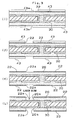
- the multilayered circuit board is a multilayered circuit board having a core substrate on which conductive circuits and interlayer insulating resin layers are alternately formed. The conductive circuits in the layers are connected to one another through a via hole.
- the glass epoxy resin substrate of the FR-4 grade encounters a problem in that the insulation resistance between the through holes is reduced in a HAST test and a steam test. Another problem arises in that the resistance of the through hole chain was excessively changed as a result of the heat cycle test. That is, the reliability realized after use for a long time has been unsatisfactory.
- Inventors of the present invention have considered probability of preventing reduction in the insulation resistance between the through holes and change in the resistance of the conductive circuit for connecting the through holes to each other by using low-cost resin such as epoxy resin in place of the costly resin, such as the BT resin. As a result, an unexpected fact was found that the foregoing problem is caused from the Tg point of the resin.
- a low-cost multilayered printed circuit board which is free from reduction in the insulation resistance between through holes as a result of the HAST test and the steam test and change in the resistance of the conductive circuit for connecting the through holes to each other as a result of a heat cycle test.
- the method of manufacturing the printed circuit board is broadly divided into a subtractive method (a Subtractive Process) and an additive method (an Additive Process).
- the subtractive method is also called an etching method which is characterized by chemically corroding the surface copper foil of a copper-plated laminated board.
- a copper-plated laminated board which incorporates an insulating substrate having two sides each of which is coated with copper foil having tens of ⁇ m. Then, an opening for forming a through hole is formed at a predetermined position of the copper-plated laminated board by drilling or the like. If a drilling step is performed, smears occurs in the opening for forming the through hole, desmear solution is used to process the copper-plated laminated board to dissolve and remove the smears. After the desmear process has been completed, electroless copper plating of the overall ground layer constituted by copper foil and the inner surface of an opening for forming the through hole is performed so that a thin plated layer is formed.
- a mask is formed on the thin plated layer. Then, thick plated layers are formed in the portions exposed through openings of the mask by electrolytic copper plating. After the foregoing plating process has been completed, the mask is separated. Then, etching is performed in a state in which an etching resist has been formed on the thick plated layer by solder plating or the like. The etching process is so performed as to remove the thin plated layer and the ground layer so as to divide the conductive pattern. Finally, the etching resist is separated so that a required printed circuit board is manufactured.
- the foregoing method is impossible to accurately form a fine pattern having a satisfactory shape.
- the characteristics of the etching causes a so-called divergent conductive pattern having a bottom which is longer than the top to easily be formed. Therefore, a pattern cannot easily be formed in a portion (for example, a bonding pad portion) which must have a fine and precise structure.
- a still further object of the present invention is to provide a method of manufacturing a printed circuit board with which a fine conductive pattern having a satisfactory shape can be formed.
- a multilayered printed circuit board comprising: a substrate on which a conductive circuit is formed; an interlayer insulating resin layer formed on the conductive circuit; an opening for forming a via hole formed in the interlayer insulating resin layer; and another conductive circuit including a via hole and formed on the interlayer insulating resin layer, wherein the surface of the conductive circuit is subjected to a coarsening process using etching solution containing cupric complex and organic acid, and stripe pits and projections are formed on the inner wall of the opening for forming the via hole.
- a method of manufacturing a multilayered printed circuit board including (1) a step of forming a conductive circuit; (2) a step of forming an interlayer insulating resin layer on the conductive circuit; (3) a step of applying a laser beam to form an opening for forming a via hole in the interlayer insulating resin layer; and (4) a step of forming another conductive circuit including a via hole on the interlayer insulating resin layer, wherein the surface of the conductive circuit is subjected to a coarsening process by using etching solution containing cupric complex and organic acid.
- the method of manufacturing the multilayered printed circuit board has the step of spraying etching solution containing the cupric complex and the organic acid to the surface of the conductive circuit or the conductive circuit is immersed in the etching solution under a bubbling condition so that the surface of the conductive circuit is subjected to the coarsening process.
- a multilayered printed circuit board incorporating interlayer insulating resin layers and conductive layers laminated alternately and structured such that the conductive layers are connected to one another through via holes each of which is formed by forming a metal film in a through hole formed in each of the interlayer insulating resin layers, said multilayered printed circuit board according to the present invention comprising:
- An aspect of the present invention according to claim 4 has the structure that stripe pits and projections are provided for the side wall of the through hole.
- the area of connection with the metal film can be enlarged, causing the adhesiveness to be improved.
- a reliable via hole can be formed.
- the bump is provided for the via hole. If an element, such as an IC chip, having a different coefficiency of thermal expansion is mounted, force is exerted in the vertical direction of the via hole owing to the heat cycle. Also in the foregoing case, the stripe pits and projections in the direction of the opening prevent separation of the via hole.
- the stripe pits and projections have the structure that the intervals between projections (or pits) are 1 ⁇ m to 20 ⁇ m. If the interval is too long or too short, the adhesiveness effect with the metal film deteriorates.
- the foregoing interval is substantially the same as 1/2 of the wavelength of the laser beam.
- the metal film for forming the via hole is formed such that the electroless copper plated film and the electrolytic copper plated film are formed in this order from a position adjacent to the side wall of the through hole.
- the electroless copper plated film is harder than the electrolytic copper plated film.
- the stripe pits and projections are formed into a pseudo coarsened surface. Therefore, if separating force is exerted, breakage of the metal film does not cause the via hole to be separated from the through hole.
- a coarsened surface having an average surface roughness Ra of about 0.05 ⁇ m to about 5 ⁇ m is formed (Fig. 31 (A) which is an enlarged view) on the surface of the stripe pits and projections.
- the reason for this lies in that the adhesiveness can furthermore be improved.
- the stripe pits and projections according to the present invention are formed at the intervals of 1 ⁇ m to 20 ⁇ m. Therefore, the skin effect does not raise a critical problem. Moreover, the adhesiveness can be improved.
- the surface of the conductive circuit to which the through hole reaches is made of an electrolytic copper plated film.
- the electrolytic copper plated film has small crystal particles as compared with those of the electroless copper plated film.
- the electrolytic copper plated film exhibitsexcellent glossiness to easily reflect a laser beam. Therefore, the electrolytic copper plated film is an optimum film in a case where incident light of the laser beam and reflected light are caused to interfere with each other as described later.
- the surface of the conductive circuit to which the through hole reaches has a metal coarsened layer.
- the laser beam is reflected by the surface of the metal coarsened layer to enable the laser beam to be reflected by the surface of the metal coarsened layer to cause the incident light of the laser beam and the reflected wave to interfere with each other.
- the stripe pits and projections formed in the direction of the opening can be provided for the surface of the wall of the through hole of the interlayer insulating resin layer.
- the coarsened layer enables the reflection of the laser beam to be prevented to a level not higher than a predetermined level, residual resin on the surface of the conductive circuit can be prevented. Since the coarsened layer enables the adhesiveness with the interlayer insulating resin layer to be maintained, separation of the interlayer insulating resin layer owing to deterioration in the thermal shock of the laser beam can be prevented.
- the reflection is raised excessively, causing residue of the resin to easily occur. If an oxidizing (a blackening) process is performed to form the coarsened layer, the laser beam is undesirably absorbed. Thus, the laser beam cannot be reflected.
- Rj of the coarsened layer is 0.05 ⁇ m to 20 ⁇ m. If Rj is 0.05 ⁇ m or smaller, the reverse side is blackened. Thus, the laser beam is undesirably absorbed. If Rj is larger than 20 ⁇ m, the laser beam scatters. In either of the two cases, incident light a reflected wave cannot cause to interfere with each other.
- the coarsened layer is a coarsened layer obtained by non-acidic chemical coarsening process, such as physical coarsening including a polishing process, an oxidizing (a blackening) and reducing process, a process using sulfuric acid and hydrogen peroxide solution or a coarsening process using etching solution composed of cupric complex and organic acid under coexistence of oxygen.
- non-acidic chemical coarsening process such as physical coarsening including a polishing process, an oxidizing (a blackening) and reducing process, a process using sulfuric acid and hydrogen peroxide solution or a coarsening process using etching solution composed of cupric complex and organic acid under coexistence of oxygen.
- the coarsened layer is a coarsened layer obtainable from a plating process using an alloy, such as Cu-Ni-P or Cu-Co-P. The reason for this lies in that the foregoing coarsened layer is able to reflect the laser beam.
- Plating of Cu-Ni-P may be performed by using electroless plating bath, the pH of which is 9 and which is water solution of, for example, copper sulfate (0.1 ⁇ 10 -2 to 25 ⁇ 10 -2 mol/l), nickel sulfate (0.1 ⁇ 10 -3 to 40 ⁇ 10 -3 mol/l), citric acid (1 ⁇ 10 -2 to 20 ⁇ 10 -2 mol/l), sodium hypophosphite (1 ⁇ 10 -1 to 10 ⁇ 10 -1 mol/l), boric acid (1 ⁇ 10 -1 to 10.0 ⁇ 10 -1 mol/l) or a surface active agent (Surfinol 465 manufactured by Nissin Chemical Industry) (0.1 g/l to 10 g/l).
- a surface active agent Sudfinol 465 manufactured by Nissin Chemical Industry
- the cupric complex according to the present invention is a cupric complex of azole.
- the cupric complex of azole is employed as an oxidizer for oxidizing metal copper.
- the azole may be diazole, triazole or tetra azole.
- any one of the following material is employed: imidazole, 2-methyl imidazole, 2-ethyl imidazole, 2-ethyl-4-methyl imidazole, 2-phenyl imidazole or 2-undecyl imidazole.
- the quantity of cupric complex of azole which must be added is 1 wt% to 15 wt%. The reason for this lies in that noble metal, such as Pd, exhibiting satisfactory solubility, stability and constituting crystal core can be dissolved.
- organic acid is mixed with the cupric complex of azole.
- the organic acid is at least one type of material selected from a group consisting of formic acid, acetic acid, propionic acid, butyric acid, valerianic acid, capronic acid, acrylic acid, crotonic acid, oxalic acid, malonic acid, succinic acid, glutaric acid, maleic acid, benzoic acid, glycollic acid, lactic acid, malic acid and sulfamic acid. It is preferable that the content of the organic acid is 0.1 wt% to 30 wt% to maintain the solubility of oxidized copper and dissolution stability.
- cuprous complex is dissolved owing to an action of the acid so as to be combined with oxygen so that cupric complex is produced which is again contributed to the oxidation of copper.
- halogen ions for example, fluorine ions, chlorine ions or bromine ions
- hydrochloric acid or sodium chloride may be added to supply halogen ions. It is preferable that the quantity of halogen ions is 0.01 wt% to 20 wt% to improve the adhesiveness between the formed coarsened surface and the interlayer insulating resin layer.
- cupric complex of azole and the organic acid (and halogen ions if necessary) are dissolved in water to adjust the etching solution.
- the oxidizing and reducing process may be performed by using an oxidizing bath of 1 g/l to 100 g/l NaOH, 1 g/l to 100 g/l NaClO 2 and 1 g/l to 50 g/l Na 3 PO 4 and a reducing bath of 1 g/l to 100 g/l NaOH to 1 g/l to 50 g/l NaBH 4 .
- the metal coarsened layer may be coated with at least one type of metal materials selected from a group consisting of Ti, Al, Cr, Zn, Fe, In, Tl, Co, Ni, Sn, Pb, Bi and noble metal to maintain glossiness and improve adhesiveness with the solder resist. It is preferable that the thickness of the selected metal material is 0.01 ⁇ m to 10 ⁇ m.
- the diameter of the through hole for forming the via hole is 80 ⁇ m or smaller.
- the foregoing precise via hole has a small area of contact between the metal film for forming the via hole and the side wall of the through hole for forming the via hole. Therefore, separation considerably easily occurs. Therefore, the formation of the conventional coarsened surface cannot satisfactorily prevent the separation. If the coarsened surface is made to be excessively complicated, the foregoing skin effect problem of delay in transmission and production of noise arises.
- the present invention is able to overcome the foregoing problems.
- the interlayer insulating resin layer is made of thermosetting resin or a composite material of the thermosetting resin and thermoplastic resin.
- An aspect of the present invention according to claim 5 has a structure that the interlayer insulating resin layer is made of thermosetting resin or a composite material of thermosetting resin and thermoplastic resin. Therefore, stripe pits and projections can easily be formed owing to interference of the laser beam. Note that only the thermosetting resin, which encounters dissolution of resin, cannot form clear stripe pits and projections.
- the interlayer insulating resin layer contains acrylic monomer.
- an aspect of the present invention according to claim 6 is structured such that the interlayer insulating resin layer contains acrylic monomer.
- the reason for this lies in that residues of the resin can be reduced.
- the acrylic monomer crosslinks monomer or oligomer of the thermosetting resin (including the thermosetting resin, a portion of which has been sensitized).
- the acrylic monomer can be decomposed relatively easily. Therefore, the acrylic monomer is contained in the molecular chain, the acrylic monomer is decomposed owing to a laser beam, causing the thermosetting resin to have low molecular weight. Moreover, the resin having the low molecular weight is decomposed by the laser beam. Therefore, formation into plasma can easily be formed, causing residue of resin to substantially be eliminated.
- the acrylic monomer may be any one of a variety of commercial products.
- DPE-6A KAYAMAER PM-2 or PM-21 manufactured by Nihon Kayaku, R-604 manufactured by Kyoei or Aronix M-315, M-325 or M-215 manufactured by Toa may be employed.
- DPE-6A is expressed by chemical formula 1 shown in Fig. 59
- R-604 is expressed by chemical formula 2
- Aronix M-315 is expressed by chemical formula 3
- M215 is expressed by chemical formula 4 shown in Fig. 60
- KAYAMAER PM-2 is expressed by chemical formula 5.
- a method of manufacturing a multilayered printed circuit board according to claim 7 comprising at least the steps (a) to (d):
- an aspect has a structure that the conductive circuit below the resin is vertically irradiated with a carbon-dioxide-gas laser beam to cause interference between reflected wave from the conductive circuit and incident wave to occur. Therefore, the stripe pits and projections can be formed on the side wall of the through hole. Therefore, the adhesiveness with metal can be improved so that a reliable via hole can be formed.
- the resin is thermosetting resin or a composite material of the thermosetting resin and thermoplastic resin.
- An aspect of claim 8 has a structure that the interlayer insulating resin layer is made of the thermosetting resin or a composite of the thermosetting resin and thermoplastic resin. Therefore, the stripe pits and projections can easily be formed by the laser beam.
- the step of forming the via hole includes a step of forming a resist after an electroless copper plated film has been formed in the through hole and supplying electric power through the electroless plated film to form an electrolytic plated film in a portion in which the resist is not formed.
- An aspect of claim 9 has a structure that an electroless copper plated film is formed on the surface of the through hole, followed by forming a resist. Then, electric power is supplied through the electroless copper plated film to form an electrolytic copper plated film in a portion in which no resist is formed. Thus, the via hole is formed. Since the stripe pits and projections are formed on the side wall of the through hole by using the interference of the laser beam and then the electroless plated film is formed, the adhesiveness between the electroless copper plated film and the through hole in the interlayer insulating resin layer canbe improved. As a result, a reliable via hole can be formed.
- the interlayer insulating resin layer contains acrylic monomer.
- a method of manufacturing a printed circuit board according to item 1 comprising at least the steps (a) and (b) :
- An aspect item 1 has a structure that the through hole is formed in the solder resist layer by using the laser beam. Therefore, the material is not limited to the photosensitive material. As a material of the solder-resist layer, any one a variety of materials may be employed.
- the surface of the conductive circuit is constituted by the electrolytic plated film.
- the electrolytic plated film has large crystal particles as compared with those of the electroless plated film. Moreover, the electrolytic plated film exhibits excellent glossiness to easily reflect a laser beam. Therefore, the electrolytic plated film is an optimum film in a case where incident light of the laser beam and reflected light are caused to interfere with each other as described later.
- the surface of the conductive circuit has a metal coarsened layer.
- An aspect of item 2 is characterized in that the surface of the conductive circuit has a metal coarsened layer.
- the laser beam can be reflected by the surface of the metal coarsened layer.
- incident waves of the laser beam and reflected waves can be caused to interfere with each other.
- the stripe pits and projections formed in the direction of the opening can be provided for the wall of the through hole of the solder-resist layer.
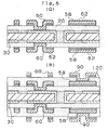
- An aspect item 3 has a structure that a bump made of a low-melting-point metal is provided for the through hole in the solder-resist layer.
- a bump made of a low-melting-point metal is provided for the through hole in the solder-resist layer.
- an electrode of an IC chip can be connected to the foregoing bump or the foregoing bump may be used to mount the printed circuit board to another printed circuit board.
- a laser beam in a single mode is applied in the step of forming the through hole so that a through hole having a diameter of 300 ⁇ m to 650 ⁇ m is formed.
- An aspect of item 4 has a structure that a single-mode laser beam, the diameter of a spot light of which can be enlarged is applied. Therefore, a through hole for forming a through hole having a diameter of 300 ⁇ m to 650 ⁇ m, that is, a through hole for forming a bump for establishing the connection with another printed circuit board (for example, a mother board) can be formed in the solder-resist layer.
- a laser beam in a multi mode is applied in the step of forming the through hole so that a through hole having a diameter of 50 ⁇ m to 300 ⁇ m is formed.
- An aspect of item 5 has a structure that a multimode laser beam, the diameter of which can be reduced is applied. Therefore, a through hole for forming a through hole having a diameter of 50 ⁇ m to 300 ⁇ m, that is, a through hole for forming a bump for establishing the connection with an IC chip can be formed in the solder-resist layer.
- the step of forming the through hole is performed such that the carbon-dioxide gas laser beam is vertically applied to the conductive circuit below the resin to cause interference of reflected wave from the conductive circuit and incident wave to occur so that stripe pits and projections are formed on the side wall of the through hole.
- An aspect item 6 has a structure that a step for forming the through hole is arranged such that reflected wave of the carbon-dioxide gas laser beam and the incident wave are caused to interfere with each other.
- the stripe pits and projections are formed on the side wall of the through hole. Therefore, when the metal film is provided for the through hole, the metal film can be brought into hermetic contact with the through hole.
- the step of forming the bump is performed such that a metal film is provided for the through hole having the side wall provided with the stripe pits and projections, and then metal having a low melting point is enclosed.
- An aspect of item 7 has a structure that the metal film is provided for the through hole having the side wall. Then, low-melting-point metal is enclosed to form the bump. The metal film is brought into hermetic contact with the through hole having the stripe pits and projections so that the bump is strongly connected to the conductive circuit.
- a printed circuit board incorporating a substrate provided with a conductive circuit and having a surface on which a solder-resist layer is formed, said printed circuit board according to the present invention comprising:
- An aspect of item 8 has a structure that the stripe pits and projections are formed on the side wall of the through hole formed in the solder-resist layer. Therefore, when the metal film is formed on the surface of the through hole, the metal film can strongly be brought into hermetic contact with the through hole.
- a heat cycle sometimes causes a crack to sometimes occur in the solder-resist layer owing to the difference between the coefficiency of thermal expansion of the metal film and that of the solder-resist layer.
- the present invention causes the metal film and the wall of the through hole of the solder-resist layer to be brought into hermetic contact to each other. Therefore, a crack cannot easily be formed.
- the stripe pits and projections are provided for the wall of the through hole in the direction of the opening, the contact between the wall and the low-melting-point metal is made to be line contact in place of the plane contact. Therefore, a phenomenon (migration) that the low-melting-point metal is ionized and diffused under hot and high humidity conditions can be prevented.
- the employed low-melting-point metal and the metal film are the same as those described above. It is most preferable that the surface of the conductive circuit is constituted by an electolytically plated film.
- the electolytically plated film has smaller crystal particles as compared with the electroless platted film and exhibiting excellent glossiness. Moreover, discoloration, called "color change owing to plating" can be prevented. Thus, the laser beam can easily be reflected.
- the stripe pits and projections can be formed on the surface of the wall in the direction of the opening.
- the stripe pits and projections have the structure that the intervals between projections (or pits) are 1 ⁇ m to 20 ⁇ m. If the interval is too long or too short, the adhesiveness effect with the metal film deteriorates. A similar state is realized to that realized by the plane contact and, therefore, the foregoing effect cannot be obtained.
- the foregoing interval is substantially the same as 1/2 of the wavelength of the laser beam.
- the low-melting-point metal may be solder, such as Sn/Pb, Ag/Sn or Ag/Sn/Cu.
- the foregoing bump can be formed through a metal film made of Ni/Au, Ni/Pd/Au, Cu/Ni/Au or Cu/Ni/Pd/Au. Adjustments are performed such that the thickness of the Cu layer and that of the Ni layer is 0.1 ⁇ m, to 10 ⁇ m and that of each of the Pd layer and the Au layer is 0.01 ⁇ m to 10 ⁇ m.
- a bump made of metal having a low melting point is formed in the through hole through a metal film.
- An aspect of item 9 has a structure that the low-melting-point metal is enclosed to form the bump.
- the bump can. strongly be connected to the conductive circuit.
- the solder-resist layer is made of thermosetting resin or a composite material of the thermosetting resin and thermoplastic resin.
- An aspect of item 10 has a structure that the solder-resist layer is constituted by thermosetting resin or a composite of the thermosetting resin and the thermoplastic resin. Therefore, the stripe pits and projections can easily be formed on the side surface of the through hole by the laser beam. When only the thermoplastic resin is employed, the res in is undesirably dissolved. Thus, clear pits and projections cannot be formed.
- a coarsened layer is formed on the surface of the conductive circuit.
- An aspect of item 11 is characterized in that the surface of the conductive circuit has a metal coarsened layer.
- the laser beam can be reflected by the surface of the metal coarsened layer.
- the incident wave and the reflected wave of the laser beam can be caused to interfere with each other.
- the stripe pits and projections can be formed on the surface of the wall of the through hole in the solder-resist layer in the direction of the opening.
- an adhesive for electroless plating as the above interlayer resin insulating layer.
- this adhesive for electroless plating it is optimal that heat resisting resin particles soluble to a hardened acid or oxidizing agent are dispersed into unhardened heat resisting resin difficult to be soluble to an acid or an oxidizing agent.
- the heat resisting resin particles are dissolved and removed by processing these resin particles using an acid or an oxidizing agent and a coarsened face constructed by an anchor formed in the shape of an octopus trap can be formed on a layer surface.
- the above heat resisting resin particles particularly hardened are desirably constructed by using 1 heat resisting resin powder having an average particle diameter equal to or smaller than 10 ⁇ m, 2 cohesive particles formed by aggregating heat resisting resin powder having an average particle diameter equal to or smaller than 2 ⁇ m, 3 a mixture of heat resisting powder resin powder having an average particle diameter from 2 to 10 ⁇ m and heat resisting resin powder having an average particle diameter equal to or smaller than 2 ⁇ m, 4 pseudo-particles in which at least one kind of heat resisting resin powder or inorganic powder having an average particle diameter equal to or smaller than 2 ⁇ m is attached to the surface of heat resisting resin powder having an average particle diameter from 2 to 10 ⁇ m, a mixture of heat resisting powder resin powder having an average particle diameter from 0.1 to 0.8 ⁇ m and heat resisting resin powder having an average particle diameter greater than 0.8 ⁇ m and smaller than 2 ⁇ m, and 6 heat resisting powder resin powder having an average particle diameter from 0.1 to 1.0 ⁇ m.
- Rj preferably ranges from 0.1 to 5 ⁇ m in the semi-additive method since an electroless plating film can be removed while the close attaching property is secured.
- the heat resisting resin difficult to be soluble to an acid or an oxidizing agent mentioned above is desirably constructed by "a resin complex constructed by thermosetting resin and thermoplastic resin", or "a resin complex constructed by photosensitive resin and thermoplastic resin” .
- the former has a high heat resisting property.
- the latter is desirable since the opening for the via hole, can be, formed by photolithography.
- thermosetting resin can be constructed by using epoxy resin, phenol resin, polyimide resin, etc.
- thermosetting resin is photosensitized, a thermosetting group acrylic-reacts on methacrylic acid, acrylic acid, etc. Acrylate of the epoxy resin is particularly optimal.
- the epoxy resin can be constructed by using epoxy resin of novolak type such as phenol novolak type, cresol novolak type, etc., dicyclopentadiene-modified alicyclic epoxy res in, etc.
- the thermoplastic resin can be constructed by using polyether sulfone (PES), polysulfone (PSF), polyphenylene sulfone (PPS), polyphenylene sulfide (PPES), polyphenyl ether (PPE), polyether imide (PI), etc.
- PES polyether sulfone
- PPS polysulfone
- PES polyphenylene sulfide
- PPE polyphenyl ether
- PI polyether imide
- a mixing weight ratio of the above heat resisting resin particles is preferably set to range from 5 to 50 weight % and desirably range from 10 to 40 weight % with respect to the solid content of a heat resisting resin matrix.
- the heat resisting resin particles are preferably constructed by amino resin (melamine resin, urea resin, guanamine resin), epoxy resin, etc.
- amino resin melamine resin, urea resin, guanamine resin
- epoxy resin etc.
- a acrylic-system monomer can be used.
- the adhesive may be constructed by two layers having different compositions.
- Various kinds of resins can be used as a solder resist layer added to a surface of the multilayer build-up wiring board.
- resins can be used as a solder resist layer added to a surface of the multilayer build-up wiring board.
- bisphenol A-type epoxy resin acrylate of bisphenol A-type epoxy resin, novolak type epoxy resin, resin formed by hardening acrylate of novolak type epoxy resin by an amine-system hardening agent, an imidazole hardening agent, etc.
- solder resist layer is separated since the solder resist layer is constructed by resin having a stiff skeleton. Therefore, the separation of the solder resist layer can be also prevented by arranging a reinforcing layer.
- the above acrylate of the novolak type epoxy resin can be constructed by using epoxy resin in which glycidyl ether of phenol novolak and cresol novolak reacts with acrylic acid, methacrylic acid, etc.
- the above imidazole hardening agent is desirably formed in a liquid state at 25 °C since the imidazole hardening agent can be uniformly mixed in the liquid state.
- Such a liquid state imidazole hardening agent can be constructed by using 1-benzyl-2-methylimidazole (product name: 1B2MZ), 1-cyanoethyl-2-ethyl-4-methylimidazole (product name: 2E4MZ-CN) and 4-methyl-2-ethylimidazole (product name: 2E4MZ).
- An adding amount of this imidazole hardening agent is desirably set to range from 1 to 10 weight % with respect to a total solid content of the above solder resist composition substance. This is because the imidazole hardening agent is easily uniformed and mixed if the adding amount lies within this range.
- a composition substance prior to the hardening of the above solder resist is desirably constructed by using a solvent of a glycol ether system as a solvent.
- Such a solvent of the glycol ether system is constructed by using the following structural formula, particularly desirably using at least one kind selected from diethylene glycol dimethyl ether (DMDG) and triethylene glycol dimethyl ether (DMTG). This is because these solvents can perfectly dissolve benzophenone and Michler' s ketone as reaction starting agents at a heating temperature from about 30 to 50 °C .
- DMDG diethylene glycol dimethyl ether
- DMTG triethylene glycol dimethyl ether
- This solvent of the glycol ether system preferably has 10 to 70 wt% with respect to a total weight amount of the solder resist composition substance.
- thermosetting resin for improving a heat resisting property and an antibasic property and giving a flexible property thermosetting resin for improving a heat resisting property and an antibasic property and giving a flexible property
- a photosensitive monomer for improving resolution, etc. can be further added to the solder resist composition substance.
- the leveling agent is preferably constructed by monomer of acrylic ester.
- a starting agent is preferably constructed by Irugacure 1907 manufactured by CHIBAGAIGI.
- a photosensitizer is preferably constructed by DETX-S manufactured by NIHON KAYAKU.
- a coloring matter and a pigment may be added to the solder resist composition substance since a wiring pattern can be hidden.
- This coloring matter is desirably constructed by using phthalocyaline green.
- Bisphenol type epoxy resin can be used as the above thermosetting resin as an adding component.
- this bisphenol type epoxy resin there are bisphenol A-type epoxy resin and bisphenol F-type epoxy resin.
- the former is preferable when an antibasic property is seriously considered.
- the latter is preferable when low viscosity is required (when a coating property is seriously considered).
- a polyhydric acrylic-system monomer can be used as the above photosensitive monomer as an adding component since the polyhydric acrylic-systemmonomer can improve resolution.
- DPE-6A manufactured by NIHON KAYAKU and R-604 manufactured by KYOEISYA KAGAKU can be used as the polyhydric acrylic-system monomer.
- solder resist composition substances preferably have 0.5 to 10 Pa ⁇ s in viscosity at 25 °C and more desirably have 1 to 10 Pa ⁇ s in viscosity since these solder resist composition substances are easily coated by a roll coater in these cases.
- a method of manufacturing a multilayered printed circuit board such that a through hole is formed in a double-side copper-plated laminated board by performing a laser machining and the through hole is made to be conductive to form a through hole so that a core substrate is manufactured, and an interlayer insulating resin layer and a conductive circuit are formed on the core substrate, said method of manufacturing a multilayered printed circuit board comprising the step of:
- a substrate for forming a through hole such that a through hole is formed in a double-side copper-plated laminated board and the through hole is made to be conductive so that a through hole is formed said substrate comprising:
- a multilayered printed circuit board incorporating a substrate in the form of a double-side copper-plated laminated board in which a through hole is formed such that the through hole is made to be conductive so that a through hole is formed and an interlayer insulating resin layer and a conductive circuit are formed on at least either side of the substrate, said multilayered printed circuit board comprising:
- the thickness of the copper foil is smaller than 12 ⁇ m, preferably about 1 ⁇ m to about 10 ⁇ m. Thus, conversion of the energy of the laser beam into heat which is conducted as described above can be prevented. Thus, formation of an opening using the laser beam can be realized.
- the copper-plated laminated board according to the present invention may be a copper-plated laminated board obtained by bonding copper foil to prepreg, such as glass-cloth epoxy resin, glass-cloth bis maleimide-triazine resin or glass-cloth fluororesin.
- the thickness of the copper foil is 1 ⁇ m to 10 ⁇ m.
- the reason for this lies in that an opening can easily be formed by the laser beam if the thickness is 10 ⁇ m or smaller. If the thickness is smaller than 1 ⁇ m, blister or the like occurs.
- the thickness of the copper foil is adjusted by etching. Specifically, chemical etching is employed which uses sulfuric acid and hydrogen peroxide solution, ammonium persulfate solution, cupric chloride solution or ferric chloride solution; or physical etching, such as ion-beam etching is employed.
- the thickness of the copper-plated laminated board is 0. 5 mm to 1.0 mm. If the thickness is too large, the opening cannot be formed. If the thickness is too small, warp or the like occurs.
- the carbon-dioxide gas laser beam for use in the present invention is a short-pulse laser of 20 mJ to 40 mJ and 10 -4 second to 10 -8 second.
- the number of shots of the laser beams is 5 shots to 100 shots.
- the diameter of the through hole which must be formed is 50 ⁇ m to 150 ⁇ m. If the thickness is smaller than 50 ⁇ m, the surface of the wall cannot be made to be conductive by plating or the like. If the thickness is larger than 150 ⁇ m, a drill work enables an advantage to be realized.
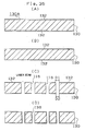
- the through hole encounters taper. Taper occurs on the side on which the laser beam is made incident such that the diameter of the through hole is enlarged.
- a through hole having a cross section formed into a concave shape is undesirably formed.
- the foregoing through hole is made to be conductive by electric plating, electroless plating, sputtering, evaporation or enclosure of conductive paste.
- taper is provided for the through hole to easily enclose the paste.
- the through hole can be filled with a filler.
- the inner wall of the metalized through hole may be coarsened.
- each of the thickness of the copper foil and that of the metalized layer is 10 ⁇ m to 30 ⁇ m.
- the filler may be any one of a variety of materials including a filler constituted by inorganic particles made of bis phenol F epoxy resin, silica or alumina, metal particles and resin.
- the conductive circuit is provided for the substrate having the through hole structured as described above.
- the conductive circuit is formed by an etching process.
- the surface of the conductive circuit is subjected to a coarsening process in order to improve the adhesiveness.
- the interlayer insulating resin layer made of insulating resin is formed.
- the insulating resin may be thermosetting resin, thermoplastic resin or their composite resin.
- the interlayer insulating resin layer may be adhesive agent for electroless plating.
- the opening can be formed in the foregoing interlayer insulating resin layer by a laser beam, exposure or a development process.
- a built-up multilayered printed circuit board comprising: a substrate having a through hole and a conductive circuit and structured such that interlayer insulating resin layers and conductive circuits are alternately formed and the conductive circuits in the different layers are electrically connected to one another through via holes formed in the interlayer insulating resin layers, wherein the substrate is a glass epoxy resin substrate made of epoxy resin having Tg point of 190°C or higher.
- the reason why the insulation resistance between the through holes is reduced during the HAST test and the steam test is that metal, such as copper, which forms the through hole is ionized and ions are moved (migration) between the through holes, causing the insulation resistance to be reduced.
- the foregoing problems can be prevented.
- the ionization of the metal which forms the through hole and ions are moved (migration) as described above to reduce the insulation resistance between the plated through holes during the HAST test and the steam test can be prevented.
- the thermal expansion and contraction occurring in the heat cycle test resulting in the conductive circuit or the through hole being broken and thus the resistance is changed, can be prevented.
- the epoxy resin is low-cost resin as compared with BT resin.
- the glass epoxy resin substrate having a Tg point of 190°C or higher (a DMA method (temperature rise rate: 2°C /minute)
- a known substrate developed for a mass-lamination type multilayered printed circuit board may be used.
- any one of the foregoing materials may be employed: HL830 (Tg point: 217°C) or HL830FC (Tg point: 212°C) manufactured by Mitsubishi Gas Chemical, MCL-E-679LD (Tg point: 205°C to 215°C) or MCL-E-679F (Tg point: 205°C to 217°C) manufactured by Hitachi Chemical or R-5715 (Tg point: 190°C) manufactured by Matsushita Electric Works.
- An opening is, by a laser beam or drilling, formed in the foregoing glass epoxy resin substrate or the copper-plated laminated board, followed by metalizing the surface of the inner wall by electric plating, electroless plating, sputtering or evaporation.
- the through hole is formed.
- a filler may be enclosed in the foregoing through hole.
- the metalized inner wall of the through hole may be coarsened.
- the filler may be made of any one of a variety of materials including inorganic particles made of bis phenol F epoxy resin, silica or alumina; or metal particles; and resin.
- the conductive circuit is provided for the thus-formed substrate having the through hole formed therein.
- the conductive circuit is formed by an etching process.
- the surface of the conductive circuit is subjected to the coarsening process.
- the insulating resin may be thermosetting resin, thermoplastic resin or their composite resin.
- a method of manufacturing a printed circuit board incorporating through holes and conductor patterns formed by a subtractive method comprising:
- An aspect of item 25 enables smear taken place during an opening forming process to be dissolved and removed by performing a desmear process. Also the conductive metal foil is dissolved and removed at this time. Thus, the conductive metal foil is thinned. A first plating process is performed so that a thin plated layer is formed. Then, a second plating process is performed so that a thick plated layer is formed. As a result, only portions which will be formed into the conductive pattern are selectively thickened. Then, etching is performed so that the thin plated layer below the mask and the ground layer are removed. Thus, the conductive pattern is divided. In the present invention, both of the thin plated layer and the ground layer are thin layers.
- the thickness which must be removed by etching performed in the conductive pattern dividing step is very small. Therefore, formation of a divergent shape of the conductive pattern formed by dividing does not easily occur. Thus, a fine pattern having a satisfactory shape can accurately be formed.
- the conductive metal foil can be made with copper, aluminum, gold, silver, platinum or nickel. Specifically, the copper or the metal mainly comprising the copper is desirable.
- the first plating step uses an electroless plating bath
- the second plating step uses an electrolytic plating bath.
- An aspect of item 27 has a structure that the electroless plating bath is employed only when the plated layer is formed on the inner wall of the opening for forming the through hole. Then, the low-cost electrolytic plating bath which exhibits high speed plating deposition speed is employed. As a result, the cost reduction can be realized and the productivity can be improved.
- the first plating step uses an electroless copper plating bath to form a copper plated layer having a thickness of 0.2 ⁇ m to 2.5 ⁇ m
- the second plating step uses an electrolytic copper plating bath to form a copper plated layer having a thickness of 8.0 ⁇ m or greater.
- An aspect of item 28 has a structure that the electroless plating bath is employed only when the plated layer is formed on the inner wall of the opening for forming the through hole. Then, the low-cost electrolytic plating bath which exhibits high speed plating deposition speed is employed. As a result, the cost reduction can be realized and the productivity can be improved. Since a very thin copper plated layer is formed in the first plating step, the thickness which must be removed by etching in the conductive pattern dividing step is very small. Therefore, a fine pattern having a satisfactory shape can furthermore accurately be formed.
- the step for dividing the conductor pattern by performing etching is performed in a state in which no etching resist is provided for the thick plated layer formed in the second plating step.
- An aspect of item 29 has a structure that the step for forming and separating the etching resist in the conduct ive pattern dividing step can be omitted.
- the number of manufacturing steps can be reduced and the productivity can be improved.
- the thickness of the thickplated layer which is removed when the etching process is performed is very small. Thus, no adverse influence is exerted on the accuracy of the formed pattern.
- a printed circuit board incorporating a conductive pattern is provided which is formed by, for example, subtractive method, wherein the conductive pattern includes a metal ground layer provided for an insulating substrate and having a thickness of 0.2 ⁇ m to 3.0 ⁇ m and a plated layer formed on the metal ground layer.
- the conductive pattern includes a metal ground layer provided for an insulating substrate and having a thickness of 0.2 ⁇ m to 2.5 ⁇ m, a plated layer formed on the metal ground layer and having a thickness of 0.2 ⁇ m to 2.5 ⁇ m and a plated layer formed on the plated layer and having a thickness of 8.0 ⁇ m or greater.
- a method of manufacturing a multilayered printed circuit board according to item 32 comprising the steps (1) to (5):
- the present invention according to item 32 employs a metal film thinned by etching and thus having a lowered thermal conductivity as a conformal mask. Therefore, an opening can be formed by a small output laser. Hence it follows that generation of undercut of resin for forming an interlayer insulating resin layer can be prevented.
- a method of manufacturing amultilayered printed circuit board according to item 33 comprising the steps (1) to (8):
- the present invention according to item 33 employs a metal film thinned by etching and thus having a lowered thermal conductivity as a conformal mask. Therefore, an opening can be formed by a small output laser. Hence it follows that generation of undercut of resin for forming an interlayer insulating resin layer can be prevented.
- an electroless copper plated film is formed on the metal film. Then, an electrolytic copper plated film is formed on the electroless copper plated film.
- the electroless copper plated film lower than the resist layer is removed by etching. Since the metal film and the electroless copper plated film, which are thin films, can easily be removed, the electrolytic copper plated film constituting the conductive circuit and the via hole is not corroded during the etching process. As a result, a circuit having a fine pitch and a via hole having a precise diameter can be formed.
- the metal film is copper foil.
- the thickness of the metal film is made to be 5 ⁇ m to 0.5 ⁇ m in the step for reducing the thickness of the metal film by performing etching.
- the thickness of the metal film is made to be 5 ⁇ m to 0.5 ⁇ m.
- the reason for this lies in that undercut occurs if the thickness of the metal film is larger than 5 ⁇ m. If the thickness is not larger than 0.5 ⁇ m, the function of the conformal mask cannot be obtained.
- an interlayer insulating resin layer incorporating a metal film having a thickness of 5 ⁇ m to 0.5 ⁇ m is pressed against a substrate having a conductive circuit formed thereon.
- the resin film having a metal film formed previously is pressed. Therefore, satisfactory flexibility can be realized which permits the resin film to easily be pressed against the substrate having the conductive circuit formed thereon.
- a method of manufacturing a multilayered printed circuit board incorporating a substrate on which a lower conductive circuit is formed, an insulating resin layer and an upper conductive circuit formed on the lower conductive circuit and having a structure that the lower conductive circuit and the upper conductive circuit are connected to each other through a via hole
- the method of manufacturing a multilayered printed circuit board comprising the steps of: forming the lower conductive circuit on the substrate; forming the insulating resin layer on the lower conductive, circuit; forming a coarsened surface on the surface of the insulating resin layer; forming, on the coarsened surface, a metal layer having an opening through which a portion of the coarsened surface is exposed; irradiating the coarsened surface exposed through the opening with a laser beam to remove the insulating resin layer to form an opening for the via hole; and forming the upper conductive circuit and the via hole.
- a method of manufacturing a multilayered printed circuit board incorporating a substrate on which a lower conductive circuit is formed, an insulating resin layer and an upper conductive circuit formed on the lower conductive circuit and having a structure that the lower conductive circuit and the upper conductive circuit are connected to each other through a via hole
- the method of manufacturing a multilayered printed circuit board comprising the steps of: forming the lower conductive circuit on the substrate; laminating, heating and compressing metal foil having a coarsened surface formed either surface thereof and the insulating resin layer formed on the coarsened surface such that the insulating resin layer makes contact with the lower conductive circuit so that the metal foil is integrated; etching a portion of the metal foil to form an opening to expose the coarsened surface of the insulating resin layer; irradiating the coarsened surface exposed through the opening with a laser beam to remove the insulating resin layer so as to form an opening for forming the via hole; and forming the upper conductive circuit and the via
- the cause of residues produced in the operation for forming the opening for forming the via hole is the structure that the surface which is irradiated with the laser beam is a mirror surface which reflects the laser beam to inhibit complete removal of the insulating resin layer.
- the present invention uses the detected fact such that the surface irradiated with the laser beam is formed into the coarsened surface to prevent reflection of the laser beam.
- the resist against the laser beam is metal layer or metal foil.
- the opening is formed in the metal layer or the metal foil.
- the opening is irradiated with a laser beam capable of realizing a diameter of a spot light which is larger than the diameter of the opening so that the opening for forming the via hole is formed in the insulating resin layer.
- the surface of the insulating resin layer exposed through the opening in the metal layer or the like is formed into the coarsened surface. Therefore, reflection of the laser beam can be prevented and the insulating resin layer can completelybe removed. Since upward expansion of the periphery of the insulating resin layer can be prevented, also disconnection of the via hole can be prevented.
- etching solution containing a cupric complex and organic acid is used to etch the conductive circuit.
- flattening can be prevented when the surface of the conductive circuit is irradiated with a laser beam.
- a coarsened surface exhibiting satisfactory adhesiveness with the interlayer insulating resin layer formed on the conductive circuit and the via hole can be formed.
- the foregoing detected fact is used to establish the present invention having the following essential portion.
- the resin filler 40 obtained in the process (3) is applied to the two sides of the substrate 30 by using a roll coater within 24 hours after the adjustment.
- the resin filler 40 is enclosed between the conductive circuit (the inner-layer copper pattern) 34 and the conductive circuit 34 and in the through hole 36.
- the resin filler 40 is dried at 70°C for 20 minutes.
- Another side is similarly processed.
- the resin filler 40 is enclosed between the conductive circuits 34 or in the through hole 36, and then heated and dried at 70°C for 20 minutes (see Fig. 1 (D)).
- Either side of the substrate 30 subjected to the process (4) is belt-sander-polished by using #600 belt polishing paper (manufactured by Sankyo).
- polishing is performed such that the resin filler 40 is not left on the surface of the inner-layer copper pattern 34 and the surfaces of lands 36a of the through hole 36.
- flaws caused from the belt-sander-polishing were removed by performing buff polishing.
- the foregoing sequential polishing process is performed for another surface (see Fig. 2 (E)).
- heat treatment was performed at 100°C for 1 hour, 120°C for 3 hours, 150°C for 1 hour and 180°C for 7 hours.
- the resin filler 40 was hardened.
- the substrate 30 having the conductive circuit 34 was degreased by using alkali material, and soft etching was performed. Then, a process using a catalyst composed of palladium chloride and organic acid was performed so that a Pd catalyst was imparted.
- electroless plating solution composed of 3.2 ⁇ 10 -2 mol/l copper sulfate, 3.9 ⁇ 10 -3 mol/l nickel sulfate, 5.4 ⁇ 10 -2 mol/l complexing agent, 3.3 ⁇ 10 -1 mol/l sodium hypophosphite, 5.0 ⁇ 10 -1 mol
- copper foil having resin (MCF-6000E manufactured by Hitachi Kasei and including resin 20 having a thickness of 60 ⁇ m and copper foil 22 having a thickness of 12 ⁇ m) 20A is pressed against to the two sides of the substrate 30 having the thickness of 0. 8 mm by operating a vacuum pressing machine (see Fig. 2 (G)), the vacuum pressing operation being performed under conditions that the temperature is 175°C for 90 minutes, the pressure is 30 Kg/cm2 and the degree of vacuum ⁇ 50 torr).
- the overall surface of the surface copper foil 22 is etched to make the thickness to be 3 ⁇ m by using. etching solution (SE-07 manufactured by Mitsubishi Gas) (see Fig. 2 (H) ) .
- a dry-film resist (NIT-215 manufactured by NichigoMoton) is applied to the copper foil 22, and then a mask is placed. Then, exposure is performed with 100 mJ/cm2 and a development process is performed by using 0.8 % sodium. carbonate. Thus, an etching resist 43 having an opening 43a formed in a portion in which the via hole will be formed is provided (see Fig. 3 (I)).
- the copper foil 22 in the opening 43a is removed by cupric chloride etching solution (see Fig. 3 (J)), and then the etching resist 43 is separated by sodium hydroxide solution so that copper foil 22 serving as the conformal mask is completed (see Fig. 3 (K)).
- a carbon-dioxide gas laser irradiating apparatus (605GTX manufactured by Mitsubishi Electric) is operated to irradiate each opening 22a of the copper foil with a two-shot and short-pulse laser beam so that a through hole 20a having a diameter of 60 ⁇ m is formed in the interlayer insulating resin layer (resin) 20 (see Fig. 3 (L)). That is, the copper foil 22 having the thickness of 3 ⁇ m is used as the conformal mask to form the opening 22a by applying the laser beam.
- the irradiation with the carbon-dioxide gas laser may be performed for each opening 22a of the copper foil 22 or the overall portion of the printed circuit board is irradiated and scanned with the laser beam to remove the resin 20 in the lower portion of each opening 22a of the copper foil 22. It is preferable that the diameter of the laser beam is 1.3 times or more the diameter of the opening.
- residues may be removed. For example, immersion in solution of, for example, chromic acid, permanganic acid or potassium or use of O 2 plasma, CF 4 plasma or plasma of mixture gas of O 2 and CF 4 enables the residues to be removed.
- fluorine resin is employed to form the interlayer insulating resin layer, the plasma process is an optimum process.
- a development process is performed by using 0.8% sodium carbonate so that an etching resist 54 for covering the portion in which the via hole will be formed and a portion in which a circuit will be formed and having a structure of Line/Space: 30/30 ⁇ m is formed (see Fig. 4 (0)).
- cupric chloride is used to perform pattern etching.
- 2 % NaOH s used to separate the etching resist 54 so that a via hole 60 and a conductive circuit 58 are formed (see Fig. 4 (P)).
- the electrolytic copper plating 56 may be formed after the resist 54 has been formed.
- a dry-film resist (NIT-215 manufactured by NichigoMoton) is applied to the copper foil 22, and then a mask (not shown) is placed. Then, exposure is performed with 100 mJ/cm 2 and a development process is performed by using 0.8 % sodium carbonate.
- an etching resist 54 having an opening 54a formed in a portion in which the via hole will be formed and a portion in which the circuit will be formed is provided (see Fig. 5 (N')).
- electrolytic copper plating is performed under the following conditions so that an electrolytic copper plating film 56 is formed which has a thickness of 20 ⁇ m (see Fig. 5 (O')).
- the plating resist 54 is removed by using 5 % KOH, and then mixed solution of sulfuric acid and hydrogen peroxide is used to perform etching so that the electroless copper plated film 52 and the copper foil 22 under the plating resist 54 are dissolved and removed.
- a conductive circuit 58 composed of the copper foil 20, the electroless copper plated films 30 and 40 and the electrolytic copper plated film 44 and having a thickness of 18 ⁇ m and the via hole 60 are formed (see Fig. 5 (P')).
- the metal film (the copper foil) 22 the thickness of which has been reduced (3 mm) by etching and the thermal conductivity of which has been lowered is used as the conformal mask. Therefore, the opening 20a can be formed by a small-output laser. Specifically, the conventional manufacturing method is required to apply a short pulse laser beam three times to form one opening 20a in the resin 20 by the foregoing carbon-dioxide gas laser apparatus. On the other hand, the first embodiment is able to form the opening 20a by applying two short-pulse laser beams.
- the first embodiment is able to form the opening 20a with the small-output laser or such that the number of operations for applying the pulse laser beams is reduced. Therefore, occurrence of undercut in the resin 20 for forming interlayer insulating resin layer can be prevented (see Fig. 3 (L)). Therefore, the reliability of the connection of the via hole can be improved. It is preferable that the thickness of the metal film is reduced to 5 ⁇ m to 0.5 ⁇ m by etching. If the thickness of the metal film is larger than 5 ⁇ m, undercut occurs. If the thickness is not larger than 0.5 ⁇ m, the function of the conformal mask cannot be realized.
- the interlayer insulating resin layer forming resin having the metal film formed thereon is pressed against the substrate on which the conductive circuit will now be formed and then etching is performed, the thick metal film exists as a reinforcing member until the pressing operation is performed. Therefore, an excellent handling characteristic can be obtained.
- the interlayer insulating resin layer forming resin having the metal film formed thereon is pressed, and then etching is performed. Note that the interlayer insulating resin layer forming resin having a thin metal film having a thickness of 5 ⁇ m to 0.5 ⁇ m may be pressed.
- the metal film which is used as the conformal mask is etched so as to be thinned.
- the conformal mask 30 in an unnecessary portion is removed by etching. Since the conformal mask 30 has a small thickness, it can easily be reduced. Therefore, the foregoing etching operation does not result in excessive corrosion of the electrolytic copper plated film 56 for forming the conductive circuit 58 and the via hole 60. Therefore, a circuit having a fine pitch and a via hole having a precise diameter can be formed.
- the conventional manufacturing method has been able to form a circuit having a size of 75 ⁇ m.
- the first embodiment is able to improve the performance to 50 ⁇ m.
- the conventional technique has been able to form the conformal mask having a diameter of 50 ⁇ m.
- the first embodiment is able to form an opening having a diameter of 13 ⁇ m. Therefore, a via hole having a small diameter can be formed.
- a method of manufacturing a multilayered printed circuit board according to a second modification of the first embodiment will now be described.
- the second modification employs similar process to that of the manufacturing method according to the first embodiment except for employed base member. Therefore, the description will be made with reference to Figs. 1 to 6.
- the overall surface of the surface copper foil 22 is etched to make the thickness to be 3 mm by using etching solution (SE-07 manufactured by Mitsubishi Gas) (see Fig. 2 (H))
- a dry-film resist (NIT-215 manufactured by NichigoMoton) is applied to the copper foil 22, and then a mask is placed. Then, exposure is performed with 100 mJ/cm 2 and a development process is performed by using 0.8 % sodium carbonate. Thus, an etching resist 44 having an opening 44a formed in a portion in which the via hole will be formed is provided (see Fig. 3 (I)).
- the copper foil 22 in the opening 44a is removed by cupric chloride etching solution (see Fig. 3 (J)), and then the etching resist 44 is separated by sodium hydroxide solution so that copper foil 22 serving as the conformal mask is completed (see Fig. 3 (K)).
- a carbon-dioxide gas laser irradiating apparatus (605GTX manufactured by Mitsubishi Electric) is operated to irradiate each opening 22a of the copper foil with a two-shot and short-pulse laser beam so that a through hole 20a having a diameter of 60 ⁇ m is formed in the interlayer insulating resin layer (resin) 20 (see Fig. 3 (L)).
- An electroless copper plated film 52 is formed on the surface of the substrate 30 by usual electroless plating (see Fig. 4 (M)). Then, copper sulfate plating is performed so that an electrolytic copper plated film 56 having a thickness of 10 ⁇ m is formed (see Fig. 4 (N)).
- a dry film resist (NIT-215 manufactured by NichigoMorton) is applied to the copper foil 22, and then a mask (not shown) having a pattern formed at a predetermined position thereof is placed. Then, exposure is performed. Then, a development process is performed by using 0.8% sodium carbonate so that an etching resist 54 for covering the portion in which the via hole will be formed and a portion in which a circuit will be formed and having a structure of Line/Space: 50/50 ⁇ m is formed (see Fig. 4 (0)).
- cupric chloride is used to perform pattern etching.
- 2 % NaOH is used to separate the etching resist 54 so that a via hole 60 and a conductive circuit 58 are formed (see Fig. 4 (P)).
- similar processes are repeated so that a printed circuit board having six layers formed on the two sides is manufactured (see Fig. 6 (R)).
- a method of manufacturing a multilayered printed circuit board according to a thirdmodification of the first embodiment will now be described.
- the thirdmodification employs similar processes to those of the manufacturing method according to the first embodiment except for the employed base member. Therefore, the description will be made with reference to Figs. 1 to 6.
- the overall surface of the surface copper foil 22 is etched to make the thickness to be 3 mm by using etching solution (SE-07 manufactured by Mitsubishi Gas) (see Fig. 2 (H)).
- a dry-film resist (NIT-215 manufactured by NichigoMoton) is applied to the copper foil 22, and then a mask is placed. Then, exposure is performed with 100 mJ/cm 2 and a development process is performed by using 0. 8 % sodium carbonate. Thus, an etching resist 44 having an opening 44a formed in a portion in which the via hole will be formed is provided (see Fig. 3 (I)).
- the copper foil 22 in the opening 44a is removed by cupric chloride etching solution (see Fig. 3 (J)), and then the etching resist 44 is separated by sodiumhydroxide solution so that copper foil 22 serving as the conformal mask is completed (see Fig. 3 (K)).
- a carbon-dioxide gas laser irradiating apparatus (605GTX manufactured by Mitsubishi Electric) is operated to irradiate each opening 22a of the copper foil with a two-shot and short-pulse laser beam so that a through hole 20a having a diameter of 60 ⁇ m is formed in the interlayer insulating resin layer (resin) 20 (see Fig. 3 (L)).
- An electroless copper plated film 52 is formed on the surface of the substrate 30 by usual electroless plating (see Fig. 4 (M)). Then, copper sulfate plating is performed so that an electrolytic copper plated film 56 having a thickness of 10 ⁇ m is formed (see Fig. 4 (N)).
- a dry film resist (NIT-215 manufactured by NichigoMorton) is applied to the copper foil 22, and then a mask (not shown) having a pattern formed at a predetermined position thereof is placed. Then, exposure is performed. Then, a development process is performed by using 0.8% sodium carbonate so that an etching resist 54 for covering the portion in which the via hole will be formed and a portion in which a circuit will be formed and having a structure of Line/Space: 50/50 ⁇ m is formed (see Fig. 4 (O)).
- cupric chloride is used to perform pattern etching.
- 2 % NaOH is used to separate the etching resist 54 so that a via hole 60 and a conductive circuit 58 are formed (see Fig. 4 (P)).
- similar processes are repeated so that a printed circuit board having six layers formed on the two sides is manufactured (see Fig. 6 (R)).
- the resin to which the copper foil has been allowed to adhere to is employed.
- a metal film, such as copper foil may afterwards be bonded to the resin.
- the resin to which the copper foil has been allowed to adhere to is employed.
- the resin including glass cloth to which the copper foil has been allowed to adhere to is employed. Resin to which anyone of a variety of materials (for example, unwoven fabric) has been added may be employed.
- the opening for forming the via hole can be formed by using a small-output laser or by reducing the number of the irradiation operations of the pulse laser beams. Therefore, occurrence of undercut of the resin for forming the interlayer insulating resin layer can be prevented. Therefore, the reliability of the connection of the via hole can be improved.
- the substrate for use in the second embodiment may be a resin substrate, such as a glass-cloth epoxy resin substrate, a glass-cloth bis maleimide-triazine resin, glass-cloth fluorine resin substrate; a copper-plated laminated board obtained by bonding copper foil to the foregoing resin substrate, a metal substrate or a ceramic substrate.
- a resin substrate such as a glass-cloth epoxy resin substrate, a glass-cloth bis maleimide-triazine resin, glass-cloth fluorine resin substrate; a copper-plated laminated board obtained by bonding copper foil to the foregoing resin substrate, a metal substrate or a ceramic substrate.
- a conductive circuit is provided for the upper surface of the substrate.
- the conductive circuit can be formed by electroless plating or electrolytic plating.
- the conductive circuit can be formed by an etching process.
- the insulating resin layer is irradiated with a laser beam so that an opening for forming the via hole is formed. Therefore, the foregoing insulating resin layer is made of a material with which the opening can be formed by applying the laser beam.
- thermosetting resin thermoplastic resin or their composite resin.
- an adhesive agent for electroless plating may be employed, the basic material of which is thermosetting resin.
- the thermosetting resin is any one of epoxy resin, phenol resin and polyimide resin.
- the thermoplastic resin may be any one of polyether sulfone (PES), polysulfone (PSF), polyphenylene sulfone (PPS), polyphenylene sulfide (PPES), polyphenyl ether (PPE), polyetherimide (PI) and fluorine resin.
- the coarsened surface of the metal layer or the insulating resin layer exposed over the metal foil is formed by the following method.
- particles which can be dissolved with acid or an oxidizing agent is previously contained in the insulating resin layer, followed by dissolving the particles with the acid or the oxidizing agent.
- the coarsened surface can be formed on the insulating resin layer.
- a metal layer must be formed after the coarsened surface has been formed.
- the foregoing heat-resisting resin particles may be heat-resisting resin particles made of amino resin (melamine resin, urea resin or guanamine resin), epoxy resin (an optimum material is a resin obtained by hardening bisphenol type epoxy resin with an amine hardener) or bis maleimide-triazine resin.
- amino resin melamine resin, urea resin or guanamine resin
- epoxy resin an optimum material is a resin obtained by hardening bisphenol type epoxy resin with an amine hardener
- bis maleimide-triazine resin bis maleimide-triazine resin.
- the foregoing adhesive agent for electroless plating may contain hardened heat-resisting resin particles, inorganic particles or a fiber filler, if necessary.
- the above heat resisting resin particles particularly hardened are desirably constructed by using 1 heat resisting resin powder having an average particle diameter equal to or smaller than 10 ⁇ m 2 cohesive particles formed by aggregating heat resisting resin powder having an average particle diameter equal to or smaller than 2 ⁇ m, 3 a mixture of heat resisting powder resin powder having an average particle diameter from 2 to 10 ⁇ m and heat resisting resin powder having an average particle diameter equal to or smaller than 2 ⁇ m, 4 pseudo-particles in which at least one kind of heat resisting resin powder or inorganic powder having an average particle diameter equal to or smaller than 2 ⁇ m is attached to the surface of heat resisting resin powder having an average particle diameter from 2 to 10 ⁇ m, 5 a mixture of heat resisting powder resin powder having an average particle diameter from 0.1 to 0.8 ⁇ m and heat resisting resin powder having an average particle diameter greater than 0.8 ⁇ m and smaller than 2 ⁇ m, and 6 heat resisting powder resin powder having an average particle diameter from 0.1 to 1.0 ⁇ m. This is because these materials can form a
- the coarsened surface of the insulating resin layer according to the second embodiment may be formed by using a metal foil having a coarsened layer, such as so-called RCC (RESIN COATED COPPER: copper foil with resin).
- RCC REIN COATED COPPER: copper foil with resin
- the coarsened layer is formed on either side of the metal foil, and the insulating resin layer is formed on the coarsened layer.
- the metal foil is formed.
- the coarsened layer on the metal surface can be formed by any one of a variety of coarsening processes.
- the coarsening process is exemplified by an etching process including a matting process, an oxidizing process, an oxidizing and reducing process, a blackening and reducing process, a sulfuric acid and hydrogen peroxide process and a process using cupric complex and organic acid or a plating process, such as a needle alloy plating using copper, nickel and phosphorus.
- the thus-formed metal foil is laminated on a lower conductive circuit provided for the core substrate. At this time, the surface of the insulating resin layer and the lower conductive circuit is brought into contact with each other. Moreover, the core substrate and the metal foil are heated and compressed so as to be integrated with each other.
- the coarsened surface caused from the coarsened layer can be transferred to the surface of the exposed insulating resin layer.
- etching solution which is employed in a case of the copper foil, sulfuric acid-hydrogen peroxide solution, ammonium persulfate solution or ferric chloride may be employed.
- the coarsened surface which is formed on the surface of the insulating resin layer or the coarsened layer which is formed on the surface of the copper foil has a maximum roughness (Rj) of 0.01 ⁇ m to 5 ⁇ m. If the maximum roughness is smaller than 0.01 ⁇ m, the coarsened surface which is formed on the surface of the insulating resin layer or the coarsened surface which is transferred to the surface of the insulating resin layer can easily reflect the laser beam. As a result, the insulating resin layer cannot sufficiently be removed. If the maximum roughness is larger than 5 ⁇ m, the coarsened layer cannot easily be removed by etching.
- the thus-formed coarsened surface is irradiated with a laser beam to remove the insulating resin layer.
- a laser beam to remove the insulating resin layer.
- an opening for forming the via hole is formed.
- the via hole can be formed.
- the foregoing laser beam may be a carbon dioxide gas laser beam, an ultraviolet laser beam or an eximer laser beam.
- the carbon dioxide gas laser beam is a preferred laser beam because it can be generated by a low-cost apparatus.
- the coarsened surface is formed on the surface of the lower conductive circuit.
- the foregoing coarsened surface can be formed by any one of a variety of coarsening processes.
- the coarsening process is exemplified by an etching process including an oxidizing process, an oxidizing and reducing process, a blackening and reducing process, a sulfuric acid and hydrogen peroxide process and a process using cupric complex and organic acid or a plating process, such as a needle alloy plating using copper, nickel and phosphorus.
- the lower conductive circuit easily encounters leaving of the resin on the coarsened surface when the opening for forming the via hole is formed.
- the method according to the second embodiment is arranged to provide the coarsened surface for the surface of the insulating resin layer. Therefore, irradiation of the coarsened surface with the laser beam enables the insulating resin layer to be removed without leaving of the resin on the coarsened surface of the lower conductive circuit.
- a catalyst such as Pd catalyst, for electroless plating is added to plate the inside portion of the opening for forming the via hole so that the via hole is formed.
- the conductive circuit is provided for the surface of the insulating resin layer.
- the electroless plated film is formed to the inner wall of the opening and the overall surface of the insulating resin layer.
- a plating resist is formed, and then electric plating is performed. The plating resist is removed so that the conductive circuit is formed by etching.
- the substrate was immersed in 80 g/L chromic acid at 70°C for 3 minutes to etch the surface of the adhesive layer 250 for electroless plating between the conductive circuits 258 by a depth opening 1 ⁇ m so as to remove the palladium catalyst on the surface.
- a multilayered printed circuit board structured as shown in Fig. 11 (N) was manufactured.
- the copper foil 229 having resin was processed such that either side of the copper foil 232 having a thickness of 12 ⁇ m was etched similarly to the process (2) of the second embodiment so as to be coarsened. Thus, a coarsened layer 232a having a depth of 3 ⁇ m was formed. The coarsened surface was coated with epoxy resin 220, and then heated at 60°C for 3 hours. Thus, a B stage was obtained.
- Fig. 12 (B) two copper foil 229 with resin were placed on the two sides of the core substrate 230, followed by applying pressure of 10 kg/cm 2 at 150°C so as to be integrated with each other.
- a substrate structured as shown in Fig. 12 (C) was obtained.
- the epoxy-resin adhesive layer 220 of the copper foil having the resin as shown in Fig. 12 (A) was made contact with the lower conductive circuit 234 of the core substrate 230.
- the substrate 230 was processed similarly to the process (10) of the second embodiment so that a dry film was bonded to the surface of the copper foil 232. Then, exposure and development processes were performed by using an ultraviolet ray so that an etching resist was provided. Then, solution composed of sulfuric acid and hydrogen peroxide was used to perform etching so as to remove the copper foil 232 in which the via hole would be formed. Thus, an opening 233 as shown in Fig. 13 was formed. Thus, a coarsened surface 220a obtained by transferring the shape of the coarsened layer 232a of the copper foil 232 was exposed over the surface of the adhesive layer 220.
- the coarsened surface was irradiated with the carbon-dioxide gas laser beam similar to the process (11) of the second embodiment so that an opening having a diameter of 50 ⁇ m and arranged to use to form the via hole was formed. Then, an electroless plated film and an electrolytic plated film were formed on the surface of the laminated substrate under conditions similar to those in the processes (13) to 15). Then the electroless plated film was dissolved and removed in accordance with the pattern. Thus, a multilayered printed circuit board composed of the electroless copper plated film and the electrolytic copper plated film was manufactured.
- the coarsened layer was not formed on the surface of the copper foil having resin.
- circuit boards obtained in the second embodiment, the modification of the second embodiment and comparative example 1 were subjected to heat cycle tests which were performed at-55°C to 125°C and in which the cycle was repeated 500 times. In the tests, change rates of the resistance of the via hole portion were measured. Whether or not the resin in the periphery of the opening was expanded was confirmed by using an optical microscope. Results were shown in table shown in Fig. 56.
- the manufacturing method according to the second embodiment is able to prevent leaving of resin on the surface of the lower conductive circuit in the portion in which the via holes are connected to each other. Therefore, separation between the lower conductive circuit and the via hole conductor can be prevented even during the heat cycle. Thus, defective connection in the via hole portion can be prevented. Thus, a multilayered printed circuit board exhibiting reliably of connection can be obtained.
- the method of manufacturing the multilayered printed circuit board according to the third embodiment has the steps of (1) forming a conductive circuit; (2) forming an interlayer insulating resin layer on the conductive circuit; (3) applying a laser beam to form an opening for forming a via hole in the interlayer insulating resin layer; and (4) forming another conductive circuit having a via hole on the interlayer insulating resin layer, wherein a solution containing cupric complex and organic acid is used to coarsen the surface of the conductive circuit before the process (2).
- the multilayered printed circuit board obtained by the foregoing manufacturing method incorporates the conductive circuit, the surface of which is coarsened by the etching solution containing the cupric complex and the organic acid. Moreover, the interlayer insulating resin layer is formed on the conductive circuit. In addition, the opening frequency forming the via hole is formed in the interlayer insulating resin layer. Moreover, a stripe pits and projections are formed on the inner wall of the opening.
- the surface of the conductive circuit is coarsened by using the etching solution containing the cupric complex and the organic acid.
- a complicated coarsened surface as shown in Figs. 14 to 16 is formed on the surface of the conductive circuit.
- the coarsened surface exhibits excellent adhesiveness with the interlayer insulating resin layer which is formed on the coarsened surface.
- the coarsened surface is arranged to be irradiated with a laser beam. Even after the laser beam is applied, the shape of the coarsened surface is not changed, that is, the coarsened surface is not flattened. Therefore, after the interlayer insulating resin layer has been formed on the conductive circuit, the laser beam is applied so that the opening for forming the via hole can be formed without flattening of the conductive circuit.
- the coarsened surface formed by using the etching solution containing the cupric complex and the organic acid is free from a large quantity of residual resin if the opening is formed by the laser beam. Therefore, expansion of the resin left owing to the heating process which breaks the connection with the via hole can be prevented.
- the laser beam can easily be reflected, the incident light and reflected light of the laser beam can be allowed to interfere with each other.
- an advantage can be obtained in that the stripe pits and projections can easily be formed on the inner wall of the opening for forming the via hole.
- the multilayered printed circuit board according to the third embodiment exhibits excellent adhesiveness between the conductive circuit including the via hole portion and the interlayer insulating resin layer. Moreover, also excellent adhesiveness can be realized between the conductive circuit and the via hole (the conductive circuit) formed on the conductive circuit.
- Fig. 14 is a plan view schematically showing a coarsened surface of the conductive circuit formed by the coarsening process according to the third embodiment.
- Fig. 15 is a vertical cross sectional view taken along line A-A shown in Fig. 14.
- Fig. 16 is a vertical cross sectional view showing another portion.
- reference numeral 321 represents an opening (hereinafter called an "anchor portion") in which a surface portion which has not been etched is left.
- Reference numeral 322 represents a recess portion.
- Reference numeral 323 represents a ridge formed between the recess portions 322.
- the anchor portion 321 includes a multiplicity of portions each having an upper portion, the width of which is larger than the width of the lower portion.
- the inner wall of the opening for forming the via hole according to the third embodiment has the stripe pits and projections, as shown in Fig. 20.
- the depth of the pits and projections in the direction of the surface of the wall is 0.1 ⁇ m to 5 ⁇ m and the intervals between pits and projections are 1 ⁇ m to 20 ⁇ m. If the dimensions do not satisfy the foregoing requirements, the adhesiveness with the metal which constitutes the via hole deteriorates.
- a coarsened surface having an average roughness Ra of about 0.05 ⁇ m to 5 ⁇ m is formed on the surfaces of the stripe pits and projections.
- the reason for this lies in that the anchor effect is improved and, therefore, the adhesiveness with the via hole can be improved.
- the anchor effect connection can be obtained from the anchor portion 321 of the coarsened surface.
- a via hole exhibiting excellent adhesiveness with the lower conductive circuit can be formed.
- plating can be allowed to sufficiently adhere to the coarsened surface. Therefore, the plated layer can reliably be formed on the recess portion 322 and the anchor portion 321. As a result, a via hole exhibiting excellent adhesiveness with the lower conductive circuit can be formed.
- the quantity of the residual resin can be reduced owing to the coarsened structure. Therefore, the reliability of the connection with the via hole can be improved.
- the cupric complex is not limited particularly. It is preferable that cupric complex of azole is employed.
- the cupric complex serves as an oxidizer for oxidizingmetal copper or the like.
- the azole maybe diazole, triazole or tetra azole.
- any one of the following material is employed: imidazole, 2-methyl imidazole, 2-ethyl imidazole, 2-ethyl-4-methyl imidazole, 2-phenyl imidazole or 2-undecyl imidazole.
- the quantity of cupric complex of azole which must be added is 1 wt% to 15 wt%. The reason for this lies in that solubility and stability of the cupric complex can be improved.
- the organic acid is as well as mixed with the cupric complextodissolvecopperoxide.
- cupric complex of azole it is preferable that the organic acid is selected from a group consisting of formic acid, acetic acid, propionic acid, butyric acid, valerianic acid, capronic acid, acrylic acid, crotonic acid, oxalic acid, malonic acid, succinic acid, glutaric acid, maleic acid, benzonic acid, glycollic acid, lactic acid, malic acid and sulfamic acid. It is preferable that the content of the organic acid is 0.1 wt% to 30 wt%. The reason for this lies in that the solubility of the oxidizd copper must be maintained and stability of the solubility must be kept.
- halogen ions for example, fluorine ions chlorine ions or bromine ions
- the halogen ions can be supplied as hydrochloric acid, sodium chloride resist and the like. It is preferable that the quantity of halogen ions which must be added is 0.01 wt% to 20 wt%. In this case, a coarsened surface exhibiting excellent adhesiveness with the interlayer insulating resin layer can be formed.
- the foregoing etching solution can be prepared by dissolving cupric complex, the organic acid and, if necessary halogen ions in water.
- a commercial etching solution for example, "Mech Etch Bond” manufactured by Mech may be employed.
- the etching solution is sprayed to the surface of the conductive circuit (hereinafter called a "spraying method").
- the conductive circuit is immersed in the etching solution under a bubbling condition (hereinafter called a “bubbling method”).
- oxygen coexists in the etching solution.
- Chemical reactions expressed by the following formulas (1) and (2) occur so that etching proceeds.
- the prepared cuprous complex is dissolved owing to the action of the acid and oxidized with oxygen so as to be cupric complex so as to again contribute to the oxidation of copper.
- the etching using the foregoing etching solution is performed such that the depth of the etched portion is about 1 ⁇ m to 10 ⁇ m. If the etching is performed excessively, defective connection occurs between the formed coarsened surface and the via hole conductor.
- the coarsening process of the surface of the conductive circuit is performed by the foregoing method, and then an interlayer insulating resin layer is formed on the conductive circuit.
- the interlayer insulating resin layer which is formed in the third embodiment is composed of thermosetting resin, thermoplastic resin or their composite resin.
- thermosetting resin is selected from a group consisting of thermosetting or thermoplastic polyolefine resin,epoxy resin,polyimide resin, phenol resin and bis maleimide-triazine resin.
- thermoplastic resin may be any one of the following engineering plastic materials: polymethylpentenne (PMP), polystyrene (PS), polyethersulfone (PES), polyphenylene ether (PPF) and polyphenylene sulfide (PPS).
- PMP polymethylpentenne
- PS polystyrene
- PS polyethersulfone
- PPF polyphenylene ether
- PPS polyphenylene sulfide
- the interlayer insulating resin layer is made of the thermosetting or thermoplastic polyolefine resin.
- thermosetting or thermoplastic polyolefine resin may be,for example,polyethylene,polypropylene,isobutylene, polybutadiene, polyisoprene or their copolymer.
- thermoplastic polyolefine resin having a melting point of 200°C is exemplified by TPX (melting point: 240°C) which is a trade name of Mitsui Petrochemical and SPS (melting point: 270°C) which is a trade name of Idemitus Petrochemical.
- the interlayer insulating resin layer is formed by applying non-hardened solution or by thermally pressing film-shape resin and by laminating the layers.
- the interlayer insulating resin layer is irradiated with a laser beam so that an opening for forming the via hole is formed.
- a laser beam for use in the foregoing operation for example, a carbon-dioxide gas (CO2) laser beam, an ultraviolet laser beam and eximer laser beam are exemplified.
- CO2 carbon-dioxide gas
- an ultraviolet laser beam and eximer laser beam are exemplified.
- short-pulse carbon-dioxide gas laser beam is employed.
- the short-pulse carbon-dioxide gas laser beam is free from a large quantity of residual resin in the opening. Moreover, resin in the periphery of the opening is not considerably damaged.
- the intervals of the carbon-dioxide gas laser beam pulses are 10 -4 seconds to 10 -8 seconds. It is preferable that time for which the laser beam is applied to form the opening is 10 ⁇ S to 500 ⁇ S.
- the diameter of the beam is 1 mm to 20 mm and the laser beam is applied one to ten shots in a multi-mode (a so-called "top-hat mode").
- the multi-mode is able to uniform energy density of the surface which is irradiated with the laser beam. Although a large aperture cannot be obtained, an opening for forming a via hole similar to a complete round and free from considerable residues of resin.
- the laser beam is allowed to pass through an opening called a mask and formed into a complete round. It is preferable that the diameter of the opening is about 0.1 mm to about 2 mm.
- the opening is formed by the carbon-dioxide gas laser beam, it is preferable that a desmear process is performed.
- the desmear process can be performed by using an oxidizer in the form of solution of chromic acid or permanganate.
- the process may be performed by using oxygen plasma or mixture plasma of CF4 and oxygen or by performing corona discharge.
- a low-pressure mercury lamp may be employed to apply ultraviolet rays to modify the surface.
- the electroless plating and electric plating to be described later are performed so that an upper conductive circuit having the via hole is formed on the conductive circuit.
- the obtained multilayered printed circuit board was subjected to a heating test set to 128°C for 48 hours and a heat cycle test at - 55°C to 125°C to perform cycles 1,000 times. After the tests were performed, separation between the interlayer insulating resin layer and the lower conductive circuit and change in the resistance of the via hole portion were evaluated. Results are shown in a table shown in Fig. 57.
- a process similar to that according to the third embodiment was performed except for a bubbling method employed in the processes (2) and (5) and a coarsened surface formed on the surface of the lower conductive circuit 334 under the following conditions so that a multilayered printed circuit board was manufactured.
- the obtained multilayered printed circuit board was subjected to the heating test and the heat cycle test. Results are shown in the table shown in Fig. 57.
- the conductive circuit was immersed in the etching solution employed in the processes (2) and (5). Then, the coarsening process was performed while air was being bubbled.
- a process similar to that according to the third embodiment was performed except for employment of a Cu-Ni-P plating method and a coarsened layer made of a Cu-Ni-P alloy and formed on the surface of the lower conductive circuit 334 in the processes (2) and (5) so that a multilayered printed circuit board was manufactured.
- the obtained multilayered printed circuit board was subjected to the heating test and the heat cycle test. Results are shown in the table shown in Fig. 57.
- the substrate was degreased with an alkali material, followed by performing soft etching. Then, a process using catalyst solution composed of palladium chloride and organic acid was performed so that a Pd catalyst was imparted to activate the catalyst.
- the substrate was electroless-plated by using electroless plating bath, the pH of which was 9, the bath being water solution of, for example, copper sulfate (3.2 ⁇ 10 -2 mol/l), nickel sulfate (2. 4 ⁇ 10 -3 mol/l), citric acid (5.2 ⁇ 10 -2 mol/l), sodium hypophosphite (2.7 ⁇ 10 -1 mol/l) boric acid (5.0 ⁇ 10 -1 mol/l) and a surface active agent (Surfinol 465 manufactured by Nissin Chemical Industry) (1.0 g/l).
- a coarsened layer made of Cu-Ni-P alloy was formed on the overall surface of the conductive circuit.
- a process similar to that according to the third embodiment was performed except for employment of a blackening and reducing process and a coarsened surface formed on the surface of the conductive circuit in the processes (2) and (5) so that a multilayered printed circuit board was manufactured.
- the obtained multilayered printed circuit board was subjected to the heating test and the heat cycle test. Results are shown in the table shown in Fig. 57.
- a process similar to that according to the third embodiment was performed except for employment of a soft etching method using mixed solution of hydrogen peroxide and sulfuric acid as etching solution to form a coarsened surface on the surface of the conductive circuit in the processes (2) and (5) so that a multilayered printed circuit board was manufactured.
- the obtained multilayered printed circuit board was subjected to the heating test and the heat cycle test. Results are shown in the table shown in Fig. 57.
- a process similar to that according to the third embodiment was performed except for the following conditions for forming the coarsened surface on the surface of the conductive circuit in the processes (2) and (5) so that a multilayered printed circuit board was manufactured.
- the obtained multilayered printed circuit board was subjected to the heating test and the heat cycle test. Results are shown in the table shown in Fig. 57.
- the multilayered printed circuit board according to the third embodiment was free from a great change rate of the resistance between the conductive circuit and the via hole even after the heating test and the heat cycle test. Thus, no separation between the conductive circuit and the interlayer insulating resin layer was observed. On the other hand, the multilayered printed circuit board according to the comparative example encountered an excessively great rate of change of the resistance or separation observed after the test.
- a multilayered printed circuit board can be manufactured with which satisfactory adhesiveness is realized between the conductive circuit and the interlayer insulating resin layer which is formed on the conductive circuit and also satisfactory adhesiveness with the via hole which is formed on the conductive circuit is realized even after the opening for forming the via hole is formed in the interlayer insulating resin layer by the laser beam.
- the multilayered printed circuit board according to the third embodiment exhibits excellent adhesiveness between the conductive circuit including the via hole portion and the interlayer insulating resin layer. Moreover, excellent adhesiveness can be realized between the conductive circuit and the via hole which is formed on the conductive circuit.
- Fig. 27 is a cross sectional view showing the multilayered printed circuit board 10 in a state in which the IC chip has not been mounted.
- Fig. 28 is a diagram showing a state in which an IC chip 90 has been mounted on the multilayered printed circuit board 10 and joined to a daughter board 94.
- the multilayered printed circuit board 10 incorporates a core substrate 30 in which a through hole 36 is formed. Moreover, a conductive circuit 34 is formed on each of the two sides of the core substrate 30 .
- An interlayer insulating resin layer 50 having a via hole 60 and a conductive circuit 58 is formed on the core substrate 30.
- An upper interlayer insulating resin layer 150 having a via hole 160 and a conductive circuit 158 is formed on the interlayer insulating resin layer 50.
- a solder bump 76U for establishing the connection with a land 92 of the IC chip 90 is disposed in an opening 71U of a solder-resist 70 on the upper surface of the multilayered printed circuit board.
- a solder bump 76D for establishing the connection with a land 96 of a daughter board 94 is formed in an opening 71D in the lower surface.
- the solder bump 76U is connected to a through hole 36 through a via hole 160 formed in an upper interlayer insulating resin layer 150 and a via hole 160 formed in the upper interlayer insulating resin layer 150.
- the solder bump 76D is connected to the through hole 36 through the via hole 160 formed in the upper interlayer insulating resin layer 150 and the via hole 60 formed in the interlayer insulating resin layer 50.
- the via hole 60 is formed by forming a through hole 48 in the interlayer insulating resin layer 50 and by depositing an electroless plated film 52 and an electrolytic plated film 56 on the inner surface of the through hole 48. Since the fourth embodiment is arranged to form the through hole 48 by a carbon dioxide laser beam, a small diameter (60 ⁇ m) can be realized. Since the stripe pits and projections are formed on the side wall of the through hole 48 as described later owing to interference of laser beams when the through hole 48 is formed by using the laser beam, the electroless plated film 52 can make hermetic contact with the side wall. Thus, the reliability of the via hole can be improved.
- solder bumps 76U and 76D are, through a nickel-plated layer 72 and a gold-plated layer 74, formed in the conductive circuit 158 and the via hole 160 below the openings 71U and 71D formed in the solder-resist 70.
- the openings 71U and 71D of the solder-resist 70 are formed by laser beams. That is, the fourth embodiment is arranged such that the opening is formed in the solder-resist 70 by the laser beam. Therefore, the material is not limited to the photosensitive resin. Therefore, a variety of materials exhibiting an excellent electric characteristic can be employed as the solder resist.
- the nickel-plated layer 72 can be made to hermetically contact with the side walls. As a result, the reliability of the connection of each of the solder bumps 76U and 76D can be improved.
- Fig. 34 schematically shows the structure of the laser unit for forming the through hole in the multilayered printed circuit board according to the fourth embodiment.
- the laser unit is ML505GT manufactured by Mitsubishi Electric.
- ML5003D manufactured by Mitsubishi Electric when the through hole (60 ⁇ m) 48 is formed in the interlayer insulating resin layer and a through hole (133 ⁇ m) 71U for connecting the IC chip is formed in the upper portion of the solder resist.
- ML5003D2 manufactured by Mitsubishi Electric is employed.
- the galvano head 170 is composed of a pair of galvano mirrors consisting of a galvano mirror 174X for scanning the laser beam into the direction X and a galvano mirror 17 4Y for scanning the laser beam into the direction Y.
- the mirrors 174X and 174Y are operated by control motors 172X and 172Y. In accordance with a control command issued from a control unit (not shown), the motors 172X and 172Y adjust the angles of the mirrors 174X and 174Y. Moreover, the motors 172X and 172Y transmits, to the computer, a detection signal obtained from encoders included therein.
- the laser beam is allowed to pass through the mirrors 174X and 174Y so as to be scanned into the direction X-Y, and then allowed to pass through a f- ⁇ lens 176. Then, the laser beam is impinged on an interlayer insulating resin layer of the core substrate 30 to be described later.
- an opening (a through hole) 48 for forming the via hole is formed.
- the openings (through holes) 71U and 71D for the solder bump are formed in the solder-resist 70.
- the core substrate 30 is placed on an X-Y table 190 which is capable of moving in the direction X-Y.
- a resin composition substance is obtained by stirring and mixing 35 weight parts of a resin liquid, 3.15 weight parts of a photosensitive monomer (manufactured by TO-A GOSEI, Alonix M315), 0.5 weight part of an antifoaming agent (manufactured by SAN-NOPUKO, S-65) and 3.6 weight parts of NMP.
- a resin liquid 25% of a cresol novolak type epoxy resin (manufactured by NIHON KAYAKU, molecular weight 2500) and 80 wt% of an acrylic substance in concentration are dissolved to DMDG.
- a polyhydric acrylic-system monomer manufactured by NIHON KAYAKU, R604 can be used as a photosensitive monomer.
- a resin composition substance is obtained by mixing 12 weight parts of polyether sulfone (PES), 7.2 weight parts of epoxy resin particles (manufactured by SANYO KASEI, polymer pole) having an average particle diameter of 1.0 ⁇ m, and 3. 09 weight parts of epoxy resin particles having an average particle diameter of 0.5 ⁇ m, and then adding 30 weight parts of NMP to the mixed material and stirring and mixing these materials by a beads mill.
- PES polyether sulfone
- epoxy resin particles manufactured by SANYO KASEI, polymer pole
- a hardening agent composition substance is obtained by stirring and mixing 2 weight parts of an imidazole hardening agent (manufactured by SHIKOKU KASEI, 2E4MZ-CN), 2 weight parts of an optical starting agent (manufactured by CHIBAGAIGI, Irugacure I-907), 0.2 weight part of a photosensitizer (manufactured by NIHON KAYAKU, DETX-S), and 1. 5 weight parts of NMP.
- an imidazole hardening agent manufactured by SHIKOKU KASEI, 2E4MZ-CN
- an optical starting agent manufactured by CHIBAGAIGI, Irugacure I-907
- a photosensitizer manufactured by NIHON KAYAKU, DETX-S
- NMP NMP
- a resin composition substance is obtained by stirring and mixing 35 weight parts of a resin liquid, 4 weight parts of a photosensitive monomer (manufactured by TO-A GOSEI, Alonix M315), 0.5 weight part of an antifoaming agent (manufactured by SAN-NOPUKO, S-65) and 3.6 weight parts of NMP.
- a resin liquid 25% of a cresol novolak type epoxy resin (manufactured by NIHON KAYAKU, molecular weight 2500) and 80 wt% of an acrylic substance in concentration are dissolved to DMDG.
- a resin composition substance is obtained by mixing 12 weight parts of polyether sulfone (PES) and 14.49 weight parts of epoxy resin particles (manufactured by SANYO KASEI, polymer pole) having an average particle diameter of 0.5 ⁇ m, and then adding 30 weight parts of NMP to the mixed material and stirring and mixing these materials by a beads mill.
- PES polyether sulfone
- epoxy resin particles manufactured by SANYO KASEI, polymer pole
- a hardening agent composition substance is obtained by stirring and mixing 2 weight parts of an imidazole hardening agent (manufactured by SHIKOKU KASEI, 2E4MZ-CN), 2 weight parts of an optical starting agent (manufactured by CHIBAGAIGI, Irugacure I-907), 0.2 weight part of a photosensitizer (manufactured by NIHON KAYAKU, DETX-S), and 1.5 weight parts of NMP.
- an imidazole hardening agent manufactured by SHIKOKU KASEI, 2E4MZ-CN
- an optical starting agent manufactured by CHIBAGAIGI, Irugacure I-907
- a photosensitizer manufactured by NIHON KAYAKU, DETX-S
- Solder resist composition is obtained by mixing 46. 67g of photosensitive oligomer (molecular weight 4000) obtained by acrylic-modifying 50% of epoxy groups of 60 percentage by weight of cresol novolac dissolved into DMDG of 50% epoxy resin (Nippon Kayaku); 15.0g of 80 percentage by weight of bisphenol A type epoxy resin (Yuka Shell, Epikote 1001) dissolved intomethyl ethyl ketone; 1.
- the viscosity is measured by B-type measurement (TOKYO measurement DVL-B type).
- a rotator No. 4 was used in 60rpm, and a rotator No.3 was used in 6rpm.
- the multilayered printed circuit board is formed by a semi-additive method.
- a pad 92 of the IC chip 90 is located to correspond to the solder bump 76U of the multilayered printed circuit board 10, followed by performing reflowing.
- the IC chip 90 is mounted.
- the multilayered printed circuit board 10, on which the IC chip 90 has been mounted, is placed to correspond to the bump 96 adjacent to the daughter board 94, followed by performing reflowing.
- multilayered printed circuit board 10 is joined to the daughter board 94 (see Fig. 28).
- the obtained printed circuit board was subjected to a heating test (heated at a temperature of 121°C for 48 hours) to examine the change rate of the resistance of the via hole portion.
- the IC chip was mounted so as to be subjected to a TS test (in this test, the mounted IC chip was allowed to stand at - 125°C for 30 minutes and 55°C for 30 minutes). The test was repeated 1000 times to examine the change rate of the resistance in the via hole portion.
- a printed circuit was subjected to a similar test, the printed circuit being a printed circuit board having the solder-resist layer according to the embodiment and exposed to ultraviolet rays and the through hole formed by performing development using diethylene glycol dimethylether.
- the printed circuit board according to the fourth embodiment resulted in a change rate of the resistance being 1 % in both of the heating test and the TS test.
- the change rate of the comparative example was 5 %.
- the printed circuit board according to the fourth embodiment exhibits excellent reliability of the connection between precise via holes.
- the IC chip was mounted on the printed circuit board so as to be subjected to a HAST test (relative humidity was 100 %, applied voltage was 1.3 V and the board was allowed to stand at 121°C for 48 hours). Moreover, cross cuts were examined by a fluorescent X-ray analyzer (Rigaku RIX2100) to confirm Pb dispersed in the solder-resist layer.
- the TS test (the sample was allowed to stand at - 125°C for 30 minutes and 55°C for 30 minutes) was repeated 1000 times to examine separation of the Ni layer and the Au layer and occurrence of a crack in the solder-resist layer.
- a printed circuit was subjected to a similar test, the printed circuit being a printed circuit board having the solder-resist layer according to the embodiment and exposed to ultraviolet rays and the through hole formed by performing development using diethylene glycol dimethylether.
- the printed circuit board according to the fourth embodiment was substantially free from migration of Pb.
- the printed circuit board according to the comparative example encountered migration of Pb in spite of prevention of a short circuit.
- the embodiment was free from separation and a crack.
- the comparative example encountered separation of the bump in each Ni layer and a crack of the solder-resist layer.
- the printed circuit board according to the fourth embodiment is able to prevent separation of the Ni-plated film, dispersion of metal ions from the bump and a crack of the solder-resist layer.
- a multilayered printed circuit board according to a fifth embodiment of the present invention will now be described.
- the multilayered printed circuit board 10 incorporates a core substrate 30 having built-up circuit layers 80A and 80B formed on the right side and reverse side thereof.
- the built-up circuit layer 80A incorporates an interlayer insulating resin layer 50 having a via hole 60 and a conductive circuit 58; and an upper interlayer insulating resin layer 150 having a via hole 160 and a conductive circuit 158.
- the built-up circuit layer 80B incorporates an interlayer insulating resin layer 50 having the via hole 60 and the conductive circuit 58; and an upper interlayer insulating resin layer 150 having the via hole 160 and the conductive circuit 158.
- a solder bump 76U for establishing the connection with a land (not shown) of the IC chip is formed on the upper surface of the multilayered printed circuit board 10.
- the solder bump 76U is connected to the through hole 36 through the via hole 160 and the via hole 60.
- a solder bump 76D for establishing the connection with a land (not shown) of the daughter board is formed on the lower surface.
- the solder bump 76D is connected to the through hole 36 through the via hole 160 and the via hole 60.
- the fifth modification is similarly to the fourth modification. Note that a substrate 330 having a through hole was employed as the core substrate, the substrate 330 having a concave through hole 336 obtained in the third modification.
- Fig. 44 shows the structure of a multilayered printed circuit board according to a sixth modification.
- the foregoing printed circuit board has the structure that the diameter D of the communication hole 16 of the through hole 36 formed by a laser beam is 100 mm to 200 mm.
- the communication hole 16 is not tapered.
- the multilayered printed circuit board 10 has the via hole 60 which is so formed as to close the communication hole 16 of the through hole 36 formed in the core substrate 30.
- the via hole 60 is formed at a position directly above the through hole 36. Therefore, the length of the circuit in the multilayered printed circuit board can be minimized. Therefore, the operation speed of the IC chip can be raised.
- the region directly above the through hole 36 is made to serve as the inner pad so that dead space is eliminated. Since a necessity of wiring the inner pad for establishing the connection from the through hole 36 to the via hole 60 can be eliminated, the shape of the land 36a of the through hole 36 can be made to be true round. As a result, the density at which the through holes 36 are formed in the multilayered core substrate 30 can be raised. If 20 % to 50 % of the surface of the bottom of the through hole 36 formed in the multilayered core substrate 30 is made contact with the land 36a of the through hole 36, satisfactory electric connection can be realized in this embodiment.
- the fifth embodiment is able to form an operation in the copper-plated laminated board by thecarbon-dioxidegaslaserbeam. Therefore, a small through hole can be formed at a low cost.
- a multilayered printed circuit board according to a sixth embodiment of the present invention will now be described.
- a double-side copper-plated laminated board which was R-1705 (FR-4 grade: Tg point: 165°C) manufactured by Matsushita Electrics Works was employed. Similarly to the sixth embodiment, a multilayered printed circuit board was manufactured.
- the multilayered printed circuit board according to the sixth embodiment and a multilayered printed circuit board according to a comparative example were subjected to the HAST, STEAM and TS tests. Results were shown in a table shown in Fig. 58.
- the HAST test was performed such that 10 multilayered printed circuit boards were used under conditions of 130°C, 85 %RH, 1.3 atm, 1.8 V applied. The foregoing state was maintained for 10 hours, and then insulation resistance between plated through holes was measured.
- the STEAM test was performed such that 10 multilayered printed circuit boards were used such that a state that the temperature is 121°C and 100 % RH and 2.1 atm was maintained for 336 hours to measure the insulation resistance between the plated through holes.
- the TS test was performed such that 10 multilayered printed circuit boards were used such that heating and cooling at - 55°C for three minutes and 125°C for three minutes were repeated 1000 times. Thus, change in the resistance in the plated through hole chain was measured.
- the plated through hole chain is called a chain formed by adjacent through holes 36 are electrically connected to one another by the conductive circuits 34 on the right side of the core substrate and the conductive circuits 34 on the reverse side, as shown in Fig. 45 (E').
- the substrate 30 was the R5715 (Tg: 190°C) manufactured by Matsushita Electrics Works so that the reliability required as the multilayered printed circuit board was satisfied.
- the following glass epoxy resin substrates (1) to (4) having Tg point not lower than 190°C were subject to the HAST, STEAM and TS tests. As a result, reliability similar to that obtainable from the sixth embodiment was realized.
- use of the glass epoxy resin substrate having Tg point not lower than 190°C enables the required reliability to be realized.
- the sixth embodiment is structured such that the core material constituted by a low-cost glass epoxy resin substrate was employed as the core substrate.
- the core material constituted by a low-cost glass epoxy resin substrate was employed as the core substrate.
- satisfactory insulation resistance between the plated through holes and heat cycle characteristic can be realized.
- a printed circuit board 701 according to the seventh embodiment is a so-called double-side board incorporating an insulation substrate 704 which has, on the right side and reverse side thereof, a conductor pattern 702 and a plated through hole 703 formed by the subtractive method. That is, the printed circuit board 701 has two conductor layers.
- the insulation substrate 704 is structured such that a glass cloth substrate is impregnated with, for example, epoxy resin, polyimide resin or BT (bis maleimide-triazine) resin.
- a substrate a so-called glass epoxy resin substrate impregnated with a relatively low-cost epoxy resin is selected. Note that the insulation substrate 704 is caused from a copper-plated laminated member 705 which is a metal-plated laminated plate.
- the conductor pattern 702 formed on each of the two sides of the insulation substrate 704 incorporates a copper ground layer 706 having a thickness of 0.2 ⁇ m to 3.0 ⁇ m and serving as a ground layer; a thin copper-plated layer 707 formed on the copper ground layer 706; and a thick copper-plated layer 708 formed on the thin copper-plated layer 707. That is, the conductor pattern 702 has a three-layered structure. Note that the copper ground layer 706 is caused from a very-thin copper foil 709 which is very thin conductive metal foil. The space between the adjacent conductor patterns 702 is made to be about 35 ⁇ m. The width (the width of the top portion) of the line of the conductor pattern 702 is made to be about 70 ⁇ m.
- the conductor patterns 702 formed on the two sides of the insulation substrate 704 are electrically connected to each other through the plated through hole 703 formed to penetrate the insulation substrate 704.
- the conductor layer in the plated through hole 703 incorporates a thin copper-plated layer 707 formed on the inner wall of an opening 710 for forming the through hole and a thick copper-plated layer 708 formed on the thin copper-plated layer 707. That is, the conductor layer in the plated through hole 703 is formed into a two-layer structure.
- a land 3a of the plated through hole 703 has the same structure as that of the conductor pattern 702, that is, the three-layer structure.
- the copper-plated laminatedmember 705 which is the metal-plated laminated board is prepared.
- very thin copper foil 709 is applied to each of the two sides of the insulation substrate 704 of the copper-plated laminated member 705.
- the thickness of the copper foil 709 is 0.5 ⁇ m to 7.0 ⁇ m, more preferably 1.0 ⁇ m to 3.0 ⁇ m. If the thickness of the copper foil 709 is too small, handling of the foil deteriorates. Thus, the bonding work cannot easily be completed. If the thickness of the copper foil 709 is too large, a portion of the thickness which must be removed by etching in a conductor pattern dividing process cannot sufficiently be reduced. Therefore,this embodiment has the structure that the copper foil 709 (electrolytic copper foil having a purity of 99. 8 % or higher) has the thickness of 3.0 ⁇ m.
- metal foil such as aluminum foil, tin foil, gold foil, silver foil, platinum foil or nickel foil maybe employed. From a viewpoint of cost reduction and easy etching, it is preferable that the copper foil 709 is employed similarly to the seventh embodiment.
- a drilling process is performed so that an opening 710 for forming the through hole having a diameter of 0.1 mm to 0.2 ⁇ m is formed at a predetermined position of the prepared copper-plated laminated member 705 by drilling (see Fig. 51 (B)).
- a laser work may be performed in place of the drilling work.
- desmear occurs in the opening 710 for forming the through hole owingtoproducedheat.
- desmear solution is used to process the copper-plated laminated member 705. Note that the desmear process may be performed by a plasma method.
- the desmear process is performed under conditions that the very thin copper foil 709 does not disappear. Specifically, the desmear process is performed under condition that the initial thickness of the copper foil 709 is reduced from 1/10 to 1/2.
- the desmear solution is solution of sulfuric acid, chromic acid or alkali permanganate.
- sodium permanganate solution having somewhat weak oxidizing power was processed at 30°C to 70°C for 5 minutes to 20 minutes. The foregoing desmear process has completely removed the smear and reduced the initial thickness of the copper foil 709 to about 1/3. As a result, as shown in Fig.
- the copper ground layer 706 caused from the very thin copper foil 709 and having a thickness of about 1.0 ⁇ m was formed. It is preferable that the thickness of the copper ground layer 706 satisfies a range from 0.2 ⁇ m to 3.0 ⁇ m.
- a catalyst core is added to cause plating to be deposited on the surface of the inner wall of the opening 710 for forming the through hole. Then, the catalyst core is activated.
- noble metal ions or noble metal colloid is employed. In general, palladium chloride or palladium colloid is employed.
- electroless copper plating is performed to form the thin copper-plated layer 707 on the overall surface of the copper ground layer 706 and the surface of the inner wall of the opening 710 for forming the through hole (see Fig. 51 (C)).
- an electroless copper plating bath which is one of electroless plating baths is employed so that the thin copper-plated layer 707 having a thickness of 0.5 ⁇ m to 2.5 ⁇ m is formed.
- the thickness of the thin copper-plated layer 707 is made to be about 1.0 ⁇ m. If the thickness of the thin copper-plated layer 707 is too small, there is apprehension that the electrolytic plating cannot reliably be deposited on the overall surface of the inner wall of the opening 710 for forming the through hole in the following plating process. Therefore, there is apprehension that defective conduction of the plated through hole 703 occurs and a satisfactory improvement in the reliability cannot be realized.
- the productivity deteriorates or the cost is raised. Moreover, there is apprehension that a sufficiently large portion corresponding to the thickness which must be reduced in the conductor pattern dividing process cannot be reduced.
- a predetermined mask 711 which serves as the plating resist is formed on the thin copper-plated layer 707.
- the mask 711 is formed by using a commercial dry film photoresist.
- the reason for this lies in that use of the photosensitive material will contribute to an improvement in the accuracy of formation of the pattern.
- the foregoing dry film photoresist is laminated, and then exposure and development are performed by usual methods. As a result, as shown in Fig. 52 (A), the mask 711 having the opening 712 at a predetermined position thereof and a thickness of 35 ⁇ m is formed.
- electrolytic copper plating bath which is one of the electrolytic plating is used to form the thick copper-plated layer 708 in the portion exposed over the opening 712 (see Fig. 52 (B)).
- electrolytic copper plating bath a copper sulfate plating bath is employed in the seventh embodiment.
- the thick copper-plated layer 708 having a thickness of about 15 ⁇ mm to about 50 ⁇ m is formed on the thin copper-plated layer 707 positioned at the exposed position.
- the thickness of the thick copper-plated layer 708 is made to be about 20 ⁇ m.
- the mask 711 which has beenmade to be unnecessary is separated.
- the thin copper-plated layer 707 positioned below the mask 711 is exposed (see Fig. 53 (A)).
- An etchant which is capable of dissolving copper is used to perform an etching process so that the thin copper-plated layer 707 and the copper ground layer 706 are completely removed.
- the process is performed such that no etching resist is provided on the thick copper-plated layer 708. Therefore, the uppermost layer of the thick copper-plated layer 708 is also etched by about 2 ⁇ m.
- the conductor pattern 702 is divided so that the printed circuit board 701 shown in Fig. 53 (B) is manufactured.
- the seventh embodiment attains the following effects.
- the seventh embodiment is not limited to the foregoing double-side board.
- the printed circuit board 701 according to the embodiment may be used as the core substrate to manufacture a multilayered printed circuit board 21 according to a first modification shown in Fig. 54.
- the printed circuit board 701 may be used as the base substrate to manufacture a built-up and multilayered printed circuit board 31 according to a second modification shown in Fig. 9.
- a variety of metal-plated laminated board to which, for example, aluminum foil, tin foil, gold foil, silver foil, platinum foil or nickel foil except for the copper-plated laminated member 705 is applied may be used to manufacture the printed circuit board 701.
- the desmear process may be performed by a dry method which is represented by, for example, a plasma method.
- the electroless plating bath except for the electroless copper plating bath may be employed to form a thin electroless solder plating layer, electroless gold plating layer or electroless palladium plating layer.
- an electrolytic plating bath except for the electrolytic copper plating bath may be employed to form a thick electroless nickel plating layer, electroless plating chrome plating layer or electroless gold plating layer.
- the thin electroless plating layer, the thick electrolytic plating layer and the ground layer are not always required to be made of the same metal material. Different metal materials may be combined with one another.
Landscapes
- Engineering & Computer Science (AREA)
- Manufacturing & Machinery (AREA)
- Microelectronics & Electronic Packaging (AREA)
- Physics & Mathematics (AREA)
- Optics & Photonics (AREA)
- Plasma & Fusion (AREA)
- Mechanical Engineering (AREA)
- Production Of Multi-Layered Print Wiring Board (AREA)
Applications Claiming Priority (9)
| Application Number | Priority Date | Filing Date | Title |
|---|---|---|---|
| JP24938298A JP2000077851A (ja) | 1998-09-03 | 1998-09-03 | 多層プリント配線板の製造方法 |
| JP28194298A JP2000091750A (ja) | 1998-09-16 | 1998-09-16 | スルーホールの形成方法、多層プリント配線板の製造方法、およびスルーホール形成基板、多層プリント配線板 |
| JP28194098A JP2000091742A (ja) | 1998-09-16 | 1998-09-16 | プリント配線板の製造方法 |
| JP30324798A JP2000114727A (ja) | 1998-10-09 | 1998-10-09 | 多層プリント配線板 |
| JP04351499A JP4127441B2 (ja) | 1999-02-22 | 1999-02-22 | 多層ビルドアップ配線板の製造方法 |
| JP04351599A JP4127442B2 (ja) | 1999-02-22 | 1999-02-22 | 多層ビルドアップ配線板及びその製造方法 |
| JP6024099A JP2000261149A (ja) | 1999-03-08 | 1999-03-08 | 多層プリント配線板およびその製造方法 |
| JP11624699A JP4137279B2 (ja) | 1999-04-23 | 1999-04-23 | プリント配線板及びその製造方法 |
| EP99933214A EP1121008B1 (fr) | 1998-09-03 | 1999-07-30 | Carte imprimee multicouches et son procede de fabrication |
Related Parent Applications (2)
| Application Number | Title | Priority Date | Filing Date |
|---|---|---|---|
| EP99933214A Division EP1121008B1 (fr) | 1998-09-03 | 1999-07-30 | Carte imprimee multicouches et son procede de fabrication |
| EP99933214.1 Division | 1999-07-30 |
Publications (3)
| Publication Number | Publication Date |
|---|---|
| EP1843650A2 true EP1843650A2 (fr) | 2007-10-10 |
| EP1843650A3 EP1843650A3 (fr) | 2007-11-07 |
| EP1843650B1 EP1843650B1 (fr) | 2012-03-07 |
Family
ID=27572302
Family Applications (3)
| Application Number | Title | Priority Date | Filing Date |
|---|---|---|---|
| EP07013523A Withdrawn EP1843649A3 (fr) | 1998-09-03 | 1999-07-30 | Panneau à circuit imprimé multicouche et son procédé de fabrication |
| EP07013524A Expired - Lifetime EP1843650B1 (fr) | 1998-09-03 | 1999-07-30 | Procédé de fabrication d'un panneau à circuit imprimé multicouche |
| EP99933214A Expired - Lifetime EP1121008B1 (fr) | 1998-09-03 | 1999-07-30 | Carte imprimee multicouches et son procede de fabrication |
Family Applications Before (1)
| Application Number | Title | Priority Date | Filing Date |
|---|---|---|---|
| EP07013523A Withdrawn EP1843649A3 (fr) | 1998-09-03 | 1999-07-30 | Panneau à circuit imprimé multicouche et son procédé de fabrication |
Family Applications After (1)
| Application Number | Title | Priority Date | Filing Date |
|---|---|---|---|
| EP99933214A Expired - Lifetime EP1121008B1 (fr) | 1998-09-03 | 1999-07-30 | Carte imprimee multicouches et son procede de fabrication |
Country Status (6)
| Country | Link |
|---|---|
| US (5) | US6591495B2 (fr) |
| EP (3) | EP1843649A3 (fr) |
| KR (8) | KR20070086863A (fr) |
| DE (1) | DE69939221D1 (fr) |
| MY (2) | MY139553A (fr) |
| WO (1) | WO2000015015A1 (fr) |
Families Citing this family (188)
| Publication number | Priority date | Publication date | Assignee | Title |
|---|---|---|---|---|
| DE69934981T2 (de) | 1998-05-19 | 2007-11-15 | Ibiden Co., Ltd., Ogaki | Gedruckte leiterplatte und verfahren zur herstellung |
| EP1843649A3 (fr) * | 1998-09-03 | 2007-10-31 | Ibiden Co., Ltd. | Panneau à circuit imprimé multicouche et son procédé de fabrication |
| MY139405A (en) * | 1998-09-28 | 2009-09-30 | Ibiden Co Ltd | Printed circuit board and method for its production |
| US20030039106A1 (en) * | 2000-04-14 | 2003-02-27 | Tatsunori Koyanagi | Double-sided wiring board and its manufacture method |
| WO2002000756A1 (fr) * | 2000-06-28 | 2002-01-03 | Sumitomo Chemical Company, Limited | Composition de resine isolante, composition de resine adhesive et revetement adhesif |
| JP2002252446A (ja) * | 2001-02-23 | 2002-09-06 | Sony Chem Corp | フレキシブル配線基板の製造方法 |
| JP3941433B2 (ja) * | 2001-08-08 | 2007-07-04 | 株式会社豊田自動織機 | ビアホールのスミア除去方法 |
| JP4000796B2 (ja) * | 2001-08-08 | 2007-10-31 | 株式会社豊田自動織機 | ビアホールの銅メッキ方法 |
| EP1915041A1 (fr) * | 2001-09-28 | 2008-04-23 | Ibiden Co., Ltd. | Carte de circuit imprimé et procédé de fabrication de carte de circuit imprimé |
| US6395625B1 (en) * | 2001-10-12 | 2002-05-28 | S & S Technology Corporation | Method for manufacturing solder mask of printed circuit board |
| US6753480B2 (en) * | 2001-10-12 | 2004-06-22 | Ultratera Corporation | Printed circuit board having permanent solder mask |
| US6818464B2 (en) * | 2001-10-17 | 2004-11-16 | Hymite A/S | Double-sided etching technique for providing a semiconductor structure with through-holes, and a feed-through metalization process for sealing the through-holes |
| JP2003234572A (ja) * | 2002-02-06 | 2003-08-22 | Nitto Denko Corp | 両面配線基板の製造方法 |
| US8076782B2 (en) * | 2002-04-01 | 2011-12-13 | Ibiden Co., Ltd. | Substrate for mounting IC chip |
| US20040012097A1 (en) * | 2002-07-17 | 2004-01-22 | Chien-Wei Chang | Structure and method for fine pitch flip chip substrate |
| TWI290016B (en) * | 2002-10-14 | 2007-11-11 | Atotech Deutschland Gmbh | A process and an apparatus for coating printed circuit boards with laser-structurable, thermally curable solder stop lacquers and electroresists |
| CN100525586C (zh) * | 2002-10-14 | 2009-08-05 | 阿托特希德国有限公司 | 利用可用激光形成结构的、可热固化的焊料阻挡漆和不导电物对印刷电路板进行涂覆的方法和装置 |
| US6839965B2 (en) * | 2003-02-06 | 2005-01-11 | R-Tec Corporation | Method of manufacturing a resistor connector |
| JP4029759B2 (ja) * | 2003-04-04 | 2008-01-09 | 株式会社デンソー | 多層回路基板およびその製造方法 |
| US6759318B1 (en) * | 2003-04-15 | 2004-07-06 | Kinsus Interconnect Technology Corp. | Translation pad flip chip (TPFC) method for improving micro bump pitch IC substrate structure and manufacturing process |
| JP4133560B2 (ja) * | 2003-05-07 | 2008-08-13 | インターナショナル・ビジネス・マシーンズ・コーポレーション | プリント配線基板の製造方法およびプリント配線基板 |
| US7476813B2 (en) * | 2003-05-14 | 2009-01-13 | Rambus Inc. | Multilayer flip-chip substrate interconnect layout |
| JP2004363478A (ja) * | 2003-06-06 | 2004-12-24 | Sanyo Electric Co Ltd | 半導体装置の製造方法 |
| JP2005101506A (ja) * | 2003-08-21 | 2005-04-14 | Seiko Epson Corp | 電子部品実装体の製造方法、電気光学装置の製造方法、電子部品実装体、電気光学装置 |
| JPWO2005025857A1 (ja) * | 2003-09-10 | 2006-11-16 | 日本ゼオン株式会社 | 樹脂複合フィルム |
| JP4226981B2 (ja) * | 2003-09-24 | 2009-02-18 | 三井金属鉱業株式会社 | プリント配線板の製造方法及びその製造方法で得られたプリント配線板 |
| JP2005150552A (ja) * | 2003-11-18 | 2005-06-09 | Ngk Spark Plug Co Ltd | 配線基板の製造方法 |
| JP2005158848A (ja) * | 2003-11-21 | 2005-06-16 | Nitto Denko Corp | 配線回路基板の製造方法 |
| WO2005055680A1 (fr) * | 2003-12-05 | 2005-06-16 | The Commonwealth Of Australia | Procede pour fabriquer un composant electrique |
| JP2005183720A (ja) * | 2003-12-19 | 2005-07-07 | Brother Ind Ltd | 素子実装基板の製造方法及びプリント基板 |
| US7622844B1 (en) * | 2003-12-30 | 2009-11-24 | Hipercon, Llc | Metal fiber brush interface conditioning |
| JP4516320B2 (ja) * | 2004-01-08 | 2010-08-04 | シチズン電子株式会社 | Led基板 |
| TW200541434A (en) * | 2004-04-30 | 2005-12-16 | Hitachi Via Mechanics Ltd | Printed circuit board and method for processing printed circuit board and method for manufacturing printed circuit board |
| JP4536430B2 (ja) * | 2004-06-10 | 2010-09-01 | イビデン株式会社 | フレックスリジッド配線板 |
| US20060022339A1 (en) * | 2004-07-30 | 2006-02-02 | Texas Instruments Incorporated | Solder ball opening protrusion for semiconductor assembly |
| JP4028863B2 (ja) * | 2004-09-10 | 2007-12-26 | 富士通株式会社 | 基板製造方法 |
| JP4346541B2 (ja) * | 2004-11-26 | 2009-10-21 | 日東電工株式会社 | 配線回路基板およびその製造方法 |
| JP4955263B2 (ja) * | 2004-12-15 | 2012-06-20 | イビデン株式会社 | プリント配線板 |
| US20090032285A1 (en) * | 2005-01-27 | 2009-02-05 | Matsushita Electric Industrial Co., Ltd. | Multi-layer circuit substrate manufacturing method and multi-layer circuit substrate |
| KR20100025597A (ko) * | 2005-05-23 | 2010-03-09 | 이비덴 가부시키가이샤 | 프린트 배선판 |
| JP2007067216A (ja) * | 2005-08-31 | 2007-03-15 | Sanyo Electric Co Ltd | 半導体装置およびその製造方法、回路基板およびその製造方法 |
| JP2007103816A (ja) * | 2005-10-07 | 2007-04-19 | Nec Electronics Corp | 配線基板および電子回路装置 |
| JP2007123531A (ja) * | 2005-10-27 | 2007-05-17 | Toshiba Corp | プリント配線基板及びこれを用いたプリント回路基板 |
| JP4287458B2 (ja) * | 2005-11-16 | 2009-07-01 | サムソン エレクトロ−メカニックス カンパニーリミテッド. | ペーストバンプを用いた印刷回路基板およびその製造方法 |
| US8129623B2 (en) * | 2006-01-30 | 2012-03-06 | Kyocera Corporation | Resin film, adhesive sheet, circuit board, and electronic apparatus |
| JP5021216B2 (ja) * | 2006-02-22 | 2012-09-05 | イビデン株式会社 | プリント配線板およびその製造方法 |
| KR100717909B1 (ko) * | 2006-02-24 | 2007-05-14 | 삼성전기주식회사 | 니켈층을 포함하는 기판 및 이의 제조방법 |
| JP2007307599A (ja) * | 2006-05-20 | 2007-11-29 | Sumitomo Electric Ind Ltd | スルーホール成形体およびレーザー加工方法 |
| JP4917361B2 (ja) * | 2006-06-13 | 2012-04-18 | 株式会社ディスコ | ビアホールの加工方法 |
| KR100744005B1 (ko) * | 2006-06-29 | 2007-07-30 | 주식회사 하이닉스반도체 | 반도체 소자의 금속 패턴 형성방법 |
| US8071883B2 (en) * | 2006-10-23 | 2011-12-06 | Ibiden Co., Ltd. | Flex-rigid wiring board including flexible substrate and non-flexible substrate and method of manufacturing the same |
| US7982135B2 (en) * | 2006-10-30 | 2011-07-19 | Ibiden Co., Ltd. | Flex-rigid wiring board and method of manufacturing the same |
| JP5029026B2 (ja) * | 2007-01-18 | 2012-09-19 | 富士通株式会社 | 電子装置の製造方法 |
| KR100843368B1 (ko) * | 2007-03-02 | 2008-07-03 | 삼성전기주식회사 | 다층 인쇄회로기판의 제조방법 |
| TW200906263A (en) * | 2007-05-29 | 2009-02-01 | Matsushita Electric Industrial Co Ltd | Circuit board and method for manufacturing the same |
| US8440916B2 (en) * | 2007-06-28 | 2013-05-14 | Intel Corporation | Method of forming a substrate core structure using microvia laser drilling and conductive layer pre-patterning and substrate core structure formed according to the method |
| KR100841987B1 (ko) * | 2007-07-10 | 2008-06-27 | 삼성전기주식회사 | 다층 인쇄회로기판 제조방법 |
| CN101690433B (zh) * | 2007-07-10 | 2013-10-02 | 揖斐电株式会社 | 布线基板及其制造方法 |
| US8044306B2 (en) | 2007-07-11 | 2011-10-25 | Ibiden Co., Ltd. | Wiring board and method of manufacturing the same |
| KR100929839B1 (ko) * | 2007-09-28 | 2009-12-04 | 삼성전기주식회사 | 기판제조방법 |
| JP2009099589A (ja) * | 2007-10-12 | 2009-05-07 | Elpida Memory Inc | ウエハまたは回路基板およびその接続構造体 |
| JP2009099621A (ja) * | 2007-10-12 | 2009-05-07 | Fujitsu Ltd | 基板の製造方法 |
| JP5125389B2 (ja) * | 2007-10-12 | 2013-01-23 | 富士通株式会社 | 基板の製造方法 |
| US20090114430A1 (en) * | 2007-11-06 | 2009-05-07 | Industry Academic Cooperation Foundation Of Kukmin University | Method for patterning of conductive polymer |
| US8309856B2 (en) * | 2007-11-06 | 2012-11-13 | Ibiden Co., Ltd. | Circuit board and manufacturing method thereof |
| US7759787B2 (en) * | 2007-11-06 | 2010-07-20 | International Business Machines Corporation | Packaging substrate having pattern-matched metal layers |
| CN101658081B (zh) | 2008-03-10 | 2012-05-30 | 揖斐电株式会社 | 挠性线路板及其制造方法 |
| US8263878B2 (en) * | 2008-03-25 | 2012-09-11 | Ibiden Co., Ltd. | Printed wiring board |
| KR101044103B1 (ko) * | 2008-04-03 | 2011-06-28 | 삼성전기주식회사 | 다층 인쇄회로기판 및 그 제조방법 |
| US8026200B2 (en) * | 2008-05-01 | 2011-09-27 | Advanced Technology Materials, Inc. | Low pH mixtures for the removal of high density implanted resist |
| JP5138459B2 (ja) * | 2008-05-15 | 2013-02-06 | 新光電気工業株式会社 | 配線基板の製造方法 |
| JP2009277916A (ja) * | 2008-05-15 | 2009-11-26 | Shinko Electric Ind Co Ltd | 配線基板及びその製造方法並びに半導体パッケージ |
| JP2009283739A (ja) * | 2008-05-23 | 2009-12-03 | Shinko Electric Ind Co Ltd | 配線基板および配線基板の製造方法 |
| US20100006334A1 (en) * | 2008-07-07 | 2010-01-14 | Ibiden Co., Ltd | Printed wiring board and method for manufacturing the same |
| US7542302B1 (en) * | 2008-07-14 | 2009-06-02 | International Business Machines Corporation | Minimizing thickness of deadfronted display assemblies |
| US8132321B2 (en) * | 2008-08-13 | 2012-03-13 | Unimicron Technology Corp. | Method for making embedded circuit structure |
| CN102132639A (zh) * | 2008-11-06 | 2011-07-20 | 揖斐电株式会社 | 电子部件内置线路板及其制造方法 |
| US8431833B2 (en) * | 2008-12-29 | 2013-04-30 | Ibiden Co., Ltd. | Printed wiring board and method for manufacturing the same |
| US8872329B1 (en) * | 2009-01-09 | 2014-10-28 | Amkor Technology, Inc. | Extended landing pad substrate package structure and method |
| US8410374B2 (en) * | 2009-02-27 | 2013-04-02 | Ibiden Co., Ltd. | Printed wiring board |
| KR20120006012A (ko) * | 2009-04-01 | 2012-01-17 | 스미토모 베이클리트 컴퍼니 리미티드 | 프린트 배선판의 제조방법, 프린트 배선판, 다층 프린트 배선판 및 반도체 패키지 |
| KR101019642B1 (ko) * | 2009-04-27 | 2011-03-07 | 삼성전기주식회사 | 인쇄회로기판 제조 방법 |
| US9276336B2 (en) | 2009-05-28 | 2016-03-01 | Hsio Technologies, Llc | Metalized pad to electrical contact interface |
| WO2014011232A1 (fr) | 2012-07-12 | 2014-01-16 | Hsio Technologies, Llc | Embase de semi-conducteur à métallisation sélective directe |
| WO2010147939A1 (fr) | 2009-06-17 | 2010-12-23 | Hsio Technologies, Llc | Douille semi-conductrice |
| WO2010138493A1 (fr) | 2009-05-28 | 2010-12-02 | Hsio Technologies, Llc | Interconnexion électrique montée en surface à efficacité élevée |
| WO2010141316A1 (fr) | 2009-06-02 | 2010-12-09 | Hsio Technologies, Llc | Outil de diagnostic pour carte sonde à circuit imprimé adaptable |
| WO2010141297A1 (fr) | 2009-06-02 | 2010-12-09 | Hsio Technologies, Llc | Boîtier de semi-conducteur sur tranche à circuit imprimé adaptable |
| US9930775B2 (en) | 2009-06-02 | 2018-03-27 | Hsio Technologies, Llc | Copper pillar full metal via electrical circuit structure |
| US8525346B2 (en) * | 2009-06-02 | 2013-09-03 | Hsio Technologies, Llc | Compliant conductive nano-particle electrical interconnect |
| WO2010141295A1 (fr) | 2009-06-02 | 2010-12-09 | Hsio Technologies, Llc | Circuit souple imprimé adaptable |
| US9093767B2 (en) | 2009-06-02 | 2015-07-28 | Hsio Technologies, Llc | High performance surface mount electrical interconnect |
| US8789272B2 (en) | 2009-06-02 | 2014-07-29 | Hsio Technologies, Llc | Method of making a compliant printed circuit peripheral lead semiconductor test socket |
| US8610265B2 (en) | 2009-06-02 | 2013-12-17 | Hsio Technologies, Llc | Compliant core peripheral lead semiconductor test socket |
| US8970031B2 (en) | 2009-06-16 | 2015-03-03 | Hsio Technologies, Llc | Semiconductor die terminal |
| WO2010141264A1 (fr) | 2009-06-03 | 2010-12-09 | Hsio Technologies, Llc | Ensemble sonde sur tranche adaptable |
| US8988093B2 (en) | 2009-06-02 | 2015-03-24 | Hsio Technologies, Llc | Bumped semiconductor wafer or die level electrical interconnect |
| US9613841B2 (en) | 2009-06-02 | 2017-04-04 | Hsio Technologies, Llc | Area array semiconductor device package interconnect structure with optional package-to-package or flexible circuit to package connection |
| US9231328B2 (en) | 2009-06-02 | 2016-01-05 | Hsio Technologies, Llc | Resilient conductive electrical interconnect |
| US9318862B2 (en) | 2009-06-02 | 2016-04-19 | Hsio Technologies, Llc | Method of making an electronic interconnect |
| US9184527B2 (en) | 2009-06-02 | 2015-11-10 | Hsio Technologies, Llc | Electrical connector insulator housing |
| WO2012061008A1 (fr) | 2010-10-25 | 2012-05-10 | Hsio Technologies, Llc | Structure de circuit électrique à hautes performances |
| US9603249B2 (en) | 2009-06-02 | 2017-03-21 | Hsio Technologies, Llc | Direct metalization of electrical circuit structures |
| US8928344B2 (en) | 2009-06-02 | 2015-01-06 | Hsio Technologies, Llc | Compliant printed circuit socket diagnostic tool |
| WO2010141298A1 (fr) | 2009-06-02 | 2010-12-09 | Hsio Technologies, Llc | Contacts électriques polymère-métal composites |
| US8618649B2 (en) | 2009-06-02 | 2013-12-31 | Hsio Technologies, Llc | Compliant printed circuit semiconductor package |
| US9320133B2 (en) | 2009-06-02 | 2016-04-19 | Hsio Technologies, Llc | Electrical interconnect IC device socket |
| WO2010141311A1 (fr) | 2009-06-02 | 2010-12-09 | Hsio Technologies, Llc | Boîtier de dispositif à semi-conducteur matriciel à circuit imprimé adaptable |
| US9196980B2 (en) | 2009-06-02 | 2015-11-24 | Hsio Technologies, Llc | High performance surface mount electrical interconnect with external biased normal force loading |
| US9699906B2 (en) | 2009-06-02 | 2017-07-04 | Hsio Technologies, Llc | Hybrid printed circuit assembly with low density main core and embedded high density circuit regions |
| WO2010141266A1 (fr) | 2009-06-02 | 2010-12-09 | Hsio Technologies, Llc | Boîtier de semi-conducteur à sorties périphériques avec circuit imprimé adaptable |
| US9276339B2 (en) | 2009-06-02 | 2016-03-01 | Hsio Technologies, Llc | Electrical interconnect IC device socket |
| US9184145B2 (en) | 2009-06-02 | 2015-11-10 | Hsio Technologies, Llc | Semiconductor device package adapter |
| WO2011002709A1 (fr) | 2009-06-29 | 2011-01-06 | Hsio Technologies, Llc | Interface de testeur de semi-conducteur de circuit imprimé conforme |
| US8987886B2 (en) | 2009-06-02 | 2015-03-24 | Hsio Technologies, Llc | Copper pillar full metal via electrical circuit structure |
| US8981568B2 (en) | 2009-06-16 | 2015-03-17 | Hsio Technologies, Llc | Simulated wirebond semiconductor package |
| US8984748B2 (en) | 2009-06-29 | 2015-03-24 | Hsio Technologies, Llc | Singulated semiconductor device separable electrical interconnect |
| DE102009038674B4 (de) * | 2009-08-24 | 2012-02-09 | Epcos Ag | Trägervorrichtung, Anordnung mit einer solchen Trägervorrichtung sowie Verfahren zur Herstellung eines mindestens eine keramische Schicht umfassenden struktururierten Schichtstapels |
| TW201110839A (en) * | 2009-09-04 | 2011-03-16 | Advanced Semiconductor Eng | Substrate structure and method for manufacturing the same |
| JP5001395B2 (ja) * | 2010-03-31 | 2012-08-15 | イビデン株式会社 | 配線板及び配線板の製造方法 |
| US9350093B2 (en) | 2010-06-03 | 2016-05-24 | Hsio Technologies, Llc | Selective metalization of electrical connector or socket housing |
| US9689897B2 (en) | 2010-06-03 | 2017-06-27 | Hsio Technologies, Llc | Performance enhanced semiconductor socket |
| US8758067B2 (en) | 2010-06-03 | 2014-06-24 | Hsio Technologies, Llc | Selective metalization of electrical connector or socket housing |
| US10159154B2 (en) | 2010-06-03 | 2018-12-18 | Hsio Technologies, Llc | Fusion bonded liquid crystal polymer circuit structure |
| JP5580135B2 (ja) * | 2010-08-03 | 2014-08-27 | 三井金属鉱業株式会社 | プリント配線板の製造方法及びプリント配線板 |
| JP5471987B2 (ja) * | 2010-09-07 | 2014-04-16 | 株式会社大真空 | 電子部品パッケージ用封止部材、電子部品パッケージ、及び電子部品パッケージ用封止部材の製造方法 |
| JP5447316B2 (ja) * | 2010-09-21 | 2014-03-19 | 株式会社大真空 | 電子部品パッケージ用封止部材、及び電子部品パッケージ |
| US8572840B2 (en) * | 2010-09-30 | 2013-11-05 | International Business Machines Corporation | Method of attaching an electronic module power supply |
| JP5602584B2 (ja) * | 2010-10-28 | 2014-10-08 | 新光電気工業株式会社 | 配線基板及びその製造方法 |
| US8693203B2 (en) * | 2011-01-14 | 2014-04-08 | Harris Corporation | Method of making an electronic device having a liquid crystal polymer solder mask laminated to an interconnect layer stack and related devices |
| GB2492541B (en) * | 2011-03-31 | 2014-06-11 | Fusion Optix Inc | Method for developing and manufacturing optical elements and assemblies |
| WO2012166405A1 (fr) * | 2011-06-01 | 2012-12-06 | E. I. Du Pont De Nemours And Company | Structure céramique cocuite à basse température pour applications haute fréquence et son procédé de fabrication |
| JP5953681B2 (ja) * | 2011-09-09 | 2016-07-20 | イビデン株式会社 | プリント配線板の製造方法 |
| US9050780B2 (en) | 2011-09-22 | 2015-06-09 | Hitachi Chemical Company, Ltd. | Laminate body, laminate plate, multilayer laminate plate, printed wiring board, and method for manufacture of laminate plate |
| US9101061B2 (en) | 2011-09-22 | 2015-08-04 | Hitachi Chemical Company, Ltd. | Laminate body, laminate plate, multilayer laminate plate, printed wiring board, and method for manufacture of laminate plate |
| DE102011088256A1 (de) * | 2011-12-12 | 2013-06-13 | Zf Friedrichshafen Ag | Multilayer-Leiterplatte sowie Anordnung mit einer solchen |
| JP6011074B2 (ja) | 2012-01-20 | 2016-10-19 | 富士通株式会社 | 電子装置の製造方法及び電子装置の製造装置 |
| DE102012200915A1 (de) | 2012-01-23 | 2013-07-25 | Robert Bosch Gmbh | Verfahren zur Herstellung eines strukturierten Mehrschichtsystems |
| CN103298247A (zh) * | 2012-02-24 | 2013-09-11 | 宏恒胜电子科技(淮安)有限公司 | 电路板及其制作方法 |
| DE112013001716B4 (de) * | 2012-03-29 | 2019-09-12 | Taiwan Green Point Enterprises Co., Ltd. | Verfahren zum Herstellen von doppelseitigen Leiterplatten |
| US20130293482A1 (en) * | 2012-05-04 | 2013-11-07 | Qualcomm Mems Technologies, Inc. | Transparent through-glass via |
| US9761520B2 (en) | 2012-07-10 | 2017-09-12 | Hsio Technologies, Llc | Method of making an electrical connector having electrodeposited terminals |
| TWI536508B (zh) * | 2012-08-24 | 2016-06-01 | 日本特殊陶業股份有限公司 | Wiring board |
| US20140106179A1 (en) * | 2012-10-17 | 2014-04-17 | Raytheon Company | Plating design and process for improved hermeticity and thermal conductivity of gold-germanium solder joints |
| JP2014086651A (ja) * | 2012-10-26 | 2014-05-12 | Ibiden Co Ltd | プリント配線板及びプリント配線板の製造方法 |
| US10028394B2 (en) * | 2012-12-17 | 2018-07-17 | Intel Corporation | Electrical interconnect formed through buildup process |
| US9664509B2 (en) * | 2012-12-18 | 2017-05-30 | Bruker Nano Inc. | Signal sectioning for profiling printed-circuit-bord vias with vertical scanning interferometry |
| US8953171B1 (en) * | 2012-12-18 | 2015-02-10 | Bruker Nano Inc | Signal sectioning for profiling printed-circuit-board vias with vertical scanning interferometry |
| KR101396704B1 (ko) | 2012-12-20 | 2014-05-16 | 삼성전기주식회사 | 회로 기판 및 그 제조 방법 |
| CN103182608B (zh) * | 2013-04-03 | 2015-12-23 | 大族激光科技产业集团股份有限公司 | Pcb板开盖的加工方法 |
| JP6162458B2 (ja) * | 2013-04-05 | 2017-07-12 | 新光電気工業株式会社 | 配線基板、半導体装置及び配線基板の製造方法 |
| US10667410B2 (en) | 2013-07-11 | 2020-05-26 | Hsio Technologies, Llc | Method of making a fusion bonded circuit structure |
| US10506722B2 (en) | 2013-07-11 | 2019-12-10 | Hsio Technologies, Llc | Fusion bonded liquid crystal polymer electrical circuit structure |
| CN104349609A (zh) * | 2013-08-08 | 2015-02-11 | 北大方正集团有限公司 | 印刷线路板及其制作方法 |
| CN104378907B (zh) * | 2013-08-12 | 2017-06-30 | 富葵精密组件(深圳)有限公司 | 电路板及其制作方法 |
| KR101548421B1 (ko) * | 2013-08-27 | 2015-08-28 | 삼성전기주식회사 | 다층인쇄회로기판의 제조방법 |
| KR20150033979A (ko) * | 2013-09-25 | 2015-04-02 | 삼성전기주식회사 | 인터포저 기판 및 인터포저 기판 제조 방법 |
| JP6316609B2 (ja) | 2014-02-05 | 2018-04-25 | 新光電気工業株式会社 | 配線基板及び半導体装置と配線基板の製造方法及び半導体装置の製造方法 |
| CN105657988B (zh) * | 2014-11-21 | 2019-04-23 | 宏启胜精密电子(秦皇岛)有限公司 | 柔性电路板及其制作方法 |
| US9755335B2 (en) | 2015-03-18 | 2017-09-05 | Hsio Technologies, Llc | Low profile electrical interconnect with fusion bonded contact retention and solder wick reduction |
| CN105163520A (zh) * | 2015-08-19 | 2015-12-16 | 深圳市迅捷兴电路技术有限公司 | 机械盲、埋孔精细线路印制电路板制作方法 |
| JP6834121B2 (ja) * | 2015-09-17 | 2021-02-24 | 味の素株式会社 | 配線板の製造方法 |
| US10211071B2 (en) * | 2016-01-29 | 2019-02-19 | Nxp B.V. | IC packaging method and a packaged IC device |
| JP2017152536A (ja) * | 2016-02-24 | 2017-08-31 | イビデン株式会社 | プリント配線板及びその製造方法 |
| KR20190043536A (ko) * | 2016-09-01 | 2019-04-26 | 에이지씨 가부시키가이샤 | 배선 기판 및 그 제조 방법 |
| KR101952864B1 (ko) | 2016-09-30 | 2019-02-27 | 삼성전기주식회사 | 팬-아웃 반도체 패키지 |
| US10283445B2 (en) | 2016-10-26 | 2019-05-07 | Invensas Corporation | Bonding of laminates with electrical interconnects |
| KR20180095350A (ko) * | 2017-02-17 | 2018-08-27 | 삼성전기주식회사 | 기판 및 기판의 제조방법 |
| US10892671B2 (en) * | 2017-07-25 | 2021-01-12 | GM Global Technology Operations LLC | Electrically conductive copper components and joining processes therefor |
| JP7011946B2 (ja) * | 2017-10-27 | 2022-01-27 | 京セラ株式会社 | 配線基板 |
| US10405421B2 (en) | 2017-12-18 | 2019-09-03 | International Business Machines Corporation | Selective dielectric resin application on circuitized core layers |
| CN108235591B (zh) * | 2018-01-08 | 2020-08-18 | 昆山首源电子科技有限公司 | 5g通讯高频信号板镀金蚀刻工艺 |
| JP7083256B2 (ja) * | 2018-02-19 | 2022-06-10 | 富士電機株式会社 | 半導体モジュール及びその製造方法 |
| TWI651991B (zh) * | 2018-03-02 | 2019-02-21 | 李俊豪 | 導電線路之製作方法 |
| WO2019198190A1 (fr) * | 2018-04-12 | 2019-10-17 | 株式会社Fuji | Procédé de formation de substrat imprimé et dispositif de formation de substrat imprimé |
| TWI667946B (zh) * | 2018-05-29 | 2019-08-01 | 夏爾光譜股份有限公司 | 軟式電路板基材及其製作方法 |
| TWI705536B (zh) * | 2018-11-16 | 2020-09-21 | 欣興電子股份有限公司 | 載板結構及其製作方法 |
| KR102687513B1 (ko) * | 2018-12-31 | 2024-07-22 | 엘지디스플레이 주식회사 | 마스크 및 이의 제조 방법 |
| EP3709779A1 (fr) * | 2019-03-12 | 2020-09-16 | AT & S Austria Technologie & Systemtechnik Aktiengesellschaft | Support de composant et son procédé de fabrication |
| EP3954182A4 (fr) | 2019-04-08 | 2022-06-01 | Nano-Dimension Technologies, Ltd. | Systèmes et procédés de fabrication additive de prises de montage smt |
| JP2021036554A (ja) * | 2019-08-30 | 2021-03-04 | イビデン株式会社 | プリント配線板の製造方法 |
| DE102019132314B4 (de) * | 2019-11-28 | 2022-03-03 | Infineon Technologies Ag | Package mit Einkapselung unter Kompressionsbelastung |
| TWI715458B (zh) * | 2020-03-04 | 2021-01-01 | 金像電子股份有限公司 | 硬式電路板的製造方法 |
| CN112363640A (zh) * | 2020-11-12 | 2021-02-12 | 业成科技(成都)有限公司 | 触控感测模组与形成其之方法 |
| WO2022153275A1 (fr) * | 2021-01-18 | 2022-07-21 | Vayyar Imaging Ltd. | Systèmes et procédés pour améliorer la transmission haute fréquence dans des cartes de circuits imprimés |
| WO2022246708A1 (fr) * | 2021-05-26 | 2022-12-01 | 深南电路股份有限公司 | Procédé de préparation de carte de circuit imprimé et carte de circuit imprimé |
| EP4462964A4 (fr) * | 2022-01-04 | 2025-05-07 | Sumitomo Electric Industries, Ltd. | Carte de circuit imprimé et son procédé de fabrication |
| CN119208288A (zh) * | 2024-08-27 | 2024-12-27 | 中国科学院微电子研究所 | 一种玻璃基板及其制造方法 |
Family Cites Families (88)
| Publication number | Priority date | Publication date | Assignee | Title |
|---|---|---|---|---|
| AT310843B (de) | 1966-06-28 | 1973-10-25 | Photocircuits Corp | Verfahren zur Herstellung einer gedruckten Leiterplatte |
| JPS5123266B2 (fr) * | 1972-04-21 | 1976-07-15 | ||
| US4211603A (en) * | 1978-05-01 | 1980-07-08 | Tektronix, Inc. | Multilayer circuit board construction and method |
| JPS5746679A (en) | 1980-09-01 | 1982-03-17 | Toshiba Corp | Power converter |
| FR2520147B1 (fr) * | 1982-01-18 | 1985-10-25 | Commissariat Energie Atomique | Piece d'extremite d'assemblage combustible de reacteurs nucleaires dans laquelle les parois laterales sont elastiques |
| JPS58129684A (ja) * | 1982-01-29 | 1983-08-02 | Toshiba Corp | パタ−ン認識装置 |
| JPS6199596A (ja) | 1984-10-22 | 1986-05-17 | Hitachi Ltd | 基板の穴あけ方法 |
| JPS61207584A (ja) * | 1985-03-11 | 1986-09-13 | Sumitomo Electric Ind Ltd | 回路基板の製造方法 |
| JPS6273937A (ja) * | 1985-09-26 | 1987-04-04 | 富士通株式会社 | 多層プリント板 |
| JPS62237792A (ja) * | 1986-04-09 | 1987-10-17 | 株式会社日立製作所 | プリント基板のエツチング装置 |
| JPS62239591A (ja) | 1986-04-11 | 1987-10-20 | キヤノン株式会社 | プリント配線板の製造方法 |
| JPS62272546A (ja) * | 1986-05-20 | 1987-11-26 | Hitachi Cable Ltd | 半導体装置用フイルムキヤリア |
| JPS63283098A (ja) | 1987-05-14 | 1988-11-18 | Hitachi Plant Eng & Constr Co Ltd | パタ−ン形成法 |
| DE3913966B4 (de) * | 1988-04-28 | 2005-06-02 | Ibiden Co., Ltd., Ogaki | Klebstoffdispersion zum stromlosen Plattieren, sowie Verwendung zur Herstellung einer gedruckten Schaltung |
| DE68923904T2 (de) * | 1988-05-20 | 1996-03-14 | Mitsubishi Gas Chemical Co | Verfahren zur Herstellung eines mit einer dünnen Kupferfolie kaschierten Substrats für Schaltungsplatten. |
| US4978639A (en) * | 1989-01-10 | 1990-12-18 | Avantek, Inc. | Method for the simultaneous formation of via-holes and wraparound plating on semiconductor chips |
| JPH0734505B2 (ja) * | 1989-01-18 | 1995-04-12 | イビデン株式会社 | 多層プリント配線板およびその製造方法 |
| US5108553A (en) * | 1989-04-04 | 1992-04-28 | Olin Corporation | G-tab manufacturing process and the product produced thereby |
| JPH0332100A (ja) * | 1989-06-29 | 1991-02-12 | Yokohama Rubber Co Ltd:The | 多層プリント配線板 |
| US5063280A (en) * | 1989-07-24 | 1991-11-05 | Canon Kabushiki Kaisha | Method and apparatus for forming holes into printed circuit board |
| US5412285A (en) * | 1990-12-06 | 1995-05-02 | Seiko Epson Corporation | Linear amplifier incorporating a field emission device having specific gap distances between gate and cathode |
| JP3026580B2 (ja) | 1990-04-20 | 2000-03-27 | 旭光学工業株式会社 | データ信号復調装置 |
| JPH045844A (ja) * | 1990-04-23 | 1992-01-09 | Nippon Mektron Ltd | Ic搭載用多層回路基板及びその製造法 |
| US5227588A (en) * | 1991-03-25 | 1993-07-13 | Hughes Aircraft Company | Interconnection of opposite sides of a circuit board |
| JPH05283866A (ja) * | 1992-04-03 | 1993-10-29 | Hitachi Ltd | ポリマ−印刷抵抗内蔵多層配線板 |
| JPH06112649A (ja) | 1992-09-24 | 1994-04-22 | Mitsubishi Gas Chem Co Inc | 多層プリント板の層間接続の製造方法 |
| JPH06120139A (ja) * | 1992-10-05 | 1994-04-28 | Ricoh Co Ltd | 半導体材料製造装置 |
| JPH06216488A (ja) | 1993-01-19 | 1994-08-05 | Canon Inc | プリント配線板及びその加工方法 |
| JPH06314869A (ja) * | 1993-04-30 | 1994-11-08 | Eastern:Kk | プリント配線板のスルーホール形成方法 |
| JPH0828581B2 (ja) * | 1993-05-31 | 1996-03-21 | 日本電気株式会社 | 多層印刷配線板およびその製造方法 |
| US5446247A (en) * | 1993-11-19 | 1995-08-29 | Motorola, Inc. | Electrical contact and method for making an electrical contact |
| JP2781954B2 (ja) * | 1994-03-04 | 1998-07-30 | メック株式会社 | 銅および銅合金の表面処理剤 |
| JPH07283538A (ja) | 1994-04-14 | 1995-10-27 | Ibiden Co Ltd | 多層プリント配線板の製造方法 |
| JPH07288386A (ja) | 1994-04-19 | 1995-10-31 | Hitachi Chem Co Ltd | 多層配線板 |
| JPH07307410A (ja) | 1994-05-16 | 1995-11-21 | Hitachi Ltd | 半導体装置 |
| US5536579A (en) | 1994-06-02 | 1996-07-16 | International Business Machines Corporation | Design of high density structures with laser etch stop |
| JPH08116174A (ja) | 1994-08-25 | 1996-05-07 | Matsushita Electric Ind Co Ltd | 回路形成基板およびその製造方法 |
| JPH08186376A (ja) * | 1994-12-28 | 1996-07-16 | Hitachi Ltd | 高密度薄膜多層配線基板並びにその実装構造体及びその製造方法 |
| JPH08242064A (ja) * | 1995-03-01 | 1996-09-17 | Ibiden Co Ltd | プリント配線板 |
| JPH0936551A (ja) | 1995-05-15 | 1997-02-07 | Ibiden Co Ltd | 多層プリント配線板用片面回路基板、および多層プリント配線板とその製造方法 |
| JPH08316642A (ja) * | 1995-05-19 | 1996-11-29 | Toagosei Co Ltd | インタースティシャルバイアホールを有する多層プリント配線板およびその製造方法 |
| JP3458023B2 (ja) * | 1995-08-01 | 2003-10-20 | メック株式会社 | 銅および銅合金のマイクロエッチング剤 |
| JP3115987B2 (ja) * | 1995-09-14 | 2000-12-11 | 松下電工株式会社 | 多層配線板の製造方法 |
| JP3172456B2 (ja) | 1995-10-23 | 2001-06-04 | イビデン株式会社 | プリント配線板 |
| JP3242009B2 (ja) | 1995-10-23 | 2001-12-25 | イビデン株式会社 | 樹脂充填剤 |
| SG71684A1 (en) * | 1995-10-23 | 2000-04-18 | Ibiden Co Ltd | Multilayer printed circuit board method of producing multilayer printed circut board and resin filler |
| JP2773715B2 (ja) | 1995-10-31 | 1998-07-09 | 日立エーアイシー株式会社 | 多層プリント配線板の製造方法 |
| US6010768A (en) * | 1995-11-10 | 2000-01-04 | Ibiden Co., Ltd. | Multilayer printed circuit board, method of producing multilayer printed circuit board and resin filler |
| GB2307351A (en) * | 1995-11-16 | 1997-05-21 | Marconi Gec Ltd | Printed circuit boards and their manufacture |
| WO1997024229A1 (fr) * | 1995-12-26 | 1997-07-10 | Ibiden Co., Ltd. | Corps sur lequel est lie un film metallique, couche d'agent de liaison et agent de liaison |
| US5826330A (en) * | 1995-12-28 | 1998-10-27 | Hitachi Aic Inc. | Method of manufacturing multilayer printed wiring board |
| JPH09186460A (ja) * | 1995-12-28 | 1997-07-15 | C A D Prod:Kk | 多層プリント基板の製造方法 |
| JP2773722B2 (ja) * | 1995-12-28 | 1998-07-09 | 日立エーアイシー株式会社 | 多層印刷配線板およびその製造方法 |
| JP3229923B2 (ja) * | 1996-03-01 | 2001-11-19 | イビデン株式会社 | 多層プリント配線板およびその製造方法 |
| AU2993997A (en) * | 1996-05-01 | 1997-11-19 | Allied-Signal Inc. | New method of forming fine circuit lines |
| JP4212006B2 (ja) * | 1996-05-28 | 2009-01-21 | パナソニック電工株式会社 | 多層プリント配線板の製造方法 |
| JP3865083B2 (ja) * | 1996-06-18 | 2007-01-10 | 日立化成工業株式会社 | 多層プリント配線板の製造方法 |
| TW331698B (en) * | 1996-06-18 | 1998-05-11 | Hitachi Chemical Co Ltd | Multi-layered printed circuit board |
| JPH1027960A (ja) * | 1996-07-09 | 1998-01-27 | Mitsui Mining & Smelting Co Ltd | 多層プリント配線板の製造方法 |
| US5733468A (en) * | 1996-08-27 | 1998-03-31 | Conway, Jr.; John W. | Pattern plating method for fabricating printed circuit boards |
| JP3296992B2 (ja) | 1996-09-27 | 2002-07-02 | イビデン株式会社 | 多層プリント配線板の製造方法 |
| SG72752A1 (en) * | 1996-10-31 | 2000-05-23 | Hitachi Chemical Co Ltd | Heat resistant resin composition and adhesive sheet using the same |
| US5910255A (en) * | 1996-11-08 | 1999-06-08 | W. L. Gore & Associates, Inc. | Method of sequential laser processing to efficiently manufacture modules requiring large volumetric density material removal for micro-via formation |
| JP2001525120A (ja) * | 1996-11-08 | 2001-12-04 | ダブリュ.エル.ゴア アンド アソシエイツ,インコーポレイティド | ブラインドおよびスルーの両マイクロ―ヴァイアの入口の品質を向上するために吸光コーティングを用いる方法 |
| EP0841840A1 (fr) * | 1996-11-12 | 1998-05-13 | Hewlett-Packard Company | Procédé de fabrication de micro-perles de soudure sur des plages de cuivre |
| US6217987B1 (en) * | 1996-11-20 | 2001-04-17 | Ibiden Co. Ltd. | Solder resist composition and printed circuit boards |
| JP3853142B2 (ja) | 1996-11-20 | 2006-12-06 | イビデン株式会社 | ソルダーレジスト組成物およびプリント配線板の製造方法 |
| JP3633252B2 (ja) * | 1997-01-10 | 2005-03-30 | イビデン株式会社 | プリント配線板及びその製造方法 |
| KR100691297B1 (ko) * | 1997-02-28 | 2007-03-12 | 이비덴 가부시키가이샤 | 프린트배선판및 그 제조방법 |
| JPH10242654A (ja) | 1997-03-03 | 1998-09-11 | Hitachi Chem Co Ltd | 多層プリント配線板およびその製造法 |
| JPH10247784A (ja) | 1997-03-04 | 1998-09-14 | Ibiden Co Ltd | 多層プリント配線板およびその製造方法 |
| JPH10323777A (ja) | 1997-05-26 | 1998-12-08 | Sumitomo Heavy Ind Ltd | レーザによるプリント配線基板用穴あけ加工装置 |
| DE69842086D1 (de) * | 1997-07-08 | 2011-02-17 | Ibiden Co Ltd | Gedruckte Leiterplatte umfassend Leiterbahnen für Lot-Anschlußflächen |
| JPH1168291A (ja) | 1997-08-12 | 1999-03-09 | Nippon Carbide Ind Co Inc | プリント配線板及びその製造方法 |
| US6376049B1 (en) * | 1997-10-14 | 2002-04-23 | Ibiden Co., Ltd. | Multilayer printed wiring board and its manufacturing method, and resin composition for filling through-hole |
| TW469228B (en) * | 1998-01-14 | 2001-12-21 | Mitsui Mining & Smelting Co | Method for producing multi-layer printed wiring boards having blind vias |
| US6261941B1 (en) * | 1998-02-12 | 2001-07-17 | Georgia Tech Research Corp. | Method for manufacturing a multilayer wiring substrate |
| SG77652A1 (en) * | 1998-03-18 | 2001-01-16 | Hitachi Cable | Semiconductor device lead-patterning substrate and electronics device and method for fabricating same |
| KR100328807B1 (ko) * | 1998-05-08 | 2002-03-14 | 가네코 히사시 | 제조비용이 저렴하고 충분한 접착 강도가 수득될 수 있는 수지구조물 및 이의 제조 방법 |
| JP2000022337A (ja) * | 1998-06-30 | 2000-01-21 | Matsushita Electric Works Ltd | 多層配線板及びその製造方法 |
| EP1843649A3 (fr) * | 1998-09-03 | 2007-10-31 | Ibiden Co., Ltd. | Panneau à circuit imprimé multicouche et son procédé de fabrication |
| DE60023202T2 (de) * | 1999-02-15 | 2006-07-20 | Mitsubishi Gas Chemical Co., Inc. | Leiterplatte für Plastikhalbleitergehäuse |
| TW411737B (en) * | 1999-03-09 | 2000-11-11 | Unimicron Technology Corp | A 2-stage process to form micro via |
| JP3635219B2 (ja) * | 1999-03-11 | 2005-04-06 | 新光電気工業株式会社 | 半導体装置用多層基板及びその製造方法 |
| JP3585796B2 (ja) * | 1999-12-17 | 2004-11-04 | 新光電気工業株式会社 | 多層配線基板の製造方法、及び半導体装置 |
| JP3760101B2 (ja) * | 2001-02-13 | 2006-03-29 | 富士通株式会社 | 多層プリント配線板およびその製造方法 |
| US6986454B2 (en) * | 2003-07-10 | 2006-01-17 | Delphi Technologies, Inc. | Electronic package having controlled height stand-off solder joint |
| JP2006100489A (ja) * | 2004-09-29 | 2006-04-13 | Ricoh Co Ltd | プリント基板及びそのプリント基板を用いた電子ユニット並びに樹脂流出防止用ダムの形成方法 |
-
1999
- 1999-07-30 EP EP07013523A patent/EP1843649A3/fr not_active Withdrawn
- 1999-07-30 KR KR1020077015085A patent/KR20070086863A/ko not_active Ceased
- 1999-07-30 EP EP07013524A patent/EP1843650B1/fr not_active Expired - Lifetime
- 1999-07-30 KR KR1020077015081A patent/KR20070086860A/ko not_active Ceased
- 1999-07-30 KR KR1020077015080A patent/KR100855529B1/ko not_active Expired - Fee Related
- 1999-07-30 KR KR1020077015087A patent/KR20070086864A/ko not_active Ceased
- 1999-07-30 WO PCT/JP1999/004142 patent/WO2000015015A1/fr not_active Ceased
- 1999-07-30 KR KR1020077015082A patent/KR100855530B1/ko not_active Expired - Lifetime
- 1999-07-30 EP EP99933214A patent/EP1121008B1/fr not_active Expired - Lifetime
- 1999-07-30 DE DE69939221T patent/DE69939221D1/de not_active Expired - Lifetime
- 1999-07-30 KR KR1020017002801A patent/KR20010088796A/ko not_active Ceased
- 1999-07-30 KR KR1020077015083A patent/KR20070086862A/ko not_active Ceased
- 1999-07-30 KR KR1020077015079A patent/KR100855528B1/ko not_active Expired - Lifetime
- 1999-09-02 MY MYPI20044181A patent/MY139553A/en unknown
- 1999-09-02 MY MYPI99003796A patent/MY123228A/en unknown
-
2001
- 2001-03-05 US US09/797,916 patent/US6591495B2/en not_active Expired - Lifetime
-
2003
- 2003-02-03 US US10/356,464 patent/US7415761B2/en not_active Expired - Lifetime
-
2007
- 2007-10-19 US US11/875,486 patent/US8148643B2/en not_active Expired - Fee Related
-
2008
- 2008-04-07 US US12/098,582 patent/US7832098B2/en not_active Expired - Fee Related
-
2012
- 2012-01-25 US US13/357,663 patent/US20120125680A1/en not_active Abandoned
Also Published As
| Publication number | Publication date |
|---|---|
| EP1121008A1 (fr) | 2001-08-01 |
| KR20070086864A (ko) | 2007-08-27 |
| MY123228A (en) | 2006-05-31 |
| KR20070086861A (ko) | 2007-08-27 |
| EP1843649A3 (fr) | 2007-10-31 |
| US6591495B2 (en) | 2003-07-15 |
| WO2000015015A1 (fr) | 2000-03-16 |
| EP1843650B1 (fr) | 2012-03-07 |
| KR100855529B1 (ko) | 2008-09-01 |
| EP1121008A4 (fr) | 2005-02-02 |
| US20040025333A1 (en) | 2004-02-12 |
| KR20010088796A (ko) | 2001-09-28 |
| US20120125680A1 (en) | 2012-05-24 |
| KR20070086859A (ko) | 2007-08-27 |
| US7415761B2 (en) | 2008-08-26 |
| EP1843649A2 (fr) | 2007-10-10 |
| KR20070086860A (ko) | 2007-08-27 |
| US7832098B2 (en) | 2010-11-16 |
| EP1843650A3 (fr) | 2007-11-07 |
| US8148643B2 (en) | 2012-04-03 |
| KR100855530B1 (ko) | 2008-09-01 |
| KR20070086858A (ko) | 2007-08-27 |
| KR20070086862A (ko) | 2007-08-27 |
| KR20070086863A (ko) | 2007-08-27 |
| US20010042637A1 (en) | 2001-11-22 |
| US20080189943A1 (en) | 2008-08-14 |
| KR100855528B1 (ko) | 2008-09-01 |
| EP1121008B1 (fr) | 2008-07-30 |
| US20080173473A1 (en) | 2008-07-24 |
| MY139553A (en) | 2009-10-30 |
| DE69939221D1 (de) | 2008-09-11 |
Similar Documents
| Publication | Publication Date | Title |
|---|---|---|
| EP1121008B1 (fr) | Carte imprimee multicouches et son procede de fabrication | |
| EP1194022B1 (fr) | Carte a circuit imprime multicouche et procede de fabrication d'une telle carte | |
| JP2001102751A (ja) | 多層プリント配線板およびその製造方法 | |
| JP2001102750A (ja) | 多層プリント配線板およびその製造方法 | |
| JP2001102752A (ja) | 多層プリント配線板およびその製造方法 | |
| JP2001203451A (ja) | プリント配線板の製造方法 |
Legal Events
| Date | Code | Title | Description |
|---|---|---|---|
| PUAI | Public reference made under article 153(3) epc to a published international application that has entered the european phase |
Free format text: ORIGINAL CODE: 0009012 |
|
| PUAL | Search report despatched |
Free format text: ORIGINAL CODE: 0009013 |
|
| 17P | Request for examination filed |
Effective date: 20070808 |
|
| AC | Divisional application: reference to earlier application |
Ref document number: 1121008 Country of ref document: EP Kind code of ref document: P |
|
| AK | Designated contracting states |
Kind code of ref document: A2 Designated state(s): DE FI GB NL |
|
| AK | Designated contracting states |
Kind code of ref document: A3 Designated state(s): DE FI GB NL |
|
| AKX | Designation fees paid |
Designated state(s): DE FI GB NL |
|
| 17Q | First examination report despatched |
Effective date: 20080627 |
|
| GRAP | Despatch of communication of intention to grant a patent |
Free format text: ORIGINAL CODE: EPIDOSNIGR1 |
|
| RIC1 | Information provided on ipc code assigned before grant |
Ipc: H05K 3/46 20060101AFI20110901BHEP Ipc: B23K 26/38 20060101ALI20110901BHEP Ipc: H05K 3/00 20060101ALI20110901BHEP Ipc: H05K 3/38 20060101ALI20110901BHEP |
|
| RTI1 | Title (correction) |
Free format text: METHOD OF MANUFACTURING A MULTILAYERED PRINTED CIRCUIT BOARD |
|
| GRAS | Grant fee paid |
Free format text: ORIGINAL CODE: EPIDOSNIGR3 |
|
| GRAA | (expected) grant |
Free format text: ORIGINAL CODE: 0009210 |
|
| RIN1 | Information on inventor provided before grant (corrected) |
Inventor name: SHOUDA, ATSUSHI Inventor name: HIROSE, NAOHIRO Inventor name: SEGAWA, HIROSHI Inventor name: NODA, KOUTA Inventor name: ASANO, KOUJI Inventor name: EN, HONJIN Inventor name: TSUKADA, KIYOTAKA Inventor name: ISHIDA, NAOTO |
|
| AC | Divisional application: reference to earlier application |
Ref document number: 1121008 Country of ref document: EP Kind code of ref document: P |
|
| AK | Designated contracting states |
Kind code of ref document: B1 Designated state(s): DE FI GB NL |
|
| REG | Reference to a national code |
Ref country code: GB Ref legal event code: FG4D |
|
| REG | Reference to a national code |
Ref country code: DE Ref legal event code: R096 Ref document number: 69944092 Country of ref document: DE Effective date: 20120503 |
|
| REG | Reference to a national code |
Ref country code: NL Ref legal event code: VDEP Effective date: 20120307 |
|
| PG25 | Lapsed in a contracting state [announced via postgrant information from national office to epo] |
Ref country code: NL Free format text: LAPSE BECAUSE OF FAILURE TO SUBMIT A TRANSLATION OF THE DESCRIPTION OR TO PAY THE FEE WITHIN THE PRESCRIBED TIME-LIMIT Effective date: 20120307 |
|
| PG25 | Lapsed in a contracting state [announced via postgrant information from national office to epo] |
Ref country code: FI Free format text: LAPSE BECAUSE OF FAILURE TO SUBMIT A TRANSLATION OF THE DESCRIPTION OR TO PAY THE FEE WITHIN THE PRESCRIBED TIME-LIMIT Effective date: 20120307 |
|
| PGFP | Annual fee paid to national office [announced via postgrant information from national office to epo] |
Ref country code: DE Payment date: 20120831 Year of fee payment: 14 |
|
| PLBE | No opposition filed within time limit |
Free format text: ORIGINAL CODE: 0009261 |
|
| STAA | Information on the status of an ep patent application or granted ep patent |
Free format text: STATUS: NO OPPOSITION FILED WITHIN TIME LIMIT |
|
| 26N | No opposition filed |
Effective date: 20121210 |
|
| GBPC | Gb: european patent ceased through non-payment of renewal fee |
Effective date: 20120730 |
|
| REG | Reference to a national code |
Ref country code: DE Ref legal event code: R097 Ref document number: 69944092 Country of ref document: DE Effective date: 20121210 |
|
| PG25 | Lapsed in a contracting state [announced via postgrant information from national office to epo] |
Ref country code: GB Free format text: LAPSE BECAUSE OF NON-PAYMENT OF DUE FEES Effective date: 20120730 |
|
| PG25 | Lapsed in a contracting state [announced via postgrant information from national office to epo] |
Ref country code: DE Free format text: LAPSE BECAUSE OF NON-PAYMENT OF DUE FEES Effective date: 20140201 |
|
| REG | Reference to a national code |
Ref country code: DE Ref legal event code: R119 Ref document number: 69944092 Country of ref document: DE Effective date: 20140201 |