WO2014136701A1 - 透明導電性フィルムおよびタッチパネル - Google Patents
透明導電性フィルムおよびタッチパネル Download PDFInfo
- Publication number
- WO2014136701A1 WO2014136701A1 PCT/JP2014/055224 JP2014055224W WO2014136701A1 WO 2014136701 A1 WO2014136701 A1 WO 2014136701A1 JP 2014055224 W JP2014055224 W JP 2014055224W WO 2014136701 A1 WO2014136701 A1 WO 2014136701A1
- Authority
- WO
- WIPO (PCT)
- Prior art keywords
- transparent conductive
- conductive film
- transparent
- film
- resin
- Prior art date
- Legal status (The legal status is an assumption and is not a legal conclusion. Google has not performed a legal analysis and makes no representation as to the accuracy of the status listed.)
- Ceased
Links
Images
Classifications
-
- G—PHYSICS
- G06—COMPUTING OR CALCULATING; COUNTING
- G06F—ELECTRIC DIGITAL DATA PROCESSING
- G06F3/00—Input arrangements for transferring data to be processed into a form capable of being handled by the computer; Output arrangements for transferring data from processing unit to output unit, e.g. interface arrangements
- G06F3/01—Input arrangements or combined input and output arrangements for interaction between user and computer
- G06F3/03—Arrangements for converting the position or the displacement of a member into a coded form
- G06F3/041—Digitisers, e.g. for touch screens or touch pads, characterised by the transducing means
-
- B—PERFORMING OPERATIONS; TRANSPORTING
- B29—WORKING OF PLASTICS; WORKING OF SUBSTANCES IN A PLASTIC STATE IN GENERAL
- B29C—SHAPING OR JOINING OF PLASTICS; SHAPING OF MATERIAL IN A PLASTIC STATE, NOT OTHERWISE PROVIDED FOR; AFTER-TREATMENT OF THE SHAPED PRODUCTS, e.g. REPAIRING
- B29C48/00—Extrusion moulding, i.e. expressing the moulding material through a die or nozzle which imparts the desired form; Apparatus therefor
- B29C48/03—Extrusion moulding, i.e. expressing the moulding material through a die or nozzle which imparts the desired form; Apparatus therefor characterised by the shape of the extruded material at extrusion
- B29C48/07—Flat, e.g. panels
-
- B—PERFORMING OPERATIONS; TRANSPORTING
- B29—WORKING OF PLASTICS; WORKING OF SUBSTANCES IN A PLASTIC STATE IN GENERAL
- B29C—SHAPING OR JOINING OF PLASTICS; SHAPING OF MATERIAL IN A PLASTIC STATE, NOT OTHERWISE PROVIDED FOR; AFTER-TREATMENT OF THE SHAPED PRODUCTS, e.g. REPAIRING
- B29C48/00—Extrusion moulding, i.e. expressing the moulding material through a die or nozzle which imparts the desired form; Apparatus therefor
- B29C48/03—Extrusion moulding, i.e. expressing the moulding material through a die or nozzle which imparts the desired form; Apparatus therefor characterised by the shape of the extruded material at extrusion
- B29C48/12—Articles with an irregular circumference when viewed in cross-section, e.g. window profiles
-
- B—PERFORMING OPERATIONS; TRANSPORTING
- B29—WORKING OF PLASTICS; WORKING OF SUBSTANCES IN A PLASTIC STATE IN GENERAL
- B29C—SHAPING OR JOINING OF PLASTICS; SHAPING OF MATERIAL IN A PLASTIC STATE, NOT OTHERWISE PROVIDED FOR; AFTER-TREATMENT OF THE SHAPED PRODUCTS, e.g. REPAIRING
- B29C48/00—Extrusion moulding, i.e. expressing the moulding material through a die or nozzle which imparts the desired form; Apparatus therefor
- B29C48/16—Articles comprising two or more components, e.g. co-extruded layers
- B29C48/18—Articles comprising two or more components, e.g. co-extruded layers the components being layers
- B29C48/21—Articles comprising two or more components, e.g. co-extruded layers the components being layers the layers being joined at their surfaces
-
- B—PERFORMING OPERATIONS; TRANSPORTING
- B29—WORKING OF PLASTICS; WORKING OF SUBSTANCES IN A PLASTIC STATE IN GENERAL
- B29C—SHAPING OR JOINING OF PLASTICS; SHAPING OF MATERIAL IN A PLASTIC STATE, NOT OTHERWISE PROVIDED FOR; AFTER-TREATMENT OF THE SHAPED PRODUCTS, e.g. REPAIRING
- B29C48/00—Extrusion moulding, i.e. expressing the moulding material through a die or nozzle which imparts the desired form; Apparatus therefor
- B29C48/25—Component parts, details or accessories; Auxiliary operations
- B29C48/92—Measuring, controlling or regulating
-
- G—PHYSICS
- G06—COMPUTING OR CALCULATING; COUNTING
- G06F—ELECTRIC DIGITAL DATA PROCESSING
- G06F1/00—Details not covered by groups G06F3/00 - G06F13/00 and G06F21/00
- G06F1/16—Constructional details or arrangements
-
- G—PHYSICS
- G06—COMPUTING OR CALCULATING; COUNTING
- G06F—ELECTRIC DIGITAL DATA PROCESSING
- G06F3/00—Input arrangements for transferring data to be processed into a form capable of being handled by the computer; Output arrangements for transferring data from processing unit to output unit, e.g. interface arrangements
- G06F3/01—Input arrangements or combined input and output arrangements for interaction between user and computer
- G06F3/03—Arrangements for converting the position or the displacement of a member into a coded form
- G06F3/041—Digitisers, e.g. for touch screens or touch pads, characterised by the transducing means
- G06F3/044—Digitisers, e.g. for touch screens or touch pads, characterised by the transducing means by capacitive means
- G06F3/0445—Digitisers, e.g. for touch screens or touch pads, characterised by the transducing means by capacitive means using two or more layers of sensing electrodes, e.g. using two layers of electrodes separated by a dielectric layer
-
- B—PERFORMING OPERATIONS; TRANSPORTING
- B29—WORKING OF PLASTICS; WORKING OF SUBSTANCES IN A PLASTIC STATE IN GENERAL
- B29C—SHAPING OR JOINING OF PLASTICS; SHAPING OF MATERIAL IN A PLASTIC STATE, NOT OTHERWISE PROVIDED FOR; AFTER-TREATMENT OF THE SHAPED PRODUCTS, e.g. REPAIRING
- B29C2948/00—Indexing scheme relating to extrusion moulding
- B29C2948/92—Measuring, controlling or regulating
- B29C2948/92504—Controlled parameter
- B29C2948/92704—Temperature
-
- B—PERFORMING OPERATIONS; TRANSPORTING
- B29—WORKING OF PLASTICS; WORKING OF SUBSTANCES IN A PLASTIC STATE IN GENERAL
- B29C—SHAPING OR JOINING OF PLASTICS; SHAPING OF MATERIAL IN A PLASTIC STATE, NOT OTHERWISE PROVIDED FOR; AFTER-TREATMENT OF THE SHAPED PRODUCTS, e.g. REPAIRING
- B29C48/00—Extrusion moulding, i.e. expressing the moulding material through a die or nozzle which imparts the desired form; Apparatus therefor
- B29C48/03—Extrusion moulding, i.e. expressing the moulding material through a die or nozzle which imparts the desired form; Apparatus therefor characterised by the shape of the extruded material at extrusion
- B29C48/07—Flat, e.g. panels
- B29C48/08—Flat, e.g. panels flexible, e.g. films
-
- B—PERFORMING OPERATIONS; TRANSPORTING
- B29—WORKING OF PLASTICS; WORKING OF SUBSTANCES IN A PLASTIC STATE IN GENERAL
- B29C—SHAPING OR JOINING OF PLASTICS; SHAPING OF MATERIAL IN A PLASTIC STATE, NOT OTHERWISE PROVIDED FOR; AFTER-TREATMENT OF THE SHAPED PRODUCTS, e.g. REPAIRING
- B29C48/00—Extrusion moulding, i.e. expressing the moulding material through a die or nozzle which imparts the desired form; Apparatus therefor
- B29C48/25—Component parts, details or accessories; Auxiliary operations
- B29C48/30—Extrusion nozzles or dies
- B29C48/305—Extrusion nozzles or dies having a wide opening, e.g. for forming sheets
-
- B—PERFORMING OPERATIONS; TRANSPORTING
- B29—WORKING OF PLASTICS; WORKING OF SUBSTANCES IN A PLASTIC STATE IN GENERAL
- B29K—INDEXING SCHEME ASSOCIATED WITH SUBCLASSES B29B, B29C OR B29D, RELATING TO MOULDING MATERIALS OR TO MATERIALS FOR MOULDS, REINFORCEMENTS, FILLERS OR PREFORMED PARTS, e.g. INSERTS
- B29K2023/00—Use of polyalkenes or derivatives thereof as moulding material
- B29K2023/38—Polymers of cycloalkenes, e.g. norbornene or cyclopentene
-
- B—PERFORMING OPERATIONS; TRANSPORTING
- B29—WORKING OF PLASTICS; WORKING OF SUBSTANCES IN A PLASTIC STATE IN GENERAL
- B29K—INDEXING SCHEME ASSOCIATED WITH SUBCLASSES B29B, B29C OR B29D, RELATING TO MOULDING MATERIALS OR TO MATERIALS FOR MOULDS, REINFORCEMENTS, FILLERS OR PREFORMED PARTS, e.g. INSERTS
- B29K2045/00—Use of polymers of unsaturated cyclic compounds having no unsaturated aliphatic groups in a side-chain, e.g. coumarone-indene resins or derivatives thereof, as moulding material
-
- B—PERFORMING OPERATIONS; TRANSPORTING
- B29—WORKING OF PLASTICS; WORKING OF SUBSTANCES IN A PLASTIC STATE IN GENERAL
- B29K—INDEXING SCHEME ASSOCIATED WITH SUBCLASSES B29B, B29C OR B29D, RELATING TO MOULDING MATERIALS OR TO MATERIALS FOR MOULDS, REINFORCEMENTS, FILLERS OR PREFORMED PARTS, e.g. INSERTS
- B29K2995/00—Properties of moulding materials, reinforcements, fillers, preformed parts or moulds
- B29K2995/0003—Properties of moulding materials, reinforcements, fillers, preformed parts or moulds having particular electrical or magnetic properties, e.g. piezoelectric
- B29K2995/0005—Conductive
-
- B—PERFORMING OPERATIONS; TRANSPORTING
- B29—WORKING OF PLASTICS; WORKING OF SUBSTANCES IN A PLASTIC STATE IN GENERAL
- B29K—INDEXING SCHEME ASSOCIATED WITH SUBCLASSES B29B, B29C OR B29D, RELATING TO MOULDING MATERIALS OR TO MATERIALS FOR MOULDS, REINFORCEMENTS, FILLERS OR PREFORMED PARTS, e.g. INSERTS
- B29K2995/00—Properties of moulding materials, reinforcements, fillers, preformed parts or moulds
- B29K2995/0018—Properties of moulding materials, reinforcements, fillers, preformed parts or moulds having particular optical properties, e.g. fluorescent or phosphorescent
- B29K2995/0026—Transparent
-
- B—PERFORMING OPERATIONS; TRANSPORTING
- B29—WORKING OF PLASTICS; WORKING OF SUBSTANCES IN A PLASTIC STATE IN GENERAL
- B29L—INDEXING SCHEME ASSOCIATED WITH SUBCLASS B29C, RELATING TO PARTICULAR ARTICLES
- B29L2031/00—Other particular articles
- B29L2031/34—Electrical apparatus, e.g. sparking plugs or parts thereof
- B29L2031/3475—Displays, monitors, TV-sets, computer screens
-
- G—PHYSICS
- G06—COMPUTING OR CALCULATING; COUNTING
- G06F—ELECTRIC DIGITAL DATA PROCESSING
- G06F2203/00—Indexing scheme relating to G06F3/00 - G06F3/048
- G06F2203/041—Indexing scheme relating to G06F3/041 - G06F3/045
- G06F2203/04103—Manufacturing, i.e. details related to manufacturing processes specially suited for touch sensitive devices
-
- G—PHYSICS
- G06—COMPUTING OR CALCULATING; COUNTING
- G06F—ELECTRIC DIGITAL DATA PROCESSING
- G06F2203/00—Indexing scheme relating to G06F3/00 - G06F3/048
- G06F2203/041—Indexing scheme relating to G06F3/041 - G06F3/045
- G06F2203/04112—Electrode mesh in capacitive digitiser: electrode for touch sensing is formed of a mesh of very fine, normally metallic, interconnected lines that are almost invisible to see. This provides a quite large but transparent electrode surface, without need for ITO or similar transparent conductive material
Definitions
- the present invention relates to a transparent conductive film and a touch panel. Specifically, the present invention relates to a transparent conductive film having a thermal dimensional change rate measured under a high temperature and high humidity condition within a specific range, and a touch panel using the transparent conductive film.
- a transparent conductive film having a transparent conductive layer formed on a support such as a transparent resin film has been used in various electronic devices.
- electronic devices equipped with a touch panel have recently been widely used, and development of transparent conductive films used for capacitive touch panels has been underway.
- an ITO film which is an indium oxide is mainly used for a transparent conductive layer of a transparent conductive film.
- the ITO film as the transparent conductive layer is mainly formed by a sputtering method.
- the sputtering method has a problem that the apparatus becomes large in addition to a slow film forming speed. Therefore, in recent years, a transparent conductive layer is formed from a conductive material such as silver without using a sputtering method.
- Such a transparent conductive layer is formed in a pattern shape by subjecting the transparent conductive layer formed in a layer shape to exposure / development processing and removing a part of the conductive layer (for example, Patent Document 1).
- Patent Document 2 discloses a transparent conductive film in which a conductive mesh containing silver and a water-soluble binder is formed on a transparent resin film substrate.
- a polyethylene naphthalate (PEN) film is used as the transparent resin film substrate, but there is a description that cyclic olefins (COC, COP) can be used as the transparent resin film substrate.
- COC, COP cyclic olefins
- Patent Document 3 discloses a transparent conductive film in which a mesh-like conductive layer using a silver-based conductive material is formed on a transparent resin film substrate containing a cyclic olefin.
- the transparent conductive film can be used for a filter for a plasma display panel and a display device.
- transparent conductive films provided with a conductive layer formed of a conductive material such as silver are used in various electronic devices.
- a cyclic olefin can be used for the transparent resin film base material of a transparent conductive film.
- the conductive layer is easily peeled from the transparent resin film substrate.
- the conductive layer is peeled off from the transparent resin film, it will not function as a touch panel, which causes a serious defect.
- the present inventors are transparent conductive films using a cyclic olefin as a transparent resin film, and have excellent adhesion between the conductive layer and the transparent resin film substrate.
- the study was advanced for the purpose of providing a transparent conductive film.
- the present inventors found that the transparent conductive film using a cyclic olefin as the transparent resin film has a thermal dimensional change of the transparent conductive film within a predetermined range. By doing, it discovered that the adhesiveness of a transparent conductive layer and a transparent resin film base material can be improved. As a result, it was found that a touch panel having high sensitivity and excellent durability can be obtained, and the present invention has been completed. Specifically, the present invention has the following configuration.
- a transparent conductive film including a transparent resin film and a conductive layer formed on the transparent resin film, wherein the transparent resin film includes a cyclic olefin resin, and is 100 ° C. of the transparent conductive film.
- a transparent conductive film having a thermal dimensional change rate of 0.01 to 0.2% in 60 seconds of hot water.
- the in-plane variation of in-plane birefringence (Re) is 1 to 10%
- the in-plane variation of thickness direction birefringence (Rth) is 1 to 10%. 7].
- the manufacturing method of the transparent conductive film characterized by including the extrusion process which makes resin into a sheet form, and the said extrusion process includes the process of providing thickness unevenness to the said sheet-like molten resin.
- the step of forming the transparent resin film includes a step of sending a molten resin containing a cyclic olefin resin to a die before the extrusion step, and in the step of sending the molten resin to the die, The method for producing a transparent conductive film as described in [10], wherein a temperature distribution of 1 to 10 ° C. is imparted to the melt pipe to be fed to.
- the step of forming the transparent resin film includes a step of feeding a composition containing a cyclic olefin resin into an extruder before the extrusion step.
- the composition is (Tg ⁇ 80) to Tg ° C., wherein the method for producing a transparent conductive film according to [10] or [11].
- the charging step includes a step of charging an inert gas into the extruder. In the step of charging the inert gas, the supply amount of the inert gas varies by 0.5 to 10%. The method for producing a transparent conductive film according to [12], which is applied.
- the extruding step includes a step of extruding a molten resin onto a cast drum, and the cast drum is given a temperature distribution of 0.5 to 10 ° C.
- the manufacturing method of the transparent conductive film in any one of.
- the step of forming the transparent resin film includes a step of bringing a sheet-like resin sheet into contact with the hot roll after the step of extruding the cast drum, and in the step of bringing into contact with the hot roll, rotation of the hot roll
- the step of forming the conductive layer includes a step of forming a silver halide emulsion layer and a step of exposing and developing the silver halide emulsion layer.
- the manufacturing method of the transparent conductive film in any one.
- a transparent conductive film using a cyclic olefin as a transparent resin film and having a high adhesion between the conductive layer and the transparent resin film substrate can be obtained.
- a touch panel having high sensitivity and excellent durability can be obtained.
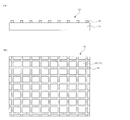
- FIG. 1 is a schematic sectional view and a schematic plan view showing one embodiment of the transparent conductive film of the present invention.
- a numerical range expressed using “to” means a range including numerical values described before and after “to” as a lower limit value and an upper limit value.
- the present invention relates to a transparent conductive film including a transparent resin film and a conductive layer formed on the transparent resin film.
- the transparent resin film includes a cyclic olefin resin.
- the rate of change in the thermal dimension of the transparent conductive film in 100 ° C. hot water for 60 seconds is 0.01 to 0.2%.
- the conductive layer includes a transparent conductive layer.
- the conductive layer may be formed in a layer shape, or may be formed in a pattern shape or a mesh shape.
- the thermal dimensional change rate of the transparent resin film in 100 ° C. hot water for 60 seconds may be 0.01% or more, preferably 0.02% or more, and more preferably 0.03% or more. Further, the thermal dimensional change rate in 100 ° C. hot water for 60 seconds may be 0.2% or less, preferably 0.15% or less, and more preferably 0.1% or less.
- the adhesiveness of a conductive layer and a transparent resin film can be improved. Furthermore, delamination of the transparent resin film itself can be suppressed. If the rate of thermal dimensional change in 100 ° C. hot water for 60 seconds is less than 0.01%, the residual strain is too small and the cyclic olefin molecules are present in a rounded structure, so the intermolecular interaction is weak. This is not preferable because the transparent resin film itself is likely to delaminate or cleave.
- the cyclic olefin resin is hydrophobic and hardly affected by humidity.
- the effect of humidity on the cyclic olefin resin can be measured by performing heat treatment for a short time in a high temperature and high humidity environment.
- a hydrophilic resin is used for the electrode layer.
- the heat treatment for 60 seconds in 100 ° C. hot water reproduces the influence of humidity applied from the electrode layer when combined with the electrode layer. can do. That is, in the present invention, the heat treatment for 60 seconds in hot water at 100 ° C. is considered to reproduce the contribution to the adhesion failure given by the moisture in the resin layer contained in the electrode layer when combined with the electrode layer. It is done.
- the heat treatment of the present invention is a heat treatment in a high-humidity atmosphere, and may be a short-time treatment of 60 seconds.
- the heat capacity becomes large, and the amount of heat given to the cyclic olefin film tends to be larger than in a dry atmosphere, and a short heat treatment is sufficient.
- the thermal dimensional change rate for 60 seconds in 100 ° C. hot water represents the change rate of dimensions when the transparent conductive film is immersed in hot water at 100 ° C. for 60 seconds.
- L1 represents the dimensions of the transparent conductive film before heat treatment in 100 ° C. hot water for 60 seconds
- L2 represents the dimensions of the transparent conductive film after heat treatment in 100 ° C. hot water for 60 seconds.
- the dimension of a transparent conductive film can be calculated
- the rate of thermal dimensional change for 60 seconds in 100 ° C. hot water as described above can be achieved by imparting some thickness unevenness to the molten resin before solidifying the molten resin forming the transparent resin film.
- a method of imparting thickness unevenness to the molten resin include a method of giving a distribution of 1 to 20%, more preferably 2 to 15%, and further preferably 3 to 10% to the lip interval (gap) of the die lip. Can do. When there is a distribution in the die lip spacing in this way, thickness unevenness occurs in the molten resin (melt) that comes out of it. As a result, when the molten resin is cooled and solidified on the cast drum, portions with different cooling rates are generated.
- the cooling rate of the thick part is slow, and the cooling rate is fast in the thin part.
- the volume shrinks when rapidly cooled on the cast drum the presence of a part where the melt is partially soft absorbs the cooling shrinkage and can reduce the residual strain.
- the distance between the die lips is constant.
- the thermal dimensional change rate of the transparent resin film discharged from the die lip at regular intervals in 100 ° C. hot water for 60 seconds is at least 0.3% or more and is often 1% or more.
- the above-described variation in the die lip interval can be achieved by installing bolts on the die lip at regular intervals (for example, 10 to 20 equally divided points) and tightening or loosening them.
- bolts positioned on the end side may be tightened so that both ends of the film are thick, or bolts positioned on the center side may be tightened so that the central part of the film is thick.
- every other bolt may be tightened from one end side bolt so that a plurality of concave and convex shapes are formed in the molten resin.
- the thickness nonuniformity provided to the molten resin can be eliminated by bringing the film into contact with a hot roll after the cast drum. Since unevenness in thickness occurs as unevenness on the surface opposite to the surface in contact with the cast drum, it can be smoothed by bringing the uneven surface into contact with a hot roll.
- the temperature of the hot roll at this time is Tg to Tg-30 ° C of the film, more preferably Tg-1 to Tg-28 ° C, and further preferably Tg-2 to Tg-25 ° C.
- the conveyance tension is 50 to 200 N / m, more preferably 60 to 180 N / m, and still more preferably 70 to 160 N / m.
- the conveyance is preferably performed at a wrap angle of 60 to 180 degrees, more preferably 65 to 175 degrees, and further preferably 70 to 170 degrees.
- the winding tension is preferably 50 to 200 N / m, more preferably 50 to 200 N / m, and still more preferably 50 to 200 N / m. It is also possible to correct the thickness by leaving it at room temperature for 30 days or more after winding. Since all of such heat treatments are performed at Tg or less, the increase in free volume due to melting of the molten resin does not occur, and only the thickness is corrected. The thickness unevenness imparted to the molten resin can be eliminated by bringing it into contact with the hot roll under the conditions as described above. Thereby, the thickness nonuniformity of a transparent resin film is reduced, and adhesiveness with a conductive layer can be improved.
- the thermal dimensional change rate for 60 seconds in 100 ° C. hot water can be achieved by imparting density unevenness to the molten resin before solidifying the molten resin forming the transparent resin film.
- density unevenness that is, resin density unevenness can be achieved by imparting thickness unevenness to the molten resin coming out of the die. This is presumed to be due to the following mechanism.
- the molten resin is solidified on the cast drum, when rapidly cooled, the molten resin is solidified at a low density, and the density of the produced film is lowered. That is, the density is low at a location where the thickness of the molten resin is thin.
- the molten resin is gradually cooled, and during this time, the density gradually increases, resulting in a location having a high density.
- the thickness unevenness of such a molten resin is preferably 1 to 20%, more preferably 2 to 15%, and further preferably 3 to 10%. Such thickness unevenness can be achieved by adjusting the die lip interval as described above.
- the thermal dimensional change rate for 60 seconds in 100 ° C. hot water within the above-described range, not only residual distortion can be eliminated, but also the free volume of the cyclic olefin resin in the molten resin can be reduced.
- the free volume of the cyclic olefin resin By reducing the free volume of the cyclic olefin resin, the dimensional change of the transparent resin film can be effectively suppressed.
- the cyclic olefin resin has a large free volume in a molten state. This is because when rapidly solidifying on a cast drum, the shrinkage of the free volume cannot follow the cooling rate and solidify with a large free volume. Due to the cyclic olefin resin having such a large free volume, residual distortion is likely to occur in the transparent resin film.
- the free volume can be kept small by imparting uneven thickness of the molten resin. This is because the free volume is small at locations where the molten resin is thick, and the free volume tends to increase at locations where the thickness is thin, but the presence of thick locations suppresses the increase in free volume at thin locations. This is because it can be done. Thereby, the free volume of the whole transparent resin film can be suppressed small. By suppressing the free volume in this way, the movement of the cyclic olefin molecule can be suppressed, the residual strain can be reduced, and the adhesion between the transparent resin film and the conductive layer can be increased. Furthermore, by reducing the free volume, there is an effect of suppressing the intrusion of water molecules. This is effective in suppressing the thermal dimensional change in 100 ° C. hot water for 60 seconds.
- the in-plane variation of the thermal dimensional change rate in 100 ° C. hot water for 60 seconds is preferably 1 to 10%.
- the in-plane variation of the thermal dimensional change rate in 100 ° C. hot water for 60 seconds is preferably 1% or more, more preferably 1.5% or more, and further preferably 2% or more.
- the in-plane variation is preferably 10% or less, more preferably 9% or less, and further preferably 8% or less.
- the in-plane variation means that the thermal dimensional change rate has a distribution in the plane direction along the surface of the film. That is, when the film is equally divided in both the longitudinal direction and the width direction of the film, it means that the rate of thermal dimensional change in 60 seconds of 100 ° C.
- the hot water is different between the divided unit regions. For example, if the film has a longitudinal direction of less than 3 m, the central 2/3 region in the longitudinal direction is divided into 10 equal parts in the longitudinal direction, and the central 2/3 region in the width direction is equally divided into 10 parts in the width direction. Then, the film was divided into 100, and the rate of thermal dimensional change in 100 ° C. hot water at 60 ° C. at the center of each 1-segment piece was measured, and the difference between the maximum and minimum values was divided by the average value and expressed as a percentage This is called in-plane variation of the thermal dimensional change rate.
- the film has a longitudinal direction of 3 m or more, an arbitrary point in the longitudinal direction is set as the central point, and 5 points each from the central point in the upstream direction and the downstream direction in the longitudinal direction, a total of 10 points in the longitudinal direction.
- the rate is measured, the difference between the maximum and minimum values divided by the average value and expressed as a percentage is called the in-plane variation of the thermal dimensional change rate.
- the adhesion between the transparent resin film and the conductive layer can be enhanced. This is because there are places where the heat shrinkage is small, that is, places where the adhesive force is high, which acts as an adhesion strengthening point and suppresses the entire peeling.
- the adhesiveness of a transparent resin film and an electroconductive layer can be improved effectively by making the in-plane fluctuation
- the in-plane variation of the thermal dimensional change rate as described above can be achieved by applying a temperature distribution of 1 to 10 ° C. to the melt pipe for sending the melt to the die in the step of sending the molten resin to the die.
- the same temperature distribution can be given to molten resin by giving temperature distribution to melt piping.
- the flow rate of the melt becomes non-uniform, and a distribution occurs in the cooling rate when cooling out and solidifying from the die.
- in-plane variation of the thermal dimensional change rate is given.
- the in-plane variation of the thermal dimensional change rate can be achieved by applying temperature modulation to the melt pipe that sends the molten resin to the die.
- the temperature modulation of the melt pipe is, for example, the initial flow part of the melt pipe (the part from the side where the molten resin flows from the extruder to 1/3 of the total length of the melt pipe) and the final part (the molten resin is Two heaters are installed on the melt pipe from the outlet side to the length of 1/3 of the total length of the melt pipe, and the temperature of the initial flow part on the extruder side and the temperature of the final flow part on the outlet side are different. It can be given by doing so.
- the temperature distribution of such a melt pipe is preferably 1 to 10 ° C, more preferably 1.5 to 9 ° C, and further preferably 2 to 8 ° C.
- Such a temperature difference can be a difference between the maximum temperature and the minimum temperature of the molten resin between the extruder and the die.
- the distribution of the thermal dimensional change rate can be imparted also in the longitudinal direction by the temperature distribution of the melt pipe as described above.
- the distribution of the thermal dimensional change rate in the width direction can be given, so by combining the methods described above, the variation in the thermal dimensional change rate in both the longitudinal direction and the width direction can be achieved. And the adhesion between the transparent resin film and the conductive layer can be more effectively enhanced.
- the change rate of the dielectric constant of the transparent conductive film at ⁇ 20 to 30 ° C. is preferably 0.1 to 10%.
- the change rate of the dielectric constant of the transparent conductive film is preferably 0.1% or more, more preferably 0.3% or more, and further preferably 0.5% or more.
- the dielectric change rate of the transparent conductive film is preferably 10% or less, more preferably 8% or less, and further preferably 7% or less.
- the change rate of the dielectric constant is the change rate of the dielectric constant at ⁇ 20 to 30 ° C.
- the change rate of the dielectric constant is within the above range in the entire temperature range of ⁇ 20 to 30 ° C. Is preferred. That is, the temperature dependence of the change in dielectric constant is small.
- a large change in dielectric constant means that the difference in molecular mobility also increases on the film surface. Therefore, in the cycle test between the high temperature and the low temperature, the close contact state changes greatly, which causes a close contact failure.
- the change rate of the dielectric constant of the present invention within the above range, it is possible to suppress the occurrence of poor adhesion even in cycle thermo (harsh conditions).
- the temperature of the resin (pellet) to be fed into the extruder is Tg-80 ⁇ It is effective to use Tg.
- the temperature of the resin (pellet) charged into the extruder is more preferably Tg ⁇ 70 to Tg ⁇ 5 ° C., and further preferably Tg ⁇ 60 to Tg ⁇ 10 ° C.
- the resin (pellet) charged into the extruder When the temperature of the resin (pellet) charged into the extruder is within the above range, the resin (pellet) can be supplied to the extruder in a somewhat soft state. Thereby, it is possible to prevent unmelted pellets from rubbing with each other at the inlet of the extruder and causing the resin to decompose and lower in molecular weight due to the accompanying shearing force and frictional heat.
- the mobility of the molten resin increases and the change rate of the dielectric constant is increased. By preventing the generation of this low molecular component, the present invention achieves the change rate of the dielectric constant in the above range. can do.
- the in-plane variation of the change rate of the dielectric constant of ⁇ 20 to 30 ° C. is preferably 1 to 10%.
- the in-plane variation of the dielectric change rate is preferably 1% or more, more preferably 1.5% or more, and further preferably 2% or more. Further, the in-plane variation is preferably 10% or less, more preferably 9% or less, and further preferably 8% or less.
- Such distribution of the change rate of the dielectric constant may be achieved by adding an in-plane distribution to the thermally decomposed low molecular component, and is achieved by changing the inert gas supplied to the extruder.
- a preferable variation is 0.5 to 10%, more preferably 1 to 8%, and still more preferably 1.5 to 7%.
- the in-plane variation of the change rate of the dielectric constant of ⁇ 20 to 30 ° C. can be set within the desired range.
- the inert gas can suppress thermal decomposition of the resin. For this reason, a variation
- the inert gas examples include nitrogen and rare gases (Ar, He, Ne, etc.). Such a change in the flow rate of the inert gas is achieved, for example, by attaching a motor to a gas supply valve and opening and closing the valve.
- the fluctuation amount of the inert gas is a value obtained by monitoring the flow rate for 10 minutes and dividing the difference between the maximum flow rate and the minimum flow rate by the average flow rate and expressed as a percentage.
- the average flow rate of the inert gas is preferably V ⁇ 0.1 to V ⁇ 10, where V is the supply volume of resin to the extruder per unit time.
- the in-plane birefringence (Re) is preferably 1 to 20 nm
- the thickness direction birefringence (Rth) is preferably 1 to 20 nm.
- the in-plane birefringence (Re) and the thickness direction birefringence (Rth) are each preferably 1 nm or more, more preferably 2 nm or more, and further preferably 3 nm or more.
- the in-plane birefringence (Re) and the thickness direction birefringence (Rth) are each preferably 20 nm or less, more preferably 18 nm or less, and further preferably 15 nm or less.
- in-plane birefringence indicates in-plane orientation
- Re in-plane birefringence
- elongation tension
- brittleness can be improved.
- it is too small it is unfavorable because one molecule is rounded into a string, and the interaction between molecules hardly occurs and brittleness tends to occur.
- Thickness direction birefringence indicates the orientation in the thickness direction, and by reducing Rth, the molecules are prevented from being oriented in layers, and at the time of adhesion evaluation, they are prevented from cleaving into layers and causing poor adhesion. be able to. On the other hand, if it is too small, it is unfavorable because one molecule is rounded into a string, and the interaction between molecules hardly occurs and brittleness tends to occur.
- the adhesion between the transparent resin film and the conductive layer can be enhanced, Cleavage can be suppressed.
- this method solidifies in the state of a melt having a large free volume, a film having a small free volume as described above cannot be formed.
- a method for producing a film having a small free volume and a small Re and Rth a method of giving vibration between the die and the cast drum (air gap) after extruding the molten state (melt) from the die. be able to.
- vibration can be imparted to the molecules, the packing of the molecules can be increased, and the free volume can be reduced. Furthermore, the molecular orientation is disturbed by vibration, and Re and Rth are reduced.
- Such vibrations are effective before and after the molecules solidify (Tg ⁇ 20 ° C.). If the temperature is too high, the thermal motion of the molecule is too large to reduce the free volume, and if it is too low, the mobility of the molecule is too low to reduce the free volume. Such temperature is before and after the melt contacts the cast drum, and it is effective to apply vibration in this region.
- the vibration of the melt on the air gap may be performed by any means.
- the melt may be subjected to a wind speed fluctuation to apply the wind, or the cast drum rotation speed may be varied.
- the fluctuation of the rotation speed can be achieved by changing the rotation speed of the cast drum per minute, and the fluctuation of the rotation speed is preferably 10 to 300 times / minute, and preferably 20 to 250 times / minute. More preferred is 30 to 200 times / minute.
- Re and Rth can be within the desired ranges.
- the temperature of the cast drum is preferably Tg ⁇ 60 to Tg + 20 ° C., more preferably Tg ⁇ 50 to Tg + 10 ° C., and Tg ⁇ 45 to Tg ° C. More preferably it is.
- Such temperature control can be achieved by flowing a heat medium (oil, water, etc.) in the cast drum.
- Re and Rth can be set within desired ranges.
- the in-plane variation of in-plane birefringence (Re) is preferably 1 to 10%
- the in-plane variation of thickness direction birefringence (Rth) is preferably 1 to 10%
- the in-plane variation of the in-plane birefringence (Re) and the in-plane variation of the thickness direction birefringence (Rth) are each preferably 1% or more, more preferably 1.5% or more, and 2%. More preferably, it is the above.
- the in-plane variation of in-plane birefringence (Re) and the in-plane variation of thickness direction birefringence (Rth) are each preferably 10% or less, more preferably 9% or less, and 8%.
- the adhesion between the transparent resin film and the conductive layer can be improved, and further transparent Delamination and cleavage of the resin film itself can be suppressed.
- the Re and Rth distributions can be achieved by giving a temperature distribution to the cast drum and changing the cooling and solidification rate of the molten resin.
- a preferable temperature distribution of the cast drum is 0.5 to 10 ° C, more preferably 1 to 8 ° C, and further preferably 1.5 to 7 ° C.
- Such a temperature distribution can be achieved by generating unevenness in the flow of the heat medium of the cast drum.
- a baffle plate can be provided in the cooling roll to disturb the flow path.
- the thickness of the transparent resin film is preferably 20 to 60 ⁇ m.
- the thickness of the transparent resin film is preferably 20 ⁇ m or more, more preferably 25 ⁇ m or more, and further preferably 30 ⁇ m or more.
- the thickness of the transparent resin film is preferably 60 ⁇ m or less, more preferably 55 ⁇ m or less, and further preferably 50 ⁇ m or less.
- the transparent conductive film of the present invention includes a transparent resin film, and the transparent resin film includes a cyclic olefin resin.
- the cyclic olefin resin include addition polymerization type cycloolefin resin (COC) and ring-opening polymerization type cycloolefin resin (COP). These may be used alone or in combination.
- Tg of these cyclic olefin resins is preferably 100 to 200 ° C, more preferably 120 to 190 ° C, and further preferably 125 to 185 ° C.
- the cyclic olefin resin is preferably used after being polymerized and then pelletized.
- ring-opening polymerization type cycloolefin resin examples include those described in JP-A 2010-164538, paragraphs [0032] to [0069], and JP-A 4492116, paragraphs [0016] to [0022]. Can be used.
- Examples of the addition polymerization type cycloolefin resin (COC) include those described in paragraphs [0014] to [0060] of Japanese Patent No. 3723616 and those described in paragraphs [0015] to [0062] of Japanese Patent No. 36833631. The ones described in paragraphs [0008] to [0093] of Japanese Patent No. 3377833 can be used.
- ultraviolet absorber those described in paragraph [0034] of Japanese Patent No. 4729802 and those described in paragraph [0101] of Japanese Patent No. 3377833 can be used.
- other additives include those described in paragraphs [0025] and [0026] of Japanese Patent No. 4492116.
- the transparent conductive film of the present invention includes a conductive layer.
- the conductive layer may be formed in a layer shape, but is preferably formed so as to have an intermittent portion.
- An intermittent part means the part in which the conductive layer is not provided, and it is preferable that the outer periphery of an intermittent part is surrounded by the conductive layer.
- forming a conductive layer so as to have an intermittent portion is also referred to as forming a conductive layer in a pattern or mesh.
- Fig.1 (a) is a schematic sectional drawing which shows the one aspect
- FIG.1 (b) is a schematic plan view which shows the one aspect
- the transparent conductive film 10 preferably has an intermittent portion 20.
- the intermittent portion 20 is a portion where the conductive layer 14 is not provided.
- the conductive layer is preferably formed in a pattern or mesh.
- the conductive layer include JP2013-1009A, JP2012-216550A, JP2012-151095A, JP2012-25158A, JP2011-253546A, and JP2011. -197754, JP2011-34806, JP2010-198799, JP2009-277466, JP2012-216550, JP2012-151095, International Publication 2010/140275. No. pamphlet and the conductive layer described in the international publication 2010/114056 pamphlet.
- the conductive layer used in the present invention more preferably contains silver and a hydrophilic resin.
- the water-soluble resin include gelatin, polyvinyl alcohol (PVA), polyvinyl pyrrolidone (PVP), starch and other polysaccharides, cellulose and derivatives thereof, polyethylene oxide, polyvinylamine, chitosan, polylysine, polyacrylic acid, polyalginic acid, Examples include polyhyaluronic acid and carboxycellulose. These have neutral, anionic, and cationic properties depending on the ionicity of the functional group. Of these, gelatin is particularly preferred.
- the method for producing a conductive layer includes the following three forms depending on the light-sensitive material and the form of development processing.
- a photosensitive silver halide black-and-white photosensitive material containing no physical development nuclei and an image receiving sheet having a non-photosensitive layer containing physical development nuclei are overlapped and developed by diffusion transfer, and the metallic silver portion is non-photosensitive image-receiving sheet.
- the aspect (1) is an integrated black-and-white development type, and a light-transmitting conductive film such as a light-transmitting conductive film is formed on the photosensitive material.
- the resulting developed silver is chemically developed silver or heat developed silver, and is highly active in the subsequent plating or physical development process in that it is a filament with a high specific surface.
- the light-transmitting conductive film such as a light-transmitting conductive film is formed on the photosensitive material by dissolving silver halide grains close to the physical development nucleus and depositing on the development nucleus in the exposed portion. A characteristic film is formed.
- This is also an integrated black-and-white development type.
- the development action is precipitation on the physical development nuclei, it is highly active, but developed silver is a sphere with a small specific surface.
- the silver halide grains are dissolved and diffused in the unexposed area and deposited on the development nuclei on the image receiving sheet, whereby a light transmitting conductive film or the like is formed on the image receiving sheet.
- a conductive film is formed. This is a so-called separate type in which the image receiving sheet is peeled off from the photosensitive material.
- negative development processing can be performed by using an auto-positive type photosensitive material as a photosensitive material. Become.
- the silver salt emulsion layer serving as the conductive layer may contain additives such as a solvent and a dye in addition to the silver salt and the binder.
- the silver salt include inorganic silver salts such as silver halide and organic silver salts such as silver acetate. In the present invention, it is preferable to use silver halide having excellent characteristics as an optical sensor.
- the solvent used for forming the silver salt emulsion layer is not particularly limited.
- water organic solvents (for example, alcohols such as methanol, ketones such as acetone, amides such as formamide, dimethyl sulfoxide, etc. Sulphoxides such as, esters such as ethyl acetate, ethers, etc.), ionic liquids, and mixed solvents thereof.
- the content of the solvent used in the silver salt emulsion layer is in the range of 30 to 90% by mass with respect to the total mass of silver salt and binder contained in the silver salt emulsion layer, and 50 to 80% by mass. % Is preferable.
- Silver coating amount of silver salt emulsion layer is preferably 1 ⁇ 30g / m 2 in terms of silver, more preferably 1 ⁇ 25g / m 2, more preferably 5 ⁇ 20g / m 2 .
- a desired surface resistance can be obtained by setting the coated silver amount within the above range.
- Content of the binder contained in a silver salt emulsion layer is not specifically limited, It can determine suitably in the range which can exhibit a dispersibility and adhesiveness.
- the content of the binder in the silver salt emulsion layer is preferably 1: 4 or more, more preferably 1: 2 or more in terms of a silver: binder volume ratio.
- the silver: binder volume ratio is preferably 100: 1 or less, and more preferably 50: 1 or less. Further, the silver: binder volume ratio is more preferably 1: 1 to 4: 1, and most preferably 1: 1 to 3: 1.
- the silver: binder volume ratio is converted from the amount of silver halide in the raw material: the amount of binder (weight ratio) to the amount of silver: binder amount (weight ratio), and the amount of silver: binder amount (weight ratio) is silver amount. : It can obtain
- a protective layer may be provided on the silver salt emulsion layer.
- the protective layer means a layer composed of a binder such as gelatin or a high molecular polymer, and is formed on a silver salt emulsion layer having photosensitivity in order to exhibit an effect of preventing scratches and improving mechanical properties.
- the thickness is preferably 0.5 ⁇ m or less.
- the coating method and forming method of the protective layer are not particularly limited, and a known coating method and forming method can be appropriately selected. For example, regarding the protective layer, the description in JP-A-2008-250233 can be referred to.
- an undercoat layer and an antistatic layer may be provided.
- the undercoat layer those described in paragraphs [0021] to [0023] of JP-A-2008-250233 can be applied.
- the antistatic layer those described in paragraphs [0012] and [0014] to [0020] of JP-A-2008-250233 can be applied.
- the manufacturing method of the transparent conductive film of this invention includes the process of forming the transparent resin film containing cyclic olefin resin, and the process of forming a conductive layer on a transparent resin film.
- the process of forming a transparent resin film includes the extrusion process which makes the molten resin containing cyclic olefin resin into a sheet form, and this extrusion process includes the process of providing thickness unevenness to a sheet-like molten resin.
- the transparent resin film used in the present invention is preferably formed by the following method. First, the above-mentioned cyclic olefin resin pellets (COC, COP pellets) and master pellets are dried until the water content becomes 100 ppm or less. Next, the pellets are put into an extruder and kneaded.
- the temperature of the resin (pellet) charged into the extruder is preferably Tg-80 to Tg.
- the temperature of the resin (pellet) charged into the extruder is more preferably Tg ⁇ 70 to Tg ⁇ 5 ° C., and further preferably Tg ⁇ 60 to Tg ⁇ 10 ° C.
- the pellets are heated as described above and then loaded into the extruder hopper.
- the extruder may be a single screw extruder or a twin screw extruder, and a preferable extrusion temperature is 250 to 330 ° C, more preferably 260 to 315 ° C. It is preferable to flow an inert gas through the extruder and to vary the flow rate. A preferable variation is 0.5 to 10%, more preferably 1 to 8%, and still more preferably 1.5 to 7%. By setting the variation of the active gas within the above range, the in-plane variation of the change rate of the dielectric constant of ⁇ 20 to 30 ° C. can be set within the desired range.
- the inert gas include nitrogen and rare gases (Ar, He, Ne, etc.).
- the molten resin (melt) kneaded by the extruder into a melt is guided to the die through the melt pipe. It is preferable to impart a temperature distribution of 1 to 10 ° C. to the melt pipe. By providing such a temperature distribution, the flow rate of the melt becomes non-uniform, and a distribution occurs in the cooling rate when cooling out and solidifying from the die. In this way, in-plane variation of the thermal dimensional change rate is given.
- the temperature modulation of the melt pipe is, for example, the initial flow part of the melt pipe (the part from the side where the molten resin flows from the extruder to 1/3 of the total length of the melt pipe) and the final part (the molten resin is
- Two heaters are installed in the area from the outlet side to the melt pipe to 1/3 of the total length of the melt pipe, and the temperature of the initial flow part on the extruder side and the temperature of the final flow part on the outlet side are set. It can be given by making it different.
- the temperature distribution of such a melt pipe is preferably 1 to 10 ° C, more preferably 1.5 to 9 ° C, and further preferably 2 to 8 ° C. Such a temperature difference can be a difference between the maximum temperature and the minimum temperature of the molten resin between the extruder and the die.
- the pore size of the melt filter is preferably 1 to 30 ⁇ m, more preferably 2 to 20 ⁇ m, still more preferably 3 to 10 ⁇ m.
- a T-die, a hanger coat die, a fish tail die or the like can be used as the die.
- Coextrusion is also preferable, and a multi-manifold die, a feed block die, or the like can be used.
- the melt extruded from the die is solidified on a cast drum (also called a cooling drum or a chill roll). Between the die and the cast drum (air gap), it is preferable to include a step of applying a vibration of 10 to 300 times / minute to the sheet-like molten resin. As a result, vibration can be imparted to the molecules, the packing of the molecules can be increased, and the free volume can be reduced. Furthermore, the molecular orientation is disturbed by vibration, and Re and Rth are reduced.
- the vibration of the melt on the air gap may be performed by any means. For example, the melt may be subjected to a wind speed fluctuation to apply the wind, or the cast drum rotation speed may be varied.
- the fluctuation of the rotation speed can be achieved by changing the rotation speed of the cast drum per minute, and the fluctuation of the rotation speed is preferably 10 to 300 times / minute, and preferably 20 to 250 times / minute. More preferred is 30 to 200 times / minute.
- Re and Rth can be within the desired ranges.
- the cast drum is preferably given a temperature distribution.
- a preferable temperature distribution is 0.5 to 10 ° C., more preferably 1 to 8 ° C., and still more preferably 1.5 to 7 ° C.
- Such a temperature distribution can be achieved by generating unevenness in the flow of the heat medium of the cast drum.
- a baffle plate can be provided in the cooling roll to disturb the flow path.
- the resin film solidified on the cast drum is preferably passed through a hot roll.
- the problem can be solved by bringing it into contact with a hot roll installed after the cast drum.
- the temperature of the hot roll at this time is Tg to Tg-30 ° C of the film, more preferably Tg-1 to Tg-28 ° C, and further preferably Tg-2 to Tg-25 ° C.
- the conveyance tension is 50 to 200 N / m, more preferably 60 to 180 N / m, and still more preferably 70 to 160 N / m.
- the conveyance is preferably performed at a wrap angle of 60 to 180 degrees, more preferably 65 to 175 degrees, and further preferably 70 to 170 degrees.
- the winding tension is preferably 50 to 200 N / m, more preferably 50 to 200 N / m, and still more preferably 50 to 200 N / m. Further, it is preferable that the rotation speed of the hot roll is changed by 0.1 to 5% or less, more preferably 0.2 to 4%, and still more preferably 0.3 to 3%. Thereby, an increase in Re and Rth can be suppressed. It is also preferable to apply thickness processing and trimming at both ends before winding. It is also preferable to bond with a laminate film, and those having a thickness of 10 to 100 ⁇ m such as polyolefin and polyester can be used.
- the winding width is preferably 0.5 to 3 m, more preferably 1 to 2.5 m, further preferably 1.2 to 2.2 m, and the winding length is 1000 to 15000 m, more preferably 2000 to 12000 m, It is preferably 3000 to 10,000 m.
- a patterned conductive layer as the conductive layer, including the case where it is applied by a printing method, but it is preferable to form a transparent conductive pattern by exposure and development, etc., except for the printing method. That is, exposure is performed on a photosensitive material having a silver salt-containing layer provided on a transparent resin film or a photosensitive material coated with a photopolymer for photolithography.
- the exposure can be performed using electromagnetic waves. Examples of the electromagnetic wave include light such as visible light and ultraviolet light, and radiation such as X-rays.
- a light source having a wavelength distribution may be used for exposure, or a light source having a specific wavelength may be used.
- the development processing can be performed by a normal development processing technique used for silver salt photographic film, photographic paper, printing plate-making film, photomask emulsion mask, and the like.
- the developer is not particularly limited, but PQ developer, MQ developer, MAA developer and the like can also be used.
- Commercially available products include, for example, CN-16, CR-56, CP45X, FD prescribed by FUJIFILM Corporation. -3, Papitol, developers such as C-41, E-6, RA-4, D-19, and D-72 prescribed by KODAK, or developers included in the kit can be used.
- a lith developer can also be used.
- the development processing in the present invention can include a fixing processing performed for the purpose of removing and stabilizing the silver salt in an unexposed portion.
- a fixing process technique used for silver salt photographic film, photographic paper, film for printing plate making, emulsion mask for photomask, and the like can be used.
- the fixing temperature in the fixing step is preferably about 20 ° C. to about 50 ° C., more preferably 25 to 45 ° C.
- the fixing time is preferably 5 seconds to 1 minute, more preferably 7 seconds to 50 seconds.
- the replenishing amount of the fixing solution is preferably 600 ml / m 2 or less with respect to the processing of the photosensitive material, more preferably 500 ml / m 2 or less, 300 ml / m 2 or less is particularly preferred.
- the light-sensitive material that has been subjected to development and fixing processing is preferably subjected to water washing treatment or stabilization treatment.
- the washing water amount is usually 20 liters or less per 1 m 2 of the light-sensitive material, and can be replenished in 3 liters or less (including 0, ie, rinsing with water).
- the mass of the metallic silver contained in the exposed part after the development treatment is preferably 50% by mass or more, and 80% by mass or more, based on the mass of silver contained in the exposed part before exposure. More preferably. If the mass of silver contained in the exposed portion is 50% by mass or more based on the mass of silver contained in the exposed portion before exposure, it is preferable because high conductivity can be obtained.
- the gradation after the development processing in the present embodiment is not particularly limited, but is preferably more than 4.0.
- the conductivity of the conductive metal portion can be increased while keeping the light transmissive property of the light transmissive portion high.
- Examples of means for setting the gradation to 4.0 or higher include doping with rhodium ions and iridium ions.
- the conductive layer is obtained through the above steps, but the surface resistance of the obtained conductive layer is 0.1 to 100 ohm / sq. Is preferably in the range of 1 to 10 ohm / sq. It is more preferable that it is in the range. Further, the conductive layer after the development treatment may be further subjected to a calendar treatment, and can be adjusted to a desired surface resistance by the calendar treatment.
- conductive metal particles may be supported on the metallic silver portion by only one of physical development and plating treatment, or the conductive metal particles are supported on the metallic silver portion by combining physical development and plating treatment. Also good.
- a metal silver portion including a physical development and / or plating treatment can be referred to as a “conductive metal portion”.
- the “conductive metal part” formed on the transparent resin film is referred to as “conductive layer”.
- “Physical development” means that metal particles such as silver ions are reduced on a nucleus of a metal or a metal compound by using a reducing agent to deposit metal particles. This physical phenomenon is used for instant B & W film, instant slide film, printing plate manufacturing, and the like, and the technology can be used in the present invention. Further, the physical development may be performed simultaneously with the development processing after exposure or separately after the development processing.
- electroless plating chemical reduction plating or displacement plating
- electrolytic plating electrolytic plating
- electrolytic plating electrolytic plating
- electrolytic plating electrolytic plating
- electrolytic plating electrolytic plating
- a known electroless plating technique can be used, for example, an electroless plating technique used in a printed wiring board or the like can be used.
- Plating is preferred.
- Oxidation treatment It is preferable to subject the metallic silver portion after the development treatment and the conductive metal portion formed by physical development and / or plating treatment to oxidation treatment.
- oxidation treatment for example, when a metal is slightly deposited on the light transmitting portion, the metal can be removed, and the light transmitting portion can be made almost 100% transparent.
- the conductive metal portion is preferably formed in a pattern shape or a mesh shape so as to have an intermittent portion.
- the line width of the conductive metal portion is preferably selected from 5 to 200 ⁇ m (0.2 mm), and is preferably 5 to 50 ⁇ m when used as a touch panel material. More preferably, it is 5 to 30 ⁇ m, and most preferably 5 to 20 ⁇ m.
- the line spacing is preferably 30 to 500 ⁇ m or less, more preferably 50 to 400 ⁇ m, and most preferably 100 to 350 ⁇ m.
- the conductive metal portion may have a portion whose line width is wider than 200 ⁇ m for the purpose of ground connection or the like.
- the conductive metal portion in the present embodiment has an aperture ratio of preferably 85% or more, more preferably 90% or more, and most preferably 95% or more from the viewpoint of visible light transmittance.
- the aperture ratio can also be expressed as a ratio of the area of the intermittent portion to the total area (area of the transparent resin film) where the conductive metal portion is formed.
- the “light transmissive part” in the present embodiment means a part having translucency other than the conductive metal part in the transparent conductive film.
- the transmittance in the light transmissive part is 90% or more, preferably 95% or more, as shown by the minimum value of the transmittance in the wavelength region of 380 to 780 nm excluding the contribution of light absorption and reflection of the transparent resin film. More preferably, it is 97% or more, still more preferably 98% or more, and most preferably 99% or more.
- a method through a glass mask or a pattern exposure method by laser drawing is preferable.
- the thickness of the conductive metal part (conductive layer) provided on the transparent resin film can be appropriately determined according to the coating thickness of the silver salt-containing layer coating applied on the transparent conductive film.
- the thickness of the conductive metal portion (conductive layer) can be selected from 0.001 mm to 0.2 mm, preferably 30 ⁇ m or less, more preferably 20 ⁇ m or less, and 0.01 to 9 ⁇ m. More preferably, it is most preferably 0.05 to 5 ⁇ m.
- a metal silver part is pattern shape.
- the conductive metal portion may be a single layer or a multilayer structure of two or more layers.
- the conductive metal portion has a pattern shape and has a multilayer structure of two or more layers, different color sensitivities can be imparted so as to be sensitive to different wavelengths. Thereby, when the exposure wavelength is changed and exposed, a different pattern can be formed in each layer.
- the thickness of the conductive metal part is preferably as the thickness of the touch panel is thinner because the viewing angle of the display panel is wider, and a thin film is also required for improving the visibility. From such a viewpoint, the thickness of the layer made of the conductive metal supported on the conductive metal part is preferably less than 9 ⁇ m, more preferably 0.1 to 5 ⁇ m, and more preferably 0.1 to 3 ⁇ m. More preferably.
- the thickness of the layer made of conductive metal particles is formed by controlling the coating thickness of the silver salt-containing layer described above to form a metallic silver portion having a desired thickness, and further by physical development and / or plating treatment. Therefore, even if there is a conductive metal portion having a thickness of less than 5 ⁇ m, preferably less than 3 ⁇ m, it can be easily formed.
- this invention can be used in combination with the technique of the publication gazette and international publication pamphlet which are described in following Table 1 and Table 2.
- FIG. Notations such as “JP,” “Gazette” and “No. Pamphlet” are omitted.
- the touch panel Since the touch panel includes the transparent conductive film as described above, the touch panel has high light transmittance, is colorless, has high durability and water resistance, and has a wide operable temperature range. For this reason, it can be used for various display devices. Moreover, the touch panel of this invention has at least the transparent conductive film of this invention, and also has another member as needed. For example, you may have functional layers, such as a polarizing plate, an antireflection film, a hard-coat film, an antistatic film, and an antifouling film.
- the bonding system which bonds the said 2 electrically conductive film, Both surfaces of the base material of 1 sheet It is preferable that any one of the above-mentioned methods comprising a conductive film, a single-sided jumper or through-hole method, or a single-area layer method.
- any type of touch panel such as a resistive film type, a surface acoustic wave type, an infrared type, an electromagnetic induction type, and a capacitance type can be manufactured. Since the touch panel includes a transparent conductive film excellent in light transmittance, heat resistance, heat resistance coloration and the like, a resistive film type or capacitive type touch panel is preferable, and a capacitive type touch panel is more preferable.
- the display device includes the touch panel described above. Since the display device includes the touch panel of the present invention, it can be used without limitation on a mobile phone, a smart phone, a personal digital assistant, a car navigation system, a tablet PC, a sales device, an ATM, an FA device, and the like.
- Example 1 Transparent resin film production
- the temperature distribution shown in Table 1 was given to the cast drum.
- a distribution of Re and Rth can be formed.
- Such distribution can be achieved by modulating the flow path of the heat transfer oil flowing in the cast drum. For example, this can be achieved by installing a baffle plate or the like in the flow path of the heat transfer oil.
- Heat roll A heat roll was installed in the process immediately after the cast roll.
- the temperature of the hot roll was adjusted as described in Table 1.
- the average value of the rotational speed was set to be 98% of the peripheral speed of the cast roll, and the rotational speed variation shown in Table 1 was given.
- tensile_strength was as Table 1.
- the coating amount of silver is 10 g / m 2.
- the transparent resin film was coated on the undercoat layer. At this time, the volume ratio of Ag: gelatin was 2: 1.
- Application was performed for 2000 m with a width of 1.5 m, and both ends were cut off so as to leave 1.4 m of the central part of the application to obtain a roll-shaped silver halide photosensitive material.
- the exposure pattern was formed according to the pattern shown in FIG.
- the arrangement pitch Ps of the small lattices 18 is 200 ⁇ m
- the arrangement pitch Pm of the medium lattices 20a to 20h is 2 ⁇ Ps.
- the thickness of the conductive portion of the small lattice 18 was 2 ⁇ m, and the width was 10 ⁇ m.
- the exposure was performed using parallel light using a high-pressure mercury lamp as a light source through the photomask having the above pattern. Further, although a doden pattern was formed in accordance with FIG. 5 of Japanese Patent No. 4820451, the following evaluation results were similar to those in FIG.
- developer 1L is as follows. Hydroquinone 20 g Sodium sulfite 50 g Potassium carbonate 40 g Ethylenediamine tetraacetic acid 2 g Potassium bromide 3 g Polyethylene glycol 2000 1 g Potassium hydroxide 4 g The pH was adjusted to 10.3.
- the prescription for 1 L of the fixing solution is as follows.
- Ammonium thiosulfate solution (75%) 300 ml
- Ammonium sulfite monohydrate 25 g 1,3-diaminopropane tetraacetic acid 8 g
- Acetic acid 5 g
- Ammonia water (27%) 1 g
- the pH was adjusted to 6.2.
- the exposed photosensitive material is processed using Fujifilm's automatic developing machine FG-710PTS. Processing conditions: development 35 ° C., 30 seconds, fixing 34 ° C., 23 seconds, water washing, running water (5 L / min) For 20 seconds.
- the humidity was adjusted for 2 hours at 25 ° C. and a relative humidity of 60%. Then, pin holes at intervals of 10 cm were opened, and the distance between the pins was measured using a pin gauge. This was designated L2. ⁇
- ⁇ Dielectric constant change and in-plane distribution at -20 to 30 ° C> Ten sample films cut to a diameter of 50 mm were cut from arbitrary locations. Using a TR-1100 dielectric loss automatic measuring device manufactured by Ando Electric Co., Ltd., a dielectric constant was measured at a frequency of 100 kHz in a constant temperature room at ⁇ 20 ° C. and 30 ° C. using a main electrode having a diameter of 30 mm and a back electrode having a diameter of 50 mm. . These were designated as ⁇ 1 and ⁇ 2, respectively. ⁇
- the difference between the maximum value and the minimum value of the ten dielectric constant changes divided by the average value of 10 points and expressed as a percentage was taken as the in-plane distribution (%) of the dielectric constant change.
- the same value as that of the transparent conductive film was obtained by measuring the transparent conductive layer after immersing and peeling it in an aqueous sodium hypochlorite solution.
- Re ( ⁇ ) and Rth ( ⁇ ) represent in-plane retardation and retardation in the thickness direction at the wavelength ⁇ , respectively.
- Re ( ⁇ ) was measured with KOBRA 21ADH (manufactured by Oji Scientific Instruments Co., Ltd.) by making light having a wavelength of ⁇ nm incident in the normal direction of the film.
- Rth ( ⁇ ) is Re ( ⁇ )
- the slow axis (determined by KOBRA 21ADH) is used as the tilt axis (rotation axis)
- light having a wavelength of ⁇ nm is incident from a direction inclined + 40 ° with respect to the film normal direction. It was measured.
- retardation value and retardation value measured by making light of wavelength ⁇ nm incident from a direction inclined by -40 ° with respect to the film normal direction with the slow axis as the tilt axis (rotation axis)
- Each value was calculated using KOBRA 21ADH based on the retardation value obtained.
- KOBRA 21ADH calculates nx, ny, nz, and Rth by inputting the assumed average refractive index of 1.51 and the film thickness.
- measurement was performed at a wavelength of 590 nm, 25 ° C., and a relative humidity of 60%.
- Re and Rth the difference between the maximum value and the minimum value divided by the average value and expressed as a percentage was defined as the in-plane distribution of Re and Rth.
- the same value as that of the transparent conductive film was obtained by measuring the transparent conductive layer after immersing and peeling it in an aqueous sodium hypochlorite solution.
- ⁇ Thickness and thickness unevenness> The thickness was measured continuously along the entire width. The difference between the maximum value and the minimum value of the thickness divided by the average value and expressed as a percentage is defined as TD thickness unevenness. Further, the thickness central portion is measured 1 m along the MD continuously, and the difference between the maximum value and the minimum value is divided by the average value and expressed as a percentage as MD thickness unevenness. The average value of MD thickness unevenness and TD thickness unevenness was defined as thickness unevenness (%).
- ⁇ Adhesion> Ten samples cut into 10 cm square were cut from arbitrary locations. Specifically, a square sample of 30 cm ⁇ 30 cm extracted at 5 points each in the width direction and the longitudinal direction was cut out. This sample film was immersed in hot water at 100 ° C. for 60 seconds. Next, a cycle thermo that was alternately exposed to ⁇ 20 ° C. and 30 ° C. for 10 minutes each was repeated 10 times. The transparent conductive layer was cut at 5 mm intervals along the MD and TD, each with 11 cutter blades, to form 100 squares. Adhesive tape was affixed to this, and it peeled off at once, the number of the squares which the transparent conductive layer peeled was counted, and this was made into peeling rate (%). This method is a close contact evaluation under severe conditions with large temperature and humidity changes.
- the thermal dimensional change rate is 0.01 to 0.2%. This is achieved by setting the variation of the die lip interval distribution to 1 to 20% and imparting the variation of the thickness to the transparent resin film. Thereby, in Examples 1 to 5, the peeling rate is low. On the other hand, in Comparative Examples 1 and 2, it can be seen that the thermal dimensional change rate is outside the range of 0.01 to 0.2%, and the peel rate is remarkably high.
- the in-plane distribution is changed to the thermal dimensional change rate of the transparent resin film. This is achieved by imparting a temperature distribution to the melt pipe. In Examples 6 to 12, the rate of thermal dimensional change is in the range of 0.01 to 0.2%, so the peeling rate is suppressed. In Examples 7 to 11, the in-plane distribution of the rate of thermal dimensional change is achieved. From 1 to 10%, it can be seen that the peeling rate is more effectively suppressed. In Examples 13 to 19, the change rate of the dielectric constant of the transparent resin film is changed. This is achieved by setting the pellet heating temperature before extrusion within a specific range. In Examples 13 to 19, the rate of thermal dimensional change is in the range of 0.01 to 0.2%, so that the peeling rate is suppressed. In Examples 14 to 18, the rate of change in dielectric constant is 0.1%. From 1 to 10%, it can be seen that the peeling rate is more effectively suppressed.
- Example 20 to 26 the in-plane distribution of the dielectric constant change of the transparent resin film is changed. This is achieved by providing a variation in the flow rate of the inert gas.
- the thermal dimensional change rate is in the range of 0.01 to 0.2% of the in-plane distribution of the thermal dimensional change rate, so the peeling rate is suppressed.
- Examples 21 to 25 Since the in-plane distribution of the change in dielectric constant is 1 to 10%, it can be seen that the peeling rate is more effectively suppressed.
- Re and Rth of the transparent resin film are changed. This is achieved by applying vibration to the rotational speed of the cast drum.
- the rate of thermal dimensional change is in the range of 0.01 to 0.2%, so that the peel rate is suppressed.
- Re and Rth are 1 to 20 nm. Therefore, it can be seen that the peeling rate is more effectively suppressed.
- Example 34 to 40 the in-plane distribution of Re and Rth of the transparent resin film is changed. This is achieved by providing a variation in the temperature distribution of the cast drum. In Examples 34 to 40, the rate of thermal dimensional change is in the range of 0.01 to 0.2%, so the peeling rate is suppressed. In Examples 35 to 39, the in-plane distribution of Re and Rth is From 1 to 10%, it can be seen that the peeling rate is more effectively suppressed. In Examples 41 to 47, the thickness and thickness unevenness of the transparent resin film are changed. In Examples 41 to 47, the rate of thermal dimensional change is in the range of 0.01 to 0.2%, and thus the peel rate is suppressed. In Examples 42 to 46, the thickness and uneven thickness of the transparent resin film are suppressed. Is within the predetermined range, it can be seen that the peeling rate is more effectively suppressed.
- Examples 48 to 54 the hot roll rotation fluctuation and the effects of Re and Rth associated therewith are shown.
- Re and Rth are in a desired range by setting the fluctuation in the number of rotations of the hot roll to a specific range, and the peeling rate tends to be further suppressed.
- Examples 55 to 61 the influence on the hot roll temperature and the thickness unevenness associated therewith is shown.
- Examples 55 to 61 by setting the heat roll temperature in a specific range, the thickness unevenness is in a desired range, and the peeling rate is further suppressed.
- Examples 62 to 68 show the effect on the hot roll conveyance tension and the thickness unevenness associated therewith. In Examples 62 to 68, by setting the hot roll conveyance tension within a specific range, the thickness unevenness is in a desired range, and the peeling rate is further suppressed.
- Comparative Example 3 is a trial of Example 1 of Patent Document 2.
- the transparent conductive layer is made of silver nanowires according to Example 1 of Patent Document 2.
- the thermal dimensional change rate is not in the range of 0.01 to 0.2%, the peel rate is extremely high.
- the present invention was carried out with respect to Comparative Example 3.
- the transparent conductive layer was formed according to Patent Document 1.
- Example 69 since the thermal dimensional change rate is in the range of 0.01 to 0.2%, an extremely low peeling rate is shown.
- Comparative Example 4 is a trial of Example 1 of Patent Document 1.
- the thermal dimensional change rate is not in the range of 0.01 to 0.2%, the peel rate is extremely high.
- the heating temperature of the pellet is carried out within the present invention (the Tg of PET is low, and it is within the scope of the present invention even when charged at room temperature), the corresponding change in dielectric constant is within the scope of the present invention. It is out of the range.
- Example 72 In Comparative Example 6, according to Example 2 of Patent Document 3, ITO was formed on an alicyclic polymer (Arton) by sputtering.
- Arton Arton was used in the same manner as in Comparative Example 6, but the present invention was carried out in a film forming method.
- the transparent conductive layer was formed of silver halide and a water-soluble resin.
- the thermal dimensional change rate is in the range of 0.01 to 0.2%, and the peeling rate is effectively suppressed.
- Examples 72 and 73 compare the effects of the transparent conductive layer.
- Example 72 is provided with a conductive layer made of the above-described silver and water-soluble resin, and Example 73 is made of silver nanowires according to Example 1 of Patent Document 1.
- Example 74 ITO is formed by sputtering according to Example 2 of Patent Document 3. Among these, it can be seen that Example 72 has the lowest peeling rate.
- a transparent conductive film using a cyclic olefin as a transparent resin film substrate and having a high adhesion between the transparent conductive layer and the transparent resin film substrate can be obtained.
- touch panel, antistatic for display, electromagnetic wave shield, electrode for organic EL display, electrode for inorganic EL display, electronic paper, electrode for flexible display, antistatic for flexible display It can be widely used for films, solar cells, and other various devices.
Landscapes
- Engineering & Computer Science (AREA)
- Theoretical Computer Science (AREA)
- General Engineering & Computer Science (AREA)
- Mechanical Engineering (AREA)
- Human Computer Interaction (AREA)
- Physics & Mathematics (AREA)
- General Physics & Mathematics (AREA)
- Non-Insulated Conductors (AREA)
- Laminated Bodies (AREA)
- Extrusion Moulding Of Plastics Or The Like (AREA)
- Position Input By Displaying (AREA)
- Manufacturing Of Electric Cables (AREA)
Abstract
Description
しかしながら、透明樹脂フィルムに環状オレフィンを用いた透明導電性フィルムをタッチパネルに使用した場合、導電層が透明樹脂フィルム基材から剥離しやすくなるという問題があった。導電層が透明樹脂フィルムから剥離した場合、タッチパネルとして機能しなくなるため重大な欠陥を生ずることとなる。
具体的に、本発明は、以下の構成を有する。
[2]上記導電層は、間欠部を有するように形成されることを特徴とする[1]に記載の透明導電性フィルム。
[3]上記導電層が水溶性樹脂と銀を含むことを特徴とする[1]または[2]に記載の透明導電性フィルム。
[4]-20~30℃の誘電率の変化率が0.1~10%であることを特徴とする[1]~[3]のいずれかに記載の透明導電性フィルム。
[5]面内複屈折(Re)が1~20nmであり、厚み方向複屈折(Rth)が1~20nmであることを特徴とする[1]~[4]のいずれかに記載の透明導電性フィルム。
[6]100℃熱水中60秒の熱寸法変化率の面内変動が1~10%であることを特徴とする[1]~[5]のいずれかに記載の透明導電性フィルム。
[7]-20~30℃の誘電率の変化率の面内変動が1~10%であることを特徴とする[1]~[6]のいずれかに記載の透明導電性フィルム。
[8]面内複屈折(Re)の面内変動が1~10%であり、厚み方向複屈折(Rth)の面内変動が1~10%であることを特徴とする[1]~[7]のいずれかに記載の透明導電性フィルム。
[9]上記透明樹脂フィルムの厚みが20~60μmであることを特徴とする[1]~[8]のいずれかに記載の透明導電性フィルム。
[10]環状オレフィン樹脂を含む透明樹脂フィルムを形成する工程と、上記透明樹脂フィルムの上に導電層を形成する工程とを含み、上記透明樹脂フィルムを形成する工程は、環状オレフィン樹脂を含む溶融樹脂をシート状にする押出工程を含み、上記押出工程は、上記シート状の溶融樹脂に厚みムラを付与する工程を含むことを特徴する透明導電性フィルムの製造方法。
[11]上記透明樹脂フィルムを形成する工程は、上記押出工程の前に、環状オレフィン樹脂を含む溶融樹脂をダイに送る工程を有し、上記溶融樹脂をダイに送る工程では、溶融樹脂をダイに送るメルト配管に1~10℃の温度分布を付与することを特徴とする[10]に記載の透明導電性フィルムの製造方法。
[12]上記透明樹脂フィルムを形成する工程は、上記押出工程の前に、環状オレフィン樹脂を含む組成物を押出機に投入する工程を含み、上記投入する工程では、上記組成物を(Tg-80)~Tg℃に加熱することを特徴とする[10]または[11]に記載の透明導電性フィルムの製造方法。
[13]上記投入する工程は、上記押出機に不活性ガスを投入する工程を含み、上記不活性ガスを投入する工程では、上記不活性ガスの供給量に0.5~10%の変動を付与することを特徴とする[12]に記載の透明導電性フィルムの製造方法。
[14]上記押出工程は、溶融樹脂に10~300回/分の振動を与える工程を含むことを特徴とする[10]~[13]のいずれかに記載の透明導電性フィルムの製造方法。
[15]上記押出工程は、溶融樹脂をキャストドラムに押し出す工程を含み、上記キャストドラムには、0.5~10℃の温度分布が付与されることを特徴とする[10]~[14]のいずれかに記載の透明導電性フィルムの製造方法。
[16]上記透明樹脂フィルムを形成する工程は、上記キャストドラムに押し出す工程の後に、シート状の樹脂シートを熱ロールに接触させる工程を含み、上記熱ロールに接触させる工程では、熱ロールの回転数に0.1~5%の変動を与えることを特徴とする[15]に記載の透明導電性フィルムの製造方法。
[17]上記導電層を形成する工程は、ハロゲン化銀乳剤層を形成する工程と、上記ハロゲン化銀乳剤層に露光処理をし、現像処理をする工程を含む[10]~[16]のいずれかに記載の透明導電性フィルムの製造方法。
[18][10]~[17]のいずれかに記載の製造方法により製造した透明導電性フィルム。
[19][1]~[9]および[18]のいずれか1項に記載の透明導電性フィルムを用いたタッチパネル。
本発明は、透明樹脂フィルムと、透明樹脂フィルムの上に形成された導電層を含む透明導電性フィルムに関する、透明樹脂フィルムは、環状オレフィン樹脂を含む。また、透明導電性フィルムの100℃熱水中60秒の熱寸法変化率は0.01~0.2%である。ここで、導電層には透明導電層が含まれるものとする。また、導電層は層状に形成されてもよく、パターン状もしくはメッシュ状に形成されてもよいものとする。
R={|L1-L2|/L1}×100
ここで、L1は、100℃の熱水中で60秒間熱処理を行う前の透明導電フィルムの寸法を表し、L2は100℃の熱水中で60秒間熱処理を行った後の透明導電フィルムの寸法を表す。透明導電フィルムの寸法は、例えば、10cm間隔のピン孔を開け、ピン間の間隔を、ピンゲージを用いて測長することによって求めることができる。
通常、溶融樹脂は厚みムラが生じないように押し出されるため、ダイリップの間隔は一定である。このように一定間隔のダイリップから吐出された透明樹脂フィルムの100℃熱水中60秒の熱寸法変化率は少なくとも0.3%以上であり、1%以上であることが多い。
上述したような条件で、熱ロールに接触させることにより、溶融樹脂に付与された厚みムラを解消することができる。これにより透明樹脂フィルムの厚みムラは低減され、導電層との密着性を高めることができる。
通常、環状オレフィン樹脂は溶融状態では大きな自由体積を有する。これは、キャストドラム上で急冷固化する際、冷却速度に自由体積の収縮が追随できず、大きな自由体積のまま固化するためである。このように大きな自由体積を持った環状オレフィン樹脂により、透明樹脂フィルムでは残留歪が発生しやすくなる。しかし、本発明では、溶融樹脂の厚みムラを付与することにより、自由体積を小さく抑えることができる。これは、溶融樹脂が厚い箇所では、自由体積が小さくなり、厚みが薄い箇所では、自由体積が増大しやすい傾向となるが、厚い箇所が存在することによって、薄い箇所における自由体積の増大を抑制することができるためである。これにより、透明樹脂フィルム全体の自由体積を小さく抑えることができる。このように自由体積を小さく抑えることによって、環状オレフィン分子の動きを抑えることができ、残留歪を少なくすることができ、透明樹脂フィルムと導電層の密着性を高めることができる。
さらに、自由体積を小さくすることで、水分子の浸入を抑止する効果がある。これは、100℃熱水中60秒の熱寸法変化の抑制に有効である。
ここで、面内変動とは、フィルムの表面に沿って、面方向に熱寸法変化率が分布を有していることをいう。すなわち、フィルムの長手方向、幅方向の両方向で等分した場合に分割された単位領域の100℃熱水中60秒の熱寸法変化率が異なっていることを意味する。例えば、長手方向が3m未満のフィルムであれば、長手方向の中央の2/3の領域を長手方向に10等分し、幅方向の中央の2/3の領域を幅方向に10等分することでフィルムを100分割し、これらの1分割片の中央部の100℃熱水中60秒の熱寸法変化率を測定し、その最大値と最小値の差を平均値で割り百分率で表したものを熱寸法変化率の面内変動という。また、長手方向が3m以上のフィルムであれば、長手方向の任意の点を中心点とし、その中心点から長手方向の上流方向および下流方向に各々5点ずつ、計10点で長手方向を10等分し、幅方向の中央の2/3の領域を幅方向に10等分することでフィルムを100分割し、これらの1分割片の中央部の100℃熱水中60秒の熱寸法変化率を測定し、その最大値と最小値の差を平均値で割り百分率で表したものを熱寸法変化率の面内変動という。
熱寸法変化率の面内変動の付与は、具体的には、溶融樹脂をダイに送るメルト配管に温度変調を付与することで達成できる。メルト配管の温度変調は、例えば、メルト配管の初流部分(溶融樹脂が押出機から流入してくる側からメルト配管の全長の1/3の長さまでの箇所)と終流部分(溶融樹脂が出口方向へ流出していく側からメルト配管の全長1/3の長さまでの箇所)に2つのヒーターを設置し、押出機側の初流部分の温度と出口側の終流部分の温度を異なるようにすることで付与することができる。このようなメルト配管の温度分布は1~10℃であることが好ましく、1.5~9℃であることがより好ましく、2~8℃であることがさらに好ましい。なお、このような温度差は押出機からダイの間の溶融樹脂の最高温度と最低温度の差とすることができる。
なお、上記のようなメルト配管の温度分布により長手方向にも熱寸法変化率の分布を付与することができる。ダイのリップ間隔を調整することによって幅方向に熱寸法変化率の分布を付与することができるため、上述したような方法を組み合わせることによって、長手方向と幅方向の両方に熱寸法変化率の変動を付与することができ、透明樹脂フィルムと導電層の密着性をより効果的に高めることができる。
誘電率変化が大きいことは、フィルム表面においても分子の運動性の差が大きくなることを意味する。したがって、高温と低温の間のサイクルテストにおいて、密着状態が大きく変化することとなり、これにより密着不良が発生することとなる。本発明では、誘電率の温度依存性を小さくすることで、サイクルテスト後であっても、透明樹脂フィルムと導電層間の密着不良を低減することができる。すなわち、本発明の誘電率の変化率を上記範囲内とすることで、サイクルサーモ(過酷条件下)においても密着不良の発生を抑制することができる。
押出機に投入する樹脂(ペレット)の温度を上記範囲内とすると、樹脂(ペレット)をある程度柔らかい状態で押出機に供給することができる。これにより、押出機入口で未溶融のペレット同士が擦れあい、それに伴う剪断力、摩擦熱で樹脂が分解し低分子化することを防ぐことができる。低分子成分が混在すると溶融樹脂の運動性が増大し、誘電率の変化率を上昇させるため、この低分子成分の発生を防ぐことにより、本発明では、上記範囲の誘電率の変化率を達成することができる。
不活性ガスは、樹脂の熱分解を抑制することができる。このため、この流入量に変動を付与することで、熱分解物(低分子成分)の生成量に変動を与えることができる。不活性ガスとしては、例えば窒素、希ガス(Ar、He、Ne等)を挙げることができる。なお、このような不活性ガスの流量の変動は、例えば、ガス供給するバルブにモーターを取りつけ、バルブの開閉を行うことで達成される。不活性ガスの変動量とは、流量を10分間モニターし、最大流量と最小流量の差を平均流量で割り百分率で表した値である。なお、不活性ガスの平均流量は、押出機への樹脂の単位時間あたりの供給体積をVと、V×0.1~V×10が好ましい。
ここで、面内複屈折(Re)は、面内の配向を示し、Reを小さくすることで樹脂分子の伸長(緊張)を減らし、脆性を向上させることができる。この結果、密着評価時にフィルム内の樹脂の破壊を抑制し密着を改良する効果を得ることができる。一方、小さくしすぎると、一分子で糸まり状に丸まり、分子間の相互作用が発生し難く、脆性が発生し易い傾向となるため好ましくない。
厚み方向複屈折(Rth)は、厚み方向の配向を示し、Rthを小さくすることで分子が層状に配向することを抑制し、密着評価時に、層状に劈開し密着不良が発生することを抑制することができる。一方、小さくしすぎると、一分子で糸まり状に丸まり、分子間の相互作用が発生し難く、脆性が発生し易い傾向となるため好ましくない。
Re、Rthを小さくするためには、溶融状態(配向の無いランダムな状態)から急冷し無配向のまま固化するのが一般的である。しかし、この方法では自由体積の大きな融体の状態で固まるため、上記のような自由体積の小さな膜を作れない。このため、自由体積が小さく、Re、Rthが小さい膜を作る方法としては、溶融状態(メルト)をダイから押出した後、ダイからキャストドラム上(エアギャップ)の間で振動を与える方法を挙げることができる。これにより分子に振動を付与し分子のパッキングを上げ自由体積を低減することができる。さらに振動により分子配向は乱れ、Re、Rthは低減する。このような振動は、分子が固化する前後(Tg±20℃)が有効である。なお高温すぎると分子の熱運動が大きすぎ自由体積を低減できず、低温すぎると分子の運動性が低すぎ、自由体積が低減できない。このような温度はキャストドラムにメルトが接触する前後であり、この領域で振動を与えるのが有効である。
なお、キャストドラム直上でメルトを固化するには、キャストドラムの温度はTg-60~Tg+20℃であることが好ましく、Tg-50~Tg+10℃であることがより好ましく、Tg-45~Tg℃であることがさらに好ましい。このような温度制御は、キャストドラム中の熱媒体(オイルや水等)を流すことで達成できる。キャストドラムの温度を上記範囲内とすることにより、Re、Rthを所望の範囲内とすることができる。
なお、Re、Rth分布はキャストドラムに温度分布を与え、溶融樹脂の冷却固化速度を変えることで達成できる。キャストドラムの好ましい温度分布は0.5~10℃、より好ましくは1~8℃、さらに好ましくは1.5~7℃である。このような温度分布は、キャストドラムの熱媒の流れにムラを発生することで達成でき、例えば冷却ロール内に邪魔板を設け、流路を乱すことで達成できる。
なお、通常、透明樹脂フィルムの厚さを上記範囲となるように薄くすることにより、Re、Rthが大きくなる傾向となる。これに対し、キャストロールの後に設置した熱ロールの回転速度に0.1~5%以下、より好ましくは0.2~4%、さらに好ましくは0.3~3%の変動を与えることでRe、Rthの増加を抑制することができる。これは、ロールの回転速度を上記範囲に制御することにより剥ぎ取り中のフィルムに働く張力が変化し、フィルム面に垂直な方向にも張力がかかりフィルムをロールから剥ぎ取り易くすることで、剥ぎ取り時の張力に因るRe、Rthの増加を抑制できるためである。つまり、熱ロールの回転速度の変動を上記範囲とすることによりRe、Rthの増大を抑制することができる。なお、ここでいう回転速度の変動とは、1分間計測した回転速度の最大値と最小値の差を平均値で割り百分率で示したものである。
(2-1)透明樹脂フィルムに含まれる樹脂
本発明の透明導電性フィルムは透明樹脂フィルムを含み、透明樹脂フィルムは、環状オレフィン樹脂を含む。環状オレフィン樹脂のとしては、例えば、付加重合型シクロオレフィン樹脂(COC)や開環重合型シクロオレフィン樹脂(COP)等が挙げられる。これらは単独で使用しても良く、混合して使用しても良い。また、これらの環状オレフィン樹脂のTgは100~200℃が好ましく、120~190℃であることがより好ましく、125~185℃であることがさらに好ましい。なお、環状オレフィン樹脂は重合した後、ペレット化して使用することが好ましい。
上記のCOC、COPには熱安定剤(酸化防止剤)、紫外線吸収剤、染料等を添加することも好ましい。これらの添加剤は、COC、COPペレットと一緒に押出機に入れて製膜しても良く、COC、COPペレットと予め混練、ペレット化しマスターペレットにした後、押出機に投入し製膜しても良い。
熱安定剤としては、例えば、特開2012-229405号公報の段落[0045]および[0046]に記載のものや、特許33723616号公報の段落[0071]および[0072]に記載のものを使用することができる。
また、紫外線吸収剤としては、特許4729802号公報の段落[0034]に記載のものや、特許3377833号公報の段落[0101]に記載のものを使用することができる。なお、その他添加剤としては、特許4492116号公報の段落[0025]および[0026]に記載のものを例示することができる。
本発明の透明導電性フィルムは、導電層を含む。導電層は層状に形成されてもよいが、間欠部を有するように形成されることが好ましい。間欠部とは、導電層が設けられていない部分をいい、間欠部の外周は導電層により囲まれていることが好ましい。本発明では、間欠部を有するように導電層が形成されることを、パターン状やメッシュ状に導電層が形成されるともいう。
図1(a)は、本発明の透明導電性フィルム10の一態様を示す概略断面図である。図1(a)に示されているように、本発明の透明導電性フィルム10は、透明樹脂フィルム12と導電層14を有する。なお、導電層14は図1(a)に示されているように、部分的に形成されてもよく、透明樹脂フィルムの全面を覆うように層状に形成されてもよい。
図1(b)は、本発明の透明導電性フィルム10の一態様を示す概略平面図である。図1(b)に示されているように、透明導電性フィルム10は、間欠部20を有することが好ましい。間欠部20は導電層14が設けられていない箇所であり、透明樹脂フィルム12と導電層14が隣接して積層されている場合は、透明樹脂フィルム12が露出することとなる。
本発明で用いる導電層は、銀と親水性樹脂を含むことがより好ましい。水溶性樹脂としては、例えば、ゼラチン、ポリビニルアルコール(PVA)、ポリビニルピロリドン(PVP)、澱粉等の多糖類、セルロース及びその誘導体、ポリエチレンオキサイド、ポリビニルアミン、キトサン、ポリリジン、ポリアクリル酸、ポリアルギン酸、ポリヒアルロン酸、カルボキシセルロース等が挙げられる。これらは、官能基のイオン性によって中性、陰イオン性、陽イオン性の性質を有する。これらの中で特に好ましいのが、ゼラチンである。
(1) 物理現像核を含まない感光性ハロゲン化銀黒白感光材料を化学現像又は熱現像して金属銀部を上記感光材料上に形成させる態様。
(2) 物理現像核をハロゲン化銀乳剤層中に含む感光性ハロゲン化銀黒白感光材料を溶解物理現像して金属銀部を上記感光材料上に形成させる態様。
(3) 物理現像核を含まない感光性ハロゲン化銀黒白感光材料と、物理現像核を含む非感光性層を有する受像シートを重ね合わせて拡散転写現像して金属銀部を非感光性受像シート上に形成させる態様。
上記(2)の態様は、露光部では、物理現像核近縁のハロゲン化銀粒子が溶解されて現像核上に沈積することによって感光材料上に光透過性導電性膜等の透光性導電性膜が形成される。これも一体型黒白現像タイプである。現像作用が、物理現像核上への析出であるので高活性であるが、現像銀は比表面の小さい球形である。
上記(3)の態様は、未露光部においてハロゲン化銀粒子が溶解されて拡散して受像シート上の現像核上に沈積することによって受像シート上に光透過性導電性膜等の透光性導電性膜が形成される。いわゆるセパレートタイプであって、受像シートを感光材料から剥離して用いる態様である。
本発明において導電層となる銀塩乳剤層は、銀塩とバインダーの他、溶媒や染料等の添加剤を含有してもよい。銀塩としては、ハロゲン化銀等の無機銀塩及び酢酸銀等の有機銀塩が挙げられる。本発明では、光センサーとしての特性に優れるハロゲン化銀を用いることが好ましい。
なお、銀:バインダー体積比は、原料のハロゲン化銀量:バインダー量(重量比)を銀量:バインダー量(重量比)に変換し、さらに、銀量:バインダー量(重量比)を銀量:バインダー量(体積比)に変換することで求めることができる。
銀塩乳剤層の上には、保護層を設けてもよい。本発明において保護層とは、ゼラチンや高分子ポリマーといったバインダーからなる層を意味し、擦り傷防止や力学特性を改良する効果を発現するために感光性を有する銀塩乳剤層上に形成される。その厚みは0.5μm以下が好ましい。保護層の塗布方法及び形成方法は特に限定されず、公知の塗布方法及び形成方法を適宜選択することができる。例えば、保護層に関しては、特開2008-250233号公報等の記載を参照することができる。
本発明の透明導電性フィルムの製造方法は、環状オレフィン樹脂を含む透明樹脂フィルムを形成する工程と、透明樹脂フィルムの上に導電層を形成する工程とを含む。なお、透明樹脂フィルムを形成する工程は、環状オレフィン樹脂を含む溶融樹脂をシート状にする押出工程を含み、この押出工程は、シート状の溶融樹脂に厚みムラを付与する工程を含む。
(5-1-1.押出し)
本発明で用いる透明樹脂フィルムは、下記の方法により製膜することが好ましい。
まず、上述した環状オレフィン樹脂のペレット(COC、COPペレット)、マスターペレットを含水率100ppm以下になるまで乾燥する。次いで、このペレットを押出機に投入し混練する。ここで、押出機に投入する樹脂(ペレット)の温度はTg-80~Tgにすることが好ましい。押出機に投入する樹脂(ペレット)の温度は、Tg-70~Tg-5℃であることがより好ましく、Tg-60~Tg-10℃であることがさらに好ましい。押出機に投入する樹脂(ペレット)の温度を上記範囲内とすることにより、-20~30℃における誘電率の変化率を所望の範囲内とすることができる。
押出機には不活性ガスを流し、その流量に変動を付与するのが好ましい。好ましい変動量は0.5~10%であり、より好ましくは1~8%、さらに好ましくは1.5~7%である。活性ガスに変動を上記範囲内とすることにより、-20~30℃の誘電率の変化率の面内変動を所望の範囲内とすることができる。不活性ガスとしては、例えば窒素、希ガス(Ar、He、Ne等)を挙げることができる。
ダイから押出されたメルトは、キャストドラム(冷却ドラムあるいはチルロールともいう)上で固化される。ダイからキャストドラム上(エアギャップ)の間では、シート状の溶融樹脂に10~300回/分の振動を与える工程を含むことが好ましい。これにより分子に振動を付与し分子のパッキングを上げ自由体積を低減することができる。さらに振動により分子配向は乱れ、Re、Rthは低減する。エアギャップ上でのメルトの振動はいかなる手段で実施しても良く、例えばメルトに風速変動を与えて風を当てても良く、キャストドラムの回転速度に変動を与えても良い。回転速度の変動は、1分間あたりのキャストドラムの回転数に変動を与えることで達成でき、回転数の変動は、10~300回/分であることが好ましく、20~250回/分であることがより好ましく、30~200回/分であることがさらに好ましい。回転数の変動を上記範囲内とすることにより、Re、Rthを所望の範囲内とすることができる。
また、キャストドラムには温度分布が付与されることが好ましい。好ましい温度分布は0.5~10℃、より好ましくは1~8℃、さらに好ましくは1.5~7℃である。このような温度分布は、キャストドラムの熱媒の流れにムラを発生することで達成でき、例えば冷却ロール内に邪魔板を設け、流路を乱すことで達成できる。
巻取り前に両端に厚みだし加工、トリミングすることも好ましい。またラミネートフィルムと貼り合せることも好ましく、ポリオレフィン、ポリエステル等の10~100μmのものを用いることができる。巻取り幅は0.5~3mが好ましく、より好ましくは1~2.5m、さらに好ましくは1.2~2.2mであり、巻取り長は1000~15000m、より好ましくは2000~12000m、さらに好ましくは3000~10000mである。
(5-2-1.露光)
本発明では、導電層としては、パターン状導電層を用いることが好ましく、印刷方式によって施す場合を含むが、印刷方式以外は、透明導電パターンを露光と現像等によって形成することが好ましい。すなわち、透明樹脂フィルム上に設けられた銀塩含有層を有する感光材料又はフォトリソグラフィ用フォトポリマーを塗工した感光材料への露光を行う。露光は、電磁波を用いて行うことができる。電磁波としては、例えば、可視光線、紫外線等の光、X線等の放射線等が挙げられる。さらに露光には波長分布を有する光源を利用してもよく、特定の波長の光源を用いてもよい。
銀塩含有層を露光した後、さらに現像処理が行われる。現像処理は、銀塩写真フイルムや印画紙、印刷製版用フイルム、フォトマスク用エマルジョンマスク等に用いられる通常の現像処理の技術を用いることができる。現像液については特に限定はしないが、PQ現像液、MQ現像液、MAA現像液等を用いることもでき、市販品では、例えば、富士フイルム社処方のCN-16、CR-56、CP45X、FD-3、パピトール、KODAK社処方のC-41、E-6、RA-4、D-19、D-72等の現像液、又はそのキットに含まれる現像液を用いることができる。また、リス現像液を用いることもできる。
本発明では、露光及び現像処理により形成された金属銀部の導電性を向上させる目的で、導電層に導電性金属粒子を担持させるための物理現像及び/又はめっき処理を行ってもよい。本発明では物理現像又はめっき処理のいずれか一方のみで導電性金属粒子を金属銀部に担持させてもよく、物理現像とめっき処理とを組み合わせて導電性金属粒子を金属銀部に担持させてもよい。なお、本明細書においては、金属銀部に物理現像及び/又はめっき処理を施したものを含めて「導電性金属部」と称することができる。また、「導電性金属部」が透明樹脂フィルムの上に形成されたものを「導電層」という。
「物理現像」とは、金属や金属化合物の核上に、銀イオン等の金属イオンを還元剤で還元して金属粒子を析出させることをいう。この物理現象は、インスタントB&Wフイルム、インスタントスライドフイルムや、印刷版製造等に利用されており、本発明ではその技術を用いることができる。また、物理現像は、露光後の現像処理と同時に行っても、現像処理後に別途行ってもよい。
現像処理後の金属銀部、並びに、物理現像及び/又はめっき処理によって形成された導電性金属部には、酸化処理を施すことが好ましい。酸化処理を行うことにより、例えば、光透過性部に金属が僅かに沈着していた場合に、その金属を除去し、光透過性部の透過性をほぼ100%にすることができる。
本発明では、導電性金属部は、間欠部を有するようにパターン状またはメッシュ状に形成されることが好ましい。このため、導電性金属部の線幅は、5~200μm(0.2mm)から選択されることが好ましく、タッチパネルの材料としての用途である場合、5~50μmが好ましい。さらに好ましくは5~30μm、最も好ましくは5~20μmである。線間隔は30~500μm以下であることが好ましく、さらに好ましくは50~400μm、最も好ましくは100~350μmである。なお、導電性金属部は、アース接続等の目的においては、線幅は200μmより広い部分を有していてもよい。
本実施の形態における「光透過性部」とは、透明導電性フィルムのうち導電性金属部以外の透光性を有する部分を意味する。光透過性部における透過率は、透明樹脂フィルムの光吸収及び反射の寄与を除いた380~780nmの波長領域における透過率の最小値で示される透過率が90%以上、好ましくは95%以上、さらに好ましくは97%以上であり、さらにより好ましくは98%以上であり、最も好ましくは99%以上である。
銀塩乳剤層に対して現像処理を行った後に、硬膜剤に浸漬して硬膜処理を行うことが好ましい。硬膜剤としては、例えば、グルタルアルデヒド、アジポアルデヒド、2,3-ジヒドロキシ-1,4-ジオキサン等のジアルデヒド類及びほう酸等の特開平2-141279号に記載のものを挙げることができる。


タッチパネルは、上述したような透明導電性フィルムを含むため、光透過性が高く、無色であり、耐久性、耐水性が高く、動作可能温度範囲が広い。このため、様々な表示装置に使用することができる。また、本発明のタッチパネルは、本発明の透明導電性フィルムを少なくとも有し、必要に応じて、さらにその他の部材を有する。例えば、偏光板、反射防止膜、ハードコート膜、帯電防止膜および防汚膜等の機能性層を有してもよい。
表示装置は、上述したタッチパネルを含む。表示装置は、本発明のタッチパネルを含むため、携帯電話、スマートフォン、携帯情報端末、カーナビ、タブレットPC、販売機器、ATM、FA機器等に制限なく使用することができる
(透明樹脂フィルムの製膜)
実施例および比較例では、透明樹脂フィルムは以下のものを用いた。
・COP-1:特開2008-273029の段落[0021]に記載のもの:Tg=139℃
・COP-2:特開2008-273029の段落[0022]~[0023]に記載のもの:Tg=110℃
・COC-1:トパス6015(ポリプラスチック社製):Tg=150℃
・COC-2:トパス6017(ポリプラスチック社製):Tg=170℃
上記樹脂を各々、100℃で10時間乾燥し、脱水した。次いで、乾燥した樹脂に安定剤(チバ・ジャパン株式会社製、イルガノックス1010)を30wt%添加した。これを、2軸押出機を用い、窒素気流中280℃で混練し、ペレット化した。
イ)押出し
上記樹脂および安定剤を添加したマスターバッチを、真空中で乾燥し水分を30ppmとした後、表1に記載の温度(ペレット加熱温度)に加熱した後、押出機のホッパーに投入した。次いで、上記樹脂およびマスターバッチを混合し、単軸押出機にて窒素気流中280℃で混練する。この時、表1のように不活性ガス(N2)流量に変動を与えた。なお、N2の平均流量は投入ペレットの体積と同じ量になるように調整した。また、マスターバッチは全樹脂量の1/100の重量になるように添加した。
上記混練後、表1に記載の温度分布となるように、溶融樹脂をダイに送るメルト配管に温度分布を付与した。なお、溶融樹脂に付与した温度分布は、メルト配管の初流部分(溶融樹脂が押出機から流入してくる側からメルト配管の1/3の長さまでの箇所)と終流部分(溶融樹脂が出口方向へ流出していく側からメルト配管の1/3の長さまでの箇所)に2つのヒーターを設置し、押出機側の初流部分の温度を出口側の終流部分の温度より、表1記載の温度だけ高くすることで実施した。なお、2つのヒーターの平均温度はいずれも280℃とした。なお、3つ以上のヒーターを設置した実験も行ったが、温度分布が同じであれば、2つのヒーターの場合と同じ効果であった。
ダイリップのリップ間隔(隙間)に表1に示す分布を付与した。ダイリップ間隔はダイリップ上の20等分した点に設置したボルトの締め込みにより調整した。すなわち、ボルトの締め込みをきつくした箇所では、ダイリップのリップ間隔が大きくなり、ボルトの締め込みを緩くした箇所では、ダイリップのリップ間隔は小さくなる。このように、ダイリップ上の20等分した点に設置したボルトの締め込み具合を変動させることによって、ダイリップの間隔に凹凸を持たせることができる。本発明では、ダイリップの間隔は中央部を厚く、両端を薄くなるように設定したが、その逆の設定でも同様の効果が得られ、パターンによらず分布が支配要因であることがわかった。なお、ダイ、ダイリップの温度は280℃とした。
ダイからキャストドラムの間(エアギャップ)のメルトに表1に記載の振動を与えた。なお、この振動はキャストドラムの回転数に振動を与えることで達成した。なお、この時のキャストドラムの温度はTg-30℃で実施した。ここでいうキャストドラムの温度とは、幅方向に5等分した箇所×周長方向に6等分した箇所の計30点の測定点の平均値である。なお、エアギャップは100mmとし、キャストロールにメルトが着地する地点に、メルトの両端に静電印加を行った。
キャストロールの直後の工程には熱ロールを設置した。熱ロールの温度は表1に記載したように調整した。また、この回転数の平均値は、キャストロールの周速度の98%となるように設置し、かつ表1に記載の回転数変動を与えた。なお、熱ロール上では、ラップ角120度で搬送し、搬送張力は表1の通りとした。
両端5%ずつをトリミングし、両端に厚み出し加工を行った後、室温において表1に記載の張力で巻き取った。なおトリミング後の幅は1.5mであった。
上記のように製膜した透明樹脂フィルムの片面に、コロナ処理を行った後、第一下塗り層、第ニ下塗り層を塗設した。一下塗り層、第ニ下塗り層の組成および塗布方法は、特開2010-256908の段落[0117]~[0120]に記載の通りとした。
上記下塗り層の上に、下記ハロゲン化銀感光材料を塗設し透明導電性フィルムを作成した。
水媒体中のAg150gに対してゼラチン10.0gを含む、球相当径平均0.1μmの沃臭塩化銀粒子(I=0.2モル%、Br=40モル%)を含有する乳剤を調製した。なお、この乳剤中にはK3Rh2Br9及びK2IrCl6を濃度が10-7(モル/モル銀)になるように添加し、臭化銀粒子にRhイオンとIrイオンをドープした。この乳剤にNa2PdCl4を添加し、さらに塩化金酸とチオ硫酸ナトリウムを用いて金硫黄増感を行った後、ゼラチン硬膜剤と共に、銀の塗布量が10g/m2となるように、透明樹脂フィルムの上記下塗り層上に塗布した。この際、Ag:ゼラチンの体積比は2:1とした。
露光のパターンは、特許4820451号の図1に示すパターンに準じて形成した。小格子18の配列ピッチPsを200μmとし、中格子20a~hの配列ピッチPmを2×Psとした。また、小格子18の導電部の厚みを2μmとし、幅を10μmとした。露光は上記パターンのフォトマスクを介して高圧水銀ランプを光源とした平行光を用いて露光した。
また、特許4820451の図5に準じてもドウデンパターン形成したが、下記評価結果は図1の場合と同様の結果が得られた。
現像液1Lの処方は下記の通りである。
ハイドロキノン 20 g
亜硫酸ナトリウム 50 g
炭酸カリウム 40 g
エチレンジアミン・四酢酸 2 g
臭化カリウム 3 g
ポリエチレングリコール2000 1 g
水酸化カリウム 4 g
pHは10.3に調整した。
チオ硫酸アンモニウム液(75%) 300 ml
亜硫酸アンモニウム・1水塩 25 g
1,3-ジアミノプロパン・四酢酸 8 g
酢酸 5 g
アンモニア水(27%) 1 g
pHは6.2に調整した。
<100℃熱水中60秒の熱寸法変化、および面内分布>
サンプルフィルムを短辺5cm、長辺15cmに裁断した。長辺をMD方向に平行に裁断したものを「MD」、短辺をMD方向に平行に裁断したものを「TD」とし、各々10枚ずつ任意の箇所から裁断した。具体的には、幅方向、長手方向に各々5点ランダムに抽出した30cm×30cmの正方形のサンプルを切り出した。
次いで、上記フィルムを25℃、相対湿度60%で2時間調湿後、10cm間隔のピン孔を開け、ピン間の間隔をピンゲージを用いて測長した。これをL1とした。次いで、100℃の熱水中で60秒熱処理を行った。
熱処理後、25℃、相対湿度60%で2時間調湿後、10cm間隔のピン孔を開け、ピン間の間隔をピンゲージを用いて測長した。これをL2とした。
{|L1-L2|/L1}×100を求め、MD、TD各10点の全平均値を熱寸法変化率(%)とした。
また、MDの10点について最大の熱寸法変化率と最小の熱寸法変化率の差を全10点の平均値で割り百分率で表したものをMDの熱寸法変化の面内分布とした。同様にTDの熱寸法変化率の面内分布も求めた。 MD、TDの熱寸法変化の面内分布の平均を、熱寸法変化の面内分布とした。
サンプルフィルムを直径50mmに裁断したものを10枚、任意の箇所から裁断した。 安藤電気株式会社製TR-1100誘電体損自動測定装置を用い、直径30mmの主電極、直径50mmの裏面電極を用い、-20℃、30℃の恒温室内で、周波数100kHzで誘電率を測定した。これを各々ε1、ε2とした。
{|ε1-ε2|/ε2}×100を求め誘電率変化(%)とする。
また、上記10枚の誘電率変化の最大値と最小値の差を、10点の平均値で割り百分率で示したものを、誘電率変化の面内分布(%)とした。
なお、透明導電性フィルムの場合、透明導電層を次亜塩素酸ソーダ水溶液に浸漬し剥離した後、測定することでも、透明導電性フィルムと同じ値が得られた。
サンプルフィルムを10cm角に裁断したものを10枚、任意の箇所から裁断した。このサンプルフィルムのReレターデーション値およびRthレターデーション値は、以下に基づき算出した。ここで、Re(λ)、Rth(λ)は各々、波長λにおける面内のリターデーションおよび厚さ方向のリターデーションを表す。
Re(λ)はKOBRA 21ADH(王子計測機器(株)製)において波長λnmの光をフィルム法線方向に入射させて測定した。Rth(λ)はRe(λ)、遅相軸(KOBRA 21ADHにより判断される)を傾斜軸(回転軸)としてフィルム法線方向に対して+40°傾斜した方向から波長λnmの光を入射させて測定した。レターデーション値、および遅相軸を傾斜軸(回転軸)としてフィルム法線方向に対して-40°傾斜した方向から波長λnmの光を入射させて測定したレターデーション値の計3つの方向で測定したレターデーション値を基にKOBRA 21ADHを用いて各値を算出した。さらに、平均屈折率の仮定値1.51および膜厚を入力することで、KOBRA 21ADHはnx、ny、nz、及びRthを算出する。本発明においては波長590nmにて、25℃、相対湿度60%で測定を行った。
また、Re、Rthについて、最大値と最小値の差を平均値で割り百分率で示したものを、Re、Rthの面内分布とした。
なお、透明導電性フィルムの場合、透明導電層を次亜塩素酸ソーダ水溶液に浸漬し剥離した後、測定することでも、透明導電性フィルムと同じ値が得られた。
全幅に沿って連続的に厚みを測定した。この厚みの最大値と最小値の差を平均値で割り百分率で示したものをTD厚みムラとする。また、幅中央部をMDに沿って1m、連続的に厚みを測定し最大値と最小値の差を平均値で割り百分率で示したものをMD厚みムラとする。MD厚みムラとTD厚みムラの平均値を厚みムラ(%)とした。
サンプルフィルムを10cm角に裁断したものを10枚、任意の箇所から裁断した。具体的には、幅方向、長手方向に各々5点ランダムに抽出した30cm×30cmの正方形のサンプルを切り出した。このサンプルフィルムを100℃熱水に60秒浸漬した。
次いで、-20℃と30℃にそれぞれ10分ずつ交互に曝すサイクルサーモを10回繰り返した。透明導電層に5mm間隔で、MD、TDに沿って各11本、カッターナイフで切り込みを入れ、100の升目を形成した。これに粘着テープを貼り付け、一気に剥ぎ取り、透明導電層が剥離した升目の数を数え、これを剥離率(%)とした。
なお、この方法は大きな温度変化、湿度変化を伴い、過酷な条件での密着評価である。
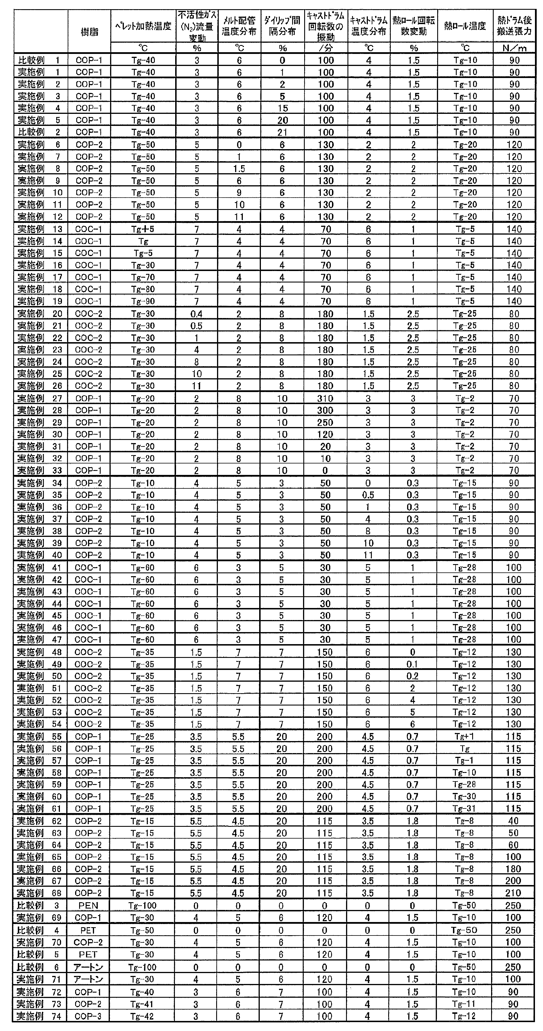

また、実施例13~19では、透明樹脂フィルムの誘電率の変化率を変えている。これは、押出し前のペレット加熱温度を特定の範囲内とすることにより達成されている。実施例13~19では熱寸法変化率が0.01~0.2%の範囲内であるため、剥離率が抑制されているが、実施例14~18では、誘電率の変化率が0.1~10%であるため、剥離率がより効果的に抑制されていることがわかる。
また、実施例27~33では、透明樹脂フィルムのRe、Rthを変えている。これは、キャストドラムの回転数に振動を付与することにより達成されている。実施例27~33では熱寸法変化率が0.01~0.2%の範囲内であるため、剥離率が抑制されているが、実施例28~32では、Re、Rthが1~20nmであるため、剥離率がより効果的に抑制されていることがわかる。
また、実施例41~47では、透明樹脂フィルムの厚みおよび厚みムラを変えている。実施例41~47では熱寸法変化率が0.01~0.2%の範囲内であるため、剥離率が抑制されているが、実施例42~46では、透明樹脂フィルムの厚みおよび厚みムラが所定の範囲内であるため、剥離率がより効果的に抑制されていることがわかる。
また、実施例55~61では、熱ロール温度と、これに伴う厚みムラへの影響を示している。実施例55~61では、熱ロール温度を特定の範囲とすることにより、厚みムラが所望の範囲となっており、剥離率がより抑制されている。
実施例62~68では、熱ロール搬送張力と、これに伴う厚みムラへの影響を示している。実施例62~68では、熱ロール搬送張力を特定の範囲とすることにより、厚みムラが所望の範囲となっており、剥離率がより抑制されている。
実施例69は、比較例3に対し本発明を実施したものである。透明導電層は特許文献1に従い形成した。実施例69では、熱寸法変化率が0.01~0.2%の範囲内であるため、極めて低い剥離率を示している。
また、比較例5は、透明支持体としてPETを使用(Tg=78℃)し、実施例70と同様の製膜方法を実施したものである。実施例70では、剥離率が極めて低いのに対し、比較例5では、剥離率が高くなっている。これは、透明支持体としてPETを使用したことによる性能低下が現れている。すなわち、透明樹脂フィルムの脂環ポリマーの効果が示されている。
なお、比較例6は、特許文献3の実施例2に従い、脂環ポリマー(アートン)上にスパッタ法によりITOを製膜したものである。実施例71は、比較例6と同様にアートンを用いたが、製膜法において本発明を実施した。透明導電層は実施例1と同様にハロゲン化銀と水溶性樹脂からなるものを形成した。これにより、実施例71では、熱寸法変化率が0.01~0.2%の範囲内となり、剥離率が効果的に抑制されていることがわかる。
実施例72および73は透明導電層の効果を比較したものである。実施例72は上記の銀と水溶性樹脂から成る導電層を付与したものであり、実施例73は特許文献1の実施例1に従い銀ナノワイヤーからなるものを使用したものである。また、実施例74は特許文献3の実施例2に従いスパッタ法によりITOを製膜したものである。これらの中では、実施例72が最も剥離率が低いことがわかる。
特開2009-176608の段落[0073]~[0075]の記載に従い、タッチパネルを作成した。熱寸法変化率が0.01~0.2%の範囲内の透明導電性フィルムを用いたタッチパネルは、-20℃~30℃のサイクルサーモ後も良好な動作性能を示すことを確認した。
12 透明樹脂フィルム
14 導電層
20 間欠部
Claims (19)
- 透明樹脂フィルムと、前記透明樹脂フィルムの上に形成された導電層を含む透明導電性フィルムであって、
前記透明樹脂フィルムは、環状オレフィン樹脂を含み、
前記透明導電性フィルムの100℃熱水中60秒の熱寸法変化率が0.01~0.2%であることを特徴とする透明導電性フィルム。 - 前記導電層は、間欠部を有するように形成されることを特徴とする請求項1に記載の透明導電性フィルム。
- 前記導電層が水溶性樹脂と銀を含むことを特徴とする請求項1または2に記載の透明導電性フィルム。
- -20~30℃の誘電率の変化率が0.1~10%であることを特徴とする請求項1~3のいずれか1項に記載の透明導電性フィルム。
- 面内複屈折Reが1~20nmであり、厚み方向複屈折Rthが1~20nmであることを特徴とする請求項1~4のいずれか1項に記載の透明導電性フィルム。
- 100℃熱水中60秒の熱寸法変化率の面内変動が1~10%であることを特徴とする請求項1~5のいずれか1項に記載の透明導電性フィルム。
- -20~30℃の誘電率の変化率の面内変動が1~10%であることを特徴とする請求項1~6のいずれか1項に記載の透明導電性フィルム。
- 面内複屈折Reの面内変動が1~10%であり、厚み方向複屈折Rthの面内変動が1~10%であることを特徴とする請求項1~7のいずれか1項に記載の透明導電性フィルム。
- 前記透明樹脂フィルムの厚みが20~60μmであることを特徴とする請求項1~8のいずれか1項に記載の透明導電性フィルム。
- 環状オレフィン樹脂を含む透明樹脂フィルムを形成する工程と、
前記透明樹脂フィルムの上に導電層を形成する工程とを含み、
前記透明樹脂フィルムを形成する工程は、環状オレフィン樹脂を含む溶融樹脂をシート状にする押出工程を含み、
前記押出工程は、前記シート状の溶融樹脂に厚みムラを付与する工程を含むことを特徴する透明導電性フィルムの製造方法。 - 前記透明樹脂フィルムを形成する工程は、前記押出工程の前に、環状オレフィン樹脂を含む溶融樹脂をダイに送る工程を有し、前記溶融樹脂をダイに送る工程では、溶融樹脂をダイに送るメルト配管に1~10℃の温度分布を付与することを特徴とする請求項10に記載の透明導電性フィルムの製造方法。
- 前記透明樹脂フィルムを形成する工程は、前記押出工程の前に、環状オレフィン樹脂を含む組成物を押出機に投入する工程を含み、前記投入する工程では、前記組成物を(Tg-80)~Tg℃に加熱することを特徴とする請求項10または11に記載の透明導電性フィルムの製造方法。
- 前記投入する工程は、前記押出機に不活性ガスを投入する工程を含み、前記不活性ガスを投入する工程では、前記不活性ガスの供給量に0.5~10%の変動を付与することを特徴とする請求項12に記載の透明導電性フィルムの製造方法。
- 前記押出工程は、溶融樹脂に10~300回/分の振動を与える工程を含むことを特徴とする請求項10~13のいずれか1項に記載の透明導電性フィルムの製造方法。
- 前記押出工程は、溶融樹脂をキャストドラムに押し出す工程を含み、前記キャストドラムには、0.5~10℃の温度分布が付与されることを特徴とする請求項10~14のいずれか1項に記載の透明導電性フィルムの製造方法。
- 前記透明樹脂フィルムを形成する工程は、前記キャストドラムに押し出す工程の後に、シート状の樹脂シートを熱ロールに接触させる工程を含み、前記熱ロールに接触させる工程では、熱ロールの回転数に0.1~5%の変動を与えることを特徴とする請求項15に記載の透明導電性フィルムの製造方法。
- 前記導電層を形成する工程は、ハロゲン化銀乳剤層を形成する工程と、前記ハロゲン化銀乳剤層に露光処理をし、現像処理をする工程を含む請求項10~16のいずれか1項に記載の透明導電性フィルムの製造方法。
- 請求項10~17のいずれか1項に記載の製造方法により製造した透明導電性フィルム。
- 請求項1~9および請求項18のいずれか1項に記載の透明導電性フィルムを用いたタッチパネル。
Priority Applications (4)
| Application Number | Priority Date | Filing Date | Title |
|---|---|---|---|
| CN201480012208.3A CN105027231B (zh) | 2013-03-04 | 2014-03-03 | 透明导电性膜及触控面板 |
| KR1020157022788A KR101741350B1 (ko) | 2013-03-04 | 2014-03-03 | 투명 도전성 필름 및 터치 패널 |
| US14/843,426 US10228782B2 (en) | 2013-03-04 | 2015-09-02 | Transparent conductive film and touch panel |
| US16/250,295 US10684710B2 (en) | 2013-03-04 | 2019-01-17 | Transparent conductive film and touch panel |
Applications Claiming Priority (2)
| Application Number | Priority Date | Filing Date | Title |
|---|---|---|---|
| JP2013041688A JP6207846B2 (ja) | 2013-03-04 | 2013-03-04 | 透明導電性フィルムおよびタッチパネル |
| JP2013-041688 | 2013-03-04 |
Related Child Applications (1)
| Application Number | Title | Priority Date | Filing Date |
|---|---|---|---|
| US14/843,426 Continuation US10228782B2 (en) | 2013-03-04 | 2015-09-02 | Transparent conductive film and touch panel |
Publications (1)
| Publication Number | Publication Date |
|---|---|
| WO2014136701A1 true WO2014136701A1 (ja) | 2014-09-12 |
Family
ID=51491219
Family Applications (1)
| Application Number | Title | Priority Date | Filing Date |
|---|---|---|---|
| PCT/JP2014/055224 Ceased WO2014136701A1 (ja) | 2013-03-04 | 2014-03-03 | 透明導電性フィルムおよびタッチパネル |
Country Status (5)
| Country | Link |
|---|---|
| US (2) | US10228782B2 (ja) |
| JP (1) | JP6207846B2 (ja) |
| KR (1) | KR101741350B1 (ja) |
| CN (1) | CN105027231B (ja) |
| WO (1) | WO2014136701A1 (ja) |
Cited By (2)
| Publication number | Priority date | Publication date | Assignee | Title |
|---|---|---|---|---|
| KR20210132004A (ko) | 2019-02-26 | 2021-11-03 | 니폰 제온 가부시키가이샤 | 적층 필름 |
| US12014011B2 (en) | 2017-12-25 | 2024-06-18 | Dai Nippon Printing Co., Ltd. | Conductive film, sensor, touch panel, image display device, and conductive film with protection film |
Families Citing this family (14)
| Publication number | Priority date | Publication date | Assignee | Title |
|---|---|---|---|---|
| WO2013129611A1 (ja) * | 2012-02-29 | 2013-09-06 | 昭和電工株式会社 | エレクトロルミネッセント素子の製造方法 |
| JP6207846B2 (ja) * | 2013-03-04 | 2017-10-04 | 富士フイルム株式会社 | 透明導電性フィルムおよびタッチパネル |
| JP6196180B2 (ja) * | 2014-03-26 | 2017-09-13 | 日東電工株式会社 | 透光性導電フィルム |
| JP6285904B2 (ja) * | 2015-03-30 | 2018-02-28 | 富士フイルム株式会社 | 導電シートの製造方法、および、タッチパネル |
| JP2017200739A (ja) * | 2016-05-06 | 2017-11-09 | ホシデン株式会社 | 樹脂積層体及びこれを備えたタッチ入力装置 |
| KR102412042B1 (ko) | 2016-06-29 | 2022-06-21 | 니폰 제온 가부시키가이샤 | 도전성 필름 |
| CN109414919A (zh) | 2016-07-20 | 2019-03-01 | 日本瑞翁株式会社 | 导电性膜及其制造方法 |
| US11305478B2 (en) | 2016-11-08 | 2022-04-19 | Altec Industries, Inc. | Door assembly for use on a utility truck |
| CN110431520B (zh) * | 2017-03-24 | 2023-05-26 | 大日本印刷株式会社 | 导电性膜、触控面板和图像显示装置 |
| EP3667466B1 (en) * | 2017-08-07 | 2022-09-07 | Alps Alpine Co., Ltd. | Input device and manufacturing method for input device in which plastic cover and film sensor are stacked |
| WO2019130842A1 (ja) * | 2017-12-28 | 2019-07-04 | 日東電工株式会社 | 光透過性導電フィルム、その製造方法、調光フィルム、および、調光部材 |
| CN110162199A (zh) * | 2018-02-13 | 2019-08-23 | 宸美(厦门)光电有限公司 | 触控面板及其制作方法 |
| TWI716098B (zh) * | 2019-05-21 | 2021-01-11 | 仁寶電腦工業股份有限公司 | 切換觸控板操作模式的方法 |
| KR102461794B1 (ko) * | 2020-08-13 | 2022-11-02 | 한국과학기술연구원 | 은 나노와이어 메쉬 전극 및 이의 제조방법 |
Citations (4)
| Publication number | Priority date | Publication date | Assignee | Title |
|---|---|---|---|---|
| JP2008230098A (ja) * | 2007-03-22 | 2008-10-02 | Mitsubishi Plastics Ind Ltd | ガスバリア積層フィルムとその製造方法。 |
| JP2010089458A (ja) * | 2008-10-10 | 2010-04-22 | Jsr Corp | 積層フィルム、無機蒸着層を有する積層フィルムおよびその製造方法 |
| WO2011108494A1 (ja) * | 2010-03-01 | 2011-09-09 | Jsr株式会社 | 導電性積層フィルムおよびそれを用いたタッチパネル |
| JP2012064546A (ja) * | 2010-09-17 | 2012-03-29 | Toppan Printing Co Ltd | 透明導電性積層体及びその製造方法 |
Family Cites Families (155)
| Publication number | Priority date | Publication date | Assignee | Title |
|---|---|---|---|---|
| JPH02141278A (ja) | 1988-11-22 | 1990-05-30 | Oji Paper Co Ltd | 感熱記録材料 |
| JP3164908B2 (ja) * | 1992-09-08 | 2001-05-14 | 帝人株式会社 | 押出し成形用ダイ |
| JP3377833B2 (ja) | 1993-08-06 | 2003-02-17 | 三井化学株式会社 | 環状オレフィン系樹脂からなる成形体およびその製造方法 |
| JP3723616B2 (ja) | 1995-12-22 | 2005-12-07 | 三井化学株式会社 | 環状オレフィン系樹脂組成物およびその用途 |
| JP3683631B2 (ja) | 1995-12-22 | 2005-08-17 | 三井化学株式会社 | 環状オレフィン系樹脂組成物およびその用途 |
| JP2002113758A (ja) | 2000-10-12 | 2002-04-16 | Toray Ind Inc | 脂環式ポリオレフィン樹脂フィルムの製造方法、脂環式ポリオレフィン樹脂フィルム、液晶表示素子基板用脂環式ポリオレフィン樹脂フィルム、及び液晶表示素子基板 |
| JP4729802B2 (ja) | 2001-03-23 | 2011-07-20 | Jsr株式会社 | 熱可塑性樹脂組成物およびその用途 |
| JP3819777B2 (ja) | 2002-01-09 | 2006-09-13 | 日東電工株式会社 | 表示装置用電磁波シールドフィルタ、プラズマディスプレイパネル用フィルタおよぴプラズマディスプレイパネル表示装置 |
| JP2003266520A (ja) | 2002-03-15 | 2003-09-24 | Nippon Zeon Co Ltd | 熱可塑性樹脂フィルムの製造方法 |
| EP1496376B1 (en) | 2002-03-25 | 2011-06-15 | Zeon Corporation | Optical film and process for producing the same |
| JP4623257B2 (ja) | 2002-03-25 | 2011-02-02 | 日本ゼオン株式会社 | 光学用フィルムおよびその製造方法 |
| JP2004085655A (ja) | 2002-08-23 | 2004-03-18 | Asahi Kasei Aimii Kk | 耐汚染性の含水ソフトコンタクトレンズ |
| JP4084645B2 (ja) | 2002-12-03 | 2008-04-30 | 富士フイルム株式会社 | 熱現像感光材料 |
| US20060014113A1 (en) | 2004-07-16 | 2006-01-19 | Fuji Photo Film Co., Ltd. | Photothermographic material |
| US7381520B2 (en) | 2002-12-03 | 2008-06-03 | Fujifilm Corporation | Photothermographic material |
| JP4641719B2 (ja) | 2002-12-27 | 2011-03-02 | 富士フイルム株式会社 | 透光性電磁波シールド膜の製造方法及び透光性電磁波シールド膜 |
| JP4807934B2 (ja) | 2002-12-27 | 2011-11-02 | 富士フイルム株式会社 | 透光性電磁波シールド膜およびその製造方法 |
| EP2101556B1 (en) | 2002-12-27 | 2013-02-13 | FUJIFILM Corporation | Light transmitting electromagnetic wave shielding film and plasma display panel using the shielding film |
| JP2004244080A (ja) | 2003-02-17 | 2004-09-02 | Maruha Corp | 冷凍ころも付きえび用収納トレー |
| JP4322549B2 (ja) | 2003-05-12 | 2009-09-02 | 富士フイルム株式会社 | 熱現像感光材料 |
| JP2005010752A (ja) | 2003-05-22 | 2005-01-13 | Fuji Photo Film Co Ltd | 熱現像感光材料及び画像形成方法 |
| US7144688B2 (en) | 2003-05-22 | 2006-12-05 | Fuji Photo Film Co., Ltd. | Photothermographic material and image forming method |
| JP4337454B2 (ja) | 2003-07-24 | 2009-09-30 | 日本ゼオン株式会社 | 光学補償フィルム、光学補償フィルムの製造方法、光学積層体及び液晶表示装置 |
| JP4492116B2 (ja) | 2003-12-10 | 2010-06-30 | 日本ゼオン株式会社 | 光学用フィルムの製造方法 |
| JP2005302508A (ja) | 2004-04-12 | 2005-10-27 | Fuji Photo Film Co Ltd | 透明導電性シートおよびそれを用いたエレクトロルミネッセンス素子 |
| US20060008745A1 (en) | 2004-06-23 | 2006-01-12 | Fuji Photo Film Co., Ltd. | Translucent electromagnetic shield film, producing method therefor and emulsifier |
| JP2006010795A (ja) | 2004-06-23 | 2006-01-12 | Fuji Photo Film Co Ltd | 感光性ハロゲン化銀乳剤、これを用いた導電性銀薄膜、導電性銀材料 |
| CN101002519B (zh) | 2004-06-23 | 2012-02-22 | 富士胶片株式会社 | 透光性电磁波屏蔽膜及其制造方法 |
| JP2006012935A (ja) | 2004-06-23 | 2006-01-12 | Fuji Photo Film Co Ltd | 透光性電磁波シールド膜の製造方法および透光性電磁波シールド膜 |
| JP2006153983A (ja) | 2004-11-25 | 2006-06-15 | Sekisui Chem Co Ltd | 光学フィルムの製造方法及び光学フィルム |
| US20080177002A1 (en) * | 2005-01-05 | 2008-07-24 | Jsr Corporation | Thermoplastic Resin Composition, Optical Film, And Process For Producing Film |
| JP2006228469A (ja) | 2005-02-15 | 2006-08-31 | Fuji Photo Film Co Ltd | 導電性膜形成用感光材料、導電性膜、透光性電磁波シールド膜、及びそれらの製造方法 |
| JP2006228478A (ja) | 2005-02-15 | 2006-08-31 | Fuji Photo Film Co Ltd | 電性膜及びその製造方法、並びに導電性膜を用いた光学フィルター |
| JP2006228836A (ja) | 2005-02-15 | 2006-08-31 | Fuji Photo Film Co Ltd | 透光性導電性膜及びその製造方法並びに透光性導電性膜を用いた光学フィルター |
| JP2006228473A (ja) | 2005-02-15 | 2006-08-31 | Fuji Photo Film Co Ltd | 透光性導電性膜及びその製造方法並びに透光性導電性膜の製造に用いられる現像液 |
| TWI403761B (zh) | 2005-02-15 | 2013-08-01 | Fujifilm Corp | 透光性導電性膜之製法 |
| JP2006255892A (ja) | 2005-02-21 | 2006-09-28 | Jsr Corp | フィルム加工方法 |
| JP4591114B2 (ja) * | 2005-02-25 | 2010-12-01 | 日本ゼオン株式会社 | 多層押出成形装置、多層フィルムの製造方法及び多層延伸フィルムの製造方法 |
| US20090078459A1 (en) | 2005-03-15 | 2009-03-26 | Fujifilm Corporation | Light-transmitting conductive film and process for producing light-transmitting conductive film |
| US8253035B2 (en) | 2005-03-15 | 2012-08-28 | Fujifilm Corporation | Plating processing method, light transmitting conductive film and electromagnetic wave shielding film |
| TWI406084B (zh) | 2005-03-15 | 2013-08-21 | Fujifilm Corp | 鍍敷處理方法 |
| WO2006098335A1 (ja) | 2005-03-15 | 2006-09-21 | Fujifilm Corporation | 積層材料、透光性電磁波シールド膜および光学フィルター |
| KR20070110875A (ko) | 2005-03-15 | 2007-11-20 | 후지필름 가부시키가이샤 | 광투과성 전자파 차폐 필름, 광학 필터 및 플라즈마텔레비전 |
| JP4500715B2 (ja) | 2005-03-16 | 2010-07-14 | 富士フイルム株式会社 | 透光性導電性膜の製造方法、透光性導電性膜、透光性電磁波シールド膜および光学フィルター |
| JP2006269795A (ja) | 2005-03-24 | 2006-10-05 | Fuji Photo Film Co Ltd | 透光性導電性膜形成用現像液並びに透光性導電性膜、透光性電磁波シールド膜及びそれらの製造方法 |
| JP2006324203A (ja) | 2005-05-20 | 2006-11-30 | Fujifilm Holdings Corp | 透光性導電性膜及びその製造方法並びに透光性電磁波シールド膜、光学フィルター及びプラズマディスプレーパネル |
| JP2006352073A (ja) | 2005-05-20 | 2006-12-28 | Fujifilm Holdings Corp | 導電性パターン材料、透光性導電性膜、透光性電磁波シールド膜、光学フィルター、透明導電性シート、エレクトロルミネッセンス素子、及び平面光源システム |
| JP2006332459A (ja) | 2005-05-27 | 2006-12-07 | Fujifilm Holdings Corp | 導電性金属膜形成用感光材料、導電性金属膜の製造方法、導電性金属膜、及びプラズマディスプレイパネル用透光性電磁波シールド膜 |
| WO2006129869A1 (en) | 2005-05-31 | 2006-12-07 | Fujifilm Corporation | Film for display panel, optical filter, manufacturing method thereof and plasma display panel |
| JP2007013130A (ja) | 2005-05-31 | 2007-01-18 | Fujifilm Holdings Corp | ディスプレーパネル用フィルム、光学フィルター、それらの製造方法及びプラズマディスプレーパネル |
| JP2006336090A (ja) | 2005-06-03 | 2006-12-14 | Fujifilm Holdings Corp | 導電性膜形成用めっき液、導電性膜及びその製造方法並びに透光性電磁波シールド膜及びプラズマディスプレーパネル |
| KR20080011644A (ko) | 2005-06-03 | 2008-02-05 | 후지필름 가부시키가이샤 | 도금 처리 방법, 도전성 필름 및 투광성 전자기파 차폐필름 |
| JP2007009326A (ja) | 2005-06-03 | 2007-01-18 | Fujifilm Corp | めっき処理方法、導電性膜、及び透光性電磁波シールド膜 |
| JP4719512B2 (ja) | 2005-06-06 | 2011-07-06 | 富士フイルム株式会社 | めっき処理方法、透光性導電性膜、及び透光性電磁波シールド膜 |
| JP2006348351A (ja) | 2005-06-16 | 2006-12-28 | Fujifilm Holdings Corp | めっき被膜付きフィルムの製造装置及び方法 |
| JP2007002027A (ja) | 2005-06-21 | 2007-01-11 | Fujifilm Holdings Corp | 飽和ノルボルネン樹脂フィルムおよびその製造方法、偏光板、光学補償フィルム、反射防止フィルム並びに液晶表示装置 |
| JPWO2007001008A1 (ja) | 2005-06-27 | 2009-07-16 | 富士フイルム株式会社 | プリント基板の製造方法及びプリント基板 |
| JP4224479B2 (ja) | 2005-09-07 | 2009-02-12 | 富士フイルム株式会社 | パターン露光方法及び装置 |
| US8383330B2 (en) | 2005-09-07 | 2013-02-26 | Fujifilm Corporation | Pattern exposure method and pattern exposure apparatus |
| JP4861778B2 (ja) | 2005-09-08 | 2012-01-25 | 富士フイルム株式会社 | パターン露光方法及び装置 |
| US20070076155A1 (en) | 2005-09-09 | 2007-04-05 | Fuji Photo Film Co., Ltd. | Optical film, optical compensation film, polarizing plate and liquid crystal display |
| US20090246486A1 (en) | 2005-09-22 | 2009-10-01 | Fujifilm Corporation | Light-transmittable electromagnetic wave shielding film, process for producing light-transmittable electromagnetic wave shielding film, film for display panel, optical filter for display panel and plasma display panel |
| JP2007088219A (ja) | 2005-09-22 | 2007-04-05 | Fujifilm Corp | 透光性電磁波シールド膜、ディスプレイパネル用フィルム、ディスプレイパネル用光学フィルター及びプラズマディスプレイパネル |
| JP4951299B2 (ja) | 2005-09-22 | 2012-06-13 | 富士フイルム株式会社 | 透光性電磁波シールド膜とその製造方法、ディスプレイパネル用フィルム、ディスプレイパネル用光学フィルター、プラズマディスプレイパネル |
| US7749686B2 (en) | 2005-09-30 | 2010-07-06 | Fujifilm Corporation | Method for producing conductive film and light-sensitive material for conductive film production |
| JP2007131704A (ja) * | 2005-11-09 | 2007-05-31 | Fujifilm Corp | 環状オレフィン系重合体、およびそれを用いた光学材料、偏光板および液晶表示装置 |
| JP2007134439A (ja) | 2005-11-09 | 2007-05-31 | Fujifilm Corp | ロール状光学フィルターおよびその製造方法 |
| JP2007149760A (ja) | 2005-11-24 | 2007-06-14 | Fujifilm Corp | ロール状光学フィルムおよびその製造方法 |
| JP4855070B2 (ja) | 2005-12-28 | 2012-01-18 | 富士フイルム株式会社 | 金属微粒子分散物及び赤外線遮蔽フィルター |
| JP2007200922A (ja) | 2006-01-23 | 2007-08-09 | Fujifilm Corp | プラズマディスプレイの光学フィルター用透光性電磁波シールド膜および光学フィルター |
| JP4832322B2 (ja) | 2006-01-27 | 2011-12-07 | 富士フイルム株式会社 | 導電性金属膜、透光性電磁波シールドフィルム、光学フィルターおよびプラズマディスプレイパネル、及び導電性金属膜の製造方法 |
| JP2007201378A (ja) | 2006-01-30 | 2007-08-09 | Fujifilm Corp | 透光性電磁波シールド膜、光学フィルター、およびプラズマディスプレイパネル |
| JP4961220B2 (ja) | 2006-01-31 | 2012-06-27 | 富士フイルム株式会社 | 導電性膜の製造方法、並びに、透光性電磁波シールド膜、光学フィルターおよびプラズマディスプレイパネル |
| JP2007207883A (ja) | 2006-01-31 | 2007-08-16 | Fujifilm Corp | 透光性電磁波シールド膜、光学フィルター、およびプラズマディスプレイパネル |
| JP2007207987A (ja) | 2006-02-01 | 2007-08-16 | Fujifilm Corp | 透光性電磁波シールド膜、光学フィルター、およびプラズマディスプレイパネル |
| JP2007208133A (ja) | 2006-02-03 | 2007-08-16 | Fujifilm Corp | 透光性電磁波シールドフィルム、透光性電磁波シールド性積層体、光学フィルター、およびプラズマディスプレイパネル |
| CN101454384A (zh) * | 2006-03-23 | 2009-06-10 | 日本瑞翁株式会社 | 降冰片烯化合物加聚物膜、其制备方法以及该加聚物膜的用途 |
| TW200738765A (en) | 2006-03-23 | 2007-10-16 | Zeon Corp | Norbornene compound addition polymer film, process for production thereof, and use thereof |
| JP4841996B2 (ja) | 2006-03-31 | 2011-12-21 | 富士フイルム株式会社 | 洗浄装置、めっき被膜付きフィルムの製造装置、洗浄方法及びめっき被膜付きフィルムの製造方法 |
| JP4786393B2 (ja) | 2006-03-31 | 2011-10-05 | 富士フイルム株式会社 | 洗浄装置及びめっき被膜付きフィルムの製造装置 |
| JP2007310091A (ja) | 2006-05-17 | 2007-11-29 | Fujifilm Corp | プラズマディスプレイパネル |
| JP2007334325A (ja) | 2006-05-18 | 2007-12-27 | Fujifilm Corp | 近赤外線吸収フィルター及びその製造方法 |
| JP2007335729A (ja) | 2006-06-16 | 2007-12-27 | Fujifilm Corp | 導電性金属膜および透光性電磁波シールド膜 |
| JP5096771B2 (ja) | 2007-03-23 | 2012-12-12 | 三菱製紙株式会社 | 導電性発現方法 |
| DE112007001519B4 (de) | 2006-06-22 | 2022-03-10 | Mitsubishi Paper Mills Limited | Verfahren zum Herstellen eines leitfähigen Materials |
| JP4884948B2 (ja) | 2006-12-12 | 2012-02-29 | 藤森工業株式会社 | 電磁波シールド材ロール体及びその製造方法、ディスプレイ用電磁波シールドフィルム |
| JP4846558B2 (ja) | 2006-12-22 | 2011-12-28 | 藤森工業株式会社 | 周波数選択透過型の電磁波シールド材およびその製造方法 |
| JP5058583B2 (ja) | 2006-12-22 | 2012-10-24 | 藤森工業株式会社 | 周波数選択遮蔽型の電磁波シールド材およびその製造方法 |
| JP5144074B2 (ja) | 2007-01-05 | 2013-02-13 | 三菱製紙株式会社 | 導電性基材の作製方法 |
| JP2008198388A (ja) | 2007-02-08 | 2008-08-28 | Mitsubishi Paper Mills Ltd | 導電性材料前駆体の製造方法 |
| JP4909123B2 (ja) | 2007-03-01 | 2012-04-04 | 三菱製紙株式会社 | 導電性材料前駆体 |
| JP5144092B2 (ja) | 2007-03-06 | 2013-02-13 | 三菱製紙株式会社 | 導電性材料の製造方法 |
| JP2008218784A (ja) | 2007-03-06 | 2008-09-18 | Konica Minolta Holdings Inc | 電磁波遮蔽材料用感光材料及び電磁波遮蔽材料の製造方法 |
| JP4616852B2 (ja) | 2007-03-12 | 2011-01-19 | 三菱製紙株式会社 | ハロゲン化銀感光材料 |
| JP2008227350A (ja) | 2007-03-15 | 2008-09-25 | Konica Minolta Holdings Inc | 電磁波遮蔽フィルムの製造方法及び電磁波遮蔽フィルム |
| JP2008227351A (ja) | 2007-03-15 | 2008-09-25 | Konica Minolta Holdings Inc | 電磁波遮蔽材料、該電磁波遮蔽材料を用いたパネル材料の製造方法 |
| JP4866277B2 (ja) | 2007-03-19 | 2012-02-01 | 三菱製紙株式会社 | 導電性材料前駆体 |
| JP2008244067A (ja) | 2007-03-27 | 2008-10-09 | Konica Minolta Holdings Inc | 透明導電膜形成用感光材料、透明導電膜及びその製造方法、電磁波遮蔽材料 |
| JP2008241987A (ja) | 2007-03-27 | 2008-10-09 | Mitsubishi Paper Mills Ltd | 連続露光装置 |
| JP2008251275A (ja) | 2007-03-29 | 2008-10-16 | Mitsubishi Paper Mills Ltd | 導電性材料の処理方法及び処理装置 |
| JP4890318B2 (ja) | 2007-03-29 | 2012-03-07 | 三菱製紙株式会社 | 導電性材料前駆体 |
| JP5079369B2 (ja) | 2007-03-30 | 2012-11-21 | 藤森工業株式会社 | 周波数選択遮蔽型の電磁波シールド積層体 |
| JP4887198B2 (ja) | 2007-03-30 | 2012-02-29 | 富士フイルム株式会社 | ハロゲン化銀写真感光材料、及び画像形成方法 |
| JP2008267814A (ja) | 2007-04-16 | 2008-11-06 | Konica Minolta Holdings Inc | 透光性導電性薄膜、その検査方法及び検査装置 |
| JP2008270405A (ja) | 2007-04-18 | 2008-11-06 | Konica Minolta Holdings Inc | 透明電磁波遮断フィルム、その製造方法、及びそれ用いたプラズマディスプレイパネル |
| JP5230221B2 (ja) | 2007-04-20 | 2013-07-10 | 富士フイルム株式会社 | 熱可塑性フィルムおよびその製造方法 |
| JP4964805B2 (ja) * | 2007-04-20 | 2012-07-04 | 富士フイルム株式会社 | 熱可塑性フイルム及びその製造方法、熱処理方法、並びに、偏光板、液晶表示板用光学補償フイルム、反射防止フイルム及び液晶表示装置 |
| JP2008277428A (ja) | 2007-04-26 | 2008-11-13 | Fujimori Kogyo Co Ltd | 電磁波シールド材及びディスプレイパネル |
| JP5483804B2 (ja) | 2007-04-27 | 2014-05-07 | 富士フイルム株式会社 | シクロオレフィン樹脂フィルム、およびこれらを用いた偏光板、光学補償フィルム、反射防止フィルム、液晶表示装置、ならびに、シクロオレフィン樹脂フィルムの製造方法 |
| JP2008273057A (ja) | 2007-04-27 | 2008-11-13 | Fujifilm Corp | シクロオレフィン樹脂フィルム、およびこれらを用いた偏光板、光学補償フィルム、反射防止フィルム、液晶表示装置 |
| JP2008277676A (ja) | 2007-05-07 | 2008-11-13 | Konica Minolta Holdings Inc | 透明電磁波遮断フィルムその製造方法及びプラズマディスプレイパネル |
| JP4957364B2 (ja) | 2007-05-07 | 2012-06-20 | コニカミノルタホールディングス株式会社 | 透光性導電パターン材料、電磁波遮蔽フィルター及び周波数選択性電磁波遮蔽フィルム |
| JP2008282840A (ja) | 2007-05-08 | 2008-11-20 | Konica Minolta Holdings Inc | 透光性導電性薄膜の製造方法及び製造装置、それにより得られる透光性導電性薄膜 |
| JP2008283029A (ja) | 2007-05-11 | 2008-11-20 | Konica Minolta Holdings Inc | 電磁波遮蔽フィルムの製造方法及び電磁波遮蔽フィルム |
| JP2008288305A (ja) | 2007-05-16 | 2008-11-27 | Konica Minolta Holdings Inc | 電磁波シールドフィルム及びその製造方法 |
| JP4957376B2 (ja) | 2007-05-18 | 2012-06-20 | コニカミノルタホールディングス株式会社 | 透明性導電膜形成用感光材料、それを用いた透明性導電膜、その製造方法及び電磁波遮蔽材料 |
| JP2008300721A (ja) | 2007-06-01 | 2008-12-11 | Konica Minolta Holdings Inc | ディスプレイ用電磁波シールド材ロール体 |
| JP2008300720A (ja) | 2007-06-01 | 2008-12-11 | Konica Minolta Holdings Inc | 透光性導電性フィルム及び電磁波遮蔽フィルター |
| JP2008307831A (ja) * | 2007-06-15 | 2008-12-25 | Fujifilm Corp | 環状ポリオレフィン系樹脂フィルム及びその製造方法 |
| JP2009004213A (ja) | 2007-06-21 | 2009-01-08 | Konica Minolta Holdings Inc | 光透過性導電膜の製造方法、光透過性導電膜及び光透過性電磁波シールド膜 |
| JP2009010001A (ja) | 2007-06-26 | 2009-01-15 | Konica Minolta Holdings Inc | 電磁波遮蔽フィルムの製造方法及び電磁波遮蔽フィルム |
| JP2009016526A (ja) | 2007-07-04 | 2009-01-22 | Konica Minolta Holdings Inc | 透明電磁波遮蔽フィルム及びその作製方法 |
| JP2009021334A (ja) | 2007-07-11 | 2009-01-29 | Konica Minolta Holdings Inc | 透明電磁波遮蔽フィルム及びその作製方法 |
| JP2009021153A (ja) | 2007-07-13 | 2009-01-29 | Mitsubishi Paper Mills Ltd | 導電性発現方法および導電性部材 |
| JP2009026933A (ja) | 2007-07-19 | 2009-02-05 | Konica Minolta Holdings Inc | 電磁波遮蔽フィルムの製造方法及び電磁波遮蔽フィルム |
| JP2009083322A (ja) | 2007-09-28 | 2009-04-23 | Fujifilm Corp | 環状オレフィン系樹脂フィルム及びその製造方法 |
| JP2009090541A (ja) | 2007-10-09 | 2009-04-30 | Toray Ind Inc | 熱可塑性樹脂フィルムの製造方法 |
| JP5173476B2 (ja) | 2007-12-05 | 2013-04-03 | 富士フイルム株式会社 | 熱可塑性樹脂フィルムの製造装置 |
| JP5376808B2 (ja) | 2008-01-25 | 2013-12-25 | Dic株式会社 | 透明導電性フィルムの製造方法、透明導電性フィルム及びタッチパネル |
| JP2009203249A (ja) * | 2008-02-26 | 2009-09-10 | Nippon Zeon Co Ltd | 環状オレフィン重合体フィルム及びその作成方法 |
| JP2009277466A (ja) | 2008-05-14 | 2009-11-26 | Konica Minolta Holdings Inc | 透明導電性フィルム及びその製造方法 |
| JP5408923B2 (ja) * | 2008-08-04 | 2014-02-05 | 富士フイルム株式会社 | 熱可塑性フィルムの製造方法 |
| JP5193077B2 (ja) | 2009-01-19 | 2013-05-08 | 株式会社アルバック | 表面修飾基板の解析方法、解析用基板及び表面修飾基板の製造方法、並びに表面修飾基板 |
| JP5400420B2 (ja) | 2009-02-23 | 2014-01-29 | 三菱製紙株式会社 | 透明導電性材料 |
| US8314986B2 (en) * | 2009-03-25 | 2012-11-20 | Fujifilm Corporation | Transparent electromagnetic wave-shielding filter and method of producing thereof, and conductive film |
| CN102438822B (zh) | 2009-03-31 | 2015-11-25 | 帝人株式会社 | 透明导电性层叠体和透明触摸面板 |
| WO2010140269A1 (ja) | 2009-06-03 | 2010-12-09 | 東洋紡績株式会社 | 透明導電性積層フィルム |
| JP2011021057A (ja) | 2009-07-13 | 2011-02-03 | Teijin Techno Products Ltd | 耐熱性樹脂成型体 |
| JP2011034806A (ja) | 2009-07-31 | 2011-02-17 | Nissha Printing Co Ltd | 貼合わせ適性に優れた透明導電性フィルム及びこれを用いたタッチパネル |
| JP2011043628A (ja) | 2009-08-20 | 2011-03-03 | Gunze Ltd | 位相差フィルム、タッチパネル用透明導電性積層体の製造方法およびタッチパネル |
| JP2012014669A (ja) | 2009-11-20 | 2012-01-19 | Fujifilm Corp | 導電シート、導電シートの使用方法及び静電容量方式タッチパネル |
| JP4820451B2 (ja) | 2009-11-20 | 2011-11-24 | 富士フイルム株式会社 | 導電シート、導電シートの使用方法及びタッチパネル |
| JP4780254B2 (ja) | 2009-12-10 | 2011-09-28 | 凸版印刷株式会社 | 導電性基板およびその製造方法ならびにタッチパネル |
| JP5375692B2 (ja) | 2010-03-17 | 2013-12-25 | 大日本印刷株式会社 | タッチパネルセンサの製造方法 |
| JP2011210579A (ja) * | 2010-03-30 | 2011-10-20 | Mitsubishi Paper Mills Ltd | 透明導電性フィルム |
| JP2010256908A (ja) | 2010-05-07 | 2010-11-11 | Fujifilm Corp | 映画用ハロゲン化銀写真感光材料 |
| JP2012004042A (ja) | 2010-06-18 | 2012-01-05 | Fujifilm Corp | 透明導電性フイルム及び透明導電性フイルムの製造方法 |
| JP5709311B2 (ja) * | 2010-06-25 | 2015-04-30 | グンゼ株式会社 | 透明面状体及び透明タッチパネル |
| JP2012080091A (ja) * | 2010-09-07 | 2012-04-19 | Fujifilm Corp | 透明導電フィルム、その製造方法、それを用いた有機薄膜太陽電池 |
| JP2012066481A (ja) | 2010-09-24 | 2012-04-05 | Nippon Zeon Co Ltd | ハードコート層を有する積層フィルム、およびタッチパネル用積層フィルム |
| JP2012151095A (ja) | 2010-12-27 | 2012-08-09 | Dic Corp | 透明導電性フィルム、静電容量式タッチパネルの透明電極及びタッチパネル |
| JP2012216550A (ja) | 2011-03-31 | 2012-11-08 | Mitsubishi Materials Corp | 透明導電膜形成用分散液、透明導電膜、および透明導電膜の製造方法 |
| KR20140003476A (ko) | 2011-04-13 | 2014-01-09 | 닛폰고세이가가쿠고교 가부시키가이샤 | 수지 성형체, 및 이를 이용하여 이루어진 적층체 |
| JP5473990B2 (ja) | 2011-06-17 | 2014-04-16 | 日東電工株式会社 | 導電性積層体、パターン配線付き透明導電性積層体、および光学デバイス。 |
| JP6207846B2 (ja) * | 2013-03-04 | 2017-10-04 | 富士フイルム株式会社 | 透明導電性フィルムおよびタッチパネル |
-
2013
- 2013-03-04 JP JP2013041688A patent/JP6207846B2/ja active Active
-
2014
- 2014-03-03 CN CN201480012208.3A patent/CN105027231B/zh active Active
- 2014-03-03 KR KR1020157022788A patent/KR101741350B1/ko active Active
- 2014-03-03 WO PCT/JP2014/055224 patent/WO2014136701A1/ja not_active Ceased
-
2015
- 2015-09-02 US US14/843,426 patent/US10228782B2/en active Active
-
2019
- 2019-01-17 US US16/250,295 patent/US10684710B2/en active Active
Patent Citations (4)
| Publication number | Priority date | Publication date | Assignee | Title |
|---|---|---|---|---|
| JP2008230098A (ja) * | 2007-03-22 | 2008-10-02 | Mitsubishi Plastics Ind Ltd | ガスバリア積層フィルムとその製造方法。 |
| JP2010089458A (ja) * | 2008-10-10 | 2010-04-22 | Jsr Corp | 積層フィルム、無機蒸着層を有する積層フィルムおよびその製造方法 |
| WO2011108494A1 (ja) * | 2010-03-01 | 2011-09-09 | Jsr株式会社 | 導電性積層フィルムおよびそれを用いたタッチパネル |
| JP2012064546A (ja) * | 2010-09-17 | 2012-03-29 | Toppan Printing Co Ltd | 透明導電性積層体及びその製造方法 |
Cited By (2)
| Publication number | Priority date | Publication date | Assignee | Title |
|---|---|---|---|---|
| US12014011B2 (en) | 2017-12-25 | 2024-06-18 | Dai Nippon Printing Co., Ltd. | Conductive film, sensor, touch panel, image display device, and conductive film with protection film |
| KR20210132004A (ko) | 2019-02-26 | 2021-11-03 | 니폰 제온 가부시키가이샤 | 적층 필름 |
Also Published As
| Publication number | Publication date |
|---|---|
| KR20150108917A (ko) | 2015-09-30 |
| US20150378461A1 (en) | 2015-12-31 |
| US20190155413A1 (en) | 2019-05-23 |
| CN105027231A (zh) | 2015-11-04 |
| CN105027231B (zh) | 2017-05-17 |
| JP6207846B2 (ja) | 2017-10-04 |
| US10684710B2 (en) | 2020-06-16 |
| JP2014168886A (ja) | 2014-09-18 |
| US10228782B2 (en) | 2019-03-12 |
| KR101741350B1 (ko) | 2017-05-29 |
Similar Documents
| Publication | Publication Date | Title |
|---|---|---|
| JP6207846B2 (ja) | 透明導電性フィルムおよびタッチパネル | |
| JP6483811B2 (ja) | 透明基材フィルム積層体、タッチパネル用センサーフィルム、タッチパネル、画像表示装置および画像表示装置の視認性改善方法 | |
| US9485856B2 (en) | Transparent electrode sheet, method for manufacturing transparent electrode sheet, and capacitive touch panel using such transparent electrode sheet | |
| JP2012004042A (ja) | 透明導電性フイルム及び透明導電性フイルムの製造方法 | |
| US10664118B2 (en) | Conductive film and touch panel | |
| WO2015115534A1 (ja) | 透明フィルム及びその製造方法、透明導電フィルム、タッチパネル、反射防止フィルム、偏光板および表示装置 | |
| WO2009125855A1 (ja) | 発熱体 | |
| JP6275961B2 (ja) | 光学フィルム及び表示装置 | |
| WO2014185253A1 (ja) | 環状オレフィン共重合体フィルム及びその応用 | |
| JP5337342B2 (ja) | 透光性電磁波シールドフィルム | |
| JP2010250132A (ja) | エレクトロクロミック装置 | |
| JP2015114612A (ja) | 偏光板 | |
| JP2014224170A (ja) | 環状オレフィン共重合体及び環状オレフィン共重合体フィルム | |
| CN114003148A (zh) | 用于金属网格触摸传感器的保护膜 | |
| JP5663381B2 (ja) | 透明導電シート、透明導電シートを用いた静電容量方式のタッチパネル | |
| WO2014204683A1 (en) | Method for improving patterned silver conductivity | |
| JP6113683B2 (ja) | 透明フィルム及びその製造方法、積層フィルム、透明導電フィルム、ハードコートフィルム、タッチパネル、偏光板ならびに表示装置 | |
| WO2019035317A1 (ja) | 導電性フィルム、タッチパネル、及び、導電性フィルムの製造方法 | |
| CN105934714B (zh) | 卤化银导电元件前体和设备 | |
| TW201626407A (zh) | 提供具有導電金屬連接件之導電物件 | |
| US12379815B1 (en) | Touch sensor, touch panel, and image display device | |
| JP6235993B2 (ja) | フィルム材料および導電材料の製造方法 | |
| JP6053184B2 (ja) | タッチパネル | |
| JP2009059998A (ja) | 透光性導電膜、その製造方法及びその透光性導電膜を用いた透光性電磁波遮蔽フィルター | |
| JP2013131480A (ja) | 導電フィルム及びその製造方法 |
Legal Events
| Date | Code | Title | Description |
|---|---|---|---|
| WWE | Wipo information: entry into national phase |
Ref document number: 201480012208.3 Country of ref document: CN |
|
| 121 | Ep: the epo has been informed by wipo that ep was designated in this application |
Ref document number: 14760639 Country of ref document: EP Kind code of ref document: A1 |
|
| ENP | Entry into the national phase |
Ref document number: 20157022788 Country of ref document: KR Kind code of ref document: A |
|
| NENP | Non-entry into the national phase |
Ref country code: DE |
|
| 122 | Ep: pct application non-entry in european phase |
Ref document number: 14760639 Country of ref document: EP Kind code of ref document: A1 |